

Jvc RX-F31-S Service Manual
SERVICE MANUAL
HOME CINEMA CONTROL CENTER
MB44920057
RX-F31S
Area suffix
A ------------------------ Australia
US ------------------------ Singapore
UF ------------------------------ China
UJ ---------------------- U.S.Military
Lead free solder used in the board (material : Sn-Ag-Cu, melting point : 219 Centigrade)
TABLE OF CONTENTS
1 PRECAUTION. . . . . . . . . . . . . . . . . . . . . . . . . . . . . . . . . . . . . . . . . . . . . . . . . . . . . . . . . . . . . . . . . . . . . . . . . 1-3
2 SPECIFIC SERVICE INSTRUCTIONS . . . . . . . . . . . . . . . . . . . . . . . . . . . . . . . . . . . . . . . . . . . . . . . . . . . . . . 1-4
3 DISASSEMBLY . . . . . . . . . . . . . . . . . . . . . . . . . . . . . . . . . . . . . . . . . . . . . . . . . . . . . . . . . . . . . . . . . . . . . . . 1-5
4 ADJUSTMENT . . . . . . . . . . . . . . . . . . . . . . . . . . . . . . . . . . . . . . . . . . . . . . . . . . . . . . . . . . . . . . . . . . . . . . . 1-15
5 TROUBLESHOOTING . . . . . . . . . . . . . . . . . . . . . . . . . . . . . . . . . . . . . . . . . . . . . . . . . . . . . . . . . . . . . . . . . 1-15
COPYRIGHT © 2005 Victor Company of Japan, Limited
No.MB449
2005/7

SPECIFICATION
Amplifier Output Power At stereo operation Front channels 100 W*1 per channel, min. RMS, driven into
6
Ω at 1 kHz with no more than 10% total har-
monic distortion.
At surround operation Front channels 100 W*1 per channel, min. RMS, driven into
Center channel 100 W*1, min. RMS, driven into 6
Surround channels 100 W*1 per channel, min. RMS, driven into
Surround back channel 100 W*1, min. RMS, driven into 6
Audio Audio Input Sensitivity
Video Video Input Sensitivity/
FM tuner (IHF) Tuning Range 87.50 MHz to 108.00 MHz
Usable Sensitivity Monaural 12.8 dBf (1.2
50 dB Quieting Sensitivity Monaural 16.0 dBf (1.7
Stereo Separation at OUT(REC) 35 dB at 1 kHz
AM tuner Tuning Range 531 kHz to 1 710 kHz (at 9 kHz intervals)
General Power Requirements AC 110 V/127 V/220 V/230 V - 240 V , adjust-
Power Consumption 120 W (at operation)
Dimensions (W
Mass 6.3 kg
/Impedance
Audio Input
(DIGITAL IN)*2
Audio Output Level DVR, VCR, MONITOR OUT 330 mV
Signal-to-Noise Ratio ('66 IHF/DIN) 80 dB/62 dB
Frequency Response (8
Bass Boost +4 dB ±1 dB at 100 Hz
Equalization
(at DSP operation)
Impedance
Video Output Level/
Impedance
Synchronization Negative
× H × D) 435 mm × 70 mm × 317.2 mm
DVR/DVD (DVD MULTI), VCR, DBS, TV 330 mV/47 k
Coaxial: DIGITAL IN 1(DVR/DVD) 0.5 V(p-p)/75 Ω
Optical: DIGITAL IN 2(DBS), 3(VCR) -21 dBm to -15 dBm (660 nm ±30 nm)
Ω) 20 Hz to 20 kHz (±1 dB)
Center frequency 63 Hz, 250 Hz, 1 kHz, 4 kHz, 16 kHz
Control range ±8 dB
Composite video: DVR/DVD, VCR, DBS 1 V(p-p)/75
S-video: DVR/DVD, VCR, DBS Y (luminance): 1 V(p-p)/75 Ω
Component: DVR/DVD, VCR Y (luminance): 1 V(p-p)/75 Ω
Composite video: DVR, VCR, MONITOR OUT 1 V(p-p)/75 Ω
S-video: DVR, VCR, MONITOR OUT Y (luminance): 1 V(p-p)/75 Ω
Component: MONITOR OUT Y (luminance): 1 V(p-p)/75 Ω
Stereo 37.5 dBf (20.5
6
Ω at 1 kHz with no more than 0.8% total
harmonic distortion.
Ω at 1 kHz,
with no more than 0.8% total harmonic distortion.
6
Ω at 1 kHz with no more than 0.8% total
harmonic distortion.
Ω at 1 kHz,
with no more than 0.8% total harmonic distortion.
Ω
Ω
C (chrominance, burst): 0.286 V(p-p)/75 Ω
PB, PR: 0.7 V(p-p)/75 Ω
C (chrominance, burst): 0.286 V(p-p)/75 Ω
PB, PR: 0.7 V(p-p)/75 Ω
µV/75 Ω)
µV/75 Ω)
µV/75 Ω)
530 kHz to 1 710 kHz (at 10 kHz intervals)
able with the voltage selector, 50 Hz/60 Hz
5 W (in standby mode)
*1: Measured on AC 110 V, 127 V, 220 V, and 240 V.
*2: Corresponding to Linear PCM, Dolby Digital, and DTS (with sampling frequency -32 kHz, 44.1 kHz, 48 kHz).
Designs and specifications are subject to change without notice.
1-2 (No.MB449)
SECTION 1
PRECAUTION
1.1 Safety Precautions
(1) This design of this product contains special hardware and
many circuits and components specially for safety purposes. For continued protection, no changes should be made
to the original design unless authorized in writing by the
manufacturer. Replacement parts must be identical to
those used in the original circuits. Services should be performed by qualified personnel only.
(2) Alterations of the design or circuitry of the product should
not be made. Any design alterations of the product should
not be made. Any design alterations or additions will void
the manufacturers warranty and will further relieve the
manufacture of responsibility for personal injury or property
damage resulting therefrom.
(3) Many electrical and mechanical parts in the products have
special safety-related characteristics. These characteristics are often not evident from visual inspection nor can the
protection afforded by them necessarily be obtained by using replacement components rated for higher voltage, wattage, etc. Replacement parts which have these special
safety characteristics are identified in the Parts List of Service Manual. Electrical components having such features
are identified by shading on the schematics and by ( ) on
the Parts List in the Service Manual. The use of a substitute
replacement which does not have the same safety characteristics as the recommended replacement parts shown in
the Parts List of Service Manual may create shock, fire, or
other hazards.
(4) The leads in the products are routed and dressed with ties,
clamps, tubings, barriers and the like to be separated from
live parts, high temperature parts, moving parts and/or
sharp edges for the prevention of electric shock and fire
hazard. When service is required, the original lead routing
and dress should be observed, and it should be confirmed
that they have been returned to normal, after reassembling.
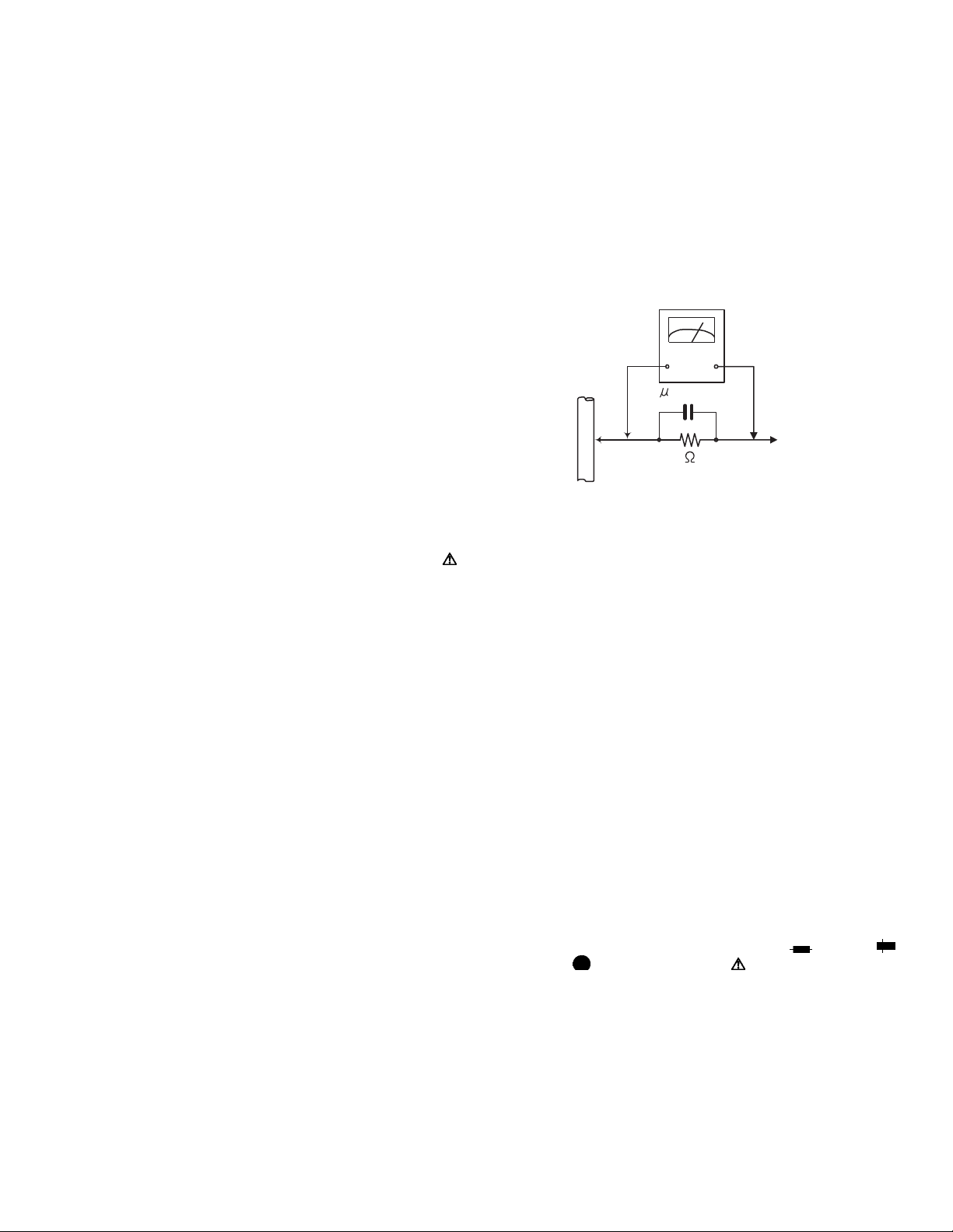
(5) Leakage shock hazard testing
After reassembling the product, always perform an isolation check on the exposed metal parts of the product (antenna terminals, knobs, metal cabinet, screw heads,
headphone jack, control shafts, etc.) to be sure the product
is safe to operate without danger of electrical shock.Do not
use a line isolation transformer during this check.
• Plug the AC line cord directly into the AC outlet. Using a
"Leakage Current Tester", measure the leakage current
from each exposed metal parts of the cabinet, particularly any exposed metal part having a return path to the
chassis, to a known good earth ground. Any leakage current must not exceed 0.5mA AC (r.m.s.).
• Alternate check method
Plug the AC line cord directly into the AC outlet. Use an
AC voltmeter having, 1,000Ω per volt or more sensitivity
in the following manner. Connect a 1,500Ω 10W resistor
paralleled by a 0.15µF AC-type capacitor between an ex-
posed metal part and a known good earth ground.
Measure the AC voltage across the resistor with the AC
voltmeter.
Move the resistor connection to each exposed metal
part, particularly any exposed metal part having a return
path to the chassis, and measure the AC voltage across
the resistor. Now, reverse the plug in the AC outlet and
repeat each measurement. Voltage measured any must
not exceed 0.75 V AC (r.m.s.). This corresponds to 0.5
mA AC (r.m.s.).
AC VOLTMETER
(Having 1000
ohms/volts,
or more sensitivity)
0.15 F AC TYPE
Place this
probe on
1500 10W
Good earth ground
1.2 Warning
(1) This equipment has been designed and manufactured to
meet international safety standards.
(2) It is the legal responsibility of the repairer to ensure that
these safety standards are maintained.
(3) Repairs must be made in accordance with the relevant
safety standards.
(4) It is essential that safety critical components are replaced
by approved parts.
(5) If mains voltage selector is provided, check setting for local
voltage.
1.3 Caution
Burrs formed during molding may be left over on some parts
of the chassis.
Therefore, pay attention to such burrs in the case of preforming repair of this system.
1.4 Critical parts for safety
In regard with component parts appearing on the silk-screen
printed side (parts side) of the PWB diagrams, the parts that are
printed over with black such as the resistor ( ), diode ( )
and ICP ( ) or identified by the " " mark nearby are critical
for safety. When replacing them, be sure to use the parts of the
same type and rating as specified by the manufacturer.
(This regulation dose not Except the J and C version)
each exposed
metal part.
(No.MB449)1-3

SECTION 2
SPECIFIC SERVICE INSTRUCTIONS
This service manual does not describe SPECIFIC SERVICE INSTRUCTIONS.
1-4 (No.MB449)
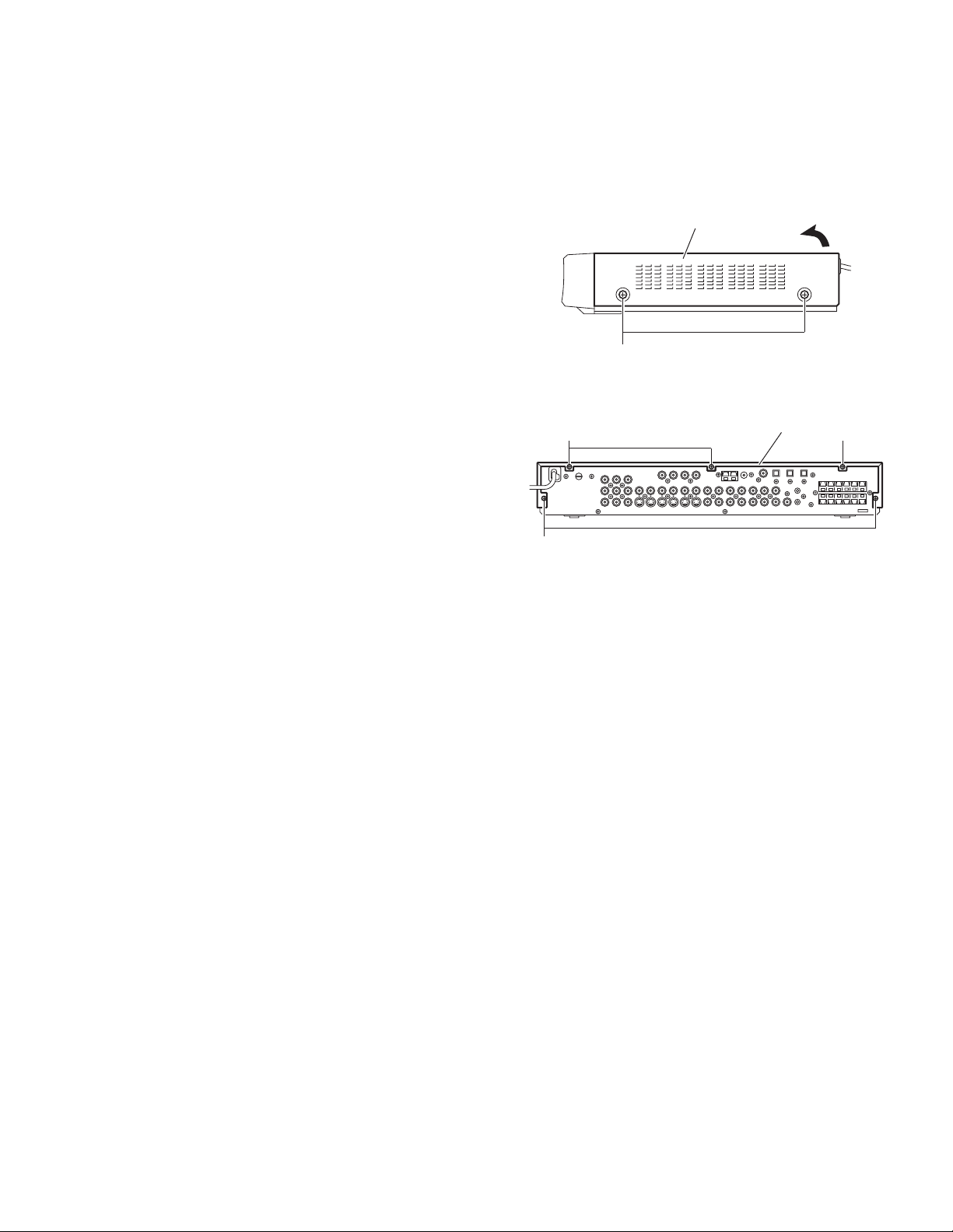
SECTION 3
DISASSEMBLY
3.1 Main body section
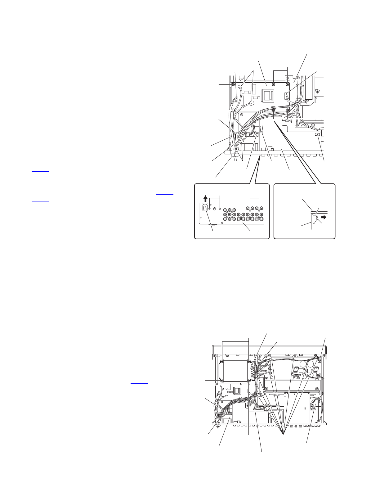
3.1.1 Removing the top cover
(See Figs.1 and 2)
(1) From the both sides of the main body, remove the four
screws A attaching the top cover. (See Fig.1)
(2) From the back side of the main body, remove the five
screws B attaching the top cover. (See Fig.2)
(3) Remove the top cover in the direction of the arrow. (See
Fig.1.)
Top cover
A
Fig.1
B
B
Fig.2
Top cover
B
(No.MB449)1-5
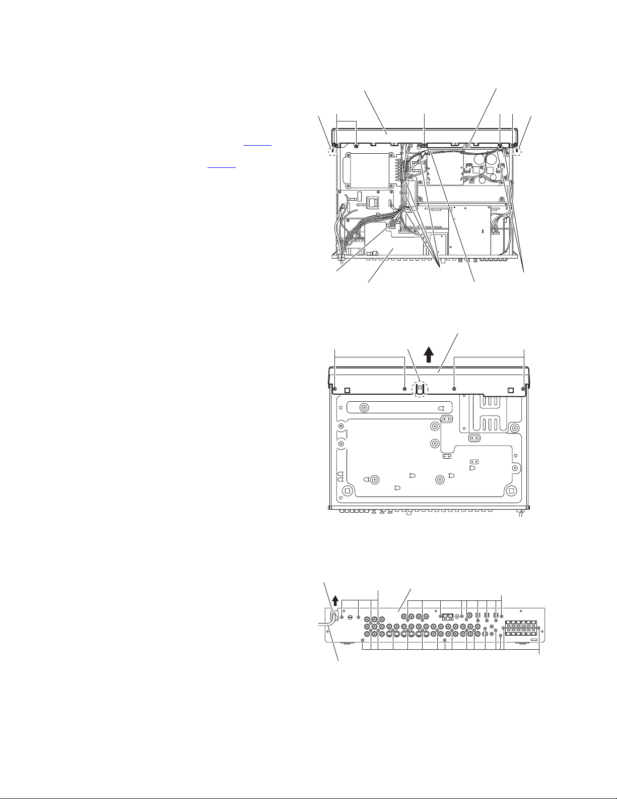
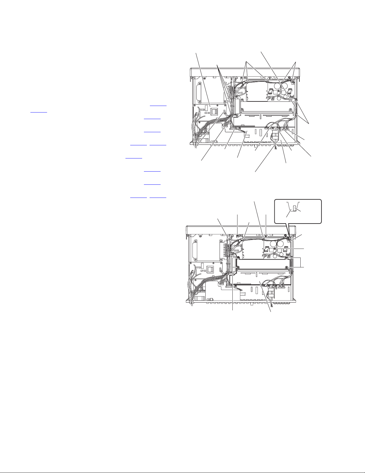
3.1.2 Removing the front panel assembly
(See Figs.3 and 4)
• Remove the top cover.
(1) From the top side of the main body, remove the tie bands
bundling the wires. (See Fig.3.)
Reference:
After reassembling, bundle the wires with the new tie
bands as before. (See Fig.3.)
(2) Disconnect the parallel wire from the connector CN412
the regulator connect board. (See Fig.3)
(3) Disconnect the wire from the connector CN451
mother board. (See Fig.3)
(4) Remove the four screws C and screw C' attaching the front
panel assembly. (See Fig.3)
Reference:
When attaching the screw C', attach the earth wires with
it as before. (See Fig.3.)
(5) From the bottom side of the main body, remove the four
screws C attaching the front panel assembly. (See Fig.4)
(6) From the both and bottom sides of the main body, release
the joints (a, b) and remove the front panel assembly in the
direction of the arrow. (See Figs.3 and 4)
on the input
on
Front panel assembly
C C C
aa
CN451
Input mother board
CC
b
Regulator connect board
Tie bands
CN412
Fig.3
Front panel assembly
C'
Earth wires
3.1.3 Removing the rear panel
(See Fig.5)
• Remove the top cover.
(1) From the back side of the main body, remove the strain re-
lief from the rear panel in the direction of the arrow and remove the power cord.
(2) Remove the twenty-nine screws D attaching the rear panel.
1-6 (No.MB449)
Strain relief
Power cord
D
Fig.4
Rear panel
Fig.5
D
D

3.1.4 Removing the tuner
(See Fig.6)
• Remove the top cover.
(1) From the top side of the main body, disconnect the card
wire from the connector CN1
(2) From the back side of the main body, remove the two
screws E attaching the tuner to the rear panel and take out
the tuner.
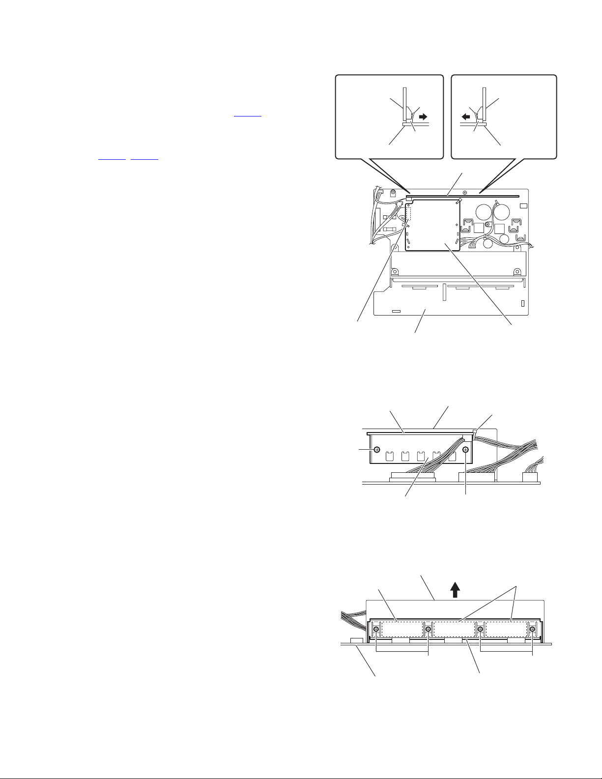
3.1.5 Removing the DSP board
(See Fig.6)
• Remove the top cover.
(1) From the back side of the main body, remove the five
screws E attaching the DSP board to the rear panel.
(2) From the top side of the main body, disconnect the DSP
board from the vol IC board while releasing the claw c of
the connector CN601
Note:
When releasing the claw c, take care not to break it.
(3) Take out the DSP board and disconnect the card wire from
the connector CN602
board.
Reference:
When attaching the DSP board, align the section d of the
speaker relay board in hole on the DSP board.
on the tuner.
on the DSP board.
on the forward side of the DSP
CN1
Tuner
DSP board
Rear panel
CN601
c
E
Vol IC
board
DSP board
CN601
CN602
Speaker relay board
Rear panel
E
d
3.1.6 Removing the master clock board
(See Fig.7)
• Remove the top cover.
(1) From the top side of the main body, remove the screw F.
Reference:
When attaching the screw F, attach the holder with it as
before.
(2) Disconnect the connector CN771
board from the main amplifier board in an upward direction.
3.1.7 Removing the gate drive-2 board
(See Fig.7)
• Remove the top cover.
From the top side of the main body, disconnect the connector
on the gate drive-2 board from the main amplifier board
CN311
in an upward direction.
3.1.8 Removing the S.S. setup board
(See Fig.7)
• Remove the top cover.
(1) From the top side of the main body, remove the tie band fix-
ing the wire.
Reference:
After reassembling, fix the wire with a new tie band as
before.
(2) Disconnect the wire from the connector CN725
setup board.
(3) Disconnect the S.S. setup board from the main amplifier
board while releasing the claw e of the connector CN727
on the main amplifier board.
Note:
When releasing the claw e, take care not to break it.
on the master clock
on the S.S.
Main amplifier board
CN771
Holder
Master clock board
Fig.6
Gate drive-2 board
CN311
F
Tie band
S.S. setup
board
Speaker terminal board
Fig.7
S.S. setup board
CN725
e
CN727
(No.MB449)1-7
3.1.9 Removing the vol sel board
(See Fig.8)
• Remove the top cover.
(1) Remove the strain relief from the rear panel in the direction
of the arrow.
(2) From the back side of the main body, remove the two
screws G attaching the vol sel board to the rear panel.
(3) From the top side of the main body, disconnect the wires
from the connectors (CN204
(4) Take out the vol sel board from the main body and remove
the wires from the soldered sections f on the reverse side
of the vol sel board.
3.1.10 Removing the audio input/output board
(See Fig.8)
• Remove the top cover.
(1) From the back side of the main body, remove the two
screws G attaching the audio input/output board to the rear
panel.
(2) Disconnect the audio input/output board from the video
connect board while releasing the claw g of the connector
on the audio input/output board.
CN516
Note:
When releasing the claw g, take care not to break it.
(3) Disconnect the card wires from the connectors (CN508
CN514) on the forward side of the audio input/output
board.
, CN205) on the vol sel board.
Chassis base assembly
Primary board
CN203
h
H
CN218
H
Vol sel board
Power cord
CN205
Stain relief
,
G G
f
CN204
CN514
Audio input/output
board
Audio input/output
board
H
CN508
CN516
3.1.11 Removing the primary board
(See Fig.8)
• Remove the top cover.
(1) From the top side of the main body, disconnect the power
cord from the connector CN203
(2) Disconnect the wires from the connector CN218 on the pri-
mary board.
(3) Remove the six screws H attaching the primary board on
the chassis base assembly.
(4) Take out the primary board from the main body and remove
the wires from the soldered sections h on the reverse side
of the primary board.
3.1.12 Removing the power transformer
(See Fig.9)
• Remove the top cover.
(1) From the top side of the main body, remove the tie bands
bundling the wires.
Reference:
After reassembling, bundle the wires with the new tie
bands as before.
(2) Disconnect the wires from the connectors (CN201
on the main amplifier board.
(3) Disconnect the wire from the connector CN202
mary board.
(4) Remove the four screws J attaching the power transformer
on the chassis base assembly.
on the primary board.
, CN702)
on the pri-
Strain relief
J
CN204
Rear panel
Fig.8
Power transformer
J
Video
connect
board
CN201
g
CN702
1-8 (No.MB449)
CN205
Vol sel board
J
Chassis base assembly
Tie bands
Main amplifier board
Fig.9
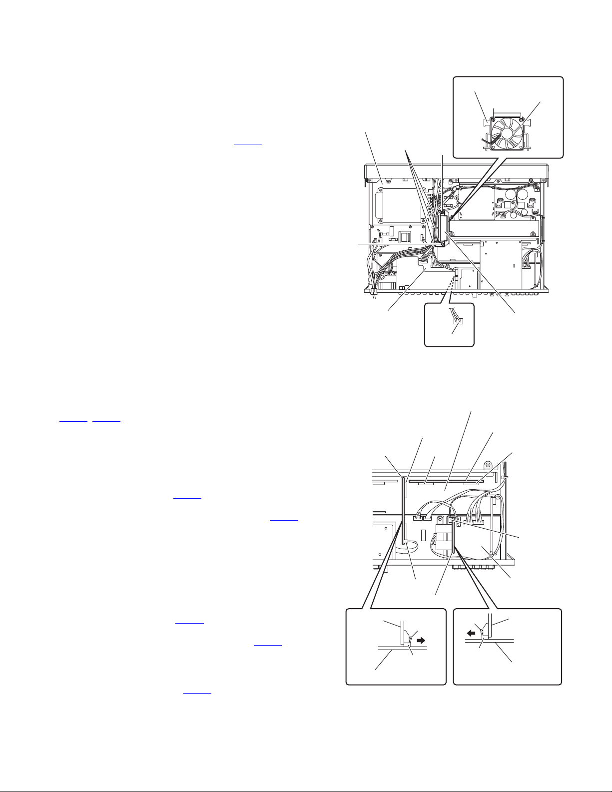
3.1.13 Removing the fan motor
(See Fig.10)
• Remove the top cover.
(1) Form the top side of the main body, remove the tie bands
bundling the wires.
Reference:
After reassembling, bundle the wires with the new tie
bands as before.
(2) Disconnect the wire from the connector CN552
mother board.
(3) Remove the two screws K attaching the fan motor assem-
bly on the chassis base assembly.
(4) Take out the fan motor assembly from the main body.
(5) Remove the two screws M attaching the fan motor on the
fan holder.
on the input
Chassis base assembly
Tie bands
K
K
Fan holder
M
Fan motor
3.1.14 Removing the gate drive-1 board
(See Fig.11)
• Remove the top cover and DSP board.
From the top side of the main body, disconnect the connectors
(CN811
fier board in an upward direction.
3.1.15 Removing the speaker relay board
• Remove the top cover and DSP board.
Note:
3.1.16 Removing the vol IC board
• Remove the top cover and DSP board.
, CN911) on the gate drive-1 board from the main ampli-
(See Fig.11)
(1) From the top side of the main body, disconnect the parallel
wire from the connector CN301
(2) Disconnect the speaker relay board from the main amplifier
board while releasing the claw j of the connector CN392 on
the main amplifier board.
When releasing the claw j, take care not to break it.
(See Fig.11)
(1) From the top side of the main body, disconnect the card
wire from the connector CN518
(2) Disconnect the vol IC board from the main amplifier board
while releasing the claw k of the connector CN501
input mother board.
Note:
When releasing the claw k, take care not to break it.
(3) Disconnect the connector CN512
the main amplifier board in an upward direction.
on the speaker relay board.
on the vol IC board.
on the
on the vol IC board from
Input mother board
CN512
Vol IC board
CN518
Speaker relay board
Vol IC
board
CN501
Input mother board
CN552
Fig.10
Main amplifier board
CN911
k
j
CN319
Fig.11
Fan motor assembly
Gate drive-1 board
CN811
CN301
Speaker
terminal board
Speaker
relay board
Speaker
terminal board
(No.MB449)1-9
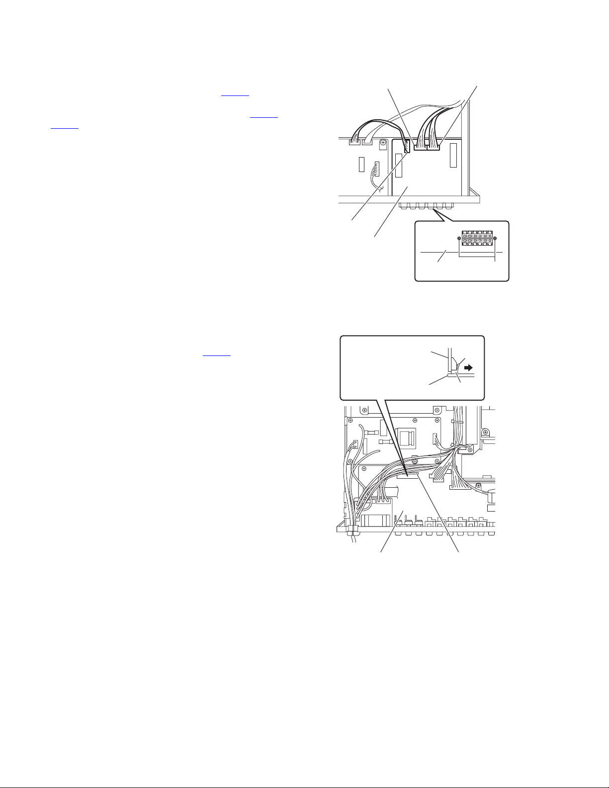
3.1.17 Removing the speaker terminal board
(See Fig.12)
• Remove the top cover, DSP board, S.S. setup board and
speaker relay board.
(1) Disconnect the wire from the connector CN751 on the
speaker terminal board.
(2) Disconnect the parallel wires from the connectors (CN701
CN801) on the speaker terminal board.
(3) From the back side of the main body, remove the two
screws N attaching the speaker terminal board to the rear
panel and take out the speaker terminal board from the
main body.
3.1.18 Removing the video connect board
(See Fig.13)
• Remove the top cover and audio input/output board.
Disconnect the video connect board from the input mother board
while releasing the claw m of the connector CN506
mother board.
Note:
When releasing the claw m, take care not to break it.
on the input
CN701
,
CN751
Speaker
terminal board
Rear panel
Fig.12
Video connect board
Input mother board
CN801
M
m
CN506
1-10 (No.MB449)
Input mother board
Video connect board
Fig.13
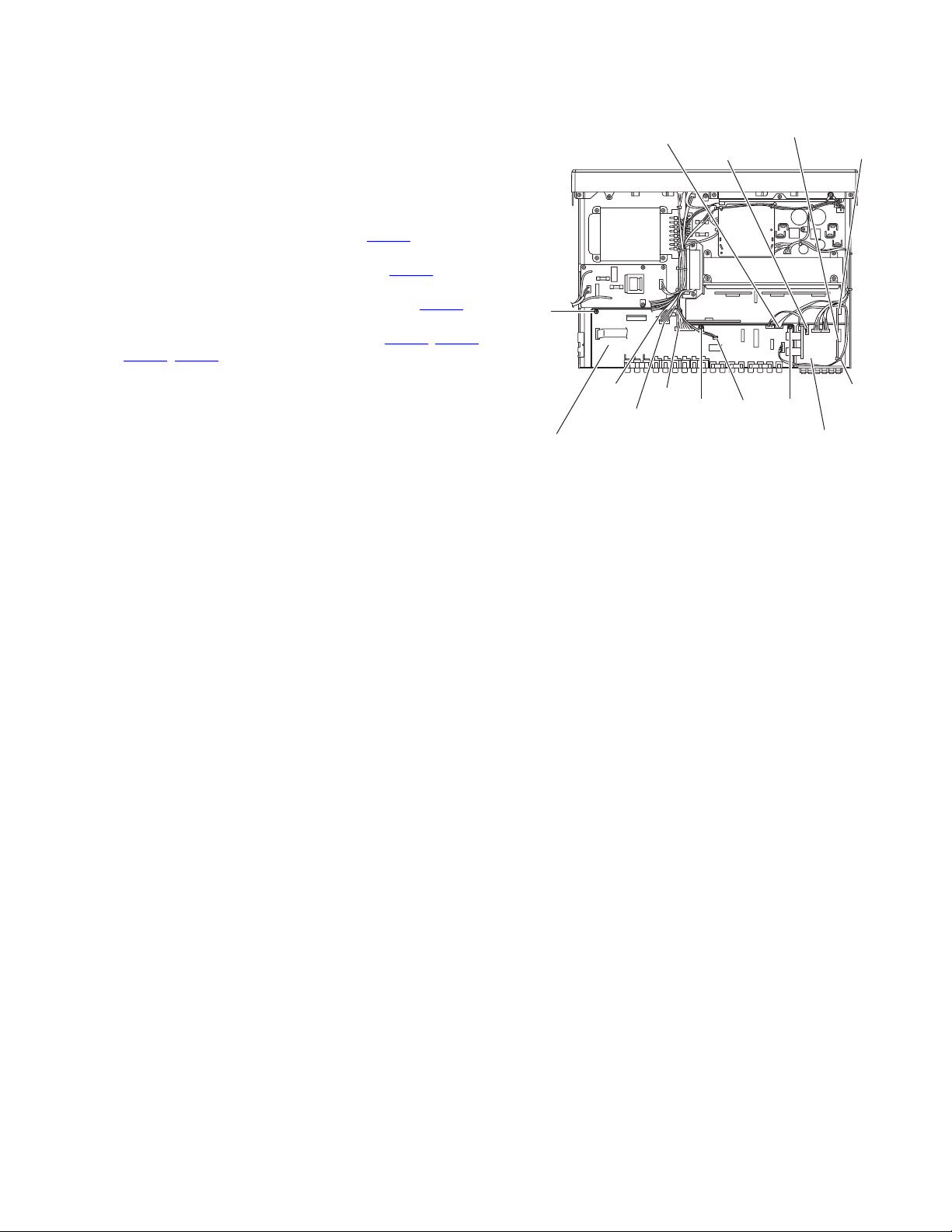
3.1.19 Removing the input mother board
(See Fig.14)
• Remove the top cover, rear panel, tuner, DSP board, vol sel
board, audio input/output board, vol IC board and video connect board.
(1) Remove the tie band fixing the wire.
Reference:
After reassembling, fix the wire with the new tie band as
before.
(2) Disconnect the wire from the connector CN725
setup board.
(3) Disconnect the wire from the connector CN751
speaker terminal board.
(4) Disconnect the parallel wire from the connector CN509
the input mother board.
(5) Disconnect the wires from the connectors (CN451
, CN552) on the input mother board.
CN540
(6) Remove the three screws P and take out the input mother
board.
on the S.S.
on the
on
, CN530,
P
CN451
CN540
Input mother board
CN509
CN530
CN751
P
Fig.14
S.S. setup board
CN725
Tie band
CN552
P
Speaker terminal board
(No.MB449)1-11
3.1.20 Removing the main amplifier board
(See Figs.15 and 16)
• Remove the top cover, tuner, DSP board, master clock board,
gate drive-2 board, S.S. setup board, gate drive-1 board and
vol IC board.
(1) Remove the tie bands bundling the wires. (See Fig.15.)
Reference:
• After reassembling, bundle the wires with the new tie
bands as before. (See Fig.15.)
• After reassembling, fix the support board with the new
tie bands as before. (See Fig.15.)
(2) Disconnect the parallel wires from the connectors (CN701
) on the speaker terminal board. (See Fig.15.)
CN801
(3) Disconnect the parallel wire from the connector CN301
the speaker relay board. (See Fig.15.)
(4) Disconnect the parallel wire from the connector CN509
the input mother board. (See Fig.15.)
(5) Disconnect the wires from the connectors (CN530
on the input mother board. (See Fig.15.)
(6) Disconnect the wire from the connector CN218
mary board. (See Fig.15.)
(7) Disconnect the parallel wire from the connector CN412 on
the regulator connect board. (See Fig.16.)
(8) Disconnect the parallel wire from the connector CN216
the headphone board. (See Fig.16.)
(9) Disconnect the wires from the connectors (CN201
on the main amplifier board. (See Fig.16.)
(10) Remove the four screws Q and three screws R and take
out the main amplifier board with the regulator and regulator connect boards from the main body. (See Fig.16.)
on the pri-
on
on
, CN540)
on
, CN702)
Primary board
Tie bands
,
CN218
CN540
CN530
Input mother board
Regulator connect board
CN201
Support board
Tie bands
CN509
Speaker terminal board
Speaker relay board
Fig.15
R R
CN412
Tie bands
Tie bands
CN801
CN301
CN701
CN216
Headphone board
CN702
Q
R
Q
Main amplifier board
Fig.16
1-12 (No.MB449)
3.1.21 Removing the regulator connect board
(See Fig.17)
• Remove the top cover, tuner, DSP board, master clock board,
gate drive-2 board, S.S. setup board, gate drive-1 board, vol IC
board and main amplifier board.
(1) From the forward side of the main amplifier board, discon-
nect the parallel wire from the connector CN705
ulator board.
(2) Disconnect the regulator connect board from the main am-
plifier board while releasing the claws (n, p) of the connectors (CN703
Note:
When releasing the claws (n, p), take care not to break them.
, CN704) on the main amplifier board.
on the reg-
Regulator
connect board
pn
CN704 CN703
Main amplifier board Main amplifier board
Regulator connect board
Regulator
connect board
3.1.22 Removing the regulator board
(See Fig.18)
• Remove the top cover, tuner, DSP board, master clock board,
gate drive-2 board, S.S. setup board, gate drive-1 board, vol IC
board, main amplifier board and regulator connect board.
(1) From the forward side of the main amplifier board, remove
the tie band fixing the wire.
Reference:
After reassembling, fix the wire with a new tie band as
before.
(2) From the front side of the main amplifier board, remove the
two screws S attaching the TR bracket to the heat sink.
3.1.23 Removing the regulator connect board
(See Fig.19)
• Remove the top cover, tuner, DSP board, master clock board,
gate drive-2 board, S.S. setup board, gate drive-1 board, vol IC
board, main amplifier board, regulator connect board and regulator board.
(1) From the back side of the main amplifier board, remove the
four screws T attaching the FET bracket to the heat sink.
(2) Remove the cooling rubbers on the heat sink from the FET
bracket and remove the heat sink from the main amplifier
board in the direction of the arrow.
CN705
Main amplifier board
Regulator board
S
TR bracket
Cooling rubber
Regulator board
Fig.17
Heat sink
Tie band
S
Fig.18
Heat sink
Cooling rubbers
Main amplifier board
TT
FET bracket
Fig.19
(No.MB449)1-13
3.2 Front panel assembly section
• Remove the front panel assembly.
(See "3.1.2 Removing the front panel assembly".)
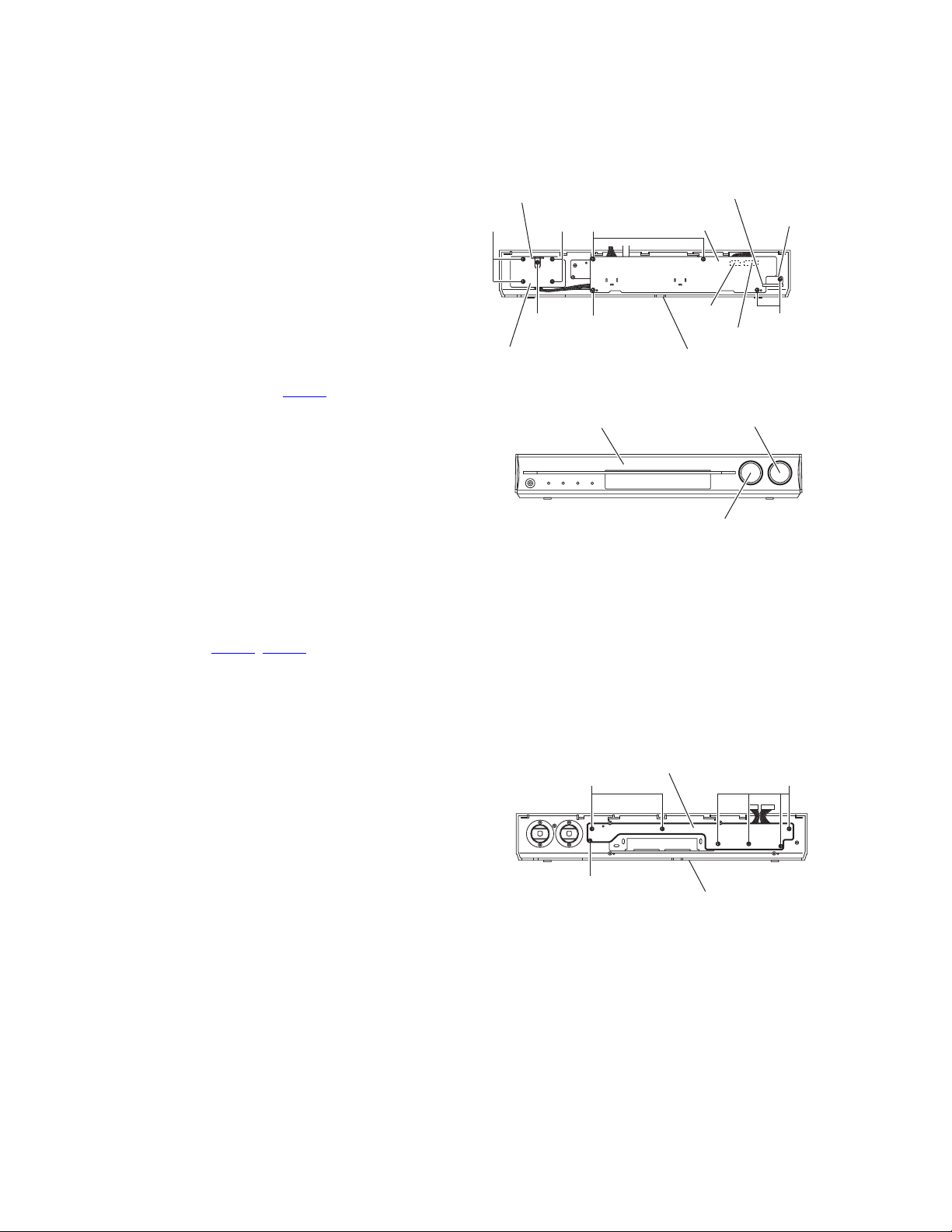
3.2.1 Removing the volume & JOG board
(See Figs.1 and 2)
(1) From the inside of the front panel assembly, remove the
four screws A and screw A' attaching the volume & JOG
board. (See Fig.1.)
Reference:
When attaching the screw A', attach the earth bracket
with it as before. (See Fig.1.)
(2) Take out the volume & JOG board while lifting it from the
front panel assembly little by little.
Reference:
The master volume knob and source selector knob are
removed from the front side simultaneously. (See Fig.2.)
(3) From the forward side of the volume & JOG board, discon-
nect the wire from the connector CN413
. (See Fig.1)
Earth bracket
A
A'
Volume & JOG board
AA
A A
Headphone board
FL board
CN415
Front panel assembly
Fig.1
Support board
CN414
3.2.2 Removing the headphone board
(See Fig.1)
(1) From the inside of the front panel assembly, remove the
screw A attaching the support board.
(2) Take out the headphone board from the front panel assem-
bly.
3.2.3 Removing the FL board
(See Fig.1)
• Remove the volume & JOG board and headphone board.
(1) Remove the four screws A and take out the FL board form
the front panel assembly.
(2) From the forward side of the FL board, disconnect the wires
from the connectors (CN414
3.2.4 Removing the key & LED board
(See Fig.3)
• Remove the volume & JOG board, headphone board and FL
board.
(1) From the seven screws A attaching the key & LED board.
(2) Take out the key & LED board from the front panel assem-
bly.
, CN415).
Front panel assembly
Key & LED board
A
Master volume knob
Source selector knob
Fig.2
A
1-14 (No.MB449)
A
Front panel assembly
Fig.3

SECTION 4
ADJUSTMENT
This service manual does not describe ADJUSTMENT.
SECTION 5
TROUBLESHOOTING
This service manual does not describe TROUBLESHOOTING.
(No.MB449)1-15

Victor Company of Japan, Limited
AV & MULTIMEDIA COMPANY AUDIO/VIDEO SYSTEMS CATEGORY 10-1,1chome,Ohwatari-machi,Maebashi-city,371-8543,Japan
(No.MB449)
Printed in Japan
VPT
SCHEMATIC DIAGRAMS
HOME CINEMA CONTROL CENTER
RX-F31S
CD-ROM No.SML200507
Area suffix
A ------------------------ Australia
US ------------------------ Singapore
UF ------------------------------ China
UJ ---------------------- U.S.Military
Lead free solder used in the board (material : Sn-Ag-Cu, melting point : 219 Centigrade)
Contents
Block diagram
Standard schematic diagrams
Printed circuit boards
COPYRIGHT 2005 Victor Company of Japan, Limited.
2-1
2-2
2-13 to 16
No.MB449SCH
2005/7

In regard with component parts appearing on the silk-screen printed side (parts side) of the PWB diagrams, the
parts that are printed over with black such as the resistor ( ), diode ( ) and ICP ( ) or identified by the " "
mark nearby are critical for safety.
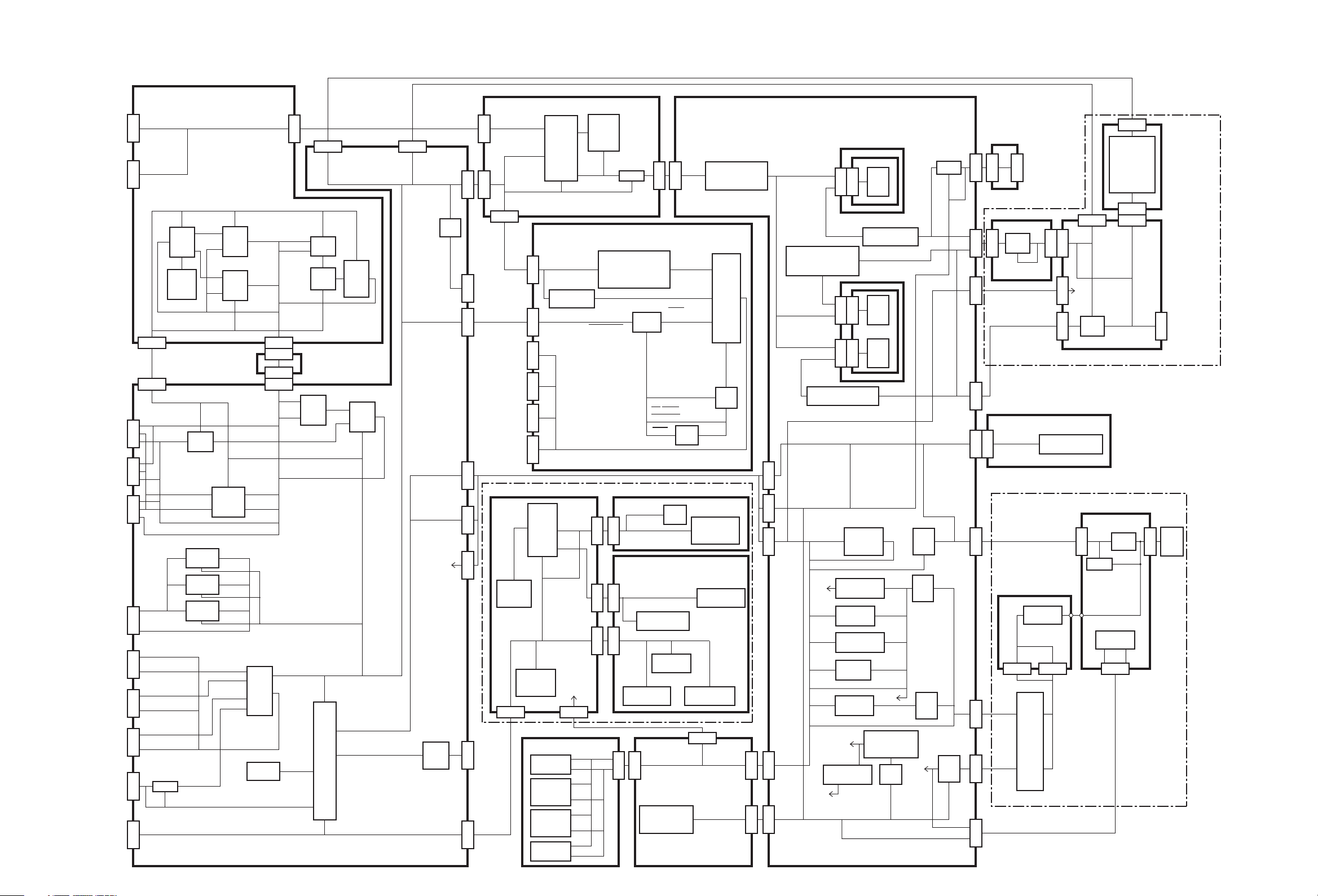
Block diagram
5.1ch
MULTI
IN
Y/C IN
CV IN/OUT
Y/C IN
CV IN/OUT
Y/C IN
CV IN/OUT
VCR IN
VCR/DVD IN
MONITOR OUT
DVR IN/OUT
VCR IN/OUT
DBS/TV IN
MONITOR OUT
TO
TUNER
AV_COMPULINK
Audio/Video signal input/output
(Component/DVD multi) section
J6521
MULTI_SL/SR
MULTI_C
J6522
MULTI_SW
CV
IC351
Y/C
SEPA.
CKIN
IC359
CLOCK
GEN.
1270_SDA
1270_SCL
VCONT10
Y
IC352
REC_SY
AMP
SY
& SEL
C
IC353
REC_SC
AMP
SC
& SEL
VCONT10
CN514 CN516
VCONT1
J6511
VCONT4
CV_IN
IC555
SEL
REC_SY/SC
J6512
VCONT1
VCONT4
J6513
J4503
DVR_RECL/RECR
J6501
J6502
VCR_RECL/RECR
Y
C
Y/C SEL
Y
IC451
Y SEL.
PB
IC452
PB SEL.
PR
IC453
PR SEL.
DVR_L/R
VCR_L/R
DBS_L/R
TV_L/R
IC551
IC552
Y OUT
PB OUT
PR OUT
TU_L/R
SY
SC
M_OUT_CV
IC502
6CH
SW
J6503
MOUT_L/R
CN505
J505
MUTE
TU_MUTE
AV_LINK
IC507
EEPROM
TU_DATAI,TU_DATAO
TU_CLK,TU_CE,TU_MUTE
CN536
CN526
CN506CN504
CV
VCONT1
L,R
CN508
REC_SY
CV
OSD_SY
OSD_SC
OSD_SIN
OSD_SCLK
OSD_CS
SY
SC
CV_OUT
RC_SDA
RC_SCL
IC553
Y/C
MIX
CN525
IC362
SEL
IC360
OSD
IC501
CPU
SMART SETUP L/R
SMART SETUP C
SMART SETUP SL/SR
SMART SETUP SB
VCONT8VCONT9
IC356
IC357
AMP
& SEL
IC554
AMP
& SEL
VCONT5
TH1,TH2,LIMITTER
DA_PROTECTOR
CLK_F_CONT
REG_SAFETY,POWER
HP_RELAY,HP_SW
B_SW1,B_SW2
FAN
FAN_L
BLUE_LED
LED_DIMMER1
LED_DIMMER2
AV_LINK,M_CLK
M_COMMAND
M_STATUS,M_CS
M_BUSY,M_RESET
System control and audio/Video signal input/output section
CN521
C_RELAY
S_RELAY
F_RELAY
SB_RELAY
SBWFR OUT
DSP_STATUS
DSP_READY
DSP_RESET
DSP_COMMAND
DSP_CLK
TH1,TH2
LIMITTER
DA_PROTECTOR
CLK_F_CONT
REG_SAFETY
POWER
HP_RELAY
HP_SW
B_SW1
B_SW2
VIDEO+9V
VIDEO+5V
B+5V,A+5V
D+5V,+5V
TU+9V
+7V,-7V
+S2B
Q532
Q533
Q536
IC504
AMP
Vol. control section
CN501
CN518
IN.L
IN.R
SBWFR OUT
CN511
DSP_L/R,DSP_C,DSP_LFE
DSP_SL/SR,DSP_SB,IN.L,IN.R
CN611
IC503
6CH
VOLUME
DA,CL
IC508
AUDIO
SOUND
CPU
SBOUT
MUTE
SOURCE_MUTE
CN512
CN522
DSP and digital signal input terminal section
DSP_L,DSP_R
DSP_LS,DSP_RS
CN601
J504
SUBWOOFER
OUT
CN502
CN540 CN530CN509
DIGITAL
IN1
DIGITAL
IN2
DIGITAL
IN3
DIGITAL
OUT
DSP_C,DSP_LFE
DSP_SB
DSP_IN_L
DSP_IN_R
IC601,IC602
CN602
J681 UN682
RX0
RX1
UN683
RX2
UN686
TX
AMP.
IC611 to IC613
IC615,IC621,IC622
IC632 to IC634,IC651
AMP.
DSPSTATUS
DSPREADY
DSPRESET
DSPCOMMAND
DSPCLK
IC671
CPU
GPIO1,GPIO2
GPIO3,GPIO4
MOSI,MISO
SS,HREQ
DSP_RST
A1+/- to A4+/B1+/- to B3+/-
CDIN,CDOUT
CCLK,D_CS
D_RST,INT
C_LRCK,S_LRCK
C_BCK,S_BCK
D/A0 to D/A3
DATA,MCK,XTAL
User control keys, system control and FL display section
JOG1,JOG2
VOL1,VOL2
CN403
CN413
BLUE_LED
TUNER_IND,TV_IND
DVD_MULTI_IND
VCR_G_IND,VCR_R_IND
VIDEO_G_IND,VIDEO_R_IND
CN414
CN404
DVD_G_IND,DVD_R_IND
REMOCON
CN405
KEY_IN1
KEY_IN2
KEY_IN3
IR DETECTOR
CN415
S401 to S406
FW715
CN705
SW control section
JS401
JS402
IC402
BLUE_LED
D408,D409
BLUE LED
STANDBY_IND
SW
+S2B,9.4V
VIDEO+7V
D+5V,A+5V,9.0V
IC851 to IC855
Q851 to Q858
SW CONT.
CN552
TO
FAN
MOTOR
CN451
SEG1 to 35
GRID1 to 13
DI401
FL
DISPLAY
CN401
JOG1
JOG2
IC401
VOL1
VOL2
CPU
&
FL DRV.
BLUE_LED
MCLK,M_CS
M_COMMAND
M_STATUS
M_BUSY
M_RESET
STANDBY_IND
BLUE_LED
KEY_IN1 to 3
LED_DIMMER1
LED_DIMMER2
Q403,Q411
DIMMER
CONT.
F1,F2
-VPP,5.0V
FW402
Regulator 2 section
Q211,Q212
D+5V REG.
VIDEO+5V
VIDEO+9V
9.0V REG.
Q226
REG.
Q227
REG.
Q202
+S2B
+S2B
+S2B
9.4V
Regulator, PWM modulator, digital power amplifier
and low pass filter section
FL,FR
SL,SR
C,SB
FM MODULATOR
LIN+/RIN+/-
SCKMICK
IC673
INV
D412 to D415
BLUE LED
JOG/VOL.
D421 to D426
INDICATOR
D407
STANDBY LED
CN412
F1,F2
-VPP,5.0V
AC_ON/OFF
B_SW1,B_SW2
POWER_PWM
AMP_CLK,+12V
IC301,IC801
IC901
IC667
8CH
CODEC
IC661
DSP
CN714 CN713
CN520
CN510FW201
CN704 CN703
PWM_L/R
FB1_L/R
FB2_L/R
Q1901 to Q1904
CENTERch
SURROUND BACKch
PWM_C
PWM_SB
FB1_C,FB2_C
FB1_SB
FB2_SB
PWM_SL/SR
FB1_SL/SR
FB2_SL/SR
Q1801 to Q1804
SURROUND Lch/Rch
+S2B,-S2B
AMP_CLK
+5V
B+5V
9.0V
9.4V
+7V
-7V
A+5V
TU+9V
5.0V
+S2B
-VPP
B_SW1
B_SW2
AMP_CLK
F1,F2
-B+12V
CN321
CN311
CN921
CN911
CN821
CN811
Q203
+5V/B+5V
REG.
Q207,Q208
-7V/+7V REG.
Q213
A+5V REG.
Q210
TU+9V REG.
Q209
+5V REG.
Q205
-VPP REG.
AMP+B
AMP-B
Q722 to Q726
-B+12V REG.
POWER_PWM
+12V
IC311
IC312
AMP
Q1301 to Q1304
FRONT Lch/Rch
IC911
IC912
AMP
IC811
IC812
AMP
HP_SW
HP_RELAY
+S2B
Q703,Q704
AMP+B/AMP-B
IC701
+S2B
-S2B
+S2B
+S2B
+S2B
REG.
AMP
AC_ON/OFF
FL
FR
CLK_F_CONT
AMP_CLK
POWER
D201
to
D204
D208
to
D211
D231
D233
D234
+B
RY211
SL
SR
S2
S2
S3
D701
to
D704
HP_SW
C
SB
S1
+B
CN725
IC371
FW226
CN216
J7501
HEADPHONE
OUT
IC871
IC971
SMART
SURROUND
SETUP
CN728
FL,FR,C
S_RELAY
SB_RELAY
SL,SR
SB
CN727
FL,FR,C
SL,SR
SB
J7001
FW301
FW792
CN301
RY301
RY901
C_RELAY
F_RELAY
CN302
CN312
CN701
CN801
CN751
+S2B
-S2B
RY801
RY902
Speaker terminal and smart surround setup section
FW801
Master clock section
CN771
CN781
AMP_CLK
CLK_F_CONT
IC702,IC704,IC706
Master clock GEN.
Primary section
T202
Trans.
CN203
Main
plug
CN201 CN702CN208
FW721
CN204
Power
VS201
VOL. SEL.
trans.
CN205
CN218
RY201
+12V REG.
+B +12V
Q702
CN711
SPEAKER
TERMINAL
2-1
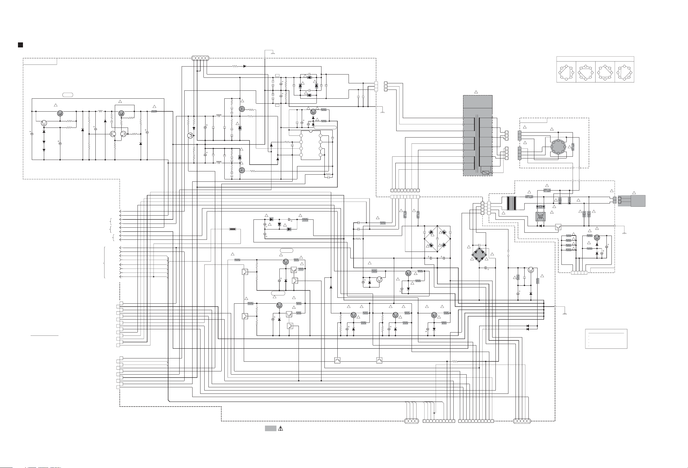
Standard schematic diagrams
Primary and regulator section
LVA10564-1
-B+12V
!
Q725
KTA1046/Y
-22.2V
-21.1V-22.9V
-21.7V-22.4V
D723
D724
D725
R760
680
R761
C744
100/16
100/16C745
Q726
2SC2812N/6
MTZJ10C
1SS133
1SS133
VERSION CODES
J :U.S.A.
C :CANADA
EN:NORDIC COUNTRIES
E :CONTINENTAL EUROPE
B :U.K.
EV:EAST EUROPEAN COUNTRIES
UP:KOREA
UJ:U.S. ARMY
US:SINGAPORE
UT:TAIWAN
A :AUSTRARIA
UF:CHINA
UX:SAUDI ARABIA
330
L701
220u
4.7k
MTZJ16BD726
R753
C742
47/25
-27.5V
5.6k
R754
(SHEET 3)
(SHEET 2), (SHEET 3)
(SHEET 3)
(SHEET 2)
(SHEET 3)
!
Q722
KTA1046/Y
0V-21.0V
P.GND
AMP+B
-B+12V
D.GND
HP_SW
THCOM
R757
AMP-B
R751
-0.3V
R756
220
1.2K
C743
R752
-2.0V
0V
R758
-27.5V
470
Q723
-28.0V
KTC3199/GL
470
-B
-B
AMP-B
P.GND
AMP+B
-B+12V
D.GND
+7V
+7V
-7V
-7V
+S2B
+S2B
AMP_CLK
CLK_F_CONT
HP_SW
HP_RELAY
PROTECT
TH1
TH1
THCOM
CN704
QGB2510J1-14
+S2B
1
2
0V
VIDEO+5V
3
D+5V
4
VIDEO+9V
5
TV DIRECT
6
REG_SAFETY
7
8
+5V
9
-VPP
10
F1
11
F2
12
D.GND
13
0V
14
CN703
QGB2510J1-10
AC_ON/OFF
1
B_SW2
2
B_SW1
3
4
POWER_PWM
5
+12V
6
7
0V
AMP_CLK
8
0V
9
10
ERA18-04
Q724
CLK_F_CONT
47K
D721
0.0047/50
KTC3199/GL
AMP_CLK
HP_RELAY
PROTECT
17.5V
5.1V
4.9V
8.7V
4.2V
3.6V
9.4V
9.0V
-25.8V
-19.3V
-19.4V
5.0V
-39.4V
4.5V
4.5V
2.3V
-59.5V
13.4V
32.0V
0.6V
TO CN713 OF LVA10566-3 (SHEET 5) TO CN714 OF LVA10566-3 (SHEET 5)
MTZJ6.2B
!
UNF
1 R759
(1/2W)
6.8KR755
100/50C741
D722
TO CN711 OF LVA10566-4 (SHEET 1)
R721
1k
R718
D720
Q705
31.1V2.3V
R719
R720
TH2
12345
1k
MA111
33.6V
39k
3300/50
47k
C722
C723
FW721
QQL77AK-220
3300/50
QQL77AK-220
528
3
6
C217
0.22u
0V0V
OMFR274
OMFR273
OMFR272
OMFR271
CN711
4
PW212
PW202
1.2K
1.2K
1.2K
1.2K
!
528
6
110V
R243
3.3M
3
!
2W
!
2W
!
2W
!
2W
32.0V0V0V
VOLTAGE SELECTOR LOCATION
1
7
4
F201
T1.6AL
PW211
PW201
!
!
0.001/250
C219
C218
R723
FR
10
59.5V
!
R713
UNF
6.8k
1/2W
59.8V
13.5V
12345
3
!
0.001/250
2SD2394/EF/
Q702
D714
1
7
QGA7901C1-02
QNZ0136-001Z
!
13.5V
12.9V
D718
MA111
UDZS13B
528
3
6
4
220V
!
CN203
EP201
100/16
C727
10/50 C715
528
6
127V
!
LVA10566-4
VOLTAGE MEASUREMENT CONDITION
POWER ON
SOURCE FM(NO SIGNAL)
SURROUND OFF
VOLUME 0
528
3
1
6
7
4
230-240V
!
LIVE/
BRN
2
2
1
1
NEUTRAL/
BLU
MAINS
PLUG
EP701
1/4W
R254
(1/4W)
QNZ0136-001Z
D701-D704
30PRA20-FC
R724
4.7
220/50
100k
100k
C241
D231
1A3G
MTZJ5.6C
C714
16.7V
Q218
0V
0V
FR
C705
-47.4V
44.3V
33.3V
32.0V
!
FR
!
UNF
9.7V
KRA102S
4.4V
C713
R236
10
KRA102S
Q219
KRC102S
0V
Q214
KRC102S
C753 0.22/100
!
!
D702
C754
0.22/100
-47.3V 0V
0.1/50
C712
1/50
1
Vcc
2
VB
3
HO
4
Vs
IC701 IRS2011S
TH201
!
4.7
(1/4W)
!
!
UNF
R237
3.3k
5.8V
4.5V
R225
10
(1/4W)
R226
1k
(1/4W)
Q215
D701
0.47/100
!
KTC1027/OY/
!
100/25
C711
(1/4W)
!
D704
D703
Q701
!
-46.8V
MA111
D717
!
D711
UDZS13B
-B+12V REGULATOR
LO
COM
LIN
HIN
C704
FR R711
10
1/2W
UNFR712
6.8k
-58.0V
8
-60.1V
7
-59.3V
6
5
C740
C703
0.47/100
0.1/160
C739
1/16
R726
1k
NI
1A3G
D222
R223
1k
R224
100k
5.6V
3.6V
3.6V
Q221
KRC111S
+B
C755
1/50
C701
R705
6800/68
C757
1/50
C756
1/50
C702
R706
6800/68
C758
1/50
R714
33
R727
4.7
R715
33
C243
100/100
C242
100/100
R238
5.0V
R239
100k
10
R227
39k
4.5V
R228
47k
-B
UNF
D712 1SS133
0.33/50
D719
1SS133
D233
!
1A3G
D234
!
1A3G
!
A+5V
!
Q213
2SD2394/EF/
5.2V
1k
C224
100/16
C226
1000/25
TUNER +9V
2SD2394/EF/
9.0V
9.7V
5.8V
D220
!
Q210
16.5V
D218
MTZJ10B
5.6V
C223
!
2SD2394/EF/
6.3V
100/16
QGA3901C1-03
CN702
S1
1
1
COM
2
2
S1
3
3
C751
C752
1/100
1/100
W701
GND
AC 44.1V
AC 0V
AC 44.1V
!
POWER
POWER
TRANSFORMER
TRANSFORMER
127V
LVA10566-7
17V
QGA2501C1-04
CN218
D202
1A3G
!
1
2
3
1
2
3
4
!
QQT0281-006
0V
127V
110V
0V
TH.FUSE
TH.FUSE
TH.FUSE
TH.FUSE
123456789
123456789
S3
S3
!
-19.1V
-19.1V
7.0V
C222
100/16
!
Q208
2SD2394/EF/
7.6V
KTA1046/Y
!
C215
16.4V
MTZJ7.5C
-25.8V
F203
Q205
-26.1V
47/50
!
(1/4W)
FR
R218
!
1.5k
(1/4W)
UNF
D216
C212
0.047MY
C213
0.047MY
R208
100k
C214
1/50
!
Q209
(1/4W)
FR
16.6V
R222
!
3.3k
(1/4W)
UNF
D217
MTZJ6.2C
R207
!
12
(1/4W)
UNF
R209
!
10
(1/4W)
UNF
-18.9V
Q204
KTC3200/GL/
-24.8V
D224
MTZJ6.2C
R221
10
R219
22k
R220
47k
4.4V
3.5V
3.6V
Q220
KRC111S
AC14.8V
R217
8.2
CN201
QGA3901C1-09
S2
S2
COM
0V
AC14.8V
!
T2AL
T2AL
F202
D208
D209
1A3G
!
D210
1A3G
C210
4700/25
!
Q207
KTA1046/Y
-7.0V
-7.6V
1A3G
C208
!
0.1MY
(100V)
!
1000/25
!
UNF
D215
UDZS7.5B
C209
(1/4W)
0.1MY
(100V)
D211
1A3G
C211
-19.8V
R215
!
10
FR
R216
1.5k
(1/4W)
R242
2.2k
!
-18.9V
-51.0V
UNF
!
(1/2W)
D223
MTZJ27B
FR
!
(1/4W)
C207
0.1MY
(100V)
17.2V
R210
10
R211
5.6k
C221
100/16
CN208
1
1
2
2
9.8V
3
3
4.4V
4
4
C202
0.0047/100
!
D201
1A3G
!
!
D204
D203
1A3G
1A3G
C203
220/63
!
CN204
1
2
3
!
CN205
1
2
3
4
!
F204
T100mAL
T202
D205
1SS133
Q203
KTC3203/OY
9.8V
5.7V
820R206
!
6.3V
R245
C205
0.0047
(1/4W)
UNF
C206
470/16
2.2
(1/4W)
UNF
D207
MTZJ6.2C
D212
1A3G
D213
1A3G
1
7
VS201
!
QSW0812-001
1
7
4
!
F205
T3.15AL
!
C201
!
0.0047
!
RY201
QSK0142-001
Q201
KRC105S
4.4V
QGA2001C1-05
!
FROM FW721 OF LVA10564-1 (SHEET 1)
EP202
QNZ0136-001Z
1/4W
D706
R707
3.3k
1SS133
!
1W
2SK3599
UNF
R716
10
Q703
D
C728
0.0022/50
C716
UNFR728
C734
C736
R729
C735
R717101W
C717
0.0022/50
TH302
UNF
(1/4W)
10
0.0022/50
1W
10
C737
C729
!
Q224
KRC111S
1W
0.0022/50
0.0022/50
0.0022/50
R253
S
0.0022/50
!
D715
D716
0.0022/50
D
S
2.2
Q222
FMB-G19L
!
FMB-G19L
!
Q704
2SK3599
KRC111S
G
UNF
G
4.3V
4.3V
!
UNF
3.7V
3.6V
L702
22u
0.1/100
C718
C720
0.47/50
C719
0.1/100
C721
0.47/50
L703
22u
QAD0146-103
Parts are safety assurance parts.
When replacing those parts make
sure to use the specified one.
2-2
HP_SW
B_SW1
HP_RELAY
123
FW201
0V
0V
FROM CN509 OF LVA10576-1 (SHEET 7)
4.7V
TH2
B_SW2
THCOM
123456789
4
0V
CN520
4.7V
TH1
PROTECT
CLK_F_CONT
123456789
10
0V
4.8V0V5.1V
5.1V
1.6V
D+5V
POWER
TU+9V
REG SAFTY
3.5V
4.4V
TV DIRECT
4.5V
+7V
VIDEO+9V
VIDEO+5V
-7V
8.5V
7.0V
4.9V
5.1V
8.9V
-7.1V
TO CN530 OF LVA10576-1 (SHEET 7)TO CN540 OF LVB10576-1 (SHEET 7)
CN510
10
11
+5V
+S2B
A+5V
D.GND
0V
4.9V B+5V
5.0V
5.0V
17.3V
17.2V0V-19.8V
5.1V
12345
0.6V
FW792
TO CN701 OF LVA10564-2 (SHEET 4)
SHEET 1
 Loading...