

Page 1
RX-DV5RSL
SERVICE MANUAL
HOME CINEMA DVD/CD CONTROL CENTER
RX-DV5RSL
Area suffix
B ----------------------- U.K.
E --- Continental Europe
EN----- Northern Europe
HOME CINEMA
DVD-AUDIO/VIDEO CONTROL CENTER
STANDBY/ON
VCRSTB TV AUDIO
TAPETV CDR FM/AM
TV DIRECT
VCRSTB DVD
/FF
TV/VIDEO
REW/
TUNING/GROUP
REPEAT SLEEP
FM MODE STROBE
TV/STB CH
CENTER
EFFECT
CONTROL
231
ANALOG
TEST
/DIGITAL
INPUT
564
SURR ON/OFF
AUDIO
897
Ð SUBWOOFER +
SURR MODE
SUBTITLE
10/0 +10
100+ TV RETURN
DIMMER
ANGLE
+Ð+
PAGE
TV VOL
MUTING
ZOOM
TA/NEWS/INFO
TOP MENU
DIGEST
PTY SEARCH
CHOICE
ENTER
ON SCREEN
REMOTE CONTROL RM-SRXDV5R
REARáL
REARáR
VFP
PROGRESSIVE
VOLUME
Ð
MENU
PTYPTY
RETURN
DISPLAY
STANDBY/ON
STANDBY
INPUT
DVD AUDIO
ON/OFF
ANALOG/DIGITAL
INPUT ATT. REC MODE
RX-DV5R HOME CINEMA DVD-AUDIO/VIDEO CONTROL CENTER
SURROUND
MODE
SOURCE NAME
FM/AMTAPE/CDR
SETTING ADJUST MEMORY
TVVCRSTBDVD
TV DIRECT
Contents
Safety precautions -------------------------------------------------------Preventing static electricity ---------------------------------------------Disassembly method -----------------------------------------------------Adjustment method ------------------------------------------------------Description of major ICs -------------------------------------------------
MASTER VOLUME
CONTROL
SUPER VIDEO
DVD/SUPER VCD/VCD/CD
1-2
1-4
1-5
1-14
1-16~52
COMPACT
COPYRIGHT 2002 VICTOR COMPANY OF JAPAN, LTD.
No.21186
Oct. 2002
Page 2
RX-DV5RSL
1. This design of this product contains special hardware and many circuits and components specially for safety
purposes. For continued protection, no changes should be made to the original design unless authorized in
writing by the manufacturer. Replacement parts must be identical to those used in the original circuits. Services
should be performed by qualified personnel only.
2. Alterations of the design or circuitr y of the product should not be made. Any design alterations of the product
should not be made. Any design alterations or additions will void the manufacturer`s warranty and will further
relieve the manufacture of responsibility for personal injury or property damage resulting therefrom.
3. Many electrical and mechanical parts in the products have special safety-related characteristics. These
characteristics are often not evident from visual inspection nor can the protection afforded by them necessarily
be obtained by using replacement components rated for higher voltage, wattage, etc. Replacement par ts which
have these special safety characteristics are identified in the Parts List of Service Manual. Electrical
components having such features are identified by shading on the schematics and by ( ) on the Parts List in
the Service Manual. The use of a substitute replacement which does not have the same safety characteristics
as the recommended replacement parts shown in the Parts List of Service Manual may create shock, fire, or
other hazards.
4. The leads in the products are routed and dressed with ties, clamps, tubings, barriers and the like to be
separated from live parts, high temperature parts, moving parts and/or sharp edges for the prevention of
electric shock and fire hazard. When service is required, the original lead routing and dress should be
observed, and it should be confirmed that they have been returned to normal, after re-assembling.
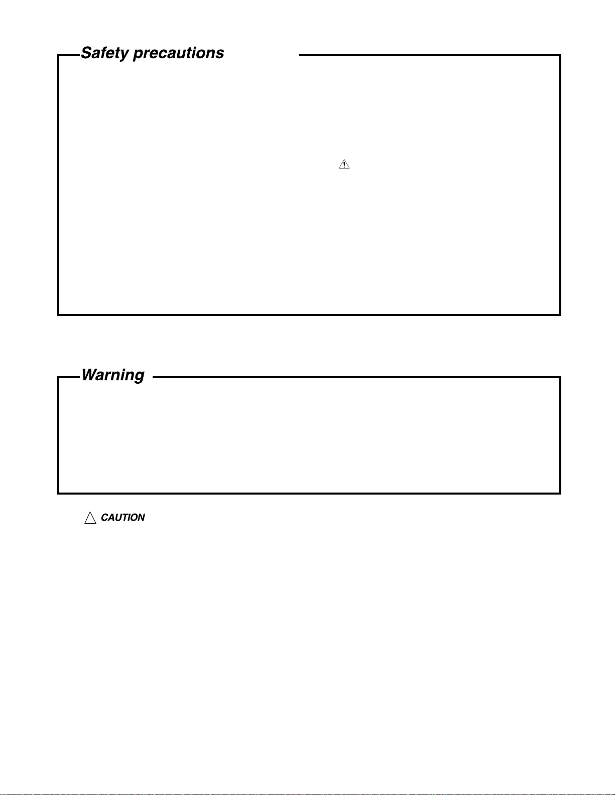
5. Leakage current check (Electrical shock hazard testing)
After re-assembling the product, always perform an isolation check on the exposed metal parts of the product
(antenna terminals, knobs, metal cabinet, screw heads, headphone jack, control shafts, etc.) to be sure the
product is safe to operate without danger of electrical shock.
Do not use a line isolation transformer during this check.
Plug the AC line cord directly into the AC outlet. Using a "Leakage Current Tester", measure the leakage
current from each exposed metal parts of the cabinet, particularly any exposed metal part having a return
path to the chassis, to a known good earth ground. Any leakage current must not exceed 0.5mA AC (r.m.s.).
Alternate check method
Plug the AC line cord directly into the AC outlet. Use an AC voltmeter having, 1,000 ohms per volt or more
sensitivity in the following manner. Connect a 1,500 10W resistor paralleled by a 0.15 F AC-type capacitor
between an exposed metal part and a known good earth ground.
Measure the AC voltage across the resistor with the AC
voltmeter.
Move the resistor connection to each exposed metal part,
particularly any exposed metal part having a return path to
the chassis, and measure the AC voltage across the resistor.
Now, reverse plug in the AC outlet and repeat each
measurement. Voltage measured any must not exceed 0.75 V
AC (r.m.s.). This corresponds to 0.5 mA AC (r.m.s.).
0.15 F AC TYPE
1500 10W
Good earth ground
AC VOLTMETER
(Having 1000
ohms/volts,
or more sensitivity)
Place this
probe on
each exposed
metal part.
!
1. This equipment has been designed and manufactured to meet international safety standards.
2. It is the legal responsibility of the repairer to ensure that these safety standards are maintained.
3. Repairs m ust be made in accordance with the relevant safety standards.
4. It is essential that safety critical components are replaced by approved parts.
5. If mains voltage selector is provided, check setting for local voltage.
Burrs formed during molding may
be left over on some parts of the
chassis. Therefore, pay attention to
such burrs in the case of
preforming repair of this system.
In regard with component parts appearing on the silk-screen pr inted side (parts side) of the PWB diagrams, the
parts that are printed over with black such as the resistor ( ), diode ( ) and ICP ( ) or identified by the " "
mark nearby are critical for safety.
(This regulation does not correspond to J and C version.)
1-2
Page 3
RX-DV5RSL
(U.K only)
1. This design of this product contains special hardware and many circuits and components specially
for safety purposes. For continued protection, no changes should be made to the original
design unless authorized in writing by the manufacturer. Replacement parts must be identical to
those used in the original circuits.
2. Any unauthorised design alterations or additions will void the manufacturer's guarantee ; further more the
manufacturer cannot accept responsibility f or personal injury or property damage resulting therefrom.
3. Essential safety critical components are identified by ( ) on the Parts List and by shading on the
schematics, and must never be replaced by parts other than those listed in the manual. Please note
however that many electrical and mechanical parts in the product have special safety related
characteristics. These characteristics are often not evident from visual inspection. Parts other than
specified by the manufacturer may not have the same safety characteristics as the recommended
replacement parts shown in the Parts List of the Service Manual and may create shock, fire, or
other hazards.
4. The leads in the products are routed and dressed with ties, clamps, tubings, barriers and the
like to be separated from live parts, high temperature parts, moving parts and/or sharp edges
for the prevention of electric shock and fire hazard. When service is required, the or iginal lead
routing and dress should be observed, and it should be confirmed that they have been returned
to normal, after re-assembling.
1. Service should be performed by qualified personnel only.
2. This equipment has been designed and manufactured to meet international safety standards.
3. It is the legal responsibility of the repairer to ensure that these safety standards are maintained.
4. Repairs must be made in accordance with the relevant safety standards.
5. It is essential that safety critical components are replaced by approved parts.
6. If mains voltage selector is provided, check setting for local voltage.
!
Burrs formed during molding may be left over on some parts of the chassis. Therefore,
pay attention to such burrs in the case of preforming repair of this system.
1-3
Page 4
RX-DV5RSL
Preventing static electricity
1. Grounding to prevent damage by static electricity
Electrostatic discharge (ESD), which occurs when static electricity stored in the body, fabric, etc. is discharged,
can destroy the laser diode in the traverse unit (optical pickup). Take care to prevent this when performing repairs.
2. About the earth processing for the destruction prevention by static electricity
In the equipment which uses optical pick-up (laser diode), optical pick-up is destroyed by the static electricity of
the work environment.
Be careful to use proper grounding in the area where repairs are being performed.
2-1 Ground the workbench
Ground the workbench by laying conductive material (such as a conductive sheet) or an iron plate over
it before placing the traverse unit (optical pickup) on it.
2-2 Ground yourself
Use an anti-static wrist strap to release any static electricity built up in your body.
(caption)
Anti-static wrist strap
Conductive material
(conductive sheet) or iron plate
3. Handling the optical pickup
1. In order to maintain quality during transport and before installation, both sides of the laser diode on the
replacement optical pickup are shorted. After replacement, return the shorted parts to their original condition.
(Refer to the text.)
2. Do not use a tester to check the condition of the laser diode in the optical pickup. The tester's internal power
source can easily destroy the laser diode.
4. Handling the traverse unit (optical pickup)
1. Do not subject the traverse unit (optical pickup) to strong shocks, as it is a sensitive, complex unit.
2. Cut off the shorted part of the flexible cable using nippers, etc. after replacing the optical pickup. For specific
details, refer to the replacement procedure in the text. Remove the anti-static pin when replacing the traverse
unit. Be careful not to take too long a time when attaching it to the connector.
3. Handle the flexible cable carefully as it may break when subjected to strong force.
4. It is not possible to adjust the semi-fixed resistor that adjusts the laser power. Do not turn it.
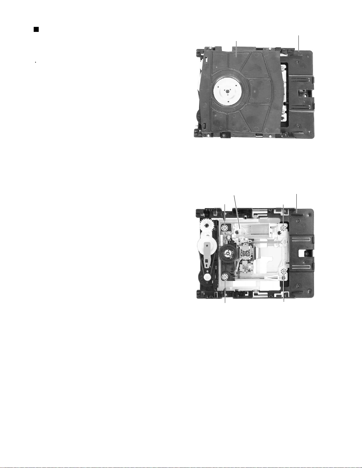
Attention when traverse unit is decomposed
Because the DVD/ CD mechanism assembly of this model is a
unit component, the individual component parts consisting of
the DVD / CD mechanism assembly are not supplied
separately.
If you need to decompose the traverse unit, solder the two
soldering points on the flexible board respectively before
removing the traverse unit.
DVD / CD unit
Flexible board
Fig.1
DVD / CD
holder
mechanism
1-4
Soldering
points
Fig.2
Pickup unit
connector
Page 5
RX-DV5RSL
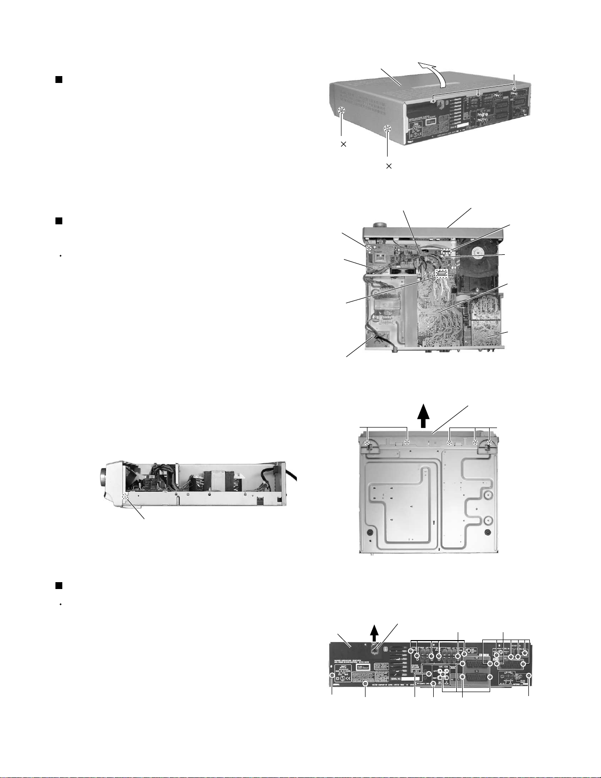
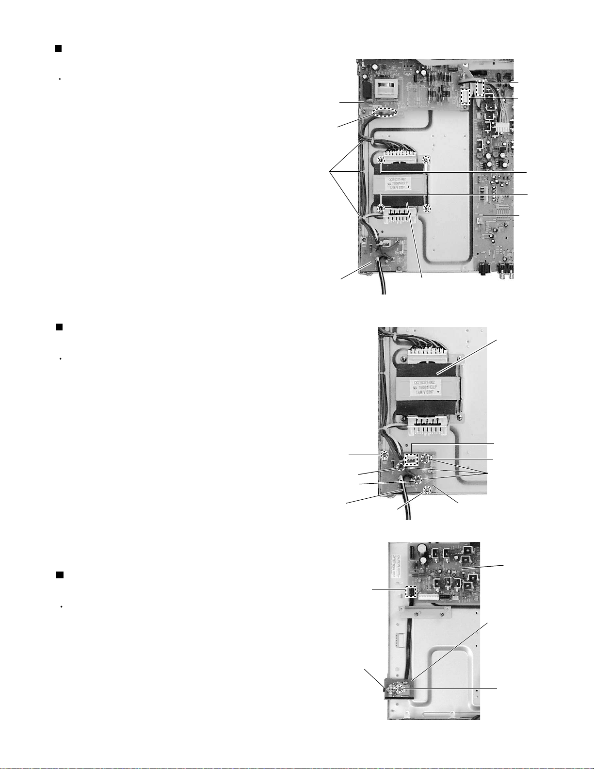
Disassembly method
Removing the top cover (See Fig.1)
1.
Remove the four screws marked A attaching the top
cover on both sides of the body.
2.
Remove the three screws marked B on the back of
the body.
3.
Remove the top cover from behind in the direction of
the arrow while pulling both sides outward.
Removing the front panel assembly
(See Fig.2 to 4)
Prior to performing the following procedures, remove
the top cover.
1.
Disconnect the card wire from the connector CN114
on the main board.
2.
Remove the screw marked C attaching the earth
wire to the power supply board.
3.
Remove the five screws marked D attaching the front
panel assembly on the bottom of the body. Detach
the front panel assembly toward the front.
4.
Release the two joints marked a on both sides of the
body using a screwdriver.
A
C
Power
supply
board
CN201
Power
/Fuse
board
Top cover
2
D
A
2
Tie band
B
Fig.1
Front panel assembly
CN114
Main
board
Amplifier
board
DSP
board
Fig.2
Front panel assembly
D
Joint a
Fig.4
Removing the rear panel (See Fig.5)
Prior to performing the following procedures, remove
the top cover.
1.
Remove the power cord stopper from the rear panel
by moving it in the direction of the arrow.
2.
Remove the eighteen screws marked E attaching
each boards to the rear panel on the back of the
body.
3.
Remove the fore screws marked F attaching the rear
panel on the back of the body.
Rear panel
F
F
Fig.3
Cord stopper
Fig.5
E
E
EE
FF
1-5
Page 6
RX-DV5RSL
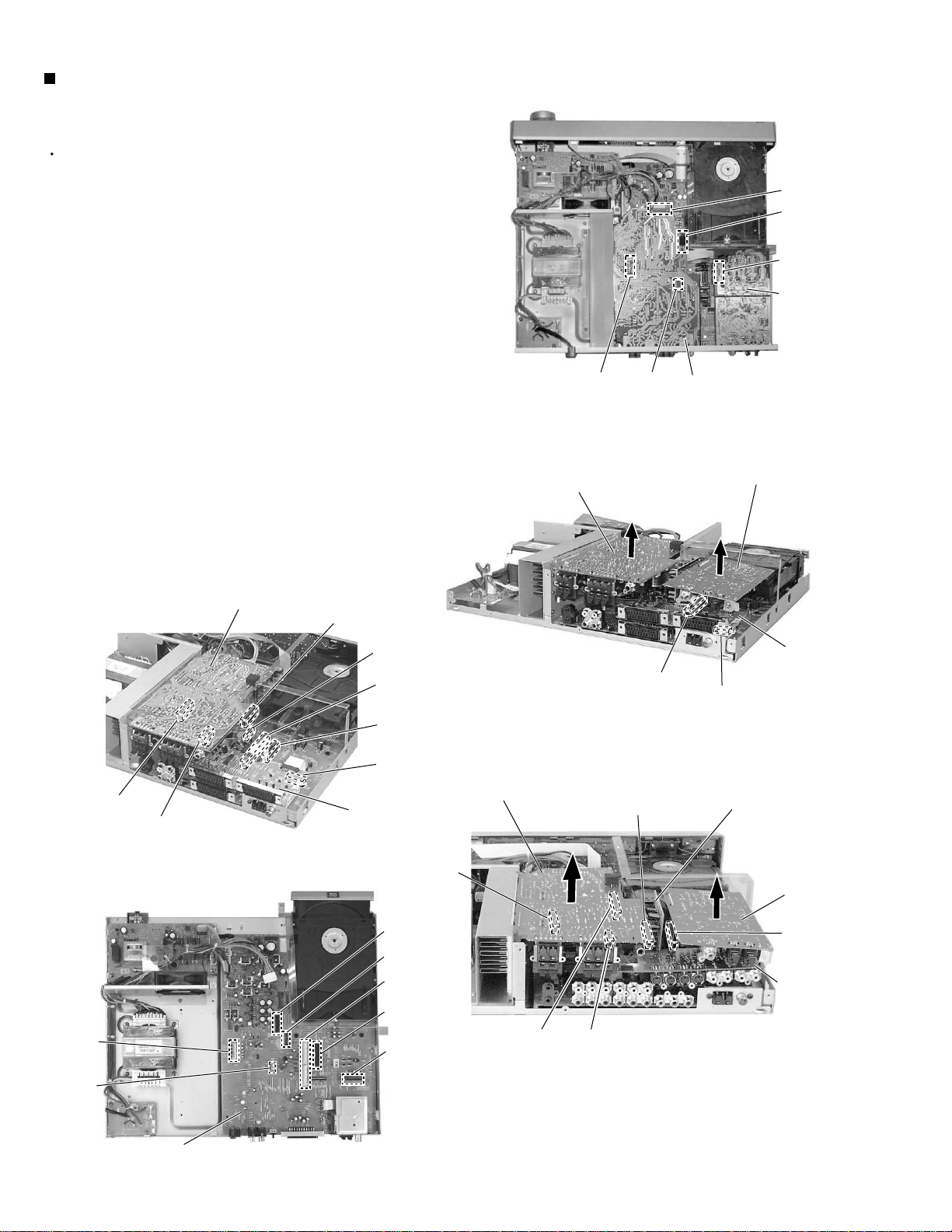
Removing each board connected to the
main board
(See Fig.6 to 10)
Prior to performing the following procedures, remove
the top cover and rear panel.
1.
Cut off the tie band fixing the harness.
2.
Disconnect the video board from the connector
CN911 CN912 on the main board.
CN201
CN212
CN612
3.
Disconnect the DSP board from the connector
CN612 on the main board,
4.
Disconnect the card wire from the connecter CN614
on the main board.
5.
Disconnect the video select board from the
connector CN411, CN412 on the main board.
Amplifier board
CN212
CN614
CN911
/ CN912
CN612
CN231
Fig.6
Amplifier board
CN241
CN612
Fig.7
DSP
board
Amplifier
board
DSP board
Video select
board
CN412
1-6
CN231
CN241
CN231
CN241
Main
board
Fig.9
Fig.10
CN412
Video select
board
CN212
CN614
CN911
/ CN912
CN612
CN412
CN231
Amplifier board
/ CN912
CN241CN212
Fig.8
Video boardCN911
DSP
board
CN612
S-video
board
Page 7
Removing the amplifier board
(See Fig.11, 12)
Prior to performing the following procedures, remove
the top cover, and rear panel.
1.
Disconnect the wire from the connector CN201 on
the amplifier board.
2.
Disconnect the amplifier board from the connector
CN212 on the main board.
Tie
band
G
H
RX-DV5RSL
CN201
CN212
DSP
board
CN612
3.
Disconnect the amplifier board from the wire
connected to the connector CN231 and CN241 on
the main board.
4.
Disconnect the screws marked G attaching the earth
wire and the amplifier board on the fan bracket.
5.
Disconnect the four screws H attaching the amplifier
board on the body.
Removing the power ICs
(See Fig.13, 14)
Prior to performing the following procedures, remove
the top cover, rear panel and amplifier board.
Heat sink
I
CN231
Fig.11
Fig.12
Amplifier board
Power ICs
CN241
CN212
CN231
CN241
Main
board
I
1.
Remove the six screws marked I attaching the power
ICs.
2.
Unsolder the two p
the rear side of the amplifier board.
3.
Pull out the amplifier board from the bracket hooks
on the heat sink.
ower ICs solder points
attaching
Fook
Amplifier board
Amplifier board
rear side
Fig.13
Power ICs solder points
Fook
Heat sink
Fig.14
1-7
Page 8
RX-DV5RSL
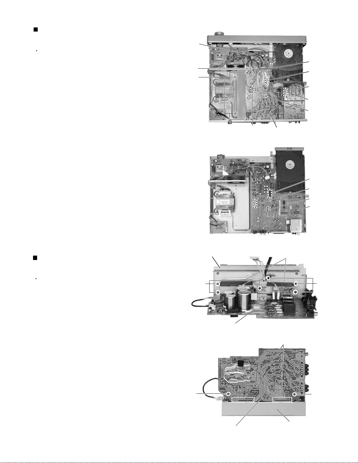
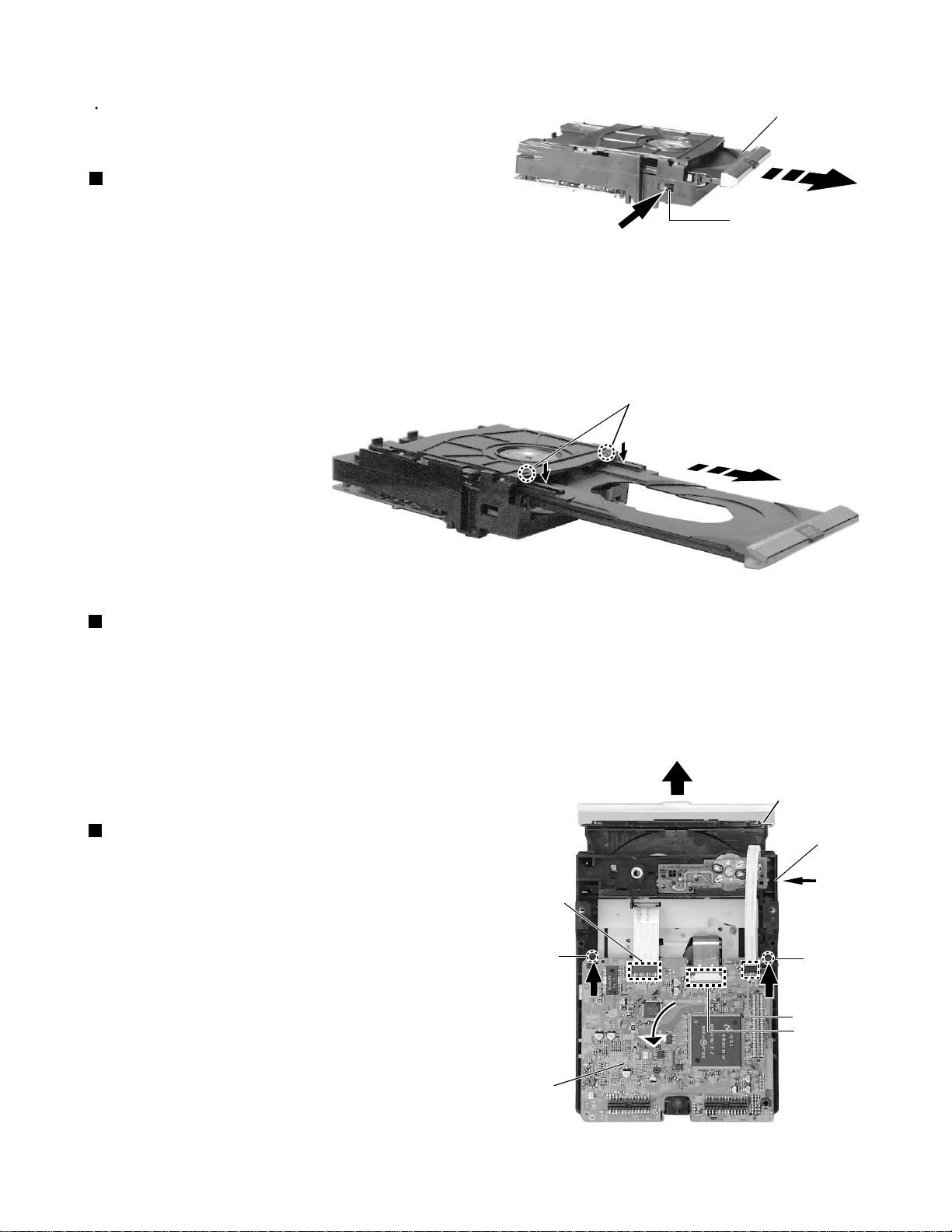
Removing the DVD / CD unit
(See Fig.15)
Prior to performing the following procedures, remove
the top cover, rear cover and DSP board.
1.
Pull up the two plastic rivet attaching the DVD / CD
unit dust proof cover.
2.
Remove the DVD / CD unit dust proof cover
attaching on the main board.
3.
Remove the three screws marked J attaching the
DVD / CD unit.
Dust proof
cover
DVD
/ CD
unit
J
J
Bracket a
CN512
4.
Remove the bracket marked a attaching on the DVD
/ CD unit.
5.
Disconnect the connectors CN512 and CN513 on
the main board.
Removing the fan bracket (See Fig.16)
Prior to performing the following procedures, remove
the top cover, rear cover, video board, DSP board,
amplifier board and S-video board.
1.
If necessary, cut off the tie band fixing the harness.
2.
Remove the two screws marked K attaching the fan
bracket on the body.
3.
Remove the harness bands fixing the harness on the
fan bracket.
4.
Disconnect the connector CN122 on the main board.
Removing the power supply board
(See Fig.17)
Plastic
rivet
Power
supply
board
Fan
bracket
Fig.15
Harness bands
Fig.16
CN513
Main
board
CN115
CN121
CN111
CN122
K
Main
board
Prior to performing the following procedures, remove
the top cover, rear cover, video board, DSP board,
amplifier board, S-video board and fan bracket.
1.
If necessary, cut off the tie band fixing the harness.
2.
Disconnect the card wire from the connector CN115
on the power supply board.
3.
Disconnect the harness connected to the connector
CN111 on the power supply board.
4.
Remove the four screws marked L attaching the
power supply board on the body.
5.
Unsolder the solder points at the three harnesses
connected to the power supply board.
1-8
Power
supply
board
Tie
band
L
Solder
points
L
CN115
CN121
CN111
CN122
Fig.17
Page 9
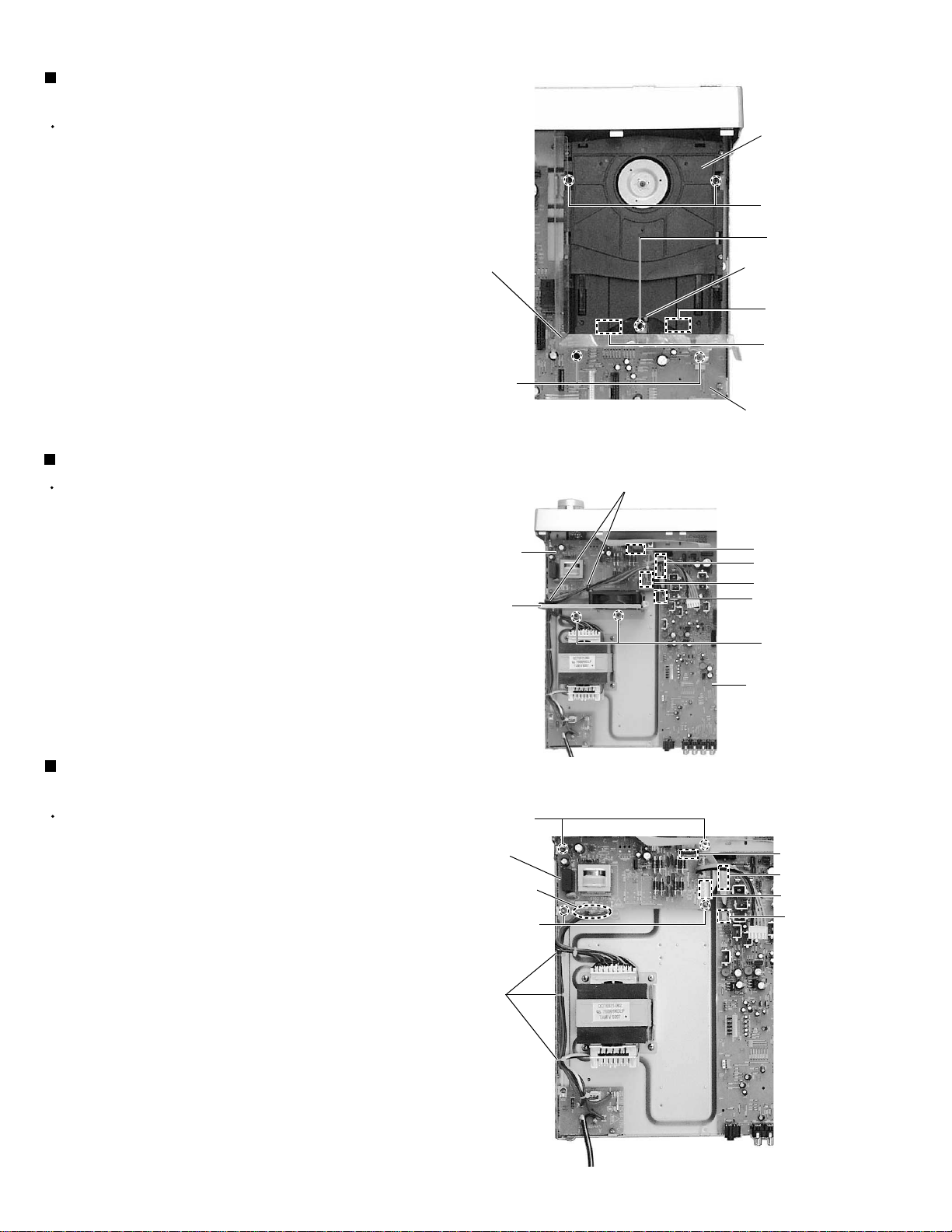
Removing the power transformer
(See Fig.18, 19)
Prior to performing the following procedures, remove
the top cover and rear panel.
1.
If necessary, cut off the tie band fixing the harness.
2.
Disconnect the harness from the connector CN101
on the power / fuse board.
Power
supply
board
Solder
points
RX-DV5RSL
CN121
CN111
3.
Disconnect the harness from the connectors CN111
and CN121 on the power supply board and main
board respectively.
4.
Unsolder the three harnesses connected to the
power supply board.
5.
Remove the four screws marked M attaching the
power transformer on the body.
Removing the power / fuse board
(See Fig.19)
Prior to performing the following procedure, remove
the top cover and rear panel.
1.
Disconnect the harness connected to the connector
CN101 on the power / fuse board (If necessary, cut
off the tie band fixing the harness on the side of the
base chassis).
2.
Unsolder the power cord and other harnesses
connected to the power / fuse board.
3.
Remove the two screws marked N attaching the
power / fuse board on the body.
Tie
band
Power / Fuse board
N
PW103
PW102
Power cord
N
M
M
Amp.
board
Power
transformer
Fig.18
Power
transformer
CN101
PW101
Solder
points
Power / Fuse board
Fig.19
Removing the headphone board
(See Fig.20)
Prior to performing the following procedures, remove
the top cover, rear cover, front panel assembly and
power supply board.
1.
Disconnect the harness connected to the connector
CN291 on the main board (If necessary, remove the
amplifier board and fan bracket).
2.
Remove the screw marked O attaching the
headphone board on the body.
Main
board
CN291
Headphone
board
Headphones
jack
O
Fig.20
1-9
Page 10
RX-DV5RSL
Removing the tuner board
(See Fig.21)
Prior to performing the following procedures, remove
the top cover, rear panel, video board, DSP board
and video select board.
1.
Disconnect the card wire from the connector CN301
on the main board.
2.
Remove the two screws marked P attaching the
tuner board on the body.
Removing the main board
(See Fig.22)
Prior to performing the following procedures, remove
the top cover, rear panel, video selector board, DSP
board, video select board, amplifier board, DVD /
CD unit and tuner board.
1.
Disconnect the card wire from the connectors CN114
CN125 on the main board.
CN291
CN121
CN125
CN122
Fig.21
CN301
Main
board
Tuner
board
P
CN114
Q
2.
Disconnect the wire from the connectors CN121,
CN122 and CN291 on the main board.
3.
Remove the five screws marked Q attaching the
main board on the body.
Removing each board connected to the
rear side of the front panel
(See Fig.23)
Prior to performing the following procedures, remove
the top cover and front panel assembly.
1.
Remove the two screws marked R attaching the
power switch board.
2.
Remove the eight screws marked S attaching the
system control board.
3.
Remove the two screws marked T attaching the lens
cover.
4.
Pull out the lens and indicator board.
(If necessary, unsolder the FW701, FW702.)
Main board
Front panel
W
System control board
Fig.22
Indicator
Control board
Fig.23
board
U
Power switch
board
RS T
Lens cover
Select board
5.
Remove the two screws marked U attaching the
select board.
6.
Remove the three screws marked W attaching the
control board.
1-10
Page 11
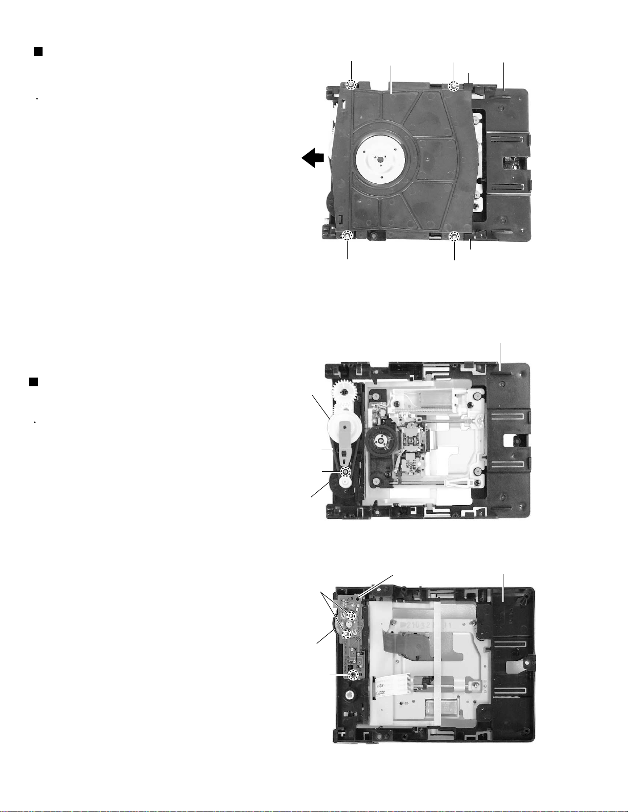
<DVD / CD unit>
g
RX-DV5RSL
Prior to performing the following procedures, remove
the DVD / CD unit.
Removing the DVD / CD tray
(See Fig.1, 2)
1.
Push the cam lever toward the center side of the
DVD / CD unit in the direction of the arrow and draw
the DVD / CD tray toward the front.
2.
Push the two tray stoppers marked a on the DVD /
CD tray in the direction of the arrow and draw the
DVD / CD tray toward the front.
Fig.1
a (Tray stopper)
DVD / CD
Loading cam lever
tray
Reinstall the DVD / CD tray
(See Fig. 1, 2)
1.
Align the rail with the DVD / CD tray as shown fig.2,
then mount the DVD / CD tray.
Removing the DVD / CD servo board
(See Fig.3)
1.
Disconnect the card wire from the connectors
CN101, CN201 and CN202 on the DVD / CD servo
board.
2.
Push the two DVD / CD servo board hooks marked b
and pull out the DVD / CD servo board.
CN201
Hook b
Fig.2
DVD / CD
tray
Loading
cam
lever
Hook b
CN202
CN101
DVD / CD
servo board
.3
Fi
1-11
Page 12
RX-DV5RSL
Removing the the top cover
(See Fig.4)
Prior to performing the following procedures, remove
the DVD / CD tray.
1.
Remove the four screws marked A attaching the top
cover on the DVD / CD unit.
2.
Pull the top cover toward the direction of the arrow
and draw the top cover toward the upper side.
A
A
Top cover
Fig.4
A
A
DVD / CD
Stopper
Stopper
DVD / CD
unit
unit
Removing the tray drive motor board
(See Fig.5, 6)
Prior to performing the following procedures, remove
the DVD / CD tray, top cover, and DVD / CD servo
board.
1.
Unsolder the solder points at the tray drive motor
board.
2.
Detach the belt from the pulley on the bottom of the
DVD / CD unit. (Do not stain the belt with grease).
3.
Remove the screws marked B attaching the tray
drive motor on the DVD / CD unit.
4.
Remove the screws marked C attaching the tray
drive motor board on the DVD / CD unit.
Pulley
Belt
B
Motor
Solder
points
Motor
C
Fig.5
Tray drive
motor board
DVD / CD
unit
1-12
Fig.6
Page 13
RX-DV5RSL
Removing the DVD / CD mechanism
holder assembly (mechanism included)
(See Fig. 7, 8)
Prior to performing the following procedures, remove
the DVD / CD tray, the DVD / CD servo board and
top cover.
Remove the four screws marked D attaching the
1.
DVD / CD mechanism holder assembly on the DVD /
CD unit.
Pull out the DVD / CD mechanism holder assembly.
2.
Top cover
Fig.7
DVD / CD mechanism
holder assembly
D
DVD / CD
DVD / CD
D
unit
unit
D
Fig.8
D
1-13
Page 14

RX-DV5RSL
Adjustment method
Measurement instruments required
for adjustment
1. Low frequency oscillator,
This oscillator should have a capacity to output 0dBs
to 600ohm at an oscillation frequency of 50Hz-20kHz.
2. Attenuator impedance : 600ohm
3. Electronic voltmeter
4. Frequency counter
5. Wow flutter meter
6. Test tape
VT712 : For Tape speed and wow flutter ( 3kHz)
VT724 : For Reference level (1kHz)
VT703L : For Head angle (10kHz)
Because of frequency-mixed tape with 63,1k,10k and
14kHz(250nWb/m -24dB).
Use this tape together with a filter.
7. Blank tape
TAPE : AC-225
8. Torque gauge : For play and back tension
Forward ; TW2111A, Reverse ; TW2121A
Fast Forward and Rewind ; TW2231A
9. Test disc
: VT-501(12cm)
10. Jitter meter
Measurement conditions
Power supply voltage
AC120V(50Hz)
Measurement
output terminal : Speaker out
:TP101 (Measuring for TUNER/DECK/CD)
:Dummy load 6ohm
Radio input signal
AM modulation frequency : 400Hz
Modulation factor : 30%
FM modulation frequency : 400Hz
Frequency displacement : 22.5kHz
Frequency Range
AM 530kHz~1600kHz (10kHz step)
FM 87.5MHz~108MHz
Standard measurement positions of volume
and switch
Power : Standby (Light STANDBY Indicator)
Sub woofer VOL. : Minimum
Sound mode : OFF
Main VOL. : 0 Minimum
Traverse mecha set position : Disc 1
Mic MIX VOL : MAX
ECHO : OFF
Precautions for measurement
1. Apply 30pF and 33kohm to the IF sweeper output
side and 0.082 F and 100kohm in series to
the sweeper input side.
2. The IF sweeper output level should be made as
low as possible within the adjustable range.
3. Since the IF sweeper is a fixed device, there is
no need to adjust this sweeper.
4. Since a ceramic oscillator is used, there is no need
to perform any MPX adjustment.
5. Since a fixed coil is used, there is no need to adjust
the FM tracking.
6. The input and output earth systems are separated.
In case of simultaneously measuring the voltage
in both of the input and output systems with an
electronic voltmeter for two channels, therefore,
the earth should be connected particularly.
7. In the case of BTL connection amplifier, the minus
terminal of speaker is not for earthing. Therefore,
be sure not to connect any other earth terminal
to this terminal. This system is of an OTL system.
1-14
Page 15
Initialization method of DVD section
When microprocessor ICs or pick-up has been replaces, initialize the
DVD player in the following manner.
If tray is not completely close up, make power to standby from on to close up the tray.
1.
After confirming that tray is completely close up, pull off the power plug.
Insert the power plug to the outlet while pressing "STOP" and "DVD" Button at the same time to be
2.
TEST Mode.
FL display indicates "TEST **" and "** (Area code)" is indicated at the upper left of the display.
** : Area code
Press "PAUSE" button to initialize.
3.
When an indication of "ATT" is displayed, initialization finishes.
Push the POWER SW to be standby.
4.
About TEST MODE
Before implementing the TEST Mode please do the change to the mode of remote control the DVD Mode.
The operation of the remote control is because it is not produced
This player has a TEST MODE for product QC, service or repair. Contents are given as follows.
TEST MODE has the 4 different states. These are changed with the CHOICE key on
the remote controller. TEST MODE is canceled by the POWER key.
Insert the power plug to the outlet while pressing "STOP" and "DVD" buttons at the same time.
"** (Area code)" is indicated at the upper left of the display.
FL Display indicates " TEST ** ".
** : Area code .... Refer to (Fig, 1)
RX-DV5RSL
DVD Button
CHOICE Button
(Test mode)
HOME CINEMA
DVD-AUDIO/VIDEO CONTROL CENTER
STANDBY/ON
VCRSTB TV AUDIO
TAPETV CDR FM/AM
TV DIRECT
TV/VIDEO
REW/ TUNING/GROUP
FM MODE STROBE
REPEAT SLEEP
EFFECT
CONTROL
ANALOG
TEST
/DIGITAL
INPUT
SURR ON/OFF
AUDIO
SURR MODE
SUBTITLE
10/0 +10
DIMMER
ANGLE
PAGE
MUTING
ZOOM
TA/NEWS/INFO
DIGEST
TOP MENU
PTY SEARCH
CHOICE
ON SCREEN
REMOTE CONTROL RM-SRXDV5R
VCRSTB DVD
Ð SUBWOOFER +
100+ TV RETURN
TV VOL
ENTER
/FF
TV/STB CH
CENTER
231
REARáL
564
REARáR
897
VFP
PROGRESSIVE
+Ð+
VOLUME
Ð
MENU
PTYPTY
RETURN
DISPLAY
DVD
Button
(Test mode)
(Initialize complete)
POWER Button
STANDBY
STANDBY/ON
DVD AUDIO
INPUT
SURROUND
ON/OFF
ANALOG/DIGITA
L
INPUT ATT. REC MODE
RX-DV5R HOME CINEMA DVD-AUDIO/VIDEO CONTROL CENTER
MODE
STOP Button
(Test mode )
TVVCRSTBDVD
SOURCE NAME
OPEN/CLOSE
FL Display
The first: FL display shows the player firmware version.
1.
Button (Test mode)
Contents: [System firm] [Front End firm] [Back End firm]
The second: Indicator check mode. All FL segment and all LED light.
2.
The third: Mechanism check mode. In this mode the player displays "CHECK".
3.
The fourth: Front-end check mode. In this mode the FL displays "EXPERT".
4.
FM/AMTAPE/CDR
TV DIRECT
SETTING ADJUST MEMORY
MASTER VOLUME
CONTROL
DVD/SUPER VCD/VCD/CD
COMPACT
SUPER VIDEO
1-15
Page 16
RX-DV5RSL
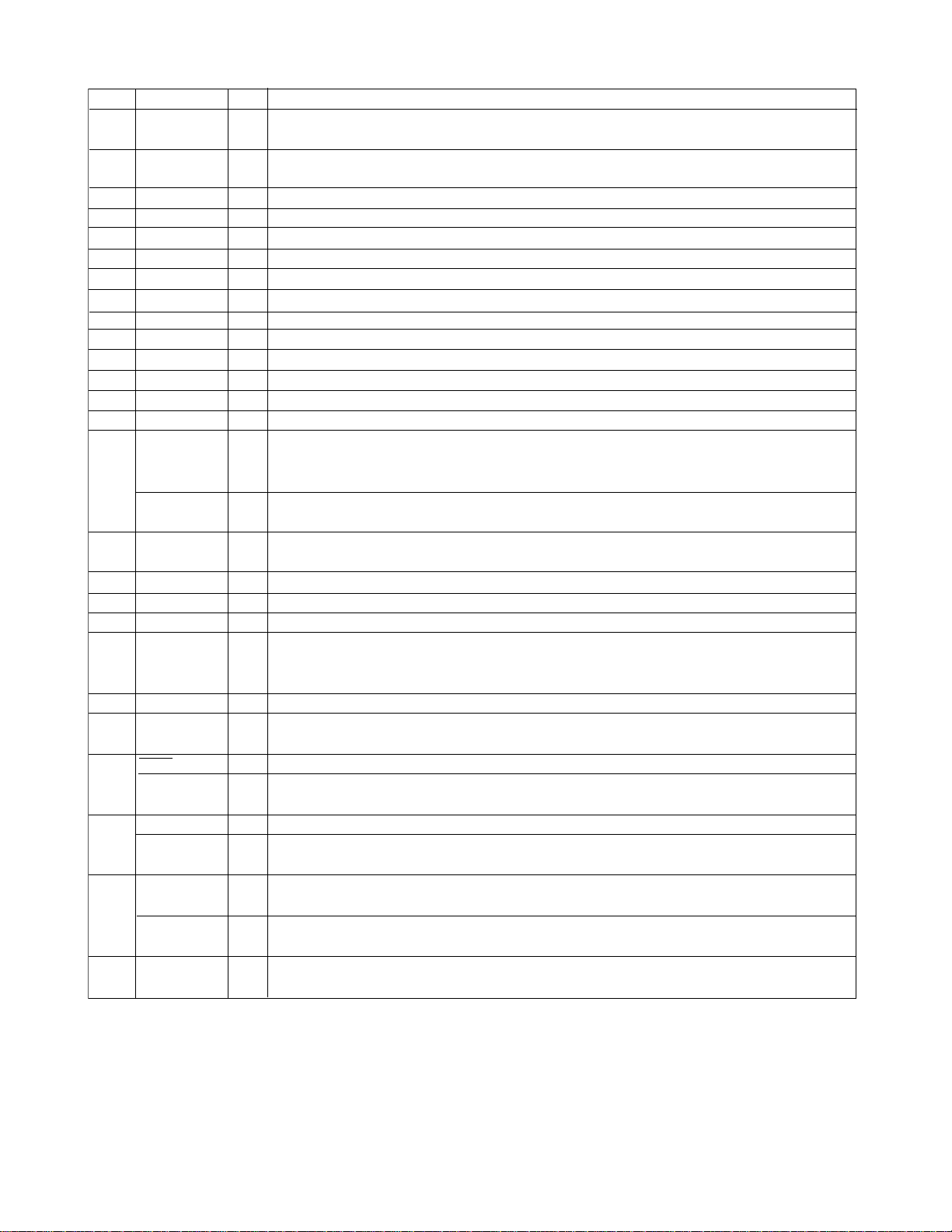
Description of major ICs
AK4527BVQP (IC601) : A/D,D/A converter
1. Pin layout
2. Pin function (1/2)
No.
1
2
3
4
5
6
7
8
9
10
11
12
13
14
15
16
17
18
Symbol
SDOS
OSKS
MIS
BICK
LRCK
SDTI1
SDTI2
SDTI3
SDTO
D,AUX
DFS
DEMI
DEMO
MCKO
DVDD
DVSS
PD
XTS
4443424140393837363534
1
2
3
4
5
6
7
8
9
10
11
1213141516171819202122
I/O
I
SDTO Source Select Pin (Note 1)
Top View
Function
33
32
31
30
29
28
27
26
25
24
23
"L" : Internal ADC output, "H" : DAUX input
I
Control Mode Select Pin
"L" : 3-wire Serial, "H" : I
-
Soft Mute Pin (Note 1), Connect to GND
2C Bus
When this pin goes to "H", soft mute cycle is initialized.
When returning to "L", the output mute releases.
I
Audio Serial Data Clock Pin
I/O
Input Channel Clock Pin
I
DAC1 Audio Serial Data Input Pin
I
DAC2 Audio Serial Data Input Pin
I
DAC3 Audio Serial Data Input Pin
O
Audio Serial Data Output Pin
-
Sub Audio Serial Data Input Pin, Connect to GND
-
Double Speed Sampling Mode Pin (Note 1)
"L" : Normal Speed, "H" : Double Speed
-
Connect to GND
No internal bonding.
-
Zero Input Detect Enable Pin, Connect to GND
"L" : mode 7 (disable) at parallel mode,
-
zero detect mode is selectable by DZFM2-0 bits at serial mode.
-
"H" : mode 0 (DZF is AND of all six channels)
-
Output Buffer Power supply Pin, 2.7V~5.5V
I
Digital Power Supply Pin, 4.5V~5.5V
-
De-emphasis Pin, 0V
I
Power-Down & Reset Pin
When "L", the AK4527B is powered-do wn and the control registers are reset to def ault
state. If the state of P/S or CAD0-1 changes, then the AK4527B m ust be reset b y PDN.
-
Test Pin, Connect to GND
This pin should be connected to DVSS.
1-16
Page 17
RX-DV5RSL
Pin function (2/2)
Symbol
No.
ICKS
19
ADIF
20
CAD1
21
CAD0
22
LOUT3
23
ROUT3
24
LOUT2
25
ROUT2
26
LOUT1
27
ROUT1
28
LIN-
29
LIN+
30
RIN-
31
RIN+
32
VREFL
33
OVF
VCOM
34
VREFH
35
AVDD
36
AVSS
37
XTI
38
XTO
39
P1S
40
CS
41
CSN
DIF1
42
SCL/CCLK
LOOP0
43
SAD/CDTI
CDTD
44
I/O
Connect to GND
-
Function
No internal bonding.
Analog Input Format Select Pin, Digital Power Supply
"H" : Full-differential input, "L" : Single-ended input
Chip Address 1 Pin,
Chip Address 0 Pin,
DAC3 Lch Analog Output Pin
O
DAC3 Rch Analog Output Pin
O
DAC2 Lch Analog Output Pin
O
DAC2 Rch Analog Output Pin
O
DAC1 Lch Analog Output Pin
O
DAC1 Rch Analog Output Pin
O
Lch Analog Negative Input Pin
I
Lch Analog Positive Input Pin
I
Rch Analog Negative Input Pin
I
Rch Analog Positive Input Pin
I
Zero Input Detect 2 Pin (Note 2), Non
-
Connect to GND
Connect to GND
Connect
When the input data of the group 1 follow total 8192LRCK cycles with "0"
input data, this pin goes to "H".
Analog Input Overflow Detect Pin (Note 3)
O
This pin goes to "H" if the analog input of Lch or Rch is overflows.
Common Voltage Output Pin,AVDD/2
O
Large external capacitor around 2.2uF is used to reduce power-supply noise.
Positive Voltage Reference Input Pin,AVDD
Analog Power Supply Pin,4.5V~5.5V
Analog Ground Pin,0V
Zero Input Detect 1 Pin (Note 2), Non connect
When the input data of the group 1 follow total 8192 LRCK cycles with "0"
input data, this pin goes to "H".
Master Clock Input Pin
I
Parallel / Serial Select Pin
"L" : Serial control mode, "H" : Parallel control mode
Audio Data Interface Format 0 Pin in parallel mode
I
Chip select pin in 3-wire serial control mode
I
This pin should be connected to DVDD at I2C bus control mode
Audio Data Interface Format 1 Pin in parallel mode
I
Control Data Clock Pin in serial control mode
I
I2C = "L" : CCLK(3-wire Serial), I2C = "H" : SCL(I2CBus)
Loopback Mode 0 Pin in parallel control mode
I
Enables digital loop-back from ADC to 3 DACs.
Control Data Input Pin in serial control mode
I/O
I2C = "L" : CDTI(3-wire Serial), I2C = "H" : SDA(I2CBus)
Loopback Mode 1 Pin (Note 1)
I
Enable all 3 DAC channels to be input from SDTII.
AK4527
Notes : 1. SDOS, SMUTE, DFS, and LOOP1 pins are ORed with register data if P/S = "L".
2. The group 1 and 2 can be selected by DZFM2-0 bit if P/S = "L" and DZFME = "L".
3. This pin becomes OVF pin if OVFE bit is set to "1" at serial control mode.
4. All input pins should not be left floating.
1-17
Page 18

RX-DV5RSL
MN101C35DKF (IC701) : Panel MICOM
1. Pin layout
~
100 76
1
~
75
~
2. Pin function
Pin No.
1
2
3
4
5
6
7
8
9
10
11
12
13
14
15
16
17
18
19
20
21
22
23
24
25
26
27
28
29
30
31
32
33
34
35
36
37
38
39
40
41
42
43
Symbol
TXD/SBO0/P00
RXO/SBI0/P01
SBT0/P02
SBO1/P03
SBI1/P04
SBT1/P05
BUZZER/P06
OSC2
OSC1
MMOD
VREF-
VERSION1
VERSION2
VREF+
LED DIMMER
RESET
LED BLUE
LED VCR
LED STB
LED AUDIO
LED DVD
DI BUSY
REMO
VOL IN1
VOL IN2
IRQ4
DI PS2
DI S2P
DI CK
25
VDD
VSS
XI
XO
KEY1
KEY2
KEY3
KEY4
KEY5
KEY6
DI CS
P25
~
26 50
51
I/O
O
No connect
No connect
O
No connect
O
No connect
O
No connect
O
No connect
O
No connect
O
-
Power supply
O
External terminal for main clock
External terminal for main clock
I
-
Connect to GND
-
Connect to GND
O
No connect
-
Connect to GND
-
Connect to GND
Key input terminal 1
I
I
Key input terminal 2
I
Key input terminal 3
I
Key input terminal 4
I
Key input terminal 5
I
Key input terminal 6
Chip select 1
I
I
Chip select 2
-
Reference voltage terminal
O
LED DIMER
I
Reset input
O
LDE (BLUE)
O
LED (VCR)
O
LED (STB)
O
LED (DVD audio)
O LED (DVD)
Micom communication BUSY
O
Micom communication CS
I
Remote control signal input
I
I
VOL JOG IN1
I
VOL JOG IN2
O
No connect
O
No connect
O Micom communication status output
I
Micom communication status input
I
Micom communication CLK
O
No connect
O
No connect
Function
1-18
Page 19

Pin No
.
44
45
46
47
48
49
50
51
52
53
54
55
56
57
SEG0/DGT7/P77
58
SEG1/DGT6/P76
59
SEG2/DGT5/P75
SEG3/DGT4/P74
60
SEG4/DGT3/P73
61
62
SEG5/DGT2/P72
63
SEG6/DGT1/P71
64
SEG7/DGT0/P70
65
66
67
68
69
70
71
72
73
74
75
76
77
78
79
80
81
82
83
84
85
86
87
88
89
90
91
92
93
94
95
96
97
98
99
100
Symbol I/O
P52
P53
P54
DGT17/P67
DGT16/P66
DGT15/P65
DGT14/P64
DGT13/P63
DGT12/P62
DGT11/P61
DGT10/P60
DGT9/P41
DGT8/P40
SEG8/P87
SEG9/P86
SEG10/P85
SEG11/P84
SEG12/P83
SEG13/P82
SEG14/P81
SEG15/P80
SEG16/P97
SEG17/P96
SEG18/P95
SEG19/P94
SEG20/P93
SEG21/P92
SEG22/P91
SEG23/P90
SEG24/PC2
SEG25/PC1
SEG26/PC0
SEG27/PB7
SEG28/PB6
SEG29/PB5
SEG30/PB4
SEG31/PB3
SEG32/PB2
SEG33/PB1
SEG34/PB0
SEG35/PD7
SEG36/PD6
SEG37/PD5
SEG38/PD4
SEG39/PD3
SEG40/PD2
SEG41/PD1
SEG42/PD0
VPP
O
O
O
O
O
O
O
O
O
O
O
O
O
O
O
O
O
O
O
O
O
O
O
O
O
O
O
O
O
O
O
O
O
O
O
O
O
O
O
O
O
O
O
O
O
O
O
O
O
O
O
O
O
O
O
O
-
RX-DV5RSL
MN101C35DKF
Function
No connect
No connect
No connect
No connect
No connect
No connect
No connect
GRID1
GRID2
GRID3
GRID4
GRID5
GRID6
GRID7
GRID8
GRID9
GRID10
GRID11
GRID12
GRID13
SEGMENT36
SEGMENT35
SEGMENT34
SEGMENT33
SEGMENT32
SEGMENT31
SEGMENT30
SEGMENT29
SEGMENT28
SEGMENT27
SEGMENT26
SEGMENT25
SEGMENT24
SEGMENT23
SEGMENT22
SEGMENT21
SEGMENT20
SEGMENT19
SEGMENT18
SEGMENT17
SEGMENT16
SEGMENT15
SEGMENT14
SEGMENT13
SEGMENT12
SEGMENT11
SEGMENT10
SEGMENT9
SEGMENT8
SEGMENT7
SEGMENT6
SEGMENT5
SEGMENT4
SEGMENT3
SEGMENT2
SEGMENT1
VPP
1-19
Page 20

RX-DV5RSL
MN101C49GKG (IC761) : System MICOM
1. Pin layout
~
100 76
1
~
75
~
25
26 50
51
~
2. Pin function
Pin No.
1 VREF - Connect to GND
2 PA0 I NTSTEL(RGBESL)
3 PA1 I VCR S/C SW
4 PA2 I DBS S/C SW
5 PA3 I SAFETY
6 PA4 I SHORT&TH DET (A/D)
7 PA5 I OUTLEVEL DETECT (A/D)
8 PA6 I VCR IN (A/D)
9 PA7 I STB IN (A/D)
10 VREF+ - Reference voltage
11 VDD - VDD
12 OSC2 O External terminal for connected oscillator
13 OSC1 I External terminal for connected oscillator
14 VSS - Connect to GND
15 XI I Connect to GND
16 XO O No connect
17 MMO0 I Connect to GND
18 SBO0 O DI DO
19 SBI0 I DI DI
20 SBT0 O DI CK
21 SBO2 O S2UDT
22 SBI2 I U2SDT
23 SBT2 I SCLK
24 NDK O INTP
25 SYSCLK O CPURST
26 IRQ0 I CS
27 IRQ1 I
28 IRQ2 I PROTECT
29 IRQ3 I RDS SET
30 IRQ4 I DI BUSY
31 IRQ5 I HAEADPHONE
32 GND I Connect to GND
33 NSRT I RESET IN
34 TM0IO O DSP RST
35 TM1IO O DSP RDY
36 TM2IO O AVC OUT
37 TM3IO I AVC IN
38 TM7IO O VIDEO MUTE1
39 P15 O VIDEO MUTE2
40 TM4IO O VIDEO YCMIX
41 P17 O VIDEO RGB
42 SBO1 O DSP COM
43 SBI1 I DSP STAT
Symbol
I/O
Function
1-20
Page 21

Pin No.
44 SBT1 O DSP CLK
45 CBO3 O VOL DATA
46 SBI3 O VOL LATCH
47 SBT3 O VOL CLK
48 MP3 O D.O.MUTE
49 INT/PROG O INT/PROG
50 KEY0 O HEADPHONE RELAY
51 KEY1 O EEDO
52 KEY2 O EEDI
53 KEY3 O EECK
54 KEY4 O EECS
55 KEY5 O FRONT SPK RELAY
56 KEY6 O CENTER SPK RELAY
57 KEY7 O REAR SPK RELAY
58 NEW O S1RELAY
59 NRE I INH
60 NCS O SLOW L
61 A16 O SLOW M
62 A17 O SYSTEM P.ON
63 A0 O FAN ON/OFF
64 A1 O DVD P.ON
65 A2 O TUNER P.ON
66 A3 O MECHA.ON
67 A4 I/O RDS DATA
68 A5 O RDS CLK
69 A6 O STEREO
70 A7 I TUNER DATAI
71 A8 O TUNER MUTE
72 A9 O TUNER DATA0
73 A10 O TUNER CLK
74 A11 O TUNER CE
75 A12 O S1OUT
76 A13 O SMUTE
77 A14 O DSP ON
78 A15 O VS3
79 LED0 O STBY LED
80 LED1 O FAN ON/OFF1-LOW
81 LED2 O FAN ON/OFF2-MID
82 LED3 O DISC SET
83 LED4 I DISC STOP
84 LED5 O FAN ON/OFF3-HIGH
85 LED6 O No connect
86 LED7 O SW MUTE
87 SDO0 O VIDEO SW1
88 SDO1 O VIDEO SW2
89 SDO2 O VIDEO SW3
90 SDO3 O VIDEO SW4
91 SDO4 O DI RST
92 SDO5 O DI CS
93 SDO6 O No connect
94 SDO7 O LMUTE
95 DAVSS - SW OPEN
96 DA0 I OCDAT
97 DA1 I DWDET
98 DA2 O LOPEN
99 DA3 O LCLOSE
100 DAVDD -
Symbol
I/O
Reference voltage
Function
RX-DV5RSL
MN101C49GKG
1-21
Page 22

RX-DV5RSL
UPD784215AGC (IC681) : Dital signal controller
1. Pin layout
100 76
~
2. Pin function (1/2)
Pin No.
1~8
9
10
11
12
13
14
15
16
17
18
19
20
21
22
23
24
25
26
27
28
29
30
31
32
33
34,35
36
37
38
39
40
41
42
43
44
45
46
47
48
AUTODAT A
DIGITAL0
FORMAT
CHANNEL
REST IN
AV REF1
DSPCOM
DSPSTS
DSPCLK
DSPRDY
MIDIO IN
MIDIO OUT
Symbol
VDD
X2
X1
VSS
XT2
XT1
RESET
LOCK
ERR
AVDD
AVREF0
AVSS
RX
TX
MICK
MICS
1
~
25
~
26 50
I/O
-
Non connect
-
Power supply terminal
O
Connecting the crystal oscillator for system main clock
I
Connecting the crystal oscillator for system main clock
-
Connect to GND
O
Connecting the crystal oscillator for system sub clock
I
Connecting the crystal oscillator for system sub clock
I
System reset signal input
I
Output of DSP to general-purpose port
I
Output of DSP to general-purpose port
I
Output of DSP to general-purpose port
I
Output of DSP to general-purpose port
I
Output of DSP to general-purpose port
I
Output of DSP to general-purpose port
I
Reset signal input
-
Power supply terminal
-
Connect to GND
-
Connect to GND
-
Connect to GND
-
Connect to GND
-
Connect to GND
-
Connect to GND
-
Connect to GND
-
Connect to GND
-
Connect to GND
-
Connect to GND
-
Non connect
-
Power supply terminal
-
Not use
-
Not use
-
Non connect
I
Communication port from IC701
O
Status communication port to IC701
I
Clock input from IC701
I
Ready signal input from IC701
-
Non connect
I/O
Interface I/O terminal with microcomputer
I/O
Interface I/O terminal with microcomputer
O
Interface I/O terminal with microcomputer of clock signal
O
Interface I/O terminal with microcomputer of chip select
75
~
51
Function
1-22
Page 23

RX-DV5RSL
Pin function (2/2)
Pin No.
49
50
Symbol
MILP
MIACK
51
52
53
DSPRST
54~63
64
CODEC OUT
65
66
67
68
CODEC IN
CODEC CLK
CODEC CS
CODEC XTS
69
70
71
72
PD
GND
73
74
75
76
77
78
79
80
81
VDD
82
83
84
ANA/T-TONE
85
LEF-MIX
86
87
88
D.MUTE
S.MUTE
89
90
91
92
93
94
ASW1
ASW2
ASW3
ASW4
TEST
95
96
97
98
99
100
I/O
O
O
-
-
O
I/O
I/O
O
O
-
-
-
O
-
-
-
-
-
-
-
-
-
-
-
-
O
O
-
O
O
-
O
O
O
O
-
-
-
-
-
-
-
UPD784215AGC167
Function
Interface I/O terminal with microcomputer
Interface I/O terminal with microcomputer
Non connect
Non connect
Reset signal output of DSP
Non connect
Interface I/O terminal with microcomputer
Interface I/O terminal with microcomputer
Interface I/O terminal with microcomputer of clock signal
Interface I/O terminal with microcomputer of chip select
Non connect
Non connect
Non connect
Reset signal output
Connect to GND
Non connect
Non connect
Non connect
Non connect
Non connect
Non connect
Non connect
Non connect
Power supply
Non connect
Non connect
Test tone control
Control at output destination of LFE channel
Non connect
Mute of the digital out terminal is controlled
Mute of the audio signal is controlled
Non connect
Selection of digital input selector
Selection of digital input selector
Selection of digital input selector
Selection of digital input selector
Test terminal
Non connect
Non connect
Non connect
Non connect
Non connect
Non connect
1-23
Page 24

RX-DV5RSL
V
AN8703FH-V (IC101) : Front-end processor for DVD
1.Pin layout
48~33
49~64
32~17
1~16
2. Block diagram
ASOUT
FBAL
FEN
FEOUT
RFC
RFOUT
DCRF
VFOSHORT
TESTSG
RFINN
RFINP
20 7 21 22 37 35 38 5 46 48 47 43 42 41 32 25 31 30 19 23
+
-
+
TEOUT
+
-
+
-
LPCO2
+
-
49
VIN5
EQ
EQ
EQ
EQ
+
-
RFDIFO
FBAL
ADD
50
VIN6
51
VIN7
52
VIN8
VIN9
53
IN10
54
VIN11
62
VIN12
63
VIN1
57
VIN2
58
VIN3
59
VIN4
60
A
M
P
J-line s-line
RSCL
JLINE
ADD
ADD
ADD
ADD
TBAL
MON
+
-
Differential
Phase
Det.
Mirro
Det.
POFLT
SW
TBAL
TBAL
+
-
+
-
-
+
-
TEN
PEAK
BOTTOM
HOLD
EQ
VGA
FC
Boost
Cont.
Cont.
LPC AMP SIF
LPCO1
LPC2
LPC1
HDTYPE
RFENV
ACC
Cont.
STDI
DCFLT
SCK
+
-
Vol. Adj.
REG
SEN
AGCLVL
DFLTOP
STANBY
+
BDO
Det.
OFLR
Det.
DFLTON
-
IDGT
AGCBAL
Level
Cont.
910111213146412341516 1817682434
DTRD
Level
Cont.
AGCOFST
40
BDO
OFTR
39
AGCO
45
AGCG
44
29
VHALF
27
VREF2
56
VREF1
36
VCC3
28
VCC2
VCC1
55
33
GND3
26
GND2
61
GND1
1-24
3.Pin function (1/2)
Pin No.
1
2
3
4
5
6
7
Symbol
LPC1
LPCO1
LPC2
LPCO2
VFOSHORT
TBAL
FBAL
Function
Laser pin input (DVD head)
Laser drive output (DVD head)
Laser pin input (CD head)
Laser drive output (CD head)
VFOSHORT control
Tracking balance control
Focus balance control
Page 25

RX-DV5RSL
3.Pin function (2/2)
Pin No.
8
9
10
11
12
13
14
15
16
17
18
19
20
21
22
23
24
25
26
27
28
29
30
31
32
33
34
35
36
37
38
39
40
41
42
43
44
45
46
47
48
49
50
51
52
53
54
55
56
57
58
59
60
61
62
63
64
Symbol
POFLT
DTRD
IDGT
STANBY
SEN
SCK
STDI
RSCL
JLINE
TEN
TEOUT
AGCBAL
ASOUT
FEN
FEOUT
AGCOFST
MON
AGCLVL
GND2
VREF2
VCC2
VHALF
DFLTON
DFLTOP
DCFLT
GND3
RFDIFO
RFOUT
VCC3
RFC
DCRF
OFTR
BDO
RFENV
BOTTOM
PEAK
AGCG
AGCO
TESTSG
RFINP
RFINN
VIN5
VIN6
VIN7
VIN8
VIN9
VIN10
VCC1
VREF1
VIN1
VIN2
VIN3
VIN4
GND1
VIN11
VIN12
HDTYPE
Function
Tracking detection threshold level
Data slice data read signal input (for RAM)
Data slice address gate signal input (for RAM)
Standby mode control
SEN (serial data input)
SCK (serial data input)
STDI (serial data I/o)
Reference current supply
J-line current setting
Tracking error amplifier inverted input
Tracking error signal output
Offset adjustment for DRC - 1
Full addition signal output
Focus error amplifier inverted input
Focus error signal output
Offset adjustment for DRC - 2
Monitor
Output amplitude adjustment for DRC
Ground 2
VREF2 voltage output
Power supply 2 (5V)
VHALF voltage output
Filter amplifier inverted output
Filter amplifier positive output
Filter output capacitance connection
Ground3
Radial differential output
RF full-addition amplifier output
Power supply 3 (3.3V)
Filter for RF-group delay correction amplifier
DC-cut filter for RF full-addition amplifier
OFTR output
BDO output
RF envelope output
Bottom envelope detection filter
Peak envelope detection filter
AGC amplifier gain control
AGC amplifier level control
TEST signal input
RF signal positive input
RF signal inverted input
Internal four-partition (CD) RF input 1
Internal four-partition (CD) RF input 2
Internal four-partition (CD) RF input 3
Internal four-partition (CD) RF input 4
External two-partition (DVD) RF input 2
External two-partition (DVD) RF input 1
Power supply 1 (5V)
VREF1 voltage output
Internal four-partition (DVD) RF input 1
Internal four-partition (DVD) RF input 2
Internal four-partition (DVD) RF input 3
Internal four-partition (DVD) RF input 4
Ground 1
3-beam sub (CD) input 2
3-beam sub (CD) input 1
HD type selection
1-25
Page 26

RX-DV5RSL
B
M61516FP (IC301) : Sound controller
1. Block diagram
TONEOUT R
FRVIN FROUT
FROUT
40
39
38
SROUT
37
SBOUT
SWOUT
36
35
COUT
34
SBLOUT
SLOUT
33
32
FLOUT
OUTGND
31
30
AVCC
29
DGND
CLOCK
28
27
DA TA
26
LATCH
25
24
23
22
21
20
19
18
17
16
15
14
13
12
11
10
50K 50K 50K 50K
9
8
7
6
5
4
3
DVDD
TINT
VOLGND2
FLVIN
TNEOUT
TREL
BASS L2
BASS L1
FRIN1
SRIN1
SBRIN1
SWIN1
CIN1
SBLIN1
SLIN1
FLIN1
VOLGND1
REC L4
REC L3
REC L2
REC L1
INLJ
CIN2
41
42
43
44
45
46
47
48
49
50
51
52
53
BALNCE/LOUDNESS
54
55
56
57
BALNCE/LOUDNESS
58
50K 50K 50K 50K
59
60
61
62
TONE OUTPUT
SELECTOR
FRONT INPUT
SELECTOR
CHANGE SW
A
LOUDNESS TAP
B
CHANGE SW
REC SW
REC SW
REC SW
REC SW
OUTPUT GAIN
-
+
TONE
BASS/TRE
10K
+
-
Lch
10K
BALANCE OUTPUT
Rch
10K
+
10K
INPUT GAIN
CONTROL
CONTROL
50K
+
-
50K
FL VOL
LOUDNESS
TAP B
-
+
50K
SR VOL
SBR VOL SBL VOL SL VOLSW VOL C VOL
-
+
50K
OUTPUT GAIN
CONTROL
50K
+
-
50K
LOUDNESS
TAP A
+-+-+-+-+
50K 50K 50K 50K 50K
+
-
INPUT
SELECTOR
INPUT
SELECTOR
FL VOL
-
+
MCU
I/F
ZERO CROSS
DETECTOR &
TIMER DETECTOR
TONE OUTPUT
+
-
SELECTOR
TONE
BASS/TRE
FRONT INPUT
SELECTOR
INPUT GAIN
CONTROL
-
+
50K
-
REC SW
REC SW
REC SW
REC SW
TRE R
BASS R2
BASS R1
FRIN2
SRIN2
SBRIN2
SWIN2
SBLIN2
SLIN2
FLIN2
VOLGND3
VOLGND4
BALANCE L/+
BALANCE L/-/LOUD L
INGND
ALANCE R/-/LOUD R
BALANCE R/+
REC R4
REC R3
REC R2
REC R1
1-26
INRJ
INRI
63
64
65
INRH
66
INRG
67
INRF
68
INRE
69
INRD
70
INRC
71
INRB
72
INRA
73
VEE
74
INLA
75
INLB
76
INLC
77
INLD
78
INLE
79
INLF
80
INLG
2
INLI
1
INLH
Page 27

2.Pin function
Pin No.
74,75,76,77,78,
79,80,1,2,3
4,5,6,7,59,60,61
8,22,52,53
9,51
10,50
11,49
12,48
13,47
14,46
15,45
16,44
17,18,42,43
19,41
20,40
21
23
24
12,26,27
28
29
30
31
32
33
34
35
36
37
38
39
54,55
56
57,58
62,63,64,65,66,
67,68,69,70
73
Symbol
INLA,B,C,D,E,F,G,H,I,J
REC L1,L2,L3,L4
/REC R1,R2,R3,R4
VOLGND1,2,3,4
FLIN1/FLIN2
SLIN1/SLIN2
SBLIN1/SBLIN2
CIN1/CIN2
SWIN1/SWIN2
SBRIN1/SBRIN2
SRIN1/SRIN2
FRIN1/FRIN2
BASS L1,L2/BASS R1,R2
TRE L/TRE R
TONEOUT L/TONEOUT R
FLVIN
TIM1
DVDD
LATCH,DATA,CLOCK
DGND
AVCC
OUTGND
FLOUT
SLOUT
SBLOUT
COUT
SWOUT
SBROUT
SROUT
FROUT
FRVIN
LOUD L/BALANCE L/+,L/-
INGND
LOUD R/BALANCE R/+,R/-
INRA,B,C,D,E,F,G,H,I,J
AVEE
RX-DV5RSL
Function
Lch input
REC output
Analog GND for vol.
FLch input
SLch input
SBLch input
Cch input
SWch input
SBRch input
SRch input
FRch input
Tone path frequency characteristic setup
Tone treble frequency characteristic setup
Tone output
FL vol. input
Timer setup
Internal logic circuit Power supply terminal
CLOCK,DATA,LATCH input for serial data transmission
Internal logic circuit GND terminal
Internal analog circuit Power supply terminal(+)
Analog GND
FLch output
SLch output
SBLch output
Cch output
SWch output
SBRch output
SRch output
FRch output
FR vol. input
Lch loudness frequency setup/Lch balance output for ADC
Analog GND
Rch loudness frequency setup/Rch balance output for ADC
Rch input
Internal analog circuit Power supply terminal(-)
MM74HCT32MTC (IC521) : OR gate
1.Pin layout
Vcc B4 A4 Y4 B3 A3 Y3
14
13 12 11 10 9 8
123456 7
A1 B1 Y1 A2 B2 Y2 GND
1-27
Page 28

RX-DV5RSL
1
1
NDV8611VWA (IC501) : Pantera
1.Pin layout
120 - 61
21
|
80
181 - 240
60
|
1
2. Block diagram
digital audio
serial
peripherals
DVD Data
audio DAC
Processor
Serial
Port
Controller
digital audio
Audio
Output
DVD
A/V
Port
+
CSS
Audio
DSP
Demux
Engine
MPEG
Video
Decoder
SDRAM
Controller
SDRAM
Video I/O Port
Video
Output
Processor
RISC
Processor
+ cache
NTSC
PAL
SCART
Encoder
XBUS
Controller
Video
XBUS
3.Pin function (1/4)
1-28
Pin No.
1
2, 3
4
5
6
7, 8, 9
10
11
12, 13
14
15, 16
17
18
19
20, 21
22
23
24
25, 26
27
28-30
31
32, 33
34
35
36
37
38
39
40
41, 42
Symbol
VDDIO
MD
VDD
MD
VSSIO
MD
VDDIO
DQM
MA
VSSIO
MA
VSS
MA
VDDIO
MA
MCLK
VSSIO
CKE
MA
VDDIO
MA
VSSIO
MA
VDD
CS0
VDDIO
RAS
CAS
WE
VSSIO
DQM
I/O
Function
I/O pad power =3.3V
I/O
SDRAM data bus
Core power =1.8V
I/O
SDRAM data bus
I/O pad ground
I/O
SDRAM data bus
I/O pad power =3.3V
O
SDRAM data byte enables
O
SDRAM address bus
I/O pad ground
O
SDRAM address bus
Core and Ring ground
O
SDRAM address bus
I/O pad power =3.3V
O
SDRAM address bus
O
SDRAM clock
I/O pad ground
O
SDRAM clock enable
O
SDRAM address bus
I/O pad power =3.3V
O
SDRAM address bus
I/O pad ground
O
SDRAM address bus, reserved for pin compatibility with 64Mb SDRAM
Core power =1.8V
O
SDRAM primary bank chip select
I/O pad power =3.3V
O
SDRAM command bit
O
SDRAM command bit
O
SDRAM command bit
I/O pad ground
O
SDRAM data byte enables
Page 29

RX-DV5RSL
3.Pin function (2/4)
Pin No.
43
44
45, 46
47
48
49
50-52
53
54, 55
56
57
58-61
62
63, 64
65
66
67
68
69
70
71
72
73
74
75
76
77
78
79
80
81
82
83
84
85
86
87
88
89
90
91
92
93
94
95
96
97
98
99
100
101
102
103
104
105
106
107
Symbol
MD
VDDIO
MD
VSS
MD
VSSIO
MD
VDDIO
MD
MD
VSSIO
MD
VDDIO
MD
DQM
CS1
VSSIO
SPDIF
VSS
AIN
AOUT3
AOUT2
AOUT1
AOUT0
VDDIO
PCMCLK
VDD
ACLK
LRCLK
SRST
RSTP
VSSIO
RXD1
SSPIN1/BAUD1
VSS
SSPOUT1/DTR1
SSPCLK1/CTS1
SSPCLK0/RTS1
VDD
SSPIN0/BAUD0
VDDIO
SSPOUT0/DTR0
TXD0
RXD0
CTS0
RTS0
VSSIO
CXI
CXO
OSCVSS
OSCVDD
MVCKVDD
SCEN
MVCKVSS
ACLKVSS
SCMD
ACLKVDD
I/O
Function
I/O
SDRAM data bus
I/O pad power =3.3V
I/O
SDRAM data bus
Core and Ring ground
I/O
SDRAM data bus
I/O pad ground
I/O
SDRAM data bus
I/O pad power =3.3
I/O
VSDRAM data bus
I/O
SDRAM data bus
I/O pad ground
I/O
SDRAM data bus
I/O pad power =3.3V
I/O
SDRAM data bus
O
SDRAM data byte enables
O
SDRAM extension bank chip select
I/O pad ground
O
S/PDIF digital audio output
Core and Ring ground
I
Digital audio input for digital micro
O
Serial audio output data to audio DAC for Lch and Rch for down-mixed stereo
O
Serial audio output data to audio DAC for SLch and SRch
O
Serial audio output data to audio DAC for Cch and LFEch
O
Serial audio output data to audio DAC for Lch and Rch
I/O pad power =3.3V
O
Audio DAC PCM sampling click frequency, common clock for DACs and ADC
Core power =1.8V
O
Audio interface serial data clock, common clock for DACs and ADC
O
L/R channel clock, common clock for DACs and ADC
O
Active low RESET signal for peripheral reset
I
RESET input pin form system
I/O pad ground
I
UART1 serial data input from external serial devise
I/O
SSP1 data in or 16X clock for USART function in UART1
Core and Ring ground
I/O
SSP1data out or UART1 data-terminal-ready signal
I/O
SSP1clock or UART1 clear-to-send signal
I/O
SSP0 clock or request-to-send function in UART1
Core power =1.8V
I/O
SSP0 data in or 16X clock for USART function in UART0
I/O pad power =3.3V
I/O
SSP0 data out or UART0 data-terminal-ready signal
I/O
UART0 serial data output to an external serial device
I
UART0 serial data input from external serial device
I/O
UART0 clear-to-send signal
I/O
UART0 request-to-send signal
I/O pad ground
I
Crystal input pin for on-chip oscillator or system input clock
O
Crystal output pin for on-chip oscillator
Oscillator ground
Oscillator power
Main and video clock PLL power
I
Scan chain test enable
Main and video clock PLL ground
Audio clock PLL ground
I
Scan chain test mode
Audio clock PLL power
1-29
Page 30

RX-DV5RSL
3.Pin function (3/4)
Pin No.
108
109
110
111
112
113
114
115
116
117
118
119
120
121
122
123
124
125
126-131
132
133, 134
135
136-139
140
141-144
145
146
147
148-153
154
155
156
157, 158
159
160
161
162
163-168
169
170
171
172-176
177
178-180
181
182
183
184-187
188
189
190
191
192
193
195
196
197-200
Symbol
VDDDAC
VSSDAC
DAC3
IOM
DAC2
VAA3
DAC1
VSSA
VREF
NC
DAC0
RSET
COMP
VSS
VIOCLK
VSYNC
HSYNC
VDDIO
VIO
VSSIO
VIO
VDD
AD
VDDIO
AD
PWE
AD
VSSIO
AD
VDDIO
AD
PWE
AD
VDD
SCLK
ACK
VSSIO
AD
VDDIO
PWE
VSS
AD
VSSIO
AD
VDDIO
PWE
ALE
LA
VSSIO
RD
LHLDA
LHLD
VDD
PCS0
XIO
VDDIO
XIO
I/O
Function
DAC digital power
DAC digital ground
O
Video DAC3 output
O
Cascaded DAC differential output used to dump current into external resistor for power
O
Video DAC2 output
DAC analog power
O
Video DAC1 output
DAC analog ground
I
Input voltage reference for output DACs
Unused
O
Video DAC output
O
Current setting resistor of output DACs
O
Compensation capacitor connection
Core and Ring ground
I/O
VCLK input/output for video I/O port function
I/O
Bi-directional VSYNC signal for devices
I/O
Bi-directional HSYNC signal for devices
I/O pad power =3.3V
I/O
Bi-directional digital video port data bus
I/O pad ground
I/O
Bi-directional digital video port data bus
Core power =1.8V
I/O
Multipleced address/data bus
I/O pad power =3.3V
I/O
Multipleced address/data bus
I/O
Byte write enable for FLASH, EEPROM, SRAM or peripherals
I/O
Multipleced address/data bus
I/O pad ground
I/O
Multipleced address/data bus
I/O pad power =3.3V
I/O
Multipleced address/data bus
I/O
Byte write enable for FLASH, EEPROM, SRAM or peripherals
I/O
Multipleced address/data bus
Core power =1.8V
O
Ecternal bus clock used for programmable host bus peripherals
I/O
Programmable WAIT-/ACK-/RDY- control
I/O pad ground
I/O
Multipleced address/data bus
I/O pad power =3.3V
I/O
Byte write enable for FLASH, EEPROM, SRAM or peripherals
Core and Ring ground
I/O
Multipleced address/data bus
I/O pad ground
I/O
Multipleced address/data bus
I/O pad power =3.3V
I/O
Byte write enable for FLASH, EEPROM, SRAM or peripherals
I/O
Address latch enable
I/O
Latched address
I/O pad ground
I/O
Read
O
Bus hold acknwledge in slave mode
I
Bus hold request from extrnal master in slave mode
Core power =1.8V
O
Peripheral chip select 0
I/O
External input/output
I/O pad power =3.3V
I/O
External input/output
1-30
Page 31

RX-DV5RSL
3.Pin function (4/4)
Pin No.
201
202-203
204
205-209
210
211
212
213
214
215
216
217
218
219-223
224
225
226
227
228
229
230
231, 232
233
234-236
237
238-240
Symbol
VSS
XIO
VSSIO
XIO
VDDIO
XIO
VDD
DSYNC
DRQE
DCLK
DSTB
DVD
VSSIO
DVD
VDDIO
DVD
DVD
MD
VSSIO
MD
VSS
MD
VDDIO
MD
VSSIO
MD
I/O
I/O
I/O
I/O
O
I/O
I/O
I/O
I/O
I/O
Function
Core and Ring ground
External input/output
I/O pad ground
External input/output
I/O pad power =3.3V
External input/output
Core power =1.8V
I
DVD parallel mode Sector Sync
DVD parallel mode Data Request
I
I
I
Data sampling clock
Parallel mode Data valid, serial mode left/ right clock
DVD drive parallel data port
I/O pad ground
I
DVD drive parallel data port
I/O pad power =3.3V
I
I
DVD drive parallel data port
DVD drive parallel data port
SDRAM data bus
I/O pad ground
SDRAM data bus
Core and Ring ground
SDRAM data bus
I/O pad power =3.3V
SDRAM data bus
I/O pad ground
SDRAM data bus
S-93C66AFJ-X (IC451) : Memory
1.Pin layout
1
|
4
3.Pin function
Pin No.
1
2
3
4
5
6
7
8
8
|
5
Symbol
NC
VCC
CS
SK
DI
DO
GND
TEST
2. Block diagram
DI
CS
SK
Function
No connection
Power supply
Chip select input
Selial clock input
Serial data input
Serial data output
Ground
Test
Memory array
Data register Output buffer
Mode decode
logic
Clock generating circuit
Address
decoder
VCC
GND
DO
1-31
Page 32

RX-DV5RSL
MN103S26EGA (IC301) : Super optical disc controller
1.Terminal layout
176 133
1
132
44
45 88
2.Block diagram
(core 1 I/O)
89
Analog
Servo I/O
Servo core
(core 2)
RAM
DVD-ROM
Formatter
CGEN
MODE
CD-PRE
Instruction
memory
(40KB)
Data
memory
(6KB)
General purpose IO bus
DMA
I/F
High speed IO bus
32 bit
CPU core
ECC
Host I/F
MPEG I/F
DMA
BCU
DRAMC
ATAPI
2Mbit
DRAM
3.Pin function (1/4)
Pin No.
1,2
3
4
5
6
7
8
9~17
18
19
20
21
22~30
31
32
33
34
35
CPUADR17~9
DRAMVDD18
CPUADR8~0
DRAMVDD3
CIRC
Symbol
NINT0,1
VDD3
VSS
NINT2
WAITDOC
NMPST
DASPST
VDD18
VSS
DRAMVSS
VDD3
VSS
NCS
NWR
I/O
O
-
O
O
O
I
I
-
-
-
-
I
-
-
-
I
I
WDT
16 bit
timer x 2
SYSTEM
Interruption of system control 0,1
Power supply terminal for I/O(3.3V)
Connect to ground
Interruption of system control 2
Wait control of system control
Reset of system control (Non connect)
Setting of initial value of DASP signal
System control address
Power supply terminal for I/O (1.8V)
Connect to ground
Power supply terminal for DRAM (1.8V)
Connect to ground for DRAM
System control address
Power supply terminal for I/O (3.3V)
Connect to ground
Power supply terminal for DRAM (3.3V)
System control chip select
Writing system control
I/F
INTC
Description
1-32
Page 33

3.Pin function (MN103S26EGA : 2/4)
RX-DV5RSL
Pin No.
36
37~44
45
46
47
48
49
50
51
52
53~56
57
58
59
60
61~64
65
66
67
68
69
70
71
72
73
74
75
76
77
78
79
80
81
82
83
84
85
86
87
88
89
90
91
92
93
94
95
96
97
98
99
100
Symbol
NRD
CPUDT7~0
CLKOUT1
MMOD
NRST
MSTPOL
SCLOCK
SDATA
OFTR
BDO
PWM1~4
VDD3
DRAMVDD18
DRAMVSS
VSS
PWM5~8
TBAL
FBAL
TRSDRV
SPDRV
FG
TILTP
TILT
TILTN
TX
DTRD
IDGT
VDD18
VSS
VDD3
OSCI1
OSCO1
VSS
TSTSG
VFOSHORT
JLINE
AVSSD
ROUT
LOUT
AVDD
VCOF
TRCRS
CMPIN
LPFOUT
LPFIN
AVSS
HPFOUT
FPFIN
CSLFLT
RFDIF
AVDDC
PLFLT2
I/O
I/O
-
-
-
-
-
-
-
-
O
O
O
O
-
-
O
-
-
-
-
-
O
O
O
O
-
-
-
-
-
-
-
-
-
-
Description
Read signal input from system controller
I
System control data
Non connect
Test mode switch signal
I
System reset
I
Master terminal polarity switch input
I
Non connect
Non connect
Off track signal input
I
Drop out signal input
I
Non connect
Power supply terminal for I/O (3.3V)
Power supply terminal for DRAM (1.8V)
Connect to ground for DRAM
Connect to ground
Non connect
Tracking balance adjustment output
Focus balance adjustment output
Traverse drive output
Spindle drive output
Motor FG input
I
Non connect
Non connect
Non connect
Digital output signal (Non connect)
Non connect
Non connect
Power supply terminal for I/O (1.8V)
Connect to ground
Power supply terminal for I/O (3.3V)
Oscillation input 16.9MHz
I
Oscillation output 16.9MHz
Connect to ground
Calibration signal
VFO short output
J-line setting output
Connect to ground for analog circuit
Non connect
Non connect
Power supply terminal for analog circuit (3.3V)
JFVCO control voltage
I
Input signal for track cross formation
I
Non connect
Non connect
Pull-up to VHALF
I
Connect to ground for analog circuit
Non connect
HPF input
I
Pull-up to VHALF
I
Non connect
Power supply terminal for analog circuit (3.3V)
Connect to capacitor 2 for PLL
I
1-33
Page 34

RX-DV5RSL
3.Pin function (MN103S26EGA : 3/4)
Pin No.
101
102
103
104
105
106
107,108
109
110
111
112
113
114
115
116
117
118
119
120
121
122
123
124
125
126
127
128
129
130
131
132
133
134
135
136,137
138
139
140
141
142
143
144
145
146
147
148
149
150
151
152
153
154
Symbol
PLFLT1
AVSS
RVI
VREFH
PLPG
VHALF
DSLF2,1
AVDD
NARF
ARF
JITOUT
AVSS
DAC0
DAC1
AVDD
AD0
AD1
AD2
AD3
AD4
AD5
AD6
TECAPA
VDD3
VSS
MONI0
MONI1
MONI2
MONI3
NEJECT
NTRYCTL
NDASP
NCS3FX
NCS1FX
DA2,0
NPDIAG
DA1
NIOCS16
INTRQ
NDMACK
VDD3
VSS
IORDY
NIORD
NIOWR
DMARQ
HDD15
HDD0
HDD14
VDD18
PO
UATASEL
I/O
O
O
O
I/O
I/O
I/O
I/O
I/O
I/O
O
I/O
I/O
I/O
I/O
Description
Connect to capacitor 1 for PLL
I
Connect to ground for analog circuit
Connect to resistor for VREF reference current source
I
Reference voltage input (2.2V)
I
Non connect
-
I
Reference voltage input (1.65V)
I
Connect to capacitor 2,1 for DSL
-
Power supply terminal for analog circuit (3.3V)
I
Equivalence RF-
I
Equivalence RF+
Output for jitter signal monitor
-
Connect to ground for analog circuit
Tracking drive output
Focus drive output
-
Power supply terminal for analog circuit (3.3V)
I
Focus error input
I
Phase difference/3 beams tracking error
I
AS : Full adder signal
I
RF envelope input
I
DVD laser current control terminal
I
I
CD laser current control terminal
-
Non connect
-
Power supply terminal for I/O (3.3V)
-
Connect to ground
-
Connect to TP306
-
Connect to TP307
-
Connect to TP308
-
Connect to TP309
Eject detection
Tray close detection
ATAPI drive active / slave connect I/O
I
ATAPI host chip select
I
ATAPI host chip select
ATAPI host address 2,0
ATAPI slave master diagnosis input
ATAPI host address 1
-
Non connect
ATAPI host interruption output
I
ATAPI host DMA characteristic
-
Power supply terminal I/O (3.3V)
-
Connect to ground
-
NOn connect
ATAPI host read
-
Non connect
-
Non connect
ATAPI host data 15
ATAPI host data 0
ATAPI host data 14
-
Power supply terminal for I/O (1.8V)
I
Connect to ground
I
Connect to ground
1-34
Page 35

3.Pin function (MN103S26EGA : 4/4)
RX-DV5RSL
Pin No.
155
156
157
158
159
160
161
162
163
164
165
166
167
168
169
170
171~173
174
175
176
Symbol
VSS
VDD3
HDD1
HDD13
HDD2
HDD12
HDD3
VDD3
VSS
HDD11
HDD4
HDD10
HDD5
HDD9
VDD3
VSS
HDD6~8
VDDH
NRESET
MASTER
I/O
-
I/O
I/O
I/O
I/O
I/O
-
I/O
I/O
I/O
I/O
I/O
-
I/O
-
I
I
Description
Connect to ground
Power supply terminal for I/O (3.3V)
ATAPI host data 1
ATAPI host data 13
ATAPI host data 2
ATAPI host data 12
ATAPI host data 3
Power supply terminal for I/O (3.3V)
Connect to ground
ATAPI host data 11
ATAPI host data 4
ATAPI host data 10
ATAPI host data 5
ATAPI host data 9
Power supply terminal for I/O (3.3V)
Connect to ground
ATAPI host data 6~8
Reference power supply for ATAPI (5.0V)
ATAPI host reset input
ATAPI master / slave select
NJM4580E (IC911,IC921, IC941, IC951, IC971, IC981, IC991, IC992, IC993, IC994)
: Op amp.
1.Pin layout
A OUT
A -IN
A +IN
1
2
3
-
4
V
2.Block diagram
+
V
A
B
8
7
6
5
+
V
B OUT
B -IN
B +IN
INPUT
V
+
OUTPUT
-
1-35
Page 36

RX-DV5RSL
W986432DH-7 (IC505) : 32 Bits SDRAM
1.Pin layout
86
85
84
83
82
81
80
1
2
3
4
5
6
7
2.Pin function
50
49
48
47
46
45
44
37
38
39
40
41
42
43
Pin No.
1
2
3
4~5
6
7~8
9
10~11
12
13
14
15
16
17
18
19
20
21
22~23
24~27
28
29
30
31
32
33~34
35
I/O
I/O
I/O
I/O
I/O
I/O
I/O
I/O
I/O
I/O
I/O
I/O
I/O
I/O
I/O
I/O
-
-
-
-
-
-
-
-
-
-
-
-
-
Symbol
Vcc
DQ0
VccQ
DQ1~DQ2
VssQ
DQ3~DQ4
VccQ
DQ5~DQ6
VssQ
DQ7
NC
Vcc
DQM0
WE
CAS
RAS
CS
NC
BS0
BS1
A0~A10
DQM2
Vcc
NC
DQ16
VssQ
DQ17~18
VssQ
Function
Power for input buffers and logic circuit inside DRAM. (+3.3V)
Multiplexed pins for data out put and input.
Separated power from VCC, to improve DQ noise immunity. (+3.3V)
Multiplexed pins for data out put and input.
Separated power from VSS, to improve DQ noise immunity.
Multiplexed pins for data out put and input.
Separated power from VCC, to improve DQ noise immunity.
Multiplexed pins for data out put and input.
Separated power from VSS, to improve DQ noise immunity.
Multiplexed pins for data out put and input.
No connection
Power for input buffers and logic circuit inside DRAM. (+3.3V)
The output buffer is placed at Hi-Z (with latency of 2) when DQM is
sampled high in read cycle. In write cycle, sampling DQM high will
block the write operation with zero latency.
Referred to RAS
Referred to RAS
Command input. When sampled at the rising edge of the clock RAS,
CAS and WE define the operation to be executed.
Disable or enable the command decoder. When command decoder is
disabled, new command is ignored and previous operation continues.
No connection
Select bank to activate dining row address latch time,
or bank to read / write during address latch time.
Multiplexed pins for row and column address. Row address: Ao-A10.
Column address:A0-A7.A10 is sampled during a recharge command to
determine if all banks are to be recharged or bank selected by BS0, BS1.
The output buffer is placed at Hi-Z (with latency of 2) when DQM is
sampled high in read cycle. In write cycle, sampling DQM high will
block the write operation with zero latency.
Power for input buffers and logic circuit inside DRAM. (+3.3V)
No connection
Multiplexed pins for data out put and input.
Separated power from VSS, to improve DQ noise immunity.
Multiplexed pins for data out put and input.
Separated power from VCC, to improve DQ noise immunity.
1-36
Page 37

Pin No.
36~37
38
39~40
41
42
43
44
45
46
47~48
49
50~51
52
53~54
55
56
57
58
59
60~66
67
68
69~70
71
72
73
74
75
76~77
78
79~80
81
82~83
84
85
86
I/O
I/O
I/O
I/O
I/O
I/O
I/O
I/O
I/O
I/O
I/O
I/O
I/O
I/O
I/O
I/O
I/O
I/O
I/O
I/O
I/O
I/O
I/O
I/O
-
-
-
-
-
-
-
-
-
I
-
-
-
Symbol
DQ19~20
VssQ
DQ21~22
VccQ
DQ23
Vcc
Vss
DQ24
VssQ
DQ25~26
VccQ
DQ27~28
VssQ
DQ29~30
VccQ
DQ31
NC
Vss
DQM3
A3~A9
CKE
CLK
NC
DQM1
Vss
NC
DQ8
VccQ
DQ9~10
VssQ
DQ11~12
VccQ
DQ13~14
VssQ
DQ15
Vss
W986432DH-7
Function
Multiplexed pins for data out put and input.
Separated power from VSS, to improve DQ noise immunity.
Multiplexed pins for data out put and input.
Separated power from VCC, to improve DQ noise immunity. (+3.3V)
Multiplexed pins for data out put and input.
Power for input buffers and logic circuit inside DRAM. (+3.3V)
Ground for input buffers and logic circuit inside DRAM.
Multiplexed pins for data out put and input.
Separated power from VSS, to improve DQ noise immunity.
Multiplexed pins for data out put and input.
Separated power from VCC, to improve DQ noise immunity. (+3.3V)
Multiplexed pins for data out put and input.
Separated power from VSS, to improve DQ noise immunity.
Multiplexed pins for data out put and input.
Separated power from VCC, to improve DQ noise immunity. (+3.3V)
Multiplexed pins for data out put and input.
No connection
Ground for input buffers and logic circuit inside DRAM.
The output buffer is placed at Hi-Z (with latency of 2) when DQM is
sampled high in read cycle. In write cycle, sampling DQM high will
block the write operation with zero latency.
Multiplexed pins for row and column address. Row address: Ao-A10.
Column address:A0-A7.A10 is sampled during a recharge command to
determine if all banks are to be recharged or bank selected by BS0, BS1.
CKE controls the clock activation and deactivation.
When CKE is low, Power Down rising edge of clock.
System clock used to sample inputs on the rising edge of clock.
No connection
The output buffer is placed at Hi-Z (with latency of 2) when DQM is
sampled high in read cycle. In write cycle, sampling DQM high will
block the write operation with zero latency.
Ground for input buffers and logic circuit inside DRAM.
No connection
Multiplexed pins for data out put and input.
Separated power from VCC, to improve DQ noise immunity. (+3.3V)
Multiplexed pins for data out put and input.
Separated power from VSS, to improve DQ noise immunity.
Multiplexed pins for data out put and input.
Separated power from VCC, to improve DQ noise immunity. (+3.3V)
Multiplexed pins for data out put and input.
Separated power from VSS, to improve DQ noise immunity.
Multiplexed pins for data out put and input.
Ground for input buffers and logic circuit inside DRAM.
RX-DV5RSL
1-37
Page 38

RX-DV5RSL
3. Block diagram
CLK
CKE
CS
RAS
CAS
WE
A10
A0
A9
BS0
BS1
Clock
buffer
Command
buffer
Address
buffer
Control
signal
generator
Mode
register
Column decoder
Cell array
bank #0
Row decoder
Sense amplifier
Column decoder
Cell array
bank #1
Row decoder
Sense amplifier
Refresh
counter
Data control
circuit
Column
counter
Column decoder
Cell array
bank #2
Row decoder
Sense amplifier
NOTE:
The cell array configuration is 2048 * 256 * 32
DQ
buffer
Column decoder
Cell array
bank #3
Row decoder
Sense amplifier
DQ1
DQ31
DQM0~3
1-38
Page 39

TC9446F-025 (IC631) : Digital signal processor for dolby digital (AC-3)
/ DTS audio decode
Pin No. Symbol I/O Function
1
2
3
4
5
6
7
8~11
12
13
14
15
16~18
19
20
21
22
23
24
25
26
27,28
29~30
31
32,33
34
35
36
37
38,39
40
41
42
43
44
45
46
47
48
49
50
51
52
53
54~61
62
63~70
71
72~80
81
82~89
90
91
92,93
94
95
96
97
98,99
100
RST
MIMD
MICS
MILP
MIDIO
MICK
MIACK
FI0~3
IRQ
VSS
LRCKA
BCKA
SDO0~2
SD03
LRCKB
BCKB
SDT0
SDT1
VDD
LRCKOA
BCKOA
TEST0,1
LRCKOB,BCKOB
TXO
TEST2,3
RX
VSS
TSTSUB0
FCONT
TSTSUB1,TSTSUB2
PDO
VDDA
PLON
AMPI
AMPO
CKI
VSSA
CKO
LOCK
VSS
WR
OE
CE
VDD
IO7~0
VSS
AD0~7
VDD
AD8~16
VSS
PO0~7
VDDDL
LPFO
DLON,DLCKS
SCKO
VSSDL
SCKI
VSSX
XO,XI
VDDX
Reset signal input terminal (L:reset H: normal operation)
I
Microcomputer interface mode selection input terminal (L:serial H:IC bus)
I
Microcomputer interface chip select input terminal
I
Microcomputer interface latch pulse input
I
Microcomputer interface data I/O terminal
I/O
Microcomputer interface clock input terminal
I
Microcomputer interface acknowledge output terminal
O
Flag input terminal 0~3
I
Interrupt input terminal
I
Digital ground terminal
Audio interface LR clock input terminal A
I
Audio interface bit clock input terminal A
I
Audio interface data output terminal 0
O
Non connect
Audio interface LR clock input terminal B
I
Audio interface bit clock input terminal B
I
Audio interface data input terminal 0
I
Audio interface data input terminal 1
I
Power supply for digital circuit
Audio interface LR clock output terminal A
O
Audio interface bit clock output terminal A
O
Test input terminal 0/1 (L:test H: normal operation)
I
Non connect
SPDIF Output
O
Test input terminal (L:test H: normal operation)
I
SPDIF input terminal
I
Ground terminal for digital circuit
Test sub input terminal 0 (L:test H: normal operation)
I
VCO Frequency control output terminal
O
Test sub input terminal 1,2 (L:test H: normal operation)
I
Phase detect signal output terminal
O
Power supply for analog circuit
Clock selection input terminal (L:external clock H:VCO clock)
I
amplifier input terminal for LPF
I
amplifier output terminal for LPF
O
External clock input terminal
I
Ground terminal for analog circuit
DIR Clock output terminal
O
VCO Clock output terminal
O
Ground terminal for digital circuit
External SRAM writing signal output terminal
O
External SRAM output enable signal output terminal
O
External SRAM chip enable signal output terminal
O
Power supply terminal for digital circuit
External SRAM data I/O terminal 7~0
I/O
Ground terminal for digital circuit
External SRAM address output terminal 0~7
O
Power supply terminal for digital circuit
External SRAM address output terminal 8~16
O
Ground terminal for digital circuit
General purpose output terminal 0~7
O
Power supply terminal for DLL
LPF output terminal for DLL
O
Refer to the undermentioned table
I
Non connect
Ground terminal for DLL
External system clock input terminal
I
Ground termonal for oscillation circuit
Oscillation I/O terminal
I/O
Power supply terminal for oscillation circuit
-
RX-DV5RSL
DLCKS terminal
L
L
H
H
DLONterminal
L
H
L
H
DLL clock setting
SCKI input (DLL circuit OFF)
Four times XI clock
Three times XI clock
Six times XI clock
1-39
Page 40

RX-DV5RSL
MN102L62GLF (IC401) : Unit CPU
Pin function
Pin No. Pin No.
1
2
3
4
5
6
7
8
9
10
11
12
13
14
15
16
17
18
19
20
21
22
23
24
25
26
27
28
29
30
31
32
33
34
35
36
37
38
39
40
41
42
43
44
45
46
47
48
49
50
Symbol SymbolI/O I/OFunction Function
Micon wait signal input
WAIT
RE
SPMUTE
WEN
LMMUTE
CS1
CS2
HDTYPE
DRVMUTE
SBRK
LSIRST
WORD
A0
A1
A2
A3
VDD
SYSCLK
VSS
XI
XO
VDD
OSCI
OSCO
MODE
A4
A5
A6
A7
A8
A9
A10
A11
VDD
A12
A13
A14
A15
A16
A17
A18
A19
VSS
A20
DISCSTP
HUGUP
TCLOSE
WOBBLEF1L
HFMON
TRVSW
I
Read enable
O
Spindle muting output to IC251
O
Write enable
O
Non connect
Chip select for SODC
O
Non connect
HD T ype selection
O
Driver mute
O
Short brake terminal
O
LSI reset
O
Bus selection input
I
Address bus 0 for CPU
O
Address bus 1 for CPU
O
Address bus 2 for CPU
O
Address bus 3 for CPU
O
Power supply
Non connect
Ground
Not use (Connect to vss)
Non connect
Power supply
Clock signal input(13.5MHz)
I
Clock signal output(13.5MHz)
O
CPU Mode selection input
I
Address bus 4 for CPU
O
Address bus 5 for CPU
O
Address bus 6 for CPU
O
Address bus 7 for CPU
O
Address bus 8 for CPU
O
Address bus 9 for CPU
O
Address bus 10 for CPU
O
Address bus 11 for CPU
O
Power supply
Address bus 12 for CPU
O
Address bus 13 for CPU
O
Address bus 14 for CPU
O
Address bus 15 for CPU
O
Address bus 16 for CPU
O
Address bus 17 for CPU
O
Non connect
Non connect
Ground
Non connect
Mechanism state signal output
O
Connect to pick-up
O
Non connect
-
HFM Control output to Q103
O
Detection switch of traverse
I
inside
51
52
53
54
55
56
57
58
59
60
61
62
63
64
65
66
67
68
69
70
71
72
73
74
75
76
77
78
79
80
81
82
83
84
85
86
87
88
89
90
91
92
93
94
95
96
97
98
99
100
SWUPDN
MECHA_H/V
DISCSET
VDD
FEPEN
SLEEP
BUSY
REQ
-
-
VSS
EPCS
EPSK
EPDI
EPDO
VDD
SCLKO
S2UDT
U2SDT
CPSCK
P74/SBI1
SDOUT
-
-
NMI
ADSCIRQ
ODCIRQ
DECIRQ
CSSIRQ
ODCIRQ2
ADSEP
RST
VDD
TEST1
TEST2
TEST3
TEST4
TEST5
TEST6
TEST7
TEST8
VSS
D0
D1
D2
D3
D4
D5
D6
D7
Non connect
Connect to ground
Mechanism state signal input
I
Power supply
Serial enable signal for FEP
O
Standby signal for FEP
O
Non connect
Communication request
O
Connect to TP405
Non connect
Ground
EEPROM chip select
O
EEPROM clock
O
EEPROM data input
I
EEPROM data output
O
Power supply
Communication clock
O
Communication input data
I
Communication output data
O
Clock for ADSC serial
O
Not use (Pull down)
I
ADSC serial data output
O
Not use (Pull up)
I
Not use (Pull up)
I
NMI T erminal
I
Interrupt input of ADSC
I
Interrupt input of ODC
I
Interrupt input of ZIVA
I
Not use (Pull down)
I
Interruption of system control
I
Address data selection input
I
Reset input
I
Power supply
Test signal 1 input
I
Test signal 2 input
I
Test signal 3 input
I
Test signal 4 input
I
Test signal 5 input
I
Test signal 6 input
I
Test signal 7 input
I
Test signal 8 input
I
Ground
Data bus 0 of CPU
I/O
Data bus 1 of CPU
I/O
Data bus 2 of CPU
I/O
Data bus 3 of CPU
I/O
Data bus 4 of CPU
I/O
Data bus 5 of CPU
I/O
Data bus 6 of CPU
I/O
Data bus 7 of CPU
I/O
1-40
Page 41

RX-DV5RSL
TC7SET32FU (IC683) : Z-Input or gate
1. Block diagram
1
IN B
IN A
GND
2
3
54VCC
OUT Y
TC74HCU08AF (IC612) : Inverter
1. Block diagram
Vcc4B4A
14
13
12
4Y
11
3B
10
3A
9
3Y
8GND
TC74HCU04AF (IC621) : Inverter
1. Pin layout
VCC6A6Y
14
11A
2.Truth table
A
L
L
13
21Y
B
L
H
12
32A
Y
L
L
5A
11
42Y
5Y
10
53A
4A
9
63Y
4Y
8GND
7
2. Truth table
A
L
H
Y
H
L
11A
21B
31Y
42A
52B
62Y
H
H
7
L
H
L
H
TC74HC4072AF (IC611) : 4-Input gate
1. Block diagram
1Y
1
1A
2
1B
3
1C
4
1D
5
NC
6
GND
7
14
13
12
11
10
9
8
Vcc
2Y
2D
2C
2B
2A
NC
2. Truth table
A
B
H
X
X
H
X
X
X
X
L
L
D
C
X
X
H
X
L
Y
X
H
X
H
X
H
H
H
L
L
BA15218F (IC303, IC602, IC603, IC651, CI652, IC661, IC671, IC672) : Ope. amp.
1. Block diagram
EE
1OUT1
2-IN1
-
8
7
V
CC
OUT2
1
3+IN1
+
6
-
-IN2
2
4
5V
+
+IN2
1-41
Page 42

RX-DV5RSL
LP61L1024S-12-X (IC641) : SRAM
1. Pin layout
A16
A14
A12
I/O1
I/O2
I/O3
Vss
NC
2. Block diagram
V
DD
1
2
3
4
5
A7
6
A6
7
A5
8
A4
9
A3
10
A2
11
A1
12
A0
13
14
15
16
32
31
30
29
28
27
26
25
24
23
22
21
20
19
18
17
V
A15
CS2
WE
A13
A8
A9
A11
OE
A10
CS1
I/O8
I/O7
I/O6
I/O5
I/O4
DD
Vss
A0
DECODER
A16
CS2
CS1
CONTROL
OE
WE
3. Pin function
Symbol
A0 - A16
I/O1 - I/O8
CS1, CS2
WE
OE
V
DD
Vss
NC
CORE
ARRAY
DATA I/O
I/O1
I/O8
Description
Address Input
Data Input/Output
Chip Select Inputs
Write Enable Input
Output Enable Input
Power Supply
Ground
No Connection
NJM2246M (IC402, IC403, IC404) : Video switch
1. Pin layout / Block diaglam
GND
8
1
Vin1
1-42
6dB
AMP.
Vout
7
2
CTL1
V+
6
3
Vin2
BIAS
Vin3
5
4
CTL2
Control input - output signal
CTL 1
L
H
L/H
CTL 2
L
L
H
Output
VIN 1
VIN 2
VIN 3
Page 43

AK93C65AF-X (IC510) : EEPROM
1.Pin layout
RX-DV5RSL
PE
VCC
CS
SK
2.Block diagram
DI
CS
1
2
3
4
8 PIN SOP
INSTRUCTION
REGISTER
8
7
6
5
INSTRUCTION
GENERATION
NC
GND
DO
DI
DECODE,
CONTROL
AND
CLOCK
DATA
REGISTER
ADD.
BUFFERS
16
R/W AMPS
AND
AUTO ERASE
DECODER
DO
16
EEPROM
4096bit
256 x 16
SK
PE
3.Pin function
Pin no. Symbol
1 PE
2 VCC
3 CS
4 SK
5 DI
6 DO
7 GND
8 NC
Function
Program enable (With built-in pull-up resistor)
Power supply
Chip selection
Cereal clock input
Cereal data input
Cereal data output
Ground
No connection
NOTE : The pull-up resistor of the PE pin is about 2.5M (VCC=5V)
VREF
VPP SW
VPP
GENERATOR
1-43
Page 44

RX-DV5RSL
BA6664FM (IC251) : Motor driver
1. Block diagram
DRIVER
A3
2
A2
A1
GND
H1+
H1-
H2+
H2-
H3+
H3-
4
7
8
9
10
11
12
13
14
TL
HALL AMP
+
+
+
+
+
+
-
GAIN
CONTROL
CURRENT
SENSE AMP
R
DCKQ
Q
TSD
+
-
TORQUE
SENSE AMP
VCC
SHORT BRAKE
BRAKE MODE
Hall Bias
GAIN
SWITCH
VCC
PS
+
-
VCC
28
27
26
25
24
23
22
21
20
19
18
17
16
15
RNF
VM
GSW
VCC
FG
PS
EC
ECR
FR
FG2
SB
CNF
BR
VH
2.Pin function
Pin No.
1
2
3
4
5
6
7
8
9
10
11
12
13
14
15
16
17
18
1-44
Symbol
NC
A3
NC
A2
NC
NC
A1
GND
H1+
H1-
H2+
H2-
H3+
H3-
VH
BR
CNF
SB
Function
NC
Output3 for motor
NC
Output2 for motor
NC
NC
Output1 for motor
GND
Positive input for hall input Amp1
Negative input for hall input Amp1
Positive input for hall input Amp2
Negative input for hall input Amp2
Positive input for hall input Amp3
Negative input for hall input Amp3
Hall bias terminal
Brake Mode terminal
Capacitor connection pin for
phase compensation
Short brake terminal
Pin No.
19
20
21
22
23
24
25
26
27
28
FIN
Symbol
FG2
FR
ECR
EC
PS
FG
Vcc
GSW
VM
RNF
FIN
Function
N3Phase synthesized FG signal
output terminal
Rotation detect signal output terminal
Torque control standard voltage input
terminal
Torque control voltage input terminal
START/STOP switch
FG signal output terminal
Power supply for signal division
Gain switch
Power supply for driver division
Resistance connection pin for output
current sense
GND
Page 45

SAA6588 (IC302) : RDS detector
RX-DV5RSL
1.Pin layout
MRO
OSCO
OSCI
VSSD
VDDD
DAVN
NC
GND
SDA
SCL
1
2
3
4
5
6
7
8
9
10
20
19
18
17
16
15
14
13
12
11
NC
CIN
SCOUT
Vref
MPX
VSSA
VDDA
NC
GND
NC
2.Pin function
Pin
No.
1
2
3
4
5
6
7
8
9
10
11
12
13
14
15
16
17
18
19
20
MRO
NC
GND
OSCO
OSCI
VSSD
VDDD
DAVN
SDA
SCL
NC
GND
NC
VDDA
VSSA
MPX
Vref
SCOUT
CIN
NC
FunctionI/OSymbol
Multi-path rectifier output
O
Non connect
Test control input pin
I
Oscillator output
O
Oscillator input
I
Digital ground (0V)
Digital power supply (5V)
Data available output (active LOW)
O
IC-bus serial data I/O
I/O
IC-bus serial clock input
I
Non connect
Connect to ground
Non connect
Analog power supply (5V)
Connect to ground
Multiplex input signal
I
Reference voltage output
O
Band-pass filter output
O
Comparator output
O
Level input
I
3.Block diagram
16
MPX
AFIN
LVIN
VDDA
13
20
14
VSSA
SCOUT
57 kHz
8th ORDER
BAND-PASS
PAUSE
DETECTOR
POWER
SUPPLY
AND RESET
15
18
17
Vref
19
CLOCK
COMPARATOR
MULTI-PATH
DETECTOR
TEST
CONTROL
3
TCON
RDS/RDBS
DEMODULATOR
SIGNAL QUALITY
DETECTOR
OSCILLATOR
AND CLOCK
1
MRO
OSCI OSCO
VDDDCIN
7
DAVN
12
MAD
11
2
9
10
8
PSWN
MPTH
SDA
SCL
RDS/RDBS
DECODER
INTERFACE
REGISTER
IC-BUS SLAVE
TRANSCEIVER
5
4
6
VSSD
1-45
Page 46

RX-DV5RSL
SST39VF160 (IC508, IC509) : EEPROM
1. Pin layout
10
11
12
13
14
15
16
17
18
19
20
21
22
23
24
1
2
3
4
5
6
7
8
9
A15
A14
A13
A12
A11
A10
A9
A8
A19
NC
WE#
NC
NC
NC
NC
A18
A17
A7
A6
A5
A4
A3
A2
A1
2. Block diagram
48
47
46
45
44
43
42
41
40
39
38
37
36
35
34
33
32
31
30
29
28
27
26
25
X-Decoder
A16
NC
Vss
DQ15
DQ7
DQ14
DQ6
DQ13
DQ5
DQ12
DQ4
VDD
DQ11
DQ3
DQ10
DQ2
DQ9
DQ1
DQ8
DQ0
OE#
Vss
CE#
A0
EEPROM
Cell Array
Memory Address
CE#
OE#
WE#
3. Pin function
Symbol FunctionPin name
AMS- A0
DQ15- DQ0
CE#
OE#
WE#
VDD
Vss
NC
Address Inputs
Data Input/Output
Chip Enable
Output Enable
Write Enable
Power Supply
Ground
No Connection
Address Buffer & Latches
Control Logic
To provide memory address. During Sector-Erase AMS-A11 address
lines will select the sector. During Block-Erase AMS-A15 address lines will
select the block.
To output data during read cycles and receive input data during write
cycles. Data is internally latched during a write cycle. The outputs
are in tri-state when OE# or CE# is high.
To active the device when CE# is low.
To gate the data output buffers.
To control the write operations.
To provide power supply voltage: 2.7-3.6V
Unconnected Pins
Y-Decoder
I/O Buffers & Data Latches
DQ15~DQ0
1-46
Page 47

74LCX32MTC-X (IC522) : OR gate
RX-DV5RSL
1.Block diagram
1
A0
2
B0
3
C0
4
A1
5
B1
6
C1
7
GND
14
13
12
11
10
9
8
Vcc
A2
B2
C2
A3
B3
C3
2.Pin function
Symbol
An,Bn
On
74LCX373MTC-X (IC512, IC513) : Latch
1.Pin layout
OE
1
O0
2
D0
3
D1
4
O1
5
O2
6
D2
7
D3
8
O3
9
GND
10
20
19
18
17
16
15
14
13
12
11
Vcc
O7
D7
D6
O6
O5
D5
D4
O4
LE
2. Pin function
Symbol
D0-D7
LE
OE
O0-O7
Description
Data Inputs
Latch Enable Input
Output Enable Input
3-STATE Latch Outputs
Description
Inputs
Outputs
3.Truth table
Inputs
LE
X
H
H
L
H=HIGH Voltage Level
L=LOW Vlotage Level
Z=High Impedance
X=Immaterial
O0=Previous O0 before HIGH-to-LOW transition of Latch Enable
OE
H
L
L
L
Dn
X
L
H
X
Outputs
On
Z
L
H
O0
BA7625 (IC405) : Video selector
1.Block diagram
MONITOR OUT
GND
IN5
GND
IN4
CTL E
IN3
CTL D
1
2
3
4
5
6
7
8
logic
logic
16
15
14
13
12
11
10
11
IN1
CTL A
VOUT 1
V
CC
IN2
CTL B
VOUT 2
CTL C
2.Truth table
A B E MONITOR OUT
LL
HL
LH
H H L IN4
H H H IN5
*
*
*
C D E VOUT1
LL
HL
LH
H H L IN4
H H H IN5
*
*
*
C D E VOUT2
LL
HL
LH
H H L IN4
H H H IN5
*
*
*
IN1
IN2
IN3
-IN2
IN3
IN1
-IN3
1-47
Page 48

RX-DV5RSL
BA5983FM (IC201) : 4ch driver
1.Block diagram
27
28
Vcc
1
2
25
26
10k
10k
3
20k
10k
4
24
5
23 22
10k
10k
6
20k
10k
7
2.Pin function
Pin No. Pin No.
10
11
12
13
14
Symbol Symbol
1
BLAS IN
2
OPIN1(+)
3
OPIN1(-)
4
OPOUT1
5
OPIN2(+)
6
OPIN2(-)
7
OPOUT2
8
9
GND
STBY1
PowVcc1
VO2(-)
VO2(+)
VO1(-)
VO1(+)
I/O I/O
Input for Bias-amplifier
I
Non inverting input for CH1 OP-AMP
I
Inverting input for CH1 OP-AMP
I
Output for CH1 OP-AMP
O
Non inverting input for CH2 OP-AMP
I
Inverting input for CH2 OP-AMP
I
Output for CH2 OP-AMP
O
Substrate ground
Input for CH1/2/3 stand by control
I
Vcc for CH1/2 power block
Inverted output of CH2
O
Non inverted outpur of CH2
O
Inverted output of CH1
O
Non inverted outpur of CH1
O
Function
15
16
17
18
19
20
21
22
23
24
25
26
27
28
21
20
Vcc
STAND BY
CH4
STAND BY
CH1/2/3
89
VO4(+)
VO4(-)
VO3(+)
VO3(-)
PowVcc2
STBY2
GND
OPOUT3
OPIN3(-)
OPIN3(+)
OPOUT4
OPIN4(-)
OPIN4(+)
PreVcc
19
Vcc
10
17 16
18
10k
10k
10k
Level Shift
Level Shift
10k
10k
11
10k
10k
10k
Level Shift
Level Shift
10k
10k
10k
10k
12
13
Function
O
Non inverted output of CH4
O
Inverted output of CH4
O
Non inverted output of CH3
O
Inverted output of CH3
-
Vcc for CH3/4 power block
I
Input for Ch4 stand by control
-
Substrate ground
O
Output for CH3 OP-AMP
I
Inverting input for CH3 OP-AMP
I
Non inverting input for CH3 OP-AMP
O
Output for CH4 OP-AMP
I
Inverting input for CH4 OP-AMP
I
Non inverting input for CH4 OP-AMP
-
Vcc for pre block
15
10k
10k
10k
10k
14
TC74HC4053AF (IC406) : Multiplexer
1. Pin layout 2. Truth table
1Y
1-48
0Y
1Z
Z-COM
0Z
INH
V
EE
GND
1
2
3
4
5
6
7
8
16
15
14
13
12
11
10
9
Vcc
Y-COM
X-COM
1X
0X
A
B
C
X: Don't Care.
CONTROL INPUTS
INHIBIT
L
L
L
L
L
L
L
L
H
C
L
L
L
L
H
H
H
H
X
B
L
L
H
H
L
L
H
H
X
"ON" CHANNEL
A
L
H
L
H
L
H
L
H
0X, 0Y, 0Z
1X, 0Y, 0Z
0X, 1Y, 0Z
1X, 1Y, 0Z
0X, 0Y, 1Z
1X, 0Y, 1Z
0X, 1Y, 1Z
1X, 1Y, 1Z
X
NONE
Page 49

K4S643232E-TC60 / K4S643232E-TC70 (IC505) : SDRAM
RX-DV5RSL
1.Pin layout
VDD
1
DQ0
2
VDDQ
3
DQ1
4
DQ2
5
6
VSSQ
7
DQ3
8
DQ4
9
VDDQ
10
DQ5
11
DQ6
12
VSSQ
13
DQ7
14
N.C
15
VDD
16
DQM0
17
WE
18
CAS
19
RAS
20
CS
21
N.C
22
BA0
23
BA1
DQM2
VDD
N.C
DQ16
VSSQ
DQ17
DQ18
VDDQ
DQ19
DQ20
VSSQ
DQ21
DQ22
VDDQ
DQ23
VDD
24
25
A0
26
A1
27
A2
28
29
30
31
32
33
34
35
36
37
38
39
40
41
42
43
A10/AP
86
85
84
83
82
81
80
79
78
77
76
75
74
73
72
71
70
69
68
67
66
65
64
63
62
61
60
59
58
57
56
55
54
53
52
51
50
49
48
47
46
45
44
2. Block diagram
VSS
DQ15
VSSQ
DQ14
DQ13
VDDQ
DQ12
DQ11
VSSQ
DQ10
DQ9
VDDQ
DQ8
N.C
VSS
DQM1
N.C
N.C
CLK
CKE
A9
A8
A7
A6
A5
A4
A3
DQM3
VSS
N.C
DQ31
VDDQ
DQ30
DQ29
VSSQ
DQ28
DQ17
VDDQ
DQ26
DQ25
VSSQ
DQ24
VSS
CLK
ADD
Address Register
LCKE
Bank Select
Refresh Counter
Row Buffer
LCBR
LRAS
Timing Register
LWELCBR LCAS LWCBRLRAS
Row Decoder
Col. Buffer
Data Input Register
512K 32
512K 32
512K 32
512K 32
Column Decoder
Latency & Burst Length
Programming Register
Sense AMP
LWE
LDQM
Output BufferI/O Control
DQI
LDQM
3.Pin function
Symbol
CLK
CS
CKE
A0~A10
BA0,1
RAS
CAS
WE
DQM0~3
DQ0~31
VDD/VSS
VDDQ/VSSQ
N.C
CLK CKE CS RAS CAS WE
Function
System clock
Chip select
Clock enable
Address
Bank select address
Row address strobe
Write enable
Data input/output mask
Data input/output
Power supply/ground
Data output power/ground
Data output power/ground
No connection
DQM
1-49
Page 50

RX-DV5RSL
LA73054 (IC401) : Video driver
1. Block diagram
10
11
12
13
14
15
16
17
1
2
3
4
5
6
7
8
9
CLAMP
2Step
Amp2
CLAMP
PEDESTAL
CLAMP
C_OFFSET
DC_CLT
LPF1
Y/C
MIX
SYNC
SEP
CLAMP
PEDESTAL
CLAMP
PEDESTAL
CLAMP
VCC
2Step
Amp3
2Step
Amp4
2Step
Amp5
2Step
Amp6
2Step
Amp1
LPF1
LPF2
LPF1
LPF2
LPF1
LPF2
LPF1
LPF
DRIVER
75
DRIVER
75
75
DRIVER
75
DRIVER
75
DRIVER
75
DRIVER
36
35
34
33
32
31
30
29
28
27
26
25
24
23
22
21
20
18
REG
NC7SZ125P5-X (IC523) : Buffer
1
OE Vcc
2
A
3
GND
1-50
5
4
Y
2.Pin function1.Pin layout
Symbol
A, OE
Y
Function
Inputs
Output
19
3. Truth table
Inputs
OE
H=HIGH Logic Level
L=LOW Logic Level
X=HIGH or LOW Logic Level
Z=HIGH Impedance State
In A
L
L
H
L
H
X
Outputs
Out Y
L
H
Z
Page 51

SI-8033JF (IC191) / SI-8050JF (IC192) / SI-8090JF (IC193) : Switching regulator
1. Block diagram
RX-DV5RSL
1
Vin
PReg
5
ON/OFF
ON/OFF
SoftStart
Reset
Oscillator
+
Comparator
Error amp
3
MM1563DF-X (IC615) : Regulator
Over-current
protection
GND
+
-
protection
Standard
voltage
Latch
&
Driver
Heating
2
SW OUT
VOS
4
1. Pin layout
765
3. Pin function
Pin No.
1
2
3
4
5
6
7
Symbol
Vout
NC
GND
Cn
Cont
Sub
Vin
2. Block diagram
Vin
Bias
Cont
4321
GND
Thermal
shutdown
Driver
Current
limitter
Cn
Vo
Reference
Function
Output pin
No connection
Ground
Noise decrease pin
Control pin
Substrate
Input pin
1-51
Page 52

RX-DV5RSL
MN35505 (IC901, IC931, IC961) : DAC
1. Pin layout
28 15~
114~
2. Pin function
Pin No.
1M5
2
3
4
5
6
7
8
9
10
11
12
13
14
15
16
17
18
19
20
21
22
23
24
DIN
LRCK
BCK
M3
DD
2
DV
CKO
SS
2
DV
M2
M1
OUT1C
DD
1
AV
OUT1D
SS
1
AV
SS
2
AV
OUT2D
DD
2
AV
OUT2C
M9
SS
2
DV
XOUT
XIN
VCOF
DD
1
DV
25 M7
26 M8
27 M4
28 M6
I/OSymbol
I
I
I
I
I
-
-
I
I
O
-
O
-
-
O
-
O
I
-
-
I
-
-
I
I
Control signal for DAC
Digital data input
L and R clock for DAC
Bit clock for DAC
Control signal for DAC
Power supply
No connect
Connect to GND
Control signal for DAC
Control signal for DAC
Analog output 1
Power supply
Analog output 1
Connect to GND
Connect to GND
Analog output 2
Power supply
Analog output 2
Control signal for DAC
Connect to GND
No connect
No connect
VCO frequency
Power supply D+5V
Connect to GND
Connect to GND
Control signal for DAC
Clock for control signal
Function
1-52
Page 53

< MEMO >
RX-DV5RSL
1-53
Page 54

RX-DV5RSL
VICTOR COMPANY OF JAPAN, LIMITED
AUDIO & COMMUNICATION BUSINESS DIVISION
PERSONAL & MOBILE NETWORK BUSINESS UNIT. 10-1,1chome,Ohwatari-machi,Maebashi-city,371-8543,Japan
(No.21186)
Printed in Japan
200210
 Loading...