

Page 1
SERVICE MANUAL
HOME THEATER DVD/CD RECEIVER
RX-DV3SL
Area suffix
J -------------------- U.S.A.
RX-DV3SL
REMOTE CONTROL RM-SRXDV3J
STANDBY/ON
VCRDBS TV AUDIO
TAPETV CDR FM/AM
VCRDBS DVD
/FF
TV/VIDEO REW/ TUNING
REPEAT SLEEP
FM MODE STROBE
– TV/DBS CH +
CENTER
EFFECT
SOUND
231
ANALOG
TEST
REAR·L
/DIGITAL
INPUT
564
REAR·R
SURR ON/OFF
AUDIO
897
SUBTITLE
–
SUBWOOFER
+
SURR MODE
VFP
10/0 +10
100+ TV RETURN
PROGRESSIVE
DIMMER
ANGLE
+–+
TV VOL VOLUME
MUTING
ZOOM
–
DIGEST TOP MENU MENU
CHOICE
ENTER
ON SCREEN
RETURN
HOME THEATER
DVD/CD RECEIVER
Contents
Safety precautions -------------------------------------------------------Importance administering point on the safety ---------------------Preventing static electricity ---------------------------------------------Disassembly method -----------------------------------------------------Adjustment method ------------------------------------------------------Description of major ICs -------------------------------------------------
STANDBY/ON
STANDBY
INPUT
SURROUND
ON/OFF
MODE
L
ANALOG/DIGITA
INPUT ATT. REC MODE
RX-DV3 HOME THEATER DVD/CD RECEIVER
TVVCRDBSDVD
SOURCE NAME
FM/AMTAPE/CDR
SETTING ADJUST MEMORY
MASTER VOLUME
CONTROL
DVD/SUPER VCD/VCD/CD
COMPACT
SUPER VIDEO
1-2
1-3
1-4
1-5
1-14
1-16~26
COPYRIGHT 2002 VICTOR COMPANY OF JAPAN, LTD.
No.21124
Jul. 2002
Page 2
RX-DV3SL
1. This design of this product contains special hardware and many circuits and components specially for safety
purposes. For continued protection, no changes should be made to the original design unless authorized in
writing by the manufacturer. Replacement parts must be identical to those used in the original circuits. Services
should be performed by qualified personnel only.
2. Alterations of the design or circuitry of the product should not be made. Any design alterations of the product
should not be made. Any design alterations or additions will void the manufacturer`s warranty and will further
relieve the manufacture of responsibility for personal injury or property damage resulting therefrom.
3. Many electrical and mechanical parts in the products have special safety-related characteristics. These
characteristics are often not evident from visual inspection nor can the protection afforded by them necessarily
be obtained by using replacement components rated for higher voltage, wattage, etc. Replacement parts which
have these special safety characteristics are identified in the Parts List of Service Manual. Electrical
components having such features are identified by shading on the schematics and by ( ) on the Parts List in
the Service Manual. The use of a substitute replacement which does not have the same safety characteristics
as the recommended replacement parts shown in the Parts List of Service Manual may create shock, fire, or
other hazards.
4. The leads in the products are routed and dressed with ties, clamps, tubings, barriers and the like to be
separated from live parts, high temperature parts, moving parts and/or sharp edges for the prevention of
electric shock and fire hazard. When service is required, the original lead routing and dress should be
observed, and it should be confirmed that they have been returned to normal, after re-assembling.
5. Leakage currnet check (Electrical shock hazard testing)
After re-assembling the product, always perform an isolation check on the exposed metal parts of the product
(antenna terminals, knobs, metal cabinet, screw heads, headphone jack, control shafts, etc.) to be sure the
product is safe to operate without danger of electrical shock.
Do not use a line isolation transformer during this check.
Plug the AC line cord directly into the AC outlet. Using a "Leakage Current Tester", measure the leakage
current from each exposed metal parts of the cabinet, particularly any exposed metal part having a return
path to the chassis, to a known good earth ground. Any leakage current must not exceed 0.5mA AC (r.m.s.).
Alternate check method
Plug the AC line cord directly into the AC outlet. Use an AC voltmeter having, 1,000 ohms per volt or more
sensitivity in the following manner. Connect a 1,500 10W resistor paralleled by a 0.15 F AC-type capacitor
between an exposed metal part and a known good earth ground.
Measure the AC voltage across the resistor with the AC
voltmeter.
Move the resistor connection to each exposed metal part,
particularly any exposed metal part having a return path to
the chassis, and meausre the AC voltage across the resistor.
Now, reverse the plug in the AC outlet and repeat each
measurement. Voltage measured any must not exceed 0.75 V
AC (r.m.s.). This corresponds to 0.5 mA AC (r.m.s.).
0.15 F AC TYPE
1500 10W
Good earth ground
AC VOLTMETER
(Having 1000
ohms/volts,
or more sensitivity)
Place this
probe on
each exposed
metal part.
!
1. This equipment has been designed and manufactured to meet international safety standards.
2. It is the legal responsibility of the repairer to ensure that these safety standards are maintained.
3. Repairs m ust be made in accordance with the relevant safety standards.
4. It is essential that safety critical components are replaced by approved parts.
5. If mains voltage selector is provided, check setting for local voltage.
Burrs formed during molding may
be left over on some parts of the
chassis. Therefore, pay attention to
such burrs in the case of
preforming repair of this system.
In regard with component parts appearing on the silk-screen pr inted side (parts side) of the PWB diagrams, the
parts that are printed over with black such as the resistor ( ), diode ( ) and ICP ( ) or identified by the " "
mark nearby are critical for safety.
(This regulation does not correspond to J and C version.)
1-2
Page 3
Importance administering point on the safety
LVA10332-A2
5A-125V
Primary part
F 101
5A-125V
RX-DV3SL
Secondary parts
F 132
2A-125V
F 131
2A-125V
LVA10330-1
Caution: For continued protection against risk of
fire, replace only with same type 5A/125V for
F101, 2A/125V for F202 and F203.
This symbol specifies type of fast operating fuse.
Precaution: Pour eviter risques de feux, remplacez
le fusible de surete de F101 comme le meme type
que 5A/125V, et 2A/125V pour F131 et F132.
Ce sont des fusibles suretes qui functionnes rapide.
^
1-3
Page 4
RX-DV3SL
Preventing static electricity
1. Grounding to prevent damage by static electricity
Electrostatic discharge (ESD), which occurs when static electricity stored in the body, fabric, etc. is discharged,
can destroy the laser diode in the traverse unit (optical pickup). Take care to prevent this when performing repairs.
2. About the earth processing for the destruction prevention by static electricity
In the equipment which uses optical pick-up (laser diode), optical pick-up is destroyed by the static electricity of
the work environment.
Be careful to use proper grounding in the area where repairs are being performed.
2-1 Ground the workbench
Ground the workbench by laying conductive material (such as a conductive sheet) or an iron plate over
it before placing the traverse unit (optical pickup) on it.
2-2 Ground yourself
Use an anti-static wrist strap to release any static electricity built up in your body.
(caption)
Anti-static wrist strap
Conductive material
(conductive sheet) or iron plate
3. Handling the optical pickup
1. In order to maintain quality during transport and before installation, both sides of the laser diode on the
replacement optical pickup are shorted. After replacement, return the shorted parts to their original condition.
(Refer to the text.)
2. Do not use a tester to check the condition of the laser diode in the optical pickup. The tester's internal power
source can easily destroy the laser diode.
4. Handling the traverse unit (optical pickup)
1. Do not subject the traverse unit (optical pickup) to strong shocks, as it is a sensitive, complex unit.
2. Cut off the shorted part of the flexible cable using nippers, etc. after replacing the optical pickup. For specific
details, refer to the replacement procedure in the text. Remove the anti-static pin when replacing the traverse
unit. Be careful not to take too long a time when attaching it to the connector.
3. Handle the flexible cable carefully as it may break when subjected to strong force.
4. It is not possible to adjust the semi-fixed resistor that adjusts the laser power. Do not turn it.
Attention when traverse unit is decomposed
Because the DVD/ CD mechanism assembly of this model is a
unit component, the individual component parts consisting of
the DVD / CD mechanism assembly are not supplied
separately.
If you need to decompose the traverse unit, short-circuit the
connector of the flexible board by using a metal clip and the like
prior to decomposing the traverse unit.
DVD / CD unit
Card wire
Fig.1
DVD / CD
holder
mechanism
1-4
Soldering
points
Fig.2
Pickup unit
connector
Page 5
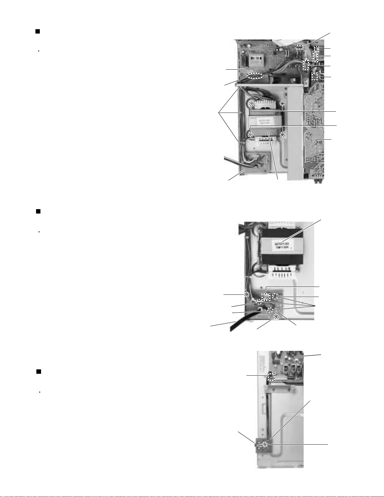
RX-DV3SL
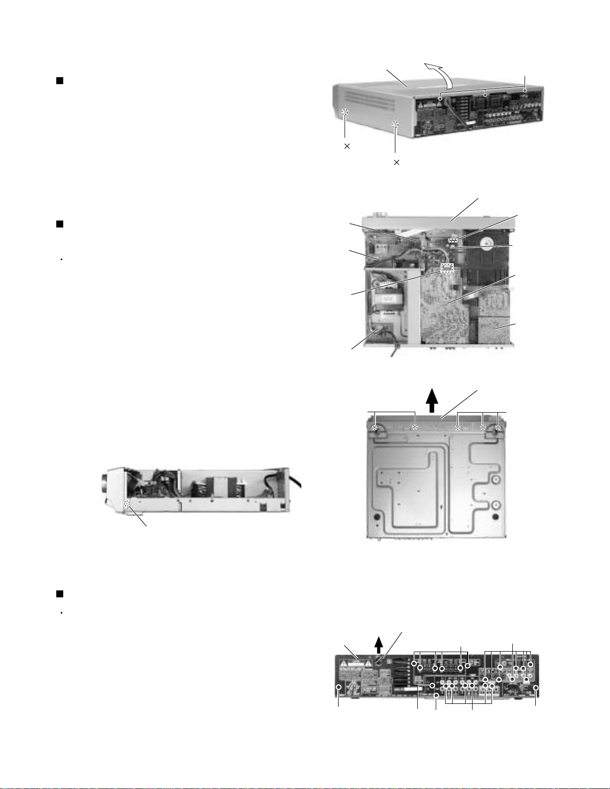
Disassembly method
Removing the top cover (See Fig.1)
1.
Remove the four screws marked A attaching the top
cover on both sides of the body.
2.
Remove the three screws marked B on the back of
the body.
3.
Remove the top cover from behind in the direction of
Removing the front panel assembly
(See Fig.2 to 4)
Prior to performing the following procedures, remove
the top cover.
1.
Disconnect the card wire from the connector CN114
on the main board.
2.
Remove the five screws marked C attaching the front
panel assembly on the bottom of the body. Detach
the front panel assembly toward the front.
A
Tie band
Power
supply
board
CN201
Power
/Fuse
board
Top cover
2
A
B
2
Fig.1
Front panel assembly
CN114
Main
board
Amplifier
board
DSP
board
Fig.2
3.
Release the two joints marked a on both sides on the
bottom of the body using a screwdriver.
Joint a
Fig.4
Removing the rear panel (See Fig.5)
Prior to performing the following procedures, remove
the top cover.
1.
Remove the power cord stopper from the rear panel
by moving it in the direction of the arrow.
C
Rear panel
Fig.3
Cord stopper
Front panel assembly
C
D
D
2.
Remove the twenty one screws marked D attaching
each boards to the rear panel on the back of the
body.
3.
Remove the three screws marked E attaching the
rear panel on the back of the body.
E
D
E
Fig.5
D
E
1-5
Page 6
RX-DV3SL
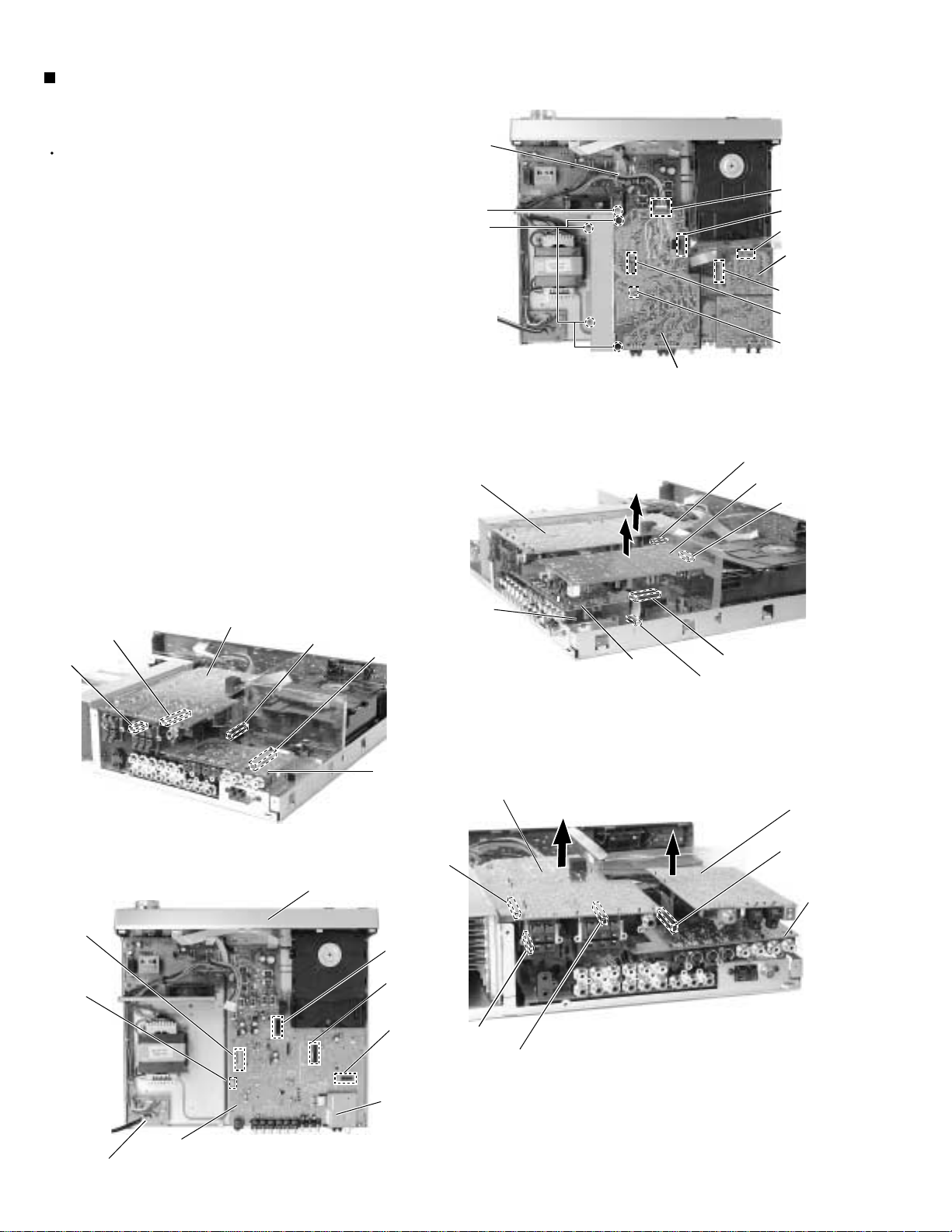
Removing each board connected to the
rear side of the main board
(See Fig.6 to 10)
Prior to performing the following procedures, remove
the top cover and rear panel.
1.
Cut off the tie band fixing the harness.
2.
Disconnect the DSP board from the connector
CN612 on the main board,
3.
Disconnect the card wire frome the connecter CN614
on the main board.
4.
Disconnect the S-video board from the connector
CN412 on the main board.
Tie
band
F
G
Amplifier board
CN201
CN212
CN602
DSP
board
CN612
CN231
CN241
Amplifier
board
Fig.6
CN212
DSP board
CN231
CN241
CN231
Amplifier board
Fig.9
Front panel assembly
CN212
CN612
S-video
board
CN212
board
CN231
Tuner
Amplifier board
S-video
board
Fig.7
CN602
CN612
CN412
DSP
board
CN612
S-video
board
1-6
CN241
Power
/Fuse
board
Main
board
Fig.10
CN612
CN412
Tuner
board
CN241
CN212
Fig.8
Page 7
Removing the amplifier board
(See Fig.11, 12)
Prior to performing the following procedures, remove
the top cover, and rear panel.
1.
Disconnect the amplifier board from the connector
CN201.
2.
Disconnect the amplifier board from the connector
CN212 on the main board.
3.
Disconnect the amplifier board from the wire
connected to the connector CN231 and CN241 on
the main board.
4.
Disconnect the screws marked F frome the ground
wire attaching the amplifier board on the fan bracket.
5.
Disconnect the four screws G attaching the amplifier
board on the body.
Tie
band
F
G
Fig.11
RX-DV3SL
CN201
CN212
CN602
DSP
board
CN612
CN231
CN241
Amplifier
board
CN212
Removing the power ICs
(See Fig.13, 14)
1.
Remove the six screws marked H attaching the heat
sink.
2.
Unsolder the two p
the rear side of the amplifier board.
3.
Pull out the amplifier board from the bracket hooks
on the heat sink.
ower ICs solder points
attaching
Heat sink
H
Amplifier board
Fig.12
Fig.13
Power ICs solder points
CN231
CN241
Main
board
H
Fook
Amplifier board
rear side
Fook
Heat sink
Fig.14
1-7
Page 8
RX-DV3SL
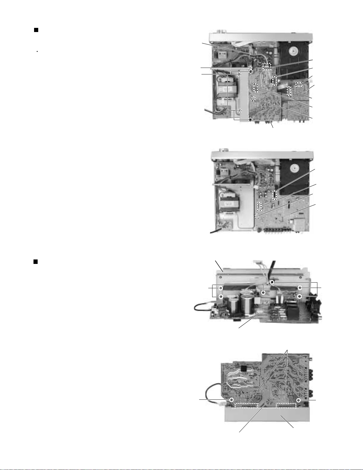
Removing the DVD CD unit
(See Fig.15)
Prior to performing the following procedures, remove
the top cover, rear cover and DSP board.
1.
Remove the DVD / CD unit dust proof cover
attaching on the main board.
2.
Remove the three screws marked I attaching the
DVD /CD unit.
3.
Disconnect the connectors CN512 and CN513 on
the main board.
Removing the fan bracket
(See Fig.16)
Prior to performing the following procedures, remove
the top cover, rear cover, DSP board, amplifier board
and S-video board.
Tie
band
Dust proof cover
DVD
/ CD
unit
I
I
CN512
CN513
Main
board
Fig.15
Harness bands
1.
If necessary, cut off the tie band fixing the harness.
2.
Remove the two screws marked J attaching the fan
bracket on the body.
3.
Remove the harness bands fixing the harness on the
fan bracket.
4.
Disconnect the connector CN111 on the power
supply board.
5.
Disconnect the connector CN122 on the main board.
Removing the power supply board
(See Fig.17)
Prior to performing the following procedures, remove
the top cover, rear cover, DSP board, amplifier board
S-video board and fan bracket.
1.
If necessary, cut off the tie band fixing the harness.
2.
Disconnect the card wire from the connector CN115
on the power supply board.
3.
Disconnect the harness connected to the connector
CN111 on the power supply board.
Power
supply
board
Fan
bracket
Power
supply
board
Solder
points
K
CN115
CN121
CN111
CN122
J
Main
board
Fig.16
K
CN115
CN121
CN111
CN122
4.
Disconnect the harness connected to the connector
CN121 on the main board.
5.
Remove the four screws marked K attaching the
power supply board on the body.
6.
Unsolder the solder points at the three harnesses
connected to the power supply board.
1-8
Tie
band
Fig.17
Page 9
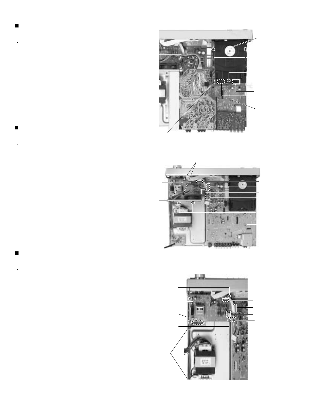
RX-DV3SL
r
Removing the power transformer
(See Fig.18, 19)
Prior to performing the following procedures, remove
the top cover and rear panel.
1.
If necessary, cut off the tie band fixing the harness.
2.
Disconnect the harness from the connector CN101
on the power / fuse board.
3.
Disconnect the harness from the connectors CN111
and
CN121 on the power supply board and main board.
4.
Unsolder the three harnesses connected to the
power supply board.
5.
Remove the four screws marked L attaching the
power transformer on the body.
Removing the power / fuse board
(See Fig.19)
Prior to performing the following procedure, remove
the top cover and rear panel.
1.
Disconnect the harness connected to the connector
CN101 on the power / fuse board (If necessary, cut
off the band fixing the harness on the side of the
base chassis).
2.
Unsolder the power cord and other harnesses
connected to the power / fuse board.
3.
Remove the two screws marked M attaching the
power / fuse board on the body.
Power
supply
board
Solder
points
Tie
band
Power / Fuse board
M
PW103
PW102
Power cord
M
CN115
CN291
CN121
CN111
CN122
L
L
Amp.
board
Power
transformer
Fig.18
Power
transforme
CN101
PW101
Solder
points
Power / Fuse board
Fig.19
Removing the headphones board
(See Fig.20)
Prior to performing the following procedures, remove
the top cover, rear cover, front panel assembly and
power supply board.
1.
Disconnect the harness connected to the connector
CN291 on the main board (If necessary, remove the
amplifier board and fan bracket).
2.
Remove the screw marked N attaching the
headphones board on the body.
Main
board
CN291
Headphones
board
Headphones
jack
N
Fig.20
1-9
Page 10

RX-DV3SL
y.
ed
Q
.
ed
.
ed
d.
ed
d.
ed
d.
p
l
)
d.
e ma
d.
ed
y.
d
)
.
.
,
.
ed
.
d
)
3
d
ch
d
d
t
d
d
2
5
1N291
l
Removing the tuner boar
(See Fig.21
Prior to performing the following procedures, remove
the top cover, rear panel, DSP board and S-video
oar
Disconnect the card wire from the connector CN301
on th
in boar
Remove the two screws mark
tuner board on the rear of the side bod
attaching the
Removing the main boar
(See Fig.22
Prior to performing the following procedures, remove
the top cover, rear panel, DSP board, S-video board,
amplifier board, DVD / CD unit and tuner board
Disconnect the card wire from the connectors CN114
N125 on the main board
Disconnect the wire from the connectors CN121
N122 and CN291 on the main board
Remove the five screws mark
main board on the body
attaching the
N12
N12
N12
Fig.21
CN301
Main
board
Tuner
board
O
CN114
P
Main board
Removing each board connected to the
rear side of the front
ane
(See Fig.23
Prior to performing the following procedures, remove
the top cover and front panel assembl
Remove the two screws mark
power switch board
Remove the seven screws mark
system control board
Remove the two screws mark
indicator boar
Remove the four screws mark
lect boar
Remove the three screws mark
ontrol boar
1-10
attaching the
attaching the
attaching the
attaching the
attaching the
System control boar
Fig.22
Front pane
R
ontrol boar
Fig.2
Power swit
T
boar
boar
elec
oar
Page 11

<DVD / CD unit>
g
RX-DV3SL
Prior to performing the following procedures, remove
the DVD / CD unit.
Removing the DVD / CD tray
(See Fig.1, 2)
1.
Push the cam lever toward the center side of the
DVD / CD unit in the direction of the arrow and draw
the DVD / CD tray toward the front.
2.
Push the two tray stoppers marked a on the DVD /
CD tray in the direction of the arrow and draw the
DVD / CD tray toward the front.
Fig.1
a (Tray stopper)
DVD / CD
Loading cam lever
tray
Reinstall the DVD / CD tray
(See Fig. 1, 2)
1.
Align the rail with the DVD / CD tray as shown fig.2,
then mount the DVD / CD tray.
Removing the DVD / CD servo board
(See Fig.3)
1.
Disconnect the card wire from the connectors
CN101, CN201 and CN202 on the DVD / CD servo
board.
2.
Push the two DVD / CD servo board hooks marked b
and pull out the DVD / CD servo board.
CN201
Hook b
Fig.2
DVD / CD
tray
Loading
cam
lever
Hook b
CN202
CN101
DVD / CD
servo board
.3
Fi
1-11
Page 12

RX-DV3SL
Removing the the top cover
(See Fig.4)
Prior to performing the following procedures, remove
the DVD / CD tray.
1.
Remove the four screws marked A attaching the top
cover on the DVD / CD unit.
2.
Pull the top cover toward the direction of the arrow
and draw the top cover toward the upper side.
A
A
Top cover
Fig.4
A
A
DVD / CD
Stopper
Stopper
DVD / CD
unit
unit
Removing the tray drive motor board
(See Fig.5, 6)
Prior to performing the following procedures, remove
the DVD / CD tray, top cover, servo board and DVD /
CD unit.
1.
Unsolder the solder points at the tray drive motor
board.
2.
Detach the belt from the pulley on the bottom of the
DVD / CD unit. (Do not stain the belt with grease).
3.
Remove the screws marked B attaching the tray
drive motor on the DVD / CD unit.
4.
Remove the screws marked C attaching the tray
drive motor board on the DVD / CD unit.
Pulley
Belt
B
Motor
Solder
points
Motor
C
Fig.5
Tray drive
motor board
DVD / CD
unit
1-12
Fig.6
Page 13

RX-DV3SL
Removing the DVD / CD the mechanism
holder assembly (mechanism included)
(See Fig. 7, 8)
Prior to performing the following procedures, remove
the DVD / CD tray, the servo board and top cover.
Remove the four screws marked D attaching the
1.
DVD / CD mechanism holder assembly on the DVD /
CD unit.
Pull out the DVD / CD mechanism holder assembly.
2.
Top cvover
Fig.7
DVD / CD mechanism
holder assembly
D
DVD / CD
DVD / CD
D
unit
unit
D
Fig.8
D
1-13
Page 14

RX-DV3SL
Adjustment method
Measurement instruments required
for adjustment
1. Low frequency oscillator,
This oscillator should have a capacity to output 0dBs
to 600ohm at an oscillation frequency of 50Hz-20kHz.
2. Attenuator impedance : 600ohm
3. Electronic voltmeter
4. Frequency counter
5. Wow flutter meter
6. Test tape
VT712 : For Tape speed and wow flutter ( 3kHz)
VT724 : For Reference level (1kHz)
VT703L : For Head angle (10kHz)
Because of frequency-mixed tape with 63,1k,10k and
14kHz(250nWb/m -24dB).
Use this tape together with a filter.
7. Blank tape
TAPE : AC-225
8. Torque gauge : For play and back tension
Forward ; TW2111A, Reverse ; TW2121A
Fast Forward and Rewind ; TW2231A
9. Test disc
: VT-501(12cm)
10. Jitter meter
Measurement conditions
Power supply voltage
AC120V(50Hz)
Measurement
output terminal : Speaker out
:TP101 (Measuring for TUNER/DECK/CD)
:Dummy load 6ohm
Radio input signal
AM modulation frequency : 400Hz
Modulation factor : 30%
FM modulation frequency : 400Hz
Frequency displacement : 22.5kHz
Frequency Range
AM 530kHz~1600kHz (10kHz step)
FM 87.5MHz~108MHz
Standard measurement positions of volume
and switch
Power : Standby (Light STANDBY Indicator)
Sub woofer VOL. : Minimum
Sound mode : OFF
Main VOL. : 0 Minimum
Traverse mecha set position : Disc 1
Mic MIX VOL : MAX
ECHO : OFF
Precautions for measurement
1. Apply 30pF and 33kohm to the IF sweeper output
side and 0.082 F and 100kohm in series to
the sweeper input side.
2. The IF sweeper output level should be made as
low as possible within the adjustable range.
3. Since the IF sweeper is a fixed device, there is
no need to adjust this sweeper.
4. Since a ceramic oscillator is used, there is no need
to perform any MPX adjustment.
5. Since a fixed coil is used, there is no need to adjust
the FM tracking.
6. The input and output earth systems are separated.
In case of simultaneously measuring the voltage
in both of the input and output systems with an
electronic voltmeter for two channels, therefore,
the earth should be connected particularly.
7. In the case of BTL connection amplifier, the minus
terminal of speaker is not for earthing. Therefore,
be sure not to connect any other earth terminal
to this terminal. This system is of an OTL system.
1-14
Page 15

Initialization method of DVD section
When microprocessor ICs or pick-up has been replaces, initialize the
DVD player in the following manner.
If tray is not completely close up, make power to standby frome on to close up the tray.
1.
After confirming that tray is completely close up, pull off the power plug.
Insert the power plug to the outlet while pressing "STOP" and "DVD" Button at the same time to be
2.
TEST Mode.
FL display indicates "TEST **" and "** (Area code)" is indicated at the upper left of the display.
** : Area code
Press "PAUSE" button to initialize.
3.
When an indication of "ATT" is displayed, initialization finishes.
Push the POWER SW to be standby.
4.
About TEST MODE
Before implementing the TESE Mode please do the change to the mode of remote control the DVD Mode.
The operation of the remote control is because it is not produced
This player has a TEST MODE for product QC, service or repair. Contents are given as follows.
TEST MODE has the 4 different states. These are changed with the CHOICE key on
the remote controller. TEST MODE is canceled by the POWER key.
Insert the power plug to the outlet while pressing "STOP" and "DVD" buttons at the same time.
"** (Area code)" is indicated at the upper left of the display.
FL Display indicates " TEST ** ".
** : Area code .... Refer to (Fig, 1)
RX-DV3SL
DVD Button
CHOICE Button
(Test mode)
REMOTE CONTROL RM-SRXDV3J
STANDBY/ON
VCRDBS TV AUDIO
TAPETV CDR FM/AM
TV/VIDEO REW/ TUNING
REPEAT SLEEP
FM MODE STROBE
SOUND
EFFECT
ANALOG
TEST
/DIGITAL
INPUT
SURR ON/OFF
AUDIO
SUBTITLE
SURR MODE
10/0 +10
DIMMER
ANGLE
MUTING
ZOOM
DIGEST TOP MENU MENU
CHOICE
ON SCREEN
HOME THEATER
DVD/CD RECEIVER
VCRDBS DVD
– TV/DBS CH +
231
564
897
–
SUBWOOFER
100+ TV RETURN
+–+
TV VOL VOLUME
ENTER
/FF
CENTER
REAR·L
REAR·R
+
VFP
PROGRESSIVE
–
RETURN
DVD
Button
(Test mode)
(Initialize complete)
POWER Button
STANDBY
STANDBY/ON
INPUT
SURROUND
ON/OFF
L
ANALOG/DIGITA
INPUT ATT. REC MODE
RX-DV3 HOME THEATER DVD/CD RECEIVER
MODE
STOP Button
TVVCRDBSDVD
SOURCE NAME
OPEN/CLOSE
FL Display
The first: FL display shows the player firmware version.
1.
Button(Test mode)
Contents: [System firm] [Front End firm] [Back End firm]
The second: Indicator check mode. All FL segment and all LED light.
2.
The third: Mechanism check mode. In this mode the player displays "CHECK".
3.
The fourth: Front-end check mode. In this mode the FL displays "EXPERT".
4.
(Test mode )
FM/AMTAPE/CDR
SETTING ADJUST MEMORY
MASTER VOLUME
CONTROL
DVD/SUPER VCD/VCD/CD
COMPACT
SUPER VIDEO
1-15
Page 16

RX-DV3SL
Description of major ICs
AK4527BVQP (IC601) : A/D,D/A converter
1. Pin layout
2. Pin function (1/2)
No.
1
2
3
4
5
6
7
8
9
10
11
12
13
14
15
16
17
18
Symbol
SDOS
OSKS
MIS
BICK
LRCK
SDTI1
SDTI2
SDTI3
SDTO
D,AUX
DFS
DEMI
DEMO
MCKO
DVDD
DVSS
PD
XTS
1-16
4443424140393837363534
1
2
3
4
5
6
7
8
9
10
11
1213141516171819202122
I/O
I
SDTO Source Select Pin (Note 1)
Top View
Function
33
32
31
30
29
28
27
26
25
24
23
"L" : Internal ADC output, "H" : DAUX input
I
Control Mode Select Pin
"L" : 3-wire Serial, "H" : I
-
Soft Mute Pin (Note 1), Connect to GND
2C Bus
When this pin goes to "H", soft mute cycle is initialized.
When returning to "L", the output mute releases.
I
Audio Serial Data Clock Pin
I/O
Input Channel Clock Pin
I
DAC1 Audio Serial Data Input Pin
I
DAC2 Audio Serial Data Input Pin
I
DAC3 Audio Serial Data Input Pin
O
Audio Serial Data Output Pin
-
Sub Audio Serial Data Input Pin, Connect to GND
-
Double Speed Sampling Mode Pin (Note 1)
"L" : Normal Speed, "H" : Double Speed
-
Connect to GND
No internal bonding.
-
Zero Input Detect Enable Pin, Connect to GND
"L" : mode 7 (disable) at parallel mode,
-
zero detect mode is selectable by DZFM2-0 bits at serial mode.
-
"H" : mode 0 (DZF is AND of all six channels)
-
Output Buffer Power supply Pin, 2.7V~5.5V
I
Digital Power Supply Pin, 4.5V~5.5V
-
De-emphasis Pin, 0V
I
Power-Down & Reset Pin
When "L", the AK4527B is powered-do wn and the control registers are reset to def ault
state. If the state of P/S or CAD0-1 changes, then the AK4527B m ust be reset b y PDN.
-
Test Pin, Connect to GND
This pin should be connected to DVSS.
Page 17

RX-DV3SL
Pin function (2/2)
Symbol
No.
ICKS
19
ADIF
20
CAD1
21
CAD0
22
LOUT3
23
ROUT3
24
LOUT2
25
ROUT2
26
LOUT1
27
ROUT1
28
LIN-
29
LIN+
30
RIN-
31
RIN+
32
VREFL
33
OVF
VCOM
34
VREFH
35
AVDD
36
AVSS
37
XTI
38
XTO
39
P1S
40
CS
41
CSN
DIF1
42
SCL/CCLK
LOOP0
43
SAD/CDTI
CDTD
44
I/O
Connect to GND
-
Function
No internal bonding.
Analog Input Format Select Pin, Digital Power Supply
"H" : Full-differential input, "L" : Single-ended input
Chip Address 1 Pin,
Chip Address 0 Pin,
DAC3 Lch Analog Output Pin
O
DAC3 Rch Analog Output Pin
O
DAC2 Lch Analog Output Pin
O
DAC2 Rch Analog Output Pin
O
DAC1 Lch Analog Output Pin
O
DAC1 Rch Analog Output Pin
O
Lch Analog Negative Input Pin
I
Lch Analog Positive Input Pin
I
Rch Analog Negative Input Pin
I
Rch Analog Positive Input Pin
I
Zero Input Detect 2 Pin (Note 2), Non
-
Connect to GND
Connect to GND
Connect
When the input data of the group 1 follow total 8192LRCK cycles with "0"
input data, this pin goes to "H".
Analog Input Overflow Detect Pin (Note 3)
O
This pin goes to "H" if the analog input of Lch or Rch is overflows.
Common Voltage Output Pin,AVDD/2
O
Large external capacitor around 2.2uF is used to reduce power-supply noise.
Positive Voltage Reference Input Pin,AVDD
Analog Power Supply Pin,4.5V~5.5V
Analog Ground Pin,0V
Zero Input Detect 1 Pin (Note 2), Non connect
When the input data of the group 1 follow total 8192 LRCK cycles with "0"
input data, this pin goes to "H".
Master Clock Input Pin
I
Parallel / Serial Select Pin
"L" : Serial control mode, "H" : Parallel control mode
Audio Data Interface Format 0 Pin in parallel mode
I
Chip select pin in 3-wire serial control mode
I
This pin should be connected to DVDD at I2C bus control mode
Audio Data Interface Format 1 Pin in parallel mode
I
Control Data Clock Pin in serial control mode
I
I2C = "L" : CCLK(3-wire Serial), I2C = "H" : SCL(I2CBus)
Loopback Mode 0 Pin in parallel control mode
I
Enables digital loop-back from ADC to 3 DACs.
Control Data Input Pin in serial control mode
I/O
I2C = "L" : CDTI(3-wire Serial), I2C = "H" : SDA(I2CBus)
Loopback Mode 1 Pin (Note 1)
I
Enable all 3 DAC channels to be input from SDTII.
AK4527
Notes : 1. SDOS, SMUTE, DFS, and LOOP1 pins are ORed with register data if P/S = "L".
2. The group 1 and 2 can be selected by DZFM2-0 bit if P/S = "L" and DZFME = "L".
3. This pin becomes OVF pin if OVFE bit is set to "1" at serial control mode.
4. All input pins should not be left floating.
1-17
Page 18

RX-DV3SL
MN101C35DKF (IC701) : Panel MICOM
1. Pin layout
~
100 76
1
~
75
~
2. Pin function
Pin No.
1
2
3
4
5
6
7
8
9
10
11
12
13
14
15
16
17
18
19
20
21
22
23
24
25
26
27
28
29
30
31
32
33
34
35
36
37
38
39
40
41
42
43
Symbol
TXD/SBO0/P00
RXO/SBI0/P01
SBT0/P02
SBO1/P03
SBI1/P04
SBT1/P05
BUZZER/P06
OSC2
OSC1
MMOD
VREF-
VERSION1
VERSION2
VREF+
LED DIMMER
RESET
LED BLUE
LED VCR
LED STB
LED AUDIO
LED DVD
DI BUSY
REMO
VOL IN1
VOL IN2
DI PS2
DI S2P
DI CK
25
VDD
VSS
XI
XO
KEY1
KEY2
KEY3
KEY4
KEY5
KEY6
DI CS
IRQ4
P25
~
26 50
51
I/O
O
No connect
No connect
O
No connect
O
No connect
O
O
No connect
O
No connect
No connect
O
-
Power supply
O
External terminal for main clock
I
External terminal for main clock
-
Connect to GND
-
Connect to GND
O
No connect
-
Connect to GND
-
Connect to GND
I
Key input terminal 1
I
Key input terminal 2
I
Key input terminal 3
I
Key input terminal 4
I
Key input terminal 5
I
Key input terminal 6
Chip select 1
I
I
Chip select 2
-
Reference voltage terminal
O
LED DIMER
I
Reset input
O
LDE (BLUE)
O
LED (VCR)
O
LED (STB)
O
LED (DVD audio)
O LED (DVD)
Micom communication BUSY
O
Micom communication CS
I
Remote control signal input
I
I
VOL JOG IN1
I
VOL JOG IN2
O
No connect
O
No connect
O
Micom communication status output
I
Micom communication status input
I
Micom communication CLK
O
No connect
O
No connect
Function
1-18
Page 19

Pin No
44
45
46
47
48
49
50
51
52
53
54
55
56
57
58
59
60
61
62
63
64
65
66
67
68
69
70
71
72
73
74
75
76
77
78
79
80
81
82
83
84
85
86
87
88
89
90
91
92
93
94
95
96
97
98
99
100
.
Symbol I/O
P52
P53
P54
DGT17/P67
DGT16/P66
DGT15/P65
DGT14/P64
DGT13/P63
DGT12/P62
DGT11/P61
DGT10/P60
DGT9/P41
DGT8/P40
SEG0/DGT7/P77
SEG1/DGT6/P76
SEG2/DGT5/P75
SEG3/DGT4/P74
SEG4/DGT3/P73
SEG5/DGT2/P72
SEG6/DGT1/P71
SEG7/DGT0/P70
SEG8/P87
SEG9/P86
SEG10/P85
SEG11/P84
SEG12/P83
SEG13/P82
SEG14/P81
SEG15/P80
SEG16/P97
SEG17/P96
SEG18/P95
SEG19/P94
SEG20/P93
SEG21/P92
SEG22/P91
SEG23/P90
SEG24/PC2
SEG25/PC1
SEG26/PC0
SEG27/PB7
SEG28/PB6
SEG29/PB5
SEG30/PB4
SEG31/PB3
SEG32/PB2
SEG33/PB1
SEG34/PB0
SEG35/PD7
SEG36/PD6
SEG37/PD5
SEG38/PD4
SEG39/PD3
SEG40/PD2
SEG41/PD1
SEG42/PD0
VPP
O
O
O
O
O
O
O
O
O
O
O
O
O
O
O
O
O
O
O
O
O
O
O
O
O
O
O
O
O
O
O
O
O
O
O
O
O
O
O
O
O
O
O
O
O
O
O
O
O
O
O
O
O
O
O
O
-
RX-DV3SL
MN101C35DKF
Function
No connect
No connect
No connect
No connect
No connect
No connect
No connect
GRID1
GRID2
GRID3
GRID4
GRID5
GRID6
GRID7
GRID8
GRID9
GRID10
GRID11
GRID12
GRID13
SEGMENT36
SEGMENT35
SEGMENT34
SEGMENT33
SEGMENT32
SEGMENT31
SEGMENT30
SEGMENT29
SEGMENT28
SEGMENT27
SEGMENT26
SEGMENT25
SEGMENT24
SEGMENT23
SEGMENT22
SEGMENT21
SEGMENT20
SEGMENT19
SEGMENT18
SEGMENT17
SEGMENT16
SEGMENT15
SEGMENT14
SEGMENT13
SEGMENT12
SEGMENT11
SEGMENT10
SEGMENT9
SEGMENT8
SEGMENT7
SEGMENT6
SEGMENT5
SEGMENT4
SEGMENT3
SEGMENT2
SEGMENT1
VPP
1-19
Page 20

RX-DV3SL
MN101C49GKG (IC761) : System MICOM
1. Pin layout
~
100 76
1
~
75
~
25
26 50
51
~
2. Pin function
Pin No.
1 VREF - Connect to GND
2 PA0 I NTSTEL(RGBESL)
3 PA1 I VCR S/C SW
4 PA2 I DBS S/C SW
5 PA3 I SAFETY
6 PA4 I SHORT&TH DET (A/D)
7 PA5 I OUTLEVEL DETECT (A/D)
8 PA6 I VCR IN (A/D)
9 PA7 I STB IN (A/D)
10 VREF+ - Reference voltage
11 VDD - VDD
12 OSC2 O External terminal for connected oscirator
13 OSC1 I External terminal for connected oscirator
14 VSS - Connect to GND
15 XI I Connect to GND
16 XO O No connect
17 MMO0 I Connect to GND
18 SBO0 O DI DO
19 SBI0 I DI DI
20 SBT0 O DI CK
21 SBO2 O S2UDT
22 SBI2 I U2SDT
23 SBT2 I SCLK
24 NDK O INTP
25 SYSCLK O CPURST
26 IRQ0 I CS
27 IRQ1 I
28 IRQ2 I PROTECT
29 IRQ3 I RDS SET
30 IRQ4 I DI BUSY
31 IRQ5 I HAEADPHONE
32 GND I Connect to GND
33 NSRT I RESET IN
34 TM0IO O DSP RST
35 TM1IO O DSP RDY
36 TM2IO O AVC OUT
37 TM3IO I AVC IN
38 TM7IO O VIDEO MUTE1
39 P15 O VIDEO MUTE2
40 TM4IO O VIDEO YCMIX
41 P17 O VIDEO RGB
42 SBO1 O DSP COM
43 SBI1 I DSP STAT
Symbol
I/O
Function
1-20
Page 21

Pin No.
44 SBT1 O DSP CLK
45 CBO3 O VOL DATA
46 SBI3 O VOL LATCH
47 SBT3 O VOL CLK
48 MP3 O D.O.MUTE
49 INT/PROG O INT/PROG
50 KEY0 O HEADPHONE RELAY
51 KEY1 O EEDO
52 KEY2 O EEDI
53 KEY3 O EECK
54 KEY4 O EECS
55 KEY5 O FRONT SPK RELAY
56 KEY6 O CENTER SPK RELAY
57 KEY7 O REAR SPK RELAY
58 NEW O S1RELAY
59 NRE I INH
60 NCS O SLOW L
61 A16 O SLOW M
62 A17 O SYSTEM P.ON
63 A0 O FAN ON/OFF
64 A1 O DVD P.ON
65 A2 O TUNER P.ON
66 A3 O MECHA.ON
67 A4 I/O RDS DATA
68 A5 O RDS CLK
69 A6 O STEREO
70 A7 I TUNER DATAI
71 A8 O TUNER MUTE
72 A9 O TUNER DATA0
73 A10 O TUNER CLK
74 A11 O TUNER CE
75 A12 O S1OUT
76 A13 O SMUTE
77 A14 O DSP ON
78 A15 O VS3
79 LED0 O STBY LED
80 LED1 O FAN ON/OFF1-LOW
81 LED2 O FAN ON/OFF2-MID
82 LED3 O DISC SET
83 LED4 I DISC STOP
84 LED5 O FAN ON/OFF3-HIGH
85 LED6 O No connect
86 LED7 O SW MUTE
87 SDO0 O VIDEO SW1
88 SDO1 O VIDEO SW2
89 SDO2 O VIDEO SW3
90 SDO3 O VIDEO SW4
91 SDO4 O DI RST
92 SDO5 O DI CS
93 SDO6 O No connect
94 SDO7 O LMUTE
95 DAVSS - SW OPEN
96 DA0 I OCDAT
97 DA1 I DWDET
98 DA2 O LOPEN
99 DA3 O LCLOSE
100 DAVDD -
Symbol
I/O
Reference voltage
Function
RX-DV3SL
MN101C49GKG
1-21
Page 22

RX-DV3SL
UPD784215AGC167 (IC681) : Dital signal controller
1. Pin layout
~
100 76
2. Pin function (1/2)
Pin No.
1~8
9
10
11
12
13
14
15
16
17
18
19
20
21
22
23
24
25
26
27
28
29
30
31
32
33
34,35
36
37
38
39
40
41
42
43
44
45
46
47
48
AUTODAT A
DIGITAL0
FORMAT
CHANNEL
REST IN
AV REF1
DSPCOM
DSPSTS
DSPCLK
DSPRDY
MIDIO IN
MIDIO OUT
Symbol
VDD
X2
X1
VSS
XT2
XT1
RESET
LOCK
ERR
AVDD
AVREF0
AVSS
RX
TX
MICK
MICS
1
~
25
~
26 50
I/O
-
Non connect
-
Power supply terminal
O
Connecting the crystal oscillator for system main clock
I
Connecting the crystal oscillator for system main clock
-
Connect to GND
O
Connecting the crystal oscillator for system sub clock
I
Connecting the crystal oscillator for system sub clock
I
System reset signal input
I
Output of DSP to general-purpose port
I
Output of DSP to general-purpose port
I
Output of DSP to general-purpose port
I
Output of DSP to general-purpose port
I
Output of DSP to general-purpose port
I
Output of DSP to general-purpose port
I
Reset signal input
-
Power supply terminal
-
Connect to GND
-
Connect to GND
-
Connect to GND
-
Connect to GND
-
Connect to GND
-
Connect to GND
-
Connect to GND
-
Connect to GND
-
Connect to GND
-
Connect to GND
-
Non connect
-
Power supply terminal
-
Not use
-
Not use
-
Non connect
I
Communication port from IC701
O
Status communication port to IC701
I
Clock input from IC701
I
Ready signal input from IC701
-
Non connect
I/O
Interface I/O terminal with microcomputer
I/O
Interface I/O terminal with microcomputer
O
Interface I/O terminal with microcomputer of clock signal
O
Interface I/O terminal with microcomputer of chip select
75
~
51
Function
1-22
Page 23

RX-DV3SL
Pin function (2/2)
Pin No.
49
50
Symbol
MILP
MIACK
51
52
53
DSPRST
54~63
64
CODEC OUT
65
66
67
68
CODEC IN
CODEC CLK
CODEC CS
CODEC XTS
69
70
71
72
PD
GND
73
74
75
76
77
78
79
80
81
VDD
82
83
84
ANA/T-TONE
85
LEF-MIX
86
87
88
D.MUTE
S.MUTE
89
90
91
92
93
94
ASW1
ASW2
ASW3
ASW4
TEST
95
96
97
98
99
100
I/O
Interface I/O terminal with microcomputer
O
Interface I/O terminal with microcomputer
O
Non connect
Non connect
Reset signal output of DSP
O
Non connect
Interface I/O terminal with microcomputer
I/O
Interface I/O terminal with microcomputer
I/O
Interface I/O terminal with microcomputer of clock signal
O
Interface I/O terminal with microcomputer of chip select
O
Non connect
Non connect
Non connect
Reset signal output
O
Connect to GND
Non connect
Non connect
Non connect
Non connect
Non connect
Non connect
Non connect
Non connect
Power supply
Non connect
Non connect
Test tone control
O
Control at output destination of LFE channel
O
Non connect
Mute of the digital out terminal is controlled
O
Mute of the audio signal is controlled
O
Non connect
Selection of digital input selector
O
Selection of digital input selector
O
Selection of digital input selector
O
Selection of digital input selector
O
Test terminal
Non connect
Non connect
Non connect
Non connect
Non connect
Non connect
-
Function
UPD784215AGC167
1-23
Page 24

RX-DV3SL
TC9446F-025 (IC631) : Digital signal processor for dolby digital (AC-3)
/ DTS audio decode
Pin No. Symbol I/O Function
1
2
3
4
5
6
7
8~11
12
13
14
15
16~18
19
20
21
22
23
24
25
26
27,28
29~30
31
32,33
34
35
36
37
38,39
40
41
42
43
44
45
46
47
48
49
50
51
52
53
54~61
62
63~70
71
72~80
81
82~89
90
91
92,93
94
95
96
97
98,99
100
RST
MIMD
MICS
MILP
MIDIO
MICK
MIACK
FI0~3
IRQ
VSS
LRCKA
BCKA
SDO0~2
SD03
LRCKB
BCKB
SDT0
SDT1
VDD
LRCKOA
BCKOA
TEST0,1
LRCKOB,BCKOB
TXO
TEST2,3
RX
VSS
TSTSUB0
FCONT
TSTSUB1,TSTSUB2
PDO
VDDA
PLON
AMPI
AMPO
CKI
VSSA
CKO
LOCK
VSS
WR
OE
CE
VDD
IO7~0
VSS
AD0~7
VDD
AD8~16
VSS
PO0~7
VDDDL
LPFO
DLON,DLCKS
SCKO
VSSDL
SCKI
VSSX
XO,XI
VDDX
Reset signal input terminal (L:reset H: normal operation)
I
Microcomputer interface mode selection input terminal (L:serial H:IC bus)
I
Microcomputer interface chip select input terminal
I
Microcomputer interface latch pulse input
I
Microcomputer interface data I/O terminal
I/O
Microcomputer interface clock input terminal
I
Microcomputer interface acknowledge output terminal
O
Flag input terminal 0~3
I
Interrupt input terminal
I
Digital ground terminal
Audio interface LR clock input terminal A
I
Audio interface bit clock input terminal A
I
Audio interface data output terminal 0
O
Non connect
Audio interface LR clock input terminal B
I
Audio interface bit clock input terminal B
I
Audio interface data input terminal 0
I
Audio interface data input terminal 1
I
Power supply for digital circuit
Audio interface LR clock output terminal A
O
Audio interface bit clock output terminal A
O
Test input terminal 0/1 (L:test H: normal operation)
I
Non connect
SPDIF Output
O
Test input terminal (L:test H: normal operation)
I
SPDIF input terminal
I
Ground terminal for digital circuit
Test sub input terminal 0 (L:test H: normal operation)
I
VCO Frequency control output terminal
O
Test sub input terminal 1,2 (L:test H: normal operation)
I
Phase detect signal output terminal
O
Power supply for analog circuit
Clock selection input terminal (L:external clock H:VCO clock)
I
amplifier input terminal for LPF
I
amplifier output terminal for LPF
O
External clock input terminal
I
Ground terminal for analog circuit
DIR Clock output terminal
O
VCO Lock output terminal
O
Ground terminal for digital circuit
External SRAM writing signal output terminal
O
External SRAM output enable signal output terminal
O
External SRAM chip enable signal output terminal
O
Power supply terminal for digital circuit
External SRAM data I/O terminal 7~0
I/O
Ground terminal for digital circuit
External SRAM address output terminal 0~7
O
Power supply terminal for digital circuit
External SRAM address output terminal 8~16
O
Ground terminal for digital circuit
General purpose output terminal 0~7
O
Power supply terminal for DLL
LPF output terminal for DLL
O
Refer to the undermentioned table
I
Non connect
Ground terminal for DLL
External system clock input terminal
I
Ground termonal for oscillation circuit
Oscillation I/O terminal
I/O
Power supply terminal for oscillation circuit
-
1-24
DLCKS terminal
L
L
H
H
DLONterminal
L
H
L
H
DLL clock setting
SCKI input (DLL circuit OFF)
Four times XI clock
Three times XI clock
Six times XI clock
Page 25

RX-DV3SL
TC7SET32FU (IC683) : Z-Input or gate
1. Pin layout / Block diagram
1
IN B
IN A
GND
2
3
54VCC
OUT Y
TC74HCU08AF (IC612) : Inverter
1. Pin layout / Block diagram
Vcc4B4A
14
13
12
4Y
11
3B
10
3A
9
3Y
8GND
TC74HCU04AF (IC621) : Inverter
1. Pin layout
VCC6A6Y
14
13
11A
21Y
2.The truth value table
A
L
L
B
L
H
12
32A
Y
L
L
5A
11
42Y
5Y
10
53A
4A
9
63Y
4Y
8GND
7
2. Truth value
A
L
H
Y
H
L
11A
21B
31Y
42A
52B
62Y
H
H
7
L
H
L
H
TC74HC4072AF (IC611) : 4-Input gate
1. Pin layout & block diagram
1Y
1
1A
2
1B
3
1C
4
1D
5
NC
6
GND
7
14
13
12
11
10
9
8
Vcc
2Y
2D
2C
2B
2A
NC
2. Truth table
A
B
H
X
X
H
X
X
X
X
L
L
D
C
X
X
H
X
L
Y
X
H
X
H
X
H
H
H
L
L
BA15218F (IC303, 602, 603, 651, 652, 661, 671, 672) : Ope. amp.
1. Pin layout / Block diagram
EE
1OUT1
2-IN1
-
8
7
V
CC
OUT2
1
3+IN1
+
6
-
-IN2
2
4
5V
+
+IN2
1-25
Page 26

RX-DV3SL
W24L010AJ-12 (IC641) : SRAM
1. Pin layout
DD
A15
V
32
31
1 2 3 4 5 6 7 8 9
NC
A16
3. Pin function
Pin No.
1
2
3
4
5
6
7
8
9
10
11
12
13
14
15
16
CS2WEA13A8A9
30
29
28
27
A7A6A5A4A3A2A1
A14
A12
Symbol
NC
A16
A14
A12
A7
A6
A5
A4
A3
A2
A1
A0
I/O1
I/O2
I/O3
Vss
A11OEA10
26
25
24
23
10
CS1
22
11
I/O8
21
12
A0
Function
No Connection
Address Input
Address Input
Address Input
Address Input
Address Input
Address Input
Address Input
Address Input
Address Input
Address Input
Address Input
Data Input/Output
Data Input/Output
Data Input/Output
Ground
I/O7
20
13
I/O1
I/O6
19
14
I/O2
I/O5
18
15
I/O3
I/O4
17
16
Vss
2. Block diaglam
V
Vss
A16
CS2
CS1
WE
Pin No.
17
18
19
20
21
22
23
24
25
26
27
28
29
30
31
32
DD
A0
OE
Symbol
I/O4
I/O5
I/O6
I/O7
I/O8
CS1
A10
OE
A11
A9
A8
A13
WE
CS2
A15
VDD
DECODER
CONTROL
Function
Data Input/Output
Data Input/Output
Data Input/Output
Data Input/Output
Data Input/Output
Chip Select Inputs
Address Input
Output Enable Input
Address Input
Address Input
Address Input
Address Input
Write Enable Input
Chip Select Inputs
Address Input
Power Supply
CORE
ARRAY
DATA I/O
I/O1
I/O8
NJM2246M (IC402, 403, 404) : Video switch
1. Pin layout / Block diaglam
GND
8
1
Vin1
1-26
6dB
AMP.
Vout
7
2
CTL1
V+
6
3
Vin2
BIAS
CTL2
Vin3
5
4
Control input - output signal
CTL 1
L
H
L/H
CTL 2
L
L
H
Output
VIN 1
VIN 2
VIN 3
Page 27

< MEMO >
RX-DV3SL
1-27
Page 28

RX-DV3SL
VICTOR COMPANY OF JAPAN, LIMITED
AUDIO & COMMUNICATION BUSINESS DIVISION
PERSONAL & MOBILE NETWORK BUSINESS UNIT. 10-1,1chome,Ohwatari-machi,Maebashi-city,371-8543,Japan
(No.21124)
200207
 Loading...