

Page 1
SERVICE MANUAL
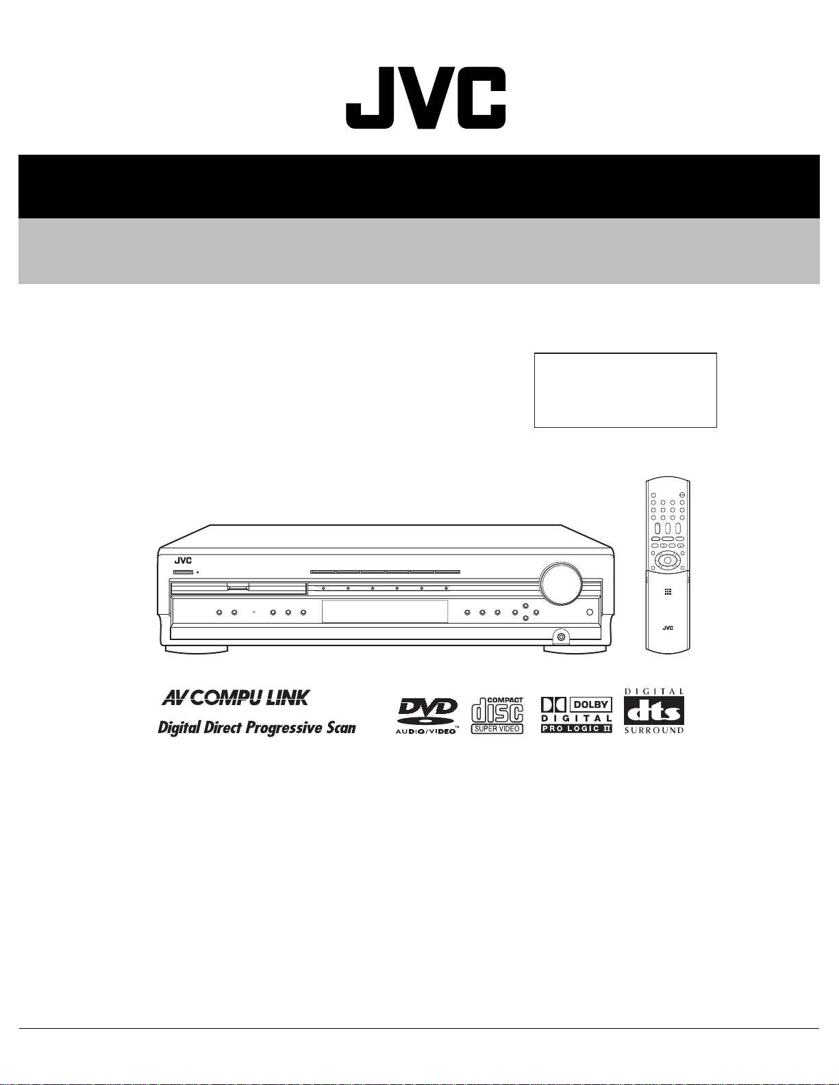
HOME THEATER DVD-AUDIO/VIDEO RECEIVER
2202320036
RX-DV31SL
Area suffix
J ----------------------------- U.S.A.
C -------------------------- Canada
RX-DV31 HOME THEATER DVD-AUDIO/VIDEO RECEIVER
COMPAC T
SUPER VIDE O
DVD/SUPER VCD/VCD/CD
TABLE OF CONTENTS
1 PRECAUTION. . . . . . . . . . . . . . . . . . . . . . . . . . . . . . . . . . . . . . . . . . . . . . . . . . . . . . . . . . . . . . . . . . . . . . . . . 1-3
2 SPECIFIC SERVICE INSTRUCTIONS. . . . . . . . . . . . . . . . . . . . . . . . . . . . . . . . . . . . . . . . . . . . . . . . . . . . . . 1-5
3 DISASSEMBLY . . . . . . . . . . . . . . . . . . . . . . . . . . . . . . . . . . . . . . . . . . . . . . . . . . . . . . . . . . . . . . . . . . . . . . . 1-6
4 ADJUSTMENT . . . . . . . . . . . . . . . . . . . . . . . . . . . . . . . . . . . . . . . . . . . . . . . . . . . . . . . . . . . . . . . . . . . . . . . 1-21
5 TROUBLE SHOOTING. . . . . . . . . . . . . . . . . . . . . . . . . . . . . . . . . . . . . . . . . . . . . . . . . . . . . . . . . . . . . . . . . 1-22
6 DESCRIPTION OF MAJOR ICS. . . . . . . . . . . . . . . . . . . . . . . . . . . . . . . . . . . . . . . . . . . . . . . . . . . . . . . . . . 1-23
COPYRIGHT © 2003 VICTOR COMPANY OF JAPAN, LIMITED
No.22023
2003/6
Page 2
SPECIFICATION
Amplifier Output Power At Stereo operation Front channels 100 W per channel, min. RMS, driven into
8 Ω, 40 Hz to 20 kHz with no more than
0.8% total harmonic distortion.
At Surround operation Front channels 100 W per channel, min. RMS, driven into
8 Ω at 1 kHz, with no more than 0.8% total
harmonic distortion.
Center channel 100 W, min. RMS, driven into 8 Ω at 1 kHz,
with no more than 0.8% total harmonic
distortion.
Surround channels 100 W per channel, min. RMS, driven into
8 Ω at 1 kHz, with no more than 0.8% total
harmonic distortion.
Audio Audio Input Sensitivity/
Impedance (1 kHz)
Audio Input (DIGITAL IN)* Coaxial DIGITAL 1 (DBS) 0.5 V(p-p)/75 Ω
Signal-to-Noise Ratio
('66 IHF/'78 IHF)
Frequency Response (8 Ω) TV, TAPE/CDR, DBS, VCR 20 Hz to 20 kHz (±1 dB)
Tone Control Bass (100 Hz) ±10 dB ±2 dB
Video Video Input
Sensitivity/
Impedance
(1 kHz)
Video Output
Level/Impedance
(1 kHz)
FM tuner
(IHF)
AM tuner Tuning Range 530 kHz to 1 710 kHz
General Power
Tuning Range 87.5 MHz to 108.0 MHz
Requirements
Power
Consumption
Dimensions
(W × H × D)
Mass 8.4 kg (18.5 lbs)
Composite
video
S-video DBS IN, VCR IN (Y:luminance) 1 V(p-p)/75Ω
Composite
video
S-video VCR OUT, MONITOR
Component
video
Color System NTSC
Horizontal
Resolution
Signal-to-
Noise Ratio
(S/N)
Synchronize Negative
AC 120 V , 60 Hz
200 W/255 VA (in operation)
2 W (in standby mode)
435 mm × 100 mm × 403.5 mm
(17 3/16 in. × 3 15/16 in. × 15 15/16 in.)
TV, TAPE/CDR, DBS, VCR 240 mV/47 kΩ
Optical DIGITAL 2 (TV) -21 dBm to -15 dBm (660 nm ±30 nm)
* Corresponding to Linear PCM, Dolby Digital, and DTS Digital Surround
(with sampling frequency-32 kHz, 44.1 kHz, 48 kHz).
TV, TAPE/CDR, DBS, VCR 87 dB/67 dB
Treble (10 kHz) ±10 dB ±2 dB
DBS IN, VCR IN 1 V(p-p)/75 Ω
(C:chrominance) 0.286 V(p-p)/75 Ω
VCR OUT, MONITOR OUT 1 V(p-p)/75 Ω
(Y:luminance) 1 V(p-p)/75 Ω
OUT
DVD COMPONENT
VIDEO OUT
500 lines
63 dB
(C:chrominance) 0.286 V(p-p)/75 Ω
(Component-Y) 1.0 V(p-p)/75 Ω
(Component-PB/PR) 0.7 V(p-p)/75 Ω
1-2 (No.22023)
Page 3
1.1 Safety Precautions
Good earth ground
d
AC VOLTMETER
SECTION 1
PRECAUTION
(1) This design of th is product contains special hardw are and
many circuits and components specially for safety purposes. For continued protection, no changes should be made
to the original design unless authorized in writing by the
manufacturer. Replacement parts must be identical to
those used in the original circuits. Services should be performed by qualified personnel only.
(2) Alterations of the design or circuitry of the product should
not be made. Any design alterations of the product should
not be made. Any design alterations or additions will void
the manufacturers warranty and will further relieve the
manufacture of responsibility for personal injury or property
damage resulting therefrom.
(3) Many electrical and mechanical parts in the products have
special safety-related characteristics. These characteristics are often not evident from visual inspection nor can the
protection afforded by them necessarily be obtained by using replacement components rated for higher voltage, wattage, etc. Replacement parts which have these special
safety characteristics are identified in the Parts List of Service Manual. Electrical components having such features
are identified by shading on the schematics and by ( ) on
the Parts List in the Service Manual. The use of a substitute
replacement which does not have the same safety characteristics as the recommended replacement parts shown in
the Parts List of Service Manual may create shock, fire, or
other hazards.
(4) The leads in the products are routed and dressed with ties,
clamps, tubings, barriers and the like to be separated from
live parts, high temperature parts, moving parts and/or
sharp edges for the prevention of electric shock and fire
hazard. When service is required, the original lead routing
and dress should be observed, and it should be confirmed
that they have been returned to normal, after reassembling.
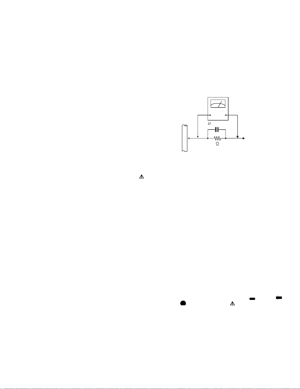
(5) Leakage shock hazard testing
After reassembling the product, always perform an isolation check on the exposed metal parts of the product (antenna terminals, knobs, metal cabinet, screw heads,
headphone jack, control shafts, etc.) to be sure the product
is safe to operate without danger of electrical shock.Do not
use a line isolation transformer during this check.
• Plug the AC line cord directly into the AC outlet. Using a
"Leakage Current Tester", measure the leakage current
from each exposed metal parts of the cabinet, particularly any exposed metal part having a return path to the
chassis, to a known good earth ground. Any leakage current must not exceed 0.5mA AC (r.m.s.).
• Alternate check method
Plug the AC line cord directly into the AC outlet. Use an
AC voltmeter having, 1,000Ω per volt or more sensitivity
in the following manner. Connect a 1,500Ω 10W resistor
paralleled by a 0.15µF AC-type capacitor between an exposed metal part and a known good earth ground.
Measure the AC voltage across the resistor with the AC
voltmeter.
Move the resistor connection to each exposed metal
part, particularly any exposed metal part having a return
path to the chassis, and measure the AC voltage across
the resistor. Now, reverse the plug in the AC outlet and
repeat each measurement. Voltage measured any must
not exceed 0.75 V AC (r.m.s.). This corresponds to 0.5µ
mA AC (r.m.s.).
(Having 1000
ohms/volts,
or more sensitivity)
0.15 F AC TYPE
Place this
probe on
1500 10W
1.2 Warning
(1) This equipment has been designed and manufactured to
meet international safety standards.
(2) It is the legal resp onsibility of the repairer to ensure that
these safety standards are maintained.
(3) Repairs must be made in accordance with the relevant
safety standards.
(4) It is essential that safety critical compone nts are replaced
by approved parts.
(5) If mains voltage selector is provided, check setting for local
voltage.
1.3 Caution Burrs formed during molding may be left over on some parts
of the chassis.
Therefore, pay attention to such burrs in the case of preforming repair of this system.
1.4 Critical parts for safety
In regard with component parts appearing on the silk-screen
printed side (parts side) of the PWB diagrams, the parts that are
printed over with black such as the resistor ( ), diode ( )
and ICP ( ) or identified by the " " mark nearby are critical
for safety. When replacing them, be sure to use the parts of the
same type and rating as specified by the manufacturer.
(This regulation dose not Except the J and C version)
each expose
metal part.
(No.22023)1-3
Page 4
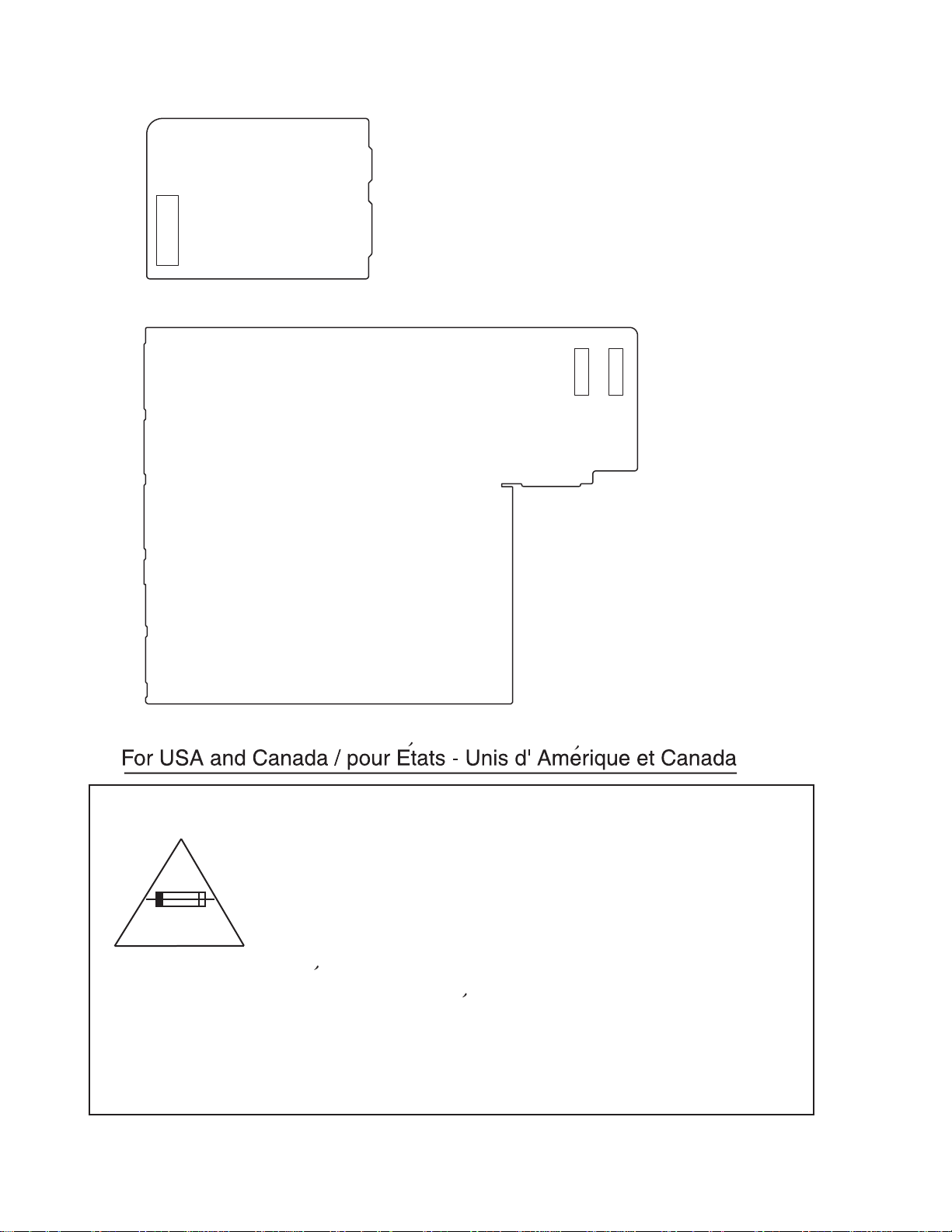
1.5 Importance administering poin on the safety
Power board (Forward side)
F101
Main board (Forward side)
F132
F131
1-4 (No.22023)
Caution: For continued protection against risk of
fire, replace only with same type 5A/125V for
F101, 2A/125V for F131 and F132.
This symbol specifies type of fast operating fuse.
Precaution: Pour eviter risques de feux, remplacez
le fusible de surete de F101 comme le meme type
que 5A/125V, et 2A/125V pour F131 et F132.
Ce sont des fusibles suretes qui functionnes rapide.
^
Page 5

SECTION 2
SPECIFIC SERVICE INSTRUCTIONS
This service manual does not describe SPECIFIC SERVICE INSTRUCTIONS.
(No.22023)1-5
Page 6
SECTION 3
DISASSEMBLY
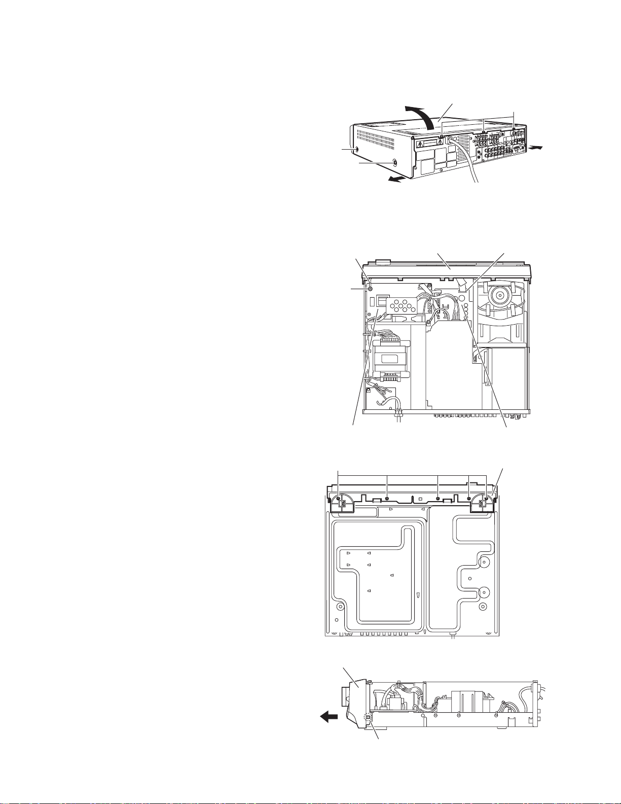
3.1 Main body section
3.1.1 Removing the top cover
(See Fig.1)
(1) From the both sides of the main body, remove the four
screws A attaching the top cover.
(2) From the back side of the main body, remove the three
screws B attaching the top cover.
(3) Remove the top cover in the dire ction o f the arrow 2 while
extending the lower sections of the top cover in the direction of the arrow 1.
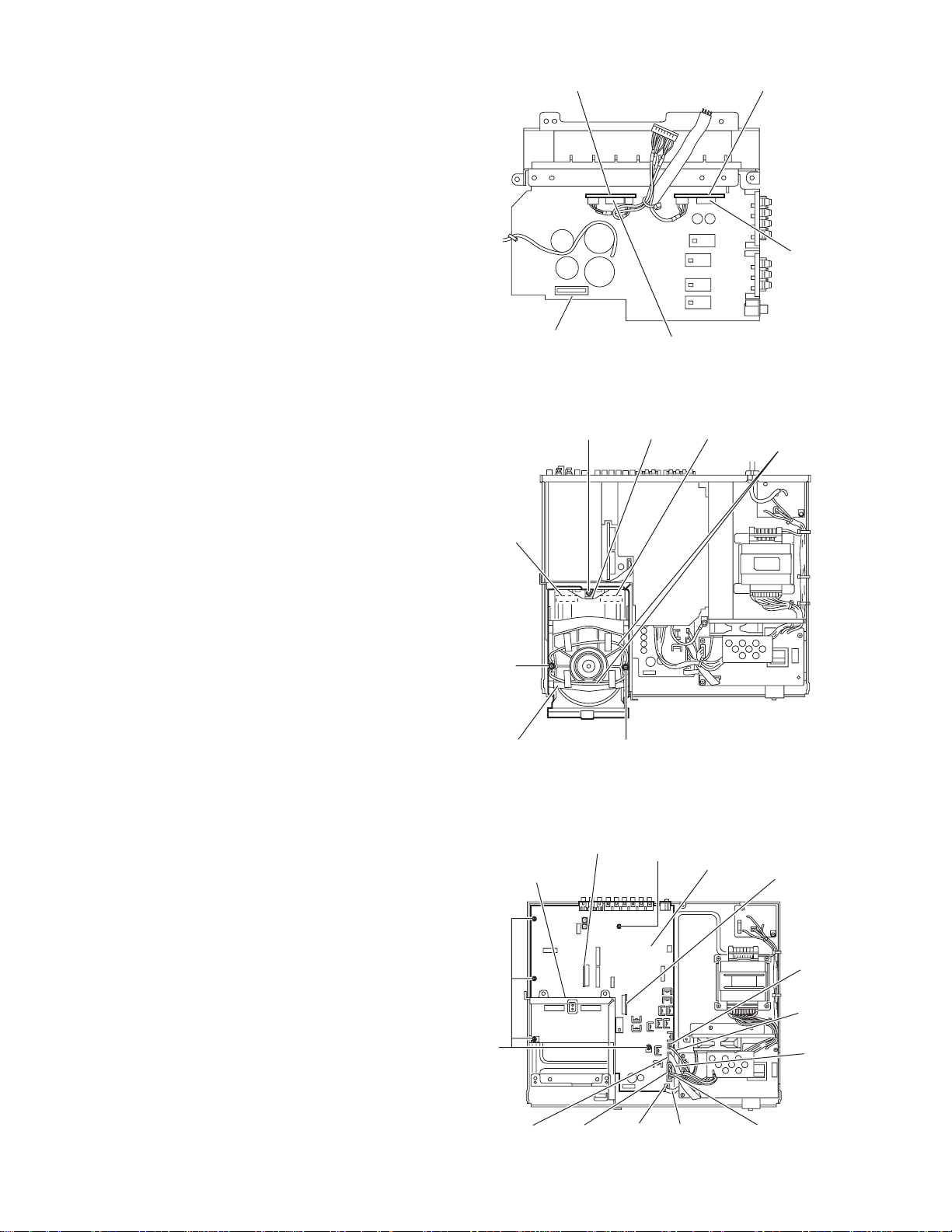
3.1.2 Removing the front panel assembly
(See Figs.2 to 4)
• Prior to performing the following procedures, remove the top
cover.
(1) From the top side of the main body, disconnect the card wire
from the connector CN114 on the main board. (See Fig.2.)
(2) Remove the screw C attaching the earth wire and sub
trans. Board. (See Fig.2.)
(3) From the bottom side of the main bo dy, remove the five
screws D attaching the front panel assembly. (See Fig.3.)
(4) From the both side of the main body, release the two joints
a using a flat-bladed screwdriver and remove the front panel assembly in the direction of the arrow. (See Fig.4.)
Ax2
Ax2
Earth wire
C
2
1
Front panel assembly
Top cover
Fig.1
B
1
CN114
Sub trans board
D
Front panel assembly
Main board
Fig.2
Front panel assembly
Fig.3
1-6 (No.22023)
Joint a
Fig.4
Page 7
3.1.3 Removing the rear panel
(See Fig.5)
• Prior to performing the following procedures, remove th e top
cover.
(1) From the back side of the main body, remove the strain re-
lief from the rear panel in the direction of the arrow.
(2) Remove the twenty three screws E attaching the each
board to the rear panel.
(3) Remove the four screws F attaching the rear panel.
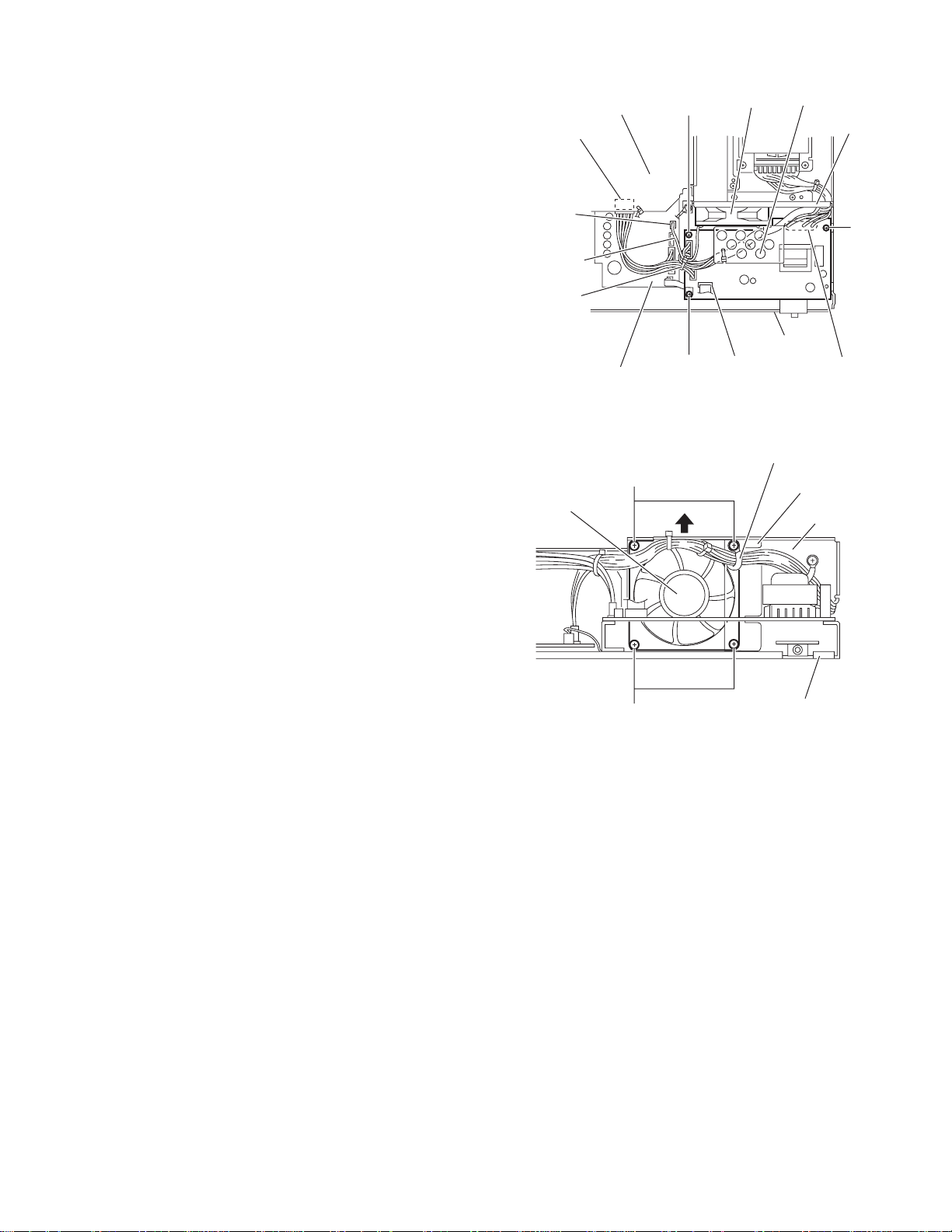
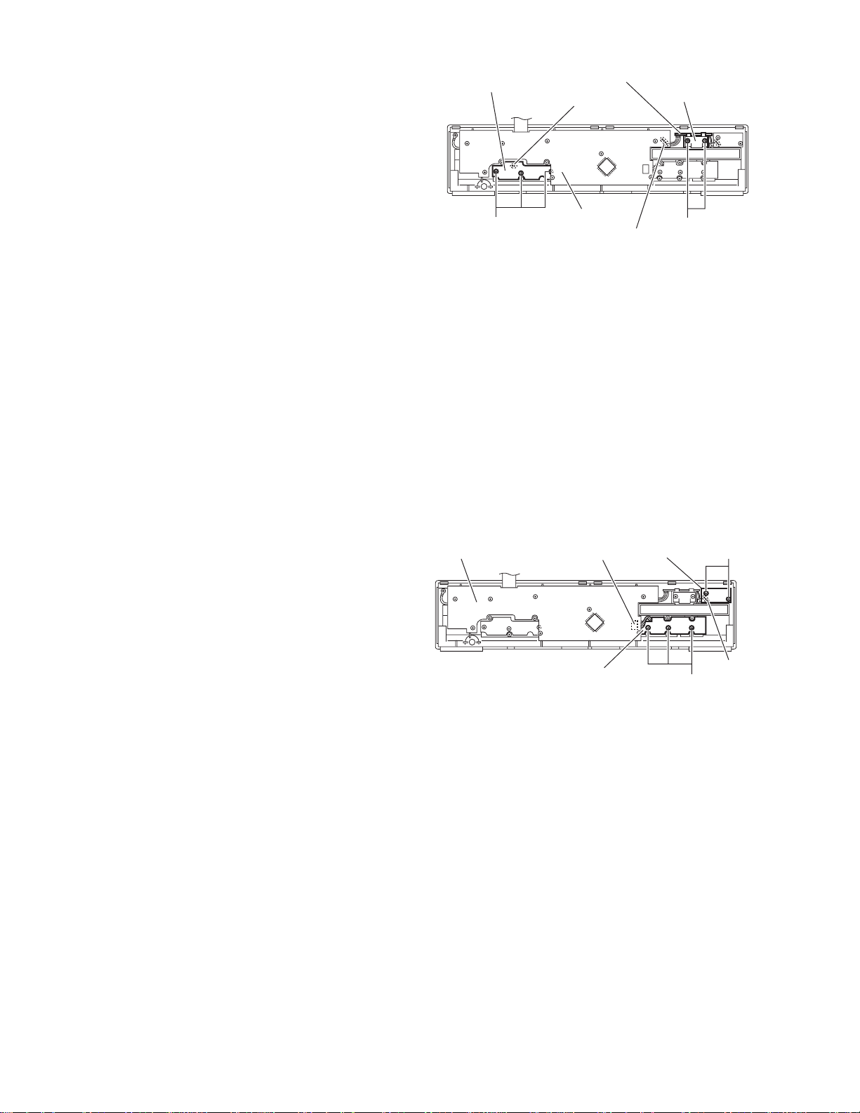
3.1.4 Removing the DSP board
(See Figs.6 and 7)
• Prior to performing the following procedures, remove th e top
cover.
(1) From the back side of the main body, remove the four
screws G attaching the DSP board to the rear panel. (See
Fig.6.)
(2) From the top side of the main body, disconnect the DSP
board from the connector CN611 on the DSP connector
board. (See Fig.7.)
(3) From the left side of the main body, lift the DSP board in the
direction of the arrow and disconnect the card wire from the
connector CN602 on the DSP board. (See Fig.7.)
(4) Take out the DSP board.
Rear panel
F
Rear panel
F
Strain relief
EEF
Fig.5
Fig.6
E
F
G
H
3.1.5 Removing the video jack board
(See Figs.6 and 7)
• Prior to performing the following procedures, remove th e top
cover and DSP board.
(1) From the back side of the main body, remove the four
screws H attaching the video jack board. (See Fig.6.)
(2) Disconnect the card wire from the connector CN402 on the
video jack board and take out the video jack board. (See
Fig.7.)
DSP board
Video jack
board
CN402
Card wire
Fig.7
CN611
CN602
Card wire
DSP connector
board
(No.22023)1-7
Page 8
3.1.6 Removing the tuner
(See Figs.8 and 9)
• Prior to performing the following procedures, remove the top
cover, DSP board and video jack board.
(1) From the back side of the main body, remove the two
screws J attaching the tuner. (See Fig.8.)
(2) From the top side of the main bod y, disconnect the card
wire from the connector CN1 on the tuner. (See Fig.9.)
(3) Take out the tuner.
J
Fig.8
Card wire
CN 1
Tuner
Fig.9
3.1.7 Removing the DAC board
(See Fig.10)
• Prior to performing the following procedures, remove the top
cover.
(1) From the top side of the main body, disconnect the DAC
board from the connectors CN911 and CN912 on the main
board.
Main board
CN911
DAC board
CN912
Fig.10
1-8 (No.22023)
Page 9
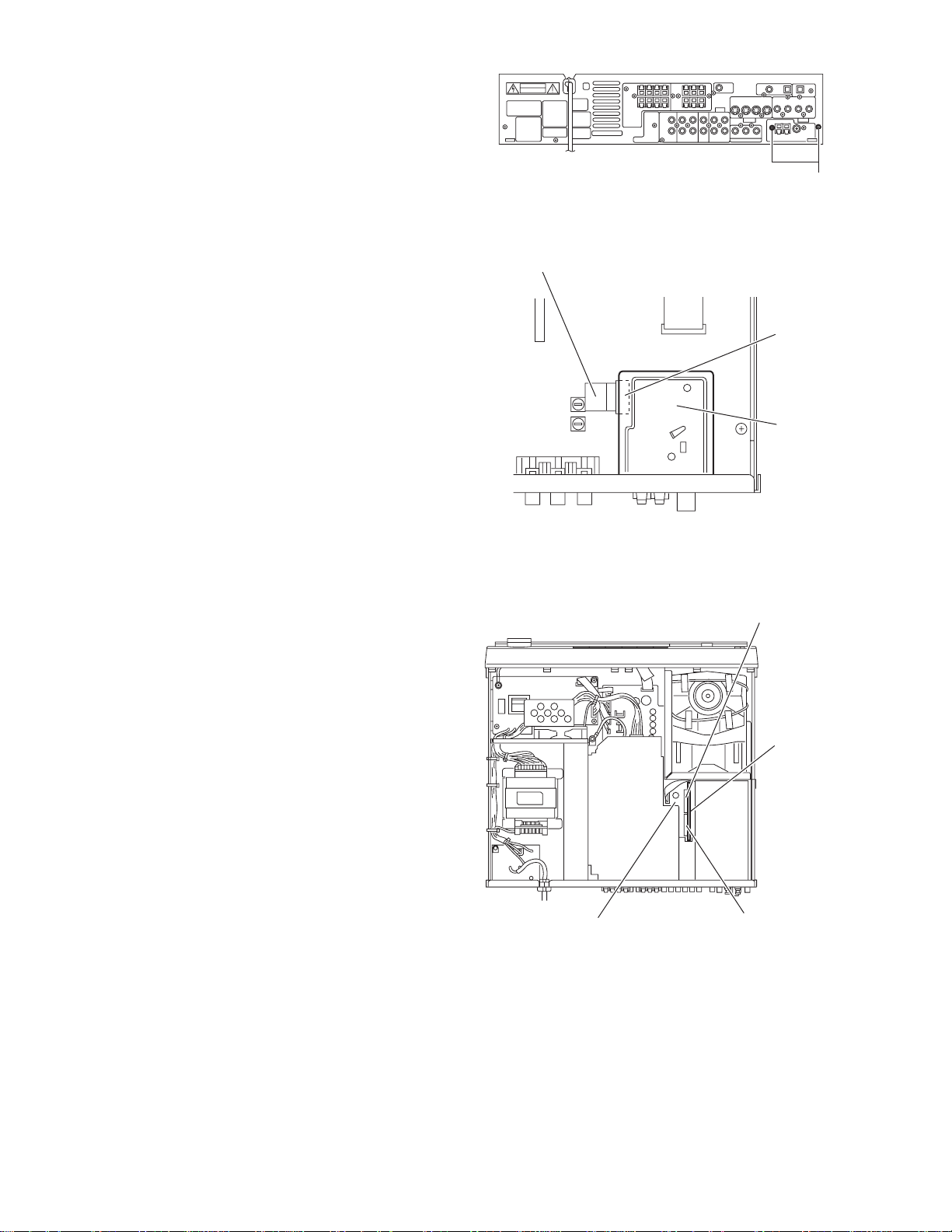
3.1.8 Removing the amp. board
(See Fig.11)
• Prior to performing the following procedures, remove th e top
cover and rear panel.
(1) From the top side of the main bod y, disconnect the wire
from the connector CN201 on the amp. board.
(2) Remove the screw K attaching the earth wire to the heat
sink barcket.
(3) Remove the four screws L attaching the amp. board.
(4) Disconnect the connector CN202 on the amp. board.
(5) Lift the amp. board and disconnect the wire from th e con-
nector CN231 on the main board.
(6) Disconnect the parallel wi re from th e con nector CN241 on
the main board and take out the amp. board.
Heat sink bracket
L
K
Earth wire
CN201
CN202
3.1.9 Removing the heat sink
(See Fig.12)
• Prior to performing the following procedures, remove th e top
cover, rear panel and amp. board.
(1) Remove the screw M attaching the H.sensor board.
(2) Remove the five screws N attaching the IC bracket, heat
sink bracket and heat sink.
3.1.10 Removing the power ICs
(See Fig.13)
• Prior to performing the following procedures, remove th e top
cover, rear panel, amp. board and heat sink.
(1) From the reverse side of the amp. board, remove the sol-
ders from the soldered points b attaching the power ICs to
the amp. board.
Heat sink
Heat sink bracket
IC bracket
N
Amp. board
CN241
Fig.11
N
Fig.12
Amp. board
CN231
M
Main board
H. sensor board
N
Amp. board
Power ICs solbered points b
Fig.13
(No.22023)1-9
Page 10
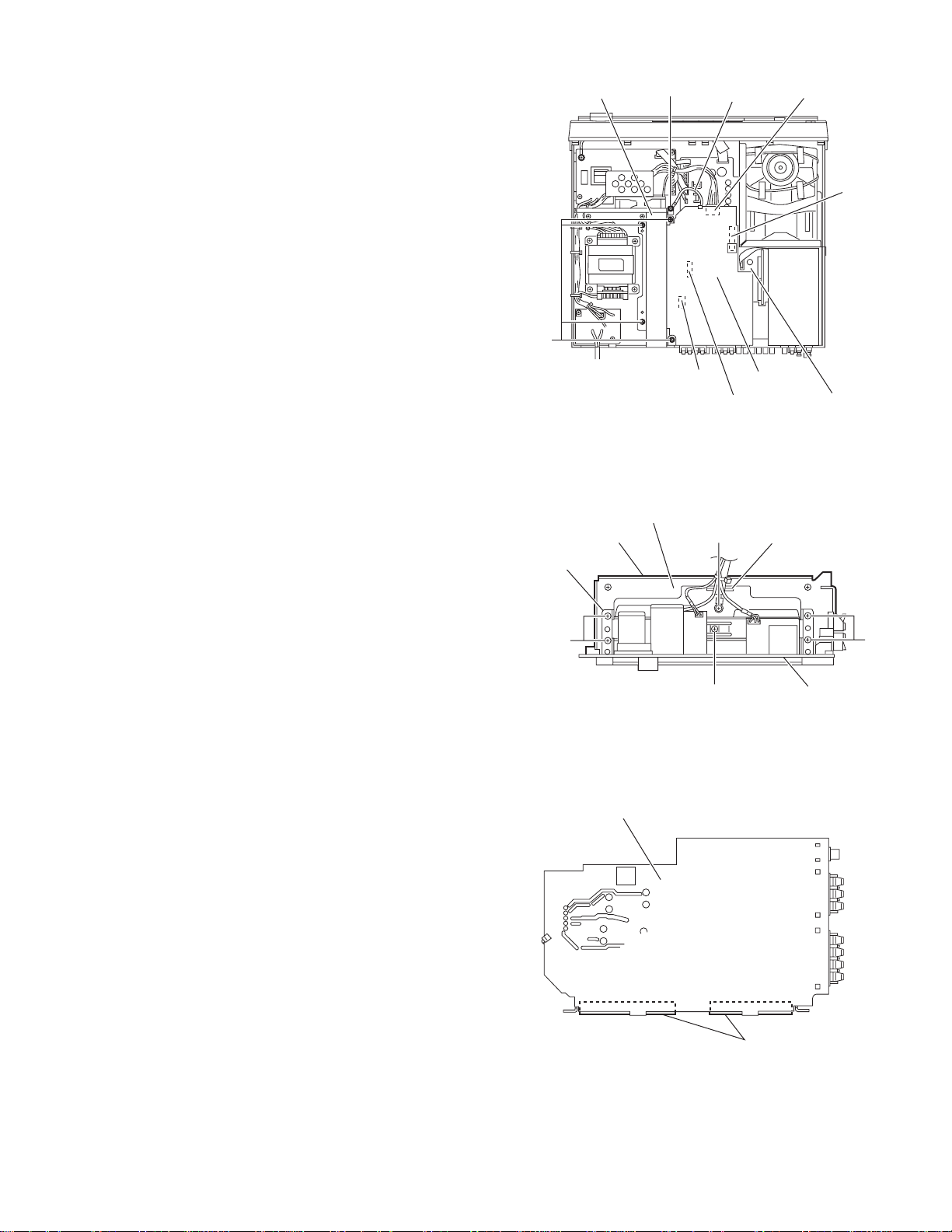
3.1.11 Removing the amp. sub(a) board and amp. sub(b) board
(See Fig.14)
• Prior to performing the following procedures, remove the top
cover, rear panel and amp. board.
(1) From the forward side of the amp. board, disconn ect the
amp. sub(a) board from the connector CN203 on the amp
board.
(2) Disconnect the amp. sub(b) board from the connector
CN204 on the amp. board.
Amp. sub (b) board Amp. sub (a) board
CN203
3.1.12 Removing the DVD mechanism assembly
(See Fig.15)
• Prior to performing the following procedures, remove the top
cover and front panel assembly.
(1) From the top side of th e main body, remove the screw P
and two screws Q attaching the DVD mechanism assembly.
Reference:
• When attaching the screw P, attach the thrust spring
together with it.
• When attaching the screw Q, attach the earth wires together with them.
(2) Disconnect the DVD mechanism assembly from the con-
nectors CN512 and CN513 on the main board.
(3) Take out the DVD mechanism assembly.
3.1.13 Removing the main board
(See Fig.16)
• Prior to performing the following procedures, remove the top
cover, rear panel, DAC board, DSP board, video jack board,
tuner, amp. board and DVD mechanism assembly.
(1) From the top side of the main body, disconnect the fan mo-
tor wire from the connector CN122 on the main board.
(2) Disconnect the card wire from the connector CN125 on the
main board.
(3) Disconnect the wire from the connector CN121 on the main
board.
(4) Disconnect the parallel wire from the connecto r CN291 on
the main board.
(5) Remove the five screws R attaching the main board.
Reference:
Remove the barrier, DSP connector board and amp. connector board as required.
Amp. board
CN512
Q
DVD mechanism
assembly
DSP connecter
board
Barrier
R
Thrust spring
P
Q
CN204
Fig.14
Fig.15
R
CN513
Main board
Earth wires
Amp.
connector
board
CN122
Fan
motor
wire
Card
wire
1-10 (No.22023)
CN125 CN121 CN291
Fig.16
Parallel wire
Wire
Page 11
3.1.14 Removing the sub trans . Bo ar d
(See Fig.17)
• Prior to performing the following procedures, remove th e top
cover and front panel assembly.
(1) From the top side of the main b ody, remove the tie band
bundling the wires.
(2) Disconnect the card wire from the connector CN115 on the
sub trans. board.
(3) Disconnect the wire from the connector CN111 on the sub
trans. board.
(4) Disconnect the wire from the connector CN201 on the amp.
board.
(5) Remove the three screws S attaching the sub trans. board.
(6) From the reverse side of the sub trans. board, remove the
solders from the soldered points c attaching the wires.
CN201
CN122
Fan motor
wier
Tie band
Amp. board
S
Fan motor
Sub trans.
board
Fan
bracket
S
3.1.15 Removing the fan motor
(See Figs.17 and 18)
• Prior to performing the following procedures, remove th e top
cover and front panel assembly.
(1) From the top side of the main b ody, remove the tie band
bundling the wires. (See Fig.17.)
(2) Disconnect the fan motor wire from the connector CN122
on the main board. (See Fig.17.)
(3) From the front side of the main body, remove the four
screws T attaching the fan motor to the fan bracket. (See
Fig.18.)
(4) Take out the fan motor in the directi on of the arrow. (See
Fig.18.)
Reference:
• When attaching the screws T, attach the wire holder and
wire clamp together with them. (See Fig.18.)
• After attaching the fan motor, bundle the wires using the wire
clamp. (See Fig.18.)
Main board
Fan motor
T
T
S
Fig.17
Fig.18
Chassis base
CN115
Wire clamp
Soldered
points c
Wire holder
Fan bracket
Chassis base
(No.22023)1-11
Page 12
3.1.16 Removing the power board
(See Fig.19)
• Prior to performing the following procedures, remove the top
cover.
(1) From the top side of the main body, disconnect the wire
from the connector CN101 on the power board.
Reference:
Remove the tie bands as required.
(2) Remove the solders from the soldered poin ts d attaching
the power cord.
(3) Remove the two screws U attaching the power board.
(4) From the reverse side of the power board, remove the sol-
ders from the soldered point e attaching the wires.
3.1.17 Removing the power trans. former
(See Figs.19 and 20)
• Prior to performing the following procedures, remove the top
cover.
(1) From the top side of the main body, remove the tie ban ds
and wire clamps bundling the wires. (See Fig.20.)
(2) Disconnect the wire from the connector CN121 on the main
board. (See Fig.20.)
(3) Disconnect the wires from the connector CN111 on the sub
trans. board. (See Fog.20.)
(4) Remove the two screws U attaching the power board and
then turn over the power board. (See Fig.19.)
(5) Remove the solders from the soldered points e attaching
the wires. (See Fig.19.)
(6) Remove the four screws V attaching the power trans.
former. (See Fig.19.)
(7) Take out the power trans. former.
Power board
CN101
Main board
CN111
Tie bans
Power cord
U
Power trans. former
Fig.19
S
Soldered points d
Soldered points e
U
Tie bands
VV
Wire clamps
Sub
trans
board
S
3.1.18 Removing the headphone board
(See Fig.20)
• Prior to performing the following procedures, remove the top
cover and front panel assembly.
(1) From the top side of the main body, disconnect the parallel
wire from the connector CN291 on the main board.
(2) Remove the three screws S attaching the sub trans. board.
Reference:
It is not necessary to remove the wire from the sub trans.
board.
(3) Remove the screw W attaching the headphone board while
lifting the sub trans. board slightly.
CN121 CN291
S
Tie bans
Fig.20
W
Headphone
board
1-12 (No.22023)
Page 13
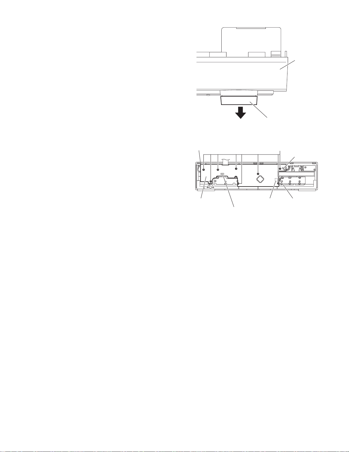
3.2 Front panel assembly section
3.2.1 Removing the FL board
(See Figs.21 and 22)
• Prior to performing the following procedures, remove th e top
cover and front panel assembly.
(1) From the front side of the front panel assembly, pull out the
volume knob assembly in the direction of the arrow. (See
Fig.21.)
(2) From the back side of the front panel assembly, remove the
eight screws X attaching the FL board. (See Fig.22.)
(3) Disconnect the wire from the connector CN703 on the FL
board while lifting the FL board slightly. (See Fig.22.)
(4) Remove the solders from the soldered points f and g at-
taching the parallel wires while lifting the FL board. (See
Fig.22.)
(5) Take out the FL board from the front panel assembly.
Reference:
Remove the parallel wires as required.
Front panel
Front panel
assembly
Volume knob assembly
Fig.21
X
Soldered point g
FL board Wire
Soldered point f
CN703
Fig.22
(No.22023)1-13
Page 14
3.2.2 Removing the control board
(See Fig.23)
• Prior to performing the following procedures, remove the top
cover, front panel assembly and FL board.
Reference:
It is not necessary to remove the parallel wires from the FL
board.
(1) Remove the three screws Y attaching the control board.
(2) Remove the solders from the soldered poin ts h attaching
the parallel wire while lifting the control board.
Reference:
Remove the parallel wire as required.
3.2.3 Removing the indicator board
(See Fig.23)
• Prior to performing the following procedures, remove the top
cover and front panel assembly.
(1) From the back side of the front panel assembly, remove the
two screws Z attaching the lens holder.
(2) Remove the solders from the soldered points i on the FL
board attaching the parallel wire.
(3) Remove the solders from the soldered points j on the pow-
er switch board attaching the parallel wire.
Reference:
Remove the parallel wires as required.
Control board
YZ
Indicator board
Soldered point h
FL board
Soldered point i
Fig.23
Lens holder
3.2.4 Removing the power switch board
(See Fig.24)
• Prior to performing the following procedures, remove the top
cover and front panel assembly.
(1) From the back side of the front panel assembly, remove the
two screws AA attaching the power switch board.
(2) Remove the solders from the soldered points j on the pow-
er switch board attaching the parallel wire.
Reference:
Remove the parallel wire as required.
3.2.5 Removing the speaker SW. board
(See Fig.24)
• Prior to performing the following procedures, remove the top
cover and front panel assembly.
(1) From the back side of the front panel assembly, remove the
three screws AB attaching the speaker SW. board.
(2) Disconnect the wire from the connector CN703 on the FL
board.
FL board
Power switch
CN703
Speaker SW. board
Fig.24
board
AB
AA
Soldered
point j
1-14 (No.22023)
Page 15
3.3 DVD mechanism section
• Remove the top cover.
• Remove the front panel assembly.
• Remove the DVD mechanism assembly.
3.3.1 Removing the tray
(See Figs.1 and 2)
(1) From the left side of the DVD mechanism a ssembly, push
the slide cam in the direction of the arrow 1 and then pull
out the tray in the direction of the arrow 2. (See Fig.1.)
(2) Push the tray stoppers a in the direction of the arrow 3, pull
out the tray in the direction of the arrow 4. (See Fig.2.)
3.3.2 Attaching the tray
(See Fig.2)
When attaching the tray, insert the tray to the rail of the DVD
mechanism assembly and then push th e tray in the DVD mechanism assembly.
Tr ay
2
1
Slide cam
Fig.1
3.3.3 Removing the tray
(See Fig.3)
(1) From the bottom side of the DVD mechanism assembly,
disconnect the card wires from the connectors CN201 and
CN202 on the DVD servo board.
Caution:
Be sure to solder the short land sections b on the flexible
wire before disconnecting the flexible wire from connector CN101 on the DVD servo board.
If the flexible wire is disconnected without attaching solder, the DVD pickup unit may be destroyed by static
electricity.
(2) Release the locks of the connector CN101 on the DVD ser-
vo board in the direction of the arrow 1, disconnect the flexible wire.
Caution:
In the assembly, be sure to remove solders from the
short land sections b after connecting the flexible wire to
the connector CN101 on the DVD servo board.
(3) While pushing the claws c of the DVD mechanism assem-
bly in the direction of the arrow 2, remove the DVD servo
board in an upward direction.
Card wire
CN201
Claw c
Tray stoppers
3
DVD mechanism assembly
Fig.2
Flexible wire
Short land sections b
DVD mechanism assembly
11
2 22
a
4
Tr ay
Card wire
CN202
Claw c
DVD servo board
CN101
Fig.3
(No.22023)1-15
Page 16
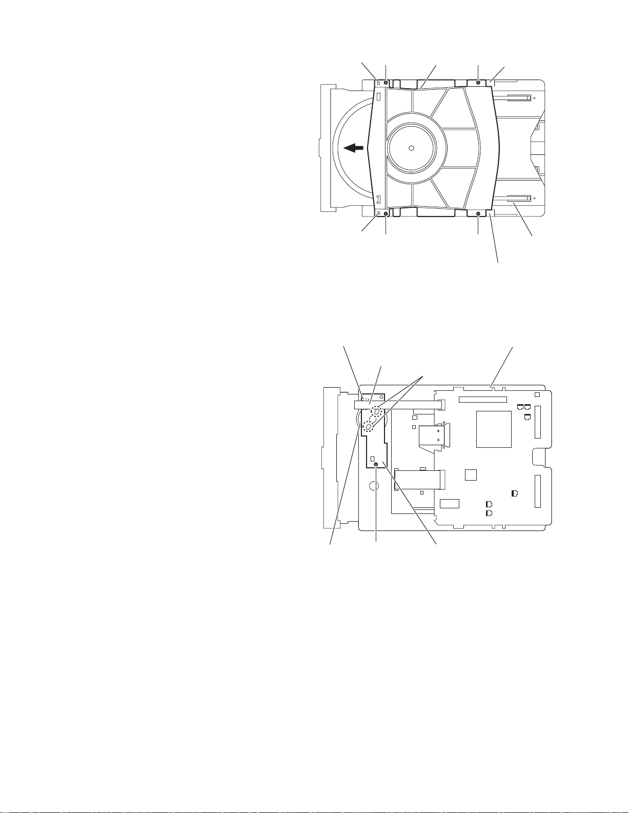
3.3.4 Removing the clamper base
(See Fig.4)
(1) From the top side of the DVD mechanism assembly, re-
move the four screws A attaching the clamper base.
(2) Remove the clamper base from the bosse s d of the loadi ng
base in an upward direction, remove the clamper base
from the sections e while sliding it in the direction of the arrow.
Boss d
Clamper base
AA
Section e
3.3.5 Removing the tray drive board
(See Fig.5)
• Remove the clamper base.
(1) From the bottom side of the DVD mechanism assembly,
disconnect the card wire from the connector on the tray
drive board.
(2) Remove the solders from the soldered sections f on the
tray drive board.
(3) Remove the screw B attaching th e tray drive board to the
DVD mechanism assembly.
Boss d
Connector
A A
Fig.4
Card wire
Soldered
sections f
Loading base
Section e
DVD mechanism assembly
1-16 (No.22023)
Motor
B
Tray drive board
Fig.5
Page 17
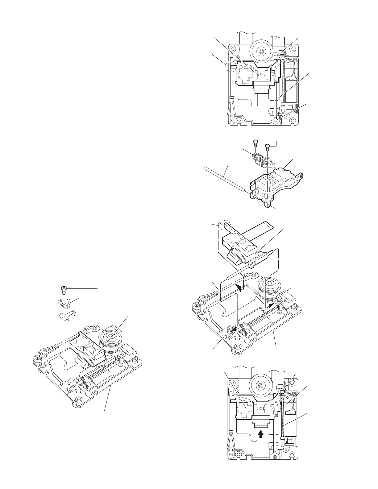
3.3.6 Removing the motor
(See Fig.6)
• Remove the clamper base.
• Remove the tray drive board.
(1) From the top side of the DVD mechan ism assembly, re-
move the belt of the pulley gear.
Note:
Take care not to attach grease on the belt.
(2) Remove the screw C attaching the motor to the DVD mech-
anism assembly.
3.3.7 Removing the DVD traverse mechanism assembly
(See Figs.7)
• Remove the DVD servo board.
• Remove the clamper base.
(1) From the top side of the DVD mechan ism assembly, re-
move the four screws D attaching the DVD traverse mechanism assembly to the loading base.
(2) Take out the DVD traverse mechanism assembly from the
loading base.
Pulley gear
DVD mechanism assembly
Belt
C
Motor
Fig.6
DVD traverse mechanism assembly
D D
DD
Fig.7
Loading base
(No.22023)1-17
Page 18
3.3.8 Removing the DVD pickup unit
(See Figs.8 to 10)
• Remove the DVD servo board.
• Remove the clamper base.
• Remove the DVD traverse mechanism assembly.
(1) From the top side of the DVD traverse mechanism assem-
bly, remove the screw E attaching the plate and torsion
spring. (See Fig.8.)
(2) Remove the shaft from the section g and then remove the
shaft from the section h. (See Fig.9.)
(3) Disengage the section i of the DVD pickup unit and then re-
move the DVD pickup unit with the shaft. (See Fig.9.)
(4) Pull the shaft out of the DVD pickup unit. (See Fig.10.)
(5) Remove the two screws F attaching the SW. actuator. (See
Fig.10.)
3.3.9 Attaching the DVD pickup unit
(See Figs.8, 10 to 12)
Reference:
Refer to the explanation of "Removing the DVD pickup unit" on
the preceding page.
(1) Attach the SW. actuator and shaft to the DVD p ickup unit.
(See Fig.10.)
(2) Engage the section i of the DVD pickup unit to the shaft of
the DVD traverse mechanism assembly first, and set the
both ends of the shaft of the DVD pickup unit in the sections
g and h of the DVD traverse mechanism assembly. (See
Fig.11.)
(3) Slide the DVD pickup unit all the way in the direction of the
arrow. (See Fig.12.)
(4) Mesh the lead screw to the section j of DVD pickup unit and
then set the end of the lead screw to the section k. (See
Fig.12.)
(5) Attach the torsion spring. (See Fig.8.)
(6) Attach the plate. (See Fig.8.)
DVD pickup unit
Section i
Section i
SW. actuator
Shaft
Section h
Shaft
Section g
Fig.9
F
DVD pickup unit
Fig.10
DVD pickup unit
E
Plate
Torsion spring
DVD traverse mechanism assembly
Fig.8
DVD pickup unit
Shaft
Section g
DVD pickup unit
Section h
DVD traverse mechanism assembly
Fig.11
Section k
Section j
Lead screw
1-18 (No.22023)
Fig.12
Page 19
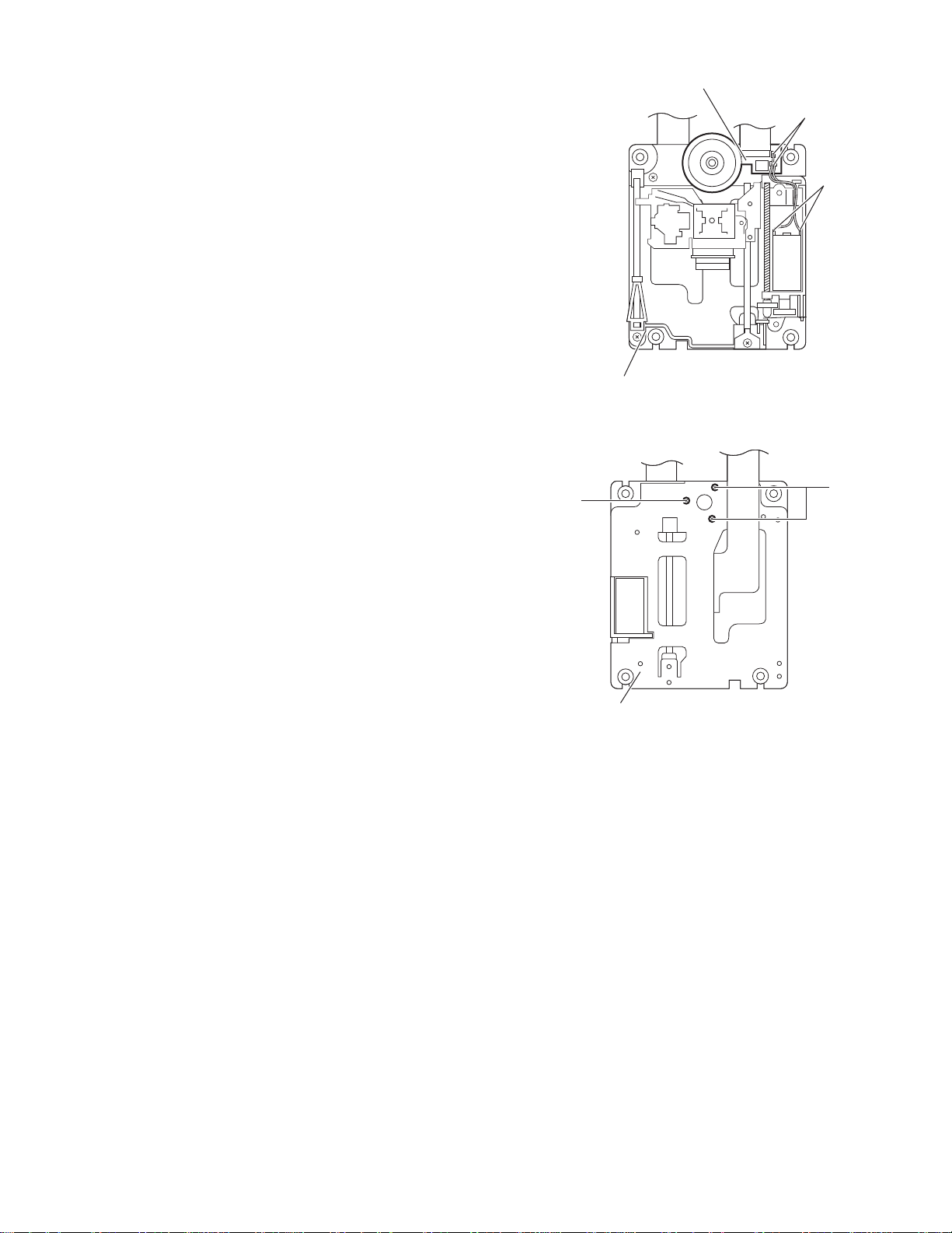
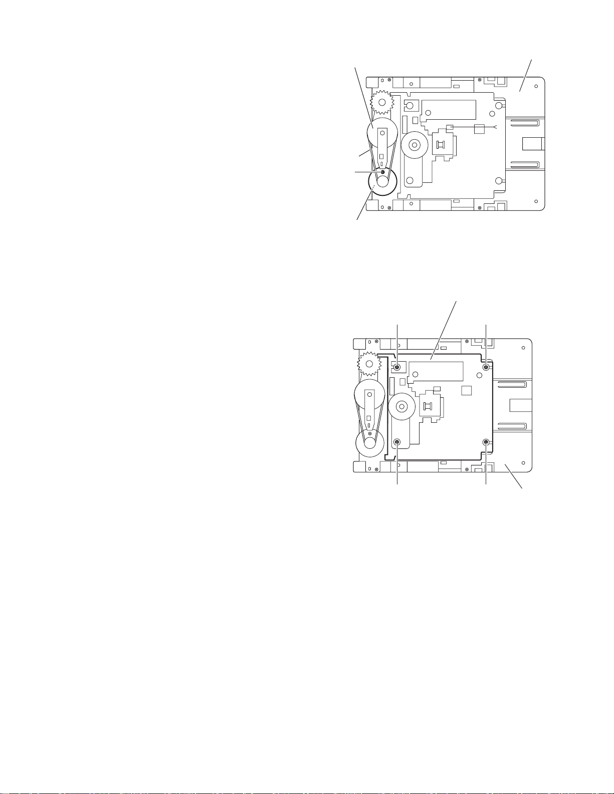
3.3.10 Removing the spindl e m oto r board
r
(See Figs.13 and 14)
• Remove the DVD servo board.
• Remove the clamper base.
• Remove the DVD traverse mechanism assembly.
(1) From the top side of the DVD traverse mechanism assem-
bly, remove the feed motor wire that is soldered to the spindle motor board. (See Fig.13.)
(2) From the bottom side of the DVD traverse mechanism as-
sembly, remove the three screws G attaching the spindle
motor board. (See Fig.14.)
Spindle motor board
Remove the solders.
Feed moto
wire
DVD traverse mechanism assembly
Fig.13
G
DVD traverse mechanism assembly
Fig.14
G
(No.22023)1-19
Page 20
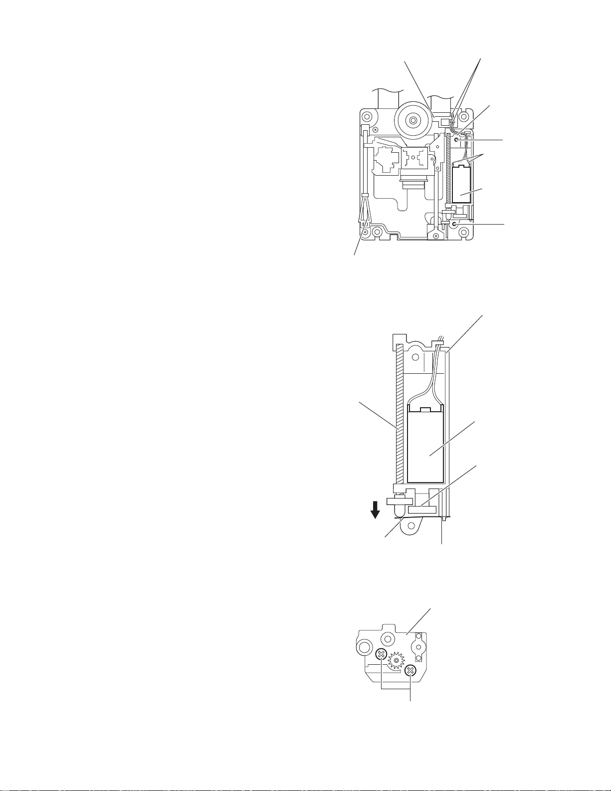
3.3.11 Removing the feed motor
r
(See Figs.15 to 17)
• Remove the DVD servo board.
• Remove the clamper base.
• Remove the DVD traverse mechanism assembly.
(1) From the top side of the DVD traverse mechanism assem-
bly, remove the feed motor wire that is soldered to the spindle motor board. (See Fig.15.)
(2) Remove the two screws H attaching the feed holder as-
sembly and then take out the feed holder assembly. (See
Fig.15.)
(3) Remove the screw J attaching the thrust spring. (See
Fig.16.)
(4) Remove the feed gear and lead screw in the direction of the
arrow. (See Fig.16.)
(5) Remove the two screws K attaching the feed motor. (See
Fig.17.)
Spindle motor board
DVD traverse mechanism assembly
Fig.15
Feed holder assembly
Remove the solders.
Feed holde
assembly
H
Feed motor
wire
Feed motor
H
Lead screw
Feed motor
Feed gear
Thrust spring
J
Fig.16
Feed holder assembly
1-20 (No.22023)
K
Fig.17
Page 21

SECTION 4
C
ADJUSTMENT
4.1 TEST mode (See Fig.1)
(1) Before executing the test mode, press the DVD button on the remote control unit to set the main unit to the DVD mode.
(2) This model is provided with a test mode for use in production control, servicing and repair.
(3) The test mode includes the followin g four submodes, which are switched over every time the CHOICE button on the remote
control unit is pressed.
(4) The test mode is exited when the power is switched on or off.
(5) While holding the STOP and DVD buttons on the main unit, plug the power cord into the wall power outlet.
(6) The opening screen showing the version number is displayed.
The FL display shows "TEST ". : Destination type symbol.
DVD button
(Initialization)
STANDBY/ON button
DVD button
(TEST mode)
HOICE button
(TEST mode)
OPEN/CLOSE button
(TEST mode)
STOP button
(TEST mode)
FL display
(1) Press the button once: Microcomputer version display mode / The FL display shows the version numbers of the microcomputers
in use.
Displayed information: [System MICON] [Front-end (FE) MICON] [Back-end (BE) MICON]
(2) Press the button twice: Display check mode / All FL and LED segments light up.
(3) Press the button three times: Mechanism check mode / The FL display shows "CHECK".
(4) Press the button four times: Front-end check mode / The FL display shows "EXPERT".
(No.22023)1-21
Page 22

SECTION 5
TROUBLE SHOOTING
This service manual does not describe TROUBLE SHOOTING.
1-22 (No.22023)
Page 23

DESCRIPTION OF MAJOR ICS
6.1 74LCX32MTC-X (IC522) : OR gate
• Pin layout & Block diagram
11A
21B
31Y
42A
52B
62Y
7
(TOP VIEW)
6.2 74LCX373MTC-X (IC512,IC513) : Latch
•Pin layout
1OE
2O0
3D0
4D1
5O1
6O2
7
8D3
9O3
10GND
(TOP VIEW)
• Pin function
Symbol Description
D0~D7 Data inputs
LE Latch enable input
OE
Output enable input
O0~O7 3-State latch outputs
14
13
12
11
10
9
8GND
20
19
18
17
16
15
14D2
13
12
11
CC
V
4B
4A
4Y
3B
3A
3Y
VCC
O7
D7
D6
O6
O5
D5
D4
O4
LE
SECTION 6
• Truth table
ABY
LLL
LHH
HLH
HHH
• Truth table
LE OE
H = HIGH Voltage level
L = LOW Voltage level
Z = High impedance
X = Immaterial
O0 = Previous O0 before HIGH to LOW transition of latch enable
• Block diagram
11
LE
1
OE
INPUTS OUTPUT
INPUTS OUTPUT
Dn On
XHXZ
HLLL
HLHH
LLXO0
D0
D1
D2
D3
D4
D5
3
4
7
8
13
D
D
D
D
O
O
L
L
2
O0
O
L
L
5
6
O1
O2
14
D
O
O
L
9
12
O3
O4
D6
17
D
L
15
18
D
O
O
L
16
O5
O6
D7
D
O
L
19
O7
6.3 TC74HC4072AF-X (IC611) : OR gate
• Block diagram
1Y
1
1A
2
1B
3
1C
4
1D
5
NC
6
GND
7
14
13
12
11
10
9
8
Vcc
2Y
2D
2C
2B
2A
NC
• Truth table
ABCDY
HXXXH
XHXXH
XXHXH
XXXHH
LLLLL
X : Don't care
(No.22023)1-23
Page 24

6.4 AK4527BVQP (IC601): A/D, D/A converter
• Pin layout
4443424140393837363534
1
2
3
4
5
6
7
8
9
10
11
1213141516171819202122
Top View
• Pin function
No. Symbol I/O Function
1 SDOS I SDTO Source Select Pin (Note 1)
"L" : Internal ADC output "H" : DAUX input
2 OSKS I Control Mode Select Pin
"L" : 3-wire Serial "H" : I2C Bus
3 MIS - Soft Mute Pin (Note 1) Connect to GND
When this pin goes to "H" soft mute cycle is initialized.
When returning to "L" the output mute releases.
4 BICK I Audio Serial Data Clock Pin
5 LRCK I/O Input Channel Clock Pin
6 SDTI1 I DAC1 Audio Serial Data Input Pin
7 SDTI2 I DAC2 Audio Serial Data Input Pin
8 SDTI3 I DAC3 Audio Serial Data Input Pin
9 SDTO O Audio Serial Data Output Pin
10 D,AUX - Sub Audio Serial Data Input Pin Connect to GND
11 DFS - Double Speed Sampling Mode Pin (Note 1)
"L" : Normal Speed "H" : Double Speed
12 DEMI - Connect to GND
No internal bonding.
13 DEMO - Zero Input Detect Enable Pin Connect to GND
"L" : mode 7 (disable) at parallel mode
- zero detect mode is selectable by DZFM2-0 bits at serial mode.
- H : mode 0 (DZF is AND of all six channels)
14 MCKO - Output Buffer Power supply Pin 2.7V~5.5V
15 DVDD I Digital Power Supply Pin 4.5V~5.5V
16 DVSS - De-emphasis Pin 0V
17 PD
I Power-Down & Reset Pin
When "L" the AK4527B is powered-down and the control registers are reset to default state.
If the state of P/S or CAD0-1 changes then the AK4527B must be reset by PDN.
18 XTS - Test Pin Connect to GND
This pin should be connected to DVSS.
19 ICKS - Connect to GND No internal bonding.
20 ADIF - Analog Input Format Select Pin Digital Power Supply
H : Full-differential input "L" : Single-ended input
21 CAD1 - Chip Address 1 Pin Connect to GND
33
32
31
30
29
28
27
26
25
24
23
1-24 (No.22023)
Page 25

No. Symbol I/O Function
22 CAD0 O Chip Address 0 Pin Connect to GND
23 LOUT3 O DAC3 Lch Analog Output Pin
24 ROUT3 O DAC3 Rch Analog Output Pin
25 LOUT2 O DAC2 Lch Analog Output Pin
26 ROUT2 O DAC2 Rch Analog Output Pin
27 LOUT1 O DAC1 Lch Analog Output Pin
28 ROUT1 O DAC1 Rch Analog Output Pin
29 LIN- I Lch Analog Negative Input Pin
30 LIN+ I Lch Analog Positive Input Pin
31 RIN- I Rch Analog Negative Input Pin
32 RIN+ I Rch Analog Positive Input Pin
33 VREFL - Zero Input Detect 2 Pin (Note 2) Non Connect
When the input data of the group 1 follow total 8192LRCK cycles with "0" input data this pin
goes to "H".
OVF O Analog Input Overflow Detect Pin (Note 3)
This pin goes to "H" if the analog input of Lch or Rch is overflows.
34 VCOM O Common Voltage Output PinAVDD/2
Large external capacitor around 2.2uF is used to reduce power-supply noise.
35 VREFH - Positive Voltage Reference Input PinAVDD
36 AVDD - Analog Power Supply Pin4.5V~5.5V
37 AVSS - Analog Ground Pin0V
38 XTI - Zero Input Detect 1 Pin (Note 2) Non connect
When the input data of the group 1 follow total 8192 LRCK cycles with "0" input data this pin
goes to "H".
39 XTO I Master Clock Input Pin
40 P1S - Parallel / Serial Select Pin
"L" : Serial control mode "H" : Parallel control mode
41 CS
CSN I Chip select pin in 3-wire serial control mode
42 DIF1 I Audio Data Interface Format 1 Pin in parallel mode
SCL/CCLK I Control Data Clock Pin in serial control mode
43 LOOP0 I Loopback Mode 0 Pin in parallel control mode
SAD/CDTI I/O Control Data Input Pin in serial control mode
44 CDTD I Loopback Mode 1 Pin (Note 1)
Note:
(1) SDOS, SMUTE, DFS, and LOOP1 pins are ORed with register data if P/S = "L".
(2) The group 1 and 2 can be selected by DZFM2-0 bit if P/S = "L" an d DZFME = "L".
(3) This pin becomes OVF pin if OVFE bit is set to "1" at serial control mode.
(4) All input pins should not be left floating.
I Audio Data Interface Format 0 Pin in parallel mode
This pin should be connected to DVDD at I2C bus control mode
I2C = "L" : CCLK(3-wire Serial) I2C = "H" : SCL(I2CBus)
Enables digital loop-back from ADC to 3 DACs.
I2C = "L" : CDTI(3-wire Serial) I2C = "H" : SDA(I2CBus)
Enable all 3 DAC channels to be input from SDTII.
(No.22023)1-25
Page 26

6.5 AN8703FH-V (IC101) : Frontend processor for DVD
• Pin layout
• Block diagram
AGOFST
AGCBAL
DFLTOP
AGCLVL
DCFLT
DCFLT
RFENV
BOTTOM
PEAK
48 33~
49
~
64
116
~
23
19
30
31
25
32
41
42
43
32
~
17
Level
Cont.
BDO
Det.
+-
+-
HOLD EQ
+-+-
UDO
OFTR
AGCO
AGCG
VHALP
VREF2
VREF1
VCC3
VCC2
VCC1
GND3
GND2
40 39 45 44 29 27 56 36 36 28 55 26 61
Level
Cont.
OFTR
Det.
REG SIF
Vol. Adg
AGC Cont.
Boost
Cont.
FC
Cont.
VGA
GND1
LPC AMP
+-
DTRD
9
10
IDGT
11
STANBY
12
SEN
13
SCK
14
STDI
64
HDTYPE
1
LPC1
2
LPCO1
LPC2
3
LPCO2
4
18
TEOUT
RFINP
RFINN
TESTSG
VFOSHORT
DCRF
RFOUT
RFC
FEOUT
FEN
FBAL
ASOUT
47
48
46
38
35
37
22
21
20
TEN
+-
S-line
J-line
17
6
8
24
34
15
16
TBAL
POFLT
MON
RFDIFO
RSCL
JLINE
+-
+-
5
+-
7
FBAL
+-
49 50 51 52 53 54 62
VIN5
VIN6
VIN7
+-
SW
ADD ADD ADD
VIN8
VIN9
VIN10
AMP
Differential
Phase
TBAL
Det.
EQ EQ EQ EQ
63 57 58 59 60
VIN1
VIN11
VIN12
TBAL
VIN2
VIN3
VIN4
Micro
Det.
ADD
+-
ADD
1-26 (No.22023)
Page 27

• Pin function
Pin No. Symbol Function
1 LPC1 Laser pin input (DVD head)
2 LPCO1 Laser drive output (DVD head)
3 LPC2 Laser in input (CD head)
4 LPCO2 Laser drive output (CD head)
5 VFOSHORT VFOSHORT control
6 TBAL Tracking balance control
7 FBAL Focus balance control
8 POFLT Track detection threshold level
9 DTRD Data slice data read signal input (for RAM)
10 IDGT Data slice address gate signal input (for RAM)
11 STANBY Standby mode control
12 SEN SEN (serial data input)
13 SCK SCK(serial data input)
14 STDI STDI(serial data I/O)
15 RSCL Reference current setting
16 JLINE J-line vurrent setting
17 TEN Tracking error amplifier inverted input
18 TEOUT Tracking error signal output
19 AGCBAL Offset adjustment for DRC-1
20 ASOUT Full addition signal output
21 FEN Focus error amplifier inverted input
22 FEOUT Focus error signal output
23 AGCOFST Offeset adjustment for DRC-2
24 MON Monitor
25 AGCLVL Output amplitude adjustment for DRC
26 GND2 Ground 2
27 VREF2 VREF2 voltage output
28 VCC2 Power supply 2 (5V)
29 VHALF VHALF voltage output
30 DFLTON Filter amplifier inverted output
31 DFLTOP Filter amplifier positive output
32 DCFLT Filter output capacitance connection
33 GND3 Groud 3
34 RFDIFO Raidal differntial output
35 RFOUT RF full-addition amplifier output
36 VCC3 Power supply 3 (3.3V)
37 RFC Filter for RF-group delay correction ampl ifier
38 DCRF DC-cut filter for RF full-addition amplifier
39 OFTR OFTR output
40 BDO BDO output
41 RFENV RF envelope output
42 BOTTOM Bottom envelope detection filter
43 PEAK Peak envelope detection filter
44 AGCG AGC amplifier again control
45 AGCO AGC amplifier level control
(No.22023)1-27
Page 28

Pin No. Symbol Function
46 TESTSG TEST signal input
47 REFINP RF signal positive input
48 RFINN RE signal inverterd input
49 VIN5 Internal four-partition (CD) RF input 1
50 VIN6 Internal four-partition (CD) RF input 2
51 VIN7 Internal four-partition (CD) RF input 3
52 VIN8 Internal four-partition (CD) RF input 4
53 VIN9 Internal four-partition (DVD) RF input 2
54 VIN10 Internal four-partition (DVD) RF input 1
55 VCC1 Power supply 1 (5V)
56 VREF1 VREF1 voltage output
57 VIN1 Internal four-partition (DVD) RF input 1
58 VIN2 Internal four-partition (DVD) RF input 2
59 VIN3 Internal four-partition (DVD) RF input 3
60 VIN4 Internal four-partition (DVD) RF input 4
61 GND1 Groud 1
62 VIN11 3-deam sub (CD) input 2
63 VIN12 3-deam sub (CD) input 1
64 HDTYPE HD type selection
1-28 (No.22023)
Page 29

6.6 BA15218F-XE (IC303,IC602,IC603,IC651,IC652,IC661,IC671,IC672) : Dual operation amplifier
•Pin layout
OUT1 1
-IN1 2
+IN1 3
VEE 4
• Block diagram
Vcc
-IN
+IN
1
2
R1
Q5
Q1
Q2
D1
Q3 Q4
8 Vcc
7 OUT2
6 -IN2
5 +IN2
C2
R5
Q6
Q9
Q8
Q10
Q7
R7
Q11
R6
Q12
R8
Q18Q13
OTHER
CH
Q19
Q17Q16
VEE
C1
R3R2
R4
Q14 Q15Q114
R9
OUTPUT
(No.22023)1-29
Page 30

6.7 BA5983FM-X (IC201) : 4ch driver
• Pin layout & Block diagram
28 27 26
VCC
+-
25 24 23 22 21 20 19 18 17 16 15
+-
10k
10k
10k
20k
+-
+-
10k
10k
20k
+-
+-
10k
STAND BY
+-+-
3 4
21
6 7
5
• Pin function
Pin No Symbol Function
1 BIAS IN NC
2 OPIN1(+) Output3 for motor
3OPIN1(-)NC
4 OPOUT1 Output2 for motor
5OPIN2(+)NC
6OPIN2(-)NC
7 OPOUT2 Output1 for motor
8GNDGND
9 STBY1 Positive input for hall input Amp1.
10 PowVCC1 Negative input for hall input Amp1.
11 VO2(-) Positive input for hall input Amp2.
12 VO2(+) Negative input for hall input Amp2.
13 VO1(-) Positive input for hall input Amp3.
14 VO1(+) Negative input for hall input Amp3.
15 VO4(-) Hall bias terminal
16 VO4(+) Brake Mode terminal
17 VO3(-) Capacitor connection pin for phase compensation
18 VO3(+) Short brake terminal
19 PowVCC2 3Phase synthesized FG signal output termnal
20 STBY2 Rotation detect signal output terminal
21 GND Torque control standard voltage input terminal
22 OPOUT3 Torque control voltage input termi nal
23 OPIN3(-) START/STOP switch
24 OPIN3(+) FG signal output terminal
25 OPOUT4 Power supply for driver division
26 OPIN4(-) Gain switch
27 OPIN4(+) Power supply for driver division
28 PreVCC Resistance connection pin for output current sense
C #1/2/3
89
VCC
STAND BY
C #4
VCC
10k
10k
10k
10k
10k
10 11
10k
10k
+- +- +- +-
10k
10k
Level
Sblft
Level
Sblft
Level
Sblft
Level
Sblft
10k
10k
+-
12
+- +-
10k10k
13
10k
10k
10k
+-
10k
14
1-30 (No.22023)
Page 31

6.8 BA6664FM-X (IC251) : Motor driver
• Pin layout & Block diagram
RNF
VM GSW VCC
28
27 26
GAIN
SWITCH
TSD
FG PS EC ECR FR FG2 SB CNF
25 24 23 22 21 20 19 18 17 16 15
VCC
PS
TORQUE
+-
SENSE AMP
VCC
VCC
SHORT BRAKE BRAKE MODE
+ -
CURRENT
SENSE AMP
DRIVER
GAIN
CONTROL
TL
HALL AMP
2
4
7
8
A3 A2 A1 GND H1
• Pin function
Pin No. Symbol Function
1NCNC
2 A3 Output3 for motor
3NCNC
4 A3 Output2 for motor
5NCNC
6NCNC
7 A1 Output1 for motor
8GNDGND
9 H1+ Positive input for hall input Amp1.
10 H1- Negative input for hall input Amp1.
11 H2+ Positive input for hall input Amp2.
12 H2- Negative input for hall input Amp2.
13 H3+ Positive input for hall input Amp3.
14 H3- Negative input for hall input Amp3.
15 VH Hall bias terminal
16 BR Brake Mode terminal
17 CNF Capacitor connection pin for phase compe nsation
18 SB Short brake terminal
19 FG2 3Phase synthesized FG signal output termnal
20 FR Rotation detect signal output terminal
21 ECR Torque control standard voltage input terminal
22 EC Torque control voltage input terminal
23 PS START/STOP switch
24 FG FG signal output terminal
25 VCC Power supply for driver division
26 GSW Gain switch
27 VM Power supply for driver division
28 RNF Resistance connection pin for output current sense
FIN FIN GND
910
+
H1
-
11
H2
VHBR
Hall Bias
Q Q
R
CK
D
+-+-+-+-+-+-
12
+
H2
H3
13
14
+
H3
-
(No.22023)1-31
Page 32

6.9 GP1UM281X (IC702) : Dual operation amplifier
R
L
Amp
6.10 IC-PST9139-T(IC763) : Regulator
• Terminal layout
123
• Block diagram
B.P.FLimiter
Demodulator
Integrator
Comparator
GND Vcc Vout
CO1
VCC
2
OUT
1
OP1
GND
3
1-32 (No.22023)
Page 33

6.11 JCV8007 (IC201) : 2 channel AF power amplifier
TR41
• Pin Layout
118
• Block Diagram
TR1 TR2
R1
14
TR3
15
16
TR5
R2
13 1718
R41
D41
D51
Comparator
D42
D43
SUB
D53
D52
Comparator
R51
R3D2
TR6
C2
C1
R4
TR4
R5
R6
D1
TR7
R7
TR9
TR8
TR10
12 9 8 11 10
TR19
TR20
TR18
R13 D12
TR16
R16
TR17
R17
R14
R15
C12
C11
TR14
R11
TR15
R12
TR11TR12
TR13
TR51
1
3
2
7
5
4
6
(No.22023)1-33
Page 34

6.12 JCV8008 (IC202) : 3 channel AF power amplifier
• Pin Layout
122
• Block Diagram
TR11
TR12
D3
13
D2
TR4
R3
TR6
C2
TR8
R4
R5
R6
TR7
D1
TR9
TR10
R7
12 9 8
TR1
TR2
C1
R1
14
TR3
15
16
TR5
R2
TR16
R13
TR19
TR29
R23
TR26
D4
TR22
TR21
TR13
TR23
R11
C11
C12
TR18
TR28
C22
C21
R21
TR14
R14 R15
TR20
TR30
R24
TR24
1718
R25
2019
R16
R26
TR15
TR25
TR17
TR27
R12
R17
R27
R22
10 11
22 21
TR41
D41
D51
TR51
R41
Comparator
Comparator
R51
D42
D52
D43
D44
D54
D53
1
3
2
7
SUB
5
4
6
1-34 (No.22023)
Page 35

6.13 AK93C65AF-X (IC510) : EEPROM
•Pin layout
• Block diagram
DI
CS
PE
VCC
CS
SK
1
2
3
4
8 PIN SOP
INSTRUCTION
REGISTER
NC
8
GND
7
DO
6
5
INSTRUCTION
DECODE,
CONTROL
AND
CLOCK
GENERATION
DI
DATA
REGISTER
ADD.
BUFFERS
16
R/W AMPS
AND
AUTO ERASE
DECODER
DO
16
EEPROM
4096bit
256 x 16
SK
PE
• Pin function
Pin no. Symbol Function
1 PE Program enable (With built-in pull-up resistor)
2 VCC Power supply
3 CS Chip selection
4 SK Cereal clo ck in put
5 DI Cereal data input
6 DO Cereal data output
7 GND Ground
8 NC No connection
NOTE :
The pull-up resistor of the PE pin is about 2.5Mohm (VCC=5V)
VREF
VPP SW
VPP
GENERATOR
(No.22023)1-35
Page 36

6.14 K4S643232E-TC60 (IC505) : 512K x 32 bit x 4 banks synchronous DRAM
A
• Pin layout
86 44
143
• Block diagram
Data Input Register
512K x 32
512K x 32
512K x 32
512K x 32
Column Decoder
Latency & Burst Length
Programming Register
LWCBR
CLK
DD
LCKE
Bank Select
Row Buffer
Refresh Counter
Address Register
LRAS
LCBR
LRAS LCBR LWE
Row Decoder
Col. Buffer
LCAS
Sense AMP
LDQM
LWE
LDQM
I/O Control
DQi
Output Buffer
Timing Register
CLK CKE CS
RAS CAS
WE DQM
• Pin function
Pin No. Symbol Function
1 VDD Power for the input buffers and core logic.
2 DQ0 Data input/output are multiplexed on the same pin.
3 VDDQ Isolated power supply for the output buffers to provide improved noise immunity.
4,5 DQ1,DQ2 Data inputs/outputs are multiplexed on the same pins.
6 VSSQ Isolated ground for the output buffers to provide improved noise immunity.
7,8 DQ3,DQ4 Data inputs/outputs are multiplexed on the same pins.
9 VDDQ Isolated power supply for the output buffers to provide improved noise immunity.
10,11 DQ5,DQ6 Data inputs/outputs are multiplexed on the same pins.
12 VSSQ Isolated ground for the output buffers to provide improved noise immunity.
13 DQ7 Data input/output are multiplexed on the same pin.
14 N.C This pin is recommended to be left no connection on the device.
15 VDD Power for the input buffers and core logic.
16 DQM0 Makes data output Hi-Z, tSHZ after the clock and masks the output.
Blocks data input when DQM active.
17 WE
Enables write operation and row precharge.
Latches data in starting from CAS, WE active.
18 CAS
Latches column addresses on the positive going edge of the CLK with CAS low.
Enables column access.
19 RAS
Latches row addresses on the positive going edge of the CLK with RAS low.
Enables row access & precharge.
20 CS Disables or enables device operation by masking or enabling all inputs except CLK, CKE and DQM.
21 N.C This pin is recommended to be left no connection on the device.
22,23 BA0,BA1 Selects bank to be activated during row add ress latch time.
Selects bank for read/write during column address latch time.
1-36 (No.22023)
Page 37

Pin No. Symbol Function
24,25~27 A10,A0 - A2 Row/column addresses are multiplexed on the same pins.
Row address : RA0 ~ RA10, Column address : CA0 ~ CA7
28 DQM2 Makes data output Hi-Z, tSHZ after the clock and masks the output.
Blocks data input when DQM active.
29 VDD Power for the input buffers and core logic.
30 N.C This pin is recommended to be left no connection on th e device.
31 DQ16 Data input/output are multiplexed on the same pin.
32 VSSQ Isolated ground for the output buffers to provide improved noise immunity.
33,34 DQ17,DQ18 Data inputs/outputs are multiplexed on the same pins.
35 VDDQ Isolated power supp ly for the output buffers to provide improved noise immunity.
36,37 DQ19,DQ20 Data inputs/outputs are multiplexed on the same pins.
38 VSSQ Isolated ground for the output buffers to provide improved noise immunity.
39,40 DQ21,DQ22 Data inputs/outputs are multiplexed on the same pins.
41 VDDQ Isolated power supp ly for the output buffers to provide improved noise immunity.
42 DQ23 Data input/output are multiplexed on the same pin.
43 VDD Power for the input buffers and core logic.
44 VSS Ground for the input buffers and core logic.
45 DQ24 Data input/output are multiplexed on the same pin.
46 VSSQ Isolated ground for the output buffers to provide improved noise immunity.
47,48 DQ25,DQ26 Data inputs/outputs are multiplexed on the same pins.
49 VDDQ Isolated power supp ly for the output buffers to provide improved noise immunity.
50,51 DQ27,DQ28 Data inputs/outputs are multiplexed on the same pins.
52 VSSQ Isolated ground for the output buffers to provide improved noise immunity.
53,54 DQ29,DQ30 Data inputs/outputs are multiplexed on the same pins.
55 VDDQ Isolated power supp ly for the output buffers to provide improved noise immunity.
56 DQ31 Data input/output are multiplexed on the same pin.
57 N.C This pin is recommended to be left no connection on th e device.
58 VSS Ground for the input buffers and core logic.
59 DQM3 Makes data output Hi-Z, tSHZ after the clock and masks the output.
Blocks data input when DQM active.
60~66 A3 - A9 Row/column addresses are multiplexed on the same pins.
Row address : RA0 - RA10, Column address : CA0 - CA7
67 CKE Masks system clock to freeze operation from the next clock cycle.
CKE should be enabled at least one cycle prior to new command.
Disables input buffers for power down mode.
68 CLK Active on the positive going edge to sample all inputs.
69,70 N.C This pin is recommended to be left no connection on the device.
71 DQM1 Makes data output Hi-Z, tSHZ after the clock and masks the output.
Blocks data input when DQM active.
72 VSS Ground for the input buffers and core logic.
73 N.C This pin is recommended to be left no connection on th e device.
74 DQ8 Data input/output are multiplexed on the same pin.
75 VDDQ Isolated power supp ly for the output buffers to provide improved noise immunity.
76,77 DQ9,DQ10 Data inputs/outputs are multi plexed on the same pins.
78 VSSQ Isolated ground for the output buffers to provide improved noise immunity.
79,80 DQ11,DQ12 Data inputs/outputs are multiplexed on the same pins.
81 VDDQ Isolated power supp ly for the output buffers to provide improved noise immunity.
82,83 DQ13,DQ14 Data inputs/outputs are multiplexed on the same pins.
84 VSSQ Isolated ground for the output buffers to provide improved noise immunity.
85 DQ15 Data input/output are multiplexed on the same pin.
86 VSS Ground for the input buffers and core logic.
(No.22023)1-37
Page 38

6.15 LA73054-X (IC401) : Video driver
• Pin layout & Block diagram
36 35 34 33 32 31 30 29 28 27 26 25 24 23 22 21 20 19
75
DRIVER
LPF
2Step
Amp1
C_OFFSET
DC_CTL
CLAMP
1 2 3 4 5 6 7 8 9 10 11 12 13 14 15 16 17 18
75
DRIVER
LPF1
2Step
Amp2
Y/C
MIX
75
DRIVER
LPF1
2Step
Amp3
CLAMP
SYNC
SEP
75
DRIVER
2Step
Amp4
PEDESTAL
CLAMP
LPF1LPF2
CLAMP
• Pin function
Pin No. Symbol I/O Function
1 VCC1 - VCC except for 75ohm driver
2 COMPOSITE.IN I Input composite
3 SQUEEZE.SW I Selecting squeeze mode
4 LETTER-BOX.SW I Selecting letter-box mode
5 MUTE-SW-1 I Composite/S si gnal mute selection
6 C-IN I Input Chroma signal
7 GND11 - Composite/S GND except for 75ohm driver
8 Y-IN-1 I Input Y signal
9 YC-MIX.SW I Selecting of doing Y/C-MIX or not
10 SIGNAL-IN.SW I Selection of a kind of signal
11 Y-IN-2 I Input component Y or baseband signal
12 MUTE-SW-2 I Component signal mute selection
13 LPF.SW I Selection of a kind of component LPF
14 CB.IN I Input componen t or baseband signal
15 AMP.SW-2 I Selecting amplifier gain for component signal
16 CR.IN I Input component or baseband signal
17 GND12 - Component GND except for 75ohm driver
18 REG O Capacitor terminal for regulator
19 DRIVE.SW-2 I 2drive/1drive select for component signal
20 GND26 - CR-GND for 75ohm driver
21 CR.OUT O 75ohm driver output of pin16 input
22 GND25 - CB-OUT for 75ohm driver
23 CB.OUT O 75ohm driver output of pin14 input
24 VCC22 - Component Vcc for 75ohm driver
25 Y-OUT-2 O 75ohm driver output of pin11 input
26 GND24 - Component Y out for 75ohm driver
27 GND23 - Y out for 75ohm driver
28 Y-OUT-1 O 75ohm driver output of pin8 input
29 GND22 - Chroma out for 75ohm driver
30 C-DC.OUT O DC voltage output for S1,S2
31 C-OUT O 75ohm driver output of pin6 input
32 GND21 - Composite out for 75ohm driver
33 COMPOSITE-OUT O 75ohm driver output of pin2 input
34 VCC21 - Composite/S Vcc for 75ohm driver
35 DRIVE.SW-1 I 2drive/1drive select for composite/S signal
36 AMP.SW-1 I Selecting amplifier gain for composite/S signal
75
DRIVER
LPF1LPF2 LPF1LPF2
2Step
Amp5
PEDESTAL
CLAMP
75
DRIVER
2Step
Amp6
PEDESTAL
CLAMP
VCC
REG
1-38 (No.22023)
Page 39

6.16 LM1117MP1.8-X (IC511) : Regulator
A
8
• Pin layout • Block diagram
Top view
V
IN
INPUT
DJ/GND
OUTPUT
6.17 LP61L1024S-12-X (IC641) : SRAM
• Pin layout • Block diagram
DD
V
NC
A16
A14
A12
A7
A6
A5
A4
A3
A2
A1
A0
I/O1
I/O2
I/O3
VSS
10
11
12
13
14
15
16
1
2
3
4
5
6
7
8
9
32
31
30
29
28
27
26
25
24
23
22
21
20
19
18
17
VDD
A15
NC(CE2)
WE
A13
A8
A9
A11
OE
A10
CS1
I/O8
I/O7
I/O6
I/O5
I/O4
• Pin function
I/O1 - I/O8 Data Input/Output
CS1
Vss
A0
A16
CS2
CS1
OE
WE
SYMBOL DESCRIPTION
A0 - A16 Address Input
, CS2 Chip Select Inputs
WE
OE
VDD Power Supply
Vss Ground
NC No Connection
Thermal
Limit
Current
GND (FIXED OUTPUT)
ADJ.(ADJUSTABLE OUTPUT)
DECODER
CONTROL
Write Enable Input
Output Enable Input
Limit
CORE
ARRAY
DATA I/O
Substrate
I/O1
I/O
V
OUT
(No.22023)1-39
Page 40

6.18M61516FP (IC301) : Sound controller
A
• Pin layout & Block diagram
TONEOUT R
40
FRVIN FROUT
FROUT
SROUT
39
38
37
SBOUT
SWOUT
36
35
COUT
34
SBLOUT
SLOUT
33
32
FLOUT
OUTGND
31
30
AVCC
29
DGND
CLOCK
28
27
DATA
26
LATCH
25
TRE R
BASS R2
BASS R1
FRIN2
SRIN2
SBRIN2
SWIN2
CIN2
SBLIN2
SLIN2
FLIN2
VOLGND3
VOLGND4
BALANCE L/+
BALANCE L/-/LOUD L
INGND
BALANCE R/-/LOUD R
BALANCE R/+
REC R4
REC R3
REC R2
REC R1
41
42
43
44
45
46
47
48
49
50
51
52
53
54
55
56
57
BALNCE/LOUDNESS
58
50K 50K 50K 50K
59
60
61
62
TONE OUTPUT
SELECTOR
FRONT INPUT
SELECTOR
BALNCE/LOUDNESS
CHANGE SW
A
LOUDNESS TAP
B
CHANGE SW
REC SW
REC SW
REC SW
REC SW
OUTPUT GAIN
+
TONE
BASS/TRE
10K
+
-
Lch
10K
BALANCE OUTPUT
Rch
10K
+
10K
INPUT GAIN
CONTROL
CONTROL
50K
-
-
50K
FL VOL
LOUDNESS
TAP B
-
+
50K
SR VOL
SBR VOL SBL VOL SL VOLSW VOL C VOL
+
50K
+
50K
LOUDNESS
TAP A
+-+-+-+-+
50K 50K 50K 50K 50K
-
+
INPUT
SELECTOR
SELECTOR
OUTPUT GAIN
CONTROL
50K
+
-
FL VOL
INPUT
ZERO CROSS
DETECTOR &
TIMER DETECTOR
-
-
INPUT GAIN
CONTROL
-
+
50K
+
-
MCU
I/F
TONE OUTPUT
+
SELECTOR
TONE
BASS/TRE
FRONT INPUT
SELECTOR
REC SW
REC SW
REC SW
REC SW
50K 50K 50K 50K
24
23
22
21
20
19
18
17
16
15
14
13
12
11
10
9
8
7
6
5
4
3
DVDD
TINT
VOLGND2
FLVIN
TNEOUT
TREL
BASS L2
BASS L1
FRIN1
SRIN1
SBRIN1
SWIN1
CIN1
SBLIN1
SLIN1
FLIN1
VOLGND1
REC L4
REC L3
REC L2
REC L1
INLJ
1-40 (No.22023)
INRJ
INRI
63
64
65
INRH
66
INRG
67
INRF
68
INRE
69
INRD
70
INRC
71
INRB
72
INRA
73
VEE
74
INLA
75
INLB
76
INLC
77
INLD
78
INLE
79
INLF
80
INLG
2
INLI
1
INLH
Page 41

• Pin function
Pin No. Symbol Function
1~3 INLH,INLI,INLJ Lch input
4~7 REC L1,REC L2,REC L3,REC L4 REC output
8 VOLGND1 Analog GND for vol.
9~12 FLIN1,SLIN1,SBLIN1,CIN1 FLch,SLch,SBLch,Cch input
13~16 SWIN1,SBRIN1,SRIN1,FRIN1 SWch,SBRch,SRch,FRch input
17,18 BASS L1,BASS L2 Tone path frequency characteristic setup
19 TRE L Treble frequency characteristic setup
20 TONEOUT L Tone output
21 FLVIN FL vol. input
22 VOLGND2 Analog GND for vol.
23 TIM1 Timer setup
24 DVDD Internal logic circuit Power supply terminal
25,26,27 LATCH,DATA,CLOCK Latch,Data,Clock input for serial data transmission
28 DGND Internal logic circuit GND terminal
29 AVCC Internal analog cicuit power supply terminal (+)
30 OUTGND analog GND
31~34 FLOUT,SLOUT,SBLOUT,COUT FLch,SLch,SBLch,Cch output
35~38 SWOUT,SBROUT,SROUT,FROUT SWch,SBRch,SRch,FRch output
39 FRVIN FR vol.input
40 TONEOUT R Tone output
41 TRE R Treble frequency characteristic setup
42,43 BASS R1,BASS R2 Tone path frequency characteristic setup
44~47 FRIN2,SRIN2,SBRIN2,SWIN2 FRch,SRch,SBRch,SWch input
48~51 CIN2,SBLIN2,SLIN2,FLIN2 Cch,SBLch,SLch,FLch input
52,53 VOLGND3,VOLGND4 Analog GND for vol.
54 BALANCE L/+ Lch balance output for ADC
55 BALANCE L/- LOUD L Lch loudness frequency setup
56 INGND Analog GND
57 BALANCE R/+ Rch balance output for ADC
58 BALANCE R/- LOUD R Rch loudness frequency setup
59~62 REC R1,REC R2,REC R3,REC R4 REC inp ut
63~66 INRJ,INRI,INRH,INRG Rch input
67~70 INRF,INRE,INRD,INRC Rch input
71,72 INRB,INRA Rch input
73 AVEE Internal analog circuit power supply terminal (-)
74~77 INLA,INLB,INLC,INLD Lch input
78~80 INLE,INLF,INLG Lch input
(No.22023)1-41
Page 42

6.19MM1563DF-X (IC615) : Regulator
• Pin layout
756
(TOP VIEW)
1
234
• Block diagram
V
IN
7
Bias
Cont
5
Thermal
shutdown
GND
3
• Pin function
Pin No. Symbol Function
1 Vo Output pin
2 NC Not connect
3 GND Ground
4 Cn Noise decrease pin
5 CONT Control pin
Driver
Current
limiter
Cn
Vo
1
Reference
4
CONT
H
L
Output
ON
OFF
6 Sub Substrate pin, The 6pin must be connected to GND.
7 VIN Input pin
6.20 MM74HCU04SJ-X (IC621) : Inverter
• Pin Layout • Truth table
11A
14
VCC
AY
LH
21Y
32A
42Y
53A
63Y
7
13
12
11
10
9
8GND
6A
6Y
5A
5Y
4A
4Y
HL
1-42 (No.22023)
Page 43

6.21 MM1613DN-X (IC682) : Regulator
• Pin layout • Block diagram
Vin
5
54
(TOP VIEW)
1
23
Cont
GND
1
2
Bias
Reference
3
Cn
Driver
Thermal
shutdown
• Pin function
Pin No. Symbol Function
1 Cont ON/OFF Control pin
Cont
H
L
Vo
ON
OFF
Cont pin must be connected with VIN pin, if it is not used.
2 GND Ground
3 Cn Noise decrease pin, Connecting 0.01uF capacitor can decrease output noise.
4 Vout If the noise decrease capacitor is not connected, the pin may be influenced by outside noise.
Output pin, The capacitor must be connected with output pin more than 1uF.
5 Vin Input pin
The capacitor is required to connect with input pin more than 1uF.
Current
limiter
Vout
4
6.22 MM74HC08SJ-X (IC612) : Quad. 2-input AND gates
• Pin layout & Block diagram
Vcc
A1
B1
Y1
A2
B2
Y2
GND
1
2
3
4
5
6
7
14
13
12
11
10
9
8
B4
A4
Y4
B3
A3
Y3
6.23 MM74HCT32MTC-X (IC521) : OR gate
• Pin layout & Block diagram • Truth table
11A
21B
31Y
42A
52B
62Y
7
14
13
12
11
10
9
8GND
V
4B
4A
4Y
3B
3A
3Y
CC
INPUTS OUTPUT
ABY
LLL
LHH
HLH
HHH
(TOP VIEW)
(No.22023)1-43
Page 44

6.24 MN103S26EGA (IC301) : Optical disc controller
• Pin layout
176 133
1
132
44
89
45 88
• Pin function
Pin No. Symbol I/O Function
1 NINT0 O System control interruption 0
2 NINT1 O System control interruption 1
3 VDD3 - Power supply (3.3V)
4 VSS - Ground
5 NINT2 O System control interruption 2
6 WAITODC O System control wait control
7 NMRST - System control reset (Not connect.)
8 DASPST - DASP signal initializing
9~17 CPUADR17 - 9 I System control address
18 VDD18 - Power supply (1.8V)
19 VSS - Ground
20 DRAMVDD18 - Con nect to VDD18
21 DRAMVSS - Connect to VSS
22~30 CPUADR8 - 0 I System control address
31 VDD3 - Power supply (3.3V)
32 VSS - Ground
33 DRAMVDD3 - Connect to VDD3
34 NCS I System control chip select
35 NWR I System control write
36 NRD I System control read
37~44 CPUDT7 - 0 I/O System control data
45 CLKOUT1 - Not connect.
46 MMOD I Connect to VSS
47 NRST I System reset
48 MSTPOL I Master terminal polarity switch input (Connect to VSS.)
49 SCLOCK - Not connect.
50 SDATA - Not connect.
51 OFTR I Off track signal input
52 BDO I RF dropout/BCA data of making to binary
53~56 PWM1 - 4 - Not connect.
57 VDD3 - Power supply (3.3V)
58 DRAMVDD18 - Con nect to VDD18
59 DRAMVSS - Connect to VSS
60 VSS - Ground
61~64 PWM5 - 8 - Not connect.
65 TBAL O Tracking balance adjustment output
66 FBAL O Focus balance adjustment output
67 TRSDRV O Traverse drive output
68 SPDRV O Spindle drive output
69 FG I Motor FG input
70 TILTP - Not connect.
1-44 (No.22023)
Page 45

Pin No. Symbol I/O Function
71 TILT - Not connect.
72 TILTN - Not connect.
73 TX - Not connect.
74 DTRD - Not connect.
75 IDGT - Not connect.
76 VDD18 - Power supply (1.8V)
77 VSS - Ground
78 VDD3 - Power supply (1.8V)
79 OSCI1 I 16.9MHz clock input
80 OSCO1 - Not connect.
81 VSS - Ground
82 TSTSG O Calibration signal
83 VFOSHORT O VFO short output
84 JLINE O J-line setting output
85 AVSS - Analog ground
86 ROUT - Not connect.
87 LOUT - Not connect.
88 AVDD - Analog power supply
89 VCOF I JFVCO control voltage
90 TRCRS I Input signal for track cross formation
91 CMPIN - Not connect.
92 LPFOUT - Not connect.
93 LPFIN I Pull-up to VHALF
94 AVSS - Analog ground
95 HPFOUT - Not connect.
96 HPFIN I HP F input
97 CSLFLT I Pull-up to VHALF
98 RFOIF - Not connect.
99 AVDD - Analog power supply
100 PLFLT2 I Connect to capacitor 2 for PLL
101 PLFLT1 I Connect to capacitor 1 for PLL
102 AVSS - Analog ground
103 RVI I Connect to resistor for VREF reference current source
104 VREFH I Reference voltage input (2.2V)
105 PLPG - Not connect.
106 VHALF I Reference voltage input (1.65V)
107 DSLF2 I Connect to capacitor 2 for DSL
108 DSLF1 I Connect to capacitor 1 for DSL
109 AVDD - Analog power supply
110 NARF I Equivalence RF111 ARF I Equivalence RF+
112 JITOUT O Output for jitter signal monitor
113 AVSS - Analog ground
114 DAC0 O Tracking drive output
115 DAC1 O Focus drive output
116 AVDD - Analog power supply
117 AD0 I Focus error input
118 AD1 I Phase difference/3 beams tracking error
(No.22023)1-45
Page 46

Pin No. Symbol I/O Function
119 AD2 I AS: Full adder signal
120 AD3 I RF envelope input
121 AD4 I DVD laser current control terminal
122 AD5 I Tracking drive IC input offset
123 AD6 I CD laser current control terminal
124 TECAPA - Not connect.
125 VDD3 - Power supply (3.3V)
126 VSS - Ground
127~130 MONI0 - 3 O Internal goods title monitor (Connect to TP306 - TP309)
131 NEJECT I Eject detection
132 NTRYCTL I Tray close detection
133 NDASP I/O ATAPI drive active / Slave connection I/O
134 NCS3FX I ATAPI host chip select (Not connect.)
135 NCS1FX I ATAPI host chip select (Not connect.)
136 DA2 I/O ATAPI host address
137 DA0 I/O ATAPI host address (Not connect.)
138 NPDIAG I/O ATAPI slave master diagnosis input
139 DA1 I/O ATAPI host address (Not connect.)
140 NIOCS16 - ATAPI output of selection of host data bus width (Not connect.)
141 INTRQ O ATAPI host interruption output
142 NDMACK I ATAPI host DMA response (Not connect.)
143 VDD3 - Power supply (3.3V)
144 VSS - Ground
145 IORDI - ATAPI host ready output (Not connect.)
146 NIORD I ATAPI host read (Not connect.)
147 NIOWR I/O ATAPI host write
148 DMARQ - ATAPI host DMA request (Not connect.)
149~151 HDD15,HDD0,HDD14 I/O ATAPI host data 15,0,14
152 VDD18 - Power supply (1.8V)
153 PO - Connect to ground
154 UATASEL I Connect to VSS
155 VSS - Ground
156 VDD3 - Power supply (3.3V)
157~159 HDD1,HDD13,HDD2 I/O ATAPI data 1,13,2
160161 HDD12,HDD3 I/O ATAPI data 12,3
162 VDD3 - Power supply (3.3V)
163 VSS - Ground
164~166 HDD11,HDD4,HDD10 I/O ATAPI data 11,4,10
167168 HDD5,HDD9 I/O ATAPI data 5,9
169 VDD3 - Power supply (3.3V)
170 VSS - Ground
171~173 HDD6,HDD8,HDD7 I/O ATAPI data 6,8,7
174 VDDH - Reference power supply for ATAPI (5.0V)
175 NRESET I ATAPI host reset
176 MASTER I/O ATAPI master / Slave selection
1-46 (No.22023)
Page 47

6.25 MN35505-X (IC901,IC931,IC961) : DAC
• Terminal layout
28 15~
114~
• Pin function
Pin No. Symbol I /O Function
1 M5 I Control signa l for DAC
2 DIN I Digital data input
3 LRCK I L and R clock for DAC
4 BCK I Bit clock for DAC
5 M3 I Control signa l for DAC
6 DVDD2 - Power supply
7 CKO - Non connect
8 DVSS2 - Connect to ground
9 M2 I Control signa l for DAC
10 M1 I Control signal for DAC
11 OUT1C O Analog output 1
12 AVDD1 - Power supply
13 OUT1D O Analog output 1
14 AVSS1 - Connect to GND
15 AVSS2 - Connect to GND
16 OUT2D O Analog output 2
17 AVDD2 - Power supply
18 OUT2C O Analog output 2
19 M9 I Control signal for DAC
20 DVSS2 - Connect to GND
21 XOUT - Non connect
22 XIN - Non connect
23 VCOF I VCO Frequency
24 DVDD1 - Power supply D+5V
25 M7 - Connect to GND
26 M8 - Connect to GND
27 M4 I Control signal for DAC
28 M6 I Clock for control signal
(No.22023)1-47
Page 48

6.26 NC7ST32P5-X (IC683) : 2-Input OR Gate
• Pin layout & Block diagram • Truth table
Vcc Y
54
INPUTS OUTPUT
ABY
LLL
LHH
1
23
A B GND
HLH
HHH
H : HIGH logic level
L : LOW logic level
6.27 NC7SZ125P5-X (IC523) : Bus buffer gate with 3-state output
• Pin layout & Block diagram • Truth table
VCC Y
54
INPUTS OUTPUT
OE
LHH
LLL
1
23
OE A GND
HXZ
X: Don't care
Z: High impedance
BY
1-48 (No.22023)
Page 49

6.28 MN102L62GLF3 (IC401) : Unit CPU
•Pin layout
100 76
1
75
25
26 50
51
• Pin function
Pin No. Symbol I/O Function
1 WAIT I Micro computer wait signal input
2 RE O Read enable
3 /SPMUTE O Spindle muting output to IC251
4 WEN O Write enable
5 /LMMUTE - Not connect
6 CS1 O Chip select for ODC
7 CS2 - Chip select for ZIVA
(Not connect.)
8 HDTYPE O HD TYPE selection
9 /DRVMUTE O Driver mute
10 SBRK O SP motor brake control
11 LSIRST O LSI reset
12 WOR0 O Bus selection input
13-16 A0-A3 O Address bus (0-3) for CPU
17 VDD - Power supply
18 SYSCLK - System clock signal output
(Not connect.)
19 VSS - Ground
20 XI - Not use (Connect to VSS)
21 XO - Not connect
22 VDD - Power supply
23 OSCI I Clock signal input (13.5MHz)
24 OSCO O Clock signal output (13.5MHz)
(Not connect.)
25 MODE I CPU mode selection input
26-33 A4-A11 O Address bus (4-11) for CPU
34 VDD - Power supply
35-40 A12-A17 O Address bus (12-17) for CPU
41 A18 - Address bus 18 for CPU
(Not connect.)
42 A19 - Address bus 19 for CPU
(Not connect.)
43 VSS - Ground
44 A20 - Address bus 20 for CPU
( Not connect.)
45 DISCSTP O DISC STOP control
46 HAGUP O H/A gain control
47 TCLOSE - Not connect.
48 WOBBLEFIL - Not connect.
49 /HFMON I HF monitor
50 TRVSW I Detection switch of traverse in-
side
Pin No. Symbol I/O Function
51 SWUPDN - Not connect.
52 MECHA_H/V I Disc detection
53 DISCSET O Serial enable signal for ADSC
54 VDD - Power supply
55 FEPEN O Serial enable signal for FEP
56 SLEEP O Sta ndby signal for FEP
57 BUSY - Not connect.
58 REQ O Communication request
59 - Connect to TP405 (REQ)
60 - Not connect.
61 VSS - Ground
62 EPCS O EEPROM chip select
63 EPSK O EEPROM clock
64 EPDI I EEPROM data input
65 EPDO O EEPROM data output
66 VDD - Power supply
67 SCLKO I Commun ication clock
68 S2UTD I Communication input data
69 U2SDT O Communication output data
70 CPSCK O Clock for ADSC serial
71 P74/SBI1 - Connect to VSS
72 SDOUT O ADSC serial data output
73 - Not use.
(Pull-up to power supply)
74 - Not use.
(Pull-up to power supply)
75 NMI - Not use.
(Pull-up to power supply)
76 ADSCIRQ I Interrupt input of ADSC
77 ODCIRQ I Interrupt input of ODC
78 DECIRQ I Interrupt input of ZIVA
79 CSSIRQ I Interrupt input of SODC
80 ODCIRQ2 I Interruption of system control
81 ADSEP I Address data selection input
(Pull-up to power supply)
82 RST I Reset input
83 VDD - Power supply
84-91 TEST1-TEST 8 I Test signal (1-8) input
(Not connect.)
92 VSS - Ground
93-100 D0-7 I/O Data bus (0-7) of CPU
(No.22023)1-49
Page 50

6.29 NDV8611VWA (IC501) : Pantera
1
1
0
|
1
o
S
SDRAM
d
digital audio
• Pin Layout
120 - 61
• Block Diagram
21
|
80
igital audio
serial
peripherals
DVD Data
181 - 240
6
audio DAC
Processor
Serial
Port
Controller
Audio
Output
DVD
A/V
Port
+
CSS
Audio
DSP
Demux
Engine
MPEG
Video
Decoder
SDRAM
Controller
Video I/O Port
Video
Output
Processor
RISC
Processor
+ cache
NTSC
PAL
SCART
Encoder
XBUS
Controller
Vide
XBU
• Pin function
1-50 (No.22023)
Pin No. Symbol I/O Function
1 VDDIO I/O pad power =3.3V
2, 3 MD I/O SDRAM data bus
4 VDD Core power =1.8V
5 MD I/O SDRAM data bus
6 VSSIO I/O pad ground
7, 8, 9 MD I/O SDRAM data bus
10 VDDIO I/O pad power =3.3V
11 DQM O SDRAM data byte enables
12, 13 MA O SDRAM address bus
14 VSSIO I/O pad ground
15, 16 MA O SDRAM address bus
17 VSS Core and Ring ground
18 MA O SDRAM address bus
19 VDDIO I/O pad power =3.3V
20, 21 MA O SDRAM address bus
22 MCLK O SDRAM clock
23 VSSIO I/O pad ground
24 CKE O SDRAM clock enable
25, 26 MA O SDRAM address bus
27 VDDIO I/O pad power =3.3V
28-30 MA O SDRAM address bus
Page 51

Pin No. Symbol I/O Function
31 VSSIO I/O pad ground
32, 33 MA O S DRAM address bus, reserved for pin compatibility with 64Mb SDRAM
34 VDD Core power =1.8V
35 CS0 O SDRAM primary bank chip select
36 VDDIO I/O pad power =3.3V
37 RAS O SDRAM command bit
38 CAS O SDRAM command bit
39 WE O SDRAM command bit
40 VSSIO I/O pad ground
41, 42 DQM O SDRAM data byte enables
43 MD I/O SDRAM data bus
44 VDDIO I/O pad power =3.3V
45, 46 MD I/O SDRAM data bus
47 VSS Core and Ring ground
48 MD I/O SDRAM data bus
49 VSSIO I/O pad ground
50-52 MD I/O SDRAM data bus
53 VDDIO I/O pad power =3.3
54, 55 MD I/O VSDRAM data bus
56 MD I/O SDRAM data bus
57 VSSIO I/O pad ground
58-61 MD I/O SDRAM data bus
62 VDDIO I/O pad power =3.3V
63, 64 MD I/O SDRAM data bus
65 DQM O SDRAM data byte enables
66 CS1 O SDRAM extension bank chip select
67 VSSIO I/O pad ground
68 SPDIF O S/PDIF digital audio output
69 VSS Core and Ring ground
70 AIN I Digital audio inp ut for digita l micro
71 AOUT3 O Serial audio output data to audio DAC for Lch and Rch for down-mixed stereo
72 AOUT2 O Serial audio output data to audio DAC for SLch and SRch
73 AOUT1 O Serial audio output data to audio DAC for Cch and LFEch
74 AOUT0 O Serial audio output data to audio DAC for Lch and Rch
75 VDDIO I/O pad power =3.3V
76 PCMCLK O Audio DAC PCM sampling click frequency, common clock for DACs and ADC
77 VDD Core power =1.8V
78 ACLK O Audio interface serial data clock, common clock for DACs and ADC
79 LRCLK O L/R channel clock, common clock for DACs and ADC
80 SRST O Active low RESET signal for peripheral reset
81 RSTP I RESET input pin form system
82 VSSIO I/O pad ground
83 RXD1 I UART1 serial data input from external serial devise
84 SSPIN1/BAUD1 I/O SSP1 data in or 16X clock for USART function in UART1
85 VSS Core and Ring ground
86 SSPOUT1/DTR1 I/O SSP1data out or UART1 data-terminal-ready signal
87 SSPCLK1/CTS1 I/O SSP1clock or UART1 clear-to-send signal
88 SSPCLK0/RTS1 I/O SSP0 clock or request-to-send function in UART1
89 VDD Core power =1.8V
90 SSPIN0/BAUD0 I/O SSP0 data in or 16X clock for USART function in UART0
91 VDDIO I/O pad power =3.3V
(No.22023)1-51
Page 52

Pin No. Symbol I/O Function
92 SSPOUT0/DTR0 I/O SSP0 data out or UART0 data-terminal-ready signal
93 TXD0 I/O UART0 serial data output to an external serial device
94 RXD0 I UART0 serial data input from external serial device
95 CTS0 I/O UART0 clear-to-send signal
96 RTS0 I/O UART0 request-to-send signal
97 VSSIO I/O pad ground
98 CXI I Crystal input pin for on-chip oscillator or system input clock
99 CXO O Crystal output pin for on-chip oscillator
100 OSCVSS Oscillator ground
101 OSCVDD Oscillator power
102 MVCKVDD Main and video clock PLL power
103 SCEN I Scan chain test enable
104 MVCKVSS Main and video clock PLL ground
105 ACLKVSS Audio clock PLL ground
106 SCMD I Scan chain test mode
107 ACLKVDD Audio clock PLL power
108 VDDDAC DAC digital power
109 VSSDAC DAC digital ground
110 DAC3 O Video DAC3 output
111 IOM O Cascaded DAC differential output used to dump current into external resistor for power
112 DAC2 O Video DAC2 output
113 VAA3 DAC analog power
114 DAC1 O Video DAC1 output
115 VSSA DAC analog ground
116 VREF I Input voltage reference for output DACs
117 NC Unused
118 DAC0 O Video DAC output
119 RSET O Current setting resistor of output DACs
120 COMP O Compensation capacitor connection
121 VSS Core and Ring ground
122 VIOCLK I/O VCLK input/output for video I/O port function
123 VSYNC I/O Bi-directional VSYNC signal for devices
124 HSYNC I/O Bi-directional HSYNC signal for devices
125 VDDIO I/O pad power =3.3V
126-131 VIO I/O Bi-directional digital video port data bus
132 VSSIO I/O pad ground
133, 134 VIO I/O Bi-directional digital video port data bus
135 VDD Core power =1.8V
136-139 AD I/O Multipleced address/data bus
140 VDDIO I/O pad power =3.3V
141-144 AD I/O Multipleced address/data bus
145 PWE I/O Byte write enable for FLASH, EEPROM, SRAM or peripherals
146 AD I/O Multipleced address/data bus
147 VSSIO I/O pad ground
148-153 AD I/O Multipleced address/data bus
154 VDDIO I/O pad power =3.3V
155 AD I/O Multipleced address/data bus
156 PWE I/O Byte write enable for FLASH, EEPROM, SRAM or peripherals
157, 158 AD I/O Multipleced address/data bus
159 VDD Core power =1.8V
160 SCLK O External bus clock used for programmable host bus peripherals
1-52 (No.22023)
Page 53

Pin No. Symbol I/O Function
161 ACK I/O Programmable WAIT-/ACK-/RDY- control
162 VSSIO I/O pad ground
163-168 AD I/O Multipleced address/data bus
169 VDDIO I/O pad power =3.3V
170 PWE I/O Byte write enable for FLASH, EEPROM, SRAM or peripherals
171 VSS Core and Ring ground
172-176 AD I/O Multipleced address/data bus
177 VSSIO I/O pad ground
178-180 AD I/O Multipleced address/data bus
181 VDDIO I/O pad power =3.3V
182 PWE I/O Byte write enable for FLASH, EEPROM, SRAM or peripherals
183 ALE I/O Address latch enable
184-187 LA I/O Latched address
188 VSSIO I/O pad ground
189 RD I/O Read
190 LHLDA O Bus hold acknowledge in slave mode
191 LHLD I Bus hold request from external master in slave mode
192 VDD Core power =1.8V
193 PCS0 O Peripheral chip select 0
195 XIO I/O External input/output
196 VDDIO I/O pad power =3.3V
197-200 XIO I/O External input/output
201 VSS Core and Ring ground
202-203 XIO I/O External input/output
204 VSSIO I/O pad ground
205-209 XIO I/O External input/output
210 VDDIO I/O pad power =3.3V
211 XIO I/O External input/output
212 VDD Core power =1.8V
213 DSYNC I DVD parallel mode Sector Sync
214 DRQE O DVD parallel mode Data Request
215 DCLK I Data sampling clock
216 DSTB I Parallel mode Data valid, serial mode left/ right clock
217 DVD I DVD drive parallel data port
218 VSSIO I/O pad ground
219-223 DVD I DVD drive parallel data port
224 VDDIO I/O pad power =3.3V
225 DVD I DVD drive parallel data port
226 DVD I DVD drive parallel data port
227 MD I/O SDRAM data bus
228 VSSIO I/O pad ground
229 MD I/O SDRAM data bus
230 VSS Core and Ring ground
231, 232 MD I/O SDRAM data bus
233 VDDIO I/O pad power =3.3V
234-236 MD I/O SDRAM data bus
237 VSSIO I/O pad ground
238-240 MD I/O SDRAM data bus
(No.22023)1-53
Page 54

6.30 NJM2279M-W (IC402,IC403,IC404) : 3-input 2-output video switch
V
V
t1
t2
V
V
A
T
• Pin Layout • Pin function
14 13 12 11 10 9 8
1Vin38 V+
2SW19N.C.
1
3Vin210Vout1
4MUTE211MUTE1
5 Vout2 12 Vin1
2
1 2 3 4 5 67
6 GND2 13 SW2
7 GND1 14 V-
• Block Diagram
+
in1
SW2
MUTE1 V
in2
in3
20k
20k
20k
6dB
20k
4.14k
6dB
20k
4.14k
MUTE2SW1 GND1 GND2
DriverAMP.
75
4.45k
DriverAMP.
75
4.45k
-
6.31 NJM4580E-W (IC911,IC921,IC941,IC951,IC971,IC981,IC991 to IC994) : Ope amp.
OUT 1
A -IN 2
A +IN 3
8 V+
7 B OU
6 B -IN
Vou
Vou
1-54 (No.22023)
V- 4
5 B +IN
Page 55

6.32 S-93C66AFJ-X (IC451) : Memory
T
O
•Pin layout
NC
Vcc
CS
SK
1
2
3
4
Top view
TEST
8
GND
7
DO
6
DI
5
• Pin function
Pin No. Symbol Function
1 NC Not connect
2 Vcc Po wer supply
3 CS Chip select input
4 SK Serial clock input
5 DI Serial data input
6.33 SI-8033JF (IC191) : Switching regulator
• Block Diagram
6 DO Serial data output
7 GND Ground
8 TEST TEST pin:Open
• Block diagram
Memory array
Data register
DI
Mode decode
CS
SK
logic
Clock generator
circuit
Address
decoder
VCC
GND
Output buffer
DO
Vin
N/OFF
1
PReg
5
ON/OFF
SoftStart
Oscillator
Over-current
Reset
+
Comparator
Error amp
3
GND
protection
+
-
protection
Standard
voltage
Latch
&
Driver
Heating
2
SW OU
VOS
4
(No.22023)1-55
Page 56

6.34 SST39VF160-7CEK (IC509) : 16 Mbit multi-purpose flash memory
• Pin layout
• Block diagram
A15
A14
A13
A12
A11
A10
A9
A8
A19
NC
WE#
NC
NC
NC
NC
A18
A17
A7
A6
A5
A4
A3
A2
A1
1
2
3
4
5
6
7
8
9
10
11
12
13
14
15
16
17
18
19
20
21
22
23
24
Top view
X-Decoder
48
47
46
45
44
43
42
41
40
39
38
37
36
35
34
33
32
31
30
29
28
27
26
25
A16
NC
V
SS
DQ15
DQ7
DQ14
DQ6
DQ13
DQ5
DQ12
DQ4
DD
V
DQ11
DQ3
DQ10
DQ2
DQ9
DQ1
DQ8
DQ0
OE#
SS
V
CE#
A0
Super flash memory
Memory Address
Address buffer & Latches
CE#
OE#
Control Logic
WE#
• Pin function
Pin
Symbol I/O Function
No.
1-9 A15-A8,A19 I Address inputs : To provide memory addresses.
During Sector-Erase A19-A11 address lines will select the sector.
During Block-Erase, A19-A15 address line will select the block.
10 NC - No connection : Unconnected pins
11 WE# I Write Enable : To control the Write operations
12-15 NC - No connection : Unconnected pins
16-25 A18,A17,A7-A0 I Address inputs : To provide memory addresses.
During Sector-Erase A19-A11 address lines will select the sector.
During Block-Erase, A19-A15 address line will select the block.
26 CE# I Chip Enable : To activate the device when CE# is low.
27 VSS - Ground
28 OE# I Output Enable : To gate the data output buffers
29-36 DQ0,DQ8,DQ1
DQ9,DQ2,DQ10
DQ3,DQ11
I/O Data input/output : To output data during Read cycles and receive input data during write cycles.
Data is internally latched during a write cycle.
The outputs are in tri-state when OE# or CE# is high.
37 VDD - Power supply : To provide power supply voltage (2.7-3.6V)
38-45 DQ4,DQ12,DQ5
DQ13,DQ6,DQ14
DQ7,DQ15
I/O Data input/output : To output data during Read cycles and receive input data during write cycles.
Data is internally latched during a write cycle.
The outputs are in tri-state when OE# or CE# is high.
46 VSS - Ground
47 NC - No connection : Unconnected pins
48 A16 I Address input : To provide memory address.
During Sector-Erase A19-A11 address lines will select the sector.
During Block-Erase, A19-A15 address line will select the block.
Y-Decoder
I/O Buffers and Data Latches
DQ15 - DQ0
1-56 (No.22023)
Page 57

6.35 TC9446F-025 (IC631): Digital signal processor for dolby digital (AC-3) / DTS audio decode
• Pin Function
Pin No. Symbol I/O Function
1 RST I Reset signal input terminal (L:reset H: normal operation)
2 MIMD I Microcomputer interface mode selection input terminal (L:serial H:IC bus)
3 MICS I Microcomputer interface chip select input terminal
4 MILP I Microcomputer interface latch pulse input
5 MIDIO I/O Microcomputer interface data I/O terminal
6 MICK I Microcomputer interface clock input terminal
7 MIACK O Microcomputer interface acknowledge output terminal
8~11 FI0~3 I Flag input terminal 0~3
12 IRQ I Interrupt input terminal
13 VSS - Digital ground terminal
14 LRCKA I Audio interface LR clock input terminal A
15 BCKA I Audio interface bit clock input terminal A
16~18 SDO0~2 O Audio interface data output terminal 0
19 SD03 - Non connect
20 LRCKB I Audio interface LR clock input terminal B
21 BCKB I Audio interface bit clock input terminal B
22 SDT0 I Audio interface data input terminal 0
23 SDT1 I Audio interface data input terminal 1
24 VDD - Power supply for digital circuit
25 LRCKOA O Audio interface LR clock output terminal A
26 BCKOA O Audio interface bit clock output terminal A
27, 28 TEST0,1 I Test input terminal 0/1 (L:test H: normal operation)
29~30 LRCKOBBCKOB - Non connect
31 TXO O SPDIF Output
32, 33 TEST2,3 I Test input terminal (L:test H: normal operation)
34 RX I SPDIF input terminal
35 VSS - Ground terminal for digital circuit
36 TSTSUB0 I Test sub input terminal 0 (L:test H: normal operation)
37 FCONT O VCO Frequency control output terminal
38, 39 TSTSUB1TSTSUB2 I Test sub input terminal 12 (L:test H: normal operation)
40 PDO O Phase detect signal output terminal
41 VDDA - Power supply for analog circuit
42 PLON I Clock selection input terminal (L:external clock H:VCO clock)
43 AMPI I amplifier input terminal for LPF
44 AMPO O amplifier output terminal for LPF
45 CKI I External clock input terminal
46 VSSA - Ground terminal for analog circuit
47 CKO O DIR Clock output terminal
48 LOCK O VCO Lock output terminal
49 VSS - Ground terminal for digital circuit
50 WR O External SRAM writing signal output terminal
51 OE O External SRAM output enable signal output terminal
52 CE O External SRAM chip enable signal output terminal
53 VDD - Power supply terminal for digital circuit
54~61 IO7~0 I/O External SRAM data I/O terminal 7~0
62 VSS - Ground terminal for digital circuit
63~70 AD0~7 O External SRAM address output terminal 0~7
71 VDD - Power supply terminal for digital circuit
72~80 AD8~16 O External SRAM address output terminal 8~16
81 VSS - round terminal for digital circuit
82~89 PO0~7 O General purpose output terminal 0~7
90 VDDDL - Power supply terminal for DLL
91 LPFO O LPF output terminal for DLL
92, 93 DLON,DLCKS I Refer to the undermentioned table
94 SCKO - Non connect
95 VSSDL - Ground terminal for DLL
96 SCKI I External system clock input terminal
97 VSSX - Ground terminal for oscillation circuit
98, 99 XO,XI I/O Oscillation I/O terminal
100 VDDX - Power supply terminal for oscillation circuit
DLCKS terminal DLON terminal DLL clock setting
L L SCKI input (DLL circuit OFF)
L H Four times XI clock
H L Three times XI clock
H H Six times XI clock
(No.22023)1-57
Page 58

6.36 UPD784215AGC167 (IC671): Digital signal controller
• Pin layout
~
100 76
1
~
25
~
26 50
• Pin function
Pin No. Symbol I/O Function
1~8 - Non connect
9 VDD - Power supply terminal
10 X2 O Connecting the crystal oscillator for system main clock
11 X1 I Connecting the crystal oscillator for system main clock
12 VSS - Connect to GND
13 XT2 O Connecting the crystal oscillator for system sub clock
14 XT1 I Connecting the crystal oscillator for system sub clock
15 RESET I System reset signal input
16 AUTODATA I Output of DSP to general-purpose port
17 LOCK I Output of DSP to general-purpose port
18 DIGITAL0 I Ou tp ut of DSP to general-p urpose port
19 FORMAT I Output of DSP to general-purpose port
20 CHANNEL I Output of DSP to general-purpose port
21 ERR I Output of DSP to general-purpose port
22 REST IN I Reset signal input
23 AVDD - Power supply terminal
24 AVREF0 - Connect to GND
25 - Connect to GND
26 - Connect to GND
27 - Connect to GND
28 - Connect to GND
29 - Connect to GND
30 - Connect to GND
31 - Connect to GND
32 - Connect to GND
33 AVSS - Connect to GND
34,35 - Non connect
36 AV REF1 - Power supply terminal
37 RX - Not use
38 TX - Not use
39 - Non connect
40 DSPCOM I Communication port from IC701
41 DSPSTS O Status communication port to IC701
42 DSPCLK I Clock input from IC701
43 DSPRDY I Ready signal input from IC701
44 - Non connect
75
~
51
1-58 (No.22023)
Page 59

Pin No. Symbol I/O Function
45 MIDIO IN I/O Interface I/O terminal with microcomputer
46 MIDIO OUT I/O Interface I/O terminal with microcomputer
47 MICK O I nterface I/O terminal with microcomputer of clock signal
48 MICS O I nterface I/O terminal with micro computer of chip se lect
49 MILP O Interface I/O terminal with microcomputer
50 MIACK O Interface I/O terminal with microcomputer
51 - Non connect
52 - Non connect
53 DSPRST O Reset signal output of DSP
54~63 - Non connect
64 CODEC OUT I/O Interface I/O terminal with microcomputer
65 CODEC IN I/O Interface I/O terminal with microcomputer
66 CODEC CLK O Interface I/O terminal with microcomputer of clock signal
67 CODEC CS O I nterface I/O terminal with microcomputer of chip select
68 CODEC XTS - Non connect
69 - Non connect
70 - Non connect
71 PD O Reset signal output
72 GND - Connect to GND
73 - Non connect
74 - Non connect
75 - Non connect
76 - Non connect
77 - Non connect
78 - Non connect
79 - Non connect
80 - Non connect
81 VDD - Power supply
82 - Non connect
83 - Non connect
84 ANA/T-TONE O Test tone control
85 LEF-MIX O Control at output destination of LFE channel
86 - Non connect
87 D.MUTE O Mute of the digital out terminal is controlled
88 S.MUTE O Mute of the audio signal is controlled
89 O Non connect
90 ASW1 O Selection of digital input selector
91 ASW2 - Selection of digital input selector
92 ASW3 - Selection of digital input selector
93 ASW4 - Selection of digital input selector
94 TEST - Test terminal
95 - Non connect
96 - Non connect
97 - Non connect
98 - Non connect
99 - Non connect
100 - Non connect
(No.22023)1-59
Page 60

6.37SI-8050JF-F1 (IC192) : Switching Regulator
T
O
• Pin layout • Pin function
Pin No. Pin function
1Vin
2SW out
3GND
4Vos
5ON/OFF
1 2 3 4 5
• Block diagram
6.38 SI-8090JF (IC193) : Switching regulator
• Block Diagram
1
Vin
5
N/OFF
Vin
ON/OFF
5
ON/OFF
SoftStart
ON/OFF
SoftStart
PReg
PReg
OSC
GND
Oscillator
Over current
RESET
compalater
error amp
3
Reset
+
Comparator
Error amp
protect
Over-current
protection
+
-
Reference
voltage
protection
Standard
voltage
Lach &
DRIVER
Thermal
protect
Latch
&
Driver
Heating
SW OUT
Vos
21
4
2
SW OU
VOS
4
1-60 (No.22023)
3
GND
Page 61

6.39 MN101C35DKF (IC701) : Panel micon
2
26
5
1
50
• Pin Layout
100
1
76
7
5
5
• Pin function
Pin No. Symbol I/O Function
1 to 7 NC - Not connect
8 VDD - Power supply
9OSC2O8MHz
10 OSC1 I 8MHz
11 VSS - Ground
12 XI I Connect to ground
13 XO O Not connect
14 MMOD - Connect to ground
15 VREF- - Connect to ground
16 KEY1 I Key input 1 (7 key)
17 KEY2 I Key input 2 (7 key)
18 KEY3 I Key input 3 (7 key)
19 KEY4 I Key input 4 (7 key)
20 KEY5 I Key input 5 (7 key)
21 KEY6 I Key input 6 (7 key)
22 CS1 I Chip select 1
23 CS2 I Chip select 2
24 VREF+ - Connect to power supply
25 LED_DIMMER O LED dimmer
26 M_RESET I Reset input
27 BLUE_LED O LED (BLUE)
28 VCR_LED O LED (VCR)
29 STB_LED O LED (STB)
30 DVDA_LED O LED (DVD audio)
31 DVD_LED O LED (DVD)
32 M_BUSY O Micon communication BUSY
33 M_CS I Micon communication CS
34 REMO I Remote control input
35 JOG1 I Volume JOG input 1
36 JOG2 I Volume JOG input 2
37,38 NC - Not connect
39 M_STATUS O Micon communication status output
40 M_COMMAND I Micon communication command input
41 M_CLK I Micon communication CLK
42 to 50 NC - Not connect
51 to 63 G1 to G13 O GRID1 to GRID13
64 to 99 P36 to P1 O SEGMENT36 to SEGMENT1
100 VPP - VPP
(No.22023)1-61
Page 62

6.40 MN101C49GMM1 (IC761) : System control micon
• Pin Layout
100 76
1
75
25
51
26 50
• Pin function
Pin No. Symbol I/O Function
1 GND - Ground
2 NTSC/PAL I NTSC/PAL discrimination switch (RBG switching discrimination)
3 VCR S/C I VCR S/Composite detection
4 DBS S/C I DBS S/Composite detection
5 SAFETY I Short detection
6 TH I Short state and heat sink temperature detection
7 OUTPUTLEVEL I Output level detection
8 VSR IN I VCR voltage detection
9 DBS IN I STB voltage detection
10 VREF+ - Reference voltage
11 VDD - Power supply
12 OSCOUT O 8MHz crystal output
13 OSCIN I 8MHz crystal input
14 GND - Ground
15 GND - Ground
16 NC - Not connect
17 GND - Ground
18 DI DO O Panel control serial communication DATA OUT
19 DI DI I Panel control serial communication DATA IN
20 DI CLK O Panel control serial communication CLOCK
21 S2UDT O PANTERA serial communication DATA OUT
22 U2SDT I PANTERA serial communication DATA IN
23 SCLK I PANTERA serial communication CLOCK
24 INTP O PANTERA communication transmitting request
25 CPURST O PANTERA reset
26 CS I PANTERA communication receiving request (Interrupt)
27 GND - Ground
28 PROTECT I Speaker protect detection
29 NC - RDS communication STROBE (Interrupt), connect to ground
30 DI BUSY I Panel control communication busy
31 HPSW I Headphone detection
32 VDD2/FLASH-VDD - Flash memory writing power supply port
33 RESET IN I System control reset input
34 DSP RST O DSP micon reset output
35 DSP RDY O DSP micon ready
36 AVC OUT O AV compulink output
37 AVC IN I AV compulink input
1-62 (No.22023)
Page 63

Pin No. Symbol I/O Function
38 VIDEO MUTE1 O Video driver MUTE1 control
39 VIDEO MUTE2 O Video driver MUTE2 control
40 VIDEO YCMIX O Video driver YCMIX control
41 VPP/FLASH-VSS O Flash memory writing power supply port
42 DSP COM O DSP serial communication DATA OUT
43 DSP STAT I DSP serial communication DATA IN
44 DSP CLK O DSP serial communication CLOCK
45 VOL DATA O VOLUME serial communication DATA OUT (M61516)
46 VOL LATCH O VOLUME serial communication STROBE (M61516)
47 VOL CLK O VOLUME serial communication CLOCK (M61516)
48 NC - DIGITAL OUT mute control (ON:H)
49 INT/PROG O DIGITAL terminal LINE2 switching (INT:H,PROG:L)
50 HEADPHONE RE-
LAY
51 VIDEO RGB O Video driver RGB control
52 NC - Not connect
53 NC - Not connect
54 FRT2 SPK RELAY O Front speaker relay switching 2 (ON:H)
55 FRT1 SPK RELAY O Front speaker relay switching 1 (ON:H)
56 CNT SPK RELAY O Center speaker relay switching (ON:H)
57 REAR SPK RELAY O Rear speaker relay switching (ON:H)
58 S1RELAY O Power amplifier power supply control (ON:H)
59 INH I AC cutting off detection (INH:L)
60 NC - SLOW switching output
61 NC - SLOW switching output
62 SYSTEM PON O System power supply control (ON:H)
63 FAN ON/OFF O Fan ON/OFF control (ON:H)
64 DVD PON O DVD power supply control (ON:L)
65 TUNER PON O TUNER power supply control (ON:H)
66 ME ON O MECHA power supply control (ON:L)
67 RDS DATA I/O RDS communication DATA, not connect
68 NC - RDS communication CLOCK, not connect
69 NC - TUNER stereo detection, not connect
70 TUNER DATA IN I TUNER serial communication DATA IN
71 NC - Not connect
72 TUNER DATA O TUNER serial communication DATA OUT
73 TUNER CLK O TUNER serial communication CLOCK
74 TUNER CE O TUNER serial communication CE
75 S1OUT O For S1 output control
76 SMUTE O System mute (MUTE:H)
77 DSPON O DSP power supply control (ON:H)
78 O Not connect
79 STANDBY LED O Standby LED control (ON:L)
80 FAN LOW O Fan control 1 (ON:H)
81 FAN MID O Fan control 2 (ON:H)
82 DISC SET O Read start permission to front end (SET:H)
O Headphone relay switching (ON:H)
(No.22023)1-63
Page 64

Pin No. Symbol I/O Function
83 DISC STOP I EJECT permission from front end (STOP:H)
84 FAN HIGH O Fan control 3 (ON:H)
85 NC - Not connect
86 SW MUTE O Sub woofer mute (MUTE:H)
87 VIDEO SW1 O Video switching output 1
88 O Video switching output 2
89 O Video switching output 3
90 VIDEO SW4 O Video switching output 4
91 DI RST O Panel control reset output
92 DI CS O Panel control serial communication CS
93 NC - Not connect
94 LMUTE O Lo ader mute output
95 DAVSS - Ground
96 SWOPEN I Loader OPEN/CLOSE SW detection
97 SWUPDN I Loader mechanism down detection
98 TOPEN O Loader motor open control (PWM)
99 TCLOSE O Loader motor close control (PWM)
100 DAVDD - Power supply
1-64 (No.22023)
Page 65

(No.22023)1-65
Page 66

VICTOR COMPANY OF JAPAN, LIMITED
AV & MULTIMEDIA COMPANY AUDIO/VIDEO SYSTEMS CATEGORY 10-1,1chome,Ohwatari-machi,Maebashi-city,371-8543,Japan
(No.22023)
Printed in Japan
WPC
 Loading...