

Page 1
SERVICE MANUAL
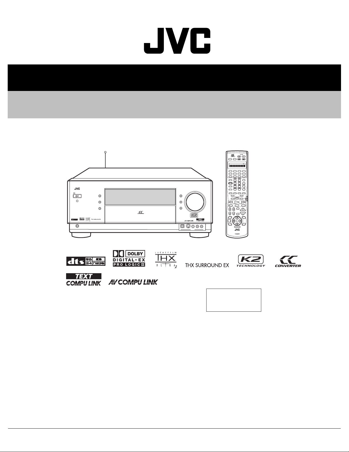
AUDIO/VIDEO CONTROL RECEIVER
RX-DP20VBK
TR NSMTEA N
SAND Y
ON
ZO E 2
ONE 1
Z NE 1
T BS
N/ F O /O F
ST NDB / N ST NDB / N
ZONE 2 L ARNZO E 1
DVD
D MU
CD
HO O
C R
PEM
CR 1 CR 2
XT 7 C
FMAMIDOVDB
AN LOGD GT L
FFECT
NPU
123
LV NESS
SOUND
456
EST
/
89
7
STANDBY
STANDBY/ON
MASTER VOLUME
CC CONVERTER
ZONE 1
ON/OFF
ZONE 2
ON/OFF
PHONES
RX DP20V
AUDO/V DEO CONTROL RECE VER
D MMER
DOOR
UP
DOOR
DOWN
VIDEO LÑAUDIOÑR
S-VDEODG TAL
VIDEO
CC CO VER ER
RE URN
THX
XES 71
SLEEP DIMMER
REW
DOWN UP
REC
CHANNEL
TV VOL
TU
M N
T XT
I P A
DVD
ME U
RMSR DP20J
AV CONTROL RECE VER
10 100
PLAY
TUNNG
STOP PAU E
TVVIDEO
MUTNG
SET
M MODE
DSP URRDSPS RROUND
AN LOG DI ECT
RE OTE CO TROL
+
0
O F
TV
CAV
BS
FF
VOLUME
A JU
ENU
E IT
Area Suffix
J --------------- U.S.A.
C ------------- Canada
TABLE OF CONTENTS
1 PRECAUTION. . . . . . . . . . . . . . . . . . . . . . . . . . . . . . . . . . . . . . . . . . . . . . . . . . . . . . . . . . . . . . . . . . . . . . . . . 1-4
2 SPECIFIC SERVICE INSTRUCTIONS. . . . . . . . . . . . . . . . . . . . . . . . . . . . . . . . . . . . . . . . . . . . . . . . . . . . . . 1-6
3 DISASSEMBLY . . . . . . . . . . . . . . . . . . . . . . . . . . . . . . . . . . . . . . . . . . . . . . . . . . . . . . . . . . . . . . . . . . . . . . . 1-7
4 ADJUSTMENT . . . . . . . . . . . . . . . . . . . . . . . . . . . . . . . . . . . . . . . . . . . . . . . . . . . . . . . . . . . . . . . . . . . . . . . 1-18
5 TROUBLE SHOOTING. . . . . . . . . . . . . . . . . . . . . . . . . . . . . . . . . . . . . . . . . . . . . . . . . . . . . . . . . . . . . . . . . 1-21
COPYRIGHT © 2003 VICTOR COMPANY OF JAPAN, LIMITED
No.22008
2003/7
Page 2
SPECIFICATION
Amplifier Output Power At Stereo operation
(Analog Direct On)
At Surround operation
(Analog Direct On)
Audio Audio Input
Sensitivity
/Impedance
(1 kHz)
Video Video Input
Sensitivity
/Impedance
Video Output
Level
PHONO IN (MC) 0.25 mV/100 Ω
(MM) 2.5 mV/47 kΩ
CD IN, CDR IN, TAPE/MD IN, EXT 7.1CH IN 200 mV/47 kΩ
DVD IN, VCR 1 IN, VCR 2 IN, TV SOUND/DBS IN, VIDEO 200 mV/47 k Ω
Audio Input
(DIGITAL IN)*
* Corresponding to Linear PCM, Dolby Digital, and DTS Digital Surround
(with sampling frequency - 32 kHz, 44.1 kHz, 48 kHz)
Audio Output Level ZONE 2 PREOUT 200 mV
Recording Output
Level
Digital output Optical DIGITAL OUT
Signal wave length 660 nm
Output level
Signal-to-Noise Ratio
(‘66 IHF/’78 IHF)
(Analog Direct On)
CD IN, CDR IN, TAPE/MD IN, EXT 7.1CH IN 92 dB/80 dB
DVD IN, VCR 1 IN, VCR 2 IN, TV SOUND/DBS IN, VIDEO 92 dB/80 dB
Frequency Response
(8 Ω)
CD IN, CDR IN, TAPE/MD IN, EXT 7.1CH IN 10 Hz to 100 kHz (+1 dB, -3 dB)
DVD IN, VCR 1 IN, VCR 2 IN, TV SOUND/DBS IN, VIDEO 10 Hz to 100 kHz (+1 dB, -3 dB)
RIAA Phono Equalization ±1.0 dB (20 Hz to 20 kHz)
Composite video
DVD IN, VCR 1 IN, VCR 2 IN, TV SOUND/DBS IN, VIDEO
S-video
DVD IN, VCR 1 IN, VCR 2 IN, TV
SOUND/DBS IN, VIDEO
Component
1 IN (DVD), 2 IN,3 IN
Composite video
VCR 1 OUT,VCR 2 OUT,MONITOR OUT
S-video
VCR 1 OUT, VCR 2 OUT, MONITOR OUT
Component
MONITOR OUT
Synchronization Negative
Signal-to-Noise Ratio 45 dB
Front channels
120 W per channel, min. RMS, driven into 8 Ω, 20 Hz to 20 kHz with no more
than 0.02% total harmonic distortion. 120 W per channel, min. RMS, driven
into 4 Ω, 20 Hz to 20 kHz with no more than 0.07% total harmonic distortion.
Front channels
120 W per channel, min. RMS, driven into 8 Ω, 20 Hz to 20 kHz with no more
than 0.02% total harmonic distortion.
Center channel
120 W, min. RMS, driven into 8 Ω, 20 Hz to 20 kHz with no more than 0.02%
total harmonic distortion.
Surround channels
120 W per channel, min. RMS, driven into 8 Ω, 20 Hz to 20 kHz with no more
than 0.02% total harmonic distortion.
Surround back channels
120 W per channel, min. RMS, driven into 8 Ω, 20 Hz to 20 kHz with no more
than 0.02% total harmonic distortion.
Coaxial 1(DVD), 2(CD), 3(TV/DBS) 0.5 V(p-p)/75 Ω
Optical 4(CDR), 5(MD), 6(VCR1) -21 dBm to -15 dBm (660 nm ±30 nm)
PREOUT 1 V
TAPE/MD OUT, CDR OUT, VCR 1
OUT, VCR 2 OUT
PHONO IN (MC) 60 dB/72 dB (at REC OUT)
(MM) 72 dB/80 dB (at REC OUT)
PHONO IN (MC) 20 Hz to 20 kHz (±1 dB)
(MM) 20 Hz to 20 kHz (±1 dB)
(Y: luminance) 1 V(p-p)/75Ω
(C: chrominance, burst) 0.286 V(p-p)/75 Ω
(Y: luminance) 1 V(p-p)/75 Ω
(PB, PR) 0.7 V(p-p)/75 Ω
(Y: luminance) 1 V(p-p)/75Ω
(C: chrominance, burst) 0.286 V(p-p)/75 Ω
(Y: luminance) 1 V(p-p)/75 Ω
200 mV
1 V(p-p)/75 Ω
1 V(p-p)/75 Ω
(PB, PR): 0.7 V(p-p)/75 Ω
1-2 (No.22008)
Page 3
FM tuner
(IHF)
AM tuner Tuning Range 530 kHz to 1 710 kHz
General Power Requirements AC 120V~, 60 Hz
Designs & specifications are subject to change without notice.
Tuning Range 87.5 MHz to 108.0 MHz
Usable Sensitivity Monaural 12.8 dBf (1.2 µV/75 Ω)
50 dB Quieting Sensitivity Monaural 18.2 dBf (2.2 µV/75 Ω)
Stereo 38.2 dBf (22.3 µV/75 Ω)
Signal-to-Noise Ratio (IHF-A weighted) Monaural 78 dB at 85 dBf
Stereo 73 dB at 85 dBf
Total Harmonic Distortion Monaural 0.2% at 1 kHz
Stereo 0.3% at 1 kHz
Stereo Separation at REC OUT 40 dB at 1 kHz
Alternate Channel Selectivity 60 dB (±400 kHz)
Frequency Response 30 Hz to 15 kHz (+0.5 dB, -3 dB)
Usable Sensitivity Loop antenna: 400 µV/m
Signal-to-Noise Ratio 50 dB (100 mV/m)
Power Consumption 580 W/690 VA (at operation)
2.7 watts (in standby mode)
Dimensions (W × H × D) 445 mm × 177 mm × 475 mm
(17 9/16 in. × 7 in. × 18 3/4 in.)
Mass 23.5 kg (52 lbs)
(No.22008)1-3
Page 4
SECTION 1
Good earth ground
d
AC VOLTMETER
PRECAUTION
1.1 Safety Precautions
(1) This design of this product contains special hardware and
many circuits and components specially for safety purposes. For continued protection, no changes should be made
to the original design unless authorized in writing by the
manufacturer. Replacement parts must be identical to
those used in the original circuits. Services should be performed by qualified personnel only.
(2) Alterations of the design or circuitry of the product should
not be made. Any design alterations of the product should
not be made. Any design alterations or additions will void
the manufacturers warranty and will further relieve the
manufacture of responsibility for personal injury or property
damage resulting therefrom.
(3) Many electrical and mechanical parts in the products have
special safety-related characteristics. These characteristics are often not evident from visual inspection nor can the
protection afforded by them necessarily be obtained by using replacement components rated for higher voltage, wattage, etc. Replacement parts which have these special
safety characteristics are identified in the Parts List of Service Manual. Electrical components having such features
are identified by shading on the schematics and by ( ) on
the Parts List in the Service Manual. The use of a substitute
replacement which does not have the same safety characteristics as the recommended replacement parts shown in
the Parts List of Service Manual may create shock, fire, or
other hazards.
(4) The leads in the products are routed and dressed with ties,
clamps, tubings, barriers and the like to be separated from
live parts, high temperature parts, moving parts and/or
sharp edges for the prevention of electric shock and fire
hazard. When service is required, the origin al lead routing
and dress should be observed, and it should be confirmed
that they have been returned to normal, after reassembling.
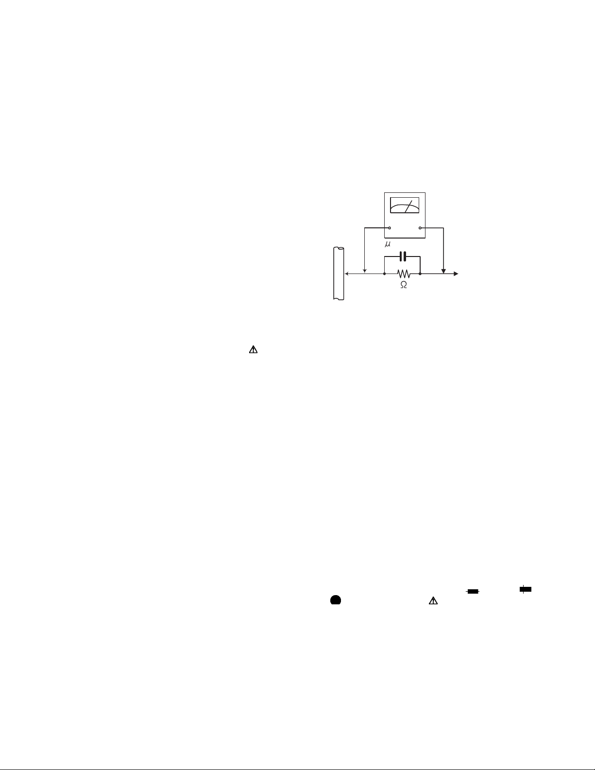
(5) Leakage shock hazard testing
After reassembling the product, always perform an isolation check on the exposed metal parts of the product (antenna terminals, knobs, metal cabinet, screw heads,
headphone jack, control shafts, etc.) to be sure the product
is safe to operate without danger of electrical shock.Do not
use a line isolation transformer during this check.
• Plug the AC line cord directly into the AC outlet. Using a
"Leakage Current Tester", measure the leakage current
from each exposed metal parts of the cabinet, particularly any exposed metal part having a return path to the
chassis, to a known good earth ground. Any leakage current must not exceed 0.5mA AC (r.m.s.).
• Alternate check method
Plug the AC line cord directly into the AC outlet. Use an
AC voltmeter having, 1,000Ω per volt or more sensitivity
in the following manner. Connect a 1,500Ω 10W resistor
paralleled by a 0.15µF AC-type capacitor between an exposed metal part and a known good earth ground.
Measure the AC voltage across the resistor with the AC
1-4 (No.22008)
voltmeter.
Move the resistor connection to each exposed metal
part, particularly any exposed metal part having a return
path to the chassis, and measure the AC voltage across
the resistor. Now, reverse the plug in the AC outlet and
repeat each measurement. Voltage measured any must
not exceed 0.75 V AC (r.m.s.). This corresponds to 0.5µ
mA AC (r.m.s.).
(Having 1000
ohms/volts,
or more sensitivity)
0.15 F AC TYPE
Place this
probe on
1500 10W
1.2 Warning
(1) This equipment has been designed and manufactured to
meet international safety standards.
(2) It is the legal responsibility of the repairer to ensure that
these safety standards are maintained.
(3) Repairs must be made in accordance with the relevant
safety standards.
(4) It is essential that safety critical components are replaced
by approved parts.
(5) If mains voltage selector is provided, check setting for local
voltage.
1.3 Caution
Burrs formed during molding may be left over on some parts
of the chassis.
Therefore, pay attention to such burrs in the case of preforming repair of this system.
1.4 Critical parts for safety
In regard with component parts appearing on the silk-screen
printed side (parts side) of the PWB diagrams, the parts that are
printed over with black such as the resistor ( ), diode ( )
and ICP ( ) or identified by the " " mark nearby are critical
for safety. When replacing them, be sure to use the parts of the
same type and rating as specified by the manufacturer.
(This regulation dose not Except the J and C version)
each expose
metal part.
Page 5
1.5 Importance administering point on the safety
WR42
WR48
PW26
PW21
PW24
EP21
TW51
C42
R41
R57
Q53
PW25
PW23
PW22
R21
R42
D45
C60
C43
FC41 FC42
C40
C41
D41
Q54
Q55
R51
R54
CN41
D25
RY21
C21
FC22 FC21
WR41
FC43 FC44
CN44 CN45
C56
D50
Q44
Q42
Q43
CN46
D51
C52
C25
D26
Q22
C24
R22
T42
R26
R27
T21
CN25
R28
D22
D21
C22
WR26
Q21
C27
D27
Q23
R24
R23
C26
R25
C23
D24
EP22
D23
CN47
R55
R50
Q41
C59
C51
R47
R46
R56
TH41
D48
C49
R4011
R4012
T41
FC401 FC402
R45
C44
C45
C57 C58
D4004
C47 C48
D4003
D4002
C46
D4001
C55
R49
C54
D49
R48
C53
R43
Q47
Q45
Q46
IC44
TW41
TW42
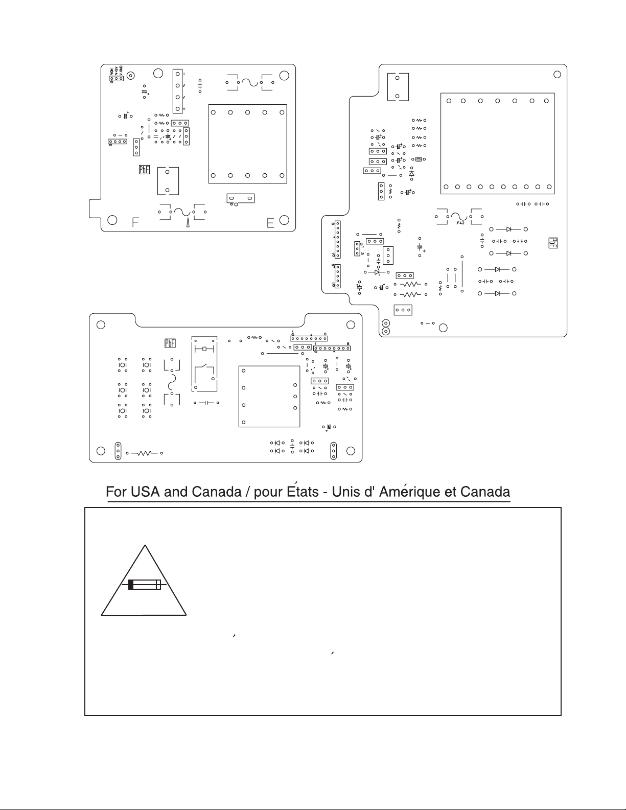
Caution: For continued protection against risk of
fire, replace only with same type 8A/250V for F21,
0.5A/250V for F41 and 2A/125V for F42 and F43.
This symbol specifies type of fast operating fuse.
Precaution: Pour eviter risques de feux, remplacez
le fusible de surete de F21 comme le meme type
que 8A/250V, et 0.5A/250V pour F41, et 2A/125V
pour F42 et F43.
Ce sont des fusibles suretes qui functionnes rapide.
^
(No.22008)1-5
Page 6

SECTION 2
SPECIFIC SERVICE INSTRUCTIONS
This service manual does not describe SPECIFIC SERVICE INSTRUCTIONS.
1-6 (No.22008)
Page 7
SECTION 3
A
DISASSEMBLY
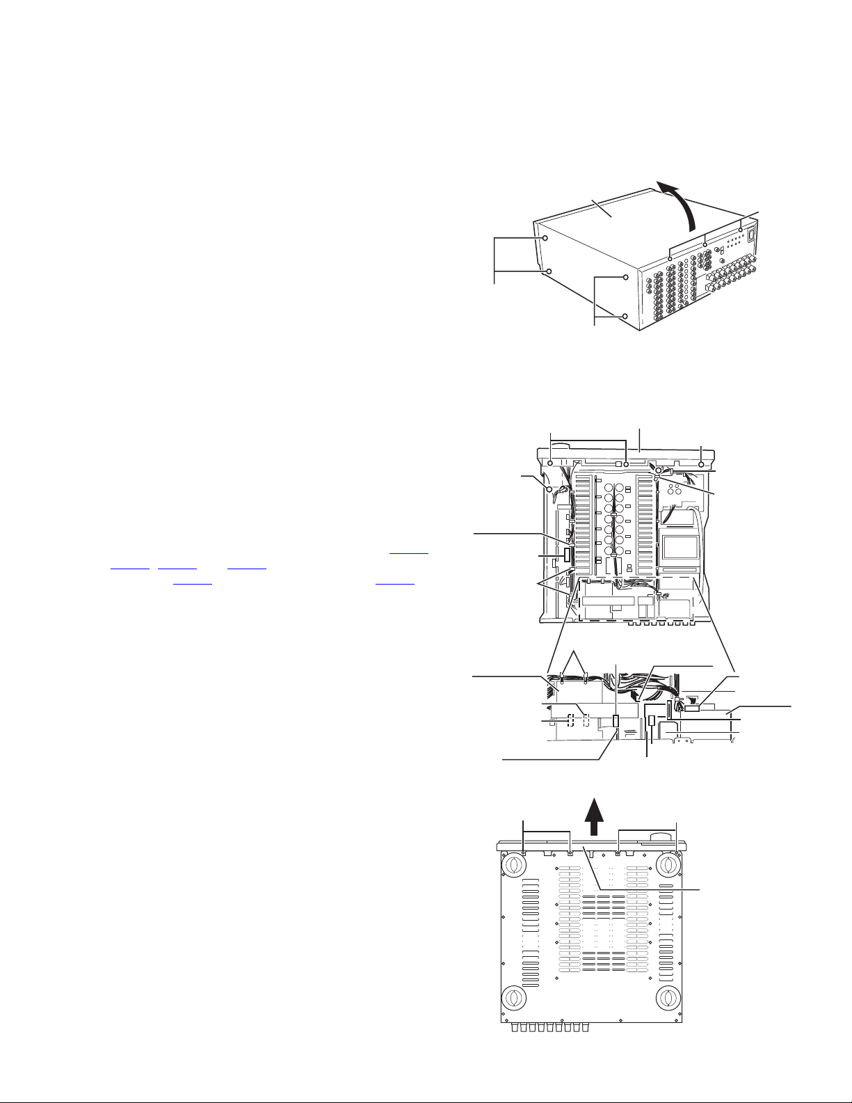
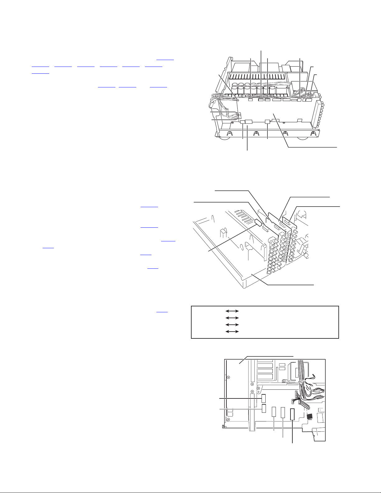
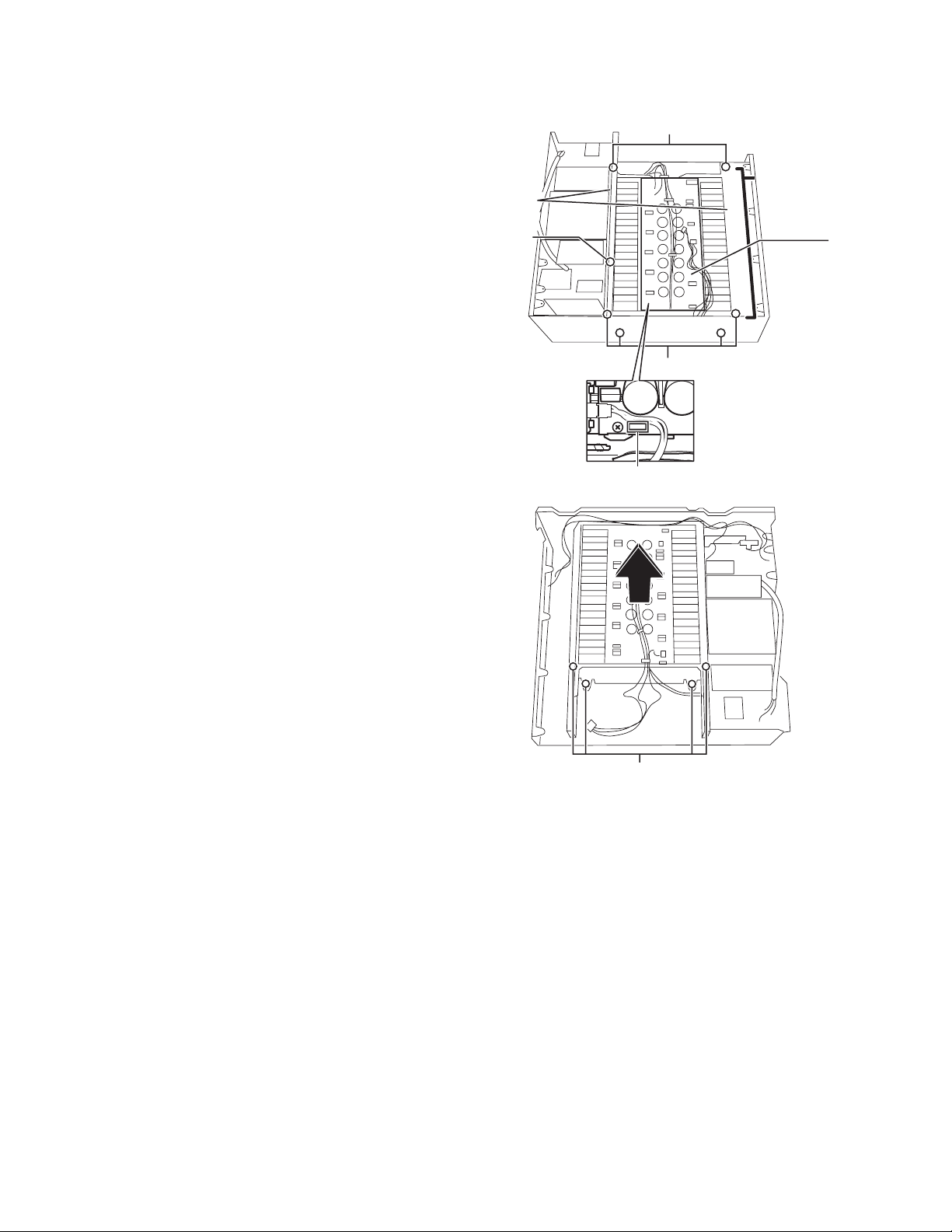
3.1 Main body section
3.1.1 Removing the top cover
(See Fig.1)
(1) Remove the eight screws A attaching the top cover on both
sides of the body.
(2) Remove the three screws B on back of the body.
(3) Remove the top cover from behind in the direction of the ar-
row while pulling both sides outward.
3.1.2 Removing the front panel assembly
(See Fig.2 and 3)
• P rior to performing the following procedure, remove the top
cover.
(1) Cut off the tie band 1 fixing the harness.
(2) Remove the screw a, and remove the lug wire.
(3) Remove the three screws C attaching the front pane l as-
sembly.
(4) Remove the four screws D attaching the front panel as-
sembly on bottom of the body. Detach the front pa nel assembly toward the front.
(5) Disconnect the harness from the connector CN971
, CN983 and CN985 on the system control board
CN977
(see fig.5), CN973 on the front AV in board and CN373 on
the front DIGITAL board (see 2-3.Front panel assembly
section/ fig.2).
,
(both sides)
a
(fixing the
lug wire)
Audio signal
1 board
CN201
Tie band 3
Top cover
A(both sides)
Fig.1
Front panel assembly
C
B
C
Tie band 1
Harness
band
Y/C separator
board
CN482
CN481
V compo 2 board
D
Tie band 2
CN581
Audio 7.1ch
in board
CN301
Compu
link board
CN1
Tuner unit
CN1
RF remote unit
Fig.2
D
Front panel
assembly
Fig.3
(No.22008)1-7
Page 8
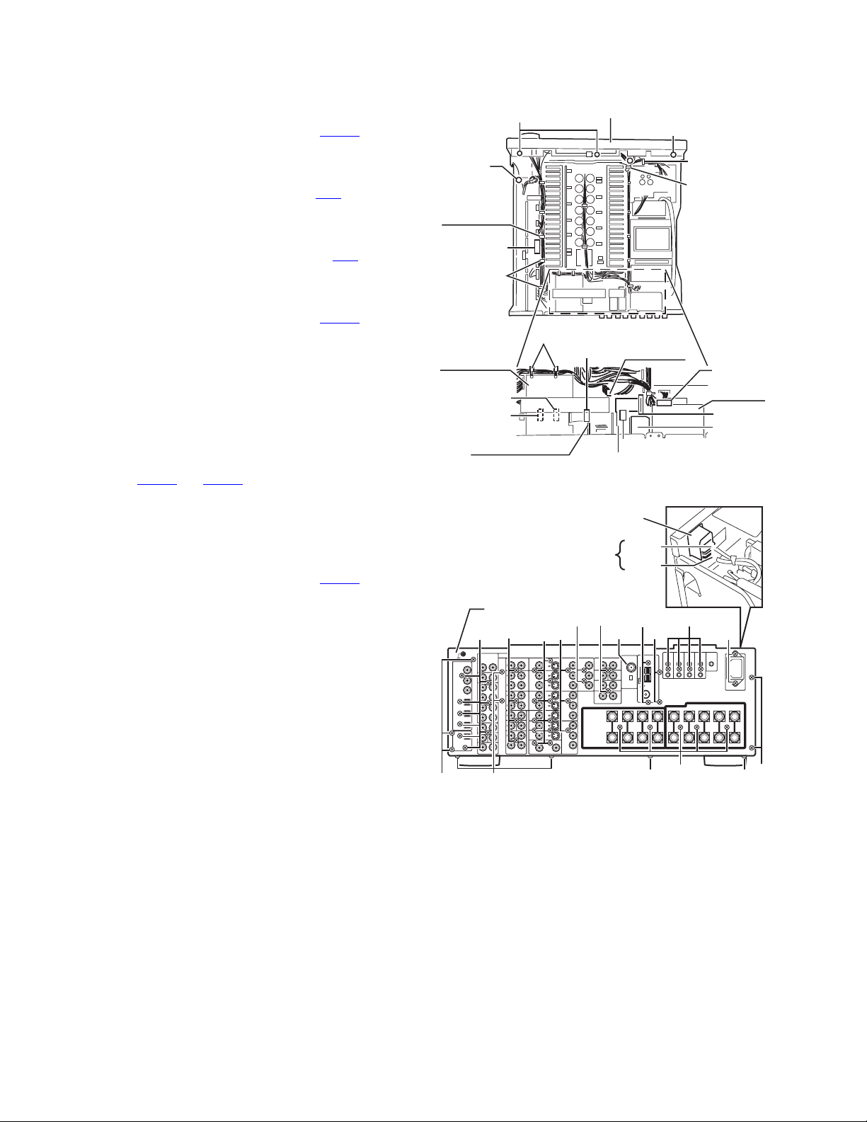
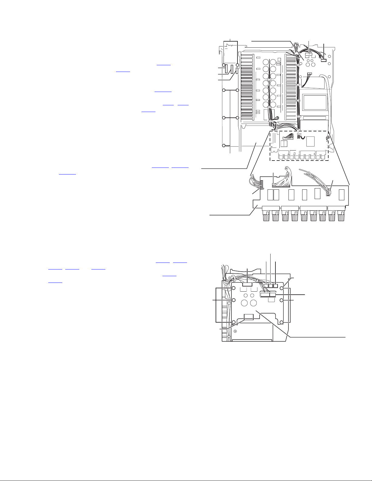
3.1.3 Removing the V compo 2 board & RF remote unit & tuner unit & compu link board
(See Fig.2 and 4)
• Prior to performing the following procedure, remove the top
cover.
(1) Disconnect the harness from the con nector CN581 on the
V compo 2 board.
Remove the two screws E' attaching the V compo 2 board
to the rear panel.
(2) Disconnect the harness from the connector CN1
remote unit.
Remove the nut b attaching the RF remote unit to the rear
panel.
(3) Disconnect the card wire from the connector CN1
tuner unit.
Remove the two screws E'' attaching the tuner unit to the
rear panel.
(4) Disconnect the harness from the con nector CN301
compu link board.
Remove the four screws E''' attaching the compu link
board to the rear panel.
3.1.4 Removing the Y/C separator board
(See Fig.2)
• Prior to performing the following procedure, remove the top
cover.
(1) Cut off the tie band 2 fixing the harness.
(2) Draw out up the Y/C separator board, disconnecting the
connectors CN481
3.1.5 Removing the audio 7.1ch in board
(See Fig.2 and 4)
• Prior to performing the following procedure, remove the top
cover.
(1) Cut off the tie band 2 & 3 fixing the harness.
(2) Disconnect the harness from the con nector CN201
audio signal 1 board.
(3) Remove the two screws E'''' attaching the audio 7.1ch in
board to the rear panel.
3.1.6 Removing the rear panel
(See Fig.4)
• Prior to performing the following procedure, remove the top
cover.
(1) Unsolder the two solder parts on the AC inlet.
(2) Remove the forty four screws E & E' & E'' & E''' & E'''' and
the nut b attaching each board to the rear panel.
(3) Remove the thirteen screws F attaching the rear panel on
the back of the body and bottom.
and CN482 on the Y/C separator board.
on the RF
on the
on the
on the
a
(fixing the
lug wire)
Audio signal
1 board
CN201
Tie band 3
Y/C separator
board
CN482
CN481
V compo 2 board
Rear panel
E
Front panel assembly
C
Tie band 2
Solder part
E
E
E
FF
CN581
RF remote unit
Fig.2
AC inlet
E''''
E'
b
Fig.4
C
Audio 7.1ch
in board
CN1
Black
Red
E''
F
F
Tie band 1
Harness
band
Compu
link board
E'''
E
CN301
CN1
Tuner unit
E
F
F
1-8 (No.22008)
Page 9
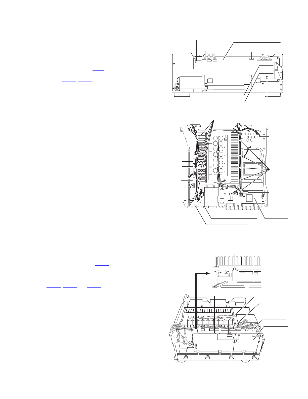
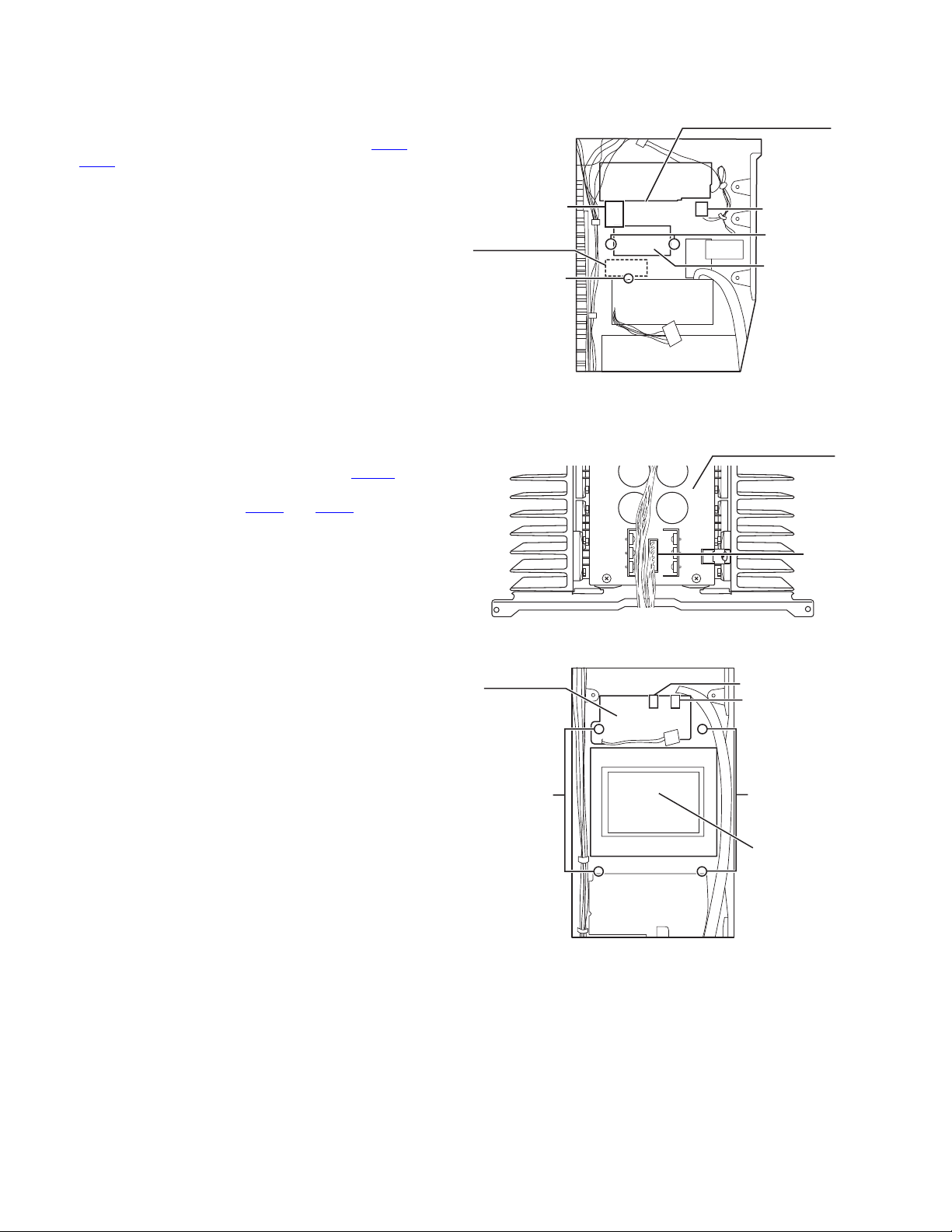
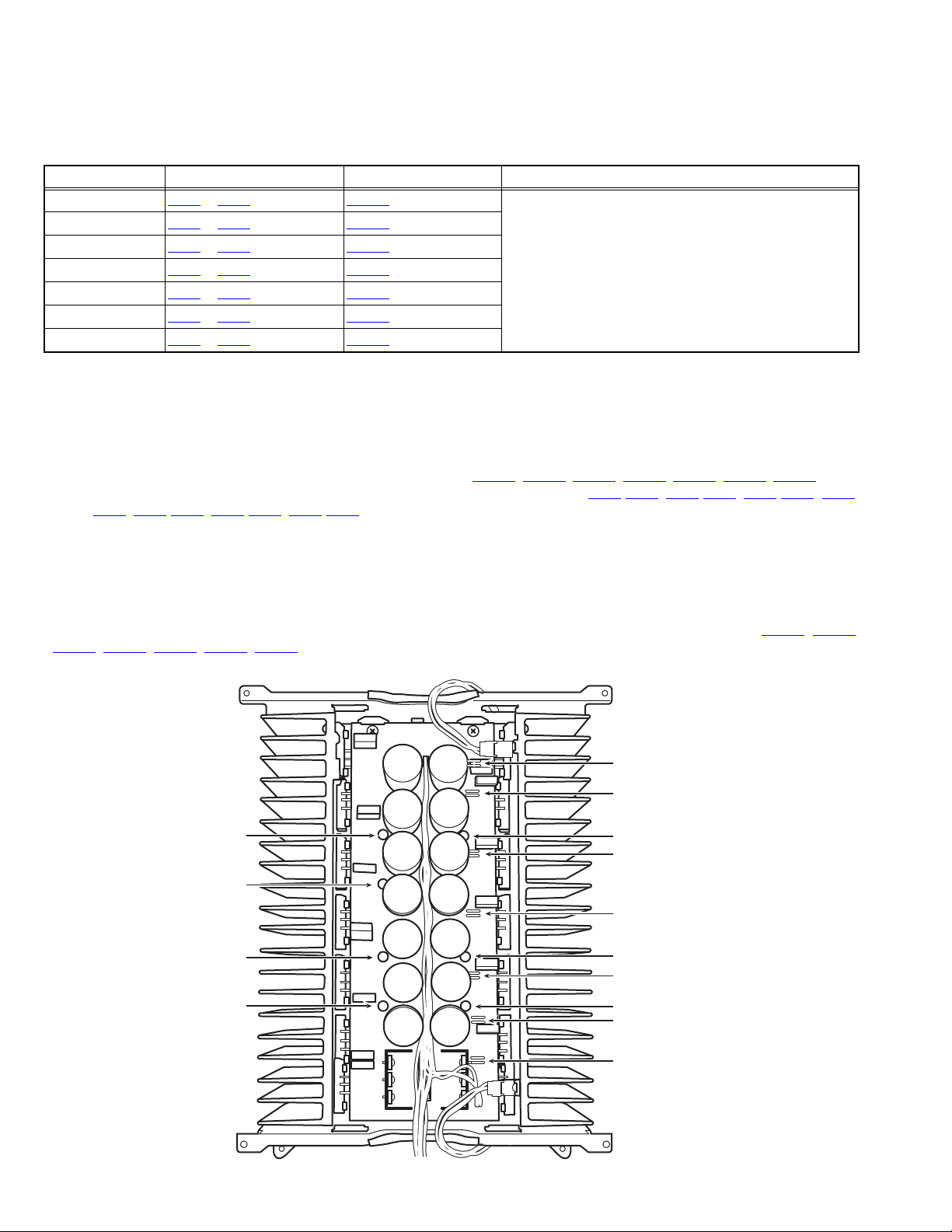
3.1.7 Removing the system control board
(See Fig.5 and 6)
• P rior to performing the following procedure, remove the top
cover and front panel assembly.
(1) Disconnect the card wires and harness from the connector
, CN964 and CN981 on the system control board.
CN963
(2) Cut off the tie bands fixing the harness.
(3) Disconnect the harness from the connector CN45
power supply 2 board and CN25
(4) Disconnect the connector CN324
board and CN234, CN208 on the audio signal 1 board.
(5) Remove the three plastic rivet.
on the power/ fuse board.
on the audio signal 2
on the
CN983
Plastic rivet
CN977
CN981
System control board
CN985
Plastic rivet
3.1.8 Removing the DSP board & shield cover
(See Fig.7)
• P rior to performing the following procedure, remove the top
cover, rear panel and front panel assembly.
(1) Disconnect the connector CN631
(2) Disconnect the connector CN203
board.
And cut off the tie bands fixing the harness.
(3) Removing the two plastic rivet, and disconnect the connec-
tor CN633
(4) Removing the screw G attaching the shield cover and re-
move the shield cover.
, CN643 and CN635 on the DSP board.
on the DSP board.
on the audio signal 1
CN234
CN224
CN208
CN203
CN324
Tie band
Top view
Shield cover
CN963
CN964
Fig.5
Audio signal 2 board
Audio signal 1 board
Fig.6
G
CN971
Shield cover
CN631
CN203
CN45
(on power
supply 2
)
board
Tie band
CN25
Power/ fuse
board
CN633
CN643
Plastic rivet
Fig.7
Audio signal
1 board
DSP board
CN635
(No.22008)1-9
Page 10
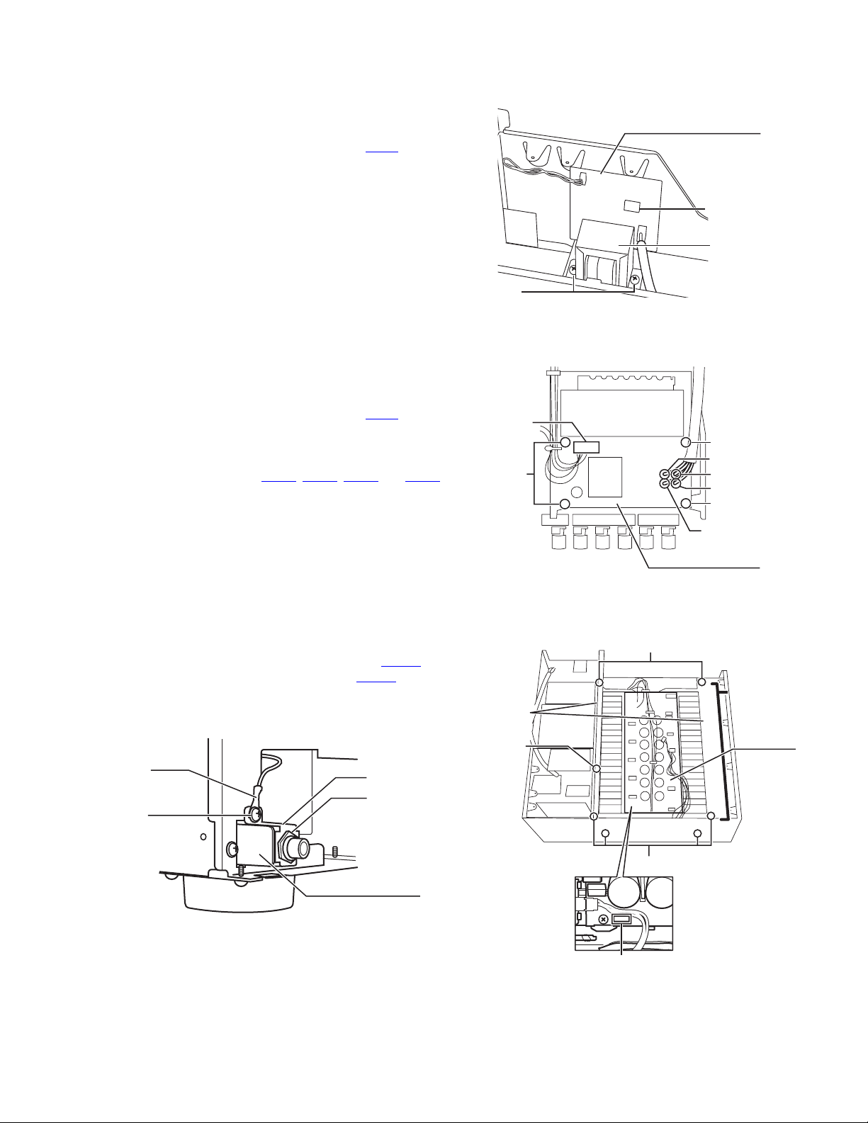
3.1.9 Removing the audio signal 1 board
(See Fig.8)
• Prior to performing the following procedure, remove the top
cover, rear panel and DSP board.
(1) Disconnect the harness from the connector CN202,
, CN234, CN224, CN208, CN207, CN218 and
CN204
on the audio signal 1 board.
CN223
(2) Remove the plastic rivet.
(3) Disconnect the connector CN205
the audio signal 1 board.
, CN221 and CN206 on
Plastic rivet
CN204
CN202
CN234
CN224
CN208
CN207
CN218
CN223
3.1.10 Removing the audio signal 2 board & video board & S video board
(See Fig.9 to 11)
• Prior to performing the following procedure, remove the top
cover, rear panel, Y/C separator board, DSP board and audio
signal 1 board.
(1) Disconnect the harness from the con nector CN973
front AV in board (see 2-3.Front panel assembly section/
fig.2).
(2) Disconnect the harness from the con nector CN324
audio signal 2 board.
(3) Remove the audio signal 2 board from the connector CN15
and CN6 on the input base board.
(4) Remove the video board from the connector CN7 on the in-
put base board.
(5) Remove the S video board from the connector CN8
input base board.
3.1.11 Removing the V compo 1 board
(See Fig.9 to 11)
• Prior to performing the following procedure, remove the top
cover and rear panel.
(1) Remove the V compo 1 board from the connector CN9
the input base board.
on the
on the
on the
on
Audio signal 2 board
CN324
Connection between the Input base board and each board.
CN15/CN6
CN205
Video board
CN7
CN8
CN9
CN206
Audio signal 1 board
CN221
Fig.8
S video board
V compo 1 board
Input base board
Fig.9
Audio signal 2 board (CN325/CN321)
Video board (CN401)
S video board (CN451)
V compo 1 board (CN501)
Fig.10
Input base board
1-10 (No.22008)
CN15
CN6
CN7
CN8
CN9
Fig.11
Page 11
3.1.12 Removing the input base board
(See Fig.12)
• P rior to performing the following procedure, remove the top
cover, rear panel, DSP board, audio signal 1 board, audio signal 2 board, video board, S video board and V compo 1 board.
(1) Disconnect the harness from the connector CN62
power supply 1 board and CN44
board.
And cut off the tie bands fixing the harness.
(2) Disconnect the harness from the connecto r CN743
speaker board.
(3) Disconnect the card wire from the connector CN1
and the harness from the connector CN11 on the input
base board.
(4) Remove the seven screws H attaching the input base
board.
3.1.13 Removing the speaker board
(See Fig.12)
• P rior to performing the following procedure, remove the top
cover and rear panel.
(1) Disconnect the harness from the connector CN741
and CN743 on the speaker board.
on the power supply 2
on the
on the
, CN2
, CN742
H
CN1
CN2
CN11
H
Input base board
CN743
Power supply
1 board
CN741
CN62
CN44
(on the power
supply 2 board)
CN742
3.1.14 Removing the power supply 1 board
(See Fig.13)
• P rior to performing the following procedure, remove the top
cover.
(1) Disconnect the harness from the connector CN61
CN63, CN64 and CN65 on the power supply 1 board.
(2) Disconnect the harness from the connector CN44 and
on the power supply 2 board.
CN45
(3)
, CN62,
Speaker board
Fig.12
CN63
CN65
CN62
II
CN61
CN64
Fig.13
(fixing the
lug wire)
CN44/CN45
(on the power
supply 2 board)
Power supply 1 board
(No.22008)1-11
Page 12
3.1.15 Removing the power transformer 1 with the power supply 2 board
(See Fig.14)
• Prior to performing the following procedure, remove the top
cover and power supply 1 board.
(1) Disconnect the harness from the connector CN46 and
on the power supply 2 board.
CN47
(2) Remove the two screws J attaching the power transformer
1.
3.1.16 Removing the thermal SW 1 board
(See Fig.14)
• Prior to performing the following procedure, remove the top
cover and power supply 1 board.
(1) Remove the screw K attaching the thermal SW 1 board.
3.1.17 Removing the power transformer 2
(See Fig.15 and 16)
• Prior to performing the following procedure, remove the top
cover and power supply 1 board.
(1) Disconnect the harness from the con nector CN701
power amp. board.
(2) Unsolder the solder points PW81
trans board.
(3) Remove the four screws L attaching the power transformer
2.
and PW82 on the power
on the
Thermal SW
CN47
1 board
K
Power supply 2 board
CN46
J
Power
transformer 1
Fig.14
Power amp. board
CN701
Power trans
board
LL
Fig.15
PW81
PW82
Power
transformer 2
Fig.16
1-12 (No.22008)
Page 13
3.1.18 Removing the power transformer 3 with the power supply 3 board
(See Fig.17)
• P rior to performing the following procedure, remove the top
cover, power supply 1 board, power transformer 1 a nd power
transformer 2.
(1) Disconnect the harness from the connector CN41
power supply 3 board.
(2) Remove the two screws M attaching the power transformer
3.
on the
M
3.1.19 Removing the power/ fuse board
(See Fig.18)
• P rior to performing the following procedure, remove the top
cover, rear panel, power supply 1 board and power transformer 2.
(1) Disconnect the harness from the connector CN25
power/ fuse board.
(2) Remove the four screws N attaching the power/ fuse
board.
(3) Unsolder the solder points PW21
on the power/ fuse board.
, PW22, PW23 and PW24
on the
CN25
N
Power supply 3 board
CN41
Power
transformer 3
Fig.17
N
PW23 (red)
PW21 (blue)
PW24 (white)
N
PW22 (brown)
3.1.20 Removing the head phone board
(See Fig.19 and 20)
• P rior to performing the following procedures, remove the top
cover and front panel assembly.
(1) Disconnect the harnesses from the connector CN981
the system control board (see fig.5) and CN738 on the
power amp. board.
(2) Removing the nut O fixing the head phone board.
(3) Removing the screw P attaching the lug wire and bra cket.
Lug wire
Bracket
on
O
P
Head phone board
Fig.19
Barrier
Q
(Front side)
Power/ fuse board
Fig.18
Q
Power
amp.
assembly
Power amp.
board
R
CN738
Fig.20
(No.22008)1-13
Page 14
3.1.21 Removing the power amp. Assembly
(See Fig.20 and 21)
• Prior to performing the following procedures, remove the top
cover, rear panel, front panel assembly, system control board,
DSP board, audio signal 1 board, audio signal 2 board, video
board, S video board, V compo 1 board and speaker board.
(1) Remove the three screws Q fixing the barriers, and remove
the tow barriers.
(2) Remove the eight screws R attach ing the power amp. as-
sembly.
(3) Pull up the power amp. assembly.
Barrier
Q
Q
Power
amp.
assembly
Power amp.
board
(Front side)
R
CN738
Fig.20
(Rear side)
R
Fig.21
1-14 (No.22008)
Page 15
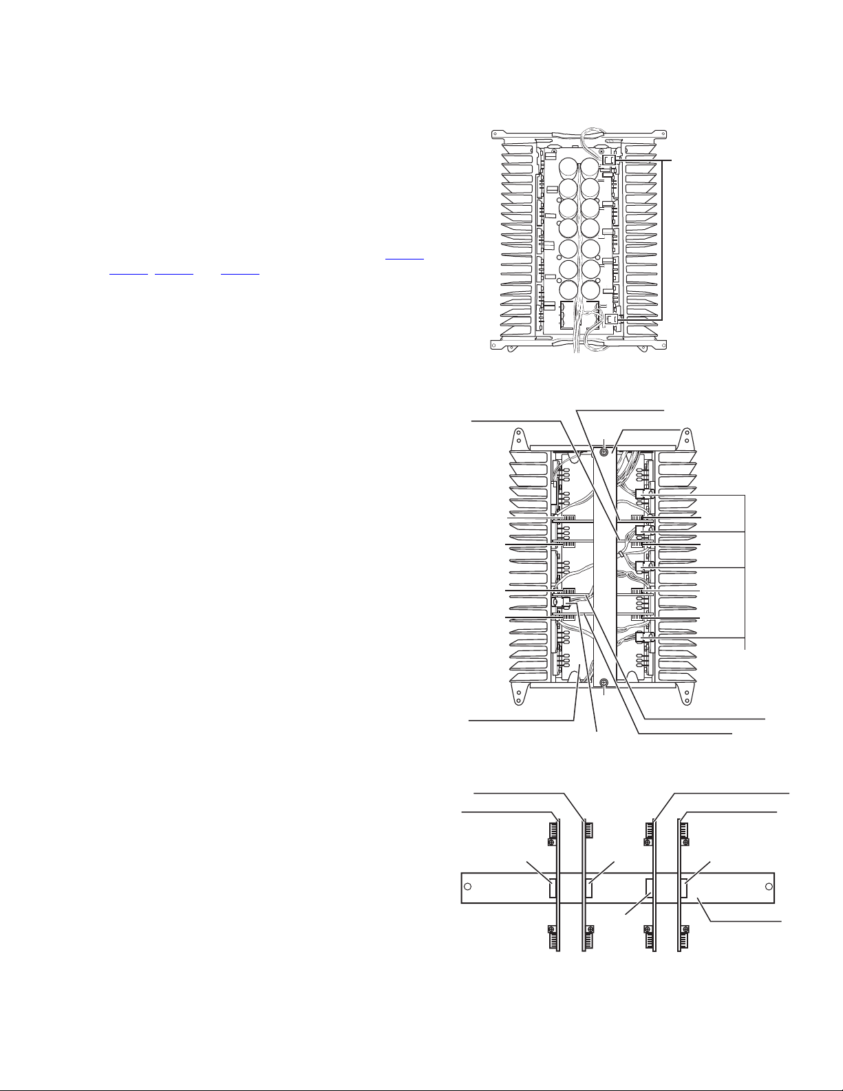
3.2 Power amp. assembly section
3.2.1 Removing the relay board & Rch amp. board & Lch amp. board & Cch amp. board & SL/SRch amp. board
(See Fig.1 to 3)
• Prior to performing the following procedure, remove the power
amp. assembly.
(1) Disconnect the harness from the two connectors on each
thermal compensation board (top side).
(2) Remove the two screws A attaching the relay board.
(3) Disconnect the harness from the five connectors on each
thermal compensation board (bottom side).
(4) Pull up each amp. board of Lch, Cch, SL/SRch and Rch
from the power amp. board with the relay board.
(5) Remove each amp. board from the connector CN721
, CN781 and CN761 on the relay board.
CN821
,
Fig.1
Cch amp. board
Lch amp. board
Relay board
A
top side
Connector
(on the thermal
compensation
board)
bottom side
CN713
CN813
CN773
CN753
Power amp. board
Connector (on the thermal
compensation board)
Cch amp. board
Lch amp. board
CN721 CN821
A
Fig.2
CN781
CN712
CN812
CN772
CN752
Connector
(on the thermal
compensation
board)
SL/SRch amp. board
Rch amp. board
SL/SRch amp. board
Rch amp. board
CN761
Relay board
Fig.3
(No.22008)1-15
Page 16
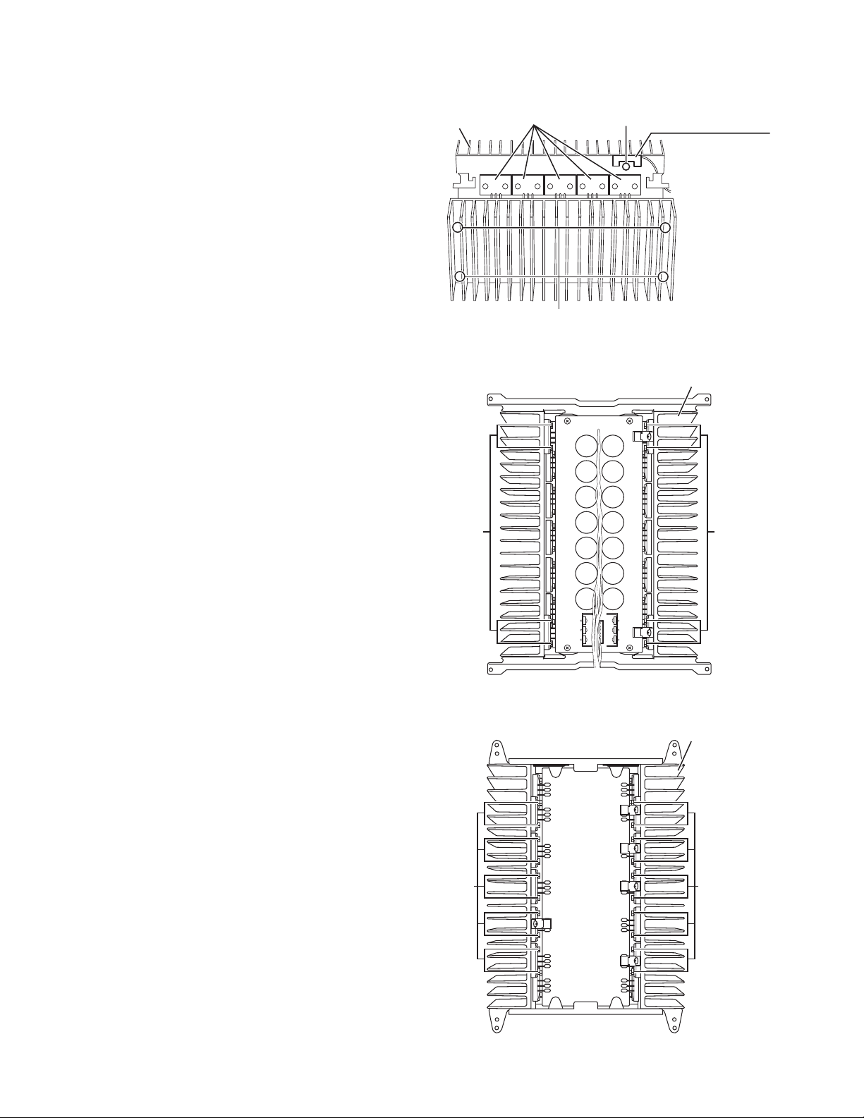
3.2.2 Removing the thermal SW 2 board
(See Fig.4)
• Prior to performing the following procedure, remove the power
amp. assembly, relay board and each amp. board of Lch, Cch,
SL/SRch, Rch.
(1) Remove the screw B attaching the thermal SW 2 board.
3.2.3 Removing the heat sink
(See Fig.4 to 6)
• Prior to performing the following procedure, remove the power
amp. assembly, relay board and each amp. board of Lch, Cch,
SL/SRch, Rch.
(1) Remove the eight screws C attaching the heat sink on the
both sides of the power amp. assembly.
(2) Remove the eight screws D attaching the power ICs (top
side).
(3) Remove the twenty screws D attaching the power ICs (bot-
tom side).
Heat sink
Power ICs
C (both sides)
Fig.4
B
Thermal SW 2 board
top side
Heat sink
bottom side
DD
Fig.5
bottom side
Heat sink
DD
1-16 (No.22008)
Fig.6
Page 17
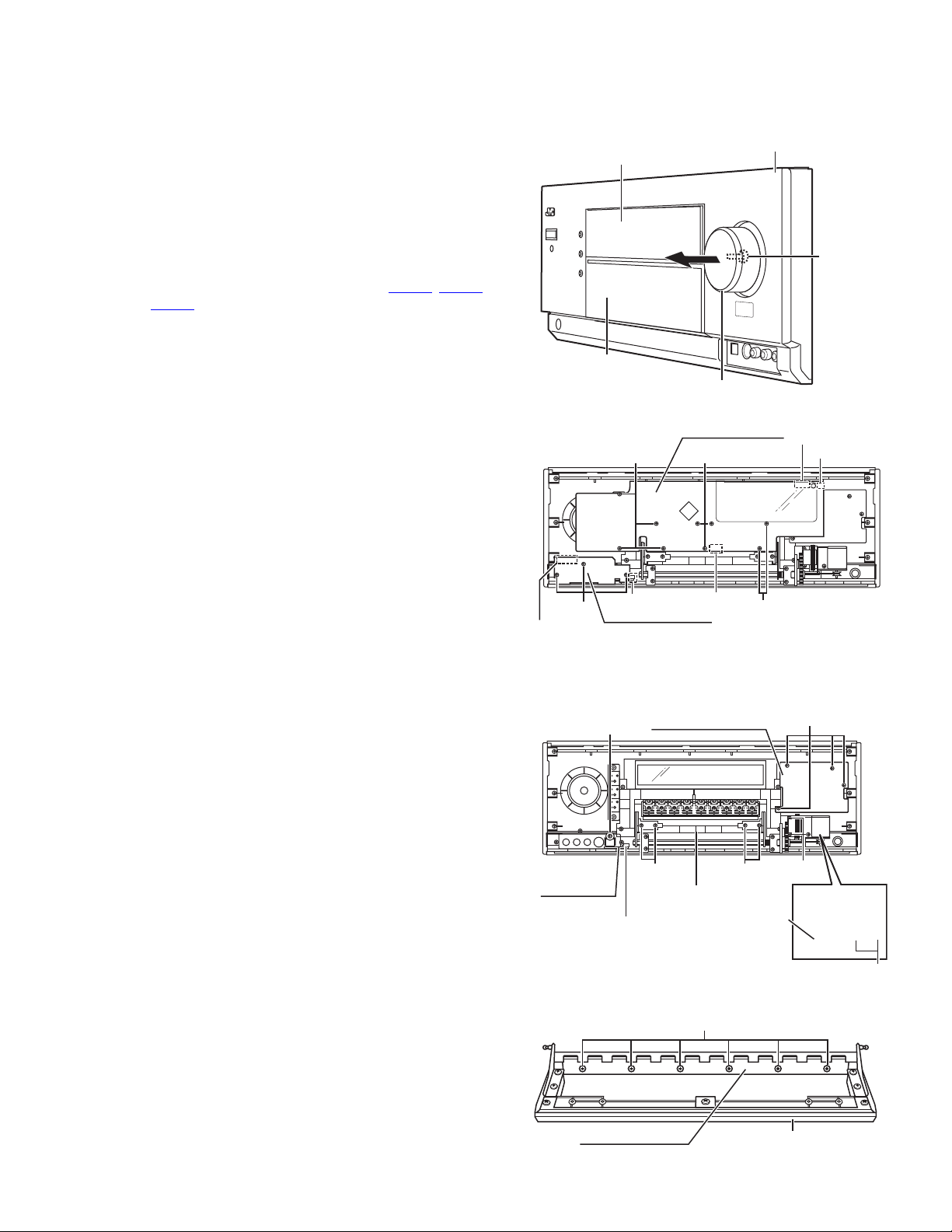
3.3 Front panel assembly section
3.3.1 Removing the FL display board & front AV in board
(See Fig.1 and 2)
• P rior to performing the following procedure, remove the top
cover and front panel assembly.
(1) Pull out the volume knob on the front side of the front panel
assembly and remove the nut attaching the FL display
board.
(2) Remove the three screws A attaching the front AV in board
and remove the front AV in board.
(3) Remove the nine screws B attaching the FL display bo ard
on the back of the front panel assembly.
(4) Disconnect the harness from the connector CN969
and CN982 on the FL display board.
, CN975
Operation switch panel
Door
B
Front panel assembly
Volume knob
Fig.1
FL display board
B
Nut
CN969
CN975
CN973
A
3.3.2 Removing the power switch board & front DIGITAL in board & motor assembly
(See Fig.3)
• P rior to performing the following procedure, remove the front
panel assembly and FL display board.
(1) Remove the four screws C attaching the power switch
board and remove the power switch board.
(2) Remove the screw D attaching the front DIGITAL in board
and remove the front DIGITAL in board.
(3) Remove the three screws E attaching the motor assembly
on the back of the front panel assembly.
(4) Remove the belt and the two screws a attaching the motor.
3.3.3 Removing the door input board
(See Fig.3 and 4)
• P rior to performing the following procedure, remove the front
panel assembly and FL display board.
(1) Remove the four screws F attaching the door and remove
the door from the front panel assembly.
(2) Remove the six screws G attaching the door input board.
Front DIGITAL
in board
CN373
Front AV in board
D
CN373
CN982
B
Fig.2
Power switch board
FF
Door
Fig.3
C
E
Belt
Motor assembly
G
a
Door input board
Door
Fig.4
(No.22008)1-17
Page 18
SECTION 4
ADJUSTMENT
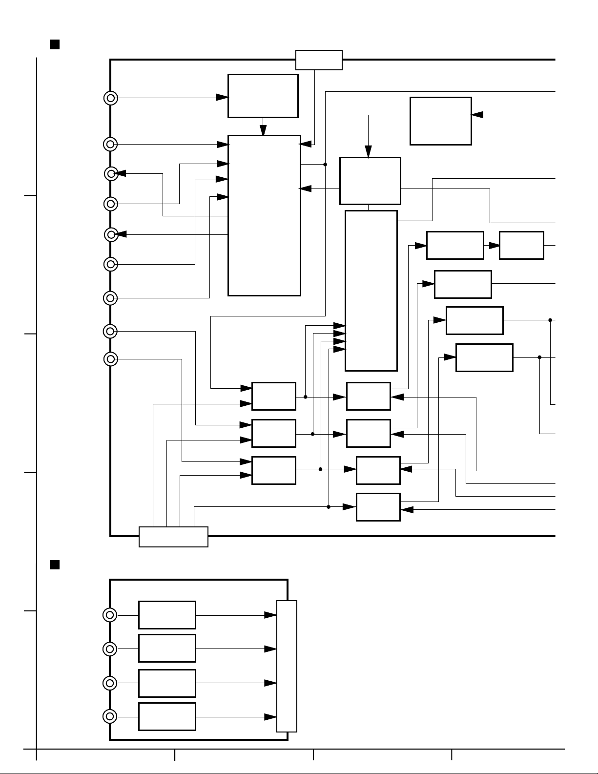
4.1 Adjustment of idling current
Measuring point Alignment point Measuring condition
Lch B903
Rch B911
Cch B907 & B908 VR801
SLch B907 & B908 VR771
SRch B909 & B910 VR772
SBLch B901 & B902 VR702
SBRch B913 & B914 VR752
Attention:
This adjustment does not obtain a correct adjustment value immediately after the amplifier is used (state that an internal temperature
has risen).
Please adjust immediately after using the amplifier after turning off the power supply of the amplifier and falling an internal temperature.
Adjustment method
(1) Prior to turning the power ON, fully turn the adjusting resistor (VR701
terclockwise direction and connect the DC voltmeter to the measuring terminal ( B901-B902, B903-B904, B905-B906, B907-
B908, B909-B910, B911-B912, B913-B914).
(2) Adjust the resistor so that the measured value becomes 2.0mV just after the power supply is turned on.
(3) Adjust the resistor so that the measured value becomes 2.5mV more than 60 seconds afte r the power supply is turned on.
(4) After stability is 1.0-4.0mV.
& B904 VR701 No load and No signal.Rated line voltage
& B912 VR751
SURROUND : OFF
Room temperature : 20~25ºC
, VR702, VR751, VR752, VR771, VR772, VR801) coun-
Refer to following page "Idling Current graph".
* It is not abnormal though the idling current might not b ecome 0mA even if it is finished to turn variable resistance ( VR701
, VR752, VR771, VR772, VR801) in the direction of counterclockwise.
VR751
B901, B902 (SBLch)
B903, B904 (Lch)
VR701 (Lch)
VR702 (SBLch)
B905, B906 (SLch)
VR801 (Cch)
B907, B908 (Cch)
VR771 (SLch)
VR772 (SRch)
B909, B910 (SRch)
VR751 (Rch)
VR752 (SBRch)
B911, B912 (Rch)
, VR702,
1-18 (No.22008)
B913, B914 (SBRch)
Page 19
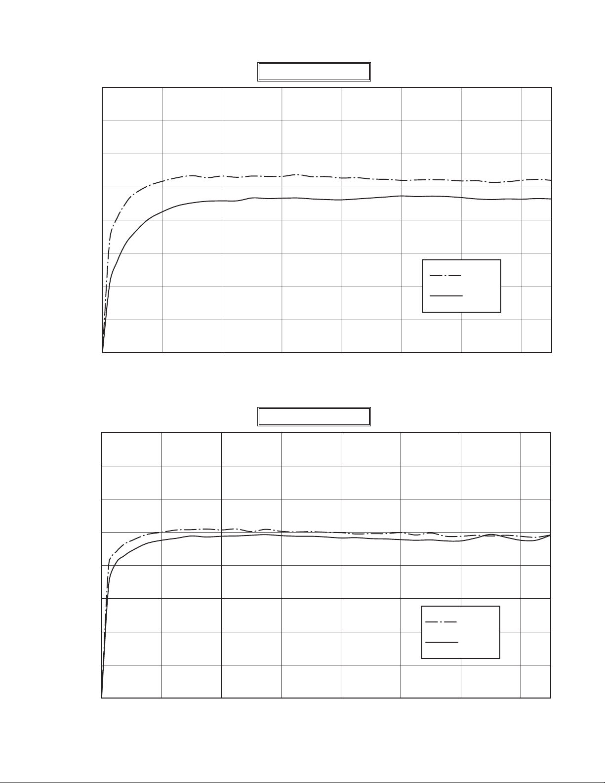
4.2 Idling Current graph (1/2)
4
3.5
3
2.5
2
1.5
1
Voltage at measering point(mV)
0.5
SL ch / SR ch
SL ch
SR ch
0
02468101214
Time(Min)
SBL ch / SBR ch
4
3.5
3
2.5
2
1.5
1
Voltage at measering point(mV)
SBL ch
SBR ch
0.5
0
02468101214
Time(Min)
(No.22008)1-19
Page 20
4.3 Idling Current graph (2/2)
4
3.5
3
2.5
2
1.5
1
Voltage at measering point(mV)
0.5
L ch / R ch
L ch
R ch
0
02468101214
Time(Min)
C ch
4
3.5
3
2.5
2
1.5
1
Voltage at measering point(mV)
0.5
0
02468101214
1-20 (No.22008)
Time(Min)
Page 21

SECTION 5
TROUBLE SHOOTING
This service manual does not describe TROUBLE SHOOTING.
(No.22008)1-21
Page 22

VICTOR COMPANY OF JAPAN, LIMITED
AV & MULTIMEDIA COMPANY AUDIO/VIDEO SYSTEMS CATEGORY 10-1,1chome,Ohwatari-machi,Maebashi-city,371-8543,Japan
(No.22008)
Printed in Japan
WPC
Page 23
SCHEMATIC DIAGRAMS
AUDIO/VIDEO CONTROL RECEIVER
RX-DP20VBK
CD-ROM No.SML200307
Area suffix
J ----------------------------- U.S.A.
C -------------------------- Canada
TAN M TRN
S AND Y
ON
2
O
Z NE 1
Z NE 2
TVCA V D S
VR 1
N/ FF O/ O F
T ND Y ON T ND Y ON
ONE 2 EARNZO E 1
DVD
D MU
CDDRPH N
P/M
CR V R
T 1C
MA MI EOV D S
ANLO / I IT L
FFCT
NP T
123
L EN SS
SOU D
456
ET
/P
89
7
STA NDBY
STA NDB Y /O N
MASTE R VOLUME
CC CONV R TER
ZONE 1
ON/OFF
ZONE 2
ON/OFF
HONES
RX DP 20V
AUDIO/VIDEO CONTROL REC EIVER
DMMER
DOOR
UP
DOOR
DOWN
VID O L AUDIO R
S-V DEODGI A L
VIDE O
CC ON ER ER
RT RN
HX
X E/ 7 1
SL EP DIMM R
/ EW
DOWN P
REC
CHANNL
TV VOL
EU P
MNU
TX T
I L A
V
MEU
RMSRX D 20J
AV O NTR OL R CE VER
10 100
PLAY
TUNNG
M MODE
DP UR / SPURRU ND
AN LOG DR CT
STOP PAU E
TVV DEO
MUTNG
ST
I HT
RM OTE ONT ROL
00
OF
V
CT V
BS
FF
VOLUME
A J ST
ENU
XT
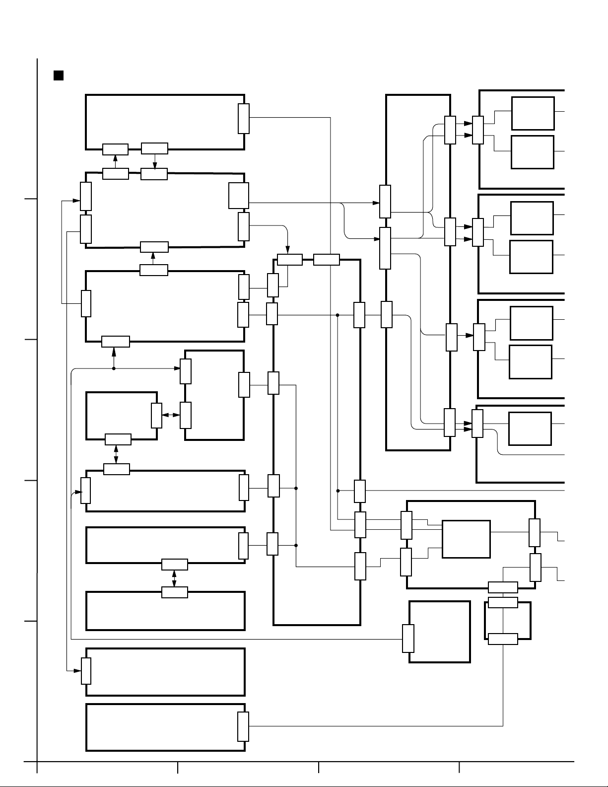
Contents
Block diagrams
Standard schematic diagrams
Printed circuit boards
COPYRIGHT 2003 VICTOR COMPANY OF JAPAN, LTD.
2-1
2-7
2-29 to 49
No.22008SCH
2003/7
Page 24

RX-DP20VBK
In regard with component parts appearing on the silk-screen printed side (parts side) of the PWB diagrams, the
parts that are printed over with black such as the resistor ( ), diode ( ) and ICP ( ) or identified by the " "
mark nearby are critical for safety.
(This regulation does not correspond to J and C version.)
Page 25

RX-DP20VBK
< MEMO >
Page 26
RX-DP20VBK
o
b
P
Block diagrams
Signal input/output & Main section
5
DSP board
CN631
WR632
IC601
CN635
IC602
WR204
CN207CN201
Audio signal 1 board
4
WR307
WR322
3
Y/C sep board
CN482
CN203
CN223
WR323
Audio signal 2 board
CN481
WR403CN402
Video
board
CN202,
CN204
CN221
CN321
CN325
CN401
CN6
CN15
CN7
CN5
CN3
CN11
WR701 WR702
WR703
CN761 CN721
CN781
CN821
Lch/SBLch PRE AMP b
IC603
CN751 CN711
IC604
Rch/SBRch PRE AMP
IC605
CN771
IC606
L/R Surround PRE AM
IC607
CN811
WR453
CN452
S Video board
CN451
CN8
WR14
Center PRE AMP board
System control board
2
Video sep board
CN502
CN581
CN501
CN9
CN1
CN2
CN963
CN964
IC961
CN985
CN983
WR961
CN25
Component video board
Front AV
Audio signal 3 board
WR700
board
CN973
WR26
1
CONPU LINK board
CN301
2-1
ABC D
Page 27
RX-DP20VBK
2
1
AMP board
AMP board
Q710
Q711
Q1710
Q1711
Q760
Q761
Q1760
Q1761
Q1610
Q1611
Q1660
Q1661
CN712
CN713
CN752
CN753
CN772
CN773
CN722
CN723
CN762
CN763
CN782
CN783
Q714
Q715
Q1714
Q1715
Q764
Q765
Q1764
Q1765
Q1614
Q1615
Q1664
Q1665
WR731
WR732
WR733WR734WR735
WR736
WR737
CN741
CN742
RY901
RY902
RY906
RY904
RY905
L
FRONT
R
L
FRONT
SPK2
R
CENTER
REAR L
REAR R
S. BACK L
S.BACK R
SPK1
E AMP board
Speaker board
P board
Q810
Q811
WR986
WR984
CN812
CN813
FL Display board
Q814
Q815
CN822
CN823
Power AMP board
DI961
IC962
Q772
PROTECTER
WR969
CN982
RY751
CN738
CN970
Power sw board
Input select sw board
KEY
KEY
Q1991 to Q1996
CN743
H/P board
WR85
PROTECTER
HDE F G
2-2
Page 28
RX-DP20VBK
D
C
S
B
r
D
S
P
R
S
S
M
Audio signal 1 section
CN207
PHONO
IC201
EQ
TUNER
IC262
V SIG L/R
SUB VI L/R
SUB ROOM
5
CD
TAPE/MD
REC
TAPE/MD
P. B
IC202
IC203
IC212
SUB ROOM
SWITCH
SOURCE
CDR
SELECTOR
REC
CDR
4
P. B
IC211
A/D
DVD
FRONT
FRONT L/R
SW
DVD
C/SW
DVD
REAR
VOLUME
IC221
Volume
IC222
Volume
IC223
Volume
IC224
Volume
SUBROO
IC213
A/D SW
CENTER/
SB L/R
A/
A/D.
A/D.
A/D.S
F
Sr L/
3
1
2
CN201
Audio signal 3 section
FRONT
L/R
C/SW
SURR.
L/R
IC701
Amp
IC702
Amp
IC703
Amp
ZIST. L/R
ZIST. C/SW
ZIST.S L/R
ZIST.SB L/R
ZIST. L/R
ZIST. C/SW
ZIST.S L/R
RY271
RY272
RY273
WR700
RY274
RY275
RY276
RY277
DS
D
D
2-3
SURR.B
L/R
IC704
ZIST.SB L/R
Amp
ABC D
Page 29
Audio signal 2 section
RX-DP20VBK
R
R
A/D. L/R,
A/D. C/SW,
A/D.S L/R,
A/D.SB L/R
ROOM L/R
Fr L/R
3
W
TER/SW
Sr L/R
L/R
CN223
WR204
CN221
TV/DBS
VCR1
REC
VCR1
P. B
VCR2
REC
VCR2
P. B
FRONT
L/R
C/SW
SURR.
L/R
SURR.B
L/R
IC321
IC322
SOURCE
SELECTOR
Q323,Q324
Q329,Q330,Q351
Mute
VIDEO L/R
V SIG L/R
SUB.VI L/R
SUBROOM L/R
Fr L/R
CENTER/SW
Sr L/R
SrB L/R
WR322
WR323
CN321
CN325
DSP. L/R
DSP. C/SW
DSP.S L/R
DSP.B L/R
CN202CN204
CN203
PRE OUT
Video SEP section
Y1
Cb1
Cr1
Y2
Cb2
Cr2
RY501
to
RY506
SW
IC503
IC502
Y/C
COMPONENT
CONVERTER
CN501CN502
Y
Cb
Cr
Cr3,Cb3,Y3
OUTCr,OUTCb,OUTY
HDE F G
2-4
Page 30
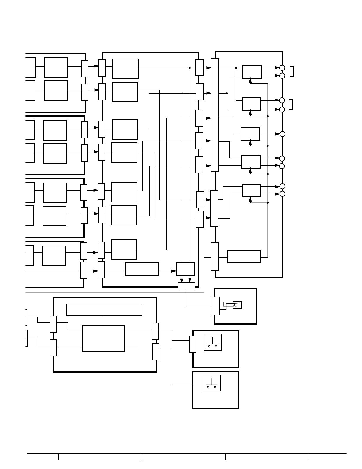
RX-DP20VBK
n
M
N
N
C
C
5
4
Video section
TV/
DBS
VCR1
VCR2
SUBROOM.R
R
P
R
P
DVD
MON
ZONE2
SELECTOR
SUBROOM-R
IC401,
IC441
IC402,
IC403
SELECTOR
IC404
Y/C, V
IC405
OSD
VIDEO
VMIX
V.SEPA
V.OSDOUT
V.OSDIN
WR403
CN401
CN402
S-video sectio
TV/DBS
VCR1
VCR2
DVD
MON
ZONE2
SUBROOM.L
R
P
R
P
SUBROO
DSP section
CN631
3
DIGITAL
IN1
DIGITAL
IN2
DIGITAL
IN3
DIGITAL
IN4
2
DIGITAL
IN5
DIGITAL
IN6
DIGITAL
OUT
DIGITAL
IN7
WR636
1
IC673
DIR
&
SELECTOR
IC674
SELECTOR
DSP_RESET,DSP_READY
DSP_STATUS,DSP_CLK,
IC675
DIT
ANALOG IN
IC657
to
IC659
IC681
A/D DIR
SELECTOR
MOSI,MISO,SCK,
READY,CLKR1
DSP_RST,CSDSP
DSP_COMMOND,
IC666
DSP
IC671
LOCAL
MICOM
SB L/R
REC DATA
CC_DATA,CC_CLK,
CC_RST,CC_CS
IC651
SW
F L/R
C/LEF
S L/R
I
CO
I
CO
I
CON
I
CON
2-5
CN633
ABC D
Page 31

RX-DP20VBK
ction
BROOM-L
IC461
to
IC464,
IC491
SELECTOR
(Y BLOCK)
IC465
to
IC468,
IC492
SELECTOR
(C BLOCK)
VIDEO Y/C
Y/C OUT
V.OSDIN
SEPA.Y
SEPA.C
V.OSDOUT
YCOUT
WR453
CN451
CN452
Component
VIDEO2
IN Y
Component
VIDEO2
IN Cb
Component
VIDEO2
IN Cr
Component video section
RY581
Switch
CN581
RY582
Switch
IC635
CC
CONVERTOR
IC640
CC
CONVERTOR
IC645
CC
CONVERTOR
IC650
CC
CONVERTOR
IC634
DAC
IC639
DAC
IC644
DAC
IC649
DAC
DSP. L/R
DSP. C/SW
DSP.S L/R
DSP.SB L/R
CW632
HDE F G
2-6
Page 32

RX-DP20VBK
2
W
7
K
0
2
KR M
Standard schematic diagrams
Primary / Regulator section
5
SHEET 10/11 SHEET 11/11
4
SHEET 4/11
SHEET 5/11 SHEET 7/11 SHEET 6/11 SHEET 8/11
3
2
Q3
2SD2394/EF/
Q4
2SD2394/EF/
R7R1R6
Q5
100
CN14
QGB2510J1 04
R9
3 9
R10
3 9
100
2SC1740S RS/ T
C2
0 0022
Q6
KRA104M T
R5
K1
100/16
470/10
K2
820
C3
D4
R8
4.7K
MTZJ6.2C
C4
Q7
KRC104M T
RY1
D3
1SS133-T2
150
2SC1740S/RS/-T
Q2
R4
4.7K
R2
47K
D1
MTZJ4 7B
CN3
QGB2510J1 06
DSP RESET
DSP COMMAND DSP RESET
DSP CLOCK
DSP READY
CN13
QGB2510J1 04
CN4
EP1
CN5
Fr L
Fr R
CENTER
SW
Sr L
Sr R
SrB L
SrB R
SUBROOM L
SUBROOM R
EP2
CN6
Fr L
Fr R
CENTER
SW
Sr L
Sr R
SrB L
SrB R
SUBROOM
SUBROOM R
CN7
VIDEO+5V
OSD STB
OSD DATA
OSD CLK
SYNCDET
V S/C OUT
MAIN VIDEO1
MAIN VIDEO2
MAIN VIDEO3
MAIN VIDEO4
SUB VIDEO1
SUB VIDEO2
SUB VIDEO3
SUBROOM R
CN8
SUBROOM L
SUB VIDEO4
SUB VIDEO3
SUB VIDEO2
SUB VIDEO1
MAIN VIDEO3
MAIN VIDEO2
MAIN VIDEO
DBS S/C
VCR1 S/C
VCR2 S/C
DVD S/C
DSP COMMANDDSP STATUS
DSP STATUS
DSP CLOCK
DSP READY
F1 RELAY
F2 RELAY
SUB RELAY
C RELAY
SUR RELAY
SB RELAY
SW MUTE
MA N VIDEO5
MA N VIDEO6
MA N VIDEO7
SUB VIDEO4
SUB VIDEO3
SUB VIDEO2
SUB VIDEO1
MA N VIDEO4
MA N VIDEO3
MA N VIDEO2
MA N VIDEO1
OSD CLK
OSD DATA
OSD STB
DBS S/C
VCR1 S/C
VCR2 S/C
DVD S/C
V S/C OUT
SYNCDET
PROTECT
SAFETY
HP RELAY
SBRMUTE
DM STB
DM CLK
DM DAT
S MUTE
ZIST
ANALOG DIRECT
VOL STB
VOL CLK
VOL DAT
DM STB
DM CLK
DM DAT
S MUTE
SBRMUTE
ZIST
ANALOG DIRECT
VOL STB
VOL CLK
VOL DAT
C RELAY
SW MUTE
SUR RELAY
SB RELAY
D2
1SS133
PROTECT
Q1
2SC1740S
C1
100/16
HP RELAY
SHUT
EP3
CN11
WR12
CN1
CN2
CN12
CN15
TF2
QMR0008 001
TF1
QMR0007 001
SHEET 9/11
SHEET 4/11
WR65
WR64 CN64
EP61
CN65
CN62
CN44
2SD2394/EF/
HZ18 2L T2
HZ18 2L T2
KTA1046/Y/
Q51
KTA1046/Y/
R53
100
C77
100/25
Q62
Q52
KTA1046/Y/
R52
100
R77
10K
Q63
2SC1740S/RS/ T
1SS133 T2
R79
2 2K
Q53
R4011
2 2
R4012
910
KRC104M
D72
D74
1SS133 T2
10K
R78
R80
16K
R83
10K
R69
10K
C43
100/16
R43
0 22
Q46
KRA104M
Q47
D73
1SS133 T2
31DF2 FC6
0 022
31DF2 FC6
0 022
0 022
31DF2 FC6
0 022
31DF2 FC6
R57
820
C60
0 0022
R75
10K
R73
2 2K
D61
C62
D62
C63
C64
D63
C65
D64
C79
22/25
1SS133 T2
C78
4 7/50
D45
MTZJ6.8A
R72
16K
Q64
KRC104M
R74
12K
C80
22/25
1SS133-T2
1SS133-T2
1SS133-T2
1SS133-T2
D65
D67
D66
D68
D4003
2200/25
C40
D4001
31DF2 FC6
C45
0 022
C46
0 022
D4002
31DF2 FC6
R
2
C4
22
T
R71
0.022
220
C61
R67
5 6K
D71
R68
8 2K
R41
4 7
R42
4 7
Q54
KRA104M T
R51
820
R54
4 7K
Q55
KRC104M T
31DF2 FC6
C47
0 022
C48
0 022
D4004
C49
31DF2 FC6
6800/25
68
68
R84
R76
IC61
KIA7812AP
R66
12
R65
10
R61
15
0 0047
0 0047
R85
15
R63
910
C73
220/50
C74
220/50
R64
910
R86
15
R62
15
D75
1SS133 T2
CN46
C51
100/25
2200/35
2200/35
WR48CN48
WR42
Q45
2SD2394/EF/
0 0047
D51
HZ6B1L T2
C71
C72
C59
Q65
KRC104M T
2SC1740S/RS/ T
C75
C76
Q61
D69
D70
2-7
IC44
KIA7806AP
R45
C52
CN9
MAIN VIDEO5
MAIN VIDEO6
MAIN VIDEO7
1
SHUT
SAFETY
F1 RELAY
F2 RELAY
SUB RELAY
C RELAY
SUR RELA
SB RELAY
WR13
WR14
SHEET 3/11 SHEET 2/11 SHEET 5/11
CN45
SHEET 9/11
100/25
1
TW41
Q44
KTC3200/GL/
1/50
100K
C56
D50
MTZJ8 2C
R50
Q43
TW42
ABC D
Page 33

RX-DP20VBK
D66
1 133-T2
0
001
DF2 FC6
C45
0 022
C46
022
D4002
DF2 FC6
4
00/GL/
TW42
1SS133-T2
D65
R70
220
D41
RS403L
C42
2200/25
TW51
Q42
KRC102M
Q43
KRA104M
CN63
EP62
0 1
C41
CN61
0 022
C44
R56
4 7
R46
4 7
R47
4 7
R55
4 7
WR102
To CN701
OF LAV10380-1
SHEET 3/11
WR101
F43
2A 125V
C58
2SB1357/EF
22K
22/50
C55
R49
D49 C54
MTZJ36C
RY101
QSK0131 001
QSK0131 001
T42
QQT0379 001
F42
0.047
Q41
22/50
RY104
C57
R48
0.047
3.3K
D101
1SS133 T2
RY102
QSK0131 001
RY103
QSK0131 001
500mA 250V
D48
11ES2 T4
C53
220/63
WR81
F41
TH41
QAD0095 4R7Z
CN41
WR41
CN47
WR86
WR85
SHEET 3/11 SHEET 9/11
PW81
PW82
PW22
PW21
PW23
PW24
T21
QQT0281 003
C22
0 01
D21
D22
11ES2-T4
11ES2-T4
D24 D23
11ES2 T4 11ES2 T4
C23
CN25
J81
QNS0061 001
2200/25
TW81
EP22
R81
470
R82
470
Parts are safety assurance parts.
When replacing those parts make
sure to use the specified one.
1 5K
R28
R26
4.7
C21
0 0047
RY21
D25
1SS133
R22
4 7
Q21
KRC105M
R25
4 7
R24
820
SHEET 9/11
SHEET
NUMBER
1 / 11
2 / 11
3 / 11
4 / 11
5 / 11
6 / 11
7 / 11
8 / 11
9 / 11
10 / 11
11 / 11
F21
8 0A 125V
820
R23
470/16
2SD468/BC/ T
C25
470/16
2SD468/BC/ T
C27
R21C26
QRZ9037-335
EP21
Q22
C24
0.0047
Q23
0.0047
D26
MTZJ6.2A
D27
MTZJ6.2A
PW25
PW26
Audio signal
Front audio signal
WR26
Rear audio signal
Center audio signal
Surround back audio signal
CIRCUIT DESCRIPTION
PRIMARY / REGULATOR
PRE MAIN AMP
POWER AMP
AUDIO SIGNAL INPUT 1
AUDIO SIGNAL INPUT 2
VIDEO SIGNAL INPUT 1
VIDEO SIGNAL INPUT 2
VIDEO SIGNAL INPUT 3
SYSTEM CONTROL LSI / FL DISPLAY
DSP1
DSP2
SHEET 1/11
HDE F G
2-8
Page 34

RX-DP20VBK
Pre main amp section
CN821
C709
R720WR711
1SS133
VC5022 2
D708D709
D710D711
R733
Q731
1SS133
Q1731
2SC2412K/RS/
R1733
10K
IC601
10K
VC5022 2
47P
120
R721
120
R1720
120
IC602
R1721
120
DTA124EKA
Q732
Q1732
DTA124EKA
Q716
2SC2412K/RS/
R735
680
R737
240
TH703
QAD0010-351
R738
240
TH704
QAD0010-351
R736
680
Q717
2SA1037AK/RS/
C710
47P
R731
47K
C731
47100
C1709
47P
Q1716
2SC2412K/RS/
R1735
680
R1722
R1737
240
TH705
QAD0010-351
R1738
240
TH706
QAD0010 351
R1736
680
Q1717
2SA1037AK/RS/
C1710
47P
1505 6K10K
2K
2K
CN701
R706
R1705
R708
R705
100K
100K
C704
00033
100
Q704
KTC3199/GL/
C1704
100 00033
R1708
Q1704
KTC3199GL/
Q705
C715
33P
68
R712
D702
1SS133
1505 6K10K
R1709R1710R1711
Q1705
C1715
33P
68
R1712
D1702
1SS133
001
CN781
5
CN 11CN721
C701
C801
1080
1080
1080
1080
1080
C1701
C1651
C1601
100
100
100
100
100
R1701
R801
R701
R1601
R1651
WR701
4
WR702
WR703
SHEET 1/11 SHEET 4/11
Q7091
2SC3422Y/
Q7096
2SC3422Y/
C7191
C703
100P
Q702
2SC1775A/E/
Q701
2SC1775A/E/
R703
1K
Q703
KTC3200GL/
R702
C702
100P
001
C7196
C1702
100P
CN706
C1703
100P
Q1701
2SC1775AE/
KTC3200GL/
R704
100K
330
2K
R1707
2K
R1706
Q1702
2SC1775AE/
R1703
1K
Q1703
R1702
100K
R1704
330
KTA1268/GL/
33K
R714
KTA1268/GL/
33K
R1714
Q706
KTA1267/YG/
15K
R713
Q707Q708
KTA1268GL/KTC3200 GL/
C705
22P
68
R716
Q1706
KTA1267/YG/
15K
R1713
Q1707Q1708
KTA1268/GL/KTC3200/GL/
C1705
22P
C1708
68
R1716
R709R710R711
R707
TH701
QAD0010 351
R717
330
VR701
D703
500
R718
470
R719
390
C708
00047
R732
330
C741
10P
D713 D712
1SS355 1SS355
C721
0022
R1732
330
D1711
1SS355
D1713
1SS355
C1721
0022
UDZS24BUDZS24B
1SS3551SS355
2SC2412KRS/
WR716
D1703
D1708D1709
UDZS24BUDZS24B
D1710
1SS355
D1712
1SS355
R743
100K
R744
36K
C742
1080
TH702
QAD0010 351
R1717
330
VR702
500
R1718
470
R1719
390
00047
C1741
10P
R1743
100K
R1744
36K
C1742
1080
R723
12
C711
47/100
27K
R722
C712
47100
Q711 Q710
R724
KTA1268/GL/ KTC3200GL/
12
R1723
12
C1711
47/100
27K
C1712
47/100
Q1711 Q1710
R1724
KTA1268/GL/ K KTC3200/GL/
12
3
C759
R770
150
R759
R757
100
R751
10/80
C751
100
R1751
10/80
C1751
CN751
CN761
Q7092
2SC3422/Y/
C7192
2
C752
100P
2K
Q751
KTC3200GL/
R752
100K
2K
R756
C754
00033
C765
33P
100
R758
Q752
2SC1775A/E/
R753
1K
R755
100K
Q753
68
R762
Q754
KTC3199GL/
D752
R754
330
1SS133
CN702
001
C753
100P
2SC1775A/E/
Q756
KTA1267/YG/
15K
R763
Q755
KTA1268GL/
56K
R760
10K
R761
Q757Q758
KTA1268/GL/
C755
22P
C758
KTC3200/GL/
68
33K
R766
R764
TH751
QAD0010 351
R767
330
VR751
500
R768
470
R769
390
00047
C791
10P
R793
100K
R794
36K
C792
1080
WR712
D753
R782
330
D759 D758
UDZS24B UDZS24B
D761
1SS355
1SS355
2SC2412K/RS/
D762
D763
1SS355
1SS355
C771
0022
47P
120
1SS133
C603
VC5022 2
R771
D760
R783
10K
Q781
120
DTA124EKA
Q782
Q766
2SC2412KRS/
R785
680
R787
27K
R772
240
TH753TH754
QAD0010-351QAD0010-351
R788
240
R786
680
Q767
2SA1037AK/RS/
C760
47P
Q761 Q760
KTA1268/GL/ K KTC3200 G/
R781
47K
C781
47100
R773
C761
47100
C762
47100
R774
12
2-9
R1773
C1759
R1770
330
D1761
1SS355
D1763 D1762
1SS355 1SS355
C1771
0022
WR717
D1753
15056K10K
R1759R1760R1761
Q1755
KTA1268/GL/
Q1756
KTA1267/YG/
15K
R1763
Q1757Q1758
KTA1268/GL/KTC3200GL/
C1755
22P
68
33K
R1766
R1764
R1757
2K
CN707
2K
R1756
001
C7197
Q7097
2SC3422Y/
C1753
100P
Q1751
2SC1775AE/
1
KTC3200GL/
R1752
C1752
100K
100P
C1754
00033
C1765
33P
100
R1758
Q1752
2SC1775AE/
R1753
1K
R1755
100K
Q1753
68
R1762
R1754
Q1754
330
KTC3199/GL/
D1752
1SS133
TH752
QAD0010 351
R1767
330
VR752
500
R1768
470
R1769
390
C1758
00047
R1782
C1791
10P
R1793
100K
R1794
36K
C1792
1080
1SS133
D1758D1759
UDZS24BUDZS24B
D1760
1SS355
Q1781
2SC2412K/RS/
R1783
10K
VC5022 2
47P
120
Q1766
R1785
2SC2412K/RS/
680
27K
R1772
R1788
240
TH755
QAD0010 351
R1787
240
TH756
QAD0010-351
R1786
IC604
R1771
120
Q1782
DTA124EKA
680
Q1767
2SA1037AKRS/
C1760
47P
Q1761 Q1760
KTA1268GL/ K KTC3200G/
12
C1761
47100
C1762
47100
R1774
12
ABC D
Page 35

RX-DP20VBK
R723
12
1
0
2SC1775AE/
KTC3200GL/
R1602
100K
CN705
2SC1775AE/
KTC3200GL/
R1652
100K
2SC1775A/E/
R805
100K
R1607R1606
2K2K
R1608 C1604
Q1602
2SC1775A/E/
Q1601
R1603
1K
Q1603
R1604
330
R1657
2K
2K
R1656
Q1652
2SC1775AE/
Q1651
R1653
1K
Q1653
R1654
330
C803
100P
Q801
R803
1K
Q803
KTC3200GL/
Q804
KTC3199/GL/
R804
330
CN704
CN712
SHEET 3/11
CN771
00
24
12
23
2
11
0
CN713
Q7094
2SC3422Y/
C1602
Q7095
2SC3422/Y/
001
C7194
C1603
100P
100P
001
C7195
SHEET 3/11 SHEET 3/11
C1653
12
0
724
12
R773
12
C761
47100
CN752
Q7093
2SC3422/Y/
C762
47100
R774
12
CN811
R1773
12
C1761
47100
100P
C1652
100P
CN703
001
C7193
C802
R802
100P
100K
100 0 0033
R1605
100K
Q1604
C1654
100
R1658
R1655
100K
Q1654
R807R806
2K2K
100
R808 C804
Q802
2SC1775AE/
KTC3199/GL/
00033
KTC3199GL/
00033
C815
33P
15056K
R1609R1610
Q1605
C1615
33P
R1611
10K
68
R1612
D1602
1SS133
R1659R1660R1661
Q1655
C1665
33P
68
R1662
D1652
1SS133
R809
150
Q805
KTA1268GL/
R810
56K
R811
10K
68
R812
D802
1SS133
KTA1268GL/
15056K10K
KTA1268/GL/
33K
R814
Q1606
KTA1267YG/
15K
R1613
Q1607Q1608
KTA1268/GL/KTC3200 GL/
C1605
22P
33K
68
R1616
R1614
Q1656
KTA1267/YG/
15K
R1663
Q1657Q1658
KTA1268/GL/KTC3200/GL/
C1655
22P
68
33K
R1666
R1664
Q806
KTA1267/YG/
R813
15K
Q807Q808
KTA1268GL/KTC3200/GL/
C805
22P
C808
68
R816
TH771
QAD0010 351
R1617
330
500
VR771
R1618
470
R1619
390
C1608
R1632
00047
C1658
00047
00047
330
C1641
10P
R1649
D1611
100K
1SS355
R1650
36K
C1642
10/80
C1691
10P
R1696
36K
C1692
10/80
C841
10P
R843
100K
R844
36K
C842
1080
D1613
1SS355
C1621
0022
TH772
QAD0010 351
R1667
330
VR772
500
R1668
470
R1669
390
R1682
330
D1659
UDZS24B
D1661
R1695
100K
1SS355
D1663 D1662
1SS355 1SS355
C1671
0022
TH801
QAD0010 351
R818
470
R819
390
R817
330
R832
WR713
VR801
500
D803
330
D808D809
UDZS24BUDZS24B
D810
D811
1SS355
Q831
D812
D813
1SS355
1SS355
C821
0022
WR714
1SS133
D1603
D1608D1609
UDZS24BUDZS24B
D1610
1SS355
Q1631
2SC2412K/RS/
D1612
1SS355
WR715
1SS133
D1653
D1658
UDZS24B
D1660
1SS355
Q1681
2SC2412K/RS/
1SS133
VC5022 2
2SC2412K/RS/
R833
10K
IC607
1SS355
C1609
R1620
47P
120
Q1616
2SC2412K/RS/
R1635
680
27K
R1622
R1637
240
TH773TH774
QAD0010-351QAD0010-351
R1638
240
R1636
C605
VC5022 2
R1621
120
DTA124EKA
Q1632
R1633
10K
R1670
120
C606
VC5022 2
R1671
120
DTA124EKA
Q1682
R1683
10K
C809
R820
120
R821
120
DTA124EKA
Q832
680
Q1617
2SA1037AKRS/
C1610
47P
C1659
47P
Q1666
TH775TH776
QAD0010-351QAD0010-351
Q1667
2SA1037AK/RS/
C1660
47P
47P
Q816
2SC2412KRS/
TH802TH803
QAD0010-351QAD0010-351
Q817
2SA1037AK/RS/
C810
47P
2SC2412K/RS/
R1685
680
R1686
680
R835
680
R837
240
R838
240
R836
680
Q1611 Q1610
KTA1268/GL/ KTC3200/GL/
R1631
47K
C1631
47/100
R1687
240
27K
R1672
R1688
240
Q1661 Q1660
KTA1268/GL/ K KTC3200 GL/
Q810
KTC3200/GL/
R822
27K
Q811
KTA1268/GL/
R831
47K
C831
7/100
R1623
12
C1611
47/100
CN772
SHEET 3/11 SHEET 3/11
C1612
47/100
R1624
12
R1673
12
C1661
47/100
CN773
C1662
47/100
R1674
12
R823
12
C811
47100
CN812
SHEET 3/11 SHEET 3/11
CN813
C812
47100
R824
12
CN753
SHEET 3/11
C1762
47100
R1774
12
Front audio signal
Rear audio signal
Center audio signal
Surround back audio signal
SHEET 2/11
HDE F G
2-10
Page 36

RX-DP20VBK
D
C 777
1
R
Power amp section
5
CN722
Q712
2SC4883A/Y/
D715 R725
HZ3 0BP 270
R726
D716
MTZJ33C
1
R739
91K
R741
1 8K
Q714
2SC3858/PG/
R1901
2 7K
R728R729
0.10.1
R1902
R1903
12K
Q1901
2SC3906K/RS/
R1904
100K
15K
Q1712
2SC4883A/Y/
D1715
HZ3 0BP
R1725
270
R1726
D1716
MTZJ33C
Q1714
R1739
91K
R1741
1 8K
2SC3858/PG/
R1941
2 7K
0.1
R1728R1729
R1942
15K
1
R1943
12K
Q1941
2SC3906K/RS/
R1944
100K
C1745C1746
3300/803300/80
D1901
D1911
1SS133
15K15K
R1912R1922
1SS1331SS133
B903
B904
R1913
12K
Q1911
2SC3906K/RS/
R1914
100K
B911
B912
2SA1859A/Y/
Q1762
2SC4883A/Y/
D1765
HZ3 0BP
2SA1859A/Y/
Q1713
Q1763
R1775
270
R1776
R1777
R1727
1
1
0.1
R1742
1 8K
R1740
91K
1
Q1715
2SA1494/PG/
D1717
MTZJ33C
D1766
MTZJ33C
Q1764
2SC3858/PG/
R1789R789
R1951
91K91K
2 7K
R1791
1 8K
0.1
R1778
0.1
R1792
R1779
1 8K
R1790
91K
Q1765
2SA1494/PG
D1767
MTZJ33C
SHEET 2/11 SHEET 2/11 SHEET 2/11 SHEET 2/11
CN723
Q713
2SA1859A/Y/
Q762
2SC4883A/Y/
4
D765
HZ3 0BP
Q763
2SA1859A/Y/
R775
270
R776
R777
R727
1
1
R742
1 8K
R740
91K
1
Q715
2SA1494/PG/
D717
MTZJ33C
D766
MTZJ33C
Q764
2SC3858/PG/
R1911
2 7K
R791
1 8K
0.1
R778
R779
R792
1 8K
R790
91K
Q765
2SA1494/PG/
D767
MTZJ33C
D1941
R1952
D1951
1SS133
15K
1SS133
B902
B901
R1953
Q1951
2SC3906K/RS
R1954
100K
B914
B913
12K
C795
C1795
3300/80
3300/80
C796
C1796
3300/80
3300/80
3
Q1612
2SC4883A/Y/
D1615 D1665
HZ3 0BP HZ3 0BP
2
CN783 CN762CN763CN782CN822CN823
Q1613
2SA1859A/Y/
Q812
2SC4883A/Y/
D815
HZ3 0BP
1
Q813
2SA1859A/Y/
D1616
MTZJ33C
R1626
1
R1625 R1675
270 270
R1627
1
R826
1
R825
270
R827
1
Q1614
2SC3858/PG/
R1639 R1689
R1921
91K 91K
2 7K
R1641
1 8K
0.1 0.10.1
R1628
R1642
R1629
1 8K
R1640
91K
D1921
Q1615
2SA1494/PG/
D1617
MTZJ33C
D816
MTZJ33C
Q814
2SC3858/PG/
R839
R1961
91K
2 7K
R841
1 8K
0.22
R1962
R828R829
0.22
R842
1 8K
R840
91K
D817
MTZJ33C
Q815
2SA1494/PG/
D1961
15K
1SS133
R1923
12K
Q1921
2SC3906K/RS/
R1924
100K
B905
B906
R1963
12K
Q1961
2SC3906K/RS/
R1964
100K
B907
B908
Q1662
2SC4883A/Y/
Q1663
2SA1859A/Y/
R1676
R1677
R1971
D1666
MTZJ33C
1
R1691
1 8K
R1692
1 8K
R1690
91K
1
D1667
MTZJ33C
10K
C1971
2SA1514K/RS/
R1977
22/50
Q1971
82K
Q1664
2SC3858/PG/
R1931
2 7K
0.1
R1678
0.1
R1679
2SA1494/PG
Q1665
3.3K
R1972
47K
R1973
47/10
C1972
R1932
D1931
15K
1SS133
R1974
C1973
56K
0.001
R1933
12K
Q1931
2SC3906K/RS/
R1934
100K
B909
B910
0.01
C1974
R1975
68K
R1978
C1776
C895
C1695
C1645C1646
3300/80
3300/80
3300/803300/80
C896
C1696
3300/80
3300/80
27K
R1976
IC951
TA7317P
220K
R1979
22K
22/16
C1975
TW702
D845
F10P20F
D846
F10P20F
0.1/100
F
2-11
ABC D
Page 37

C745
C1745C1746
3300/803300/80
3300/803300/80
C746
C1774
C1776
0.1/100
0.1/100
45 D745
D795
20F F10P20F
F10P20F
C1777
0.1/100
C1775
0.1/100
F10P20FRF10P20FRF10P20FR
RX-DP20VBK
C1981
1/50
KRC105M
1SS133
RY906
R1981
RY901
QSK0109 001
1/50
C1982
RY902
C1983
1/50
RY903
C1986
1/50
C1984
1/50
RY904
1/50
C1985
RY905
4 7
Q1993
Q1994
KRC105M
KRC105M
D1994
D1993
1SS133
1SS133
WR731
WR732
WR733
WR734
WR735
WR736
WR737
D773
1SS133
Q772
DTD123TKA
RY751
QSK0112 001
R797
33
D774
C775C776C773C774
1SS133
0.1/1000.1/1000.1/1000.1/100
C1772
0.1/100
C1773
0.1/100
D746D796D846
CN738
CN701
WR101
LVA10382-7
To SHEET 1/11
SHEET 1/11
CN741
CN742
L1701
CN743
SHEET 1/11
L701
1u
R746
10
R745
4 7
C735 C736
0 047 0 047
L751
1u
R796
10
R795
4 7
C785 C786
0 047
0 047
L801
1u
R846
10
R845
4 7
C835
C836
0 047
Q1991
R1648
10
C1635
0 047
R1694
10
C1685 C1686
0 047 0 047
R1746
10
C1735 C1736
0 047 0047
R1796
10
C1785 C1786
0 047 0047
D1991
0 047
C1636
0 047
1SS133
Q1992
D1992
L1601
1u
R1647
4 7
L1651
1u
R1693
4 7
1u
R1745
4 7
L1751
1u
R1795
4 7
KRC105M
Q1995
KRC105M
D1995
1SS133
C788 C787
Q1996
KRC105M
D1996
1SS133
C738 C737
C1788 C1787 C1738 C1737 C1688 C1687 C1638 C1637 C837C838 C790 C789 C740 C739
Audio signal
Front audio signal
Rear audio signal
Parts are safety assurance parts.
When replacing those parts make
sure to use the specified one.
Center audio signal
Surround back audio signal
SHEET 3/11
HDE F G
2-12
Page 38

RX-DP20VBK
C2302
N
0
00056
Audio signal intput 1 section
QNN0299 001
J201
5
J201
QNN0299 001
QSW0511 001
SW201
4
QNN0396 001
QNN0396 001
QNN0396 001
3
QNN0396 001
C271
10/50
C211
C272
10/50
2
C276
22/25
C212
C277
22/25
R207
2 2K
Q205
2SA970 GL/ T
2SK170/L/ T
C227
220P
C228
220P
2SK170/L/ T
Q206
2SA970/GL/ T
R227
4 7K
R228
330P 330P
C254C253
330P 330P
C258C257
330P 330P
330P 330P
C2403
22/50
C2404
22/50
IC271
NJM5532M D XE
C2413
10/50
C2414
10/50
IC272
NJM4580E W
R286
A/D SRR
R285
A/D SLL
SBR
SUB SG R
SBL
SUB SG L
C205
0 0056
Q201
Q202
C206
0 0056
R208 R210
2 2K 2 4K
10K
J202J202
QNN0199 001QNN0199001
330P330P
J202
QNN0199 001
J203
QNN0392 001
330P330P
J203
QNN0392 001
J203
QNN0392 001
J204
QNN0396 001
R2405R2406
100K100K
R2415R2416
100K100K
1K
A/D SR
1K
A/D SL
R288
SrB-RS B-L
L201
L203
100
100
R229
C202 C201
R230
L202
L204
100
100
R226
1K
CDR REC L
CDR PLAY L
DVDF L DVD F R
J204
330P330P
C263C264
J204
J204
C265C266
330P330P
J204
A/D RRA/D LL
TC9162AF-X
SUB AMPR
TC9162AF-X
SUB AMPL
R201
5 6
100
R205
C203
0 001
47K47K
R203R204
RY278
QSK0112 001
100
R206
C204
0 001
R202
5 6
Q211
DTC123JKA X
Q212
KAR107S X
C222
22/50
R251
470
R253
470
R255
J202
470
QNN0199 001
J203
QNN0392 001
J203
QNN0392 001
R261
J203
470
QNN0392 001
J204
QNN0396 001
C2401
22/50
R263
R2403R2404
47K47K
R264
C2402
22 50
C2411
R265
10 50
470
R2413R2414
47K47K
R266
470
C2412
10 50
1K1K
R282R281
A/D SWW
A/D R
A/D L
A/D CC
R287
0
SUB R
SUB OUTRSUB OUTL
R290 R289
00
SUB L
C221
1 50
C251 C252
C255 C256
C259 C260
C261 C262
C271
NJM5532M D XE
C272
NJM4580E W
1K
R284
A/D SW
1K
R283
A/D C
R209
2 4K
R211
2 7K
R213
12
Q203
2SK170/L/ T
R215
2 2K
R217
1 8K
R218
1 8K
R216
2 2K
Q204
2SK170 L/ T
R214
12
R212
2 7K
R252
470
R254
470
TAPE/MD REC RTAPE/MD REC L
R256
470
TAPE/MD PLAY RTAPE/MD PLAY L
R258R257
470470
CDR REC R
R260R259
470470
CDR PLAY R
R262
470
R2619
68
C2419
C2405
47/50
0 022
C2420
C2406
47/50
0 022
R2620
68
R2621
68
C2415
10/50
C2416
10/50
R2622
68
R267
68
SUB VR
DATA a
CLK a
C275
560P
SUB VL
R268
68
R269
68
DATA b
0
C280
560P
R270
68
CD RCD L
STB a
CLK b
STB b
R221
1M
Q209
2SK2980 X
R224
470K
Q210
2SK2980 X
R222
1M
FRONT R
FRONT L
C217
2200/6 3
R231
270
R232
270
C218
22006 3
R233
22
R234
22
IC201
NJM4580E W
RY271
QSK0112 001
RY272
QSK0112 001
ZST SR
RY273
QSK0112 001
ZST SL
IC201
NJM4580E W
ZIST R
ZIST L
ZIST C
ZISTSW
Q207
KRC105M
C213
R249
C207 C209
0 0068 0 0047
R235
10K 16K
0 01
C211
R243R241
4 7M4 7M
R244R242
4 7M4 7M
C212
0 01
R236 R240
10K 16K
C208
0 0068
R250
1 2M
C214
47P
6868
R2611R2612
C231
22 25
C202
TC9164AF-X
PHONO L
C232
22 25
C273
1 50
R225
120
R271
47P
1 2M
R237
180K
R238
180K
PHONO-R
360
R245
1 2M
R246
1 2M
CD-R
CD-L
A/D RR
A/D LL
A/D CC
A/D SWW
A/D SRR
A/D SLL
Q271
2SD468/BC/ T
C215
220P
R239
R247
1 5M
R248
1 5M
C210
0 0047
C216
220P
TUNER-R
TAPE MDPLAY-R
TUNER-L
TAPE/MD PLAY-L
ZIST SBR
ZIST SBL
R273
4 7K
C219
R2601
22/50
100
C220
22/50
R2602
100
DVD F R
CDR PLAY-R
DVD F-L
V SG L
CDR PLAY-L
R276
1K
R275
1K
C225
1 50
R277
1K
R278
1K
R280
1K
R279
1K
91
R272
Z ST_
R2603
100K
R2604
100K
TAPE MDREC RTAPE/MD REC-L
DSP R
DSP L
DSP C
DSP SW
DSP SR
DSP SL
DSP SBR
DSP SBL
2SD468/BC/ T
Q272
CDR REC-R
CDR REC-L
PHONO-R
Q213
2SC1740S/RS/ T
Q214
2SA933S RS/ T
PHONO-L
STB a
C278
47/25
R2514
470
C223
470 25
C224
470 25
R2515
470
RY274
QSK0112 001
RY275
QSK0112 001
RY276
QSK0112 001
RY277
QSK0112 001
R274
4 7K
R2605
68
R2023
Q2013
1K
DTA114YKA X
R2027
R2091R2093R2094R2092
R2025
10K
Q2011
2SC3576 JVC-T
R2026
10K
Q2012
2SC3576-JVC-T
R2024
R2606
68
C2001
22 25
C235
560P
CLK a
DATA a
C292
22/50
C291
22/50
C293
22/50
C294
22/50
C296
22/50
C295
22/50
C298
22/50
C297
22/50
DSPON
C2002
22 25
C2203
0 022
IC221
TC9459F X
0 022
C2204
C2212
0 022
IC222
TC9459F X
C2213
0 022
C2221
0 022
IC223
TC9459F X
C2222
0 022
C2230
0 022
IC224
TC9459F X
C2231
0 022
SUB SG L
C203
PHONO L
SUB SG R
R2001
68
TC9164AF-X
R2002
68
1K
PHONO-R
CD-L
STB
DATA
CLK
STB
DATA
CLK
STB
DATA
CLK
STB
DATA
CLK
1K
C2028
22/50
SUB AMPL
SUB AMPR
DVD F-R
TUNER-R
CD R
CDR PLAY-R
TAPE/MD PLAY R
TUNER-L
DVD F-L
CDR PLAY-L
TAPE/MD PLAY-L
C2051
22/50
100K
R2053
C2059
22/50
R2061R2069
100K100K
C2067
22/50
C2075
22 50
R2077
100K
2-13
TUNER RTUNER L
R2303
1K
QGA2501F1 03
SHEET 5/11
6 8K
0 0056
C2301
R2302
R2304
1K
CN207
6 8K
B335
R2301
FL301 FL302
1
DSP L
DSP R
DSP C
DSP SW
DSP SL
Z STL
Z STR
Z STC
CN201
QGA2001F1 14
to WR700
DSP SR
DSP SBR
ZST SW
ZST SL
ZST SR
Z STSBL
Z STSBR
STB a
DATA a
CLK a
CN224
QGA2001F1 07
CN234
QGA2001F1 06
CN203
QGA2001F1 12
DSP SBL
A/D L
A/D C
A/D R
WR204
QJK016 09****
A/D SR
A/D SL
A/D SW
V SG R
V SG L
CN223
QGA2001F1 08
SUB VR
SUB VL
QQR0590 001 QQR05900
SHEET 5/11 SHEET 5/11 SHEET 9/11 SHEET 11/11 SHEET 11/11 SHEET 5/11
ABC D
Page 39

RX-DP20VBK
R2053
R2061
R2069
R2077
DVD F R
DVD F L
R2039
IC263
NJM4580E W
C2033
4 750
R2091R2093R2094R2092
2 2K4704702 2K
R2035
5 1K
1K1K
R2033R2034
R2036
5 1K
C2034
4 750
C263
NJM4580E W
B337
SUB R
CDR REC-R
TAPE/MD REC-R
SUB L
STB b
CDR REC-L
TAPE/MD REC-L
B338
C2055
51
0
59
0
67
0
5
0
2
590 001
100/25
C251
NJM5532M D W
C2053
10/80
R2353
5 1K
100K
C2063
100/25
NJM5532M D W
100K
C2071
100/25
NJM5532M D W
100K
NJM5532M D W
100K
0 0056
C2302
R2055
1K
R2351
C252
C253
1K 1K
R2359 R2355
C2079
100 25
C254
1K
R2363
100K
R2065
68
C2061
10/80
R2357
5 1K
R2063
100K
R2073 R2074
68 68
C2069
10/80
R2361
5 1K
R2071
100K
C2077
10 80
R2365
5 1K
R2079
B336
68
C2031
4 7/50
R2031
100K
C2035C2036
47 2547/25
SUB MUTE
R2032
100K
C2032
4 7/50
R2040
68
C2005
560P
DATA b
CLK b
C2056
100/25
C2052
22/50
R2054
100K
C2064
100/25
C2060
22/50
R2062
100K
C2072
100/25
C2068
22 50
R2070
100K
C2076
22 50
R2078
100K
100K
STB c
IC251
NJM5532M D W
R2354
5 1K
1K
R2352
IC252
NJM5532M D W
R2358
9 1k
1K
R2356
IC253
NJM5532M D W
R2362
5 1K
C2080
100/25
IC254
NJM5532M D W
R2366
5 1K
1K 1K
R2364 R2360
MUTE
DATA c
CLK c
SBRMUTE
SHEET 1/11
R2017
68
SUB VIL
C2015
47/25
C2016
47/25
SUB VIR
R2018
68
R2613
68
C245
47/50
C246
47/50
R2614
68
R2058R2057
6868
C2054
10 80
R2056
100K
R2066
68
C2062
10/80
R2064
100K
C2070
10/80
R2072
100K
R2082R2081
6868
C2078
10/80
R2080
100K
DATA
CLK
STB
1K1K1K
R313
R312
R311
Z ST
DSPON
IC261
NJM4580E W
C2011
10 50
R2013
47K
R2014
47K
C2012
NJM4580E W
10 50
C2417
C241
0 022
22/50
C242
22/50
C2418
0 022
R2623
68
C281C282
47 5047 50
68
R2624
R2501
R2502
R2513
C311
220P
C312
220P
C313
220P
IC261
NJM5532M D XE
47K47K
R2615R2616
NJM5532M D XE
R2512
68
C2501
10 50
33K
IC281
NJM4580E W
33K
C2502
10/50
68
SUB PREMUTE
DATA b
CLK b
STB b
CN208
QGA2001F1 08
SHEET 9/11
C2013
10 50
R2015
100K
R2016
100K
C2014
10 50
IC204
C243
22/50
C244
22/50
IC204
C2251
22/50
R2259
47K
R2260
47K
C2252
22/50
R2266
R2265
R2503
D2501
100K
1SS355 X
R2505
22K
D2503
1SS355 X
IC281
NJM4580E W
D2504
1SS355 X
R2506
22K
R2504
D2502
1SS355 X
100K
Q2043
DTA114YKA X
R2046
1K
C2042
22 50
1K
1K
R315
R314
R316
1K
SUB VCLK
SUB VDATA
SUB PREMUTE
SUB MUTE
SUB VSTB
CN218
QGA2001F1 03
SHEET 5/11 SHEET 1/11 SHEET 2/11 SHEET 2/11 SHEET 1/11
R2618 R2617
R2267
R2268
C314
220P
C315
220P
C316
220P
FRONT L
47K
47K
100K 100K
100K
100K
R2263
R2264
NJM78L05A T
33K33K
R2507R2508
SUB OUT L
C2025
0 022
SUB VSTB
SUB VDATA
C262
TC9459F X
68
TC9162AF X
R2511
10K
1SS133 T2
SBRMUTE
SUBROOM-L
C2265
10/80
C2266
10/80
IC213
C285
560P
D2508
1SS355 X1SS355 X
R308
D291
SUBROOM-R
SUB VCLK
R2279
100K
R2280
100K
Q2501
KTC3199/GL/ T
Q300
DTA143EKA X
C302
1K
10 50
Q299
KRA107S X
1K
R307
1SS133 T2
C301
22/50
STB c
MUTE
Fr-L
R292
470
10K
R299
10K
R304
10K
R303
10K
R298
470
R306
10K
R305
10K
R297
470
R309
CLK c
DATA c
470K
Sr-L
Fr-R
CENTER
Sr-R
L MT
CN202 CN204
QGA2001F1 09 QGA2001F1 03
To WR701 LVA103807 To WR702 LVA10380 7
Fr R
Q292R300
2SC3576 JVC T
Q291
2SC3576 JVC T
R291
Fr L
470
R293
470
Q293R301
2SC3576 JVC T
10K
R302
2 2K
Q294
2SD2144S/VW/ T
R294
470
R296
470
Q296
2SC3576-JVC-
Q295
R295
2SC3576-JVC-T
470
Q298
2SC3576-JVC-T
Q297
SC3576-JVC-T
SrB-R
SrB-L
CENTER
SW
Sr R
Sr L
LIMIT
SBR
Audio signal
Tuner signal
Front audio signal
Rear audio signal
Center audio signal
SBL
Surround back audio signal
Main audio signal
Sub audio signal
A+18V2
A 18V2
RY+24V
RY GND
A-18V1
A+18V1
CN206
QGB2510K1 06
SUB L
SUB R
FRONT R
2 4k2 4k
R2269R2270
47K
47K
IC283
C2503C2504
R2041
R2043
10K
R2044
10K
R2042
1k
SUB OUT R
IC241
NJM4580E W
IC241
NJM4580E W
6 2K1K
R2509R2510
11
1k
C2026
0 022
68
R2276
R2275
R2273
2 4K
C2267
47/50
C2268
47/50
R2274
2 4K
47K
R2261
47K
R2262
IC282
NJM2903M XE
D2507
D2505
1SS355 X
D2506
1SS355 X
C282
NJM2903M XE
Q2041Q2042
2SC3576-JVC T
D292
2SC3576-JVC T
SUBROOM L
SUBROOM R
Fr-L
Sr-L
Sr-R
Fr-R
CENTER
SW
SBL
SBR
CN221CN205
QGB2510K1 10QGB1214K110S
SHEET 4/11
HDE F G
2-14
Page 40

RX-DP20VBK
N
Audio signal intput 2 section
R7702 C701
10K NJM5532D
FR H
R7710
FR C
10K
C7701 C7702
0 022 0 022
C7703 C7704
0 022 0 022
C7705
0 022
C7707 C7708
0 022 0 022
J701
FR H
C7710
560P
FR C
J701
SW H
C7712
560P
SW C
J701
SR H
C7714
C7706
560P
SR C
0 022
J702
SBR H
C7716
560P
SBR C
R7704
10K
SW H
R7712
SW C
10K
R7706
10K
SR H
R7714
SR C
10K
R7708
10K
SBR H
R7716
SBR C
10K
J701
5
FL H
C7709
560P
FL C
J701
C H
C7711
560P
C C
J701
SL H
C7713
560P
SL C
J702
SBL H
C7715
560P
SBL C
R7734
100
ZIST R
C7734
R7726
10P
C702
NJM5532D
C703
NJM5532D
C704
NJM5532D
10K
R7736
100
ZISTSW
C7736
R7728
10P
10K
R7738
100
ZISTSR
C7738
R7730
10K
10P
R7740
100
ZIST SBR
C7740
R7732
10K
10P
10K
R7718
10K 10K 10K
R7724 R7722 R7720
R7701
10K
FL H
R7709
FL C
10K
R7703
10K
C H
R7711
C C
10K
R7719R7721R7723 R7717
R7705
10K
SL H
R7713
SL C
10K
R7707
10K
SBL H
R7715
SBL C
10K
10K10K10K 10K
NJM5532D
NJM5532D
NJM5532D
R7733
100
Z STL
C7733
R7725
10P
10K
IC702
R7735
100
Z STC
C7735
R7727
10P
10K
IC703
R7737
100
ZST SL
C7737
R7729
10P
10K
IC704
R7739
100
Z STSBL
C7739
R7731
10P
10K
IC701
NJM5532D
R7751
47
C7751
47/50
C7752
47/50
R7752
47
R7753
47
C7753
47/50
C7754
47/50
R7754
47
R7755
47
C7755
47/50
C7756
47/50
R7756
47
R7757
47
C7757
47/50
C7758
47/50
R7758
47
ZIST L
ZIST R
ZIST C
ZISTSW
ZISTSL
ZISTSR
ZIST SBL
ZIST SBR
A+18V
A 18V
WR700
SHEET 4/11
4
1K
1K
TV/DBS-L
C2315
330P
C311
SAA6588
47P
Q2312
KRA102M
IC382
BA15218
R2115
47K
R2116
1K
V DEO-R
V DEO-L
560P
C2313
1
C2314
R2312
470K
IC381
BA15218N
C2113
R2113
10/25
C2111
C321 C322
330P 330P
C323
470
R323
VCR1 REC L
330P
C325
470
R325
VCR1 PLAY L
3
Fr L
CENTER
Sr L
SrB L
330P
C327
470
R327
VCR2 REC L
330P
C329
470
R329
VCR2 PLAY L
330P
C331
470
R331
330P
470
R333
C333
330P
470
R335
C335
330P
470 470
R337 R338
C337
330P
2
470470
R322R321
TV/DBS R
C324
470
R324
VCR1 REC R
330P
C326
470
R326
VCR1 PLAY R
330P
C328
470
R328
VCR2 REC R
330P
C330
470
R330
VCR2 PLAY R
330P
C332
470
R332
330P
C334
330P
C336
330P
C338
330P
Fr R
470
R334
SW
470
R336
Sr R
SrB R
Fr L
Fr R
CENTER
SrB L
SrB R
Sr L
2SC3576 JVC
Q324
2SC3576 JVC
Q330
B321
10/50
C341
0 022
C343
C344
C342
Sr-R
R346
470
R348
10K
QSK0112 001
R356
470
R358
10K
C321
TC9163AF
SW
TV/DBS R
VCR1 PLAY-R
V DEO-R
VCR2 PLAY-R
0 022
10/50
TV DBS-L
Q323
2SD2144S VW/
RY351
Q351
KRC105M
Q329
2SC3576 JVC
V DEO-L
VCR1 PLAY L
VCR2 PLAY L
R345
470
R347
10K
R1351
360
C361
R355
470
R357
10K
VCR1 REC-R
VCR2 REC-R
V SG RV S G L
C345
560P
DATA
CLK
STB
VCR1 REC-L
VCR2 REC-L
Q342
KRA107S X
C363
22/50
R364
470K
Q343
C365
22/50
R366
470K
C369
22 50
Q345
KRA107S X
DTC114YKA X
R370
470K
10/25
R363
1K
Q332
DTC114YKA X
R365
1K
R369
1K
Q334
IC381
BA15218N
10/50
C2101
0 022
C2103
C322
TC9163AF
0 022
C2104
10/50
C2102
1K
C2112
R2114
10/25
R2112R2111
100K47K
TV/DBS R
VCR1 PLAY-R
VCR2 PLAY-R
TV/DBS-L
VCR1 PLAY-L
VCR2 PLAY-L
R2315
1K
R2311
QAX0263 001Z
X311
82P
C2311
C2312
Q2311
KRC102M
C2319
100P
2-15
SUBROOM-L
1
SHEET 1/11
CN321
QGB1214K1 10S
SUBROOM-R
CN325
QGB2510K2 06
SHEET 1/11
CN324 CN323
QGA2001F1 09 QGF1205F1 15
SHEET 9/11
ABC D
Page 41

RX-DP20VBK
C2313
IC382
BA15218N
D2111
1SS355 X
47K
15
C2114
10 25
6
VCR1 REC-RVCR1REC-L
IC382
BA15218N
100K
R2117
VCR2 REC-RVCR2REC-L
SUBROOM-RSUBROOM-L
C2115
10 25
R2118
10K
R2120
10K
R2121
R2119C2116
10/25
10K
R2123R2122
10K10K
Q2111
KTC3199
Q2112
DTC144ESA
3 3K
D2123
MTZJ5 1C
D2121
1SS355 X
D2122R2124
100
1SS355-X
Audio signal
Tuner signal
Front audio signal
Rear audio signal
C2105
560P
SUB VL
SUB VR
Center audio signal
Surround back audio signal
Main audio signal
Sub audio signal
560P
C2316
2 2/50
10 16
0 047
R2313
C2318
R2312
470K
C2317
10K
R2314
10K
R2317
10K
C2320
R2316
100P
10K
R400
R399
470
470
68
L321
L322
120u
120u
68
R339
R340
05F1 15
WR307
QJP001 031001
SHEET 4/11
B341
V DEO-R
V DEO-L
SHEET 9/11
DATA
CLK
QJK014 031403
STB
WR324WR318
V SG L
V SG R
SUB VL
SUB VR
WR323WR322
QGA2001F1 08WJP0032 001A
SHEET 4/11
SHEET 5/11
HDE F G
2-16
Page 42

RX-DP20VBK
Video signal intput 1 section
5
4
3
J491
2
QND0027 001
J492
QNN0515 001
C4702
47/25
C4701
R4711
100k
Q4704
KTC3199/GL/-T
Q4705
R4704
VCR2R S12
R4501
C4521
75
0 047
R4502
75
C4502
C4531 D470
47p
C4532
47p
C4533
47p
C4534
47p
C4535
100p
C4536
100p
C4931
100p
C4932
100p
R4904
1/50
C4503
R4553
1k
0 047
R4503
75
C4504
470 63
R4504
75
R4505
1k
1k
75
75
1k
560
75
75
560
1k
75
75
1k
470
C4523
0 047
R4507
C4508
470 63
R4510
C4525 R4511
0 047 75
R4512
C4527 R4513
0 047 75
R4514
C4512
1 50
R4517
C4514
470 63
R4903
C4902
470/6 3
47k
R4506
75
C4524 R4522
0 01 56k
75
C4506
1/50
C4507
0 047
47k
75
C4510
1/50
75
C4513
0 001
47k
C4901
0 047
47k
R4554
R4558
R4508
R4509
R4559
R4565
R4515
R4516
R4518
R4951
R4901
R4902
R4952
C4501
0 01
TV C
R4521C4522
5 6k001
R4523C4526
5 6k0 01
R4524C4528
5 6k0 01
TV S12
TV Y
TV SC
VCR1R S12
VCR1R C
VCR1R Y
C4505
0 01
VCR1P C
VCR1P S12
VCR1P Y
VCR1 SC
VCR2R S12
VCR2R C
VCR2R Y VCR1PY
C4509
0 01
VCR2P C
VCR2P S12
VCR2P Y
VCR2 SC
C4511
0 01
DVD C
DVD S12
DVD Y
DVD SC
MONI S12
MONI C
MONI Y
ZONE2 C
ZONE2 Y
MONI Y
MONI S12
VCR1P S12
DVD S12
TV S12
VCR2P S12
TV Y
DVD Y
VCR2P Y
VCR1R Y
VCR2R Y
ZONE2 Y
R4705
R4706
R4607
Q4607
KTA1267/YG/-T
C4515
1 50
KTC3199/GL/-T
10k
10k
10k
MAIN1
MAIN2
SUB1
SUB2
R4657
120
X
R4707
4 7k
C4640
120p
Q4620
R4708
4 7k
DTC143TKA-X
Q4605 R4605
KTA1267/YG/-T 120
Q4706
KTC3199 GL/-T
Q4707
KTA1267/YG/-T
R4709
4 7k
R4710
330k
C4604
1/50
1/50
1/50
1/50
Q4621
47 25
0 01
C4641
47 25
0 01
DTC143TKA X
R4603
Q4603
120p
120
KTA1267/YG/-T
C4605
MAIN1
C4914
1/50
C4915
1/50
SUB1
D461
1SS133 T2
D462
1SS133 T2
10k
R4621
D463
1SS133 T2
Q4623
DTC114YKA X
D464
1SS133 T2
X
120
R4601
R4653
Q4604
KTC3199 GL/-T
R4651
Q4602
KTC3199 GL/-T
Q4601
KTA1267/YG/-T
R4604
330
C4601
C4602
C461
NJM2286V W
C4603
C4911
C4912
C491
NJM2286V W
C4913
R4620
10k
Q4622
DTC114YKA X
X
R4655
0 01
C471
BU4051BC
MAIN2
MAIN3
MAIN1
MAIN3
1/50
C4611
X
470
R4627
R4632
x
R4602
330
Q4631
R4633
6 8k
2SA1037AK/RS/ X
22k
22k
22k
Q4701
KRC102S X
R4702
R4701
R4703
Q4702
KRC102S X
47/25
C4606
0 01
C4607
C462
MM1118XF X
MAIN3
YCOUT
47/25
C4609
0 01
C4610
C463
MM1118XF X
SUB3
1/50
C4613
C4614
x
SUB4
R4634
8 2k
R4630
300
47/25
C4615
0 01
C4616
NJM2285V W
C464
2SA1037AK/RS/ X
C4642
X
R4629
820
R4624
1 5K
Q4629
DTA144WKA X
C4620
100/10
D469
1SS133 T2
1SS133 T2
C4618
1/50
MA N1
MA N2VCR1R S12
MA N3
C4608
1 50
MAIN4
R4631
1K
Q4630
L4601
56
C4619
33P
2-17
WR453
WJP0032 001A
SHEET 9/11
1
ABC D
Page 43

R4626
1K
Q4628
SA1037AK/RS/ X
Q4703
KRC102S X
R4844 R4846
220 220
MAIN1
MAIN2
TV C
VCR1P C
DVD C
VCR2P C
VCR1R C
VCR2R C
MONI C
ZONE2 C
R4525
C4529
0 01
SUB1
SUB2
R4617
R4667
120
X
C4516
0 01
5 6k
Q4617
KTA1267/YG/-T
47 25
C4854
0 01
C4855
NJM2509V W
IC483
R4842
1M
1/50
C4856
/50
C4857
0 01
R4845R4843
750750
C4621
C4622 C4627
IC465
C4643
C4623
120p
C4921
C4922
IC492
C4923
Q4624
DTC143TKA-X
X
R4665
Q4615 R4615
KTA1267/YG/-T 120
C4858
0
R4625
C4624
1
1
C4625
47/25
0 01 0 01
NJM2283V W
MA N1
0 01
C464
120p
C4924
1
47/25
NJM2283V W
10k
R4622
Q4626
470/10
C4646
0 01
DTC114YKA X
0 01
Q4625
DTC143TKA-X
120
R4613
Q4613
KTA1267/YG/-T
C4925
1
SUB1
D465
1SS133 T2
MAIN2
MAIN3
D466
1SS133 T2
D467
1SS133 T2
10k
R4623
Q4627
X
R4663
Q4614
KTC3199 GL/-T
R4614
330
DTC114YKA X
120
R4611
Q4611
KTA1267/YG/-T
D468
1SS133 T2
Q4612
KTC3199 GL/-T
MAIN1
MAIN3
470
X
R4661
R4628
R4612
330
RX-DP20VBK
47/25
C4626
MM1118XF X
IC466
MA N
YCOUT
C4629
C4630
IC467
SUB3
C4633
C4635
C4636
NJM2283V W
IC468
C4631
0 01
SUB4
47/25
0 01
MM1118XF X
0 01
47/25
0 01
C4645
C4628
1
MAIN4B
C4639
820p
L489
2 2
SUB1
SUB2
SUB3
SUB4
SUB4
MA N4B
YCOUT
CN452
QGB1224K1 15
MA N4
SHEET 7/11 SHEET 1/11
MA N2
MA N3
TV-SC
MA N1
CN451
QGB1214K1 20S
VCR1-SC
VCR2-SC
R4541
DVD-SC
6 8
R4542
1
SHEET 6/11
HDE F G
2-18
Page 44

RX-DP20VBK
7
2
x
/
Video signal intput 2 section
5
4
J4001
QNN0508 001
J4002
QNN0509 001
1/50
C411
C413
47/25
C408
001
C409
NJM2286V W
C401
MAN1
C403
R410
0
R403
75
R402
75
R1402
47p
C443
1k
R401
75
R404
75
R1404
47p
C444
1k
R405
75
R406
75
R407
75
R1407
C445
47p
820
R4001
75
47p
C4007
R4101
1k
R4002
470
1/50
C402
R409
4706 3
47k
R408
C401
0
1/50
C404
R411
470/63
47k
R412
C405
0
1/50
R413
C406
0
1/50
C407
470/63
R414
47k
C4001
R4003
470/63
47k
MAN2
C447
120p
C412
1/50
47/25
C4002
001
C4003
NJM2286V W
C441
SUB1
SUB2
C4004
1/50
R435
10k
Q409 Q410
KRC110M T KRC1 0M T
120
R1421
R421
120
Q407
KTA1267YG/-T
C410R423
1/500
Q411 Q412
KRC107M T KRC107MT
120
R419
R1419
Q405
KTA1267YG/-T 120
R417
120
470/10
C451
Q403
KTA1267YG/-T
1/50
MAN1
C448
120p
C4005
1/50
C4006
1/50
SUB1
D401
1SS133 T2
MAN2
D402
MAN3
1SS133 T2
R436
D403
10k
1SS133 T2
MAN1
MAN3
D404
1SS133 T2
X
R1415
X
R415
120
R1417
KTC3199GL/-T
Q404
KTC3199GL/-T
Q402
Q401
KTA1267YG/-T
330
R418
330
R416
1/50
C419
470
R438
C414
4725
001
C415
MM1118XF X
C402
MAIN3
R437
C449
10k
YCOUT
SUB3
C422
150
SUB4
x
Q413
DTC114YKA X
C417
4725
001
C418
MM1118XF X
C403
470/10
C427
001
C428
LC74761M 9847 X
C405
X401
x
x
C429
10p
C421
1/50
C423
4725
C424
001
C404
NJM2286V W
C430
001
C450
0001
C431
270p
C432
120p
C433
1/50
C434
MAIN4
1/50
C425
560
560
560
R426
R425
R424
R428
15k
D405 R433
1SS133 T2 51k
120
R430
R429
68k
C436
150
L401
x
C44
047
R432
27k
C441
39p
L402
56
C440
24p
1k
R431
C439
C438
0022
1/50
C446
00068
C437
220
R427
C143
x
C435
x
1
R434
MAN4
YCOUT
MAN1
MAN2
YCOUT
MAN4
SUB4
3
WR403
WJP0032 001A
CN402
QGB1224K1 13 QGB1214K1 16S
SHEET 9/11
L485
10
UPC1862GS X
100/16
R4831
15k
C4852
10016
R4844
R4845
X
390
C4872
47p
33k 1k
R4832 R4833
2SC2412KRS/-X
Q4801
R4835
360
C4859 C4861
47p 12p
2SC2412KRS/-X
Q4802
L488
22
C4860
10p
18k
18k
R4834
R4836
C4853 R4837
1/50 100
R4838
33k
R4839
27k
2
R4841
1k
68p
C4825
Q4803
2SC2412KRS/-X
SA1037AKRS/-X
Q4804
R4840
1k
47p
C4826
C4821
01
C4822
001
C4823
001
C4824
15
680
L487
R4811
001
C4827
047 50
C4828
R4812C4829
01
C4830
1k
R4813
0033
C4831
5p
C4862
X483
C4864 R4843
15p 100
1M
R4842
C4863
C482
22/16
510
68p
L486
10
R4824 C4845
220 47/50
R4822
220
R4819
22k
R4818
270
C4840
47/50
C4839
C4838
C4837
R4846
0
R4847
0
10
L481
100k
R4825
100k
R4823
47 50
C4844
01/50
C4843
100k
R4821
15k
R4820
C4842
220p
C4841
00015
X482
R4817
27k
82k
R4816
0015
001
100/16
C4801
C4802
C4803
C4804
C4805
C4806
R4849
0
R4851
0
C4807
C481
001
10/16
10/16
01
001
001
R4848
0
R4850
0
001
SUB3
TC9090AN
SUB1
SUB2
CN401
SHEET 1/11
MAN3
10
10
10
L484
L482
L483
10/16
C4820
01
C4819
R4804
82k
001
C4818
001
C4817
001
C4816
00
R4802 C4815
10k
180p
C4814
R4801
820
001
C4812
100/16
C4811
001
C4810
C4809
10/16
C4808
001
2-19
C4873
CN482
QGB1224J1 15
10p
CN481
QGB1224J1 13
1
SHEET 6/11
ABC D
Page 45

RX-DP20VBK
R434
1
J581
3
C442
047/50
C441
39p
C440
24p
1k
431
C439
0022
C446
00068
x
C437
220
C1437
5
x
J581
J581
R581
R582
R583
R584
75
RY581
75
75
RY582
75
CN581
QGF1205F1 16
SHEET 8/11
R585
15
D581
1SS355-X
Q581
KRC105M T
R586
15
D582
1SS355 X
Q582
KRC105M T
10/16
01
R4805
12k
001
C4818
001
001
001
C4815
R4803
10k
180p
C4813
001
001
100/16
001
10/16
001
Q4805
2SC2412KRS/ X
C4867
R4852
560
R4853 L489
12k 6 8 68p
R4856
Q4807
SC2412KRS/ X
2SA1037AK/RS/ X
C4868 R4854
C4870
7p
2SA1037AK/RS/ X
L490
560 27
C4869 C4871
33p 68p 4 7k
R4855
47k
Q4806
R4858
47k
Q4808
R4857
SHEET 7/11
HDE F G
2-20
Page 46

RX-DP20VBK
7
7
Video signal intput section
5
R512
R513
R514
R515
R516
D501
1SS355 X
D502
1SS355 X
D503
1SS355 X
D504
1SS355 X
D505
1SS355 X
15
Q501
KRC105M T
15
Q502
KRC105M T
15
Q503
KRC105M T
15
Q504
KRC105M T
15
Q505
KRC105M T
R501
75
RY501
R502
75
R503
75
RY502
4
R505
75
RY503
R506
75
R507
75
RY504
R508
75
3
RY505
R509
75
R1530
75
R1533
47k
R1531
75
R1534
47k
R1532
75
R1535
47k
C502
C1501
IC503
NJM2580M X
680p
C1502
560P
R1503
2 7k
QAX0529 001
C1503
R1504
C1504
R1505
2 2/50
R1506 R1507
00
C1505
C1506
R1544
1 2k
R1542
820
C1507
C1508
R1501
2 2k
R1502X501
330
0 0047
4 7k
X
0 1
22 25
R1541
2 2k
R1543
1 8k
C1509
0 1
0 1
C1510
22 25
0 1
C1511
0 1
100/10
OSD
47 25
C510
COMP
470/10
220/10
220/10
C507
C508
C506
0 1
C511
C505
2 2/50
C509
0 1
0 1
C513
C512
x
R518
C504
C503
2 2/50
0 1/50
UPC1830GT XE
R1509
0
R1508
C1515
1
R1524
470
X502
0
R1510 R1511
22k 22k
R1512 R1513
39k 3 9k
R1514
C1512
R1515
R 516
100k
R1517
8 2k
R1519
22k
R1520
15k
C1516
C1517
C1518
C1519
R1522
C1520
R1523
15k
C1522
C1523
R1545
820
R1526
C1525
X
1/50
180k
R1518
R1536
R154
4 7k
220
C1513
C1514
R1521
0 1
22/16
0 1
1 50
680k
4 7/25
R1546
0 01
C1524
R1525
1 8k
680k
0 22
1k
0 1
C1526
2 2/50
0 1
Q50
2SA10
6 8k
R1539
180
C1527
330p
R1540
270
4 7M
C1521
0 150
10p
C501
R517
D506
1SS355 X
15
Q506
KRC105M T
D1
R510
75
RY506
C502
C501
TC74HC238AF X
47/16
0 01
D1
COMP
OSD
2
OSD Y
OSD C
CN502
QGF1205F1 16
SHEET 7/11
CN501
QGB2510K1 10
SHEET 1/11
1
2-21
ABC D
Page 47

RX-DP20VBK
D561
1SS355 X
D562
1SS355 X
R565
15
Q561
KRC105M T
R566
15
Q562
KRC105M T
L2 2
L2 1
L3 2
L3OUT
L3 1
SL2 2
SL2 1
SL3 2
SL3OUT
SL3 1
C575
C573
IC561
TC74HC4053AF X
C576
C574
IC562
TC74HC4053AF X
47/16
0 01
L2OUT
L1OUT
L1 2
L1 1
47/16
0 01
SL2OUT
SL1OUT
SL1 2
SL1 1
75
R561
RY561
75
R562
75
R563
RY562
75
J561
QNZ0499 001
R1536
R1547
220
1k
C1526
2 2/50
Q507
2SA1037AK/RS/ X
OSDY
R1537
R1539
0
180
OSD C
C1527
R1538
330p
750
R1540
270
0 150
J562
QNZ0499 001
0 047
C561
0 047
C562
0 047
C563
0 047
C564
0 047
C565
0 047
C566
0 047
C567
0 047
C568
0 047
C569
0 047
C570
0 047
C571
0 047
C572
R564
L1 1
L2 1
SL2 1
L3 1
SL3 1
SL1 1
L1 2
L2 2
SL2 2
L3 2
SL3 2
SL1 2
J563
QNZ0499 001
2SC2412K/RS/ X 2SC2412K/RS/X
R571
R572
R574
R592
Q563 Q565
10k
1k
1k
R593
100k
1k
1k
R575
1k
R573
1k
R576
2SC2412K/RS/ X
Q566Q564
2SA1037AK/RS/ X2SA1037AK/RS/ X
R596
100k
R598
Q567
10k
Q568
SA1037AK/RS/ X
L3OUT
R597
2 2k
R599
100k
L2OUT
L1OUT
SL3OUT
SL2OUT
SL1OUT
CN562
QGF1205F1 16
(OPEN)
CN561
QGB2510K1 05
(OPEN)
R595
10k
R594R591
2 2k2 2k
SHEET 8/11
HDE F G
2-22
Page 48

RX-DP20VBK
S
S
S
S
S
S
S
4
System control LSI / FL display section
RA966
QRB169J 104
G11
G12
G13
G14
G15
G16
G17
G18
G19
G20
G21
G22
G23
G24
G25
C1013
47 50
C1012
5
47/50
4
3
G26
G9
G10
S12
G18A
G19A
G20A
G21A
G22A
G18
Q1012
KRA107M
G19
Q1013
KRA107M
S13
S14
KRA107M
G25A
S15
S16
S17
S18
S19
S20
S21
S22
S23
S24
S25
S26
S27
S28
S29
S30
S31
S32
S33
S34
S35
S36
Q1020
KRA107M
G26A
G20
Q1014
KRA107M
G21
Q1015
KRA107M
G22
Q1016
KRA107M
G23
Q1017
KRA107M
G24
Q1018
KRA107M
G25
Q1019
G26
G24A
G23A
S11
G26A
G25A
51K
R1011
G7
G8
Q1011
KRC107M
S5S4S3S2S1G2G3G4G5G6G7G8G9
S10S9S8S7S6
G23A
G24A
QAX0246 001Z
X1002
G1
MN101C35DHN
G1
G2G3G4
G5
G6
G1A
IC962
KEY2
KEY3
DI961
QLF0110 001
G10
G11
G12
G13
CS2
S1S2S3S4S5S6S7S8S9
R1071
220
220
R1072
220
R1073
220
R1074
220
R1075
SUB ROOM LED
220
R1076
C1009
001
MAIN ROOM LED
R1056 R1057
1k 1k
10k
B1151
R1048
G14
G15
G16
G17
G18A
G19A
G20A
G21A
G22A
M COMMAND
M STATUS
M BUSY
EXK2 LED
STANDBY LED
M RESET
S10
S11
S12
S13
S14
RF DATA
M CLK
VCRI
DCSI
JOG2
JOG1
M CS
C1059
01
VCRO
DCSO
S21
S22
S23
S24
S25
S26
S27
S28
S29
S30
S31
S32
S33
S34
S35
S15
S16
S17
S18
S19
S20
DCSO
Q1021
KRC111M
R1021
DCS
AV VCR
10K
10K
R1059
100K
C1060
01
R1050
R1049
R1060
100K
S36
DCS
Q1022
KRC109M KRC107M
R1022
C1021
10k470
330p
JS961
QSW0867 001
VCRO
Q1023
C1006
C1007
15
100/63
2
CN982
QGF1005F1 04
1K
R1108
1k
R1109
S1009
S1010
S1011
1
S1012
S1013
S1014
S1016
S1017
12k15k2 7k 22k
R1110R1111R1113 R1112
S1018
S1019
S1020
S1021
R1114
33k
1K
R1115
1k
R1116
27k 22k
R1120 R1119
R1121 R1117R1118
33k 12k1 5k
C964
GP1UM271XK
R1025
10k
C1025
100/63
QGA2001C1 09
QJK016 090802
10k
10k
10k
10k
10k
10k
10k
R1044
R1043
R1047
R1046
R1045
R1042
R1041
KEY4
CN969
MAN ROOM LED
SUB_ROOM_LED
EXK2 LED
STANDBY LED
WR970
KRA107M
KRA107M
Q1033
Q1032
220
R1033
R1032
D1032
D1033
KRA107M
Q1034
220
220
R1034
D1034
0022
C1034
470p1k470p
470p
KRA107M
SLR-342VC
470p
470p
C1043
C1044
C1045
C1047
C1046
CS1
KEY5
KEY4
KEY6
KEY5
S1025
S1026
S1027
S1028
S1029
S1030
1k
S1022
S1023
S1024
S1041
R1122
1k
R1123
R1124
12k
15K
R1141
UN634
GP1FM312RZ
R1125
R1126
12k15k
R1127
R1128
22k 1k
R1129
27K
R1130
C3734
01
R3734
220
QGA2501C1 03
KEY6
S1031
S1032
S1033
S1034
S1035
1k
R1131
1K
R1132
R1133R1134R1135
12k15k2 2k
CN373
470p
470p
C1041
C1042
KEY1
Q1031
220
R1031
10k
D1031
R1030
2-23
ABC D
Page 49

Q1023
KRC107M
RX-DP20VBK
SHEET 1/11
WR961
QJK014 087002
DCS
RF DATA
AV_VCR
TEXT
DGND
B+5V
POWER ON
SAFETY2
QJK016-101104
CN983
QGA2001F1 10
CN975 WR984
QGA2001F1-02
SHEET 1/11
WR986
AV VCR
DCS
RF DATA
QGA2001F1-02
CN981
HPHONE
M COMMAND
M STATUSM STATUS
M CLK
M RESET
M CS
M BUSY
CN985
QGA2001F1 06
D1001
11ES2 T4
IC967
DOOR LOCK
C1038
47/16
DOOR_OPEN
K1035
QQR0779 001Z
TEXT
Q1003
KRC107M
DOOR DET1
DOOR DET2
DOOR DET3
TV POWER
HPHONE
SAFETY
DOOR LOCK
R1024
22K
C1003 R1003
C963
C-PST9139-T
R1005
47K
D1005
1SS133
C1004
22 50
R1004
22k
1SS133
AV VCR
DCS
RF DATA
VCR
D1023
R1023
10k
M COMMAND
M CLK
M RESET
M CS
M BUSY
QJK016 061102
C1011
47/50
VCRO
WR962
QJK014 083003
F2
15
C1036
10k
R1081
R1006
47K
AD RECT
D1003
11ES2 T4
D1004D1002
11ES2 T411ES2 T4
10/16
10k
R1082
X1001
QAX0246 001Z
-VPP
FL ON
DOOR_CLOS
10k
R1083
SBRMUTE
OSD DATA
OSD STB
OSD CLK
SYNCDET
V S/C OUT
R1037
15k
R1039
27k
R1038
33k
470k
R1084
QGF1205F1 06
F1
QJK030 042404
QGA2001F1 04
UB V DEO4
UB_VDEO3
UB V DEO2
UB V DEO1
MAN V DEO7
MAN V DEO6
C965
BU2092F X
0022
C1008
Q1035
KRC103M-T
MAN V DEO2
MAN V DEO3
MAN_V DEO1
BU2092CLK
BU2092DATA
DOOR CLOSE
STEREO
BU2092LCK
M COMMAND
M STATUS
M CLK
M RESET
M CS
VON
SAFETY2
DOOR SP
IC961
MN101CP49K923
RDS ST
PROTECT
TUNER MUTE
TUNER DATA
TUNER CE
TUNER CK
C1061
100P
DOOR_SP
DOOR OPEN
10k
33K
R1085
R1086
CN965
M BUSY
TUNED
R1066
10K
R1236
X
RDS DATA
1SS133
10K
MAN V DEO4
MAN V DEO5
R1061
BU2092CLK
BU2092DATA
BU2092LCK
FL ON
POWER ON
DSPRESET
RDS_CLK
D1024
VON
TA8409S
10
10
47/16
C1035
R1035
R1036
C1037
15
330
C1002
C1001
100/63
0047/5 5
0022
C1005
WR977
CN977
DOOR DET1
10K
10K
R1063
R1062
VCR2 S/C
VCR1_S/C
DVD S/C
DSPCOMMAND
DSPSTATUS
DSPCLK
10K
R1064
DBS S/C
DSPREADY
DOOR DET2
10K
R1065
V S C N
SW MUTE
S1051 S1052
QSW0851 001 QSW0851 001
DOOR DET3
R1224
R1225
R1226
R1230
R1229
R1228
R1227
R1223
R1235
AD RECTS MUTE
R1234
R1220
SB RELAY
SUB MUTE
SUB PRE
SUB RELAY
SUR RELAY
C RELAY
F2 RELAY
F1 RELAY
HP RELAY
SUBV DAT
SUBV CLK
SUBV STB
SUB DATA
SUB CLK
SUB STB
MAIN DAT
MAIN CLK
MAIN STB
VOL DAT
VOL CLK
VOL STB
EXT RELAY
DM DAT
DM CLK
DM STB
DSPRESET
DSPCOMMAND
DSPSTATUS
DSPCLK
DSPREADY
F1 RELAY
F2 RELAY
SUB RELAY
C RELAY
SUR RELAY
SB RELAY
SW MUTE
MAN VIDEO5
33K
MAN VIDEO6
33K
MAN VIDEO7
33K
SUB VIDEO4
33K
SUB VIDEO3
33K
SUB VIDEO2
33K
SUB VIDEO1
33K
MAN VIDEO4
33K
MAN VIDEO3
18K
MAN VIDEO2
18K
MAN VIDEO1
18K
OSD CLK
OSD DATA
OSD STB
DBS S/C
VCR1 S/C
VCR2 S/C
DVD S/C
V S C OUT
SYNCDET
PROTECT
SAFETY
HP RELAY
SBRMUTE
DM STB
DM CLK
DM DAT
S MUTE
EXT RELAY
ADIRECT
VOL STB
VOL CLK
VOL DAT
MAIN STB
MAIN CLK
MAIN DAT
TV POWER
220
R1152
220
R1153
220
R1154
220
R1155
CN963
QGF1205F1 21
220
R1156
220
R1157
220
R1158
220
R1161
220
R1162
220
R1163
220
R1164
220
R1165
220
R1166
220
R1167
220
R1168
220
R1169
220
R1170
220
R1171
CN964
QGF1205F1 24
220
R1172
220
R1173
220
R1174
R1178
220
220
R1179
220
R1180
220
R1182
220
R1183
220
R1184
WR966
QJK016 062401
SHEET 1/11
220
R1151
SHEET 4/11
R1191
R1192
R1193
R1194
R1195
R1196
R1197
R1198
QGA2001F1 02
220
220
WR967
220
QJK016 082802
220
220
220
220
220
220
R1091
220
R1092
R1093
R1094
R1095
R1096
R1097
R1098
R1099
CN971
WR968
220
QJK016 094403
220
220
220
220
220
220
SHEET 4/11
SHEET 5/11
SUB STB
SUB CLK
SUB DATA
SUB MUTE
SUB PRE
SUBV STB
SUBV CLK
SUBV DAT
RDS ST
RDS DATA
RDS CLK
TUNER CE
TUNER CK
TUNER DATA
TUNER MUTE
STEREO
TUNED
V S/C N
1k
R1131
1K
R1132R1133R1134R1135
12k15k2 2k
S1001
S1002
S1003
S1004
S1005
S1006
S1007
SHEET 10/11
WR972
10010
WR301
QJK017 030801
KEY1
1k1k
R1101R1102
12k
R1103
15K
R1104R1105R1106
22K2 7K
33k
R1107
CS1
CN301
QGA2001F1 08
S1042
1k
R1052
S1043
12k15k22k 1k
B1148
R1053R1054R1055 R1051
B1149
B1150
S1044
22K
27K
R1143
33k
R1144 R1142
SHEET 1/11
QNS0073 001
QNS0001 001
QNS0073 001
J1213
QNS0077 001
QNS0073 001
J1201
J1210
J1211
1SS133
D1202
1SS133
D1201
J1212
R1202
39k
Q1201
KRA107M
R1201
C1201
C1204
39k
0001
100/10
R1208
1k
R1209
15k
D1203
MTZJ12C T2
C1203
R1203 R1206
R1205
100k 10k
NJM2406F X
R1204
27k
Q1202
KTA1273/Y/ T
R1207
56
R1210
47
C1205
100/10
220p
C1211
220p
C1213
220p
C1212
R1216
220
100k
C1202
01
IC301
R1212
470
R1211
220
R1214
100
R1213
220
R1215
220
D1211
MTZJ62C
C1221 C1222
330p 330p
J1221
QNN0394 001
470
R1221
470
R1222
470
C1231 R1232
220p
220
R1231
220
R1233
SHEET 6/11
D1231
MTZJ62C T2
SHEET 7/11
SHEET 5/11
Audio signal
Digital audio signal
WR302
QJP001-032601
TW471
QGA2001F1-08
CN302
(OPEN)
(OPEN)
QGA2501F1 09
J471
J471
C474
0022
J471
J471
QND0026-001
K471
CN973
47p
C471
C479
R471
75
0047
J471
75
R472
47p
C472
B1154
X
QJK014 021202
C475
330p
C476
330p
K472
QQR0779-001
C473
R473
75
47p
C478
002
SHEET 9/11
HDE F G
2-24
Page 50

RX-DP20VBK
3
3
3
2
Q
Q
DSP 1 section
C801
LC801
IC809
C3617
C3550
C3556
001
001
DSP CE1
DSP_CE1
R3601
100
DSP_CE0
NQR0450 001X
R3603
27K
C3603
SN74LV74APW X
01
C3582
001
DSP A18
DSP D15
DSP D7
DSP D14
DSP D6
DSP D13
DSP D5
DSP D12
DSP D4
DSP D11
DSP D3
DSP D10
DSP D2
DSP D9
DSP D1
DSP D8
DSP D0
DSP AOE
DSP A2
DSP A20
DSP_A17
DSP_A19
K
R3521
C3519
R3602
1
C3514
001
TC5081BP
27K
C3604
NQR0450 001X
10K
R3581
C3549
001
1k751k
R3563
C3605
15
C3606
0022
00068
R3613
LC663
C3581
10/16
DSP_A12
DSP A15
DSP_A14
DSP A13
DSP A16
DSP A18
001
C3548
1k
1K
R35 5
R3568
C3558
C3557
001
001
R3522
AD/DR
1SS355-X
D3604
C831
PQ20VZ11 X
C3652
R3653
C3651
01
1016
D3603
NI
C3607
NI
Q3651
DTC114YE X
C3654
C3653
R3651
01
1k
3k
100/10
R3652
1k
C3601 C3602
1016 01
5
NQR0450 001X
LC673
1
C3741
10/16
C3743
10
R3742
R3741
18K
C3744
C3742
01
1016
WR636
QJP001 035803
4
3
2
SHEET 9/11
J3701
QNN0512 001
J3701
QNN0512 001
J3701
QNN0512 001
UN631
GP1FA351RZ
UN632
GP1FA351RZ
UN633
GP1FA351RZ
UN635
GP1FA351TZ
C3702 R3702
1/50 220
K3701
NQR0269 004X
75
100P
K3711
NQR0269 004X
100P
K3721
NQR0269 004X
100P
C3731
01
R3731
220
C3732
01
R3732
220
C3733
01
R3733
220
R3735
220
C3735
01
C3712
1/50
C3722
1/50
C3751 C3753
10/16 0 1
33P
C3703
R3712
220
33P
C3713
R3722
220
C3723
33P
C3758
100p
220
220
220
R3752
R3754
R3753
R3701
C3701
R3711
C3711
R3721
C3721
75
1
CC_SDO
CC LRCK
C673
AK4112BVF X
Cbt
Ubt
BSS
C3736
01
IC674
SN74LV126APW X
IC676
SN74LV157APW X
IC677
SN74AHC2G74T X
C3756
01
IC678
SN74LV74APW X
C3757
01
R3755
R3756
R3757
R3758
C3752
10/16 0 1
C675
CS8405A CS X
PD DIR
CDTO
R3743
220
CDTI
R3744
220
CCLK
R3745
220
CSDIR
R3746
220
MCK
C3745
100p
BCK
DR
LRCK
ERF
BC801
NNZ0095 001X
BC802
NNZ0095 001X
DSP A17
DSP A16
DSP A15
DSP A14
DSP A13
DSP A12
DSP A11
DSP A10
DSP A21
DSP AWE
DSP A20
DSP A19
DSP A9
DSP A8
DSP A7
DSP A6
INPUTSEL1
INPUTSEL2
INPUTSEL3
INPUTSEL4
DIT RST
220
DIT CS
220
DIT CLK
220
DIT DATA
220
C3754
R3751
100
C3755
01
CC BCK
DSP A5
DSP A4
DSP A3
DSP BE1
DSP A21
DSP BE0
DSP D13
DSP D15
DSP D14
DSP D11
DSP D12
MCK
DSP D9
DSP D10
DSP D6
DSP D7
DSP D8
DSP D4
DSP D5
DSP D3
DSP D2
DSP D1
DSP D0
S LRCK
S BCK
R3532
47
REC BCK
FL/FR
C/LFE
R3533
47
REC LRCK
SL/SR
SBL/SBR
REC DATA
PLY BCK
PLY LRCK
SST39VF160 7CEK
C3551
001
C3515
001
C3516
001
C3552
001
C3553
001
C3517
001
C3554
001
H
NT
BRE
HLDA
HOLD
C3518
001
R3536
47
R3537
47
R3538
47
R3539
47
R3531
47
C3555
001
R3534
47
R3573
1
R3535
47
R3574
1K
C3610
01
C802
SN74LVC1GU04K X
L3601C3608 C3609
039100p 100p
R3604 R3605
100K 100K
D3602D3601
SVC343 XSVC343 X
R3606
100K
C803 C804
SN74AHC2G74T X TC3W03FU X
C805
SN74LV393APW X
R3614
100
DSP D0
DSP D1
DSP D2
DSP D3
DSP D4
DSP D5
DSP D6
DSP D7
DSP BE0
DSP AWE
DSP ARE
DSP AOE
DSP CE0
DSP A14
DSP A15
DSP A12
DSP A2
DSP A3
DSP A4
DSP A5 DSP A6
DSP A11
DSP AWE
001
C3513
C3512
001
001
1K
R3575
C3559
001
1K
R3524
R3523
1K
NM
DSP_RST
1K
R3527
100
C3547
IC661
TMX320DA610P225
R3609
150
C3611
01
C3613
01
C663IC662
K4S641632F TC75
DSP ARE
SDRAM CLK
R3541
001
C3671
C3520
001
70P
C3566
DSP A10
100
47p
CKO3
470P
C3567
EMU1
DSP_AOE
EMU0
R3607
DSP A9
100K
TDOTDTMS
C3521
001
C3612
DSP_A8
C3511
001
C3560
C3618
01
IC810
SN74LVC1G04K X
C3661
C3662
33p
R3608
56
01
C3592
001
R3591
0
DSP A6
DSP_A5
DSP A7
C3546
TCK
001
47p
R3610
220
DSP D15
DSP D14
DSP D13
DSP D12
DSP D11
DSP D10
DSP D9
DSP D8
DSP BE1
SDRAM CLK
DSP A13
DSP A11
DSP A10
DSP A9
DSP A8
DSP A7
001
001
C3561
B3504
PLLSEL2
PLLSEL1
LC662
NQR0450 001X
DSP A3
DSP A4
C3510
001
TRST
001
C3562
C3616
01
C808
SN74AHCT32PW X
C3591
1016
CE2
DSP_A2
C3545
001
RSV
RSV
01
C3575
K3502
K3501
NQR0229-001X
NQR0229-001X
RSV
C362
01
IC811
C3621
SN74LV157APW X
01
R3621
220
C3624
01
R3611
220
C814
SN74LV126APW
C3627
01
R36
220
IC817
SN74LVC2G241T X
C3541
001
C3533
001
LC664
NQR0345 001X
10/16
C3574
10K
01
R36
47
LC
N
3502
01
C3532
01
LC
N
C3543
001
C3542
001
C3507
001
C3506
001
C3540
001
C3539
001
R3506
R3505
C3538
001
R3504
R3503
R3502
C3537
001
C3505
001
C3536
001
C3535
001
R3507
C3534
001
C3504
R
001
2
C3503
001
ARDY
CE3
C3508
C3509
001
001
C3544
001
563
001
1K
01
C3573
R3526
C3571
001
R3571
001
C3576
C3522
001
X3571
NAX0572 001X
C3572
47
R3572
C700
SN74LVC1G04K X
2-25
ABC D
Page 51

RX-DP20VBK
AGND
C681
SN74LV157APW X
R3813
BCK
220
ABCK
R3814
LRCK
220
ALRCK
R3818
R3817
C3622
01
R3623
220
C3621
X
01
SN74AHC2G74T X
C821
SN74LVC1G04K
C822
C3624
01
R3611
220
IC815
W
SN74LV393APW X
C3626
0
IC816
SN74LV126APW X
R3631
220
1T X
R3633
47
K3661
NQR0269 031X
1
C3620
01
C3619
01
C812
SN74LV74APW-
R3624
220
R3625
220
R3632
220
C818
SN74LV126APW X
R3612
220
C819
SN74LV393APW X
R3626
220
C3643
01
3625
01
220
R3643
IC820
SN74LV126APW X
IC806 IC807
SN74AHC2G74T X SN74LVC1G04K X
C3614
R3635
47
R3634
47
01
AD/DIR
C3811
01
R3811
MCK
100
R3815
S MCK
R3812
DIR
47
220
ADATA
DATIN0
R3816
47
S LRCK
47
S BCK
47
S LRCK
S BCK
C3641
01
R3636
47
RCLKSEL3
RCLKSEL2
CLKSEL
R3646
220
R3648
47
R3647
47
PCLKSEL3
PCLKSEL2
PCLKSEL1
RCLKSEL
01
C3642
REC LRCK DSP
REC LRCK
REC BCK
REC BCK DSP
REC DATA CC BCK
DATN1
DATN2
FLFR
CLFE
SLSR
SBL/SBR
C3615
01
PLY LRCK
PLY BCK
S MCK
CLKSEL
C690
PQ012FZ01Z X
1
01
100/10
100/10
C3903
C3902
C3904
C3901
IC691
BA033FP X
100/1010010
C3905
C3906
01
1
C3907
IC692
BA033FP X
10010
C3911
C3912
01
100/10
1
C3914
C3913
ABCK
ALRCK
ADATA
CN641
QGB1220M1 21
CC LRCK
CC SDO
CN642
QGF1016C1 21
ADC fs1
ADC fs2
ADC fs3
ADC RST1
ADC RST2
SHEET 11/11
IC693
BA033FP X
LC661
NQR0450 001X
C
502
C3501
01
100/63
C3532
C3531
01
100/63
LC691
NQR0450 001X
C3507
001
C3506
001
SDA0
R3506
220
R3505
220
R3504
220
R3503
220
R3502
220
C3505
001
R3507
220
C3504
R3501
001
220
GP07
MT0
C3503
001
GP06
MT1
X
B3502
R3512
47
R3511
47
B3501
DATN0
S LRCK
REC LRCK DSP
S BCK
DATN2
DATN1
REC BCK DSP
READY
MOSI
CLKR
SCK
MISO
CSDSP
CLKS1
C3931
C3933C3932
C3934
10010
101
CN634
QGF1205F1 06
TP671
QMV5005 002K
X3801
NAX0427 001X
R3801
R3803
10K
R3806
10K
R3807
10K
LC671
NQR0450 001X
01
C3802
C3801
R3805
Q3921
DTC114YE X
10k 10k
R3929
Q3922
DTC114YE X
R3926
10k
R3927
10k
R3928
10k
AGND
C3921
100p
C3922
100p
51k
51k2051k
R3921
R3922
R3923
C3923
01
C3924
01
220
R3924
EP710
R3925
E409182 001SM
CN635
QGB2510K1 07
100/63
CLKSEL
MSO
MOSI
SCK
READY
CLKR1
CSDSP
CLKS1
DSP RST
PCLKSEL1
PCLKSEL2
PCLKSEL3
1M
C671
UPD78F4216AC195
PD_DD
PLLSEL1
PLLSEL2
DT RST
CDTO
CCLK
CDT
CC/DM
ERF
PD_DR
CSDR
RST_DD
192k/96k
Digital audio signal
NPUTSEL3
NPUTSEL2
NPUTSEL1
NPUTSEL4
R3802
10K
PMTE
R3804
10k
RMTE
ADDIR
DIT CLK
DIT DATA
DIT CS
RCLKSEL3
RCLKSEL2
RCLKSEL1
ADC RST2
ADC RST1
ADC fs3
ADC fs2
ADC fs1
192k/96k
RST DD
PD DD
SHEET 10/11
SHEET 1/11
HDE F G
2-26
Page 52

RX-DP20VBK
18 P
1 0P
18
1 0P
18 P
1 0P
DSP 2 section
5
X3001
NAX0435 001X
1M
R3071
C3071 C3072
100P 100P
IC660
C3004
180P
R3006
R3004
C3002
56K
22/50
10K
IC656
SHEET 4/11
CN631
QGA2001F 09
R3002
R3001
C3001
22/50
NJM4580E W
100K
NJM4580E W
100K
4750
0022
4750
C3010
C3011
C3009
R3007
10K
IC655
R3003
R3005
10K
56K
C3003
180P
4
3
BCKO
MCKO
LRCKO
CN651
QGB1220L1 21
FOUT
SN74LVC1GU04K X
R3012
0K
22
R3008
10P
C3006
R3010
10K
C656
NJM4580E W
C655
NJM4580E W
0022
C3012
R3009
10K
C3005
10P
NNZ0095 001X
NNZ0095 001X
BC601
BC604
BC605
NNZ0095 001X
C3032
2250
1K1K1K1K
R3032R3031R3052R3051
C3031 R3033
22/50 150
C3051
22/50
SOUT
COUT
SBOUT
220
R3027
C3008
1000P
R3014
22
R3013
22
C3007
1000P
R3011
22
47K
R3036
NNZ0095 001X
BC606
R3034
150
47
R3037
C3034
001
C3033
001
47K
R3056
R3054C3052
15022/50
47
R3057
C3054
001
C3053
001
R3053
150
SHEET 10/11 SHEET 10/11
C3073
01
R3022
10K
IC657
CS5361 KS X
IC658
CS5333 KZ X
IC659
CS5333 KZ X
100
R3072
R3026
R3025
10K
R3023
10K
R3024
C3022
01
R3028
R3029
C3197
1006 3
C3297
1006 3
C3397
1006 3
2
BC602
BC603
NNZ0095-001X
NNZ0095-001X
CN652
QGF1016C1 21
ADC fs1
ADC fs2
ADC fs3
ADC RST1
ADC RST2
PD DD
R3491
NI
RST DD
192k/96k
LFE CONT
LFE M X
R3040
D+5V
10k
S MUTE
R3039
D+33V
10k
1006 3
C3497
1
CGAIN
Q3263
DTA114YE X
DTA114YE X
DTA114YE X
Q3363
Q3463
SGAIN
Q3163
DTA114YE X
SBGAIN F GAIN
220
220
C3025
1/50
C3026
01
C3023
1/50
C3024
01
C3029
1050
C3030
01
C3027
220/10
C3028
01
10K
10K
C3035
1/50
C3036
01
C3037
1/50
C3038
01
C3039
1/50
C3040
01
C3041
1/50
C3042
01
R3038
10K
C3055
1/50
C3056
01
C3057
1/50
C3058
01
C3059
1/50
C3060
01
C3061
1/50
C3062
01
LC635
NQR0450 001X
LC640
NQR0450 001X
LC645
NQR0450 001X
C3476
01
IC651
SN74LV157APW X
LC650
NQR0450 001X
LFE CONT
LFE MIX
220
R3171
220
R3172
220
R3173
R3174
C3171
100p
001
C3173
220
R3271
220
R3272
220
R3273
220
R3274
ADC RST1
C3271
100p
D+5V
10/50
C3 21
A+5V
ADC fs2
ADC fs1
ADC RST2
ADC fs3
A+33V
D+33V
10k
R3041
C3198
01
C3298
01
C3398
01
C3473
001
C3498
01
R3478
R3479
R3480
220
R3371
220
R3372
220
R3373
220
R3374
C3371
100p
001 001
C3373 C3273
R3471
220
R3472
220
R3473
220
R3474
220
C3471
100p
100
100
100
100/10
C3941
C3942
01
220
C3172
C635
JCV8006
C3174
C3272
001
IC640
JCV8006
C645
JCV8006
C3374
001
C3472
IC650
JCV8006
C3474
001
IC694
BA033FP X
C3943 C3944
1 100 10
47
47
R3177
R3176
001
K3184
NQR0229 001X
R3175
100
C3175
001
R3183
001
474747 47
47
47
R3276
R3552R3553R355 R3551
R3277
C3274
001
47
47
R3376
001
R3377
C3372
001
47
R3477
R3476
100
PD DD
K3284
NQR0229 001X
R3275
100
C3275
001
R3283
100
PD DD
K3384
NQR0229 001X
R3375
100
C3375
001
R3383
100
PD DD
K3484
NQR0229 001X
R3475
100
C3475
001
R3483
100
PD DD
RST DD
192k/96k192k/96k
C3185
R3184
100
151560
C3188
C3187
12006 3
C634
MN35505-X
C3189
R3284
100
151560
C3288
220/10
C3287
C639
MN35505 X
C3289
R3384
100
151560
C3387
220/10
C3388
C644
MN35505-X
C3389
R3484
100
151560
2216
C3487
C3488
C649
MN35505 X
C3489
022
33K
R3185
C3186
560
R3191
001
R3186
C3179
560
220
220
220
15
R3187
R3188
R3189
R3190
K3183
NQR0229-001X
R3492
0
RST DD
022
C3285
33K
R3285
C3286
560560
R3286
R3192R3193
001
C3279
560
220
220
220
15
R3287
R3288
R3289
R3290
NQR0229-001X
K3283
192k/96k
RST DD
022
C3385
33K
R3385
C3386
R3386
001
C3379
560
220
220
220
15
R3387
R3388
R3389
R3390
K3383
NQR0229 001X
192k96k
RST DD
022
C3485
33K
R3485
C3486
560
R3194
R3486
001
C3479
560
22047220
220
15
R3487
R3488
R3489
R3490
NQR0229-001X
K3483
R3106
16k
R3108
16k
24k
24k
R3104
R3102
R3110
36k
R3182
100
15
C3184
C3182
1200/63
1200/63
C3181
15
C3183
R3181
100
R3109
36k
24k
R3103
R3101
R3107
16k
R3105
16k
R3206
16k
R3208
16k
24k
24k
R3204
R3202
R3210
R3282
100
15
C3284
12006 3
C3282
1200/63
C3281
15
C3283
R3281
100
R3209
36k
24k
24k
R3201
R3203
R3207
16k
R3205
16k
R3306
16k
R3308
16k
24k
24k 24k
R3304
R3302
R3310
36k
R3382
100
15
C3384
220/10
C3382
220/10
C3381
15
C3383
R3381
100
R3309
36k
24k
24k
R3301
R3303
R3307
16k
R3305
16k
R3406
16k
R3408
16k
24k
24k
R3404
R3402
R3410
36k
R3482
100
15
C3484
22010
C3482
220/10
C3481
15
C3483
R3481
100
R3409
36k
24k
24k
R3401
R3403
R3407
16k
R3405
16k
BA033FP X
22010
C3951
D+33V
C3952
01
C3953 C3954
1 100 10
NQR0229 001X
K3181
NQR0229 001X
36k
K3282
NQR0229 001X
K3281
NQR0229 001X
K3382
NQR0229 001X
K3381
NQR0229 001X
K3482
NQR0229 001X
K3481
NQR0229 001X
C695
C3102
K3182
C3101
C3202
C3201
C3302
C3301
C3402
C3401
2-27
ABC D
Page 53

RX-DP20VBK
C3154
4750
C3152
R3112
100/25
16k
C3112
R3114
16k
C3102
1800P
001X
180p
IC633
NJM5532M D XE
C3114
0068
R3116R3115
18k18k
C3116
22/50
R3118
47K
R3162
10k
Q3162
2SC2412K/RS
C632
NJM5532M D XE
R3164
1M
R3134
22k
R3136
22k
C3144
10p
R3148
R3146
33k
33k
R3144
33k
IC687
NJM5532M D XE
R3122 R3124
560
R3126
560
C3124
1000P
C3126
560
IC631
NJM5532M D XE
001
C3122
R3292
33k
R3132
1080
560
100K100K
R3130R3129
R3158
33K
C3128C3127
1800P1800P
Q3108
2SD1328/ST
R3117
C3115
2250
IC686
NJM4580E W
R3262
C3263
33p
R3263
20k
47k
R3261
C3292 C3293
01 0 1
47k47k
R3295R3296
DTC114YE-X
Q3291
47K
C3262
C3261
01
47k
IC654
NJM2121M X
0068
001X
C3101
C3202
001X
001X
C3201
C3302
01X
001X
C3301
C3113
IC633
NJM5532M D XE
1800P
1800P
R3216R3215
18k18k
1800P
1800P
R3316R3315
18k18k
1800P
C3111R3113
16k
180p
R3111
16k
C3151
10025
C3252
R3212
100/25
16k
C3212
R3214
16k
180p
C3216
22/50
IC638
NJM5532M D XE
C3214
0068
0068
C3213
C638
NJM5532M D XE
C3215
2250
C3211
R3213
16k
180p
R3211
16k
C3251
100/25
C33 2
R3312
100/25
16k
C3312
R3314
16k
180p
C3316
2250
IC643
NJM5532M D XE
C3314
0068
C3313
0068
C643
NJM5532M D XE
C3315
2250
C3311
R3313
16k
180p
R3311
16k
C3351
100/25
FGAIN
01
192k/96k
SGA N
R3163
1M
R3161
10k
Q3161
2SC2412KRS
R3135
22k
R3133
1M
R3165
C632
NJM5532M D XE
C3265
1
R3265R3264
2k2k
IC686
NJM4580E W
C3266
022
Q3265
DTA114YE X
R3362
R3363
R3361
10k
47K 47K
R3327 R3328
22k
C3232
10/80
R3266
1k
R3267
47k
2SD1328/ST
Q3266
C3267
R3268
470k
NJM4580E W
3K3K
R3336R3335
10k
Q3362Q3462Q3461
1M
Q3361
NJM4580E W
047
CGA N
C642
R3332
43K
R3334R3333
10K10K
2SC2412KRS
Q3301
2SC2412KRS
DTA114YE X
R3331
43K
IC642
R3353
R3322 R3324
560 470
R3352
47K
K
R3351
47K
C3326
001
Q3303 Q3304
2SC2412KRS 2SC2412K RS
R3323R3321
C3325
001
C687
NJM5532M D XE
R3143
33k
R3145
33k
R3147
33k
C3143
10p
R3230
560
C3226
C3328
10/80
C3327
10/80
R3251
47K
R3222 R3224
2k 2k
24k
R3293
Q3203
2SC2412K/RS
R3223R3221
470560
C3225
001
R3342
560
100K100K
R3340R3339
R3341
560
1
C3222
047
1M
R3225
C3221
1200P
C3 3
C3330C3329
1800P1800P
Q3308
2SD1328ST
Q3307
2SD1328ST
100K
R3228
C636
NJM4580E W
2SC2412KRS
Q3261
1M
R3242
R3241
10k
10K
3K
47K
R3233
R3243
R3231
NJM4580E W
NJM5532M D XE
C3255
4750
IC641
NJM4580E W
IC641
43K
IC637
C3354
47/50
C3353
47/50
R3227
2200P
1200P
C3322
C3324
1M1M
R3 6R 325
C3323
1200P
C3321
2200P
470560
R329
001
C3121
2200P
R3123R3121
560560
R3125
560
IC631
NJM5532M D XE
C636
NJM4580E W
C637
NJM5532M D XE
33k
C3125
10/80
C3123
1000P
C3153
47/50
R3240
560
100K100K
R3238R3237
C3227
R3239
560
10/80
C3253
47/50
R3157
33K
Q3107
2SD1328/ST
R3131
560
R3258
33K
C3230C3229
1800P1800P
Q3208
2SD1328/ST
R3257
33K
Q3207
2SD1328/ST
QJK016-124600
WR632
SHEET 4/11
R3358
33K
R3357
33K
C3452
R3412
100/25
16k
C3412
R3414
16k
C3402
1800P
001X
001X
C3401
1800P
4
0
180p
C3416
22/50
IC648
NJM5532M D XE
C3414
0068
R3416R3415
18k18k
SBGAIN
C3413
0068
C648
NJM5532M D XE
C3415
2250
C3411
R3413
16k
180p
R3411
16k
C3451
100/25
IC696
BA033FP X
22025
C3961
A+33V
C3962
01
C3963 C3964
1 100/10
CN633
QGB2510K1 04
A+5V
D+5V
CN643
QGB2510K1 04
C647
NJM4580E W
R3432
43K
47K
R3428
10K
3K3K
R3434
R3436R3435
R3462
10k
2SC2412K/RS2SC2412K RS
R3463
1M
R3461
10k
47K
R3427
R3433
NJM4580E W
R3431
10K
43K
IC647
Digital audio signal
Front audio signal
Rear audio signal
R3422 R3424
560 470
R3452
47K
R3451
47K
Q3403 Q3404
2SC2412K/RS 2SC2412K/RS
C3426
001
C3422
C3424
1200P
1M1M
R 26R 425
C3423
1200P
C3421
R3423R3421
470560
C3425
001
2200P
2200P
NJM4580E W
IC646
NJM4580E W
IC646
C3454
47/50
C3428
R3442
10/80
560
100K100K
R3440R3439
C3430C3429
C3427
R3441
560
10/80
C3453
47/50
Center audio signal
Surround back audio signal
1800P1800P
Q3408
2SD1328ST
Q3407
2SD1328ST
R3458
33K
470K
R3155
R3457
33K
Q3105
DTA114YE X
S_MUTE
SHEET 11/11
SHEET 1/11
HDE F G
2-28
Page 54

RX-DP20VBK
6
6
6
R1677
Printed circuit board
Amp board
Power amp board
Foward side
WR736
R1725
B902
R1729
B901
D1941
R1726
R729
Q1712
R726
B903
B904
WR731
C1745 C1746
Q712
Q713
R725
R1727
CN738
R1978
IC951
R1976
D1715
Q1713
D774
D773
RY751
C1972 C1975
C1971
R1728
5
4
Lch
pre-main amp board
R722
VR701 VR702
Q1711
R1722
R721
R1721
R718
C709
Q710
Q711
C710
R716
R712
D702
C711 C712
C1711 C1712
R1712
R1716
C1710
TH705
C1709
R1718
R720
3
2
R723
R724
R1724
R1723
CN712
Q1710
CN713
R1720
D1702
R717
TH703
TH704
R1714
R1715
TH706
R1717
C707
R715
R714
C1707
TH701
R709
R711
R710
R731
Q1708
R171
R1709
TH702
Q708
Q703
R1710
WR711
C731
WR716
R743
C742
C1742
Q706
R713
Q707
C705
R704
Q704
R705
R1743
C1741
R1705
Q1704
R1704
C1705
Q1703
Q1707
R1713
Q1706
C1715
Q1705
Q705
C715
R744
CN711
R1744
R1719
1
Interface board
D703
C703
C1703
R727
D1901
R719
R707
R706
R708
R703
C704
R702
C741
C1702
R1702
Q1701
Q1702
C1704
R1703
R1708
R1706
R1707
D1703
Q702
Q701
D1717
D717
D715
D716
R728
C708
CN722
D1716
R1629
CN723
C746
WR734
C745
D1615
Rch
pre-main amp board
IC601
CN753
VR752
C702
R1774
R774
R773
C762
VR751
IC602
C1708
R701
CN752
WR703
R1770
Q1760
R1772
R1771
R1773
R771
R772
WR702
WR701
R1626
Q760
C759
B905
C1761 C1762
C761
R1701
B906
Q1613
C1759
C1760
C760
C701
Q1612
Q1761
Q761
R770
R1625
R1768
R1766
R766
TH755
R1762
D1752
C1701
R1767
D752
R762
TH754
TH753
R767
D1921
TH756
C1757
R1765
R1764
R781
R764
R765
C757
R1627
TH752
R1759
R176
C781
R760
R761
R759
R768
WR712
C1645 C1646
R1628
WR717
R1760
Q1758
Q1753
R1754
Q1754
Q753
Q758
CN823
CN822
R1793
CN721
R797
C1792
C792
R1755
R793
Q1755
C1765
Q1756
R1763
Q1757
R755
Q754
R754
C755
Q757
R763
TH751
C1753
CN751
Q756
R794
R829
D817
D816
R1794
C801
R1769
D1753
R1757
R1756
R1758
R1753
Q1752
C1755
R1752
C1752
C1791
C752
C791
R752
C753
Q755
D753
R769
R1751
R826
C1754
Q1751
Q751
Q752
C754
R753
R758
C765
R756
R757
D815
R801
B907
B908
Q813
C896
WR735
C895
D1961
R825
Q812
C1758
Surround back ch
pre-main amp board
IC604
CN772
VR771
R1623
R1624
R1674
R1673
C1662
VR772
IC603
CN773
C758
R827
R1620
R1622
R1621
C1612
R1672
Q1660
R1670
CN821
D1667
R828
C1609
Q1610
C1610
C1659
D1616
Q1611
R1671
D1617
D1665
C1661
D1666
C1611
R1651
R1601
R751
CN782
C1660
Q1661
R1618
R1617
TH773
TH774
R1616
R1662
R1666
TH775
R1668
WR732 WR733
R1612
D1602
D1652
CN783
C1695 C1696
C1607
R1615
R1614
R1664
R1665
C1657
TH776
R1667
R1679
R1631
R1609
R1611
R1661
R1659
TH772
WR715
R1676
WR714
TH771
Q1608
Q1603
R1604
Q1604
R1695
Q1654
Q1653
Q1658
B909
R1649
C1642
C1631
C1651
C1601
B910
C1692
Q1663
Q1662
R1675
Q1605
C1615
Q1606
R1610
R1613
Q1607
C1605
C1603
R1605
C1641
CN771
C1691
R1655
R1654
C1655
Q1657
R1663
R1660
Q1656
C1665
Q1655
D1931
R1678
R1
R1
C1
2-29
ABC D
Page 55

RX-DP20VBK
42
1
e
Q1663
Q1662
9
92
R1675
Q1605
C1615
Q1606
R1610
R1613
Q1607
C1605
C1603
R1605
C1641
CN771
C1691
R1655
R1654
C1655
Q1657
R1663
R1660
Q1656
C1665
Q1655
R1678
R1650
R1696
C1653
R1677
D1931
D1603
D1653
D1767
WR737
R1619
R1606
R1608
R1603
C1604
Q1602
Q1601
R1602
C1602
C1652
R1652
Q1651
Q1652
C1654
R1653
R1658
R1656
R1657
R1669
C796
C795
CN762
IC605
R1607
IC606
C1608
C1658
CN763
D766
Q802
Q801
B912
D1766
WR713
TH801
R802
C802
B911
R817
R806
R808
CN811
R776
R803
C841
D767
R779
Q763
HS702
C1795 C1796
D765
R775
D1911
Q762
D803
Center ch
pre-main amp board
IC607
C808
R813
TH802
R809
Q807
C805
R807
C804
C803
C1751
C842
Q808
R843
R844
Q806
C815
Q805
D802
R812
R816
Q803
R823
R824
TH803
R811
B913
Q1763
B914
R777
D746 D796 D846
D1951
R819
R822
Q811
C810
R814
R815
C807
R810
R804
Q804
R805
R831
R1777
C1773
C775 C776 C773 C774
C1772
D745 D795
D1765
R778
R818
R820
C809
Q810
VR801
R821
C812
C1774
C831
C1775
R1778
C811
CN812
CN813
R1775
C1777
C1776
R1776
C1982
C1983
Q1994
D1994
Q1991
D1991
Q1992
D1992
Q1993
D1993
Q1995
D1995
TW701
CN701
R1779
TW702
D845
EP701
Q1762
EP702
HS701
C1984
CN741
R1981
CN743
Speaker board
L1751
RY905
C1985
L1701
R1745
CN742
R1647
R1693
C1986
RY906
L801 L1651
RY903
L701
C1981
Q1996
L751
D1996
R845
C1735
L1601
R745
R795
C836
C1736
C736
C785
C735
C786
C1635
C835
R1795
R1796
C1636
C1685 C1686
C1785
RY904
R1746
R1648
R1694
R846
RY902
RY901
R796 R746
C1786
ST903
ST902
ST901
1
CN781
C751
CN761
HDE F G
2-30
Page 56

RX-DP20VBK
Q 93
Q8 3
W
Amp board
Speaker board
C1786
R1796
5
C1737
C1738
C1787
C1788
C1637
4
R1795
C1785
R1746
ST903
R1648
C1735
C1736
C1635 C1636
L1751
RY905
L1701
CN742
L1601
Power amp board
EP702
R1779
C1985
R1745
R1647
TW701
TW702
C1776
HS701
C1777
R1777
C1775
CN701
C1774
C1773
Q1763
C775 C776 C773 C774
C1772
Reverse side
R779
D767
C1795
R790
R792
C1796
CN763
Q1951
WR737
R1790
R1953
D1767
R1677
R1954
C795
Q1663
C796
R1913
R1679
R1692
Q1911
WR732
R1914
R1690
R1640
CN783
R827
D1617
D1667
C1696
R1933
C1695
R1792
R777
Q763
D746 D796 D846
HS702
D745 D795 D845
Q1762
EP701
R1776
D1765
R1775
C1688
C1638
C1687
R1694
C1686
C1685
RY904
C1984
Center ch
ST902
ST901
R846
R746
R796
RY906
C835 C836
C735 C736
C785 C786
R845 R1693
RY903
R745
L701
RY902
RY901
R795
L751
C838
3
2
C789
C790
C837
C739
C740
C737
C738
C788
C787
L801 L1651
Q1996
D1996
C1986
C1981
R1981
CN743
CN741
Q1995
pre-main amp board
CN812
R818
VR801
C1982
C1983
Q1994
D1994
Q1991
D1991
Q1992
D1992
Q1993
D1993
D1995
CN813
R1778
C812
C811
C831
R1911
R1912
R791
R1951
R1952
R1791
D1951 D1961
R814
R815
C807
R810
R811
R805
R823
R824
D1911
Q816
Q817
R835
R837
R838
TH803
Q808
R812
R816
Q803
R804
Q804
C821
TH802
D812
D813
D810
D808
R775
C808
R813
C805
R832
D811
D809
C815
Q805
D802
Q807
Q806
R803
C841
R843
R844
C842
Q762
D803
WR713
R809
Q811
R778
R819
R820
C809
Q810
R822
R836
C810
R821
R831
Q831
D765
TH801
R806
R807
C804
R808
C803
R817
IC607
Q802
Q801
R833
R776
CN811
Q832
R1789
D1766
R802
C802
R789
D766
CN762
R1606
Q1602
Q1601
C1608
IC605
R1608
R1603
C1604
R1602
C1652
R1652
Q1651
Q1652
C1654
R1653
R1658
R1656
R1657
IC606
C1658
D1931
R1932
R1691
R1607
C1602
Q1632 Q1682
R1931
Q1606
CN771
Q1657
R1619
D1603
Q1605
C1615
C1605
C1603
C1641
R1650
R1696
C1691
C1653
C1655
C1665
D1653
R1669
Q1607
Q1656
R1678
Q1655
R1604
C1621
C1671
R1655
R1663
R1675
WR714
R1613
Q1603
R1633
R1683
Q1654
R1654
Q1653
TH772
WR715
Q1662
Surround back ch
pre-main amp board
TH771
R1609
Q1616
TH773
R1611
R1610
R1638
TH774
Q1608
Q1617
Q1604
D1602
R1605
R1649
R1615
C1642
R1614
D1612
D1613
Q1631
C1631
Q1681
D1663
C1692
R1664
R1665
R1695
Q1667
Q1658
TH776
R1660
R1688
R1661
TH775
R1659
Q1666
R1618
R1617
R1616
D1662
R1668
R1676
D1611
D1658
D1660
CN782
R1635
R1636
C1607
R1612
D1609
R1631
D1652
R1662
R1666
C1657
R1686
D1610
D1661
R1667
R1637
D1608
D1659
C1661
R1687
R1620
C1609
C1611
R1685
C1659
R1622
Q1611
C1610
R1621
R1632
R1682
R1671
C1660
R1672
R1670
D1665
D1666
R1689
Q1610
R1623
R1624
R1674
R1673
Q1661
D1616
C1612
Q1660
R1639
R828
R1962
C1662
R841
VR771
CN772
CN773
R1961
VR772
R825
2-31
1
C1651
C1751
C1601
CN761
C751
CN781
R1651
R1601
R751
CN821
ABC D
Page 57

ide
R841
R1690
RX-DP20VBK
R827
C1696
961
828
ch
oard
CN772
VR771
662
CN773
R1933
R1961
VR772
WR735
R825
Q813
Q1931
Q812
IC604
R1757
R1756
R1758
R1753
C1754
Q1752
Q1751
R1752
C754
R753
R1934
C1758
C1752
R752
R758
R756
R757
IC603
C758
C752
Q751
Q752
Q1782
R763
R829
R826
C896
C895
D815
R1769
D1753
C1765
Q1756
R1763
C1755
C1753
C1791
R1794
CN751
Q782
R794
C791
C753
C755
Q757
C765
D753
R769
R842
D816
Q1755
Q1757
Q756
Q755
R840
R839
R1754
C1771
Q754
R754
D817
Q1753
R1783
R783
C771
R1963
CN822
Q781
WR712
CN823
R797
R1627
Q1961
R1964
WR733
D1921
R1641
R1628
R1921
R1922
WR717
Rch
pre-main amp board
R1768
R1767
Q1766
TH752
R1759
R1761
R1760
Q1758
R1755
R1793
C1792
Q1781
R793
R755
Q753
R760
R761
R759
TH751
C781
C792
Q767
Q758
TH753
Q766
Q1754
D1763
D1762
D763
TH755
R1787
TH756
Q1767
D1752
R1765
R1764
D762
R764
R765
D752
C757
TH754
R788
D1761
D760
R767
R768
D758
R1786
R1762
D1759
R781
R762
R766
C1757
R1766
D1760
D761
R1785
R786
R1625
R1788
C761
R787
R785
Q1613
C1645 C1646
D1758
D759
R1701
Q1612
R1770
C1759
R1772
C1760
R1771
C1761
R1782
R782
R771
C760
C759
R770
R1923
Q1761
R1773
R1774
R774
R773
R772
Q1760
Q761
Q760
R1629
R1626
C762
C1762
WR734
CN753
VR752
VR751
CN752
R1642
CN723
D1615
CN722
Q1921
R1924
R1740
R739
R1739
D1716
D1717
C708
C601
R706
R708
R703
C704
Q702
Q701
R702
C702
C1702
R1702
Q1701
Q1702
C1704
R1703
R1708
R1706
R1707
D1703
IC602
C1708
D715
D717
C745 C746
D716
D1901
R1902
R707
R713
Q732
R740
R1901
CN711
R727
R728
D703
Q705
C715
Q706
R744
R1744
C1741
C1703
C1705
Q1706
C1715
R1719
R741
R719
Q707
C705
C703
C741
Q1705
R1903
Q1732
Q713
R725
TH701
Q703
R704
C1721
Q1707
R1713
WR731
C721
R733
Q1731
R1733
R742
R1742
R729
Q712
R1904
C1746
C1745
D1941
R726
Lch
Q1712
Q1901
WR711
pre-main amp board
R718
R709
R711
R710
R705
R743
C742
Q731
R1743
R1705
Q1708
R1710
R1738
R1711
R1709
TH702
WR716
Q708
Q1703
C731
D1713
C1742
TH706
TH703
R738
Q704
D712
D1712 D713
Q1704
R1704
Q1716
TH704
Q717
R714
R1714
R1715
Q1717
R1736
TH705
R735
D1702
R1712
R1716
R1717
D711
D1710
R1718
D709
D1708
Q716
R736
R716
R712
D702
R715
R731
C707
C1707
R1729
R717
D710
D1711
R1735
R737
C711
D1709
C1711
R1737
Q772
R1943
Q1711
C1709
R1720
R720
C709
Q711
C710
R732
D708
R1732
R1721
C1710
R1722
Q1971
Q1941
R1726
R722
R721
Q1710
D774
D773
WR736
R1724
C1975
R1725
R723
R724
R1723
RY751
Q710
R1971
R1944
R1942
C712
C1712
R1727
C1971
R1972
R1977
CN712
Q1713
R1973
C1972
R1974
R1975
R1979
R1728
VR701 VR702
CN713
CN738
R1978
C1973
IC951
C1974
R1976
R1941
R1741
D1715
C801
R1751
R801
CN721
C1701
C701
R701
WR702
WR701
WR703
Interface board
HDE F G
2-32
Page 58

RX-DP20VBK
3
R
R3554
Audio & Video board
5
4
3
S1019
S1020
C3127
C3128
R3239
R3240
C3230
R3132
Q3108
WR632
R3131
C3227
Q3208
Q3107
Q3207
Q3407
R3129
R3341
C3329
C3330
C3429
R3442
C3430
Q3408
CN633
S1021
R3257
R3258
Q3307
R3342
Q3308
C3154
R3130
R3158
R3231
R3233
R3238
R3230
R3441
R3157
R3237
C3229
R3235
R3227
R3243
C3226
R3228
R3340
C3232
R3439
R3457
C3253
C637
R3339
Q3105
C3125
C3126
R3292
R3128
R3155
R3440
R3291
R3126
R3357 R3358
C3354
R3458
R3125
R3127
C3328
C3454
IC636
C3123
R3124
R3122
R3121
R3123
C3124
S1017 S1018
C3427
C3428
IC631
C3225
C3327
R3337
R3338
C3326
R3437
IC646
R3438
C3325
IC641
C3425
R3223
R3146
R3224
C3426
C3121
C3122
R3148
R3221
C3255
Q3261
R3293
C3324
C3322
R3322
R3424
R3422
R3147
C3143
R3145
C3153
R3242
R3321
R3323
C3353
R3421
R3423
R3144
C3144
Q3203
R3222
R3324
C3424
C3422
C3223
R3241
C3222
R3352
R3133
R3141
R3143
C3221
R3251
C3321
R3351
R3142
C3323
C3423
C687
R3118
R3136
R3326
Q3304
C3421
C3453
R3135
R3266
R3225
C3267
R3363
Q3362
R3336
R3426
C3152
C3265
R3295
Q3361
R3353
R3451
R3452
S1016
R3134
C3116
Q3301
R3433
R3435
Q3461
R3425
R3325
Q3303
R3335
R3361
Q3403
Q3404
R3362
R3462 R3463
Q3266
R3261
Q3291
R3296
R3431
Q3462
C3115
R3269
IC654
R3461
R3163
Q3161
R3161
R3267
R3262 R3263
C3415
R3436
R3165
R3162
Q3162
R3164
R3333
Q3265
R3327
R3331
R3265
R3264
R3434
R3114
R3268
R3328
C3314
C3316
C3112
C3102
C3416
S1013
Foward side
C3101
C3113
R3113
R3111
R3115
C3111
C3151
R3108
R3116
C3114
C3213
R3112
C3215
C3266
R3213
C3201
R3211
C3252
C3211
R3212
R3214
C3212
C3216
C3202
C3315
C3313
C3311
C3352
R3316
C3312
R3314
C3302
C3401
C3413
R3413
C3412
C3402
C3452
R3415
R3412
C3411
R3427
R3428
R3414
C3301
R3313
R3307
R3308
R3312
R3306
R3411
R3408
C3414
R3311
C3351
R3382
R3416
R3404
C3484
C3451
R3402
R3105
R3215
R3205
R3208
R3305
R3410
R3107
R3207
R3216
C3214
R3181
R3182
IC634
R3104
C3184
R3281
R3282
R3106
C3251
R3406
C3485
C3482
R3102
R3485
S1014
C3183
R3103
R3110
R3405
R3101
C3486
R3109
C3488
C3182
R3303
R3381
C644
R3304
R3407
R3481
IC649
R3482
C3483
C696
C3181
C3186
R3206
C3383
C3384
R3302
R3301
R3401
IC639
R3204
C3284
R331
C3283
R3203
R3202
C3382
R3190
R3189
R3188
R3187
R3191
R3186
R3183
K3183
R3201
R3210
R3309
R3409
R3403
C3189
C3281
R3209
C3282
C3179
C3187
C3381
C3385
C3963
R3385
C3481
C3962
C3961
C3198
K3184
R3184
C3174
R3185
C3188
R3175
C3289
C3185
K3283
R3283
C3279
K3383
C3389
C3379
R3387
R3193
R3386
C3387
C3386
C3388
C3489 C3497
K3483
C3479
R3487
R3194
R3486
C3487
R3478
R3479
R3480
C3964
R3288
R3192
K3384
R3483
R3490
R3489
LC635
R3286
C3287
R3488
R3484
R3290
R3289
R3383
R3384
R3390
R3389
R3388
K3484
C3474
C3175
R3287
C3285
C3374
C3286
R3285
C3498
R3284
C3398
R3375
LC650
K3284
C3288
C3173
C3274
R3275
C3298
LC645
C3197
LC640
C635
C3172
R3475
C3171
C3373
C3375
C3473
CN643
R3177
IC650
C694
R3176
R3174
C3297
C3273
C3475
C3275
C3397
C645
R3377
R3476
IC640
C3372
R3376
C3472
C3371
C3471
S1010 S1011 S1012
R317
R317
R3553
R3474
R3
R
C3272
R
R3477
C3271
2-33
R585
R586
Q581
Q582
RY581
RY582
2
D505
RY505
C1506
R509
C1517
R1541
R1543
J502
R508
R1542
R1544
C1508
C1510 C1511
C1519
R1519
R1520
X502
C1520
C1525
R1526
R1521
C1514
R510
RY506
C1526
D506
C1521
IC501
C502
R517
CN501
C501
Q506
J503
CN581
R514
CN502
Q503
R512
D503
D501
RY503
R505
R501
R506
R502
Q502
Q504
R515
R513
D504
D502
R507
R503
RY504
RY502
Q505
C1512
IC502
R516
Q501
J501
RY501
C510
IC503
R518
C504
C508
C507
R1533
1
Video sep. board Video component board
C506
R1530 R1531
R1534
C509
C513
C512
C511
C505
C503
R1535
R1532
X501
C1504
R1505
R1504
C1503
ABC D
Page 59

A/D convertor board
C694
CN631
R3051
R3052
R3032
RX-DP20VBK
R3031
3177
375
73
R3176
3
IC650
3
R3174
C3297
C3273
C3397
C3475
C3275
C645
R3377
C3497
R3476
IC640
C3372
C3472
C3371
R3376
C3471
R3173
R3172
R3553
R3474
R3171
R3551
C3272
R3277
R3473
R3477
C3271
R3276
R3471
R3554
R3374
R3274
R3373
R3372
R3371
R3472
C3052
R3552
C3943
C3941
R3273
R3272
R3271
C3942
C3059
C3057
C3056
R3008
C3055
IC656
C3006
R3010
C3060
IC659
C3944
C3951
C3051
C3021
C3027
C3029
S1009 S1010
C3061
C3058
R3057
R3038
C3031
C3032
C3039
C3040
C3062
C3037
R3036
C3038
R3037
C3035
R3056
C3002
R3002
R3005
R3011
R3006
R3004
C3004
R3012
R3014
R3028 R3029
C3022
C 08
C3028
C657
C3030
IC695
C3952
C3953
Door input board
C3041
C3009
C3003
C3007
Q3263
C3954
C3001
C3036
R3003
C3042
IC658
R3027
R3026
R3039
Q3463
R3040
BCKO
R3022
R3023
C3024
R3025
R3024
CN652
LRCKO
MCKO
SOUT
FOUT
COUT
C655
C3010
C3026
CN651
Q3163
C3071
R3009
IC660
R3071
X3001
R3072
C651
R3007
C3025
C3023
C3005
R3013
Q3363
C3072 C3073
J581
581
582
HDE F G
2-34
Page 60

RX-DP20VBK
Audio & Video board
A/D convertor board
5
4
C3009
C3010
C3025
C3023
3
CN651
C3476
CN652
C3033
R3001
C3012
R3033
C3041
SBOUT
C3011
CN631
C3039
R3491
C3031
C3035
C3954
C3034
R3034
C3037
C3001
C3032
R3053
C3055
C3053
C3061
C3027
C3029
C3951
C3002
C3021
C3051
R3041
C3054
C3944
C3941
R3054
C3059
C3057
C3052
BC602
BC603
BC601
R3283
R3284
C3287
R3383
R3384
R3484
R3483
C3487
C3961
R3183
C3281
R3184
C3282
C3964
C3187
C3381
C3481
C3482
Reverse side
BC604
C3181
C3182
R3205
R3207
R3208
R3308
C3382 C3387
R3281
R3282
R3206
R3492
K3282
K3181
R3108
R3305
R3307
R3381
R3382
R3306
R3405
R3407
R3481
R3482
R3408
R3406
R3105
R3107
R3181
C3213
K3281
K3382
BC605
R3182
R3106
C3201
IC638
C3214
K3482
C3251
K3381
K3182
C3202
C3312
C3302
C3401
C3414
C3301
C3311
C3411
K3481
C3451
C3211
C3351
IC648
IC633
C3212
IC643
C3412
C3402
C3101
C3111
C3114
C3215
R3332
C3151
C3112
C3102
C3252
C3313
R3315
C3314
C3413
C3262
C3352
C3415
C3452
C3263
C3216
C3416
C3113
C3266
C3315
R3334
C3152
C3116
C3261
R3432
C3115
C3156
C3265
IC686
C3292
IC642
C3316
IC647
C3323
R3117
C3221
C3267
C3293
C3324
IC632
C3145
C3321
C3353
C3322
C3421
C3423
C3424
C3422
C3146
C3155
C3223
C3222
C3453
C3121
C3122
C3255
C3153
C3225
BC606
C3325 C3326
C3425
C3426
C3123
C3124
C3226
C3427 C3428
C3232
C3327
C3354
C3454
C3328
C3126
C3253
C3329
C3330
C3429
C3430
C3125
C3154
CN633 CN643
C3127
C3227
C3229
R3236
C3230
C3128
WR632
2-35
R1108
R1109
J581
R1110
R1111
R1112
R1114
R1113
R1116 R1117
R1115
R1118
R1121
2
CN501
R1538
R1540
R1537
C1522
R517
C1521
C501
RY506
Q507
R1523
C1526
R1539
X502
C1524
C1527
C1520
R1546
R1525
Q581
R582
RY581
R581
R584
RY582
R583
1
Video component board
D581 D582
R585
CN581
Q582
R586
Q506
Video sep. board
C1519
R1522
R1536
R1524
R1545
C1523
C1513
C1517
R1518
RY505
R1517
C1508
J502 J503
C1518
R1516
C1507
C1512
C1516
C1506
C1509
R1513
R1514
C1515
C1505
R1506
R516
R1512
R1547
R1515
R1507
R1502
C1504
Q505
R1503
R1501
X501
RY504
RY502
C1502
C1501
C505
R515
R513
C503
Q504
Q502
C504
ABC D
Page 61

RX-DP20VBK
127
128
227
29
30
504
01
WR632
RY502
C1502
C1501
R513
C503
C505
R515
R1120
Q504
Q502
C504
C510
R1508
R1509
RY501
R1511
J501
RY503
R1510
C509
C506
C508
R514
R512
C507
Q503
Q501
CN502
R1119
Door input board
HDE F G
2-36
Page 62

RX-DP20VBK
Power supply board
CN1
Main board
R9
K2
R10
CN13 CN14
5
CN2
Q2
R4
CN11
CN12
CN5
Power supply / fuse board
R26
4
FC22 FC21
RY21
C21
PW26
PW21
PW24
PW25
PW23
PW22
D25
R27
T21
R1
D3
EP2
RY1
CN4
Digital power supply board
CN25
Q21
Q23
C26
WR26
C27
D26
Q22
C25
C24
R22
D27
R23
R25
C23
R28
R24
EP21
R21
3
D22
D21
Power transformer 2 board Power transformer 1 board
RY104
WR101
RY102
RY103
RY101
WR102
D101
WR42
WR48
PW81 PW82
PW83
TW51
C41
C42
R41
R57
Q53
R42
C60
FC41 FC42
C40
D41
Q54
D45
C43
Q55
R51
R54
CN41
2
1
D24
T41
R47
R56
R46
R55
C55
R50
D50
C56
C61
C72
R64
C76
CN61
D48
TH41
R49
D49
C54
Q42
Q44
Q43
D61
D62
R80 R83
C71
D69 D70
C73 C74
HS61
Q61 Q62
WR41
WR81
T42
EP22
FC43 FC44
EP61
CN47
Q65
C64
D63
D64
C65
R62
R88
R86
D75
HS62
D23
C22
2-37
CN62
Video power supply board Audio power supply board
ABC D
Page 63

RX-DP20VBK
HS1
K1
K2
CN3
EP1
C57 C58
D4004
D4003
C47 C48
C44
D4002
C46
D4001
C45
CN15
Q3
R6
CN6
HS2
Q4
R7
Q5
Q6
EP3
C4
C2
R5
D4
C3
R8
Q7
R80
D69
73
HS61
Q1
C1
R52 R53
J81
CN48
D1
R2
WR14
D2
WR12
C81
C82
Q51
C83
TW82
Head phone board
CN10
TW83
R82
WR85
FC401 FC402
D48
C53
R48
Q41
Q43
C62
D61
D62
C63
C71
Q61
R61
R85
R87
R63
C75
C49
R43
R70
R78
R71
R67
R65
Q45
Q47
C59
CN46
D65
D66
R79
D67
D68
D71
R66
R69
R76
HS63
R84
C77
R77
R45
R4011
Q46
CN44 CN45
C80
R68
C78
IC61
Q63
CN63 CN65
R4012
IC44
TW41
TW42
C51
D51
C52
WR13
C79
R72
R75
R74
Q64
R73
D73
D74
D72
Q52
EP62
CN64
Power supply temp
compensation board
CN7
CN8
CN9
R81
WR86
TW81
HDE F G
2-38
Page 64

RX-DP20VBK
R 0 5
X1001
Front board
5
4
Front digital
input board
FL display board
S1041
S1022
S1023
CN373
Power switch board
WR970
R1030
C3734
C1034
UN634
R3734
R1141
R1124
R1122 R1123
D1032
D1033
R1032
D1034
Q1032
Q1033
R1106
Q1034
S1006
S1005
R1033
R1034
Q1031
R1107
S1007
C1025
S1024
R1025
D1031
IC964
R1105
Compu link board
R1031
WR301
R1211
J1211
R1104
S1004
S1001
R1041
C1041
C1211
R1103
S1003
R1101
R1102
R1212
CN301
R1205
C301
D1211
S1002
R1216
J1212
C1042
C1201
R1204
CN982
C1043
R1201
R1214
R1042
R1043
R1203
R1130
C1213
C1203
R1206
R1213
R1202
J1213
S1029
S1030
C1202
C1212
D1202
Q1201
C1204
R1215
R1129
R1135
R1209
R1207
R1128
J1201
R1134
D1201
R1210
S1028
S1034 S1035
R1208
Q1202
D1203
C1205
R1127
C1045
Q1023
C1021
D1023
Q1021
Q1022
Q1017
Q1018
Q1019
Q1012
Q1013
Q1014
Q1015
R1004
D1001
R1003
C1005
Q1016
Q1003
D1004
C1003
D1002
C1001
D1005
C1004
D1003
C1002
IC963
R1011
R1005
R1066
C1061
Q1011
R1236
D1024
R1024
DI961
IC961
R1021
R1022
R1023
3
C1013
C1012
R1044
CN969
C1044
WR984
CN975
Q1020
2
Heat sink switch board Power trans switch board
TF2
TF1
WR65
K1035
C1037
1
CN983
Q1035
R1039
CN977
R1037
R1038
IC967
CN981
C1036
R1035
R1036
C1038
WR64
C1035
IC962
R1065
C1009
RA963 RA964 RA965 RA966
2-39
WR962
WR961
System control board
ABC D
Page 65

Door switch board
RX-DP20VBK
R1208
Q1202
D1203
C1205
R1127
C1045
C1009
R1126
R1045
J1210
S1026
R1125
R1076
S1025
C1046
R1133
R1046
R1132
R1131
X1002
S1032
S1031
S1033
S1027
R1048
C1006
C1007
R1056
R1057
WR977
C471
R1051 R1052 R1053 R1054 R1055
R1047
R471
C479
C478
S1051
C1047
J471
K472
WR972
R1142 R1143 R1144
S1043
S1044
S1042
S1052
R472
C472
Front AV board
C474
R473
C473
K471 TW471 C480
C475 C476
CN973
C1060
TW961
R1060
R1050
R1049
JS961
R1059
C1059
X1001
R1083
R1006
R1082
R1061
R1081
R1062
R1085
CN965
R1063
R1064
R1086
CN985
R1071
R1072
R1073
R1074
R1075
C1011
RA961 RA962 RA963
R1182
R1084
R1183
R1184
WR966
WR986
R1191
R1192
WR967
R1193
R1194
IC965
R1195
C1008
R1196
R1230
R1234
R1197
R1229
R1220
R1198
R1091
CN971
R1092
R1224
R1093
R1227
R1228
R1153
R1094
WR968
R1226
R1155
R1095
R1172
R1174
R1178
R1225
R1096
R1151
R1097
R1098
R1168
R1170
R1180
R1157
R1152
R1161
R1166
R1154
R1099
R1163
R1165
R1223
R1235
CN964
R1167
R1169
R1171
R1173
R1179
CN963
R1164
R1156
R1158
R1162
HDE F G
2-40
Page 66

RX-DP20VBK
DSP board
5
DSP board
4
CN641
GP06
IC700
MTI1
R3572
C3522
C3563
C3533
C3503
C3504
3
2
C3534
C3802
LC671
R3502
RMTE
B3502
C3906
R3526
C3801
C3905
C3931
C3572
PMTE
R3503 R3504
R3505
R3506
C3506
C3507
SDA0
C3901
CN634
R3512
C3934
C3536
C3505
C3537
C3538
C3539
C3540
C3541
C3542
C3543
X3571
AXR03
CN642
R3571
GP07
AXR04
R3511
R3807
IC691
C3571
TP671
MTI0
R3501
B3501
LC661
C3914
C3904
C3907
LC664
C3574
C3573
C3502
C3501
IC681
IC819
C3575
C3576
ARDY
IC818
IC820
K3502
K3501
CE2
C3911
Q3651
D3604
CE3
C3652
D3603
C3544
C3508
C3562
C3561
IC821
IC822
IC815
IC816
C3560
C3651
R3653
R3652
IC812
IC661
C3521
C3509
IC831
R3651
R3612
R3633
C3567
C3520
C3545
IC811
IC817
EMU1
CKO3
C3566
C3559
C3621
IC814
R3527
C3558
C3548
C3510
C3546
C3653
RSV1
R3523
R3524
C3557
C3511
R3541
CN635
C3654
R3613
RSV0
RSV2
NMI
C3512
C3547
IC808
TRST
TCK
C3550
C3549
C3513
R3604
D3601
IC807
IC809
TMS
TDI TDO
C3514
EMU0
C3554
C3517
C3553
C3552
C3516
C3515
C3551
C3608
R3606
HOLD
IC662
IC801
R3605
C3609
D3602
R3607
K3721
C3723
R3722
IC806
R3625
C3531
R3522
R3565 R3566
C3519
C3556
C3722
R3567 R3568
R3574
R3573
C3555
C3518
HLDA
R3609
R3610
C3721
R3721
LC691
C3532
R3563 R3564
R3521
BREQ
C3605
IC804
R3535
R3534
R3531
R3539
R3538
R3537
R3536
HINT
CBIT
IC663
R3591
C3602
C3606
LC801
IC805
UBIT
BSS
IC673
C3754
IC803
R3614
IC674
R3758
C3752
R3751
CC/DM
C3582
R3581
C3601
C3742
R3811
R3757
C3591
LC662
C3592
Foward side
WR636
K3701
R3701
C3701
C3703
R3702
K3711
C3741
C3758
R3756
R3752
C3581
C3751
R3753
R3732
R3754
C3711
C3732
R3733
C3702
R3711
R3731
C3731
C3735
R3735
C3713
C3712
R3712
LC663
UN632
EP710
J3701
UN631
UN633
UN635
2-41
1
ABC D
Page 67

Y/C sep. board
RX-DP20VBK
R4832
R4833
C4859
C4860
C4861
R4834
R4839
R4837
R4838
R4840
R4841
R4831
L488
R4836
C4852
Q4802
Q4804
C4825
C4826
R4811
L487
C4872
C4873
Q4801
R4835
L483
L482
C4853
Q4803
X482
R4845
R4844
L484
L486
C4840
C4843
R4857
C4871
C4869
CN481
C4837 C4838 C4839
R4847
R4821
Q4807
R4858
Q4808
R4846
R4819
Q4806
R4855
L490
R4856
C4867
C4870
R4854
C4868
R4853
L489
R4852
Q4805
IC482
IC481
C4822
CN482
C4804
C4831
C4827
L481
C4803
C4802
C4830
X483
R4813
C4828
L485
C4821
HDE F G
2-42
Page 68

RX-DP20VBK
2
2
3
R3805
DSP boards
Revevse side
5
WR636
4
3
2
Y/C sep. board
R4802
R4803
C48 5
C4864
X483
C4806
C4805
R4843
C4863
C4862
C4829
R4812
C4823
CN482
R4850
R4851
R4848
R4849
C4801
R4842
C4824
C4813
R4801
IC481
R4822
R4823
R4825
C4807
R4824
C4808
R4816
R4820
C4842
CN481
C4809
C4844
C4845
C4812
C4814
C4816
C4817
R4805
C4818
C4841
C48 0
R4804
R4818
C4811
C4820
C4819
R4817
X482
J3701
R3755
UN632
UN633
UN635
EP710
UN631
IC676
C3924
C3923
C3753
IC678
C3744
R3742
C3743
C3733
C3607
R3741
LC673
C3736
R3533
R3532
C3755
C3756
IC677
C3757
B3503
R3743
IC675
C3611
C3745
R3746
R3745
R3744
R3601
C3613
BC801
IC801
C3661
C3614
C3615
R3575
C3616
C3617
R3603
R3611
IC8 0
C3618
R3621
C3603
C3662
R3608
C3612
R3602
C3604
L360
IC80
R
C36
2-43
1
ABC D
Page 69

C3615
C3616
C3617
R3603
R3611
IC810
C3618
R3621
C3603
C3662
R3608
C3612
R3602
C3604
L3601
IC802
R3636
C3627
C3624
R3631
C3610
R3623
R3634
K3661
R3817
R3818
R3814
R3813
C3622
C3620
C3619
C3625
R3635
R3632
C3626
R3624
R3626
R3647
R3643
R3812
C3811
C3641
R3646
C3642
R3648
C3643
R3816
R3815
DSP board
BC802
C3903
IC690
C3902
C3932
C3933
RX-DP20VBK
CN641
IC693
R3575
R3805
R3929
R3925
CN635
R3924
C3921
C3671
R3928
R3923
R3927
B3504
R3922
R3926
R3921
C3922
C3535
Q3921
R3507
Q3922
IC692
TP671
C3913
R3806
C3912
R3803
CN642
X3801
IC671
CN634
R3801
R3802
R3804
HDE F G
2-44
Page 70

RX-DP20VBK
N
B336
Audio & Video signal I/O board
Audio signal 1 board
5
R292
Q292
4
Q291
CN205
C2265 C2266
CN202
R291
CN204
C283
Q2501
R293
R2276
R294
Q293
Q294
R2275
C2268
Q297
C2267
CN221
R297
C2503
C2504
C301
R2623
R2273
R2274
C281 C282
D292
C302
D291
R2269
R2270
R298
Q298
C2251
C2252
C2501
CN234
R2624
Q295
C2502
R2259
R295
Q296
R296
R2513
R2512
R2260
C2054
C2062
C2078
C2061
C2069
C2070
C2077
C2053
R2057
R2065
R2073
R2081
R2058
R2074
R2066
C2079
R2082
CN224
C2063
C2055
C2071
C2080
C2056
C2064
C2072
R2364
R2352
R2356
R2360
R2359
R2363
R2351
R2355
R2353
R2354
R2357
R2358
R2361
R2362
R2365
R2366
CN208
C2051
R2051
C2052
R2052
C2059
R2059
C2060
R2060
C2067
R2067
C2068
R2068
C2075
R2075
C2076
R2076
CN206
C291 C292 C293 C294 C295 C296 C297 C298
C274
B339
C225
RY277
Q207
R272
Q2012
C2028
Q2011
D2042
Foward side
CN201
R276
RY274
R275
R277
RY275
R278
R280
RY276
R279
Q272
C278
R269
C276 C277
R270
C2042
Q2041
B335
FL301 FL302
R271
Q2042
R286
R285
C2033 C2034
Q271
R284
R283
C
C271
R282
R281
C272
C2035 C2036
RY272
RY273
3
C4902
J453 J454 J491
J452
J492
C4508
C4506
C4504
C4514
C4512
C4510
R4541
C4620
CN451
C4613
C4605
C4913
C4603
C4608
C4915
C4601
C4606
C4604
C4911
C4609
C4914
C4611
Audio signal 2 board
X311
C363
C2318
C365
CN325
Q351
2
CN321
C361
Q330
Q329
J324
RY351
Q324
Q323
R1351
C369
WR323
WR318
R340
WR324
R2124
D2123
R339
B331
Q2112
C2102
IC311
C2115
Q2111
C2101
B332
B333
C2316
J321 J322 J323
C382
C2116
B334
Q2312
C2114
C2113
C381
Q2311
WR307
C341 C342
C2111
B321
C2112
CN324
L321
L322
CN323
WR322
B341
1
2-45
C4618
C4502
J451
C4614
CN452
ABC D
Page 71

RX-DP20VBK
FL302
R282
RY273
R281
C2035 C2036
RY272
C272
CN203
C271
B336
C2414
R268
R2039
R2040
C2413
C219 C220
R267
R2606
R2605
C2403
C2415
WR204
C2032
C2031
C2416
RY271
C273
R2622
C224
C223
Q214
Q213
TW1
C244
C243
R2621
C2411
C215 C216
C2418
C2417
C2404
C2412
C2013 C2014
R2619
CN207
C206
C205
C246
C2015
R2620
C2016
C245
Q205
Q206
R2614
R2018
R2017
C210
C209
R2613
C2012
CN218
C242
C241
C2011
C212
C208
C211
C207
B337
C2420
B338
C2419
C217 C218
CN223
C2406
Q203
C222
Q204
C2405
Q201
C232
C2002
Q202
SW201
R225
C2001
C231
C2401
L203
R2202
C2402
RY278
L204
J204
C221
L202
L201
J201
R2201
R2611 R2612
J203
R2001
R2002
C4606
C4604
C4911
C4609
C4601
C4611
Q4603
Q4601
Q4604
Q4605
C4615
Q4602
D470
R4542
S-video signal board
D469
Q4607
D468
C4854
C4856
C471
C4515
D467
Q4612
D463
Q4615
Q4617
D464
Q4614
Q4611
C4646
C4858
D462
Q4613
Q4707
D461
D465
WR453
D466
C4626 C4629
Q4704
C4621
C4921
C4635
C4702
Q4705
Q4706
J4002
J4001
J403
J402
C404
J401
C4001
C402
C403
C401
C406
C405
C407
R434
CN401
L401
C434
CN402
Q407
C438
C408
C412
C413
C446
C436
Q405
D402
L402
X401
C439
C414
Q411
C442
C411
C451
D401
Video signal board
D405
C421
C427
C425
C419
C4002
C4004
Q403
Q404
D404
D403
Q412
Q410
Q409
C417
C4005 C4006
WR403
C422
Q401
C423
Q402
C410
HDE F G
2-46
Page 72

RX-DP20VBK
2
Audio & Video signal I/O board
5
4
3
C423
C424
2
C417
C418
R438
1
C410
Video signal board
Audio signal 1 board
SW201
Q211
C202
R230
C201
L202
C252
R229
C251
L201
J201
C253 C254 C255 C256
R253
R254 R255
R256
C258
R258
J203
C257
R260
C259 C260
R262
C262
R261
C261
R2404
C264
R263
C263
C266
J204
C265
C441
C440
R433
Q401
WR403
R439
IC441
R417
C4003
Q404
C425
C419
D405
C4002
C415
C4006
R1417
D404
D403
C427
IC405
R418
Q412
R432
X401
C4004
Q403
C403
R415
C422
Q402
C421
IC404
C4005
R416
R1415
R423
L204
R251
R257
Q413
L203
R2201
R259
R2002
R264
C2401
Q410
C221
RY278
R204
R2611
R2001
R2403
C442
C428
C429
C411
R436
C228
R2202
C232
R2612
C2001
C2402
C439
L402
C414
IC402
C451
IC271
Q409
C204
R252
R431
R437
C231
C2002
R430
C449
R1419
R435
Q411
R206
C437
C1437
R428
R202
R225
C2405
C430
Q405
D401
R227
Q202
R216
R215
Q201
C413
R419
CN401
C446
C431
D402
Q203
IC202
R426
R217
IC203
R226
Q204
R218
R429
R421
R1421
C222
R222
C438
R427
C409
CN223
R231
C436
C450
C408
CN402
C218
R224
C2419
L401
R425
C432
IC401
C447
R232
C217
C235
C2406
C433
C448
Q407
Q209 Q210
C203
R205
R434
Q212
R424
C412
C227
R236
C434 C435
R221
R203
R201
C404
C208
R235
C211
R2616
C241
C2420
R4001
R4101
C407
C406
R1404
R1402
R234
R233
C242
C405
R404
R409
R402
C212
C207
C2005
C403
R242
R241
R4003
C2012
C2011
C4001
C445
C401
R408
C402
R410
R238
R2615
R2018
R2014
R2013
J4001
R411
CN218
C210
R244
R243
R237
C209
R2613
R2620
R414
R412
C444
R403
R245
R239
IC204
IC261
R2017
R4002
C4007
R401
C443
R240
R246
R2614
R2619
R407
R1407
R406
R413
R405
R212
R211
R247
R2015
R248
CN207
R228
Q206
Q205
R207
C246
C245
R210
R209
R214
R213
R208
C201
R2016
C206
C205
C2014
C213
R249
C2418
C2417
IC262
R250
C214
C244
C243
C2013
C2015 C2016
R2621
R2406
C2404
C2412
R2414
R265 R266
C4622
C466
C4922
IC492
C4924
C4635
C4516
C4701
IC465
C4624
IC468
R4711
R2413
C4626
C4629
Q4706
R4525
J4002
J401 J402 J403
R4708
R4709
S-video signal board
C2411
C4627
C4921
C4630
C4925
C4636
C4529
C215 C216
R2622
C4621
C4623
IC467
C4702
Q214
Q213
R2618
R2617
IC272
Q4704
Q4705
R4710
WR453
TW1
C4631
C2025
C4645
C4639
IC471
WR204
R2515
R2514
RY271
C4644
C4628
C4633
C4625
C4858
C223 C224
C2416
D466
C4923
R4622
R4665
C4646
R4845
R4707
C273
C2026
D465
R4613
C4643
Q4624
R4615
R4617
C2032
C2415
R4628
R4611
Q4626
L489
C4515
C2403
D461
R4663
R4614
R4661
R4846
C2031
C4857
R4625
Q4707
R2605 R2606
C2413
D462
Q4613
R2032
R2031
D464
Q4614
Q4625
R4623
R4667
R4842
R4703
R2040
R2405
Q4612
R4620
Q4617
R2602
R2601
D463
Q4611
Q4627
Q4615
IC483
Q4703
R4702
R267
R2036
R2039
C2414
R2415
R4603
Q4620
C4856
R4701
C220
C219
D467
R4653
R4612
R4627
R4657
IC211
R268
R2035
R2416
D468
R4604
R4651
C4854 C4855
Q4702
CN203
R4601
Q4622
R4605
R4843
D469
R2603 R2604
C272
IC263
RY272
Q4621
R4607
R4655
Q4628
FL302
R4844
C4616
D470
R2302
C271
R281
C2036
RY273
R4542
Q4607
R4626
Q4701
C2035
C4602
Q4603
Q4604
Q4601
Q4602
R4621
IC464
C4615
R2304
C2302
R283
R2033 R2034
Q4605
R4602
Q4623
R2024
R2023
R290
R273
C4604
C4911
C4609
R282
R285
C4601
Q271
C4606
C4610
R284
C4912
IC463
C4642
R2303
C275
C2034
C2033
R2093
R2091
C462
C491
C2301
R271
C4607
C4614
Reverse side
FL301
RY274
R275
R2301
R286
C278
R287
C276
R288
R269
R2094
R2092
R270
C277
Q2042
Q2041
R2042
R2041
CN451
R4952
R4902
C4513
C4932
R4706
C4514
C4640
C4914
C4641
C4913
Q4630
R4631
C4603
C4605
Q4629
C4608
R4634
C4620
Q4631
C4613
C4507
R4629
C4618
R4510
R4524
R4558
R4509
R4559
R4633
R4554
L4601
R4517
C4619
C4501
IC461
C4915
C4611
R4624
CN452
CN201
R277
RY275
RY276
Q272
R2044
R4541
R4515
R4565
R4518
C4528
R4513
C4512
C4509
C4525
C4526
R4508
C4508
R4501
C4502
R279
R2043
R4903
C4902
C4511
C4527
R4523
R4511
R4632 R4630
R4522
C4506
C4532
C4522
R278
R280
Q2043
C4901
R4514
R4504
C4504
R4505
R276
R4516
C4510
IC212
C280
RY277
C2042
R4901
R4951
Q207
R272
R2046
R4705
R4502
Q2011
C4931
D2042
C225
R274
R289
R4904
C4536
C4533
C4534
C4505
C4523
C4531
C4521
R4521
C
C4535
R4512
R4506
C4524
R4507
R4553
C4503
2-47
ABC D
Page 73

2
D2042
C225
R274
R289
R4904
C274
Q2012
J492
C293
C296
R2027
R2025
C291 C292
C294 C295
C298
C297
C2203
C2204
C2213
C2230
C2231
C2212
C2221
C2222
IC223
IC221
IC222
R2026
CN208
Q2013
IC224
C2028
CN206
C2051
R2051
C2052
R2052
C2059
R2059
C2060
R2060
C2068
R2068
C2076
R2076
C2067
R2067
C2075
R2075
R2053
R2054
R2061
R2062
R2069
R2077
R2358
R2070
R316
R2353
R2354
R2357
R2365
R2078
R315
IC251
IC253
R314
IC252
R2361
R2362
IC254
R2359
R2366
CN224
R2351
R2355
R2363
R2356
R2364
R2352
R2360
C2063
C2071
C316
C2055
C2079
C315
C2056
C2064
C2072
C2080
C314
R2058
R2082
R2066
R2074
C2053
R2057
R2065
R2073
R2081
D2503
IC281 IC282
C2054
C2061
C2062
C2069
C2070
C2077
R2080
C2078
R2503
D2501
CN234
R2501
R2055
R2056
R2505
R2510
R2063 R2064
R304
R2071
R2072
R2079
R2507
R2260
R2513
R296
R2259
R309
Q296
R2512
C2501 C2502
D2504
C2251
R2267
R295
CN221
R2268
R303
R306
Q295
R2504
R2623
C2252
R298
R2269 R2270
R2624
Q300
D292
D291
Q298
D2502
C281 C282
R2273
R2502
R2274
R308
C302
R2265
Q299
R307
C2504
IC241
R2266
C301
R2506
C2503
R2509
C2267 C2268
R2263
R2264
R305
R297
Q297
R2275
R2261
R2508
R302
R294
Q294
D2508
R2276
R2262
IC283
R2279
R2280
CN205
R301
R293
Q293
IC213
R299
D2505 D2506
Q2501
C2265 C2266
C285
R2511
D2507
C311
R311
R291
Q291
R300
CN204
CN202
C312
RX-DP20VBK
R292
Q292
C313
R313
R312
931
Audio signal 2 board
J491
C4535
CN324
J454
C4536
R4512
C4533
C4534
C4505
C4523
C4531
C4521
R4521
R4506
C4524
R4507
R4553
C4503
J453
R4704
R4503
J451 J452
C2319
WR322
R2317
R2316
R322
L321
L322
C322
R321
C2320
CN323
R400
C2112
C341
R2112
WR307
R399
C342
R324
C343
C321
C2111
Q2311
R2111
C344
IC321
C324
IC381
R2113
C2114
R323
C2113
R2117
Q2312
R2114
J321
C323
R2116
C2116
R2115
C345
D2111
R2119
C326
IC382
R326
D2121
C325
C2316
R2118
R325
C2115
R2120
R328
R2121
C2101 C2102
D2122
C2314
Q2111
C2103
C2313
R2124
C2104
R327
J322
R2312
R2122
C2311
Q2112
R330
R2311
C2312
R2123
R2315
IC322
C327 C328
X311
C2315
D2123
C2317
R329
C330
R2313
R2314
R339
IC311
WR324
R340
C329
WR318
C2105
C2318
WR323
R366
R370
R332
C332
Q324
R364
C365
C369
R331
R1351
R345
C331
C363
Q342
Q343
Q345
R346
R348
R347
Q323
R333
R355
R334
R336 R337
C334
R363
Q332
R365
CN325
Q334
C333
J323 J324
R356
Q329
Q351
R358
C336
Q330
R357
R369
CN321
C361
RY351
R335
R338
C335
C337
C338
HDE F G
2-48
Page 74

Audio signal I/O board
Audio signal 3 board
RX-DP20VBK
5
C7715
J702
R7706
R7714
R7730
R7756
C7706
C7714
R7711
R7727
C7707
C7716
C7708
C7705
C7713
R7715
R7707
4
C7739
R7731
R7739
C7757
R7757
R7723
R7724
IC704
C7758
R7708
R7740
C7740
R7732
R7716
R7758
R7713
R7729
R7755
R7705
R7737
C7755
R7721
C7737
R7722
C7738
IC703
C7756
R7738
J701
C7703
C7711
R7703
R7719
C7735
IC702
R7735
C7753 C7754
R7753
WR700
C7712
R7720
C7704
C7736
R7736
R7704
R7712
R7728
R7754
R7709
C7733
R7725
C7701
C7709
R7701
R7733
R7751
C7710
R7717
C7751
R7718
C7734
IC701
C7702
R7752
R7702
R7734
C7752
R7710
R7726
3
2
Temp compensation board
Temp compensation board
CN731
R7301
C7191
Q7091
1
ABC
2-49
Page 75

RX-DP20VBK
< MEMO >
Page 76

VICTOR COMPANY OF JAPAN, LIMITED
AV & MULTIMEDIA COMPANY AUDIO/VIDEO SYSTEMS CATEGORY 10-1,1chome,Ohwatari-machi,Maebashi-city,371-8543,Japan
(No.22008SCH)
Printed in Japan
WPC
Page 77

PARTS LIST
[ RX-DP20VBK ]
* All printed circuit boards and its assemblies are not available as service parts.
Area suffix
J ----------------------------- U.S.A.
C -------------------------- Canada
- Contents -
Exploded view of general assembly and parts list (Block No.M1)
Electrical parts list (Block No.01~07)
Packing materials and accessories parts list (Block No.M3)
No. 22008 3-1
3- 2
3- 6
3-32
Page 78

Exploded view of general assembly and parts list
a
a
3
1
9
Block No.
186
Power trans
2 board
10
182
132
Power / fuse board
J
U
165
188
76
160
141
Power trans 1
board
140
S
W
143
78
Head phone board
Y
X
142
Q
REG. board
178
80
q
79
r
H
90
95
H
96
C
94
93
25
16
62
61
C
Door SW
57
board
63
64
70
65
8
58
14
56
59
29
24
B
M
69
55
69
60
66
61
A
63
FL Display board
62
70
19
17
3
4
45
43
46
168
170
30
31
v
11
n
12
72
7
98
R
185
Power supply
2 board
9.5 0.3mm
28
132
Power supply 1 board
193
134
R
T
e
I
a'
Y
Q
193
198
S
134
W
203
79
o
p
Power supply
3 board
T
136
V
e
68
138
e
135
184
B
53
52
48
54
49
51
47
50
183
139
137
68
Power SW board
67
195
13
9
2
32
34
15
12
97
6
1
5
46
44
42
36
41
37
35
39
38
169
A
Door input
board
40
187
33
86
186
M
166
177
M
1
M
18
w
99
111
89
88
87
89
o
q
e'
J
90
92
K
L
N
194
113
Therm
M
SW bo
13
m
s
89
t
90
D
System control
board
93
173
23
22
v
m
23
n
90
172
P
O
71
20
21
18
D
34
26
h
Front DIGITAL in
board
Front AV in
board
3-2
Page 79

c
180
f
155
i
g
159
145
157
156
154
153
153
151
152
145
191
150
149
148
161
147
105
x
E
119
h
145
y
121
202
123
DSP1 board
115
181
196
Input base
board
201
k
h
193
i
84
158
189
163
Speaker board
Z
164
Compu link
board
a
z
U
174
c
129
144
186
175
145
w
131
Y/C separator
f
F
S Video
board
K
j
L
Audio signal 1
board
127
board
g
k
G
Video
board
b'
u
x
V
P
z
116
b
h
j
Audio signal 2
board
122
118
120
201
121
117
I
O
b'
N
162
DSP2 board
111
99
T. c. board
103
111
165
T. c. board
103
104
190
T. c. board
102
130
114
108
103
X
192
176
Audio 7.1ch
in board
109
114
197
V compo
2 board
V compo
1 board
101
102
113
Thermal
SW board
133
Power amp.
104
a
112
113
board
103
a
Z
T. c. board
110
99
128
126
111
125
102
100
110
108
Cch amp.
board
d
b
c
Rch amp.
board
SL/SRch amp. board
Relay board
106
107
111
124
u
82
s
m
s
89
t
Lch amp. board
n
90
172
P
O
177
d
c
178
77
181
t
71
73
r
p
116
y
21
6
ront AV in
board
IGITAL in
ard
74
D
27
E
F
179
G
75
81
91
83
146
85
74
75
3-3
Page 80

General assembly
Block No. [M][1][M][M]
Symbol No.
1 LV10535-020A FRONT PANEL
2 EXO150010H09S11 FELT SPACER
3 LV10536-024A FRONT BASE
4 LV30225-0D5A SPACER
5 PQ45130-1-1 JVC MARK
6 E60912-003 SPEED NUT
7 LV43263-001A K2 MARK
8 E408131-002 REMOTE LENS
9 LV42395-001A INDICATOR
10 LV32831-002A GUIDE(L)
11 LV32832-002A GUIDE(R)
12 QYSDSF2608M TAPPING SCREW 2.6mm x 8mm(x4)
13 LV32812-002A PUSH BUTTON
14 LV32813-003A PUSH BUTTON
15 LV32826-003A INDICATOR (x3)
16 QYSDSF2608Z SCREW 2.6mm x 8mm(x4)
17 LV32815-006A PUSH BUTTON
18 LV32816-004A PUSH BUTTON
19 LV32817-006A PUSH BUTTON
20 LV32818-004A PUSH BUTTON
21 LV32814-002A PUSH BUTTON
22 FSYS4004-004 WASHER
23 QYSDSF2608Z SCREW 2.6mm x 8mm(x9)
24 LV42684-001A BARRIER
25 E310243-002 PLASTIC RIVET
26 E65923-003 TAPP NG SCREW
27 QYSDSF2608Z SCREW 2.6mm x 8mm(x3)
28 LV32811-008A LENS
29 LV42095-003A FL SCREEN
30 LV42405-002A VOL RING
31 LV42726-002A VOL.SPACER
32 LV21375-001A S DE FITTING(L)
33 LV21376-001A S DE FITTING(R)
34 QYSBSF3008Z SCREW 3mm x 8mm(x6)
35 LV21061-007A DOOR
36 LV21062-004A DOOR BASE
37 LV21065-002A PUSH BUTTON (x2)
38 WJT0073-001A E-CARD W RE
39 LV30225-074A SPACER
40 QYSDSF2004Z SCREW 2mm x 4mm(x6)
41 QYSSSG2004Z SCREW 2mm x 4mm(x8)
42 QYSSSG2004Z SCREW 2mm x 4mm(x2)
43 QYSDSF2606Z SCREW 2.6mm x 6mm(x3)
44 LV32835-002A GP. BKT(L)ASSY
45 LV32836-002A GP.BKT(R)ASSY
46 QYSDSF2606Z SCREW 2.6mm x 6mm(x4)
47 LV42478-001A WORM GEAR
48 LV32837-002A MOTOR BASE
49 LV41536-201A PULLEY
50 LV41598-001A BELT
51 LV32838-001A WORM WHEEL
52 QAR0100-001 DC MOTOR
53 WJM0233-001A E-SI C WIRE C-F
54 QYSPSP3004Z SCREW M3 x 4mm(x2)
55 LV32830-001A MAIN SHAFT
56 LV42400-001A MAIN GEAR
57 LV42729-002A SPRING
58 QYREE3000X E RING M3
59 LV32833-002A H.BKT(L) ASSY
60 LV32834-002A H.BKT(R) ASSY
61 LV42396-002A ARM (x2)
62 QYREE3000X E RING M3(x2)
63 QYREE6000X E RING M6(x4)
64 LV42397-001A S.STOPPER(L)
65 QYSDSG2606Z SCREW 2.6mm x 6mm
66 LV42398-001A S.STOPPER(R)
67 LV32839-001A WHEEL STOPPER
68 QYSBSF3008Z SCREW 3mm x 8mm(x3)
69 QYSDSF2608Z SCREW 2.6mm x 8mm(x4)
70 QYSDSF2606M SCREW 2.6mm x 6mm(x4)
71 LV42783-001A EARTH PLATE
72 LV43235-004A SHEET
73 LV10537-005A BOTTOM PLATE
74 QZF6018-001 FOOT 60mm x 18mm(x4)
Part No. Part Name Description Local
Symbol No.
75 QYSBST3010Z TAPP NG SCREW M3 x 10mm(x4)
76 LV10541-003A SIDE BKT(L)
77 QYSBSGG3008E TAPPNG SCREW 3mm x 8mm(x4)
78 LV10542-004A TRANS BASE
79 QYSDSG3008E TAPP NG SCREW 3mm x 8mm(x10)
80 LV10543-003A CENTER BKT(L)
81 QYSBSGG3008E TAPPNG SCREW 3mm x 8mm(x5)
82 LV10544-002A CENTER BKT(R)
83 QYSBSGG3008E TAPPNG SCREW 3mm x 8mm(x5)
84 LV21066-002A SIDE BKT(R)
85 QYSBSGG3008E TAPPNG SCREW 3mm x 8mm(x4)
86 LV10539-003A FRONT BKT
87 LV41603-001A LEAF SPRING
88 QYSBSG3008E TAPP NG SCREW 3mm x 8mm
89 LV30225-071A SPACER (x4)
90 QYSBSGG3008E TAPPNG SCREW 3mm x 8mm(x9)
91 QYSBSGG3008E TAPPNG SCREW 3mm x 8mm(x5)
92 LV30225-0C8A SPACER
93 E310243-002 PLASTIC RIVET (x3)
94 LV43600-001A H.P.JACK BKT
95 QYSBSGG3006Z SCREW 3mm x 6mm
96 VKZ4150-001 SPECIAL NUT
97 QYSDSG3008E TAPP NG SCREW 3mm x 8mm(x3)
98 QYSBSGG3008E TAPPNG SCREW 3mm x 8mm(x4)
99 LV32828-006A HEAT SINK (x2)
100 2SC3858/PG/-F1 TRANSISTOR
101 2SA1494/PG/-F1 TRANSISTOR
102 E73525-003SS SCREW (x28)
103 QYSBSGG3010E TAPP NG SCREW 3mm x 10mm(x7)
104 QYSBSGG3010E TAPP NG SCREW 3mm x 10mm(x4)
105 QYSBSGG3008E TAPPING SCREW 3mm x 8mm
106 QYSBSGG3010E TAPP NG SCREW 3mm x 10mm(x2)
107 LV30225-0D3A SPACER
108 LV21067-002A H.SINK BKT (x2)
109 LV30225-071A SPACER
110 LV30225-074A SPACER (x3)
111 QYSBSGG3010E TAPP NG SCREW 3mm x 10mm(x8)
112 QYSBSG3010E TAPPNG SCREW 3mm x 10mm
113 QYSBSGG3008E TAPP NG SCREW 3mm x 8mm(x4)
114 QYSBSGG3008E TAPP NG SCREW 3mm x 8mm(x4)
115 QYSBSGG3008E TAPP NG SCREW 3mm x 8mm(x7)
116 E310244-003 FASTENER (x4)
117 LV30225-0P2A SPACER
118 LV30225-0N9A SPACER
119 LV21068-003A SHIELD COVER
120 LV30225-0N9A SPACER
121 LV30225-0D4A SPACER (x2)
122 LV30226-034A SPACER (x2)
123 E310243-002 PLASTIC RIVET (x2)
124 QYSBSGG3008E TAPPING SCREW 3mm x 8mm
125 LV30225-0P1A SPACER
126 LV30225-0P3A SPACER
127 E310243-002 PLASTIC RIVET
128 LV30225-0C7A SPACER
129 QAU0233-001 TUNER
130 QAU0237-002 TUNER
131 E310244-003 FASTENER
132 QYSBSGG3008E TAPP NG SCREW 3mm x 8mm(x4)
133 LV30225-074A SPACER
134 QYSBSGG3008E TAPP NG SCREW 3mm x 8mm(x6)
135 QQT0378-001 POWER TRANSF T 41
136 QYSDSTL4008E TAP SCREW M4 x 8mm(x2)
137 QQT0379-001 POWER TRANSF T 42
138 LV43364-001A BARRIER (x2)
139 QYSDSTL4008E TAP SCREW M4 x 8mm(x2)
140 QQT0380-001 POWER TRANSF T 1
141 QYSDSTL4008E TAP SCREW M4 x 8mm(x4)
142 QYSBSG3008E TAPP NG SCREW 3mm x 8mm
143 QYSDSG3008E TAPP NG SCREW 3mm x 8mm
144 LV10728-015A REAR PANEL
144 LV10728-009A REAR PANEL
Part No. Part Name Description Local
Q714 Q764 Q814
Q1614 Q1664
Q1714 Q1764(x7)
Q715 Q765 Q815
Q1615 Q1665
Q1715 Q1765(x7)
DP20
VBKC
DP20
VBKJ
3-4
Page 81

Symbol No.
145 QYSBSGY3008E SPECIAL SCREW 3mm x 8mm(x8)
146 QYSBSGY3008E SPECIAL SCREW 3mm x 8mm(x4)
147 QYSBSGY3008E SPECIAL SCREW 3mm x 8mm(x6)
148 QYSBSGY3008E SPECIAL SCREW 3mm x 8mm
149 QYSBSGY3008E SPECIAL SCREW 3mm x 8mm(x4)
150 QYSBSGY3008E SPECIAL SCREW 3mm x 8mm(x4)
151 QYSBSGY3008E SPECIAL SCREW 3mm x 8mm(x5)
152 QYSBSGY3008E SPECIAL SCREW 3mm x 8mm(x6)
153 QYSBSGY3008E SPECIAL SCREW 3mm x 8mm(x5)
154 QYSBSGY3008E SPECIAL SCREW 3mm x 8mm(x2)
155 QYSBSGY3008E SPECIAL SCREW 3mm x 8mm(x4)
156 QYSBSGY3008E SPECIAL SCREW 3mm x 8mm(x2)
157 QYSBSGY3008E SPECIAL SCREW 3mm x 8mm(x5)
158 QNC0095-001 AC INLET(2PIN)
159 QYSBSGY3008E SPECIAL SCREW 3mm x 8mm(x2)
160 LV40911-001A LABEL
161 E409257-001 GND TERM NAL
162 LV43356-001A KNOB
163 LV10538-006A TOP COVER
164 QYSBSGY3008E SPECIAL SCREW 3mm x 8mm(x3)
165 E406308-003 SPECIAL SCREW (x8)
166 LV30226-029A SPACER
168 LV32819-002A VOL KNOB
169 LV33243-001A PROTECT SHEET
170 E71862-003T VOL.NUT
172 QUQ412-2119DJ FFC WIRE
173 QUQ412-2419DJ FFC WIRE
174 QUQ412-1522DJ FFC WIRE
175 QUQ412-1605DJ FFC WIRE
176 LV30225-074A SPACER
177 LV33163-001A BARRIER (x2)
178 QYSBSGG3008E TAPPING SCREW 3mm x 8mm(x3)
179 QQR0594-001 NOISE FILTER FL 1
180 QQR1406-001 NOISE FILTER FL 2
181 QNZ0649-001 EARTH TERMINAL (x2)
182 QMF51U1-8R0-J1 FUSE
183 QMF51N2-R50-J1 FUSE
184 QMF51U1-2R0-J1 FUSE
185 QMF51U1-2R0-J1 FUSE
186 LV42388-001A FUSE CAUTION (x3)
187 E67199-001 J=FISE C.LABEL
188 E75803-001 J=FUSE C.LABEL
189 E409396-003 CAUTION LABEL
189 E409394-001 CAUTION LABEL
190 LV43341-006A LICENSE LABEL
190 LV43341-005A LICENSE LABEL
191 QAM0486-001 SHORT PI PLUG (x2)
192 QYSBSG3008E TAPPING SCREW 3mm x 8mm(x6)
193 QYSBSG3008E TAPPING SCREW 3mm x 8mm(x5)
194 KTA1046/Y/ TRANSISTOR Q 51 Q 52(x2)
195 LV32827-002A LED HOLDER (x3)
196 QUQ110-2105BJ FFC WIRE
197 VND4113-001 G.CAUTION
198 QWTJ809-210 GLASS TUBE
201 NNZ0095-001X EARTH TERMINAL
202 NNZ0095-001X EARTH TERMINAL BC 801 BC 802(x2)
203 E65507-001 CAUTION LABEL
Part No. Part Name Description Local
F 21 8A
AC125V
F 41 0.5A
AC250V
F 43 2A
AC125V
F 42 2A
AC125V
BC601 BC602
BC603 BC604
BC605 BC606(x6)
DP20
VBKJ
DP20
VBKJ
DP20
VBKC
DP20
VBKJ
DP20
VBKC
DP20
VBKJ
DP20
VBKC
3-5
Page 82

Electrical parts list
Power amp. board
Block No. [0][1][0][0]
Symbol No.
IC601 VC5022-2 IC Super A
IC602 VC5022-2 IC Super A
IC603 VC5022-2 IC Super A
IC604 VC5022-2 IC Super A
IC605 VC5022-2 IC Super A
IC606 VC5022-2 IC Super A
IC607 VC5022-2 IC Super A
IC951 TA7317P IC Protecter
Q701 2SC1775A/E/-T TRANSISTOR
Q702 2SC1775A/E/-T TRANSISTOR
Q703 KTC3200/GL/-T TRANSISTOR
Q704 KTC3199/GL/-T TRANSISTOR
Q705 KTA1268/GL/-T TRANSISTOR
Q706 KTA1267/YG/-T TRANSISTOR
Q707 KTA1268/GL/-T TRANSISTOR
Q708 KTC3200/GL/-T TRANSISTOR
Q710 KTC3200/GL/-T TRANSISTOR
Q711 KTA1268/GL/-T TRANSISTOR
Q712 2SC4883A/Y/ POW TRANSISTOR
Q713 2SA1859A/Y/ POW TRANSISTOR
Q716 2SC2412K/RS/-X TRANSISTOR
Q717 2SA1037AK/RS/-X TRANSISTO R
Q731 2SC2412K/RS/-X TRANSISTOR
Q732 DTA124EKA-X DIGI TRANSISTOR
Q751 2SC1775A/E/-T TRANSISTOR
Q752 2SC1775A/E/-T TRANSISTOR
Q753 KTC3200/GL/-T TRANSISTOR
Q754 KTC3199/GL/-T TRANSISTOR
Q755 KTA1268/GL/-T TRANSISTOR
Q756 KTA1267/YG/-T TRANSISTOR
Q757 KTA1268/GL/-T TRANSISTOR
Q758 KTC3200/GL/-T TRANSISTOR
Q760 KTC3200/GL/-T TRANSISTOR
Q761 KTA1268/GL/-T TRANSISTOR
Q762 2SC4883A/Y/ POW TRANSISTOR
Q763 2SA1859A/Y/ POW TRANSISTOR
Q766 2SC2412K/RS/-X TRANSISTOR
Q767 2SA1037AK/RS/-X TRANSISTO R
Q772 DTD123TK-X CH P D.TRANSISTOR
Q781 2SC2412K/RS/-X TRANSISTOR
Q782 DTA124EKA-X DIGI TRANSISTOR
Q801 2SC1775A/E/-T TRANSISTOR
Q802 2SC1775A/E/-T TRANSISTOR
Q803 KTC3200/GL/-T TRANSISTOR
Q804 KTC3199/GL/-T TRANSISTOR
Q805 KTA1268/GL/-T TRANSISTOR
Q806 KTA1267/YG/-T TRANSISTOR
Q807 KTA1268/GL/-T TRANSISTOR
Q808 KTC3200/GL/-T TRANSISTOR
Q810 KTC3200/GL/-T TRANSISTOR
Q811 KTA1268/GL/-T TRANSISTOR
Q812 2SC4883A/Y/ POW TRANSISTOR
Q813 2SA1859A/Y/ POW TRANSISTOR
Q816 2SC2412K/RS/-X TRANSISTOR
Q817 2SA1037AK/RS/-X TRANSISTO R
Q831 2SC2412K/RS/-X TRANSISTOR
Q832 DTA124EKA-X DIGI TRANSISTOR
Q1601 2SC1775A/E/-T TRANSISTOR
Q1602 2SC1775A/E/-T TRANSISTOR
Q1603 KTC3200/GL/-T TRANSISTOR
Q1604 KTC3199/GL/-T TRANSISTOR
Q1605 KTA1268/GL/-T TRANSISTOR
Q1606 KTA1267/YG/-T TRANSISTOR
Q1607 KTA1268/GL/-T TRANSISTOR
Q1608 KTC3200/GL/-T TRANSISTOR
Q1610 KTC3200/GL/-T TRANSISTOR
Q1611 KTA1268/GL/-T TRANSISTOR
Q1612 2SC4883A/Y/ POW TRANSISTOR
Q1613 2SA1859A/Y/ POW TRANSISTOR
Q1616 2SC2412K/RS/-X TRANSISTOR
Q1617 2SA1037AK/RS/-X TRANSISTOR
Part No. Part Name Description Local
Symbol No.
Q1631 2SC2412K/RS/-X TRANSISTOR
Q1632 DTA124EKA-X DIGI TRANSISTOR
Q1651 2SC1775A/E/-T TRANSISTOR
Q1652 2SC1775A/E/-T TRANSISTOR
Q1653 KTC3200/GL/-T TRANSISTOR
Q1654 KTC3199/GL/-T TRANSISTOR
Q1655 KTA1268/GL/-T TRANSISTOR
Q1656 KTA1267/YG/-T TRANSISTOR
Q1657 KTA1268/GL/-T TRANSISTOR
Q1658 KTC3200/GL/-T TRANSISTOR
Q1660 KTC3200/GL/-T TRANSISTOR
Q1661 KTA1268/GL/-T TRANSISTOR
Q1662 2SC4883A/Y/ POW TRANSISTOR
Q1663 2SA1859A/Y/ POW TRANSISTOR
Q1666 2SC2412K/RS/-X TRANSISTOR
Q1667 2SA1037AK/RS/-X TRANSISTOR
Q1681 2SC2412K/RS/-X TRANSISTOR
Q1682 DTA124EKA-X DIGI TRANSISTOR
Q1701 2SC1775A/E/-T TRANSISTOR
Q1702 2SC1775A/E/-T TRANSISTOR
Q1703 KTC3200/GL/-T TRANSISTOR
Q1704 KTC3199/GL/-T TRANSISTOR
Q1705 KTA1268/GL/-T TRANSISTOR
Q1706 KTA1267/YG/-T TRANSISTOR
Q1707 KTA1268/GL/-T TRANSISTOR
Q1708 KTC3200/GL/-T TRANSISTOR
Q1710 KTC3200/GL/-T TRANSISTOR
Q1711 KTA1268/GL/-T TRANSISTOR
Q1712 2SC4883A/Y/ POW TRANSISTOR
Q1713 2SA1859A/Y/ POW TRANSISTOR
Q1716 2SC2412K/RS/-X TRANSISTOR
Q1717 2SA1037AK/RS/-X TRANSISTOR
Q1731 2SC2412K/RS/-X TRANSISTOR
Q1732 DTA124EKA-X DIGI TRANSISTOR
Q1751 2SC1775A/E/-T TRANSISTOR
Q1752 2SC1775A/E/-T TRANSISTOR
Q1753 KTC3200/GL/-T TRANSISTOR
Q1754 KTC3199/GL/-T TRANSISTOR
Q1755 KTA1268/GL/-T TRANSISTOR
Q1756 KTA1267/YG/-T TRANSISTOR
Q1757 KTA1268/GL/-T TRANSISTOR
Q1758 KTC3200/GL/-T TRANSISTOR
Q1760 KTC3200/GL/-T TRANSISTOR
Q1761 KTA1268/GL/-T TRANSISTOR
Q1762 2SC4883A/Y/ POW TRANSISTOR
Q1763 2SA1859A/Y/ POW TRANSISTOR
Q1766 2SC2412K/RS/-X TRANSISTOR
Q1767 2SA1037AK/RS/-X TRANSISTOR
Q1781 2SC2412K/RS/-X TRANSISTOR
Q1782 DTA124EKA-X DIGI TRANSISTOR
Q1901 2SC3906K/RS/-X P TRANSISTOR
Q1911 2SC3906K/RS/-X P TRANSISTOR
Q1921 2SC3906K/RS/-X P TRANSISTOR
Q1931 2SC3906K/RS/-X P TRANSISTOR
Q1941 2SC3906K/RS/-X P TRANSISTOR
Q1951 2SC3906K/RS/-X P TRANSISTOR
Q1961 2SC3906K/RS/-X P TRANSISTOR
Q1971 2SA1514K/RS/-X TRANSISTOR
Q1991 KRC105M-T DIGI TRANSISTOR
Q1992 KRC105M-T DIGI TRANSISTOR
Q1993 KRC105M-T DIGI TRANSISTOR
Q1994 KRC105M-T DIGI TRANSISTOR
Q1995 KRC105M-T DIGI TRANSISTOR
Q1996 KRC105M-T DIGI TRANSISTOR
D702 1SS133-T2 DIODE
D703 1SS133-T2 DIODE
D708 UDZS24B-X Z DIODE
D709 UDZS24B-X Z DIODE
D710 1SS355-X SI DIODE
D711 1SS355-X SI DIODE
D712 1SS355-X SI DIODE
D713 1SS355-X SI DIODE
D715 HZ3.0BP Z DIODE
Part No. Part Name Description Local
3-6
Page 83

Symbol No.
Part No. Part Name Description Local
Symbol No.
Part No. Part Name Description Local
D716 MTZJ33C-T2 Z DIODE
D717 MTZJ33C-T2 Z DIODE
D745 F10P20F DIODE
D746 F10P20FR DIODE
D752 1SS133-T2 DIODE
D753 1SS133-T2 DIODE
D758 UDZS24B-X Z DIODE
D759 UDZS24B-X Z DIODE
D760 1SS355-X SI DIODE
D761 1SS355-X SI DIODE
D762 1SS355-X SI DIODE
D763 1SS355-X SI DIODE
D765 HZ3.0BP Z DIODE
D766 MTZJ33C-T2 Z DIODE
D767 MTZJ33C-T2 Z DIODE
D773 1SS133-T2 DIODE
D774 1SS133-T2 DIODE
D795 F10P20F DIODE
D796 F10P20FR DIODE
D802 1SS133-T2 DIODE
D803 1SS133-T2 DIODE
D808 UDZS24B-X Z DIODE
D809 UDZS24B-X Z DIODE
D810 1SS355-X SI DIODE
D811 1SS355-X SI DIODE
D812 1SS355-X SI DIODE
D813 1SS355-X SI DIODE
D815 HZ3.0BP Z DIODE
D816 MTZJ33C-T2 Z DIODE
D817 MTZJ33C-T2 Z DIODE
D845 F10P20F DIODE
D846 F10P20FR DIODE
D1602 1SS133-T2 DIODE
D1603 1SS133-T2 DIODE
D1608 UDZS24B-X Z DIODE
D1609 UDZS24B-X Z DIODE
D1610 1SS355-X SI DIODE
D1611 1SS355-X SI DIODE
D1612 1SS355-X SI DIODE
D1613 1SS355-X SI DIODE
D1615 HZ3.0BP Z DIODE
D1616 MTZJ33C-T2 Z DIODE
D1617 MTZJ33C-T2 Z DIODE
D1652 1SS133-T2 DIODE
D1653 1SS133-T2 DIODE
D1658 UDZS24B-X Z DIODE
D1659 UDZS24B-X Z DIODE
D1660 1SS355-X SI DIODE
D1661 1SS355-X SI DIODE
D1662 1SS355-X SI DIODE
D1663 1SS355-X SI DIODE
D1665 HZ3.0BP Z DIODE
D1666 MTZJ33C-T2 Z DIODE
D1667 MTZJ33C-T2 Z DIODE
D1702 1SS133-T2 DIODE
D1703 1SS133-T2 DIODE
D1708 UDZS24B-X Z DIODE
D1709 UDZS24B-X Z DIODE
D1710 1SS355-X SI DIODE
D1711 1SS355-X SI DIODE
D1712 1SS355-X SI DIODE
D1713 1SS355-X SI DIODE
D1715 HZ3.0BP Z DIODE
D1716 MTZJ33C-T2 Z DIODE
D1717 MTZJ33C-T2 Z DIODE
D1752 1SS133-T2 DIODE
D1753 1SS133-T2 DIODE
D1758 UDZS24B-X Z DIODE
D1759 UDZS24B-X Z DIODE
D1760 1SS355-X SI DIODE
D1761 1SS355-X SI DIODE
D1762 1SS355-X SI DIODE
D1763 1SS355-X SI DIODE
D1765 HZ3.0BP Z DIODE
D1766 MTZJ33C-T2 Z DIODE
D1767 MTZJ33C-T2 Z DIODE
D1901 1SS133-T2 DIODE
D1911 1SS133-T2 DIODE
D1921 1SS133-T2 DIODE
D1931 1SS133-T2 DIODE
D1941 1SS133-T2 DIODE
D1951 1SS133-T2 DIODE
D1961 1SS133-T2 DIODE
D1991 1SS133-T2 DIODE
D1992 1SS133-T2 DIODE
D1993 1SS133-T2 DIODE
D1994 1SS133-T2 DIODE
D1995 1SS133-T2 DIODE
D1996 1SS133-T2 DIODE
C701 QTE1K44-106Z E CAPACITOR 10uF 80V
C702 QCS32HJ-101Z C CAP ACITOR 100pF 500V J
C703 QCS32HJ-101Z C CAP ACITOR 100pF 500V J
C704 QFN31HJ-332Z M CAPACITOR 3300pF 50V J
C705 QCS32HJ-220Z C CAP ACITOR 22pF 500V J
C708 QFN31HJ-472Z M CAPACITOR 4700pF 50V J
C709 QCS32HJ-470Z C CAP ACITOR 47pF 500V J
C710 QCS32HJ-470Z C CAP ACITOR 47pF 500V J
C711 QEZ0539-476Z E CAPACITOR 47uF
C712 QEZ0539-476Z E CAPACITOR 47uF
C715 QCS32HJ-330Z C CAP ACITOR 33pF 500V J
C721 NCF21EZ-224X E CAPA CITOR 0 22uF 25V Z
C731 QEZ0539-476Z E CAPACITOR 47uF
C735 QFLC1HJ-473Z M CAPACITOR 0 047uF 50V J
C736 QFLC1HJ-473Z M CAPACITOR 0 047uF 50V J
C741 QCS32HJ-100Z C CAP ACITOR 10pF 500V J
C742 QTE1K44-106Z E CAPACITOR 10uF 80V
C745 QEZ0545-338 E CAPACITOR 3300uF
C746 QEZ0545-338 E CAPACITOR 3300uF
C751 QTE1K44-106Z E CAPACITOR 10uF 80V
C752 QCS32HJ-101Z C CAP ACITOR 100pF 500V J
C753 QCS32HJ-101Z C CAP ACITOR 100pF 500V J
C754 QFN31HJ-332Z M CAPACITOR 3300pF 50V J
C755 QCS32HJ-220Z C CAP ACITOR 22pF 500V J
C758 QFN31HJ-472Z M CAPACITOR 4700pF 50V J
C759 QCS32HJ-470Z C CAP ACITOR 47pF 500V J
C760 QCS32HJ-470Z C CAP ACITOR 47pF 500V J
C761 QEZ0539-476Z E CAPACITOR 47uF
C762 QEZ0539-476Z E CAPACITOR 47uF
C765 QCS32HJ-330Z C CAP ACITOR 33pF 500V J
C771 NCF21EZ-224X E CAPA CITOR 0 22uF 25V Z
C773 QFV72AJ-104Z MF CAPACITOR 0.1uF 100V J
C774 QFV72AJ-104Z MF CAPACITOR 0.1uF 100V J
C775 QFV72AJ-104Z MF CAPACITOR 0.1uF 100V J
C776 QFV72AJ-104Z MF CAPACITOR 0.1uF 100V J
C781 QEZ0539-476Z E CAPACITOR 47uF
C785 QFLC1HJ-473Z M CAPACITOR 0 047uF 50V J
C786 QFLC1HJ-473Z M CAPACITOR 0 047uF 50V J
C791 QCS32HJ-100Z C CAP ACITOR 10pF 500V J
C792 QTE1K44-106Z E CAPACITOR 10uF 80V
C795 QEZ0545-338 E CAPACITOR 3300uF
C796 QEZ0545-338 E CAPACITOR 3300uF
C801 QTE1K44-106Z E CAPACITOR 10uF 80V
C802 QCS32HJ-101Z C CAP ACITOR 100pF 500V J
C803 QCS32HJ-101Z C CAP ACITOR 100pF 500V J
C804 QFN31HJ-332Z M CAPACITOR 3300pF 50V J
C805 QCS32HJ-220Z C CAP ACITOR 22pF 500V J
C808 QFN31HJ-472Z M CAPACITOR 4700pF 50V J
C809 QCS32HJ-470Z C CAP ACITOR 47pF 500V J
C810 QCS32HJ-470Z C CAP ACITOR 47pF 500V J
C811 QEZ0539-476Z E CAPACITOR 47uF
C812 QEZ0539-476Z E CAPACITOR 47uF
C815 QCS32HJ-330Z C CAP ACITOR 33pF 500V J
C821 NCF21EZ-224X E CAPA CITOR 0 22uF 25V Z
C831 QEZ0539-476Z E CAPACITOR 47uF
C835 QFLC1HJ-473Z M CAPACITOR 0 047uF 50V J
C836 QFLC1HJ-473Z M CAPACITOR 0 047uF 50V J
C841 QCS32HJ-100Z C CAP ACITOR 10pF 500V J
C842 QTE1K44-106Z E CAPACITOR 10uF 80V
C895 QEZ0545-338 E CAPACITOR 3300uF
C896 QEZ0545-338 E CAPACITOR 3300uF
C1601 QTE1K44-106Z E CAPACITOR 10uF 80V
C1602 QCS32HJ-101Z C CAPACITOR 100pF 500V J
C1603 QCS32HJ-101Z C CAPACITOR 100pF 500V J
C1604 QFN31HJ-332Z M CAPACITOR 3300pF 50V J
C1605 QCS32HJ-220Z C CAPACITOR 22pF 500V J
3-7
Page 84

Symbol No.
Part No. Part Name Description Local
Symbol No.
Part No. Part Name Description Local
C1608 QFN31HJ-472Z M CAPACITOR 4700pF 50V J
C1609 QCS32HJ-470Z C CAPACITOR 47pF 500V J
C1610 QCS32HJ-470Z C CAPACITOR 47pF 500V J
C1611 QEZ0539-476Z E CAPACITOR 47uF
C1612 QEZ0539-476Z E CAPACITOR 47uF
C1615 QCS32HJ-330Z C CAPACITOR 33pF 500V J
C1621 NCF21EZ-224X E CAPACITOR 0.22uF 25V Z
C1631 QEZ0539-476Z E CAPACITOR 47uF
C1635 QFLC1HJ-473Z M CAPACITOR 0.047uF 50V J
C1636 QFLC1HJ-473Z M CAPACITOR 0.047uF 50V J
C1641 QCS32HJ-100Z C CAPACITOR 10pF 500V J
C1642 QTE1K44-106Z E CAPACITOR 10uF 80V
C1645 QEZ0545-338 E CAPACITOR 3300uF
C1646 QEZ0545-338 E CAPACITOR 3300uF
C1651 QTE1K44-106Z E CAPACITOR 10uF 80V
C1652 QCS32HJ-101Z C CAPACITOR 100pF 500V J
C1653 QCS32HJ-101Z C CAPACITOR 100pF 500V J
C1654 QFN31HJ-332Z M CAPACITOR 3300pF 50V J
C1655 QCS32HJ-220Z C CAPACITOR 22pF 500V J
C1658 QFN31HJ-472Z M CAPACITOR 4700pF 50V J
C1659 QCS32HJ-470Z C CAPACITOR 47pF 500V J
C1660 QCS32HJ-470Z C CAPACITOR 47pF 500V J
C1661 QEZ0539-476Z E CAPACITOR 47uF
C1662 QEZ0539-476Z E CAPACITOR 47uF
C1665 QCS32HJ-330Z C CAPACITOR 33pF 500V J
C1671 NCF21EZ-224X E CAPACITOR 0.22uF 25V Z
C1685 QFLC1HJ-473Z M CAPACITOR 0.047uF 50V J
C1686 QFLC1HJ-473Z M CAPACITOR 0.047uF 50V J
C1691 QCS32HJ-100Z C CAPACITOR 10pF 500V J
C1692 QTE1K44-106Z E CAPACITOR 10uF 80V
C1695 QEZ0545-338 E CAPACITOR 3300uF
C1696 QEZ0545-338 E CAPACITOR 3300uF
C1701 QTE1K44-106Z E CAPACITOR 10uF 80V
C1702 QCS32HJ-101Z C CAPACITOR 100pF 500V J
C1703 QCS32HJ-101Z C CAPACITOR 100pF 500V J
C1704 QFN31HJ-332Z M CAPACITOR 3300pF 50V J
C1705 QCS32HJ-220Z C CAPACITOR 22pF 500V J
C1708 QFN31HJ-472Z M CAPACITOR 4700pF 50V J
C1709 QCS32HJ-470Z C CAPACITOR 47pF 500V J
C1710 QCS32HJ-470Z C CAPACITOR 47pF 500V J
C1711 QEZ0539-476Z E CAPACITOR 47uF
C1712 QEZ0539-476Z E CAPACITOR 47uF
C1715 QCS32HJ-330Z C CAPACITOR 33pF 500V J
C1721 NCF21EZ-224X E CAPACITOR 0.22uF 25V Z
C1735 QFLC1HJ-473Z M CAPACITOR 0.047uF 50V J
C1736 QFLC1HJ-473Z M CAPACITOR 0.047uF 50V J
C1741 QCS32HJ-100Z C CAPACITOR 10pF 500V J
C1742 QTE1K44-106Z E CAPACITOR 10uF 80V
C1745 QEZ0545-338 E CAPACITOR 3300uF
C1746 QEZ0545-338 E CAPACITOR 3300uF
C1751 QTE1K44-106Z E CAPACITOR 10uF 80V
C1752 QCS32HJ-101Z C CAPACITOR 100pF 500V J
C1753 QCS32HJ-101Z C CAPACITOR 100pF 500V J
C1754 QFN31HJ-332Z M CAPACITOR 3300pF 50V J
C1755 QCS32HJ-220Z C CAPACITOR 22pF 500V J
C1758 QFN31HJ-472Z M CAPACITOR 4700pF 50V J
C1759 QCS32HJ-470Z C CAPACITOR 47pF 500V J
C1760 QCS32HJ-470Z C CAPACITOR 47pF 500V J
C1761 QEZ0539-476Z E CAPACITOR 47uF
C1762 QEZ0539-476Z E CAPACITOR 47uF
C1765 QCS32HJ-330Z C CAPACITOR 33pF 500V J
C1771 NCF21EZ-224X E CAPACITOR 0.22uF 25V Z
C1772 QFV72AJ-104Z MF CAPACITOR 0.1uF 100V J
C1773 QFV72AJ-104Z MF CAPACITOR 0.1uF 100V J
C1774 QFV72AJ-104Z MF CAPACITOR 0.1uF 100V J
C1775 QFV72AJ-104Z MF CAPACITOR 0.1uF 100V J
C1776 QFV72AJ-104Z MF CAPACITOR 0.1uF 100V J
C1777 QFV72AJ-104Z MF CAPACITOR 0.1uF 100V J
C1785 QFLC1HJ-473Z M CAPACITOR 0.047uF 50V J
C1786 QFLC1HJ-473Z M CAPACITOR 0.047uF 50V J
C1791 QCS32HJ-100Z C CAPACITOR 10pF 500V J
C1792 QTE1K44-106Z E CAPACITOR 10uF 80V
C1795 QEZ0545-338 E CAPACITOR 3300uF
C1796 QEZ0545-338 E CAPACITOR 3300uF
C1971 QETN1HM-226Z E CAPACITOR 22uF 50V M
C1972 QETN1EM-476Z E CAPACITOR 47uF 25V M
C1973 NCS21HJ-102X C CAPACITOR 1000pF 50V J
C1974 NCF21HZ-103X C CAPACITOR 0.01uF 50V Z
C1975 QETN1HM-226Z E CAPACITOR 22uF 50V M
C1981 QETN1HM-105Z E CAPACITOR 1uF 50V M
C1982 QETN1HM-105Z E CAPACITOR 1uF 50V M
C1983 QETN1HM-105Z E CAPACITOR 1uF 50V M
C1984 QETN1HM-105Z E CAPACITOR 1uF 50V M
C1985 QETN1HM-105Z E CAPACITOR 1uF 50V M
C1986 QETN1HM-105Z E CAPACITOR 1uF 50V M
R701 QRZ0133-101 C.RES RMA 100
R702 QRA14CF-1003Y CMF RESISTOR 100kΩ 1/4W F
R703 QRE141J-102Y C RESISTOR 1kΩ 1/4W J
R704 QRE141J-331Y C RESISTOR 330Ω 1/4W J
R705 QRE141J-104Y C RESISTOR 100kΩ 1/4W J
R706 QRE141J-202Y C RESISTOR 2kΩ 1/4W J
R707 QRE141J-202Y C RESISTOR 2kΩ 1/4W J
R708 QRE141J-101Y C RESISTOR 100Ω 1/4W J
R709 QRJ146J-151X UNF C RESISTOR 150Ω 1/4W J
R710 QRJ146J-562X UNF C RESISTOR 5.6kΩ 1/4W J
R711 QRK126J-103X UNF C RESISTOR 10kΩ 1/2W J
R712 QRE141J-680Y C RESISTOR 68Ω 1/4W J
R713 QRE141J-152Y C RESISTOR 1.5k
R714 QRE141J-333Y C RESISTOR 33k
R716 QRE141J-680Y C RESISTOR 68Ω 1/4W J
R717 QRE141J-331Y C RESISTOR 330Ω 1/4W J
R718 QRE141J-471Y C RESISTOR 470Ω 1/4W J
R719 QRE141J-391Y C RESISTOR 390Ω 1/4W J
R720 QRJ146J-121X UNF C RESISTOR 120Ω 1/4W J
R721 QRJ146J-121X UNF C RESISTOR 120Ω 1/4W J
R722 QRJ146J-272X UNF C RESISTOR 2.7kΩ 1/4W J
R723 QRJ146J-120X UNF C RESISTOR 12Ω 1/4W J
R724 QRJ146J-120X UNF C RESISTOR 12Ω 1/4W J
R725 QRJ146J-271X UNF C RESISTOR 270Ω 1/4W J
R726 QRJ146J-1R0X UNF C RESISTOR 1Ω 1/4W J
R727 QRJ146J-1R0X UNF C RESISTOR 1Ω 1/4W J
R728 QRZ0182-R10 EMIT.RESISTOR 0.1
R729 QRZ0182-R10 EMIT.RESISTOR 0.1
R731 QRL027J-472 OMF RESISTOR 4.7kΩ 2W J
R732 NRSA02J-331X MG RESISTOR 330Ω 1/10W J
R733 NRSA02J-103X MG RESISTOR 10kΩ 1/10W J
R735 NRSA02J-681X MG RESISTOR 680Ω 1/10W J
R736 NRSA02J-681X MG RESISTOR 680Ω 1/10W J
R737 NRSA02J-241X MG RESISTOR 240Ω 1/10W J
R738 NRSA02J-241X MG RESISTOR 240Ω 1/10W J
R739 NRSA02J-913X MG RESISTOR 91kΩ 1/10W J
R740 NRSA02J-913X MG RESISTOR 91kΩ 1/10W J
R741 NRSA02J-182X MG RESISTOR 1.8kΩ 1/10W J
R742 NRSA02J-182X MG RESISTOR 1.8kΩ 1/10W J
R743 QRA14CF-1003Y CMF RESISTOR 100kΩ 1/4W F
R744 QRA14CF-3601Y CMF RESISTOR 3.6kΩ 1/4W F
R745 QRJ125J-4R7 UNF C RESISTOR 4.7
R746 QRL027J-100 OMF RESISTOR 10Ω 2W J
R751 QRZ0133-101 C.RES RMA 100
R752 QRA14CF-1003Y CMF RESISTOR 100kΩ 1/4W F
R753 QRE141J-102Y C RESISTOR 1kΩ 1/4W J
R754 QRE141J-331Y C RESISTOR 330
R755 QRE141J-104Y C RESISTOR 100k
R756 QRE141J-202Y C RESISTOR 2kΩ 1/4W J
R757 QRE141J-202Y C RESISTOR 2k
R758 QRE141J-101Y C RESISTOR 100Ω 1/4W J
R759 QRJ146J-151X UNF C RESISTOR 150
R760 QRJ146J-562X UNF C RESISTOR 5.6k
R761 QRK126J-103X UNF C RESISTOR 10kΩ 1/2W J
R762 QRE141J-680Y C RESISTOR 68
R763 QRE141J-152Y C RESISTOR 1.5k
R764 QRE141J-333Y C RESISTOR 33kΩ 1/4W J
R766 QRE141J-680Y C RESISTOR 68
R767 QRE141J-331Y C RESISTOR 330
R768 QRE141J-471Y C RESISTOR 470
R769 QRE141J-391Y C RESISTOR 390
R770 QRJ146J-121X UNF C RESISTOR 120Ω 1/4W J
R771 QRJ146J-121X UNF C RESISTOR 120
R772 QRJ146J-272X UNF C RESISTOR 2.7k
R773 QRJ146J-120X UNF C RESISTOR 12Ω 1/4W J
R774 QRJ146J-120X UNF C RESISTOR 12
R775 QRJ146J-271X UNF C RESISTOR 270
R776 QRJ146J-1R0X UNF C RESISTOR 1Ω 1/4W J
R777 QRJ146J-1R0X UNF C RESISTOR 1
R778 QRZ0182-R10 EMIT.RESISTOR 0.1
Ω
Ω
Ω
Ω
Ω
Ω
1/2W J
Ω
Ω
Ω
Ω
1/4W J
Ω
Ω
Ω
1/4W J
Ω
Ω
1/4W J
Ω
Ω
Ω
Ω
Ω
Ω
1/4W J
Ω
Ω
1/4W J
Ω
1/4W J
1/4W J
1/4W J
1/4W J
1/4W J
1/4W J
1/4W J
1/4W J
1/4W J
1/4W J
1/4W J
1/4W J
1/4W J
3-8
Page 85

Symbol No.
Part No. Part Name Description Local
Symbol No.
Part No. Part Name Description Local
R779 QRZ0182-R10 EMIT.RESISTOR 0.1
R781 QRL027J-472 OMF RESISTOR 4.7kΩ 2W J
R782 NRSA02J-331X MG RESISTOR 330Ω 1/10W J
R783 NRSA02J-103X MG RESISTOR 10kΩ 1/10W J
R785 NRSA02J-681X MG RESISTOR 680Ω 1/10W J
R786 NRSA02J-681X MG RESISTOR 680
R787 NRSA02J-241X MG RESISTOR 240
R788 NRSA02J-241X MG RESISTOR 240Ω 1/10W J
R789 NRSA02J-913X MG RESISTOR 91kΩ 1/10W J
R790 NRSA02J-913X MG RESISTOR 91kΩ 1/10W J
R791 NRSA02J-182X MG RESISTOR 1.8kΩ 1/10W J
R792 NRSA02J-182X MG RESISTOR 1.8kΩ 1/10W J
R793 QRA14CF-1003Y CMF RESISTOR 100kΩ 1/4W F
R794 QRA14CF-3601Y CMF RESISTOR 3.6kΩ 1/4W F
R795 QRJ125J-4R7 UNF C RESISTOR 4.7Ω 1/2W J
R796 QRL027J-100 OMF RESISTOR 10Ω 2W J
R797 QRJ146J-330X UNF C RESISTOR 33Ω 1/4W J
R801 QRZ0133-101 C.RES RMA 100
R802 QRA14CF-1003Y CMF RESISTOR 100kΩ 1/4W F
R803 QRE141J-102Y C RESISTOR 1kΩ 1/4W J
R804 QRE141J-331Y C RESISTOR 330
R805 QRE141J-104Y C RESISTOR 100k
R806 QRE141J-202Y C RESISTOR 2kΩ 1/4W J
R807 QRE141J-202Y C RESISTOR 2kΩ 1/4W J
R808 QRE141J-101Y C RESISTOR 100Ω 1/4W J
R809 QRJ146J-151X UNF C RESISTOR 150Ω 1/4W J
R810 QRJ146J-562X UNF C RESISTOR 5.6kΩ 1/4W J
R811 QRK126J-103X UNF C RESISTOR 10kΩ 1/2W J
R812 QRE141J-680Y C RESISTOR 68Ω 1/4W J
R813 QRE141J-152Y C RESISTOR 1.5kΩ 1/4W J
R814 QRE141J-333Y C RESISTOR 33kΩ 1/4W J
R816 QRE141J-680Y C RESISTOR 68Ω 1/4W J
R817 QRE141J-331Y C RESISTOR 330Ω 1/4W J
R818 QRE141J-471Y C RESISTOR 470Ω 1/4W J
R819 QRE141J-391Y C RESISTOR 390Ω 1/4W J
R820 QRJ146J-121X UNF C RESISTOR 120Ω 1/4W J
R821 QRJ146J-121X UNF C RESISTOR 120Ω 1/4W J
R822 QRJ146J-272X UNF C RESISTOR 2.7kΩ 1/4W J
R823 QRJ146J-120X UNF C RESISTOR 12Ω 1/4W J
R824 QRJ146J-120X UNF C RESISTOR 12Ω 1/4W J
R825 QRJ146J-271X UNF C RESISTOR 270Ω 1/4W J
R826 QRJ146J-1R0X UNF C RESISTOR 1Ω 1/4W J
R827 QRJ146J-1R0X UNF C RESISTOR 1Ω 1/4W J
R828 QRZ0182-R10 EMIT.RESISTOR 0.1
R829 QRZ0182-R10 EMIT.RESISTOR 0.1
R831 QRL027J-472 OMF RESISTOR 4.7kΩ 2W J
R832 NRSA02J-331X MG RESISTOR 330Ω 1/10W J
R833 NRSA02J-103X MG RESISTOR 10kΩ 1/10W J
R835 NRSA02J-681X MG RESISTOR 680Ω 1/10W J
R836 NRSA02J-681X MG RESISTOR 680
R837 NRSA02J-241X MG RESISTOR 240Ω 1/10W J
R838 NRSA02J-241X MG RESISTOR 240
R839 NRSA02J-913X MG RESISTOR 91k
R840 NRSA02J-913X MG RESISTOR 91kΩ 1/10W J
R841 NRSA02J-182X MG RESISTOR 1.8k
R842 NRSA02J-182X MG RESISTOR 1.8k
R843 QRA14CF-1003Y CMF RESISTOR 100kΩ 1/4W F
R844 QRA14CF-3601Y CMF RESISTOR 3.6k
R845 QRJ125J-4R7 UNF C RESISTOR 4.7Ω 1/2W J
R846 QRL027J-100 OMF RESISTOR 10
R1601 QRV12DF-1000 CMF RESISTOR 100
R1602 QRA14CF-1003Y CMF RESISTOR 100kΩ 1/4W F
R1603 QRE141J-102Y C RESISTOR 1k
R1604 QRE141J-331Y C RESISTOR 330
R1605 QRE141J-104Y C RESISTOR 100kΩ 1/4W J
R1606 QRE141J-202Y C RESISTOR 2k
R1607 QRE141J-202Y C RESISTOR 2k
R1608 QRE141J-101Y C RESISTOR 100
R1609 QRJ146J-151X UNF C RESISTOR 150
R1610 QRJ146J-562X UNF C RESISTOR 5.6kΩ 1/4W J
R1611 QRK126J-103X UNF C RESISTOR 10k
R1612 QRE141J-680Y C RESISTOR 68
R1613 QRE141J-152Y C RESISTOR 1.5kΩ 1/4W J
R1614 QRE141J-333Y C RESISTOR 33k
R1616 QRE141J-680Y C RESISTOR 68
R1617 QRE141J-331Y C RESISTOR 330Ω 1/4W J
R1618 QRE141J-471Y C RESISTOR 470
R1619 QRE141J-391Y C RESISTOR 390
Ω
Ω
1/10W J
Ω
1/10W J
Ω
Ω
1/4W J
Ω
1/4W J
Ω
Ω
Ω
1/10W J
Ω
1/10W J
Ω
1/10W J
Ω
1/10W J
Ω
1/10W J
Ω
1/4W F
Ω
2W J
Ω
1/2W F
Ω
1/4W J
Ω
1/4W J
Ω
1/4W J
Ω
1/4W J
Ω
1/4W J
Ω
1/4W J
Ω
1/2W J
Ω
1/4W J
Ω
1/4W J
Ω
1/4W J
Ω
1/4W J
Ω
1/4W J
R1620 QRJ146J-121X UNF C RESISTOR 120Ω 1/4W J
R1621 QRJ146J-121X UNF C RESISTOR 120Ω 1/4W J
R1622 QRJ146J-272X UNF C RESISTOR 2.7kΩ 1/4W J
R1623 QRJ146J-120X UNF C RESISTOR 12Ω 1/4W J
R1624 QRJ146J-120X UNF C RESISTOR 12Ω 1/4W J
R1625 QRJ146J-271X UNF C RESISTOR 270
R1626 QRJ146J-1R0X UNF C RESISTOR 1
R1627 QRJ146J-1R0X UNF C RESISTOR 1Ω 1/4W J
R1628 QRZ0182-R10 EMIT.RESISTOR 0.1
R1629 QRZ0182-R10 EMIT.RESISTOR 0.1
R1631 QRL027J-472 OMF RESISTOR 4.7kΩ 2W J
R1632 NRSA02J-331X MG RESISTOR 330Ω 1/10W J
R1633 NRSA02J-103X MG RESISTOR 10kΩ 1/10W J
R1635 NRSA02J-681X MG RESISTOR 680Ω 1/10W J
R1636 NRSA02J-681X MG RESISTOR 680Ω 1/10W J
R1637 NRSA02J-241X MG RESISTOR 240Ω 1/10W J
R1638 NRSA02J-241X MG RESISTOR 240Ω 1/10W J
R1639 NRSA02J-913X MG RESISTOR 91kΩ 1/10W J
R1640 NRSA02J-913X MG RESISTOR 91kΩ 1/10W J
R1641 NRSA02J-182X MG RESISTOR 1 8kΩ 1/10W J
R1642 NRSA02J-182X MG RESISTOR 1 8k
R1647 QRJ125J-4R7 UNF C RESISTOR 4.7
R1648 QRL027J-100 OMF RESISTOR 10Ω 2W J
R1649 QRA14CF-1003Y CMF RESISTOR 100kΩ 1/4W F
R1650 QRA14CF-3601Y CMF RESISTOR 3.6kΩ 1/4W F
R1651 QRV12DF-1000 CMF RESISTOR 100Ω 1/2W F
R1652 QRA14CF-1003Y CMF RESISTOR 100kΩ 1/4W F
R1653 QRE141J-102Y C RESISTOR 1kΩ 1/4W J
R1654 QRE141J-331Y C RESISTOR 330Ω 1/4W J
R1655 QRE141J-104Y C RESISTOR 100kΩ 1/4W J
R1656 QRE141J-202Y C RESISTOR 2kΩ 1/4W J
R1657 QRE141J-202Y C RESISTOR 2kΩ 1/4W J
R1658 QRE141J-101Y C RESISTOR 100Ω 1/4W J
R1659 QRJ146J-151X UNF C RESISTOR 150Ω 1/4W J
R1660 QRJ146J-562X UNF C RESISTOR 5.6kΩ 1/4W J
R1661 QRK126J-103X UNF C RESISTOR 10kΩ 1/2W J
R1662 QRE141J-680Y C RESISTOR 68Ω 1/4W J
R1663 QRE141J-152Y C RESISTOR 1 5kΩ 1/4W J
R1664 QRE141J-333Y C RESISTOR 33kΩ 1/4W J
R1666 QRE141J-680Y C RESISTOR 68Ω 1/4W J
R1667 QRE141J-331Y C RESISTOR 330Ω 1/4W J
R1668 QRE141J-471Y C RESISTOR 470Ω 1/4W J
R1669 QRE141J-391Y C RESISTOR 390Ω 1/4W J
R1670 QRJ146J-121X UNF C RESISTOR 120Ω 1/4W J
R1671 QRJ146J-121X UNF C RESISTOR 120Ω 1/4W J
R1672 QRJ146J-272X UNF C RESISTOR 2.7kΩ 1/4W J
R1673 QRJ146J-120X UNF C RESISTOR 12Ω 1/4W J
R1674 QRJ146J-120X UNF C RESISTOR 12Ω 1/4W J
R1675 QRJ146J-271X UNF C RESISTOR 270Ω 1/4W J
R1676 QRJ146J-1R0X UNF C RESISTOR 1
R1677 QRJ146J-1R0X UNF C RESISTOR 1Ω 1/4W J
R1678 QRZ0182-R10 EMIT.RESISTOR 0.1
R1679 QRZ0182-R10 EMIT.RESISTOR 0.1
R1682 NRSA02J-331X MG RESISTOR 330Ω 1/10W J
R1683 NRSA02J-103X MG RESISTOR 10k
R1685 NRSA02J-681X MG RESISTOR 680
R1686 NRSA02J-681X MG RESISTOR 680Ω 1/10W J
R1687 NRSA02J-241X MG RESISTOR 240
R1688 NRSA02J-241X MG RESISTOR 240Ω 1/10W J
R1689 NRSA02J-913X MG RESISTOR 91k
R1690 NRSA02J-913X MG RESISTOR 91k
R1691 NRSA02J-182X MG RESISTOR 1 8kΩ 1/10W J
R1692 NRSA02J-182X MG RESISTOR 1 8k
R1693 QRJ125J-4R7 UNF C RESISTOR 4.7
R1694 QRL027J-100 OMF RESISTOR 10Ω 2W J
R1695 QRA14CF-1003Y CMF RESISTOR 100k
R1696 QRA14CF-3601Y CMF RESISTOR 3.6k
R1701 QRZ0133-101 C.RES RMA 100
R1702 QRA14CF-1003Y CMF RESISTOR 100kΩ 1/4W F
R1703 QRE141J-102Y C RESISTOR 1kΩ 1/4W J
R1704 QRE141J-331Y C RESISTOR 330
R1705 QRE141J-104Y C RESISTOR 100k
R1706 QRE141J-202Y C RESISTOR 2kΩ 1/4W J
R1707 QRE141J-202Y C RESISTOR 2k
R1708 QRE141J-101Y C RESISTOR 100
R1709 QRJ146J-151X UNF C RESISTOR 150Ω 1/4W J
R1710 QRJ146J-562X UNF C RESISTOR 5.6k
R1711 QRK126J-103X UNF C RESISTOR 10k
Ω
1/4W J
Ω
1/4W J
Ω
Ω
Ω
Ω
1/2W J
Ω
1/4W J
Ω
Ω
Ω
1/10W J
Ω
1/10W J
Ω
1/10W J
Ω
1/10W J
Ω
1/10W J
Ω
Ω
1/2W J
Ω
Ω
Ω
Ω
1/4W J
Ω
Ω
1/4W J
Ω
1/4W J
Ω
Ω
1/2W J
1/10W J
1/10W J
1/4W F
1/4W F
1/4W J
1/4W J
3-9
Page 86

Symbol No.
Part No. Part Name Description Local
Symbol No.
Part No. Part Name Description Local
R1712 QRE141J-680Y C RESISTOR 68Ω 1/4W J
R1713 QRE141J-152Y C RESISTOR 1.5kΩ 1/4W J
R1714 QRE141J-333Y C RESISTOR 33kΩ 1/4W J
R1716 QRE141J-680Y C RESISTOR 68Ω 1/4W J
R1717 QRE141J-331Y C RESISTOR 330Ω 1/4W J
R1718 QRE141J-471Y C RESISTOR 470
R1719 QRE141J-391Y C RESISTOR 390
R1720 QRJ146J-121X UNF C RESISTOR 120Ω 1/4W J
R1721 QRJ146J-121X UNF C RESISTOR 120Ω 1/4W J
R1722 QRJ146J-272X UNF C RESISTOR 2.7kΩ 1/4W J
R1723 QRJ146J-120X UNF C RESISTOR 12Ω 1/4W J
R1724 QRJ146J-120X UNF C RESISTOR 12Ω 1/4W J
R1725 QRJ146J-271X UNF C RESISTOR 270Ω 1/4W J
R1726 QRJ146J-1R0X UNF C RESISTOR 1Ω 1/4W J
R1727 QRJ146J-1R0X UNF C RESISTOR 1Ω 1/4W J
R1728 QRZ0182-R10 EMIT.RESISTOR 0.1
R1729 QRZ0182-R10 EMIT.RESISTOR 0.1
R1732 NRSA02J-331X MG RESISTOR 330Ω 1/10W J
R1733 NRSA02J-103X MG RESISTOR 10kΩ 1/10W J
R1735 NRSA02J-681X MG RESISTOR 680Ω 1/10W J
R1736 NRSA02J-681X MG RESISTOR 680
R1737 NRSA02J-241X MG RESISTOR 240
R1738 NRSA02J-241X MG RESISTOR 240Ω 1/10W J
R1739 NRSA02J-913X MG RESISTOR 91kΩ 1/10W J
R1740 NRSA02J-913X MG RESISTOR 91kΩ 1/10W J
R1741 NRSA02J-182X MG RESISTOR 1.8kΩ 1/10W J
R1742 NRSA02J-182X MG RESISTOR 1.8kΩ 1/10W J
R1743 QRA14CF-1003Y CMF RESISTOR 100kΩ 1/4W F
R1744 QRA14CF-3601Y CMF RESISTOR 3.6kΩ 1/4W F
R1745 QRJ125J-4R7 UNF C RESISTOR 4.7Ω 1/2W J
R1746 QRL027J-100 OMF RESISTOR 10Ω 2W J
R1751 QRZ0133-101 C.RES RMA 100
R1752 QRA14CF-1003Y CMF RESISTOR 100kΩ 1/4W F
R1753 QRE141J-102Y C RESISTOR 1kΩ 1/4W J
R1754 QRE141J-331Y C RESISTOR 330Ω 1/4W J
R1755 QRE141J-104Y C RESISTOR 100kΩ 1/4W J
R1756 QRE141J-202Y C RESISTOR 2kΩ 1/4W J
R1757 QRE141J-202Y C RESISTOR 2kΩ 1/4W J
R1758 QRE141J-101Y C RESISTOR 100Ω 1/4W J
R1759 QRJ146J-151X UNF C RESISTOR 150Ω 1/4W J
R1760 QRJ146J-562X UNF C RESISTOR 5.6kΩ 1/4W J
R1761 QRK126J-103X UNF C RESISTOR 10kΩ 1/2W J
R1762 QRE141J-680Y C RESISTOR 68Ω 1/4W J
R1763 QRE141J-152Y C RESISTOR 1.5kΩ 1/4W J
R1764 QRE141J-333Y C RESISTOR 33kΩ 1/4W J
R1766 QRE141J-680Y C RESISTOR 68Ω 1/4W J
R1767 QRE141J-331Y C RESISTOR 330Ω 1/4W J
R1768 QRE141J-471Y C RESISTOR 470Ω 1/4W J
R1769 QRE141J-391Y C RESISTOR 390Ω 1/4W J
R1770 QRJ146J-121X UNF C RESISTOR 120
R1771 QRJ146J-121X UNF C RESISTOR 120Ω 1/4W J
R1772 QRJ146J-272X UNF C RESISTOR 2.7k
R1773 QRJ146J-120X UNF C RESISTOR 12
R1774 QRJ146J-120X UNF C RESISTOR 12Ω 1/4W J
R1775 QRJ146J-271X UNF C RESISTOR 270
R1776 QRJ146J-1R0X UNF C RESISTOR 1
R1777 QRJ146J-1R0X UNF C RESISTOR 1Ω 1/4W J
R1778 QRZ0182-R10 EMIT.RESISTOR 0.1
R1779 QRZ0182-R10 EMIT.RESISTOR 0.1
R1782 NRSA02J-331X MG RESISTOR 330Ω 1/10W J
R1783 NRSA02J-103X MG RESISTOR 10k
R1785 NRSA02J-681X MG RESISTOR 680Ω 1/10W J
R1786 NRSA02J-681X MG RESISTOR 680
R1787 NRSA02J-241X MG RESISTOR 240
R1788 NRSA02J-241X MG RESISTOR 240Ω 1/10W J
R1789 NRSA02J-913X MG RESISTOR 91k
R1790 NRSA02J-913X MG RESISTOR 91k
R1791 NRSA02J-182X MG RESISTOR 1.8k
R1792 NRSA02J-182X MG RESISTOR 1.8k
R1793 QRA14CF-1003Y CMF RESISTOR 100kΩ 1/4W F
R1794 QRA14CF-3601Y CMF RESISTOR 3.6k
R1795 QRJ125J-4R7 UNF C RESISTOR 4.7
R1796 QRL027J-100 OMF RESISTOR 10Ω 2W J
R1901 NRSA02J-122X MG RESISTOR 1.2k
R1902 NRSA02J-153X MG RESISTOR 15k
R1903 NRSA02J-123X MG RESISTOR 12kΩ 1/10W J
R1904 NRSA02J-104X MG RESISTOR 100k
R1911 NRSA02J-122X MG RESISTOR 1.2k
Ω
1/4W J
Ω
1/4W J
Ω
Ω
Ω
1/10W J
Ω
1/10W J
Ω
Ω
1/4W J
Ω
1/4W J
Ω
1/4W J
Ω
1/4W J
Ω
1/4W J
Ω
Ω
Ω
1/10W J
Ω
1/10W J
Ω
1/10W J
Ω
1/10W J
Ω
1/10W J
Ω
1/10W J
Ω
1/10W J
Ω
1/4W F
Ω
1/2W J
Ω
1/10W J
Ω
1/10W J
Ω
Ω
1/10W J
1/10W J
R1912 NRSA02J-153X MG RESISTOR 15kΩ 1/10W J
R1913 NRSA02J-123X MG RESISTOR 12kΩ 1/10W J
R1914 NRSA02J-104X MG RESISTOR 100kΩ 1/10W J
R1921 NRSA02J-122X MG RESISTOR 1.2kΩ 1/10W J
R1922 NRSA02J-153X MG RESISTOR 15kΩ 1/10W J
R1923 NRSA02J-123X MG RESISTOR 12k
R1924 NRSA02J-104X MG RESISTOR 100k
R1931 NRSA02J-122X MG RESISTOR 1.2kΩ 1/10W J
R1932 NRSA02J-153X MG RESISTOR 15kΩ 1/10W J
R1933 NRSA02J-123X MG RESISTOR 12kΩ 1/10W J
R1934 NRSA02J-104X MG RESISTOR 100kΩ 1/10W J
R1941 NRSA02J-122X MG RESISTOR 1.2kΩ 1/10W J
R1942 NRSA02J-153X MG RESISTOR 15kΩ 1/10W J
R1943 NRSA02J-123X MG RESISTOR 12kΩ 1/10W J
R1944 NRSA02J-104X MG RESISTOR 100kΩ 1/10W J
R1951 NRSA02J-122X MG RESISTOR 1.2kΩ 1/10W J
R1952 NRSA02J-153X MG RESISTOR 15kΩ 1/10W J
R1953 NRSA02J-123X MG RESISTOR 12kΩ 1/10W J
R1954 NRSA02J-104X MG RESISTOR 100kΩ 1/10W J
R1961 NRSA02J-122X MG RESISTOR 1.2kΩ 1/10W J
R1962 NRSA02J-153X MG RESISTOR 15k
R1963 NRSA02J-123X MG RESISTOR 12k
R1964 NRSA02J-104X MG RESISTOR 100kΩ 1/10W J
R1971 NRSA02J-103X MG RESISTOR 10kΩ 1/10W J
R1972 NRSA02J-332X MG RESISTOR 3.3kΩ 1/10W J
R1973 NRSA02J-473X MG RESISTOR 47kΩ 1/10W J
R1974 NRSA02J-563X MG RESISTOR 56kΩ 1/10W J
R1975 NRSA02J-683X MG RESISTOR 68kΩ 1/10W J
R1976 QRE141J-273Y C RESISTOR 27kΩ 1/4W J
R1977 NRSA02J-224X MG RESISTOR 220kΩ 1/10W J
R1978 QRE141J-223Y C RESISTOR 22kΩ 1/4W J
R1979 NRSA02J-224X MG RESISTOR 220kΩ 1/10W J
R1981 QRJ146J-4R7X UNF C RESISTOR 4.7Ω 1/4W J
VR701 QVP0008-501Z TRIM RESISTOR 500
VR702 QVP0008-501Z TRIM RESISTOR 500
VR751 QVP0008-501Z TRIM RESISTOR 500
VR752 QVP0008-501Z TRIM RESISTOR 500
VR771 QVP0008-501Z TRIM RESISTOR 500
VR772 QVP0008-501Z TRIM RESISTOR 500
VR801 QVP0008-501Z TRIM RESISTOR 500
L701 QQR1339-001 COIL
L751 QQR1339-001 COIL
L801 QQR1339-001 COIL
L1601 QQR1339-001 COIL
L1651 QQR1339-001 COIL
L1701 QQR1339-001 COIL
L1751 QQR1339-001 COIL
CN701 QGA3901C1-06 CONNECTOR W-B (1-6)
CN711 QGB2510K2-06 CONNECTOR B-B (1-6)
CN712 QGB2012K1-07 CONNECTOR B-B (1-7)
CN713 QGB2012K1-06 CONNECTOR B-B (1-6)
CN721 QGB2510J1-06 CONNECTOR B-B (1-6)
CN722 QGB2012J1-07 CONNECTOR B-B (1-7)
CN723 QGB2012J1-06 CONNECTOR B-B (1-6)
CN738 QGA2501C1-03 CONNECTOR W-B (1-3)
CN741 QGA3901C1-10 CONNECTOR W-B (1-10)
CN742 QGA3901C1-04 CONNECTOR W-B (1-4)
CN743 QGA2001C1-09 CONNECTOR W-B (1-9)
CN751 QGB2510K2-06 CONNECTOR B-B (1-6)
CN752 QGB2012K1-07 CONNECTOR B-B (1-7)
CN753 QGB2012K1-06 CONNECTOR B-B (1-6)
CN761 QGB2510J1-06 CONNECTOR B-B (1-6)
CN762 QGB2012J1-07 CONNECTOR B-B (1-7)
CN763 QGB2012J1-06 CONNECTOR B-B (1-6)
CN771 QGB2510K2-06 CONNECTOR B-B (1-6)
CN772 QGB2012K1-06 CONNECTOR B-B (1-6)
CN773 QGB2012K1-07 CONNECTOR B-B (1-7)
CN781 QGB2510J1-06 CONNECTOR B-B (1-6)
CN782 QGB2012J1-06 CONNECTOR B-B (1-6)
CN783 QGB2012J1-07 CONNECTOR B-B (1-7)
CN811 QGB1214K1-08S CONNECTOR B-B (1-8)
CN812 QGB2012K1-06 CONNECTOR B-B (1-6)
CN813 QGB2012K1-06 CONNECTOR B-B (1-6)
CN821 QGB1214J1-08S CONNECTOR B-B (1-8)
CN822 QGB2012J1-06 CONNECTOR B-B (1-6)
CN823 QGB2012J1-06 CONNECTOR B-B (1-6)
Ω
1/10W J
Ω
1/10W J
Ω
1/10W J
Ω
1/10W J
Ω
Ω
Ω
Ω
Ω
Ω
Ω
3-10
Page 87

Symbol No.
Part No. Part Name Description Local
Symbol No.
Part No. Part Name Description Local
EP701 QNZ0136-001Z EARTH PLATE
HS701 LV43256-001A HEAT SINK
HS702 LV43256-001A HEAT SINK
RY751 QSK0112-001 RELAY
RY901 QSK0109-001 RELAY
RY902 QSK0109-001 RELAY
RY903 QSK0109-001 RELAY
RY904 QSK0109-001 RELAY
RY905 QSK0109-001 RELAY
RY906 QSK0149-001 RELAY
ST901 QNB0110-001 SPK TERMINAL
ST902 QNB0109-001 SPK TERMINAL
ST903 QNB0108-001 SPK TERMINAL
TH701 QAD0010-351 THERMISTOR 350
TH702 QAD0010-351 THERMISTOR 350
TH703 QAD0010-351 THERMISTOR 350
TH704 QAD0010-351 THERMISTOR 350
TH705 QAD0010-351 THERMISTOR 350
TH706 QAD0010-351 THERMISTOR 350
TH751 QAD0010-351 THERMISTOR 350
TH752 QAD0010-351 THERMISTOR 350
TH753 QAD0010-351 THERMISTOR 350
TH754 QAD0010-351 THERMISTOR 350
TH755 QAD0010-351 THERMISTOR 350
TH756 QAD0010-351 THERMISTOR 350
TH771 QAD0010-351 THERMISTOR 350
TH772 QAD0010-351 THERMISTOR 350
TH773 QAD0010-351 THERMISTOR 350
TH774 QAD0010-351 THERMISTOR 350
TH775 QAD0010-351 THERMISTOR 350
TH776 QAD0010-351 THERMISTOR 350
TH801 QAD0010-351 THERMISTOR 350
TH802 QAD0010-351 THERMISTOR 350
TH803 QAD0010-351 THERMISTOR 350
TW701 QUB050-40FMQP LUG W RE
TW702 QUB111-32PPPP SIN TWIST W RE
WR701 WJK0159-001A E-SI C WIRE C-B
WR702 QJK016-033603 SIN CR C-B WIRE
WR703 QJK016-053800 SIN CR C-B WIRE
WR711 WJK0139-001A E-SI C WIRE C-B
WR712 WJK0139-001A E-SI C WIRE C-B
WR713 WJK0139-002A E-SI C WIRE C-B
WR714 WJK0139-003A E-SI C WIRE C-B
WR715 WJK0139-002A E-SI C WIRE C-B
WR716 WJK0140-001A E-SI C WIRE C-B
WR717 WJK0140-002A E-SI C WIRE C-B
WR731 WJK0149-001A E-SI C WIRE C-B
WR736 WJK0150-001A E-SI C WIRE C-B
Ω
Ω
Ω
Ω
Ω
Ω
Ω
Ω
Ω
Ω
Ω
Ω
Ω
Ω
Ω
Ω
Ω
Ω
Ω
Ω
Ω
Input board
Block No. [0][2][0][0]
Symbol No.
IC201 NJM4580E-W IC Ope amp.
IC202 TC9164AF-X IC
IC203 TC9164AF-X IC
IC204 NJM5532M-D-XE IC
IC211 TC9162AF-X IC Analog switch
IC212 TC9162AF-X IC Analog switch
IC213 TC9162AF-X IC Analog switch
IC221 TC9459F-X IC
IC222 TC9459F-X IC
IC223 TC9459F-X IC
IC224 TC9459F-X IC
IC241 NJM4580E-W IC Ope amp.
IC251 NJM5532M-D-XE IC
IC252 NJM5532M-D-XE IC
IC253 NJM5532M-D-XE IC
IC254 NJM5532M-D-XE IC
IC261 NJM4580E-W IC Ope amp.
IC262 TC9459F-X IC
IC263 NJM4580E-W IC Ope amp.
IC271 NJM5532M-D-XE IC
Part No. Part Name Description Local
IC272 NJM4580E-W IC Ope amp.
IC281 NJM4580E-W IC Ope amp.
IC282 NJM2903M-XE IC
IC283 NJM78L05A-T IC
IC321 TC9163AF-X IC
IC322 TC9163AF-X IC
IC381 BA15218N IC Dual Ope. Amp.
IC382 BA15218N IC Dual Ope. Amp.
IC401 NJM2286V-W IC
IC402 MM1118XF-X IC
IC403 MM1118XF-X IC
IC404 NJM2286V-W IC
IC405 LC74761M-9847-X IC
IC441 NJM2286V-W IC
IC461 NJM2286V-W IC
IC462 MM1118XF-X IC
IC463 MM1118XF-X IC
IC464 NJM2285V-W IC
IC465 NJM2283V-W IC
IC466 MM1118XF-X IC
IC467 MM1118XF-X IC
IC468 NJM2283V-W IC
IC471 BU4051BC IC
IC483 NJM2509V-W IC
IC491 NJM2286V-W IC
IC492 NJM2283V-W IC
Q201 2SK170/L/-T FET
Q202 2SK170/L/-T FET
Q203 2SK170/L/-T FET
Q204 2SK170/L/-T FET
Q205 2SA970/GL/-T TRANSISTOR
Q206 2SA970/GL/-T TRANSISTOR
Q207 KRC105M-T DIGI TRANSISTOR
Q209 2SK2980-X MOS FET
Q210 2SK2980-X MOS FET
Q211 DTC123JKA-X CHIP D.TRANSISTOR
Q212 KRA107S-X TRANSISTOR
Q213 2SC1740S/RS/-T TRANSISTOR
Q214 2SA933S/RS/-T TRANSISTOR
Q271 2SD468/BC/-T TRANSISTOR
Q272 2SD468/BC/-T TRANSISTOR
Q291 2SC3576-JVC-T TRANSISTOR
Q292 2SC3576-JVC-T TRANSISTOR
Q293 2SC3576-JVC-T TRANSISTOR
Q294 2SD2144S/VW/-T TRANSISTOR
Q295 2SC3576-JVC-T TRANSISTOR
Q296 2SC3576-JVC-T TRANSISTOR
Q297 2SC3576-JVC-T TRANSISTOR
Q298 2SC3576-JVC-T TRANSISTOR
Q299 KRA107S-X TRANSISTOR
Q300 DTA143EKA-X TRANSISTOR
Q323 2SC3576-JVC-T TRANSISTOR
Q324 2SC3576-JVC-T TRANSISTOR
Q329 2SC3576-JVC-T TRANSISTOR
Q330 2SC3576-JVC-T TRANSISTOR
Q332 DTC114YKA-X DIGI TRANSISTOR
Q334 DTC114YKA-X DIGI TRANSISTOR
Q342 KRA107S-X TRANSISTOR
Q343 KRA107S-X TRANSISTOR
Q345 KRA107S-X TRANSISTOR
Q351 KRC105M-T DIGI TRANSISTOR
Q401 KTA1267/YG/-T TRANSISTOR
Q402 KTC3199/GL/-T TRANSISTOR
Q403 KTA1267/YG/-T TRANSISTOR
Q404 KTC3199/GL/-T TRANSISTOR
Q405 KTA1267/YG/-T TRANSISTOR
Q407 KTA1267/YG/-T TRANSISTOR
Q409 KRC110M-T TRANSISTOR
Q410 KRC110M-T TRANSISTOR
Q411 KRC107M-T DIGI TRANSISTOR
Q412 KRC107M-T DIGI TRANSISTOR
Q413 DTC114YKA-X DIGI TRANSISTOR
Q2011 2SC3576-JVC-T TRANSISTOR
Q2012 2SC3576-JVC-T TRANSISTOR
Q2013 KRA107S-X TRANSISTOR
Analog
multiprexers/DE
multiprexers
3-11
Page 88

Symbol No.
Part No. Part Name Description Local
Symbol No.
Part No. Part Name Description Local
Q2041 2SC3576-JVC-T TRANSISTOR
Q2042 2SC3576-JVC-T TRANSISTOR
Q2043 KRA107S-X TRANSISTOR
Q2111 KTC3199/GL/-T TRANSISTOR
Q2112 DTC144ESA-T DIGI TRANSISTOR
Q2311 KRC102M-T DIGI TRANSISTOR
Q2312 KRA102M-T DIGI TRANSISTOR
Q2501 KTC3199/GL/-T TRANSISTOR
Q4601 KTA1267/YG/-T TRANSISTOR
Q4602 KTC3199/GL/-T TRANSISTOR
Q4603 KTA1267/YG/-T TRANSISTOR
Q4604 KTC3199/GL/-T TRANSISTOR
Q4605 KTA1267/YG/-T TRANSISTOR
Q4607 KTA1267/YG/-T TRANSISTOR
Q4611 KTA1267/YG/-T TRANSISTOR
Q4612 KTC3199/GL/-T TRANSISTOR
Q4613 KTA1267/YG/-T TRANSISTOR
Q4614 KTC3199/GL/-T TRANSISTOR
Q4615 KTA1267/YG/-T TRANSISTOR
Q4617 KTA1267/YG/-T TRANSISTOR
Q4620 DTC143TKA-X DIGI TRANSISTOR
Q4621 DTC143TKA-X DIGI TRANSISTOR
Q4622 DTC114YKA-X DIGI TRANSISTOR
Q4623 DTC114YKA-X DIGI TRANSISTOR
Q4624 DTC143TKA-X DIGI TRANSISTOR
Q4625 DTC143TKA-X DIGI TRANSISTOR
Q4626 DTC114YKA-X DIGI TRANSISTOR
Q4627 DTC114YKA-X DIGI TRANSISTOR
Q4628 2SA1037AK/RS/-X TRANSISTOR
Q4629 DTA144WKA-X TRANSISTOR
Q4630 2SA1037AK/RS/-X TRANSISTOR
Q4631 2SA1037AK/RS/-X TRANSISTOR
Q4701 KRC102S-X DIGI TRANSISTOR
Q4702 KRC102S-X DIGI TRANSISTOR
Q4703 KRC102S-X DIGI TRANSISTOR
Q4704 KTC3199/GL/-T TRANSISTOR
Q4705 KTC3199/GL/-T TRANSISTOR
Q4706 KTC3199/GL/-T TRANSISTOR
Q4707 KTA1267/YG/-T TRANSISTOR
D291 1SS133-T2 DIODE
D292 1SS133-T2 DIODE
D401 1SS133-T2 DIODE
D402 1SS133-T2 DIODE
D403 1SS133-T2 DIODE
D404 1SS133-T2 DIODE
D405 1SS133-T2 DIODE
D461 1SS133-T2 DIODE
D462 1SS133-T2 DIODE
D463 1SS133-T2 DIODE
D464 1SS133-T2 DIODE
D465 1SS133-T2 DIODE
D466 1SS133-T2 DIODE
D467 1SS133-T2 DIODE
D468 1SS133-T2 DIODE
D469 1SS133-T2 DIODE
D470 1SS133-T2 DIODE
D2111 1SS355-X SI DIODE
D2121 1SS355-X SI DIODE
D2122 1SS355-X SI DIODE
D2123 MTZJ5.1C-T2 Z DIODE
D2501 1SS355-X SI DIODE
D2502 1SS355-X SI DIODE
D2503 1SS355-X SI DIODE
D2504 1SS355-X SI DIODE
D2505 1SS355-X SI DIODE
D2506 1SS355-X SI DIODE
D2507 1SS355-X SI DIODE
D2508 1SS355-X SI DIODE
C201 NCS31HJ-101X C CAP ACITOR 100pF 50V J
C202 NCS31HJ-101X C CAP ACITOR 100pF 50V J
C203 NCS31HJ-102X C CAP ACITOR 1000pF 50V J
C204 NCS31HJ-102X C CAP ACITOR 1000pF 50V J
C205 QFN31HJ-562Z M CAPACITOR 5600pF 50V J
C206 QFN31HJ-562Z M CAPACITOR 5600pF 50V J
C207 QFN31HJ-682Z M CAPACITOR 6800pF 50V J
C208 QFN31HJ-682Z M CAPACITOR 6800pF 50V J
C209 QFN31HJ-472Z M CAPACITOR 4700pF 50V J
C210 QFN31HJ-472Z M CAPACITOR 4700pF 50V J
C211 QFN31HJ-103Z M CAPACITOR 0.01uF 50V J
C212 QFN31HJ-103Z M CAPACITOR 0.01uF 50V J
C213 NCS31HJ-470X C CAPACITOR 47pF 50V J
C214 NCS31HJ-470X C CAPACITOR 47pF 50V J
C215 QCS31HJ-221Z C CAPACITOR 220pF 50V J
C216 QCS31HJ-221Z C CAPACITOR 220pF 50V J
C217 QETN0JM-228Z E CAPACITOR 2200uF 6.3V M
C218 QETN0JM-228Z E CAPACITOR 2200uF 6.3V M
C219 QTE1H44-226Z E CAPACITOR 22uF 50V
C220 QTE1H44-226Z E CAPACITOR 22uF 50V
C221 QETN1HM-226Z E CAPACITOR 22uF 50V M
C222 QETN1HM-226Z E CAPACITOR 22uF 50V M
C223 QETN1EM-477Z E CAPACITOR 470uF 25V M
C224 QETN1EM-477Z E CAPACITOR 470uF 25V M
C225 QETN1HM-105Z E CAPACITOR 1uF 50V M
C231 QEZ0538-476Z C CAPACITOR 47uF
C232 QEZ0538-476Z C CAPACITOR 47uF
C235 NCB31HK-561X C CAPACITOR 560pF 50V K
C241 QTE1H44-226Z E CAPACITOR 22uF 50V
C242 QTE1H44-226Z E CAPACITOR 22uF 50V
C243 QTE1H44-226Z E CAPACITOR 22uF 50V
C244 QTE1H44-226Z E CAPACITOR 22uF 50V
C245 QEZ0630-476 E.CAPA AWF 47uF
C246 QEZ0630-476 E.CAPA AWF 47uF
C271 QEZ0538-106Z E CAPACITOR 10uF
C272 QEZ0538-106Z E CAPACITOR 10uF
C273 QETN1HM-105Z E CAPACITOR 1uF 50V M
C274 QETN1HM-105Z E CAPACITOR 1uF 50V M
C275 NCB31HK-561X C CAPACITOR 560pF 50V K
C276 QETN1EM-226Z E CAPACITOR 22uF 25V M
C277 QETN1EM-226Z E CAPACITOR 22uF 25V M
C278 QETN1EM-476Z E CAPACITOR 47uF 25V M
C280 NCB31HK-561X C CAPACITOR 560pF 50V K
C281 QEZ0538-476Z C CAPACITOR 47uF
C282 QEZ0538-476Z C CAPACITOR 47uF
C285 NCB31HK-561X C CAPACITOR 560pF 50V K
C291 QTE1H44-226Z E CAPACITOR 22uF 50V
C292 QTE1H44-226Z E CAPACITOR 22uF 50V
C293 QTE1H44-226Z E CAPACITOR 22uF 50V
C294 QTE1H44-226Z E CAPACITOR 22uF 50V
C295 QTE1H44-226Z E CAPACITOR 22uF 50V
C296 QTE1H44-226Z E CAPACITOR 22uF 50V
C297 QTE1H44-226Z E CAPACITOR 22uF 50V
C298 QTE1H44-226Z E CAPACITOR 22uF 50V
C301 QETN1HM-226Z E CAPACITOR 22uF 50V M
C302 QETN1HM-106Z E CAPACITOR 10uF 50V M
C311 NCS31HJ-221X C CAPACITOR 220pF 50V J
C312 NCS31HJ-221X C CAPACITOR 220pF 50V J
C313 NCS31HJ-221X C CAPACITOR 220pF 50V J
C314 NCS31HJ-221X C CAPACITOR 220pF 50V J
C315 NCS31HJ-221X C CAPACITOR 220pF 50V J
C316 NCS31HJ-221X C CAPACITOR 220pF 50V J
C341 QEZ0538-106Z E CAPACITOR 10uF
C342 QEZ0538-106Z E CAPACITOR 10uF
C343 NCB31HK-223X C CAPACIT O R 0.022uF 50V K
C344 NCB31HK-223X C CAPACIT O R 0.022uF 50V K
C345 NCB31HK-561X C CAPACITOR 560pF 50V K
C361 QETN1HM-105Z E CAPACITOR 1uF 50V M
C363 QETN1HM-226Z E CAPACITOR 22uF 50V M
C365 QETN1HM-226Z E CAPACITOR 22uF 50V M
C369 QETN1HM-226Z E CAPACITOR 22uF 50V M
C401 QETN1HM-105Z E CAPACITOR 1uF 50V M
C402 QETN0JM-477Z E CAPACITOR 470uF 6.3V M
C403 QETN1HM-105Z E CAPACITOR 1uF 50V M
C404 QETN0JM-477Z E CAPACITOR 470uF 6.3V M
C405 QETN1HM-105Z E CAPACITOR 1uF 50V M
C406 QETN1HM-105Z E CAPACITOR 1uF 50V M
C407 QETN0JM-477Z E CAPACITOR 470uF 6.3V M
C408 QETN1EM-476Z E CAPACITOR 47uF 25V M
C409 NCB31HK-103X C CAPACIT O R 0.01uF 50V K
C410 QETN1HM-105Z E CAPACITOR 1uF 50V M
C411 QETN1HM-105Z E CAPACITOR 1uF 50V M
C412 QETN1HM-105Z E CAPACITOR 1uF 50V M
C413 QETN1HM-105Z E CAPACITOR 1uF 50V M
C414 QETN1EM-476Z E CAPACITOR 47uF 25V M
C415 NCB31HK-103X C CAPACIT O R 0.01uF 50V K
3-12
Page 89

Symbol No.
Part No. Part Name Description Local
Symbol No.
Part No. Part Name Description Local
C417 QETN1EM-476Z E CAPACITOR 47uF 25V M
C418 NCB31HK-103X C CAPACITOR 0.01uF 50V K
C419 QETN1HM-105Z E CAPACITOR 1uF 50V M
C421 QETN1HM-105Z E CAPACITOR 1uF 50V M
C422 QETN1HM-105Z E CAPACITOR 1uF 50V M
C423 QETN1EM-476Z E CAPACITOR 47uF 25V M
C424 NCB31HK-103X C CAPACITOR 0.01uF 50V K
C425 QETN1HM-105Z E CAPACITOR 1uF 50V M
C427 QETN1AM-477Z E CAPACITOR 470uF 10V M
C428 NCB31HK-103X C CAPACITOR 0.01uF 50V K
C430 NCS31HJ-100X C CAPACITOR 10pF 50V J
C431 NCB31HK-102X C CAPACITOR 1000pF 50V K
C432 NCS31HJ-271X C CAPACITOR 270pF 50V J
C433 NCS31HJ-121X C CAPACITOR 120pF 50V J
C434 QETN1HM-105Z E CAPACITOR 1uF 50V M
C436 QETN1HM-105Z E CAPACITOR 1uF 50V M
C438 QENC1HM-105Z BP E CAPACITOR 1uF 50V M
C439 QFN31HJ-223Z M CAPACITOR 0.022uF 50V J
C440 NCS31HJ-240X C CAPACITOR 24pF 50V J
C441 NCS31HJ-390X C CAPACITOR 39pF 50V J
C442 QETN1HM-474Z E CAPACITOR 0.47uF 50V M
C443 NCS31HJ-470X C CAPACITOR 47pF 50V J
C444 NCS31HJ-470X C CAPACITOR 47pF 50V J
C445 NCS31HJ-470X C CAPACITOR 47pF 50V J
C446 QFN31HJ-682Z M CAPACITOR 6800pF 50V J
C447 NCS31HJ-121X C CAPACITOR 120pF 50V J
C448 NCS31HJ-121X C CAPACITOR 120pF 50V J
C450 NCB31HK-103X C CAPACITOR 0.01uF 50V K
C451 QETN1AM-477Z E CAPACITOR 470uF 10V M
C2001 QEZ0538-476Z C CAPACITOR 47uF
C2002 QEZ0538-476Z C CAPACITOR 47uF
C2005 NCB31HK-561X C CAPACITOR 560pF 50V K
C2011 QETN1HM-106Z E CAPACITOR 10uF 50V M
C2012 QETN1HM-106Z E CAPACITOR 10uF 50V M
C2013 QETN1HM-106Z E CAPACITOR 10uF 50V M
C2014 QETN1HM-106Z E CAPACITOR 10uF 50V M
C2015 QETN1EM-476Z E CAPACITOR 47uF 25V M
C2016 QETN1EM-476Z E CAPACITOR 47uF 25V M
C2025 NCB31HK-223X C CAPACITOR 0.022uF 50V K
C2026 NCB31HK-223X C CAPACITOR 0.022uF 50V K
C2028 QETN1HM-226Z E CAPACITOR 22uF 50V M
C2031 QETN1HM-475Z E CAPACITOR 4.7uF 50V M
C2032 QETN1HM-475Z E CAPACITOR 4.7uF 50V M
C2033 QETN1HM-475Z E CAPACITOR 4.7uF 50V M
C2034 QETN1HM-475Z E CAPACITOR 4.7uF 50V M
C2035 QETN1EM-476Z E CAPACITOR 47uF 25V M
C2036 QETN1EM-476Z E CAPACITOR 47uF 25V M
C2042 QETN1HM-226Z E CAPACITOR 22uF 50V M
C2053 QTE1K44-106Z E CAPACITOR 10uF 80V
C2054 QTE1K44-106Z E CAPACITOR 10uF 80V
C2055 QEZ0629-107 E.CAPA AWF 100uF
C2056 QEZ0629-107 E.CAPA AWF 100uF
C2061 QTE1K44-106Z E CAPACITOR 10uF 80V
C2062 QTE1K44-106Z E CAPACITOR 10uF 80V
C2063 QEZ0629-107 E.CAPA AWF 100uF
C2064 QEZ0629-107 E.CAPA AWF 100uF
C2069 QTE1K44-106Z E CAPACITOR 10uF 80V
C2070 QTE1K44-106Z E CAPACITOR 10uF 80V
C2071 QEZ0629-107 E.CAPA AWF 100uF
C2072 QEZ0629-107 E.CAPA AWF 100uF
C2077 QTE1K44-106Z E CAPACITOR 10uF 80V
C2078 QTE1K44-106Z E CAPACITOR 10uF 80V
C2079 QEZ0629-107 E.CAPA AWF 100uF
C2080 QEZ0629-107 E.CAPA AWF 100uF
C2101 QEZ0538-106Z E CAPACITOR 10uF
C2102 QEZ0538-106Z E CAPACITOR 10uF
C2103 NCB31HK-223X C CAPACITOR 0.022uF 50V K
C2104 NCB31HK-223X C CAPACITOR 0.022uF 50V K
C2105 NCB31HK-561X C CAPACITOR 560pF 50V K
C2111 QETN1EM-106Z E CAPACITOR 10uF 25V M
C2112 QETN1EM-106Z E CAPACITOR 10uF 25V M
C2113 QETN1EM-106Z E CAPACITOR 10uF 25V M
C2114 QETN1EM-106Z E CAPACITOR 10uF 25V M
C2115 QETN1EM-106Z E CAPACITOR 10uF 25V M
C2116 QETN1EM-106Z E CAPACITOR 10uF 25V M
C2203 NCB31HK-223X C CAPACITOR 0.022uF 50V K
C2204 NCB31HK-223X C CAPACITOR 0.022uF 50V K
C2212 NCB31HK-223X C CAPACITOR 0.022uF 50V K
C2213 NCB31HK-223X C CAPACITOR 0 022uF 50V K
C2221 NCB31HK-223X C CAPACITOR 0 022uF 50V K
C2222 NCB31HK-223X C CAPACITOR 0 022uF 50V K
C2230 NCB31HK-223X C CAPACITOR 0 022uF 50V K
C2231 NCB31HK-223X C CAPACITOR 0 022uF 50V K
C2251 QTE1H44-226Z E CAPACITOR 22uF 50V
C2252 QTE1H44-226Z E CAPACITOR 22uF 50V
C2265 QTE1K44-106Z E CAPACITOR 10uF 80V
C2266 QTE1K44-106Z E CAPACITOR 10uF 80V
C2267 QEZ0538-476Z C CAPACITOR 47uF
C2268 QEZ0538-476Z C CAPACITOR 47uF
C2301 NCB31HK-562X C CAPACITOR 5600pF 50V K
C2302 NCB31HK-562X C CAPACITOR 5600pF 50V K
C2319 NCS31HJ-101X C CAPACITOR 100pF 50V J
C2320 NCS31HJ-101X C CAPACITOR 100pF 50V J
C2401 QTE1H44-226Z E CAPACITOR 22uF 50V
C2402 QTE1H44-226Z E CAPACITOR 22uF 50V
C2403 QTE1H44-226Z E CAPACITOR 22uF 50V
C2404 QTE1H44-226Z E CAPACITOR 22uF 50V
C2405 QEZ0630-476 E.CAPA AWF 47uF
C2406 QEZ0630-476 E.CAPA AWF 47uF
C2411 QTE1H44-106Z E CAPACITOR 10uF 50V
C2412 QTE1H44-106Z E CAPACITOR 10uF 50V
C2413 QTE1H44-106Z E CAPACITOR 10uF 50V
C2414 QTE1H44-106Z E CAPACITOR 10uF 50V
C2415 QEZ0538-106Z E CAPACITOR 10uF
C2416 QEZ0538-106Z E CAPACITOR 10uF
C2417 QFVJ1HJ-223Z MF CAPACITOR 0 022uF 50V J
C2418 QFVJ1HJ-223Z MF CAPACITOR 0 022uF 50V J
C2419 QFVJ1HJ-223Z MF CAPACITOR 0 022uF 50V J
C2420 QFVJ1HJ-223Z MF CAPACITOR 0 022uF 50V J
C2501 QETN1HM-226Z E CAPACITOR 22uF 50V M
C2502 QETN1HM-226Z E CAPACITOR 22uF 50V M
C2503 QETN1CM-107Z E CAPACITOR 100uF 16V M
C2504 QETN1CM-107Z E CAPACITOR 100uF 16V M
C4001 QETN0JM-477Z E CAPACIT OR 470uF 6.3V M
C4002 QETN1EM-476Z E CAPACITOR 47uF 25V M
C4003 NCB31HK-103X C CAPACITOR 0 01uF 50V K
C4004 QETN1HM-105Z E CAPACITOR 1uF 50V M
C4005 QETN1HM-105Z E CAPACITOR 1uF 50V M
C4006 QETN1HM-105Z E CAPACITOR 1uF 50V M
C4007 NCS31HJ-470X C CAPACITOR 47pF 50V J
C4501 NCF31HZ-103X C CAPACITOR 0 01uF 50V Z
C4502 QETN1HM-105Z E CAPACITOR 1uF 50V M
C4503 NCF31HZ-473X C CAPACITOR 0 047uF 50V Z
C4504 QETN0JM-477Z E CAPACIT OR 470uF 6.3V M
C4505 NCF31HZ-103X C CAPACITOR 0 01uF 50V Z
C4506 QETN1HM-105Z E CAPACITOR 1uF 50V M
C4507 NCF31HZ-473X C CAPACITOR 0 047uF 50V Z
C4508 QETN0JM-477Z E CAPACIT OR 470uF 6.3V M
C4509 NCF31HZ-103X C CAPACITOR 0 01uF 50V Z
C4510 QETN1HM-105Z E CAPACITOR 1uF 50V M
C4511 NCF31HZ-103X C CAPACITOR 0 01uF 50V Z
C4512 QETN1HM-105Z E CAPACITOR 1uF 50V M
C4513 NCS31HJ-102X C CAPACITOR 1000pF 50V J
C4514 QETN0JM-477Z E CAPACIT OR 470uF 6.3V M
C4515 QETN1HM-105Z E CAPACITOR 1uF 50V M
C4516 NCF31HZ-103X C CAPACITOR 0 01uF 50V Z
C4521 NCF31HZ-473X C CAPACITOR 0 047uF 50V Z
C4522 NCB31HK-103X C CAPACITOR 0 01uF 50V K
C4523 NCF31HZ-473X C CAPACITOR 0 047uF 50V Z
C4524 NCB31HK-103X C CAPACITOR 0 01uF 50V K
C4525 NCF31HZ-473X C CAPACITOR 0 047uF 50V Z
C4526 NCB31HK-103X C CAPACITOR 0 01uF 50V K
C4527 NCF31HZ-473X C CAPACITOR 0 047uF 50V Z
C4528 NCB31HK-103X C CAPACITOR 0 01uF 50V K
C4529 NCB31HK-103X C CAPACITOR 0 01uF 50V K
C4531 NCS31HJ-470X C CAPACITOR 47pF 50V J
C4532 NCS31HJ-470X C CAPACITOR 47pF 50V J
C4533 NCS31HJ-470X C CAPACITOR 47pF 50V J
C4534 NCS31HJ-470X C CAPACITOR 47pF 50V J
C4535 NCS31HJ-101X C CAPACITOR 100pF 50V J
C4536 NCS31HJ-101X C CAPACITOR 100pF 50V J
C4601 QETN1EM-476Z E CAPACITOR 47uF 25V M
C4602 NCB31HK-103X C CAPACITOR 0 01uF 50V K
C4603 QETN1HM-105Z E CAPACITOR 1uF 50V M
C4604 QETN1HM-105Z E CAPACITOR 1uF 50V M
C4605 QETN1HM-105Z E CAPACITOR 1uF 50V M
3-13
Page 90

Symbol No.
Part No. Part Name Description Local
Symbol No.
Part No. Part Name Description Local
C4606 QETN1EM-476Z E CAPACITOR 47uF 25V M
C4607 NCB31HK-103X C CAPACITOR 0.01uF 50V K
C4608 QETN1HM-105Z E CAPACITOR 1uF 50V M
C4609 QETN1EM-476Z E CAPACITOR 47uF 25V M
C4610 NCB31HK-103X C CAPACITOR 0.01uF 50V K
C4611 QETN1HM-105Z E CAPACIT OR 1uF 50V M
C4613 QETN1HM-105Z E CAPACITOR 1uF 50V M
C4615 QETN1EM-476Z E CAPACITOR 47uF 25V M
C4616 NCB31HK-103X C CAPACITOR 0.01uF 50V K
C4618 QETN1HM-105Z E CAPACITOR 1uF 50V M
C4619 NCS31HJ-330X C CAPACITOR 33pF 50V J
C4620 QETN1AM-107Z E CAPACITOR 100uF 10V M
C4621 QETN1EM-476Z E CAPACITOR 47uF 25V M
C4622 NCB31HK-103X C CAPACITOR 0.01uF 50V K
C4623 NCF31HZ-103X C CAPACITOR 0.01uF 50V Z
C4624 NCF31AZ-105X C CAPACITOR 1uF 10V Z
C4625 NCF31AZ-105X C CAPACITOR 1uF 10V Z
C4626 QETN1EM-476Z E CAPACITOR 47uF 25V M
C4627 NCB31HK-103X C CAPACITOR 0.01uF 50V K
C4628 NCF31AZ-105X C CAPACITOR 1uF 10V Z
C4629 QETN1EM-476Z E CAPACITOR 47uF 25V M
C4630 NCB31HK-103X C CAPACITOR 0.01uF 50V K
C4631 NCF31HZ-103X C CAPACITOR 0.01uF 50V Z
C4633 NCF31HZ-103X C CAPACITOR 0.01uF 50V Z
C4635 QETN1EM-476Z E CAPACITOR 47uF 25V M
C4636 NCB31HK-103X C CAPACITOR 0.01uF 50V K
C4639 NCS31HJ-821X C CAPACITOR 820pF 50V J
C4640 NCS31HJ-121X C CAPACITOR 120pF 50V J
C4641 NCS31HJ-121X C CAPACITOR 120pF 50V J
C4643 NCS31HJ-121X C CAPACITOR 120pF 50V J
C4644 NCS31HJ-121X C CAPACITOR 120pF 50V J
C4645 NCS31HJ-820X C CAPACITOR 82pF 50V J
C4646 QETN1AM-477Z E CAPACITOR 470uF 10V M
C4701 NCB31HK-103X C CAPACITOR 0.01uF 50V K
C4702 QETN1EM-476Z E CAPACITOR 47uF 25V M
C4854 QETN1EM-476Z E CAPACITOR 47uF 25V M
C4855 NCB31HK-103X C CAPACITOR 0.01uF 50V K
C4856 QETN1HM-105Z E CAPACITOR 1uF 50V M
C4857 NCB31HK-103X C CAPACITOR 0.01uF 50V K
C4858 QETN1HM-105Z E CAPACITOR 1uF 50V M
C4901 NCF31HZ-473X C CAPACITOR 0.047uF 50V Z
C4902 QETN0JM-477Z E CAPACITOR 470uF 6.3V M
C4911 QETN1EM-476Z E CAPACITOR 47uF 25V M
C4912 NCB31HK-103X C CAPACITOR 0.01uF 50V K
C4913 QETN1HM-105Z E CAPACITOR 1uF 50V M
C4914 QETN1HM-105Z E CAPACITOR 1uF 50V M
C4915 QETN1HM-105Z E CAPACITOR 1uF 50V M
C4921 QETN1EM-476Z E CAPACITOR 47uF 25V M
C4922 NCB31HK-103X C CAPACITOR 0.01uF 50V K
C4923 NCF31HZ-103X C CAPACITOR 0.01uF 50V Z
C4924 NCF31AZ-105X C CAPACITOR 1uF 10V Z
C4925 NCF31AZ-105X C CAPACITOR 1uF 10V Z
C4931 NCS31HJ-101X C CAPACITOR 100pF 50V J
C4932 NCS31HJ-101X C CAPACITOR 100pF 50V J
Ω
R201 NRSA63J-5R6X MG RESISTOR 5.6
R202 NRSA63J-5R6X MG RESISTOR 5.6Ω 1/16W J
R203 NRSA63J-473X MG RESISTOR 47k
R204 NRSA63J-473X MG RESISTOR 47kΩ 1/16W J
R205 NRSA63J-101X MG RESISTOR 100
R206 NRSA63J-101X MG RESISTOR 100
R207 NRSA63J-222X MG RESISTOR 2.2kΩ 1/16W J
R208 NRSA63J-222X MG RESISTOR 2.2k
R209 NRSA63J-242X MG RESISTOR 2.4k
R210 NRSA63J-242X MG RESISTOR 2.4kΩ 1/16W J
R211 NRSA63J-272X MG RESISTOR 2.7k
R212 NRSA63J-272X MG RESISTOR 2.7k
R213 NRSA63J-120X MG RESISTOR 12
R214 NRSA63J-120X MG RESISTOR 12
R215 NRSA63J-222X MG RESISTOR 2.2kΩ 1/16W J
R216 NRSA63J-222X MG RESISTOR 2.2k
R217 NRSA63J-182X MG RESISTOR 1.8k
R218 NRSA63J-182X MG RESISTOR 1.8kΩ 1/16W J
R221 NRSA63J-105X MG RESISTOR 1M
R222 NRSA63J-105X MG RESISTOR 1M
R224 NRSA63J-474X MG RESISTOR 470kΩ 1/16W J
R225 QRJ146J-331X UNF C RESISTOR 330
R226 NRSA63J-102X MG RESISTOR 1k
1/16W J
Ω
1/16W J
Ω
1/16W J
Ω
1/16W J
Ω
1/16W J
Ω
1/16W J
Ω
1/16W J
Ω
1/16W J
Ω
1/16W J
Ω
1/16W J
Ω
1/16W J
Ω
1/16W J
Ω
1/16W J
Ω
1/16W J
Ω
1/4W J
Ω
1/16W J
R227 NRSA63J-472X MG RESISTOR 4.7kΩ 1/16W J
R228 NRSA63J-103X MG RESISTOR 10kΩ 1/16W J
R229 NRSA63J-0R0X MG RESISTOR 0Ω 1/16W J
R230 NRSA63J-0R0X MG RESISTOR 0Ω 1/16W J
R231 NRSA63J-271X MG RESISTOR 270Ω 1/16W J
R232 NRSA63J-271X MG RESISTOR 270
R233 NRSA63J-270X MG RESISTOR 27
R234 NRSA63J-270X MG RESISTOR 27Ω 1/16W J
R235 NRSA63J-103X MG RESISTOR 10kΩ 1/16W J
R236 NRSA63J-103X MG RESISTOR 10kΩ 1/16W J
R237 NRSA63J-184X MG RESISTOR 180kΩ 1/16W J
R238 NRSA63J-184X MG RESISTOR 180kΩ 1/16W J
R239 NRSA63J-163X MG RESISTOR 16kΩ 1/16W J
R240 NRSA63J-163X MG RESISTOR 16kΩ 1/16W J
R241 NRSA63J-475X MG RESISTOR 4.7MΩ 1/16W J
R242 NRSA63J-475X MG RESISTOR 4.7MΩ 1/16W J
R243 NRSA63J-475X MG RESISTOR 4.7MΩ 1/16W J
R244 NRSA63J-475X MG RESISTOR 4.7MΩ 1/16W J
R245 NRSA63J-125X MG RESISTOR 1MΩ 1/16W J
R246 NRSA63J-125X MG RESISTOR 1MΩ 1/16W J
R247 NRSA63J-155X MG RESISTOR 1.5M
R248 NRSA63J-155X MG RESISTOR 1.5M
R249 NRSA63J-125X MG RESISTOR 1MΩ 1/16W J
R250 NRSA63J-125X MG RESISTOR 1MΩ 1/16W J
R251 NRSA63J-471X MG RESISTOR 470Ω 1/16W J
R252 NRSA63J-471X MG RESISTOR 470Ω 1/16W J
R253 NRSA63J-471X MG RESISTOR 470Ω 1/16W J
R254 NRSA63J-471X MG RESISTOR 470Ω 1/16W J
R255 NRSA63J-471X MG RESISTOR 470Ω 1/16W J
R256 NRSA63J-471X MG RESISTOR 470Ω 1/16W J
R257 NRSA63J-471X MG RESISTOR 470Ω 1/16W J
R258 NRSA63J-471X MG RESISTOR 470Ω 1/16W J
R259 NRSA63J-471X MG RESISTOR 470Ω 1/16W J
R260 NRSA63J-471X MG RESISTOR 470Ω 1/16W J
R261 NRSA63J-471X MG RESISTOR 470Ω 1/16W J
R262 NRSA63J-471X MG RESISTOR 470Ω 1/16W J
R263 NRSA63J-471X MG RESISTOR 470Ω 1/16W J
R264 NRSA63J-471X MG RESISTOR 470Ω 1/16W J
R265 NRSA63J-471X MG RESISTOR 470Ω 1/16W J
R266 NRSA63J-471X MG RESISTOR 470Ω 1/16W J
R267 QRZ9005-680X FUSI RESISTOR 68
R268 QRZ9005-680X FUSI RESISTOR 68
R269 QRZ9005-680X FUSI RESISTOR 68
R270 QRZ9005-680X FUSI RESISTOR 68
R271 QRJ146J-121X UNF C RESISTOR 120Ω 1/4W J
R272 QRJ146J-820X UNF C RESISTOR 82Ω 1/4W J
R273 NRSA63J-472X MG RESISTOR 4.7kΩ 1/16W J
R274 NRSA63J-472X MG RESISTOR 4.7kΩ 1/16W J
R275 QRA14CF-1001Y CMF RESISTOR 1kΩ 1/4W F
R276 QRA14CF-1001Y CMF RESISTOR 1k
R277 QRA14CF-1001Y CMF RESISTOR 1kΩ 1/4W F
R278 QRA14CF-1001Y CMF RESISTOR 1k
R279 QRA14CF-1001Y CMF RESISTOR 1k
R280 QRA14CF-1001Y CMF RESISTOR 1kΩ 1/4W F
R281 QRA14CF-1001Y CMF RESISTOR 1k
R282 QRA14CF-1001Y CMF RESISTOR 1k
R283 QRA14CF-1001Y CMF RESISTOR 1kΩ 1/4W F
R284 QRA14CF-1001Y CMF RESISTOR 1k
R285 QRA14CF-1001Y CMF RESISTOR 1kΩ 1/4W F
R286 QRA14CF-1001Y CMF RESISTOR 1k
R291 QRZ0133-471 C.RES RMA 470
R292 QRZ0133-471 C.RES RMA 470
R293 QRZ0133-471 C.RES RMA 470
R294 QRZ0133-471 C.RES RMA 470
R295 QRV12DF-4700 CMF RESISTOR 470Ω 1/2W F
R296 QRV12DF-4700 CMF RESISTOR 470
R297 QRZ0133-471 C.RES RMA 470
R298 QRZ0133-471 C.RES RMA 470
R299 NRSA63J-103X MG RESISTOR 10kΩ 1/16W J
R300 NRSA63J-103X MG RESISTOR 10kΩ 1/16W J
R301 NRSA63J-103X MG RESISTOR 10k
R302 NRSA63J-222X MG RESISTOR 2.2k
R303 NRSA63J-103X MG RESISTOR 10kΩ 1/16W J
R304 NRSA63J-103X MG RESISTOR 10k
R305 NRSA63J-103X MG RESISTOR 10k
R306 NRSA63J-103X MG RESISTOR 10kΩ 1/16W J
R307 NRSA63J-102X MG RESISTOR 1k
R308 NRSA63J-102X MG RESISTOR 1k
Ω
1/16W J
Ω
1/16W J
Ω
1/16W J
Ω
1/16W J
Ω
Ω
Ω
Ω
Ω
1/4W F
Ω
1/4W F
Ω
1/4W F
Ω
1/4W F
Ω
1/4W F
Ω
1/4W F
Ω
1/4W F
Ω
Ω
Ω
Ω
Ω
1/2W F
Ω
Ω
Ω
1/16W J
Ω
1/16W J
Ω
1/16W J
Ω
1/16W J
Ω
1/16W J
Ω
1/16W J
3-14
Page 91

Symbol No.
Part No. Part Name Description Local
Symbol No.
Part No. Part Name Description Local
R309 NRSA63J-474X MG RESISTOR 470kΩ 1/16W J
R311 NRSA63J-102X MG RESISTOR 1kΩ 1/16W J
R312 NRSA63J-102X MG RESISTOR 1kΩ 1/16W J
R313 NRSA63J-102X MG RESISTOR 1kΩ 1/16W J
R314 NRSA63J-102X MG RESISTOR 1kΩ 1/16W J
R315 NRSA63J-102X MG RESISTOR 1k
R316 NRSA63J-102X MG RESISTOR 1k
R321 NRSA63J-471X MG RESISTOR 470Ω 1/16W J
R322 NRSA63J-471X MG RESISTOR 470Ω 1/16W J
R323 NRSA63J-471X MG RESISTOR 470Ω 1/16W J
R324 NRSA63J-471X MG RESISTOR 470Ω 1/16W J
R325 NRSA63J-471X MG RESISTOR 470Ω 1/16W J
R326 NRSA63J-471X MG RESISTOR 470Ω 1/16W J
R327 NRSA63J-471X MG RESISTOR 470Ω 1/16W J
R328 NRSA63J-471X MG RESISTOR 470Ω 1/16W J
R329 NRSA63J-471X MG RESISTOR 470Ω 1/16W J
R330 NRSA63J-471X MG RESISTOR 470Ω 1/16W J
R331 NRSA63J-471X MG RESISTOR 470Ω 1/16W J
R332 NRSA63J-471X MG RESISTOR 470Ω 1/16W J
R333 NRSA63J-471X MG RESISTOR 470Ω 1/16W J
R334 NRSA63J-471X MG RESISTOR 470
R335 NRSA63J-471X MG RESISTOR 470
R336 NRSA63J-471X MG RESISTOR 470Ω 1/16W J
R337 NRSA63J-471X MG RESISTOR 470Ω 1/16W J
R338 NRSA63J-471X MG RESISTOR 470Ω 1/16W J
R339 QRZ9005-680X FUSI RESISTOR 68
R340 QRZ9005-680X FUSI RESISTOR 68
R345 NRSA63J-471X MG RESISTOR 470Ω 1/16W J
R346 NRSA63J-471X MG RESISTOR 470Ω 1/16W J
R347 NRSA63J-103X MG RESISTOR 10kΩ 1/16W J
R348 NRSA63J-103X MG RESISTOR 10kΩ 1/16W J
R355 NRSA63J-471X MG RESISTOR 470Ω 1/16W J
R356 NRSA63J-471X MG RESISTOR 470Ω 1/16W J
R357 NRSA63J-103X MG RESISTOR 10kΩ 1/16W J
R358 NRSA63J-103X MG RESISTOR 10kΩ 1/16W J
R363 NRSA63J-102X MG RESISTOR 1kΩ 1/16W J
R364 NRSA63J-474X MG RESISTOR 470kΩ 1/16W J
R365 NRSA63J-102X MG RESISTOR 1kΩ 1/16W J
R366 NRSA63J-474X MG RESISTOR 470kΩ 1/16W J
R369 NRSA63J-102X MG RESISTOR 1kΩ 1/16W J
R370 NRSA63J-474X MG RESISTOR 470kΩ 1/16W J
R399 NRSA63J-471X MG RESISTOR 470Ω 1/16W J
R400 NRSA63J-471X MG RESISTOR 470Ω 1/16W J
R401 NRSA63J-750X MG RESISTOR 75Ω 1/16W J
R402 NRSA63J-750X MG RESISTOR 75Ω 1/16W J
R403 NRSA63J-750X MG RESISTOR 75Ω 1/16W J
R404 NRSA63J-750X MG RESISTOR 75Ω 1/16W J
R405 NRSA63J-750X MG RESISTOR 75Ω 1/16W J
R406 NRSA63J-750X MG RESISTOR 75Ω 1/16W J
R407 NRSA63J-750X MG RESISTOR 75
R408 NRSA63J-0R0X MG RESISTOR 0Ω 1/16W J
R409 NRSA63J-473X MG RESISTOR 47k
R410 NRSA63J-0R0X MG RESISTOR 0
R411 NRSA63J-473X MG RESISTOR 47kΩ 1/16W J
R412 NRSA63J-0R0X MG RESISTOR 0
R413 NRSA63J-0R0X MG RESISTOR 0
R414 NRSA63J-473X MG RESISTOR 47kΩ 1/16W J
R415 NRSA02J-121X MG RESISTOR 120
R416 NRSA63J-331X MG RESISTOR 330Ω 1/16W J
R417 NRSA02J-121X MG RESISTOR 120
R418 NRSA63J-331X MG RESISTOR 330
R419 NRSA02J-121X MG RESISTOR 120Ω 1/10W J
R421 NRSA63J-121X MG RESISTOR 120
R423 NRSA63J-0R0X MG RESISTOR 0
R424 NRSA63J-561X MG RESISTOR 560Ω 1/16W J
R425 NRSA63J-561X MG RESISTOR 560
R426 NRSA63J-561X MG RESISTOR 560
R427 NRSA63J-221X MG RESISTOR 220
R428 NRSA63J-152X MG RESISTOR 1.5k
R429 NRSA63J-682X MG RESISTOR 6.8kΩ 1/16W J
R430 NRSA63J-121X MG RESISTOR 120
R431 NRSA63J-102X MG RESISTOR 1k
R432 NRSA63J-272X MG RESISTOR 2.7kΩ 1/16W J
R433 NRSA63J-513X MG RESISTOR 51k
R434 QRJ146J-1R0X UNF C RESISTOR 1
R435 NRSA63J-103X MG RESISTOR 10kΩ 1/16W J
R436 NRSA63J-103X MG RESISTOR 10k
R437 NRSA63J-103X MG RESISTOR 10k
Ω
1/16W J
Ω
1/16W J
Ω
1/16W J
Ω
1/16W J
Ω
Ω
Ω
1/16W J
Ω
1/16W J
Ω
1/16W J
Ω
1/16W J
Ω
1/16W J
Ω
1/10W J
Ω
1/10W J
Ω
1/16W J
Ω
1/16W J
Ω
1/16W J
Ω
1/16W J
Ω
1/16W J
Ω
1/16W J
Ω
1/16W J
Ω
1/16W J
Ω
1/16W J
Ω
1/16W J
Ω
1/4W J
Ω
1/16W J
Ω
1/16W J
R438 NRSA63J-471X MG RESISTOR 470Ω 1/16W J
R439 NRSA63J-0R0X MG RESISTOR 0Ω 1/16W J
R1351 QRZ9005-331X FUSI RESISTOR 330
R1402 NRSA63J-102X MG RESISTOR 1kΩ 1/16W J
R1404 NRSA63J-102X MG RESISTOR 1kΩ 1/16W J
R1407 NRSA63J-821X MG RESISTOR 820
R1419 NRSA02J-121X MG RESISTOR 120
R1421 NRSA02J-121X MG RESISTOR 120Ω 1/10W J
R2001 QRZ9005-680X FUSI RESISTOR 68
R2002 QRZ9005-680X FUSI RESISTOR 68
R2013 NRSA63J-473X MG RESISTOR 47kΩ 1/16W J
R2014 NRSA63J-473X MG RESISTOR 47kΩ 1/16W J
R2015 NRSA63J-104X MG RESISTOR 100kΩ 1/16W J
R2016 NRSA63J-104X MG RESISTOR 100kΩ 1/16W J
R2017 QRZ9005-680X FUSI RESISTOR 68
R2018 QRZ9005-680X FUSI RESISTOR 68
R2023 NRSA63J-102X MG RESISTOR 1kΩ 1/16W J
R2024 NRSA63J-102X MG RESISTOR 1kΩ 1/16W J
R2025 NRSA63J-103X MG RESISTOR 10kΩ 1/16W J
R2026 NRSA63J-103X MG RESISTOR 10kΩ 1/16W J
R2027 NRSA63J-102X MG RESISTOR 1k
R2031 NRSA63J-104X MG RESISTOR 100k
R2032 NRSA63J-104X MG RESISTOR 100kΩ 1/16W J
R2033 NRSA63J-102X MG RESISTOR 1kΩ 1/16W J
R2034 NRSA63J-102X MG RESISTOR 1kΩ 1/16W J
R2035 NRSA63J-512X MG RESISTOR 5.1kΩ 1/16W J
R2036 NRSA63J-512X MG RESISTOR 5.1kΩ 1/16W J
R2039 QRZ9005-680X FUSI RESISTOR 68
R2040 QRZ9005-680X FUSI RESISTOR 68
R2041 NRSA63J-102X MG RESISTOR 1kΩ 1/16W J
R2042 NRSA63J-102X MG RESISTOR 1kΩ 1/16W J
R2043 NRSA63J-103X MG RESISTOR 10kΩ 1/16W J
R2044 NRSA63J-103X MG RESISTOR 10kΩ 1/16W J
R2046 NRSA63J-102X MG RESISTOR 1kΩ 1/16W J
R2051 QRE141J-101Y C RESISTOR 100Ω 1/4W J
R2052 QRE141J-101Y C RESISTOR 100Ω 1/4W J
R2055 NRSA63J-104X MG RESISTOR 100kΩ 1/16W J
R2056 NRSA63J-104X MG RESISTOR 100kΩ 1/16W J
R2057 QRJ146J-680X UNF C RESISTOR 68Ω 1/4W J
R2058 QRJ146J-680X UNF C RESISTOR 68Ω 1/4W J
R2059 QRE141J-101Y C RESISTOR 100Ω 1/4W J
R2060 QRE141J-101Y C RESISTOR 100Ω 1/4W J
R2063 NRSA63J-104X MG RESISTOR 100kΩ 1/16W J
R2064 NRSA63J-104X MG RESISTOR 100kΩ 1/16W J
R2065 QRJ146J-680X UNF C RESISTOR 68Ω 1/4W J
R2066 QRJ146J-680X UNF C RESISTOR 68Ω 1/4W J
R2067 QRE141J-101Y C RESISTOR 100Ω 1/4W J
R2068 QRE141J-101Y C RESISTOR 100Ω 1/4W J
R2071 NRSA63J-104X MG RESISTOR 100kΩ 1/16W J
R2072 NRSA63J-104X MG RESISTOR 100k
R2073 QRJ146J-680X UNF C RESISTOR 68Ω 1/4W J
R2074 QRJ146J-680X UNF C RESISTOR 68
R2075 QRE141J-101Y C RESISTOR 100
R2076 QRE141J-101Y C RESISTOR 100Ω 1/4W J
R2079 NRSA63J-104X MG RESISTOR 100k
R2080 NRSA63J-104X MG RESISTOR 100k
R2081 QRJ146J-680X UNF C RESISTOR 68Ω 1/4W J
R2082 QRJ146J-680X UNF C RESISTOR 68
R2091 NRSA63J-122X MG RESISTOR 1 2kΩ 1/16W J
R2092 NRSA63J-122X MG RESISTOR 1 2k
R2093 NRSA63J-471X MG RESISTOR 470
R2094 NRSA63J-471X MG RESISTOR 470Ω 1/16W J
R2111 NRSA63J-473X MG RESISTOR 47k
R2112 NRSA63J-104X MG RESISTOR 100k
R2113 NRSA63J-102X MG RESISTOR 1kΩ 1/16W J
R2114 NRSA63J-102X MG RESISTOR 1k
R2115 NRSA63J-473X MG RESISTOR 47k
R2116 NRSA63J-102X MG RESISTOR 1k
R2117 NRSA63J-104X MG RESISTOR 100k
R2118 NRSA63J-103X MG RESISTOR 10kΩ 1/16W J
R2119 NRSA63J-103X MG RESISTOR 10k
R2120 NRSA63J-103X MG RESISTOR 10k
R2121 NRSA63J-332X MG RESISTOR 3.3kΩ 1/16W J
R2122 NRSA63J-103X MG RESISTOR 10k
R2123 NRSA63J-103X MG RESISTOR 10k
R2124 QRJ146J-101X UNF C RESISTOR 100Ω 1/4W J
R2259 QRV14CF-4702Y MG RESISTOR 47k
R2260 QRV14CF-4702Y MG RESISTOR 47k
Ω
Ω
1/16W J
Ω
1/10W J
Ω
Ω
Ω
Ω
Ω
1/16W J
Ω
1/16W J
Ω
Ω
Ω
1/16W J
Ω
1/4W J
Ω
1/4W J
Ω
1/16W J
Ω
1/16W J
Ω
1/4W J
Ω
1/16W J
Ω
1/16W J
Ω
1/16W J
Ω
1/16W J
Ω
1/16W J
Ω
1/16W J
Ω
1/16W J
Ω
1/16W J
Ω
1/16W J
Ω
1/16W J
Ω
1/16W J
Ω
1/16W J
Ω
1/4W F
Ω
1/4W F
3-15
Page 92

Symbol No.
Part No. Part Name Description Local
Symbol No.
Part No. Part Name Description Local
R2261 NRSA63J-473X MG RESISTOR 47kΩ 1/16W J
R2262 NRSA63J-473X MG RESISTOR 47kΩ 1/16W J
R2263 NRSA63J-473X MG RESISTOR 47kΩ 1/16W J
R2264 NRSA63J-473X MG RESISTOR 47kΩ 1/16W J
R2265 NRSA63J-473X MG RESISTOR 47kΩ 1/16W J
R2266 NRSA63J-473X MG RESISTOR 47k
R2267 NRSA63J-104X MG RESISTOR 100k
R2268 NRSA63J-104X MG RESISTOR 100kΩ 1/16W J
R2269 QRA14CF-2401Y CMF RESISTOR 2.4kΩ 1/4W F
R2270 QRA14CF-2401Y CMF RESISTOR 2.4kΩ 1/4W F
R2273 QRA14CF-2401Y CMF RESISTOR 2.4kΩ 1/4W F
R2274 QRA14CF-2401Y CMF RESISTOR 2.4kΩ 1/4W F
R2275 QRJ146J-680X UNF C RESISTOR 68Ω 1/4W J
R2276 QRJ146J-680X UNF C RESISTOR 68Ω 1/4W J
R2279 NRSA63J-104X MG RESISTOR 100kΩ 1/16W J
R2280 NRSA63J-104X MG RESISTOR 100kΩ 1/16W J
R2301 NRSA63J-682X MG RESISTOR 6.8kΩ 1/16W J
R2302 NRSA63J-682X MG RESISTOR 6.8kΩ 1/16W J
R2303 NRSA63J-102X MG RESISTOR 1kΩ 1/16W J
R2304 NRSA63J-102X MG RESISTOR 1kΩ 1/16W J
R2316 NRSA63J-103X MG RESISTOR 10k
R2317 NRSA63J-103X MG RESISTOR 10k
R2351 QRV14CF-1001Y CMF RESISTOR 1kΩ 1/4W F
R2352 QRV14CF-1001Y CMF RESISTOR 1kΩ 1/4W F
R2353 QRV14CF-4701Y CMF RESISTOR 4.7kΩ 1/4W F
R2354 QRV14CF-4701Y CMF RESISTOR 4.7kΩ 1/4W F
R2355 QRV14CF-1001Y CMF RESISTOR 1kΩ 1/4W F
R2356 QRV14CF-1001Y CMF RESISTOR 1kΩ 1/4W F
R2357 QRV14CF-4701Y CMF RESISTOR 4.7kΩ 1/4W F
R2358 QRV14CF-9101Y CMF RESISTOR 9.1kΩ 1/4W F
R2359 QRV14CF-1001Y CMF RESISTOR 1kΩ 1/4W F
R2360 QRV14CF-1001Y CMF RESISTOR 1kΩ 1/4W F
R2361 QRV14CF-4701Y CMF RESISTOR 4.7kΩ 1/4W F
R2362 QRV14CF-4701Y CMF RESISTOR 4.7kΩ 1/4W F
R2363 QRV14CF-1001Y CMF RESISTOR 1kΩ 1/4W F
R2364 QRV14CF-1001Y CMF RESISTOR 1kΩ 1/4W F
R2365 QRV14CF-4701Y CMF RESISTOR 4.7kΩ 1/4W F
R2366 QRV14CF-4701Y CMF RESISTOR 4.7kΩ 1/4W F
R2403 NRSA63J-473X MG RESISTOR 47kΩ 1/16W J
R2404 NRSA63J-473X MG RESISTOR 47kΩ 1/16W J
R2405 NRSA63J-104X MG RESISTOR 100kΩ 1/16W J
R2406 NRSA63J-104X MG RESISTOR 100kΩ 1/16W J
R2413 NRSA63J-473X MG RESISTOR 47kΩ 1/16W J
R2414 NRSA63J-473X MG RESISTOR 47kΩ 1/16W J
R2415 NRSA63J-104X MG RESISTOR 100kΩ 1/16W J
R2416 NRSA63J-104X MG RESISTOR 100kΩ 1/16W J
R2501 NRSA63J-333X MG RESISTOR 33kΩ 1/16W J
R2502 NRSA63J-333X MG RESISTOR 33kΩ 1/16W J
R2503 NRSA63J-104X MG RESISTOR 100kΩ 1/16W J
R2504 NRSA63J-104X MG RESISTOR 100k
R2505 NRSA63J-223X MG RESISTOR 22kΩ 1/16W J
R2506 NRSA63J-223X MG RESISTOR 22k
R2507 NRSA63J-333X MG RESISTOR 33k
R2508 NRSA63J-333X MG RESISTOR 33kΩ 1/16W J
R2509 NRSA63J-622X MG RESISTOR 6.2k
R2510 NRSA63J-102X MG RESISTOR 1k
R2511 NRSA63J-103X MG RESISTOR 10kΩ 1/16W J
R2512 QRE141J-680Y C RESISTOR 68
R2513 QRJ146J-680X UNF C RESISTOR 68Ω 1/4W J
R2514 NRSA63J-471X MG RESISTOR 470
R2515 NRSA63J-471X MG RESISTOR 470
R2601 NRSA63J-101X MG RESISTOR 100Ω 1/16W J
R2602 NRSA63J-101X MG RESISTOR 100
R2603 NRSA63J-104X MG RESISTOR 100k
R2604 NRSA63J-104X MG RESISTOR 100kΩ 1/16W J
R2605 QRJ146J-680X UNF C RESISTOR 68
R2606 QRJ146J-680X UNF C RESISTOR 68
R2611 QRZ9005-680X FUSI RESISTOR 68
R2612 QRZ9005-680X FUSI RESISTOR 68
R2613 QRJ146J-680X UNF C RESISTOR 68Ω 1/4W J
R2614 QRJ146J-680X UNF C RESISTOR 68
R2615 NRSA63J-473X MG RESISTOR 47k
R2616 NRSA63J-473X MG RESISTOR 47kΩ 1/16W J
R2617 NRSA63J-104X MG RESISTOR 100k
R2618 NRSA63J-104X MG RESISTOR 100k
R2619 QRJ146J-680X UNF C RESISTOR 68Ω 1/4W J
R2620 QRJ146J-680X UNF C RESISTOR 68
R2621 QRJ146J-680X UNF C RESISTOR 68
Ω
1/16W J
Ω
1/16W J
Ω
1/16W J
Ω
1/16W J
Ω
1/16W J
Ω
1/16W J
Ω
1/16W J
Ω
1/16W J
Ω
1/16W J
Ω
1/4W J
Ω
1/16W J
Ω
1/16W J
Ω
1/16W J
Ω
1/16W J
Ω
1/4W J
Ω
1/4W J
Ω
Ω
Ω
1/4W J
Ω
1/16W J
Ω
1/16W J
Ω
1/16W J
Ω
1/4W J
Ω
1/4W J
R2622 QRJ146J-680X UNF C RESISTOR 68Ω 1/4W J
R2623 QRJ146J-680X UNF C RESISTOR 68Ω 1/4W J
R2624 QRJ146J-680X UNF C RESISTOR 68Ω 1/4W J
R4001 NRSA63J-750X MG RESISTOR 75Ω 1/16W J
R4002 NRSA63J-471X MG RESISTOR 470Ω 1/16W J
R4003 NRSA63J-473X MG RESISTOR 47k
R4101 NRSA63J-102X MG RESISTOR 1k
R4501 NRSA63J-750X MG RESISTOR 75Ω 1/16W J
R4502 NRSA63J-750X MG RESISTOR 75Ω 1/16W J
R4503 NRSA63J-750X MG RESISTOR 75Ω 1/16W J
R4504 NRSA63J-750X MG RESISTOR 75Ω 1/16W J
R4505 NRSA63J-473X MG RESISTOR 47kΩ 1/16W J
R4506 NRSA63J-750X MG RESISTOR 75Ω 1/16W J
R4507 NRSA63J-750X MG RESISTOR 75Ω 1/16W J
R4508 NRSA63J-750X MG RESISTOR 75Ω 1/16W J
R4509 NRSA63J-750X MG RESISTOR 75Ω 1/16W J
R4510 NRSA63J-473X MG RESISTOR 47kΩ 1/16W J
R4511 NRSA63J-750X MG RESISTOR 75Ω 1/16W J
R4512 NRSA63J-750X MG RESISTOR 75Ω 1/16W J
R4513 NRSA63J-750X MG RESISTOR 75Ω 1/16W J
R4514 NRSA63J-750X MG RESISTOR 75
R4515 NRSA63J-750X MG RESISTOR 75
R4516 NRSA63J-750X MG RESISTOR 75Ω 1/16W J
R4517 NRSA63J-473X MG RESISTOR 47kΩ 1/16W J
R4518 NRSA63J-561X MG RESISTOR 560Ω 1/16W J
R4521 NRSA63J-562X MG RESISTOR 5.6kΩ 1/16W J
R4522 NRSA63J-562X MG RESISTOR 5.6kΩ 1/16W J
R4523 NRSA63J-562X MG RESISTOR 5.6kΩ 1/16W J
R4524 NRSA63J-562X MG RESISTOR 5.6kΩ 1/16W J
R4525 NRSA63J-562X MG RESISTOR 5.6kΩ 1/16W J
R4541 QRJ146J-6R8X UNF C RESISTOR 6.8Ω 1/4W J
R4542 QRJ146J-1R0X UNF C RESISTOR 1Ω 1/4W J
R4553 NRSA63J-102X MG RESISTOR 1kΩ 1/16W J
R4554 NRSA63J-102X MG RESISTOR 1kΩ 1/16W J
R4558 NRSA63J-102X MG RESISTOR 1kΩ 1/16W J
R4559 NRSA63J-102X MG RESISTOR 1kΩ 1/16W J
R4565 NRSA63J-561X MG RESISTOR 560Ω 1/16W J
R4601 NRSA02J-121X MG RESISTOR 120Ω 1/10W J
R4602 NRSA63J-331X MG RESISTOR 330Ω 1/16W J
R4603 NRSA02J-121X MG RESISTOR 120Ω 1/10W J
R4604 NRSA63J-331X MG RESISTOR 330Ω 1/16W J
R4605 NRSA02J-121X MG RESISTOR 120Ω 1/10W J
R4607 NRSA02J-121X MG RESISTOR 120Ω 1/10W J
R4611 NRSA02J-121X MG RESISTOR 120Ω 1/10W J
R4612 NRSA63J-331X MG RESISTOR 330Ω 1/16W J
R4613 NRSA02J-121X MG RESISTOR 120Ω 1/10W J
R4614 NRSA63J-331X MG RESISTOR 330Ω 1/16W J
R4615 NRSA02J-121X MG RESISTOR 120Ω 1/10W J
R4617 NRSA02J-121X MG RESISTOR 120Ω 1/10W J
R4620 NRSA63J-103X MG RESISTOR 10k
R4621 NRSA63J-103X MG RESISTOR 10kΩ 1/16W J
R4622 NRSA63J-103X MG RESISTOR 10k
R4623 NRSA63J-103X MG RESISTOR 10k
R4624 NRSA63J-152X MG RESISTOR 1.5kΩ 1/16W J
R4625 NRSA63J-0R0X MG RESISTOR 0
R4626 NRSA63J-102X MG RESISTOR 1k
R4627 NRSA02J-471X MG RESISTOR 470Ω 1/10W J
R4628 NRSA02J-471X MG RESISTOR 470
R4629 NRSA63J-821X MG RESISTOR 820Ω 1/16W J
R4630 NRSA63J-301X MG RESISTOR 300
R4631 NRSA63J-102X MG RESISTOR 1k
R4633 NRSA63J-682X MG RESISTOR 6.8kΩ 1/16W J
R4634 NRSA63J-822X MG RESISTOR 8.2k
R4701 NRSA63J-223X MG RESISTOR 22k
R4702 NRSA63J-223X MG RESISTOR 22kΩ 1/16W J
R4703 NRSA63J-223X MG RESISTOR 22k
R4704 NRSA63J-103X MG RESISTOR 10k
R4705 NRSA63J-103X MG RESISTOR 10k
R4706 NRSA63J-103X MG RESISTOR 10k
R4707 NRSA63J-472X MG RESISTOR 4.7kΩ 1/16W J
R4708 NRSA63J-472X MG RESISTOR 4.7k
R4709 NRSA63J-472X MG RESISTOR 4.7k
R4710 NRSA63J-334X MG RESISTOR 330kΩ 1/16W J
R4711 NRSA63J-104X MG RESISTOR 100k
R4842 NRSA63J-105X MG RESISTOR 1M
R4843 NRSA63J-751X MG RESISTOR 750Ω 1/16W J
R4844 NRSA63J-221X MG RESISTOR 220
R4845 NRSA63J-751X MG RESISTOR 750
Ω
1/16W J
Ω
1/16W J
Ω
1/16W J
Ω
1/16W J
Ω
1/16W J
Ω
1/16W J
Ω
1/16W J
Ω
1/16W J
Ω
1/16W J
Ω
1/10W J
Ω
1/16W J
Ω
1/16W J
Ω
1/16W J
Ω
1/16W J
Ω
1/16W J
Ω
1/16W J
Ω
1/16W J
Ω
1/16W J
Ω
1/16W J
Ω
1/16W J
Ω
Ω
1/16W J
Ω
1/16W J
Ω
1/16W J
1/16W J
3-16
Page 93

Symbol No.
R4846 NRSA63J-221X MG RESISTOR 220Ω 1/16W J
R4901 NRSA63J-750X MG RESISTOR 75Ω 1/16W J
R4902 NRSA63J-750X MG RESISTOR 75Ω 1/16W J
R4903 NRSA63J-473X MG RESISTOR 47kΩ 1/16W J
R4904 NRSA63J-471X MG RESISTOR 470Ω 1/16W J
R4951 NRSA63J-102X MG RESISTOR 1k
R4952 NRSA63J-102X MG RESISTOR 1k
L321 QQL231K-121Y COIL 120uH K
L322 QQL231K-121Y COIL 120uH K
L402 QQL231K-5R6Y COIL 5.6uH K
L489 NQL012K-2R2X COIL 2.2uH K
L4601 NQL012K-560X COIL 56uH K
CN201 QGA2001F1-14 CONNECTOR W-B (1-14)
CN202 QGA2001F1-09 CONNECTOR W-B (1-9)
CN203 QGA2001F1-12 CONNECTOR W-B (1-12)
CN204 QGA2001F1-03 CONNECTOR W-B (1-3)
CN205 QGB1214K1-10S CONNECTOR B-B (1-10)
CN206 QGB2510K1-06 CONNECTOR B-B (1-6)
CN207 QGA2501F1-03 CONNECTOR W-B (1-3)
CN208 QGA2001F1-08 CONNECTOR W-B (1-8)
CN218 QGA2001F1-03 CONNECTOR W-B (1-3)
CN221 QGB2510K1-10 CONNECTOR B-B (1-10)
CN223 QGA2001F1-08 CONNECTOR W-B (1-8)
CN224 QGA2001F1-07 CONNECTOR W-B (1-7)
CN234 QGA2001F1-09 CONNECTOR W-B (1-9)
CN321 QGB1214K1-10S CONNECTOR B-B (1-10)
CN323 QGF1205F1-15 CONNECTOR FFC/FPC (1-15)
CN324 QGA2001F1-09 CONNECTOR W-B (1-9)
CN325 QGB2510K2-06 CONNECTOR B-B (1-6)
CN401 QGB1214K1-16S CONNECTOR B-B (1-16)
CN402 QGB1224K1-13 CONNECTOR B-B (1-13)
CN451 QGB1214K1-20S CONNECTOR B-B (1-20)
CN452 QGB1224K1-15 CONNECTOR B-B (1-15)
FL301 QQR0590-001 F LTER
FL302 QQR0590-001 F LTER
J201 QNN0502-001 PIN JACK
J203 QNN0502-001 PIN JACK
J204 QNN0503-001 PIN JACK
J321 QNN0502-001 PIN JACK
J322 QNN0506-001 4P N JACK ASSY
J323 QNN0503-001 PIN JACK
J324 QNN0507-001 PIN JACK
J401 QNN0504-001 PIN JACK
J402 QNN0505-001 PIN JACK
J403 QNN0505-001 PIN JACK
J451 QND0090-001 S JACK
J452 QND0029-001 DIN CONNECTOR
J453 QND0029-001 DIN CONNECTOR
J454 QND0089-001 S JACK
J491 QND0027-001 DIN CONNECTOR
J492 QNN0515-001 PIN JACK
J4001 QNN0508-001 PIN JACK
J4002 QNN0509-001 PIN JACK
RY271 QSK0151-001 RELAY
RY272 QSK0151-001 RELAY
RY273 QSK0151-001 RELAY
RY274 QSK0151-001 RELAY
RY275 QSK0151-001 RELAY
RY276 QSK0151-001 RELAY
RY277 QSK0151-001 RELAY
RY278 QSK0151-001 RELAY
RY351 QSK0151-001 RELAY
SW201 QSW0511-001 PUSH SWITCH
WR204 QJK016-091804 SIN CR C-B WIRE
WR307 QJP001-031001 SHI CR C-B WIRE
WR318 QJK016-031403 SIN CR C-B WIRE
WR322 WJP0032-002A E-SH C WIRE C-B
WR323 QJK016-081403 SIN CR C-B WIRE
WR324 WJK0130-001A E-SI C WIRE C-B
Part No. Part Name Description Local
Ω
1/16W J
Ω
1/16W J
AC supply board
Block No. [0][3][0][0]
Symbol No.
PW21 QUB056-32QPQP SIN TWIST WIRE
PW22 QUB051-32QPQP SIN TWIST WIRE
PW23 WJK0132-002A E-SI C WIRE C-B
PW25 QUB052-10QPA8 SIN TWIST WIRE
PW26 QUB050-10QPA8 SIN TWIST WIRE
IC44 KIA7806API IC Regulator
IC61 KIA7812API IC Regulator
Q1 2SC1740S/RS/-T TRANSISTOR
Q2 2SC1740S/RS/-T TRANSISTOR
Q3 2SD2394/EF/ TRANSISTOR
Q4 2SD2394/EF/ TRANSISTOR
Q5 2SC1740S/RS/-T TRANSISTOR
Q6 KRA104M-T DIGI TRANSISTOR
Q7 KRC104M-T DIGI TRANSISTOR
Q21 KRC105M-T DIGI TRANSISTOR
Q22 2SD468/BC/-T TRANSISTOR
Q23 2SD468/BC/-T TRANSISTOR
Q41 2SB1357/EF/-T TRANSISTOR
Q42 KRC102M-T DIGI TRANSISTOR
Q43 KRA104M-T DIGI TRANSISTOR
Q44 KTC3200/GL/-T TRANSISTOR
Q45 2SD2394/EF/ TRANSISTOR
Q46 KRA104M-T DIGI TRANSISTOR
Q47 KRC104M-T DIGI TRANSISTOR
Q53 2SC1740S/RS/-T TRANSISTOR
Q54 KRA104M-T DIGI TRANSISTOR
Q55 KRC104M-T DIGI TRANSISTOR
Q61 2SD2394/EF/ TRANSISTOR
Q62 KTA1046/Y/ TRANSISTOR
Q63 2SC1740S/RS/-T TRANSISTOR
Q64 KRC104M-T DIGI TRANSISTOR
Q65 KRC104M-T DIGI TRANSISTOR
D1 MTZJ4.7B-T2 Z DIODE
D2 1SS133-T2 DIODE
D3 1SS133-T2 DIODE
D4 MTZJ6 8B-T2 Z DIODE
D21 11ES2-T4 DIODE
D22 11ES2-T4 DIODE
D23 11ES2-T4 DIODE
D24 11ES2-T4 DIODE
D25 1SS133-T2 DIODE
D26 MTZJ6 2A-T2 Z DIODE
D27 MTZJ6 2A-T2 Z DIODE
D41 RS403L DIODE
D45 MTZJ5.6C-T2 Z DIODE
D48 11ES2-T4 DIODE
D49 MTZJ36C-T2 Z DIODE
D50 MTZJ8 2C-T2 Z DIODE
D51 HZ6B1L-T2 Z DIODE
D61 31DF2-FC6 FR DIODE
D62 31DF2-FC6 FR DIODE
D63 31DF2-FC6 FR DIODE
D64 31DF2-FC6 FR DIODE
D65 1SS133-T2 DIODE
D66 1SS133-T2 DIODE
D67 1SS133-T2 DIODE
D68 1SS133-T2 DIODE
D69 HZ18-2L-T2 Z DIODE
D70 HZ18-2L-T2 Z DIODE
D71 1SS133-T2 DIODE
D72 1SS133-T2 DIODE
D73 1SS133-T2 DIODE
D74 1SS133-T2 DIODE
D75 1SS133-T2 DIODE
D101 1SS133-T2 DIODE
D4001 31DF2-FC6 FR DIODE
D4002 31DF2-FC6 FR DIODE
D4003 31DF2-FC6 FR DIODE
D4004 31DF2-FC6 FR DIODE
C1 QETN1CM-107Z E CAP A CITOR 100uF 16V M
Part No. Part Name Description Local
3-17
Page 94

Symbol No.
Part No. Part Name Description Local
Symbol No.
Part No. Part Name Description Local
C2 QCBB1HK-222Y C CAPACITOR 2200pF 50V K
C3 QETN1CM-107Z E CAP ACITOR 100uF 16V M
C4 QETN1AM-227Z E CAPACITOR 220uF 10V M
C21 QCZ9105-472 C CAPACITOR 4700pF 250V M
C22 QCF31HZ-103Z C CAPACITOR 0.01uF 50V Z
C23 QETM1EM-228 E CAPACITOR 2200uF 25V M
C24 QCF31HZ-472Z C CAPACITOR 4700pF 50V Z
C25 QETN1CM-477Z E CAPACITOR 470uF 16V M
C26 QCF31HZ-472Z C CAPACITOR 4700pF 50V Z
C27 QETN1CM-477Z E CAPACITOR 470uF 16V M
C28 QCF31HZ-472Z C CAPACITOR 4700pF 50V Z
C40 QETM1EM-228 E CAPACITOR 2200uF 25V M
C41 QFVC1HJ-104Z MF CAPACITOR 0.1uF 50V J
C42 QETM1EM-228 E CAPACITOR 2200uF 25V M
C43 QETN1CM-107Z E CAPACITOR 100uF 16V M
C44 QFN31HJ-223Z M CAPACITOR 0.022uF 50V J
C45 QFN31HJ-223Z M CAPACITOR 0.022uF 50V J
C46 QFN31HJ-223Z M CAPACITOR 0.022uF 50V J
C47 QFN31HJ-223Z M CAPACITOR 0.022uF 50V J
C48 QFN31HJ-223Z M CAPACITOR 0.022uF 50V J
C49 QEZ0558-688 E CAPACITOR 6800uF
C51 QEZ0629-107 E.CAPA AWF 100uF
C52 QETN1EM-107Z E CAPACITOR 100uF 25V M
C53 QETN1JM-227Z E CAPACITOR 220uF 63V M
C54 QETN1HM-226Z E CAPACITOR 22uF 50V M
C55 QETN1HM-226Z E CAPACITOR 22uF 50V M
C56 QETN1HM-105Z E CAPACITOR 1uF 50V M
C57 QFVC1HJ-473Z MF CAPACITOR 0.047uF 50V J
C58 QFVC1HJ-473Z MF CAPACITOR 0.047uF 50V J
C59 QFN31HJ-472Z M CAPACITOR 4700pF 50V J
C60 QCBB1HK-222Y C CAPACIT OR 2200pF 50V K
C61 QFZ0160-223Z PP CAPACITOR 0.022uF
C62 QFZ0160-223Z PP CAPACITOR 0.022uF
C63 QFZ0160-223Z PP CAPACITOR 0.022uF
C64 QFZ0160-223Z PP CAPACITOR 0.022uF
C65 QFZ0160-223Z PP CAPACITOR 0.022uF
C71 QEZ0596-228 C CAPACITOR 2200uF
C72 QEZ0596-228 C CAPACITOR 2200uF
C73 QEZ0538-227Z C CAP ACITOR 220uF
C74 QEZ0538-227Z C CAP ACITOR 220uF
C75 QFN31HJ-472Z M CAPACITOR 4700pF 50V J
C76 QFN31HJ-472Z M CAPACITOR 4700pF 50V J
C77 QETN1EM-107Z E CAPACITOR 100uF 25V M
C78 QETN1HM-475Z E CAPACITOR 4.7uF 50V M
C79 QETN1HM-226Z E CAPACITOR 22uF 50V M
C80 QETN1HM-226Z E CAPACITOR 22uF 50V M
R1 QRJ146J-151X UNF C RESISTOR 150Ω 1/4W J
R2 QRE141J-473Y C RESISTOR 47kΩ 1/4W J
R4 QRE141J-472Y C RESISTOR 4.7k
R5 QRE141J-821Y C RESISTOR 820Ω 1/4W J
R6 QRE141J-101Y C RESISTOR 100
R7 QRE141J-101Y C RESISTOR 100
R8 QRE141J-472Y C RESISTOR 4.7kΩ 1/4W J
R9 QRZ0133-3R9 C.RES RMA 3.9
R10 QRZ0133-3R9 C.RES RMA 3.9
R21 QRZ9037-335 COMP RESISTOR 3.3MΩ 1/2W K
R22 QRZ9006-4R7X FUSI RESISTOR 4.7Ω 1/4W J
R23 QRE141J-821Y C RESISTOR 820Ω 1/4W J
R24 QRE141J-821Y C RESISTOR 820
R25 QRZ9006-4R7X FUSI RESISTOR 4.7Ω 1/4W J
R26 QRZ9006-4R7X FUSI RESISTOR 4.7Ω 1/4W J
R28 QRE141J-152Y C RESISTOR 1.5k
R41 QRT01DJ-R22X MF RESISTOR 0.22
R43 QRT01DJ-R22X MF RESISTOR 0.22Ω 1W J
R45 QRJ146J-1R0X UNF C RESISTOR 1
R46 QRT01DJ-4R7X MF RESISTOR 4.7Ω 1W J
R47 QRT01DJ-4R7X MF RESISTOR 4.7Ω 1W J
R48 QRJ146J-332X UNF C RESISTOR 3.3kΩ 1/4W J
R49 QRE141J-223Y C RESISTOR 22kΩ 1/4W J
R50 QRE141J-104Y C RESISTOR 100k
R51 QRE141J-821Y C RESISTOR 820
R52 QRE141J-101Y C RESISTOR 100Ω 1/4W J
R53 QRE141J-101Y C RESISTOR 100
R54 QRE141J-472Y C RESISTOR 4.7k
R55 QRT01DJ-4R7X MF RESISTOR 4.7Ω 1W J
R56 QRT01DJ-4R7X MF RESISTOR 4.7Ω 1W J
R57 QRE141J-821Y C RESISTOR 820
Ω
1/4W J
Ω
1/4W J
Ω
1/4W J
Ω
Ω
Ω
1/4W J
Ω
1/4W J
Ω
Ω
1/4W J
Ω
Ω
1/4W J
Ω
1/4W J
Ω
1/4W J
Ω
1/4W J
1W J
1/4W J
R63 QRZ0133-911 C RESISTOR 910
R64 QRZ0133-911 C RESISTOR 910
R65 QRZ9005-100X FUSI RESISTOR 10
R66 QRZ9005-120X FUSI RESISTOR 12
R67 QRE141J-562Y C RESISTOR 5.6kΩ 1/4W J
R68 QRE141J-822Y C RESISTOR 8.2k
R69 QRE141J-103Y C RESISTOR 10k
R70 QRE141J-221Y C RESISTOR 220Ω 1/4W J
R71 QRE141J-221Y C RESISTOR 220Ω 1/4W J
R72 QRE141J-163Y C RESISTOR 16kΩ 1/4W J
R73 QRE141J-222Y C RESISTOR 2.2kΩ 1/4W J
R74 QRE141J-123Y C RESISTOR 12kΩ 1/4W J
R75 QRE141J-103Y C RESISTOR 10kΩ 1/4W J
R76 QRZ9005-680X FUSI RESISTOR 68
R77 QRE141J-103Y C RESISTOR 10kΩ 1/4W J
R78 QRE141J-103Y C RESISTOR 10kΩ 1/4W J
R79 QRE141J-222Y C RESISTOR 2.2kΩ 1/4W J
R80 QRE141J-163Y C RESISTOR 16kΩ 1/4W J
R81 QRL027J-471 OMF RESISTOR 470Ω 2W J
R82 QRL027J-471 OMF RESISTOR 470Ω 2W J
R83 QRE141J-103Y C RESISTOR 10k
R84 QRZ9005-680X FUSI RESISTOR 68
R85 QRZ9005-150X FUSI RESISTOR 15
R86 QRZ9005-150X FUSI RESISTOR 15
R87 QRZ9005-150X FUSI RESISTOR 15
R88 QRZ9005-150X FUSI RESISTOR 15
R4011 QRZ0133-2R2 C.RES RMA 2.2
R4012 QRZ0133-911 C RESISTOR 910
T21 QQT0317-001 POWER TRANSF
CN1 QGF1205C1-21 CONNECTOR FFC/FPC (1-21)
CN2 QGF1205C1-24 CONNECTOR FFC/FPC (1-24)
CN3 QGB2510J1-07 CONNECTOR B-B (1-7)
CN4 QGB2510J1-06 CONNECTOR B-B (1-6)
CN5 QGB2510J1-10 CONNECTOR B-B (1-10)
CN6 QGB1214J1-10S CONNECTOR B-B (1-10)
CN7 QGB1214J1-16S CONNECTOR B-B (1-16)
CN8 QGB1214J1-20S CONNECTOR B-B (1-20)
CN9 QGB2510J1-10 CONNECTOR B-B (1-10)
CN11 QGA2001C1-05 CONNECTOR W-B (1-5)
CN12 QGB1214J1-10S CONNECTOR B-B (1-10)
CN13 QGB2510J1-04 CONNECTOR B-B (1-4)
CN14 QGB2510J1-04 CONNECTOR B-B (1-4)
CN15 QGB2510J1-06 CONNECTOR B-B (1-6)
CN25 QGA2001C1-08 CONNECTOR W-B (1-8)
CN41 QGA7901C1-02 CONNECTOR W-B (1-2)
CN44 QGA2001F1-05 CONNECTOR W-B (1-5)
CN45 QGA2001F1-08 CONNECTOR W-B (1-8)
CN46 QGA2001C1-03 CONNECTOR W-B (1-3)
CN47 QGA7901C1-02 CONNECTOR W-B (1-2)
CN48 QGA2001C1-04 CONNECTOR W-B (1-4)
CN61 QGA3901C1-04 CONNECTOR W-B (1-4)
CN62 QGA2001C1-09 CONNECTOR W-B (1-9)
CN63 QGA2501C1-02 CONNECTOR W-B (1-2)
CN64 QGA2001C1-03 CONNECTOR W-B (1-3)
CN65 QGA2001C1-02 CONNECTOR W-B (1-2)
EP1 QNZ0136-001Z EARTH PLATE
EP2 QNZ0136-001Z EARTH PLATE
EP3 QNZ0136-001Z EARTH PLATE
EP21 QNZ0136-001Z EARTH PLATE
EP22 QNZ0136-001Z EARTH PLATE
EP61 QNZ0136-001Z EARTH PLATE
EP62 QNZ0136-001Z EARTH PLATE
FC21 QNG0020-001Z FUSE CLIP
FC22 QNG0020-001Z FUSE CLIP
FC41 QNG0020-001Z FUSE CLIP
FC42 QNG0020-001Z FUSE CLIP
FC43 QNG0020-001Z FUSE CLIP
FC44 QNG0020-001Z FUSE CLIP
FC401 QNG0020-001Z FUSE CLIP
FC402 QNG0020-001Z FUSE CLIP
HS1 E70306-005 HEAT SINK
HS2 E70306-005 HEAT SINK
HS61 E70306-001 HEAT SINK
HS62 E70306-001 HEAT SINK
HS63 E70306-001 HEAT SINK
J81 QNS0061-001 6.3 JACK
Ω
Ω
Ω
Ω
Ω
Ω
1/4W J
Ω
Ω
1/4W J
Ω
Ω
Ω
Ω
Ω
Ω
Ω
1/4W J
3-18
Page 95

Symbol No.
Part No. Part Name Description Local
Symbol No.
Part No. Part Name Description Local
K1 QQR0779-001Z COIL
K2 QQR0779-001Z COIL
RY1 QSK0109-001 RELAY
RY21 QSK0098-001 RELAY
RY101 QSK0131-001 RELAY
RY102 QSK0131-001 RELAY
RY103 QSK0131-001 RELAY
RY104 QSK0131-001 RELAY
TH41 QAD0095-4R7Z P THERMISTOR 4. 7Ω M
TW41 QUB220-08HPDM SIN TWIST W RE
TW42 QUB220-08HPDM SIN TWIST W RE
TW51 QUB220-10HPDM LUG W RE
TW81 QUB270-07HPDM SIN TWIST W RE
WR12 QJK016-056500 SIN CR C-B WIRE
WR13 QJK016-096004 SIN CR C-B WIRE
WR14 QJK016-090802 SIN CR C-B WIRE
WR26 QJK016-081103 SIN CR C-B WIRE
WR41 WJK0153-001A E-SI C WIRE C-B
WR42 QJK016-031503 E-SI C WIRE C-B
WR48 QJK016-041204 E-SI C WIRE C-B
WR81 QJK015-041204 E-SI C WIRE C-B
WR85 QJP001-033801 SHI CR C-B WIRE
WR86 QJK016-022202 SIN CR C-B WIRE
WR101 QJK012-063801 E-SI C WIRE C-B
WR102 QJK017-025202 E-SI C WIRE C-B
Front board
Block No. [0][4][0][0]
Symbol No.
IC301 NJM2406F-X IC
IC961 MN101CP49K923 IC
IC962 MN101C35DHN IC
IC963 IC-PST9139-T IC
IC964 GP1UM271XK IR DETECT UNIT
IC965 BU2092F-X IC
IC967 TA8409S IC Motor driver
Q1003 KRC107M-T DIGI TRANSISTOR
Q1011 KRC107M-T DIGI TRANSISTOR
Q1012 KRA107M-T DIGI TRANSISTOR
Q1013 KRA107M-T DIGI TRANSISTOR
Q1014 KRA107M-T DIGI TRANSISTOR
Q1015 KRA107M-T DIGI TRANSISTOR
Q1016 KRA107M-T DIGI TRANSISTOR
Q1017 KRA107M-T DIGI TRANSISTOR
Q1018 KRA107M-T DIGI TRANSISTOR
Q1019 KRA107M-T DIGI TRANSISTOR
Q1020 KRA107M-T DIGI TRANSISTOR
Q1021 KRC111M-T TRANSISTOR
Q1022 KRC109M-T DIGI TRANSISTOR
Q1023 KRC107M-T DIGI TRANSISTOR
Q1031 KRA107M-T DIGI TRANSISTOR
Q1032 KRA107M-T DIGI TRANSISTOR
Q1033 KRA107M-T DIGI TRANSISTOR
Q1034 KRA107M-T DIGI TRANSISTOR
Q1035 KRC103M-T TRANSISTOR
Q1201 KRA107M-T DIGI TRANSISTOR
Q1202 KTA1273/Y/-T TRANSISTOR
D1001 11ES2-T4 DIODE
D1002 11ES2-T4 DIODE
D1003 11ES2-T4 DIODE
D1004 11ES2-T4 DIODE
D1005 1SS133-T2 DIODE
D1023 1SS133-T2 DIODE
D1024 1SS133-T2 DIODE
D1031 SLR-342VC-T LED
D1032 SLA-370LT3F LED
D1033 SLA-370LT3F LED
D1034 SLA-370LT3F LED
D1201 1SS133-T2 DIODE
Part No. Part Name Description Local
IR detecting unit for
remote control
D1202 1SS133-T2 DIODE
D1203 MTZJ12C-T2 Z DIODE
D1211 MTZJ6 2C-T2 Z DIODE
C28 QCF31HZ-472Z C CAPACITOR 4700pF 50V Z
C471 QCSB1HJ-470Y C CAPACITOR 47pF 50V J
C472 QCSB1HJ-470Y C CAPACITOR 47pF 50V J
C473 QCSB1HJ-470Y C CAPACITOR 47pF 50V J
C475 QCBB1HK-331Y C CAPACITOR 330pF 50V K
C476 QCBB1HK-331Y C CAPACITOR 330pF 50V K
C478 QDVB1EZ-223Y C CAPACITOR 0 022uF 25V Z
C479 QFN31HJ-473Z M CAPACITOR 0 047uF 50V J
C1001 QEKC0JM-107Z E CAPACITOR 100uF 6.3V M
C1002 QCZ0202-155Z C CAPACITOR 1 5uF 25V Z
C1003 QEZ0361-479 E.D.L. CAPA CITOR 0047F
C1004 QEKC1HM-225Z E CAPACITOR 2 2uF 50V M
C1005 NCF21HZ-223X C CAPACITOR 0 022uF 50V Z
C1006 QEKC0JM-107Z E CAPACITOR 100uF 6.3V M
C1007 QCZ0202-155Z C CAPACITOR 1 5uF 25V Z
C1008 NCF21HZ-223X C CAPACITOR 0 022uF 50V Z
C1009 NCB31HK-103X C CAPACITOR 0 01uF 50V K
C1011 QEKC1HM-475Z E CAPACITOR 4.7uF 50V M
C1012 QEKC1HM-475Z E CAPACITOR 4.7uF 50V M
C1013 QEKC1HM-475Z E CAPACITOR 4.7uF 50V M
C1021 QCBB1HK-331Y C CAPACITOR 330pF 50V K
C1025 QEKC0JM-107Z E CAPACITOR 100uF 6.3V M
C1034 QDVB1EZ-223Y C CAPACITOR 0 022uF 25V Z
C1035 QEKC1CM-476Z E CAPACITOR 47uF 16V M
C1036 QEKC1CM-106Z E CAPACITOR 10uF 16V M
C1037 QCZ0202-155Z C CAPACITOR 1 5uF 25V Z
C1038 QEKC1CM-476Z E CAPACITOR 47uF 16V M
C1041 NCB31HK-471X C CAPACITOR 470pF 50V K
C1042 NCB31HK-471X C CAPACITOR 470pF 50V K
C1043 NCB31HK-471X C CAPACITOR 470pF 50V K
C1044 NCB31HK-471X C CAPACITOR 470pF 50V K
C1045 NCB31HK-471X C CAPACITOR 470pF 50V K
C1046 NCB31HK-471X C CAPACITOR 470pF 50V K
C1047 NCB31HK-471X C CAPACITOR 470pF 50V K
C1059 NCF31CZ-104X C CAPACITOR 0.1uF 16V Z
C1060 NCF31CZ-104X C CAPACITOR 0.1uF 16V Z
C1061 QCBB1HK-101Y C CAPACITOR 100pF 50V K
C1201 NCB31HK-102X C CAPACITOR 1000pF 50V K
C1202 QFVF1HJ-104Z MF CAPACITOR 0.1uF 50V J
C1203 QER61AM-107Z E CAPACITOR 100uF 10V M
C1204 QER61AM-107Z E CAPACITOR 100uF 10V M
C1205 QETN1AM-107Z E CAPACITOR 100uF 10V M
C1211 NCB31HK-221X C CAPACITOR 220pF 50V K
C1212 NCB31HK-221X C CAPACITOR 220pF 50V K
C1213 NCB31HK-221X C CAPACITOR 220pF 50V K
C3734 NCF31CZ-104X C CAPACITOR 0.1uF 16V Z
R471 QRE141J-750Y C RESISTOR 75Ω 1/4W J
R472 QRE141J-750Y C RESISTOR 75
R473 QRE141J-750Y C RESISTOR 75Ω 1/4W J
R1003 NRSA63J-331X MG RESISTOR 330
R1004 NRSA63J-223X MG RESISTOR 22k
R1005 NRSA63J-472X MG RESISTOR 4.7kΩ 1/16W J
R1006 NRSA63J-473X MG RESISTOR 47k
R1011 QRE141J-513Y C RESISTOR 51kΩ 1/4W J
R1021 QRE141J-471Y C RESISTOR 470
R1022 QRE141J-103Y C RESISTOR 10k
R1023 QRE141J-103Y C RESISTOR 10kΩ 1/4W J
R1024 QRE141J-223Y C RESISTOR 22k
R1025 QRE141J-103Y C RESISTOR 10k
R1030 QRE141J-103Y C RESISTOR 10kΩ 1/4W J
R1031 QRE141J-221Y C RESISTOR 220
R1032 QRE141J-221Y C RESISTOR 220
R1033 QRE141J-221Y C RESISTOR 220
R1034 QRE141J-221Y C RESISTOR 220
R1035 QRE141J-100Y C RESISTOR 10Ω 1/4W J
R1036 QRE141J-100Y C RESISTOR 10
R1037 QRE141J-153Y C RESISTOR 15k
R1038 QRE141J-333Y C RESISTOR 33kΩ 1/4W J
R1039 QRE141J-273Y C RESISTOR 27k
R1041 NRSA63J-103X MG RESISTOR 10k
R1042 NRSA63J-103X MG RESISTOR 10kΩ 1/16W J
R1043 NRSA63J-103X MG RESISTOR 10k
R1044 NRSA63J-103X MG RESISTOR 10k
Ω
1/4W J
Ω
1/16W J
Ω
1/16W J
Ω
1/16W J
Ω
1/4W J
Ω
1/4W J
Ω
1/4W J
Ω
1/4W J
Ω
1/4W J
Ω
1/4W J
Ω
1/4W J
Ω
1/4W J
Ω
1/4W J
Ω
1/4W J
Ω
1/4W J
Ω
1/16W J
Ω
1/16W J
Ω
1/16W J
3-19
Page 96

Symbol No.
Part No. Part Name Description Local
Symbol No.
Part No. Part Name Description Local
R1045 NRSA63J-103X MG RESISTOR 10kΩ 1/16W J
R1046 NRSA63J-103X MG RESISTOR 10kΩ 1/16W J
R1047 NRSA63J-103X MG RESISTOR 10kΩ 1/16W J
R1048 NRSA63J-103X MG RESISTOR 10kΩ 1/16W J
R1049 NRSA63J-103X MG RESISTOR 10kΩ 1/16W J
R1050 NRSA63J-103X MG RESISTOR 10k
R1051 NRSA63J-102X MG RESISTOR 1k
R1052 NRSA63J-102X MG RESISTOR 1kΩ 1/16W J
R1053 NRSA63J-122X MG RESISTOR 1.2kΩ 1/16W J
R1054 NRSA63J-152X MG RESISTOR 1.5kΩ 1/16W J
R1055 NRSA63J-222X MG RESISTOR 2.2kΩ 1/16W J
R1056 NRSA63J-102X MG RESISTOR 1kΩ 1/16W J
R1057 NRSA63J-102X MG RESISTOR 1kΩ 1/16W J
R1059 NRSA63J-104X MG RESISTOR 100kΩ 1/16W J
R1060 NRSA63J-104X MG RESISTOR 100kΩ 1/16W J
R1061 NRSA63J-103X MG RESISTOR 10kΩ 1/16W J
R1062 NRSA63J-103X MG RESISTOR 10kΩ 1/16W J
R1063 NRSA63J-103X MG RESISTOR 10kΩ 1/16W J
R1064 NRSA63J-103X MG RESISTOR 10kΩ 1/16W J
R1065 NRSA63J-103X MG RESISTOR 10kΩ 1/16W J
R1066 NRSA63J-103X MG RESISTOR 10k
R1071 NRSA63J-221X MG RESISTOR 220
R1072 NRSA63J-221X MG RESISTOR 220Ω 1/16W J
R1073 NRSA63J-221X MG RESISTOR 220Ω 1/16W J
R1074 NRSA63J-221X MG RESISTOR 220Ω 1/16W J
R1075 NRSA63J-221X MG RESISTOR 220Ω 1/16W J
R1076 NRSA63J-221X MG RESISTOR 220Ω 1/16W J
R1081 NRSA63J-103X MG RESISTOR 10kΩ 1/16W J
R1082 NRSA63J-103X MG RESISTOR 10kΩ 1/16W J
R1083 NRSA63J-103X MG RESISTOR 10kΩ 1/16W J
R1084 NRSA63J-474X MG RESISTOR 470kΩ 1/16W J
R1085 NRSA63J-103X MG RESISTOR 10kΩ 1/16W J
R1086 NRSA63J-333X MG RESISTOR 33kΩ 1/16W J
R1091 NRSA63J-221X MG RESISTOR 220Ω 1/16W J
R1092 NRSA63J-221X MG RESISTOR 220Ω 1/16W J
R1093 NRSA63J-221X MG RESISTOR 220Ω 1/16W J
R1094 NRSA63J-221X MG RESISTOR 220Ω 1/16W J
R1095 NRSA63J-221X MG RESISTOR 220Ω 1/16W J
R1096 NRSA63J-221X MG RESISTOR 220Ω 1/16W J
R1097 NRSA63J-221X MG RESISTOR 220Ω 1/16W J
R1098 NRSA63J-221X MG RESISTOR 220Ω 1/16W J
R1099 NRSA63J-221X MG RESISTOR 220Ω 1/16W J
R1101 NRSA63J-102X MG RESISTOR 1kΩ 1/16W J
R1102 NRSA63J-102X MG RESISTOR 1kΩ 1/16W J
R1103 NRSA63J-122X MG RESISTOR 1.2kΩ 1/16W J
R1104 NRSA63J-152X MG RESISTOR 1.5kΩ 1/16W J
R1105 NRSA63J-222X MG RESISTOR 2.2kΩ 1/16W J
R1106 NRSA63J-272X MG RESISTOR 2.7kΩ 1/16W J
R1107 NRSA63J-332X MG RESISTOR 3.3kΩ 1/16W J
R1122 NRSA63J-102X MG RESISTOR 1k
R1123 NRSA63J-102X MG RESISTOR 1kΩ 1/16W J
R1124 NRSA63J-122X MG RESISTOR 1.2k
R1125 NRSA63J-102X MG RESISTOR 1k
R1126 NRSA63J-102X MG RESISTOR 1kΩ 1/16W J
R1127 NRSA63J-122X MG RESISTOR 1.2k
R1128 NRSA63J-152X MG RESISTOR 1.5k
R1129 NRSA63J-222X MG RESISTOR 2.2kΩ 1/16W J
R1130 NRSA63J-272X MG RESISTOR 2.7k
R1131 NRSA63J-102X MG RESISTOR 1kΩ 1/16W J
R1132 NRSA63J-102X MG RESISTOR 1k
R1133 NRSA63J-122X MG RESISTOR 1.2k
R1134 NRSA63J-152X MG RESISTOR 1.5kΩ 1/16W J
R1135 NRSA63J-222X MG RESISTOR 2.2k
R1141 NRSA63J-152X MG RESISTOR 1.5k
R1142 NRSA63J-222X MG RESISTOR 2.2kΩ 1/16W J
R1143 NRSA63J-272X MG RESISTOR 2.7k
R1144 NRSA63J-332X MG RESISTOR 3.3k
R1151 NRSA63J-221X MG RESISTOR 220
R1152 NRSA63J-221X MG RESISTOR 220
R1153 NRSA63J-221X MG RESISTOR 220Ω 1/16W J
R1154 NRSA63J-221X MG RESISTOR 220
R1155 NRSA63J-221X MG RESISTOR 220
R1156 NRSA63J-221X MG RESISTOR 220Ω 1/16W J
R1157 NRSA63J-221X MG RESISTOR 220
R1158 NRSA63J-221X MG RESISTOR 220
R1161 NRSA63J-221X MG RESISTOR 220Ω 1/16W J
R1162 NRSA63J-221X MG RESISTOR 220
R1163 NRSA63J-221X MG RESISTOR 220
Ω
1/16W J
Ω
1/16W J
Ω
1/16W J
Ω
1/16W J
Ω
1/16W J
Ω
1/16W J
Ω
1/16W J
Ω
1/16W J
Ω
1/16W J
Ω
1/16W J
Ω
1/16W J
Ω
1/16W J
Ω
1/16W J
Ω
1/16W J
Ω
1/16W J
Ω
1/16W J
Ω
1/16W J
Ω
1/16W J
Ω
1/16W J
Ω
1/16W J
Ω
1/16W J
Ω
1/16W J
Ω
1/16W J
Ω
1/16W J
R1164 NRSA63J-221X MG RESISTOR 220Ω 1/16W J
R1165 NRSA63J-221X MG RESISTOR 220Ω 1/16W J
R1166 NRSA63J-221X MG RESISTOR 220Ω 1/16W J
R1167 NRSA63J-221X MG RESISTOR 220Ω 1/16W J
R1168 NRSA63J-221X MG RESISTOR 220Ω 1/16W J
R1169 NRSA63J-221X MG RESISTOR 220
R1170 NRSA63J-221X MG RESISTOR 220
R1171 NRSA63J-221X MG RESISTOR 220Ω 1/16W J
R1172 NRSA63J-221X MG RESISTOR 220Ω 1/16W J
R1173 NRSA63J-221X MG RESISTOR 220Ω 1/16W J
R1174 NRSA63J-221X MG RESISTOR 220Ω 1/16W J
R1178 NRSA63J-221X MG RESISTOR 220Ω 1/16W J
R1179 NRSA63J-221X MG RESISTOR 220Ω 1/16W J
R1180 NRSA63J-221X MG RESISTOR 220Ω 1/16W J
R1182 NRSA63J-221X MG RESISTOR 220Ω 1/16W J
R1183 NRSA63J-221X MG RESISTOR 220Ω 1/16W J
R1184 NRSA63J-221X MG RESISTOR 220Ω 1/16W J
R1191 NRSA63J-221X MG RESISTOR 220Ω 1/16W J
R1192 NRSA63J-221X MG RESISTOR 220Ω 1/16W J
R1193 NRSA63J-221X MG RESISTOR 220Ω 1/16W J
R1194 NRSA63J-221X MG RESISTOR 220
R1195 NRSA63J-221X MG RESISTOR 220
R1196 NRSA63J-221X MG RESISTOR 220Ω 1/16W J
R1197 NRSA63J-221X MG RESISTOR 220Ω 1/16W J
R1198 NRSA63J-221X MG RESISTOR 220Ω 1/16W J
R1201 NRSA63J-393X MG RESISTOR 39kΩ 1/16W J
R1202 NRSA63J-393X MG RESISTOR 39kΩ 1/16W J
R1203 NRSA63J-104X MG RESISTOR 100kΩ 1/16W J
R1204 NRSA63J-273X MG RESISTOR 27kΩ 1/16W J
R1205 NRSA63J-104X MG RESISTOR 100kΩ 1/16W J
R1206 NRSA63J-103X MG RESISTOR 10kΩ 1/16W J
R1207 QRJ146J-5R6X UNF C RESISTOR 5.6Ω 1/4W J
R1208 NRSA63J-102X MG RESISTOR 1kΩ 1/16W J
R1209 NRSA63J-152X MG RESISTOR 1.5kΩ 1/16W J
R1210 QRZ9006-4R7X FUSI RESISTOR 4.7Ω 1/4W J
R1211 NRSA63J-221X MG RESISTOR 220Ω 1/16W J
R1212 NRSA63J-471X MG RESISTOR 470Ω 1/16W J
R1213 NRSA63J-221X MG RESISTOR 220Ω 1/16W J
R1214 NRSA63J-101X MG RESISTOR 100Ω 1/16W J
R1215 NRSA63J-221X MG RESISTOR 220Ω 1/16W J
R1216 NRSA63J-221X MG RESISTOR 220Ω 1/16W J
R1220 NRSA63J-182X MG RESISTOR 1.8kΩ 1/16W J
R1223 NRSA63J-332X MG RESISTOR 3.3kΩ 1/16W J
R1224 NRSA63J-332X MG RESISTOR 3.3kΩ 1/16W J
R1225 NRSA63J-332X MG RESISTOR 3.3kΩ 1/16W J
R1226 NRSA63J-332X MG RESISTOR 3.3kΩ 1/16W J
R1227 NRSA63J-332X MG RESISTOR 3.3kΩ 1/16W J
R1228 NRSA63J-332X MG RESISTOR 3.3kΩ 1/16W J
R1229 NRSA63J-332X MG RESISTOR 3.3kΩ 1/16W J
R1230 NRSA63J-332X MG RESISTOR 3.3k
R1234 NRSA63J-182X MG RESISTOR 1.8kΩ 1/16W J
R1235 NRSA63J-182X MG RESISTOR 1.8k
R3734 NRSA63J-221X MG RESISTOR 220
RA966 QRB169J-104 NET RESISTOR 100kΩ J
BK961 LV42093-001A FL HOLDER(L)
BK962 LV42092-001A FL HOLDER(R)
CN301 QGA2001F1-08 CONNECTOR W-B (1-8)
CN373 QGA2501C1-03 CONNECTOR W-B (1-3)
CN963 QGF1205F1-21 CONNECTOR FFC/FPC (1-21)
CN964 QGF1205F1-24 CONNECTOR FFC/FPC (1-24)
CN965 QGF1205F1-06 CONNECTOR FFC/FPC (1-6)
CN969 QGA2001C1-09 CONNECTOR W-B (1-9)
CN971 QGA2001F1-02 CONNECTOR W-B (1-2)
CN973 QGA2501F1-09 CONNECTOR W-B (1-9)
CN975 QGA2001F1-02 CONNECTOR W-B (1-2)
CN977 QGA2001F1-04 CONNECTOR W-B (1-4)
CN981 QGA2001F1-02 CONNECTOR W-B (1-2)
CN982 QGF1005F1-04 CONNECTOR FFC/FPC (1-4)
CN983 QGA2001F1-10 CONNECTOR W-B (1-10)
CN985 QGA2001F1-06 CONNECTOR W-B (1-6)
DI961 QLF0110-001 FL TUBE
FS28 VYSH101-009 SPECER
FS961 E3400-444 FELT SPACER
FS962 E3400-444 FELT SPACER
J471 QND0026-001 S JACK
J1201 QNS0073-001 JACK
J1210 QNS0001-001 3.5 JACK
Ω
1/16W J
Ω
1/16W J
Ω
1/16W J
Ω
1/16W J
Ω
1/16W J
Ω
1/16W J
Ω
1/16W J
3-20
Page 97

Symbol No.
Part No. Part Name Description Local
Symbol No.
Part No. Part Name Description Local
J1211 QNS0073-001 JACK
J1212 QNS0073-001 JACK
J1213 QNS0077-001 3.5 JACK
JS961 QSW0867-001 SWITCH
K472 QQR0779-001Z COIL
K1035 QQR1183-001Z FERRITE BEADS
S1001 QSW0683-001Z PUSH SW
S1002 QSW0683-001Z PUSH SW
S1003 QSW0683-001Z PUSH SW
S1004 QSW0683-001Z PUSH SW
S1005 QSW0683-001Z PUSH SW
S1006 QSW0683-001Z PUSH SW
S1007 QSW0683-001Z PUSH SW
S1022 QSW0683-001Z PUSH SW
S1023 QSW0683-001Z PUSH SW
S1024 QSW0683-001Z PUSH SW
S1025 QSW0683-001Z PUSH SW
S1026 QSW0683-001Z PUSH SW
S1027 QSW0683-001Z PUSH SW
S1028 QSW0683-001Z PUSH SW
S1029 QSW0683-001Z PUSH SW
S1030 QSW0683-001Z PUSH SW
S1031 QSW0683-001Z PUSH SW
S1032 QSW0683-001Z PUSH SW
S1033 QSW0683-001Z PUSH SW
S1034 QSW0683-001Z PUSH SW
S1035 QSW0683-001Z PUSH SW
S1041 QSW0683-001Z PUSH SW
S1042 QSW0683-001Z PUSH SW
S1043 QSW0683-001Z PUSH SW
S1044 QSW0683-001Z PUSH SW
S1051 QSW0851-001 SWITCH
S1052 QSW0851-001 SWITCH
TF1 QMR0010-001 TH PROTECTOR
TF2 QMR0008-001 TH PROTECTOR
TW471 QUB220-14HPDM TER.WIRE
UN634 GP1FM313RZ OPT RECEIVER
WR64 QJK030-033403 SIN CR C-B WIRE
WR65 QJK030-023002 SIN CR C-B WIRE
WR301 QJK017-030803 SIN CR C-B WIRE
WR961 QJK030-084803 SIN CR C-B WIRE
WR962 QJK030-082003 SIN CR C-B WIRE
WR966 QJK016-092004 SIN CR C-B WIRE
WR967 QJK016-082402 SIN CR C-B WIRE
WR968 QJK016-094403 SIN CR C-B WIRE
WR970 QJK016-090802 SIN CR C-B WIRE
WR972 QJK016-021002 SIN CR C-B WIRE
WR977 QJK030-042004 SIN CR C-B WIRE
WR984 QJK016-101104 SIN CR C-B WIRE
WR986 QJK016-061102 SIN CR C-B WIRE
X1001 QAX0246-001Z C RESONATOR 8.00MHz
X1002 QAX0246-001Z C RESONATOR 8.00MHz
DSP board
Block No. [0][5][0][0]
Symbol No.
IC481 TC9090AN IC
IC482 UPC1862GS-X IC
IC661 TMX320DA610P225 IC
IC662 SST39VF160-7CEK IC (FLASH)
IC663 HY57641620HGT7 IC
IC671 UPD78F4216AC924 IC
IC673 AK4112BVF-X IC(MICRO C ROM)
IC674 SN74LV126APW-X IC
IC675 CS8405A-CS-X IC
IC676 SN74LV157APW-X IC
IC677 SN74AHC2G74T-X IC
IC678 SN74LV74APW-X IC
IC681 SN74LV157APW-X IC
IC690 PQ012FZ01Z-X IC
Part No. Part Name Description Local
16 Mbit multipurpose flash
memory
Digital audio
receiver
IC691 BA033FP-X IC Regulator
IC692 BA033FP-X IC Regulator
IC693 BA033FP-X IC Regulator
IC700 SN74LVC1G04K-X IC
IC801 TC5081BP IC
IC802 SN74LVC1GU04K-X IC
IC803 SN74AHC2G74T-X IC
IC804 TC3W03FU-X IC
IC805 SN74LV393APW-X IC
IC806 SN74AHC2G74T-X IC
IC807 SN74LVC1G04K-X IC
IC808 SN74AHCT32PW-X IC(DIGITAL)
IC809 SN74LV74APW-X IC
IC810 SN74LVC1G04K-X IC
IC811 SN74LV157APW-X IC
IC812 SN74LV74APW-X IC
IC814 SN74LV126APW-X IC
IC815 SN74LV393APW-X IC
IC816 SN74LV126APW-X IC
IC817 SN74LVC2G241T-X IC
IC818 SN74LV126APW-X IC
IC819 SN74LV393APW-X IC
IC820 SN74LV126APW-X IC
IC821 SN74AHC2G74T-X IC
IC822 SN74LVC1G04K-X IC
IC831 PQ20VZ11-X IC Regulator
Q3651 DTC114YE-X TRANSISTOR
Q3921 DTC114YE-X TRANSISTOR
Q3922 DTC114YE-X TRANSISTOR
Q4801 2SC2412K/RS/-X TRANSISTOR
Q4802 2SC2412K/RS/-X TRANSISTOR
Q4803 2SC2412K/RS/-X TRANSISTOR
Q4804 2SA1037AK/RS/-X TRANSISTOR
Q4805 2SC2412K/RS/-X TRANSISTOR
Q4806 2SA1037AK/RS/-X TRANSISTOR
Q4807 2SC2412K/RS/-X TRANSISTOR
Q4808 2SA1037AK/RS/-X TRANSISTOR
D3601 SVC343-X VARI CAP
D3602 SVC343-X VARI CAP
D3604 1SS355-X SI DIODE
C3501 NEA70JM-107X E CAPACITOR 100uF 6.3V M
C3502 NCF31CZ-104X C CAPACITOR 0.1uF 16V Z
C3503 NCB31HK-103X C CAPACITOR 0 01uF 50V K
C3504 NCB31HK-103X C CAPACITOR 0 01uF 50V K
C3505 NCB31HK-103X C CAPACITOR 0 01uF 50V K
C3506 NCB31HK-103X C CAPACITOR 0 01uF 50V K
C3507 NCB31HK-103X C CAPACITOR 0 01uF 50V K
C3508 NCB31HK-103X C CAPACITOR 0 01uF 50V K
C3509 NCB31HK-103X C CAPACITOR 0 01uF 50V K
C3510 NCB31HK-103X C CAPACITOR 0 01uF 50V K
C3511 NCB31HK-103X C CAPACITOR 0 01uF 50V K
C3512 NCB31HK-103X C CAPACITOR 0 01uF 50V K
C3513 NCB31HK-103X C CAPACITOR 0 01uF 50V K
C3514 NCB31HK-103X C CAPACITOR 0 01uF 50V K
C3515 NCB31HK-103X C CAPACITOR 0 01uF 50V K
C3516 NCB31HK-103X C CAPACITOR 0 01uF 50V K
C3517 NCB31HK-103X C CAPACITOR 0 01uF 50V K
C3518 NCB31HK-103X C CAPACITOR 0 01uF 50V K
C3519 NCB31HK-103X C CAPACITOR 0 01uF 50V K
C3520 NCB31HK-103X C CAPACITOR 0 01uF 50V K
C3521 NCB31HK-103X C CAPACITOR 0 01uF 50V K
C3522 NCB31HK-103X C CAPACITOR 0 01uF 50V K
C3531 NEA70JM-107X E CAPACITOR 100uF 6.3V M
C3532 NCF31CZ-104X C CAPACITOR 0.1uF 16V Z
C3533 NCB31HK-103X C CAPACITOR 0 01uF 50V K
C3534 NCB31HK-103X C CAPACITOR 0 01uF 50V K
C3535 NCB31HK-103X C CAPACITOR 0 01uF 50V K
C3536 NCB31HK-103X C CAPACITOR 0 01uF 50V K
C3537 NCB31HK-103X C CAPACITOR 0 01uF 50V K
C3538 NCB31HK-103X C CAPACITOR 0 01uF 50V K
C3539 NCB31HK-103X C CAPACITOR 0 01uF 50V K
C3540 NCB31HK-103X C CAPACITOR 0 01uF 50V K
C3541 NCB31HK-103X C CAPACITOR 0 01uF 50V K
C3542 NCB31HK-103X C CAPACITOR 0 01uF 50V K
C3543 NCB31HK-103X C CAPACITOR 0 01uF 50V K
3-21
Page 98

Symbol No.
Part No. Part Name Description Local
Symbol No.
Part No. Part Name Description Local
C3544 NCB31HK-103X C CAPACITOR 0.01uF 50V K
C3545 NCB31HK-103X C CAPACITOR 0.01uF 50V K
C3546 NCB31HK-103X C CAPACITOR 0.01uF 50V K
C3547 NCB31HK-103X C CAPACITOR 0.01uF 50V K
C3548 NCB31HK-103X C CAPACITOR 0.01uF 50V K
C3549 NCB31HK-103X C CAPACITOR 0.01uF 50V K
C3550 NCB31HK-103X C CAPACITOR 0.01uF 50V K
C3551 NCB31HK-103X C CAPACITOR 0.01uF 50V K
C3552 NCB31HK-103X C CAPACITOR 0.01uF 50V K
C3553 NCB31HK-103X C CAPACITOR 0.01uF 50V K
C3554 NCB31HK-103X C CAPACITOR 0.01uF 50V K
C3555 NCB31HK-103X C CAPACITOR 0.01uF 50V K
C3556 NCB31HK-103X C CAPACITOR 0.01uF 50V K
C3557 NCB31HK-103X C CAPACITOR 0.01uF 50V K
C3558 NCB31HK-103X C CAPACITOR 0.01uF 50V K
C3559 NCB31HK-103X C CAPACITOR 0.01uF 50V K
C3560 NCB31HK-103X C CAPACITOR 0.01uF 50V K
C3561 NCB31HK-103X C CAPACITOR 0.01uF 50V K
C3562 NCB31HK-103X C CAPACITOR 0.01uF 50V K
C3563 NCB31HK-103X C CAPACITOR 0.01uF 50V K
C3566 NCS31HJ-471X C CAPACITOR 470pF 50V J
C3567 NCS31HJ-471X C CAPACITOR 470pF 50V J
C3571 NCB31HK-103X C CAPACITOR 0.01uF 50V K
C3572 NCF31CZ-104X C CAPACITOR 0.1uF 16V Z
C3573 NCF31CZ-104X C CAPACITOR 0.1uF 16V Z
C3574 NEA71CM-106X E CAPACITOR 10uF 16V M
C3575 NCF31CZ-104X C CAPACITOR 0.1uF 16V Z
C3576 NCB31HK-103X C CAPACITOR 0.01uF 50V K
C3581 NEA71CM-106X E CAPACITOR 10uF 16V M
C3582 NCB31HK-103X C CAPACITOR 0.01uF 50V K
C3591 NEA71CM-106X E CAPACITOR 10uF 16V M
C3592 NCB31HK-103X C CAPACITOR 0.01uF 50V K
C3601 NEA71CM-106X E CAPACITOR 10uF 16V M
C3602 NCF31CZ-104X C CAPACITOR 0.1uF 16V Z
C3603 NCB30JK-105X C CAPACITOR 1uF 6.3V K
C3604 NCB31HK-682X C CAPACITOR 6800pF 50V K
C3605 NCF21CZ-155X C CAPACITOR 1.5uF 16V Z
C3606 NCB31HK-223X C CAPACITOR 0.022uF 50V K
C3608 NCS31HJ-101X C CAPACITOR 100pF 50V J
C3609 NCS31HJ-101X C CAPACITOR 100pF 50V J
C3610 NCF31CZ-104X C CAPACITOR 0.1uF 16V Z
C3611 NCF31CZ-104X C CAPACITOR 0.1uF 16V Z
C3612 NCF31CZ-104X C CAPACITOR 0.1uF 16V Z
C3613 NCF31CZ-104X C CAPACITOR 0.1uF 16V Z
C3614 NCF31CZ-104X C CAPACITOR 0.1uF 16V Z
C3615 NCF31CZ-104X C CAPACITOR 0.1uF 16V Z
C3616 NCF31CZ-104X C CAPACITOR 0.1uF 16V Z
C3617 NCF31CZ-104X C CAPACITOR 0.1uF 16V Z
C3618 NCF31CZ-104X C CAPACITOR 0.1uF 16V Z
C3619 NCF31CZ-104X C CAPACITOR 0.1uF 16V Z
C3620 NCF31CZ-104X C CAPACITOR 0.1uF 16V Z
C3621 NCF31CZ-104X C CAPACITOR 0.1uF 16V Z
C3622 NCF31CZ-104X C CAPACITOR 0.1uF 16V Z
C3624 NCF31CZ-104X C CAPACITOR 0.1uF 16V Z
C3625 NCF31CZ-104X C CAPACITOR 0.1uF 16V Z
C3626 NCF31CZ-104X C CAPACITOR 0.1uF 16V Z
C3627 NCF31CZ-104X C CAPACITOR 0.1uF 16V Z
C3641 NCF31CZ-104X C CAPACITOR 0.1uF 16V Z
C3642 NCF31CZ-104X C CAPACITOR 0.1uF 16V Z
C3643 NCF31CZ-104X C CAPACITOR 0.1uF 16V Z
C3651 NCF31CZ-104X C CAPACITOR 0.1uF 16V Z
C3652 NEA71CM-106X E CAPACITOR 10uF 16V M
C3653 NCF31CZ-104X C CAPACITOR 0.1uF 16V Z
C3654 NEA71AM-107X E CAPACITOR 100uF 10V M
C3661 NCS31HJ-330X C CAPACITOR 33pF 50V J
C3662 NCS31HJ-470X C CAPACITOR 47pF 50V J
C3701 NCS31HJ-101X C CAPACITOR 100pF 50V J
C3702 NEA71HM-105X E CAPACITOR 1uF 50V M
C3703 NCS31HJ-330X C CAPACITOR 33pF 50V J
C3711 NCS31HJ-101X C CAPACITOR 100pF 50V J
C3712 NEA71HM-105X E CAPACITOR 1uF 50V M
C3713 NCS31HJ-330X C CAPACITOR 33pF 50V J
C3721 NCS31HJ-101X C CAPACITOR 100pF 50V J
C3722 NEA71HM-105X E CAPACITOR 1uF 50V M
C3723 NCS31HJ-330X C CAPACITOR 33pF 50V J
C3731 NCF31CZ-104X C CAPACITOR 0.1uF 16V Z
C3732 NCF31CZ-104X C CAPACITOR 0.1uF 16V Z
C3733 NCF31CZ-104X C CAPACITOR 0.1uF 16V Z
C3735 NCF31CZ-104X C CAPAC ITOR 0.1uF 16V Z
C3736 NCF31CZ-104X C CAPAC ITOR 0.1uF 16V Z
C3741 NEA71CM-106X E CAPACITOR 10uF 16V M
C3742 NEA71CM-106X E CAPACITOR 10uF 16V M
C3743 NCF31CZ-104X C CAPAC ITOR 0.1uF 16V Z
C3744 NCF31CZ-104X C CAPAC ITOR 0.1uF 16V Z
C3745 NCS31HJ-101X C CAPACITOR 100pF 50V J
C3751 NEA71CM-106X E CAPACITOR 10uF 16V M
C3752 NEA71CM-106X E CAPACITOR 10uF 16V M
C3753 NCF31CZ-104X C CAPAC ITOR 0.1uF 16V Z
C3754 NCF31CZ-104X C CAPAC ITOR 0.1uF 16V Z
C3755 NCF31CZ-104X C CAPAC ITOR 0.1uF 16V Z
C3756 NCF31CZ-104X C CAPAC ITOR 0.1uF 16V Z
C3757 NCF31CZ-104X C CAPAC ITOR 0.1uF 16V Z
C3758 NCS31HJ-101X C CAPACITOR 100pF 50V J
C3801 NEA70JM-107X E CAPACITOR 100uF 6.3V M
C3802 NCF31CZ-104X C CAPAC ITOR 0.1uF 16V Z
C3811 NCF31CZ-104X C CAP ACITOR 0.1uF 16V Z
C3901 NEA71AM-107X E CAPACITOR 100uF 10V M
C3902 NCF31CZ-104X C CAPAC ITOR 0.1uF 16V Z
C3903 NCB30JK-105X C CAPACITOR 1uF 6.3V K
C3904 NEA71AM-107X E CAPACITOR 100uF 10V M
C3905 NEA71AM-107X E CAPACITOR 100uF 10V M
C3906 NCF31CZ-104X C CAPAC ITOR 0.1uF 16V Z
C3907 NCB30JK-105X C CAPACITOR 1uF 6.3V K
C3911 NEA71AM-107X E CAPACITOR 100uF 10V M
C3912 NCF31CZ-104X C CAPAC ITOR 0.1uF 16V Z
C3913 NCB30JK-105X C CAPACITOR 1uF 6.3V K
C3914 NEA71AM-107X E CAPACITOR 100uF 10V M
C3921 NCS31HJ-101X C CAPACITOR 100pF 50V J
C3922 NCS31HJ-101X C CAPACITOR 100pF 50V J
C3923 NCF31CZ-104X C CAPAC ITOR 0.1uF 16V Z
C3924 NCF31CZ-104X C CAPAC ITOR 0.1uF 16V Z
C3931 NEA71AM-107X E CAPACITOR 100uF 10V M
C3932 NCF31CZ-104X C CAPAC ITOR 0.1uF 16V Z
C3933 NCB30JK-105X C CAPACITOR 1uF 6.3V K
C3934 NEA71AM-107X E CAPACITOR 100uF 10V M
C4801 NCB31HK-103X C CAPACITOR 0.01uF 50V K
C4802 NEA71CM-106X E CAPACITOR 10uF 16V M
C4803 NEA71CM-106X E CAPACITOR 10uF 16V M
C4804 NCF31CZ-104X C CAPAC ITOR 0.1uF 16V Z
C4805 NCB31HK-103X C CAPACITOR 0.01uF 50V K
C4806 NCB31HK-103X C CAPACITOR 0.01uF 50V K
C4807 NCB31HK-103X C CAPACITOR 0.01uF 50V K
C4808 NCB31HK-103X C CAPACITOR 0.01uF 50V K
C4809 NEA71CM-106X E CAPACITOR 10uF 16V M
C4810 NCB31HK-103X C CAPACITOR 0.01uF 50V K
C4811 NEA71CM-107X E CAPACITOR 100uF 16V M
C4812 NCB31HK-103X C CAPACITOR 0.01uF 50V K
C4813 NCB31HK-103X C CAPACITOR 0.01uF 50V K
C4814 NCS31HJ-181X C CAPACITOR 180pF 50V J
C4815 NCB31HK-103X C CAPACITOR 0.01uF 50V K
C4816 NCB31HK-103X C CAPACITOR 0.01uF 50V K
C4817 NCB31HK-103X C CAPACITOR 0.01uF 50V K
C4818 NCB31HK-103X C CAPACITOR 0.01uF 50V K
C4819 NCF31EZ-104X C CAPACITOR 0.1uF 25V Z
C4820 NEA71CM-106X E CAPACITOR 10uF 16V M
C4821 NEA71CM-107X E CAPACITOR 100uF 16V M
C4822 NCF31CZ-104X C CAPAC ITOR 0.1uF 16V Z
C4823 NCB31HK-103X C CAPACITOR 0.01uF 50V K
C4824 NCB31HK-103X C CAPACITOR 0.01uF 50V K
C4825 NCS31HJ-680X C CAPACITOR 68pF 50V J
C4826 NCS31HJ-470X C CAPACITOR 47pF 50V J
C4827 NCB31HK-103X C CAPACITOR 0.01uF 50V K
C4828 NEA71HM-474X E CAPACITOR 0.47uF 50V M
C4829 NCF31CZ-104X C CAPAC ITOR 0.1uF 16V Z
C4830 NEA71CM-226X E CAPACITOR 22uF 16V M
C4831 NCB31CK-333X C CAPACITOR 0.033uF 16V K
C4837 NEA71CM-107X E CAPACITOR 100uF 16V M
C4838 NCB31HK-103X C CAPACITOR 0.01uF 50V K
C4839 NCB31HK-153X C CAPACITOR 0.015uF 50V K
C4840 NEA71HM-475X E CAPACITOR 4.7uF 50V M
C4841 NCB31HK-152X C CAPACITOR 1500pF 50V K
C4842 NCB31HK-221X C CAPACITOR 220pF 50V K
C4843 NEA71HM-104X E CAPACITOR 0.1uF 50V M
C4844 NEA71HM-475X E CAPACITOR 4.7uF 50V M
C4845 NEA71HM-475X E CAPACITOR 4.7uF 50V M
C4852 NEA71CM-107X E CAPACITOR 100uF 16V M
3-22
Page 99

Symbol No.
Part No. Part Name Description Local
Symbol No.
Part No. Part Name Description Local
C4853 NEA71HM-105X E CAPACITOR 1uF 50V M
C4859 NCS31HJ-470X C CAPACITOR 47pF 50V J
C4860 NCS31HJ-100X C CAPACITOR 10pF 50V J
C4861 NCS31HJ-120X C CAPACITOR 12pF 50V J
C4862 NCS31HJ-5R0X C CAPACITOR 5pF 50V J
C4863 NCS31HJ-680X C CAPACITOR 68pF 50V J
C4864 NCS31HJ-150X C CAPACITOR 15pF 50V J
C4868 NCS31HJ-680X C CAPACITOR 68pF 50V J
C4869 NCS31HJ-330X C CAPACITOR 33pF 50V J
C4870 NCS31HJ-7R0X C CAPACITOR 7pF 50V J
C4871 NCS31HJ-680X C CAPACITOR 68pF 50V J
C4872 NCS31HJ-470X C CAPACITOR 47pF 50V J
C4873 NCS31HJ-100X C CAPACITOR 10pF 50V J
R3501 NRSA63J-221X MG RESISTOR 220Ω 1/16W J
R3502 NRSA63J-221X MG RESISTOR 220Ω 1/16W J
R3503 NRSA63J-221X MG RESISTOR 220Ω 1/16W J
R3504 NRSA63J-221X MG RESISTOR 220Ω 1/16W J
R3505 NRSA63J-221X MG RESISTOR 220Ω 1/16W J
R3506 NRSA63J-221X MG RESISTOR 220Ω 1/16W J
R3507 NRSA63J-221X MG RESISTOR 220
R3511 NRSA63J-470X MG RESISTOR 47
R3512 NRSA63J-470X MG RESISTOR 47Ω 1/16W J
R3521 NRSA63J-102X MG RESISTOR 1kΩ 1/16W J
R3522 NRSA63J-102X MG RESISTOR 1kΩ 1/16W J
R3523 NRSA63J-102X MG RESISTOR 1kΩ 1/16W J
R3524 NRSA63J-102X MG RESISTOR 1kΩ 1/16W J
R3526 NRSA63J-102X MG RESISTOR 1kΩ 1/16W J
R3527 NRSA63J-102X MG RESISTOR 1kΩ 1/16W J
R3531 NRSA63J-470X MG RESISTOR 47Ω 1/16W J
R3532 NRSA63J-470X MG RESISTOR 47Ω 1/16W J
R3533 NRSA63J-470X MG RESISTOR 47Ω 1/16W J
R3534 NRSA63J-470X MG RESISTOR 47Ω 1/16W J
R3535 NRSA63J-470X MG RESISTOR 47Ω 1/16W J
R3536 NRSA63J-470X MG RESISTOR 47Ω 1/16W J
R3537 NRSA63J-470X MG RESISTOR 47Ω 1/16W J
R3538 NRSA63J-470X MG RESISTOR 47Ω 1/16W J
R3539 NRSA63J-470X MG RESISTOR 47Ω 1/16W J
R3541 NRSA63J-101X MG RESISTOR 100Ω 1/16W J
R3563 NRSA63J-102X MG RESISTOR 1kΩ 1/16W J
R3565 NRSA63J-102X MG RESISTOR 1kΩ 1/16W J
R3568 NRSA63J-102X MG RESISTOR 1kΩ 1/16W J
R3571 NRSA63J-103X MG RESISTOR 10kΩ 1/16W J
R3572 NRSA63J-470X MG RESISTOR 47Ω 1/16W J
R3573 NRSA63J-102X MG RESISTOR 1kΩ 1/16W J
R3574 NRSA63J-102X MG RESISTOR 1kΩ 1/16W J
R3575 NRSA63J-102X MG RESISTOR 1kΩ 1/16W J
R3581 NRSA63J-103X MG RESISTOR 10kΩ 1/16W J
R3591 NRSA63J-0R0X MG RESISTOR 0Ω 1/16W J
R3601 NRSA63J-101X MG RESISTOR 100
R3602 NRSA63J-273X MG RESISTOR 27kΩ 1/16W J
R3603 NRSA63J-272X MG RESISTOR 2.7k
R3604 NRSA63J-104X MG RESISTOR 100k
R3605 NRSA63J-104X MG RESISTOR 100kΩ 1/16W J
R3606 NRSA63J-104X MG RESISTOR 100k
R3607 NRSA63J-104X MG RESISTOR 100k
R3608 NRSA63J-560X MG RESISTOR 56Ω 1/16W J
R3609 NRSA63J-151X MG RESISTOR 150
R3610 NRSA63J-221X MG RESISTOR 220Ω 1/16W J
R3611 NRSA63J-221X MG RESISTOR 220
R3612 NRSA63J-221X MG RESISTOR 220
R3613 NRSA63J-101X MG RESISTOR 100Ω 1/16W J
R3614 NRSA63J-101X MG RESISTOR 100
R3621 NRSA63J-221X MG RESISTOR 220
R3623 NRSA63J-221X MG RESISTOR 220Ω 1/16W J
R3624 NRSA63J-221X MG RESISTOR 220
R3625 NRSA63J-221X MG RESISTOR 220
R3626 NRSA63J-221X MG RESISTOR 220
R3631 NRSA63J-221X MG RESISTOR 220
R3632 NRSA63J-221X MG RESISTOR 220Ω 1/16W J
R3633 NRSA63J-470X MG RESISTOR 47
R3634 NRSA63J-470X MG RESISTOR 47
R3635 NRSA63J-470X MG RESISTOR 47Ω 1/16W J
R3636 NRSA63J-470X MG RESISTOR 47
R3643 NRSA63J-221X MG RESISTOR 220
R3646 NRSA63J-221X MG RESISTOR 220Ω 1/16W J
R3647 NRSA63J-470X MG RESISTOR 47
R3648 NRSA63J-470X MG RESISTOR 47
Ω
1/16W J
Ω
1/16W J
Ω
1/16W J
Ω
1/16W J
Ω
1/16W J
Ω
1/16W J
Ω
1/16W J
Ω
1/16W J
Ω
1/16W J
Ω
1/16W J
Ω
1/16W J
Ω
1/16W J
Ω
1/16W J
Ω
1/16W J
Ω
1/16W J
Ω
1/16W J
Ω
1/16W J
Ω
1/16W J
Ω
1/16W J
Ω
1/16W J
Ω
1/16W J
Ω
1/16W J
R3651 NRSA63J-302X MG RESISTOR 3kΩ 1/16W J
R3652 NRSA63J-102X MG RESISTOR 1kΩ 1/16W J
R3653 NRSA63J-102X MG RESISTOR 1kΩ 1/16W J
R3701 NRSA63J-750X MG RESISTOR 75Ω 1/16W J
R3702 NRSA63J-221X MG RESISTOR 220Ω 1/16W J
R3711 NRSA63J-750X MG RESISTOR 75
R3712 NRSA63J-221X MG RESISTOR 220
R3721 NRSA63J-750X MG RESISTOR 75Ω 1/16W J
R3722 NRSA63J-221X MG RESISTOR 220Ω 1/16W J
R3731 NRSA63J-221X MG RESISTOR 220Ω 1/16W J
R3732 NRSA63J-221X MG RESISTOR 220Ω 1/16W J
R3733 NRSA63J-221X MG RESISTOR 220Ω 1/16W J
R3735 NRSA63J-221X MG RESISTOR 220Ω 1/16W J
R3741 NRSA63F-183X MG RESISTOR 18kΩ 1/16W F
R3742 NRSA63J-100X MG RESISTOR 10Ω 1/16W J
R3743 NRSA63J-221X MG RESISTOR 220Ω 1/16W J
R3744 NRSA63J-221X MG RESISTOR 220Ω 1/16W J
R3745 NRSA63J-221X MG RESISTOR 220Ω 1/16W J
R3746 NRSA63J-221X MG RESISTOR 220Ω 1/16W J
R3751 NRSA63J-101X MG RESISTOR 100Ω 1/16W J
R3752 NRSA63J-221X MG RESISTOR 220
R3753 NRSA63J-221X MG RESISTOR 220
R3754 NRSA63J-221X MG RESISTOR 220Ω 1/16W J
R3755 NRSA63J-221X MG RESISTOR 220Ω 1/16W J
R3756 NRSA63J-221X MG RESISTOR 220Ω 1/16W J
R3757 NRSA63J-221X MG RESISTOR 220Ω 1/16W J
R3758 NRSA63J-221X MG RESISTOR 220Ω 1/16W J
R3801 NRSA63J-105X MG RESISTOR 1MΩ 1/16W J
R3802 NRSA63J-103X MG RESISTOR 10kΩ 1/16W J
R3803 NRSA63J-103X MG RESISTOR 10kΩ 1/16W J
R3804 NRSA63J-103X MG RESISTOR 10kΩ 1/16W J
R3805 NRSA63J-103X MG RESISTOR 10kΩ 1/16W J
R3806 NRSA63J-103X MG RESISTOR 10kΩ 1/16W J
R3807 NRSA63J-103X MG RESISTOR 10kΩ 1/16W J
R3811 NRSA63J-101X MG RESISTOR 100Ω 1/16W J
R3812 NRSA63J-221X MG RESISTOR 220Ω 1/16W J
R3813 NRSA63J-221X MG RESISTOR 220Ω 1/16W J
R3814 NRSA63J-221X MG RESISTOR 220Ω 1/16W J
R3815 NRSA63J-470X MG RESISTOR 47Ω 1/16W J
R3816 NRSA63J-470X MG RESISTOR 47Ω 1/16W J
R3817 NRSA63J-470X MG RESISTOR 47Ω 1/16W J
R3818 NRSA63J-470X MG RESISTOR 47Ω 1/16W J
R3921 NRSA63J-512X MG RESISTOR 5.1kΩ 1/16W J
R3922 NRSA63J-512X MG RESISTOR 5.1kΩ 1/16W J
R3923 NRSA63J-221X MG RESISTOR 220Ω 1/16W J
R3924 NRSA63J-512X MG RESISTOR 5.1kΩ 1/16W J
R3925 NRSA63J-221X MG RESISTOR 220Ω 1/16W J
R3926 NRSA63J-103X MG RESISTOR 10kΩ 1/16W J
R3927 NRSA63J-103X MG RESISTOR 10kΩ 1/16W J
R3928 NRSA63J-103X MG RESISTOR 10k
R3929 NRSA63J-103X MG RESISTOR 10kΩ 1/16W J
R4801 NRSA63J-821X MG RESISTOR 820
R4802 NRSA63J-103X MG RESISTOR 10k
R4803 NRSA63J-103X MG RESISTOR 10kΩ 1/16W J
R4804 NRSA63J-822X MG RESISTOR 8 2k
R4805 NRSA63J-123X MG RESISTOR 12k
R4811 NRSA63J-681X MG RESISTOR 680Ω 1/16W J
R4812 NRSA63J-105X MG RESISTOR 1M
R4813 NRSA63J-102X MG RESISTOR 1kΩ 1/16W J
R4816 NRSA63J-822X MG RESISTOR 8 2k
R4817 NRSA63J-272X MG RESISTOR 2.7k
R4818 NRSA63J-271X MG RESISTOR 270Ω 1/16W J
R4819 NRSA63J-222X MG RESISTOR 2 2k
R4820 NRSA63J-152X MG RESISTOR 1 5k
R4821 NRSA63J-104X MG RESISTOR 100kΩ 1/16W J
R4822 NRSA63J-221X MG RESISTOR 220
R4823 NRSA63J-104X MG RESISTOR 100k
R4824 NRSA63J-221X MG RESISTOR 220
R4825 NRSA63J-104X MG RESISTOR 100k
R4831 NRSA63J-153X MG RESISTOR 15kΩ 1/16W J
R4832 NRSA63J-333X MG RESISTOR 33k
R4833 NRSA63J-102X MG RESISTOR 1k
R4834 NRSA63J-182X MG RESISTOR 1 8kΩ 1/16W J
R4835 NRSA63J-361X MG RESISTOR 360
R4836 NRSA63J-182X MG RESISTOR 1 8k
R4837 NRSA63J-101X MG RESISTOR 100Ω 1/16W J
R4838 NRSA63J-333X MG RESISTOR 33k
R4839 NRSA63J-273X MG RESISTOR 27k
Ω
1/16W J
Ω
1/16W J
Ω
1/16W J
Ω
1/16W J
Ω
1/16W J
Ω
1/16W J
Ω
1/16W J
Ω
1/16W J
Ω
1/16W J
Ω
1/16W J
Ω
1/16W J
Ω
1/16W J
Ω
1/16W J
Ω
1/16W J
Ω
1/16W J
Ω
1/16W J
Ω
1/16W J
Ω
1/16W J
Ω
1/16W J
Ω
1/16W J
Ω
1/16W J
Ω
1/16W J
Ω
1/16W J
Ω
1/16W J
3-23
Page 100

Symbol No.
Part No. Part Name Description Local
Symbol No.
Part No. Part Name Description Local
R4840 NRSA63J-102X MG RESISTOR 1kΩ 1/16W J
R4841 NRSA63J-102X MG RESISTOR 1kΩ 1/16W J
R4842 NRSA63J-511X MG RESISTOR 510Ω 1/16W J
R4843 NRSA63J-101X MG RESISTOR 100Ω 1/16W J
R4844 NRSA63J-391X MG RESISTOR 390Ω 1/16W J
R4847 NRSA63J-0R0X MG RESISTOR 0
R4848 NRSA63J-0R0X MG RESISTOR 0
R4851 NRSA63J-0R0X MG RESISTOR 0Ω 1/16W J
R4852 NRSA63J-561X MG RESISTOR 560Ω 1/16W J
R4853 NRSA63J-122X MG RESISTOR 1.2kΩ 1/16W J
R4855 NRSA63J-472X MG RESISTOR 4.7kΩ 1/16W J
R4856 NRSA63J-561X MG RESISTOR 560Ω 1/16W J
R4857 NRSA63J-472X MG RESISTOR 4.7kΩ 1/16W J
R4858 NRSA63J-472X MG RESISTOR 4.7kΩ 1/16W J
L481 NQL085J-100X COIL 10uH J
L482 NQL085J-100X COIL 10uH J
L483 NQL085J-100X COIL 10uH J
L484 NQL085J-100X COIL 10uH J
L485 NQL085J-100X COIL 10uH J
L486 NQL085J-100X COIL 10uH J
L487 NQL085J-150X COIL 15uH J
L488 NQL085J-220X COIL 22uH J
L489 NQL085J-6R8X COIL 6.8uH J
L490 NQL085J-270X COIL 27uH J
L3601 NQL025J-R39X P COIL 0.39uH J
CN481 QGB1224J1-13 CONNECTOR B-B (1-13)
CN482 QGB1224J1-15 CONNECTOR B-B (1-15)
CN634 QGF1205F1-06 CONNECTOR FFC/FPC (1-6)
CN635 QGB2510K1-07 CONNECTOR B-B (1-7)
CN641 QGB1220M1-21 CONNECTOR B-B (1-21)
CN642 QGF1016C1-21 CONNECTOR FFC/FPC (1-21)
EP710 E409182-001SM GRAND TERMINAL
J3701 QNN0512-001 P N JACK
K3501 NQR0229-001X FERRITE BEADS
K3502 NQR0229-001X FERRITE BEADS
K3661 NQR0269-013X FERRITE BEADS
K3701 NQR0269-004X FERRITE BEADS
K3711 NQR0269-004X FERRITE BEADS
K3721 NQR0269-004X FERRITE BEADS
LC661 NQR0450-001X EMI FILTER 0.022uF 50V M
LC662 NQR0450-001X EMI FILTER 0.022uF 50V M
LC663 NQR0450-001X EMI FILTER 0.022uF 50V M
LC664 NQR0345-001X FERRITE BEADS
LC671 NQR0450-001X EMI FILTER 0.022uF 50V M
LC673 NQR0450-001X EMI FILTER 0.022uF 50V M
LC691 NQR0450-001X EMI FILTER 0.022uF 50V M
LC801 NQR0450-001X EMI FILTER 0.022uF 50V M
UN631 GP1FA351RZ OPT RECEIVER Fiber optic receiver
UN632 GP1FA351RZ OPT RECEIVER Fiber optic receiver
UN633 GP1FA351RZ OPT RECEIVER Fiber optic receiver
UN635 GP1FA351TZ OPT TRANSMITTER
WR636 QJP001-035803 S N CR C-B WIRE
X482 QAX0687-001 C RESONATOR 503.50kHz
X483 QAX0260-001Z CRYSTAL 14.31818MHz
X3571 NAX0572-001X CXO
X3801 NAX0427-001X C RESONATOR
Ω
1/16W J
Ω
1/16W J
Exit 7.1ch input board
Block No. [0][6][0][0]
Symbol No.
IC701 NJM5532D-D IC
IC702 NJM5532D-D IC
IC703 NJM5532D-D IC
IC704 NJM5532D-D IC
Q7091 2SC3422/OY/ TRANSISTOR
Q7092 2SC3422/OY/ TRANSISTOR
Q7093 2SC3422/OY/ TRANSISTOR
Q7094 2SC3422/OY/ TRANSISTOR
Q7095 2SC3422/OY/ TRANSISTOR
Part No. Part Name Description Local
Q7096 2SC3422/OY/ TRANSISTOR
Q7097 2SC3422/OY/ TRANSISTOR
C7191 QDVB1EZ-103Y C CAPACITOR 0.01uF 25V Z
C7192 QDVB1EZ-103Y C CAPACITOR 0.01uF 25V Z
C7193 QDVB1EZ-103Y C CAPACITOR 0.01uF 25V Z
C7194 QDVB1EZ-103Y C CAPACITOR 0.01uF 25V Z
C7195 QDVB1EZ-103Y C CAPACITOR 0.01uF 25V Z
C7196 QDVB1EZ-103Y C CAPACITOR 0.01uF 25V Z
C7197 QDVB1EZ-103Y C CAPACITOR 0.01uF 25V Z
C7701 QCBB1HK-223Y C CAPACITOR 0.022uF 50V K
C7702 QCBB1HK-223Y C CAPACITOR 0.022uF 50V K
C7703 QCBB1HK-223Y C CAPACITOR 0.022uF 50V K
C7704 QCBB1HK-223Y C CAPACITOR 0.022uF 50V K
C7705 QCBB1HK-223Y C CAPACITOR 0.022uF 50V K
C7706 QCBB1HK-223Y C CAPACITOR 0.022uF 50V K
C7707 QCBB1HK-223Y C CAPACITOR 0.022uF 50V K
C7708 QCBB1HK-223Y C CAPACITOR 0.022uF 50V K
C7709 QCBB1HK-561Y C CAPACITOR 560pF 50V K
C7710 QCBB1HK-561Y C CAPACITOR 560pF 50V K
C7711 QCBB1HK-561Y C CAPACITOR 560pF 50V K
C7712 QCBB1HK-561Y C CAPACITOR 560pF 50V K
C7713 QCBB1HK-561Y C CAPACITOR 560pF 50V K
C7714 QCBB1HK-561Y C CAPACITOR 560pF 50V K
C7715 QCBB1HK-561Y C CAPACITOR 560pF 50V K
C7716 QCBB1HK-561Y C CAPACITOR 560pF 50V K
C7733 QCSB1HJ-100Y C CAPACITOR 10pF 50V J
C7734 QCSB1HJ-100Y C CAPACITOR 10pF 50V J
C7735 QCSB1HJ-100Y C CAPACITOR 10pF 50V J
C7736 QCSB1HJ-100Y C CAPACITOR 10pF 50V J
C7737 QCSB1HJ-100Y C CAPACITOR 10pF 50V J
C7738 QCSB1HJ-100Y C CAPACITOR 10pF 50V J
C7739 QCSB1HJ-100Y C CAPACITOR 10pF 50V J
C7740 QCSB1HJ-100Y C CAPACITOR 10pF 50V J
C7751 QEZ0630-476 E.CAP A AWF 47uF
C7752 QEZ0630-476 E.CAP A AWF 47uF
C7753 QEZ0630-476 E.CAP A AWF 47uF
C7754 QEZ0630-476 E.CAP A AWF 47uF
C7755 QEZ0630-476 E.CAP A AWF 47uF
C7756 QEZ0630-476 E.CAP A AWF 47uF
C7757 QEZ0630-476 E.CAP A AWF 47uF
C7758 QEZ0630-476 E.CAP A AWF 47uF
R7701 QRV12DF-1002 CMF RESISTOR 10kΩ 1/2W F
R7702 QRV12DF-1002 CMF RESISTOR 10kΩ 1/2W F
R7703 QRV12DF-1002 CMF RESISTOR 10kΩ 1/2W F
R7704 QRV12DF-1002 CMF RESISTOR 10kΩ 1/2W F
R7705 QRV12DF-1002 CMF RESISTOR 10kΩ 1/2W F
R7706 QRV12DF-1002 CMF RESISTOR 10kΩ 1/2W F
R7707 QRV12DF-1002 CMF RESISTOR 10k
R7708 QRV12DF-1002 CMF RESISTOR 10kΩ 1/2W F
R7709 QRV12DF-1002 CMF RESISTOR 10k
R7710 QRV12DF-1002 CMF RESISTOR 10k
R7711 QRV12DF-1002 CMF RESISTOR 10kΩ 1/2W F
R7712 QRV12DF-1002 CMF RESISTOR 10k
R7713 QRV12DF-1002 CMF RESISTOR 10k
R7714 QRV12DF-1002 CMF RESISTOR 10kΩ 1/2W F
R7715 QRV12DF-1002 CMF RESISTOR 10k
R7716 QRV12DF-1002 CMF RESISTOR 10kΩ 1/2W F
R7717 QRV12DF-1002 CMF RESISTOR 10k
R7718 QRV12DF-1002 CMF RESISTOR 10k
R7719 QRV12DF-1002 CMF RESISTOR 10kΩ 1/2W F
R7720 QRV12DF-1002 CMF RESISTOR 10k
R7721 QRV12DF-1002 CMF RESISTOR 10k
R7722 QRV12DF-1002 CMF RESISTOR 10kΩ 1/2W F
R7723 QRV12DF-1002 CMF RESISTOR 10k
R7724 QRV12DF-1002 CMF RESISTOR 10k
R7725 QRV12DF-1002 CMF RESISTOR 10k
R7726 QRV12DF-1002 CMF RESISTOR 10k
R7727 QRV12DF-1002 CMF RESISTOR 10kΩ 1/2W F
R7728 QRV12DF-1002 CMF RESISTOR 10k
R7729 QRV12DF-1002 CMF RESISTOR 10k
R7730 QRV12DF-1002 CMF RESISTOR 10kΩ 1/2W F
R7731 QRV12DF-1002 CMF RESISTOR 10k
R7732 QRV12DF-1002 CMF RESISTOR 10k
R7733 QRV12DF-1000 CMF RESISTOR 100Ω 1/2W F
R7734 QRV12DF-1000 CMF RESISTOR 100
R7735 QRV12DF-1000 CMF RESISTOR 100
Ω
1/2W F
Ω
1/2W F
Ω
1/2W F
Ω
1/2W F
Ω
1/2W F
Ω
1/2W F
Ω
1/2W F
Ω
1/2W F
Ω
1/2W F
Ω
1/2W F
Ω
1/2W F
Ω
1/2W F
Ω
1/2W F
Ω
1/2W F
Ω
1/2W F
Ω
1/2W F
Ω
1/2W F
Ω
1/2W F
Ω
1/2W F
Ω
1/2W F
3-24
 Loading...