

Page 1
SERVICE MANUAL
CONTROL
AUDIO /VIDEO CONTROL RECEIVER
2205820035
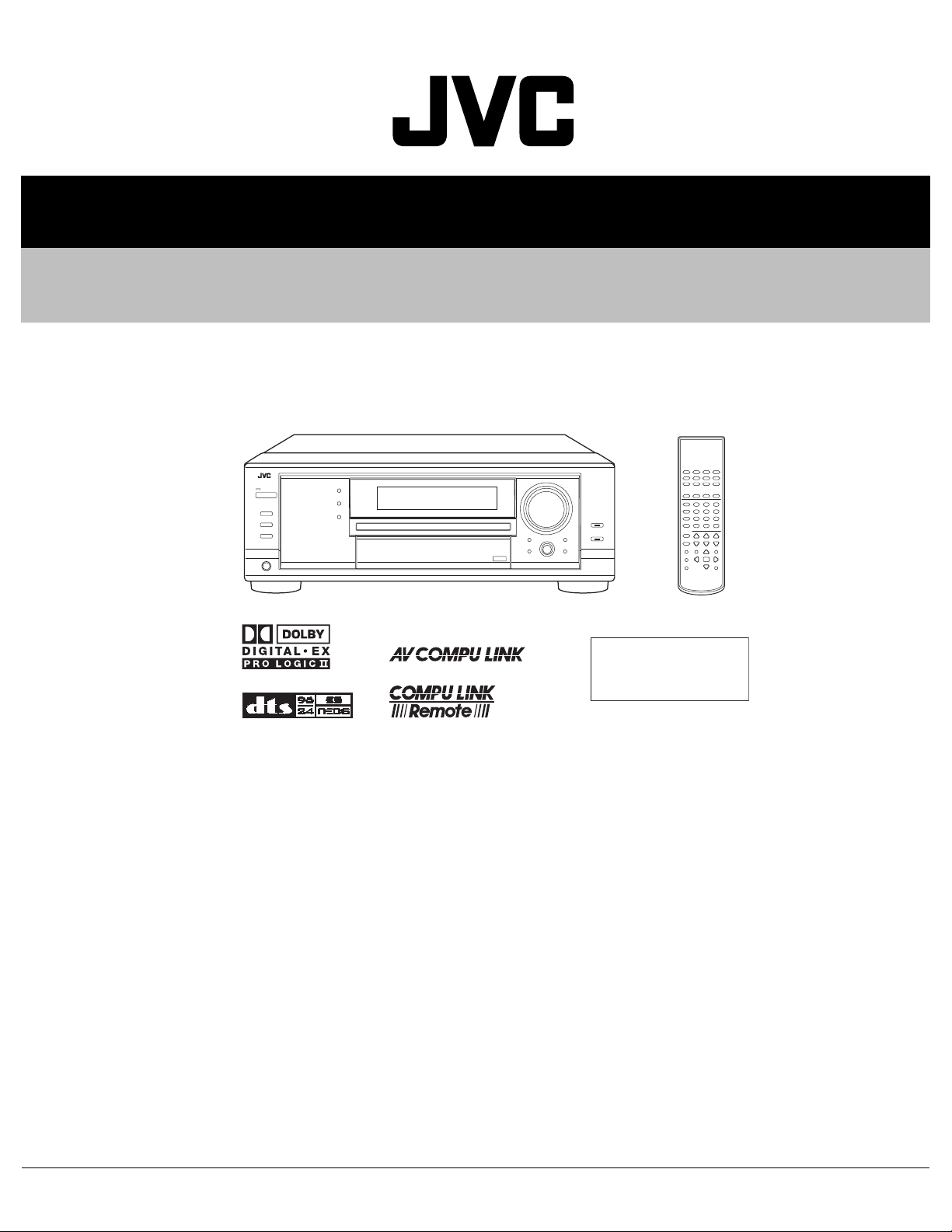
RX-7030VBK
A/V CONTROL RECEIVER
231
MENU
564
ENTER
7/P
89
+10
10/0
0
Area Suffix
J ------------------ U.S.A.
C --------------- Canada
TABLE OF CONTENTS
1 Precautions . . . . . . . . . . . . . . . . . . . . . . . . . . . . . . . . . . . . . . . . . . . . . . . . . . . . . . . . . . . . . . . . . . . . . . . . . . . . 1-3
2 Disassembly method . . . . . . . . . . . . . . . . . . . . . . . . . . . . . . . . . . . . . . . . . . . . . . . . . . . . . . . . . . . . . . . . . . . .1- 4
3 Adjustment. . . . . . . . . . . . . . . . . . . . . . . . . . . . . . . . . . . . . . . . . . . . . . . . . . . . . . . . . . . . . . . . . . . . . . . . . . . . 1-12
4 Description of major ICs. . . . . . . . . . . . . . . . . . . . . . . . . . . . . . . . . . . . . . . . . . . . . . . . . . . . . . . . . . . . . . . . . 1-14
COPYRIGHT © 2003 VICTOR COMPANY OF JAPAN, LTD.
No.22058
2003/5
Page 2
SPECIFICATION
At Stereo operation Front ch
Amplifier Output Power
At Surround
operation
Audio Input Sensitivity/Impedance (1
kHz)
Audio Input
(DIGITAL IN)*
Audio Output Level SUBWOOFER OUT : 1V
Recording Output Level VCR OUT, TAPE/CDR OUT : 200 mV
Digital output Optical : DIGITAL OUT
Audio
Video
FM tuner
(IHF)
AM tuner Tuning Range 530 kHz to 1 710 kHz
General
Signal wave length 660 nm
Output level -21 dBm to -15 dBm
Signal-to-Noise Ratio (‘66 IHF/’78 IHF) DVD IN, VCR IN, TV SOUND/DBS IN 87 dB/80 dB
CD IN TAPE/CDR IN 87 dB/80 dB
Frequency Response (8Ω at 1 kHz, with no more than 0.8% total harmonic
distortion.) DVD IN, VCR IN, TV SOUND/DBS IN
CD IN, TAPE/CDR IN 20 Hz to 100 kHz (+1 dB, -3 dB)
Equalization (5 bands) 63 Hz, 250 Hz, 1 kHz, 4 kHz, 16 kHz (±8 dB)
Bass boost +6 dB ±1.0 dB at 100 Hz
Video Input Sensitivity/Impedance Composite video DVD IN, VCR IN, TV SOUND/DBS IN 1 V(p-p)/75Ω
S-video
Component video DVD IN, DBS IN
Video Output Level Composite video VCR OUT, MONITOR OUT 1 V(p-p)/75Ω
S-video
Component video MONITOR OUT
Synchronization Negative
Signal-to-Noise Ratio 45 dB
Tuning Range 87.5 MHz to 108.0 MHz
Usable Sensitivity Monaural 12.8 dBf (1.2 µV/75Ω)
50 dB Quieting Sensitivity
Stereo Separation at REC OUT 35 dB at 1 kHz
Power Requirements AC 120V ~ 60 Hz
Power Consumption 320 W/440 VA (at operation) 2 W (in standby mode)
Dimensions (W x H x D) 435 mm x 157 mm x 425 mm (17 3/16 in. x 6 3/16 in. x 16 3/4 in.)
Mass 12.1 kg (26.7 lbs)
DVD IN, VCR IN, TV SOUND/DBS IN 200 mV/47 kΩ
CD IN, TAPE/CDR IN 200 mV/47 kΩ
Coaxial DIGITAL 1 (DVD) : 0.5 V(p-p)/75 Ω
Optical
DVD IN, VCR IN,
TV SOUND/DBS IN
VCR OUT,
MONITOR OUT
Monaural 16.0 dBf (1.7 µV/75Ω)
Stereo 37.5 dBf (20.5 µV/75Ω)
110 W per channel, min. RMS, driven into
8Ω, 20 Hz to 20 kHz, with no more than
0.08% total harmonic distortion.
110 W per channel, min. RMS, driven into 8Ω
Front ch
Center ch
Surround ch
Surround Back ch
DIGITAL 2 (CD), DIGITAL 3 (TV), DIGITAL 4 (CDR) :
-21 dBm to -15 dBm (660 nm ±30 nm)
(Y: luminance) 1 V(p-p)/75Ω
(C: chrominance, burst) 0.286 V(p-p)/75Ω
(Y: luminance) 1 V(p-p)/75Ω
(PB/PR): 0.7 V(p-p)/75Ω
(Y: luminance) 1 V(p-p)/75Ω
(C: chrominance, burst) 0.286 V(p-p)/75Ω
(Y: luminance) 1 V(p-p)/75Ω
(PB/PR) 0.7 V(p-p)/75Ω
at 1 kHz, with no more than 0.8% total
harmonic distortion.
110 W, min. RMS, driven into 8Ω at 1 kHz,
with no more than 0.8% total harmonic
distortion.
110 W per channel, min. RMS, driven into 8Ω
at 1 kHz, with no more than 0.8% total
harmonic distortion.
110 W, min. RMS, driven into 8Ω at 1 kHz,
with no more than 0.8% total harmonic
distortion.
20 Hz to 100 kHz (+1 dB, -3 dB)
* Corresponding to Linear PCM, Dolby Digital, and DTS Digital Surround (with sampling frequency - 32 kHz, 44.1 kHz, 48 kHz).
Designs & specifications are subject to change without notice
1-2 (No.22058)
Page 3
SECTION 1
Precautions
1.1 Safety Precautions
(1) This design of this product contains spec ial hardware and
many circuits and components specially for safety purposes. For continued protection, no changes should be made
to the original design unless authorized in writing by the
manufacturer. Replacement parts must be identical to
those used in the original circuits. Services should be performed by qualified personnel only.
(2) Alterations of the design or circuitry of the product should
not be made. Any design alterations of the product should
not be made. Any design alterations or additions will void
the manufacturers warranty and will further relieve the
manufacture of responsibility for personal injury or property
damage resulting therefrom.
(3) Many electrical and mechanical parts in the products have
special safety-related characteristics. These characteristics are often not evident from visual inspection nor can the
protection afforded by them necessarily be obtained by using replacement components rated for higher voltage, wattage, etc. Replacement parts which have these special
safety characteristics are identified in the Parts List of Service Manual. Electrical components having such features
are identified by shading on the schematics and by ( ) on
the Parts List in the Service Manual. The use of a substitute
replacement which does not have the same safety characteristics as the recommended replacement parts shown in
the Parts List of Service Manual may create shock, fire, or
other hazards.
(4) The leads in the products are routed and dressed with ties,
clamps, tubings, barriers and the like to be separated from
live parts, high temperature parts, moving parts and/or
sharp edges for the prevention of electric shock and fire
hazard. When service is required, the original lead routing
and dress should be observed, and it should be confirmed
that they have been returned to normal, after reassembling.
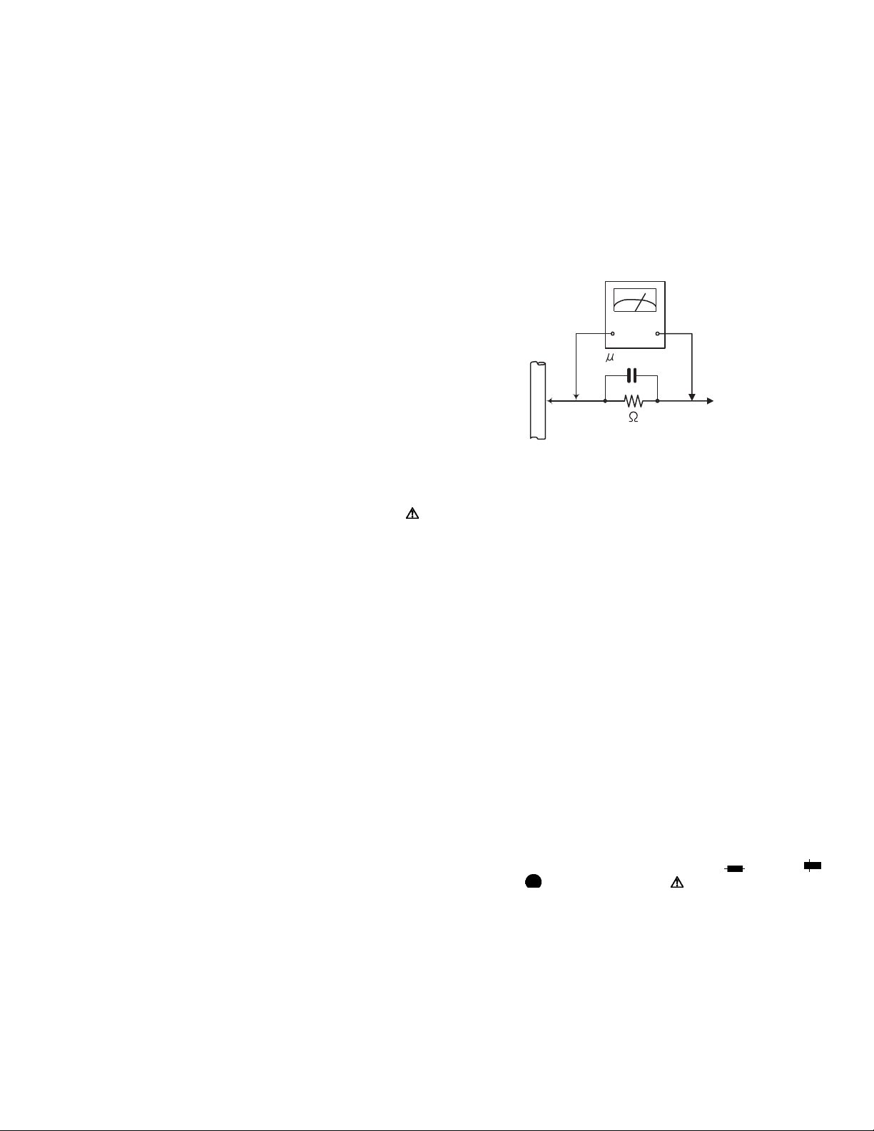
(5) Leakage shock hazard testing
After reassembling the product, always perform an isolation check on the exposed metal parts of the product (antenna terminals, knobs, metal cabinet, screw heads,
headphone jack, control shafts, etc.) to be sure the product
is safe to operate without danger of electrical shock.Do not
use a line isolation transformer during this check.
• Plug the AC line cord directly into the AC outlet. Using a
"Leakage Current Tester", measure the leakage current
from each exposed metal parts of the cabinet, particularly any exposed metal part having a return path to the
chassis, to a known good earth ground. Any leakage current must not exceed 0.5mA AC (r.m.s.).
• Alternate check method
Plug the AC line cord directly into the AC outlet. Use an
AC voltmeter having, 1,000Ω per volt or more sensitivity
in the following manner. Connect a 1,500Ω 10W resistor
paralleled by a 0.15µF AC-type capacitor between an exposed metal part and a known good earth ground.
Measure the AC voltage across the resistor with the AC
voltmeter.
Move the resistor connection to each exposed metal
part, particularly any exposed metal part having a return
path to the chassis, and measure the AC voltage across
the resistor. Now, reverse the plug in the AC outlet and
repeat each measurement. Voltage measured any must
not exceed 0.75 V AC (r.m.s.). This corresponds to 0.5µ
mA AC (r.m.s.).
AC VOLTMETER
(Having 1000
ohms/volts,
or more sensitivity)
0.15 F AC TYPE
Place this
probe on
1500 10W
Good earth ground
1.2 Warning
(1) This equipment has been designed and manufactured to
meet international safety standards.
(2) It is the legal responsibility of the repairer to ensure that
these safety standards are maintained.
(3) Repairs must be made in accordance with the relevant
safety standards.
(4) It is essential that safety critic al components are replaced
by approved parts.
(5) If mains voltage selector is provided, check setting for local
voltage.
1.3 Caution Burrs formed during molding may be left over on some parts
of the chassis.
Therefore, pay attention to such burrs in the case of preforming repair of this system.
1.4 Critical parts for safety
In regard with component parts appearing on the silk-screen
printed side (parts side) of the PWB diagrams, the parts that are
printed over with black such as the resistor ( ), diode ( )
and ICP ( ) or identified by the " " mark nearby are critical
for safety. When replacing them, be sure to use the parts of the
same type and rating as specified by the manufacturer.
(This regulation dose not Except the J and C version)
each exposed
metal part.
(No.22058)1-3
Page 4
SECTION 2
Disassembly method
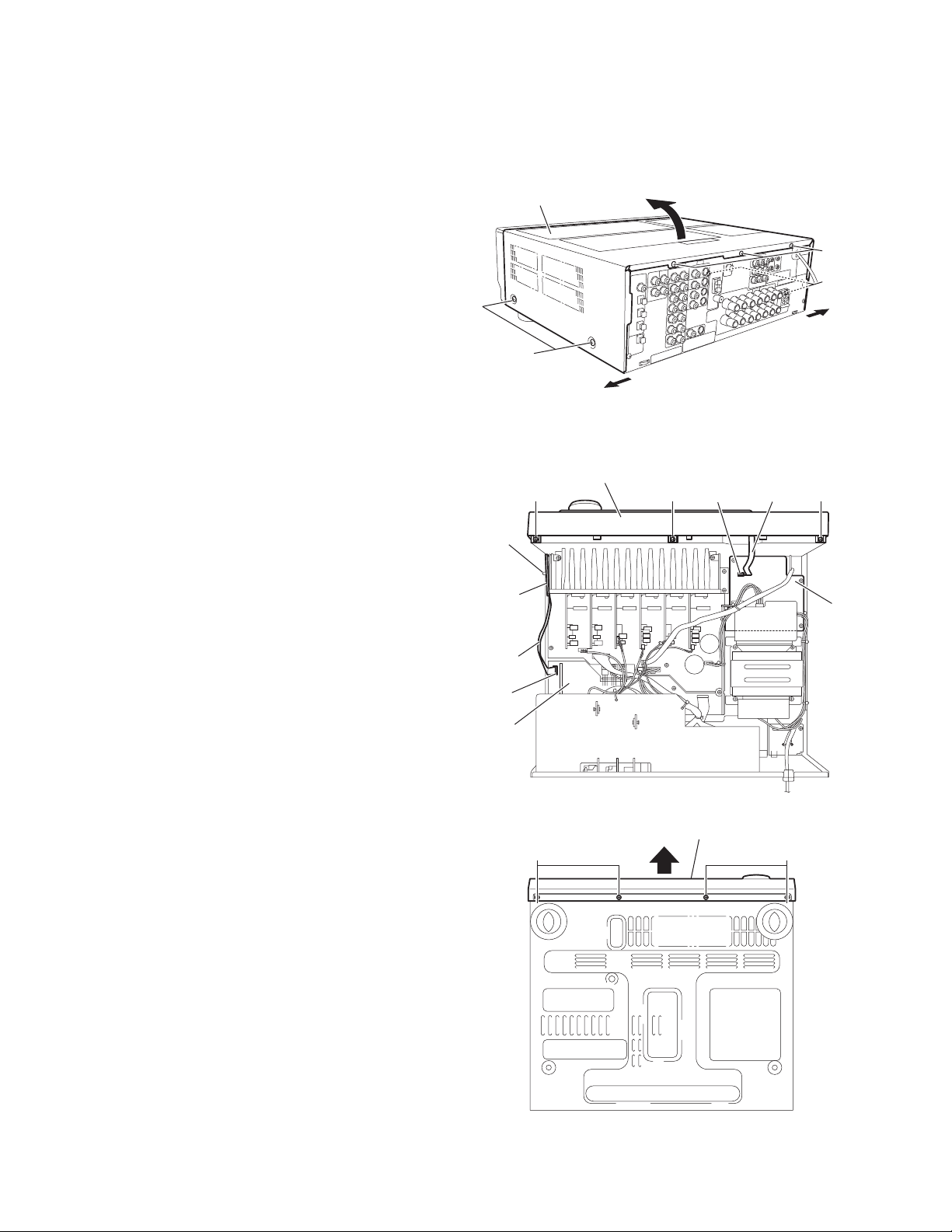
2.1 Removing the top cover (See Fig.1)
(1) From the right and left sides of the main body, remove the
four screws A attaching the top cover.
(2) From the back side of the main body, remove the three
screws B attaching the top cover.
(3) Remove the top cove r in the di rection o f the arrow 2 while
extending the lower sections of the top cover in the direction of the arrow 1.
2.2 Removing the front panel assembly (See Figs.2 and 3)
• Prior to performing the following procedures, remove the top
cover.
(1) Disconnect the card wire from the connector CN400 on the
micon board. (See Fig.2.)
(2) Disconnect the card wire from the connector CN402 on the
power supply board. (See Fig.2.)
(3) Remove the tie band and wire protection board fi xing the
card wire. (See Fig.2.)
(4) Remove the three screws C attaching the front panel as-
sembly. (See Fig.2.)
(5) From the bottom side of th e main body, remove the four
screws D attaching the front panel assembly. (See Fig.3.)
(6) Remove the front panel assembly in the direction of the ar-
row. (See Fig.3.)
Top cover
Tie band
Wire
protection
board
Card
wire
CN400
Micon
board
A
1
Front panel assembly
C
2
Fig.1
CN402
C C
Card wire
B
A
1
Power
supply
board
1-4 (No.22058)
Fig.2
Front panel assembly
DD
Fig.3
Page 5
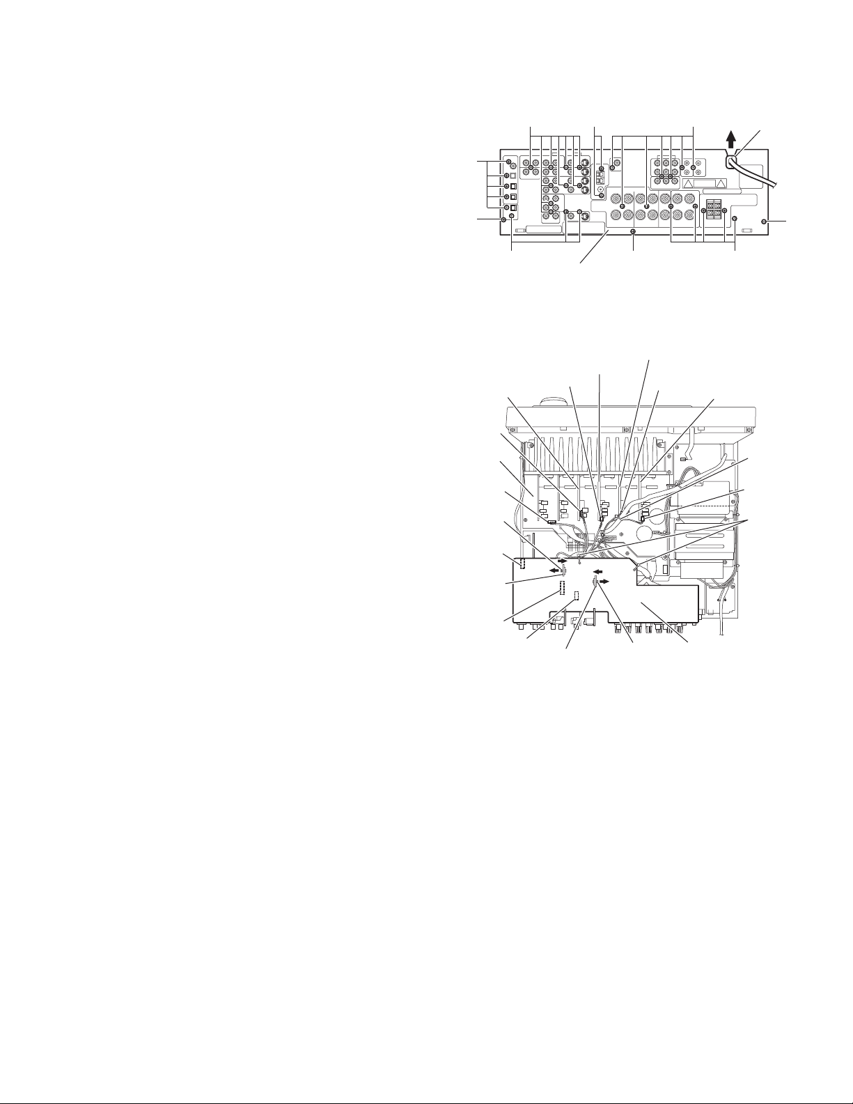
2.3 Removing the rear panel
1
(See Fig.4)
• Prior to performing the following procedures, remove th e top
cover.
(1) From the back side of the main body, remove the strain re-
lief from the rear panel in the direction of the arrow.
(2) Remove the twenty-nine screws E, two screws F and three
screws G attaching the rear panel.
E
E
F
E
Strain relief
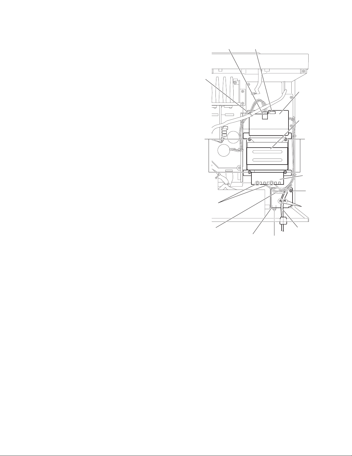
2.4 Removing the I/O board
(See Fig.5)
• Prior to performing the following procedures, remove th e top
cover and rear panel.
(1) Remove the two plastic ri vets in the direction of the arrow
1 from the top side of the main body, remove the stopper
boards in the direction of the arrow 2.
(2) Remove the tie bands bundling the wires.
(3) Disconnect the wire from the connector CN722 on the cen-
ter board.
(4) Disconnect the wire from the connector CN714 on the front
board(L).
(5) Disconnect the wire from the connector CN717 on the sur-
round back board.
(6) Disconnect the wire from the connector CN719 on the front
board(R).
(7) Disconnect the wire from the connector CN723 on the main
board.
(8) Disconnect the connectors (CN205,CN381,C N501 ) on the
I/O board in an upward direction.
G
Front board(R)
CN719
Main
board
CN723
Plastic
rivet
CN501
Stopper
board
CN381
CN205
Stopper board
Rear panel
Front board(L)
Surround board
CN717
22
22
11
1
1
Plastic rivet
GE
Fig.4
Fig.5
CN714
G
E
Center board
Tie band
CN722
Tie bands
I/O board
(No.22058)1-5
Page 6
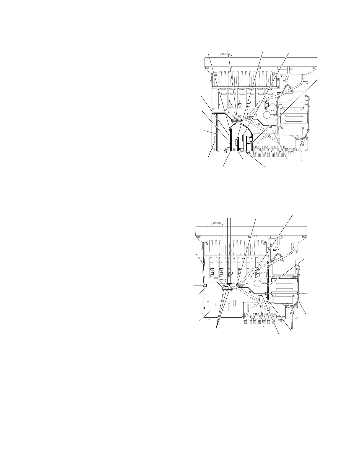
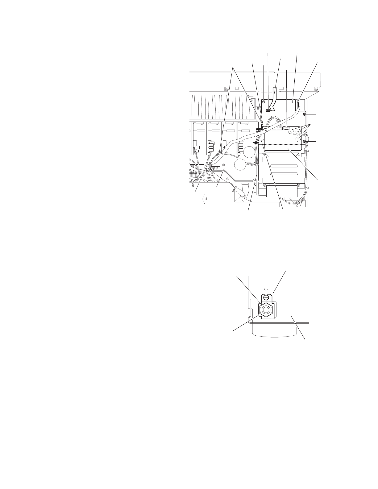
2.5 Removing the tuner, DSP board, audio board, video board and S-video board
r
(See Fig.6)
• Prior to performing the following procedures, remove the top
cover, rear panel and I/O board.
(1) Disconnect the card wire from the connector CN314 on the
audio board from the top side of the main body, take out the
tuner.
(2) (2) Disconnect the DSP board from the connector CN601
on the micon board.
(3) Disconnect the audio board from the connectors
(CN101,CN303) on the micon board.
(4) Disconnect the video bo ard from the connecto r CN201 on
the micon board.
(5) Disconnect the S-vid eo board from the connector CN241
on the micon board.
CN314
CN303
CN101
DSP board
Card wire
CN201 CN241
Tune
2.6 Removing the micon board
(See Fig.7)
• Prior to performing the following procedures, remove the top
cover, rear panel, I/O board, tuner, DSP board, audio board,
video board and S-video board.
(1) From the top side of the main body, disconnect the card
wire from the connector CN400 on the micon board.
(2) Disconnect the relay board from the connecto rs CN81 on
the micon board.
(3) Disconnect the parallel wire from th e connectors CN931
and CN932 on the micon board.
(4) Disconnect the parallel wire from the conn ecto r CN83 1 on
the main board.
(5) Remove the three screws H attaching the micon board.
(6) Remove the three screws J attaching the transistors
(Q921,Q931,Q941) to the chassis base.
(7) Loosen the screw K attaching the micon board.
CN601
Audio board
Card
wire
H
CN400
H
Micon board
Transistors
(Q921,Q931,Q941)
Video board
J
Fig.6
CN831
H
Fig.7
Micon board
S-video board
CN931
CN932
Main board
Relay
board
K
Chassis
base
CN81
1-6 (No.22058)
Page 7
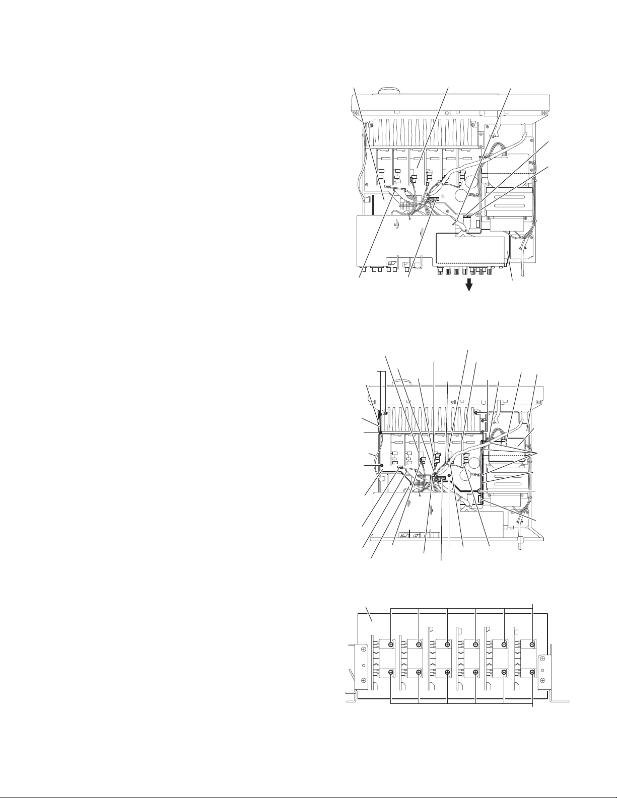
2.7 Removing the speaker board (See Fig.8)
• Prior to performing the following procedures, remove th e top
cover and rear panel.
(1) From the top side of the main body, remove the tie band
bundling the wires.
(2) Disconnect the wires from the connectors (CN813,CN814)
on the main board.
(3) Disconnect the parallel wire from the connectors
(CN931,CN932) on the micon board.
(4) Take out the speaker board in the direction of the arrow.
Micon board
Main board
Tie band
CN931
CN932
2.8 Removing the main board (See Fig.9)
• Prior to performing the following procedures, remove th e top
cover.
(1) From the top side of the main body, remove the tie bands
bundling the wires.
(2) Remove the tie band and wire protection board bu ndling
the card wire.
(3) Disconnect the wire from the connector CN811 on the pow-
er transformer board 1.
(4) Disconnect the relay board from the connectors (CN71,
CN81) on the power supply board and micon board.
(5) Disconnect the parallel wires from the connectors
(CN831,CN881) on the main board.
(6) Disconnect the wires from the connectors
(CN723,CN813,CN814) on the main board.
(7) Disconnect the wire from the connector CN722 on the cen-
ter board.
(8) Disconnect the wire from the connector CN714 on the front
board(L).
(9) Disconnect the wire from the connector CN717 on the sur-
round back board.
(10) Disconnect the wire from the connector CN719 on the front
board(R).
(11) Remove the screw K, five screws L, screw M and two
screws N attaching the main board.
(12) Take out the main board.
CN814
Front board(R)
L
Tie band
Wire
protection
board
M
Card wire
N
Main
board
CN723
CN814
Micon board
Heat sink
CN813
CN881
CN719
Surround
board
CN717
CN831
Fig.8
Front board(L)
Tie
band
CN714
N
CN813
Fig.9
Speaker board
Center board
CN811
L
CN71
CN722
Power
supply
board
Power
transformer
board 1
Tie bands
Relay board
K
CN81
Q
Fig.11
Q
(No.22058)1-7
Page 8
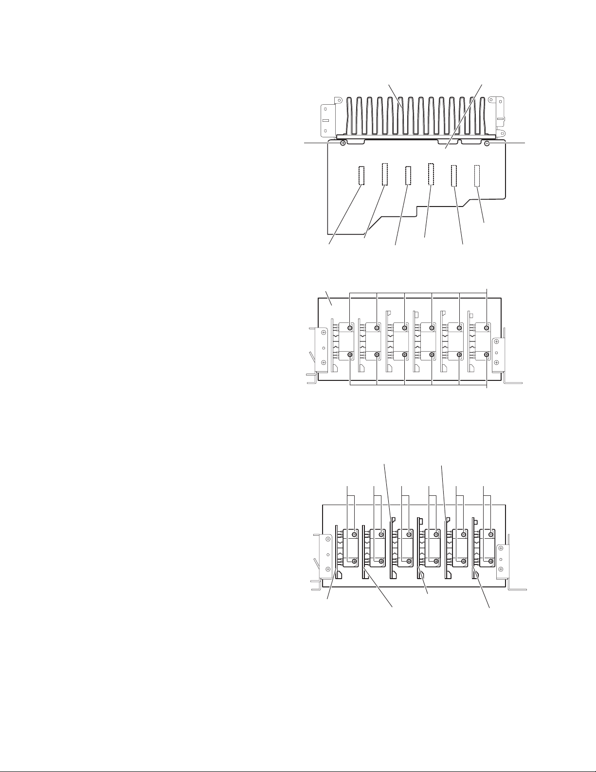
2.9 Removing the heat sink (See Figs.10 and 11)
• Prior to performing the following procedures, remove the top
cover and main board.
(1) From the reverse side of the main board, remove the two
screws P attaching the main board to the heat sink. (See
Fig.10.)
(2) Disconnect the connectors (CN701-CN706) on the main
board, remove the main board. (See Fig.10.)
(3) Remove the twelve screws Q attaching the heat sink. (See
Fig.11.)
P
CN703
Heat sink
CN701
CN704
CN702
Fig.10
Main board
P
CN706
CN705
Heat sink
Fig.11
2.10 emoving the center board, surround back board, front amp. boards (L/R) an d rear amp. boards (L/R) (See Figs.10 and 12)
• Prior to performing the following procedures, remove the top
cover and main board.
(1) From the reverse side of the main board, remove the two
screws P attaching the main board to the heat sink. (See
Fig.10.)
(2) Disconnect the connectors (CN701-CN706) on the main
board, remove the main board. (See Fig.10.)
(3) Remove the two screws Q attaching the center board. (See
Fig.12.)
(4) Remove the two screws Q attaching the front board(L).
(See Fig.12.)
(5) Remove the two screws Q attaching the surround back
board. (See Fig.12.)
(6) Remove the two screws Q attaching the front board(R).
(See Fig.12.)
(7) Remove the two screws Q attaching the surround board(L).
(See Fig.12.)
(8) Remove the two screws Q attaching the surround
board(R). (See Fig.12.)
Surround board(R)
Front board(R)
Front board(L)
Q Q Q Q Q Q
Surround board
Surround board(L)
Fig.12
Q
Q
Center board
1-8 (No.22058)
Page 9
2.11 Removing the power transformer
r
(See Fig.13)
• Prior to performing the following procedures, remove th e top
cover.
(1) From the top side of the main body, remove the tie band
bundling the wires.
(2) Disconnect the wire from the connectors (CN55,CN811) on
the power transformer board 1.
(3) Remove the solders from the soldered sections a on the
power transformer board 2.
(4) Remove the four screws R attachin g the power transfo rm-
er.
2.12 Removing the power/fuse board
(See Fig.13)
• Prior to performing the following procedures, remove th e top
cover.
(1) From the back and top sides of the main body, remove the
screw S and screw T attaching the power/fuse board.
(2) Remove the solders from the soldered sections b attaching
the power cord.
(3) From the reverse side of the power/fuse board, remove the
solders from the soldered sections c attaching the wires.
Tie band
Soldered
sections a
CN811
CN55
Power
transformer
board 1
Power
transformer
RR
Power
transforme
board 2
T
Soldered
sections b
Soldered sections c
Power/fuse board
Power cord
S
Fig.13
(No.22058)1-9
Page 10
2.13 Removing the power supply board (See Fig.14)
• Prior to performing the following procedures, remove the top
cover.
(1) From the top side of the main body, disconnect the parallel
wires from the connector CN55 on the power transformer
board 1.
(2) Disconnect the card wire from the connector CN402 on the
power supply board.
(3) Disconnect the relay board from the conn ector CN71 on
the power supply board.
(4) Remove the three screws U attaching the power supply
board.
(5) Remove the power sup ply board from the hook d of the
chassis base bracket in the direction of the arrow, take out
the power supply board.
(6) Turn over the power supply board, remove the solders from
the soldered sections e attaching the wires.
CN881
Tie bands
Main board
CN71
CN402
Card wire
U
Power supply board
Headphone jack
CN55
board
Soldered
sections e
Power
transformer
board 1
U
U
2.14 Removing the headphone jack board (See Figs.14 and 15)
• Prior to performing the following procedures, remove the top
cover and front panel assembly.
(1) From the top side of the main body, remove the tie bands
attaching the parallel wire. (See Fig.14.)
(2) Disconnect the parallel wire from the conn ecto r CN88 1 on
the main board. (See Fig.14.)
(3) From the front side of the main b ody, remove the nut and
screw V attaching the headphone bracket to the front
bracket. (See Fig.15.)
(4) Remove the three screws U attaching the power supply
board. (See Fig.14.)
(5) Take out the headpho ne jack board from the inside of the
chassis base while lifting the power supply board.
Relay board
Nut
Headphone bracket
Hook d of the chassis
base bracket
Fig.14
V
Headphone jack board
Front bracket
Fig.15
1-10 (No.22058)
Page 11
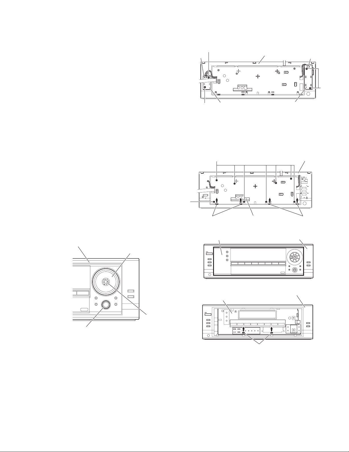
2.15 Removing the switch board
Y
(See Fig.16)
• Prior to performing the following procedures, remove th e top
cover and front panel assembly.
(1) From the back side of the front panel assembly, remove the
two screws W attaching the switch board.
(2) Take out the switch board, disconnect the wire from the
connector CN432 on the switch board.
2.16 Removing the power switch board
(See Fig.16)
• Prior to performing the following procedures, remove th e top
cover and front panel assembly.
(1) From the back side of the front panel assembly, remove the
two screws X attaching the power switch board.
(2) Take out the power switch board, disconnect the wire from
the connector CN430 on the power switch board.
2.17 Removing the front key & system control board
(See Figs.17 to 20)
• Prior to performing the following procedures, remove th e top
cover, front panel assembly, switch board and power switch
board.
(1) Pull out the volume and jog knobs from the front side of the
front panel assembly, remove the nut attaching the front
key & system control board. (See Fig.17.)
(2) From the back side of the front panel assembly, remove the
eight screws Y attaching the sub panel assembly. (See
Fig.18.)
(3) Remove the sub panel assembly while releasing the claws
f in the direction of the arrow. (See Figs.18 and 19.)
(4) Release the claws g attaching the front key & system con-
trol board in the direction of the arrow and take out the front
key & system control board. (See Fig.20.)
Front panel assembly
Volume knob
W
CN432
Switch board
W
Y
Claws f Claws f
Sub panel assembly
Front panel assembly
Power switch board
Fig.16
Front panel assembly
Sub panel assembly
Fig.18
Front panel assembly
CN430
X
Fig.19
Front panel assembly
Front key & System control board
Nut
Jog knob
Fig.17
Claws g
Fig.20
(No.22058)1-11
Page 12
SECTION 3
Adjustment
3.1 Adjustment method Tuner section
1. Tuner range
FM 87.5MHz to 108.0MHz
AM 530kHz to 1710kHz
Power amplifier section
Adjustment of idling current
Measurement location B2204-B2205 (Lch), B2213-B2214 (Rch)
Adjustment part VR787 (Lch), VR788 (Rch)
Attention:
This adjustment does not obtain a correct adjustme nt value i mmediately after the amplifier is u sed (state that an in ternal temperature has risen).
Please adjust, after you turn off amplifier and internal temperature falls.
<Adjustment method>
(1) Set the volume control to minimum during this adjustment. (No signal & No load)
(2) Set the surround mode OF F.
(3) Turn VR787 and VR788 fully counterclockwise to warm up before adjustment.
If the heat sink is already warm from previous use the correct adjustment can not be made.
(4) For L-ch, connect a DC voltmeter between B2204 and B2205 (Lch) and, connect it between B2213 and B2214 (Rch).
(5) 30 minutes later after power on, adjust VR787 for Lch, or VR788 for Rch so that the DC voltmeter value has 1mV to 10mV.
• It is not abnormal though the idling current might no t become 0mA even if it i s finished to turn variable resistance (VR787,
VR788) in the direction of counterclockwise.
Front amp. board (L)
VR787
B2204
B2205
Front amp. board (R)
VR788
B2213
B2214
VR787 (Lch)
B2204, B2205 (Lch)
VR788 (Rch)
B2213, B2214 (Rch)
1-12 (No.22058)
Page 13
3.2 Self-diagnose function
This model incorporates the following self-diagnostic functions.
1. PROTECTOR
• The PROTECTOR IN port detects errors such as speaker overcurrent and DC voltage output errors (Active: L). Immediately after
detection, all relays are switched off and the alarm display as shown below (blinking at intervals of 0.5 sec. ON and 0.5 sec. OFF)
is displayed in the lower part of the FL matrix.
During the alarm display, all other FL and LED segments are turned off.
OVERLOAD
• The overload status can be canceled by switching the power off. When the power is switched on again, the unit is turned on in
the same abnormal status as before. Lower the volume level for 10 steps for protection. (If the previous volume level was between 0 and 9, lower it to 0).
• The detection by the protector is not performed for 4 seconds after power on.
2. Supply voltage error detection
• When the power is switched on, the supply voltage at the A/D input po rt (pins 2 to 5 and 7) is monitored and, when an error is
detected continuously for 1 second, the unit immediately enters the standby mode.
• When the power is switched on again, the unit is turned on in the same abnormal status as before.
• The supply voltage error detection is not performed for 4 seconds after power on.
• The following table shows the error detection thresholds.
At abnormal state (Low voltage)
Analog value : 0 - 2.2
Pin 2
Digital value : 000 - 1C0
Analog value : 0 - 2.2
Pin 3
Digital value : 000 - 1C0
Analog value : 0 - 2.2
Pin 4
Digital value : 000 - 1C0
Analog value : 0 - 2.2
Pin 5
Digital value : 000 - 1C0
Analog value : 0 - 2.2
Pin 7
Digital value : 000 - 1C0
At normal state
Analog value : 2.2 - 2.8
Digital value : 1C1 - 240
Analog value : 2.2 - 2.8
Digital value : 1C1 - 240
Analog value : 2.2 - 2.8
Digital value : 1C1 - 240
Analog value : 2.2 - 2.8
Digital value : 1C1 - 240
Analog value : 2.2 - 2.8
Digital value : 1C1 - 240
At abnormal state (High voltage)
Analog value : 2.8 - 5.0
Digital value : 241 - 3FF
Analog value : 2.8 - 5.0
Digital value : 241 - 3FF
Analog value : 2.8 - 5.0
Digital value : 241 - 3FF
Analog value : 2.8 - 5.0
Digital value : 241 - 3FF
Analog value : 2.8 - 5.0
Digital value : 241 - 3FF
(No.22058)1-13
Page 14
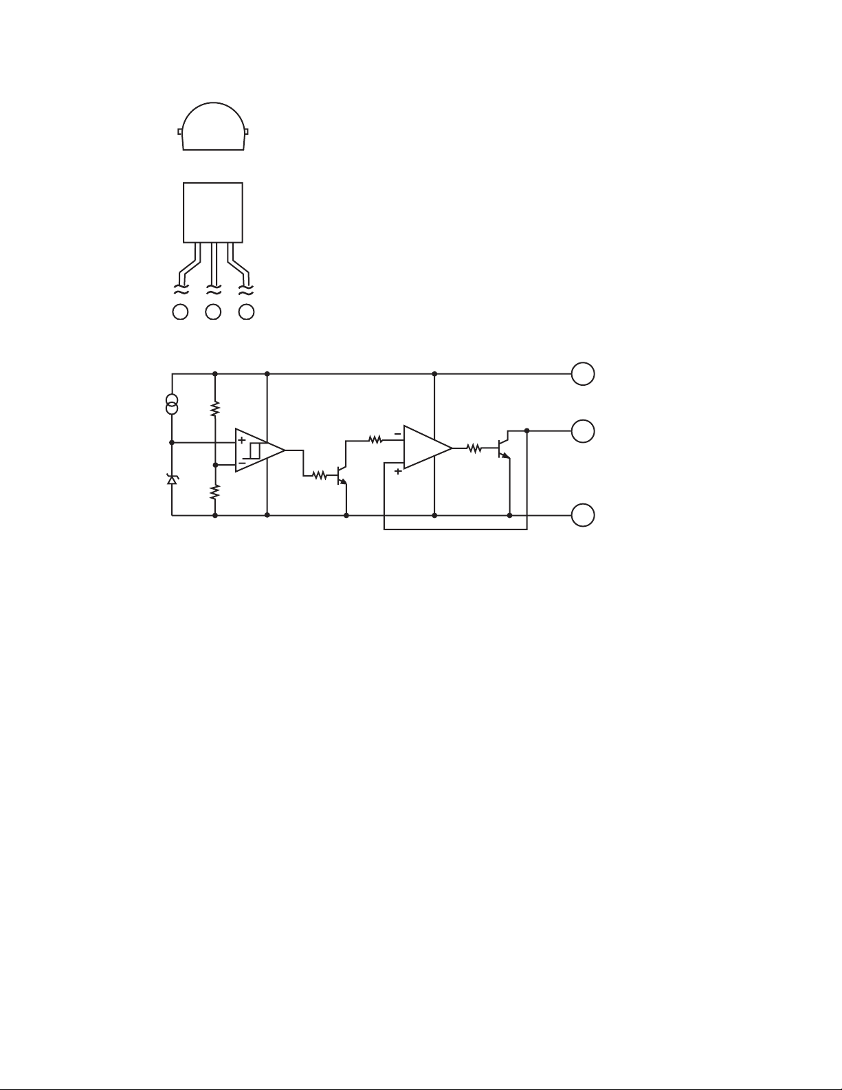
4.1 39VF0207CWHR01 (IC511) : EEPROM
• Pin layout
SECTION 4
Description of major ICs
• Block diagram
Memory Address
A11
A13
A14
A17
WE#
VDD
NC
A16
A15
A12
CE#
OE#
WE#
1
10
11
12
13
14
15
16
2
3
4
5
6
7
8
9
A9
A8
A7
A6
A5
A4
Address Buffer & Latches
Control Logic
X-Decoder
32
31
30
29
28
27
26
25
24
23
22
21
20
19
18
17
OE#
A10
CE#
DQ7
DQ6
DQ5
DQ4
DQ3
Vss
DQ2
DQ1
DQ0
A0
A1
A2
A3
EEPROM
Cell Array
Y-Decoder
I/O Buffers & Data Latches
DQ7~DQ0
• Pin function
Symbol Pin name Function
AMS- A0 Address Inputs To provide memory address. During Sector-Erase AMS-A12 address lines will select the
sector.
DQ7- DQ0 Data Input/Output To output data during read cycles and receive input data during write cycles. Data is in-
ternally latched during a write cycle. The outputs are in tri-state when OE# or CE# is high.
CE# Chip Enable To active the device when CE# is low.
OE# Output Enable To gate the data output buffers.
WE# Write Enable To control the write operations.
VDD Power Supply To provide power supply voltage: 3.0-3.6V for SST39LF512/010/020/040
2.7-3.6V for SST39VF512/010/010/040
Vss Ground
NC No Connection Unconnected Pins
1-14 (No.22058)
Page 15
4.2 BA7625 (IC201,IC242) : Video selector
MONITOR OUT
GND
IN5
GND
IN4
CTL E
IN3
CTL D
1
2
16
IN1
15
CTL A
A B E MONOTOR OUT
LL* IN1
HL* IN2
LH* IN3
14
13
12
11
10
9
VOUT 1
CC
V
IN2
CTL B
VOUT 2
CTL C
3
4
5
6
7
8
logic
logic
HHL IN4
HHH IN5
CDE VOUT1
LL* -HL* IN2
LH* IN3
HHL IN4
HHH IN5
CDE VOUT2
LL* IN1
HL* -LH* IN3
HHL IN4
HHH IN5
4.3 BA7626 (IC241) : Video selector
MONITOR OUT
GND
IN5
GND
IN4
CTL E
IN3
CTL D
1
2
3
4
5
6
7
8
logic
logic
16
15
14
13
12
11
10
9
IN1
CTL A
VOUT 1
CC
V
IN2
CTL B
VOUT 2
CTL C
A B E MONOTOR OUT
LL* IN1
HL* IN2
LH* IN3
HHL IN4
HHH IN5
CDE VOUT1
LL* -HL* IN2
LH* IN3
HHL IN4
HHH IN5
CDE VOUT2
LL* IN1
HL* --
LH* IN3
HHL IN4
HHH IN5
(No.22058)1-15
Page 16
4.4 AK4112BVF-X (IC551) : Digital audio receiver
• Pin layout
DVDD
DVSS
TVDD
V/TX
XTI
XTO
PDN
AVDD
AVSS
RX1
RX2/DIF0
RX3/DIF1
RX4/DIF2
1
2
3
4
5
6
7
8
R
9
10
11
12
13
14
28
CM0/CDTO
27
CM1/CDT1
26
OCKS1/CCLK
25
OCKS0/CSN
24
MCKO1
23
MCKO2
22
DAUX
21
BICK
20
SDTO
19
LRCK
18
ERF
17
FS96
16
P/SN
15
AUTO
• Pin function
Pin No. Symbol I/O Function
1 DVDD - Digital Power Supply Pin 3.3V
2 DVSS - Digital Ground Pin
3 TVDD - Input Buffer Power Supply Pin 3.3V or
5V
4 V O Validity Flag Output Pin in Parallel
Mode
TX O T ransmit channel (through data) Out-
put Pin in Serial Mode
5 XTI I X'tal Input Pin
6 XTO O X 'tal Output Pin
7 PDN I Power-Down Mode Pin
When "L" the AK4112B is powered-
down and reset
8 R - External Resistor Pin
18kΩ +/-1% resistor to AVSS exter-
nally.
9 AVDD - Analog Power Supply Pin
10 AVSS - Analog Ground Pin
11 RX1 I Receiver Channel 1
This channel is selected in Parallel
Mode or default of Serial Mode.
12 RX2 I Receiver Channel 2 in Serial Mode
12 DIF0 I Audio Data Interface Format 0 Pin in
Parallel Mode
13 RX3 I Receiver Channel 3 in Serial Mode
13 DIF1 I Audio Data Interface Format 1 Pin in
Parallel Mode
14 RX4 I Receiver Channel 4 in Serial Mode
14 DIF2 I Audio Data Interface Format 2 Pin in
Parallel Mode
15 AUTO O Non-PCM Detect Pin
"L": No detect "H": Detect
16 P/S I Parallel/Serial Select Pin
"L": Serial Mode "H": Parallel Mode
Pin No. Symbol I/O Function
17 FS96 O 9 6kHz Sampling Detect Pin
(RX Mode)
"H": fs=88.2kHz or more
"L": fs=54kHz or less.
(X'tal Mode) "H": XFS96=1
"L": XFS96=0.
18 ERF O Unlock & Parity Error Output Pin
"L": No Error "H": Error
19 LRCK I/O Output Channel Clock Pin
20 SDTO O Audio Serial Data Output Pin
21 BICK I/O Audio Serial Data Clock Pin
22 DAUX I Auxiliary Audio Data Input Pin
23 MCK02 O Master Clock #2 Output Pin
24 MCK01 O Master Clock #1 Output Pin
25 OCKS
0
I O utput Clock Select 0 Pin in Parallel
Mode
CSN I Chip Select Pin in Serial Mode
26 OCKS
1
I O utput Clock Select 1 Pin in Parallel
Mode
CCLK I Control Data Clock Pin in Serial Mode
27 CM1 I Master Clock Operation Mode Pin0 in
Parallel Mode
CDTI I Control Data Input Pin in Serial Mode
28 CM0 I Master Clock Operation Mode Pin1 in
Parallel Mode
CDTO O Control Data Output Pin in Serial
Mode
NOTE:
All input pins except internal pull-down pins should not be
left floating.
1-16 (No.22058)
Page 17
• Block diagram
AVSS
AVDD R MCKO1 MCKO2 XTI XTO
RX1
RX2
RX3
RX4
V/TX
DVDD
DVSS
PDN
Input
Selector
System
Control
Clock
Recovery
DAIF
Decoder
AC-3/MPEG
Detect
AUTO ERF P/S="L"
Clock
Generator
DEM
Error
Detect
X'tal
Oscillator
Serial Control Mode
96kHz
Detect
Audio
I/F
p I/F
FS96
DAUX
LRCK
BICK
SDTO
TVDD
CSN
CCLK
CDTO
CDTI
RX1
V
DVDD
DVSS
OCKS0
OCKS1
CM0
CM1
PDN
System
Control
AVSS
AVDD R MCKO1 MCKO2 XTI XTO
Clock
Recovery
DAIF
Decoder
AC-3/MPEG
Detect
AUTO ERF P/S="H"
Clock
Generator
DEM
Error
Detect
Parallel Control Mode
X'tal
Oscillator
4
96kHz
Detect
Audio
I/F
FS96
DAUX
LRCK
BICK
SDTO
DIF0
DIF1
DIF2
TVDD
OCKS0
OCKS1
CM0
CM1
(No.22058)1-17
Page 18
4.5 AK4527BVQP (IC571) : A/D, D/A converter
• Pin layout
• Block diagram
LOOP1
CDTI
CCLK
CSN
P/S
MCLK
DZF1
AVSS
AVD D
VREFH
SDOS
I2C
SMUTE
BICK
LRCK
SDTI1
SDTI2
SDTI3
SDTO
D.AUX
DFS
4443424140393837363534
1
2
3
4
5
6
7
8
9
10
11
1213141516171819202122
NC
DZFE
TVDD
DVDD
DVSS
PDN
TST
NC
DIF
VCOM
CAD1
CAD0
33
DZF2
32
RIN+
31
RIN-
30
LIN+
29
LIN-
28
ROUT1
27
LOUT1
26
ROUT2
25
LOUT2
24
ROUT3
23
LOUT3
LIN+
LIN-
RIN+
RIN-
LOUT1
ROUT1
LOUT2
ROUT2
LOUT3
ROUT3
LPF
LPF
LPF
LPF
LPF
LPF
Block Diagram (DIR and AC-3) DSP are external parts)
• Pin function
Pin No. Symbol I/O Function
1 SDOS I SDTO Source select pin
"L" : Internal ADC output, "H" : DAUX input
ORed with serial control register if P/S="L".
2 I2C I MCKO Clock frequency select pin
"L" : MCLK "H" : MCLK/2.
ORed with serial control register if P/S= "L".
3 SMUTE I Connect to GND
4 BICK I Audio serial data clock pin
5 LRCK I/O Input/Output channel clock pin
6 SDTI1 I DAC1 Audio serial data input pin
7 SDTI2 I DAC2 Audio serial data input pin
8 SDTI3 I DAC3 Audio serial data input pin
9 SDTO O Audio serial data output pin
10 D.AUX I AUX Audio serial data input pin
11 DFS I Double speed sampling mode pin
"L" : Normal speed "H" : Double speed the ADC is powered down.
ORed with serial control register if P/S="L".
12 NC - De-emphasis pin
ORed with serial control register if P/S="L"
13 DZFE I De-emphasis Pin
ORed with serial control register if P/S="L"
14 TVDD O Master clock output pin
15 DVDD - Digital power supply pin
16 DVSS - Digital ground pin
17 PDN I Power-down & Reset pin
When "L", the AK4527 is powered-down and the control registers are reset to default state. If the
state of CAD0-1 changes then the AK4527 must be reset by PDN.
18 TST I X'tal oscillator Select/Test mode pin
"H" : X'tal Oscillator selected
"L" : External clock source selected
ADC
ADC
DAC
DAC
DAC
DAC
DAC
DAC
HPF
HPF
DATT
DATT
DATT
DATT
DATT
DATT
Audio
I/F
LRCK
BICK
MCLK
SDOUT
SDIN1
SDIN2
SDIN3
D.AUX
Format
Converter
SDOS
SDTO
SDTI1
SDTI2
SDTI3
1-18 (No.22058)
Page 19
Pin No. Symbol I/O Function
19 NC I Input clock select 1 pin
20 ADIF I Input clock select 0 pin
21 CAD1 I Chip address pin
Used during the serial control mode.
22 CAD0 I Chip address pin
Used during the serial control mode.
23 LOUT3 O Lch #3 analog output pin
24 ROUT3 O Rch #3 analog output pin
25 LOUT2 O Lch #2 analog output pin
26 ROUT2 O Rch #2 analog output pin
27 LOUT1 O Lch #2 analog output pin
28 ROUT1 O Rch #1 analog output pin
29 LIN- I Lch analog negative Input Pin
30 LIN+ I Lch analog positive Input Pin
31 RIN- I Rch analog negative Input Pin
32 RIN+ I Rch analog positive Input Pin
33 DZF2 I Negative voltage reference Input pin, AVSS
34 VCOM O Common voltage output pin, AVDD/2
Large external capacitor around 2.2uF is used to reduce power-supply noise
35 VREFH I Positive voltage reference input pin, AVDD
36 AVDD - Analog power supply pin
37 AVSS - Analog ground pin
38 DZF1 I X'tal input pin
39 MCKI I External master clock input pin if XTS="L"
40 P/S I Paral lel/Serial select pin
"L" : Serial control mode, "H" : Parallel control mode
41 CSN I Chip select pin in serial mode
42 CCLK I Control data clock pin in serial mode
43 CDTI I Control data input pin in serial mode
44 LOOP1 I Loop back mode pin in parallel mode
Enable all 3 DAC channels to be input from SDTII.
(No.22058)1-19
Page 20
4.6 DSPD56367PV150 (IC501) : DSP
• Pin layout
108 73
109 72
144 37
136
• Block diagram
1
TRIPLE
TIMER
2
DAX
(SPDIF Tx.)
INTER-FA
CE
ADDRESS
GENERATION
UNIT
SIX CHANNELS
DMA UNIT
INTERNAL
DATA
BUS
HOST
INTER-
FACE
16
8
ESAI
INTER-
FACE
ESAI_1
PERIPHERAL
EXPANSION AREA
PIO_EB
DSP56300
4
24-BIT
Core
6
SHI
INTER-
FACE
5
MEMORY EXPANSION AREA
PROGRAM
RAM
/INTERFACE
3K x 24
PROGRAM
ROM
40K x 24
Bootstrap
DDB
YDB
XDB
PDB
GDB
PM_EB
YAB
XAB
PAB
DAB
X MEMORY
RAM
13K x 24
ROM
32K x 24
XM_EB
Y MEMORY
RAM
7K x 24
ROM
8K x 24
YM_EB
EXTERNAL
ADDRESS
SWITCH
DRAM &
SRAM BUS
INTERFACE
I-CACHE
EXTERNAL
DATA BUS
SWITCH
BUS
&
18
ADDRESS
10
CONTROL
24
DATA
1-20 (No.22058)
PLL
CLOCK
GENERAT
EXTAL
RESET
PINIT/NMI
PROGRAM
INTERRUPT
CONTROLLER
PROGRAM
DECODE
CONTROLLER
MODA/IRQA
MODB/IRQB
MODC/IRQC
MODD/IRQD
PROGRAM
ADDRESS
GENERATOR
DATA ALU
+->
24X24 56 56-BIT MAC
TWO 56-BIT ACCUMULATORS
BARREL SHIFTER
24 BITS BUS
POWER
MNGMNT
JTAG
™
OnCE
4
Page 21

• Pin function
Pin No. Symbol I/O Function
1 SCK I/O SPI Serial Clock
2 SS I SPI Slave Select
3 HREQ I/O Host Request
4 SDO0 O Serial Data Output 0
5 SDO1 O Serial Data Output 1
6 SDO2 O Serial Data Output 2
6 SDI3 I Serial Data Input 3
7 SDO3 O Serial Data Output 3
7 SDI2 I Serial Data Input 2
8 VCCS - SHI, ESAI, ESAI_1, DAX and Timer Power
9 GNDS - SHI, ESAI, ESAI_1, DAX and Timer Ground
10 SDO4 O Serial Data Output 4
10 SDI1 I Serial Data Input 1
11 SDO5 O Serial Data Output 5
11 SDI0 I Serial Data Input 0
12 FST I/O Frame Sync for Transmitter
13 FSR I/O Frame Sync for Receiver
14 SCKT I/O Transmitter Serial Clock
15 SCKR I/O Receiver Serial Clock
16 HCKT I/O High Frequency Clock for Transmitter
17 HCKR I/O High Frequency Clock for Receiver
18 VCCQL - Quiet Core (Low ) power
19 GNDQ - Quiet Ground
20 VCCQH - Quiet External (High) Power
21 HDS I Host Data Strobe
21 HWR I Host Write Data
22 HRW I Host Read/Write
22 HRD I Host Read Data
23 HACK I Host Acknowledge
23 HRRQ O Receive Host Request
24 HOREQ O Host Request
24 HTRQ O Transmit Host Request
25 VCCS - SHI, ESAI, ESAI_1, DAX and Timer Power
26 GNDS - SHI, ESAI, ESAI_1, DAX and Timer Ground
27 ADO O Digital Audio Data Output
28 ACI I Audio Clock Input
29 TIO0 I/O Timer 0 Schmitt-Trigger Input/Output
30 HCS I Host Chip Select
31 HA2 I host Address Input 2
31 HA9 I Host Address 9
32 HA1 I Host Address Input 1
32 HA8 I Host Address 8
33 HA0 I Host Address Input 0
33 HAS I Host Address Strobe
34 to 37 HAD7 to HAD4 I/O Host Address/Data
(No.22058)1-21
Page 22

Pin No. Symbol I/O Function
38 VCCH - Host Power
39 GNDH - Host Ground
40 to 43 HAD3 to HAD0 I/O Host Address/Data
44 RESET I Reset
45 VCCP - PLL Power
46 PCAP I PLL Capacitor
47 GNDP - PLL Ground
48 SDO5_1 O Serial Data Output 5_1
48 SDI2_1 I Serial Data Input 2
49 VCCQH - Quiet External (High) Power
50 FST_1 I/O Frame Sync for Transmitter_1
51 AA2 O Address Attribute
51 RAS2 O Row Address Strobe
52 CAS O Column Address Strobe
53 SCKT_1 I/O Transmitter Serial Clock_1
54 GNDQ - Quiet Ground
55 EXTAL I External Clock Input
56 VCCQL - Quiet Core (Low) Power
57 VCCC - Bus Control Power
58 GNDC - Bus Control Ground
59 CLKOUT O Not connect
60 NC - Not connect
61 FSR_1 I/O Frame Sync for Receiver_1
62 SCKR_1 I/O Receiver Serial Clock_1
63 BR O Bus Request
64 BB I/O Bus Busy
65 VCCC - Bus Control Power
66 GNDC - Bus Control Ground
67 WR O Write Enable
68 RD O Read Enable
69 AA1 O Address Attribute
69 RAS1 O Row Address Strobe
70 AA0 O Address Attribute
70 RAS0 O Row Address Strobe
71 BG I Bus Grant
72,73 A0,A1 O Address Bus
74 VCCA - Address Bus Power
75 GNDA - Address Bus Ground
76 to 79 A2 to A5 O Address Bus
80 VCCA - Address Bus Power
81 GNDA - Address Bus Ground
82 to 85 A6 to A9 O Address Bus
86 VCCA - Address Bus Power
87 GNDA - Address Bus Ground
88,89 A10,A11 O Address Bus
90 GNDQ - Quiet Ground
1-22 (No.22058)
Page 23

Pin No. Symbol I/O Function
91 VCCQL - Quiet Core (Low ) Power
92 to 94 A12 to A14 O Address Bus
9 VCCQH - Quiet External (High) Power
96 GNDA - Address Bus Ground
97 to 99 A15 to A17 O Address Bus
100 to 102 D0 to D2 I/O Data Bus
103 VCCD - Data Bus Power
104 GNDD - Data Bus Ground
105 to 110 D3 to D8 I/O Data Bus
111 VCCD - Data Bus Power
112 GNDD - Data Bus Ground
113 to 118 D9 to D14 I/O Data Bus
119 VCCD - Data Bus Power
120 GNDD - Data Bus Ground
121 to 125 D15 to D19 I/O Data Bus
126 VCCQL - Quiet Core (Low) Power
127 GNDQ - Quiet Ground
128 D20 I/O Data Bus
129 VCCD - Data Bus Power
130 GNDD - Data Bus Ground
131 to 133 D21 to D23 I/O Data Bus
134 MODD I Mode Select D
134 IRQD I External Interrupt Request D
135 MODC I Mode Select C
135 IRQC I External Interrupt Request C
136 MODB I Mode Select B
136 IRQB I External Interrupt Request B
137 MODA I Mode Select A
137 IRQA I External Interrupt Request A
138 SDO4_1 O Serial Data Output 4_1
138 SDI1_1 I Serial Data Input 1_1
139 TDO O Test Data Output
140 TDI I Test Data Input
141 TCK I Test Clock
142 TMS I Test Mode Select
143 MOSI I/O SPI Master-Out-Slave-In
143 HA0 I IIC Slave Address 0
144 MISO I/O SPI Master-In-Slave-Out
144 SDA I/O IIC Data and Acknowledge
(No.22058)1-23
Page 24
4.7 GP1UM281XK (IC404) : Dual operation amplifier
• Block diagram
R
L
Amp
B.P.FLimiter
Demodulator
Integrator
Comparator
GND Vcc Vout
4.8 HA17558AF-X (IC303,IC304,IC386,IC397,IC399,IC520 to IC526,IC528 to IC530) : Ope. amp.
• Pin layout & Block diagram
1
2
3
4
GND
Vcc
8
7
6
5
1-24 (No.22058)
Page 25
4.9 IC63LV102410K-X (IC512,IC513,IC514) : CMOS SRAM
•Pin layout
A16
A0
A1
A2
A3
CE
I/O0
I/O1
Vcc
GND
I/O2
I/O3
WE
A4
A5
A6
A7
1
2
3
4
5
6
7
8
9
10
11
12
13
14
15
16
32
31
30
29
28
27
26
25
24
23
22
21
20
19
18
17
A15
A14
A13
OE
I/O7
I/O6
GND
Vcc
I/O5
I/O4
A12
A11
A10
A9
A8
• Block diagram
• Pin function
Symbol Function
A0-A16 Address Input
CE Chip Enable Input
OE Output Enable Input
WE Write Enable Input
I/O1-I/O7 Bidirectional Ports
Vcc Power
GND Ground
A0-A16
VCC
GND
I/O0-I/O7
CE
OE
WE
DECODER
I/O
DATA
CIRCUIT
CONTROL
CIRCUIT
128K X 8
MEMORY ARRAY
COLUMN I/O
(No.22058)1-25
Page 26
4.10 IC-PST9139-T(IC903) : Regulator
• Terminal layout
123
• Block diagram
CO1
VCC
2
OUT
1
OP1
3
GND
1-26 (No.22058)
Page 27
4.11 MM1563DF-X (IC506,IC583) : Regulator
•Pin layout
756
(TOP VIEW)
1
234
• Block diagram
V
IN
7
Bias
Cont
5
Thermal
shutdown
GND
3
• Pin function
Pin No. Symbol Function
1 Vo Output pin
2 NC Not connect
3 GND Ground
4 Cn Noise decrease pin
5 CONT Control pin
Driver
Current
limiter
Cn
Vo
1
Reference
4
CONT
H
L
Output
ON
OFF
6 Sub Substrate pin, The 6pin must be connected to GND.
7 VIN Input pin
4.12 MM74HC4053SJ-X (IC389) : Multiplexer
•Pin layout
1Y
0Y
Z-COM
0Z
INH
V
EE
GND
1
2
IZ
3
4
5
6
7
8
16
15
14
13
12
11
10
9
Vcc
Y-CO M
X-COM
1X
0X
A
B
C
• Pin function
CONTROL INPUTS
INHIBIT C B A
LLLK
LLLH
LLHK
LLHH
LHLK
LHLH
LHHK
LHHH
HXXX
X: Don't Care.
(No.22058)1-27
Page 28
4.13 MN101C35DMF (IC400) : System control & FL driver
• Pin layout
100 76
1
75
25
51
26 50
• Pin function
Pin No. Symbol I/O Function
1 TXD / SBO0 / P00 I MULTI JOG IN1
2 RXD / SBI0 / P01 I MULTI JOG IN2
3 SBT0 / P02 O LED1
4 SBO1 / P03 O LED2 (STANDBY)
5 SBI1 / P04 O BU2092 CLK
6 SBT1 / P05 O BU2092 DATA
7 BUZZER / P06 O BU2092 STB
8VDD-+5V
9 OSC2 - 8MHz oscillation terminal
10 OSC1 - 8MHz oscillation terminal
11 VSS - Ground
12 XI - Connect to ground
13 XO - Not connect
14 MMOD - Connect to ground
15 VREF- - Ground
16 AN0 / PA0 I Key input 1 (7 key)
17 AN1 / PA1 I Key input 2 (7 key)
18 AN2 / PA2 I Key input 3 (7 key)
19 AN3 / PA3 I Key input 4 (7 key)
20 AN4 / PA4 I Key input 5 (7 key)
21 AN5 / PA5 I Key input 6 (7 key)
22 AN6 / PA6 I Chip select 1
23 AN7 / PA7 I Chip select 2
24 VREF+ - +5V
25 P07 O LED3 (CC CNV/BASS B)
26 /RST / P27 I Reset input
RMOUT / TM0IO / P10
27
28 TM1IO / P11 O LED5
29 TM2IO / P12 O LED6
30 TM3IO / P13 O DCS output
31 TM4IO / P14 O AV link VCR output
32 P15 I/O Micom transmit BUSY
33 IRQ0 / P20 I Micom transmit CS
34
35 IRQ2 / P22 I Volume JOG input1
36 IRQ3 / P23 I Volume JOG input2
37 IRQ4 / P24 I DCS input
38 P25 I AV link VCR input
39 SBO2 / P30 O Micom transmit STATUS
40 SBI2 / P31 I Micom transmit COM41 SBT2 / P32 I Micom transmit CLK
42 to 46 P50 to P54 O LED7 to LED11
47 DGT17 / P67 O GRID17
48 DGT16 / P66 O GRID16
49 DGT15 / P65 O GRID15
50 DGT14 / P64 O GRID14
51 DGT13 / P63 O GRID13
52 DGT12 / P62 O GRID12
SENS / IRQ1 / P21
O LED4 (DIRECT)
I Remocon input
output
MAND input
Pin No. Symbol I/O Function
53 DGT11 / P61 O GRID11
54 DGT10 / P60 O GRID10
55 DGT9 / P41 O GRID9
56 DGT8 / P40 O GRID8
57
58
59
60
61
62
63
64
65 SEG8 / P87 O SEGMENT2
66 SEG9 / P86 O SEGMENT3
67 SEG10 / P85 O SEGMENT4
68 SEG11 / P84 O SEGMENT5
69 SEG12 / P83 O SEGMENT6
70 SEG13 / P82 O SEGMENT7
71 SEG14 / P81 O SEGMENT8
72 SEG15 / P80 O SEGMENT9
73 SEG16 / P97 O SEGMENT10
74 SEG17 / P96 O SEGMENT11
75 SEG18 / P95 O SEGMENT12
76 SEG19 / P94 O SEGMENT13
77 SEG20 / P93 O SEGMENT14
78 SEG21 / P92 O SEGMENT15
79 SEG22 / P91 O SEGMENT16
80 SEG23 / P90 O SEGMENT17
81 SEG24 / PC2 O SEGMENT18
82 SEG25 / PC1 O SEGMENT19
83 SEG26 / PC0 O SEGMENT20
84 SEG27 / PB7 O SEGMENT21
85 SEG28 / PB6 O SEGMENT22
86 SEG29 / PB5 O SEGMENT23
87 SEG30 / PB4 O SEGMENT24
88 SEG31 / PB3 O SEGMENT25
89 SEG32 / PB2 O SEGMENT26
90 SEG33 / PB1 O SEGMENT27
91 SEG34 / PB0 O SEGMENT28
92 SEG35 / PD7 O SEGMENT29
93 SEG36 / PD6 O SEGMENT30
94 SEG37 / PD5 O SEGMENT31
95 SEG38 / PD4 O SEGMENT32
96 SEG39 / PD3 O SEGMENT33
97 SEG40 / PD2 O SEGMENT34
98 SEG41 / PD1 O SEGMENT35
99 SEG42 / PD0 O SEGMENT36
100 VPP - VPP
SEG0 / DGT7 / P77
SEG1 / DGT6 / P76
SEG2 / DGT5 / P75
SEG3 / DGT4 / P74
SEG4 / DGT3 / P73
SEG5 / DGT2 / P72
SEG6 / DGT1 / P71
SEG7 / DGT0 / P70
OGRID7
OGRID6
OGRID5
OGRID4
OGRID3
OGRID2
OGRID1
O SEGMENT1
1-28 (No.22058)
Page 29
4.14 MM101C49GMG (IC901) : System control
•Pin layout
100 76
1
75
25
51
26 50
• Pin function
Pin No. Symbol I/O Function
1 VREF- - GND
2 AN0/PA0 I Micom 5V unusual det.
3 AN1/PA1 I DSP A5V unusual det.
4 AN2/PA2 I DSP D5V unusual det.
5 AN3/PA3 I Analog 15V unusual det.
6 AN4/PA4 I Ground
7 AN5/PA5 I TU 9V unusual detect
8 AN6/PA6 I Ground
9 AN7/PA7 I Ground
10 VREF+ - +5V
11 VDD - +5V
12 OSC2 - 8MHz
13 OSC1 - 8MHz
14 VSS - Ground
15 XI - Ground
16 XO - Open
17 MMOD I Ground
18 SBO0/P00 I Ground
19 SBI0/P01 I Ground
20 SBT0/P02 I Ground
21 SBO2/P03 O Display micom command
22 SBI2/P04 I Display micom status
23 SBT2/P05 O Display micom clock
24
NDK/BUZZER/P06
25 SYSLK/P07 O Display micom CS
26 P2 0/IRQ0 I Display micom BUSY
27 P21/IRQ1/SENS I Ground
28 P22/IRQ2 I Ground
29 P23/IRQ3 I RDS DAVN
30 P24/IRQ4 I INH
31 P25/IRQ5 I Protector
32 P26 I VDD2(FLASH)
33 P27/NRST I Reset input
34 P10/TM0IO O Tuner data out
35 P11/TM1IO I Tuner data in
36 P12/TM2IO O Tuner CLK
37 P13/TM3IO O Tuner CE
38 P14/TM7IO O RDS SDA input/output
39 P15 O RDS SCL output
40 P16/TM4IO O Tuner mute
41 P17 I VPP(+5V:FLASH)
42 P30/TXD1/SBO1 I Multi detect input
43 P31/RXD1/SBI1 O Multi voltage switching
44 P32/SBT1 O DSP micom reset
45 P33/NBR/SBO3 O DSP micom command
46 P34/NBT/SBI3 I DSP micom status
47 P35/SCL/SBT3 O DSP micom clock
48 P36 O DSP micom READY
49 P37 O SUBWFR MUTE
50 P40/KEY0 O SOURCE MUTE
51 P41/KEY1 O VIDEO SWITCH 1
O Display micom reset
Pin No. Symbol I/O Function
52 P42/KEY2 O VIDEO SWITCH 2
53 P43/KEY3 O VIDEO SWITCH 3
54 P44/KEY4 O VIDEO SWITCH 4
55 P45/KEY5 O TC9459 STB
56 P46/KEY6 O TC9459 CLK
57 P47/KEY7 O TC9459 DAT
58 P50/NWE O TC916X STB
59 P51/NRE O TC916X CLK
60 P52/NCS O TC916X DAT
61 P53/A16 O SURRBACK 1SPK
62 P54/PA17 I Ground
63 P60/A0 I Ground
64 P61/A1 I Ground
65 P62/A2 I Ground
66 P63/A3 I Ground
67 P64/A4 I Ground
68 P65/A5 I Ground
69 P66/A6 I Ground
70 P67/A7 I Ground
71 P70/A8 O HEADPHONE relay
72 P71/A9 O FRONT 1 relay
73 P72/A10 O FRONT 2 relay
74 P73/A11 O CENTER relay
75 P74/A12 O SURR relay
76 P75/A13 O SURRBACK relay
77 P76/A14 I VIDEO S/C input
78 P77/A15 I DBS S/C input
79 P80/D0/LED0 I VCR2 S/C input
80 P81/D1/LED1 I VCR1 S/C input
81 P82/D2/LED2 I DVD S/C input
82 P83/D3/LED3 O POWER ON
83 P84/D4/LED4 I Ground
84 P85/D5/LED5 I Ground
85 P86/D6/LED6 I Ground
86 P87/D7/LED7 I Ground
87 PD0/SDO0 I Ground
88 PD1/SDO1 I Ground
89 PD2/SDO2 I Ground
90 PD3/SDO3 I Ground
91 PD4/SDO4 I Ground
92 PD5/SDO5 I Ground
93 PD6/SDO6 I Ground
94 PD7/SDO7 I Ground
95 DAVSS - Ground
96 PC0/DA0 I Ground
97 PC1/DA1 I Ground
98 PC2/DA2 I Ground
99 PC3/DA3 I Ground
100 DAVDD - Ground
(No.22058)1-29
Page 30

4.15 MN35505-X (IC561) : DAC
• Pin layout
28 15~
114~
• Pin function
Pin No. Symbol I/O Function
1 M5 I Control signal for DAC
2 DIN I Digital data inp ut
3 LRCK I L and R clock for DAC
4 BCK I Bit clock for DAC
5 M3 I Control signal for DAC
6 DVDD2 - Power supply
7 CKO - Non connect
8 DVSS2 - Connect to ground
9 M2 I Control signal for DAC
10 M1 I Control signal for DAC
11 OUT1C O Analog output 1
12 AVDD1 - Power supply
13 OUT1D O Analog output 1
14 AVSS1 - Connect to GND
15 AVSS2 - Connect to GND
16 OUT2D O Analog output 2
17 AVDD2 - Power supply
18 OUT2C O Analog output 2
19 M9 I Control signal for DAC
20 DVSS2 - Connect to GND
21 XOUT - Non connect
22 XIN - Non connect
23 VCOF I VCO Frequency
24 DVDD1 - Power supply D+5V
25 M7 - Connect to GND
26 M8 - Connect to GND
27 M4 I Control signal for DAC
28 M6 I Clock for control signal
1-30 (No.22058)
Page 31

4.16 NC7S04P5-X (IC503) : CMOS invereter
• Pin layout & Block diagram
NC
1
A
2
GND
4.17 NC7ST32P5-X (IC582) : 2-Input or gate
• Pin layout & Block diagram
4.18 NC7SU04P5-X (IC502) : CMOS invereter
• Pin layout & Block diagram
GND
3
A
1
2
B
3
5
4
54Vcc
Y
Vcc
Y
NC
1
A
2
GND
4.19 NC7SZ74K8-X (IC573) : Clock buffer
•Pin layout
CK
D
Q
GND
3
1
2
3
4
8
7
6
5
(Top View)
5
4
Vcc
Y
Vcc
PR
CLR
Q
• Pin function
PR
CK
D
CLR
(7)
(1)
(2)
(6)
S
C
D
R
(5)
(3)QQ
(No.22058)1-31
Page 32

4.20 NC7WZ125K8-X (IC572) : Dual buffer with 3-state outputs
• Pin layout & Block diagram
OE
1
1
2
A
1
3
Y
2
4
GND
4.21 NJM2121M-X (IC527) : Op amp.
• Block diagram
V-
1
2
- + - +
3
4
SW. CONTROL
A +INPUT
A -INPUT
4.22 NJM2580M-X (IC390) : Video amp.
• Block diagram
VIN1
GND1
8
7
6
5
8
7
6
5
V
CC
OE
2
Y
1
A
2
V+
B +INPUT
B -INPUT
OUTPUT
1
2
BIAS
6dB
AMP
75
Driver
14
13
V+1
VOUT1
VIN2
GND2
VIN3
GND3
PowerSave
BIAS
75
Driver
75
Driver
12
11
10
9
8
V+2
VOUT2
V+3
VOUT3
VSAG
3
BIAS
4
5
CLAMP
6
7
6dB
AMP
6dB
AMP
1-32 (No.22058)
Page 33
4.23 NJM4580D-D (IC301) : Dual ope amp.
A
OUT 1
A -IN 2
8 V+
7 B OUT
AB
A +IN 3
V- 4
4.24 PQ070XZ1HZ-X (IC505) : Regulator
•Pin layout •Pin function
1423 5
6 B -IN
5 B +IN
Vin
Vc
1
Vo
3
Specific IC
Vadj
2
5
GND
4
4.25 PQ20VZ11-X (IC507) : Regulator
• Pin layout • Block diagram
1 2 3 4 5
Vin 1
IC
Vc 2
3 Vo
4 Vadj
5
GND
(No.22058)1-33
Page 34

4.26 TC9162AF-X (IC380) : Analog switch
• Pin Layout
28272625242322212019181716
12345
• Block Diagram
L-S1
L-S2
L-COM1
L-S3
L-S4
L-COM2
15
6
7
8
9
1011121314
VSS
2
3
4
5
6
7
GND VDD
1
14
28
27
26
25
24
23
22
R-S1
R-S2
R-COM1
R-S3
R-S4
R-COM2
L-S5
L-S6
L-COM3
L-S7
L-COM4
ST
8
9
10
11
12
13
LEVEL SHIFTER
LATCH CIRCUIT
SHIFT REGISTER
LATCH CIRCUIT
LEVEL SHIFTER
21
20
19
18
17
16
15
R-S5
R-S6
R-COM3
R-S7
R-COM4
DATA
CK
1-34 (No.22058)
Page 35

4.27 TC9163AF-X (IC371) : Analog switch
•Pin layout
28272625242322212019181716
• Pin function
L-COM
1
L-S
L-S
L-S
L-S
2
1
2
3
1
4
34567
2
3
4
5
6
8
910111213
15
14
VSS GND VDD
11428
27
26
25
24
23
R-S1
R-S2
R-S3
R-COM1
R-S4
L-S
L-S
L-COM
L-S
L-S
L-COM
ST
5
7
6
8
2
9
7
10
8
11
3
12
LEVEL SHIFTER
LATCH CIRCUIT
LATCH CIRCUIT
LEVEL SHIFTER
13
SHIFT REGISTER
22
21
20
19
18
17
16
15
R-S5
R-S6
R-COM2
R-S7
R-S8
R-COM3
DATA
CK
(No.22058)1-35
Page 36
4.28 UPD784215AGC196 (IC581) : CPU
• Pin layout
100
1
25
26
76
75
51
50
• Pin function
Pin No. Symbol I/O Function
1-Open
2-Open
3-Open
4-Open
5-Open
6-Open
7-Open
8-Open
9VDD-+3.0V
10 X2 - Main system clock input
11 X1 I Main system clock input
12 VSS - Ground
13 XT2 - Open
14 XT1 - Connect to ground
15 RESET I Reset INPUT
16 I 96/24 OPERATION input
17 ERF I ERROR input (UNLOCK detect)
18 - Connect to ground
19 - Connect to ground
20 - Connect to ground
21 - Connect to ground
22 - Connect to ground
23 AVDD - +3.0V
24 AV REF0 - Ground
25 7030/8030 I
26 CS1 I CHIP SELECT INPUT PORT (Pull down with 10kΩ resistor)
27 CS2 I CHIP SELECT INPUT PORT (Pull down with 10kΩ resistor)
28 CS3 I CHIP SELECT INPUT PORT (Pull down with 10kΩ resistor)
29 CS4 I CHIP SELECT INPUT PORT (Pull down with 10kΩ resistor)
30 - Connect to ground
31 - Connect to ground
32 - Connect to ground
33 AVSS - Ground
34 - Open
35 - Open
36 AV REF1 - +3.0V
37 RX O For flash memory writing terminal (Pull down with 10kΩ resistor)
38 - Open
39 - Open
40 DSP_COM I HOST DATA IN (Serial 1)
41 DSP_STB O HOST DATA OUT (Serial1)
42 DSP_CLK I HOST CLOCK (Serial1)
43 DSP_RDY O HOST READY
44 - Open
1-36 (No.22058)
Page 37

Pin No. Symbol I/O Function
45 MIDIO_IN I DATA IN (Serial0)
46 MIDIO_OUT O DATA OUT (Serial0)
47 KICK O CLOCK (Serial0)
48 HREQ O HREQ
49 SS O S lave Select
50 - Open
51 - Open
52 DSP_RST O DSP RESET
53 96/24 O
54 D_CS O DIR CS
55 O Open
56 D_PD O DIR POWER DOWN
57 C_PD O CODEC POWER DOWN
58 192K/98K - Open
59 RST_DD O DAC RESET
60 PD_DD O DAC POWER DOWN
61 - Open
62 - Open
63 P_DIG_SEL O
64 CODEC_D-OUT O DIR, CODEC DATA OUT
65 CODEC_D-IN I DIR DATA IN
66 CODEC_CLK O DIR, CODEC CLOCK
67 CODEC_CS O CODEC CS
68 DEBUG1 O DEBUG OUT PORT
69 DEBUG2 O DEBUG OUT PORT
70 DEBUG3 O DEBUG OUT PORT
71 DEBUG4 O DEBUG OUT PORT
72 GND - Ground
73 - Open
74 - Open
75 - Open
76 EQ O G ain Control : Front
77 CTR_TONE O Gain Control : Center
78 3D O MIX 3D SIGNAL TO FRONT ch
79 3D O Gain Control : Surr
80 - Open
81 VDD - +3.0v
82 - Open
83 - Open
84 ANA/T. TONE O
85 - Open
86 - Open
87 - Open
88 S.MUTE O
89 LFE.MIX O
90 LFE_CONT O
91 - Open
92 - Open
93 - Open
94 TEST - Connect to VSS
95 - Open
96 - Open
97 - Open
98 - Open
99 - Open
100 - Open
(No.22058)1-37
Page 38

4.29 TC9459F-X (IC381 to IC384) : Electronic volume control
• Pin layout • Pin function
L-ch
VSS
L-OUT
NC
L-IN
L-LD1
L-LD2
L-A-GND
NC
CS1
NC
GND
CK
1
2
3
4
5
6
7
8
9
10
11
12
24
23
22
21
20
19
18
17
16
15
14
13
VDD
R-OUT
NC
R-IN
R-LD1
R-LD2
R-A-GND
NC
CS2
NC
STB
DATA
• Pin function
Pin No. Symbol Function
1 VSS Negative power supply pin
2 L-OUT Volume output pin
3 NC No connection
4 NC No connection
5 L-LD1 Loudness tap output pin
6 L-LD2 Loudness tap output pin
7 L-A-GND Analog GND pin
8 NC No connection
9 CS1 Chip select input pin
10 NC No connection
11 NC No connection
12 CK Clock input pin
R-ch
L-OUT
NC
L-1N
L-LD1
L-LD2
L-A-GND
NC
CS1
NC
GND
CK
VSS
1
2
3
4
VR
5
6
7
8
L-ch 7 to 91
decoder
L-ch data
latch circuit
Shift register (24BIT)
9
10
11
12
Level shift circuit
VDD
24
R-ch 7 to 91
decoder
R-ch data
latch circuit
Same as L-ch
Circuit
Pin No. Symbol Function
13 DATA Data input pin
14 STB Strobe input pin
15 NC No connection
16 CS2 Chip select input pin
17 NC No connection
18 R-A-GND Analog GND pin
19 R-LD2 Loudness tap output pin
20 R-LD1 Loudness tap output pin
21 R-IN Volume input pin
22 NC No connection
23 R-OUT Volume output pin
24 VDD Positive power supply pin
23
22
21
20
19
18
17
16
15
14
13
R-OUT
NC
R-IN
R-LD1
R-LD2
R-A-GND
NC
CS2
NC
STB
DATA
1-38 (No.22058)
Page 39

(No.22058)1-39
Page 40

VICTOR COMPANY OF JAPAN, LIMITED
AV & MULTIMEDIA COMPANY AUDIO/VIDEO SYSTEMS CATEGORY 10-1,1chome,Ohwatari-machi,Maebashi-city,371-8543,Japan
(No.22058)
Printed in Japan
WPC
Page 41

RX-7030VBK
CONTR OL
SCHEMATIC DIAGRAMS
AUDIO/VIDEO CONTROL RECEIVER
RX-7030VBK
CD-ROM No.SML200305
Area suffix
J ----------------------------- U.S.A.
C -------------------------- Canada
A/V CONTROL RECEIVER
231
MENU
564
ENTER
7/P
89
+10
10/0
0
Contents
Block diagrams
Standard schematic diagrams
Printed circuit boards
COPYRIGHT 2003 VICTOR COMPANY OF JAPAN, LTD.
2-2
2-4
2-24 to 35
No.22058SCH
2003/05
Page 42

< MEMO >
Page 43

RX-7030VBK
In regard with component parts appearing on the silk-screen printed side (parts side) of the PWB diagrams, the
parts that are printed over with black such as the resistor ( ), diode ( ) and ICP ( ) or identified by the " "
mark nearby are critical for safety.
(This regulation does not correspond to J and C version.)
Page 44

RX-7030VBK
Block diagrams
L
SPK1
R
L
SPK2
R
CENTER
SURR-L
SURR-R
SURR-BACK
R
Q762
Q764
R
RY832
Rch
5
FW881
CN881
L
4
Lch
CN701
CN711
Q761
CN714
L
CN731
CN702
CN712
Q763
CN719
CN732 CN733 CN734 CN735
CN823
CN813
L
C
RY831
R
C
CN703
CN713
Q1751
Cch
CN722
RY851
Q1752
RY852
CN824
CN814
SL
SR
SB
CN704 CN723
CN718
Q1951
CN717
SB
RY853
Q1952
SR
SBch
SL
SL/SR
CN705 CN706
CN715
Q1851
Q1853
SLch
CN716
Q1852
Q1584
SRch
3
AV CONPU LINK
COMPU LINK
Monitor OUT
STB
DVD
SW
J1491
IC397
CN390
CN389
IC381
IC380
SW
IC382
IC383
IC399
IC384
IC304
DVD-LS
DVD-SW
DVD-RS
DVD-C
DT400
SYSTERM
FL DISPLAY
KEY
IC400
CONTROLLER
2-2
IC386
2
CN205
VIDEO3, 4 VIDEO3, 4
S-VIDEO
CN240
1
CN241
DATA
CN601
VIDEO
CN200 CN204
DATA
IC901
L/RCSL/SR
CN501
L/RCSL/SR
SB
DSP CLK
CN201
CPU
SB
CN587 CN581
DSP
DATA
CN381
FL/FR
DATA
CN303
CN371
CN313
AUDIO
CN314
TO TUNER
CN400
CN410
AB CD
Page 45
RX-7030VBK
DSP_C
DSP.SrBK
IC 561
IN4
DIGITAL
CN581
DSP_IN_R
DSP_IN_L
DSP.L, DSP.R
SRAM
SRAM
SRAM
DIGITAL
IC 514
IC 513
IC 512
IC 511
F ROM
OUT
CN587
DSP_LS
DSP_RS
DATA
DSP
IC 581
CONTROLLER
DIGITAL
IN1
DAC
IC 571
DSP
IC 501
IC 551
DIR & CODEC
IN2
DIGITAL
DIGITAL
DAC
IN3
TUNER
VCR2 REC
CN314
TO TUNER
VCR2 P.B
CD
DSP section
SOURCE
SELECTOR
VCR1 REC
CN371
FRONT AUDIO
IC 371
VCR1 P.B
5
CN313
DATA/CLK
4
DVD F
Audio signal input section
TV/DBS
3
CN200
DATA
2
SW
IC 201
P
1
DVD
Video section
R
TV/DBS
VCR1
CN204
VIDEO 3,4
AV-VCR, DCS
MON
CN240
DATA
S-Video section
SW
IC 241
DVD
TV/DBS
SW
IC 242
P
R
VCR1
MON
AB C
2-3
Page 46

RX-7030VBK
0
3
Standard schematic diagrams
Power supply section
Power trans 1board
5
CN811
QGA3901F2-03
SHEET 2/10
Power supply board
F61
!
F62
4
CN55
SHEET 8/10
CN402
QGF1205C1-05
C69
0.047MY
FW51
QUM135-10DGZ4
QGD2501C1-05Z
!
R61
C68
0.047MY
C61
Q71
KTA1046/Y/
C73
22/50
MTZ36JC
0.1MY
Relay board
3
SHEET 9/10
CN82
QGB2510K1-06
CN72
QGB2510K1-06
CN71
QGB2510J1-06
2
100k
R74
C74
1/50
D75
MTZ8.2JC
Q74
KTC3200/GL/
R73 D74 C72
22k
3300/35
D61
10E2-FD
!
D63
10E2-FD
C65
3.3k
R72
22/50
!
D73
11ES2-T4
C71
11
100/63
2-4
POWER SUPPLY
MAIN & SPEAKER TERMINAL
AUDIO AMP (FRONT CHANNEL)
1
AUDIO AMP (CENTER, SURR, S-BACK CHANNEL)
AUDIO SIGNAL INPUT
VIDEO/S-VIDEO SIGNAL INPUT
I/O
FRONT KEY/SYSTEM CONTROL
MICON
DSP
AB C D
Page 47
RX-7030VBK
0
R61
D
D
D73
S2-T4
!
!
C71
F61
F62
100/63
3.3
11ES2-T4
D62
!
C63
0.1MY
1000/35
C70
220/50
D71
11ES2-T4
D72
11ES2-T4
!
D64
C66
C62
0.1MY
11ES2-T4
!
TH71
QAD0095-4R7
131
132
113
112
111
123
122
121
134
133
!
D51
!
!
D53
11ES2-T4
C51
0.0047/100
11ES2-T4
!
!
C52
1000/25
Power trans 2board Power/fuse board
PW20
PW17
PW26
PW18
PW19
PW30
T2
QQT0317-001
!
D52
D54
11ES2-T4
11ES2-T4
1SS133
D57
!
R53
PW10
PW11
PW12
PW13
PW14
PW15
PW16
!
6.8
C1
0.0047
!
RY1
QSK0098-001
R54
820
C54
470/16
Q53
KRC105M
Q52
KTD863/Y/
C55
0.0047
D56
MTZ6.2JB
PW28
PW29
PW40
EP1
!
R1
3.3M
F1
TA1
TA2
!
!
EP51
Parts are safety assurance parts.
When replacing those parts make
sure to use the specified one.
SHEET 1/1
HDE F G
2-5
Page 48

RX-7030VBK
t
E
Main & Speaker terminal section
5
CN704
QGB2510J1-10
SHEET 4/10
SHEET 4/10 SHEET 3/10 SHEET 3/10 SHEET 4/10
CN701
QGB2510J1-12 QGB2510J1-12
CN703
QGB2510J1-10
CN702
QGB2510J1-12
CN705
SHE
4
C816
47/25
D816
MTZ18JC
C801
D801
!
30DF2-FC
D803
QJK012-032403
CN801
SHEET 1/10
AC43.7V AC43.7V
3
!
C805
!
!
30DF2-FC
C802
D802
30DF2-FC
30DF2-FC
C807C808
100k100k
R801R802
6800/716800/71
D804
R816
3.3k
12
R815
Q811
R812
3.3k
KTC3200/GL/
2SD2395/EF/
D811
R814
Q812
10k
47k
R813
R811
C811
0.0047
2
Main board
FRONT signal
CENTER signal
1
REAR signal
SURROUND signal
Parts are safety
When replacing
sure to use the s
2-6
AB C D
Page 49

SHEET 7/10
CN723
QGA2510C1-04
SHEET 4/10
CN706
QGB2510J1-12
RX-7030VBK
Speaker board
C845
C833
220p
R831
12
RY831
RY832
CN813
QGA3901C1-06
L843
0.45
B6001
CN823
QGE3901A2-06
D831
1SS133
R832
12
1SS133
D832
R833
10
C835
0.022
C847
220p
0.022
C834
0.022
220p 220p
C836
0.022
10
C842 C841
R834
220p
C846
10
R837
R838
220p
C843
C837
0.022
C839
0.022
C838
220p
0.022
10
C844
C848
220p
ST832
ST833
C840
0.022
10/25
10k
R825
C824
Q824
KTC3200/GL/
R823
10k
R826
100k
47/16
Q825
130k
R824
KTA1268/GL/
C823
safety assurance parts.
lacing those parts make
e the specified one.
Q823
KTC3199/GL/
SHEET 9/10
R851
L844
L845
L846
100k
R841
82k
R842
100k
R843
100k
R844
82k
R845
12
R871
1SS133
D825
CN831
QGD2501C1-04Z
D871
1SS133
CN814
0.45
QGA3901C1-07
B6002
0.45
B6004
0.45
B6003
RY871
QSK0109-001
CN881
QGD2501C1-03Z
Headphone jack board
FW881
QUM133-44DGZ4
R91
470
R92
470
CN824
QGE3901A2-07
C91
C92
470p
470p
12
D851
1SS133
RY851
QSK0149-001
R852
12
1SS133
RY852
D852
R886
12
D853
1SS133
RY853
QSK0149-001
J91
FW931
QUM137-08DGZ4
R855
R854
MTZ5.1JC
100k
R885
10
C885
0.047
10
R888
C888
0.047
C887
0.047
10
R887
10
R889
C895
0.047
C850
4.7/50
D841
3.9k
D845
1SS133
D846
1SS133
D848
1SS133
Q833
KRC109M
C881
C891
220p
330p
220p
C886
220p
C890
C892
C884
220p
330p
220p
C889
C893
C883
220p
330p
C897
220p
220p
C896
R868
4.7k
R858
4.7k
Q830
KRC109M
R865
4.7k
KRC109M
ST833
ST853
C898
330p
Q839
D847
KRC109M
1SS133
R864
C454
4.7k
4.7/50
Q831
KRC109M
R861
4.7k
Q832
KRC109M
C852
4.7/50
R866
4.7k
Q836
Q834
KRC109M
22k
R862
D843
1SS133
D844
1SS133
D842
1SS133
C851
C853
4.7/504.7/50
R863
Q835
Q837 Q838
KRC109M
KRC109M KRC109M
22K
R867
22k
22k
R859
R856
R869
6.8k
6.8k
6.8k
R857
R860
6.8k
R870
4.7k
SHEET 9/10
SHEET 2/10
HDE F G
2-7
Page 50

RX-7030VBK
6
9
2
2
L
L
Audio amp. section (1/2)
Front board(L)
C751
47p
D771
1SS133
KTC3200/GL/
KTA1268/GL/
D773
1SS133
R775
R777
R761
10
R771
390
200
200
R773
390
R763
10
C753
47p
R707R705
2k
2k
150
R721
5
R725
Q705
0.01
C711
KTA1268/GL/
220
R733
C717
5.6k
Q703
2SC2240-BL/AB/
R709
9.1k
R717
R719
10k
R723
D703
390
1SS133
390
R731
D701
1SS133
R701 C701
10/35
2.2k
CN714
SHEET 7/10
QGA2501F1-02
4
C703 R703
100p
100k
C705
100P
Q701
2SC2240-BL/AB/
1.5k
22P( 500V)
33k
R727
C713
C715
68p
68p
Q707
KTA1268/GL/
Q709
Q711
KTC3200/GL/
390
R729
KTA1268/GL/
C709
10p
R715
100k
R711
620
C707
100/16
C745
C741
47/100
47/100
C719
0.0047MY
VR787
500
R783
620
Q781
2SD637/QR/
R781
390
R789
270
TH783
QAD0012-202
Q771
Q773
!
Q761
2SD2390/PY/-F6
R779
0.22( 7W)
R795
!
Q763
2SB1560/PY/-F6
Q791
KTA1268/G
C7
0.0
1k
R797
15k
D791
1SS133
3
Front board(R)
R706
R708
2k
2k
150
R722
D772
TH784
QAD0012-202
Q772
KTC3200/GL/
Q774
KTA1268/GL/
1SS133
D774
1SS133
Q708
KTA1268/GL/
R726
1.5K
Q706
C712
0.01
KTA1268/GL/
220
R734
2
R718
Q704
2SC2240-BL/AB/
R720
5.6k
C718
22P( 500V)
10k
R724
390
390
D704
1SS133
R732
SHEET 7/10
CN719
QGA2501F1-03
C702
R702
10/35
2.2k
C704
100p 100k
R704
D702
1SS133
C706
100p
Q702
2SC2240-BL/AB/
R710
9.1k
33k
R728
C716
C714
68p
68p
390
R730
Q710
Q712
KTA1268/GL/
C710
R716
100k
R712
620
KTC3200/GL/
C708
100/16
VR788
500
R784
620
C720
0.0047MY
Q782
C742
C746
47/100
47/100
2SD637/QR/
R782
390
10p
R790
270
R776
200
R778
200
R772
R774
C752
47p
R762
10
390
390
R764
10
C754
47p
!
Q762
2SD2390/PY/-F6
R780
0.22( 7W)
R796
!
Q764
2SB1560/PY/-F6
Q792
KTA1268/G
C79
0.02
1k
15k
R798
D792
1SS133
1
2-8
AB C D
Page 51
Q791
KTA1268/GL/
C795
0.022
R797
15k
D791
1SS133
R787
R791
RX-7030VBK
47k
33
L791
1u
R793
10
C791
0.047
C793
0.047
Q792
KTA1268/GL/
0.022
R798
15k
D792
1SS133
C796
48.8V
48.5V
46.8V
SHEET 2/10
R788
47k
R792
33
L792
1u
R794
10
C792
0.047
C794
0.047
48.8V
48.8V
CN711
QGB2510K1-12
48.8V
48.5V
46.8V
SHEET 2/10
48.8V
48.8V
CN712
QGB2510K1-12
FRONT signal
Parts are safety assurance parts.
When replacing those parts make
sure to use the specified one.
SHEET 3/10
HDE F G
2-9
Page 52

RX-7030VBK
s
k
Audio amp. section (2/2)
5
SHEET 7/10
4
Center board
CN722
QGA2001F1-02
R1721
R1703
2k
D1701
1SS133
C1701
R1701
2.2k
C1703
1/50
Q1701
2SC2240-BL/AB/
R1702
C1702
68k
100p
Q1702
2SC2240-BL/AB/
R1705
12k
C1713
R1712
56k
C1705
5p
R1711
330
C1704
100/16
220
100/16
Q1703
KTA1268/GL/
C1711
33p
C1712
0.01MY
270
R1733
R1722
3.3k
R1723
3.3k
Q1731
2SD637/QR/
TH731
QAD0012-202
C1715
47/50
R1724
3.3k
R1725
3.3k
D1771
910390
R1731
1SS133
Q1771Q1772
R1732
KTC3200/GL/KTA1268/GL/
D1772
1SS133
C1751
R1751
47p
10
R1773
200
R1774
200
2SB1560/PY/-F6
R1752
10
!
Q1751
2SD2390/PY/-F6
R1771
390
R1753
0.22
R1791
R1772
1k
390
Q1752
C1752
47p
R1793
!
D1791
1SS133
R1795
47k
Q1791
KTA1268/GL/
R1761
C1791
33
0.022
L1761
R1762
0.45u
10
18k
C1761
0.047
C1762
0.047
C1741
47/100
C1743
R1741
47/100
220
48.8V
17.6V
48.8V
48.8V
CN713
QGB2510K1-10
SHEET 2/10
3
Surround board(L)
R1821
C1815
R1805
2k
D1801
1SS133
C1801
R1801
2.2k
2
C1805
1/50
Q1801
2SC2240-BL/AB/
R1809
12k
R1803
C1803
68k
100p
Q1803
2SC2240-BL/AB/
R1813
56k
C1809
5p
R1811
330
C1807
100/16
220
100/16
Q1805
KTA1268/GL/
C1811
33p
C1813
0.01MY
270
R1835
R1823
3.3k
R1825
3.3k
Q1831
2SD637/QR/
TH831
QAD0012-202
C1817
47/50
R1827
3.3k
R1829
3.3k
C1843
47/100
D1871
910390
1SS133
R1831R1833
Q1871Q1873
KTC3200/GLKTA1268/GL/
D1873
1SS133
R1841
220
R1851
R1853
10
10
R1875
200
R1877
200
2SB1560/PY/-F6
C1851
47p
!
Q1851
2SD2390/PY/-F6
R1871
390
R1855
0.22
R1873
R1891
1k
390
Q1853
C1853
47p
R1893
!
D1891
1SS133
R1895
47k
Q1891
KTA1268/GL/
R1861
C1891
33
0.022
L1861
R1863
0.45u
10
18k
C1861
0.047
C1863
0.047
C1841
47/100
2-10
48.8V
46.8V
48.8V
17.6V
48.8V
CN715
QGB2510K1-12
SHEET 2/10
1
CENTER signal
REAR signal
SURROUND signal
Parts are safety assurance part
When replacing those parts ma
sure to use the specified one.
AB C D
Page 53
Surround back board
SHEET 7/10
CN717
QGA2001F1-03
RX-7030VBK
R1921
C1913
R1903
2k
D1901
1SS133
C1903
C1901
R1901
2.2k
C1902
100p
100P
1/50
Q1901
2SC2240-BL/AB/
R1905
12k
R1902
68k
Q1902
2SC2240-BL/AB/
R1912
56k
C1905
5p
R1911
330
C1904
100/16
220
100/16
Q1903
KTA1268/GL/
C1911
33p
C1912
0.01MY
270
R1933
R1922
3.3k
R1923
3.3k
Q1931
2SD637/QR/
TH901
QAD0012-202
C1915
47/50
R1924
3.3k
R1925
3.3k
D1971
910390
R1931
1SS133
Q1971Q1972
R1932
KTC3200/GL/KTA1268/GL/
D1992
1SS133
R1951
R1952
10
10
R1973
200
R1994
200
2SB1560/PY/-F6
C1951
47p
!
Q1951
2SD2390/PY/-F6
R1971
390
R1953
0.22
R1972
R1991
1k
390
Q1952
C1952
47p
R1993
!
D1993
1SS133
R1995
47k
Q1991
KTA1268/GL/
R1961
C1991
33
0.022
L1961
R1962
0.45u
10
18k
C1961
0.047
C1962
0.047
C1941
47/100
Surround board(R)
C1943
R1941
47/100
220
17.6V
48.8V
46.8V
48.8V
48.8V
CN718
QGB2510K1-10
SHEET 2/10
R1822
C1816
R1806
2k
D1802
1SS133
C1802
R1802
2.2k
C1806
1/50
Q1802
2SC2240-BL/AB/
R1810
12k
R1804
C1804
68k
100p
Q1804
2SC2240-BL/AB/
R1814
56k
C1810
5p
R1812
330
C1808
100/16
220
100/16
Q1806
KTA1268/GL/
C1812
33p
C1814
0.01MY
270
R1836
R1824
3.3k
R1826
3.3k
Q1832
2SD637/QR/
TH832
QAD0012-202
C1818
47/50
R1828
3.3k
R1830
3.3k
C1844
47/100
D1872
910390
R1832R1834
1SS133
Q1872Q1874
KTC3200/GL
KTA1268/GL/
D1874
1SS133
R1842
220
R1852
R1854
10
R1876
200
R1878
200
10
R1872
390
R1874
390
Q1854
2SB1560/PY/-F6
C1852
47p
!
Q1852
2SD2390/PY/-F6
R1856
0.22
R1892
1k
R1894
!
D1892
1SS133
C1854
47p
R1896
47k
Q1892
KTA1268/GL/
R1862
C1892
33
0.022
L1862
R1864
0.45u
10
18k
C1862
0.047
C1864
0.047
C1842
47/100
e parts.
rts make
one.
48.8V
17.6V
46.8V
SHEET 2/10
48.8V
48.8V
CN716
QGB2510K1-12
SHEET 4/10
HDE F G
2-11
Page 54

RX-7030VBK
3
R
Audio signal input section
Audio board
1k
TAPE/CDR.PLAY-R
TAPE/CDR.PLAY-L
IC372
SAA6588
C396
560p
C397
2.2/50
C398
330p
IC303
HA17558AF
FL
QQ
C343
10/16
C344
10/16
C352
6.8k
R352
0.0056
C341
CD-R
V.SIG.R
C389
560p
CD-L
V.SIG.L
10/16
100k100k
R343
100k100k
R341R342
R344
C342
10/16
IC303
HA17558AF
FL351
QQR0590-001
6.8k
R351
C351
0.0056
C391
0.1
R387
DVD.F-R
DVD.F-L
TV/DBS-L T V/DBS-R
470k
C392
47p
C393
47p
RDS_ST
RDS_DATA
RDS_CLK
C395
10/16
C394
0.047
10k
VCR.REC-R
VCR.REC-L
QAX0263-001Z
VCR.PLAY-R
VCR.PLAY-L
R388
X301
R390R389
10k
TAPE/CDR.REC-R
TAPE/CDR.REC-L
5
DVD.F-L
J371
QNN0018-002
J372
QNN0018-002
J373
QNN0546-001
4
R373
TV/DBS-L
R375
VCR.REC-L
R377
VCR.PLAY-L
R379
TAPE/CDR.REC-L
R381
TAPE/CDR.PLAY-L
R317 R318
CD-L CD-R
C371 C372
220p 220p
C373 C374
470
220p
C375 C376
470
330p
C377 C378
470
220p
C379 C380
470
330p
C381 C382
470
220p
C317 C318
470 470
220p
R372R371
R374
220p
R376
330p
R378
220p
R380
330p
220p
220p
TAPE/CDR.REC-R
R382
TAPE/CDR.PLAY-R
470470
DVD.F-R
470
TV/DBS-R
470
VCR.REC-R
470
VCR.PLAY-R
470
470
C385
22/25
IC371
TC9163AF-X
C386
22/25
68
R385
68
R386
TUNER-L
3
2-12
2
AG
V.SIG.L
V.SIG.R
MAIN_STB
MAIN_CLK
SHEET 7/10
S_MUTE
MAIN_DATA
SW_MUTE
SBK.1SPK
SUR_RELAY
FR_RELAY
C_RELAY
SBK_RELAY
CN371 CN313
QGB1214K1-18S
TUCE
TUDI
TUCK
TUDO
RDS_ST
RDS_DATA
RDS_CLK
SHEET 9/10
TUMUTE
AUDIO signal
1
TUNER signal
TU+5V
S_MUTE
SBK.1SPK
SW_MUTE
QGB2510K1-18
AB C D
Page 55

RX-7030VBK
CN314
QGF1205F1-11
TUCE
R398
TUDI
220
TUCK
TUDO
R391
6.8k
R393
6.8k
FL352
QQR0590-001
C343
10/16
303
58AF
100k 100k
R346 R345
C344
10/16
R392
1k
R394
1k
Q302
2SC3576-JVC-T
Q301
2SC3576-JVC-T
Q303
KRA104S-X
C399
22/16
TUMUTE
TUL
TU+9V
TUR
RDS
R396
10k
R395
10k
R397
1k
10K1-18
FR_RELAY
SUR_RELAY
C_RELAY
SBK_RELAY
CN315
QGB2510K1-04
SHEET 9/10
Parts are safety assurance parts.
When replacing those parts make
sure to use the specified one.
SHEET 5/10
HDE F G
2-13
Page 56

RX-7030VBK
Video & S-Video signal input section
5
Video board
J201J202J204
QNN0011-001QND0011-001QNN0017-002
4
CN200
QGB2510K1-12
R225
R226
C208
47/16
C209
C201
R207
330
R200
75
R201
C228
47p
75
R202
75
R203
75
4.7/50
C202
R208
330
4.7/50
C203
R209
470/6.3
47k
C204
R210
330
4.7/50
0.01
IC201
BA7625
IN1
A
IN5
VOUT1
IN4
D
R219
0.01
47/16
C212
C211
620
Q204
KTA1267/YG/-T
2.2
2.2
SHEET 9/10
620
R214
R206
75
C226
47p
C207
R213
470/6.3
47k
Q200
KTA1267/YG/-T
3
AV_VCR
DCS
CN204
QGB1214K1-10S
SHEET 7/10
2
2-14
1
AB C D
Page 57

SHEET 9/10
S-Video board
J242 J241
QNN0098-001 QND0108-001
RX-7030VBK
C241
757575 757575
47P47P47P47P47P47P
R240R242R245 R241R243R246
C280C281C282C283C284C285
C242
4.7/50
C245
4.7/50
R253
C269
R244
47P
75
R266
75
C268
47p
47k
C246
0.047
R267
47k
C247
470/6.3
C250
4.7/50
0.047
1.2K
C244
0.047
C249
0.047
KTA1267/YG/-T
R248
Q240
BA7626
IC241
0.01
C256
C257
47/16
300
R284
R252
2.2
0.01
47/16
C243
C248
CN240
QGB2510K1-10
SHEET 9/10
J244
QND0107-001
BA7625
IC242
R271
R255
470/6.3
47k
C251
0.047
R269
47k
C252
R259
1.2K
Q244
KTA1267/YG/-T
Q254
KTA1267/YG/-T
R221
820
820
R249
Q241
KTA1267/YG/-T
C271
R247
47p
75
R268
75
C270
47p
0.01
C259
C258
47/16
3.3
Parts are safety assurance parts.
When replacing those parts make
sure to use the specified one.
SHEET 6/10
HDE F G
2-15
Page 58

RX-7030VBK
I/O section
5
I/O board
J1350
QNS0089-001
R1350
470
R1351
220
220p
C1350
QNS0089-001
R1355
J1352
220
D1350
MA3062/H/-X
R1312
100k
C1312C1341
4.7/50
4.7/50
C1316C1326
4
IC381
R1301
CN205
QGB1214J1-10S
VIDEO3
VIDEO4
VOL_DATA
VOL_CLK
VOL_STB
AV_VCR
SHEET 6/10SHEET 10/10
CN501
QGB1214J1-14S
DSP_IN_L
DSP_IN_R
DSP.L
DSP.R
DSP.LS
DSP.RS
DSP.C
SHEET 5/10
DSP.SW
DSP.SrBK
CN381
QGB1214J1-18S
FRONT-L
FRONT-R
MAIN_STB
MAIN_CLK
MAIN_DATA
S_MUTE
SW_MUTE
SPK.1SPK
FR_RELAY
C_RELAY
SUR_RELAY
SBK_RELAY
3
68
C1301
47/25
5.6k
R1308
FRONT-RFRONT-L
DSP.R
IC380
TC9162AF-X
DSP.L
DSP.LS DSP.RS
C1302
47/25
R1302
68
DSP.C DSP.SW
1.2k
R1304
MAIN_CLK
MAIN_DATA
MAIN_STB
C1303
220p
1.2k
R1303
DSP_IN_L DSP_IN_R
2.2k 2.2k
5.6k
R1305 R1306
R1307
TC9459F-X
IC382
TC9459F-X
4.7/50
4.7/50
C1311
C1313 C1314
C1315
0.22/50 0.22/500.22/500.22/50
100k
R1311
R1322
100k
4.7/50
4.7/50
C1322
C1324C1323
C1325
C1321
4.7/50
4.7/50
R1321
100k
R1332
100k
C1334
C1332
4.7/50
4.7/50
2-16
CN361
QGB1214J1-06S
MAIN_CLK
2
1
MAIN_DATA
MAIN_STB
V.SIG.R
V.SIG.L
J1360
QNN0548-001
R1361
C1363
4.7/50
R1363R1364
C1361
100k100k
C1362
C1364
R1362
560
4.7/50
R333
470
C361
4.7/50
C333
100k100k
R361R362
C334
R334
470
4.7/50
IC386
HA17558AF
C1365
DVD-C
R1365R1366
R363
R364
C362
4.7/50
100k100k
100k
100k
IC386
HA17558AF
IC304
HA17558AF
IC304
HA17558AF
100k100k
R1367R1368
C1366
DVD-SW
4.7/50
C363
4.7/50
R365R366
100k100k
C364
4.7/50
IC383
TC9459F-X
TC9459F-X
C1331
C1333
4.7/50
4.7/50
R1331
100k
IC384
C1343
4.7/50
4.7/50
100k
R1341
AB C D
Page 59

RX-7030VBK
4.7/50
4.7/50
VIDEO4
VIDEO3
C1381 C1382 C1383
47p 47p 47p
R1385
75
C1384 C1385 C1386
0.01
47/25
TC74HC4053AF-X
C1374
C1373
C1499
1.5ML
C1312C1341
4.7/50
C1319
220p
C1316C1326
0.22/500.22/500.22/50
IC389
C1379
22/25
C1377
22/25
C1375
22/25
1M
R1373
IC390
NJM2580M-X
C1376
22/16
47/25 4.7/50 4.7/50
C1387 C1388 C1389
47p 47p 47p
R1388
75
C1390 C1391 C1392
47/25 4.7/50 4.7/50
C1393
100p
75
R1391
R1392
R1394
47k
C1396 C1397
470/6.3 100/10
C1394 C1395
100p 100p
75
R1393
R1395
47k
R1387R1386
7575
J1380
R1390R1389
75
R1396
C1398
100/10
QNN0391-001
7575
47k
C1311C1322C1321
C1332
C1331
R1331
100k
VOL_STB
4.7/50
4.7/50
4.7/50
4.7/50
4.7/50
VOL_CLK
C1315
0.22/50
R1313
1k
R1315
10k
Q1313
2SC3576-JVC-T
2SC3576-JVC-T
C1310
C1329
220p
VOL_STB
VOL_DATA
VOL_CLK
C1325
C1339
220p
VOL_STB
VOL_DATA VOL_DATA
VOL_CLK
S_MUTE
R1310
1k
SHEET 1/10SHEET 1/10
R1309
470k
22/16
KRA104S-X
Q1310
R1335
R1336
Q1314
R1316
10k
R1314
1k
C1309
10/50
R1439
68
C1431
4.7/50
100k
R1431
C1439
47/25
R1433
R1326
10k
Q1324
R1324
2SC3576-JVC-T
1k
R1333
1k
10k
Q1333
2SC3576-JVC-T
10k
Q1334
2SC3576-JVC-T
R1334
1k
R1434
100k
R1432
C1440
47/25
R1440
68
SW_MUTE
IC397
HA17558AF
C1433
4.7/50
R1437
R1435
9.1k
1.2k
R1436
5.1k
1.2k
IC397
HA17558AF
R1441 R1445
470 470
R1446
R1443
Q1441
10k
100k
2SC3576-JVC-T
Q1447
KRA104S-X
Q1445
10k
2SC3576-JVC-T
470k
R1447
QGE2501A1-02
CN732
QGE2501A1-03
CN733
QGE2008A1-02
CN734
QGE2008A1-04
CN735
QGE2008A1-03
CN731
SHEET 3/10SHEET 4/10 SHEET 3/10SHEET 2/10SHEET 4/10
C1349
220p
C1471
R1490
R1487
10k
VOL_STB
VOL_DATA
VOL_CLK
4.7/50
SPK.1SPK
C1344
22/16
2SC3576-JVC-T
470K
R1343
Q1490
KRA104S
10/50
1k
Q1492
R1486
R1472
510
R1342
Q1491
10k
2SC3576-JVC-T
IC399
HA17558AF
100k
R1471
R1475
5.1k
R1473R1474
1.2k10k
R1476
10k
C1474
100k
R1478
10/50
IC399
HA17558AF
C1494
J1491
QNN0284-001
SW
330p
AUDIO signal
FRONT signal
CENTER signal
REAR signal
510
Parts are safety assurance parts.
When replacing those parts make
SURROUND signal
SHEET 7/10
sure to use the specified one.
HDE F G
2-17
Page 60
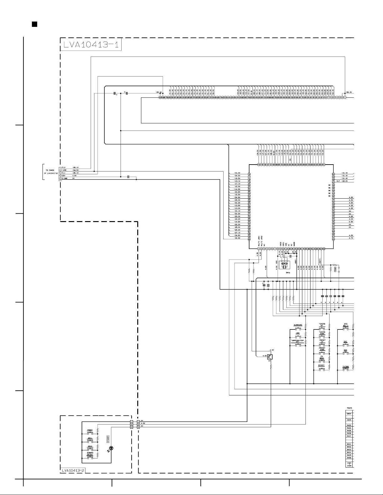
RX-7030VBK
Front key & System control section
5
4
SHEET 1/10
Front key & System control board
CN412
QGF1205F1-05
G10
G9G8G7G6G5G4G3G2G1
G11
G13
G16
G17
G12
G14
C409
C400
4.7/50
4.7/50
C427
1
G15
S1S2S3S4S5S6S7
QLF0113-001
S13
S14
S15
S16
S17
S18
S19
S20
S21
S22
S23
S24
S25
S26
S27
S28
S29
S30
S31
S32
S33
S34
S35
S36
S11
S10
S8
S9
DI400
S12
S11
S10S9S8S7S6S5S4S3S2S1G2G3G4G5G6G7G8G9G10
S18
S19
S16
S17
S14
S15
S12
S13
S21
S20
IC400
MN101C35DMF
S26
S24
S25
S22
S23
G11
G12
G13
G14
G15
G16
M_CLK
M_COMMAND
M_STATUS
VCRI
DCSI
JOG2
JOG1
RM
M_CS
M_BUSY
VCRO
DCSO
DIRECT_LED
M_RESET
S36
S35
S34
S33
S31
S32
S30
S28
S29
S27
2.2
10k
R446
UN2114-X
QAX0246-001Z
X400
10k
10k
R448
R447
C411
KEY2
KEY3
KEY4
KEY5
KEY6
KEY1
10k
10k
10k
R450
R449
R451
1k1k
R400R401
S400
S401
S402
S403
S404
R402
1.2k
S405
S406
S407
S408
R439
1k
CS2
CS1
CC_CON_LED
10k
R438
B407
C420
C421
C422
C423
C424
C425
S409
1k
R404
R405R406R408 R407 R403
1.2k1.5k2.7k 2.2k 1k
S411
S412
S414
3
10k
R484
10k
R485
C412
100/6.3 1.5
STANDBY_LED
C407
10k
R445
2
STANDBY_LED
Q413
220
R468
Power switch board
R480
1
S480
S481
S482
S483
1.5k
R482 R481
2.7k 2.2k
3.9k
R483
CN430 CN420
QGA2501C1-03 QJK025-031301
D480
SRL-343VC
2-18
AB C D
Page 61

RX-7030VBK
C410
4.7/50
STATUS
SI
2
1
USY
SO
ECT_LED
409
411
412
414
LK
OMMAND
I
S
O
ESET
DCSO
Q407
G1
G17
C425
1k1k
R409R410
1.2k1.5k
R411R412
R414 R413
2.7k 2.2k
KRC107S
Q408
KRC107S
10k
10k
R454
R453
1k
R415
S415
1k
R416
S416
1.2k1.5k
R417R418
S417
S418
Q402
470
R455
R458
N.I
R419R420
S419
R421
S421
R422
S422
S424
R424 R423
GP1UM281XK
1k1k
1.2k
1.5K
2.7k 2.2k
Q403
330p
C406
IC404
C404
0.022
S425
S426
S427
S429
DCSI
C401
1k1.5K
R425R428
R426
1K
1.2K
R427
2.2K
R429
DTC144WKA
10k
R456
JS400
QSW1017-001
0.1 0.1
VCRO
Q404
KRC107S
C402
B401
B402
B403
B404
B405
B406
VCRI
D405
1SS133UN2215-X
10k
R457
CN410
C403
QGF1205F1-09
0.01
R459
220
M_CLK
R460
220
M_COMMAND
R461
220
M_STATUS
R462
220
M_CS
R463
220
M_BUSY
R464
220
M_RESET
CC_CON_LED
DIRECT_LED
UN2114-X
JS401
QSW1015-001
0.1
0.1
C414
R434
1.2k
R435 R432R433
1.5k 1k1k
2.2k
R436
2.7k
R437
C413
UN2114-X
Q411
Q410
330
330
R465
R466
SHEET 9/10
CN422
QJK025-041201
CN432
QGA2501C1-04
2.7K
R430
D491
S430
S431
D490
SRL-343VC
3.9K
R431
Switch board
SRL-343VC
SHEET 8/10
HDE F G
2-19
Page 62

RX-7030VBK
X
D975
Micon section
5
4
Micon board
2SD2395/EF/
C971
330/25
Q971
C972
0.0047
D971
MTZ10JC
R971
12
R973
R962
22
C952
0.0047
R914
R953
2.2k
16
100/25
C951
D951
MTZ13JC
Q951
2SD2395/EF/
Q961
KTA1046/Y/
3.3k
C961
100/25
0.0047
D961
MTZ13JC
C962
R963
2.2k
R961
22
CN301
QGB2510J1-04
R940
3.3
3
22
R975
MAIN_STB
MAIN_CLK
MAIN_DATA
TUCE
R937
220
R960
220
TUDI
TUCK
R939
TUDO
SHEET 5/10
2
SHEET 5/10
TUMUTE
S_MUTE
SW_MUTE
SBK.1SPK
CN303
QGB2510J1-18
FR_RELAY
C_RELAY
SUR_RELAY
SBK_RELAY
CN101
QGB2510J1-04
R936
R935
R934
D956
1SS133-T2
D955
1SS133-T2
220
220
220
220
RDS_ST
RDS_DATA
RDS_CLK
F1_RELAY
F2_RELAY
R999
C985
0.01
C975
10k
470/6.3
D904
R911
1SS133-T2
4.7k
Q901
KRC107M
C904
2.2/50
220
R925
IC-PST9139
220
220
R927
R926
IC903
R910
R928
22k
220
220
R929
C903
R903
330
2200/6.3
C905
R976
R978
R993
R995
R997
100/6.3
C901
0.022
4.7k
13k
6.2k
13k
15k
1.5
C902
2-20
C994
DBS_S/C
DVD_S/C
VCR1_S/C
DCS
AV_VCR
VIDEO4
VIDEO3
VIDEO2
VOL_CLK
CN201
QGB2510J1-12
VIDEO1
VOL_STB
VOL_DATA
CN241
QGB2510J1-10
1
SHEET 6/10
SHEET 6/10
VCR2_S/C
CN601
QGD2510J1-07
DSPSTATUS
DSPCLK
SHEET 10/10
DSPREADY
DSPRESET
DSPCOMMAND
270P
AB C D
Page 63

RX-7030VBK
C905
R976
R978
R993
R995
R997
100/6.3
C901
0.022
C931
470/16
!!!
Q931
2SD2395/EF/
B7007
B7008
D931
MTZ6.2JC
C932
0.0047
R933
B7009
R918
2.7k
10
R931
R916
10
10
CN81
QGB2510J1-06
C941
100/25
D941
MTZ13JC
R943
3.9
R913
Q941
2SD2395/EF/
B7001
B7002
C921
100/25
0.0047
D921
MTZ5.6JC
B7003
R915
2.2K
3.9
C942
R923
2.7k
Q921
2SD2395/EF/
B7004
B7005
R921
C922
0.0047
B7006
12
SHEET 1/10
Q908
D900
11ES2-T4
R924
KRC105M
SHEET 2/10
FW831
QUM134-08DGZ4
10k
PROTECT
MULTI_OUT
HP_RELAY
SUR_RELAY
C_RELAY
F2_RELAY
F1_RELAY
HP_RELAY
SBK.1SPK
MAIN_DATA
MAIN_CLK
MAIN_STB
VOL_DATA
VOL_CLK
VOL_STB
VIDEO4
VIDEO3
VIDEO2
VIDEO1
F1_RELAY
F2_RELAY
SUR_RELAY
SBK_RELAY
C_RELAY
MULTI_IN
R944
220
R945
220
R946
220
R954
220
R955
220
R956
220
R930
R987
R985
R984
R983
R982
R981
R980
N.I
Q907
220
220
220
220
220
220
220
Q906
KRC105M
C981
330p
KRC105M
C982
C983
330p
Q905
C984
330p
Q904
KRC105M
KRC105M
330p
Q903
KRC105M
QGF1205C1-09
M_RESET
M_BUSY
M_CS
M_STATUS
M_COMMAND
M_CLK
CN400
CN931
QGD2501C1-04Z
SHEET 8/10
EP901
SHEET 2/10
D901
D902
11ES2-T4
11ES2-T4
10k
10k
10k
10k
10k
R969
R965
R966
R967
R968
4.7k
3.3k
5.1k
3.3k
5.6k
R994
R996
R998
R979
R977
4.7k
13k
6.2k
13k
15k
D977
D978
D976
1SS133-T2
8MHz
D979
10k
R957
M_COMMAND
M_STATUS
M_CLK
M_RESET
M_CS
10k
R958
R959
10k
M_BUSY
RDS_ST
PROTECT
C993
100p
220
R938
TUDO
TUDI
IC901
MN101C49GMG
TUCK
TUCE
RDS_DATA
RDS_CLK
D975
1.5
C902
X901
TUMUTE
MULTI_IN
R904
MULTI_OUT
DSPRESET
DSPCOMMAND
100k
DVD_S/C
VCR1_S/C
DSPSTATUS
DSPCLK
DBS_S/C
VCR2_S/C
SW_MUTE
DSPREADY
VIDEO_S/C
SBK_RELAY
S_MUTE
CN932
4
P
QGD2501C1-03Z
Parts are safety assurance parts.
When replacing those parts make
sure to use the specified one.
SHEET 9/10
HDE F G
2-21
Page 64

RX-7030VBK
E
E
C
2
0
9
S
D
DSP section
5
DSP board
Q2201
2SD2114K/VW/
Q2202
2SD2114K/VW/
4
Q2301
2SD2114K/VW/
Q2302
2SD2114K/VW/
DSP.L
DSP.R
DSP.LS
DSP.RS
R2007
10K
C2009
0.1
C2214
0.1
IC522
HA17558AF
24k
R2005
10K
IC520
HA17558AF
R2006
10K
R2008
R2211
1k
HA17558AF
R2212
1k
C2005
120P
10K
R2215
R2213
1k
1k
IC522
C2215
2700p
C2216
2700p
R2214
R2216
1k
R2009
10K
C2010
0.1
IC520
HA17558AF
R2010 R2012
10K 22K
C2006
120P
C2237
33p
R2237
33k
C2251
0.1
IC523
HA17558AF
0.1
C2252
R2238
1k
33k
C2238
33p
C2001
R2003
4.7/25
DSP_IN_L
R2001
R2002
DSP_IN_R
R2205
1k
R2201
10k
C2201C2202
R2202
10k
R2206
1k
R2305
R2301
10k
560p560p
C2301C2302
R2302
10k
R2306
10K
C2003
0.0012
100K
C2004
0.0012
100K
R2004
C2002
10K
4.7/25
C2207
4.7/50
C2211
330p
C2213
0.1
1000p1000p
100k
R2207
33k 33k
R2222 R2221
R2223
100k
C2230
R2208
4.7/50
C2212
330p
C2208
4.7/50
C2307
2.2/50
1K
N.IN.I
R2307
100k
R2303
R2308
100k
R2304
C2308
1k
2.2/50
R2235
R2233
33k
R2231
27k
IC523
HA17558AF
R2232
R2234
R2236
R2353
2.2k
Q2363
2SD2114K/VW/
Q2364
2SD2114K/VW/
R2354
2.2k
C2013
33P
R2013
C2019
0.1
22K
R2011
22K
IC521
HA17558AF
C2020
C2007
390P
C2008
IC521
390P
HA17558AF
33k
100k
R2225
R2227
100k
R2226
27k
33k
33k
C2351
1/50
R2355
10k
10k
R2356
C2352
1/50
0.1
C2018
47/6.3
22K
R2014
C2014
33P
33p
C2283
10k
R2283
0.1
C2255
C2271
4.7/25
C2256
R2279
0.1
100k
100k
R2280
100k
IC524
HA17558AF
C2272
R2284
4.7/25
10k
C2284
33p
C2355
0.1
C2356
0.1
R2357
47k
33p
C2353
C2354
33p
R2358
47k
IC526
HA17558AF
1M
R2277
1M
R2278
IC526
HA17558AF
R2359
27k
R2360
27k
IC524
HA17558AF
Q2274 Q2273
R2376
6.8k
R2275
2SC2412K/RS/
2SC2412K/RS/
6.8k
R2276
10k
R2274
R2375
18k
Q2375
2SC2412K/RS/
18k
Q2376
2SC2412K/RS/
C2243
C2241
C2281
4.7/25
R2273
330
R2022
330
R2021
R2018
4.7K
R2017
4.7K
330
R2023
330
R2024
R2241
16k
180p
R2243
1.6k
0.1
IC525
4.7/25
C2282
10k
HA17558AF
C2242
0.1
R2251
C2245
0.068
0.068
C2246
100k 100k
R2282 R2281
R2361
R2373
10k
R2374
10k
R2252
IC525
HA17558AF
C2244
180p
1.6k
R2244
R2242
16k
C2357
2.2/50
0
R2363
100k
R2364
100k
R2362
C2358
0
2.2/50
LIN-
LIN+
RIN+
K2262
RIN-
R2245
16k
R2247
16k
R2249
24k
24k
3.6k
R2253
R2255
C2248 C2247
0.0018 0.0018
1.8k 1.8k
R2250
3.6k
24k
24k
R2248
R2254
R2256
16k
R2246
16k
LOUT1
ROUT1
Q2155
DTA114YE
NQR0007-003X
100
R2261
100
1.0
100
C2268
R2262
K2261
NQR0007-003X
100
100
R2269
1.5
C2267
R2270
R2271
C2266
1.5
C2265
10/16
IC561
MN35505
C2269
0.01
C2270
0.22
1.5
C2261
10/16
C2262
C2264
1.5
100
R2263
K2263
NQR0007-003X
LOUT3
LOUT2
ROUT2
LOUT1
ROUT1
C2021
220p
LIN-
LIN+
RIN-
RIN+
C2022
220p
560
R2265
560
3.3k
R2268
C2263
10/16
100
R2264
K2264
560
R2260
NQR0007-003X
R2267
IC571
AK4527BVQP
0.1
10/16
C2708
C2710
0.1
10/16
C2707
C2709
R2713
220
IC572
NC7WZ125K8
R2711
220
R2712
220
NC7SZ74K8
P
R
C
IC573
Q2156
DTA114YE
C2539C2538
0.10.1
IC507
PQ20VZ11
C2706
3K1K
R2535R2536
0.1
2.2/50
C2703
DIGITAL signal
FRONT signal
C2154
C2152
0.082
R2153
0.1
IC528
HA17558AF
Q2131
2SD2114K/VW/
C2131
0.082
R2152
10k
10k
C2155
0.033
C2431
0.1
R2131
10k
C2132
0.033
C2855
0.1
C2856
0.1
R2857
C2853
IC530
HA17558AF
C2432
0.1
R2133R2132
10k10k
R2181
47k
C2181
33p
IC530
HA17558AF
47k
33p
R2859
27k
10k
C2433
33p
R2425
R2431
IC529
47k
HA17558AF
R2433
18k
27k
Q2431
R2432
2SC2412K/RS/
8.2k
R2182
IC529
HA17558AF
R2861
0
R2191
1M
Q2152
DTC114YE
R2194
1M
Q2154
DTA114YE
3
C2407
R2405
1k
DSP.C
Q2401
2SD2114K/VW/
Q2101
2SD2114K/VW/
DSP.SW
2
DSP.SrBK
Q2801
2SD2114K/VW/
2.2/50
R2401
10k
R2407
C2401
100k
560p
R2101
10k
C2101
560p
R2105
R2801
10k
C2127
R2128
0.1
100k
R2107
C2107
1k
4.7/25
R2127
C2807
2.2/50
R2805
1K
C2801
R2807
560p
100k
47k
47k
NJM2121M
IC527
0.1
R2151
10
C2153
2.2k
R2130
C2130
4.7/50
C2128
0.1
R2129
IC528
10
HA17558AF
1
DSP_IN_L
DSP_IN_R
DSP.L
DSP.R
DSP.LS
DSP.RS
DSP.C
DSP.SW
DSP.SrBK
CN581
QGB1214K1-14S
Q2158
DTA114YE
1M
1M
1M
1M
Q2157
R2197
R2196
R2198
R2195
DTA114YE
LOUT2
R2435
C2434
0
2.2/50
R2434
100k
R2183
100k
C2857
2.2/50
R2863
100k
C581
10/16
C2182
4.7/25
Q2151
DTA114YE
C582
10/16
ROUT2
LOUT3
R2485
1k
C2481
47/6.3
B581
0
B582
N.I
C583
47/6.3
SHEET 7/10
CCLK
C_CS
0.1
10/16
C2705
C2704
C_PD
CDTI
8.2K
4.3K
R2172
R2171
R582
10k
ERF
C584
C573
0.1
IC582
NC7ST32P5
R2597
1k
1
Q572
DTC114YE
TP_34
TP_35
1
C
R
2-22
AB C D
Page 65

RX-7030VBK
TP_1
R2568
K2606
NQR0269-004X
220
C2568
1/50
C2565
IC551
C2712C2711
0.110/16
D_PD
0
B571
0
B572
0
B573
D0D1D2
D3D6D4
D5
A16
A15
A14
A17
C2517
C2520
C2516
A13
A12
A9A8A7A6A5A4A3A2A1
A11
A10
C2515
C2514
C2513
C2512
NAX0435-001X
C2702
10p
X2701
10p
C2701
R2705
C2715
100p
B574
AK4112B
CDTO
CDTI
CCLK
D_CS
R2701
100
R2702
220
18K
C2713
0.1
0
R2703
220
R2704
220
I_LRCK
TP_2
R2561
MCK
A/D
I_BCK
DATA
ERF
220
TP_3
220
R2562
TP_4
220
R2563
J564
QNN0347-001
100p
R2565
J564
0
B598
C2561
0.1
UN561
GP1FA351RZ
C2562
0.1
UN562
GP1FA351RZ
C2563
0.1
UN563
GP1FA351RZ
13
0
7
IC572
NC7WZ125K8
R2711
220
R2712
220
IC573
NC7SZ74K8
C573
0.1
IC582
NC7ST32P5
TP_35
Q572
DTC114YE
CENTER signal
REAR signal
PD_DD
RST_DD
C2524
TP_34
100/4
D7
D8
C2518
D9
D10
D11
D12
D13
D14
C2519
CDTI
DIG_SEL
220
R2588
IC581
R577
8.2k
D15
D16
D17
D18
D19
C2503
D20
D21
D22
D23
R2613
TP_20
R2614
TP_21
R2615
TP_22
R2616
TP_23
R2517
TP_24
TP_25
TP_26
TP_27
PD_DD
RST_DD
C_PD
D_PD
220
220
22075220
220
R2584
R2586
R2587
R2583
ERF
4.3k
R573
DSPRESET
B583
0
X581
NAX0275-001X
IC501
DSPD56367PV150
C2521
MOSI
MISO
R2612
R2511
R2512
R2513
R2524
R2519
R2518
HREQ
DSP_RST
10k
R588
R2520
C2502
R2515
DATA
R2516
D/A0
D/A1
D/A2
D/A3
P_LRCK
I_LRCK
DSP_RST
SCK
C2523
0.1
220
220
220
220
220
R2599
10K
10k
10k
R587
R586
NC7S04P5
SS
HREQ
MOSI
MISO
8.2k
8.2k
8.2k
TP501
R578
R579
R580
TP_31
TP_30
TP_29
TP_28
10k
R585
R2523
R2522
R2521
R2502
SCK
SS
96/24
D_CS
220
220
R2580
R2581
R2582
R2579
R2578
R2577
R2576
R2575
N.I
10k
R2592
R2593
R2594
220
P_BCK
IC503
R574
R575
R576
Q570
DTC114YE
R2508
R2509
C2504
C2505
R2611
C2509
I_BCK
DSPREADY
4.3k
DSPCLK
4.3k
DSPCOMMAND
4.3k
C579
100p
DSPSTATUS
R570
10k
R2510
TP_7
C2529
TP_8
TP_9
TP_14
TP_12
TP_11
TP_13
TP_10
C2533
0.1
0.1
C2530
0.1
C587
220/6.3
96/24
I_LRCK
B599
0
I_BCK
0.1
A/D
D/A3
D/A2
D/A1
P_LRCK
P_BCK
C2525
0.1
MCK
CCLK
CDTO
C_CS
220
220
220
TP_32
TP_33
R2589
R2590
R2591
UPD784215AGC196
C577
100p
C571
0.01
C572
SURROUND signal
100/4
IC505
PQ070XZ1HZ
C588
0
B586
R2505
R2506
R2507
1k 510
R2532 R2531
0
B585
DSPRESET
SHEET 9/10
R2525
47
C2531
0.1
C589
0.1
DSPREADY
A0
R2504
CE
RAS
READ
WRITE
C2511
C2510
R2514
C2501
R2503
C2506
0.1
C2534
IC506
MM1563DF
DSPCOMMAND
DSPCLK
DSPSTATUS
-
C590
100/4
C2532
100/4
IC583
CN587
MM1563DF
C2522
C2508
C2507
100/4
C2535
100/4
QGB2510K1-07
IC502
NC7SU04P5
0.01
R2501
1M
X2501
NAX0308-001X
A11
A9
A8
A13
TP_19
TP_18
TP_17
TP_16
TP_15
A14
A17
WRITE
A16
A15
A12
A7
A6
A5
A4
C2536C2537
0.1
SA14
SA12
SA7
SA16
47
R2636
A16
47
R2634
A14
47
R2632
A12
47
R2627
A7
CE
D0
D1
SA6
SA5
SA4
SA3
SWRITE
D2
D3
R2527
47
WRITE
47
R2626
A6
47
R2625
A5
47
R2624
A4
47
R2623
A3
C2571
C2572
100/4
0.1
LC505
NQR0450-001X
SA16
SA14
SA12
SA7
CE
D8
D9
D10
D11
SWRITE
SA6
SA5
SA4
SA3
C2574 C2573
100/4 0.1
LC506
NQR0450-001X
SA16
SA14
SA12
SA7
CE
D16
D17
D18
D19
SWRITE
SA6
SA5
SA4
SA3
C2576 C2575
100/4 0.1
LC507
NQR0450-001X
IC511
39VF0207CWHR01
IC512
IC63LV102410K
IC513
IC63LV102410K
IC514
IC63LV102410K
R2560
220
TX
C2605
1
READ
A10
RAS
D7
D6
D5
D4
D3
D2
D1
D0
A0
A1
A2
A3
SA9
SREAD
SA8
SA15
SA13
R2635
R2633
R2628
R2629
R2526
D7
D6
SA11
SA10
SA1
SA0
SA2
D5
D4
R2631
R2630
R2622
R2621
R2620
SA15
SA13
SA8
SA9
SREAD
D15
D14
D13
D12
SA11
SA10
SA2
SA1
SA0
SA15
SA13
SA8
SA9
SREAD
D23
D22
D21
D20
SA11
SA10
SA2
SA1
SA0
UN560
GP1FA351TZ
C2560
0.1
N.I
B577
EP561
E409182-001SM
B576
0
47
A15
47
A13
47
A8
47
A9
47
READ
47
A11
47
A10
47
A2
47
A1
47
A0
SHEET 10/1
HDE F G
2-23
Page 66

RX-7030VBK
6
Printed circuit boards
Main board
(Speaker board)
RY832
C847
C837
Q835 Q836
C843
B515
B712
B432
B115
C839
B113
C840
CN823
C848
C838
B701
B215
R851
B513
C844
D851
R838
RY851
ST833
R860
B212
R861
Q832
R885
B213
C853
R859
C881
B218
B219
C885
Q831
B220
D844
C852
B111
R863
Q837 Q838
C886
B114
R862
C887
C891
C883
FW931
R868
B118
D843
C454
C889
Q833
B112
R864
R865
Q839
R869
B216
R887 R888
C893
Q834
B323
D847
B512
B322
C892
R852
RY852
C888
C890
D852
B514
ST853
C884
B511
C899
CN824
C895
R886
D853
RY853
R867
R889
C896
C898
C897
R866
RY831
R834
C842
R855
ST832
C846
D846
D845
B217
R832
B321
C836
R837
C834
D841
C850
R854
R858
R857
D842
R856
R870
C851
C833
Q830
B214
C835
C841
D831 D832
D848
R831
R833
C845
5
4
3
B6204
B6709
B6104
B6708
R871
B6605
RY871
B6604
R842
B
CN702
B6705
B6706
B6707
CN814
B6505
B6510
R844
B6508
B6003
B6509
B6507
L846
D871
B6206
B6506
B6205
(Main board)
CN723
Q824
R825
R824
Q823
Q825
C824
R826
CN706
B6413
L845
R845
B6004
B6302
B6105
B6607
CN705
B6606
R823
2
D825
B6106
C823
1
2-24
AB C D
Page 67

RX-7030VBK
R886
53
RY853
R842
CN702
B6707
R889
C896
C897
B6706
B6604
B6412
B6705
B6603
B6704
C894
B6602
B6203
R846
B6601
L844
B6703
R843
CN831
CN881
B6103
CN704
B6002
B6303
B6005
R815
B6001
CN813
R816
B6960
D816
C816
L843
B6201
B6411
B6806
B6406
B6407
B6408
B6409
B6414
B6410
B6202
B6107
EP801
B6301
R841
CN701
B6805
B6953
B6961
B6954
B6955
B6956
B6957
B6962
B6503
B6901
B6502
B6959
B6802
B6405
B6701
B6101
B6504
B6804
B6803
C802 C805
B6501
C808
CN703
B6952
B6958
B6951
B6963
B6801
B6403
B6404
B453
B452
C801
B451
B6710
CN801
C807
R814
R813
R801 R802
D803 D804
D801 D802
B6401
B6402
R811
R812
C811
HS811
Q811
D811
Q812
B6102
HDE F G
2-25
Page 68

RX-7030VBK
R
Front board
(Front key & System control board)
R414
R405
R456
R457
S405
S406
R406
D417 D418 D419
Q404
D420 D421
IC404
R418
R416
S416
S410
R411
S418
S404
C424
R449
RA402
S411
R404
C423
R448
S403
R403
R412
C422
R447
R468
R455
Q402 Q403
S412 S413
R413
C421
C420
R446
R445
Q413
C406
S417
R417
5
S409
S402
CN420
S401
S415
R415
R409
R410
4
C400
R400 R401 R402
S400
R458
C427
CN412
C404
C409
D405
Q408
Q407
R407
S414
S407
D416
DI400
R408
RA401
S408
R419
D414
S419
CN414
R247
R273 R274
R245
R254
R272
C275
C284
Q254
Q240
Q241
R250
C287
C276
R269
C244
C251
R255
C252
C286
C274
C246
R276
R240
C277
R253
C272
C273
C249
C250
R244
R266 R267
R242
C247
R243
C245
C241
C242
R248
Q242
Q243
R259
Q244
R221
R251
CN240
3
R252
R271
C248
C243
C259
C258
2
CN244
(S-Video board)
C254
C257
C255
C253
C256
IC242
R249
R280 R284
IC241
1
C281
R246
R275
C282
R241
C270
C271
R268
C285
C269
C268
C283
C280
J244
J242 J243
J241
IC372
C396
R395
R398
CN314
C391
Q303
R394
C343
R345 R346
R396
C344
C392
R392
Q302
IC303
R387
Q301
C398
FL352
X301
C397
FL351
R388
C352
C393
R391
R393
CN313
C399
R397
C394
R389
R390
C395
R351
C351
R352
R342
R341
C341
R343
C342
R344
D490 D491
CN371
C386
C385
R318
R317
R380 R381 R382
R379
R377
C377
R378
C375
R373
C373
R374 R375 R376
C371
R371
R372
CN315
R386
C389
IC371
R385
CN432
S430 S431
2-26
R431
R430
(Switch board)
AB C D
Page 69

RX-7030VBK
S426
C413
C402
C403
JS400
JS401
R460
C401
R464
R463
R462
C414
S425
Q410 Q411
R439
R440
R432
R433
R434
R435
R436
R437
R425 R426
R465 R466
PW402
S421
R422
1
C411 C412
C407
C408
C415
IC402
C416
C417
RA400
S422
R423
C410
S423
R450
C425
R424
R451
R479
R485
R453
S424
D410 D411 D412 D413
R438
R484
R454
CN410
R461
R459
S429
S427
R428
CN422
R429
R427
D480
CN206
C208
C209
C211
C212
R225
R218
R226
CN200
C210
CN204
IC201
Q204
Q200
R215
R219
Q201
R214
C206
C203
C201 C202
C207
C205
C204
R211
R213
J203
J202
R209
J201
R206
R212
R204
R210
R202
R208
R207
C226
J204
R205
C227
R203
C228
(Video board)
R201
R200
CN430
S480
R480
R481 R482 R483
(Power switch board)
S481
S482
S483
HDE F G
2-27
Page 70

RX-7030VBK
Micon board
5
4
B526
B527
CN72
B528
(Power supply board)
R66
B3129
R55
B531
R73
C73
B3237
B529
B530
CN71
B3238
C68
C66
B3234
CN402
B3334
Q71
C69
R72
R74
D75
C74
Q74
B3337
C62
D62
D64
C65
B3233
B3335
TH71
B3235
B3431
HS51
B3128
B3333
C71
C72
D74
Q51
B3332
C63
C70
D71
D73
D72
B3232
C53
FW51
D63
Q52
Q42
C61
R54
C55
D56
C54
R44
C45
D46
C44
D61
B3231
B3127
R53
B3331
R51
B3430
Q53
PW28
RY1 B3230
D57
PW40
B3124
B3125
D51
D53
D52
C51
D54
B3126
C52
B3122
B3123
B3121
B3120
C1
PW29
T2
FC3 FC4
D55
R52
EP51
C81
B3184
PW70
B3185
3
R916
EP902
(Relay board)
Q903 Q904 Q905 Q906 Q907
B7134
B7135
CN81
D901
D900
R930
C91
R91
B7136
D902
2
C92
R92
FW881
1
(Headp hone jack board)
CN932
CN931
B7133
B7130
B7132
B7131
EP91
J91
B7128
B7129
B7555
B7553
B7512 B7272
B7554
B7552
B7357
R913
R914
B7204
B7127
B7146
R971
R961
R962
B7412
B7411
B7410
R973
B7453
Q951
Q971
R963
R953
B7452
D9
2-28
CN82
Q961
AB C D
Page 71

RX-7030VBK
(
)
(Power trans 1board)(Power trans 2board)
B7410
R973
B7453
Q971
R963
R953
Q951
Q961
B7452
D951
R931
B7663
C952
D971
C972
D961
C962
B7206
C971
B7310
B7658
C951
B7451
C961
(Power/fuse board)
EP1
R1
PW17 PW18
PW20
FW831
R921
R923
Q908
B7126
B7265
B7143
B7508
B7309
B7312
B7209
B7210
B7211
C921
B7657
B7662
CN241
B7142
B7100
C984
B7108
FC62
CN400
R959
B7103
FC64
B7366
C994
B7104
B7106
Q901
B7200
CN601
D904
131
122
121
134
111
123
133
R982
B7105
132
113
112
EP901
R981
R980
CN334
C904
IC903
R911
B7139
Micon board
FC63
B7113
B7117
B7141
CN811
FC61
B7118
B7251
B7252
B7253
B7254
B7255
B7256
B7257
B7116
B7140
C903
B7202
R954
R955
B7119
C905
R61
C901
C902
R956
R940
X901
R987
B7250
R934
B7115
R938
R937
B3183
B7111
B7352
R910
R935
PW60
R904
C993
R939
R985
B7351
B7107
B7109
B7110
R984
B7350
B7201
B7102
R960
B3182
R983
C983
C982
C981
B7101
R958
R957
10 11 12 13 14 15 16
PW13 PW16 PW10 PW11 PW12 PW14 PW15
TA1 TA2
PW30
FC1 FC2
PW19
PW26
D955
B7500
B7501
B7502
B7505
B7120
D956
B7504
R968
B7137
B7301
B7365
R924
R994
B7121
R979
B7364
R969
R976
B7359
B7264
B7661
B7005
D921
B7415
B7267
C922
B7006
B7269
B7302
B7004
R918
Q921
B7414
C932
R933
B7308
B7408
B7007
C941
C985
D931
B7009
B7208
Q931
R943
CN201
D941
B7207
B7406
C931
B7407
R999
C975
B7008
B7406
Q941
R915
B7260
C942
B7125
R936
B7655
R997
B7664
B7001
CN303
R975
B7003
B7509
B7002
B7556
R998
R995
CN101
B7258
B7259
B7261
R996
B7405
R978
B7203
B7362
B7360
B7361
R993
B7550
B7454
B7401
B7402
B7403
B7506
R977
R944
R945
R946
B7354
B7300
B7114
R903
IC901
D979
D978
B7138
B7511
CN55
CN301
B7112
B7650
B7651
B7652
R967
R966
R965
D975
D976 D977
R929
R927
R926
R925
R928
HDE F G
2-29
Page 72

RX-7030VBK
2
3
2
Power board
5
R1896
Q1892
C1892
4
R1892
R1854
C1854
C1842
Q1806
B2315
C1814
B2141
C1816
R1822
C1812
R1874
B2505
R1856
(Surround board [R]) (Front board [L])
R704
C754
C706
C704
Q710
Q764
R734
B2215
Q702
D702
R706
R710
R722
C716
C720
B2212
Q704
C712
Q706
B2320
B2114
R708
R778
Q774
D774
B2607
C710
R716
R798
B2761
R1842
B2430
R1824
R1830
B2140
D1892
R1894
B2762
B2142
B2143
R1832
R1828
R1826
D1874
C1844
R1878
Q1874
R1806
R1812
C1818
C1896
L1862
R1836
TH832
R1834
Q1832
D1802
C1806
Q1804
C1810
B2226
R1852
Q1802
R1814
B2809
C1852
R1804
C1808
R1862
D1872
Q1852 Q1854
R1802
R1810
C1804
R1864
Q1872
R1872
B2760
B2225
C1802
B2506
C1864
C1862
R1876
CN716
C796
R788
R796
CN719
C722
B2214
VR788
R702
B2115
Q708
R726
Q792
B2213
C702
C718
R728
R774
R784
R732
C714
R764
C708
R712
D792
R790
TH784
R718 R720
R792
R780
R782
Q782
Q712
R730
L792
R762
R724
D704
C752
C746
D772
Q762
C742
R794
Q772
R77
B275
3
R709
R703
C717
C703
R733
B2206
Q763
Q701
R705
C705
D701
R721
C715
C719
B2203
Q703
B2319
B2105
C711
Q705
R707
R777
D773
B2603
R715
Q773
R711
R797
C707
D791
C709
B2851
R789
R779
TH783
R781
Q781
R717 R719
Q711
R791
L791
R761
R729
C751
R723
D703
C745
D771
Q761
C741
R793
Q771
R77
B
R1811
C1851
C1807
R1861
D1871
Q1851
R1801
R1809
C1803
B2220
R1863
Q1871
R1871
B2755
C1801
B2502
C1863
C1861
R1875
R1803
CN715
CN714
C795
R787
R795
C721
R701
R725
Q791
B2204
B2205
VR787
C701
Q707
Q709
B2106
R727
R731
C713
R773
R783
R763
C753
Q1801
R1805
C1817
C1805
C1895
B2221
L1861
R1855
R1835
TH831
R1833
Q1831
D1801
Q1803
R1813
C1809
B2807
R1851
C1841
2
R1895
C1891
R1891
1
R1821
C1811
Q1805
R1853
C1853
B2310
C1813
Q1891
B2131
C1815
R1873
Q1853
B2501
B2756
R1841
B2425
D1873
R1823
R1829
R1877
Q1873
B2130
R1827
R1825
D1891
R1893
B2757
B2132
B2133
R1831
C1843
2-30
(Surround board [L])
(Front board [R])
AB C D
Page 73

(Surround back board)
C746
C745
RX-7030VBK
D772
Q762
C742
R794
Q772
R772
B2753
C792 C794
CN712
R776
C1901
C1902
R1902
Q1991
C1991
R1991
CN717
R1901
R1995
Q1902
B2075
R1905
R1911
C1904
R1952
C1952
Q1901
C1915
C1995
R1923
R1922
B2322
Q1952
D1901
R1912
B2323
C1903
C1905
C1912
R1972
R1933
B2077
R1903
TH901
R1932
Q1931
B2073
R1925
R1924
D1993
R1994
B2810
R1931
C1913
R1921
C1911
Q1903
C1943
B2076
B2432
R1993
Q1972
D1992
B2074
L1961
R1941
R1951
C1941
R1953
C1951
R1961
Q1951
D1971
R1962
Q1971
B2702
CN718
B2431
B2321
C1962
C1961
R1973
R1971
R723
D703
D771
Q761
C741
R793
Q771
R771
B2751
C791 C793
CN711
R775
CN722
R1701
Q1791
C1791
R1791
C1701
C1702
R1702
R1795
B2122
R1705
Q1702
R1711
C1704
R1752
C1752
Q1701
C1795
C1715
R1723
R1722
B2302
Q1752
D1701
B2303
C1703
R1712
R1793
R1733
B2124
R1703
C1705
C1712
R1772
C1713
B2120
R1721
C1711
Q1703
R1725
R1724
C1743
B2123
B2422
D1791
R1774
L1761
Q1772
D1772
B2805
B2121 B2701
R1731
TH731
R1732
Q1731
R1741
R1751
C1741
R1753
C1751
R1761
Q1751
R1762
D1771
B2301
Q1771
R1771
CN713
B2421
C1762
C1761
R1773
(Center board)
HDE F G
2-31
Page 74

RX-7030VBK
R1309
6
3
1
R1458
7
3
4
1
Input board
CN733
C1310
C1309
5
R1440
Q1462
C1453
C1432
C1431
C1471
C1454
Q1482
C1434
Q1441
Q1445
C1440
C1439
R1439
C1468
C1433
Q1461
(I/O board)
C1377
C1375
C1376
C1398
C1379
C1386
C1392
4
J1350 J1352
J1380
C1397
C1396
C1373
C1385
C1391
C1384
C1390
C1428
Q1421
C1413
Q1422
C1448
C1414
Q1442
J1490 J1491
Q1324
C1473
Q1481
Q1492
Forward side
CN731
Q1313
C1322
C1326
C1321
C1325
C1488
Q149
C1474
C134
C1324
C1323
C1
Q1490
IC396
IC384
R1342
R1343
C1474
C1324
IC382
R1341
Reverse side
CN731
R1315
Q1313
C1322
R1322
R1324
C1326
C1329
C1323
Q1489
R1483
R1490
R1489
R1477
R1503
R1481
R1321
C1321
C1349
Q1488
C1325
C1488
Q1481
R1488
R1487
C1497
C1432
Q1492
D1489
C1431
C1471
R1432
R1431
R1471
CN733
Q1324
R1433
R1474
R1473
D1488
J1491
R1434
R1502
C1473
C1498
R1464
Q1482
R132
R14
R14
R14
R1463
R1484
R
C1454
R1482
3
R1454
R1455
CN732
IC398
R1456
CN381
R1313
C1314
R1311
Q1314
R1314
C1313
R1312
C1311
C1315
R1316
C1312
CN205
IC381
C1316
C1319
CN735
C1412
R1412
C1411
R1335
C1302
C361
C1364
C1333
C1303
C363
C1362
C1360
R1331
R1367
R1366
C1367
CN734
C1365
C1366
C1363
IC386
R333
C1331
R1368
R1365
C1334
C1361
C333
R1332
R361
C1339
R1363
J1360
R1334
C1332
R1361
C1451
IC383
CN361
R1451
R1452
C1452
R1453
R1336
Q1334
Q1333
IC304
R1305
C364
R334
R1304
C362
R362
R1302
R1303
R1362
R1364
C334
R1301
R1307
R366
R364
R1308
C1301
R1333
R365
R363
CN501
R1306
2
IC380
1
R1486
R1411
R1413
C1499
C1341
R1478
R1472
R1414
R1416
C1343
Q1491
C1344
R1415
2-32
AB C D
Page 75

RX-7030VBK
Q1491
C1344
C1343
C1411
C1341
CN735
C1412
C1499
C1316
C1313
C1311
C1315
CN205
Q1314
C1312
C1314
CN381
CN732
C1452
C1451
CN734
CN361
C1332
C1363
J1360
C1365
C1366
C1334
C1302
C1331
C1364
C1333
C363
Q1334
Q1333
CN501
R1302
R1301
C1301
C364
C361
C362
1432
R1431
471
71
CN733
Q1324
R1433
R1474
R1473
D1488
J1491
R1434
R1502
C1473
R1464
Q1482
R1326
R1435
R1476
R1475
R1463
R1484
R1309
R1436
R1458
C1454
R1482
R1469
R1457
C1309
Q1310
IC397
C1453
R1462
Q1462
R1440
C1440
R1439
IC399
R1468
C1468
C1496 C1498
C1439
Q1461
C1310
R1505
D1469
Q1468
Q1469
R1310
R1437 R1438
D1468
R1445
R1461
C1495
C1433
R1441
Q1445
C1494
C1434
C1493
R1447
R1446
R1449
R1418
R1422
Q1442
R1442
R1501
Q1447
R1443
Q1441
D1449
R1424
C1448
C1491
C1492
D1448
R1448
C1414
Q1422
Q1448
Q1449
R1444
R1500
D1429
C1413
R1417
D1428
R1428
R1429
C1428
C1390
Q1428
Q1429
R1385
R1388 R1389 R1390
R1423
R1421
Q1421
C1387
C1393
C1381
C1396
C1384
R1391
R1394
C1391
R1386
C1373
C1388
C1374
C1385
C1382
R1392
C1394
C1389
IC389
J1380 J1490
C1397
R1395
R1387
C1383
C1392
R1393
C1395
C1377
C1375
C1379
C1350
C1386
R1396
J1350
C1398
R1373
C1376
R1351
R1350
IC390
D1350
R1355
J1352
HDE F G
2-33
Page 76

RX-7030VBK
DSP board
5
Forward side
R2582
R2583
R2584
R2585
R2586
R2587
R2588
R2589
R2590
R2010
R2011
C2153
C2433
R2431
R2627
C2518
C2519
C2503
R2580
R2581
R2591
C2008
R2012
C2014
IC521
R2013
C2434
IC528
C2152
R2632
C2271
R2502
R2024
R2014
C2013
C2432
IC527
R2634
R2235
R2231
R2524
R2522
R2023
R2021
R2636
R2233
R2237
R2711
IC571
C2019
C2182
UN562
R2562
C2237
R2712
C2431
C2130
IC501
R2521
R2713
C2181
IC529
R2129
C2127
R2128
R2127
IC511
R2523
IC572
R2363
R2361
R2181
R2182
R2520
C2357
R2375
R2183
C2562
C2517
C2502
IC573
R2515
B589
R2133
R2132
C2132
C2131
C2351
R2353
C2307
R2303
C2301
R2509
R2510
C2358
R2357
R2130
C2509
C2705
C2706
C2353
C2506
C2516
R2171
R2305
R2307
C2511
C2510
C2508
C2522
C2514
C2501
C2507
C2504
LC509
R2172
C2704
R2269
R2270
R2271
C2505
K2261
R2261
C2268
C2267
R2262
C2292
K2262
LC510
C2703
C2356
IC526
C2355
R2215
C2515
R2265
IC541
B588
R2304
C2302
UN563
C2352
C2215
R2213
R2563
IC502
C2513
C2291
R2364
R2362
R2376
C2563
R2501
C2512
C2265
R2255
B599
R2249
R2251
C2245
C2266
R2253
C2247
R2241
C2281
R2283
R2308
C2211
R2211
R2221
B592
LC502
R2247
R2245
C2283
R2358
C2354
R2354
C2308
R2306
CN599
B587
LC501
R2575
R2243
C2537
C2243
C2213
R2207
C2201
R2205
C2207
R2701
R2702
R2703
R2704
C2535
C590
IC525
C2256
C2255
C2252
UN560
C2529
R2576
R2578
R2579
C2241
IC524
IC523
C2251
C2214
IC522
R2706
C2242
C2532
C2540
C591
R2206
R2208
IC583
R2267
R2266
C2202
IC505
IC561
C2212
IC552
B585
R2242
C2208
R2212
C589
B583
R2577
C2216
R2214
K2264
R2260
R2264
C2264
R2254
R2250
R2252
C2246
C2244
C2282
C2284
C2272
R2223
R2216
IC551
IC506
R2256
R2244
R2560
C2560
B574
C2712
B586
R570
C587
R2599
IC581
R2268
C2269
R2246
R2248
C2248
R2284
R2568
C2715
C572
C2263
C2270
R2196
R2197
R2195
R2198
C2230
R2238
C2238
R2234
C2711
R2222
R2236
R2232
C2714
Q2156
C2481
R2191
EP561
B575
Q2151
Q2152
R2194
C2713
LC508
R2594
R2705
C2531
C2530
R573
R577
C577
B594
TP501
Q2157
Q2155
Q2154
C588
CN587
R2592
X581
LC504
CN588
C2262
Q2158
R2593
C2261
UN561
K2606
R2623
R2624
R2561
C2568
R2625
R2626
IC513
C2561
R2527
IC512
C2521
J564
C2571
LC505
4
C2572
C2573
LC506
C2574
3
C584
C2005
R2005
C2004
C2856
R2004
R2006
C2006
R2001
Q2801
R2801
C2407
R2008
C2018
R2405
R2407
C2401
R2009
R2153
R2152
C2155
C2154
IC514
R2017
R2018
C2007
R2434
R2022
C2857
R2435
C2435
R2433
C2128
R2007
R2432
R2151
C2575
LC507
C2576
C2010
C582
C583
R2002
B582
C2002
C2009
C2020
IC520
2
C2003
R2003
CN581
R2861
R2863
C2859
R2859
C2855
R2807
C2807
R2536
R2857
R2535
C581
C2853
B581
C2538
C2539
C2001
C2801
R2805
IC530
IC507
1
2-34
AB C D
Page 77

6
J564
RX-7030VBK
Reverse side
B598
TP_1
R2620
R2621
R2622
R2630
R2565
C2565
R2631
TP_2
R2526
R2629
TP_20 TP_21
TP_22 TP_23
TP_25
C2606
CN581
UN561
UN562
TP_3
R2635
R2633
R2628
TP_24
TP_26 TP_27
R2613
R2615
R2517
R2512
R2516
R2518
R2511
R2513
C2607
C2707
C2710
C2709
C2021
C2708
C2525
C2524
C2520
R2519
R2614
R2616
R2508
C2022
UN563
TP_11
TP_12
TP_13
TP_9
TP_14
TP_17
TP_7
TP_8
R2612
R2611
R2294
R2292
R2293
C2608
TP_4
CN599
TP_10
TP_15
C2536
R2564
TP_5
X2501
TP_18
TP_16
B572
B571
B573
C2523
TP_19
TP_32
TP_34
UN560
R2504
R2525
R2505
R2506
R2507
R2514
R2503
IC503
TP_33
C2564
LC503
R574
R578
C579
TP_35
TP_6
C2701
B593
C2534
R575
R579
EP5
B577
B576
C2605
X2701
C2702
R2531
R2532
C2533
TP_28
TP_29
TP_30
R585
R586
R587
R576
R580
R588
Q570
TP_31
R2571
C573
IC582
Q572
R2597
C2609
K2263
R2263
R2573
CN588
C571
CN587
R2574
R2572
R582
TP501
R2425
Q2431
R2401
Q2401
R2101
Q2101
R2105
R2107
C2101
C2107
Q2131
R2131
R2373
Q2375
C2359
R2359
R2355
Q2363
R2301
Q2301 Q2302
C2360
R2360
R2356
Q2364
R2302
R2374
Q2376
R2281
R2277
R2275
R2279
R2225
R2201
Q2201
R2273
Q2273
Q2274
R2274
R2227
R2202
Q2202
R2282
R2278
R2276
R2280
R2226
R2485
HDE F G
2-35
Page 78

RX-7030VBK
VICTOR COMP ANY OF JAP AN, LIMITED
AV & MULTIMEDIA COMPANY 10-1,1Chome,Ohwatari-machi,Maebashi-city,371-8543,Japan
(No.22058SCH)
Printed in Japan
2003/05
Page 79

PARTS LIST
[ RX-7030VBK ]
* All printed circuit boards and its assemblies are not available as service parts.
Area suffix
RX-7030VBK
J ----------------------------- U.S.A.
C -------------------------- Canada
- Contents -
Exploded view of general assembly and parts list (Block No.M1)
Electrical parts list (Block No.01~06)
Packing materials and accessories parts list (Block No.M3)
3- 2
3- 5
3-17
No. 22058 3-1
Page 80

RX-7030VBK
2
8
8
Exploded view of general assembly and parts list
Block No.
M
M
1
M
74
73
80
Power tran
71
A
Power trans
board
54
53
7
7
B
72
74
49
Relay board
45
43
Power switch
board
11
18
Headphone jack
board
k
Power supply
board
41
49
24
36
12
29
30
28
1
2
C
21
20
14
4
13
20
Switch board
19
15
5
8
7
6
10
9
16
Front key &
System
control board
22
m
17
23
3-2
3
75
76
Page 81

Power trans board
s
78
78
53
45
42
54
RX-7030VBK
69
70
55
I/O board
52
Power/Fuse
77
board
e
f
g
h
i
Speaker
board
c
a
D
b
37
Main
board
46
82
47
E
k
e
f
42
37
g
Surround
back board
44
37
h
Front
board (R)
37
37
Surround
board (L)
Center amp.
board
45
43
Front amp.
board (L)
59
83
n
a
Surround
board (R)
37
79
Stopper
60
board
S-video
board
c
51
Video
board
48
Micon
board
50
b
i
46
39
32
38
31
D
m'
56
A
n
32
E
31
51
32
67
Stopper
board
Audio
board
51
68
81
57
60
66
58
63
64
62
DSP board
61
65
56
26
40
m'
31
B
m
C
27
25
33
34
35
35
3-3
Page 82

RX-7030VBK
General assembly
Block No. [M][1][M][M]
Symbol No.
1 LV10469-015A FRONT PANEL
2 LV43338-001A JVC MARK
3 LV21438-001A LENS
4 LV10767-001A SUB PANEL
5 LV34032-001A CONTROL PLATE
6 LV21437-001A SEALING DOOR
7 LV34086-001A DOOR COVER
8 QYSPSGU2030M SCREW 2mm x 3mm(x3)
9 LV43357-001A DOOR SPRING
10 QYSBSF2608Z TAPPING SCREW 2.6mm x 8mm
11 LV20939-003A PUSH BUTTON
12 LV42096-001A INDICATOR
13 LV21442-001A P.BUTTON(TUNER)
14 LV21439-001A P.BUTTON(DSP)
15 LV21440-001A P.BUTTON(SOURCE
16 LV21443-001A P.BUTTON(ADJUST
17 LV32486-001A P.BUTTON ASSY
18 QYSBSF2610Z SCREW 2.6mm x 10mm(x2)
19 QYSBSF2610Z SCREW 2.6mm x 10mm(x2)
20 QYSBSF2610Z SCREW 2.6mm x 10mm(x8)
21 QUQ412-0517CJ FFC WIRE
22 QUQ412-0930DJ FFC WIRE
23 QYSDSG3006Z SCREW 3mm x 6mm(x4)
24 QYSBSG3006Z TAP SCREW 3mm x 6mm(x3)
25 LV10019-006A CHASSIS BASE
26 LV10471-002A FRONT BRACKET
27 QYSDSG3006Z SCREW 3mm x 6mm(x7)
28 LV42094-003A H.P BKT
29 QYSBSG3006Z TAP SCREW 3mm x 6mm
30 VKZ4150-001 SPECIAL NUT
31 E68587-223SM CB BKT (x3)
32 QYSBST3006Z TAPPING SCREW 3mm x 6mm(x3)
33 QZF6018-001 FOOT (x2)
34 E47227-036 FOOT (x2)
35 QYSBST3010Z TAPPING SCREW 3mm x 10mm(x4)
36 LV21444-001A HEAT SINK
37 QYSBSG3012E SCREW 3mm x 12mm(x12)
38 LV42098-001A C.B BKT
39 QYSBST3006Z TAPPING SCREW 3mm x 6mm
40 LV32433-001A H.S BRACKET(R)
41 LV32434-001A H.S BRACKET(L)
42 QYSBSG3008Z TAPPING SCREW 3mm x 8mm(x4)
43 QYSBST3006Z TAPPING SCREW 3mm x 6mm(x2)
44 QYSBSG3006Z TAP SCREW 3mm x 6mm(x2)
45 QYSBST3006Z TAPPING SCREW 3mm x 6mm(x4)
46 QYSBSG3006Z TAP SCREW 3mm x 6mm(x2)
47 E65923-003 TAPPING SCREW
48 LV30225-0B2A SPACER
49 QYSBSG3006Z TAP SCREW 3mm x 6mm(x3)
50 QYSBSG3008M TAPPING SCREW 3mm x 8mm(x3)
51 QYSBSG3006Z TAP SCREW 3mm x 6mm(x3)
52 QYSBSG3006Z TAP SCREW 3mm x 6mm
53 QQT0397-001 POWER TRANSF
54 QYSDSTL4008Z ASSY SCREW 4mm x 8mm(x4)
55 LV10768-011A REAR PANEL
56 QYSBSGY3008M SPECIAL SCREW 3mm x 8mm(x3)
57 QYSBSGY3008M SPECIAL SCREW 3mm x 8mm
58 QYSBST3006M TH TAP SCREW 3mm x 6mm(x2)
59 LV30225-011A SPACER
60 FMYH4004-001 PLASTIC RIVET (x2)
61 QYSBSGY3008M SPECIAL SCREW 3mm x 8mm
62 QYSBSGY3008M SPECIAL SCREW 3mm x 8mm(x4)
63 QYSBSGY3008M SPECIAL SCREW 3mm x 8mm(x3)
64 QYSBSGY3008M SPECIAL SCREW 3mm x 8mm(x3)
65 QYSBSGY3008M SPECIAL SCREW 3mm x 8mm(x6)
66 QYSBSGY3008M SPECIAL SCREW 3mm x 8mm(x3)
67 QYSBSGY3008M SPECIAL SCREW 3mm x 8mm(x6)
68 QYSBSGY3008M SPECIAL SCREW 3mm x 8mm(x2)
69 QMPD420-200-JV
70 QZW0033-001 STRAIN RELIEF
71 LV20038-011A TOP COVER
72 LV30225-088A SPACER
73 QYSBSGY3008M SPECIAL SCREW 3mm x 8mm(x3)
74 E406308-003 SPECIAL SCREW (x4)
Part No. Part Name Description Local
POWER CORD(US/CA)
2m BLACK
Symbol No.
75 LV43463-001A VOL KNOB ASSY
76 LV43458-001A JOG KNOB ASSY
77 QMF51U1-6R3-J8 FUSE
78 QMF51U1-2R0-J8 FUSE
79 LV43517-001A FUSE CAUTION
80 E409396-003 CAUTION LABEL
80 E409394-001 CAUTION LABEL
81 QYSBSG3008E TAP.SCREW 3mm x 8mm(x3)
82 QUQ412-1124DJ FFC WIRE
83 QAU0307-002 TUNER
Part No. Part Name Description Local
F 1 6.3A
AC125V
F 61 F 62 2A
AC125V(x2)
7030V
BKC
7030V
BKJ
3-4
Page 83

Electrical parts list
Main board
Block No. [0][1][0][0]
Symbol No.
Q811 2SD2395/EF/ TRANTRANSISTOR
Q812 KTC3200/GL/-T TRANSISTOR
Q823 KTC3199/GL/-T TRANSISTOR
Q824 KTC3200/GL/-T TRANSISTOR
Q825 KTA1268/GL/-T TRANSISTOR
Q830 KRC109M-T DIGI TRANSISTOR
Q831 KRC109M-T DIGI TRANSISTOR
Q832 KRC109M-T DIGI TRANSISTOR
Q833 KRC109M-T DIGI TRANSISTOR
Q834 KRC109M-T DIGI TRANSISTOR
Q835 KRC109M-T DIGI TRANSISTOR
Q836 KRC109M-T DIGI TRANSISTOR
Q837 KRC109M-T DIGI TRANSISTOR
Q838 KRC109M-T DIGI TRANSISTOR
Q839 KRC109M-T DIGI TRANSISTOR
D801 30DF2-FC DIODE
D802 30DF2-FC DIODE
D803 30DF2-FC DIODE
D804 30DF2-FC DIODE
D811 MTZJ24C-T2 Z DIODE
D816 MTZJ18C-T2 Z DIODE
D825 1SS133-T2 SI DIODE
D831 1SS133-T2 SI DIODE
D832 1SS133-T2 SI DIODE
D841 MTZJ5.1C-T2 Z DIODE
D842 1SS133-T2 SI DIODE
D843 1SS133-T2 SI DIODE
D844 1SS133-T2 SI DIODE
D845 1SS133-T2 SI DIODE
D846 1SS133-T2 SI DIODE
D847 1SS133-T2 SI DIODE
D848 1SS133-T2 SI DIODE
D851 1SS133-T2 SI DIODE
D852 1SS133-T2 SI DIODE
D853 1SS133-T2 SI DIODE
D871 1SS133-T2 SI DIODE
C454 QETN1HM-475Z E CAPACITOR 4.7uF 50V M
C801 QCE22HP-103 C CAPACITOR 0.01uF 500V P
C802 QCE22HP-103 C CAPACITOR 0.01uF 500V P
C805 QCE22HP-103 C CAPACITOR 0.01uF 500V P
C807 QEZ0588-688 E CAPACITOR 6800uF
C808 QEZ0588-688 E CAPACITOR 6800uF
C811 QCF31HZ-472Z C CAPACITOR 4700pF 50V Z
C816 QETN1EM-476Z E CAPACITOR 47uF 25V M
C823 QETN1CM-476Z E CAPACITOR 47uF 16V M
C824 QETN1EM-106Z E CAPACITOR 10uF 25V M
C850 QETN1HM-475Z E CAPACITOR 4.7uF 50V M
C851 QETN1HM-475Z E CAPACITOR 4.7uF 50V M
C852 QETN1HM-475Z E CAPACITOR 4.7uF 50V M
C853 QETN1HM-475Z E CAPACITOR 4.7uF 50V M
R801 QRE141J-104Y C RESISTOR 100kΩ 1/4W J
R802 QRE141J-104Y C RESISTOR 100k
R811 QRJ146J-150X UNF C RESISTOR 15
R812 QRK126J-332X UNF C RESISTOR 3.3kΩ 1/2W J
R813 QRE141J-473Y C RESISTOR 47k
R814 QRE141J-103Y C RESISTOR 10k
R815 QRJ146J-120X UNF C RESISTOR 12Ω 1/4W J
R816 QRL027J-332 OMF RESISTOR 3.3k
R823 QRE141J-103Y C RESISTOR 10k
R824 QRE141J-134Y C RESISTOR 130k
R825 QRE141J-103Y C RESISTOR 10k
R826 QRE141J-104Y C RESISTOR 100kΩ 1/4W J
R831 QRZ9005-330X FUSI RESISTOR 33
R832 QRZ9005-330X FUSI RESISTOR 33
R841 QRE141J-104Y C RESISTOR 100kΩ 1/4W J
R842 QRE141J-823Y C RESISTOR 82k
R843 QRE141J-104Y C RESISTOR 100k
R844 QRE141J-104Y C RESISTOR 100kΩ 1/4W J
R845 QRE141J-823Y C RESISTOR 82k
Part No. Part Name Description Local
Ω
Ω
1/4W J
Ω
1/4W J
Ω
1/4W J
Ω
2W J
Ω
1/4W J
Ω
Ω
1/4W J
Ω
Ω
Ω
1/4W J
Ω
Ω
1/4W J
1/4W J
1/4W J
1/4W J
Symbol No.
R846 QRE141J-104Y C RESISTOR 100kΩ 1/4W J
R851 QRZ9005-120X FUSI RESISTOR 12
R852 QRJ146J-120X UNF C RESISTOR 12Ω 1/4W J
R852 QRZ9005-330X FUSI RESISTOR 33
R854 QRE141J-104Y C RESISTOR 100kΩ 1/4W J
R855 QRJ146J-392X UNF C RESISTOR 3.9kΩ 1/4W J
R856 QRE141J-223Y C RESISTOR 22kΩ 1/4W J
R857 QRE141J-682Y C RESISTOR 6.8kΩ 1/4W J
R858 QRE141J-472Y C RESISTOR 4.7kΩ 1/4W J
R859 QRE141J-223Y C RESISTOR 22kΩ 1/4W J
R860 QRE141J-682Y C RESISTOR 6.8kΩ 1/4W J
R861 QRE141J-472Y C RESISTOR 4.7kΩ 1/4W J
R862 QRE141J-223Y C RESISTOR 22kΩ 1/4W J
R863 QRE141J-682Y C RESISTOR 6.8kΩ 1/4W J
R864 QRE141J-472Y C RESISTOR 4.7kΩ 1/4W J
R865 QRE141J-472Y C RESISTOR 4.7kΩ 1/4W J
R866 QRE141J-472Y C RESISTOR 4.7kΩ 1/4W J
R867 QRE141J-223Y C RESISTOR 22k
R868 QRE141J-472Y C RESISTOR 4.7k
R869 QRE141J-682Y C RESISTOR 6.8kΩ 1/4W J
R870 QRE141J-472Y C RESISTOR 4.7kΩ 1/4W J
R871 QRZ9005-330X FUSI RESISTOR 33
R886 QRZ9005-120X FUSI RESISTOR 12
CN72 QGB2510K1-06 CONNECTOR B-B (1-6)
CN82 QGB2510K1-06 CONNECTOR B-B (1-6)
CN701 QGB2510J1-12 CONNECTOR B-B (1-12)
CN702 QGB2510J1-12 CONNECTOR B-B (1-12)
CN703 QGB2510J1-10 CONNECTOR B-B (1-10)
CN704 QGB2510J1-10 CONNECTOR B-B (1-10)
CN705 QGB2510J1-12 CONNECTOR B-B (1-12)
CN706 QGB2510J1-12 CONNECTOR B-B (1-12)
CN723 QGA2501C1-04 CONNECTOR W-B (1-4)
CN801 QJK012-032403 SKT WIRE ASSY
CN813 QGA3901C1-06 CONNECTOR W-B (1-6)
CN814 QGA3901C1-07 CONNECTOR W-B (1-7)
CN823 QJK015-063001 C-B WIRE ASSY
CN824 QJK015-073202 SKT WIRE ASSY
CN831 QGD2501C1-04Z CONNECTOR (1-4)
CN881 QGD2501C1-03Z CONNECTOR (1-3)
EP801 QNZ0136-001Z EARTH PLATE
FW931 QUM217-08DGZ4 PARA RIBON WIRE
RY831 QSK0109-001 RELAY
RY832 QSK0109-001 RELAY
RY851 QSK0149-001 RELAY
RY852 QSK0109-001 RELAY
RY853 QSK0149-001 RELAY
RY871 QSK0109-001 RELAY
ST832 QNB0082-002 SPK TERMINAL
ST833 QNB0078-001 SPK TERMINAL
ST853 QNB0105-002 SPK.TERMINAL
Part No. Part Name Description Local
Ω
Ω
Ω
1/4W J
Ω
1/4W J
Ω
Ω
Front board
Block No. [0][2][0][0]
Symbol No.
IC201 BA7625 IC
IC241 BA7626 IC
IC242 BA7625 IC
IC303 HA17558AF-X IC
IC371 TC9163AF-X IC
IC400 MN101C35DMF IC
IC404 GP1UM281XK IR DETECT UNIT 38kHz
Q200 KTA1267/YG/-T TRANSISTOR
Q204 KTA1267/YG/-T TRANSISTOR
Q240 KTA1267/YG/-T TRANSISTOR
Q241 KTA1267/YG/-T TRANSISTOR
Q244 KTA1267/YG/-T TRANSISTOR
Part No. Part Name Description Local
RX-7030VBK
3-5
Page 84

RX-7030VBK
Symbol No.
Part No. Part Name Description Local
Symbol No.
Part No. Part Name Description Local
Q254 KTA1267/YG/-T TRANSISTOR
Q301 2SC3576-JVC-T TRANSISTOR
Q302 2SC3576-JVC-T TRANSISTOR
Q303 KRA104S-X DIGI TRANSISTOR
Q402 UN2215-X TRANSISTOR
Q403 KRC109S-X TRANSISTOR
Q404 KRC107S-X DIGI TRANSISTOR
Q407 KRC107S-X DIGI TRANSISTOR
Q408 KRC107S-X DIGI TRANSISTOR
Q410 UN2114-X D.TRANSISTOR
Q411 UN2114-X D.TRANSISTOR
Q413 UN2114-X D.TRANSISTOR
D405 1SS133-T2 SI DIODE
D480 SLR-343VC/NPQ-T LED
D490 SLR-343VC/NPQ-T LED
D491 SLR-343VC/NPQ-T LED
C201 QETN1HM-475Z E CAPACITOR 4.7uF 50V M
C202 QETN1HM-475Z E CAPACITOR 4.7uF 50V M
C203 QETN0JM-477Z E CAPACITOR 470uF 6.3V M
C204 QETN1HM-475Z E CAPACITOR 4.7uF 50V M
C207 QETN0JM-477Z E CAPACITOR 470uF 6.3V M
C208 QETN1CM-476Z E CAPACITOR 47uF 16V M
C209 QCF31HZ-103Z C CAPACITOR 0.01uF 50V Z
C211 QETN1CM-476Z E CAPACITOR 47uF 16V M
C212 QCF31HZ-103Z C CAPACITOR 0.01uF 50V Z
C226 NCS31HJ-470X C CAPACITOR 47pF 50V J
C228 NCS31HJ-470X C CAPACITOR 47pF 50V J
C241 QDX31EM-473Z C CAPACITOR 0.047uF 25V M
C242 QETN1HM-475Z E CAPACITOR 4.7uF 50V M
C243 QCF31HZ-103Z C CAPACITOR 0.01uF 50V Z
C244 QDX31EM-473Z C CAPACITOR 0.047uF 25V M
C245 QETN1HM-475Z E CAPACITOR 4.7uF 50V M
C246 QDX31EM-473Z C CAPACITOR 0.047uF 25V M
C247 QETN0JM-477Z E CAPACITOR 470uF 6.3V M
C248 QETN1CM-476Z E CAPACITOR 47uF 16V M
C249 QDX31EM-473Z C CAPACITOR 0.047uF 25V M
C250 QETN1HM-475Z E CAPACITOR 4.7uF 50V M
C251 QDX31EM-473Z C CAPACITOR 0.047uF 25V M
C252 QETN0JM-477Z E CAPACITOR 470uF 6.3V M
C256 QCF31HZ-103Z C CAPACITOR 0.01uF 50V Z
C257 QETN1CM-476Z E CAPACITOR 47uF 16V M
C258 QCF31HZ-103Z C CAPACITOR 0.01uF 50V Z
C259 QETN1CM-476Z E CAPACITOR 47uF 16V M
C268 NCS31HJ-470X C CAPACITOR 47pF 50V J
C269 NCS31HJ-470X C CAPACITOR 47pF 50V J
C270 NCS31HJ-470X C CAPACITOR 47pF 50V J
C271 NCS31HJ-470X C CAPACITOR 47pF 50V J
C341 QETN1CM-106Z E CAPACITOR 10uF 16V M
C342 QETN1CM-106Z E CAPACITOR 10uF 16V M
C343 QETN1CM-106Z E CAPACITOR 10uF 16V M
C344 QETN1CM-106Z E CAPACITOR 10uF 16V M
C351 QFLC1HJ-562Z M CAPACITOR 5600pF 50V J
C352 QFLC1HJ-562Z M CAPACITOR 5600pF 50V J
C385 QETN1EM-226Z E CAPACITOR 22uF 25V M
C386 QETN1EM-226Z E CAPACITOR 22uF 25V M
C389 NCB31HK-561X C CAPACITOR 560pF 50V K
C399 QETN1CM-226Z E CAPACITOR 22uF 16V M
C400 QEKC1HM-475Z E CAPACITOR 4.7uF 50V M
C401 NCB31CK-104X C CAPACITOR 0.1uF 16V K
C402 NCB31CK-104X C CAPACITOR 0.1uF 16V K
C403 NCB31HK-103X C CAPACITOR 0.01uF 50V K
C404 NCB31EK-223X C CAPACITOR 0.022uF 25V K
C406 NCB31HK-331X C CAPACITOR 330pF 50V K
C407 QCZ0202-155Z C CAPACITOR 1.5uF 25V Z
C409 QEKC1HM-475Z E CAPACITOR 4.7uF 50V M
C410 QEKC1HM-475Z E CAPACITOR 4.7uF 50V M
C411 NCB21AK-225X C CAPACITOR 2.2uF 10V K
C412 QEKJ0JM-107Z E CAPACITOR 100uF 6.3V M
C413 NCB31CK-104X C CAPACITOR 0.1uF 16V K
C414 NCB31CK-104X C CAPACITOR 0.1uF 16V K
C420 NCB31HK-471X C CAPACITOR 470pF 50V K
C421 NCB31HK-471X C CAPACITOR 470pF 50V K
C422 NCB31HK-471X C CAPACITOR 470pF 50V K
C423 NCB31HK-471X C CAPACITOR 470pF 50V K
C424 NCB31HK-471X C CAPACITOR 470pF 50V K
C425 NCB31HK-471X C CAPACITOR 470pF 50V K
C427 NCF31AZ-105X C CAPACITOR 1uF 10V Z
R200 NRSA63J-750X MG RESISTOR 75Ω 1/16W J
R201 NRSA63J-750X MG RESISTOR 75Ω 1/16W J
R202 NRSA63J-750X MG RESISTOR 75Ω 1/16W J
R203 NRSA63J-750X MG RESISTOR 75
R206 NRSA63J-750X MG RESISTOR 75
R207 NRSA63J-331X MG RESISTOR 330Ω 1/16W J
R208 NRSA63J-331X MG RESISTOR 330Ω 1/16W J
R209 NRSA63J-473X MG RESISTOR 47kΩ 1/16W J
R210 NRSA63J-331X MG RESISTOR 330Ω 1/16W J
R213 NRSA63J-473X MG RESISTOR 47kΩ 1/16W J
R214 NRSA63J-621X MG RESISTOR 620Ω 1/16W J
R219 NRSA63J-621X MG RESISTOR 620Ω 1/16W J
R221 NRSA63J-821X MG RESISTOR 820Ω 1/16W J
R225 QRJ146J-2R2X UNF C RESISTOR 2.2Ω 1/4W J
R226 QRJ146J-2R2X UNF C RESISTOR 2.2Ω 1/4W J
R240 NRSA63J-750X MG RESISTOR 75Ω 1/16W J
R241 NRSA63J-750X MG RESISTOR 75Ω 1/16W J
R242 NRSA63J-750X MG RESISTOR 75Ω 1/16W J
R243 NRSA63J-750X MG RESISTOR 75
R244 NRSA63J-750X MG RESISTOR 75
R245 NRSA63J-750X MG RESISTOR 75Ω 1/16W J
R246 NRSA63J-750X MG RESISTOR 75Ω 1/16W J
R247 NRSA63J-750X MG RESISTOR 75Ω 1/16W J
R248 NRSA63J-122X MG RESISTOR 1.2kΩ 1/16W J
R249 NRSA63J-821X MG RESISTOR 820Ω 1/16W J
R252 QRJ146J-2R2X UNF C RESISTOR 2.2Ω 1/4W J
R253 NRSA63J-473X MG RESISTOR 47kΩ 1/16W J
R255 NRSA63J-473X MG RESISTOR 47kΩ 1/16W J
R259 NRSA63J-122X MG RESISTOR 1.2kΩ 1/16W J
R266 NRSA63J-750X MG RESISTOR 75Ω 1/16W J
R267 NRSA63J-473X MG RESISTOR 47kΩ 1/16W J
R268 NRSA63J-750X MG RESISTOR 75Ω 1/16W J
R269 NRSA63J-473X MG RESISTOR 47kΩ 1/16W J
R271 QRJ146J-3R3X UNF C RESISTOR 3.3Ω 1/4W J
R284 NRSA63J-301X MG RESISTOR 300Ω 1/16W J
R317 NRSA63J-471X MG RESISTOR 470Ω 1/16W J
R318 NRSA63J-471X MG RESISTOR 470Ω 1/16W J
R341 NRSA63J-104X MG RESISTOR 100kΩ 1/16W J
R342 NRSA63J-104X MG RESISTOR 100kΩ 1/16W J
R343 NRSA63J-104X MG RESISTOR 100kΩ 1/16W J
R344 NRSA63J-104X MG RESISTOR 100kΩ 1/16W J
R345 NRSA63J-104X MG RESISTOR 100kΩ 1/16W J
R346 NRSA63J-104X MG RESISTOR 100kΩ 1/16W J
R351 NRSA63J-682X MG RESISTOR 6.8kΩ 1/16W J
R352 NRSA63J-682X MG RESISTOR 6.8kΩ 1/16W J
R371 NRSA63J-471X MG RESISTOR 470Ω 1/16W J
R372 NRSA63J-471X MG RESISTOR 470Ω 1/16W J
R373 NRSA63J-471X MG RESISTOR 470
R374 NRSA63J-471X MG RESISTOR 470Ω 1/16W J
R375 NRSA63J-471X MG RESISTOR 470
R376 NRSA63J-471X MG RESISTOR 470
R377 NRSA63J-471X MG RESISTOR 470Ω 1/16W J
R378 NRSA63J-471X MG RESISTOR 470
R379 NRSA63J-471X MG RESISTOR 470
R380 NRSA63J-471X MG RESISTOR 470Ω 1/16W J
R381 NRSA63J-471X MG RESISTOR 470
R382 NRSA63J-471X MG RESISTOR 470Ω 1/16W J
R385 QRZ9005-680X FUSI RESISTOR 68
R386 QRZ9005-680X FUSI RESISTOR 68
R391 NRSA63J-682X MG RESISTOR 6.8kΩ 1/16W J
R392 NRSA63J-102X MG RESISTOR 1k
R393 NRSA63J-682X MG RESISTOR 6.8k
R394 NRSA63J-102X MG RESISTOR 1kΩ 1/16W J
R395 NRSA63J-103X MG RESISTOR 10k
R396 NRSA63J-103X MG RESISTOR 10k
R397 NRSA63J-102X MG RESISTOR 1k
R398 NRSA63J-221X MG RESISTOR 220
R400 NRSA63J-102X MG RESISTOR 1kΩ 1/16W J
R401 NRSA63J-102X MG RESISTOR 1k
R402 NRSA63J-122X MG RESISTOR 1.2k
R403 NRSA63J-102X MG RESISTOR 1kΩ 1/16W J
R404 NRSA63J-102X MG RESISTOR 1k
R405 NRSA63J-122X MG RESISTOR 1.2k
R406 NRSA63J-152X MG RESISTOR 1.5kΩ 1/16W J
R407 NRSA63J-222X MG RESISTOR 2.2k
R408 NRSA63J-272X MG RESISTOR 2.7k
Ω
1/16W J
Ω
1/16W J
Ω
1/16W J
Ω
1/16W J
Ω
1/16W J
Ω
1/16W J
Ω
1/16W J
Ω
1/16W J
Ω
1/16W J
Ω
1/16W J
Ω
Ω
Ω
1/16W J
Ω
1/16W J
Ω
1/16W J
Ω
1/16W J
Ω
1/16W J
Ω
1/16W J
Ω
1/16W J
Ω
1/16W J
Ω
1/16W J
Ω
1/16W J
Ω
1/16W J
Ω
1/16W J
3-6
Page 85

Symbol No.
Part No. Part Name Description Local
Symbol No.
RX-7030VBK
Part No. Part Name Description Local
R409 NRSA63J-102X MG RESISTOR 1kΩ 1/16W J
R410 NRSA63J-102X MG RESISTOR 1kΩ 1/16W J
R411 NRSA63J-122X MG RESISTOR 1.2kΩ 1/16W J
R412 NRSA63J-152X MG RESISTOR 1.5kΩ 1/16W J
R413 NRSA63J-222X MG RESISTOR 2.2kΩ 1/16W J
R414 NRSA63J-272X MG RESISTOR 2.7k
R415 NRSA63J-102X MG RESISTOR 1k
R416 NRSA63J-102X MG RESISTOR 1kΩ 1/16W J
R417 NRSA63J-122X MG RESISTOR 1.2kΩ 1/16W J
R418 NRSA63J-152X MG RESISTOR 1.5kΩ 1/16W J
R419 NRSA63J-102X MG RESISTOR 1kΩ 1/16W J
R420 NRSA63J-102X MG RESISTOR 1kΩ 1/16W J
R421 NRSA63J-122X MG RESISTOR 1.2kΩ 1/16W J
R422 NRSA63J-152X MG RESISTOR 1.5kΩ 1/16W J
R423 NRSA63J-222X MG RESISTOR 2.2kΩ 1/16W J
R424 NRSA63J-272X MG RESISTOR 2.7kΩ 1/16W J
R425 NRSA63J-102X MG RESISTOR 1kΩ 1/16W J
R426 NRSA63J-102X MG RESISTOR 1kΩ 1/16W J
R427 NRSA63J-122X MG RESISTOR 1.2kΩ 1/16W J
R428 NRSA63J-152X MG RESISTOR 1.5kΩ 1/16W J
R429 NRSA63J-222X MG RESISTOR 2.2k
R430 NRSA63J-272X MG RESISTOR 2.7k
R431 NRSA63J-392X MG RESISTOR 3.9kΩ 1/16W J
R432 NRSA63J-102X MG RESISTOR 1kΩ 1/16W J
R438 NRSA63J-103X MG RESISTOR 10kΩ 1/16W J
R439 NRSA63J-102X MG RESISTOR 1kΩ 1/16W J
R445 NRSA63J-103X MG RESISTOR 10kΩ 1/16W J
R446 NRSA63J-103X MG RESISTOR 10kΩ 1/16W J
R447 NRSA63J-103X MG RESISTOR 10kΩ 1/16W J
R448 NRSA63J-103X MG RESISTOR 10kΩ 1/16W J
R449 NRSA63J-103X MG RESISTOR 10kΩ 1/16W J
R450 NRSA63J-103X MG RESISTOR 10kΩ 1/16W J
R451 NRSA63J-103X MG RESISTOR 10kΩ 1/16W J
R453 NRSA63J-103X MG RESISTOR 10kΩ 1/16W J
R454 NRSA63J-103X MG RESISTOR 10kΩ 1/16W J
R455 NRSA63J-471X MG RESISTOR 470Ω 1/16W J
R456 NRSA63J-103X MG RESISTOR 10kΩ 1/16W J
R457 NRSA63J-103X MG RESISTOR 10kΩ 1/16W J
R459 NRSA63J-221X MG RESISTOR 220Ω 1/16W J
R460 NRSA63J-221X MG RESISTOR 220Ω 1/16W J
R461 NRSA63J-221X MG RESISTOR 220Ω 1/16W J
R462 NRSA63J-221X MG RESISTOR 220Ω 1/16W J
R463 NRSA63J-221X MG RESISTOR 220Ω 1/16W J
R464 NRSA63J-221X MG RESISTOR 220Ω 1/16W J
R465 NRSA63J-331X MG RESISTOR 330Ω 1/16W J
R466 NRSA63J-331X MG RESISTOR 330Ω 1/16W J
R468 NRSA63J-221X MG RESISTOR 220Ω 1/16W J
R480 NRSA63J-152X MG RESISTOR 1.5kΩ 1/16W J
R481 NRSA63J-222X MG RESISTOR 2.2kΩ 1/16W J
R482 NRSA63J-272X MG RESISTOR 2.7k
R483 NRSA63J-392X MG RESISTOR 3.9kΩ 1/16W J
R484 NRSA63J-103X MG RESISTOR 10k
R485 NRSA63J-103X MG RESISTOR 10k
RA400 QRB169J-104 NET RESISTOR 100kΩ J
RA401 QRB119J-104 NET RESISTOR 100k
RA402 QRB089J-104 NET RESISTOR 100k
BK400 LV42092-001A FL HOLDER(R)
BK401 LV42093-001A FL HOLDER(L)
CN200 QGB2510K1-12 CONNECTOR B-B (1-12)
CN204 QGB1214K1-10S CONNECTOR B-B (1-10)
CN240 QGB2510K1-10 CONNECTOR B-B (1-10)
CN313 QGB2510K1-18 CONNECTOR B-B (1-18)
CN314 QGF1205F1-11 CONNECTOR FFC/FPC (1-11)
CN315 QGB2510K1-04 CONNECTOR B-B (1-4)
CN371 QGB1214K1-18S CONNECTOR B-B (1-18)
CN410 QGF1205F1-09 CONNECTOR FFC/FPC (1-9)
CN412 QGF1205F1-05 CONNECTOR FFC/FPC (1-5)
CN420 QJK025-031301 C-B WIRE ASSY
CN422 QJK025-041201 SIN ID C-B WIRE
CN430 QGA2501C1-03 CONNECTOR W-B (1-3)
CN432 QGA2501C1-04 CONNECTOR W-B (1-4)
DI400 QLF0113-001 FL TUBE
FL351 QQR0590-001 FILTER
FL352 QQR0590-001 FILTER
FS400 E3400-444 FELT SPACER
FS401 E3400-444 FELT SPACER
J201 QNN0011-001 PIN JACK
Ω
1/16W J
Ω
1/16W J
Ω
1/16W J
Ω
1/16W J
Ω
1/16W J
Ω
1/16W J
Ω
1/16W J
Ω
J
Ω
J
J202 QNN0011-001 PIN JACK
J204 QNN0017-002 PIN JACK
J241 QND0108-001 S-CONNECTOR
J242 QND0098-001 DIN CONNECTOR
J244 QND0107-001 S JACK
J371 QNN0018-002 PIN JACK
J372 QNN0018-002 PIN JACK
J373 QNN0546-001 PIN JACK
JS400 QSW1017-001 JOG VOLUME
JS401 QSW1015-001 ROTARY ENCODER
S400 QSW0683-001Z PUSH SW
S401 QSW0683-001Z PUSH SW
S402 QSW0683-001Z PUSH SW
S403 QSW0683-001Z PUSH SW
S404 QSW0683-001Z PUSH SW
S405 QSW0683-001Z PUSH SW
S406 QSW0683-001Z PUSH SW
S407 QSW0683-001Z PUSH SW
S408 QSW0683-001Z PUSH SW
S409 QSW0683-001Z PUSH SW
S411 QSW0683-001Z PUSH SW
S412 QSW0683-001Z PUSH SW
S414 QSW0683-001Z PUSH SW
S415 QSW0683-001Z PUSH SW
S416 QSW0683-001Z PUSH SW
S417 QSW0683-001Z PUSH SW
S418 QSW0683-001Z PUSH SW
S419 QSW0683-001Z PUSH SW
S421 QSW0683-001Z PUSH SW
S422 QSW0683-001Z PUSH SW
S424 QSW0683-001Z PUSH SW
S425 QSW0683-001Z PUSH SW
S426 QSW0683-001Z PUSH SW
S427 QSW0683-001Z PUSH SW
S429 QSW0683-001Z PUSH SW
S430 QSW0683-001Z PUSH SW
S431 QSW0683-001Z PUSH SW
S480 QSW0683-001Z PUSH SW
S481 QSW0683-001Z PUSH SW
S482 QSW0683-001Z PUSH SW
S483 QSW0683-001Z PUSH SW
X400 QAX0246-001Z C RESONATOR 8.00MHz
Micon board
Block No. [0][3][0][0]
Symbol No.
PW12 QUB111-16PPPP WIRE
PW16 QUB116-16PPPP PIN WIRE
PW18 QUB112-28PPPP SIN TWIST WIRE
PW19 QUB111-28PPPP SIN TWIST WIRE
PW30 QUB116-28PPPP SIN TWIST WIRE
IC901 MN101C49GMG IC(MCU)
IC903 IC-PST9139-T IC
Q52 KTD863/Y/-T TRANSISTOR
Q53 KRC105M-T DIGI TRANSISTOR
Q71 KTA1046/Y/ TRANSISTOR
Q74 KTC3200/GL/-T TRANSISTOR
Q901 KRC107M-T DIGI TRANSISTOR
Q903 KRC105M-T DIGI TRANSISTOR
Q904 KRC105M-T DIGI TRANSISTOR
Q905 KRC105M-T DIGI TRANSISTOR
Q906 KRC105M-T DIGI TRANSISTOR
Q907 KRC105M-T DIGI TRANSISTOR
Q908 KRC105M-T DIGI TRANSISTOR
Q921 2SD2395/EF/ TRANTRANSISTOR
Q931 2SD2395/EF/ TRANTRANSISTOR
Q941 2SD2395/EF/ TRANTRANSISTOR
Q951 2SD2395/EF/ TRANTRANSISTOR
Q961 KTA1046/Y/ TRANSISTOR
Q971 2SD2395/EF/ TRANTRANSISTOR
Part No. Part Name Description Local
3-7
Page 86

RX-7030VBK
Symbol No.
D51 11ES2-T4 DIODE
D52 11ES2-T4 DIODE
D53 11ES2-T4 DIODE
D54 11ES2-T4 DIODE
D56 MTZJ6.2B-T2 Z DIODE
D57 1SS133-T2 SI DIODE
D61 10E2-FD DIODE
D62 11ES2-T4 DIODE
D63 10E2-FD DIODE
D64 11ES2-T4 DIODE
D71 11ES2-T4 DIODE
D72 11ES2-T4 DIODE
D73 11ES2-T4 DIODE
D74 MTZJ36C-T2 Z DIODE
D75 MTZJ8.2C-T2 Z DIODE
D900 11ES2-T4 DIODE
D901 11ES2-T4 DIODE
D902 11ES2-T4 DIODE
D904 1SS133-T2 SI DIODE
D921 MTZJ5.6C-T2 Z DIODE
D931 MTZJ6.2C-T2 Z DIODE
D941 MTZJ13C-T2 Z DIODE
D951 MTZJ13C-T2 Z DIODE
D955 1SS133-T2 SI DIODE
D956 1SS133-T2 SI DIODE
D961 MTZJ13C-T2 Z DIODE
D971 MTZJ10C-T2 Z DIODE
D975 1SS133-T2 SI DIODE
D976 1SS133-T2 SI DIODE
D977 1SS133-T2 SI DIODE
D978 1SS133-T2 SI DIODE
D979 1SS133-T2 SI DIODE
C1 QCZ9104-472 C CAPACITOR 4700pF
C51 QFLC2AJ-472Z M CAPACITOR 4700pF 100V J
C52 QETM1EM-108 E CAPACITOR 1000uF 25V M
C54 QETN1CM-477Z E CAPACITOR 470uF 16V M
C55 QCF31HZ-472Z C CAPACITOR 4700pF 50V Z
C61 QFN32AJ-104Z M CAPACITOR 0.1uF 100V J
C62 QFN32AJ-104Z M CAPACITOR 0.1uF 100V J
C63 QFN32AJ-104Z M CAPACITOR 0.1uF 100V J
C65 QETM1VM-338 E CAPACITOR 3300uF 35V M
C66 QETM1VM-108 E CAPACITOR 1000uF 35V M
C68 QFLC1HJ-473Z M CAPACITOR 0.047uF 50V J
C69 QFLC1HJ-473Z M CAPACITOR 0.047uF 50V J
C70 QETN1HM-227Z E CAPACITOR 220uF 50V M
C71 QETN1JM-107Z E CAPACITOR 100uF 63V M
C72 QETN1HM-226Z E CAPACITOR 22uF 50V M
C73 QETN1HM-226Z E CAPACITOR 22uF 50V M
C74 QETN1HM-105Z E CAPACITOR 1uF 50V M
C901 QETN0JM-107Z E CAPACITOR 100uF 6.3V M
C902 QCZ0202-155Z C CAPACITOR 1.5uF 25V Z
C903 QETN0JM-228Z E CAPACITOR 2200uF 6.3V M
C904 QETN1HM-225Z E CAPACITOR 2.2uF 50V M
C905 QDVB1EZ-223Y C CAPACITOR 0.022uF 25V Z
C921 QETN1EM-107Z E CAPACITOR 100uF 25V M
C922 QCF31HZ-472Z C CAPACITOR 4700pF 50V Z
C931 QETN1CM-477Z E CAPACITOR 470uF 16V M
C932 QCF31HZ-472Z C CAPACITOR 4700pF 50V Z
C941 QETN1EM-107Z E CAPACITOR 100uF 25V M
C942 QCF31HZ-472Z C CAPACITOR 4700pF 50V Z
C951 QETN1EM-107Z E CAPACITOR 100uF 25V M
C952 QCF31HZ-472Z C CAPACITOR 4700pF 50V Z
C961 QETN1EM-107Z E CAPACITOR 100uF 25V M
C962 QCF31HZ-472Z C CAPACITOR 4700pF 50V Z
C971 QETN1EM-337Z E CAPACITOR 330uF 25V M
C972 QCF31HZ-472Z C CAPACITOR 4700pF 50V Z
C975 QETN0JM-477Z E CAPACITOR 470uF 6.3V M
C981 QCBB1HK-331Y C CAPACITOR 330pF 50V K
C982 QCBB1HK-331Y C CAPACITOR 330pF 50V K
C983 QCBB1HK-331Y C CAPACITOR 330pF 50V K
C984 QCBB1HK-331Y C CAPACITOR 330pF 50V K
C985 QCBB1HK-103Y C CAPACITOR 0.01uF 50V K
C993 QCBB1HK-101Y C CAPACITOR 100pF 50V K
C994 QCBB1HK-271Y C CAPACITOR 270pF 50V K
R1 QRZ9037-335 COMP RESISTOR 3.3MΩ 1/2W K
Part No. Part Name Description Local
Symbol No.
R53 QRJ146J-6R8X UNF C RESISTOR 6.8Ω 1/4W J
R54 QRE141J-821Y C RESISTOR 820Ω 1/4W J
R61 QRJ146J-3R3X UNF C RESISTOR 3.3Ω 1/4W J
R72 QRJ146J-332X UNF C RESISTOR 3.3kΩ 1/4W J
R73 QRE141J-223Y C RESISTOR 22kΩ 1/4W J
R74 QRE141J-104Y C RESISTOR 100k
R91 QRL027J-471 OMF RESISTOR 470
R92 QRL027J-471 OMF RESISTOR 470Ω 2W J
R903 QRE141J-331Y C RESISTOR 330Ω 1/4W J
R904 QRE141J-104Y C RESISTOR 100kΩ 1/4W J
R910 QRE141J-223Y C RESISTOR 22kΩ 1/4W J
R911 QRE141J-472Y C RESISTOR 4.7kΩ 1/4W J
R913 QRT027J-3R9 MF RESISTOR 3.9Ω 2W J
R914 QRL027J-160 OMF RESISTOR 16Ω 2W J
R915 QRT027J-3R9 MF RESISTOR 3.9Ω 2W J
R916 QRL027J-100 OMF RESISTOR 10Ω 2W J
R918 QRL027J-100 OMF RESISTOR 10Ω 2W J
R921 QRK126J-120X UNF C RESISTOR 12Ω 1/2W J
R923 QRJ146J-272X UNF C RESISTOR 2.7kΩ 1/4W J
R924 QRE141J-103Y C RESISTOR 10kΩ 1/4W J
R925 QRE141J-221Y C RESISTOR 220
R926 QRE141J-221Y C RESISTOR 220
R927 QRE141J-221Y C RESISTOR 220Ω 1/4W J
R928 QRE141J-221Y C RESISTOR 220Ω 1/4W J
R929 QRE141J-221Y C RESISTOR 220Ω 1/4W J
R930 QRE141J-103Y C RESISTOR 10kΩ 1/4W J
R931 QRL027J-100 OMF RESISTOR 10Ω 2W J
R933 QRJ146J-272X UNF C RESISTOR 2.7kΩ 1/4W J
R934 QRE141J-221Y C RESISTOR 220Ω 1/4W J
R935 QRE141J-221Y C RESISTOR 220Ω 1/4W J
R936 QRE141J-221Y C RESISTOR 220Ω 1/4W J
R937 QRE141J-221Y C RESISTOR 220Ω 1/4W J
R938 QRE141J-221Y C RESISTOR 220Ω 1/4W J
R939 QRE141J-221Y C RESISTOR 220Ω 1/4W J
R940 QRJ146J-3R3X UNF C RESISTOR 3.3Ω 1/4W J
R943 QRJ146J-222X UNF C RESISTOR 2.2kΩ 1/4W J
R944 QRE141J-221Y C RESISTOR 220Ω 1/4W J
R945 QRE141J-221Y C RESISTOR 220Ω 1/4W J
R946 QRE141J-221Y C RESISTOR 220Ω 1/4W J
R953 QRJ146J-222X UNF C RESISTOR 2.2kΩ 1/4W J
R954 QRE141J-221Y C RESISTOR 220Ω 1/4W J
R955 QRE141J-221Y C RESISTOR 220Ω 1/4W J
R956 QRE141J-221Y C RESISTOR 220Ω 1/4W J
R957 QRE141J-103Y C RESISTOR 10kΩ 1/4W J
R958 QRE141J-103Y C RESISTOR 10kΩ 1/4W J
R959 QRE141J-103Y C RESISTOR 10kΩ 1/4W J
R960 QRE141J-221Y C RESISTOR 220Ω 1/4W J
R961 QRZ9005-220X FUSI RESISTOR 22
R962 QRZ9005-220X FUSI RESISTOR 22
R963 QRJ146J-222X UNF C RESISTOR 2.2kΩ 1/4W J
R965 QRE141J-103Y C RESISTOR 10kΩ 1/4W J
R966 QRE141J-103Y C RESISTOR 10k
R967 QRE141J-103Y C RESISTOR 10k
R968 QRE141J-103Y C RESISTOR 10kΩ 1/4W J
R969 QRE141J-103Y C RESISTOR 10k
R971 QRJ146J-120X UNF C RESISTOR 12
R973 QRJ146J-332X UNF C RESISTOR 3.3kΩ 1/4W J
R975 QRJ146J-220X UNF C RESISTOR 22
R976 QRE141J-472Y C RESISTOR 4.7kΩ 1/4W J
R977 QRE141J-472Y C RESISTOR 4.7k
R978 QRE141J-133Y C RESISTOR 13k
R979 QRE141J-332Y C RESISTOR 3.3kΩ 1/4W J
R980 QRE141J-221Y C RESISTOR 220
R981 QRE141J-221Y C RESISTOR 220
R982 QRE141J-221Y C RESISTOR 220Ω 1/4W J
R983 QRE141J-221Y C RESISTOR 220
R984 QRE141J-221Y C RESISTOR 220
R985 QRE141J-221Y C RESISTOR 220
R987 QRE141J-221Y C RESISTOR 220
R993 QRE141J-622Y C RESISTOR 6.2kΩ 1/4W J
R994 QRE141J-512Y C RESISTOR 5.1k
R995 QRE141J-133Y C RESISTOR 13k
R996 QRE141J-332Y C RESISTOR 3.3kΩ 1/4W J
R997 QRE141J-153Y C RESISTOR 15k
R998 QRE141J-562Y C RESISTOR 5.6k
R999 QRE141J-103Y C RESISTOR 10kΩ 1/4W J
T2 QQT0317-001 POWER TRANSF
Part No. Part Name Description Local
Ω
Ω
2W J
Ω
1/4W J
Ω
1/4W J
Ω
Ω
Ω
1/4W J
Ω
1/4W J
Ω
1/4W J
Ω
1/4W J
Ω
1/4W J
Ω
Ω
1/4W J
Ω
1/4W J
Ω
1/4W J
Ω
1/4W J
Ω
1/4W J
Ω
1/4W J
Ω
1/4W J
Ω
Ω
1/4W J
Ω
1/4W J
Ω
1/4W J
1/4W J
1/4W J
1/4W J
3-8
Page 87

Symbol No.
Part No. Part Name Description Local
Symbol No.
RX-7030VBK
Part No. Part Name Description Local
CN55 QGD2501C1-05Z CONNECTOR (1-5)
CN71 QGB2510J1-06 CONNECTOR B-B (1-6)
CN72 QGB2510K1-06 CONNECTOR B-B (1-6)
CN81 QGB2510J1-06 CONNECTOR B-B (1-6)
CN82 QGB2510K1-06 CONNECTOR B-B (1-6)
CN101 QGB2510J1-04 CONNECTOR B-B (1-4)
CN201 QGB2510J1-12 CONNECTOR B-B (1-12)
CN241 QGB2510J1-10 CONNECTOR B-B (1-10)
CN301 QGB2510J1-04 CONNECTOR B-B (1-4)
CN303 QGB2510J1-18 CONNECTOR B-B (1-18)
CN334 QGF1205C1-06 CONNECTOR FFC/FPC (1-6)
CN400 QGF1205C1-09 CONNECTOR FFC/FPC (1-9)
CN402 QGF1205C1-05 CONNECTOR FFC/FPC (1-5)
CN601 QGB2510J1-07 CONNECTOR B-B (1-7)
CN811 QGA3901F2-03 CONNECTOR W-B (1-3)
CN931 QGD2501C1-04Z CONNECTOR (1-4)
CN932 QGD2501C1-03Z CONNECTOR (1-3)
EP1 E409182-001SM GRAND TERMINAL
EP51 QNZ0136-001Z EARTH PLATE
EP91 E406523-001SM GND BKT
EP901 QNZ0136-001Z EARTH PLATE
EP902 QNZ0136-001Z EARTH PLATE
FC1 QNG0020-001Z FUSE CLIP
FC2 QNG0020-001Z FUSE CLIP
FC61 QNG0020-001Z FUSE CLIP
FC62 QNG0020-001Z FUSE CLIP
FC63 QNG0020-001Z FUSE CLIP
FC64 QNG0020-001Z FUSE CLIP
FW51 QUM215-10DGZ4 PARA RIBON WIRE
FW831 QUM134-08DGZ4 PARA RIBON WIRE
FW881 QUM213-44DGZ4 PARA RIBON WIRE
HL901 VYH7237-002 IC HOLDER
HS951 E70306-001 HEAT SINK
HS961 E70306-001 HEAT SINK
HS971 E70306-001 HEAT SINK
J91 QNS0022-001 JACK
RY1 QSK0098-001 RELAY
TA1 QNZ0079-001Z TAB
TA2 QNZ0079-001Z TAB
TH71 QAD0095-4R7Z POSISTOR 4.7Ω M
X901 QAX0246-001Z C RESONATOR 8.00MHz
Power board
Block No. [0][4][0][0]
Symbol No.
Q701 2SC2240-BL/AB/T TRANSISTOR
Q702 2SC2240-BL/AB/T TRANSISTOR
Q703 2SC2240-BL/AB/T TRANSISTOR
Q704 2SC2240-BL/AB/T TRANSISTOR
Q705 KTA1268/GL/-T TRANSISTOR
Q706 KTA1268/GL/-T TRANSISTOR
Q707 KTA1268/GL/-T TRANSISTOR
Q708 KTA1268/GL/-T TRANSISTOR
Q709 KTA1268/GL/-T TRANSISTOR
Q710 KTA1268/GL/-T TRANSISTOR
Q711 KTC3200/GL/-T TRANSISTOR
Q712 KTC3200/GL/-T TRANSISTOR
Q761 2SD2390/PY/-F6 TRANSISTOR
Q762 2SD2390/PY/-F6 TRANSISTOR
Q763 2SB1560/PY/-F6 TRANSISTOR
Q764 2SB1560/PY/-F6 TRANSISTOR
Q771 KTC3200/GL/-T TRANSISTOR
Q772 KTC3200/GL/-T TRANSISTOR
Q773 KTA1268/GL/-T TRANSISTOR
Q774 KTA1268/GL/-T TRANSISTOR
Q781 2SD637/QR/ TRANSISTOR
Q782 2SD637/QR/ TRANSISTOR
Q791 KTA1268/GL/-T TRANSISTOR
Q792 KTA1268/GL/-T TRANSISTOR
Q1701 2SC2240-BL/AB/T TRANSISTOR
Q1702 2SC2240-BL/AB/T TRANSISTOR
Part No. Part Name Description Local
Q1703 KTA1268/GL/-T TRANSISTOR
Q1731 2SD637/QR/ TRANSISTOR
Q1751 2SD2390/PY/-F6 TRANSISTOR
Q1752 2SB1560/PY/-F6 TRANSISTOR
Q1771 KTC3200/GL/-T TRANSISTOR
Q1772 KTA1268/GL/-T TRANSISTOR
Q1791 KTA1268/GL/-T TRANSISTOR
Q1801 2SC2240-BL/AB/T TRANSISTOR
Q1802 2SC2240-BL/AB/T TRANSISTOR
Q1803 2SC2240-BL/AB/T TRANSISTOR
Q1804 2SC2240-BL/AB/T TRANSISTOR
Q1805 KTA1268/GL/-T TRANSISTOR
Q1806 KTA1268/GL/-T TRANSISTOR
Q1831 2SD637/QR/ TRANSISTOR
Q1832 2SD637/QR/ TRANSISTOR
Q1851 2SD2390/PY/-F6 TRANSISTOR
Q1852 2SD2390/PY/-F6 TRANSISTOR
Q1853 2SB1560/PY/-F6 TRANSISTOR
Q1854 2SB1560/PY/-F6 TRANSISTOR
Q1871 KTC3200/GL/-T TRANSISTOR
Q1872 KTC3200/GL/-T TRANSISTOR
Q1873 KTA1268/GL/-T TRANSISTOR
Q1874 KTA1268/GL/-T TRANSISTOR
Q1891 KTA1268/GL/-T TRANSISTOR
Q1892 KTA1268/GL/-T TRANSISTOR
Q1901 2SC2240-BL/AB/T TRANSISTOR
Q1902 2SC2240-BL/AB/T TRANSISTOR
Q1903 KTA1268/GL/-T TRANSISTOR
Q1931 2SD637/QR/ TRANSISTOR
Q1951 2SD2390/PY/-F6 TRANSISTOR
Q1952 2SB1560/PY/-F6 TRANSISTOR
Q1971 KTC3200/GL/-T TRANSISTOR
Q1972 KTA1268/GL/-T TRANSISTOR
Q1991 KTA1268/GL/-T TRANSISTOR
D701 1SS133-T2 SI DIODE
D702 1SS133-T2 SI DIODE
D703 1SS133-T2 SI DIODE
D704 1SS133-T2 SI DIODE
D771 1SS133-T2 SI DIODE
D772 1SS133-T2 SI DIODE
D773 1SS133-T2 SI DIODE
D774 1SS133-T2 SI DIODE
D791 1SS133-T2 SI DIODE
D792 1SS133-T2 SI DIODE
D1701 1SS133-T2 SI DIODE
D1771 1SS133-T2 SI DIODE
D1772 1SS133-T2 SI DIODE
D1791 1SS133-T2 SI DIODE
D1801 1SS133-T2 SI DIODE
D1802 1SS133-T2 SI DIODE
D1871 1SS133-T2 SI DIODE
D1872 1SS133-T2 SI DIODE
D1873 1SS133-T2 SI DIODE
D1874 1SS133-T2 SI DIODE
D1891 1SS133-T2 SI DIODE
D1892 1SS133-T2 SI DIODE
D1901 1SS133-T2 SI DIODE
D1971 1SS133-T2 SI DIODE
D1992 1SS133-T2 SI DIODE
D1993 1SS133-T2 SI DIODE
C701 QTE1V06-106Z E CAPACITOR 10uF 35V
C702 QTE1V06-106Z E CAPACITOR 10uF 35V
C703 QCS31HJ-101Z C CAPACITOR 100pF 50V J
C704 QCS31HJ-101Z C CAPACITOR 100pF 50V J
C705 QCS31HJ-101Z C CAPACITOR 100pF 50V J
C706 QCS31HJ-101Z C CAPACITOR 100pF 50V J
C707 QETN1CM-107Z E CAPACITOR 100uF 16V M
C708 QETN1CM-107Z E CAPACITOR 100uF 16V M
C709 QCS31HJ-100Z C CAPACITOR 10pF 50V J
C710 QCS31HJ-100Z C CAPACITOR 10pF 50V J
C711 QFLC1HJ-103Z M CAPACITOR 0.01uF 50V J
C712 QFLC1HJ-103Z M CAPACITOR 0.01uF 50V J
C713 QCS31HJ-680Z C CAPACITOR 68pF 50V J
C714 QCS31HJ-680Z C CAPACITOR 68pF 50V J
C715 QCS31HJ-680Z C CAPACITOR 68pF 50V J
C716 QCS31HJ-680Z C CAPACITOR 68pF 50V J
3-9
Page 88

RX-7030VBK
Symbol No.
Part No. Part Name Description Local
Symbol No.
Part No. Part Name Description Local
C717 QCS32HJ-220Z C CAPACITOR 22pF 500V J
C718 QCS32HJ-220Z C CAPACITOR 22pF 500V J
C719 QFLC1HJ-472Z M CAPACITOR 4700pF 50V J
C720 QFLC1HJ-472Z M CAPACITOR 4700pF 50V J
C741 QETN2AM-476Z E CAPACITOR 47uF 100V M
C742 QETN2AM-476Z E CAPACITOR 47uF 100V M
C745 QETN2AM-476Z E CAPACITOR 47uF 100V M
C746 QETN2AM-476Z E CAPACITOR 47uF 100V M
C751 QCS32HJ-470Z C CAPACITOR 47pF 500V J
C752 QCS32HJ-470Z C CAPACITOR 47pF 500V J
C753 QCS32HJ-470Z C CAPACITOR 47pF 500V J
C754 QCS32HJ-470Z C CAPACITOR 47pF 500V J
C791 QFLC1HJ-473Z M CAPACITOR 0.047uF 50V J
C792 QFLC1HJ-473Z M CAPACITOR 0.047uF 50V J
C793 QFLC1HJ-473Z M CAPACITOR 0.047uF 50V J
C794 QFLC1HJ-473Z M CAPACITOR 0.047uF 50V J
C795 QCF31HZ-223Z C CAPACITOR 0.022uF 50V Z
C796 QCF31HZ-223Z C CAPACITOR 0.022uF 50V Z
C1701 QETN1HM-105Z E CAPACITOR 1uF 50V M
C1702 QCS31HJ-101Z C CAPACITOR 100pF 50V J
C1703 QCS31HJ-101Z C CAPACITOR 100pF 50V J
C1704 QETN1CM-107Z E CAPACITOR 100uF 16V M
C1705 QCS31HJ-5R0Z C CAPACITOR 5pF 50V J
C1711 QCS32HJ-330Z C CAPACITOR 33pF 500V J
C1712 QFLC1HJ-103Z M CAPACITOR 0.01uF 50V J
C1713 QETN1CM-107Z E CAPACITOR 100uF 16V M
C1715 QETN1HM-476Z E CAPACITOR 47uF 50V M
C1741 QETN2AM-476Z E CAPACITOR 47uF 100V M
C1743 QETN2AM-476Z E CAPACITOR 47uF 100V M
C1751 QCS32HJ-470Z C CAPACITOR 47pF 500V J
C1752 QCS32HJ-470Z C CAPACITOR 47pF 500V J
C1761 QFLC1HJ-473Z M CAPACITOR 0.047uF 50V J
C1762 QFLC1HJ-473Z M CAPACITOR 0.047uF 50V J
C1791 QCF31HZ-223Z C CAPACITOR 0.022uF 50V Z
C1801 QETN1HM-105Z E CAPACITOR 1uF 50V M
C1802 QETN1HM-105Z E CAPACITOR 1uF 50V M
C1803 QCS31HJ-101Z C CAPACITOR 100pF 50V J
C1804 QCS31HJ-101Z C CAPACITOR 100pF 50V J
C1805 QCS31HJ-101Z C CAPACITOR 100pF 50V J
C1806 QCS31HJ-101Z C CAPACITOR 100pF 50V J
C1807 QETN1CM-107Z E CAPACITOR 100uF 16V M
C1808 QETN1CM-107Z E CAPACITOR 100uF 16V M
C1809 QCS31HJ-5R0Z C CAPACITOR 5pF 50V J
C1810 QCS31HJ-5R0Z C CAPACITOR 5pF 50V J
C1811 QCS32HJ-330Z C CAPACITOR 33pF 500V J
C1812 QCS32HJ-330Z C CAPACITOR 33pF 500V J
C1813 QFLC1HJ-103Z M CAPACITOR 0.01uF 50V J
C1814 QFLC1HJ-103Z M CAPACITOR 0.01uF 50V J
C1815 QETN1CM-107Z E CAPACITOR 100uF 16V M
C1816 QETN1CM-107Z E CAPACITOR 100uF 16V M
C1817 QETN1HM-476Z E CAPACITOR 47uF 50V M
C1818 QETN1HM-476Z E CAPACITOR 47uF 50V M
C1841 QETN2AM-476Z E CAPACITOR 47uF 100V M
C1842 QETN2AM-476Z E CAPACITOR 47uF 100V M
C1843 QETN2AM-476Z E CAPACITOR 47uF 100V M
C1844 QETN2AM-476Z E CAPACITOR 47uF 100V M
C1851 QCS32HJ-470Z C CAPACITOR 47pF 500V J
C1852 QCS32HJ-470Z C CAPACITOR 47pF 500V J
C1853 QCS32HJ-470Z C CAPACITOR 47pF 500V J
C1854 QCS32HJ-470Z C CAPACITOR 47pF 500V J
C1861 QFLC1HJ-473Z M CAPACITOR 0.047uF 50V J
C1862 QFLC1HJ-473Z M CAPACITOR 0.047uF 50V J
C1863 QFLC1HJ-473Z M CAPACITOR 0.047uF 50V J
C1864 QFLC1HJ-473Z M CAPACITOR 0.047uF 50V J
C1891 QCF31HZ-223Z C CAPACITOR 0.022uF 50V Z
C1892 QCF31HZ-223Z C CAPACITOR 0.022uF 50V Z
C1901 QETN1HM-105Z E CAPACITOR 1uF 50V M
C1902 QCS31HJ-101Z C CAPACITOR 100pF 50V J
C1903 QCS31HJ-101Z C CAPACITOR 100pF 50V J
C1904 QETN1CM-107Z E CAPACITOR 100uF 16V M
C1905 QCS31HJ-5R0Z C CAPACITOR 5pF 50V J
C1911 QCS32HJ-330Z C CAPACITOR 33pF 500V J
C1912 QFLC1HJ-103Z M CAPACITOR 0.01uF 50V J
C1913 QETN1CM-107Z E CAPACITOR 100uF 16V M
C1915 QETN1HM-476Z E CAPACITOR 47uF 50V M
C1941 QETN2AM-476Z E CAPACITOR 47uF 100V M
C1943 QETN2AM-476Z E CAPACITOR 47uF 100V M
C1951 QCS32HJ-470Z C CAPACITOR 47pF 500V J
C1952 QCS32HJ-470Z C CAPACITOR 47pF 500V J
C1961 QFLC1HJ-473Z M CAPACITOR 0.047uF 50V J
C1962 QFLC1HJ-473Z M CAPACITOR 0.047uF 50V J
C1991 QCF31HZ-223Z C CAPACITOR 0.022uF 50V Z
Ω
R701 QRE141J-222Y C RESISTOR 2.2k
R702 QRE141J-222Y C RESISTOR 2.2k
R703 QRE141J-104Y C RESISTOR 100kΩ 1/4W J
R704 QRE141J-104Y C RESISTOR 100kΩ 1/4W J
R705 QRE141J-202Y C RESISTOR 2kΩ 1/4W J
R706 QRE141J-202Y C RESISTOR 2kΩ 1/4W J
R707 QRE141J-202Y C RESISTOR 2kΩ 1/4W J
R708 QRE141J-202Y C RESISTOR 2kΩ 1/4W J
R709 QRE141J-912Y C RESISTOR 9.1kΩ 1/4W J
R710 QRE141J-912Y C RESISTOR 9.1kΩ 1/4W J
R711 QRE141J-621Y C RESISTOR 620Ω 1/4W J
R712 QRE141J-621Y C RESISTOR 620Ω 1/4W J
R715 QRE141J-104Y C RESISTOR 100kΩ 1/4W J
R716 QRE141J-104Y C RESISTOR 100kΩ 1/4W J
R717 QRJ146J-562X UNF C RESISTOR 5.6kΩ 1/4W J
R718 QRJ146J-562X UNF C RESISTOR 5.6k
R719 QRK126J-103X UNF C RESISTOR 10k
R720 QRK126J-103X UNF C RESISTOR 10kΩ 1/2W J
R721 QRJ146J-151X UNF C RESISTOR 150Ω 1/4W J
R722 QRJ146J-151X UNF C RESISTOR 150Ω 1/4W J
R723 QRE141J-391Y C RESISTOR 390Ω 1/4W J
R724 QRE141J-391Y C RESISTOR 390Ω 1/4W J
R725 QRE141J-152Y C RESISTOR 1.5kΩ 1/4W J
R726 QRE141J-152Y C RESISTOR 1.5kΩ 1/4W J
R727 QRE141J-333Y C RESISTOR 33kΩ 1/4W J
R728 QRE141J-333Y C RESISTOR 33kΩ 1/4W J
R729 QRE141J-391Y C RESISTOR 390Ω 1/4W J
R730 QRE141J-391Y C RESISTOR 390Ω 1/4W J
R731 QRE141J-391Y C RESISTOR 390Ω 1/4W J
R732 QRE141J-391Y C RESISTOR 390Ω 1/4W J
R733 QRE141J-221Y C RESISTOR 220Ω 1/4W J
R734 QRE141J-221Y C RESISTOR 220Ω 1/4W J
R761 QRJ146J-100X UNF C RESISTOR 10Ω 1/4W J
R762 QRJ146J-100X UNF C RESISTOR 10Ω 1/4W J
R763 QRJ146J-100X UNF C RESISTOR 10Ω 1/4W J
R764 QRJ146J-100X UNF C RESISTOR 10Ω 1/4W J
R771 QRE141J-391Y C RESISTOR 390Ω 1/4W J
R772 QRE141J-391Y C RESISTOR 390Ω 1/4W J
R773 QRE141J-391Y C RESISTOR 390Ω 1/4W J
R774 QRE141J-391Y C RESISTOR 390Ω 1/4W J
R775 QRE141J-201Y C RESISTOR 200Ω 1/4W J
R776 QRE141J-201Y C RESISTOR 200Ω 1/4W J
R777 QRE141J-201Y C RESISTOR 200Ω 1/4W J
R778 QRE141J-201Y C RESISTOR 200Ω 1/4W J
R779 QRZ0218-R22 EMIT.RESISTOR 0.22
R780 QRZ0218-R22 EMIT.RESISTOR 0.22
R781 QRE141J-391Y C RESISTOR 390Ω 1/4W J
R782 QRE141J-391Y C RESISTOR 390
R783 QRE141J-621Y C RESISTOR 620Ω 1/4W J
R784 QRE141J-621Y C RESISTOR 620
R787 QRE141J-473Y C RESISTOR 47k
R788 QRE141J-473Y C RESISTOR 47kΩ 1/4W J
R789 QRE141J-271Y C RESISTOR 270
R790 QRE141J-271Y C RESISTOR 270Ω 1/4W J
R791 QRJ125J-330 UNF C RESISTOR 33
R792 QRJ125J-330 UNF C RESISTOR 33
R793 QRL027J-100 OMF RESISTOR 10Ω 2W J
R794 QRL027J-100 OMF RESISTOR 10
R795 QRE141J-102Y C RESISTOR 1k
R796 QRE141J-102Y C RESISTOR 1kΩ 1/4W J
R797 QRE141J-153Y C RESISTOR 15k
R798 QRE141J-153Y C RESISTOR 15k
R1701 QRE141J-222Y C RESISTOR 2.2k
R1702 QRE141J-683Y C RESISTOR 68k
R1703 QRE141J-202Y C RESISTOR 2kΩ 1/4W J
R1705 QRE141J-123Y C RESISTOR 12k
R1711 QRE141J-331Y C RESISTOR 330
R1712 QRE141J-563Y C RESISTOR 56kΩ 1/4W J
R1721 QRJ146J-221X UNF C RESISTOR 220
R1722 QRE141J-332Y C RESISTOR 3.3k
R1723 QRE141J-332Y C RESISTOR 3.3kΩ 1/4W J
R1724 QRE141J-332Y C RESISTOR 3.3k
R1725 QRE141J-332Y C RESISTOR 3.3k
1/4W J
Ω
1/4W J
Ω
1/4W J
Ω
1/2W J
Ω
Ω
Ω
1/4W J
Ω
1/4W J
Ω
1/4W J
Ω
1/4W J
Ω
1/2W J
Ω
1/2W J
Ω
2W J
Ω
1/4W J
Ω
1/4W J
Ω
1/4W J
Ω
1/4W J
Ω
1/4W J
Ω
1/4W J
Ω
1/4W J
Ω
1/4W J
Ω
1/4W J
Ω
1/4W J
Ω
1/4W J
3-10
Page 89

Symbol No.
Part No. Part Name Description Local
Symbol No.
RX-7030VBK
Part No. Part Name Description Local
R1731 QRE141J-911Y C RESISTOR 910Ω 1/4W J
R1732 QRE141J-391Y C RESISTOR 390Ω 1/4W J
R1733 QRE141J-271Y C RESISTOR 270Ω 1/4W J
R1741 QRJ146J-221X UNF C RESISTOR 220Ω 1/4W J
R1751 QRJ146J-100X UNF C RESISTOR 10Ω 1/4W J
R1752 QRJ146J-100X UNF C RESISTOR 10
R1753 QRZ0218-R22 EMIT.RESISTOR 0.22
R1761 QRJ125J-330 UNF C RESISTOR 33Ω 1/2W J
R1762 QRL027J-100 OMF RESISTOR 10Ω 2W J
R1771 QRE141J-391Y C RESISTOR 390Ω 1/4W J
R1772 QRE141J-391Y C RESISTOR 390Ω 1/4W J
R1773 QRE141J-201Y C RESISTOR 200Ω 1/4W J
R1774 QRE141J-201Y C RESISTOR 200Ω 1/4W J
R1791 QRE141J-102Y C RESISTOR 1kΩ 1/4W J
R1793 QRE141J-183Y C RESISTOR 18kΩ 1/4W J
R1795 QRE141J-473Y C RESISTOR 47kΩ 1/4W J
R1801 QRE141J-222Y C RESISTOR 2.2kΩ 1/4W J
R1802 QRE141J-222Y C RESISTOR 2.2kΩ 1/4W J
R1803 QRE141J-683Y C RESISTOR 68kΩ 1/4W J
R1804 QRE141J-683Y C RESISTOR 68kΩ 1/4W J
R1805 QRE141J-202Y C RESISTOR 2k
R1806 QRE141J-202Y C RESISTOR 2k
R1809 QRE141J-123Y C RESISTOR 12kΩ 1/4W J
R1810 QRE141J-123Y C RESISTOR 12kΩ 1/4W J
R1811 QRE141J-331Y C RESISTOR 330Ω 1/4W J
R1812 QRE141J-331Y C RESISTOR 330Ω 1/4W J
R1813 QRE141J-563Y C RESISTOR 56kΩ 1/4W J
R1814 QRE141J-563Y C RESISTOR 56kΩ 1/4W J
R1821 QRJ146J-221X UNF C RESISTOR 220Ω 1/4W J
R1822 QRJ146J-221X UNF C RESISTOR 220Ω 1/4W J
R1823 QRE141J-332Y C RESISTOR 3.3kΩ 1/4W J
R1824 QRE141J-332Y C RESISTOR 3.3kΩ 1/4W J
R1825 QRE141J-332Y C RESISTOR 3.3kΩ 1/4W J
R1826 QRE141J-332Y C RESISTOR 3.3kΩ 1/4W J
R1827 QRE141J-332Y C RESISTOR 3.3kΩ 1/4W J
R1828 QRE141J-332Y C RESISTOR 3.3kΩ 1/4W J
R1829 QRE141J-332Y C RESISTOR 3.3kΩ 1/4W J
R1830 QRE141J-332Y C RESISTOR 3.3kΩ 1/4W J
R1831 QRE141J-911Y C RESISTOR 910Ω 1/4W J
R1832 QRE141J-911Y C RESISTOR 910Ω 1/4W J
R1833 QRE141J-391Y C RESISTOR 390Ω 1/4W J
R1834 QRE141J-391Y C RESISTOR 390Ω 1/4W J
R1835 QRE141J-271Y C RESISTOR 270Ω 1/4W J
R1836 QRE141J-271Y C RESISTOR 270Ω 1/4W J
R1841 QRJ146J-221X UNF C RESISTOR 220Ω 1/4W J
R1842 QRJ146J-221X UNF C RESISTOR 220Ω 1/4W J
R1851 QRJ146J-100X UNF C RESISTOR 10Ω 1/4W J
R1852 QRJ146J-100X UNF C RESISTOR 10Ω 1/4W J
R1853 QRJ146J-100X UNF C RESISTOR 10Ω 1/4W J
R1854 QRJ146J-100X UNF C RESISTOR 10
R1855 QRZ0218-R22 EMIT.RESISTOR 0.22
R1856 QRZ0218-R22 EMIT.RESISTOR 0.22
R1861 QRJ125J-330 UNF C RESISTOR 33Ω 1/2W J
R1862 QRJ125J-330 UNF C RESISTOR 33Ω 1/2W J
R1863 QRL027J-100 OMF RESISTOR 10
R1864 QRL027J-100 OMF RESISTOR 10
R1871 QRE141J-391Y C RESISTOR 390Ω 1/4W J
R1872 QRE141J-391Y C RESISTOR 390
R1873 QRE141J-391Y C RESISTOR 390Ω 1/4W J
R1874 QRE141J-391Y C RESISTOR 390
R1875 QRE141J-201Y C RESISTOR 200
R1876 QRE141J-201Y C RESISTOR 200Ω 1/4W J
R1877 QRE141J-201Y C RESISTOR 200
R1878 QRE141J-201Y C RESISTOR 200
R1891 QRE141J-102Y C RESISTOR 1kΩ 1/4W J
R1892 QRE141J-102Y C RESISTOR 1k
R1893 QRE141J-183Y C RESISTOR 18k
R1894 QRE141J-183Y C RESISTOR 18k
R1895 QRE141J-473Y C RESISTOR 47k
R1896 QRE141J-473Y C RESISTOR 47kΩ 1/4W J
R1901 QRE141J-222Y C RESISTOR 2.2k
R1902 QRE141J-683Y C RESISTOR 68k
R1903 QRE141J-202Y C RESISTOR 2kΩ 1/4W J
R1905 QRE141J-123Y C RESISTOR 12k
R1911 QRE141J-331Y C RESISTOR 330
R1912 QRE141J-563Y C RESISTOR 56kΩ 1/4W J
R1921 QRJ146J-221X UNF C RESISTOR 220
R1922 QRE141J-332Y C RESISTOR 3.3k
Ω
1/4W J
Ω
Ω
1/4W J
Ω
1/4W J
Ω
1/4W J
Ω
Ω
Ω
2W J
Ω
2W J
Ω
1/4W J
Ω
1/4W J
Ω
1/4W J
Ω
1/4W J
Ω
1/4W J
Ω
1/4W J
Ω
1/4W J
Ω
1/4W J
Ω
1/4W J
Ω
1/4W J
Ω
1/4W J
Ω
1/4W J
Ω
1/4W J
Ω
1/4W J
Ω
1/4W J
R1923 QRE141J-332Y C RESISTOR 3.3kΩ 1/4W J
R1924 QRE141J-332Y C RESISTOR 3.3kΩ 1/4W J
R1925 QRE141J-332Y C RESISTOR 3.3kΩ 1/4W J
R1931 QRE141J-911Y C RESISTOR 910Ω 1/4W J
R1932 QRE141J-391Y C RESISTOR 390Ω 1/4W J
R1933 QRE141J-271Y C RESISTOR 270
R1941 QRJ146J-221X UNF C RESISTOR 220
R1951 QRJ146J-100X UNF C RESISTOR 10Ω 1/4W J
R1952 QRJ146J-100X UNF C RESISTOR 10Ω 1/4W J
R1953 QRZ0218-R22 EMIT.RESISTOR 0.22
R1961 QRJ125J-330 UNF C RESISTOR 33Ω 1/2W J
R1962 QRL027J-100 OMF RESISTOR 10Ω 2W J
R1971 QRE141J-391Y C RESISTOR 390Ω 1/4W J
R1972 QRE141J-391Y C RESISTOR 390Ω 1/4W J
R1973 QRE141J-201Y C RESISTOR 200Ω 1/4W J
R1991 QRE141J-102Y C RESISTOR 1kΩ 1/4W J
R1993 QRE141J-183Y C RESISTOR 18kΩ 1/4W J
R1994 QRE141J-201Y C RESISTOR 200Ω 1/4W J
R1995 QRE141J-473Y C RESISTOR 47kΩ 1/4W J
VR787 QVP0008-501Z TRIM RESISTOR 500
VR788 QVP0008-501Z TRIM RESISTOR 500
L791 QQLZ003-1R0 COIL 1uH
L792 QQLZ003-1R0 COIL 1uH
L1761 QQLZ005-R45 COIL 0.45uH
L1861 QQLZ005-R45 COIL 0.45uH
L1862 QQLZ005-R45 COIL 0.45uH
L1961 QQLZ005-R45 COIL 0.45uH
CN711 QGB2510K1-12 CONNECTOR B-B (1-12)
CN712 QGB2510K1-12 CONNECTOR B-B (1-12)
CN713 QGB2510K1-10 CONNECTOR B-B (1-10)
CN714 QGA2501F1-02 CONNECTOR W-B (1-2)
CN715 QGB2510K1-12 CONNECTOR B-B (1-12)
CN716 QGB2510K1-12 CONNECTOR B-B (1-12)
CN717 QGA2001F1-03 CONNECTOR W-B (1-3)
CN718 QGB2510K1-10 CONNECTOR B-B (1-10)
CN719 QGA2501F1-03 CONNECTOR W-B (1-3)
CN722 QGA2001F1-02 CONNECTOR W-B (1-2)
TH731 QAD0012-202 THERMISTOR 2kΩ L
TH783 QAD0012-202 THERMISTOR 2kΩ L
TH784 QAD0012-202 THERMISTOR 2kΩ L
TH831 QAD0012-202 THERMISTOR 2kΩ L
TH832 QAD0012-202 THERMISTOR 2kΩ L
TH901 QAD0012-202 THERMISTOR 2kΩ L
Ω
Ω
Ω
Ω
Ω
Input board
Block No. [0][5][0][0]
Symbol No.
PW401 QUB030-17PPHM SIN TWIST WIRE
IC304 HA17558AF-X IC
IC380 TC9162AF-X IC
IC381 TC9459F-X IC
IC382 TC9459F-X IC
IC383 TC9459F-X IC
IC384 TC9459F-X IC
IC386 HA17558AF-X IC
IC389 MM74HC4053SJ-X IC
IC390 NJM2580M-X IC
IC397 HA17558AF-X IC
IC399 HA17558AF-X IC
Q1310 KRA104S-X DIGI TRANSISTOR
Q1313 2SC3576-JVC-T TRANSISTOR
Q1314 2SC3576-JVC-T TRANSISTOR
Q1324 2SC3576-JVC-T TRANSISTOR
Q1333 2SC3576-JVC-T TRANSISTOR
Q1334 2SC3576-JVC-T TRANSISTOR
Q1441 2SC3576-JVC-T TRANSISTOR
Q1445 2SC3576-JVC-T TRANSISTOR
Q1447 KRA104S-X DIGI TRANSISTOR
Part No. Part Name Description Local
1/4W J
1/4W J
3-11
Page 90

RX-7030VBK
Symbol No.
Part No. Part Name Description Local
Symbol No.
Part No. Part Name Description Local
Q1490 KRA104S-X DIGI TRANSISTOR
Q1491 2SC3576-JVC-T TRANSISTOR
Q1492 2SC3576-JVC-T TRANSISTOR
D1350 MA3062/H/-X Z DIODE
C333 NCS31HJ-391X C CAPACITOR 390pF 50V J
C334 NCS31HJ-391X C CAPACITOR 390pF 50V J
C361 QETN1HM-475Z E CAPACITOR 4.7uF 50V M
C362 QETN1HM-475Z E CAPACITOR 4.7uF 50V M
C363 QETN1HM-475Z E CAPACITOR 4.7uF 50V M
C364 QETN1HM-475Z E CAPACITOR 4.7uF 50V M
C1301 QETN1EM-476Z E CAPACITOR 47uF 25V M
C1302 QETN1EM-476Z E CAPACITOR 47uF 25V M
C1303 NCB31HK-221X C CAPACITOR 220pF 50V K
C1309 QENC1HM-106Z BP E CAPACITOR 10uF 50V M
C1310 QETN1CM-226Z E CAPACITOR 22uF 16V M
C1311 QETN1HM-475Z E CAPACITOR 4.7uF 50V M
C1312 QETN1HM-475Z E CAPACITOR 4.7uF 50V M
C1313 QETN1HM-475Z E CAPACITOR 4.7uF 50V M
C1314 QETN1HM-475Z E CAPACITOR 4.7uF 50V M
C1315 QER61HM-224Z E CAPACITOR 0.22uF 50V M
C1316 QER61HM-224Z E CAPACITOR 0.22uF 50V M
C1319 NCB31HK-221X C CAPACITOR 220pF 50V K
C1321 QETN1HM-475Z E CAPACITOR 4.7uF 50V M
C1322 QETN1HM-475Z E CAPACITOR 4.7uF 50V M
C1323 QETN1HM-475Z E CAPACITOR 4.7uF 50V M
C1324 QETN1HM-475Z E CAPACITOR 4.7uF 50V M
C1325 QER61HM-224Z E CAPACITOR 0.22uF 50V M
C1326 QER61HM-224Z E CAPACITOR 0.22uF 50V M
C1329 NCB31HK-221X C CAPACITOR 220pF 50V K
C1331 QETN1HM-475Z E CAPACITOR 4.7uF 50V M
C1332 QETN1HM-475Z E CAPACITOR 4.7uF 50V M
C1333 QETN1HM-475Z E CAPACITOR 4.7uF 50V M
C1334 QETN1HM-475Z E CAPACITOR 4.7uF 50V M
C1339 NCB31HK-221X C CAPACITOR 220pF 50V K
C1341 QETN1HM-475Z E CAPACITOR 4.7uF 50V M
C1343 QETN1HM-475Z E CAPACITOR 4.7uF 50V M
C1344 QETN1CM-226Z E CAPACITOR 22uF 16V M
C1349 NCB31HK-221X C CAPACITOR 220pF 50V K
C1350 NCB31HK-221X C CAPACITOR 220pF 50V K
C1360 NCB31EK-223X C CAPACITOR 0.022uF 25V K
C1361 NCS31HJ-391X C CAPACITOR 390pF 50V J
C1362 NCS31HJ-391X C CAPACITOR 390pF 50V J
C1363 QETN1HM-475Z E CAPACITOR 4.7uF 50V M
C1364 QETN1HM-475Z E CAPACITOR 4.7uF 50V M
C1365 QETN1HM-475Z E CAPACITOR 4.7uF 50V M
C1366 QETN1HM-475Z E CAPACITOR 4.7uF 50V M
C1367 NCB31EK-223X C CAPACITOR 0.022uF 25V K
C1373 QETN1EM-476Z E CAPACITOR 47uF 25V M
C1374 NCB31HK-103X C CAPACITOR 0.01uF 50V K
C1375 QETN1EM-226Z E CAPACITOR 22uF 25V M
C1376 QETN1CM-226Z E CAPACITOR 22uF 16V M
C1377 QETN1EM-226Z E CAPACITOR 22uF 25V M
C1379 QETN1EM-226Z E CAPACITOR 22uF 25V M
C1381 NCS31HJ-470X C CAPACITOR 47pF 50V J
C1382 NCS31HJ-470X C CAPACITOR 47pF 50V J
C1383 NCS31HJ-470X C CAPACITOR 47pF 50V J
C1384 QETN1EM-476Z E CAPACITOR 47uF 25V M
C1385 QETN1HM-475Z E CAPACITOR 4.7uF 50V M
C1386 QETN1HM-475Z E CAPACITOR 4.7uF 50V M
C1387 NCS31HJ-470X C CAPACITOR 47pF 50V J
C1388 NCS31HJ-470X C CAPACITOR 47pF 50V J
C1389 NCS31HJ-470X C CAPACITOR 47pF 50V J
C1390 QETN1EM-476Z E CAPACITOR 47uF 25V M
C1391 QETN1HM-475Z E CAPACITOR 4.7uF 50V M
C1392 QETN1HM-475Z E CAPACITOR 4.7uF 50V M
C1393 NCS31HJ-101X C CAPACITOR 100pF 50V J
C1394 NCS31HJ-101X C CAPACITOR 100pF 50V J
C1395 NCS31HJ-101X C CAPACITOR 100pF 50V J
C1396 QETN0JM-477Z E CAPACITOR 470uF 6.3V M
C1397 QETN1AM-107Z E CAPACITOR 100uF 10V M
C1398 QETN1AM-107Z E CAPACITOR 100uF 10V M
C1431 QETN1HM-475Z E CAPACITOR 4.7uF 50V M
C1433 QETN1HM-475Z E CAPACITOR 4.7uF 50V M
C1439 QETN1EM-476Z E CAPACITOR 47uF 25V M
C1440 QETN1EM-476Z E CAPACITOR 47uF 25V M
C1471 QETN1HM-106Z E CAPACITOR 10uF 50V M
C1474 QETN1HM-106Z E CAPACITOR 10uF 50V M
C1494 NCB31HK-331X C CAPACITOR 330pF 50V K
C1499 QCZ0202-155Z C CAPACITOR 1.5uF 25V Z
R333 NRSA63J-471X MG RESISTOR 470Ω 1/16W J
R334 NRSA63J-471X MG RESISTOR 470
R361 NRSA63J-104X MG RESISTOR 100k
R362 NRSA63J-104X MG RESISTOR 100kΩ 1/16W J
R363 NRSA63J-104X MG RESISTOR 100kΩ 1/16W J
R364 NRSA63J-104X MG RESISTOR 100kΩ 1/16W J
R365 NRSA63J-104X MG RESISTOR 100kΩ 1/16W J
R366 NRSA63J-104X MG RESISTOR 100kΩ 1/16W J
R1301 QRZ9005-680X F.RESISTOR 68
R1302 QRZ9005-680X F.RESISTOR 68
R1303 NRSA63J-122X MG RESISTOR 1.2kΩ 1/16W J
R1304 NRSA63J-122X MG RESISTOR 1.2kΩ 1/16W J
R1305 NRSA63J-222X MG RESISTOR 2.2kΩ 1/16W J
R1306 NRSA63J-222X MG RESISTOR 2.2kΩ 1/16W J
R1307 NRSA63J-562X MG RESISTOR 5.6kΩ 1/16W J
R1308 NRSA63J-562X MG RESISTOR 5.6kΩ 1/16W J
R1309 NRSA63J-474X MG RESISTOR 470k
R1310 NRSA63J-102X MG RESISTOR 1k
R1311 NRSA63J-104X MG RESISTOR 100kΩ 1/16W J
R1312 NRSA63J-104X MG RESISTOR 100kΩ 1/16W J
R1313 NRSA63J-102X MG RESISTOR 1kΩ 1/16W J
R1314 NRSA63J-102X MG RESISTOR 1kΩ 1/16W J
R1315 NRSA63J-103X MG RESISTOR 10kΩ 1/16W J
R1316 NRSA63J-103X MG RESISTOR 10kΩ 1/16W J
R1321 NRSA63J-104X MG RESISTOR 100kΩ 1/16W J
R1322 NRSA63J-104X MG RESISTOR 100kΩ 1/16W J
R1324 NRSA63J-102X MG RESISTOR 1kΩ 1/16W J
R1326 NRSA63J-103X MG RESISTOR 10kΩ 1/16W J
R1331 NRSA63J-104X MG RESISTOR 100kΩ 1/16W J
R1332 NRSA63J-104X MG RESISTOR 100kΩ 1/16W J
R1333 NRSA63J-102X MG RESISTOR 1kΩ 1/16W J
R1334 NRSA63J-102X MG RESISTOR 1kΩ 1/16W J
R1335 NRSA63J-103X MG RESISTOR 10kΩ 1/16W J
R1336 NRSA63J-103X MG RESISTOR 10kΩ 1/16W J
R1341 NRSA63J-104X MG RESISTOR 100kΩ 1/16W J
R1342 NRSA63J-103X MG RESISTOR 10kΩ 1/16W J
R1343 NRSA63J-474X MG RESISTOR 470kΩ 1/16W J
R1350 NRSA63J-471X MG RESISTOR 470Ω 1/16W J
R1351 NRSA63J-221X MG RESISTOR 220Ω 1/16W J
R1355 NRSA63J-221X MG RESISTOR 220Ω 1/16W J
R1361 NRSA63J-561X MG RESISTOR 560Ω 1/16W J
R1362 NRSA63J-561X MG RESISTOR 560Ω 1/16W J
R1363 NRSA63J-104X MG RESISTOR 100kΩ 1/16W J
R1364 NRSA63J-104X MG RESISTOR 100kΩ 1/16W J
R1365 NRSA63J-104X MG RESISTOR 100kΩ 1/16W J
R1366 NRSA63J-104X MG RESISTOR 100k
R1367 NRSA63J-104X MG RESISTOR 100kΩ 1/16W J
R1368 NRSA63J-104X MG RESISTOR 100k
R1369 NRSA63J-0R0X MG RESISTOR 0
R1370 NRSA63J-0R0X MG RESISTOR 0Ω 1/16W J
R1373 NRSA63J-105X MG RESISTOR 1M
R1385 NRSA63J-750X MG RESISTOR 75
R1386 NRSA63J-750X MG RESISTOR 75Ω 1/16W J
R1387 NRSA63J-750X MG RESISTOR 75
R1388 NRSA63J-750X MG RESISTOR 75Ω 1/16W J
R1389 NRSA63J-750X MG RESISTOR 75
R1390 NRSA63J-750X MG RESISTOR 75
R1391 NRSA63J-750X MG RESISTOR 75Ω 1/16W J
R1392 NRSA63J-750X MG RESISTOR 75
R1393 NRSA63J-750X MG RESISTOR 75
R1394 NRSA63J-473X MG RESISTOR 47kΩ 1/16W J
R1395 NRSA63J-473X MG RESISTOR 47k
R1396 NRSA63J-473X MG RESISTOR 47k
R1431 NRSA63J-104X MG RESISTOR 100k
R1432 NRSA63J-104X MG RESISTOR 100k
R1433 NRSA63J-122X MG RESISTOR 1.2kΩ 1/16W J
R1434 NRSA63J-122X MG RESISTOR 1.2k
R1435 NRSA63J-912X MG RESISTOR 9.1k
R1436 NRSA63J-512X MG RESISTOR 5.1kΩ 1/16W J
R1437 NRSA63J-104X MG RESISTOR 100k
R1439 QRZ9005-680X F.RESISTOR 68
R1440 QRZ9005-680X F.RESISTOR 68
R1441 NRSA63J-471X MG RESISTOR 470Ω 1/16W J
R1443 NRSA63J-103X MG RESISTOR 10k
Ω
1/16W J
Ω
1/16W J
Ω
Ω
Ω
1/16W J
Ω
1/16W J
Ω
1/16W J
Ω
1/16W J
Ω
1/16W J
Ω
1/16W J
Ω
1/16W J
Ω
1/16W J
Ω
1/16W J
Ω
1/16W J
Ω
1/16W J
Ω
1/16W J
Ω
1/16W J
Ω
1/16W J
Ω
1/16W J
Ω
1/16W J
Ω
1/16W J
Ω
1/16W J
Ω
1/16W J
Ω
Ω
Ω
1/16W J
3-12
Page 91

Symbol No.
Part No. Part Name Description Local
Symbol No.
RX-7030VBK
Part No. Part Name Description Local
R1445 NRSA63J-471X MG RESISTOR 470Ω 1/16W J
R1446 NRSA63J-103X MG RESISTOR 10kΩ 1/16W J
R1447 NRSA63J-474X MG RESISTOR 470kΩ 1/16W J
R1471 NRSA63J-104X MG RESISTOR 100kΩ 1/16W J
R1472 NRSA63J-511X MG RESISTOR 510Ω 1/16W J
R1473 NRSA63J-122X MG RESISTOR 1.2k
R1474 NRSA63J-103X MG RESISTOR 10k
R1475 NRSA63J-512X MG RESISTOR 5.1kΩ 1/16W J
R1476 NRSA63J-103X MG RESISTOR 10kΩ 1/16W J
R1478 NRSA63J-104X MG RESISTOR 100kΩ 1/16W J
R1486 NRSA63J-511X MG RESISTOR 510Ω 1/16W J
R1487 NRSA63J-103X MG RESISTOR 10kΩ 1/16W J
R1490 NRSA63J-102X MG RESISTOR 1kΩ 1/16W J
R1505 NRSA63J-0R0X MG RESISTOR 0Ω 1/16W J
CN205 QGB1214J1-10S CONNECTOR B-B (1-10)
CN361 QGB1214J1-06S CONNECTOR B-B (1-6)
CN381 QGB1214J1-18S CONNECTOR B-B (1-18)
CN501 QGB1214J1-14S CONNECTOR B-B (1-14)
CN731 QJP002-021901 SHI CR C-B WIRE
CN732 QJP001-031701 SHI CR C-B WIRE
CN733 QJP017-021701 SHI CR C-B WIRE
CN734 WJP0047-001A E-SH C WIRE C-B
CN735 QJP007-031301 CONNECTOR
J1350 QNS0089-001 3.5 JACK
J1352 QNS0089-001 3.5 JACK
J1360 QNN0548-001 4PIN JACK ASSY
J1380 QNN0391-001 PIN JACK
J1490 QNN0284-001 PIN JACK
J1491 QNN0284-001 PIN JACK
Ω
1/16W J
Ω
1/16W J
DSP board
Block No. [0][6][0][0]
Symbol No.
IC501 DSPD56367PV150 IC
IC502 NC7SU04P5-X IC(DIGITAL)
IC503 NC7S04P5-X IC(DIGITAL)
IC505 PQ070XZ1HZ-X IC
IC506 MM1563DF-X IC 3.3V Regulator
IC507 PQ20VZ11-X IC
IC511 39VF0207CWHR01 IC
IC512 IC63LV102410K-X IC
IC513 IC63LV102410K-X IC
IC514 IC63LV102410K-X IC
IC520 HA17558AF-X IC
IC521 HA17558AF-X IC
IC522 HA17558AF-X IC
IC523 HA17558AF-X IC
IC524 HA17558AF-X IC
IC525 HA17558AF-X IC
IC526 HA17558AF-X IC
IC527 NJM2121M-X IC
IC528 HA17558AF-X IC
IC529 HA17558AF-X IC
IC530 HA17558AF-X IC
IC551 AK4112BVF-X IC(MICRO C ROM)
IC561 MN35505-X IC
IC571 AK4527BVQP IC
IC572 NC7WZ125K8-X IC
IC573 NC7SZ74K8-X IC
IC581 UPD784215AGC196 IC
IC582 NC7ST32P5-X IC(DIGITAL)
IC583 MM1563DF-X IC 3.3V Regulator
Q570 DTC114YE-X TRANSISTOR
Q572 DTC114YE-X TRANSISTOR
Q2101 2SD2114K/VW/-X TRANSISTOR
Q2131 2SD2114K/VW/-X TRANSISTOR
Q2151 DTA114YE-X TRANSISTOR
Q2152 DTC114YE-X TRANSISTOR
Q2154 DTA114YE-X TRANSISTOR
Q2155 DTA114YE-X TRANSISTOR
Part No. Part Name Description Local
Q2156 DTA114YE-X TRANSISTOR
Q2157 DTA114YE-X TRANSISTOR
Q2158 DTA114YE-X TRANSISTOR
Q2201 2SD2114K/VW/-X TRANSISTOR
Q2202 2SD2114K/VW/-X TRANSISTOR
Q2273 2SC2412K/RS/-X TRANSISTOR
Q2274 2SC2412K/RS/-X TRANSISTOR
Q2301 2SD2114K/VW/-X TRANSISTOR
Q2302 2SD2114K/VW/-X TRANSISTOR
Q2363 2SD2114K/VW/-X TRANSISTOR
Q2364 2SD2114K/VW/-X TRANSISTOR
Q2375 2SC2412K/RS/-X TRANSISTOR
Q2376 2SC2412K/RS/-X TRANSISTOR
Q2401 2SD2114K/VW/-X TRANSISTOR
Q2431 2SC2412K/RS/-X TRANSISTOR
Q2801 2SD2114K/VW/-X TRANSISTOR
C571 NCB31HK-103X C CAPACITOR 0.01uF 50V K
C572 NEA70GM-107X E CAPACITOR 100uF 4V M
C573 NCF31CZ-104X C CAPACITOR 0.1uF 16V Z
C577 NCS31HJ-101X C CAPACITOR 100pF 50V J
C579 NCS31HJ-101X C CAPACITOR 100pF 50V J
C581 NEA71CM-106X E CAPACITOR 10uF 16V M
C582 NEA71CM-106X E CAPACITOR 10uF 16V M
C583 NEA70JM-476X E CAPACITOR 47uF 6.3V M
C584 NCF31AZ-105X C CAPACITOR 1uF 10V Z
C587 NCF31CZ-104X C CAPACITOR 0.1uF 16V Z
C588 NEA70JM-227X E CAPACITOR 220uF 6.3V M
C589 NCF31CZ-104X C CAPACITOR 0.1uF 16V Z
C590 NEA70GM-107X E CAPACITOR 100uF 4V M
C591 NCS31HJ-471X C CAPACITOR 470pF 50V J
C2001 NEA71EM-475X E CAPACITOR 4.7uF 25V M
C2002 NEA71EM-475X E CAPACITOR 4.7uF 25V M
C2003 NCB31HK-122X C CAPACITOR 1200pF 50V K
C2004 NCB31HK-122X C CAPACITOR 1200pF 50V K
C2005 NCS31HK-121X C CAPACITOR 120pF 50V K
C2006 NCS31HK-121X C CAPACITOR 120pF 50V K
C2007 NCS31HJ-391X C CAPACITOR 390pF 50V J
C2008 NCS31HJ-391X C CAPACITOR 390pF 50V J
C2009 NCF31CZ-104X C CAPACITOR 0.1uF 16V Z
C2010 NCF31CZ-104X C CAPACITOR 0.1uF 16V Z
C2013 NCS31HJ-330X C CAPACITOR 33pF 50V J
C2014 NCS31HJ-330X C CAPACITOR 33pF 50V J
C2018 NEA70JM-476X E CAPACITOR 47uF 6.3V M
C2019 NCF31CZ-104X C CAPACITOR 0.1uF 16V Z
C2020 NCF31CZ-104X C CAPACITOR 0.1uF 16V Z
C2021 NCB31HK-221X C CAPACITOR 220pF 50V K
C2022 NCB31HK-221X C CAPACITOR 220pF 50V K
C2101 NCB31HK-561X C CAPACITOR 560pF 50V K
C2107 NEA71EM-475X E CAPACITOR 4.7uF 25V M
C2127 NCF31CZ-104X C CAPACITOR 0.1uF 16V Z
C2128 NCF31CZ-104X C CAPACITOR 0.1uF 16V Z
C2130 NEA71HM-475X E CAPACITOR 4.7uF 50V M
C2131 NCB31CK-823X C CAPACITOR 0.082uF 16V K
C2132 NFV41HJ-333X C CAPACITOR 0.033uF 50V J
C2152 NCF31CZ-104X C CAPACITOR 0.1uF 16V Z
C2153 NCF31CZ-104X C CAPACITOR 0.1uF 16V Z
C2154 NCB31CK-823X C CAPACITOR 0.082uF 16V K
C2155 NFV41HJ-333X C CAPACITOR 0.033uF 50V J
C2181 NCS31HJ-330X C CAPACITOR 33pF 50V J
C2182 NEA71EM-475X E CAPACITOR 4.7uF 25V M
C2201 NCB31HK-102X C CAPACITOR 1000pF 50V K
C2202 NCB31HK-102X C CAPACITOR 1000pF 50V K
C2207 NEA71HM-475X E CAPACITOR 4.7uF 50V M
C2208 NEA71HM-475X E CAPACITOR 4.7uF 50V M
C2211 NCB31HK-331X C CAPACITOR 330pF 50V K
C2212 NCB31HK-331X C CAPACITOR 330pF 50V K
C2213 NCF31CZ-104X C CAPACITOR 0.1uF 16V Z
C2214 NCF31CZ-104X C CAPACITOR 0.1uF 16V Z
C2215 NCB31HK-272X C CAPACITOR 2700pF 50V K
C2216 NCB31HK-272X C CAPACITOR 2700pF 50V K
C2230 NEA71HM-475X E CAPACITOR 4.7uF 50V M
C2237 NCS31HJ-330X C CAPACITOR 33pF 50V J
C2238 NCS31HJ-330X C CAPACITOR 33pF 50V J
C2241 NCF31CZ-104X C CAPACITOR 0.1uF 16V Z
C2242 NCF31CZ-104X C CAPACITOR 0.1uF 16V Z
C2243 NCS31HJ-181X C CAPACITOR 180pF 50V J
C2244 NCS31HJ-181X C CAPACITOR 180pF 50V J
3-13
Page 92

RX-7030VBK
Symbol No.
Part No. Part Name Description Local
Symbol No.
Part No. Part Name Description Local
C2245 NCB31CK-683X C CAPACITOR 0.068uF 16V K
C2246 NCB31CK-683X C CAPACITOR 0.068uF 16V K
C2247 NCB31HK-182X C CAPACITOR 1800pF 50V K
C2248 NCB31HK-182X C CAPACITOR 1800pF 50V K
C2251 NCF31CZ-104X C CAPACITOR 0.1uF 16V Z
C2252 NCF31CZ-104X C CAPACITOR 0.1uF 16V Z
C2255 NCF31CZ-104X C CAPACITOR 0.1uF 16V Z
C2256 NCF31CZ-104X C CAPACITOR 0.1uF 16V Z
C2261 NEA71CM-106X E CAPACITOR 10uF 16V M
C2262 NCF21CZ-155X C CAPACITOR 1.5uF 16V Z
C2263 NEA71CM-106X E CAPACITOR 10uF 16V M
C2264 NCF21CZ-155X C CAPACITOR 1.5uF 16V Z
C2265 NEA71CM-106X E CAPACITOR 10uF 16V M
C2266 NCF21CZ-155X C CAPACITOR 1.5uF 16V Z
C2267 NCF21CZ-155X C CAPACITOR 1.5uF 16V Z
C2268 NCB30JK-105X C CAPACITOR 1uF 6.3V K
C2269 NCB31HK-103X C CAPACITOR 0.01uF 50V K
C2270 NCB31AK-224X C CAPACITOR 0.22uF 10V K
C2271 NEA71EM-475X E CAPACITOR 4.7uF 25V M
C2272 NEA71EM-475X E CAPACITOR 4.7uF 25V M
C2281 NEA71EM-475X E CAPACITOR 4.7uF 25V M
C2282 NEA71EM-475X E CAPACITOR 4.7uF 25V M
C2283 NCS31HJ-330X C CAPACITOR 33pF 50V J
C2284 NCS31HJ-330X C CAPACITOR 33pF 50V J
C2292 NCF31CZ-104X C CAPACITOR 0.1uF 16V Z
C2301 NCB31HK-561X C CAPACITOR 560pF 50V K
C2302 NCB31HK-561X C CAPACITOR 560pF 50V K
C2307 NEA71HM-225X E CAPACITOR 2.2uF 50V M
C2308 NEA71HM-225X E CAPACITOR 2.2uF 50V M
C2351 NEA71HM-105X E CAPACITOR 1uF 50V M
C2352 NEA71HM-105X E CAPACITOR 1uF 50V M
C2353 NCS31HJ-330X C CAPACITOR 33pF 50V J
C2354 NCS31HJ-330X C CAPACITOR 33pF 50V J
C2355 NCF31CZ-104X C CAPACITOR 0.1uF 16V Z
C2356 NCF31CZ-104X C CAPACITOR 0.1uF 16V Z
C2357 NEA71HM-225X E CAPACITOR 2.2uF 50V M
C2358 NEA71HM-225X E CAPACITOR 2.2uF 50V M
C2359 NCS31HJ-821X C CAPACITOR 820pF 50V J
C2360 NCS31HJ-821X C CAPACITOR 820pF 50V J
C2401 NCB31HK-561X C CAPACITOR 560pF 50V K
C2407 NEA71HM-225X E CAPACITOR 2.2uF 50V M
C2431 NCF31CZ-104X C CAPACITOR 0.1uF 16V Z
C2432 NCF31CZ-104X C CAPACITOR 0.1uF 16V Z
C2433 NCS31HJ-330X C CAPACITOR 33pF 50V J
C2434 NEA71HM-225X E CAPACITOR 2.2uF 50V M
C2435 NCS31HJ-821X C CAPACITOR 820pF 50V J
C2481 NEA70JM-476X E CAPACITOR 47uF 6.3V M
C2501 NCB31HK-123X C CAPACITOR 0.012uF 50V K
C2502 NCB31HK-103X C CAPACITOR 0.01uF 50V K
C2503 NCB31HK-103X C CAPACITOR 0.01uF 50V K
C2504 NCB31HK-103X C CAPACITOR 0.01uF 50V K
C2505 NCB31HK-103X C CAPACITOR 0.01uF 50V K
C2506 NCB31HK-103X C CAPACITOR 0.01uF 50V K
C2507 NCB31HK-103X C CAPACITOR 0.01uF 50V K
C2508 NCB31HK-103X C CAPACITOR 0.01uF 50V K
C2509 NCB31HK-103X C CAPACITOR 0.01uF 50V K
C2510 NCB31HK-103X C CAPACITOR 0.01uF 50V K
C2511 NCB31HK-103X C CAPACITOR 0.01uF 50V K
C2512 NCB31HK-103X C CAPACITOR 0.01uF 50V K
C2513 NCB31HK-103X C CAPACITOR 0.01uF 50V K
C2514 NCB31HK-103X C CAPACITOR 0.01uF 50V K
C2515 NCB31HK-103X C CAPACITOR 0.01uF 50V K
C2516 NCB31HK-103X C CAPACITOR 0.01uF 50V K
C2517 NCB31HK-103X C CAPACITOR 0.01uF 50V K
C2518 NCB31HK-103X C CAPACITOR 0.01uF 50V K
C2519 NCB31HK-103X C CAPACITOR 0.01uF 50V K
C2520 NCB31HK-103X C CAPACITOR 0.01uF 50V K
C2521 NCB31HK-103X C CAPACITOR 0.01uF 50V K
C2522 NCB31HK-103X C CAPACITOR 0.01uF 50V K
C2523 NCF31CZ-104X C CAPACITOR 0.1uF 16V Z
C2524 NCF31CZ-104X C CAPACITOR 0.1uF 16V Z
C2525 NCF31CZ-104X C CAPACITOR 0.1uF 16V Z
C2529 NEA70GM-107X E CAPACITOR 100uF 4V M
C2530 NCF31CZ-104X C CAPACITOR 0.1uF 16V Z
C2531 NCF31CZ-104X C CAPACITOR 0.1uF 16V Z
C2532 NEA70GM-107X E CAPACITOR 100uF 4V M
C2533 NCF31CZ-104X C CAPACITOR 0.1uF 16V Z
C2534 NCF31CZ-104X C CAPACITOR 0.1uF 16V Z
C2535 NEA70GM-107X E CAPACITOR 100uF 4V M
C2536 NCF31CZ-104X C CAPACITOR 0.1uF 16V Z
C2537 NEA70GM-107X E CAPACITOR 100uF 4V M
C2538 NCF31CZ-104X C CAPACITOR 0.1uF 16V Z
C2539 NCF31CZ-104X C CAPACITOR 0.1uF 16V Z
C2540 NCS31HJ-471X C CAPACITOR 470pF 50V J
C2560 NCF31CZ-104X C CAPACITOR 0.1uF 16V Z
C2561 NCF31CZ-104X C CAPACITOR 0.1uF 16V Z
C2562 NCF31CZ-104X C CAPACITOR 0.1uF 16V Z
C2563 NCF31CZ-104X C CAPACITOR 0.1uF 16V Z
C2565 NCS31HJ-101X C CAPACITOR 100pF 50V J
C2568 NEA71HM-105X E CAPACITOR 1uF 50V M
C2571 NCF31CZ-104X C CAPACITOR 0.1uF 16V Z
C2572 NEA70GM-107X E CAPACITOR 100uF 4V M
C2573 NCF31CZ-104X C CAPACITOR 0.1uF 16V Z
C2574 NEA70GM-107X E CAPACITOR 100uF 4V M
C2575 NCF31CZ-104X C CAPACITOR 0.1uF 16V Z
C2576 NEA70GM-107X E CAPACITOR 100uF 4V M
C2605 NCF31AZ-105X C CAPACITOR 1uF 10V Z
C2606 NCF31AZ-105X C CAPACITOR 1uF 10V Z
C2607 NCF31AZ-105X C CAPACITOR 1uF 10V Z
C2608 NCF31AZ-105X C CAPACITOR 1uF 10V Z
C2609 NCF31AZ-105X C CAPACITOR 1uF 10V Z
C2701 NCS31HJ-100X C CAPACITOR 10pF 50V J
C2702 NCS31HJ-100X C CAPACITOR 10pF 50V J
C2703 NEA71HM-225X E CAPACITOR 2.2uF 50V M
C2704 NEA71CM-106X E CAPACITOR 10uF 16V M
C2705 NCF31CZ-104X C CAPACITOR 0.1uF 16V Z
C2706 NCF31CZ-104X C CAPACITOR 0.1uF 16V Z
C2707 NEA71CM-106X E CAPACITOR 10uF 16V M
C2708 NEA71CM-106X E CAPACITOR 10uF 16V M
C2709 NCF31CZ-104X C CAPACITOR 0.1uF 16V Z
C2710 NCF31CZ-104X C CAPACITOR 0.1uF 16V Z
C2711 NEA71CM-106X E CAPACITOR 10uF 16V M
C2712 NCF31CZ-104X C CAPACITOR 0.1uF 16V Z
C2713 NCF31CZ-104X C CAPACITOR 0.1uF 16V Z
C2715 NCS31HJ-101X C CAPACITOR 100pF 50V J
C2801 NCB31HK-561X C CAPACITOR 560pF 50V K
C2807 NEA71HM-225X E CAPACITOR 2.2uF 50V M
C2853 NCS31HJ-330X C CAPACITOR 33pF 50V J
C2855 NCF31CZ-104X C CAPACITOR 0.1uF 16V Z
C2856 NCF31CZ-104X C CAPACITOR 0.1uF 16V Z
C2857 NEA71HM-225X E CAPACITOR 2.2uF 50V M
C2859 NCS31HJ-821X C CAPACITOR 820pF 50V J
R570 NRSA63J-103X MG RESISTOR 10kΩ 1/16W J
R573 NRSA63J-432X MG RESISTOR 4.3kΩ 1/16W J
R574 NRSA63J-432X MG RESISTOR 4.3kΩ 1/16W J
R575 NRSA63J-432X MG RESISTOR 4.3kΩ 1/16W J
R576 NRSA63J-432X MG RESISTOR 4.3k
R577 NRSA63J-822X MG RESISTOR 8.2kΩ 1/16W J
R578 NRSA63J-822X MG RESISTOR 8.2k
R579 NRSA63J-822X MG RESISTOR 8.2k
R580 NRSA63J-822X MG RESISTOR 8.2kΩ 1/16W J
R582 NRSA63J-103X MG RESISTOR 10k
R585 NRSA63J-103X MG RESISTOR 10k
R586 NRSA63J-103X MG RESISTOR 10kΩ 1/16W J
R587 NRSA63J-103X MG RESISTOR 10k
R588 NRSA63J-103X MG RESISTOR 10kΩ 1/16W J
R2001 NRSA63J-104X MG RESISTOR 100k
R2002 NRSA63J-104X MG RESISTOR 100k
R2003 NRSA63J-103X MG RESISTOR 10kΩ 1/16W J
R2004 NRSA63J-103X MG RESISTOR 10k
R2005 NRSA63J-103X MG RESISTOR 10k
R2006 NRSA63J-103X MG RESISTOR 10kΩ 1/16W J
R2007 NRSA63J-103X MG RESISTOR 10k
R2008 NRSA63J-103X MG RESISTOR 10k
R2009 NRSA63J-103X MG RESISTOR 10k
R2010 NRSA63J-103X MG RESISTOR 10k
R2011 NRSA63J-223X MG RESISTOR 22kΩ 1/16W J
R2012 NRSA63J-223X MG RESISTOR 22k
R2013 NRSA63J-223X MG RESISTOR 22k
R2014 NRSA63J-223X MG RESISTOR 22kΩ 1/16W J
R2017 NRSA63J-472X MG RESISTOR 4.7k
R2018 NRSA63J-472X MG RESISTOR 4.7k
R2021 NRSA63J-331X MG RESISTOR 330Ω 1/16W J
R2022 NRSA63J-331X MG RESISTOR 330
R2023 NRSA63J-331X MG RESISTOR 330
Ω
1/16W J
Ω
1/16W J
Ω
1/16W J
Ω
1/16W J
Ω
1/16W J
Ω
1/16W J
Ω
1/16W J
Ω
1/16W J
Ω
1/16W J
Ω
1/16W J
Ω
1/16W J
Ω
1/16W J
Ω
1/16W J
Ω
1/16W J
Ω
1/16W J
Ω
1/16W J
Ω
1/16W J
Ω
1/16W J
Ω
1/16W J
Ω
1/16W J
3-14
Page 93

Symbol No.
Part No. Part Name Description Local
Symbol No.
RX-7030VBK
Part No. Part Name Description Local
R2024 NRSA63J-331X MG RESISTOR 330Ω 1/16W J
R2101 NRSA63J-103X MG RESISTOR 10kΩ 1/16W J
R2105 NRSA63J-102X MG RESISTOR 1kΩ 1/16W J
R2107 NRSA63J-104X MG RESISTOR 100kΩ 1/16W J
R2127 NRSA63J-473X MG RESISTOR 47kΩ 1/16W J
R2128 NRSA63J-473X MG RESISTOR 47k
R2129 NRSA63J-100X MG RESISTOR 10
R2130 NRSA63J-222X MG RESISTOR 2.2kΩ 1/16W J
R2131 NRSA63J-103X MG RESISTOR 10kΩ 1/16W J
R2132 NRSA63J-103X MG RESISTOR 10kΩ 1/16W J
R2133 NRSA63J-103X MG RESISTOR 10kΩ 1/16W J
R2151 NRSA63J-100X MG RESISTOR 10Ω 1/16W J
R2152 NRSA63J-103X MG RESISTOR 10kΩ 1/16W J
R2153 NRSA63J-103X MG RESISTOR 10kΩ 1/16W J
R2171 NRSA63J-432X MG RESISTOR 4.3kΩ 1/16W J
R2172 NRSA63J-822X MG RESISTOR 8.2kΩ 1/16W J
R2181 NRSA63J-473X MG RESISTOR 47kΩ 1/16W J
R2182 NRSA63J-822X MG RESISTOR 8.2kΩ 1/16W J
R2183 NRSA63J-104X MG RESISTOR 100kΩ 1/16W J
R2191 NRSA63J-105X MG RESISTOR 1MΩ 1/16W J
R2194 NRSA63J-105X MG RESISTOR 1M
R2195 NRSA63J-105X MG RESISTOR 1M
R2196 NRSA63J-105X MG RESISTOR 1MΩ 1/16W J
R2197 NRSA63J-105X MG RESISTOR 1MΩ 1/16W J
R2198 NRSA63J-105X MG RESISTOR 1MΩ 1/16W J
R2201 NRSA63J-103X MG RESISTOR 10kΩ 1/16W J
R2202 NRSA63J-103X MG RESISTOR 10kΩ 1/16W J
R2205 NRSA63J-102X MG RESISTOR 1kΩ 1/16W J
R2206 NRSA63J-102X MG RESISTOR 1kΩ 1/16W J
R2207 NRSA63J-104X MG RESISTOR 100kΩ 1/16W J
R2208 NRSA63J-104X MG RESISTOR 100kΩ 1/16W J
R2211 NRSA63J-102X MG RESISTOR 1kΩ 1/16W J
R2212 NRSA63J-102X MG RESISTOR 1kΩ 1/16W J
R2213 NRSA63J-102X MG RESISTOR 1kΩ 1/16W J
R2214 NRSA63J-102X MG RESISTOR 1kΩ 1/16W J
R2215 NRSA63J-102X MG RESISTOR 1kΩ 1/16W J
R2216 NRSA63J-102X MG RESISTOR 1kΩ 1/16W J
R2221 NRSA63J-333X MG RESISTOR 33kΩ 1/16W J
R2222 NRSA63J-333X MG RESISTOR 33kΩ 1/16W J
R2223 NRSA63J-243X MG RESISTOR 24kΩ 1/16W J
R2225 NRSA63J-104X MG RESISTOR 100kΩ 1/16W J
R2226 NRSA63J-104X MG RESISTOR 100kΩ 1/16W J
R2227 NRSA63J-104X MG RESISTOR 100kΩ 1/16W J
R2231 NRSA63J-273X MG RESISTOR 27kΩ 1/16W J
R2232 NRSA63J-273X MG RESISTOR 27kΩ 1/16W J
R2233 NRSA63J-333X MG RESISTOR 33kΩ 1/16W J
R2234 NRSA63J-333X MG RESISTOR 33kΩ 1/16W J
R2235 NRSA63J-333X MG RESISTOR 33kΩ 1/16W J
R2236 NRSA63J-333X MG RESISTOR 33kΩ 1/16W J
R2237 NRSA63J-333X MG RESISTOR 33k
R2238 NRSA63J-333X MG RESISTOR 33kΩ 1/16W J
R2241 NRSA63J-163X MG RESISTOR 16k
R2242 NRSA63J-163X MG RESISTOR 16k
R2243 NRSA63J-162X MG RESISTOR 1.6kΩ 1/16W J
R2244 NRSA63J-162X MG RESISTOR 1.6k
R2245 NRSA63F-163X MG RESISTOR 16k
R2246 NRSA63F-163X MG RESISTOR 16kΩ 1/16W F
R2247 NRSA63F-163X MG RESISTOR 16k
R2248 NRSA63F-163X MG RESISTOR 16kΩ 1/16W F
R2249 NRSA63J-362X MG RESISTOR 3.6k
R2250 NRSA63J-362X MG RESISTOR 3.6k
R2251 NRSA63J-182X MG RESISTOR 1.8kΩ 1/16W J
R2252 NRSA63J-182X MG RESISTOR 1.8k
R2253 NRSA63J-243X MG RESISTOR 24k
R2254 NRSA63J-243X MG RESISTOR 24kΩ 1/16W J
R2255 NRSA63J-243X MG RESISTOR 24k
R2256 NRSA63J-243X MG RESISTOR 24k
R2260 NRSA63J-561X MG RESISTOR 560
R2261 NRSA63J-101X MG RESISTOR 100
R2262 NRSA63J-101X MG RESISTOR 100Ω 1/16W J
R2263 NRSA63J-101X MG RESISTOR 100
R2264 NRSA63J-101X MG RESISTOR 100
R2265 NRSA63J-561X MG RESISTOR 560Ω 1/16W J
R2267 NRSA63J-561X MG RESISTOR 560
R2268 NRSA63J-332X MG RESISTOR 3.3k
R2269 NRSA63J-101X MG RESISTOR 100Ω 1/16W J
R2270 NRSA63J-101X MG RESISTOR 100
R2271 NRSA63J-101X MG RESISTOR 100
Ω
1/16W J
Ω
1/16W J
Ω
1/16W J
Ω
1/16W J
Ω
1/16W J
Ω
1/16W J
Ω
1/16W J
Ω
1/16W J
Ω
1/16W F
Ω
1/16W F
Ω
1/16W J
Ω
1/16W J
Ω
1/16W J
Ω
1/16W J
Ω
1/16W J
Ω
1/16W J
Ω
1/16W J
Ω
1/16W J
Ω
1/16W J
Ω
1/16W J
Ω
1/16W J
Ω
1/16W J
Ω
1/16W J
Ω
1/16W J
R2273 NRSA63J-103X MG RESISTOR 10kΩ 1/16W J
R2274 NRSA63J-103X MG RESISTOR 10kΩ 1/16W J
R2275 NRSA63J-682X MG RESISTOR 6.8kΩ 1/16W J
R2276 NRSA63J-682X MG RESISTOR 6.8kΩ 1/16W J
R2277 NRSA63J-105X MG RESISTOR 1MΩ 1/16W J
R2278 NRSA63J-105X MG RESISTOR 1M
R2279 NRSA63J-104X MG RESISTOR 100k
R2280 NRSA63J-104X MG RESISTOR 100kΩ 1/16W J
R2281 NRSA63J-104X MG RESISTOR 100kΩ 1/16W J
R2282 NRSA63J-104X MG RESISTOR 100kΩ 1/16W J
R2283 NRSA63J-103X MG RESISTOR 10kΩ 1/16W J
R2284 NRSA63J-103X MG RESISTOR 10kΩ 1/16W J
R2293 NRSA63J-221X MG RESISTOR 220Ω 1/16W J
R2294 NRSA63J-221X MG RESISTOR 220Ω 1/16W J
R2301 NRSA63J-103X MG RESISTOR 10kΩ 1/16W J
R2302 NRSA63J-103X MG RESISTOR 10kΩ 1/16W J
R2303 NRSA63J-102X MG RESISTOR 1kΩ 1/16W J
R2304 NRSA63J-102X MG RESISTOR 1kΩ 1/16W J
R2305 NRSA63J-102X MG RESISTOR 1kΩ 1/16W J
R2306 NRSA63J-102X MG RESISTOR 1kΩ 1/16W J
R2307 NRSA63J-104X MG RESISTOR 100k
R2308 NRSA63J-104X MG RESISTOR 100k
R2353 NRSA63J-222X MG RESISTOR 2.2kΩ 1/16W J
R2354 NRSA63J-222X MG RESISTOR 2.2kΩ 1/16W J
R2355 NRSA63J-103X MG RESISTOR 10kΩ 1/16W J
R2356 NRSA63J-103X MG RESISTOR 10kΩ 1/16W J
R2357 NRSA63J-473X MG RESISTOR 47kΩ 1/16W J
R2358 NRSA63J-473X MG RESISTOR 47kΩ 1/16W J
R2359 NRSA63J-273X MG RESISTOR 27kΩ 1/16W J
R2360 NRSA63J-273X MG RESISTOR 27kΩ 1/16W J
R2361 NRSA63J-0R0X MG RESISTOR 0Ω 1/16W J
R2362 NRSA63J-0R0X MG RESISTOR 0Ω 1/16W J
R2363 NRSA63J-104X MG RESISTOR 100kΩ 1/16W J
R2364 NRSA63J-104X MG RESISTOR 100kΩ 1/16W J
R2373 NRSA63J-103X MG RESISTOR 10kΩ 1/16W J
R2374 NRSA63J-103X MG RESISTOR 10kΩ 1/16W J
R2375 NRSA63J-183X MG RESISTOR 18kΩ 1/16W J
R2376 NRSA63J-183X MG RESISTOR 18kΩ 1/16W J
R2401 NRSA63J-103X MG RESISTOR 10kΩ 1/16W J
R2405 NRSA63J-102X MG RESISTOR 1kΩ 1/16W J
R2407 NRSA63J-104X MG RESISTOR 100kΩ 1/16W J
R2425 NRSA63J-103X MG RESISTOR 10kΩ 1/16W J
R2431 NRSA63J-473X MG RESISTOR 47kΩ 1/16W J
R2432 NRSA63J-273X MG RESISTOR 27kΩ 1/16W J
R2433 NRSA63J-183X MG RESISTOR 18kΩ 1/16W J
R2434 NRSA63J-104X MG RESISTOR 100kΩ 1/16W J
R2435 NRSA63J-0R0X MG RESISTOR 0Ω 1/16W J
R2485 NRSA63J-102X MG RESISTOR 1kΩ 1/16W J
R2501 NRSA63J-105X MG RESISTOR 1MΩ 1/16W J
R2502 NRSA63J-473X MG RESISTOR 47k
R2503 NRSA63J-473X MG RESISTOR 47kΩ 1/16W J
R2504 NRSA63J-473X MG RESISTOR 47k
R2505 NRSA63J-473X MG RESISTOR 47k
R2506 NRSA63J-473X MG RESISTOR 47kΩ 1/16W J
R2507 NRSA63J-473X MG RESISTOR 47k
R2508 NRSA63J-473X MG RESISTOR 47k
R2509 NRSA63J-221X MG RESISTOR 220Ω 1/16W J
R2510 NRSA63J-221X MG RESISTOR 220
R2511 NRSA63J-221X MG RESISTOR 220Ω 1/16W J
R2512 NRSA63J-221X MG RESISTOR 220
R2513 NRSA63J-221X MG RESISTOR 220
R2514 NRSA63J-103X MG RESISTOR 10kΩ 1/16W J
R2515 NRSA63J-103X MG RESISTOR 10k
R2516 NRSA63J-103X MG RESISTOR 10k
R2517 NRSA63J-103X MG RESISTOR 10kΩ 1/16W J
R2518 NRSA63J-221X MG RESISTOR 220
R2519 NRSA63J-221X MG RESISTOR 220
R2520 NRSA63J-221X MG RESISTOR 220
R2521 NRSA63J-103X MG RESISTOR 10k
R2522 NRSA63J-103X MG RESISTOR 10kΩ 1/16W J
R2523 NRSA63J-103X MG RESISTOR 10k
R2524 NRSA63J-221X MG RESISTOR 220
R2525 NRSA63J-470X MG RESISTOR 47Ω 1/16W J
R2526 NRSA63J-470X MG RESISTOR 47
R2527 NRSA63J-470X MG RESISTOR 47
R2531 NRSA63F-511X MG RESISTOR 510Ω 1/16W F
R2532 NRSA63F-102X MG RESISTOR 1k
R2535 NRSA63J-302X MG RESISTOR 3k
Ω
1/16W J
Ω
1/16W J
Ω
1/16W J
Ω
1/16W J
Ω
1/16W J
Ω
1/16W J
Ω
1/16W J
Ω
1/16W J
Ω
1/16W J
Ω
1/16W J
Ω
1/16W J
Ω
1/16W J
Ω
1/16W J
Ω
1/16W J
Ω
1/16W J
Ω
1/16W J
Ω
1/16W J
Ω
1/16W J
Ω
1/16W J
Ω
1/16W J
Ω
1/16W J
Ω
1/16W J
Ω
1/16W F
Ω
1/16W J
3-15
Page 94

RX-7030VBK
Symbol No.
Part No. Part Name Description Local
Symbol No.
Part No. Part Name Description Local
R2536 NRSA63J-102X MG RESISTOR 1kΩ 1/16W J
R2560 NRSA63J-221X MG RESISTOR 220Ω 1/16W J
R2561 NRSA63J-221X MG RESISTOR 220Ω 1/16W J
R2562 NRSA63J-221X MG RESISTOR 220Ω 1/16W J
R2563 NRSA63J-221X MG RESISTOR 220Ω 1/16W J
R2565 NRSA63J-750X MG RESISTOR 75
R2568 NRSA63J-221X MG RESISTOR 220
R2575 NRSA63J-221X MG RESISTOR 220Ω 1/16W J
R2576 NRSA63J-221X MG RESISTOR 220Ω 1/16W J
R2577 NRSA63J-221X MG RESISTOR 220Ω 1/16W J
R2578 NRSA63J-221X MG RESISTOR 220Ω 1/16W J
R2579 NRSA63J-221X MG RESISTOR 220Ω 1/16W J
R2580 NRSA63J-221X MG RESISTOR 220Ω 1/16W J
R2581 NRSA63J-221X MG RESISTOR 220Ω 1/16W J
R2582 NRSA63J-221X MG RESISTOR 220Ω 1/16W J
R2583 NRSA63J-221X MG RESISTOR 220Ω 1/16W J
R2584 NRSA63J-221X MG RESISTOR 220Ω 1/16W J
R2586 NRSA63J-221X MG RESISTOR 220Ω 1/16W J
R2587 NRSA63J-221X MG RESISTOR 220Ω 1/16W J
R2588 NRSA63J-221X MG RESISTOR 220Ω 1/16W J
R2589 NRSA63J-221X MG RESISTOR 220
R2590 NRSA63J-221X MG RESISTOR 220
R2591 NRSA63J-221X MG RESISTOR 220Ω 1/16W J
R2592 NRSA63J-103X MG RESISTOR 10kΩ 1/16W J
R2593 NRSA63J-103X MG RESISTOR 10kΩ 1/16W J
R2594 NRSA63J-221X MG RESISTOR 220Ω 1/16W J
R2597 NRSA63J-102X MG RESISTOR 1kΩ 1/16W J
R2599 NRSA63J-103X MG RESISTOR 10kΩ 1/16W J
R2611 NRSA63J-473X MG RESISTOR 47kΩ 1/16W J
R2612 NRSA63J-473X MG RESISTOR 47kΩ 1/16W J
R2613 NRSA63J-473X MG RESISTOR 47kΩ 1/16W J
R2614 NRSA63J-473X MG RESISTOR 47kΩ 1/16W J
R2615 NRSA63J-473X MG RESISTOR 47kΩ 1/16W J
R2616 NRSA63J-473X MG RESISTOR 47kΩ 1/16W J
R2620 NRSA63J-470X MG RESISTOR 47Ω 1/16W J
R2621 NRSA63J-470X MG RESISTOR 47Ω 1/16W J
R2622 NRSA63J-470X MG RESISTOR 47Ω 1/16W J
R2623 NRSA63J-470X MG RESISTOR 47Ω 1/16W J
R2624 NRSA63J-470X MG RESISTOR 47Ω 1/16W J
R2625 NRSA63J-470X MG RESISTOR 47Ω 1/16W J
R2626 NRSA63J-470X MG RESISTOR 47Ω 1/16W J
R2627 NRSA63J-470X MG RESISTOR 47Ω 1/16W J
R2628 NRSA63J-470X MG RESISTOR 47Ω 1/16W J
R2629 NRSA63J-470X MG RESISTOR 47Ω 1/16W J
R2630 NRSA63J-470X MG RESISTOR 47Ω 1/16W J
R2631 NRSA63J-470X MG RESISTOR 47Ω 1/16W J
R2632 NRSA63J-470X MG RESISTOR 47Ω 1/16W J
R2633 NRSA63J-470X MG RESISTOR 47Ω 1/16W J
R2634 NRSA63J-470X MG RESISTOR 47Ω 1/16W J
R2635 NRSA63J-470X MG RESISTOR 47
R2636 NRSA63J-470X MG RESISTOR 47Ω 1/16W J
R2701 NRSA63J-101X MG RESISTOR 100
R2702 NRSA63J-221X MG RESISTOR 220
R2703 NRSA63J-221X MG RESISTOR 220Ω 1/16W J
R2704 NRSA63J-221X MG RESISTOR 220
R2705 NRSA63J-183X MG RESISTOR 18k
R2711 NRSA63J-221X MG RESISTOR 220Ω 1/16W J
R2712 NRSA63J-221X MG RESISTOR 220
R2713 NRSA63J-221X MG RESISTOR 220Ω 1/16W J
R2801 NRSA63J-103X MG RESISTOR 10k
R2805 NRSA63J-102X MG RESISTOR 1k
R2807 NRSA63J-104X MG RESISTOR 100kΩ 1/16W J
R2857 NRSA63J-473X MG RESISTOR 47k
R2859 NRSA63J-273X MG RESISTOR 27k
R2861 NRSA63J-0R0X MG RESISTOR 0Ω 1/16W J
R2863 NRSA63J-104X MG RESISTOR 100k
Ω
1/16W J
Ω
1/16W J
Ω
1/16W J
Ω
1/16W J
Ω
1/16W J
Ω
1/16W J
Ω
1/16W J
Ω
1/16W J
Ω
1/16W J
Ω
1/16W J
Ω
1/16W J
Ω
1/16W J
Ω
1/16W J
Ω
1/16W J
Ω
1/16W J
LC506 NQR0450-001X EMI FILTER 0.022uF 50V M
LC507 NQR0450-001X EMI FILTER 0.022uF 50V M
UN560 GP1FA351TZ OPT TRANSMITTER
UN561 GP1FA351RZ OPT RECEIVER
UN562 GP1FA351RZ OPT RECEIVER
UN563 GP1FA351RZ OPT RECEIVER
X581 NAX0275-001X 1COSCIALLATOR 6.144MHz
X2501 NAX0308-001X RESONATOR 12.500MHz
X2701 NAX0435-001X CRYSTAL 24.576MHz
CN581 QGB1214K1-14S CONNECTOR B-B (1-14)
CN587 QGB2510K1-07 CONNECTOR B-B (1-7)
CN588 QGF1205C1-06 CONNECTOR FFC/FPC (1-6)
EP561 E409182-001SM GRAND TERMINAL
J564 QNN0347-001 PIN JACK
K2261 NQR0007-003X FERRITE BEADS
K2262 NQR0007-003X FERRITE BEADS
K2263 NQR0007-003X FERRITE BEADS
K2264 NQR0007-003X FERRITE BEADS
K2606 NQR0269-004X FERRITE BEADS
LC505 NQR0450-001X EMI FILTER 0.022uF 50V M
3-16
Page 95

Packing materials and accessories parts list
P6
A1,A2, A3, A4,
A5,A6, A7
P4
A8
1/2
Block No.
P2
RX-7030VBK
3
M
M
M
P4
2/2
P2
Packing and accessories
Block No. [M][3][M][M]
Symbol No.
A 1 LVT1007-002A 7030/8030 INST ENG,FRE
A 1 LVT1007-001A 7030/8030 INST ENG
A 2 EWP503-001C ANT.WIRE
A 3 QAL0014-001 AM LOOP ANT
A 4 BT-51028-2 J=REGIST CARD
A 5 YU20333 SAFETY INST.
A 6 ---------------- BATTERY (x2)
A 7 BT-52006-2 WARRANTY CARD
A 8 RM-SRX7030J REMOCON
Part No. Part Name Description Local
P3
2/2
7030V
BKC
7030V
BKJ
7030V
BKJ
7030V
BKJ
7030V
BKC
P3
1/2
P5
P1
Symbol No.
P 1 LV21445-001A CARTON BOX
P 2 LV32034-004A SHEET (x2)
P 3 LV20947-001A PACKING PAD(F)
P 4 LV20948-002A PACKING PAD(R)
P 5 QPC06507015P POLY BAG 65cm x 70cm
P 6 QPA02503505P POLY BAG 25cm x 35cm
Part No. Part Name Description Local
3-17
 Loading...