

Page 1
SERVICE MANUAL
AUDIO/VIDEO CONTROL RECEIVER
RX-5000VBK
RX-5001VGD
UF
US
RX-5000VBK
RX-5001VGD
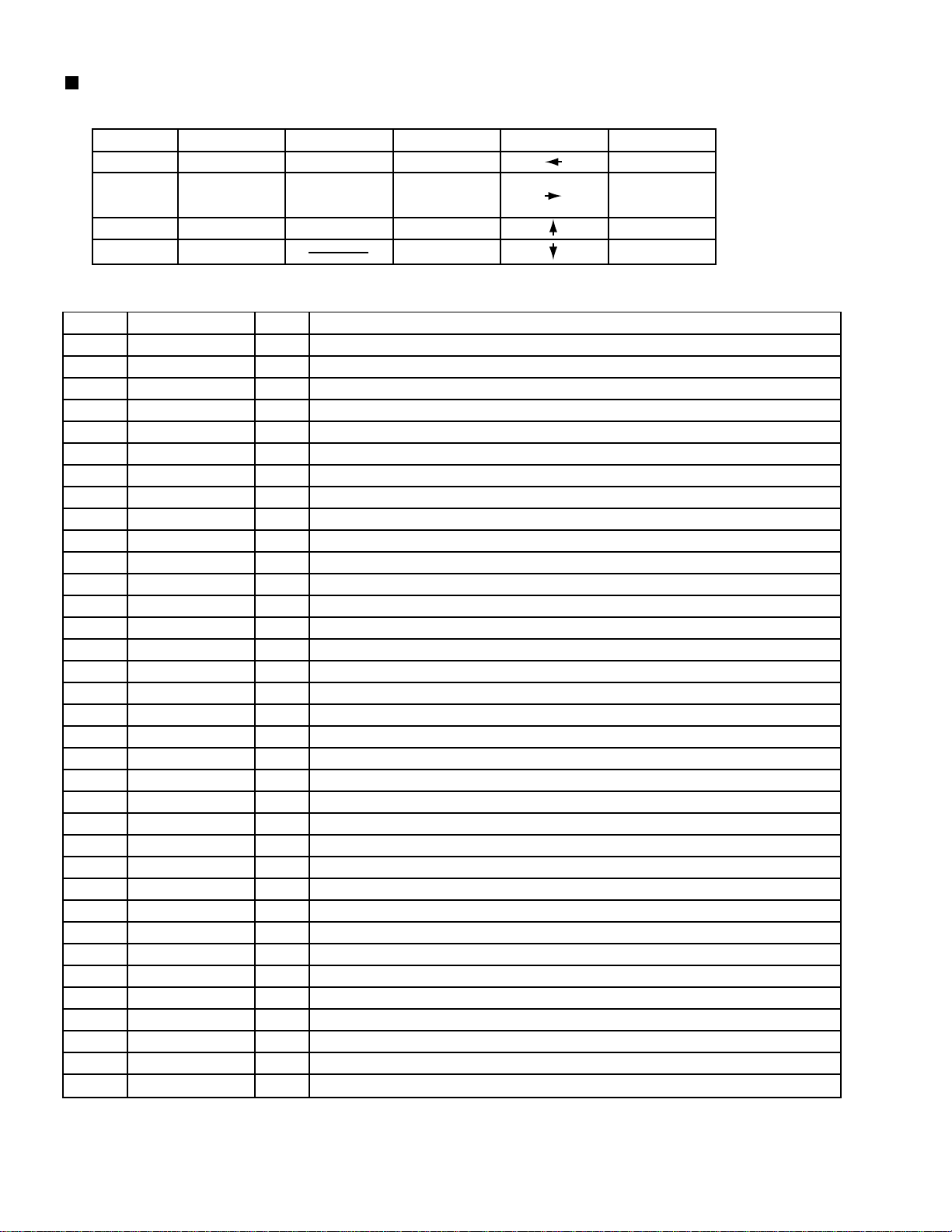
Area Suffix
China
Singapore
POWER
TV
CD
VCR
AUDIO
TAPE/MD
SURROUND
TESTDELAY
5
321
EFFECT
FM/AM
– CENTER +
5
54
6
5
VCR
– REAR•L +
5
98
7/P
MENU
SOUND
DVD
CONTROL
– REAR•R +
+10
10
ENT
DVD MULTI
CD-DISC
TV VOL.
+
PHONO
ONE TOUCH
OPERATION
VOLUME
MUTING
SLEEP
8
4
1
RM-SR558U REMOTE CONTROL
–
TV CH–TV/VIDEO
+
+
+
VCR CH
–
–
£
4
1
7
RX-5000V AUDIO/VIDEO CONTROL RECEIVER
STANDBY
POWER
SPEAKERS
PHONES
12
DVD MULTICDDVD
PHONO
OFF_ ON
Contents
Safety precautions ---------------- 1-2
Disassembly method ------------- 1-3
Adjustment method --------------- 1-5
MASTER VOLUME
– +
ADJUSTBASS BOOST
SETTING
VCR
FM
SURROUND MULTI CURSOR
ONE TOUCH OPERATION
AM
TAPE/MD
SOURCE NAME
INPUT ATT.
MEMORY
Description of major ICs --------- 1-6
Internal connections for
FL display tube ----- 1-15
COPYRIGHT 2000 VICTOR COMPANY OF JAPAN, LTD.
No.20883
Nov. 2000
Page 2
http://getMANUAL.com
RX-5000VBK/RX-5001VGD
Safety Precautions
1. This design of this product contains special hardware and many circuits and components specially
for safety purposes. For continued protection, no changes should be made to the original design
unless authorized in writing by the manufacturer. Replacement parts must be identical to those
used in the original circuits. Services should be performed by qualified personnel only.
2. Alterations of the design or circuitry of the product should not be made. Any design alterations of
the product should not be made. Any design alterations or additions will void the manufacturer`s
warranty and will further relieve the manufacture of responsibility for personal injury or proper ty
damage resulting therefrom.
3. Many electrical and mechanical par ts in the products have special safety-related characteristics.
These characteristics are often not evident from visual inspection nor can the protection afforded
by them necessarily be obtained by using replacement components rated for higher voltage,
wattage, etc. Replacement parts which have these special safety characteristics are identified in
the Parts List of Service Manual. Electrical components having such features are identified by
shading on the schematics and by ( ) on the Parts List in the Service Manual. The use of a
substitute replacement which does not have the same safety characteristics as the recommended
replacement parts shown in the Parts List of Service Manual may create shock, fire, or other
hazards.
4. The leads in the products are routed and dressed with ties, clamps, tubings, barriers and the
like to be separated from live parts, high temperature parts, moving parts and/or sharp edges
for the prevention of electric shock and fire hazard. When service is required, the or iginal lead
routing and dress should be observed, and it should be confirmed that they have been returned
to normal, after re-assembling.
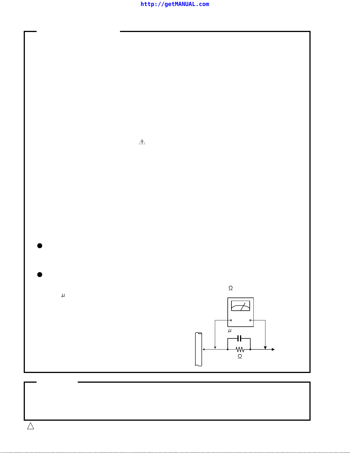
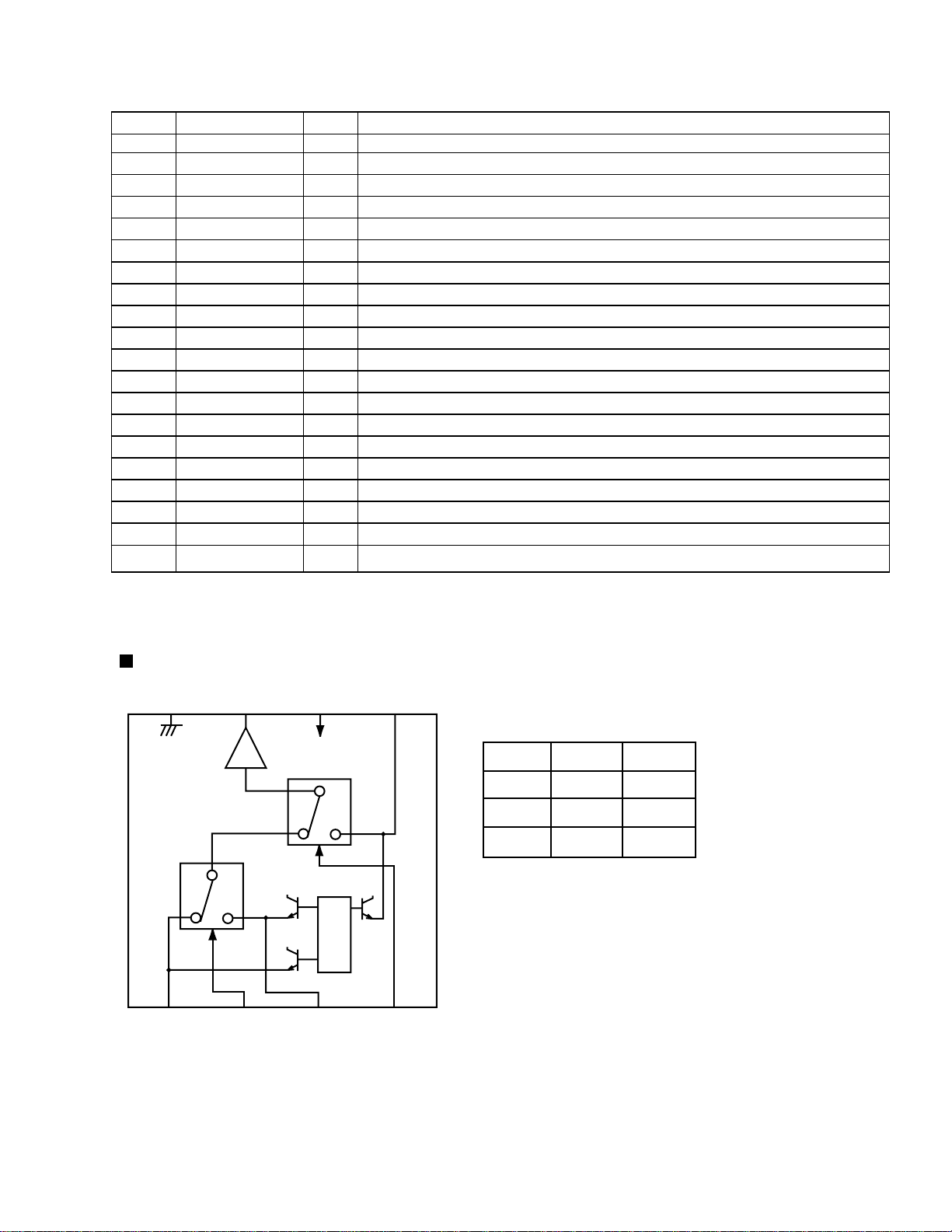
5. Leakage currnet check (Electrical shock hazard testing)
After re-assembling the product, always perform an isolation check on the exposed metal parts
of the product (antenna terminals, knobs, metal cabinet, screw heads, headphone jack, control
shafts, etc.) to be sure the product is safe to operate without danger of electrical shock.
Do not use a line isolation transformer during this check.
Plug the AC line cord directly into the AC outlet. Using a "Leakage Current Tester", measure
the leakage current from each exposed metal parts of the cabinet , particularly any exposed
metal part having a return path to the chassis, to a known good earth ground. Any leakage
current must not exceed 0.5mA AC (r.m.s.)
Alternate check method
Plug the AC line cord directly into the AC outlet. Use an AC voltmeter having, 1,000 ohms
per volt or more sensitivity in the following manner. Connect a 1,500 10W resistor paralleled by
a 0.15 F AC-type capacitor between an exposed
metal part and a known good earth ground.
Measure the AC voltage across the resistor with the
AC voltmeter.
Move the resistor connection to eachexposed metal
part, par ticularly any exposed metal part having a
return path to the chassis, and meausre the AC
voltage across the resistor. Now, reverse the plug in
the AC outlet and repeat each measurement. voltage
measured Any must not exceed 0.75 V AC (r.m.s.).
This corresponds to 0.5 mA AC (r.m.s.).
0.15 F AC TYPE
1500 10W
Good earth ground
AC VOLTMETER
(Having 1000
ohms/volts,
or more sensitivity)
Place this
probe on
each exposed
metal part.
Warning
1. This equipment has been designed and manufactured to meet international safety standards.
2. It is the legal responsibility of the repairer to ensure that these safety standards are maintained.
3. Repairs must be made in accordance with the relevant safety standards.
4. It is essential that safety critical components are replaced by approved parts.
5. If mains voltage selector is provided, check setting for local voltage.
Burrs formed during molding may be left over on some parts of the chassis. Therefore,
pay attention to such burrs in the case of preforming repair of this system.
1-2
CAUTION
!
Page 3
RX-5000VBK/RX-5001VGD
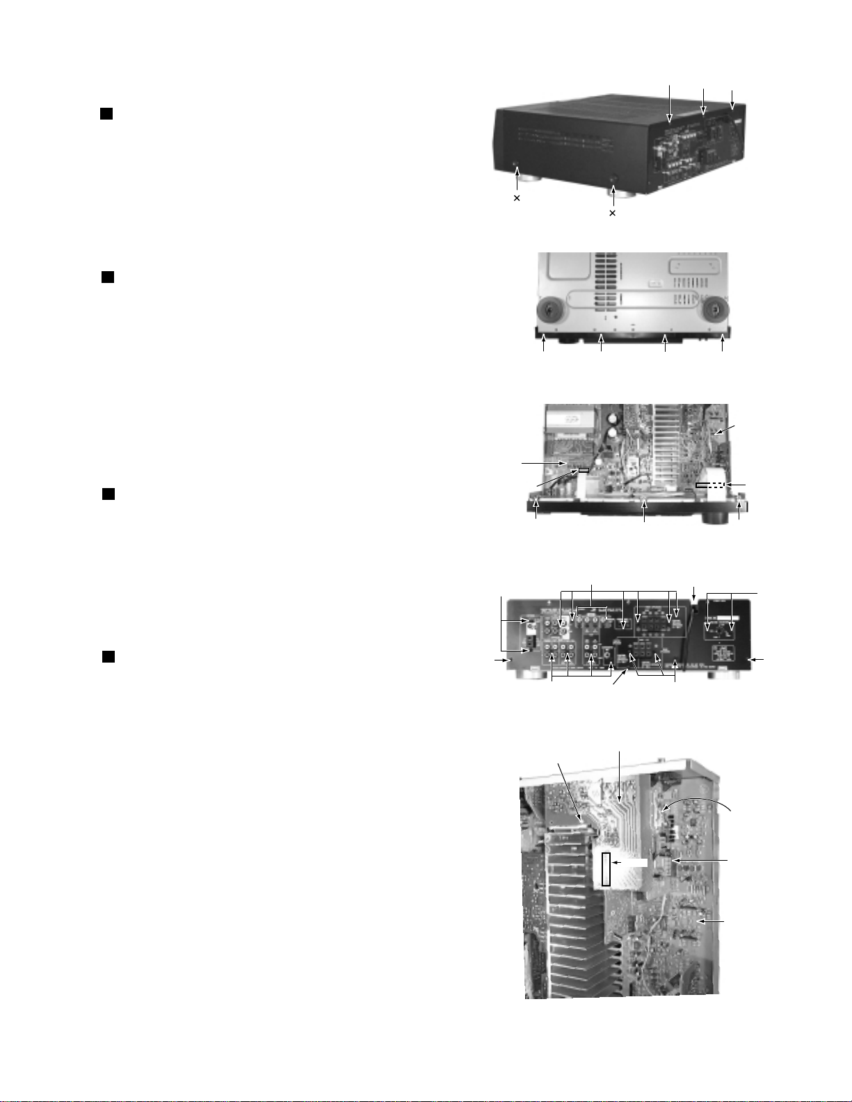
Disassembly method
Removing the top cover (See Fig.1)
1. Remove 4 screws "A" on both sides of the top cover
and 3 screws "B" on the rear side.
2. Lift the back of the top cover spreading both sides
to remove.
Removing the front panel assembly (See Fig.2,3)
1. Remove the top cover.
2. Remove 4 screws "C" on the bottom side and 3 screws
"D" on the top side.
3. Disconnect the wire CN811 on the main board.
4. Disconnect the wire CN314 on the audio & source
selector board.
5. Remove the front panel assembly.
Removing the rear panel (See Fig.4)
1. Remove the top cover.
2. Remove 21 screws "E" on the rear panel.
3. Remove 3 screws "F" on the rear panel.
4. Remove the power cord stopper up side.
5. Remove the rear panel.
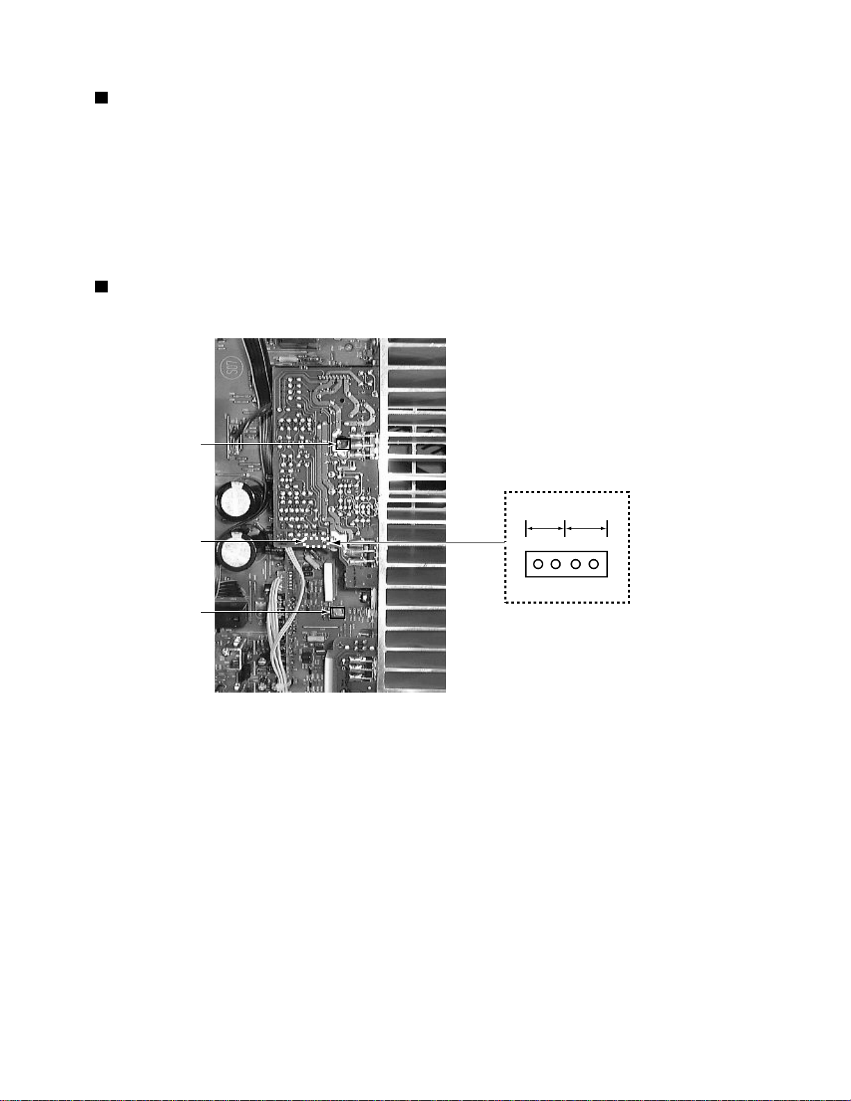
Removing the tuner board and
video board (See Fig.5)
1. Remove the rear panel.
2. Remove 1 screw "G" on the video board
3. Disconnect the connector CN311 on the
video board
4. Disconnect the connector CN111 on the
audio & source selector board.
A 2
A 2
B
B
B
Fig.1
C C
C
C
Fig.2
BOTTOM COVER
Fig.4
Power cord
Stopper
E
CN311
G
VIDEO board
Fig.5
Audio &
source
selector
board
Tuner
board
CN111
D
D
D
Fig.3
CN811
CN314
Main
board
Audio &
source
selector
board
F
F
F
E
E
E
E
1-3
Page 4
RX-5000VBK/RX-5001VGD
Removing the audio & source selector
board (See Fig.6)
1. Remove the rear panel.
2. Remove the video board and Tuner board.
3. Disconnect the connector CN512 and CN619 on the
audio & source selector board.
4. Disconnect to the card wire CN314 on the audio &
source selector board.
5. Disconnect the connector CN712 on the AMP board.
6. Each tie band is cut out.
7. Pullout the connection board.
8. Remove 4 screws "H" on the audio & source
selector board.
9. Remove the audio & source selector board.
Removing the main board (See Fig.6 to 8)
CN712
H
H
Audio & source
Audio & source
selector board
selector board
CN619
CN512
H
CN314
Connection board
H
Fig.6
Main
CN511
I
PCB
(Standing substrate)
I
Audio & source
selector board
1. Remove the rear panel and front panel assembly.
2. Pull out the pre AMP board and connection board.
3. Remove 8 screws "I" on the main board.
4. Remove 8 screws "J" on the power transistor.
5. Disconnect the connector CN511 and wire
CN831 on the main board.
6. Each tie band is cut out.
7. Remove 2 screws "K" on push switch of the front side.
8. Remove nut on terminal of the headphone.
9. The solder of the wire connected with the
transformer is removed.
10. Remove the main board.
Removing the front board (See Fig.9)
Solder
Pre AMP board
(Standing substrate)
Solder
Headphone jack
I
J
I
Fig.7
NUT
I
KK
L
I
CN831
I
Connection
board
Fig.8
1. Remove the top cover.
2. Remove the Front panel assembly.
3. Remove the master volume knob and nut.
4. Remove the 13 screws "L" on the Front board.
1-4
L
L
L
L
L
L
Fig.9
Page 5
Adjustment method
TUNER SECTION
1.Tuner range
FM 87.5MHz~108.0MHz
AM(MW) 530kHz~1710kHz
POWER AMPLIFIER SECTION
RX-5000VBK/RX-5001VGD
VR742
Rch
Lch
TP001
VR741
IDLING CURRENT
1.Set the volume control to minimum during this adjustment.
2.Set the surround mode OFF.
2.Turn VR741 and VR742 fully counterclockwise to warm up before adjustment.
If the heat sink is already warm from previous use the correct adjustment can not be made.
3.For L-ch,connect a DC voltmeter between TP001's pin1 and pin2 (Lch)
And,connect it between pin3 and pin4(Rch).
4.30 minutes later after power on, adjust VR741 for L-ch, or VR742 for R-ch so that the DC voltmeter
value has 1mV~10mV.
4 3 2 1
TP001
1-5
Page 6
RX-5000VBK/RX-5001VGD
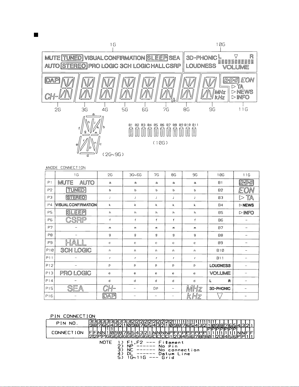
Description of major ICs
M62446FP(IC341) : 6CH Master volume
1.Block Diagram
OUT4
OUT3
OUT2
OUT1
AVDD
SWIN
GNDS
SRin
SLin
GNDC
Cin
GNDR
Rin
GNDL
Lin
BYPASSR
BYPASSL
LTRE
LBASS3
LBASS2
LBASS1
10
11
12
13
14
15
16
17
18
19
20
21
1
2
3
4
5
6
7
8
9
OUTPUT
PORT
tone
volume
volume
volume
volume
volume
volume
MCU
I/F
tone
42
41
40
39
38
37
36
35
34
33
32
31
30
29
28
27
26
25
24
23
22
DVDD
CLK
DATA
LATCH
DGND
AGND
SWout
SRout
SLout
Cout
Rout
Lout
AVSS
CL1
CL2
CR1
CR2
RTRE
RBASS3
RBASS2
RBASS1
1-6
Page 7

2.Pin Function
RX-5000VBK/RX-5001VGD
Pin No.
1
2
3
4
5
6
7
8
9
10
11
12
13
14
15
16,17
18
19~21
22
23,24
25
26
27
28
29
30
31
32
33
34
35
36
37
38
39
40
41
42
Symbol I/O Descriptions
SURROUND
BASS BOOST
INPUT-ATT
MUTING
AVDD
SWIN
A.GND
RR IN
RL IN
A.GND
C IN
A.GND
R IN
A.GND
L IN
AVSS
L OUT
R OUT
C OUT
RL OUT
RR OUT
SW OUT
A.GND
D.GND
VOL STB
VOL DATA
VOL CLK
DVDD
O
O
O
O
I
I
I
I
I
I
-
-
-
O
-
-
I
O
I
O
O
O
O
O
O
-
-
I
I
I
-
SURROUND control terminal
BASS BOOST control terminal
Input attenuator control terminal
MUTING control terminal
Analog positive power supply terminal
SUB Woofer volume signal input terminal
Analog ground terminal
R ch volume signal input terminal for rear speaker
L ch volume signal input terminal for rear speaker
Analog ground terminal
Center volume signal input terminal
Analog ground terminal
R ch volume signal input terminal
Analog ground terminal
L ch volume signal input terminal
Non connect
Frequency adjustment terminal tone/treble
Frequency adjustment terminal tone/bass
Tone output terminal
Frequency adjustment terminal tone/bass
Frequency adjustment terminal tone/treble
Frequency adjustment terminal tone/bass
L/R volume input terminal
Tone output terminal
L/R volume input terminal
Analog negative power supply terminal
L ch output
R ch output
Center volume signal output terminal
L ch volume signal output terminal for rear speaker
R ch volume signal output terminal for rear speaker
SUB Woofer volume signal output terminal
Analog ground terminal
Digital ground terminal
Latch input terminal
Volume data input terminal
Clock input terminal for data transfer
Digital power supply terminal
1-7
Page 8
RX-5000VBK/RX-5001VGD
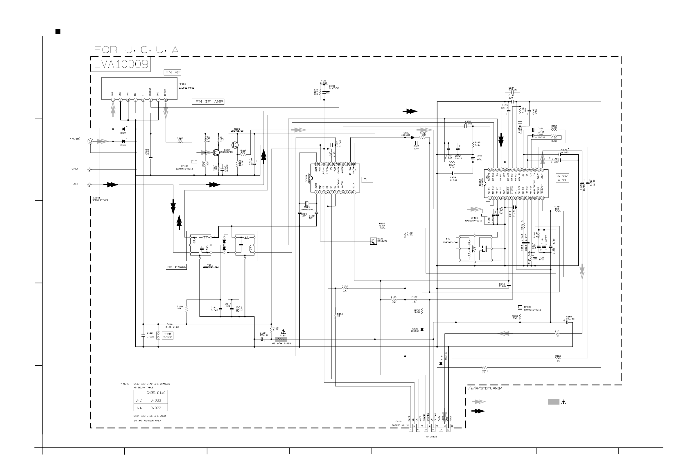
LA1838(IC102): FM AM IF AMP&detector, FM MPX Decoder
1. Block Diagram
30
ALC
BUFF
FM
S-METER
FM IF
1
2. Pin Function
Pin
Symbol
No.
FM IN
1
AM MIX
2
3
FM IF
AM IF
4
GND
5
6
TUNED
STEREO
7
8
VCC
9
FM DET
10
AM SD
FM VSM
11
AM VSM
12
13
MUTE
14
FM/AM
MONO/ST O
15
29
28
AM
OSC
SD
COMP
S-CLRVE
PM
DET
2
I/O
I
This is an input terminal of FM IF
REG
AM
MIX
AM/FM
IF-BUFF
3
27
FM
RF.AMP
AM IF
4
26
AGC
AM
S-METER
GND
Function
DET
5
signal.
This is an out put terminal for AM
O
mixer.
I
Bypass of FM IF
Input of AM IF Signal.
I
I
This is the device ground terminal.
When the set is tunning,this terminal
O
becomes "L".
O
Stereo indicator output. Stereo "L",
Mono: "H"
III
This is the power supply terminal.
I
FM detect transformer.
I
This is a terminal of AM ceramic filter.
O
Adjust FM SD sensitivity.
O
Adjust AM SD sensitivity.
I/O
When the signal of IF REQ of IC121(
LC72131) appear, the signal of FM/AM
IF output. //Muting control input.
Change over the FM/AM input.
I
"H" :FM, "L" : AM
Stereo : "H", Mono: "L"
25
TUNING
DRIVE
6
24
STEREO
DRIVE
7
22
23
P-DET
VCC
89
Pin
Symbol
No.
16
R OUT
17
L OUT
18
19
20
21
22
23
24
25
26
27
28
29
30
R IN
L IN
RO
LO
IF IN
FM OUT
AM DET
AM AGC
AFC
AM RF
REG
AM OSC
OSC BUFFER
21
DECODER
ANIT-BIRDIE
VCO
384KHz
10
20
STEREO
5N
SW
FF
38k
11
I/O
O
Right channel signal output.
O
Left channel signal output.
Input terminal of the Right channel post
I
18
19
MUTE
FF
/
19k
2
12 13
FF
19k
/LS
Function
17 16
PILOT
DET
14
AMP.
Input terminal of the Left channel
I
post AMP.
Mpx Right channel signal output.
O
O
Mpx Left channel signal output.
I
Mpx input terminal
FM detection output.
O
AM detection output.
O
This is an AGC voltage input terminal
I
for AM
I
This is an output terminal of voltage
for FM-AFC.
AM RF signal input.
I
Register value between pin 26 and pin28
O
besides the frequency width of the
input signal.
I
This is a terminal of AM Local
oscillation circuit.
AM Local oscillation Signal output.
O
15
1-8
Page 9
1. Pin layout
1
2
3
4
5
6
7
8
9
10
11
22
21
20
19
18
17
16
15
14
13
12
XT
FM/AM
CE
DI
CLOCK
DO
FM/ST/VCO
AM/FM
SDIN
XT
GND
LPFOUT
LPFIN
PD
VCC
FMIN
AMIN
IFCONT
IFIN
Pin
No.
1
2
3
4
5
6
7
8
9
10
11
Pin
No.
12
13
14
15
16
17
18
19
20
21
22
Symbol
XT
FM/AM
CE
DI
CLOCK
DO
FM/ST/VCO
AM/FM
LW
MW
SDIN
Symbol
IFIN
IFCONT
AMIN
FMIN
VCC
PD
LPFIN
LPFOUT
GND
XT
Function
X'tal oscillator connect (75kHz)
LOW:FM mode
When data output/input for 4pin(input) and
6pin(output): H
Input for receive the serial data from
controller
Sync signal input use
Data output for Controller
Output port
"Low": MW mode
Open state after the power on reset
Input/output port
Input/output port
Data input/output
Function
IF counter signal input
IF signal output
Not use
AM Local OSC signal output
FM Local OSC signal input
Power suplly(VDD=4.5-5.5V)
When power ON:Reset circuit move
PLL charge pump output(H: Local OSC
frequency Height than Reference frequency.
L: Low Agreement: Height impedance)
Input for active lowpassfilter of PLL
Output for active lowpassfilter of PLL
Connected to GND
X'tal oscillator(75KHz)
I/O
I
O
I
I
I
O
O
O
I/O
I/O
I/O
I/O
I
O
-
I
I
-
O
I
O
I
Reference
Driver
Phase
Detector
Charge Pump
Unlock
Detector
Universal
Counter
Swallow Counter
1/16,1/17 4bit
12bit
Programmable
DriverS
Swallow Counter
1/16,1/17 4bit
Data Shift Register & Latch
Power
on
Reset
C
2B
I/F
1/2
7821113
21
17
6
5
4
3
15
16
22
1
18
19
20
12
2. Block diagram
3. Pin function
LC72136N (IC121) : PLL Frequency Synthesizer
RX-5000VBK/RX-5001VGD
1-9
Page 10
RX-5000VBK/RX-5001VGD
MN173222BA(IC401) : System controller
1.Key Matrix
KEY OUT 0
KEY IN 0
KEY IN 1
KEY IN 2
KEY IN 3
2.Pin Function (1/2)
Pin No. Symbol
1,2
3,4
5
6
7~10
11
12~21
22
23
24~39
40
41
42
43
44
45
46
47
48
49
50
51
52
53
54
55
56
57
58
59
60
61
62
63
64
IN1,2
VIDEO1,2
PROTECT
POWER
KI0~3
VCR /S/C
G11~G2
G1/KO7
VPP
S1~16
B.BOOST LED
CLK.D
DATAIN.D
DATAOUT.D
INH
RDS CLK
RDS DATA
SW DATA
REMOCON IN
RDS D.ST
STEREO
TUNED
CE.PLL
CK.PLL
SW.CLK
DO.PLL
DCS IN
DCS OUT
ERR.DSP
IFOK.DSP
ACK.DSP
CD.DSP
RELAY Sch
T.MUTE
SUBWFMUTE
POWER
ADJUST
SETTING
MEMORY
KEY OUT1
SURROUND
ONE TOUCH
OPERATION
INPUT ATT
KEY OUT 2
DVD MULTI
DVD
VCR
FM
KEY OUT 3 KEY OUT 4
I/O Function
Volume jog signal input
I
Video signal switch output
O
Protect signal input of speaker
I
Power ON output
O
Key matrix signal input
I
Not used
FL grid signal output
O
FL grid signal output / Key matrix signal output
O
Power supply
FL segment control signal output
O
Bass boost indicator control
O
Clock signal output to DSP
O
Data signal input from DSP
I
Data signal output to DSP
O
Inhibit detection signal input
I
Clock signal input from RDS
I
Data input from RDS
I
Function switch data signal output
O
Remote control signal input
I
Data start signal for block data to output serial data
I
Stereo indicator output. Stereo "L" Mono "H"
I
When the set is tuning, this terminal becomes "L"
I
Chip enable output to IC121
O
Clock signal for IC121
I/O
Function switch clock signal output
O
Tuner PLL data
I/O
Compulink signal input
I
Compulink signal output
O
DSP control data input
I
DSP control data input
I
DSP control data input
I
DSP control data output
O
Rear ch relay control signal output
O
TUNER mute signal output
O
Sub woofer mute signal output
O
CD
PHONE
TAPE/MD
AM
1-10
Page 11
65
66
67
68
69
70
71
72
73
74
75
76
77
78
79
80
81
82
83
84
TV OUT
VCR OUT
VCR IN
RESET IN
X1
X2
VSS
OSC2
OSC1
VDD
RELAY Cch
RELAY L/R
SURROUND
INPUT ATT LED
ONE T. LED
STANDBY LED
STB-SW
VOLUME DATA
VOLUME CLK
VOLUMESTB
Pin No. Symbol
I/O Function
Connect to GND
Connect to GND
Reset signal input
Connect to GND
Non connect
Connect to GND
Oscillation terminal
Oscillation terminal
Power supply
Center ch relay control signal output
Front ch relay control signal output
Surround ON/OFF control
INPUT ATT. Indicator control
ONE TOUCH OPERATION indicator control
STANDBY indicator control
Strobe signal output of function switch
Data output to IC341
Clock signal output to IC341
Strobe signal output to IC341
-
-
I
-
-
-
-
-
-
O
O
O
O
O
O
O
O
O
O
2.Pin Function (2/2)
CTL 1
L
H
L/H
CTL 2
L
L
H
Output
VIN 1
VIN 2
VIN 3
Control input - output signal
GND
8
Vout
7
V+
6
Vin3
5
1
Vin1
2
CTL1
3
Vin2
4
CTL2
6dB
AMP.
BIAS
NJM2246D(IC201):Video Switch
RX-5000VBK/RX-5001VGD
1-11
Page 12
RX-5000VBK/RX-5001VGD
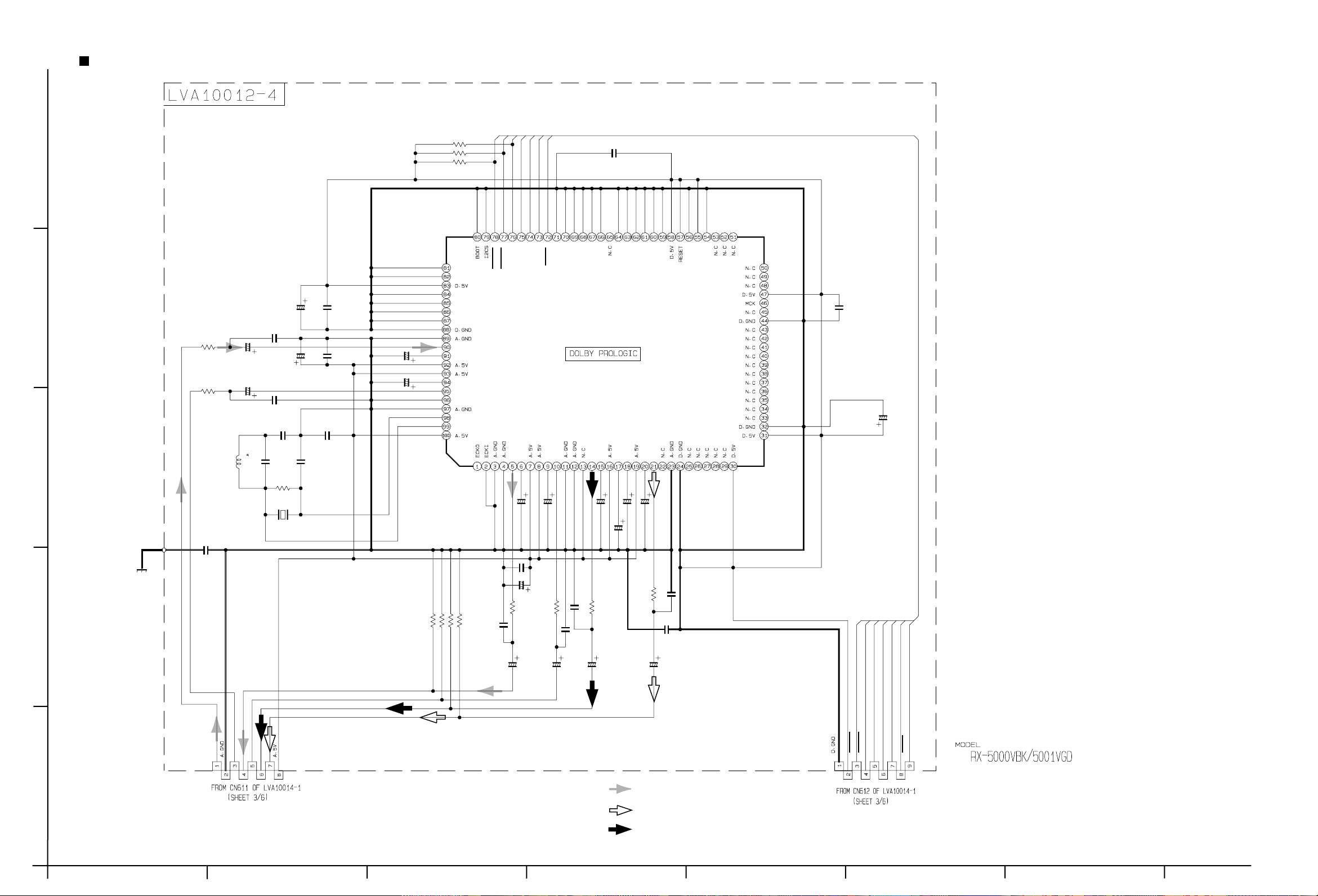
TC9471F(IC601) : Dolby prologic
1.Block Diagram
FBUS
STABUS
Timing Gen.
DBUS
OFP
CP
DLA Gen.
DFRAM
64w 16b
CRAM
320w 16b
DLRAM
DLRO DLRI
FBUS
4kw 16b
MAC Block
DBUS
SI0 register
SI1 register
SO0 register
SO2 register
SO1 register
PC Block
CRP Gen.
Lin Log Adj.
DP Gen.
CROM
256w 16b
DRAM
256w 24b
PROM
1kw 32b
FBUS
DBUS
(LDA)
IR
(JMP)
LC
(LDB)
IDEC
Self
Boot
MCU-I/F
ADC(L)
ADC(R)
DF Block
(digital Filter)
DAC(L)
DAC(R)
DAC(C)
DAC(S)
1-12
Page 13

2.Pin Function (1/2)
RX-5000VBK/RX-5001VGD
Pin No.
1
2
3
4
5
6
7
8
9
10
11
12
13
14
15
16
17
18
19
20
21
22
23
24
25~29
30
31
32
33~43
44
45.46
47
48~53
54
55
56
57
Symbol
ECKO
ECKI
A.GND
A.GND
LchOUT
V-REF1
A.5V
A.5V
V-REF2
RchOUT
A.GND
A.GND
N.C
CchOUT
V-REF3
A.5V
VRO
VRI
A.5V
V-REF4
SchOUT
NC
A.GND
D.GND
NC
D.5V
D.5V
D.GND
NC
D.GND
NC
D.5V
NC
RESET
I/O
Non connect
Amplifier input terminal for external clock input.
I
Ground terminal.(For crystal oscillator circuit)
Ground terminal.(For DAC L channel)
DAC analog signal output terminal.(L channel)
O
Reference voltage terminal.(For DAC L channel)
Power supply terminal.(For DAC L channel)
Power supply terminal.(For DAC R channel)
Reference voltage terminal.(For DAC R channel)
DAC analog signal output terminal.(R channel)
O
Ground terminal.(For DAC R channel)
Ground terminal.(For DAC C channel)
DAC analog signal output terminal.(C channel)
O
DAC analog signal output terminal with attenuator.(For C channel)
O
Reference voltage terminal.(For DAC C channel)
Power supply terminal.(For DAC C channel)
Reference voltage terminal for attenuator.(Output buffer)
O
Reference voltage terminal for attenuator.(Input buffer)
I
Power supply terminal.(For DAC S channel)
Reference voltage terminal.(For DAC S channel)
DAC analog signal output terminal with attenuator.(For S channel)
O
Non connect.
Ground terminal.(For DAC S channel)
Ground terminal.
Non connect.
Power supply terminal.
Power supply terminal.(For DLRAM)
Ground terminal.(For DLRAM)
Non connect.
Ground terminal.
Non connect.
Power supply terminal.
Non connect.
Ground terminal.
Power supply.
Ground terminal.
Power supply.
I
Function
1-13
Page 14
RX-5000VBK/RX-5001VGD
2.Pin Function (2/2)
Pin No.
58
59~71
72
73
74
75
76
77
78
79
80
81,82
83
84~87
88
89
90
91
92,93
94
95
96,97
98
99
100
Symbol
D.5V
DSP-CS
DSP-CLK
DATA-IN
DATA-OUT
DSP-IFOK
DSP-ACK
DSP-ERR
I2CS
BOOT
D.5V
D.GND
A.GND
LchIN
V-REF5
A.5V
V-REF6
RchIN
A.GND
XI
XO
A.5V
I/O
Power supply terminal
Non connect.
Chip select signal input terminal.(MCU interface)
I
Data sift clock input terminal.(MCU interface)
I
Data input terminal.(MCU interface)
I/O
At the IC bus mode,data input /output terminal.
Data output terminal.(MCU interface)
O
At the IC bus mode,normally open.
Operation flag output terminal.(MCU interface)
O
Acknowledge signal output terminal.(MCU interface)
O
Error flag output terminal.(MCU interface)
O
IC bus mode select terminal.
I
Self-boot control terminal.
I
Non connect.
Power supply terminal.
Ground terminal.
Digital ground terminal.(For ADC L channel)
Analog ground terminal.(For ADC L channel)
ADC analog signal input terminal.(L channel)
I
Reference voltage terminal.(For ADC L channel)
Analog power supply terminal.
Reference voltage terminal.(For ADC R channel)
ADC analog signal input terminal.(R channel)
Analog ground terminal.(For ADC R channel)
Crystal oscillator connection terminal.(input)
I
Crystal oscillator connection terminal.(output)
O
Power supply terminal.(For crystal oscillator circuit)
-
Function
1-14
Page 15
Internal connections for FL display tube
QLF0002-001(DI401):FL DISPLAY TUBE
RX-5000VBK/RX-5001VGD
1-15
Page 16
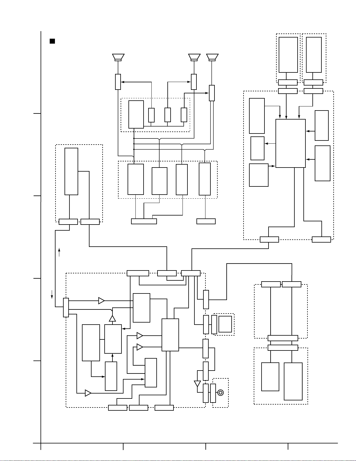
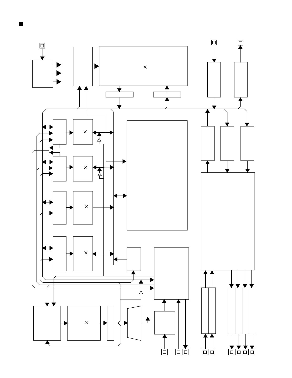
Block diagrams
FL DISPLAY &
OPERATION SW
CONTROL
IC401
MN173222BA
FL TUBE
DI401
MAIN VOLUME
JS401
KEY MATRIX
S417~S423
KEY MATRIX
S402~S416
KEY MATRIX
POWER KEY
S401
OSC1,2
X401
6MHz
REMOCOM
IC402
CN411CN412
MCLK
COMMAND
STATUS
M.RESET
M/CS
RDS.DST
RDS.CLK
RDS.DATA
CN401CN402
CN404 CN304
DVD INPUT
AUDIO
J211
VIDEO
INPUT/OUTPUT
J212~J215
CN311
CN301
CN604 CN603
REAR L/R CENTER
SUB.W FRONT L/R
VCR S/C
DVD S/C VIDEO1,2
CN512 CN613CN702
CN611
CN614
6CH MASTER
VOLUME
IC341
SURROUND
ON/OFF
IC323
SOURCE
SELECTOR
IC321
PHONO EQ.
IC301
DVD MULTI
IC322
AUDIO
INPUT/OUTPUT
J301~J303
IC332
IC331
RR
RL
CENTER
SUBWOOFER
IC311
IC313
IC333
IC312
LIN
RIN
LOUT
ROUT
FL
FR
VOL.CLK
VOL.DATA
VOL.STB
VIDEO1,2
DCS
J1251
CN616
CN606
DCS
CN314 CN612 CN121
REAR.R
SUB
WOOFER
REAR.L CENTER FL FR
SUB WOOFER
CN609
CN618
CN608
Q701~Q704
Q707~Q708
Q761~Q764
Q551.Q522
Q561.Q575
Q576
Q501~Q503
Q507~Q508
Q1501~Q1503
Q1507,Q1508
POWER AMP.
Q901.Q902
Q591.Q509
Q1509
Q903
Q951
Q952
PROTECTOR
RY952
RY951
RY921
FRONT L/R
CENTER
REAR L/R
FRONT
CENTER
REAR L
REAR R
CN712CN502
DOLBY PROLOGIC
IC601
DATA I/O,DSP CLK,DSP CS
L/R IN
L/R,CENTER,REAR OUT
CN602 CN601
TO
CN712
TO
CN502
TO
CN603
FROM
CN702
FROM
CN512
FROM
CN613
FROM
CN414
TU L/R
TO
CN111
TUNER
SECTION
CN619
Amplifier/Control section
5
4
RX-5000VBK/RX-5001VGD
3
2
1
ABC
2-1
Page 17
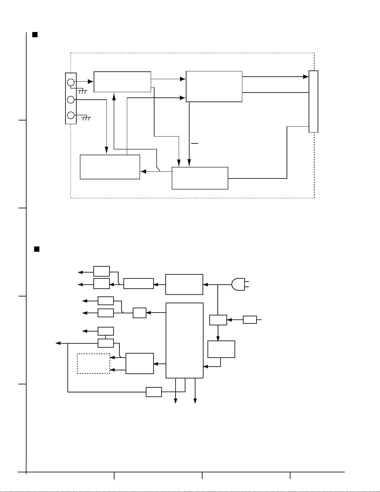
RX-5000VBK/RX-5001VGD
Tuner Section
5
FM
AM
FM FRONTEND
RF101
AM RF
AM OSC
IF OUT
FM IF/DET/MPX
AM RF/IF/DET
IC102
TUNER
OUT L/R
MPX
TO
CN121
CN111
VT
4
MW RF/MWOSC
COIL
T111
FM OSC
AM/FM
AM OSC
OUT
PLL Synthesizer
DATA
CLOCK
CE
IC121
3
2
Power Supply Section
Only U type
+5V
+5V
+5.6V
+12V
-12V
-25V
Q802
Q805
Q802
Q891
Q851
Q821
Q841
POWER AMP
+B
-B
D801~D804
D811
D812
D861~D864
T801
POWER
TRANSFOMER
T001
POWER
TRANSFORMER
RY801
VOLT AGE
SELECTOR
VS801
Only U type
Q803
POWER ON
STANDBY
1
2-2
Q885
FL FL
ABCD
Page 18
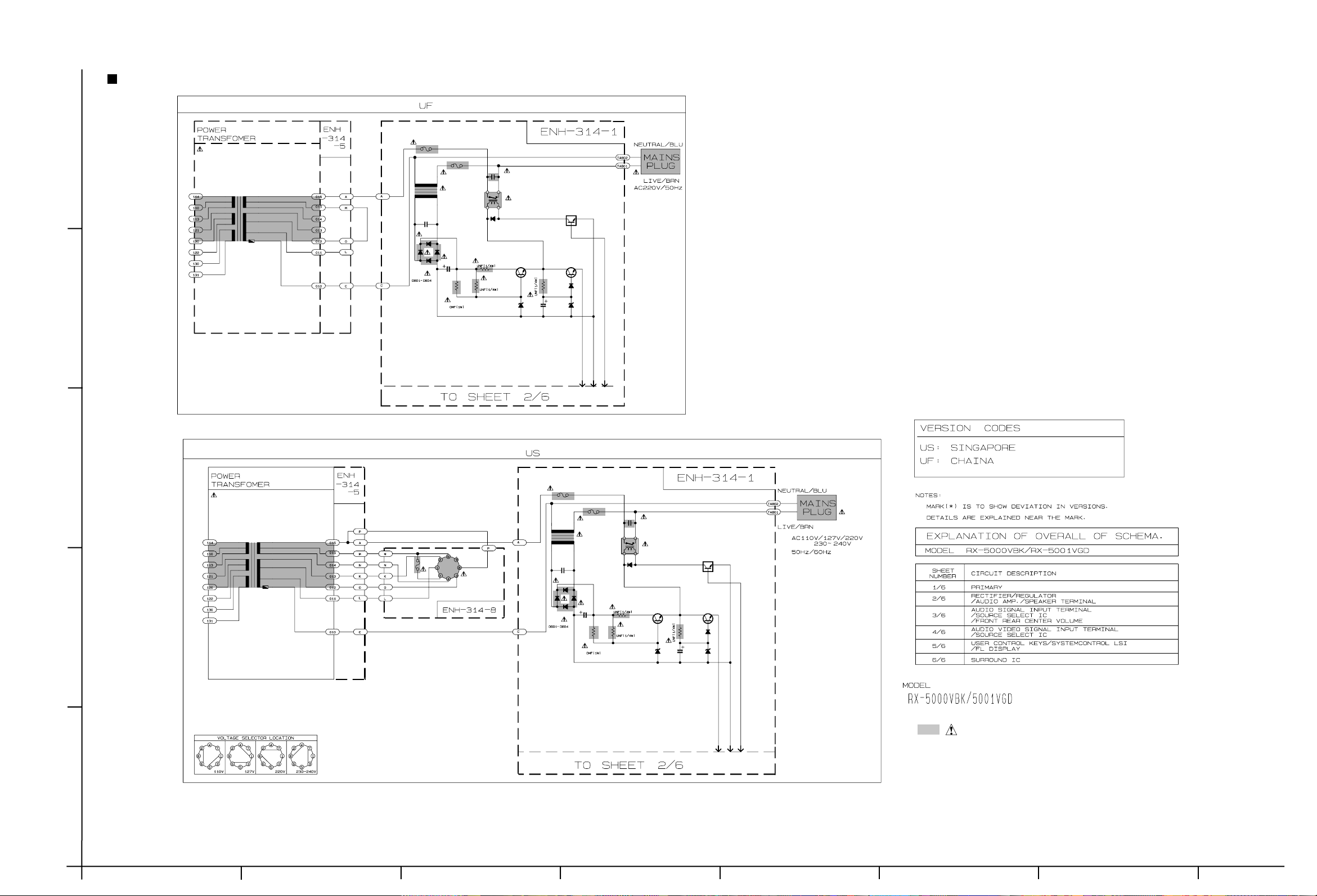
Standard schematic diagrams
Power supply section
RX-5000VBK/RX-5001VGD
F801
T3.15A
5
4
C801
0.0047/100
D801
D802
D803
1SR35
F802
T801
QQT0281-004
D804
C802
470/63
R807
3.3K
T100mA
R801
3.3
R806
15K
D808
1ss133
C804
0.0047
RY801
MTZ12JC
Q805
2SD1266 2SC2235
820
R803
D805
470/10
C803
Q803
KRC105M
Q802
D806
1SS133
D807
MTZ6.2JC
B5V
L.GND
ACC
3
T6.3A
F801
T100mA
F802
T801
QQT0281-004
F803
T3.15A
VS801
2
C801
0.0047/100
D801
D802
D803
1SR35
D804
C802
470/63
R807
3.3K
R801
3.3
R806
15K
D808
1ss133
C804
0.0047
RY801
MTZ12JC
Q805 Q802
2SD1266 2SC2235
820
R803
D805
C803
470/10
Q803
KRC105M
D806
1SS133
D807
MTZ6.2JC
B5V
L.GND
ACC
Parts are safety assurance parts.
When replacing those parts make
sure to use the specified.
1
SHEET 1/6
ABCD E F G
2-3
Page 19
RX-5000VBK/RX-5001VGD
Audio AMP / Power primary section
C571
C556
0.0015
R553
3k
R556
D553
1SS133
C553
5
4
R551
2.2K
CN712
R701
2.2K
C703
270P
C704
R702
2.2K 10/50
100P
C551
10/50
18k
Q551
C552
270P
C701
10/50
R703
C702
R555
56k
R552
2SC2240( BL)
0.0015
R705
D703
R717
1SS133
C705
100P
Q701
Q703
2SC2240( BL)
R709
56k
R710
C712
R704
100/16
56k270P
Q702
R712
2SC2240
Q704
2SC2240
C706
100P
D704
1SS133
R706
100
C717
100
2SA1038S( SE)
R711
2SC2240( BL)
390
C722
R718
100
C718
0.0015
Q552
Q707
C721
C713
22P
R561
330
C561
2.2/50
2SC2240( BL)
22P
R713
2SC2389S
390
C711
R714
56k
C714
Q561
2SA1038S( SE)
C562
R569
C563
10
0.01
33P
R563
3.3k
R560
56k
C557
R564
22p
C564
47/50
R558
300
C558
47/16
R570
R739
10
R721
22p
56k
Q711
R729
R730
100/16
2SC2389S
22p
Q708
2SA1038S
R722
CN701
3.3k 3.3k 3.3k
R566 R565
10
10
R740
C723
C727
0.01MY
R727
47K
D711
SLR-342MG
C739
100/63
D712
SLR-342MG
R728
47K
Q712
C728
0.01MY
C724
CN711
R746
CN703
CN713
R744
VR742
R562
R576
300
470
Q568
2SD637( Q,R)
R567
360
TH568
ERT-D2WHL202S
C845
47/50
R747
470
1K
VR741
R743
TH749
470
ERT-D2WHL202S
R745
360
360
470
Q741
TH750
R748
4701K
ERT-D2WHL202S
C504
0.0015
C511
2.2/50
R503
3k
R504
100
3
D503
1SS133
100P
R501
C503C501
2.2K
10/50
C1504
0.0015
R1504
100
Q1502
2SC2240( BL)
2SC2240( BL)
R505
Q501
18k
2SC2240( BL)
C1517
10/100
C1511
2.2/50
R1511
330
Q1503
2SA1038S( SE)
33P
C1513
C1512
0.01MY
R1512
3.3K
R1513
3.3K
R1507
56K
47/50
C1507
R1514
22P
3.3K
R1508
390
R1515
3.3K
C1508
47/+16
C502 R502
270P
56k
2
R1503
3K
C1500
470P
D1503
CN502
1SS133
R1501
C1501
C1503
2.2K
10/50
100P
C1502
270P
R1505
56K
Q1501
18K
R1502
2SC2240( BL)
D585
1SS133
D586
1SS133
D781
1SS133
2SD637( Q,R)
Q742
2SD637( Q,R)
D782
1SS133
Q502
R1541
C1514
47P
R571
10
Q585
2SC2389S( SE)
Q586
2SA1038S( SE)
R572
10
C572
R845
1K
C751
47P
R751
10
Q781
2SC2389S( SE)
Q783
2SA1038S( SE)
R753
2SB1560LD( O,P,Y)
10
R507
56k
C508
47/16
R754
10
1SS133
2SA1038S( SE)
2SC2389S( SE)
C513
33P
C512
0.01MY
C507
22P
R1517
R1549R1542
D784
Q784
Q782
10
TH541
R752
10
C752
ERT-D2WHL202S
300360
R1518
10
C753
C754
2SB1560LD( O,P,Y)
C517
10/100
R511
330
Q503
2SA1038S( SE)
R541
R512
3.3k
R513
3.3k
C514
47/50
R514
3.3k
R515
3.3k
D1511Q1540
1SS133
2SD637( Q,R)
Q763
470
R1523
1SS133
D783
1SS133
R508
390
470
R585
180
R587
180
R588
180
47P
R781
180
R785
120
R787
120
R783
180
47P
47P
Q764
R784
180
R788
120
R786
120
R782
180
47P
10
Q1511
2SC2389S( SE)
180
Q1512
2SA1038S( SE)
D1512
R1524
10
R586
180
R517
300
R549
10
TH540
R542
R518
R1545
R1546
180
R577
0.22
R771
0.22
ERT-D2WHL202S
360
10
C1521
47P
R1543
180
R1544
180
D511
Q540
R1527
C1522
47P
1SS133
2SD637( Q,R)
Q575
2SD2390LD( O,P,Y)
Q576
2SB1560LD( O,P,Y)
Q761
2SD2390LD( O,P,Y)
R901
D901
1SS133
D902
1SS133
R902
R772
0.22
Q762
2SD2390LD( O,P,Y)
R523
10
Q511
2SC2389S( SE)
Q512
2SA1038S( SE)
D512
1SS133
R524
0.22
R591
1K
2SA1038S( SE)
1K
1K
Q902
2SA1038S( SE)
C521
47P
R543
R545
180
R546
180
10
Q1507
2SD2390LD( O,P,Y)
R1531
1K
Q1508
2SB1560LD( O,P,Y)
R593
47k
Q591
2SA1038S( SE)
R581
33
L581
R582
0.45
10
C581
0.047MY
D591
1SS135
C582
R592
0.022MY
18K
R905
Q901
R903
R904
180
47k
R773
33
L771
0.45
C771
0.047MY
15K
C773
0.022MY
C774
0.022MY
15K
C772
0.047MY
L772
0.45
R774
33
R906
47k
Q507
2SD2390LD( O,P,Y)
R527
0.22
R531
R544
1K
180
C522
47P
D1531
1SS133
R1532
18K
Q508
2SB1560LD( O,P,Y)
R1533
12K
Q1509
2SA1038S( SE)
R1528
33
L1501
0.45
R1547
10
C1543
0.047MY
C1544
0.047MY
D531
1SS133
R532
18K
R775
10
R776
10
R533
12K
Q509
2SA1038S( SE)
R528
33
L501
0.45
C543
0.047MY
C544
0.022MY
CN501
0.1/160
D864
D862
D861
C863
R861
100K 100K
R547
C865
D860
1SS133
C864
C861
6800/63
R862
10
CN511
B758
22
R860
D863
B759
D811
C812
C862
6800/63
D812
C811
Q860
KRC104M
RY860
C816
0.022 0.022
C813
10E2-FD
0.1/100
10E2-FD
2200/35
R594
R909
R910
R548
R550
EP110
C817
0.1/100
FW801
FW801
2SB1566/EF/
C822
C821
47/50
100K
100K
82K
100K
10/25
100K
10K
R917
C904
R918
100K
Q906
100K
R916
2SA1038S( S,E)
Q821
47/50
Q905
R915
10K
2SC2240( GR,BL)
D822
MTZ13JC
2SC2389S( S,E)
47/16
C903
R821
10
R822
1.8K
Q904
2SC1740S( R,S)
R808
F811
F812
CN811
F1
F2
VPP
+5.6V
SURR
L/Rch
Cch
R840
22
R911
Q885
2SB1566/EF/
C841
1SS133
D925
C885
1/50
D885
MTZ6.2JC
R843
10
R841
10
Q841
R842
4.7K
D841
C840
47/50
MTZ16JC
47/50
D840
MTZ10JC
ST951
Q952
KRC104M
Q951
KRC104M
Q903
KRC104M
10k
R885
100K
0.1
C833
IC831
2SD2395/EF/
100/25
C853
C984
220P
NJM78M05FA
R853
4.7
Q851
R854
5.6K
D851
MTZ13JC
R891
10
Q891
2SD2395/EF/
R892
2.7K
100/25
100/25
C897
C896
C983
220P
R952
100
R951
100
100
R921
MTZ6.2JC
D952D951D921
100/25
D891
C854
RY952
QSK0109-001
1SS133
RY951
QSK0109-001
1SS133
RY921
QSK0109-001
1SS133
D832
MTZ3.3JB
C832
0.33
CN831
100/25
C831
D831
MTZ7.5JC
C972
220P
FW902
EP961
Sch
CN851
+12V
-12V
DSP5V
2.7K
R832
4.7
R831
FW831
R830
ST901
C941
C943
220P
220P
FW901
FW901
S901a
FW902
Q831
2SC4466LD( O,P,Y)
4.7
C945 C946
220P 220P 220P
R961
470
C942
C944
220P
S901b
R962
470
FW961
FW961
C962
J961
330P
C961
330P
Front signal
1
Surround Signal
Parts are safety assurance parts.
When replacing those parts make
Center signal
sure to use the specified.
SHEET 2/6
2-4
HABC DEFG
Page 20
Audio IN / OUT & Source selector section
RX-5000VBK/RX-5001VGD
R378
D.GND
DSP_ERR
33K
D+5V
DSP_ACK
DSP_IFOK
NJM4580L( 1/2)
IC311
NJM4580L( 1/2)
R377
CN612
CLK.D
DATA_OUT
DATA_IN
DSP_CS
R356
10K
R355
10K
R353
C346
0.022/25
C343
4.7/50
R345
IC311
33K
510
R347
Q341
2SD2144S( VW)
Q342
2SD2144S( VW)
R348
C344
4.7/50
R346
510
C345
0.022/25
33K
C356
R368
100K
R366
1K
R365
1K
C355
R367
100K
C357
C358
CN611
DCSCEDATA
VIDEO1
VIDEO2
T.MUTE
VOL_STB
VOL_CLK
VOL_DATA
DATA_IN
DSP_IFOK
DSP_ERR
SUBW_MUTE
DSP_ACK
R357
1K
INPUT_ATT
C364
4.7/50
SURROUND
CK
R385
1/50
10K
KRA104M
CLK.D
TUNED
STEREO
DATA_OUT
DSP_CS
0.022/25
0.022/25
C354
C353
100K
Q354
KRA104M
C362
1K
22/25
R371
C361
4.7/50
Q351
KRA104M
Q352
KRC104M
10K
R372
22/25
C363
LOUT
ROUT
SOUT
RIN13COUT
LIN
A+5V
R395
8.2
IC312
NJM4580L
R382 R381
36K 36K
IC323
C366
NJM4580L
C351
10K
10K
100K
R384
R383
Bu4066BC
R373
Q353
2.2/50
R376
100K
R375
100K
C352
1/50
15K
15K
R386
R354
220
R349
10K
R350
10K
220
C365
2.2/50
1/50
1/50
0.022/25
IC313
R364
5.6K
R363
4.3K
0.022/25
R362
R361
270
270
SW_STB
CN314
SW_CLK
SW_DATA
C390
0.022/25
C1052
RR
RL
CENTER
SUBWOOFER
4.7K
R393
R394
4.7/50
100K100K
R1054
R1052R1051
R1053
C1051
4.7/50
C1031
4.7/50
100K
R1031
R1033
100K
R1034
R1032
C1032
4.7/50
4.7K
C1054
0.022/25
R1050
0.022/25
IC332
BA15218( 1/2)
IC332
BA15218( 1/2)
IC331
BA15218( 1/2)
IC331
BA15218( 1/2)
68
4.7/50
C1053
4.7/50
IC341
C1033
4.7/50
R1062
100K
R1064
100K
R1065
C1034
4.7/50
C388
0.022/25
R1049
68
C371
0.0082
C373C375
0.015MY0.33TF
R1063
C1011
0.022/25
R1021
68
R1022
68
C1012
0.022/25
C384
100/25
D303
MTZ10JC
R1076
C383
0.022
SURROUND
INPUT_ATT
MUTING
1K
C377 C378
100K
Q383
2SC2060( Q,R)
1K
R1075
10
M62446FP
VOL_CLK
VOL_DATA
VOL_STB
0.022/25 0.022/25
Q373
KRC104M
R1023
1K
IC351
NJM4580L
MTZ7.5JC
C382
C379
4.7/50
C380
4.7/50
C372
0.0082
C374
0.015MY
C376
0.33TF
R1024
R1025
3.3K
C1013
100P
R1015
C1014
R1016
2.7K
Q382
2SC2060( Q,R)
R1074
2.2K
47/25
100K
100K
C389
C387
100K
100K
3.3K
Q374
2.7K
R1073
KRA104M
R1011
R1013
100P
R1014
10
C1056
C1055
C1035
4.7/50
C385
0.022/25
R1012
10K 10K
10K
C1003
10K
C1004
D301D302
MTZ7.5JC
C381
47/25
4.7/50
R1058
1K
Q370
100K
2SD2144S( VW)
R1056
Q369
100K
2SD2144S( VW)
R1055
R1057
1K
4.7/50
R1037
1K
100K
Q367
R1035
Q362
C1002
2SK301( P,Q)
R1004
R1002
10K
R1001
10K
Q361
C1001
2SK301( P,Q)
R1010
10K
R1009
Q363
10K
C1008
0.022MY
C1006
4.7/50
0.68TF
C1005
0.68TF
C1007
0.022MY
4.7/50
Q381
2SA965( O,Y)
R1072
2.2K
R1071
10
R1060
R1059
R1039
2SD2144S( VW)
4.7/50
100K
100K
R1003
4.7/50
Q364
2SK301( P,Q)
2SK301( P,Q)
R1019
R1018
R1017
4.7K
R1061
1K
Q371
KRA104M
10K
10K
10K
R1006
1K
R1005
1K
R1020
51K 51K
4.7K
Q366
Q365
MUTING
C1057
100/10
2SD2144S( VW)
2SD2144S( VW)
IC352
NJM4580L
CN512
CN619
R1008
10K
CN702
REAR_L
R1007
10K
CENTER
FL
FR
CN414CN122
CE
RDS_STB
RDS_DATA
R306
560 470K 39K
5
IC301
C314
100/10
NJM4580DO
R304
47K
C304
100P
C303
100P
R303
4.7/50
2.2K
R1046
C302
R302
330P 330P
330P 330P
330P
330P 330P
C334
330P 330P
330P 330P
R1038
100K
330P
1K
Q368
4.7/50
2.2K
R326
470
C340
R330
C348
R336
R1045
2SD2144S( VW)
47K
C309
R313
390
2
4
6
10
12
1K
Q376
2SD2144S( VW)
R1041
10K
R1040
10K
C301
R301
C300
0.022/25
C337 C338
4
J301
J302
J303
CN609
IC333
C1036
4.7/50
R1036
BA15218( 1/2)
100K
R1044
1K
3
C325 C326
R325
470
1
R327 R328
470 470
C327 C328
3
C339
220P 220P
R329
470 470
C329 C330
5
C333
R333 R334
470 470
9
C347
220P 220P
R335
470 470
11
C335 C336
C1038
4.7/50
R1042
27K
R310 R308
C310
100P
C308 C306
0.0068MY
0.0018MY
C312
4.7/50
C313
100/10
R305
560
R309 R307
470K 39K
C307 C305
C311
0.0068MY 0.0018MY
4.7/50
100P
C316C315
47/1647/16
R314
390
Q372
KRA104M
D305
ISS133
MUTING
D304
ISS133
SUBW_MUTE
RDS_CLK
100K
R312
R311
100K
R321
C321
0.022/25
IC321
TC9164AN
C322
0.022/25
R322
C359
0.022/25
IC322
TC9162AN
C360
0.022/25
DATACKT.MUTE
D.GND
RDS_STB
RDS_DATA
RDS_CLK
C395
1000P
FL141
QQR0590-001
C181
0.0056TF
R163
4.7K
270
5
TUNER_L
6
21
TUNER_R
270
C323
16
SUBWOOFER
17
RL
MIX
14
CENTER
RR
18
15
DAP_C
R337
CN121
TUR
TUL
5.6V
9V
TUNED
STEREO
R391
C393
470/6.3
FL142
QQR0590-001
C182
0.0056TF
R164
4.7K
C341
4.7/50
9311
10412
220P
R352
R351
SW_DATA
1K
SW_STB
SW_DATA
R323
270
270
SW_CLK
SW_CLK
100K
100K
R341
R343
100K
100K
R342
R344
1K
SW_STB
C342
4.7/50
R379
220P
C367
13
CN618
DCS
CN616
1614151718
CN613
VIDEO1
VIDEO2
CN614
CN615
2
CN608
C391
J311
470P
C392
0.1TF
J1251
J1251
R1253
C1252
470
220P
R1254
220
C1254
CN606
DCS
Front signal
Surround signal
FM / Tuner signal
Center signal
CN605
5.6V
D.GND
+12V
-12V
A+5V
D+5V
CN841
DVD signal
Parts are safety assurance parts.
1
When replacing those parts make
sure to use the specified one.
SHEET 3/6
ABCD E F G
2-5
Page 21
RX-5000VBK/RX-5001VGD
Video signal input / output section
5
C201
C202
R202R201
330P
330P
470470
13
14
C203 C204
330P 330P
C205 C206
330P 330P
C217
C218
R204
470
16
R206
470
18
C216
1000/16
C213
R215
330
4.7/50
R216
C211
R211
75
1000/6.3
47P
47K
R212
C212
R213
330
4.7/50
75 75
R214
C214
R217
75
1000/6.3
47P
47K
R218
Q218
KTA1267/YG/
R225
Q201
2SC458/CD
R223
150
R227
1.5K
150
Q203
KRC101M
C215
0.022/25
C219
0.1/50
IC201
NJM2246D
R244
1.5K
150
R222R221
Q216
Q217
KTA1267/YG/
2SD458/CD
150
K1001
K1002
18
16
15
14
13
CN311
17
CN301
R271
6.8
CN603
CN604
R203
470
15
J211
R205
470
17
4
J214
J212
J213
J215
3
DVD signal
2
Parts are safety assurance parts.
When replacing those parts make
sure to use the specified.
1
SHEET 4/6
2-6
HABC DEFG
Page 22
RX-5000VBK/RX-5001VGD
System control & operation switch section
C411C414 C412
4.7/504.7/50 4.7/50
5
Q411
Q412
KRC107M
G1/KO7
Q413
KRC107M
G2/KO6
Q414
KRC107M
G9
G11
G10
gg11
gg10
gg9
G8/KO0
G7/KO1
G6/KO2
G5/KO3
G4/KO4
G3/KO5
g2
g1
S1S3S2S4S5S6S7S8S9
KI0
KI1
4
S413
KI2
KI3
D437
1SS133
D441
1SS133
STANDBYI
KI0
KO0.a
L.GND
CN411
DI401
S417
D438
1SS133
D442
1SS133
KI1
CN401
S404S403S402
1SS133
D431
SLR-342VC
SLR-342VC
220
S408S406
1SS133
D432
S412S411S410S409
D435
1SS133
S416S415S414
D436
1SS133
S407S405
D419
D420
R424
KI0
KI1
KI2
KI3
KO1
KO2
KO3
KO4
ONETOCHI
INPUTATT
L.GND
CN412
CN402
KI0
KI1
KI2
KI3
G7/KO1
G6/KO2
G5/KO3
G4/KO4
ONETOCHI
INPUTATT
KI2
KI0
R411
220
S401
SLR-342VC
D411
D439
1SS133
D443
1SS133
STANDBYI
KI0
KO0.a
S10
S11
S12
S13
S14
S15
S16
S419
S418
D433
G8/KO0
1SS133
S422S421S420
S423
D434
G3/KO5
D440
1SS133
1SS133
G2/KO6
D444
1SS133
G1/KO7
KI3
IN1
gg11
gg10
gg9
g2
g1
JS401
QSJ4003-E01
IN2
G2/KO6
G5/KO3
G4/KO4
G3/KO5
G6/KO2
IN1
G7/KO1
G8/KO0G9G10
RA401
10Kx4
POWER
KI2
KI3
KI1
KI0
VCR_S/C
G11
KRC107M
Q410
KRC107M
R412
10K
R401
10K
R413
10K
R414
10K
VIDEO2
PROTECT
VIDEO1
IN2
R425
220
G1/KO7
D427
SLR-342VC
R469
220
S1
S2
S3
S4
S5
S6
S7
S8
S9
S10
S11
S12
S13
S14
S15
S16
CLK.D
STATUS.D
Q444
KRC107M
IC401
MN173222BA
DCSO
STEREO
R420R421
100K100K
R408
10K
Q403
KRC109M
DCSI
DSP_CS
DSP_ACK
DSP_IFOK
DSP_ERR
CKCETUNED
DATA
R422
100K
R419
4.7K
RM
COMMAND.D
DCS
R409
470
Q402
KRC111M
C406
330P
D410
1SS133
3
CN404
DCS
CE
CK
DATA
TUNED
STEREO
VIDEO1
VIDEO2
STATUS.D
CLK.D
DSP_CS
T.M UT E
COMMAND.D
DSP_IFOK
DSP_ERR
DSP_ACK
VOL_STB
VOL_CLK
VOL_DATA
SW_STB
SW_DATA
SW_CLK
VCR
TV
VCR_S/C
R444
R446
R443
R445
R447
R448
R449
R451
R452
R450
R442
R441
R436
R453
R437
R438
R439
R440
R454
R455
R456
R457
R458
R410
10k
IC402
GP1U271X
C413
100/10
220
220
220
220
220
220
220
220
220
220
220
220
220
220
220
220
220
220
220
220
220
220
220
RM
CN304
2
1
VOL_STB
VOL_CLK
VOL_DATA
SW_STB
STANDBYI
ONETOCHI
INPUTATT
SURR
LR-ch
C-ch
R435
10k
T.M UT E
R434
10k
X401
6MHZ
C402
C401
220/10
1.5ML
R404
10K
C405
R416
10k
0.022/25
RA402
10Kx10
CN801
1SS133
D426
D425
1SS133
F1
5.6V
B5.6V
L.GND
POWER
SURR
PROTECT
LR-ch
C-ch
S-ch
D401
1SR139
D402
1SS133
R402
330
R403
22K
C403
1SS133
0.1F/5.5
R405
4.7K
D415
Q401
KRC107M
D404
1SS133
PST9139
D403
1SS133
C404
2.2/50
IC403
ABCD E F G
SHEET 5/6
2-7
Page 23
RX-5000VBK/RX-5001VGD
DSP Control section
R612
10k
10k
R613
10k
5
R614
C631
0.01/16
47/10
C615
R603
270
DATA_OUT
V_REF1
DATA_IN
C624
0.01/16
C623
47/10
DSP_CS
DSP_CLK
V_REF2
47/10
C616
270
R604
RchOUT
0.0022/16
C608
IC601
TC9471F
0.0022/16
C611
V_REF3
CchOUT
47/10
C617
R605
270
C609C606C605
4.7/504.7/504.7/50
47/10
C619
C630
1.5
C628
1000/6.3
V_REF4
VRI
VRO
47/10
C620
47/10
C618
270
R606
SchOUT
C638
0.0018
C610
4.7/50
0.0022/16
C612
DSP_ERR
DSP_ACK
DSP_IFOK
1.5
C603
C604
1000/6.3
C633
C632
100K
R608
100K
R609
100K
R610
LchIN
V_REF5
V_REF6
RchIN
A.GND
XI
XO
100K
R611
C607
0.0022/16
LchOUT
C613
C614
47/10
47/10
C622C621
0.01/1647/10
C636
10P
C634
0.01/16
C635
0.001
47P
R607
2.2M
X601
4
C602
L601
C601
4.7/50
0.0022/16
4.7/50
0.0022/16
C637
2.2
R601
1K
R602
1K
3
C639
1.5
2
D.5V
DSP_ERR
DSP_ACK
DSP_IFOK
DATA_OUT
DATA_IN
DSP_CLK
LIN
CN601
1
Front signal
CN602
SOUT
COUT
ROUT
LOUT
RIN
DSP_CS
Surround Signal
Center signal
SHEET 6/6
2-8
HABC DEFG
Page 24
RX-5000VBK/RX-5001VGD
Tuner section
5
4
3
2
1
FM / Tuner signal
AM / Tuner signal
Parts are safety assurance parts.
When replacing those parts make
sure to use the specified one.
ABCD E F G
SHEET END
2-9
Page 25

RX-5000VBK/RX-5001VGD
Printed circuit boards
System control & DSP board
5
4
3
2
1
2-10
HABC DEFG
Page 26

RX-5000VBK/RX-5001VGD
Power supply & Main board
5
4
3
2
1
ABCD E F G
2-11
Page 27

RX-5000VBK/RX-5001VGD
AV Input/output bard
5
4
3
2
1
2-12
HABC DEFG
Page 28

RX-5000VBK/RX-5001VGD
Tuner board
5
4
3
2
1
ABC
2-13
Page 29

RX-5000VBK/RX-5001VGD
-MEMO-
2-14
Page 30

RX-5000VBK/RX-5001VGD
PARTS LIST
* All printed circuit boards and its assemblies are not available as service parts.
- Contents -
Exploded view of general assembly and parts list
Electrical parts list
Packing materials and accessories parts list
[ RX-5000VBK ]
[ RX-5001VGD ]
3-3
3-6
3-17
Area suffix
UF --------------------------- China
US --------------------- Singapore
RX-5000VBK
RX-5000VGD
Area suffix
UF --------------------------- China
3-1
Page 31

RX-5000VBK/RX-5001VGD
-MEMO-
3-2
Page 32

RX-5000VBK/RX-5001VGD
Exploded view of general assembly and parts list
Block No.
58
69
70
65
68
96
91
92
94
58
64
63
66
62
60
61
67
68
59
58
5
M
4
54
57
56
3
55
56
56
2
76
56
24
24
23
42
23
22
21
97
40
39
35
90
75
40
89
38
43
86
44
35
24
23
53
35
44
44
49
44
48
47
35
Main board
52
46
47
M
1
M
93
73
32
73
Tunner
board
Video
board
72
31
k
D.S.P.
board
31
k
72
Audio
11
board
11
34
11
31
11
11
3
50
45
37
51
86
35
11
73
71
72
72
88
95
17
20
30
28
29
System Control board
33
19
20
15
10
5
Accessories
4
12
74
9
16
18
25
1
27
36
25
41
18
27
18
ABCD E F G
27
25
18
1
14
2
13
7
8
6
3-3
Page 33

RX-5000VBK/RX-5001VGD
)
)
)
)
A
A
Parts list (General assembly)
Item Parts number Parts name Area
A
1 LV10128-022A FRONT PANEL 1 RX-5001VGD
LV10128-020A FRONT PANEL 1 RX-5000VBK
2 VJD5429-001SS JVC MARK 1
3 LV30684-004A POWER BUTTON 1 RX-5001VGD
LV30684-002A POWER BUTTON 1 RX-5000VBK
4 FSJD4001-002 INDICATOR 1 POWER
5 LV40767-001A INDICATOR 1 BASS BOOST
6 LV20228-008A FRONT ESC. 1 RX-5001VGD
LV20228-007A FRONT ESC. 1 RX-5000VBK
7 LV20227-001A SOURCE BUTTON 1 RX-5000VBK
LV20227-004A SOURCE BUTTON 1 RX-5001VGD
8 LV40604-001A INDICATOR 1
9 LV20229-015A LENS 1 RX-5001VGD
LV20229-013A LENS 1 RX-5000VBK
10 LV30685-001A PUSH BUTTON 1 SEA
11 QYSDSF2608Z SCREW 6 F.C.B-F.PANEL
12 QYSDSF2608Z SCREW 6 F.ESC.-F.PANEL
13 QYSDSF2608Z SCREW 1 C.B-F.ESC.
14 QYSDSG3008M SCREW 4 F.P-F.B(LOW
15 QYSBSG3008E T.SCREW 3 F.P-F.B(UP
16 LE10081-004A CHASSIS BASE US1
LE10081-005A CHASSIS BASE UF1
17 LV20230-001A FRONT BKT 1
18 QYSBSG3008E T.SCREW 6 C.B-F.B
19 LV30687-001A BRACKET 1
20 QYSBSG3008E T.SCREW 2 BKT-F.B
21 E68587-223SM CB BKT 2
22 QYSBST3006E T.SCREW 2 C.B-BKT
23 LE40138-001A BRACKET 3
24 QYSBSG3008E T.SCREW 3 BKT-C.B
25 QZF6018-001 FOOT 4
27 QYSBST3010Z T.SCREW 4 FOOT
28 E407321-007SM PUSH BUTTON(SPK
E407321-002SM PUSH BUTTON(SPK
29 QYSBST3006E T.SCREW 2 SPK SW C.B
30 VKZ4150-001 SPECIAL NUT 1
31 QYSBSG3008E T.SCREW 4 PRI.C.B-FRAME
32 QYSBSG3008E T.SCREW 1
33 QUQ412-2918CJ FFC WIRE UF1 FW304
QUQC12-2918CJ FFC WIRE US1 FW304
34 QUQC12-1316CJ FFC WIRE US1 FW811
QUQ412-1316CJ FFC WIRE UF1 FW811
35 QYSBSG3008E T.SCREW 8
36 LV30384-001A FASTENER UF1
37 LV30351-202A HEAT SINK 1
38 E310171-001SM H.S BKT 1 FRONT SIDE
39 E310172-001SM H.S BKT 1 REAR SIDE
40 QYSBSG3008E T.SCREW 2 H.S BKT-H.S
Q'ty Description
2 RX-5001VGD
2 RX-5000VBK
Block No. M1MM
Parts list (General assembly)
Item Parts number Parts name Area
A
41 QYSDSG3008M SCREW 1 H.BKT(F)-C.BASE
42 QYSDSG3008M SCREW 2 H.BKT(R)-C.BASE
43 QYSBSG3008E T.SCREW 1 H.BKT(F)-F.BKT
44 E73525-003 SCREW 11 P.TR
45 VKZ4001-111S WIRE CLAMP 1
46 2SD2390LD/OPY/ TRANSISTOR
47 2SB1560LD/OPY/ TRANSISTOR
A
48 2SD2390LD/OPY/ TRANSISTOR
A
49 2SB1560LD/OPY/ TRANSISTOR
A
50 2SD2390LD/OPY/ TRANSISTOR
51 2SB1560LD/OPY/ TRANSISTOR
52 2SD2390LD/OPY/ TRANSISTOR
A
53 2SB1560LD/OPY/ TRANSISTOR
A
54 2SC4466LD/OPY/ TRANSISTOR
A
55 QQT0283-001 TRANSFORMER
A
56 QYSDSTL4008E SPECIAL SCREW 4 P.TRANS
57 LE20127-048A REAR PANEL US1
LE20127-050A REAR PANEL UF1
58 QYSBSGY3008M SPECIAL SCREW 3 R.P-C.BASE
59 QYSBSGY3008M SPECIAL SCREW 2 TUNER
60 QYSBSGY3008M SPECIAL SCREW 3 INPUT
61 QYSBSGY3008M SPECIAL SCREW 4 VIDEO
62 QYSBSGY3008M SPECIAL SCREW 1 DCS
63 QYSBSGY3008M SPECIAL SCREW 2 F.SPK
64 QYSBSGY3008M SPECIAL SCREW 2 SURROUND
65 QYSBSGY3008M SPECIAL SCREW 1 MAIN C.B
66 QYSBSGY3008M SPECIAL SCREW 1 SUB.WOOF
67 QYSBSGY3008M SPECIAL SCREW 1 DVD
68 QYSBSGY3008M SPECIAL SCREW 2 BKT
69 QMPR100-200-JC POWER CORD
A
70 QHS3771-108 CORD STOPPER
A
71 LE20131-006A/S/ METAL COVER 1 RX-5000VBK
LE20131-003A/S/ METAL COVER 1 RX-5001VGD
72 E406308-003 SPECIAL SCREW 4 RX-5000VBK
E406308-004 SPECIAL SCREW 4 RX-5001VGD
73 QYSBSGY3008M SPECIAL SCREW 3 RX-5000VBK
QYSBSGY3008E SPECIAL SCREW 3 RX-5001VGD
74 LV30480-006A VOL KNOB ASS'Y 1 RX-5001VGD
LV30480-004A VOL KNOB ASS'Y 1 RX-5000VBK
75 QMF51E2-6R3-J1 FUSE US
A
A
A
A
QMF51E2-3R15-J1 FUSE UF
76 QMF51E2-2R0-J1 FUSE
86 QYSBSG3008E T.SCREW 4
88 E208294-001SM PROTECT SHEET 1 RX-5000VBK
E208294-002SM PROTECT SHEET 1 RX-5001VGD
89 QMF51E2-R10-J1 FUSE
90 E307572-001 FASTENER 1
91 LV41768-001A CCIB LABEL UF1
Q'ty Description
2 Q761 Q762
2 Q763 Q764
1 Q507
1 Q508
1 Q575
1 Q576
1 Q1507
1 Q1508
1 Q831
1
1
1
1 F801
1 F801
2 F811 F812
1 F802
Block No. M1MM
3-4
Page 34

RX-5000VBK/RX-5001VGD
Parts list (General assembly)
Item Parts number Parts name Area
A
92 E409372-001 CCEE LABEL UF1
93 E409396-001 CAUTION LABEL 1
94 LV30092-091A UF LABEL UF1 RX-5001VGD
LV30092-090A UF LABEL UF1 RX-5000VBK
95 LV30225-024A FELT SPACER 2 RX-5001VGD
96 QYSBSGY3008M SPECIAL SCREW US2 VOL.SEL
97 QMF51E2-3R15-J1 FUSE US
A
Q'ty Description
1 F803
Block No. M1MM
3-5
Page 35

RX-5000VBK/RX-5001VGD
)
(
)
(
)
Electrical parts list
Electrical parts list (System control & DSP board)
Item
A
C 401 QEKC1AM-227Z E CAPACITOR 220MF 20% 10V
C 402 QCZ0202-155Z ML C CAPACITOR 1.5MF
C 403 QEZ0227-479Z EDL CAPACITOR 47000MF
C 404 QEKC1HM-225Z E CAPACITOR 2.2MF 20% 50V
C 405 QDVB1EZ-223Y C CAPACITOR
C 406 QCBB1HK-331Y C CAPACITOR 330PF 10% 50V
C 411 QEKC1HM-475Z E CAPACITOR 4.7MF 20% 50V
C 412 QEKC1HM-475Z E CAPACITOR 4.7MF 20% 50V
C 413 QEKC1AM-107Z E CAPACITOR 100MF 20% 10V
C 414 QEKC1HM-475Z E CAPACITOR 4.7MF 20% 50V
C 551 QETN1HM-106Z E CAPACITOR 10MF 20% 50V
C 552 QCS31HJ-271Z C CAPACITOR 270PF 5% 50V
C 553 QCS11HJ-101 C CAPACITOR 100PF 5% 50V
C 556 QCB31HK-152Z C CAPACITOR 1500PF 10% 50V
C 557 QCS11HJ-220 C CAPACITOR 22PF 5% 50V
C 558 QETN1CM-476Z E CAPACITOR 47MF 20% 16V
C 561 QETN1HM-225Z E CAPACITOR 2.2MF 20% 50V
C 562 QCS32HJ-330Z C CAPACITOR 33PF 5% 500V
C 563 QFLC1HJ-103Z M CAPACITOR US.010MF 5% 50V
C 563 QFN31HJ-103Z M CAPACITOR UF.010MF 5% 50V
C 564 QETN1HM-476Z E CAPACITOR 47MF 20% 50V
C 601 QETN1HM-475Z E CAPACITOR 4.7MF 20% 50V
C 602 QETN1HM-475Z E CAPACITOR 4.7MF 20% 50V
C 603 QDXB1CM-222Y C CAPACITOR
C 604 QDXB1CM-222Y C CAPACITOR
C 605 QETN1HM-475Z E CAPACITOR 4.7MF 20% 50V
C 606 QETN1HM-475Z E CAPACITOR 4.7MF 20% 50V
C 607 QDXB1CM-222Y C CAPACITOR
C 608 QDXB1CM-222Y C CAPACITOR
C 609 QETN1HM-475Z E CAPACITOR 4.7MF 20% 50V
C 610 QETN1HM-475Z E CAPACITOR 4.7MF 20% 50V
C 611 QDXB1CM-222Y C CAPACITOR
C 612 QDXB1CM-222Y C CAPACITOR
C 613 QETN1CM-476Z E CAPACITOR 47MF 20% 16V
C 614 QETN1CM-476Z E CAPACITOR 47MF 20% 16V
C 615 QETN1CM-476Z E CAPACITOR 47MF 20% 16V
C 616 QETN1CM-476Z E CAPACITOR 47MF 20% 16V
C 617 QETN1CM-476Z E CAPACITOR 47MF 20% 16V
C 618 QETN1CM-476Z E CAPACITOR 47MF 20% 16V
C 619 QETN1CM-476Z E CAPACITOR 47MF 20% 16V
C 620 QETN1CM-476Z E CAPACITOR 47MF 20% 16V
C 621 QETN1CM-476Z E CAPACITOR 47MF 20% 16V
C 622 QDYB1CM-103Y C CAPACITOR
C 623 QETN1CM-476Z E CAPACITOR 47MF 20% 16V
C 624 QDYB1CM-103Y C CAPACITOR
C 628 QETN0JM-108Z E CAPACITOR 1000MF 20% 6.3V
C 630 QCZ0202-155Z ML C CAPACITOR 1.5MF
C 631 QDYB1CM-103Y C CAPACITOR
C 632 QETN0JM-108Z E CAP.(C633) 1000MF 20% 6.3V
C 633 QCZ0202-155Z ML C CAPA.(C632(C632
C 634 QDYB1CM-103Y C CAPACITOR
C 635 QDGB1HK-102Y C CAPACITOR
C 636 QCS11HJ-100 C CAPACITOR 10PF 5% 50V
C 637 QCS11HJ-470 C CAPACITOR 47PF 5% 50V
C 638 QCB31HK-182Z C CAPACITOR 1800PF 10% 50V
C 639 QCZ0202-155Z ML C CAPACITOR 1.5MF
C 701 QETN1HM-106Z E CAPACITOR 10MF 20% 50V
C 702 QETN1HM-106Z E CAPACITOR 10MF 20% 50V
C 703 QCS31HJ-271Z C CAPACITOR 270PF 5% 50V
C 704 QCS31HJ-271Z C CAPACITOR 270PF 5% 50V
C 705 QCS11HJ-101 C CAPACITOR 100PF 5% 50V
C 706 QCS11HJ-101 C CAPACITOR 100PF 5% 50V
C 711 QETN1CM-107Z E CAPACITOR 100MF 20% 16V
Parts number Parts name Area
Remarks
Block No. 01
Item
A
C 712 QETN1CM-107Z E CAPACITOR 100MF 20% 16V
C 713 QCS11HJ-220 C CAPACITOR 22PF 5% 50V
C 714 QCS11HJ-220 C CAPACITOR 22PF 5% 50V
C 717 QCB31HK-152Z C CAPACITOR 1500PF 10% 50V
C 718 QCB31HK-152Z C CAPACITOR 1500PF 10% 50V
C 721 QCS32HJ-220Z C CAPACITOR 22PF 5% 500V
C 722 QCS32HJ-220Z C CAPACITOR 22PF 5% 500V
C 723 QETN1HM-336Z E CAPACITOR 33MF 20% 50V
C 724 QETN1HM-336Z E CAPACITOR 33MF 20% 50V
C 727 QFN31HJ-103Z M CAPACITOR UF.010MF 5% 50V
C 727 QFLC1HJ-103Z M CAPACITOR US.010MF 5% 50V
C 728 QFLC1HJ-103Z M CAPACITOR US.010MF 5% 50V
C 728 QFN31HJ-103Z M CAPACITOR UF.010MF 5% 50V
C 739 QETN1JM-107Z E CAPACITOR 100MF 20% 63V
CN304 QGF1210G1-29 FFC/FPC CONNE
CN401 QJK018-041004 SKT.WIRE ASS'Y
CN402 QGA2001F1-11 11P CN RIG
CN411 QGA2001F1-04 4P PLUG ASSY
CN412 QJK018-111001 CONN.WIRE ASSY US
CN412 QJB002-111001 SKT.WIRE ASSY UF
CN601 QGB2510K1-08 CONNEC T O R
CN602 QGB2510K1-09 CONNEC T O R
CN605 QGB2510K1-06 CONNEC T O R
CN606 QGB2510K1-04 CONNEC T O R
CN701 QGB2510K1-10 CONNEC T O R
CN703 QGB2510K1-05 CONNEC T O R
CN712 QGA2001F1-06 6P PLUG ASSY
CN801 QGF1205F1-13 CONNECTOR
CN841 QGB2510K1-06 CONNEC T O R
C1252 QCBB1HK-221Y C CAPACITOR 220PF 10% 50V
C1254 QFVJ1HJ-104Z MF CAPACITOR .10MF 5% 50V
D 401 1SR139-400-T4 DIODE
D 402 1SS133-T2 SI DIODE
D 403 1SS133-T2 SI DIODE
D 404 1SS133-T2 SI DIODE
D 410 1SS133-T2 SI DIODE
D 411 SLR-342VC-T LED
D 415 1SS133-T2 SI DIODE
D 419 SLR-342VC-T LED ONE TOUCH
D 420 SLR-342VC-T LED INPUT ATT
D 425 1SS133-T2 SI DIODE
D 426 1SS133-T2 SI DIODE
D 427 SLR-342VC-T LED
D 431 1SS133-T2 SI DIODE
D 432 1SS133-T2 SI DIODE
D 433 1SS133-T2 SI DIODE
D 435 1SS133-T2 SI DIODE
D 436 1SS133-T2 SI DIODE
D 439 1SS133-T2 SI DIODE
D 553 1SS133-T2 SI DIODE
D 703 1SS133-T2 SI DIODE
D 704 1SS133-T2 SI DIODE
D 711 SLR-342MC-T LED
D 712 SLR-342MC-T LED
DI401 QLF0002-001 F L
FH001 E309106-001SM FL HOLDER
FS001 E3400-444 FELT SPACER
FS002 E3400-444 FELT SPACER
HL401 VYH7653-001 IC HOLDER
HL601 VYH7237-002SC I C H O LDER
IC401 MN173222BA IC
IC402 GP1U281X IC
IC403 IC-PST9139-T IC
Parts number Parts name Area
Remarks
STAND-BY
BAND2
3-6
Page 36

RX-5000VBK/RX-5001VGD
Q
Q
Q
Q
Q
Q
Q
Q
Q
Q
Q
Q
Q
Q
Q
Q
Q
Q
Q
Q
Electrical parts list (System control & DSP board)
Item
A
IC601 TC9471F IC
JS401 QSW0502-001 SWITCH
J1251 QNS0083-001 3.5 JACK
L 601 QQL231K-2R2Y INDUCTOR
R 401 QRE141J-103Y C RESISTOR 10K 5% 1/4W
R 402 QRE141J-331Y C RESISTOR 330 5% 1/4W
R 403 QRE141J-223Y C RESISTOR 22K 5% 1/4W
R 404 QRE141J-103Y C RESISTOR 10K 5% 1/4W
R 405 QRE141J-472Y C RESISTOR 4.7K 5% 1/4W
R 408 QRE141J-103Y C RESISTOR 10K 5% 1/4W
R 409 QRE141J-471Y C RESISTOR 470 5% 1/4W
R 410 QRE141J-103Y C RESISTOR 10K 5% 1/4W
R 411 QRE141J-221Y C RESISTOR 220 5% 1/4W
R 412 QRE141J-103Y C RESISTOR 10K 5% 1/4W
R 413 QRE141J-103Y C RESISTOR 10K 5% 1/4W
R 414 QRE141J-103Y C RESISTOR 10K 5% 1/4W
R 416 QRE141J-103Y C RESISTOR 10K 5% 1/4W
R 419 QRE141J-472Y C RESISTOR 4.7K 5% 1/4W
R 420 QRE141J-104Y C RESISTOR 100K 5% 1/4W
R 421 QRE141J-104Y C RESISTOR 100K 5% 1/4W
R 422 QRE141J-104Y C RESISTOR 100K 5% 1/4W
R 424 QRE141J-221Y C RESISTOR 220 5% 1/4W
R 425 QRE141J-221Y C RESISTOR 220 5% 1/4W
R 434 QRE141J-103Y C RESISTOR 10K 5% 1/4W
R 435 QRE141J-103Y C RESISTOR 10K 5% 1/4W
R 436 QRE141J-221Y C RESISTOR 220 5% 1/4W
R 437 QRE141J-221Y C RESISTOR 220 5% 1/4W
R 438 QRE141J-221Y C RESISTOR 220 5% 1/4W
R 439 QRE141J-221Y C RESISTOR 220 5% 1/4W
R 440 QRE141J-221Y C RESISTOR 220 5% 1/4W
R 441 QRE141J-221Y C RESISTOR 220 5% 1/4W
R 442 QRE141J-221Y C RESISTOR 220 5% 1/4W
R 443 QRE141J-221Y C RESISTOR 220 5% 1/4W
R 444 QRE141J-221Y C RESISTOR 220 5% 1/4W
R 445 QRE141J-221Y C RESISTOR 220 5% 1/4W
R 446 QRE141J-221Y C RESISTOR 220 5% 1/4W
R 447 QRE141J-221Y C RESISTOR 220 5% 1/4W
R 448 QRE141J-221Y C RESISTOR 220 5% 1/4W
R 449 QRE141J-221Y C RESISTOR 220 5% 1/4W
R 450 QRE141J-221Y C RESISTOR 220 5% 1/4W
R 451 QRE141J-221Y C RESISTOR 220 5% 1/4W
R 452 QRE141J-221Y C RESISTOR 220 5% 1/4W
R 453 QRE141J-221Y C RESISTOR 220 5% 1/4W
Parts number Parts name Area
401 KRC107M-T D.TRANSISTOR
402 KRC111M-T TRANSISTOR
403 KRC109M-T D.TRANSISTOR
410 KRC107M-T D.TRANSISTOR
411 KRC107M-T D.TRANSISTOR
412 KRC107M-T D.TRANSISTOR
413 KRC107M-T D.TRANSISTOR
414 KRC107M-T D.TRANSISTOR
444 KRC107M-T D.TRANSISTOR
551 2SC2240/L/-T TRANSISTOR
552 2SC2240/L/-T TRANSISTOR
561 2SA1038S/SE/-T TRANSISTOR
701 2SC2240/L/-T TRANSISTOR
702 2SC2240/L/-T TRANSISTOR
703 2SC2240/L/-T TRANSISTOR
704 2SC2240/L/-T TRANSISTOR
707 2SA1038S/SE/-T TRANSISTOR
708 2SA1038S/SE/-T TRANSISTOR
711 2SC2389S/SE/-T TRANSISTOR
712 2SC2389S/SE/-T TRANSISTOR
Remarks
Block No. 01
Item
A
R 454 QRE141J-152Y C RESISTOR 1.5K 5% 1/4W
R 455 QRE141J-221Y C RESISTOR 220 5% 1/4W
R 456 QRE141J-221Y C RESISTOR 220 5% 1/4W
R 457 QRE141J-221Y C RESISTOR 220 5% 1/4W
R 458 QRE141J-221Y C RESISTOR 220 5% 1/4W
R 469 QRE141J-221Y C RESISTOR 220 5% 1/4W
R 551 QRE141J-222Y C RESISTOR 2.2K 5% 1/4W
R 552 QRE141J-563Y C RESISTOR 56K 5% 1/4W
R 553 QRE141J-302Y C RESISTOR 3.0K 5% 1/4W
R 555 QRE141J-183Y C RESISTOR 18K 5% 1/4W
R 556 QRE141J-101Y C RESISTOR 100 5% 1/4W
R 558 QRE141J-301Y C RESISTOR 300 5% 1/4W
R 560 QRE141J-563Y C RESISTOR 56K 5% 1/4W
R 561 QRJ146J-331X UNF C.RESISTORA330 5% 1/4W
R 563 QRE141J-332Y C RESISTOR 3.3K 5% 1/4W
R 564 QRE141J-332Y C RESISTOR 3.3K 5% 1/4W
R 565 QRE141J-332Y C RESISTOR 3.3K 5% 1/4W
R 566 QRE141J-332Y C RESISTOR 3.3K 5% 1/4W
R 569 QRJ146J-100X UNF.C RESISTORA10 5% 1/4W
R 570 QRJ146J-100X UNF.C RESISTORA10 5% 1/4W
R 601 QRE141J-271Y C RESISTOR 270 5% 1/4W
R 602 QRE141J-271Y C RESISTOR 270 5% 1/4W
R 603 QRE141J-271Y C RESISTOR 270 5% 1/4W
R 604 QRE141J-271Y C RESISTOR 270 5% 1/4W
R 605 QRE141J-271Y C RESISTOR 270 5% 1/4W
R 606 QRE141J-271Y C RESISTOR 270 5% 1/4W
R 607 QRE141J-225Y C RESISTOR 2.2M 5% 1/4W
R 608 QRE141J-104Y C RESISTOR 100K 5% 1/4W
R 609 QRE141J-104Y C RESISTOR 100K 5% 1/4W
R 610 QRE141J-104Y C RESISTOR 100K 5% 1/4W
R 611 QRE141J-104Y C RESISTOR 100K 5% 1/4W
R 612 QRE141J-103Y C RESISTOR 10K 5% 1/4W
R 613 QRE141J-103Y C RESISTOR 10K 5% 1/4W
R 614 QRE141J-103Y C RESISTOR 10K 5% 1/4W
R 701 QRE141J-222Y C RESISTOR 2.2K 5% 1/4W
R 702 QRE141J-222Y C RESISTOR 2.2K 5% 1/4W
R 703 QRE141J-683Y C RESISTOR 68K 5% 1/4W
R 704 QRE141J-683Y C RESISTOR 68K 5% 1/4W
R 705 QRE141J-202Y C RESISTOR 2.0K 5% 1/4W
R 706 QRE141J-202Y C RESISTOR 2.0K 5% 1/4W
R 709 QRE141J-223Y C RESISTOR 22K 5% 1/4W
R 710 QRE141J-223Y C RESISTOR 22K 5% 1/4W
R 711 QRE141J-391Y C RESISTOR 390 5% 1/4W
R 712 QRE141J-391Y C RESISTOR 390 5% 1/4W
R 713 QRE141J-563Y C RESISTOR 56K 5% 1/4W
R 714 QRE141J-563Y C RESISTOR 56K 5% 1/4W
R 717 QRE141J-101Y C RESISTOR 100 5% 1/4W
R 718 QRE141J-101Y C RESISTOR 100 5% 1/4W
R 721 QRJ146J-121X UNF C.RESISTORA120 5% 1/4W
R 722 QRJ146J-121X UNF C.RESISTORA120 5% 1/4W
R 727 QRE141J-473Y C RESISTOR 47K 5% 1/4W
R 728 QRE141J-473Y C RESISTOR 47K 5% 1/4W
R 729 QRJ146J-471X UNF C.RESISTORA470 5% 1/4W
R 730 QRJ146J-471X UNF C.RESISTORA470 5% 1/4W
R 739 QRJ146J-100X UNF.C RESISTORA10 5% 1/4W
R 740 QRJ146J-100X UNF.C RESISTORA10 5% 1/4W
RA401 QRB049J-103 R.NETWORK 10K 5% 1/4W
RA402 QRB109J-103 R.NETWORK 10K 5% 1/0W
R1253 QRE141J-471Y C RESISTOR 470 5% 1/4W
R1254 QRE141J-221Y C RESISTOR 220 5% 1/4W
S 401 QSW0683-001Z PUSH SWITCH POWER
S 402 QSW0683-001Z PUSH SWITCH SURROND
S 403 QSW0683-001Z PUSH SWITCH ONE TOUCH
Parts number Parts name Area
Remarks
3-7
Page 37

RX-5000VBK/RX-5001VGD
Electrical parts list (System control & DSP board)
Item
A
S 404 QSW0683-001Z PUSH SWITCH INPUT ATT
S 405 QSW0683-001Z PUSH SWITCH DVD
S 406 QSW0683-001Z PUSH SWITCH DVD MULTI
S 407 QSW0683-001Z PUSH SWITCH VCR
S 408 QSW0683-001Z PUSH SWITCH FM
S 409 QSW0683-001Z PUSH SWITCH CONTROL
S 410 QSW0683-001Z PUSH SWITCH CONTROL
S 411 QSW0683-001Z PUSH SWITCH CONTROL
S 412 QSW0683-001Z PUSH SWITCH CONTROL
S 413 QSW0683-001Z PUSH SWITCH CD
S 414 QSW0683-001Z PUSH SWITCH PHONO
S 415 QSW0683-001Z PUSH SWITCH TAPE/MD
S 416 QSW0683-001Z PUSH SWITCH AM
S 417 QSW0683-001Z PUSH SWITCH ADJUT
S 418 QSW0683-001Z PUSH SWITCH SETTING
S 419 QSW0683-001Z PUSH SWITCH MEMORY
X 401 QAX0112-001Z RESONATOR
X 601 QAX0257-001Z RESONATOR
Parts number Parts name Area
Block No. 01
Remarks
3-8
Page 38

RX-5000VBK/RX-5001VGD
Electrical parts list (Power supply & Main board)
Item
A
C 501 QETN1HM-106Z E CAPACITOR 10MF 20% 50V
C 502 QCS31HJ-271Z C CAPACITOR 270PF 5% 50V
C 503 QCS11HJ-101 C CAPACITOR 100PF 5% 50V
C 504 QCB31HK-152Z C CAPACITOR 1500PF 10% 50V
C 507 QCS11HJ-220 C CAPACITOR 22PF 5% 50V
C 508 QETN1CM-476Z E CAPACITOR 47MF 20% 16V
C 511 QETN1HM-225Z E CAPACITOR 2.2MF 20% 50V
C 512 QFN31HJ-103Z M CAPACITOR UF.010MF 5% 50V
C 512 QFLC1HJ-103Z M CAPACITOR US.010MF 5% 50V
C 513 QCS32HJ-330Z C CAPACITOR 33PF 5% 500V
C 514 QETN1HM-476Z E CAPACITOR 47MF 20% 50V
C 517 QETC2AM-106Z E.CAPACITOR UF10MF 20% 100V
C 517 QETN2AM-106Z AL E.CAPACITOR US10MF 20% 100V
C 521 QCS32HJ-470Z C CAPACITOR 47PF 5% 500V
C 522 QCS32HJ-470Z C CAPACITOR 47PF 5% 500V
C 543 QFN31HJ-473Z M CAPACITOR UF.047MF 5% 50V
C 543 QFLC1HJ-473Z M CAPACITOR US.047MF 5% 50V
C 544 QFLC1HJ-223Z M CAPACITOR US.022MF 5% 50V
C 544 QFN31HJ-223Z M CAPACITOR UF.022MF 5% 50V
C 571 QCS32HJ-470Z C CAPACITOR 47PF 5% 500V
C 572 QCS32HJ-470Z C CAPACITOR 47PF 5% 500V
C 581 QFN31HJ-473Z M CAPACITOR UF.047MF 5% 50V
C 581 QFLC1HJ-473Z M CAPACITOR US.047MF 5% 50V
C 582 QFLC1HJ-223Z M CAPACITOR US.022MF 5% 50V
C 582 QFN31HJ-223Z M CAPACITOR UF.022MF 5% 50V
C 751 QCS32HJ-470Z C CAPACITOR 47PF 5% 500V
C 752 QCS32HJ-470Z C CAPACITOR 47PF 5% 500V
C 753 QCS32HJ-470Z C CAPACITOR 47PF 5% 500V
C 754 QCS32HJ-470Z C CAPACITOR 47PF 5% 500V
C 771 QFN31HJ-473Z M CAPACITOR UF.047MF 5% 50V
C 771 QFLC1HJ-473Z M CAPACITOR US.047MF 5% 50V
C 772 QFLC1HJ-473Z M CAPACITOR US.047MF 5% 50V
C 772 QFN31HJ-473Z M CAPACITOR UF.047MF 5% 50V
C 773 QFN31HJ-223Z M CAPACITOR UF.022MF 5% 50V
C 773 QFLC1HJ-223Z M CAPACITOR US.022MF 5% 50V
C 774 QFLC1HJ-223Z M CAPACITOR US.022MF 5% 50V
C 774 QFN31HJ-223Z M CAPACITOR UF.022MF 5% 50V
C 801 QFN32AK-472Z M.CAPACITOR 4700PF 10% 100V
C 802 QETM1JM-477 E CAPACITOR 470MF 20% 63V
C 803 QETN1AM-477Z E CAPACITOR 470MF 20% 10V
C 804 QCZ9019-472 C.CAPACITOR
A
C 811 QETM1VM-228 E CAPACITOR 2200MF 20% 35V
C 812 QFN32AJ-104Z M CAPACITER .10MF 5% 100V
C 813 QFN32AJ-104Z M.CAPACITOR .10MF 5% 100V
C 816 QCF31HZ-223Z C CAPACITOR .022MF +80:-20%
C 817 QCF31HZ-223Z C CAPACITOR .022MF +80:-20%
C 821 QETN1HM-476Z E CAPACITOR 47MF 20% 50V
C 822 QETN1HM-476Z E CAPACITOR 47MF 20% 50V
C 831 QETN1EM-107Z E CAPACITOR 100MF 20% 25V
C 832 QFVJ1HJ-334Z M.CAPACITOR .33MF 5% 50V
C 833 QFVF1HJ-104Z MF CAPACITOR .10MF 5% 50V
C 840 QETN1HM-476Z E CAPACITOR 47MF 20% 50V
C 841 QETN1HM-476Z E CAPACITOR 47MF 20% 50V
C 845 QETN1HM-476Z E CAPACITOR 47MF 20% 50V
C 853 QETN1EM-107Z E CAPACITOR 100MF 20% 25V
C 854 QETN1EM-107Z E CAPACITOR 100MF 20% 25V
C 861 QEZ0341-688 E CAPACITER 6800MF
C 862 QEZ0341-688 E CAPACITER 6800MF
C 863 QFN82CK-104 M CAPACITER .10MF 10% 160V
C 864 QFN82CK-104 M CAPACITER .10MF 10% 160V
C 865 QFN82CK-104 M CAPACITER .10MF 10% 160V
C 885 QETN1HM-105Z E CAPACITOR 1.0MF 20% 50V
C 896 QETN1EM-107Z E CAPACITOR 100MF 20% 25V
Parts number Parts name Area
Remarks
4700PF
Block No. 02
Item
A
C 897 QETN1EM-107Z E CAPACITOR 100MF 20% 25V
C 903 QETN1CM-476Z E CAPACITOR 47MF 20% 16V
C 904 QETN1EM-106Z E CAPACITOR 10MF 20% 25V
C 941 QCS11HJ-221 C CAPACITOR 220PF 5% 50V
C 942 QCS11HJ-221 C CAPACITOR 220PF 5% 50V
C 943 QCS11HJ-221 C CAPACITOR 220PF 5% 50V
C 944 QCS11HJ-221 C CAPACITOR 220PF 5% 50V
C 945 QCS11HJ-221 C CAPACITOR 220PF 5% 50V
C 946 QCS11HJ-221 C CAPACITOR 220PF 5% 50V
C 961 QCBB1HK-331Y C CAPACITOR 330PF 10% 50V
C 962 QCBB1HK-331Y C CAPACITOR 330PF 10% 50V
C 972 QCS11HJ-221 C CAPACITOR 220PF 5% 50V
C 983 QCS11HJ-221 C CAPACITOR 220PF 5% 50V
C 984 QCS11HJ-221 C CAPACITOR 220PF 5% 50V
CN511 QGA2001C1-09 9P PLUG ASSY
CN711 QGB2510J1-10 CONNECTOR
CN713 QGB2510J1-05 CONNECTOR
CN811 QGF1205C1-13 CONNECTOR
CN831 QGD2501C1-03Z SOCKET
CN851 QGB2510J1-06 CONNECTOR
D 503 1SS133-T2 SI DIODE
D 511 1SS133-T2 SI DIODE
D 512 1SS133-T2 SI DIODE
D 531 1SS133-T2 SI DIODE
D 585 1SS133-T2 SI DIODE
D 586 1SS133-T2 SI DIODE
D 591 1SS133-T2 SI DIODE
D 781 1SS133-T2 SI DIODE
D 782 1SS133-T2 SI DIODE
D 783 1SS133-T2 SI DIODE
D 784 1SS133-T2 SI DIODE
D 801 1SR35-400A-T5 DIODE
A
D 802 1SR35-400A-T5 DIODE
A
D 803 1SR35-400A-T5 DIODE
A
D 804 1SR35-400A-T5 DIODE
A
D 805 MTZJ12C-T2 ZENER DIODE
D 806 1SS133-T2 SI DIODE
D 807 MTZJ6.8C-T2 Z DIODE
D 808 1SS133-T2 SI DIODE
D 811 10E2-FD DIODE
A
D 812 10E2-FD DIODE
A
D 822 MTZJ13C-T2 ZENER DIODE
D 831 MTZJ7.5C-T2 ZENER DIODE
D 832 MTZJ3.3B-T2 ZENER DIODE
D 840 MTZJ10C-T2 Z.DIODE
D 841 MTZJ16C-T2 Z.DIODE
D 851 MTZJ13C-T2 ZENER DIODE
D 860 1SS133-T2 SI DIODE
D 861 30DF2-FC DIODE
A
D 862 30DF2-FC DIODE
A
D 863 30DF2-FC DIODE
A
D 864 30DF2-FC DIODE
A
D 885 MTZJ6.2C-T2 Z DIODE
D 891 MTZJ6.2C-T2 Z DIODE
D 901 1SS133-T2 SI DIODE
D 902 1SS133-T2 SI DIODE
D 921 1SS133-T2 SI DIODE
D 925 1SS133-T2 SI DIODE
D 951 1SS133-T2 SI DIODE
D 952 1SS133-T2 SI DIODE
EP110 QNZ0136-001Z EARTH PLATE
EP500 QNZ0136-001Z EARTH PLATE
EP800 E409182-001SM GRAND TERMINAL
Parts number Parts name Area
Remarks
3-9
Page 39

RX-5000VBK/RX-5001VGD
Q
Q
Q
Q
Q
Q
Q
Q
Q
Q
Q
Q
Q
Q
Q
Q
Q
Q
Q
Q
Q
Q
Q
Q
Q
Q
Q
Q
Q
Q
Q
Q
Q
Q
Electrical parts list (Power supply & Main board)
Item
A
EP901 E409182-001SM GRAND TERMINAL
EP961 QNZ0136-001Z EARTH PLATE
FC801 QNG0020-001Z FUSE CLIP
FC802 QNG0020-001Z FUSE CLIP
FC803 QNG0020-001Z FUSE CLIP
FC804 QNG0020-001Z FUSE CLIP
FC805 QNG0020-001Z FUSE CLIP US
FC806 QNG0020-001Z FUSE CLIP US
FC810 QNG0020-001Z FUSE CLIP
FC811 QNG0020-001Z FUSE CLIP
FC812 QNG0020-001Z FUSE CLIP
FC813 QNG0020-001Z FUSE CLIP
FW801 QUM13A-13Z4Z4 PARA RIBON WIRE UF
FW801 QUM13A-08Z4Z4 FLAT WIRE US
FW831 QUM133-10DGZ4 PARA RIBON WIRE
FW901 QUM136-40Z4Z4 PARA RIBON WIRE
FW902 QUM135-20Z4Z4 PARA RIBON WIRE
FW961 QUM133-10Z4Z4 PARA RIBON WIRE
HS805 E70945-H40B HEAT SINK
HS841 E70306-001 HEAT SINK
HS851 E70945-H40B HEAT SINK
HS891 E70306-001 HEAT SINK
IC831 NJM78M05FA IC
J 961 QNS0023-001 JACK
L 501 QQLZ005-R45 INDUCTOR
L 581 QQLZ005-R45 INDUCTOR
L 771 QQLZ005-R45 INDUCTOR
L 772 QQLZ005-R45 INDUCTOR
LA801 E67132-T3R15 T3R15 FUSE LABE U F
LA801 E67132-T6R3 T6R3 FUSE LABEL US
LA803 E67132-T3R15 FUSE LABEL US
LA811 E67132-T2R0 T2R0 FUSE LABEL
LA812 E67132-T2R0 T2R0 FUSE LABEL
Parts number Parts name Area
501 2SC2240/L/-T TRANSISTOR
502 2SC2240/L/-T TRANSISTOR
503 2SA1038S/SE/-T TRANSISTOR
509 2SA1038S/SE/-T TRANSISTOR
511 2SC2389S/SE/-T TRANSISTOR
512 2SA1038S/SE/-T TRANSISTOR
540 2SD637/QR/ TRANSISTOR
568 2SD637/QR/ TRANSISTOR
585 2SC2389S/SE/-T TRANSISTOR
586 2SA1038S/SE/-T TRANSISTOR
591 2SA1038S/SE/-T TRANSISTOR
741 2SD637/QR/ TRANSISTOR
742 2SD637/QR/ TRANSISTOR
781 2SC2389S/SE/-T TRANSISTOR
782 2SC2389S/SE/-T TRANSISTOR
783 2SA1038S/SE/-T TRANSISTOR
784 2SA1038S/SE/-T TRANSISTOR
802 2SC2235/OY/-T TRANSISTOR
803 KRC105M-T D.TRANSISTOR
805 2SD1266/Q/ TRANSISTOR
821 2SB1566/EF/ TRANSISTOR
841 2SB1566/EF/ TRANSISTOR
851 2SD2395/EF/ TRANSISTOR
860 KRC105M-T D.TRANSISTOR
885 2SC2240/GL/-T TRANSISTOR
891 2SD2395/EF/ TRANSISTOR
901 2SA1038S/SE/-T TRANSISTOR
902 2SA1038S/SE/-T TRANSISTOR
903 KRC105M-T D.TRANSISTOR
904 KTC3199/GL/-T TRANSISTOR
Block No. 02
Remarks
Item
A
R 1 QRE141J-103Y C RESISTOR US10K 5% 1/4W
R 2 QRE141J-103Y C RESISTOR US10K 5% 1/4W
R 3 QRE141J-103Y C RESISTOR US10K 5% 1/4W
R 501 QRE141J-222Y C RESISTOR 2.2K 5% 1/4W
R 502 QRE141J-563Y C RESISTOR 56K 5% 1/4W
R 503 QRE141J-302Y C RESISTOR 3.0K 5% 1/4W
R 504 QRE141J-101Y C RESISTOR 100 5% 1/4W
R 505 QRE141J-183Y C RESISTOR 18K 5% 1/4W
R 507 QRE141J-563Y C RESISTOR 56K 5% 1/4W
R 508 QRE141J-391Y C RESISTOR 390 5% 1/4W
R 511 QRJ146J-331X UNF C.RESISTORA330 5% 1/4W
R 512 QRE141J-332Y C RESISTOR 3.3K 5% 1/4W
R 513 QRE141J-332Y C RESISTOR 3.3K 5% 1/4W
R 514 QRE141J-332Y C RESISTOR 3.3K 5% 1/4W
R 515 QRE141J-332Y C RESISTOR 3.3K 5% 1/4W
R 517 QRJ146J-100X UNF.C RESISTORA10 5% 1/4W
R 518 QRJ146J-100X UNF.C RESISTORA10 5% 1/4W
R 523 QRJ146J-100X UNF.C RESISTORA10 5% 1/4W
R 524 QRJ146J-100X UNF.C RESISTORA10 5% 1/4W
R 527 QRZ0196-R22 EMIT.RESISTOR
A
R 528 QRJ125J-330 UNF.C RESISTOR 33 5% 1/2W
R 531 QRE141J-102Y C RESISTOR 1.0K 5% 1/4W
R 532 QRE141J-183Y C RESISTOR 18K 5% 1/4W
R 533 QRE141J-123Y C RESISTOR 12K 5% 1/4W
R 541 QRE141J-471Y C RESISTOR 470 5% 1/4W
R 542 QRE141J-361Y C RESISTOR 360 5% 1/4W
R 543 QRE141J-181Y C RESISTOR 180 5% 1/4W
R 544 QRE141J-181Y C RESISTOR 180 5% 1/4W
R 545 QRE141J-181Y C RESISTOR 180 5% 1/4W
R 546 QRE141J-181Y C RESISTOR 180 5% 1/4W
R 547 QRL022J-100 UNF.OMF.RES.
A
R 548 QRE141J-104Y C RESISTOR 100K 5% 1/4W
R 549 QRE141J-301Y C RESISTOR 300 5% 1/4W
R 550 QRE141J-104Y C RESISTOR 100K 5% 1/4W
R 562 QRE141J-471Y C RESISTOR 470 5% 1/4W
R 567 QRE141J-361Y C RESISTOR 360 5% 1/4W
R 571 QRJ146J-100X UNF.C RESISTORA10 5% 1/4W
R 572 QRJ146J-100X UNF.C RESISTORA10 5% 1/4W
R 576 QRE141J-301Y C RESISTOR 300 5% 1/4W
R 577 QRZ0196-R22 EMIT.RESISTOR
A
R 581 QRJ125J-330 UNF.C.RESISTORA33 5% 1/2W
R 582 QRL022J-100 UNF.OMF.RES.
A
R 585 QRE141J-181Y C RESISTOR 180 5% 1/4W
R 586 QRE141J-181Y C RESISTOR 180 5% 1/4W
R 587 QRE141J-181Y C RESISTOR 180 5% 1/4W
R 588 QRE141J-181Y C RESISTOR 180 5% 1/4W
R 591 QRE141J-102Y C RESISTOR 1.0K 5% 1/4W
R 592 QRE141J-183Y C RESISTOR 18K 5% 1/4W
R 593 QRE141J-473Y C RESISTOR 47K 5% 1/4W
R 594 QRE141J-104Y C RESISTOR 100K 5% 1/4W
R 743 QRE141J-471Y C RESISTOR 470 5% 1/4W
R 744 QRE141J-471Y C RESISTOR 470 5% 1/4W
R 745 QRE141J-361Y C RESISTOR 360 5% 1/4W
R 746 QRE141J-361Y C RESISTOR 360 5% 1/4W
R 747 QRE141J-471Y C RESISTOR 470 5% 1/4W
R 748 QRE141J-471Y C RESISTOR 470 5% 1/4W
R 751 QRJ146J-100X UNF.C RESISTORA10 5% 1/4W
R 752 QRJ146J-100X UNF.C RESISTORA10 5% 1/4W
R 753 QRJ146J-100X UNF.C RESISTORA10 5% 1/4W
Parts number Parts name Area
905 2SC2389S/SE/-T TRANSISTOR
906 2SA1038S/SE/-T TRANSISTOR
951 KRC105M-T D.TRANSISTOR
952 KRC105M-T D.TRANSISTOR
1/1W
10 5% 1/2W
1/1W
10 5% 1/2W
Remarks
3-10
Page 40

RX-5000VBK/RX-5001VGD
Electrical parts list (Power supply & Main board)
Item
A
R 754 QRJ146J-100X UNF.C RESISTORA10 5% 1/4W
R 771 QRZ0196-R22 EMIT.RESISTOR
A
R 772 QRZ0196-R22 EMIT.RESISTOR
A
R 773 QRJ125J-330 UNF.C.RESISTORA33 5% 1/2W
R 774 QRJ125J-330 UNF.C.RESISTORA33 5% 1/2W
R 775 QRL022J-100 UNF.OMF.RES.
A
R 776 QRL022J-100 UNF.OMF.RES.
A
R 781 QRE141J-181Y C RESISTOR 180 5% 1/4W
R 782 QRE141J-181Y C RESISTOR 180 5% 1/4W
R 783 QRE141J-181Y C RESISTOR 180 5% 1/4W
R 784 QRE141J-181Y C RESISTOR 180 5% 1/4W
R 785 QRE141J-121Y C RESISTOR 120 5% 1/4W
R 786 QRE141J-121Y C RESISTOR 120 5% 1/4W
R 787 QRE141J-121Y C RESISTOR 120 5% 1/4W
R 788 QRE141J-121Y C RESISTOR 120 5% 1/4W
R 801 QRJ146J-3R3X UNF C.RESISTORA3.3 5% 1/4W
R 803 QRJ146J-821X UNF C.RESISTORA820 5% 1/4W
R 806 QRJ146J-153X UNF C.RESISTORA15K 5% 1/4W
R 807 QRL012J-332 UNF.OMF.RES.
A
R 808 QRJ146J-8R2X UNF C.RESISTORA8.2 5% 1/4W
R 821 QRJ146J-100X UNF.C RESISTORA10 5% 1/4W
R 822 QRJ146J-182X UNF C.RESISTORA1.8K 5% 1/4W
R 830 QRZ9006-4R7X F RESISTOR
A
R 831 QRZ9006-4R7X F RESISTOR
A
R 832 QRJ146J-272X UNF C.RESISTORA2.7K 5% 1/4W
R 840 QRJ146J-220X UNF C.RESISTORA22 5% 1/4W
R 841 QRZ9005-100X F.RESISTOR
A
R 842 QRJ146J-472X UNF C.RESISTORA4.7K 5% 1/4W
R 843 QRJ146J-100X UNF.C RESISTORA10 5% 1/4W
R 845 QRJ146J-102X UNF C.RESISTORA1.0K 5% 1/4W
R 853 QRZ9006-4R7X F RESISTOR
A
R 854 QRK126J-562X UNF.C.RESISTORA5.6K 5% 1/2W
R 860 QRJ146J-220X UNF C.RESISTORA22 5% 1/4W
R 885 QRE141J-104Y C RESISTOR 100K 5% 1/4W
R 891 QRZ9005-100X F.RESISTOR
A
R 892 QRJ146J-272X UNF C.RESISTORA2.7K 5% 1/4W
R 901 QRE141J-102Y C RESISTOR 1.0K 5% 1/4W
R 902 QRE141J-102Y C RESISTOR 1.0K 5% 1/4W
R 903 QRE141J-153Y C RESISTOR 15K 5% 1/4W
R 904 QRE141J-153Y C RESISTOR 15K 5% 1/4W
R 905 QRE141J-473Y C RESISTOR 47K 5% 1/4W
R 906 QRE141J-473Y C RESISTOR 47K 5% 1/4W
R 909 QRE141J-104Y C RESISTOR 100K 5% 1/4W
R 910 QRE141J-823Y C RESISTOR 82K 5% 1/4W
R 911 QRE141J-103Y C RESISTOR 10K 5% 1/4W
R 915 QRE141J-103Y C RESISTOR 10K 5% 1/4W
R 916 QRE141J-104Y C RESISTOR 100K 5% 1/4W
R 917 QRE141J-103Y C RESISTOR 10K 5% 1/4W
R 918 QRE141J-104Y C RESISTOR 100K 5% 1/4W
R 921 QRJ146J-101X UNF C.RESISTORA100 5% 1/4W
R 951 QRJ146J-101X UNF C.RESISTORA100 5% 1/4W
R 952 QRJ146J-101X UNF C.RESISTORA100 5% 1/4W
R 961 QRL022J-471 UNF OMF.RES.
A
R 962 QRL022J-471 UNF OMF.RES.
A
RY801 QSK0055-001 RELAY
A
RY860 QSK0082-001 RELAY
A
RY921 QSK0109-001 RELAY
A
RY951 QSK0109-001 RELAY
A
RY952 QSK0109-001 RELAY
A
S 901 QSW0653-001 PUSH SWITCH
ST901 QNB0007-001 SPK TERMINAL
ST951 QNB0016-001 SPK TERMINAL
T 801 QQT0281-004 POWER TRANSF
Parts number Parts name Area
1/1W
1/1W
10 5% 1/2W
10 5% 1/2W
3.3K 5% 1/1W
4.7 1/0W
4.7 1/0W
10 1/0W
4.7 1/0W
10 1/0W
470 5% 1/2W
470 5% 1/2W
Remarks
Block No. 02
Item
A
TA801 QNZ0079-001Z TAB
TA802 QNZ0079-001Z TAB I.M
TH540 QAD0012-202 THERMISTOR
TH568 QAD0012-202 THERMISTOR
TH749 QAD0012-202 THERMISTOR
TH750 QAD0012-202 THERMISTOR
TP001 QMV5005-004K 4P PLUG ASSY
VR741 QVP0004-102Z SEMI.V.RESISTOR
VR742 QVP0004-102Z SEMI.V.RESISTOR
VS801 QSW0524-001 VOLTAGE SWITCH US
A
Parts number Parts name Area
Remarks
3-11
Page 41

RX-5000VBK/RX-5001VGD
Electrical parts list (AV input / output board)
Item
A
C 181 QFN31HJ-562Z M CAPACITOR UF5600PF 5% 50V
C 181 QFLC1HJ-562Z M CAPACITOR US5600PF 5% 50V
C 182 QFLC1HJ-562Z M CAPACITOR US5600PF 5% 50V
C 182 QFN31HJ-562Z M CAPACITOR UF5600PF 5% 50V
C 201 QCBB1HK-331Y C CAPACITOR 330PF 10% 50V
C 202 QCBB1HK-331Y C CAPACITOR 330PF 10% 50V
C 203 QCBB1HK-331Y C CAPACITOR 330PF 10% 50V
C 204 QCBB1HK-331Y C CAPACITOR 330PF 10% 50V
C 205 QCBB1HK-331Y C CAPACITOR 330PF 10% 50V
C 206 QCBB1HK-331Y C CAPACITOR 330PF 10% 50V
C 211 QETN0JM-108Z E CAPACITOR 1000MF 20% 6.3V
C 212 QETN1HM-475Z E CAPACITOR 4.7MF 20% 50V
C 213 QETN1HM-475Z E CAPACITOR 4.7MF 20% 50V
C 214 QETN0JM-108Z E CAPACITOR 1000MF 20% 6.3V
C 215 QDVB1EZ-223Y C CAPACITOR
C 216 QETN1CM-108Z E CAPACITOR 1000MF 20% 16V
C 217 QCS11HJ-470 C CAPACITOR 47PF 5% 50V
C 218 QCS11HJ-470 C CAPACITOR 47PF 5% 50V
C 219 QETN1HM-104Z 05CAPACITOR .10MF 20% 50V
C 261 QETN1EM-476Z E CAPACITOR 47MF 20% 25V
C 300 QDVB1EZ-223Y C CAPACITOR
C 301 QETN1HM-475Z E CAPACITOR 4.7MF 20% 50V
C 302 QETN1HM-475Z E CAPACITOR 4.7MF 20% 50V
C 303 QCBB1HK-101Y C CAPACITOR 100PF 10% 50V
C 304 QCBB1HK-101Y C CAPACITOR 100PF 10% 50V
C 305 QFN31HJ-182Z M CAPACITOR UF1800PF 5% 50V
C 305 QFLC1HJ-182Z M CAPACITOR US1800PF 5% 50V
C 306 QFLC1HJ-182Z M CAPACITOR US1800PF 5% 50V
C 306 QFN31HJ-182Z M CAPACITOR UF1800PF 5% 50V
C 307 QFN31HJ-682Z M CAPACITOR UF6800PF 5% 50V
C 307 QFLC1HJ-682Z M CAPACITOR US6800PF 5% 50V
C 308 QFLC1HJ-682Z M CAPACITOR US6800PF 5% 50V
C 308 QFN31HJ-682Z M CAPACITOR UF6800PF 5% 50V
C 309 QCS11HJ-101 C CAPACITOR 100PF 5% 50V
C 310 QCS11HJ-101 C CAPACITOR 100PF 5% 50V
C 311 QETN1HM-475Z E CAPACITOR 4.7MF 20% 50V
C 312 QETN1HM-475Z E CAPACITOR 4.7MF 20% 50V
C 313 QETN1AM-107Z E CAPACITOR 100MF 20% 10V
C 314 QETN1AM-107Z E CAPACITOR 100MF 20% 10V
C 315 QETN1CM-476Z E CAPACITOR 47MF 20% 16V
C 316 QETN1CM-476Z E CAPACITOR 47MF 20% 16V
C 321 QDVB1EZ-223Y C CAPACITOR
C 322 QDVB1EZ-223Y C CAPACITOR
C 323 QCBB1HK-221Y C CAPACITOR 220PF 10% 50V
C 325 QCBB1HK-331Y C CAPACITOR 330PF 10% 50V
C 326 QCBB1HK-331Y C CAPACITOR 330PF 10% 50V
C 327 QCBB1HK-331Y C CAPACITOR 330PF 10% 50V
C 328 QCBB1HK-331Y C CAPACITOR 330PF 10% 50V
C 329 QCBB1HK-331Y C CAPACITOR 330PF 10% 50V
C 330 QCBB1HK-331Y C CAPACITOR 330PF 10% 50V
C 331 QCBB1HK-331Y C CAPACITOR 330PF 10% 50V
C 332 QCBB1HK-331Y C CAPACITOR 330PF 10% 50V
C 333 QCBB1HK-331Y C CAPACITOR 330PF 10% 50V
C 334 QCBB1HK-331Y C CAPACITOR 330PF 10% 50V
C 335 QCBB1HK-331Y C CAPACITOR 330PF 10% 50V
C 336 QCBB1HK-331Y C CAPACITOR 330PF 10% 50V
C 337 QCBB1HK-331Y C CAPACITOR 330PF 10% 50V
C 338 QCBB1HK-331Y C CAPACITOR 330PF 10% 50V
C 339 QCBB1HK-221Y C CAPACITOR 220PF 10% 50V
C 340 QCBB1HK-221Y C CAPACITOR 220PF 10% 50V
C 341 QETN1HM-475Z E CAPACITOR 4.7MF 20% 50V
C 342 QETN1HM-475Z E CAPACITOR 4.7MF 20% 50V
C 343 QETN1HM-475Z E CAPACITOR 4.7MF 20% 50V
Parts number Parts name Area
Remarks
Block No. 03
Item
A
C 344 QETN1HM-475Z E CAPACITOR 4.7MF 20% 50V
C 345 QDVB1EZ-223Y C CAPACITOR
C 346 QDVB1EZ-223Y C CAPACITOR
C 347 QCBB1HK-221Y C CAPACITOR 220PF 10% 50V
C 348 QCBB1HK-221Y C CAPACITOR 220PF 10% 50V
C 351 QETN1HM-105Z E CAPACITOR 1.0MF 20% 50V
C 352 QETN1HM-105Z E CAPACITOR 1.0MF 20% 50V
C 353 QDVB1EZ-223Y C CAPACITOR
C 354 QDVB1EZ-223Y C CAPACITOR
C 355 QETN1HM-105Z E CAPACITOR 1.0MF 20% 50V
C 356 QETN1HM-105Z E CAPACITOR 1.0MF 20% 50V
C 357 QDVB1EZ-223Y C CAPACITOR
C 358 QDVB1EZ-223Y C CAPACITOR
C 359 QDVB1EZ-223Y C CAPACITOR
C 360 QDVB1EZ-223Y C CAPACITOR
C 361 QETN1HM-475Z E CAPACITOR 4.7MF 20% 50V
C 362 QETN1EM-226Z E CAPACITOR 22MF 20% 25V
C 363 QETN1EM-226Z E CAPACITOR 22MF 20% 25V
C 364 QETN1HM-475Z E CAPACITOR 4.7MF 20% 50V
C 365 QETN1HM-225Z E CAPACITOR 2.2MF 20% 50V
C 366 QETN1HM-225Z E CAPACITOR 2.2MF 20% 50V
C 367 QCBB1HK-221Y C CAPACITOR 220PF 10% 50V
C 371 QCB31HK-822Z C CAPACITOR 8200PF 10% 50V
C 372 QCB31HK-822Z C CAPACITOR 8200PF 10% 50V
C 373 QFN31HJ-153Z M CAPACITOR UF.015MF 5% 50V
C 373 QFLC1HJ-153Z M CAPACITOR US.015MF 5% 50V
C 374 QFLC1HJ-153Z M CAPACITOR US.015MF 5% 50V
C 374 QFN31HJ-153Z M CAPACITOR UF.015MF 5% 50V
C 375 QFVF1HJ-334Z MF CAPACITOR .33MF 5% 50V
C 376 QFVF1HJ-334Z MF CAPACITOR .33MF 5% 50V
C 377 QDVB1EZ-223Y C CAPACITOR
C 378 QDVB1EZ-223Y C CAPACITOR
C 379 QETN1HM-475Z E CAPACITOR 4.7MF 20% 50V
C 380 QETN1HM-475Z E CAPACITOR 4.7MF 20% 50V
C 381 QETN1EM-476Z E CAPACITOR 47MF 20% 25V
C 382 QETN1EM-476Z E CAPACITOR 47MF 20% 25V
C 383 QCF31HZ-223Z C CAPACITOR .022MF +80:-20%
C 384 QETN1EM-107Z E CAPACITOR 100MF 20% 25V
C 385 QDVB1EZ-223Y C CAPACITOR
C 387 QDVB1EZ-223Y C CAPACITOR
C 388 QDVB1EZ-223Y C CAPACITOR
C 389 QDVB1EZ-223Y C CAPACITOR
C 390 QDVB1EZ-223Y C CAPACITOR
C 391 QCBB1HK-471Y C CAPACITOR 470PF 10% 50V
C 392 QFVF1HJ-104Z MF CAPACITOR .10MF 5% 50V
C 393 QETN0JM-477Z E CAPACITOR 470MF 20% 6.3V
C 395 QDGB1HK-102Y C CAPACITOR
CN121 QGB2501J1-12 CONNEC TOR
CN301 QGB2510K1-15 C0NNE0TOR
CN311 QGB2510J1-15 CONNEC TOR
CN314 QGF1205C1-29 CONNECTOR
CN501 QJB001-091304 C-B WIRE ASSY UF
CN501 QJK021-091304 CONN.WIRE ASSY US
CN502 QJP010-034001 CONN.WIRE ASSY US
CN502 QJF001-03400H SKT.WIRE ASSY UF
CN512 QGA2001C1-03 3P PLUG ASSY
CN603 QGB2510K1-07 CONNEC T O R
CN604 QGB2510K1-07 CONNEC T O R
CN608 QGB2510K1-04 CONNEC T O R
CN609 QJF001-03360H SKT WIRE UF
CN609 QJP010-033601 CONN.WIRE ASSY US
CN611 QGB2510J1-08 CONNEC TOR
CN612 QGB2510J1-09 CONNEC TOR
Parts number Parts name Area
Remarks
3-12
Page 42

RX-5000VBK/RX-5001VGD
(
)
(
)
(
)
(
)
Q
Q
Q
Q
Q
Q
Q
Q
Q
Q
Q
Q
Q
Q
Q
Q
Q
Q
Q
Q
Q
Q
Q
Q
Q
Q
Q
Q
Q
Q
Q
Q
Electrical parts list (AV input / output board)
Item
A
CN613 QGB2510J1-07 CONNECTOR
CN614 QGB2510J1-07 CONNECTOR
CN615 QGB2510J1-06 CONNECTOR
CN616 QGB2510J1-04 CONNECTOR
CN618 QGB2510J1-04 CONNECTOR
CN619 QGA2001C1-03 3P PLUG ASSY
CN702 QJF002-06360H SOCKET WIRE ASS UF
CN702 QJP009-063601 CONN.WIRE ASSY US
C1001 QETN1HM-475Z E CAPACITOR 4.7MF 20% 50V
C1002 QETN1HM-475Z E CAPACITOR 4.7MF 20% 50V
C1003 QETN1HM-475Z E CAPACITOR 4.7MF 20% 50V
C1004 QETN1HM-475Z E CAPACITOR 4.7MF 20% 50V
C1005 QETN1HM-474Z E CAPACITOR .47MF 20% 50V
C1006 QETN1HM-474Z E CAPACITOR .47MF 20% 50V
C1007 QFN31HJ-223Z M CAPACITOR UF.022MF 5% 50V
C1007 QFLC1 HJ-223Z M CAPACITOR US.022MF 5% 50V
C1008 QFLC1 HJ-223Z M CAPACITOR US.022MF 5% 50V
C1008 QFN31HJ-223Z M CAPACITOR UF.022MF 5% 50V
C1011 QDVB1EZ-223Y C CAPACITOR
C1012 QDVB1EZ-223Y C CAPACITOR
C1013 QCBB1HK-101Y C CAPACITOR 100PF 10% 50V
C1014 QCBB1HK-101Y C CAPACITOR 100PF 10% 50V
C1031 QETN1HM-475Z E CAPACITOR 4.7MF 20% 50V
C1032 QETN1HM-475Z E CAPACITOR 4.7MF 20% 50V
C1033 QETN1HM-475Z E CAPACITOR 4.7MF 20% 50V
C1034 QETN1HM-475Z E CAPACITOR 4.7MF 20% 50V
C1035 QETN1HM-475Z E CAPACITOR 4.7MF 20% 50V
C1036 QETN1HM-475Z E CAPACITOR 4.7MF 20% 50V
C1038 QETN1HM-475Z E CAPACITOR 4.7MF 20% 50V
C1051 QETN1HM-475Z E CAPACITOR 4.7MF 20% 50V
C1052 QETN1HM-475Z E CAPACITOR 4.7MF 20% 50V
C1053 QETN1HM-475Z E CAPACITOR 4.7MF 20% 50V
C1054 QETN1HM-475Z E CAPACITOR 4.7MF 20% 50V
C1055 QETN1HM-475Z E CAPACITOR 4.7MF 20% 50V
C1056 QETN1HM-475Z E CAPACITOR 4.7MF 20% 50V
C1057 QETN1AM-107Z E CAPACITOR 100MF 20% 10V
C1500 QCBB1HK-471Y C CAPACITOR 470PF 10% 50V
C1501 QEHR1HM-106Z E CAPACITOR 10MF 20% 50V
C1502 QCS31HJ-271Z C CAPACITOR 270PF 5% 50V
C1503 QCS11HJ-101 C CAPACITOR 100PF 5% 50V
C1504 QCB31HK-152Z C CAPACITOR 1500PF 10% 50V
C1507 QCS11HJ-220 C CAPACITOR 22PF 5% 50V
C1508 QEHR1VM-476Z E CAPACITOR 47MF 20% 35V
C1511 QEHR1HM-225Z E CAPACITOR 2.2MF 20% 50V
C1512 QFN31HJ-103Z M CAPACITOR UF.010MF 5% 50V
C1512 QFLC1 HJ-103Z M CAPACITOR US.010MF 5% 50V
C1513 QCS32HJ-330Z C CAPACITOR 33PF 5% 500V
C1514 QEHR1HM-476Z E CAPACITOR 47MF 20% 50V
C1517 QEHR2AM-106Z E CAPACITOR 10MF 20% 100V
C1521 QCS32HJ-470Z C CAPACITOR 47PF 5% 500V
C1522 QCS32HJ-470Z C CAPACITOR 47PF 5% 500V
C1543 QFN31HJ-473Z M CAPACITOR UF.047MF 5% 50V
C1543 QFLC1 HJ-473Z M CAPACITOR US.047MF 5% 50V
C1544 QFLC1 HJ-473Z M CAPACITOR US.047MF 5% 50V
C1544 QFN31HJ-473Z M CAPACITOR UF.047MF 5% 50V
D 301 MTZJ7.5C-T2 ZENER DIODE
D 302 MTZJ7.5C-T2 ZENER DIODE
D 303 MTZJ10C-T2 Z.DIODE
D 304 1SS133-T2 SI DIODE
D 305 1SS133-T2 SI DIODE
D1503 1SS133-T2 SI DIODE
D1511 1SS133-T2 SI DIODE
D1512 1SS133-T2 SI DIODE
Parts number Parts name Area
Remarks
Block No. 03
Item
A
D1531 1SS133-T2 SI DIODE
EP201 E409182-001SM GRAND TERMINAL
FL141 QQR0590-001 FILTER
FL142 QQR0590-001 FILTER
HL341 VYH7237-003SC IC HOLDE R
IC201 NJM2246D IC
IC301 NJM4580D-D IC
IC311 BA15218N IC
IC312 BA15218N IC
IC313 BA15218N IC
IC321 TC9164AN IC
IC322 TC9162AN IC
IC323 BU4066BC IC
IC331 BA15218 IC
IC332 BA15218 IC
IC333 BA15218 IC
IC341 M62446FP-X IC
IC351 BA15218N IC
IC352 BA15218N IC
J 211 QNN0180-001 PIN JACK
J 212 QNN0059-001 PIN JACK
J 213 QNN0059-001 PIN JACK
J 214 QNN0059-001 PIN JACK
J 215 QNN0059-001 PIN JACK
J 301 QNN0163-001 PIN JACK
J 302 QNN0163-001 PIN JACK
J 303 QNN0163-001 PIN JACK
J 311 QNN0060-001 PIN JACK
K1001 QQR0601-001Z FERRITE BEADS
K1002 QQR0601-001Z FERRITE BEADS
L1501 QQLZ005-R45 INDUCTOR
Parts number Parts name Area
201 2SC458/CD/-T TRANSISTOR
203 KRC101M-T TR I/M
216 2SC458/CD/-T TRANSISTOR
217 KTA1267/YG/-T TRANSISTOR
218 KTA1267/YG/-T TRANSISTOR
341 2SD2144S/VW/-T TRANSISTOR
342 2SD2144S/VW/-T TRANSISTOR
351 KRA104M-T D.TRANSISTOR
352 KRC104M-T D.TRANSISTOR
353 KRA104M-T D.TRANSISTOR
354 KRA104M-T D.TRANSISTOR
361 2SK301/QR/-T TRANSISTOR(FET)
362 2SK301/QR/-T TRANSISTOR(FET)
363 2SK301/QR/-T TRANSISTOR(FET)
364 2SK301/QR/-T TRANSISTOR(FET)
365 2SD2144S/VW/-T TRANSISTOR
366 2SD2144S/VW/-T TRANSISTOR
367 2SD2144S/VW/-T TRANSISTOR
368 2SD2144S/VW/-T TRANSISTOR
369 2SD2144S/VW/-T TRANSISTOR
370 2SD2144S/VW/-T TRANSISTOR
371 KRA104M-T D.TRANSISTOR
372 KRA104M-T D.TRANSISTOR
373 KRC104M-T D.TRANSISTOR
374 KRA104M-T D.TRANSISTOR
376 2SD2144S/VW/-T TRANSISTOR
381 2SA965/OY/-T TRANSISTOR
382 2SC2060/QR/-T TRANSISTOR
383 2SC2060/QR/-T TRANSISTOR
1501 2SC2240/L/-T TRANSIS TOR
1502 2SC2240/L/-T TRANSIS TOR
1503 2SA1038S/SE/-T TRANSISTOR
Remarks
VCR REC
VCR PLAY
DVD
M.OUT
3-13
Page 43

RX-5000VBK/RX-5001VGD
Q
Q
Q
Q
Electrical parts list (AV input / output board)
Item
A
R 163 QRE141J-472Y C RESISTOR 4.7K 5% 1/4W
R 164 QRE141J-472Y C RESISTOR 4.7K 5% 1/4W
R 201 QRE141J-471Y C RESISTOR 470 5% 1/4W
R 202 QRE141J-471Y C RESISTOR 470 5% 1/4W
R 203 QRE141J-471Y C RESISTOR 470 5% 1/4W
R 204 QRE141J-471Y C RESISTOR 470 5% 1/4W
R 205 QRE141J-471Y C RESISTOR 470 5% 1/4W
R 206 QRE141J-471Y C RESISTOR 470 5% 1/4W
R 211 QRE141J-750Y C RESISTOR 75 5% 1/4W
R 212 QRE141J-473Y C RESISTOR 47K 5% 1/4W
R 213 QRE141J-331Y C RESISTOR 330 5% 1/4W
R 214 QRE141J-750Y C RESISTOR 75 5% 1/4W
R 215 QRE141J-331Y C RESISTOR 330 5% 1/4W
R 216 QRE141J-750Y C RESISTOR 75 5% 1/4W
R 217 QRE141J-750Y C RESISTOR 75 5% 1/4W
R 218 QRE141J-473Y C RESISTOR 47K 5% 1/4W
R 221 QRE141J-151Y C RESISTOR 150 5% 1/4W
R 222 QRE141J-151Y C RESISTOR 150 5% 1/4W
R 223 QRE141J-151Y C RESISTOR 150 5% 1/4W
R 224 QRE141J-152Y C RESISTOR 1.5K 5% 1/4W
R 225 QRE141J-151Y C RESISTOR 150 5% 1/4W
R 227 QRE141J-152Y C RESISTOR 1.5K 5% 1/4W
R 271 QRJ146J-6R8X UNF C.RESISTORA6.8 5% 1/4W
R 301 QRE141J-222Y C RESISTOR 2.2K 5% 1/4W
R 302 QRE141J-222Y C RESISTOR 2.2K 5% 1/4W
R 303 QRE141J-473Y C RESISTOR 47K 5% 1/4W
R 304 QRE141J-473Y C RESISTOR 47K 5% 1/4W
R 305 QRE141J-561Y C RESISTOR 560 5% 1/4W
R 306 QRE141J-561Y C RESISTOR 560 5% 1/4W
R 307 QRE141J-393Y C RESISTOR 39K 5% 1/4W
R 308 QRE141J-393Y C RESISTOR 39K 5% 1/4W
R 309 QRE141J-474Y C RESISTOR 470K 5% 1/4W
R 310 QRE141J-474Y C RESISTOR 470K 5% 1/4W
R 311 QRE141J-104Y C RESISTOR 100K 5% 1/4W
R 312 QRE141J-104Y C RESISTOR 100K 5% 1/4W
R 313 QRJ146J-391X UNF C.RESISTORA390 5% 1/4W
R 314 QRJ146J-391X UNF C.RESISTORA390 5% 1/4W
R 321 QRE141J-271Y C RESISTOR 270 5% 1/4W
R 322 QRE141J-271Y C RESISTOR 270 5% 1/4W
R 323 QRE141J-102Y C RESISTOR 1.0K 5% 1/4W
R 325 QRE141J-471Y C RESISTOR 470 5% 1/4W
R 326 QRE141J-471Y C RESISTOR 470 5% 1/4W
R 327 QRE141J-471Y C RESISTOR 470 5% 1/4W
R 328 QRE141J-471Y C RESISTOR 470 5% 1/4W
R 329 QRE141J-471Y C RESISTOR 470 5% 1/4W
R 330 QRE141J-471Y C RESISTOR 470 5% 1/4W
R 331 QRE141J-471Y C RESISTOR 470 5% 1/4W
R 332 QRE141J-471Y C RESISTOR 470 5% 1/4W
R 333 QRE141J-471Y C RESISTOR 470 5% 1/4W
R 334 QRE141J-471Y C RESISTOR 470 5% 1/4W
R 335 QRE141J-471Y C RESISTOR 470 5% 1/4W
R 336 QRE141J-471Y C RESISTOR 470 5% 1/4W
R 337 QRE141J-102Y C RESISTOR 1.0K 5% 1/4W
R 341 QRE141J-104Y C RESISTOR 100K 5% 1/4W
R 342 QRE141J-104Y C RESISTOR 100K 5% 1/4W
R 343 QRE141J-104Y C RESISTOR 100K 5% 1/4W
R 344 QRE141J-104Y C RESISTOR 100K 5% 1/4W
R 345 QRE141J-511Y C RESISTOR 510 5% 1/4W
R 346 QRE141J-511Y C RESISTOR 510 5% 1/4W
Parts number Parts name Area
1509 2SA1038S/SE/-T TRANSISTOR
1511 2SC2389S/SE/-T TRANSISTOR
1512 2SA1038S/SE/-T TRANSISTOR
1540 2SD637/QR/ TRANSISTOR
Remarks
Block No. 03
Item
A
R 347 QRE141J-221Y C RESISTOR 220 5% 1/4W
R 348 QRE141J-221Y C RESISTOR 220 5% 1/4W
R 349 QRE141J-103Y C RESISTOR 10K 5% 1/4W
R 350 QRE141J-103Y C RESISTOR 10K 5% 1/4W
R 351 QRJ146J-271X UNF C.RESISTORA270 5% 1/4W
R 352 QRJ146J-271X UNF C.RESISTORA270 5% 1/4W
R 353 QRE141J-153Y C RESISTOR 15K 5% 1/4W
R 354 QRE141J-153Y C RESISTOR 15K 5% 1/4W
R 355 QRE141J-103Y C RESISTOR 10K 5% 1/4W
R 356 QRE141J-103Y C RESISTOR 10K 5% 1/4W
R 357 QRE141J-102Y C RESISTOR 1.0K 5% 1/4W
R 361 QRJ146J-271X UNF C.RESISTORA270 5% 1/4W
R 362 QRJ146J-271X UNF C.RESISTORA270 5% 1/4W
R 363 QRE141J-432Y C RESISTOR 4.3K 5% 1/4W
R 364 QRE141J-562Y C RESISTOR 5.6K 5% 1/4W
R 365 QRE141J-102Y C RESISTOR 1.0K 5% 1/4W
R 366 QRE141J-102Y C RESISTOR 1.0K 5% 1/4W
R 367 QRE141J-104Y C RESISTOR 100K 5% 1/4W
R 368 QRE141J-104Y C RESISTOR 100K 5% 1/4W
R 371 QRE141J-102Y C RESISTOR 1.0K 5% 1/4W
R 372 QRE141J-103Y C RESISTOR 10K 5% 1/4W
R 373 QRE141J-103Y C RESISTOR 10K 5% 1/4W
R 375 QRE141J-104Y C RESISTOR 100K 5% 1/4W
R 376 QRE141J-104Y C RESISTOR 100K 5% 1/4W
R 377 QRE141J-333Y C RESISTOR 33K 5% 1/4W
R 378 QRE141J-333Y C RESISTOR 33K 5% 1/4W
R 379 QRE141J-333Y C RESISTOR 33K 5% 1/4W
R 381 QRE141J-363Y C RESISTOR 36K 5% 1/4W
R 382 QRE141J-363Y C RESISTOR 36K 5% 1/4W
R 383 QRE141J-103Y C RESISTOR 10K 5% 1/4W
R 384 QRE141J-103Y C RESISTOR 10K 5% 1/4W
R 385 QRE141J-104Y C RESISTOR 100K 5% 1/4W
R 386 QRE141J-104Y C RESISTOR 100K 5% 1/4W
R 391 QRJ146J-220X UNF C.RESISTORA22 5% 1/4W
R 392 QRE141J-102Y C RESISTOR 1.0K 5% 1/4W
R 393 QRE141J-472Y C RESISTOR 4.7K 5% 1/4W
R 394 QRE141J-472Y C RESISTOR 4.7K 5% 1/4W
R 395 QRJ146J-8R2X UNF C.RESISTORA8.2 5% 1/4W
R1001 QRE141J-103Y C RESISTOR 10K 5% 1/4W
R1002 QRE141J-103Y C RESISTOR 10K 5% 1/4W
R1003 QRE141J-154Y C RESISTOR 150K 5% 1/4W
R1004 QRE141J-154Y C RESISTOR 150K 5% 1/4W
R1005 QRE141J-102Y C RESISTOR 1.0K 5% 1/4W
R1006 QRE141J-102Y C RESISTOR 1.0K 5% 1/4W
R1007 QRE141J-103Y C RESISTOR 10K 5% 1/4W
R1008 QRE141J-103Y C RESISTOR 10K 5% 1/4W
R1009 QRE141J-103Y C RESISTOR 10K 5% 1/4W
R1010 QRE141J-103Y C RESISTOR 10K 5% 1/4W
R1011 QRE141J-103Y C RESISTOR 10K 5% 1/4W
R1012 QRE141J-103Y C RESISTOR 10K 5% 1/4W
R1013 QRE141J-103Y C RESISTOR 10K 5% 1/4W
R1014 QRE141J-103Y C RESISTOR 10K 5% 1/4W
R1015 QRE141J-272Y C RESISTOR 2.7K 5% 1/4W
R1016 QRE141J-272Y C RESISTOR 2.7K 5% 1/4W
R1017 QRE141J-472Y C RESISTOR 4.7K 5% 1/4W
R1018 QRE141J-472Y C RESISTOR 4.7K 5% 1/4W
R1019 QRE141J-513Y C RESISTOR 51K 5% 1/4W
R1020 QRE141J-513Y C RESISTOR 51K 5% 1/4W
R1021 QRZ9005-680X F.RESISTOR
A
R1022 QRZ9005-680X F.RESISTOR
A
R1023 QRE141J-102Y C RESISTOR 1.0K 5% 1/4W
R1024 QRE141J-103Y C RESISTOR 10K 5% 1/4W
R1025 QRE141J-103Y C RESISTOR 10K 5% 1/4W
Parts number Parts name Area
68 1/0W
68 1/0W
Remarks
3-14
Page 44

RX-5000VBK/RX-5001VGD
Electrical parts list (AV input / output board)
Item
A
R1031 QRE141J-104Y C RESISTOR 100K 5% 1/4W
R1032 QRE141J-104Y C RESISTOR 100K 5% 1/4W
R1033 QRE141J-104Y C RESISTOR 100K 5% 1/4W
R1034 QRE141J-104Y C RESISTOR 100K 5% 1/4W
R1035 QRE141J-104Y C RESISTOR 100K 5% 1/4W
R1036 QRE141J-104Y C RESISTOR 100K 5% 1/4W
R1037 QRE141J-102Y C RESISTOR 1.0K 5% 1/4W
R1038 QRE141J-102Y C RESISTOR 1.0K 5% 1/4W
R1039 QRE141J-103Y C RESISTOR 10K 5% 1/4W
R1040 QRE141J-103Y C RESISTOR 10K 5% 1/4W
R1041 QRE141J-103Y C RESISTOR 10K 5% 1/4W
R1042 QRE141J-273Y C RESISTOR 27K 5% 1/4W
R1044 QRE141J-102Y C RESISTOR 1.0K 5% 1/4W
R1045 QRE141J-102Y C RESISTOR 1.0K 5% 1/4W
R1046 QRE141J-104Y C RESISTOR 100K 5% 1/4W
R1049 QRZ9005-680X F.RESISTOR
A
R1050 QRZ9005-680X F.RESISTOR
A
R1051 QRE141J-104Y C RESISTOR 100K 5% 1/4W
R1052 QRE141J-104Y C RESISTOR 100K 5% 1/4W
R1053 QRE141J-104Y C RESISTOR 100K 5% 1/4W
R1054 QRE141J-104Y C RESISTOR 100K 5% 1/4W
R1055 QRE141J-104Y C RESISTOR 100K 5% 1/4W
R1056 QRE141J-104Y C RESISTOR 100K 5% 1/4W
R1057 QRE141J-102Y C RESISTOR 1.0K 5% 1/4W
R1058 QRE141J-102Y C RESISTOR 1.0K 5% 1/4W
R1059 QRE141J-103Y C RESISTOR 10K 5% 1/4W
R1060 QRE141J-103Y C RESISTOR 10K 5% 1/4W
R1061 QRE141J-102Y C RESISTOR 1.0K 5% 1/4W
R1062 QRE141J-104Y C RESISTOR 100K 5% 1/4W
R1063 QRE141J-104Y C RESISTOR 100K 5% 1/4W
R1064 QRE141J-104Y C RESISTOR 100K 5% 1/4W
R1065 QRE141J-102Y C RESISTOR 1.0K 5% 1/4W
R1071 QRZ9005-100X F.RESISTOR
A
R1072 QRJ146J-222X UNF C.RESISTORA2.2K 5% 1/4W
R1073 QRZ9005-100X F.RESISTOR
A
R1074 QRJ146J-222X UNF C.RESISTORA2.2K 5% 1/4W
R1075 QRZ9005-100X F.RESISTOR
A
R1076 QRJ146J-102X UNF C.RESISTORA1.0K 5% 1/4W
R1501 QRE141J-222Y C RESISTOR 2.2K 5% 1/4W
R1502 QRE141J-563Y C RESISTOR 56K 5% 1/4W
R1503 QRE141J-302Y C RESISTOR 3.0K 5% 1/4W
R1504 QRE141J-101Y C RESISTOR 100 5% 1/4W
R1505 QRE141J-183Y C RESISTOR 18K 5% 1/4W
R1507 QRE141J-563Y C RESISTOR 56K 5% 1/4W
R1508 QRE141J-391Y C RESISTOR 390 5% 1/4W
R1511 QRJ146J-331X UNF C.RESISTORA330 5% 1/4W
R1512 QRE141J-332Y C RESISTOR 3.3K 5% 1/4W
R1513 QRE141J-332Y C RESISTOR 3.3K 5% 1/4W
R1514 QRE141J-332Y C RESISTOR 3.3K 5% 1/4W
R1515 QRE141J-332Y C RESISTOR 3.3K 5% 1/4W
R1517 QRJ146J-100X UNF.C RESISTORA10 5% 1/4W
R1518 QRJ146J-100X UNF.C RESISTORA10 5% 1/4W
R1523 QRJ146J-100X UNF.C RESISTORA10 5% 1/4W
R1524 QRJ146J-100X UNF.C RESISTORA10 5% 1/4W
R1527 QRZ0196-R22 EMIT.RESISTOR
A
R1528 QRJ125J-330 UNF.C.RESISTORA33 5% 1/2W
R1531 QRE141J-102Y C RESISTOR 1.0K 5% 1/4W
R1532 QRE141J-183Y C RESISTOR 18K 5% 1/4W
R1533 QRE141J-123Y C RESISTOR 12K 5% 1/4W
R1541 QRE141J-471Y C RESISTOR 470 5% 1/4W
R1542 QRE141J-361Y C RESISTOR 360 5% 1/4W
R1543 QRE141J-181Y C RESISTOR 180 5% 1/4W
R1544 QRE141J-181Y C RESISTOR 180 5% 1/4W
Parts number Parts name Area
68 1/0W
68 1/0W
10 1/0W
10 1/0W
10 1/0W
1/1W
Remarks
Block No. 03
Item
A
R1545 QRE141J-181Y C RESISTOR 180 5% 1/4W
R1546 QRE141J-181Y C RESISTOR 180 5% 1/4W
R1547 QRL022J-100 UNF.OMF.RES.
A
R1549 QRE141J-301Y C RESISTOR 300 5% 1/4W
TH541 QAD0012-202 THERMISTOR
A
Parts number Parts name Area
10 5% 1/2W
Remarks
3-15
Page 45

RX-5000VBK/RX-5001VGD
Q
Q
Q
Electrical parts list (Tuner board)
Item
A
AT101 QNB0014-001 ANT TERMINAL
BK 1 LV31618-001A SHIELD BKT
C 101 NCB21HK-103X C CAPACITOR
C 103 NCB21HK-223X C CAPACITOR
C 105 NCB21HK-223X C CAPACITOR
C 107 QEKC1CM-226Z E CAPACITOR 22MF 20% 16V
C 111 NCB21HK-473X C CAPACITOR
C 112 NDC21HJ-120X C CAPACITOR
C 121 NDC21HJ-120X C CAPACITOR
C 122 NDC21HJ-120X C CAPACITOR
C 123 NCB21HK-473X C CAPACITOR
C 126 NCS21HJ-101X C CAPACITOR
C 128 QENC1HM-474Z NP E.CAPACITOR .47MF 20% 50V
C 129 NCB21HK-102X C CAPACITOR
C 130 QEKC1AM-107Z E CAPACITOR 100MF 20% 10V
C 133 QEKC1CM-226Z E CAPACITOR 22MF 20% 16V
C 134 NCB21HK-222X C CAPACITOR
C 135 NCB21HK-223X C CAPACITOR
C 136 QEKC1HM-105Z E CAPACITOR 1.0MF 20% 50V
C 137 NCB21HK-331X C CAPACITOR
C 138 NCB21HK-473X C CAPACITOR
C 139 NCB21HK-223X C CAPACITOR
C 140 NCB21HK-223X C CAPACITOR
C 141 NCB21HK-473X C CAPACITOR
C 143 NCB21HK-223X C CAPACITOR
C 144 NCB21HK-473X C CAPACITOR
C 146 QEKC1HM-105Z E CAPACITOR 1.0MF 20% 50V
C 147 QEKC1HM-105Z E CAPACITOR 1.0MF 20% 50V
C 148 QEKC1HM-224Z E CAPACITOR .22MF 20% 50V
C 149 QEKC1HM-105Z E CAPACITOR 1.0MF 20% 50V
C 150 QEKC1CM-226Z E CAPACITOR 22MF 20% 16V
C 156 QDGB1HK-102Y C CAPACITOR
C 157 NCB21HK-473X C CAPACITOR
C 158 QEKC1CM-226Z E CAPACITOR 22MF 20% 16V
C 161 QEK41CM-106 E CAPACITOR 10MF 20% 16V
C 162 QEK41CM-106 E CAPACITOR 10MF 20% 16V
C 163 NCB21HK-223X C CAPACITOR
C 164 NCB21HK-473X C CAPACITOR
C 168 QEKC1HM-105Z E CAPACITOR 1.0MF 20% 50V
C 184 QEKC1CM-107Z E CAPACITOR 100MF 20% 16V
C 185 QEK41CM-106 E CAPACITOR 10MF 20% 16V
C 186 QEK41CM-106 E CAPACITOR 10MF 20% 16V
CF101 QAX0419-001Z C FILTER
CF102 QAX0604-001Z C FILTER
CF103 QAX0519-001Z C FILTER
CN111 QGB2501K2-12 CONECTOR
D 121 1SS133-T2 SI DIODE
D 123 1SS133-T2 SI DIODE
D 129 1SS133-T2 SI DIODE
IC102 LA1838 IC
IC121 LC72136N IC
R 103 NRSA02J-221X MG RESISTOR
R 104 NRSA02J-272X MG RESISTOR
R 105 NRSA02J-391X MG RESISTOR
R 106 NRSA02J-102X MG RESISTOR
R 107 NRSA02J-391X MG RESISTOR
R 108 NRSA02J-332X MG RESISTOR
R 109 NRSA02J-221X MG RESISTOR
R 115 NRSA02J-104X MG RESISTOR
R 119 NRSA02J-103X MG RESISTOR
Parts number Parts name Area
102 2SC535/BC/-T TRANSISTOR
103 2SC461/BC/-T TRANSISTOR
121 KRA103M-T TRANSISTOR
Remarks
Block No. 04
Item
A
R 122 NRSA02J-472X MG RESISTOR
R 124 NRSA02J-222X MG RESISTOR
R 126 NRSA02J-562X MG RESISTOR
R 127 NRSA02J-822X MG RESISTOR
R 128 NRSA02J-472X MG RESISTOR
R 129 NRSA02J-222X MG RESISTOR
R 130 QRZ9005-680X F RESISTOR
A
R 132 NRSA02J-393X MG RESISTOR
R 133 NRSA02J-392X MG RESISTOR
R 134 NRSA02J-102X MG RESISTOR
R 140 NRSA02J-183X MG RESISTOR
R 141 NRSA02J-102X MG RESISTOR
R 142 NRSA02J-470X MG RESISTOR
R 143 NRSA02J-562X MG RESISTOR
R 144 NRSA02J-332X MG RESISTOR
R 145 NRSA02J-103X MG RESISTOR
R 146 NRSA02J-392X MG RESISTOR
R 147 NRSA02J-332X MG RESISTOR
R 150 NRSA02J-331X MG RESISTOR
R 157 NRSA02J-682X MG RESISTOR
R 158 NRSA02J-682X MG RESISTOR
R 161 NRSA02J-102X MG RESISTOR
R 162 NRSA02J-102X MG RESISTOR
R 182 NRSA02J-103X MG RESISTOR
R 183 NRSA02J-103X MG RESISTOR
R 184 NRSA02J-103X MG RESISTOR
RF101 QAU0124-002 FRONT END
T 111 QQR0796-001 COIL BLOCK
T 142 QQR0973-001 IFT
X 121 QAX0402-001 CRYSTAL
Parts number Parts name Area
Remarks
68 1/0W
3-16
Page 46

P5
A8
P6
A1~A7
P3
P3
P4
P2
P2
1/2
1/2
2/2
2/2
P1
P4
Packing materials and accessories parts list
Block No.
M
M
M
2
Block No.
M
M
M
3
Parts list (Packing)
Block No. M2MM
)
)
)
)
Parts list (Accessories)
Block No. M3MM
---------------
BATTERY
RX-5000VBK/RX-5001VGD
Item Parts number Parts name Area
A
P 1 LV30044-0E4A PACKING CASE US1 RX-5001VGD
P 2 LV20231-001A PACKING PAD(F
P 3 LV20232-001A PACKING PAD(R
P 4 LV32034-001A PACKING SHEET US2
P 5 LV40363-001A POLY BAG 1 RX-5001VGD
P 6 QPA02503505P POLY BAG 1
LV20806-001A PACKING CASE UF1 RX-5000VBK
LV20806-002A PACKING CASE UF1 RX-5001VGD
LV20231-201A PACKING PAD(F
LV20232-201A PACKING PAD(R
QPC06507015P POLY BAG 1 RX-5000VBK
Q'ty Description
US1
UF1
US1
UF1
Item Parts number Parts name Area
A
A 1 LVT0384-00 9 A INST.BOOK UF1 CHI
A 2 BT-59009-1 SVC CENTER LIST UF1
A 3 BT-59007-2 WARRANTY CARD UF1
A 4 EWP503-001C ANT.WIRE 1
A 5 QAL0014-001 AM LOOP ANT UF1
A 6 QAM0054-001 AC PLUGADAPTER 1
A 7
A 8 RM-SR5 58XU REMOCON 1
Q'ty Description
LVT0384-006A INST.BOOK US1 ENG,SPA,POR,CHI
QAL0204-001 AM LOOP ANT US1
1
3-17
Page 47

RX-5000VBK
RX-5001VGD
VICTOR COMPANY OF JAPAN, LIMITED
AUDIO & COMMUNICATION BUSINESS DIVISION
PERSONAL & MOBILE NETWORK BUSINESS UNIT. 10-1,1Chome,Ohwatari-machi,maebashi-city,371-8543,Japan
No.20883
Printed in Japan
200011(V)
Page 48

AUDIO/VIDEO CONTROL RECEIVER
RECEPTOR DE CONTROL DE AUDIO/VÍDEO
RECEPTOR DE COMANDO AUDIO/VÍDEO
RX-5000VBK / RX-5001VGD
TV
CD
TAPE/MD
EFFECT
FM/AM
5
VCR
7/P
SOUND
DVD
CONTROL
DVD MULTI
CD-DISC
PHONO
ONE TOUCH
OPERATION
VOLUME
MUTING
SLEEP
8
4
1
RM-SR558XU REMOTE CONTROL
VCR
AUDIO
SURROUND
TESTDELAY
5
321
– CENTER +
54
6
5
– REAR•L +
5
98
MENU
– REAR•R +
+10
10
ENT
TV VOL.
+
–
TV CH–TV/VIDEO
+
+
+
VCR CH
–
–
£
4
1
7
STANDBY
STANDBY/ON
PHONES
/I
AUDIO/VIDEO CONTROL RECEIVER
SPEAKERS
12
— OFF_ ON
DVD MULTICDDVD
ADJUSTBASS BOOST
SETTING
MEMORY
VCR
FM
SURROUND
PHONO
TAPE/MD
SOURCE NAME
ONE TOUCH OPERATION
AM
MULTI CURSOR
INPUT ATT.
MASTER VOLUME
–+
INSTRUCTIONS
MANUAL DE INSTRUCCIONES
INSTRUÇÕES
For Customer Use:
Enter below the Model No. and Serial
No. which are located either on the rear,
bottom or side of the cabinet. Retain this
information for future reference.
Model No.
Serial No.
LVT0384-006A
[U, US]
Page 49

Warnings, Cautions and Others / Avisos, precauciones y otras notas /
Advertêcias, precauções e outras notas /
CAUTION
To reduce the risk of electrical shocks, fire, etc.:
1. Do not remove screws, covers or cabinet.
2. Do not expose this appliance to rain or moisture.
PRECAUCIÓN
Para reducir riesgos de choques eléctricos, incendio, etc.:
1. No extraiga los tornillos, los cubiertas ni la caja.
2. No exponga este aparato a la lluvia o a la humedad.
ATENÇÃO
Para reduzir riscos de choques eléctricos, incêndio, etc.:
1. Não retire parafusos nem desmonte as tampas ou o gabinete.
2. Não exponha este aparelho à chuva nem à umidade.
Caution –– switch!
Disconnect the mains plug to shut the power off completely. The
switch in any position does not disconnect the mains line. The power
can be remote controlled.
Precaución –– Interruptor !
Desconectar el cable de alimentación para desactivar la alimentación
totalmente. Cualquier que sea la posición de ajuste del interruptor
, la alimentación no es cortada completamente. La alimentación
puede ser controlada remotamente.
Precaução –– Interruptor !
Desconectar o cabo de alimentação para desligar a alimentação por
completo. Qualquer que seja a posição de ajuste do interruptor ,
a alimentação não é completamente cortada. A alimentação pode
ser controlada remotamente.
G-1
Page 50

Caution: Proper Ventilation
To avoid risk of electric shock and fire and to protect from damage.
Locate the apparatus as follows:
Front: No obstructions open spacing.
Sides: No obstructions in 10 cm from the sides.
Top: No obstructions in 10 cm from the top.
Back: No obstructions in 15 cm from the back
Bottom: No obstructions, place on the level surface.
In addition, maintain the best possible air circulation as illustrated.
Precaución: Ventilación Adecuada
Para evitar el riesgo de choque eléctrico e incendio y para proteger el
aparato contra daños.
Ubique el aparato de la siguiente manera:
Frente: Espacio abierto sin obstrucciones
Lados: 10 cm sin obstrucciones a los lados
Parte superior: 10 cm sin obstrucciones en la parte superior
Parte trasera: 15 cm sin obstrucciones en la parte trasera
Fondo: Sin obstrucciones, colóquelo sobre una superficie
nivelada
Además, mantenga la mejor circulación de aire posible como se
ilustra.
Precaução: ventilação apropriada
Para prevenir o risco de choque elétrico ou incêndio e para proteger o
aparelho contra danos.
Localize-o da seguinte maneira:
Frente: Espaço aberto, sem obstruções
Lados: Espaço de 10 cm sem obstruções nos lados
Topo: Espaço de 10 cm sem obstruções acima
Atrás: Espaço de 15 cm sem obstruções atrás
Parte inferior: Sem obstruções. Coloque o aparelho em superfície
nivelada.
Mantenha, além disso, a maior circulação de ar possível, como indica
a ilustração.
EnglishPortuguês
Español
Wall or obstructions
Pared u obstrucciones
Parede ou obstáculo
Spacing 15 cm or more
Espacio de 15 cm o más
Espaço de 15 cm ou mais
RX-5000VBK/
RX-5001VGD
Floor
Piso
Piso
Front
Frente
Frente
Stand height 15 cm or more
Allura del soporte 15 cm o más
Base com altura de 15 cm ou mais
G-2
Page 51

English
Table of Contents
Parts Identification...................................... 2
Getting Started........................................... 3
Before Installation ...................................................................... 3
Checking the Supplied Accessories ........................................... 3
Connecting the FM and AM Antennas ....................................... 3
Connecting the Speakers ............................................................ 4
Connecting Audio/Video Components....................................... 5
Connecting the Power Cord ....................................................... 7
Putting Batteries in the Remote Control .................................... 7
Basic Operations ......................................... 8
Turning the Power On and Off (Standby) .................................. 8
Selecting the Source to Play....................................................... 8
Adjusting the Volume ................................................................. 9
Selecting the Front Speakers ...................................................... 9
Muting the Sound ....................................................................... 9
Recording a Source .................................................................... 9
Attenuating the Input Signal .................................................... 10
Adjusting the Front Speaker Output Balance........................... 10
Reinforcing the Bass ................................................................ 10
Adjusting the Tone ................................................................... 10
Basic Settings........................................... 11
Changing the Source Name...................................................... 11
Setting Center and Rear Speakers for the DSP Modes ............ 1 1
Storing the Basic Settings and Adjustments — One Touch
Operation ........................................................................... 12
Using the Sleep Timer.............................................................. 12
Receiving Radio Broadcasts ........................ 13
Setting the AM Tuner Internal Spacing.................................... 13
Tuning in Stations Manually .................................................... 13
Using Preset Tuning ................................................................. 13
Selecting the FM Reception Mode........................................... 14
Using the DSP Modes ................................ 15
Available DSP Modes According to the Speaker Arrangement .. 16
Adjusting the 3D-PHONIC Modes .......................................... 17
Adjusting the DAP Modes ....................................................... 17
Adjusting the Surround Modes — Dolby Surround and JVC
Theater Surround ............................................................... 18
Activating the DSP Modes ....................................................... 19
Using the DVD MULTI Playback Mode.......... 20
Activating the DVD MULTI Playback Mode.......................... 20
1
COMPU LINK Remote Control System ......... 21
Operating JVC’s Audio/Video Components ... 22
Troubleshooting......................................... 24
Specifications............................................ 25
Page 52

Parts Identification
Become familiar with the buttons and controls on the receiver before use.
Refer to the pages in parentheses for details.
1234869p
AUDIO/VIDEO CONTROL RECEIVER
STANDBY
/I
STANDBY/ON
PHONES
SPEAKERS
1
DVD MULTI
2
— OFF_ ON
CD
DVD
PHONO
rty
VCR
TAPE/MD
SOURCE NAME
FM
AM
e
SURROUND
ONE TOUCH OPERATION
INPUT ATT.
w
Front Panel
1
1
2
3
4
5
6
7
TV
CD
TAPE/MD
EFFECT
FM/AM
5
VCR
7/P
SOUND
DVD
CONTROL
DVD MULTI
CD-DISC
PHONO
TV/VIDEO
ONE TOUCH
OPERATION
+
VOLUME
MUTING
–
SLEEP
8
4
1
RM-SR558XU REMOTE CONTROL
VCR
5
– CENTER +
54
– REAR•L +
5
– REAR•R +
10
TV VOL.
–
–
£
7
TV CH
SURROUNDTESTDELAY
AUDIO
6
+10
VCR CH
321
5
98
MENU
ENT
+
+
+
–
4
1
8
9
p
q
w
e
r
STANDBY/ON button and STANDBY
lamp (8)
2
Display (8)
3
SURROUND button (16)
4
ONE TOUCH OPERATION button and lamp
(12)
5
Remote sensor (7)
6
BASS BOOST lamp (10)
7
SETTING button (11)*
8
ADJUST button (10)*
9
MEMORY button (13)
p
MASTER VOLUME control (9)
q
Cursor control buttons
w
INPUT ATT. button and lamp (10)
e
SOURCE NAME button (11)
r
Source selecting buttons (8)
DVD MULTI, DVD, VCR, FM*, AM*,
TAPE/MD, PHONO, CD
t
SPEAKERS 1/2 buttons (9)
y
PHONES jack (9)
5
7
ADJUST
BASS BOOST
SETTING
MEMORY
MULTI CURSOR
q
Remote Control
1
buttons (8, 23)
TV, VCR, AUDIO
2
Source selecting buttons (8)
CD, TAPE/MD, FM/AM, VCR, DVD,
DVD MULTI, PHONO
3
ONE TOUCH OPERATION button (12)
4
VOLUME +/– buttons (9)
5
MUTING button (9)
6
SLEEP button (12)
7 •
Operating buttons for audio/video components
(22)
8 •
10 keys for selecting preset channel (14, 22)
•
10 keys for adjusting sound (12, 17, 22)
•
10 keys for operating audio/video components
(22)
9
SOUND CONTROL button (12, 17, 22)
p
TV VOL. –/+ buttons (23)
q
CD-DISC button (22)
w
TV CH –/+ buttons (23)
e
TV/VIDEO button (23)
r
VCR CH +/– buttons (23)
MASTER VOLUME
–+
English
IMPORTANT:
To use the Cursor control buttons (q) on the front panel:
What these buttons actually do depends on which function you are trying to adjust. Before using these buttons, select the function by
pressing one of the buttons marked with *.
2
Page 53

Getting Started
This section explains how to connect audio/video components and speakers to the receiver, and how to connect the
power supply.
English
Before Installation
General
• Be sure your hands are dry.
• Turn the power off to all components.
• Read the manuals supplied with the components you are going to
connect.
Locations
• Install the receiver in a location that is level and protected from
moisture.
• The temperature around the receiver must be between –5°C and
35°C (23°F and 95°F).
• Make sure there is good ventilation around the receiver. Poor
ventilation could cause overheating and damage the receiver.
Handling the receiver
• Do not insert any metal object into the receiver.
• Do not disassemble the receiver or remove screws, covers, or
cabinet.
• Do not expose the receiver to rain or moisture.
Checking the Supplied Accessories
Check to be sure you have all of the following items, which are
supplied with the receiver.
The number in the parentheses indicates quantity of the pieces
supplied.
• Remote Control (1)
• Batteries (2)
• AM Loop Antenna (1)
• FM Antenna (1)
If anything is missing, contact your dealer immediately.
Connecting the FM and AM Antennas
FM Antenna Connections
A
ANTENNA
AM
LOOP
A. Using the Supplied FM Antenna
The FM antenna provided can be connected to the FM 75Ω
COAXIAL terminal as temporary measure.
B. Using the Standard Type Connector (Not Supplied)
A standard type connector should be connected to the FM 75Ω
COAXIAL terminal.
Note:
If reception is poor, connect the outside antenna.
Before attaching a 75
going to an outside antenna), disconnect the supplied FM antenna.
ANTENNA
AM
LOOP
FM 75
COAXIAL
EXT
AM
LOOP
ANTENNA
FM 75
COAXIAL
AM
EXT
FM 75
COAXIAL
B
AM
EXT
FM Antenna
Extend the supplied FM antenna horizontally.
Outside FM Antenna Cable
AM
Ω
coaxial cable (the kind with a round wire
3
Page 54

AM Antenna Connections
RIGHT LEFT
FRONT SPEAKERS
1
2
1
2
ANTENNA
FM 75
COAXIAL
Snap the tabs on the loop into the
slots of the base to assemble the
AM loop.
Basic connecting procedure
1
2
3
English
AM
LOOP
1
AM
EXT
AM Loop Antenna
2
3
Outdoor single vinyl-covered wire
Turn the loop until you have the best reception.
Notes:
• Make sure the antenna conductors do not touch any other
terminals, connecting cords and power cord. This could cause poor
reception.
• If reception is poor, connect an outdoor single vinyl-covered wire to
the AM EXT terminal. (Keep the AM loop antenna connected.)
1 Cut, twist and remove the insulation at the end of
each speaker signal cable.
2 Open the terminal and then insert the speaker
signal cable.
3 Close the terminal.
Connecting the front speakers
You can connect two pairs of front speakers (one pair to the FRONT
SPEAKERS 1 terminals, and another pair to the FRONT
SPEAKERS 2 terminals).
Right speaker
FRONT SPEAKERS 1
Left speaker
Connecting the Speakers
You can connect the following speakers:
• Two pairs of front speakers to produce normal stereo sound.
• One pair of rear speakers to enjoy the surround effect.
• One center speaker to produce more effective surround effect (to
emphasize human voices).
• One subwoofer to enhance the bass.
IMPORTANT:
After connecting the speakers listed above, set the speaker setting
information properly to obtain the best possible DSP (Digital Signal
Processor ) effect. For details, see page 11.
For each speaker (except for a subwoofer), connect the (–) and (+)
terminals on the rear panel to the (–) and (+) terminals marked on
the speakers. For connecting a subwoofer, see page 5.
CAUTION:
Use speakers with the SPEAKER IMPEDANCE indicated by the
speaker terminals.
Right speaker
FRONT SPEAKERS 2
Left speaker
Connecting the rear and center speakers
Connect rear speakers to the REAR SPEAKERS terminals and a
center speaker to the CENTER SPEAKER terminals.
Center speaker
Left rear
speaker
Right rear
speaker
CENTER
SPEAKER
RIGHT LEFT
SPEAKERS
REAR
4
Page 55

Connecting the subwoofer speaker
AUDIO
PHONO
TAPE/MDCD
OUT
(REC)IN(PLAY)
L
R
You can enhance the bass by connecting a subwoofer.
English
Connect the input jack of a powered subwoofer to the
SUBWOOFER OUT jack on the rear panel, using a cable with RCA
pin plugs.
Powered subwoofer
Connecting Audio/Video Components
You can connect the following audio/video components to this
receiver using cables with RCA pin plugs (not supplied). Refer also
to the manuals supplied with your components.
SUBWOOFER
OUT
Turntable
If an earth cable is
ANTENNA
FM 75
COAXIAL
provided for your
turntable, connect the
cable to the ground
terminal (H) of the
ANTENNA terminals
on the rear panel.
Turntable
AM
LOOP
EXT
PHONO
AM
L
R
AUDIO
OUT
(REC)IN(PLAY)
TAPE/MDCD
To audio output
Note:
Any turntables incorporating a small-output cartridge such as an MC
(moving-coil type) must be connected to this receiver through a
commercial head amplifier or step-up transformer. Direct connection
may result in insufficient volume.
CD player
Use the cables with RCA pin plugs (not supplied).
Connect the white plug to the audio left jack, and the red plug to the
audio right jack.
Audio component connections
CAUTION:
If you connect a sound-enhancing device such as a graphic equalizer
between the source components and this receiver, the sound output
through this receiver may be distorted.
CD player
To audio output
Cassette deck or MD recorder
Cassette deck
To audio input
PHONO
L
R
To audio input
TAPE/MDCD
AUDIO
OUT
(REC)IN(PLAY)
MD recorder
To audio output
To audio output
5
Note:
You can connect either a cassette deck or an MD recorder to the
TAPE/MD jacks. When connecting an MD recorder to the TAPE/MD
jacks, change the source name, which will be shown on the display
when selected as the source, to “M D.” See page 11 for details.
If your audio components have a COMPU LINK-3
terminal
See also page 21 for detailed information about the connection and
the COMPU LINK-3 remote control system.
Page 56

Video component connections
Use the cables with RCA pin plugs (not supplied).
Connect the white plug to the audio left jack, the red plug to the
audio right jack and the yellow plug to the video jack.
TV (as the monitor)
TV (or Monitor)
DVD
VIDEO
OUT
(REC)IN(PLAY)
VCR
OUT
(REC)IN(PLAY)
AUDIO
VCR
LEFT
RIGHT
DVD
MONITOR
OUT
OUT
(REC)IN(PLAY)
OUT
(REC)IN(PLAY)
VIDEO
VCR
To video input
MONITOR
OUT
LEFT
DVD player
• When you connect the DVD player with stereo output jacks:
DVD player
DVD
Å ı
DVD
FRONT CENTER REAR
L
R
SUBWOOFER
DVD
LEFT
RIGHT
Å To front left/right channel audio output (or to audio mixed
output if necessary)
ı To video output
• When you connect the DVD player with its analog discrete output
(5.1 CH reproduction) jacks:
VIDEO
OUT
(REC)IN(PLAY)
VCR
OUT
(REC)IN(PLAY)
AUDIO
LEFT
RIGHT
MONITOR
OUT
English
To audio/video
input
DVD player
RIGHT
AUDIO
VHS
Å
ı ljÎ
DVD
To audio/video
VCR
output
DVD
FRONT CENTER REAR
L
R
SUBWOOFER
LEFT
RIGHT
DVD
VIDEO
OUT
(REC)IN(PLAY)
VCR
OUT
(REC)IN(PLAY)
AUDIO
LEFT
RIGHT
MONITOR
OUT
Å To front left/right channel audio output
ı To center channel audio output
Ç To subwoofer audio output
Î To video output
‰ To rear left/right channel audio output
6
Page 57

Connecting the Power Cord
English
Before plugging the receiver into an AC outlet, make sure that all
connections have been made.
Plug the power cord into an AC outlet.
Keep the power cord away from the connecting cables and the
antenna. The power cord may cause noise or screen interference.
We recommend that you use a coaxial cable to connect the
antenna, since it is well-shielded against interference.
Note:
The preset settings such as preset channels and sound adjustment
may be erased in a few days in the following cases:
– When you unplug the power cord.
– When a power failure occurs.
CAUTIONS:
• Do not touch the power cord with wet hands.
• Do not pull on the power cord to unplug the cord. When
unplugging the cord, always grasp the plug so as not to damage
the cord.
Putting Batteries in the Remote Control
Before using the remote control, put two supplied batteries first.
When using the remote control, aim the remote control directly at
the remote sensor on the receiver.
1. On the back of the remote control, remove the
battery cover as illustrated.
2. Insert batteries. Make sure to observe the proper
polarity: (+) to (+) and (–) to (–).
R6P (SUM-3)/AA (15F)
3. Replace the cover.
If the range or effectiveness of the remote control decreases, replace
the batteries. Use two R6P (SUM-3)/AA (15F) type dry-cell
batteries.
CAUTION:
Follow these precautions to avoid leaking or cracking cells:
• Place batteries in the remote control so they match the polarity
indicated: (+) to (+) and (–) to (–).
• Use the correct type of batteries. Batteries that look similar may
differ in voltage.
• Always replace both batteries at the same time.
• Do not expose batteries to heat or flame.
7
Page 58

Basic Operations
The following operations are commonly used when you play any sound source.
Turning the Power On and Off (Standby)
On the front panel:
To turn on the power, press STANDBY/ON .
The STANDBY lamp goes off. The name of the
current source (or station frequency) appears on
the display.
VOLUME
Current source
name appears
Current volume level
is shown here
To turn off the power (into standby mode),
press STANDBY/ON again.
The STANDBY lamp lights up. A small amount
of power is consumed in standby mode.
To turn the power off completely, unplug the AC
power cord.
From the remote control:
To turn on the power, press AUDIO .
The STANDBY lamp goes off. The name of the
current source (or station frequency) appears on
the display.
To turn off the power (into standby mode),
press AUDIO
again.
The STANDBY lamp lights up.
STANDBY
/I
STANDBY/ON
STANDBY
/I
STANDBY/ON
AUDIO
MUTE TUNED SLEEP 3D-PHONIC
AUTO STEREO PRO LOGIC HALL
DAP
CH-
L
VOLUME
MHz
kHz
R
Selected source name appears
On the front panel:
DVD MULTI Select the DVD player for viewing the digital video
disc using the analog discrete output mode (5.1CH
reproduction) on the DVD player.
To enjoy the DVD MULTI playback, see page 20.
DVD Select the DVD player for viewing the stereo digital
video disc.
VCR Select the video component connected to the VCR
jacks.
FM Select an FM broadcast.
AM Select an AM broadcast.
TAPE/MD Select the cassette deck (or the MD recorder).
PHONO Select the turntable.
CD Select the CD player.
From the remote control:
FM/AM Select an FM or AM broadcast.
Each time you press the button, the band changes
alternately.
• Other buttons function in the same way as the buttons on the front
panel.
English
Selecting the Source to Play
Press one of the source selecting buttons.
On the front panel:
DVD MULTI
CD
From the remote control:
Note:
When you press one of the source
selecting buttons, marked above
with an asterisk (*), on the remote
control, the receiver automatically
turns on.
DVD
PHONO
VCR
TAPE/MD
SOURCE NAME
TAPE/MD
DVD MULTI
FM
AM
CD
FM/AM
VCR
DVD
PHONO
Note:
When connecting an MD recorder (to the TAPE/MD jacks), change the
source name that appears on the display. See page 11 for details.
Selecting different sources for picture and sound
You can watch picture from a video component while listening to
sound from another component.
Press one of the audio source selecting buttons (CD, TAPE/MD,
PHONO, FM, AM), while viewing the picture from a video
component such as the VCR or DVD player, etc.
Note:
*
Once you have selected a video source, pictures of the selected
source are sent to the TV until you select another video source.
*
*
*
8
Page 59

Adjusting the Volume
English
On the front panel:
To increase the volume, turn MASTER
VOLUME clockwise (+).
To decrease the volume, turn it
counterclockwise (–).
• When you turn MASTER VOLUME rapidly,
the volume level also changes rapidly.
• When you turn MASTER VOLUME slowly,
the volume level also changes slowly.
From the remote control:
To increase the volume, press VOLUME +.
To decrease the volume, press VOLUME –.
CAUTION:
Always set the volume to the minimum before starting any source. If
the volume is set at its high level, the sudden blast of sound energy
can permanently damage your hearing and/or ruin your speakers.
Note:
The volume level can be adjusted within the range of “0” (minimum) to
“80” (maximum).
Selecting the Front Speakers
On the front panel ONLY:
When you have connected two pairs of the front
speakers, you can select which to use. Pressing
SPEAKERS 1 or SPEAKERS 2 activates the
respective set of speakers.
• To use the speakers connected to the FRONT SPEAKERS 1
terminals, press SPEAKERS 1 to set it in the _ ON position, and
press SPEAKERS 2 to set it in the — OFF position.
• To use the speakers connected to the FRONT SPEAKERS 2
terminals, press SPEAKERS 2 to set it in the _ ON position, and
press SPEAKERS 1 to set it in the — OFF position.
• To use both sets of the speakers, press SPEAKERS 1 to set it in
the _ ON position, and press SPEAKERS 2 to set it in the _ ON
position.
• To use neither set of the speakers, press SPEAKERS 1 and
SPEAKERS 2 to set them in the — OFF position.
Note:
When only one set of the speakers is connected to either the FRONT
SPEAKERS 1 or 2 terminals, do not activate both pairs of the
speakers. If you do, no sound comes out of the front speakers.
–
+
VOLUME
–
MASTER VOLUME
+
SPEAKERS
12
_ ON — OFF
Listening only with headphones
1. Connect a pair of headphones to the PHONES jack on the front
panel.
2. Press SPEAKERS 1 and SPEAKERS 2 to set them in the —
OFF position.
CAUTION:
Be sure to turn down the volume before connecting or putting on
headphones, as high volume can damage both the headphones and
your hearing.
Note:
You cannot shut off the sound through the other speakers using the
SPEAKERS 1 and 2 buttons.
Muting the Sound
From the remote control ONLY:
Press MUTING to mute the sound through all
speakers and headphones connected.
MUTING
“MUTING” appears on the display and the
volume turns off (the volume level indicator goes
off).
To restore the sound, press MUTING again.
• Turning MASTER VOLUME or pressing VOLUME +/– also
restores the sound.
Recording a Source
You can record any source playing through the receiver to a cassette
deck (or an MD recorder) connected to the TAPE/MD jacks and the
VCR connected to the VCR jacks at the same time.
While recording, you can listen to the selected sound source at
whatever sound level you like, without affecting the sound levels of
the recording.
Note:
The output volume level, tone adjustment (see page 10), Bass Boost
(see page 10) and DSP modes (see page 15) cannot affect the
recording.
IMPORTANT:
Before recording, turn off the DVD MULTI playback mode.
9
Page 60

Attenuating the Input Signal
When the input level of the playing source is too high, the sounds
will be distorted. If this happens, you need to attenuate the input
signal level to prevent the sound distortion.
On the front panel ONLY:
Press INPUT ATT. so that the lamp next to
the button lights up.
• Each time you press the button, the Input Attenuator mode turns
on or off.
Note:
When selecting “DVDMULTI” as the source, this effect only applies to
front left and right channel signals.
INPUT ATT .
Adjusting the Front Speaker Output
Balance
If the sounds you hear from the front right and left speakers are
unequal, you can adjust the speaker output balance.
Before y ou start, remember...
• There is a time limit in doing the following steps. If the setting is
canceled before you finish, start from step 1 again.
On the front panel ONLY:
1. Press ADJUST so that MULTI
ADJUST
CURSOR % / fi buttons work for
adjusting the sound.
Reinforcing the Bass
With this Bass Boost function, you can boost the bass level.
Before y ou start, remember...
• There is a time limit in doing the following steps. If the setting is
canceled before you finish, start from step 1 again.
On the front panel ONLY:
1. Press ADJUST so that MULTI
ADJUST
CURSOR % / fi buttons work for
adjusting the sound.
MULTI CURSOR
2. Press MULTI CURSOR % / fi
repeatedly until “B–BOOST”
appears on the display.
3. Press MUL TI CURSOR @ / # to
MULTI CURSOR
switch this function “ON” or
“OFF.”
• When this function is switched “ON,” the
BASS BOOST lamp on the front panel
lights up.
Note:
The Bass Boost function affects the front speaker sounds only.
Adjusting the Tone
English
2. Press MULTI CURSOR % / fi
repeatedly until “BALANCE”
appears on the display.
3. Press MUL TI CURSOR @ / # to
adjust the balance.
• Pressing @ decreases the right channel
output.
• Pressing # decreases the left channel
output.
MULTI CURSOR
MULTI CURSOR
You can adjust the treble and bass sounds as you like.
Before y ou start, remember...
• There is a time limit in doing the following steps. If the setting is
canceled before you finish, start from step 1 again.
On the front panel ONLY:
1. Press ADJUST so that MULTI
ADJUST
CURSOR % / fi buttons work for
adjusting the sound.
2. Press MULTI CURSOR % / fi
MULTI CURSOR
repeatedly until “– BASS +” or
“–TREBLE+” appears on the
display.
• Select “– BASS +” to adjust the bass sound
level.
• Select “–TREBLE+” to adjust the treble
sound level.
3. Press MUL TI CURSOR @ / # to
MULTI CURSOR
adjust the bass or treble sound
level within the range of –10 to
+10.
• Each time you press the button, the sound
level changes by ±2.
10
Page 61

Basic Settings
Some of the following settings are required after connecting and positioning your speakers in your listening room, while
others will make operations easier.
English
Changing the Source Name
When you have connected an MD recorder to the TAPE/MD jacks
on the rear panel: Change the source name shown on the display
when you select the MD recorder as the source.
On the front panel ONLY:
When changing the source name from “TAPE” to “M D”:
TAPE/MD
1. Press TAPE/MD .
• Make sure “TAPE” appears on the display.
2. Press and hold SOURCE NAME
(the same button as TAPE/MD)
until “M D” appears on the
display.
To change the source name from “M D” to “TAPE,”
repeat the same procedure above (in step 1, make sure “M D”
appears on the display).
Note:
Without changing the source name, you can still use the connected
components. However, there may be some inconvenience.
– “TAPE” will appear on the display when you select the MD recorder.
– You cannot use the COMPU LINK remote control system (see page
21) to operate the MD recorder.
SOURCE NAME
TAPE/MD
SOURCE NAME
3. Press MUL TI CURSOR @ / # to
MULTI CURSOR
select your center speaker size.
LARGE SMALL NO
LARGE: Select this mode when the size of the center speaker
is the same as that of the front speakers.
SMALL: Select this mode when the size of the center speaker
is smaller than that of the front speakers.
NO: Select this mode when you do not use a center
speaker.
Rear Speaker Setting
Register whether you have connected the rear speakers or not.
Before y ou start, remember...
• There is a time limit in doing the following steps. If the setting is
canceled before you finish, start from step 1 again.
On the front panel ONLY:
1. Press SETTING so that MULTI
SETTING
CURSOR % / fi buttons work for
setting the rear speaker
information.
Setting Center and Rear Speakers for
the DSP Modes
To obtain the best possible surround sound of the DSP (Digital
Signal Processor) modes (see page 15), you have to register the
information about the speaker arrangement after all connections are
completed.
Center Speaker Setting
Register the center speaker size.
Before y ou start, remember...
• There is a time limit in doing the following steps. If the setting is
canceled before you finish, start from step 1 again.
On the front panel ONLY:
1. Press SETTING so that MULTI
SETTING
CURSOR % / fi buttons work for
setting the center speaker size.
2. Press MULTI CURSOR % / fi
MULTI CURSOR
repeatedly until “CNTR SPK”
(Center Speaker) appears on the
display.
2. Press MULTI CURSOR % / fi
MULTI CURSOR
repeatedly until “REAR SPK”
(Rear Speaker) appears on the
display.
3. Press MUL TI CURSOR @ / # to
MULTI CURSOR
register whether you have
connected the rear speakers.
YES: Select this mode when you use rear speakers.
NO: Select this mode when you do not use rear speakers.
Note:
When you change your speakers, you need to register the information
about the speakers again.
Delay Time Setting
Register the delay time of the sound from the rear speakers,
comparing the sound from the front speakers.
Before y ou start, remember...
• There is a time limit in doing the following steps. If the setting is
canceled before you finish, start from step 1 again.
• You can adjust the delay time only when you have connected the
rear speakers and have set “REAR SPK” to “YES’’ (see above).
• Delay time setting is only valid for “PROLOGIC” (see page 15).
11
Page 62

On the front panel:
ONE TOUCH OPERATION
2010 30 40 50 60 70 80
(Canceled)
0
1. Press SETTING so that MULTI
CURSOR % / fi buttons work for
setting the delay time.
2. Press MULTI CURSOR % / fi
repeatedly until “–DELAY +”
appears on the display.
3. Press MUL TI CURSOR @ / # to
select an appropriate delay time.
DELAY 1
DELAY 3
DELAY 2
SETTING
MULTI CURSOR
MULTI CURSOR
To store the sound settings
1. Press ONE TOUCH OPERATION.
The ONE TOUCH OPERATION lamp lights up, then the
previously memorized settings are recalled.
ONE TOUCH
OPERATION
On the remoteOn the front panel
2. Adjust the sound using the functions listed to the
left.
The newly adjusted settings are memorized.
To recall the sound settings
With the ONE TOUCH OPERATION lamp lit, the settings for the
currently selected source are recalled, when the source is selected.
English
DELAY 1: Select this mode when the distance from you to
your rear speakers is greater than that to the front
speakers.
DELAY 2: Select this mode when the distance from you to
your rear speakers is almost equal to that to the
front speakers.
DELAY 3: Select this mode when the distance from you to
your rear speakers is less than that to the front
speakers.
From the remote control:
1. Press SOUND CONTROL.
2. Press SURROUND repeatedly until “PROLOGIC” appears on
the display.
3. Press DELAY repeatedly until an appropriate delay time appears
on the display.
Storing the Basic Settings and
Adjustments — One Touch Operation
JVC’s One Touch Operation function is used to assign and store
different sound settings for each different playing source. By using
this function, you do not have to change the settings every time you
change the source. The stored settings for the newly selected source
are automatically recalled.
The following can be stored for each source:
• Volume level (see page 9)
• Input Attenuator (see page 10)
• Balance (see page 10)
• Bass Boost (see page 10)
• Tone adjustment (see page 10)
• DSP modes
– 3D-PHONIC mode settings (see page 17)
– DAP mode settings (see page 17)
– Surround mode settings (see page 18)
• DVD MULTI playback mode settings (see page 20)
To cancel the One Touch Operation function
Press ONE TOUCH OPERATION so that the lamp goes off.
(Even though the One Touch Operation function is canceled, the
recalled sound effects remain active.)
Notes:
• If the source is FM or AM, you can assign a different setting for
each band.
• The DSP modes and DVD MULTI playback mode cannot be used at
the same time.
Using the Sleep Timer
Using the Sleep Timer, you can fall asleep to music and know the
receiver will turn off by itself rather than play all night.
From the remote control ONLY:
Press SLEEP repeatedly.
The SLEEP indicator lights up on the display,
and the shut-off time changes as follows (in
minutes):
When the shut-off time comes
The receiver turns off automatically.
To check or change the time remaining until the
shut-off time
Press SLEEP once.
The remaining time until the shut-off time appears in minutes.
• To change the shut-off time, press SLEEP repeatedly.
To cancel the Sleep Timer
Press SLEEP repeatedly until “0” appears on the display. (The
SLEEP indicator goes off.)
Turning off the power also cancels the Sleep Timer.
SLEEP
12
Page 63

Receiving Radio Broadcasts
You can browse through all the stations or use the preset function to go immediately to a particular station.
English
Setting the AM Tuner Interval Spacing
Some countries space AM stations 9 kHz apart, and other countries
use 10 kHz spacing. When shipped, the spacing is set to 9 kHz.
On the front panel ONLY:
To select the 10 kHz interval:
Be sure the receiver is tuned off, but is plugged into an AC outlet.
Hold down MULTI CURSOR % and press STANDBY/ON
Now the 10 kHz interval is selected.
MULTI CURSOR
and
To change back to the 9 kHz interval:
Be sure the receiver is tuned off, but plugged into an AC outlet. Hold
down MULTI CURSOR fi and press STANDBY/ON . Now the
9 kHz interval is selected.
MULTI CURSOR
and
STANDBY
/I
STANDBY/ON
STANDBY
/I
STANDBY/ON
Using Preset Tuning
Once a station is assigned to a channel number, the station can be
quickly tuned. You can preset up to 30 FM stations and 15 AM
stations.
To store the preset stations
.
Before y ou start, remember...
• There is a time limit in doing the following steps. If the setting is
canceled before you finish, start from step 1 again.
On the front panel ONLY:
1. Tune in the station you want to preset (see
“Tuning in Stations Manually”).
If you want to store the FM reception mode for this station,
select the FM reception mode you want. See “Selecting the FM
Reception Mode”.
2. Press MEMORY.
“CH-” appears and the channel number
position starts flashing on the display for
about 5 seconds.
CH-
_ _
MEMORY
Tuning in Stations Manually
On the front panel ONLY:
1. Press FM or AM.
The last station of the selected band is tuned
in.
• MULTI CURSOR % / fi / @ / # buttons
can be now used for operating the tuner.
2. Press MULTI CURSOR % / fi
repeatedly until “–TUNING+”
appears on the display.
3. Press MUL TI CURSOR @ / #
until you find the frequency you
want.
• Pressing @ decreases the frequency.
• Pressing # increases the frequency.
FM
AM
MULTI CURSOR
MULTI CURSOR
3. Press MUL TI CURSOR @ / # to
MULTI CURSOR
select a channel number while the
channel number position is
flashing.
Note:
You can use the 10 keys on the remote control to select the preset
number. When using the 10 keys, be sure that they are activated
for the tuner, not for the CD and others. (See page 22.)
4. Press MEMORY again while the
MEMORY
selected channel number is
flashing on the display.
The selected channel number stops flashing.
The station is assigned to the selected channel number.
5. Repeat steps 1 to 4 until you store all the stations
you want.
To erase a stored preset station
Storing a new station on a used number erases the previously stored
one.
Notes:
• When you hold MULTI CURSOR @ / # in step 3, the frequency
keeps changing until a station is tuned in.
• When a station of sufficient signal strength is tuned in, the TUNED
indicator lights up on the display.
When an FM stereo program is received, the STEREO indicator
also lights up.
13
Page 64

To tune in a preset station
On the front panel:
1. Press FM or AM.
The last station of the selected band is tuned
in.
• MULTI CURSOR % / fi / @ / # buttons
can be now used for operating the tuner.
2. Press MULTI CURSOR % / fi
repeatedly until “–PRESET+”
appears on the display.
3. Press MUL TI CURSOR @ / # to
select a preset channel station.
• Pressing @ decreases the preset channel
number.
• Pressing # increases the preset channel
number.
FM
AM
MULTI CURSOR
MULTI CURSOR
Selecting the FM Reception Mode
When an FM stereo broadcast is hard to
receive or noisy
You can change the FM reception mode while receiving an FM
broadcast.
On the front panel ONLY:
1. Press FM.
The last station of the selected band is tuned
in.
• MULTI CURSOR % / fi / @ / # buttons
can be now used for operating the tuner.
2. Press MULTI CURSOR % / fi
FM
MULTI CURSOR
repeatedly until “FM MODE”
appears on the display.
English
From the remote control:
FM/AM
1. Press FM/AM.
The last station is tuned in.
• Each time you press the button, the band
alternates between FM and AM.
SURROUND
EFFECT
7/P
TESTDELAY
5
321
– CENTER +
5
54
6
– REAR•L +
5
98
– REAR•R +
+10
10
2. Press the 10 keys to select a preset
channel number.
• For channel number 5, press 5.
• For channel number 15, press +10 then 5.
• For channel number 20, press +10 then 10.
• For channel number 30, press +10, +10,
then 10.
Note:
When you use the 10 keys on the remote control, be sure that they
are activated for the tuner, not for the CD and others. (See page 22.)
3. Press MUL TI CURSOR @ / # to
MULTI CURSOR
switch the FM reception “FM
MONO” or “FM AUTO.”
5
MENU
ENT
FM MONO: Reception will be improved although you will lose
the stereo effect. In this mode, you will hear noise while
tuning into the stations. The MUTE AUTO indicator
goes off on the display.
FM AUTO: When a program is broadcasted in stereo, you will
hear stereo sound; when in monaural, you will hear
monaural sounds. This mode is also useful to suppress
static noise between stations. The MUTE AUTO
indicator lights up on the display.
14
Page 65

Using the DSP Modes
DOLBY SURROUND
DOLBY SURROUND
The built-in Surround Processor provides three types of the DSP (Digital Signal Processor) mode — 3D-PHONIC mode,
DAP (Digital Acoustic Processor) mode and Surround mode (Dolby Pro Logic and JVC Theater Surround).
English
3D-PHONIC modes
The 3D-PHONIC mode gives you such a nearly surround effect as it
is reproduced through the Dolby Surround decoder, which is widely
used to reproduce sounds with a feeling of movement like those
experienced in movie theaters. The 3D-PHONIC mode is the result
of research on sound localization technology carried out at JVC for
many years. This mode can be used when two front speakers ar e
connected to this receiver (without respect to the rear/center
speaker connection).
You can select either 3D ACTION or 3D THEATER to your
preference.
3D ACTION: Best for action and war movies — where the
action is fast and explosive.
3D THEA TER: Reproduces the sound field of a large theater.
Surround Modes
With this receiver, you can use two types of the Surround modes.
• Dolby Surround
Dolby Surround has been developed to reproduce the important
elements of the acoustic surround at home.
To watch the soundtracks of video software bearing the mark
* which includes the same encoded surround
information as found in Dolby Stereo films, the receiver can provide
you with Dolby Surround decoder.
There are two types of Dolby Surround – “Pro Logic” and “3
Stereo.”
“Pro Logic” can be used when the front speakers and rear
speakers are connected to this receiver (regardless of the center
speaker connection). On the other hand, “3 Stereo” can be used
when the rear speakers are not connected (center speaker must
be connected).
• JVC Theater Surround
In order to reproduce a more realistic sound field in your listening
room while playing soundtracks of video software bearing the mark
, JVC Theater Surround has been designed to give
you clearer vocals and to create a real “being there” feeling.
This mode can be used when the front speakers and rear
speakers are connected to this receiver (without respect to the
center speaker connection).
DAP modes
The sound heard in a concert hall or club consists of direct sound
and indirect sound — early reflections and reflections from behind.
Direct sounds reach the listener directly without any reflection. On
the other hand, indirect sounds are delayed by the distances of the
ceiling and walls. These direct sounds and indirect sounds are the
most important elements of the acoustic surround effects. The DAP
mode can create these important elements, and gives you a real
“being there” feeling. This mode can be used when the front
speakers are connected to this receiver (without respect to the
rear/center speaker connection).
You can select one of the following to your preference.
DANCE CLUB:Gives a throbbing bass beat.
LIVE CLUB: Gives the feeling of a live music club with a low
ceiling.
HALL: Gives clear vocal and the feeling of a concert hall.
PAVILION: Gives the spacious feeling of a pavilion with a high
ceiling.
Reflections from
Early reflections
behind
Notes:
• The DSP modes have no effect on monaural sources.
• The DSP modes cannot be used for recording.
• When you select “DVDMULTI” as the source to play, you cannot
select or adjust the DSP modes.
IMPORTANT:
Before recording, turn off the DVD MUL TI playback mode.
As for the DVD MULTI playback mode, see
page 20.
15
Direct sounds
*
Manufactured under license from Dolby Laboratories Licensing
Corporation. “Dolby,” the double-D symbol, and “Pro Logic” are
trademarks of Dolby Laboratories Licensing Corporation.
Page 66

Available DSP Modes According to the Speaker Arrangement
Available DSP modes will vary depending on how many speakers are used with this receiver.
Make sure that you have set the speaker information correctly (see page 11).
English
Front
speaker
Front
speaker
Speaker arrangements
TV
TV
Center speaker
Front
speaker
Front
speaker
Available DSP modes
Each time you press SURROUND, the DSP modes change as
follows:
• 3D THEATER
• DANCE C (DANCE CLUB)
• LIVE C (LIVE CLUB)
• HALL
• PAVILION
• 3D A CTION
• OFF (DSP mode is canceled)
Each time you press SURROUND, the DSP modes change as
follows:
• 3 STEREO
• 3D THEATER
• DANCE C (DANCE CLUB)
• LIVE C (LIVE CLUB)
• HALL
• PAVILION
• 3D A CTION
• OFF (DSP mode is canceled)
Front
speaker
Rear
speaker
Front
speaker
Rear
speaker
TV
TV
Center speaker
Front
speaker
Rear
speaker
Front
speaker
Rear
speaker
Each time you press SURROUND, the DSP modes change as
follows:
• PRO LOGIC
• THEATER
• DANCE C (DANCE CLUB)
• LIVE C (LIVE CLUB)
• HALL
• PAVILION
• 3D A CTION
• OFF (DSP mode is canceled)
Each time you press SURROUND, the DSP modes change as
follows:
• PRO LOGIC
• THEATER
• DANCE C (DANCE CLUB)
• LIVE C (LIVE CLUB)
• HALL
• PAVILION
• 3D A CTION
• OFF (DSP mode is canceled)
16
Page 67

Adjusting the 3D-PHONIC Modes
English
Before y ou start, remember...
• Make sure that you have set the speaker information correctly
(see page 11).
• There is a time limit in doing the following steps. If the setting is
canceled before you finish, start from step 1 again.
On the front panel:
1. Press SURROUND repeatedly until
“3DACTION” or “3DTHEATR”
appears on the display.
The 3D-PHONIC and PRO LOGIC indicators also light up on
the display.
2. Press ADJUST so that MULTI
CURSOR % / fi / @ / # buttons
work for adjusting the surround
setting.
3. Press MULTI CURSOR % / fi
repeatedly until “–EFFECT+”
appears on the display.
4. Press MUL TI CURSOR @ / # to
select an effect level you want.
• Each time you press the button, the effect
level changes as follows:
EFFECT 1 EFFECT 2
EFFECT 5
As the number increases, the selected 3D-PHONIC mode
becomes stronger.
From the remote control:
1. Press SOUND CONTROL.
The 10 keys are activated for sound adjustments.
2. Press SURROUND repeatedly until
“3DACTION” or “3DTHEATR”
appears on the display.
The 3D-PHONIC and PRO LOGIC indicators also light up on
the display.
3. Press EFFECT to select an effect
level you want.
• Each time you press the button, the effect
level changes as follows:
EFFECT 1 EFFECT 2
EFFECT 5
As the number increases, the selected 3D-PHONIC mode
becomes stronger.
EFFECT 4
EFFECT 3
EFFECT 4
EFFECT 3
SURROUND
ADJUST
MULTI CURSOR
MULTI CURSOR
SOUND
CONTROL
SURROUND
3
EFFECT
5
4
Adjusting the DAP Modes
Before y ou start, remember...
• Make sure that you have set the speaker information correctly
(see page 11).
• There is a time limit in doing the following steps. If the setting is
canceled before you finish, start from step 1 again.
• You can only adjust the rear speaker output level when you have
connected the rear speakers and have set “REAR SPK” to “YES”
(see page 11).
On the front panel:
1. Press SURROUND repeatedly
SURROUND
until the DAP mode — DANCE
CLUB, LIVE CLUB, HALL, or
PAVILION — appears on the
display.
The DAP indicator also lights up on the display.
2. Press ADJUST so that MULTI
ADJUST
CURSOR % / fi / @ / # buttons
work for adjusting the DSP
setting.
3. Press MULTI CURSOR % / fi
MULTI CURSOR
repeatedly until “– REAR +”
appears on the display.
4. Press MUL TI CURSOR @ / # to
MULTI CURSOR
adjust the rear speaker output
level (from –10 to +10).
Note:
You cannot adjust the left and right rear speaker output levels
separately.
5. Press MULTI CURSOR % / fi
MULTI CURSOR
repeatedly until “–EFFECT+”
appears on the display.
6. Press MUL TI CURSOR @ / # to
MULTI CURSOR
select an effect level you want.
• Each time you press the button, the effect
level changes as follows:
EFFECT 1 EFFECT 2
EFFECT 5
As the number increases, the selected DAP mode becomes
stronger.
EFFECT 3
EFFECT 4
17
Page 68

From the remote control:
1. Press SOUND CONTROL.
The 10 keys are activated for sound adjustments.
2. Press SURROUND repeatedly
until the DAP mode — DANCE
CLUB, LIVE CLUB, HALL, or
PAVILION — appears on the
display.
The DAP indicator also lights up on the display.
3. Press REAR•L – / + to adjust the
rear speaker output level.
• Pressing REAR•L – decreases the output
level up to –10 dB.
• Pressing REAR•L + increases the output
level up to +10 dB.
SOUND
CONTROL
SURROUND
3
– REAR•L +
5
3. Press TEST to check the speaker
output balance.
“TEST” starts flashing on the display, and a
test tone comes out of the speakers in the
following order:
Left front speaker
Rear speaker
Note:
You can adjust the speaker output levels without outputting the
test tone.
Center speaker
Right front speaker
TEST
2
5
English
98
4. Press CENTER – / + repeatedly to
adjust the center speaker output
– CENTER +
5
6
5
level (from –10 to +10).
Note:
You cannot adjust the left and right rear speaker output levels
separately.
4. Press EFFECT to select an effect
level you want.
• Each time you press the button, the effect
level changes as follows:
EFFECT 1 EFFECT 2
EFFECT 5
As the number increases, the selected DAP mode becomes
stronger.
EFFECT 3
EFFECT 4
EFFECT
4
5
Adjusting the Surround Modes — Dolby
Surround and JVC Theater Surround
Before y ou start, remember...
• Make sure that you have set the speaker information correctly
(see page 11).
• There is a time limit in doing the following steps. If the setting is
canceled before you finish, start from step 1 again.
• You can only adjust the effect level when selecting JVC Theater
Surround.
• You can only adjust the rear and/or center speaker output levels
when you have connected rear speakers and/or a center speaker
and have set “REAR SPK” and/or “CNTR SPK” correctly. See
page 11.
5. Press REAR•L – / + to adjust the
– REAR•L +
5
rear speaker output level (from
–10 to +10).
Notes:
• You cannot adjust the left and right rear speaker output levels
separately.
• You cannot use the REAR•R – / + buttons to adjust the rear
speaker output level.
6. Press TEST again to stop the test
tone.
7. ONLY FOR JVC Theater
Surround:
Press EFFECT to select an effect
level you want.
• Each time you press the button, the effect
level changes as follows:
EFFECT 1 EFFECT 2
EFFECT 5
As the number increases, JVC Theater Surround becomes
stronger.
EFFECT 3
EFFECT 4
TEST
5
2
EFFECT
4
98
5
From the remote control:
1. Press SOUND CONTROL.
The 10 keys are activated for sound adjustments.
2. Press SURROUND repeatedly
SOUND
CONTROL
SURROUND
until the mode — “PROLOGIC,”
“3 STEREO,” or “THEATER” —
appears on the display.
• For “PROLOGIC” and “3 STEREO,” the PRO LOGIC
indicator lights up on the display.
• For “THEATER,” the PRO LOGIC and DAP indicators light
up on the display.
3
18
Page 69

On the front panel:
You can also use the buttons on the front panel to adjust the
English
Surround modes. However, no test tone is available when using the
buttons on the front panel. So, make adjustments while listening to
the sound of the source played back.
1. Press SURROUND repeatedly
until the mode — “PROLOGIC,”
“3 STEREO,” or “THEATER”—
appears on the display.
The PRO LOGIC indicator lights up on the display.
SURROUND
8. ONLY FOR JVC Theater
Surround:
Press MULTI CURSOR @ / # to
select an effect level you want.
• Each time you press the button, the effect
level changes as follows:
EFFECT 1 EFFECT 2
EFFECT 5
MULTI CURSOR
EFFECT 3
EFFECT 4
2. Press ADJUST so that MULTI
CURSOR % / fi / @ / # buttons
work for adjusting the DSP
setting.
3. Press MULTI CURSOR % / fi
repeatedly until “–CENTER+”
appears on the display.
4. Press MUL TI CURSOR @ / # to
adjust the center speaker output
level (from –10 to +10).
5. Press MULTI CURSOR % / fi
repeatedly until “– REAR +”
appears on the display.
6. Press MUL TI CURSOR @ / # to
adjust the rear speaker output
level (from –10 to +10).
ADJUST
MULTI CURSOR
MULTI CURSOR
MULTI CURSOR
MULTI CURSOR
As the number increases, JVC Theater Surround becomes
stronger.
Activating the DSP Modes
Once you have finished adjustments for the DSP modes, you can use
the same adjustments every time you want to use these modes.
On the front panel:
SURROUND
1. Press SURROUND repeatedly
until the DSP mode you want
appears on the display.
• Each time you press the button, the DSP modes change. (See
page 16 for more details.)
2. Select and play a sound source.
• To enjoy the 3D-PHONIC, Dolby Surround, and JVC Theater
Surround, play back a software which was processed with
Dolby Surround and is labeled with
DOLBY SURROUND
To cancel the DSP mode
Press SURROUND repeatedly until “OFF” appears on the display.
From the remote control:
1. Press SOUND CONTROL.
The 10 keys are activated for sound adjustments.
mark.
SOUND
CONTROL
Note:
You cannot adjust the left and right rear speaker output levels
separately.
7. ONLY FOR JVC Theater
Surround:
Press MULTI CURSOR % / fi
repeatedly until “–EFFECT+”
appears on the display.
19
MULTI CURSOR
2. Press SURROUND repeatedly
until the DSP mode you want
appears on the display.
• Each time you press the button, the DSP
modes change. (See page 16 for more
details.)
SURROUND
3
3. Select and play a sound source.
• To enjoy the 3D-PHONIC, Dolby Surround, and JVC Theater
Surround, play back a software which was processed with
Dolby Surround and is labeled with
To cancel the DSP mode
Press SURROUND repeatedly until “OFF” appears on the display in
step 2 above.
DOLBY SURROUND
mark.
Page 70

Using the DVD MULTI Playback Mode
This receiver provides the DVD MULTI playback mode for reproducing the analog discrete output mode of the DVD
player. Before playing back a DVD, refer also to the manual supplied with the DVD player.
MULTI CURSOR
MULTI CURSOR
MULTI CURSOR
Activating the DVD MULTI Playback Mode
You can adjust the DVD MULTI playback mode while playing back
a DVD using the analog discrete output mode on the DVD player.
Once you made adjustments, the receiver memorizes the
adjustments until you change them.
Before y ou start, remember...
• Make sure that you have set the speaker information correctly
(see page 11).
• There is a time limit in doing the following steps. If the setting is
canceled before you finish, start from step 1 again.
• You can only adjust the rear and/or center speaker output levels
when you have connected rear speakers and/or a center speaker
and have set “REAR SPK” and/or “CNTR SPK” correctly. See
page 11.
7. Press MUL TI CURSOR @ / # to
adjust the left rear speaker output
level (from –10 to +10).
8. Press MULTI CURSOR % / fi
repeatedly until “–REAR R+”
appears on the display.
9. Press MUL TI CURSOR @ / # to
adjust the right rear speaker
output level (from –10 to +10).
English
On the front panel:
DVD MULTI
1. Press DVD MULTI .
Note:
When you select “DVDMULTI” as the source to play, the DSP
mode is canceled temporarily, and the SURROUND button does
not work.
2. Select the analog discrete output mode on the
DVD player, and start playing a DVD.
• Refer to the manual supplied with the DVD player.
If you need to make any adjustment, go to the following
steps.
3. Press ADJUST so that MULTI
ADJUST
CURSOR % / fi / @ / # buttons
work for adjusting the DVD
MULTI playback setting.
4. Press MULTI CURSOR % / fi
MULTI CURSOR
repeatedly until “–CENTER+”
appears on the display.
From the remote control:
1. Press DVD MULTI.
Note:
When you select “DVDMULTI” as the source to play, the DSP
mode is canceled temporarily, and the SURROUND button does
not work.
DVD MULTI
2. Select the analog discrete output mode on the
DVD player, and start playing a DVD.
• Refer to the manual supplied with the DVD player.
If you need to make any adjustment, go to the following
steps.
SOUND
3. Press SOUND CONTROL.
The 10 keys are activated for adjusting the sound.
4. Press CENTER – / + to adjust the
center speaker output level.
• Pressing CENTER – decreases the output
level up to –10 dB.
• Pressing CENTER + increases the output
level up to +10 dB.
CONTROL
– CENTER +
5
6
5
5. Press MUL TI CURSOR @ / # to
adjust the center speaker output
level (from –10 to +10).
6. Press MULTI CURSOR % / fi
repeatedly until “–REAR L+”
appears on the display.
MULTI CURSOR
MULTI CURSOR
5. Press REAR•L – / + to adjust the
left rear speaker output level.
• Pressing REAR•L – decreases the output
level up to –10 dB.
• Pressing REAR•L + increases the output
level up to +10 dB.
6. Press REAR•R – / + to adjust the
right rear speaker output level.
• Pressing REAR•R – decreases the output
level up to –10 dB.
• Pressing REAR•R + increases the output
level up to +10 dB.
– REAR•L +
5
– REAR•R +
10
98
+10
20
Page 71

COMPU LINK Remote Control System
The COMPU LINK remote control system allows you to operate JVC audio components through the remote sensor on
the receiver.
English
To use this remote control system, you need to connect JVC audio
components through the COMPU LINK-3 (SYNCHRO) jacks (see
below) in addition to the connections using cables with RCA pin
plugs (see page 5).
• Make sure that the AC power cords of these components are
unplugged before connection. Plug the AC power cords only after
all connections are complete.
CD player
Cassette deck
or
MD recorder
COMPU LINK – 3
(SYNCHRO)
Turntable
To connect the components, use the cables with monaural
mini plug.
Notes:
• If your audio component has two COMPU LINK-3 (SYNCHRO)
jacks, you can use either one. If it has only one COMPU LINK-3
(SYNCHRO) jack, connect it so that it is the last item in the series
of components. (For example, the turntable or CD player in the
diagram above.)
• To operate the cassette deck or MD recorder using the COMPU
LINK remote control system, set the source name correctly. (See
page 11.)
• Refer also to the manuals supplied with your audio components.
This remote control system allows you to use four functions listed
below.
Remote Control through the Remote Sensor on the
Receiver
You can control the connected audio components through the remote
sensor on the receiver using this remote control. Aim the remote
control directly at the remote sensor on the receiver. For details, see
pages 22 and 23.
Automatic Power On/Off (Standby): only possible
with the COMPU LINK-3 connection
Both the CD player and cassette deck (or MD recorder) turn on and
off (standby) along with the receiver.
When you turn on the receiver, the CD player or cassette deck (or
MD recorder) will turn on automatically, depending on which
component has been previously selected.
When you turn off the receiver, both the CD player and cassette
deck (or MD recorder) will turn off (standby).
Synchronized Recording
Synchronized recording means the cassette deck (or MD recorder)
starts recording as soon as a CD or a record begins playing.
To use synchronized recording, follow these steps:
1. Put a tape in the cassette deck (or an MD in the
MD recorder), and a disc in the CD player (or a
record on the turntable).
2. Press the record (¶) button and the pause (8)
button on the cassette deck (or MD recorder) at
the same time.
This puts the cassette deck (or MD recorder) into recording
pause.
If you do not press the record (¶) button and pause (8) button at
the same time, the synchronized recording feature will not
operate.
3. Press the play (3) button on the CD player or on
the turntable.
The source changes on the receiver, and as soon as play starts,
the cassette deck (or MD recorder) starts recording. When the
play ends, the cassette deck (or MD recorder) enters recording
pause, and stops about 4 seconds later.
Notes:
• During synchronized recording, the selected source cannot be
changed.
• If the power of any component is shut off during synchronized
recording, the COMPU LINK remote control system may not
operate properly. In this case, you must start again from the
beginning.
Automatic Source Selection
When you press the play (
on its own remote control, the receiver automatically turns on and
changes the source to the component. On the other hand, if you
select a new source on the receiver or the remote control, the
selected component begins playing immediately.
In both cases, the previously selected source continues playing
without sound for a few seconds.
33
3) button on a connected component or
33
21
Page 72

Operating JVC’s Audio/Video Components
You can operate JVC’s audio and video components with this receiver’s remote control, since control signals for JVC
components are preset in the remote control.
IMPORTANT:
To operate JVC’s audio components using this remote control:
• You need to connect JVC audio components through the COMPU
LINK-3 (SYNCHRO) jacks (see page 21) in addition to the
connections using cables with RCA pin plugs (see page 5).
• Aim the remote control directly at the remote sensor on the
receiver.
• If you use the buttons on the front panel to choose a source, the
remote control will not operate that source. To operate a source
with the remote control, the source must be selected using buttons
on the remote control.
• Refer also to the manuals supplied with your components.
TV
CD
TAPE/MD
FM/AM
VCR
DVD
DVD MULTI
PHONO
ONE TOUCH
OPERATION
MUTING
SLEEP
8
EFFECT
CONTROL
CD-DISC
TV/VIDEO
4
1
7/P
SOUND
5
+
VOLUME
–
VCR
TESTDELAY
5
– CENTER +
54
– REAR•L +
5
– REAR•R +
10
TV VOL.
–
TV CH
–
£
7
AUDIO
SURROUND
321
6
98
+10
+
+
+
VCR CH
–
5
MENU
ENT
4
1
Sound control section (Amplifier)
After pressing SOUND CONTROL, you can perform the following
operations:
SURROUND: Selects the DSP modes.
CENTER – / +: Adjusts the center speaker output level for the
Surround/DVD MULTI playback modes.
REAR•L – / +: Adjusts the left/right rear speaker output level for
the DSP modes.
Adjusts the left rear speaker output level for the
DVD MULTI playback mode.
REAR•R – / +: Adjusts the right rear speaker output level for the
DVD MULTI playback mode.
DELA Y: Selects the delay time of the rear speaker sound.
(Only works when “PROLOGIC” is selected.)
EFFECT: Selects the effect level for the DSP modes.
TEST: Turns on or off the test tone output for the
Surround mode.
Note:
After adjusting sounds, press the corresponding source selecting
button or CD-DISC to operate your target source by using the 10
keys; otherwise, the 10 keys cannot be used for operating your target
source.
Cassette deck
After pressing TAPE/MD, you can perform the following operations
on a cassette deck:
3: Starts playing.
11
1: Fast winds the tape from right to left.
11
¡¡
¡: Fast winds the tape from left to right.
¡¡
7: Stops operations.
8: Pauses playing. To release it, press 3.
Note:
To operate the cassette deck or MD recorder using the COMPU LINK
remote control system, set the source name correctly. (See page 11.)
English
RM-SR558XU REMOTE CONTROL
Tuner
After pressing FM/AM, you can perform the following operations:
FM/AM: Alternates between FM and AM.
1 – 10, +10: Selects a preset channel number directly.
For channel number 5, press 5.
For channel number 15, press +10, then 5.
For channel number 20, press +10, then 10.
CD player
After pressing CD, you can perform the following operations on the
CD player:
3: Starts playing.
44
4: Returns to the beginning of the current (or
44
previous) track.
¢¢
¢: Skips to the beginning of the next track.
¢¢
7: Stops playing.
8: Pauses playing. To release it, press 3.
1 – 10, +10: Selects a track number directly.
For track number 5, press 5.
For track number 15, press +10, then 5.
For track number 20, press +10, then 10.
22
Page 73

CD player-changer
After pressing CD-DISC, you can perform the following operations
English
on a CD player-changer:
3: Starts playing.
44
4: Returns to the beginning of the current (or previous)
44
track.
¢¢
¢: Skips to the beginning of the next track.
¢¢
7: Stops playing.
8: Pauses playing. To release it, press 3.
1 – 6, 7/P: Selects the number of a disc installed in a CD
player-changer.
After pressing CD, you can perform the following operations on the
CD player-changer:
1 – 10, +10: Selects a track number directly.
For track number 5, press 5.
For track number 15, press +10, then 5.
For track number 20, press +10, then 10.
MD recorder
After pressing TAPE/MD, you can perform the following operations
on the MD recorder:
3: Starts playing.
4: Returns to the beginning of the current (or previous)
track.
¢: Skips to the beginning of the next track.
7: Stops playing.
8: Pauses playing. To release it, press 3.
Note:
To operate the cassette deck or MD recorder using the COMPU LINK
remote control system, set the source name correctly. (See page 11.)
IMPORTANT:
To operate JVC’s video components using this remote control:
• Aim the remote control directly at the remote sensor on the VCR,
DVD player or TV, not on the receiver.
• Some JVC VCRs can accept two types of the control signals —
remote code “A” and “B.” Before using this remote control, make
sure that the remote control code of the VCR connected to the
VCR jacks is set to code “A.”
VCR
You can always perform the following operations :
VCR
:Turns on or off the VCR.
VCR CH +/–: Changes the channels on the VCR.
After pressing VCR, you can perform the following operations on
the VCR:
3: Starts playing.
1: Rewinds a tape.
¡: Fast winds a tape.
7: Stops operations.
8: Pauses playing. To release it, press 3.
DVD player
After pressing DVD or DVD MULTI, you can perform the following
operations on a DVD player:
3: Starts playing.
4: Returns to the beginning of the current (or previous)
track.
¢: Skips to the beginning of the next track.
7: Stops playing.
8: Stops playing temporarily. To release it, press 3.
After pressing DVD or DVD MULTI, these buttons can be used
for the DVD menu operations.
TEST
5
2
EFFECT
5
7/P
Note:
For detailed menu operations, refer to the instructions supplied
with the discs or the DVD player.
– CENTER +
54
– REAR•L +
5
– REAR•R +
10
6
98
MENU
+10
5
(ENTER)
ENT
TV
You can always perform the following operations:
23
TV : Turns on or off the TV.
TV VOL. –/+: Adjusts the volume.
TV/VIDEO: Sets the input mode (either TV or VIDEO).
TV CH –/+: Changes the channels.
Page 74

Troubleshooting
Use this chart to help you solve daily operational problems. If there is any problem you cannot solve, contact your JVC
service center.
PROBLEM
POSSIBLE CAUSE
SOLUTION
English
The display does not light up.
No sound from speakers.
Sound from one speaker only.
Continuous hiss or buzzing during FM
reception.
Occasional cracking noise during FM
reception.
The power cord is not plugged in.
Speaker signal cables are not connected.
The SPEAKERS 1 and 2 buttons are not
set correctly.
An incorrect source is selected.
Muting is activated.
Speaker signal cables are not connected
properly.
The balance is set to one extreme.
Incoming signal is too weak.
The station is too far away.
An incorrect antenna is used.
Antennas are not connected properly.
Ignition noise from automobiles.
Plug the power cord into an AC outlet.
Check speaker wiring and reconnect if
necessary.
Press SPEAKERS 1 and 2 correctly.
Select the correct source.
Press MUTING to cancel the mute.
Check speaker wiring and reconnect if
necessary.
Adjust the balance properly (see page 9).
Connect an outside FM antenna or contact
your dealer.
Select a new station.
Check with your dealer to be sure you have
the correct antenna.
Check connections.
Move the antenna farther from automobile
traffic.
Howling during record playing.
“OVERLOAD” starts flashing on the
display.
Remote control does not work.
Your turntable is too close to speakers.
Speakers are overloaded because of high
volume.
Speakers are overloaded because of short
circuit of speaker terminals.
There is an obstruction in front of the
remote sensor on the receiver.
Batteries are weak.
Move speakers away from the turntable.
Rotate the MASTER VOLUME control
counterclockwise three or four times, then
press STANDBY/ON
If “OVERLOAD” does not disappear, unplug
the AC power cord, then plug it back again.
Press STANDBY/ON
then check the speaker wiring.
If “OVERLOAD” does not disappear, unplug
the AC power cord, then plug it back again.
If speaker wiring is not short-circuited,
contact your dealer.
Remove the obstruction.
Replace batteries.
on the front panel.
on the front panel,
24
Page 75

English
Specifications
Amplifier
Output Power
At Stereo operation: 100 W per channel, min. RMS, both
channels driven into 8 Ω at 1 kHz, with no
more than 0.9% total harmonic distortion.
(IEC268-3/DIN)
At Surround operation:
Front Channel: 70 W per channel, min. RMS, driven into
8 Ω at 1 kHz, with no more than 0.8% total
harmonic distortion.
Center channel: 70 W, min. RMS, driven into 8 Ω at 1 kHz,
with no more than 0.8% total harmonic
distortion.
Rear channel: 70 W per channel, min. RMS, driven into
8 Ω at 1 kHz, with no more than 0.8% total
harmonic distortion.
T otal Harmonic Distortion (8 Ω, 1 kHz):
0.8%* at 100 W output
(* Measured by JVC Audio Analysis
System)
Audio
Audio Input Sensitivity/Impedance (1 kHz):
PHONO (MM): 2.7 mV/47 k Ω
CD, TAPE/MD, VCR, DVD:
220 mV/47 k Ω
Audio Output Level: TAPE/MD, VCR 220 mV
Signal-to-Noise Ratio (’66 IHF/DIN):
PHONO: 70 dB/66 dB
CD, TAPE/MD, VCR, DVD:
87 dB/67 dB
Frequency Response (8 Ω):
PHONO: 20 Hz to 20 kHz (±1 dB)
CD, TAPE/MD, VCR, DVD:
20 Hz to 20 kHz (±1 dB)
RIAA Phono Equalization: ±1.0 dB (20 Hz to 20 kHz)
Video
Video Input Sensitivity/Impedance:
VCR, DVD: 1V(p-p)/75 Ω
25
Video Output Level:
VCR, MONITOR OUT: 1V(p-p)/75 Ω
Synchronization: Negative
Signal-to-Noise Ratio: 45 dB
Page 76

FM tuner (IHF)
Tuning Range: 87.50 MHz to 108.00 MHz
Usable Sensitivity: Monaural: 12.8 dBf (1.20 µV/75 Ω)
50 dB Quieting Sensitivity:
Monaural: 21.3 dBf (3.2 µV/75 Ω)
Stereo: 41.3 dBf (31.5 µV/75 Ω)
Signal-to-Noise Ratio (IHF-A weighted):
Monaural: 78 dB at 85 dBf
Stereo: 73 dB at 85 dBf
Total Harmonic Distortion:
Monaural: 0.4% at 1 kHz
Stereo: 0.6% at 1 kHz
Stereo Separation at REC OUT: 35 dB at 1 kHz
Alternate Channel Selectivity:
45 dB: (±400 kHz)
Frequency Response:30 Hz to 15 kHz: (+0.5 dB, –3 dB)
English
AM tuner
Tuning Range: 531 kHz to 1,602 kHz (at 9 kHz interval)
530 kHz to 1,600 kHz (at 10 kHz interval)
Usable Sensitivity: Loop antenna 400 µV/m
Signal-to-Noise Ratio: 50 dB (100 mV/m)
General
Power Requirements: AC 220 V ,
adjustable with the voltage selector,
50 Hz
Power Consumption: 250 W (at operation)
5 W (in standby mode)
Dimensions (W x H x D): 435 mm x 146 mm x 403.5 mm
Mass: 10.2 kg (22.5 lbs)
3
(17
/16 in. x 5 3/4 in. x 15 15/16 in.)
Designs & specifications are subject to change without notice.
26
Page 77

Mains (AC) Line Instruction (not applicable for Europe, U.S.A., Canada, Australia
and U.K.)
Instrucción sobre la línea de la red (CA) (no aplicable para Europa, EE.UU.,
Canadá, Australia, ni el Reino Unido)
Instrução sobre a tensão da rede eléctrica (CA) (não aplicável para a Europa, os
E.U.A., o Canadá, a Austrália e o Reino Unido)
VOLTAGE SELECTOR
127V
110V
230
-240V
220V
VOLTAGE SELECTOR
127V
110V
230
-240V
220V
CAUTION for mains (AC) line
BEFORE PLUGGING IN, do check that your mains (AC)
line voltage corresponds with the position of the voltage
selector switch provided on the outside of this equipment
and, if different, reset the voltage selector switch, to prevent
from a damage or risk of fire/electric shock.
PRECAUCIÓN para la línea de la red (CA)
ANTES DE ENCHUFAR EL EQUIPO, compruebe si la
tensión de la línea de la red (CA) corresponde con la posición
del selector de tensión situado en la parte exterior del equipo,
y si es diferente, reajuste el selector de tensión para evitar el
riesgo de incendios/ descargas eléctricas.
PRECAUÇÃO para a ligação à tensão da rede (CA)
ANTES DE LIGAR O APARELHO A UMA TOMADA DA
REDE, verifique se a tensão da rede CA corresponde à posição
do selector de voltagem localizado na parte externa deste
equipamento. Caso não corresponda, reajuste o selector de
voltagem a fim de evitar avarias ou riscos de incêndio e choque
eléctrico.
EN, SP, PR, CH
VICTOR COMPANY OF JAPAN, LIMITED
JVC
0400HIMMDWJEIN
 Loading...