

Page 1

KD-SH77R/KD-SH55R
SERVICE MANUAL
CD RECEIVER
KD-SH77R/KD-SH55R
ATT
ANGLE
CD
FM
AM
CH
AUX SEL
R D
VOLUME
KD-SH77R
EQ
KD-SH55R
E
EX
Area Suffix
Continental Europe
Central Europe
Difference
point
KD-SH77R
KD-SH55R
Contents
RM-RK100
DVD
control
O
X
LINE IN
O
X
SUBWOOFER
OUT
O
X
Safety precaution
Preventing static electricity
Disassembly method
Adjustment method
Flow of functional operation
until TOC read
Maintenance of laser pickup
Replacement of laser pickup
Description of major ICs
EXT OUT
O
X
1-2
1-3
1-4
1-15
1-17
1-19
1-19
1-20~35
COPYRIGHT 2001 VICTOR COMPANY OF JAPAN, LTD.
No.49634
Mar. 2001
Page 2

KD-SH77R/KD-SH55R
Safety precaution
!
!
Burrs formed during molding may be left over on some parts of the chassis. Therefore,
pay attention to such burrs in the case of preforming repair of this system.
Please use enough caution not to see the beam directly or touch it in case of an
adjustment or operation check.
1-2
Page 3

KD-SH77R/KD-SH55R
Preventing static electricity
1.Grounding to prevent damage by static electricity
Electrostatic discharge (ESD), which occurs when static electricity stored in the body, fabric, etc. is discharged,
can destroy the laser diode in the traverse unit (optical pickup). Take care to prevent this when performing repairs.
2.About the earth processing for the destruction prevention by static electricity
Static electricity in the work area can destroy the optical pickup (laser diode) in devices such as CD players.
Be careful to use proper grounding in the area where repairs are being performed.
2-1 Ground the workbench
Ground the workbench by laying conductive material (such as a conductive sheet) or an iron plate over
it before placing the traverse unit (optical pickup) on it.
2-2 Ground yourself
Use an anti-static wrist strap to release any static electricity built up in your body.
(caption)
Anti-static wrist strap
Conductive material
3. Handling the optical pickup
1. In order to maintain quality during transport and before installation, both sides of the laser diode on the
replacement optical pickup are shorted. After replacement, return the shorted parts to their original condition.
(Refer to the text.)
2. Do not use a tester to check the condition of the laser diode in the optical pickup. The tester's internal power
source can easily destroy the laser diode.
(conductive sheet) or iron plate
4.Handling the traverse unit (optical pickup)
1. Do not subject the traverse unit (optical pickup) to strong shocks, as it is a sensitive, complex unit.
2. Cut off the shorted part of the flexible cable using nippers, etc. after replacing the optical pickup. For specific
details, refer to the replacement procedure in the text. Remove the anti-static pin when replacing the traverse
unit. Be careful not to take too long a time when attaching it to the connector.
3. Handle the flexible cable carefully as it may break when subjected to strong force.
4. It is not possible to adjust the semi-fixed resistor that adjusts the laser power. Do not turn it
CD mechanism ass’y
Damper bracket
Attention when traverse unit is decomposed
*Please refer to "Disassembly method" in the text for pick-up and how to
detach the substrate.
1.Solder is put up before the card wire is removed from connector on
the CD substrate as shown in Figure.
(When the wire is removed without putting up solder, the CD pick-up
assembly might destroy.)
2.Please remove solder after connecting the card wire with
when you install picking up in the substrate.
Front bracket
Feed motor ass’y
FD screw
CD mechanism
control board
Soldering
FD gear
Pickup unit
1-3
Page 4
KD-SH77R/KD-SH55R
Disassembly method
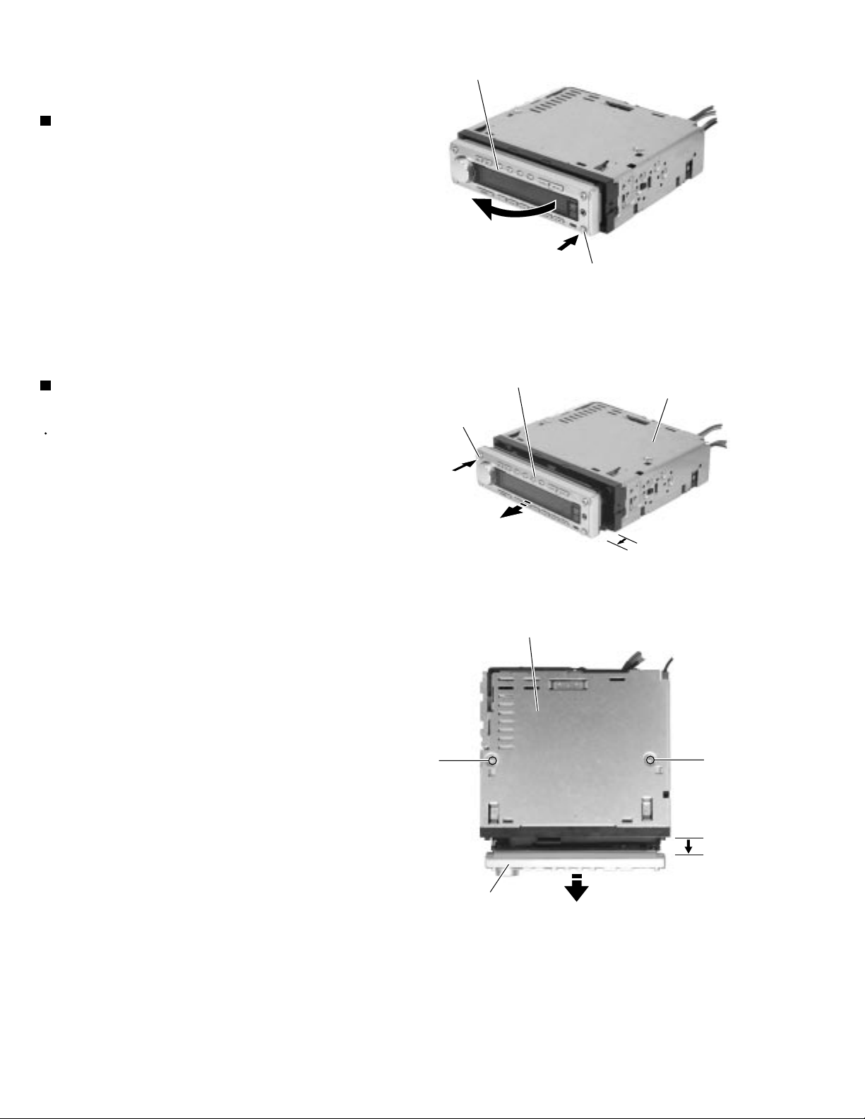
Removing the front panel assembly
(See Fig.1)
1.
Press the release button in the lower right part of the
front panel assembly to unlock.
2.
Remove the front panel assembly in the direction of
the arrow.
Removing the top chassis
(See Fig.2 to 6)
Turn on power.
1.
Press the eject button in the upper left part of the
front panel assembly to move the assembly as
shown in Fig.2 and turn off power.
Front panel assembly
Front panel assembly
Eject button
Release button
Fig.1
Top chassis
2.
Remove the two screws A on the upper side of the
body.
Top chassis
A
Front panel assembly
Fig.2
A
Fig.3
1-4
Page 5

3.
Remove the three screws B on both sides of the
body.
4.
Remove the screw C and the three screws D on the
left side of the body.
5.
Remove the two screws E and the screw F on the
back of the body.
6.
Move the top chassis upward and remove it with the
CD mechanism assembly. The connector on the CD
mechanism assembly is disconnected from
connector CN601 on the main board.
KD-SH77R/KD-SH55R
Top chassis
BB
Fig.4
Top chassis
C
E
F
Heat sink
E
BD
Fig.5
F
Fig.6 (KD-SH55RE)Fig.6 (KD-SH77RE)
1-5
Page 6
KD-SH77R/KD-SH55R
Removing the CD mechanism assembly
(See Fig.7)
Prior to performing the following procedure, remove
the top chassis.
1.
Remove the three screws G inside the top chassis
and remove the CD mechanisma ssembly.
Removing the motor assembly
(See Fig.8 to 10)
Prior to performing the following procedure, remove
the top chassis.
1.
Disconnect the wire from connector CN703 on the
main board.
2.
Remove the motor bracket and the spring attached
to the arm braket assembly (R).
Top chassis
G
Spring
G
G
CD mechanisma ssembly
Fig.7
Motor braket
3.
Remove the two screws H attaching the motor
bracket.
4.
Remove the washer attaching the clutch assembly
and pull out the clutch assembly from the shaft.
5.
Remove the two screws I and the motor assembly
from the motor bracket.
Motor braket
Clutch assembly
Motor assembly
Motor assembly
Arm braket assembly (R)
Fig.8
Main board
CN703
CN601
H
Motor braket
H
1-6
Washer
Fig.10
R
Fig.9
Page 7

Removing the main board
(See Fig.11 to 15)
Prior to performing the following procedures, remove
the top chassis and the motor bracket.
1.
Disconnect the flexible wire from connector CN701
and CN702 on the main board respectively.
2.
Move the front bracket backward until it stops.
3.
Remove the four screws J attaching the arm
brackets (L) and (R). Move the right and arm lefter
brackets from the rod gear.
4.
Remove the rod gear.
5.
Remove the screw K attaching the rear panel to the
bottom cover on the back of the body.
J
Arm
brackets (L)
J
CN701
L
Main board
CN702
Fig.11
KD-SH77R/KD-SH55R
L
Arm
brackets (R)
J
Rod gear
Arm brackets (R)
Arm brackets (L)
Main board
Rod gear
Fig.12
Rear panel
K
Bottom cover
Rear panel
K
Bottom cover
Fig.13 (KD-SH55RE)Fig.13 (KD-SH77RE)
1-7
Page 8
KD-SH77R/KD-SH55R
6.
Remove the two screws L and move the main board
backwards to release the two joints a. (The main
board will be removed with the rear panel and the
rear heat sink)
7.
Remove the screw M and N attaching the rear heat
sink.
8.
Remove the two screws O and the screw P
attaching the rear panel. Remove the mainboard
(KD-SH55RE).
9.
Remove the three screws O and the screw P
attaching the rear panel. Remove the main board
(KD-SH77RE).
Joint a
Joint a
Main board
Fig.14
O
Rear panel
P
N
Rear heat sink
M
Removing the lifter switch board
(See Fig.16)
Prior to performing the following procedures, remove
the top chassis, the motor bracket and the main
board.
O
Rear panel
Lifter switch board
P
M
N
Fig.15 (KD-SH55RE)Fig.15 (KD-SH77RE)
Rear heat sink
Bottom cover
1.
Remove the two screws Q attaching the lifter switch
board.
1-8
Q
Fig.16
Page 9

KD-SH77R/KD-SH55R
Removing the lifter board
(See Fig.17 to 23)
Prior to performing the following procedure, remove
the top chassis assembly and thefront panel
assembly.
1.
Disconnect the flexible wire from connector CN702
on the main board.
2.
Remove the four screws R attaching the front
bracket on both sides of the body.
3.
Push the pin of the joint c on the front of the front
bracket to release the lock lever.
Main board
CN702
Front bracket
Fig.17
Front bracket
Joint c
Lock lever
Front bracket
R
Fig.18
Front bracket
R
Fig.19Fig.20
1-9
Page 10
KD-SH77R/KD-SH55R
4.
Remove the screw S attaching the lifter board cover
in the rear of the front bracket.
5.
Release the two joints d while pushing the front side.
Move the lifter board cover inthe direction of the
arrow and release the eight joints e.
Joint d
Joints e
Lifter board cover
Joints e
Joint d
6.
Remove the two screws T attaching the lifter board
on the front of the body.
S
Joints e
Lifter board
Joint e
Front bracket
Fig.21
Lifter board cover
Fig.22
1-10
Fig.23
T
Page 11
KD-SH77R/KD-SH55R
<Front panel assembly>
Prior to performing the following procedure, remove
the front panel assembly.
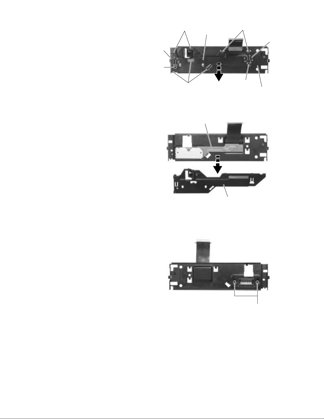
Removing the front board
(See Fig.24 and 25)
1.
Remove the four screws U attaching the rear panel
to the front panel assembly.
2.
Release the eleven joints f of the front panel and the
rear panel.
3.
Disconnect the wire from connector CN503 on the
front board.
4.
If necessary, unsolder connector CN502 on the front
board.
Removing the volume board
(See Fig.25 and 26)
Prior to performing the following procedure, remove
the rear panel.
U
Line in board
U
Joint f 11
Front board
V
Rear panel
Fig.24
Soldering
(CN502)
CN503
Fig.25
W
V
U
U
Soldering
Volume board
W
1.
Remove the two screws W attaching the volume
board.
2.
Disconnect the volume knob, ring lens and volume
ring from the volume board.
3.
If necessary, unsolder the volume board.
Removing the line in board
(See Fig.25 and 27)
Prior to performing the following procedure, remove
the rear panel.
1.
Disconnect the wire from connector CN503 on the
front board.
2.
Pull out the line in board from the front panel
assembly.
Volume board
Volume lens, Volume ring
Rng knob
Fig.26
Line in board
Fig.25
1-11
Page 12
KD-SH77R/KD-SH55R
<CD mechanism section>
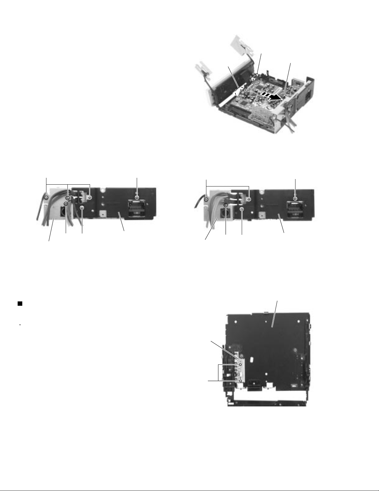
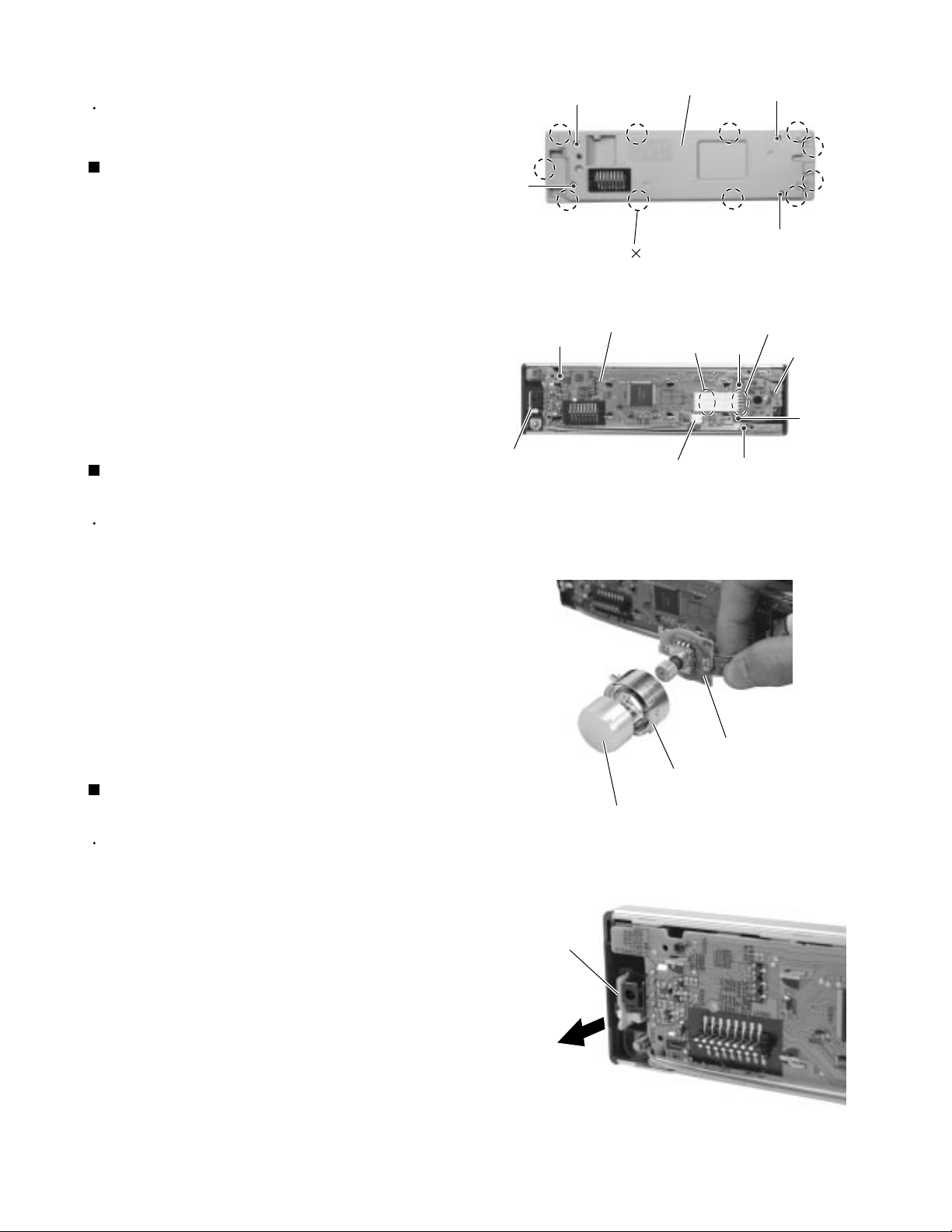
Removing the CD mechanism control
board (See Fig.1 and 2)
1.
Unsolder the part a and b on the CD mechanism
control board.
2.
Remove the stator fixing the CD mechanism control
board and the damper bracket (To remove the stator
smoothly, pick up the center part).
3.
Remove the screw A attaching the CD mechanism
control board.
4.
Remove the CD mechanism control board in the
direction of the arrow while releasing it from the two
damper bracket slots d and the front bracket slot e.
5.
Disconnect the flexible wire from connector on the
pickup unit.
ATTENTION:
Turn the FD gear in the direction of the
arrow to move the entire pickup unit to
the appropriate position where the
flexible wire of the CD mechanism unit
can be disconnected easily.
(Refer to Fig.2)
CD mechanism assembly
D
h
Front bracket
Pickup unit
Damper bracket
D
A
b
Fig.1
Flexible wire
a
CD mechanism
e
control board
h
c
D
d
Shift the lock
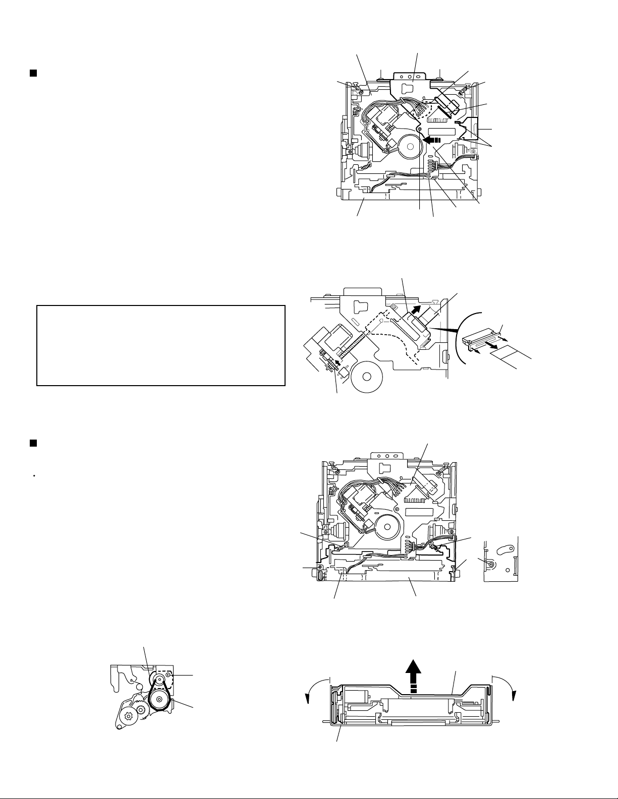
Removing the loading motor
(See Fig.3 to 5)
Prior to performing the following procedure, remove
the CD mechanism control board.
1.
Remove the two springs f attaching the CD
mechanism assembly and the front bracket.
2.
Remove the two screws B and the front bracket
while pulling the flame outward.
3.
Remove the belt and the screw C from the loading
motor.
Loading motor
C
FD gear
f
B
Loading motor
Pull outward
Fig.2
CD mechanism control board
f
B
Front bracket
Fig.3
Front bracket
Pull outward
1-12
Fig.5
Belt
Flame
Fig.4
Page 13
KD-SH77R/KD-SH55R
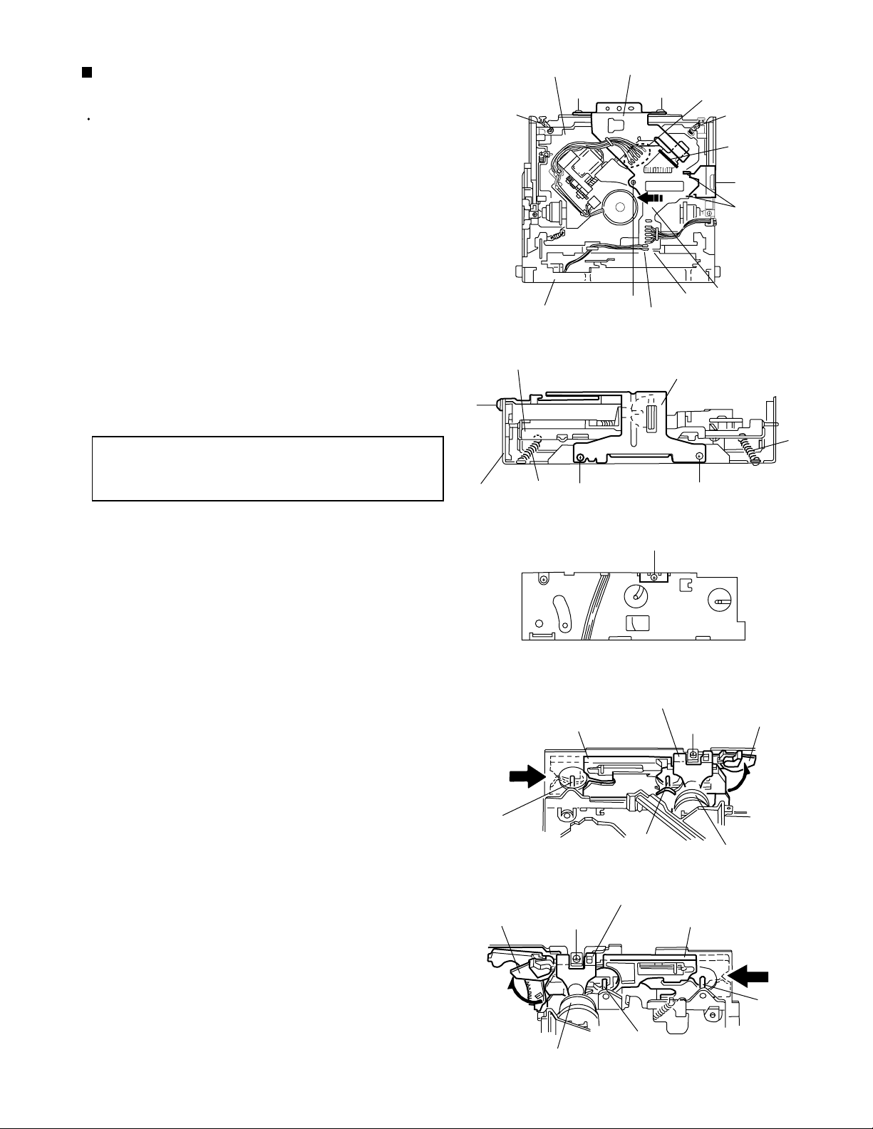
Removing the CD mechanism assembly
(See Fig.1, 6 to 9)
Prior to performing the following procedure, remove
the CD mechanism control board and the front
bracket (loading motor).
1.
Remove the three screws D and the damper
bracket.
2.
Raise the both sides fix arms and move the fix plates
in the direction of the arrow to place the four shafts g
as shown in Fig.8 and 9.
3.
Remove the CD mechanism assembly and the two
springs h attaching the flame.
4.
Remove the two screws E and both sides rear
damper brackets from the dampers. Detach the CD
mechanism assembly from the left side to the right
side.
ATTENTION:
The CD mechanism assembly can be
removed if only the rear damper
bracket on the left side is removed.
CD mechanism
h
Front bracket
CD mechanism
D
Flame
assembly
D
assembly
h
D
Damper bracket
D
A
Fig.1
e
b
Damper bracket
D
Fig.6
a
h
c
D
d
CD mechanism
control board
h
Fix plate (L)
g
Fix arm (R)
D
Fig.7
Rear damper bracket
g
Fig.8
Rear damper bracket
E
Fix plate(R)
E
Fix arm (L)
Damper
Damper
g
g
Fig.9
1-13
Page 14
KD-SH77R/KD-SH55R
Removing the feed motor assembly
(See Fig.10)
Prior to performing the following procedure, remove
the CD mechanism control board, the front bracket
(loading motor) and the CD mechanism assembly.
1.
Remove the two screws F and the feed motor
assembly.
Removing the pickup unit
(See Fig.10 and 11)
Prior to performing the following procedure, remove
the CD mechanism control board, the front bracket
(loading motor), the CD mechanism assembly and
the feed motor assembly.
1.
Detach the FD gear part of the pickup unit upward.
Then remove the pickup unit while pulling out the
part i of the FD screw.
Feed motor assembly
F
FD gear
Nut push spring plate
FD screw
Pickup unit
Fig.10
Part i
Part j
Pickup unit
G
Pickup mount nut
Pickup unit
ATTENTION:
2.
Remove the screw G attaching the nut push spring
plate and the pickup mount nut from the pickup unit.
Pull out the FD screw.
When reattaching the pickup unit,
reattach the part j of the pickup unit,
then the part i of the FD screw.
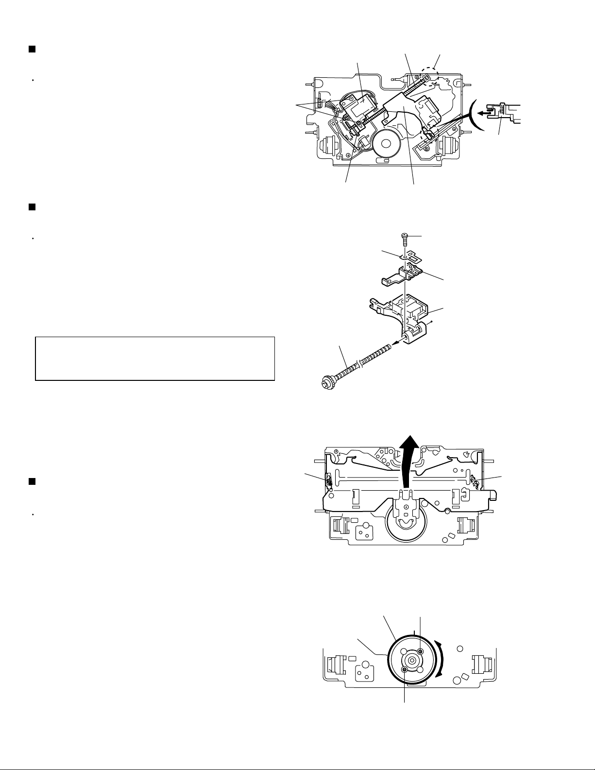
Removing the spindle motor
(See Fig.12 and 13)
Prior to performing the following procedure, remove
the CD mechanism control board, the front bracket
(loading motor), the CD mechanism assembly and
the feed motor assembly.
1.
Turn up the CD mechanism assembly and remove
the two springs k on both sides of the clamper arms.
Open the clamper arm upward.
2.
Turn the turn table, and remove the two screws H
and the spindle motor.
k
FD screw
Spindle motor
Fig.11
k
Fig.12
H
1-14
H
Fig.13
Page 15

Adjustment method
KD-SH77R/KD-SH55R
Test instruments required for adjustment
1. Digital oscilloscope (100MHz)
2. AM Standard signal generator
3. FM Standard signal generator
4. Stereo modulator
5. Electric voltmeter
6. Digital tester
7. Tracking offset meter
8. Test Disc JVC :CTS-1000
9. Extension cable for check
EXTGS004-26P 1
Standard measuring conditions
Power supply voltage DC14.4V(10.5~16V)
Load impedance 20Kohm(2 Speakers connection)
Output Level KD-SH77R Line out 4.0V (Vol. MAX)
KD-SH55R Line out 2.0V (Vol. MAX)
How to connect the extension cable for adjusting
Standard volume position
Balance and Bass &Treble volume : lndication"0"
Loudness : OFF
BBE : OFF
Frequency Band
FM 87.5MHz ~ 108.0MHz
MW 522kHz ~ 1620 kHz
LW 144kHz ~ 279kHz
Dummy load
Exclusive dummy load should be used for AM,and FM. For
FM dummy load,there is a loss of 6dB between SSG output
and antenna input.The loss of 6dB need not be considered
since direct reading of figures are applied in this working
standard.
1-15
Page 16

KD-SH77R/KD-SH55R
<ERROR CODE of Panel mechanism>
Memory to EEPROM of 6 digits, 1st and 2nd digit are indicate the operation mode when occur the error,
3rd to 6th digit are indicate details of error.
LCD indication time is use lower 2digits of details of error.
This series is indicate ERR XX (XX is error code).
<ex.> When details of error is 0A0001 , it is indicate ERR 01, details of error is 0E0031 , it is ERR 31.
Switch is from this side sequentially PSW1, PSW2,.....PSW6.
Details of error Error code
1. Error of door open (fault of PSW1)
(1) Time out by PSW1 not changed
(2) PSW1 change during waiting 300ms after open position detected
2. Error of door close (fault of PSW6)
(1) Time out by PSW6 not changed
(2) PSW6 change during waiting 300ms after close position detected
3. Error of shift to DETACH position (fault of PSW5)
(1) Time out by PSW5 not changed to open side
(2) Shift to open side, pass the DETACH position then detect ANGLE1
(3) Time out by PSW5 not changed to close side
(4) Shift to close side, pass the DETACH position then detect close position
4. Error of angle adjustment
4-1 Shift to ANGLE1 (fault of PSW4)
(1) Time out by PSW4 not changed to shift for open side
(2) Shift to open side, pass the ANGLE1 then detect ANGLE2
(3) Time out by PSW4 not changed to shift for close side
(4) Shift to close side, pass the ANGLE1 then detect DETACH position
4-2 Shift to ANGLE2 (fault PSW3)
(1) Time out by PSW3 not change to shift for open side
(2) Shift to open side, pass the ANGLE2 then detect ANGLE3
(3) Time out by PSW3 not changed to shift for close side
(4) Shift to close side, pass the ANGLE2 then detect ANGLE1
4-3 Shift to ANGLE3 (fault PSW2)
(1) Time out by PSW2 not changed to shift for open side
(2) Shift to open side, pass the ANGLE3 then detect OPEN position
(3) Time out by PSW2 not changed for shift for close side
(4) Shift to close side, pass the ANGLE3 then detect ANGLE2
5. PSW fault condition at initialize
When all PSW is checked immediately after RESET, and the state of SWITCH which
cannot be originally is detected, it is displayed as ERR 00.
0A0001
0A0002
0B0006
0B0007
0C0011
0C0012
0C0013
0C0014
0D0021
0D0022
0D0023
0D0024
0E0031
0E0032
0E0033
0E0034
0F0041
0F0042
0F0043
0F0044
000000
1-16
Page 17

Flow of functional operation until TOC read
Power ON
• When the pickup correctly moves
to the inner area of the disc
Set Function to CD
KD-SH77R/KD-SH55R
• When the laser diode correctly
emits
Microprocessor
commands
FMO
TC9462 "53"
FEED MOTOR
+TERMINAL
TERMINAL
IC581 "5"
REST SW
• When correctly focused
Focus Servo Loop ON
Disc inserted
Pickup feed to the inner area
Laser emitted
Focus search
Disc rotates
RF signal eye-pattern
remains closed
Tracking loop closed
RF signal eye-pattern
opens
TOC readout
YES
YES
Microprocessor
commands
"No disc"
display
• When the disc correctly rotates
Microprocessor
commands
Spindle
motor (-)
IC581 "7"
AccelerationAcceleration
0.5 Sec
Rough
Servo
0.5 Sec
Servo CLV
Jump to the first track
Play
Tracking Servo Loop ON
• RF signal
Rough Servo Mode
CLV Servo Mode
(ProgramArea)
CLV Servo Mode
(Lead-In Area;
Digital: 0)
1-17
Page 18
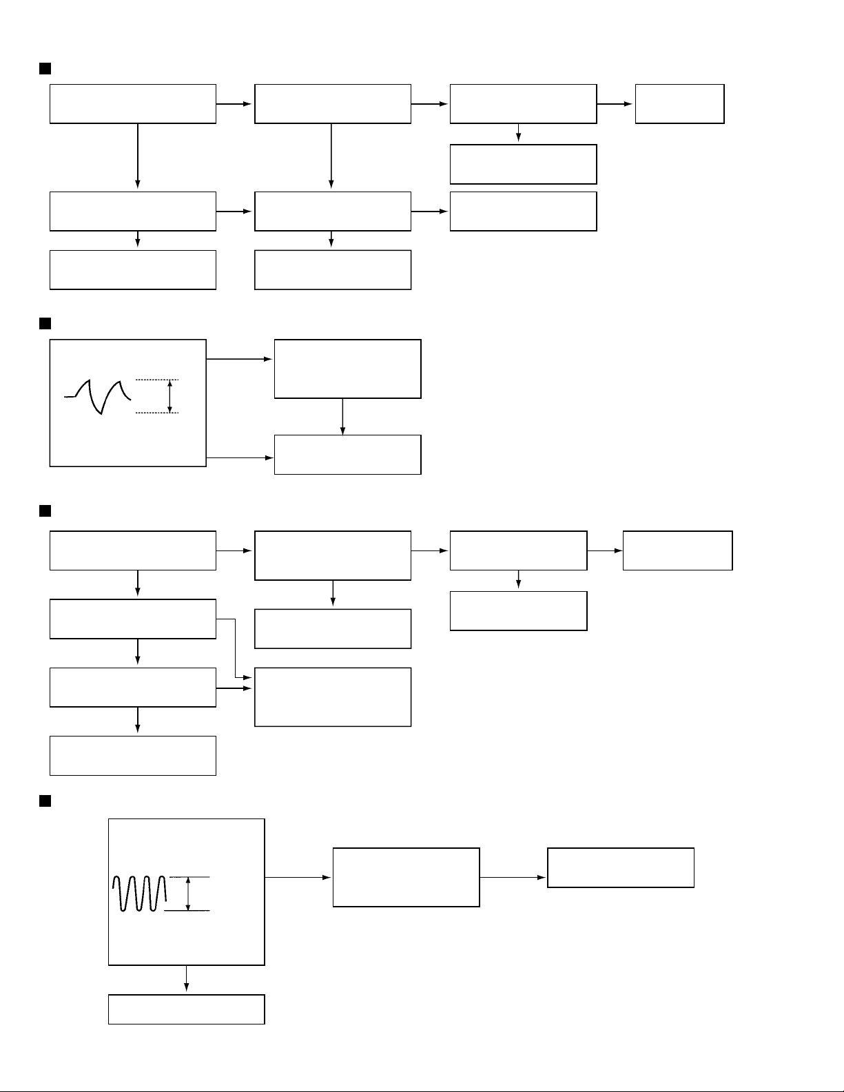
KD-SH77R/KD-SH55R
Feed Section
Is the voltage output at
IC521 pin "53" 5V or 0V?
YES
Is 4V present at both
sides of the feed motor?
YES
NO
Is the wiring for IC521
(90) ~ (100) correct?
NO
Is 6V or 2V present at
IC581 "5" and "6"?
NO
YES
YES
Is 5V present at IC581
pin "11"?
YES
Check the vicinity of
IC521.
Check the feed motor
connection wiring.
NONO
Check CD 9V
and 5V.
Check the feed motor.
Focus Section
When the lens is
moving:
4V
Does the S-search
waveform appear at
IC581 pins "17" and "18"?
Spindle Section
Is the disk rotated?
YES
Does the RF signal
appear at TP1?
YES
Check IC581.
NO
YES
NO
NO
Check the circuits in
the vicinity of IC581
pins "15" ~ "18".
Check the pickup and
its connections.
Is 4V present at IC581
pins "7" and "8" ?
Check the spindle motor
and its wiring.
YES
YES
NO NO
Is 4V present at IC521
pin "55" ?
YES
Check the vicinity of
IC581.
Check IC501 and
IC521.
Is the RF waveform at TP1
distorted?
Proceed to the Tracking
section
Tracking Section
When the disc is rotated
Is the tracking error signal
output at IC501 "12"?
1-18
YES
at first:
Approx. 1.2 V
YES
Check IC521.
NO
Check the circuits in the
vicinity of IC501 "19" ~
"24" or the pickup
Check the circuit in the
vicinity of IC501 pins
"2" ~ "12".
YESYES
Check the pickup and
its connections.
Page 19

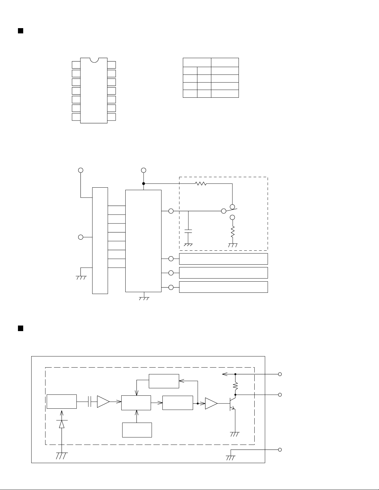
Maintenance of laser pickup
(1) Cleaning the pick up lens
Before you replace the pick up, please try to
clean the lens with a alcohol soaked cotton
swab.
(2) Life of the laser diode
When the life of the laser diode has expired,
the following symptoms will appear.
(1) The level of RF output (EFM output:ampli
tude of eye pattern) will be low.
KD-SH77R/KD-SH55R
Is RF output
1.0 0.35Vp-p?
YES
O.K
(3) Semi-fixed resistor on the APC PC board
The semi-fixed resistor on the APC printed
circuit board which is attached to the pickup
is used to adjust the laser power.Since this
adjustment should be performed to match the
characteristics of the whole optical block,
do not touch the semi-fixed resistor.
If the laser power is lower than the specified
value,the laser diode is almost worn out, and
the laser pickup should be replaced.
If the semi-fixed resistor is adjusted while
the pickup is functioning normally,the laser
pickup may be damaged due to excessive current.
NO
Replace it.
Replacement of laser pickup
Turn off the power switch and,disconnect the
power cord from the ac outlet.
Replace the pickup with a normal one.(Refer
to "Pickup Removal" on the previous page)
Plug the power cord in,and turn the power on.
At this time,check that the laser emits for
about 3seconds and the objective lens moves
up and down.
Note: Do not observe the laser beam directly.
Play a disc.
Check the eye-pattern at TP1.
Finish.
1-19
Page 20

KD-SH77R/KD-SH55R
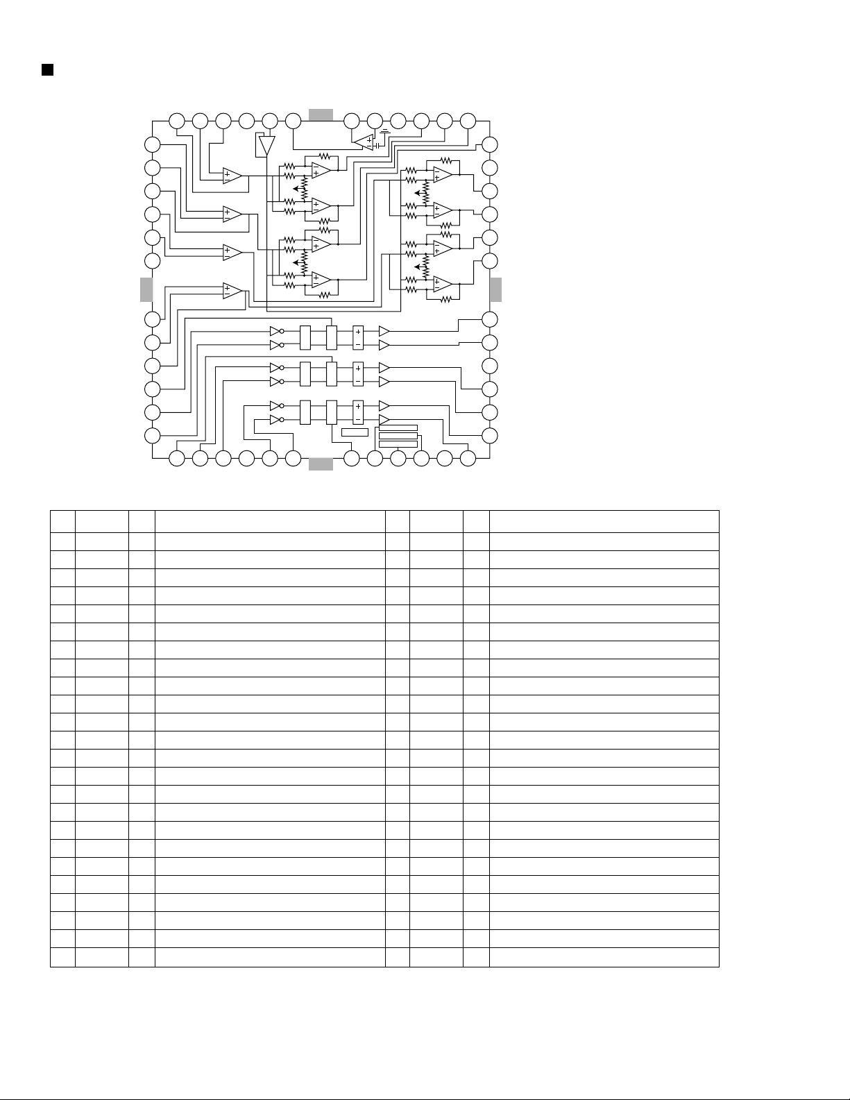
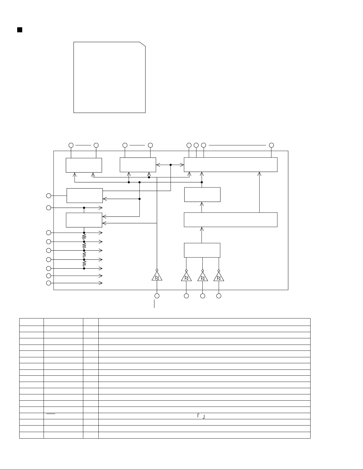
Description of major ICs
TC9490FA (IC621) : DSP
1. Pin layout & Block diagram
DD3
XO
XV
48 47 46 45 44 43 42 41 40 39 38 37 36 35 34 33
SS3
XI
XV
TESIN
DD3VSS3
V
DMO
FMO
DD3
AV
SEL
TEBC
RFGC
REF
V
TRO
FOO
2. Pin function (1/2)
No. Symbol
1
2
3
4
5
6
7
8
9
10
11
12
13
14
15
16
17
18
19
20
21
22
23
24
25
BCK
LRCK
AOUT
DOUT
IPF
VDD3
VSS3
SBOK
CLCK
DATA
SFSY
SBSY
/HSO
/UHSO
PVDD3
PDO
TMAX
LPFN
LPFO
PVREF
VCOF
AVSS3
SLCO
RFI
AVSS3
49DV
SS3
RO
50
51
DV
DD3
DVR
DV
DD3
ZDET
V
SS5
BUS0
BUS1
BUS2
BUS3
BUCK
/CCE
/RST
V
DD5
LO
LPF
52
53
54
55
56
57
58
59
60
61
62
63
64
1 2 3 4 5 6 7 8 9 10 11 12 13 14 15 16
BCK
I/O
O
Bit clock output pin.32fs, 48fs, or 64fs selectable by command.
O
L/R channel clock output pin. "L" for L channel and "H" for R channel.
O
Audio data output pin. MSB-first or LSB-first selected by command.
O
Digital data output pin. Outputs up to double-speed playback.
O
Correction flog output pin.
-
Digital 3.3V power supply voltage pin.
-
Digital GND pin.
O
Subcode Q data CRCC result output pin. "H" level when result is OK.
I/O
Sub-code P-W data read clock I/O pin. I/O polarity selectable by command.
O
Sub-code P-W data output pin.
O
Playback frames sync signal output pin.
O
Sub-code block sync output pin.
O
Playback speed mode flag output pin.
O
Playback speed mode flag output pin.
-
PLL-only 3.3V power supply voltage pin.
O
EFM and PLCK phase difference signal output pin.
O
TMAX detection result output pin.
I
Inverted input pin for PLL RF amp.
O
Output pin for PLL LPF amp.
-
PLL-only VREF pin.
O
VCO filter pin.
-
Analog GND pin.
O
DAC output pin for data slice level generation.
I
RF signal input pin.
-
Analog 3.3V power supply voltage pin.
generator
Micro-
controller
interface
LRCK
Clock
AOUT
1-bit
DAC
circuit
Correction
Audio output
circuit
IPF
DOUT
Address
circuit
16 k
RAM
Digital output
SS3
DD3
V
V
PWM
SBOK
Servo control
ROM
RAM
CLV servo
Sync signal
protection
EFM
Sub code
decoder
DATA
CLCK
Function
Digital equalizer
automatic
adjustment circuit
SFSY
SBSY
/HSO
A/D
VCO
PLL
TMAX
D/A
Data
slicer
/UHSO
DD3
PDO
PV
32
TEZI
31
TEI
30
SBAD
29
FEI
28
RFRP
27
RFZI
26
RFCT
AV
25
DD3
24
RFI
23
SLCO
AV
22
SS3
21
VCOF
PV
20
REF
19
LPFO
18
LPFN
TMAX
17
1-20
Page 21
2. Pin function (2/2)
No. Symbol
26
27
28
29
30
31
32
33
34
35
36
37
38
39
40
41
42
43
44
45
46
47
48
49
50
51
52
53
54
55
56
57
58
59
60
61
62
63
64
RFCT
RFZI
RFRP
FEI
SBADTEI
TEI
TEZI
FOO
TRO
VREF
RFGC
TEBC
SEL
AVDD3
FMO
DMO
VSS3
VDD3
TESIN
XVSS3
XI
XO
XVDD3
DVSS3
RO
DVDD3
DVR
LO
DVSS3
ZDET
VSS5
BUS0
BUS1
BUS2
BUS3
BUCK
/CCE
/RST
VDD5
I/O
I
RFRP signal center level input pin.
I
RFRP signal zero-cross input pin.
I
RF ripple signal input pin.
I
Focus error signal input pin.
I
Sub-beam adder signal input pin.
I
Tracking error input pin. Inputs when tracking servo is on.
I
Tracking error signal zero-cross input pin.
O
Focus equalizer output pin.
O
Tracking equalizer output pin.
-
Analog reference power supply voltage pin.
O
RF amplitude adjustment control signal output pin.
O
Tracking barance control signal output pin.
O
APC circuit ON/OFF signal output pin.
-
Analog 3.3V power supply voltage pin.
O
Feed equalizer output pin.
O
Disc equalizer output pin.
-
Digital GND pin.
-
Digital 3.3V power supply voltage pin.
I
Test input pin.
-
System clock oscillator GND pin.
I
System clock oscillator input pin.
O
System clock oscillator output pin.
-
System clock oscillator 3.3V power supply voltage pin.
-
DA converter GND pin.
O
R-channel data foward output pin.
-
DA converter 3.3V power supply pin.
-
Reference voltage pin.
O
L-channel data forward output pin.
-
DC converter GND pin.
O
1 bit DA converter zero data detection flag output pin.
-
Microcontroller interface GND pin.
I/O
Microcontroller interface data I/O pins.
I/O
Microcontroller interface data I/O pins.
I/O
Microcontroller interface data I/O pins.
I/O
Microcontroller interface data I/O pins.
I
Microcontroller interface clock input pin.
I
Microcontroller interface chip enable signal input pin.
I
Reset signal input pin.
-
Microcontroller interface 5V power supply pin.
Function
KD-SH77R/KD-SH55R
1-21
Page 22

KD-SH77R/KD-SH55R
UPD784217AGC134 (IC701) : CPU
1. Pin layout
76 ~ 100
1 ~ 25
26 ~ 50
2. Pin function (1/2)
Pin No. FunctionSymbol I/O
1
2
3
4
5
6
7
8
9
10
11
12
13
14
15
16
17
18
19
20
21
22
23
24
25
26
27
28
29
30
31
32
33
34
35
36
37
38
39
40
41
42
43
SW2
SW3
SW4
REST-SW
LM0
LM1
NC
ANT REM
VDD
X2
X1
VSS
XT2
XT1
RESET
SW1
BUS-INT
PS2
NC
RDS-SCK
RDS_DA
REMOCON
AVDD
AVREF0
SD/ST
MRC DATA
KEY0
KEY1
TEMP
LEVEL
SQ
SM
AVSS
INLOCK
NC
AVREF
BUS-SI
BUS-SO
BUS-SCK
STAGE
LCD-DA
LCD-SCK
LCD-CE
51 ~ 75
CD mecha switch 2 detection signal input
I
CD mecha switch 3 detection signal input
I
CD mecha switch 4 detection signal input
I
Rest switch detection signal input
I
Loading side motor control signal output
O
Eject side motor control signal output
O
Non connect
O
Antenna remote output
O
5V connection
Connect to X'tal for main clock
Connect to X'tal for main clock
Connect to GND
Connect to X'tal for sub clock
Connect to X'tal for sub clock
Reset detection terminal
I
CD mecha switch 1 detection signal input
I
J-BUS signal interrupt input
I
Power save 2
I
Non connect
RDS clock signal input
I
RDS data input
I
Remocon signal input
I
5V connect
5V connect
Station detector, Stereo signal input
I
MRC data input
I
Key input 0
I
Key input 1
I
Temperature data input for contrast correction
I
Level meter input
I
S.Quality level input
I
S.meter level input
I
Connect to GND
Lock detection output
O
Non connect
5V connect
J-BUS data input
I
J-BUS data output
O
J-BUS clock input/output
I/O
H:SH77, L:SH55
I
Data output for LCD driver
O
Clock output for LCD driver
O
Chip enable output for LCD driver
O
1-22
Page 23

2. Pin function (2/2)
Pin No. FunctionSymbol I/O
44
45
46
47
48
49
50
51
52
53
54
55
56~61
62
63
64
65
66
67
68
69
70
71
72
73
74
75
76
77
78
79
80
81
82
83
84
85
86
87
88
89
90
91
92
93
94
95
96
97
98
99
100
BUZZER
I2C-DAI
I2C-DAO
I2C-CLK
BUS-I/O
PM0
PM1
DACML
DACMC
DACMD
DETACH
VCR CONT
PNL-SW1~6
AFCK
SEEK/STOP
S MUTE
FM/AM
PLL-CE
PLL-DO
PLL-CLK
PLL-DI
TEL-MUTE
AMP-KILL
VSS
DIM-IN
PS1
POWER
CD-ON
MUTE
W-LPF1
W-LPF2
W-MUTE
VDD
VOL-DA
VOL-CLK
CF SEL
PMKICK
EMPH
CS
VOL-1
VOL-2
NC
BUCK
CCE
LSIRST
TEST
BUS0
BUS1
BUS2
BUS3
DISCSEL
CD-RW
Buzzer output
O
I2C data input
I
I2C data output
O
I2C clock output
O
J-BUS I/O switching output
O
Panel close side motor control signal output
O
Panel open side motor control signal output
O
DAC mode control latch
O
DAC mode control clock
O
DAC mode control data
O
Detach signal input
I
VCR control signal output
O
Panel position detection switch 1 to 6 signal input
I
AF check output
O
Auto seek / Stop switching output
O
Soft mute output for CF switching noise
O
FM / AM select output
O
PLL IC control CE output
O
PLL IC control data output
O
PLL IC control clock output
O
PLL IC control data input
I
Telephone mute detection input
Power amp ON /OFF select output
O
Connect to GND
Dimmer detection input
I
Power save 1
I
Power ON / OFF select output
O
CD power supply control signal output
O
Mute output
O
Sub woofer cut off frequency control output 1
O
Sub woofer cut off frequency control output 2
O
Sub woofer mute output
O
5V connect
O
E. volume IC control data output
O
E. volume IC control clock data output
O
FM band area filter select signal output
O
Panel motor kick signal output
O
CD emphasis output
O
DAC chip select
O
Rotary volume pulse
I
Rotary volume pulse signal input
I
Non connect
Data communication clock output with CD LSI
O
Data communication CE output with CD LSI
O
CD LSI reset signal output
O
Connect to GND
Data communication input/output port 0 with CD LSI
I/O
Data communication input/output port 1 with CD LSI
I/O
Data communication input/output port 2 with CD LSI
I/O
Data communication input/output port 3 with CD LSI
I/O
H: 8 cm disc non correspondence L: 8 cm disc correspondence
I
CD-RW select signal output
O
KD-SH77R/KD-SH55R
1-23
Page 24

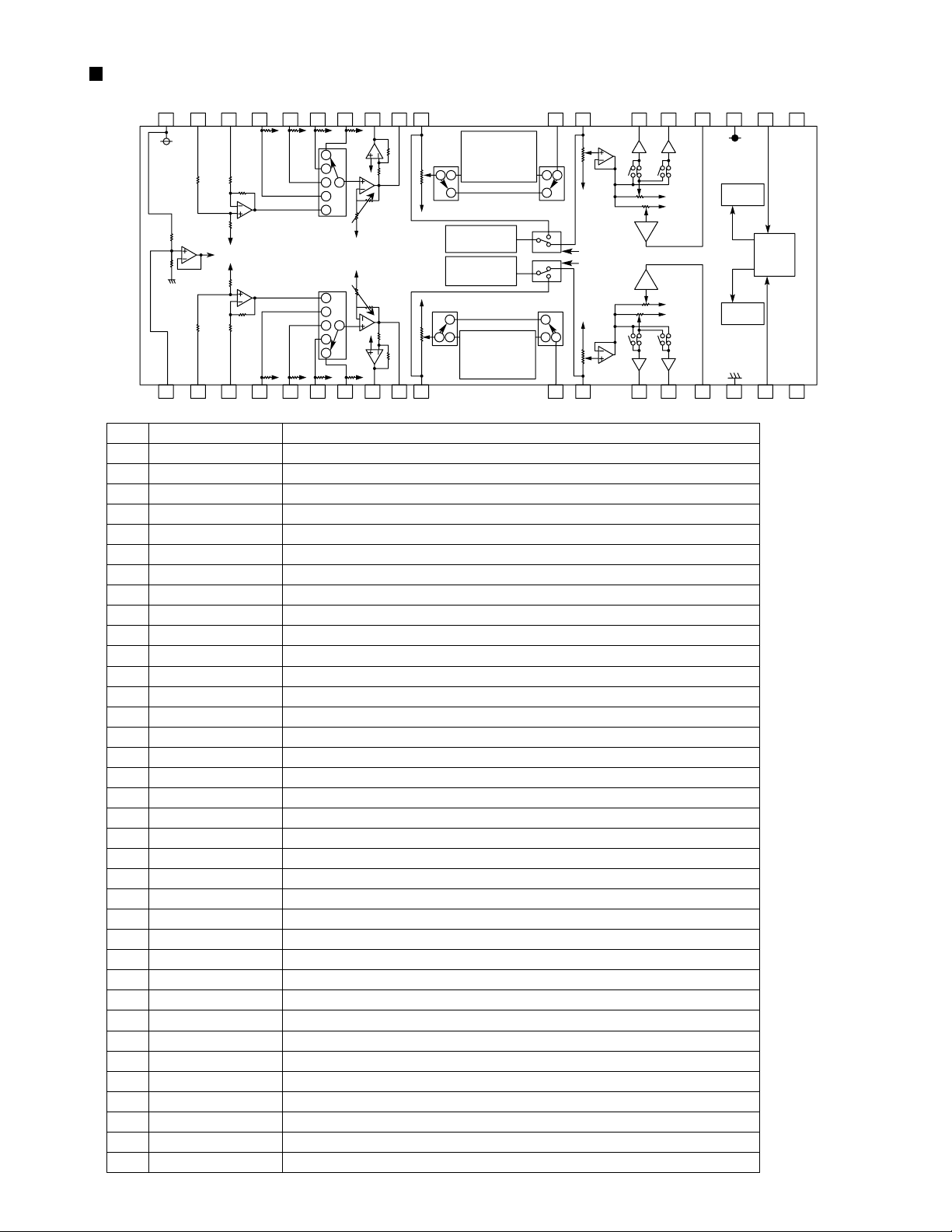
KD-SH77R/KD-SH55R
+
+
-
-
+
+
-
-
-
+
+
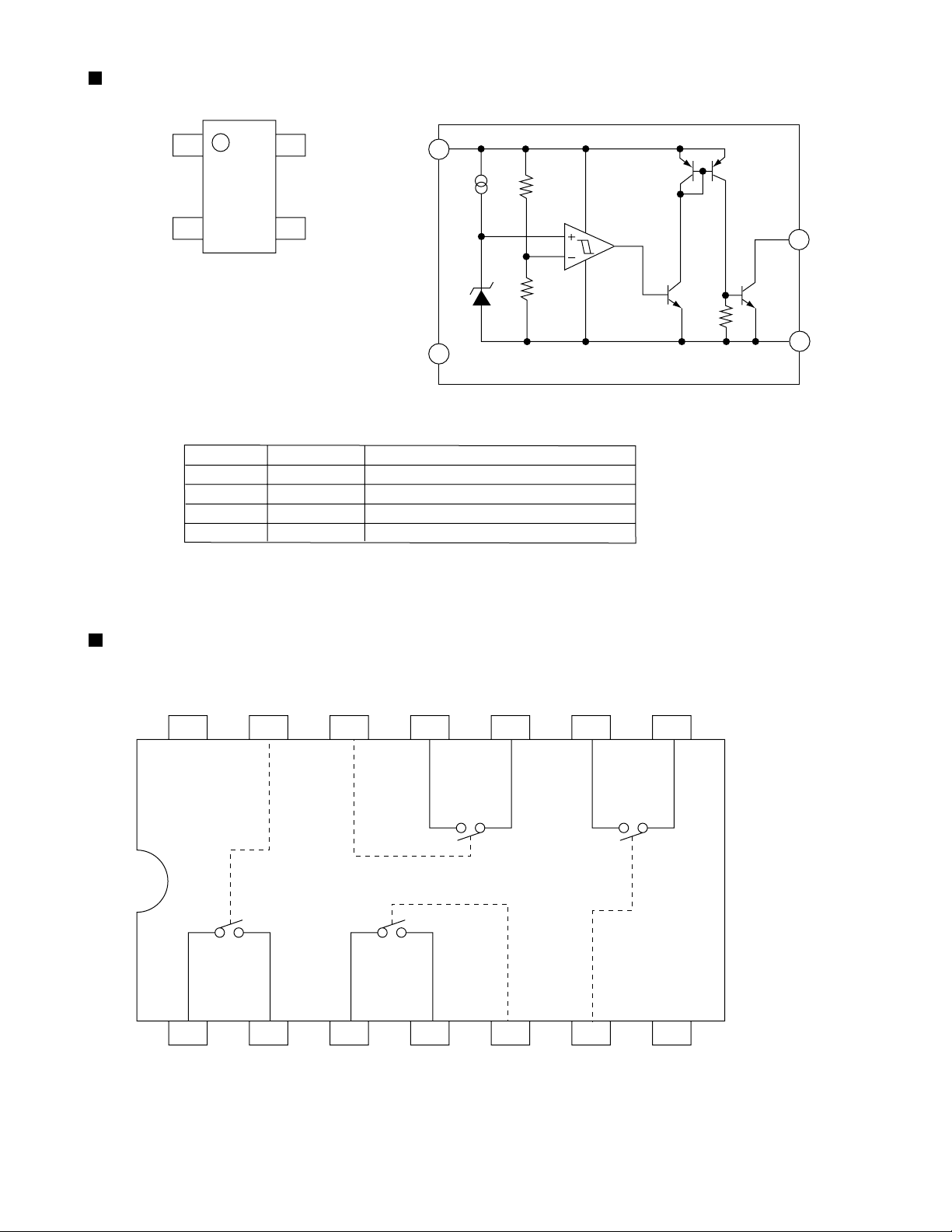
BA3220FV-X (IC301,IC401) : Line out amp
1.Pin layout
LGND
13
8
OUTL OUTR RGND
14
3220
17
2.Block diagram
CL-
14
CR-
1112
10
9
CR+
8
REFL
1
2
Vcc
3
INL
4
NFLCL+
REFR
FILTER
56
FIL
NFR
7
INR
1-24
Page 25

BR24C32F-X (IC703) : EEPROM
2. Block diagram
58
A0 1
32 kbit EEROM ARRAY
KD-SH77R/KD-SH55R
V Vcc
3. Pin function
Pin No.
1
2
3
4
5
6
7
8
Symbol
A0
A1
A2
GND
SDA
SCL
WP
Vcc
41
I/O
I/O
12bit
A1 2
A2 3
GND 4
ADDRESS
DECODER
CONTROL LOGIC
HIGH VOLTAGE GEN. Vcc LEVEL DETECT
SLAVE/WARD
12bit
ADDRESS REGISTER
START
STOP
Function
I
Slave address set
I
Slave address set
I
Slave address set
-
Ground
Slave & Word address, Serial data input/Serial address output
I
Serial clock input
I
Write protect input
-
Power supply
ACK
8bit
DATA
REGISTER
7 WP
6 SCL
5 SDA
NJM4580V-X (IC671) : Ope amp
1. Pin layout & Block diagram 2. Pin function
Pin
Function
1
2
3
4
A
B
8
7
6
8
No.
1
2
3
4
5
6
7
8
A output
A -input
A +input
VB +input
B -input
B output
V+
1-25
Page 26
KD-SH77R/KD-SH55R
FAN8037 (IC661) : CD driver
1. Pin layout & Block diagram
48 47 46 45 44 43 42 41 40 39 38 37
2. Pin function
Pin
Symbol
No.
1
IN2+
2
IN2-
3
OUT2
4
IN3+
5
IN3-
6
OUT3
7
IN4+
8
IN4-
9
OUT4
10
CTL1
11
FWD1
12
REV1
13
CTL2
14
FWD2
15
REV2
16
SGND
17
FWD3
18
REV3
19
CTL3
20
SB
21
PS
22
MUTE
23
PVCC2
24
DO7-
1
2
3
4
5
6
7
8
9
10
11
12
13 14 15 16 17 18 19 20 21 22 23 24
Function
I/O
I
CH2 op-amp input(+)
I
CH2 op-amp input(-)
O
CH2 op-amp output
I
CH3 op-amp input(+)
I
Ch3 op-amp input(-)
O
CH3 op-amp output
I
CH4 op-amp input(+)
I
CH4 op-amp input(-)
O
CH4 op-amp output(+)
I
CH5 motor speed control
I
CH5 forward input
I
CH5 reverse input
I
CH6 motor speed control
I
CH6 forward input
I
CH6 reverse input
-
Signal ground
I
CH7 forward input
I
CH7 reverse input
I
CH7 motor speed control
I
Stand by
I
Power save
I
All mute
-
Power supply voltage
O
CH7 drive output(-)
M
s
S
w
C
M
s
S
w
C
M
s
S
w
C
T.S . D
D
D
D
D
D
D
STAND BY
ALL MUTE
POWER SAVE
Pin
No.
25
26
27
28
29
30
31
32
33
34
35
36
37
38
39
40
41
42
43
44
45
46
47
48
Symbol
DO7+
DO6-
DO6+
PGND2
DO5-
DO5+
DO4-
DO4+
DO3-
DO3+
PGND1
DO2-
DO2+
DO1-
DO1+
PVCC1
REGOX
REGX
RESX
VREF
SVCC
IN1+
IN1-
OUT1
36
35
34
33
32
31
30
29
28
27
26
25
Function
I/O
O
CH7 drive output(+)
O
CH6 drive output(-)
O
CH6 drive output(+)
-
Power ground2
O
CH5 drive output(-)
O
CH5 drive output(+)
O
CH4 drive output(-)
O
CH4 drive output(+)
O
CH3 drive output(-)
O
CH3 drive output(+)
-
Power ground1
O
CH2 drive output(-)
O
CH2 drive output(+)
O
CH1 drive output(-)
O
CH1 drive output(+)
-
Power supply voltage
I
Regulator feedback input
O
Regulator output
I
Regulator reset input
I
Bias voltage input
-
Signal supply voltage
I
CH1 op-amp input(+)
I
CH1 op-amp input(-)
O
CH1 op-amp output
1-26
Page 27
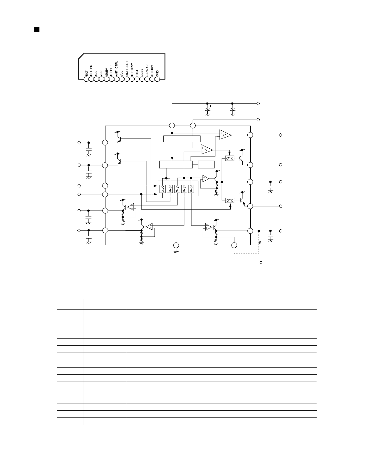
HA13164 (IC961) : Regulator
1.Terminal layout
123456789101112131415
KD-SH77R/KD-SH55R
2.Block diagram
ANT OUT
C3
0.1u
EXT OUT
C4
0.1u
ANT CTRL
CTRL
CD OUT
C5
0.1u
AUDIO OUT
C6
10u
11
12
10
BATT.DET OUT
9
COMPOUT
6
VDD OUT
4
SW5VOUT
5
14
UNIT R:
+B
ACC
ILMOUT
R1
C7
0.1u
0.1u
C8
C1
100u
VCC ACC
8
2
1
7
Surge Protector
BIAS TSD
15
3
note1) TAB (header of IC)
connected to GND
ILM AJGND
13
C2
0.1u
C:F
3.Pin function
Pin No. Symbol Function
1
2
EXTOUT
ANTOUT
Output voltage is VCC-1 V when M or H level applied to CTRL pin.
Output voltage is VCC-1 V when M or H level to CTRL pin and H level
to ANT-CTRL.
3
4
5
6
7
8
9
10
11
12
13
14
15
ACCIN
VDDOUT
SW5VOUT
COMPOUT
ANT CTRL
VCC
BATT DET
AUDIO OUT
CTRL
CD OUT
ILM AJ
ILM OUT
GND
Connected to ACC.
Regular 5.7V.
Output voltage is 5V when M or H level applies to CTRL pin.
Output for ACC detector.
L:ANT output OFF , H:ANT output ON
Connected to VCC.
Low battery detect.
Output voltage is 9V when M or H level applied to CTRL pin.
L:BIAS OFF, M:BIAS ON, H:CD ON
Output voltage is 8V when H level applied to CTRL pin.
Adjustment pin for ILM output voltage.
Output voltage is 10V when M or H level applies to CTRL pin.
Connected to GND.
1-27
Page 28
KD-SH77R/KD-SH55R
HD74HC126FP-X (IC771) : Buffer
1.Terminal layout
1C
1
1A
2
3
1Y
4
2C
5
2A
6
2Y
GND
7
2.Block diagram
Input
3Y
14
3A
13
12
3C
11
4Y
10
4A
9
4C
8
Vcc
Vcc Vcc
1A
2A
3A
4A
1C
2C
3C
See Function Table
4C
3.Pin function
Output
1Y
Output
2Y
Output
3Y
Output
4Y
Input Output
C
L
H
H
A
X
L
H
Note:
Y
Z
H
L
H : High
L : Low
X : H and L
Z : H.L.X
1k
S1
CL
1k
Sample as Load Circuit 1
Sample as Load Circuit 1
Sample as Load Circuit 1
RPM6938-SV4 (IC561) : Remote sensor
1.Block diagram
AMP
I/V
conversion
PD
magnetic shield
1-28
BPF
fo
trimming
circuit
AGC
Detector
Vcc
Comp
Vcc
22k
Rout
GND
Page 29
IC-PST9333U-X (IC702) : Reset IC
1. Pin layout 2. Block diagram
KD-SH77R/KD-SH55R
NC
GND
3. Pin function
1
2
GND
Pin No.
1
2
3
4
NC
4
Vcc
3
VOUT
Symbol
NC
GND
VOUT
Vcc
Vcc
Function
Non connect
GND terminal
Reset signal output terminal
Power supply terminal
NC
4
1
3
2
VOUT
GND
BU4066BCFV-X (IC322) : Quad analog switch
1. Pin layout & Block diagram
VDD C1 C4 I/O4 I/O3O/I4 O/I3
14 13 12 11 810 9
1234 756
I/O1 O/I1 O/I2 I/O2 VssC2 C3
1-29
Page 30
KD-SH77R/KD-SH55R
LC75878W (IC501) : LCD driver
1. Pin layout
100 ~ 76
2. Block diagram
OSC
VLCD
VLCD0
VLCD1
VLCD2
VLCD3
VLCD4
VDD
VSS
1
~
25
26 ~ 50
P1
GENERAL
PORT
CLOCK
GENERATOR
CONTRAST
ADJUSTER
P4
75
~
51
COM1
COMMON
DRIVER
COM8
S75/COM9
S74/COM10
S73
SEGMENT DRIVER & LATCH
CONTROL
REGISTER
SHIFT REGISTER
CCB
INTERFACE
S1
3. Pin function
No. Symbol
1~73
74
75
76~83
84~87
88
89
90
91
92
93
94
95
96
97
98
99
100
1-30
S1~S73
S74 / COM10
S75 / COM9
COM8~COM1
P1~P4
VDD
VLCD
VLCD0
VLCD1
VLCD2
VLCD3
VLCD4
VSS
OSC
INH
CE
CL
DI
DI
INH
I/O
O
Segment driver output pin.
O
Segment driver output pin.
O
Segment driver output pin.
O
Common driver output pin.
O
General-purpose output pin.
-
Logic block power supply pin.
-
LCD driver power supply pin.
O
LCD driver bias 4/4 voltage (H-level) power pin.
I
LCD driver bias 3/4 voltage (intermediate level) power pin.
I
LCD driver bias 2/4 voltage (intermediate level) power pin.
I
LCD driver bias 1/4 voltage (intermediate level) power pin.
I
LCD driver bias 0/4 voltage (L-level) power pin.
-
Power supply pin to connect to ground.
I/O
Oscillator pin.
I
Display off, general-purpose output port L fixed input pin.
I
Chip enable
I
Synchronization clock
I
Transfer data
Function
CL
CE
Page 31
M61508FP-X (IC911) : E. volume
1. Pin layout & Block diagram
VCC
(Anarog)
2. Pin function
Pin No.
1
2
3
DEFP IN1
DEFN IN1
4
5
6
7
8
9
DEFN OUT1
SEL OUT1
10
11
12
13
14
15
TONE OUT1
FADER IN1
REAR OUT1
FRONT OUT1
NonFader OUT1
16
17
18
19
20
21
22
NonFader OUT2
23
24
25
26
FRONT OUT2
REAR OUT2
FADER IN2
TONE OUT2
27
28
29
SEL OUT2
DEFN OUT1
30
31
32
33
34
35
DEFN IN1
DEFP IN1
36
REF
Symbol Function
REF
Grand for IC signal
Differential motion amp. Positive terminal
Differential motion amp. Negative terminal
INA1
INB1
INC1
IND1
Input terminal of input selector switch channel 1
Input terminal of input selector switch channel 1
Input terminal of input selector switch channel 1
Input terminal of input selector switch channel 1
Differential output terminal (-)
Input selector output terminal
VOL IN1
Volume 1 input terminal
Tone output terminal
Volume 2 input terminal
Fader volume control (Rear) output terminal
Fader volume control (Front) output terminal
Non fader volume output terminal
GND
DATA
TEST1
TEST2
CLOCK
VDD
GND terminal
Control data input terminal
Test terminal
Test terminal
Clock input terminal for serial data transport
Power supply terminal for digital
Non fader volume control output terminal
Fader volume (Front) output terminal
Fader volume (Rear) output terminal
Volume 2 input terminal
Tone output terminal
VOL IN2
Volume 1 input terminal
Input selector output terminal
Differential output terminal (-)
IND2
INC2
INB2
INA2
Input terminal of input selector switch channel 2
Input terminal of input selector switch channel 2
Input terminal of input selector switch channel 2
Input terminal of input selector switch channel 2
Differential motion amp negative input terminal
Differential motion amp positive input terminal
VCC
Power supply terminal
50K
27282930313233343536
LOUDNESS
+
3BAND TONE CONTROL
(BASS/MID/TREBLE)
ZERO CROSS
DETECTOR
ZERO CROSS
DETECTOR
LOUDNESS
+
3BAND TONE CONTROL
(BASS/MID/TREBLE)
A
B
B
A
2526
Zero detect
Select SW
121110987654321
KD-SH77R/KD-SH55R
24 23 22 21 20 19
VDO
(Digital)
Soft select
12dB
I/F
12dB
TIMER
DETECTOR
GND
13 14 15 16 17
18
1-31
Page 32

KD-SH77R/KD-SH55R
PCM1716E-X (IC681) : D/A converter
1. Pin layout
28 15
2. Block diagram
BCK
LBCK
DATA
ML/llS
MC/DM1
MD/DM0
CS/WO
MODE
MUTE
RST
3. Pin function
Pin
Symbol Function
No.
1
LRCK
2
DATA
3
BCK
4
CLKO
5
6
7
8
9
10
11
12
13
14
15
16
17
18
19
20
21
22
23
24
25
26
27
28
XTI
XTO
DGND
VDD
VDD2R
AGND2R
EXTR
NC
VOUTR
AGND1
Vcc1
VOUTL
NC
EXTL
AGND2L
Vcc2L
ZERO
RST
CS/IWO
MODE
MUTE
MD/DM0
MC/DM1
ML/IIS
114
Serial
Input
I/F
Mode
Control
I/F
Mult-level
8X Oversampling
Digital Filter
with
Function Controller
SCK
BPZ-Cont
Crystal OSC
XTI XTO CLKO Vcc1 VccAGND1 DGND
Delta-Sigma
Modulator
Power Supply
Vcc2L
DAC
DAC
AGND2L
Vcc2R
AGND2R
Open drain
Low-pass
Filter
Low-pass
Filter
I/O
I
LRCK clock input
I
Serial audio data input
I
Bit clock input for serial audio data
O
Buffered output of system clock
I
Oscillator input / External clock input
O
Oscillator output
-
Digital ground
-
Digital power +5V
-
Analog power +5V
-
Analog ground
O
Rch common pin of analog output amp
-
Non connection
O
Rch analog voltage output of audio signal
-
Analog ground
-
Analog power +5V
O
Lch analog voltage output of audio signal
-
Non connection
O
Lch common pin of analog output amp
-
Analog ground
-
Analog power +5V
O
Zero data flag
I
Reset
I
Chip select / Input format selection
I
Mode control select
I
Mute control
I
Mode control, Data / De-emphasis selection 1
I
Mode control, BCK / De-emphasis selection 2
I
Mode control, WDCK / Input format selection
VoutL
EXTL
VoutR
EXTR
ZERO
1-32
Page 33

SAA6579T-X (IC51) : RDS detector
1. Pin layout 2. Pin function
1
2
3
4
5
6
7
8
16
15
14
13
12
11
10
9
Pin
Symbol Function
No.
1
2
3
4
5
6
7
8
9
10
11
12
13
14
15
16
QUAL
RDDA
Vref
MUX
VDDA
VSSA
CIN
SCOUT
MODE
TEST
VSSD
VDDD
OSCI
OSCO
T57
RDCL
Quality indication output
RDS data output
Reference voltage output (0.5VDDA)
Multiplex signal input
+5V supply voltage for anarog part
Ground for analog part (0V)
Subcarrier input to comparator
Subcarrier output of reconstruction filter
Oscillator mode / test sontrol input
Test enable input
Ground for digital part (0V)
+5V supply voltage for digital part
Oscillator input
Oscillator output
57kHz clock signal output
RDS clock output
KD-SH77R/KD-SH55R
3. Block diagram
MUX
4
CIN
VDDA
Vref
8
7
5
3
SCOUT
ANTI-
ALIASING
FILTER
CLOCKED
COMPARATOR
Vp1
REFERENCE
VOLTAGE
6
57kHz
BANDPASS
(8th ORDER)
COSTAS LOOP
VARIABLE AND
FIXED DIVIDER
CLOCK
REGENERATION
AND SYNC
RECONSTRUCTION
FILTER
TEST LOGIC AND OUTPUT
OSCI OSCO VDDD
13
OSCCILLATOR
BIPHASE
SYMBOL
DECODER
SELECTOR SWITCH
9
14
AND
DIVIDER
DIFFERRENTIAL
10
12
QUALITY BIT
GENERATOR
DECODER
11
VSDDTESTMODEVSSA
1
2
16
15
QUAL
RDDA
RDCL
T57
1-33
Page 34

KD-SH77R/KD-SH55R
TA2147F-X (IC601) : RF amp
1. Pin layout & Block diagram
GND
RFN
RFO
AGCIN
RFGC
RFGO
RFRPIN
RFRP
FEN
FEO
VRO
GVSW
cc
12 k
2 k
50 k
16
20 k
50 A
9
TEBC
24
1
V
3 k
3 k
23
40 pF
20 k
2
FNI
180 k
60 k
80 k
22
180 k
40 pF
60 k
20 k
3
FPI
30 k
80 k
21
1
2
4
TPI
0.5
20 k
240 k
15 pF
2
20
k
5
TNI
0.5
240 k
15 pF
19
1.75 k
6
MDI
40 k
14 k
2 k
18
BOTTOM
PEAK
1 k
7
LDO
17
20 k
12 k
1.3 V
60 A
8
SEL
15
10 pF
15 k
20 k
40 k
20 k
10 pF
10
TEN
20 k
40 k
14
20 A
11
TEO
13
20 k 20 k
PEAK
50 k 15 k
12
RFDC
2. Pin function
Pin
Symbol I/O Function
No.
1
2
3
4
5
6
7
8
9
10
11
12
13
14
15
16
17
18
19
20
21
22
23
24
MDI
LDO
SEL
TEBC
TEN
TEO
RFDC
GVSW
VRO
FEO
FEN
RFRP
RFRPIN
RFGO
RFGC
AGCIN
RFO
RFN
GND
Vcc
FNI
FPI
TPI
TNI
-
3.3V power supply pin
I
Main-beam amp input pin
I
Main-beam amp input pin
I
Sub-beam amp input pin
I
Sub-beam amp input pin
I
Monitor photo diode amp input pin
O
Laser diode amp output pin
I
APC circuit ON/OFF control signal, laser diode control signal input
or bottom/peak detection frequency change pin
I
Tracking error balance adjustment signal input pin
I
Tracking error signal generation amp negative-phase input pin
O
Tracking error signal generation amp output pin
O
RF signal peak detection output pin
I
AGC/FE/TE amp gain change pin
O
Reference voltage output pin
O
Focus error signal generation amp output pin
I
Focus error signal generation amp negative-phase input pin
O
Signal amp output pin for track count
I
Signal generation amp input pin for track count
O
RF signal amplitude adjustment amp output pin
I
RF amplitude adjustment control signal input pin
I
RF signal amplitude adjustment amp input pin
O
RF signal generation amp output pin
I
RF signal generation amp input pin
-
GND pin
1-34
Page 35

TA8273H (IC941) : Power amp
1. Pin layout
125
2. Block diagram
2
7
8
9
5
3
17
18
19
21
KD-SH77R/KD-SH55R
24
23
PW-GND2
-
+
OUT2 (-)
-
OUT3 (+)
+
+
IN3
PW-GND3
-
6
20
1
CC2
V
CC1
V
TA B
OUT1 (+)
+
+
IN1
OUT1 (-)
PW-GND1
-
-
OUT2 (+)
+
IN2
AUX IN
11
12
16
15
NJM4565V-X (IC171,IC301,IC323,IC401,IC951) : Ope amp
1. Pin layout & Block diagram 2. Pin function
OUT3 (-)
-
OUT4 (+)
+
+
IN4
14
OUT4 (-)
PW-GND4
-
22
-
25
OUT
DIAGNOSIS
4
10
RIP STBY MUTE
13
Pin
Function
No.
1
2
3
4
A
B
8
7
6
8
1
2
3
4
5
6
7
8
A output
A-input
A+input
VB+input
B-input
B output
V+
1-35
Page 36

KD-SH77R/KD-SH55R
VICTOR COMPANY OF JAPAN, LIMITED
MOBILE ELECTRONICS DIVISION
PERSONAL & MOBILE NETWORK BUSINESS UNIT. 10-1,1Chome,Ohwatari-machi,Maebashi-city,Japan
(No.49634)
200103
 Loading...