

Page 1
SERVICE MANUAL
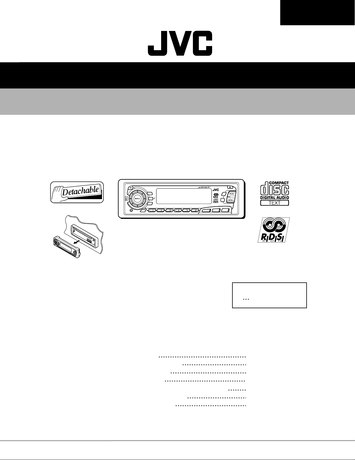
CD RECEIVER
KD-S9R
KD-S9R
Contents
A
T
T
/
/I
45Wx4
DISP
RDS
TP
PTY
789101112
SCM
MO
RND
SSM
RPT
CD
FM
AM
Area Suffix
E Continental Europe
Safety precaution
Preventing static electricity
Disassembly method
Adjustment method
Flow of functional operation unit TOC read
Maintenance of laser pickup
Description of major ICs
This service manual is printed on 100% recycled paper.
COPYRIGHT 2000 VICTOR COMPANY OF JAPAN, LTD.
1-2
1-3
1-4
1-9
1-10
1-11
1-12
No.49579
Dec. 2000
Page 2
KD-S9R
Safety precaution
CAUTION
!
CAUTION
!
Burrs formed during molding may be left over on some parts of the chassis. Therefore,
pay attention to such burrs in the case of preforming repair of this system.
Please use enough caution not to see the beam directly or touch it in case of an
adjustment or operation check.
1-2
Page 3
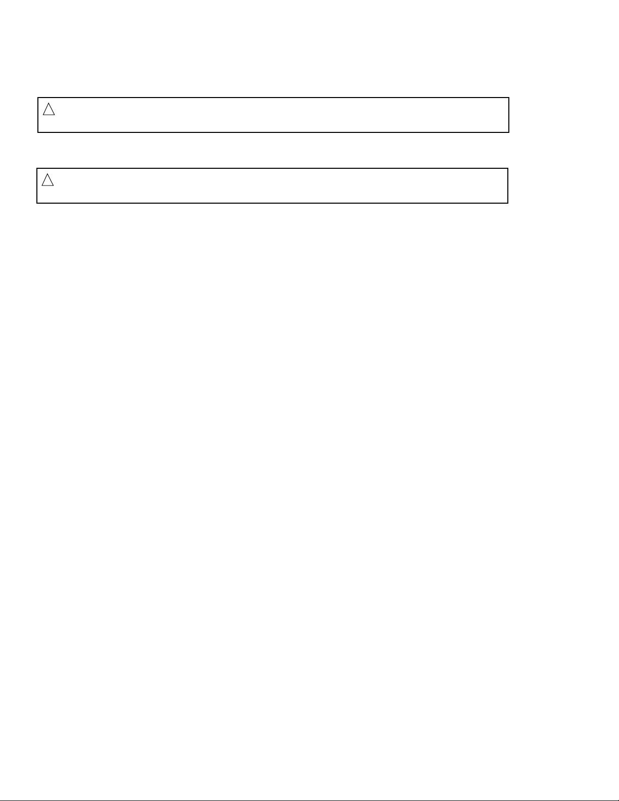
Preventing static electricity
1.Grounding to prevent damage by static electricity
Electrostatic discharge (ESD), which occurs when static electricity stored in the body, fabric, etc. is discharged,
can destroy the laser diode in the traverse unit (optical pickup). Take care to prevent this when performing repairs.
KD-S9R
2.About the earth processing for the destruction prevention by static electricity
Static electricity in the work area can destroy the optical pickup (laser diode) in devices such as CD players.
Be careful to use proper grounding in the area where repairs are being performed.
2-1 Ground the workbench
Ground the workbench by laying conductive material (such as a conductive sheet) or an iron plate over
it before placing the traverse unit (optical pickup) on it.
2-2 Ground yourself
Use an anti-static wrist strap to release any static electricity built up in your body.
(caption)
Anti-static wrist strap
Conductive material
(conductive sheet) or iron plate
3. Handling the optical pickup
1. In order to maintain quality during transport and before installation, both sides of the laser diode on the
replacement optical pickup are shorted. After replacement, return the shorted parts to their original condition.
(Refer to the text.)
2. Do not use a tester to check the condition of the laser diode in the optical pickup. The tester's internal power
source can easily destroy the laser diode.
4.Handling the traverse unit (optical pickup)
1. Do not subject the traverse unit (optical pickup) to strong shocks, as it is a sensitive, complex unit.
2. Cut off the shorted part of the flexible cable using nippers, etc. after replacing the optical pickup. For specific
details, refer to the replacement procedure in the text. Remove the anti-static pin when replacing the traverse
unit. Be careful not to take too long a time when attaching it to the connector.
3. Handle the flexible cable carefully as it may break when subjected to strong force.
4. It is not possible to adjust the semi-fixed resistor that adjusts the laser power. Do not turn it
CD mechanism ass’y
Damper bracket
Attention when traverse unit is decomposed
*Please refer to "Disassembly method" in the text for pick-up and how to
detach the substrate.
1.Solder is put up before the card wire is removed from connector on
the CD substrate as shown in Figure.
(When the wire is removed without putting up solder, the CD pick-up
assembly might destroy.)
2.Please remove solder after connecting the card wire with
when you install picking up in the substrate.
Front bracket
Feed motor ass’y
FD screw
CD mechanism
control board
Soldering
FD gear
Pickup unit
1-3
Page 4
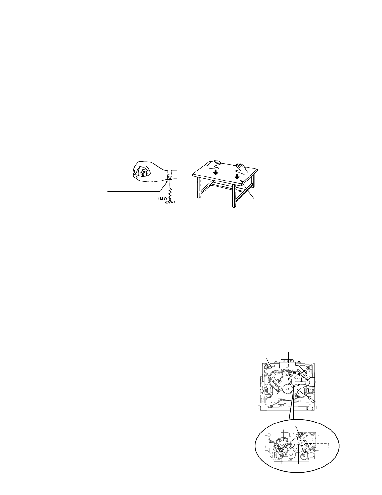
KD-S9R
Disassembly method
Removing the front panel unit (See Fig. 1, 2)
1.Press the Eject button to open the front panel unit
2.Push and open the right and left open/close shaft arms
outward to remove the shaft.
3.Remove the front panel unit from the same side as the
shaft was removed.
Removing the front chassis assembly (See Fig. 3, 4)
1.Remove the front panel unit.
2.Remove the two screws A attaching the front chassis
assembly.
3.Remove the four ribs a attaching the front chassis
assembly to the chassis.
Front panel unit
Eject button
Fig 1
Open/close
shaft arm
A
Fig 3
a
Removing the bottom cover assembly
(See Fig. 5)
Fig 4
b
Fig 2
a
Turn the unit upside down,then insert and turn to
b the screwdriver to remove the bottom cover.
1-4
b
b
Fig 5
Page 5
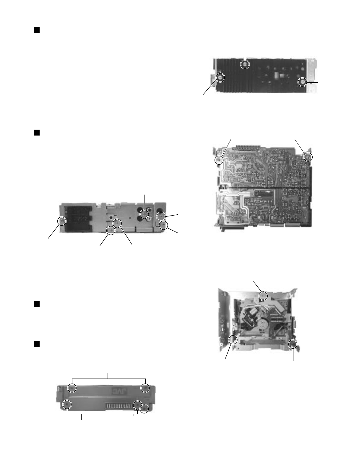
Removing the main board(wiht rear panel)
(See Fig. 6, Fig. 7)
1.Remove three screws E retaining the rear panel to the
chassis
2.Remove one screw C retaining the IC to the heat sink.
3.Remove two screws D retaining the main board.
4.Lift up the main board to remove it.
5.Remove two screws B to remove the heat sink.
KD-S9R
C
B
B
Fig 6
Removing the rear bracket (See Fig. 7)
1.Remove one screw I to remove the IC bracket.
2.Remove one screw F to remove the line-out jack.
3.Remove one screw G to remove the antenna jack.
F
E
E
I
Fig 7-2
G
E
D
D
Fig 7-1
J
CD mechanism assembly (See Fig. 8)
Remove three mechanism mounting screws J retaining the
top cover.
Front panel unit (See Fig.9)
Remove five screws K retaining the rear cover.
K
K
Fig 9
J
J
Fig 8
1-5
Page 6
KD-S9R
Removing the CD mechanism control
board (See Fig.1 and 2)
Unsolder the part f and g on the CD mechanism
control board.
Remove the stator fixing the CD mechanism control
board and the damper bracket (To remove the stator
smoothly, pick up the center part).
Remove the screw F attaching the CD mechanism
control board.
Remove the CD mechanism control board in the
direction of the arrow while releasing it from the two
damper bracket slots i and the front bracket slot j.
Disconnect the flexible wire from connector on the
pickup unit.
ATTENTION:
Turn the FD gear in the direction of the
arrow to move the entire pickup unit to
the appropriate position where the
flexible wire of the CD mechanism unit
can be disconnected easily (Refer to
Fig.2).
CD mechanism ass’y
m
Front bracket
Damper bracket
I
g
F
Fig.1
Pickup unit
I
j
Flexible wire
f
m
h
I
i
CD mechanism
control board
Shift the lock
k
G
Loading motor
Pull outward
FD gear
Fig.2
CD mechanism control board
Front bracket
Fig.3
Front bracket
k
G
Pull outward
1-6
Flame
Fig.4
Page 7
KD-S9R
Removing the loading motor
(See Fig.3 to 5)
*
Prior to performing the following procedure, remove
the CD mechanism control board.
1.
Remove the two springs k attaching the CD mechanism
ass’y and the front bracket.
2.
Remove the two screws G and the front bracket
while pulling the flame outward.
3.
Remove the belt and the screw H from the loading
motor.
Removing the CD mechanism ass’y
(See Fig.1, 6 to 9)
CD mechanism ass’y
I
Flame
m
Loading motor
Fig.5
I
Fig.6
H
Belt
Damper bracket
m
I
I
*
Prior to performing the following procedure, remove
the CD mechanism control PWB and the front
bracket (loading motor).
1.
Remove the three screws I and the damper bracket.
2.
Raise the both sides fix arms and move the fix plates
in the direction of the arrow to place the four shafts l
as shown in Fig.8 and 9.
3.
Remove the CD mechanism ass’y and the two
springs m attaching the flame.
4.
Remove the two screws J and both sides rear
damper brackets from the dampers. Detach the CD
mechanism ass’y from the left side to the right side.
ATTENTION:
The CD mechanism ass’y can be
removed if only the rear damper
bracket on the left side is removed.
Fix plate (L)
l
Fix arm (R)
Fig.7
Rear damper bracket
l
Fig.8
Rear damper bracket
J
Fix plate(R)
J
Fix arm (L)
Damper
Damper
l
l
Fig.9
1-7
Page 8
KD-S9R
Removing the feed motor ass’y
(See Fig.10)
*
Prior to performing the following procedure, remove
the CD mechanism control board, the front bracket
(loading motor) and the CD mechanism ass’y.
1.
Remove the two screws K and the feed motor ass’y.
Removing the pickup unit
(See Fig.10 and 11)
*
*Prior to performing the following procedure, remove
the CD mechanism control board, the front bracket
(loading motor), the CD mechanism ass’y and the
feed motor ass’y.
1.
Detach the FD gear part of the pickup unit upward.
Then remove the pickup unit while pulling out the
part n of the FD screw.
Feed motor ass’y
K
FD gear
Nut push spring plate
FD screw
Pickup unit
Part n
Part O
Pickup unit
Fig.10
L
Pickup mount nut
Pickup unit
ATTENTION:
2.
Remove the screw L attaching the nut push spring
plate and the pickup mount nut from the pickup unit.
Pull out the FD screw.
When reattaching the pickup unit,
reattach the part o of the pickup unit,
then the part n of the FD screw.
Removing the spindle motor
(See Fig.12 and 13)
*
Prior to performing the following procedure, remove
the CD mechanism control board, the front bracket
(loading motor), the CD mechanism ass’y and the
feed motor ass’y.
1.
Turn up the CD mechanism ass’y and remove the
two springs p on both sides of the clamper arms.
Open the clamper arm upward.
2.
Turn the turn table, and remove the two screws M
and the spindle motor.
FD screw
p
Spindle motor
Fig.11
p
Fig.12
M
1-8
M
Fig.13
Page 9
Adjustment method
KD-S9R
Test instruments required for adjustment
1.Digital oscilloscope(100MHz)
2.AM Standard signal generator
3.FM Standard signal generator
4.Stereo modulator
5.Electric voltmeter
6.Digital tester
7.Tracking offset meter
8.Test Disc JVC:CTS-1000
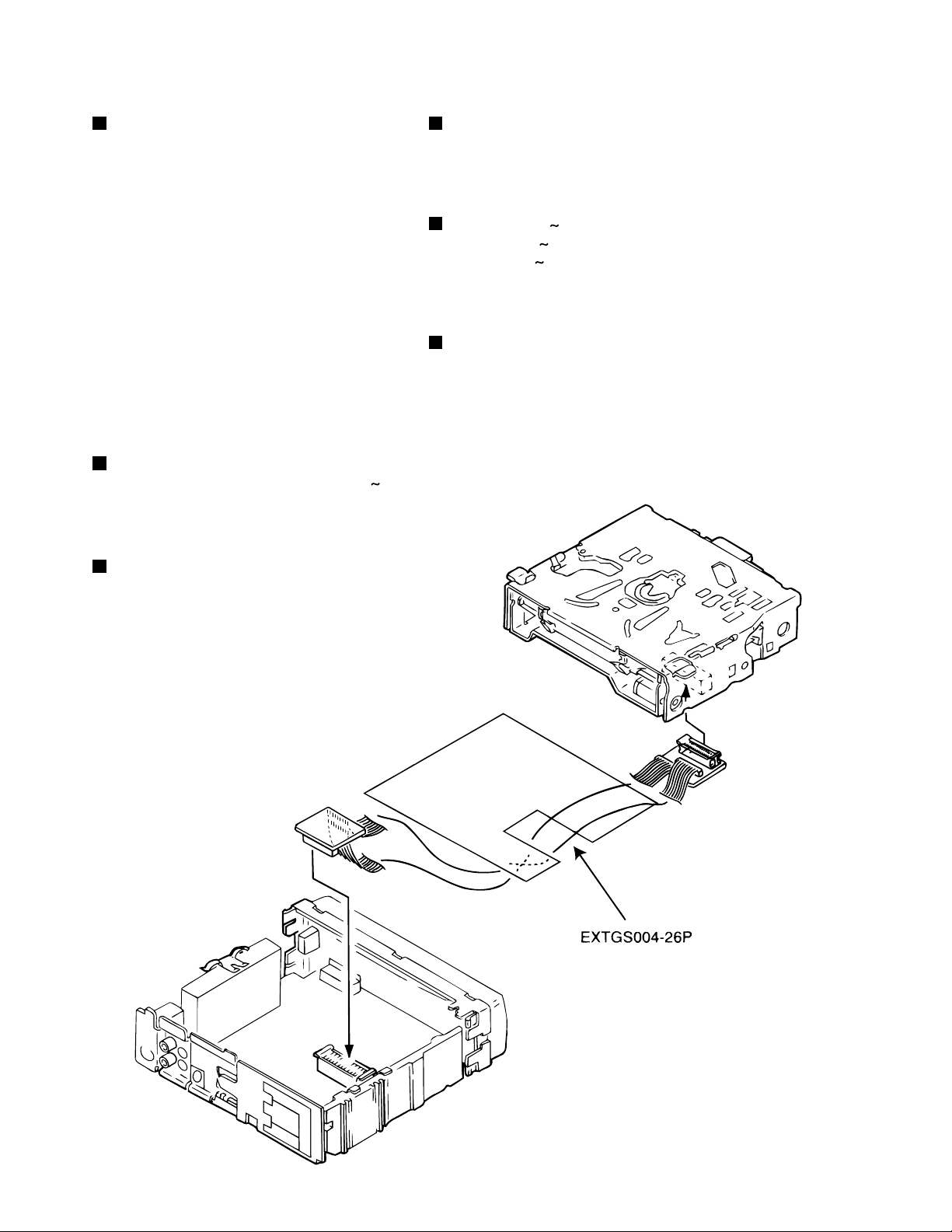
9.Extension cable for check
EXTGS004-26P x 1
Standard measuring conditions
Power supply voltage DC14.4V(10.5 16V)
Load impedance 20Kohm(2 Speakers connection)
Output Level Line out 2.0V (Vol.MAX)
How to connect the extension cable for adjusting
Standard volume position
Balance and Bass & Treble volume:Indication"0"
Loudness:OFF
BBE :OFF
Frequency Band
FM 87.5MHz 108.0MHz
MW 522kHz 1620 kHz
LW 144kHZ 279kHz
Dummy load
Exclusive dummy load should be used for AM, and FM,For
FM dummy load,there is a loss of 6dB between SSG output
and antenna input, The loss of 6dB need not be considered
since direct reading of figures are applied in this working
standard.
1-9
Page 10
KD-S9R
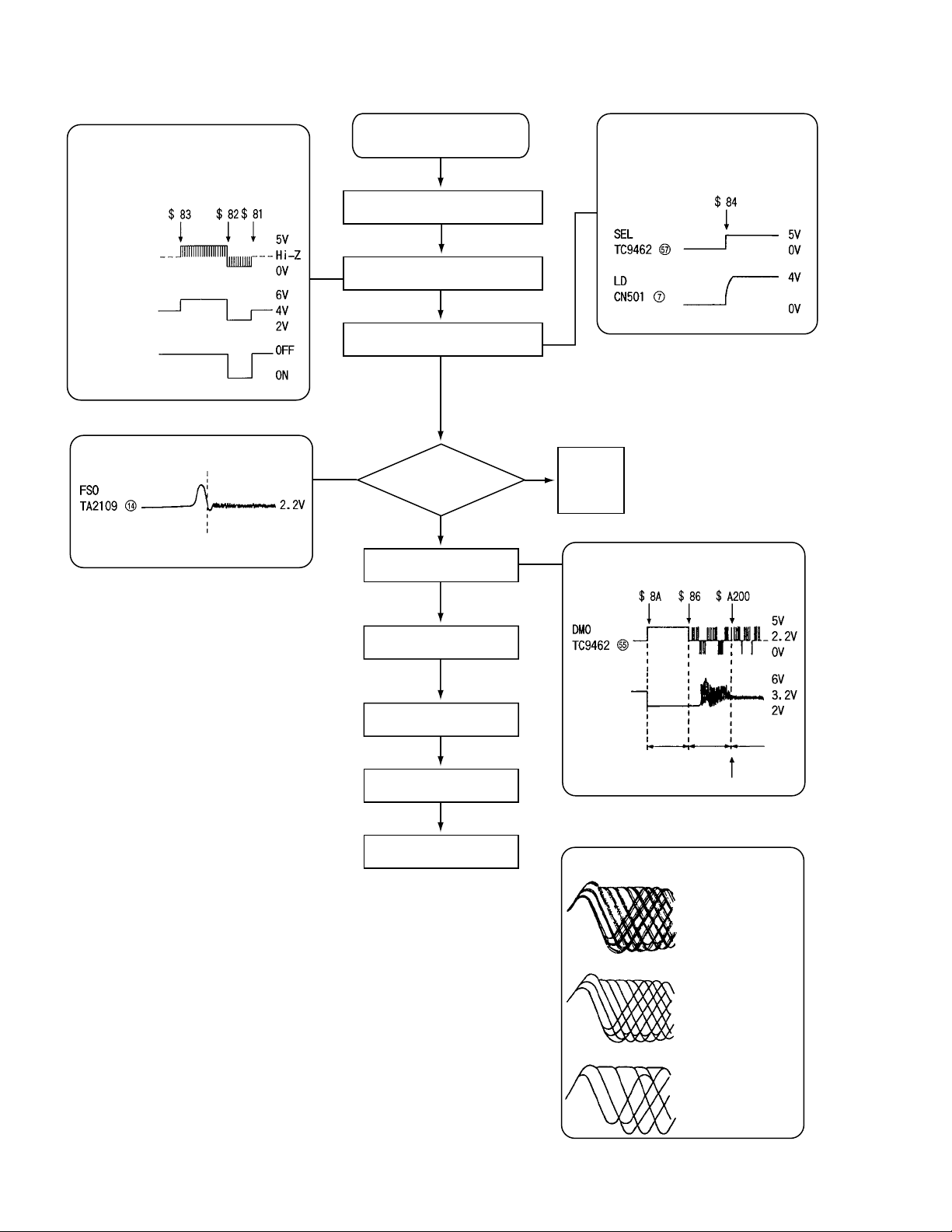
Flow of functional operation until TOC read
Power ON
• When the pickup correctly moves
to the inner area of the disc
Set Function to CD
• When the laser diode correctly
emits
Microprocessor
commands
FMO
TC9462 "53"
FEED MOTOR
+TERMINAL
TERMINAL
IC581 "5"
REST SW
• When correctly focused
Focus Servo Loop ON
Disc inserted
Pickup feed to the inner area
Laser emitted
Focus search
Disc rotates
RF signal eye-pattern
remains closed
Tracking loop closed
RF signal eye-pattern
opens
TOC readout
YES
YES
Microprocessor
commands
"No disc"
display
• When the disc correctly rotates
Microprocessor
commands
Spindle
motor (-)
IC581 "7"
AccelerationAcceleration
0.5 Sec
Rough
Servo
0.5 Sec
Servo CLV
1-10
Jump to the first track
Play
Tracking Servo Loop ON
• RF signal
Rough Servo Mode
CLV Servo Mode
(Program Area)
CLV Servo Mode
(Lead-In Area;
Digital: 0)
Page 11
Maintenance of laser pickup
(1) Cleaning the pick up lens
Before you replace the pick up, please try to
clean the lens with a alcohol soaked cotton
swab.
(2) Life of the laser diode
When the life of the laser diode has expired,
the following symptoms will appear.
(1) The level of RF output (EFM output:ampli tude of eye pattern) will be low.
KD-S9R
Is RF output
1.0 0.35Vp-p?
YES
O.K
(3) Semi-fixed resistor on the APC PC board
The semi-fixed resistor on the APC printed
circuit board which is attached to the pickup
is used to adjust the laser power.Since this
adjustment should be performed to match the
characteristics of the whole optical block,
do not touch the semi-fixed resistor.
If the laser power is lower than the specified
value,the laser diode is almost worn out, and
the laser pickup should be replaced.
If the semi-fixed resistor is adjusted while
the pickup is functioning normally,the laser
pickup may be damaged due to excessive current.
NO
Replace it.
Replacement of laser pickup
Turn off the power switch and,disconnect the
power cord from the ac outlet.
Replace the pickup with a normal one.(Refer
to "Pickup Removal" on the previous page)
Plug the power cord in,and turn the power on.
At this time,check that the laser emits for
about 3seconds and the objective lens moves
up and down.
Note: Do not observe the laser beam directly.
Play a disc.
Check the eye-pattern at TP1.
Finish.
1-11
Page 12

KD-S9R
Descrption of major ICs
UPD784215AGC126(IC701):DSP controller
1.Terminal layout
75 ~ 51
76
~
50
~
1-12
100
1 ~ 25
26
2.Pin function
Pin No. Symbol I/O Function
-
1~8
9
10
11
12
13
14
15
16
17
18
19
20
21
22
23
24
25~32
33
34,35
36
37,38
39
40
41
42
43
44
45,46
47
48
49
50
51,52
53
54~63
64,65
66
67
68
69,70
71
72
73~80
81
82
83
84
85
86
87
88
89
90~93
94
95~100
VDD
X2
X1
VSS
XT2
XT1
RESET
AUTODATA
LOCK
DIGITAL0
FORMAT
CHANNEL
ERR
RSTDET
AVDD
AVREF0
AVSS
RX,TX
DSPCOM
DSPSTS
DSPCLK
DSPRDY
MIDIO_IN/OUT
MICK
MICS
MILP
MIACK
DSPRST
CDTI/CDTO
CCLK
CS
XTS
PD
GND
VDD
3D-ON
3D-ON
ANA/T-TONE
REF-MIX
D.MUTE
S.MUTE
ASW1~4
TEST
I/O
I/O
Unused terminal
-
Power supply terminal
O
Crystal oscillation terminal 6.14MHz (main clock)
I
Crystal oscillation terminal 6.14MHz (main clock)
-
Connects to ground
-
Unused terminal
-
Unused terminal
I
Reset signal input
I
DSP general-purpose port output interrupt
I
DSP general-purpose port output interrupt
I
DSP general-purpose port output interrupt
I
DSP general-purpose port output interrupt
I
DSP general-purpose port output interrupt
I
DSP general-purpose port output interrupt
I
DSP general-purpose port output interrupt
-
Power supply terminal
-
Connects to ground
-
Connects to ground
-
Connects to ground
-
Unused terminal
-
Power supply terminal
-
Unused terminal
-
Unused terminal
I
Communication port with IC401
O
Status communication port to IC401
I
Clock input from IC401
I
Ready signal input from IC401
-
Unused terminal
DSP-microcomputer I/F
O
Clock signal to IC631
O
Chip selection to IC631
O
DSP-microcomputer I/F
O
DSP-microcomputer I/F
-
Unused terminal
O
Output of reset signal of DSP
-
Unused terminal
CODEC-microcomputer I/F
O
Clock signal to IC601
O
Chip selection to IC601
O
OSC selection
-
Unused terminal
O
Reset signal output
-
Connects to ground
-
Unused terminal
-
Power supply terminal
-
Unused terminal
O
Switches at the output destination of the surround channel
O
Test tone control
O
Control at output destination of LFE channel
-
Unused terminal
O
MUTE of digital out terminal
O
Audio signal MUTE
-
Unused terminal
O
Digital input selection
-
Test terminal
-
Unused terminal
Page 13

TEA6320T-X (IC161) : E.volume
1.Pin layout
2.Block diagram
10 8 9 7 6
KD-S9R
5
12
SDA
1
GND
2
OUTLR
OUTLF
MUTE
TL
B2L
B1L
IVL
ILL
QSL
IDL
ICL
IMD
IBL
IAL
3
4
5
6
7
8
9
10
11
12
13
14
15
16
3.Pin functions
Pin
Symbol
No.
SDA
1
SCL
32
VCC
31
OUTRR
30
OUTRF
29
TR
28
B2R
27
B1R
26
IVR
25
ILR
24
QSR
23
IDR
22
Vref
21
ICR
CD-CH
TAPE
TUNER
20
19
18
17
CAP
IBR
IAR
I/O
Serial data input/output.
I/O
MUTE
21
31
2
19
16
15
13
11
14
22
20
18
17
Functions Functions
POWER
SUPPLY
SOURCE
SELECTOR
23 25 24 26 27 28
VOLUME 1
+20 to -31 dB
LOUDNESS
LEFT
VOLUME 1
+20 to -31 dB
LOUDNESS
RIGHT
Pin
No.
17
Symbol
IAR
BASS
LEFT
+15 dB
LOGIC
BASS
RIGHT
+15 dB
I/O
I
Input A right source.
TREBLE
LEFT
+12 dB
TREBLE
RIGHT
+12 dB
FUNCTION
ZERO CROSS
DETECTOR
VOLUME 2
0 to 55 dB
BALANCE
FENDER REAR
VOLUME 2
0 to 55 dB
BALANCE
FENDER FRONT
HC BUS
REC
VOLUME 2
0 to -55dB
BALANCE
FENDER FRONT
VOLUME 2
0 to -55dB
BALANCE
FENDER REAR
3
4
32
1
29
30
2
3
4
5
6
7
8
9
10
11
12
13
14
15
16
GND
OUTLR
OUTLF
TL
B2L
B1L
IVL
ILL
QSL
IDL
MUTE
ICL
IMO
IBL
IAL
Ground.
-
output left rear.
O
output left front.
O
Treble control capacitor left channel or
I
input from an external equalizer.
Bass control capacitor left channel or
-
output to an external equalizer.
Bass control capacitor left channel.
-
Input volume 1. left control part.
I
Input loudness. left control part.
I
Output source selector. left channel.
O
Not used
-
Not used
-
Input C left source.
I
Not used
-
Input B left source.
I
Input A left source.
I
18
19
20
21
22
23
24
25
26
27
28
29
30
31
32
IBR
CAP
ICR
Vref
IDR
QSR
ILR
IVR
B1R
B2R
TR
OUTRF
OUTRR
Vcc
SCL
I
Input B right source.
-
Electronic filtering for supply.
I
Input C right source.
-
Reference voltage (0.5Vcc)
-
Not used
O
Output source selector right channel.
I
Input loudness right channel.
I
Input volume 1. right control part.
-
Bass control capacitor right channel
Bass control capacitor right channel or
O
output to an external equalizer.
Treble control capacitor right channel or
I
input from an external equalizer.
O
Output right front.
O
Output right rear.
-
Supply voltage.
I
Serial clock input.
1-13
Page 14

KD-S9R
BA4905-V3 (IC901) : Regulator
1.Terminal layout
12 34 56 78 9101112
2.Block diagram
REGULATOR
EXT
OIVPC
RESET
1 2 3 4 5 6 7 8 9 10 11 12
RESET COMP VDD 5.7V CD 8V VCC AJ
EXT ACC AUDIO 9V CTRL ILM 10V GND
37K
5K
1-14
Page 15

KD-S9R
Explanation of terminals
1
2
2
4
5
6
7
8
9
RESET
EXT output
COMP output
ACC
VDD output
AUDIO output
CD output
CTRL
VCC
BA4905-V3
If VDD voltage becomes 4V or less, RESET output becomes low level.
This outout voltage is approximately 0.5V lower than VCC, and max
output current is 300mA.
A voltage supply for ACC block this outout voltage is approximately
0.7V lower than VDD'S. The max output current is 100mA.
Control of the COMP output by inputting voltage.
This output voltage is 5.7V, and max output current is 100mA.
This voltage supply is for microcomputer. Whenever block up voltage
supply is connected. the output keeps on running.
This output voltage is 9.0V, and max output current is 500mA.
This voltage supply for AUDIO.
This output voltage is 8.0V, and max output current is 1A.
This voltage supply for CD.
Output selector of CD, AUDIO,ILM and EXT.
To be connected with the BACK UP of car.
10
11
12
ILM output
AJ
GND
This output voltage is 10V, and max output current is 500mA.
Output voltage is adjustable.
Putting a resistance between ILM and AJ or between AJ and GND
makes ILM output voltage adjustable.
Ground.
1-15
Page 16

KD-S9R
LA4743B(IC301):Power AMP
1.Block diagram
IN 1
TA B
IN 2
+
0.22 F
+
0.22 F
11
1
12
Vcc 1/2 Vcc 3/4
6 20
-
+
Protective
circuit
-
+
2200 F 0.022 F
+
9
7
+
OUT 1+
OUT 1-
PWR GND1
8
+
OUT 2+
5
-
OUT 2-
3
PWR GND2
2
ST BY
R.F
47 F
IN 3
PRE GND
IN 4
+5V
ST ON
+
0.22 F
N.C
+
0.22 F
4
Stand by
Switch
Mute
10
+
Ripple
Filter
Mute
22
circuit
3.3 F
+
15
-
+
-
17
19
10K
+
OUT 3+
OUT 3-
Low Level
Mute ON
25
18
24
23
PWR GND3
OUT 4+
OUT 4-
13
14
Protective
circuit
-
+
+
-
1-16
ON TIME C
22 F
Muting &
16
+
ON Time Control
Circuit
PWR GND4
24
Page 17

2.Terminal layout
3.Pin function
1
2
3
4
5
6
7
8
9
10
11
12
13
14
15
16
17
18
19
20
21
22
23
24
25
SymbolPin No. Function
TA B
GND
OUTRRSTBY
OUTRR+
VCC1/2
OUTRFGND
OUTRF+
RIPPLE
INRF
INRR
SGND
INLR
INLF
ONTIME
OUTLF+
GND
OUTLFVCC3/4
OUTLR+
MUTE
OUTLRGND
NC
Header of IC
Power GND
Outpur(-) for front Rch
Stand by input
Output (+) for front Rch
Power input
Output (-) for rear Rch
Power GND
Output (+) for rear Rch
Ripple filter
Rear Rch input
Front Rch input
Signal GND
Front Lch input
Rear Lch input
Power on time control
Output (+) for rear Lch
Power GND
Output (-) for rear Lch
Power input
Output (+) for front
Muting control input
Output (-) for front
Power GND
Non connection
KD-S9R
LA4743B
1-17
Page 18

KD-S9R
LA6567H-X(IC501):CD DRIVE
1.Pin layout & blockdiagram
VCC2
V05-
V05+
V04+
V04-
V03+
V03-
FR
1
2
3
4
5
6
7
FR
CH 3,4,5
Power supply
CH5
CH4
CH3
Thermal shutdown
Output control
Level shiftLevel shiftLevel shiftLevel shift
Input
22K 11K
Signal system power supply
28
27
26
25
24
23
22
FR
REV
FWD
S-GND
VCONT
VIN4
VIN4G
VCC-S
FR
VC2+
V02-
V01+
V01-
VCC1
VIN1
VIN1G
8
9
10
11
12
13
14
CH2
CH1
CH1,2
Power supply
11K
22K
5VREG(PNPTr
The outside puuting)
22K
11K
22K
11K
21
20
19
18
17
16
15
VREF-IN
REG-OUT
REG-IN
VIN3G
VIN3
VIN2G
VIN2
1-18
Page 19

KD-S9R
2. Pin function
Pin no. Symbol
1
2
3
4
5
6
7
8
9
10
11
12
13
14
15
16
17
18
19
20
21
22
23
24
25
26
27
28
VCC2
V05V05+
V04+
V04V03+
V03V02+
V02V01+
V01-
VCC1
VIN1
VIN1G
VIN2
VIN2G
VIN3
VIN3G
REG-IN
REG-OUT
VREF-IN
VCC-S
VIN4G
VIN4
VCONT
S-GND
FWD
REV
LA6567H-X(2/2)
Function
CH3,4,5 Power supply( It is short with VCC1,VCC-S)
Loading output(-)
Loading terminal (+)
CH4 Output terminal(+)
CH4 Output terminal(-)
CH3 Output terminal(+)
CH3 Output terminal(-)
CH2 Output terminal(+)
CH2 Output terminal(-)
CH1 Output terminal(+)
CH1 Output terminal(-)
CH1,2(BTL) Power supply(It is short with VCC-S,VCC2)
CH1 Input terminal
CH1 Input terminal(For gain adjustment)
CH2 Input terminal
CH2 Input terminal(For gain adjustment)
CH3 Input terminal
CH3 Input terminal(For gain adjustment)
Regulator terminal(Outside putting PNP base)
Regulator terminal(Outside putting PNP collector)
Standard voltage input terminal
Signal system power supply(It is short with VCC1,VCC2)
CH4 Input terminal(For gain adjustment)
CH4 Input terminal
5CH(VLO) Output voltag set terminal
Signal system GND
5CH(VLO)Signal output switch terminal(FWD),Input of logic of loading part
5CH(VLO)Signal output switch terminal(REV),
Input of logic of loading part
Frame(FR)at the center bocomes system GND power.
Please be short-circuited on the outside and use the terminal of the power supply system
and three teminals of VCC-S, VCC1,VCC2.
1-19
Page 20

KD-S9R
TC9462F(IC541):
1.Pin layout & Block Diagram
RST
DD
XV
80
79
81DV
SR
82RO
83DV
DD
84DVR
85LO
86DV
SL
87TEST1
88TEST2
89TEST3
90BUS0
91BUS1
92BUS2
93BUS3
94V
DD
95V
SS
96BUCK
97CCE
98TEST4
99TSMOD
100
1 2 3
TEST0
XO78XI
LPF
HSO
Micon
interface
UHSO
SS
XV
77
4 5
EMPH
DD
V
75
76
1bit
DAC
PXO
SS
PXI
V
74
73
Clock
generator
Correction
circuit
Audio out
circuit
6
7 8 9 10 11 12 13
SS
V
BCK
LRCK
AOUT
72
TESIO1
DOUT
71
TESIN
MBOV
DACT
69
70
Address circuit
16KRAM
Digital out
IPF
CKSE
SBOK
DMOUT
68
CLCK
IO3
IO265IO164IO063V
67
66
ROM
Automatic adjustment
RAM
Synchronous
guarantee
EFM decode
Sub code
decoder
14 15
16 17 18 19 20 21 22
SS
DD
V
V
DATA
SFSY
SS
DD
V
61
62
Servo
control
Digital equalizer
circuit
CLV servo
SBSY
SPCK
FLGD60FLGC59FLGB58FLGA57SEL562V
PWM D/A
A/D
Status
TMAX
23 24 25
DD
COFS
MONIT
V
TESIO0
SPDA
REF
DMO54FVO53FMO52TEBC51RFGC
55
+
-
Data
slicer
VCO
PLL
26
27 28
REF
ZDET
HSSW
P2V
+
PDO
50 V
REF
49 TRO
48 FOO
TEZI
+
TMAXS
30
TMAX
47
46 TEI
45 TSIN
44 SBAD
43 FEI
42 RFRP
41 RFZI
40 RFCT
39 AV
DD
38 RFI
37 SLCO
36 AV
SS
35 VCOF
34 VCOREF
33 PV
REF
32 LPFO
31 LPFN
+
-
-
-
29
2.Pin function
PIN No.
1
2
3
4
5
6
7
8
9
10
11
12
13
14
15
16
17
18
19
20
21
22
23
24
25 P2V
SYMBOL
TEST0
HSO
UHSO
EMPH
LRCK
V
SS
BCK
AOUT
DOUT
MBOV
IPF
SBOK
CLCK
V
DD
V
SS
DATA
SFSY
SBSY
SPCK
SADA
COFS
MONIT
V
DD
TESIO0--I
REF
FUNCTIONAL DESCRIPTION
I/O
Test mode terminal.Normally, Keep at open.
I
Playback speed mode fllag output terminal.
UHSO
HSO
O
H
H
L
O
Subcode Q data emphasis flag output terminal.Emphasis ON at "H" level and OFF at "L"
O
level.The output polarity can invert by command.
Channel clock output terminal.(44.1khz)L-ch at "L" level and R-ch at "H" level. the output
O
polarity can invert by command.
Digital GND terminal.
-O
Bit clock output terminal.(1.4122MHz)
Audio data output terminal.
O
Digital data output terminal.
O
Buffer memory over signal output terminal. Over at "H" level.
O
Correction flag output terminal. At "H" level,AOUT output is made to correction
O
impossibility by C
Subcode Q data CRCC check adjusting result output terminal.
O
The adjusting result is OK at "H" level.
Subcode P W data reabout clock input/output terminal.
I/O
This terminal can select by command bit.
--
Digital power supply voltage terminal.
--
Digital GND terminal.
O
Subcode P W data output terminal.
O
Play-back frame sync signal output terminal.
O
Subcode block sync signal output terminal.
O
Processor status signal reabout clock output terminal.
O
Processor status signal output terminal.
O
Correction frame clock output terminal. (7.35kHz)
Internal signal (DSP internal flag and PLL clock) output terminal.Selected by command.
O
This terminal output the text data with serial by command.
L
PLAYBACK SPEED
H
L
H
Nomal
2 times
4 times
L
2
correction processing.
--
Digital power supply voltage terminal.
Test input/output terminal.Normally,keep at "L" level.
The terminal that inputted the clock for read of text data by command.
--
PLL double reference voltage supply terminal.
REMARKS
With pull-up resistor.
--
--
--
--
--
--
--
--
--
--
--
--
--
--
--
--
--
--
--
--
--
--
--
1-20
Page 21

KD-S9R
2.Pin Function (2/2)
Pin No.
40
41
42
43
44
45
46
47
48
49
50
51
52
53
54
55
56
57
58~61
62
63
64~67
68
69
70
71
72
73
74
75
76
77
78
79
80
81
82
83
84
85
86
87~89
90~93
94
95
96
97
98
99
100
Symbol
RFCT
RFZI
RFRP
FEI
SBAD
TSIN
TEI
TEZI
FOO
TRO
VREF
RFGC
TEBC
FMO
FVO
DMO
2VREF
SEL
FLGA~D
VDD
VSS
IO0~3
DMOUT
CKSE
DACT
TESIN
TESIO1
VSS
PXI
PXO
VDD
XVSS
XI
XO
XVDD
DVSR
RO
DVDD
DVR
LO
DVSL
TEST1~3
BUS0~3
VDD
VSS
BUCK
CCE
TEST4
TSMOD
RST
I/O
RFRP signal center level input terminal
I
RFRP zero cross input terminal
I
RF ripple signal input terminal
I
Focus error signal input terminal
I
Sub-beam adder signal input terminal
I
Test input terminal Normally, keep at "vref" level
I
Tracking error signal input terminal. Take in at tracking servo ON.
I
Tracking error zero cross input terminal
I
Focus servo equalizer output terminal
O
Tracking servo equalizer output terminal
O
Analog reference voltage supply terminal
RF amplitude adjustment control signal output terminal
O
Tracking balance control signal output terminal
O
Feed equalizer output terminal
O
Speed error signal or feed search equalizer output terminal
O
Disk equalizer output terminal
O
Analog double reference voltage supply terminal
APC circuit ON/OFF indication signal output terminal
O
External flag output terminal for internal signal
O
Digital power supply voltage terminal
Digital GND terminal
General I/O terminal
I/O
This terminal control IO0~IO3 terminal
I
Normally, keep at open
I
DAC test mode terminal. Normally, keep at open
I
Test input terminal, Normally, keep at "L" level
I
Test input/output terminal. Normally, keep at "L" level
I
Digital GND terminal
Crystal oscillator connecting input terminal for DSP
I
Crystal oscillator connecting output terminal for DSP
O
Digital power supply voltage terminal
Oscillator GND terminal for system clock
Crystal oscillator connecting input terminal for system clock
I
Crystal oscillator connecting output terminal for system clock
O
Oscillator power supply voltage terminal for system clock
Analog GND terminal for DA converter (Rch)
R channel data forward output terminal
O
Analog supply voltage terminal for DA converter
Reference voltage terminal for DA converter
L channel data forward output terminal
O
Analog GND terminal for DA converter (Lch)
Test mode terminal . Normal keep at open
I
Micon interface data input/output terminal
I/O
Digital power supply voltage terminal
Digital GND terminal
Micon interface clock input terminal
I
Command and data sending/receiving chip enable signal input terminal
I
Test mode terminal. Normal, keep at open
I
Local test mode selection terminal
I
Reset signal input terminal. Reset at "L" level
I
Function
(PWM carrier=88.2kHz for DSP, Synchronize to PXO)
TC9462F
1-21
Page 22

KD-S9R
BA3880FS-X(IC181) : BBE
1. Pin layout & Block Diagram
GND
1
DETR
DEFR
2
CTL
3
CTL
24
23
22
DETL
DEFL
CTL
VCAR
MIXR
OUTR
INR
APFR
HPFR
LPFR
BIASC
10
11
12
4
5
6
7
8
9
VCA
HPF
LPF
+
+
HI MID
+
+
+
+
-
+
+
HI
LO
+
VCA
+
+
+
MID
+
+
LO
+
+
-
LPF
HPF
21
20
19
18
17
16
15
14
13
Vcc
VCAL
MIXL
OUTL
INL
APFL
HPFL
LPFL
2. Pin Functions
Pin
Symbole Function Symbole Function
No.
10
11
12
GND
1
DETR
2
DEFR
3
CTL
4
VCAR
5
MXIR
6
OUTR
7
8
APFR
9
HPFR
LPFR
BIAS
Grounding terminal
Peak level detector output for treble VCA control
Control signal time constant terminal
Control signal input terminal
Treble CA output terminal
Output MIX amplifier summing terminal
Signal output terminal
INR
Signal input terminal
Input inversion amplifier output terminal
HPF output terminal
LPF output terminal
Reference voltage output terminal (1/2 Vcc)
Pin
No.
13
14
15
16
17
18
19
20
21
22
23
24
LPFL
HPFL
APFL
INL
OUTL
MIXL
VCAL
VCC
DEFL
DETL
LPF output terminal
HPF output terminal
Input inversion amplifier output terminal
Non connector
Signal input terminal
Signal output terminal
Output MIX amplifier summing terminal
Treble CA output terminal
Power supply terminal
Control signal time constant terminal
Non connector
Peak level detector output for treble VCA control
1-22
Page 23

BA6218 (IC591) : Motor driver
KD-S9R
1. Block diagram
7
OUT 2
12k
6 Vcc
9 OUT1
6.8k 6.8k
12k
3
RIN
2. Function truth table
3Pin (IN)
20k
1Pin (IN)
H
L
H
L
L
H
H
L
528
GND GND COM
7Pin (OUT)
H
H
L
OPEN
9Pin (OUT)
OPEN
1 FIN
20k
H
L
L
1-23
Page 24

KD-S9R
HD74HC126FP-X (IC801) : Buffer
1.Terminal layout
1
2
3
4
5
6
7
2.Block diagram
Input
14
13
12
11
10
9
8
Vcc Vcc
1A
2A
3A
4A
1C
2C
3C
See Function Table
4C
3.Pin function
Output
1Y
2Y
Output
2Y
Output
3Y
Output
4Y
Input Outout
C
A
L
X
H
L
H
H
1k
CL
Sample as Load Circuit 1
Sample as Load Circuit 1
Sample as Load Circuit 1
Y
Z
H
L
S1
1k
1-24
Page 25

SAA6579T-X(IC71):RDS Detector
KD-S9R
1.Terminal Layout
QUAL
RDDA
MUX
VDDA
GND
SCOUT
Vref
CIN
1
2
3
4
5
6
7
8
16
15
14
13
12
11
10
9
RDCL
T75
OSCO
OSC1
VDD
GND
TEST
MODE
2.Pin Function
Pin
No.
1
2
3
4
5
6
7
8
9
10
11
12
13
14
15
16
QUAL
RDDA
Vref
MUX
VDDA
GND
CIN
SCOUT
MODE
TEST
GND
VDD
OSC1
OSC0
T75
RDCL
FunctionI/OSymbol
Non connect
RDS data output
O
Reference voltage output
O
Multiplex signal input
I
+5V Supply voltage for analog
Ground for analog part (0V)
Sub carrier output of reconstruction filter
I
Ground for digital part (0V)
O
Ground for digital part (0V)
Ground for digital part (0V)
Ground for digital part (0V)
+5V supply voltage for digital part
Oscillator input
I
Oscillator output
O
Non connect
RDS clock output
O
3.Block Diagram
4
8
7
5
3
ANI-
ALLUDING
FILTER
CLOCKED
COMPARATOR
REFERENCE
VOLTAGE
1413
5kHz
BAND PASS
(8th ORDER)
COSTAS LOOP
VARIABLE AND
FIXWD DIVIDER
CLOCK
REGENERATION
AND SYNC
6
RECONSTRUCTION
FILTER
BIPHASE
DECODER
TEST LOGIC AND OUTPUT
OSCILLATOR
AND
DIVIDER
SYMBOL
SELECTOR SWITCH
9
10
12
DUALITY BIT
GENERATOR
DIFFERENTIAL
DECODER
11
1
2
16
15
1-25
Page 26

KD-S9R
TA2109F-X (IC521) : RF amp.
1. Pin layout
24 13
112
2. Block diagram
SBAD
13
FEO
14
10pF
FEN
15
VRO
16
RFRP
17
RFIS
18
RFGO
19
10k ohm
21k ohm
20k ohm
20k ohm
50k ohm
36pF
7.96k ohm
50uA
20k ohm
15k ohm 30k ohm
15k ohm
20uA
10k ohm
21k ohm
12k ohm
12k ohm
PEAK
BOTTOM
10k ohm
10k ohm
30k ohm
21k ohm 29k ohm
24k ohm 24k ohm
180k ohm
1.74k ohm
20pF
65uA
10k ohm
47k ohm
SW3
13k ohm
7.67k ohm
3 STATE
DET.
SW1
1k ohm
SW2
680 ohm
2.12k ohm
LCD
20pF
TEO
TEN
2VRO
TEB
SEL
LDO
MDI
12
11
10
9
8
7
6
3. Pin function
Pin
Symbol I/O
No.
Vcc
FNI
FPI
TPI
TNI
MDI
SEL
I
I
I
I
I
O
I
I
O
I
O
10
11
12
1
2
3
4
5
6
7
8
9
LDO
TEB
2VRO
TEN
TEO
RFGC
20
AGCI
21
re=130 ohm
RFO
22
GND
23
RFN
24
23.5k ohm
3.3k ohm
12k ohm
1.53k ohm
3.3k ohm
Pin function
Power supply input terminal
Main beam I-V amp input terminal
Main beam I-V amp input terminal
Sub beam I-v input terminal
Sub beam I-V input terminal
Monitor photo diode amp input terminal
Laser diode amp output terminal
Laser diode control signal input terminal
T. error balance adj. signal input terminal
Reference voltage output terminal
TE amp negative input terminal
TE error signal output terminal
180k ohm
40pF
180k ohm
Pin
No.
13
14
15
16
17
18
19
20
21
22
23
24
180k ohm
20pF
60k ohm
60k ohm
40pF
Symbol I/O
SBAD
FEO
O
O
FEN
VRO
O
RFRP
O
RFIS
RFGO
O
RFGC
AGCI
RFO
O
GND
-
RFN
TNI
TPI
FPI
FNI
Vcc
5
4
3
2
1
I-I
I-I
20k ohm
20k ohm
20k ohm
20k ohm
Pin function
Sub beam adder signal output terminal
Focus error signal output terminal
FE amp negative input terminal
I
Reference voltage (VREF) output terminal
Track count signal output terminal
RFRP detect circuit input terminal
I
RF gain signal output terminal
RF amplitude adj. control signal input terminal
I
RF signal amplitude adj. amp input terminal
I
RF signal output terminal
Ground terminal
RF amp negative input terminal
I
1-26
Page 27

TB2118F-X (IC31) : PLL
1.Terminal Layout
2423222120191817161514
KD-S9R
13
2.Block diagram
osc
2
1
XO
24
XI
FM VCO
AMVCO
IFC
CE
DIN
DOUT
DIMM
15
16
13
3
4
5
6
123456789
Buff.
ON/OFF
OSC circuit
AMP
AMP
AMP
Serial
Interface
101112
Reference Counter
Prescaler
20-bit BINARY COUNTER
Resistor 1
Resistor 2
I/O PORT
Swallow counter
Phase
Comparator
4-bit
12-bit
Programmable counter
22-bit
40bit shift register
OUTPUT PORT
Constant
power supply voltage
switch
Vdd
switch
Vcc
AM CP.
20
+
+
-
REG.
22
19
vt
18
FM cp
3.Pin Function
Pin
Symbol I/O Function
No.
XOUT
10
11
12
1
2
3
4
5
6
7
8
9
OSC
CE
DI
CK
DOUT
SR
I/01
I/02
OUT1
OUT2
VDD2
Crystal oscillator pin
O
Non connect
Chip enable input
I
Serial data input
I
Clock input
I
Serial data output
O
Register control pin
O
I/O ports
I/O
I/O ports
I/O
Non connect
Non connect
Single power supply for REF. frequency block
-
7
SL
8
9
I/O -2I/O -1
10 11
12
out-2out-1
vdd2
Pin
Symbol I/O Function
No.
IFC
13
VDD
14
FMIN
15
AMIN
16
DGND
17
FMCP
18
VT
19
AMCP
20
VCC
21
RF
22
AGND
23
XIN
24
17
14
IF signal input
I
Power pins for digital block
FM band local signal input
I
AM band local signal input
I
Connect to GND (for digital circuit)
Charge pump output for FM
O
Tuning voltage biased to 2.5V.
Charge pump output for AM
O
Power pins for analog block
Ripple filter connecting pin
I
Connect to GND (for analog circuit)
Crystal oscillator pin
I
21
23
a-gnd
vccd-gndvdd
1-27
Page 28

KD-S9R
NJM2100M-WE (IC861) : Cruise
1. Pin layout
2. Block diagram
-INPUT
+INPUT
A OUTPUT
A -INPUT
A +INOUT
V-
1
2
3
4
V+
8
B OUTPUT
7
B -INPUT
6
B +INPUT
5
V+
OUTPUT
NJM4565M-WE (IC581,IC171) : Ope. amp
A OUTPUT
-
A INPUT
+
A INPUT
1
2
3
-
4
V
+
8
V
B OUTPUT
7
-
B INPUT
6
5
+
B INPUT
V-
1-28
Page 29

IC-PST600M/G/-W1197(IC702):Reset
1.Terminal layout
2.Block diagram
Co1
OP1
KD-S9R
Vcc
1
Vout
3
M24C16-WMN6-X(IC771):EPROM
1.Terminal layout 2.Block diagram
CONTROL
LOGIC
SDA SCL
VCC
Vss
I/O
WP
MEMORY
CONTROL
LOGIC
XDEC
GND
2
HV GENERATOR
EEPROM ARRAY
(8x 256 x8)
PAGE LATCHES
SENSE AMP
F/W CNTROL
YDEC
3.Pin function
Pin No.
1 3
Symbol Function
A0 A2
4
5
6
7
8
GND
SDA
SCL
WPIN
Vdd
No internal connection
+2.5V to 5.5V Power supply
Write protect input
Serial clock
Serial address / data I/O
Ground
1-29
Page 30

KD-S9R
VICTOR COMPANY OF JAPAN, LIMITED
MOBILE ELECTRONICS DIVISION
PERSONAL & MOBILE NETWORK BUSINESS UNIT. 10-1,1Chome,Ohwatari-machi,Maebashi-city,Japan
(No.49579)
Printed in Japan
200012 (V)
Page 31

1
2
3
4
5
KD-S9R
Block diagram
SWITCH BOARDMAIN BOARDCD MECHA
AB C
CD PICKUP UNIT
VA,VB,VC,VE,VF,VR,LD,MD
RF AMP
IC521
RF
TE
FE
SW1 ~ 4
TRACKING
FOCUS
CN501
CD DRIVER
FMO
DMO
TRO
FOO
DSP & DAC
IC541
IC501
LOADING
MECHA. SWITCH
SPINDLE/FEED
MOTOR
SPINDLE
FEED
LOADING MOTOR
BUSO ~ 3
BUCK,CCE,RST
CD L/R
RESET
RDSCL/RDSDA
DETECTOR
DET OUT
RESET
IC702
SYSTEM
CONTROLLER
IC701
CD LPF
IC581
RDS
IC71
TUL/R
FM/AM
TUNER
TU1
VOL CL
VOL DA
CD L/R
EPROMCK
EPROMDI
E.VOL
IC161
POWER
AMP
IC301
ENC1/ENC2
KEY0 KEY2
LCD CL
LCD CL
LCD CE
PLLCE/PLLDA/
PLLCL/PLLDI
AM/FM
FM VT/
AM VT
FRONT L
FRONT R
REAR L
REAR R
EPROM
IC771
PLL
IC31
CN701
J1
ENC1,2
CN601
CN711
SHUTTLE SW.
EN601
KEY0 2
OPERATION SW.
S601 ~ S619
LCDDA
LCDCL
LCDCE
LCD DRIVER
IC601
S1 S68
LCD
COM1 3
LINE OUT
J321
2-1
CN901
Page 32

KD-S9R
< MEMO >
2-2
Page 33

Standard schematic diagrams
Main amp.section
TU1
QAU0156-002
J1 L1
B1
4.7uH
0.047
D703
C34
D704
QNZ0009-001
X31
QAX0616-001Z
IC31
TB2118F
R32
6.2K
D705
D706
47/6.3
0
0
10K
R41
C44
R42
C717
0.1
47K
R802
0.01
0.01
C6
C49
0.01
100/10
C31
0.01
0.0027
C45
C7
C39
1000P
FM/AM
SD/ST
SQ
4.7K
R31
VT
C1
R7
10( 1/4W)
22/16
22K
R804
1SS133
1SS133
D1 D2
100
R38
R39
C38
1000P
C37
10P
C33
D707
D708
C48
0.047
UN2211
39K
C40
10/16
0.047
0.01
R40
0.047
C43
C42
C41
0.01
C46
C47
0.01
10( 1/4W)
R43
R44
470
220
C50
C32
100P
47P
Q31
C716
0.1
5
4
3
2
1
Note:KD-S9R FSDH3192-005AV 1/2
/s/C/jes/3192.001
C36
7P
C35
10P
PLLCE
2.2K
R37
PLLDA
2.2K
R36
PLLCL
2.2K
R35
PLLDI
R34
2.2K
R33
47K
9V
CD.R
GND
CD.L
REST
SW1
SW2
SW3
SW4
LM0
LM1
BUS0
BUS1
BUS2
BUS3
BUCK
CCE
RST
CD8V
GND
ACC5V
10V
ENC1
ENC2
LCDCE
LCDDA
LCDCL
KEY2
KEY1
KEY0
CN701
QNZ0007-002
D701
D702
AB CD E F G
AM.VCC
0.047
C2
2SB815B7
Q6
Q7
UN2211
R58
470
C55
0.47/50
2SC2412K( R)
PL701
QLD0033-001
KD-S9R
D243
1SS133
C244
0.22/50
R247
68K
C81
C91
2SD601A( R)
Q53
UN2211
R59
R2
47K
R1
22K
SM
R51
C706
0.047
VOLDA
VOLCL
BUCK
CCE
RST
BUS0
BUS1
BUS2
BUS3
C5
47K
8.2( 1/8W)
MONO
R708
0.1/50
R3
4.7k
SEEK/STP
AFCK
UPD784215AGC-126
R720
R719
VPP
R760
R716
R715
R714
R713
R712
R711
R710
R709
R707
R706
R705
R704
TU.OSC
FM.VCC
TU.VCC
C94
0.01
D4
MA152WK
R4
3.3K
C54
0.1
C53
0.0047
0.015
220/10
C4
R5
47K
( Q8)
UN2211
R54
10k
R55
2.2k
Q51
2SC2412K( R)
( R8)
C84
Q5
10K
R53
47k
C52
0.01
R52
47k
0.015
Q1
2SB709A( R)
C51
330P
C3
R9
0
R6
47k
R57
15k
R56
10k
Q52
R807
100K
22K
R809
47K
R801
R81
1/50 8.2K
R91
1/50
2SD601A( R)
Q2
Q91
2SD601A( R)
R93
4.7k
Q3
C83
UN2111
0.1
Q4
UN2111
D3
1SS133
C77
47/6.3
C76
0.01
C75
47P
C74
82P
X71
QAX0425-001Z
1K
IC701
R763
1.2K
0
VDD
47k
0
0
47K
0
0
0
0
47K
47K
LM0
LM1
47K
47K
47K
47K
8.2K
C92
820P
R92
18K
R83
4.7k
Q9
UN2111
R71
2.2k
SAA6579T
RDSCL
R758
47K
1K
10K
R721
R722
SW2
SW3
SW4
REST
Q81
2SD601A( R)
IC71
PLLDI
PLLCL
PLLDA
VSS
R703
R702
R755
0
0
10M
LM0
LM1
X701
X1
C704
C705
0.047
QAX0617-001Z QAX0401-001
C82R82
820P18K
RDSDA
PLLCE
R754
8P
C71
560P
0.022
C73
2.2/50
R73R72
2.2k2.2k
C703
FM/AM
820
C72
27P
R74
100
AFCK
SEEK/STP
10K
0
R723
R724
R701
X702
27P
C702
S702
QSW0451-001
10K
R725
SW1
47k
22P
C701
47K
R753
TU.L
CD.L
CD.R
TU.R
RDSCL
47K
R752
MONO
10K
R726
RDSDA
C708
0.047
SD/ST
10K
R728
C172
C171
C161
C162
R750
ENC1
RESET
1/50
1/50
1/50
1/50
R729
47K
10K
R756
47K
C191 C192
47/16 100/10
IC771
270
270
R771
R772
R730
10K
R732
R734
R735
R736
R737
R738
R740
R741
R742
R743
R744
R745
R746
10K
1SS133
C709
D710
0.01
C771
0.047
10K
2.2K
2.2K
2.2K
0
4.7K
4.7K
10K
10K
10K
10K
10K
R161
220K
D241
MA152WK
R731
47K
TD
C710
47/6.3
R171
220K
C174 C175
0.0082 0.15
M24C16-WMN6-X
S701
QSW0451-001
LCDCE
LCDCL
LCDDA
RD
KEY2
KEY1
KEY0
ENC2
4.7K
R747
R748
4.7K
R749
4.7K
IC702
IC-PST600MG
R172
R162
22K
22K
0.047
LEVEL
C707
SM
SQ
R173
2.2K
C176 C177
0.22 0.033
C166
0.22
C165C164
0.150.0082
R163
2.2K
L701
4.7uH
CPU.VDD
D711
MA152WK
R757
2.2K
C167
0.033
100/10
0.0056
C711
C713
0.01
0.0056
C168
C712
0.01
C178
R872
47K
R174
47K
C169
R164
47K
47/6.3
UN2211
4.7/25
C781
Q891
D242
C179
1SS133
R175
47K
4.7/25
C170
R165
0.047
1k
R246
47K
C243
4.7/25
R245
100
C180
4.7/25
Q781
UN2111
D781
1SS133
C193
100/10
R892
47K
R244
12k
R242
22k
C242
22/16
Q241
2SD601A( R)
C194
0.01
C782
0.082
5V
R891
1K
D891
MA152WA
C891
0.1
R243
180k
C241
1/50
R241
47k
TELMUTE
IC161
TEA6320T
220/10
C909
R784
47K
D782
1SS133
220/10
C908
2SB709A( R)
R181
270
R182
270
Q902
C907
220/10
R782
47K
R783
4.7K
Q782
UN2211
UN2211
C906
Q976
0.01
LEVEL
VOLDA
VOLCL
D902
MA152WA
R907
47k
R908
2.2K
Q903
UN2213
C905
22/16
Q977
2SA1037
R904
C910
47/16
OUTLF
OUTLR
OUTRF
OUTRR
100
C911
IC901
C912
0.1
D784
MA3110
IC301
LA4743B
C311
R311
2.2/50
27K
R312
C312
27K
2.2/50
390P
2.2/50
R351
2.2k
R901
1K( 1/4W)
0.047
C341
47K47K
R314R304
C301
2.2/50
C302
390P
C313
C314
390P
390P
C303
C304
R315
10K
Q341
2SD1048/6-7
C315
4.7/16
C316
4.7/16
Q351
2SD1048/6-7
100
R343
J321
QNN0170-001
100
R353
D971
CRS03
47K
R313
47K
R303
R301
27K
R302
27K
R342
820
R352
820
D341
MA152WA
R341
2.2k
Q784
UN2111
C784
R977
100/16
12K
R976
27K
BA4905-V3
14.4V
C903
C904
10/16
47/16
0.01
R903 R902
C902
2.2/50
4.7K 9.1K
1N5401TU
L901
QQR0703-001
C317
CRS03
CRS03
CRS03
CRS03
CRS03
CRS03
CRS03
CRS03
D901
C901
2200/16
0.1
D972
C971
CN901
QNZ0112-001
100P
100P
100P
100P
100P
100P
100P
100P
CRS03
47/25
0.1
0.1
0.1
0.1
R971
C322
C323
C324
C325
R972
2.2K( 1/8W)
D991
D992
D993
D994
D995
D996
D997
D998
C961
C962
C963
C964
C965
C966
C967
C968
2.2K( 1/8W)
C318
22/25
QAM0160-001
C319
0.022
C320
0.022
TUNER SIGNAL
CD SIGNAL
FRONT SIGNAL
REAR SIGNAL
2-3
Page 34

KD-S9RKD-S9R
CD servo,LCD & Key control section
R506 R507
8.2K 20K
TR
LM0
LM1
LOADING-
LOADING+
SPINDLE+
SPINDLE-
TRACKING+
TRACKING-
CN501
VCC
SW4
SW3
SW1
SW2
REST
VREF
FOCUS-
FOCUS+
FEED+
FEED-
LD
VE
R504
VB
20K
VA
VF
VC
MD
LA6557
IC501
LOADING+
LOADING-
TRACKING-
TRACKING+
FOCUS-
FOCUS+
LD
VCC
SW4
VF
SW3
VB
5
SW1
VA
SW2
VE
GND
VC
LOADINGVR
LOADING+
MD
REST
VREF
SPINDLE+
FOCUSSPINDLEFOCUS+
FEED+
TRACKING+
FEEDTRACKING-
4
QGB2027M1-26S
R533
56P
6.8K
R532 R531
R534
15K 2.2K
47K
IC521
TA2109F
C524
100/6.3
R521
R522
R523
R524
R525
R526
47K
47K
47K
47K
100K
100K
C533
C523
0.01
VREF
C521
0.01
VCC
C522
0.01
VC
3
VA
VB
VE
VF
MD
LD
C525
0.01
SPINDLE+
SPINDLE-
0.1
C532
FEED+
FO
FEED-
RFGC
FD
RF
RF
C531
Q521
2SB1322
0.1
C526
100/6.3
R528
R527
RFRP
SEL
SP
C530
TEB
C503
22/16
R502
5.6K
R503
2.4K
C527
C529
100/6.3
R530
100/6.3
22
22
R581
D501
DSK10C
R505
0
D502
DSK10C
0.01
220/10
C501
C502
Q501
2SB1322
FE
SBAD
FE
VREF
0.01
47K
27K
100P
TE
C528
R529
TE
R501
8.2K
R558
L542
4.7uH
4.7K
R541
C541
C542
4.7K
R542
4.7K
R543
L541
4.7uH
4.7K
R544
C571
C572
C573
100/6.3
0.01
100/6.3
R545
10K
100/6.3
0.01
BUS0
BUS1
BUS2
BUS3
C569
C567
C568
C570
100P
100/6.3
GND
R-CH
L-CH
BUCK
CCE
RST
C543
IC541
1/50
TC9462F
C565
10P
10P
0.01
0.01
X541 C566
QAX0413-001
R-CH
L-CH
R591
C545
0.01
4.7/25
C582
24K
C581
820P
C591
820P
24K
C564
0.01
C563
100/6.3
C592
22K22K
22K22K
R582R583
R592R593
C583
C593
47/6.3
47/6.3
4.7/25
C562
C561
SEL
TEB
C560
6.8K
3.3K
1.5K
R555
R556
R557
R549
R548
R546 R547
10K 47K
0.047
0.047
0.047
R554
3.3K
470K
68K
R595
R594
C559
0.047
R552
R553
C552
C551
C550
R584
R585
12K
33K
15K
1.5K
C555
R551
0.01
2700P
0.01
R550
33K 0.015
0.033
C548
R586
33K
12K
1.5K
C584
120P
IC581
NJM4565M
C595
C596
0.01
100/10
C594
120P
R596
1.5K
RFGC
C558
C557
560P
100/6.3
C556
3300P
10K
C554
0.01
C553
100/6.3
100/6.3
C549
SBAD
RFRP
TE
FE
RF
CD.R
CD.L
REST
SW1
SW2
SW3
SW4
LM0
LM1
BUS0
BUS1
BUS2
BUS3
BUCK
CCE
RST
CD8V
GND
9V
GND
2
R611
3.9K
S613
1
Note:KD-S9R FSDH3192-005AV 2/2 /s/C/jes/3192.002
S28
S29
S30
S31
S32
S33
S34
S35
S36
S27
S26
S37
S38
S39
S40
S41
S42
R601R602R603R604R605
8208201.2k1.8k2.7k
S603S604S605S606
R606R607R610 R609 R608
8208202.7k 1.8k 1.2k
S608
S609S610S611S612
R613
R614R615R616
1.2K1.8K2.7K
S617S618S619
S616
R612
820
820
S615
S49
S43
S44
S45
S46
S47
S48
S24
S25
S23
S601S602
S607
S614
S52
S51
S50
S22
S21
S20
D601
SML-310LT/MN/-X
R620
560( 1/8W)
S53
S19
R621
S55
S54
S18
S17
270( 1/8W)
S56
S16
R622
D602
D603
D604
S57
S15
270( 1/8W)
S61
S60
S59
S58
S14
S13
S12
S11
R623
270( 1/8W)
D605
D606
D607
S62
S10S9S8S7S6S5S4S3S2
S63
R624
D608
D609
D610
S65
S64
270( 1/8W)
D611
D612
D613
S67
S66
R625
430( 1/8W)
S68
R626
D614
D615
COM1
COM2
270( 1/8W)
COM3
S1
R627
D616
D617
D618
LCD1
270( 1/8W)
D620
D621
R628
560( 1/8W)
D619
D623
D622
D658
R629
560( 1/8W)
D624
LNJ308G81/1-3/X
MA3047/M/-X
R630
270( 1/8W)
D625
D626D627
D641
R641
3.3K
3.3K
3.3K
R661
R662
R663
CN601
ACC5V
ENC1
ENC2
LCDCE
LCDDA
LCDCL
KEY2
KEY1
10V
GND
CD SIGNAL
HAB C DE FG
EN601
QSW0863-001
S43
S44
S45
S46
S47
S48
S49
S50
S51
S52
S53
S54
S55
S56
S57
S58
S59
S60
S61
S62
ENC2
ENC1
R652
47K
100
R651
47K
R650
KEY1
KEY2
KEY0
10V
ACC5V
R644
0( 1/8W)
1K
1K
1K
R642
R643
D643
D642
D654
LCDCE
LCDCL
LCDDA
D653
MA152WK
MA152WA
R653 R654
1K( 1/8W) 220
D651
MA152WK
D656
MA152WA
D655
R655
R656
390K
C601
330K
R669
4.7/6.3
10K
MA3051/M/-X
0.01220P
C602C603
R670
10K
0.22
MA152WK
C604
D652
C605
R671
S63
S64
S65
S66
S67
S68
COM1
COM2
COM3
IC601
LC75873NW
10K
0.22
S3
S1
S2
S4S5S6S7S8S9S10
S11
S12
S13
S14
S15
S16
S17
S18
S19
S20
S21
S22
S42
S41 KEY0
S40
S39
S38
S37
S36
S35
S34
S33
S32
S31
S30
S29
S28
S27
S26
S25
S24
S23
2-4
Page 35

Printed circuit boards
Main board (Forward side)
KD-S9R
5
C904
D901
L901
IC861
R734
C502
C902
R736
R586
C910
IC501
C592
IC581
C584
C582
C881
C596
C595
C501
R584
C583
C909
C866
D902
R743
R744
R745
D502
C593
Q891
C315
C964
R303
C968
IC521
R304
C312
D994
D998
C526
C544
C302
R302
C523
R526
C563
C316
C565
R525
R782
R315
R784
R312
R313
R314
R311
R521
C543
R524
R783
C524
R522
R523
Q881
C503
C569
Q903
D782
C570
C568
CN901
D993
D997
C318
D996
C965
C961
C962
C966
C967
R547
C303
R529
C528
C553
IC541
R530
CN701
C963
C311
C301
R301
CN501
C546
C564
D992
D995
D991
C313 C314
C304
C317
4
3
IC301
C527
C530
Q521
C547
R546
R548
R549
R550
C548
C550
C551
C552
R551
C555
C549
R552
R553
C557
C556
C841
S702
BZ841
C558
R908
C868
C865
C861
R881
D891
R892
X541
R867
R866
C541
Q902
C901
L542
C891
C572
C571
R891
R861
R750
R901
R882
R907
Q501
L541
R746
R585
C867
R751
R596
R594
C594
C905
R703
R702
D243
S01
D501
R735
R747
R748
R749
C710
C907
C908
D242
R705
R704
R595
IC901
D781
PL701
D710
C906
R758
X701
X702
C903
C242
C801
C781
C244
R715
R707
R706
IC701
R755
IC702
FSMW1092A
J801
Q784
R245
R716
IC801
C177
C178
Q241
C708
C243
R242
R246
C784
C176
R244
C707
C175
C168
C167
R713
C174
R241
R810
R809
R712
R711
R710
R801
C712
C193
R708
R709
R714
R243
R733
C802
R761
C166
C170
R174
R175
C173
C241
R771
C180
C165
IC771
C164
J321
R741
C43
R742
C161
R341
C4
L1
R34
C55
C77
J1
Q341
D1
IC161
C171
R172
R173
C92
R92
R91
R81
R82
C82
C91
C81
R44
C50
R43
C32
Q31
C33
D3
Q52
R56
R58
C54
D2
C1
TU1
C5
R53
R54
R57
Q51
R52
R55
C53
R51
C51
S701
C52
Q321
R321
C163
R164R165
C179
C162
R31
C40
R181
R182
X31
IC31
R760
R36
R37
R723
R724
R732
R731
R772
IC71
C73
D341
D321
R331
R351
C192
C191
C169
C172
C31
C46
C42
R759
C47
R33
L701
C706
R35
C711
R728
C71
C41
R726
X71
R730
C72
Note:KD-S9R
2
/d2/c/jes/s9rpwb/1092mo
1
Note:KD-S9R
/d2/c/jes/s9rswb/1081mo
Switch board (Forward side)
D601
D611
S614
D612
EN601
S607
D602
D614
D603
D604
D624
D613
IC602
S615
D618
S616
D617
D615
S617
D616
S618
LCD1
D605
D606
S608
S619
AB C
R607
D607
D608
R608
S609 S610
R609
D609
D621
S605
D641
D642D643
R610
S611
D610
D625
S601
S612
R601
D626
S602
D619
S01
R602
D620
R605
R604
S604
D627
S613
D623
D622
S606
S603
2-5
Page 36

KD-S9R
Main board (Reverse side)
D971
D972
R971
C971
C315
C782
Q782
C521 C522
LOAD+
RST
SM+
SM-
FE+
FE-
C503
C526
R532
C524
C544
C543
C574
C542
R541
C569
C563
REMOCON
LCDCE
LCDDA
LCDCL
ACC5V
ENC2
ENC1
10V
R545
KEY0
R977
VREFF-F+
KEY1
R543
R542
R972
D782
MD
R544
KEY2
CN901
2
1
5
9161215
C316
VR
VC
LOAD-
GND
R531
R533
3
7
13
11
10
14
C311
C312
C302
C301
VCC
VE
VB
VF
VA
SW3
SW4
SW1
SW2
LD
C532
C531
C533
C546
C529
C545
R556
C561
C562
C717
R557
D709
C716
1
R555
R534
R527
C554
CN501
R528
R554
4
18
TE
BZ841
C558
Q841
C318
C317
FE
C841
R841
C527
C530
C525
C322 C323 C324
C325
C319
17
19
IC301
C320
25
1
S702
8
Q521
VREFRF
C553
C549
C559
C560
R725
R806
C180
C170
C241
C193
R722
R729
CH.R
CONT
C173
R719
R753
C703
SCK
VPP
A.GND
R762
R754
C704
R752
SI
C784
LM0
C705
SI/SO
CH.L
D784
R701
VDD
RD
R805
10V
CD8V
CTRL
9V
VDD5V
RST
EXT
C595
C881
R507
C902
D701
IC901
R869
C581
R581
L901
R870
C592
C582
R976
R864R865R868
R506
Q501
L541
D702 D703
R862
C911
R904
R558
R901
Q977
C862
R863
C573
C571
D901
Q976
R872
R861
C863
Q781
C901
TR+
TR-
R503
R502
R501
R504
L542
C541
C572
C566 C567
X541
DIMMER
GND
NC
NC
D704 D705 D706 D707 D708
MEM.IN
GND
C905
C912
C903
C781
C908
D781
D242 D243
C242
C244
R247
X1
X701
C701
C702
X702
R757
D711
SO
SCK
R807
D710
RESET
PL701
R808
ACC5V
ACC.IN
C904
R902
R903
C907
C910
R871
C909
C866
C867
C864
D501
C501
D502
R505
LM1
C593
R593
R591
R592
C591
R582
R583
C583
C709
R756
C710
TD
D712
T03
CN701
15
R353
C341
J321
C321
J801
R322
R323
R332
R333
R342
R343
R352
5
C161
L701
R74
D241
R171
R93
C43
R42
D3
Q53
R59
X71
C75
FSMW1092A
C713
C74
C711
Q331
C163
R162
R163
C169
C194
C179
R161
C162
C172
C31
C40
R40
R41
C44
C45
X31
C38
R39
R38
C37
C36
C48
C35
C34
R32
R721
R720
R763
R72
R802
R803
R740
R73
R738
R739
R737
R804
VSS
C771
R71
C73
Q351
B1
C7
C4
C191 C192
J1
D1
AMANT
FMANT
NC
D2
NC
GND
FMVT
GND
AMVCC
GND
C2
C1
GND
D4
C3
R4
4
3
OSC
FMVCC
AMVT
Q8
SEEK
C5
Q2
LCH
C94
C84
RCH
S.MTR
SD
SNC
DET
R6
VCC
VCC
C39
GND
GND
R8
NC
Q6
C6
MUTE
R3
S701
L1
TU1
R1
R5
Q5
C171
Q9
Q81 Q91
R83
R9
C91
C81
C49
C33
R2
C83
Q1
Q4
R7
Q7
Q3
C55
C77
C76
2
Switch board (Reverse side)
D657
C604
R669
D643
D641
R643
D655
D653
R641
D652
C602
R656
R655
C601
R670
C605
C603
R671
D651
R606
R663
R662
R661
R654
R653
R623
R658
R657
60
61
80
1
20
41
40
IC601
21
R612
C606
R616
1
CN601
R614
R613
R615
R651
R622
R629
D658
Q641
R645
R628
R611
R630
1
2-6
R644
R646
R627
D642
Q642
R603
T01
R642
D656
D654
FSMW1081-001QX
AB C
R652
R650
R624
R626
R625
R620
R621
 Loading...