

Page 1
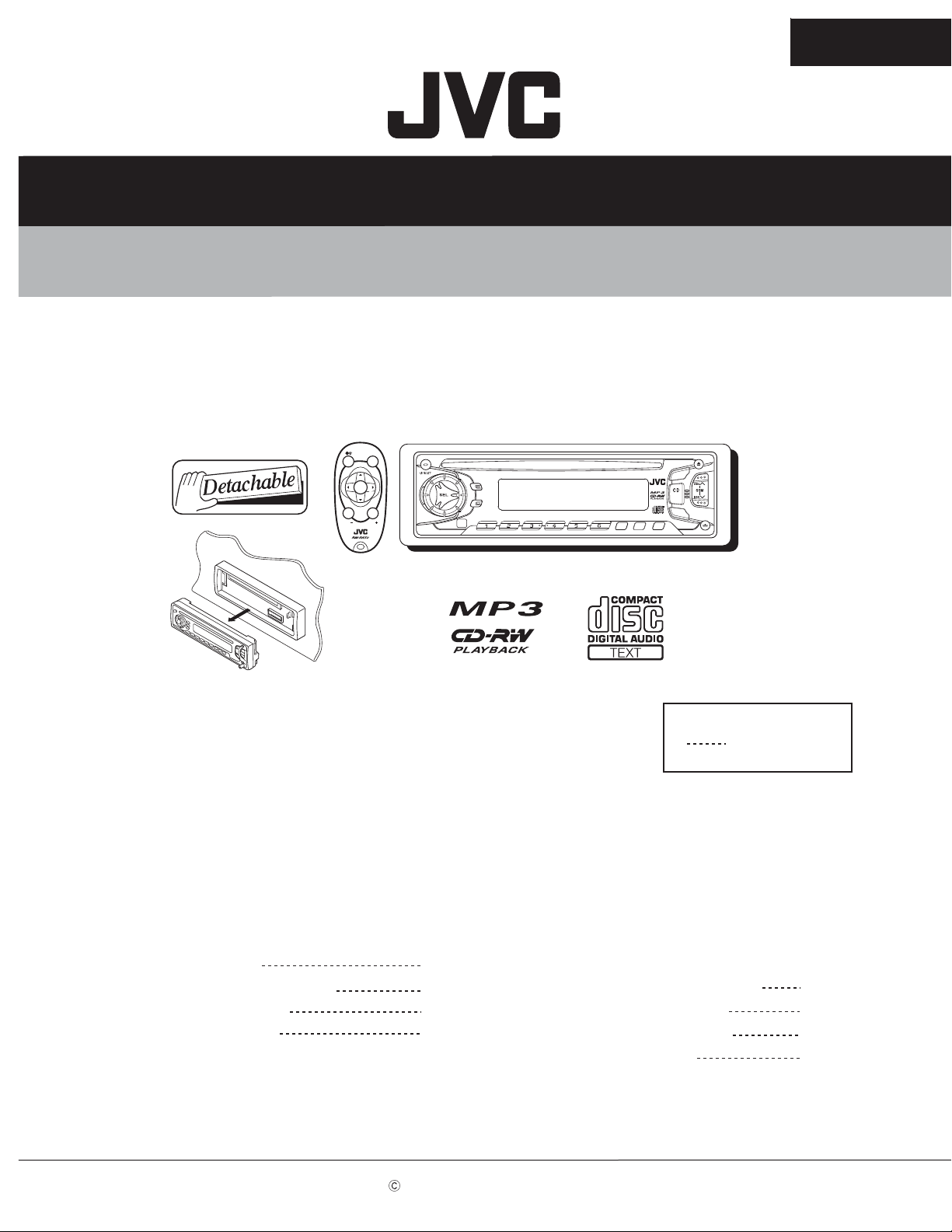
SERVICE MANUAL
CD RECEIVER
KD-S785
SOUND
ATT
D
N
A
U
SOURCE
F
R
D
VOL
VOL
LOUD
DISP
7
45Wx4
89
KD-S785
10
12
11
SCAN
RPT RND SCM
B
TUNER
MO
KD-S785
Contents
Safety precaution
Preventing static electricity
Disassembly method
Adjustment method
1-2
1-3
1-4
1-11
Area Suffix
U Other Areas
Flow of functional
operation untill TOC read
Maintenance of laser pickup
Replacement of laser pickup
Description of major ICs
1-12
1-14
1-14
1-15~33
COPYRIGHT 2002 VICTOR COMPANY OF JAPAN, LTD.
No.49748
Jun. 2002
Page 2
KD-S785
Safety precaution
!
!
Burrs formed during molding may be left over on some parts of the chassis. Therefore,
pay attention to such burrs in the case of preforming repair of this system.
Please use enough caution not to see the beam directly or touch it in case of an
adjustment or operation check.
1-2
Page 3
KD-S785
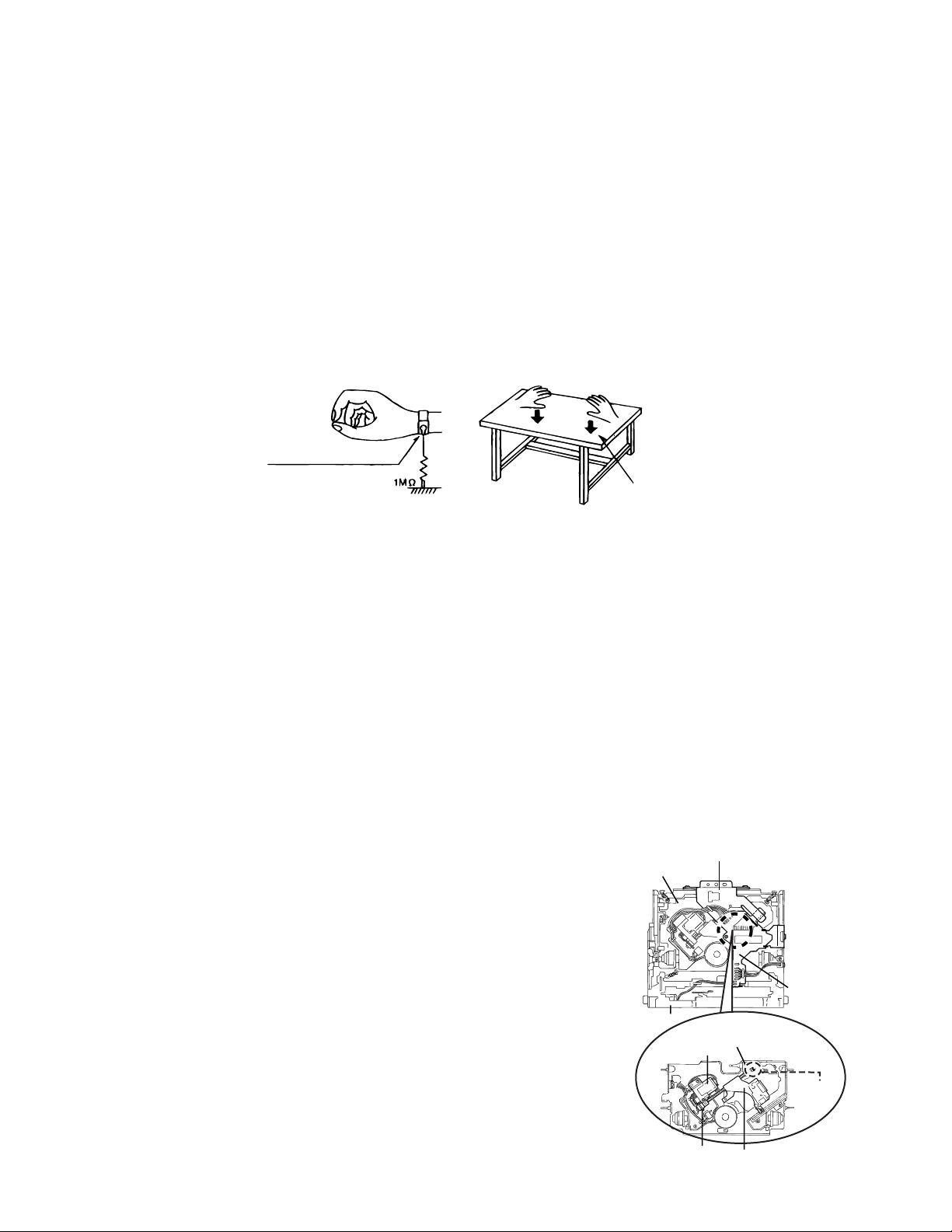
Preventing static electricity
1.Grounding to prevent damage by static electricity
Electrostatic discharge (ESD), which occurs when static electricity stored in the body, fabric, etc. is discharged,
can destroy the laser diode in the traverse unit (optical pickup). Take care to prevent this when performing repairs.
2.About the earth processing for the destruction prevention by static electricity
Static electricity in the work area can destroy the optical pickup (laser diode) in devices such as CD players.
Be careful to use proper grounding in the area where repairs are being performed.
2-1 Ground the workbench
Ground the workbench by laying conductive material (such as a conductive sheet) or an iron plate over
it before placing the traverse unit (optical pickup) on it.
2-2 Ground yourself
Use an anti-static wrist strap to release any static electricity built up in your body.
(caption)
Anti-static wrist strap
Conductive material
3. Handling the optical pickup
1. In order to maintain quality during transport and before installation, both sides of the laser diode on the
replacement optical pickup are shorted. After replacement, return the shorted parts to their original condition.
(Refer to the text.)
2. Do not use a tester to check the condition of the laser diode in the optical pickup. The tester's internal power
source can easily destroy the laser diode.
(conductive sheet) or iron plate
4.Handling the traverse unit (optical pickup)
1. Do not subject the traverse unit (optical pickup) to strong shocks, as it is a sensitive, complex unit.
2. Cut off the shorted part of the flexible cable using nippers, etc. after replacing the optical pickup. For specific
details, refer to the replacement procedure in the text. Remove the anti-static pin when replacing the traverse
unit. Be careful not to take too long a time when attaching it to the connector.
3. Handle the flexible cable carefully as it may break when subjected to strong force.
4. It is not possible to adjust the semi-fixed resistor that adjusts the laser power. Do not turn it
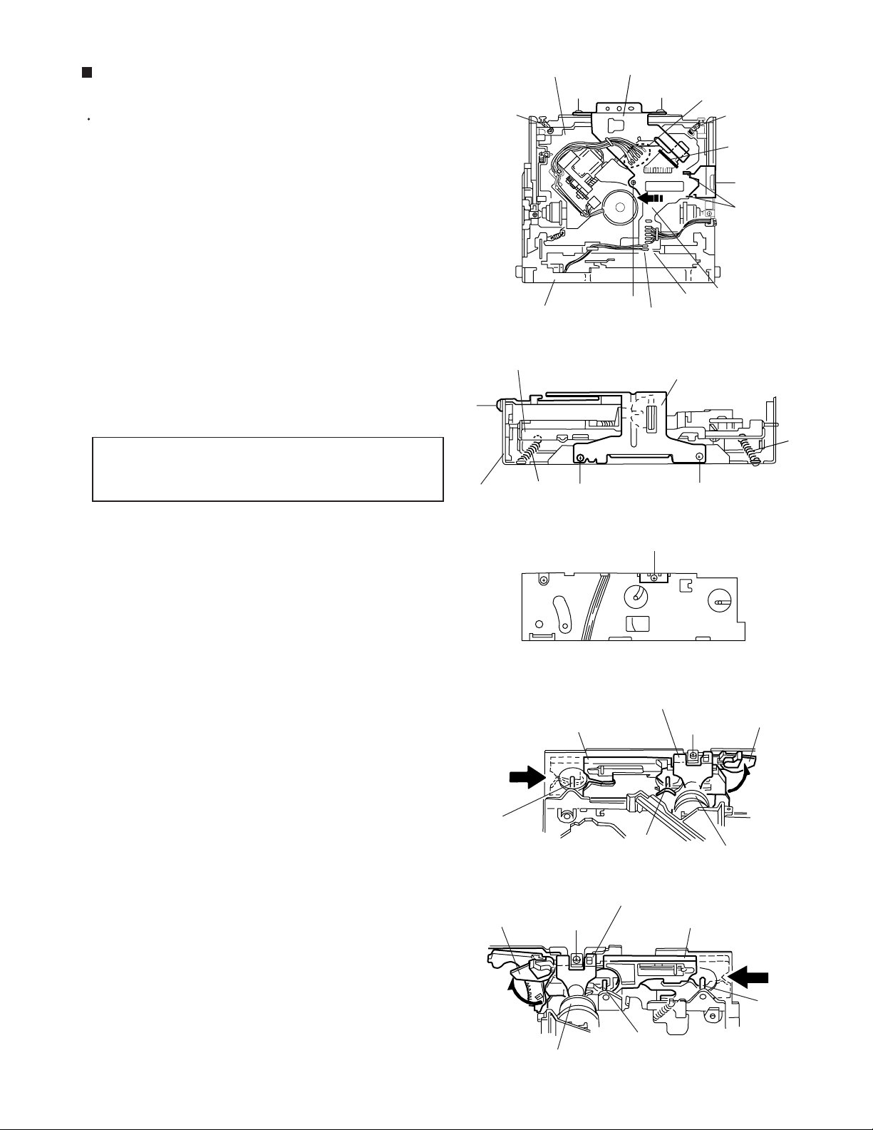
CD mechanism ass’y
Damper bracket
Attention when traverse unit is decomposed
*Please refer to "Disassembly method" in the text for pick-up and how to
detach the substrate.
1.Solder is put up before the card wire is removed from connector on
the CD substrate as shown in Figure.
(When the wire is removed without putting up solder, the CD pick-up
assembly might destroy.)
2.Please remove solder after connecting the card wire with
when you install picking up in the substrate.
Front bracket
Feed motor ass’y
FD screw
CD mechanism
control board
Soldering
FD gear
Pickup unit
1-3
Page 4
KD-S785
Disassembly method
<Main body>
Removing the front panel assembly
(See Fig.1)
1.
Press the eject button in the lower right part of the
front panel. Remove the front panel assembly from
the body.
Front panel assembly
Eject button
Fig.1
Removing the front chassis assembly
(See Fig.2, 3)
Prior to performing the following procedure, remove
the front panel assembly.
1.
Release the four joint tabs a on both sides of the
front chassis assembly and remove the front chassis
assembly toward the front.
Tab a
Tab a
Front chassis assembly
Heat sink
Fig.2
Tab a
1-4
Fig.3
Tab a
Front chassis
assembly
Page 5
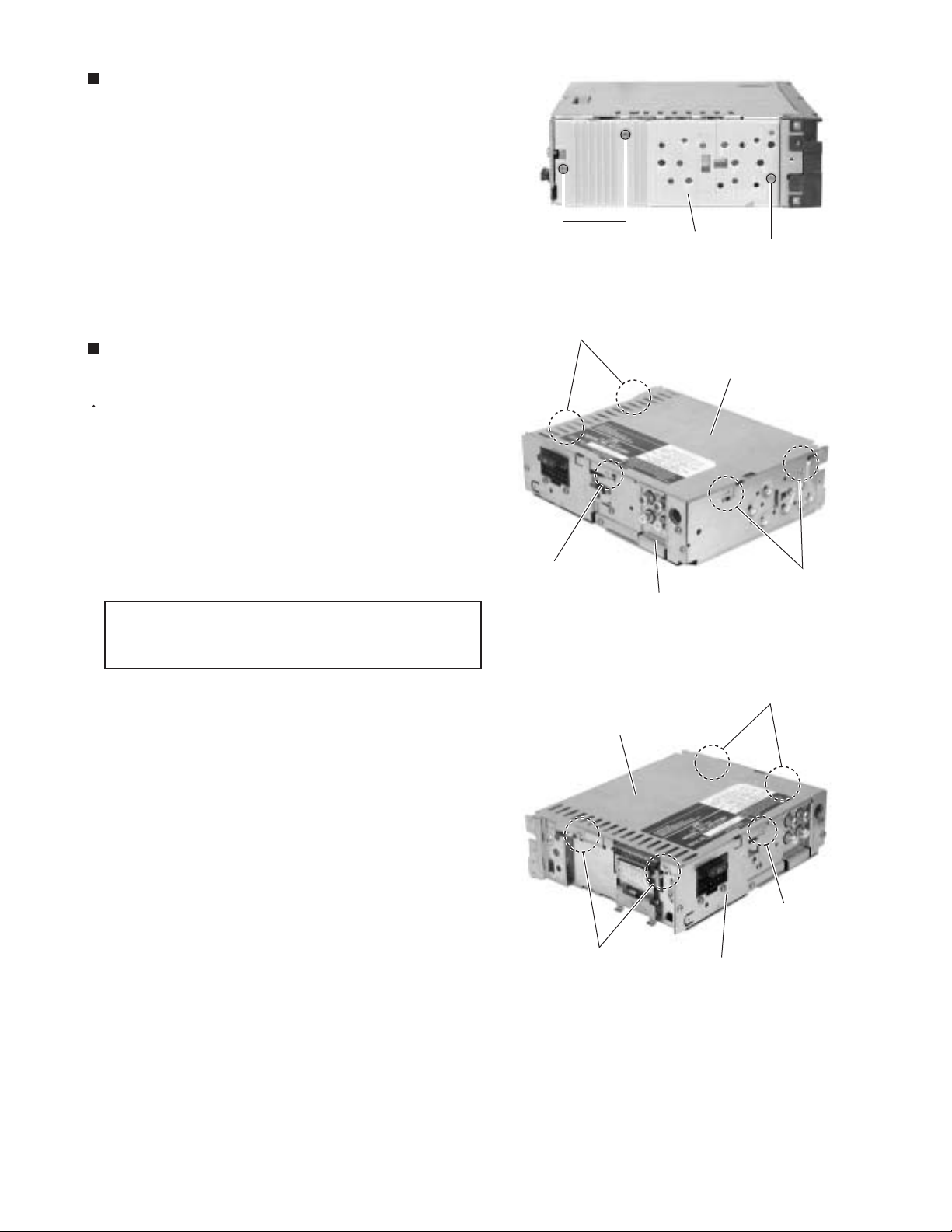
Removing the heat sink (See Fig.4)
1.
Remove the three screws A on the left side of the
body.
KD-S785
Removing the bottom cover
(See Fig.5, 6)
Prior to performing the following procedure, remove
the front panel assembly, the front chassis assembly
and the heat sink.
1.
Turn the body upside down.
2.
Insert a screwdriver to the two joints b and two joints
c on both sides of the body and the joint d on the
back of the body, then detach the bottom cover from
the body.
CAUTION:
When disengaging the joint d using a
screwdriver, do not damage or break the
board.
A
Joint d
Joint b
Heat sink
Fig.4
Rear panel
Fig.5
A
Bottom cover
Joint c
Bottom cover
Joint b
Joint c
Joint d
Rear panel
Fig.6
1-5
Page 6
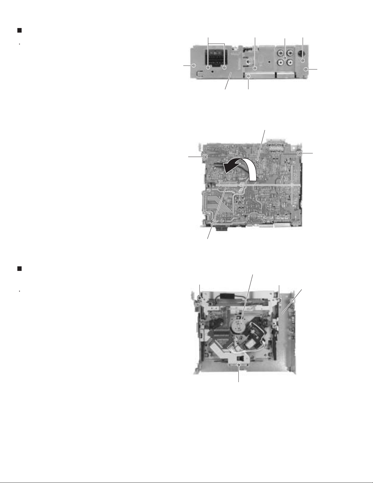
KD-S785
Removing the main board (See Fig.7, 8)
Prior to performing the following procedure, remove
the front panel assembly, the front chassis assembly,
the heat sink and the bottom cover.
1.
Remove the screw B, the four screws C and the
three screws D attaching the rear bracket on the
back of the body. Remove the rear panel.
2.
Remove the two screws E attaching the main board
on the bottom of the body. Disconnect connector
CN501 on the main board in the direction of the
arrow.
D
E
Rear panel
D
Fig.7
Main board
B
CCC
D
E
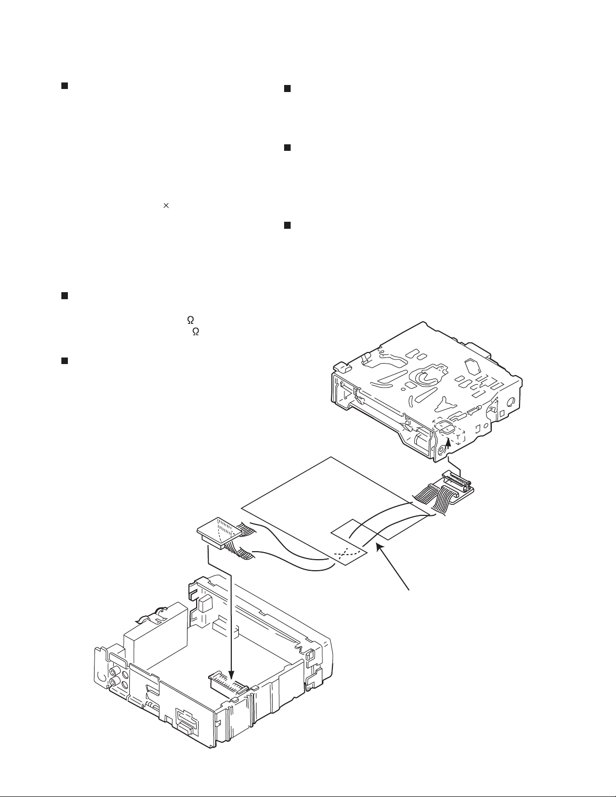
Removing the CD mechanism section
(See Fig.9)
Prior to performing the following procedure, remove
the front panel assembly, the front chassis assembly,
the heat sink, the bottom cover and the main board.
1.
Remove the three screws F attaching the cassette
mechanism section on the back of the top chassis.
CN501
F
Fig.8
CD mechanism section
F
Fig.9
F
Top chassis
1-6
Page 7
KD-S785
Removing the control switch board
(See Fig.10 ~ 12)
Prior to performing the following procedure, remove
the front panel assembly.
1.
Remove the four screws G attaching the rear cover
on the back of the front panel assembly.
2.
Unjoint the eleven joints e with the front panel and
the rear cover.
3.
Remove the control switch board on the back of the
front panel.
Joint e
Front panel
G
G
Rear cover
Fig.10
Joint e
G
G
Joint e
Front panel
Rear cover
Joint e
Fig.11
Control switch board
Fig.12
1-7
Page 8
KD-S785
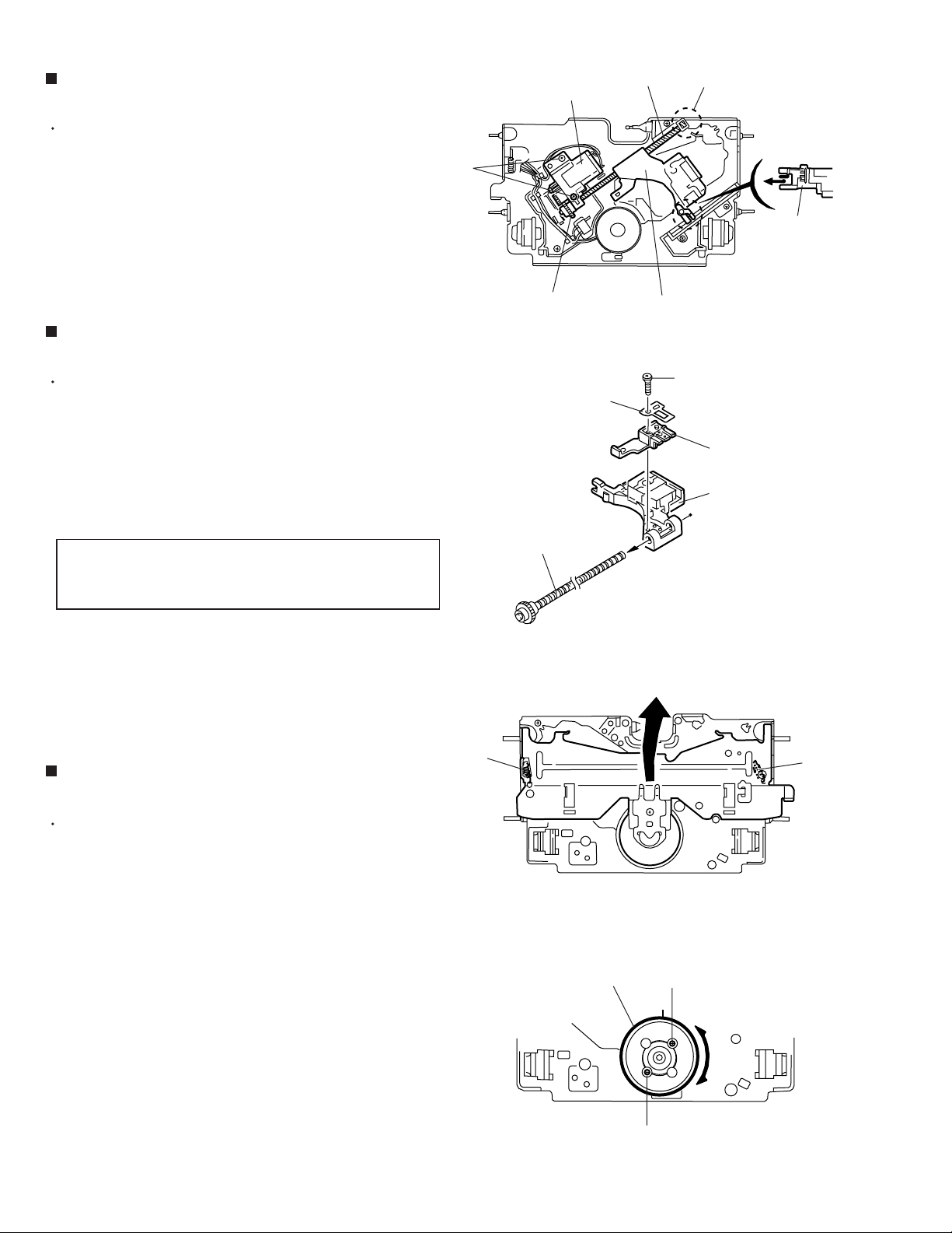
<CD mechanism section>
Removing the CD mechanism control
board (See Fig.1 and 2)
1.
Unsolder the part a and b on the CD mechanism
control board.
2.
Remove the stator fixing the CD mechanism control
board and the damper bracket (To remove the stator
smoothly, pick up the center part).
3.
Remove the screw A attaching the CD mechanism
control board.
4.
Remove the CD mechanism control board in the
direction of the arrow while releasing it from the two
damper bracket slots d and the front bracket slot e.
5.
Disconnect the flexible wire from connector on the
pickup unit.
ATTENTION:
Turn the FD gear in the direction of the
arrow to move the entire pickup unit to
the appropriate position where the
flexible wire of the CD mechanism unit
can be disconnected easily.
(Refer to Fig.2)
CD mechanism assembly
D
h
Front bracket
Pickup unit
Damper bracket
D
A
Fig.1
e
b
Flexible wire
a
h
c
D
d
CD mechanism
control board
Shift the lock
Removing the loading motor
(See Fig.3 to 5)
Prior to performing the following procedure, remove
the CD mechanism control board.
1.
Remove the two springs f attaching the CD
mechanism assembly and the front bracket.
2.
Remove the two screws B and the front bracket
while pulling the flame outward.
3.
Remove the belt and the screw C from the loading
motor.
Loading motor
C
FD gear
f
B
Loading motor
Pull outward
Fig.2
CD mechanism control board
f
B
Front bracket
Fig.3
Front bracket
Pull outward
1-8
Fig.5
Belt
Flame
Fig.4
Page 9
KD-S785
Removing the CD mechanism assembly
(See Fig.1, 6 to 9)
Prior to performing the following procedure, remove
the CD mechanism control board and the front
bracket (loading motor).
1.
Remove the three screws D and the damper
bracket.
2.
Raise the both sides fix arms and move the fix plates
in the direction of the arrow to place the four shafts g
as shown in Fig.8 and 9.
3.
Remove the CD mechanism assembly and the two
springs h attaching the flame.
4.
Remove the two screws E and both sides rear
damper brackets from the dampers. Detach the CD
mechanism assembly from the left side to the right
side.
ATTENTION:
The CD mechanism assembly can be
removed if only the rear damper
bracket on the left side is removed.
CD mechanism
h
Front bracket
CD mechanism
D
Flame
assembly
D
assembly
h
D
Damper bracket
D
A
Fig.5
e
b
Damper bracket
D
Fig.6
a
h
c
D
d
CD mechanism
control board
h
g
Fix arm (R)
Fix plate (L)
E
D
Fig.7
Rear damper bracket
E
g
Fig.8
Rear damper bracket
Fix plate(R)
Fix arm (L)
Damper
Damper
g
g
Fig.9
1-9
Page 10
KD-S785
Removing the feed motor assembly
(See Fig.10)
Prior to performing the following procedure, remove
the CD mechanism control board, the front bracket
(loading motor) and the CD mechanism assembly.
1.
Remove the two screws F and the feed motor
assembly.
Removing the pickup unit
(See Fig.10 and 11)
Prior to performing the following procedure, remove
the CD mechanism control board, the front bracket
(loading motor), the CD mechanism assembly and
the feed motor assembly.
1.
Detach the FD gear part of the pickup unit upward.
Then remove the pickup unit while pulling out the
part i of the FD screw.
Feed motor assembly
F
FD gear
Nut push spring plate
FD screw
Pickup unit
Fig.10
Part i
Part j
Pickup unit
G
Pickup mount nut
Pickup unit
ATTENTION:
2.
Remove the screw G attaching the nut push spring
plate and the pickup mount nut from the pickup unit.
Pull out the FD screw.
When reattaching the pickup unit,
reattach the part j of the pickup unit,
then the part i of the FD screw.
Removing the spindle motor
(See Fig.12 and 13)
Prior to performing the following procedure, remove
the CD mechanism control board, the front bracket
(loading motor), the CD mechanism assembly and
the feed motor assembly.
1.
Turn up the CD mechanism assembly and remove
the two springs k on both sides of the clamper arms.
Open the clamper arm upward.
2.
Turn the turn table, and remove the two screws H
and the spindle motor.
FD screw
k
Spindle motor
Fig.11
k
Fig.12
H
1-10
H
Fig.13
Page 11
Adjustment method
KD-S785
Test instruments required for adjustment
1. Digital oscilloscope (100MHz)
2. AM Standard signal generator
3. FM Standard signal generator
4. Stereo modulator
5. Electric voltmeter
6. Digital tester
7. Tracking offset meter
8. Test Disc JVC :CTS-1000
9. Extension cable for check
EXTGS004-26P 1
Standard measuring conditions
Power supply voltage DC14.4V(10.5~16V)
Load impedance 4 (2 Speakers connection)
Line oout impeadance 20k
Output Level Line out 2.0V (Vol. MAX)
How to connect the extension cable for adjusting
Standard volume position
Balance and Bass &Treble volume : lndication"0"
Loudness : OFF
BBE : OFF
Frequency Band
FM 87.5MHz ~ 108.0MHz
AM 531kHz ~ 1602 kHz
Dummy load
Exclusive dummy load should be used for AM,and FM. For
FM dummy load,there is a loss of 6dB between SSG output
and antenna input.The loss of 6dB need not be considered
since direct reading of figures are applied in this working
standard.
EXTGS004-26P
1-11
Page 12

KD-S785
Flow of functional operation until TOC read
Power ON
• When the pickup correctly moves
to the inner area of the disc
Set Function to CD
• When the laser diode correctly
emits
Microprocessor
commands
FMO
TC9462 "53"
FEED MOTOR
+TERMINAL
TERMINAL
IC581 "5"
REST SW
• When correctly focused
Focus Servo Loop ON
Disc inserted
Pickup feed to the inner area
Laser emitted
Focus search
Disc rotates
RF signal eye-pattern
remains closed
Tracking loop closed
RF signal eye-pattern
opens
TOC readout
YES
YES
Microprocessor
commands
"No disc"
display
• When the disc correctly rotates
Microprocessor
commands
Spindle
motor (-)
IC581 "7"
AccelerationAcceleration
0.5 Sec
Rough
Servo
0.5 Sec
Servo CLV
1-12
Jump to the first track
Play
Tracking Servo Loop ON
• RF signal
Rough Servo Mode
CLV Servo Mode
(ProgramArea)
CLV Servo Mode
(Lead-In Area;
Digital: 0)
Page 13

Feed Section
Is the voltage output at
IC521 pin "53" 5V or 0V?
YES
Is 4V present at both
sides of the feed motor?
YES
NO
Is the wiring for IC521
(90) ~ (100) correct?
NO
Is 6V or 2V present at
IC581 "5" and "6"?
NO
YES
YES
Is 5V present at IC581
pin "11"?
YES
Check the vicinity of
IC521.
Check the feed motor
connection wiring.
NONO
KD-S785
Check CD 9V
and 5V.
Check the feed motor.
Focus Section
When the lens is
moving:
4V
Does the S-search
waveform appear at
IC581 pins "17" and "18"?
Spindle Section
Is the disk rotated?
YES
Does the RF signal
appear at TP1?
YES
Check IC581.
NO
YES
NO
NO
Check the circuits in
the vicinity of IC581
pins "15" ~ "18".
Check the pickup and
its connections.
Is 4V present at IC581
pins "7" and "8" ?
Check the spindle motor
and its wiring.
YES
YES
NO NO
Is 4V present at IC521
pin "55" ?
YES
Check the vicinity of
IC581.
Check IC501 and
IC521.
Is the RF waveform at TP1
distorted?
YES
Proceed to the Tracking
section
Tracking Section
When the disc is rotated
at first:
Is the tracking error signal
output at IC501 "12"?
Check IC521.
NO
Approx. 1.2 V
YES
Check the circuits in the
vicinity of IC501 "19" ~
"24" or the pickup
Check the circuit in the
vicinity of IC501 pins
"2" ~ "12".
YESYES
Check the pickup and
its connections.
1-13
Page 14

KD-S785
Maintenance of laser pickup
(1) Cleaning the pick up lens
Before you replace the pick up, please try to
clean the lens with a alcohol soaked cotton
swab.
(2) Life of the laser diode
When the life of the laser diode has expired,
the following symptoms will appear.
(1) The level of RF output (EFM output:ampli
tude of eye pattern) will be low.
Is RF output
1.0 0.35Vp-p?
YES
O.K
(3) Semi-fixed resistor on the APC PC board
The semi-fixed resistor on the APC printed
circuit board which is attached to the pickup
is used to adjust the laser power.Since this
adjustment should be performed to match the
characteristics of the whole optical block,
do not touch the semi-fixed resistor.
If the laser power is lower than the specified
value,the laser diode is almost worn out, and
the laser pickup should be replaced.
If the semi-fixed resistor is adjusted while
the pickup is functioning normally,the laser
pickup may be damaged due to excessive current.
NO
Replace it.
Replacement of laser pickup
Turn off the power switch and,disconnect the
power cord from the ac outlet.
Replace the pickup with a normal one.(Refer
to "Pickup Removal" on the previous page)
Plug the power cord in,and turn the power on.
At this time,check that the laser emits for
about 3seconds and the objective lens moves
up and down.
Note: Do not observe the laser beam directly.
1-14
Play a disc.
Check the eye-pattern at TP1.
Finish.
Page 15

Description of major ICs
/
TC9490FA (IC541) : DSP & DAC
1.Pin layout & Block daiagram
KD-S785
DV
SS3
RO
DD3
DV
DVR
LO
DV
SS3
ZDET
V
SS5
BUS0
BUS1
BUS2
BUS3
BUCK
/CCE
/RST
VXDD3XOXI
SS3
XV
TEIN
DD3VSS3
V
DMO
FMO
DD3
AV
SEL
TEBC
RFGC
48 47 46 45 44 43 42 41 40 39 38 37 36 35 34 33
49
50
51
52
LPF
Clock
generator
1-bit
DAC
PWM
Servo control
A/D
53
54
55
56
Address
circuit
ROM
RAM
Digital equalizer
automatic
adjustment circuit
57
58
59
60
61
62
Micro-
controller
interface
circuit
Correction
Audio output
circuit
16k
RAM
Digital output
CLV servo
Sync signal
protection
EFM
Sub code
detector
63
VCO
PLL
TMAX
REF
V
D/A
Data
slicer
TRO
FOO
32
31
30
29
28
27
26
25
24
23
22
21
20
19
18
TEZI
TEI
SBAD
FEI
RFRP
RFZI
RFCT
AV
DD3
RFI
SLCO
SS3
AV
VCOF
REF
RV
LPFO
LPFN
64
DD5
V
17
TMAX
1 2 3 4 5 6 7 8 9 10 11 12 13 14 15 16
BCK
LRCK
AOUT
DOUT
IPF
DD3
V
V
SBOK
CLCK
DATA
SFSY
SBSY
/HSO
UHSO
DD3
PV
PDO
SS3
1-15
Page 16

KD-S785
2.Pin function (1/2)
Pin No.
1
2
3
4
Symbol
BCK
LRCK
AOUT
DOUT
5
6
7
8
9
10
11
12
13
14
VDD3
VSS3
SBOK
CLCK
DATA
SFSY
SBSY
/HSO
/UHSO
IPF
I/O
O
O
O
O
O
-
-
O
I/O
O
O
O
O
O
TC9490FA(2/3)
Function
Bit clock outputpin 32fs, 48fs, or 64fs selectable by command.
L/R channel clock output pin."L" for L channe and "H" for R channel.
Output polarity can be inverted by command.
Audio data output pin. MSB-first or LSB-first selectable by command.
Digital data output pin. Outputs up to double-speed playback.
Correction flag output pin.When set to "H",AOUT output cannot be corrected
by C2 correction processing.
Digital 3.3V power supply voltage pin.
Digital GND pin.
Subcode Q data CRCC result output pin."H" level when result is OK.
Subcode P-W data read clockI/O pin. I/O polarity selectable by command.
Subcode P-W data output pin.
Playback frame sync signal output pin.
Subcode block sync signal output pin. "H" level at S1 when subcode sync is
detected.
Playback speed mode flag output pins.
/HSO
H
H
L
--
H
L
L
--
Playback speed/UHSO
Normal
Double
4 times
---
15
16
17
18
19
20
21
22
23
24
25
26
27
28
29
30
31
32
33
34
35
PVDD3
PDO
TMAX
LPFN
LPFO
PVREF
VCOF
AV
SS3
SLCO
RFI
AV
RFCT
RFZI
RFRP
FEI
SBAD
TEI
TEZI
FOO
TRO
REF
V
-
PLL-only 3.3V power supply voltage pin.
O
EFM and PLCK phase difference signal output pin.
O
TMAX detection result output pin.
TMAX Detection result
Longer than fixed period
Within fixed period
Shorter than fixed period
I
Inverted input pin for PLL LPF amp.
O
Output oin for PLL LPF amp.
REF
-
PLL-only V
VCO filter pin.
O
Analog GND pin.
DAC output pin for data slice level generation.
O
RF signal input pin.Zin selectable by command.
I
Analog 3.3V power supply voltage pin.
RFRP signal center level input pin.
I
RFRP signal zero-cross input pin.
I
RF ripple signal input pin.
I
Focus error signal input pin.
I
Sub-beam adder signal input pin.
I
Tracking error input pin. Inputs when tracking servo is on.
I
Tracking error signal zero-cross input pin.
I
Focus equalizer output pin.
O
Tracking equalizer output pin.
O
Analog reference power supply voltage pin.
-
pin.
TMAX Output
"PV
"HIZ"
"AV
DD3
SS3"
"
1-16
Page 17

KD-S785
2.Pin function (2/2)
Pin No.
36
37
38
39
40
41
42
43
44
45
Symbol
RFGC
TEBC
SEL
AV
FMO
DMO
V
V
TESIN
XV
46
47
48
49
XV
DV
50
51
52
DV
DVR
53
54
55
56
57
58
59
60
61
62
63
64
DV
ZDET
V
BUS0
BUS1
BUS2
BUS3
BUCK
/CCE
/RST
V
DD3
SS3
DD3
XI
XO
DD3
RO
DD3
LO
SS5
DD5
SS3
SS3
SS3
I/O
Function
O
RF amplitude adjustment control signal output pin.
O
Tracking balance control signal output pin.
O
APC circuit ON/OFF signal output pin. At laser on,high impedance with
UHS="L" ,H output with UHS="H".
-
Analog 3.3V power supply voltage pin.
O
Feed equalizer output pin.
O
Disc equalizer output pin.
-
Digital GND pin.
-
Digital 3.3V power supply voltage pin.
I
Test input pin. Normally,fixed to "L".
-
System clock oscillator GND pin.
I
System clock oscilatoe input pin.
O
System clock oscillator output pin.
-
System clock oscillator 3.3V power supply voltage pin.
-
DA converter GND pin.
O
R-channel data forward output pin.
-
DA converter 3.3V power supply pin.
-
Reference voltage pin.
O
L-channel data forward output pin.
-
DA converter GND pin.
O
1 bit DA converter zero data detection flag output pin.
-
Microcontroller interface GND pin.
I/O
Microcontroller interface data I/O pins.
I
Microcontroller interface clock input pin.
I
Microcontroller interface chip enable signal input pin.At "L".
Bus0 to BUS3 are active.
I
Reset signal input pin. At reset,"L".
-
Microcontroller interface 5V power supply pin.
TC9490FA(3/3)
IC-PST600M/G/-W (IC702) : System reset
Co1
OP1
1
3
2
IN
Vout
GND
1-17
Page 18

KD-S785
UPD784215AGC172 (IC701) : Main micon
1.Pin layout
100 ~ 76
1
75
~
25
26 ~ 50
2.Pin functions(1/2)
Pin No.
1
2
3
4
5
6
7
8
9
10
11
12
13
14
15
16
17
18
19~21
22
23
24
25
26
27
28
29
30
31
32
33
34,35
36
37
38
39
40
41
42
43
44
45~52
Symbol
SW2
SW3
SW4
REST
LM0
LM1
ANT CONT
VDD
VSS
XT2
XT1
RESET
SW1
BUS-INT
PS2
REMOCON
AVDD
AVREF0
VOL1
VOL2
KEY0
KEY1
KEY2
LEVEL
SM
AVSS
AVRE F
BUS-SI
BUS-SO
BUS-SCK
BUS-I/O
LCD-DA
LCD-SCK
LCD-CE
BUZZER
X2
X1
~
51
I/O
Function
I
CD mecha sw2
I
CD mecha sw3
I
CD mecha sw4
I
Rest sw
O
Loading/Eject motor control (Loading side)
O
Loading/Eject motor control (Eject side)
-
-
-
-
-
-
No use
O
Antenna remote control
-
Maicon power supply
-
-
-
GND
-
I
Reset detection
I
CD mecha sw1
I
J-BUS int
I
Power save 2, H means STOP mode
-
No use
I
Remocon input
-
A/D converter power supply
-
A/D reference voltage
I
Volume encoder pulse input 1
I
Volume encoder pulse input 2
I
Key input 0
I
Key input 1
I
Key input 2
I
Level meter input
-
No use
I
S.METER input
-
GND
-
No use
I
J-BUS data input
O
J-BUS data output
I/O
J-BUS clock input/output
O
J-BUS I/O selection output H:output L:input
O
Data output for LCD driver
O
CLK output for LCD driver
O
CE for LCD driver
O
Buzzer output
-
No use
1-18
Page 19

2.Pin functions(2/2)
KD-S785
Pin No.
53
54
55
56
57
58
59
60
61
62
63
64
65
66
67
68
69
70
71
72
73
74
75
76
77
78~80
81
82
83
84
85
86~89
90
91
92
93
94
95
96
97
98
99
100
Symbol
SD/ST
LOCAL
MONO
MP3 CLK
MP3 DATA IN
MP3 DATA OUT
MP3 STANDBY
MP3 RESET
MP3 REQ
DETACH
SEEK/STOP
-
FM/AM
PLL-CE
PLL-DO
PLL-CLK
PLL-DI
TEL-MUTE
-
VSS
VSDIM-IN
PS1
POWER
CD-ON
MUTING
-
VDD
-
VOL-DA
VOL-CLK
DIM-OUT
-
STAGE
BUCK
CCE
RST
TEST
BUS0
BUS1
BUS2
BUS3
-
CD-RW
I/O
Function
I
Station detector or stereo signal input
O
Loal or distance selecting output
O
Monoral selection output
O
CLK output for MP3 decoder
I
Data input for MP3 decoder / inverting input due to converter
O
Data output for MP3 decoder / H level during input mode
O
Standby output for MP3 decoder
O
Reset output for MP3 decoder
I
REQ input for MP3 decoder / inverting input due to converter
I
Detach detect input H: detaching
O
Auto seek and stop selecting output
-
No use
O
FM,AM band selecting output
O
CE output for PLL IC
O
Data output for PLL IC
O
Clock output for PLL IC
I
Data input from PLL IC
I
Telephone muting detection input, active level can selected H or L is PSM
-
No use
-
GND
I
Dimmer detecter input L=dimmer on
I
POWER SAVE 1 L=ACC off
O
Power ON/OFF control output H=power on
O
CD power supply control output H=CD power ON
O
Muting output L=Muting ON
-
No use
-
Micon power supply
-
No use
O
Data output for E-vol IC
O
Clock output for E-vol IC
O
Dimmer control output L=dimmer on
-
No use
I
L=U version, H=Japanversion
O
Clock output for CD LSI
O
CE output for CD LSI
O
Reset output for CD LSI
-
For rewriting flash memory
I/O
Data output and input 0 for CD LSI
I/O
Data output and input 1 for CD LSI
I/O
Data output and input 2 for CD LSI
I/O
Data output and input 3 for CD LSI
-
No use
-
RF gain control L=CD-RW, H=CD-DA
1-19
Page 20

KD-S785
LA4743K (IC301) : Power amp.
1.Block diagram
IN 1
0.22 F
TA B
IN 2
0.22 F
+
Vcc 1/2 Vcc 3/4
2200 F 0.022 F
6 20
+
11
-
+
+
-
9
7
OUT 1+
OUT 1-
1
Protective
circuit
+
-
+
12
+
-
PWR GND1
8
OUT 2+
5
OUT 2-
3
PWR GND2
2
ST BY
R.F
47 F
IN 3
PRE GND
IN 4
+5V
ST ON
+
0.22 F
N.C
+
0.22 F
4
Stand by
Switch
Mute
10
+
Ripple
Filter
Mute
22
circuit
3.3 F
+
15
-
+
-
17
19
10K
+
OUT 3+
OUT 3-
Low Level
Mute ON
25
18
21
23
PWR GND3
OUT 4+
OUT 4-
13
14
Protective
circuit
-
+
+
-
1-20
ON TIME C
22 F
Muting &
16
+
ON Time Control
Circuit
PWR GND4
24
Page 21

2.Terminal layout
3.Pin function
KD-S785
1
2
3
4
5
6
7
8
9
10
11
12
13
14
15
16
17
18
19
20
21
22
23
24
25
SymbolPin No.
TA B
GND
RFOSTBY
RFO+
VCC1/2
RROGND
RRO+
VREF
RRIN
RFIN
SGND
LFIN
LRIN
ONTIME
LRO+
GND
LROVCC3/4
LFO+
MUTE
LFOGND
NC
Function
Header of IC
Power GND
Outpur(-) for front Rch
Stand by input
Output (+) for front Rch
Power input
Output (-) for rear Rch
Power GND
Output (+) for rear Rch
Ripple filter
Rear Rch input
Front Rch input
Signal GND
Front Lch input
Rear Lch input
Power on time control
Output (+) for rear Lch
Power GND
Output (-) for rear Lch
Power input
Output (+) for front
Muting control input
Output (-) for front
Power GND
No connection
1-21
Page 22

KD-S785
TA2147F-X (IC521) : RF amp.
1.Terminal layout
2.Block diagram
VRO
FEO
FEN
RFRP
RFRPIN
RFGO
RFGC
AGCIN
RFO
RFN
13GVSW
14
15
16
17
18
19
20
21
22
23
10pF
40k
30k
20k 20k
20k
20k
BOTTOM
3k
15k
50 A
12k
12k
PEAK
20k
180k
40pF
20k
20k
PEAK
1.3V
180k
40k
240k
15pF
240k
15pF
60k
40k
40pF
60k
50k
2k
20 A
20k
60 A
50k
14k
k
1
80k
x0.5
x0.5
80k
20k
20k
15k
x2
x2
1k
2k
1.75k
10pF
12 RFDC
11
TEO
10
TEN
TEBC
9
8
SEL
7
LDO
MDI
6
5
TNI
4
TPI
3
FPI
2
FNI
1-22
GND
24
3k
1
Vcc
Page 23

3.Pin function
KD-S785
Pin No.
1
2
3
4
5
6
7
8
9
10
11
12
13
Symbol
Vcc
FNI
FPI
TPI
TNI
MDI
LDO
SEL
TEBC
TEN
TEO
RFDC
GVSW
I/O
Function
-
3.3V Power supply pin
I
Main-beam amp input pin
I
Main-beam amp input pin
I
Sub-beam amp input pin
I
Sub-beam input pin
I
Monitor photo diode amp input pin
O
Laser diode amp output pin
I
APC circuit ON/OFF control signal,laser diode (LDO) control signal input or
bottom/peak detection frequency change pin.
APC
circuit
GND OFF
HIZ
Vcc
I
Tracking error balance adjustment signal pin
Adjusts TE signal balance by eliminating carrier component from
PWM signal(3-state output, PWM carrier = 88.2kHz) output from
TC9490F/FA TEBC pin using RC-LPF and inputting DC.
TEBC input voltage:GND~Vcc
I
Tracking error signal generation amp negative-phase input pin
O
Tracking error signal generation amp output pin.
Combining TEO signal and RFRP signal with TC9490F/FA configures
tracking search system.
O
RF signal peak detection output pin
I
AGC/FE/TE amp gain change pin
Connected to Vcc
through 1k resistor
Control signal output
ON
Control signal output
ON
LDOSEL
14
15
16
17
18
19
20
21
22
23
24
VRO
FEO
FEN
RFRP
RFRPIN
RFGO
RFGC
AGCIN
RFO
RFN
GND
ModeGVSW
GND
HIZ
Vcc
Reference voltage (VRO) output pin *VRO = 1/2 Vcc when Vcc = 3.3V
O
Focus error signal generation amp output pin
O
Focus error signal generation amp negative-phase input pin
I
Signal amp output pin for track count
O
Combining RFRP signal TEO signal with TC9490F/FA configures tracking
search system.
Signal generation amp input pin for track count
I
RF signal amplitude adjustment amp output pin
O
RF amplitude adjustment control signal input pin
I
Adjusts RF signal amplitude by eliminating carrier component from PWM
signal (3-state output, PWM carrier = 88.2kHz) output from TC9490F/FA
RFGC pin using RC-LPF and inputting DC.
*RFGC input voltage : GND-Vcc
RF signal amplitude adjustment amp input pin
I
RF signal generation amp output pin
O
RF signal generation amp input pin
I
GND pin
-
CD-RW
CD-DA
CD-DA
1-23
Page 24

KD-S785
TC94A02F-005 (IC401) : DSP
AD11
32
33
AD10
AD12
31
CKS
30
TESTP
29
VSSR
28
VRAR
27
Ro
26
VDAR
25
VDAL
24
Lo
VRAL
VSSL
VSS
STANDBY
VDD
/oE
23
22
21
20
19
18
17
16
/CE
AD9
VDDT
AD8
AD7
AD6
REQ
VSS
AD13
DAC
34
Bus
register
C-Pointer
register
Y-Pointer
register
X-Pointer
Switch
register
X0 X1 X2
35
36
37
General
Output Port
38
39
40
41
Flag
2sets
Address Calc.
ERAM
2k word
*3
CROM
4k word
Y0 Y1 Y2
DAC
AY
AX
MX MY MZ
MAC ALU
A3
A2
A0 A1
round & limit
round & limit
Audio.I/F
15
AD5
14
LRCKiA
13
BCKiA
12
SDi0
AD4
11
AD3
10
9
SDo
87
VDDT
AD14
/WR
AD16
AD15
io0
io1
VSS
VSSX
AD2
6
/MiCK
543
MiDio
AD1
AD0
MiMD
2
/RESET
1
42
YRAM
4k word
43
Timer
44
4546
47
48
Interrupt
Control
SRAM I/F
49
io2
I-Bus
Generator
50
io3
Timing
51
io4
XRAM
4k word
52
VDD
53
io5
X-Bus
Start
Prog.
54
io6
Y-Bus
DIT
55
io7
56
VSSP
PRAM
256word
57
PDo
Control
Program
PROM
4k*2+2k
=10kword
VC0
58
VCoi
59
VDDP
40bit
Decoder
Instruction
General Input Port
60
61
CK0
VDDX
Microcom.I/F
62
63
Xi
64
Xo
1-24
Page 25

KD-S785
3.Pin function(1/2)
Pin No. Symbol
1
/RESET
2
MiMD
3
AD0
4
AD1
5
MiDio
6
/MiCK
7
AD2
8
VDDT
9
SDo
10
11
12
13
14
15
16
17
18
19
20
21
22
23
24
25
26
27
28
29
30
31
32
33
34
35
36
37
38
39
40
41
42
43
44
45
46
47
48
49
50
AD3
AD4
SDi0
BCKiA
LRCKiA
AD5
CE
OE
VDD
STANBY
VSS
VSSL
VRAL
LO
VDAL
VDAR
RO
VRAR
VSSR
TESTP
CKS
AD12
AD11
AD10
AD9
VDDT
AD8
AD7
AD6
REQ
VSS
AD13
AD14
WR
AD16
AD15
io0
io1
VSS
io2
io3
I/O
O
O
I/O
O
O
O
O
O
O
O
O
O
O
O
O
O
O
O
O
O
O
O
O
O
O
I/O
I/O
I/O
I/O
Function
Hard reset input terminal(H:Normal operation L: Reset)
I
Micon I/F mode select input terminal
I
External SRAM address output 0 terminal
External SRAM address output 1 terminal
Micon I/F data input/output terminal
Micon I/F clock input terminal
I
External SRAM address output 2 terminal
Digital power supply (3.3V)
Data output terminal
External SRAM address output 3 terminal
External SRAM address output 4 terminal
Data input terminal 0
I
Bit clock input terminal A
I
LR clock input terminal A
I
External SRAM address output 5 terminal
External SRAM chip enable terminal
External SRAM output enable terminal
Digital power supply (2.5V)
Standby mode control terminal
I
Digital GND
DAC Lch GND
DAC Lch reference voltage terminal
DAC Lch output terminal
DAC Rch power supply terminal(2.5V)
DAC Lch power supply terminal(2.5V)
DAC Rch output terminal
DAC Rch reference voltage terminal
DAC Rch GND
Test terminal
I
VCO select terminal
I
External SRAM address output 12 terminal
External SRAM address output 11 terminal
External SRAM address output 10 terminal
External SRAM address output 9 terminal
Digital power supply terminal (3.3V)
External SRAM address output 8 terminal
External SRAM address output 7 terminal
External SRAM address output 6 terminal
Squeeze request terminal to host
Digital GND
External SRAM address output 13 terminal
External SRAM address output 14 terminal
External SRAM write signal
External SRAM address output 16 terminal
External SRAM address output 15 terminal
External SRAM data input/output 0 terminal
External SRAM data input/output 1 terminal
Digital GND
External SRAM data input/output 2 terminal
External SRAM data input/output 3 terminal
TC94A02F-005
1-25
Page 26

KD-S785
3.Pin function(2/2)
Pin No. Symbol
51
52
53
54
55
56
57
58
59
60
61
62
63
64
io4
VDD
io5
io6
io7
VSSP
Pdo
Vcoi
VDDP
Cko
VDDX
Xi
Xo
VSSX
I/O
I/O
I/O
I/O
I/O
O
O
O
External SRAM data input/output 4 terminal
Digital power supply (2.5V) terminal
External SRAM data input/output 5 terminal
External SRAM data input/output 6 terminal
External SRAM data input/output 7 terminal
VCO GND
PLL phase error detection signal output terminal
VCO control voltage input terminal
I
VCO power supply
-
16.934 MHz clock output terminal
Power supply (2.5V) terminal for oscillator
Connection terminal for oscillator(input)
I
Connection terminal for oscillator(output)
GND for oscillator
-
Function
K6R1008V1D (IC512, IC513, IC514) : CMOS SRAM
A0
A1
A2
A3
CS
I/O1
I/O2
Vcc
Vss
I/O3
I/O4
WE
A4
A5
A6
A7
1
2
3
4
5
6
7
8
9
10
11
12
13
14
15
16
32
31
30
29
28
27
26
25
24
23
22
21
20
19
18
17
A16
A15
A14
A13
OE
I/O8
I/O7
Vss
Vcc
I/O6
I/O5
A12
A11
A10
A9
A8
Symbol
A0-A16
WE
CS
OE
I/O1~I/O8
Vcc
Vss
N.C
Function
Address Input
Write Enable
Chip Select
Output Enable
Data Inputs/Outputs
Power (+3.3V)
Ground
No Connection
3. Block diagram1. Pin layout 2. Pin function
A0
A1
A2
A3
A4
A5
A6
A7
A8
I/O1~I/O8
Clk Gen.
Data
Cont.
CLK
Gen.
TC94A02F-005
Pre-Charge Circuit
Memory Array
512 Rows
256x8 Columns
Row Select
I/O Circuit
Column Select
A9 A10 A11 A12 A13 A14 A15 16
1-26
CS
WE
OE
Page 27

AN80T07 (IC901) : Regulator
1.Pin layout
116
2.Block diagram
*ASO,Peak Current Protection.
*Thermal Protection (Except
VDD,Comp output).
MODE1
6
ACC
3
KD-S785
No.
5
Outputs
Pre
Driver
15
ILM
10V
14
ILM
AJ
3.Pin functions
Pin No.
1
2
COMP Output
3
4
5
6
7
8
9
10
11
12
13
14
15
16
11
MODE2
1
SW5V Out
Symbol
SW5V Output
ACC Input
VDD Output
NC
MODE1
CD Output
EXT Output
VCC
ANT Output
MODE2
BATT,DET
Audio Output
ILM AJ
ILM Output
GND
Reference Voltage
Pre
Driver
4
VDD
5.7V
EXT
Out
ANT
Out
89
EXT
Vcc
10
ANT
Pre
Driver
7
CD
8.0V
12
BATT.DET
2
COMP
Function
When Mode 1 pin is "M","H" SW output is VDD -0.7V
When ACC input pin is "H" COMP Output is VDD -0.7V
L:COMP Output OFF and H:COMP Output ON
5.7V Output voltage for a microcontroller
NC pin
3 Input "L","M","H" control pin
When Mode 1 pin is "H" CD output is 8V
When Mode 1 pin is "M","H" EXT output is VCC -1.0V
Connected to car BACKUP Power supply.
When mode 2 pin is "H" ANT output is Vcc -1.0V
L:ANT output OFF and H:ANT Output ON
NPN Trs open collector Output
When Mode 1 pin is "M","H" Audio output is 9V
ILM output adjustable pin
When Mode 1 pin is "M","H" ILM output is 10V
Connect to IC substrate
13 16
AUDIO
9.0V
Pre
Driver
GND
1-27
Page 28

KD-S785
K6R1008VCTI12-X (IC451) : SRAM
1.Pin layout
1
A0
2
A1
3
A2
4
A3
CS
5
1
I/O
6
I/O2
7
Vcc
8
Vss
9
3
I/O
10
I/O4
11
WE
12
4
A
13
A5
14
A6
15
A7
16
3.Pin function
Pin Name Pin Function
0 - A16 Address Inputs
A
WE Write Enable
CS Chip Select
OE Output Enable
1 ~ I/O8 Data Inputs/Outputs
I/O
CC Power(+3.3V)
V
SS Ground
V
N.C
SOJ/
TSOP2
No Connection
2.Block diagram
Clk Gen.
16
32
A
A15
31
A14
30
A13
29
OE
28
8
I/O
27
I/O7
26
Vss
25
Vcc
24
6
I/O
23
I/O5
22
A12
21
A11
20
A10
19
A9
18
A8
17
A0
A1
A2
A3
A4
A5
A6
A7
A8
I/O1~I/O8
Row Select
Data
Cont.
CLK
Gen.
CS
WE
OE
Pre-Charge Circuit
Memory Array
512 Rows
256x8 Columns
I/O Circuit
Column Select
A10 A11 A12 A13 A14 A15
A9 A16
RPM6938-SV4 (IC602) : Remote sensor
1.Block diagram
AMP
I/V
conversion
PD
magnetic shield
1-28
BPF
fo
trimming
circuit
AGC
Detector
Vcc
Comp
Vcc
22k
Rout
GND
Page 29

LA6574H-X (IC501) :CD driver
1.Terminal layout & brock daiagram
KD-S785
VCC2 1
V05- 2
V05+ 3
V04+ 4
V04- 5
V03+ 6
V03- 7
FR FR
V02+ 8
V02- 9
V01+ 10
V01- 11
VCC1 12
VIN1 13
VIN1G 14
CH5
POWER supplise
CH5
CH4
CH3
CH2
CH1
CH1.2.3.4
POWER
11k
Thermal Shutdown
Level Shift Level Shift Level Shift Level ShiftOutput Control
22k
22k 11k
Signal System Power
3.3VREG (External
PNP Tr)
22k
11k
22k
11k
Input
28 REV
27 FWD
26 S-GND
25 VCONT
24 VIN4
23 VIN4G
22 VCC-S
FR FR
21 VREF-IN
20 REG-OUT
19 REG-IN
18 VIN3G
17 VIN3
16 VIN2G
15 VIN2
2.Pin function
Pin
Symbol Function Symbol Function
No.
1
2
3
4
5
6
7
8
9
10
11
12
13
14
VCC2
VO5VO5+
VO4+
VO4VO3+
VO3VO2+
VO2VO1+
VO1VCC1
VIN1
VIN1G
CH5 power supplies.
Loading output(-)
Loading output(+)
CH4 output terminal(+)
CH4 output terminal(-)
CH3 output terminal(+)
CH3 output terminal(-)
CH2 output terminal(+)
CH2 output terminal(-)
CH1 output terminal(+)
CH1 output terminal(-)
CH1,2,3,4 power supplies
CH1 input terminal
CH1 input terminal
Pin
No.
15
16
17
18
19
20
21
22
23
24
25
26
27
28
VIN2
VIN2G
VIN3
VIN3G
REG-IN
REG-OUT
VREF-IN
VCC-S
VIN4G
VIN4
VCONT
S-GND
FWD
REV
CH2 input terminal
CH2 input terminal(for gain adjustment)
CH3 input terminal
CH3 input terminal(for gain adjustment)
Regulator terminal
Regulator terminal
Standard voltage input terminal
Signal system power
CH4 input terminal(for gain adjustment)
CH4 input terminal
CH5 output voltage set terminal
Signal system GND
CH5 output switch terminal
CH5 output switch terminal
(for gain adjustment)
1-29
Page 30

KD-S785
LC75823W (IC601) : LCD driver
1. Pin Layout & Symbol
S1
S2
S3
S4
S5
S6
S7
S8
S9
S10
S11
S12
S13
S14
S15
S16
DICLCE
64 63 62 61 60 59 58 57 56 55 54 53 52 51 50 49
1
2
3
4
5
6
7
8
9
10
11
12
13
14
15
16
17 18 19 20 21 22 23 24 25 26 27 28 29 30 31 32
S17
S18
S19
OSC
S20
Vss
S21
VDD2
VDD1
S22
S23
INH
S24
VDD
S25
COM3
COM2
S26
S27
COM1
S52
S28
S29
S51
S30
S50
S31
S49
48
47
46
45
44
43
42
41
40
39
38
37
36
35
34
33
S32
S48
S47
S46
S45
S44
S43
S42
S41
S40
S39
S38
S37
S36
S35
S34
S33
2. Pin Function
Pin No.
1 to 52
53 to 55
COM1 to COM3
56
57
58
59
60
61
62
63
Symbol
S1 to S52
VDD
INH
VDD1
VDD2
Vss
OSC
CE
CL
I/O
O
Segment output pins used to display data transferred
Function
by serial data input.
O
Common driver output pins. The frame frequency is given
by : t0=(fosc/384)Hz.
--
Power supply connection. Provide a voltage of between
4.5 and 6.0V.
I
Display turning off input pin.
INT="L" (Vss) ----- off (S1 to S52, COM1 to COM3="L"
INT="H" (VDD)----- on
Serial data can be transferred in display off mode.
I
Used for applying the LCD drive 2/3 bias voltage
externally.
Must be connected to VDD2 when a 1/2 bias drive scheme
is used.
I
Used for applying the LCD drive 1/3 bias voltage
externally.
Must be connected to VDD1 when a 1/2 bias drive scheme
is used.
--
Power supply connection. Connect to GND.
I/O
Oscillator connection.
An oscillator circuit is formed by connecting an external
resistor and capacitor at this pin.
Serial data CE : Chip enable
interface connection
I
to the controller. CL : Sync clock
1-30
64
DI
DI : Transfer data
Page 31

NJM4565M-WE (IC581) : Ope. amp
A OUTPUT
1
KD-S785
+
8
V
-
A INPUT
+
A INPUT
V
2
3
-
4
B OUTPUT
7
B INPUT
-
6
5
+
B INPUT
NJU7241F25-X (IC461) : Regulator
1.Pin layout 2.Block diagram
GND 1
VIN 2
VOUT 3
5 STB
4 NC
VIN 2
STB 5
Short protect
3 VOUT
GND 1
NJU7241F33-X (IC471) : Voltage regulator
PIN FUNCTION
1
2
3
5
4
1. GND
IN
2. V
3. V
OUT
4. +NC
5. STB
Vref
1 GND
1-31
Page 32

KD-S785
TB2118F-X (IC31) : PLL
1.Terminal Layout
2423222120191817161514
13
2.Block diagram
osc
2
1
XO
24
XI
FM VCO
AMVCO
IFC
CE
DIN
CK
DOUT
15
16
13
3
4
5
6
123456789
Buff.
ON/OFF
OSC circuit
AMP
AMP
AMP
Serial
Interface
101112
Reference Counter
Prescaler
20-bit BINARY COUNTER
Resistor 1
Resistor 2
I/O PORT
Swallow counter
Phase
Comparator
4-bit
12-bit
Programmable counter
22-bit
40bit shift register
OUTPUT PORT
Constant
power supply voltage
switch
Vdd
switch
Vcc
AM CP.
20
+
+
-
RF
22
19
Vt
18
FM cp
3.Pin Function
Pin
Symbol I/O Function
No.
1
XOUT
2
OSC
3
CE
4
DI
5
CK
6
DOUT
7
SR
8
I/01
9
I/02
10
OUT1
11
OUT2
12
VDD2
1-32
7
SL
Crystal oscillator pin
O
Non connect
Chip enable input
I
Serial data input
I
Clock input
I
Serial data output
O
Register control pin
O
I/O ports
I/O
I/O ports
I/O
Non connect
Non connect
Single power supply for REF. frequency block
-
8
9
I/O -2I/O -1
10 11
12
out-2out-1
vdd2
Pin
Symbol I/O Function
No.
IFC
13
VDD
14
FMIN
15
AMIN
16
DGND
17
FMCP
18
Vt
19
AMCP
20
VCC
21
RF
22
AGND
23
XIN
24
17
14
I
I
I
-
O
-
O
I
I
21
23
a-gnd
vccd-gndvdd
IF signal input
Power pins for digital block
FM band local signal input
AM band local signal input
Connect to GND (for digital circuit)
Charge pump output for FM
Tuning voltage biased to 2.5V.
Charge pump output for AM
Power pins for analog block
Ripple filter connecting pin
Connect to GND (for analog circuit)
Crystal oscillator pin
Page 33

TEA6320T-X (IC161) : E.volume
1.Pin layout
2.Block diagram
10 8 9 7 6
KD-S785
5
12
SDA
1
GND
2
OUTLR
OUTLF
MUTE
TL
B2L
B1L
IVL
ILL
QSL
IDL
ICL
IMD
IBL
IAL
3
4
5
6
7
8
9
10
11
12
13
14
15
16
3.Pin functions
Pin
Symbol
No.
SDA
1
SCL
32
VCC
31
OUTRR
30
OUTRF
29
TR
28
B2R
27
B1R
26
IVR
25
ILR
24
QSR
23
IDR
22
Vref
21
ICR
CD-CH
TAPE
TUNER
20
19
18
17
CAP
IBR
IAR
I/O
Serial data input/output.
I/O
MUTE
21
31
2
19
16
15
13
11
14
22
20
18
17
Functions Functions
POWER
SUPPLY
SOURCE
SELECTOR
23 25 24 26 27 28
VOLUME 1
+20 to -31 dB
LOUDNESS
LEFT
VOLUME 1
+20 to -31 dB
LOUDNESS
RIGHT
Pin
No.
17
Symbol
IAR
BASS
LEFT
+15 dB
LOGIC
BASS
RIGHT
+15 dB
I/O
I
Input A right source.
TREBLE
LEFT
+12 dB
TREBLE
RIGHT
+12 dB
FUNCTION
ZERO CROSS
DETECTOR
VOLUME 2
0 to 55 dB
BALANCE
FENDER REAR
VOLUME 2
0 to 55 dB
BALANCE
FENDER FRONT
HC BUS
REC
VOLUME 2
0 to -55dB
BALANCE
FENDER FRONT
VOLUME 2
0 to -55dB
BALANCE
FENDER REAR
3
4
32
1
29
30
2
3
4
5
6
7
8
9
10
11
12
13
14
15
16
GND
OUTLR
OUTLF
TL
B2L
B1L
IVL
ILL
QSL
IDL
MUTE
ICL
IMO
IBL
IAL
Ground.
-
output left rear.
O
output left front.
O
Treble control capacitor left channel or
I
input from an external equalizer.
Bass control capacitor left channel or
output to an external equalizer.
Bass control capacitor left channel.
-
Input volume 1. left control part.
I
Input loudness. left control part.
I
Output source selector. left channel.
O
Not used
-
Not used
-
Input C left source.
I
Not used
-
Input B left source.
I
Input A left source.
I
18
19
20
21
22
23
24
25
26
27
28
29
30
31
32
IBR
CAP
ICR
Vref
IDR
QSR
ILR
IVR
B1R
B2R
TR
OUTRF
OUTRR
Vcc
SCL
I
Input B right source.
-
Electronic filtering for supply.
I
Input C right source.
-
Reference voltage (0.5Vcc)
-
Not used
O
Output source selector right channel.
I
Input loudness right channel.
I
Input volume 1. right control part.
-
Bass control capacitor right channel
Bass control capacitor right channel or
O
output to an external equalizer.
Treble control capacitor right channel or
I
input from an external equalizer.
O
Output right front.
O
Output right rear.
-
Supply voltage.
I
Serial clock input.
1-33
Page 34

KD-S785
VICTOR COMPANY OF JAPAN, LIMITED
MOBILE ELECTRONICS DIVISION
PERSONAL & MOBILE NETWORK BUSINESS UNIT. 10-1,1Chome,Ohwatari-machi,Maebashi-city,371-8543,Japan
(No.49748)
200206
 Loading...