

Page 1
SERVICE MANUAL
CD RECEIVER
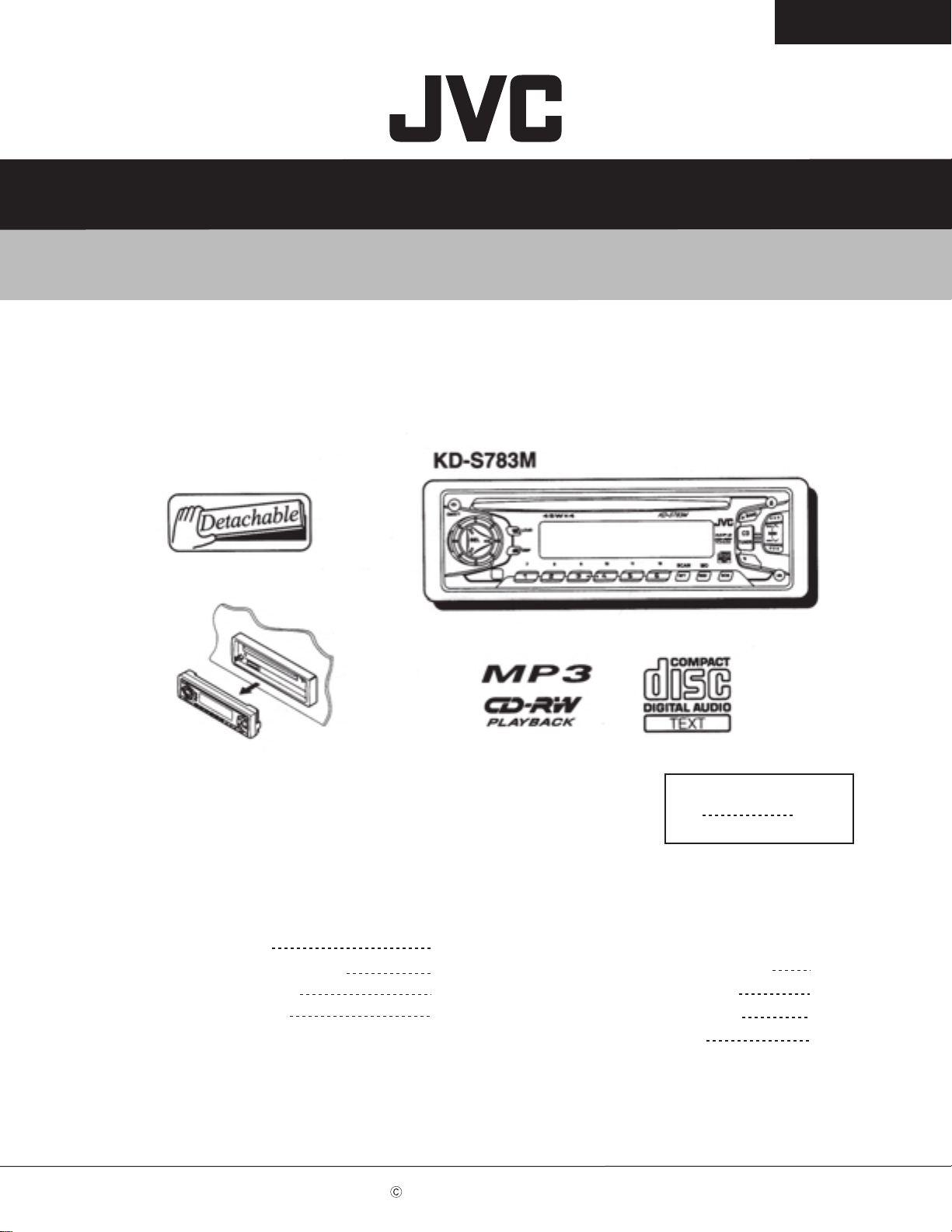
KD-S783M
KD-S783M
KD-S783M
Contents
Safety precaution
Preventing static electricity
Disassembly method
Adjustment method
COPYRIGHT 2002 VICTOR COMPANY OF JAPAN, LTD.
1-2
1-3
1-4
1-11
Area Suffix
UF China
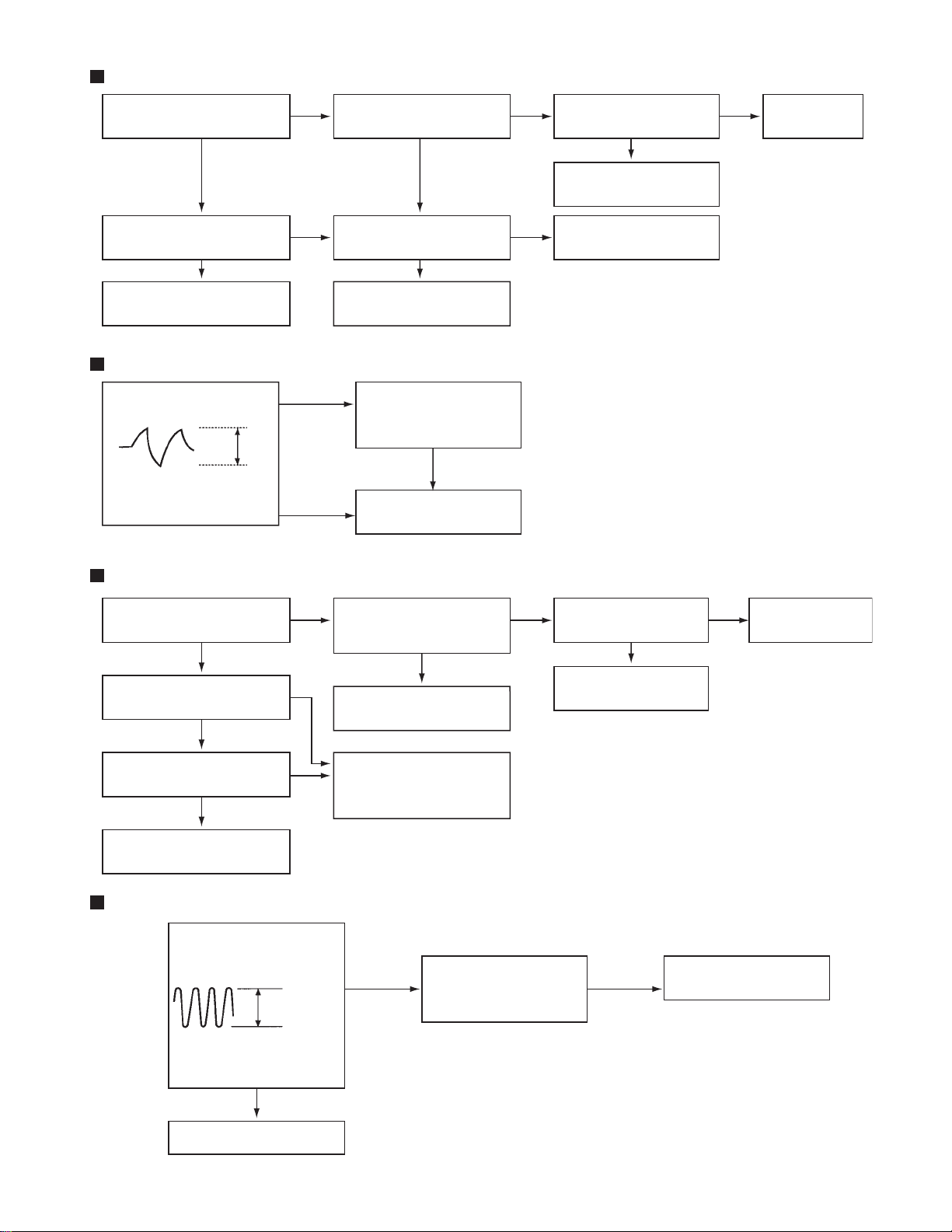
Flow of functional
operation unit TOC read
Maintenance of laser pickup
Replacement of laser pickup
Description of major ICs
1-12
1-14
1-14
1-15~33
No.49764
Nov. 2002
1-1
Page 2
KD-S783M
Safety precaution
!
!
Burrs formed during molding may be left over on some parts of the chassis. Therefore,
pay attention to such burrs in the case of preforming repair of this system.
Please use enough caution not to see the beam directly or touch it in case of an
adjustment or operation check.
1-2
Page 3
KD-S783M
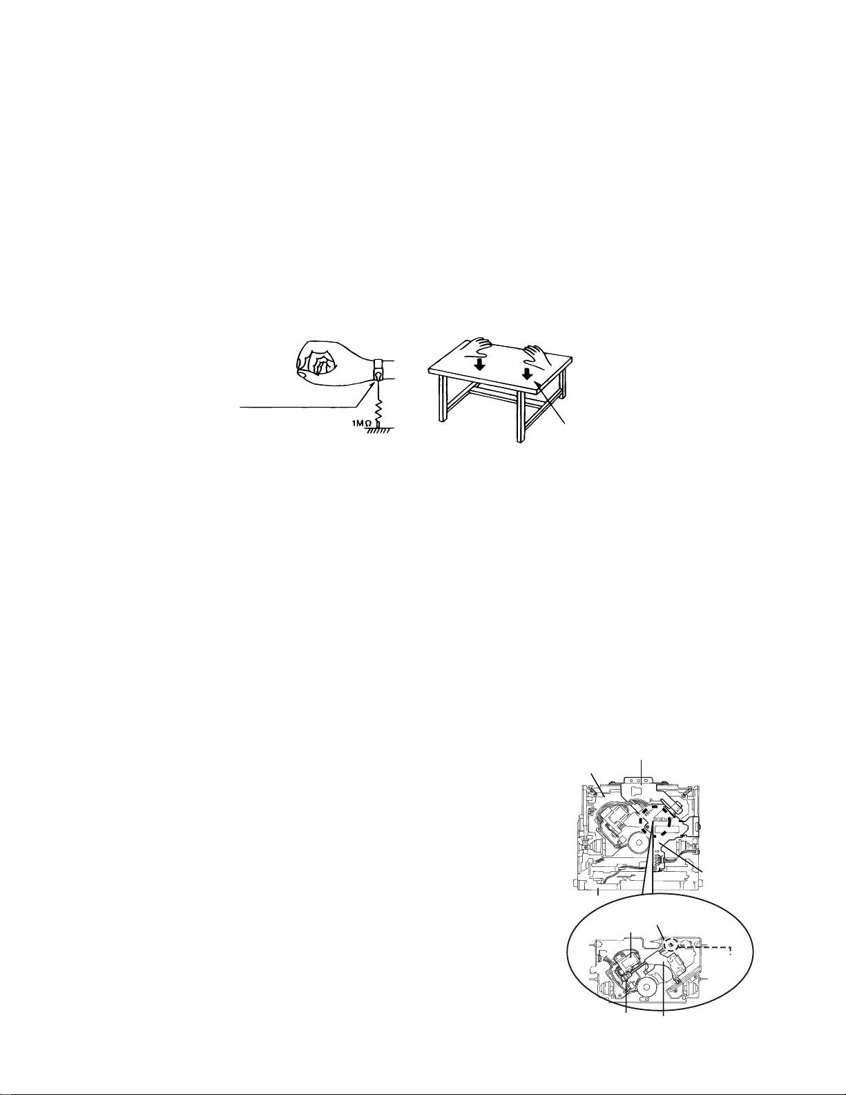
Preventing static electricity
1.Grounding to prevent damage by static electricity
Electrostatic discharge (ESD), which occurs when static electricity stored in the body, fabric, etc. is discharged,
can destroy the laser diode in the traverse unit (optical pickup). Take care to prevent this when performing repairs.
2.About the earth processing for the destruction prevention by static electricity
Static electricity in the work area can destroy the optical pickup (laser diode) in devices such as CD players.
Be careful to use proper grounding in the area where repairs are being performed.
2-1 Ground the workbench
Ground the workbench by laying conductive material (such as a conductive sheet) or an iron plate over
it before placing the traverse unit (optical pickup) on it.
2-2 Ground yourself
Use an anti-static wrist strap to release any static electricity built up in your body.
(caption)
Anti-static wrist strap
Conductive material
3. Handling the optical pickup
1. In order to maintain quality during transport and before installation, both sides of the laser diode on the
replacement optical pickup are shorted. After replacement, return the shorted parts to their original condition.
(Refer to the text.)
2. Do not use a tester to check the condition of the laser diode in the optical pickup. The tester's internal power
source can easily destroy the laser diode.
(conductive sheet) or iron plate
4.Handling the traverse unit (optical pickup)
1. Do not subject the traverse unit (optical pickup) to strong shocks, as it is a sensitive, complex unit.
2. Cut off the shorted part of the flexible cable using nippers, etc. after replacing the optical pickup. For specific
details, refer to the replacement procedure in the text. Remove the anti-static pin when replacing the traverse
unit. Be careful not to take too long a time when attaching it to the connector.
3. Handle the flexible cable carefully as it may break when subjected to strong force.
4. It is not possible to adjust the semi-fixed resistor that adjusts the laser power. Do not turn it
CD mechanism ass’y
Damper bracket
Attention when traverse unit is decomposed
*Please refer to "Disassembly method" in the text for pick-up and how to
detach the substrate.
1.Solder is put up before the card wire is removed from connector on
the CD substrate as shown in Figure.
(When the wire is removed without putting up solder, the CD pick-up
assembly might destroy.)
2.Please remove solder after connecting the card wire with
when you install picking up in the substrate.
Front bracket
Feed motor ass’y
FD screw
CD mechanism
control board
Soldering
FD gear
Pickup unit
1-3
Page 4
KD-S783M
Disassembly method
<Main body>
Removing the front panel assembly
(See Fig.1)
1.
Press the eject button in the lower right part of the
front panel. Remove the front panel assembly from
the body.
Front panel assembly
Eject button
Fig.1
Removing the front chassis assembly
(See Fig.2, 3)
Prior to performing the following procedure, remove
the front panel assembly.
1.
Release the four joint tabs a on both sides of the
front chassis assembly and remove the front chassis
assembly toward the front.
Tab a
Tab a
Front chassis assembly
Heat sink
Fig.2
Tab a
1-4
Fig.3
Tab a
Front chassis
assembly
Page 5
Removing the heat sink (See Fig.4)
g
1.
Remove the three screws A on the left side of the
body.
KD-S783M
Removing the bottom cover
(See Fig.5, 6)
Prior to performing the following procedure, remove
the front panel assembly, the front chassis assembly
and the heat sink.
1.
Turn the body upside down.
2.
Insert a screwdriver to the two joints b and two joints
c on both sides of the body and the joint d on the
back of the body, then detach the bottom cover from
the body.
CAUTION:
When disengaging the joint d using a
screwdriver, do not damage or break the
board.
A
Joint d
Joint b
Heat sink
Fig.4
Rear panel
Fig.5
A
Bottom cover
Joint c
Bottom cover
Joint b
Rear panel
.6
Fi
Joint c
Joint d
1-5
Page 6
KD-S783M
Removing the main board (See Fig.7, 8)
Prior to performing the following procedure, remove
the front panel assembly, the front chassis assembly,
the heat sink and the bottom cover.
1.
Remove the screw B, the four screws C and the
three screws D attaching the rear bracket on the
back of the body. Remove the rear panel.
2.
Remove the two screws E attaching the main board
on the bottom of the body. Disconnect connector
CN501 on the main board in the direction of the
arrow.
D
E
C
Rear panel
C
D
Fig.7
Main board
B
C
D
E
Removing the CD mechanism section
(See Fig.9)
Prior to performing the following procedure, remove
the front panel assembly, the front chassis assembly,
the heat sink, the bottom cover and the main board.
1.
Remove the three screws F attaching the cassette
mechanism section on the back of the top chassis.
CN501
F
Fig.8
CD mechanism section
F
Fig.9
F
Top chassis
1-6
Page 7
KD-S783M
g
Removing the control switch board
(See Fig.10 ~ 12)
Prior to performing the following procedure, remove
the front panel assembly.
1.
Remove the four screws G attaching the rear cover
on the back of the front panel assembly.
2.
Unjoint the eleven joints e with the front panel and
the rear cover.
3.
Remove the control switch board on the back of the
front panel.
Joint e
Front panel
G
G
Rear cover
Fig.10
Joint e
G
G
Joint e
Front panel
Joint e
Fig.11
Fi
.12
Rear cover
Control switch board
1-7
Page 8
KD-S783M
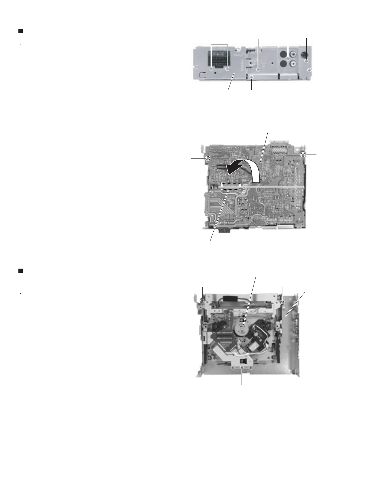
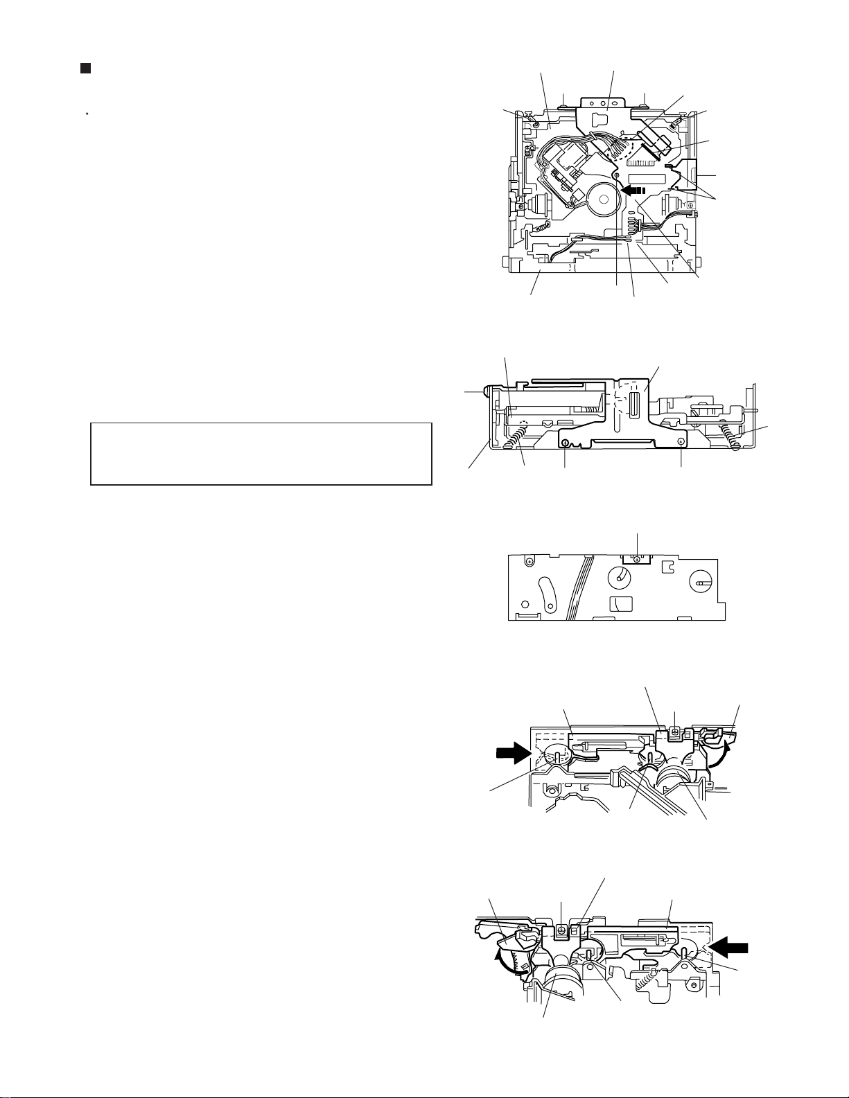
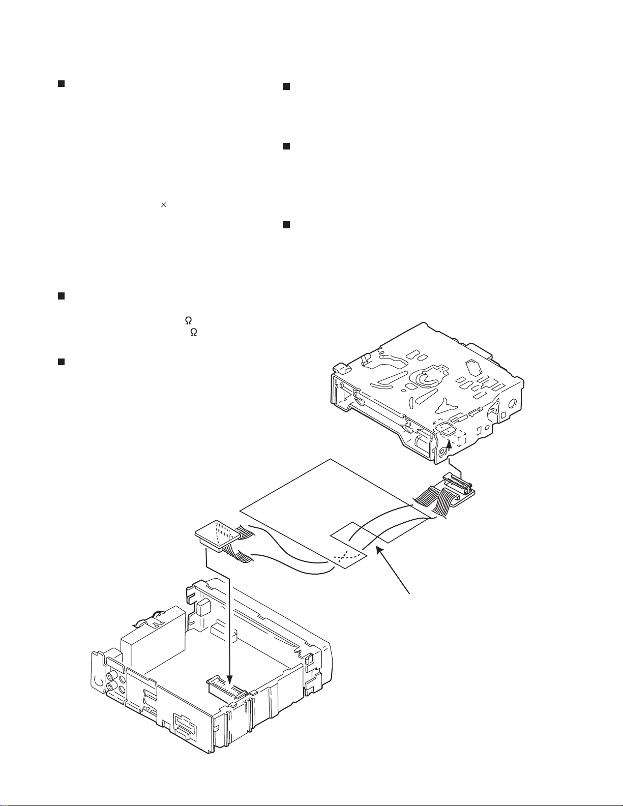
<CD mechanism section>
Removing the CD mechanism control
board (See Fig.1 and 2)
1.
Unsolder the part a and b on the CD mechanism
control board.
2.
Remove the stator fixing the CD mechanism control
board and the damper bracket (To remove the stator
smoothly, pick up the center part).
3.
Remove the screw A attaching the CD mechanism
control board.
4.
Remove the CD mechanism control board in the
direction of the arrow while releasing it from the two
damper bracket slots d and the front bracket slot e.
5.
Disconnect the flexible wire from connector on the
pickup unit.
ATTENTION:
Turn the FD gear in the direction of the
arrow to move the entire pickup unit to
the appropriate position where the
flexible wire of the CD mechanism unit
can be disconnected easily.
(Refer to Fig.2)
CD mechanism assembly
D
h
Front bracket
Pickup unit
Damper bracket
D
A
Fig.1
e
b
Flexible wire
a
h
c
D
d
CD mechanism
control board
Shift the lock
Removing the loading motor
(See Fig.3 to 5)
Prior to performing the following procedure, remove
the CD mechanism control board.
1.
Remove the two springs f attaching the CD
mechanism assembly and the front bracket.
2.
Remove the two screws B and the front bracket
while pulling the flame outward.
3.
Remove the belt and the screw C from the loading
motor.
Loading motor
C
FD gear
f
B
Loading motor
Pull outward
Fig.2
CD mechanism control board
f
B
Front bracket
Fig.3
Front bracket
Pull outward
1-8
Fig.5
Belt
Flame
Fig.4
Page 9
KD-S783M
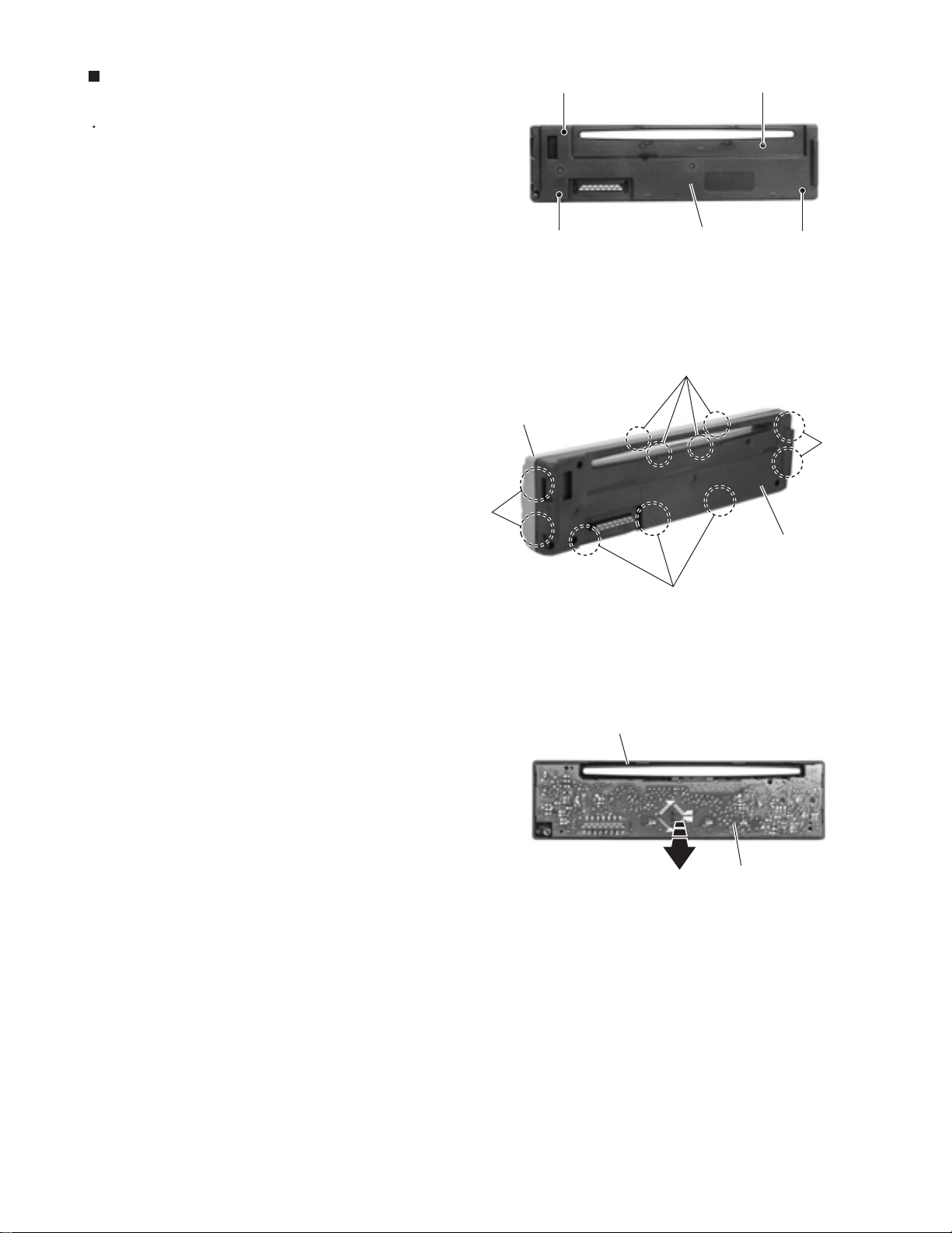
Removing the CD mechanism assembly
(See Fig.1, 6 to 9)
Prior to performing the following procedure, remove
the CD mechanism control board and the front
bracket (loading motor).
1.
Remove the three screws D and the damper
bracket.
2.
Raise the both sides fix arms and move the fix plates
in the direction of the arrow to place the four shafts g
as shown in Fig.8 and 9.
3.
Remove the CD mechanism assembly and the two
springs h attaching the flame.
4.
Remove the two screws E and both sides rear
damper brackets from the dampers. Detach the CD
mechanism assembly from the left side to the right
side.
ATTENTION:
The CD mechanism assembly can be
removed if only the rear damper
bracket on the left side is removed.
CD mechanism
h
Front bracket
CD mechanism
D
Flame
assembly
D
assembly
h
D
Damper bracket
D
A
Fig.5
e
b
Damper bracket
D
Fig.6
a
h
c
D
d
CD mechanism
control board
h
Fix plate (L)
g
Fix arm (R)
D
Fig.7
Rear damper bracket
g
Fig.8
Rear damper bracket
E
Fix plate(R)
E
Fix arm (L)
Damper
Damper
g
g
Fig.9
1-9
Page 10
KD-S783M
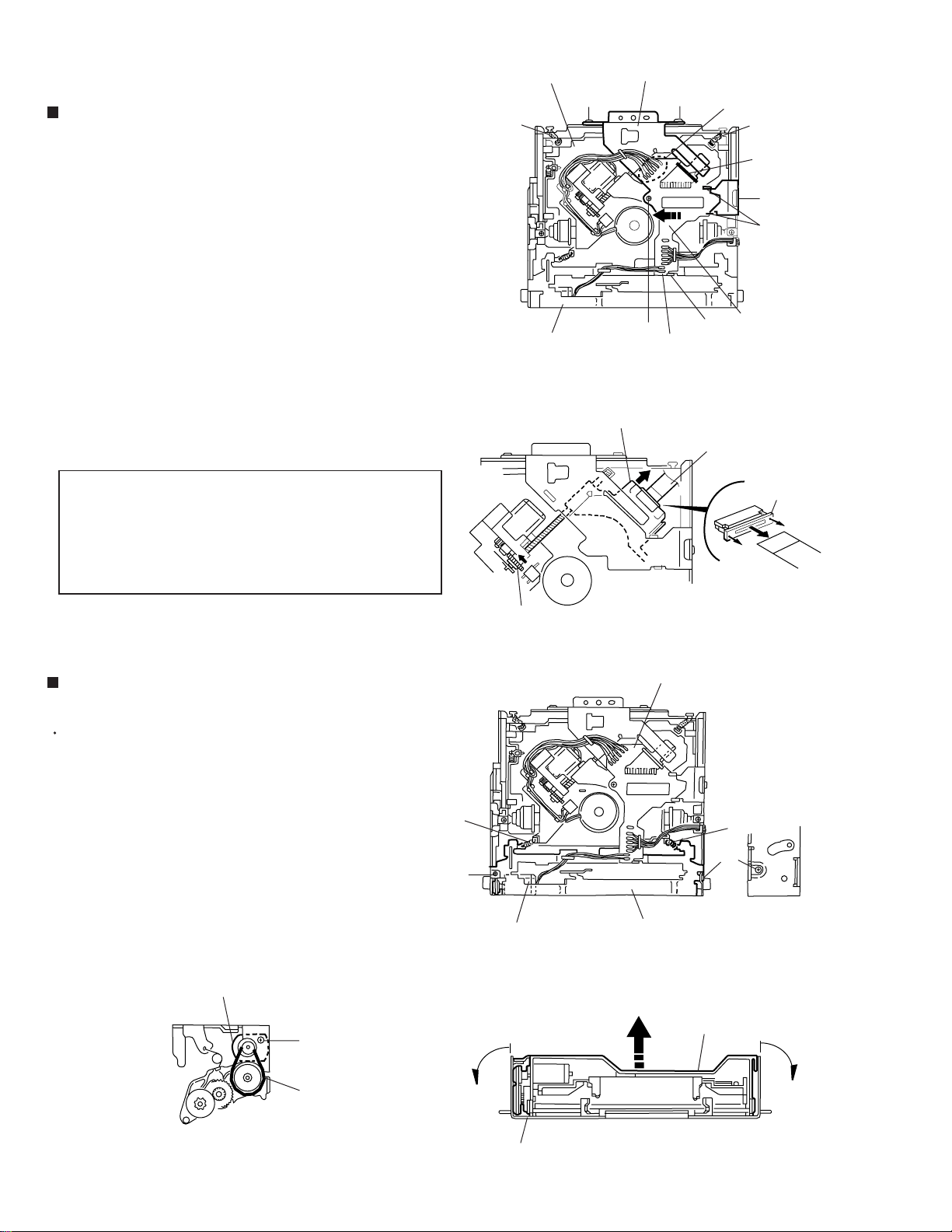
Removing the feed motor assembly
(See Fig.10)
Prior to performing the following procedure, remove
the CD mechanism control board, the front bracket
(loading motor) and the CD mechanism assembly.
1.
Remove the two screws F and the feed motor
assembly.
Removing the pickup unit
(See Fig.10 and 11)
Prior to performing the following procedure, remove
the CD mechanism control board, the front bracket
(loading motor), the CD mechanism assembly and
the feed motor assembly.
1.
Detach the FD gear part of the pickup unit upward.
Then remove the pickup unit while pulling out the
part i of the FD screw.
Feed motor assembly
F
FD gear
Nut push spring plate
FD screw
Pickup unit
Fig.10
Part i
Part j
Pickup unit
G
Pickup mount nut
Pickup unit
ATTENTION:
2.
Remove the screw G attaching the nut push spring
plate and the pickup mount nut from the pickup unit.
Pull out the FD screw.
When reattaching the pickup unit,
reattach the part j of the pickup unit,
then the part i of the FD screw.
Removing the spindle motor
(See Fig.12 and 13)
Prior to performing the following procedure, remove
the CD mechanism control board, the front bracket
(loading motor), the CD mechanism assembly and
the feed motor assembly.
1.
Turn up the CD mechanism assembly and remove
the two springs k on both sides of the clamper arms.
Open the clamper arm upward.
2.
Turn the turn table, and remove the two screws H
and the spindle motor.
k
FD screw
Spindle motor
Fig.11
k
Fig.12
H
1-10
H
Fig.13
Page 11
Adjustment method
KD-S783M
Test instruments required for adjustment
1. Digital oscilloscope (100MHz)
2. AM Standard signal generator
3. FM Standard signal generator
4. Stereo modulator
5. Electric voltmeter
6. Digital tester
7. Tracking offset meter
8. Test Disc JVC :CTS-1000
9. Extension cable for check
EXTGS004-26P 1
Standard measuring conditions
Power supply voltage DC14.4V(10.5~16V)
Load impedance 4 (2 Speakers connection)
Line oout impeadance 20k
Output Level Line out 2.0V (Vol. MAX)
How to connect the extension cable for adjusting
Standard volume position
Balance and Bass &Treble volume : lndication"0"
Loudness : OFF
BBE : OFF
Frequency Band
FM 87.5MHz ~ 107.9MHz
MW 530kHz ~ 1710 kHz
Dummy load
Exclusive dummy load should be used for AM,and FM. For
FM dummy load,there is a loss of 6dB between SSG output
and antenna input.The loss of 6dB need not be considered
since direct reading of figures are applied in this working
standard.
EXTGS004-26P
1-11
Page 12
KD-S783M
Acceleration
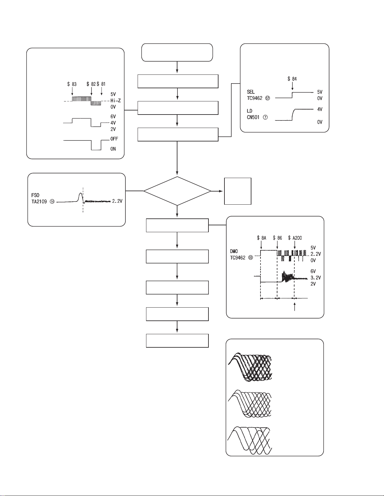
Flow of functional operation until TOC read
Power ON
• When the pickup correctly moves
to the inner area of the disc
Set Function to CD
• When the laser diode correctly
emits
Microprocessor
commands
FMO
TC9462 "53"
FEED MOTOR
+TERMINAL
TERMINAL
IC581 "5"
REST SW
• When correctly focused
Focus Servo Loop ON
Disc inserted
Pickup feed to the inner area
Laser emitted
Focus search
Disc rotates
RF signal eye-pattern
remains closed
Tracking loop closed
RF signal eye-pattern
opens
TOC readout
YES
YES
Microprocessor
commands
"No disc"
display
• When the disc correctly rotates
Microprocessor
commands
Spindle
motor (-)
IC581 "7"
Acceleration
Acceleration
0.5 Sec
Rough
Servo
0.5 Sec
Servo CLV
1-12
Jump to the first track
Play
Tracking Servo Loop ON
• RF signal
Rough Servo Mode
CLV Servo Mode
(ProgramArea)
CLV Servo Mode
(Lead-In Area;
Digital: 0)
Page 13
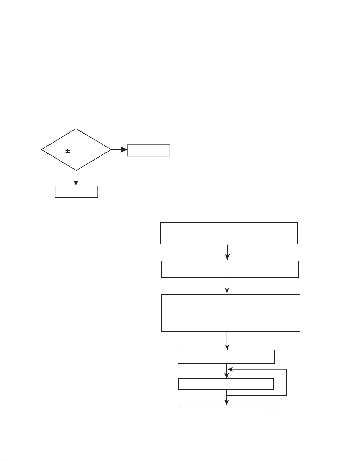
Feed Section
Is the voltage output at
IC521 pin "53" 5V or 0V?
YES
Is 4V present at both
sides of the feed motor?
YES
NO
Is the wiring for IC521
(90) ~ (100) correct?
NO
Is 6V or 2V present at
IC581 "5" and "6"?
NO
YES
YES
Is 5V present at IC581
pin "11"?
YES
Check the vicinity of
IC521.
Check the feed motor
connection wiring.
NONO
KD-S783M
Check CD 9V
and 5V.
Check the feed motor.
Focus Section
When the lens is
moving:
4V
Does the S-search
waveform appear at
IC581 pins "17" and "18"?
Spindle Section
Is the disk rotated?
YES
Does the RF signal
appear at TP1?
YES
Check IC581.
NO
YES
NO
NO
Check the circuits in
the vicinity of IC581
pins "15" ~ "18".
Check the pickup and
its connections.
Is 4V present at IC581
pins "7" and "8" ?
Check the spindle motor
and its wiring.
YES
YES
NO NO
Is 4V present at IC521
pin "55" ?
YES
Check the vicinity of
IC581.
Check IC501 and
IC521.
Is the RF waveform at TP1
distorted?
YES
Proceed to the Tracking
section
Tracking Section
When the disc is rotated
at first:
Is the tracking error signal
output at IC501 "12"?
Check IC521.
NO
Approx. 1.2 V
YES
Check the circuits in the
vicinity of IC501 "19" ~
"24" or the pickup
Check the circuit in the
vicinity of IC501 pins
"2" ~ "12".
YESYES
Check the pickup and
its connections.
1-13
Page 14
KD-S783M
Maintenance of laser pickup
(1) Cleaning the pick up lens
Before you replace the pick up, please try to
clean the lens with a alcohol soaked cotton
swab.
(2) Life of the laser diode
When the life of the laser diode has expired,
the following symptoms will appear.
(1) The level of RF output (EFM output:ampli
tude of eye pattern) will be low.
Is RF output
1.0 0.35Vp-p?
YES
O.K
(3) Semi-fixed resistor on the APC PC board
The semi-fixed resistor on the APC printed
circuit board which is attached to the pickup
is used to adjust the laser power.Since this
adjustment should be performed to match the
characteristics of the whole optical block,
do not touch the semi-fixed resistor.
If the laser power is lower than the specified
value,the laser diode is almost worn out, and
the laser pickup should be replaced.
If the semi-fixed resistor is adjusted while
the pickup is functioning normally,the laser
pickup may be damaged due to excessive current.
NO
Replace it.
Replacement of laser pickup
Turn off the power switch and,disconnect the
power cord from the ac outlet.
Replace the pickup with a normal one.(Refer
to "Pickup Removal" on the previous page)
Plug the power cord in,and turn the power on.
At this time,check that the laser emits for
about 3seconds and the objective lens moves
up and down.
Note: Do not observe the laser beam directly.
1-14
Play a disc.
Check the eye-pattern at TP1.
Finish.
Page 15
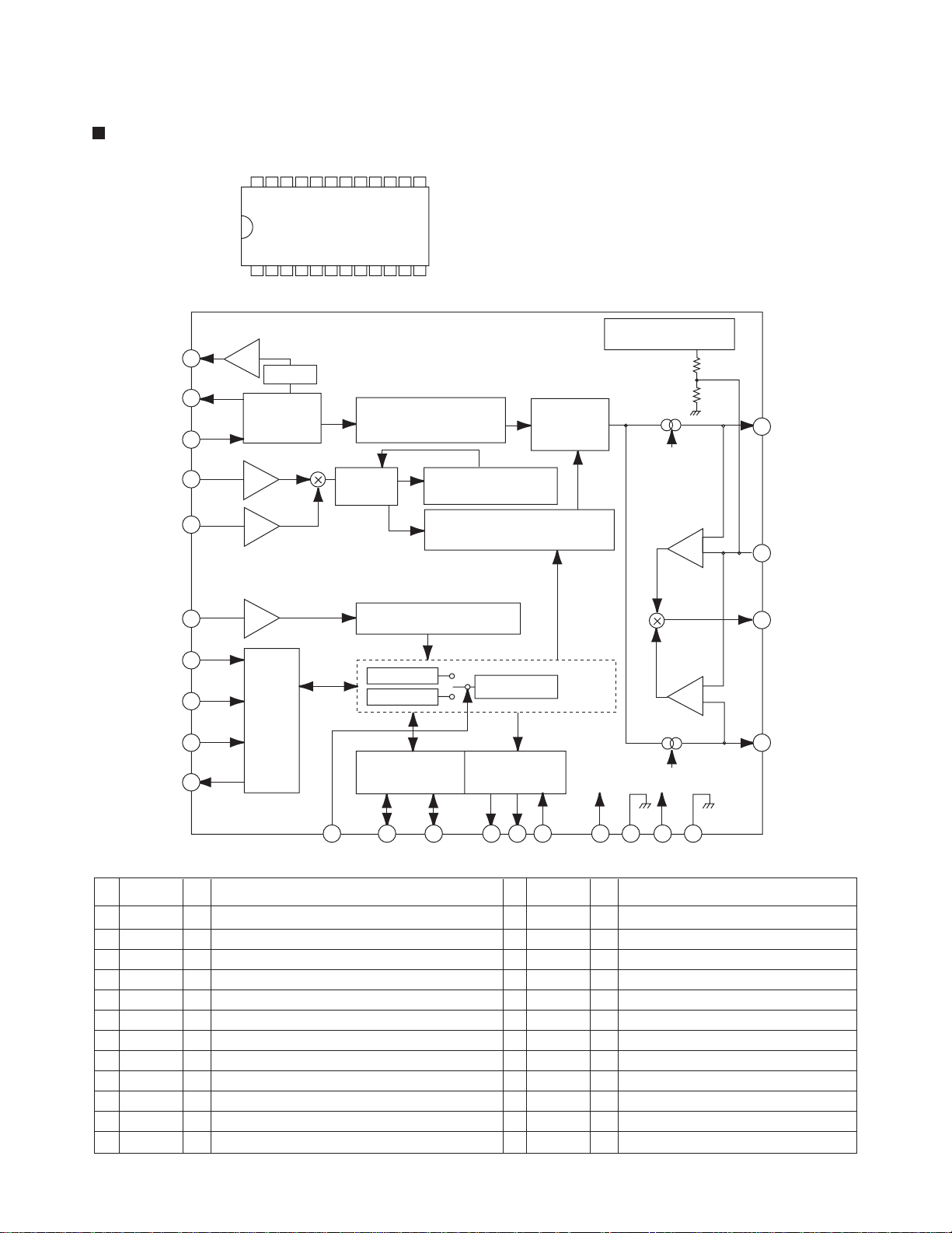
Description of major ICs
TB2118F-X (IC31) : PLL
1. Terminal layout
2423222120191817161514
KD-S783M
13
2. Block diagram
osc
2
1
XO
24
XI
FM VCO
AMVCO
IFC
CE
DIN
DOUT
DIMM
15
16
13
3
4
5
6
123456789
Buff.
ON/OFF
OSC circuit
AMP
AMP
AMP
Serial
Interface
101112
Reference Counter
Prescaler
20-bit BINARY COUNTER
Resistor 1
Resistor 2
I/O PORT
Swallow counter
Phase
Comparator
4-bit
12-bit
Programmable counter
22-bit
40bit shift register
OUTPUT PORT
Constant
power supply voltage
switch
Vdd
switch
Vcc
AM CP.
20
+
+
-
REG.
22
19
vt
18
FM cp
3. Pin function
Pin
Symbol I/O Function
No.
XOUT
10
11
12
1
2
3
4
5
6
7
8
9
OSC
CE
DI
CK
DOUT
SR
I/01
I/02
OUT1
OUT2
VDD2
Crystal oscillator pin
O
Non connect
Chip enable input
I
Serial data input
I
Clock input
I
Serial data output
O
Register control pin
O
I/O ports
I/O
I/O ports
I/O
Non connect
Non connect
Single power supply for REF. frequency block
-
7
SL
8
9
I/O -2I/O -1
10 11
12
out-2out-1
vdd2
Pin
Symbol I/O Function
No.
IFC
13
VDD
14
FMIN
15
AMIN
16
DGND
17
FMCP
18
VT
19
AMCP
20
VCC
21
RF
22
AGND
23
XIN
24
17
14
IF signal input
I
Power pins for digital block
FM band local signal input
I
AM band local signal input
I
Connect to GND (for digital circuit)
Charge pump output for FM
O
Tuning voltage biased to 2.5V.
Charge pump output for AM
O
Power pins for analog block
Ripple filter connecting pin
I
Connect to GND (for analog circuit)
Crystal oscillator pin
I
21
23
a-gnd
vccd-gndvdd
1-15
Page 16
KD-S783M
TA2147F-X (IC521) : RF amp.
1.Terminal layout
2.Block diagram
VRO
FEO
FEN
RFRP
RFRPIN
RFGO
RFGC
AGCIN
RFO
RFN
13GVSW
14
15
16
17
18
19
20
21
22
23
10pF
40k
30k
20k 20k
20k
20k
BOTTOM
3k
15k
50 A
12k
12k
PEAK
20k
180k
40pF
20k
20k
PEAK
1.3V
240k
180k
40k
240k
15pF
15pF
40pF
60k
40k
60k
50k
2k
20 A
20k
60 A
50k
14k
k
1
80k
x0.5
x0.5
80k
20k
20k
15k
x2
x2
1k
2k
1.75k
10pF
12 RFDC
11
TEO
10
TEN
TEBC
9
8
SEL
7
LDO
MDI
6
5
TNI
4
TPI
3
FPI
2
FNI
1-16
GND
24
3k
1
Vcc
Page 17
3.Pin function
KD-S783M
Pin No.
1
2
3
4
5
6
7
8
9
10
11
12
13
Symbol
Vcc
FNI
FPI
TPI
TNI
MDI
LDO
SEL
TEBC
TEN
TEO
RFDC
GVSW
I/O
I
I
I
I
I
O
I
I
I
O
O
I
Function
3.3V Power supply pin
Main-beam amp input pin
Main-beam amp input pin
Sub-beam amp input pin
Sub-beam input pin
Monitor photo diode amp input pin
Laser diode amp output pin
APC circuit ON/OFF control signal,laser diode (LDO) control signal input or
bottom/peak detection frequency change pin.
APC
circuit
GND OFF
HIZ
Vcc
Tracking error balance adjustment signal pin
Adjusts TE signal balance by eliminating carrier component from
PWM signal(3-state output, PWM carrier = 88.2kHz) output from
TC9490F/FA TEBC pin using RC-LPF and inputting DC.
TEBC input voltage:GND~Vcc
Tracking error signal generation amp negative-phase input pin
Tracking error signal generation amp output pin.
Combining TEO signal and RFRP signal with TC9490F/FA configures
tracking search system.
RF signal peak detection output pin
AGC/FE/TE amp gain change pin
Connected to Vcc
through 1k resistor
Control signal output
ON
Control signal output
ON
LDOSEL
14
15
16
17
18
19
20
21
22
23
24
VRO
FEO
FEN
RFRP
RFRPIN
RFGO
RFGC
AGCIN
RFO
RFN
GND
ModeGVSW
GND
HIZ
Vcc
Reference voltage (VRO) output pin *VRO = 1/2 Vcc when Vcc = 3.3V
O
Focus error signal generation amp output pin
O
Focus error signal generation amp negative-phase input pin
I
Signal amp output pin for track count
O
Combining RFRP signal TEO signal with TC9490F/FA configures tracking
search system.
Signal generation amp input pin for track count
I
RF signal amplitude adjustment amp output pin
O
RF amplitude adjustment control signal input pin
I
Adjusts RF signal amplitude by eliminating carrier component from PWM
signal (3-state output, PWM carrier = 88.2kHz) output from TC9490F/FA
RFGC pin using RC-LPF and inputting DC.
*RFGC input voltage : GND-Vcc
RF signal amplitude adjustment amp input pin
I
RF signal generation amp output pin
O
RF signal generation amp input pin
I
GND pin
-
CD-RW
CD-DA
CD-DA
1-17
Page 18
KD-S783M
F
LA4743K (IC301) : Power amp
1.Block diagram
IN 1
TA B
IN 2
+
0.22 F
+
0.22 F
11
1
12
Vcc 1/2 Vcc 3/4
6 20
-
+
Protective
circuit
-
+
2200 F 0.022
+
9
7
+
OUT 1+
OUT 1-
PWR GND1
8
+
OUT 2+
5
-
OUT 2-
3
PWR GND2
2
ST BY
R.F
47 F
IN 3
PRE GND
IN 4
+5V
ST ON
+
0.22 F
N.C
+
0.22 F
4
Stand by
Switch
Mute
10
+
Ripple
Filter
Mute
22
circuit
3.3 F
+
15
-
+
-
17
19
10K
+
OUT 3+
OUT 3-
Low Level
Mute ON
25
18
21
23
PWR GND3
OUT 4+
OUT 4-
13
14
Protective
circuit
-
+
+
-
1-18
ON TIME C
22 F
Muting &
16
+
ON Time Control
Circuit
PWR GND4
24
Page 19

2.Terminal layout
KD-S783M
3.Pin function
1
2
3
4
5
6
7
8
9
10
11
12
13
14
15
16
17
18
19
20
21
22
23
24
25
SymbolPin No. Function
TA B
GND
OUTRRSTBY
OUTRR+
VCC1/2
OUTRFGND
OUTRF+
RIPPLE
INRF
INRR
SGND
INLR
INLF
ONTIME
OUTLF+
GND
OUTLFVCC3/4
OUTLR+
MUTE
OUTLRGND
NC
Header of IC
Power GND
Outpur(-) for front Rch
Stand by input
Output (+) for front Rch
Power input
Output (-) for rear Rch
Power GND
Output (+) for rear Rch
Ripple filter
Rear Rch input
Front Rch input
Signal GND
Front Lch input
Rear Lch input
Power on time control
Output (+) for rear Lch
Power GND
Output (-) for rear Lch
Power input
Output (+) for front
Muting control input
Output (-) for front
Power GND
Non connection
LA4743B
1-19
Page 20

KD-S783M
UPD784215AGC184 (IC701) : Main micon
1.Pin layout
100 ~ 76
1
75
~
25
26 ~ 50
2.Pin functions (1/2)
Pin No.
1
2
3
4
5
6
7
8
9
10
11
12
13
14
15
16
17
18
19~21
22
23
24
25
26
27
28
29
30
31
32
33
34,35
36
37
38
39
40
41
42
43
44
45~52
Symbol
SW2
SW3
SW4
REST
LM0
LM1
ANT CONT
VDD
X2
X1
VSS
XT2
XT1
RESET
SW1
BUS-INT
PS2
REMOCON
AVDD
AVREF0
VOL1
VOL2
KEY0
KEY1
KEY2
LEVEL
SM
AVSS
AVREF
BUS-SI
BUS-SO
BUS-SCK
BUS-I/O
LCD-DA
LCD-SCK
LCD-CE
BUZZER
~
51
I/O
Function
I
CD mecha sw2
I
CD mecha sw3
I
CD mecha sw4
I
Rest sw
O
Loading/Eject motor control (Loading side)
O
Loading/Eject motor control (Eject side)
-
-
-
-
-
-
No use
O
Antenna remote control
-
Maicon power supply
-
-
-
GND
-
I
Reset detection
I
CD mecha sw1
I
J-BUS int
I
Power save 2, H means STOP mode
-
No use
I
Remocon input
-
A/D converter power supply
-
A/D reference voltage
I
Volume encoder pulse input 1
I
Volume encoder pulse input 2
I
Key input 0
I
Key input 1
I
Key input 2
I
Level meter input
-
No use
I
S.METER input
-
GND
-
No use
I
J-BUS data input
O
J-BUS data output
I/O
J-BUS clock input/output
O
J-BUS I/O selection output H:output L:input
O
Data output for LCD driver
O
CLK output for LCD driver
O
CE for LCD driver
O
Buzzer output
-
No use
1-20
Page 21

2.Pin functions (2/2)
KD-S783M
Pin No.
53
54
55
56
57
58
59
60
61
62
63
64
65
66
67
68
69
70
71
72
73
74
75
76
77
78~80
81
82
83
84
85
86~89
90
91
92
93
94
95
96
97
98
99
100
Symbol
SD/ST
LOCAL
MONO
MP3 CLK
MP3 DATA IN
MP3 DATA OUT
MP3 STANDBY
MP3 RESET
MP3 REQ
DETACH
SEEK/STOP
-
FM/AM
PLL-CE
PLL-DO
PLL-CLK
PLL-DI
TEL-MUTE
-
VSS
VSDIM-IN
PS1
POWER
CD-ON
MUTING
-
VDD
-
VOL-DA
VOL-CLK
DIM-OUT
-
STAGE
BUCK
CCE
RST
TEST
BUS0
BUS1
BUS2
BUS3
-
CD-RW
I/O
Function
I
Station detector or stereo signal input
O
Loal or distance selecting output
O
Monoral selection output
O
CLK output for MP3 decoder
I
Data input for MP3 decoder / inverting input due to converter
O
Data output for MP3 decoder / H level during input mode
O
Standby output for MP3 decoder
O
Reset output for MP3 decoder
I
REQ input for MP3 decoder / inverting input due to converter
I
Detach detect input H: detaching
O
Auto seek and stop selecting output
-
No use
O
FM,AM band selecting output
O
CE output for PLL IC
O
Data output for PLL IC
O
Clock output for PLL IC
I
Data input from PLL IC
I
Telephone muting detection input, active level can selected H or L is PSM
-
No use
-
GND
I
Dimmer detecter input L=dimmer on
I
POWER SAVE 1 L=ACC off
O
Power ON/OFF control output H=power on
O
CD power supply control output H=CD power ON
O
Muting output L=Muting ON
-
No use
-
Micon power supply
-
No use
O
Data output for E-vol IC
O
Clock output for E-vol IC
O
Dimmer control output L=dimmer on
-
No use
I
L=U version, H=Japanversion
O
Clock output for CD LSI
O
CE output for CD LSI
O
Reset output for CD LSI
-
For rewriting flash memory
I/O
Data output and input 0 for CD LSI
I/O
Data output and input 1 for CD LSI
I/O
Data output and input 2 for CD LSI
I/O
Data output and input 3 for CD LSI
-
No use
-
RF gain control L=CD-RW, H=CD-DA
1-21
Page 22

KD-S783M
TC9490FA (IC541) : DSP & DAC
1.Pin layout & Block daiagram
DV
SS3
RO
DV
DD3
DVR
LO
DV
SS3
ZDET
V
SS5
BUS0
BUS1
BUS2
BUS3
BUCK
/CCE
/RST
VXDD3XOXI
SS3
XV
TEIN
DD3VSS3
V
DMO
FMO
DD3
AV
SEL
TEBC
RFGC
48 47 46 45 44 43 42 41 40 39 38 37 36 35 34 33
49
50
51
52
LPF
Clock
generator
1-bit
DAC
PWM
Servo control
A/D
53
54
55
56
Address
circuit
ROM
RAM
Digital equalizer
automatic
adjustment circuit
57
58
59
60
61
62
Micro-
controller
interface
circuit
Correction
Audio output
circuit
16k
RAM
Digital output
CLV servo
Sync signal
protection
EFM
Sub code
detector
63
VCO
PLL
TMAX
REF
V
D/A
Data
slicer
TRO
FOO
32
31
30
29
28
27
26
25
24
23
22
21
20
19
18
TEZI
TEI
SBAD
FEI
RFRP
RFZI
RFCT
AV
DD3
RFI
SLCO
AV
SS3
VCOF
RV
REF
LPFO
LPFN
1-22
64
V
DD5
17
TMAX
1 2 3 4 5 6 7 8 9 10 11 12 13 14 15 16
SS3
BCK
LRCK
AOUT
DOUT
IPF
DD3
V
V
SBOK
CLCK
DATA
SFSY
SBSY
/HSO
UHSO
DD3
PV
PDO
Page 23

KD-S783M
2.Pin function (1/2)
Pin No.
1
2
3
4
Symbol
BCK
LRCK
AOUT
DOUT
5
6
7
8
9
10
11
12
13
14
VDD3
VSS3
SBOK
CLCK
DATA
SFSY
SBSY
/HSO
/UHSO
IPF
I/O
O
O
O
O
O
-
-
O
I/O
O
O
O
O
O
TC9490FA(2/3)
Function
Bit clock outputpin 32fs, 48fs, or 64fs selectable by command.
L/R channel clock output pin."L" for L channe and "H" for R channel.
Output polarity can be inverted by command.
Audio data output pin. MSB-first or LSB-first selectable by command.
Digital data output pin. Outputs up to double-speed playback.
Correction flag output pin.When set to "H",AOUT output cannot be corrected
by C2 correction processing.
Digital 3.3V power supply voltage pin.
Digital GND pin.
Subcode Q data CRCC result output pin."H" level when result is OK.
Subcode P-W data read clockI/O pin. I/O polarity selectable by command.
Subcode P-W data output pin.
Playback frame sync signal output pin.
Subcode block sync signal output pin. "H" level at S1 when subcode sync is
detected.
Playback speed mode flag output pins.
/HSO
H
H
L
--
H
L
L
--
Playback speed/UHSO
Normal
Double
4 times
---
15
16
17
18
19
20
21
22
23
24
25
26
27
28
29
30
31
32
33
34
35
PVDD3
PDO
TMAX
LPFN
LPFO
PVREF
VCOF
SS3
AV
SLCO
RFI
AV
RFCT
RFZI
RFRP
FEI
SBAD
TEI
TEZI
FOO
TRO
REF
V
-
PLL-only 3.3V power supply voltage pin.
O
EFM and PLCK phase difference signal output pin.
O
TMAX detection result output pin.
TMAX OutputTMAX Detection result
Longer than fixed period
Within fixed period
Shorter than fixed period
I
Inverted input pin for PLL LPF amp.
O
Output oin for PLL LPF amp.
-
PLL-only V
VCO filter pin.
O
Analog GND pin.
DAC output pin for data slice level generation.
O
RF signal input pin.Zin selectable by command.
I
Analog 3.3V power supply voltage pin.
RFRP signal center level input pin.
I
RFRP signal zero-cross input pin.
I
RF ripple signal input pin.
I
Focus error signal input pin.
I
Sub-beam adder signal input pin.
I
Tracking error input pin. Inputs when tracking servo is on.
I
Tracking error signal zero-cross input pin.
I
Focus equalizer output pin.
O
Tracking equalizer output pin.
O
Analog reference power supply voltage pin.
-
REF pin.
"PVDD3"
"HIZ"
"AV
SS3"
1-23
Page 24

KD-S783M
t
2.Pin function (2/2)
Pin No.
36
37
38
39
40
41
42
43
44
45
Symbol
RFGC
TEBC
SEL
AV
FMO
DMO
V
V
TESIN
XV
46
47
48
49
XV
DV
50
51
52
DV
DVR
53
54
55
56
57
58
59
60
61
62
63
64
DV
ZDET
V
BUS0
BUS1
BUS2
BUS3
BUCK
/CCE
/RST
V
DD3
SS3
DD3
SS3
XI
XO
DD3
SS3
RO
DD3
LO
SS3
SS5
DD5
I/O
Function
O
RF amplitude adjustment control signal output pin.
O
Tracking balance control signal output pin.
O
APC circuit ON/OFF signal output pin. At laser on,high impedance with
UHS="L" ,H output with UHS="H".
-
Analog 3.3V power supply voltage pin.
O
Feed equalizer output pin.
O
Disc equalizer output pin.
-
Digital GND pin.
-
Digital 3.3V power supply voltage pin.
I
Test input pin. Normally,fixed to "L".
-
System clock oscillator GND pin.
I
System clock oscilatoe input pin.
O
System clock oscillator output pin.
-
System clock oscillator 3.3V power supply voltage pin.
-
DA converter GND pin.
O
R-channel data forward output pin.
-
DA converter 3.3V power supply pin.
-
Reference voltage pin.
O
L-channel data forward output pin.
-
DA converter GND pin.
O
1 bit DA converter zero data detection flag output pin.
-
Microcontroller interface GND pin.
I/O
Microcontroller interface data I/O pins.
I
Microcontroller interface clock input pin.
I
Microcontroller interface chip enable signal input pin.At "L".
Bus0 to BUS3 are active.
I
Reset signal input pin. At reset,"L".
-
Microcontroller interface 5V power supply pin.
TC9490FA(3/3)
RPM6938-SV4 (IC602) : Remote control receiver
AGC
AMP
I/V
conversion
PD
magnetic shield
1-24
BPF
for
trimming
circuit
Detector
Vcc
Comp
Vcc
22k
ohm
Rou
GND
Page 25

TC94A02F-005 (IC401) : DSP
AD11
AD12
CKS
32
31
30
33
AD10
TESTP
29
VSSR
28
VRAR
27
Ro
26
VDAR
25
VDAL
24
KD-S783M
Lo
VRAL
VSSL
VSS
STANDBY
VDD
/oE
23
22
21
20
19
18
17
16
/CE
AD9
VDDT
AD8
AD7
AD6
REQ
VSS
AD13
DAC
34
Bus
register
C-Pointer
register
Y-Pointer
register
X-Pointer
Switch
register
X0 X1 X2
35
36
37
General
Output Port
38
39
40
41
Flag
2sets
Address Calc.
ERAM
2k word
*3
CROM
4k word
Y0 Y1 Y2
DAC
AX AY
MX MY MZ
MAC ALU
A3
A2
A0 A1
round & limit
round & limit
Audio.I/F
15
AD5
14
LRCKiA
13
BCKiA
12
SDi0
AD4
11
AD3
10
9
SDo
87
VDDT
AD14
/WR
AD16
AD15
io0
io1
VSS
VSSX
AD2
6
/MiCK
543
MiDio
AD1
AD0
MiMD
2
/RESET
1
42
YRAM
4k word
43
Timer
44
4546
47
48
Interrupt
Control
SRAM I/F
49
io2
I-Bus
Generator
50
io3
Timing
51
io4
XRAM
52
VDD
4k word
53
io5
X-Bus
Start
Prog.
54
io6
Y-Bus
DIT
55
io7
56
VSSP
PRAM
256word
57
PDo
Control
Program
PROM
4k*2+2k
VC0
58
VCoi
=10kword
59
VDDP
40bit
Decoder
Instruction
General Input Port
60
61
CK0
VDDX
Microcom.I/F
62
63
Xi
64
Xo
1-25
Page 26

KD-S783M
3.Pin function(1/2)
Pin No. Symbol Function
1
/RESET
2
MiMD
3
AD0
4
AD1
5
MiDio
6
/MiCK
7
AD2
8
VDDT
9
SDo
10
11
12
13
14
15
16
17
18
19
20
21
22
23
24
25
26
27
28
29
30
31
32
33
34
35
36
37
38
39
40
41
42
43
44
45
46
47
48
49
50
AD3
AD4
SDi0
BCKiA
LRCKiA
AD5
CE
OE
VDD
STANBY
VSS
VSSL
VRAL
LO
VDAL
VDAR
RO
VRAR
VSSR
TESTP
CKS
AD12
AD11
AD10
AD9
VDDT
AD8
AD7
AD6
REQ
VSS
AD13
AD14
WR
AD16
AD15
io0
io1
VSS
io2
io3
I/O
O
O
I/O
O
O
O
O
O
O
O
O
O
O
O
O
O
O
O
O
O
O
O
O
O
O
I/O
I/O
I/O
I/O
Hard reset input terminal(H:Normal operation L: Reset)
I
Micon I/F mode select input terminal
I
External SRAM address output 0 terminal
External SRAM address output 1 terminal
Micon I/F data input/output terminal
Micon I/F clock input terminal
I
External SRAM address output 2 terminal
Digital power supply (3.3V)
Data output terminal
External SRAM address output 3 terminal
External SRAM address output 4 terminal
Data input terminal 0
I
Bit clock input terminal A
I
LR clock input terminal A
I
External SRAM address output 5 terminal
External SRAM chip enable terminal
External SRAM output enable terminal
Digital power supply (2.5V)
Standby mode control terminal
I
Digital GND
DAC Lch GND
DAC Lch reference voltage terminal
DAC Lch output terminal
DAC Rch power supply terminal(2.5V)
DAC Lch power supply terminal(2.5V)
DAC Rch output terminal
DAC Rch reference voltage terminal
DAC Rch GND
Test terminal
I
VCO select terminal
I
External SRAM address output 12 terminal
External SRAM address output 11 terminal
External SRAM address output 10 terminal
External SRAM address output 9 terminal
Digital power supply terminal (3.3V)
External SRAM address output 8 terminal
External SRAM address output 7 terminal
External SRAM address output 6 terminal
Squeeze request terminal to host
Digital GND
External SRAM address output 13 terminal
External SRAM address output 14 terminal
External SRAM write signal
External SRAM address output 16 terminal
External SRAM address output 15 terminal
External SRAM data input/output 0 terminal
External SRAM data input/output 1 terminal
Digital GND
External SRAM data input/output 2 terminal
External SRAM data input/output 3 terminal
TC94A02F-005
1-26
Page 27

KD-S783M
3.Pin function(2/2)
Pin No. Symbol Function
51
52
53
54
55
56
57
58
59
60
61
62
63
64
io4
VDD
io5
io6
io7
VSSP
Pdo
Vcoi
VDDP
Cko
VDDX
Xi
Xo
VSSX
I/O
I/O
I/O
I/O
I/O
-
O
I
-
O
-
I
O
-
IC-PST600M / G / -W (IC702) : Reset
TC94A02F-005
External SRAM data input/output 4 terminal
Digital power supply (2.5V) terminal
External SRAM data input/output 5 terminal
External SRAM data input/output 6 terminal
External SRAM data input/output 7 terminal
VCO GND
PLL phase error detection signal output terminal
VCO control voltage input terminal
VCO power supply
16.934 MHz clock output terminal
Power supply (2.5V) terminal for oscillator
Connection terminal for oscillator(input)
Connection terminal for oscillator(output)
GND for oscillator
1. Terminal layout
2. Block diagram
Co1
OP1
Vcc
1
Vout
3
GND
2
1-27
Page 28

KD-S783M
AN80T07 (IC901) :
1.Pin layout
1 2 3 4 5 6 7 8 9 10 11 12 13 14 15 16
2.Block diagram
*ASO,Peak Cument Protection.
*Thermal Protection (Except
VDD,Comp output).
Outputs
Pre
Drive
-
+
MODEI
Reference Voltage
Pre
Drive
+
EXT
Out
ANT
Out
ACC
3
Pre
Drive
+
56
+
-
15 14 11 1 4 8 9 10 7 12 2 13 16
ILM
10V
ILMAJMODE2 SW5V Out VDD
5.7V
EXT VCC ANT BATT.DET COMP GND
CD
8.0V
AUDIO
9.0V
Pre
Drive
-
+
3.Pin function
Pin
No.
1
2
3
4
5
6
7
8
9
10
11
12
13
14
15
16
Pin Descriptions Function
SW5V Output
COMP Output
ACC Input
VDD Output
NC
MODE1
CD Output
EXT Output
VCC
ANT Output
MODE2
BATT,DET
Audio Output
ILM AJ
ILM (Illumination) Output
GND
1-28
When Mode 1 pin is "M","H" SW output is VDD-0.7V (Io=100mA min).
When ACC input pin is "H" COMP Output is VDD-0.7V (Io=100mA min).
L:COMP Output OFF and H: COMP Output ON
5.7V Output voltage for a microcontroller (Io=100mA min).
NC pin
3 Input "L","M","H" control pin
When Mode 1 pin is "H" CD output is 8V (Io=1200mA min).
When Mode 1 pin is "M","H" EXT output is Vcc-1.0V (Io=300mA min).
Connected to car BACKUP Power supply.
When Mode 2 pin is "H" ANT output is Vcc-1.0V (Io=300mA).
L: ANT Output OFF and H: ANT Output ON
NPN Trs open collector Output (When battery is lower then 9V "L")
When Mode 1 pin is "M","H" Audio output is 9V (Io=500mA min).
ILM (Illumination) Output adjustable pin.
When Mode 1 pin is "M","H" ILM output is 10V (Io=300mA min).
Connected to the IC substrate.
Page 29

KSR1008VDT110-X (IC451) : CMOS SRAM
KD-S783M
1. Pin layout
1
A0
2
A1
3
A2
4
A3
5
CS
6
I/O1
7
I/O2
Vcc
8
Vss
9
I/O3
10
11
I/O4
WE
12
13
A4
14
A5
15
A6
16
A7
3. Block diagram
32
A16
31
A15
30
A14
29
A13
28
OE
27
I/O8
26
I/O7
Vss
25
Vcc
24
I/O6
23
I/O5
22
A12
21
A11
20
19
A10
18
A9
17
A8
Clk Gen.
2. Pin function
Pin No. Symbol Function
1~4
5
6,7
8
9
10,11
12
13~21
22,23
24
25
26,27
28
29~32
Pre-Charge Circuit
A0~A3
CS
I/O1, I/O2
Vcc
Vss
I/O3, I/O4
WE
A4~A12
I/O5, I/O6
Vcc
Vss
I/O7, I/O8
OE
A13~A16
Address inputs
Chip select
Data inputs / outputs
Power (+3.3V)
Ground
Data inputs / outputs
Write enable
Address inputs
Data inputs / outputs
Power (+3.3V)
Ground
Data inputs / outputs
Output enable
Address inputs
A
A
A
A
A
A
A
A
A
CS
WE
OE
0
1
2
3
4
5
6
7
8
I/O1~I/O
Memory Array
512 Rows
Row Select
8
Data
Cont.
256x8 Columns
I/O Circuit
Column Select
CLK
Gen.
A
9
A
10
A11A
12
A13A
14
A15A
16
1-29
Page 30

KD-S783M
LA6574H-X (IC501) :CD driver
1.Terminal layout & brock daiagram
VCC2 1
V05- 2
V05+ 3
V04+ 4
V04- 5
V03+ 6
V03- 7
FR FR
V02+ 8
V02- 9
V01+ 10
V01- 11
VCC1 12
VIN1 13
VIN1G 14
CH5
POWER supplise
CH5
CH4
CH3
CH2
CH1
CH1.2.3.4
POWER
11k
Thermal Shutdown
Level Shift Level Shift Level Shift Level ShiftOutput Control
22k
Input
22k 11k
Signal System Power
3.3VREG (External
PNP Tr)
22k
11k
22k
11k
28 REV
27 FWD
26 S-GND
25 VCONT
24 VIN4
23 VIN4G
22 VCC-S
FR FR
21 VREF-IN
20 REG-OUT
19 REG-IN
18 VIN3G
17 VIN3
16 VIN2G
15 VIN2
2.Pin function
Pin
Symbol Function Symbol Function
No.
1
VCC2
2
VO5-
3
VO5+
4
VO4+
5
VO4-
6
VO3+
7
VO3-
8
VO2+
9
VO2-
10
VO1+
11
VO1-
12
VCC1
13
VIN1
14
VIN1G
1-30
CH5 power supplies.
Loading output(-)
Loading output(+)
CH4 output terminal(+)
CH4 output terminal(-)
CH3 output terminal(+)
CH3 output terminal(-)
CH2 output terminal(+)
CH2 output terminal(-)
CH1 output terminal(+)
CH1 output terminal(-)
CH1,2,3,4 power supplies
CH1 input terminal
CH1 input terminal
(for gain adjustment)
Pin
No.
15
16
17
18
19
20
21
22
23
24
25
26
27
28
VIN2
VIN2G
VIN3
VIN3G
REG-IN
REG-OUT
VREF-IN
VCC-S
VIN4G
VIN4
VCONT
S-GND
FWD
REV
CH2 input terminal
CH2 input terminal(for gain adjustment)
CH3 input terminal
CH3 input terminal(for gain adjustment)
Regulator terminal
Regulator terminal
Standard voltage input terminal
Signal system power
CH4 input terminal(for gain adjustment)
CH4 input terminal
CH5 output voltage set terminal
Signal system GND
CH5 output switch terminal
CH5 output switch terminal
Page 31

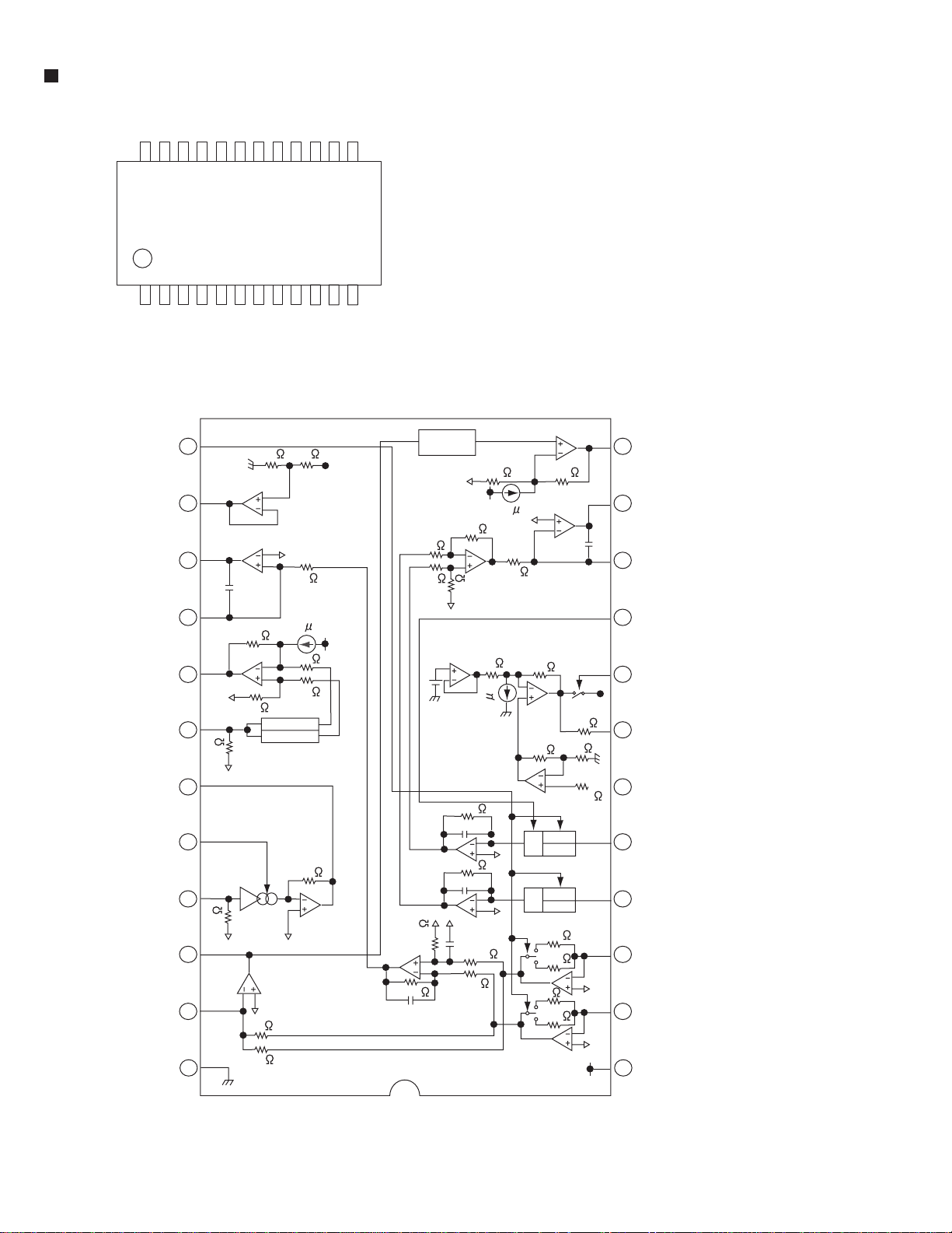
LC75823W (IC601) : LCD driver
1. Pin layout & Symbol
KD-S783M
S1
S2
S3
S4
S5
S6
S7
S8
S9
S10
S11
S12
S13
S14
S15
S16
DICLCE
64 63 62 61 60 59 58 57 56 55 54 53 52 51 50 49
1
2
3
4
5
6
7
8
9
10
11
12
13
14
15
16
17 18 19 20 21 22 23 24 25 26 27 28 29 30 31 32
S17
S18
S19
OSC
S20
Vss
S21
VDD2
VDD1
S22
S23
INH
S24
VDD
S25
COM3
COM2
S26
S27
COM1
S52
S28
S29
S51
S30
S50
S31
S49
48
47
46
45
44
43
42
41
40
39
38
37
36
35
34
33
S32
S48
S47
S46
S45
S44
S43
S42
S41
S40
S39
S38
S37
S36
S35
S34
S33
2. Pin function
Pin No.
1 to 52
53 to 55
COM1 to COM3
56
57
58
59
60
61
62
63
Symbol
S1 to S52
VDD
INH
VDD1
VDD2
Vss
OSC
CE
CL
I/O
O
Segment output pins used to display data transferred
Function
by serial data input.
O
Common driver output pins. The frame frequency is given
by : t0=(fosc/384)Hz.
--
Power supply connection. Provide a voltage of between
4.5 and 6.0V.
I
Display turning off input pin.
INT="L" (Vss) ----- off (S1 to S52, COM1 to COM3="L"
INT="H" (VDD)----- on
Serial data can be transferred in display off mode.
I
Used for applying the LCD drive 2/3 bias voltage
externally.
Must be connected to VDD2 when a 1/2 bias drive scheme
is used.
I
Used for applying the LCD drive 1/3 bias voltage
externally.
Must be connected to VDD1 when a 1/2 bias drive scheme
is used.
--
Power supply connection. Connect to GND.
I/O
Oscillator connection.
An oscillator circuit is formed by connecting an external
resistor and capacitor at this pin.
Serial data CE : Chip enable
interface connection
I
to the controller. CL : Sync clock
64
DI
DI : Transfer data
1-31
Page 32

KD-S783M
TEA6320T-X (IC161) : E. volume
1. Pin layout
2. Block diagram
10 8 9 7 6
5
12
SDA
1
GND
2
OUTLR
OUTLF
MUTE
TL
B2L
B1L
IVL
ILL
QSL
IDL
ICL
IMD
IBL
IAL
3
4
5
6
7
8
9
10
11
12
13
14
15
16
3. Pin functions
Pin
Symbol
No.
SDA
1
SCL
32
VCC
31
OUTRR
30
OUTRF
29
TR
28
B2R
27
B1R
26
IVR
25
ILR
24
QSR
23
IDR
22
Vref
21
ICR
CD-CH
TAPE
TUNER
20
19
18
17
CAP
IBR
IAR
I/O
Serial data input/output.
I/O
MUTE
21
31
2
19
16
15
13
11
14
22
20
18
17
Functions Functions
POWER
SUPPLY
SOURCE
SELECTOR
23 25 24 26 27 28
VOLUM E 1
+20 to -31 dB
LOUDNESS
LEFT
VOLUM E 1
+20 to -31 dB
LOUDNESS
RIGHT
Pin
No.
17
Symbol
IAR
BASS
LEFT
+15 dB
LOGIC
BASS
RIGHT
+15 dB
I/O
I
Input A right source.
TREBLE
LEFT
+12 dB
TREBLE
RIGHT
+12 dB
FUNCTION
ZERO CROSS
DETECTOR
VOLUM E 2
0 to 55 dB
BALANCE
FENDER REAR
VOLUM E 2
0 to 55 dB
BALANCE
FENDER FRONT
HC BUS
REC
VOLUM E 2
0 to -55dB
BALANCE
FENDER FRONT
VOLUM E 2
0 to -55dB
BALANCE
FENDER REAR
3
4
32
1
29
30
2
3
4
5
6
7
8
9
10
11
12
13
14
15
16
GND
OUTLR
OUTLF
TL
B2L
B1L
IVL
ILL
QSL
IDL
MUTE
ICL
IMO
IBL
IAL
Ground.
-
output left rear.
O
output left front.
O
Treble control capacitor left channel or
I
input from an external equalizer.
Bass control capacitor left channel or
output to an external equalizer.
Bass control capacitor left channel.
-
Input volume 1. left control part.
I
Input loudness. left control part.
I
Output source selector. left channel.
O
Not used
-
Not used
-
Input C left source.
I
Not used
-
Input B left source.
I
Input A left source.
I
18
19
20
21
22
23
24
25
26
27
28
29
30
31
32
IBR
CAP
ICR
Vref
IDR
QSR
ILR
IVR
B1R
B2R
TR
OUTRF
OUTRR
Vcc
SCL
I
Input B right source.
-
Electronic filtering for supply.
I
Input C right source.
-
Reference voltage (0.5Vcc)
-
Not used
O
Output source selector right channel.
I
Input loudness right channel.
I
Input volume 1. right control part.
-
Bass control capacitor right channel
Bass control capacitor right channel or
O
output to an external equalizer.
Treble control capacitor right channel or
I
input from an external equalizer.
O
Output right front.
O
Output right rear.
-
Supply voltage.
I
Serial clock input.
1-32
Page 33

NJM4565M-WE (IC581) : Ope. amp
A OUTPUT
1
KD-S783M
+
8
V
-
A INPUT
+
A INPUT
V
2
3
-
4
B OUTPUT
7
B INPUT
6
5
+
B INPUT
NJU7241F25-X (IC461) : Regulator
1.Pin layout 2.Block diagram
GND 1
VIN 2
VOUT 3
5 STB
4 NC
VIN 2
STB 5
-
Short protect
3 VOUT
GND 1
NJU7241F33-X (IC471) : Voltage regulator
PIN FUNCTION
1
2
3
5
4
1. GND
2. V
IN
3. V
OUT
4. +NC
5. STB
Vref
1 GND
1-33
Page 34

KD-S783M
(
)
KD-S783M
VICTOR COMPANY OF JAPAN, LIMITED
MOBILE ELECTRONICS DIVISION
PERSONAL & MOBILE NETWORK BUSINESS UNIT. 10-1,1Chome,Ohwatari-machi,Maebashi-city,371-8543,Japan
No.49764
1-34
Printed in Japan
200211
Page 35

KD-S783M
SCHEMATIC DIAGRAMS
CD RECEIVER
KD-S783M
CD-ROM No.SML200211
Contents
Block diagram
Standard schematic diagrams
Printed circuit boards
COPYRIGHT 2002 VICTOR COMPANY OF JAPAN, LTD.
Area Suffix
UF China
2-1
2-2
2-5~6
No.49764SCH
Nov. 2002
Page 36

Safety precaution
!
!
Burrs formed during molding may be left over on some parts of the chassis. Therefore,
pay attention to such burrs in the case of preforming repair of this system.
Please use enough caution not to see the beam directly or touch it in case of an
adjustment or operation check.
Page 37

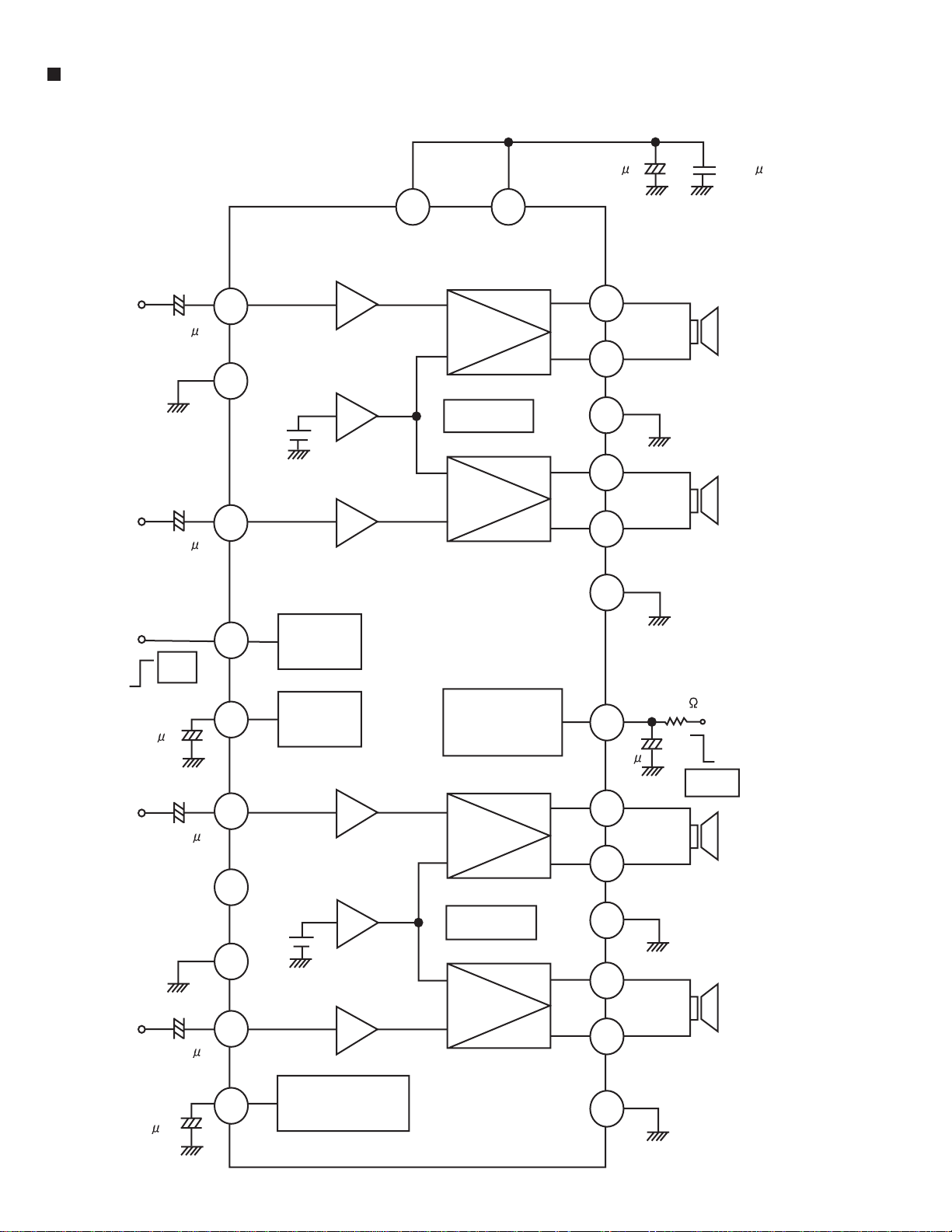
Block diagram
5
REST SW
4
FOCUS COIL
TRACKING COIL
3
2
SW1~SW4
MMM
LOADING MOTOR
FEED MOTOR
SPINDLE MOTOR
KD-S783M
GEB10017A
LOADING+
LOADING-
SPINDLE+
SPINDLE-
REST SW
SW1~SW4
FEED+
FEED-
FEED+
FEED-
LOADING+
LOADING-
SPINDLE+
SPINDLE-
CD DRIVER
IC501
LM0
LM1
DMO
FMO
TRO
FOO
CD LSI
CN601
FOCUS+
FOCUS-
VA
VB
VC
VD
VE
VF
MD
LD
TRACKING+
TRACKING-
FOCUS+
FOCUS-
VREF
VC
VA
VB
VD
VE
VF
MD
LD
TRACKING+
TRACKING-
RF AMP
IC521
PLL
IC31
PLLCE
PLLDA
PLLCL
PLLDI
RFDC
RFGC
RF
RFRP
SEL
TEB
FE
TE
IC541
BUS0
BUS1
BUS2
BUS3
BUCK
CCE
RST
DETACH
REMOCON
ENC1
ENC2
LCDCL
LCDDA
LCDCE
KEY0
KEY1
KEY2
GND
CN701
BCK
LRCK
AOUT
XO
XI
REST SW
SW1~SW4
CDRW
SRAM
IC451
A0~A16
D0~D7
CS
WE
OE
MP3 LSI
IC401
MP3REQ
MP3RESET
MP3STBY
MP3DOUT
MP3DIN
MP3CLK
L-CH
R-CH
CD L.P.F.
IC581
CPU
IC701
CDL
CDR
VOLDA
VOLCL
ANT. CTRL
E.VOLUME
IC161
REGULATOR
IC901
10V
ACC5V
OUTFL
OUTFR
OUTRL
OUTRR
TUL
TUR
SM
SD/ST
LOCAL
SEEK/STOP
POWER AMP.
IC301
FM/AM TUNER
TU1
STBY
FLRLRRFRFL+
FLRR+
FR+
REAR L
REAR R
ACC
ANT
REMOTE
CN901
J321
LINE OUTPUT
KEY0
KEY1
KEY2
10V
CJ601
DETACH
ACC5V
REMOCON
ENC1
ENC2
LCDCL
LCDDA
LCDCE
GEB10018A
LCD DISPLAY
S601~S619 D601~D624
1
KEY MATRIX
LIGHTING DISPLAY
REMOCON
IC602
AB CD E F G
ENCODER
JS690
LCD DRIVER
IC601
LCD1
2-1
Page 38

Standard schematic diagrams
Main amp. section
TU1
QAU0258-002
J1 L1
B1
4.7u
5
C36
7p
C35
10p
2.2k
R37
PLLCE
2.2k
R36
PLLDA
2.2k
R35
PLLCL
2.2k
R34
PLLDI
4
R33
9V
CD.R
A-GND
CD.L
REST
SW1
SW2
SW3
SW4
LM0
LM1
BUS0
3
2
BUS1
BUS2
BUS3
BUCK
CCE
RST
CD8V
MP3REQ
MP3RESET
MP3STBY
MP3DOUT
MP3DIN
MP3CLK
CDON
CDRW
SW5V
VDD5V
DETACH
10V
ACC5V
REMOCON
ENC1
ENC2
LCDCL
LCDDA
LCDCE
KEY0
KEY1
KEY2
CN701
VMC0334-001
D701
1
0
QNB0100-002
1SS133
1SS133
D1 D2
R39
R38
D708
100
C38
0.001
C37
10p
C48
D709
0.047
UN2211
C40
D712
39k
10/16
0.047
0.01
R40
0.047
C43
C42
C41
C46
0.01
0.01
C47
10( 1/8W)
R43
R44
470
220
C32
C50
100p
47p
Q31
0.1
0.1
C716
C718
10k
D702
C34
0.047
1SS355-X
D981
D982
1SS355-X
D703
D704
R32
6.2k
TB2118F
X31
QAX0616-001Z
IC31
C33
47/6.3
R981
47k
D705
D706
Q981
D707
CD SIGNAL
TUNER SIGNAL
LINE OUT SIGNAL
MAIN SIGNAL
Parts are safety assurance parts.
When replacing those parts make
sure to use the specified one.
0
10k
R41
C44
R42
C717
LOCAL
0.01
0.1
0.0027
100/10
C31
0.01
C6
C45
C1
C39
1000P
AM.VCC
22/16
FM/AM
C49
0.001
C2
SD/ST
4.7k
R31
0.047
R7
10( 1/8W)
0.01
C3
2SB815/7
Q6
Q7
UN2211
KD-S783M
C5
1/50
1/50 1.2k
C81
C91
Q2
2SD601A( R)
2SD601A( R)
R3
4.7k
R2
47k
R720
R719
0
0
0
0
0
0
R707
R706
R705
R704
Q3
UN2111
1.2k
0
47k
47k
47k
47k
3.3k
47k
47k
47k
47k
C84
0.018
VDD
VPP
Q5
2SB709A( R)
C51
330P
SM
R1
22k
R51
BUCK
CCE
RST
BUS0
BUS1
BUS2
BUS3
CDRW
SW5V
CDON
C706
0.047
VOLDA
VOLCL
Q1
12( 1/8W)
MONO
R760
R759
R716
R715
R714
R713
R712
R711
R710
R709
R708
R9
47
220/10
C4
R5
47k
D4
D5
1SS355-X
1SS355-X
R6
47k
R4
3.3k
C10
R10
10/16
10k
SEEK/STOP
R81
1/50
1.2k
R91
R758
C92
0.0056
R92
4.7k
47k
1k
10k
R721
R722
SW2
SW3
SW4
REST
X1
C82R82
4.7k
0.0056
PLLDI
PLLCL
PLLDA
PLLCE
FM/AM
VSS
UPD784215AGC184
R703
R702
R755
820
R754
0
0
10M
LM0
LM1
X701
C704
8P
0.047
C705
C703
QAX0617-001Z QAX0401-001
IC701
27p
SEEK/STP
10k
10k
R723
R725
R701
X702
27p
C702
TU.L
CD.L
CD.R
TU.R
MP3REQ
47k
C701
MP3STBY
MP3DOUT
MP3RESET
SW1
47k
R753
22p
MP3DIN
C172
C171
C161
C162
MP3CLK
MONO
10k
R726
47k
R752
1/50
1/50
1/50
1/50
SD/ST
LOCAL
10k
10k
R727
R728
R751
10k
REMOCON
0.047
C708
R750
ENC1
RESET
R729
47k
R734
R735
R736
R741
R742
R743
R744
R745
R746
10k
1SS355-X
R756
47k
C709
D710
C94
0.018
1k
R763
C192C191
100/1047/16
2.2k
2.2k
2.2k
TD
RD
10k
47k
10k
10k
10k
10k
R765
IC702
IC-PST600MG
C710
47/6.3
0.01
KD-S783M
2.2k
R173
R172
22k
C174
C175
0.0082
0.15
C176
0.22
C166
0.22
C164
C165
0.15
0.0082
R162
22k
R163
2.2k
LCDCE
LCDCL
LCDDA
C707
0.047
SM
LEVEL
KEY2
KEY1
KEY0
ENC2
4.7k
R747
4.7k
R748
4.7k
R749
0
47k
R767
47k
R766
R757
2.2k
R161
220k
220k
R171
0.033
C167
0.033
C177
L701
47u
CPU.VDD
C711
220/10
C713
0.1
C712
0.01
D243
1SS133
C244
0.22/50
D240
1SS355-X
1SS355-X
D241
C178
0.0056
C168
0.0056
C194
0.082
R247
56k
C781
47/6.3
D242
C243
0.047
1SS133
1k
R246
R245
100
C193
100/10
Q781
UN2111
D781
1SS133
R244
12k
R242
22k
C242
22/16
Q241
2SD601A( R)
C179
C180
R181
R182
C170
C169
C782
0.082
R243
180k
C241
1/50
R241
47k
4.7/25
4.7/25
270
IC161
TEA6320T-X
270
4.7/25
4.7/25
47k
R165
C909
220/10
47k
R164
R784
47k
D782
1SS133
C908
220/10
47k
R174
C907
47k
R175
220/10
R783
1k
Q782
UN2211
Q976
UN2211
C906
C913
10/16
LEVEL
VOLDA
VOLCL
D902
1SS355-X
C905
0.01
C910
47/16
47/16
C919
2SA1037
IC901
OUTLF
OUTLR
Q977
10/16
OUTRR
OUTRF
C904
C911
0.1
10/16
D784
UDZS11B-X
AN80T07
C915
0.1
100/16
C851
10/16
Q784
UN2111
C784
100/16
R976
27k
C914
D851
RB160M-30-X
RB160M-30-X
D852
C912
R977
12k
0.01
R851
C903
10k
47/16
C852
0.01
R903 R902
IC301
LA4743K
27k
2.2/50
C312
R312
R311
C311
27k
2.2/50
390p
390p
C313
C314
C315
4.7/25
390p
390p
C301
R301
2.2/50
27k
R302
27k
R342
R352
820
D351
1SS355-X
R351
2.2k
R341
2.2k
D341
1SS355-X
C902
2.2/50
4.7k 9.1k
820
2.2/50
R901
1k( 1/4W)
C302
C303
C304
Q341
2SD1781K/QR/-X
0.047
C321
J321
QNN170-001
C316
4.7/25
Q351
2SD1781K/QR/-X
100
R343
100
R353
D971
RB160M-30-X
C320
0.022
1N5401TU
L901
QQR0703-001
CN901
CNZ0003-001
QMFZ047-150-T
D901
0.1
C971
C901
2200/16
RB160M-30-X2SD601A( R)
D972
C317
47/16
0.1
C322
0.1
C323
0.1
C324
0.1
C325
100p
100p
100p
100p
100p
100p
100p
100p
R972
R971
2.2k( 1/8W)
C961
C962
C963
C964
C965
C966
C967
C968
2.2k( 1/8W)
C319
C318
0.022
22/16
RL-
FR+
RR-
RR+
RL+
FR-
FL+
FL-
RR+
RL+
FL+
FR-
RR-
RL-
FL-
ACC
GRD
ANT
REMOTE
FR+
AB CD E F G
2-2
Page 39

KD-S783M
Mecha control section
LM0
LM1
R507
20k
R506
82k
82k
82k
82k
150k
150k
RA454
C533
8.2k
IC501
LA6574H
LOADING+
LOADING-
SPINDLE-
SPINDLE+
FEED-
FEED+
FOCUS+
RF
LD
0.1
TA2147F
C420
22p
RFGC
IC521
MD
L403
47u
C410
100/10
C411
0.01
C412
0.33
C414
100/10
C413
0.01
C416
QAX0413-001Z
RF
C531
Q521
2SB1241
C422
R402
X401
R411
2.2M
R409
330
0.1
C526
R528
IC461
0.027
0.01
47
C421
R533
1k
68p
C524
100/10
A10
A8
A9
RA456
RA455
R534 R532
2k 10k
A11
D7
D6
D5
D4
D7
D5
D4
A12
C453
A14
A13
OE
C528
A16
A15
A14
A13
R451
10K
0.1
A12
A11
A10
R531
100
C532
5p
C525
0.01
OE
A9
A8
CN601
QGB2027M1-26S
5
4
3
2
1
LD
SW4
VD
SW3
VB
SW1
VC
SW2
VA
MD
LOADINGVREF
LOADING+
VE
VCC
VF
FOCUS+
TRACKINGTRACKING+
FOCUSFEED+
REST
SPINDLE+
FEEDSPINDLE-
RA453
C454
0.001
C451
100/10
A0
A1
A2
A3
CS
C452
0.1
WE
A4
A5
A6
A7
A2
A3
CS
VREF
C521
0.01
VD
R521
VC
R522
VA
R523
VB
R524
VE
R525
VF
R526
C522
0.01
C523
0.01
RA457
A4A5A6A7A0A1A15
IC451
K6R10008VCDTI10-X
D0
D1
D2
D3
D0
RA451
D1
D2
D3
WE
RA452
R537
27k
A16
FOCUS-
TRACKING-
FE
RFRP
R530
SEL
100/10
R527
NJU7241F25
R410
330
22p
TRACKING+
C530
100/10
47k
R529
TEB
22
22
D2
D3
D4
D5
D6
D7
R502
6.8k
5.6k
R503
R501
6.8k
Q501
2SB1322
R504
10k
C502
0.01
C529
0.01
FE
82k
VREF
R536
47k
C527
0.0068
R535
820
TE
RFDC
C461 C464
0.1 0 .1
C463C462
100/6.3100/6.3
D0
D1
R404
10k
DMO
FMO
FOO
C503
47/6.3
D501
1A3G-T1
TRO
C501
220/10
CDRW
TE
SW5V
3.3V
L402
47u
A13
A14
A16
WE
A15
IC401
TC94A02F
A0A1A2A3A4
C423
220p
Q541
UN2111
C409
100/10
3.3V
C595
C546
0.033
47P
C594
56p
C584
56p
C571
0.01
MP3DIN
IC471
NJU7241F33
R586
1.5k
IC581
NJM4565M
R596
1.5k
C596
0.01
3.3V
SEL
TEB
RFGC
RFDC
RFRP
C472
0.01
CD.R
CD.L
9V
9V
CD.R
A-GND
CD.L
REST
SW1
SW2
SW3
TE
FE
RF
C473
220/6.3
C474
220/6.3
C471
0.1
SW4
LM0
LM1
FEED+
FEED-
BUS0
BUS1
BUS2
BUS3
BUCK
CCE
RST
CD8V
GND
MP3REQ
MP3RESET
MP3STBY
MP3DIN
MP3DOUT
MP3CLK
CDON
CDRW
SW5V
R584
R581
20k
R591
20k
0.01
C562
TC9490FA
R423R427
R425
R421
IC541
C581
560p
C591
560p
DMO
100
R558
C582
4.7/25
R592R593
R583 R582
C560
0.01
R556
UN2211
22k22k
22k 22k
C583
C593
47/6.3
47/6.3
FOO
TRO
C559
0.047
C558
0.047
C557
470p
C556
470p
R554
0
R553
0
R552
0
100
R555
100
C552
C547
0.015
R548
1.5M
R546
5.6k
C544
100/10
MP3CLK
MP3STBY
MP3DOUT
R440
1k
C430
0.01
C592
4.7/25
FMO
C561
100/10
100
R557
C545
0.01
R422
22k
47k
R424
220
470
R426
220
470
R420
220
470
C440
0.01
CD SIGNAL
R587
R-CH
0
R597
L-CH
0
C565
C567
0.01
100p
C566
100/10
R571
R573
R575
220
R574
R559
220
R572
1M
220
R570
L544
47u
470
470
470
L541
47u
L542
47u
C568
0.1
C569
100/10
C570
0.01
BUCK
BUS0
CCE
BUS1
RST
BUS2
BUS3
4.7k
4.7k
4.7k
4.7k
L543
R541
R542
R543
R544
47u
Q542
UN2211
C408
0.01
A9
A8A7A6
A10
A5
A11
A12
OE
CS
CDON
R408
R412
0
R545
10k
C543
C542
C541
100/10
47k
C406
0.01
C419
0.1
C405
100/10
L401
47u
100/10
C407
C424
0.022
C403
0.01
0.01
C404
1/50
0.1
R585
R595
R594
0.033
R551
10k
C550
C549
C548
R550
10k
R549
470k
MP3REQ
MP3RESET
18k
0.047
C555
0.01
0.0027
0.01
UN2211
56k
18k
56k
100/10
0.047
0.047
C553
C554
C551
R547
47k
R430
1k
Q430Q440
AB CD E F G
2-3
Page 40

KD-S783M
KD-S783M
LCD & Key switch section
5
QSW0793-001
RPM6938-SV4
IC602
10k
D646
R661
S45
C612
S43
S44
LC75823W
IC601
4.7/6.3
S42
470
R662
S35
S36
S37
S38
S39
S40
S41
S10S2S11S1S12
S13
S14
C611
4
LCD1
QLD0225-001
R605
3.9k
S606
R611
S605
R610 R609 R608
R601
R602R603R604
1.8k
1.2k1.8k2.7k
S603S604
S602
3
S613
S619
S610
S611S612
R614 R613R615R616
1.2k 8201.8k2.7k
R606R607
8208203.9k 2.7k 1.8k 1.2k
S608S609
R612
820
S1S2S3S4S5S6S7S8S9
Key0
S601
Key1
S607
Key2
S614S615S616S617S618
S14
S10
S11
S12
S13
S15
S16
S18
S19
S20
S21
S22
S23
S24
S25
S26
S27
S28
S29
S30
S31
S32
S33
S34
S35
S36
S37
S38
S39
S40
S41
S42
S44
S45
S46
S47
R633
S50
S48
S49
COM2
COM3
COM1
BUS2
BUS1
2.2k
LCD_CO
LCD_CLK
LCD_SO
10/6.3
C603
R653
R654
R655
R656
D642
D643
R658
R651
2.2k
R652
10k
10k
10k
10k
1SS335-X
1SS335-X
180k
D622
D623
390( 1/8W)
D624
R632
D625
R631
820
1.2k
1.2k
R659
D644
390( 1/8W)
R660
D645
UDZS5.1B-X
D641
0.022
C601
680p
C602
820
R647
D602
D601
820
R646
R645
S17
D606
D608
D607
D609
D610
D611
510
510
470
510
R641
R642
R639
R640
D603
D604
D605
820
820
470
R644
R643
D613
D614
D615
510
R638
R648
D618
820
510
680
R637
R649
D616
D617
S43
D619
D620
D621
510
910
910
R634
R635
R636
UDZS6.2B-X
51k
R657
S50
COM1
COM2
COM3
0.012
S46
S47
S48
S3S4S5S6S7S8S9
JS690
100
R681
VCM0335-001
CJ601
10V
ACC5V
REMOCON
ENC1
ENC2
LCDCL
LCDDA
LCDCE
KEY0
KEY1
KEY2
BUS3
GND
BUS4
S34
S32S49
S31
S30
S29
S28
S27
S26
S25
S24
S23
S22
S21
S20
S19
S18
S17
S15
S16 S33
2
1
AB CD E F G
2-4
Page 41

Printed circuit boards
Main board
KD-S783M
(Forward side)
R707
R706
R705
R704
C712
C710
C919
C180
C801
C914
C193
X701
IC702
C908
R164
IC801
C907
R981
R806
R165
C179
R709
R904
C170
C711
R708
R809
Q981
IC701
X702
R808
C169
R807
R804
L701
R738
C905
R737
C903
IC161
C173
C192
R743
R744
R745
C802
C244
R714
R760
R759
R747
R748
R749
C191
J801
C163
R763 R765
R721
R720
D243
D242
Q321
R321
C172 C171
R727
R758
R722
R734
R161
R171
R736
X31
C241
C162 C161
D240
D241
R728
R735
C40
D321
C242
R767
R331
C31
R746
IC31
R750
D331
C33
D351
R766
C4
R351
C41
C32
R751
D341
C50
J321
Q341
R341
J1
L1
D2
D1
C42
R44
C43
C49
C48
R43
CN701
Q31
C81 C91
C1
C10
TU1
C5
D852
D782
C502
Q501
R901
D851
C561
L901
D901
C781
IC501
C569
R852
D781
R882
C545
C913
C902
C556 C557 C558
R555 R556 R557 R558
R420
R421
R427
R426
C911
R980
C851
C881
IC901
C546
R548
C543
L542
L541
R547
R424
R425
R423
R422
Q541
D501
C503
R546
L544
C544
C541
D902
R702
R703
L543
C910
C909
R175
R174
C904
5
4
3
IC301
RA457
IC451
C462
C463
C313
C304
C524
C451
C318
C317
C314
C303
C526
RA451
C901
CN901
C461
C464
R451
C453
C452
RA452 RA453
IC461
L402
IC521
RA455 RA456
C302
C473
C409
Q521
D991
C530
RA454
C301
D992
CN601
R408
C410
R412
C404
D993
C311
R586
R585
C474
IC401
L403
C961
D994
R584
C408
C962
R521
C963
D996
R524
C582 C583
C584
C553
C555
L401
C411
C964
D995
R522
R553
C422
D998
R523
C554
C405
C312
C966
IC581
R552
R554
C418
C587
R587
C965
C316
D997
C315
D981
R525
C597
C416
C414
C968
C596
C593
R597
R573
C967
R526
C551
R551
R575
R404
C402
Q891
D892
Q881
R571
D891
C595
R595
IC541
R979
R403
C415
C784
R596
C592
C552
R978
C501
C594
R594
X401
R881
R892
C559
R891
C547
R550
C401
R851
R549
C566
2
Front board
1
S601
D608
JS690
(Forward side)
D625
D618
S615
D645
D644
D619
S617
D621
S607
D603
D604
D605
D606
D601
S608
D602
D607
LCD1
S609
IC602
R644 R645
S602
D609
R601
S603
D610
R602
S604
D611
R603
S605
D613
R604
S606
D614
R605
S614
D615
S610
D616
R608
S611
D617
AB C
R609
R655
S618
D620
R638
S616
R639
R633
D624
R616
S612
R632
R610
D623
D622
R634
S619
S613
R635
2-5
Page 42

KD-S
M
783
Main board
5
4
3
C51
R51
C6
C1
C94
C84
(Reverse side)
C916
C917
C521
R582
C405
R302
R581
C323 C324
R304
C406
C413
R583
C581
C474
C407
R303
C582
R570
R301
RF
C410
C311
R531
R532
R574
C322
R572
C891
C404
R402
C532
C528
C531
C529
C473
C412
C301
CN601
Q521
R409
C971
C530
C409
R410
C525
C302
C852
C523
R537
R534
R533
C533
R530
IC471
C423
CN901
C471
C317
VREF
C318
C526
C472
TE
C454
C901
C524
C462
R528
R527
R536
R529
R535
C527
C463
IC301
C319
C320
C451
C321
R343
R352
R353
J321
Q351
J1
L1
TU1
B1
C8
C7
C2
C3
R10
C10
C39
Q8
R8
D4 D5
R4
R1
R5
C43
Q5
R39
C38
R38
C45
C47
C46
R9
B2
C34
R32
R42
C33
C81
Q1
R2
R81
R6
R82
C82
Q6
R7
C5
Q2
Q7
R3
C718
CN701
R342
D1 D2
C44
C91
Q3
D712
R41
C37
C36
C35
C717
R242
R246
R31
C716
R40
R332
R91
R92
C92
R723
R726
R333
C4
C31
C11
R241
R35
R36
R440
C242
C40
D709
Q331
R33
R34
D708
C341
R243
C162
X31
D704
R322
R323
J801
C163
R244
C241
C244
Q241
C243
R245
C191
C161
C175
C177
R172
R173
C178
C174
C176
C172 C171
R719
R37
R729
R725
R741
Q430 Q440
C430
C440
D706
R430
D702
D705
D707
D701
D703
R182
RD
C192
R181
C706
C703
C704
C701
C702
R753
TD
R247
C166
C164
C707
C173
D243
D242
R162
VPP
C165
C705
C708
R752
C167
B904
R163
C169
R712
R711
R710
C711
R739
C168
C905
C903
C713
R742
R805
C906
C194
C179
R802
R701
C908
C709
R756
R803
VDD
VSS
R754
X702
R740
C170
C912
C907
C180
R755
R757
R810
B903
X701
C914
C909
C193
RESET
B902
C919
D710
R801
C915
X1
C710
C910
R716
R715
R713
C904
Q542
C851
D501
C881
C920
C913
C902
R545
R541
R542
R543
R544
C781
C544
C541
IC901
Q977
B901
R977
C503
C543
D781
C561
R902
R501
D971
R971
R972
D972
Q781
R503
C571
C401
R976
Q784
C782
Q501
C542
C569
D782
C548
B906
L901
R901
C568
C570
C784
D784
C592
C562
R504
C560
D901
R782
R502
R903
Q976
R506
C549
C550
C566
R784
Q782
R559
C567
R783
C595
R592
R593
C591
R591
R411
X401
C325
R315
C501
C424
C415
C565
R312
C918
R507
D982
C522
C593
R313
C583
C418
C420 C421
C419
C316
C315
R314
C312
R311
C403
R401
C414
2-6
2
Front board
R658
C603
R614
R653
R612
R611
1
C602
R613
R648
(Reverse side)
R615
D643
R660
R649
R659
D642
R637
R636
R657
D641
D644
D645
R654
R656
CJ601
IC601
C601
R651
R652
R607
R640
R641
R661
D646
R647
IC602
R646
C611
C612
R606
R662
C681
AB C
R631
R681
C682
R642
R643
Page 43

< MEMO >
Page 44

KD-S783M
VICTOR COMPANY OF JAPAN, LIMITED
MOBILE ERECTRONICS DIVISION
PERSONAL & MOBILE NETWORK BUSINESS UNIT. 10-1,1Chome,Ohwatari-machi,Maebashi-city,371-8543,Japan
No.49764SCH
Printed in Japan
200211
Page 45

PARTS LIST
[ KD-S783M ]
* All printed circuit boards and its assemblies are not available as service parts.
KD-S783M
Area suffix
UF ---------------------------- China
- Contents -
Exploded view of general assembly and parts list (Block No.M1)
CD mechanism assembly and parts list (Block No.MB)
Electrical parts list (Block No.01~02)
Packing materials and accessories parts list (Block No.M3,M5)
3- 2
3- 5
3- 8
3-14
3-1
Page 46

KD-S783M
Exploded view of general assembly and parts list
Block No.
M
M
1
M
8
49
50
45
51
8
51
8
46
3
7
10
47
43
48
Main board
5
44
9
13
16
9
12
11
35
15
34
4
42
40
37
39
55
41
36
14
35
7
56
30
Front
2
1
6
6
27
53
52
6
board
54
19
28
26
25
23
20
33
24
17
29
22
21
38
32
31
18
3-2
Page 47

KD-S783M
Parts list (General assembly)
Item
A
1 ---------------
2 FSJC1029-401
3 FSMH3001-202
4 FSKM3011-002SSF BOTTOM COVER 1
5 FSMA3004-203
6 QYSDST2604Z
7 FSKZ4005-001 SCREW 2 CHASSIS+SIDE PANEL
8 QYSDST2604Z
9 QYSDST2606Z
10 FSKZ4005-001
11 FSJC2013-013
12 FSKS3010-001
13 FSKW4005-003
14 FSXP3026-002 RLS KNOB 1
15 FSKW3002-015
16 FSPK3009-002
17 GE10003-002A
18 GE30111-032A
19 GE20104-002A
20 GE30105-002B
21 GE30109-002A EJECT BUTTON 1
22 GE20110-007C
23 GE30112-001A
24 GE40102-001A
25 GE30366-001A
26 FSYH4036-032
27 GE30546-002A
28 GE30104-001A RIM LENS 1
29 GE20109-001C
30 GE30106-001A
31 FSXP3055-001 DETACH BUTTON 1
32 FSKW3002-012
33 GE30117-001A
34 GE10004-003B
35 VKZ4777-001
36 QLD0225-001
37 QNZ0442-001
38 GE30276-001A LCD CASE 1
39 FSJK3025-001
40 FSKS3019-001
41 FSYH4074-001
42 GE30848-001A
43 QMFZ047-150-T
44 VMA4652-001SS
45 FSKM3010-020SSF REAR BRACKET 1
46 FSKL4024-001
47 GE40107-002A
48 GE40103-002A
Parts number Parts name Area
CD MECHA (1325)
TOP CHASSIS
SIDE PANEL
INSULATOR
SCREW
SCREW
SCREW
SCREW
FRONT CHASSIS
LOCK LEVER
TORSION SPRING
COMP.SPRING
BLIND
FRONT PANEL
FINDER ASSY
PRESET BUTTON
POWER BUTTON
D FUNC.BUTTON
PUSH BUTTON(2)
REMOTE LENS
SEL BUTTON
SHEET
KNOB
UP DOWN BUTTON
SND FUNC BUTTON
COMP.SPRING
LIGHT LENS
REAR COVER
MINI SCREW
LCD MODULE
LCD CONNECTOR
LCD LENS
LENS CASE
LIGHTING SHEET
NAME PLATE
FUSE
EARTH PLATE
IC BRACKET
HEAT SINK
REG BRACKET
Q'ty
1
1
1
1
3
CHASSIS+MECHA
3
CHASSIS+REAR BKT
2
CHASSIS+MAIN PWB
1
SIDE PANEL+IC BKT
1
1
1
LOCK LEVER
RLS KNOB
1
1
1
1
1
1
1
1
1
1
1
SEL BUTTON
1
1
1
1
DETACH BUTTON
1
1
4
FRONT PANEL+REAR COVER
1
1
1
1
1
1
1
1
1
1
1
Description
Block No. M1MM
3-3
Page 48

KD-S783M
Parts list (General assembly)
Item
A
49 QYSDST2606Z
50 QYSDSF3006Z
51 QYSDST2606Z
52 QYSDST2004Z SCREW 1
53 LV40847-002A
54 FSYH4036-069
55 FSYH4071-001 LIGHTING SHEET 1
56 GE30854-001A
Parts number Parts name Area
SCREW
SCREW
SCREW
SPACER
SHEET
LED HOLDER
Q'ty
1
1
3
1
2
1
Block No. M1MM
Description
ANT
LINE OUT
16P & REG BKT
3-4
Page 49

CD mechanism assembly and parts list
KD-S783M
Grease
G-31SA
G-31SA(Bottom side)
RX-405
101
14
17
12
16
70
b
90
91
5
71
15
1
7
100
Block No.
TN-CCD1001Z-138S
M
M
B
M
102
23
49
102
23
101
101
101
20
10
9
11
105
65
66
62
13
2
4
100
7
6
8
64
b
a
62
68
d
110
67
c
61
72
113
88
93
3
80
86
102
113
19
18
103
135
48
43
41
50
42
134
49
104
40
51
107
49
79
c
82
81
92
117
133
22
22
84
116
36
107
d
131
56
d
107
130
32
38
39
a
63
57
132
62
101
108
89
107
33
106
29
106
108
3-5
Page 50

KD-S783M
Parts list (CD mechanism)
Item
A
1 30310101T
2 30310103T
3 30310107T
4 30310108T SEL STOP PLATE 1
5 30310142T
6 30310143T
7 30310145T S ARM SPRING(L) 2
8 30310112T
9 30310155T
10 30310115T
11 30310116T
12 30310134T
13 30310159T
14 30310150T FIX PL (L)Z 1
15 30310156T
16 30310138T
17 30310122T
18 30310148T
19 30310125T
20 30310149T
22 30310151T HUNG UP SP (FZ) 2
23 30310129T
29 30300510T
32 30310544T
33 30310547T
36 30310546T
38 30310533T
39 30310577T PU M NUT(Z-S) 1
40 30310512T
41 30310558T
42 30310514T CLP ARM SPRING 1
43 30310552T
48 30310557T
49 30310524T
50 30310525T
51 30310545T
56 64180405T
57 QAL0230-001 C.D PICK (SONY) 1
61 30311035T
62 19501403T
63 30311045T
64 30311044T
65 30311038T
66 30311039T
67 30311040T WIRE (FD-Z) 1
68 30311041T
70 64180402T
71 64180403T
Parts number Parts name Area
FRAME
DANPER PIN
UPPER PLATE
SEL ARM (L)L
SEL ARM (R)L
TRIG LEVER
TRIG PL(Z)
TRIG PL SPRING
TRIG ARM
FIX ARM (L)B
FIX ARM (R)Z
FIX PL (R) Z
LDG GR (6)B
LDG GEAR (6)SP
S.L ARM(N)
S.L ARM SPRING
REAR DAM BKT(Z)
HUNG UP SP (R)
PU GEAR(B)
F.M.BASE(Z)
FD GR BLK(Z)
PU GUIDE(Z)
THRUST SPR(M)
NUT PUSH SPR PL
CLP ARM(Z)
CLAMPER(Z)
CLAMPER PLATE(Z
DAMPER (J)
CLP ARM SPR (L)
F SCREW GUIDE(Z
DET SW
FPC HOLDER(Z)
WIRE CLAMPER
PICK UP FPC(Z-S
CONNECT.PCB(Z-S
WIRE (5P-Z)
WIRE (LD-Z)
WIRE (RS-Z)
DET SWITCH
DET SWITCH
Q'ty
1
2
1
1
1
1
1
1
1
1
1
1
1
1
1
1
1
2
1
1
1
1
1
1
1
1
1
3
1
1
1
ESE11SF4
1
4
1
1
1
1
1
2
ESE22MH1
2
ESE22MH3
Block No. MBMM
Description
3-6
Page 51

KD-S783M
Parts list (CD mechanism)
Item
A
72 68150242T
79 30311105T
80 30311138T
81 30311109T LDG GEAR (2) 1
82 30311110T
84 30311112T
86 30311136T LDG ROLLER 2
88 30311118T
89 30311119T
90 30311123T
91 30311124T
92 30311129T
93 30311140T
100 9C0620503T C B TAP SCREW 2 M2X5
101 9C2020401T
102 9C4320403T
103 9C0117223T
104 9C0917703T
105 9C0320201T
106 9C4920013T
107 9C4920603T C TAP SCREW B3 4 M2X6
108 9P0220031T
110 9C0420253
113 9W0330276
116 9W0725030T
117 9W0640030T
130 303105310T
131 303105311T SPINDLE MO ASSY 1
132 303105312T
133 303111301T
134 303111302T RDG RLR SFT ASY 1
135 303105502T
Parts number Parts name Area
CONNECTOR
SOPPORT PLATE
GR MT BLK(N)
LDG GEAR (3)
LDG GEAR (5)
L.P SPRING (L)
L.P SPRING (R)
SW PCB
SW ACTUATOR
LDG BELT
FRONT BRKT (J)
C SCREW TS.G
C B TAP SCREW
SCREW
C TAP SCREW S3
C TAP SCREW S3
C TAP SCREW S3
TAMS SCREW
C TAP SCREW
NW BLUE
LUMILAR W
WASHER
FEED MO ASSY
FEED SCREW ASSY
LDG MOTOR ASSY
T.T.BASE ASSY
Q'ty
1
TKC-W26X-A1
1
1
1
1
1
1
1
1
1
1
5
M2X4
4
M2X4
2
M1.7X2.2
1
M1.7X7
1
M2X2
2
M2X10
2
M2X3
1
M2X2.5
2
2.9X5X0.3
1
2.3X9.8X0.25
1
1.4X3.2X0.4
1
1
1
1
Block No. MBMM
Description
3-7
Page 52

KD-S783M
r
r
Electrical parts list (Main board)
Item
A
C 1 QEKJ1CM-226Z E CAPACITOR 22MF 20% 16V
C 2 NCB31EK-473X C CAPACITOR
C 3 NCB31EK-103X C CAPACITOR
C 4 QERF1AM-227Z E CAPACITOR
C 5 QEKJ1HM-105Z E CAPACITOR
C 6 NCB31HK-103X C CAPACITOR
C 10 QERF1CM-106Z E CAPACITOR
C 11 NCB31EK-103X C CAPACITOR
C 31 QEKJ1AM-107Z E CAPACITOR 100MF 20% 10V
C 32 NDC31HJ-470X C CAPACITOR
C 33 QERF0JM-476Z E CAPACITOR 47MF 20% 6.3V
C 34 NCB31EK-473X C CAPACITOR
C 35 NDC31HJ-100X C CAPACITOR
C 36 NDC31HJ-7R0X C CAPACITOR
C 37 NDC31HJ-100X C CAPACITOR
C 38 NCB31HK-102X C CAPACITOR
C 39 NCB31HK-102X C CAPACITOR
C 40 QEKJ1CM-106Z E CAPACITOR 10MF 20% 16V
C 41 NCB31EK-473X C CAPACITOR
C 42 NCB31HK-103X C CAPACITOR
C 43 QFV61HJ-473Z MF CAPACITOR .047MF 5% 50V
C 44 NCB31HK-103X C CAPACITOR
C 45 NCB31HK-272X C CAPACITOR
C 46 NCB31HK-103X C CAPACITOR
C 47 NCB31HK-103X C CAPACITOR
C 48 NCB31EK-473X C CAPACITOR
C 49 NCB31HK-102X C CAPACITOR
C 50 NCS31HJ-101X C CAPACITOR
C 51 NCS31HJ-331X C CAPACITOR
C 81 QERF1HM-105Z E CAPACITOR 1.0MF 20% 50V
C 82 NCB31HK-562X C CAPACITOR
C 84 NCB31HK-183X C CAPACITOR
C 91 QERF1HM-105Z E CAPACITOR
C 92 NCB31HK-562X C CAPACITOR
C 94 NCB31HK-183X C CAPACITOR
C 161 QEKJ1HM-105Z E CAPACITOR
C 162 QEKJ1HM-105Z E CAPACITOR 1.0MF 20% 50V
C 164 NCB31HK-822X C CAPACITOR
C 165 NCB21CK-154X C CAPACITOR
C 166 NCB21CK-224X C CAPACITOR
C 167 NCB31EK-333X C CAPACITOR
C 168 NCB31HK-562X C CAPACITOR
C 169 QEKJ1EM-475Z E CAPACITOR
C 170 QEKJ1EM-475Z E CAPACITOR
C 171 QEKJ1HM-105Z E CAPACITOR
C 172 QEKJ1HM-105Z E CAPACITOR
C 174 NCB31HK-822X C CAPACITOR
C 175 NCB21CK-154X C CAPACITOR
C 176 NCB21CK-224X C CAPACITOR
C 177 NCB31EK-333X C CAPACITOR
C 178 NCB31HK-562X C CAPACITOR
C 179 QEKJ1EM-475Z E CAPACITOR
C 180 QEKJ1EM-475Z E CAPACITOR
C 191 QEKJ1CM-476Z E CAPACITOR
C 192 QEKJ1AM-107Z E CAPACITOR
C 193 QEKJ1AM-107Z E CAPACITOR 100MF 20% 10V
C 194 NCB31EK-823X C CAPACITOR
C 241 QEKJ1HM-105Z E CAPACITOR 1.0MF 20% 50V
C 242 QEKJ1CM-226Z E CAPACITOR 22MF 20% 16V
C 243 NCB31EK-473X C CAPACITOR
C 244 QEKJ1HM-224Z E CAPACITOR
C 301 QERF1HM-225Z E CAPACITOR
C 302 QERF1HM-225Z E CAPACITOR
C 303 NCS31HJ-391X C CAPACITOR
C 304 NCS31HJ-391X C CAPACITOR
C 311 QERF1HM-225Z E CAPACITOR 2.2MF 20% 50V
Parts numbe
Parts name Area
220MF 20% 10V
1.0MF 20% 50V
10MF 20% 16V
1.0MF 20% 50V
1.0MF 20% 50V
4.7MF 20% 25V
4.7MF 20% 25V
1.0MF 20% 50V
1.0MF 20% 50V
4.7MF 20% 25V
4.7MF 20% 25V
47MF 20% 16V
100MF 20% 10V
.22MF 20% 50V
2.2MF 20% 50V
2.2MF 20% 50V
Block No. 01
Remarks
Item
A
C 312 QERF1HM-225Z E CAPACITOR 2.2MF 20% 50V
C 313 NCS31HJ-391X C CAPACITOR
C 314 NCS31HJ-391X C CAPACITOR
C 315 QERF1EM-475Z E CAPACITOR
C 316 QERF1EM-475Z E CAPACITOR
C 317 QERF1CM-476Z E CAPACITOR
C 318 QEKJ1CM-226Z E CAPACITOR
C 319 NCB31EK-223X C CAPACITOR
C 320 NCB31EK-223X C CAPACITOR
C 321 NCB31EK-473X C CAPACITOR
C 322 NCB31EK-104X C CAPACITOR
C 323 NCB31EK-104X C CAPACITOR
C 324 NCB31EK-104X C CAPACITOR
C 325 NCB31EK-104X C CAPACITOR
C 403 NCB31HK-103X C CAPACITOR
C 404 QERF1AM-107Z E CAPACITOR
C 405 QERF1AM-107Z E CAPACITOR
C 406 NCB31HK-103X C CAPACITOR
C 407 NCB31EK-104X C CAPACITOR
C 408 NCB31HK-103X C CAPACITOR
C 409 QERF1AM-107Z E CAPACITOR 100MF 20% 10V
C 410 QERF1AM-107Z E CAPACITOR
C 411 NCB31HK-103X C CAPACITOR
C 412 NCB31AK-334X C CAPACITOR
C 413 NCB31HK-103X C CAPACITOR
C 414 QERF1AM-107Z E CAPACITOR
C 416 NCB31HK-103X C CAPACITOR
C 419 NCB31EK-104X C CAPACITOR
C 420 NDC31HJ-220X C CAPACITOR
C 421 NDC31HJ-220X C CAPACITOR
C 422 NCB31EK-273X C CAPACITOR
C 423 NCB31HK-221X C CAPACITOR
C 424 NCB31EK-223X C CAPACITOR
C 430 NCB31HK-103X C CAPACITOR
C 440 NCB31HK-103X C CAPACITOR
C 451 QERF1AM-107Z E CAPACITOR
C 452 NCB31EK-104X C CAPACITOR
C 453 NCB31EK-104X C CAPACITOR
C 454 NCS31HJ-102X C CAPACITOR
C 461 NCB31EK-104X C CAPACITOR
C 462 QERF0JM-107Z E CAPACITOR
C 463 QERF0JM-107Z E CAPACITOR
C 464 NCB31EK-104X C CAPACITOR
C 471 NCB31EK-104X C CAPACITOR
C 472 NCB31HK-103X C CAPACITOR
C 473 QEKJ0JM-227Z E CAPACITOR
C 474 QEKJ0JM-227Z E CAPACITOR 220MF 20% 6.3V
C 501 QERF1AM-227Z E CAPACITOR 220MF 20% 10V
C 502 NCB31HK-103X C CAPACITOR
C 503 QEDJ1AM-476Z E CAPACITOR
C 521 NCB31HK-103X C CAPACITOR
C 522 NCB31HK-103X C CAPACITOR
C 523 NCB31HK-103X C CAPACITOR
C 524 QERF1AM-107Z E CAPACITOR
C 525 NCB31HK-103X C CAPACITOR
C 526 QERF1AM-107Z E CAPACITOR 100MF 20% 10V
C 527 NCB31HK-682X C CAPACITOR
C 528 NDC31HJ-5R0X C CAPACITOR
C 529 NCB31HK-103X C CAPACITOR
C 530 QERF1AM-107Z E CAPACITOR
C 531 NCB31EK-104X C CAPACITOR
C 532 NCB31EK-104X C CAPACITOR
C 533 NDC31HJ-680X C CAPACITOR
C 541 QERF1AM-107Z E CAPACITOR
C 542 NCB31HK-103X C CAPACITOR
C 543 QEKJ1HM-105Z E CAPACITOR 1.0MF 20% 50V
Parts numbe
Parts name Area
4.7MF 20% 25V
4.7MF 20% 25V
47MF 20% 16V
22MF 20% 16V
100MF 20% 10V
100MF 20% 10V
100MF 20% 10V
100MF 20% 10V
100MF 20% 10V
100MF 20% 6.3V
100MF 20% 6.3V
220MF 20% 6.3V
47MF 20% 10V
100MF 20% 10V
100MF 20% 10V
100MF 20% 10V
Remarks
3-8
Page 53

KD-S783M
r
r
Electrical parts list (Main board)
Item
A
C 544 QERF1AM-107Z E CAPACITOR 100MF 20% 10V
C 545 NCB31HK-103X C CAPACITOR
C 546 NDC31HJ-470X C CAPACITOR
C 547 NCB31HK-153X C CAPACITOR
C 548 NCB31HK-103X C CAPACITOR
C 549 NCB31HK-272X C CAPACITOR
C 550 NCB31HK-103X C CAPACITOR
C 551 NCB31EK-333X C CAPACITOR
C 552 NCB31EK-333X C CAPACITOR
C 553 NCB31EK-473X C CAPACITOR
C 554 NCB31EK-473X C CAPACITOR
C 555 NCB31EK-473X C CAPACITOR
C 556 NCB31HK-471X C CAPACITOR
C 557 NCB31HK-471X C CAPACITOR
C 558 NCB31EK-473X C CAPACITOR
C 559 NCB31EK-473X C CAPACITOR
C 560 NCB31HK-103X C CAPACITOR
C 561 QERF1AM-107Z E CAPACITOR 100MF 20% 10V
C 562 NCB31HK-103X C CAPACITOR
C 565 NCB31HK-103X C CAPACITOR
C 566 QERF1AM-107Z E CAPACITOR 100MF 20% 10V
C 567 NCS31HJ-101X C CAPACITOR
C 568 NCB31EK-104X C CAPACITOR
C 569 QERF1AM-107Z E CAPACITOR
C 570 NCB31HK-103X C CAPACITOR
C 571 NCB31HK-103X C CAPACITOR
C 581 NCS31HJ-561X C CAPACITOR
C 582 QEKJ1EM-475Z E CAPACITOR 4.7MF 20% 25V
C 583 QEKJ0JM-476Z E CAPACITOR 47MF 20% 6.3V
C 584 NCS31HJ-560X C CAPACITOR
C 591 NCS31HJ-561X C CAPACITOR
C 592 QEKJ1EM-475Z E CAPACITOR
C 593 QEKJ0JM-476Z E CAPACITOR
C 594 NCS31HJ-560X C CAPACITOR
C 595 QEKJ1AM-107Z E CAPACITOR
C 596 NCB31HK-103X C CAPACITOR
C 701 NDC31HJ-220X C CAPACITOR
C 702 NDC31HJ-270X C-CAPACITOR
C 703 NDC31HJ-270X C-CAPACITOR
C 704 NDC31HJ-8R0X C CAPACITOR
C 705 NCB31EK-473X C CAPACITOR
C 706 NCB31EK-473X C CAPACITOR
C 707 NCB31EK-473X C CAPACITOR
C 708 NCB31EK-473X C CAPACITOR
C 709 NCB31HK-103X C CAPACITOR
C 710 QERF0JM-476Z E CAPACITOR
C 711 QERF1AM-227Z E CAPACITOR 220MF 20% 10V
C 712 NCB31HK-103X C CAPACITOR
C 713 NCB31EK-104X C CAPACITOR
C 716 NCB31EK-104X C CAPACITOR
C 717 NCB31EK-104X C CAPACITOR
C 718 NCB31EK-104X C CAPACITOR
C 781 QERF0JM-476Z E CAPACITOR
C 782 NCB31EK-823X C CAPACITOR
C 784 QERF1CM-107Z E CAPACITOR
C 851 QEKJ1CM-106Z E CAPACITOR 10MF 20% 16V
C 852 NCB31HK-103X C CAPACITOR
C 901 QEZ0337-228 E CAPACITOR 2200MF
C 902 QERF1HM-225Z E CAPACITOR 2.2MF 20% 50V
C 903 QERF1CM-476Z E CAPACITOR
C 904 QERF1CM-106Z E CAPACITOR
C 905 QERF1CM-476Z E CAPACITOR
C 906 NCB31HK-103X C CAPACITOR
C 907 QERF1AM-227Z E CAPACITOR
C 908 QERF1AM-227Z E CAPACITOR
C 909 QERF1AM-227Z E CAPACITOR 220MF 20% 10V
Parts numbe
Parts name Area
100MF 20% 10V
4.7MF 20% 25V
47MF 20% 6.3V
100MF 20% 10V
47MF 20% 6.3V
47MF 20% 6.3V
100MF 20% 16V
47MF 20% 16V
10MF 20% 16V
47MF 20% 16V
220MF 20% 10V
220MF 20% 10V
Block No. 01
Remarks
Item
A
C 910 QERF1CM-476Z E CAPACITOR 47MF 20% 16V
C 911 NCB31CK-104X C CAPACITOR
C 912 NCB31HK-103X C CAPACITOR
C 913 QERF1CM-106Z E CAPACITOR
C 914 QERF1CM-107Z E CAPACITOR
C 915 NCB31CK-104X C CAPACITOR
C 918 NCB31EK-473X C CAPACITOR
C 919 QERF1CM-106Z E CAPACITOR
C 920 NCB31HK-103X C CAPACITOR
C 961 NCS31HJ-101X C CAPACITOR
C 962 NCS31HJ-101X C CAPACITOR
C 963 NCS31HJ-101X C CAPACITOR
C 964 NCS31HJ-101X C CAPACITOR
C 965 NCS31HJ-101X C CAPACITOR
C 966 NCS31HJ-101X C CAPACITOR
C 967 NCS31HJ-101X C CAPACITOR
C 968 NCS31HJ-101X C CAPACITOR
C 971 NCB31EK-104X C CAPACITOR
CN601 QGB2027M1-26S CONNECTOR
CN701 VMC0334-001 CONNECTOR
CN901 QNZ0002-001 JACK UNIT
D 1 1SS133-T1 SI DIODE
D 2 1SS133-T1 SI DIODE
D 4 1SS355-X DIODE
D 5 1SS355-X DIODE
D 240 1SS355-X DIODE
D 241 1SS355-X DIODE
D 242 1SS133-T1 SI DIODE
D 243 1SS133-T1 SI DIODE
D 341 1SS355-X DIODE
D 351 1SS355-X DIODE
D 501 1A3G-T1 SI DIODE
D 701 UDZS5.6B-X Z DIODE
D 702 UDZS5.6B-X Z DIODE
D 703 UDZS5.6B-X Z DIODE
D 704 UDZS5.6B-X Z DIODE
D 705 UDZS5.6B-X Z DIODE
D 706 UDZS5.6B-X Z DIODE
D 707 UDZS5.6B-X Z DIODE
D 708 UDZS5.6B-X Z DIODE
D 709 UDZS5.6B-X Z DIODE
D 710 1SS355-X DIODE
D 712 UDZS5.6B-X Z DIODE
D 781 1SS133-T1 SI DIODE
D 782 1SS133-T1 SI DIODE
D 784 UDZS11B-X Z DIODE
D 851 RB160M-30-X SB DIODE
D 852 RB160M-30-X SB DIODE
D 901 1N5401-TU-15 DIODE
D 902 1SS355-X DIODE
D 971 RB160M-30-X SB DIODE
D 972 RB160M-30-X SB DIODE
D 981 1SS355-X DIODE
D 982 1SS355-X DIODE
IC 31 TB2118F-X IC
IC161 TEA6320T-X IC
IC301 LA4743K IC
IC401 TC94A02F-005 IC
IC451 K6R1008VDTI10-X IC
IC461 NJU7241F25-X IC
IC471 NJU7241F33-X IC
IC501 LA6574H-X IC
IC521 TA2147F-X IC
IC541 TC9490FA IC
IC581 NJM4565M-WE IC
IC701 UPD784215AGC184 IC
Parts numbe
Parts name Area
10MF 20% 16V
100MF 20% 16V
10MF 20% 16V
Remarks
3-9
Page 54

KD-S783M
r
r
Electrical parts list (Main board)
Item
A
Parts numbe
IC702 IC-PST600M/G/-W IC
IC901 AN80T07 IC
J 1 QNB0100-002 ANT TERMINAL
J 321 QNN0170-001 PIN JACK (REEL)
L 1 QQL244J-4R7Z INDUCTOR
L 401 NQL114K-470X INDUCTOR
L 402 NQL114K-470X INDUCTOR
L 403 NQL114K-470X INDUCTOR
L 541 NQL114K-470X INDUCTOR
L 542 NQL114K-470X INDUCTOR
L 543 NQL114K-470X INDUCTOR
L 544 NQL114K-470X INDUCTOR
L 701 NQL114K-470X INDUCTOR
L 901 QQR0703-001 CHOKE COIL
Q 1 2SD601A/R/-X TRANSISTOR
Q 2 2SD601A/R/-X TRANSISTOR
Q 3 UN2111-X TRANSISTOR
Q 5 2SB709A/R/-X TRANSISTOR
Q 6 2SB815/7/-X TRANSISTOR
Q 7 UN2211-X TRANSISTOR
Q 31 UN2211-X TRANSISTOR
Q 241 2SD601A/R/-X TRANSISTOR
Q 341 2SD1781K/QR/-X TRANSISTOR
Q 351 2SD1781K/QR/-X TRANSISTOR
Q 430 UN2211-X TRANSISTOR
Q 440 UN2211-X TRANSISTOR
Q 501 2SB1322/RS/-T TRANSISTOR
Q 521 2SB1241/QR/-T TRANSISTOR
Q 541 UN2111-X TRANSISTOR
Q 542 UN2211-X TRANSISTOR
Q 781 UN2111-X TRANSISTOR
Q 782 UN2211-X TRANSISTOR
Q 784 UN2111-X TRANSISTOR
Q 976 UN2211-X TRANSISTOR
Q 977 2SA1037AK/RS/-X TRANSISTOR
Q 981 2SD601A/R/-X TRANSISTOR
R 1 NRS181J-120X MG RESISTOR
R 2 NRSA63J-473X MG RESISTOR
R 3 NRSA63J-472X MG RESISTOR
R 4 NRSA63J-332X MG RESISTOR
R 5 NRSA63J-473X MG RESISTOR
R 6 NRSA63J-473X MG RESISTOR
R 7 NRSA63J-472X MG RESISTOR
R 9 NRSA63J-470X MG RESISTOR
R 10 NRSA63J-103X MG RESISTOR
R 31 NRS181J-100X MG RESISTOR
R 32 NRSA63J-622X MG RESISTOR
R 33 NRSA63J-103X MG RESISTOR
R 34 NRSA63J-222X MG RESISTOR
R 35 NRSA63J-222X MG RESISTOR
R 36 NRSA63J-222X MG RESISTOR
R 37 NRSA63J-222X MG RESISTOR
R 38 NRSA63J-101X MG RESISTOR
R 39 NRSA63J-0R0X MG RESISTOR
R 40 NRSA63J-393X MG RESISTOR
R 41 NRSA63J-103X MG RESISTOR
R 42 NRS181J-100X MG RESISTOR
R 43 NRSA63J-471X MG RESISTOR
R 44 NRSA63J-221X MG RESISTOR
R 51 NRSA63J-223X MG RESISTOR
R 81 NRSA63J-122X MG RESISTOR
R 82 NRSA63J-472X MG RESISTOR
R 91 NRSA63J-122X MG RESISTOR
R 92 NRSA63J-472X MG RESISTOR
R 161 NRSA63J-224X MG RESISTOR
R 162 NRSA63J-223X MG RESISTOR
Parts name Area
Block No. 01
Remarks
Item
A
R 163 NRSA63J-222X MG RESISTOR
R 164 NRSA63J-473X MG RESISTOR
R 165 NRSA63J-473X MG RESISTOR
R 171 NRSA63J-224X MG RESISTOR
R 172 NRSA63J-223X MG RESISTOR
R 173 NRSA63J-222X MG RESISTOR
R 174 NRSA63J-473X MG RESISTOR
R 175 NRSA63J-473X MG RESISTOR
R 181 NRSA63J-271X MG RESISTOR
R 182 NRSA63J-271X MG RESISTOR
R 241 NRSA63J-473X MG RESISTOR
R 242 NRSA63J-223X MG RESISTOR
R 243 NRSA63J-184X MG RESISTOR
R 244 NRSA63J-123X MG RESISTOR
R 245 NRSA63J-101X MG RESISTOR
R 246 NRSA63J-102X MG RESISTOR
R 247 NRSA63J-563X MG RESISTOR
R 301 NRSA63J-273X MG RESISTOR
R 302 NRSA63J-273X MG RESISTOR
R 311 NRSA63J-273X MG RESISTOR
R 312 NRSA63J-273X MG RESISTOR
R 341 NRSA63J-222X MG RESISTOR
R 342 NRSA63J-821X MG RESISTOR
R 343 NRSA63J-101X MG RESISTOR
R 351 NRSA63J-222X MG RESISTOR
R 352 NRSA63J-821X MG RESISTOR
R 353 NRSA63J-101X MG RESISTOR
R 402 NRSA63J-470X MG RESISTOR
R 404 NRSA63J-103X MG RESISTOR
R 408 NRSA63J-473X MG RESISTOR
R 409 NRSA63J-331X MG RESISTOR
R 410 NRSA63J-331X MG RESISTOR
R 411 NRSA63J-225X MG RESISTOR
R 412 NRSA63J-0R0X MG RESISTOR
R 420 NRSA63J-221X MG RESISTOR
R 421 NRSA63J-471X MG RESISTOR
R 422 NRSA63J-223X MG RESISTOR
R 423 NRSA63J-473X MG RESISTOR
R 424 NRSA63J-221X MG RESISTOR
R 425 NRSA63J-471X MG RESISTOR
R 426 NRSA63J-221X MG RESISTOR
R 427 NRSA63J-471X MG RESISTOR
R 430 NRSA63J-102X MG RESISTOR
R 440 NRSA63J-102X MG RESISTOR
R 451 NRSA63J-103X MG RESISTOR
R 501 NRSA63J-682X MG RESISTOR
R 502 NRSA63J-682X MG RESISTOR
R 503 NRSA63J-562X MG RESISTOR
R 504 NRSA63J-103X MG RESISTOR
R 506 NRSA63J-822X MG RESISTOR
R 507 NRSA63J-203X MG RESISTOR
R 521 NRSA63J-823X MG RESISTOR
R 522 NRSA63J-823X MG RESISTOR
R 523 NRSA63J-823X MG RESISTOR
R 524 NRSA63J-823X MG RESISTOR
R 525 NRSA63J-154X MG RESISTOR
R 526 NRSA63J-154X MG RESISTOR
R 527 NRSA02J-220X MG RESISTOR
R 528 NRSA02J-220X MG RESISTOR
R 529 NRSA63J-823X MG RESISTOR
R 530 NRSA63J-473X MG RESISTOR
R 531 NRSA63J-101X MG RESISTOR
R 532 NRSA63J-103X MG RESISTOR
R 533 NRSA63J-102X MG RESISTOR
R 534 NRSA63J-202X MG RESISTOR
R 535 NRSA63J-821X MG RESISTOR
Parts numbe
Parts name Area
Remarks
3-10
Page 55

KD-S783M
r
r
Electrical parts list (Main board)
Item
A
R 536 NRSA63J-473X MG RESISTOR
R 537 NRSA63J-273X MG RESISTOR
R 541 NRSA63J-472X MG RESISTOR
R 542 NRSA63J-472X MG RESISTOR
R 543 NRSA63J-472X MG RESISTOR
R 544 NRSA63J-472X MG RESISTOR
R 545 NRSA63J-103X MG RESISTOR
R 546 NRSA63J-562X MG RESISTOR
R 547 NRSA63J-473X MG RESISTOR
R 548 NRSA63J-155X MG RESISTOR
R 549 NRSA63J-474X MG RESISTOR
R 550 NRSA63J-103X MG RESISTOR
R 551 NRSA63J-103X MG RESISTOR
R 552 NRSA63J-0R0X MG RESISTOR
R 553 NRSA63J-0R0X MG RESISTOR
R 554 NRSA63J-0R0X MG RESISTOR
R 555 NRSA63J-101X MG RESISTOR
R 556 NRSA63J-101X MG RESISTOR
R 557 NRSA63J-101X MG RESISTOR
R 558 NRSA63J-101X MG RESISTOR
R 559 NRSA63J-105X MG RESISTOR
R 570 NRSA63J-221X MG RESISTOR
R 571 NRSA63J-471X MG RESISTOR
R 572 NRSA63J-221X MG RESISTOR
R 573 NRSA63J-471X MG RESISTOR
R 574 NRSA63J-221X MG RESISTOR
R 575 NRSA63J-471X MG RESISTOR
R 581 NRSA63J-203X MG RESISTOR
R 582 NRSA63J-223X MG RESISTOR
R 583 NRSA63J-223X MG RESISTOR
R 584 NRSA63J-563X MG RESISTOR
R 585 NRSA63J-183X MG RESISTOR
R 586 NRSA63J-152X MG RESISTOR
R 587 NRSA63J-0R0X MG RESISTOR
R 591 NRSA63J-203X MG RESISTOR
R 592 NRSA63J-223X MG RESISTOR
R 593 NRSA63J-223X MG RESISTOR
R 594 NRSA63J-563X MG RESISTOR
R 595 NRSA63J-183X MG RESISTOR
R 596 NRSA63J-152X MG RESISTOR
R 597 NRSA63J-0R0X MG RESISTOR
R 701 NRSA63J-473X MG RESISTOR
R 702 NRSA63J-0R0X MG RESISTOR
R 703 NRSA63J-0R0X MG RESISTOR
R 704 NRSA63J-473X MG RESISTOR
R 705 NRSA63J-473X MG RESISTOR
R 706 NRSA63J-473X MG RESISTOR
R 707 NRSA63J-473X MG RESISTOR
R 708 NRSA63J-332X MG RESISTOR
R 709 NRSA63J-473X MG RESISTOR
R 710 NRSA63J-0R0X MG RESISTOR
R 711 NRSA63J-0R0X MG RESISTOR
R 712 NRSA63J-0R0X MG RESISTOR
R 713 NRSA63J-0R0X MG RESISTOR
R 714 NRSA63J-473X MG RESISTOR
R 715 NRSA63J-0R0X MG RESISTOR
R 716 NRSA63J-0R0X MG RESISTOR
R 719 NRSA63J-0R0X MG RESISTOR
R 720 NRSA63J-122X MG RESISTOR
R 721 NRSA63J-102X MG RESISTOR
R 722 NRSA63J-103X MG RESISTOR
R 723 NRSA63J-103X MG RESISTOR
R 725 NRSA63J-103X MG RESISTOR
R 726 NRSA63J-103X MG RESISTOR
R 728 NRSA63J-103X MG RESISTOR
R 729 NRSA63J-473X MG RESISTOR
Parts numbe
Block No. 01
Parts name Area
Remarks
Item
A
R 734 NRSA63J-222X MG RESISTOR
R 735 NRSA63J-222X MG RESISTOR
R 736 NRSA63J-222X MG RESISTOR
R 741 NRSA63J-103X MG RESISTOR
R 742 NRSA63J-473X MG RESISTOR
R 743 NRSA63J-103X MG RESISTOR
R 744 NRSA63J-103X MG RESISTOR
R 745 NRSA63J-103X MG RESISTOR
R 746 NRSA63J-103X MG RESISTOR
R 747 NRSA63J-472X MG RESISTOR
R 748 NRSA63J-472X MG RESISTOR
R 749 NRSA63J-472X MG RESISTOR
R 750 NRSA63J-103X MG RESISTOR
R 751 NRSA63J-103X MG RESISTOR
R 752 NRSA63J-473X MG RESISTOR
R 753 NRSA63J-473X MG RESISTOR
R 754 NRSA63J-821X MG RESISTOR
R 755 NRSA63J-106X MG RESISTOR
R 756 NRSA63J-473X MG RESISTOR
R 757 NRSA63J-222X MG RESISTOR
R 758 NRSA63J-473X MG RESISTOR
R 760 NRSA63J-473X MG RESISTOR
R 763 NRSA63J-102X MG RESISTOR
R 765 NRSA63J-0R0X MG RESISTOR
R 766 NRSA63J-473X MG RESISTOR
R 767 NRSA63J-473X MG RESISTOR
R 783 NRSA63J-102X MG RESISTOR
R 784 NRSA63J-473X MG RESISTOR
R 851 NRSA63J-103X MG RESISTOR
R 901 QRE142J-102X C RESISTOR 1.0K 5% 1/4W
R 902 NRSA02J-912X MG RESISTOR
R 903 NRSA02J-472X MG RESISTOR
R 971 NRS181J-222X MG RESISTOR
R 972 NRS181J-222X MG RESISTOR
R 976 NRSA02J-273X MG RESISTOR
R 977 NRSA02J-123X MG RESISTOR
R 981 NRSA63J-473X MG RESISTOR
RA451 NRZ0014-103X NET RESISTOR
RA452 NRZ0014-103X NET RESISTOR
RA453 NRZ0014-103X NET RESISTOR
RA454 NRZ0014-103X NET RESISTOR
RA455 NRZ0014-103X NET RESISTOR
RA456 NRZ0014-103X NET RESISTOR
RA457 NRZ0014-103X NET RESISTOR
TU 1 QAU0258-002 TUNER
X 31 QAX0616-001Z CRYSTAL
X 401 QAX0413-001Z CRYSTAL
X 701 QAX0617-001Z CRYSTAL
X 702 QAX0401-001 CRYSTAL
Parts numbe
Parts name Area
Remarks
3-11
Page 56

KD-S783M
r
r
Electrical parts list (Front board)
Item
A
C 601 NCB31HK-223X C CAPACITOR
C 602 NCS31HJ-681X C CAPACITOR
C 603 NBE20JM-106X TS E CAP SVB20J
C 611 NCB31HK-123X C CAPACITOR
C 612 NBE20JM-475X TS E CAPACITOR
CJ601 VMC0335-001 CONNECTOR
D 601 SML-310VT/JK/-X LED
D 602 SML-310VT/JK/-X LED
D 603 SML-310VT/JK/-X LED
D 604 SML-310VT/JK/-X LED
D 605 SML-310VT/JK/-X LED
D 606 SML-310VT/JK/-X LED
D 607 SML-310VT/JK/-X LED
D 608 SML-310VT/JK/-X LED
D 609 SML-310VT/JK/-X LED
D 610 SML-310VT/JK/-X LED
D 611 SML-310VT/JK/-X LED
D 613 SML-310VT/JK/-X LED
D 614 SML-310VT/JK/-X LED
D 615 SML-310VT/JK/-X LED
D 616 SML-310VT/JK/-X LED
D 617 SML-310VT/JK/-X LED
D 618 LNJ308G81/1-3/X LED
D 619 SML-310VT/JK/-X LED
D 620 SML-310VT/JK/-X LED
D 621 SML-310VT/JK/-X LED
D 622 SML-310VT/JK/-X LED
D 623 SML-310VT/JK/-X LED
D 624 SML-310VT/JK/-X LED
D 625 SML-310LT/MN/-X LED POWER LED
D 641 UDZS5.1B-X Z DIODE
D 642 1SS355-X DIODE
D 643 1SS355-X DIODE
D 644 NSPW310BS/BRS/ LED
D 645 NSPW310BS/BRS/ LED
D 646 UDZS6.2B-X SI DIODE
IC601 LC75823W IC
IC602 RPM6938-SV4 IC
JS690 QSW0793-001 ROTARY ENCODER
R 601 NRSA63J-182X MG RESISTOR
R 602 NRSA63J-122X MG RESISTOR
R 603 NRSA63J-182X MG RESISTOR
R 604 NRSA63J-272X MG RESISTOR
R 605 NRSA63J-392X MG RESISTOR
R 606 NRSA63J-821X MG RESISTOR
R 607 NRSA63J-821X MG RESISTOR
R 608 NRSA63J-122X MG RESISTOR
R 609 NRSA63J-182X MG RESISTOR
R 610 NRSA63J-272X MG RESISTOR
R 611 NRSA63J-392X MG RESISTOR
R 612 NRSA63J-821X MG RESISTOR
R 613 NRSA63J-821X MG RESISTOR
R 614 NRSA63J-122X MG RESISTOR
R 615 NRSA63J-182X MG RESISTOR
R 616 NRSA63J-272X MG RESISTOR
R 631 NRSA63J-821X MG RESISTOR
R 632 NRSA63J-122X MG RESISTOR
R 633 NRSA63J-122X MG RESISTOR
R 634 NRSA63J-911X MG RESISTOR
R 635 NRSA63J-911X MG RESISTOR
R 636 NRSA63J-511X MG RESISTOR
R 637 NRSA63J-511X MG RESISTOR
R 638 NRSA63J-511X MG RESISTOR
R 639 NRSA63J-511X MG RESISTOR
R 640 NRSA63J-511X MG RESISTOR
R 641 NRSA63J-511X MG RESISTOR
Parts numbe
Parts name Area
Block No. 02
Remarks
Item
A
R 642 NRSA63J-471X MG RESISTOR
R 643 NRSA63J-471X MG RESISTOR
R 644 NRSA63J-821X MG RESISTOR
R 645 NRSA63J-821X MG RESISTOR
R 646 NRSA63J-821X MG RESISTOR
R 647 NRSA63J-821X MG RESISTOR
R 648 NRSA63J-122X MG RESISTOR
R 649 NRSA63J-122X MG RESISTOR
R 651 NRSA63J-222X MG RESISTOR
R 652 NRSA63J-222X MG RESISTOR
R 653 NRSA63J-103X MG RESISTOR
R 654 NRSA63J-103X MG RESISTOR
R 655 NRSA63J-103X MG RESISTOR
R 656 NRSA63J-103X MG RESISTOR
R 657 NRSA63J-513X MG RESISTOR
R 658 NRSA63J-184X MG RESISTOR
R 659 NRS181J-391X MG RESISTOR
R 660 NRS181J-391X MG RESISTOR
R 661 NRS181J-103X MG RESISTOR
R 662 NRSA63J-471X MG RESISTOR
R 681 NRSA63J-101X MG RESISTOR
S 601 NSW0124-001X TACT SWITCH
S 602 NSW0124-001X TACT SWITCH
S 603 NSW0124-001X TACT SWITCH
S 604 NSW0124-001X TACT SWITCH
S 605 NSW0124-001X TACT SWITCH
S 606 NSW0124-001X TACT SWITCH
S 607 NSW0124-001X TACT SWITCH
S 608 NSW0124-001X TACT SWITCH
S 609 NSW0124-001X TACT SWITCH
S 610 NSW0124-001X TACT SWITCH
S 611 NSW0124-001X TACT SWITCH
S 612 NSW0124-001X TACT SWITCH
S 613 NSW0124-001X TACT SWITCH
S 614 NSW0124-001X TACT SWITCH
S 615 NSW0124-001X TACT SWITCH
S 616 NSW0124-001X TACT SWITCH
S 617 NSW0124-001X TACT SWITCH
S 618 NSW0124-001X TACT SWITCH
S 619 NSW0124-001X TACT SWITCH
Parts numbe
Parts name Area
Remarks
POWER
1
2
3
4
5
SELECT
DISP/LOUD
S-EQ
SCAN/RPT
MO/RND
EJECT
|<<
6
INFO
AM
CD
FM
>>|
3-12
Page 57

< MEMO >
KD-S783M
3-13
Page 58

KD-S783M
Packing materials and accessories parts list
P1
A1
P6
Block No.
Block No.
P7
M
M
3
M
M
5
M
M
P7
P5
A11
A10
A12
P2
KIT : A4~A8
P3
3-14
P4
A9
Page 59

KD-S783M
Parts list (Packing)
Item
A
P 1 FSPG4002-001
P 2 QPA00801205
P 3 ---------------
P 4 --------------- SHEET 1
P 5 QPC03004315P
P 6 ---------------
P 7 --------------- CUSHION 2
Parts number Parts name Area
POLY BAG
POLY BAG
POLY BAG
POLY BAG
PACKING CASE
Parts list (Accessories)
Item
A
A 1 ---------------
A 4 VKZ4027-202
A 5 VKH4871-001SS
A 6 VKZ4328-001 LOCK NUT 1 M5
A 7 WNS5000Z
A 8 FSKL4010-002
A 9 FSJB3001-30A HARD CASE 1
A 10 FSKM2004-202SSF
A 11 QAM0390-001
A 12 FSJD2034-001SSF
K I T KDGS717K-SCREW1
Parts number Parts name Area
INST.BOOK
PLUG NUT
MOUNT BOLT
WASHER
HOOK
MOUNTING SLEEVE
CAR BATT CORD
TRIM PLATE
SCREW PARTS KIT
Q'ty
Q'ty
1
INST.BOOK
1
SCREW KIT
1
HARD CASE
1
SET
1
1
1
1
1
2
1
1
1
1
A4-A8
Block No. M3MM
Description
Block No. M5MM
Description
3-15
 Loading...