

Page 1
SERVICE MANUAL
CD RECEIVER
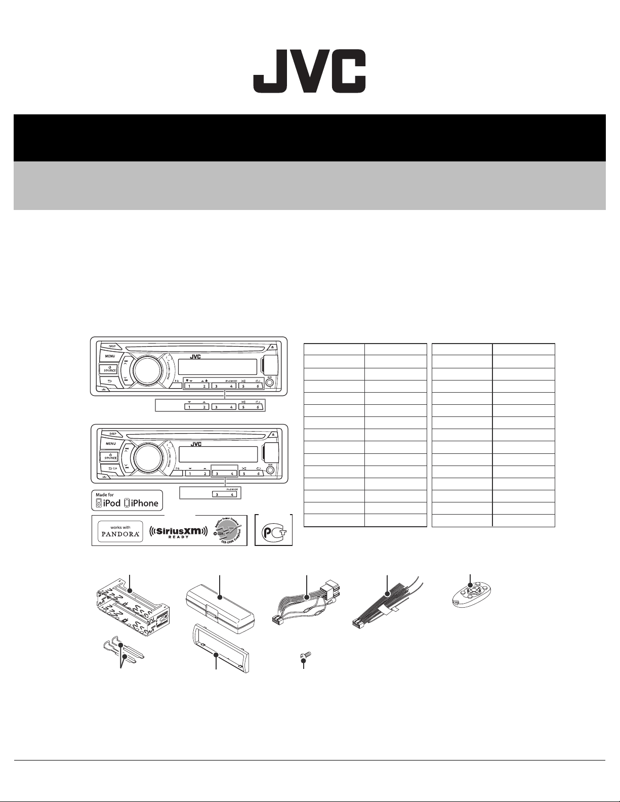
MA538<Rev.003>20135SERVICE MANUAL
KD-R440J, KD-R440JW, KD-R441E, KD-R441EN, KD-R441EU,
KD-R441EY, KD-R442E, KD-R442EN, KD-R442EY, KD-R443E,
KD-R443EN, KD-R443EY, KD-R444UI, KD-R445U, KD-R445UN,
KD-R446EU, KD-R446U, KD-R446UN, KD-R446UP, KD-R446UT,
KD-R447EE, KD-R449E, KD-R449EE, KD-R449UR, KD-R540J,
KD-R541E, KD-R541EN, KD-R541EY, KD-R547EE
For US
For Asia,Europe
KD-R440
For US
KD-R541
For Erope
(RU,UK)
DETACHABLE PANEL
Model ModelParts number
KD-R440J
KD-R440JW
KD-R441E
KD-R441EY
KD-R441EN
KD-R441EU
KD-R442E
KD-R442EY
KD-R442EN
KD-R443E
KD-R443EY
KD-R443EN
KD-R444UI
KD-R445U
CP-R440JD
CP-R440JD
CP-R441ED
CP-R441ED
CP-R441ED
CP-R441ED
CP-R442ED
CP-R442ED
CP-R442ED
CP-R443ED
CP-R443ED
CP-R443ED
CP-R444UID
CP-R445UD
KD-R445UN
KD-R446EU
KD-R446U
KD-R446UN
KD-R446UP
KD-R446UT
KD-R447EE
KD-R449E
KD-R449EE
KD-R540J
KD-R541E
KD-R541EY
KD-R541EN
KD-R547EE
Parts number
CP-R445UD
CP-R446UD
CP-R446UD
CP-R446UD
CP-R446UD
CP-R446UD
CP-R447EED
CP-R449EED
CP-R449EED
CP-R540JD
CP-R541ED
CP-R541ED
CP-R541ED
CP-R547EED
Mounting sleeve
(GE20316-001A)
Hook
(GE40643-001A) x2
COPYRIGHT © 2013 JVC KENWOOD Corporation
Hard case assy *
(GE32320-001A)
Trim plate *
(GE2031x-001A)
Lead free solder used in the board (material: Sn-Ag-Cu, melting point: 219 Centigrade)
Lead free solder used in the board (material: Sn-Cu, melting point: 230 Centigrade)
COPYRIGHT © 2013 JVC KENWOOD Corporation
DC cord *
(QAM1344-00x)
Tap screw (2x8) *
(QYSDSF2008ZA)
DC cord *
(QAM13xx-001)
* It uses it by some models.
Refer to the parts list.
Remocon unit (RM-RK52) *
(RM-RK52xx)
No.MA538<Rev.003>
2013/5
Page 2
SPECIFICATION
For US
Audio amplifier
Power Output 20 W RMS x 4 Channels at 4 Ω and ≤ 1% THD+N
Load Impedance 4 Ω (4 Ω to 8 Ω allowance)
Frequency Response 40 Hz to 20 000 Hz
Signal-to-Noise Ratio 80 dBA (reference: 1 W into 4Ω)
Line-Out or Subwoofer-Out Level/Impedance 2.5 V/10 kΩ load (full scale)
Output Impedance ≤ 600Ω
Tuner
FM Frequency Range 87.9 MHz to 107.9 MHz (200 kHz step)
87.5 MHz to 108.0 MHz (50 kHz step)
Usable Sensitivity 9.3 dBf (0.8 µV/75Ω)
50 dB Quieting Sensitivity 16.3 dBf (1.8 µV/75Ω)
Alternate Channel Selectivity
Frequency Response 40 Hz to 15 000 Hz
Stereo Separation 40 dB
AM Frequency Range 530 kHz to 1 700 kHz (10 kHz step)
Sensitivity/Selectivity 20 µV/40 dB
CD player
Signal Detection System Non-contact optical pickup (semiconductor laser)
Number of Channels 2 channels (stereo)
Frequency Response 5 Hz to 20 000 Hz
Signal-to-Noise Ratio 98 dB
Wow and Flutter Below measurable limit
USB
USB Standard USB 1.1, USB 2.0
Data Transfer Rate (Full Speed) Max. 12 Mbps
Compatible Devices Mass storage class
Compatible File Systems FAT 32/16/12
Playable Audio Formats MP3/WMA
Maximum Supply Current DC 5 V 1 A
General
Power Requirement (Operating Voltage) DC 14.4 V (11 V to 16 V allowance)
Grounding System Negative ground
Allowable Operating Temperature 0°C to +40°C (32°F to 104°F)
Dimensions (W × H × D) Installation Size (approx.) 182 mm × 53 mm × 159 mm (7-3/16” × 2-1/8” × 6-5/16”)
Panel Size (approx.) 188 mm × 59 mm × 13 mm (7-7/16" × 2-3/8" × 9/16")
Weight (excluding accessories) 1.2 kg (2.6 lbs)
65 dB (at 400 kHz)
531 kHz to 1 611 kHz (9 kHz step)
• Subject to change without notice.
(No.MA538<Rev.003>)2/18
Page 3
SPECIFICATION
For Asia
Audio amplifier
Maximum Power Output 50 W per channel
Continuous Power Output (RMS) 20 W per channel into 4Ω, 40 Hz to 20 000 Hz at less than 1% total harmonic distortion
Load Impedance 4 Ω (4 Ω to 8 Ω allowance)
Frequency Response 40 Hz to 20 000 Hz
Signal-to-Noise Ratio 70 dB
Line-Out or Subwoofer-Out Level/Impedance 4.8 V/10 kΩ load (full scale)
Output Impedance ≤ 600Ω
Tuner
FM Frequency Range 87.5 MHz to 108.0 MHz (50 kHz step)
Usable Sensitivity 9.3 dBf (0.8 µV/75Ω)
50 dB Quieting Sensitivity 16.3 dBf (1.8 µV/75Ω)
Alternate Channel Selectivity 65 dB (at 400 kHz)
Frequency Response 40 Hz to 15 000 Hz
Stereo Separation 40 dB
AM Frequency Range MW : 531 kHz to 1 611 kHz (9 kHz step)
SW1 : 2 940 kHz to 7 735 kHz (5 kHz step)
SW2 : 9 500 kHz to 10 135 kHz/11 580 kHz to 18 135 kHz (5 kHz step)
Sensitivity/Selectivity 20 µV/40 dB
CD player
Signal Detection System Non-contact optical pickup (semiconductor laser)
Number of Channels 2 channels (stereo)
Frequency Response 5 Hz to 20 000 Hz
Signal-to-Noise Ratio 98 dB
Wow and Flutter Below measurable limit
USB
USB Standard USB 1.1, USB 2.0
Data Transfer Rate (Full Speed) Max. 12 Mbps
Compatible Devices Mass storage class
Compatible File Systems FAT 32/16/12
Playable Audio Formats MP3/WMA
Maximum Supply Current DC 5 V 1 A
General
Power Requirement (Operating Voltage) DC 14.4 V (11 V to 16 V allowance)
Grounding System Negative ground
Allowable Operating Temperature 0°C to +40°C
Dimensions
(W × H × D)
Weight (excluding accessories) 1.2 kg
Installation Size (approx.) 182 mm × 53 mm × 159 mm
Panel Size (approx.) 188 mm × 59 mm × 13 mm
• Subject to change without notice.
(No.MA538<Rev.003>)3/18
Page 4
SPECIFICATION
For Europe
Audio amplifier
Power Output 50 W per channel
Continuous Power Output (RMS) 20 W per channel into 4Ω, 40 Hz to 20 000 Hz at less than 1% total harmonic distortion
Load Impedance 4 Ω (4 Ω to 8 Ω allowance)
Frequency Response 40 Hz to 20 000 Hz
Signal-to-Noise Ratio 70 dB
Line-Out or Subwoofer-Out Level/Impedance For KD-R547/KD-R541/KD-R449 : 2.5 V/10 kΩ load (full scale)
Output Impedance ≤ 600Ω
Tuner
FM Frequency Range For KD-R541/KD-R443 /KD-R442/KD-R441/KD-R449 : FM: 87.5 MHz to 108.0 MHz
For KD-R547/KD-R449 /KD-R447 : FM: 87.5 MHz to 108.0 MHz / FM-LO: 65.0 MHz to
74.0 MHz
Usable Sensitivity 9.3 dBf (0.8 µV/75Ω)
50 dB Quieting Sensitivity 16.3 dBf (1.8 µV/75Ω)
Alternate Channel Selectivity 65 dB (at 400 kHz)
Frequency Response 40 Hz to 15 000 Hz
Stereo Separation 40 dB
AM Frequency Range MW : 531 kHz to 1 611 kHz
LW : 153 kHz to 279 kHz
Sensitivity/Selectivity MW : 20 µV/40 dB
LW : 50 µV/-
CD player
Signal Detection System Non-contact optical pickup (semiconductor laser)
Number of Channels 2 channels (stereo)
Frequency Response 5 Hz to 20 000 Hz
Signal-to-Noise Ratio 98 dB
Wow and Flutter Below measurable limit
USB
USB Standard USB 1.1, USB 2.0
Data Transfer Rate (Full Speed) Max. 12 Mbps
Compatible Devices Mass storage class
Compatible File Systems FAT 32/16/12
Playable Audio Formats MP3/WMA
Maximum Supply Current DC 5 V 1 A
General
Power Requirement (Operating Voltage) DC 14.4 V (11 V to 16 V allowance)
Grounding System Negative ground
Allowable Operating Temperature 0°C to +40°C
Dimensions
(W × H × D)
Weight (excluding accessories) 1.2 kg
Installation Size (approx.) 182 mm × 53 mm × 159 mm
Panel Size (approx.) 188 mm × 59 mm × 13 mm
• Subject to change without notice.
(No.MA538<Rev.003>)4/18
Page 5
SECTION 1
PRECAUTION
1.1 Safety Precautions
(1) This design of this product contains special hardware and
many circuits and components specially for safety purposes. For continued protection, no changes should be made
to the original design unless authorized in writing by the
manufacturer. Replacement parts must be identical to
those used in the original circuits. Services should be performed by qualified personnel only.
(2) Alterations of the design or circuitry of the product should
not be made. Any design alterations of the product should
not be made. Any design alterations or additions will void
the manufacturers warranty and will further relieve the
manufacture of responsibility for personal injury or property
damage resulting therefrom.
(3) Many electrical and mechanical parts in the products have
special safety-related characteristics. These characteristics are often not evident from visual inspection nor can the
protection afforded by them necessarily be obtained by using replacement components rated for higher voltage, wattage, etc. Replacement parts which have these special
safety characteristics are identified in the Parts List of Service Manual. Electrical components having such features
are identified by shading on the schematics and by ( ) on
the Parts List in the Service Manual. The use of a substitute
replacement which does not have the same safety characteristics as the recommended replacement parts shown in
the Parts List of Service Manual may create shock, fire, or
other hazards.
(4) The leads in the products are routed and dressed with ties,
clamps, tubings, barriers and the like to be separated from
live parts, high temperature parts, moving parts and/or
sharp edges for the prevention of electric shock and fire
hazard. When service is required, the original lead routing
and dress should be observed, and it should be confirmed
that they have been returned to normal, after reassembling.
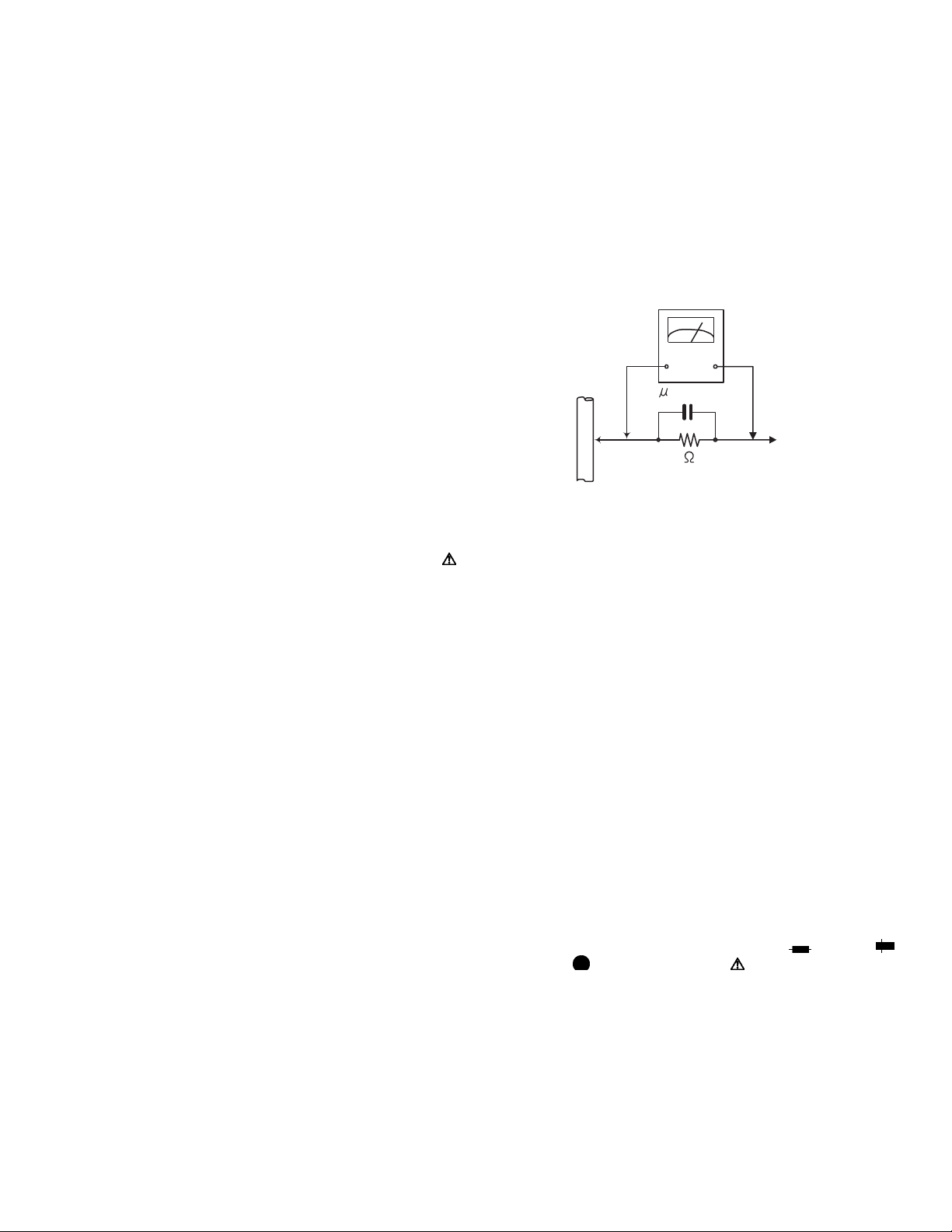
(5) Leakage shock hazard testing
After reassembling the product, always perform an isolation check on the exposed metal parts of the product (antenna terminals, knobs, metal cabinet, screw heads,
headphone jack, control shafts, etc.) to be sure the product
is safe to operate without danger of electrical shock.Do not
use a line isolation transformer during this check.
• Plug the AC line cord directly into the AC outlet. Using a
"Leakage Current Tester", measure the leakage current
from each exposed metal parts of the cabinet, particularly any exposed metal part having a return path to the
chassis, to a known good earth ground. Any leakage current must not exceed 0.5mA AC (r.m.s.).
• Alternate check method
Plug the AC line cord directly into the AC outlet. Use an
AC voltmeter having, 1,000Ω per volt or more sensitivity
in the following manner. Connect a 1,500Ω 10W resistor
paralleled by a 0.15µF AC-type capacitor between an ex-
posed metal part and a known good earth ground.
Measure the AC voltage across the resistor with the AC
voltmeter.
Move the resistor connection to each exposed metal
part, particularly any exposed metal part having a return
path to the chassis, and measure the AC voltage across
the resistor. Now, reverse the plug in the AC outlet and
repeat each measurement. Voltage measured any must
not exceed 0.75 V AC (r.m.s.). This corresponds to 0.5
mA AC (r.m.s.).
AC VOLTMETER
(Having 1000
ohms/volts,
or more sensitivity)
0.15 F AC TYPE
Place this
probe on
1500 10W
Good earth ground
1.2 Warning
(1) This equipment has been designed and manufactured to
meet international safety standards.
(2) It is the legal responsibility of the repairer to ensure that
these safety standards are maintained.
(3) Repairs must be made in accordance with the relevant
safety standards.
(4) It is essential that safety critical components are replaced
by approved parts.
(5) If mains voltage selector is provided, check setting for local
voltage.
1.3 Caution
Burrs formed during molding may be left over on some parts
of the chassis.
Therefore, pay attention to such burrs in the case of preforming repair of this system.
1.4 Critical parts for safety
In regard with component parts appearing on the silk-screen
printed side (parts side) of the PWB diagrams, the parts that are
printed over with black such as the resistor ( ), diode ( )
and ICP ( ) or identified by the " " mark nearby are critical
for safety. When replacing them, be sure to use the parts of the
same type and rating as specified by the manufacturer.
(This regulation dose not Except the J and C version)
each exposed
metal part.
(No.MA538<Rev.003>)5/18
Page 6
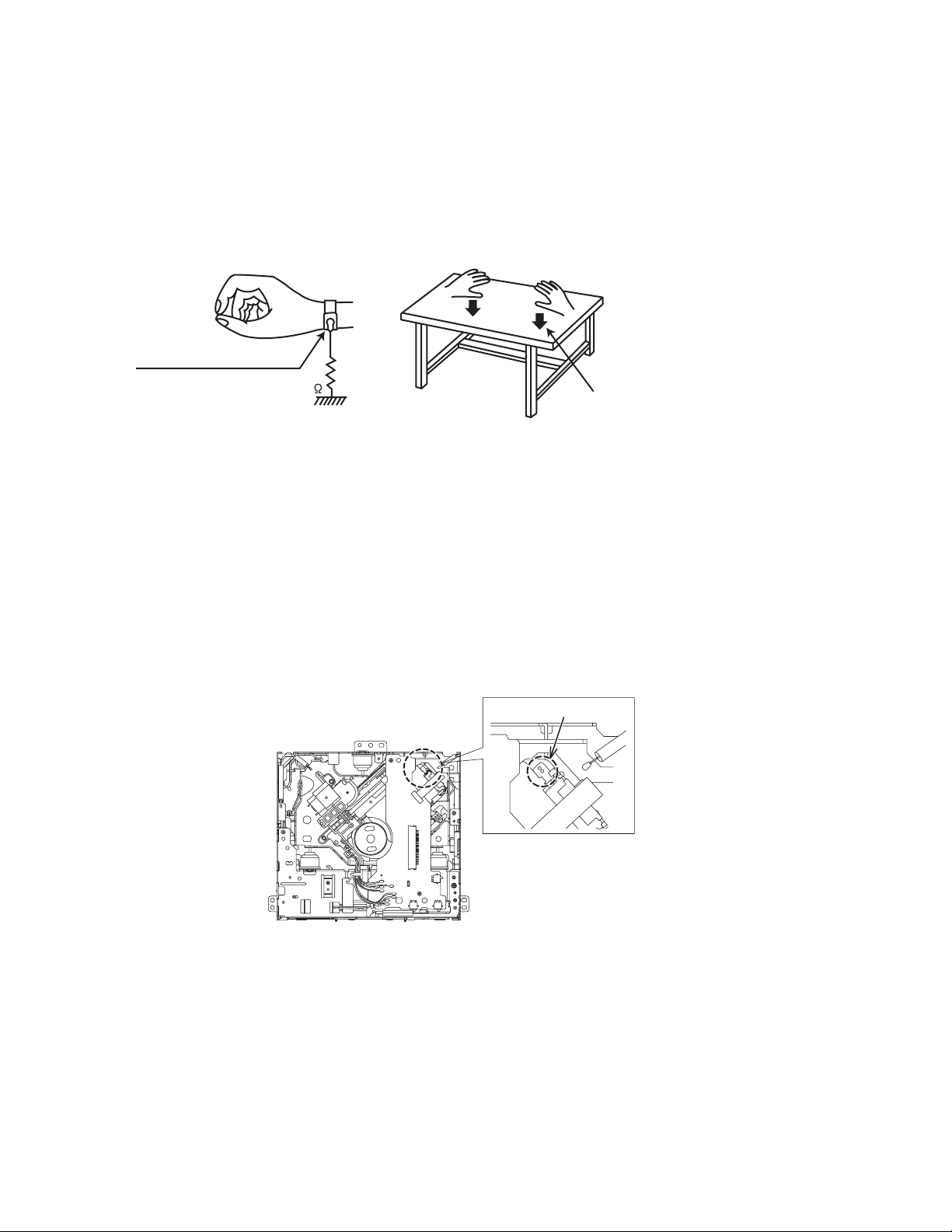
1.5 Preventing static electricity
Electrostatic discharge (ESD), which occurs when static electricity stored in the body, fabric, etc. is discharged, can destroy the laser
diode in the traverse unit (optical pickup). Take care to prevent this when performing repairs.
1.5.1 Grounding to prevent damage by static electricity
Static electricity in the work area can destroy the optical pickup (laser diode) in devices such as laser products.
Be careful to use proper grounding in the area where repairs are being performed.
(1) Ground the workbench
Ground the workbench by laying conductive material (such as a conductive sheet) or an iron plate over it before placing the
traverse unit (optical pickup) on it.
(2) Ground yourself
Use an anti-static wrist strap to release any static electricity built up in your body.
(caption)
Anti-static wrist strap
1M
Conductive material
(conductive sheet) or iron palate
(3) Handling the optical pickup
• In order to maintain quality during transport and before installation, both sides of the laser diode on the replacement optical
pickup are shorted. After replacement, return the shorted parts to their original condition.
(Refer to the text.)
• Do not use a tester to check the condition of the laser diode in the optical pickup. The tester's internal power source can easily
destroy the laser diode.
1.6 Handling the traverse unit (optical pickup)
(1) Do not subject the traverse unit (optical pickup) to strong shocks, as it is a sensitive, complex unit.
(2) Cut off the shorted part of the flexible cable using nippers, etc. after replacing the optical pickup. For specific details, refer to the
replacement procedure in the text. Remove the anti-static pin when replacing the traverse unit. Be careful not to take too long a
time when attaching it to the connector.
(3) Handle the flexible cable carefully as it may break when subjected to strong force.
(4) I t is not possible to adjust the semi-fixed resistor that adjusts the laser power. Do not turn it.
SOLDER
(No.MA538<Rev.003>)6/18
Page 7
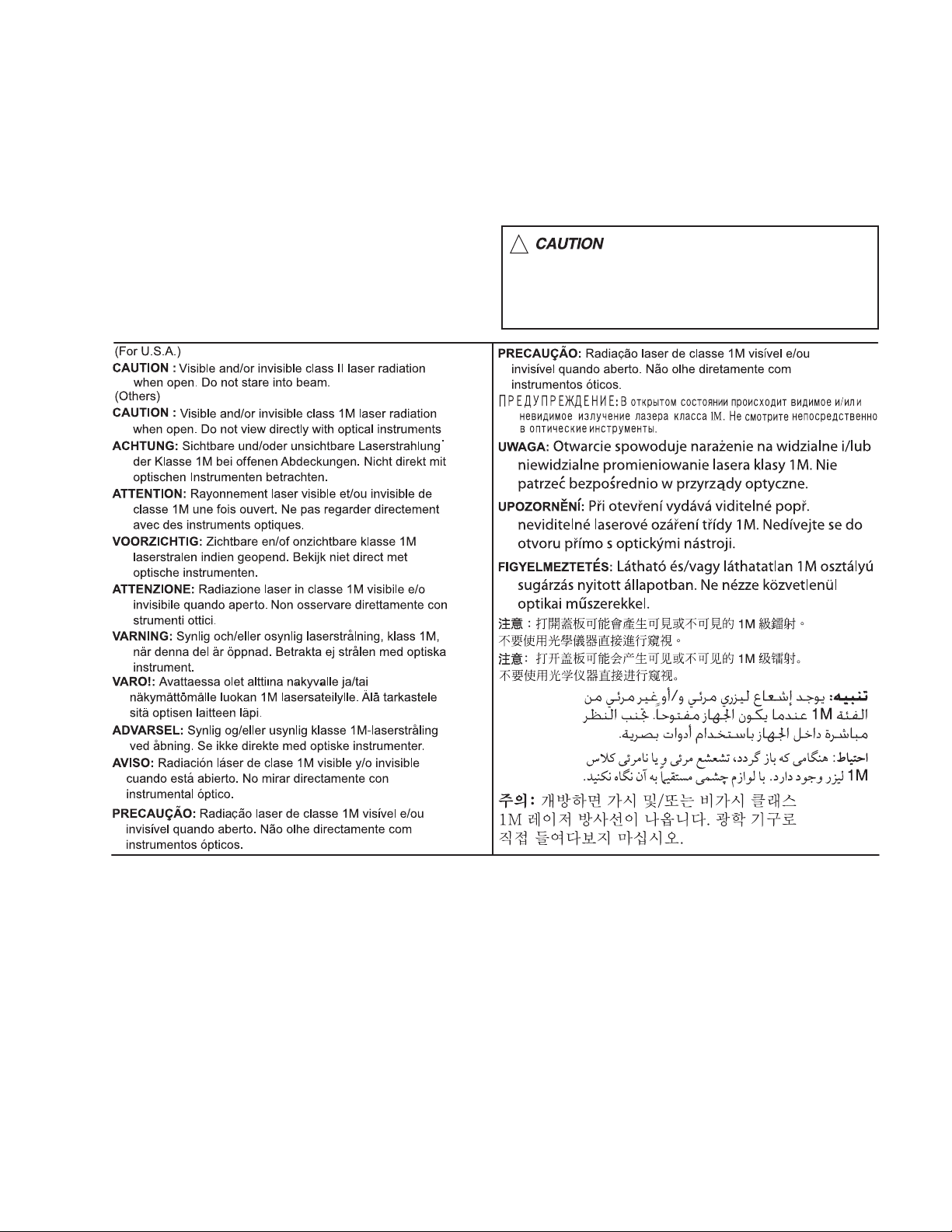
1.7 Important for laser products
1.CLASS 1 LASER PRODUCT
2.CAUTION :
(For U.S.A.) Visible and/or invisible class II laser radiation
when open. Do not stare into beam.
(Others) Visible and/or invisible class 1M laser radiation
when open. Do not view directly with optical instruments.
3.CAUTION : Visible and/or invisible laser radiation when
open and inter lock failed or defeated. Avoid direct
exposure to beam.
4.CAUTION : This laser product uses visible and/or invisible
laser radiation and is equipped with safety switches which
prevent emission of radiation when the drawer is open and
the safety interlocks have failed or are defeated. It is
dangerous to defeat the safety switches.
5.CAUTION : If safety switches malfunction, the laser is able
to function.
6.CAUTION : Use of controls, adjustments or performance of
procedures other than those specified here in may result in
hazardous radiation exposure.
!
Please use enough caution not to
see the beam directly or touch it
in case of an adjustment or operation
check.
(No.MA538<Rev.003>)7/18
Page 8
SECTION 2
SPECIFIC SERVICE INSTRUCTIONS
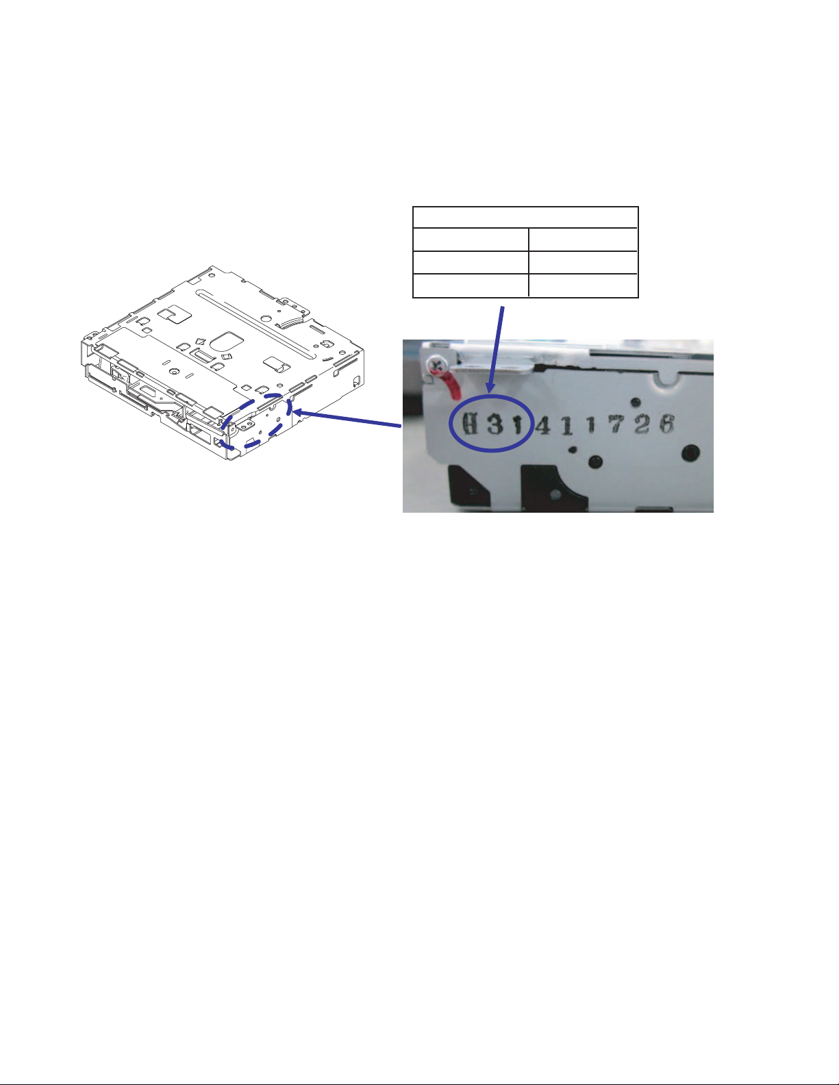
2.1 Identifying the CD Mechanism
This unit is equipped with one of the two CD mechanism types below.
• FLM-HC3-1D
• FLM-HC5-1D
Before sending the mechanism for repair, please check the following and refer to the corresponding materials.
SPECIFICATION
MODEL NAME STAMP No.
FLM-HC3-1D H31
FLM-HC5-1D H51
Chassis Stamp Print on Right Side of Mechanism
(No.MA538<Rev.003>)8/18
Page 9
SECTION 3
DISASSEMBLY
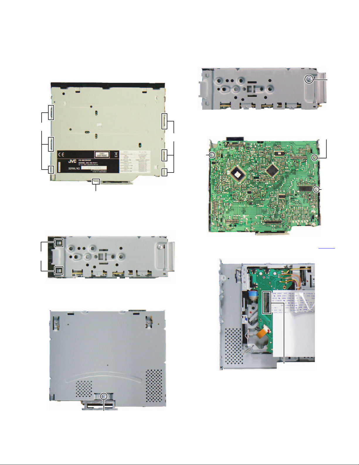
3.1 Main body (Used model: KD-R441E)
3.1.1 Removing the Bottom chassis (See Fig.1)
(1) Disengage the 7 hooks a engaging the Bottom chassis.
(2) Slide the Bottom chassis backward to remove it.
a
a
Fig.1
3.1.2 Removing the Front chassis (See Fig.2)
(1) Disengage the 4 hooks b engaging both sides of the Front
chassis.
(2) Remove the 2 screws B attaching both sides of the Top
chassis. (See Fig.4)
B
Fig.4
(3) Remove the 2 screws C and 1 clamp attaching the Electric
unit. (See Fig.5)
a
Clamp
C
C
b
Fig.2
3.1.3 Removing the Electric unit (See Fig.3, 4 and 5)
Remove the 1 screw A attaching the Top chassis. (See Fig.
(1)
3)
Fig.5
(4) Disconnect the FFC wire connected to connector CN101
the CD mechanism. (See Fig.6)
CN101
Fig.6
of
A
Fig.3
(No.MA538<Rev.003>)9/18
Page 10
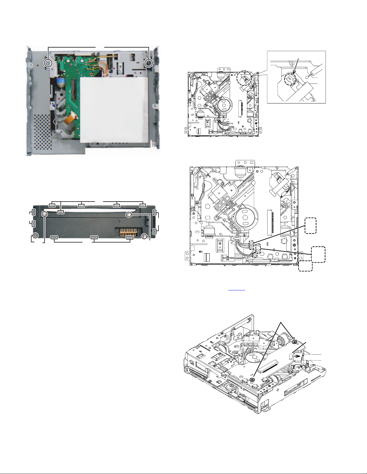
3.1.4 Removing the CD mechanism (See Fig.7)
(1) Remove the 2 screws D attaching the CD mechanism.
D
Fig.7
3.1.5 Removing the Switch unit (See Fig.8)
(1) Remove the Volume knob.
(2) Remove the 4 screws E attaching the Rear cover.
(3) Disengage the 12 hooks c engaging the Rear cover.
c
3.2 CD mechanism assembly section
3.2.1 Removing the Mecha control board
(1) Solder the short land on the pickup. (See Fig. 1)
SOLDER
Fig.1
(2) Remove the 8 wires from the Mecha control board. (See
Fig.2)
c
E
c
Fig.8
E
c
Fig.2
(3) Disconnect the flexible wire from the pickup connected to
the connector CN102
Fig.3)
(4) Remove the 2 screws A attaching the Mecha control board.
(See Fig.3)
on the Mecha control board. (See
BLACK
RED
WHITE
WHITE
YELLOW
YELLOW
ORANGE
ORANGE
A
CN102
(No.MA538<Rev.003>)10/18
Fig.3
Page 11

3.2.2 Removing the Traverse mechanism (See Fig.4, 5)
(1) Remove the 5 springs from the traverse mechanism. (See
Fig.4)
Fig.4
(2) Remove the 3 screws B attaching the bottom frame as-
sembly. (See Fig.5)
(3) Remove the 3 dumpers from the bottom frame assembly.
(See Fig.5)
B
(2) Remove the shaft from the TM base. (See Fig.7)
(3) Disengage the hook a on the pickup from the TM base.
(See Fig.7)
shaft
B
Fig.5
3.2.3 Removing the Pickup (See Fig.6, 7)
(1) Remove the 2 screws C attaching the feed bracket assem-
bly. (See Fig.6)
CC
Fig.7
3.2.4 Removing the Spindle motor (See Fig.8. 9)
(1) Remove the HC CL. Spring from the HC CL. base and the
TM base, and then lift up the HC CL. base. (See Fig.8)
HC CL. spring
[ SIDE VIEW ]
Fig.8
Fig.6
(No.MA538<Rev.003>)11/18
Page 12
(2) Remove the HC CL. base from the holes on the TM base.
(See Fig.9)
Fig.9
(3) Remove the 2 screws D attaching the spindle motor. (See
Fig.10)
D
3.2.5 Removing the Loading motor
(1) Remove the roller arm assembly from the bottom frame as-
sembly. (See Fig.11)
Fig.11
(2) Remove the 2 screws E attaching the loading motor as-
sembly, and then remove the loading motor assembly in
the direction of the arrow. (See Fig.12)
Fig.10
E
Fig.12
(No.MA538<Rev.003>)12/18
Page 13
SECTION 4
ADJUSTMENT
4.1 Service Test mode
4.1.1 Default status immediately after the mode activation
Operating Key: [MENU] + [] (7sec) Press and hold.
4.1.2 How to release each Test mode
• Reset
•Acc off
• Power off
• Panel Detach
4.1.3 Mode content
Syscon shall display the following information after entering this mode. The operation shown below shall be workable.
Display content Detail
S R V T E S T
The display is released when another operation is executed.
4.1.4 Common operation mode for all sources.
means Press and hold.
Operation Display content Detail
[EQ]
CD error
information display
Transit to CD error information display mode
mode
[MENU]
Syscon version
display
S Y S #
@ @ @
# = Display of destination.
J = USA
R = EUROPE
E = EASTERN-EUROPE
U = OTHERS(e.g. ASIA)
@@@ = Syscon version number
Power ON duration
display
[2]
Disc operation
duration display
[1]
P O N T M 0 H X X
P O N T M X X X X X
C D T M 0 H X X
C D T M X X X X X
00 - 50 are displayed in " XX ".
For less than 1 hour, the display is
indicated per 10 minutes.
00001 - 10922 are displayed in "
XXXXX ".
MAX 10922 (hours).
00 - 50 are displayed in " XX ".
For less than 1 hour, the display is
indicated per 10 minutes.
00001 - 10922 are displayed in "
XXXXX ".
MAX 10922 (hours).
[DISP]
[DISP]
Disc eject number
of times
Disc eject number
of times clear
E J C N T X X X X X
E J C N T 0 0 0 00
00001 - 99999 are displayed in
"XXXXX"
Clear Disc Eject number of times by
pressing for 2 seconds when it is
displayed.
[]
Force Power OFF
information display
P O F F - --
P O F F P N L
No force Power OFF
Force Power OFF due to SysconPanel communication error.
Will not show in JK12 Models.
[]
Force Power OFF
information clear
P O F F - --
Clear Force Power OFF information by
pressing for 2 seconds when it is
displayed.
Will not show in JK12 Models.
(No.MA538<Rev.003>)13/18
Page 14

4.1.5 CD error information display mode
Operation Display content Detail
CD mecha error
log display
Mecha error history 1,2,3 (latest)
# = History No. (1,2,3)
XX : kind of errors, " -- " when there is
none.
00: No Error
04: TOC read Error
M E C H E R #AXX
05: Unknown CD
06: Heat Error
0A: Update Error
0D: Hold Error
15: Unknown Disc
99: Mecha Error
CD load error
information display
L O A D E R # X X
Load error switch 1,2
# = History No. (1,2)
XX: numbers of errors, " -- " when there
is none
History No. 2 is un-used
CD eject error
information display
Eject error switch 1,2,3,4
# =History No. (1,2,3,4)
XX: numbers of errors, " -- "when there
Move
between
[DISP]
(Forward
search)
i t e m w i t h
[] / []
CD time code error
count information
display (count skip)
E J E C T E R # X X
C N T L O S E
C D D A XX
is none
History No.3 is un-used
History No.1: Eject before SW1 is on.
History No.2: Eject until SW1 and SW2
is on.
History No.3: Eject between SW2 on
and Eject end
CD-DA error count number information
CD-DA error count numbers
XX: numbers of errors and " -- " when
there is none
Can only be checked via debugger by
jap member
CD-ROM (compressed file) error count
numbers
XX: numbers of errors and " -- " when there
C D R O M X X
is none
Can only be checked via debugger by jap
member
CD time code error
count information
display (no count
update)
C N T S T A Y
C D D A XX
CD time code error count information
(count not updated) mode display
CD-DA error count numbers
XX: numbers of errors and " -- " when
there is none
CD-ROM (compressed file) error count
numbers
C D R O M X X
XX: numbers of errors and " -- " when
there is none
[EQ]
CD error
information clear
CD error information all clear Clear CD error information by pressing
M E C H A E R 1 - -
for 2 seconds when it is displayed.
[EQ] Mode release CD error information display mode release Back to default status, All lights on
(No.MA538<Rev.003>)14/18
Page 15
4.2 Service Information Clear Mode
4.2.1 Default status immediately after the mode activation
* The receiver is connected with the DC power supply (with the power supply turned off).
Operating Key: [BACK] + [POWER] Press and hold + DC power supply turned ON
4.2.2 How to release each Test mode
• Reset
•Acc off
• Power off
• Panel Detach
4.2.3 Mode content
After entering this mode, Syscon shall clear the information stored for service and output the result to the display tube.
CD will be ejected upon process ended.
Preset Frequencies and Tagging (HD models) information shall be cleared.
Display content Detail
D A T A C L R O K
When normal end
When error end
D A T A C L R N G
Display blinks with 250ms interval.
The following table shows the data that is cleared.
Information for data clearing Detail Storage area
CD mecha log display E2PROM
CD load error information display E2PROM
CD mecha information
CD eject error information display E2PROM
CD time code error count information display (count skip) E2PROM
CD time code error count information display (no count update) E2PROM
Service information
DC error information
CD EJECT number of times display E2PROM
Force Power OFF information display E2PROM
DC error 1 display (wrong connection & other detection information in detecting duration) E2PROM
DC error 2 display (capacitor leakage detection number information) E2PROM
Tuner Area Setting E2PROM
Preset information
Preset Frequency E2PROM
Preset PI code E2PROM
Preset HD Station Name and Sub-Channel Number (HD models) E2PROM
SXM Preset Channel SID E2PROM
Sirius XM information
(Sirius models)
SXM Lock SID E2PROM
SXM Last Channel ID E2PROM
SXM Channel Lock Code E2PROM
Tagging information (HD models) Token data memory index E2PROM
(No.MA538<Rev.003>)15/18
Page 16
4.3 DC error information mode
4.3.1 Default status immediately after the mode activation
* The receiver is connected with the DC power supply (with the power supply turned off).
Operating Key: [MENU] + [] Press and hold + DC power supply turned ON
4.3.2 How to release each Test mode
• Reset
•Acc off
• Power off
• Panel Detach
4.3.3 Mode content
Syscon shall display the following information after entering this mode. The operation shown below shall be workable.
Display content Detail
D C E R R
D C O K
When DC error is detected (in case that one of capacitor leakage,
wrong connection or other detection is found).
When DC error is not detected (in case that none of capacitor leakage, wrong connection or other detection is found).
4.3.4 Mode operation specification
means Press and hold
Operation Display content Detail
[]
[]
DC ERR1
display
DC ERR1
clear
D C 1 E R R
D C 1 O K
D C 1 O K
When wrong connection & DC error in other detection duration is detected.
When wrong connection & DC error in other detection duration is not detected.
Clear detection information when wrong connection & DC error in other detection duration is
displayed.(Clear data flash)
[]
[]
DC ERR2
display
DC ERR2
clear
D C 2 4
D C 2 0
Display detecting number of times in capacitor
leakage detection duration (0 - 4)
Clear number of times for detection information
in capacitor leakage detection duration.(Clear
data flash)
(No.MA538<Rev.003>)16/18
Page 17
4.4 DC offset error description
A
4.4.1 DC offset detection circuit design
•Purpose:
To prevent breakdown, burning and emitting smoke from customer's car speaker when occur DC offset between speaker
output "+" and "-".
• Target:
Detect DC offset, then stop the Power Amp operation and shift
to specified condition.
4.4.2 Possible causes of DC offset at speaker output lines
(1) Mis-connection for speaker output for example touch to car
body or battery line.
(2) Current leak of coupling capacitor for Power IC input.
(3) Current leak of Ac-GND capacitor for Power IC Ac-GND.
(4) Capacitor shorted of above parts due to foreign object.
C-tc
E-Vol
Win_TC
Win_In
DC Error
C-in
C-in
R3
C-in
C-in
C-ac2C-ac1
Sw5V
R2
R1
C3
R4
Audio Pwr Amp
In 1
In 2
In 3
In 4
AcGnd
Offset Detect
Out
Micon
ADC In
4.4.5 Manipulate after detect DC offset
• If detected error 10 consecutive times, and 10th error occurred
in "Mis-connect detection period", judge as "Mis-connect".
• If detected error 10 consecutive times, and 10th error occurred
in "Capacitor leak detection period", judge as "Capacitor leak ".
• If detected error 10 consecutive times, and 10th error occurred
in "Other detection period" and detected another 10 errors consecutively, then judge as "Other".
• If judge as "Mis-connect".
- turn off speaker output.
- display "MIS WIRING" → "CHK WIRING" → "THEN RESET"
→ "UNIT".
- key access disable except button of Eject, Reset and service
mode
- record error in EEPROM "DC1 ERR"
- Set is able to be recovered by Reset button.
• If judge as "Capacitor leak ".
- turn off speaker output.
- display "WARNING" → "CHK WIRING" → "THEN RESET"
→ "UNIT".
- key access disable except button of Eject, Reset and service
mode
- record error in EEPROM "DC2 #" (# means counter number)
- Set can be recovered by pressing the Reset button before
the capacitor leak error counter reach "DC2 4".
After that, only clear the counter back to "0" can recover the
set.
• If judge as "Other" (manipulation same as mis-connect)
SECTION 5
4.4.3 Type of checking
4.4.3.1 To detect DC offset Error
• Mis-connection
- Short any one speaker out line to GND or Vcc
• Capacitor leak
- Parallel 330kΩ to either any one of coupling cap or Ac-GND
cap (to simulate current leakage of capacitor)
- Shorted either any one of coupling cap or Ac-GND cap.
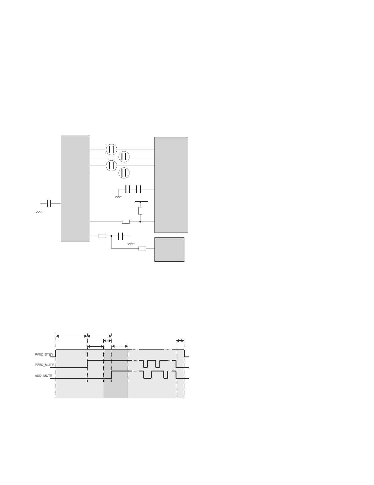
4.4.4 Detection Timing chart
PWIC_STBY
PWIC_MUTE
UD_MUTE
2.0sec or more
Missconnect
detection period
1.5sec or more
0.8sec
0.7sec or more
1.0sec
Capacitor leak
detection period
Other (miss detection etc.)
detection period
50ms
or more
TROUBLESHOOTING
5.1 How to cancel DC offset error
Check to be sure the terminals of the speaker leads are covered
with insulating tape properly, then reset the unit.
If an error message does not disappear even after a reset, there
is a need for internal repair.
5.2 How to clear DC offset error recorded in EEPROM
DC Error Information Mode is started.
[MENU] + [] Press and hold + DC power supply turned ON
DC1 ERR → [] Press and hold.→ DC1 OK
DC2 1-4 → [] Press and hold.→ DC2 0
(No.MA538<Rev.003>)17/18
Page 18

JVC KENWOOD Corporation
Car Electronics Business Group 2967-3, Ishikawa-machi, Hachioji-shi, Tokyo, 192-8525, Japan
(No.MA538<Rev.003>)
Printed in Japan
VSE
Page 19

SCHEMATIC DIAGRAMS
19
CD RECEIVER
KD-R440J KD-R440JW KD-R441E
KD-R441EN KD-R441EU KD-R441EY
KD-R442E KD-R442EN KD-R442EY
KD-R443E KD-R443EN KD-R443EY
KD-R444UI KD-R445U KD-R445UN
KD-R446EU KD-R446U KD-R446UN
KD-R446UP KD-R446UT KD-R447EE
KD-R449E KD-R449EE KD-R449UR
KD-R540J KD-R541E KD-R541EN
KD-R541EY KD-R547EE
(No.MA538<Rev.003>)1/
Page 20

■ PRECAUTIONS ON SCHEMATIC DIAGRAMS
z Due to the improvement in performance, some part numbers shown in the circuit diagrams
may not agree with those indicated in the Parts List.
z The parts numbers, values and rated voltage etc. in the Schematic Diagrams are for
reference only.
z Since the circuit diagrams are standard ones, the circuits and circuit constants may be
subject to change for improvement without any notice.
■ PRECAUTIONS ON PARTS LIST
z
The parts identified by the symbol are critical for safety. Whenever replacing these parts, be sure to
use specified ones to secure the safety.
z
The parts not indicated in this Parts List and those which are filled with lines --- in the Parts No.
columns will not be supplied.
z
P.W. BOARD Ass'y will not be supplied, but those which are filled with the Parts No. in the Parts No.
columns will be supplied.
z
When ordering chips, screws etc., place bulk orders (unit of tens) whenever possible to improve
shipping efficiency.
z
There are cases where the actual implemented parts in the sets and the service parts are different.
When ordering parts, make sure to refer to the Parts List.
■
PRECAUTIONS ON SERVICE
Certain parts of the power circuits and the GNDs differ according to the models. Care must be
taken for the following points as the differences are indicated separately in the LIVE GND ( ) and
the ISOLATED (NEUTRAL) GND ( ).
1. Do not touch the LIVE GND, or do not touch the LIVE GND and the ISOLATED (NEUTRAL)
GND at the same time. It may cause an electric shock.
Before pulling out the chassis or other parts, make sure to pull out the power cord from the
wall outlet first.
2. Do not short circuit between the LIVE GND and ISOLATED (NEUTRAL) GND, or never
measure the LIVE GND and ISOLATED (NEUTRAL) GND at the same time using measuring
instruments (oscilloscope, etc.). It may blow fuses or damage other parts.
■ DEVIATION TOLERANCE RANGE
DEVIATION TOLERANCE RANGE
F G J K M N R H Z P
± 1% ± 2% ± 5% ±10% ±20% ±30%
+30%
-10%
+50%
-10%
+80%
-20%
+100%
-0%
19
(No.MA538<Rev.003>)2/
Page 21

DC DC
IC981
REGULATOR
IC901
EEPROM
IC771
MICON
IC701
REMOCON
IC681
DRIVER
LCD
IC661
HS SWITCH
IC603
& INT. SRAM
MP3 LSI
IC540
BTL DRIVER
IC501
POWER AMP
IC301
E-VOLUME
IC161
iPOD Coprocessor
IC80
TUNER IC
IC1
ANT
J1
SP OUT
AUX-IN
USB
BLOCK DIAGRAM
CN603
Backlight LED
D655
Button LED
D659
D654
to
to
D656
D627
LCD
CN601
J601
ENCODER
JS601
KEY MATRIX
S617
to
S601
CP_Reset
CP_SDA
CP_SCL
USB iPod model only
CN101
CD PLAYER UNIT
SW2SW1,
MOTOR
SPINDLE
TRK -
TRK +
FOCUS -
FOCUS +
LD
CD_MD
VT1, VT2
VF1, VF2
FOCUS -
FOCUS +
FEED -
FEED +
SW2
SW1
SPINDLE-
SPINDLE+
MOTOR
LOAD&FEED
SET SWITCH
POSITION
PICK UP
PWS
J321(1PRE)
FM/AM
MUTE
-MUTEE
AMP STBY
AMP MUTE
CN901
MEMORY
DATA
LRCK
BCK
OFFSET
DC_ERR
CTRL2
CTRL1
FREQ SEL
CIRCUITRY
MUTE
ELECTRIC UNIT
SURGE DET
BU-DET/
TEL MUTE
DETBU
(DC CORD)
REV
FWR
DRV_Mute
CN502
D-
D+
REMOCON
VOL2
VOL1
LCD DA
LCDCE
LCDCL
KEY2
KEY1
KEY0
SCL TU/EVOL
SDA TU/EVOL
SCL TU/EVOL
SDA TU/EVOL
CN701
SRAM STB
CD_MUTE
CDR_RESET
CMD_CCE
CMD_BUCK
CMD_SI
CMD_SO
LD
CD_MD
VT2VT1,
VF2VF1,
SW3
SW2
SW1
PSW
Vref
BTL_TRO
BTL_FOO
BTL_FMO
BTL_DMO
LOAD -
LOAD +
TRK -
TRK +
SP -
SP +
FOCUS -
FOCUS +
FEED -
FEED +
F-AUXR
F-AUXG
F-AUXL
RR/SW
RL/SWL
RROUT
FROUR
RLOUT
OUT
FL
REAR RIGHT(-)
REAR RIGHT(+)
REAR LEFT(-)
REAR LEFT(+)
FRONT RIGHT(-)
FRONT RIGHT(+)
FRONT LEFT(-)
FRONT LEFT(+)
CDR
CDL
CDR
CDL
TUR
TUL
Line Out (Rear)
L&R /
Subwoofer L&R
KEY0
KEY1
KEY2
SWITCH UNIT
to
S50S1
COM4
P1
COM3
COM2
P3
COM1
P2
LCDCE
LCDDA
AUX-L
LCDCLAUX-G
AUX-R
USB 5V
HS_EN1
D-
VOL2
D+
VOL1
REMOCON
*Remark
*Remark
created date:2013-02-18No.MA538
19
(No.MA538<Rev.003>)3/
Page 22

SURGE DETBU DET
CONDITION
---FM MODE. ( )CD MODE.AM MODE.
ALL RESISTANCE VALUES ARE IN OHM.
ALL CAPACITORS ARE 50V OR 25V CERAMIC CAPACITOR.
1. VOLTAGES ARE DC-MEASURED WITH A DIGITAL VOLT METER WITHOUT INPUT SIGNAL
COMPONENTS IN ( ) INDICATE NOT USE.
ALL RESISTORS ARE 1/16W 5% METAL GLAZE RESISTOR.
UNLESS OTHERWISE SPECIFIED.
3.
2.
ALL E.CAPACITORS ARE SHOWN IN THE FORM OF CAPACITANCE(uF)/RATED VOLTAGE(V)
ALL CAPACITANCE VALUES ARE IN uF(P=pF)
NOTES
8.2K
39K
0.6V
1.8V
27K
22K
KD-R449E
OTHERS & KD-R446EU
KD-R446EU
KD-R446EU
KD-R446EU
KD-R446EU,KD-R449E
KD-R446EU
KD-R446EU
FOR KD-R646UP ONLY
(3.3V)
KD-R646UP ONLY
FOR KD-R446UP &
KD-R440JW
FOR KD-R64X SERIES ONLY
FOR KD-R64X SERIES ONLY
*
*
*
*
*
*
*
* *
*
*
*
*
*
*
*
*
*
*
*
*
*
*
*
*
*
*
*
*
*
*
*
LINEOUT
X
X
X
X
X
X
X
X
X
X
X
X
X
X
X
0
0
0
0
0
0
0
0
0
0
0
0
0
0
0
X
X
X
X
X
X
X
C341,C351
C340,C350
Q341
D341
R347,R349
R350,R351,R352
R340,R341,R342
0
0
0
0
0
0
0
0
C321,C331
C320,C330
Q321
D321
R357,R358
R330,R331,R332
R320,R321,R322
R323,R333
KD-R647EE KD-R447EE
11.4V8.3V
voltage
Pin 24
*
GEB10354APWB X
X
X
3.3V
3.3V
D902/D903:MBRX130-TP-X
*
KD-R646U SERIES
1.8V
27K
22K
8.2K
39K
27K
22K
27K
22K
47K
X
R767
R765
*MODELS
1.8VSTAGE 1
27KR766
R764
KD-R647EE
22K
STAGE 2
27K
22K
1.8V0V
1.8V
KD-R447EE
1.5V
1.8V0.6V
1.8V 0.6V
STAGE 2
47K
R765
X
R767
R764
STAGE 1
*MODELS
22K
27K
R766 8.2K
0V
39K
KD-R646U
0.6V
27K
22K
27K
22K
KD-R641E
KD-R449EE
KD-R440J
KD-R444UI
KD-R446U
KD-R443E
KD-R442E
1.5V
1.5V1.5V
1.8V
1.5V
0V
0.6V
0.6V
0V
1.5V
KD-R647EE,KD-R440JW,KD-R446EU
KD-R541E SERIES,R547EE
KD-R440J,R445/6U SERIES
KD-R447EE
0V
(3.3V)
0V
0V
0V
0V
3.3V
3.3V
0V
KD-R641E SERIESQAM1345-001
KD-R647EE,KD-R449E
KD-R449EE,KD-R541E SERIES,KD-R547EE
KD-R449EE,KD-R540J,KD-R541E SERIES
KD-R440J,KD-R445/6U SERIES,KD-R444UI
3.2V
*
QQLA1AM-220L981 QQL92AK-220ZQQL92AK-220Z
(1/8W)
KD-R646U SERIESQAM1330-001
KD-R641E SERIES
FOR KD-R64X SERIES ONLY
22K
27K
8.2K
39K
KD-R541E
SERIES
FRONT RIGHT(-)
FRONT RIGHT(+)
47k
22k
22k
10k
LTC014EUB-X
LTC024EUB-X
47k
10k
22k
22k
LTA024EUB-X
LTC044EUB-X
KEY0
KEY1
KEY1
KEY0
LCDCL
LCDCE
LCDDA
LCDCL
LCDDA
LCDCE
QGG2504M5-02
QGG2521M1-03XX
CN81
CN80
0
0
0
0
0
0
0
X
X
X
X
X
X
X
X
KD-R441/2/3E SERIES,KD-R447EE
KD-R445/6U SERIES,KD-R444UI,KD-R446EU
KD-R440J,KD-R540J,KD-R440JW
QAM1344-001
QAM1328-001
QAM1326-001
MODELSPOWER CORD
*
KD-R441/2/3E SERIES
REMOTE)
(WITHOUT OE &
KD-R444UI,R449EE,R540J,R449E
REMOTE)
(WITHOUT OE/ WITH
R787
0 ohm2.2K
22k27K 22k
2.2KR738
REMOTE
OE &
0 XX
D704
R777
(WITH OE & REMOTE)
*
*
NOT USED FOR KD-R441/2/3E SERIES & KD-R447EE
*
C170
C169
C175
R178
R167
IC161
E-VOL IC
R168
TDA7720B-XTDA7718B-X
R169
U VERSIONS
J/E/EE VERSIONSMODELS
QTE1V67-475Z
QTE1V67-475Z
C305-C308:NCB21CK-224X-A
QEKJ1EM-106Z-S
*
*
27K
22K
27K
22K
27K
X
47K
22K
39K
39K
8.2K
8.2K
KD-R547EEKD-R540J
KD-R445U
KD-R441E
iPOD
MFI337S3959-X
C80
0.1
X
C753
X
X
C166
IC80
OTHERS
R751
0.1u
22K
0.1u
X
* MODELS
X
KD-R54X & KD-R64X
U VERSION &
U VERSION &
*
J321
KD-R646U SERIES
MODELS
1 pair 2 pairs
KD-R547EE,KD-R641E SERIES,KD-R440JW
QNN0868-001
NO LINEOUT
KD-R441/2/3E SERIES
0
R335
QNN0874-001
E,EE & UP VERSIONTUNER
OTHERS
GEA10354A
27K
STAGE 2
47K
R765
X
R767
R764
STAGE 1
*MODELS
22KR766
X
X
X X
X
X
X
X
X
X
REAR-L/SUB-L
SUB-L
FRONT-L
SUB-R
FRONT-R
REAR-R/SUB-R
4.7V
NOT USED
1.6V
4.8V
9.7V
14.4V
1.0V
1.1V
0V
5.2V
1.6V
3.2V
**
*
*
*
*
*
*
*
L10
R1,R2
NQL103J-10NX
10pF
U VERSION
0.47uH
R10
C28
1.0uH
6pF
0 ohm
C27
0.47uH
R9
7pF
680k
C2
L8
1.8uH
0 ohm
4pF
4.7uH
470k
3.3uH
J VERSION
2pF 2pF
7pF
6pF
X
1.8uH
C6
R3
TUNER
TEF6614TV1S3-X
L2
680k
IC1
0 ohm
TEF6614TV1S4-X
100
4pF
4.7uH
L1
*
*
0.6V
0V
0V
0.6V
0V
0V
0.6V
*
S.GND
*
*
MAINGND
(3.2V)
(3.3V)
(3.3V)
(3.3V)
(3.3V)
(3.3V)
(0V)
(0V)
(0V)
(0V)
3.3V
(0V)
3.3V
3.3V
(3.3V)
3.3V
(7.9V)
14.4V
*
VDD5V
*
*
0V
3.3V
0V
3.3V
3.3V
0V
3.3V
3.3V
3.3V
0V
0V
0V
2.9V
0V
0V
0.6V
4V
4V
4V
4V
4V
4V
14.3V
3.3V
1.6V
0V
14.3V
4.9V
4.9V
4.9V
14.3V
4.9V
1.3V
8.4V
0V
1.2V
11.5V
3.3V 3.3V
2.6V
0V
0V
5.0V
4.7V
0V
3.2V
3.2V
0V
0V
0V
0.6V
0.6V
0.6V
1.5V
3.3V
0V
0V
0V
0V
1.5V
3.3V
0V
0V
3.3V
1.48V
*
*
3.3V
3.3V
3.3V
0V
(3.3V)
3.3V
3.3V
3.3V
3.3V
3.3V1V1.6V
0V
3.3V
3.3V
0V
(3.3V)0V0V
0V
0V
3.3V
3.3V
3.3V
3.3V
(3.3V)
3.3V
3.3V
3.3V
3.3V
3.3V
0V
0V
3.3V0V(0V)
0V0V0V0V0V
0V
3.3V
3.3V
3.3V
(3.3V)
3.3V
3.3V
3.3V0V3.3V
3.3V
(1/8W)
0V
0V
FRONT AUX
USE ONLY
DETAIL DEBUGGING
GND
BTLGND
IPOD CP CIRCUIT
DC-DC USB5V
EPROM
0V
3.2V
0V
0V
LINE MUTE
POWER IC MUTE
ILMI
TEL MUTE
ANT
ACC IN
REMOTE OUT
OE REMOTE
TEL MUTE
ILL
4V
3.3V
3.3V
3.2V
3.2V
3.2V
3.2V
3.2V
3.2V
3.2V
1.6V
1.6V
3.0V
6.7V
6.7V
(1/10W)
3.2V
3.2V
3.2V
0V
0.0V
0.0V 3.3V
3.3V
E.VOLUME
3.5V
5V
2.0V
1.8V
2.9V
4.2V
8.3V
8.3V
0V
(1/8W)
2.2V
3.5V
0V
REAR LEFT(+)
0V
FRONT LEFT(+)
0V
5.6V
REAR RIGHT(+)
REAR LEFT(-)
FRONT LEFT(-)
REAR RIGHT(-)
ACC
REMOTE/P-con
MEMORY
0V
0V
6.8V
0V
0V
* POWER CORD ASS'Y
0V
ANTENNA
FUSE 10A
8.3V
7.0V
0V
6.9V
14.4V
3.6V
3.2V
3.9V
3.2V
3.2V
0V6.0V
6.0V
3.9V
3.5V
0.4V
3.8V
6.9V
3.8V
6.9V
6.9V
6.9V
7.0V
7.0V
7.0V
6.9V
7.0V
7.0V
7.0V
7.0V
8.3V
3.1V
3.1V
0V
0V
0V
0V
1.4V
0V
REGULATOR
LINE OUT
0V
CPU
(1/10W)
TOMIC
POWER AMP.
TUNER
FM/AM
(1/10W)
4MHz
ANT
TUNER CD
(1/8W)
RESET
MAIN PWB: GEB10343A
VDD3.3V
SW3.3V
USBPON
BU_DET
VFD_INH
RESET
SDATU
SCLTU
VFD_INH
RSTCP
FL-
FL+
RL-
RL+
RR+
RR-
FR+
FR-
BEEP
SDACP
SCKCP
SDATU
SCLTU
CNDET
RESET
REMOCON
D-
KEY2
USBPON
CD.L
CD.R
HC3-4
DC_ERR
KEY2
E_MUTE
RLOUT
FLOUT
FROUT
RROUT
VOL1
VOL2
D+
CD8V
RGBCLK
DC_ERR
VOL1
FROUT
VOL2
RL/SUBL
RR/SUBR
REMOCON
SW2
DIMMER_IN
FLOUT
FROUT
FREQ_SEL
SCLTU
RROUT
SDATU
FREQ_SEL
FLOUT
RGBCLK
CD.R
CD.L
RR+
RR-
KEY2
OFFSET2
FAUX-L
FAUX-G
FAUX-R
FAUX-R
FAUX-G
HC3-4
OFFSET
SCLTU
SDATU
REV
FWD
D-
D+
RLOUT
BU_DET
RESET
PSW
FAUX-L
CMDREQ
BSIF_REQ
GATE
CMDBUCK
CMDSI
CMDSO
CMDCCE
RROUT
RLOUT
DIMMER_IN
RL/SUBL
RR/SUBR
SCKCP
SDACP
RSTCP
DRVMUTE
CDRESET
CD_PON
SW3
SW2
SW1
PSW
AMP_STBY
OFFSET2
MUTE
TELMUTE
CDMUTE
SRAMSTB
AMP_MUTE
SW3
SW1
DRVMUTE
REV
FWD
CDMUTE
SRAMSTB
CDRESET
CMDCCE
CMDBUCK
CMDSI
CMDSO
LRCK
BCK
GATE
DATA
BSIF_REQ
CMDREQ
CD_PON
TELMUTE
BU_DETDATA
BCK
LRCK
MUTE
E_MUTE
AMP_MUTE
AMP_STBY
TU.R
TU.L
OFFSET
BEEP
RL-
FL-
FR-
RL+
FL+
FR+
E_MUTE
TU.L
TU.R
CHASSIS
CHASSIS
!
!
!
!
!
!
!
sure to use the specified one.
When replacing those parts make
Parts are safety assurance parts.!
F901
QMFZ064-100-J1
X702
QAX0401-001
X1
QAX0952-001Z
X701
QAX0968-001Z
TRCLK
TP10
VOL2
SCL
VOL1
RGBCLK
BACKUP
ILL
TELMUTE
ANT
REMOTE
ACC
USB5V
USBGND
SUB-RSUB-LFRONT-R
REAR-R
FRONT-LREAR-L
TU1
TRDA0
TP9
TRDA1
TP8
TRDA3
TP6
RST
GND
VDD
VFDDAD+D-
VFD_INH
KEY0
KEY1
REMO
FL11.5V
A9V
TP15
TRDA2
TP7
SN
SWDIO
SWCLK
VFDCE
VFDCLK
TM
ACC.DET
TXM
RXM
BU.DET
SDA
TEST4
TEST5
TP12
TP11
OE
TP4
SW5V
VDD5V
SW3.3V
CD8V
ACC5V
AUX-L
AUX-G
AUX-R
KEY2
S701
QSW0648-001Z
R2
R792
0
R979
0
R980
R984
* R178 2.2k
*
R751
22k
R750 3.3k
R791 0
R775
15k
R749 3.3k
R739
10k
R736
47k
R735
47k
R744
R731
47k
R748
R177
R988
0
R753
3.3k
R990
0
R892
68k
R985
22
R754 3.3k
R757
100k
R981
91K
R796
10k
R795
10k
R788
R902
6.8k
R909
27k
R310
5.1
4.7kR983
R534 47k
R769
R784 10K
R941 4.7k
R882
4.7k
R851
4.7k
R906
5.6K
R905
10K
27K
R982
R705
2.2k
R785
R975
47k
R741 10k
R712
910
R335
R350
330
R976
68k
R794
30
R372
110KR986
R987
10K
R965
R962
R252 4.7k
R251 4.7k
R358 4.7k
R357 4.7k
R347
4.7k
R349 4.7k
R730
47k
R728 47k
R9
R160
R758 100k
R974
47k
R759
47k
R793 0
R308 2.2K
R901
6.8k
R727
47k
R768 4.7K
R733
4.7K
R352
180
R762 4.7K
R168
0
R169
0
R363 0
R364 0
R362 0
R361 0
R340
330
R342
180
OPEN
R883
R701
0
R745
100
R726 47k
R725
47k
R780
47k
*
R167 2.2k
R908
4.7k
R4
4.7k
R10
R763 4.7K
R6 220
R1
R3
R7 220
R112
470
R341
22k
R706
910
0
R474
R790
27
R789
27
R351
22k
R722
47k
R165
100
R163
100
R302 47k
R786
10K
R709
R783 100K
*
R764
R970
47k
R321
22k
R740 10k
R331
22k
*
R765
*
R766
R781
330
R746
47k
R330 330
R720
47K
R787
R703
910
R907
1.5M
R776
15k
R782
820
R721
1M
R881
27k
1K
R777
R893
12k
R752
10k
R323
0
*
R767
R972
10k
R774 4.7k
R324
0
R334
0
R253 330
R891
10k
R778
270
R258
180
R256
22k
R257
180
R779 270
R770 4.7k
R771 4.7k
R254 330
R255
22k
R738
R737 910
R732
4.7K
R894
0
R952
330
R951
1K
R333
0
R704
R161
10k
R162 0
R8
22
R111
47K
R101
47K
R332
180
R307 0
R320 330
R743
47k
R742 47k
R306
R304
0
R718 47k
R303
R772 4.7k
R100
0
R102
0
R110
0
R773
4.7k
R747
24k
R724
4.7K
R322
180
R723
47k
R702
2.2K
R973
20k
R971
10k
Q952
LTC044EUB-X
Q781
LTC024EUB-X
Q881
LTC014EUB-X
Q780
LTA024EUB-X
Q782
LTA024EUB-X
Q701
LSCR523UB-X
Q971
LSCR523UB-X
Q970
Q951
2SA812A/5-6/-X
L901
QQR1884-001
L981
22
L3
0.27u
L982
4.7
L701
4.7u
L6
560u
L5
560u
L10
L8
L9
0.47u
L1
L2
L7
4.7u
L161
L703
NQR0154-006X
L703
L702
NQR0154-006X
L702
L704
NQR0154-006X
L704
NQR0251-002X
L12
NQR0251-002X
L11
KEY0100
KEY1
99
KEY298
STAGE 197
STAGE 296
TEL MUTE95
AVCC394
ENC293
RGB_CLK92
NO USE91
NO USE90
/NMI89
D-88
D+87
DVSS86
DVCC385
X284
CVSS83
X182
CVCC381
XT280XT1
79
REGVCC3
78NC77
USB_PON
76
SCL CP
75
SDA CP
74
BSIF-REQ
73
CP RESET
72
SCL TU EVOL EEPROM
71
SDA TU EVOL EEPROM
70
CMD_REQ
69
DRVMUTE
68
GATE
67
REV
66
FWD
65
SWCLK
64
SWDIO
63
DVSS
62
DVCC3
61
BU_DET
60
CMD_BUCK
59
CMD_SI
58
CMD_SO
57
CMD_CCE
56
CD_RST
55
CD_MUTE
54
PON_CD
53
SRAMSTB
52
SW3(LOAD END)
51
SW2(EJECT END)
50
SW1 49
PSW(RST SW) 48
AMP MUTE 47
RCA MUTE 46
NC 45
HC3_4 44
NC 43
AMP STBY 42
DIMMER 41
NC 40
NC 39
NO USE 38
SN 37
DVSS 36
DVCC3 35
TEST1 34
NC 33
NC 32
REG1-1 31
NC30NC29NC28NC27NC26NC25NC24ACC DET23REG1-322DATA21BCK20LRCK19REG2-218REC2-117REMO16DVSS15FREQ_SEL14LCDCL13NC12LCDDA11REG1-210LCDCE9NC8BEEP7MODE6/RESET5VREFH4AVSS3ENC12DC OFFSET DET
1
IC701
JCV8019
AMRFIN
1
AMRFDEC
2
FMRFIN23FMRFIN14GNDRF5VCC6AMRFAGC7LOUT8ROUT9AGND10AMIFAGC211MPXIN12MPXOUT13RSSI14TEST15XTAL
16
DGND
17
SCL
18
SDA
19
VREF
20
VREG
21
VCC
22
GNDRF
23
VCO
24
PLL1
25
PLLREF
26
PLL2
27
AMSELIN128AMSELIN2
29
AMIFAGC1
30
AMSELOUT1
31
AMSELOUT2
32
IC1
SE1L1SE1R2SE2L3SE2R4SE3L5SE3R6QD1L7QD1G8QD1R9QD2L10QD2G11QD2G12QP2R/Mute13CREF
14
GND
15
SWR
16
SWL
17
OUTRF
18
OUTRR
19
OUTLR
20
OUTLF
21
WINTCL
22
MUTE/WINTCR
23
VCC
24
SCL
25
SDA
26
DC_ERR
27
WIN_IN
28
IC161
TAB
1
GND
2
OUTFR-
3
STBY
4
OUTFR+
5
VCC1/2
6
OUTRR-
7
GND
8
OUTRR+
9
RIPPLE
10
INRR
11
INFR
12
PRE-GND
13
INFL
14
INRL
15
AC-GND
16
OUTRL+
17
GND
18
OUTRL-
19
VCC3/4
20
OFFSET
25
GND
24
OUTFL-
23
MUTE
22
OUTFL+
21
TB2931HQ
IC301
EXT15ANT OUT14SW5V13VDD5V12ACCOUT11ACC IN10GND9CTRL18VCC7CTRL26AUDIO OUT5AUDIO F4CD OUT3ILM F2ILM OUT
1
IC901 LV5680NPVC
LX
1
GND
2
VC
3
FB4SYNC
5
EN
6
BST
7
VCC
8
BD9673EFJ-X
IC981
A0
1
A1
2
A2
3
GND4SDA
5
SCL
6
WPIN
7
VDD
8
IC771
BR24T02FJ-W-X
654
3 2 1
Q251
IMX9-W
654
3 2 1
Q321
IMX9-W
654
3 2 1
Q341
IMX9-W
RST
1
VDD
2
NC3GND
4
IC702
BU4828F-W
VIN
4
VOUT3GND
2
CTRL
1
IC931
XC6213B332NG-X
8 7
6 4
321
QQR1872-001
L4
D9
NAF0029-002X
D705
NAF0029-001X
D783
BAW56-TP-X
-
D891
MC2836-X
D251
BAW56-TP-X
-
D780
BAW56-TP-X
-
D781
BAW56-TP-X
-
D321
BAW56-TP-X
-
D341
BAW56-TP-X
-
RKZ6.2B2KG-X
D704
RKZ6.2B2KG-X
D100
RKZ6.2B2KG-X
D110
RKZ6.8B2KG-X
D970
RKZ6.2B2KG-X
D101
RKZ6.8B2KG-X
D971
RKZ6.2B2KG-X
D111
D981 DB22306-X
D901
1N5401-BPC04
D902
D782
RKS801KF-X
D903
D941
MBRX130-TP-X
D851
MBRX130-TP-X
D942
MBRX130-TP-X
D852
MBRX130-TP-X
2
1
CN81
C168 0.1
C180
10
C907 330/6.3
C911
C932
330
C902
10/25
C908
10/25
C913 330/6.3
C252
10/50
C251 10/50
C881
22/16
C174 4.7/50
C162 4.7/50
C906 100/16
C903
47/16
QEKJ1CM-107Z-S
C172 100/16
C340
10/50
C350
10/50
C704
100/16
C963
100/10
QEZ0937-278
C901
2700/16
C24
100/16
QEKJ1CM-106Z-S
C160
10/16
C309
10/25
C330 10/50
C910
10/25
C904
47/16
C320
10/50
R365
100p
C341
100p
C351
100p
C321
100p
C331
100p
C712
470p
C713
0.1
C714
0.1
C715
0.1
C716 0.1
C706
0.1
C723
0.047
C711 0.1
C708
0.1
10
C981
C983
6800p
C985 10
C912 0.1
C954
0.1
*
C170 1*C175 1
NCB21AK-105X-A
C313
1
C941
0.1
C305
0.22
C306
0.22
C307
0.22
C308
0.22
C931
0.1
C933
0.1
C101
1
C703
0.01
C102
1
C177
1
C111
1
C909
C891
0.1
C253
100p
C254
100p
10C987
C984
0.1
C724
15p
C725
12p
C989 10
C368
4700p
C990 0.1
C727
27P
C316
C317
C318
C319
C728
0.01
C6
C1
1000P
C2
470p
C26
C27
C731
0.1
C732
C8
0.1
C733
10
C28
C29
C915
3p
C794
C986
C722
10
C788
0.01
C993
10
C994
0.01
C995
10
C996
10
C729
10
C992
C900
C997
0.01
C917
100p
C916
100p
C752
*
C169 1
C171 1
C998
0.01
C110
1000p
C179
C720
C991
470p
C707
0.47
C999
0.01
C980
10
C311
0.022
C100
1000p
C979
0.01
C982
0.01
C753
0.1
C367
0.01
C977
470p
C978
R366
100p
R367
100p
R368
100p
C705 0.1
C5
15p
C314
1
C173
1
C166
0.1
C315
1
C312
0.022
C702
18p
C21
0.1
C161
1
C4
0.22
C701
18p
C10
1
C19 0.1
C13 1
C851
C15
0.1
C16
0.01
C942
C18
0.01
C12
0.01
C11
0.01
C17 0.1
C23 0.1
C905
0.1
C7
27P
C14
0.22
C22
0.1
C717
0.1
C718 0.47
C112 0.1
C20
12p
C3
1000P
J321
QNB0358-001
J1
KEY1 20
KEY0 19
USB5V 18
HS_EN 17
D- 16
D+ 15
USBGND 14
LCDDA 13
LCDCE 12
LCDCL 11
VOL2 10
VOL1 9
NC 8
REMOCON 7
11.5V 6
KEY2 5
GND 4
AUX-G 3
AUX-R 2
AUX-L 1
QGZ1102J1-20
CN701
18171615141312111098765432
1
CN901
QNZ0607-001
3
2
1
CN80
ELECTRIC UNIT-1 (GEA10343-xxA)
CN601
(GEA10344-xxA)
To SWITCH UNIT
(GEA10343-xxA)
To ELECTRIC UNIT-2
Subwoofer L&R
L&R /
Line Out (Rear)
(GEA10354-03A)
To SUB UNIT (KD-R54x series)
created date:2013-02-18No.MA538
19
(No.MA538<Rev.003>)4/
Page 23

1.6V
4.6V
4.6V
1.4V
12.5V
0V
3.5V0V9.7V
0V
0V
3.6V
0V
0V
3.6V
0V
0V
3.6V
0V0V0V0V0V
3.6V
3.6V
3.6V
1.6V
3.6V
1.6V
3.6V
1.6V
3.6V7V3.6V
7V
7V
3.3V
1.6V
4.4V
5V
7V
S.GND
1.7V
0V
3.3V
1.5V
3.3V
1.5V
1.6V
1.6V
3.3V
1.5V
1.6V
VDD5V
1.8V
2.4V
3.0V
1.5V
3.3V
0V
0V
0V
4.6V
4.6V
1.6V
1.4V
1.6V
0.9V
3.3V
0V
3.3V
2.5V
0V0V3.3V
0V
0V
2.5V
0V
0V
3.3V
3.3V
1.4V
1.5V
3.3V
1.5V
0V
0V
0V
0V
0V
3.3V
3.3V
0V
0V
1.7V
0V
1.6V
1.9V
1.6V
3.3V
1.9V
1.6V
0V
1.6V
0V0V0V0V0V0V0V
0V
1.5V
1.6V
1.6V
1.9V
1.8V
1.9V
1.9V
1.6V
0V
2.2V
0V
0V
1.6V
1.3V
1.6V
1.6V
3.3V
1.6V
1.6V
1.3V
MAIN PWB: GEB10343A
BTLGND
LASER DIODE CIRCUIT
16.9344MHz
VREF
MAINGND
GATE
D1.5V
CD_PON
LRCK
BCK
DATA
CD_PON
LOAD-
LOAD+
SP+
SP-
FEED-
FEED+
FEED-
FOCUS-
FOCUS+
TRK+
TRK-
FEED+
SP-
SP+
LOAD+
LOAD-
HC3-4
CD_MD
VT1
PSW
VT2
SW1
VF2
SW2
SW3
VF1
DSPL
DSPR
CD.R
CD.L
BTL_DMO
BTL_FMO
BTL_TRO
BTL_FOO
VREF
DRVMUTE
VREF
DSPL
BTL_TRO
VREF
BTL_FOO
BTL_FMO
BTL_DMO
HC3-4
FOCUS-
FOCUS+
VT1
CD8V
FWD
REV
TRK+
CD_MD
TRK-
SW3
PSW
SW2
SW1
DRVMUTE
REV
FWD
CDMUTE
VT2
VF2
VF1
SRAMSTB
CDMUTE
SRAMSTB
CDRESET
CDRESET
CMDCCE
CMDBUCK
CMDSI
CMDSO
CMDCCE
CMDBUCK
CMDSO
CMDSI
LRCK
BCK
GATE
DATA
BSIF_REQ
CMDREQ
CMDREQ
BSIF_REQ
DSPR
!
sure to use the specified one.
When replacing those parts make
Parts are safety assurance parts.!
!
3 2 1
X540
QAX0929-001Z
PSW
VT2
BU1.5V
SP-
FOCUS-
LOAD-
LOAD+
SW1
FOK IPT
/DET
FE
TE
VT1
ARF
RF
VREF
VF2
SW2
FOCUS+
SW3
VF1
CD_MD
TRK+
TRK-
TSDO
D3.3V
FEED-
SP+
FEED+
D1.5V
HC3-4
R502
100
R596
2K
R561 100
R560 100
R559 100
R577
10K
R576
10K
R565 10K
R566 10K
R518
100
R517
R516 33k
R510 47K
R507 56K
R514
R504 270k
R557
470
R567 100
R568 100
R530
0
R569 100
R572 100K
R571 10K
R570 100
R574
15K
R573
330K
R556 0
R595
2K
R535
R519
33K
R546
R554
4.7
R520 3.3k
R503 100
R548 100K
R512 0
R513 0
R508 0
R509 0
R558
1M
R521
680
R511 13K
R549 1K
R555
4.7
R522
680
R545 2.2M
R501
110K
R553 47K
R505 100K
R547 4.7
R531
10K
R539
0
R533
0
R506 30K
R540
220
R575
3.3k
R550
4.7K
Q540
2SA2188/F/-X
NQR0154-006X
L562
NQR0154-006X
L561
NQR0154-006X
L531
VCoF 80
PVREF 79
LPFo
78
LPFN
77
TMAX
76
PDo 75
VDDM1
74
/SRAMSTB 73
VSS-1
72
VDD-1 71
TEST 70
/RST 69
MS
68
/CCE 67
BUCK 66
BUS3 65
BUS2 64
BUS1 63
BUS0 62
VDD3
61
Pio7
60
Pio6
59
Pio5
58
Pio4
57
Pio3
56
Pio2
55
Pio1
54
Pio0
53
VSS-2
52
VDD1-2
51
XVDD3
50
Xo
49
Xi
48
XVSS3
47
DVSS3L
46
Lo
45
DVDD3L
44
DVDD3R
43
Ro
42
DVSS3R
41
CDMoN340
Pio14/CDMoN239
Pio13/CDMoN138
Pio12/CDMoN0/FGiN37
Pio1136
Pio1035
Pio934
Pio833
VDD1-332
DMo31
FMoS30
FMo29
VSS-328
TRo27
Foo26
AVDD325
TEi24
RFRP23
RFZi22
FSMoNiT21
LDo
20
MDi
19
AVSS3
18
VRo
17
TNi
16
TPi
15
FPi1
14
FPi2
13
FNi1
12
FNi2
11
RVSS3
10
RFo
9
AGCi
8
DCoFC
7
RFEQo
6
RFRPI
5
RFI
4
SLCO
3
RVDD3
2
VCOI
1
JCV8022
IC540
VO3+
44
VO2-
43
VO2+
42
VO1-
41
VO1+
40NC39NC38NC37
PGND2
36
VM2
35
VIN134VIN233VIN3
32NC31
VIN4
30NC29
SWREG
28
GND
27FB26
REG0
25
VREF
24
TSDO
23
EN122EN221REG520VCC19NC18NC17NC16VCONT15REV14FWD13VG12CP11CPC10VM19PGND18NC7NC6LO-5LO+4VO4-3VO4+2VO3-
1
LV8281VR
IC501
VOUT
5
NC4STBY
3
GND
2
VIN
1
BU15TD3WG-W
IC531
VOUT
5
NC4STBY
3
GND
2
VIN
1
BU15TD3WG-W
IC532
VOUT
5
NC4STBY
3
GND
2
VIN
1
BU33TD3WG-W
IC530
D502
GS1J-LTP-X
RKS801KF-X
D540
C514
100/10
C510
C509
C508
C516 0.1
C550 10
C552
0.033
C553 4700p
C554 330P
C555 680P
C556 0.068
C557 0.033
C551
0.1
C546 1
C548 68p
C549
0.1
C547
0.015
C545 0.1
C544 3300p
C543
0.01
C541 2200p
C540 0.1
C504 0.1
C535
0.1
C534
0.1
C572
0.015
C574 0.01
C573 0.1
C571
47p
C569
0.1
C567 1
C531
0.1
C530
1
C532
1
C533
0.1
C511
C512
C513
0.1/16
C503
C575
C576
1500p
C592
100P
C593
100P
C570
0.1
C581
470p
C505
0.047
C561 10
C562 10
C565
0.1
C564
0.1
C559
0.1
C542 0.1
C568
0.1
C566
0.1
C558
0.1
C506
0.22
C507 0.1
C501
0.1
C583
1000P
C582
1000P
TRK-
26
TRK+
25
FOCUS+
24
FOCUS-
23
GND
22
LD
21
GND
20
SPINDLE-
19
SPINDLE+
18
FEED-
17
FEED+
16
LOAD+
15
LOAD-
14
HC3_4
13
GND
12
MD
11
VREF
10
VT1
9
PSW
8
VT2
7
SW1
6
VF2
5
SW2
4
D3.3V
3
SW3
2
VF1
1
CN502
QGF1040F1-26
ELECTRIC UNIT-2 (GEA10343-xxA)
(GEA10343-xxA)
To ELECTRIC UNIT-1
CN101
(FLM-HC3-1D)
(LVA11003-03A)
To CD PLAYER UNIT
CN101
(FLM-HC5-1D)
(LVA11003-05A)
To CD PLAYER UNIT
created date:2013-02-18No.MA538
19
(No.MA538<Rev.003>)5/
Page 24

*
*
*
*
0V
3.3V
3.3V
3.3V
0V
IPOD CP CIRCUIT
* SUB PWB: GEB10354A
GND
1
SDA
2
NC
3
NC
4
NC
5
SCL
6
RST
7
VCC
8
MFI337S3959-X
IC80
3
2
1
QGG2521M1-03
CN80
2
1
QGG2504M5-02
CN81
C80
0.1
SUB UNIT (KD-R54x series) (GEA10354-03A)
CN81
(GEA10343-xxA)
To ELECTRIC UNIT-1
CN80
(GEA10343-xxA)
To ELECTRIC UNIT-1
created date:2013-02-18No.MA538
19
(No.MA538<Rev.003>)6/
Page 25

KD-R449E
KD-R446EU
KD-R446EU,KD-R449E
KD-R446EU,KD-R449E
KD-R446EU
NRSA02J-4R7X
KD-R446 U SERIES
REMARKS OTHERS
L673/L674
NQR0007-002X
L670
NRSA02J-101X
2K
1.2K
1K1K1K1K
2SC6046-X2SC6046-X2SC6046-X2SC6046-X
-
-
R653
Q632
* *
KD-R440JW
1.2K
1.2K1.2K
-
-
-
R655-R656
0.2V
0.6V
0.6V
0.2V
PWR
(1/8W)
(1/8W)
QLD0713-001
KD-R443E
*
*
-
430
1K
2SC6046-X
KD-R449EE
KD-R440J, KD-R440JW
SML-D12P8W-X
GREEN
KD-R447EE
KD-R446U, KD-R444UI
KD-R441E, KD-R443E
KD-R440J, KD-R540J, KD-R541E, KD-R547EE
KD-R449EE,KD-R446EU,KD-R449E
KD-R441E, KD-R442E, KD-R447EE
KD-R445U, KD-R446U, KD-R444UI
KD-R443E, KD-R447EE
KD-R444UI, KD-R440J, KD-R445U
KD-R442E
2K
430
KD-R445U
KD-R447EE,KD-R449EE,KD-R445U,KD-R444UI
KD-R446U,KD-R547EE, KD-R541E, KD-R540J
KD-R441/443E,KD-R440J,KD-R440JW
D657
R648, R649
*
* *
**
*
*
*
*
*
*
*
*
*
*
*
*
*
*
*
**
*
-
--
-
-
-
430
-
-
-R637
-
-
-
1K
2SC6046-X
R654
Q631
5.1V
5.1V
SML-D12V8W-X
RED
QSMR-C13/BCMN-X
BLUE
SML-311WT/JK/X
AMBER
SML-D12V8W-X
RED
SML-D12P8W-X
KD-R547EE
KD-R541E, KD-R540J
KD-R445UKD-R442E
D639 - D656
D619 - D638
GREEN
-
-
-
-
-
MBRX130-TP-X
330
RKZ3.3B2KG-X
0.1U
KSM-2003TN5B
D682
R681
D681
C682
IC681
*
*
*
*
*
*
**
*
*
*
*
*
*
*
*
*
*
*
*
*
*
*
*
*
KD-R547EE, KD-R449EE, KD-R440JW
QLD0695-001QLD0715-001DI1
MODELS
*
***********
2K
680
1.2K
R643, R644
430
R645~ R647
R638~ R642
MODELS
3.3V
5V5V
USB5V
HS_EN
(1/8W)
(1/8W)
(1/8W)
(1/8W)
P3
P2
(1/8W)
5
6434
3
2
1
EQ
B.SKIP F.SKIP
BACK PWR
MENU DISP
VOL VOL
VOL VOL
VOL VOL
EJECT
Remote Sensor Circuit
0.78V
0V
(WITHOUT REMOCON)
0.1 U
1 U
-
330
470
470
(WITH REMOCON)
KD-R446U, KD-R540J, KD-R541E
FOR KD-R442E, KD-R441E
MODELS
R661
C662
R660
*
**
(1/8W)
AF
HOLD
P
TAG
HD
TEXT
MENU
ST TP
LOUD
(1/8W)
(1/8W)
(1/8W)
(1/8W)
(1/8W)
(1/8W)
(1/8W)
(1/8W)
(1/8W)
(1/8W)
VOL
VOL
VOL
VOL
(1/8W)
BACK
DISP
6
5
2
1
S601~S614: NSW0246-001X
46 3 15 2
PWR
(1/8W)
EQ
MENU
2.4V
2.4V
D-
D+
GND
USB
VCC
2.4V
2.4V
EJECT
F.SKIP
2.4V
AUX-IN
BA
SW
BACK LIGHT
SELECT
1.7V
3.2V
B.SKIP
NAF0029-001X
EQ
POWER/SRC
T --- TANTAL CAPACITOR.
NOTES
ALL E.CAPACITORS ARE SHOWN IN THE FORM OF CAPACITANCE(uF)/RATED VOLTAGE(V)
ALL CAPACITANCE VALUES ARE IN uF(P=pF)
ALL RESISTANCE VALUES ARE IN OHM.
ALL CAPACITORS ARE 50V OR 25V CERAMIC CAPACITOR.
UNLESS OTHERWISE SPECIFIED.2.
1. VOLTAGES ARE DC-MEASURED WITH A DIGITAL VOLT METER WITHOUT INPUT SIGNAL
(1/8W)
COMPONENTS IN ( ) INDICATE NOT USE.3.
OV 3.3V
SW PWB:GEB10344A
2.4V
2.4V
2.4V
2.4V
2.4V
2.4V
2.4V
2.4V
2.4V
2.4V
2.4V
2.4V
2.4V
2.4V
2.4V
2.4V
2.4V
2.4V
2.4V
2.4V
2.4V
2.4V
2.4V
2.4V
2.4V
2.4V
2.4V
2.4V
2.4V
2.4V
2.4V
2.4V
2.4V
2.4V
2.4V
2.4V
2.4V
2.4V
2.4V
2.4V
2.4V
2.4V
2.4V
2.4V
2.4V
5.1V
2.4V
2.4V
2.4V
2.4V
2.4V
0V
5.1V
ENCODER
LCD DISPLAY
REMOCON
VDD
3.3V
GNDOUT
BACKDISP
LCD DRIVER
LIGHTING DISPLAY
KEY MATRIC
ALL RESISTORS ARE 1/16W +5% METAL GLAZE RESISTOR.
MENUEJECT
B-SKIPF-SKIP
2.4V
2.4V
(1/8W)
GND
USBGND
NC
D-
D+
VDD
11.5V
KEY1
VOL1
VOL2
RED/AMBER/BLUE
LCDDA
LCDCL
LCDCE
KEY2
KEY0
LCDDA
LCDCL
LCDCE
GREEN
VDD1
S1S2S3S4S5
S16
REMOCON
KEY2
S4S5S6S7S8S9S10
S11
S12
S13
S14
S15
S16
S17
S18
S19
S20
S21
S22
S23
S24
S25
S26
S27
S28
S29
S30
S31
S32
S33
S34
S35
S36
S37
S38
S2
S1
AUX-G
P1
S39
S3
AUX-L
VDD2
AUX-R
VOL2
S40
S41
S42
S43
S44
S45
S46
S47
S48
S49
S50
COM4
COM3
COM2
COM1
S34
S6S7S8S9S10
S11
S12
S13
S14
S15
S17
S19
S18
S21
S23
S20
S24
S26
S25
S28
S27
S29
S30
S32
S31
S33
S35
S36
S37
S38
S40
S39
S41
S42
S43
S44
S45
S47
S48
S46
COM1
COM3
S50
S49
S22
COM2
COM4
KEY0
KEY1
VOL1
S604
S614 S611S612S613 S609S610
S603 S602 S601
S606 S605S608 S607
7
65
4
321
QSW1299-001
JS601
R671
R648
R649
R677 1.5
R637
R665
100
R672
R601
1.6k
10K
R615
R660
R616
0
R662
1K
R681
R664
1K
R603
1.8k
R608
3.9K
R609
10K
R602
1.2k
R661
R645
R642
R643
R646
R644
R647
R640
R639
R638
R641
R691
10K
910
R651
910
R650
R614
2.7k
R654
R676 1.5
R653
R666
100
R652
2.7k
R607
2.7k
R679
R663
1K
R610
820
R613
1.8k
R612
1.2k
R667
100
R617
R604
3k
R655
R611
820
R656
R606
820
R678
0
R605
820
2SC6046-X
Q631
LSCR523UB-X
Q633
2SC6046-X
Q632
3412
LF691
NQR0536-001X
L670*
L674
*
L673*
64
63
62
61
60
59
58
57
56
55
54
53
52
51
50
49
48 47 46 45 44 43 42 41 40 39 38 37 36 35 34 33
32
31
30
29
28
27
26
25
24
23
22
21
20
19
18
17
16151413121110987654321
PT16580-LQ
IC661
VIN
5
EN4OC
3
GND
2
VOUT
1
TPS2065CDBV-X
IC603
IC681
D661
D636
D655
D650
D648
D646
D647
D627
D634
D643
D652
D637
D638
D654
D656
D632
D633
D629
D619
D639
D641
D620
D623
LWY1SG/45/Z1-X
D659
D657
D649
D651
D628
D631
D642
D630
D653
D635
D645
D644
D621
D626
D622
D624
D625
D640
D692
RKZ5.1B2KG-X
D662
RKZ5.1B2KG-X
D681
D691
RKZ5.1B2KG-X
D660
RKZ5.1B2KG-X
D663
RKZ5.1B2KG-X
D664
RKZ5.1B2KG-X
D682
C682
C662
C691
10
4700P
C672
4700P
C671
C665 1
C661
0.01
C679
27p
C680
27p
C601
C602
C604C603
10
C605
C606
470P
C607
0.01U
C663
0.1
C664
0.1
3
2
1
J601
QNS0279-001
39383736353433323130292827262524232221201918171615141312111098765432
1
DI1
545352515049484746454443424140
20
19
18
17
16
15
14
13
12
11
10
9
8
7
6
5
4
3
2
1
QGZ1102K3-20X
CN601
4
3
2
1
QNZ1076-001
CN603
SWITCH UNIT (GEA10344-xxA)
CN701
(GEA10343-xxA)
To ELECTRIC UNIT-1
created date:2013-02-18No.MA538
19
(No.MA538<Rev.003>)7/
Page 26

LVB11141-A2
SW GND
LD
SW3
FOCUS-
LD
VR
MD
VT2
TRACKING+
Vc
VF2
VT1
GND
Vcc
TRACKING-
VF1
FOCUS+
GND
VT1
GND
VF1
FOCUS+
Vc
VF2
Vcc
TRACKING-
GND
FOCUS-
LD
VT2
VR
TRACKING+
MD
109876
5 4 3 2 1
HDU-120
0.1
1k
0.1
1
15
14
13
12
11
10
9
8
7
6
5
4
3
2
1
PICKUP A'SSY
OPTIMA-750B1
FOCUSING COIL TRACKING COIL
SPINDLE+
MD
PSW/REST
SW2
FEED+
SPINDLE-
TRACKING-
SW1
FOCUS-
VT1
Vcc
LVB11141-A1
MOTOR
MOTOR
MOTOR
LOAD
FEED
SPINDLE
LOADING-
LOADING+
GND
FEED-
TRACKING+
FOCUS+
GND
VREF(Vc)
VF1
VT2
VF2
SW GND
REST SW
SW2
TR-
LD
LD
SW1
SW2
SW3
VT2
VCC
LO-
VT1
VC
MD
VF2
REST
VF1
LO+
FO+
SP-
FO-
FE+
FE-
TR+
SP+
SW1
SW3
TR-
TR+
FO+
FO-
MD
VF1
VC
VT1
VT2
VCC
VF2
LO+
LO-
FE-
FE+
REST
SP-
SP+
MGND
FE+
FE-
LO+
SP-
SP+
LO-
REST
SL1
SL2
NSW0291-001X
SW2
NSW0291-001X
SW4
NSW0291-001X
SW3
13
NSW0291-001X
SW1
R1 130
B1
0
26
25
24
23
22
21
20
19
18
17
16
15
14
13
12
11
10
9
8
7
6
5
4
3
2
1
QGF1044F2-26X
CN101
15
14
13
12
11
10
9
8
7
6
5
4
3
2
1
QGF0522F3-15W
CN102
CD PLAYER UNIT (LVA11003-03A)(FLM-HC3-1D)
CN502
(GEA10343-xxA)
To ELECTRIC UNIT-2
created date:2013-02-18No.MA538
19
(No.MA538<Rev.003>)8/
Page 27

SW GND
LD
SW3
FOCUS-
LD
VR
MD
VT2
TRACKING+
Vc
VF2
VT1
GND
Vcc
TRACKING-
VF1
FOCUS+
GND
VT1
GND
VF1
FOCUS+
Vc
VF2
Vcc
TRACKING-
GND
FOCUS-
LD
VT2
VR
TRACKING+
MD
109876
5 4 3 2 1
HDU-120
0.1
1k
0.1
1
15
14
13
12
11
10
9
8
7
6
5
4
3
2
1
PICKUP A'SSY
OPTIMA-750C2
FOCUSING COIL TRACKING COIL
SPINDLE+
MD
PSW/REST
SW2
FEED+
SPINDLE-
TRACKING-
SW1
FOCUS-
VT1
Vcc
LVB11141-A1
MOTOR
MOTOR
MOTOR
LOAD
FEED
SPINDLE
LOADING-
LOADING+
GND
FEED-
TRACKING+
FOCUS+
GND
VREF(Vc)
VF1
VT2
VF2
SW GND
REST SW
LVB11141-A2
SW2
TR-
LD
LD
SW1
SW2
SW3
VT2
VCC
LO-
VT1
VC
MD
VF2
REST
VF1
LO+
FO+
SP-
FO-
FE+
FE-
TR+
SP+
SW1
SW3
TR-
TR+
FO+
FO-
MD
VF1
VC
VT1
VT2
VCC
VF2
LO+
LO-
FE-
FE+
REST
SP-
SP+
FE+
FE-
LO-
LO+
REST
SP-
SP+
MGND
SL2
SL1
NSW0349-001X
SW4
13
NSW0349-001X
SW1
NSW0349-001X
SW3
NSW0349-001X
SW2
B1
0
R1 130
26
25
24
23
22
21
20
19
18
17
16
15
14
13
12
11
10
9
8
7
6
5
4
3
2
1
QGF1044F3-26X
CN101
15
14
13
12
11
10
9
8
7
6
5
4
3
2
1
QGF0522F5-15W
CN102
CD PLAYER UNIT (LVA11003-05A)(FLM-HC5-1D)
CN502
(GEA10343-xxA)
To ELECTRIC UNIT-2
created date:2013-02-18No.MA538
19
(No.MA538<Rev.003>)9/
Page 28

ELECTRIC UNIT GEA10343-xxA (GEB10343-001B)
(Lead free solder used in the board (material : Sn-Cu, melting point : 230 Centigrade))
(Lead free solder used in the board (material : Sn-Ag-Cu, melting point : 219 Centigrade))
S1B
1
1
GEA10343- A
B925
B552
B551
C913
B315
B924
MARK
UL
C963
J321
B503
B782
B783
B784
B914
B911
B186
B190
B175
B184
B176
B170
B311
B251
B5
B4
B180
B179
B178
B177
B182
B3
B192
B301
B529
B528
B527
B765
B307
B535
IC301
B909
B901
IC901
B920
B919
C251
L901
B763
B913
B764
B790
B791
B191
B766
B767
B792
B768
B793
B762
B174
B173
B183
B181
L981
B540
B539
B543
B532
B533
B534
B538
B537
B787
B531
B788
B167
B780
B779
B776
B117
B922
B772
B166
B777
CN80
CN81
B775
B760
B773
B774
B761
B188
B169
B168
B164
B163
B171
B172
B918
B910
B908
B906
B905
B904
B903
B902
B917
B797
B921
B302
B303
B304
B305
B306
B796
B795
B310
C252
B308
B165
C514
B6
B309
B10
X540
CN502
B781
B933
B116
B115
B114
B113
B112
B108
B771
B109
B103
B101
B102
B111
CN701
C704
B100
B107
C330
C320
B104
B110
B106
B105
C881
C907
C932
C902
C908
J1
X701
X1
X702
S701
B1
B9
L4
D901
CN901
C162
C906
C903
C172
C340
C350
C901
C24
PbF
C174
C160
C309
C910
C904
created date:2013-02-18No.MA538
19
(No.MA538<Rev.003>)10/
Page 29

P1B
T1B
1
1
1
RXM
TXM
BACKUP
TM
1
GEB10343A
1
A
L
1
3.3
1
DET
1
1
1
1
M
B
M
B
L
K
K
ARF
VREF
1
1
1
A
C732
C731
R790
R789
L531
L704
L703
L702
R788
R783
D783
Q782
Q781
C728
C316
C317
C318
C319
R786
C367
R168
R401
R417
R534
C727
D902
C913
C990
REMO
R490
F101
R457
L561
R965
C963
L562
J321
R784
C724
R987
R432
R461
R739
R744
R738
R737
R732
R894
C985
C725
R470
R952
R951
R444
R441
C992
C576
R477
R787
R962
C27
R577
C575
C535
R303
R304
R410
R411
R467
R576
C368
C313
R306
IC301
RST
R334
SN
SCL
SDA
R479
R324
D251
IC901
R252
R514
R517
R510
R251
C532
Q251
C251
R253
R257
R440
L901
C305
C306
C307
C308
R451
C581
R423
R456
R430
R447
R983
C983
R782
R428
R438
R102
R471
R426
R439
R483
R100
R472
R465
R982
R981
C981
R10
L981
R431
C26
R408
C984
D981
R414
R400
IC701
L7
L10
R455
C977
C533
R462
R474
R449
R445
C980
C999
R905
L902
SW3.3V
R308
C979
CN80
CN81
R497
C982
R468
R747
R419
R539
R985
R531
R533
R990
C998
C175
R178
R453
C978
C753
C180
Q701
R450
D1.5V
D3.3V
BU1.5V
IC532
R530
IC531
IC530
L161
R255
R110
R452
R984
R980
R979
R705
R988
R307
R718
R443
C253
R254
R177
C252
R256
R258
C254
R791
D903
C582
R752
Q970
C583
USB5V
D705
R433
C513
C503
R575
R550
D540
C551
C550
R548
R546
Q540
R547
C993
R405
C996
L9
L2
C788
C916
C917
R473
R478
R518
R427
D502
C995
R506
C722
C997
R511
R507
C516
R504
C504
R503
R502
R501
R519
C511
C512
C509
C510
C508
C514
R549
R545
C552
C553
C554
C555
C556
C557
R488
C794
R794
IC981
R553
R769
C986
R986
C546
C548
C549
C547
C545
C544
C543
C541
C540
R540
R573
R574
C572
C574
C573
C571 C569
C567
R570
R571
R572
R569
R568
R567
R566
R565
R559
R560
R561
R556
C534
C530
C531
CD8V
C570
R554
R555
C561
C562
C565
C564
C559
C542
C568
C566
C558
R557 X540
R558
R420
R595
C592
C593
R596
IC540
CN502
R403
C729
R508
R748
R768
R712
C501
R792
R741
R740
R709
R733
R402
GND
VDD
SWDIO
SWCLK
R442
Q971
R793
R475
R362
R361
C171
C170
C169
R777
D704
R363
C987
R335
R372
L982
C989
R776
R775
C708
C711
CN701
R774
R773
R772
R771
R770
R779
R778 IC771
C723
R767
R766
R765
R764
R763
R762
R796
C704
R759
C716
R758
R757
C752
R754
R753
R751
R750
R749
R743
R742
RF
R736
R735
R731
R730
R728
R522
R521
R727
R520
R726
R725
R706
R704
R703
R724
R723
R702
C715
C714
C713
C712
R448
R12
C994
R169
R795
R785
R496
SW5V
R365
R366
R367
ACC5V
R333
R323
C331
R358
R330
Q321
R331
R321
R322
R357
C330
R320
R332
C320
D321
C321
R368
R364
R516
C341
C351
D781
D780
C179
R970
R972
R971
R973
R974
D971
D970
C720
FL11.5V
VDD5V
C706
C881
R881
R892
R909
C900
R908
R907
C912
Q951
C954
Q952
C907
C911
C941
R460
R458
PANDET
R902
C507
C506
C932
C703
C933
IC931
C6
BU DET
L3
R8
C902
R505
C931
R513
C505
R162
C177
R161
C908
C909
C891
D891
R891
R893
J1
IC501
X701
X1
X702
S701
C915
R512
R340
R111
R101
R720
R746
R1
R310
R781
ACC
R302
R163
R165
R722
R351
R341
R509
R112
R160
R9
C991
R7
R6
R349
R4
R535
R167
R780
R745
R347
R721
TP4
R701
R883
R2
R342
R352
R976
R350
R975
R901
R906
R851
R882
R941
R3
Q881
Q780
L4
L701
L8
A9V
L5
L6
C707
IC1
IC161
REMOTE
Q341
IC702
D341
D100
D110D101
D111
D851
D941
D901
D942
D852
D782
CN901
C110
C100
C168
C162
C906
C903
C172
C340
C350
C29
C901
C24
C28
C174
C160
TP3
C733
C309
R495
C910
C904
C705
C5
C314
C173
C166
C315C312
C8
L11
C702
C21
C161
C4
C701
C2
C10
C101
C19
C13
C851
C15
C16
C942
C18
C102
C12
C111
C11
C17
C23
C905
L12
C7
C14
C22
L1
C717
C718
C112
D9
C1
C20
C3
C311
ELECTRIC UNIT GEA10343-xxA (GEB10343-001B)
(Lead free solder used in the board (material : Sn-Cu, melting point : 230 Centigrade))
(Lead free solder used in the board (material : Sn-Ag-Cu, melting point : 219 Centigrade))
created date:2013-02-18No.MA538
19
(No.MA538<Rev.003>)11/
Page 30

SUB UNIT (KD-R54x series) GEA10354-03A (GEB10354-001A)
(Lead free solder used in the board (material : Sn-Cu, melting point : 230 Centigrade))
(Lead free solder used in the board (material : Sn-Ag-Cu, melting point : 219 Centigrade))
F1A
S1A
X89-3130-10
GEA10354A
1
CN81
C80
IC80
CN80
created date:2013-02-18No.MA538
19
(No.MA538<Rev.003>)12/
Page 31

P1A
T1A
GEB10354A
CN81
MARK
UL
CN80
W
K
SUB UNIT (KD-R54x series) GEA10354-03A (GEB10354-001A)
(Lead free solder used in the board (material : Sn-Cu, melting point : 230 Centigrade))
(Lead free solder used in the board (material : Sn-Ag-Cu, melting point : 219 Centigrade))
created date:2013-02-18No.MA538
19
(No.MA538<Rev.003>)13/
Page 32

SWITCH UNIT GEA10344-xxA (GEB10344-001A)
(Lead free solder used in the board (material : Sn-Cu, melting point : 230 Centigrade))
(Lead free solder used in the board (material : Sn-Ag-Cu, melting point : 219 Centigrade))
F1A
S1A
GEA10344-
A
D657
S604
JS601
D621
D623
D625
D624D622
D626
C603
C604
R645
R639
R638
D659
D656
D654
D638
D652
D643
D634
D627
D628
S610
S609
R610
R613
R612
R614
S613
S612
S611
R611
S614
D630
D636D635
D640
D637
D631
D651
D649
D655
D650
D648
D646
D647
R650
R651
D632
D633
D629
D619
D639
D641
D620
CN603
R609
R608
D645
D644
S603
S602
S601
S606
S605
S607
S608
R601
R604
R603
R602
R607
R606
R605
J601
IC681
DI1
D653
D642
created date:2013-02-18No.MA538
19
(No.MA538<Rev.003>)14/
Page 33

P1A
T1A
GEB10344A
1
R675
C607
R682
R679
C608
R618
R656
R655
R617
C606
D682
R616
R615
MARK
UL
PbF
C605
IC603
R677
R649
R648
JS601
R637
D662
D663
D664
C602
C601
R661
R642
R643
R646
R644
R647
R640
R641
D681
L673
L670
L674
C680
C679
R676
C665
R678
C671
C672
R652
Q633
R653
Q632
R654
Q631
D692
R691
LF691
CN603
D691
C691
C662
C661
IC661
R681
CN601
R660
R662
R663
R671
R672
R664
R665
R666
R667
J601
IC681
D661
D660
C663
C664
C682
SWITCH UNIT GEA10344-xxA (GEB10344-001A)
(Lead free solder used in the board (material : Sn-Cu, melting point : 230 Centigrade))
(Lead free solder used in the board (material : Sn-Ag-Cu, melting point : 219 Centigrade))
created date:2013-02-18No.MA538
19
(No.MA538<Rev.003>)15/
Page 34

CN101
A1
SW1
B1
PbF
SW2
SW3
WHT
LO+
YEL
LO-
REST
ORG
ORG
MGND
SL1
WHT
FE-
SP-
SP+
RED
BLK
YEL
FE+
CN102
R1
LVA11141-
P2A
MARK
UL
SW1
SW3
SW2
C
N
1
0
2
B1
R1
CN101
CD PLAYER UNIT-1 LVA11003-03A (LVB11141-001A)
(Lead free solder used in the board (material : Sn-Cu, melting point : 230 Centigrade))
(Lead free solder used in the board (material : Sn-Ag-Cu, melting point : 219 Centigrade))
created date:2013-02-18No.MA538
19
(No.MA538<Rev.003>)16/
Page 35

PbF
P2A
LVA11141-A2
SW4
SW4
CD PLAYER UNIT-2 LVA11003-03A (LVB11141-001A)
(Lead free solder used in the board (material : Sn-Cu, melting point : 230 Centigrade))
(Lead free solder used in the board (material : Sn-Ag-Cu, melting point : 219 Centigrade))
created date:2013-02-18No.MA538
19
(No.MA538<Rev.003>)17/
Page 36

CN101
A1
SW1
B1
PbF
SW2
SW3
WHT
LO+
YEL
LO-
REST
ORG
ORG
MGND
SL1
WHT
FE-
SP-
SP+
RED
BLK
YEL
FE+
CN102
R1
LVA11141-
P2A
MARK
UL
SW1
SW3
SW2
C
N
1
0
2
B1
R1
CN101
CD PLAYER UNIT-1 LVA11003-05A (LVB11141-001A)(FLM-HC5-1D)
(Lead free solder used in the board (material : Sn-Cu, melting point : 230 Centigrade))
(Lead free solder used in the board (material : Sn-Ag-Cu, melting point : 219 Centigrade))
created date:2013-02-18No.MA538
19
(No.MA538<Rev.003>)18/
Page 37

PbF
P2A
LVA11141-A2
SW4
SW4
CD PLAYER UNIT-2 LVA11003-05A (LVB11141-001A)(FLM-HC5-1D)
(Lead free solder used in the board (material : Sn-Cu, melting point : 230 Centigrade))
(Lead free solder used in the board (material : Sn-Ag-Cu, melting point : 219 Centigrade))
created date:2013-02-18No.MA538
19
(No.MA538<Rev.003>)19/
Page 38

PARTS LIST
22
CD RECEIVER
KD-R440J KD-R440JW KD-R441E
KD-R441EN KD-R441EU KD-R441EY
KD-R442E KD-R442EN KD-R442EY
KD-R443E KD-R443EN KD-R443EY
KD-R444UI KD-R445U KD-R445UN
KD-R446EU KD-R446U KD-R446UN
KD-R446UP KD-R446UT KD-R447EE
KD-R449E KD-R449EE KD-R449UR
KD-R540J KD-R541E KD-R541EN
KD-R541EY KD-R547EE
(No.MA538<Rev.003>)1/
Page 39

■ PRECAUTIONS ON SCHEMATIC DIAGRAMS
z Due to the improvement in performance, some part numbers shown in the circuit diagrams
may not agree with those indicated in the Parts List.
z The parts numbers, values and rated voltage etc. in the Schematic Diagrams are for
reference only.
z Since the circuit diagrams are standard ones, the circuits and circuit constants may be
subject to change for improvement without any notice.
■ PRECAUTIONS ON PARTS LIST
z
The parts identified by the symbol are critical for safety. Whenever replacing these parts, be sure to
use specified ones to secure the safety.
z
The parts not indicated in this Parts List and those which are filled with lines --- in the Parts No.
columns will not be supplied.
z
P.W. BOARD Ass'y will not be supplied, but those which are filled with the Parts No. in the Parts No.
columns will be supplied.
z
When ordering chips, screws etc., place bulk orders (unit of tens) whenever possible to improve
shipping efficiency.
z
There are cases where the actual implemented parts in the sets and the service parts are different.
When ordering parts, make sure to refer to the Parts List.
■
PRECAUTIONS ON SERVICE
Certain parts of the power circuits and the GNDs differ according to the models. Care must be
taken for the following points as the differences are indicated separately in the LIVE GND ( ) and
the ISOLATED (NEUTRAL) GND ( ).
1. Do not touch the LIVE GND, or do not touch the LIVE GND and the ISOLATED (NEUTRAL)
GND at the same time. It may cause an electric shock.
Before pulling out the chassis or other parts, make sure to pull out the power cord from the
wall outlet first.
2. Do not short circuit between the LIVE GND and ISOLATED (NEUTRAL) GND, or never
measure the LIVE GND and ISOLATED (NEUTRAL) GND at the same time using measuring
instruments (oscilloscope, etc.). It may blow fuses or damage other parts.
■ DEVIATION TOLERANCE RANGE
DEVIATION TOLERANCE RANGE
F G J K M N R H Z P
± 1% ± 2% ± 5% ±10% ±20% ±30%
+30%
-10%
+50%
-10%
+80%
-20%
+100%
-0%
22
(No.MA538<Rev.003>)2/
Page 40

RC1
PA1
LCD1
K
J
H
G
FC1
F901
F
E
DC2
DC1
D
D
D
C
B
B
A
A
A
A
505
504503502501
241
240
239
235
234
233
228
227
226
225
224
223
222
221
217
216
215
214
213
212
210
209
208
207
206
205
204
x2
x2
736
,,
KD-R441
442
443
738
x2
731
,
,
,
(SUB)
(SWITCH)
720
711
719
730
718
740
737
732
729
(ELECTRIC)
701
703
702
x2
KD-R540J
Parts with the exploded numbers larger than 700 are not supplied.
KD-R447EE
E/EE/EN/EU/EY
Block No.M1MM
EXPLODED VIEW (UNIT)
created date:2013-02-18No.MA538
22
(No.MA538<Rev.003>)3/
Page 41

MODEL MARK MODEL MARK MODEL MARK MODEL MARK
22
KD-R440J A KD-R440JW B KD-R441E C KD-R441EN D
KD-R441EU E KD-R441EY F KD-R442E G KD-R442EN H
KD-R442EY I KD-R443E J KD-R443EN K KD-R443EY L
KD-R444UI M KD-R445U N KD-R445UN O KD-R446EU P
KD-R446U Q KD-R446UN R KD-R446UP S KD-R446UT T
KD-R447EE U KD-R449E V KD-R449EE W KD-R449UR X
KD-R540J Y KD-R541E Z KD-R541EN AA KD-R541EY AB
KD-R547EE AC
Safe Symbol No. Parts No. Parts Name Description QTY Local
EXPLODED VIEW (UNIT) <M1MM>
! DC1 QAM1326-001 DC CORD 1 A,B,Y
! DC1 QAM1328-001 DC CORD 1 M,N,O,P,Q,R,S,T
! DC1 QAM1371-001 DC CORD 1 X
! DC2 QAM1344-001 DC CORD 1 C,D,E,F,G,H,I,J,K,L,
! DC2 QAM1344-002 DC CORD 1 V
! F901 QMFZ064-100-J1 FUSE 10A 1
FC1 WJT0277-001A-E E-CARD WIRE 1
LCD1 QLD0695-001 LCD MODULE 1 A,B,X,Y,Z,AA,AB,AC
LCD1 QLD0715-001 LCD MODULE 1 C,D,E,F,G,H,I,M,N,O,
LCD1 QLD0713-001 LCD MODULE 1 J,K,L
PA1 GE10346-001A FRONT PANEL 1 A,B,P,Q,R,S,T,X,Y
PA1 GE10346-002A FRONT PANEL 1 C,D,E,F,G,H,I,J,K,L,
PA1 GE10347-001A FRONT PANEL 1 M,N,O
RC1 RM-RK52C REMOCON UNIT 1 A,B,M,N,O,P,Q,R,S,T,
RC1 RM-RK52M3 REMOCON UNIT 1 X
A QYSDSF2008ZA TAP SCREW M2 x 8mm 4
B GE40377-002A SCREW 2
C QYSDST2604ZA TAP SCREW M2.6 x 4mm 2
D QYSDST2606ZA TAP SCREW M2.6 x 6mm 3
E GE40377-005A SPECIAL SCREW 2
F QYSDSF2608ZA TAP SCREW M2.6 x 8mm 1 A,B,M,N,O,P,Q,R,S,T,
G QYSDSG3006ZA TAP SCREW M3 x 6mm 1
H QYSDST2608ZA TAP SCREW M2.6 x 8mm 1
J GE40662-001A SPECIAL SCREW 2
K QYSDST2610ZA TAP SCREW M2.6 x 10mm 1
204 GE10348-001A REAR COVER 1
205 GE20317-010A FINDER(USB) 1 A,B
205 GE20317-003A FINDER(USB) 1 C,D,E,F
205 GE20317-012A FINDER(USB) 1 G,H,I
205 GE20317-004A FINDER(USB) 1 J,K,L
205 GE20317-002A FINDER(USB) 1 M
205 GE20317-001A FINDER(USB) 1 N,O
205 GE20317-011A FINDER(USB) 1 P,Q,R,S,T
205 GE20317-005A FINDER(USB) 1 U
205 GE20317-018A FINDER(USB) 1 V,W,X
205 GE20317-007A FINDER(USB) 1 Y
205 GE20317-008A FINDER(USB) 1 Z,AA,AB
205 GE20317-009A FINDER(USB) 1 AC
206 GE20320-001A PRESET BUTTON 1
207 GE34857-001A MENU BUTTON 1 A,B,M,N,O,P,Q,R,S,T
207 GE34857-002A MENU BUTTON 1 C,D,E,F,G,H,I,J,K,L,
208 GE34858-001A MENU BUTTON 1 Y
209 GE34859-001A SOURCE BUTTON 1 Y
210 GE34898-001A USB DOOR 1
212 GE35006-001A SEARCH BUTTON 1
213 GE35021-001A DETACH BUTTON 1 A,B,C,D,E,F,G,H,I,J,
213 GE35022-001A DETACH BUTTON 1 M,N,O
214 GE30999-009A COMP.SPRING 1
215 GE35023-001A VOL KNOB 1 A,B,C,D,E,F,U,X
215 GE34917-001A VOL KNOB 1 G,H,I,J,K,L,M,N,O,Q,
215 GE34917-005A VOL KNOB 1 P,V
215 GE34917-002A VOL KNOB 1 Y
216 GE40127-006A KNOB SPRING 1
217 GE35024-001A EJECT BUTTON 1
221 QNZ1002-001 RUBBER CONNE 1
222 QNZ1003-001 RUBBER CONNE 1
223 GE10339-001A FRONT CHASSIS 1
223 GE35897-001A FRONT CHASSIS 1 V
224 GE34842-001A LOCK LEVER 1 A,B,C,D,E,F,G,H,I,J,
224 GE34842-002A LOCK LEVER 1 P,V
225 GE40514-002A TORSION SPRING 1
226 GE34843-001A RELEASE LEVER 1
227 GE30999-008A COMP.SPRING 1
228 GE40630-001A BLIND 1
233 GE20316-001A MOUNTING SLEEVE 1
234 GE20318-001A TRIM PLATE 1 A,B,C,D,E,F,G,H,I,J,
234 GE20319-001A TRIM PLATE 1 M,N,O
235 GE40643-001A HOOK 2
239 GE32320-001A HARD CASE ASSY 1 B,M,N,O,P,Q,R,S,T,U,
240 QYSDSF2008ZA TAP SCREW M2 x 8mm 1 A,B,C,D,E,F,G,H,I,J,
U,W,Z,AA,AB,AC
P,Q,R,S,T,U,V,W
U,V,W,Z,AA,AB,AC
Y
V,W,X,Y,Z,AA,AB,AC
U,V,W,X,Z,AA,AB,AC
K,L,P,Q,R,S,T,U,V,W,
X,Y,Z,AA,AB,AC
R,S,T,W,Z,AA,AB,AC
K,L,M,N,O,Q,R,S,T,U,
W,X,Y,Z,AA,AB,AC
K,L,P,Q,R,S,T,U,V,W,
X,Y,Z,AA,AB,AC
W,X,AC
(No.MA538<Rev.003>)4/
Page 42

MODEL MARK MODEL MARK MODEL MARK MODEL MARK
22
KD-R440J A KD-R440JW B KD-R441E C KD-R441EN D
KD-R441EU E KD-R441EY F KD-R442E G KD-R442EN H
KD-R442EY I KD-R443E J KD-R443EN K KD-R443EY L
KD-R444UI M KD-R445U N KD-R445UN O KD-R446EU P
KD-R446U Q KD-R446UN R KD-R446UP S KD-R446UT T
KD-R447EE U KD-R449E V KD-R449EE W KD-R449UR X
KD-R540J Y KD-R541E Z KD-R541EN AA KD-R541EY AB
KD-R547EE AC
Safe Symbol No. Parts No. Parts Name Description QTY Local
K,L,P,U,W,Y,Z,AA,AB,
241 GE40466-015A SPACER 1 A,B,M,N,O,P,Q,R,S,T,
501 GET0829-001A INST BOOK ENG SPA FRE 1 A,B,Y
501 GET0832-001A INST BOOK ENG FRE 1 C,D,E,G,H,J,K,Z,AA
501 GET0830-001A INST BOOK ENG 1 M,N,Q
501 GET0830-005A INST BOOK INA 1 O,R
501 GET0830-001B INST BOOK ENG 1 P
501 GET0830-004A INST BOOK KOR 1 S
501 GET0919-001A INST BOOK 1 V
501 GET0902-001A INST BOOK POR 1 X
502 GET0832-002A INST BOOK DUT SPA ITA POR 1 C,G,J,Z
502 GET0832-008A INST BOOK TUR SPA ARA PER 1 E
502 GET0832-005A INST BOOK POL GRE 1 F,I,L,AB
502 GET0830-002A INST BOOK RUS THA ARA PER 1 N,Q
502 GET0830-002B INST BOOK RUS THA ARA PER 1 P
502 GET0919-002A INST BOOK 1 V
503 GET0832-003A INST BOOK GER 1 C,D,F,G,H,I,J,K,L,Z,
503 GET0832-004A INST BOOK SWE DAN FIN 1 D,H,K,AA
503 GET0832-006A INST BOOK ROM BUL CZE HUN 1 F,I,L,AB
503 GET0830-003A INST BOOK CHI(TAIWAN) 1 N,Q,T
503 GET0830-003B INST BOOK CHI(TAIWAN) 1 P
504 GET0832-007A INST BOOK RUS UKR 1 F,I,L,U,W,AB,AC
505 GE35129-002A INNER CARTON 1 A,B
505 GE35141-001A INNER CARTON 1 C,D,E,F
505 GE35144-001A INNER CARTON 1 G,H,I
505 GE35147-001A INNER CARTON 1 J,K,L
505 GE35132-001A INNER CARTON 1 M
505 GE35135-001A INNER CARTON 1 N,O
505 GE35138-002A INNER CARTON 1 P,Q,R,S,T
505 GE35150-001A INNER CARTON 1 U
505 GE35711-001A INNER CARTON 1 V
505 GE35153-001A INNER CARTON 1 W
505 GE35644-001A INNER CARTON 1 X
505 GE35156-003A INNER CARTON 1 Y
505 GE35159-001A INNER CARTON 1 Z,AA,AB
505 GE35162-001A INNER CARTON 1 AC
AC
V,W,X,Y,Z,AA,AB,AC
AA,AB
(No.MA538<Rev.003>)5/
Page 43

K
K
J
H
H
G
G
G
FPC1
F
E
DPU1
DM3
DM2
DM1
D
C
B
B
A
A
44
43
42
42
41
40
39
38
37
36
35
34
33
32
31
30
29
28
27
26
25
24
23
22
21
20
19
19
18
17
16
16
15
14
13
12
11
10
9
8
7
6
5
4
3
2
1
11.7mm ± 0.1mm
12.7mm ± 0.1mm
x2
x2
(CD PLAYER) (1/2)901
Parts with the exploded numbers larger than 900 are not supplied.
BOTTOM VIEW
SIDE VIEW
JVG-31N
460
Grease
JVS-1003
G332
Block No.MBMM
EXPLODED VIEW (CD MECHANISM: FLM-HC3-1D)
BOTTOM VIEW
(CD PLAYER) (2/2)901
a
a
k
k
j
j
h
h
g
f
g
f
e
e
d
b
b
a
d
a
created date:2013-02-18No.MA538
22
(No.MA538<Rev.003>)6/
Page 44

MODEL MARK MODEL MARK MODEL MARK MODEL MARK
22
KD-R440J A KD-R440JW B KD-R441E C KD-R441EN D
KD-R441EU E KD-R441EY F KD-R442E G KD-R442EN H
KD-R442EY I KD-R443E J KD-R443EN K KD-R443EY L
KD-R444UI M KD-R445U N KD-R445UN O KD-R446EU P
KD-R446U Q KD-R446UN R KD-R446UP S KD-R446UT T
KD-R447EE U KD-R449E V KD-R449EE W KD-R449UR X
KD-R540J Y KD-R541E Z KD-R541EN AA KD-R541EY AB
KD-R547EE AC
Safe Symbol No. Parts No. Parts Name Description QTY Local
EXPLODED VIEW (CD MECHANISM: FLM-HC3-1D) <MBMM>
DM1 CM-FLMHC1D SPINDLE MOTOR ASSY 1
DM2 QAR0144-003 MOTOR 2.0V DC 1
DM3 QAR0144-003 MOTOR 2.0V DC 1
! DPU1 QAL1226-001 PICK UP 1
FPC1 QAL0817-003 FPC 1
A QYSPSPT2025MA SCREW M2 x 2.5mm 2
B VKZ4539-054 MINI SCREW 2
C QYSPSGT1745ZA TAP SCREW M1.7 x 4.5mm 1
D VKZ4539-054 MINI SCREW 1
E QYSPSPT2025MA SCREW M2 x 2.5mm 2
F VKZ4539-054 MINI SCREW 2
G VKZ4539-054 MINI SCREW 3
H VKZ4539-054 MINI SCREW 2
J VKZ4539-054 MINI SCREW 1
K LV45449-001A WASHER 2
1 LV11685-004A TOP FRAME 1
2 LV38953-002A TRIGGER PLATE 1
3 LV38952-001A FL SLIDER(B) 1
4 LV22826-003A LOAD CAM 1
5 LV38951-001A TRIGGER RACK 1
6 LV45415-001A TRIGGER SPRING 1
7 LV22827-001A FL SLIDER(L) 1
8 LV45416-001A LOAD CAM SPRING 1
9 LV45417-001A FL SLIDERSPRING 1
10 LV11689-001A DISC GUIDE 1
11 LV38957-001A SW SLIDER(R) 1
12 LV45505-001A SW ACT SPRING 1
13 LV22828-001A FEED BRACKET 1
14 LV36814-201A F WORM GEAR 1
15 LV36815-002A F WHEEL GEAR 1
16 LV36904-001A DAMPER 2
17 LV37061-001A DAMPER 1
18 LV45422-001A SUS SPRING(F) 1
19 LV45423-001A SUS SPRING(B) 2
20 LV38960-001A FEED RACK 1
21 LV36813-201A SUB GUIDE CAP 1
22 LV44555-001A MAIN SHAFT 1
23 LV38950-002A HC CL.BASE ASSY 1
24 LV45421-001A HC CL.SPRING 1
25 LV11686-003A BOTTOM FRAME 1
26 LV38954-003A R.ARM GUIDE 1
27 LV39496-001A SW ACTUATOR (2) 1
28 LV45505-001A SW ACT SPRING 1
29 LV38962-001A WIRE GUIDE 1
30 LV11688-001A LOADING BASE 1
31 LV38963-001A D.WORM GEAR 1
32 LV38964-001A D.WHEEL GEAR 1
33 LV38965-002A ACT GEAR(1) 1
34 LV38966-001A ACT GEAR(2) 1
35 LV38967-001A ACT GEAR(3) 1
36 LV38968-001A ROLLER ACT GEAR 1
37 LV38969-001A DRIVE GEAR 1
38 LV11690-001A ROLLER ARM 1
39 LV45654-003A ROLLER SHAFT 2 1
40 LV45412-001A RA COLLAR(R) 1
41 LV38970-001A HC ROLLER GEAR 1
42 LV45424-001A HC ROLLER 2
43 LV45648-001A RA COLLAR(L) 2 1
44 LV45418-001A R.ARM SPRING 1
(No.MA538<Rev.003>)7/
Page 45

K
K
J
H
H
G
G
G
FPC1
F
E
DPU1
DM3
DM2
DM1
D
C
B
B
A
A
44
43
42
42
41
40
39
38
37
36
35
34
33
32
31
30
29
28
27
26
25
24
23
22
21
20
19
19
18
17
16
16
15
14
13
12
11
10
9
8
7
6
5
4
3
2
1
11.7mm ± 0.1mm
12.7mm ± 0.1mm
x2
x2
(CD PLAYER) (1/2)901
Parts with the exploded numbers larger than 900 are not supplied.
BOTTOM VIEW
SIDE VIEW
JVG-31N
1771E
Grease
JVS-1003
G332
Block No.MCMM
EXPLODED VIEW (CD MECHANISM: FLM-HC5-1D)
BOTTOM VIEW
(CD PLAYER) (2/2)901
a
a
k
k
j
j
h
h
g
f
g
f
e
e
d
b
b
a
d
a
created date:2013-02-18No.MA538
22
(No.MA538<Rev.003>)8/
Page 46

MODEL MARK MODEL MARK MODEL MARK MODEL MARK
22
KD-R440J A KD-R440JW B KD-R441E C KD-R441EN D
KD-R441EU E KD-R441EY F KD-R442E G KD-R442EN H
KD-R442EY I KD-R443E J KD-R443EN K KD-R443EY L
KD-R444UI M KD-R445U N KD-R445UN O KD-R446EU P
KD-R446U Q KD-R446UN R KD-R446UP S KD-R446UT T
KD-R447EE U KD-R449E V KD-R449EE W KD-R449UR X
KD-R540J Y KD-R541E Z KD-R541EN AA KD-R541EY AB
KD-R547EE AC
Safe Symbol No. Parts No. Parts Name Description QTY Local
EXPLODED VIEW (CD MECHANISM: FLM-HC5-1D) Expect KD-R449URA <MCMM>
DM1 CM-FLMHC1D SPINDLE MOTOR ASSY 1 A,B,C,D,E,F,G,H,I,J,
DM2 QAR0144-003 MOTOR 2.0V DC 1 A,B,C,D,E,F,G,H,I,J,
DM3 QAR0144-003 MOTOR 2.0V DC 1 A,B,C,D,E,F,G,H,I,J,
! DPU1 QAL1498-001 PICK UP 1 A,B,C,D,E,F,G,H,I,J,
FPC1 QAL1465-001 FPC 1 A,B,C,D,E,F,G,H,I,J,
A QYSPSPT2025MA SCREW M2 x 2.5mm 2 A,B,C,D,E,F,G,H,I,J,
B VKZ4539-054 MINI SCREW 2 A,B,C,D,E,F,G,H,I,J,
C QYSPSGT1745ZA TAP SCREW M1.7 x 4.5mm 1 A,B,C,D,E,F,G,H,I,J,
D VKZ4539-054 MINI SCREW 1 A,B,C,D,E,F,G,H,I,J,
E QYSPSPT2025MA SCREW M2 x 2.5mm 2 A,B,C,D,E,F,G,H,I,J,
F VKZ4539-054 MINI SCREW 2 A,B,C,D,E,F,G,H,I,J,
G VKZ4539-054 MINI SCREW 3 A,B,C,D,E,F,G,H,I,J,
H VKZ4539-054 MINI SCREW 2 A,B,C,D,E,F,G,H,I,J,
J VKZ4539-054 MINI SCREW 1 A,B,C,D,E,F,G,H,I,J,
K LV45449-001A WASHER 2 A,B,C,D,E,F,G,H,I,J,
1 LV11685-004A TOP FRAME 1 A,B,C,D,E,F,G,H,I,J,
2 LV38953-002A TRIGGER PLATE 1 A,B,C,D,E,F,G,H,I,J,
3 LV38952-001A FL SLIDER(B) 1 A,B,C,D,E,F,G,H,I,J,
4 LV22826-003A LOAD CAM 1 A,B,C,D,E,F,G,H,I,J,
5 LV38951-001A TRIGGER RACK 1 A,B,C,D,E,F,G,H,I,J,
6 LV45415-001A TRIGGER SPRING 1 A,B,C,D,E,F,G,H,I,J,
7 LV22827-001A FL SLIDER(L) 1 A,B,C,D,E,F,G,H,I,J,
8 LV45416-001A LOAD CAM SPRING 1 A,B,C,D,E,F,G,H,I,J,
9 LV45417-001A FL SLIDERSPRING 1 A,B,C,D,E,F,G,H,I,J,
10 LV11689-001A DISC GUIDE 1 A,B,C,D,E,F,G,H,I,J,
11 LV38957-001A SW SLIDER(R) 1 A,B,C,D,E,F,G,H,I,J,
12 LV45505-001A SW ACT SPRING 1 A,B,C,D,E,F,G,H,I,J,
13 LV22828-001A FEED BRACKET 1 A,B,C,D,E,F,G,H,I,J,
14 LV36814-201A F WORM GEAR 1 A,B,C,D,E,F,G,H,I,J,
K,L,M,N,O,P,Q,R,S,T,
U,V,W,Y,Z,AA,AB,AC
K,L,M,N,O,P,Q,R,S,T,
U,V,W,Y,Z,AA,AB,AC
K,L,M,N,O,P,Q,R,S,T,
U,V,W,Y,Z,AA,AB,AC
K,L,M,N,O,P,Q,R,S,T,
U,V,W,Y,Z,AA,AB,AC
K,L,M,N,O,P,Q,R,S,T,
U,V,W,Y,Z,AA,AB,AC
K,L,M,N,O,P,Q,R,S,T,
U,V,W,Y,Z,AA,AB,AC
K,L,M,N,O,P,Q,R,S,T,
U,V,W,Y,Z,AA,AB,AC
K,L,M,N,O,P,Q,R,S,T,
U,V,W,Y,Z,AA,AB,AC
K,L,M,N,O,P,Q,R,S,T,
U,V,W,Y,Z,AA,AB,AC
K,L,M,N,O,P,Q,R,S,T,
U,V,W,Y,Z,AA,AB,AC
K,L,M,N,O,P,Q,R,S,T,
U,V,W,Y,Z,AA,AB,AC
K,L,M,N,O,P,Q,R,S,T,
U,V,W,Y,Z,AA,AB,AC
K,L,M,N,O,P,Q,R,S,T,
U,V,W,Y,Z,AA,AB,AC
K,L,M,N,O,P,Q,R,S,T,
U,V,W,Y,Z,AA,AB,AC
K,L,M,N,O,P,Q,R,S,T,
U,V,W,Y,Z,AA,AB,AC
K,L,M,N,O,P,Q,R,S,T,
U,V,W,Y,Z,AA,AB,AC
K,L,M,N,O,P,Q,R,S,T,
U,V,W,Y,Z,AA,AB,AC
K,L,M,N,O,P,Q,R,S,T,
U,V,W,Y,Z,AA,AB,AC
K,L,M,N,O,P,Q,R,S,T,
U,V,W,Y,Z,AA,AB,AC
K,L,M,N,O,P,Q,R,S,T,
U,V,W,Y,Z,AA,AB,AC
K,L,M,N,O,P,Q,R,S,T,
U,V,W,Y,Z,AA,AB,AC
K,L,M,N,O,P,Q,R,S,T,
U,V,W,Y,Z,AA,AB,AC
K,L,M,N,O,P,Q,R,S,T,
U,V,W,Y,Z,AA,AB,AC
K,L,M,N,O,P,Q,R,S,T,
U,V,W,Y,Z,AA,AB,AC
K,L,M,N,O,P,Q,R,S,T,
U,V,W,Y,Z,AA,AB,AC
K,L,M,N,O,P,Q,R,S,T,
U,V,W,Y,Z,AA,AB,AC
K,L,M,N,O,P,Q,R,S,T,
U,V,W,Y,Z,AA,AB,AC
K,L,M,N,O,P,Q,R,S,T,
U,V,W,Y,Z,AA,AB,AC
K,L,M,N,O,P,Q,R,S,T,
(No.MA538<Rev.003>)9/
Page 47

MODEL MARK MODEL MARK MODEL MARK MODEL MARK
22
KD-R440J A KD-R440JW B KD-R441E C KD-R441EN D
KD-R441EU E KD-R441EY F KD-R442E G KD-R442EN H
KD-R442EY I KD-R443E J KD-R443EN K KD-R443EY L
KD-R444UI M KD-R445U N KD-R445UN O KD-R446EU P
KD-R446U Q KD-R446UN R KD-R446UP S KD-R446UT T
KD-R447EE U KD-R449E V KD-R449EE W KD-R449UR X
KD-R540J Y KD-R541E Z KD-R541EN AA KD-R541EY AB
KD-R547EE AC
Safe Symbol No. Parts No. Parts Name Description QTY Local
15 LV36815-002A F WHEEL GEAR 1 A,B,C,D,E,F,G,H,I,J,
16 LV36904-001A DAMPER 2 A,B,C,D,E,F,G,H,I,J,
17 LV37061-001A DAMPER 1 A,B,C,D,E,F,G,H,I,J,
18 LV45422-001A SUS SPRING(F) 1 A,B,C,D,E,F,G,H,I,J,
19 LV45423-001A SUS SPRING(B) 2 A,B,C,D,E,F,G,H,I,J,
20 LV38960-001A FEED RACK 1 A,B,C,D,E,F,G,H,I,J,
21 LV36813-201A SUB GUIDE CAP 1 A,B,C,D,E,F,G,H,I,J,
22 LV44555-001A MAIN SHAFT 1 A,B,C,D,E,F,G,H,I,J,
23 LV38950-002A HC CL.BASE ASSY 1 A,B,C,D,E,F,G,H,I,J,
24 LV45421-001A HC CL.SPRING 1 A,B,C,D,E,F,G,H,I,J,
25 LV11686-003A BOTTOM FRAME 1 A,B,C,D,E,F,G,H,I,J,
26 LV38954-003A R.ARM GUIDE 1 A,B,C,D,E,F,G,H,I,J,
27 LV39496-001A SW ACTUATOR (2) 1 A,B,C,D,E,F,G,H,I,J,
28 LV45505-001A SW ACT SPRING 1 A,B,C,D,E,F,G,H,I,J,
29 LV38962-001A WIRE GUIDE 1 A,B,C,D,E,F,G,H,I,J,
30 LV11688-001A LOADING BASE 1 A,B,C,D,E,F,G,H,I,J,
31 LV38963-001A D.WORM GEAR 1 A,B,C,D,E,F,G,H,I,J,
32 LV38964-001A D.WHEEL GEAR 1 A,B,C,D,E,F,G,H,I,J,
33 LV38965-002A ACT GEAR(1) 1 A,B,C,D,E,F,G,H,I,J,
34 LV38966-001A ACT GEAR(2) 1 A,B,C,D,E,F,G,H,I,J,
35 LV38967-001A ACT GEAR(3) 1 A,B,C,D,E,F,G,H,I,J,
36 LV38968-001A ROLLER ACT GEAR 1 A,B,C,D,E,F,G,H,I,J,
37 LV38969-001A DRIVE GEAR 1 A,B,C,D,E,F,G,H,I,J,
38 LV11690-001A ROLLER ARM 1 A,B,C,D,E,F,G,H,I,J,
39 LV45654-003A ROLLER SHAFT 2 1 A,B,C,D,E,F,G,H,I,J,
40 LV45412-001A RA COLLAR(R) 1 A,B,C,D,E,F,G,H,I,J,
41 LV38970-001A HC ROLLER GEAR 1 A,B,C,D,E,F,G,H,I,J,
42 LV45424-001A HC ROLLER 2 A,B,C,D,E,F,G,H,I,J,
43 LV45648-001A RA COLLAR(L) 2 1 A,B,C,D,E,F,G,H,I,J,
U,V,W,Y,Z,AA,AB,AC
K,L,M,N,O,P,Q,R,S,T,
U,V,W,Y,Z,AA,AB,AC
K,L,M,N,O,P,Q,R,S,T,
U,V,W,Y,Z,AA,AB,AC
K,L,M,N,O,P,Q,R,S,T,
U,V,W,Y,Z,AA,AB,AC
K,L,M,N,O,P,Q,R,S,T,
U,V,W,Y,Z,AA,AB,AC
K,L,M,N,O,P,Q,R,S,T,
U,V,W,Y,Z,AA,AB,AC
K,L,M,N,O,P,Q,R,S,T,
U,V,W,Y,Z,AA,AB,AC
K,L,M,N,O,P,Q,R,S,T,
U,V,W,Y,Z,AA,AB,AC
K,L,M,N,O,P,Q,R,S,T,
U,V,W,Y,Z,AA,AB,AC
K,L,M,N,O,P,Q,R,S,T,
U,V,W,Y,Z,AA,AB,AC
K,L,M,N,O,P,Q,R,S,T,
U,V,W,Y,Z,AA,AB,AC
K,L,M,N,O,P,Q,R,S,T,
U,V,W,Y,Z,AA,AB,AC
K,L,M,N,O,P,Q,R,S,T,
U,V,W,Y,Z,AA,AB,AC
K,L,M,N,O,P,Q,R,S,T,
U,V,W,Y,Z,AA,AB,AC
K,L,M,N,O,P,Q,R,S,T,
U,V,W,Y,Z,AA,AB,AC
K,L,M,N,O,P,Q,R,S,T,
U,V,W,Y,Z,AA,AB,AC
K,L,M,N,O,P,Q,R,S,T,
U,V,W,Y,Z,AA,AB,AC
K,L,M,N,O,P,Q,R,S,T,
U,V,W,Y,Z,AA,AB,AC
K,L,M,N,O,P,Q,R,S,T,
U,V,W,Y,Z,AA,AB,AC
K,L,M,N,O,P,Q,R,S,T,
U,V,W,Y,Z,AA,AB,AC
K,L,M,N,O,P,Q,R,S,T,
U,V,W,Y,Z,AA,AB,AC
K,L,M,N,O,P,Q,R,S,T,
U,V,W,Y,Z,AA,AB,AC
K,L,M,N,O,P,Q,R,S,T,
U,V,W,Y,Z,AA,AB,AC
K,L,M,N,O,P,Q,R,S,T,
U,V,W,Y,Z,AA,AB,AC
K,L,M,N,O,P,Q,R,S,T,
U,V,W,Y,Z,AA,AB,AC
K,L,M,N,O,P,Q,R,S,T,
U,V,W,Y,Z,AA,AB,AC
K,L,M,N,O,P,Q,R,S,T,
U,V,W,Y,Z,AA,AB,AC
K,L,M,N,O,P,Q,R,S,T,
U,V,W,Y,Z,AA,AB,AC
K,L,M,N,O,P,Q,R,S,T,
U,V,W,Y,Z,AA,AB,AC
K,L,M,N,O,P,Q,R,S,T,
(No.MA538<Rev.003>)10/
Page 48

MODEL MARK MODEL MARK MODEL MARK MODEL MARK
22
KD-R440J A KD-R440JW B KD-R441E C KD-R441EN D
KD-R441EU E KD-R441EY F KD-R442E G KD-R442EN H
KD-R442EY I KD-R443E J KD-R443EN K KD-R443EY L
KD-R444UI M KD-R445U N KD-R445UN O KD-R446EU P
KD-R446U Q KD-R446UN R KD-R446UP S KD-R446UT T
KD-R447EE U KD-R449E V KD-R449EE W KD-R449UR X
KD-R540J Y KD-R541E Z KD-R541EN AA KD-R541EY AB
KD-R547EE AC
Safe Symbol No. Parts No. Parts Name Description QTY Local
44 LV45418-001A R.ARM SPRING 1 A,B,C,D,E,F,G,H,I,J,
U,V,W,Y,Z,AA,AB,AC
K,L,M,N,O,P,Q,R,S,T,
U,V,W,Y,Z,AA,AB,AC
(No.MA538<Rev.003>)11/
Page 49

MODEL MARK MODEL MARK MODEL MARK MODEL MARK
22
KD-R440J A KD-R440JW B KD-R441E C KD-R441EN D
KD-R441EU E KD-R441EY F KD-R442E G KD-R442EN H
KD-R442EY I KD-R443E J KD-R443EN K KD-R443EY L
KD-R444UI M KD-R445U N KD-R445UN O KD-R446EU P
KD-R446U Q KD-R446UN R KD-R446UP S KD-R446UT T
KD-R447EE U KD-R449E V KD-R449EE W KD-R449UR X
KD-R540J Y KD-R541E Z KD-R541EN AA KD-R541EY AB
KD-R547EE AC
Safe Symbol No. Parts No. Parts Name Description QTY Local
ELECTRIC UNIT (GEA10343-xxA) <01>
! IC1 TEF6614TV1S4-X IC 1 A,B,M,N,O,P,Q,R,T,X,
! IC1 TEF6614TV1S3-X IC 1 C,D,E,F,G,H,I,J,K,L,
IC161 TDA7718B-X IC 1 A,B,C,D,E,F,G,H,I,J,
IC161 TDA7720B-X IC 1 M,N,O,P,Q,R,S,T
! IC301 TB2931HQ IC 1
! IC501 LV8281VR-X IC 1
IC530 BU33TD3WG-W IC 1
IC531 BU15TD3WG-W IC 1
IC532 BU15TD3WG-W IC 1
! IC540 JCV8022 IC 1
! IC701 JES250D IC 1 A,B,C,D,E,F,G,H,I,J,
! IC701 JES250E IC(MICRO C ROM) 1 V
IC702 BU4828F-W IC 1
IC771 BR24T02FJ-W-X IC 1
! IC901 LV5680NPVC IC 1
IC931 XC6213B332NG-X IC 1
IC981 BD9673EFJ-X IC 1
Q321 IMX9-W PAIR TRANSISTOR 1 A,B,M,N,O,P,Q,R,S,T,
Q540 2SA2188/F/-X TRANSISTOR 1
Q780 LTA024EUB-X DIGI TRANSISTOR 1 A,B,M,N,O,P,Q,R,S,T,
Q781 LTC024EUB-X DIGI TRANSISTOR 1
Q782 LTA024EUB-X DIGI TRANSISTOR 1
Q881 LTC014EUB-X DIGI TRANSISTOR 1
Q951 2SA812/5-6/-X TRANSISTOR 1
Q952 LTC044EUB-X DIGI TRANSISTOR 1
Q970 LSCR523UB-X TRANSISTOR 1
Q971 LSCR523UB-X TRANSISTOR 1
D9 NAF0029-002X ESD SUPPRESSOR 1
D100 RKZ6.2B2KG-X Z DIODE 1
D101 RKZ6.2B2KG-X Z DIODE 1
D110 RKZ6.2B2KG-X Z DIODE 1
D111 RKZ6.2B2KG-X Z DIODE 1
D321 BAW56-TP-X SI DIODE 1 A,B,M,N,O,P,Q,R,S,T,
D502 GS1J-LTP-X DIODE 1
D540 RKS801KF-X SI DIODE 1
D704 RKZ6.2B2KG-X Z DIODE 1 X
D780 BAW56-TP-X SI DIODE 1
D781 BAW56-TP-X SI DIODE 1 A,B,M,N,O,P,Q,R,S,T,
D782 RKS801KF-X SI DIODE 1
D783 BAW56-TP-X SI DIODE 1
D851 MBRX130-TP-X SB DIODE 1 M,N,O,P,Q,R,S,T
D852 MBRX130-TP-X SB DIODE 1 M,N,O,P,Q,R,S,T
D891 BAW56-TP-X SI DIODE 1
! D901 1N5401-BPC04 SI DIODE 1
D902 MBRX130-TP-X SB DIODE 1
D941 MBRX130-TP-X SB DIODE 1
D942 MBRX130-TP-X SB DIODE 1
D970 RKZ6.8B2KG-X Z DIODE 1
D971 RKZ6.8B2KG-X Z DIODE 1
D981 DB22306-X SB DIODE 1
C1 NCB31HK-102X C CAPACITOR 1000pF 50V K 1
C2 NDC31HJ-7R0X C CAPACITOR 7pF 50V J 1 A,B,C,D,E,F,G,H,I,J,
C2 NDC31HJ-4R0X C CAPACITOR 4pF 50V J 1 M,N,O,P,Q,R,S,T
C3 NCB31HK-102X C CAPACITOR 1000pF 50V K 1
C4 NCB31CK-224X C CAPACITOR 0.22uF 16V K 1
C5 NDC31HJ-150X C CAPACITOR 15pF 50V J 1
C6 NDC31HJ-6R0X C CAPACITOR 6pF 50V J 1 A,B,C,D,E,F,G,H,I,J,
C6 NDC31HJ-4R0X C CAPACITOR 4pF 50V J 1 M,N,O,P,Q,R,S,T
C7 NDC31HJ-270X C CAPACITOR 27pF 50V J 1
C10 NCB21CK-105X C CAPACITOR 1uF 16V K 1
C11 NCB31HK-103X C CAPACITOR 0.01uF 50V K 1
C12 NCB31HK-103X C CAPACITOR 0.01uF 50V K 1
C13 NCB21CK-105X C CAPACITOR 1uF 16V K 1
C14 NCB31CK-224X C CAPACITOR 0.22uF 16V K 1
C15 NCB31HK-104X C CAPACITOR 0.1uF 50V K 1
C16 NCB31HK-103X C CAPACITOR 0.01uF 50V K 1
C17 NCB31HK-104X C CAPACITOR 0.1uF 50V K 1
C18 NCB31HK-103X C CAPACITOR 0.01uF 50V K 1
C19 NCB31HK-104X C CAPACITOR 0.1uF 50V K 1
C20 NDC31HJ-120X C CAPACITOR 12pF 50V J 1
Y
S,U,V,W,Z,AA,AB,AC
K,L,U,V,W,X,Y,Z,AA,A
B,AC
K,L,M,N,O,P,Q,R,S,T,
U,W,X,Y,Z,AA,AB,AC
V,W,X,Y,Z,AA,AB,AC
V,W,X,Y,Z,AA,AB,AC
V,W,X,Y,Z,AA,AB,AC
V,W,X,Y,Z,AA,AB,AC
K,L,U,V,W,X,Y,Z,AA,A
B,AC
K,L,U,V,W,X,Y,Z,AA,A
B,AC
(No.MA538<Rev.003>)12/
Page 50

MODEL MARK MODEL MARK MODEL MARK MODEL MARK
22
KD-R440J A KD-R440JW B KD-R441E C KD-R441EN D
KD-R441EU E KD-R441EY F KD-R442E G KD-R442EN H
KD-R442EY I KD-R443E J KD-R443EN K KD-R443EY L
KD-R444UI M KD-R445U N KD-R445UN O KD-R446EU P
KD-R446U Q KD-R446UN R KD-R446UP S KD-R446UT T
KD-R447EE U KD-R449E V KD-R449EE W KD-R449UR X
KD-R540J Y KD-R541E Z KD-R541EN AA KD-R541EY AB
KD-R547EE AC
Safe Symbol No. Parts No. Parts Name Description QTY Local
C21 NCB31HK-104X C CAPACITOR 0.1uF 50V K 1
C22 NCB31CK-105X C CAPACITOR 1uF 16V K 1
C23 NCB31HK-104X C CAPACITOR 0.1uF 50V K 1
C24 QEKJ1CM-107Z E CAPACITOR 100uF 16V M 1
C26 NDC31HJ-471X C CAPACITOR 470pF 50V J 1
C27 NDC31HJ-2R0X C CAPACITOR 2pF 50V J 1 A,B,C,D,E,F,G,H,I,J,
C28 NDC31HJ-100X C CAPACITOR 10pF 50V J 1 A,B,X,Y
C100 NCB31HK-102X C CAPACITOR 1000pF 50V K 1 S
C101 NCB31CK-105X C CAPACITOR 1uF 16V K 1
C102 NCB31CK-105X C CAPACITOR 1uF 16V K 1
C110 NCB31HK-102X C CAPACITOR 1000pF 50V K 1 S
C111 NCB31CK-105X C CAPACITOR 1uF 16V K 1
C112 NCB31HK-104X C CAPACITOR 0.1uF 50V K 1
C160 QEKJ1CM-106Z-S E CAPACITOR 10uF 16V M 1
C161 NCB31AK-105X C CAPACITOR 1uF 10V K 1
C162 QTE1V67-475Z E CAPACITOR 4.7uF 35V 1
C166 NCB31HK-104X C CAPACITOR 0.1uF 50V K 1 Y,Z,AA,AB,AC
C168 NCB31HK-104X C CAPACITOR 0.1uF 50V K 1
C169 NCB31AK-105X C CAPACITOR 1uF 10V K 1 A,B,C,D,E,F,G,H,I,J,
C170 NCB31AK-105X C CAPACITOR 1uF 10V K 1 A,B,C,D,E,F,G,H,I,J,
C171 NCB31AK-105X C CAPACITOR 1uF 10V K 1
C172 QEKJ1CM-107Z-S E CAPACITOR 100uF 16V M 1
C173 NCB31AK-105X C CAPACITOR 1uF 10V K 1
C174 QTE1V67-475Z E CAPACITOR 4.7uF 35V 1
C175 NCB31AK-105X C CAPACITOR 1uF 10V K 1 M,N,O,P,Q,R,S,T
C177 NCB31AK-105X C CAPACITOR 1uF 10V K 1
C305 NCB21CK-224X-A C CAPACITOR 0.22uF 16V K 1
C306 NCB21CK-224X-A C CAPACITOR 0.22uF 16V K 1
C307 NCB21CK-224X-A C CAPACITOR 0.22uF 16V K 1
C308 NCB21CK-224X-A C CAPACITOR 0.22uF 16V K 1
C309 QEKJ1EM-106Z-S E CAPACITOR 10uF 25V M 1
C311 NCB31HK-223X C CAPACITOR 0.022uF 50V K 1
C312 NCB31HK-223X C CAPACITOR 0.022uF 50V K 1
C313 NCB21AK-105X-A C CAPACITOR 1uF 10V K 1
C314 NCB31AK-105X C CAPACITOR 1uF 10V K 1
C315 NCB31AK-105X C CAPACITOR 1uF 10V K 1
C320 QEKJ1HM-106Z E CAPACITOR 10uF 50V M 1 A,B,M,N,O,P,Q,R,S,T,
C321 NDC31HJ-101X C CAPACITOR 100pF 50V J 1 A,B,M,N,O,P,Q,R,S,T,
C330 QEKJ1HM-106Z E CAPACITOR 10uF 50V M 1 A,B,M,N,O,P,Q,R,S,T,
C331 NDC31HJ-101X C CAPACITOR 100pF 50V J 1 A,B,M,N,O,P,Q,R,S,T,
C367 NCB31HK-103X C CAPACITOR 0.01uF 50V K 1
C368 NCB31HK-472X C CAPACITOR 4700pF 50V K 1
C501 NCB31HK-104X C CAPACITOR 0.1uF 50V K 1
C504 NCB31HK-104X C CAPACITOR 0.1uF 50V K 1
C505 NCB31HK-473X C CAPACITOR 0.047uF 50V K 1
C506 NCB31CK-224X C CAPACITOR 0.22uF 16V K 1
C507 NCB31HK-104X C CAPACITOR 0.1uF 50V K 1
C513 NCB31HK-104X C CAPACITOR 0.1uF 50V K 1
C514 QERF1AM-107Z E CAPACITOR 100uF 10V M 1
C530 NCB31AK-105X C CAPACITOR 1uF 10V K 1
C531 NCB31HK-104X C CAPACITOR 0.1uF 50V K 1
C532 NCB31AK-105X C CAPACITOR 1uF 10V K 1
C533 NCB31HK-104X C CAPACITOR 0.1uF 50V K 1
C534 NCB31HK-104X C CAPACITOR 0.1uF 50V K 1
C535 NCB31HK-104X C CAPACITOR 0.1uF 50V K 1
C540 NCB31HK-104X C CAPACITOR 0.1uF 50V K 1
C541 NCB31HK-222X C CAPACITOR 2200pF 50V K 1
C542 NCB31HK-104X C CAPACITOR 0.1uF 50V K 1
C543 NCB31HK-103X C CAPACITOR 0.01uF 50V K 1
C544 NCB31HK-332X C CAPACITOR 3300pF 50V K 1
C545 NCB31HK-104X C CAPACITOR 0.1uF 50V K 1
C546 NCB31AK-105X C CAPACITOR 1uF 10V K 1
C547 NCB31HK-153X C CAPACITOR 0.015uF 50V K 1
C548 NDC31HJ-680X C CAPACITOR 68pF 50V J 1
C549 NCB31HK-104X C CAPACITOR 0.1uF 50V K 1
C550 NCB20JK-106X-R C CAPACITOR 10uF 6.3V K 1
C551 NCB31HK-104X C CAPACITOR 0.1uF 50V K 1
C552 NCB31HK-333X C CAPACITOR 0.033uF 50V K 1
C553 NCB31HK-472X C CAPACITOR 4700pF 50V K 1
C554 NDC31HJ-331X C CAPACITOR 330pF 50V J 1
C555 NDC31HJ-681X C CAPACITOR 680pF 50V J 1
C556 NCB31CK-683X C CAPACITOR 0.068uF 16V K 1
C557 NCB31HK-333X C CAPACITOR 0.033uF 50V K 1
C558 NCB31HK-104X C CAPACITOR 0.1uF 50V K 1
K,L,U,V,W,X,Y,Z,AA,A
B,AC
K,L,U,V,W,X,Y,Z,AA,A
B,AC
K,L,U,V,W,X,Y,Z,AA,A
B,AC
V,W,X,Y,Z,AA,AB,AC
V,W,X,Y,Z,AA,AB,AC
V,W,X,Y,Z,AA,AB,AC
V,W,X,Y,Z,AA,AB,AC
(No.MA538<Rev.003>)13/
Page 51

MODEL MARK MODEL MARK MODEL MARK MODEL MARK
22
KD-R440J A KD-R440JW B KD-R441E C KD-R441EN D
KD-R441EU E KD-R441EY F KD-R442E G KD-R442EN H
KD-R442EY I KD-R443E J KD-R443EN K KD-R443EY L
KD-R444UI M KD-R445U N KD-R445UN O KD-R446EU P
KD-R446U Q KD-R446UN R KD-R446UP S KD-R446UT T
KD-R447EE U KD-R449E V KD-R449EE W KD-R449UR X
KD-R540J Y KD-R541E Z KD-R541EN AA KD-R541EY AB
KD-R547EE AC
Safe Symbol No. Parts No. Parts Name Description QTY Local
C559 NCB31HK-104X C CAPACITOR 0.1uF 50V K 1
C561 NCB20JK-106X C CAPACITOR 10uF 6.3V K 1
C562 NCB20JK-106X C CAPACITOR 10uF 6.3V K 1
C564 NCB31HK-104X C CAPACITOR 0.1uF 50V K 1
C565 NCB31HK-104X C CAPACITOR 0.1uF 50V K 1
C566 NCB31HK-104X C CAPACITOR 0.1uF 50V K 1
C567 NCB31AK-105X C CAPACITOR 1uF 10V K 1
C568 NCB31HK-104X C CAPACITOR 0.1uF 50V K 1
C569 NCB31HK-104X C CAPACITOR 0.1uF 50V K 1
C570 NCB31HK-104X C CAPACITOR 0.1uF 50V K 1
C571 NDC31HJ-470X C CAPACITOR 47pF 50V J 1
C572 NCB31HK-153X C CAPACITOR 0.015uF 50V K 1
C573 NCB31HK-104X C CAPACITOR 0.1uF 50V K 1
C574 NCB31HK-103X C CAPACITOR 0.01uF 50V K 1
C576 NCB31HK-152X C CAPACITOR 1500pF 50V K 1
C581 NDC31HJ-471X C CAPACITOR 470pF 50V J 1
C582 NCB31HK-102X C CAPACITOR 1000pF 50V K 1
C583 NCB31HK-102X C CAPACITOR 1000pF 50V K 1
C592 NDC31HJ-101X C CAPACITOR 100pF 50V J 1
C593 NDC31HJ-101X C CAPACITOR 100pF 50V J 1
C701 NDC31HJ-180X C CAPACITOR 18pF 50V J 1
C702 NDC31HJ-180X C CAPACITOR 18pF 50V J 1
C704 QEKJ1CM-107Z E CAPACITOR 100uF 16V M 1
C705 NCB31HK-104X C CAPACITOR 0.1uF 50V K 1
C706 NCB31HK-104X C CAPACITOR 0.1uF 50V K 1
C707 NCB31CK-474X C CAPACITOR 0.47uF 16V K 1
C708 NCB31HK-104X C CAPACITOR 0.1uF 50V K 1
C711 NCB31HK-104X C CAPACITOR 0.1uF 50V K 1
C712 NDC31HJ-471X C CAPACITOR 470pF 50V J 1
C713 NCB31HK-104X C CAPACITOR 0.1uF 50V K 1
C714 NCB31HK-104X C CAPACITOR 0.1uF 50V K 1
C715 NCB31HK-104X C CAPACITOR 0.1uF 50V K 1
C716 NCB31HK-104X C CAPACITOR 0.1uF 50V K 1
C717 NCB31HK-104X C CAPACITOR 0.1uF 50V K 1
C718 NCB31CK-474X C CAPACITOR 0.47uF 16V K 1
C722 NCB10JK-106X-A C CAPACITOR 10uF 6.3V K 1
C723 NCB31CK-473X C CAPACITOR 0.047uF 16V K 1
C724 NDC31HJ-150X C CAPACITOR 15pF 50V J 1
C725 NDC31HJ-120X C CAPACITOR 12pF 50V J 1
C728 NCB31HK-103X C CAPACITOR 0.01uF 50V K 1
C729 NCJ11EK-106X-R C CAPACITOR 10uF 25V 1
C731 NCB21HK-104X C CAPACITOR 0.1uF 50V K 1
C733 NCB10JK-106X-A C CAPACITOR 10uF 6.3V K 1
C753 NCB31HK-104X C CAPACITOR 0.1uF 50V K 1 Y,Z,AA,AB,AC
C788 NCB31HK-103X C CAPACITOR 0.01uF 50V K 1
C794 NDC31HJ-3R0X C CAPACITOR 3pF 50V J 1
C881 QERF1CM-226Z E CAPACITOR 22uF 16V M 1
C891 NCB31HK-104X C CAPACITOR 0.1uF 50V K 1
C901 QEZ0937-278 E CAPACITOR 2700uF 1
C903 QEKJ1CM-476Z E CAPACITOR 47uF 16V M 1
C904 QEKJ1CM-476Z E CAPACITOR 47uF 16V M 1
C905 NCB31HK-104X C CAPACITOR 0.1uF 50V K 1
C906 QEKJ1CM-107Z E CAPACITOR 100uF 16V M 1
C907 QERF0JM-337Z E CAPACITOR 330uF 6.3V M 1
C908 QEKJ1HM-106Z E CAPACITOR 10uF 50V M 1 M,N,O,P,Q,R,S,T
C910 QEKJ1EM-106Z E CAPACITOR 10uF 25V M 1
C912 NCB31HK-104X C CAPACITOR 0.1uF 50V K 1
C913 QERF0JM-337Z E CAPACITOR 330uF 6.3V M 1
C916 NDC31HJ-101X C CAPACITOR 100pF 50V J 1
C917 NDC31HJ-101X C CAPACITOR 100pF 50V J 1
C931 NCB31HK-104X C CAPACITOR 0.1uF 50V K 1
C932 QERF0JM-337Z E CAPACITOR 330uF 6.3V M 1
C933 NCB31HK-104X C CAPACITOR 0.1uF 50V K 1
C941 NCB31HK-104X C CAPACITOR 0.1uF 50V K 1
C954 NCB31HK-104X C CAPACITOR 0.1uF 50V K 1
C963 QERF1AM-107Z E CAPACITOR 100uF 10V M 1
C977 NDC31HJ-471X C CAPACITOR 470pF 50V J 1
C981 NCB10JK-106X-A C CAPACITOR 10uF 6.3V K 1
C982 NCB31HK-103X C CAPACITOR 0.01uF 50V K 1
C983 NCB31HK-682X C CAPACITOR 6800pF 50V K 1
C984 NCB31HK-104X C CAPACITOR 0.1uF 50V K 1
C985 NCJ11EK-106X-R C CAPACITOR 10uF 25V 1
C987 NCB10JK-106X-A C CAPACITOR 10uF 6.3V K 1
C989 NCJ11EK-106X-R C CAPACITOR 10uF 25V 1
C990 NCB31HK-104X C CAPACITOR 0.1uF 50V K 1
C991 NDC31HJ-471X C CAPACITOR 470pF 50V J 1
C993 NCJ11EK-106X-R C CAPACITOR 10uF 25V 1
C994 NCB31HK-103X C CAPACITOR 0.01uF 50V K 1
C995 NCJ11EK-106X-R C CAPACITOR 10uF 25V 1
C996 NCJ11EK-106X-R C CAPACITOR 10uF 25V 1
C997 NCB31HK-103X C CAPACITOR 0.01uF 50V K 1
R1 NRSA63J-684X MG RESISTOR 680kΩ 1/16W J 1 A,B,C,D,E,F,G,H,I,J,
K,L,U,V,W,X,Y,Z,AA,A
B,AC
(No.MA538<Rev.003>)14/
Page 52

MODEL MARK MODEL MARK MODEL MARK MODEL MARK
22
KD-R440J A KD-R440JW B KD-R441E C KD-R441EN D
KD-R441EU E KD-R441EY F KD-R442E G KD-R442EN H
KD-R442EY I KD-R443E J KD-R443EN K KD-R443EY L
KD-R444UI M KD-R445U N KD-R445UN O KD-R446EU P
KD-R446U Q KD-R446UN R KD-R446UP S KD-R446UT T
KD-R447EE U KD-R449E V KD-R449EE W KD-R449UR X
KD-R540J Y KD-R541E Z KD-R541EN AA KD-R541EY AB
KD-R547EE AC
Safe Symbol No. Parts No. Parts Name Description QTY Local
R1 NRSA63J-474X MG RESISTOR 470kΩ 1/16W J 1 M,N,O,P,Q,R,S,T
R2 NRSA63J-684X MG RESISTOR 680kΩ 1/16W J 1 A,B,C,D,E,F,G,H,I,J,
R2 NRSA63J-474X MG RESISTOR 470kΩ 1/16W J 1 M,N,O,P,Q,R,S,T
R3 NRSA63J-101X MG RESISTOR 100Ω 1/16W J 1 M,N,O,P,Q,R,S,T
R4 NRSA63J-472X MG RESISTOR 4.7kΩ 1/16W J 1
R6 NRSA63J-221X MG RESISTOR 220Ω 1/16W J 1
R7 NRSA63J-221X MG RESISTOR 220Ω 1/16W J 1
R8 NRS181J-220X MG RESISTOR 22Ω 1/8W J 1
R9 NRSA63J-0R0X MG RESISTOR 0Ω 1/10W J 1 C,D,E,F,G,H,I,J,K,L,
R10 NRSA63J-0R0X MG RESISTOR 0Ω 1/10W J 1 M,N,O,P,Q,R,S,T
R12 NRS181J-0R0X MG RESISTOR 0Ω 1/8W J 1
R101 NRSA63J-473X MG RESISTOR 47kΩ 1/16W J 1
R111 NRSA63J-473X MG RESISTOR 47kΩ 1/16W J 1
R112 NRSA63J-471X MG RESISTOR 470Ω 1/16W J 1
! R161 NRSA63J-103X MG RESISTOR 10kΩ 1/16W J 1
R162 NRS181J-0R0X MG RESISTOR 0Ω 1/8W J 1
R163 NRSA63J-101X MG RESISTOR 100Ω 1/16W J 1
R165 NRSA63J-101X MG RESISTOR 100Ω 1/16W J 1
R167 NRS181J-222X MG RESISTOR 2.2kΩ 1/8W J 1 A,B,C,D,E,F,G,H,I,J,
R168 NRS181J-0R0X MG RESISTOR 0Ω 1/8W J 1 A,B,C,D,E,F,G,H,I,J,
R169 NRS181J-0R0X MG RESISTOR 0Ω 1/8W J 1 M,N,O,P,Q,R,S,T
R178 NRSA63J-222X MG RESISTOR 2.2kΩ 1/16W J 1 M,N,O,P,Q,R,S,T
R302 NRSA63J-473X MG RESISTOR 47kΩ 1/16W J 1
R304 NRSA63J-0R0X MG RESISTOR 0Ω 1/10W J 1
R307 NRSA63J-0R0X MG RESISTOR 0Ω 1/10W J 1
R308 NRSA63J-222X MG RESISTOR 2.2kΩ 1/16W J 1
R310 NRS181J-5R1X MG RESISTOR 5.1Ω 1/8W J 1
R320 NRSA63J-331X MG RESISTOR 330Ω 1/16W J 1 A,B,M,N,O,P,Q,R,S,T,
R321 NRSA63J-223X MG RESISTOR 22kΩ 1/16W J 1 A,B,M,N,O,P,Q,R,S,T,
R322 NRSA63J-181X MG RESISTOR 180Ω 1/16W J 1 A,B,M,N,O,P,Q,R,S,T,
R323 NRSA63J-0R0X MG RESISTOR 0Ω 1/10W J 1 A,B,M,N,O,P,Q,R,S,T,
R330 NRSA63J-331X MG RESISTOR 330Ω 1/16W J 1 A,B,M,N,O,P,Q,R,S,T,
R331 NRSA63J-223X MG RESISTOR 22kΩ 1/16W J 1 A,B,M,N,O,P,Q,R,S,T,
R332 NRSA63J-181X MG RESISTOR 180Ω 1/16W J 1 A,B,M,N,O,P,Q,R,S,T,
R333 NRSA63J-0R0X MG RESISTOR 0Ω 1/10W J 1 A,B,M,N,O,P,Q,R,S,T,
R335 NRSA63J-0R0X MG RESISTOR 0Ω 1/10W J 1 A,B,M,N,O,P,Q,R,S,T,
R357 NRSA63J-472X MG RESISTOR 4.7kΩ 1/16W J 1 A,B,M,N,O,P,Q,R,S,T,
R358 NRSA63J-472X MG RESISTOR 4.7kΩ 1/16W J 1 A,B,M,N,O,P,Q,R,S,T,
R361 NRSA63J-0R0X MG RESISTOR 0Ω 1/10W J 1
R362 NRSA63J-0R0X MG RESISTOR 0Ω 1/10W J 1
R363 NRSA63J-0R0X MG RESISTOR 0Ω 1/10W J 1
R364 NRSA63J-0R0X MG RESISTOR 0Ω 1/10W J 1
R400 NRS181J-0R0X MG RESISTOR 0Ω 1/8W J 1
R401 NRS181J-0R0X MG RESISTOR 0Ω 1/8W J 1
R402 NRSA63J-0R0X MG RESISTOR 0Ω 1/10W J 1
R403 NRS181J-0R0X MG RESISTOR 0Ω 1/8W J 1
R405 NRSA63J-100X MG RESISTOR 10Ω 1/16W J 1
R408 NRS181J-0R0X MG RESISTOR 0Ω 1/8W J 1
R410 NRS181J-0R0X MG RESISTOR 0Ω 1/8W J 1
R414 NRS181J-0R0X MG RESISTOR 0Ω 1/8W J 1
R417 NRS181J-0R0X MG RESISTOR 0Ω 1/8W J 1
R419 NRS181J-0R0X MG RESISTOR 0Ω 1/8W J 1
R420 NRSA63J-0R0X MG RESISTOR 0Ω 1/10W J 1
R423 NRS181J-0R0X MG RESISTOR 0Ω 1/8W J 1
R427 NRS181J-0R0X MG RESISTOR 0Ω 1/8W J 1
R428 NRS181J-0R0X MG RESISTOR 0Ω 1/8W J 1
R430 NRS181J-0R0X MG RESISTOR 0Ω 1/8W J 1
R431 NRSA63J-0R0X MG RESISTOR 0Ω 1/10W J 1
R432 NRS181J-0R0X MG RESISTOR 0Ω 1/8W J 1
R433 NRS181J-0R0X MG RESISTOR 0Ω 1/8W J 1
R438 NRS181J-0R0X MG RESISTOR 0Ω 1/8W J 1 A,B,M,N,O,P,Q,R,S,T,
R439 NRS181J-0R0X MG RESISTOR 0Ω 1/8W J 1
R440 NRS181J-0R0X MG RESISTOR 0Ω 1/8W J 1
R441 NRS181J-0R0X MG RESISTOR 0Ω 1/8W J 1
R442 NRSA63J-0R0X MG RESISTOR 0Ω 1/10W J 1
K,L,U,V,W,X,Y,Z,AA,A
B,AC
M,N,O,P,Q,R,S,T,U,V,
W,Z,AA,AB,AC
K,L,U,V,W,X,Y,Z,AA,A
B,AC
K,L,U,V,W,X,Y,Z,AA,A
B,AC
V,W,X,Y,Z,AA,AB,AC
V,W,X,Y,Z,AA,AB,AC
V,W,X,Y,Z,AA,AB,AC
V,W,X,Y,Z,AA,AB,AC
V,W,X,Y,Z,AA,AB,AC
V,W,X,Y,Z,AA,AB,AC
V,W,X,Y,Z,AA,AB,AC
V,W,X,Y,Z,AA,AB,AC
V,W,X,Y,Z,AA,AB,AC
V,W,X,Y,Z,AA,AB,AC
V,W,X,Y,Z,AA,AB,AC
V,W,X,Y,Z,AA,AB,AC
(No.MA538<Rev.003>)15/
Page 53

MODEL MARK MODEL MARK MODEL MARK MODEL MARK
22
KD-R440J A KD-R440JW B KD-R441E C KD-R441EN D
KD-R441EU E KD-R441EY F KD-R442E G KD-R442EN H
KD-R442EY I KD-R443E J KD-R443EN K KD-R443EY L
KD-R444UI M KD-R445U N KD-R445UN O KD-R446EU P
KD-R446U Q KD-R446UN R KD-R446UP S KD-R446UT T
KD-R447EE U KD-R449E V KD-R449EE W KD-R449UR X
KD-R540J Y KD-R541E Z KD-R541EN AA KD-R541EY AB
KD-R547EE AC
Safe Symbol No. Parts No. Parts Name Description QTY Local
R444 NRS181J-0R0X MG RESISTOR 0Ω 1/8W J 1
R445 NRSA63J-0R0X MG RESISTOR 0Ω 1/10W J 1
R447 NRS181J-0R0X MG RESISTOR 0Ω 1/8W J 1 A,B,M,N,O,P,Q,R,S,T,
R448 NRS181J-0R0X MG RESISTOR 0Ω 1/8W J 1
R449 NRSA63J-0R0X MG RESISTOR 0Ω 1/10W J 1
R450 NRS181J-0R0X MG RESISTOR 0Ω 1/8W J 1
R451 NRS181J-0R0X MG RESISTOR 0Ω 1/8W J 1
R452 NRSA63J-0R0X MG RESISTOR 0Ω 1/10W J 1
R453 NRS181J-0R0X MG RESISTOR 0Ω 1/8W J 1
R455 NRS181J-0R0X MG RESISTOR 0Ω 1/8W J 1
R456 NRSA63J-0R0X MG RESISTOR 0Ω 1/10W J 1 A,B,M,N,O,P,Q,R,S,T,
R457 NRS181J-0R0X MG RESISTOR 0Ω 1/8W J 1
R458 NRS181J-0R0X MG RESISTOR 0Ω 1/8W J 1
R460 NRS181J-0R0X MG RESISTOR 0Ω 1/8W J 1
R461 NRSA63J-0R0X MG RESISTOR 0Ω 1/10W J 1
R462 NRSA02J-0R0X MG RESISTOR 0Ω 1/10W J 1
R465 NRSA63J-0R0X MG RESISTOR 0Ω 1/10W J 1
R467 NRSA63J-0R0X MG RESISTOR 0Ω 1/10W J 1
R468 NRS181J-0R0X MG RESISTOR 0Ω 1/8W J 1 A,B,M,N,O,P,Q,R,S,T,
R470 NRS181J-0R0X MG RESISTOR 0Ω 1/8W J 1
R471 NRSA63J-0R0X MG RESISTOR 0Ω 1/10W J 1
R472 NRS181J-0R0X MG RESISTOR 0Ω 1/8W J 1
R473 NRSA63J-0R0X MG RESISTOR 0Ω 1/10W J 1
R474 NRSA63J-0R0X MG RESISTOR 0Ω 1/10W J 1
R475 NRS181J-0R0X MG RESISTOR 0Ω 1/8W J 1
R477 NRSA63J-0R0X MG RESISTOR 0Ω 1/10W J 1
R478 NRS181J-0R0X MG RESISTOR 0Ω 1/8W J 1
R479 NRSA63J-0R0X MG RESISTOR 0Ω 1/10W J 1
R483 NRSA63J-0R0X MG RESISTOR 0Ω 1/10W J 1 A,B,M,N,O,P,Q,R,S,T,
R488 NRS181J-0R0X MG RESISTOR 0Ω 1/8W J 1
R490 NRS181J-0R0X MG RESISTOR 0Ω 1/8W J 1
R495 NRS181J-0R0X MG RESISTOR 0Ω 1/8W J 1
R497 NRSA63J-0R0X MG RESISTOR 0Ω 1/10W J 1
R501 NRSA63J-114X MG RESISTOR 110kΩ 1/16W J 1
R502 NRS181J-0R0X MG RESISTOR 0Ω 1/8W J 1
R503 NRS181J-0R0X MG RESISTOR 0Ω 1/8W J 1
R504 NRSA63J-274X MG RESISTOR 270kΩ 1/16W J 1
R505 NRSA63J-104X MG RESISTOR 100kΩ 1/16W J 1
R506 NRSA63J-303X MG RESISTOR 30kΩ 1/16W J 1
R507 NRSA63J-563X MG RESISTOR 56kΩ 1/16W J 1
R508 NRSA63J-0R0X MG RESISTOR 0Ω 1/10W J 1
R509 NRSA63J-0R0X MG RESISTOR 0Ω 1/10W J 1
R510 NRSA63J-473X MG RESISTOR 47kΩ 1/16W J 1
R511 NRSA63J-133X MG RESISTOR 13kΩ 1/16W J 1
R512 NRSA63J-0R0X MG RESISTOR 0Ω 1/10W J 1
R513 NRSA63J-0R0X MG RESISTOR 0Ω 1/10W J 1
R516 NRSA63J-333X MG RESISTOR 33kΩ 1/16W J 1
R518 NRS181J-0R0X MG RESISTOR 0Ω 1/8W J 1
R519 NRSA63J-333X MG RESISTOR 33kΩ 1/16W J 1
R520 NRSA63J-332X MG RESISTOR 3.3kΩ 1/16W J 1
R521 NRSA63J-681X MG RESISTOR 680Ω 1/16W J 1
R522 NRSA63J-681X MG RESISTOR 680Ω 1/16W J 1
R530 NRS181J-0R0X MG RESISTOR 0Ω 1/8W J 1
R534 NRS181J-473X MG RESISTOR 47kΩ 1/8W J 1
R539 NRSA63J-0R0X MG RESISTOR 0Ω 1/10W J 1
R540 NRSA63J-221X MG RESISTOR 220Ω 1/16W J 1
R545 NRSA63J-225X MG RESISTOR 2.2MΩ 1/16W J 1
R547 NRSA63J-4R7X MG RESISTOR 4.7Ω 1/16W J 1
R548 NRSA63J-104X MG RESISTOR 100kΩ 1/16W J 1
R549 NRSA63J-102X MG RESISTOR 1kΩ 1/16W J 1
R550 NRSA63J-472X MG RESISTOR 4.7kΩ 1/16W J 1
R553 NRSA63J-473X MG RESISTOR 47kΩ 1/16W J 1
R554 NRSA02J-4R7X MG RESISTOR 4.7Ω 1/10W J 1
R555 NRSA02J-4R7X MG RESISTOR 4.7Ω 1/10W J 1
R556 NRSA63J-0R0X MG RESISTOR 0Ω 1/10W J 1
R557 NRSA63J-471X MG RESISTOR 470Ω 1/16W J 1
R558 NRSA63J-105X MG RESISTOR 1MΩ 1/16W J 1
R559 NRSA63J-101X MG RESISTOR 100Ω 1/16W J 1
R560 NRSA63J-101X MG RESISTOR 100Ω 1/16W J 1
R561 NRSA63J-101X MG RESISTOR 100Ω 1/16W J 1
R565 NRSA63J-103X MG RESISTOR 10kΩ 1/16W J 1
R566 NRSA63J-103X MG RESISTOR 10kΩ 1/16W J 1
R567 NRS181J-101X MG RESISTOR 100Ω 1/8W J 1
R568 NRS181J-101X MG RESISTOR 100Ω 1/8W J 1
R569 NRS181J-101X MG RESISTOR 100Ω 1/8W J 1
R570 NRSA63J-101X MG RESISTOR 100Ω 1/16W J 1
R571 NRSA63J-103X MG RESISTOR 10kΩ 1/16W J 1
R572 NRSA63J-104X MG RESISTOR 100kΩ 1/16W J 1
R573 NRSA63J-334X MG RESISTOR 330kΩ 1/16W J 1
R574 NRSA63J-153X MG RESISTOR 15kΩ 1/16W J 1
V,W,X,Y,Z,AA,AB,AC
V,W,X,Y,Z,AA,AB,AC
V,W,X,Y,Z,AA,AB,AC
V,W,X,Y,Z,AA,AB,AC
(No.MA538<Rev.003>)16/
Page 54

MODEL MARK MODEL MARK MODEL MARK MODEL MARK
22
KD-R440J A KD-R440JW B KD-R441E C KD-R441EN D
KD-R441EU E KD-R441EY F KD-R442E G KD-R442EN H
KD-R442EY I KD-R443E J KD-R443EN K KD-R443EY L
KD-R444UI M KD-R445U N KD-R445UN O KD-R446EU P
KD-R446U Q KD-R446UN R KD-R446UP S KD-R446UT T
KD-R447EE U KD-R449E V KD-R449EE W KD-R449UR X
KD-R540J Y KD-R541E Z KD-R541EN AA KD-R541EY AB
KD-R547EE AC
Safe Symbol No. Parts No. Parts Name Description QTY Local
R575 NRS181J-332X MG RESISTOR 3.3kΩ 1/8W J 1
R576 NRSA63J-103X MG RESISTOR 10kΩ 1/16W J 1
R577 NRSA63J-103X MG RESISTOR 10kΩ 1/16W J 1
R595 NRSA63J-202X MG RESISTOR 2kΩ 1/16W J 1
R596 NRSA63J-202X MG RESISTOR 2kΩ 1/16W J 1
R701 NRS181J-0R0X MG RESISTOR 0Ω 1/8W J 1
R702 NRSA63J-222X MG RESISTOR 2.2kΩ 1/16W J 1
R703 NRSA63J-911X MG RESISTOR 910Ω 1/16W J 1
R705 NRSA63J-222X MG RESISTOR 2.2kΩ 1/16W J 1
R706 NRSA63J-911X MG RESISTOR 910Ω 1/16W J 1
R712 NRSA63J-911X MG RESISTOR 910Ω 1/16W J 1
R718 NRS181J-473X MG RESISTOR 47kΩ 1/8W J 1
R720 NRSA63J-473X MG RESISTOR 47kΩ 1/16W J 1
R721 NRSA63J-105X MG RESISTOR 1MΩ 1/16W J 1
R722 NRSA63J-473X MG RESISTOR 47kΩ 1/16W J 1
R723 NRSA63J-473X MG RESISTOR 47kΩ 1/16W J 1
R724 NRSA63J-472X MG RESISTOR 4.7kΩ 1/16W J 1
R725 NRSA63J-473X MG RESISTOR 47kΩ 1/16W J 1
R726 NRSA63J-473X MG RESISTOR 47kΩ 1/16W J 1
R727 NRSA63J-473X MG RESISTOR 47kΩ 1/16W J 1
R728 NRSA63J-473X MG RESISTOR 47kΩ 1/16W J 1
R730 NRSA63J-473X MG RESISTOR 47kΩ 1/16W J 1
R731 NRSA63J-473X MG RESISTOR 47kΩ 1/16W J 1
R732 NRSA63J-472X MG RESISTOR 4.7kΩ 1/16W J 1
R733 NRSA63J-472X MG RESISTOR 4.7kΩ 1/16W J 1
R735 NRSA63J-473X MG RESISTOR 47kΩ 1/16W J 1
R736 NRS181J-473X MG RESISTOR 47kΩ 1/8W J 1
R738 NRSA63J-222X MG RESISTOR 2.2kΩ 1/16W J 1 A,B,M,N,O,P,Q,R,S,T,
R738 NRSA63J-0R0X MG RESISTOR 0Ω 1/10W J 1 C,D,E,F,G,H,I,J,K,L,
R739 NRSA63J-103X MG RESISTOR 10kΩ 1/16W J 1
R740 NRSA63J-103X MG RESISTOR 10kΩ 1/16W J 1
R741 NRSA63J-103X MG RESISTOR 10kΩ 1/16W J 1
R742 NRSA63J-473X MG RESISTOR 47kΩ 1/16W J 1
R743 NRSA63J-473X MG RESISTOR 47kΩ 1/16W J 1
R744 NRSA63J-473X MG RESISTOR 47kΩ 1/16W J 1
R745 NRSA63J-101X MG RESISTOR 100Ω 1/16W J 1
R746 NRSA63J-473X MG RESISTOR 47kΩ 1/16W J 1
R747 NRS181J-243X MG RESISTOR 24kΩ 1/8W J 1
R749 NRSA63J-332X MG RESISTOR 3.3kΩ 1/16W J 1
R750 NRSA63J-332X MG RESISTOR 3.3kΩ 1/16W J 1
R751 NRSA63J-223X MG RESISTOR 22kΩ 1/16W J 1 Y,Z,AA,AB,AC
R752 NRS181J-103X MG RESISTOR 10kΩ 1/8W J 1
R753 NRSA63J-332X MG RESISTOR 3.3kΩ 1/16W J 1
R754 NRSA63J-332X MG RESISTOR 3.3kΩ 1/16W J 1
R757 NRSA63J-104X MG RESISTOR 100kΩ 1/16W J 1
R758 NRSA63J-104X MG RESISTOR 100kΩ 1/16W J 1
R762 NRSA63J-472X MG RESISTOR 4.7kΩ 1/16W J 1
R763 NRSA63J-472X MG RESISTOR 4.7kΩ 1/16W J 1
R764 NRSA63J-273X MG RESISTOR 27kΩ 1/16W J 1 C,D,E,F,G,H,I,J,K,L,
R764 NRSA63J-393X MG RESISTOR 39kΩ 1/16W J 1 M,N,O,P,Q,R,S,T
R764 NRSA63J-223X MG RESISTOR 22kΩ 1/16W J 1 U,W,AC
R764 NRSA63J-153X MG RESISTOR 15kΩ 1/16W J 1 X
R765 NRSA63J-393X MG RESISTOR 39kΩ 1/16W J 1 A,B,M,N,O,P,Q,R,S,T,
R765 NRSA63J-273X MG RESISTOR 27kΩ 1/16W J 1 Y,Z,AA,AB,AC
R766 NRSA63J-473X MG RESISTOR 47kΩ 1/16W J 1 A,B,Y
R766 NRSA63J-223X MG RESISTOR 22kΩ 1/16W J 1 C,D,E,F,G,H,I,J,K,L,
R766 NRSA63J-822X MG RESISTOR 8.2kΩ 1/16W J 1 M,N,O,P,Q,R,S,T
R766 NRSA63J-273X MG RESISTOR 27kΩ 1/16W J 1 U,W,AC
R766 NRSA63J-333X MG RESISTOR 33kΩ 1/16W J 1 X
R767 NRSA63J-822X MG RESISTOR 8.2kΩ 1/16W J 1 A,B,M,N,O,P,Q,R,S,T,
R767 NRSA63J-473X MG RESISTOR 47kΩ 1/16W J 1 C,D,E,F,G,H,I,J,K,L,
R767 NRSA63J-223X MG RESISTOR 22kΩ 1/16W J 1 Y,Z,AA,AB,AC
R768 NRSA63J-472X MG RESISTOR 4.7kΩ 1/16W J 1
R770 NRSA63J-472X MG RESISTOR 4.7kΩ 1/16W J 1
R771 NRSA63J-472X MG RESISTOR 4.7kΩ 1/16W J 1
R772 NRSA63J-472X MG RESISTOR 4.7kΩ 1/16W J 1
R773 NRSA63J-472X MG RESISTOR 4.7kΩ 1/16W J 1
R774 NRSA63J-472X MG RESISTOR 4.7kΩ 1/16W J 1
R775 NRSA63J-153X MG RESISTOR 15kΩ 1/16W J 1
R776 NRSA63J-153X MG RESISTOR 15kΩ 1/16W J 1
R777 NRSA63J-102X MG RESISTOR 1kΩ 1/16W J 1 X
R778 NRSA63J-271X MG RESISTOR 270Ω 1/16W J 1
R779 NRSA63J-271X MG RESISTOR 270Ω 1/16W J 1
R780 NRSA63J-473X MG RESISTOR 47kΩ 1/16W J 1
R781 NRSA63J-331X MG RESISTOR 330Ω 1/16W J 1
R782 NRSA63J-821X MG RESISTOR 820Ω 1/16W J 1
R783 NRSA63J-104X MG RESISTOR 100kΩ 1/16W J 1
V,W,X,Y,Z,AA,AB,AC
U
V,Z,AA,AB
V,W,X
V,Z,AA,AB
V,W,X
U
(No.MA538<Rev.003>)17/
Page 55

MODEL MARK MODEL MARK MODEL MARK MODEL MARK
22
KD-R440J A KD-R440JW B KD-R441E C KD-R441EN D
KD-R441EU E KD-R441EY F KD-R442E G KD-R442EN H
KD-R442EY I KD-R443E J KD-R443EN K KD-R443EY L
KD-R444UI M KD-R445U N KD-R445UN O KD-R446EU P
KD-R446U Q KD-R446UN R KD-R446UP S KD-R446UT T
KD-R447EE U KD-R449E V KD-R449EE W KD-R449UR X
KD-R540J Y KD-R541E Z KD-R541EN AA KD-R541EY AB
KD-R547EE AC
Safe Symbol No. Parts No. Parts Name Description QTY Local
R784 NRSA63J-103X MG RESISTOR 10kΩ 1/16W J 1
R786 NRSA63J-103X MG RESISTOR 10kΩ 1/16W J 1
R787 NRS181J-223X MG RESISTOR 22kΩ 1/8W J 1
R789 NRSA63J-270X MG RESISTOR 27Ω 1/16W J 1
R790 NRSA63J-270X MG RESISTOR 27Ω 1/16W J 1
R791 NRS181J-0R0X MG RESISTOR 0Ω 1/8W J 1
R792 NRSA63J-0R0X MG RESISTOR 0Ω 1/10W J 1
R794 NRSA63J-300X MG RESISTOR 30Ω 1/16W J 1
R795 NRSA63J-103X MG RESISTOR 10kΩ 1/16W J 1
R796 NRSA63J-103X MG RESISTOR 10kΩ 1/16W J 1
R851 NRSA63J-472X MG RESISTOR 4.7kΩ 1/16W J 1 M,N,O,P,Q,R,S,T
R881 NRSA63J-273X MG RESISTOR 27kΩ 1/16W J 1
R882 NRS181J-472X MG RESISTOR 4.7kΩ 1/8W J 1
R891 NRSA63J-103X MG RESISTOR 10kΩ 1/16W J 1
R892 NRSA63J-683X MG RESISTOR 68kΩ 1/16W J 1
R893 NRS181J-123X MG RESISTOR 12kΩ 1/8W J 1
R894 NRS181J-0R0X MG RESISTOR 0Ω 1/8W J 1
R901 NRS181J-682X MG RESISTOR 6.8kΩ 1/8W J 1
R902 NRS181J-682X MG RESISTOR 6.8kΩ 1/8W J 1
R905 NRS181J-103X MG RESISTOR 10kΩ 1/8W J 1
R906 NRSA63J-562X MG RESISTOR 5.6kΩ 1/16W J 1
R907 NRSA63J-155X MG RESISTOR 1.5MΩ 1/16W J 1
R908 NRSA63J-472X MG RESISTOR 4.7kΩ 1/16W J 1
R909 NRSA63J-273X MG RESISTOR 27kΩ 1/16W J 1
R941 NRS181J-472X MG RESISTOR 4.7kΩ 1/8W J 1
R951 NRSA63J-102X MG RESISTOR 1kΩ 1/16W J 1
R952 NRSA63J-331X MG RESISTOR 330Ω 1/16W J 1
R970 NRSA63J-473X MG RESISTOR 47kΩ 1/16W J 1
R971 NRSA63J-103X MG RESISTOR 10kΩ 1/16W J 1
R972 NRSA63J-103X MG RESISTOR 10kΩ 1/16W J 1
R973 NRSA63J-203X MG RESISTOR 20kΩ 1/16W J 1
R974 NRSA63J-473X MG RESISTOR 47kΩ 1/16W J 1
R975 NRSA02J-473X MG RESISTOR 47kΩ 1/10W J 1
R976 NRSA02J-683X MG RESISTOR 68kΩ 1/10W J 1
R979 NRSA63J-0R0X MG RESISTOR 0Ω 1/10W J 1
R981 NRSA63D-913X MG RESISTOR 91kΩ 1/16W D 1
R982 NRSA63D-273X MG RESISTOR 27kΩ 1/16W D 1
R983 NRSA63J-472X MG RESISTOR 4.7kΩ 1/16W J 1
R985 NRS181J-220X MG RESISTOR 22Ω 1/8W J 1
R986 NRSA63D-114X MG RESISTOR 110kΩ 1/16W D 1
R987 NRSA63J-103X MG RESISTOR 10kΩ 1/16W J 1
R990 NRSA63J-0R0X MG RESISTOR 0Ω 1/10W J 1
L1 NQL093K-R47X P COIL 0.47uH K 1 A,B,C,D,E,F,G,H,I,J,
L1 NQL093K-1R0X P COIL 1uH K 1 M,N,O,P,Q,R,S,T
L2 NQL093K-1R8X P COIL 1.8uH K 1 A,B,C,D,E,F,G,H,I,J,
L2 NQL093K-3R3X P COIL 3.3uH K 1 M,N,O,P,Q,R,S,T
L3 NQL093K-R27X P COIL 0.27uH K 1
L4 QQR1872-001 RF COIL 1
L5 NQL114K-561X P COIL 560uH K 1
L6 NQL114K-561X P COIL 560uH K 1
L7 NQL79GM-4R7X COIL 4.7uH M 1
L8 NQL093K-4R7X P COIL 4.7uH K 1 A,B,C,D,E,F,G,H,I,J,
L9 NQL093K-R47X P COIL 0.47uH K 1
L10 NQL103J-10NX COIL 10nH J 1 A,B,X,Y
L11 NQR0251-002X FERRITE BEADS 1
L12 NQR0251-002X FERRITE BEADS 1
L531 NQR0154-006X FERRITE CORE 1
L561 NQR0154-006X FERRITE CORE 1
L562 NQR0154-006X FERRITE CORE 1
L701 NQL79GM-4R7X COIL 4.7uH M 1
L702 NQR0154-006X FERRITE CORE 1
L703 NQR0154-006X FERRITE CORE 1
L704 NQR0154-006X FERRITE CORE 1
L901 QQR1884-001 CHOKE COIL 1
L981 QQL92AK-220Z COIL 22uH K 1 A,B,C,D,E,F,G,H,I,J,
L981 QQLA1AM-220 COIL 22uH M 1 M,N,O,P,Q,R,S,T
L982 NQLH25M-4R7X COIL 4.7uH M 1
CN502 QGF1040F1-26 CONNECTOR FFC/FPC (1-26) 1
CN701 QGZ1102J1-20 CONNECTOR (1-20) 1
CN901 QNZ0607-001 CAR CONNECTOR 1
J1 QNB0358-001 ANT TERMINAL 1
J321 QNN0874-001 PIN JACK 1 A,B,M,N,O,P,Q,R,S,T,
S701 QSW0648-001Z TACT SWITCH 1
X1 QAX0952-001Z CRYSTAL 1
X540 QAX0929-001Z C RESONATOR 1
K,L,U,V,W,X,Y,Z,AA,A
B,AC
K,L,U,V,W,X,Y,Z,AA,A
B,AC
K,L,U,V,W,X,Y,Z,AA,A
B,AC
K,L,U,V,W,X,Y,Z,AA,A
B,AC
V,W,X,Y,Z,AA,AB,AC
(No.MA538<Rev.003>)18/
Page 56

MODEL MARK MODEL MARK MODEL MARK MODEL MARK
22
KD-R440J A KD-R440JW B KD-R441E C KD-R441EN D
KD-R441EU E KD-R441EY F KD-R442E G KD-R442EN H
KD-R442EY I KD-R443E J KD-R443EN K KD-R443EY L
KD-R444UI M KD-R445U N KD-R445UN O KD-R446EU P
KD-R446U Q KD-R446UN R KD-R446UP S KD-R446UT T
KD-R447EE U KD-R449E V KD-R449EE W KD-R449UR X
KD-R540J Y KD-R541E Z KD-R541EN AA KD-R541EY AB
KD-R547EE AC
Safe Symbol No. Parts No. Parts Name Description QTY Local
X701 QAX0968-001Z CRYSTAL 1
X702 QAX0401-001 CRYSTAL 32.768KHz 1
SWITCH UNIT (GEA10344-xxA) <02>
IC603 TPS2065CDBV-X IC 1
IC661 PT16580-LQ IC 1
IC681 KSM-2003TN5B IR DETECT UNIT 1 A,B,M,N,O,P,Q,R,S,T,
Q631 2SC6046-X TRANSISTOR 1 U,V,W,AC
Q632 2SC6046-X TRANSISTOR 1 A,B,C,D,E,F,G,H,I,J,
Q633 LSCR523UB-X TRANSISTOR 1
D619 SML-D12P8W-X LED 1 U,V,W,AC
D620 SML-D12P8W-X LED 1 U,V,W,AC
D621 SML-D12P8W-X LED 1 U,V,W,AC
D622 SML-D12P8W-X LED 1 U,V,W,AC
D623 SML-D12P8W-X LED 1 U,V,W,AC
D624 SML-D12P8W-X LED 1 U,V,W,AC
D625 SML-D12P8W-X LED 1 U,V,W,AC
D626 SML-D12P8W-X LED 1 U,V,W,AC
D627 SML-D12P8W-X LED 1 U,V,W,AC
D628 SML-D12P8W-X LED 1 U,V,W,AC
D629 SML-D12P8W-X LED 1 U,V,W,AC
D630 SML-D12P8W-X LED 1 U,V,W,AC
D631 SML-D12P8W-X LED 1 U,V,W,AC
D632 SML-D12P8W-X LED 1 U,V,W,AC
D633 SML-D12P8W-X LED 1 U,V,W,AC
D634 SML-D12P8W-X LED 1 U,V,W,AC
D635 SML-D12P8W-X LED 1 U,V,W,AC
D636 SML-D12P8W-X LED 1 U,V,W,AC
D637 SML-D12P8W-X LED 1 U,V,W,AC
D638 SML-D12P8W-X LED 1 U,V,W,AC
D639 SML-D12V8W-X LED 1 A,B,C,D,E,F,J,K,L,M,
D639 QSMR-C13/BCMN-X LED 1 G,H,I
D639 SML-311WT/JK/X LED 1 N,O
D640 SML-D12V8W-X LED 1 A,B,C,D,E,F,J,K,L,M,
D640 QSMR-C13/BCMN-X LED 1 G,H,I
D640 SML-311WT/JK/X LED 1 N,O
D641 SML-D12V8W-X LED 1 A,B,C,D,E,F,J,K,L,M,
D641 QSMR-C13/BCMN-X LED 1 G,H,I
D641 SML-311WT/JK/X LED 1 N,O
D642 SML-D12V8W-X LED 1 A,B,C,D,E,F,J,K,L,M,
D642 QSMR-C13/BCMN-X LED 1 G,H,I
D642 SML-311WT/JK/X LED 1 N,O
D643 SML-D12V8W-X LED 1 A,B,C,D,E,F,J,K,L,M,
D643 QSMR-C13/BCMN-X LED 1 G,H,I
D643 SML-311WT/JK/X LED 1 N,O
D644 SML-D12V8W-X LED 1 A,B,C,D,E,F,J,K,L,M,
D644 QSMR-C13/BCMN-X LED 1 G,H,I
D644 SML-311WT/JK/X LED 1 N,O
D645 SML-D12V8W-X LED 1 A,B,C,D,E,F,J,K,L,M,
D645 QSMR-C13/BCMN-X LED 1 G,H,I
D645 SML-311WT/JK/X LED 1 N,O
D646 SML-D12V8W-X LED 1 A,B,C,D,E,F,J,K,L,M,
D646 QSMR-C13/BCMN-X LED 1 G,H,I
D646 SML-311WT/JK/X LED 1 N,O
D647 SML-D12V8W-X LED 1 A,B,C,D,E,F,J,K,L,M,
D647 QSMR-C13/BCMN-X LED 1 G,H,I
D647 SML-311WT/JK/X LED 1 N,O
D648 SML-D12V8W-X LED 1 A,B,C,D,E,F,J,K,L,M,
D648 QSMR-C13/BCMN-X LED 1 G,H,I
D648 SML-311WT/JK/X LED 1 N,O
D649 SML-D12V8W-X LED 1 A,B,C,D,E,F,J,K,L,M,
D649 QSMR-C13/BCMN-X LED 1 G,H,I
V,W,X,Y,Z,AA,AB,AC
K,L,M,N,O,P,Q,R,S,T,
V,W,X,Y,Z,AA,AB,AC
P,Q,R,S,T,V,W,X,Y,Z,
AA,AB,AC
P,Q,R,S,T,V,W,X,Y,Z,
AA,AB,AC
P,Q,R,S,T,V,W,X,Y,Z,
AA,AB,AC
P,Q,R,S,T,V,W,X,Y,Z,
AA,AB,AC
P,Q,R,S,T,V,W,X,Y,Z,
AA,AB,AC
P,Q,R,S,T,V,W,X,Y,Z,
AA,AB,AC
P,Q,R,S,T,V,W,X,Y,Z,
AA,AB,AC
P,Q,R,S,T,V,W,X,Y,Z,
AA,AB,AC
P,Q,R,S,T,V,W,X,Y,Z,
AA,AB,AC
P,Q,R,S,T,V,W,X,Y,Z,
AA,AB,AC
P,Q,R,S,T,V,W,X,Y,Z,
AA,AB,AC
(No.MA538<Rev.003>)19/
Page 57

MODEL MARK MODEL MARK MODEL MARK MODEL MARK
22
KD-R440J A KD-R440JW B KD-R441E C KD-R441EN D
KD-R441EU E KD-R441EY F KD-R442E G KD-R442EN H
KD-R442EY I KD-R443E J KD-R443EN K KD-R443EY L
KD-R444UI M KD-R445U N KD-R445UN O KD-R446EU P
KD-R446U Q KD-R446UN R KD-R446UP S KD-R446UT T
KD-R447EE U KD-R449E V KD-R449EE W KD-R449UR X
KD-R540J Y KD-R541E Z KD-R541EN AA KD-R541EY AB
KD-R547EE AC
Safe Symbol No. Parts No. Parts Name Description QTY Local
D649 SML-311WT/JK/X LED 1 N,O
D650 SML-D12V8W-X LED 1 A,B,C,D,E,F,J,K,L,M,
D650 QSMR-C13/BCMN-X LED 1 G,H,I
D650 SML-311WT/JK/X LED 1 N,O
D651 SML-D12V8W-X LED 1 A,B,C,D,E,F,J,K,L,M,
D651 QSMR-C13/BCMN-X LED 1 G,H,I
D651 SML-311WT/JK/X LED 1 N,O
D652 SML-D12V8W-X LED 1 A,B,C,D,E,F,J,K,L,M,
D652 QSMR-C13/BCMN-X LED 1 G,H,I
D652 SML-311WT/JK/X LED 1 N,O
D653 SML-D12V8W-X LED 1 A,B,C,D,E,F,J,K,L,M,
D653 QSMR-C13/BCMN-X LED 1 G,H,I
D653 SML-311WT/JK/X LED 1 N,O
D654 SML-D12V8W-X LED 1 A,B,C,D,E,F,J,K,L,M,
D654 QSMR-C13/BCMN-X LED 1 G,H,I
D654 SML-311WT/JK/X LED 1 N,O
D655 SML-D12V8W-X LED 1 A,B,C,D,E,F,J,K,L,M,
D655 QSMR-C13/BCMN-X LED 1 G,H,I
D655 SML-311WT/JK/X LED 1 N,O
D656 SML-D12V8W-X LED 1 A,B,C,D,E,F,G,H,I,J,
D657 SML-D12P8W-X LED 1 U,V,W,AC
D659 LWY1SG/45/Z1-X LED 1
D660 RKZ5.1B2KG-X SB DIODE 1
D662 RKZ5.1B2KG-X SB DIODE 1
D663 RKZ5.1B2KG-X SB DIODE 1
D664 RKZ5.1B2KG-X SB DIODE 1
D681 RKZ3.3B2KG-X Z DIODE 1 A,B,M,N,O,P,Q,R,S,T,
D682 MBRX130-TP-X SB DIODE 1 A,B,M,N,O,P,Q,R,S,T,
D691 RKZ5.1B2KG-X SB DIODE 1
D692 RKZ5.1B2KG-X SB DIODE 1
C605 NCJ11EK-106X-R C CAPACITOR 10uF 25V 1
C606 NDC31HJ-471X C CAPACITOR 470pF 50V J 1
C607 NCB31HK-103X C CAPACITOR 0.01uF 50V K 1
C661 NCB31HK-103X C CAPACITOR 0.01uF 50V K 1
C662 NCB31CK-105X C CAPACITOR 1uF 16V K 1 A,B,M,N,O,P,Q,R,S,T,
C662 NCB31HK-104X C CAPACITOR 0.1uF 50V K 1 C,D,E,F,G,H,I,J,K,L,
C663 NCB31HK-104X C CAPACITOR 0.1uF 50V K 1
C664 NCB31HK-104X C CAPACITOR 0.1uF 50V K 1
C665 NCB31CK-105X C CAPACITOR 1uF 16V K 1
C671 NCB31HK-472X C CAPACITOR 4700pF 50V K 1
C672 NCB31HK-472X C CAPACITOR 4700pF 50V K 1
C679 NDC31HJ-270X C CAPACITOR 27pF 50V J 1
C680 NDC31HJ-270X C CAPACITOR 27pF 50V J 1
C682 NCB31HK-104X C CAPACITOR 0.1uF 50V K 1 A,B,M,N,O,P,Q,R,S,T,
C691 NCJ11EK-106X-R C CAPACITOR 10uF 25V 1
R601 NRSA63J-162X MG RESISTOR 1.6kΩ 1/16W J 1
R602 NRSA63J-122X MG RESISTOR 1.2kΩ 1/16W J 1
R603 NRSA63J-182X MG RESISTOR 1.8kΩ 1/16W J 1
R604 NRSA63J-302X MG RESISTOR 3kΩ 1/16W J 1
R605 NRSA63J-821X MG RESISTOR 820Ω 1/16W J 1
R606 NRSA63J-821X MG RESISTOR 820Ω 1/16W J 1
R607 NRSA63J-272X MG RESISTOR 2.7kΩ 1/16W J 1
R608 NRSA63J-392X MG RESISTOR 3.9kΩ 1/16W J 1
R609 NRSA63J-103X MG RESISTOR 10kΩ 1/16W J 1
R610 NRSA63J-821X MG RESISTOR 820Ω 1/16W J 1
R611 NRSA63J-821X MG RESISTOR 820Ω 1/16W J 1
R612 NRSA63J-122X MG RESISTOR 1.2kΩ 1/16W J 1
R613 NRSA63J-182X MG RESISTOR 1.8kΩ 1/16W J 1
R614 NRSA63J-272X MG RESISTOR 2.7kΩ 1/16W J 1
R615 NRSA63J-103X MG RESISTOR 10kΩ 1/16W J 1
R637 NRS181J-431X MG RESISTOR 430Ω 1/8W J 1 U,V,W,AC
R638 NRS181J-431X MG RESISTOR 430Ω 1/8W J 1 A,B,C,D,E,F,J,K,L,M,
R638 NRS181J-681X MG RESISTOR 680Ω 1/8W J 1 G,H,I
P,Q,R,S,T,V,W,X,Y,Z,
AA,AB,AC
P,Q,R,S,T,V,W,X,Y,Z,
AA,AB,AC
P,Q,R,S,T,V,W,X,Y,Z,
AA,AB,AC
P,Q,R,S,T,V,W,X,Y,Z,
AA,AB,AC
P,Q,R,S,T,V,W,X,Y,Z,
AA,AB,AC
P,Q,R,S,T,V,W,X,Y,Z,
AA,AB,AC
K,L,M,N,O,P,Q,R,S,T,
V,W,X,Y,Z,AA,AB,AC
V,W,X,Y,Z,AA,AB,AC
V,W,X,Y,Z,AA,AB,AC
V,W,X,Y,Z,AA,AB,AC
U
V,W,X,Y,Z,AA,AB,AC
N,O,P,Q,R,S,T,U,V,W,
X,Y,Z,AA,AB,AC
(No.MA538<Rev.003>)20/
Page 58

MODEL MARK MODEL MARK MODEL MARK MODEL MARK
22
KD-R440J A KD-R440JW B KD-R441E C KD-R441EN D
KD-R441EU E KD-R441EY F KD-R442E G KD-R442EN H
KD-R442EY I KD-R443E J KD-R443EN K KD-R443EY L
KD-R444UI M KD-R445U N KD-R445UN O KD-R446EU P
KD-R446U Q KD-R446UN R KD-R446UP S KD-R446UT T
KD-R447EE U KD-R449E V KD-R449EE W KD-R449UR X
KD-R540J Y KD-R541E Z KD-R541EN AA KD-R541EY AB
KD-R547EE AC
Safe Symbol No. Parts No. Parts Name Description QTY Local
R639 NRS181J-431X MG RESISTOR 430Ω 1/8W J 1 A,B,C,D,E,F,J,K,L,M,
R639 NRS181J-681X MG RESISTOR 680Ω 1/8W J 1 G,H,I
R640 NRS181J-431X MG RESISTOR 430Ω 1/8W J 1 A,B,C,D,E,F,J,K,L,M,
R640 NRS181J-681X MG RESISTOR 680Ω 1/8W J 1 G,H,I
R641 NRS181J-431X MG RESISTOR 430Ω 1/8W J 1 A,B,C,D,E,F,J,K,L,M,
R641 NRS181J-681X MG RESISTOR 680Ω 1/8W J 1 G,H,I
R642 NRS181J-431X MG RESISTOR 430Ω 1/8W J 1 A,B,C,D,E,F,J,K,L,M,
R642 NRS181J-681X MG RESISTOR 680Ω 1/8W J 1 G,H,I
R643 NRS181J-122X MG RESISTOR 1.2kΩ 1/8W J 1 A,B,C,D,E,F,J,K,L,M,
R643 NRS181J-202X MG RESISTOR 2kΩ 1/8W J 1 G,H,I
R644 NRS181J-122X MG RESISTOR 1.2kΩ 1/8W J 1 A,B,C,D,E,F,J,K,L,M,
R644 NRS181J-202X MG RESISTOR 2kΩ 1/8W J 1 G,H,I
R645 NRS181J-431X MG RESISTOR 430Ω 1/8W J 1 A,B,C,D,E,F,J,K,L,M,
R645 NRS181J-681X MG RESISTOR 680Ω 1/8W J 1 G,H,I
R646 NRS181J-431X MG RESISTOR 430Ω 1/8W J 1 A,B,C,D,E,F,J,K,L,M,
R646 NRS181J-681X MG RESISTOR 680Ω 1/8W J 1 G,H,I
R647 NRS181J-431X MG RESISTOR 430Ω 1/8W J 1 A,B,C,D,E,F,J,K,L,M,
R647 NRS181J-681X MG RESISTOR 680Ω 1/8W J 1 G,H,I
R648 NRS181J-122X MG RESISTOR 1.2kΩ 1/8W J 1 A,B,C,D,E,F,J,K,L,M,
R648 NRS181J-202X MG RESISTOR 2kΩ 1/8W J 1 G,H,I,N,O
R649 NRS181J-122X MG RESISTOR 1.2kΩ 1/8W J 1 A,B,C,D,E,F,J,K,L,M,
R649 NRS181J-202X MG RESISTOR 2kΩ 1/8W J 1 G,H,I,N,O
R650 NRS181J-911X MG RESISTOR 910Ω 1/8W J 1
R651 NRS181J-911X MG RESISTOR 910Ω 1/8W J 1
R652 NRSA63J-272X MG RESISTOR 2.7kΩ 1/16W J 1
R653 NRSA63J-102X MG RESISTOR 1kΩ 1/16W J 1 A,B,C,D,E,F,G,H,I,J,
R654 NRSA63J-102X MG RESISTOR 1kΩ 1/16W J 1 U,V,W,AC
R655 NRS181J-122X MG RESISTOR 1.2kΩ 1/8W J 1 U,V,W,AC
R656 NRS181J-122X MG RESISTOR 1.2kΩ 1/8W J 1 U,V,W,AC
R660 NRS181J-471X MG RESISTOR 470Ω 1/8W J 1 A,B,M,N,O,P,Q,R,S,T,
R660 NRS181J-331X MG RESISTOR 330Ω 1/8W J 1 C,D,E,F,G,H,I,J,K,L,
R661 NRS181J-471X MG RESISTOR 470Ω 1/8W J 1 A,B,M,N,O,P,Q,R,S,T,
R662 NRSA63J-102X MG RESISTOR 1kΩ 1/16W J 1
R663 NRSA63J-102X MG RESISTOR 1kΩ 1/16W J 1
R664 NRSA63J-102X MG RESISTOR 1kΩ 1/16W J 1
R665 NRSA63J-101X MG RESISTOR 100Ω 1/16W J 1
R666 NRSA63J-101X MG RESISTOR 100Ω 1/16W J 1
R667 NRSA63J-101X MG RESISTOR 100Ω 1/16W J 1
R676 NRS181J-1R5X MG RESISTOR 1.5Ω 1/8W J 1
R678 NRS181J-0R0X MG RESISTOR 0Ω 1/8W J 1
R681 NRS181J-331X MG RESISTOR 330Ω 1/8W J 1 A,B,M,N,O,P,Q,R,S,T,
R682 NRSA63J-0R0X MG RESISTOR 0Ω 1/10W J 1
R691 NRS181J-103X MG RESISTOR 10kΩ 1/8W J 1
L670 NQR0007-002X FERRITE BEADS 1 A,B,C,D,E,F,G,H,I,J,
L670 NRSA02J-4R7X MG RESISTOR 4.7Ω 1/10W J 1 P,Q,R,S,T
L673 NQR0007-002X FERRITE BEADS 1 A,B,C,D,E,F,G,H,I,J,
L673 NRSA02J-101X MG RESISTOR 100Ω 1/10W J 1 P,Q,R,S,T
L674 NQR0007-002X FERRITE BEADS 1 A,B,C,D,E,F,G,H,I,J,
L674 NRSA02J-101X MG RESISTOR 100Ω 1/10W J 1 P,Q,R,S,T
CN601 QGZ1102K3-20X CONNECTOR (1-20) 1
CN603 QNZ1076-001 USB CONNECTOR 1
J601 QNS0279-001 3.5 JACK 1
N,O,P,Q,R,S,T,U,V,W,
X,Y,Z,AA,AB,AC
N,O,P,Q,R,S,T,U,V,W,
X,Y,Z,AA,AB,AC
N,O,P,Q,R,S,T,U,V,W,
X,Y,Z,AA,AB,AC
N,O,P,Q,R,S,T,U,V,W,
X,Y,Z,AA,AB,AC
N,O,P,Q,R,S,T,U,V,W,
X,Y,Z,AA,AB,AC
N,O,P,Q,R,S,T,U,V,W,
X,Y,Z,AA,AB,AC
N,O,P,Q,R,S,T,U,V,W,
X,Y,Z,AA,AB,AC
N,O,P,Q,R,S,T,U,V,W,
X,Y,Z,AA,AB,AC
N,O,P,Q,R,S,T,U,V,W,
X,Y,Z,AA,AB,AC
P,Q,R,S,T,U,V,W,X,Y,
Z,AA,AB,AC
P,Q,R,S,T,U,V,W,X,Y,
Z,AA,AB,AC
K,L,M,N,O,P,Q,R,S,T,
V,W,X,Y,Z,AA,AB,AC
V,W,X,Y,Z,AA,AB,AC
U
V,W,X,Y,Z,AA,AB,AC
V,W,X,Y,Z,AA,AB,AC
K,L,M,N,O,U,V,W,X,Y,
Z,AA,AB,AC
K,L,M,N,O,U,V,W,X,Y,
Z,AA,AB,AC
K,L,M,N,O,U,V,W,X,Y,
Z,AA,AB,AC
(No.MA538<Rev.003>)21/
Page 59

MODEL MARK MODEL MARK MODEL MARK MODEL MARK
22
KD-R440J A KD-R440JW B KD-R441E C KD-R441EN D
KD-R441EU E KD-R441EY F KD-R442E G KD-R442EN H
KD-R442EY I KD-R443E J KD-R443EN K KD-R443EY L
KD-R444UI M KD-R445U N KD-R445UN O KD-R446EU P
KD-R446U Q KD-R446UN R KD-R446UP S KD-R446UT T
KD-R447EE U KD-R449E V KD-R449EE W KD-R449UR X
KD-R540J Y KD-R541E Z KD-R541EN AA KD-R541EY AB
KD-R547EE AC
Safe Symbol No. Parts No. Parts Name Description QTY Local
JS601 QSW1299-001 ROTARY ENCODER 1
LF691 NQR0536-001X CHOKE COIL 1
S601 NSW0246-001X TACT SWITCH 1
S602 NSW0246-001X TACT SWITCH 1
S603 NSW0246-001X TACT SWITCH 1
S604 NSW0246-001X TACT SWITCH 1
S605 NSW0246-001X TACT SWITCH 1
S606 NSW0246-001X TACT SWITCH 1
S607 NSW0246-001X TACT SWITCH 1
S608 NSW0246-001X TACT SWITCH 1
S609 NSW0246-001X TACT SWITCH 1
S610 NSW0246-001X TACT SWITCH 1
S611 NSW0246-001X TACT SWITCH 1
S612 NSW0246-001X TACT SWITCH 1
S613 NSW0246-001X TACT SWITCH 1
S614 NSW0246-001X TACT SWITCH 1
SUB UNIT (KD-R54x series) (GEA10354-03A) KD-R540J,R541E/EN/EY,R547EE <03>
IC80 MFI337S3959-X IC 1 Y,Z,AA,AB,AC
C80 NCB31HK-104X C CAPACITOR 0.1uF 50V K 1 Y,Z,AA,AB,AC
CN80 QGG2521M1-03 CONNECTOR (1-3) 1 Y,Z,AA,AB,AC
CN81 QGG2504M5-02 CONNECTOR (1-2) 1 Y,Z,AA,AB,AC
CD PLAYER UNIT (LVA11003-03A) (FLM-HC3-1D) IN CD MECHA <04>
R1 NRSA63J-131X MG RESISTOR 130Ω 1/16W J 1
B1 NRS181J-0R0X MG RESISTOR 0Ω 1/8W J 1
CN101 QGF1044F3-26X CONNECTOR FFC/FPC (1-26) 1
CN102 QGF0522F3-15W CONNECTOR FFC/FPC (1-15) 1
SW1 NSW0349-001X DETECT SWITCH 1
SW2 NSW0349-001X DETECT SWITCH 1
SW3 NSW0349-001X DETECT SWITCH 1
SW4 NSW0349-001X DETECT SWITCH 1
CD PLAYER UNIT (LVA11003-05A) (FLM-HC5-1D) IN CD MECHA Expect KD-R449URA <05>
R1 NRSA63J-131X MG RESISTOR 130Ω 1/16W J 1 A,B,C,D,E,F,G,H,I,J,
B1 NRS181J-0R0X MG RESISTOR 0Ω 1/8W J 1 A,B,C,D,E,F,G,H,I,J,
CN101 QGF1044F3-26X CONNECTOR FFC/FPC (1-26) 1 A,B,C,D,E,F,G,H,I,J,
CN102 QGF0522F5-15W CONNECTOR FFC/FPC (1-15) 1 A,B,C,D,E,F,G,H,I,J,
SW1 NSW0349-001X DETECT SWITCH 1 A,B,C,D,E,F,G,H,I,J,
SW2 NSW0349-001X DETECT SWITCH 1 A,B,C,D,E,F,G,H,I,J,
SW3 NSW0349-001X DETECT SWITCH 1 A,B,C,D,E,F,G,H,I,J,
SW4 NSW0349-001X DETECT SWITCH 1 A,B,C,D,E,F,G,H,I,J,
K,L,M,N,O,P,Q,R,S,T,
U,V,W,Y,Z,AA,AB,AC
K,L,M,N,O,P,Q,R,S,T,
U,V,W,Y,Z,AA,AB,AC
K,L,M,N,O,P,Q,R,S,T,
U,V,W,Y,Z,AA,AB,AC
K,L,M,N,O,P,Q,R,S,T,
U,V,W,Y,Z,AA,AB,AC
K,L,M,N,O,P,Q,R,S,T,
U,V,W,Y,Z,AA,AB,AC
K,L,M,N,O,P,Q,R,S,T,
U,V,W,Y,Z,AA,AB,AC
K,L,M,N,O,P,Q,R,S,T,
U,V,W,Y,Z,AA,AB,AC
K,L,M,N,O,P,Q,R,S,T,
U,V,W,Y,Z,AA,AB,AC
(No.MA538<Rev.003>)22/
 Loading...