

Page 1
SERVICE MANUAL
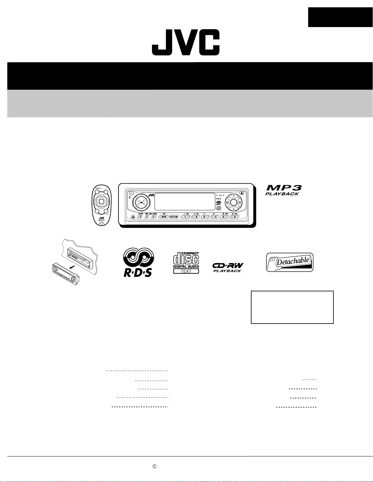
CD RECEIVER
KD-LH7R
SOUND
7
U
SOURCE
F
R
D
VOL
VOL
D
KD-LH7R
Contents
Safety precaution
Preventing static electricity
Important for laser products
Disassembly method
Adjustment method
COPYRIGHT 2002 VICTOR COMPANY OF JAPAN, LTD.
1-2
1-3
1-4
1-5
1-20
Area Suffix
E ---- Continental Europe
EX ------- Central Europe
Flow of functional
operation unit TOC read
Maintenance of laser pickup
Replacement of laser pickup
Description of major ICs
1-21
1-23
1-23
1-24
No.49724
Apr. 2002
Page 2
KD-LH7R
Safety precaution
!
!
Burrs formed during molding may be left over on some parts of the chassis. Therefore,
pay attention to such burrs in the case of preforming repair of this system.
Please use enough caution not to see the beam directly or touch it in case of an
adjustment or operation check.
1-2
Page 3
KD-LH7R
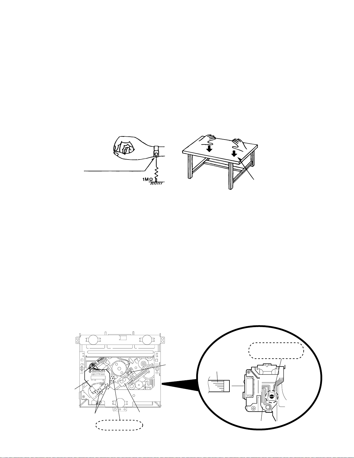
Preventing static electricity
Electrostatic discharge (ESD), which occurs when static electricity stored in the body, fabric, etc. is discharged,
can destroy the laser diode in the traverse unit (optical pickup). Take care to prevent this when performing repairs.
1.1. Grounding to prevent damage by static electricity
Static electricity in the work area can destroy the optical pickup (laser diode) in devices such as DVD players.
Be careful to use proper grounding in the area where repairs are being performed.
1.1.1. Ground the workbench
1. Ground the workbench by laying conductive material (such as a conductive sheet) or an iron plate over
it before placing the traverse unit (optical pickup) on it.
1.1.2. Ground yourself
1. Use an anti-static wrist strap to release any static electricity built up in your body.
(caption)
Anti-static wrist strap
Conductive material
(conductive sheet) or iron plate
1.1.3. Handling the optical pickup
1. In order to maintain quality during transport and before installation, both sides of the laser diode on the
replacement optical pickup are shorted. After replacement, return the shorted parts to their original condition.
(Refer to the text.)
2. Do not use a tester to check the condition of the laser diode in the optical pickup. The tester's internal power
source can easily destroy the laser diode.
1.2. Handling the traverse unit (optical pickup)
1. Do not subject the traverse unit (optical pickup) to strong shocks, as it is a sensitive, complex unit.
2. Cut off the shorted part of the flexible cable using nippers, etc. after replacing the optical pickup. For specific
details, refer to the replacement procedure in the text. Remove the anti-static pin when replacing the traverse
unit. Be careful not to take too long a time when attaching it to the connector.
3. Handle the flexible cable carefully as it may break when subjected to strong force.
4. It is not possible to adjust the semi-fixed resistor that adjusts the laser power. Do not turn it
Short-circuit point
(Soldering)
Connector board
Joints b
Short-circuit
Pickup
DET switch
Flexible wire
Pickup
1-3
Page 4
KD-LH7R
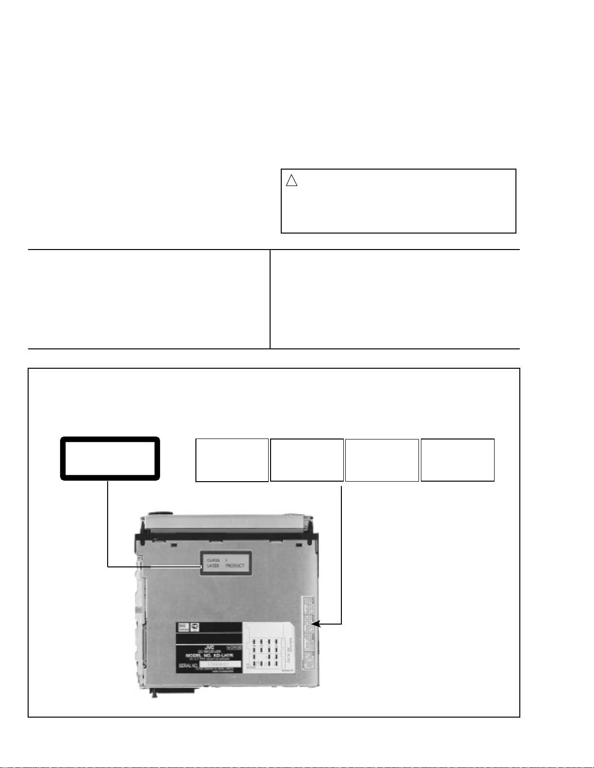
Important for laser products
1.CLASS 1 LASER PRODUCT
2.DANGER : Invisible laser radiation when open and inter lock
failed or defeated. Avoid direct exposure to beam.
3.CAUTION : There are no serviceable parts inside the
Laser Unit. Do not disassemble the Laser Unit. Replace the
complete Laser Unit if it malfunctions.
4.CAUTION : The compact disc player uses invisible laser
radiation and is equipped with safety switches which prevent
emission of radiation when the drawer is open and the safety
interlocks have failed or are defeated.
It is dangerous to defeat the safety switches.
VARNING : Osynlig laserstrålning är denna del är öppnad
och spårren är urkopplad. Betrakta ej strålen.
VARO : Avattaessa ja suojalukitus ohitettaessa olet
alttiina näkymättömälle lasersäteilylle.Älä katso
säteeseen.
5.CAUTION : If safety switches malfunction, the laser is able
to function.
6.CAUTION : Use of controls, adjustments or performance of
procedures other than those specified herein may result in
hazardous radiation exposure.
CAUTION
!
Please use enough caution not to
see the beam directly or touch it
in case of an adjustment or operation
check.
ADVARSEL : Usynlig laserstråling ved åbning , når
sikkerhedsafbrydere er ude af funktion. Undgå
udsættelse for stråling.
ADVARSEL : Usynlig laserstråling ved åpning,når
sikkerhetsbryteren er avslott. unngå utsettelse
for stråling.
REPRODUCTION AND POSITION OF LABELS
WARNING LABEL
CLASS 1
LASER PRODUCT
DANGER : Invisible laser
radiation when open and
interlock or defeated.
AVOID DIRECT EXPOSURE
TO BEAM (e)
ADVARSEL :Usynlig laserstråling ved åbning , når
sikkerhedsafbrydere er ude
af funktion. Undgå udsæt
telse for stråling. (f)
VARNING : Osynlig laserstrålning är denna del
är öppnad och spårren är
urkopplad. Betrakta ej
strålen. (s)
VARO : Avattaessa ja suojalukitus ohitettaessa olet
alttiina näkymättömälle
lasersäteilylle.Älä katso
säteeseen. (d)
1-4
Page 5
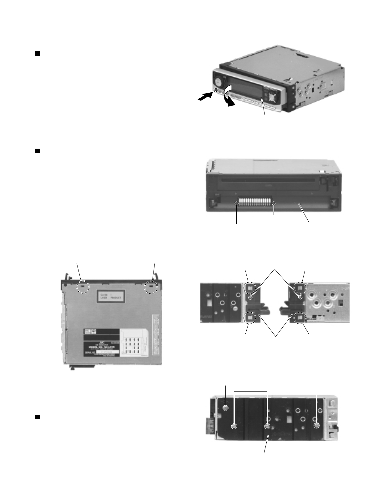
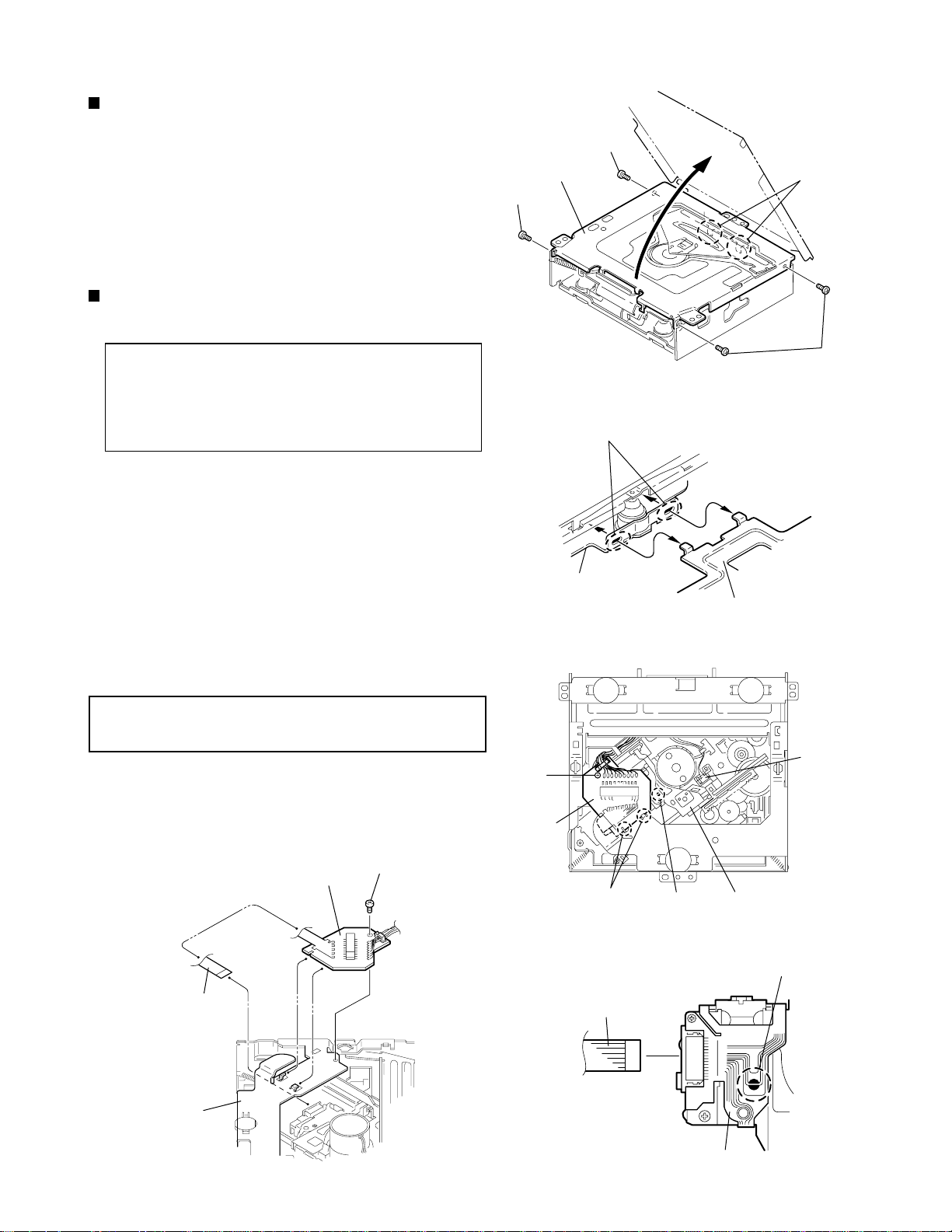
Disassembly method
Removing the front panel unit
(See Fig.1)
1.
Press the release switch and remove the front panel
unit in the direction of the arrow.
Removing the front chassis
(See Fig.2 ~ 4)
1.
Remove the two screws A attaching the front
chassis.
KD-LH7R
Front panel unit
Fig.1
2.
Remove the two screws B on each side of the body.
3.
Release the two joints a and the two joints b on the
sides. Release the two joints c at the bottom and
remove the front chassis toward the front.
Joint c
Joint c
A
Joint a
Joint a
Fig.2
B
Front chassis
Fig. 3
Front chassis
Joint b
Joint b
Fig.4
Removing the heat sink (See Fig.5)
1.
Remove the four screws C attaching the heat sink
on the left side of the body, and remove the heat
sink.
C
C
Heat sink
Fig. 5
C
1-5
Page 6
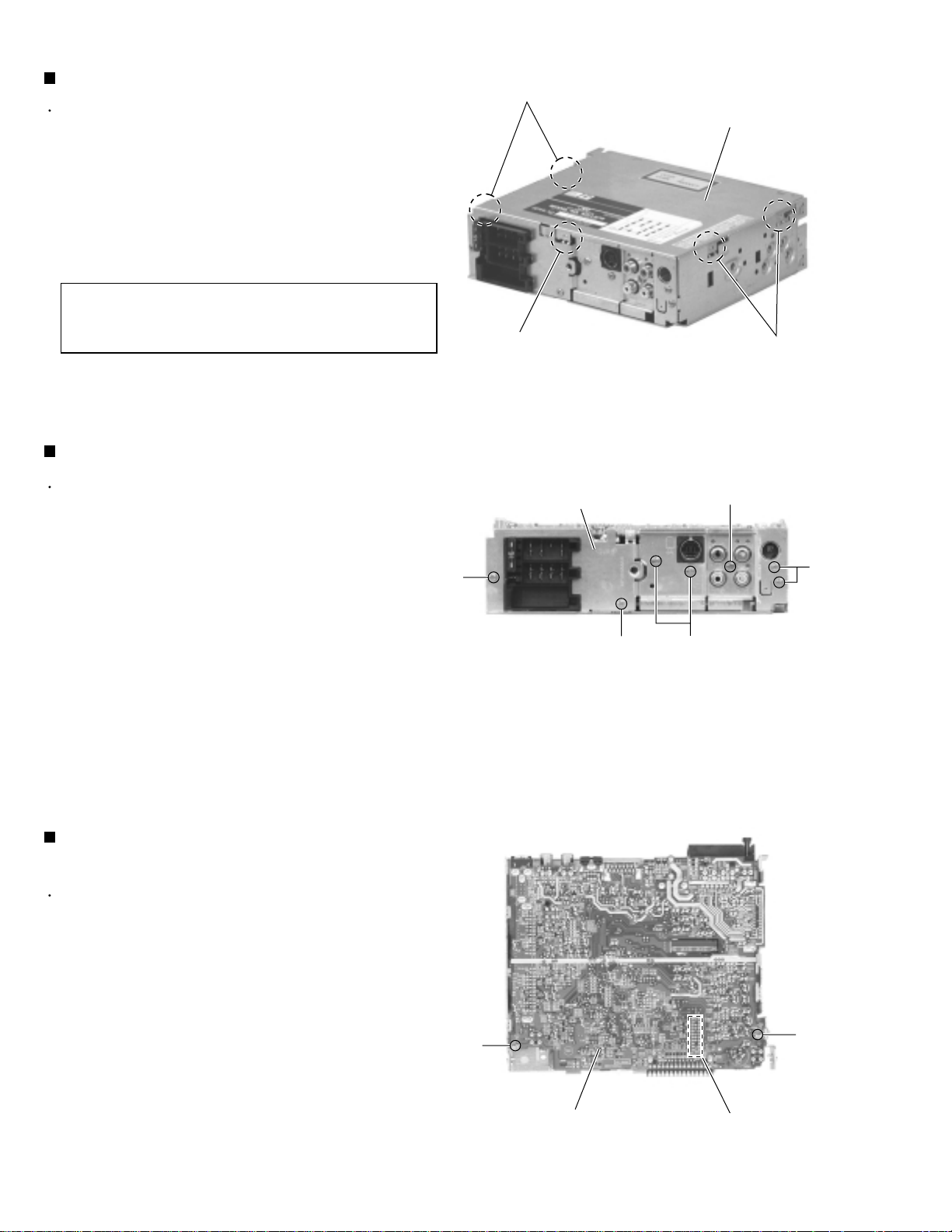
KD-LH7R
Removing the bottom cover (See Fig.6)
Prior to performing the following procedure, remove
the front chassis and the heat sink.
1.
Turn the body upside down.
2.
Insert a screwdriver to the two joints d and two joints
e on both sides of the body and the joint f on the
back of the body, then detach the bottom cover from
the body.
CAUTION:
When disengaging the joint f using a
screwdriver, do not damage or break the
board.
Removing the rear panel (See Fig.7 )
Prior to performing the following procedure, remove
the front chassis, the heat sink and bottom cover.
Joint d
Joint f
Rear panel
Bottom cover
Joint e
Fig. 6
E
1.
Remove the six screws D attaching the rear panel
and one screw E attaching the pine jack on the back
of the body.
D
Removing the main amplifier board assembly
(See Fig.8)
Prior to performing the following procedure, remove
the front chassis, the heat sink, bottom cover and the
rear panel.
1.
Remove the two screws F attaching the main
amplifier board assembly on the top cover.
D
Fig. 7
D
D
2.
Disconnect connector CN101 on the main amplifier
board assembly from the cassette mechanism
assembly.
1-6
F
Main board assembly
F
CN101
Fig. 8
Page 7
KD-LH7R
Removing the MP3 board
(See Fig.9)
Prior to performing the following procedure, remove
the top cover.
1.
Disconnect the wire from connector CN601 on the
MP3 board.
2.
Remove the five screws G and the MP3 board,
releasing the joint g and h.
G
g
h
CN601
G
Fig.9
Removing the CD mechanism assembly
(See Fig.10)
Prior to performing the following procedure, remove
the front chassis, the heat sink, bottom cover and the
main amplifier board assembly.
1.
Remove the three screws H attaching the cassette
mechanism assembly from the top cover.
Top cover
H
H
H
CD mechanism assembly
Fig. 10
1-7
Page 8
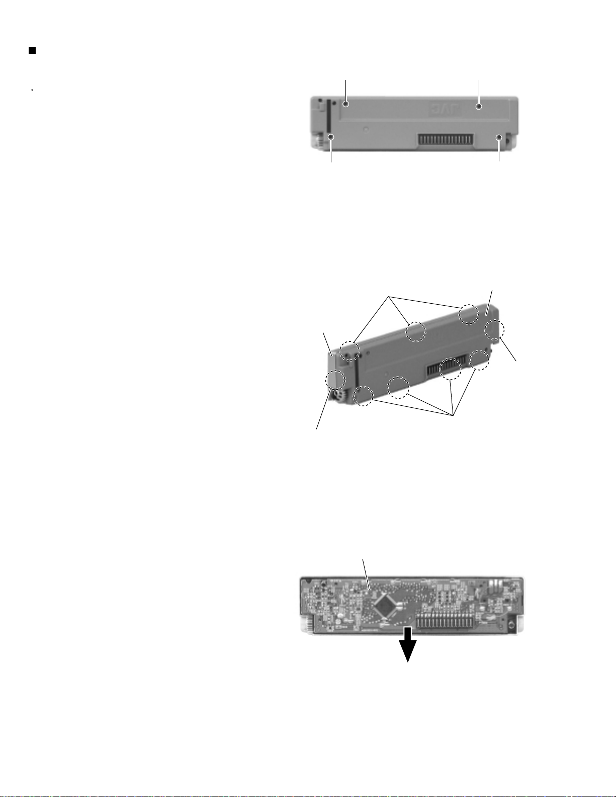
KD-LH7R
Removing the (LCD & key) control switch
board (See Fig.11
Prior to performing the following procedure, remove
the front panel assembly.
1.
Remove the four screws I attaching the rear cover
on the back of the front panel assembly.
2.
Unjoint the nine joints i with the front panel and the
rear cover.
3.
Remove the control switch board on the back of the
front panel.
~ 13)
I
I
Fig. 11
I
I
Front panel
Joint i
LCD & Key control board
Joint i
Rear cover
Joint i
Joint i
Fig. 12
1-8
Fig. 13
Page 9
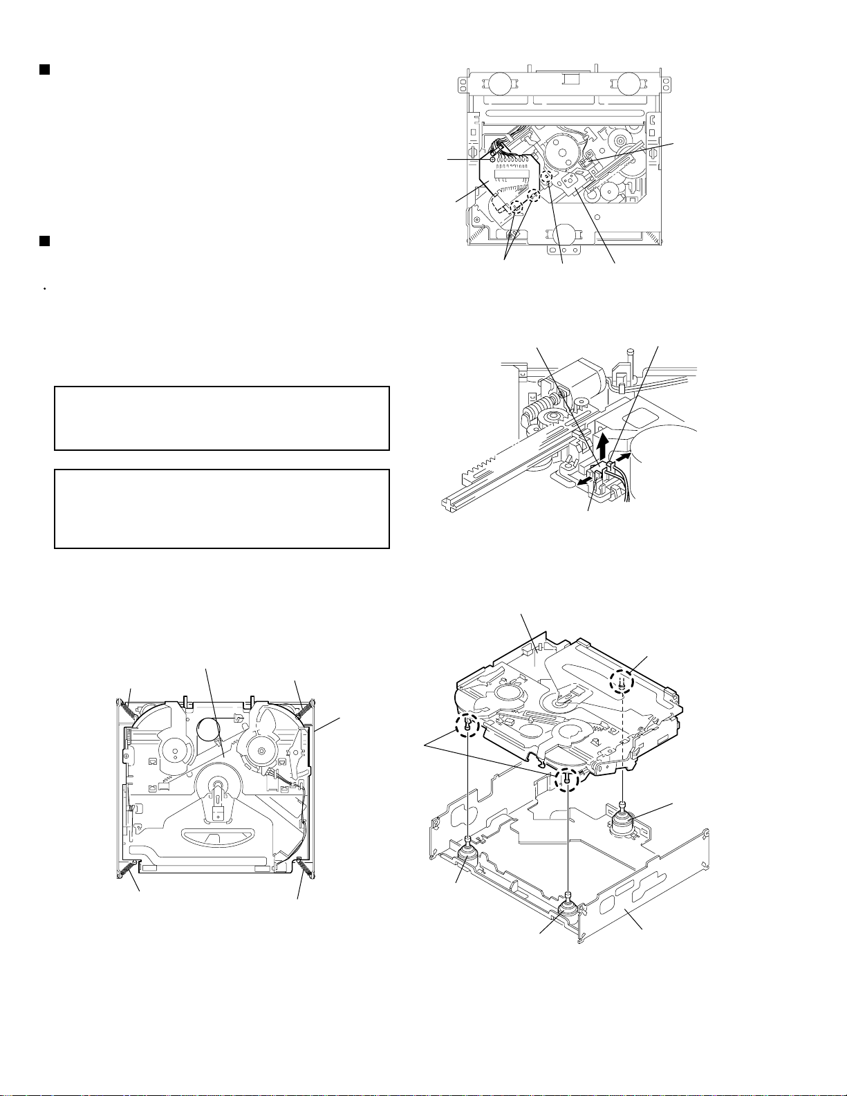
< CD mechanism section >
Removing the top cover
(See Fig.1 and 2)
1.
Remove the two screws A on each side of the body.
2.
Lift the front side of the top cover and move the
cover backward to release the two joints a.
Removing the connector board
(See Fig.3 to 5)
Top cover
A
KD-LH7R
A
Joints a
CAUTION:
1.
Remove the screw B fixing the connector board.
2.
Solder the short-circuit point on the connector board.
Disconnect the flexible wire from the pickup.
3.
Move the connector board in the direction of the
arrow to release the two joints b.
4.
Unsolder the wire on the connector board if
necessary.
CAUTION:
Before disconnecting the flexible wire
from the pickup, solder the short-circuit
point on the pickup. No observance of
this instruction may cause damage of
the pickup.
Unsolder the short-circuit point after
reassembling.
A
Fig.1
Joints a
Top cover
Fig.2
DET switch
B
Flexible wire
Frame
Connector board
B
Connector board
Joints b
Flexible wire
Short-circuit
Fig.3
Fig.4Fig.5
Pickup
Short-circuit point
(Soldering)
Pickup
1-9
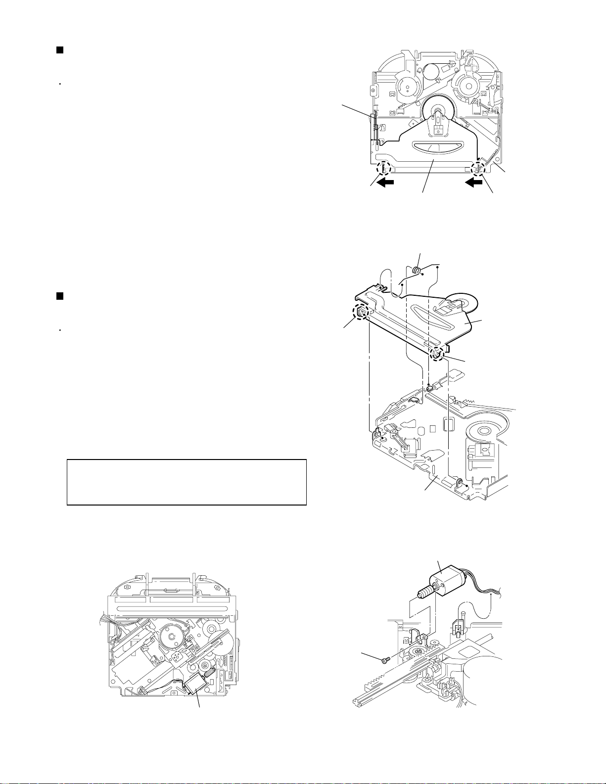
Page 10
KD-LH7R
Removing the DET switch
(See Fig.3 and 6)
1.
Extend the two tabs c of the feed sw. holder and pull
out the switch.
2.
Unsolder the DET switch wire if necessary.
Removing the chassis unit
(See Fig.7 and 8)
Prior to performing the following procedure, remove
the top cover and the connector board.
B
Connector board
Joints b
Short-circuit
Fig.3
DET switch
Pickup
1.
Remove the two suspension springs (L) and (R)
attaching the chassis unit to the frame.
CAUTION:
The shape of the suspension spring (L)
and (R) are different. Handle them with
care.
CAUTION:
When reassembling, make sure that the
three shafts on the underside of the
chassis unit are inserted to the dampers
certainly.
Chassis unit
Suspension spring (R)
Suspension spring (L)
Frame
DET switch
Chassis unit
Tab c
Feed sw. holder
Tab c
Fig.6
Shaft
1-10
Suspension spring (R)
Suspension spring (L)
Shafts
Damper
Damper
Damper
Frame
Fig.8Fig.7
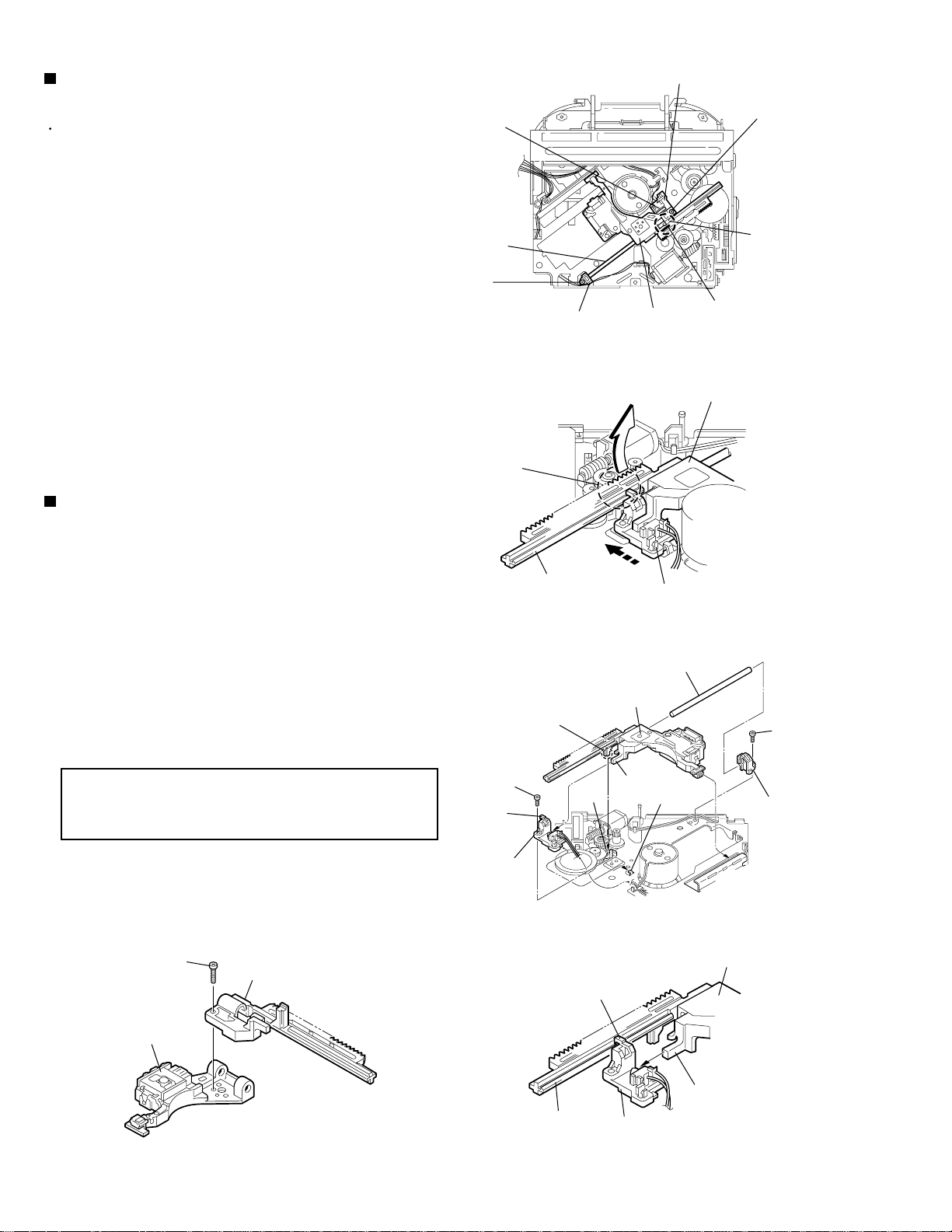
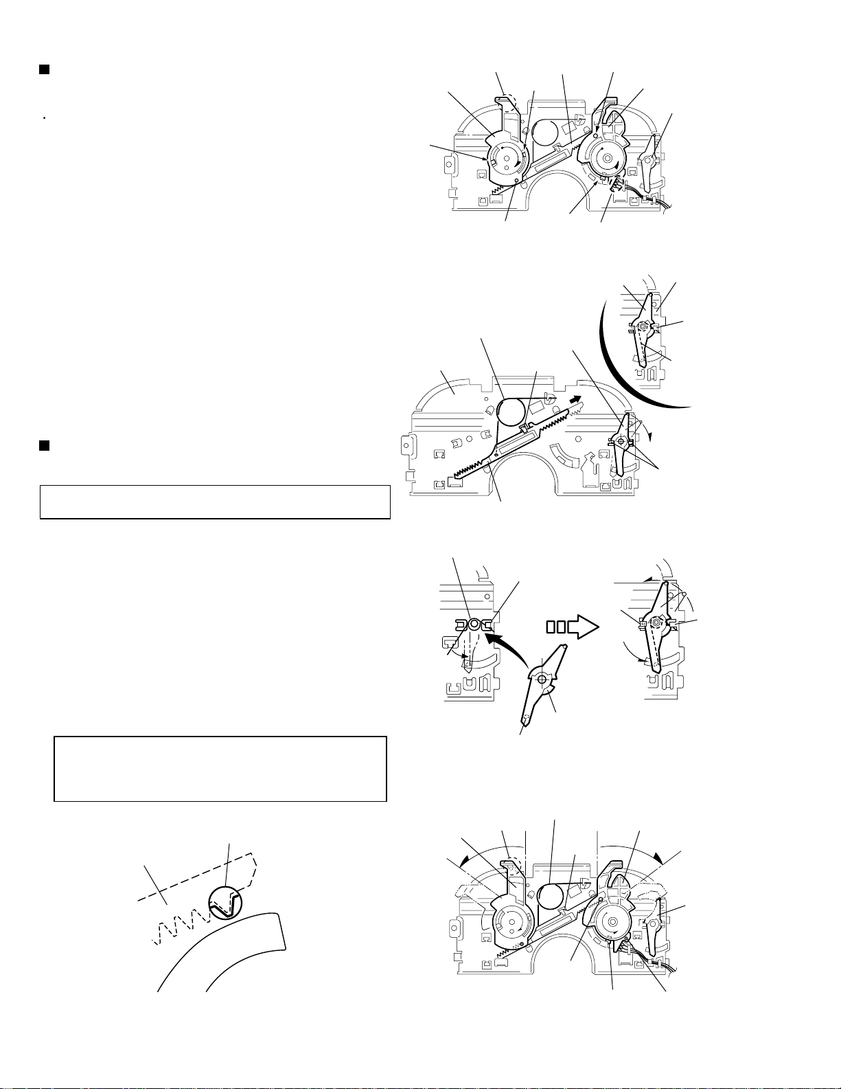
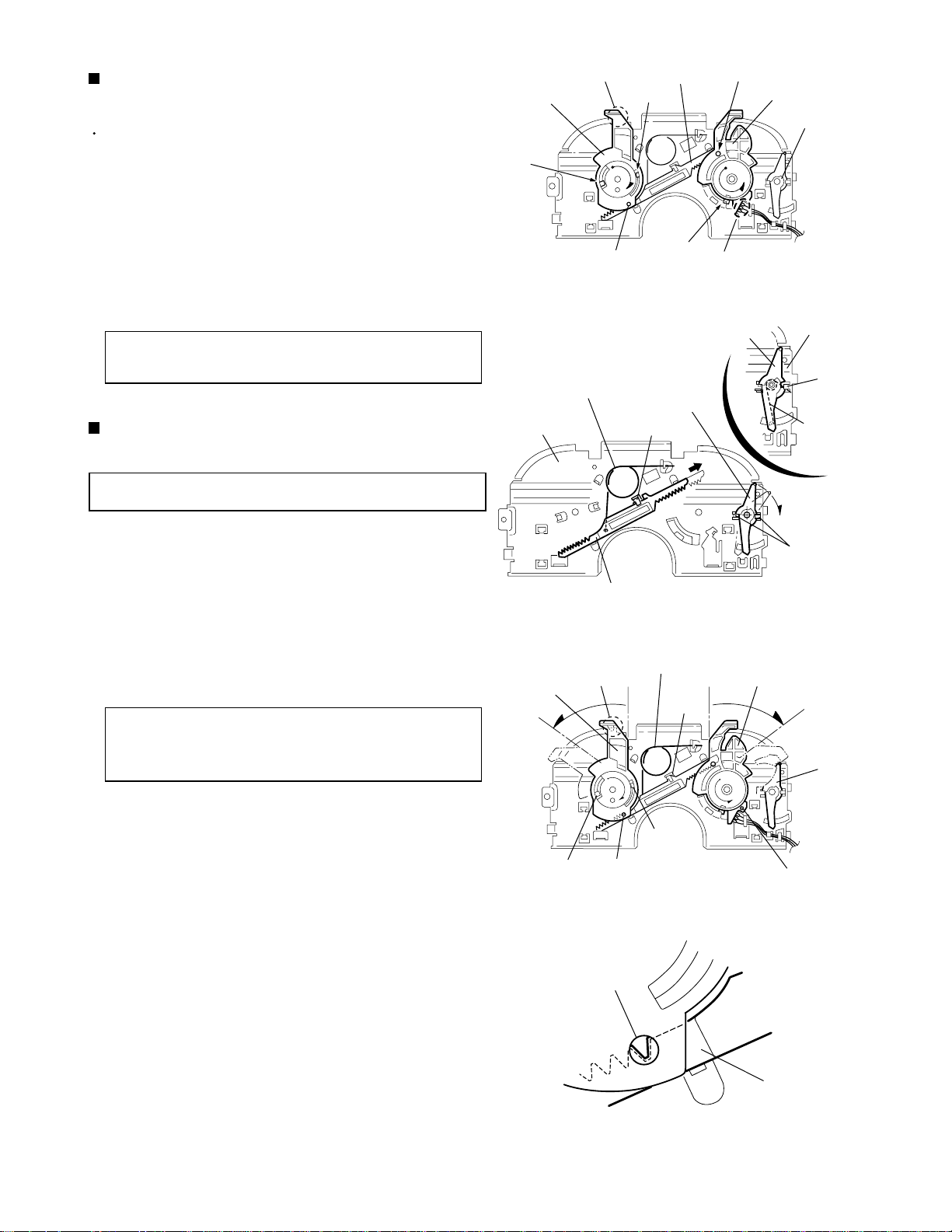
Page 11
Removing the clamper assembly
(See Fig.9 and 10)
KD-LH7R
Prior to performing the following procedure, remove
the top cover.
1.
Remove the clamper arm spring.
2.
Move the clamper assembly in the direction of the
arrow to release the two joints d.
Removing the loading / feed motor
assembly (See Fig.11 and 12)
Prior to performing the following procedure, remove
the top cover, the connector board and the chassis
unit.
1.
Remove the screw C and move the loading / feed
motor assembly in the direction of the arrow to
remove it from the chassis rivet assembly.
Clamper arm
spring
Joint d
Joint d
Clamper assembly
Fig.9
Clamper arm spring
Chassis rivet
assembly
Joint d
Clamper assembly
Joint d
2.
Disconnect the wire from the loading / feed motor
assembly if necessary.
CAUTION:
When reassembling, connect the wire
from the loading / feed motor assembly
to the flame as shown in Fig.11.
Chassis rivet assembly
Fig.10
Loading / feed motor assembly
C
Loading / feed motor assembly
Fig.12Fig.11
1-11
Page 12
KD-LH7R
Removing the pickup unit
(See Fig.13 to 17)
Prior to performing the following procedure, remove
the top cover, the connector board and the chassis
unit.
1.
Remove the screw D and pull out the pu. shaft
holder from the shaft.
2.
Remove the screw E attaching the feed sw. holder.
3.
Move the part e of the pickup unit upward with the
shaft and the feed sw. holder, then release the joint f
of the feed sw. holder in the direction of the arrow.
The joint g of the pickup unit and the feed rack is
released, and the feed sw. holder comes off.
4.
Remove the shaft from the pickup unit.
5.
Remove the screw F attaching the feed rack to the
pickup unit.
Reattaching the pickup unit
(See Fig.13 to 16)
Joint f
Shaft
D
Joint e
Pu. shaft holder
Feed sw. holder
Pickup unit
Fig.13
Pickup unit
E
Joint f
Joint e
1.
Reattach the feed rack to the pickup unit using the
screw F.
2.
Reattach the feed sw. holder to the feed rack while
setting the joint tab g to the slot of the feed rack and
setting the part f of the feed rack to the switch of the
feed sw. holder correctly.
3.
As the feed sw. holder is temporarily attached to the
pickup unit, set to the gear of the joint g and to the
bending part of the chassis (joint h) at a time.
CAUTION:
4.
Reattach the feed sw. holder using the screw E.
5.
Reattach the shaft to the pickup unit. Reattach the
pu. shaft holder to the shaft using the screw D.
Make sure that the part i on the underside
of the feed rack is certainly inserted to the
slot j of the change lock lever.
F
Feed rack
Feed rack
E
Joint g
Feed sw. holder
Part i
Pickup unit
Slot j
Joint g
Feed sw. holder
Fig.14
Shaft
Joint f
Joint h
Fig.15
D
Pu. shaft holder
Pickup unit
1-12
Pickup unit
Feed rack
Joint f
Feed sw. holder
Fig.17Fig.16
Page 13
Removing the trigger arm
(See Fig.18 and 19)
Prior to performing the following procedure, remove
the top cover, the connector board and the clamper
unit.
1.
Turn the trigger arm in the direction of the arrow to
release the joint k and pull out upward.
KD-LH7R
Joint k
Trigger arm
CAUTION:
When reassembling, insert the part l and
m of the trigger arm into the part n and
o at the slot of the chassis rivet
assembly respectively and join the joint
k at a time.
Chassis rivet assembly
Chassis rivet assembly
Trigger arm
Fig.18
Part n
Part o
Part l
Part m
Fig.19
Removing the top plate assembly
(See Fig.20)
Prior to performing the following procedure, remove
the top cover, the connector board, the chassis unit,
and the clamper assembly.
1.
Remove the screw H.
2.
Move the top plate assembly in the direction of the
arrow to release the two joints p.
3.
Unsolder the wire marked q if necessary.
H
Top plate assembly
Joints p
q
Fig.20
1-13
Page 14
KD-LH7R
Removing the select arm (L) / select lock
arm (See Fig.21 and 22)
Prior to performing the following procedure, remove
the top plate assembly.
1.
Bring up the select arm (L) to release from the link
plate (joint r) and turn in the direction of the arrow to
release the joint s.
2.
Unsolder the wire of the select arm (L) marked q if
necessary.
3.
Turn the select lock arm in the direction of the arrow
to release the two joints t.
The select lock arm spring comes off the select lock
arm at the same time.
Reassembling the select arm (L) / select
lock arm (See Fig.23 to 25)
Select arm (R)
Joint z
Link plate spring
Top plate
Joint a'
Joint y
Link plate
Joint z
Joint s
Fig.21
Select lock arm
Select lock arm
Joint b'
Joint r
Select arm (L)
Select lock arm
q
Top plate
Hook u
Select lock
arm spring
Joints t
REFERENCE:
1.
Reattach the select lock arm spring to the top plate
Reverse the above removing procedure.
and set the shorter end of the select lock arm spring
to the hook u on the top plate.
2.
Set the other longer end of the select lock arm spring
to the boss v on the underside of the select lock arm,
and join the select lock arm to the slots (joint t). Turn
the select lock arm as shown in the figure.
3.
Reattach the select arm (L) while setting the part r to
the first peak of the link plate gear, and join the joint
s.
CAUTION:
When reattaching the select arm (L),
check if the points w and x are correctly
fitted and if each part operates properly.
Joint r
Link plate
Link plate
Select lock arm spring
Boss v
Select arm (R)
Joint a'
Fig.22
Hook u
Joint t
Joint t
Select lock arm
Fig.23
Link plate spring
Select arm (L)
Joint b'
1-14
Joint r
Fig.25Fig.24
Joint s
Select
lock arm
Point x
Page 15
KD-LH7R
Removing the select arm (R) / link plate
(See Fig.21 and 22)
Prior to performing the following procedure, remove
the top plate assembly.
1.
Bring up the select arm (R) to release from the link
plate (joint y) and turn as shown in the figure to
release the two joints z and joint a’.
2.
Move the link plate in the direction of the arrow to
release the joint b’. Remove the link plate spring at
the same time.
REFERENCE:
Before removing the link plate, remove
the select arm (L).
Reattaching the Select arm (R) / link
plate (See Fig.25 and 26)
REFERENCE:
Reverse the above removing procedure.
Select arm (R)
Joint z
Link plate spring
Top plate
Joint a'
Part y
Link plate
Joint z
Joint s
Fig.21
Select lock arm
Select lock arm
Joint b'
Joint r
Select arm (L)
Select lock arm
q
Top plate
Hook u
Select lock
arm spring
1.
Reattach the link plate spring.
2.
Reattach the link plate to the link plate spring while
joining them at joint b’.
3.
Reattach the part y of the select arm (R) to the first
peak of the link plate while joining the two joints z
with the slots. Then turn the select arm (R) as shown
in the figure. The top plate is joined to the joint a’.
CAUTION:
When reattaching the select arm (R),
check if the part c’ is correctly fitted and
if each part operates properly.
Select arm (R)
Joint z
Link plate
Link plate spring
Joint a'
Part y
Part y
Fig.22
Joint b'
Joint z
Fig.25
Joints t
Select arm (L)
Select
lock arm
Point x
Fig.26
Link plate
1-15
Page 16

KD-LH7R
Removing the loading roller assembly
(See Fig.27 to 29)
Prior to performing the following procedure, remove
the clamper assembly and the top plate assembly.
1.
Push inward the loading roller assembly on the gear
side and detach it upward from the slot of the joint d’
of the lock arm rivet assembly.
Detach the loading roller assembly from the slot of
the joint e’ of the lock arm rivet assembly.
The roller guide comes off the gear section of the
loading roller assembly.
Remove the roller guide and the washer from the
shaft of the loading roller assembly.
2.
Remove the screw I attaching the lock arm rivet
assembly.
3.
Push the shaft at the joint f’ of the lock arm rivet
assembly inward to release the lock arm rivet
assembly from the slot of the slide plate. Extend the
lock arm rivet assembly outward and release the
joint g’ from the boss of the chassis rivet assembly.
The roller guide springs on both sides come off.
Roller guide
Washer
Loading roller assembly
Roller guide
Joint e'
Roller guide spring
Roller guide spring
Joint d'
Loading roller assembly
Roller guide spring
Lock arm rivet assembly
Fig.27
Loading roller assembly
Roller guide
spring
CAUTION:
When reassembling, reattach the left
and right roller guide springs to the lock
arm rivet assembly before reattaching
the lock arm rivet assembly to the
chassis rivet assembly. Make sure to fit
the part h’ of the roller guide spring (L)
inside of the roller guide (Refer to
Fig.30).
Roller guide
Washer
Roller shaft assembly
Joint h'
Loading roller assembly
Roller guide
spring
Fig.28-1
Fig.28-2
Chassis rivet assembly
Boss
Slide plate
Roller guide spring
I
1-16
Frame
Loading roller
Roller guide spring
Lock arm rivet assembly
Joint f'
Part g'
Fig.29Fig.30
Page 17

KD-LH7R
Removing the loading gear (5), (6) and
(7) (See Fig.31 and 32)
Prior to performing the following procedure, remove
the top cover, the chassis unit and the top plate
assembly.
1.
Remove the screw J attaching the loading gear
bracket. The loading gear (6) and (7) come off the
loading gear bracket.
2.
Pull out the loading gear (5).
Loading gear bracket
J
Loading gear (6)
Loading gear (5)
Loading gear (3)
Fig.31
J
Loading gear bracket
Loading gear (5)
Loading gear (6)
Loading gear (7)
Fig.32
1-17
Page 18

KD-LH7R
Removing the gears (See Fig.33 to 36)
Prior to performing the following procedure, remove
the top cover, the chassis unit, the top plate
assembly and the pickup unit.
1.
Pull out the feed gear.
Slot j'
Slide plate
2.
Move the loading plate assembly in the direction of
the arrow to release the slide plate from the two slots
j’ of the chassis rivet assembly.
3.
Detach the loading plate assembly upward from the
chassis rivet assembly while releasing the joint k’.
Remove the slide hook and the loading plate spring
from the loading plate assembly.
4.
Pull out the loading gear (2) and remove the change
lock lever.
5.
Remove the E-washer and the washer attaching the
changer gear (2).
6.
The changer gear (2), the changer gear spring and
the adjusting washer come off.
7.
Remove the loading gear (1).
8.
Move the hang plate rivet assembly in the direction
of the arrow to release from the three shafts of the
chassis rivet assembly upward.
9.
Detach the loading gear plate rivet assembly from
the shaft of the chassis rivet assembly upward while
releasing the joint l’.
Feed gear
Change plate
rivet assembly
Shafts
E-washer
Loading plate assembly
Joint k'
Slot j'
Fig.33
Joint l'
Loading gear (4)
Loading gear plate
rivet assembly
Loading gear (2)
Loading gear (1)
Change gear (2)
10.
Pull out the loading gear (4).
Loading plate assembly
Loading plate spring
Slot j'
Chassis rivet assembly
Joint k'
Slide hook
Slide plate
Slot j'
E-washer
Washer
Loading gear (2)
Loading plate spring
Adjusting washer
Change plate
rivet assembly
Chassis rivet assembly
Fig.34
Loading gear (1)
Loading gear (2)
Change lock lever
Loading gear (4)
Loading gear plate rivet assembly
Fig.36Fig.35
1-18
Page 19

KD-LH7R
Removing the turn table / spindle motor
(See Fig.37 and 38)
Prior to performing the following procedure, remove
the top cover, the connector assembly and the
chassis / clamper assembly.
1.
Remove the two screws K attaching the spindle
motor assembly through the slot of the turn table on
top of the body.
2.
Unsolder the wire on the connector board if
necessary.
K
Turn table
Fig.37
K
Turn table
Spindle motor
Fig.38
1-19
Page 20

KD-LH7R
Adjustment method
Test instruments required for adjustment
1. Digital oscilloscope (100MHz)
2. AM Standard signal generator
3. FM Standard signal generator
4. Stereo modulator
5. Electric voltmeter
6. Digital tester
7. Tracking offset meter
8. Test Disc JVC :CTS-1000
9. Extension cable for check
EXTSH002-22P 1
Standard measuring conditions
Power supply voltage : DC14.4V(11V~16V allwance)
Load impedance : 4 (4 to 8 allowance)
Line-out Level / Impedance:
2.0V / 20 k load
How to connect the extension cable for adjusting
Standard volume position
Balance and Bass &Treble volume : lndication"0"
Loudness : OFF
BBE : OFF
Frequency Band
FM 87.5MHz ~ 108.0MHz
MW 522kHz ~ 1620 kHz
LW 144kHz ~ 279kHz
Dummy load
Exclusive dummy load should be used for AM,and FM. For
FM dummy load,there is a loss of 6dB between SSG output
and antenna input.The loss of 6dB need not be considered
since direct reading of figures are applied in this working
standard.
Extension cables
EXTSH002-22P
CN101
CN501
CD Mechanism
Main board
1-20
Page 21

Flow of functional operation until TOC read
Power ON
• When the pickup correctly moves
to the inner area of the disc
Set Function to CD
KD-LH7R
• When the laser diode correctly
emits
Microprocessor
commands
FMO
TC94A14FA "40"
FEED MOTOR
TERMINAL
+TERMINAL
IC681 "4"
REST SW
• When correctly focused
FEO
TA2157FN "15"
Focus Servo Loop ON
Disc inserted
Pickup feed to the inner area
Laser emitted
Focus search
Disc rotates
RF signal eye-pattern
remains closed
Tracking loop closed
RF signal eye-pattern
opens
TOC readout
YES
YES
Microprocessor
commands
TC94A14FA"38"
CN601"10"
1
"No disc"
display
• When the disc correctly rotates
Microprocessor
commands
TN94A14FA
"41"
Spindle
motor (-)
IC681 "7"
AccelerationAcceleration
0.5 Sec
Rough
Servo
0.5 Sec
Servo CLV
3.3V
3.3V
Jump to the first track
Play
Tracking Servo Loop ON
• RF signal
Rough Servo Mode
CLV Servo Mode
(ProgramArea)
CLV Servo Mode
(Lead-In Area;
Digital: 0)
1-21
Page 22

KD-LH7R
Feed Section
Is the voltage output at
IC621 pin "40" 5V or 0V?
Is 4V present at both
sides of the feed motor?
YES
YES
NO
Is the wiring for IC621
(56) ~ (64) correct?
NO
Is 6V or 3V present at
IC681 "4" and "5"?
NO
YES
YES
Is 3.3V present at
IC681 pin "20"?
YES
Check the vicinity of
IC621.
Check the feed motor
connection wiring.
NONO
Check CD 8V
and 5V.
Check the feed motor.
Focus Section
When the lens is
moving:
4V
Does the S-search
waveform appear at
IC681 pins "10" and "11"?
Spindle Section
Is the disk rotated?
YES
Does the RF signal
appear at TP1?
YES
Check IC681.
NO
YES
NO
Check the circuits in the
vicinity of IC681 pins
"8","9" and "15".
Check the pickup and
its connections.
Is 4V present at IC681
pins "7" and "6" ?
Check the spindle motor
and its wiring.
NO
YES
YES
NO NO
Is 4V present at IC621
pin "41" ?
YES
Check the vicinity of
IC681.
Check IC621 and
IC601.
Is the RF waveform at TP1
distorted?
Proceed to the Tracking
section
Tracking Section
When the disc is rotated
Is the tracking error signal
1-22
NO
YES
at first:
Approx. 1.2 V
output at IC601 "11"?
YES
Check IC621.
Check the circuits in the
vicinity of IC601 "19"~"24"
or the pickup
Check the circuit in the
vicinity of IC601 pins
"2" ~ "12".
YESYES
Check the pickup and
its connections.
Page 23

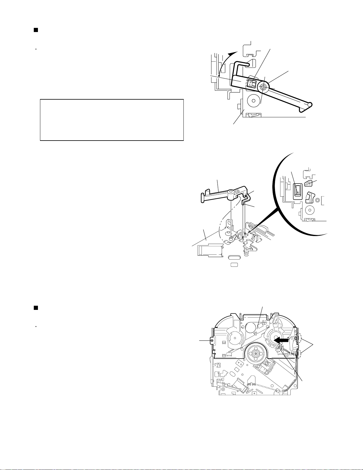
Maintenance of laser pickup
(1) Cleaning the pick up lens
Before you replace the pick up, please try to
clean the lens with a alcohol soaked cotton
swab.
(2) Life of the laser diode
When the life of the laser diode has expired,
the following symptoms will appear.
The level of RF output (EFM output:ampli
tude of eye pattern) will be low.
KD-LH7R
Is RF output
1.0 0.35Vp-p?
YES
O.K
(3) Semi-fixed resistor on the APC PC board
The semi-fixed resistor on the APC printed
circuit board which is attached to the pickup
is used to adjust the laser power.Since this
adjustment should be performed to match the
characteristics of the whole optical block,
do not touch the semi-fixed resistor.
If the laser power is lower than the specified
value,the laser diode is almost worn out, and
the laser pickup should be replaced.
If the semi-fixed resistor is adjusted while
the pickup is functioning normally,the laser
pickup may be damaged due to excessive current.
NO
Replace it.
Replacement of laser pickup
Turn off the power switch and,disconnect the
power cord from the ac outlet.
Replace the pickup with a normal one.(Refer
to "Pickup Removal" on the previous page)
Plug the power cord in,and turn the power on.
At this time,check that the laser emits for
about 3seconds and the objective lens moves
up and down.
Note: Do not observe the laser beam directly.
Play a disc.
Check the eye-pattern at TP1.
Finish.
1-23
Page 24

KD-LH7R
Description of major ICs
BR24C01AFV-W-X (IC502) : EEPROM
1.Pin layout
2.Block diagram
A0
1
A1
2
A2
3
Vcc WP SCL SDA
A0 A1 A2 GND
1kbit EEPROM ARRAY
7bit
ADDRESS
DECODER
CONTROL LOGIC
SLAVE/WORD
7bit
ADDRESS REGISTER
START
STOP
ACK
8bit
DATA
REGISTER
Vcc
8
WP
7
SCL
6
GND
4
HIGH VOLTA GE GEN.
3.Pin function
Pin name I/O
Vcc
GND
A0,A1,A2
SCL
SDA
WP
*1 An open drain output requires a pull-up resister.
-
IN
IN
IN / OUT
IN
Power supply
Ground (0v)
Slave address set
Serial clock input
Slave and word address,
serial data input, serial data output *1
Write protect input
Vcc LEVEL DETECT
Function
SDA
5
1-24
Page 25

BR24C32F-X (IC771) : EEPROM
KD-LH7R
1. Pin layout
Vdd WPIN SCL SDA
A0 A1 A2 GND
3. Block diagram
A0 1
A1 2
A2 3
11bit
Address
decoder
16kbit EEPROM allay
11bit
START
Control circuit
2. Pin function
Symbol
Vdd
GND
A0,A1,A2
SCL
SDA
WPIN
Slave Word
Address resister
STOP
I/O
-
Power supply.
-
GND
I
No use connect to GND.
I
Serial clock input.
I/O
Serial data I/O of slave and word address.
I
Write protect terminal.
8bit
Data
resister
Function
8 Vdd
7 WPIN
6 SCL
GND 4
High voltage osc circuit
Power supply
voltage det.
ACK
5 SDA
1-25
Page 26

KD-LH7R
UPD784216AGC163 (IC701): SYSTEM CPU
Pin No.
1
2
3
4
5
6
7
8
9
10
11
12
13
14
15
16
17
18
Symbol I/O Function
SW2
SW3
SW4
REST
LM0
LM1
NC
NC
VDD
O
O
O
O
Signal input of mechanism switch 2 detection
I
Signal input of mechanism switch 3 detection
I
Signal input of mechanism switch 4 detection
I
Rest switch detection signal input
I
Loading side motor control signal output
Eject side motor control signal output
Non connect
Non connect
5V connection
X2
X1
VSS
GND connection
XT2
XT1
RESET
SW1
BUS-INT
PS2
Reset detection terminal
I
Mechanism switch detection signal input
I
J-BUS signal interrupt input
I
POWER SAVE2. BACK UP and synchronization
I
Becomes stop mode because of the input of H.
19
20
21
22
23
24
25
CRUISE
RDS-SCK
RDS DA
REMOCON
AVDD
AVREF0
VOL1
Pulse signal input for cruise
I
RDS clock input
I
RDS data input
I
Remote control signal input
I
5V connection
5V connection
Rotation volumepulse signal input
I
Pulse which actually becomes judgment of change
26
27
28
29
30
31
32
33
34
35
36
37
38
39
40
41
42
43
44
45
46
47
48
49
50
VOL2
KEY0
KEY1
KEY2
LEVEL
SQ
SM
AVSS
NC
NC
AVREF
BUS-SI
BUS-SO
BUS-SCK
BUS-I/O
LCD-DA
LCD-SCK
LCD-CE
BUZZER
E2PROM-DI
E2PROM-DO
E2PROM-CLK
OPEN
NC
NC
I
I
I
I
I
I
I
O
O
I
O
I/O
O
O
O
O
OI
O
O
I
O
O
O
Rotation volume pulse signal input
Key input 0
Key input 1
Key input 2
Level meter input
S.QUALITY level input
S.METER level input
GND connection
Non connect
Non connect
5V connection
J-BUS data input
J-BUS data output
J-BUS clock input & output
J-BUS I/O switch output. At output : H, At input : L
Data output to LCD driver
Clock output to LCD driver
Chipenable to LCD driver
Buzzer output
Communication data input of 12C
Communication data output of 12C
Communication data clock output 12C
Opening detection input
Non connect
Non connect
UPD784216AGC163(1/2)
1-26
Page 27

Pin No. Symbol I/O Function
51
52
53
NC
NC
SD/ST
Non connect
O
Non connect
O
Station detector and stereo signal input.
I
It is H and there is a bureau.It is L and a stereo.
54
55
NC
MONO
Non connect
O
Monaural ON/OFF switch output.
O
At the time of the MONO ON :H.
56
57
58
59
60
61
NC
NC
NC
NC
NC
DETACH
Non connect
I
Non connect
I
Non connect
I
Non connect
I
Non connect
I
Detach signal input. It is L of 200ms or more and an
I
operation mode. H:POWER SAVE
62
63
64
65
66
67
68
69
70
AFCK
SEEK/STP
NC
FM/AM
PLL-CE
PLL-DO
PLL-CLK
PLL-DI
TEL-MUTE
AF check output. AF check:L
O
Auto seek stop switch output. At SEEK:H. At STOP:L
O
Non connect
O
FM,AM switch output
O
CE output for IC control for PLL
O
Data output for IC control for PLL
O
Clock output for IC control PLL
O
Data output for IC control for PLL
I
Telephone mute detection input.
I
It is L or H and MUTE(ACTIVE depends on the PSM setting)
71
72
73
74
NC
VSS
DIM-IN
PS1
Non connect (ex:AMP-KILL output)
O
GND connection
Dimmer detection input. At L:dimmer ON.
I
POWER SAVE 1. ACC and synchronization
I
POWER SAVE : L. At operation:H
75
76
77
78
79
80
81
82
83
84
85
86
87
88
89
90
91
92
93
94
95
96
97
98
99
100
POWER
CD-ON
MUTE
NC
NC
NC
VDD
NC
VOL-DA
VOL-CLK
DIM-OUT
NC
NC
NC
NC
STAGE
BUCK
CCE
RST
TEST
BUS0
BUS1
BUS2
BUS3
DISCSEL
J/E
O
O
O
O
O
O
O
O
O
O
O
O
O
O
I
O
O
O
I/O
I/O
I/O
I/O
O
I
POWER ON/OFF switch output. At POWER ON:H
The CD power supply control signal output. At CD :H
Mute output. At mute ON:L
Non connect
Non connect
Non connect
5V connection
Non connect
Data output by which IC for electronic volume is controlled
Clock output by which IC for electronic volume is controlled
Dimmer control output. L:DIMMER ON (ex:BBE)
Non connect
Non connect
Non connect
Non connect
H:For 991R / L:For 911R
Clock output for data communication with CDLSI
CE output for data communication with CDLSI
CDLSI reset signal output
connects GND with 10k pull down (For flash switch)
Data communication input output port 0 with CDLSI
Data communication input output port 1 with CDLSI
Data communication input output port 2 with CDLSI
Data communication input output port 3 with CDLSI
Pull-down fixation
Pull-up fixation
KD-LH7R
UPD784216AGC163(2/2)
1-27
Page 28

KD-LH7R
HA13164A(IC901):Regulator
1.Terminal layout
2.Block diagram
.IN
1 2 3 4 5 6 7 8 9 101112131415
ANT
2
C3
0.1u
EXT
1
C4
0.1u
ANT CTRL
CTRL
CD8V
7
11
12
C5
0.1u
9V
10
C6
10u
MEMORY. IN
MEMORY.IN ACC.IN
8
Surge Protector
BIAS TSD
15
3
TAB
C1
100u
9
6
4
5
14
+B
ACC
BATT.DET
ACC5V
VDD5V
SW5VOUT
10V
R1
C7
0.1u
C8
0.1u
C2
0.1u
13
AJGND GND
3.Pin function
Pin No. Symbol Function
1
2
EXT
OUT
Output voltage is VCC-1 V when M or H level applied to CTRL pin.
Output voltage is VCC-1 V when M or H level to CTRL pin and H level
to ANT-CTRL.
3
4
5
6
7
8
9
10
11
12
13
14
15
ACC.IN
VDD5V
SW5V
ACC5V
ANT.CTRL
MEMORY.IN
BATT.DET
9V
CTRL
CD8V
AJ
10V
GND
Connected to ACC.
Regular 5.7V.
Output voltage is 5V when M or H level applied to CTRL pin.
Output for ACC detector.
L:ANT output OFF , H:ANT output ON
Connected to VCC.
Low battery detect.
Output voltage is 9V when M or H level applied to CTRL pin.
L:BIAS OFF, M:BIAS ON, H:CD ON
Output voltage is 8V when H level applied to CTRL pin.
Adjustment pin for ILM output voltage.
Output voltage is 10V when M or H level applied to CTRL pin.
Connected to GND.
UNIT R:
C:F
note1) TAB (header of IC)
connected to GND
1-28
Page 29

HD74HC126FP-X (IC801) : Buffer
KD-LH7R
1.Terminal layout
1C
1
1A
2
1Y
3
2C
4
2A
5
2Y
6
GND
7
2.Block diagram
Input
VU
14
4C
13
4A
12
4Y
11
3C
10
3A
9
3Y
8
Vcc Vcc
1A
2A
3A
4A
1C
2C
3C
See Function Table
4C
3.Pin function
Output
1Y
2Y
Output
2Y
Output
3Y
Output
4Y
Input
C
L
H
H
A
X
L
H
Output
Y
Z
H
L
Note) H:High level
L:Low level
X:Irrelevant
Z:Off(High-impedance)
State a 3-state input
1k
S1
CL
1k
Sample as Load Circuit 1
Sample as Load Circuit 1
Sample as Load Circuit 1
Note) CL includes probe and jig capacitance
1-29
Page 30

KD-LH7R
HD74HCT126T-X : (IC503) Buffer
1.Terminal layout
Vcc
14
1
1C
2.Block diagram
2
1A
4C
13
3
1Y
1A
4A
12
4Y
11
4
2C
3C
10
5
2A
3A
9
6
2Y
3Y
8
7
GND
3.Pin function
INPUT
C
L
H
H
H : High level
L : Low level
X : Irrelevant
Off (Hhigh-impedance)state of a 3-stage
Z :
output
OUTPUT
A
X
L
H
Y
Z
H
L
1C
2A
2C
3A
3C
4A
1Y
2Y
3Y
1-30
4Y
4C
Page 31

LC75873NW(IC601):LCD Driver
KD-LH7R
1.Pin layout
3.Pin function
Pin No.
79
80
1,2,3
to 66
67
68
69
61
80
60 41
40
21
1 20
Pin name
DIMMER
S1/P1 TO S4/P4
S5 to S68
COM1
COM2
COM3
2.Block diagram
VDD1
VDD2
INH
OSC
VDD
VSS
I/O
O
O
O
S5
S4/P4
S3/P3
S2/P2
COM2
COM3
COMON
DRIVER
CLOCK
GENERATOR
COM1
S68
S67
DI
SEGMENT DRIVER
SHIFT REGISTOR
CL
CE
ADDRESS
DETECTOR
S1/P1
Description
Dimmer function control output
H:Dimmer off
L:Dimmer on
Segment outouts for displaying the display data
transferred by serial data input.
The S1/P1 to S4/P4 pins can be used as generalpurpose output ports under serial data control.
Common driver outputs.
The frame frequency f0 is given by :
f0 = (FOSC/384)Hz.
74
76
77
78
75
71
72
70
OSC
CE
CL
DI
INH
VDD1
VDD2
VDD
I/O
I
I
I
I
I
I
-
Oscillator connection
An oscillator circuit is formed by connecting an
external resistor and capacitor to this pin.
Serial data transfer inputs.
Connected to the controller.
CE:Chip enable
CL:Synchronization clock
DI:Transfer data
Display off control input
INH= "L"(VSS) Display forced off
S1/P1 to S4/P4 = "L"
(These pins are forcibly set to the
segment output port function and held
at the low level.)
S5 to S68 = "L"
COM1 to COM3"L"
INH = "H"(HDD) Display on
However, serial data transfer is possible when
the display is forced off by this pin.
Used for applying the LCD drive 2/3 bias voltage
externally. Must be connected to VDD2 when a
1/2 bias drive scheme is used.
Used for applying the LCD drive 1/3 bias voltage
externally. Must be connected to VDD1 when a
1/2 bias drive scheme is used.
Power supply connection.
Provide a voltage of between 3.0 and 6.0V.
73
VSS
Power supply connection. Connect to ground.
-
1-31
Page 32

KD-LH7R
LA47503(IC301):Power amp.
1.Terminal layout
206
11
1
12
4
10
Stand by
Switch
Ripple
Filter
Protective
circuit
Mute
circuit
9
7
8
5
3
2
22
1-32
15
25
13
14
16
Muting &
On Time Control
Circuit
protective
circuit
17
19
18
21
23
24
Page 33

2.Terminal layout
AC CONT1
GND
OUTRR-
STBY
OUTRR+
Vcc1/2
OUTFR-
GND
OUTFR+
REF
INRR
INFR
PREGND
INLR
INLF
ONTIME
OUTLF+
GND
OUTLF-
Vcc3/4
OUTLR+
MUTE
OUTLR-
GND
KD-LH7R
AC CONT2
3.Pin function
1
2
3
4
5
6
7
8
9
10
11
12
13
14
15
16
17
18
19
20
21
22
23
24
25
SymbolPin No. Function
AC CONT1
GND
OUTRRSTBY
OUTRR+
Vcc1/2
OUTRFGND
OUTRF+
REF
INRF
INRR
PREGND
INLR
INLF
ONTIME
OUTLF+
GND
OUTLFVcc3/4
OUTLR+
MUTE
OUTLRGND
AC CONT2
Header of IC
Power GND
Outpur(-) for front Rch
Stand by input
Output (+) for front Rch
Power input
Output (-) for rear Rch
Power GND
Output (+) for rear Rch
Ripple filter
Rear Rch input
Front Rch input
Signal GND
Front Lch input
Rear Lch input
Power on time control
Output (+) for rear Lch
Power GND
Output (-) for rear Lch
Power input
Output (+) for front
Muting control input
Output (-) for front
Power GND
No connection
LA47503
1-33
Page 34

KD-LH7R
LA6579H-X (IC681) : 4-Channel bridge driver
1. Pin layout & Block diagram
VIN1-A
VIN1+A
VCCP1
1
+
2
3
VIN1_SW
[H]: OP-AMP_A
[L]: OP-AMP_B
[H]
[L]
28
VIN1
27
VIN1-B
-
+
26
VIN1+B
VO+
VO-
VO2+
VO2-
FR
VO3+
VO3-
VO4+
4
5
6
7
FR
8
9
10
Power system
GND
Level shift
33k
11k
-
Signal system
power supply
25
S-GND
+
24
VIN1-SW
Level shift
+
Level shift
Level shift
All outputs ON/OFF
H : ON
L : OFF
3.3VREG
(External:PTP Tr)
MUTE
Power system GND
Signal system
power supply
23
MUTE
22
VREFIN
FR
21
20
FR
VCCS
3.3VREG
+
-
19
REGIN
1-34
VO4-
VCCP2
VIN4
VIN4G
11
12
13
14
11k
33k
+
33k
33k
18
VIN2G
11k
-
17
VIN2
+
16
VIN3G
11k
-
15
VIN3
+
Page 35

3.Pin function
Pin No. Symbol Function
1
2
3
4
5
6
7
8
9
10
11
12
13
14
15
16
17
18
19
20
21
22
23
24
25
26
27
28
VIN1-A
VIN1+A
VCCP1
VO1+
VO1VO2+
VO2VO3+
VO3VO4+
VO4VCCP2
VIN4
VIN4G
VIN3
VIN3G
VIN2
VIN2G
REGIN
3.3VREG
VCCS
VREFIN
MUTE
VIN1_SW
S_GND
VIN1+B
VIN1-B
VIN1
CH1 input AMP_inverted input
CH1 input AMP_non-inverted input
CH1 and CH2 power stage power supply
Output pin(+)for channel 1
CH1 output pin (-) for channel 1
Output pin(+)for channel 2
Output pin(-)for channel 2
Output pin(+)for channel 3
Output pin(-)for channel 3
Output pin(+)for channel 4
Output pin(-)for channel 4
CH3 and CH4 power stage powr supply
Input pin for channel 4
Input pin for channel 4(for gain adjustment)
Input pin for channel 3
Input pin for channel 3(for gain adjustment)
Input pin for channel 2
Input pin for channel 2(for gain adjustment)
External PNP transistor, base connection
3.3VREG output pin, external PNP transistor,collector connection
Signal system GND
Reference voltage application pin
Output ON/OFF pin
CH1 input OP AMP_changeover pin
Signal system GND
CH1 AMP_B non-inverted input pin
CH1 AMP_B inverted input pin
CH1 input pin, input OP_AMP output pin
KD-LH7R
LA6579H-X
1-35
Page 36

KD-LH7R
PCM1716E-X (IC571) : D/A converter
1. Pin layout
2. Block diagram
BCK
LBCK
DATA
ML/llS
MC/DM1
MD/DM0
CS/WO
MODE
MUTE
RST
3. Pin function
Pin
Symbol Function
No.
1
LRCK
2
DATA
3
BCK
4
CLKO
5
6
7
8
9
10
11
12
13
14
15
16
17
18
19
20
21
22
23
24
25
26
27
28
XTI
XTO
DGND
VDD
VDD2R
AGND2R
EXTR
NC
VOUTR
AGND1
Vcc1
VOUTL
NC
EXTL
AGND2L
Vcc2L
ZERO
RST
CS/IWO
MODE
MUTE
MD/DM0
MC/DM1
ML/IIS
28 15
114
Serial
Input
I/F
Mode
Control
I/F
Mult-level
8X Oversampling
Digital Filter
with
Function Controller
SCK
BPZ-Cont
Crystal OSC
XTI XTO CLKO Vcc1 VccAGND1 DGND
Delta-Sigma
Modulator
Power Supply
Vcc2L
DAC
DAC
AGND2L
Vcc2R
AGND2R
Open drain
Low-pass
Filter
Low-pass
Filter
I/O
I
LRCK clock input
I
Serial audio data input
I
Bit clock input for serial audio data
O
Buffered output of system clock
I
Oscillator input / External clock input
O
Oscillator output
-
Digital ground
-
Digital power +5V
-
Analog power +5V
-
Analog ground
O
Rch common pin of analog output amp
-
Non connection
O
Rch analog voltage output of audio signal
-
Analog ground
-
Analog power +5V
O
Lch analog voltage output of audio signal
-
Non connection
O
Lch common pin of analog output amp
-
Analog ground
-
Analog power +5V
O
Zero data flag
I
Reset
I
Chip select / Input format selection
I
Mode control select
I
Mute control
I
Mode control, Data / De-emphasis selection 1
I
Mode control, BCK / De-emphasis selection 2
I
Mode control, WDCK / Input format selection
VoutL
EXTL
VoutR
EXTR
ZERO
1-36
Page 37

SAA6579T-X(IC71):RDS detecter
1.Pin layout
CLK
16
T57
15
OSCO
14
OSCI
13
V
dd
12
GND
11
TEST
10
MODE
9
SCOUT
2.Block diagram
QUAL
DATA
Vref
MUX
GND
CIN
1
2
3
4
dd
V
5
6
7
8
KD-LH7R
121413
3.Pin function
4
8
7
CLOCKED
COMPARATOR
5
3
REFERENCE
VOLT AGE
Pin No.
1
2
3
4
ANTIALIASING
FILTER
6 11
Symbol
VP1
QUAL
DATA
Vref
MUX
57 kHz
BANDPASS
(8th ORDER)
COSTAS LOOP
VARIABLE AND
FIXED DIVIDER
CLOCK
REGERATION
AND SYNC
RECONSTRUCTION
FILTER
TEST LOGIC AND OUTPUT
SELECTOR SWITCH
OSCILATOR
AND
DIVIDER
BIPHASE
SYMBOL
DECODER
910
Description
Quality indication output
RDS data output
Reference voltage output (0.5VDDA)
Multiolex signal input
QUALITY BIT
GENERATOR
DIFFERENTIAL
DECODER
1
2
15
15
5
6
7
8
9
10
11
12
13
14
15
16
Vdd
GND
CIN
SCOUT
MODE
TEST
GND
Vdd
OSCI
OSCO
T57
CLK
+5V supply voltage for analog part
Ground for analog part (0V)
Subcarrier input to comparator
Subcarrier output of reconstruction filter
Oscllator mode / test control input
Test enable input
Ground for digital part (0V)
+5V supply voltage for digital part
Oscillator input
Oscillator output
57 kHz clock signal output
RDS clock output
1-37
Page 38

KD-LH7R
TB2118F-X (IC31) : PLL
1.Terminal Layout
2423222120191817161514
13
2.Block diagram
osc
2
1
XO
24
XI
FM VCO
AMVCO
IFC
CE
DIN
CK
DOUT
15
16
13
3
4
5
6
123456789
Buff.
ON/OFF
OSC circuit
AMP
AMP
AMP
Serial
Interface
101112
Reference Counter
Prescaler
20-bit BINARY COUNTER
Resistor 1
Resistor 2
I/O PORT
Phase
Comparator
4-bit
Swallow counter
12-bit
Programmable counter
22-bit
40bit shift register
OUTPUT PORT
Constant
power supply voltage
switch
Vdd
switch
Vcc
AM CP.
20
+
+
-
RF
22
19
Vt
18
FM cp
3.Pin Function
Pin
Symbol I/O Function
No.
XOUT
1
OSC
2
CE
3
DI
4
CK
5
DOUT
6
SR
7
I/01
8
I/02
9
OUT1
10
OUT2
11
VDD2
12
1-38
7
SL
Crystal oscillator pin
O
Non connect
Chip enable input
I
Serial data input
I
Clock input
I
Serial data output
O
Register control pin
O
I/O ports
I/O
I/O ports
I/O
Non connect
Non connect
Single power supply for REF. frequency block
-
8
9
I/O -2I/O -1
10 11
12
out-2out-1
vdd2
Pin
Symbol I/O Function
No.
IFC
13
VDD
14
FMIN
15
AMIN
16
DGND
17
FMCP
18
Vt
19
AMCP
20
VCC
21
RF
22
AGND
23
XIN
24
17
14
I
I
I
-
O
-
O
I
I
21
23
a-gnd
vccd-gndvdd
IF signal input
Power pins for digital block
FM band local signal input
AM band local signal input
Connect to GND (for digital circuit)
Charge pump output for FM
Tuning voltage biased to 2.5V.
Charge pump output for AM
Power pins for analog block
Ripple filter connecting pin
Connect to GND (for analog circuit)
Crystal oscillator pin
Page 39

UPD784225GK-623 (IC501) : CPU
1.Pin layout
KD-LH7R
80 ~ 61
1 ~ 20
21 ~ 40
2.Pin function
Pin
Symbol
no.
1
TEMP
2
GND
3
GND
4
AVSS
5
ADCONT
6
NC
7
AVREF1
8
EPROMDI
9
EPROMDO
10
EPROMCK
11
LCDCE/SO
12
LCDDA/SI
13
LCDCK
14
/BUSIO
15
BUSIO
16
BUSSI
17
BUSSO
18
BUSSCK
19
BUSOUT
20
CDON
21
CDREQ
22
CDMUTE
23
NC
24
DSPRESET
25
CCE
26
BUCK
27
BUS3
28
BUS2
29
BUS1
30
BUS0
31
2XPLAY
32
RWSEL
33
VSS1
34
LOAD
35
LD/FE
36
MP3DI
37
MP3DO
38
MP3CK
39
MP3RESET
40
MPSSTB
60 ~ 41
I/O
Connect to TEMP detecter
I41
Connect to GND
-
Connect to GND
-
Connect to GND
-
No use
-
No use
-
Analog reference voltage
-
Data input terminal from EEPROM
I
Data output terminal from EEPROM
O
Clock signal I/O terminal with EEPROM
I/O
No use
-
No use
-
No use
-
J-BUS data I/O terminal
I/O
J-BUS data I/O terminal
I/O
J-BUS data input
I
J-BUS data output
O
J-BUS clock I/O
I/O
No use
-
The CD power supply control signal output.At CD:H
O
CD request
I
CD Mute
O
No use
-
DSP reset
O
CE output for data communication with CDLSI
O
Clock output for data communication with CDLSI
O
Data communication input output port 3 with CDLSI
I/O
Data communication input output port 2 with CDLSI
I/O
Data communication input output port 1 with CDLSI
I/O
Data communication input output port 0 with CDLSI
I/O
No use
-
CD RW select
I
Connect to GND
-
Loading signal
O
LDFLE switching signal
O
MP3 data input
I
MP3 data output
O
MP3 data clock
O
MP3 data reset
O
MP3 data standby
I
Function Function
Pin
no.
42
43
44
45
46
47
48
49
50
51
52
53
54
55
TEST MODE
56
57
58
59
60
61
62
63
64
65
66
67
68
69
70
71
72
73
74
75
76
77
78
79
80
Symbol
NC
NC
NC
DACML
DACMC
DACMD
DACCS
NC
NC
NC
NC
DISCSEL
DACSEL
NC
MP3SEL
8VDET
REST
SW2
RESET
SW1
B.DET
P.DET
BUSINT
MP3REQ
NC
VSS0
VDD1
X2
X1
VPP
XT2
XT1
VDD0
AVDD
IOP
KEY0
KEY1
KEY2
KEY3
I/O
Non use
-
Non use
-
Non use
-
DAC mode control latch
O
DAC mode control clock
O
DAC mode control data
O
DA convertor chip select
I
No use
-
No use
-
No use
-
No use
-
Initial setting
O
DA convertor select
O
No use
-
Connect to GND
-
MP3/CD-DA switch SW L:CD H:MP3
O
8V detection
I
Systemreset signal input
I
Detection switch of CD mechanism
I
Reset detection terminal
Detection switch of CD mechanism
I
Panel switch detection
I
Power switch detection
I
J-BUS signal interrupt input
I
MP3 request
O
No use
-
Connect to ground
-
Reference voltage terminal
-
No use
-
Connect to X'tal osc.
I
Test terminal
I
Non use
-
Connect to ground
-
Connect to ground
-
Reference voltage terminal
-
Laser signal input output
I/O
Key control signal input 0
I
Key control signal input 0
I
Key control signal input 0
I
Key control signal input 0
I
1-39
Page 40

KD-LH7R
TA2157FN-X(IC601):RF amp
1.Terminal layout
2.Block diagram
24 ~ 13
1 ~ 12
13
14
15
16
17
18
19
20
21
10pF
20k
40k30k
20k 20k
20k
BOTTOM
15k
50 A
12k
12k
PEAK
20k
20k
20k
PEAK
1.3V
40k
40k
240k
15pF
240k
15pF
50k
2k
20k
50k
14k
K
1
15k
x0.5
x2
x0.5
x2
1k
2k
1.75k
10pF
12
11
10
9
8
7
6
5
4
1-40
22
23
24
PIN SEL
VCTRLPIN
VCC
HiZ
GND
3k
3k
(APC SW)
APC ON
APC ON
APC OFF
(LDO=H)
180k
180k
40pF
TEB
(TE BAL)
-50%
0%
+50%
40pF
60k
60k
94k
22k
94k
22k
RFGC
(AGC Gian)
+12dB
+6dB
0dB
3
2
1
TEB
(TE BAL)
Normal mode
(0dB)
Normal mode
(0dB)
CD-RW mode
(+12dB)
Page 41

3.Pin function
Pin No. Symbol I/O Function
1
VCC
2
FNI
3
FPI
4
TPI
5
TNI
6
MDI
7
LDO
8
SEL
-
3.3V power supply pin
I
Main-beam amp input pin
I
Main-beam amp input pin
I
Sub-beam amp input pin
I
Sub-beam amp input pin
I
Monitor photo diode amp input pin
O
Laser diode amp output pin
I
APC circuit ON/OFF control signal, laser diode (LDO) control signal input
or bottom/peak detection frequency change pin.
KD-LH7R
TA2175FN-X
10
11
12
13
SEL
GND
Hiz
VCC
9
TEBC
TEN
TEO
RFDC
GVSW
I
Tracking error balance adjustment signal input pin
Adjusts TE signal balance by ellminating carrier component from PWM
signal (3-state output,PWM carrier = 88.2kHz) output from TC94A14F/FA
TEBC pin using RC-LPF and inputting DC.
TEBC input voltage:GND~VCC
I
Tracking error signal genaration amp negative-phase input pin
O
Tracking error signal generation amp output pin.
Combining TEO signal RFRP signal with TC94A14F/FA configures tracking
search system.
O
RF signal peak detection output pin
I
AGC/FE/TE amp gain change pin
GVSW Mode
GND
Hiz
VCC
APC
circuit
OFF Connected VCC through 1k resistor
ON
ON Control signal output
Control signal output
CD-RW
Normal
LCD
14
15
16
17
18
19
20
21
22
23
24
VRO
FEO
FEN
RFRP
RFRPIN
RFGO
RFGC
AGCIN
RFO
RFN
GND
O
Reference voltage (VRO) output pin
VRO=1/2VCC When VCC=3.3V
O
Focus error signal generation amp output pin
I
Focus error signal generation amp negative-phase input pin
O
Signal amp output pin for track count
Combining RFRP signal and TEO signal with TC94A14F/FA configures
tracking search system.
I
Signal generation amp input pin for track count
O
RF signal amplitude adjustment amp output pin
I
RF amplitude adjustment control signal input pin
Adjusts RF signal amplitude by eliminating carrier component from PWM
signal (3-state output,PWM carrier=88.2kHz)output fromTC94A14F/14FA
RFGC pin using RC-LPF and inputting DC.
RFGC input voltage:GND~VCC
I
RF signal amplitude adjustment amp input pin
O
RF signal generation amp output pin
I
RF signal generation amp input pin
-
GND pin
1-41
Page 42

1-42
VSS
io1
io0
AD15
AD16
/WR
AD14
AD13
VSS
REQ
AD6
AD7
AD8
VDDT
AD9
KD-LH7R
TC94A02F-005(IC652) : MP3 DEC
AD10
io2
io3
io4
VDD
io5
io6
io7
VSSP
PDo
VCoi
VDDP
CK0
VDDX
Xi
48
49
50
Generator
Prog.
Start
DIT
VC0
General Input Port
Timing
51
52
53
54
55
56
57
58
59
60
61
62
47
SRAM I/F
I-Bus
PROM
4k*2+2k
=10kword
40bit
Instruction
Decoder
4546
Interrupt
Control
PRAM
256word
X-Bus
Y-Bus
Program
Control
44
Timer
XRAM
4k word
43
YRAM
4k word
42
41
Flag
CROM
4k word
*3
X0 X1 X2
Y0 Y1 Y2
40
register
ERAM
2k word
39
X-Pointer
register
MX MY MZ
MAC ALU
A0 A1
round & limit
38
General
Output Port
Address Calc.
2sets
Y-Pointer
register
AX AY
A2
37
A3
round & limit
36
C-Pointer
register
35
Bus
Switch
34
33
AD11
32
AD12
31
CKS
30
TESTP
29
28
VSSR
27
VRAR
DAC
DAC
26
Ro
25
VDAR
24
VDAL
23
Lo
22
VRAL
21
VSSL
20
VSS
19
STANDBY
Xo
VSSX
16
/CE
18
VDD
17
/oE
63
10
AD3
Audio.I/F
11
AD4
12
SDi0
13
BCKiA
14
LRCKiA
15
AD5
64
1
/RESET
2
MiMD
AD0
Microcom.I/F
AD1
543
MiDio
6
/MiCK
AD2
87
VDDT
9
SDo
Page 43

KD-LH7R
3.Pin function(1/2)
Pin No. Symbol Function
1
/RESET
2
MiMD
3
AD0
4
AD1
5
MiDio
6
/MiCK
7
AD2
8
VDDT
9
SDo
10
11
12
13
14
15
16
17
18
19
20
21
22
23
24
25
26
27
28
29
30
31
32
33
34
35
36
37
38
39
40
41
42
43
44
45
46
47
48
49
50
AD3
AD4
SDi0
BCKiA
LRCKiA
AD5
CE
OE
VDD
STANBY
VSS
VSSL
VRAL
LO
VDAL
VDAR
RO
VRAR
VSSR
TESTP
CKS
AD12
AD11
AD10
AD9
VDDT
AD8
AD7
AD6
REQ
VSS
AD13
AD14
WR
AD16
AD15
io0
io1
VSS
io2
io3
I/O
O
O
I/O
O
O
O
O
O
O
O
O
O
O
O
O
O
O
O
O
O
O
O
O
O
O
I/O
I/O
I/O
I/O
Hard reset input terminal(H:Normal operation L: Reset)
I
Micon I/F mode select input terminal
I
External SRAM address output 0 terminal
External SRAM address output 1 terminal
Micon I/F data input/output terminal
Micon I/F clock input terminal
I
External SRAM address output 2 terminal
Digital power supply (3.3V)
Data output terminal
External SRAM address output 3 terminal
External SRAM address output 4 terminal
Data input terminal 0
I
Bit clock input terminal A
I
LR clock input terminal A
I
External SRAM address output 5 terminal
External SRAM chip enable terminal
External SRAM output enable terminal
Digital power supply (2.5V)
Standby mode control terminal
I
Digital GND
DAC Lch GND
DAC Lch reference voltage terminal
DAC Lch output terminal
DAC Rch power supply terminal(2.5V)
DAC Lch power supply terminal(2.5V)
DAC Rch output terminal
DAC Rch reference voltage terminal
DAC Rch GND
Test terminal
I
VCO select terminal
I
External SRAM address output 12 terminal
External SRAM address output 11 terminal
External SRAM address output 10 terminal
External SRAM address output 9 terminal
Digital power supply terminal (3.3V)
External SRAM address output 8 terminal
External SRAM address output 7 terminal
External SRAM address output 6 terminal
Squeeze request terminal to host
Digital GND
External SRAM address output 13 terminal
External SRAM address output 14 terminal
External SRAM write signal
External SRAM address output 16 terminal
External SRAM address output 15 terminal
External SRAM data input/output 0 terminal
External SRAM data input/output 1 terminal
Digital GND
External SRAM data input/output 2 terminal
External SRAM data input/output 3 terminal
TC94A02F-005
1-43
Page 44

KD-LH7R
3.Pin function(2/2)
Pin No. Symbol Function
51
52
53
54
55
56
57
58
59
60
61
62
63
64
io4
VDD
io5
io6
io7
VSSP
Pdo
Vcoi
VDDP
Cko
VDDX
Xi
Xo
VSSX
I/O
I/O
I/O
I/O
I/O
O
O
O
External SRAM data input/output 4 terminal
Digital power supply (2.5V) terminal
External SRAM data input/output 5 terminal
External SRAM data input/output 6 terminal
External SRAM data input/output 7 terminal
VCO GND
PLL phase error detection signal output terminal
VCO control voltage input terminal
I
VCO power supply
-
16.934 MHz clock output terminal
Power supply (2.5V) terminal for oscillator
Connection terminal for oscillator(input)
I
Connection terminal for oscillator(output)
GND for oscillator
-
TC94A02F-005
1-44
Page 45

W24L010AJ-12-X(IC653):SRAM
KD-LH7R
1.Terminal layout
1
16
32
17
2.Block diagram
VDD
VSS
A0
DECODER
A16
CS2
CS1
OE
WE
CONTROL
CODE
ARRAY
I/O1
DATA I/O
I/O8
3.Pin function
Pin no.
1
2
3
4
5
6
7
8
9
10
11
12
13
14
15
16
Symbol
NC
A16
A14
A12
A7
A6
A5
A4
A3
A2
A1
A0
I/O1
I/O2
I/O3
V
SS
Function
Address inputs
Address inputs
Address inputs
Address inputs
Address inputs
Address inputs
Address inputs
Address inputs
Address inputs
Address inputs
Address inputs
Data inputs/outouts
Data inputs/outputs
Data inputs/outputs
Ground
Pin no.
17
18
19
20
21
22
23
24
25
26
27
28
29
30
31
32
Symbol
I/O4
I/O5
I/O6
I/O7
I/O8
CS1
A10
OE
A11
A9
A8
A13
WE
CS2
A15
V
DD
Function
Data inputs/output
Data inputs/outputs
Data inputs/outputs
Data input/outputs
Data inputs/outputs
Chip select inputs
Address inputs/outputs
Outputs enable input
Address inputs/outputs
Address inputs/outputs
Address inputs/outputs
Address inputs/outputs
Write enable input
Chip select inputs
Address inputs/outputs
Power supply
1-45
Page 46

KD-LH7R
TC94A14FA(IC621):DSP&DAC
1.Terminal layout & block daiagram
49
50
51
52
53
54
55
56
57
58
59
60
61
62
63
48 47 46 45 44 43 42 41 40 39
Clock
LPF
generator
Micro-
controller
interface
1-bit
DAC
Audio out
circuit
Address
circuit
circuit
Correction
Digital
output
16 k
RAM
PWM
Servo
control
ROM
RAM
CLV servo
Synchronous
guarantee
EFM
decoder
Sub code
decoder
38 37 36 35 34 33
D/A
A/D
Digital equalizer
automatic
adjustment circuit
Data
slicer
VCO
PLL
TMAX
32
31
30
29
28
27
26
25
24
23
22
21
20
19
18
64
2.Pin function
Pin
Symbol I/O Descroption
No
1
BCK
2
LRCK
O
Bit clock output pin.32fs,48fs,or 64fs selectable by command.
O
L/R channel clock output pin."L" for L channel and "H" for R channel. Output polarity
can be inverted by command.
3
AOUT
4
DOUT
5
IPF
O
Audio data output pin. MSB-first or LSB-first selectable by command.
O
Digital data output pin.Outputs up to double-speed playback.
O
Correction flag output pin. When set to "H", AOUT output cannot be corrected by C2
correction processing.
6
10
11
12
13
14
15
V
DD3
7
V
SS3
8
SBOK
9
CLCK
DATA
SFSY
SBSY
HSO
UHSO
PV
DD3
-
Digital 3.3V power supply voltage pin.
-
Digital GND pin.
O
Subcode Q data CRCC result output pin. "H" level when result is OK.
O
Subcode P-W data read I/O pin. I/O polarity selectable by command.
O
Subcode P-W data output pin.
O
Playback frame sync signal output pin.
O
Subcode block sync signal output pin. "H" level at S1 when subcode sync is detected.
I/O
General-purpose input / output pins.
Input port at reset.
-
PLL-only 3.3V power supply voltage pin.
17
161514131211101 2 3 4 5 6 7 8 9
1-46
Page 47

Pin
Symbol I/O Description
No
16
17
PDO
TMAX
EFM and PLCK phase difference signal output pin.
O
TMAX detection result output pin.
O
KD-LH7R
TC94A14FA
18
19
20
21
22
23
24
25
26
27
28
29
30
31
32
33
34
35
36
37
38
39
40
41
42
43
44
45
46
47
48
49
50
51
52
53
54
55
56
57
58
59
60
61
62
63
64
LPFN
LPFO
REF
PV
VCOF
AV
SS3
SLCO
RFI
AV
DD3
RFCT
RFZI
RFRP
FEI
SBAD
TEI
TEZI
FOO
TRO
V
REF
RFGC
TEBC
SEL
AV
DD3
FMO
DMO
V
SS3
V
DD3
TESIN
SS3
XV
XI
XO
XV
DD3
DV
SS3R
RO
DV
DD3
DVR
LO
DV
SS3L
ZDET
VSS5
BUS0
BUS1
BUS2
BUS3
BUCK
/CCE
/RST
V
DD5
TMAX Detection Result
Longer than fixed period
Within fixed period
Shorter than fixed period
Inverted input pin for PLL LPF amp.
I
Output pin for PLL LPF amp.
O
REF
PLL-only V
VCO filter pin.
O
Analog GND pin.
DAC output pin for data slice level generation.
O
RF signal input pin. Zin selectable by command.
I
Analog 3.3V power supply voltage pin.
RFRP signal center level input pin.
I
RFRP signal zero-cross input pin.
I
RF ripple signal input pin.
I
Focus error signal input pin.
I
Sub-beam adder signal input pin.
I
Tracking error input pin. Inputs when tracking servo is on.
I
Tracking error signal zero-cross input pin.
I
Focus equalizer output pin.
O
Tracking equalizer output pin.
O
Analog reference power supply voltage pin.
RF amplitude adjustment control signal output pin.
O
Tracking balance control signal output pin.
O
APC circuit ON/OFF signal output pin. At laser on, high impedance with UHS="L",
O
pin.
TMAX Output
DD3
"PV
"
"HiZ"
SS3
"AV
"
H output with UHS="H".
Analog 3.3V power supply voltage pin.
Feed equalizer output pin.
O
Disc equalizer output pin.
O
Digital GND pin.
Digital 3.3V power supply voltage pin.
Test input pin. Normally, fixed to "L".
I
System clock oscillator GND pin.
System clock oscillator input pin.
I
System clock oscillator output pin.
O
System clock oscillator 3.3V power supply voltage pin.
DA converter GND pin.
R-channel data forward output pin.
O
DA converter 3.3V power supply pin.
Reference voltage pin.
L-channel data forward output pin.
O
DA converter GND pin.
1 bit DA converter zero detection flag output pin.
O
Microcontroller interface GND pin.
Microcontroller interface data I/O pins.
I/O
Microcontroller interface clock input pin.
I
Microcontroller interface chip enable signal input pin.At "L", BUS0 to BUS3 are active.
I
Reset signal input pin. At reset, "L".
I
Microcontroller interface 5V power supply pin.
-
1-47
Page 48

KD-LH7R
GP1UM261X (IC602) : Receiver
1. Pin layout
2. Block diagram
OUT
GND
Vdd
IC-PST600M/G/-W (IC702) : System reset
Co1
OP1
B.P.F .LimiterAmp
Demodulator
1
IN
3
Vout
2
OUT
Integrator
Comparator
GND Vdd OUT
NJM4565V-X(IC572):CD LPF
1
2
3
4
A
1-48
8
7
B
6
5
Pin function
1.
A OUTPUT
2.
A-INPUT
3.
A+INPUT
-
4.
V
5.
B+INPUT
6.
B-INPUT
7.
B OUTPUT
+
8.
V
Page 49

NJU7241F25-X(IC651) : Regulator
1. Pin layout & Block diagram
KD-LH7R
Short current
Protection Circuit
GND
IN
V
OUT
V
1
2
3
5
4
STB
NC
NJU7241F33-X(IC504):Regulator
Pin function
1.
2.
3.
4.
5.
GND
V
V
NC
STB
1
5
2
3
4
V
STB
GND
IN
OUT
IN
V
OUT
+
REF
V
GND
TDA7404D-X(IC161):Carradio signal processor
1.Terminal layout 2.Block diagram
Input Multiplexer
MIX
Gain/Auto Zero
Mono/Beep
Mixing Stage
Beep
Beep
Supply
Loudness
14
1
28
15
Volume
Soft Mute
BeepDigital Control I C-Bus
Mono Fader
Mono Fader
Mono Fader
Tre ble
Bass
Zero Cross
2
Mono Fader
Mono Fader
Mono Fader
1-49
Page 50

KD-LH7R
VICTOR COMPANY OF JAPAN, LIMITED
MOBILE ELECTRONICS DIVISION
PERSONAL & MOBILE NETWORK BUSINESS UNIT. 10-1,1Chome,Ohwatari-machi,Maebashi-city,371-8543,Japan
(No.49724
200204
 Loading...