

Page 1

SERVICE MANUAL
CD RECEIVER
KD-LH7R
SOUND
7
U
SOURCE
F
R
D
VOL
VOL
D
KD-LH7R
Contents
Safety precaution
Preventing static electricity
Important for laser products
Disassembly method
Adjustment method
COPYRIGHT 2002 VICTOR COMPANY OF JAPAN, LTD.
1-2
1-3
1-4
1-5
1-20
Area Suffix
E ---- Continental Europe
EX ------- Central Europe
Flow of functional
operation unit TOC read
Maintenance of laser pickup
Replacement of laser pickup
Description of major ICs
1-21
1-23
1-23
1-24
No.49724
Apr. 2002
Page 2
KD-LH7R
Safety precaution
!
!
Burrs formed during molding may be left over on some parts of the chassis. Therefore,
pay attention to such burrs in the case of preforming repair of this system.
Please use enough caution not to see the beam directly or touch it in case of an
adjustment or operation check.
1-2
Page 3

KD-LH7R
Preventing static electricity
Electrostatic discharge (ESD), which occurs when static electricity stored in the body, fabric, etc. is discharged,
can destroy the laser diode in the traverse unit (optical pickup). Take care to prevent this when performing repairs.
1.1. Grounding to prevent damage by static electricity
Static electricity in the work area can destroy the optical pickup (laser diode) in devices such as DVD players.
Be careful to use proper grounding in the area where repairs are being performed.
1.1.1. Ground the workbench
1. Ground the workbench by laying conductive material (such as a conductive sheet) or an iron plate over
it before placing the traverse unit (optical pickup) on it.
1.1.2. Ground yourself
1. Use an anti-static wrist strap to release any static electricity built up in your body.
(caption)
Anti-static wrist strap
Conductive material
(conductive sheet) or iron plate
1.1.3. Handling the optical pickup
1. In order to maintain quality during transport and before installation, both sides of the laser diode on the
replacement optical pickup are shorted. After replacement, return the shorted parts to their original condition.
(Refer to the text.)
2. Do not use a tester to check the condition of the laser diode in the optical pickup. The tester's internal power
source can easily destroy the laser diode.
1.2. Handling the traverse unit (optical pickup)
1. Do not subject the traverse unit (optical pickup) to strong shocks, as it is a sensitive, complex unit.
2. Cut off the shorted part of the flexible cable using nippers, etc. after replacing the optical pickup. For specific
details, refer to the replacement procedure in the text. Remove the anti-static pin when replacing the traverse
unit. Be careful not to take too long a time when attaching it to the connector.
3. Handle the flexible cable carefully as it may break when subjected to strong force.
4. It is not possible to adjust the semi-fixed resistor that adjusts the laser power. Do not turn it
Short-circuit point
(Soldering)
Connector board
Joints b
Short-circuit
Pickup
DET switch
Flexible wire
Pickup
1-3
Page 4
KD-LH7R
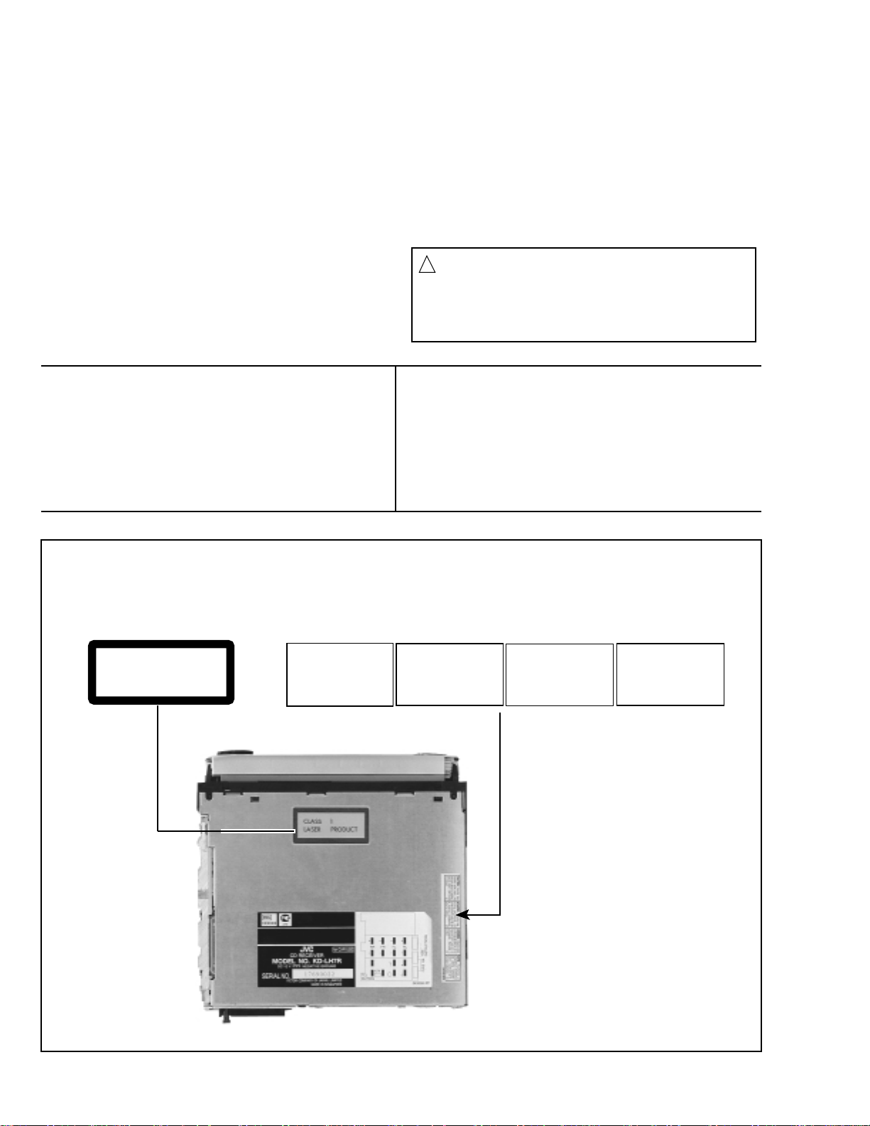
Important for laser products
1.CLASS 1 LASER PRODUCT
2.DANGER : Invisible laser radiation when open and inter lock
failed or defeated. Avoid direct exposure to beam.
3.CAUTION : There are no serviceable parts inside the
Laser Unit. Do not disassemble the Laser Unit. Replace the
complete Laser Unit if it malfunctions.
4.CAUTION : The compact disc player uses invisible laser
radiation and is equipped with safety switches which prevent
emission of radiation when the drawer is open and the safety
interlocks have failed or are defeated.
It is dangerous to defeat the safety switches.
VARNING : Osynlig laserstrålning är denna del är öppnad
och spårren är urkopplad. Betrakta ej strålen.
VARO : Avattaessa ja suojalukitus ohitettaessa olet
alttiina näkymättömälle lasersäteilylle.Älä katso
säteeseen.
5.CAUTION : If safety switches malfunction, the laser is able
to function.
6.CAUTION : Use of controls, adjustments or performance of
procedures other than those specified herein may result in
hazardous radiation exposure.
CAUTION
!
Please use enough caution not to
see the beam directly or touch it
in case of an adjustment or operation
check.
ADVARSEL : Usynlig laserstråling ved åbning , når
sikkerhedsafbrydere er ude af funktion. Undgå
udsættelse for stråling.
ADVARSEL : Usynlig laserstråling ved åpning,når
sikkerhetsbryteren er avslott. unngå utsettelse
for stråling.
REPRODUCTION AND POSITION OF LABELS
WARNING LABEL
CLASS 1
LASER PRODUCT
DANGER : Invisible laser
radiation when open and
interlock or defeated.
AVOID DIRECT EXPOSURE
TO BEAM (e)
ADVARSEL :Usynlig laserstråling ved åbning , når
sikkerhedsafbrydere er ude
af funktion. Undgå udsæt
telse for stråling. (f)
VARNING : Osynlig laserstrålning är denna del
är öppnad och spårren är
urkopplad. Betrakta ej
strålen. (s)
VARO : Avattaessa ja suojalukitus ohitettaessa olet
alttiina näkymättömälle
lasersäteilylle.Älä katso
säteeseen. (d)
1-4
Page 5
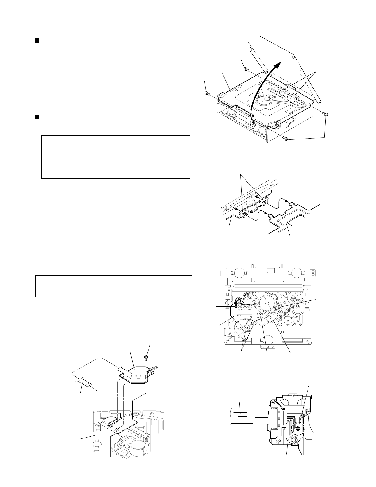
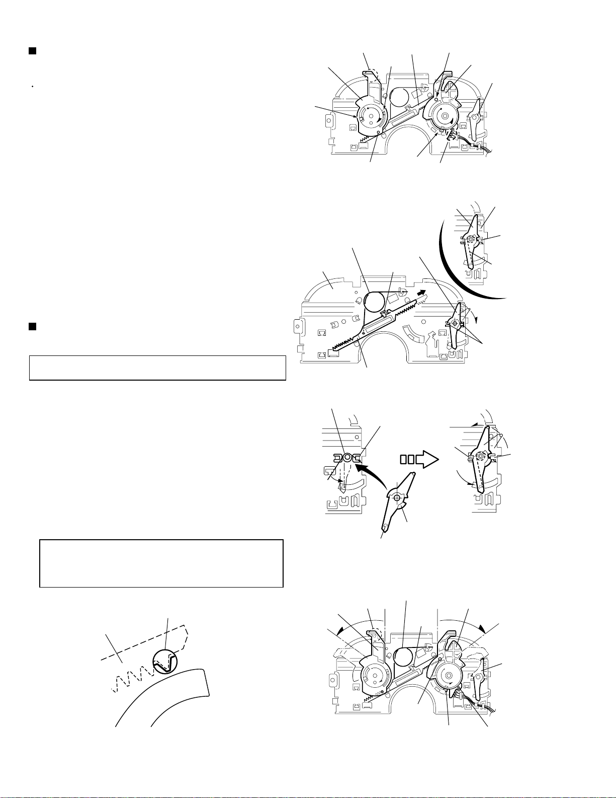
Disassembly method
Removing the front panel unit
(See Fig.1)
1.
Press the release switch and remove the front panel
unit in the direction of the arrow.
Removing the front chassis
(See Fig.2 ~ 4)
1.
Remove the two screws A attaching the front
chassis.
KD-LH7R
Front panel unit
Fig.1
2.
Remove the two screws B on each side of the body.
3.
Release the two joints a and the two joints b on the
sides. Release the two joints c at the bottom and
remove the front chassis toward the front.
Joint c
Joint c
A
Joint a
Joint a
Fig.2
B
Front chassis
Fig. 3
Front chassis
Joint b
Joint b
Fig.4
Removing the heat sink (See Fig.5)
1.
Remove the four screws C attaching the heat sink
on the left side of the body, and remove the heat
sink.
C
C
Heat sink
Fig. 5
C
1-5
Page 6
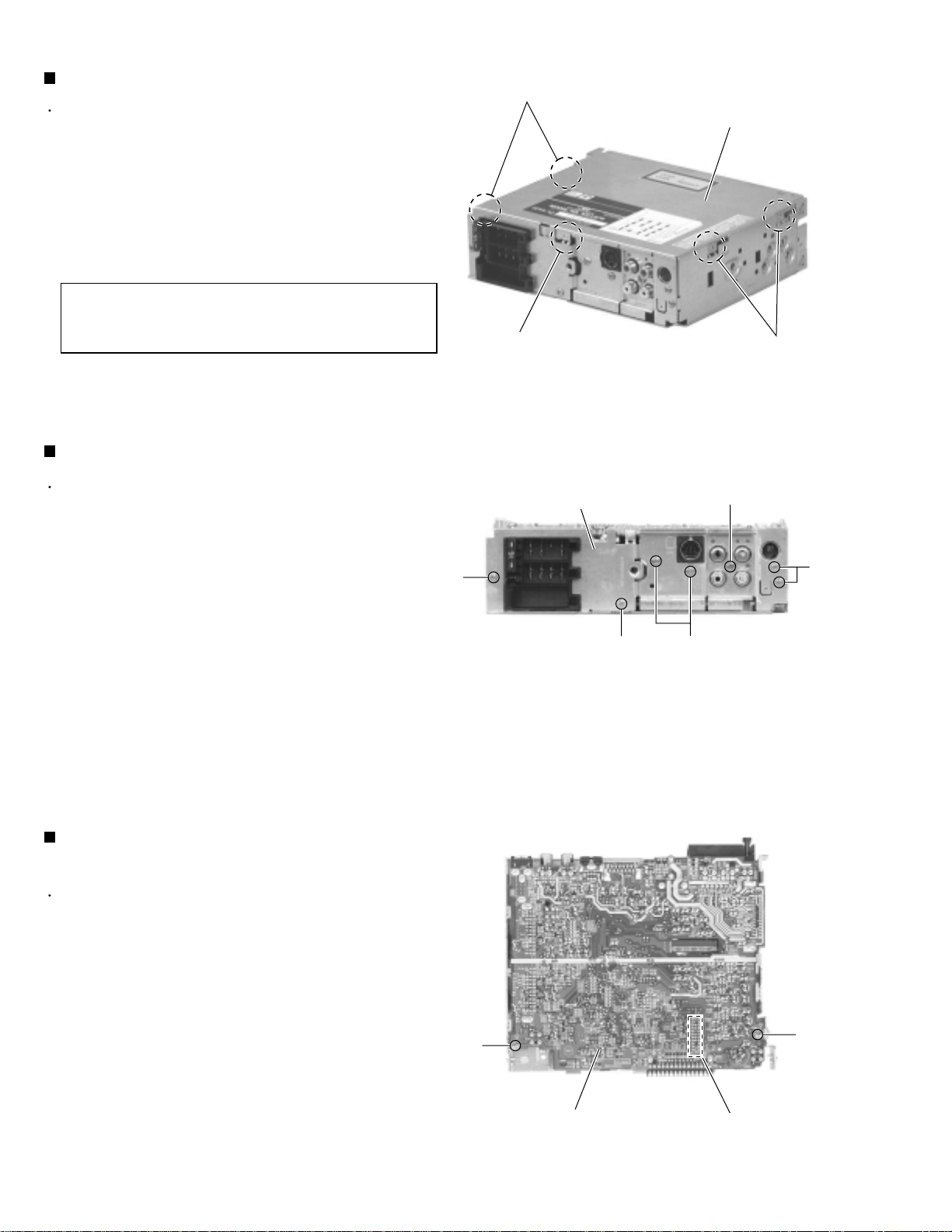
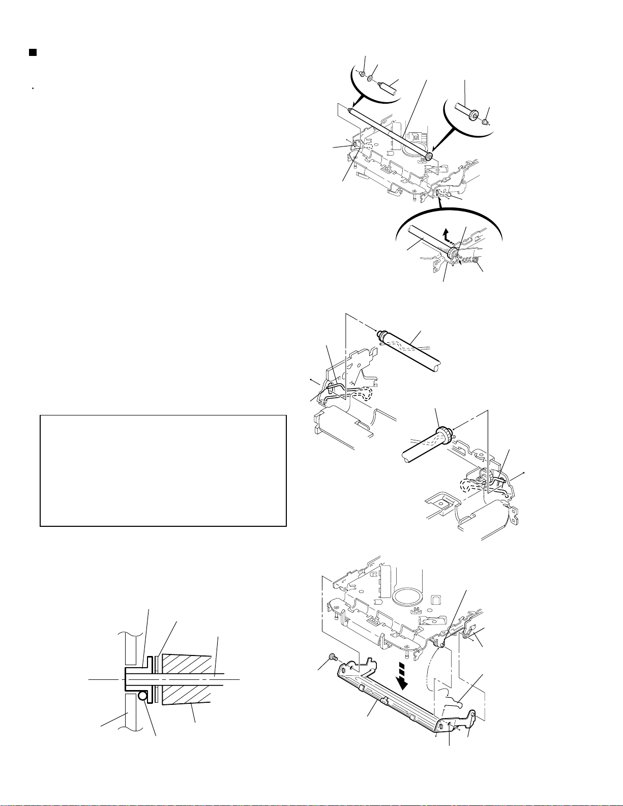
KD-LH7R
Removing the bottom cover (See Fig.6)
Prior to performing the following procedure, remove
the front chassis and the heat sink.
1.
Turn the body upside down.
2.
Insert a screwdriver to the two joints d and two joints
e on both sides of the body and the joint f on the
back of the body, then detach the bottom cover from
the body.
CAUTION:
When disengaging the joint f using a
screwdriver, do not damage or break the
board.
Removing the rear panel (See Fig.7 )
Prior to performing the following procedure, remove
the front chassis, the heat sink and bottom cover.
Joint d
Joint f
Rear panel
Bottom cover
Joint e
Fig. 6
E
1.
Remove the six screws D attaching the rear panel
and one screw E attaching the pine jack on the back
of the body.
D
Removing the main amplifier board assembly
(See Fig.8)
Prior to performing the following procedure, remove
the front chassis, the heat sink, bottom cover and the
rear panel.
1.
Remove the two screws F attaching the main
amplifier board assembly on the top cover.
D
Fig. 7
D
D
2.
Disconnect connector CN101 on the main amplifier
board assembly from the cassette mechanism
assembly.
1-6
F
Main board assembly
F
CN101
Fig. 8
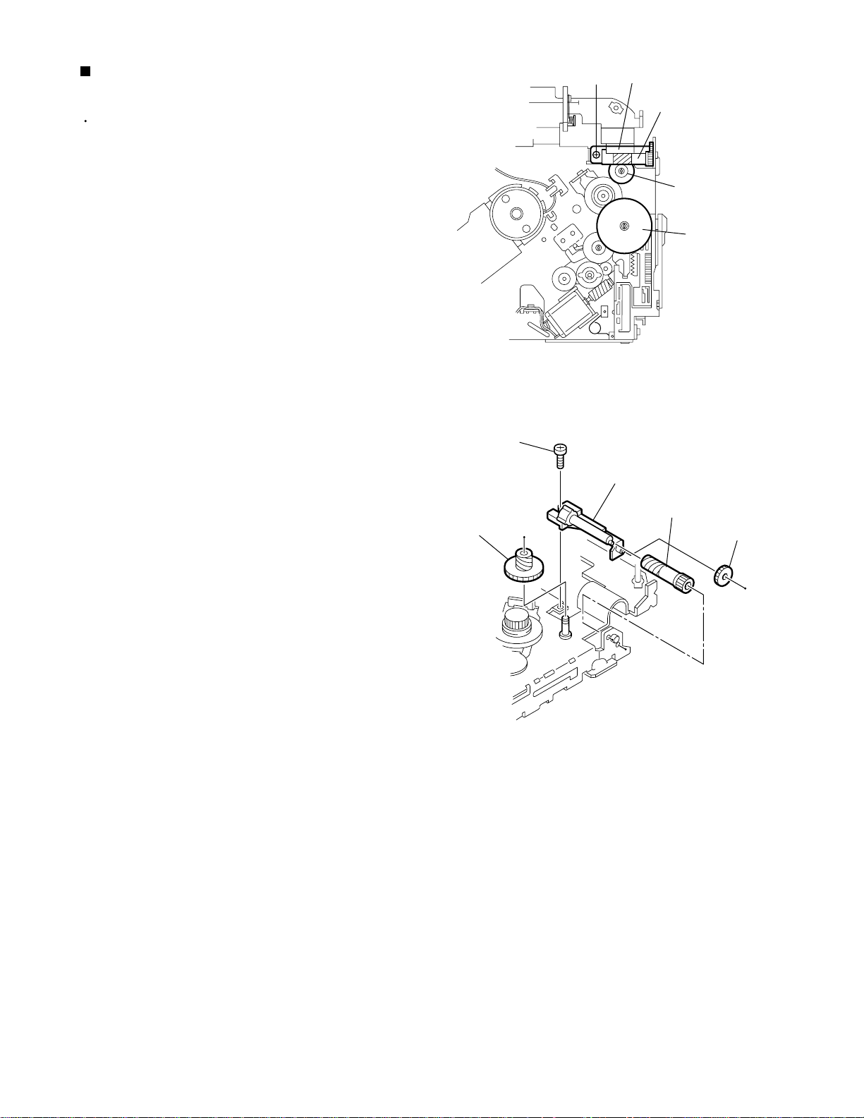
Page 7
KD-LH7R
Removing the MP3 board
(See Fig.9)
Prior to performing the following procedure, remove
the top cover.
1.
Disconnect the wire from connector CN601 on the
MP3 board.
2.
Remove the five screws G and the MP3 board,
releasing the joint g and h.
G
g
h
CN601
G
Fig.9
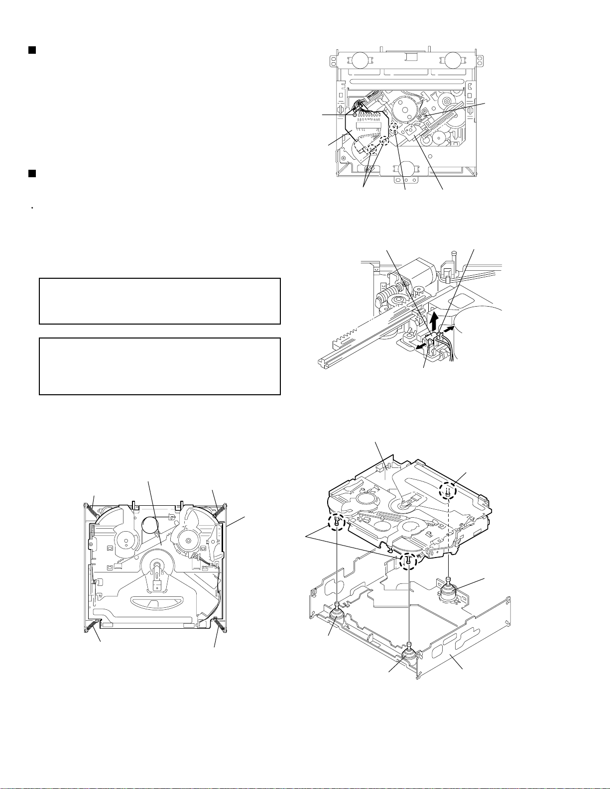
Removing the CD mechanism assembly
(See Fig.10)
Prior to performing the following procedure, remove
the front chassis, the heat sink, bottom cover and the
main amplifier board assembly.
1.
Remove the three screws H attaching the cassette
mechanism assembly from the top cover.
Top cover
H
H
H
CD mechanism assembly
Fig. 10
1-7
Page 8

KD-LH7R
Removing the (LCD & key) control switch
board (See Fig.11
Prior to performing the following procedure, remove
the front panel assembly.
1.
Remove the four screws I attaching the rear cover
on the back of the front panel assembly.
2.
Unjoint the nine joints i with the front panel and the
rear cover.
3.
Remove the control switch board on the back of the
front panel.
~ 13)
I
I
Fig. 11
I
I
Front panel
Joint i
LCD & Key control board
Joint i
Rear cover
Joint i
Joint i
Fig. 12
1-8
Fig. 13
Page 9
< CD mechanism section >
Removing the top cover
(See Fig.1 and 2)
1.
Remove the two screws A on each side of the body.
2.
Lift the front side of the top cover and move the
cover backward to release the two joints a.
Removing the connector board
(See Fig.3 to 5)
Top cover
A
KD-LH7R
A
Joints a
CAUTION:
1.
Remove the screw B fixing the connector board.
2.
Solder the short-circuit point on the connector board.
Disconnect the flexible wire from the pickup.
3.
Move the connector board in the direction of the
arrow to release the two joints b.
4.
Unsolder the wire on the connector board if
necessary.
CAUTION:
Before disconnecting the flexible wire
from the pickup, solder the short-circuit
point on the pickup. No observance of
this instruction may cause damage of
the pickup.
Unsolder the short-circuit point after
reassembling.
A
Fig.1
Joints a
Top cover
Fig.2
DET switch
B
Flexible wire
Frame
Connector board
B
Connector board
Joints b
Flexible wire
Short-circuit
Fig.3
Fig.4Fig.5
Pickup
Short-circuit point
(Soldering)
Pickup
1-9
Page 10
KD-LH7R
Removing the DET switch
(See Fig.3 and 6)
1.
Extend the two tabs c of the feed sw. holder and pull
out the switch.
2.
Unsolder the DET switch wire if necessary.
Removing the chassis unit
(See Fig.7 and 8)
Prior to performing the following procedure, remove
the top cover and the connector board.
B
Connector board
Joints b
Short-circuit
Fig.3
DET switch
Pickup
1.
Remove the two suspension springs (L) and (R)
attaching the chassis unit to the frame.
CAUTION:
The shape of the suspension spring (L)
and (R) are different. Handle them with
care.
CAUTION:
When reassembling, make sure that the
three shafts on the underside of the
chassis unit are inserted to the dampers
certainly.
Chassis unit
Suspension spring (R)
Suspension spring (L)
Frame
DET switch
Chassis unit
Tab c
Feed sw. holder
Tab c
Fig.6
Shaft
1-10
Suspension spring (R)
Suspension spring (L)
Shafts
Damper
Damper
Damper
Frame
Fig.8Fig.7
Page 11

Removing the clamper assembly
(See Fig.9 and 10)
KD-LH7R
Prior to performing the following procedure, remove
the top cover.
1.
Remove the clamper arm spring.
2.
Move the clamper assembly in the direction of the
arrow to release the two joints d.
Removing the loading / feed motor
assembly (See Fig.11 and 12)
Prior to performing the following procedure, remove
the top cover, the connector board and the chassis
unit.
1.
Remove the screw C and move the loading / feed
motor assembly in the direction of the arrow to
remove it from the chassis rivet assembly.
Clamper arm
spring
Joint d
Joint d
Clamper assembly
Fig.9
Clamper arm spring
Chassis rivet
assembly
Joint d
Clamper assembly
Joint d
2.
Disconnect the wire from the loading / feed motor
assembly if necessary.
CAUTION:
When reassembling, connect the wire
from the loading / feed motor assembly
to the flame as shown in Fig.11.
Chassis rivet assembly
Fig.10
Loading / feed motor assembly
C
Loading / feed motor assembly
Fig.12Fig.11
1-11
Page 12

KD-LH7R
Removing the pickup unit
(See Fig.13 to 17)
Prior to performing the following procedure, remove
the top cover, the connector board and the chassis
unit.
1.
Remove the screw D and pull out the pu. shaft
holder from the shaft.
2.
Remove the screw E attaching the feed sw. holder.
3.
Move the part e of the pickup unit upward with the
shaft and the feed sw. holder, then release the joint f
of the feed sw. holder in the direction of the arrow.
The joint g of the pickup unit and the feed rack is
released, and the feed sw. holder comes off.
4.
Remove the shaft from the pickup unit.
5.
Remove the screw F attaching the feed rack to the
pickup unit.
Reattaching the pickup unit
(See Fig.13 to 16)
Joint f
Shaft
D
Joint e
Pu. shaft holder
Feed sw. holder
Pickup unit
Fig.13
Pickup unit
E
Joint f
Joint e
1.
Reattach the feed rack to the pickup unit using the
screw F.
2.
Reattach the feed sw. holder to the feed rack while
setting the joint tab g to the slot of the feed rack and
setting the part f of the feed rack to the switch of the
feed sw. holder correctly.
3.
As the feed sw. holder is temporarily attached to the
pickup unit, set to the gear of the joint g and to the
bending part of the chassis (joint h) at a time.
CAUTION:
4.
Reattach the feed sw. holder using the screw E.
5.
Reattach the shaft to the pickup unit. Reattach the
pu. shaft holder to the shaft using the screw D.
Make sure that the part i on the underside
of the feed rack is certainly inserted to the
slot j of the change lock lever.
F
Feed rack
Feed rack
E
Joint g
Feed sw. holder
Part i
Pickup unit
Slot j
Joint g
Feed sw. holder
Fig.14
Shaft
Joint f
Joint h
Fig.15
D
Pu. shaft holder
Pickup unit
1-12
Pickup unit
Feed rack
Joint f
Feed sw. holder
Fig.17Fig.16
Page 13
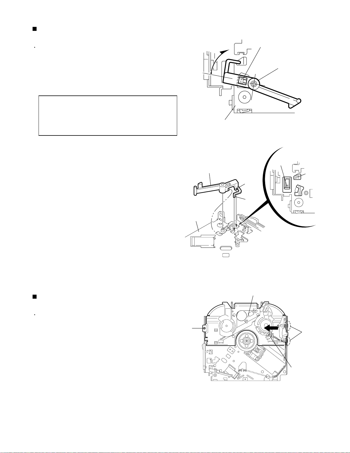
Removing the trigger arm
(See Fig.18 and 19)
Prior to performing the following procedure, remove
the top cover, the connector board and the clamper
unit.
1.
Turn the trigger arm in the direction of the arrow to
release the joint k and pull out upward.
KD-LH7R
Joint k
Trigger arm
CAUTION:
When reassembling, insert the part l and
m of the trigger arm into the part n and
o at the slot of the chassis rivet
assembly respectively and join the joint
k at a time.
Chassis rivet assembly
Chassis rivet assembly
Trigger arm
Fig.18
Part n
Part o
Part l
Part m
Fig.19
Removing the top plate assembly
(See Fig.20)
Prior to performing the following procedure, remove
the top cover, the connector board, the chassis unit,
and the clamper assembly.
1.
Remove the screw H.
2.
Move the top plate assembly in the direction of the
arrow to release the two joints p.
3.
Unsolder the wire marked q if necessary.
H
Top plate assembly
Joints p
q
Fig.20
1-13
Page 14
KD-LH7R
Removing the select arm (L) / select lock
arm (See Fig.21 and 22)
Prior to performing the following procedure, remove
the top plate assembly.
1.
Bring up the select arm (L) to release from the link
plate (joint r) and turn in the direction of the arrow to
release the joint s.
2.
Unsolder the wire of the select arm (L) marked q if
necessary.
3.
Turn the select lock arm in the direction of the arrow
to release the two joints t.
The select lock arm spring comes off the select lock
arm at the same time.
Reassembling the select arm (L) / select
lock arm (See Fig.23 to 25)
Select arm (R)
Joint z
Link plate spring
Top plate
Joint a'
Joint y
Link plate
Joint z
Joint s
Fig.21
Select lock arm
Select lock arm
Joint b'
Joint r
Select arm (L)
Select lock arm
q
Top plate
Hook u
Select lock
arm spring
Joints t
REFERENCE:
1.
Reattach the select lock arm spring to the top plate
Reverse the above removing procedure.
and set the shorter end of the select lock arm spring
to the hook u on the top plate.
2.
Set the other longer end of the select lock arm spring
to the boss v on the underside of the select lock arm,
and join the select lock arm to the slots (joint t). Turn
the select lock arm as shown in the figure.
3.
Reattach the select arm (L) while setting the part r to
the first peak of the link plate gear, and join the joint
s.
CAUTION:
When reattaching the select arm (L),
check if the points w and x are correctly
fitted and if each part operates properly.
Joint r
Link plate
Link plate
Select lock arm spring
Boss v
Select arm (R)
Joint a'
Fig.22
Hook u
Joint t
Joint t
Select lock arm
Fig.23
Link plate spring
Select arm (L)
Joint b'
1-14
Joint r
Fig.25Fig.24
Joint s
Select
lock arm
Point x
Page 15

KD-LH7R
Removing the select arm (R) / link plate
(See Fig.21 and 22)
Prior to performing the following procedure, remove
the top plate assembly.
1.
Bring up the select arm (R) to release from the link
plate (joint y) and turn as shown in the figure to
release the two joints z and joint a’.
2.
Move the link plate in the direction of the arrow to
release the joint b’. Remove the link plate spring at
the same time.
REFERENCE:
Before removing the link plate, remove
the select arm (L).
Reattaching the Select arm (R) / link
plate (See Fig.25 and 26)
REFERENCE:
Reverse the above removing procedure.
Select arm (R)
Joint z
Link plate spring
Top plate
Joint a'
Part y
Link plate
Joint z
Joint s
Fig.21
Select lock arm
Select lock arm
Joint b'
Joint r
Select arm (L)
Select lock arm
q
Top plate
Hook u
Select lock
arm spring
1.
Reattach the link plate spring.
2.
Reattach the link plate to the link plate spring while
joining them at joint b’.
3.
Reattach the part y of the select arm (R) to the first
peak of the link plate while joining the two joints z
with the slots. Then turn the select arm (R) as shown
in the figure. The top plate is joined to the joint a’.
CAUTION:
When reattaching the select arm (R),
check if the part c’ is correctly fitted and
if each part operates properly.
Select arm (R)
Joint z
Link plate
Link plate spring
Joint a'
Part y
Part y
Fig.22
Joint b'
Joint z
Fig.25
Joints t
Select arm (L)
Select
lock arm
Point x
Fig.26
Link plate
1-15
Page 16
KD-LH7R
Removing the loading roller assembly
(See Fig.27 to 29)
Prior to performing the following procedure, remove
the clamper assembly and the top plate assembly.
1.
Push inward the loading roller assembly on the gear
side and detach it upward from the slot of the joint d’
of the lock arm rivet assembly.
Detach the loading roller assembly from the slot of
the joint e’ of the lock arm rivet assembly.
The roller guide comes off the gear section of the
loading roller assembly.
Remove the roller guide and the washer from the
shaft of the loading roller assembly.
2.
Remove the screw I attaching the lock arm rivet
assembly.
3.
Push the shaft at the joint f’ of the lock arm rivet
assembly inward to release the lock arm rivet
assembly from the slot of the slide plate. Extend the
lock arm rivet assembly outward and release the
joint g’ from the boss of the chassis rivet assembly.
The roller guide springs on both sides come off.
Roller guide
Washer
Loading roller assembly
Roller guide
Joint e'
Roller guide spring
Roller guide spring
Joint d'
Loading roller assembly
Roller guide spring
Lock arm rivet assembly
Fig.27
Loading roller assembly
Roller guide
spring
CAUTION:
When reassembling, reattach the left
and right roller guide springs to the lock
arm rivet assembly before reattaching
the lock arm rivet assembly to the
chassis rivet assembly. Make sure to fit
the part h’ of the roller guide spring (L)
inside of the roller guide (Refer to
Fig.30).
Roller guide
Washer
Roller shaft assembly
Joint h'
Loading roller assembly
Roller guide
spring
Fig.28-1
Fig.28-2
Chassis rivet assembly
Boss
Slide plate
Roller guide spring
I
1-16
Frame
Loading roller
Roller guide spring
Lock arm rivet assembly
Joint f'
Part g'
Fig.29Fig.30
Page 17
KD-LH7R
Removing the loading gear (5), (6) and
(7) (See Fig.31 and 32)
Prior to performing the following procedure, remove
the top cover, the chassis unit and the top plate
assembly.
1.
Remove the screw J attaching the loading gear
bracket. The loading gear (6) and (7) come off the
loading gear bracket.
2.
Pull out the loading gear (5).
Loading gear bracket
J
Loading gear (6)
Loading gear (5)
Loading gear (3)
Fig.31
J
Loading gear bracket
Loading gear (5)
Loading gear (6)
Loading gear (7)
Fig.32
1-17
Page 18

KD-LH7R
Removing the gears (See Fig.33 to 36)
Prior to performing the following procedure, remove
the top cover, the chassis unit, the top plate
assembly and the pickup unit.
1.
Pull out the feed gear.
Slot j'
Slide plate
2.
Move the loading plate assembly in the direction of
the arrow to release the slide plate from the two slots
j’ of the chassis rivet assembly.
3.
Detach the loading plate assembly upward from the
chassis rivet assembly while releasing the joint k’.
Remove the slide hook and the loading plate spring
from the loading plate assembly.
4.
Pull out the loading gear (2) and remove the change
lock lever.
5.
Remove the E-washer and the washer attaching the
changer gear (2).
6.
The changer gear (2), the changer gear spring and
the adjusting washer come off.
7.
Remove the loading gear (1).
8.
Move the hang plate rivet assembly in the direction
of the arrow to release from the three shafts of the
chassis rivet assembly upward.
9.
Detach the loading gear plate rivet assembly from
the shaft of the chassis rivet assembly upward while
releasing the joint l’.
Feed gear
Change plate
rivet assembly
Shafts
E-washer
Loading plate assembly
Joint k'
Slot j'
Fig.33
Joint l'
Loading gear (4)
Loading gear plate
rivet assembly
Loading gear (2)
Loading gear (1)
Change gear (2)
10.
Pull out the loading gear (4).
Loading plate assembly
Loading plate spring
Slot j'
Chassis rivet assembly
Joint k'
Slide hook
Slide plate
Slot j'
E-washer
Washer
Loading gear (2)
Loading plate spring
Adjusting washer
Change plate
rivet assembly
Chassis rivet assembly
Fig.34
Loading gear (1)
Loading gear (2)
Change lock lever
Loading gear (4)
Loading gear plate rivet assembly
Fig.36Fig.35
1-18
Page 19

KD-LH7R
Removing the turn table / spindle motor
(See Fig.37 and 38)
Prior to performing the following procedure, remove
the top cover, the connector assembly and the
chassis / clamper assembly.
1.
Remove the two screws K attaching the spindle
motor assembly through the slot of the turn table on
top of the body.
2.
Unsolder the wire on the connector board if
necessary.
K
Turn table
Fig.37
K
Turn table
Spindle motor
Fig.38
1-19
Page 20
KD-LH7R
Adjustment method
Test instruments required for adjustment
1. Digital oscilloscope (100MHz)
2. AM Standard signal generator
3. FM Standard signal generator
4. Stereo modulator
5. Electric voltmeter
6. Digital tester
7. Tracking offset meter
8. Test Disc JVC :CTS-1000
9. Extension cable for check
EXTSH002-22P 1
Standard measuring conditions
Power supply voltage : DC14.4V(11V~16V allwance)
Load impedance : 4 (4 to 8 allowance)
Line-out Level / Impedance:
2.0V / 20 k load
How to connect the extension cable for adjusting
Standard volume position
Balance and Bass &Treble volume : lndication"0"
Loudness : OFF
BBE : OFF
Frequency Band
FM 87.5MHz ~ 108.0MHz
MW 522kHz ~ 1620 kHz
LW 144kHz ~ 279kHz
Dummy load
Exclusive dummy load should be used for AM,and FM. For
FM dummy load,there is a loss of 6dB between SSG output
and antenna input.The loss of 6dB need not be considered
since direct reading of figures are applied in this working
standard.
Extension cables
EXTSH002-22P
CN101
CN501
CD Mechanism
Main board
1-20
Page 21
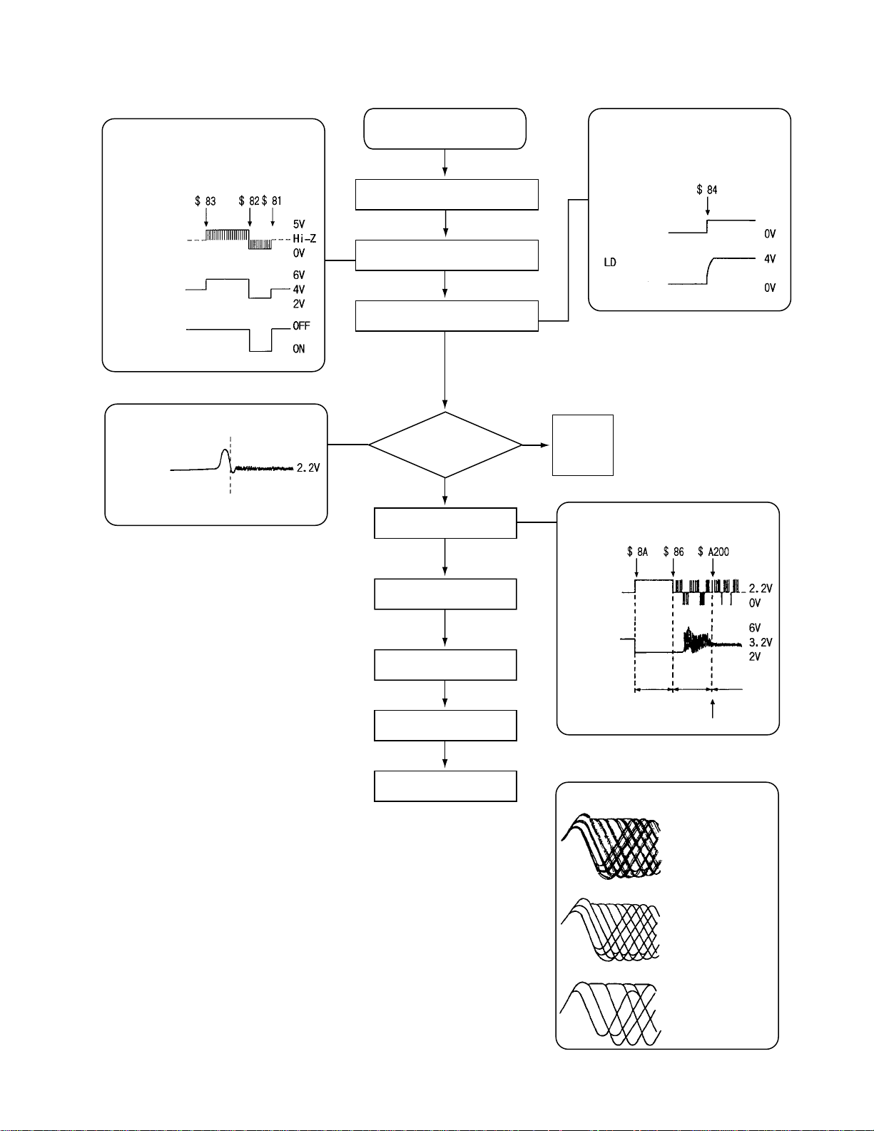
Flow of functional operation until TOC read
Power ON
• When the pickup correctly moves
to the inner area of the disc
Set Function to CD
KD-LH7R
• When the laser diode correctly
emits
Microprocessor
commands
FMO
TC94A14FA "40"
FEED MOTOR
TERMINAL
+TERMINAL
IC681 "4"
REST SW
• When correctly focused
FEO
TA2157FN "15"
Focus Servo Loop ON
Disc inserted
Pickup feed to the inner area
Laser emitted
Focus search
Disc rotates
RF signal eye-pattern
remains closed
Tracking loop closed
RF signal eye-pattern
opens
TOC readout
YES
YES
Microprocessor
commands
TC94A14FA"38"
CN601"10"
1
"No disc"
display
• When the disc correctly rotates
Microprocessor
commands
TN94A14FA
"41"
Spindle
motor (-)
IC681 "7"
AccelerationAcceleration
0.5 Sec
Rough
Servo
0.5 Sec
Servo CLV
3.3V
3.3V
Jump to the first track
Play
Tracking Servo Loop ON
• RF signal
Rough Servo Mode
CLV Servo Mode
(ProgramArea)
CLV Servo Mode
(Lead-In Area;
Digital: 0)
1-21
Page 22

KD-LH7R
Feed Section
Is the voltage output at
IC621 pin "40" 5V or 0V?
Is 4V present at both
sides of the feed motor?
YES
YES
NO
Is the wiring for IC621
(56) ~ (64) correct?
NO
Is 6V or 3V present at
IC681 "4" and "5"?
NO
YES
YES
Is 3.3V present at
IC681 pin "20"?
YES
Check the vicinity of
IC621.
Check the feed motor
connection wiring.
NONO
Check CD 8V
and 5V.
Check the feed motor.
Focus Section
When the lens is
moving:
4V
Does the S-search
waveform appear at
IC681 pins "10" and "11"?
Spindle Section
Is the disk rotated?
YES
Does the RF signal
appear at TP1?
YES
Check IC681.
NO
YES
NO
Check the circuits in the
vicinity of IC681 pins
"8","9" and "15".
Check the pickup and
its connections.
Is 4V present at IC681
pins "7" and "6" ?
Check the spindle motor
and its wiring.
NO
YES
YES
NO NO
Is 4V present at IC621
pin "41" ?
YES
Check the vicinity of
IC681.
Check IC621 and
IC601.
Is the RF waveform at TP1
distorted?
Proceed to the Tracking
section
Tracking Section
When the disc is rotated
Is the tracking error signal
1-22
NO
YES
at first:
Approx. 1.2 V
output at IC601 "11"?
YES
Check IC621.
Check the circuits in the
vicinity of IC601 "19"~"24"
or the pickup
Check the circuit in the
vicinity of IC601 pins
"2" ~ "12".
YESYES
Check the pickup and
its connections.
Page 23

Maintenance of laser pickup
(1) Cleaning the pick up lens
Before you replace the pick up, please try to
clean the lens with a alcohol soaked cotton
swab.
(2) Life of the laser diode
When the life of the laser diode has expired,
the following symptoms will appear.
The level of RF output (EFM output:ampli
tude of eye pattern) will be low.
KD-LH7R
Is RF output
1.0 0.35Vp-p?
YES
O.K
(3) Semi-fixed resistor on the APC PC board
The semi-fixed resistor on the APC printed
circuit board which is attached to the pickup
is used to adjust the laser power.Since this
adjustment should be performed to match the
characteristics of the whole optical block,
do not touch the semi-fixed resistor.
If the laser power is lower than the specified
value,the laser diode is almost worn out, and
the laser pickup should be replaced.
If the semi-fixed resistor is adjusted while
the pickup is functioning normally,the laser
pickup may be damaged due to excessive current.
NO
Replace it.
Replacement of laser pickup
Turn off the power switch and,disconnect the
power cord from the ac outlet.
Replace the pickup with a normal one.(Refer
to "Pickup Removal" on the previous page)
Plug the power cord in,and turn the power on.
At this time,check that the laser emits for
about 3seconds and the objective lens moves
up and down.
Note: Do not observe the laser beam directly.
Play a disc.
Check the eye-pattern at TP1.
Finish.
1-23
Page 24

KD-LH7R
Description of major ICs
BR24C01AFV-W-X (IC502) : EEPROM
1.Pin layout
2.Block diagram
A0
1
A1
2
A2
3
Vcc WP SCL SDA
A0 A1 A2 GND
1kbit EEPROM ARRAY
7bit
ADDRESS
DECODER
CONTROL LOGIC
SLAVE/WORD
7bit
ADDRESS REGISTER
START
STOP
ACK
8bit
DATA
REGISTER
Vcc
8
WP
7
SCL
6
GND
4
HIGH VOLTA GE GEN.
3.Pin function
Pin name I/O
Vcc
GND
A0,A1,A2
SCL
SDA
WP
*1 An open drain output requires a pull-up resister.
-
IN
IN
IN / OUT
IN
Power supply
Ground (0v)
Slave address set
Serial clock input
Slave and word address,
serial data input, serial data output *1
Write protect input
Vcc LEVEL DETECT
Function
SDA
5
1-24
Page 25

BR24C32F-X (IC771) : EEPROM
KD-LH7R
1. Pin layout
Vdd WPIN SCL SDA
A0 A1 A2 GND
3. Block diagram
A0 1
A1 2
A2 3
11bit
Address
decoder
16kbit EEPROM allay
11bit
START
Control circuit
2. Pin function
Symbol
Vdd
GND
A0,A1,A2
SCL
SDA
WPIN
Slave Word
Address resister
STOP
I/O
-
Power supply.
-
GND
I
No use connect to GND.
I
Serial clock input.
I/O
Serial data I/O of slave and word address.
I
Write protect terminal.
8bit
Data
resister
Function
8 Vdd
7 WPIN
6 SCL
GND 4
High voltage osc circuit
Power supply
voltage det.
ACK
5 SDA
1-25
Page 26

KD-LH7R
UPD784216AGC163 (IC701): SYSTEM CPU
Pin No.
1
2
3
4
5
6
7
8
9
10
11
12
13
14
15
16
17
18
Symbol I/O Function
SW2
SW3
SW4
REST
LM0
LM1
NC
NC
VDD
O
O
O
O
Signal input of mechanism switch 2 detection
I
Signal input of mechanism switch 3 detection
I
Signal input of mechanism switch 4 detection
I
Rest switch detection signal input
I
Loading side motor control signal output
Eject side motor control signal output
Non connect
Non connect
5V connection
X2
X1
VSS
GND connection
XT2
XT1
RESET
SW1
BUS-INT
PS2
Reset detection terminal
I
Mechanism switch detection signal input
I
J-BUS signal interrupt input
I
POWER SAVE2. BACK UP and synchronization
I
Becomes stop mode because of the input of H.
19
20
21
22
23
24
25
CRUISE
RDS-SCK
RDS DA
REMOCON
AVDD
AVREF0
VOL1
Pulse signal input for cruise
I
RDS clock input
I
RDS data input
I
Remote control signal input
I
5V connection
5V connection
Rotation volumepulse signal input
I
Pulse which actually becomes judgment of change
26
27
28
29
30
31
32
33
34
35
36
37
38
39
40
41
42
43
44
45
46
47
48
49
50
VOL2
KEY0
KEY1
KEY2
LEVEL
SQ
SM
AVSS
NC
NC
AVREF
BUS-SI
BUS-SO
BUS-SCK
BUS-I/O
LCD-DA
LCD-SCK
LCD-CE
BUZZER
E2PROM-DI
E2PROM-DO
E2PROM-CLK
OPEN
NC
NC
I
I
I
I
I
I
I
O
O
I
O
I/O
O
O
O
O
OI
O
O
I
O
O
O
Rotation volume pulse signal input
Key input 0
Key input 1
Key input 2
Level meter input
S.QUALITY level input
S.METER level input
GND connection
Non connect
Non connect
5V connection
J-BUS data input
J-BUS data output
J-BUS clock input & output
J-BUS I/O switch output. At output : H, At input : L
Data output to LCD driver
Clock output to LCD driver
Chipenable to LCD driver
Buzzer output
Communication data input of 12C
Communication data output of 12C
Communication data clock output 12C
Opening detection input
Non connect
Non connect
UPD784216AGC163(1/2)
1-26
Page 27

Pin No. Symbol I/O Function
51
52
53
NC
NC
SD/ST
Non connect
O
Non connect
O
Station detector and stereo signal input.
I
It is H and there is a bureau.It is L and a stereo.
54
55
NC
MONO
Non connect
O
Monaural ON/OFF switch output.
O
At the time of the MONO ON :H.
56
57
58
59
60
61
NC
NC
NC
NC
NC
DETACH
Non connect
I
Non connect
I
Non connect
I
Non connect
I
Non connect
I
Detach signal input. It is L of 200ms or more and an
I
operation mode. H:POWER SAVE
62
63
64
65
66
67
68
69
70
AFCK
SEEK/STP
NC
FM/AM
PLL-CE
PLL-DO
PLL-CLK
PLL-DI
TEL-MUTE
AF check output. AF check:L
O
Auto seek stop switch output. At SEEK:H. At STOP:L
O
Non connect
O
FM,AM switch output
O
CE output for IC control for PLL
O
Data output for IC control for PLL
O
Clock output for IC control PLL
O
Data output for IC control for PLL
I
Telephone mute detection input.
I
It is L or H and MUTE(ACTIVE depends on the PSM setting)
71
72
73
74
NC
VSS
DIM-IN
PS1
Non connect (ex:AMP-KILL output)
O
GND connection
Dimmer detection input. At L:dimmer ON.
I
POWER SAVE 1. ACC and synchronization
I
POWER SAVE : L. At operation:H
75
76
77
78
79
80
81
82
83
84
85
86
87
88
89
90
91
92
93
94
95
96
97
98
99
100
POWER
CD-ON
MUTE
NC
NC
NC
VDD
NC
VOL-DA
VOL-CLK
DIM-OUT
NC
NC
NC
NC
STAGE
BUCK
CCE
RST
TEST
BUS0
BUS1
BUS2
BUS3
DISCSEL
J/E
O
O
O
O
O
O
O
O
O
O
O
O
O
O
I
O
O
O
I/O
I/O
I/O
I/O
O
I
POWER ON/OFF switch output. At POWER ON:H
The CD power supply control signal output. At CD :H
Mute output. At mute ON:L
Non connect
Non connect
Non connect
5V connection
Non connect
Data output by which IC for electronic volume is controlled
Clock output by which IC for electronic volume is controlled
Dimmer control output. L:DIMMER ON (ex:BBE)
Non connect
Non connect
Non connect
Non connect
H:For 991R / L:For 911R
Clock output for data communication with CDLSI
CE output for data communication with CDLSI
CDLSI reset signal output
connects GND with 10k pull down (For flash switch)
Data communication input output port 0 with CDLSI
Data communication input output port 1 with CDLSI
Data communication input output port 2 with CDLSI
Data communication input output port 3 with CDLSI
Pull-down fixation
Pull-up fixation
KD-LH7R
UPD784216AGC163(2/2)
1-27
Page 28

KD-LH7R
HA13164A(IC901):Regulator
1.Terminal layout
2.Block diagram
.IN
1 2 3 4 5 6 7 8 9 101112131415
ANT
2
C3
0.1u
EXT
1
C4
0.1u
ANT CTRL
CTRL
CD8V
7
11
12
C5
0.1u
9V
10
C6
10u
MEMORY. IN
MEMORY.IN ACC.IN
8
Surge Protector
BIAS TSD
15
3
TAB
C1
100u
9
6
4
5
14
+B
ACC
BATT.DET
ACC5V
VDD5V
SW5VOUT
10V
R1
C7
0.1u
C8
0.1u
C2
0.1u
13
AJGND GND
3.Pin function
Pin No. Symbol Function
1
2
EXT
OUT
Output voltage is VCC-1 V when M or H level applied to CTRL pin.
Output voltage is VCC-1 V when M or H level to CTRL pin and H level
to ANT-CTRL.
3
4
5
6
7
8
9
10
11
12
13
14
15
ACC.IN
VDD5V
SW5V
ACC5V
ANT.CTRL
MEMORY.IN
BATT.DET
9V
CTRL
CD8V
AJ
10V
GND
Connected to ACC.
Regular 5.7V.
Output voltage is 5V when M or H level applied to CTRL pin.
Output for ACC detector.
L:ANT output OFF , H:ANT output ON
Connected to VCC.
Low battery detect.
Output voltage is 9V when M or H level applied to CTRL pin.
L:BIAS OFF, M:BIAS ON, H:CD ON
Output voltage is 8V when H level applied to CTRL pin.
Adjustment pin for ILM output voltage.
Output voltage is 10V when M or H level applied to CTRL pin.
Connected to GND.
UNIT R:
C:F
note1) TAB (header of IC)
connected to GND
1-28
Page 29

HD74HC126FP-X (IC801) : Buffer
KD-LH7R
1.Terminal layout
1C
1
1A
2
1Y
3
2C
4
2A
5
2Y
6
GND
7
2.Block diagram
Input
VU
14
4C
13
4A
12
4Y
11
3C
10
3A
9
3Y
8
Vcc Vcc
1A
2A
3A
4A
1C
2C
3C
See Function Table
4C
3.Pin function
Output
1Y
2Y
Output
2Y
Output
3Y
Output
4Y
Input
C
L
H
H
A
X
L
H
Output
Y
Z
H
L
Note) H:High level
L:Low level
X:Irrelevant
Z:Off(High-impedance)
State a 3-state input
1k
S1
CL
1k
Sample as Load Circuit 1
Sample as Load Circuit 1
Sample as Load Circuit 1
Note) CL includes probe and jig capacitance
1-29
Page 30

KD-LH7R
HD74HCT126T-X : (IC503) Buffer
1.Terminal layout
Vcc
14
1
1C
2.Block diagram
2
1A
4C
13
3
1Y
1A
4A
12
4Y
11
4
2C
3C
10
5
2A
3A
9
6
2Y
3Y
8
7
GND
3.Pin function
INPUT
C
L
H
H
H : High level
L : Low level
X : Irrelevant
Off (Hhigh-impedance)state of a 3-stage
Z :
output
OUTPUT
A
X
L
H
Y
Z
H
L
1C
2A
2C
3A
3C
4A
1Y
2Y
3Y
1-30
4Y
4C
Page 31

LC75873NW(IC601):LCD Driver
KD-LH7R
1.Pin layout
3.Pin function
Pin No.
79
80
1,2,3
to 66
67
68
69
61
80
60 41
40
21
1 20
Pin name
DIMMER
S1/P1 TO S4/P4
S5 to S68
COM1
COM2
COM3
2.Block diagram
VDD1
VDD2
INH
OSC
VDD
VSS
I/O
O
O
O
S5
S4/P4
S3/P3
S2/P2
COM2
COM3
COMON
DRIVER
CLOCK
GENERATOR
COM1
S68
S67
DI
SEGMENT DRIVER
SHIFT REGISTOR
CL
CE
ADDRESS
DETECTOR
S1/P1
Description
Dimmer function control output
H:Dimmer off
L:Dimmer on
Segment outouts for displaying the display data
transferred by serial data input.
The S1/P1 to S4/P4 pins can be used as generalpurpose output ports under serial data control.
Common driver outputs.
The frame frequency f0 is given by :
f0 = (FOSC/384)Hz.
74
76
77
78
75
71
72
70
OSC
CE
CL
DI
INH
VDD1
VDD2
VDD
I/O
I
I
I
I
I
I
-
Oscillator connection
An oscillator circuit is formed by connecting an
external resistor and capacitor to this pin.
Serial data transfer inputs.
Connected to the controller.
CE:Chip enable
CL:Synchronization clock
DI:Transfer data
Display off control input
INH= "L"(VSS) Display forced off
S1/P1 to S4/P4 = "L"
(These pins are forcibly set to the
segment output port function and held
at the low level.)
S5 to S68 = "L"
COM1 to COM3"L"
INH = "H"(HDD) Display on
However, serial data transfer is possible when
the display is forced off by this pin.
Used for applying the LCD drive 2/3 bias voltage
externally. Must be connected to VDD2 when a
1/2 bias drive scheme is used.
Used for applying the LCD drive 1/3 bias voltage
externally. Must be connected to VDD1 when a
1/2 bias drive scheme is used.
Power supply connection.
Provide a voltage of between 3.0 and 6.0V.
73
VSS
Power supply connection. Connect to ground.
-
1-31
Page 32

KD-LH7R
LA47503(IC301):Power amp.
1.Terminal layout
206
11
1
12
4
10
Stand by
Switch
Ripple
Filter
Protective
circuit
Mute
circuit
9
7
8
5
3
2
22
1-32
15
25
13
14
16
Muting &
On Time Control
Circuit
protective
circuit
17
19
18
21
23
24
Page 33

2.Terminal layout
AC CONT1
GND
OUTRR-
STBY
OUTRR+
Vcc1/2
OUTFR-
GND
OUTFR+
REF
INRR
INFR
PREGND
INLR
INLF
ONTIME
OUTLF+
GND
OUTLF-
Vcc3/4
OUTLR+
MUTE
OUTLR-
GND
KD-LH7R
AC CONT2
3.Pin function
1
2
3
4
5
6
7
8
9
10
11
12
13
14
15
16
17
18
19
20
21
22
23
24
25
SymbolPin No. Function
AC CONT1
GND
OUTRRSTBY
OUTRR+
Vcc1/2
OUTRFGND
OUTRF+
REF
INRF
INRR
PREGND
INLR
INLF
ONTIME
OUTLF+
GND
OUTLFVcc3/4
OUTLR+
MUTE
OUTLRGND
AC CONT2
Header of IC
Power GND
Outpur(-) for front Rch
Stand by input
Output (+) for front Rch
Power input
Output (-) for rear Rch
Power GND
Output (+) for rear Rch
Ripple filter
Rear Rch input
Front Rch input
Signal GND
Front Lch input
Rear Lch input
Power on time control
Output (+) for rear Lch
Power GND
Output (-) for rear Lch
Power input
Output (+) for front
Muting control input
Output (-) for front
Power GND
No connection
LA47503
1-33
Page 34

KD-LH7R
LA6579H-X (IC681) : 4-Channel bridge driver
1. Pin layout & Block diagram
VIN1-A
VIN1+A
VCCP1
1
+
2
3
VIN1_SW
[H]: OP-AMP_A
[L]: OP-AMP_B
[H]
[L]
28
VIN1
27
VIN1-B
-
+
26
VIN1+B
VO+
VO-
VO2+
VO2-
FR
VO3+
VO3-
VO4+
4
5
6
7
FR
8
9
10
Power system
GND
Level shift
33k
11k
-
Signal system
power supply
25
S-GND
+
24
VIN1-SW
Level shift
+
Level shift
Level shift
All outputs ON/OFF
H : ON
L : OFF
3.3VREG
(External:PTP Tr)
MUTE
Power system GND
Signal system
power supply
23
MUTE
22
VREFIN
FR
21
20
FR
VCCS
3.3VREG
+
-
19
REGIN
1-34
VO4-
VCCP2
VIN4
VIN4G
11
12
13
14
11k
33k
+
33k
33k
18
VIN2G
11k
-
17
VIN2
+
16
VIN3G
11k
-
15
VIN3
+
Page 35

3.Pin function
Pin No. Symbol Function
1
2
3
4
5
6
7
8
9
10
11
12
13
14
15
16
17
18
19
20
21
22
23
24
25
26
27
28
VIN1-A
VIN1+A
VCCP1
VO1+
VO1VO2+
VO2VO3+
VO3VO4+
VO4VCCP2
VIN4
VIN4G
VIN3
VIN3G
VIN2
VIN2G
REGIN
3.3VREG
VCCS
VREFIN
MUTE
VIN1_SW
S_GND
VIN1+B
VIN1-B
VIN1
CH1 input AMP_inverted input
CH1 input AMP_non-inverted input
CH1 and CH2 power stage power supply
Output pin(+)for channel 1
CH1 output pin (-) for channel 1
Output pin(+)for channel 2
Output pin(-)for channel 2
Output pin(+)for channel 3
Output pin(-)for channel 3
Output pin(+)for channel 4
Output pin(-)for channel 4
CH3 and CH4 power stage powr supply
Input pin for channel 4
Input pin for channel 4(for gain adjustment)
Input pin for channel 3
Input pin for channel 3(for gain adjustment)
Input pin for channel 2
Input pin for channel 2(for gain adjustment)
External PNP transistor, base connection
3.3VREG output pin, external PNP transistor,collector connection
Signal system GND
Reference voltage application pin
Output ON/OFF pin
CH1 input OP AMP_changeover pin
Signal system GND
CH1 AMP_B non-inverted input pin
CH1 AMP_B inverted input pin
CH1 input pin, input OP_AMP output pin
KD-LH7R
LA6579H-X
1-35
Page 36

KD-LH7R
PCM1716E-X (IC571) : D/A converter
1. Pin layout
2. Block diagram
BCK
LBCK
DATA
ML/llS
MC/DM1
MD/DM0
CS/WO
MODE
MUTE
RST
3. Pin function
Pin
Symbol Function
No.
1
LRCK
2
DATA
3
BCK
4
CLKO
5
6
7
8
9
10
11
12
13
14
15
16
17
18
19
20
21
22
23
24
25
26
27
28
XTI
XTO
DGND
VDD
VDD2R
AGND2R
EXTR
NC
VOUTR
AGND1
Vcc1
VOUTL
NC
EXTL
AGND2L
Vcc2L
ZERO
RST
CS/IWO
MODE
MUTE
MD/DM0
MC/DM1
ML/IIS
28 15
114
Serial
Input
I/F
Mode
Control
I/F
Mult-level
8X Oversampling
Digital Filter
with
Function Controller
SCK
BPZ-Cont
Crystal OSC
XTI XTO CLKO Vcc1 VccAGND1 DGND
Delta-Sigma
Modulator
Power Supply
Vcc2L
DAC
DAC
AGND2L
Vcc2R
AGND2R
Open drain
Low-pass
Filter
Low-pass
Filter
I/O
I
LRCK clock input
I
Serial audio data input
I
Bit clock input for serial audio data
O
Buffered output of system clock
I
Oscillator input / External clock input
O
Oscillator output
-
Digital ground
-
Digital power +5V
-
Analog power +5V
-
Analog ground
O
Rch common pin of analog output amp
-
Non connection
O
Rch analog voltage output of audio signal
-
Analog ground
-
Analog power +5V
O
Lch analog voltage output of audio signal
-
Non connection
O
Lch common pin of analog output amp
-
Analog ground
-
Analog power +5V
O
Zero data flag
I
Reset
I
Chip select / Input format selection
I
Mode control select
I
Mute control
I
Mode control, Data / De-emphasis selection 1
I
Mode control, BCK / De-emphasis selection 2
I
Mode control, WDCK / Input format selection
VoutL
EXTL
VoutR
EXTR
ZERO
1-36
Page 37

SAA6579T-X(IC71):RDS detecter
1.Pin layout
CLK
16
T57
15
OSCO
14
OSCI
13
V
dd
12
GND
11
TEST
10
MODE
9
SCOUT
2.Block diagram
QUAL
DATA
Vref
MUX
GND
CIN
1
2
3
4
dd
V
5
6
7
8
KD-LH7R
121413
3.Pin function
4
8
7
CLOCKED
COMPARATOR
5
3
REFERENCE
VOLT AGE
Pin No.
1
2
3
4
ANTIALIASING
FILTER
6 11
Symbol
VP1
QUAL
DATA
Vref
MUX
57 kHz
BANDPASS
(8th ORDER)
COSTAS LOOP
VARIABLE AND
FIXED DIVIDER
CLOCK
REGERATION
AND SYNC
RECONSTRUCTION
FILTER
TEST LOGIC AND OUTPUT
SELECTOR SWITCH
OSCILATOR
AND
DIVIDER
BIPHASE
SYMBOL
DECODER
910
Description
Quality indication output
RDS data output
Reference voltage output (0.5VDDA)
Multiolex signal input
QUALITY BIT
GENERATOR
DIFFERENTIAL
DECODER
1
2
15
15
5
6
7
8
9
10
11
12
13
14
15
16
Vdd
GND
CIN
SCOUT
MODE
TEST
GND
Vdd
OSCI
OSCO
T57
CLK
+5V supply voltage for analog part
Ground for analog part (0V)
Subcarrier input to comparator
Subcarrier output of reconstruction filter
Oscllator mode / test control input
Test enable input
Ground for digital part (0V)
+5V supply voltage for digital part
Oscillator input
Oscillator output
57 kHz clock signal output
RDS clock output
1-37
Page 38

KD-LH7R
TB2118F-X (IC31) : PLL
1.Terminal Layout
2423222120191817161514
13
2.Block diagram
osc
2
1
XO
24
XI
FM VCO
AMVCO
IFC
CE
DIN
CK
DOUT
15
16
13
3
4
5
6
123456789
Buff.
ON/OFF
OSC circuit
AMP
AMP
AMP
Serial
Interface
101112
Reference Counter
Prescaler
20-bit BINARY COUNTER
Resistor 1
Resistor 2
I/O PORT
Phase
Comparator
4-bit
Swallow counter
12-bit
Programmable counter
22-bit
40bit shift register
OUTPUT PORT
Constant
power supply voltage
switch
Vdd
switch
Vcc
AM CP.
20
+
+
-
RF
22
19
Vt
18
FM cp
3.Pin Function
Pin
Symbol I/O Function
No.
XOUT
1
OSC
2
CE
3
DI
4
CK
5
DOUT
6
SR
7
I/01
8
I/02
9
OUT1
10
OUT2
11
VDD2
12
1-38
7
SL
Crystal oscillator pin
O
Non connect
Chip enable input
I
Serial data input
I
Clock input
I
Serial data output
O
Register control pin
O
I/O ports
I/O
I/O ports
I/O
Non connect
Non connect
Single power supply for REF. frequency block
-
8
9
I/O -2I/O -1
10 11
12
out-2out-1
vdd2
Pin
Symbol I/O Function
No.
IFC
13
VDD
14
FMIN
15
AMIN
16
DGND
17
FMCP
18
Vt
19
AMCP
20
VCC
21
RF
22
AGND
23
XIN
24
17
14
I
I
I
-
O
-
O
I
I
21
23
a-gnd
vccd-gndvdd
IF signal input
Power pins for digital block
FM band local signal input
AM band local signal input
Connect to GND (for digital circuit)
Charge pump output for FM
Tuning voltage biased to 2.5V.
Charge pump output for AM
Power pins for analog block
Ripple filter connecting pin
Connect to GND (for analog circuit)
Crystal oscillator pin
Page 39

UPD784225GK-623 (IC501) : CPU
1.Pin layout
KD-LH7R
80 ~ 61
1 ~ 20
21 ~ 40
2.Pin function
Pin
Symbol
no.
1
TEMP
2
GND
3
GND
4
AVSS
5
ADCONT
6
NC
7
AVREF1
8
EPROMDI
9
EPROMDO
10
EPROMCK
11
LCDCE/SO
12
LCDDA/SI
13
LCDCK
14
/BUSIO
15
BUSIO
16
BUSSI
17
BUSSO
18
BUSSCK
19
BUSOUT
20
CDON
21
CDREQ
22
CDMUTE
23
NC
24
DSPRESET
25
CCE
26
BUCK
27
BUS3
28
BUS2
29
BUS1
30
BUS0
31
2XPLAY
32
RWSEL
33
VSS1
34
LOAD
35
LD/FE
36
MP3DI
37
MP3DO
38
MP3CK
39
MP3RESET
40
MPSSTB
60 ~ 41
I/O
Connect to TEMP detecter
I41
Connect to GND
-
Connect to GND
-
Connect to GND
-
No use
-
No use
-
Analog reference voltage
-
Data input terminal from EEPROM
I
Data output terminal from EEPROM
O
Clock signal I/O terminal with EEPROM
I/O
No use
-
No use
-
No use
-
J-BUS data I/O terminal
I/O
J-BUS data I/O terminal
I/O
J-BUS data input
I
J-BUS data output
O
J-BUS clock I/O
I/O
No use
-
The CD power supply control signal output.At CD:H
O
CD request
I
CD Mute
O
No use
-
DSP reset
O
CE output for data communication with CDLSI
O
Clock output for data communication with CDLSI
O
Data communication input output port 3 with CDLSI
I/O
Data communication input output port 2 with CDLSI
I/O
Data communication input output port 1 with CDLSI
I/O
Data communication input output port 0 with CDLSI
I/O
No use
-
CD RW select
I
Connect to GND
-
Loading signal
O
LDFLE switching signal
O
MP3 data input
I
MP3 data output
O
MP3 data clock
O
MP3 data reset
O
MP3 data standby
I
Function Function
Pin
no.
42
43
44
45
46
47
48
49
50
51
52
53
54
55
TEST MODE
56
57
58
59
60
61
62
63
64
65
66
67
68
69
70
71
72
73
74
75
76
77
78
79
80
Symbol
NC
NC
NC
DACML
DACMC
DACMD
DACCS
NC
NC
NC
NC
DISCSEL
DACSEL
NC
MP3SEL
8VDET
REST
SW2
RESET
SW1
B.DET
P.DET
BUSINT
MP3REQ
NC
VSS0
VDD1
X2
X1
VPP
XT2
XT1
VDD0
AVDD
IOP
KEY0
KEY1
KEY2
KEY3
I/O
Non use
-
Non use
-
Non use
-
DAC mode control latch
O
DAC mode control clock
O
DAC mode control data
O
DA convertor chip select
I
No use
-
No use
-
No use
-
No use
-
Initial setting
O
DA convertor select
O
No use
-
Connect to GND
-
MP3/CD-DA switch SW L:CD H:MP3
O
8V detection
I
Systemreset signal input
I
Detection switch of CD mechanism
I
Reset detection terminal
Detection switch of CD mechanism
I
Panel switch detection
I
Power switch detection
I
J-BUS signal interrupt input
I
MP3 request
O
No use
-
Connect to ground
-
Reference voltage terminal
-
No use
-
Connect to X'tal osc.
I
Test terminal
I
Non use
-
Connect to ground
-
Connect to ground
-
Reference voltage terminal
-
Laser signal input output
I/O
Key control signal input 0
I
Key control signal input 0
I
Key control signal input 0
I
Key control signal input 0
I
1-39
Page 40

KD-LH7R
TA2157FN-X(IC601):RF amp
1.Terminal layout
2.Block diagram
24 ~ 13
1 ~ 12
13
14
15
16
17
18
19
20
21
10pF
20k
40k30k
20k 20k
20k
BOTTOM
15k
50 A
12k
12k
PEAK
20k
20k
20k
PEAK
1.3V
40k
40k
240k
15pF
240k
15pF
50k
2k
20k
50k
14k
K
1
15k
x0.5
x2
x0.5
x2
1k
2k
1.75k
10pF
12
11
10
9
8
7
6
5
4
1-40
22
23
24
PIN SEL
VCTRLPIN
VCC
HiZ
GND
3k
3k
(APC SW)
APC ON
APC ON
APC OFF
(LDO=H)
180k
180k
40pF
TEB
(TE BAL)
-50%
0%
+50%
40pF
60k
60k
94k
22k
94k
22k
RFGC
(AGC Gian)
+12dB
+6dB
0dB
3
2
1
TEB
(TE BAL)
Normal mode
(0dB)
Normal mode
(0dB)
CD-RW mode
(+12dB)
Page 41

3.Pin function
Pin No. Symbol I/O Function
1
VCC
2
FNI
3
FPI
4
TPI
5
TNI
6
MDI
7
LDO
8
SEL
-
3.3V power supply pin
I
Main-beam amp input pin
I
Main-beam amp input pin
I
Sub-beam amp input pin
I
Sub-beam amp input pin
I
Monitor photo diode amp input pin
O
Laser diode amp output pin
I
APC circuit ON/OFF control signal, laser diode (LDO) control signal input
or bottom/peak detection frequency change pin.
KD-LH7R
TA2175FN-X
10
11
12
13
SEL
GND
Hiz
VCC
9
TEBC
TEN
TEO
RFDC
GVSW
I
Tracking error balance adjustment signal input pin
Adjusts TE signal balance by ellminating carrier component from PWM
signal (3-state output,PWM carrier = 88.2kHz) output from TC94A14F/FA
TEBC pin using RC-LPF and inputting DC.
TEBC input voltage:GND~VCC
I
Tracking error signal genaration amp negative-phase input pin
O
Tracking error signal generation amp output pin.
Combining TEO signal RFRP signal with TC94A14F/FA configures tracking
search system.
O
RF signal peak detection output pin
I
AGC/FE/TE amp gain change pin
GVSW Mode
GND
Hiz
VCC
APC
circuit
OFF Connected VCC through 1k resistor
ON
ON Control signal output
Control signal output
CD-RW
Normal
LCD
14
15
16
17
18
19
20
21
22
23
24
VRO
FEO
FEN
RFRP
RFRPIN
RFGO
RFGC
AGCIN
RFO
RFN
GND
O
Reference voltage (VRO) output pin
VRO=1/2VCC When VCC=3.3V
O
Focus error signal generation amp output pin
I
Focus error signal generation amp negative-phase input pin
O
Signal amp output pin for track count
Combining RFRP signal and TEO signal with TC94A14F/FA configures
tracking search system.
I
Signal generation amp input pin for track count
O
RF signal amplitude adjustment amp output pin
I
RF amplitude adjustment control signal input pin
Adjusts RF signal amplitude by eliminating carrier component from PWM
signal (3-state output,PWM carrier=88.2kHz)output fromTC94A14F/14FA
RFGC pin using RC-LPF and inputting DC.
RFGC input voltage:GND~VCC
I
RF signal amplitude adjustment amp input pin
O
RF signal generation amp output pin
I
RF signal generation amp input pin
-
GND pin
1-41
Page 42

1-42
VSS
io1
io0
AD15
AD16
/WR
AD14
AD13
VSS
REQ
AD6
AD7
AD8
VDDT
AD9
KD-LH7R
TC94A02F-005(IC652) : MP3 DEC
AD10
io2
io3
io4
VDD
io5
io6
io7
VSSP
PDo
VCoi
VDDP
CK0
VDDX
Xi
48
49
50
Generator
Prog.
Start
DIT
VC0
General Input Port
Timing
51
52
53
54
55
56
57
58
59
60
61
62
47
SRAM I/F
I-Bus
PROM
4k*2+2k
=10kword
40bit
Instruction
Decoder
4546
Interrupt
Control
PRAM
256word
X-Bus
Y-Bus
Program
Control
44
Timer
XRAM
4k word
43
YRAM
4k word
42
41
Flag
CROM
4k word
*3
X0 X1 X2
Y0 Y1 Y2
40
register
ERAM
2k word
39
X-Pointer
register
MX MY MZ
MAC ALU
A0 A1
round & limit
38
General
Output Port
Address Calc.
2sets
Y-Pointer
register
AX AY
A2
37
A3
round & limit
36
C-Pointer
register
35
Bus
Switch
34
33
AD11
32
AD12
31
CKS
30
TESTP
29
28
VSSR
27
VRAR
DAC
DAC
26
Ro
25
VDAR
24
VDAL
23
Lo
22
VRAL
21
VSSL
20
VSS
19
STANDBY
Xo
VSSX
16
/CE
18
VDD
17
/oE
63
10
AD3
Audio.I/F
11
AD4
12
SDi0
13
BCKiA
14
LRCKiA
15
AD5
64
1
/RESET
2
MiMD
AD0
Microcom.I/F
AD1
543
MiDio
6
/MiCK
AD2
87
VDDT
9
SDo
Page 43

KD-LH7R
3.Pin function(1/2)
Pin No. Symbol Function
1
/RESET
2
MiMD
3
AD0
4
AD1
5
MiDio
6
/MiCK
7
AD2
8
VDDT
9
SDo
10
11
12
13
14
15
16
17
18
19
20
21
22
23
24
25
26
27
28
29
30
31
32
33
34
35
36
37
38
39
40
41
42
43
44
45
46
47
48
49
50
AD3
AD4
SDi0
BCKiA
LRCKiA
AD5
CE
OE
VDD
STANBY
VSS
VSSL
VRAL
LO
VDAL
VDAR
RO
VRAR
VSSR
TESTP
CKS
AD12
AD11
AD10
AD9
VDDT
AD8
AD7
AD6
REQ
VSS
AD13
AD14
WR
AD16
AD15
io0
io1
VSS
io2
io3
I/O
O
O
I/O
O
O
O
O
O
O
O
O
O
O
O
O
O
O
O
O
O
O
O
O
O
O
I/O
I/O
I/O
I/O
Hard reset input terminal(H:Normal operation L: Reset)
I
Micon I/F mode select input terminal
I
External SRAM address output 0 terminal
External SRAM address output 1 terminal
Micon I/F data input/output terminal
Micon I/F clock input terminal
I
External SRAM address output 2 terminal
Digital power supply (3.3V)
Data output terminal
External SRAM address output 3 terminal
External SRAM address output 4 terminal
Data input terminal 0
I
Bit clock input terminal A
I
LR clock input terminal A
I
External SRAM address output 5 terminal
External SRAM chip enable terminal
External SRAM output enable terminal
Digital power supply (2.5V)
Standby mode control terminal
I
Digital GND
DAC Lch GND
DAC Lch reference voltage terminal
DAC Lch output terminal
DAC Rch power supply terminal(2.5V)
DAC Lch power supply terminal(2.5V)
DAC Rch output terminal
DAC Rch reference voltage terminal
DAC Rch GND
Test terminal
I
VCO select terminal
I
External SRAM address output 12 terminal
External SRAM address output 11 terminal
External SRAM address output 10 terminal
External SRAM address output 9 terminal
Digital power supply terminal (3.3V)
External SRAM address output 8 terminal
External SRAM address output 7 terminal
External SRAM address output 6 terminal
Squeeze request terminal to host
Digital GND
External SRAM address output 13 terminal
External SRAM address output 14 terminal
External SRAM write signal
External SRAM address output 16 terminal
External SRAM address output 15 terminal
External SRAM data input/output 0 terminal
External SRAM data input/output 1 terminal
Digital GND
External SRAM data input/output 2 terminal
External SRAM data input/output 3 terminal
TC94A02F-005
1-43
Page 44

KD-LH7R
3.Pin function(2/2)
Pin No. Symbol Function
51
52
53
54
55
56
57
58
59
60
61
62
63
64
io4
VDD
io5
io6
io7
VSSP
Pdo
Vcoi
VDDP
Cko
VDDX
Xi
Xo
VSSX
I/O
I/O
I/O
I/O
I/O
O
O
O
External SRAM data input/output 4 terminal
Digital power supply (2.5V) terminal
External SRAM data input/output 5 terminal
External SRAM data input/output 6 terminal
External SRAM data input/output 7 terminal
VCO GND
PLL phase error detection signal output terminal
VCO control voltage input terminal
I
VCO power supply
-
16.934 MHz clock output terminal
Power supply (2.5V) terminal for oscillator
Connection terminal for oscillator(input)
I
Connection terminal for oscillator(output)
GND for oscillator
-
TC94A02F-005
1-44
Page 45

W24L010AJ-12-X(IC653):SRAM
KD-LH7R
1.Terminal layout
1
16
32
17
2.Block diagram
VDD
VSS
A0
DECODER
A16
CS2
CS1
OE
WE
CONTROL
CODE
ARRAY
I/O1
DATA I/O
I/O8
3.Pin function
Pin no.
1
2
3
4
5
6
7
8
9
10
11
12
13
14
15
16
Symbol
NC
A16
A14
A12
A7
A6
A5
A4
A3
A2
A1
A0
I/O1
I/O2
I/O3
V
SS
Function
Address inputs
Address inputs
Address inputs
Address inputs
Address inputs
Address inputs
Address inputs
Address inputs
Address inputs
Address inputs
Address inputs
Data inputs/outouts
Data inputs/outputs
Data inputs/outputs
Ground
Pin no.
17
18
19
20
21
22
23
24
25
26
27
28
29
30
31
32
Symbol
I/O4
I/O5
I/O6
I/O7
I/O8
CS1
A10
OE
A11
A9
A8
A13
WE
CS2
A15
V
DD
Function
Data inputs/output
Data inputs/outputs
Data inputs/outputs
Data input/outputs
Data inputs/outputs
Chip select inputs
Address inputs/outputs
Outputs enable input
Address inputs/outputs
Address inputs/outputs
Address inputs/outputs
Address inputs/outputs
Write enable input
Chip select inputs
Address inputs/outputs
Power supply
1-45
Page 46

KD-LH7R
TC94A14FA(IC621):DSP&DAC
1.Terminal layout & block daiagram
49
50
51
52
53
54
55
56
57
58
59
60
61
62
63
48 47 46 45 44 43 42 41 40 39
Clock
LPF
generator
Micro-
controller
interface
1-bit
DAC
Audio out
circuit
Address
circuit
circuit
Correction
Digital
output
16 k
RAM
PWM
Servo
control
ROM
RAM
CLV servo
Synchronous
guarantee
EFM
decoder
Sub code
decoder
38 37 36 35 34 33
D/A
A/D
Digital equalizer
automatic
adjustment circuit
Data
slicer
VCO
PLL
TMAX
32
31
30
29
28
27
26
25
24
23
22
21
20
19
18
64
2.Pin function
Pin
Symbol I/O Descroption
No
1
BCK
2
LRCK
O
Bit clock output pin.32fs,48fs,or 64fs selectable by command.
O
L/R channel clock output pin."L" for L channel and "H" for R channel. Output polarity
can be inverted by command.
3
AOUT
4
DOUT
5
IPF
O
Audio data output pin. MSB-first or LSB-first selectable by command.
O
Digital data output pin.Outputs up to double-speed playback.
O
Correction flag output pin. When set to "H", AOUT output cannot be corrected by C2
correction processing.
6
10
11
12
13
14
15
V
DD3
7
V
SS3
8
SBOK
9
CLCK
DATA
SFSY
SBSY
HSO
UHSO
PV
DD3
-
Digital 3.3V power supply voltage pin.
-
Digital GND pin.
O
Subcode Q data CRCC result output pin. "H" level when result is OK.
O
Subcode P-W data read I/O pin. I/O polarity selectable by command.
O
Subcode P-W data output pin.
O
Playback frame sync signal output pin.
O
Subcode block sync signal output pin. "H" level at S1 when subcode sync is detected.
I/O
General-purpose input / output pins.
Input port at reset.
-
PLL-only 3.3V power supply voltage pin.
17
161514131211101 2 3 4 5 6 7 8 9
1-46
Page 47

Pin
Symbol I/O Description
No
16
17
PDO
TMAX
EFM and PLCK phase difference signal output pin.
O
TMAX detection result output pin.
O
KD-LH7R
TC94A14FA
18
19
20
21
22
23
24
25
26
27
28
29
30
31
32
33
34
35
36
37
38
39
40
41
42
43
44
45
46
47
48
49
50
51
52
53
54
55
56
57
58
59
60
61
62
63
64
LPFN
LPFO
REF
PV
VCOF
AV
SS3
SLCO
RFI
AV
DD3
RFCT
RFZI
RFRP
FEI
SBAD
TEI
TEZI
FOO
TRO
V
REF
RFGC
TEBC
SEL
AV
DD3
FMO
DMO
V
SS3
V
DD3
TESIN
SS3
XV
XI
XO
XV
DD3
DV
SS3R
RO
DV
DD3
DVR
LO
DV
SS3L
ZDET
VSS5
BUS0
BUS1
BUS2
BUS3
BUCK
/CCE
/RST
V
DD5
TMAX Detection Result
Longer than fixed period
Within fixed period
Shorter than fixed period
Inverted input pin for PLL LPF amp.
I
Output pin for PLL LPF amp.
O
REF
PLL-only V
VCO filter pin.
O
Analog GND pin.
DAC output pin for data slice level generation.
O
RF signal input pin. Zin selectable by command.
I
Analog 3.3V power supply voltage pin.
RFRP signal center level input pin.
I
RFRP signal zero-cross input pin.
I
RF ripple signal input pin.
I
Focus error signal input pin.
I
Sub-beam adder signal input pin.
I
Tracking error input pin. Inputs when tracking servo is on.
I
Tracking error signal zero-cross input pin.
I
Focus equalizer output pin.
O
Tracking equalizer output pin.
O
Analog reference power supply voltage pin.
RF amplitude adjustment control signal output pin.
O
Tracking balance control signal output pin.
O
APC circuit ON/OFF signal output pin. At laser on, high impedance with UHS="L",
O
pin.
TMAX Output
DD3
"PV
"
"HiZ"
SS3
"AV
"
H output with UHS="H".
Analog 3.3V power supply voltage pin.
Feed equalizer output pin.
O
Disc equalizer output pin.
O
Digital GND pin.
Digital 3.3V power supply voltage pin.
Test input pin. Normally, fixed to "L".
I
System clock oscillator GND pin.
System clock oscillator input pin.
I
System clock oscillator output pin.
O
System clock oscillator 3.3V power supply voltage pin.
DA converter GND pin.
R-channel data forward output pin.
O
DA converter 3.3V power supply pin.
Reference voltage pin.
L-channel data forward output pin.
O
DA converter GND pin.
1 bit DA converter zero detection flag output pin.
O
Microcontroller interface GND pin.
Microcontroller interface data I/O pins.
I/O
Microcontroller interface clock input pin.
I
Microcontroller interface chip enable signal input pin.At "L", BUS0 to BUS3 are active.
I
Reset signal input pin. At reset, "L".
I
Microcontroller interface 5V power supply pin.
-
1-47
Page 48

KD-LH7R
GP1UM261X (IC602) : Receiver
1. Pin layout
2. Block diagram
OUT
GND
Vdd
IC-PST600M/G/-W (IC702) : System reset
Co1
OP1
B.P.F .LimiterAmp
Demodulator
1
IN
3
Vout
2
OUT
Integrator
Comparator
GND Vdd OUT
NJM4565V-X(IC572):CD LPF
1
2
3
4
A
1-48
8
7
B
6
5
Pin function
1.
A OUTPUT
2.
A-INPUT
3.
A+INPUT
-
4.
V
5.
B+INPUT
6.
B-INPUT
7.
B OUTPUT
+
8.
V
Page 49

NJU7241F25-X(IC651) : Regulator
1. Pin layout & Block diagram
KD-LH7R
Short current
Protection Circuit
GND
IN
V
OUT
V
1
2
3
5
4
STB
NC
NJU7241F33-X(IC504):Regulator
Pin function
1.
2.
3.
4.
5.
GND
V
V
NC
STB
1
5
2
3
4
V
STB
GND
IN
OUT
IN
V
OUT
+
REF
V
GND
TDA7404D-X(IC161):Carradio signal processor
1.Terminal layout 2.Block diagram
Input Multiplexer
MIX
Gain/Auto Zero
Mono/Beep
Mixing Stage
Beep
Beep
Supply
Loudness
14
1
28
15
Volume
Soft Mute
BeepDigital Control I C-Bus
Mono Fader
Mono Fader
Mono Fader
Tre ble
Bass
Zero Cross
2
Mono Fader
Mono Fader
Mono Fader
1-49
Page 50

KD-LH7R
VICTOR COMPANY OF JAPAN, LIMITED
MOBILE ELECTRONICS DIVISION
PERSONAL & MOBILE NETWORK BUSINESS UNIT. 10-1,1Chome,Ohwatari-machi,Maebashi-city,371-8543,Japan
(No.49724
200204
Page 51

PARTS LIST
[ KD-LH7R ]
* All printed circuit boards and its assemblies are not available as service parts.
Area suffix
KD-LH7R
E ----------- Continental Europe
EX --------------- Central Europe
- Contents -
Exploded view of general assembly and parts list (Block No.M1)
CD mechanism assembly and parts list (Block No.MB)
Electrical parts list (Block No.01~03)
Packing materials and accessories parts list (Block No.M3,M5)
3- 2
3- 5
3- 8
3-16
3-1
Page 52

KD-LH7R
Exploded view of general assembly and parts list
Block No.
12
73
71
M
M
1
M
12
69
11
72
70
14
74
11
67
66
A
B
Main board
7
13
32
26
31
28
30
13
33
24
19
21
18
9
25
27
23
34
20
17
16
58
56
60
8
59
65
61
63
64
LCD1
29
22
35
17
A
10
6
5
B
1
2
3
15
4
10
10
56
57
Sub board
56
55
Front board
4
4
54
40
50
53
55
42
68
44
46
41
49
45
43
48
62
52
51
36
37
47
39
38
3-2
Page 53

KD-LH7R
Parts list (General assembly)
Item
A
1 ---------------
2 QUQ105-2207AE
3 VYSH101-009
4 QYSDST2004Z
5 GE10043-001A
6 GE40135-001A
7 GE30568-003A
8 GE30393-001A
9 FSMA3005-001
10 QYSDST2604Z
11 FSKZ4005-001
12 QYSDST2604Z
13 QYSDST2606Z
14 QYSDST2612Z
15 QYSDSF2006M
16 GE10049-003A
17 QYSPSPT2020Z
18 GE30381-001A
19 VKZ4777-001
20 GE30378-001A
21 FSKS3015-001
22 VKS3798-002
23 GE30379-001A
24 VKS3794-003
25 VKS3795-002
26 VKS5563-001
27 VKZ4786-002
28 FSKW4012-001
29 GE40144-001A
30 VKW5262-001
31 QYSDSF2006M
32 VKW5263-002
33 VKZ4777-001
34 FSKW4013-002
35 GE40140-001A
36 GE10044-006A
37 GE30565-001A
38 GE30539-001A
39 FSYH4036-032
40 GE30537-001A
41 GE20124-001A
42 GE30388-001A
43 GE30541-001A
44 GE30536-001A
45 GE30542-001A
46 GE40138-001A
47 GE40132-001A
48 GE20129-001A
Parts number Parts name Area
Q'ty
CD MECHA
FFC WIRE
SPACER
SCREW
TOP CHASSIS
EARTH PLATE
SIDE PANEL
BOTTOM COVER
INSULATOR
SCREW
SCREW
SCREW
SCREW
SCREW
SCREW
FRONT CHASSIS
MINI SCREW
LIGHT LENS
MINI SCREW
OPEN LEVER
LOCK LEVER(O.L)
RELEASE LEVER
LOCK LEVER(TOP)
LOCK LEVER(L)
LOCK LEVER(R)
GEAR
OIL DAMPER
T.SPRING
T.SPRING 1
T.SPRING
SCREW 1
T.SPRING
MINI SCREW
T.SPRING
BLIND
FRONT PANEL
FINDER ASSY
SEL BUTTON
SHEET
POWER BUTTON
D.FUNC BUTTON
NAV UP BUT
NAV DN BUT
NAV(L)BUT
NAV(R)BUT
NAV GUIDE 1
VOL KNOB
PRESET BUTTON
Description
1
TN-2001-1003
1
1
5
1
1
1
1
1
3
CHASSIS+CD MECHA
2
CHASSIS+SIDE PANEL
3
CHASSIS+REAR BKT
2
CHASSIS+MAIN PWB
2
SIDE PANEL+IC BKT
2
F.CHASSIS+CONNECTOR
1
2
1
1
L.LENS+F.CHASSIS
1
1
1
1
1
1
1
1
1
LOCK LEVER(TOP)
RELEASE LEVER
1
LOCK LEVER(R)
DAMPER+L.LEVER(R)
1
LOCK LEVER(L)
1
LOCK LEVER(O.L)
1
OPEN LEVER
1
1
1
1
LASER CUT
1
1
1
TMD+SOURCE
1
1
1
1
1
1
Block No. M1MM
3-3
Page 54

KD-LH7R
Parts list (General assembly)
Item
A
49 FSYH4036-069
50 GE30387-001A
51 GE30538-002A
52 VKW3001-330
53 GE30547-001A
54 VKW3001-330
55 FSYH4036-081
56 VKZ4777-001
57 GE10045-001A
58 FSYH4036-035
59 GE30362-002A
60 QNZ0449-001
61 QNZ0450-001
62 GE30389-001A
63 FSJK3028-001
64 GE40146-001A
65 FSKS3013-001
66 GE40136-001A
67 GE40124-001A
68 FSKS3017-002
69 GE30382-001A
70 QYSDST2606Z
71 QYSDST2606Z
72 QYSDST2606Z
73 QYSDSF3006Z
74 QMFZ047-150-T
A
LCD 1 QLD0215-001
Parts number Parts name Area
SHEET
RIM LENS
EJECT BUTTON
COMP.SPRING
DETACH BUTTON
COMP.SPRING
SHEET
MINI SCREW
REAR COVER
SHEET
NAME PLATE
RUBBER CONNE
RUBBER CONNE
LCD CASE
LCD LENS
LIGHTING SHEET
LENS CASE
IC BRACKET
REG BRACKET
LED HOLDER
REAR BRACKET
SCREW
SCREW
SCREW
SCREW
FUSE
LCD MODULE
Q'ty
2
1
1
1
EJECT BUTTON
1
1
DETACH BUTTON
3
4
FRONT+REAR
1
1
1
1
1
1
1
1
1
1
1
1
1
1
REAR BKT+REG BKT
1
REAR BKT+ANT JACK
1
REAR BKT+CD IN JACK
1
REAR BKT+PIN JACK
1
1
Block No. M1MM
Description
3-4
Page 55

CD mechanism assembly and parts list
KD-LH7R
Grease
31
C
22
112
24
TNG-87
72
26
36
29
61
D
116
74
62
75
Block No.
M
M
B
M
TN-2001-1003
111
34
35
33
111
25
73
85
15
A
19
B
21
112
114
11
38
30
A
23
13
32
2
111
37
27
101
93
76
94
122
100
84
73
95
38
74
100
99
115
D
97
81
32
a
113
91
111
111
96
14
123
94
75
77
a
82
90
89
93
71
C
B
92
18
20
87
125
88
3
12
121
16
17
124
3
83
86
28
98
4
1
111
3-5
Page 56

KD-LH7R
Parts list (CD mechanism)
Item
A
1 30320101T
2 30320102T
3 30320109T
4 30320110T
11 303205501T
12 303205503T
13 303205301T
14 303205304T
15 30320502T
16 30320503T
17 30320505T
18 30320506T
19 30320507T
20 30320509T
21 30320510T
22 30320511T
23 30320513T
24 30320514T
25 30320518T
26 30320519T
27 30320520T
28 30320521T
29 30320522T
30 30320525T
31 30320526T
32 30320527T
33 30320529T
34 30320530T
35 30320531T
36 30320523T
37 30320524T
38 30320528T
61 69011614T
62 64180406T
71 303210302T
72 30321002T
73 30321003T
74 30321005T
75 30321009T
76 30321011T
77 19501403T
81 303211301T
82 303211501T
83 303211302T
84 303211502T
85 303211303T
86 30321101T
87 30321102T
Parts number Parts name Area
Q'ty
FRAME
TOP COVER
DAMPER F
DAMPER R
CHASSIS RIVET A
CHANGE P.RVT A
CLAMPER ASS'Y
SPINDLE MOTOR A
CLAMPER ARM
CHANGE GEAR SPG
CHANGE GEAR 2
FEED GEAR
FEED RACK
CHANGE LOCK RAR
FEED SW HOLDER
PU SHAFT HOLDER
CLAMPER SUB SPG
FD SUB HOLDER
TOP PLATE
SELECT LOCK ARM
TRIGGER ARM
SLIDE HOOK
PU SHAFT
CLAMPER ARM SPG
SELECT L ARM SP
SUSPENSION SPG
SELECT ARM R
LINK PLATE
LINK PLATE SPG
CUSHION F
CUSHION R
SUSPENSION SPGL
PICKUP OPT-725
DET SW ESE22
CONN PWB ASS'Y
MODE SW
LOAD MOTOR WIRE
MODE SW WIRE
SL WIRE
WIRE HOLDER
WIRE CLAMPER
ROLLER SHAFT AS
L GEAR PLATE RV
LOADING PLATE A
LOCK ARM RV ASS
L/F MOTOR ASS'Y 1
LOADING GEAR 1
LOADING GEAR 2
Description
1
1
2
1
1
1
1
1
MDN1AL3RHCS
1
1
1
1
1
1
1
1
1
1
1
1
1
1
1
1
1
2
1
1
1
1
2
2
1
1
ESE22MH56
1
MP3 CONN
1
MMS000690ZMB0
1
1
1
1
1
1
1
1
1
FF030PK-10180
1
1
Block No. MBMM
3-6
Page 57

KD-LH7R
Parts list (CD mechanism)
Item
A
88 30321103T
89 30321104T
90 30321105T
91 30321106T
92 30321107T
93 30321111T
94 30321114T
95 30321116T
96 30321117T
97 30321118T
98 30321125T
99 30321131T
100 30321133T
101 18211223T
111 9P0420031T
112 9P0420041T
113 9B0320041T
114 9C0117183T
115 9C0120203T
116 9C0317503T
121 9W0130170T
122 9W0513060T
123 9W0710070T
124 9E0100152T
125 9W0113020T
Parts number Parts name Area
LOADING GEAR 3
LOADING GEAR 4
LOADING GEAR 5
LOADING GEAR 6
LOADING GEAR 7
ROLLER GUIDE
ROLLER GUIDE SP
DISC STOPPER AR
DISC ST ARM SPG
LD GEAR BRACKET
L SIDE PLATE
LOAD PLATE SPG
LDG ROLLER
COLLAR SCREW
SCREW M2X3
SCREW(M2 X 4)
SCREW(M2 X 4)
SCREW
SCREW
SCREW
PW 3.5X8X0.3
HL WASHER
L WASHER
E RING
PW 2.1X4X0.13
Q'ty
1
1
1
1
1
2
2
1
1
1
1
1
2
1
6
2
1
2
1
1
1
1
1
1
1
Block No. MBMM
Description
TAP 2X3
TAP 2X4
BIND 2X4
SCR M1.7X1.8
SCR M2X2
T SCR M1.5X5
HLW1.85X5X0.13
LW3.1X6X0.1
S 1.5
3-7
Page 58

KD-LH7R
ea
ea
Electrical parts list (Main board)
Item
A
BZ841 QAN0002-001Z BU ZZER
C 1 QERF1CM-226Z E CAPACITOR 22MF 20% 16V
C 2 NCB31EK-473X C CAPACITOR
C 3 NCB31EK-103X C CAPACITOR
C 4 QERF1AM-227Z E CAPACITOR 220MF 20% 10V
C 5 QERF1HM-105Z E CAPACITOR 1.0MF 20% 50V
C 6 NCB31HK-103X C CAPACITOR
C 10 QERF1AM-227Z E CAPACITOR 220MF 20% 10V
C 31 QERF1AM-107Z E CAPACITOR 100MF 20% 10V
C 32 NCS31HJ-470X C CAPACITOR
C 33 QERF0JM-476Z E CAPACITOR 47MF 20% 6.3V
C 34 NCB31EK-473X C CAPACITOR
C 35 NDC31HJ-100X C CAPACITOR
C 36 NDC31HJ-7R0X C CAPACITOR
C 37 NDC31HJ-100X C CAPACITOR
C 38 NCB31HK-102X C CAPACITOR
C 39 NCB31HK-102X C CAPACITOR
C 40 QERF1CM-106Z E CAPACITOR 10MF 20% 16V
C 41 NCB31EK-473X C CAPACITOR
C 42 NCB31HK-103X C CAPACITOR
C 43 QFV61HJ-473Z MF CAPACITOR 0.047MF 5% 50V
C 44 NCB31HK-103X C CAPACITOR
C 45 NCB31HK-272X C CAPACITOR
C 46 NCB31HK-103X C CAPACITOR
C 47 NCB31HK-103X C CAPACITOR
C 48 NCB31EK-473X C CAPACITOR
C 49 NCB31HK-102X C CAPACITOR
C 50 NCS31HJ-101X C CAPACITOR
C 51 NCS31HJ-331X C CAPACITOR
C 52 NCB31HK-103X C CAPACITOR
C 53 NCB31EK-472X C CAPACITOR
C 54 NCB31EK-104X C CAPACITOR
C 55 QERF1HM-474Z E CAPACITOR 0.47MF 20% 50V
C 71 NCS31HJ-561X C CAPACITOR
C 72 NCB31EK-223X C CAPACITOR
C 73 QERF1HM-225Z E CAPACITOR 2.2MF 20% 50V
C 74 NDC31HJ-820X C CAPACITOR
C 75 NDC31HJ-470X C CAPACITOR
C 76 NCB31HK-103X C CAPACITOR
C 77 QERF0JM-476Z E CAPACITOR 47MF 20% 6.3V
C 81 QERF1HM-105Z E CAPACITOR 1.0MF 20% 50V
C 82 NCB31HK-821X C CAPACITOR
C 83 NCB31EK-104X C CAPACITOR
C 84 NCB31HK-153X C CAPACITOR
C 91 QERF1HM-105Z E CAPACITOR 1.0MF 20% 50V
C 92 NCB31HK-821X C CAPACITOR
C 94 NCB31HK-153X C CAPACITOR
C 161 QERF1HM-105Z E CAPACITOR 1.0MF 20% 50V
C 162 QERF1HM-105Z E CAPACITOR 1.0MF 20% 50V
C 163 QERF1HM-105Z E CAPACITOR 1.0MF 20% 50V
C 171 QERF1HM-105Z E CAPACITOR 1.0MF 20% 50V
C 172 QERF1HM-105Z E CAPACITOR 1.0MF 20% 50V
C 173 QERF1HM-105Z E CAPACITOR 1.0MF 20% 50V
C 179 QERF1CM-106Z E CAPACITOR 10MF 20% 16V
C 181 QERF1CM-107Z E CAPACITOR 100MF 20% 16V
C 182 NCB31HK-103X C CAPACITOR
C 241 QERF1HM-105Z E CAPACITOR 1.0MF 20% 50V
C 242 QERF1CM-226Z E CAPACITOR 22MF 20% 16V
C 243 NCB31EK-473X C CAPACITOR
C 244 NCB31HK-153X C CAPACITOR
C 301 QERF1HM-225Z E CAPACITOR 2.2MF 20% 50V
C 302 QERF1HM-225Z E CAPACITOR 2.2MF 20% 50V
C 303 NCS31HJ-391X C CAPACITOR
Parts number Parts name Ar
Block No. 01
Remarks
Item
A
C 304 NCS31HJ-391X C CAPACITOR
C 305 QERF1EM-475Z E CAPACITOR 4.7MF 20% 25V
C 306 QERF1EM-475Z E CAPACITOR 4.7MF 20% 25V
C 311 QERF1HM-225Z E CAPACITOR 2.2MF 20% 50V
C 312 QERF1HM-225Z E CAPACITOR 2.2MF 20% 50V
C 313 NCS31HJ-391X C CAPACITOR
C 314 NCS31HJ-391X C CAPACITOR
C 315 QERF1EM-475Z E CAPACITOR 4.7MF 20% 25V
C 316 QERF1EM-475Z E CAPACITOR 4.7MF 20% 25V
C 317 QERF1CM-476Z E CAPACITOR 47MF 20% 16V
C 318 QERF1CM-226Z E CAPACITOR 22MF 20% 16V
C 319 NCB31EK-223X C CAPACITOR
C 320 NCB31EK-223X C CAPACITOR
C 321 NCS31HJ-151X C CAPACITOR
C 322 NCB21CK-104X C CAPACITOR
C 323 NCB21CK-104X C CAPACITOR
C 324 NCB21CK-104X C CAPACITOR
C 325 NCB21CK-104X C CAPACITOR
C 341 NCB31EK-473X C CAPACITOR
C 367 QERF1EM-475Z E CAPACITOR 4.7MF 20% 25V
C 368 QERF1EM-475Z E CAPACITOR 4.7MF 20% 25V
C 387 QERF1EM-475Z E CAPACITOR 4.7MF 20% 25V
C 388 QERF1EM-475Z E CAPACITOR 4.7MF 20% 25V
C 701 NDC31HJ-220X C CAPACITOR
C 702 NDC31HJ-270X C CAPACITOR
C 703 NDC31HJ-270X C CAPACITOR
C 704 NDC31HJ-8R0X C CAPACITOR
C 705 NCB31EK-473X C CAPACITOR
C 706 NCB31EK-473X C CAPACITOR
C 707 NCB31EK-473X C CAPACITOR
C 708 NCB31EK-473X C CAPACITOR
C 709 NCB31HK-103X C CAPACITOR
C 710 QERF0JM-476Z E CAPACITOR 47MF 20% 6.3V
C 711 QERF1AM-227Z E CAPACITOR 220MF 20% 10V
C 716 NCB31EK-104X C CAPACITOR
C 717 NCB31EK-104X C CAPACITOR
C 720 NCB31HK-103X C CAPACITOR
C 721 NCB31HK-103X C CAPACITOR
C 722 NCB31HK-103X C CAPACITOR
C 724 NCB31EK-104X C CAPACITOR
C 725 NCS31HJ-151X C CAPACITOR
C 771 NCB31EK-473X C CAPACITOR
C 781 QERF0JM-476Z E CAPACITOR 47MF 20% 6.3V
C 782 NCB31EK-823X C CAPACITOR
C 784 QERF1CM-107Z E CAPACITOR 100MF 20% 16V
C 801 NCB31EK-473X C CAPACITOR
C 802 NCB31HK-103X C CAPACITOR
C 803 NDC31HJ-220X C CAPACITOR
C 804 NDC31HJ-220X C CAPACITOR
C 841 QERF1HM-104Z E CAPACITOR 0.1MF 20% 50V
C 881 QERF1CM-226Z E CAPACITOR 22MF 20% 16V
C 891 NCB31EK-104X C CAPACITOR
C 901 QEZ0338-228 E CAPACITOR 2200MF
C 902 QERF1HM-225Z E CAPACITOR 2.2MF 20% 50V
C 903 QERF1CM-476Z E CAPACITOR 47MF 20% 16V
C 904 QERF1CM-106Z E CAPACITOR 10MF 20% 16V
C 905 QERF1CM-226Z E CAPACITOR 22MF 20% 16V
C 906 NCB31HK-103X C CAPACITOR
C 907 QERF1AM-227Z E CAPACITOR 220MF 20% 10V
C 908 QERF1AM-227Z E CAPACITOR 220MF 20% 10V
C 909 QERF1AM-227Z E CAPACITOR 220MF 20% 10V
C 910 QERF1CM-476Z E CAPACITOR 47MF 20% 16V
C 911 NCB31CK-104X C CAPACITOR
Parts number Parts name Ar
Remarks
3-8
Page 59

KD-LH7R
ea
Q
Q
Q
Q
Q
Q
Q
Q
Q
Q
Q
Q
Q
Q
Q
Q
Q
Q
Q
Q
Q
Q
Q
Q
Q
Q
Q
Q
Q
Q
Q
Q
ea
Electrical parts list (Main board)
Item
A
C 912 NCB31HK-103X C CAPACITOR
C 914 QERF1CM-107Z E CAPACITOR 100MF 20% 16V
C 915 NCB31CK-104X C CAPACITOR
C 961 NCS31HJ-101X C CAPACITOR
C 962 NCS31HJ-101X C CAPACITOR
C 963 NCS31HJ-101X C CAPACITOR
C 964 NCS31HJ-101X C CAPACITOR
C 965 NCS31HJ-101X C CAPACITOR
C 966 NCS31HJ-101X C CAPACITOR
C 967 NCS31HJ-101X C CAPACITOR
C 968 NCS31HJ-101X C CAPACITOR
C 971 NCB31EK-104X C CAPACITOR
CN101 QGB2027M4-22S CONNECTOR
CN701 QNZ0007-002 CAR CONNECTOR
CN901 QNZ0112-001 CAR CONNECTOR
D 1 1SS133-T1 SI DIODE
D 2 1SS133-T1 SI DIODE
D 3 1SS133-T1 SI DIODE
D 4 1SS355-X DIODE
D 5 1SS355-X DIODE
D 242 1SS133-T1 SI DIODE
D 243 1SS133-T1 SI DIODE
D 321 1SS355-X DIODE
D 331 1SS355-X DIODE
D 341 1SS355-X DIODE
D 351 1SS355-X DIODE
D 701 UDZS5.6B-X ZENER DIODE
D 702 UDZS5.6B-X ZENER DIODE
D 703 UDZS5.6B-X ZENER DIODE
D 704 UDZS5.6B-X ZENER DIODE
D 705 UDZS5.6B-X ZENER DIODE
D 706 UDZS5.6B-X ZENER DIODE
D 707 UDZS5.6B-X ZENER DIODE
D 708 UDZS5.6B-X ZENER DIODE
D 709 UDZS5.6B-X ZENER DIODE
D 710 1SS355-X DIODE
D 713 UDZS5.6B-X ZENER DIODE
D 714 SLR-56MC3F LED
D 721 UDZ11B-X ZENER DIODE
D 722 UDZ11B-X ZENER DIODE
D 781 1SS133-T1 SI DIODE
D 782 1SS133-T1 SI DIODE
D 784 UDZ11B-X ZENER DIODE
D 891 1SS355-X DIODE
D 892 1SS355-X DIODE
D 901 1N5401-F64 SI DIODE
D 902 1SS355-X DIODE
D 971 CRS03-W SB DIODE
D 972 CRS03-W SB DIODE
IC 31 TB2118F-X IC
IC 71 SAA6579T-X IC
IC161 TDA7404D-X IC
IC301 LA47503 IC
IC701 UPD784215AGC174 IC
IC702 IC-PST600M/G/-W IC
IC771 BR24C32F-X IC
IC801 HD74HC126FP-X IC
IC901 HA13164A IC
J 1 QNB0100-002 ANT TERMINAL
J 321 QNN0489-001 PIN JACK
J 801 QNZ0095-001 CONNECTOR
L 1 QQL244J-4R7Z INDUCTOR
L 701 QQL244K-4R7Z INDUCTOR
Parts number Parts name Ar
Block No. 01
Remarks
Item
A
L 901 QQR0703-001 CHOKE COIL
R 1 NRS181J-120X MG RESISTOR
R 2 NRSA63J-473X MG R ESISTOR
R 3 NRSA63J-472X MG R ESISTOR
R 4 NRSA63J-332X MG R ESISTOR
R 5 NRSA63J-473X MG R ESISTOR
R 6 NRSA63J-473X MG R ESISTOR
R 7 NRSA63J-472X MG R ESISTOR
R 9 NRSA63J-0R0X MG RESISTOR
R 31 NRS181J-100X MG RESISTOR
R 32 NRSA63J-622X MG RESISTOR
R 33 NRSA63J-103X MG RESISTOR
R 34 NRSA63J-222X MG RESISTOR
R 35 NRSA63J-222X MG RESISTOR
R 36 NRSA63J-222X MG RESISTOR
R 37 NRSA63J-222X MG RESISTOR
R 38 NRSA63J-101X MG RESISTOR
R 39 NRSA63J-0R0X MG RESISTOR
R 40 NRSA63J-393X MG RESISTOR
R 41 NRSA63J-103X MG RESISTOR
R 42 NRS181J-100X MG RESISTOR
R 43 NRSA63J-471X MG RESISTOR
R 44 NRSA63J-221X MG RESISTOR
R 51 NRSA63J-223X MG RESISTOR
R 52 NRSA63J-473X MG RESISTOR
R 53 NRSA63J-473X MG RESISTOR
R 54 NRSA63J-103X MG RESISTOR
R 55 NRSA63J-222X MG RESISTOR
R 56 NRSA63J-103X MG RESISTOR
R 57 NRSA63J-153X MG RESISTOR
R 58 NRSA63J-471X MG RESISTOR
Parts number Parts name Ar
1 2SD601A/R/-X TRANSISTO R
2 2SD601A/R/-X TRANSISTO R
3 UN2111-X TRANSISTOR
4 UN2111-X TRANSISTOR
5 2SB709A/R/-X TRA NSISTOR
6 2SB815/7/-X TRANSISTOR
7 UN2211-X TRANSISTOR
9 UN2111-X TRANSISTOR
31 UN2211-X TRANSISTOR
51 2SC2412K/R/-X T RANSISTOR
52 2SC2412K/R/-X T RANSISTOR
53 UN2211-X TRANSISTOR
81 2SD601A/R/-X TRAN SISTOR
91 2SD601A/R/-X TRAN SISTOR
241 2SD601A/R/-X TRA NSISTOR
321 2SD1781K/QR/-X TRANSISTOR
331 2SD1781K/QR/-X TRANSISTOR
341 2SD1781K/QR/-X TRANSISTOR
351 2SD1781K/QR/-X TRANSISTOR
701 UN2211-X TRANS ISTOR
702 UN2211-X TRANS ISTOR
703 UN2211-X TRANS ISTOR
704 UN2211-X TRANS ISTOR
705 UN2211-X TRANS ISTOR
781 UN2111-X TRANS ISTOR
782 UN2211-X TRANS ISTOR
784 UN2111-X TRANS ISTOR
841 UN2211-X TRANS ISTOR
881 UN2211-X TRANSISTOR
891 UN2211-X TRANS ISTOR
976 UN2211-X TRANS ISTOR
977 2SA1037AK/RS/-X TRANSIS TOR
Remarks
3-9
Page 60

KD-LH7R
Electrical parts list (Main board)
Item
A
R 59 NRSA63J-473X MG RESISTOR
R 71 NRSA63J-222X MG RESISTOR
R 72 NRSA63J-222X MG RESISTOR
R 73 NRSA63J-222X MG RESISTOR
R 74 NRSA02J-101X MG RESISTOR
R 81 NRSA63J-682X MG RESISTOR
R 82 NRSA63J-273X MG RESISTOR
R 83 NRSA63J-472X MG RESISTOR
R 91 NRSA63J-682X MG RESISTOR
R 92 NRSA63J-273X MG RESISTOR
R 93 NRSA63J-472X MG RESISTOR
R 161 NRSA63J-222X MG RESI STOR
R 162 NRSA63J-222X MG RESI STOR
R 163 NRSA63J-274X MG RESI STOR
R 164 NRSA63J-0R0X MG RESISTOR
R 167 NRSA63J-0R0X MG RESISTOR
R 168 NRSA63J-0R0X MG RESISTOR
R 177 NRSA63J-0R0X MG RESISTOR
R 178 NRSA63J-0R0X MG RESISTOR
R 180 NRSA63J-0R0X MG RESISTOR
R 182 NRSA63J-0R0X MG RESISTOR
R 241 NRSA63J-473X MG RESI STOR
R 242 NRSA63J-223X MG RESI STOR
R 243 NRSA63J-184X MG RESI STOR
R 244 NRSA63J-123X MG RESI STOR
R 245 NRSA63J-101X MG RESI STOR
R 246 NRSA63J-102X MG RESI STOR
R 247 NRSA63J-184X MG RESI STOR
R 301 NRSA63J-273X MG RESI STOR
R 302 NRSA63J-273X MG RESI STOR
R 311 NRSA63J-273X MG RESI STOR
R 312 NRSA63J-273X MG RESI STOR
R 316 NRSA63J-102X MG RESI STOR
R 321 NRSA63J-222X MG RESI STOR
R 322 NRSA63J-821X MG RESI STOR
R 323 NRSA63J-101X MG RESI STOR
R 331 NRSA63J-222X MG RESI STOR
R 332 NRSA63J-821X MG RESI STOR
R 333 NRSA63J-101X MG RESI STOR
R 341 NRSA63J-222X MG RESI STOR
R 342 NRSA63J-821X MG RESI STOR
R 343 NRSA63J-101X MG RESI STOR
R 351 NRSA63J-222X MG RESI STOR
R 352 NRSA63J-821X MG RESI STOR
R 353 NRSA63J-101X MG RESI STOR
R 368 NRSA63J-473X MG RESI STOR
R 369 NRSA63J-473X MG RESI STOR
R 388 NRSA63J-473X MG RESI STOR
R 389 NRSA63J-473X MG RESI STOR
R 701 NRSA63J-473X MG RESI STOR
R 714 NRSA63J-473X MG RESI STOR
R 719 NRSA63J-0R0X MG RESISTOR
R 720 NRSA63J-122X MG RESI STOR
R 721 NRSA63J-102X MG RESI STOR
R 722 NRSA63J-103X MG RESI STOR
R 723 NRSA63J-103X MG RESI STOR
R 724 NRSA63J-0R0X MG RESISTOR
R 725 NRSA63J-103X MG RESI STOR
R 726 NRSA63J-103X MG RESI STOR
R 728 NRSA63J-103X MG RESI STOR
R 729 NRSA63J-473X MG RESI STOR
R 730 NRSA63J-103X MG RESI STOR
R 731 NRSA63J-473X MG RESI STOR
Parts number Parts name Ar
Block No. 01
Remarks
Item
A
R 732 NRSA63J-103X MG RESISTOR
R 733 NRSA63J-103X MG RESISTOR
R 734 NRSA63J-222X MG RESISTOR
R 735 NRSA63J-222X MG RESISTOR
R 736 NRSA63J-222X MG RESISTOR
R 737 NRSA63J-0R0X MG RESISTOR
R 738 NRSA63J-472X MG RESISTOR
R 739 NRSA63J-472X MG RESISTOR
R 740 NRSA63J-472X MG RESISTOR
R 741 NRSA63J-103X MG RESISTOR
R 742 NRSA63J-103X MG RESISTOR
R 743 NRSA63J-103X MG RESISTOR
R 744 NRSA63J-103X MG RESISTOR
R 745 NRSA63J-103X MG RESISTOR
R 746 NRSA63J-103X MG RESISTOR
R 747 NRSA63J-472X MG RESISTOR
R 748 NRSA63J-472X MG RESISTOR
R 749 NRSA63J-472X MG RESISTOR
R 750 NRSA63J-103X MG RESISTOR
R 751 NRSA63J-103X MG RESISTOR
R 753 NRSA63J-473X MG RESISTOR
R 754 NRSA63J-821X MG RESISTOR
R 755 NRSA63J-106X MG RESISTOR
R 756 NRSA63J-473X MG RESISTOR
R 757 NRSA63J-222X MG RESISTOR
R 758 NRSA63J-473X MG RESISTOR
R 760 NRSA63J-473X MG RESISTOR
R 764 NRSA63J-101X MG RESISTOR
R 765 NRS181J-511X MG RESISTOR
R 771 NRSA63J-271X MG RESISTOR
R 772 NRSA63J-271X MG RESISTOR
R 780 NRSA63J-473X MG RESISTOR
R 781 NRSA63J-473X MG RESISTOR
R 783 NRSA63J-102X MG RESISTOR
R 784 NRSA63J-473X MG RESISTOR
R 787 NRSA63J-103X MG RESISTOR
R 801 NRSA63J-473X MG RESISTOR
R 802 NRSA63J-473X MG RESISTOR
R 803 NRSA63J-101X MG RESISTOR
R 804 NRSA63J-223X MG RESISTOR
R 805 NRSA63J-104X MG RESISTOR
R 806 NRSA63J-103X MG RESISTOR
R 807 NRSA63J-104X MG RESISTOR
R 808 NRSA63J-331X MG RESISTOR
R 809 NRSA63J-223X MG RESISTOR
R 810 NRSA63J-101X MG RESISTOR
R 841 NRSA63J-102X MG RESISTOR
R 881 NRSA63J-473X MG RESISTOR
R 882 NRSA63J-472X MG RESISTOR
R 891 NRSA63J-102X MG RESISTOR
R 892 NRSA63J-473X MG RESISTOR
R 901 QRE142J-102X C RESISTOR 1.0K 5% 1/4W
R 902 NRSA02J-912X MG RESISTOR
R 903 NRSA02J-472X MG RESISTOR
R 971 NRS181J-222X MG RESISTOR
R 972 NRS181J-222X MG RESISTOR
R 976 NRSA02J-203X MG RESISTOR
R 977 NRSA02J-822X MG RESISTOR
S 701 QSW0451-001 DETECT SWITCH OPEN
S 702 QSW0451-001 DETECT SWITCH DETACH
S 703 QSW0534-001 TACT SWITCH RESET
TU 1 QAU0259-002 TUNER PAC
X 31 QAX0616-001Z CRYSTAL
X 71 QAX0263-001Z CRYSTAL
X 701 QAX0617-001Z CRYSTAL
X 702 QAX0401-001 CRYSTAL
Parts number Parts name Ar
Remarks
3-10
Page 61

KD-LH7R
ea
ea
Electrical parts list (Sub board)
Item
A
C 501 NCB31AK-474X C CAPACITOR
C 502 NCB31HK-103X C CAPACITOR
C 503 NCB31HK-103X C CAPACITOR
C 504 NEAD0JM-107X E CAPACITOR
C 505 NDC31HJ-270X C CAPACITOR
C 506 NDC31HJ-220X C CAPACITOR
C 507 NCB31AK-474X C CAPACITOR
C 508 NCB31HK-103X C CAPACITOR
C 509 NCB31HK-103X C CAPACITOR
C 510 NCS31HJ-102X C CAPACITOR
C 511 NCB31CK-104X C CAPACITOR
C 512 NEAD0JM-107X E CAPACITOR
C 513 NCB31HK-103X C CAPACITOR
C 551 NCB31HK-103X C CAPACITOR
C 571 NDC31HJ-100X C CAPACITOR
C 572 NDC31HJ-100X C CAPACITOR
C 573 NCB31CK-104X C CAPACITOR
C 574 NEAD1CM-106X E CAPACITOR
C 575 NEAD0JM-476X E CAPACITOR
C 576 NCB31CK-104X C CAPACITOR
C 577 NCB31CK-104X C CAPACITOR
C 578 NEAD0JM-476X E CAPACITOR
C 579 NEAD1CM-106X E CAPACITOR
C 580 NCB31CK-104X C CAPACITOR
C 581 NCS31HJ-101X C CAPACITOR
C 582 NCS31HJ-101X C CAPACITOR
C 583 NCS31HJ-821X C CAPACITOR
C 584 NCS31HJ-821X C CAPACITOR
C 585 NEAD1VM-475X E CAPACITOR
C 586 NEAD1VM-475X E CAPACITOR
C 587 NCS31HJ-121X C CAPACITOR
C 588 NCS31HJ-121X C CAPACITOR
C 589 NEAD1VM-475X E CAPACITOR
C 590 NEAD1VM-475X E CAPACITOR
C 591 NEAD0JM-476X E CAPACITOR
C 592 NEAD0JM-476X E CAPACITOR
C 593 NEAD1CM-476X E CAPACITOR
C 594 NCS31HJ-102X C CAPACITOR
C 595 NCB31CK-473X C CAPACITOR
C 596 NCS31HJ-101X C CAPACITOR
C 597 NCS31HJ-102X C CAPACITOR
C 598 NCS31HJ-102X C CAPACITOR
C 599 QERF1AM-336Z E CAPACITOR 33MF 20% 10V
C 601 NEAD0JM-476X E CAPACITOR
C 602 NCB31HK-103X C CAPACITOR
C 603 NEAD0JM-107X E CAPACITOR
C 604 NCB31HK-103X C CAPACITOR
C 605 NCB31HK-682X C CAPACITOR
C 606 NEAD0JM-476X E CAPACITOR
C 607 NCB31HK-103X C CAPACITOR
C 608 NCB31CK-104X C CAPACITOR
C 609 NCB31CK-104X C CAPACITOR
C 610 NDC31HJ-5R0X C CAPACITOR
C 611 NCS31HJ-680X C CAPACITOR
C 612 NCB31HK-103X C CAPACITOR
C 613 NCB31HK-103X C CAPACITOR
C 614 NCB31HK-103X C CAPACITOR
C 621 NCB31HK-103X C CAPACITOR
C 622 NEAD0JM-476X E CAPACITOR
C 623 NCS31HJ-470X C CAPACITOR
C 624 NCB31HK-153X C CAPACITOR
C 625 NCB31HK-103X C CAPACITOR
C 626 NCB31HK-272X C CAPACITOR
Parts number Parts name Ar
Block No. 02
Remarks
Item
A
C 627 NCB31HK-103X C CAPACITOR
C 628 NEAD0JM-476X E CAPACITOR
C 629 NCB31EK-333X C CAPACITOR
C 630 NCB31EK-333X C CAPACITOR
C 631 NCS31HJ-471X C CAPACITOR
C 632 NCS31HJ-471X C CAPACITOR
C 633 NCB31CK-473X C CAPACITOR
C 634 NCB31CK-473X C CAPACITOR
C 635 NCB31CK-473X C CAPACITOR
C 636 NCB31CK-473X C CAPACITOR
C 637 NCB31CK-473X C CAPACITOR
C 638 NCB31HK-103X C CAPACITOR
C 639 NEAD0JM-476X E CAPACITOR
C 640 NCB31HK-103X C CAPACITOR
C 641 NEAD0JM-476X E CAPACITOR
C 642 NCS31HJ-101X C CAPACITOR
C 643 NCB31HK-103X C CAPACITOR
C 644 NCB31AK-334X C CAPACITOR
C 645 NEAD0JM-476X E CAPACITOR
C 646 NCB31HK-103X C CAPACITOR
C 651 NEAD0JM-476X E CAPACITOR
C 652 NCB31HK-103X C CAPACITOR
C 653 NEAD0JM-476X E CAPACITOR
C 654 NCB31CK-104X C CAPACITOR
C 655 NCB31HK-103X C CAPACITOR
C 656 NCB31CK-104X C CAPACITOR
C 657 NCB31CK-104X C CAPACITOR
C 658 NCB31CK-104X C CAPACITOR
C 659 NCB31CK-104X C CAPACITOR
C 660 NCS31HJ-101X C CAPACITOR
C 661 NCB31HK-103X C CAPACITOR
C 662 NCS31HJ-101X C CAPACITOR
C 663 NCB31CK-104X C CAPACITOR
C 664 NCB31EK-273X C CAPACITOR
C 665 NCB31AK-334X C CAPACITOR
C 666 NCS31HJ-101X C CAPACITOR
C 667 NCB31HK-103X C CAPACITOR
C 668 NEAD0JM-476X E CAPACITOR
C 669 NCB31HK-103X C CAPACITOR
C 671 NEAD0JM-476X E CAPACITOR
C 672 NCB31CK-104X C CAPACITOR
C 673 NCS31HJ-101X C CAPACITOR
C 682 NEAD1CM-106X E CAPACITOR
C 683 NCB31CK-104X C CAPACITOR
C 684 NEAD1CM-476X E CAPACITOR
C 685 NCB31CK-473X C CAPACITOR
C 686 NCB31CK-473X C CAPACITOR
C 687 NCB31CK-473X C CAPACITOR
C 688 NCB31CK-473X C CAPACITOR
C 689 NEAD1CM-476X E CAPACITOR
C 690 NBE20JM-106X TS E CAPACITOR
CN501 QGB2027L1-22X CONNECTOR
CN601 QGF0526F1-22X FPC CONNE
D 501 1SS355-X DIODE
D 502 1SS355-X DIODE
D 503 1SS355-X DIODE
D 504 1SS355-X DIODE
D 505 1SS355-X DIODE
D 506 CRS03-W SB DIODE
D 682 1SR154-400-X DIOD E
IC501 UPD784225GK-623 IC
IC502 BR24C01AFV-W-X IC
IC503 HD74HCT126T-X IC
Parts number Parts name Ar
Remarks
3-11
Page 62

KD-LH7R
ea
Q
Q
Q
Q
Q
Q
ea
Electrical parts list (Sub board)
Item
A
IC504 NJU7241F33-X IC
IC571 PCM1716E-X IC
IC572 NJM4565V-X IC
IC601 TA2157FN-X IC
IC621 TC94A14FA IC
IC651 NJU7241F25-X IC
IC652 TC94A02F-005 IC
IC653 W24L010AJ-12-X IC
IC681 LA6579H-X IC
L 501 NQL114K-470X I NDUCTOR
L 502 NQL114K-470X I NDUCTOR
L 571 NQL114K-470X I NDUCTOR
L 572 NQL114K-470X I NDUCTOR
L 621 NQL114K-470X I NDUCTOR
L 622 NQL114K-470X I NDUCTOR
L 623 NQL114K-470X I NDUCTOR
L 651 NQL114K-470X I NDUCTOR
L 652 NQL114K-470X I NDUCTOR
L 653 NQL114K-470X I NDUCTOR
R 501 NRSA63J-822X MG RESI STOR
R 502 NRSA63J-271X MG RESI STOR
R 503 NRSA63J-103X MG RESI STOR
R 504 NRSA63J-271X MG RESI STOR
R 505 NRSA63J-102X MG RESI STOR
R 506 NRSA63J-102X MG RESI STOR
R 507 NRSA63J-101X MG RESI STOR
R 508 NRSA63J-101X MG RESI STOR
R 509 NRSA63J-101X MG RESI STOR
R 510 NRSA63J-101X MG RESI STOR
R 511 NRSA63J-101X MG RESI STOR
R 512 NRSA63J-101X MG RESI STOR
R 513 NRSA63J-101X MG RESI STOR
R 514 NRSA63J-102X MG RESI STOR
R 515 NRSA63J-101X MG RESI STOR
R 516 NRSA63J-101X MG RESI STOR
R 517 NRSA63J-101X MG RESI STOR
R 518 NRSA63J-472X MG RESI STOR
R 519 NRSA63J-101X MG RESI STOR
R 520 NRSA63J-101X MG RESI STOR
R 521 NRSA63J-101X MG RESI STOR
R 522 NRSA63J-101X MG RESI STOR
R 523 NRSA63J-101X MG RESI STOR
R 524 NRSA63J-101X MG RESI STOR
R 525 NRSA63J-101X MG RESI STOR
R 527 NRSA63J-104X MG RESI STOR
R 528 NRSA63J-473X MG RESI STOR
R 530 NRSA63J-473X MG RESI STOR
R 531 NRSA63J-473X MG RESI STOR
R 533 NRSA63J-473X MG RESI STOR
R 534 NRSA63J-473X MG RESI STOR
R 535 NRSA63J-473X MG RESI STOR
R 536 NRSA63J-102X MG RESI STOR
R 537 NRSA63J-473X MG RESI STOR
R 538 NRSA63J-473X MG RESI STOR
R 539 NRSA63J-102X MG RESI STOR
R 540 NRSA63J-473X MG RESI STOR
R 541 NRSA63J-102X MG RESI STOR
Parts number Parts name Ar
501 UN2111-X TRANSISTOR
502 UN2211-X TRANSISTOR
571 UN2111-X TRANSISTOR
572 UN2211-X TRANSISTOR
601 2SB1132/QR/-X TRANSIST OR
681 2SB1184/QR/-X TRANSIST OR
Block No. 02
Remarks
Item
A
R 542 NRSA63J-101X MG RESI STOR
R 543 NRSA63J-0R0X MG RESISTOR
R 544 NRSA63J-102X MG RESI STOR
R 545 NRSA63J-103X MG RESI STOR
R 546 NRSA63J-104X MG RESI STOR
R 547 NRSA63J-472X MG RESI STOR
R 548 NRSA63J-472X MG RESI STOR
R 549 NRSA63J-472X MG RESI STOR
R 550 NRSA63J-472X MG RESI STOR
R 551 NRSA63J-104X MG RESI STOR
R 552 NRSA63J-104X MG RESI STOR
R 553 NRSA63J-183X MG RESI STOR
R 554 NRSA63J-333X MG RESI STOR
R 555 NRSA63J-101X MG RESI STOR
R 556 NRSA63J-0R0X MG RESISTOR
R 557 NRSA63J-104X MG RESI STOR
R 558 NRSA63J-104X MG RESI STOR
R 559 NRSA63J-0R0X MG RESISTOR
R 560 NRSA63J-101X MG RESI STOR
R 561 NRSA63J-104X MG RESI STOR
R 562 NRSA63J-392X MG RESI STOR
R 563 NRSA63J-682X MG RESI STOR
R 567 NRSA63J-101X MG RESI STOR
R 568 NRSA63J-102X MG RESI STOR
R 569 NRSA63J-102X MG RESI STOR
R 570 NRSA63J-102X MG RESI STOR
R 572 NRSA63J-473X MG RESI STOR
R 573 NRSA63J-473X MG RESI STOR
R 574 NRSA63J-470X MG RESI STOR
R 581 NRSA63J-203X MG RESI STOR
R 582 NRSA63J-203X MG RESI STOR
R 583 NRSA63J-123X MG RESI STOR
R 584 NRSA63J-123X MG RESI STOR
R 585 NRSA63J-303X MG RESI STOR
R 586 NRSA63J-303X MG RESI STOR
R 587 NRSA63J-473X MG RESI STOR
R 588 NRSA63J-473X MG RESI STOR
R 589 NRSA63J-103X MG RESI STOR
R 590 NRSA63J-103X MG RESI STOR
R 591 NRSA63J-103X MG RESI STOR
R 592 NRSA63J-103X MG RESI STOR
R 593 NRSA63J-4R7X MG RESISTOR
R 601 NRSA63J-823X MG RESI STOR
R 602 NRSA63J-823X MG RESI STOR
R 603 NRSA63J-334X MG RESI STOR
R 604 NRSA63J-334X MG RESI STOR
R 605 NRSA63J-220X MG RESI STOR
R 606 NRSA63J-220X MG RESI STOR
R 607 NRSA63J-823X MG RESI STOR
R 608 NRSA63J-821X MG RESI STOR
R 609 NRSA63J-563X MG RESI STOR
R 610 NRSA63J-101X MG RESI STOR
R 611 NRSA63J-103X MG RESI STOR
R 612 NRSA63J-202X MG RESI STOR
R 613 NRSA63J-102X MG RESI STOR
R 614 NRSA63J-153X MG RESI STOR
R 615 NRSA63J-151X MG RESI STOR
R 616 NRSA63J-103X MG RESI STOR
R 621 NRSA63J-470X MG RESI STOR
R 622 NRSA63J-470X MG RESI STOR
R 623 NRSA63J-470X MG RESI STOR
R 624 NRSA63J-562X MG RESI STOR
R 625 NRSA63J-473X MG RESI STOR
Parts number Parts name Ar
Remarks
3-12
Page 63

KD-LH7R
Electrical parts list (Sub board)
Item
A
R 626 NRSA63J-474X MG RESIS TOR
R 627 NRSA63J-103X MG RESI STOR
R 628 NRSA63J-225X MG RESI STOR
R 629 NRSA63J-103X MG RESI STOR
R 630 NRSA63J-101X MG RESI STOR
R 631 NRSA63J-101X MG RESI STOR
R 632 NRSA63J-0R0X MG RESISTOR
R 633 NRSA63J-0R0X MG RESISTOR
R 634 NRSA63J-0R0X MG RESISTOR
R 635 NRSA63J-101X MG RESI STOR
R 636 NRSA63J-101X MG RESI STOR
R 637 NRSA63J-105X MG RESI STOR
R 638 NRSA63J-472X MG RESI STOR
R 639 NRSA63J-472X MG RESI STOR
R 640 NRSA63J-472X MG RESI STOR
R 641 NRSA63J-472X MG RESI STOR
R 642 NRSA63J-103X MG RESI STOR
R 651 NRSA63J-104X MG RESI STOR
R 652 NRSA63J-474X MG RESIS TOR
R 653 NRSA63J-474X MG RESIS TOR
R 654 NRSA63J-470X MG RESI STOR
R 655 NRSA63J-0R0X MG RESISTOR
R 656 NRSA63J-0R0X MG RESISTOR
R 657 NRSA63J-0R0X MG RESISTOR
R 658 NRSA63J-474X MG RESIS TOR
R 659 NRSA63J-474X MG RESIS TOR
R 660 NRSA63J-474X MG RESIS TOR
R 661 NRSA63J-474X MG RESIS TOR
R 662 NRSA63J-474X MG RESIS TOR
R 663 NRSA63J-474X MG RESIS TOR
R 664 NRSA63J-474X MG RESIS TOR
R 665 NRSA63J-474X MG RESIS TOR
R 666 NRSA63J-474X MG RESIS TOR
R 667 NRSA63J-474X MG RESIS TOR
R 668 NRSA63J-0R0X MG RESISTOR
R 669 NRSA63J-474X MG RESIS TOR
R 670 NRSA63J-474X MG RESIS TOR
R 671 NRSA63J-474X MG RESIS TOR
R 672 NRSA63J-474X MG RESIS TOR
R 673 NRSA63J-474X MG RESIS TOR
R 674 NRSA63J-331X MG RESI STOR
R 675 NRSA63J-331X MG RESI STOR
R 677 NRSA63J-105X MG RESI STOR
R 681 NRSA63J-682X MG RESI STOR
R 682 NRSA63J-682X MG RESI STOR
R 683 NRSA63J-472X MG RESI STOR
R 684 NRSA63J-153X MG RESI STOR
R 685 NRSA63J-333X MG RESIS TOR
R 686 NRSA63J-822X MG RESI STOR
R 687 NRSA63J-0R0X MG RESISTOR
R 688 NRSA63J-303X MG RESI STOR
R 689 NRSA63J-223X MG RESI STOR
TH501 NAD0022-103X N THERMISTO R
X 501 NAX0430-001X CRYSTAL
X 571 NAX0375-001X CRYSTAL
Parts number Parts name Ar
Block No. 02
Remarks
3-13
Page 64

KD-LH7R
ea
Q
Q
ea
Electrical parts list (Front board)
Item
A
C 601 NBE20JM-475X TS E CAPACITOR
C 602 NCB31HK-103X C CAPACITOR
C 603 NCS31HJ-221X C CAPACITOR
C 604 NCB31AK-224X C CAPACITOR
C 605 NCB31AK-224X C CAPACITOR
C 606 NCB31EK-104X C CAPACITOR
CN601 QNZ0006-001 CAR CONNECTOR
D 601 SML-310LT/MN/-X LED
D 602 SML-310VT/JK/-X LED
D 603 SML-310VT/JK/-X LED
D 604 SML-310VT/JK/-X LED
D 605 SML-310VT/JK/-X LED
D 606 SML-310VT/JK/-X LED
D 607 SML-310VT/JK/-X LED
D 608 SML-310VT/JK/-X LED
D 609 SML-310VT/JK/-X LED
D 610 CL-190UB-X-X LED
D 611 CL-190UB-X-X LED
D 612 SML-310VT/JK/-X LED
D 613 SML-310VT/JK/-X LED
D 614 SML-310VT/JK/-X LED
D 615 SML-310VT/JK/-X LED
D 616 SML-310VT/JK/-X LED
D 617 SML-310VT/JK/-X LED
D 618 SML-310VT/JK/-X LED
D 619 SML-310VT/JK/-X LED
D 620 SML-310VT/JK/-X LED
D 621 SML-310VT/JK/-X LED
D 622 SML-310VT/JK/-X LED
D 623 SML-310VT/JK/-X LED
D 624 SML-310VT/JK/-X LED
D 625 SML-310VT/JK/-X LED
D 641 NSPW310BS/BRS/ LED
D 642 NSPW310BS/BRS/ LED
D 643 NSPW310BS/BRS/ LED
D 651 UDZS5.1B-X ZENER DIODE
D 652 1SS355-X DIODE
D 653 1SS355-X DIODE
D 654 1SS355-X DIODE
D 655 1SS355-X DIODE
D 656 1SS355-X DIODE
D 657 1SS355-X DIODE
D 658 1SS355-X DIODE
D 659 UDZS5.6B-X ZENER DIODE
EN601 QSW0863-002 ROTARY ENCODER
IC601 LC75873NW IC
IC602 GP1UM261XK IR DET ECT UNIT
R 601 NRSA63J-821X MG RESISTOR
R 602 NRSA63J-821X MG RESISTOR
R 603 NRSA63J-122X MG RESISTOR
R 604 NRSA63J-182X MG RESISTOR
R 605 NRSA63J-272X MG RESISTOR
R 606 NRSA63J-392X MG RESISTOR
R 607 NRSA63J-821X MG RESISTOR
R 608 NRSA63J-821X MG RESISTOR
R 609 NRSA63J-122X MG RESISTOR
R 610 NRSA63J-182X MG RESISTOR
R 611 NRSA63J-272X MG RESISTOR
R 612 NRSA63J-821X MG RESISTOR
R 613 NRSA63J-821X MG RESISTOR
R 614 NRSA63J-122X MG RESISTOR
Parts number Parts name Ar
641 2SB815/7/-X T RANSISTOR
642 UN2211-X TRANSISTOR
Block No. 03
Remarks
Item
A
R 620 NRS181J-821X MG RESISTOR
R 621 NRSA02J-122X MG RESISTOR
R 622 NRSA02J-122X MG RESISTOR
R 623 NRSA02J-561X MG RESISTOR
R 624 NRSA02J-561X MG RESISTOR
R 625 NRSA02J-561X MG RESISTOR
R 626 NRSA02J-561X MG RESISTOR
R 627 NRSA02J-511X MG RESISTOR
R 628 NRSA02J-511X MG RESISTOR
R 629 NRSA02J-561X MG RESISTOR
R 630 NRSA02J-561X MG RESISTOR
R 631 NRSA02J-561X MG RESISTOR
R 632 NRSA02J-561X MG RESISTOR
R 633 NRSA02J-122X MG RESISTOR
R 634 NRSA02J-122X MG RESISTOR
R 635 NRSA02J-122X MG RESISTOR
R 636 NRSA02J-122X MG RESISTOR
R 637 NRSA02J-561X MG RESISTOR
R 638 NRSA02J-561X MG RESISTOR
R 639 NRSA02J-182X MG RESISTOR
R 640 NRSA02J-182X MG RESISTOR
R 641 NRS181J-431X MG RESISTOR
R 642 NRS181J-431X MG RESISTOR
R 643 NRS181J-431X MG RESISTOR
R 644 NRS181J-471X MG RESISTOR
R 645 NRSA63J-473X MG RESISTOR
R 646 NRS181J-102X MG RESISTOR
R 650 NRSA63J-101X MG RESISTOR
R 651 NRSA63J-473X MG RESISTOR
R 652 NRSA63J-473X MG RESISTOR
R 653 NRS181J-102X MG RESISTOR
R 654 NRSA63J-221X MG RESISTOR
R 655 NRSA63J-394X MG RESISTOR
R 656 NRSA63J-334X MG RESISTOR
R 657 NRSA63J-103X MG RESISTOR
R 658 NRSA63J-103X MG RESISTOR
R 659 NRSA63J-103X MG RESISTOR
R 660 NRSA63J-103X MG RESISTOR
R 661 NRSA63J-470X MG RESISTOR
R 662 NRSA63J-332X MG RESISTOR
R 663 NRSA63J-332X MG RESISTOR
R 664 NRSA63J-332X MG RESISTOR
S 601 NSW0066-001X T ACT SWITCH
S 602 NSW0066-001X T ACT SWITCH
S 603 NSW0066-001X T ACT SWITCH
S 604 NSW0066-001X T ACT SWITCH
S 605 NSW0066-001X T ACT SWITCH
S 606 NSW0066-001X T ACT SWITCH
S 607 NSW0066-001X T ACT SWITCH
S 608 NSW0066-001X T ACT SWITCH
S 609 NSW0066-001X T ACT SWITCH
S 610 NSW0066-001X T ACT SWITCH
S 611 NSW0066-001X T ACT SWITCH
S 612 NSW0066-001X T ACT SWITCH
S 613 NSW0066-001X T ACT SWITCH
S 614 NSW0066-001X T ACT SWITCH
S 615 NSW0066-001X T ACT SWITCH
S 616 NSW0066-001X T ACT SWITCH
S 617 NSW0066-001X T ACT SWITCH
Parts number Parts name Ar
Remarks
3-14
Page 65

< MEMO >
KD-LH7R
3-15
Page 66

KD-LH7R
Packing materials and accessories parts list
E version A2~A7
EX version A1,A3,A5~A7
A8
P6
Block No.
Block No.
P1
P7
M
M
3
M
M
5
M
M
P7
P5
A17
P2
KIT:A9~A13
A18
P1
E version A1
A19
P3
A14
3-16
A15
P4
A16
Page 67

KD-LH7R
Parts list (Packing)
Item
A
P 1 FSPG4002-001
P 2 QPA00801205
P 3 QPA01003003
P 4 FSYH4036-068
P 5 QPC03004315P
P 6 GE30407-031A
P 7 GE10036-001A
Parts number Parts name Area
FSPG4002-001
Parts list (Accessories)
Item
A
A 1 GET0075-001A
A 2 GET0075-002A
A 3 GET0075-003A
A 4 GET0075-004A
A 5 BT-54013-2
A 6 VND3046-001
A 7 LVT0770-002B
A 8 LV40978-001A
A 9 VKZ4027-202
A 10 VKH4871-001SS
A 11 VKZ4328-001
A 12 WNS5000Z
A 13 GE40130-001A
A 14 RM-RK50
A 15 ---------------
A 16 FSJB3001-30C
A 17 GE20126-001A
A 18 GE20127-001A
A 19 QAM0176-001
KIT KSFX480K-SCREW1
Parts number Parts name Area
POLY BAG
POLY BAG
POLY BAG
POLY BAG
SHEET
POLY BAG
CARTON
ESP CUSHION
INST. BOOK
INST. BOOK
INSTALL MANUAL
INSTALL MANUAL
W.CARD
SERIAL TICKET
MP3 MANUAL
CAUTION SHEET
PLUG NUT
MOUNT BOLT
LOCK NUT
WASHER
HOOK
REMOCON
LI BATTERY
HARD CASE
MOUNTING SLEEVE
TRIM PLATE
POWER CORD
SCREW PARTS KIT
Q'ty
1
INST. BOOK
2
INST. BOOK
1
KIT
1
HARD CASE
1
1
SET
1
2
Q'ty
1
ENG,GER,FRE,DUT
1
SPA,ITA,SWE,RUS
1
ENG,GER,FRE,DUT
1
SPA,ITA,SWE,RUS
1
1
1
1
1
1
1
1
2
1
1
1
1
1
1
1
A9-A13
Block No. M3MM
Description
EX
E
Block No. M5MM
Description
E
E
3-17
Page 68

Block diagram
KD-LH7R
5
SEL
TEB
RFGC
TE,FE
RFDL
RF
RWSEL
IOP
IC571
24bit DAC
DACML
DACMC
DACMD
DACCS
DSPRST
VA,VB
VE,VF
MD,LD
IC601
CD RF
4
REST
REST
SWITCH
LOAD/FEED
MOTOR
SPINDLE
MOTOR
3
SW1,SW2
PICKUP
LOAD/FEED+
LOAD/FEED-
SPINDLE+
SPINDLE-
SW1,SW2
A,B,E,F
VR,MD,LD
FOCUS+
FOCUSTRACKING+
TRACKING-
CN601
LOAD/FEED+
LOAD/FEEDSPINDLE+
SPINDLETRACKING+
TRACKINGFOCUS+
FOCUS-
SW1,SW2,RESET
IC621
D.SERVO
DSP
FMO
DMO
TRO
FOO
IC681
CD DRIVER
BUS0
BUS1
BUS2
BUS3
BUCK
CCE
DSPRST
LOAD
LD/FE
CDON
IC501
CPU
SDO
LRCK
BCK
BCK
LRCK
DATA
MP3RST
MP3DA
PM3CK
/BUSIO
BUSIO
BUSSI
BUSSO
BUSSCK
VOUTL
VOUTR
IC653
SRAM
IC652
MP3 DEC
DISCSEL
CDMUTE
CDREQ
B.DET
P.DET
IC503
J-BUS
BUFF
IC572
CD LPF
CD.L-CH
CD.R-CH
IO0~IO7
AD0~AD16
OE,CE,WR
BUSSI/SO
BUSCLK
CN101
CN501
ANT
CD.L-CH
CD.R-CH
CDMUTE
CDREQ
CDRESET
B.DET
P.DET
BUSSI/SO
BUSCLK
DISCSEL
TU1
FM/AM
TUNER
FM/AMOSC
IC31
PLL
PLLCE
PLLDA
PLLCL
PLLDI
AUX.L
AUX.R
TU.L,TU.R
SEEK/STOP
SD/ST
FM/AM
MONO
SM
IC161
E.VOL
IC701
CPU
BUSSI/SO
BUSSO
I/O
BUSINT
BUSSCK
BUSCLK
VOLDA
VOLCL
OUTLF
OUTRF
OUTRF
OUTRR
CH.L
CH.R
FRONTL
REARL
FRONTR
REARR
LINE OUT
J321
INLF
INLR
IC301
POWER
AMP
INRF
INRR
OUTLF+
OUTLFOUTRF+
OUTRFOUTLR+
OUTLROUTRR+
OUOTRR-
CN901
SPK
BATT
2
J1
EN601
LCD
COM1~COM3
S1~S68
KEY0~KEY2
S601~S617
KEY
MATRIX
IC601
LCD
DRIVER
REMOCON
IC602
REMOCON
LCDCE
LCDDA
LCDCL
ENCODER
ENC1
ENC2
CN701
CN601
REMOCON
ENC1,ENC2
LCDCE,LCDDA
LCDCL
KEY0,KEY1
IC801
JVC BUS
SI/SO
SCK
J801
CHANGER
CONTROL
1
ABCD E F G
2-1
Page 69

Standard schematic diagrams
KD-LH7RKD-LH7R
Receiver & System control section
J1 L1
QNB0100-002
0
5
R37
R36
PLLCE
R35
PLLDA
R34
PLLCL
PLLDI
4
CD.L-CH
GND
GND
CD.R-CH
9V
ON5V
R786
0
CDMUTE
CDREQ
CDRESET
B.DET
3
2
1
P.DET
BUSSI/SO
BUSCLK
VDD5V
CD8V
CN101
QGB2027M4-22S
REMOCON
ACC5V
10V
ENC1
ENC2
LCDCE
LCDDA
LCDCL
KEY2
KEY1
KEY0
GND
CN701
QNZ0007-002
QNZ0095-001
J801
B1
4.7uH
Q1
Q53
UN2211
R59
47K
R2
47K
R1
22K
R51
POWER
C706
0.1
VDD5V
VOLDA
VOLCL
SUBWMUTE
R760
R759
C81
C91
C5
0.1
2SD601A( R)
12( 1/8W)
R719
R714
2SD601A( R)
R720
1/50
R3
4.7k
AFCKSMSEEK/STP
UPD784216AGC127
47k
R808
330
22k
TU.OSC
0
0.01
R9
Q5
2SB709A( R)
R56
10k
/CDREQ
47K
R801
D4
1SS355-X
R4
3.3K
C54
0.1
C53
0.0047
R781
47k
Q705
CDMUTE
BUSSI/SO
BUSSO
R807
100K
BUSINT
BUSSCK
BUSCLK
0.015
0.015
C84
C94
0.015
R5
47K
D5
Q8
UN2211
R54
10k
R55
2.2k
Q51
2SC2412K( R)
/CDMUTE
I/O
C804
22P
C95
C85
0.015
1SS355-X
R8
10K
R53
47k
C52
0.01
R52
47k
C51
330P
FM.VCC
TU.VCC
VT
1SS133
1SS133
D1 D2
C1
C39
1000P
R38
C725
C37
10P
UN2211
BUZZER
D719D720
0.01
47K
R802
Q701
C48
0.047
UN2211
C722
C803
POWER
0.01
D718 D717
R805
100k
R804
22K
R803
100
C38
1000P
C40
10/16
0.047
0.01
0.047
C42
C43
C41
C46
0.01
C47
0.01
10( 1/8W)
R43
R44
470
220
C50
C32
100P
47P
Q31
B.DET
PS2
C721
C715
0.1
100
22P
C36
7P
X31
QAX0616-001Z
IC31
TB2118F
C35
10P
2.2K
2.2K
2.2K
2.2K
R33
10K
R32
6.2K
C33
C34
47/6.3
0.047
BZ841
QAN0009-001Z
1K
R841
Q841
UN2211
C841
0.1/50
D704
D705
D707
D702
D701
D709
D706
D708
D703
CH.R
GND
CH.L
CONT+B
C802
100P
220/10
AM.VCC
C3
C6
22/16
C2
R39
0
39K
10K
R40
R41
C44
0.01
R42
0.001
P.DET
0.01
C717
C716
0.1
0.1
R806
IC801
HD74HC126FP
0.01
0.047
220/16
C4
C10 C11
C9
10/16
R11
10K
Q6
2SB815
R7
4.7K
0.0027
FM/AM
R6
47k
Q7
C45
UN2211
SD/ST
R57
RESET
C720
AUX.L
AUX.G
AUX.R
SQ
0.01
10k
R31
CDRESET
10( 1/8W)
15k
R58
470
C55
0.47/50
Q52
2SC2412K( R)
R780
47k
Q704
UN2211 UN2211
CDREQ
R765
510( 1/8W)
D714
SLR-56MC3F
R809
R810
100
C801
0.047
C49
UN2211UN2211
100/10
C31
Q703Q702
1/50 8.2k
1/50
R10
Q2
0
2SD601A( R)
R93
4.7k
Q3
C83
UN2111
0.1
Q4
UN2111
D3
1SS133
C77
47/6.3
C76
0.01
C75
47P
C74
82P
X71
QAX0263-001Z
IC701
1.2K
0
VDD
47k
47K
VPP
R81
R91
Q91
0.047
8.2k
C92
R82
820P
18K
C82
Q81
2SD601A( R)
IC71
VSS
X1
220/10
C728
RDSDA
PLLDI
PLLCL
PLLDA
R755
10M
X701
C705
C704
0.047
QAX0617-001Z
R754
820P
C71
560P
C72
0.022
2.2/50
R73
2.2k2.2k
PLLCE
8P
C73
FM/AM
820
C703
100
R74
SEEK/STP
10K
R723
27P
C702
QAX0401-001
X702
AFCK
0
R724
R701
27P
C701
S702
QSW0451-001
10K
R725
/CDREQ
47k
22P
CD.L-CH
CD.R-CH
BUSINT
PS2
IC161
TDA7404D-X
1/50
C173
1/50
C163
TU.L
C172
R183
SD/ST
10K
R728
10K
1/50
C162
1/50
C171
1/50
C161
1/50
D722
D721
C164
1/50
C175
22/16
C174
1/50
C179
10/16
15K
R181
15K
R729
47K
IC771
R750
ENC1
BR24C32F-X
270
270
C771
0.047
R771
R772
R731
R730
10K
10K
R732
10k
R733
R734
2.2K
2.2K
R735
2.2K
R736
0
R737
R738
4.7K
R739
4.7K
4.7K
R740
BUSSI/SO
RD
TD
R741
10K
10K
R742
10K
R743
10K
R744
10K
R745
R746
10K
47K
R766
RESET
10K
R756
47K
1SS355-X
S703
QSW0534-001
R764
100
D713
UDZS5.6B-X
IC702
IC-PST600MG
C710
C709
0.01
47/6.3
D710
47K
S701
QSW0451-001
BUZZER
LCDCE
LCDCL
LCDDA
I/O
BUSSCK
BUSSO
SM
SQ
LEVEL
KEY2
KEY1
KEY0
ENC2
4.7K
4.7K
4.7K
220/10
R747
R748
R749
R757
2.2K
TU.R
CH.L
CH.R
C177
0.0033
AUX.R
AUX.G
AUX.L
C176
0.0033
R180
0
R182
0
MONO
10K
R726
R751
RDSDA
RDSCL
REMOCON
47K
C708
0.047
R753
R92
18K
R83
4.7k
Q9
UN2111
R71
2.2k
R72
SAA6579T
RDSCL
R758
47K
1K
10K
R721
R722
RESET
/CDMUTE
C730
220/10
C729
D243
1SS133
C244
R247
0.015
180K
C245
0.22/50
R787
10K
R162
R163
270K
L701
4.7uH
C711
C713
0.01
C707
0.047
LEVEL
C182
0.01
C181
100/16
R161
2.2K
VOLDA
2.2K
VOLCL
R164
0
R244
C243
12k
R245
100
C242
22/16
2SD601A( R)
D781
1SS133
Q241
R242
22k
47/6.3
R177
R178
C724
C782
0.082
C781
R243
180k
C241
1/50
R241
47k
0
0
R167
0
0
R168
0.1
Q781
UN2111
IC901
HA13164A
D902
1SS355-X
14.4V
C368C387
C367
C388
4.7/25
R784
D782
1SS133
4.7/25
4.7/25
4.7/25
R782
47K
UN2211
Q782
47K
1SS355-X
1SS355-X
1SS355-X
1SS355-X
R783
1K
47K
R368
47K
R389
R342
R352
D351
D341
D321
D331
R322
R332
D784
R311
27K
R312
27K
47K
R313 R314
R369
47K
R303
R301
27K
R388
R302
27K
R351
2.2k
R341
2.2k
R321
2.2k
R331
2.2k
UDZ11B-X
C902
2.2/50
1K( 1/4W)
150P
C341
2.2/50
47K 47K
47K
2.2/50
2.2/50
820
820
Q321
820
820
Q784
UN2111
C784
100/16
R901
C321
0.047
C311
2.2/50
C312
R304
47K
C301
C302
4.7/25
Q341
2SD1781K/QR/-X
2SD1781K/QR/-X
100
R323
100P
C313
100P
C303
IC301
100P
4.7/25
C314
100P
C304
C316
1K
R316
Q351
2SD1781K/QR/-X
Q331
2SD1781K/QR/-X
100
100
R343
R333
C305
100
R353
QNZ0112-001
D971
CRS03
LA47503
L901
CN901
D991
D992
D993
D994
D995
D996
D997
D998
D901
1N5401-F64
2200/16
QQR0703-001
C727
0.1
0.1
C971
D972
C901
CRS03
C317
CRS03
CRS03
CRS03
CRS03
CRS03
CRS03
CRS03
CRS03
C320
C319
0.022
0.022
C306
4.7/25
F1
QMFZ021-150-T
C318
47/16
C315
22/16
4.7/25
0.1
C322
0.1
C323
0.1
C324
0.1
C325
100P
C961
C962
100P
100P
C963
100P
C964
C965
100P
100P
C966
100P
C967
100P
C968
R972
R971
2.2K( 1/8W)
2.2K( 1/8W)
0.047
D242
1SS133
1k
R246
Parts are safety assurance parts.
When replacing those parts make
sure to use the specified one.
Tuner signal
CD signal
CD changer signal
Front signal
Q976
UN2211
Q891
UN2211
Q977
2SA1037
R977
8.2K
R976
20K
R891R892
R881
47k
1K47K
D891
D892
1SS355-X
1SS355-X
C891
0.1
UN2211
Q881
220/10
C909
220/10
47/16
0.01
0.1
0.01
C912
C908
C906
R882
4.7K
DIMMER
TELMUTE
C881
22/16
0.1
10/16
C914
C915
C911
C910
C904
100/16
47/16
220/10
22/16
R903 R902
C905
C907
4.7K 9.1K
C903
2-2
Rear signal
HABC DEFG
Page 70

Mecha control circuit section
KD-LH7R
RWSEL
RF
R613
C611
82P
1k
R612R614
C610
2k15k
RFGC
R610R611
10010k
0.1
C609
5P
C608
FE
RFRP
0.1
56k
R609
0.01
C606
C607R630
47/6.3
5
IC601
TA2157F
R601
VB
VA
VF
VE
MD
C612
0.01
C613
0.01
QGF0501F1-22X
CN601
VA
LD
IOP
VF
4
150
FOCUS-
FOCUS+
TRACKING+
TRACKING-
SPINDLE+
SPINDLE-
REST
SW2
LOAD/FEED+
LOAD/FEED-
3
C614
0.01
VE
VREF
VB
R615
MD
LD
BUS0
BUS1
BUS2
BUS3
BUCK
CCE
DSPRST
L623
47u
82k
R602
82k
R603
330k
R604
330k
C603
100/6.3
22
22
R605
R606
47/6.3
0.01
C601
C602
R616
L622
47u
C643
0.01
4.7k
4.7k
4.7k
4.7k
10k
IC621
R638
R639
R640
TC94A14FA
R641
R642
47/6.3
0.01
0.33
C644
C645
C646
Q601
10k
2SB1132
0.01
C604
0.01
47/6.3
100P
C640
C641
C642
1M
R637
474747
R623
R621
R622
DATA
LRCK
BCK
R607
SEL
TEB
FMO
DMO
C639
100
R635
R636
0.01
L621
C621
RFDC
82k
47/6.3
100
47u
TE
C605
R608
820
0.0068
FOO
TRO
C637
VREF
0.01
C638
R631
0.047
C636
0.047
C632
470P
C631
470P
R634
R633
R632
100
100
R624
5.6k
C622
47/6.3
0.047
0.047
0.047
C633
C635
C634
0
0
0
C630
R629
10k
R626
R625
C623
0.033
C627
C626
C625
SEL
TEB
RFGC
TE
RFDC
FE
RFRP
C629
0.033
0.01
0.0027
0.01
R628
2.2M
470k
47k
47P
C628
RF
47/6.3
C624
0.015
33k
R627
47u
L652
DACML
DACMC
DACMD
DACCS
0.1
DSPRST
C579
10/16
C580
47k
47k
R572
R573
IC571
PCM1716
47NAX0375-001X
R574
X571
10/16
0.1
BCK
-
470k
R669
IC651
NJU7241F25
L651
0.01
C573
C574
C575
10P
C571
C662
R674
R676
R677
47/6.3
10P
C572
100P
R667
470k
R666
470k
R665
470k
R664
470k
C663
0.1
330
47
1M
IC652
TC94A02F
R653 R658
R652
R651
47u
C653
47/6.3
-
C510
-
R571
LRCK
SDO
DATA
R668
470k
470k
470k
470k
IO2
R673
R672
R671
R670
IO3
IO4
IO5
IO6
IO7
C665
R675
330
0.33
C664
0.0027
C666
100P
C667
0.01
C668
47/6.3
C669
0.01
C651
C652
47/6.3
0.1
C578
C577
47/6.3
47u
47u
0.1
L571
L572
C576
IO1
IO0
AD14WRAD16
AD15
470k 470k
470k
100k
0.1
C654
MP3RST
0.01
C655
MP3DA
MP3CK
AD0
AD1
AD2
R581
20k
100P 100P
C582 C581
R582
20k
AD13
4700
R654
AD3
SDO
AD6
R655
AD4
DATA
C585
4.7/35
820P820P
C583C584
C586
4.7/35
0.01
C661
AD8
AD9
AD7
R661
AD10
R662
R663
0
R659
R656
R657
CE
AD5
BCK
LRCK
L501
R585
30k
C589
C587
4.7/35
120P
R583
12k
10k10k
C592
47/6.3
R592
IC572
NJM4565V
47k 47k
C588
R584
12k
120P
R586
30k
470k
470k
C660
470k
100P
C659
0.1
AD11
AD12
C658
0.1
C657
0.1
C656
0.1
OE
470k
R660
470k
-
C670
47u
R588 R587
C590
4.7/35
47/16
C593
C594
AD16
AD14
AD12
AD7
AD6
AD5
AD4
AD3
AD2
AD1
AD0
IO0
IO1
IO2
C674
-
-
C673
C672
C671
IC653
W24L010AJ-12
R590
UN2111
UN2211
100P
0.1
47/6.3
Q571
Q572
47/6.3
C591
CD.L-CH
10k 10k
R591 R589
9V
CD.R-CH
ON5V
CDON
AGND
100P
0.047
4.7
C596
C595
R593
AD15
WR
AD13
AD8
AD9
47u
AD11
OE
AD10
L653
CE
IO7
IO6
IO5
IO4
IO3
SW1
47k
NAX0430-001X
X501
IOP
IC502
BR24C01AFV-W
R540
VPP
P.DET
CLK
10k
R538
R537
C502
UN2113
0.01
47k
R545
0.01
C508
R536
47k
CDRESET
R535
R534
R533
C509
Q501
R539
1k
R541
1k
R542
100
R543
0
R546
100k
R547
4.7k
R548
4.7k
R549
4.7k
R550
4.7k
R501
KEY0
KEY1
KEY2
KEY3
-
C647
2
LOAD/FEED+
C688
-
LOAD/FEEDSPINDLE+
SPINDLE-
TRACKINGTRACKING+
FOCUS+
-- -
FOCUS-
LCDCK
KEY0
KEY1
KEY2
KEY3
C685 C686 C687
SO
SI
0R0
R687
30k
22k
-
R688
R689
R690
LOAD
QGF0501F1-08X
CN503
1
R681
6.8k
IC681
LA6579H
R686
8.2k
C684
47/16
VREF
R682
2SB1184
Q681
6.8k
0.047
1SR154-400
D681
1SR154-400
R683
4.7k
R684
R685
C681
D682
FMO
C503
C682
10/16
0.01
100/6.3
C504
C505
C506
C507
470P
0.1
C683
LD/FE
CDON
DMO
15k
TRO
33k
FOO
1k
47k
47k
47k
0.01
8.2k
TH501
NAD0022-103X
R502
270
SW2
REST
100k
47k
47k
---
8VDET
47k
R531
/BUSIO
BUSIO
R525
R524
R523
R522
BUSSI
BUSSO
100
100
100
100
1k
BUSSCK
R544
CDON
D505
DISCSEL
R527
R528
R530
R526
R529
R532
0.01
C501
100
R567
10k
270
SO
SI
R503
R504
LCDCK
D504
1SS355
D503
1SS355
D502
1SS355
1SS355
R521
R520
R519
R518
R516
R515
R514
R513
R512
R511
R510
R509
R508
R507
R506
R505
IC501
DACCS
DACMD
DACMC
100
100
100
10k
100
100
1k
100
100
100
100
100
100
100
DACML
MP3RSTB.DET
R517
100
LD/FE
RWSEL
BUS0
BUS1
BUS2
BUS3
BUCK
CCE
DSPRST
1k
1k
D501
MP3CK
MP3DA
LOAD
CDMUTE
CDREQ
1SS355
100/6.3
R561
R568
BUSSO
R563
C551
0.01
BUSSI
R569
BUSIO
R570
/BUSIO
BUSSCK
C513
C512
C511
IC504
R562
3.9k
HD74HCT126
3.9k
NJU7241F33
L502
100
R560
0
R559
100
R555
100k
100k
R552
R551
R558
8VDET
47u
Q502
UN2211
R564
BCK
LRCK
SDO
R556
0
R557
100k
-
R565
-
R566
-
100k
0.01
0.1
100k
1k
6.8k
IC503
1k
1k
R553
6.8k
R554
CN502
QGF0501F1-08X
SI
SO
VPP
CLK
CD.L-CH
AGND
CD.R-CH
9V
ON5V
CDBCK
CDLRCK
CDDATA
DISCSEL
CDMUTE
CDREQ
CDRESET
B.DET
P.DET
BUSSI/SO
BUSCLK
VDD5V
CD8V
GND
CN501
QGB2027L1-22X
CD signal
ABCD E F G
2-3
Page 71

KD-LH7RKD-LH7R
LCD driver & Operation switch section
5
S28
S27
S26
S32
S31
S30
S29
S37
S36
S35
S34
S33
S42
S41
S40
S39
S38
S47
S46
S45
S44
S43
S52
S51
S50
S49
S48
S57
S56
S55
S54
S53
S62
S61
S60
S59
S58
S67
S66
S65
S64
S63
COM2
COM1
S68
COM3
LCD1
4
IC602
GP1UM261XK
CN601
ACC5V
R660
0.1
C606
10k
R661
47
R681
0
LCD1
QLD0215-001
S1
510
R628
D610
D611
S5S6S7
560
R629
S2
S3
S4
560
1.8k
R636
560
R637
D620
D621
R638
D623D624 D622
1.8k
R639
R640
560
R630
D612
D613
D614
560
R631
560
R632
D615
D616D617
1.2k
R633
1.2k
R634
1.2k01.2k
R635
D618
D619
D625
R680
S68
R642
R641
430
D641
NSPW310BS/BRS/
EN601
QSW0976-001
R643
430
430
D642
D643
NSPW310BS/BRS/
NSPW310BS/BRS/
R650
100
Q641
2SB815/7/-X
R646
Q642
UN2211
R644
470
1k
R652
47k
R651
47k
R645
ACC5V
47k
ENC2
ENC1
KEY1
KEY2
KEY0
10V
LCDCE
LCDCL
LCDDA
1SS355-X
D653
1SS355-X
D656
1SS355-X
D654
1SS355-X
D657
R653
1k
D651
1SS355-X
D655
1SS355-X
R655
D658
R654
220
UDZS5.1B-X
330k
R656
390k
4.7/6.3
C601
C602
0.01
220p
C603
1SS355-X
D652
C604
0.22
C605
S61
S62
S63
S64
S65
S66
S67
COM1
COM2
COM3
R659R658R657
10k10k10k
0.22
S1
S3
S2
S4S5S6S7S8S9S10
IC601
LC75873NW
S11
S12
S13
S14
S15
S16
S17
S18
S19
S20
S21
D659
UDZS5.6B-X
S41
S40
S39
S38
S37
S36
S35
S34
S33
S32
S31
S30
S29
S28
S27
S26
S25
S24
S23
S22
S42
S43
S44
S45
S46
S47
S48
S49
S50
S51
S52
S53
S54
S55
S56
S57
S58
S59
S60
S25
S24
S23
S22
S21
S20
S19
S18
S17
S16
S15
S14
S13
S12S9S11
S8
S10
3
R605
R606
3.9k
2.7k
S607
S606
R611 R610 R607
2
2.7k 1.8k 820
S611S612S613
S610
S616S617
R601R602R603R604
8208201.2k1.8k
S601
S602S603S604S605
560
560
1.2k
1.2k
560
560
D604
D605
D606
R625
R626
510
R627
D607
D608
D609
R608R609
8201.2k
S609
S608
R612
R613R614
820
8201.2k
S615
S614
D601
SML-310LT/MN/-X
820
R620
R621
R622
D602
D603
R623
R624
REMOCON
10V
ENC1
ENC2
LCDCE
LCDDA
LCDCL
KEY2
KEY1
KEY0
QNZ0006-001
R662
3.3k
3.3k
R663
3.3k
R664
1
2-4
HABC DEFG
Page 72

Printed circuit boards
KD-LH7R
Main board (Forward side)
Main board (Reverse side)
5
D971
D972
C971
C324
C242
R362
C325
D708
B2
R246
R361
C365
R366
R177
R383
R385
C381
C717
C302
R367
R178
R387
R167
C390
C361
R168
R386
C891
C385
C241
R363
C716
C852
D709
C323
C364
C727
C306
C387
C841
B5
B6
C314
C243
BZ841
D242
D243
C368
IC301
C366
C319
B3
C313
C320
C367
C386
C388
S702
C322
B8
B9
C318
C304
C303
C317
C901
C305
R247
C244
C245
C363
R365
R364
C391
C369
C362
C383
C384
R384
C392
R381
R382
C382
C389
Q841
R841
C910
J321
D721
B10
D722
Q321
D321
D331
D341
D351
C264
C261
C172
C40
IC31
X31
C83 C91
Q4
D3
C10
C77
C73
R258
C254
IC251
R93
R321
C42
Q341
CN251
R341
R351
R331
D1 D2
L1
C1
C252
Q31
C253
C43
C31
C32
C50
R44
C48
R43
C49
C33
C11
C81
Q9
R83
Q81
Q91
C4
Q52
C55
R54
R56
C54
R53
S701
J1
C9
TU1
C5
Q51
R55
C53
R51
R52
C51
C52
R311
R735
R745
D852
R314
R749
R313
C902
R368
D891
R891
R892
R369
X702
D851
C182
X701
C851
IC901
C904
C908 C909
B13
C181
R787
IC161
IC701
R737
R738
R807
R808
R806
R809
IC801
C914
C729
D714
C911
C728
IC771
IC702
R166
C915
C711
R732
C905
C907
R772
R771
R165
L701
C903
C179
R730
R731
C710
J801
C171
C161
C255
C262
C251
R252
R251
C162
R723
R724
R726
X71
IC71
S703
L901
C961
D242
B3
D243
C366
D991
C963
B4
C966
B2
D995
B5
B6
D992
C317
C305
C962
C965
C363
D996
C318
C901
R303
R301
C245
R389
C364
B8
B9
R304
R302
C241
R244
IC361
C306
4
IC301
C367
3
C389
C369
C383
IC381
C382
BZ841
CN701
C368
C387
C386
C388
C841
S702
2
C384
C967
R388
C362
C301C302
Q704
R780
D993
D997
C968
C964
C390
R243
C365
C361
CN101
C385
C381
C784
CN901
D998
Q241
R183
R182
R245
C175
D994
B12
R163
R241
R242
C242
C176
R196
C315
Q782
D782
R783
R784
R181
R180
C312
C316
C163
C164
R786
C177
R197
B7
R782
R316
C881
C173
C781
C311
C174
D901
D892
R882
Q881 Q891
R881
R746R747
R750
R743
R901
D781
R312
R736
R734
R748
R744
R272
J321
C321
C726
C271
C272
J1
B1
C8
C2
R11
C3
C9
R9
C47
C95
C94
C84
C85
Q8
R8
C72
C5
C6
R10
TU1
S701
C273
R273
R352
R353
C341
Q351
CN251
R342
R343
D1
L1
Q5
R5
D5
C1
R7
R6
Q6
R40
C46
C39
R39
C34
R32
Q1
C81
R81
C4
R82
C82
R332
R322
R323
Q271
R271
D2
R261
D4
C252
R4
Q7
R31
C253
C43
C31
C40
C37
R38
C41
R42
C35
C33
C91
R91
R92
C92
D3
R1
C10
C55
Q3
R59
R2
R3
R57
R58
Q2
B14
C725
J801
B10
C802
C171
C161
R333
Q331
D271
D272
C264
C261
R257
R256
C256
R255
R259
R260
R254
C257
C262
R253
C162
C172
L701
C44
C45
C38
R41
C36
X31
R33
R34
R35
R36
R37
R766
R742
R741
R74
Q53
X71
C77
R728
C74
R725
C75
R729
C76
C71
S703
R764
R73
C710
C73
RESET
D713
C903
C906
C905
C914
C912
C907
C179
R161
R162
C713
C711
R71
R72
C709
C706
R757
R756
C771
D710
R714
R721
R719
R720
VPP
R759 R760
C707
TD
Q977
C910
R851
R722
R701
R802
D902
X702
R803
CN701
R751
R754
R740
C851
C902
R758
C801
B7
R810
D718
R902
R903
R901
R164
X701
R801
C804
C715
IC901
C904
C909
C908
C181
VDD
VSS
X1
C705
C708
R755
R753
C728
R739
R805
RD
R733
C729
R804
R765
D719
D720
D714
C704
D717
C722
C721
Q702
Q701
C803
D701
C703
C701
C702
C730
Q703
D702
R781
C720
C881
C311
Q781
D703
C173
C174
Q976
D704
D705
D901
C312
R976
R977
L901
C316
C781
C175
C163
D706
C164
D782
D707
Q705
B12
CN901
Q784
B4
R972
R971
C315
D784
C782
CN101
C301
C724
Front board (Forward side)
S614
D601
R612
R613
D602
1
R650
EN601
S608
D604
D605
D606
S615
D607
D603
S601
S616
D608
D609
R614
S617
D610
R601
S602
D611
R602
R608
D612
S609
S610
R609
D613
R610
D614
S611
LCD1
D641
D642
D643
IC602
R611
S612
D615 D616
D618
D623
D622
S607
D620
S613
D617
R640
S604
D624
S605
D621
S606
S603
D625
R639
D619
ABCD E F G
Front board (Reverse side)
D642
R632
C606
R631
D641
D643
R642
R641
R643
R680
R661
C604
C601
R659
C605
R633
R634
R603
R605
R645
Q641
R604
R606
R636
Q642
R635
D659
R637
R638
R644
IC602
R646
D652
R658
R655
R657
CN601
R681
D660
R664
D658
D656
D657
R663
R662
D655
D653
D654
R654
R653
R652
R651
R656
C603
C602
D651
R660
R629
R630
R607
R627
R623
R628
R624
EN601
R625
R626
R620
R621
R622
2-5
Page 73

KD-LH7RKD-LH7R
5
MP3 board (Forward side)
4
TH501
R615
R602
R603
R605
R606
R601
R604
C614
R635
R636
C627
C626
C636
R608
R607
C643
C608
C642
R629
R609
C640
C632
C631
C637
C611
R616
C605
R637
R613
C638
R611
R630
R631
R632
R610
R634
R633
C573
C572
C576
C571
R564
R566
R523
R525
R567
R517
R519
R520
R521
R522
R524
R565
R571
R574
R612
C610
IC653
R666
R667
R669
R528R529
R531R532
C666
C667
C676
C675
R677
R675
R676
R668
R673
C664
C663
R674
C665
R672
R670
R671
3
R526 R527
R534
R535
2
C609
R623
R621
R622
R626
C644
R642
R640
R641
C621
R627
R625
C646
R624
R628
C602
R639
R614
C625
R638
MP3 board (Reverse side)
L501
CLK
C504
C503
DSEL
C531
R515
BCK
C530
LRCK
L571
9V
C529
C533
R590
ON5V
C528
C594
R592
C527
C586
R518
C506
R539R540
R541R542
C505
R543
R530
R536
C509
C510
R537
D504D505
D503
D502
R516
R510
R509
R511
C575
R508
R513
R512
C574
C592
R588
C521
RCH
R593
C595
C596
R585R586
R583R584
C587C588
C523
C525
C522
C524
C526
C508
R551
R552
R502
R570
R558
C551
R561
IC502
R504
R569
R560
R559
R568
IC503
R548
R544
R547
R549
R557
R556
R555
C513
CN501
R550
CN502
VPP
CN503
C538
BUSCK
R503
SO
IC504
Q501
C502
C511
R546
C537
C539
C501
X501
R545
C507
SI
IC501
R563
R553
R562
R554
D501
R507
R514
R501
R506
R533
R505
L502
X571
C512
Q572
Q571
CDMUTE
D506
C593
C535
C536
REQ
RESET
PDET
DATA
BDET
SI/SO
VDD
C532
C534
Q502
R538
R652
R653
C656
C657 C658
L572
C590
LCH
C577
C655
R654
R655
X651
R587
C670
R656
R657
C654
R651
IC571
C580
IC572
IC652
C589
C579
R589
C671
C585
C653
R572
C578
C591
C598
R591
C597
R573
C582
R582
C584
L652
L651
C659
C660
R660
L653
C622
C672
C673
R659
R658
R662 R663
R664 R665
C581
R581
C583
C669
R661
CN601
C662
C661
C651
C668
C623
C615
C624
IC621
C604
IC651
C628
RWSEL
C652
C601
C645
C689
B681
C674
D681
BUCK
C690
C647
3
C641
2
L623
1
CCE
BUS0
C630
RFRP
FE
RF
C607
RFGC
TE
IC601
Q601
C612
C613
D682
C682
L622
R686
L621
C681
C639
R684
R685
R682
R683
R688
VREF
R689
R690
C606
C629
C633
TEB
SEL
RFDC
C603
C635
C634
C688
C687
C683
R681
R687
C684
Q681
IC681
C685C686
1
2-6
HABC DEFG
 Loading...