

Page 1
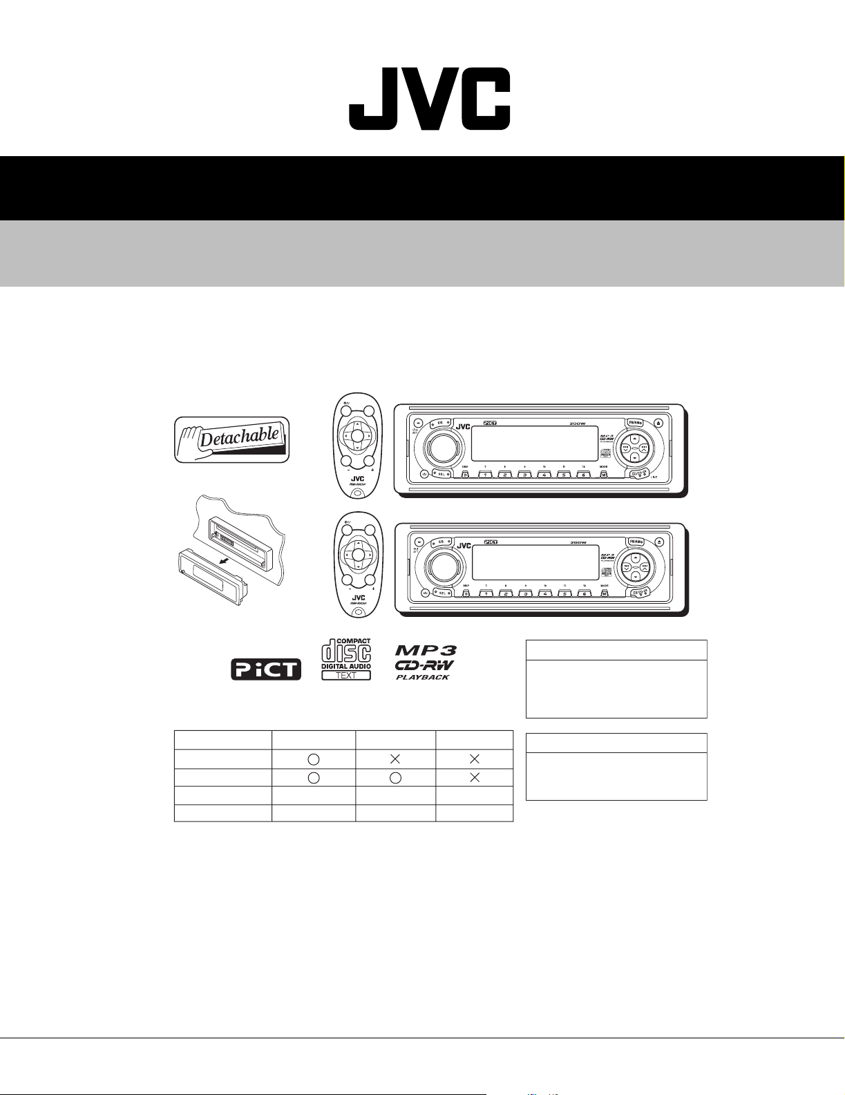
KD-LH3150, KD-LH3100
SERVICE MANUAL
CD RECEIVER
4983820034
KD-LH3150, KD-LH3100
ARSENAL rogo
LINE in
Line output level
WARRANTY
SOUND
ATT
U
SOURCE
F
R
D
VOL
VOL
SOUND
ATT
U
SOURCE
F
R
D
VOL
VOL
KD-LH3150J
KD-LH3150C KD-LH3100J
4 V 4 V 2 V
2 YEAR 1 YEAR 1 YEAR
KD-LH3150
KD-LH3150
KD-LH3100
KD-LH3100
KD-LH3150
Area Suffix
J -------------------------- U.S.A.
C --------------------- CANADA
KD-LH3100
Area Suffix
J -------------------------- U.S.A.
TABLE OF CONTENTS
1 Important Safety Precautions . . . . . . . . . . . . . . . . . . . . . . . . . . . . . . . . . . . . . . . . . . . . . . . . . . . . . . . . . . . 1-2
2 Disassembly method . . . . . . . . . . . . . . . . . . . . . . . . . . . . . . . . . . . . . . . . . . . . . . . . . . . . . . . . . . . . . . . . . . 1-4
3 Adjustment. . . . . . . . . . . . . . . . . . . . . . . . . . . . . . . . . . . . . . . . . . . . . . . . . . . . . . . . . . . . . . . . . . . . . . . . . . 1-23
4 Description of major ICs. . . . . . . . . . . . . . . . . . . . . . . . . . . . . . . . . . . . . . . . . . . . . . . . . . . . . . . . . . . . . . . 1-27
COPYRIGHT © 2003 VICTOR COMPANY OF JAPAN, LTD.
No.49838
2003/5
Page 2
KD-LH3150, KD-LH3100
1.1 Safety Precautions
SECTION 1
Important Safety Precautions
!
!
Burrs formed during molding may be left over on some parts of the chassis. Therefore,
pay attention to such burrs in the case of preforming repair of this system.
Please use enough caution not to see the beam directly or touch it in case of an
adjustment or operation check.
1-2 (No.49838)
Page 3
KD-LH3150, KD-LH3100
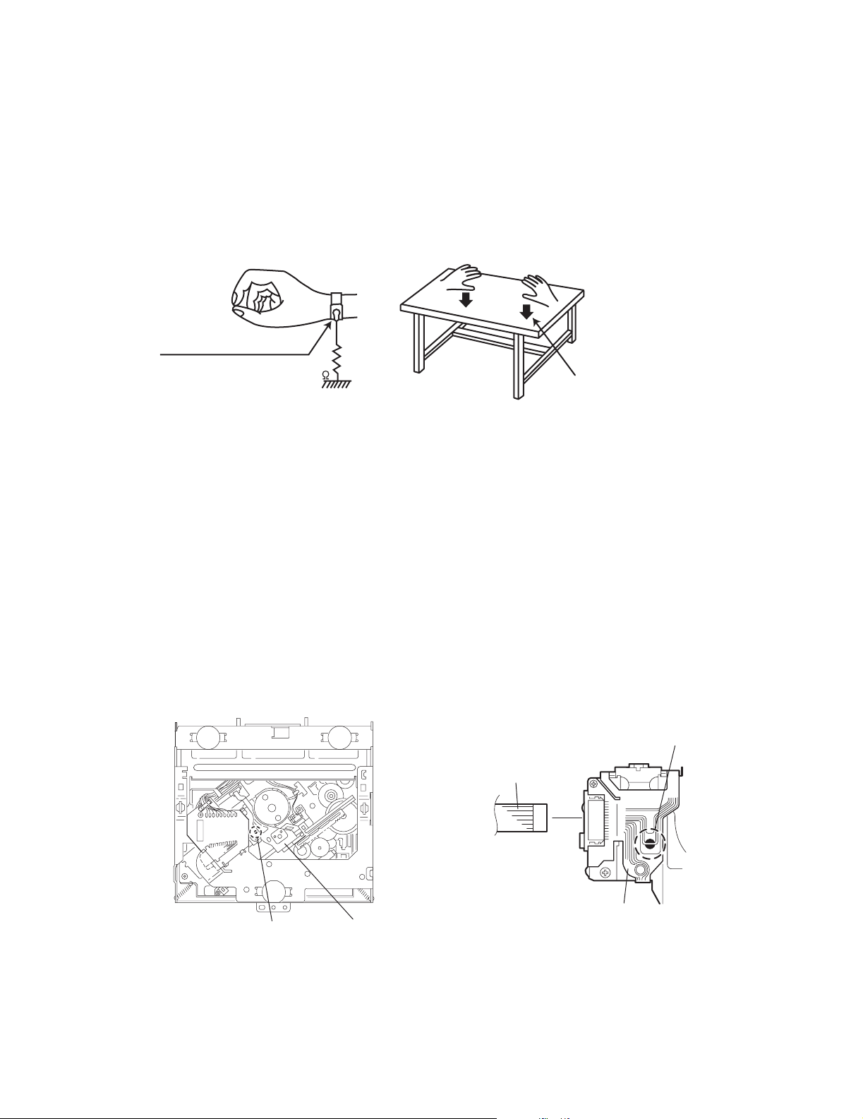
1.2 Preventing static electricity
Electrostatic discharge (ESD), which occurs when static electricity stored in the body, fabric, etc. is discharged,
can destroy the laser diode in the traverse unit (optical pickup). Take care to prevent this when performing repairs.
1.2.1 Grounding to prevent damage by static electricity
Static electricity in the work area can destroy the optical pickup (laser diode) in devices such as DVD players.
Be careful to use proper grounding in the area where repairs are being performed.
(1) Ground the workbench
Ground the workbench by laying conductive material (such as a conducti ve sheet) or an iron plate over it before placing the
traverse unit (optical pickup) on it.
(2) Grou nd yourself
Use an anti-static wrist strap to release any static electricity built up in your body.
(caption)
Anti-static wrist strap
1M
Conductive material
(conductive sheet) or iron plate
(3) Handling the optical pickup
• In order to maintain quality during transport and before insta llation, both sides of the lase r diode on the replacement o ptical
pickup are shorted. After replacement, return the shorted parts to their original condition.
(Refer to the text.)
• Do not use a tester to check the condition of the laser diode in the optical pickup. The tester's internal power source can easily
destroy the laser diode.
1.3 Handling the traverse unit (optical pickup)
(1) Do not subject the traverse unit (optical pickup) to strong shocks, as it is a sensitive, complex unit.
(2) Cut off the shorted part of the flexible cable using nippers, etc. after replacing the optical pickup. For specific details, refer to the
replacement procedure in the text. Remove the anti-static pin when replacing the traverse unit. Be careful not to take too long a
time when attaching it to the connector.
(3) Handle the flexible cable carefully as it may break when subjected to strong force.
(4) It is not possible to adjust the semi-fixed resistor that adjusts the laser power. Do not turn it.
1.4 Attention when traverse unit is decomposed *Please refer to "Disassembly method" in the text for the CD pickup unit.
• Apply solder to the short land before the flexible wire is disconnected from the connector on the CD pickup unit.
(If the flexible wire is disconnected without applying solder, the CDpickup may be destroyed by static electricity.)
• In the assembly, be sure to remove solder from the short land after connecting the flexible wire.
Short-circuit point
(Soldering)
Flexible wire
Short-circuit point
Pickup
Pickup
(No.49838)1-3
Page 4
KD-LH3150, KD-LH3100
Disassembly method
2.1 Main body
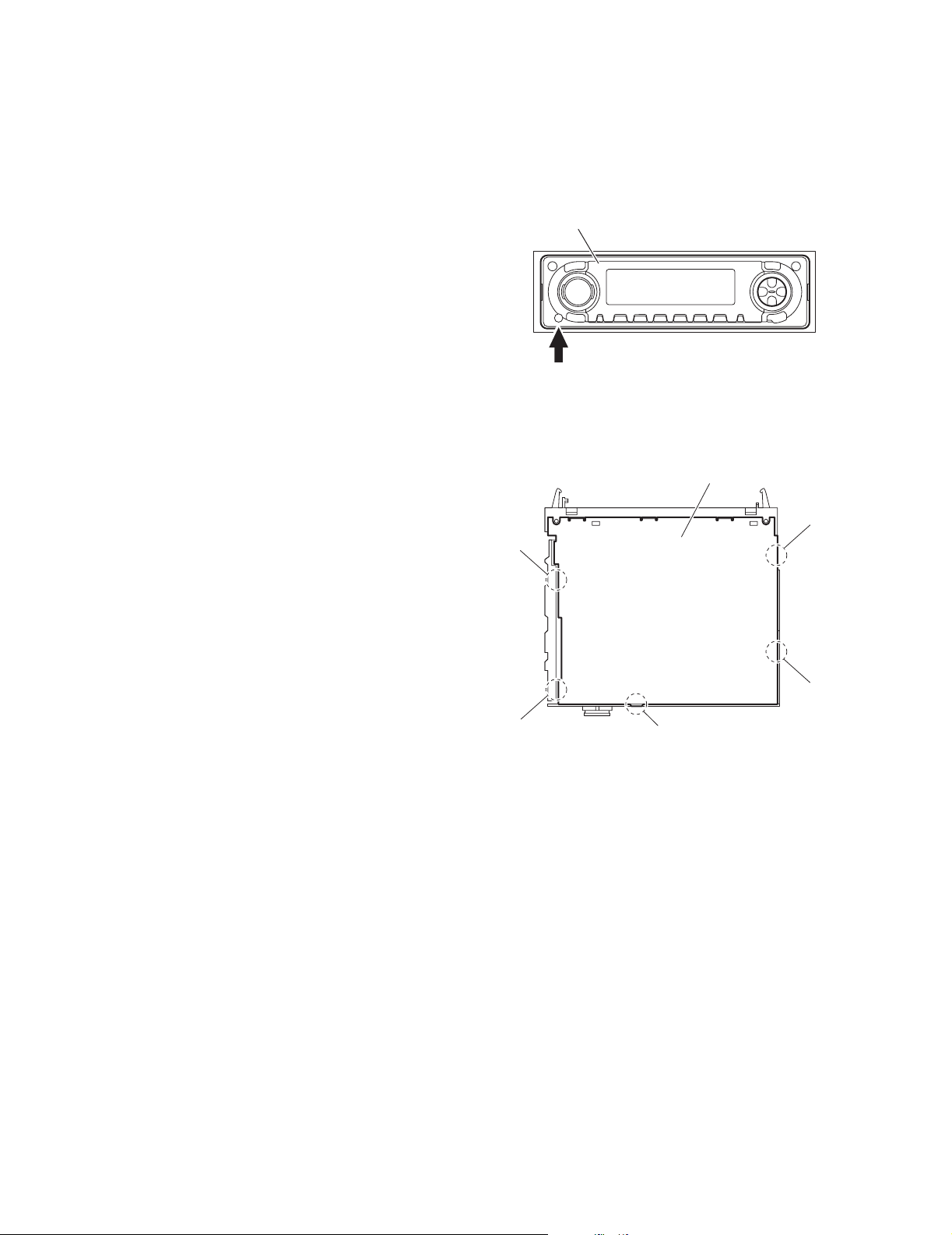
2.1.1 Removing the front panel assembly
(See Fig.1)
(1) Push the detach button in the lower left part of the front
panel assembly and remove the front panel assembly.
2.1.2 Removing the bottom cover
(See Fig.2)
• Prior to performing the following procedure, remove the front
panel assembly as required.
(1) Turn over the main body and release the two joints a, two
joints b and joint c.
NOTE:
Do not damage the main board when releasing the joints using
a screwdriver.
SECTION 2
Front panel assembly
Detach button
Fig.1
Bottom cover
Joint b
Joint a
Joint a
Joint b
Joint c
Fig.2
1-4 (No.49838)
Page 5
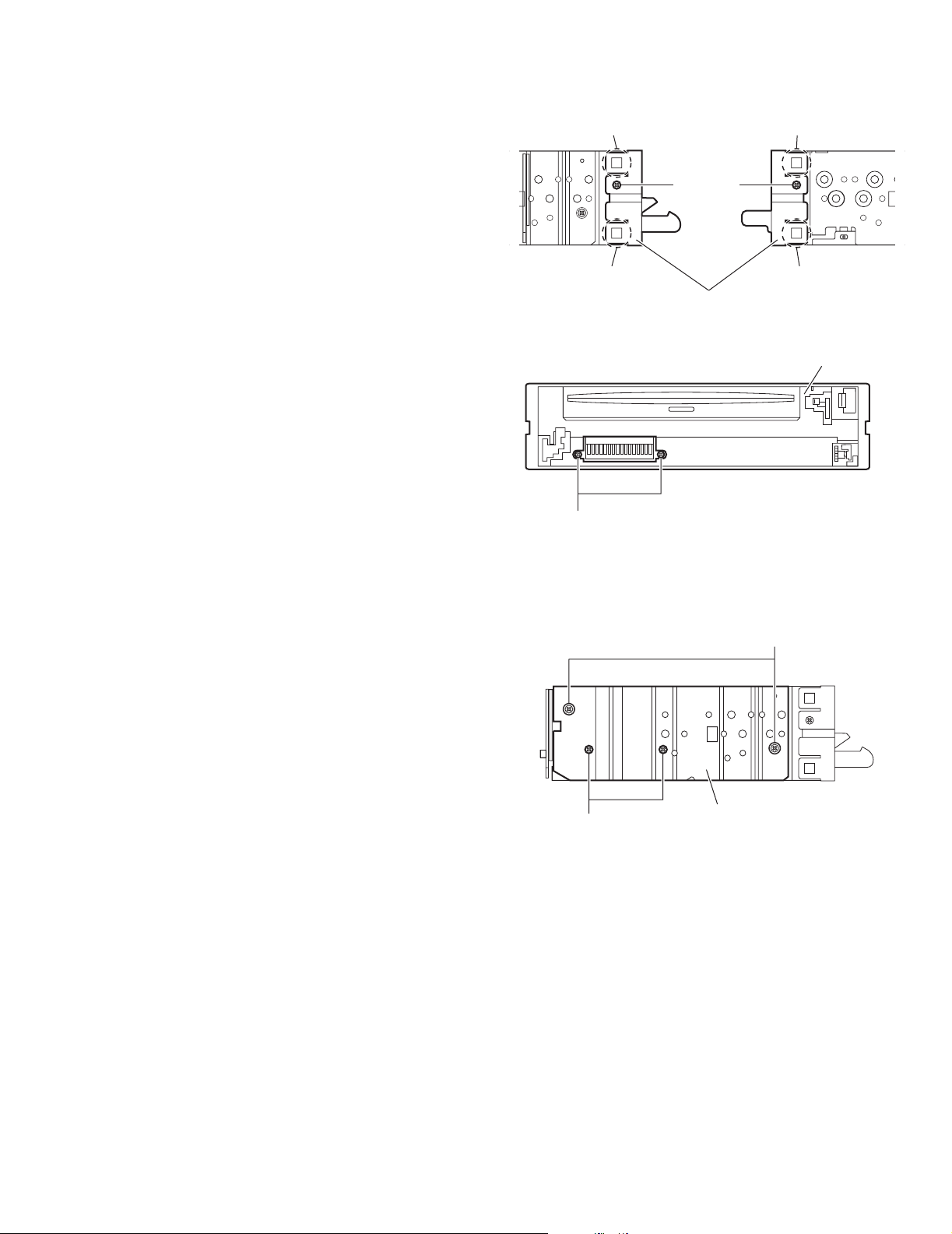
2.1.3 Removing the front chassis assembly
(See Figs.3 and 4)
• Prior to performing the following procedures, remove the front
panel assembly and bottom cover.
(1) Remove the two screws A on the both sides of the main
body. (See Fig.3.)
(2) Remove the two screws B on the front side of the main
body. (See Fig.4.)
(3) Release the two joints d and two joints e on the both sides
of the main body. (See Fig.3.)
Joint d
A
KD-LH3150, KD-LH3100
Joint e
A
2.1.4 Removing the heat sink
(See Fig.5)
• Prior to performing the following procedure, remove the front
panel assembly as required.
(1) Remove the two scre ws C and two screws D on the left
side of the main body.
B
Joint d
Front chassis assembly
Joint e
Fig.3
Front chassis assembly
Fig.4
C
D
Heat sink
Fig.5
(No.49838)1-5
Page 6
KD-LH3150, KD-LH3100
2.1.5 Removing the rear bracket
(See Fig.6)
• Prior to performing the following procedures, remove the bot-
tom cover.
(1) Remove the three screws E, three screws F and three
screws G on the back side of the main body.
(2) Remove the rear bracket.
REFERENCE:
During reassembly, before fixing the rear bracket onto the
main body, insert the SUB WOOFER cable and LINE IN cable
(KD-LH3150 only) into the slots.
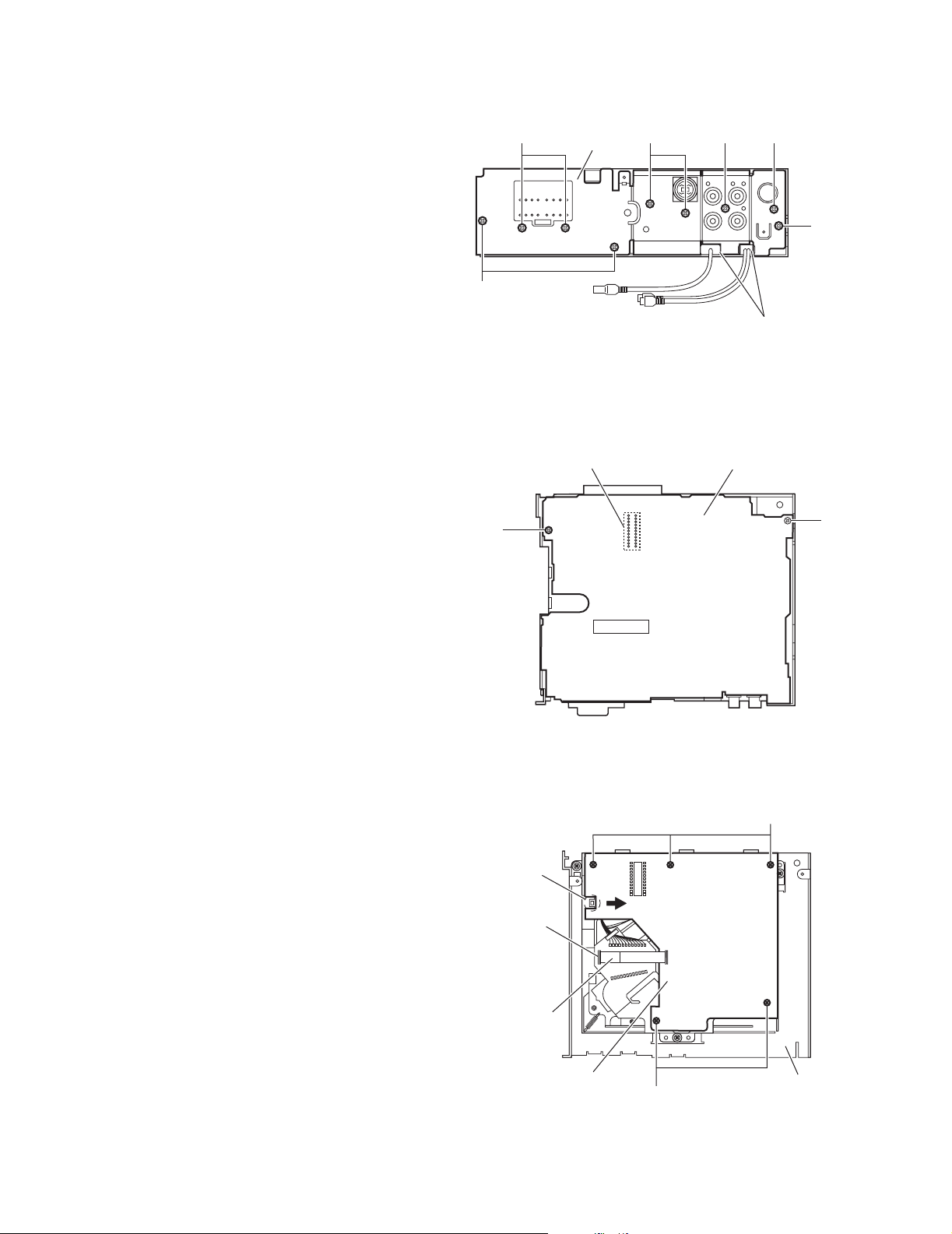
2.1.6 Removing the main board
(See Fig.7)
• Prior to performing the following procedures, remove the front
panel assembly, bottom cover, front chassis assembly, heat
sink and rear bracket
(1) Remove the two screws H attaching the main board.
(2) Disconnect the connector CN601 and remove the main
board in an upward direction.
FG
Rear bracket
G
F
E
E
Insert SUB WOOFER cable and
LINE IN cable (KD-LH3150 only)
into the slots.
Fig.6
CN601
H
Main board
H
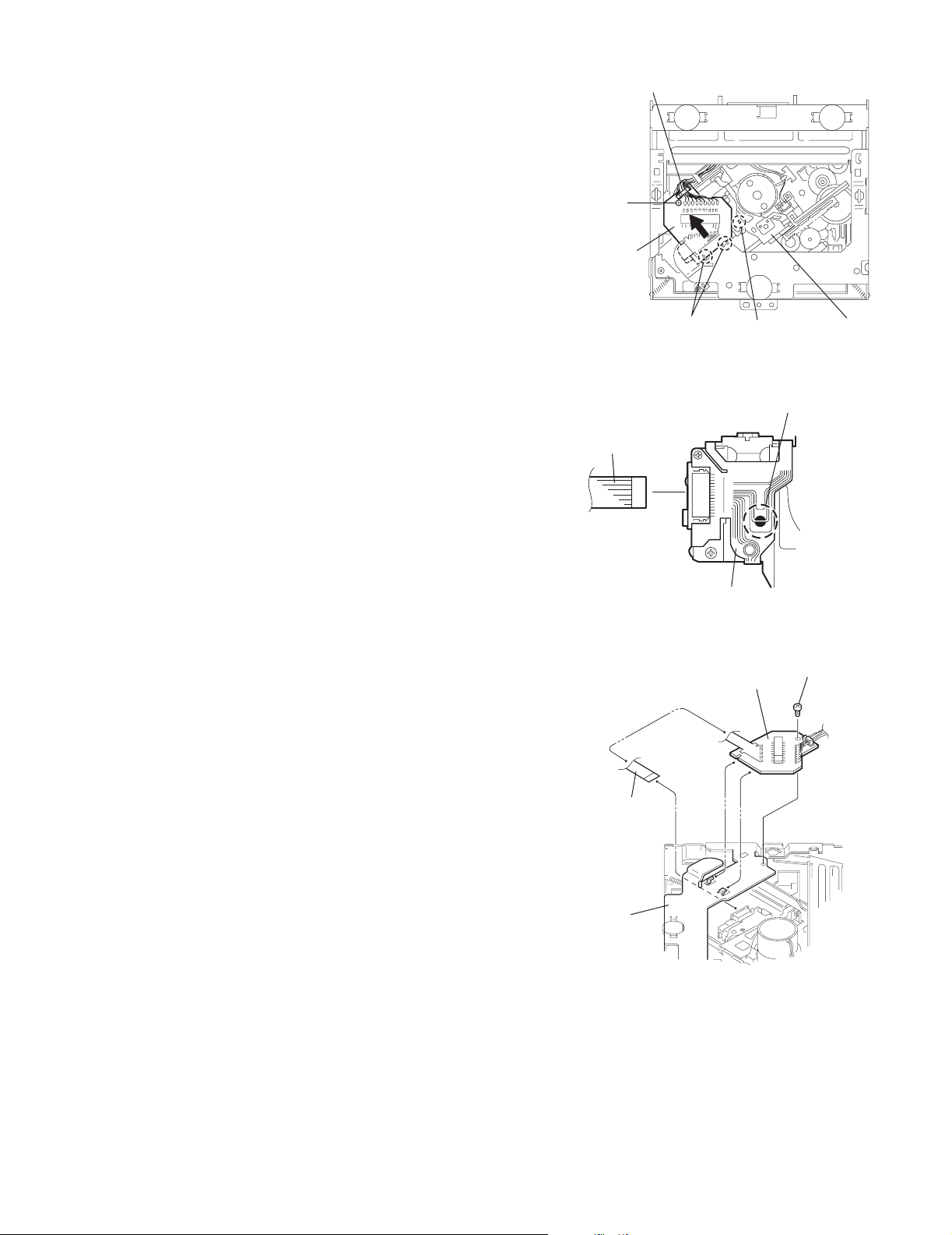
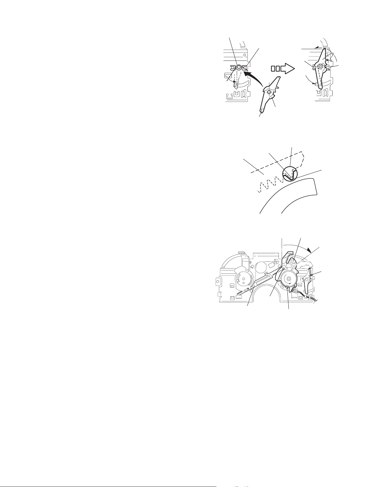
2.1.7 Removing the mecha control board
(See Fig.8)
• Prior to performing the following procedures, remove the front
panel assembly, bottom cover, front chassis assembly, heat
sink, rear bracket and main board.
(1) Remove the five screws J attaching the mecha control
board.
(2) Di sconnect the card wire from the mecha connector.
(3) Move the mecha control board in the direction of the arrow
to release it from the joint f.
Joint f
Mecha
connector
Card wire
Mecha control board
Fig.7
J
Top chassis
J
Fig.8
1-6 (No.49838)
Page 7
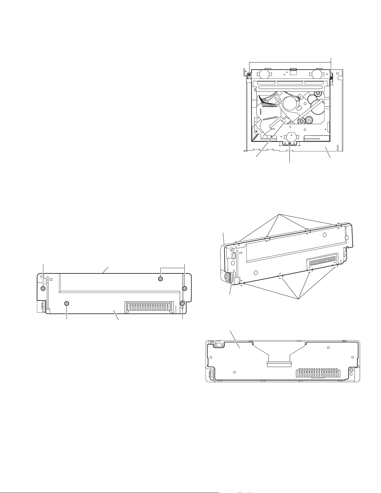
2.1.8 Removing the CD mechanism assembly
(See Fig.9)
• Prior to performing the following procedure, remove the front
panel assembly, bottom cover, front chassis assembly, heat
sink, rear bracket, main board and mecha control board.
(1) Remove the three screws K atta ching the CD mechanism
assembly to the top chassis.
KD-LH3150, KD-LH3100
K
2.1.9 Removing the front board
(See Figs.10 to 12)
• Prior to performing the following procedures, remove the front
panel assembly.
(1) Remove the five screws L attaching the rear cover on the
back side of the front panel assembly. (See Fig.10.)
(2) Rele ase the eight joints g, remove the rear cover from the
front panel assembly. (See Fig.11.)
(3) Take out the front board. (See Fig .1 2.)
L
L
Front panel assembly
Rear cover
Fig.10
L
L
CD mechanism assembly
Front panel
assembly
Rear cover
Front board
Top chassis
K
Fig.9
Joint g
Joint g
Fig.11
Fig.12
(No.49838)1-7
Page 8
KD-LH3150, KD-LH3100
A
2.2 CD Mechanism section
2.2.1 Removing the top cover
(See Figs.1 and 2)
(1) Remove the four screws A on the both side of the body.
(2) Lift th e front side of the top cover and move the top cover
backward to release the two joints a.
Top cover
Joints a
A
Joints a
A
Fig.1
Fig.2
Top cover
1-8 (No.49838)
Page 9
KD-LH3150, KD-LH3100
2.2.2 Removing the connector board
(See Figs.3 to 5)
CAUTION:
Before disconnecting the flexible wire from the pickup, solder
the short-circuit point on the pickup. No observance of this instruction may cause damage of the pickup.
(1) Remove the screw B fixing the connector board.
(2) S older the short-circuit point on the pickup.
(3) Disconnect the flexible wire from the pickup.
(4) Move the connector board in the direction of the arrow to
release the two joints b.
(5) Unsolder the wires on the connector board if necessary.
CAUTION:
Unsolder the short-circuit point after reassembling.
B
Connector board
Flexible wire
Wires
Joints b
Short-circuit point
Fig.3
Short-circuit point
(Soldering)
Pickup
Flexible wire
Frame
Pickup
Fig.4
B
Connector board
Fig.5
(No.49838)1-9
Page 10
KD-LH3150, KD-LH3100
2.2.3 Removing the DET switch
(See Figs.6 and 7)
(1) Extend the two ta bs c of the feed sw. holder and pull out
the switch.
(2) Unsolder the DET switch wire if necessary.
DET
switch
Connector
board
Pickup
Fig.6
DET switch
Tab c
Tab c
DET switch wire
Feed sw. holder
Fig.7
1-10 (No.49838)
Page 11
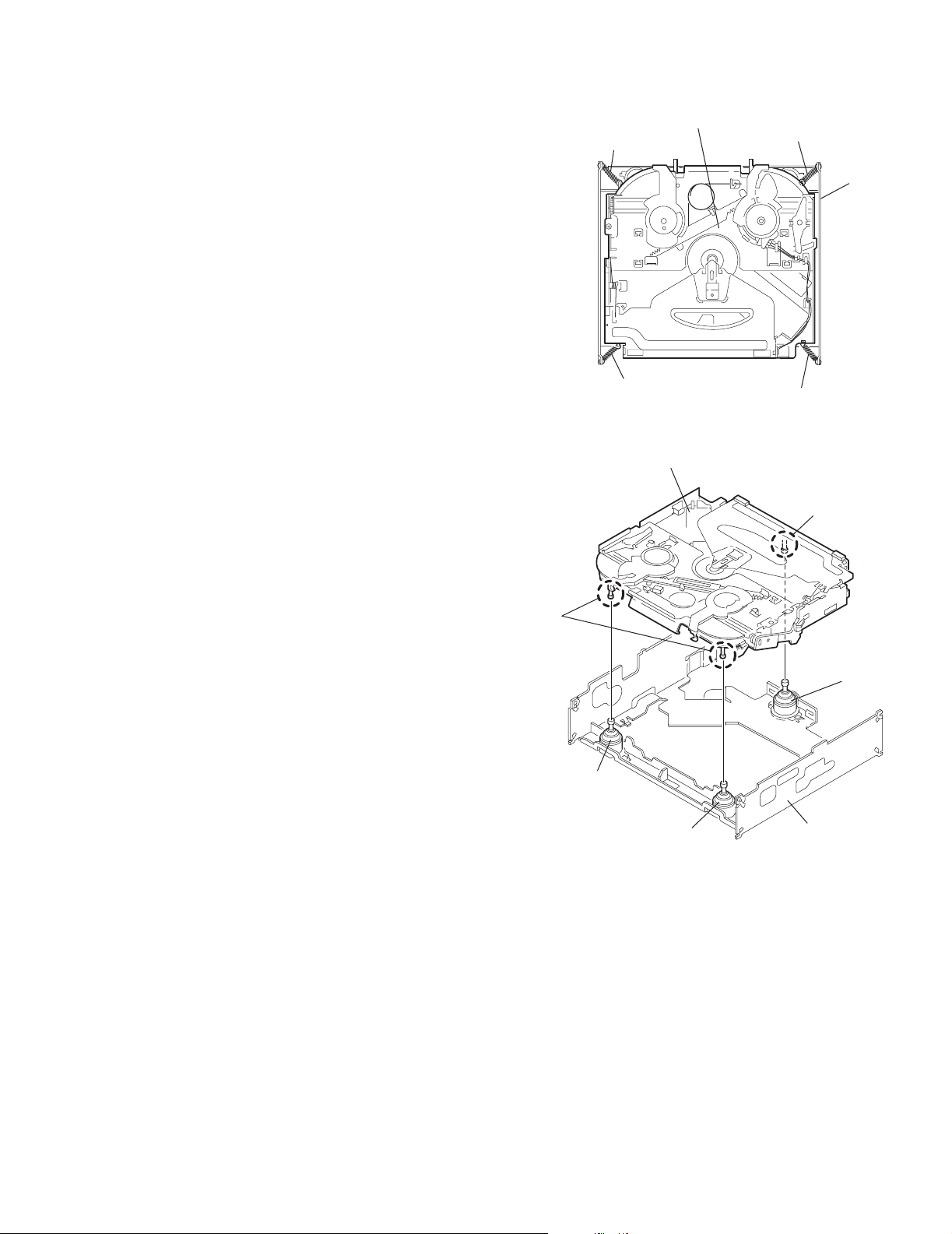
2.2.4 Removing the chassis unit
r
(See Figs.8 and 9)
• Prior to performing the following procedure, remove the top
cover and connector board.
(1) Remove the two suspension springs (L) and (R) attaching
the chassis unit to the frame.
CAUTION:
• The shape of the suspension spring (L) and (R) are different. Handle them with care.
• When reassembling, make sure that the three shafts
on the underside of the chassis unit are inserted to the
dampers certainly.
Suspension spring (R)
KD-LH3150, KD-LH3100
Chassis unit
Suspension spring (L)
Frame
Suspension spring (R)
Chassis unit
Shafts
Damper
Damper
Suspension spring (L)
Fig.8
Shaft
Dampe
Frame
Fig.9
(No.49838)1-11
Page 12
KD-LH3150, KD-LH3100
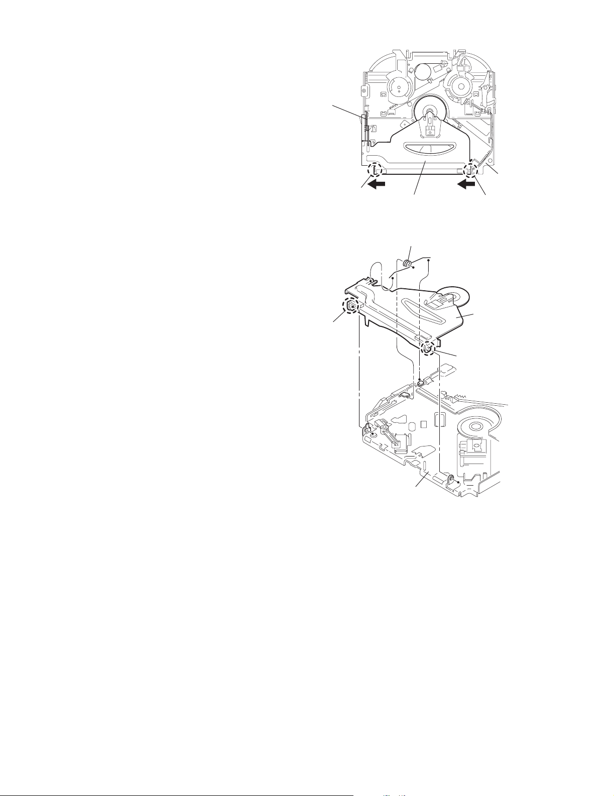
2.2.5 Removing the clamper assembly
(See Figs.10 and 11)
• Prior to performing the following procedure, remove the top
cover.
(1) Remove the clamper arm spring.
(2) Move the clamper assembly in the direction of the arrow to
release the two joints d.
Clamper arm
spring
Joint d
Clamper assembly
Fig.10
Clamper arm spring
Chassis rivet
assembly
Joint d
Joint d
Chassis rivet assembly
Clamper assembly
Joint d
Fig.11
1-12 (No.49838)
Page 13
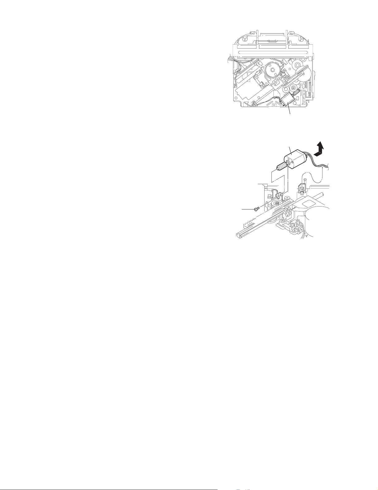
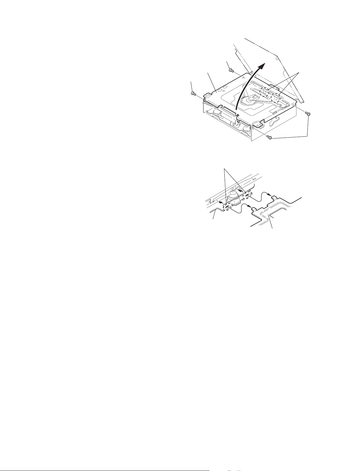
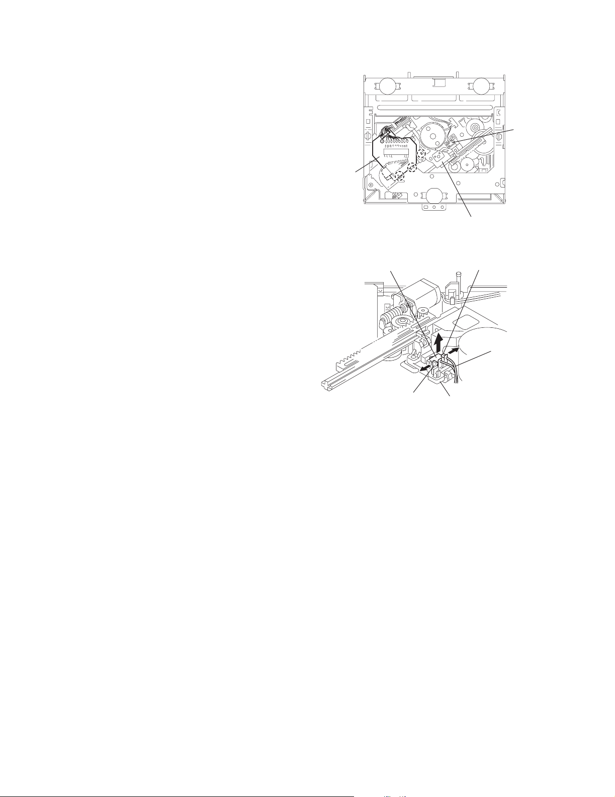
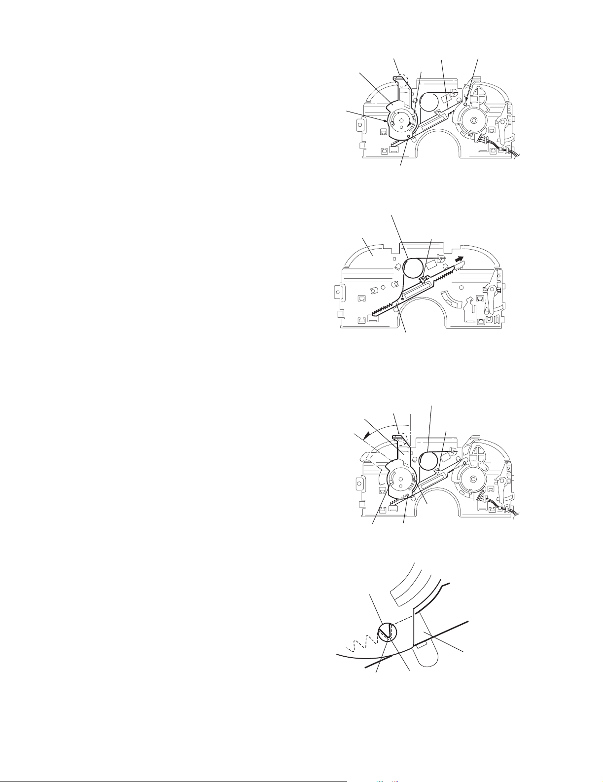
2.2.6 Removing the loading / feed motor assembly
(See Figs.12 and 13)
• Prior to performing the following procedure, remove the top
cover, connector board and chassis unit.
(1) Remove the screw C and move the loading / feed motor as-
sembly in the direction of the arrow to remove it from the
chassis rivet assembly.
(2) Disconnect the wire from the loading / feed motor assembly
if necessary.
CAUTION:
When reassembling, connect the wire from the loading /
feed motor assembly to the flame as shown in Fig.12.
KD-LH3150, KD-LH3100
Loading / feed motor assembly
Fig.12
Loading / feed motor assembly
C
Fig.13
(No.49838)1-13
Page 14
KD-LH3150, KD-LH3100
r
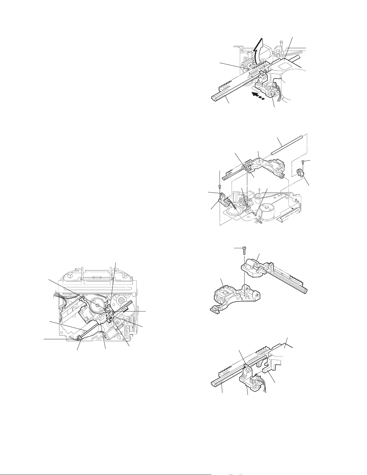
2.2.7 Removing the pickup unit
(See Figs.14 to 18)
• Prior to performing the following procedure, remove the top
cover, connector board and chassis unit.
(1) Remove the screw D and pull out the pu. shaft holder from
the pu. shaft.
(2) Remove the screw E attaching the feed sw. holder.
(3) Move the part e of the pickup unit upward with the pu. shaft
and the feed sw. holder, then release the joint f of the feed
sw. holder in the direction of the arrow. The joint g of the
pickup unit and the feed rack is released, and the feed sw.
holder comes off.
(4) Remove the pu. shaft from the pickup unit.
(5) Remove the screw F attaching the feed rack to the pickup
unit.
2.2.8 Reattaching the pickup unit
(See Figs.14 to 17)
(1) Reattach the feed rack to the pickup unit using the screw F.
(2) Reattach the feed sw. holder to the feed rack while setting
the joint g to the slot of the feed rack and setting the joint f
of the feed rack to the switch of the feed sw. holder correctly.
(3) As the feed sw. holder is temporarily attached to the pickup
unit, set to the gear of the joint g and to the bending part of
the chassis (joint h) at a time.
CAUTION:
Make sure that the part i on the underside of the feed
rack is certainly inserted to the slot j of the change lock
lever.
(4) Reattach the feed sw. holder using the screw E.
(5) Re attach the pu. shaft to the pickup unit. Reattach the pu.
shaft holder to the pu. shaft using the screw D.
Feed sw. holder
Part e
Joint g
Feed sw. holder
Feed rack
Part i
E
Slot j
F
Feed sw. holder
Fig.15
Pu. shaft
Pickup unit
Joint f
Joint h
Fig.16
Feed rack
Pickup unit
D
Pu. shaft holde
Joint f
Pu. shaft
D
Pu. shaft holder
Pickup unit
Fig.14
Part e
E
Joint g
Pickup unit
Feed rack
Fig.17
Pickup unit
Joint g
Joint f
Feed sw. holder
Fig.18
1-14 (No.49838)
Page 15
KD-LH3150, KD-LH3100
r
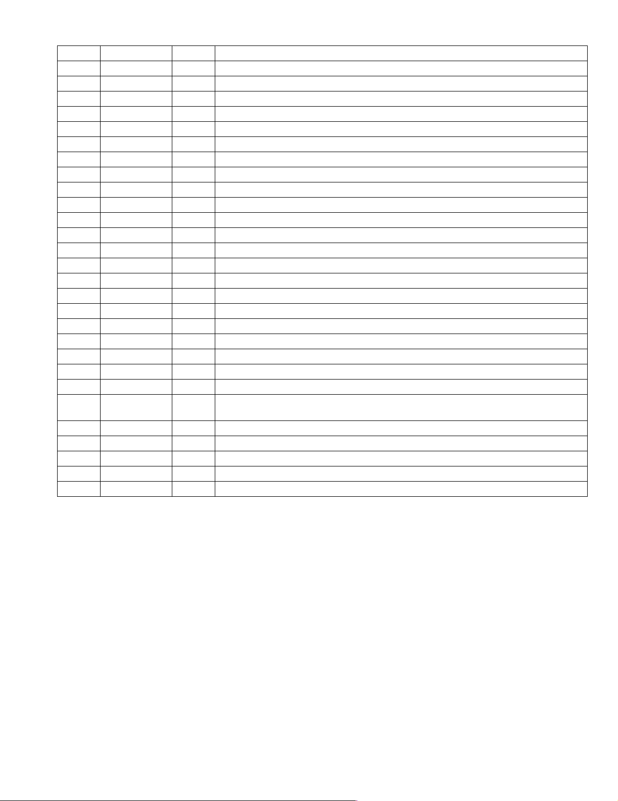
2.2.9 Removing the trigger arm
(See Figs.19 and 20)
• Prior to performing the following procedure, remove the top
cover, connector board and clamper unit.
(1) Turn the trigger arm in the direction of the arrow to release
the joint k and pull out upward.
CAUTION:
When reassembling, insert the part m and n of the trigger arm into the part p and q at the slot of the chassis rivet assembly respectively and join the joint k at a time.
Chassis rivet assembly
Trigger arm
Chassis
rivet
assembly
Joint k
Trigger arm
Fig.19
Part p
Part q
Part m
Part n
2.2.10 Removing the top plate assemb ly
(See Fig.21)
• Prior to performing the following procedure, remove the top
cover, connector board, chassis unit, and clamper assembly.
(1) Remove the screw H.
(2) Move the top plate assembly in the direction of the arrow to
release the two joints r.
(3) Unsolder the wire marked s if necessary.
H
Fig.20
Top plate assembly
Joints
s
Fig.21
(No.49838)1-15
Page 16
KD-LH3150, KD-LH3100
2.2.11 Removing the mode sw. / select lock arm
(See Figs.22 and 23)
• Prior to performing the following procedure, remove the top
plate assembly.
(1) Bring up the mode sw. to release from the link plate (joint t)
and turn in the direction of the arrow to release the joint u.
(2) Uns older the wire of the mode sw. marked s if necessary.
(3) Turn th e select lock arm in the direction of the arrow to re-
lease the two joints v.
(4) The select lock arm spring comes off the select lock arm at
the same time.
Top plate
Link plate
Joint u
Joint t
s
Fig.22
Select lock arm
Select lock arm
Mode sw.
Select lock arm
Top plate
Hook w
Select lock
arm spring
Link plate
Joints v
Fig.23
1-16 (No.49838)
Page 17
KD-LH3150, KD-LH3100
2.2.12 Reassembling the mode sw. / select lock arm
(See Figs.24 to 26)
REFERENCE:
Reverse the above removing procedure.
(1) Reattach the select lock arm spring to the top plate and set
the shorter end of the select lock arm spring to the hook w
on the top plate.
(2) Set the other longer end of the select lock arm spring to the
boss x on the underside of the select lock arm, and join the
select lock arm to the slots (joint v). Turn the select lock
arm as shown in the figure.
(3) Reattach the mode sw. while setting the part t to the first
peak of the link plate gear, and join the joint u.
CAUTION:
When reattaching the mode sw., check if the points y
and z are correctly fitted and if each part operates properly.
Select lock arm spring
Hook w
Joint v
Joint v
Select lock arm
Boss x
Fig.24
Joint t
Point y
Link plate
Point z
Link plate
Fig.25
Mode sw.
Select
lock arm
Joint t
Joint u
Fig.26
(No.49838)1-17
Page 18
KD-LH3150, KD-LH3100
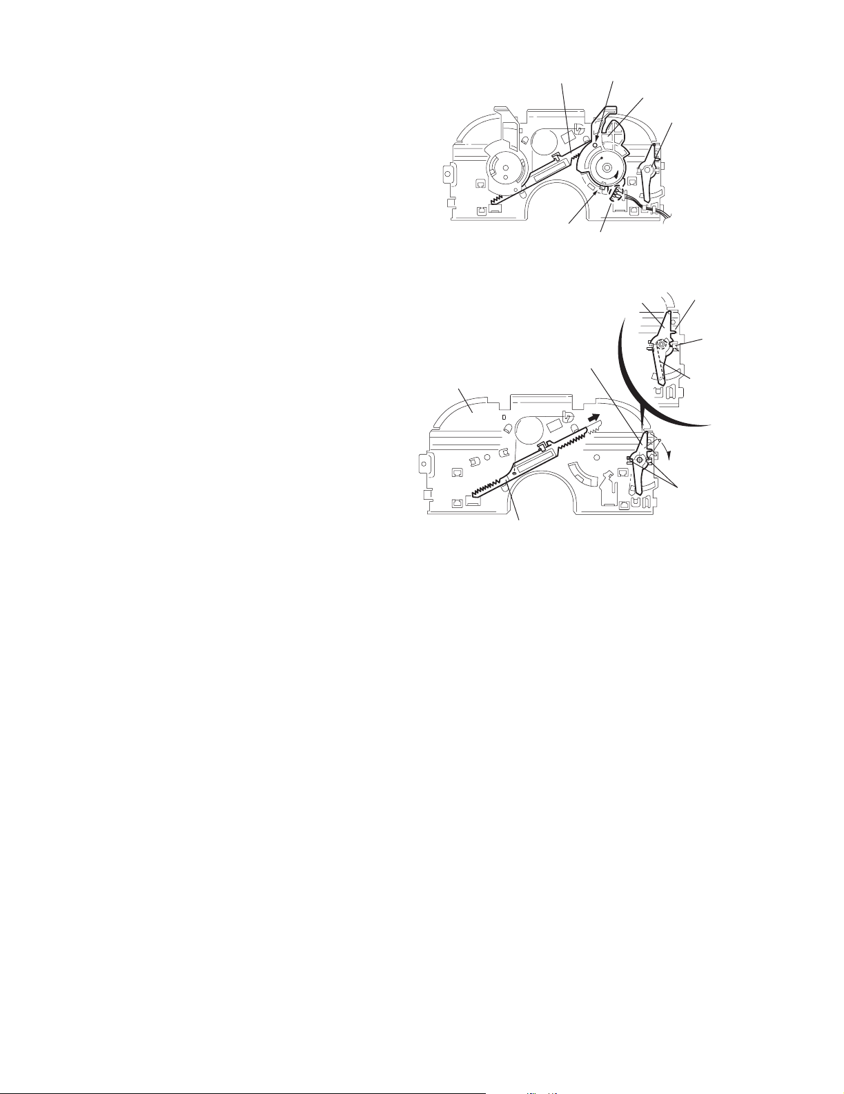
2.2.13 Removing the select arm R / link plate
(See Figs.27 and 28)
• Prior to performing the following procedure, remove the top
plate assembly.
(1) Bring up the select arm R to release from the link plate
(joint a') and turn as shown in the figure to release the two
joints b' and joint c'.
(2) Move the lin k plate in the direction of the arrow to release
the joint d'. Remove the link plate spring at the same time.
REFERENCE:
Before removing the link plate, remove the mode sw..
Select arm R
Joint b'
Link plate spring
Top plate
Joint c'
Joint a'
Link plate
Joint b'
Fig.27
Joint d'
Joint r
2.2.14 Reattaching the Select arm R / link plate
(See Figs.29 and 30)
REFERENCE:
Reverse the above removing procedure.
(1) Reattach the link plate spring.
(2) Re attach the link pl ate to the lin k p late spring whil e joi ning
them at joint d'.
(3) Reattach the joint a' of the select arm R to the first peak of
the link plate while joining the two joints b' with the slots.
Then turn the select arm R as shown in the figure. The top
plate is joined to the joint c'.
CAUTION:
When reattaching the select arm R, check if the points e'
and f' are correctly fitted and if each part operates properly.
Select arm R
Joint b'
Joint a'
Link plate
Fig.28
Link plate spring
Joint c'
Joint d'
Joint b'
Joint a'
Fig.29
1-18 (No.49838)
Point e'
Link plate
Point f'
Fig.30
Page 19

2.2.15 Removing the loading roller assemb ly
(See Figs.31 to 33)
• Prior to performing the following procedure, remove the
clamper assembly and top plate assembly.
(1) Push inward the loading roller assembly on the gear side
and detach it upward from the slot of the joint g' of the lock
arm rivet assembly.
(2) Detach the loading roller assembly from the slot of the joint
h' of the lock arm rivet assembly.
The roller guide comes off the gear section of the loading
roller assembly.
Remove the roller guide and the HL washer from the shaft
of the loading roller assembly.
(3) Remove the screw J attaching the lock arm rivet assembly.
(4) Push the shaft at the joint i' of the lock arm rivet assembly
inward to release the lock arm rivet assembly from the slot
of the L side plate.
(5) Extend the lock arm rivet assembly outward and release
the joint j' from the boss of the chassis rivet assembly. The
roller guide springs on both sides come off at the same
time.
CAUTION:
When reassembling, reattach the left and right roller
guide springs to the lock arm rivet assembly before reattaching the lock arm rivet assembly to the chassis rivet
assembly. Make sure to fit the part k' of the roller guide
spring inside of the roller guide. (Refer to Fig.34.)
Roller guide
spring
Part k'
Chassis rivet assembly
KD-LH3150, KD-LH3100
Loading roller assembly
Loading roller assembly
Roller guide
spring
Fig.32
Boss
Roller guide
Joint h'
Roller guide spring
Loading roller assembly
HL washer
Loading roller assembly
Joint g'
Lock arm rivet assembly
Fig.31
Roller guide
Roller guide spring
Roller guide spring
J
Lock arm rivet assembly
Lock arm rivet assembly
L side plate
Roller guide spring
Joint i'
Joint j'
Fig.33
Roller guide
HL washer
Roller shaft assembly
Loading roller
Roller guide spring
Fig.34
(No.49838)1-19
Page 20

KD-LH3150, KD-LH3100
2.2.16 Removing the load ing gear 5, 6 and 7
(See Figs.35 and 36)
• Prior to performing the following procedure, remove the top
cover, chassis unit, pickup unit and top plate assembly.
(1) Remove the screw K attaching the loading gear bracket.
The loading gear 6 and 7 come off the loading gear bracket.
(2) Pull out the loading gear 5.
K
Loading gear 5
Loading gear bracket
K
Loading gear 6
Loading gear 5
Fig.35
Loading gear bracket
Loading gear 6
Loading gear 3
Loading gear 7
1-20 (No.49838)
Fig.36
Page 21

KD-LH3150, KD-LH3100
2.2.17 Removing the gears
(See Figs.37 to 40)
• Prior to performing the following procedure, remove the top
cover, chassis unit, top plate assembly and pickup unit.
• Pull out the loading gear 3. (See Fig.35.)
(1) Pull out the feed gear.
(2) Move the loading plate assembly in the direction of the ar-
row to release the L side plate from the two slots m' of the
chassis rivet assembly. (See Fig.37.)
(3) Detach the loading plate a ssembly upward from the chas-
sis rivet assembly while releasing the joint n'. Remove the
slide hook and loading plate spring from the loading plate
assembly.
(4) Pull out the loading gear 2 and remove the change lock le-
ver.
(5) Remove the E ring and washer a ttaching the change gear
2.
(6) The change gear 2, change gear spring and adjusting
washer come off.
(7) Remove the loading gear 1.
(8) Move the change plate rivet assembly in the direction of the
arrow to release from the three shafts of the chassis rivet
assembly upward. (See Fig.38.)
(9) Detach the loading gear plate rivet assembly from the shaft
of the chassis rivet assembly upward while releasing the
joint p'. (See Figs.38 and 40.)
(10) Pull out the loading gear 4.
Change plate
rivet assembly
Shafts
E ring
Loading plate assembly
Loading plate spring
Joint p'
Loading gear 4
Loading gear plate
rivet assembly
Shaft
Loading gear 2
Loading gear 1
Chassis rivet assembly
Change gear 2
Fig.38
Joint n'
Slide hook
Feed gear
Fig.37
Slot m'
L side plate
Loading plate assembly
Joint n'
Slot m'
Chassis rivet assembly
Chassis rivet assembly
E ring
Washer
Change gear 2
Change gear
spring
Adjusting
washer
Change plate
rivet assembly
L side plate
Slot m'
Slot m'
Fig.39
Loading gear 1
Loading gear 2
Change lock lever
Loading gear 4
Chassis rivet assembly
Loading gear plate rivet
assembly
Fig.40
(No.49838)1-21
Page 22

KD-LH3150, KD-LH3100
2.2.18 Removing the turn ta ble / spind le motor
(See Figs.41 and 42)
• Prior to performing the following procedure, remove the top
cover, connector board, chassis unit and clamper assembly.
(1) Re move the two screws L attaching the spindle motor as-
sembly through the slot of the turn table on top of the body.
(2) Unsolder the wire on the connector board if necessary.
Turn table
L
Fig.41
L
Turn table
1-22 (No.49838)
Spindle motor
Fig.42
Page 23

SECTION 3
Adjustment
3.1 Adjustment method
Test instruments required for adjustment
1. Digital oscilloscope (100MHz)
2. AM Standard signal generator
3. FM Standard signal generator
4. Stereo modulator
5. Electric voltmeter
6. Digital tester
7. Tracking offset meter
8. Test Disc JVC :CTS-1000
9. Extension cable for check
EXTSH002-22P 1
Standard measuring conditions
Power supply voltage DC14.4V(11 to 16V)
Load impedance 20Kohm(2 Speakers connection)
Output Level Line out 2.0V (Vol. MAX)
Standard volume position
Balance and Bass &Treble volume : lndication "0"
Loudness : OFF
Frequency Band
FM 87.5MHz to 107.9MHz
AM 530kHz to 1710kHz
Dummy load
Exclusive dummy load should be used for AM, and FM. For
FM dummy load, there is a loss of 6dB between SSG output
and antenna input. The loss of 6dB need not be considered
since direct reading of figures are applied in this working
standard.
KD-LH3150, KD-LH3100
How to connect the extension cable for adjusting
The cardboard is cut in a suitable size.
uses for the insulation stand of mechanism.
Caution:
Be sure to attach the heat sink and rear
bracket onto the power amplifier IC and
regulator IC respectively, before supply
the power.
If voltage is applied without attaching
these parts, the power amplifier IC
and regulator IC will be destroyed
by heat.
Heat sink
(Attach the heat sink
using the two screws.)
Extension cable
EXTSH002-22P
Rear bracket
(Attach the rear bracket
using the screw.)
Front chassis assembly
(Attach the front chassis assembly using the two screws.)
(No.49838)1-23
Page 24

KD-LH3150, KD-LH3100
3.2 Flow of functional operation unit TOC read
When the pickup correctly moves
to the inner area of the disc
$82
Microprocessor
commands
FMO
TC94A14FA "40"
FEED MOTOR
+TERMINAL
IC681 "17"
REST SW
When correctly focused
FEO
TA2157 "15"
$83
$81
Focus Servo Loop ONo
v
3.3V
Hi-Z
0V
6V
4V
2V
OFF
ON
Pickup feed to the inner area
2.2V
RF signal eye-pattern
remains closed
RF signal eye-pattern
opens
Power ON
Set Function CD
Disc inserted
YES
Laser emitted
Focus search
Disc rotates
n
Tracking loop closed
TOC read out
YES
When the laser diode correctly
emits
Microprocessor
commands
SEL
TC94A14FA "38"
LD
CN601 "10"
"No disc"
display
When the disc correctly rotates
Microprocessor
commands
DMO
TC94A14FA "41"
Spindle
motor(-)
IC681 "16"
$84 $86 $ A200
Acceleration Servo CLV
0.5 Sec 0.5 Sec
$84
Rough
Servo
3.3V
0V
4V
0V
3.3V
2.2V
0V
6V
3.2
2V
1-24 (No.49838)
Jump to the first track
Play
Tracking Servo Loop ON
RF signal
Rough Servo Modev
CLV Servo Mode
(Program Area)
CLV Servo Mode
(Lead-In Area;
Digital :0)
Page 25

3.2.1 Feed section
KD-LH3150, KD-LH3100
Is the voltage output at
IC621 pin "40" 5V or 0V?
Is 4V present at both
sides of the feed motor?
Check the feed motor.
3.2.2 Focus section
When the lens is
moving:
Does the S-search
waveform appear at
IC681 pins "13" and "14"?
3.2.3 Spindle section
Is the disk rotated?
Does the RF signal
appear at IC601 pin "19"?
Is the RF waveform at
IC601 pin "19" distorted?
Proceed to the Tracking
section
NO YES NO
Is the wiring for IC621
pin "40"?
YES NO
NO
Is 6V or 2V present at
IC681 "16" and "17"?
YES
Check IC681.
NO
Check the circuits in
the vicinity of IC681
4V
pins "13","14"and"1".
YES
YES
Check the pickup and
its connections
NO
Is 4V present at IC681
pins "15" and "16"?
YES
Check the spindle motor
and its wiring
YES
NO
Check the circuits in the
vicinity of IC601 pin "19"
NO
YES
or the pickup
NO
YES
Is 3.3V present at IC681
pin "6"?
Check the vicinity of
IC621.
YES
Check the feed motor
connection wiring.
NO
Is 4V present at IC621
pins "41" ?
Check the vicinity of
IC681.
YES
YES
Check CD 8V
and 5V.
NO
Check the circuits in
the vicinity of IC621
or IC621
3.2.4 Tracking section
When the disc is rotated
at first:
Is the tracking error signal
output at IC601 "11"?
Approx. 1.2V
YES
Check IC621.
YES YES
Check the circuit in the
vicinity of IC601 pins
"2" to "7".
Check the pickup and
its connections
(No.49838)1-25
Page 26

KD-LH3150, KD-LH3100
3.3 Maintenance of laser pickup
(1) Cl eaning the pick up lens
Before you replace the pick up, please try to clean the lens
with a alcohol soaked cotton swab.
(2) Life of the laser di ode
When the life of the laser diode has expired, the following
symptoms will appear.
• The level of RF output (EFM output:ampli tude of eye
pattern) will be low.
Is RF output
1.3
±
0.4Vp-p?
NO
Replace it.
YES
O.K
(3) Semi-fixed resistor on the APC PC board
The semi-fixed resistor on the APC printed circuit board
which is attached to the pickup is used to adjust the laser
power.Since this adjustment should be performed to match
the characteristics of the whole optical block, do not touch
the semi-fixed resistor. If the laser power is lower than the
specified value,the laser diode is almost worn out, and the
laser pickup should be replaced. If the semi-fixed resistor
is adjusted while the pickup is functioning normally,the l aser pickup may be damaged due to excessive current.
3.4 Replacement of laser pickup
Turn of the power switch and, disconnect the
power cord.
Replace the pickup with a normal one. (Refer
to "Pickup Removal" on the previous page)
Plug the power cord in, and turn the power on.
At this time, check that the laser emits for
about 3 seconds and the objective lens moves
up and down.
Note: Do not observe the laser beam directly.
Play a disc.
Check the eye-pattern at RF test point.
Finish.
1-26 (No.49838)
Page 27

Description of major ICs
+
+
-
-
+
+
-
-
-
+
+
4.1 BA3220FV-X (IC281, IC301) : Line out amplifier
•Pin layout
KD-LH3150, KD-LH3100
SECTION 4
• Block diagram
14
8
3220
17
CL-
14
LGND
13
OUTL OUTR RGND
1112
10
CR-
9
CR+
8
REFL
REFR
FILTER
1
2
Vcc
3
INL
4
NFLCL+
56
FIL
NFR
7
INR
(No.49838)1-27
Page 28

KD-LH3150, KD-LH3100
4.2 BA5830FP-X (IC681) : Power driver
• Pin layout & Block diagram
22232425262728 15161718192021
BIAS
Pre Vcc
-
+
-
+
+
-
+
-
-
+
• Pin function
Pin No. Symbol Function
1 OPIN2(-) CH2 Pre OP amplifier invert input
2 OPOUT2 CH2 Pre OP amplifier output
3 OPIN1(-) CH1 Pre OP amplifier invert input
4 OPOUT1 CH1 Pre OP amplifier output
5 REG-B Connect to external Tr Base
6 REG(+) Regulator terminal of output feedback
7 PreGND Pre Block and Regulator GND
8 MUTE Mute terminal
9 PowGND Power Block GND
10 PowVcc1 CH1, 2 Power Block Vcc
11 VO1(-) Driver CH1 negative output
12 VO1(+) Driver CH1 positi ve outp ut
13 VO2(-) Driver CH2 negative output
14 VO2(+) Driver CH2 positi ve outp ut
10k
L
-
H
+
1.65V
20k
10k
2.4V
20k
-
+
+
-
10k
PreGND
7654321 141312111098
CH4 CH3
10k 10k 10k 10k
-
20k
10k
10k
LD/SLED
CONTROL
H
L
10k
-
+
+
-
10k
MUTE
CONTROL
Pow
GND
Pow
GND
Pow
Vcc2
Pow
Vcc1
+
Level shifter
Level shifter
+
-
+
10k 10k 10k 10k
T.S.D
10k
-
+
10k
CH1
10k
-
+
Level shifter
Level shifter
+
10k
-
10k
-
10k
CH2
T.S.D : thermal shutdown
Unit of resistance : [Ω]
Pin No. Symbol Function
15 VO3(+) Driver CH3 positive output
16 VO3(-) Driver CH3 negative output
17 VO4(+) Driver CH4 positive output
18 VO4(-) Driver CH4 negative output
19 PowVcc2 CH3, 4 Power Block VCC
20 PowGND Power Block GND
21 CNT Control terminal
22 LDIN Loading input
23 OPOUTSL SLED Pre OP amplifier output
24 OPINSL(-) SLED Pre OP amplifier invert input
25 OPOUT3 CH3 Pre OP amplifier output
26 OPIN3(-) CH3 Pre OP amplifier invert input
27 BIAS BIAS input
28 PreVcc Pre-Block VCC
-
+
10k
-
+
10k
NOTE:
When PIN2,4,22,25 is high ("H"), the positive output pin of the driver is high ("H") and the negative output pin is low ("L").
When PIN23 is high ("H"), the positive output pin of CH4 is low ("L") and negative output pin is high ("H").
1-28 (No.49838)
Page 29

4.3 BR24C01AFV-W-X (IC502) : EEPROM
A
•Pin layout
Vcc WP SCL SDA
A0 A1 A2 GND
• Block diagram
KD-LH3150, KD-LH3100
A0
1
7bit
A1
2
A2
3
GND
• Pin function
Pin name I/O Description
Vcc - Power supply
GND - Ground (0v)
A0, A1, A2 IN Slave address set
SCL IN Serial clock input
SDA IN / OUT Slave and word addressserial data input serial data output *1
WP IN Write protect input
*1 An open drain output requires a pull-up resister.
4
ADDRESS
DECODER
CONTROL LOGIC
HIGH VOLTAGE GEN.
1kbit EEPROM ARRAY
SLAVE/WORD
7bit
ADDRESS REGISTER
START
STOP
Vcc LEVEL DETECT
DATA
REGISTER
ACK
8bit
Vcc
8
7
WP
6
SCL
5
SD
(No.49838)1-29
Page 30

KD-LH3150, KD-LH3100
A
4.4 BR24C16F-X (IC703) : EEPROM
• Pin layout • Pin function
VCC WP SCL SDA
A0, A1, A2 I No use connect to GND.
A0 A1 A2 GND
• Block diagram
Symbol I/O Function
VCC - Power supply.
GND - GND
SCL I Serial clock inpu t.
SDA I/O Serial data I/O of slave and ward address.
WP I Write protect terminal.
A0 1
A1 2
A2 3
GND 4
11bit
Address
decoder
Control circuit
High voltage osc circuit
16kbit EEPROM allay
11bit
START
Slave Ward
Address resister
Power supply
voltage det.
STOP
ACK
8bit
Data
resister
8 Vcc
7 WP
6 SCL
5 SD
1-30 (No.49838)
Page 31

4.5 BU4066BCFV-X (IC131) : Quad analog switch
• Pin layout & Block diagram
VDD C1 C4 I/O4 I/O3O/I4 O/I3
14 13 12 11 810 9
1234 756
I/O1 O/I1 O/I2 I/O2 VssC2 C3
KD-LH3150, KD-LH3100
4.6 RPM6938-SV4 (IC805) : Remote control receiver
• Block diagram
I/V
conversion
PD
AMP
for
trimming circuit
magnetic shield
BPF
AGC
Detector
Vcc
Comp
22k
ohm
3
1
2
VDD
OUT
GND
(No.49838)1-31
Page 32

KD-LH3150, KD-LH3100
4.7 HA13164A (IC901) : Regulator
• Pin layout
123456789101112131415
• Block diagram
ANT CTRL
AUDIO OUT
ANT OUT
EXT OUT
CTRL
CD OUT
C3
0.1u
C4
0.1u
C5
0.1u
C6
10u
11
12
10
C1
100u
VCC ACC
8
2
1
7
Surge Protector
BIAS TSD
15
3
TAB
ILM AJGND GND
13
C2
0.1u
+B
ACC
BATT.DET OUT
9
COMPOUT
6
VDD OUT
4
SW5VOUT
5
ILMOUT
14
R1
C7
0.1u
C8
0.1u
UNIT R:
C:F
note1) TAB (header of IC)
connected to GND
• Pin function
Pin No. Symbol Function
1 EXTOUT Output voltage is VCC-1 V when M or H level applied to CTRL pin.
2 ANTOUT Output voltage is VCC-1 V when M or H level to CTRL pin and H level to ANT-CTRL.
3 ACCIN Connected to ACC.
4 VDDOUT Regular 5.7V.
5 SW5VOUT Output voltage is 5V when M or H level applied to CTRL pin.
6 COMPOUT Output for ACC detector.
7 ANT CTRL L:ANT output OFF, H:AN T output ON
8 VCC Connected to VCC.
9 BATT DET Low battery detect.
10 AUDIO OUT Output voltage is 9V when M or H level applied to CTRL pin.
11 CTRL L:BIAS OFF, M:BIAS ON H:CD ON
12 CD OUT Output voltage is 8V when H level applied to CTRL pin.
13 ILM AJ Adjustment pin for ILM output voltage.
14 ILM OUT Output voltage is 10V when M or H level applied to CTRL pin.
15 GND C onnected to GND.
1-32 (No.49838)
Page 33

4.8 HD74HC126FP-X (IC781) : Buffer
•Pin layout •Pin function
Input Output
CA Y
LX Z
HL H
HH L
Note:
H:High level
L:Low level
X:Irrelevant
Z:Off(High-impedance)
State a 3-state input
• Block diagram
1C
1A
1Y
2C
2A
2Y
GND
1
2
3
4
5
6
7
14
13
12
11
10
9
8
VCC
4C
4A
4Y
3C
3A
3Y
Vcc Vcc
1k
KD-LH3150, KD-LH3100
Input
Note:
CL includes probe and jig capacitance
See Function Table
1A
2A
3A
4A
1C
2C
3C
4C
1Y
2Y
3Y
4Y
Output
Output
Output
Output
S1
CL
1k
Sample as Load Circuit 1
Sample as Load Circuit 1
Sample as Load Circuit 1
(No.49838)1-33
Page 34

KD-LH3150, KD-LH3100
4.9 HD74HCT126T-X (IC503) : Buffer
• Pin layout • Pin function
1C
1A
1Y
2C
2A
2Y
GND
• Block diagram
1
2
3
4
5
6
7
14
13
12
11
10
Vcc
4C
4A
4Y
3C
9
3A
8
3Y
Input Output
CA Y
LX Z
HL L
HH H
H : High level
L : Low level
X : Irrelevant
Z : Off (Hhigh-impedance)state of a 3-stage output
1A
1C
2A
2C
3A
3C
4A
1Y
2Y
3Y
1-34 (No.49838)
4Y
4C
Page 35

4.10 IC-PST3424U-X (IC803) : Reset
T
•Pin layout
KD-LH3150, KD-LH3100
VOUT
VDD
• Block diagram
1
2
VDD
43VSS
NC
2
Vref
3
VSS
• Pin function
No. Pin Name Function
1 Vout Reset Signal Output PIN
2 VDD VDD PIN / Voltage Detect PIN
3 NC Non connect
4 VSS VSS PIN
+
-
1 VOU
4.11 IC-PST9333U-X (IC702) : Regulator
• Pin layout • Block diagram
NC 1
GND 2
• Pin function
Pin No. Symbol Function
1 NC Non connect
2 GND GND terminal
3 VOUT Reset signal output terminal
4 Vcc Vcc terminal/Voltage detect terminal
4 Vcc
3 VOUT
Vcc 4
NC 1
3 VOUT
2 GND
(No.49838)1-35
Page 36

KD-LH3150, KD-LH3100
4.12 LA47505 (IC951) : Power amp.
• Block diagram
206
11
1
12
4
10
Stand by
Switch
Ripple
Filter
Protective
circuit
Mute
circuit
9
7
8
5
3
2
22
15
25
13
14
16
Muting &
On Time Control
Circuit
protective
circuit
17
19
18
21
23
24
1-36 (No.49838)
Page 37

•Pin layout
AC CONT1
GND1
OUTFR-
STBY
OUTFR+
Vcc1/2
OUTRR-
GND2
OUTRR+
VREF
INRR
INFR
SGND
INFL
INRL
ONTIME
OUTRL+
GND3
OUTRL-
Vcc3/4
OUTFL+
MUTE
OUTFL-
GND4
NC
• Pin function
Pin No. Symbol Function
1 AC CONT1 Header of IC
2 GND1 Power GND
3 OUTFR- Outpur(-) for front Rch
4 STBY Stand by input
5 OUTFR+ Output (+) for front Rch
6 Vcc1/2 Power input
7 OUTRR- Output (-) for rear Rch
8 GND2 Power GND
9 OUTRR+ Output (+) for rear Rch
10 VREF Ripple filter
11 INRR Rear Rch input
12 INFR Front Rch input
13 SGND Signal GND
14 INFL Front Lch input
15 INRL Rear Lch input
16 ONTIME Power on time control
17 OUTRL+ Output (+) for rear Lch
18 GND3 Power GND
19 OUTRL- Output (-) for rear Lch
20 Vcc3/4 Power input
21 OUTFL+ Output (+) for front
22 MUTE Muting control input
23 OUTFL- Output (-) for front
24 GND4 Power GND
25 NC No connection
KD-LH3150, KD-LH3100
(No.49838)1-37
Page 38

KD-LH3150, KD-LH3100
A
4.13 LH28F160BJHET92 (IC802) : 16M flash memory
• Pin layout
• Block diagram
A15 1
14 2
A
13 3
A
A
12 4
11 5
A
A
10 6
9 7
A
A
8 8
19 9
A
NC 10
WE# 11
RP# 12
V
CCW 13
WP# 14
RY/BY# 15
A
18 16
A
17 17
7 18
A
A
6 19
A
5 20
A
4 21
A
3 22
A
2 23
A1 24
Output
buffer
48-LEAD TSOP
STANDARD PINOUT
12mm x 20mm
TOP VIEW
DQ0 to DQ15
Input
buffer
48
47
46
44
44
43
42
41
40
39
38
37
36
35
34
33
32
31
30
29
28
27
26
25
16
A
BYTE#
GND
DQ
15/A-1
DQ7
DQ14
DQ6
DQ13
DQ5
DQ12
DQ4
VCC
DQ11
DQ3
DQ10
DQ2
DQ9
DQ1
DQ8
DQ0
OE#
GND
CE#
A0
-1-A19
Input
buffer
Address
latch
Address
counter
Y
decoder
X
decoder
Output
Multiplexer
Boot block 0
Boot block 1
Parameter block 0
Parameter block 1
Parameter block 2
ID code
register
Status
register
comparator
Y gate
Main block 0
Parameter block 3
Parameter block 4
Parameter block 5
Data
32k word
(64k byte)
Main block
x 31
Main block 1
register
Command
interface
Data
machine
Main block 29
Main block 30
user
Write
state
I/O logic
Write/Erase
voltage
selecter
VCC
BYTE#
CE#
WE#
OE#
RP#
WP#
RY/BY#
VCCW
VCC
GND
1-38 (No.49838)
Page 39

• Pin function
Pin No. Symbol I/O Function
1 to 8 A
9A
15
to A
19
I Address input for memory address
8
I Address input for memory address
10 NC - Non connection
11 WE# I Write enable
12 RP# I Reset
13 VCCW - Power supply for write/erase
14 WP# I Write prot ect
15 RY/BY# O Ready/Busy
16,17 A
18 to 25 A
18,A17
to A
7
I Address input for memory address
I Address input for memory address
0
26 CE# I Chip enable
27 GND - Ground
28 OE# I Output enable
29 DQ
30 DQ
31 DQ
32 DQ
33 DQ
34 DQ
35 DQ
36 DQ
0
8
1
9
2
10
3
11
I/O Data input/output
I/O Data input/output
I/O Data input/output
I/O Data input/output
I/O Data input/output
I/O Data input/output
I/O Data input/output
I/O Data input/output
37 VCC - Power supply
38 DQ
39 DQ
40 DQ
41 DQ
42 DQ
43 DQ
44 DQ
45 DQ
A
4
12
5
13
6
14
7
15
-1
I/O Data input/output
I/O Data input/output
I/O Data input/output
I/O Data input/output
I/O Data input/output
I/O Data input/output
I/O Data input/output
I/O Data input/output
I Address input for memory address
46 GND - Ground
47 BYTE# I Byte enable
48 A
16
I Address input for memory address
KD-LH3150, KD-LH3100
(No.49838)1-39
Page 40

KD-LH3150, KD-LH3100
4.14 MN102H60KCG (IC801) : LCD display sub CPU
• Pin layout
100 76
1
75
25
26 50
51
• Pin function
Pin No. Symbol I/O Function
1 RES O LCD reset output
2 RE O Read enable output for extension memory
3 WE O Write enable output for extension memory
4 VccWCNT O Writing voltage control for external ROM
5 RY/BY I Read/Busy input for extension memory
6 CS1 O Chip select1 output for extension memory
7NCONot use
8 SWLED4 O SW_LED flashing output 4 for [PRESET1-6] key LED
9 SWLED5 O SW_LED flashing output 5 for [SEEKUP]+[SEEKDOWN] key LED
10 SWLED6 O SW_LED flashing output 6 for [DISCUP]+[DISCDOWN] key LED
11 NC O Not use
12 /WORD I Bus width setting for extension memory (H: 8-bit width)
13 to 16 A0 to A3 O Extension memory output 0 to 3
17 VDD - Power supply
18 NC O Base clock output
19 GND - Ground
20 XI I Connect to ground
21 NC O Not connect
22 VDD - Power supply
23 OSCI I Crystal connecting terminal (25MHz)
24 OSCO O Crystal connecting terminal (25MHz)
25 MODE I Mode setting input, pull up (H: memory extension mode)
26 to 33 A4 to A11 O Extension memory output 4 to 11
34 AVDD - Analog power supply
35 to 42 A12 to A19 O Extension memory output 12 to 19
43 VREF- - Analog reference power supply, connect to ground
44 A20 O Extension memory output 20
45 Thermal I Thermal fuse input
46 ANA I Audio level input for spectrum analyzer
47 WDOUT O Watch dog timer over flow output (H: over flow)
48 PON O Power on output
49 RD O LCD read strobe output
50 LCDCLK O LCD driver clock output (300kHz)
51 WR O LCD write strobe output
52,53 NC - Not use
54 VREF+ - Analog reference power supply, connect to AVDD
55 RS O LCD regist select outpu t
1-40 (No.49838)
Page 41
Pin No. Symbol I/O Function
56 CS O LCD chip select output
57 NC O Not use
58 VOL1 I Rotary encoder input 1
59 VOL2 I Rotary encoder input 2
60 NC - Not use
61 AGND - Analog ground
62 to 65 KEY0 to KEY3 I Key 0 to 3 input AD terminal
66 VDD - Power supply
67 SWLED0 O SW_LED flashing output 0 for [VOL] key LED
68 SWLED1 O SW_LED flashing output 1 for [SEL] key LED
69 SWLED2 O SW_LED flashing output 2 for [DISP] key LED
70 DISPCLK I Serial communication clock input
71 DISPDATA I Displaying data input (Serial)
72 KEYDATA O Key code data output (Serial)
73 SIFDA I/O On board serial writing data input/output, pull up
74 SIFCK I On board serial writing clock input, pull up
75 NMI I NMI (H fix)
76 DISPCE I Chip enable input for serial communication
77 - Ground
78 PSAVE2 I POWER SAVE2 (Memory power supply off) detecting input
79 NC - Not use
80 KEY_IN I Key interrupt input
81 ADSEP I Address data separate/common mode setting terminal
H: separate mode
82 RESET I Reset input (L: reset)
83 VDD - Power supply terminal
84 to 91 D0 to D7 I Extension memory input 0 to 7
92 GND - Ground
93 to 100 P10 to P17 I LCD data bus input/output 0 to 7
KD-LH3150, KD-LH3100
(No.49838)1-41
Page 42

KD-LH3150, KD-LH3100
4.15 M62449FP-X (IC912) : Equalizer
• Pin layout
DATA
LATCH
DGND
OUT2
F5R2
F5O2
F5I2
F4R2
F4O2
F4I2
F3R2
F3O2
2
3
4
5
6
9
10
11
1
7
8
12
GE5
GE4
GE3
MICON
INTERFACE
12K 12K
12K
12K
GE5
GE4
GE3
42
41
40
39
38
37
36
3534
33
32
31
CLK
AVSS
DVDD
OUT1
F5R1
F5O1
F5I1
F4R1
F4O1
F4I1
F3R1
F3O1
F3I2
F2R2
F2O2
F2I2
F1R2
F1O2
F1I2
IN2
REFIN
13
14
15
16
17
18
19
20
21
GE2
2K
SBK
GE1
AVSS
40K
70K
CH2
40K
CH1
AVDD
70K
GE1
GE2
2K
68K
3029
28
27
2625
24
23
22
F3I1
F2R1
F2O1
F2I1
F1R1
F1O1
F1I1
IN1
AVDD
1-42 (No.49838)
Page 43

4.16 NJM2360AM-X (IC921) : DC-DC convertor
•Pin layout
1. Cs
1
2
3
4
• Block diagram
8
7
6
5
2. Es
3. C
4. GND
5. INV
6. Vcc
7. S
8. C
KD-LH3150, KD-LH3100
T
IN
I
D
Switch
collector
Switch
emitter
Timing
capacitor
4.17 NJM4565V-X (IC132, IC572) : Dual operational amplifier
• Pin layout & Block diagram
1
Q
1
QS
Q
2
2
3
V
REF
4GND
1.25V
1
A
2
+
-
B
3
+
-
4
R
Ipk
C OSC
T
COMP
+
-
Driver
8
collector
Ipk sense
7
+
6
V
Comparator
5
reversal input
1
8
7
6
AOUTPUT
2
A-INPUT
3
A+INPUT
4
V
5
B+INPUT
6
B-INPUT
7
B OUTPUT
8
V
5
(No.49838)1-43
Page 44

KD-LH3150, KD-LH3100
T
4.18 NJU7241F25-X (IC651) : Regulator
• Pin layout
GND 1
5 STB
VIN 2
VOUT 3
• Block diagram
4 NC
VIN 2
STB 5
Vref
GND 1
4.19 NJU7241F33-X (IC504, IC804) : Voltage regulator
• Pin layout
PIN FUNCTION
1
2
5
1. GND
IN
2. V
3. VOUT
4. +NC
5. STB
Short protect
3 VOU
1 GND
3
4
1-44 (No.49838)
Page 45

4.20 PCM1716E-X (IC571) : D/A converter
O
•Pin layout
28 15
114
• Block diagram
KD-LH3150, KD-LH3100
BCK
LBCK
DATA
ML/llS
MC/DM1
MD/DM0
CS/WO
MODE
MUTE
RST
Serial
Input
I/F
Mode
Control
I/F
8X Oversampling
Digital Filter
with
Function Controller
SCK
BPZ-Cont
Crystal OSC
XTI XTO CLKO Vcc1 VccAGND1 DGND
• Pin function
Pin
Symbol I/O Function
No.
1 LRCK I LRCK clock input
2 DATA I Serial audio data input
3 BCK I Bit clock input for serial audio data
4 CLKO O Buffered output of system clock
5 XTI I Oscillator input / External clock input
6 XTO O Oscillator output
7 DGND - Dig ital ground
8 VDD - Digital power +5V
9 VDD2R - Analog power +5V
10 AGND2R - Analog ground
11 EXTR O Rch common pin of analog output amp
12 NC - Non connection
13 VOUTR O Rch analog voltage output of audio signal
14 AGND1 - Analog ground
15 Vcc1 - Analog power +5V
Mult-level
Delta-Sigma
Modulator
Pin
No.
Vcc2L
DAC
DAC
Power Supply
Symbol I/O Function
AGND2L
Open drain
Vcc2R
AGND2R
Low-pass
Filter
Low-pass
Filter
VoutL
EXTL
VoutR
EXTR
ZER
16 VOUTL O Lch analog voltage output of audio signal
17 NC - Non connection
18 EXTL O Lch common pin of analog output amp
19 AGND2L - Analog ground
20 Vcc2L - Analog power +5V
21 ZERO O Zero data flag
22 RST I Reset
23 CS/IWO I Chip select / Input format selection
24 MODE I Mode control select
25 MUTE I Mute control
26 MD/DM0 I Mode control, Data /
De-emphasis selection 1
27 MC/DM1 I Mode control, BCK /
De-emphasis selection 2
28 ML/IIS I Mode control, WDCK /
Input format selection
(No.49838)1-45
Page 46

KD-LH3150, KD-LH3100
4.21 TA2157FN-X (IC601) : RF amp
• Pin layout
24 ~ 13
1 ~ 12
• Block diagram
13
14
15
16
17
18
19
20
21
10pF
40k30k
20k 20k
20k
20k
15k
50 A
12k
12k
BOTTOM
PEAK
20k
20k
20k
PEAK
1.3V
40k
240k
15pF
240k
15pF
40k
50k
2k
20k
50k
14k
K
1
15k
x0.5
x2
x0.5
x2
1k
2k
1.75k
10pF
12
11
10
9
8
7
6
5
4
VCTRLPIN
1-46 (No.49838)
180k
40pF
60k
60k
(AGC Gian)
94k
RFGC
PIN
22
23
24
SEL
(APC SW)
180k
40pF
3k
3k
TEB
(TE BAL)
VCC APC ON -50% +12dB
HiZ APC ON 0% +6dB
GND
APC OFF
(LDO=H)
50% 0dB
94k
22k
22k
3
2
1
TEB
(TE BAL)
Normal mode
(0dB)
Normal mode
(0dB)
CD-RW mode
(+12dB)
Page 47

• Pin function
Pin No. Symbol I/O Function
1 VCC - 3.3V power supply pin
2 FNI I Main-beam amp input pin
3 FPI I Main-beam amp input pin
4 TPI I Sub-beam amp input pin
5 TNI I Sub-beam amp input pin
6 MDI I Monitor photo diode amp input pin
7 LDO O Laser diode amp output pin
8 SEL I APC circuit ON/OFF control signal, laser diode (LDO) control signal input
or bottom/peak detection frequency change pin.
KD-LH3150, KD-LH3100
SEL
GND
Hiz
VCC
9 TEB I Tracking error balance adjustment signal input pin
Adjusts TE signal balance by eliminating carrier component from PWM signal (3-state output,
PWM carrier = 88.2kHz) output from TC94A14F/FA
TEBC pin using RC-LPF and inputting DC.
TEBC input voltage:GND~VCC
10 TEN I Tracking error signal generation amp negative-phase input pin
11 TEO O Tracking error signal generation amp output pin.
Combining TEO signal RFRP signal with TC94A14F/FA configures tracking search system.
12 RFDC O RF signal peak detection output pin
13 GVSW I AGC/FE/TE amp gain change pin
APC
circuit
LDO
OFF Connected VCC through 1k resistor
ON
Control signal output
ON Control signal output
GVSW Mode
GND
Hiz
CD-RW
Normal
VCC
14 VRO O Reference voltage (VRO) output pin
*VRO=1/2VCC When VCC=3.3V
15 FEO O Focus error signal generation amp output pin
16 FEN I Focus error signal generation amp negative-phase input pin
17 RFRP O Signal amp output pin for track count
Combining RFRP signal and TEO signal with TC94A14F/FA configures tracking search system.
18
19
20
21 AGCIN I RF signal amplitude adjustment amp input pin
22 RFO O RF signal generation amp output pin
23 RFI I RF signal generation amp input pin
24 GND - GND pin
REIS
RFGO
RFGC
I
OIRF signal amplitude adjustment amp output pin
RF amplitude adjustment control signal input pin
Adjusts RF signal amplitude by eliminating carrier component from PWM signal (3-state output, PWM
carrier=88.2kHz)output fromTC94A14F/14FA *RFGC pin using RC-LPF and inputting DC.
*RFGC input voltage:GND~VCC
(No.49838)1-47
Page 48

KD-LH3150, KD-LH3100
4.22 TC94A14FA (IC621) : DSP & DAC
• Pin layout & Block daiagram
48 47 46 45 44 43 42 41 40 39
49
50
51
52
LPF
Clock
generator
1-bit
DAC
53
54
55
56
57
58
59
60
61
62
63
Audio out
circuit
Micro-
controller
interface
Address
circuit
circuit
Correction
Digital
output
16 k
RAM
PWM
Servo
control
ROM
RAM
CLV servo
Synchronous
guarantee
EFM
decoder
Sub code
decoder
38 37 36 35 34 33
D/A
A/D
Digital equalizer
automatic
adjustment circuit
Data
slicer
VCO
PLL
TMAX
32
31
30
29
28
27
26
25
24
23
22
21
20
19
18
64
17
161514131211101 2 3 4 5 6 7 8 9
• Pin function
Pin
Symbol I/O Descroption
No
1 BCK O Bit clock output pin.32fs, 48fs, or 64fs selectable by command.
2 LRCK O L/R channel clock output pin."L" for L channel and "H" for R ch ann el .
Output polarity can be inverted by command.
3 AOUT O Audio data output pin. MSB-first or LSB-first selectable by command.
4 DOUT O Digital data output pin.Outputs up to double-speed playback.
5 IPF O Correction flag outpu t pin. When set to "H", AOUT output cannot be corrected by C2 correction processing.
6V
DD3
7V
SS3
- Digital 3.3V power supply voltage pin.
- Digital GND pin.
8 SBOK O Subcode Q data CRCC result output pin. "H" level when result is OK.
9 CLCK O Subcode P-W data read I/O pin. I/O polarity selectable by command.
10 DATA O Subcode P-W data ou tput pin.
11 SFSY O Playback frame sync signal output pin.
12 SBSY O Subcode block sync signal output pin. "H" level at S1 when subcode sync is detected.
13 HSO
14 UHSO
15 PV
I/O General-purpose input / output pins.Input port at reset.
- PLL-only 3.3V power supply voltage pin.
DD3
16 PDO O EFM and PLCK phase difference signal output pin.
1-48 (No.49838)
Page 49

Pin
Symbol I/O Descroption
No
17 TMAX O TMAX detection result output pin.
KD-LH3150, KD-LH3100
TMAX Detection Result
Longer than fixed period
Within fixed period
Shorter than fixed period
TMAX Output
"PV
DD3"
"HiZ"
SS3"
"AV
18 LPFN I Inverted input pin for PLL LPF amp.
19 LPFO O Output pin for PLL LPF amp.
20 PVREF - PLL-only VREF pin.
21 VCOF O VCO filter pin.
22 AV
- Analog GND pin.
SS3
23 SLCO O DAC output pin for data slice level generation.
24 RFI I R F signal input pin. Zin selectable by command.
25 AV
- Analog 3.3V power supply voltage pin.
DD3
26 RFCT I RFRP signal center level input pin.
27 RFZI I RFRP signal zero-cross input pin.
28 RFRP I RF ripple signal input pin.
29 FEI I Focus error signal input pin.
30 SBAD I Sub-beam adder signal input pin.
31 TEI I Tracking error input pin. Inputs when tracking servo is on.
32 TEZI I Tracking error signal zero-cross input pin.
33 FOO O Focus equalizer output pin.
34 TRO O Tracking equalizer output pin.
35 VREF - Analog reference power supply voltage pin.
36 RFGC O RF amplitude adjustment control signal output pin.
37 TEBC O Tracking balance control signal output pin.
38 SEL O APC circuit ON/OFF signal output pin. At laser on, high impedance with UHS="L",
H output with UHS="H".
39 AV
- Analog 3.3V power supply voltage pin.
DD3
40 FMO O Feed equalizer outpu t pin.
41 DMO O Disc equalizer output pin.
42 V
43 V
SS3
DD3
- Digital GND pin.
- Digital 3.3V power supply voltage pin.
44 TESIN I Test inpu t pin. Normally, fixed to "L".
45 XV
- System clock oscillator GND pin.
SS3
46 XI I System clock oscillator input pin.
47 XO O System clock oscillator output pin.
48 XV
49 DV
SS3
- System clock oscillator 3.3V power supply voltage pin.
DD3
R - DA converter GND pin.
50 RO O R-channel data forward output pin.
51 DV
- DA converter 3.3V power supply pin.
DD3
52 DVR - Reference voltage pin.
53 LO O L-channel data forward output pin.
54 DV
L - DA converter GND pin.
SS3
55 ZDET O 1 bit DA converter zero detection flag output pin.
56 V
SS5
- Microcontroller interface GND pin.
57 BUS0
58 BUS1
I/O Microcontroller interface data I/O pins.59 BUS2
60 BUS3
61 BUCK I Microcontroller interface clock input pin.
62 /CCE I Microcontroller interface chip enable signal input pin.At "L", BUS0 to BUS3 are active.
63 /RST I Reset signal input pin. At reset, "L".
64 V
DD5
- Microcontroller inte rface 5V power supply pin.
(No.49838)1-49
Page 50

KD-LH3150, KD-LH3100
4.23 TC94A20F-008 (IC652) : Audio digital processor with DAC and SRAM
• Pin layout & Block diagram
Po1/A4
Po0/A3
TXo
TESTP
VSSR
VRARRoVDAR
28
27
26
25
Po2/A5
32
31
30
29
33
VDALLoVRAL
24
23
22
VSSL
21
VSS
20
STANDBY
19
VDD
18
/LRCKiB/A2
17
BCKiB/A1
16
Po3/A6
VDDT
Po4/A7
Po5/A8
Po6/A9
Po7
VSS
IRQ/REQ/A10R
VDDM(SRAM)
Fi0/ /OE
register
C-Pointer
register
Y-Pointer
register
X-Pointer
Bus
DAC
Switch
register
34
35
36
General
Output Port
37
38
39
40
41
Flag
42
43
DIT
2sets
Address Calc.
ERAM
CROM
2k word
*7
4k word
YRAM
4k word
Y0 - Y1 - Y2
X0 - X1 - X2
DAC
AX AY
MX MY MZ
MAC ALU
SDi1/A0
15
LRCKiA
14
BCKiA
13
A3
SDi0
round & limit
A2
Audio. I/F
round & limit
A0 A1
12
LRCKo
11
BCKo
10
9
SDo
87
VDDT
MiACK/A11R
6
/MiCK/SCL
Fi1/ /CAS
VSSM(SRAM)
Pi0/io0
Pi1/io1
VSS
Timer
44
4546
Interrupt
Control
I-Bus
SRAM I/F
47
48
49
Pi2/io2
General
Input Port
50
Pi3/io3
XRAM
4k word
SRAM I/F
51
52
VDD
Pi4/CLCK/io4
53
Pi5/DATA/io5
X-Bus
1Mbit
54
SRAM
Y-Bus
I/F
SubQ
55
56
VSSP
Fi2/SBSY/io7
PRAM
256word
57
PDo
Program
PROM
VC0
58
VCoi
Control
4k*3
=12kword
59
VDDP
40bit
Timing
Generator
60
Decoder
Instruction
61
62
Xi
VDDX
Microcom. I/F
63
Xo
64
VSSX
543
MiDiO/SDA
/MiLP/ /RAS
/MiCS/ /WE
2
MiMD
1
/RESET
TSTiN/SFSY/io6
CKi/CKo/Po6/SBOK
1-50 (No.49838)
Page 51

• Pin function
Pin No. Symbol I/O Function
1 /RESET I Hard reset input (H:Operation L: Reset)
2 MiMD I Mode select input for MCU interface (H:IIC L:Serial)
3 /MiCS I Chip select input for MCU interface
/WE O Write-enable for external DRAM
4 /MiLP I Latch pulse input for MCU interface
/RAS O Low address strobe for external DRAM
5 MiDio I/O Data input an d output for MCU interface (IIC:SDA)
6 /MiCK I Clock input for MCU interface (IIC:SCL)
7 MiACK O Acknowledge output for MCU interfa ce
A11R O Address output-11 for external DRAM
8 VDDT - Power supply for digital circuit (3.3V)
9 SDo O Data output
10 BCKo O Bit clock output
11 LRCKo O LR clock output
12 SDi0 I Data input-0
13 BCKiA I Bit clock input-A
14 LRCKiA I LR clock input-A
15 SDi1 I Data input-1 (Address output-5 for external SRAM)
A0 O Address output-1 for external DRAM
16 BCKiB I Bit clock input-B
A1 O External DRAM address output-1
17 LRCKiB I LR clock input-B (Enable signal output for external SRAM)
A2 O Address-2 for external DRAM
18 VDD - Power supply for digital circuit (2.5V)
19 STANBY I Control input for stand-by mode (H:STB, L:Normal)
20 VSS - Ground for digital circuit
21 VSSL - Ground for DAC Lch
22 VRAL - Reference voltage for DAC Lch
23 LO O DAC Lch output
24 VDAL - Power supply for DAC Lch (2.5V)
25 VDAR - Power supply for DAC Rch (2.5V)
26 RO O DAC Rch output
27 VRAR - Reference voltage for DAC Rch
28 VSSR - Ground for DAC Rch
29 TESTP I Test terminal (H:Test mode L:Normal)
30 TXO O SPDIF output
31 Po0 O General output port-0
A3 O Address-3 for external DRAM
32 Po1 O General output port-1
A4 O Address-4 for external DRAM
33 Po2 O General output port-2
A5 O Address-5 for external DRAM
34 Po3 O General output port-3
A6 O Address-6 for external DRAM
35 VDDT - Power supply for digital circuit (3.3V)
KD-LH3150, KD-LH3100
(No.49838)1-51
Page 52

KD-LH3150, KD-LH3100
Pin No. Symbol I/O Function
36 Po4 O General output port-4
A7 O Address-7 for external DRAM
37 Po5 O General output port-5 (Address output-7 for external SRAM)
A8 O Address-8 for external DRAM
38 Po6 O General output port-6 (Address output-6 for external SRAM)
A9 O Address-9 for external DRAM
39 Po7 O General output port-7
40 VSS - Ground for digital circuit
41 IRQ/REQ I/O Interruption input (BS I/F:REQ output)
A11R O Address-11 for external DRAM
42 VDDM - Power supply for built-in 1Mbit SRAM (2.5V)
43 Fi0 I Flag input-0
/OE O Enable output for external up DRAM
44 Fi1 I Flag input-1
/CAS O Column address strobe for external DRAM
45 VSSM - Ground for built-in 1Mbit SRAM
46 Pi0 I General input-0
io0 I/O Data I/O-0 for external DRAM
47 Pi1 I General input-1
io1 I/O Data I/O-1 for external DRAM
48 VSS - Digital ground
49 Pi2 I General input-2
io2 I/O Data I/O-2 for external DRAM
50 Pi3 I General input-3
io3 I/O Data I/O-3 for external DRAM
51 Pi4 I General input-4
io4/CLCK I/O Data I/O-4 for external DRAM
52 VDD - Power supply for digital circuit (2.5V)
53 Pi5 I General input-5
io5/DATA I/O Data I/O-5 for external DRAM / SUBQ I/F data input
54 TSTiN I Test terminal (H or L fixed)
io6/SFSY I/O Data I/O-6 for external DRAM / SUBQ I/F frame sync input
55 Fi2 I Flag input-2
io7/SBSY I/O Data I/O-7 for external DRAM / SUBQ I/F block sync input
56 VSSP - Ground for VCO circuit
57 Pdo O PLL phase detector signal output
58 Vcoi I VCO control voltage input
59 VDDP - Power supply for VCO circuit (2.5V)
60 CKi/CKo/Po6 I/O External system clock input/clock output/general output-6
CKo/Po6/SBOK I/O Clock output/general output-6/SUBQ I/F SBOK input
61 VDDX - Power supply for crystal oscillator (2.5V)
62 Xi I Crystal oscillator input
63 Xo O Crystal oscillator output
64 VSSX - Ground for crystal oscillator
1-52 (No.49838)
Page 53

4.24 TDA7404D-X (IC911) : Car radio signal processor
•Pin layout
KD-LH3150, KD-LH3100
• Block diagram
1
14
28
15
MIX
Gain/Auto Zero
Input Multiplexer
Mono/Beep
Mixing Stage
Beep
Loudness
Volume
Soft Mute
Digital Control I C-Bus
Treble
2
Bass
Mono Fader
Mono Fader
Mono Fader
Mono Fader
Mono Fader
Mono Fader
Zero Cross
Supply
(No.49838)1-53
Page 54

KD-LH3150, KD-LH3100
4.25 TMP91CW12AF4NB1 (IC501) : CPU
• Pin layout
75 51
76 50
100 26
125
• Pin function
Pin No Symbol I/O Function
1 VREFL I Reference power supply inpu t fo r AD conv e rte r (L)
2 AVSS - Ground for AD converter (0V)
3 AVCC - Power supply fro AD converter
4 P70 I/O Input/output port
TA0IN I 8-bit timer 0 input
5 P71 I/O Input/output port
TA1OUT O 8-bit timer 1 output
6 P72 I/O Input/output port
TA3OUT O 8-bit timer 3 output
7 P73 I/O Input/output port
TA4IN I 8-bit timer 4 input
8 P74 I/O Input/output port
TA5OUT O 8-bit timer 5 output
9 P75 I/O Input/output port
TA7OUT O 8-bit timer 7 output
10 P80 I/O Input/output port
TB0IN0 I 16-bit timer 0 input 0
INT5 I Interrupt request 5
11 P81 I/O Input/output port
TB0IN1 I 16-bit timer 0 input 1
INT6 I Interrupt request 6
12 P82 I/O Input/output port
TB0OUT0 O 16-bit timer 0 output 0
13 P83 I/O Input/output port
TB0OUT1 O 16-bit timer 0 output 1
14 P84 I/O 16-bit timer 1 input 0
TB1IN0 I Interrupt request 7
INT7 I Input/output port
15 P85 I/O 16-bit timer 1 input 1
TB1IN1 I Interrupt request 8
INT8 I Input/output port
16 P86 I/O 16-bit timer 1 output 0
TB1OUT0 O Input/output port
17 P87 I/O 16-bit timer 1 output 1
TB1OUT1 O Input/output port
18 P90 I/O Serial transmitting data 0
TXD0 O Input/output port
19 P91 I/O Serial receiving data0
RXD0 I I nput/output port
20 P92 I/O Serial clock inpu t/output 0
SCLK0 I/O Serial data transmitting possibility 0 (Clear to Send)
CTS0
I Input/output port
21 P93 I/O Serial transmitting data 1
TXD1 O Input/output port
1-54 (No.49838)
Page 55

Pin No Symbol I/O Function
22 P94 I/O Serial receiving data 1
RX1 I Serial receiving data 1
23 P95 I/O Input/output port
SCLK1 I/O Serial clock input/output 1
CTS1 I Serial data transmitting possibility 1 (Clear to Send)
24 AM0 I Action mode 0
25 DVCC - Power supply
26 X2 - Crystal oscillator connecting terminal
27 DVSS - Ground
28 X1 - Crystal oscillator connecting terminal
29 AM1 I Action mode 1
30 RESET
31 P96 I/O Input/output port
XT1 I Low frequency generator connecting terminal
32 P97 I/O Input/output port
XT2 I Low frequency generator connecting terminal
33 EMU0 O Open
34 EMU1 O Open
35 PA0 I/O Input/output port
INT1 I Interrupt request 1
36 PA1 I/O Input/output port
INT2 I Interrupt request 2
37 PA2 I/O Input/output port
INT3 I Interrupt request 3
38 PA3 I/O Input/output port
INT4 I Interrupt request 4
39 PA4 I/O Input/output port
40 PA5 I/O Input/output port
41 PA6 I/O Input/output port
42 PA7 I/O Input/output port
43 ALE O Address latch enable
44 P00 I/O Input/output po rt
AD0 I/O Address data bus 0
45 P01 I/O Input/output po rt
AD1 I/O Address data bus 1
46 P02 I/O Input/output po rt
AD2 I/O Address data bus 2
47 P03 I/O Input/output po rt
AD3 I/O Address data bus 3
48 P04 I/O Input/output po rt
AD4 I/O Address data bus 4
49 P05 I/O Input/output po rt
AD5 I/O Address data bus 5
50 P06 I/O Input/output po rt
AD6 I/O Address data bus 6
51 P07 I/O Input/output po rt
AD7 I/O Address data bus 7
52 P10 I/O Input/output po rt
AD8 I/O Address data bus 8
A8 O Address bus 8
53 P11 I/O Input/output po rt
AD9 I/O Address data bus 9
A9 O Address bus 9
54 P12 I/O Input/output po rt
AD10 I/O Address data bus 10
A10 O Address bus 10
I Reset input
KD-LH3150, KD-LH3100
(No.49838)1-55
Page 56

KD-LH3150, KD-LH3100
Pin No Symbol I/O Function
55 P13 I/O Input/output port
AD11 I/O Address data bus 11
A11 O Address bus 11
56 P14 I/O Input/output port
AD12 I/O Address data bus 12
A12 O Address bus 12
57 P15 I/O Input/output port
AD3 I/O Address data bus 3
A13 O Address bus 13
58 P16 I/O Input/output port
AD14 I/O Address data bus 14
A14 O Address bus 14
59 P17 I/O Input/output port
AD15 I/O Address data bus 15
A15 O Address bus 15
60 P20 I/O Input/output port
A0 O Address bus 0
A16 O Address bus 16
61 P21 I/O Input/output port
A1 O Address bus 1
A17 O Address bus 17
62 DVSS - Ground
63 NMI
64 DVCC - Power supply
65 P22 I/O Input/output port
A2 O Address bus 2
A18 O Address bus 18
66 P23 I/O Input/output port
A3 O Address bus 3
A19 O Address bus 19
67 P24 I/O Input/output port
A4 O Address bus 4
A20 O Address bus 20
68 P25 I/O Input/output port
A5 O Address bus 5
A21 O Address bus 21
69 P26 I/O Input/output port
A6 O Address bus 6
A22 O Address bus 22
70 P27 I/O Input/output port
A7 O Address bus 7
A23 O Address bus 23
71 P30 O Output port
RD
72 P31 O Output port
WR O Write strobe signal for AD0 to AD7 data
73 P32 I/O Input/output port (with pull up)
HWR
74 P33 I/O Input/output port (with pull up)
WAIT
75 P34 I/O Input/output port (with pull up)
BUSRQ I Bus request
76 P35 I/O Input/output port (with pull up)
BUSAK
77 P36 I/O Input/output port (with pull up)
R/W
I Non mascable int errupt equest
O Read output for external memory
O Write strobe signal for AD8 to AD15 data
I Bus wait request to CPU
O Bus acknowledge
O Read/Write
1-56 (No.49838)
Page 57

Pin No Symbol I/O Function
78 P37 I/O Input/output port (with pull up)
79 P40 I/O Input/output port (with pull up)
CS0
80 P41 I/O Input/output port (with pull up)
CS1
81 P42 I/O Input/output port (with pull up)
CS2 O Chip select 2
82 P43 I/O Input/output port (with pull up)
CS3
83 P60 I/O Input/output po rt
SCK I/O Clock input/output (SIO mode of serial bus interface)
84 P61 I/O Input/output po rt
SO O Data transmitting terminal (SIO mode of serial bus interface)
SDA I/O Open drain output terminal
85 P62 I/O Input/output po rt
SI I Data receiving terminal (SIO mode of serial bus interface)
SCL I/O Open drain output terminal
86 P63 I/O Input/output po rt
INT0 I Interrupt request 0
87 P64 I/O Input/output po rt
SCOUT O System clock output
88 P65 I/O Input/output po rt
89 DVCC - Power supply
90 P66 I/O Input/output po rt
91 DVSS - Ground
92 P50 I Input port
AN0 I AD converter input
93 P51 I Input port
AN1 I AD converter input
94 P52 I Input port
AN2 I AD converter input
95 P53 I Input port
AN3 I AD converter input
ADTRG
96 P54 I Input port
AN4 I AD converter input
97 P55 I Input port
AN5 I AD converter input
98 P56 I Input port
AN6 I AD converter input
99 P57 I Input port
AN7 I AD converter input
100 VREFH I Reference power supply input for AD converter (H)
O Chip select 0
O Chip select 1
O Chip select 3
Data transmit/receive terminal (I2C mode of serial bus interface)
Clock input/output terminal (I2C mode of serial bus interface)
I External start request for AD converter
KD-LH3150, KD-LH3100
(No.49838)1-57
Page 58

KD-LH3150, KD-LH3100
4.26 UPD784217AGC205 (IC701) : CPU
• Pin layout
75 51
76 50
100 26
125
• Pin function
Pin No. Symbol I/O Function
1 to 7 NC - Not use
8 ANT CONT - Antenna remote control
9 VDD - Power supply
10 X2 11 X1 12 VSS - Ground
13 XT2 14 XT1 15 RESET I System reset
16 REMOCON I Remocon input
17 BUS-INT I J-BUS INT
18 PS2 I Power save2, H means STOP mode
19 CD-REQ I CD REQ INPUT
20 RDS-SCK I Not use
21 STEERING REMOCON I Steering remocon input
22 KEY DATA I KEY DATA
23 AVDD - A/D converter power supply
24 AVREF0 - A/D reference voltage
25 VOL1 I Volume encoder pulse input 1
26 VOL2 I Volume encoder pulse input 2
27 to 29 NC - Not use
30 MRC I MRC input
31 SQ I Not use, pull down
32 SM I S.METER input
33 AVSS - Ground
34 NC - Not use
35 STAGE3 I Feature selection, pull up
36 AVREF 37 BUS-SI I J-BUS data input
38 BUS-SO O J-BUS data output
39 BUS-SCK I/O J-BUS clock input/output
40 BUS-I/O O J-BUS I/O selection output:H input:L
41 DISP DA O DISPLAY DATA output
42 DISP SCK O DISPLAY SCK
43 DISP CE O DISPLAY CE
44 BUZZER O Buzzer output
45 E2PROM-DI I I2C data input
1-58 (No.49838)
Page 59

Pin No. Symbol I/O Function
46 E2PROM-DO O I2C data output
47 E2PROM-CLK O I2C clock output
48 OPEN I DOOR OPEN SW
49 DETACH I Detach detect input; H means detaching
50 NC - Not use
51 to 53 NC - Not use
54 EQ-CLK O Clock output for e-EQ IC
55 EQ-DA O Data output for e-EQ IC
56 EQ-LA O Latch output for e-EQ IC
57 to 59 NC - Not use
60 RDS DA I Not use
61 SD/ST I Station detector or stereo indicator input;
H means a station is there, L means the program is stereo.
62 AFCK O Not use
63 SEEK/STOP O Auto seek and stop selecting output;
H means seeking, L means receiving.
64 CF SEL O Wide & Narrow
65 FM/AM O FM, AM band selecting output; H=FM, L=AM
66 PLL-CE O CE output for PLL IC
67 PLL-DO O Data output for PLL IC
68 PLL-CLK O Clock output for PLL IC
69 PLL-DI I Data input from PLL IC
70 TEL-MUTING I Telephone muting detection input;
Active level can be selected H or L in PSM
71 DIM-OUT O Dimmer detector output
72 VSS - Ground
73 DIM-IN I Dimmer detector input L=dimmer on
74 PS1 I Power save1 L=ACC off
75 POWER O Power on/off control output H=power on
76 CD-ON - Not use
77 MUTING O Muting output L=muting on
78 CD MUTING I CD mute input L=mute on
79 CD RESET O CD reset control out H=reset on
80 LINE SEL I Feature selection H: line input (U57:not support), L: support
81 VDD - Power supply
82 NC - Not use
83 VOL-DA O Data output for e-vol IC
84 VOL-CLK O Clock output for e-vol IC
85 WOOFER SEL I Feature selection H:support L:Not support
86 SUB MUTING O Muting control output for subwoofer
87 LPF1 O LPF control1
88 LPF2 O LPF control2
89 STAGE2 I Feature selection H: R or Do L: J or U
90 STAGE1 I Feature selection H: R or U L: J or Do
91 to 93 NC - Not use
94 TEST For rewriting flash memory
95 to 100 NC - Not use
KD-LH3150, KD-LH3100
(No.49838)1-59
Page 60

KD-LH3150, KD-LH3100
VICTOR COMPANY OF JAPAN, LIMITED
AV & MULTIMEDIA COMPANY MOBILE ENTERTAINMENT CATEGORY 10-1,1chome,Ohwatari-machi,Maebashi-city,371-8543,Japan
(No.49838)
Printed in Japan
WPC
 Loading...