

Page 1
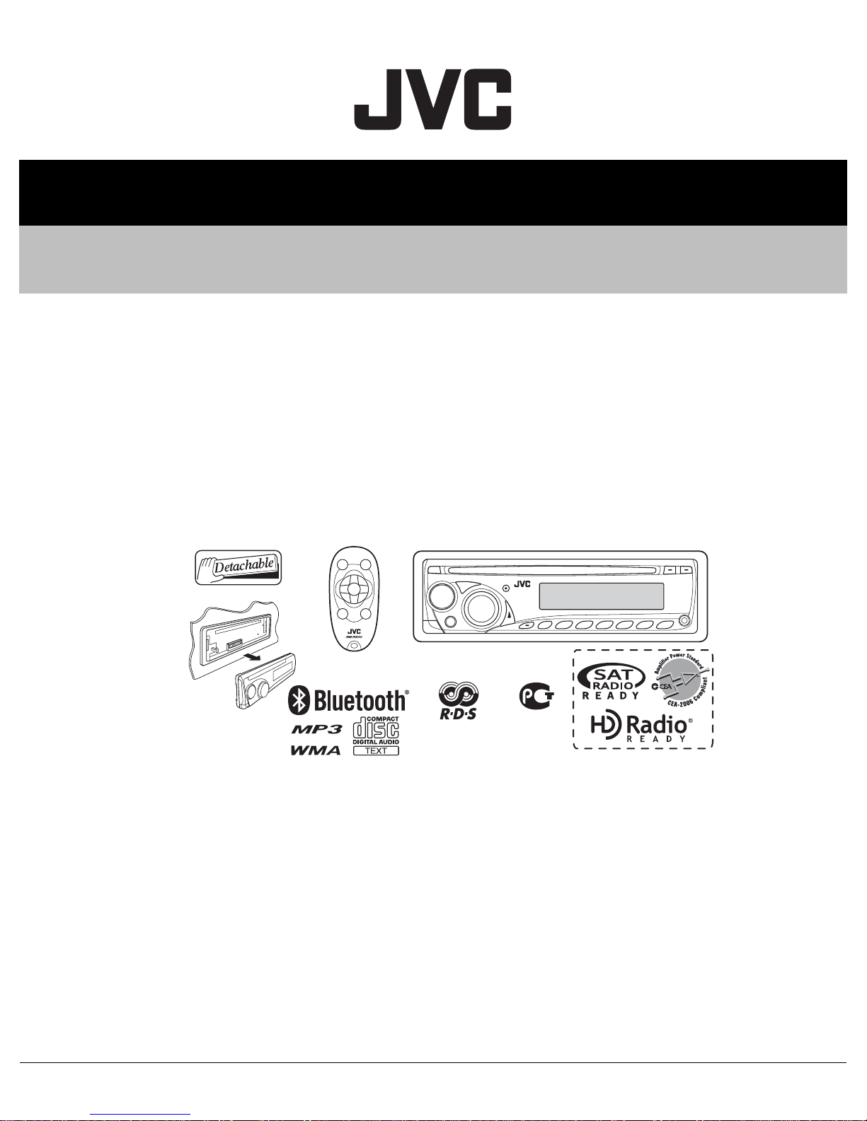
SERVICE MANUAL
CD RECEIVER
MA387<Rev.003>20089SERVICE MANUAL
KD-BT11J, KD-BT11E, KD-BT11EX,
KD-BT11EY, KD-BT11EU, KD-BT11EE,
KD-BT11U, KD-BT11UT, KD-BT19UR,
KD-BT12E, KD-BT12EX
for J/U/UT/UR
for
E/EX/EY/EU/EE
COPYRIGHT © 2008 Victor Company of Japan, Limited
Lead free solder used in the board (material : Sn-Ag-Cu, melting point : 219 Centigrade)
Lead free solder used in the board (material : Sn-Cu, melting point : 230 Centigrade)
TABLE OF CONTENTS
1 PRECAUTION. . . . . . . . . . . . . . . . . . . . . . . . . . . . . . . . . . . . . . . . . . . . . . . . . . . . . . . . . . . . . . . . . . . . . . . . . 1-6
2 SPECIFIC SERVICE INSTRUCTIONS. . . . . . . . . . . . . . . . . . . . . . . . . . . . . . . . . . . . . . . . . . . . . . . . . . . . . . 1-9
3 DISASSEMBLY . . . . . . . . . . . . . . . . . . . . . . . . . . . . . . . . . . . . . . . . . . . . . . . . . . . . . . . . . . . . . . . . . . . . . . . 1-9
4 ADJUSTMENT . . . . . . . . . . . . . . . . . . . . . . . . . . . . . . . . . . . . . . . . . . . . . . . . . . . . . . . . . . . . . . . . . . . . . . . 1-25
5 TROUBLESHOOTING . . . . . . . . . . . . . . . . . . . . . . . . . . . . . . . . . . . . . . . . . . . . . . . . . . . . . . . . . . . . . . . . . 1-26
for EE
for J/UR
COPYRIGHT © 2008 Victor Company of Japan, Limited
No.MA387<Rev.003>
2008/9
Page 2

SPECIFICATION
J / UR
AUDIO AMPLIFIER SECTION
Power Output 20 W RMS × 4 Channels at 4 Ω and < or = 1% THD+N
Signal-to-Noise Ratio 80 dBA (reference: 1 W into 4 Ω)
Load Impedance 4 Ω (4 Ω to 8 Ω allowance)
Tone Control Range Bass ±12 dB (60 Hz, 80 Hz, 100 Hz, 200 Hz)
Mid-range ±12 dB (500 Hz, 1.0 kHz, 1.5 kHz, 2.5 kHz)
Treble ±12 dB (10.0 kHz 12.5 kHz 15.0 kHz 17.5 kHz)
Q Bass: Q1.0, Q1.25, Q 1.5, Q2.0
Mid-range: Q0.5, Q0.75, Q1.0, Q1.25
Frequency Response 40 Hz to 20 000 Hz
Line-Out Level/Impedance 2.5 V/20 kΩ load (full scale)
Subwoofer-Out Level/Impedance 2.5 V /20 kΩ load (full scale)
Output Impedance 1 kΩ
Other Terminal CD changer jack AUX (auxiliary) input jack Antenna input
TUNER SECTION
Frequency Range FM
AM with channel interval set to 10 kHz: 530 kHz to 1 710 kHz
FM Tuner Usable Sensitivity 11.3 dBf (1.0 µV/75 Ω)
50 dB Quieting Sensitivity 16.3 dBf (1.8 µV/75 Ω)
Alternate Channel Selectivity (400 kHz)
Frequency Response 40 Hz to 15 000 Hz
Stereo Separation 35 dB
AM Tuner Sensitivity 20 µV
Selectivity 35 dB
CD PLAYER SECTION
Type Compact disc player
Signal Detection System Non-contact optical pickup (semiconductor laser)
Number of Channels 2 channels (stereo)
Frequency Response 5 Hz to 20 000 Hz
Dynamic Range 96 dB
Signal-to-Noise Ratio 98 dB
Wow and Flutter Less than measurable limit
MP3 Decoding Format (MPEG1/2 Audio Layer 3) Max. Bit Rate: 320 kbps
WMA (Windows Media® Audio) Decoding Format Max. Bit Rate: 192 kbps
Version Bluetooth 1.2 certified
Power Class Class 2 Radio (possible distance 10 m)
Service Area 10 m
Profile HFP 1.5, OPP 1.1, A2DP 1.2, AVRCP 1.3
Power Requirement Operating Voltage DC 14.4 V (11 V to 16 V allowance)
Grounding System Negative ground
Allowable Operating Temperature 0°C to +40°C (32°F to 104°F)
Dimensions (W × H × D)
(approx.)
Mass 1.3 kg (2.9 lbs) (excluding accessories)
Design and specifications are subject to change without notice.
Installation Size
Panel Size 188 mm × 58 mm × 6 mm (7-7/16” × 2-5/16” × 1/4”)
with channel inter val set to 100 k Hz or 200 kH z: 87.5 MH z to 107.9 MH z
with channel interval set to 50 kHz: 87.5 MHz to 108.0 MHz
with channel interval set to 9 kHz: 531 kHz to 1 602 kHz
65 dB
BLUETOOTH
GENERAL
182 mm × 52 mm × 160 mm (7-3/16” × 2-1/16” × 6-5/16”)
1-2 (No.MA387<Rev.003>)
Page 3

E/EX/EY/EU
AUDIO AMPLIFIER SECTION
Maximum Power Output Front/Rear 50 W per channel
Continuous Power Output
(RMS)
Front/Rear 19 W per channel into 4 Ω, 40 Hz to 20 000 Hz at no more than 0.8%
total harmonic distortion.
Load Impedance 4 Ω (4 Ω to 8 Ω allowance)
Tone Control Range Bass ±12 dB (60 Hz, 80 Hz, 100 Hz, 200 Hz)
Mid-range ±12 dB (500 Hz, 1.0 kHz, 1.5 kHz, 2.5 kHz)
Treble ±12 dB (10.0 kHz 12.5 kHz 15.0 kHz 17.5 kHz)
Q Bass: Q1.0, Q1.25, Q 1.5, Q2.0
Mid-range: Q0.5, Q0.75, Q1.0, Q1.25
Frequency Response 40 Hz to 20 000 Hz
Signal-to-Noise Ratio 80 dB
Line-Out/Subwoofer-O ut Level/Impedance 2.5 V /20 kΩ load (full scale)
Output Impedance 1 kΩ
Other Terminal
CD changer jack Steering wheel remote input AUX (auxiliary) input jack Aerial input
TUNER SECTION
Frequency Range FM 87.5 MHz to 108.0 MHz
AM MW: 522 kHz to 1 620 kHz
LW: 144 kHz to 279 kHz
FM Tuner Usable Sensitivity 11.3 dBf (1.0 µV/75 Ω)
50 dB Quieting Sensitivity 16.3 dBf (1.8 µV/75 Ω)
Alternate Channel Sel ectivity (400 kHz )
65 dB
Frequency Response 40 Hz to 15 000 Hz
Stereo Separation 30 dB
MW Tuner Sensitivity/Selectivity 20 µV/35 dB
LW Tuner Sensitivity 50 µV
CD PLAYER SECTION
Type Compact disc player
Signal Detection System Non-contact optical pickup (semiconductor laser)
Number of Channels 2 channels (stereo)
Frequency Response 5 Hz to 20 000 Hz
Dynamic Range 96 dB
Signal-to-Noise Ratio 98 dB
Wow and Flutter Less than measurable limit
MP3 Decoding Format (MPEG1/2 Audio Layer 3) Max. Bit Rate: 320 kbps
WMA (Windows Media® Audio) Decoding Format Max. Bit Rate: 192 kbps
BLUETOOTH
Version Bluetooth 1.2 certified
Power Class Class 2 Radio (possible distance 10 m)
Service Area 10 m
Profile HFP 1.5, OPP 1.1, A2DP 1.2, AVRCP 1.3
GENERAL
Power Requirement Operating Voltage DC 14.4 V (11 V to 16 V allowance)
Grounding System Negat ive ground
Allowable Operating Temperature 0°C to +40°C
Dimensions (W × H × D)
(approx.)
Installation Size 182 mm × 52 mm × 160 mm
Panel Size 188 mm × 58 mm × 13 mm
Mass 1.3 kg (excluding accessor ies)
Design and specifications are subject to change without notice.
(No.MA387<Rev.003>)1-3
Page 4

EE
AUDIO AMPLIFIER SECTION
Maximum Power Ou tput Front/Rear 50 W per channel
Continuous Power Output
(RMS)
Front/Rear 19 W per channel into 4 Ω, 40 Hz to 20 000 H z at no more than 0.8%
total harmonic distortion.
Load Impedance 4 Ω (4 Ω to 8 Ω allowance)
Tone Control Range Bass ±12 dB (60 Hz, 80 Hz, 100 Hz, 200 Hz)
Mid-range ±12 dB (500 Hz, 1.0 kHz, 1.5 kHz, 2.5 kHz)
Treble ±12 dB (10.0 kHz 12.5 kHz 15 .0 kHz 17.5 kHz)
Q Bass: Q1.0, Q1.25, Q 1.5, Q2.0
Mid-range: Q0.5, Q0.75, Q1.0, Q1.25
Frequency Response 40 Hz to 20 000 Hz
Signal-to-Noise Ratio 80 dB
Line-Out/Subwoofer-Out Level/Impedance 2.5 V /20 kΩ load (full scale)
Output Impedance 1 kΩ
Other Terminal AUX (auxiliary) input jack, Aerial input
TUNER SECTION
Frequency Range FM1/FM2 87.5 MHz to 108.0 MHz
FM3 65.00 MHz to 74.00 MHZ
AM MW: 522 kHz to 1 620 kHz
LW: 144 kHz to 279 kHz
FM Tuner Usable Sensitivity 11.3 dBf (1.0 µV/75 Ω)
50 dB Quieting Sensitivity 16.3 dBf (1.8 µV/75 Ω)
Alternate Channe l Selec tivity (40 0 kHz )
65 dB
Frequency Response 40 Hz to 15 000 Hz
Stereo Separation 30 dB
MW Tuner Sensitivity/Selectivity 20 µV/35 dB
LW Tuner Sensitivity: 50 µV
CD PLAYER SECTION
Type Compact disc player
Signal Detection System Non-contact optical pickup (semiconductor laser)
Number of Channels 2 channels (stereo)
Frequency Response 5 Hz to 20 000 Hz
Dynamic Range 96 dB
Signal-to-Noise Ratio 98 dB
Wow and Flutter Less than measurable limit
MP3 Decoding Format (MPEG1/2 Audio Layer 3) Max. Bit Rate: 320 kbps
WMA (Windows Media® Audio) Decoding Format Max. Bit Rate: 192 kbps
BLUETOOTH
Version Bluetooth 1.2 certified
Power Class Class 2 Radio (possible distance 10 m)
Service Area 10 m
Profile HFP 1.5, OPP 1.1, A2DP 1.2, AVRCP 1.3
GENERAL
Power Requirement Operating Voltage DC 14.4 V (11 V to 16 V allowance)
Grounding System Negative ground
Allowable Operating Temperature 0°C to +40°C
Dimensions (W × H × D)
(approx.)
Installation Size 182 mm × 52 mm × 160 mm
Panel Size 188 mm × 58 mm × 13 mm
Mass 1.3 kg (exclu ding accessories)
Design and specifications are subject to change without notice.
1-4 (No.MA387<Rev.003>)
Page 5
U/UT
AUDIO AMPLIFIER SECTION
Maximum Power Output Front/Rear 50 W per channel
Continuous Power Output
(RMS)
Front/Rear 19 W per channel into 4 Ω, 40 Hz to 20 000 Hz at no more than 0.8%
total harmonic distortion.
Load Impedance 4 Ω (4 Ω to 8 Ω allowance)
Tone Control Range Bass ±12 dB (60 Hz, 80 Hz, 100 Hz, 200 Hz)
Mid-range ±12 dB (500 Hz, 1.0 kHz, 1.5 kHz, 2.5 kHz)
Treble ±12 dB (10.0 kHz 12.5 kHz 15.0 kHz 17.5 kHz)
Q Bass: Q1.0, Q1.25, Q 1.5, Q2.0
Mid-range: Q0.5, Q0.75, Q1.0, Q1.25
Frequency Response 40 Hz to 20 000 Hz
Signal-to-Noise Ratio 80 dB
Line-Out Level/Impedance 2.5 V/20 kΩ load (full scale)
Subwoofer-Out Level/Impedance 2.5 V /20 kΩ load (full scale)
Output Impedance 1 kΩ
Other Terminal CD changer jack AUX (auxiliary) input jack Antenna input
TUNER SECTION
Frequency Range FM 87.5 MHz to 108.0 MHz
AM 531 kHz to 1 602 kHz
FM Tuner Usable Sensitivity 11.3 dBf (1.0 µV/75 Ω)
50 dB Quieting Sensitivity 16.3 dBf (1.8 µV/75 Ω)
Alternate Channel Selectivity (400 kHz)
65 dB
Frequency Response 40 Hz to 15 000 Hz
Stereo Separation 35 dB
AM Tuner Sensitivity 20 µV
Selectivity 35 dB
CD PLAYER SECTION
Type Compact disc player
Signal Detection System Non-contact optical pickup (semiconductor laser)
Number of Channels 2 channels (stereo)
Frequency Response 5 Hz to 20 000 Hz
Dynamic Range 96 dB
Signal-to-Noise Ratio 98 dB
Wow and Flutter Less than measurable limit
MP3 Decoding Format (MPEG1/2 Audio Layer 3) Max. Bit Rate: 320 kbps
WMA (Windows Media® Audio) Decoding Format Max. Bit Rate: 192 kbps
BLUETOOTH
Version Bluetooth 1.2 certified
Power Class Class 2 Radio (possible distance 10 m)
Service Area 10 m
Profile HFP 1.5, OPP 1.1, A2DP 1.2, AVRCP 1.3
GENERAL
Power Requirement Operating Voltage DC 14.4 V (11 V to 16 V allowance)
Grounding System Negative groun d
Allowable Operating Temperature 0°C to +40°C
Dimensions (W × H × D)
(approx.)
Installation Size 182 mm × 52 mm × 160 mm
Panel Size 188 mm × 58 mm × 6 mm
Mass 1.3 kg (excluding accessories)
Design and specifications are subject to change without notice.
(No.MA387<Rev.003>)1-5
Page 6
1.1 Safety Precautions
SECTION 1
PRECAUTION
!
!
Burrs formed during molding may be left over on some parts of the chassis. Therefore,
pay attention to such burrs in the case of preforming repair of this system.
Please use enough caution not to see the beam directly or touch it in case of an
adjustment or operation check.
1-6 (No.MA387<Rev.003>)
Page 7
1.2 Preventing static electricity
Electrostatic discharge (ESD), w hi ch occurs w hen sta tic ele ct ricit y sto red i n the bod y, fa bric , etc. is discharged, ca n de stroy the laser
diode in the traverse unit (optical pickup). Take care to prevent this when performing repairs.
1.2.1 Grounding to prevent damage by static electricity
Static electricity in the work area can destroy the optical pickup (laser diode) in devices such as laser products.
Be careful to use proper grounding in the area where repairs are being performed.
(1) Ground the workbench
Ground the workbench by laying conductive material (such as a conductive sheet) or an iron plate over it before placing the
traverse unit (optical pickup) on it.
(2) Ground yourself
Use an anti-static wrist strap to release any static electricity built up in your body.
(caption)
Anti-static wrist strap
1M
Conductive material
(conductive sheet) or iron plate
(3) Handling the optical pickup
• In order to maintain quality during transport and before installation, both sides of the laser diode on the replacement optical
pickup are shorted. After replacement, return the shorted parts to their original condition.
(Refer to the text.)
• Do not use a tester to che ck the con dition of th e laser dio de in the opt ical pick up. The tes ter's internal power so urce can ea sily
destroy the laser diode.
1.3 Handling the traverse unit (optical pickup)
(1) Do not subject the traverse unit (optical pickup) to strong shocks, as it is a sensitive, complex unit.
(2) Cut off the shorted part of the flexible cable using nip pers, etc. afte r replacing th e optical pi ckup. For speci fic details, refe r to the
replacement procedure in th e t ext . R em ove the anti-static pin w he n re pla cing the traverse unit. Be c arefu l not to tak e to o l on g a
time when attaching it to the connector .
(3) Handle the flexible cable carefully as it may break when subjected to strong force.
(4) It is not possible to adjust the semi-fixed resistor that adjusts the laser power. Do not turn it.
1.4 Attention when traverse unit is decomposed
*Please refer to "Disassembly method" in the text for the pickup unit.
• Apply solder to the short land before the card wire is disconnected from the connector on the pickup unit.
(If the card wire is disconnected without applying solder, the pickup may be destroyed by static electricity.)
• In the assembly, be sure to remove solder from the short land after connecting the card wire.
Pickup
Wires
Push switch
Base board
Frame
Flexible wire
Connector
CD mechanism
assembly
Pickup
(No.MA387<Rev.003>)1-7
Page 8
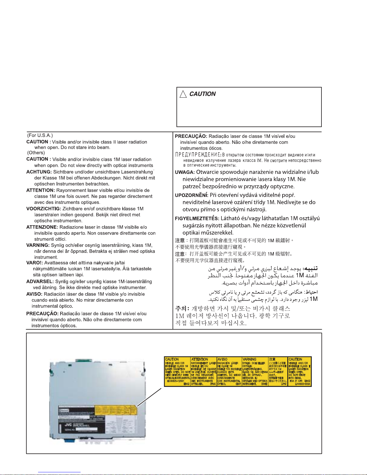
1.5 Important for laser products
1.CLASS 1 LASER PRODUCT
2.CAUTION :
(For U.S.A.) Visible and/or invisible class II laser radiation
when open. Do not stare into beam.
(Others) Visible and/or invisible class 1M laser radiation
when open. Do not view directly with optical instruments.
3.CAUTION : Visible and/or invisible laser radiation when
open and inter lock failed or defeated. Avoid direct
exposure to beam.
4.CAUTION : This laser product uses visible and/or invisible
laser radiation and is equipped with safety switches which
prevent emission of radiation when the drawer is open and
the safety interlocks have failed or are defeated. It is
dangerous to defeat the safety switches.
5.CAUTION : If safety switches malfunction, the laser is able
to function.
6.CAUTION : Use of controls, adjustments or performance of
procedures other than those specified here in may result in
hazardous radiation exposure.
!
Please use enough caution not to
see the beam directly or touch it
in case of an adjustment or operation
check.
REPRODUCTION AND POSITION OF LABELS and PRINT
WARNING LABEL and PRINT
1-8 (No.MA387<Rev.003>)
Page 9
SECTION 2
SPECIFIC SERVICE INSTRUCTIONS
This service manual does not describe SPECIFIC SERVICE INSTRUCTIONS.
SECTION 3
DISASSEMBLY
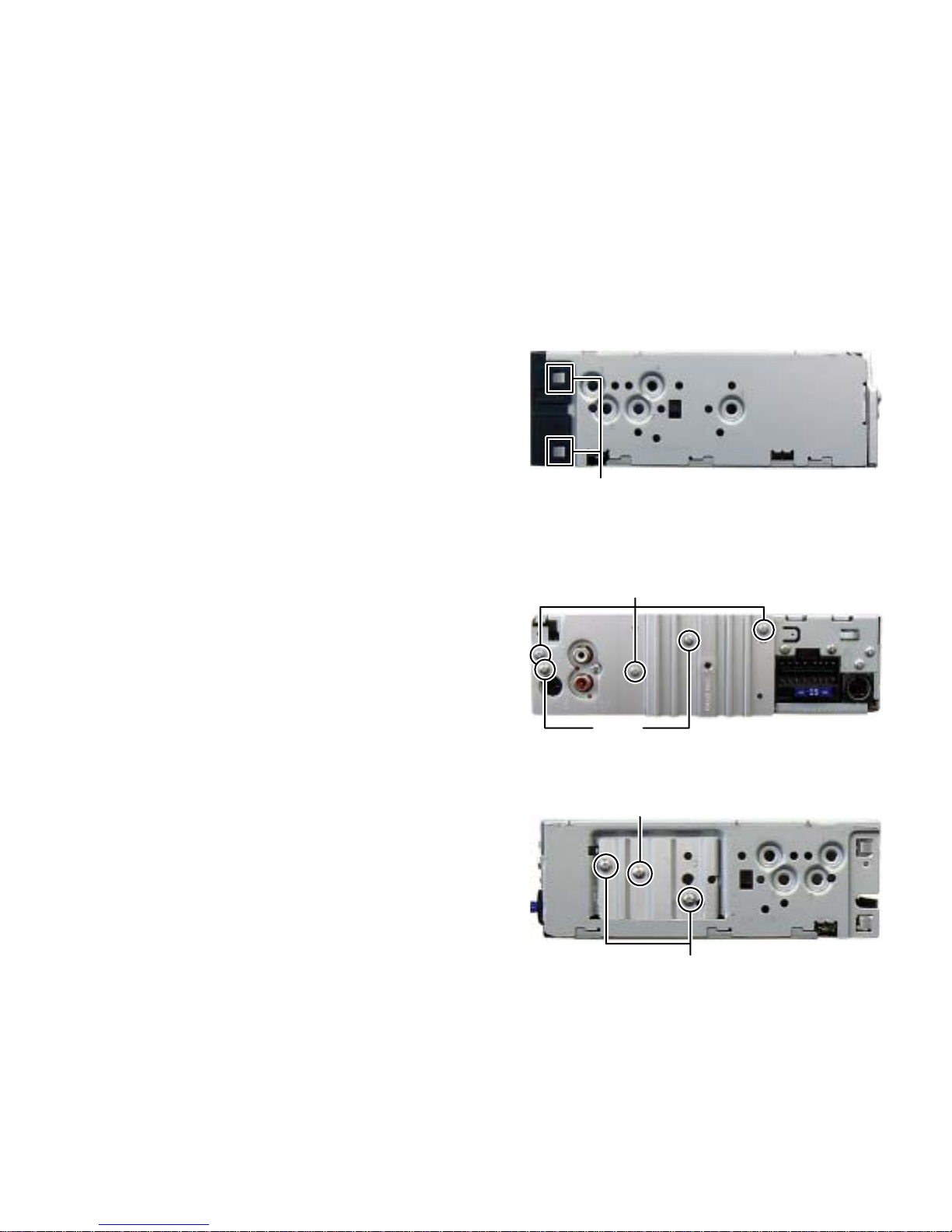
3.1 Main body
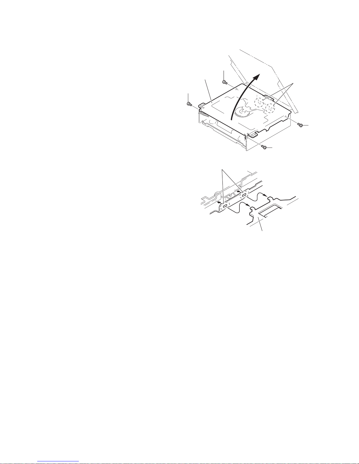
3.1.1 Removing the FRONT CHASSIS assembly (See Fig.1)
(1) Disengage the four hooks a engaged the both side of the
FRONT CHASSIS assembly.
hook
a
Fig.1
3.1.2 Removing the HEAT SINK (See Fig.2, 3)
(1) Remove the three screws A and the two screws B attaching
the HEAT SINK. (See Fig.2)
(2) Remove the two screws C and the one screw D attaching
the HEAT SINK. (See Fig.3)
A
B
Fig.2
D
C
Fig.3
(No.MA387<Rev.003>)1-9
Page 10
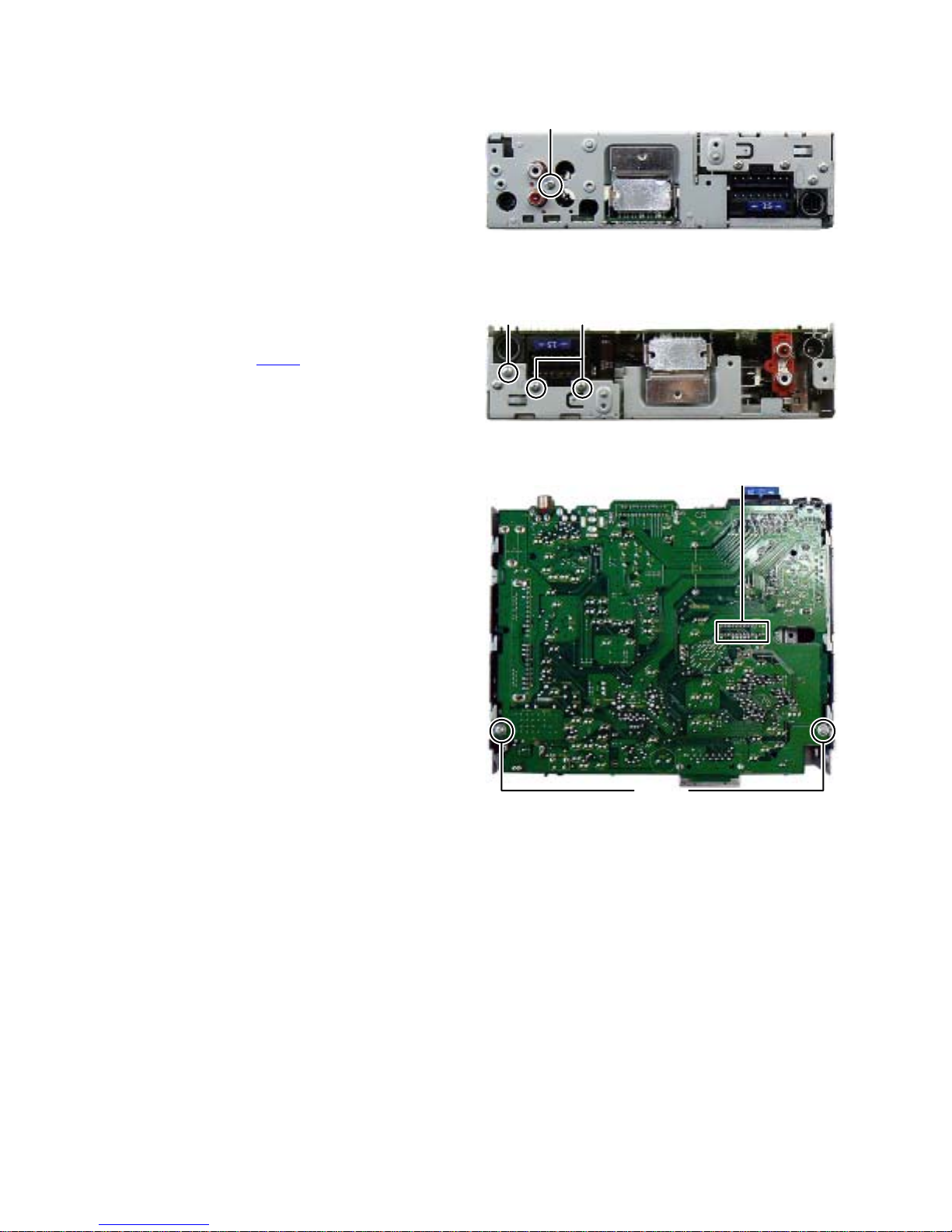
3.1.3 Removing the BOTTOM COVER (See Fig.4)
(1) Remove the one screw E attaching the BOTTOM COVER.
(2) Slide the BOTTOM COVER to backward.
3.1.4 Removing the MAIN BOARD assembly (See Fig.5, 6)
(1) Remove the two screws F and the one screw G attaching
the MAIN BOARD assembly. (See Fig.5)
(2) Remove the two screws H attaching the MAIN BOARD assembly.
(See Fig.6)
(3) Disconnect the connector CN501
BOARD assembly and CD MECHANISM assembly. (Se e
Fig.6)
connected to MAIN
E
Fig.4
FG
Fig.5
CN501
1-10 (No.MA387<Rev.003>)
H
Fig.6
Page 11
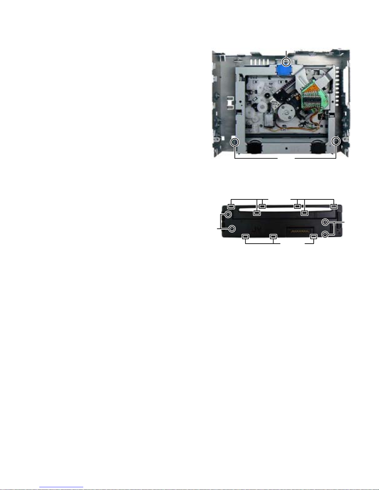
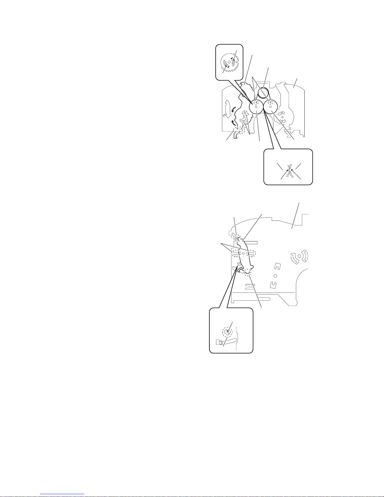
3.1.5 Removing the CD MECHANISM assembly (See Fig.7)
(1) Remove the three screws J attaching the CD MECHANISM
assembly.
3.1.6 Removing the SWITCH BOARD assembly (See Fig.8)
(1) Remove the VOLUME KNOB.
(2) Remove the four screws K attaching the REAR COVER.
(3) Disengage the nine hooks b engage d the REAR COVER.
Fig.7
hook
J
J
b
K
Fig.8
hook
K
b
(No.MA387<Rev.003>)1-11
Page 12
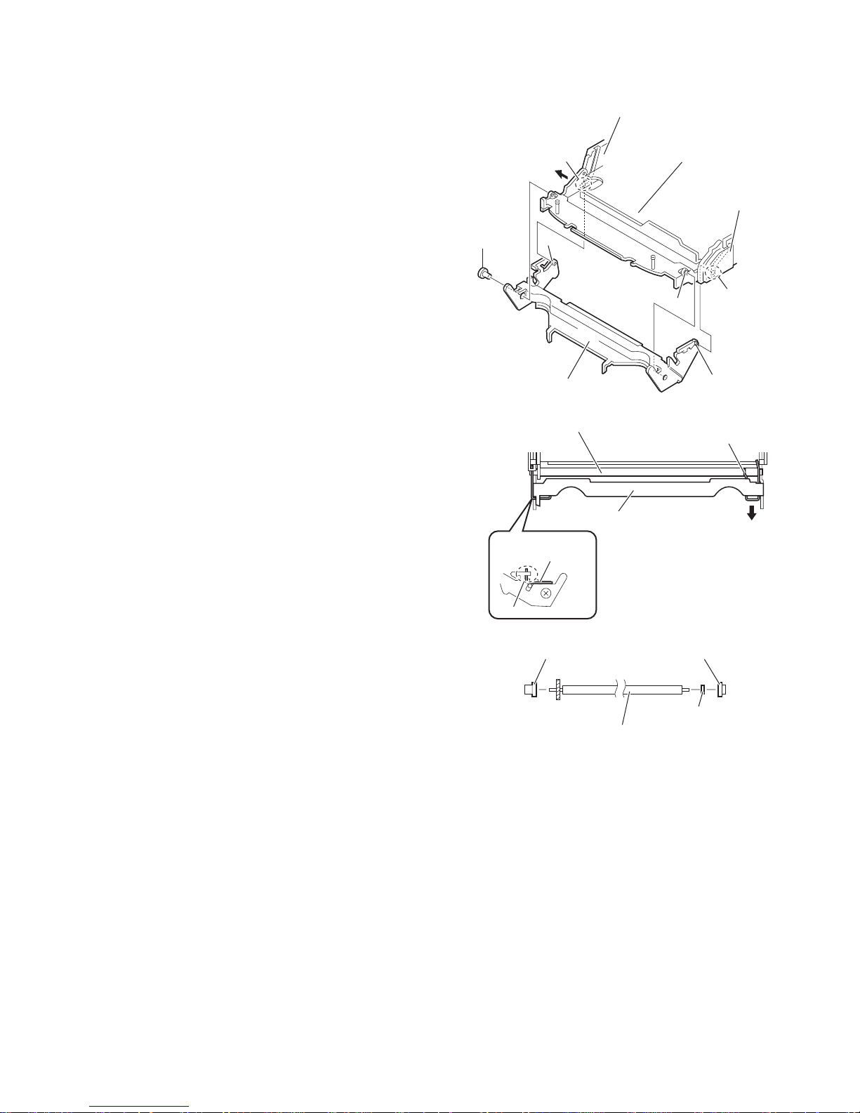
3.2 CD mechanism assembly
A
3.2.1 Removing the top cover
(See Figs.1 and 2)
(1) From the both side of the CD mechanism assembly, re-
move the four screws A attaching the top cover. (See
Fig.1.)
(2) Lift the front side of the top cover and move the top cover
backward to release the two joints a. (See Figs.1 and 2.)
Top cover
A
a
A
A
Fig.1
a
Top cover
Fig.2
1-12 (No.MA387<Rev.003>)
Page 13
3.2.2 Removing the push switch
(See Figs.3)
(1) From the bottom side of the CD mechanism assembly, re-
move the screw B attaching the push switch.
(2) Take out the push switch from the CD mechanism assem-
bly.
Reference:
Remove the wires fro m solder ed sections b of the push sw itch
as required.
3.2.3 Removing the base board
(See Figs.3 and 4)
Caution:
Solder the short land c before the f lexib le wire is disc onnec ted
from the connector on the pic ku p. If the f lex ible wire is disconnected without applying solder, the pickup may be destroyed
by static electricity. (See Fig.3.)
(1) From the bottom side of the CD mechanism assembly, re-
move the scre w C attaching the base board. (See Figs.3
and 4.)
(2) Solder the short land c on the pickup. (See Fig.3.)
(3) Disconnect the flexible wire fr om the conne ctor on the pic k-
up. (See Fig.3.)
(4) Remove the base board from the joints d of the fram e in the
direction of the arrow. (See Figs.3 and 4.)
Reference:
Remove the wires from the soldered sections e on the base
board as required. (See Fig.3.)
Caution:
When reattaching the base board, be sure to remove solder
from the short land c after connecting the flexible wire. (See
Fig.3.)
e
C
Base board
Frame
Wires
B
b
d
Push switch
Flexible wire
Connector
Fig.3
Pickup
CD mechanism
assembly
Pickup
c
C
Base board
Flexible wire
Frame
d
Fig.4
(No.MA387<Rev.003>)1-13
Page 14
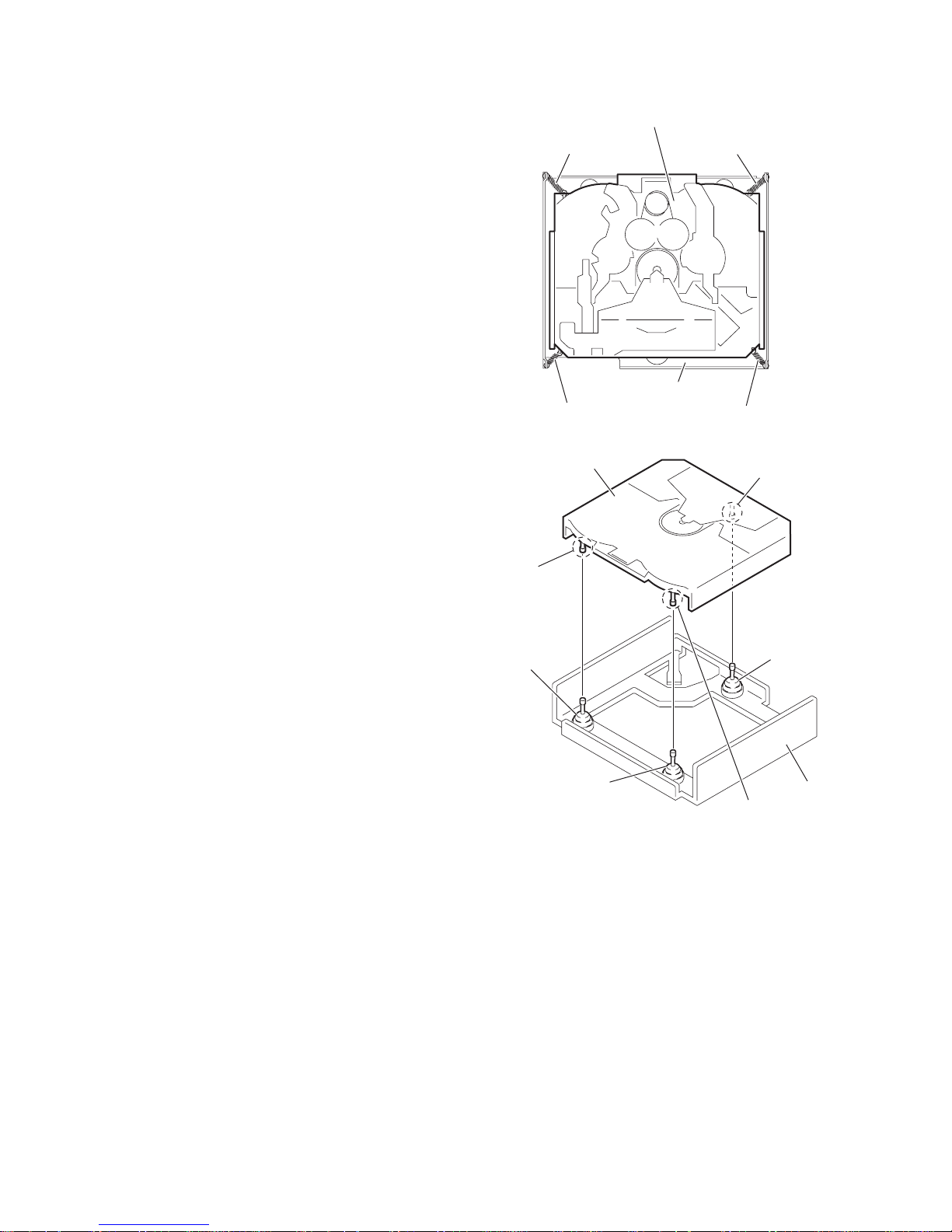
3.2.4 Removing the chassis unit
(See Figs.5 and 6)
• Remove the top cover and base board.
(1) From the top side of the CD mec hanism a ssembly, r emove
the front suspension springs and rear suspension springs
attaching the chassis unit to the frame. (See Fig.5.)
(2) Remove the chassis unit from the da mpers on the f rame in
an upward direction. (See Fig.6.)
Note:
• Pay attention to misuse and loss of each spring. (See Fi g.5.)
• When reassembling, make sure that the three shafts on the
underside of the chassis unit are inserted to the dampers
certainly. (See Fig.6.)
Chassis unit
Front suspension spring
Front suspension spring
Frame
Rear suspension spring Rear suspension spring
Fig.5
Chassis unit
Shaft
Shaft
Damper F
Damper F
Damper R
Frame
Shaft
Fig.6
1-14 (No.MA387<Rev.003>)
Page 15
3.2.5 Removing the clamper assembly
(See Figs.7 and 8)
• Remove the top cover.
Move the clamper assembly in the direction of the arrow to release the joints f from the chassis unit.
Chassis unit
f
Clamper assembly
Clamper assembly
Chassis unit
f
Fig.7
f
f
Fig.8
(No.MA387<Rev.003>)1-15
Page 16
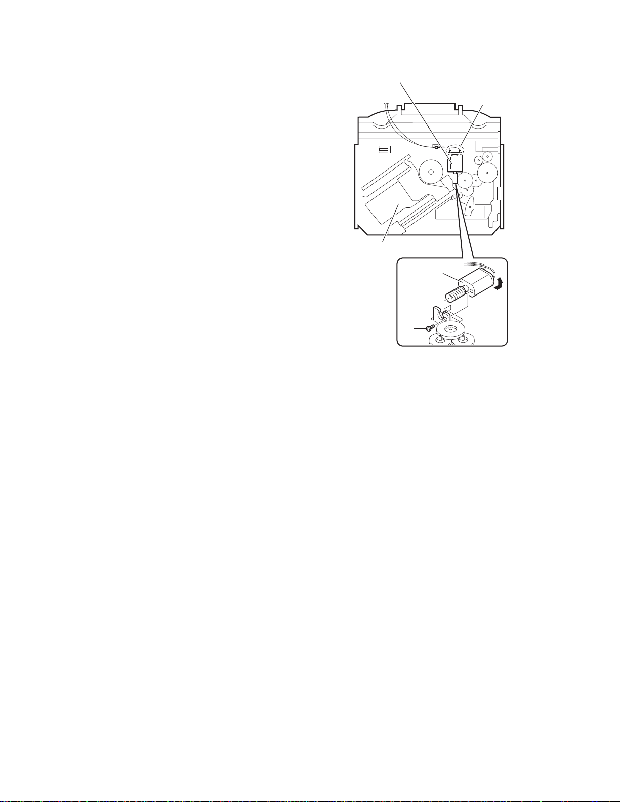
3.2.6 Removing the loading/feed motor assembly
(See Fig.9)
• Remove the top cover, base board and cha ss is unit.
From the bottom side of the chassis unit, remove the screw D
and take out the loading/feed motor assembly in the direction of
the arrow.
Reference:
Remove the wires from th e sold ered sec tions g of the lo ading /
feed motor assembly as required.
Loading/feed motor assembly
g
Chassis unit
Loading/feed
motor
assembly
D
Fig.9
1-16 (No.MA387<Rev.003>)
Page 17
3.2.7 Removing the pickup
(See Figs.10 to 12)
• Remove the top cover, base board and chassis unit.
(1) From the bottom side of the chassis unit, remove the screw
E attaching the pu. shaf t ho lder B an d pull the pu . shaft out
of the pu. shaft holder A. (See Fig.10.)
(2) Remove the screw F attaching the pu. sh aft hol der A. (See
Fig.10.)
(3) Take out the pickup with pu. shaft holder A an d feed s crew
assembly from the chassis unit. (See Fig.11.)
(4) Remove the section h of the pu. shaft holder A in th e direc-
tion of the arrow. (See Fig.11.)
(5) Remove the feed screw assembly from the section j of the
pickup in the direction of the arrow. (See Fig.11.)
(6) Remove the screw G attaching the feed screw holder to the
pickup. (See Fig.12.)
Reference:
Remove the feed nut spring from the feed screw holder
as required. (See Fig.12.)
(7) Release th e c law k in the direction of the arrow to remove
the feed sub holder. (See Fig.12.)
Pickup
Feed screw assembly
Feed screw holder
Pu. shaft holder A
Fig.11
G
h
j
Feed screw
holder
3.2.8 Reattachi ng the picku p
(See Figs.10 to 13)
(1) Reattach the feed sub holder to the pickup. (See Fig.12.)
(2) Reattach the feed screw holder to the pickup using the
screw G. (See Fig.12.)
(3) Reattach the feed screw assembly and pu. shaft holder A
to the pickup as before. (See Fig.11.)
(4) Set the section m of the pickup to the rail of the chas sis unit
at first and attach the pickup to the chassis unit with the
screw F as before. (See Figs.10 and 13.)
(5) Attach the pu. shaft to the pickup as before. (See Fig.10.)
(6) Attach the pu. shaft holder B to the chassis unit with the
screw E as before. (See Fig.10.)
Chassis unit
Pu. shaft holder A
Pu. shaft
F
Pickup
k
Feed sub holder
Pickup
Rail
Feed nut
spring
Fig.12
m
F
Pickup
E
Pu. shaft holder B
Fig.10
Chassis unit
Fig.13
(No.MA387<Rev.003>)1-17
Page 18
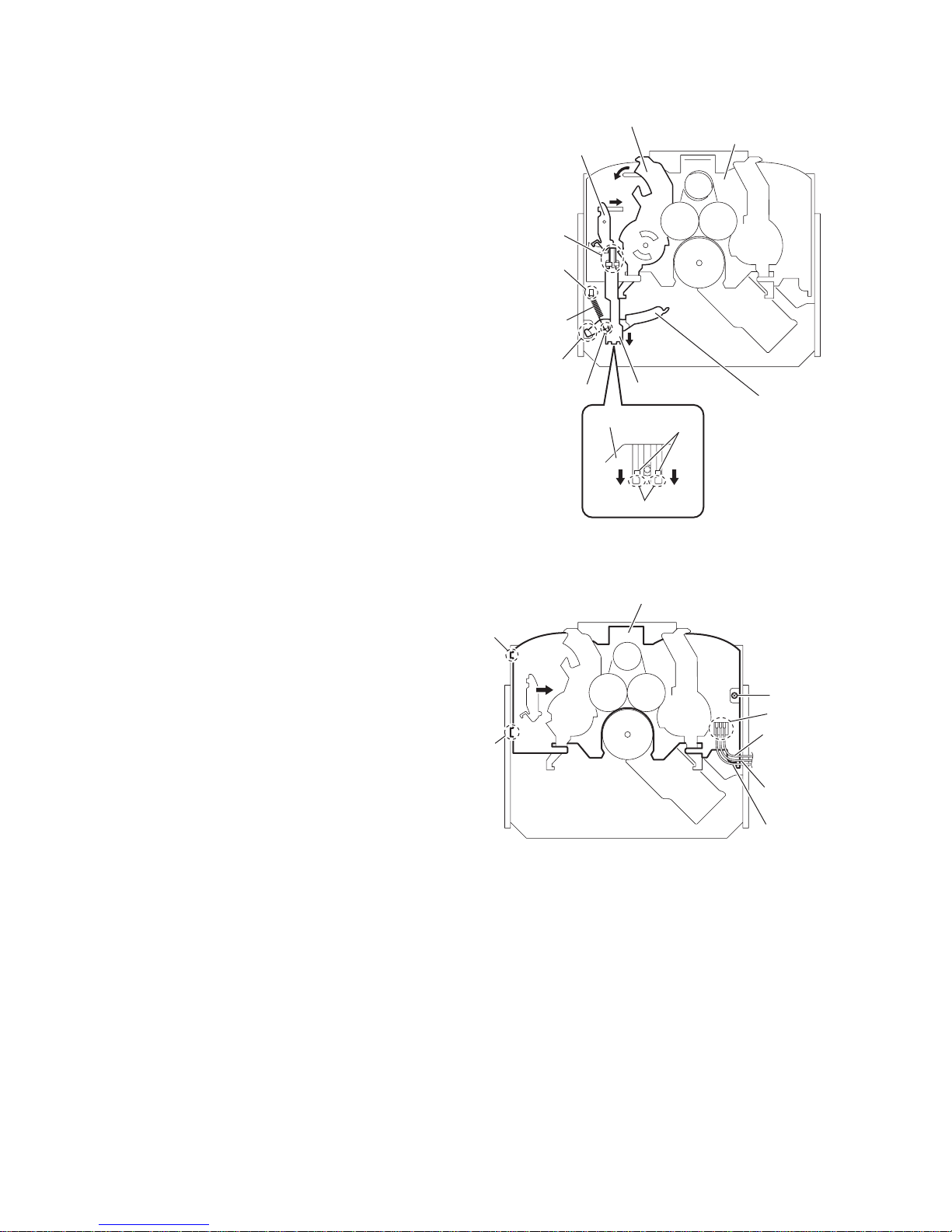
3.2.9 Removing the trigger arm
(See Fig.14)
• Remove the top cover, base board, chassis unit and clamper
assembly.
(1) From the top side of the chassis unit, remove the trigger
arm spring from the sections (n, p).
(2) From the bottom side of the chassis unit, release the claws
q of the trigger arm base in the directio n o f the arrow to remove them from the sections r of the chassis unit to the
other side.
Note:
When releasing the claws q, t ake care n ot to break th em.
(3) From the top side of the chassis unit, move the select arm
R and select lock arm in the direction of the arrow to remove the trigger arm base from the section s in the direction of the arrow.
(4) Remove the trigger arm from the section t.
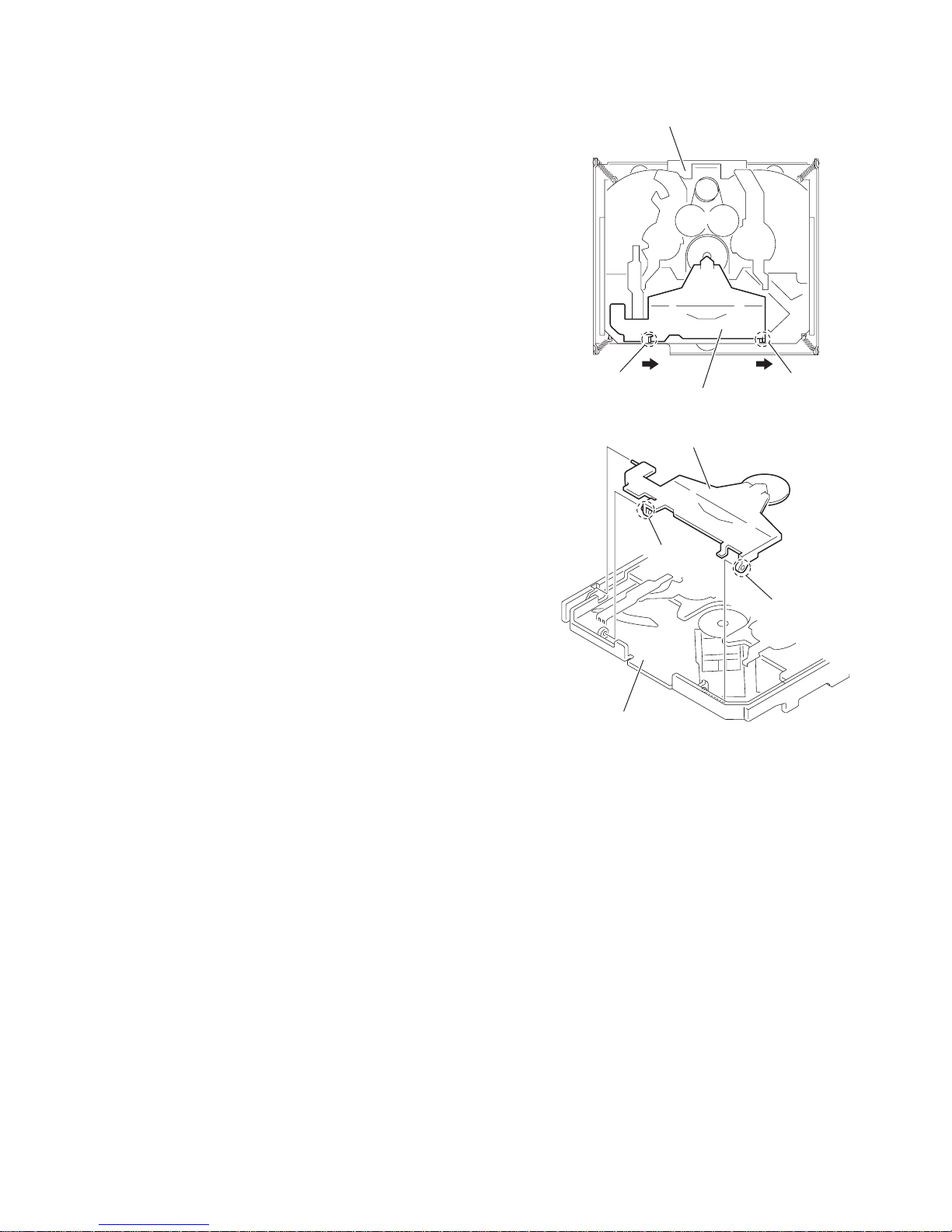
3.2.10 Removing the top plate assembly
(See Fig.15)
• Remove the top cover, base board, chassis unit, clamper as-
sembly and trigger arm.
(1) Remove the screw H attaching the top plate assembly.
(2) Move the top plate assembly in the d irection of the arr ow to
release the joints (u, v).
Reference:
Remove the wires from the soldered sections w of the top plate
assembly as required.
Note:
When reassembling, solder the wires as before.
Select lock arm
Trigger arm
spring
u
v
Select arm R
s
n
t
p
Chassis unit
Top plate assembly
Chassis unit
Trigger arm base
Trigger arm
q
r
Fig.14
H
w
Wire(Red)
1-18 (No.MA387<Rev.003>)
Wire(White)
Wire(Brown)
Fig.15
Page 19
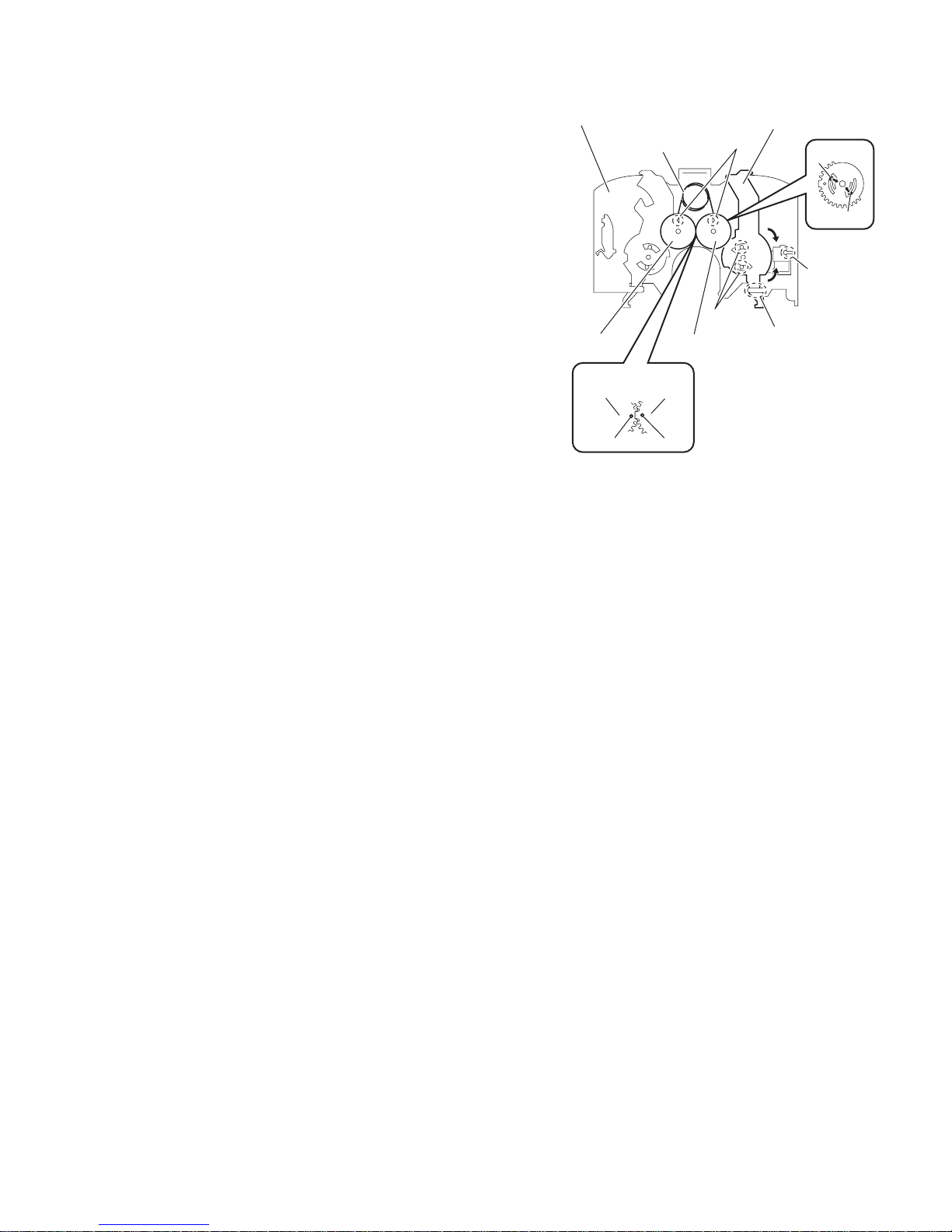
3.2.11 Removing the mode switch
(See Fig.16)
• Remove the top cover, base board, chassis unit, clamper as-
sembly, trigger arm and top plate assembly.
(1) From the top side of the top plate assembly, remove the
link gear spring from the sections x of the link gear L and
link gear R.
(2) Remove the link gear L in an upward direction whi le releas-
ing the claws y of the link gear L in the direction of the arrow.
(3) Move the mode switch in the direction of t he arrow 1 to re -
move the sections z of the top plate assembly.
(4) Move the mode switch in the direction of the arrow 2 and
remove the mode switch from the sections (aa, ab).
Note:
When reattaching the link gear L, attach it after aligning the
hole ac of the link gear L to the hole ac of the link gear R.
Reference:
When reassembling, reverse the above removing procedure.
Top plate assembly
Link gear spring
Link gear R
Link
gear R
ac ac
Link gear L
Link
gear L
aa
Fig.16
Mode switch
x
1
2
z
y
y
ab
(No.MA387<Rev.003>)1-19
Page 20
3.2.12 Removing the select arm R and select lock arm
(See Figs.17 and 18)
• Remove the top cover, base board, chassis unit, clamper as-
sembly, trigger arm and top plate asse mbly.
(1) From the top side of the top plate assembly, remove the
link gear spring from the sections ad of the link gear L and
link gear R. (See Fig.17.)
(2) Remove the link gear R in an upward direction while releas-
ing the claws ae of the lin k gear R in the dire ction of the a rrow. (See Fig.17.)
(3) Move the select arm R in the direction of the arrow 1 to re-
move the sections af of the top plate assembly. (See
Fig.17.)
(4) Move the select arm R in the direction of the arrow 2 and
remove the select arm R from the sections ag. (See
Fig.17.)
(5) From the bottom side of the top plate assembly, remove
the select lock arm spring from the section ah. (See
Fig.18.)
(6) From the top side of the top plate assembly, remove the
section aj of the select lock arm from the top plate assembly at first and remove the sections (ak, am) of th e sele ct
lock arm from the top plate assembly. (See Fig.18.)
Note:
• When removing the select lock arm spring, be careful not to
lose it. (See Fig 18.)
• When reattaching the link gear R, attach it after ali gn ing the
hole an of the link gear R to the hole an of the link gear L.
(See Fig.17.)
Reference:
When reassembling, reverse the above removing procedure.
ak
ae
1
2
af
ae
Select arm R
ad
ag
Link gear R
Select lock arm
aj
Link gear spring
Top plate assembly
Link gear L
Link
gear R
an an
Fig.17
Top plate assembly
Link
gear L
1-20 (No.MA387<Rev.003>)
Select lock
arm spring
ah
am
Fig.18
Page 21
3.2.13 Removing the loading roller assembly
(See Figs.19 to 21)
• Remove the top cover, base board, chassis unit, clamper as-
sembly and top plate assembly.
(1) From the left side of the chassis unit, remove the screw J
attaching the lock arm assembly. (See Fig.19.)
(2) Remove the projection ap of the lock arm assembly from
the joint aq while opening the cam plate R in the direction
of the arrow. (See Fig.19.)
(3) Remove the lock arm assembly from the projection ar of
the chassis unit. (See Fig.19.)
(4) Remove the projection as of the lock arm assembly from
the joint at of the cam plate L assembly. (See Fig.19.)
(5) From the right side of the lock arm assembly, remove the
loading roller spring L from the section au. (See Fig.20.)
(6) From the top side of the lock arm assembly, remove the
loading roller spring R in the direction of the arrow and remove the loading roller assembly. (See Fig.20.)
(7) Remove the roller guide R, HL washer and roller guide L
from the both ends of the loading roller assembly. (See
Fig.21.)
aq
J
ap
Lock arm assembly
Loading roller assembly
Cam plate R
Fig.19
Chassis unit
Cam plate L assembly
ar
Loading roller spring R
at
as
Lock arm assembly
Loading roller
spring L
au
Fig.20
Roller guide L Roller guide R
HL washer
Loading roller assembly
Fig.21
(No.MA387<Rev.003>)1-21
Page 22

3.2.14 Removing the loading gear 1, loading gear 2, loading gear 3 and feed gear 1
(See Fig.22)
• Remove the top cover, base board and cha ss is unit.
(1) From the bottom side of the chassis unit, pull out the load-
ing gear 1.
(2) Take out the loading gear 2.
(3) Pull out the loading gear 3.
(4) Pull out the feed gear 1.
3.2.15 Removing the loading gear 4, loading gear 5 and
loading gear 6
(See Fig.22)
• Remove the top cover, base board and cha ss is unit.
(1) From the bottom side of the chassis unit, remove the screw
K attaching the loading gear bracket.
(2) Take out the loading gear bracket and remove the loading
gear 5 and loading gear 6 from the loading gear bracket.
(3) Pull out the loading gear 4.
Loading gear bracket
Loading gear 3
Feed gear 2
Loading gear 6
Loading gear
bracket
Loading gear 4
Loading gear 1
Loading
gear 5
K
3.2.16 Removing the change gear 2, change gear 3A and
change gear 3B
(See Figs.22 and 23)
• Remove the top cover, base board and cha ss is unit.
(1) From the bottom side of the chassis unit, pull out the load-
ing gear 1. (See Fig.22.)
(2) Pull out the change gear 2. (See Fig.22.)
(3) Pull out the change arm. (See Fig.22.)
(4) Move the change gear plate rivet assembly in the direction
of the arrow 2 to remove the se ction av of the change gear
plate rivet assembly fro m the chass is unit whil e moving the
change lock lever in the direction of the arrow 1. (See
Fig.23.)
(5) Pull out the change gear 3A and change gear 3B from the
change gear plate rivet assembly. (See Fig.23.)
3.2.17 Removing the cam plate L assembly
(See Fig.24)
• Remove the top cover, base board, chassis unit, clamper as-
sembly, top plate assembly and loading roller assembly.
(1) From the left side of the chassis unit, slide the cam plate L
assembly in the direction of the arrow.
(2) Remove the cam plate L asse mb ly from th e slo ts aw of the
chassis unit.
Feed gear 1
Chassis unit
Fig.22
Change gear plate rivet assembly
Change gear 3B
1
Chassis unit
Change lock lever
Fig.23
Chassis unit
Change arm
Change gear plate
rivet assembly
2
av
Loading gear 2
Change
gear 3A
Change gear 3B
Change gear 3A
aw
1-22 (No.MA387<Rev.003>)
aw
Cam plate L assembly
Fig.24
Page 23

3.2.18 Removing the cam plate R
(See Fig.25)
• Remove the top cover, base board, chassis unit, clamper as-
sembly, top plate assembly and loading roller assembly.
From the right side of the chassis unit, remove the cam plate R
from the slots ax of the chassis unit.
Reference:
When a slide hook rivet assembly and a trigger rack spring
have come off from the chassis unit, attach them before at-
taching the cam plate R.
3.2.19 Removing the trigger rack plate
(See Figs.25 and 26)
• Remove the top cover, base board, chassis unit, clamper as-
sembly, top plate assembly, loading roller assembly and cam
plate R.
(1) Remove the slide hook rivet assembly and trigger rack
spring from the chassis unit. (See Fig.25.)
(2) From the bottom side of the chassis unit, pull out the load-
ing gear 1. (See Fig.26.)
(3) Remove the trigger control spring from the sections (ay,
az). (See Fig.26.)
(4) Take out the trigger rack plate from the chassis unit. (See
Fig.26.)
Reference:
When attaching the trigger rack plate, insert the projection a'
of the chassis unit in the slot b' on the bottom side of the trig ger
rack plate as before. (See Fig.26.)
Chassis unit
ax
Cam plate R
b'
Trigger rack spring
Slide hook rivet assembly
ax
Fig.25
Trigger control spring
az
a'
Trigger
rack plate
Trigger rack plate
Loading gear 1
ay
Chassis unit
Fig.26
(No.MA387<Rev.003>)1-23
Page 24

3.2.20 Removing the spindle motor assembly
(See Figs.27 and 28)
• Remove the top cover, base board, chassis unit and clamper
assembly.
(1) From the top side of the chassis unit, turn the turn table
from side to side and remove the two screws M attaching
the spindle motor assembly through the hole of th e turn table. (See Fig.27.)
(2) From the bottom si de of the ch assis unit , turn the ch ange
gear 2 in the direct ion of the arrow 2 while pulling the trigger
arm in the direction of the arrow 1 and let the pickup move
in the direction of the arrow 3. (See Fig.28.)
(3) Slide the spindle motor assembly in the direction of the ar-
row and take out it in an upward d irec tio n from the cha ss is
unit. (See Fig.28.)
Reference:
Remove the wires fro m the soldered sections c' on th e base
board and remove them from the se ction s (d', e') on the chas -
sis unit as required.
Chassis unit
Wire(black)
Wire(red)
M
Fig.27
Spindle motor assembly
d'
Turn table
e'
Change gear 2
c'
Base board
3
Pickup
2
1
Trigger arm
Chassis unit
Fig.28
1-24 (No.MA387<Rev.003>)
Page 25

SECTION 4
ADJUSTMENT
4.1 Test instruments required for adjustment
(1) Digital oscilloscope (100MHz)
(2) Electric voltmeter
(3) Digital tester
(4) Tracking offset meter
(5) Test Disc JVC :CTS-1000
(6) Extension cable for check
EXTSH002-22P x 1
4.2 Standard measuring conditions
Power supply voltage DC14.4V(10.5 to 16V)
Load impedance 20K.(2 Speakers connection)
Output Level Line out 2.5V (Vol. MAX)
4.5 How to connect the extension cable for adjusting
Caution:
Be sure to attach the heat sink an d rear brac ket ont o the pow er amplifi er IC and regulato r IC resp ectivel y, before supply the power.
If voltage is applied without attaching these parts, the power amplifier IC and regulator IC will be destroyed by heat.
4.3 Standard volume position
Balance and Bass &Treble volume : lndication"0"
Loudness : OFF
4.4 Dummy load
Exclusive dummy load should be used for AM,and FM.
For FM dummy load, there i s a l oss of 6dB b etw ee n SSG out put
and antenna input.
The loss of 6dB need not be considered sincedirect reading of
figures are applied in this working standard.
Extension cable
EXTSH002-22P
(No.MA387<Rev.003>)1-25
Page 26

5.1 16 PIN CORD DIAGRAM (for KD-BT11J)
SECTION 5
TROUBLESHOOTING
BK
RD
BL
WH
OR
Black
Red
Blue
White
Orange
8
7
6
5
4
3
2
1
BK
8
BK
RD
NC
BL/WH
WH
GN
VI
GY
GN
VI
GY
YL
YL
OR/WH
NC
NC
WH/BK
GN/BK
VI/BK
GY/BK
Green
Violet
Gray
Yellow
16
15
14
13
12
11
10
9
16
7
15
5
3
11
2
10
4
12
1
YL
RD
OR/WH
BL/WH
GN
GN/BK
VI
VI/BK
WH
WH/BK
GY
GY/BK
9
1-26 (No.MA387<Rev.003>)
Page 27

5.2 16 PIN CORD DIAGRAM (for KD-BT11E,EX,EY,EU,EE, KD-BT19UR,KD-BT12E,EX)
8
7
6
5
4
3
2
1
BL/WH
BK
RD
NC
WH
GN
VI
GY
7 RD
16 YL
15 OR/WH
8 BK
5 BL/WH
YL
OR/WH
NC
NC
WH/BK
GN/BK
VI/BK
GY/BK
16
15
14
13
12
11
10
9
MEMORY
ACC
ILL
GND
REMOTE
BK
RD
BL
Black
Red
Blue
WH White
OR
Orange
GN
VI
GY
YL
Green
Violet
Gray
Yellow
RD
1
3
5
7
NC
NC
BL/WH
RD
RD 7
YL 4
NC
YL
OR/WH
BK
6
8
5
2
4
6
8
3 GN
11 GN/BK
2 VI
10 VI/BK
4 WH
12 WH/BK
1 GY
9 GY/BK
RR
FR
FL
RL
Rear Right
Front Right
Front Left
Rear Left
RL+
RL-
RR+
RR-
FL+
FL-
FR+
FR-
REMOTE
ACC
MEMORY
GND
ILL
Remote out
ACC Line
Memory Backup Battery+
Ground
Illuminations Control
7
8
1
2
5
6
3
4
VI
1
GY
3
WH
5
GN
7
VI/BK
GY/BK
WH/BK
GN/BK
2
4
6
8
(No.MA387<Rev.003>)1-27
Page 28

5.3 16 PIN CORD DIAGRAM (for KD-BT11U,UT)
BK
RD
BL
WH
Black
Red
Blue
White
8
7
6
5
4
3
2
1
BK
RD
BL
BL/WH
WH
GN
VI
GY
GN
VI
GY
YL
OR
YL
OR/WH
NC
NC
WH/BK
GN/BK
VI/BK
GY/BK
Green
Violet
Gray
Yellow
Orange
16
15
14
13
12
11
10
9
8
16
7
15
3
11
10
4
12
2
1
9
5
BK
YL
RD
OR / WH
GN
GN / BK
VI
VI / BK
WH
WH / BK
GY
GY / BK
BL / WH
BL
6
1-28 (No.MA387<Rev.003>)
Page 29

(No.MA387<Rev.003>)1-29
Page 30

Victor Company of Japan, Limited
Mobile Entertainment Division 10-1,1chome,Ohwatari-machi,Maebashi-city,371-8543,Japan
(No.MA387<Rev.003>)
Printed in Japan
VPT
Page 31

REVISION INFORMATION
CD RECEIVER
KD-BT11J, KD-BT11E, KD-BT11EX,
KD-BT11EY, KD-BT11EU, KD-BT11EE,
KD-BT11U, KD-BT11UT, KD-BT19UR
■ OVERVIEW
Add KD-BT19UR
■ DETAILS
COVER SECTION
Title Line No.MA387<Rev.001> No.MA387<Rev.002> Description
Revision Rev.001 Rev.002
Issue Date 2008/01 2008/06
Model No. KD-BT11E,
Cover Illustration ILLUSTRATION(ma387_0001.png) ILLUSTRATION(ma387_0001.png)
SPECIFICATION 1 J J / UR
KD-BT11EE,
KD-BT11EU,
KD-BT11EX,
KD-BT11EY,
KD-BT11J,
KD-BT11U,
KD-BT11UT
SECTION 5 TROUBLESHOOTING
Title Line No.MA387<Rev.001> No.MA387<Rev.002> Description
5.2 16 PIN CORD
DIAGRAM (for KDBT11E,EX,EY,EU,EE,
KD-BT19UR)
T 5.2 16 PIN CORD DIAGRAM (for KD-
BT11E,EX,EY,EU,EE)
KD-BT11E,
KD-BT11EE,
KD-BT11EU,
KD-BT11EX,
KD-BT11EY,
KD-BT11J,
KD-BT11U,
KD-BT11UT,
KD-BT19UR
5.2 16 PIN CORD DIAGRAM (for KDBT11E,EX,EY,EU,EE, KD-BT19UR)
COPYRIGHT © 2008 Victor Company of Japan, Limited
MA387-R002
2008/06
Page 32

STANDARD SCHEMATIC DIAGRAMS
Description of Major ICs
Diagram Name No.MA387<Rev.001> No.MA387<Rev.002> Description
Menu - IC201: NAU0004-003
NAU0004-003.xml
PARTS LIST
MODEL No. LIST
Model No. No.MA387<Rev.002>
KD-BT11E 02
KD-BT11EE 06
KD-BT11EU 05
KD-BT11EX 03
KD-BT11EY 04
KD-BT11J 01
KD-BT11U 07
KD-BT11UT 08
KD-BT19UR 09
Geneeal assembly [M1]
Symbol or
!
M1 24 ------------ GE32864-012A F.PANEL HI ASSY (Addition) 1 09
M1 25 ------------ GE32866-021A FINDER ASSY (Addition) 1 09
M1 30 ------------ GE32817-006A DETACH BTN (Addition) 1 09
<Rev.001> <Rev.002>
Part No.
Part Name Description Qty Models
Main board [01]
Symbol or
!
! 01 IC201 ------------ NAU0004-003 RF MODULE (Addition) 1 09
01 D1 ------------ MA111-X SI DIODE (Addition) 1 09
01 D2 ------------ MA111-X SI DIODE (Addition) 1 09
01 D201 ------------ MA8056/M/-X Z DIODE (Addition) 1 09
01 D202 ------------ MA8056/M/-X Z DIODE (Addition) 1 09
01 D203 ------------ MA8056/M/-X Z DIODE (Addition) 1 09
01 D204 ------------ MA8056/M/-X Z DIODE (Addition) 1 09
01 D301 ------------ MA8062/M/-X Z DIODE (Addition) 1 09
01 D302 ------------ MA8062/M/-X Z DIODE (Addition) 1 09
01 D303 ------------ MA8062/M/-X Z DIODE (Addition) 1 09
01 D304 ------------ MA8062/M/-X Z DIODE (Addition) 1 09
01 D341 ------------ MA111-X SI DIODE (Addition) 1 09
01 D351 ------------ MA111-X SI DIODE (Addition) 1 09
01 D714 ------------ MA8056/M/-X Z DIODE (Addition) 1 09
01 D720 ------------ MA8062/M/-X Z DIODE (Addition) 1 09
01 D721 ------------ MA8062/M/-X Z DIODE (Addition) 1 09
01 D722 ------------ MA8062/M/-X Z DIODE (Addition) 1 09
01 D723 ------------ MA8062/M/-X Z DIODE (Addition) 1 09
01 D782 ------------ MA111-X SI DIODE (Addition) 1 09
01 D784 ------------ MA8110/M/-X Z DIODE (Addition) 1 09
01 C732 ------------ NCJA0JK-474W-R C CAPACITOR (Addition) 1 09
01 L1 ------------ NQL10A3-4N7X COIL (Addition) 1 09
01 CN1 ------------ NNZ0196-001X COAXIAL JACK (Addition) 1 09
<Rev.001> <Rev.002>
Part No.
Part Name Description Qty Models
Switch board [02]
Symbol or
!
02 D663 ------------ MA8062/M/-X Z DIODE (Addition) 1 09
02 D664 ------------ MA8062/M/-X Z DIODE (Addition) 1 09
02 D665 ------------ MA8062/M/-X Z DIODE (Addition) 1 09
02 R656 ------------ NRS181J-181X MG RESISTOR (Addition) 1 09
02 R664 ------------ NRSA63J-102X MG RESISTOR (Addition) 1 09
02 R670 ------------ NRSA63J-102X MG RESISTOR (Addition) 1 09
02 R672 ------------ NRSA63J-102X MG RESISTOR (Addition) 1 09
<Rev.001> <Rev.002>
Part No.
Part Name Description Qty Models
2 (MA387-R002)
Page 33

Packing and accessories [M3]
Symbol or
!
M3 A9 ------------ GE20235-002A TRIM PLATE (Addition) 1 09
M3 P8 ------------ GE40218-095A MIRAMA SHEET (Addition) 1 09
<Rev.001> <Rev.002>
Part No.
Part Name Description Qty Models
(MA387-R002) 3
Page 34

Victor Company of Japan, Limited
Mobile Entertainment Business Group Mobile Entertainment Category 10-1,1chome,Ohwatari-machi,Maebashi-city,371-8543,Japan
(MA387-R002)
Printed in Japan
No.MA387<Rev.001> VPT
Page 35

REVISION INFORMATION
CD RECEIVER
KD-BT11J, KD-BT11E, KD-BT11EX,
KD-BT11EY, KD-BT11EU, KD-BT11EE,
KD-BT11U, KD-BT11UT, KD-BT19UR,
KD-BT12E, KD-BT12EX
■ OVERVIEW
Add KD-BT12E and KD-BT12EX.
■ DETAILS
COVER SECTION
Title Line No.MA387<Rev.002> No.MA387<Rev.003> Description
Revision Rev.002 Rev.003
Issue Date 2008/06 2008/09
Model No. KD-BT11E,
KD-BT11EE,
KD-BT11EU,
KD-BT11EX,
KD-BT11EY,
KD-BT11J,
KD-BT11U,
KD-BT11UT,
KD-BT19UR
Cover Illustration ILLUSTRATION(ma387_0001.png) ILLUSTRATION(ma387_0001.png)
Category Mobile Entertainment Business Group
Mobile Entertainment Category
0 COVER 1 Lead free solder used in the board
2 Lead free solder used in the board
(material : Sn-Ag-Cu, melting point : 219
Centigrade)
3 Lead free solder used in the board
(material : Sn-Cu, melting point : 230
Centigrade)
COPYRIGHT © 2008 Victor Company of Japan, Limited
KD-BT11E,
KD-BT11EE,
KD-BT11EU,
KD-BT11EX,
KD-BT11EY,
KD-BT11J,
KD-BT11U,
KD-BT11UT,
KD-BT12E,
KD-BT12EX,
KD-BT19UR
Mobile Entertainment Division
(material : Sn-Ag-Cu, melting point : 219
Centigrade)
Lead free solder used in the board
(material : Sn-Cu, melting point : 230
Centigrade)
-
MA387-R003
2008/09
Page 36

SECTION 5 TROUBLESHOOTING
Title Line No.MA387<Rev.002> No.MA387<Rev.003> Description
5.2 16 PIN CORD
DIAGRAM (for KDBT11E,EX,EY,EU,EE,
KD-BT19UR,KDBT12E,EX)
T 5.2 16 PIN CORD DIAGRAM (for KD-
BT11E,EX,EY,EU,EE, KD-BT19UR)
5.2 16 PIN CORD DIAGRAM (for KDBT11E,EX,EY,EU,EE, KD-BT19UR,KD-
BT12E,EX)
STANDARD SCHEMATIC DIAGRAMS
Schematic Diagram
Diagram Name No.MA387<Rev.002> No.MA387<Rev.003> Description
Menu LCD & Key control section LCD and Key control section
Description of Major ICs
Diagram Name No.MA387<Rev.002> No.MA387<Rev.003> Description
Menu - IC701: UPD78F1167GC1AF
UPD78F1167GC1AF.xml
2 (MA387-R003)
Page 37

PARTS LIST
MODEL No. LIST
Model No. No.MA387<Rev.003>
KD-BT11E 02
KD-BT11EE 06
KD-BT11EU 05
KD-BT11EX 03
KD-BT11EY 04
KD-BT11J 01
KD-BT11U 07
KD-BT11UT 08
KD-BT12E 0A
KD-BT12EX 0B
KD-BT19UR 09
General assembly [M1]
Symbol or
!
M1 24 ------------ GE32864-011A F.PANEL HI ASSY (Addition) 1 0A,0B
M1 25 ------------ GE33246-018A FINDER ASSY (Addition) 1 0A,0B
M1 26 ------------ GE32812-018A TEL BUTTON (Addition) 1 0A,0B
M1 30 ------------ GE32817-001A DETACH BTN (Addition) 1 0A,0B
M1 47 ------------ GE33582-001A NAME PLATE (Addition) 1 0A,0B
<Rev.002> <Rev.003>
Electrical parts list Main board [01]
Symbol or
!
! 01 IC701 ------------ UPD78F1167GC1AF IC(PROGRAMED) (Addition) 1 0A,0B
<Rev.002> <Rev.003>
Part No.
Part No.
Part Name Description Qty Models
Part Name Description Qty Models
Packing and accessories [M3]
Symbol or
!
M3 A1 ------------ GET0508-002B INST BOOK (Addition) 1 0A
M3 A1 ------------ GET0508-004B INST BOOK (Addition) 1 0B
M3 A2 ------------ GET0508-009B INST.MANUAL (Addition) 1 0A
M3 A2 ------------ GET0508-011B INST.MANUAL (Addition) 1 0B
M3 A3 ------------ GET0508-008B INST.MANUAL (Addition) 1 0A
M3 A3 ------------ GET0508-010B INST.MANUAL (Addition) 1 0B
M3 A4 ------------ ------------ WARRANTY CARD (Addition) 1 0A,0B
M3 A19 ------------ GET0508-001B INST BOOK (Addition) 1 0A
M3 A19 ------------ GET0508-003B INST BOOK (Addition) 1 0B
M3 A20 ------------ GET0551-005A EC DOC SHEET (Addition) 1 0A,0B
M3 P1 ------------ GE33583-001A CARTON (Addition) 1 0A,0B
<Rev.002> <Rev.003>
Part No.
Part Name Description Qty Models
(MA387-R003) 3
Page 38

Victor Company of Japan, Limited
Mobile Entertainment Division 10-1,1chome,Ohwatari-machi,Maebashi-city,371-8543,Japan
(MA387-R003)
Printed in Japan
No.MA387<Rev.002> VPT
Page 39

PARTS LIST
KD-BT11J,KD-BT11E,KD-BT11EX
KD-BT11EY,KD-BT11EU,KD-BT11EE
KD-BT11U,KD-BT11UT,KD-BT19UR
KD-BT12E,KD-BT12EX
* All printed circuit boards and its assemblies are not available as service parts.
- Contents -
Exploded view of general assembly and parts list (Block No.M1)
CD mechanism assembly and parts list (Block No.MB)
Electrical parts list (Block No.01~02)
Packing materials and accessories parts list (Block No.M3)
MA387PAR<Rev.003>
3- 2
3- 6
3-11
3-18
3-1
Page 40

Exploded view of general assembly and parts list
Block No.
Only 11UT ver.
64
14
13
5
1
a
c
e
a
e
b
A
6
Except
11EE ver.
15
12
19
18
MMM1
16
Only
11EE ver.
15
40
6
37
35
62
24
30
26
31
38
32
6
36
29
28
33
25
41
Only
11EE
12E,12EX ver.
65
27
34
42
Switch board
21
20
17
42
43
46
48
45
39
3-2
Page 41

M
50
b
52
c
Main board
51
f
7
7
22
11E,11EX,11EY
11EU,12E,12EX ver.
d
g
57
60
55
f
56
63
54
59
58
g
61
53
48
42
46
43
17
44
49
Only 11J ver.
47
A
23
8
4
2
d
11
3
47
9
8
10
Only
11J,11EE,11U,
11UT,19UR ver.
2
The parts without symbol number are not service.
3-3
Page 42

General Assembly
Block No. [M][1][M][M]
Symbol No. Part No. Part Name Description Local
1 GE10216-003A TOP CHASSIS 11J,11E,11EX,11EY,11EU,11U,11UT,19UR,12E,12EX
1 GE10216-006A TOP CHASSIS 11EE
2 GE32823-002A HEAT SINK 11J,11EE,11U,11UT,19UR
2 GE32823-001A HEAT SINK 11E,11EX,11EY,11EU,12E,12EX
3 GE20228-001A BOTTOM COVER
4 GE32830-002A INSULATOR
5 GE40395-001A SIDE PANEL
6 QYSDST2604ZA TAP SCREW M2.6 x 4mm(x3)
7 GE40377-002A SCREW (x2)
8 GE40377-001A SCREW (x3)
9 QYSDST2610ZA TAP SCREW M2.6 x 10mm
10 QYSDST2610ZA TAP SCREW M2.6 x 10mm
11 QYSDSF2606ZA TAP SCREW M2.6 x 6mm
12 QYSDSF2606ZA TAP SCREW M2.6 x 6mm(x2)
13 GE40377-002A SCREW (x2)
14 QYSDST2608ZA TAP SCREW M2.6 x 8mm
15 QYSDST2604ZA TAP SCREW M2.6 x 4mm
16 QYSDST2606ZA TAP SCREW M2.6 x 6mm 11J,11E,11EX,11EY,11EU,11U,11UT,19UR,12E,12EX
17 GE10215-001A FRONT CHASSIS
18 GE32350-002A LOCK LEVER
19 GE40368-002A TORSION SPRING
20 GE32810-001A RELEASE LEVER
21 GE30999-004A COMP.SPRING
22 GE40400-001A BLIND
23 GE40417-001A DUST FILTER
24 GE32864-013A F.PANEL HI ASSY 11J
24 GE32864-014A F.PANEL HI ASSY 11E,11EX,11EY,11EU
24 GE32864-015A F.PANEL HI ASSY 11EE
24 GE32864-008A F.PANEL HI ASSY 11U,11UT
24 GE32864-012A F.PANEL HI ASSY 19UR
24 GE32864-011A F.PANEL HI ASSY 12E,12EX
25 GE32866-008A FINDER ASSY 11J
25 GE32866-009A FINDER ASSY 11E,11EX,11EY,11EU
25 GE32866-016A FINDER ASSY 11EE
25 GE32866-010A FINDER ASSY 11U,11UT
25 GE32866-021A FINDER ASSY 19UR
25 GE33246-018A FINDER ASSY 12E,12EX
26 GE32812-009A TEL BUTTON 11J,11E,11EX,11EY,11EU,11EE,11U,11UT,19UR
26 GE32812-018A TEL BUTTON 12E,12EX
27 GE32814-001A BAND EQ BTN
28 GE32815-001A PUSH BTN
29 GE32816-001A POWER BTN 11J,19UR
29 GE32816-002A POWER BTN 11E,11EX,11EY,11EU,11U,11UT,12E,12EX
29 GE32816-003A POWER BTN 11EE
30 GE32817-008A DETACH BTN 11J
30 GE32817-009A DETACH BTN 11E,11EX,11EY,11EU
30 GE32817-007A DETACH BTN 11EE
30 GE32817-005A DETACH BTN 11U,11UT
30 GE32817-006A DETACH BTN 19UR
30 GE32817-001A DETACH BTN 12E,12EX
31 GE30999-006A COMP.SPRING
32 GE32818-001A EJECT BTN
33 GE32824-001A SRC BTN 11J,19UR
33 GE32824-002A SRC BTN 11E,11EX,11EY,11EU,11U,11UT,12E,12EX
33 GE32824-003A SRC BTN 11EE
34 GE20227-001A PRESET BTN 11J,11E,11EX,11EY,11EU,11U,11UT,19UR
34 GE20233-001A PRESET BTN 11EE,12E,12EX
35 GE40218-083A SHEET
36 GE40399-001A NAVI BTN ASSY 11J,19UR
36 GE40399-002A NAVI BTN ASSY 11E,11EX,11EY,11EU,11U,11UT,12E,12EX
36 GE40399-004A NAVI BTN ASSY 11EE
37 FSYH4036-069 SHEET
38 GE40347-001A JVC BADGE
39 GE40398-001A VOL KNOB ASSY 11J,19UR
39 GE40398-002A VOL KNOB ASSY 11E,11EX,11EY,11EU,11EE,11U,11UT,12E,12EX
40 GE40127-005A KNOB SPRING
41 GE10214-001A REAR COVER
42 VKZ4777-010 MINI SCREW (x4)
43 GE32819-001A LCD LENS
44 GE32820-001A LENS CASE
45 GE32821-001A LCD CASE
46 GE40397-002A LIGHTING SHEET
47 GE32987-005A NAME PLATE 11J
47 GE32996-002A NAME PLATE 11E,11EX,11EY,11EU
3-4
Page 43

Symbol No. Part No. Part Name Description Local
47 GE32999-002A NAME PLATE 11EE
47 GE32990-001A NAME PLATE 11U,11UT
47 GE33582-001A NAME PLATE 12E,12EX
48 QLD0518-001 LCD MODULE
49 QNZ0950-001 RUBBER CONNECTO
50 QMFZ063-150-J1 FUSE 15A
51 GE40354-001A IC BRACKET
52 GE40396-002A REG BRACKET
53 GE33092-001A BT TUNER BKT
54 GE33093-001A MIC HOLDERT
55 GE40418-001A STATIC SHIELDER
56 QYSDST2004ZA TAP SCREW M2 x 4mm
57 QYSDST2004ZA TAP SCREW M2 x 4mm(x2)
58 LV44615-002A SCREW
59 QAM1059-001 COAXIAL CABLE
60 QAN0090-001 MICROPHONE
61 LVA10808-01AD BT ANT 11J,11E,11EX,11EY,11EU,11EE,11U,11UT,12E,12EX
62 GE30854-001A LED HOLDER
63 GE40424-001A OE HOLDING BKT 11E,11EX,11EY,11EU,12E,12EX
64 GE31574-083A UT LABEL 11UT
65 FSYH4036-069 SHEET (x2) 11EE,12E,12EX
3-5
Page 44

CD mechanism assembly and parts list
TN2007-1026
120
Block No.
M
M
B
M
42
A
124
44
52
127
15
33
24
102
36
50
62
51
123
25
26
10
63
14
13
16
112
122
4
120
48
47
12
20
27
79
105
101
43
61
11
35
125
B
64
99
104
45
11
46
106
21
111
121
12
49
59
A
B
80
32
28
86
23
93
87
81
78
130
76
3-6
74
75
71
64
62
a
126
63
a
72
100
120
110
89
1
120
120
92
124
58
77
108
91
90
22
88
2
The parts without symbol number are not service.
3
Page 45

CD mechanism
Symbol No. Part No. Part Name Description Local
1 30350101T FRAME
2 30350103T DAMPER F (x2)
3 30350104T DAMPER R
4 30350107T TOP COVER
10 30320513T CLAMPER SUB SPG
11 30350505T FRONT SUS SPG (x2)
12 30350506T REAR SUS SPRING (x2)
13 30350508T FEED NUT SPP
14 30350509T FEED SCREW HLDR
15 30350525T PU SHAFT HLDR B
16 30350528T LOCK LEVER
20 30350529T LOCK PLATE
21 30350581T CHANGE GEAR2
22 30350582T CHANGE GEAR 3A
23 30350583T CHANGE GEAR 3B
24 30350535T FEED SUB HOLDER
25 30350536T PU SHAFT HLDR A
26 30350539T FD THRUST SPP
27 30350542T CHANGE ARM
28 30350580T FEED GEAR 1
32 30350554T LOCK LEVER SP
33 30350555T PU SHAFT
35 64010418T PUSH SW P389-01
36 69011629T PICK UP OPTIMA-727AD
42 30350801T TOP PLATE
43 30350802T SELECT ARM R
44 30350803T MODE SWICH
45 30350806T SELECT LOCK ARM
46 30350807T SPRING
47 30350808T TRIGGER ARM
48 30350809T TRG ARM BASE
49 30350810T TRIGGER ARM SPR
50 30350811T LINK GEAR L
51 30350812T LINK GEAR R
52 30350813T LINK GEAR SPR
58 19501403T WIRE CLUMPER
59 30321013T WIRE CLAMPER
61 30351001T WIRE CLAMPER
62 30351008T MODE SW WIRE
63 30351003T REST SW WIRE
64 30351004T LD WIRE
71 30321137T LDG ROLLER (x2)
72 30321143T COLLAR SCREW
74 30351101T LOCK ARM
75 30351102T LD ROLLER SPR R
76 30351103T LD ROLLER SPR L
77 30351105T ROLLER GUIDE R
78 30351106T ROLLER GUIDE L
79 30351116T CAM PLATE R (N)
80 30351111T TR CONTROL SPR
81 30351113T SPRING
86 30351122T LOADING GEAR 1
87 30351123T LOADING GEAR 2
88 30351128T LOADING GEAR 3
89 30351129T LOADING GEAR 4
90 30351140T LOADING GEAR 5
91 30351131T LOADING GEAR 6
92 30351133T LD GEAR BRACKET
93 30351135T PLATE
99 303505309T MORTER ASSY
100 303505302T SPINDLE MOTOR
101 303505303T CLAMPER ASSY
102 303505304T FEED SCREW ASSY
104 303505501T CHASSIS RIVET
105 303505502T CLAMPER ARM RVT
106 303505503T RIVET ASSY
108 303510304T BASE BOARD ASSY
110 303511301T ROLLER SHAFT
111 303511302T CAM PLATE L
112 303511501T SLIDE HOOK RVT
120 9P0420037T SCREW (x5)
121 9C0117187T SCREW (x2)
122 9C0120207T SCREW
123 9C4517506T SCREW
Block No. [M][B][M][M]
3-7
Page 46

Symbol No. Part No. Part Name Description Local
124 9P0420047T SCREW (x2)
125 9P0420067T SCREW
126 9P0420087T SCREW
127 9C0420257T SCREW
130 9W0513060T HL WASHER
3-8
Page 47

Grease point 1/2
grease
TNG-87
TN-4456
TNS-925R
GP-501MK
back side
1
4
back side
back side
two sides
104
101
44
43
74
3-9
Page 48

Grease point 2/2
T
grease
TNG-87
TN-4456
TNS-925R
G-322
102
111
26
out side
33
106
79
27
25
16
90
92
99
105
3-10
50
93
back side
TR CONTROL SPR
side
CHF LOCK PL
51
Page 49

Electrical parts list
Main board
Block No. [0][1]
Symbol No.
IC71 LC72725KM-X IC 11E,11EX,11E
IC161 TDA7719-X IC
IC201 NAU0004-001 RF MODULE 11J,11E,11EX,
IC201 NAU0004-003 RF MODULE 19UR,12E,12
IC202 NJM4565V-X IC
IC203 NJM4565V-X IC
IC205 BD33KA5FP-X REGULATOR IC
IC301 TB2926AHQ IC
IC501 LA6242H-X IC
IC541 TC94A70FG-005A IC
IC571 NJM2878F4-15-X IC
IC581 NJM4580M-X IC
IC701 UPD78F1167GC1R IC(PROGRAMED) 11J,11U,11UT
IC701 UPD78F1167GC1S IC(PROGRAMED) 11E,11EX,11E
IC701 UPD78F1167GC1AF IC(PROGRAMED) 12E,12EX
IC771 S-24CS16A0I-G-X IC 11E,11EX,11E
IC801 TC7WT241FU-X IC 11J,11E,11EX,
IC802 TC7WT241FU-X IC 11J,11E,11EX,
IC901 AN34001A REGULATOR IC
Q1 RT1N141C-X DIGI TRANSISTOR
Q1 or UN2211-X TRANSISTOR 11J,11E,11EX,
Q252 RT1P141C-X DIGI TRANSISTOR
Q252 or UN2111-X TRANSISTOR 11J,11E,11EX,
Q322 IMX9-W PAIR TRANSISTOR
Q502 2SA1705/ST/-T TRANSISTOR
Q571 2SA1708/ST/-T TRANSISTOR
Q581 2SA1365/F/-X TRANSISTOR
Q582 RT1N141C-X DIGI TRANSISTOR
Q582 or UN2211-X TRANSISTOR 11J,11E,11EX,
Q711 RT1P141C-X DIGI TRANSISTOR
Q711 or UN2111-X TRANSISTOR 11J,11E,11EX,
Q712 RT1N141C-X DIGI TRANSISTOR
Q712 or UN2211-X TRANSISTOR 11J,11E,11EX,
Q781 RT1P141C-X DIGI TRANSISTOR
Q781 or UN2111-X TRANSISTOR 11J,11E,11EX,
Q782 DTC143TKA-X DIGI TRANSISTOR
Q784 RT1P141C-X DIGI TRANSISTOR
Q784 or UN2111-X TRANSISTOR 11J,11E,11EX,
Q881 RT1N141C-X DIGI TRANSISTOR
Part No. Part Name Description Local
Y,11EU,11EE,
12E,12EX
11EY, 11EU,11
EE ,11U ,11UT
EX
Y, 11 E U , 11 E E
Y,11EU,11EE,
12E,12EX
11EY, 11EU,11
U,11UT,19UR,
12E,12EX
11EY, 11EU,11
U,11UT,19UR,
12E,12EX
11EY, 11EU,11
EE ,11U ,11UT,
12E,12EX
11EY, 11EU,11
EE ,11U ,11UT,
12E,12EX
11EY, 11EU,11
EE ,11U ,11UT,
12E,12EX
11EY, 11EU,11
EE ,11U ,11UT,
12E,12EX
11EY, 11EU,11
EE ,11U ,11UT,
12E,12EX
11EY, 11EU,11
EE ,11U ,11UT,
12E,12EX
11EY, 11EU,11
EE ,11U ,11UT,
12E,12EX
Symbol No.
Q881 or UN2211-X TRANSISTOR 11J,11E,11EX,
Q902 RT1N141C-X DIGI TRANSISTOR
Q902 or UN2211-X TRANSISTOR 11J,11E,11EX,
Q933 2SA1365/F/-X TRANSISTOR
Q934 RT1N141C-X DIGI TRANSISTOR
Q934 or UN2211-X TRANSISTOR 11J,11E,11EX,
Q976 RT1N141C-X DIGI TRANSISTOR
Q976 or UN2211-X TRANSISTOR 11J,11E,11EX,
Q977 ISA1530AC1/R/-X TRANSISTOR
Q977 or 2SB709A/R/-X TRANSISTOR 11J,11U
Q977 or 2SB709A/QR/-X TRANSISTOR 11E,11EX,11E
D1 1SS355W-X DIODE 11J,11E,11EX,
D1 or MA111-X SI DIODE 11J,11E,11EX,
D1 MA111-X SI DIODE 19UR
D2 1SS355W-X DIODE 11J,11E,11EX,
D2 or MA111-X SI DIODE 11J,11E,11EX,
D2 MA111-X SI DIODE 19UR
D201 UDZW5.6B-X Z DIODE 11J,11E,11EX,
D201 or MA8056/M/-X Z DIODE 11J,11E,11EX,
D201 MA8056/M/-X Z DIODE 19UR
D202 UDZW5.6B-X Z DIODE 11J,11E,11EX,
D202 or MA8056/M/-X Z DIODE 11J,11E,11EX,
D202 MA8056/M/-X Z DIODE 19UR
D203 UDZW5.6B-X Z DIODE 11J,11E,11EX,
D203 or MA8056/M/-X Z DIODE 11J,11E,11EX,
D203 MA8056/M/-X Z DIODE 19UR
D204 UDZW5.6B-X Z DIODE 11J,11E,11EX,
D204 or MA8056/M/-X Z DIODE 11J,11E,11EX,
D204 MA8056/M/-X Z DIODE 19UR
Part No. Part Name Description Local
11EY, 11EU,11
EE ,11U ,11U T,
12E,12EX
11EY, 11EU,11
EE ,11U ,11U T,
12E,12EX
11EY, 11EU,11
EE ,11U ,11U T,
12E,12EX
11EY, 11EU,11
EE ,11U ,11U T,
12E,12EX
Y,11EU,11EE,
11UT,12E,12E
X
11EY, 11EU,11
EE ,11U ,11U T,
12E,12EX
11EY, 11EU,11
EE ,11U ,11U T,
12E,12EX
11EY, 11EU,11
EE ,11U ,11U T,
12E,12EX
11EY, 11EU,11
EE ,11U ,11U T,
12E,12EX
11EY, 11EU,11
EE ,11U ,11U T,
12E,12EX
11EY, 11EU,11
EE ,11U ,11U T,
12E,12EX
11EY, 11EU,11
EE ,11U ,11U T,
12E,12EX
11EY, 11EU,11
EE ,11U ,11U T,
12E,12EX
11EY, 11EU,11
EE ,11U ,11U T,
12E,12EX
11EY, 11EU,11
EE ,11U ,11U T,
12E,12EX
11EY, 11EU,11
EE ,11U ,11U T,
12E,12EX
11EY, 11EU,11
EE ,11U ,11U T,
12E,12EX
3-11
Page 50

Symbol No.
Part No. Part Name Description Local
Symbol No.
Part No. Part Name Description Local
D301 UDZW6.2B-X Z DIODE 11J,11E,11EX,
D301 or MA8062/M/-X Z DIODE 11J,11E,11EX,
D301 MA8062/M/-X Z DIODE 19UR
D302 UDZW6.2B-X Z DIODE 11J,11E,11EX,
D302 or MA8062/M/-X Z DIODE 11J,11E,11EX,
D302 MA8062/M/-X Z DIODE 19UR
D303 UDZW6.2B-X Z DIODE 11J,11E,11EX,
D303 or MA8062/M/-X Z DIODE 11J,11E,11EX,
D303 MA8062/M/-X Z DIODE 19UR
D304 UDZW6.2B-X Z DIODE 11J,11E,11EX,
D304 or MA8062/M/-X Z DIODE 11J,11E,11EX,
D304 MA8062/M/-X Z DIODE 19UR
D341 1SS355W-X DIODE 11J,11E,11EX,
D341 or MA111-X SI DIODE 11J,11E,11EX,
D341 MA111-X SI DIODE 19UR
D351 1SS355W-X DIODE 11J,11E,11EX,
D351 or MA111-X SI DIODE 11J,11E,11EX,
D351 MA111-X SI DIODE 19UR
D501 1A3G-T1 SI DIODE
D712 UDZW6.2B-X Z DIODE 11E,11EX,11E
D712 or MA8062/M/-X Z DIODE 11E,11EX,11E
D714 UDZW5.6B-X Z DIODE 11J,11E,11EX,
D714 or MA8056/M/-X Z DIODE 11J,11E,11EX,
D714 MA8056/M/-X Z DIODE 19UR
D720 UDZW6.2B-X Z DIODE 11J,11E,11EX,
D720 or MA8062/M/-X Z DIODE 11J,11E,11EX,
D720 MA8062/M/-X Z DIODE 19UR
D721 UDZW6.2B-X Z DIODE 11J,11E,11EX,
11E Y,11E U,11
EE,11U,11UT,
12E,12EX
11E Y,11E U,11
EE,11U,11UT,
12E,12EX
11E Y,11E U,11
EE,11U,11UT,
12E,12EX
11E Y,11E U,11
EE,11U,11UT,
12E,12EX
11E Y,11E U,11
EE,11U,11UT,
12E,12EX
11E Y,11E U,11
EE,11U,11UT,
12E,12EX
11E Y,11E U,11
EE,11U,11UT,
12E,12EX
11E Y,11E U,11
EE,11U,11UT,
12E,12EX
11E Y,11E U,11
EE,11U,11UT,
12E,12EX
11E Y,11E U,11
EE,11U,11UT,
12E,12EX
11E Y,11E U,11
EE,11U,11UT,
12E,12EX
11E Y,11E U,11
EE,11U,11UT,
12E,12EX
Y, 11 EU , 1 2E , 1
2EX
Y, 11 EU , 1 2E , 1
2EX
11E Y,11E U,11
EE,11U,11UT,
12E,12EX
11E Y,11E U,11
EE,11U,11UT,
12E,12EX
11E Y,11E U,11
EE,11U,11UT,
12E,12EX
11E Y,11E U,11
EE,11U,11UT,
12E,12EX
11E Y,11E U,11
EE,11U,11UT,
12E,12EX
D721 or MA8062/M/-X Z DIODE 11J,11E,11EX,
D721 MA8062/M/-X Z DIODE 19UR
D722 UDZW6.2B-X Z DIODE 11J,11E,11EX,
D722 or MA8062/M/-X Z DIODE 11J,11E,11EX,
D722 MA8062/M/-X Z DIODE 19UR
D723 UDZW6.2B-X Z DIODE 11J,11E,11EX,
D723 or MA8062/M/-X Z DIODE 11J,11E,11EX,
D723 MA8062/M/-X Z DIODE 19UR
D782 1SS355W-X DIODE 11J,11E,11EX,
D782 or MA111-X SI DIODE 11J,11E,11EX,
D782 MA111-X SI DIODE 19UR
D783 MC2836-X DIODE
D783 or MA152WA-X DIODE 11J,11E,11EX,
D784 UDZW11B-X Z DIODE 11J,11E,11EX,
D784 or MA8110/M/-X Z DIODE 11J,11E,11EX,
D784 MA8110/M/-X Z DIODE 19UR
D851 MA22D23-X SB DIODE 11U,11UT
D851 or CRS03-W SB DIODE 11U,11UT
D851 or RB160M-30-X SB DIODE 11U,11UT
D852 MA22D39-X SB DIODE 11U,11UT
D901 1N5401-F64 SI DIODE
D901 or 1N5401-TU-15 SI DIODE 11J,11E,11EX,
D903 GS1J-X DIODE 11E,11EX,11E
D971 MA22D23-X SB DIODE
D971 or CRS03-W SB DIODE 11J,11E,11EX,
D971 or RB160M-30-X SB DIODE 11J,11E,11EX,
D972 MA22D39-X SB DIODE
C3 NCBA1AK-104W C CAPACITOR 0.1uF 10V K
C4 NCBA1AK-104W C CAPACITOR 0.1uF 10V K
C5 NCBA1AK-104W C CAPACITOR 0.1uF 10V K
C6 NCBA1AK-104W C CAPACITOR 0.1uF 10V K
C7 NCBA0JK-224W C CAPACITOR 0.22uF 6.3V K
C21 QEKJ1AM-227Z E CAPACITOR 220uF 10V M
C22 QEKJ1CM-476Z E CAPACITOR 47uF 16V M
C71 NDCA1HJ-561W C CAPACITOR 560pF 50V J 11E,11EX,11E
C72 NCBA1CK-223W C CAPACITOR 0.022uF 16V K 11E,11EX,11E
11E Y,11E U,11
EE,11U,11UT,
12E,12EX
11E Y,11E U,11
EE,11U,11UT,
12E,12EX
11E Y,11E U,11
EE,11U,11UT,
12E,12EX
11E Y,11E U,11
EE,11U,11UT,
12E,12EX
11E Y,11E U,11
EE,11U,11UT,
12E,12EX
11E Y,11E U,11
EE,11U,11UT,
12E,12EX
11E Y,11E U,11
EE,11U,11UT,
12E,12EX
11E Y,11E U,11
EE,11U,11UT,
12E,12EX
11E Y,11E U,11
EE,11U,11UT,
12E,12EX
11E Y,11E U,11
EE,11U,11UT,
12E,12EX
11E Y,11E U,11
EE,11U,11UT,
12E,12EX
Y,11EU,12E,1
2EX
11E Y,11E U,11
EE,11U,11UT,
12E,12EX
11E Y,11E U,11
EE,11U,11UT,
12E,12EX
Y, 11 EU , 11 EE ,
12E,12EX
Y, 11 EU , 11 EE ,
12E,12EX
3-12
Page 51

Symbol No.
Part No. Part Name Description Local
Symbol No.
Part No. Part Name Description Local
C73 QEKJ1HM-225Z E CAPACITOR 2.2uF 50V M 11E,11EX,11E
C74 NDCA1HJ-330W C CAPACITOR 33pF 50V J 11E,11EX,11E
C75 NDCA1HJ-330W C CAPACITOR 33pF 50V J 11E,11EX,11E
C76 NCBA1CK-103W C CAPACITOR 0.01uF 16V K 11E,11EX,11E
C77 QEKJ0JM-476Z E CAPACITOR 47uF 6.3V M 11E,11EX,11E
C78 NCBA1CK-103W C CAPACITOR 0.01uF 16V K 11E,11EX,11E
C81 QTE1H57-105Z E CAPACITOR 1uF 50V
C91 QTE1H57-105Z E CAPACITOR 1uF 50V
C160 QEKJ1HM-105Z E CAPACITOR 1uF 50V M
C161 QTE1H57-105Z E CAPACITOR 1uF 50V
C162 QTE1H64-225Z E CAPACITOR 2.2uF 50V
C163 QEKJ1HM-105Z E CAPACITOR 1uF 50V M
C164 QEKJ1HM-105Z E CAPACITOR 1uF 50V M
C165 QEKJ1HM-105Z E CAPACITOR 1uF 50V M
C166 QEKJ1HM-105Z E CAPACITOR 1uF 50V M
C167 NCBA1EK-472W C CAPACITOR 4700pF 25V K
C168 QTE1A57-107Z E CAPACITOR 100uF 10V
C169 QEKJ1CM-106Z E CAPACITOR 10uF 16V M
C170 QEKJ1HM-105Z E CAPACITOR 1uF 50V M
C171 QTE1H57-105Z E CAPACITOR 1uF 50V
C172 QTE1H64-225Z E CAPACITOR 2.2uF 50V
C173 QEKJ1HM-105Z E CAPACITOR 1uF 50V M
C176 NCBA1AK-104W C CAPACITOR 0.1uF 10V K
C177 QTE1C57-106Z E CAPACITOR 10uF 16V
C201 QEKJ1CM-106Z E CAPACITOR 10uF 16V M
C202 NCBA1AK-473W C CAPACITOR 0.047uF 10V K
C203 QEKJ1CM-106Z E CAPACITOR 10uF 16V M
C204 NDCA1HJ-101W C CAPACITOR 100pF 50V J
C205 NDCA1HJ-101W C CAPACITOR 100pF 50V J
C206 NDCA1HJ-220W C CAPACITOR 22pF 50V J
C207 NCBA1AK-333W C CAPACITOR 0.033uF 10V K
C208 NDCA1HJ-391W C CAPACITOR 390pF 50V J
C212 NCBA1AK-104W C CAPACITOR 0.1uF 10V K
C213 QEKJ1CM-476Z E CAPACITOR 47uF 16V M
C215 QEKJ1CM-106Z E CAPACITOR 10uF 16V M
C216 QEKJ1CM-226Z E CAPACITOR 22uF 16V M
C217 NDCA1HJ-121W C CAPACITOR 120pF 50V J
C218 NDCA1HJ-121W C CAPACITOR 120pF 50V J
C219 NDCA1HJ-121W C CAPACITOR 120pF 50V J
C220 NDCA1HJ-121W C CAPACITOR 120pF 50V J
C230 QEKJ1HM-475Z E CAPACITOR 4.7uF 50V M
C231 QEKJ1HM-475Z E CAPACITOR 4.7uF 50V M
C240 QEKJ1HM-475Z E CAPACITOR 4.7uF 50V M
C241 QEKJ1HM-475Z E CAPACITOR 4.7uF 50V M
C243 NCBA1AK-333W C CAPACITOR 0.033uF 10V K
C251 QEKJ1CM-106Z E CAPACITOR 10uF 16V M
C252 QEKJ1HM-475Z E CAPACITOR 4.7uF 50V M
C253 QEKJ1HM-475Z E CAPACITOR 4.7uF 50V M
C254 QEKJ1CM-226Z E CAPACITOR 22uF 16V M
C255 QEKJ1HM-475Z E CAPACITOR 4.7uF 50V M
C256 NDCA1HJ-391W C CAPACITOR 390pF 50V J
C260 QEKJ1HM-475Z E CAPACITOR 4.7uF 50V M
C301 QFV91HJ-474Z MF CAPACITOR 0.47uF 50V J
C302 QFV91HJ-474Z MF CAPACITOR 0.47uF 50V J
C303 NDCA1HJ-101W C CAPACITOR 100pF 50V J
C304 NDCA1HJ-101W C CAPACITOR 100pF 50V J
C307 QEKJ1CM-476Z E CAPACITOR 47uF 16V M
C311 QFV91HJ-474Z MF CAPACITOR 0.47uF 50V J
C312 QFV91HJ-474Z MF CAPACITOR 0.47uF 50V J
C313 NDCA1HJ-101W C CAPACITOR 100pF 50V J
C314 NDCA1HJ-101W C CAPACITOR 100pF 50V J
C315 QEKJ1HM-225Z E CAPACITOR 2.2uF 50V M
C316 QEKJ1HM-475Z E CAPACITOR 4.7uF 50V M
C317 QTE1C57-476Z E CAPACITOR 47uF 16V
C318 QEKJ1HM-475Z E CAPACITOR 4.7uF 50V M
C319 NCB31EK-223X C CAPACITOR 0.022uF 25V K
C320 NCB31EK-223X C CAPACITOR 0.022uF 25V K
C321 NCBA1CK-103W C CAPACITOR 0.01uF 16V K
Y,11EU,11EE,
12E,12EX
Y,11EU,11EE,
12E,12EX
Y,11EU,11EE,
12E,12EX
Y,11EU,11EE,
12E,12EX
Y,11EU,11EE,
12E,12EX
Y,11EU,11EE,
12E,12EX
C326 QEKJ1HM-475Z E CAPACITOR 4.7uF 50V M
C385 QEKJ1HM-475Z E CAPACITOR 4.7uF 50V M
C386 QEKJ1HM-475Z E CAPACITOR 4.7uF 50V M
C501 NBE41AM-476X TA E CAPACITOR 47uF 10V M
C502 QEKJ1CM-107Z E CAPACITOR 100uF 16V M
C503 QEKJ1CM-476Z E CAPACITOR 47uF 16V M
C504 NCBA1CK-103W C CAPACITOR 0.01uF 16V K
C505 NCBA1CK-103W C CAPACITOR 0.01uF 16V K
C506 NCB31HK-103X C CAPACITOR 0.01uF 50V K
C511 NCBA1CK-103W C CAPACITOR 0.01uF 16V K
C512 NCBA1CK-103W C CAPACITOR 0.01uF 16V K
C513 NCBA1CK-103W C CAPACITOR 0.01uF 16V K
C514 NCBA1CK-103W C CAPACITOR 0.01uF 16V K
C515 NCBA1AK-473W C CAPACITOR 0.047uF 10V K
C516 NCBA1AK-473W C CAPACITOR 0.047uF 10V K
C517 NDCA1HJ-121W C CAPACITOR 120pF 50V J
C518 NCBA1AK-473W C CAPACITOR 0.047uF 10V K
C519 NCBA1AK-473W C CAPACITOR 0.047uF 10V K
C521 NCBA1AK-104W C CAPACITOR 0.1uF 10V K
C522 QEKJ1CM-107Z E CAPACITOR 100uF 16V M
C523 NCBA1AK-104W C CAPACITOR 0.1uF 10V K
C524 NCBA1AK-104W C CAPACITOR 0.1uF 10V K
C525 QEKJ1CM-107Z E CAPACITOR 100uF 16V M
C526 QEKJ1CM-107Z E CAPACITOR 100uF 16V M
C527 NCBA1CK-103W C CAPACITOR 0.01uF 16V K
C528 QEKJ1CM-107Z E CAPACITOR 100uF 16V M
C529 NCBA1CK-103W C CAPACITOR 0.01uF 16V K
C531 NCBA1HK-102W C CAPACITOR 1000pF 50V K
C532 NCBA1HK-271W C CAPACITOR 270pF 50V K
C533 NCBA1HK-271W C CAPACITOR 270pF 50V K
C534 NCBA1AK-273W C CAPACITOR 0.027uF 10V K
C535 NCBA1CK-183W C CAPACITOR 0.018uF 16V K
C536 NCBA1AK-104W C CAPACITOR 0.1uF 10V K
C537 NCBA1HK-222W C CAPACITOR 2200pF 50V K
C538 QEKJ1CM-476Z E CAPACITOR 47uF 16V M
C541 NCBA1AK-333W C CAPACITOR 0.033uF 10V K
C542 NCBA1AK-333W C CAPACITOR 0.033uF 10V K
C543 NCBA1AK-104W C CAPACITOR 0.1uF 10V K
C544 NCBA1AK-104W C CAPACITOR 0.1uF 10V K
C545 NCBA1AK-104W C CAPACITOR 0.1uF 10V K
C546 NCBA1AK-104W C CAPACITOR 0.1uF 10V K
C547 QEKJ1CM-476Z E CAPACITOR 47uF 16V M
C548 NCBA1AK-104W C CAPACITOR 0.1uF 10V K
C549 QEKJ1CM-226Z E CAPACITOR 22uF 16V M
C550 NCBA1AK-104W C CAPACITOR 0.1uF 10V K
C551 NCBA1AK-104W C CAPACITOR 0.1uF 10V K
C552 NCBA1AK-104W C CAPACITOR 0.1uF 10V K
C554 NCBA1AK-104W C CAPACITOR 0.1uF 10V K
C555 NCBA1AK-104W C CAPACITOR 0.1uF 10V K
C556 NCBA1AK-104W C CAPACITOR 0.1uF 10V K
C557 QEKJ1CM-476Z E CAPACITOR 47uF 16V M
C558 NCBA1AK-104W C CAPACITOR 0.1uF 10V K
C559 QEKJ1CM-476Z E CAPACITOR 47uF 16V M
C560 NCBA1AK-104W C CAPACITOR 0.1uF 10V K
C561 NCBA1AK-104W C CAPACITOR 0.1uF 10V K
C562 QEKJ1CM-476Z E CAPACITOR 47uF 16V M
C563 NCBA1AK-104W C CAPACITOR 0.1uF 10V K
C564 NDCA1HJ-680W C CAPACITOR 68pF 50V J
C565 NCBA1CK-153W C CAPACITOR 0.015uF 16V K
C566 NCBA1AK-104W C CAPACITOR 0.1uF 10V K
C567 NCBA1AK-104W C CAPACITOR 0.1uF 10V K
C568 NCBA1EK-472W C CAPACITOR 4700pF 25V K
C569 NCBA1CK-103W C CAPACITOR 0.01uF 16V K
C570 NCBA1CK-103W C CAPACITOR 0.01uF 16V K
C571 NCBA1CK-153W C CAPACITOR 0.015uF 16V K
C572 NDCA1HJ-470W C CAPACITOR 47pF 50V J
C573 NCBA1AK-333W C CAPACITOR 0.033uF 10V K
C574 NCBA1CK-103W C CAPACITOR 0.01uF 16V K
C575 QEKJ1CM-107Z E CAPACITOR 100uF 16V M
C576 NCBA1EK-562W C CAPACITOR 5600pF 25V K
C578 NCBA1CK-103W C CAPACITOR 0.01uF 16V K
C580 QTE1E57-475Z E CAPACITOR 4.7uF 25V
C582 NDCA1HJ-151W C CAPACITOR 150pF 50V J
C583 QTE0J57-476Z E CAPACITOR 47uF 6.3V
C584 NCBA1HK-821W C CAPACITOR 820pF 50V K
C590 QTE1E57-475Z E CAPACITOR 4.7uF 25V
C592 NDCA1HJ-151W C CAPACITOR 150pF 50V J
C593 QTE0J57-476Z E CAPACITOR 47uF 6.3V
3-13
Page 52

Symbol No.
Part No. Part Name Description Local
Symbol No.
Part No. Part Name Description Local
C594 NCBA1HK-821W C CAPACITOR 820pF 50V K
C596 QEKJ1CM-107Z E CAPACITOR 100uF 16V M
C597 NCBA1AK-104W C CAPACITOR 0.1uF 10V K
C701 NDCA1HJ-220W C CAPACITOR 22pF 50V J
C702 NDCA1HJ-270W C CAPACITOR 27pF 50V J
C705 NCBA1AK-473W C CAPACITOR 0.047uF 10V K
C706 NCBA1AK-473W C CAPACITOR 0.047uF 10V K
C707 NCBA1AK-473W C CAPACITOR 0.047uF 10V K
C708 NCBA1AK-473W C CAPACITOR 0.047uF 10V K
C709 NCBA1CK-103W C CAPACITOR 0.01uF 16V K
C711 QERF0JM-337Z E CAPACITOR 330uF 6.3V M
C712 NCBA1CK-103W C CAPACITOR 0.01uF 16V K
C713 NCBA1CK-103W C CAPACITOR 0.01uF 16V K
C714 NCBA1AK-104W C CAPACITOR 0.1uF 10V K
C715 NCBA1AK-104W C CAPACITOR 0.1uF 10V K
C716 NCBA1AK-104W C CAPACITOR 0.1uF 10V K
C717 NCBA1AK-104W C CAPACITOR 0.1uF 10V K
C718 NDCA1HJ-101W C CAPACITOR 100pF 50V J 11E,11EX,11E
C722 NCB31HK-681X C CAPACITOR 680pF 50V K
C732 NCBA0JK-474W C CAPACITOR 0.47uF 6.3V K 11J,11E,11EX,
C732 NCJA0JK-474W-R C CAPACITOR 0.47uF 6.3V K 19UR,12E,12
C771 NCBA1AK-473W C CAPACITOR 0.047uF 10V K 11E,11EX,11E
C784 QEKJ1CM-107Z E CAPACITOR 100uF 16V M
C801 NCBA1AK-473W C CAPACITOR 0.047uF 10V K 11J,11E,11EX,
C851 QEKJ1CM-106Z E CAPACITOR 10uF 16V M 11U,11UT
C852 NCB31CK-224X C CAPACITOR 0.22uF 16V K 11U,11UT
C881 QEKJ1CM-226Z E CAPACITOR 22uF 16V M
C901 QEZ0870-278 E CAPACITOR 2700uF
C902 QEKJ1HM-225Z E CAPACITOR 2.2uF 50V M
C903 QEKJ1CM-476Z E CAPACITOR 47uF 16V M
C904 QEKJ1CM-106Z E CAPACITOR 10uF 16V M
C905 QEKJ1CM-476Z E CAPACITOR 47uF 16V M
C906 NCBA1CK-103W C CAPACITOR 0.01uF 16V K
C907 QEKJ1AM-227Z E CAPACITOR 220uF 10V M
C910 QEKJ1CM-106Z E CAPACITOR 10uF 16V M
C911 NCB31EK-104X C CAPACITOR 0.1uF 25V K
C912 NCBA1CK-103W C CAPACITOR 0.01uF 16V K
C913 QEKJ1CM-106Z E CAPACITOR 10uF 16V M
C914 QEKJ1CM-107Z E CAPACITOR 100uF 16V M
C915 NCB31EK-104X C CAPACITOR 0.1uF 25V K
C918 NCBA1CK-103W C CAPACITOR 0.01uF 16V K
C920 QEKJ1CM-476Z E CAPACITOR 47uF 16V M
C961 NDCA1HJ-101W C CAPACITOR 100pF 50V J
C962 NDCA1HJ-101W C CAPACITOR 100pF 50V J
C963 NDCA1HJ-101W C CAPACITOR 100pF 50V J
C964 NDCA1HJ-101W C CAPACITOR 100pF 50V J
C965 NDCA1HJ-101W C CAPACITOR 100pF 50V J
C966 NDCA1HJ-101W C CAPACITOR 100pF 50V J
C967 NDCA1HJ-101W C CAPACITOR 100pF 50V J
C968 NDCA1HJ-101W C CAPACITOR 100pF 50V J
C971 NCB31EK-104X C CAPACITOR 0.1uF 25V K
Ω
R3 NRSA6AJ-102W MG RESISTOR 1k
R4 NRSA6AJ-683W MG RESISTOR 68k
R5 NRSA6AJ-822W MG RESISTOR 8.2k
R6 NRSA6AJ-333W MG RESISTOR 33k
R7 NRSA6AJ-332W MG RESISTOR 3.3k
R9 NRSA6AJ-103W MG RESISTOR 10k
R10 NRSA6AJ-473W MG RESISTOR 47k
R11 NRSA6AJ-472W MG RESISTOR 4.7k
R12 NRSA6AJ-331W MG RESISTOR 330
R13 NRSA6AJ-472W MG RESISTOR 4.7k
R14 NRSA6AJ-331W MG RESISTOR 330
R15 NRSA6AJ-102W MG RESISTOR 1k
R16 NRSA6AJ-332W MG RESISTOR 3.3k
R21 NRS181J-120X MG RESISTOR 12
R22 NRS181J-120X MG RESISTOR 12
R72 NRSA6AJ-222W MG RESISTOR 2.2k
1/16W J
Ω
1/16W J
Ω
Ω
1/16W J
Ω
Ω
1/16W J
Ω
1/16W J
Ω
Ω
1/16W J
Ω
Ω
1/16W J
Ω
1/16W J
Ω
Ω
1/8W J
Ω
1/8W J
Ω
Y, 11 EU , 1 2E , 1
2EX
11E Y,11E U,11
EE,11U,11UT
EX
Y,11EU,11EE,
12E,12EX
11E Y,11E U,11
U,11UT,19UR,
12E,12EX
1/16W J
1/16W J
1/16W J
1/16W J
1/16W J
1/16W J 11E,11EX,11E
Y,11EU,11EE,
12E,12EX
R73 NRSA6AJ-222W MG RESISTOR 2.2kΩ 1/16W J 11E,11EX,11E
Ω
R74 NRSA02J-101X MG RESISTOR 100
R81 NRSA6AJ-223W MG RESISTOR 22k
R81 NRSA6AJ-123W MG RESISTOR 12k
R82 NRSA6AJ-512W MG RESISTOR 5.1k
R91 NRSA6AJ-223W MG RESISTOR 22k
R91 NRSA6AJ-123W MG RESISTOR 12k
R92 NRSA6AJ-512W MG RESISTOR 5.1k
R175 NRSA6AJ-222W MG RESISTOR 2.2k
R176 NRSA6AJ-222W MG RESISTOR 2.2k
R177 NRSA6AJ-330W MG RESISTOR 33
R201 NRSA6AJ-0R0W MG RESISTOR 0
R202 NRSA6AJ-0R0W MG RESISTOR 0
R203 NRSA6AJ-0R0W MG RESISTOR 0
R204 NRSA6AJ-0R0W MG RESISTOR 0
R205 NRSA6AJ-0R0W MG RESISTOR 0
R208 NRSA6AJ-122W MG RESISTOR 1.2k
R212 NRSA6AJ-822W MG RESISTOR 8.2k
R213 NRSA6AJ-122W MG RESISTOR 1.2k
R214 NRSA6AJ-822W MG RESISTOR 8.2k
R215 NRSA6AJ-822W MG RESISTOR 8.2k
R218 NRSA6AJ-473W MG RESISTOR 47k
R219 NRSA6AJ-473W MG RESISTOR 47k
R220 NRSA6AJ-333W MG RESISTOR 33k
R221 NRSA6AJ-103W MG RESISTOR 10k
R222 NRSA6AJ-103W MG RESISTOR 10k
R225 NRSA6AJ-103W MG RESISTOR 10k
R226 NRSA6AJ-103W MG RESISTOR 10k
R227 NRSA6AJ-473W MG RESISTOR 47k
R228 NRSA6AJ-473W MG RESISTOR 47k
R229 NRSA6AJ-473W MG RESISTOR 47k
R230 NRSA6AJ-183W MG RESISTOR 18k
R231 NRSA6AJ-183W MG RESISTOR 18k
R232 NRSA6AJ-101W MG RESISTOR 100
R239 NRSA6AJ-473W MG RESISTOR 47k
R240 NRSA6AJ-183W MG RESISTOR 18k
R241 NRSA6AJ-183W MG RESISTOR 18k
R242 NRSA6AJ-101W MG RESISTOR 100
R243 NRSA6AJ-331W MG RESISTOR 330
R247 NRSA6AJ-331W MG RESISTOR 330
R305 NRSA6AJ-102W MG RESISTOR 1k
R333 NRSA6AJ-101W MG RESISTOR 100
R341 NRSA6AJ-222W MG RESISTOR 2.2k
R342 NRSA6AJ-821W MG RESISTOR 820
R351 NRSA6AJ-222W MG RESISTOR 2.2k
R352 NRSA6AJ-821W MG RESISTOR 820
R353 NRSA6AJ-101W MG RESISTOR 100
R373 NRSA6AJ-0R0W MG RESISTOR 0
R374 NRSA6AJ-0R0W MG RESISTOR 0
R383 NRSA6AJ-473W MG RESISTOR 47k
R387 NRSA6AJ-473W MG RESISTOR 47k
R502 NRSA02J-220X MG RESISTOR 22
R503 NRSA02J-220X MG RESISTOR 22
R504 NRSA6AJ-822W MG RESISTOR 8.2k
R505 NRSA6AJ-512W MG RESISTOR 5.1k
R511 NRSA6AJ-103W MG RESISTOR 10k
R512 NRSA6AJ-752W MG RESISTOR 7.5k
R513 NRSA6AJ-332W MG RESISTOR 3.3k
R514 NRSA6AJ-103W MG RESISTOR 10k
R515 NRSA6AJ-682W MG RESISTOR 6.8k
R518 NRSA6AJ-302W MG RESISTOR 3k
R519 NRSA6AJ-123W MG RESISTOR 12k
R520 NRSA6AJ-822W MG RESISTOR 8.2k
R521 NRSA6AJ-152W MG RESISTOR 1.5k
R523 NRSA6AJ-101W MG RESISTOR 100
R524 NRSA6AJ-151W MG RESISTOR 150
R525 NRSA6AJ-101W MG RESISTOR 100
R526 NRSA6AJ-101W MG RESISTOR 100
R527 NRSA6AJ-473W MG RESISTOR 47k
1/10W J 11E,11EX,11E
Ω
1/16W J 11J,19UR
Ω
1/16W J 11E,11EX,11E
Ω
Ω
1/16W J 11J,19UR
Ω
1/16W J 11E,11EX,11E
Ω
Ω
Ω
Ω
1/16W J
Ω
1/16W J
Ω
1/16W J
Ω
1/16W J
Ω
1/16W J
Ω
1/16W J
Ω
Ω
Ω
Ω
Ω
Ω
1/16W J
Ω
1/16W J
Ω
1/16W J
Ω
1/16W J
Ω
1/16W J
Ω
1/16W J
Ω
1/16W J
Ω
1/16W J
Ω
1/16W J
Ω
1/16W J
Ω
1/16W J
Ω
1/16W J
Ω
1/16W J
Ω
1/16W J
Ω
1/16W J
Ω
1/16W J
Ω
1/16W J
Ω
1/16W J
Ω
1/16W J
Ω
1/16W J
Ω
1/16W J
Ω
Ω
1/16W J
Ω
Ω
1/16W J
Ω
1/16W J
Ω
1/16W J
Ω
1/16W J
Ω
1/16W J
Ω
1/16W J
Ω
1/10W J
Ω
1/10W J
Ω
Ω
Ω
1/16W J
Ω
Ω
Ω
1/16W J
Ω
Ω
1/16W J
Ω
1/16W J
Ω
Ω
Ω
1/16W J
Ω
1/16W J
Ω
1/16W J
Ω
1/16W J
Ω
1/16W J
1/16W J
1/16W J
1/16W J
1/16W J
1/16W J
1/16W J
1/16W J
1/16W J
1/16W J
1/16W J
1/16W J
1/16W J
1/16W J
1/16W J
1/16W J
1/16W J
1/16W J
1/16W J
Y, 11 EU , 11 EE ,
12E,12EX
Y, 11 EU , 11 EE ,
12E,12EX
Y, 11 EU , 11 EE ,
11U ,11UT,12 E
,12EX
Y, 11 EU , 11 EE ,
11U ,11UT,12 E
,12EX
3-14
Page 53

Symbol No.
Part No. Part Name Description Local
Symbol No.
Part No. Part Name Description Local
R528 NRSA6AJ-102W MG RESISTOR 1kΩ 1/16W J
R531 NRSA6AJ-332W MG RESISTOR 3.3k
R532 NRSA6AJ-221W MG RESISTOR 220
R541 NRSA6AJ-101W MG RESISTOR 100
R542 NRSA6AJ-103W MG RESISTOR 10k
R543 NRSA6AJ-101W MG RESISTOR 100
R544 NRSA6AJ-101W MG RESISTOR 100
R545 NRSA6AJ-104W MG RESISTOR 100k
R546 NRSA6AJ-104W MG RESISTOR 100k
R547 NRSA6AJ-472W MG RESISTOR 4.7k
R548 NRSA6AJ-562W MG RESISTOR 5.6k
R549 NRSA6AJ-154W MG RESISTOR 150k
R550 NRSA6AJ-334W MG RESISTOR 330k
R551 NRSA6AJ-473W MG RESISTOR 47k
R552 NRSA6AJ-153W MG RESISTOR 15k
R553 NRSA6AJ-223W MG RESISTOR 22k
R554 NRSA6AJ-0R0W MG RESISTOR 0
R555 NRSA6AJ-0R0W MG RESISTOR 0
R556 NRSA6AJ-0R0W MG RESISTOR 0
R557 NRSA6AJ-0R0W MG RESISTOR 0
R560 NRSA6AJ-104W MG RESISTOR 100k
R561 NRSA6AJ-103W MG RESISTOR 10k
R562 NRSA6AJ-103W MG RESISTOR 10k
R563 NRSA6AJ-101W MG RESISTOR 100
R564 NRSA6AJ-101W MG RESISTOR 100
R565 NRSA6AJ-101W MG RESISTOR 100
R566 NRSA6AJ-101W MG RESISTOR 100
R567 NRSA6AJ-103W MG RESISTOR 10k
R568 NRSA6AJ-103W MG RESISTOR 10k
R577 NRSA02J-220X MG RESISTOR 22
R578 NRSA02J-220X MG RESISTOR 22
R580 NRSA02J-100X MG RESISTOR 10
R581 NRSA6AJ-0R0W MG RESISTOR 0
R582 NRSA6AJ-105W MG RESISTOR 1M
R583 NRSA6AJ-153W MG RESISTOR 15k
R585 NRSA6AJ-273W MG RESISTOR 27k
R586 NRSA6AJ-562W MG RESISTOR 5.6k
R587 NRSA6AJ-103W MG RESISTOR 10k
R588 NRSA6AJ-103W MG RESISTOR 10k
R589 NRSA6AJ-0R0W MG RESISTOR 0
R590 NRSA6AJ-750W MG RESISTOR 75
R591 NRSA6AJ-0R0W MG RESISTOR 0
R592 NRSA6AJ-105W MG RESISTOR 1M
R593 NRSA6AJ-153W MG RESISTOR 15k
R595 NRSA6AJ-273W MG RESISTOR 27k
R596 NRSA6AJ-562W MG RESISTOR 5.6k
R597 NRSA6AJ-103W MG RESISTOR 10k
R598 NRSA6AJ-103W MG RESISTOR 10k
R599 NRSA6AJ-0R0W MG RESISTOR 0
R701 NRSA6AJ-473W MG RESISTOR 47k
R704 NRSA6AJ-473W MG RESISTOR 47k
R705 NRSA6AJ-473W MG RESISTOR 47k
R706 NRSA6AJ-473W MG RESISTOR 47k
R707 NRSA6AJ-473W MG RESISTOR 47k
R712 NRSA6AJ-101W MG RESISTOR 100
R713 NRSA6AJ-101W MG RESISTOR 100
R715 NRSA6AJ-101W MG RESISTOR 100
R716 NRSA6AJ-101W MG RESISTOR 100
R717 NRSA6AJ-103W MG RESISTOR 10k
R718 NRSA6AJ-103W MG RESISTOR 10k
R719 NRSA6AJ-0R0W MG RESISTOR 0
R720 NRSA6AJ-562W MG RESISTOR 5.6k
R722 NRSA6AJ-223W MG RESISTOR 22k
R724 NRSA6AJ-271W MG RESISTOR 270
R728 NRSA6AJ-101W MG RESISTOR 100
R732 NRSA6AJ-432W MG RESISTOR 4.3k
R734 NRSA6AJ-152W MG RESISTOR 1.5k
R735 NRSA6AJ-152W MG RESISTOR 1.5k
R736 NRSA6AJ-152W MG RESISTOR 1.5k
R737 NRSA6AJ-0R0W MG RESISTOR 0
Ω
1/16W J
Ω
1/16W J
Ω
1/16W J
Ω
1/16W J
Ω
1/16W J
Ω
1/16W J
Ω
1/16W J
Ω
1/16W J
Ω
1/16W J
Ω
1/16W J
Ω
1/16W J
Ω
1/16W J
Ω
1/16W J
Ω
1/16W J
Ω
1/16W J
Ω
1/16W J
Ω
1/16W J
Ω
1/16W J
Ω
1/16W J
Ω
1/16W J
Ω
1/16W J
Ω
1/16W J
Ω
1/16W J
Ω
1/16W J
Ω
1/16W J
Ω
1/16W J
Ω
1/16W J
Ω
1/16W J
Ω
1/10W J
Ω
1/10W J
Ω
1/10W J
Ω
1/16W J
Ω
1/16W J
Ω
1/16W J
Ω
1/16W J
Ω
1/16W J
Ω
1/16W J
Ω
1/16W J
Ω
1/16W J
Ω
1/16W J
Ω
1/16W J
Ω
1/16W J
Ω
1/16W J
Ω
1/16W J
Ω
1/16W J
Ω
1/16W J
Ω
1/16W J
Ω
1/16W J
Ω
1/16W J
Ω
1/16W J
Ω
1/16W J
Ω
1/16W J 11E,11EX,11E
Ω
1/16W J 11J,11EE,19U
Ω
1/16W J
Ω
1/16W J
Ω
1/16W J
Ω
1/16W J
Ω
1/16W J
Ω
1/16W J
Ω
1/16W J
Ω
1/16W J
Ω
1/16W J
Ω
1/16W J
Ω
1/16W J
Ω
1/16W J 11E,11EX,11E
Ω
1/16W J
Ω
1/16W J
Ω
1/16W J
Ω
1/16W J 11J,11E,11EX,
Y,11EU,11U,11
UT,12E,12EX
R
Y,11EU,11EE,
12E,12EX
11EY, 11EU,11
U,11UT,19UR,
12E,12EX
R738 NRSA6AJ-0R0W MG RESISTOR 0Ω 1/16W J 11J,11E,11EX,
R739 NRSA6AJ-472W MG RESISTOR 4.7k
R740 NRSA6AJ-472W MG RESISTOR 4.7k
R741 NRSA6AJ-101W MG RESISTOR 100
R742 NRSA6AJ-101W MG RESISTOR 100
R743 NRSA6AJ-103W MG RESISTOR 10k
R744 NRSA6AJ-103W MG RESISTOR 10k
R745 NRSA6AJ-103W MG RESISTOR 10k
R746 NRSA6AJ-222W MG RESISTOR 2.2k
R748 NRSA6AJ-473W MG RESISTOR 47k
R749 NRSA6AJ-473W MG RESISTOR 47k
R750 NRSA6AJ-222W MG RESISTOR 2.2k
R751 NRSA6AJ-103W MG RESISTOR 10k
R752 NRSA6AJ-473W MG RESISTOR 47k
R753 NRSA6AJ-473W MG RESISTOR 47k
R754 NRSA6AJ-0R0W MG RESISTOR 0
R755 NRSA6AJ-106W MG RESISTOR 10M
R756 NRSA6AJ-473W MG RESISTOR 47k
R758 NRSA6AJ-472W MG RESISTOR 4.7k
R759 NRSA6AJ-473W MG RESISTOR 47k
R761 NRSA6AJ-471W MG RESISTOR 470
R764 NRSA6AJ-101W MG RESISTOR 100
R766 NRSA6AJ-222W MG RESISTOR 2.2k
R767 NRSA6AJ-223W MG RESISTOR 22k
R771 NRSA6AJ-271W MG RESISTOR 270
R772 NRSA6AJ-271W MG RESISTOR 270
R776 NRSA6AJ-473W MG RESISTOR 47k
R777 NRSA6AJ-473W MG RESISTOR 47k
R778 NRSA6AJ-472W MG RESISTOR 4.7k
R779 NRSA6AJ-472W MG RESISTOR 4.7k
R781 NRSA6AJ-473W MG RESISTOR 47k
R783 NRSA6AJ-103W MG RESISTOR 10k
R784 NRSA6AJ-101W MG RESISTOR 100
R785 NRSA6AJ-101W MG RESISTOR 100
R786 NRSA6AJ-101W MG RESISTOR 100
R787 NRSA6AJ-101W MG RESISTOR 100
R790 NRSA6AJ-562W MG RESISTOR 5.6k
R791 NQR0007-002X FERRITE BEADS
R792 NQR0007-002X FERRITE BEADS
R793 NQR0007-002X FERRITE BEADS
R797 NRSA6AJ-822W MG RESISTOR 8.2k
R798 NRSA6AJ-392W MG RESISTOR 3.9k
R799 NRSA6AJ-393W MG RESISTOR 39k
R801 NRSA6AJ-392W MG RESISTOR 3.9k
R802 NRSA6AJ-682W MG RESISTOR 6.8k
R803 NRSA6AJ-104W MG RESISTOR 100k
R804 NRSA6AJ-392W MG RESISTOR 3.9k
R805 NRSA6AJ-682W MG RESISTOR 6.8k
Ω
Ω
Ω
1/16W J
Ω
1/16W J
Ω
1/16W J
Ω
1/16W J
Ω
1/16W J
Ω
Ω
1/16W J
Ω
1/16W J
Ω
Ω
1/16W J
Ω
1/16W J
Ω
1/16W J
Ω
1/16W J
Ω
Ω
1/16W J
Ω
Ω
1/16W J
Ω
1/16W J
Ω
1/16W J
Ω
Ω
1/16W J 11E,11EX,11E
Ω
1/16W J 11E,11EX,11E
Ω
1/16W J 11E,11EX,11E
Ω
1/16W J
Ω
1/16W J
Ω
Ω
Ω
1/16W J
Ω
1/16W J
Ω
1/16W J
Ω
1/16W J
Ω
1/16W J
Ω
1/16W J
Ω
Ω
Ω
Ω
1/16W J
Ω
Ω
Ω
Ω
Ω
11EY, 11EU,11
U,11UT,19UR,
12E,12EX
1/16W J 11J,11E,11EX,
11EY, 11EU,11
U,11UT,19UR,
12E,12EX
1/16W J 11J,11E,11EX,
11EY, 11EU,11
U,11UT,19UR,
12E,12EX
1/16W J
1/16W J
1/16W J
1/16W J
1/16W J 11E,11EX,11E
Y, 11 E U , 1 2 E , 1
2EX
Y, 11 E U , 1 2 E , 1
2EX
Y,11EU,11EE,
12E,12EX
Y,11EU,11EE,
12E,12EX
1/16W J
1/16W J
1/16W J
1/16W J
1/16W J
1/16W J 11J,11E,11EX,
11EY, 11EU,11
U,11UT,19UR,
12E,12EX
1/16W J 11J,11E,11EX,
11EY, 11EU,11
U,11UT,19UR,
12E,12EX
1/16W J 11J,11E,11EX,
11EY, 11EU,11
U,11UT,19UR,
12E,12EX
1/16W J 11J,11E,11EX,
11EY, 11EU,11
U,11UT,19UR,
12E,12EX
1/16W J 11J,11E,11EX,
11EY, 11EU,11
U,11UT,19UR,
12E,12EX
3-15
Page 54

Symbol No.
Part No. Part Name Description Local
Symbol No.
Part No. Part Name Description Local
R806 NRSA6AJ-104W MG RESISTOR 100kΩ 1/16W J 11J,11E,11EX,
Ω
R807 NRSA6AJ-103W MG RESISTOR 10k
R808 NRSA6AJ-101W MG RESISTOR 100
R809 NRSA6AJ-473W MG RESISTOR 47k
R810 NRSA6AJ-101W MG RESISTOR 100
R811 NRSA6AJ-473W MG RESISTOR 47k
R812 NRSA6AJ-103W MG RESISTOR 10k
R813 NRSA6AJ-102W MG RESISTOR 1k
R814 NRSA6AJ-0R0W MG RESISTOR 0
R851 NRSA6AJ-472W MG RESISTOR 4.7k
R881 NRSA6AJ-473W MG RESISTOR 47k
R882 NRSA6AJ-472W MG RESISTOR 4.7k
R898 NRSA6AJ-823W MG RESISTOR 82k
R899 NRSA6AJ-823W MG RESISTOR 82k
R901 QRE142J-102X C RESISTOR 1k
R902 NRSA63J-912X MG RESISTOR 9.1k
R903 NRSA63J-472X MG RESISTOR 4.7k
R905 NRSA6AJ-103W MG RESISTOR 10k
R907 NRSA6AJ-683W MG RESISTOR 68k
R931 NRSA6AJ-473W MG RESISTOR 47k
R932 NRSA6AJ-102W MG RESISTOR 1k
R971 NRS181J-222X MG RESISTOR 2.2k
R972 NRS181J-222X MG RESISTOR 2.2k
R976 NRSA02J-273X MG RESISTOR 27k
R977 NRSA02J-123X MG RESISTOR 12k
R5002 NRSA6AJ-105W MG RESISTOR 1M
R5003 NRSA6AJ-221W MG RESISTOR 220
R5015 NRSA6AJ-222W MG RESISTOR 2.2k
L1 NQL10A3-4N7X COIL 4.7nH 3 19UR
L2 NQL553J-27NX COIL 27nH J
L3 NQL553J-27NX COIL 27nH J
L11 QQL244J-4R7Z P COIL 4.7uH J
L201 NQL79GM-470X COIL 47uH M
L531 NQL79GM-470X COIL 47uH M
L532 NQL79GM-470X COIL 47uH M
L571 NQL79GM-470X COIL 47uH M
L572 NQL79GM-470X COIL 47uH M
L701 NQL79GM-4R7X COIL 4.7uH M
L702 NQL79GM-4R7X COIL 4.7uH M
L901 QQR1809-001 CHOKE COIL
CN1 NNZ0196-001X COAXIAL JACK 19UR
CN201 QGA1002C1-02X CONNECTOR W-B (1-2)
CN501 QGB2027MD-22 CONNECTOR B-B (1-22)
CN701 QGZ1601J1-15 CONNECTOR (1-15)
CN702 QNS0283-001 STEERING
CN901 QNZ0611-001 16P CONNECTOR
J1 QNB0190-001 ANTENNA JACK
J321 QNN0802-001 PIN JACK
REMOTE
1/16W J 11J,11E,11EX,
Ω
1/16W J 11J,11E,11EX,
Ω
1/16W J 11J,11E,11EX,
Ω
1/16W J 11J,11E,11EX,
Ω
1/16W J 11J,11E,11EX,
Ω
1/16W J 11J,11E,11EX,
Ω
1/16W J 11J,11E,11EX,
Ω
1/16W J 11J,11E,11EX,
Ω
Ω
1/16W J
Ω
Ω
1/16W J
Ω
1/16W J
Ω
1/4W J
Ω
Ω
Ω
1/16W J
Ω
1/16W J
Ω
1/16W J
Ω
1/16W J
Ω
Ω
Ω
1/10W J
Ω
1/10W J
Ω
1/16W J
Ω
1/16W J
Ω
11E Y,11E U,11
U,11UT,19UR,
12E,12EX
11E Y,11E U,11
U,11UT,19UR,
12E,12EX
11E Y,11E U,11
U,11UT,19UR,
12E,12EX
11E Y,11E U,11
U,11UT,19UR,
12E,12EX
11E Y,11E U,11
U,11UT,19UR,
12E,12EX
11E Y,11E U,11
U,11UT,19UR,
12E,12EX
11E Y,11E U,11
U,11UT,19UR,
12E,12EX
11E Y,11E U,11
U,11UT,19UR,
12E,12EX
11E Y,11E U,11
U,11UT,19UR,
12E,12EX
1/16W J 11U,11UT
1/16W J
1/16W J
1/16W J
1/8W J
1/8W J
1/16W J
11E,11EX,11E
Y, 11 EU , 1 2E , 1
2EX
J801 QNZ0095-001 CONNECTOR 11J,11E,11EX,
PP1 QZW0010-001 STYLE PIN
S703 QSW0648-001Z TACT SWITCH
TU1 QAU0484-001 TUNER PACK 11J,11E,11EX,
TU1 QAU0485-001 TUNER PACK 11EE
X71 QAX0926-001Z CRYSTAL 11E,11EX,11E
X561 QAX0933-001Z C RESONATOR
X701 QAX0916-001Z CRYSTAL
X702 QAX0401-001 CRYSTAL 32.768KHz
11E Y,11E U,11
U,11UT,19UR,
12E,12EX
11E Y,11E U,11
U,11UT,19UR,
12E,12EX
Y, 11 EU , 11 EE ,
12E,12EX
Switch board
Block No. [0][2]
Symbol No.
IC661 PTC6526LQ-L IC
IC681 NJL21H380A REMOCON
D630 LHQ974/LM/-X LED
D631 LHQ974/LM/-X LED 11J,11U,11UT,19UR
D631 LSQ971/KL/-X LED 11E,11EX,11EY,11E
D632 NECBB205/WPQR/X LED
D633 NECBB205/WPQR/X LED
D634 NECBB205/WPQR/X LED
D635 NECBB205/WPQR/X LED
D636 NECBB205/WPQR/X LED
D637 LHQ974/LM/-X LED 11J,19UR
D637 LSQ971/KL/-X LED 11E,11EX,11EY,11E
D637 NECBB205/WPQR/X LED 11U,11UT
D638 LHQ974/LM/-X LED 11J,19UR
D638 LSQ971/KL/-X LED 11E,11EX,11EY,11E
D638 NECBB205/WPQR/X LED 11U,11UT
D639 LHQ974/LM/-X LED 11J,19UR
D639 LSQ971/KL/-X LED 11E,11EX,11EY,11E
D639 NECBB205/WPQR/X LED 11U,11UT
D640 LHQ974/LM/-X LED 11J,19UR
D640 LSQ971/KL/-X LED 11E,11EX,11EY,11E
D640 NECBB205/WPQR/X LED 11U,11UT
D641 LHQ974/LM/-X LED 11J,11U,11UT,19UR
D641 LSQ971/KL/-X LED 11E,11EX,11EY,11E
D642 LHQ974/LM/-X LED 11J,11U,11UT,19UR
D642 LSQ971/KL/-X LED 11E,11EX,11EY,11E
D643 LHQ974/LM/-X LED 11J,11U,11UT,19UR
D643 LSQ971/KL/-X LED 11E,11EX,11EY,11E
D644 LHQ974/LM/-X LED 11J,11U,11UT,19UR
D644 LSQ971/KL/-X LED 11E,11EX,11EY,11E
D645 LHQ974/LM/-X LED 11J,11U,11UT,19UR
D645 LSQ971/KL/-X LED 11E,11EX,11EY,11E
D646 LHQ974/LM/-X LED 11J,11U,11UT,19UR
D646 LSQ971/KL/-X LED 11E,11EX,11EY,11E
D647 LHQ974/LM/-X LED 11J,11U,11UT,19UR
D647 LSQ971/KL/-X LED 11E,11EX,11EY,11E
D648 LHQ974/LM/-X LED 11J,11U,11UT,19UR
D648 LSQ971/KL/-X LED 11E,11EX,11EY,11E
D649 LHQ974/LM/-X LED 11J,11U,11UT,19UR
Part No. Part Name Description Local
RCV
U,11EE,12E,12EX
U,11EE,12E,12EX
U,11EE,12E,12EX
U,11EE,12E,12EX
U,11EE,12E,12EX
U,11EE,12E,12EX
U,11EE,12E,12EX
U,11EE,12E,12EX
U,11EE,12E,12EX
U,11EE,12E,12EX
U,11EE,12E,12EX
U,11EE,12E,12EX
U,11EE,12E,12EX
3-16
Page 55

Symbol No.
Part No. Part Name Description Local
Symbol No.
Part No. Part Name Description Local
D649 LSQ971/KL/-X LED 11E,11EX,11EY,11E
D650 LHQ974/LM/-X LED 11J,11U,11UT,19UR
D650 LSQ971/KL/-X LED 11E,11EX,11EY,11E
D651 LHQ974/LM/-X LED 11J,11U,11UT,19UR
D651 LSQ971/KL/-X LED 11E,11EX,11EY,11E
D652 LHQ974/LM/-X LED 11J,11U,11UT,19UR
D652 LSQ971/KL/-X LED 11E,11EX,11EY,11E
D653 NSPW310CS/BTUV/ WHITE LED
D654 NSPW310CS/BTUV/ WHITE LED
D661 MA111-X SI DIODE
D661 or 1SS355W-X DIODE 11J,11E,11EX,11EY,
D662 MA8051/M/-X Z DIODE
D662 or UDZW5.1B-X SB DIODE 11J,11E,11EX,11EY,
D663 UDZW6.2B-X Z DIODE 11J,11E,11EX,11EY,
D663 or MA8062/M/-X Z DIODE 11J,11E,11EX,11EY,
D663 MA8062/M/-X Z DIODE 19UR
D664 UDZW6.2B-X Z DIODE 11J,11E,11EX,11EY,
D664 or MA8062/M/-X Z DIODE 11J,11E,11EX,11EY,
D664 MA8062/M/-X Z DIODE 19UR
D665 UDZW6.2B-X Z DIODE 11J,11E,11EX,11EY,
D665 or MA8062/M/-X Z DIODE 11J,11E,11EX,11EY,
D665 MA8062/M/-X Z DIODE 19UR
C661 NCB21CK-105X C CAPACITOR 1uF 16V K
C662 NDC31HJ-151X C CAPACITOR 150pF 50V J
C663 NCB31CK-223X C CAPACITOR 0.022uF 16V K
C665 NCB31CK-104X C CAPACITOR 0.1uF 16V K
C666 NCB31CK-104X C CAPACITOR 0.1uF 16V K
C682 NCB31EK-104X C CAPACITOR 0.1uF 25V K
C810 NCB31HK-472X C CAPACITOR 4700pF 50V K
C811 NCB31HK-472X C CAPACITOR 4700pF 50V K
R600 NRSA63J-272X MG RESISTOR 2.7k
R601 NRSA63J-821X MG RESISTOR 820
R602 NRSA63J-821X MG RESISTOR 820
R603 NRSA63J-122X MG RESISTOR 1.2k
R604 NRSA63J-182X MG RESISTOR 1.8k
R605 NRSA63J-272X MG RESISTOR 2.7k
R606 NRSA63J-821X MG RESISTOR 820
R607 NRSA63J-821X MG RESISTOR 820
R608 NRSA63J-122X MG RESISTOR 1.2k
R609 NRSA63J-182X MG RESISTOR 1.8k
R610 NRSA63J-272X MG RESISTOR 2.7k
R611 NRSA63J-821X MG RESISTOR 820
R612 NRSA63J-821X MG RESISTOR 820
R613 NRSA63J-122X MG RESISTOR 1.2k
R614 NRSA63J-182X MG RESISTOR 1.8k
R615 NRSA63J-272X MG RESISTOR 2.7k
R616 NRSA63J-392X MG RESISTOR 3.9k
R617 NRSA63J-103X MG RESISTOR 10k
R618 NRSA63J-0R0X MG RESISTOR 0
R621 NRSA63J-0R0X MG RESISTOR 0
R630 NRSA63J-271X MG RESISTOR 270
R631 NRS181J-621X MG RESISTOR 620
R635 NRSA63J-331X MG RESISTOR 330
R637 NRSA63J-331X MG RESISTOR 330
R639 NRSA63J-561X MG RESISTOR 560
R639 NRSA63J-681X MG RESISTOR 680
R640 NRSA02J-0R0X MG RESISTOR 0
Ω
Ω
Ω
Ω
Ω
Ω
Ω
Ω
Ω
Ω
Ω
Ω
Ω
Ω
Ω
Ω
Ω
Ω
Ω
1/16W J
Ω
1/16W J
Ω
Ω
Ω
Ω
Ω
Ω
Ω
1/10W J
U,11EE,12E,12EX
U,11EE,12E,12EX
U,11EE,12E,12EX
U,11EE,12E,12EX
11EU ,11 EE ,11U,11U
T,12E,12EX
11EU ,11 EE ,11U,11U
T,12E,12EX
11EU ,11 EE ,11U,11U
T,12E,12EX
11EU ,11 EE ,11U,11U
T,12E,12EX
11EU ,11 EE ,11U,11U
T,12E,12EX
11EU ,11 EE ,11U,11U
T,12E,12EX
11EU ,11 EE ,11U,11U
T,12E,12EX
11EU ,11 EE ,11U,11U
T,12E,12EX
1/16W J
1/16W J
1/16W J
1/16W J
1/16W J
1/16W J
1/16W J
1/16W J
1/16W J
1/16W J
1/16W J
1/16W J
1/16W J
1/16W J
1/16W J
1/16W J
1/16W J
1/16W J
1/16W J
1/8W J
1/16W J
1/16W J
1/16W J 11J,11E,11EX,11EY,
11EU,11EE,19UR,12
E,12EX
1/16W J 11U,11UT
R641 NRSA63J-561X MG RESISTOR 560Ω 1/16W J 11J,11E,11EX,11EY,
R641 NRSA63J-681X MG RESISTOR 680
R643 NRSA63J-561X MG RESISTOR 560
R646 NRSA63J-561X MG RESISTOR 560
R647 NRSA63J-561X MG RESISTOR 560
R649 NRSA63J-561X MG RESISTOR 560
R651 NRSA63J-561X MG RESISTOR 560
R653 NRSA63J-561X MG RESISTOR 560
R656 NRSA63J-181X MG RESISTOR 180
R656 NRS181J-181X MG RESISTOR 180
R658 NRSA63J-132X MG RESISTOR 1.3k
R659 NRSA63J-0R0X MG RESISTOR 0
R661 NRSA63J-102X MG RESISTOR 1k
R662 NRSA63J-102X MG RESISTOR 1k
R663 NRSA63J-394X MG RESISTOR 390k
R664 NRSA63J-102X MG RESISTOR 1k
R665 NRSA63J-224X MG RESISTOR 220k
R666 NRSA63J-101X MG RESISTOR 100
R667 NRSA63J-101X MG RESISTOR 100
R668 NRSA63J-101X MG RESISTOR 100
R670 NRSA63J-102X MG RESISTOR 1k
R671 NRSA63J-0R0X MG RESISTOR 0
R672 NRSA63J-102X MG RESISTOR 1k
R674 NRSA63J-0R0X MG RESISTOR 0
R676 NRSA63J-0R0X MG RESISTOR 0
R681 NRSA63J-471X MG RESISTOR 470
R682 NRSA63J-331X MG RESISTOR 330
R856 NRSA63J-473X MG RESISTOR 47k
R857 NRSA63J-473X MG RESISTOR 47k
CJ601 QGZ1601K1-15S CONNECTOR (1-15)
J602 QNS0215-001 3.5 JACK 11J,11E,11EX,11EY,
J602 QNS0245-001 AUX JACK 11U,11UT
JS686 QSW1219-001 ENCODER
S601 NSW0124-001X TACT SW
S602 NSW0124-001X TACT SW
S603 NSW0124-001X TACT SW
S604 NSW0124-001X TACT SW
S605 NSW0124-001X TACT SW
S606 NSW0124-001X TACT SW
S607 NSW0124-001X TACT SW
S608 NSW0124-001X TACT SW
S609 NSW0124-001X TACT SW
S610 NSW0124-001X TACT SW
S611 NSW0124-001X TACT SW
S612 NSW0124-001X TACT SW
S613 NSW0124-001X TACT SW
S614 NSW0124-001X TACT SW
S615 NSW0124-001X TACT SW
S616 NSW0124-001X TACT SW
S617 NSW0124-001X TACT SW
S618 NSW0124-001X TACT SW
S619 NSW0124-001X TACT SW
Ω
Ω
Ω
Ω
Ω
Ω
Ω
Ω
Ω
Ω
Ω
1/16W J
Ω
1/16W J
Ω
1/16W J
Ω
J
Ω
1/16W J 19UR,12E,12EX
Ω
J
Ω
Ω
Ω
Ω
1/16W J 19UR,12E,12EX
Ω
1/16W J
Ω
1/16W J 19UR,12E,12EX
Ω
1/16W J
Ω
1/16W J
Ω
Ω
Ω
Ω
11EU,11EE,19UR,12
E,12EX
1/16W J 11U,11UT
1/16W J
1/16W J
1/16W J
1/16W J
1/16W J
1/16W J
1/16W J 11J,11E,11EX,11EY,
11E U,11EE ,11U ,11 U
T
1/8W J 19UR,12E,12EX
1/16W J
1/16W
1/16W
1/16W J
1/16W J
1/16W J
1/16W J
1/16W J
1/16W J
1/16W J
11EU,11EE,19UR,12
E,12EX
3-17
Page 56

Packing materials and accessories parts list
No additional / supplemental order of WARRANTY CARDs are available.
Only 11J ver.
P3
P7
Block No.
MMM3
A1,A2,A4,A5,A6,
A7
11E,11EX,11EY
12E,12EX ver.
P3
A1,A2,A3,A4,A7,
A20,A21
Only 11EU ver.
P3
KIT: A10,A11,A12,
A13,A14
P4
Only
11J,11U
11UT ver.
P5
A15
A16
A9
A8
A17
P6
A18
P8
P5
Only 19UR ver.
11E,11EX,11EU11EY
11U,12E,12EX ver.
P2
A1,A2,A3,A7,A20
Only 11EE ver.
P3
A1,A2,A4,A7
3-18
Only 11U ver.
P3
A1,A2,A3,A7
A19
P3
P1
Only 11UT ver.
P3
A1,A2,A7
The parts without symbol number are not service.
Page 57

Packing and Accessories
Block No. [M][3][M][M]
Symbol No. Part No. Part Name Description Local
A 1 GET0506-001A INST BOOK ENG SPA FRE 11J
A 1 GET0508-002A INST BOOK SPA GRE POR 11E
A 1 GET0508-004A INST BOOK DUT SWE DAN FIN 11EX
A 1 GET0508-007A INST BOOK POL CZE HUN 11EY
A 1 GET0508-005A INST BOOK SPA RUS TUR PER 11EU
A 1 GET0509-001A INST BOOK ENG RUS UKR 11EE
A 1 GET0507-001A INST BOOK ENG THA RUS 11U
A 1 GET0507-003A INST BOOK ENG CHI(TAIWAN) 11UT
A 1 GET0508-002B INST BOOK SPA POR GRE 12E
A 1 GET0508-004B INST BOOK DUT DAN FIN SWE 12EX
A 2 GET0506-002A INST.MANUAL ENG SPA FRE 11J
A 2 GET0508-008A INST.MANUAL GER FRE ITA 11E
A 2 GET0508-010A INST.MANUAL ENG FRE 11EX,11EU
A 2 GET0508-013A INST.MANUAL ENG GER RUS 11EY
A 2 GET0509-002A INST.MUNUAL ENG RUS UKR 11EE
A 2 GET0507-004A INST.MANUAL ENG THA RUS 11U
A 2 GET0507-006A INST.MANUAL ENG CHI(TAIWAN) 11UT
A 2 GET0508-009B INST.MANUAL SPA POR GRE 12E
A 2 GET0508-011B INST.MANUAL DUT DAN FIN SWE 12EX
A 3 GET0508-009A INST.MANUAL SPA GRE POR 11E
A 3 GET0508-011A INST.MANUAL DUT SWE DAN FIN 11EX
A 3 GET0508-014A INST.MANUAL POL CZE HUN 11EY
A 3 GET0508-012A INST.MANUAL SPA RUS TUR PER 11EU
A 3 GET0507-005A INST.MANUAL KOR CHI(TAIWAN) ARA PER 11U
A 3 GET0508-008B INST.MANUAL GER FRE ITA 12E
A 3 GET0508-010B INST.MANUAL ENG FRE 12EX
A 4 ------------ WARRANTY CARD BT-52007-1 11J
A 4 ------------ WARRANTY CARD BT-54032-1 11E,11EX,11EY,11EE
A 4 ------------ WARRANTY CARD BT-54036-1 12E,12EX
A 5 ------------ WARRANTY CARD BT-51018-5 11J
A 6 BT-51041-1 REGIS. CARD 11J
A 7 LVT1672-001A INST SHEET 11J,11E,11EX,11EY,11EU,11EE,11U,11UT,12E,12EX
A 8 GE20137-003A MOUNTING SLEEVE
A 9 GE20235-009A TRIM PLATE 11J
A 9 GE20204-015A TRIM PLATE 11E,11EX,11EY,11EU
A 9 GE20204-008A TRIM PLATE 11EE,12E,12EX
A 9 GE20235-005A TRIM PLATE 11U,11UT
A 9 GE20235-002A TRIM PLATE 19UR
A 10 VKZ4027-202 PLUG NUT
A 11 GE40426-002A MOUNT BOLT
A 12 VKZ4328-003 LOCK NUT
A 13 QYWWS53A008ZA WASHER 0mm/5.3mm x
A 14 GE40130-002A HOOK (x2)
A 15 ------------ BATTERY 3V 11J,11U,11UT
A 16 RM-RK50C REMOCON 11J,11U,11UT
A 17 QAM0306-003 POWER CORD 11J
A 17 QAM0531-002 POWER CORD 11E,11EX,11EY,11EU,11EE,19UR,12E,12EX
A 17 QAM1087-001 POWER CORD 11U,11UT
A 18 GE32320-001A HARD CASE ASSY
A 19 GET0508-001A INST BOOK GER FRE ITA 11E
A 19 GET0508-003A INST BOOK ENG FRE 11EX,11EU
A 19 GET0508-006A INST BOOK ENG GER RUS 11EY
A 19 GET0507-002A INST BOOK KOR CHI(TAIWAN) ARA PER 11U
A 19 GET0508-001B INST BOOK GER FRE ITA 12E
A 19 GET0508-003B INST BOOK ENG FRE 12EX
A 20 GET0551-001A EC DOC SHEET 11E,11EX,11EY,11EU
A 20 GET0551-005A EC DOC SHEET 12E,12EX
A 21 VND3050-002 IDENTITY CARD 11E
KIT SRW-MA372 SCREW PARTS KIT A10 A11 A12 A13 A14
P 1 GE32988-001A CARTON 11J
P 1 GE32997-001A CARTON 11E,11EX,11EY,11EU
P 1 GE33000-001A CARTON 11EE
P 1 GE32991-001A CARTON 11U,11UT
P 1 GE33583-001A CARTON 12E,12EX
P 2 QPC 0 300 431 5 PB PO LY BA G 30cm x 43 c m 11J,11 E,11 E X,11 EY,11E U,11 EE,11U,11UT,12 E ,12 EX
P 3 FSPG4002-001 POLY BAG 11J,11EE,11UT
P 3 FSPG4002-001 POLY BAG (x2) 11E,11EX,11EY,11EU,11U,12E,12EX
P 4 QPA00801205 POLY BAG 8cm x 12cm 11J,11E,11EX,11EY,11EU,11EE,11U,11UT,12E,12EX
P 5 GE10218-001A EPS CUSHION 11J,11U,11UT
P 5 GE10220-001A EPS CUSHION 11E,11EX,11EY,11EU,11EE,12E,12EX
P 6 QPA01003003 POLY BAG 10cm x 30cm 11J,11E,11EX,11EY,11EU,11EE,11U,11UT,12E,12EX
P 7 QPC 0 100 251 5 PO LY B A G 10cm x 25 c m 11J,11 E,11 E X,11 EY,11E U,11 EE,11U,11UT,12 E,12 EX
P 8 GE40218-095A MIRAMA SHEET 19UR
3-19
Page 58

SCHEMATIC DIAGRAMS
CD RECEIVER
KD-BT11J,KD-BT11E,KD-BT11EX
KD-BT11EY,KD-BT11EU,KD-BT11EE
KD-BT11U,KD-BT11UT,KD-BT19UR
KD-BT12E,KD-BT12EX
DVD-ROM No.SML2008Q2
for J/U/UT/UR
Lead free solder used in the board (material : Sn-Ag-Cu, melting point : 219 Centigrade)
Lead free solder used in the board (material : Sn-Cu, melting point : 230 Centigrade)
Contents
Block diagram
Standard schematic diagrams
Printed circuit boards
COPYRIGHT 2008 Victor Company of Japan, Limited.
for EE
for
E/EX/EY/EU/EE
for J/UR
2-1
2-2
2-5 to 6
No.MA387SCH<Rev.003>
2008/9
Page 59

Safety precaution
!
!
Burrs formed during molding may be left over on some parts of the chassis. Therefore,
pay attention to such burrs in the case of preforming repair of this system.
Please use enough caution not to see the beam directly or touch it in case of an
adjustment or operation check.
Page 60

2-1
Block diagram
Used for Area suffix
U/UT
D851
POWER
ANTENNA
ANT
ANT
A
UX
INPUT
AUX.L/R
AUX.L/R
ILM.10V
ACC5V
S601 to S619
KEY MATRIX
KEY0
KEY1
KEY2
VOL1
VOL2
LCDDA
LCDCE
LCDCL
LCDDA
LCDCE
LCDCL
REMOCON
VOL1
VOL2
KEY0
KEY1
KEY2
IC661
LCD DRIVER
COM1 to 4
S1 to 50
LCD1
LCD MODULE
CJ601
J602
CN701
JS686
ENCODER
REMOCON
IC681
REMOCON
D630
POWER LED
LCD , AUX Jack & Key control section
D631 to D654
LIGHTING DISPLAY
IC501,Q502
CD DRIVER
IC541
D.SERVO
& DSP
IC581
CD L.P.F.
BUS0 to 3
BUCK
/CCE
REQ
RFOK
SRAMSTB
FMO, DMO, TRO, FOO
LM0, LM1
FEED+/SPINDLE+/FOCUS+/TRACKING+/-
VF1
VF2
VT1
VT2
MD
PSW
SW1, SW2
BT_RX
BT_TX
BTRST
MIC.L+/-
BT+/-
BT.L/R
BT.L/R
BTOUT.L+/BTOUT.R+/-
TU1,Q1
FM/AM TUNER
IC701
CPU
IC161
E.VOLUME
S703
RESET
IC301
POWER AMP.
IC901
REGULATOR
EACH BLOCK
TU.L/R
TU.L/R
STEERING
OUTSWL/R
OUTFL/R
OUTRL/R
REAR/SUBWOOFER L
REAR/SUBWOOFER R
FL+/FR+/RL+/RR+/-
VOLDA
VOLCK
VOLMUTE
RESET
SUBMUTE
J1
ANT
SPK
BATTERY
CN901
TUSDA
TUSCL
FSU
SSTOP
Q-OUT
AFS
CD.LO
CD.RO
CD.L/R
CH.L/R
3.3V,SW5V,ACC5V,VDD5V
CD8V,9V,ILM.10V
ACC
REMOTE
MEMORY
ANT CONT
POWER
ILLUMINATION
ILM.ADJ
IC801,IC802
JVC BUS
IC203
MIC AMP
IC202
BT L.P.F.
BUSSI, BUSSO
BUS-I/O, BUSINT, BUSSCK
SI/SO
BUSCK
CD CHANGER
CONTROL
MIC
J321
CD servo control section
Q571
Q976,Q977
PS2
Q711,Q712
CD ON
PS2
Q881
DIMMER INPUT
DIMMER IN
DIM
Q902
DIMMER
CONTROL
X702
32.768kHz
SPINDLE
MOTOR
SW1
SW2
POSITION
SET
SWITCH
LOAD
& FEED
MOTOR
PICK UP
PSW
SW1
SW2
CN501
FEED+/-
SPINDLE+/-
VF1, VF2
VT1, VT2
LD, MD
CN001
FOCUS & TRACKING
COIL
FOCUS+/TRACKING+/-
CD MECHA
CD
PICK UP
MUTE
MUTE
/RST
X701
20MHz
X561
16.9344MHz
Q252,Q322
REAR/
SUBWOOFER
MUTING
REAR/
SUBWOOFER
LINE OUT
CN702
STEERING
REMOTE
Q781,Q782
MUTE CONTROL
CD_ON
1.5V VDD
1.5V SRAM VDD
VDD5V
IC571,Q581,Q582
1.5V REG.
CN201 J801
IC201
BLUETOOTH
MODULE
VDD_3.3V
3.3V
Q933,Q934
3.3V SW
BT+3.3V
SW5V
IC205
BT+3.3V REG.
IC71
RDS
DETECTOR
RDSDA
RDSCL
MPX-OUT
X71
4.332MHz
Used for Area suffix
E/EX/EY/EU/EE
IC771
EEPROM
SCL
SDA
CD.L/R
Main amplifier & System control section
LD LDO
Used for Area suffix
E/EX/EY/EU
Used for Area suffix
J/E/EX/EY/EU/U/UT
Page 61

2-2
Parts are safety assurance parts.
When replacing those parts make
sure to use the specified one.
Standard schematic diagrams
Q1
C312
IC801
C783
R738
R812
C711
R739
R740
C311
R734
IC201
L11
C301
J321
CN702
R24
IC701
CN701
R781
C313
R899
IC301
C307
R252
R799
R898
IC161
C173
C902
R804
C314
C303 C304
R814
IC802
R807
C163
R810
R801
R813
R808
IC205
D331
TU1
D321
IC702
R332
R322
C368
C369
C160
C170
C320
L701
C316
C319
C892
R5
IC361
D301
D783
C317
R797
R742
TM
TXM
C381
R361
R362
R366
R386
IC203
Q902
C256
R220
R744
VSS
R783
R753
R720
R745
R719
R722
C243
R385
R723
R365
X701
R382
RXM
IC202
X1
C706
R241
Q332
Q322
D203
D204
R253
R172
R381
R242
R741
D998
R728
R756
X702
D997
D996
D995
R706
C891
R891
C968
C966
C967
C965
C964
R977
R976
C963
C962
C961
CN901
Q712
Q711
C707
Q977
C302
D712
D994
D993
D992
D991
R232
C713
C315
C204
C371
C205
C206
R230
C322
C323
C324
C325
R352
R342
R707
C326
J1
Q784
D782
Q891
C318
C370
D351
R737
R882
R757
D713
R218
C712
D971
Q881
D714
S703
R764
IC771
C771
R201
J801
C372
C361
R178
R91
R81
R74
R72
R179
C362
C382
C207
R931
Q301
R305
C172
C162
R308
C166
C161
C171
C165
C164
R202
C366
C385
C365
C386
R203
C260
IC901
R221
R231
R240
R851
C230
C240
C241
R724
C231
R214
L201
D302
D304
D303
R6
C723
C722
D202
R791
R792
D201
R793
CN201
R721
Q841
R841
R2
R1
L2
c180
C914
C7
C6
c181
D852
L901
R907
R777
C715
C81
C91
D701
D851
C5
R16
C906
IC204
R735
R736
D709
D722
R805
C716
C916
R751
R806
R811
R809
R802
R784
R803
R785
R786
R787
C910
C905
C911
DEBUGCLK
R790
R331
R321
D708
R333
R323
C321
R180
TOOL0
Q934
Q892
R181
C903
C801
R893
C169
D723
D703
R748
C367
R749
FLMDO
C732
D720
C919
D721
R761
R798
R282
Q782
R272
R750
D892
R743
R746
D972
C907
R905
R904
R243
VDD
R758
R371
R932
C920
R239
R227
C918
RESET
R776
C901
R250
R251
C257
C213
R215
R228
D903
C176
R226
R972
C701
C702
C220
C703
C704
C718
D891
R892
C217
R714
C913
C710
C218
D705
D707
D702
D704
D706
R715
R716
R971
C216
R705
C717
D784
C912
R205
R204
D901
R903 R902
R901
C784
Q781
R341
R351
R353
R343
C208
Q976
C904
C915
R752
D341
R766R767
R704
C708
C705
R701
C709
C971
C341
R754
R755
C881
C215
C251
R771
R732
R779
R881
R717
R718
R713
C254
R175
R778
R759
R82
C3
C78
R92
C22
C21
IC71
D1
D2
R21
C72
C76
C71
C75
C74
X71
R73
C203
C73
R75
C77
C4
R22
R372
R374
R373
Q252
R774
R206
Q933
R730
R306
R176
R177
C177
C167
C168
R367
C219
R363
R387
R383
C212
C255
R225
R222
R208
R712
R772
R12
R11
R14
R13
R10
R15
R9
R3
R7
C851
C852
R213 C253
C252
R229
C201
R219
R212
C202
L702
C714
R247
R4
C8
BT.MOSI
BT.CSB
BT.CLK
BT.MISO
BT.VDD
BT.GND
C841
BZ841
C13
C14
C11
C12
L3
RT1N141C-X
QFV91HJ-474Z
TC7WT241FU-X
0.01
0
10K
330/6.3
4.7k
MA22D23-X
4.7k
QFV91HJ-474Z
1.5K
NAU0004-001
4.7u
QFV91HJ-474Z
QNS0283-001
0
UPD78F1167GC
QGZ1601J1-15
47K
UDZW6.2B-X
100p
82K
TB2926AHQ
47/16
10K
39K
82K
TDA7719-X
1/50
2.2/50
3.9K
100p
100p 100p
0
TC7WT241FU-X
10K
1/50
100
3.9K
1K
100
QMFZ063-150-J1
BD33KA5FP-X
1SS355W-X
1SS355W-X
S-80833CNNB-G-W
820
820
220/10
47/6.3
1/50
1/50
0.022
4.7u
4.7/50
0.022
0.1
8.2K
UDZW6.2B-X
NJM2792V-X
UDZW6.2B-X
UDZW6.2B-X
UDZW6.2B-X
MC2836-X
47/16
8.2K
100
4.7/25
33k
22k
22k
22k
NJM4565V-X
RT1N141C-X
390P
33K
10K
10K
47k
5.6K
10K
0
22K
0.033
33k
4.7K
33k
QAX0916-001Z
22k
NJM4565V-X
0.047
18K
IMX9-W
IMX9-W
UDZW5.6B-X
UDZW5.6B-X
10K
10K
33k
100
100
MA22D23-X
100
47k
QAX0401-001
MA22D23-X
MA22D23-X
MA22D23-X
47k
0.1
1k
100P
100P
100P
100P
100P
12k
27k
100P
100P
100P
QNZ0611-001
RT1N141C-X
RT1P141C-X
0.047
ISA1530SC1/R/-X
QFV91HJ-474Z
UDZW6.2B-X
MA22D23-X
MA22D23-X
MA22D23-X
MA22D23-X
100
0.01
2.2/50
100P
0.1
100P
22P
18K
0.0047
0.0047
0.0047
0.0047
820
820
47k
4.7/50
RT1P141C-X
1SS355W-X
RT1N141C-X
4.7/50
0.0015
1SS355W-X
0
4.7K
2.2k
1SS355W-X
47K
0.01
CRS03-W
RT1N141C-X
UDZW5.6B-X
QSW0648-001Z
100
S-24CS16A0I-G-X
0.047
0
QNZ0095-001
4.7/25
10K
100
2.2K
10K
4.7/25
4.7/25
0.033
47k
RT1N141C-X
1K
2.2/50
2.2/50
270
1/50
1/50
1/50
1/50
1/50
0
4.7/50
4.7/50
4.7/50
4.7/50
0
4.7/50
AN34001A
10K
18K
18K
4.7/50
4.7/50
4.7/50
270
4.7/50
8.2K
47u
UDZW6.2B-X
UDZW6.2B-X
UDZW6.2B-X
33K
0.1
680P
UDZW5.6B-X
NQR0007-002X
NQR0007-002X
UDZW5.6B-X
NQR0007-002X
QGA1002C1-02X
5.6K
RT1N141C-X
3.3K
0
0
NQL553J-27NX
0.0047
100/16
0.22
0.1
0.0047
QQR1809-001
68K
47k
0.1
QTE1H57-105Z
QTE1H57-105Z
UDZW6.2B-X
MA22D39-X
0.1
3.3k
0.01
S-24CS16A0I-G-X
1.5K
1.5K
UDZW6.2B-X
6.8K
0.1
0.01
10k
100K
47K
47K
6.8K
100
100K
100
100
100
10/16
47/16
0.1
5.6K
2.2k
2.2k
UDZW6.2B-X
100
100
0.01
47K
RT1N141C-X
RT1N141C-X
47K
47/16
0.047
3.3K
10/16
UDZW6.2B-X
47k
220/10
47k
0.47
10/16
470
3.9K
0
DTC143TKA-X
0
2.2K
1SS355W-X
10K
2.2K
MA22D39-X
220/10
10K
1K
330
4.7K
0
1K
47/16
47K
47K
0.01
47k
2700/16
270
270
0.047
47/16
8.2K
47K
GS1J-X
0.1
10K
2.2k
22P
27P
120P
27P
8P
100P
1SS355W-X
47k
120P
10k
10/16
47/6.3
120P
UDZW6.2B-X
UDZW6.2B-X
UDZW6.2B-X
UDZW6.2B-X
UDZW6.2B-X
100
100
2.2k
22/16
47k
0.1
UDZW11B-X
0.01
0
0
1N5401-F64
4.7k 9.1k
1k
100/16
RT1P141C-X
2.2k
2.2k
100
100
QNB0190-001
390P
RT1N141C-X
10/16
0.1
47k
1SS355W-X
2.2k22k
47k
0.047
0.047
47k
0.01
0.1
0.047
0
10M
22/16
10/16
10/16
270
4.3K
4.7K
47K
10k
10k
100
22/16
0.0015
2.2K
4.7K
47k
5.1K
0.1
0.01
5.1K
47/16
220/10
LC72725KM-X
1SS355W-X
1SS355W-X
12
0.022
0.01
560p
33p
33p
QAX0926-001Z
2.2k
10/16
2.2/50
2K
47/6.3
0.1
12
0
0
0
RT1P141C-X
47K
20K
2SA1365/F/-X
27k
1K
2.2K
33
QTE1C57-106Z
0.0047
QTE1A57-107Z
47k
120P
47k
47k
47k
0.1
4.7/50
10K
10K
1.2K
100
270
330
4.7k
330
4.7k
47k
1K
10k
1K
3.3K
10/16
4.7K
0.22
1.2K
4.7/50
4.7/50
47K
10/16
47K
8.2K
0.047
4.7u
0.1
330
68K
33p
1/50
QAN0023-001Z
0.1
0.1
0.1
0.1
NQL553J-27NX
LCDSCK
CD.R
PSW
CD.L
CH.R
SW1
SW2
LM0
LM1
RR+
FSU
Q-OUT
BUS0
RFOK
CH.L
FL-
BUS1
9V
BUS2
OUTRL
BUSINT
CD.R
DIM
BUS3
KEY0
BUCK
BUSSCK
/CCE
/RST
REQ
CDON
SRAMSTB
KEY2
BTOUT.L+
KEY1
STEERING
AMPSW
LCDDA
BUS-I/O
FR+
VOL2
SRAMSTB
RR-
LCDCE
LCDCE
BT-
STEERING
CD.L
CH.L
CH.R
VOL1
BUZZER
VOLDA
BT.L
FR-
AFS
BT.R
REMOCON
DIM
OUTFR
AUX.L
OUTRR
AUX.R
AUX.G
FL+
OUTFL
OUTFL
OUTRL
RL-
RL+
OUTSWL
OUTSWR
BT+3.3V
BT+3.3V
BUZZER
BUSSI
BTRST
BUS-I/O
BUSSO
KEY1
GND
BUSSO
CDON
A001158
KEY2
BTOUT.L-
BT.L
BTOUT.R-
BTOUT.R+
BT.R
BT_RX
BT_TX
BTRST
AUX.G
AUX.R
BT+
AUX.L
OUTFR
BUSSCK
OUTRR
SUBMUTE
PS2
BUSSI
VOLMUTE
SSTOP
AFS
CD_8V
MUTE
VOLCK
RDSDA
SWL.4V
VOLDA
SWR.4V
VOLMUTE
LCDSCK
FSU
OUTSWR
FR.4V
REMOCON
BTOUT.R-
FR.4V
PSW
VOLCK
SSTOP
TUSDA
SUBMUTE
LCDDA
BT_TX
SWR.4V
OUTFR
SWL.4V
OUTFL
BUCK
OUTSWR
BUZZER
OUTSWL
OUTSWL
BUS3
/CCE
KEY0
BUS2
BUS1
MIC.L+
BUS0
FL.4V
/RST
OUTFL
FL.4V
BT+
AMPSW
MIC.L-
REQ
BTOUT.R+
BTOUT.L-
SW1
VOL1
VOL2
BTOUT.L+
BT-
OUTFR
Q-OUT
MIC.L+
MIC.L-
TUSCL
RDSCL
TUSDA
LM0
LM1
SW2
RFOK
RL+
FR+
RDSDA
TUSCL
BUSINT
FL+
RDSCL
BT_RX
PS2
RR+
FL-
RL-
RR-
FR-
Main section
Page 62

2-3
Parts are safety assurance parts.
When replacing those parts make
sure to use the specified one.
CD section
C570
C566
C563
C564
C565
C567
C568
C569
C571
C558
C572
C532
C557
C562
C561
C555C554
R590
X561
C581
IC541
L572
R547
SFSY
R522
R523
R515
IC571
R504
R511
R512
C556
C533
C534
C535
R532
R5015
C548
C549
C547
C553
C551
C552
R556
C574
R557
ARF
VREF
R524
C591
R580
R525
R526
R527
PO4
PIO1
PIO2
R566
R581
R591
R586
R585 R589
R599
C578
C531
R565
R564
R563
R555
R5002
C560
R595
R596
C592
C550
C582
D501
C559
R553
C580
R593
R583
C584
R546
C594
C538
C576
R584
R531
R554
L571
Q582
Q581
C541
C542
C501
C543
FEI
R548
R551
R549
R550
LRCKI
BCKI
AIN
LRCK
BCK
AOUT1
DOUT
C502
C515
C516
C512
IC501
R519
C519
R560
ZDET
IPF
SBOK
SBSY
PIO3
C518
C511
R518
C504
R521
R520
R503
R502
C514
R505
C503
R513
R514
C513
Q502
R544
C537
C536
C544
C545
R545
IO0
IO1
R582
R592
C505
C546
CN501
C506
R577
R578
C575
Q571
C517
C573
PO5
R528
R552
C520
R597
IC581
R587
R598
R562
C593
R588
RFDC
R568
R543
R541
R542
R5003
R567
R561
C590
C583
C596
C597
L532
L531
C527
C521
C529
C528
C526
C525
C522
C523
C524
0.01
0.1
0.1 68p
0.015
0.1
NBE41AM-476X
0.0047
0.01
0.015
0.1
47p
270P
47/16
47/16
0.1
0.10.1
75
QAX0933-001Z
100p
TC94A70FG-005A
47u
4.7k
100
100
6.8k
NJM2878F4-15-X
8.2k
10K
7.5k
0.1
270P
0.027
0.018
220
2.2K
0.1
22/16
47/16
0.01
0.1
0.1
0
0.01
0
150
100p
10
100
100
47K
100
0
0
5.6K
27k
0
0
0.01
0.001
100
100
100
0
1M
0.1
27k
5.6K
150p
0.1
150p
1A3G-T1
47/16
22k
QTE1E57-475Z
QTE1E57-475Z
15K
15K
820p
100k
820p
47/16
5600p
1.5M
3.3K
0
47u
RT1N141C-X
2SA1365/F/-X
0.033
0.033
0.1
5.6k
47k
150k
330k
100/16
0.047
0.047
0.01
LA6242H-X
12K
0.047
100k
0.047
0.01
3K
0.01
1.5k
8.2K
22
22
0.01
5.1k
47/16
3.3k
10k
0.01
2SA1705/ST/-T
100
2200p
0.1
0.1
0.1
100k
1M
1M
0.01
0.1
QGB2027M4-22S
0.01
22
22
100/16
2SA1708/ST/-T
120p
0.033
1k
15k
0.022
10k
NJM4580M-X
10k
10k
10K
QTE0J57-476Z
10k
10K
100
100
10k
220
10K
10K
QTE0J57-476Z
100/16
0.1
47u
47u
0.01
0.1
0.01
100/16
100/16
100/16
100/16
0.1
0.1
/RST
/RST
RFOK
FMO
BUS0
BUCK
SRAMSTB
FEED-
CDON
/CCE
BUS1
BUS2
BUS3
REQ
VR
PSW
SW2
SW1
CD.L
CD_8V
CD.R
CD.RO
GND
CD.LO
BUS0
BUS1
BUS2
BUS3
LM0
BUCK
/CCE
REQ
FEED-
RFOK
VF2
FEED+
RFVDD
GND
VT2
VF2
FEED+
SW1
1.5_V7
VT1
SRAMSTB
SW2
VF1
VT2
VT1
PSW
VF1
SPINDLE-
VR
SPINDLELD
SPINDLE+
FOCUS-
VREF
FOCUS+
MD
TRACKING+
TRACKING-
FEEDFEED+
SPINDLE+
SW1
SPINDLE-
SW2
PSW
VCC
TRACKINGTRACKING+
FOCUS+
FOCUSLD
GND
MD
VR
VF1
VREF
VT1
LD
GND
SPINDLE+
VT2
VF2
FOCUS-
VREF
FOCUS+
MD
TRACKING+
TRACKING-
VT2
VT1
MD
9V
VF2
VF1
VDD.5V
AGND
FOO
TRO
CD.RO
FOO
LM0
DMO
TRO
LM1
LD
VREF
SW2
PSW
CD.LO
/RST
SW1
SPINDLE+
FEED+
FEED-
SPINDLE-
FOCUS+
FOCUS-
TRACKING-
TRACKING+
LM1
DMO
FMO
!
Page 63

2-4
LCD & Key control section
R601
R689
D639
D641
JS686
D642
S601
IC681
C681
C682
D652
D643
D644
D651
D635
R690
D636
D631
D638
D640
S612
R605
IC661
R660
C686
D649
C687
S605
D645
D647
S606
D646
C810
D648
R610
CJ601
D681
C660
C663
C662
R666
R667
R668
S607
S602S603
R856
S604
S608
S609S610S611
S614S615S616S617
D630
R613
R612
C811
R606
R607
R609
R608
R602
R603
R604
R611
D637
D650
C661
S613
R600
R614
S618
R615
R857
S619
R858
C812
C666
C683
LCD1
R683
D633
D634
J602
R671
R674
D632
R616R617
R663
R664
R659
D661
R655
D664
D663
R682
R651
R631
R632
R643
R641
R636
D662
R646
R638
R645
R637
R639
R675
D653
D665
R647
R662
R656
R630
R661
R653
R649
C665
R681
D654
R635
R672
R670
R665
R633
R676
R618
R619
R620
R621
R657
R658
820
2.2K
QSW1219-001
NJL29H380A
4.7/6.3
0.1
2.2K
2.7k
PTC6526LQ-L
0
0.022
0.022
0.0047
2.7k
QGZ1601K1-15S
UDZW6.2B-X
1000p
0.022
150P
100
100
100
47K
1.2k
820
0.0047
820820
1.8k 1.2k
820
1.2k
1.8k
820
1u
2.7k
1.8k
2.7k
47K
470
0.0047
0.1
4.7
QLD0518-001
68K
0
0
3.9K10K
390K
0
0
1SS355W-X
180
MA8062/M/-X
MA8062/M/-X
330
560
620
820
560
MA8051/M/-X
560
620
330
0
NSPW310CS/BTUV/
MA8062/M/-X
560
1K
180
270
1K
560
560
0.1
470
NSPW310CS/BTUV/
330
0
47K
220k
0
0
0
0
0
0
620
1.3K
10V
VDD1
INH
OSC
AUX-GND
KEY2
REMOCON
KEY2
VDD2
AUX_L
AUX_R
KEY0
S22
DGND
LCDDA
VDD
KEY1
CE
CLK
DATA
VOL2
KEY0
KEY1
VSS
VOL1
LCDCE
LCDCL
S31
S32
S30
S29
S27
S28
S25
S26
S24
S20
S23
S21
S18
S19
S17
ACC5V
LCDCE
LCDCL
LCDDA
COM4
COM2
S22
COM4
COM3
S9
S49
S50S1COM1
S2
S3
S4
S5
S10
S6
S7
S8
COM3
S11
S13
S12
S14
S15
S16
S18
S17
S20
S19
S21
S23
S26
S24
S25
S27
S30
S28
S29
S31
S32
S33
S34
S35
S36
S37
S39
S38
S43
S40
S41
S42
S44
S46
S45
S48
S47
S50
S49
COM2
COM1
S46
S48
S47
S45
S44
S43
S42
S41
S39
S40
S38
S37
S34
S36
S35
S33
S16
S15
S14
S13
S12
S11
S10S9S8
S7
S6
S5S4S3
S2
S1
Page 64

Printed circuit boards
Main board
(forward side)
D971
C576
C532
C534
C535
IC901
C533
C536
J801
R531
R532
R5003
R902
C537
C916
C918
C541
C542
C543
C906
R903
R541
R542
R543
R544
C544
C545
R545
C971
C912
C920
R556
C548
C531
R972
C904
R5002
R557
R971
C902
R582
C903
C910
R555
X561
R590
C905
C552
R554
C851
R592
C551
CN901
D972
R904
R907
R905
Q902
C561
C566
C564
C563
C565
IC541
C546
C550
C553
C547
C528
C529
L572
Lead free solder used in the board (material : Sn-Ag-Cu, melting point : 219 Centigrade)
Lead free solder used in the board (material : Sn-Cu, melting point : 230 Centigrade)
C913
R976
C915
R553
R977
C911
C578
C907
Q977
C560
C567
R882
C919
L571
CN501
C568
C881
C527
C569
Q581
R528
C575
Q976
C504
C570
R527
C558
C914
C784
C503
C549
C525
C524
IC571
C852
R851
Q784
D784
C523
C891
Q582
R774
C519
C521
R797
R577
D852
R720
R525
R578
D851
C526
R526
R881
L532
C522
C892
R893
R891
D891
D892
R892
D998
C968
R898
Q712
R566
R901
D994
D701
C559
C555
C964
R565
D702
C562
R561
D997
Q892
Q891
R899
R524
Q571
L531
R547
R560
R5015
C554
R564
R562
C556
C967
C518
R563
R546
Q881
R567
D993
C574
R581
C516
R568
C963
R512
R511
R513
R583
Q711
C584
C581
D992
R584
D703
R514
C571
R552
R550
R549
R548
C901
C962
R589
R586
C538
R585
D996
C557
D704
C594
C591
C966
C573
C582
D705
D991
IC501
R551
C513
C961
C572
D706
C580
D995
C515
IC581
R593
C596
C583
C965
D707
R591
C511
C517
D501
D708
C716
C506
C514
D709
R790
R798
R580
C717
C502
C593
C590
D901
R515
R791
D721
D903
R587
R588
C715
R761
D720
D723
R518
C512
R792
C597
C520
C505
R599
R595
C322
C316
IC301
C317
L901
C173
C371
R382
R386
C372
R385
R374
R381
C370
R373
IC361
R361
R365
R362
R366
R372
R713
R718
C713
R784
C501
R785
R502
R503
R786
R705
R787
R704
R717
R712
R736
R735
R776
C707
R746
Q502
R777
R750
R758
C705
R743
R521
R520
R519
C711
R523
R522
R504
R505
R752
R597
R598
C592
R596
R751
R744
R745
R741
CN701
Q841
BZ841
R778
R779
R841
R707
R706
C722
R807
R808
R742
R793
D722
R371
C319
R716
R715
C323
IC701
C841
C313
R179
R178
C311
C314
C302
R812
R810
R811
R809
C312
L701
C163
C172
C168
IC802
C304
R719
C162
R728
C181
R172
C303
C318
R180
R724
C801
C324
R176
C180
R181
IC801
R175
R722
R734
C203
R177
C164
C167
R753
R738
R799
C320
R740
R804
C325
R767
C301
R739
R766
R805
R802
R737
R814
C315
C326
C166
R801
R721
C723
C204
R204
R205
R214
C205
C307
CN702
C365
C385
C161
X701
R771
C201
R754
R748
R759
C231
R755
R732
C714
C732
R701
R730
R305
R781
R714
R749
C706
C177
R306
C169
C216
C171
C718
C202
R231
R230
C251
D712
R282
R229
C243
C703
C253
C207
R215
C704
R232
C219
C712
C170
Q301
C381
R220
R226
C217
R228
C367
R221
R222
IC202
C160
C701
C702
C361
C783
R723
R308
IC203
R213
C208
R225
C218
R227
R757
R756
R764
D713
D331
C206
X702
C260
R212
C710
D321
R321
R218
R219
R363
D782
R240
R332
X71
C256
R208
R272
R242
R241
C709
C215
C252
R239
R343
D714
R331
R322
IC702
Q332
C220
C369
R21
R22
C73
R323
R367
C74 C75
R3
C5
R4
R6
C22
R9
R10
R11
R12
R14
R13
C4
C212
R15
C6
R7
R16
R24
C7
C240
C241
R206
R243
Q934
R932
Q933
R931
C341
Q781
D783
Q252
R783
Q782
IC161
C176
C165
IC205
L702
C782
C708
C771
R772
IC771
C230
R813
R803
C255
R806
C254
C76
R72
R5
C213
CN201
J321
D301
R333
D302
Q322
R342
R387
C321
R341
D341
C386
C368
C382
C362
IC71
C77
R74
R81
R82
C81
R91
R92
C91
L201
R203
R247
D204
D202
S703
D304
D303
C366
C21
C72
R75
C8
R201
R202
R353
R352
D351
R383
R351
C13
L3
R2
C14
C11
R1
L2
C12
C3
C71
C78
R73
Q1
IC201
PP1
C257
IC204
D201
D203
D1
J1
D2
L11
TU1
R250
R252
R253
R251
Switch board
(forward side)
D631
S607
S605
S604
R603
R604
S603
D640
D637
D639
R641
R602
R639
R605
D638
R657
Lead free solder used in the board (material : Sn-Ag-Cu, melting point : 219 Centigrade)
Lead free solder used in the board (material : Sn-Cu, melting point : 230 Centigrade)
0
3
6
R640
D
D632
R636
D633
1
0
6
S
R635
R630
S602
R601
D634
R659
S608
R638
R637
JS686
D635
R646
R653
R658
R647
R645
IC681
D636
D644
S618
D641
R661
R662
S606
R633
4
1
6
S
3
4
6
D
D653 D654
S610
S609
S615 S616 S617
D645 D646 D647 D648
R609
R600
S611 S612 S613
R610
R649
R651
D649
R613
LCD1
C813
D650D651 D652
J602
R643
R614
D642
S619
R615
J601
2-5
Page 65

Main board
(reverse side)
Lead free solder used in the board (material : Sn-Ag-Cu, melting point : 219 Centigrade)
Lead free solder used in the board (material : Sn-Cu, melting point : 230 Centigrade)
J321
C169
C177
C230
C255
C161
C201
DEBUGCLK
C231
C315
C166
C307
TM
C326
C301
C165
FLMDO
C318
C164
C203
TOOL0
C302
C312
C168
VSS
RXM
RESET
J1
C366
L11
TU1
BT.GND
PP1
C382
CN203
C385
C386
C368
C369
C362
C21
C73
C77
C22
C81
C91
BT.MISO
BT.CSB
C213
BT.VDD
C240
S703
C241
C365
C361
BT.CLK
BT.MOSI
C215
C260
C252
CN702
C367
C381
C160
C170
C171
X71
X701
X702
C710
C216
C251
C254
C253
C163
C173
C711
C841
C311
C162
C172
TXM
BZ841
IC301
C316
D901
C317
C502
Q502
VDD
C593
C590
D501
C596
C901
CN901
C881
C549
C914
C851
C907
C919
C913
C547
C528
L901
C784
R901
CN501
C503
Q571
C583
C580
C538
C557
C562
VREF
C575
C559
ARF
C526
C525
C522
CN701
C910
C902
J801
C903
C920
C905
C904
IC901
X561
Switch board
(reverse side)
R616
R617
J601
C810
R856
R857
C811
J602
C812
C814
Lead free solder used in the board (material : Sn-Ag-Cu, melting point : 219 Centigrade)
Lead free solder used in the board (material : Sn-Cu, melting point : 230 Centigrade)
R675
R672
D661
D662
R858
R671
R670
C660
C661
R678
R676
R663
2-6
IC661
C663
R665
C665
C666
C667
R674
C662
R664
R666
R667
R668
CJ601
D665
D663
D664
D654
D653
R656
R655
R682
D681
R683
IC681
JS686
R690
C686
C687
R689
R681
R608
C683
R607
C681
C682
R606
R618
R611
R619
R631
R632
R620
R612
R621
R660
Page 66

< MEMO >
Page 67

Victor Company of Japan, Limited
Mobile Entertainment Division 10-1,1chome,Ohwatari-machi,Maebashi-city,Gumma-ken,371-8543,Japan
(No.MA387SCH<Rev.003>)
Printed in Japan
VPT
 Loading...