

Page 1

SERVICE MANUAL
DVD/CD RECEIVER
MA454<Rev.001>20095SERVICE MANUAL
KD-AVX55E, KD-AVX55EU, KD-AVX55EE,
KD-AVX55A, KD-AVX77J, KD-AVX77E,
KD-AVX77EU, KD-AVX77EE, KD-AVX77A
Only for KD-AVX77J
Only for KD-AVX77
COPYRIGHT © 2009 Victor Company of Japan, Limited
Lead free solder used in the board (material : Sn-Ag-Cu, melting point : 219 Centigrade)
Lead free solder used in the board (material : Sn-Cu, melting point : 230 Centigrade)
TABLE OF CONTENTS
1 PRECAUTION. . . . . . . . . . . . . . . . . . . . . . . . . . . . . . . . . . . . . . . . . . . . . . . . . . . . . . . . . . . . . . . . . . . . . . . . . 1-5
2 SPECIFIC SERVICE INSTRUCTIONS . . . . . . . . . . . . . . . . . . . . . . . . . . . . . . . . . . . . . . . . . . . . . . . . . . . . . . 1-8
3 DISASSEMBLY . . . . . . . . . . . . . . . . . . . . . . . . . . . . . . . . . . . . . . . . . . . . . . . . . . . . . . . . . . . . . . . . . . . . . . . 1-9
4 ADJUSTMENT . . . . . . . . . . . . . . . . . . . . . . . . . . . . . . . . . . . . . . . . . . . . . . . . . . . . . . . . . . . . . . . . . . . . . . . 1-16
5 TROUBLESHOOTING . . . . . . . . . . . . . . . . . . . . . . . . . . . . . . . . . . . . . . . . . . . . . . . . . . . . . . . . . . . . . . . . . 1-28
COPYRIGHT © 2009 Victor Company of Japan, Limited
Except KD-AVX77JExcept KD-AVX77J
No.MA454<Rev.001>
2009/6
Page 2
SPECIFICATION
KD-AVX77J
AMPLIFIER
Power Output 20 W RMS × 4 Channels at 4 Ω and < or = 1% THD+N
Signal-to-Noise Ratio 80 dBA (reference: 1 W into 4 Ω)
Load Impedance 4 Ω (4 Ω to 8 Ω allowance)
Equalizer Control Range Frequencies 60 Hz, 150 Hz, 400 Hz, 1 kHz, 2.5 kHz, 6.3 kHz, 15 kHz
Level ±10 dB
Audio Output Level
LINE OUT (FRONT, REAR), CENTER OUT, SUBWOOFER OUT
Color System NTSC
Video Output (composite) 1 Vp-p/75 Ω
Other Terminals Input LINE IN, VIDEO IN, USB input, Antenna input
Output 2nd AUDIO OUT
Others CD changer, OE REMOTE, MIC IN
FM/AM TUNER
Frequency Range FM with channel interval set to 100 kHz or 200 kHz 87.5 MHz to 107.9 MHz
with channel interval set to 50 kHz 87.5 MHz to 108.0 MHz
AM with channel interval set to 10 kHz 530 kHz to 1 710 kHz
with channel interval set to 9 kHz 531 kHz to 1 602 kHz
FM Tuner Usable Sensitivity 9.3 dBf (0.8 µV/75 Ω)
50 dB Quieting Sensitivity 16.3 dBf (1.8 µV/75 Ω)
Alternate Channel Selectivity (400 kHz) 65 dB
Frequency Response 40 Hz to 15 000 Hz
Stereo Separation 40 dB
AM Tuner Sensitivity/Selectivity 20 µV/40 dB
DVD/CD
Signal Detection System Non-contact optical pickup (semiconductor laser)
Frequency Response DVD, fs=48 kHz 16 Hz to 22 000 Hz
DVD, fs=96 kHz 16 Hz to 44 000 Hz
VCD/CD 16 Hz to 20 000 Hz
Dynamic Range 93 dB
Signal-to-Noise Ratio 95 dB
Wow and Flutter Less than measurable limit
USB
USB Standards USB 2.0 Full Speed
Data Transfer Rate Full Speed Maximum 12 Mbps
Low Speed Maximum 1.5 Mbps
Compatible Device Mass storage class
Compatible File System FAT 32/16/12
Max. Current DC 5 V 500 mA
BLUETOOTH
Version Bluetooth 1.2 certified
Output Power +4 dBm Max. (Power class 2)
Service Area Within 10 m (10.9 yd)
Line-Out Level/Impedance 5 V/20 kΩ load (full scale)
Output Impedance 1 kΩ
1-2 (No.MA454<Rev.001>)
Page 3
Profile HFP (Hands-Free Profile) 1.5
OPP (Object Push Profile) 1.1
A2DP (Advanced Audio Distribution Profile) 1.2
AVRCP (Audio/Video Remote Control Profile) 1.3
MONITOR
Screen Size 5.4 inch wide liquid crystal display
Number of Pixel 576 000 pixels: 800 (horizontal) × 3 (RGB) × 240 (vertical)
Drive Method TFT (Thin Film Transistor) active matrix format
Color System PAL/NTSC
Aspect Ratio 3.32:1 (Super wide)
GENERAL
Power Requirement Operating Voltage DC 14.4 V (11 V to 16 V allowance)
Grounding System Negative ground
Allowable Storage Temperature -10°C to +60°C (14°F to 140°F)
Allowable Operating Temperature 0°C to +40°C (32°F to 104°F)
Dimensions (W × H × D) Installation Size
(approx.)
Panel Size (approx.) 188 mm × 58 mm × 12 mm (7-7/16” × 2-5/16” × 1/2”)
Mass (approx.) 2.2 kg (4.9 lbs) (excluding the accessories)
Design and specifications are subject to change without notice.
182 mm × 52 mm × 160 mm (7-3/16” × 2-1/16” × 6-5/16”)
KD-AVX77/KD-AVX55 (Except KD-AVX77J)
AMPLIFIER
Maximum Power Output Front/Rear 50 W per channel
Continuous Power Output (RMS) Front/Rear 20 W per channel into 4 Ω, 40 Hz to 20 000 Hz at no more
than 0.8% total harmonic distortion
Load Impedance 4 Ω (4 Ω to 8 Ω allowance)
Equalizer Control Range Frequencies 60 Hz, 150 Hz, 400 Hz, 1 kHz, 2.5 kHz, 6.3 kHz, 15 kHz
Level ±10 dB
Signal-to-Noise Ratio 70 dB
Audio Output Level
LINE OUT (FRONT, REAR), CENTER OUT, SUBWOOFER OUT
Color System NTSC/PAL*
Video Output (composite) 1 Vp-p/75 Ω
Other Terminals Input LINE IN, VIDEO IN, USB input, Aerial input
Output 2nd AUDIO OUT
Others CD changer, OE REMOTE, MIC IN
FM/AM TUNER
Frequency Range FM 87.5 MHz to 108.0 MHz
AM (MW) 522 kHz to 1 620 kHz
FM Tuner Usable Sensitivity 9.3 dBf (0.8 µV/75 Ω)
50 dB Quieting Sensitivity 16.3 dBf (1.8 µV/75 Ω)
Alternate Channel Selectivity (400 kHz) 65 dB
Frequency Response 40 Hz to 15 000 Hz
Stereo Separation 40 dB
MW Tuner Sensitivity/Selectivity 20 µV/40 dB
Line-Out Level/Impedance 5 V/20 kΩ load (full scale)
Output Impedance 1 kΩ
(LW) 144 kHz to 279 kHz
(No.MA454<Rev.001>)1-3
Page 4
LW Tuner Sensitivity 50 µV
DVD/CD
Signal Detection System Non-contact optical pickup (semiconductor laser)
Frequency Response DVD, fs=48 kHz 16 Hz to 22 000 Hz
DVD, fs=96 kHz 16 Hz to 44 000 Hz
VCD/CD 16 Hz to 20 000 Hz
Dynamic Range 93 dB
Signal-to-Noise Ratio 95 dB
Wow and Flutter Less than measurable limit
USB
USB Standards USB 2.0 Full Speed
Data Transfer Rate Full Speed Maximum 12 Mbps
Low Speed Maximum 1.5 Mbps
Compatible Device Mass storage class
Compatible File System FAT 32/16/12
Max. Current DC 5 V 500 mA
BLUETOOTH (KD-AVX77 only)
Version Bluetooth 1.2 certified
Output Power +4 dBm Max. (Power class 2)
Service Area Within 10 m
Profile HFP (Hands-Free Profile) 1.5
OPP (Object Push Profile) 1.1
A2DP (Advanced Audio Distribution Profile) 1.2
AVRCP (Audio/Video Remote Control Profile) 1.3
MONITOR
Screen Size 5.4 inch wide liquid crystal display
Number of Pixel 576 000 pixels: 800 (horizontal) × 3 (RGB) × 240 (vertical)
Drive Method TFT (Thin Film Transistor) active matrix format
Color System PAL/NTSC
Aspect Ratio 3.32:1 (Super wide)
GENERAL
Power Requirement Operating Voltage DC 14.4 V (11 V to 16 V allowance)
Grounding System Negative ground
Allowable Storage Temperature -10°C to +60°C
Allowable Operating Temperature 0°C to +40°C
Dimensions (W × H × D) Installation Size
(approx.)
Panel Size (approx.) 188 mm × 58 mm × 12 mm
Mass (approx.) 2.2 kg (excluding the accessories)
182 mm × 52 mm × 160 mm
Design and specifications are subject to change without notice.
1-4 (No.MA454<Rev.001>)
Page 5
SECTION 1
PRECAUTION
1.1 Safety Precautions
(1) This design of this product contains special hardware and
many circuits and components specially for safety purposes. For continued protection, no changes should be made
to the original design unless authorized in writing by the
manufacturer. Replacement parts must be identical to
those used in the original circuits. Services should be performed by qualified personnel only.
(2) Alterations of the design or circuitry of the product should
not be made. Any design alterations of the product should
not be made. Any design alterations or additions will void
the manufacturers warranty and will further relieve the
manufacture of responsibility for personal injury or property
damage resulting therefrom.
(3) Many electrical and mechanical parts in the products have
special safety-related characteristics. These characteristics are often not evident from visual inspection nor can the
protection afforded by them necessarily be obtained by using replacement components rated for higher voltage, wattage, etc. Replacement parts which have these special
safety characteristics are identified in the Parts List of Service Manual. Electrical components having such features
are identified by shading on the schematics and by ( ) on
the Parts List in the Service Manual. The use of a substitute
replacement which does not have the same safety characteristics as the recommended replacement parts shown in
the Parts List of Service Manual may create shock, fire, or
other hazards.
(4) The leads in the products are routed and dressed with ties,
clamps, tubings, barriers and the like to be separated from
live parts, high temperature parts, moving parts and/or
sharp edges for the prevention of electric shock and fire
hazard. When service is required, the original lead routing
and dress should be observed, and it should be confirmed
that they have been returned to normal, after reassembling.
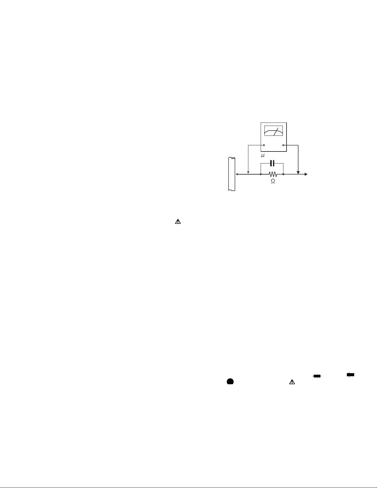
(5) Leakage shock hazard testing
After reassembling the product, always perform an isolation check on the exposed metal parts of the product (antenna terminals, knobs, metal cabinet, screw heads,
headphone jack, control shafts, etc.) to be sure the product
is safe to operate without danger of electrical shock.Do not
use a line isolation transformer during this check.
• Plug the AC line cord directly into the AC outlet. Using a
"Leakage Current Tester", measure the leakage current
from each exposed metal parts of the cabinet, particularly any exposed metal part having a return path to the
chassis, to a known good earth ground. Any leakage current must not exceed 0.5mA AC (r.m.s.).
• Alternate check method
Plug the AC line cord directly into the AC outlet. Use an
AC voltmeter having, 1,000Ω per volt or more sensitivity
in the following manner. Connect a 1,500Ω 10W resistor
paralleled by a 0.15µF AC-type capacitor between an ex-
posed metal part and a known good earth ground.
Measure the AC voltage across the resistor with the AC
voltmeter.
Move the resistor connection to each exposed metal
part, particularly any exposed metal part having a return
path to the chassis, and measure the AC voltage across
the resistor. Now, reverse the plug in the AC outlet and
repeat each measurement. Voltage measured any must
not exceed 0.75 V AC (r.m.s.). This corresponds to 0.5
mA AC (r.m.s.).
AC VOLTMETER
(Having 1000
ohms/volts,
or more sensitivity)
0.15 F AC TYPE
Place this
probe on
1500 10W
Good earth ground
1.2 Warning
(1) This equipment has been designed and manufactured to
meet international safety standards.
(2) It is the legal responsibility of the repairer to ensure that
these safety standards are maintained.
(3) Repairs must be made in accordance with the relevant
safety standards.
(4) It is essential that safety critical components are replaced
by approved parts.
(5) If mains voltage selector is provided, check setting for local
voltage.
1.3 Caution
Burrs formed during molding may be left over on some parts
of the chassis.
Therefore, pay attention to such burrs in the case of preforming repair of this system.
1.4 Critical parts for safety
In regard with component parts appearing on the silk-screen
printed side (parts side) of the PWB diagrams, the parts that are
printed over with black such as the resistor ( ), diode ( )
and ICP ( ) or identified by the " " mark nearby are critical
for safety. When replacing them, be sure to use the parts of the
same type and rating as specified by the manufacturer.
(This regulation dose not Except the J and C version)
each exposed
metal part.
(No.MA454<Rev.001>)1-5
Page 6
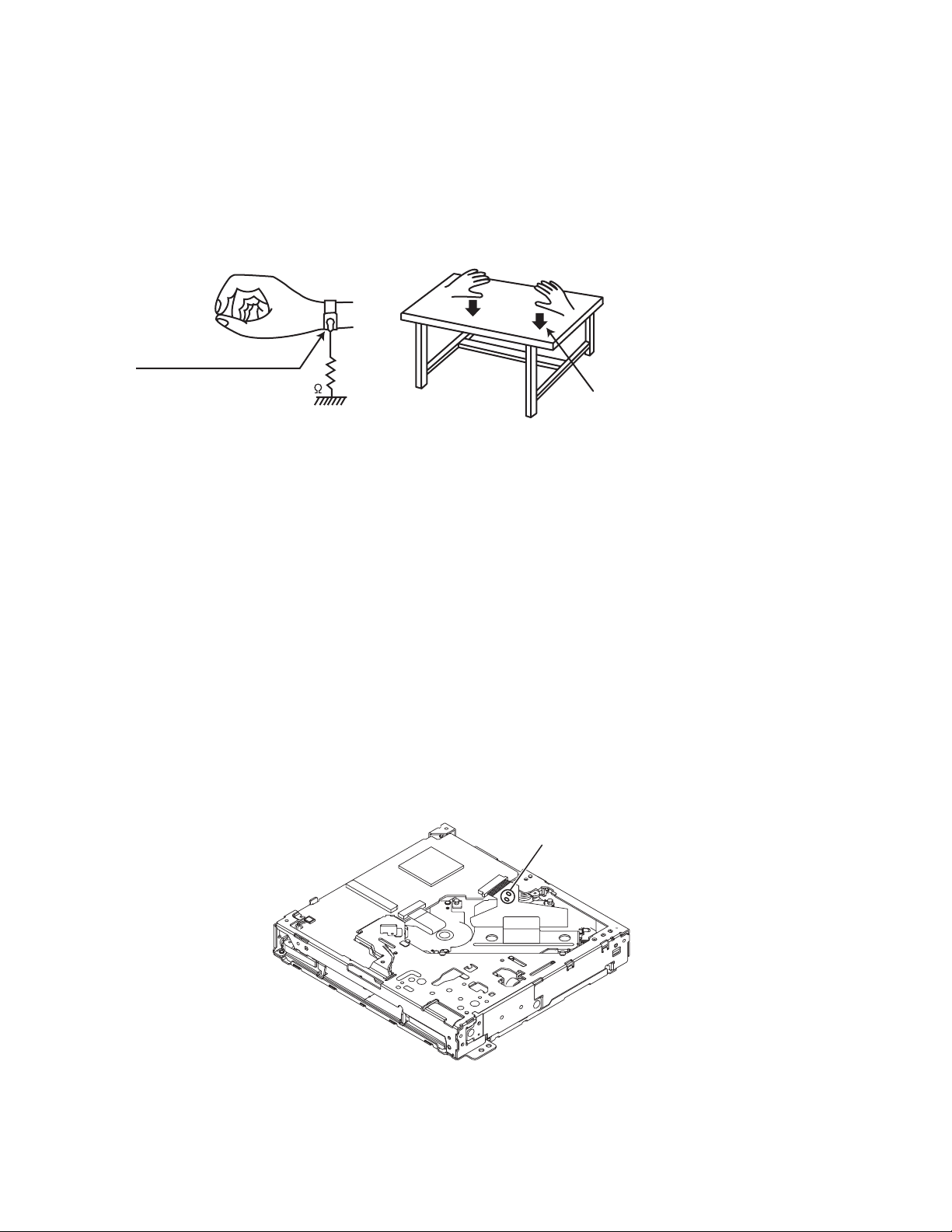
1.5 Preventing static electricity
Electrostatic discharge (ESD), which occurs when static electricity stored in the body, fabric, etc. is discharged, can destroy the laser
diode in the traverse unit (optical pickup). Take care to prevent this when performing repairs.
1.5.1 Grounding to prevent damage by static electricity
Static electricity in the work area can destroy the optical pickup (laser diode) in devices such as laser products.
Be careful to use proper grounding in the area where repairs are being performed.
(1) Ground the workbench
Ground the workbench by laying conductive material (such as a conductive sheet) or an iron plate over it before placing the
traverse unit (optical pickup) on it.
(2) Ground yourself
Use an anti-static wrist strap to release any static electricity built up in your body.
(caption)
Anti-static wrist strap
1M
Conductive material
(conductive sheet) or iron palate
(3) Handling the optical pickup
• In order to maintain quality during transport and before installation, both sides of the laser diode on the replacement optical
pickup are shorted. After replacement, return the shorted parts to their original condition.
(Refer to the text.)
• Do not use a tester to check the condition of the laser diode in the optical pickup. The tester's internal power source can easily
destroy the laser diode.
1.6 Handling the traverse unit (optical pickup)
(1) Do not subject the traverse unit (optical pickup) to strong shocks, as it is a sensitive, complex unit.
(2) Cut off the shorted part of the flexible cable using nippers, etc. after replacing the optical pickup. For specific details, refer to the
replacement procedure in the text. Remove the anti-static pin when replacing the traverse unit. Be careful not to take too long a
time when attaching it to the connector.
(3) Handle the flexible cable carefully as it may break when subjected to strong force.
(4) I t is not possible to adjust the semi-fixed resistor that adjusts the laser power. Do not turn it.
1.7 Attention when traverse unit is decomposed
*Please refer to "Disassembly method" in the text for the pickup unit.
• Apply solder to the short land sections before the card wire is disconnected from the connecto on the servo board. (If the card wire
is disconnected without applying solder, the pickup may be destroyed by static electricity.)
• In the assembly, be sure to remove solder from the short land sections after connecting the card wire.
Solder short part
1-6 (No.MA454<Rev.001>)
Page 7
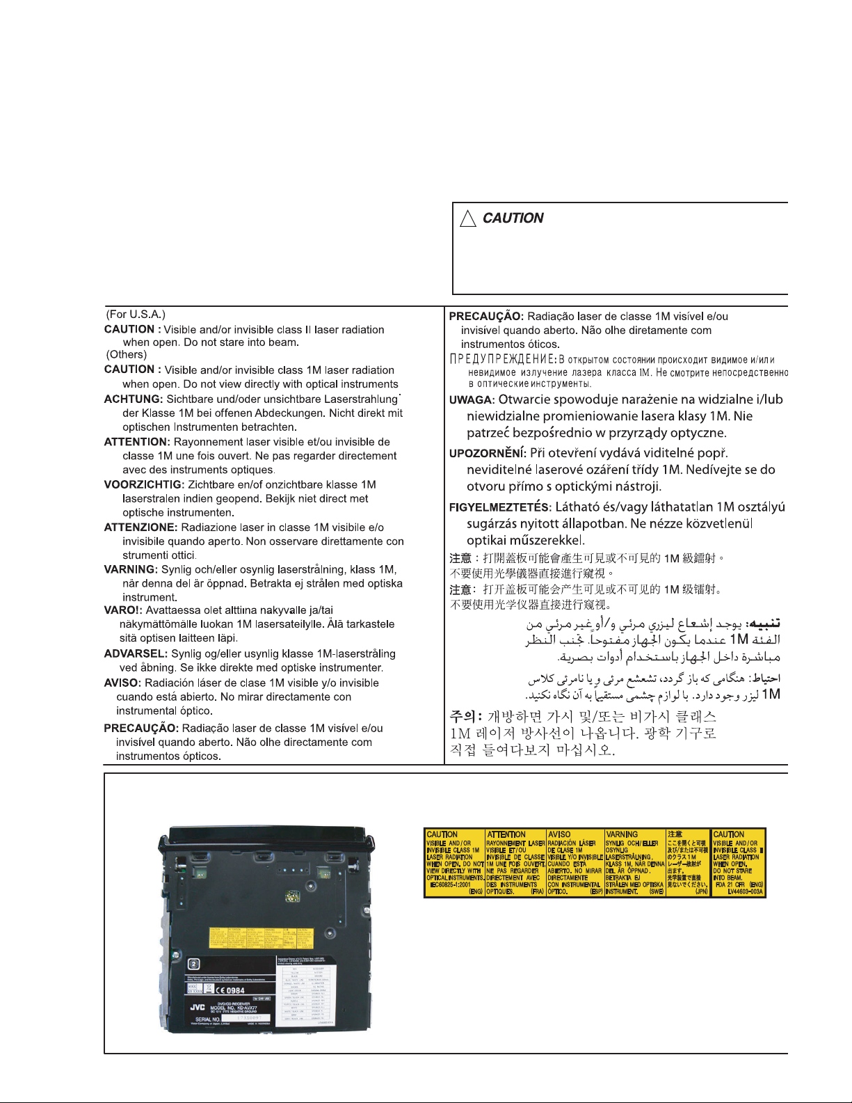
1.8 Important for laser products
1.CLASS 1 LASER PRODUCT
2.CAUTION :
(For U.S.A.) Visible and/or invisible class II laser radiation
when open. Do not stare into beam.
(Others) Visible and/or invisible class 1M laser radiation
when open. Do not view directly with optical instruments.
3.CAUTION : Visible and/or invisible laser radiation when
open and inter lock failed or defeated. Avoid direct
exposure to beam.
4.CAUTION : This laser product uses visible and/or invisible
laser radiation and is equipped with safety switches which
prevent emission of radiation when the drawer is open and
the safety interlocks have failed or are defeated. It is
dangerous to defeat the safety switches.
5.CAUTION : If safety switches malfunction, the laser is able
to function.
6.CAUTION : Use of controls, adjustments or performance of
procedures other than those specified here in may result in
hazardous radiation exposure.
!
Please use enough caution not to
see the beam directly or touch it
in case of an adjustment or operation
check.
REPRODUCTION AND POSITION OF LABELS and PRINT
WARNING LABEL and PRINT
(No.MA454<Rev.001>)1-7
Page 8

SECTION 2
SPECIFIC SERVICE INSTRUCTIONS
This service manual does not describe SPECIFIC SERVICE INSTRUCTIONS.
1-8 (No.MA454<Rev.001>)
Page 9
SECTION 3
DISASSEMBLY
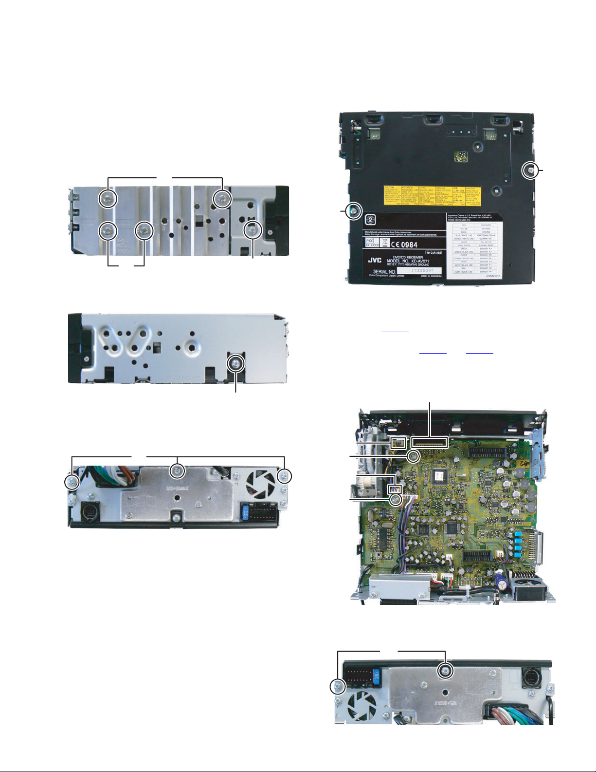
3.1 Main body (Used figure are KD-AVX77E)
3.1.1 Removing the Top chassis with DVD mechanism (See
Fig.1 to 4)
(1) Remove the two screws A and two screws B attaching the
Heat sink. (See Fig.1)
(2) Remove the one screw C attaching the Top chassis. (See
Fig.1)
A
BC
Fig.1
(3) Remove the one screw D attaching the Top chassis. (See
Fig.2)
D
Fig.2
(4) Remove the three screws E attaching the Top chassis.
(See Fig.3)
E
(5) Remove the two screws F attaching the Top chassis. (See
Fig.4)
F
F
Fig.4
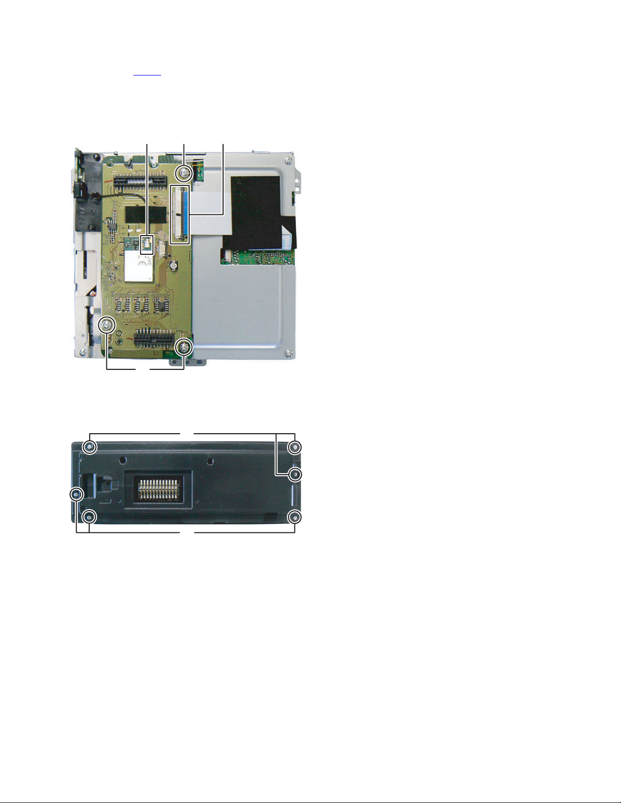
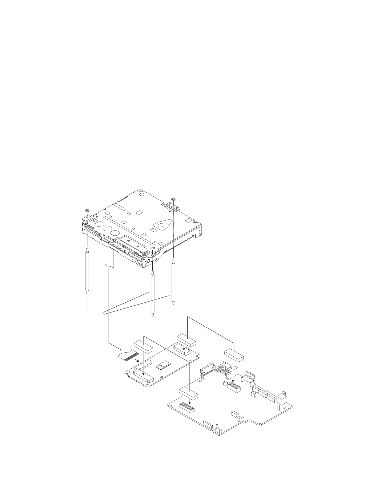
3.1.2 Removing the Main board (See Fig.5 to 10)
(1) Disconnect the card wire from Front chassis connected to
connector CN962 of the Main board. (See Fig.5)
(2) Disconnect the connector wire from Gear bracket unit con-
nected to connector CN881 and CN891 of the Main board.
(See Fig.5)
(3) Remove the two screws G attaching the Main board. (See
Fig.5)
CN962
CN891
G
Fig.3
CN881
G
Fig.5
(4) Remove the two screws H attaching the Bottom chassis.
(See Fig.6)
H
Fig.6
(No.MA454<Rev.001>)1-9
Page 10
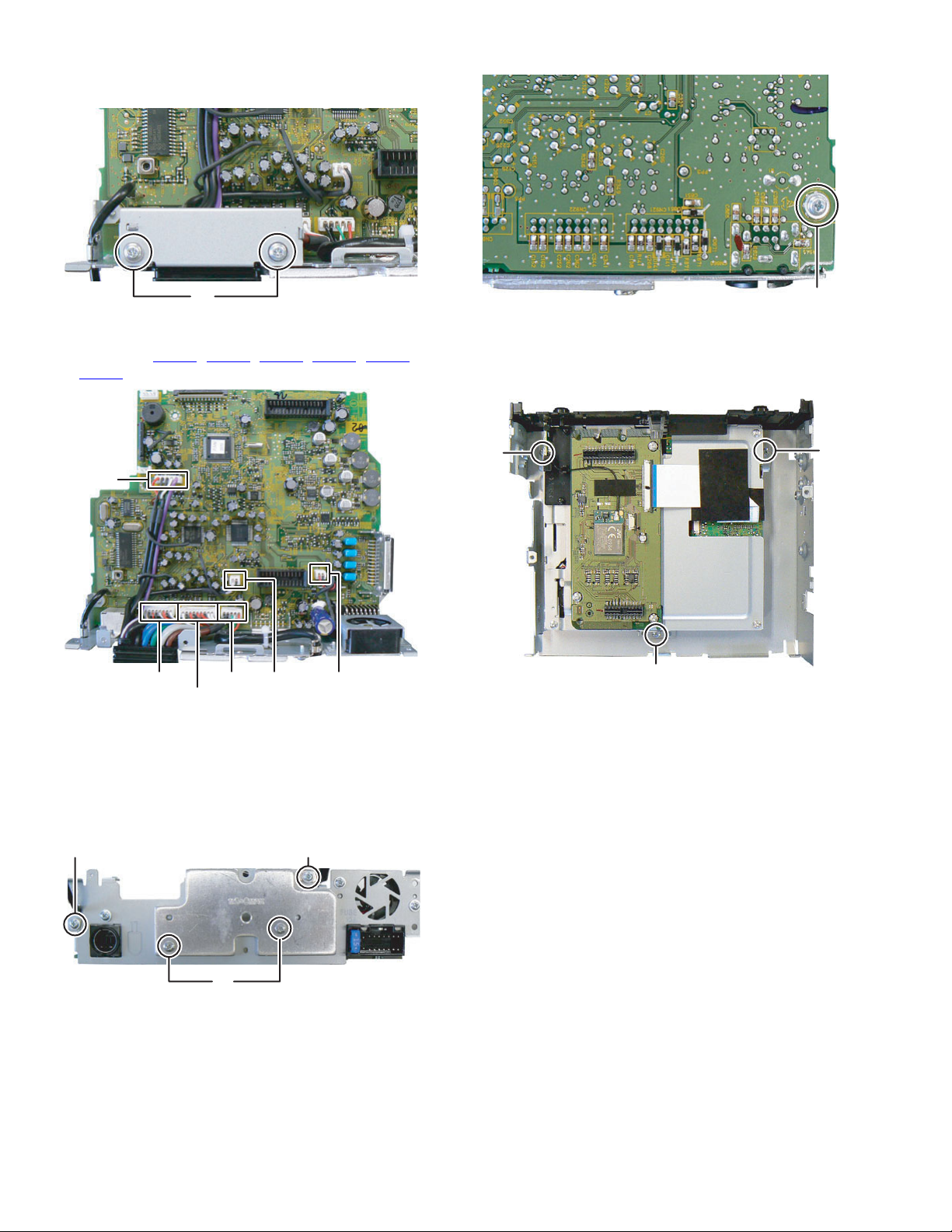
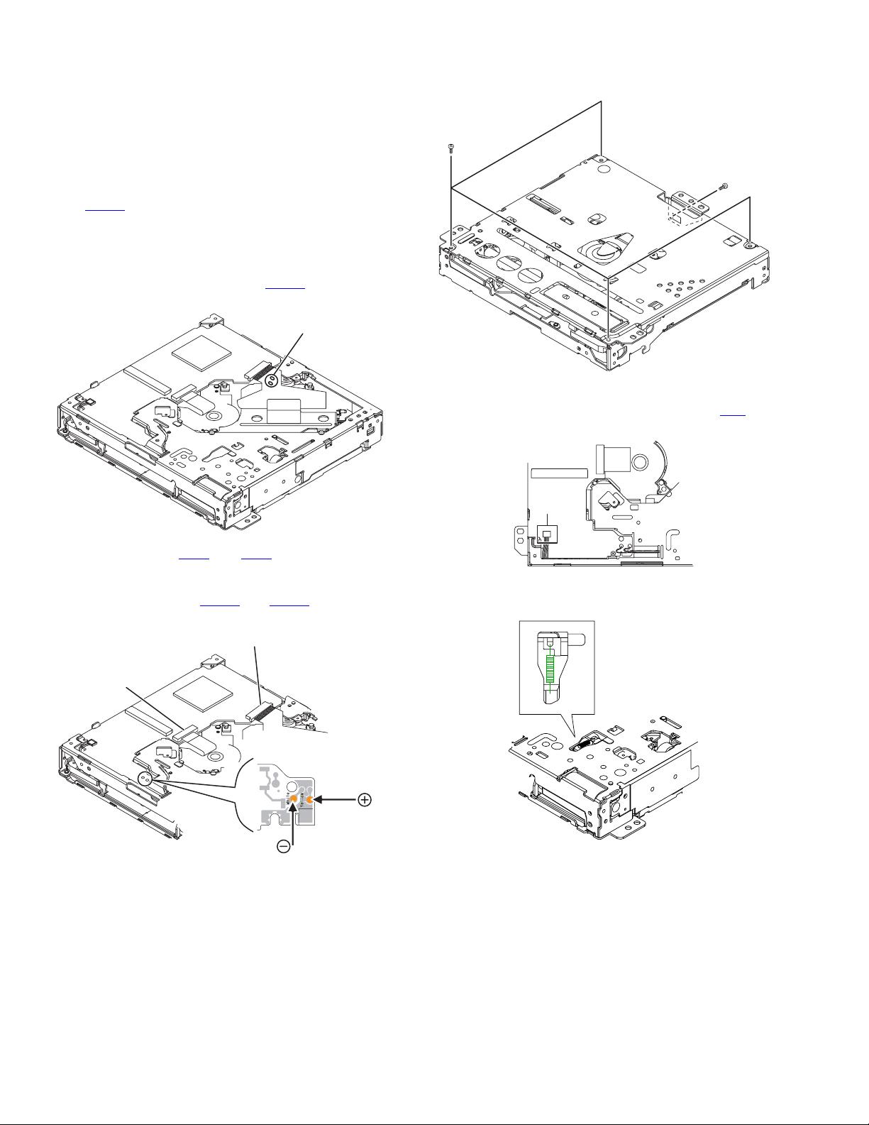
(5) Remove the two screws J attaching the Wire bracket. (See
Fig.7)
J
Fig.7
(6) Disconnect connector wire from Rear bracket connected to
connectors CN861
of the Main board. (See Fig.8)
CN981
CN981
(7) Remove the two screws K attaching the Heat sink. (See
Fig.9)
(8) Remove the one screw L attaching the Antenna wire. (See
Fig.9)
(9) Remove the one screw M attaching the USB cable. (See
Fig.9)
, CN871, CN921, CN922, CN923 and
CN861CN871 CN823CN921
CN922
Fig.8
N
Fig.10
3.1.3 Removing the DVD mechanism (See Fig.11)
(1) Remove the three screws P attaching the DVD mecha-
nism.
P
P
Fig.11
P
LM
K
Fig.9
(10) Remove the one screw N attaching the Main board. (See
Fig.10)
1-10 (No.MA454<Rev.001>)
Page 11
3.1.4 Removing the Connection board (See Fig.12)
(1) Disconnect the card wire from DVD mechanism connected
to connector CN395
(2) Disconnect the connector wire from BT antenna connected
to connector of RF module.
(3) Remove the three screws Q attaching the Connection
board.
Connector
of the Connection board.
CN395
Q
Q
Fig.12
3.1.5 Removing the Panel A control board (See Fig.13)
(1) Remove the six screws R attaching the Rear cover.
R
R
Fig.13
(No.MA454<Rev.001>)1-11
Page 12
3.2 DVD mechanism assembly section
3.2.1 Removing the Traverse mechanism assembly (See
Fig.1 to 6)
(1) Solder the short land section on the flexible wire of pickup.
(See Fig.1)
Caution:
* Solder the short land section on the flexible wire of pickup
before disconnecting the flexible wire form the connector
on the Front end board.
CN101
If the flexible wire is disconnected without attaching the
solder, the pickup may be destroyed by static electricity.
* When attaching the Traverse mechanism assembly, remove the solder from the short land section after connection
the flexible wire to the connector CN101
on the Front end
board.
Solder short part
(4) Remove the five screws A attaching the Top cover assembly.
(See Fig.3)
A
Fig.3
(5) From the bottom side, disconnect the connector wire from
Top cover assembly connected to connector CN2
Front end board. (See Fig.4)
of the
Fig.1
(2) Voltage supply to TP79
and TP81 approx DC 3.0V until
Clamper is shift to loading complete position. (See Fig.2)
(3) Disconnect the flexible wires from Traverse mechanism assembly
connected to connector CN101
and CN164 of the Front end
board. (See Fig.2)
CN101
CN164
TP79 TP81
TP79
R317
TP67
R312
R21
R357
TP81
TP92
CENTER
D-
DGND_7
WOOFER
Voltage supply
position
Fig.2
CN2
Fig.4
(6) From the bottom side, remove the spring from Traverse
mechanism assembly. (See Fig.5)
Fig.5
1-12 (No.MA454<Rev.001>)
Page 13
(7) From the top side, pull up the traverse mechanism and disengage
three dumper positions. (See Fig.6)
Dumper
(same color spring)
Dumper
(Different color spring)
Fig.6
3.2.2 Removing the Front end board (See Fig.7)
(1) Remove the Motor wires from loading motor soldered to
and TP81 of the Front end board.
TP79
(2) Remove the two screws B attaching the Front end board.
TP81
3.2.3 Removing the Loading arm assembly (See Fig.8)
(1) Remove the Loading arm spring L from Loading arm assembly.
(2) Slide to left side and then disengage hook a then hook b.
hook b
Loading arm
assembly
hook
Loading arm spring L
a
B
TP79
B
Fig.8
3.2.4 Removing the Gear base assembly (See Fig.9, 10)
(1) Remove the Loading arm spring L. (See Fig.9)
Fig.7
Loading arm
spring L
Fig.9
(No.MA454<Rev.001>)1-13
Page 14
(2) Remove the two screws C attaching the Gear base assembly.
r
(See Fig.10)
C
Fig.10
3.2.5 11Removing the Loading arm holder. (See Fig.)
(1) Remove the two screws D attaching the Loading arm holder.
(2) Remove the Loading arm spring R.
D
Loading arm
holder
3.2.7 Removing the Slide cam assembly (See Fig.13)
(1) Slide to backward the Slide cam assembly and the remove
the Slide cam spring.
(2) Slide to frontward the slide cam assembly, and then take
out it.
Slide cam assembly
Slide cam spring
Fig.13
3.2.8 Removing the Photo board (See Fig.14)
(1) Pressing the hook c and then slide to backward (slide to the
arrow side) the Disc plate.
(2) Remove the one screw F attaching the Photo board.
hook
c
hook
c
Loading arm
spring R
Fig.11
3.2.6 Removing the Loading moor assembly (See Fig.12)
(1) Remove the three screws E attaching the Loading motor
assembly.
E
Photo board
F
Fig.14
3.2.9 Removing the Loading motor (See Fig.15 to 18)
(1) Remove the A wheel gear. (See Fig.15)
A Wheel gea
Fig.15
1-14 (No.MA454<Rev.001>)
Fig.12
Page 15
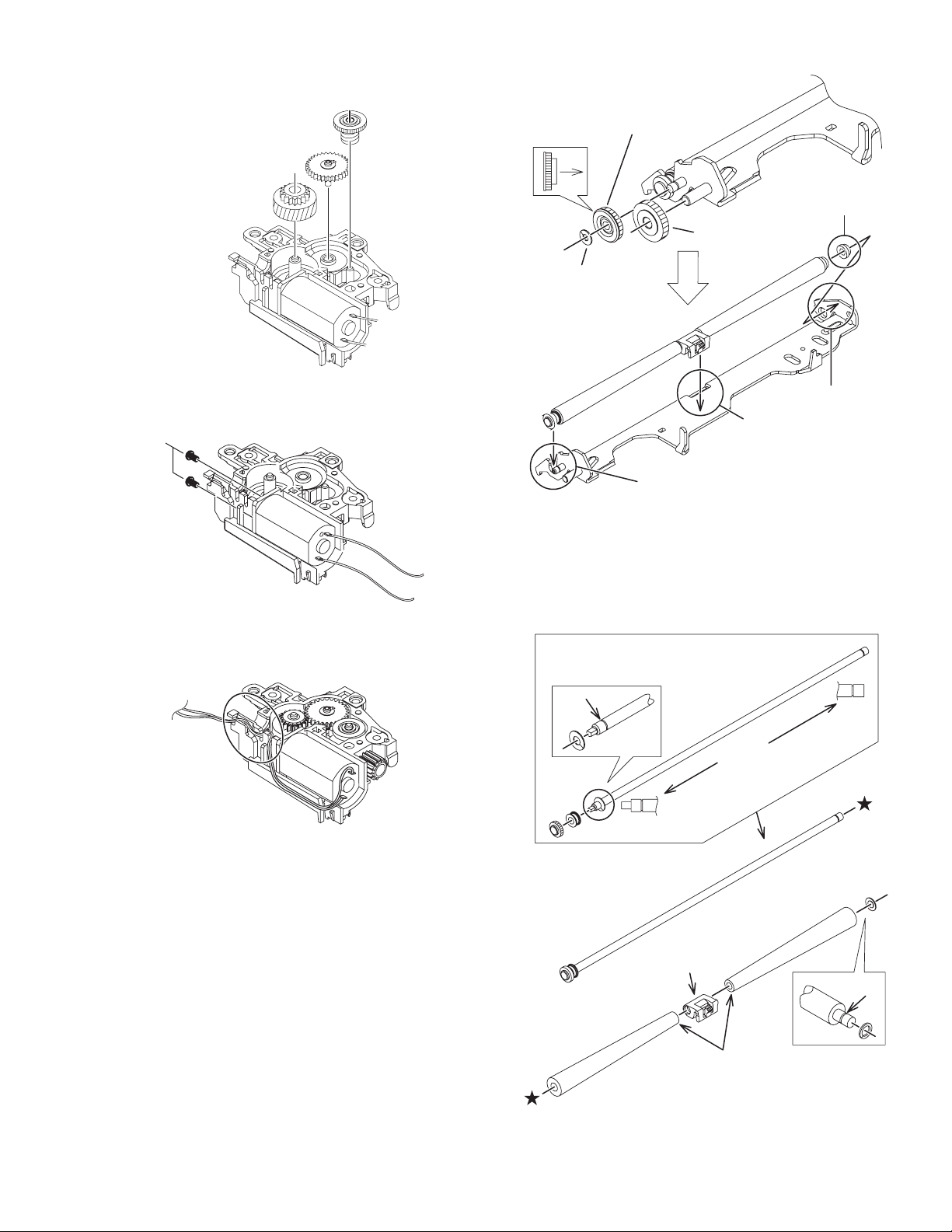
(2) Remove the A worm gear, M connect gear and M wheel
gear by sequentially. (See Fig.16)
A worm gear
M connect gear
M wheel gear
Fig.16
(3) Remove the two screws G attaching the Loading motor.
(Se Fig.17)
G
Fig.17
(4) When attaching the Loading motor, motor wire should arrange
to figure. (See Fig18.)
Direction
R middle gear
R collar R
R connect gear
Slit washer
part c
part a
part b
Fig.19
3.2.11 Removing the Roller (See Fig.20)
(1) Remove the Slit washer.
(2) Pull out the Roller shaft.
CAUTION:
When reattach the Roller shaft, Slit washer should be change
new part.
Wire arrangement
Fig.18
3.2.10 Removing the Roller assembly (See Fig.19)
(1) Remove the Slit washer.
(2) Remove the R middle gear.
(3) Remove the R connect gear.
(4) Snap off the part a of the Roller assembly.
(5) Lift up the part b of the Roller assembly, and then release
part c (When release part c, R collar R is easy to come off,
does not lose it).
CAUTION:
When reattach the Roller assembly, Middle gear should keep
direction and Slit washer should be change new part.
slit
keep direction
keep direction
slit
small side
Fig.20
(No.MA454<Rev.001>)1-15
Page 16
SECTION 4
ADJUSTMENT
4.1 Test instruments required for adjustment
(1) Digital oscilloscope (100MHz)
(2) Digital tester
(3) Test Disc
(4) Extension cable : EXTDV002-30P
EXTSH002-22P
EXTAV70X-50PF
(5) Extension stud : STDV001-3P
4.2 Standard measuring conditions
Power supply voltage DC14.4V(10.5 to 16V)
Load impedance 20K ohm (2 Speakers connection)
Output Level Line out 2.5V (Vol. MAX)
4.5 How to connect the extension cable for adjusting
Caution:
Be sure to attach the heat sink and rear bracket onto the power amplifier IC and regulator IC respectively, before supply the power.
If voltage is applied without attaching these parts, the power amplifier IC and regulator IC will be destroyed by heat.
4.3 Standard volume position
Balance and Bass &Treble volume : lndication"0"
Loudness : OFF
4.4 Dummy load
Exclusive dummy load should be used for AM,and FM.
For FM dummy load, there is a loss of 6dB between SSG
output and antenna input.
The loss of 6dB need not be considered sincedirect reading
of figures are applied in this working standard.
Extension stud
STDV001-3P
EXTAV70X-50PF
1-16 (No.MA454<Rev.001>)
EXTDV002-30P
EXTSH002-22P
Page 17
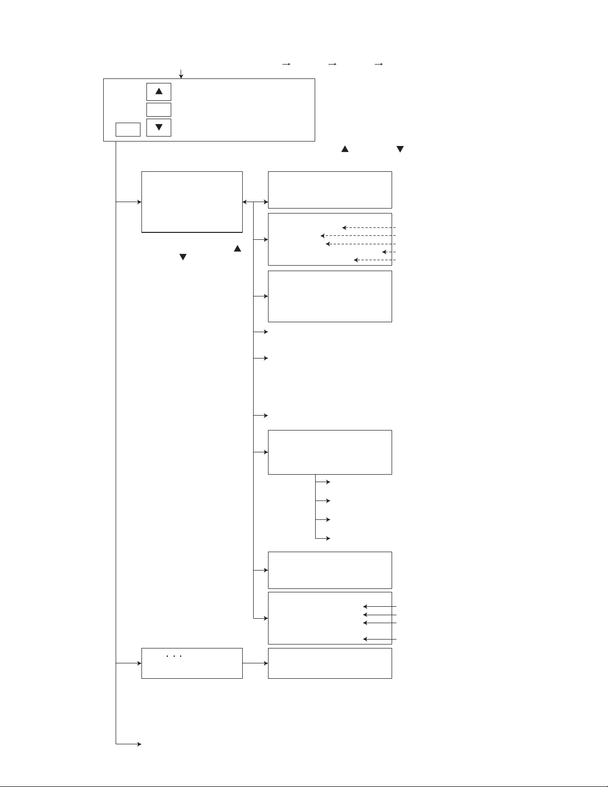
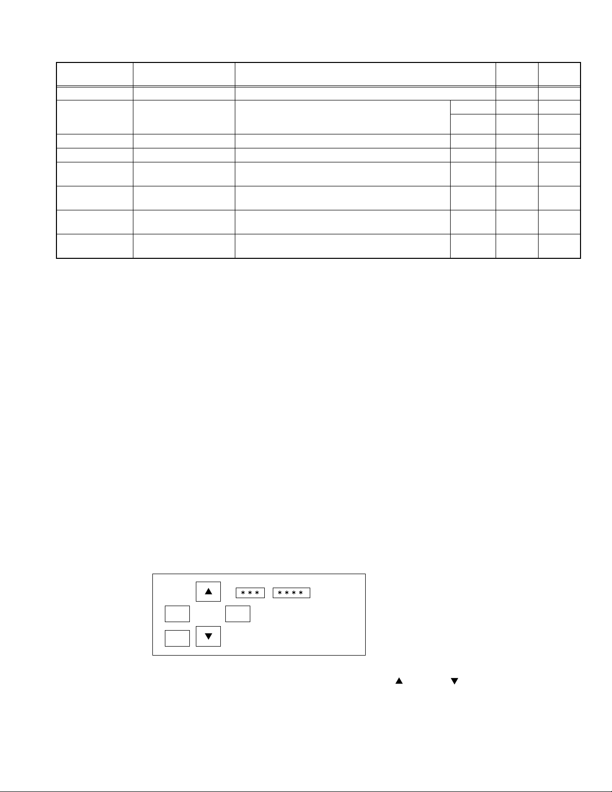
4.6 Service mode
4.6.1 Service mode 1 (Indication of a service mode 1 is nothing.)
Keep this state more 2 seconds
while continuing pressing the
[STANDBY/ON ATTENUATOR] button
and [TOUCH PANEL EJECT] button
sequentially.
Screen indication
Exchanging it operate a menu of a service mode with the [ ] button
NO EJECT?
EMERGENCY EJECT?*1*2
and [ ] button. Operate choice of a menu with a [ENTER] button.
*1 : When an [ENTER] button is pushed in NO EJECT indication, it is set
by an EJECT prohibition mode.
When an [ENTER] button is pushed in EJECT OK indication, it is set
by a normal mode.
*2 : Forced EJECT movement
A screen becomes normal indication after an [ENTER] button was pushed.
Set an area number in touch panel temporarily.
When an icon is not displayed by a screen, the key input is effective.
132
TOUCH PANEL AREA
45
STANDBY/ON ATTENUATOR button
Multiplex push timing chart (Example: Service mode 2)
[STANDBY/ON ATTENUATOR]
[AREA 1]
[AREA 5]
Within 0.5 seconds
[AREA 2]
Key ON (Hold)
Key ON
Within 2 seconds
Key ON
Key ON
Within 2 seconds
Shift to Service Mode 2
(No.MA454<Rev.001>)1-17
Page 18
4.6.2 Service mode 2
Set to service mode 2: [STANDBY/ON ATTENUATOR] [AREA 1] [AREA 5] [AREA 2]
Screen indication
SERVICE MODE 2
INITIALIZE ALL
INITIALIZE
ENT
INITIALIZE DVD
INITIALIZE BT
BACK
TOUCH PANEL CALIBRATION
TOUCH PANEL CHECK MODE
Exchanging it operate a menu of a service mode with the [ ] button and [ ] button.
Operate choice of a menu with a [ENT] button.
INITIALIZE ALL
INITIALIZE ALL (Each EEPROM is initialized by
NOW
INITIALIZE ALL
INITIALIZE ALL
OK **
a factory shipment state.)
* Main micron EEPROM initialization (user entry
domain, error history, speaker setting, subarea
of J-version, data to pre-set )
* Panel micron EEPROM initialization
(picture adjustment data)
* DVD unit EEPROM initialization
(except a permanent domain)
* Bluetooth module EEPROM initialization
* After clear completion, a screen returns to
normal indication after OK indication was
displayed for three seconds.
INITIALIZE
INITIALIZE (Initialization of a user area of each
NOW
INITIALIZE
INITIALIZE
OK **
EEPROM)
* Main micron EEPROM initialization (a user
entry domain )
(a user entry domain, speaker setting, subarea
of J-version, data to pre-set )
* Panel micron EEPROM initialization
(picture adjustment data )
* DVD unit EEPROM initialization
(except a permanent domain)
* After clear completion, a screen returns to
normal indication after OK indication was
displayed for three seconds.
INITIALIZE DVD
Full initialization of EEPROM of a DVD unit (It is included a permanent domain).
After clear completion, this indication is continued till an effective key is input.
INITIALIZE DVD
OK **
INITIALIZE BT
INITIALIZE BT
OK **
TOUCH PANEL CALIBRATION
++
+
TOUCH PANEL CHECK MODE
++
+
1-18 (No.MA454<Rev.001>)
Full initialization of EEPROM of Bluetooth.
After clear completion, this indication is continued till an effective key is input.
+
Push the center of a + character displayed in turn.
+
+
+
The confirmation mode that the calibration of the touch panel was performed
definitely.
*Return to previous menu with a [STANDBY/ON ATTENUATOR] button.
Page 19
4.6.3 Service mode 3
Set to service mode 3: [STANDBY/ON ATTENUATOR] [AREA 1] [AREA 5] [AREA 3]
Screen indication
SERVICE MODE 3
SERVICE MODE
INITIALIZE ALL
ENT
RUNNING MODE
BACK
Exchanging it operate a menu of a service mode with the [ ] button and [ ] button.
Operate choice of a menu with a [ENT] button.
SERVICE MODE
SERVICE MODE
VERSION
AREA/REGION
TEMPERATURE
MEMORY CHECK
DVD CHECK MODE
* Exchanging it operate a menu
of a service mode with the [ ]
button and [ ] button.
* Operate choice of a menu with
a [ENT] button.
* Return to previous menu with
a [BACK] button.
INITIALIZE ALL
NOW
INITIALIZE ALL
RUNNING MODE
* See "Running mode" for details.
SERVICE MODE
ERROR READ
ERROR CLEAR
BT VERSION
VERSION
MAIN
DISC
CH
PN
SW BT MODULE ***
AREA/REGION
SYS-AREA : *
DISC-AREA : **
REGION : *
PANEL AREA :*
TEMPERATURE Temperature data reading
* Temperature data by the temperature sensor in the main micon and DVD-PCB is
read every 5 seconds and displayed in hex numbers.
MEMORY CHECK ( It is displayed only at the time of the disc insertion )
Memory residual quantity indication mode
* Data residual quantity of a disc is displayed by LCD.
* About the playback control-related key ([FSKIP], [BSKIP], [UP], [DOWN], [VOL]),
only movement is effective.
Indication does not change as memory residual quantity indication.
* About cancellation of this mode, press the [STANDBY/ON ATTENUATOR] button.
DVD CHECK MODE
* See "DVD CHECK MODE" for details.
ERROR READ
DVD ERROR READ
CH ERROR READ
MECHA ERROR READ
READ ALL
ERROR CLEAR
DVD ERROR CLEAR
CH ERROR CLEAR
MECHA ERROR CLEAR
BT VERSION
SW BT CORE ***
HW BT MODULE ***
SW BT MODULE ***
ADR-************
INITIALIZE ALL
OK **
V**** [**]
****
******
V**** V*** [**] V*** ** *
DVD ERROR READ
Reading of a DVD unit error history
CH ERROR READ
Reading of a CD changer error history
MECHA ERROR READ
Reading of a door mechanism error history
READ ALL *Only the engineer use
Reading of a main micon EEPROM (All contents)
Micon version indication
Main micon version and ROM correction version
DVD module version
CH version
Panel micon version and ROM correction version
Software version of BT Module
Area and region indication
Main micon area
DVD area
Region
PANEL area
Clear of each error history
A screen returns to following
indication after clear completion.
Bluetooth version indication
Software version of BT core
Hardware version of BT Module
Software version of BT Module
BT Address
INITIALIZE ALL (Each EEPROM is initialized by
a factory shipment state.)
* Main micon EEPROM initialization
(user entry domain, error history, speaker
setting, subarea of J-version, data to pre-set )
* Panel micon EEPROM initialization
(picture adjustment data)
* DVD unit EEPROM initialization
(except a permanent domain)
* Bluetooth module EEPROM initialization
* After clear completion, a screen returns to
normal indication after OK indication was
displayed for three seconds.
(No.MA454<Rev.001>)1-19
Page 20
4.6.4 Service mode 4
Set to service mode 4: [STANDBY/ON ATTENUATOR] [AREA 1] [AREA 5] [AREA 4]
Screen indication
ENT
BACK
Exchanging it operate a menu of a service mode with the [ ] button and [ ] button.
Operate choice of a menu with a [ENT] button.
RDS MODE
* RDS service mode (Only RDS model)
SERVICE MODE 4
RDS MODE
MONITOR S MODE
HD RADIO S MODE
MONITOR S MODE
R/W CHROMA
DATA CLEAR
*See "Monitor adjustment" for details.
CHROMA DATA read/write of NTSC/PAL signal processing IC
Clear of CHROMA DATA (return to an initial value)
HD RADIO S MODE
* It is displayed in HD Radio unit connection.
4.7 DVD check mode
DVD CHECK MODE
NORMAL PLAY
EF OUT-TRACKING OFF
EF IN-TRACKING OFF
CD-LASER ON
DVD-LASER ON
DVDx1 JITTER MODE
Exchanging it operate a menu of a service mode with the [ ] button and [ ] button.
Operate choice of a menu with a [ENT] button.
DVD CHECK MODE
EEPROM DATA DISP
EEPROM DATA CLEAR
TEMPERATURE
SEARCH & JITTER
MONITOR
DVDx1 PLAY
DVD CHECK MODE
STOP
EJECT
LOAD
Command Mechanism unit operation Indication contents
NORMAL PLAY Start at normal speed
Laser current value, jitter value
(After start, jitter is measured by an inner position)
EF OUT-TRACKING OFF Tracking off the outermost position of CD For EF phase error
EF IN-TRACKING OFF Tracking off the innermost position of CD For EF phase error
CD-LASER ON CD_LD lights and laser current is displayed Laser current value, jitter value
DVD-LASER ON DVD_LD lights and laser current is displayed Laser current value, jitter value
DVD×1 JITTER MODE DVD ×1 jitter measuring mode
Laser current value, jitter value
(for use in mechanism adjustment)
EEPROM DATA DISP Contents of EEPROM is displayed EEPROM address
EEPROM contents
EEPROM DATA CLEAR Contents of EEPROM is initialized EEPROM address
EEPROM contents
TEMPERATURE Temperature indication Temperature is displayed in hex numbers
SEARCH & JITTER The search and jitter measurement to an appointed
position of DVD
Position measured with VT-501
jitter value
MONITOR Monitor terminal setting
DVD×1 PLAY DVD ×1 stopped start
Not displayed
(After start, jitter is measured by an inner position)
STOP Disc stopped, LD-OFF Not displayed
EJECT EJECT Not displayed
LOAD LOADING Not displayed
1-20 (No.MA454<Rev.001>)
Page 21
4.8 Error code tables
4.8.1 Mechanism error code
Error contents Details Error code Detailed error code
Disc loading error
(3) D1 time out 09 0013
Eject error
(3) B1 time out
(4) C1 time out
Error in loading wait Loading of a running mode
Disc was pulled out in a wait.
4.8.2 Disc error code
Error contents Details Error code Detailed error code
TOC read error TOC lead movement of a CD is not completed. 84 0059
First track access error Even if TOC reading passes after the end with
CD running mode for 30 seconds, the first track
access is not finished.
Last track access error Even if first track passes after the end with
CD running mode for 30 seconds, the last track
access is not finished.
T1 access error Even if T1 access passes in a DVD running
mode for 30 seconds, it is not finished.
T12 access error Even if T12 access passes in a DVD running
mode for 30 seconds, it is not finished.
T24 access error Even if T24 access passes in a DVD running
mode for 30 seconds, it is not finished.
Read-in area read error Read-in area read operation of DVD is not
completed.
DVD L1 layer adjustment error Adjustment of L1 layer of DVD is not finished
normally. (including focus jump failure)
DVD L0 layer adjustment error Adjustment of L0 layer of DVD is not finished
normally. (including focus jump failure)
NO DISC judgment Judgment without disc 80 0090
It is NO DISC by start failure Start is impossible 80 0091
It is stopped by playback inability. Stop in running mode playback 80 0093
Logic format NG Logic format analysis inability or
non-correspondence logic format
Seek access error It cannot arrive at an aim address even if it
passes for 15 seconds.
01
01
09 0031
80 0060
80 0061
80 0069
80 0070
80 0071
84 0072
80 0074
80 0075
80 0094
80 0095
0023
0024
(No.MA454<Rev.001>)1-21
Page 22
4.8.3 Error codes of panel mechanism
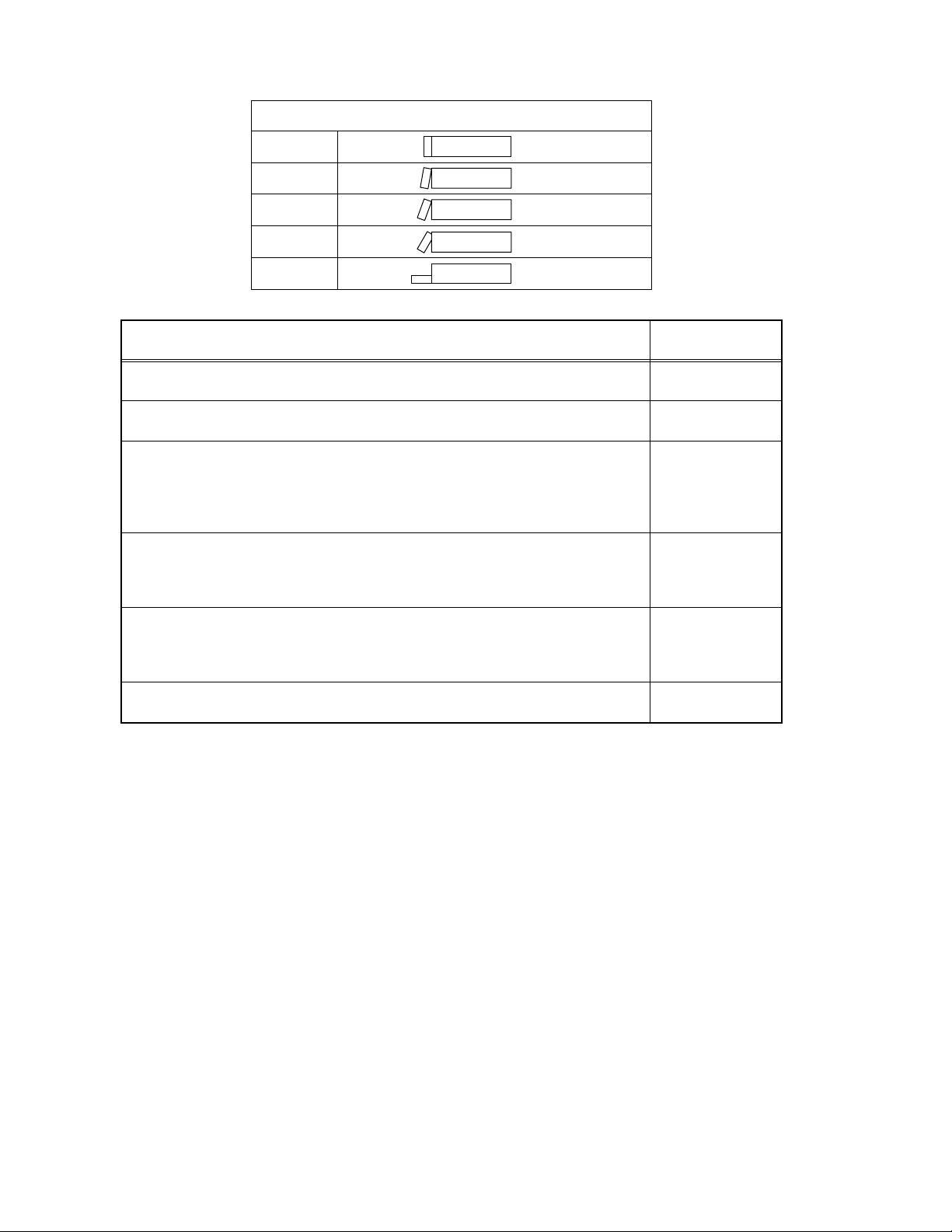
PANEL ANGLE
1 Panel Close Main body
2
3
4
OPEN
Detail
Open error
1. Time out error by OPEN position cannot detect.
Close error (ANGLE 1 error)
1. Time out error by ANGLE 1 position cannot detect.
Angle positioning error
Moving to 10 degrees (ANGLE 2 error)
1. Time out error by ANGLE 2 position cannot detect at moving to open position.
2. Missing to ANGLE 1 and detected ANGLE 2 position at moving to open position.
3. Time out error by ANGLE 2 cannot detect at moving close position.
Moving to 20 degrees (ANGLE 3 error)
1. Time out error by ANGLE 3 position cannot detect at moving to open position.
2. Missing to ANGLE 2 and detected ANGLE 3 position at moving to open position.
3. Time out error by ANGLE 3 cannot detect at moving close position.
Moving to 30 degrees (ANGLE 4 error)
1. Time out error by ANGLE 4 position cannot detect at moving to open position.
2. Missing to ANGLE 3 and detected ANGLE 4 position at moving to open position.
3. Time out error by ANGLE 4 cannot detect at moving close position.
Abnormal switch position at moving panel
The Panel move to open and close position, detected abnormal switch position. 0A0000
10 degrees
20 degrees
30 degrees
Open
Error code
(Service mode)
0A0001
0B0006
0D0021
0D0022
0D0023
0E0031
0E0032
0E0033
0F0041
0F0042
0F0043
1-22 (No.MA454<Rev.001>)
Page 23
4.9 Running mode
Indication Explanation Operation contents of 1 cycle
RUNNING1 MECHA Door mecha running 1 Panel close → Panel open - RUNNING2 MECHA Door mecha running 2 Panel close → Panel open → Panel detach position → Panel
angle 3 position → Panel angle 1 position → Panel angle 2
position
RUNNING4 DVD DVD+Door mecha running1 Loading → Eject → Wait for 5 seconds+Door open/close Stop RUNNING5 DVD DVD+Door mecha running2 Loading → Eject → Wait for 5 seconds+Door open/close Retry RUNNING6 DVD DVD+Door mecha running3 Loading → Playback → Eject → Wait for 5 seconds+Door
open/close
RUNNING7 DVD DVD+Door mecha running4 Loading → Playback → Eject → Wait for 5 seconds+Door
open/close
RUNNING8 DVD DVD+Door mecha running5 Loading → Playback → Eject → Wait for 5 seconds+Door
open/close
RUNNING9 DVD DVD+Door mecha running6 Loading → Playback → Eject → Wait for 5 seconds+Door
open/close
RETRY Retry -
NO RETRY Stop -
In mecha
error
Stop Stop
Retry Stop
Stop Retry
Retry Retry
In disc
* Cancellation of running1,2 : Press the [EJECT] key
* In running 1,2 cancellation, a door does not stop at the position and moves to a panel position.
* Cancellation of running3 to 8 : Press the [POWER] key
* The number of count and an error cord are displayed in running.
Playback contents in a running mode
•CD
The first track is played for 30 seconds. → The last track is played for 30 seconds.
(The last track is played in the case of less than till the last for 30 seconds.)
•DVD
2layer disc (Pit disc)
Title 1 (the L0 layer internal circumference) is played for 30 seconds.
→ Title 24 (L1layer internal circumference) is played for 30 seconds.
→ Title 12 (L0 layer circumference) is played for 30 seconds.
error
2layer disc (Recordable disc)
Title 1 (the L0 layer internal circumference) is played for 30 seconds.
→ Title 24 (L1layer internal circumference) is played for 30 seconds.
→ Title 13 (L0 layer circumference) is played for 30 seconds.
1layer disc
First chapter of title 1 is played for 30 seconds.
→ The last chapter of title 1 is played for 30 seconds.
4.10 Monitor adjustment
* When adjusting, switch on the main unit and insert a test disc (VT-501). And play the test disc and pause it.
* Only an item number and value are shows a screen when the choose Monitor S Mode, but can operate it by pushing the following
area.
-
BACK
+
1. Set the service mode 4.
2. Exchanging it operate a menu of a service mode with the [ ] area and [ ] area.
3. Change data with the [ + ]/[ - ] area.
4. Write data with a [ENT] area.
(No.MA454<Rev.001>)1-23
Page 24

R/W CHROMA
Indication
001 Fix Fix 00000 Fix Color amplitude revision ON/OFF
002 Fix Fix 00001 Fix Color amplitude revision CAS
003 Fix Fix 00016 Fix Color amplitude revision APC
004 Fix Fix 00001 Fix Color amplitude revision CUS
005 Fix Fix 00010 Fix Color amplitude revision APU
006 00000 00001 00001 Adjust Black level extension ON/OFF
007 00000 00001 00001 Adjust Black level extension FUNCTION
008 00000 00511 00008 Adjust Black level extension START POINT
009 00000 00511 00160 Adjust Black level extension OFFSET
010 00000 00003 00000 Adjust Filter choice of the horizontal enhancer (NTSC)
011 00000 00003 00001 Adjust Filter choice of the horizontal enhancer (PAL)
012 00000 00127 00000 Adjust
013 00000 00127 00000 Adjust
014 00000 00127 00000 Adjust Limiter of the horizontal enhancer (NTSC)
015 00000 00127 00001 Adjust Limiter of the horizontal enhancer (PAL)
016 00000 00511 00016 Adjust Horizontal enhancer gain adjustment (NTSC)
017 00000 00511 00010 Adjust Horizontal enhancer gain adjustment (PAL)
018 00000 00003 00000 Adjust Filter chice of the horizontal brightness outline revision (NTSC)
019 00000 00003 00000 Adjust Filter chice of the horizontal brightness outline revision (PAL)
020 00000 00127 00000 Adjust
021 00000 00127 00000 Adjust
022 00000 00006 00032 Adjust
023 00000 00006 00005 Adjust
024 00000 00031 00000 Adjust Tap change of the horizontal brightness outline revision (NTSC)
025 00000 00031 00000 Adjust Tap change of the horizontal brightness outline revision (PAL)
026 00000 00001 00001 Adjust Vertical enhancer ON/OFF (NTSC)
027 00000 00001 00001 Adjust Vertical enhancer ON/OFF (PAL)
028 00000 00127 00010 Adjust Limiter of the vertical enhancer (NTSC)
029 00000 00127 00010 Adjust Limiter of the vertical enhancer (PAL)
030 00000 00127 00002 Adjust Adjustment of the quantity of vertical enhancer core ring (NTSC)
031 00000 00127 00001 Adjust Adjustment of the quantity of vertical enhancer core ring (PAL)
032 00000 00511 00128 Adjust Vertical enhancer gain adjustment (NTSC)
033 00000 00511 00128 Adjust Vertical enhancer gain adjustment (PAL)
034 Fix Fix 00128 Fix Change in TINT of the whole picture (NTSC)
035 Fix Fix 00131 Fix Change in TINT of the whole picture (PAL)
036 Fix Fix 00140 Fix
037 Fix Fix 00114 Fix Change with the deepness of the color of the whole pictur (PAL)
038 00000 00255 00125 Adjust Tint adjustment (NTSC)
039 00000 00255 00124 Adjust Tint adjustment (PAL)
040 00000 00255 00040 Adjust Color adjustment (NTSC)
041 00000 00255 00123 Adjust Color adjustment (PAL)
042 00000 00511 00000 Adjust Set the offset DC of the input video signal (NTSC)
043 00000 00511 00000 Adjust Set the offset DC of the input video signal (PAL)
044 00000 00001 00000 Adjust Quantity of transmission revision of the YUV DC
045 00000 00255 00016 Adjust Quantity of transmission revision of the YUV DC
Minimum
value
Maximum
value
Initial value Detail
Adjustment of the quantity of horizontal enhancer core ring (NTSC)
Adjustment of the quantity of horizontal enhancer core ring (PAL)
Adjustment of the horizontal brightness outline revision core ring (NTSC)
Adjustment of the horizontal brightness outline revision core ring (PAL)
Adjustment of the horizontal brightness outline revision gain (NTSC)
Adjustment of the horizontal brightness outline revision gain (PAL)
Change with the deepness of the color of the whole pictur (NTSC)
1-24 (No.MA454<Rev.001>)
Page 25

Indication
046 00000 01023 00520 Adjust Contrast adjustment between the black - white (NTSC)
047 00000 01023 00520 Adjust Contrast adjustment between the black - white (PAL)
048 00000 00511 00359 Adjust Conversion coefficients from YUV to RGB (PRCL)
049 00000 00255 00227 Adjust Conversion coefficients from YUV to RGB (PBCL)
050 00000 00255 00218 Adjust Conversion coefficients from YUV to RGB (YCL)
051 00000 00255 00199 Adjust Conversion coefficients from YUV to RGB (BCL)
052 00000 00511 00261 Adjust Conversion coefficients from YUV to RGB (RCL)
053 Fix Fix 00001 Fix Noise shaving (NTSC)
054 Fix Fix 00001 Fix Noise shaving (PAL)
055 00000 00127 00037 Adjust Black level adjustment (NTSC)
056 00000 00127 00037 Adjust Black level adjustment (PAL)
057 00000 00063 00052 Adjust Gain setting of Red signal (NTSC)
058 00000 00063 00052 Adjust Gain setting of Red signal (PAL)
059 00000 00063 00050 Adjust Gain setting of Green signal (NTSC)
060 00000 00063 00050 Adjust Gain setting of Green signal (PAL)
061 00000 00063 00050 Adjust Gain setting of Blue siganl (NTSC)
062 00000 00063 00050 Adjust Gain setting of Blue siganl (PAL)
063 00000 00127 00057 Adjust Set the cut-off of the Red signal (NTSC)
064 00000 00127 00057 Adjust Set the cut-off of the Red signal (PAL)
065 00000 00127 00057 Adjust Set the cut-off of the Green signal (NTSC)
066 00000 00127 00057 Adjust Set the cut-off of the Green signal (PAL)
067 00000 00127 00057 Adjust Set the cut-off of the Blue signal (NTSC)
068 00000 00127 00057 Adjust Set the cut-off of the Blue signal (PAL)
069 00000 00001 00001 Adjust ON/OFF change of the gamma revision 1
070 00000 00255 00005 Adjust Appoint a position of gamma revision 1 point 1 for RGB signal
071 00000 00255 00020 Adjust Appoint a position of gamma revision 1 point 2 for RGB signal
072 00000 00255 00035 Adjust Appoint a position of gamma revision 1 point 3 for RGB signal
073 00000 00255 00048 Adjust Appoint a position of gamma revision 1 point 4 for RGB signal
074 00000 00255 00057 Adjust Appoint a position of gamma revision 1 point 5 for RGB signal
075 00000 00255 00061 Adjust Appoint a position of gamma revision 1 point 6 for RGB signal
076 00000 00255 00063 Adjust Appoint a position of gamma revision 1 point 7 for RGB signal
077 00000 00255 00035 Adjust Appoint gain 1 of gamma revision 1 for RGB signal
078 00000 00255 00035 Adjust Appoint gain 2 of gamma revision 1 for RGB signal
079 00000 00255 00035 Adjust Appoint gain 3 of gamma revision 1 for RGB signal
080 00000 00255 00035 Adjust Appoint gain 4 of gamma revision 1 for RGB signal
081 00000 00255 00035 Adjust Appoint gain 5 of gamma revision 1 for RGB signal
082 00000 00255 00035 Adjust Appoint gain 6 of gamma revision 1 for RGB signal
083 00000 00255 00035 Adjust Appoint gain 7 of gamma revision 1 for RGB signal
084 00000 00255 00035 Adjust Appoint gain 8 of gamma revision 1 for RGB signal
085 00000 00001 00000 Adjust ON/OFF change of the gamma revision 2
086 00000 00063 00004 Adjust Adjustment gamma revision 2 point position of a Red signal
087 00000 00127 00035 Adjust Appoint gamma revision 2 gain A of the Red signal
088 00000 00127 00035 Adjust Appoint gamma revision 2 gain B of the Red signal
089 00000 00063 00004 Adjust Adjustment gamma revision 2 point position of a Green signal
090 00000 00127 00035 Adjust Appoint gamma revision 2 gain A of the Green signal
Minimum
value
Maximum
value
Initial value Detail
(No.MA454<Rev.001>)1-25
Page 26

Indication
091 00000 00127 00035 Adjust Appoint gamma revision 2 gain B of the Green signal
092 00000 00063 00004 Adjust Adjustment gamma revision 2 point position of a Blue signal
093 00000 00127 00035 Adjust Appoint gamma revision 2 gain A of the Blue signal
094 00000 00127 00035 Adjust Appoint gamma revision 2 gain B of the Blue signal
095 Fix Fix 00000 Fix ON/OFF of the gamma revision limiter
096 Fix Fix 00063 Fix Appoint of gamma revision limiter position for Red signal
097 Fix Fix 00032 Fix Appoint of gamma revision limiter gain for Red signal
098 Fix Fix 00063 Fix Appoint of gamma revision limiter position for Green signal
099 Fix Fix 00032 Fix Appoint of gamma revision limiter gain for Green signal
100 Fix Fix 00063 Fix Appoint of gamma revision limiter position for Blue signal
101 Fix Fix 00032 Fix Appoint of gamma revision limiter gain for Blue signal
102 Fix Fix 00048 Fix Adjustment the horizontal indication point of the picture (NTSC)
103 Fix Fix 00048 Fix Adjustment the horizontal indication point of the picture (PAL)
104 Fix Fix 00010 Fix Adjustment the vertical indication point of the picture (NTSC)
105 Fix Fix 00010 Fix Adjustment the vertical indication point of the picture (PAL)
106 Fix Fix 00427 Fix Burst lock center frequency setting register 0 (High lank) (NTSC)
107 Fix Fix 24368 Fix Burst lock center frequency setting register 0 (Low lank) (NTSC)
108 Fix Fix 00422 Fix Burst lock center frequency setting register 0 (High lank) (PAL)
109 Fix Fix 20056 Fix Burst lock center frequency setting register 0 (Low lank) (PAL)
110 Fix Fix 00000 Fix Burst lock center frequency setting register 1 (High lank) (NTSC)
111 Fix Fix 00000 Fix Burst lock center frequency setting register 1 (Low lank) (NTSC)
112 Fix Fix 00000 Fix Burst lock center frequency setting register 1 (High lank) (PAL)
113 Fix Fix 00000 Fix Burst lock center frequency setting register 1 (Low lank) (PAL)
114 Fix Fix 17919 Fix
115 Fix Fix 65535 Fix
116 Fix Fix 17919 Fix
117 Fix Fix 65535 Fix
118 Fix Fix 17408 Fix
119 Fix Fix 00000 Fix
120 Fix Fix 17408 Fix
121 Fix Fix 00000 Fix
122 Fix Fix 40960 Fix Burst lock gain setting register (High lank) (NTSC)
123 Fix Fix 00085 Fix Burst lock gain setting register (Low lank) (NTSC)
124 Fix Fix 32768 Fix Burst lock gain setting register (High lank) (PAL)
125 Fix Fix 00077 Fix Burst lock gain setting register (Low lank) (PAL)
126 00000 00007 00001 Adjust Noise reduction of the Y signal (NTSC)
127 00000 00007 00001 Adjust Noise reduction of the Y signal (PAL)
128 Fix Fix 00051 Fix Choose a YC separation filter (NTSC)
129 Fix Fix 00035 Fix Choose a YC separation filter (PAL)
130 00000 00007 00000 Adjust Color pulling out filter setting (NTSC)
131 00000 00007 00000 Adjust Color pulling out filter setting (PAL)
132 Fix Fix 00017 Adjust Choose com movement mode and color BPF (NTSC)
133 Fix Fix 00001 Adjust Choose com movement mode and color BPF (PAL)
134 Fix Fix 00180 Adjust Vertical dot cancellation setting (NTSC)
135 Fix Fix 00180 Adjust Vertical dot cancellation setting (PAL)
Minimum
value
Maximum
value
Initial value Detail
Burst lock phase adjustment upper limit setting register (High lank) (NTSC)
Burst lock phase adjustment upper limit setting register (Low lank) (NTSC)
Burst lock phase adjustment upper limit setting register (High lank) (PAL)
Burst lock phase adjustment upper limit setting register (Low lank) (PAL)
Burst lock phase adjustment lower limit setting register (High lank) (NTSC)
Burst lock phase adjustment lower limit setting register (Low lank) (NTSC)
Burst lock phase adjustment lower limit setting register (High lank) (PAL)
Burst lock phase adjustment lower limit setting register (Low lank) (PAL)
1-26 (No.MA454<Rev.001>)
Page 27

Indication
136 00000 00063 00001 Adjust Noise reduction setting (NTSC)
137 00000 00063 00001 Adjust Noise reduction setting (PAL)
138 00000 01023 00264 Adjust Quantity of brightness adjustment setting (NTSC)
139 00000 01023 00272 Adjust Quantity of brightness adjustment setting (PAL)
140 00000 00255 00178 Adjust Brightness gain adjustment (NTSC)
141 00000 00255 00181 Adjust Brightness gain adjustment (PAL)
142 00000 00511 00128 Adjust Color signal output level setting (NTSC)
143 00000 00511 00128 Adjust Color signal output level setting (PAL)
144 00000 00006 00004 Adjust ACC movement mode setting
145 00000 00255 00160 Adjust
146 00000 00255 00160 Adjust
147 00000 16383 02472 Adjust Amplitude killer off level setting
148 00000 16383 02472 Adjust Amplitude killer on level setting
149 Fix Fix 00071 Fix Clamp DC level adjustment setting
150 Fix Fix 00015 Fix Clamp speed adjustment setting
151 00000 00007 00000 Adjust Unused
152 00000 00007 00000 Adjust Unused
153 00000 00063 00015 Adjust Noise filter band setting of holizontal synchronization signal and
154 00000 00063 00015 Adjust Noise filter band setting of holizontal synchronization signal and
155 Fix Fix 14976 Fix Horizontal phase comparison gain setting (NTSC)
156 Fix Fix 14976 Fix Horizontal phase comparison gain setting (PAL)
157 Fix Fix 00055 Fix Horizontal loop filter setting 1
158 Fix Fix 00003 Fix Horizontal loop filter setting 2
159 Fix Fix 00003 Fix Horizontal loop filter setting 3
160 Fix Fix 00000 Fix Unused
161 Fix Fix 00000 Fix Unused
162 Fix Fix 00252 Fix
163 Fix Fix 00252 Fix
164 00000 00255 00018 Adjust Coordinate the delay of the C signal with a Y signal (NTSC)
165 00000 00255 00020 Adjust Coordinate the delay of the C signal with a Y signal (PAL)
166 00000 00255 00141 Adjust Coordinate VCOM center value of the LCD (NTSC)
167 00000 00255 00141 Adjust Coordinate VCOM center value of the LCD (PAL)
201 00000 00254 00127 Adjust Brightness level adjustment
202 00000 00007 00000 Adjust Sharpness, outline adjustment
203 00000 00061 00030 Adjust Contrast adjustment
204 00000 00126 00063 Adjust Brightness offset adjustment
205 00000 00254 00127 Adjust Chroma level adjustment
206 00000 00254 00127 Adjust Tint adjustment
Minimum
value
Maximum
value
Initial value Detail
C signal filter characteristic setting of the Y/C separation part (NTSC)
C signal filter characteristic setting of the Y/C separation part (PAL)
vertical synchronization signal (NTSC)
vertical synchronization signal (PAL)
Free run center value setting of horizontal synchronization signal (NTSC)
Free run center value setting of horizontal synchronization signal (PAL)
(No.MA454<Rev.001>)1-27
Page 28

SECTION 5
TROUBLESHOOTING
5.1 16 PIN CORD DIAGRAM (For KD-AVX55E,EU,EE,KD-AVX77E,EU,EE)
VI
WH
WH/BK
GY/BK
GY
BR
YG
OR/WH
YL
10
11
12
13
14
15
16
9
CONNECTOR
16PIN MOLEX
8
7
6
5
4
3
2
1
GN
GN/BK
VI/BK
NC
BL/WH
RD
BK
LOCKING THE WIRE WITH INSULOK
YL2
BATT
SET
YL3
300501-2
BK
RD
BL
WH
VI
GN
2
16
1
3
13
15
Black
Red
Blue
White
Violet
Green
RD1
YL2
BK
BL/WH
BR
OR/WH
Gray
GY
BR
Brown
YG
YellowGreen
Orange
OR
YL
Yellow
YL3
RD3
DIMENSION CASE
YL2
YL2 YL3
RD2
YL 1
VIEW TOP
YL3
VIEW SIDE
7
4
1
8
5
NC
NC
3
BL/WH
5
7
RD
BR
YL
OR/WH
BK
2
4
6
8
2
6
GN
8
GN/BK
7
VI
5
VI/BK
6
WH
9
WH/BK
10
GY
12
GY/BK
11
YG
14
1-28 (No.MA454<Rev.001>)
7
6
1
2
5
8
3
4
VI/BK
GY/BK
WH/BK
GN/BK
2
4
6
8
VI
1
3
GY
5
WH
GN
7
Page 29

5.2 16 PIN CORD DIAGRAM (For KD-AVX55A, KD-AVX77A)
1
16
2
15
BK
YL1
RD
OR/WH
8
7
6
5
4
3
2
1
GN
GN/BK
VI/BK
VI
NC
BL/WH
RD
BK
WH
WH/BK
GY/BK
GY
BR
YG
OR/WH
YL
10
11
12
13
14
15
16
Black
BK
9
RD
BL
WH
VI
GN
Red
Blue
White
Violet
Green
GY
BR
YG
OR
YL
Gray
Brown
YellowGreen
Orange
Yellow
YL2
3
13
12
11
5
6
9
10
8
7
14
BL/WH
BR
GY
GY/BK
VI
VI/BK
WH
WH/BK
GN
GN/BK
YG
(No.MA454<Rev.001>)1-29
Page 30

5.3 16 PIN CORD DIAGRAM (For KD-AVX77J)
BK
RD
BL
WH
GN
1
VI
BK
8
7
6
5
4
3
2
1
Black
Red
Blue
Violet
Green
GN
GN/BK
VI/BK
VI
BL
BL/WH
RD
BK
White
WH
WH/BK
GY/BK
GY
BR
YG
OR/WH
YL
9
10
11
12
13
14
15
16
GY
BR
YG
OR
YL
Gray
Brown
YellowGreen
Orange
Yellow
CONNECTOR
16PIN MOLEX
LOCKING THE WIRE WITH INSULOK
YL1
BATT
DIMENSION CASE
YL1
YL2
YL1 YL2
SET
VIEW TOP
VIEW SIDE
YL2
WIRE CUT
16
2
15
3
13
4
12
11
5
6
9
10
YL1
YL2
RD
OR/WH
BL/WH
BR
BL
GY
GY/BK
VI
VI/BK
WH
WH/BK
GN
8
GN/BK
7
YG
14
1-30 (No.MA454<Rev.001>)
Page 31

Page 32

Victor Company of Japan, Limited
Mobile Entertainment Division 10-1,1chome,Ohwatari-machi,Maebashi-city,371-8543,Japan
(No.MA454<Rev.001>)
Printed in Japan
VSE
Page 33

PARTS LIST
KD-AVX55E, KD-AVX55EU, KD-AVX55EE
KD-AVX55A, KD-AVX77J, KD-AVX77E
KD-AVX77EU, KD-AVX77EE, KD-AVX77A
MODEL
KD-AVX55E
KD-AVX55A
KD-AVX77EU
* All printed circuit boards and its assemblies are not available as service parts.
MARK MARK MARK
MODEL
ABC
KD-AVX55EU
DEF
KD-AVX77J
KD-AVX77EE
MODEL
KD-AVX55EE
KD-AVX77E
KD-AVX77A
IHG
- Contents -
Exploded view of general assembly and parts list (Block No.M1)
DVD mechanism assembly and parts list (Block No.MJ)
Electrical parts list (Block No.01~04)
Packing materials and accessories parts list (Block No.M3)
3- 2
3- 6
3- 8
3-20
MA454PAR<Rev.001>
3-1
Page 34

Exploded view of general assembly and parts list
Block No.
42
53
52
49
53
A
51
M MM1
50
78
E
E
Backside of the DVD mecha
8
6
4
8
9
3
E
3
1
43
45
B
51
D
47
43
43
44
47
4
h
Connection
control board
3
2
h
5
10
46
7
12
11
E,F,G,H,I
55
54
k
70
56
69
71
57
59
60
63
65
72
63
74
67
68
k
61
62
58
73
64
67
Front panel board - A
66
Front panel board - B
H
H'
32
22
3-2
Page 35

A,B,C,D
76
E,F,G,H,I
76
78
51
76 76
E
c
b
a
80
A
38
Main board
18
83 83
d
c
b
41
40
L
82
86
84
e
81
a
b
d
c
h
g
38
50
89
39
e
95
87
e
92
89
a
88
E
F
85
90
93
94
50
91
e
32
14
13
14
16
h
35
29
23
28
30
17
36
79
g
39
15
G
31
33
D
H
L
F
48
B
H'
G'
77
48
75
19
31
G'
37
21
24
G
28
34
27
25
H
H'
22
20
26
The parts without symbol number are not service.
3-3
Page 36

General Assembly
Symbol No. Part No. Part Name Description Local
1 LV22622-002A PWB BRACKET
2 LV38545-001A WIRE GUIDE E,F,G,H,I
3 LV44615-001A SPECIAL SCREW (x4)
4 LV44615-001A SPECIAL SCREW (x3)
5 VKZ4777-011 SCREW (x2) E,F,G,H,I
6 QUQU05-5009AC-E FFC WIRE 50pin 9cm
7 LV40847-006A SPACER E,F,G,H,I
8 LV40847-049A SPACER(H) (x2)
9 LV45164-001A SPACER (EMC) E
10 LVA10808-01AD BT ANT E,F,G,H,I
11 LV44615-001A SPECIAL SCREW E,F,G,H,I
12 QAM1059-001 COAXIAL CABLE E,F,G,H,I
13 GE20156-001A GEAR BKT UNIT
14 LV40865-002A SCREW (x3)
15 LV40847-002A SPACER
16 FSYH4036-100 SHEET
17 GE30968-002A LEVER BKT UNIT
18 LV40865-002A SCREW (x2)
19 GE30964-003A LOWER LEVER ASS
20 LV36626-006A F.BRACKET ASSY
21 QNZ0836-002 RUBBER CONNECT.
22 QYSPSGU2040ZA TAP SCREW M2 x 4mm(x2)
23 LV35484-002A DETACH LEVER
24 GE30973-001A KICK LEVER
25 GE40192-002A SHAFT
26 QYWDL123525 SLIT WASHER 3.5mm/1.2mm x 0.25mm(x2)
27 GE40193-002A SHAFT
28 QYWDL215025 SLIT WASHER 5mm/2.1mm x 0.25mm(x2)
29 GE40194-001A T SPRING
30 GE40195-002A T SPRING
31 LV42181-002A SPECIAL SCREW (x2)
32 LV43971-001A ABSORBER (x2)
33 LV11219-003A BOTTOM CHASSIS
34 LV36625-002A FPC GUIDE
35 LV40865-002A SCREW (x3)
36 LV36627-002A INSULATER
37 LV40847-050A SPACER(H)
38 LV41200-004A SPECIAL SCREW (x2)
39 LV41200-004A SPECIAL SCREW (x2)
40 QAM1077-001 USB CABLE
41 LV41200-004A SPECIAL SCREW
42 LV11495-001A TOP CHASSIS
43 LV44800-004A SPECIAL SCREW (x3)
44 LV38529-001A F.CHASSIS ASSY
45 LV37873-003A BLIND
46 GE40196-002A ABSORBER (x2)
47 LV44159-007A MINI SCREW (x2)
48 LV44800-001A SPECIAL SCREW (x2)
49 LV44800-003A SPECIAL SCREW (x2)
50 LV41200-004A SPECIAL SCREW (x3)
51 LV41200-004A SPECIAL SCREW (x2)
52 LV35331-003A HEAT SINK
53 LV44800-001A SPECIAL SCREW (x2)
54 LV11615-003A PANEL A,B,C,D
54 LV11615-001A PANEL E
54 LV11615-002A PANEL F, G,H ,I
55 QAL1189-001 TOUCH PANEL
56 LV38549-001A CAP(POWER)
57 LV38547-001A BUTTON(POWER)
58 LV38548-001A BUTTON(DETACH)
59 LV38550-001A LENS(REMOTE)
60 LV38546-001A BUTTON(RESET)
61 LV45367-001A SPACER(LENS)
62 LV44055-001A COMPRESSION SPRING
63 VKZ4777-010 MINI SCREW (x6)
64 VKZ4777-011 SCREW (x2)
65 LV11616-002A REAR COVER
66 LV45318-001A SPACER(B)
67 LV45265-001A SPACER (x2)
68 LV45358-001A SPACER(AB)
69 QLD0590-001 LCD MODULE LCD1
70 LV11617-001A TFT CASE
71 LV11618-001A TFT HOLDER
72 LV45317-001A SHEET(FPC)
Block No. [M][1][M][M]
3-4
Page 37

Symbol No. Part No. Part Name Description Local
73 LV45264-001A PWB SHEET
74 LV40847-046A SPACER(H)
75 LV38564-002A NAME PLATE A,B
75 LV38565-001A NAME PLATE C
75 LV38657-002A NAME PLATE D
75 LV38561-001A NAME PLATE E
75 LV38562-002A NAME PLATE F,G
75 LV38563-001A NAME PLATE H
75 LV38656-002A NAME PLATE I
76 GE40101-001A PIN CAP (x12)
77 LV44603-003A LASER CAUTION
78 LV45288-001A FCC ID LABEL E
79 QJJ010-040904-E SIN CR C-C WIR
80 LV43967-001A IC BRACKET
81 LV41993-003A REG IC BKT
82 QAR0353-001 FAN M861
83 QAM1192-002 CAR CABLE A,B,C,D
83 QAM1193-002 CAR CABLE E,F,G,H,I
84 QMFZ039-150-T FUSE 15A F901
85 LV37874-002A REAR BRACKET
86 LV43966-001A FAN BRACKET
87 LV37876-001A WIRE BRACKET
88 LV37875-001A REAR HEAT SINK
89 LV41200-004A SPECIAL SCREW (x2)
90 LV41200-004A SPECIAL SCREW
91 LV41200-004A SPECIAL SCREW
92 LV41200-004A SPECIAL SCREW
93 LV44800-001A SPECIAL SCREW
94 LV44800-001A SPECIAL SCREW
95 LV41200-004A SPECIAL SCREW (x2)
3-5
Page 38

DVD mechanism assembly and parts list
FMU-XD4-21D
49
A
49
49
31
Block No.
Grease
=JVG-31N
=JVS-1003
=CFD-006ZR
=JC-803B
=1401C
=G332
M
J
M
M
21
19
16
13
22
a
15
18
11.4mm 0.1mm
46
t
44
47
41
40
20
a
37
36
45
27
28
39
30
23
26
29
t
38
24
35
39
Photo board
32
51
p
v
v
w
25
r
48
14
w
b
36
40
42
11
43
u
49
34
33
z
50
k
10
8
9
9
8
p
q
r
7
12
1
A
u
3
4
x
6
k
14
5
s
17
52
s
53
q
CN2
z
2
x
53
Front end board
3-6
b
The parts without symbol number are not service.
Page 39

DVD mechanism
Symbol No. Part No. Part Name Description Local
1 LV11434-007A FRAME UNIT
2 LV45021-001A STOPPER
3 LV44959-002A SPECIAL SCREW
4 LV45249-002A L A SPRING(R) 2
5 LV37639-002A L ARM HOLDER
6 VKZ4539-054 MINI SCREW (x2)
7 LV37640-001A DAMPER(R)
8 LV37641-001A DAMPER(F) (x2)
9 LV45074-001A DAMPER SPRING B (x2)
10 LV45073-001A DAMPER SPRING A
11 LV44897-002A FLOATING SPRING
12 LV44894-001A LOCK SLIDER SP.
13 LV11436-001A MOTOR HOLDER
14 LV45135-001A MINI TAP SCREW (x2)
15 QAR0465-001 LOAD MOTOR
16 QYSPSPU1425MA SCREW M1.4 x 2.5mm(x2)
17 LV37642-001A MOTOR TH SPRING
18 LV37643-001A MOTOR WORM GEAR
19 LV37644-002A M WHEEL GEAR
20 LV37645-002A M CONNECT GEAR
21 LV37646-001A A WORM GEAR
22 LV37647-001A A WHEEL GEAR
23 LV37648-001A ACT GEAR
24 LV37649-001A A CONNECT GEAR
25 LV37650-001A LOADING GEAR
26 LV22553-003A GEAR BASE
27 VKZ4539-054 MINI SCREW (x2)
28 LV37688-002A SLIDE CAM ASSY
29 LV45090-001A S.CAM SPRING
30 LV11437-003A TOP COVER
31 LV45157-001A SPACER
32 LV11600-001A DISC PLATE 2
33 WJM0515-001A-E E-SI C WIRE C-F
34 LV44586-001A SPECIAL SCREW
35 LV22735-001A LOADING ARM A2
36 LV44902-002A ROLLER (x2)
37 LV45244-001A ROLLER SHAFT 2
38 LV37652-002A SHAFT GUIDE
39 LV45252-001A WASHER (x2)
40 LV44960-001A SLIT WASHER (x2)
41 LV44904-001A R COLLAR L
42 LV45221-001A R COLLAR R2
43 LV45235-001A L.ARM ROD
44 LV37653-001A R CONNECT GEAR
45 LV37654-001A R MIDDLE GEAR
46 QYWDL1735250 SLIT WASHER 3.5mm/1.7mm x 0.25mm
47 LV37655-001A ROLLER GEAR
48 LV45248-001A L.A.SPRING L2
49 VKZ4539-054 MINI SCREW (x5)
50 CM-FMUXD3D TRAMECHA UNIT
51 LV44910-002A CLAMPER SPRING
52 LV45289-002A SPACER(P)
53 VKZ4539-054 MINI SCREW (x2)
Block No. [M][J][M][M]
3-7
Page 40

Electrical parts list
Main board
Block No. [0][1]
Symbol No.
IC11 TEF6606T/V3-X IC1
IC31 LC72725KM-X IC A,B,C,D,
IC321 TDA7416 IC
IC332 TC74HCT4053AFTX IC
IC350 BD3433K IC
IC371 TB2926CHQ IC
IC701 JVM3971 IC
IC721 M24C32-RMN6-X IC(EEPROM)
IC721 or BR24S32FJ-W-X IC(DIGITAL)
IC731 S-80824CNNB-G-W IC
IC801 R2S25400DS-E IC
IC803 BA9743AFV-X IC
IC804 BA9743AFV-X IC
IC822 NJM2878F3-33-X IC
IC881 BA6956AN IC
IC933 NJM2561F1-X IC
IC934 NJM2505AF-X IC
IC935 NJM2535V-X IC
IC941 TC74VHCT126AFTX IC
Q101 IMX9-W PAIR TRANSISTOR
Q151 IMX9-W PAIR TRANSISTOR
Q251 IMX9-W PAIR TRANSISTOR
Q341 2SD2704K-X TRANSISTOR
Q342 2SD2114K/VW/-X TRANSISTOR
Q350 2SA812A/5-6/-X TRANSISTOR
Q350 or ISA1530AC1/QR/X TRANSISTOR
Q351 2SA812A/5-6/-X TRANSISTOR
Q351 or ISA1530AC1/QR/X TRANSISTOR
Q352 2SA812A/5-6/-X TRANSISTOR
Q352 or ISA1530AC1/QR/X TRANSISTOR
Q371 RT1N441C-X TRANSISTOR
Q371 or UN2213-X DIGI TRANSISTOR
Q372 RT1P441C-X DIGI TRANSISTOR
Q372 or UN2113-X TRANSISTOR
Q373 RT1N441C-X TRANSISTOR
Q373 or UN2213-X DIGI TRANSISTOR
Q374 2SC1623A/5-6/-X TRANSISTOR
Q374 or 2SC3928A/QR/-X TRANSISTOR
Q701 RT1N141C-X DIGI TRANSISTOR
Q701 or UN2211-X TRANSISTOR
Q806 RT1N441C-X TRANSISTOR
Q806 or UN2213-X DIGI TRANSISTOR
Q807 RT1P441C-X DIGI TRANSISTOR
Q807 or UN2113-X TRANSISTOR
Q842 RT1P141C-X DIGI TRANSISTOR
Q842 or UN2111-X TRANSISTOR
Q843 RT1P141C-X DIGI TRANSISTOR
Q843 or UN2111-X TRANSISTOR
Q844 RT1P141C-X DIGI TRANSISTOR
Q844 or UN2111-X TRANSISTOR
Q845 RT1N141C-X DIGI TRANSISTOR
Q845 or UN2211-X TRANSISTOR
Q847 2SC1623A/5-6/-X TRANSISTOR
Q847 or 2SC3928A/QR/-X TRANSISTOR
Q848 RT1N141C-X DIGI TRANSISTOR
Q848 or UN2211-X TRANSISTOR
Q849 RT1N141C-X DIGI TRANSISTOR
Q849 or UN2211-X TRANSISTOR
Q861 RSQ030P03-W MOS FET
Q862 RT1P141C-X DIGI TRANSISTOR
Q862 or UN2111-X TRANSISTOR
Q863 RT1P141C-X DIGI TRANSISTOR
Q863 or UN2111-X TRANSISTOR
Q864 RT1P141C-X DIGI TRANSISTOR
Q864 or UN2111-X TRANSISTOR
Q865 RT1N441C-X TRANSISTOR
Q865 or UN2213-X DIGI TRANSISTOR
Q881 RT1N141C-X DIGI TRANSISTOR
Q881 or UN2211-X TRANSISTOR
Q951 2SC1623A/5-6/-X TRANSISTOR
Part No. Part Name Description Local
F, G, H, I
Symbol No.
Q951 or 2SC3928A/QR/-X TRANSISTOR
Q952 2SA812A/5-6/-X TRANSISTOR
Q952 or ISA1530AC1/QR/X TRANSISTOR
Q953 RT1N441C-X TRANSISTOR
Q953 or UN2213-X DIGI TRANSISTOR
Q955 2SC1623A/5-6/-X TRANSISTOR
Q955 or 2SC3928A/QR/-X TRANSISTOR
Q8001 RT1N441C-X TRANSISTOR
Q8001 or UN2213-X DIGI TRANSISTOR
Q8003 RT1P141C-X DIGI TRANSISTOR
Q8003 or UN2111-X TRANSISTOR
Q8004 2SC1623A/5-6/-X TRANSISTOR
Q8004 or 2SC3928A/QR/-X TRANSISTOR
Q8005 2SC1623A/5-6/-X TRANSISTOR
Q8005 or 2SC3928A/QR/-X TRANSISTOR
Q8006 RT1N441C-X TRANSISTOR
Q8006 or UN2213-X DIGI TRANSISTOR
Q8007 RT1N441C-X TRANSISTOR
Q8007 or UN2213-X DIGI TRANSISTOR
Q8011 RSQ030P03-W MOS FET
Q8012 2SC1623A/5-6/-X TRANSISTOR
Q8012 or 2SC3928A/QR/-X TRANSISTOR
Q8013 2SA812A/5-6/-X TRANSISTOR
Q8013 or ISA1530AC1/QR/X TRANSISTOR
Q8021 RSQ030P03-W MOS FET
Q8022 2SC1623A/5-6/-X TRANSISTOR
Q8022 or 2SC3928A/QR/-X TRANSISTOR
Q8023 2SA812A/5-6/-X TRANSISTOR
Q8023 or ISA1530AC1/QR/X TRANSISTOR
Q8041 RTQ035N03-W MOS FET
Q8042 2SA812A/5-6/-X TRANSISTOR
Q8042 or ISA1530AC1/QR/X TRANSISTOR
Q8043 2SC1623A/5-6/-X TRANSISTOR
Q8043 or 2SC3928A/QR/-X TRANSISTOR
Q8051 RSQ030P03-W MOS FET
Q8052 2SC1623A/5-6/-X TRANSISTOR
Q8052 or 2SC3928A/QR/-X TRANSISTOR
Q8053 2SA812A/5-6/-X TRANSISTOR
Q8053 or ISA1530AC1/QR/X TRANSISTOR
Q8091 RT1N141C-X DIGI TRANSISTOR
Q8091 or UN2211-X TRANSISTOR
Q8092 RT1N141C-X DIGI TRANSISTOR
Q8092 or UN2211-X TRANSISTOR
Q8093 RT1N141C-X DIGI TRANSISTOR
Q8093 or UN2211-X TRANSISTOR
Q8094 MTM98140-X TRANSISTOR
Q8095 RT1N441C-X TRANSISTOR
Q8095 or UN2213-X DIGI TRANSISTOR
Q8096 RT1N141C-X DIGI TRANSISTOR
Q8096 or UN2211-X TRANSISTOR
Q8097 RT1P141C-X DIGI TRANSISTOR
Q8097 or UN2111-X TRANSISTOR
Q8098 RT1P141C-X DIGI TRANSISTOR
Q8098 or UN2111-X TRANSISTOR
D13 MA22D23-X SB DIODE
D141 MA111-X SI DIODE
D141 or 1SS355W-X DIODE
D142 MA111-X SI DIODE
D142 or 1SS355W-X DIODE
D151 MC2836-X DIODE
D151 or MA152WA-X DIODE
D251 MC2836-X DIODE
D251 or MA152WA-X DIODE
D301 MC2836-X DIODE
D301 or MA152WA-X DIODE
D340 MA111-X SI DIODE
D340 or 1SS355W-X DIODE
D342 MA111-X SI DIODE
D342 or 1SS355W-X DIODE
D371 MA8110/M/-X Z DIODE
D371 or UDZW11B-X Z DIODE
D372 MA111-X SI DIODE
D372 or 1SS355W-X DIODE
D731 MA111-X SI DIODE
D731 or 1SS355W-X DIODE
Part No. Part Name Description Local
3-8
Page 41

Symbol No.
Part No. Part Name Description Local
Symbol No.
Part No. Part Name Description Local
D808 MA2SD32-X DIODE
D809 MA22D23-X SB DIODE
D8 11 M A111- X S I DIO D E
D811 or 1SS355W-X DIODE
D841 MA8110/M/-X Z DIODE
D841 or UDZW11B-X Z DIODE
D844 MC2838-X DIODE
D844 or MA152WK-X SI DIODE
D845 MA111-X SI DIODE
D845 or 1SS355W-X DIODE
D846 MC2836-X DIODE
D846 or MA152WA-X DIODE
D847 MA111-X SI DIODE
D847 or 1SS355W-X DIODE
D851 MA8180/M/-X Z DIODE
D851 or UDZW18B-X Z DIODE
D861 MA22D23-X SB DIODE
D871 MA8062/M/-X Z DIODE
D871 or UDZW6.2B-X Z DIODE
D881 MA8039-X Z DIODE
D881 or UDZW3.9B-X Z DIODE
D901 1N5401-04 SI DIODE
D921 MA2SD32-X DIODE
D922 MA2SD32-X DIODE
D931 MA8062/M/-X Z DIODE
D931 or UDZW6.2B-X Z DIODE
D932 MA8062/M/-X Z DIODE
D932 or UDZW6.2B-X Z DIODE
D933 MA8062/M/-X Z DIODE
D933 or UDZW6.2B-X Z DIODE
D934 MA8062/M/-X Z DIODE
D934 or UDZW6.2B-X Z DIODE
D951 MA8110/M/-X Z DIODE E,F,G,H,I
D951 or UDZW11B-X Z DIODE E,F,G,H,I
D952 MA8110/M/-X Z DIODE E,F,G,H,I
D952 or UDZW11B-X Z DIODE E,F,G,H,I
D960 MA8062/M/-X Z DIODE
D960 or UDZW6.2B-X Z DIODE
D961 MA8062/M/-X Z DIODE
D961 or UDZW6.2B-X Z DIODE
D962 MA8062/M/-X Z DIODE
D962 or UDZW6.2B-X Z DIODE
D963 MA8062/M/-X Z DIODE
D963 or UDZW6.2B-X Z DIODE
D964 MA8062/M/-X Z DIODE
D964 or UDZW6.2B-X Z DIODE
D965 MA8062/M/-X Z DIODE
D965 or UDZW6.2B-X Z DIODE
D966 MA8062/M/-X Z DIODE
D966 or UDZW6.2B-X Z DIODE
D967 MA8062/M/-X Z DIODE
D967 or UDZW6.2B-X Z DIODE
D968 MA8062/M/-X Z DIODE
D968 or UDZW6.2B-X Z DIODE
D969 MA8062/M/-X Z DIODE
D969 or UDZW6.2B-X Z DIODE
D970 MA8062/M/-X Z DIODE
D970 or UDZW6.2B-X Z DIODE
D971 MA8062/M/-X Z DIODE
D971 or UDZW6.2B-X Z DIODE
D972 MA8062/M/-X Z DIODE
D972 or UDZW6.2B-X Z DIODE
D976 MA8062/M/-X Z DIODE
D976 or UDZW6.2B-X Z DIODE
D981 MA22D23-X SB DIODE
D982 MA22D23-X SB DIODE E
D983 MA22D23-X SB DIODE E
D984 MA22D23-X SB DIODE
D991 LSQ971/KL/-X LED GREEN/RED
D8004 MA111-X SI DIODE
D8004 or 1SS355W-X DIODE
D8011 MA24D51-X SB DIODE
D8021 MA24D51-X SB DIODE
D8031 MA111-X SI DIODE
D8031 or 1SS355W-X DIODE
D8041 MA22D23-X SB DIODE
D8051 MA24D51-X SB DIODE
D8060 MA2SD32-X DIODE
D8061 MA2SD32-X DIODE
D8062 MA2SD32-X DIODE
D8063 MA8180/M/-X Z DIODE
D8063 or UDZW18B-X Z DIODE
D8067 MA8062/M/-X Z DIODE
D8067 or UDZW6.2B-X Z DIODE
D8068 MA8062/M/-X Z DIODE
D8068 or UDZW6.2B-X Z DIODE
D8069 MA8062/M/-X Z DIODE
D8069 or UDZW6.2B-X Z DIODE
C5 QEKJ1HM-475Z E CAPACITOR 4.7uF 50V M
C7 QEKJ1HM-475Z E CAPACITOR 4.7uF 50V M
C8 NDC31HJ-220X C CAPACITOR 22pF 50V J
C9 NCB31AK-224X C CAPACITOR 0.22uF 10V K
C10 NCB31HK-103X C CAPACITOR 0.01uF 50V K
C12 NCB31HK-103X C CAPACITOR 0.01uF 50V K
C13 NCB31CK-104X C CAPACITOR 0.1uF 16V K
C14 NCB31HK-103X C CAPACITOR 0.01uF 50V K
C16 NCB31HK-103X C CAPACITOR 0.01uF 50V K
C17 QEKJ1CM-107Z E CAPACITOR 100uF 16V M
C18 NCB31CK-104X C CAPACITOR 0.1uF 16V K
C19 NCB31AK-105X C CAPACITOR 1uF 10V K
C20 NDC31HJ-6R0X C CAPACITOR 6pF 50V J
C21 NCB31CK-104X C CAPACITOR 0.1uF 16V K
C22 NCB31HK-102X C CAPACITOR 1000pF 50V K
C23 NDC31HJ-150X C CAPACITOR 15pF 50V J
C24 NCB31AK-224X C CAPACITOR 0.22uF 10V K
C25 NCB31HK-103X C CAPACITOR 0.01uF 50V K
C26 NCB31AK-105X C CAPACITOR 1uF 10V K
C27 NDC31HJ-150X C CAPACITOR 15pF 50V J
C29 NCB31CK-104X C CAPACITOR 0.1uF 16V K
C30 NCB31HK-103X C CAPACITOR 0.01uF 50V K
C31 NCB31HK-103X C CAPACITOR 0.01uF 50V K A,B,C,D,
C32 QEKJ1CM-226Z E CAPACITOR 22uF 16V M A,B,C,D,
C33 NDC31HJ-330X C CAPACITOR 33pF 50V J A,B,C,D,
C34 NDC31HJ-330X C CAPACITOR 33pF 50V J A,B,C,D,
C35 NDC31HJ-561X C CAPACITOR 560pF 50V J A,B,C,D,
C36 NCB31HK-103X C CAPACITOR 0.01uF 50V K A,B,C,D,
C37 NCB20JK-106X C CAPACITOR 10uF 6.3V K A,B,C,D,
C38 NDC31HJ-331X C CAPACITOR 330pF 50V J A,B,C,D,
C42 NCB31CK-104X C CAPACITOR 0.1uF 16V K
C45 NDC31HJ-7R0X C CAPACITOR 7pF 50V J
C46 NDC31HJ-2R0X C CAPACITOR 2pF 50V J
C106 QEKJ1HM-475Z E CAPACITOR 4.7uF 50V M
C108 NDC31HJ-101X C CAPACITOR 100pF 50V J
C115 NDC31HJ-101X C CAPACITOR 100pF 50V J
C121 QEKJ1HM-475Z E CAPACITOR 4.7uF 50V M
C122 QEKJ1HM-475Z E CAPACITOR 4.7uF 50V M
C124 QEKJ1HM-105Z E CAPACITOR 1uF 50V M
C125 QEKJ1HM-475Z E CAPACITOR 4.7uF 50V M E,F,G,H,I
C129 QEKJ1HM-475Z E CAPACITOR 4.7uF 50V M
C141 NCB31CK-473X C CAPACITOR 0.047uF 16V K
C151 QEKJ1HM-475Z E CAPACITOR 4.7uF 50V M
C152 NDC31HJ-101X C CAPACITOR 100pF 50V J
C161 QEKJ1HM-475Z E CAPACITOR 4.7uF 50V M
C162 NDC31HJ-101X C CAPACITOR 100pF 50V J
C165 NCB31HK-102X C CAPACITOR 1000pF 50V K
C172 QFV91HJ-474Z MF CAPACITOR 0.47uF 50V J
C173 NDC31HJ-101X C CAPACITOR 100pF 50V J
C174 NDC31HJ-101X C CAPACITOR 100pF 50V J
C175 NDC31HJ-101X C CAPACITOR 100pF 50V J
C182 QFV91HJ-474Z MF CAPACITOR 0.47uF 50V J
C183 NDC31HJ-101X C CAPACITOR 100pF 50V J
C184 NDC31HJ-101X C CAPACITOR 100pF 50V J
C185 NDC31HJ-101X C CAPACITOR 100pF 50V J
C191 QEKJ1HM-475Z E CAPACITOR 4.7uF 50V M
C192 QEKJ1HM-475Z E CAPACITOR 4.7uF 50V M
C206 QEKJ1HM-475Z E CAPACITOR 4.7uF 50V M
C208 NDC31HJ-101X C CAPACITOR 100pF 50V J
C215 NDC31HJ-101X C CAPACITOR 100pF 50V J
F, G, H, I
F, G, H, I
F, G, H, I
F, G, H, I
F, G, H, I
F, G, H, I
F, G, H, I
F, G, H, I
3-9
Page 42

Symbol No.
Part No. Part Name Description Local
Symbol No.
Part No. Part Name Description Local
C221 QEKJ1HM-475Z E CAPACITOR 4.7uF 50V M
C222 QEKJ1HM-475Z E CAPACITOR 4.7uF 50V M
C224 QEKJ1HM-105Z E CAPACITOR 1uF 50V M
C225 QEKJ1HM-475Z E CAPACITOR 4.7uF 50V M E,F,G,H,I
C229 QEKJ1HM-475Z E CAPACITOR 4.7uF 50V M
C251 QEKJ1HM-475Z E CAPACITOR 4.7uF 50V M
C252 NDC31HJ-101X C CAPACITOR 100pF 50V J
C261 QEKJ1HM-475Z E CAPACITOR 4.7uF 50V M
C262 NDC31HJ-101X C CAPACITOR 100pF 50V J
C265 NCB31HK-102X C CAPACITOR 1000pF 50V K
C272 QFV91HJ-474Z MF CAPACITOR 0.47uF 50V J
C273 NDC31HJ-101X C CAPACITOR 100pF 50V J
C274 NDC31HJ-101X C CAPACITOR 100pF 50V J
C275 NDC31HJ-101X C CAPACITOR 100pF 50V J
C282 QFV91HJ-474Z MF CAPACITOR 0.47uF 50V J
C283 NDC31HJ-101X C CAPACITOR 100pF 50V J
C284 NDC31HJ-101X C CAPACITOR 100pF 50V J
C285 NDC31HJ-101X C CAPACITOR 100pF 50V J
C291 QEKJ1HM-475Z E CAPACITOR 4.7uF 50V M
C292 QEKJ1HM-475Z E CAPACITOR 4.7uF 50V M
C301 QEKJ1EM-106Z E CAPACITOR 10uF 25V M
C303 QEKJ1EM-106Z E CAPACITOR 10uF 25V M
C304 NCB31CK-104X C CAPACITOR 0.1uF 16V K
C305 NCB31CK-104X C CAPACITOR 0.1uF 16V K
C306 QEKJ1EM-106Z E CAPACITOR 10uF 25V M
C321 QEKJ1CM-107Z E CAPACITOR 100uF 16V M
C323 QEKJ1EM-106Z E CAPACITOR 10uF 25V M
C324 QEKJ1HM-105Z E CAPACITOR 1uF 50V M
C325 QEKJ1CM-226Z E CAPACITOR 22uF 16V M
C326 QEKJ1HM-475Z E CAPACITOR 4.7uF 50V M
C327 NCB31CK-104X C CAPACITOR 0.1uF 16V K
C341 NCB31HK-102X C CAPACITOR 1000pF 50V K
C344 NDC31HJ-101X C CAPACITOR 100pF 50V J
C345 QEKJ1HM-475Z E CAPACITOR 4.7uF 50V M
C352 QEKJ1HM-475Z E CAPACITOR 4.7uF 50V M
C371 NCB31HK-103X C CAPACITOR 0.01uF 50V K
C372 QEKJ1EM-106Z E CAPACITOR 10uF 25V M
C373 QEKJ1HM-475Z E CAPACITOR 4.7uF 50V M
C374 NCB31HK-103X C CAPACITOR 0.01uF 50V K
C375 QEKJ1CM-476Z E CAPACITOR 47uF 16V M
C376 QEKJ1CM-226Z E CAPACITOR 22uF 16V M
C377 NCB31AK-105X C CAPACITOR 1uF 10V K
C378 QEKJ1HM-475Z E CAPACITOR 4.7uF 50V M
C379 NDC31HJ-820X C CAPACITOR 82pF 50V J
C380 NDC31HJ-820X C CAPACITOR 82pF 50V J
C391 QEKJ1HM-475Z E CAPACITOR 4.7uF 50V M
C705 NCB31CK-104X C CAPACITOR 0.1uF 16V K
C709 NDC31HJ-270X C CAPACITOR 27pF 50V J
C710 NDC31HJ-220X C CAPACITOR 22pF 50V J
C713 NDC31HJ-471X C CAPACITOR 470pF 50V J
C715 NCB31HK-102X C CAPACITOR 1000pF 50V K
C717 NCB30JK-105X C CAPACITOR 1uF 6.3V K
C721 NDC31HJ-471X C CAPACITOR 470pF 50V J
C731 NCB31HK-103X C CAPACITOR 0.01uF 50V K
C732 NCB30JK-105X C CAPACITOR 1uF 6.3V K
C800 QEKJ0JM-227Z E CAPACITOR 220uF 6.3V M
C801 QEKJ1EM-106Z E CAPACITOR 10uF 25V M
C802 NCB31EK-104X C CAPACITOR 0.1uF 25V K
C803 QEKJ0JM-227Z E CAPACITOR 220uF 6.3V M
C804 NCB31CK-104X C CAPACITOR 0.1uF 16V K
C806 QERF1AM-227Z E CAPACITOR 220uF 10V M
C808 NCB31AK-105X C CAPACITOR 1uF 10V K
C809 NCB31CK-104X C CAPACITOR 0.1uF 16V K
C810 NCJ11EK-106X-R C CAPACITOR 10uF 25V
C811 NCB31CK-105X C CAPACITOR 1uF 16V K
C812 NCB31AK-105X C CAPACITOR 1uF 10V K
C822 QERF0JM-337Z E CAPACITOR 330uF 6.3V M
C827 QERF0JM-337Z E CAPACITOR 330uF 6.3V M
C828 QEKJ1EM-106Z E CAPACITOR 10uF 25V M
C831 QERF0JM-337Z E CAPACITOR 330uF 6.3V M
C841 QEKJ1CM-476Z E CAPACITOR 47uF 16V M
C844 QEKJ0JM-227Z E CAPACITOR 220uF 6.3V M
C845 NCB31EK-104X C CAPACITOR 0.1uF 25V K
C847 QEKJ1CM-226Z E CAPACITOR 22uF 16V M
C848 QEKJ1EM-106Z E CAPACITOR 10uF 25V M
C849 QEKJ1EM-106Z E CAPACITOR 10uF 25V M
C852 NCB31HK-102X C CAPACITOR 1000pF 50V K
C863 NCB31CK-104X C CAPACITOR 0.1uF 16V K
C865 NCB31HK-104X C CAPACITOR 0.1uF 50V K
C866 NCB31EK-104X C CAPACITOR 0.1uF 25V K
C881 QEKJ1CM-107Z E CAPACITOR 100uF 16V M
C882 NCB31CK-473X C CAPACITOR 0.047uF 16V K
C901 QEZ0723-338 E CAPACITOR 3300uF 160V M
C902 QEKJ1HM-225Z E CAPACITOR 2.2uF 50V M
C923 NCB31CK-104X C CAPACITOR 0.1uF 16V K
C926 NCB31CK-104X C CAPACITOR 0.1uF 16V K
C927 NCB31CK-104X C CAPACITOR 0.1uF 16V K
C931 NCB20JK-106X C CAPACITOR 10uF 6.3V K
C935 NCB20JM-475X C CAPACITOR 4.7uF 6.3V M
C944 NCB31CK-473X C CAPACITOR 0.047uF 16V K
C951 NCB31EK-104X C CAPACITOR 0.1uF 25V K
C952 NCB31CK-683X C CAPACITOR 0.068uF 16V K
C981 NCB31EK-104X C CAPACITOR 0.1uF 25V K E
C982 NCB31EK-104X C CAPACITOR 0.1uF 25V K
C8003 NCB30JK-105X C CAPACITOR 1uF 6.3V K
C8005 NCB31HK-103X C CAPACITOR 0.01uF 50V K
C8006 NCB31CK-104X C CAPACITOR 0.1uF 16V K
C8012 NCJ11EK-106X-R C CAPACITOR 10uF 25V
C8013 NCB20JK-106X C CAPACITOR 10uF 6.3V K
C8014 NEL91EM-107X E CAPACITOR 100uF 25V M
C8015 NCB31HK-332X C CAPACITOR 3300pF 50V K
C8017 NCB31HK-332X C CAPACITOR 3300pF 50V K
C8021 NCB20JK-106X C CAPACITOR 10uF 6.3V K
C8022 NCJ11EK-106X-R C CAPACITOR 10uF 25V
C8024 NEL91EM-107X E CAPACITOR 100uF 25V M
C8025 NCB31HK-332X C CAPACITOR 3300pF 50V K
C8027 NCB31HK-222X C CAPACITOR 2200pF 50V K
C8030 NCB31HK-272X C CAPACITOR 2700pF 50V K
C8031 NCB31CK-104X C CAPACITOR 0.1uF 16V K
C8032 NCB31HK-102X C CAPACITOR 1000pF 50V K
C8033 NCB31AK-334X C CAPACITOR 0.33uF 10V K
C8034 NCB31CK-104X C CAPACITOR 0.1uF 16V K
C8035 NCB31AK-334X C CAPACITOR 0.33uF 10V K
C8042 NCB31CK-104X C CAPACITOR 0.1uF 16V K
C8043 NCJ11EK-106X-R C CAPACITOR 10uF 25V
C8044 NEL91EM-107X E CAPACITOR 100uF 25V M
C8046 NCB31HK-102X C CAPACITOR 1000pF 50V K
C8047 NCB31HK-682X C CAPACITOR 6800pF 50V K
C8048 NDC31HJ-221X C CAPACITOR 220pF 50V J
C8052 NCJ11EK-106X-R C CAPACITOR 10uF 25V
C8054 NCB20JK-106X C CAPACITOR 10uF 6.3V K
C8057 NCB31HK-332X C CAPACITOR 3300pF 50V K
C8058 NEL91EM-107X E CAPACITOR 100uF 25V M
C8061 NEL91EM-107X E CAPACITOR 100uF 25V M
C8062 NCB21EK-105X C CAPACITOR 1uF 25V K
C8063 NCB31EK-104X C CAPACITOR 0.1uF 25V K
C8071 NCB31CK-104X C CAPACITOR 0.1uF 16V K
C8072 NCB31AK-334X C CAPACITOR 0.33uF 10V K
C8073 NCB31AK-334X C CAPACITOR 0.33uF 10V K
C8074 NCB31CK-104X C CAPACITOR 0.1uF 16V K
C8075 NCB31HK-102X C CAPACITOR 1000pF 50V K
C9061 QEKJ0JM-107Z E CAPACITOR 100uF 6.3V M
C9062 NCB31HK-103X C CAPACITOR 0.01uF 50V K
C9905 NCB20JM-475X C CAPACITOR 4.7uF 6.3V M
C9906 NCB31HK-102X C CAPACITOR 1000pF 50V K
C9925 QEKJ1EM-106Z E CAPACITOR 10uF 25V M
C9926 QEKJ1EM-106Z E CAPACITOR 10uF 25V M
C9927 NCB31CK-104X C CAPACITOR 0.1uF 16V K
C9930 QERF0JM-337Z E CAPACITOR 330uF 6.3V M
C9932 NCB31CK-104X C CAPACITOR 0.1uF 16V K
Ω
R9 NRSA63J-222X MG RESISTOR 2.2k
R14 NRSA63J-472X MG RESISTOR 4.7k
R16 NRSA63J-474X MG RESISTOR 470k
R19 NRSA63J-101X MG RESISTOR 100
R21 NRS181J-220X MG RESISTOR 22
R22 NRSA63J-474X MG RESISTOR 470k
R23 NRSA63J-101X MG RESISTOR 100
R34 NRSA63J-0R0X MG RESISTOR 0
R34 NRSA63J-153X MG RESISTOR 15k
R35 NRSA63J-0R0X MG RESISTOR 0
R35 NRSA63J-153X MG RESISTOR 15k
R36 NRSA63J-222X MG RESISTOR 2.2k
1/16W J A,B,C,D,
Ω
1/16W J
Ω
1/16W J
Ω
1/16W J
Ω
1/8W J
Ω
1/16W J
Ω
1/16W J
Ω
1/10W J A,B,C,D,
Ω
1/16W J E
Ω
1/10W J A,B,C,D,
Ω
1/16W J E
Ω
1/16W J A,B,C,D,
F,G, H ,I
F,G, H ,I
F,G, H ,I
F,G, H ,I
3-10
Page 43

Symbol No.
Part No. Part Name Description Local
Symbol No.
Part No. Part Name Description Local
R38 NRSA63J-473X MG RESISTOR 47kΩ 1/16W J A,B,C,D,
Ω
R39 NRSA63J-473X MG RESISTOR 47k
R107 NRSA63J-473X MG RESISTOR 47k
R108 NRSA63J-102X MG RESISTOR 1k
R109 NRSA02J-221X MG RESISTOR 220
R110 NRSA63J-222X MG RESISTOR 2.2k
R113 NRSA63J-473X MG RESISTOR 47k
R115 NRSA63J-473X MG RESISTOR 47k
R116 NRSA63J-222X MG RESISTOR 2.2k
R119 NRSA63J-104X MG RESISTOR 100k
R130 NRSA63J-102X MG RESISTOR 1k
R140 NRSA63J-102X MG RESISTOR 1k
R141 NRSA63J-471X MG RESISTOR 470
R151 NRSA63J-473X MG RESISTOR 47k
R153 NRSA02J-221X MG RESISTOR 220
R154 NRSA63J-222X MG RESISTOR 2.2k
R161 NRSA63J-473X MG RESISTOR 47k
R163 NRSA02J-221X MG RESISTOR 220
R164 NRSA63J-222X MG RESISTOR 2.2k
R165 NRSA63J-151X MG RESISTOR 150
R170 NRSA63J-101X MG RESISTOR 100
R171 NRSA63J-101X MG RESISTOR 100
R173 NRSA63J-102X MG RESISTOR 1k
R180 NRSA63J-101X MG RESISTOR 100
R181 NRSA63J-101X MG RESISTOR 100
R183 NRSA63J-102X MG RESISTOR 1k
R207 NRSA63J-473X MG RESISTOR 47k
R208 NRSA63J-102X MG RESISTOR 1k
R209 NRSA02J-221X MG RESISTOR 220
R210 NRSA63J-222X MG RESISTOR 2.2k
R213 NRSA63J-473X MG RESISTOR 47k
R215 NRSA63J-473X MG RESISTOR 47k
R216 NRSA63J-222X MG RESISTOR 2.2k
R219 NRSA63J-104X MG RESISTOR 100k
R230 NRSA63J-102X MG RESISTOR 1k
R240 NRSA63J-102X MG RESISTOR 1k
R251 NRSA63J-473X MG RESISTOR 47k
R253 NRSA02J-221X MG RESISTOR 220
R254 NRSA63J-222X MG RESISTOR 2.2k
R261 NRSA63J-473X MG RESISTOR 47k
R263 NRSA02J-221X MG RESISTOR 220
R264 NRSA63J-222X MG RESISTOR 2.2k
R265 NRSA63J-151X MG RESISTOR 150
R270 NRSA63J-101X MG RESISTOR 100
R271 NRSA63J-101X MG RESISTOR 100
R273 NRSA63J-102X MG RESISTOR 1k
R280 NRSA63J-101X MG RESISTOR 100
R281 NRSA63J-101X MG RESISTOR 100
R283 NRSA63J-102X MG RESISTOR 1k
R301 NRSA63J-100X MG RESISTOR 10
R302 NRSA63J-562X MG RESISTOR 5.6k
R303 NRSA63J-183X MG RESISTOR 18k
R304 NRSA63J-163X MG RESISTOR 16k
R309 NRSA63J-393X MG RESISTOR 39k
R321 NRSA63J-473X MG RESISTOR 47k
R322 NRSA63J-473X MG RESISTOR 47k
R323 NRSA63J-473X MG RESISTOR 47k
R325 NRSA63J-101X MG RESISTOR 100
R326 NRSA63J-101X MG RESISTOR 100
R329 NRSA63J-221X MG RESISTOR 220
R331 NRSA63J-472X MG RESISTOR 4.7k
R334 NRSA63J-103X MG RESISTOR 10k
R335 NRSA63J-103X MG RESISTOR 10k
R337 NRSA63J-472X MG RESISTOR 4.7k
R340 NRSA63J-821X MG RESISTOR 820
R342 NRSA02J-221X MG RESISTOR 220
R343 NRSA63J-472X MG RESISTOR 4.7k
R345 NRSA63J-472X MG RESISTOR 4.7k
R346 NRSA63J-473X MG RESISTOR 47k
R347 NRSA02J-221X MG RESISTOR 220
R348 NRSA63J-102X MG RESISTOR 1k
R349 NRSA63J-103X MG RESISTOR 10k
R352 NRSA63J-473X MG RESISTOR 47k
R370 NRSA63J-473X MG RESISTOR 47k
R372 NRSA63J-472X MG RESISTOR 4.7k
R373 NRSA63J-222X MG RESISTOR 2.2k
1/16W J A,B,C,D,
Ω
1/16W J
Ω
1/16W J
Ω
1/10W J
Ω
1/16W J
Ω
1/16W J
Ω
1/16W J
Ω
1/16W J
Ω
1/16W J E,F,G,H,I
Ω
1/16W J
Ω
1/16W J
Ω
1/16W J
Ω
1/16W J
Ω
1/10W J
Ω
1/16W J
Ω
1/16W J
Ω
1/10W J
Ω
1/16W J
Ω
1/16W J
Ω
1/16W J
Ω
1/16W J
Ω
1/16W J
Ω
1/16W J
Ω
1/16W J
Ω
1/16W J
Ω
1/16W J
Ω
1/16W J
Ω
1/10W J
Ω
1/16W J
Ω
1/16W J
Ω
1/16W J
Ω
1/16W J
Ω
1/16W J E,F,G,H,I
Ω
1/16W J
Ω
1/16W J
Ω
1/16W J
Ω
1/10W J
Ω
1/16W J
Ω
1/16W J
Ω
1/10W J
Ω
1/16W J
Ω
1/16W J
Ω
1/16W J
Ω
1/16W J
Ω
1/16W J
Ω
1/16W J
Ω
1/16W J
Ω
1/16W J
Ω
1/16W J
Ω
1/16W J
Ω
1/16W J
Ω
1/16W J
Ω
1/16W J
Ω
1/16W J
Ω
1/16W J
Ω
1/16W J
Ω
1/16W J
Ω
1/16W J
Ω
1/16W J
Ω
1/16W J
Ω
1/16W J
Ω
1/16W J
Ω
1/16W J
Ω
1/16W J
Ω
1/10W J
Ω
1/16W J
Ω
1/16W J
Ω
1/16W J
Ω
1/10W J
Ω
1/16W J
Ω
1/16W J
Ω
1/16W J
Ω
1/16W J
Ω
1/16W J
Ω
1/16W J
F, G,H , I
F, G,H , I
R374 NRSA63J-100X MG RESISTOR 10Ω 1/16W J
R375 NRSA63J-273X MG RESISTOR 27k
R376 NRSA63J-473X MG RESISTOR 47k
R700 NRSA63J-223X MG RESISTOR 22k
R702 NRSA63J-101X MG RESISTOR 100
R703 NRSA63J-102X MG RESISTOR 1k
R704 NRSA63J-102X MG RESISTOR 1k
R705 NRSA63J-102X MG RESISTOR 1k
R706 NRSA63J-473X MG RESISTOR 47k
R709 NRSA63J-106X MG RESISTOR 10M
R710 NRSA63J-101X MG RESISTOR 100
R713 NRSA63J-104X MG RESISTOR 100k
R714 NRSA63J-473X MG RESISTOR 47k
R723 NRSA63J-223X MG RESISTOR 22k
R724 NRSA63J-222X MG RESISTOR 2.2k
R728 NRSA63J-222X MG RESISTOR 2.2k
R729 NRSA63J-222X MG RESISTOR 2.2k
R730 NRSA63J-102X MG RESISTOR 1k
R731 NRSA63J-101X MG RESISTOR 100
R732 NRSA63J-473X MG RESISTOR 47k
R735 NRSA63J-223X MG RESISTOR 22k
R736 NRSA63J-222X MG RESISTOR 2.2k
R737 NRSA63J-101X MG RESISTOR 100
R738 NRSA63J-101X MG RESISTOR 100
R739 NRSA63J-102X MG RESISTOR 1k
R741 NRSA63J-472X MG RESISTOR 4.7k
R742 NRSA63J-472X MG RESISTOR 4.7k
R743 NRSA63J-102X MG RESISTOR 1k
R744 NRSA63J-104X MG RESISTOR 100k
R755 NRSA63J-102X MG RESISTOR 1k
R764 NRSA63J-470X MG RESISTOR 47
R766 NRSA63J-221X MG RESISTOR 220
R767 NRSA63J-221X MG RESISTOR 220
R769 NRSA63J-221X MG RESISTOR 220
R773 NRSA63J-123X MG RESISTOR 12k
R774 NRSA63J-272X MG RESISTOR 2.7k
R775 NRSA63J-472X MG RESISTOR 4.7k
R779 NRSA63J-103X MG RESISTOR 10k
R781 NRSA63J-473X MG RESISTOR 47k
R783 NRSA63J-223X MG RESISTOR 22k
R784 NRSA63J-473X MG RESISTOR 47k
R790 NRSA63J-103X MG RESISTOR 10k
R795 NRSA63J-223X MG RESISTOR 22k
R798 NRSA63J-103X MG RESISTOR 10k
R803 NRSA63J-472X MG RESISTOR 4.7k
R841 NRSA63J-471X MG RESISTOR 470
R842 NRSA63J-471X MG RESISTOR 470
R843 NRSA63J-471X MG RESISTOR 470
R844 NRSA63J-473X MG RESISTOR 47k
R845 NRSA63J-102X MG RESISTOR 1k
R847 NRSA63J-473X MG RESISTOR 47k
R848 NRSA63J-103X MG RESISTOR 10k
R849 NRSA63J-473X MG RESISTOR 47k
R850 NRSA63J-472X MG RESISTOR 4.7k
R852 NRSA63J-103X MG RESISTOR 10k
R853 NRSA63J-473X MG RESISTOR 47k
R856 NRSA63J-103X MG RESISTOR 10k
R859 NRSA63J-104X MG RESISTOR 100k
R861 NRSA63J-101X MG RESISTOR 100
R863 NRSA63J-103X MG RESISTOR 10k
R871 NRSA63J-271X MG RESISTOR 270
R881 NRSA63J-102X MG RESISTOR 1k
R901 QRE142J-102X C RESISTOR 1k
R902 NRSA63J-912X MG RESISTOR 9.1k
R903 NRSA63J-472X MG RESISTOR 4.7k
R906 NRSA63J-103X MG RESISTOR 10k
R910 NRSA63J-392X MG RESISTOR 3.9k
R911 NRSA63J-682X MG RESISTOR 6.8k
R912 NRSA63J-682X MG RESISTOR 6.8k
R925 NRSA63J-105X MG RESISTOR 1M
R932 NRSA63J-750X MG RESISTOR 75
R936 NRSA63J-750X MG RESISTOR 75
R939 NRSA63J-473X MG RESISTOR 47k
R940 NRSA63J-473X MG RESISTOR 47k
R942 NRSA63J-392X MG RESISTOR 3.9k
R943 NRSA63J-104X MG RESISTOR 100k
Ω
1/16W J
Ω
1/16W J
Ω
1/16W J
Ω
1/16W J
Ω
1/16W J
Ω
1/16W J
Ω
1/16W J
Ω
1/16W J
Ω
1/16W J
Ω
1/16W J
Ω
1/16W J
Ω
1/16W J
Ω
1/16W J
Ω
1/16W J A,B,C,D,
Ω
1/16W J A,B,C,D,
Ω
1/16W J A,B,C,D,
Ω
1/16W J
Ω
1/16W J
Ω
1/16W J
Ω
1/16W J
Ω
1/16W J
Ω
1/16W J
Ω
1/16W J
Ω
1/16W J
Ω
1/16W J
Ω
1/16W J
Ω
1/16W J
Ω
1/16W J
Ω
1/16W J
Ω
1/16W J
Ω
1/16W J
Ω
1/16W J
Ω
1/16W J
Ω
1/16W J
Ω
1/16W J
Ω
1/16W J
Ω
1/16W J
Ω
1/16W J
Ω
1/16W J
Ω
1/16W J
Ω
1/16W J
Ω
1/16W J
Ω
1/16W J
Ω
1/16W J
Ω
1/16W J
Ω
1/16W J
Ω
1/16W J
Ω
1/16W J
Ω
1/16W J
Ω
1/16W J
Ω
1/16W J
Ω
1/16W J
Ω
1/16W J
Ω
1/16W J
Ω
1/16W J
Ω
1/16W J
Ω
1/16W J
Ω
1/16W J
Ω
1/16W J
Ω
1/16W J
Ω
1/16W J
Ω
1/4W J
Ω
1/16W J
Ω
1/16W J
Ω
1/16W J
Ω
1/16W J
Ω
1/16W J
Ω
1/16W J
Ω
1/16W J
Ω
1/16W J
Ω
1/16W J
Ω
1/16W J
Ω
1/16W J
Ω
1/16W J
Ω
1/16W J
F, G, H, I
F, G, H, I
F, G, H, I
3-11
Page 44

Symbol No.
Part No. Part Name Description Local
Symbol No.
Part No. Part Name Description Local
R944 NRSA63J-104X MG RESISTOR 100kΩ 1/16W J
R946 NRSA63J-103X MG RESISTOR 10k
R947 NRSA63J-101X MG RESISTOR 100
R949 NRSA63J-101X MG RESISTOR 100
R955 NRSA63J-183X MG RESISTOR 18k
R956 NRSA63J-683X MG RESISTOR 68k
R960 NRSA63J-101X MG RESISTOR 100
R961 NRSA63J-222X MG RESISTOR 2.2k
R962 NRSA63D-181X MG RESISTOR 180
R963 NRSA63J-101X MG RESISTOR 100
R965 NRSA63J-101X MG RESISTOR 100
R971 NRSA63J-154X MG RESISTOR 150k
R972 NRSA63J-224X MG RESISTOR 220k
R973 NRSA63J-104X MG RESISTOR 100k
R975 NRSA63J-332X MG RESISTOR 3.3k
R976 NRSA63D-181X MG RESISTOR 180
R977 NRSA63J-332X MG RESISTOR 3.3k
R978 NRSA63D-181X MG RESISTOR 180
R981 NRS181J-332X MG RESISTOR 3.3k
R983 NRSA02J-472X MG RESISTOR 4.7k
R986 NRSA63J-333X MG RESISTOR 33k
R987 NRSA63J-102X MG RESISTOR 1k
R993 NRSA63J-331X MG RESISTOR 330
R7001 NRSA63J-153X MG RESISTOR 15k
R7001 NRSA63J-103X MG RESISTOR 10k
R7001 NRSA63J-473X MG RESISTOR 47k
R7001 NRSA63J-333X MG RESISTOR 33k
R7001 NRSA63J-273X MG RESISTOR 27k
R7003 NRSA63J-333X MG RESISTOR 33k
R7003 NRSA63J-393X MG RESISTOR 39k
R7003 NRSA63J-332X MG RESISTOR 3.3k
R7003 NRSA63J-153X MG RESISTOR 15k
R7003 NRSA63J-223X MG RESISTOR 22k
R8010 NRSA63J-333X MG RESISTOR 33k
R8011 NRSA63J-333X MG RESISTOR 33k
R8012 NRSA63J-471X MG RESISTOR 470
R8013 NRSA63J-471X MG RESISTOR 470
R8015 NRSA63J-102X MG RESISTOR 1k
R8016 NRSA63J-272X MG RESISTOR 2.7k
R8017 NRSA63J-471X MG RESISTOR 470
R8018 NRSA63J-470X MG RESISTOR 47
R8019 NRSA63J-472X MG RESISTOR 4.7k
R8021 NRSA63J-5R6X MG RESISTOR 5.6
R8022 NRSA63J-471X MG RESISTOR 470
R8023 NRSA63J-471X MG RESISTOR 470
R8025 NRSA63J-102X MG RESISTOR 1k
R8026 NRSA63J-272X MG RESISTOR 2.7k
R8027 NRSA63J-471X MG RESISTOR 470
R8028 NRSA63J-470X MG RESISTOR 47
R8029 NRSA63J-562X MG RESISTOR 5.6k
R8030 NRSA63J-122X MG RESISTOR 1.2k
R8031 NRSA63J-333X MG RESISTOR 33k
R8032 NRSA63J-473X MG RESISTOR 47k
R8033 NRSA63J-683X MG RESISTOR 68k
R8034 NRSA63J-563X MG RESISTOR 56k
R8035 NRSA63J-333X MG RESISTOR 33k
R8036 NRSA63J-333X MG RESISTOR 33k
R8037 NRSA63J-563X MG RESISTOR 56k
R8038 NRSA63J-683X MG RESISTOR 68k
R8041 NRSA63J-100X MG RESISTOR 10
R8042 NRSA63J-471X MG RESISTOR 470
R8043 NRSA63J-333X MG RESISTOR 33k
R8044 NRSA63J-333X MG RESISTOR 33k
R8045 NRSA63J-470X MG RESISTOR 47
R8046 NRSA63J-102X MG RESISTOR 1k
R8047 NRSA63J-123X MG RESISTOR 12k
R8048 NRSA63J-471X MG RESISTOR 470
R8049 NRSA63J-103X MG RESISTOR 10k
R8050 NRSA63J-392X MG RESISTOR 3.9k
R8051 NRSA63J-5R6X MG RESISTOR 5.6
R8052 NRSA63J-471X MG RESISTOR 470
R8053 NRSA63J-471X MG RESISTOR 470
R8055 NRSA63J-102X MG RESISTOR 1k
R8056 NRSA63J-122X MG RESISTOR 1.2k
R8057 NRSA63J-121X MG RESISTOR 120
R8059 NRSA63J-151X MG RESISTOR 150
R8062 NRSA02J-100X MG RESISTOR 10
R8063 NRSA63J-333X MG RESISTOR 33k
Ω
1/16W J
Ω
1/16W J
Ω
1/16W J
Ω
1/16W J
Ω
1/16W J
Ω
1/16W J
Ω
1/16W J
Ω
1/16W D
Ω
1/16W J
Ω
1/16W J
Ω
1/16W J
Ω
1/16W J
Ω
1/16W J
Ω
1/16W J
Ω
1/16W D
Ω
1/16W J
Ω
1/16W D
Ω
1/8W J
Ω
1/10W J E
Ω
1/16W J
Ω
1/16W J
Ω
1/16W J
Ω
1/16W J A,B,D
Ω
1/16W J C
Ω
1/16W J E
Ω
1/16W J F,G,I
Ω
1/16W J H
Ω
1/16W J A,B,D
Ω
1/16W J C
Ω
1/16W J E
Ω
1/16W J F,G,I
Ω
1/16W J H
Ω
1/16W J
Ω
1/16W J
Ω
1/16W J
Ω
1/16W J
Ω
1/16W J
Ω
1/16W J
Ω
1/16W J
Ω
1/16W J
Ω
1/16W J
Ω
1/16W J
Ω
1/16W J
Ω
1/16W J
Ω
1/16W J
Ω
1/16W J
Ω
1/16W J
Ω
1/16W J
Ω
1/16W J
Ω
1/16W J
Ω
1/16W J
Ω
1/16W J
Ω
1/16W J
Ω
1/16W J
Ω
1/16W J
Ω
1/16W J
Ω
1/16W J
Ω
1/16W J
Ω
1/16W J
Ω
1/16W J
Ω
1/16W J
Ω
1/16W J
Ω
1/16W J
Ω
1/16W J
Ω
1/16W J
Ω
1/16W J
Ω
1/16W J
Ω
1/16W J
Ω
1/16W J
Ω
1/16W J
Ω
1/16W J
Ω
1/16W J
Ω
1/16W J
Ω
1/16W J
Ω
1/16W J
Ω
1/10W J
Ω
1/16W J
R8064 NRSA63J-333X MG RESISTOR 33kΩ 1/16W J
R8071 NRSA63J-333X MG RESISTOR 33k
R8072 NRSA63J-473X MG RESISTOR 47k
R8073 NRSA63J-683X MG RESISTOR 68k
R8074 NRSA63J-563X MG RESISTOR 56k
R8075 NRSA63J-823X MG RESISTOR 82k
R8076 NRSA63J-563X MG RESISTOR 56k
R8077 NRSA63J-333X MG RESISTOR 33k
R8078 NRSA63J-333X MG RESISTOR 33k
R8087 NRSA63J-0R0X MG RESISTOR 0
R8101 NRSA63J-223X MG RESISTOR 22k
R8102 NRSA63J-103X MG RESISTOR 10k
R8103 NRSA63J-472X MG RESISTOR 4.7k
R8105 NRSA63J-471X MG RESISTOR 470
R8107 NRSA63J-103X MG RESISTOR 10k
R8113 NRSA63J-222X MG RESISTOR 2.2k
R8114 NRSA63J-392X MG RESISTOR 3.9k
R8115 NRSA63J-512X MG RESISTOR 5.1k
R8214 NRSA63J-5R6X MG RESISTOR 5.6
R8217 NRSA63J-471X MG RESISTOR 470
R9923 NRSA63J-104X MG RESISTOR 100k
R9924 NRSA63J-104X MG RESISTOR 100k
R9925 NRSA63J-471X MG RESISTOR 470
R9926 NRSA63J-471X MG RESISTOR 470
R9927 NRSA63J-390X MG RESISTOR 39
RA721 NRZ0065-102X NET RESISTOR 1k
RA722 NRZ0065-102X NET RESISTOR 1k
RA723 NRZ0065-102X NET RESISTOR 1k
RA724 NRZ0065-102X NET RESISTOR 1k
RA725 NRZ0065-102X NET RESISTOR 1k
RA726 NRZ0065-102X NET RESISTOR 1k
RA727 NRZ0065-102X NET RESISTOR 1k
RA728 NRZ0065-102X NET RESISTOR 1k
RA729 NRZ0065-472X MG RESISTOR 4.7k
RA951 NRZ0065-392X RESISTOR ARRAY 3.9k
L1 QQR1813-001 COIL
L2 NQL114K-561X P COIL 560uH K
L3 NQL093K-R22X COIL 0.22uH K
L5 NQL114K-561X P COIL 560uH K
L6 NQL79GM-4R7X COIL 4.7uH M
L8 NQL093K-R47X COIL 0.47uH K
L9 NQL093K-4R7X COIL 4.7uH K
L10 NQL093K-R47X COIL 0.47uH K
L11 NQL093K-1R8X COIL 1.8uH K
L702 NQL382M-220X COIL 22uH M
L827 NQL52EM-220X COIL 22uH M
L841 NQL79GM-100X COIL 10uH M
L842 NQL79GM-100X COIL 10uH M
L931 NQL382M-220X COIL 22uH M
L961 NQL52EM-220X COIL 22uH M
L8011 NQLC8CM-220X COIL 22uH M
L8021 NQLC8CM-220X COIL 22uH M
L8041 NQLC8CM-220X COIL 22uH M
L8051 NQLC8CM-220X COIL 22uH M
L9004 NQR0536-001X CHOKE COIL
BZ951 QAN0023-001Z BUZZER
CN860 QNZ0095-001 CONNECTOR
CN861 QGA2001C1-02 CONNECTOR W-B (1-2)
CN871 QGA2001C1-05 CONNECTOR W-B (1-5)
CN881 QGA2501C1-02 CONNECTOR W-B (1-2)
CN891 QGA2001C1-04 CONNECTOR W-B (1-4)
CN901 QNZ0607-001 CAR CONNECTOR
CN921 QGA2001C1-08 CONNECTOR W-B (1-8)
CN922 QGA2001C1-09 CONNECTOR W-B (1-9)
CN923 QGA2001C1-02 CONNECTOR W-B (1-2) E,F,G,H,I
CN931 QGA2501C1-05 CONNECTOR W-B (1-5)
CN961 QGB2027MD-22 CONNECTOR B-B (1-22)
CN962 QGF1041C4-24W CONNECTOR FFC/FPC (1-24)
CN963 QGB2027M4-30S CONNECTOR B-B (1-30)
F801 NMFZ026-1R0X-J1 FUSE 1A
F804 NMFZ026-2R0X-J1 FUSE 2A
F805 NMFZ026-5R0X-J1 FUSE 5A
F806 NMFZ026-2R0X-J1 FUSE 2A
PP1 QZW0010-001 STYLE PIN
PP2 QZW0010-001 STYLE PIN
PP3 QZW0010-001 STYLE PIN
Ω
1/16W J
Ω
1/16W J
Ω
1/16W J
Ω
1/16W J
Ω
1/16W J
Ω
1/16W J
Ω
1/16W J
Ω
1/16W J
Ω
1/10W J
Ω
1/16W J
Ω
1/16W J
Ω
1/16W J
Ω
1/16W J
Ω
1/16W J
Ω
1/16W J
Ω
1/16W J
Ω
1/16W J
Ω
1/16W J
Ω
1/16W J
Ω
Ω
Ω
1/16W J
Ω
1/16W J
Ω
1/16W J
Ω
1/16W J
Ω
1/16W J
Ω
1/16W J
Ω
1/16W J
Ω
1/16W J
Ω
1/16W J
Ω
1/16W J
Ω
1/16W J
Ω
Ω
1/16W J
1/16W J
3-12
Page 45

Symbol No.
Part No. Part Name Description Local
Symbol No.
Part No. Part Name Description Local
PP4 QZW0010-001 STYLE PIN
PP5 QZW0010-001 STYLE PIN E,F,G,H,I
TH700 NAD0028-103X N THERMISTOR 10k
TH721 NAD0028-103X N THERMISTOR 10k
W1 QAM1232-001 CAR CABLE
X1 QAX0928-001Z CRYSTAL
X31 QAX0263-001Z CRYSTAL 4.332MHz A,B,C,D,
X701 NAX0917-001X CRYSTAL
X702 QAX0401-001 CRYSTAL 32.768KHz
Ω
Ω
F, G,H , I
Connection control board
Block No. [0][2]
Symbol No.
IC393 NJM4565E-X IC
IC396 NJM4565E-X IC E,F,G,H,I
IC397 NJM4565E-X IC E,F,G,H,I
IC399 NAU0004-005 RF MODULE E,F,G,H,I
D3005 MA8033-X Z DIODE E,F,G,H,I
D3005 or UDZW3.3B-X Z DIODE E,F,G,H,I
D5001 MA8062/M/-X Z DIODE
D5001 or UDZW6.2B-X Z DIODE
D5002 MA8062/M/-X Z DIODE
D5002 or UDZW6.2B-X Z DIODE
D5003 MA8062/M/-X Z DIODE
D5003 or UDZW6.2B-X Z DIODE
D5004 MA8200/M/-X Z DIODE
D5004 or UDZW20B-X Z DIODE
D5005 MA8062/M/-X Z DIODE
D5005 or UDZW6.2B-X Z DIODE
D5006 MA8062/M/-X Z DIODE
D5006 or UDZW6.2B-X Z DIODE
D5007 MA8062/M/-X Z DIODE
D5007 or UDZW6.2B-X Z DIODE
D5008 MA8062/M/-X Z DIODE
D5008 or UDZW6.2B-X Z DIODE
D5009 MA8062/M/-X Z DIODE
D5009 or UDZW6.2B-X Z DIODE
D5010 MA8062/M/-X Z DIODE
D5010 or UDZW6.2B-X Z DIODE
D5011 MA8062/M/-X Z DIODE
D5011 or UDZW6.2B-X Z DIODE
D5012 MA8062/M/-X Z DIODE
D5012 or UDZW6.2B-X Z DIODE
D5013 MA8062/M/-X Z DIODE
D5013 or UDZW6.2B-X Z DIODE
D5014 MA8062/M/-X Z DIODE
D5014 or UDZW6.2B-X Z DIODE
D5015 MA8062/M/-X Z DIODE
D5015 or UDZW6.2B-X Z DIODE
D5016 MA8200/M/-X Z DIODE
D5016 or UDZW20B-X Z DIODE
D5017 MA8200/M/-X Z DIODE
D5017 or UDZW20B-X Z DIODE
D5018 MA8062/M/-X Z DIODE
D5018 or UDZW6.2B-X Z DIODE
D5019 MA8062/M/-X Z DIODE
D5019 or UDZW6.2B-X Z DIODE
C3001 NCB31CK-105X C CAPACITOR 1uF 16V K E,F,G,H,I
C3003 NCB31CK-105X C CAPACITOR 1uF 16V K E,F,G,H,I
C3004 NCB31HK-103X C CAPACITOR 0.01uF 50V K E,F,G,H,I
C3006 NCB31CK-104X C CAPACITOR 0.1uF 16V K E,F,G,H,I
C3007 NCB31EK-333X C CAPACITOR 0.033uF 25V K E,F,G,H,I
C3008 NCB31EK-333X C CAPACITOR 0.033uF 25V K E,F,G,H,I
C3009 NCB31CK-105X C CAPACITOR 1uF 16V K E,F,G,H,I
C3013 NCB31HK-103X C CAPACITOR 0.01uF 50V K E,F,G,H,I
C3015 NCB31HK-103X C CAPACITOR 0.01uF 50V K E,F,G,H,I
C3022 NDC31HJ-101X C CAPACITOR 100pF 50V J E,F,G,H,I
C3023 NDC31HJ-101X C CAPACITOR 100pF 50V J E,F,G,H,I
C3024 NDC31HJ-331X C CAPACITOR 330pF 50V J E,F,G,H,I
Part No. Part Name Description Local
C3025 NDC31HJ-331X C CAPACITOR 330pF 50V J E,F,G,H,I
C3026 NDC31HJ-101X C CAPACITOR 100pF 50V J
C3027 NDC31HJ-101X C CAPACITOR 100pF 50V J E,F,G,H,I
C3028 NCB31HK-103X C CAPACITOR 0.01uF 50V K E,F,G,H,I
C3029 NDC31HJ-561X C CAPACITOR 560pF 50V J E,F,G,H,I
C3031 NCB31HK-103X C CAPACITOR 0.01uF 50V K E,F,G,H,I
C3032 NDC31HJ-220X C CAPACITOR 22pF 50V J E,F,G,H,I
C3033 NDC31HJ-561X C CAPACITOR 560pF 50V J E,F,G,H,I
C3034 NCB31CK-105X C CAPACITOR 1uF 16V K E,F,G,H,I
C3107 NEAF1CM-106X E CAPACITOR 10uF 16V M
C3108 NCB31HK-103X C CAPACITOR 0.01uF 50V K
C3111 NCB31HK-103X C CAPACITOR 0.01uF 50V K
C3114 NDC31HJ-561X C CAPACITOR 560pF 50V J
C3116 NDC31HJ-561X C CAPACITOR 560pF 50V J
C3117 NDC31HJ-561X C CAPACITOR 560pF 50V J
C3120 NDC31HJ-561X C CAPACITOR 560pF 50V J
C3132 NCB31HK-682X C CAPACITOR 6800pF 50V K
C3133 NCB31HK-682X C CAPACITOR 6800pF 50V K
C3153 NCB31HK-332X C CAPACITOR 3300pF 50V K
C3154 NCB31HK-332X C CAPACITOR 3300pF 50V K
C3155 NCB31HK-332X C CAPACITOR 3300pF 50V K
C3156 NCB31HK-332X C CAPACITOR 3300pF 50V K
C5003 NCB20JK-106X C CAPACITOR 10uF 6.3V K
Ω
R3001 NRSA63J-822X MG RESISTOR 8.2k
R3002 NRSA63J-822X MG RESISTOR 8.2k
R3012 NRSA63J-103X MG RESISTOR 10k
R3013 NRSA63J-103X MG RESISTOR 10k
R3028 NRSA63J-223X MG RESISTOR 22k
R3033 NRSA63J-102X MG RESISTOR 1k
R3034 NRSA63J-102X MG RESISTOR 1k
R3035 NRSA63J-223X MG RESISTOR 22k
R3036 NRSA63J-223X MG RESISTOR 22k
R3037 NRSA63J-223X MG RESISTOR 22k
R3038 NRSA63J-223X MG RESISTOR 22k
R3039 NRSA63J-223X MG RESISTOR 22k
R3040 NRSA63J-223X MG RESISTOR 22k
R3041 NRSA63J-223X MG RESISTOR 22k
R3043 NRSA63J-333X MG RESISTOR 33k
R3044 NRSA63J-122X MG RESISTOR 1.2k
R3045 NRSA63J-333X MG RESISTOR 33k
R3046 NRSA63J-122X MG RESISTOR 1.2k
R3047 NRSA63J-333X MG RESISTOR 33k
R3048 NRSA63J-331X MG RESISTOR 330
R3049 NRSA63J-331X MG RESISTOR 330
R3050 NRSA63J-822X MG RESISTOR 8.2k
R3110 NRSA63J-101X MG RESISTOR 100
R3111 NRSA63J-101X MG RESISTOR 100
R3112 NRSA63J-472X MG RESISTOR 4.7k
R3114 NRSA63J-472X MG RESISTOR 4.7k
R3115 NRSA63J-472X MG RESISTOR 4.7k
R3116 NRSA63J-472X MG RESISTOR 4.7k
R3117 NRSA63J-101X MG RESISTOR 100
R3119 NRSA63J-472X MG RESISTOR 4.7k
R3123 NRSA63J-472X MG RESISTOR 4.7k
R3127 NRSA63J-472X MG RESISTOR 4.7k
R3129 NRSA63J-101X MG RESISTOR 100
R3130 NRSA63J-472X MG RESISTOR 4.7k
R3143 NRSA63J-471X MG RESISTOR 470
R3147 NRSA63J-471X MG RESISTOR 470
R3152 NRSA63J-471X MG RESISTOR 470
R3171 NRSA63J-471X MG RESISTOR 470
CN395 QGF0523F2-50W CONNECTOR FFC/FPC (1-50)
CN501 QGZ2204M1-24X CONNECTOR (1-24)
CN502 QGB0525L1-30X CONNECTOR B-B (1-30)
CN964 QGB2027LA-22X CONNECTOR B-B (1-22)
CN966 QGB2027L9-30X CONNECTOR B-B (1-30)
1/16W J E,F,G,H,I
Ω
1/16W J E,F,G,H,I
Ω
1/16W J E,F,G,H,I
Ω
1/16W J E,F,G,H,I
Ω
1/16W J E,F,G,H,I
Ω
1/16W J E,F,G,H,I
Ω
1/16W J E,F,G,H,I
Ω
1/16W J E,F,G,H,I
Ω
1/16W J E,F,G,H,I
Ω
1/16W J E,F,G,H,I
Ω
1/16W J E,F,G,H,I
Ω
1/16W J E,F,G,H,I
Ω
1/16W J E,F,G,H,I
Ω
1/16W J
Ω
1/16W J E,F,G,H,I
Ω
1/16W J E,F,G,H,I
Ω
1/16W J E,F,G,H,I
Ω
1/16W J E,F,G,H,I
Ω
1/16W J E,F,G,H,I
Ω
1/16W J E,F,G,H,I
Ω
1/16W J E,F,G,H,I
Ω
1/16W J E,F,G,H,I
Ω
1/16W J
Ω
1/16W J
Ω
1/16W J
Ω
1/16W J
Ω
1/16W J
Ω
1/16W J
Ω
1/16W J
Ω
1/16W J
Ω
1/16W J
Ω
1/16W J
Ω
1/16W J
Ω
1/16W J
Ω
1/16W J
Ω
1/16W J
Ω
1/16W J
Ω
1/16W J
3-13
Page 46

Panel board
Block No. [0][3]
Symbol No.
IC401 MN103SH13 IC(MCU)
IC402 VDG3668-D005PBS IC(PROGRAMED) A
IC402 VDG3668-D043PBS IC(PROGRAMED) B
IC402 VDG3668-D027PBS IC(PROGRAMED) C
IC402 VDG3668-D003PBS IC(PROGRAMED) D
IC402 VDG3667-D006PBS IC(PROGRAMED) E
IC402 VDG3667-D005PBS IC(PROGRAMED) F
IC402 VDG3667-D043PBS IC(PROGRAMED) G
IC402 VDG3667-D027PBS IC(PROGRAMED) H
IC402 VDG3667-D003PBS IC(PROGRAMED) I
IC403 NJM2847F3-12-X IC
IC404 TC7SZ17FE-X IC(DIGITAL)
IC451 NJM4565E-X IC
IC453 NJM2830U1-06-X IC
IC455 TC74VHCT04AFT-X IC
IC501 ML86V7668ATBZ03 IC
IC502 TC7SU04FU-X IC
IC503 TC7W14FK-X IC
IC504 NJM2878F3-25-X IC
IC551 TC74HCT4053AFTX IC
IC601 JVM3991 IC(PROGRAMED)
IC602 TC74VHC4053AFTX IC
IC671 S-80824CNNB-G-W IC
IC691 RS-771-X RM.RECEIVER
Q452 2SC1623A/5-6/-X TRANSISTOR
Q452 or 2SC3928A/QR/-X TRANSISTOR
Q453 2SC1623A/5-6/-X TRANSISTOR
Q453 or 2SC3928A/QR/-X TRANSISTOR
Q551 2SA812A/5-6/-X TRANSISTOR
Q551 or ISA1530AC1/QR/X TRANSISTOR
Q552 2SA812A/5-6/-X TRANSISTOR
Q552 or ISA1530AC1/QR/X TRANSISTOR
Q553 2SA812A/5-6/-X TRANSISTOR
Q553 or ISA1530AC1/QR/X TRANSISTOR
Q554 2SA812A/5-6/-X TRANSISTOR
Q554 or ISA1530AC1/QR/X TRANSISTOR
Q555 2SA812A/5-6/-X TRANSISTOR
Q555 or ISA1530AC1/QR/X TRANSISTOR
Q556 RT1P141C-X DIGI TRANSISTOR
Q556 or UN2111-X TRANSISTOR
Q557 RT1N141C-X DIGI TRANSISTOR
Q557 or UN2211-X TRANSISTOR
Q558 RT1N141C-X DIGI TRANSISTOR
Q558 or UN2211-X TRANSISTOR
Q559 RT1N141C-X DIGI TRANSISTOR
Q559 or UN2211-X TRANSISTOR
Q603 2SA2119K-X TRANSISTOR
Q604 2SA2119K-X TRANSISTOR
Q605 2SC5938A/B/-X TRANSISTOR
Q606 2SC5938A/B/-X TRANSISTOR
Q671 2SC1623A/5-6/-X TRANSISTOR
Q671 or 2SC3928A/QR/-X TRANSISTOR
Q672 RT1P141C-X DIGI TRANSISTOR
Q672 or UN2111-X TRANSISTOR
Q673 RT1N141C-X DIGI TRANSISTOR
Q673 or UN2211-X TRANSISTOR
Q4702 2SA812A/5-6/-X TRANSISTOR
Q4702 or ISA1530AC1/QR/X TRANSISTOR
Q4703 2SA812A/5-6/-X TRANSISTOR
Q4703 or ISA1530AC1/QR/X TRANSISTOR
Q4704 2SC1623A/5-6/-X TRANSISTOR
Q4704 or 2SC3928A/QR/-X TRANSISTOR
Q4706 2SA812A/5-6/-X TRANSISTOR
Q4706 or ISA1530AC1/QR/X TRANSISTOR
Q4707 RT1N441C-X TRANSISTOR
Q4707 or UN2213-X DIGI TRANSISTOR
Q4712 2SC1623A/5-6/-X TRANSISTOR
Q4712 or 2SC3928A/QR/-X TRANSISTOR
D454 MA111-X SI DIODE
D454 or 1SS355W-X DIODE
D542 NECBB205/WPQR/X LED
D601 MA8062/M/-X Z DIODE
Part No. Part Name Description Local
Symbol No.
D601 or UDZW6.2B-X Z DIODE
D602 MA8062/M/-X Z DIODE
D602 or UDZW6.2B-X Z DIODE
D603 MA8062/M/-X Z DIODE
D603 or UDZW6.2B-X Z DIODE
D604 MA8062/M/-X Z DIODE
D604 or UDZW6.2B-X Z DIODE
D675 MA111-X SI DIODE
D675 or 1SS355W-X DIODE
D676 MA2SD32-X DIODE
D4701 MA8100/M/-X Z DIODE
D4701 or UDZW10B-X Z DIODE
D4702 MA111-X SI DIODE
D4702 or 1SS355W-X DIODE
D4703 MA111-X SI DIODE
D4703 or 1SS355W-X DIODE
D4704 MA111-X SI DIODE
D4704 or 1SS355W-X DIODE
C401 NBE20JM-226X TA E CAPACITOR 22uF 6.3V M
C404 NCBA1AK-104W C CAPACITOR 0.1uF 10V K
C405 NCBA1AK-104W C CAPACITOR 0.1uF 10V K
C406 NCBA1AK-104W C CAPACITOR 0.1uF 10V K
C407 NCBA1AK-104W C CAPACITOR 0.1uF 10V K
C408 NCBA1AK-104W C CAPACITOR 0.1uF 10V K
C409 NCBA1AK-104W C CAPACITOR 0.1uF 10V K
C410 NCBA1AK-104W C CAPACITOR 0.1uF 10V K
C411 NCBA1AK-104W C CAPACITOR 0.1uF 10V K
C412 NCBA1AK-104W C CAPACITOR 0.1uF 10V K
C413 NCBA1AK-104W C CAPACITOR 0.1uF 10V K
C414 NCB20JK-106X C CAPACITOR 10uF 6.3V K
C415 NCBA1AK-104W C CAPACITOR 0.1uF 10V K
C416 NCBA1AK-104W C CAPACITOR 0.1uF 10V K
C417 NCBA1AK-104W C CAPACITOR 0.1uF 10V K
C418 NCBA1AK-104W C CAPACITOR 0.1uF 10V K
C419 NCBA1AK-104W C CAPACITOR 0.1uF 10V K
C420 NCBA1AK-104W C CAPACITOR 0.1uF 10V K
C421 NCBA1AK-104W C CAPACITOR 0.1uF 10V K
C422 NCB20JK-106X C CAPACITOR 10uF 6.3V K
C423 NCBA1AK-104W C CAPACITOR 0.1uF 10V K
C424 NCBA1AK-104W C CAPACITOR 0.1uF 10V K
C425 NCBA1AK-104W C CAPACITOR 0.1uF 10V K
C426 NCB20JK-106X C CAPACITOR 10uF 6.3V K
C427 NCBA1AK-104W C CAPACITOR 0.1uF 10V K
C428 NCBA1AK-104W C CAPACITOR 0.1uF 10V K
C429 NCBA1AK-104W C CAPACITOR 0.1uF 10V K
C430 NDCA1HJ-7R0W C CAPACITOR 7pF 50V J
C431 NDCA1HJ-7R0W C CAPACITOR 7pF 50V J
C432 NCBA1AK-104W C CAPACITOR 0.1uF 10V K
C433 NCBA1AK-104W C CAPACITOR 0.1uF 10V K
C434 NCBA1AK-104W C CAPACITOR 0.1uF 10V K
C435 NCBA1AK-104W C CAPACITOR 0.1uF 10V K
C436 NCBA1AK-104W C CAPACITOR 0.1uF 10V K
C437 NCBA1AK-104W C CAPACITOR 0.1uF 10V K
C438 NCBA1AK-104W C CAPACITOR 0.1uF 10V K
C439 NCBA1AK-104W C CAPACITOR 0.1uF 10V K
C441 NCBA1AK-104W C CAPACITOR 0.1uF 10V K
C442 NCBA1AK-104W C CAPACITOR 0.1uF 10V K
C443 NCBA1CK-103W C CAPACITOR 0.01uF 16V K
C444 NCBA1AK-104W C CAPACITOR 0.1uF 10V K
C445 NCBA1AK-104W C CAPACITOR 0.1uF 10V K
C447 NCBA1AK-104W C CAPACITOR 0.1uF 10V K
C448 NCBA1AK-104W C CAPACITOR 0.1uF 10V K
C449 NCBA1AK-104W C CAPACITOR 0.1uF 10V K
C450 NCBA1AK-104W C CAPACITOR 0.1uF 10V K
C451 NBE20JM-226X TA E CAPACITOR 22uF 6.3V M
C452 NCBA1AK-104W C CAPACITOR 0.1uF 10V K
C457 NCBA1AK-104W C CAPACITOR 0.1uF 10V K
C459 NCB20JM-475X C CAPACITOR 4.7uF 6.3V M
C460 NBE20JM-226X TA E CAPACITOR 22uF 6.3V M
C482 NCB21AK-225X C CAPACITOR 2.2uF 10V K
C483 NCB11EK-105X C CAPACITOR 1uF 25V K
C484 NCB11CK-225X C CAPACITOR 2.2uF 16V K
C486 NCBA1AK-104W C CAPACITOR 0.1uF 10V K
C489 NCB11AK-106X C CAPACITOR 10uF 10V K
C501 NBE20JM-226X TA E CAPACITOR 22uF 6.3V M
C502 NCBA1AK-104W C CAPACITOR 0.1uF 10V K
C506 NCBA1AK-104W C CAPACITOR 0.1uF 10V K
Part No. Part Name Description Local
3-14
Page 47

Symbol No.
Part No. Part Name Description Local
Symbol No.
Part No. Part Name Description Local
C508 NCB30JK-105X C CAPACITOR 1uF 6.3V K
C511 NCBA1AK-104W C CAPACITOR 0.1uF 10V K
C512 NCBA1CK-103W C CAPACITOR 0.01uF 16V K
C515 NCBA1AK-104W C CAPACITOR 0.1uF 10V K
C519 NCBA1AK-104W C CAPACITOR 0.1uF 10V K
C520 NCBA1AK-104W C CAPACITOR 0.1uF 10V K
C521 NCBA1AK-104W C CAPACITOR 0.1uF 10V K
C522 NCBA1AK-104W C CAPACITOR 0.1uF 10V K
C523 NCBA1AK-104W C CAPACITOR 0.1uF 10V K
C524 NCBA1AK-104W C CAPACITOR 0.1uF 10V K
C525 NCBA1AK-104W C CAPACITOR 0.1uF 10V K
C526 NCBA1AK-104W C CAPACITOR 0.1uF 10V K
C527 NCBA1AK-104W C CAPACITOR 0.1uF 10V K
C528 NCB20JK-106X C CAPACITOR 10uF 6.3V K
C531 NCBA1AK-104W C CAPACITOR 0.1uF 10V K
C532 NDCA1HJ-4R0W C CAPACITOR 4pF 50V J
C533 NDCA1HJ-4R0W C CAPACITOR 4pF 50V J
C534 NCBA1AK-104W C CAPACITOR 0.1uF 10V K
C535 NCBA1AK-104W C CAPACITOR 0.1uF 10V K
C537 NCB20JM-475X C CAPACITOR 4.7uF 6.3V M
C538 NCBA1AK-104W C CAPACITOR 0.1uF 10V K
C541 NBE20JM-226X TA E CAPACITOR 22uF 6.3V M
C551 NCBA1AK-104W C CAPACITOR 0.1uF 10V K
C562 NCB20JK-106X C CAPACITOR 10uF 6.3V K
C603 NCBA1CK-473W C CAPACITOR 0.047uF 16V K
C604 NCBA1CK-473W C CAPACITOR 0.047uF 16V K
C606 NCBA1CK-473W C CAPACITOR 0.047uF 16V K
C607 NBE21AM-226X TA E CAPACITOR 22uF 10V M
C608 NCB20JK-106X C CAPACITOR 10uF 6.3V K
C609 NCBA1CK-103W C CAPACITOR 0.01uF 16V K
C611 NCBA1AK-104W C CAPACITOR 0.1uF 10V K
C671 NCB30JK-105X C CAPACITOR 1uF 6.3V K
C673 NCBA1CK-473W C CAPACITOR 0.047uF 16V K
C674 NCBA1AK-104W C CAPACITOR 0.1uF 10V K
C692 NCB20JK-106X C CAPACITOR 10uF 6.3V K
C4701 NCB31EK-104X C CAPACITOR 0.1uF 25V K
C4901 NCBA1AK-104W C CAPACITOR 0.1uF 10V K
C4902 NCBA1AK-104W C CAPACITOR 0.1uF 10V K
C4903 NCJ21CK-106X-R C CAPACITOR 10uF 16V K
C4904 NCB31EK-104X C CAPACITOR 0.1uF 25V K
Ω
R402 NRSA6AD-103W MG RESISTOR 10k
R406 NRSA6AJ-470W MG RESISTOR 47
R407 NRSA6AJ-470W MG RESISTOR 47
R408 NRSA6AJ-102W MG RESISTOR 1k
R409 NRSA6AJ-101W MG RESISTOR 100
R410 NRSA6AJ-470W MG RESISTOR 47
R411 NRSA6AJ-220W MG RESISTOR 22
R412 NRSA6AJ-101W MG RESISTOR 100
R413 NRSA6AJ-101W MG RESISTOR 100
R414 NRSA6AJ-101W MG RESISTOR 100
R415 NRSA6AJ-101W MG RESISTOR 100
R416 NRSA6AJ-101W MG RESISTOR 100
R417 NRSA6AJ-330W MG RESISTOR 33
R420 NRSA6AJ-330W MG RESISTOR 33
R421 NRSA6AJ-105W MG RESISTOR 1M
R422 NRSA6AJ-681W MG RESISTOR 680
R424 NRSA6AJ-101W MG RESISTOR 100
R425 NRSA6AJ-472W MG RESISTOR 4.7k
R426 NRSA6AJ-102W MG RESISTOR 1k
R433 NRSA6AJ-101W MG RESISTOR 100
R434 NRSA6AJ-101W MG RESISTOR 100
R436 NRSA6AJ-220W MG RESISTOR 22
R437 NRSA6AJ-220W MG RESISTOR 22
R441 NRSA6AJ-473W MG RESISTOR 47k
R442 NRSA6AJ-103W MG RESISTOR 10k
R451 NRSA6AJ-472W MG RESISTOR 4.7k
R460 NRSA6AJ-103W MG RESISTOR 10k
R465 NRSA6AJ-103W MG RESISTOR 10k
R466 NRSA6AJ-103W MG RESISTOR 10k
R467 NRSA6AJ-103W MG RESISTOR 10k
R468 NRSA6AJ-103W MG RESISTOR 10k
R471 NRSA6AJ-103W MG RESISTOR 10k
R472 NRSA6AJ-332W MG RESISTOR 3.3k
R473 NRSA6AJ-512W MG RESISTOR 5.1k
R474 NRSA6AJ-332W MG RESISTOR 3.3k
R485 NRSA6AJ-100W MG RESISTOR 10
R491 NRSA6AJ-102W MG RESISTOR 1k
1/16W D
Ω
1/16W J
Ω
1/16W J
Ω
1/16W J
Ω
1/16W J
Ω
1/16W J
Ω
1/16W J
Ω
1/16W J
Ω
1/16W J
Ω
1/16W J
Ω
1/16W J
Ω
1/16W J
Ω
1/16W J
Ω
1/16W J
Ω
1/16W J
Ω
1/16W J
Ω
1/16W J
Ω
1/16W J
Ω
1/16W J
Ω
1/16W J
Ω
1/16W J
Ω
1/16W J
Ω
1/16W J
Ω
1/16W J
Ω
1/16W J
Ω
1/16W J
Ω
1/16W J
Ω
1/16W J
Ω
1/16W J
Ω
1/16W J
Ω
1/16W J
Ω
1/16W J
Ω
1/16W J
Ω
1/16W J
Ω
1/16W J
Ω
1/16W J
Ω
1/16W J
R492 NRSA6AJ-102W MG RESISTOR 1kΩ 1/16W J
R503 NRSA6AJ-473W MG RESISTOR 47k
R504 NRSA6AJ-101W MG RESISTOR 100
R516 NRSA6AJ-472W MG RESISTOR 4.7k
R530 NRSA6AJ-472W MG RESISTOR 4.7k
R532 NRSA6AJ-472W MG RESISTOR 4.7k
R533 NRSA6AJ-470W MG RESISTOR 47
R534 NRSA6AJ-470W MG RESISTOR 47
R535 NRSA6AJ-470W MG RESISTOR 47
R536 NRSA6AJ-471W MG RESISTOR 470
R539 NRSA6AJ-470W MG RESISTOR 47
R540 NRSA6AJ-470W MG RESISTOR 47
R541 NRSA6AJ-470W MG RESISTOR 47
R544 NRSA6AJ-470W MG RESISTOR 47
R545 NRSA6AJ-105W MG RESISTOR 1M
R547 NRSA6AJ-470W MG RESISTOR 47
R556 NRSA6AJ-122W MG RESISTOR 1.2k
R558 NRSA6AJ-102W MG RESISTOR 1k
R559 NRSA6AJ-391W MG RESISTOR 390
R563 NRSA6AJ-122W MG RESISTOR 1.2k
R565 NRSA6AJ-102W MG RESISTOR 1k
R566 NRSA6AJ-391W MG RESISTOR 390
R570 NRSA6AJ-122W MG RESISTOR 1.2k
R571 NRSA6AJ-391W MG RESISTOR 390
R572 NRSA6AJ-102W MG RESISTOR 1k
R574 NRSA6AJ-332W MG RESISTOR 3.3k
R575 NRSA02J-331X MG RESISTOR 330
R577 NRSA6AJ-332W MG RESISTOR 3.3k
R578 NRSA02J-331X MG RESISTOR 330
R580 NRSA6AJ-332W MG RESISTOR 3.3k
R581 NRSA02J-331X MG RESISTOR 330
R583 NRSA6AJ-332W MG RESISTOR 3.3k
R584 NRSA02J-331X MG RESISTOR 330
R586 NRSA6AJ-332W MG RESISTOR 3.3k
R587 NRSA02J-331X MG RESISTOR 330
R591 NRSA6AJ-221W MG RESISTOR 220
R594 NRSA6AJ-102W MG RESISTOR 1k
R601 NRSA6AJ-472W MG RESISTOR 4.7k
R602 NRSA6AJ-472W MG RESISTOR 4.7k
R605 NRSA6AJ-332W MG RESISTOR 3.3k
R606 NRSA6AJ-223W MG RESISTOR 22k
R607 NRSA6AJ-332W MG RESISTOR 3.3k
R608 NRSA6AJ-223W MG RESISTOR 22k
R609 NRSA63J-750X MG RESISTOR 75
R611 NRSA6AJ-332W MG RESISTOR 3.3k
R612 NRSA6AJ-223W MG RESISTOR 22k
R615 NRSA6AJ-332W MG RESISTOR 3.3k
R616 NRSA6AJ-223W MG RESISTOR 22k
R622 NRSA63J-750X MG RESISTOR 75
R626 NRSA6AJ-332W MG RESISTOR 3.3k
R630 NRSA6AJ-101W MG RESISTOR 100
R631 NRSA6AJ-101W MG RESISTOR 100
R633 NRSA6AJ-102W MG RESISTOR 1k
R636 NRSA6AJ-102W MG RESISTOR 1k
R637 NRSA6AJ-102W MG RESISTOR 1k
R646 NRSA6AJ-473W MG RESISTOR 47k
R648 NRSA6AJ-102W MG RESISTOR 1k
R649 NRSA6AJ-473W MG RESISTOR 47k
R660 NRSA63J-470X MG RESISTOR 47
R661 NRSA63J-470X MG RESISTOR 47
R671 NRSA6AJ-473W MG RESISTOR 47k
R676 NRSA6AJ-474W MG RESISTOR 470k
R680 NRSA6AJ-473W MG RESISTOR 47k
R684 NRSA6AJ-102W MG RESISTOR 1k
R685 NRSA63J-102X MG RESISTOR 1k
R686 NRSA63J-470X MG RESISTOR 47
R688 NRSA63J-470X MG RESISTOR 47
R691 NRSA6AJ-473W MG RESISTOR 47k
R692 NRSA6AJ-470W MG RESISTOR 47
R693 NRSA6AJ-473W MG RESISTOR 47k
R694 NRSA6AJ-473W MG RESISTOR 47k
R4700 NRSA6AJ-562W MG RESISTOR 5.6k
R4701 NRSA6AJ-562W MG RESISTOR 5.6k
R4702 NRSA6AJ-473W MG RESISTOR 47k
R4703 NRSA6AJ-472W MG RESISTOR 4.7k
R4704 NRSA6AJ-223W MG RESISTOR 22k
R4705 NRSA6AJ-473W MG RESISTOR 47k
R4706 NRSA6AJ-223W MG RESISTOR 22k
Ω
1/16W J
Ω
1/16W J
Ω
1/16W J
Ω
1/16W J
Ω
1/16W J
Ω
1/16W J
Ω
1/16W J
Ω
1/16W J
Ω
1/16W J
Ω
1/16W J
Ω
1/16W J
Ω
1/16W J
Ω
1/16W J
Ω
1/16W J
Ω
1/16W J
Ω
1/16W J
Ω
1/16W J
Ω
1/16W J
Ω
1/16W J
Ω
1/16W J
Ω
1/16W J
Ω
1/16W J
Ω
1/16W J
Ω
1/16W J
Ω
1/16W J
Ω
1/10W J
Ω
1/16W J
Ω
1/10W J
Ω
1/16W J
Ω
1/10W J
Ω
1/16W J
Ω
1/10W J
Ω
1/16W J
Ω
1/10W J
Ω
1/16W J
Ω
1/16W J
Ω
1/16W J
Ω
1/16W J
Ω
1/16W J
Ω
1/16W J
Ω
1/16W J
Ω
1/16W J
Ω
1/16W J
Ω
1/16W J
Ω
1/16W J
Ω
1/16W J
Ω
1/16W J
Ω
1/16W J
Ω
1/16W J
Ω
1/16W J
Ω
1/16W J
Ω
1/16W J
Ω
1/16W J
Ω
1/16W J
Ω
1/16W J
Ω
1/16W J
Ω
1/16W J
Ω
1/16W J
Ω
1/16W J
Ω
1/16W J
Ω
1/16W J
Ω
1/16W J
Ω
1/16W J
Ω
1/16W J
Ω
1/16W J
Ω
1/16W J
Ω
1/16W J
Ω
1/16W J
Ω
1/16W J
Ω
1/16W J
Ω
1/16W J
Ω
1/16W J
Ω
1/16W J
Ω
1/16W J
Ω
1/16W J
Ω
1/16W J
Ω
1/16W J
3-15
Page 48

Symbol No.
R4707 NRSA6AJ-472W MG RESISTOR 4.7kΩ 1/16W J
R4708 NRSA6AJ-222W MG RESISTOR 2.2k
R4709 NRSA6AJ-153W MG RESISTOR 15k
R4710 NRSA6AJ-223W MG RESISTOR 22k
R4712 NRSA6AJ-223W MG RESISTOR 22k
R4713 NRSA6AJ-223W MG RESISTOR 22k
R4714 NRSA6AJ-223W MG RESISTOR 22k
R4801 NRSA6AD-820W MG RESISTOR 82
R4802 NRSA6AD-470W MG RESISTOR 47
R4803 NRSA6AD-121W MG RESISTOR 120
R4804 NRSA6AD-820W MG RESISTOR 82
R4805 NRSA6AD-470W MG RESISTOR 47
R4806 NRSA6AD-470W MG RESISTOR 47
R4807 NRSA6AD-470W MG RESISTOR 47
R4808 NRSA6AD-470W MG RESISTOR 47
R4809 NRSA6AD-820W MG RESISTOR 82
R4810 NRSA6AD-121W MG RESISTOR 120
R4811 NRSA6AD-470W MG RESISTOR 47
R4812 NRSA6AD-820W MG RESISTOR 82
R4920 NRSA6AJ-104W MG RESISTOR 100k
R4930 NRSA6AJ-104W MG RESISTOR 100k
R4933 NRSA6AJ-104W MG RESISTOR 100k
R4935 NRSA6AJ-472W MG RESISTOR 4.7k
R4936 NRSA6AJ-104W MG RESISTOR 100k
R4937 NRSA6AJ-104W MG RESISTOR 100k
R4938 NRSA6AJ-104W MG RESISTOR 100k
R5510 NRSA6AJ-103W MG RESISTOR 10k
R5511 NRSA6AJ-473W MG RESISTOR 47k
R5512 NRSA6AJ-103W MG RESISTOR 10k
R5513 NRSA6AJ-473W MG RESISTOR 47k
R5514 NRSA6AJ-103W MG RESISTOR 10k
R5515 NRSA6AJ-153W MG RESISTOR 15k
RA401 NRZ0034-220W NET RESISTOR 22
RA402 NRZ0034-220W NET RESISTOR 22
RA403 NRZ0034-220W NET RESISTOR 22
RA404 NRZ0034-220W NET RESISTOR 22
RA405 NRZ0034-330W NET RESISTOR 33
RA406 NRZ0034-330W NET RESISTOR 33
RA407 NRZ0034-330W NET RESISTOR 33
RA408 NRZ0034-330W NET RESISTOR 33
RA409 NRZ0034-330W NET RESISTOR 33
RA410 NRZ0034-330W NET RESISTOR 33
RA411 NRZ0034-220W NET RESISTOR 22
RA412 NRZ0034-220W NET RESISTOR 22
RA413 NRZ0034-220W NET RESISTOR 22
RA414 NRZ0034-220W NET RESISTOR 22
RA415 NRZ0034-220W NET RESISTOR 22
RA416 NRZ0034-220W NET RESISTOR 22
RA501 NRZ0034-470W NET RESISTOR 47
RA502 NRZ0034-470W NET RESISTOR 47
RA503 NRZ0034-470W NET RESISTOR 47
RA504 NRZ0034-470W NET RESISTOR 47
L401 NQL382M-220X COIL 22uH M
L451 NQL382M-220X COIL 22uH M
L452 NQL382M-220X COIL 22uH M
L501 NQL382M-220X COIL 22uH M
L556 NQL382M-220X COIL 22uH M
L601 NQL382M-220X COIL 22uH M
CN401 QGF0534F2-60X CONNECTOR FFC/FPC (1-60)
CN402 QGF0534F2-10X CONNECTOR FFC/FPC (1-10)
CN551 QGB0525M1-30X CONNECTOR B-B (1-30)
CN602 QGF0534F2-08X CONNECTOR FFC/FPC (1-8)
S601 NSW0246-001X TACK SW
S671 NSW0246-001X TACK SW
X401 NAX1038-001X CRYSTAL
X501 NAX1037-001X CRYSTAL
Part No. Part Name Description Local
Ω
1/16W J
Ω
1/16W J
Ω
1/16W J
Ω
1/16W J
Ω
1/16W J
Ω
1/16W J
Ω
1/16W D
Ω
1/16W D
Ω
1/16W D
Ω
1/16W D
Ω
1/16W D
Ω
1/16W D
Ω
1/16W D
Ω
1/16W D
Ω
1/16W D
Ω
1/16W D
Ω
1/16W D
Ω
1/16W D
Ω
1/16W J
Ω
1/16W J
Ω
1/16W J
Ω
1/16W J
Ω
1/16W J
Ω
1/16W J
Ω
1/16W J
Ω
1/16W J
Ω
1/16W J
Ω
1/16W J
Ω
1/16W J
Ω
1/16W J
Ω
1/16W J
Ω
1/32W J x4
Ω
1/32W J x4
Ω
1/32W J x4
Ω
1/32W J x4
Ω
1/32W J x4
Ω
1/32W J x4
Ω
1/32W J x4
Ω
1/32W J x4
Ω
1/32W J x4
Ω
1/32W J x4
Ω
1/32W J x4
Ω
1/32W J x4
Ω
1/32W J x4
Ω
1/32W J x4
Ω
1/32W J x4
Ω
1/32W J x4
Ω
1/32W J x4
Ω
1/32W J x4
Ω
1/32W J x4
Ω
1/32W J x4
Front end board
Block No. [0][4]
Symbol No.
IC1 BD8215EFV-X IC
IC3 MM3233CF-X IC
IC4 AK4387ET-X IC
IC5 AK4387ET-X IC
IC7 TC7PA53FU-X IC
IC8 MFI341S2162-X IC
IC301 MN2DS0018MA IC
IC302 MM1701CH-X IC
IC308 NJU6368PF1-X IC
IC398 VDG1368-D021AWS IC(MICRO C ROM)
IC399 M12L128168A-7TG IC(DIGITAL)
IC399 or HY57V281620FTH IC(DIGITAL)
IC400 AK4387ET-X IC
IC481 BR24S32FVT-W-X IC(DIGITAL)
IC501 TC74LCX373FT-X IC(DIGITAL)
IC502 TC74LCX373FT-X IC(DIGITAL)
Q2 RT1N141U-X RANSISTOR
Q4 2SD601A/R/-X TRANSISTOR
Q4 or 2SC3928A/R/-X TRANSISTOR
Q7 2SD601A/R/-X TRANSISTOR
Q7 or 2SC3928A/R/-X TRANSISTOR
Q8 2SA1774/R/-X TRANSISTOR
Q9 2SC4617/R/-X TRANSISTOR
Q101 2SB1424/R/-W TRANSISTOR
Q102 2SC4617/R/-X TRANSISTOR
Q103 2SB1424/R/-W TRANSISTOR
Q104 2SC4617/R/-X TRANSISTOR
Q105 2SC4617/R/-X TRANSISTOR
Q106 2SK3546J-X MOS FET
Q107 2SK3546J-X MOS FET
Q301 RT1N441U-X DIGI TRANSISTOR
Q302 RT1N441U-X DIGI TRANSISTOR
D6 AN1102W-6-X IR LED
D7 AN1102W-6-X IR LED
D9 PS1192HB-22-X PHOTO
D11 PS1192HB-22-X PHOTO
C2 NCB31CK-104X C CAPACITOR 0.1uF 16V K
C3 NCB31CK-104X C CAPACITOR 0.1uF 16V K
C4 NCB31CK-104X C CAPACITOR 0.1uF 16V K
C5 NCB31CK-104X C CAPACITOR 0.1uF 16V K
C6 NCB31CK-104X C CAPACITOR 0.1uF 16V K
C7 NCB31CK-104X C CAPACITOR 0.1uF 16V K
C8 NCB31CK-104X C CAPACITOR 0.1uF 16V K
C9 NCB31CK-104X C CAPACITOR 0.1uF 16V K
C11 NCB31CK-104X C CAPACITOR 0.1uF 16V K
C12 NCB31CK-104X C CAPACITOR 0.1uF 16V K
C13 NCB31CK-104X C CAPACITOR 0.1uF 16V K
C14 NCB31CK-104X C CAPACITOR 0.1uF 16V K
C15 NCB31CK-104X C CAPACITOR 0.1uF 16V K
C16 NCB31CK-104X C CAPACITOR 0.1uF 16V K
C17 NCB31CK-104X C CAPACITOR 0.1uF 16V K
C18 NCB31CK-104X C CAPACITOR 0.1uF 16V K
C19 NCB31CK-104X C CAPACITOR 0.1uF 16V K
C20 NCB31CK-104X C CAPACITOR 0.1uF 16V K
C21 NBE41AM-476X TA E CAPACITOR 47uF 10V M
C22 NBE41AM-476X TA E CAPACITOR 47uF 10V M
C23 NBE41AM-476X TA E CAPACITOR 47uF 10V M
C24 NCB31CK-104X C CAPACITOR 0.1uF 16V K
C25 NCB31CK-104X C CAPACITOR 0.1uF 16V K
C26 NCB31CK-104X C CAPACITOR 0.1uF 16V K
C31 NCB31HK-681X C CAPACITOR 680pF 50V K
C32 NCB31HK-561X C CAPACITOR 560pF 50V K
C48 NCB31CK-104X C CAPACITOR 0.1uF 16V K
C50 NCB31CK-104X C CAPACITOR 0.1uF 16V K
C51 NDC31HJ-4R0X C CAPACITOR 4pF 50V J
C52 NDC31HJ-4R0X C CAPACITOR 4pF 50V J
C60 NCB31HK-103X C CAPACITOR 0.01uF 50V K
C63 NBE40JM-476X TA E CAPACITOR 47uF 6.3V M
C65 NCB31CK-104X C CAPACITOR 0.1uF 16V K
Part No. Part Name Description Local
TRANSISTOR
TRANSISTOR
3-16
Page 49

Symbol No.
Part No. Part Name Description Local
Symbol No.
Part No. Part Name Description Local
C66 NCB31CK-104X C CAPACITOR 0.1uF 16V K
C67 NCB31HK-103X C CAPACITOR 0.01uF 50V K
C68 NCB31CK-104X C CAPACITOR 0.1uF 16V K
C69 NCB21CK-105X C CAPACITOR 1uF 16V K
C70 NCB31CK-104X C CAPACITOR 0.1uF 16V K
C71 NCB31CK-104X C CAPACITOR 0.1uF 16V K
C72 NCB31CK-105X C CAPACITOR 1uF 16V K
C73 NCB31CK-104X C CAPACITOR 0.1uF 16V K
C74 NCB31CK-104X C CAPACITOR 0.1uF 16V K
C75 NCB31CK-104X C CAPACITOR 0.1uF 16V K
C76 NCB31CK-104X C CAPACITOR 0.1uF 16V K
C77 NCB31CK-104X C CAPACITOR 0.1uF 16V K
C78 NCB31CK-104X C CAPACITOR 0.1uF 16V K
C79 NCB31CK-104X C CAPACITOR 0.1uF 16V K
C80 NCB21CK-105X C CAPACITOR 1uF 16V K
C81 NDC31HJ-120X C CAPACITOR 12pF 50V J
C82 NDC31HJ-150X C CAPACITOR 15pF 50V J
C83 NCB31CK-104X C CAPACITOR 0.1uF 16V K
C84 NCB31CK-333X C CAPACITOR 0.033uF 16V K
C85 NCB31CK-104X C CAPACITOR 0.1uF 16V K
C86 NCB31CK-104X C CAPACITOR 0.1uF 16V K
C87 NCB31CK-104X C CAPACITOR 0.1uF 16V K
C88 NCB31CK-104X C CAPACITOR 0.1uF 16V K
C89 NCB31HK-183X C CAPACITOR 0.018uF 50V K
C90 NCB31HK-562X C CAPACITOR 5600pF 50V K
C91 NCB31CK-104X C CAPACITOR 0.1uF 16V K
C92 NCB21CK-105X C CAPACITOR 1uF 16V K
C93 NCB21CK-105X C CAPACITOR 1uF 16V K
C99 NCB31CK-104X C CAPACITOR 0.1uF 16V K
C100 NCB31CK-684X C CAPACITOR 0.68uF 16V K
C101 NCB31CK-104X C CAPACITOR 0.1uF 16V K
C102 NCB31CK-684X C CAPACITOR 0.68uF 16V K
C109 NCB21CK-105X C CAPACITOR 1uF 16V K
C113 NCB21CK-105X C CAPACITOR 1uF 16V K
C117 NCB21CK-105X C CAPACITOR 1uF 16V K
C118 NCB31HK-103X C CAPACITOR 0.01uF 50V K
C121 NCB31CK-104X C CAPACITOR 0.1uF 16V K
C122 NCB31CK-104X C CAPACITOR 0.1uF 16V K
C126 NCB31CK-104X C CAPACITOR 0.1uF 16V K
C127 NCB31CK-104X C CAPACITOR 0.1uF 16V K
C128 NCB31CK-104X C CAPACITOR 0.1uF 16V K
C129 NCB31CK-104X C CAPACITOR 0.1uF 16V K
C130 NCB31CK-104X C CAPACITOR 0.1uF 16V K
C131 NCB31CK-104X C CAPACITOR 0.1uF 16V K
C132 NCB31CK-104X C CAPACITOR 0.1uF 16V K
C133 NCB31CK-104X C CAPACITOR 0.1uF 16V K
C134 NCB31CK-104X C CAPACITOR 0.1uF 16V K
C135 NCB31CK-104X C CAPACITOR 0.1uF 16V K
C136 NCB31CK-104X C CAPACITOR 0.1uF 16V K
C137 NBE20JM-226X TA E CAPACITOR 22uF 6.3V M
C139 NBE20JM-226X TA E CAPACITOR 22uF 6.3V M
C140 NCB31CK-104X C CAPACITOR 0.1uF 16V K
C141 NCB31CK-104X C CAPACITOR 0.1uF 16V K
C142 NCB31CK-104X C CAPACITOR 0.1uF 16V K
C143 NBE41AM-476X TA E CAPACITOR 47uF 10V M
C144 NCB31CK-104X C CAPACITOR 0.1uF 16V K
C145 NBE41AM-476X TA E CAPACITOR 47uF 10V M
C146 NCB31CK-104X C CAPACITOR 0.1uF 16V K
C148 NCB31HK-331X C CAPACITOR 330pF 50V K
C149 NCB31CK-104X C CAPACITOR 0.1uF 16V K
C151 NCB31CK-473X C CAPACITOR 0.047uF 16V K
C155 NDC31HJ-101X C CAPACITOR 100pF 50V J
C156 NCB31CK-104X C CAPACITOR 0.1uF 16V K
C158 NCB31CK-104X C CAPACITOR 0.1uF 16V K
C159 NCB31CK-104X C CAPACITOR 0.1uF 16V K
C161 NCB31CK-104X C CAPACITOR 0.1uF 16V K
C162 NCB31CK-104X C CAPACITOR 0.1uF 16V K
C164 NCB21CK-105X C CAPACITOR 1uF 16V K
C165 NCB31CK-104X C CAPACITOR 0.1uF 16V K
C167 NDC31HJ-272X C CAPACITOR 2700pF 50V J
C170 NCB31CK-104X C CAPACITOR 0.1uF 16V K
C173 NCB31CK-104X C CAPACITOR 0.1uF 16V K
C174 NCB31CK-104X C CAPACITOR 0.1uF 16V K
C175 NBE61CM-107X TA E CAPACITOR 100uF 16V M
C176 NCB31CK-104X C CAPACITOR 0.1uF 16V K
C177 NCB31CK-104X C CAPACITOR 0.1uF 16V K
C178 NCB31CK-104X C CAPACITOR 0.1uF 16V K
C197 NCB31CK-104X C CAPACITOR 0.1uF 16V K
C199 NCB31CK-104X C CAPACITOR 0.1uF 16V K
C200 NBE40JM-476X TA E CAPACITOR 47uF 6.3V M
C201 NCB31CK-104X C CAPACITOR 0.1uF 16V K
C205 NCB21AK-225X C CAPACITOR 2.2uF 10V K
C206 NDC31HJ-222X C CAPACITOR 2200pF 50V J
C211 NCB31CK-104X C CAPACITOR 0.1uF 16V K
C215 NDC31HJ-181X C CAPACITOR 180pF 50V J
C216 NCB31CK-104X C CAPACITOR 0.1uF 16V K
C218 NCB31CK-104X C CAPACITOR 0.1uF 16V K
C219 NCB31CK-223X C CAPACITOR 0.022uF 16V K
C220 NCB31HK-102X C CAPACITOR 1000pF 50V K
C222 NCB31CK-104X C CAPACITOR 0.1uF 16V K
C223 NCB31HK-102X C CAPACITOR 1000pF 50V K
C224 NCB21AK-225X C CAPACITOR 2.2uF 10V K
C225 NBE61CM-107X TA E CAPACITOR 100uF 16V M
C228 NCB31HK-102X C CAPACITOR 1000pF 50V K
C229 NCB31CK-223X C CAPACITOR 0.022uF 16V K
C232 NBE61CM-107X TA E CAPACITOR 100uF 16V M
C233 NCB21CK-105X C CAPACITOR 1uF 16V K
C235 NCB31HK-102X C CAPACITOR 1000pF 50V K
C237 NDC31HJ-221X C CAPACITOR 220pF 50V J
C238 NCB31CK-104X C CAPACITOR 0.1uF 16V K
C240 NCB31CK-104X C CAPACITOR 0.1uF 16V K
C241 NCB31CK-104X C CAPACITOR 0.1uF 16V K
Ω
R21 NRSA63J-0R0X MG RESISTOR 0
R22 NRSA63J-0R0X MG RESISTOR 0
R25 NRSA63J-0R0X MG RESISTOR 0
R31 NRSA63J-0R0X MG RESISTOR 0
R36 NRSA6AD-153W MG RESISTOR 15k
R37 NRSA6AD-153W MG RESISTOR 15k
R46 NRSA6AD-103W MG RESISTOR 10k
R47 NRSA6AD-103W MG RESISTOR 10k
R49 NRSA63J-0R0X MG RESISTOR 0
R51 NRSA63J-0R0X MG RESISTOR 0
R52 NRSA6AD-103W MG RESISTOR 10k
R53 NRSA6AD-103W MG RESISTOR 10k
R54 NRSA6AD-910W MG RESISTOR 91
R55 NRSA6AD-910W MG RESISTOR 91
R56 NRSA63D-432X MG RESISTOR 4.3k
R57 NRSA63D-242X MG RESISTOR 2.4k
R58 NRS125J-390X MG RESISTOR 39
R59 NRSA63J-2R2X MG RESISTOR 2.2
R60 NRSA6AD-102W MG RESISTOR 1k
R61 NRSA6AD-471W MG RESISTOR 470
R62 NRSA6AD-471W MG RESISTOR 470
R64 NRSA63D-432X MG RESISTOR 4.3k
R65 NRSA63D-242X MG RESISTOR 2.4k
R66 NRS125J-120X MG RESISTOR 12
R67 NRSA63J-2R2X MG RESISTOR 2.2
R68 NRSA6AD-102W MG RESISTOR 1k
R69 NRSA63J-471X MG RESISTOR 470
R70 NRSA6AD-331W MG RESISTOR 330
R77 NRSA02J-0R0X MG RESISTOR 0
R79 NRSA6AD-104W MG RESISTOR 100k
R83 NRSA6AD-103W MG RESISTOR 10k
R87 NRSA63J-103X MG RESISTOR 10k
R89 NRSA63J-103X MG RESISTOR 10k
R90 NRSA6AD-103W MG RESISTOR 10k
R92 NRSA63J-473X MG RESISTOR 47k
R93 NRSA6AD-203W MG RESISTOR 20k
R94 NRSA6AD-223W MG RESISTOR 22k
R98 NRSA63J-0R0X MG RESISTOR 0
R100 NRSA6AD-103W MG RESISTOR 10k
R101 NRSA63J-0R0X MG RESISTOR 0
R105 NRSA63J-0R0X MG RESISTOR 0
R106 NRSA63J-103X MG RESISTOR 10k
R107 NRSA63J-152X MG RESISTOR 1.5k
R109 NRSA63J-0R0X MG RESISTOR 0
R112 NRSA63J-0R0X MG RESISTOR 0
R113 NRSA63J-0R0X MG RESISTOR 0
R114 NRSA63J-103X MG RESISTOR 10k
R117 NRSA6AD-103W MG RESISTOR 10k
R118 NRSA6AD-101W MG RESISTOR 100
R119 NRSA63D-471X MG RESISTOR 470
R120 NRSA63J-152X MG RESISTOR 1.5k
R125 NRSA63J-120X MG RESISTOR 12
R126 NRSA63J-102X MG RESISTOR 1k
1/10W J
Ω
1/10W J
Ω
1/10W J
Ω
1/10W J
Ω
1/16W D
Ω
1/16W D
Ω
1/16W D
Ω
1/16W D
Ω
1/10W J
Ω
1/10W J
Ω
1/16W D
Ω
1/16W D
Ω
1/16W D
Ω
1/16W D
Ω
Ω
Ω
1/2W J
Ω
1/16W J
Ω
1/16W D
Ω
1/16W D
Ω
1/16W D
Ω
Ω
Ω
1/2W J
Ω
1/16W J
Ω
1/16W D
Ω
1/16W J
Ω
1/16W D
Ω
1/10W J
Ω
Ω
1/16W D
Ω
1/16W J
Ω
1/16W J
Ω
1/16W D
Ω
1/16W J
Ω
1/16W D
Ω
1/16W D
Ω
1/10W J
Ω
1/16W D
Ω
1/10W J
Ω
1/10W J
Ω
1/16W J
Ω
Ω
1/10W J
Ω
1/10W J
Ω
1/10W J
Ω
1/16W J
Ω
1/16W D
Ω
1/16W D
Ω
1/16W D
Ω
Ω
1/16W J
Ω
1/16W J
1/16W D
1/16W D
1/16W D
1/16W D
1/16W D
1/16W J
1/16W J
3-17
Page 50

Symbol No.
Part No. Part Name Description Local
Symbol No.
Part No. Part Name Description Local
R128 NRSA6AD-270W MG RESISTOR 27Ω 1/16W D
R129 NRSA6AD-103W MG RESISTOR 10k
R131 NRSA6AD-102W MG RESISTOR 1k
R132 NRSA6AD-102W MG RESISTOR 1k
R133 NRSA6AD-223W MG RESISTOR 22k
R134 NRSA6AD-104W MG RESISTOR 100k
R136 NRSA63J-0R0X MG RESISTOR 0
R137 NRSA63J-0R0X MG RESISTOR 0
R138 NRSA63J-0R0X MG RESISTOR 0
R141 NRSA63D-332X MG RESISTOR 3.3k
R142 NRSA63J-0R0X MG RESISTOR 0
R143 NRSA6AD-101W MG RESISTOR 100
R144 NRSA6AD-103W MG RESISTOR 10k
R145 NRSA6AD-103W MG RESISTOR 10k
R152 NRSA63J-0R0X MG RESISTOR 0
R153 NRSA63D-162X MG RESISTOR 1.6k
R155 NRSA63J-0R0X MG RESISTOR 0
R156 NRSA63J-0R0X MG RESISTOR 0
R160 NRSA63D-303X MG RESISTOR 30k
R163 NRSA6AD-103W MG RESISTOR 10k
R164 NRSA63J-181X MG RESISTOR 180
R165 NRSA6AD-473W MG RESISTOR 47k
R166 NRSA6AD-473W MG RESISTOR 47k
R168 NRSA6AD-473W MG RESISTOR 47k
R170 NRSA6AD-471W MG RESISTOR 470
R171 NRSA63J-105X MG RESISTOR 1M
R172 NRSA6AD-101W MG RESISTOR 100
R173 NRSA6AD-101W MG RESISTOR 100
R174 NRSA6AD-101W MG RESISTOR 100
R177 NRSA63J-0R0X MG RESISTOR 0
R178 NRSA63J-0R0X MG RESISTOR 0
R181 NQR0129-002X FERRITE BEADS
R183 NRSA63J-0R0X MG RESISTOR 0
R184 NRSA63J-0R0X MG RESISTOR 0
R187 NRSA63J-0R0X MG RESISTOR 0
R189 NRSA6AD-331W MG RESISTOR 330
R190 NRSA6AD-331W MG RESISTOR 330
R195 NRSA6AD-102W MG RESISTOR 1k
R211 NRSA6AD-473W MG RESISTOR 47k
R213 NRSA63J-100X MG RESISTOR 10
R214 NRSA63J-0R0X MG RESISTOR 0
R215 NRSA63D-122X MG RESISTOR 1.2k
R216 NRSA63D-122X MG RESISTOR 1.2k
R217 NRSA6AD-100W MG RESISTOR 10
R218 NRSA63J-0R0X MG RESISTOR 0
R220 NRSA63J-0R0X MG RESISTOR 0
R226 NRSA6AD-473W MG RESISTOR 47k
R227 NRSA63J-222X MG RESISTOR 2.2k
R228 NRSA63J-103X MG RESISTOR 10k
R229 NRSA63J-0R0X MG RESISTOR 0
R233 NRSA6AD-103W MG RESISTOR 10k
R264 NRSA63J-0R0X MG RESISTOR 0
R265 NRSA6AD-103W MG RESISTOR 10k
R267 NRSA63D-472X MG RESISTOR 4.7k
R268 NRSA63J-0R0X MG RESISTOR 0
R305 NRS181F-330X MG RESISTOR 33
R306 NRS181F-330X MG RESISTOR 33
R309 NRS125J-R47X MG RESISTOR 0.47
R310 NRSA6AD-333W MG RESISTOR 33k
R311 NRSA63J-391X MG RESISTOR 390
R318 NRSA63J-203X MG RESISTOR 20k
R319 NRSA6AD-622W MG RESISTOR 6.2k
R323 NRSA6AD-391W MG RESISTOR 390
R324 NRSA63D-682X MG RESISTOR 6.8k
R325 NRSA63D-753X MG RESISTOR 75k
R329 NRS125J-R47X MG RESISTOR 0.47
R352 NRSA6AD-102W MG RESISTOR 1k
R357 NRS125J-R22X MG RESISTOR 0.22
R358 NRSA63J-0R0X MG RESISTOR 0
R359 NRSA6AD-243W MG RESISTOR 24k
R362 NRSA63J-103X MG RESISTOR 10k
R364 NRSA63J-391X MG RESISTOR 390
R365 NRSA6AD-103W MG RESISTOR 10k
R366 NRS125J-R22X MG RESISTOR 0.22
R367 NRSA6AD-104W MG RESISTOR 100k
R369 NRS125J-R22X MG RESISTOR 0.22
R371 NRSA63J-0R0X MG RESISTOR 0
R375 NRSA6AD-152W MG RESISTOR 1.5k
Ω
1/16W D
Ω
1/16W D
Ω
1/16W D
Ω
1/16W D
Ω
Ω
1/10W J
Ω
1/10W J
Ω
1/10W J
Ω
Ω
1/10W J
Ω
1/16W D
Ω
1/16W D
Ω
1/16W D
Ω
1/10W J
Ω
Ω
1/10W J
Ω
1/10W J
Ω
1/16W D
Ω
1/16W D
Ω
1/16W J
Ω
1/16W D
Ω
1/16W D
Ω
1/16W D
Ω
1/16W D
Ω
1/16W J
Ω
1/16W D
Ω
1/16W D
Ω
1/16W D
Ω
1/10W J
Ω
1/10W J
Ω
1/10W J
Ω
1/10W J
Ω
1/10W J
Ω
1/16W D
Ω
1/16W D
Ω
1/16W D
Ω
1/16W D
Ω
1/16W J
Ω
1/10W J
Ω
Ω
Ω
1/16W D
Ω
1/10W J
Ω
1/10W J
Ω
1/16W D
Ω
Ω
1/16W J
Ω
1/10W J
Ω
1/16W D
Ω
1/10W J
Ω
1/16W D
Ω
Ω
1/10W J
Ω
1/8W F
Ω
1/8W F
Ω
Ω
1/16W D
Ω
1/16W J
Ω
1/16W J
Ω
Ω
1/16W D
Ω
Ω
1/16W D
Ω
Ω
1/16W D
Ω
Ω
1/10W J
Ω
1/16W D
Ω
1/16W J
Ω
1/16W J
Ω
1/16W D
Ω
Ω
Ω
Ω
1/10W J
Ω
1/16W D
1/16W D
1/16W D
1/16W D
1/16W D
1/16W J
1/16W D
1/2W J
1/16W D
1/16W D
1/2W J
1/2W J
1/2W J
1/16W D
1/2W J
1/16W D
R376 NRSA6AD-822W MG RESISTOR 8.2kΩ 1/16W D
R379 NRSA63D-332X MG RESISTOR 3.3k
R380 NRSA63J-223X MG RESISTOR 22k
R382 NRSA6AD-102W MG RESISTOR 1k
R383 NRSA63J-223X MG RESISTOR 22k
R384 NRSA6AD-104W MG RESISTOR 100k
R386 NRSA6AD-184W MG RESISTOR 180k
R387 NRSA63D-473X MG RESISTOR 47k
R391 NRSA6AD-822W MG RESISTOR 8.2k
R392 NRSA63J-103X MG RESISTOR 10k
R393 NRSA6AD-103W MG RESISTOR 10k
R394 NRSA63J-273X MG RESISTOR 27k
R397 NRSA6AD-101W MG RESISTOR 100
R400 NRSA6AD-153W MG RESISTOR 15k
R402 NRSA6AD-473W MG RESISTOR 47k
R403 NRSA63J-101X MG RESISTOR 100
R406 NRS125J-R22X MG RESISTOR 0.22
R417 NRSA63J-183X MG RESISTOR 18k
R419 NRSA63D-104X MG RESISTOR 100k
R420 NRSA6AD-184W MG RESISTOR 180k
L302 NQLA3GK-100X COIL 10uH K
L303 NQLA3GK-100X COIL 10uH K
CN1 QGF0523F3-20W CONNECTOR FFC/FPC (1-20)
CN2 QGA1002F1-03X CONNECTOR W-B (1-3)
CN101 QGF0522F2-26W CONNECTOR FFC/FPC (1-26)
CN403 QGF0534F3-50X CONNECTOR FFC/FPC (1-50)
K7 NQR0022-005X FERRITE BEADS
K8 NQR0022-005X FERRITE BEADS
K9 NQR0022-005X FERRITE BEADS
K10 NQR0022-005X FERRITE BEADS
K101 NQR0007-002X FERRITE BEADS
K102 NQR0007-002X FERRITE BEADS
K103 NQR0502-001X FERRITE BEADS
K104 NQR0502-001X FERRITE BEADS
K105 NRSA63J-0R0X MG RESISTOR 0
K106 NRSA63J-0R0X MG RESISTOR 0
K107 NRSA63J-0R0X MG RESISTOR 0
K108 NQR0129-002X FERRITE BEADS
K110 NQR0129-002X FERRITE BEADS
K111 NQR0129-002X FERRITE BEADS
K113 NQR0502-001X FERRITE BEADS
K114 NQR0022-005X FERRITE BEADS
K115 NQR0022-005X FERRITE BEADS
K117 NQR0022-005X FERRITE BEADS
K118 NRSA63J-0R0X MG RESISTOR 0
K119 NRSA63J-0R0X MG RESISTOR 0
K120 NRSA63J-0R0X MG RESISTOR 0
K121 NQL093K-1R8X COIL 1.8uH K
K131 NQR0022-005X FERRITE BEADS
K132 NQR0022-005X FERRITE BEADS
K133 NQR0022-005X FERRITE BEADS
K134 NRSA63J-0R0X MG RESISTOR 0
K135 NQR0022-005X FERRITE BEADS
K136 NQR0022-005X FERRITE BEADS
K137 NRSA63J-0R0X MG RESISTOR 0
K141 NRSA63J-0R0X MG RESISTOR 0
K142 NRSA63J-0R0X MG RESISTOR 0
S1 NSW0313-001X DETECT SWITCH
TH491 NAD0025-103X N THERMISTOR 10k
X351 NAX0741-001X CRYSTAL 27.000MHz
X354 NAX0927-001X CRYSTAL
Ω
1/16W D
Ω
1/16W J
Ω
1/16W D
Ω
1/16W J
Ω
Ω
Ω
1/16W D
Ω
1/16W D
Ω
1/16W J
Ω
1/16W D
Ω
1/16W J
Ω
1/16W D
Ω
1/16W D
Ω
1/16W D
Ω
1/16W J
Ω
Ω
1/16W J
Ω
Ω
Ω
1/10W J
Ω
1/10W J
Ω
1/10W J
Ω
1/10W J
Ω
1/10W J
Ω
1/10W J
Ω
1/10W J
Ω
1/10W J
Ω
1/10W J
Ω
1/10W J
Ω
1/16W D
1/16W D
1/2W J
1/16W D
1/16W D
3-18
Page 51

<MEMO>
3-19
Page 52

Packing materials and accessories parts list
No additional / supplemental order of WARRANTY CARDs are available.
A5
A4
A7
A3
G
F, G, I
A26
A8
A12
E
P3
A2
P6
A3
A,B,F,G
P6
A1
A,C,F,H
P4
A27
Block No.
A13
E,F,G,H,I
M MM3
A6
A,F
A,B,F,G
G
P9
A9
A10
A11
E
P8
A23
P2
A24
A25
P5
A22
A21
A20
P7
KIT:
A14,A15,A16,
A17,A18,A19
3-20
P1
The parts without symbol number are not service.
Page 53

Packing and Accessories
Symbol No. Part No. Part Name Description Local
A 1 LVT1938-001A INST BOOK ENG GER FRE DUT A,F
A 1 LVT1938-003A INST BOOK ENG SPA FRE B,G
A 1 LVT1938-005A INST BOOK ENG RUS UKR C,H
A 1 LVT1938-006A INST BOOK ENG D,I
A 1 LVT1937-001A INST BOOK ENG SPA FRE E
A 2 LVT1938-002A INST BOOK SPA ITA POR SWE A,F
A 2 LVT1938-004A INST BOOK TUR RUS PER B,G
A 3 LV45225-001A BT LABEL (x2) G
A 4 LVT1938-007A INSTALL MANUAL ENG GER FRE DUT A,F
A 4 LVT1938-009A INSTALL MANUAL ENG SPA FRE B,G
A 4 LVT1938-011A INSTALL MANUAL ENG RUS UKR C,H
A 4 LVT1938-012A INSTALL MANUAL ENG D,I
A 4 LVT1937-002A INSTALL MANUAL ENG SPA FRE E
A 5 LVT1938-008A INSTALL MANUAL SPA ITA POR SWE A,F
A 5 LVT1938-010A INSTALL MANUAL TUR RUS PER B,G
A 6 VND3050-002 IDENTITY CARD A,F
A 7 ------------ WARRANTY CARD BT-54039-1 A,C,F,H
A 8 LVT1946-001A ECDOC SHEET F,G,I
A 9 ------------ WARRANTY CARD BT-52008-1 E
A 10 ------------ WARRANTY CARD BT-51018-6 E
A 11 BT-51044-1 REGISTRATION CARD E
A 12 LVT1920-002A CAUTION SHEET E
A 13 LVT1672-003A INST SHEET E,F,G,H,I
A 14 VKZ4027-202 PLUG NUT
A 15 VKH4871-003 MOUNT BOLT
A 16 VKZ4328-003 LOCK NUT
A 17 QYWWS53A008ZA WASHER 0mm/5.3mm x
A 18 GE40130-002A HOOK (x2)
A 19 LV41478-001A CORD CONNECTER
A 20 RM-RK252 REMOCON UNIT
A 21 ------------ BATTERY (x2)
A 22 QAM1081-001 CAR CABLE A,B,C,F,G,H
A 22 QAM1194-001 CAR CABLE D,I
A 22 QAM1080-001 CAR CABLE E
A 23 LV35787-005A HARD CASE ASSY
A 24 QAN0096-001 MICROPHONE E,F,G,H,I
A 25 GE20137-003A MOUNTING SLEEVE
A 26 LV22277-009A TRIM
A 27 LVT1941-001A CAUTION SHEET
KIT SRW-NX5000E SCREW PARTS KIT A14 A15 A16 A17 A18 A19
P 1 LV38554-001A CARTON A,B,D
P 1 LV38555-001A CARTON C
P 1 LV38551-001A CARTON E
P 1 LV38552-001A CARTON F, G, I
P 1 LV38553-001A CARTON H
P 2 LV11613-001A CUSHION(L)
P 3 LV11614-001A CUSHION(R)
P 4 LV22311-002A CUSHION(M)
P 5 QPC03004315PB POLY BAG 30cm x 43cm
P 6 FSPG4002-001 POLY BAG (x2) A,B,E,F,G
P 6 FSPG4002-001 POLY BAG C,D,H,I
P 7 QPA00801205 POLY BAG 8cm x 12cm
P 8 GE40467-002A NON WOVEN SHEET
P 9 QPA01003003 POLY BAG 10cm x 30cm
Block No. [M][3][M][M]
3-21
Page 54

SCHEMATIC DIAGRAMS
DVD/CD RECEIVER
KD-AVX55E, KD-AVX55EU,
KD-AVX55EE, KD-AVX55A,
KD-AVX77J, KD-AVX77E,
KD-AVX77EU, KD-AVX77EE,
KD-AVX77A
DVD-ROM No.SML2009Q1
Only for KD-AVX77J
Only for KD-AVX77
Lead free solder used in the board (material : Sn-Ag-Cu, melting point : 219 Centigrade)
Lead free solder used in the board (material : Sn-Cu, melting point : 230 Centigrade)
Contents
Block diagram
Standard schematic diagrams
Printed circuit boards
Except KD-AVX77JExcept KD-AVX77J
2-1
2-3
2-16 to 19
COPYRIGHT 2009 Victor Company of Japan, Limited.
No.MA454SCH<Rev.001>
2009/6
Page 55

Safety precaution
!
!
Burrs formed during molding may be left over on some parts of the chassis. Therefore,
pay attention to such burrs in the case of preforming repair of this system.
Please use enough caution not to see the beam directly or touch it in case of an
adjustment or operation check.
Page 56

< MEMO >
Page 57

Block diagram
&
Z
T
D
W
N
S
7
0
X
I
S
C
M
1
9
R
R
FOCUS
&
TRACKING
COIL
PICK UP
LOAD
MOTOR
SPINDLE
MOTOR
REST SW
D9,D11
PHOTO
SENSOR
Used for
KD-AVX77
only
LCD1
LCD
MODULE
BACK LIGHT
LED
TOUCH
PANEL
DVD section
A, B, C, D, E, F, RF+/-, LPC, HAGUP
CD VR
DVD VR
CN101
HFM VCC
DVD LD
CD LD
F+/-
T+/-
CN1
LDO+/-
H1+/H2+/H3+/-, VH
SLED1+/SLED2+/SM1 to SM3
REST
M
M
Q105
to
Q107
Q8,Q9
Q101
Q103
IC1
Q2
DRIVER
IC8
IPOD DECODER
CD/DVD
HFVC
LPCO1
DVDLDCUR
,
Q102
LPCO2
CDLDCUR
Q104
,
LM, FG, DRVCNT
/DRVMUTE
TRDRV, FODRV
SPDRV, PRTOUT
SL1IN, SL2IN
RST_I
I2CSDT_I, I2CSCL_I
,
IC308
X354
IC301
TRVSW
DV5
USBCLK
48MHz
CN2
D6,D7
IR LED
Q4
PHOTO
SW
S1
DETECT
,
Q7
M5V
ACC5V
SW3
SW1
SW4
X351
27MHz
IC481
EPROM
Q301
Q302
EPWP
I2CSCL
I2CSDT
SW
D+/-
MA0 to 11, MDQ0 to 15
DQM0/1, BA0/1
MCK, NWE
NCSM
NCAS, NRAS
PCMCLK, BCK
ADOUT0 to 2
LRCLK, DACPDN
DAC0CS to DAC2CS
DCLK
DDATA
IC7
UCS, SCS, SCLK
U2SDT, S2UDT, LRMUTE
EXADT0 to 15
EXADR16 to 20
NEXOE
NEXCE
NEXWE
DAC1, DAC2, DAC4
IC399
SDRAM
IC400
,
IC4
IC5
DAC 5.1CH
IC398
IC501,IC502
FLASH ROM
D3.3V
P3.3V
S3.3V
IC3
3.3V
REG.
D4V
WOOFER
CENTER
REAR_LCH
REAR_RCH
FROL-CH
FROR-CH
/FL_RST
D1.2V
IC302
1.2V
REG.
D2V
CPURST
SW1, SW4
CN403
CN395
Connection
section
D+/-
F-Lch
F-Rch
WOOFER
CENTER
REAR_LCH
REAR_RCH
IC393
LPF
UCS
SCS
SCLK
U2SDT
S2UDT
LRMUTE
CPURST
SW1
SW4
DAC1 (Y)
DAC2(C)
DAC4
(CVBS)
BT_L/R
MIC+/-
FL
FR
CN964
CN966
Main amplifier
CN961
BT_L, BT_R
DVD_LFE
MIC+, MIC-
DVD_FL, DVD_FR
DVD_RL, DVD_RR
DVD_C
V.PANEL
CN963
COMPOSITE
IC933
,
VIDEO A
IN1
IN2
IC
I
V
T
BT ANT
IC396
BT MIC AMP.
Front panel section
V0 to
V10
CN401
VCOM
LCD_R0 to R5,
LCD_B0 to B5,
LCD_STB, LCD_STV,
CN402
VLED1 to
VLED5
TOP
BOTTM
LEFT
CN602
RIGHT
IC455
GAMMA Circuit
IC451
Q452, Q453
Q4712
VCOM Circuit
LCD_G0 to G5
LCDCLK, LCD_STH
D542
Q554
LED-SW
IC402
FLASH ROM
IC601
Q603
TOUCH PANEL
CONTROL
COAXIAL CABLE
Audio_in_P_L
MIC+/-
VDD6V
VCOMDC_PWM
LCD_CPV, LCD_OE
POWER LED
to
Q559
A1 to A21, RE
D0 to D15, WE
CS0, FR_RST
,
IC602
Q606
to
XRES
Bluetooth
IC453
REG.
LCD_CE
X401
33MHz
BL_ON
DIMMER
IC399
Module
P11V
PANEL
MICON
Audio_Out_P_L/R
Audio_Out_N_L/R
BT_TX, BT_RX
BT_RESET
POWER/ATT
IC401
SDA, SCL
S601
PSOC_RESET
NRST
SDATA
XRES
SCLK
DISP_DATA
DISP_CE
DISP_CLK
KEY_CE, KEY_DATA
COMP, Y_GELDA
C_GELDA
R0 to R5,
G0 to G5,
B0 to B5,
DV_VSYNC
DV_HSYNC
DV_RST
LCDICLK
DV0CLK
1.2V
IC403
1.2V REG.
IC397
BT
Audio AMP.
IC691
REMOCON
,
S671
IC671
Q673
Q671
to
RESET
IC404
IC551
,
SW
Q551
Q552
Q553
IC501
IC503
VIDEO
DECODER
2.5V
3.3V
BT_L/R
REMOCON
PW_KEY
ERESET
RESET
PANEL_RST
DISPDATA
DISPCE
DISPCLK
V-PANEL
DVD_Y, DVD_C
Y_DV, C_DV
,
IC502
X401
32MHz
IC504
2.5V REG.
3.3V
CN511
CN502
CN501
CN962
PANEL
PANEL
MOTOR
DVD_Y
DVD_C
REMOCON, DETACH, P
DISP_DATA, DISP_CE, D
KEY_DATA, KEY_CE, P
SW
M
RESET
CN881 CN891
OUT1,2
THE
THE
BZ95
BU
D991
SLO
IC
RE
T
2
X
32.
2-1
Page 58

D+/-
_
A
SCK
SI/SO
TEL
PARK
ILL
-14V
CN871
CN931
CN860
CN923
CN921
CN922
CN901
A9V
CN861
USB
CABLE
VIDEO IN/OUT
REVERSE
GEAR SIGNAL
W1
ANT
J BUS
MIC IN
OE REMOTE
LINE IN
2nd_AUD OUT
AV CABLE
ASS'Y
CENTER OUT
SUB.W OUT
FRONT OUT
REAR OUT
SPK
POWER
CORD
ASS'Y
BATTERY
M861
FAN
M
MOTOR
ifier & System control section
BKLAMP
1/2
IN4
5.1ch
OUTA
OUTB
Q373
PARK.BLK
REGULATOR
CTRL
IC822
Q8011
Q8041
Q8021
Q8051
MUX
X31
4.332MHz
TU_SDA, TU_SCL
LOUT, ROUT
BUSSO, BUSI/O, BUSSI
/BUSI/O, BUSSCK
IN2
IN1
RL, RR
CENTER
AMP_RESET
MEMORY
IC801
,
Q8001
VDD3.3V REG.
to
Q8013
5.2V REG.
Q8043
to
-14/17V REG.
to
Q8023
5.3V REG.
Q8053
to
3.3V REG.
IC11
FM/AM
TUNER
ST_REM
2nd AUD MUTING
CENTER MUTING
SW
FL, FR
RL, RR
SUB.W MUTING
FL, FR, RL, RR
Q374
Q371
Q372
ANT
POWER ANTENNA
Used for J version only
ACC, EXT
,
Q8003
Q8091
Q8093
Q8092
X1
4MHz
IC941
JVC BUS
Used for
KD-AVX77
Q101
Q342
Q341
Q151,Q251
FR MUTING
MUTE
IC371
POWER
AMP.
STBY
D982, D983
VDD5V
A-9V
14V
14V
14V
FAN
Q861
FAN CONTROL
Q350
-9V REG.
TRACKING
14V
2/2
FM/AM
RDSSDA
RDSSCLK
BT/TUNER
IC31
RDS DETECTOR
IC332
BT/TUNER SEL.
Used for Area
suffix E/EE/EU/A
IC332
SW
R
R
SW_SEL
VOLMUTE
VOLDA, VOLCK
ACOUTSW
IN3
IC321
E.VOLUME
IC721
UCS_, SCS_, SCLK_
U2SDT_, S2UDT_
LRMUTE, CPURST
SW1, SW4
V.IN, V.OUT
IC934
33
,
EO AMP.
IN1
IN2
VOUT
IC935
VIDEO
SW
TH721
THERMISTOR
TH700
THERMISTOR
X701
20MHz
X702
32.768kHz
BZ951,
Q951
VSW1
VSW2
TEMP
PAMPTH
BT_TX, BT_RX
BT_RESET
BUZZER
IC701
CPU
BUZZER
,
Q701
SLOT_LED
D991
SLOT LED
CH, PNL_RESET
P_CE, DISP_CLK
CE, PW_KEY
T
IC731
RESET
VDD3.3V
AMP_RESET
PNL_SW1 to 3
5.1SDA, 5.1CLK, 5.1CS
R_MUTE
SW_MUTE
Q8006
Q8007
HPMUTE
MUTE
EXT
AMPKILL
TELMUTE
PBRK
DIMMER
ANT-CTRL
PON
Q952
Q953
PS2
Q955
PS2
SW_FRQ_SEL
EPROM
INASW, INBSW
INAFL, INAFR
INARL, INARR, INAC
,
Q862
Q842
Q863
Q843
,
,
Q864
Q844
2nd AUD OUT
LINE OUT
MUTING
Q848
TELMUTE
Q847
ILUM
EACH BLOCK
VDD (VDDP5V), SW5V
ACC5V, A9V, CD8V, ILMI
Q806
REG. SW
VDD3.3V, VDDP3.3V
,
IC803
Q8004
SW REG.
CONTROLLER
,
IC804
Q8005
SW REG.
CONTROLLER
UT1,2
IC881
Q881
PM+/PMKICK
LMUTEO
,
Q807
PON3.3V
(D2V, BT3.3V)
FL, FR
INBFL, FR, RL, RR
IC350
E.VOLUME
Q848
D5V, M5V
17V
-14V
5.3V
(USB, D4V)
SW3.3V
PANEL
DRIVER
5.2V
V.IN, V.OUT
Q849
BK LAMP
CHL, CHR
MIC+, MIC-
LINE-L, LINE-R
2nd_AUD_L
2nd_AUD_R
CENTER
SUBWOOFER
FRONT_L
FRONT_R
REAR_L
REAR_R
FRONT L+/FRONT R+/REAR L+/REAR R+/-
AUTO ANT
MEMORY
ACC, REMOTE
,
Q351
Q352
MEMORY
Q8094
to
Q8098
14V SW
,
Q865
2-2
Page 59

Standard schematic diagrams
N
G
A
Main section 1
*2 RDS
ANTENNA
WIRE
W1
QAM1232-001
C27
L3
0.22
15p
C8
D13
MA22D23-X
L6
4.7L9
C17
D11 NI
100/16
4.7
1.6V
5.0V
C926
0.1/16
NI
R16
D12
NJM2561F1-X
4
0V
5
GND
6
V+
22p
QQR1813-001
C45
C22
7p
L10
0.001
0.47
R22
470k
470k
V.OUT
IC933
0.1/16
C9930
1.4V
330/6.3
3
SAG
IN
1.4V
2
OUT
5.0V
1
PS
2.2k
R9
C38 330p
L1
321
64
87
C46 2p
L8
0.47
6p
NI
C20
C44
VIDEO IN AMP
C927
0.5%
180
2.2k
R962
R961
C37
10/6.3
C36
0.01
C35
560p
IC11
L11
1.8
C9927
4.7/6.3
4.7/6.3
IC31
(0V)
1
RDSID
RDCL
(1.5V)
2
RDDA
RST
0V
(1.5V)
3
Vref
XOUT
0V
(1.5V)
4
MPXIN
XIN
5
Vdda
Vddd
0V
6
Vssa
Vssd
(1.5V)
0V
7
FLOUT
MODE
0V
(1.5V)
CIN8TEST
LC72725KM-X
0.01
0.01
0.1/16
C14
C16
C21
560
4.7k
L2
C10 0.01
C13
560
L5
8.7V
32
TEF6606T/V3-X
0V
C42
NIR17
NJM2505AF-X
1.3V
0V
5.0V
0.1/16
C935
C9905
0.1/16
R14
C12 0.01
C26 1/10
C30 0.01
2.5V
0V
0V
5.6V0V2.2V
8.7V
1.6V
0V
22
23
24
25
26
27
29
30
PLL
GND
TEST
PLLREF
VCODEC
AMSELIN128AMSELIN2
AMIFAGC1
AMSELOUT131AMSELOUT2
AMRFIN1AMRFDEC2FMIN23FMIN14GNDRF5VCC26AMRFAGC7LOUT8ROUT9GNDAUD10AMIFAGC211MPXIN12MPXOUT13RSSI14XTAL215XTAL1
3.1V0V3.8V
3.1V0V8.7V
3.8V0V1.4V
C9
C19
0.1
0.22/10
1/10
C24
0.01
0.22/10
C11 NI
C25
C28 NI
IC934
C9925
2.0V
5
1
inGND
OUT
10/25
2
GND
2.4V
C9926
3
R9926
Vin4VCC
10/25
R9924
100k
39
R9927
100k
R9923
C9932
C923
0.1/16
0V
5.0V
1.5V
1.2V
5+B6
7
8
Vout
GND
VIN3
SW24VIN23SW12VIN1
1
0V
3.2V0V2.0V
NI
NI
R937
R924
*
D931
MA8062/M/-X
LINE-L
LINE-G
R36
0V
(1.1V)
16
0V
2.2k
15
3.3V
(1.6V)
14
0V
(1.5V)
13
C31
3.3V3.3V
12
0V
11
0V
10
(0V)
3.0V
9
NI
C18
0.1/16
C41
100R19
100R23
1/8W
22
R21
0V
3.2V
7.4V
0.1V
3.9V
8.7V
17
18
19
20
21
SCL
SDA
VREF
VCC1
GNDD
VREGSUP
16
1.6V
6.4V
0.7V
3.6V
6.4V
3.7V
C23
15p
C29
0.1/16
X1
4MHz
QAX0928-001Z
V.IN
VIN_GND
R93275R9925
470
470
D922
D921
C9906
0.001
MA2SD32-X
MA2SD32-X
NQL382M-220X
C931
1M
R925
10/6.3
0.1/16
IC935
VIDEO SW
NJM2535V-X
QAX0263-001Z
X31
22/16
L931 22
RDSSCLK
C34
RDSSDA
33p
C33
47k
47k
33p
0.01
R39
R38
FM/AM
C32
SW3.3V
NI
NI
R99
R98
TU_SDA
TU_SCL
*2 RDS
4.7/50
C7
R34
C5
NI
R13
ART
R35
4.7/50
*4 Bluetooth
C225 4.7/50
C125 4.7/50
SW5V
VSW2
VSW1
LINE-R
C352
DVD_LFE
0
0
C322
NI
C321
100/16
C325
22/16
C121 4.7/50
C221 4.7/50
C122 4.7/50
LINE-L
LINE-G
LINE-R
A9V
4.7/50
R353
47k
R352
NI
4.5V
2.4V
0V0V0V
4.5V
4.5V
4.5V
3
40Z5
8
1Y10Y21Z
INH6VEE7GND
Z-com
C327
0.1/16
IC332
X-com14Y-com
VCC
C
9B10A110X121X13
15
16
4.5V
2.3V
R337 4.7k
R331 4.7k
-14V
SW5V
TC74HCT4053AFTX
9.1V
BT/TUNER
SW_SEL
10k
10k
R334
R335
C326
4.7/50
5.1SDA
5.1CLK
5.1CS
VOLMUTE
VOLCK
A9V
SW3.3V
VOLDA
ST_REM
AMPKILL
11.0V
D841
C841 47/16
MA8110/M/-X
C302 NI
R302
10
R301
-13V
2SA812A/5-6/-X
2nd AUDIO OUT
LINE OUT MUTING
*
Q862
RT1P141C-X
4.3V
13.4V
11.0V
5.6k
Q352
Q863
RT1P141C-X
2SA812A/5-6/-X
-10.5V
-9.4V
*
0V
13.4V
11.0V
2SA812A/5-6/-X
Q351
*
Q864
RT1P141C-X
0V
-10.5V
13.4V
3.3V
0.3V
0.3V
4.5V
4.5V
47k
NI
R119 100k
R219 100k
C113 NI
C213
R113
R213 47k
N.C.
OUTRF 22
OUTRR 21
AC2INR 20
FILOR 18
OUTSW 17
SAOUT 16
MUTE 15
SACLK 14
SCL 13
SDA 12
N.C.11GND10N.C.9MIX8IN1R+7N.C.6IN1-5IN1L+4IN2R3N.C.2N.C.
E.VOLUME
SW_SEL
BT/TUNER
A9V
100
R326
4.5V
4.5V
R323
47k
4.5V
4.5V
4.5V
0V
0V
0V
0.1V
3.3V
R329
220
ST_REM
AMPKILL
SW3.3V
47k
100
R321
R325
4.5V
9.1V
0V0V0V0V4.5V
4.5V
4.5V
4.5V
4.5V
4.5V
4.5V
33
32
31
30
29
28
27
26
25
24
23
VDD
FILOL
ACINL
ACINR
OUTLF
OUTLR
AC2INL
ACOUTL
AC2OUTL
N.C.34
VREFOUT
4.5V
ACOUTR35
4.5V
ACINSW36
4.5V
ACOUTSW37
4.5V
Cref38
0V
N.C.39
4.5V
IN4L40
4.5V
IN4R41
4.5V
IN3L42
4.5V
IN3R43
4.5V
IN2L44
1
0V
0V
C222 4.7/50
C124 1/50
C123
NI
C324 1/50
C223
NI
C224 1/50
C131
NI
C231
NI
TDA7416
4.5V
4.5V
IC321
0V0V0V
4.5V
VOLCK
VOLDA
4.5V
VOLMUTE
AC2OUTR 19
0V
1.5V
47k
R322
5.1CS
5.1CLK
5.1SDA
R116
2.2k
R216
2.2k
2nd AUDIO
MUTING
R309
C306
10/25
C304
C305
*
Q350
18k
R303
-1.3V
16k
R304
C303 10/25
-9.8V-13V
*
-9V
RE
C301
10/25
TR
D845
MA111-X
*
4.4V
R841
470
R842
470
*
R843
0V
470
C844
220/6.3
2-3
VSW2
VSW1
FM/AM
TU_SCL
TU_SDA
RDSSDA
RDSSCLK
A9V
EXT
A-9V
BT_L
V.PANEL
COMPOSITE
DGND
BT_R
DVD_FL
DVD_RL
DVD_FR
VSW1
VSW2
AGND
DVD_C
DVD_RR
DVD_LFE
FM/AM
TU_SDA
RDSSDA
RDSSCLK
5.1CS
5.1CLK
VOLCK
VOLDA
VOLMUTE
5.1SDA
SW_SEL
BT/TUNER
TU_SCL
To Main section 2
-14V
SW5V
SW3.3V
AMPKILL
RT1N441C
RT1P441C
RT1
47k
47k
RT1
47k
47k
Page 60

10k
CN931
456
0V
LMUTEO
0V
VIDEO OUTVIDEO IN
54321
MA8062/M/-X
75
R936
MA8062/M/-X
C208
100p
R209
0.6V0V0V
123
0V
0.6V
2.2k
R210
R208
R207
47k
C206
4.7/50
2nd_R
OUTBRL
31
C291 4.7/50
4.4V
30
OUTBC
OUTBSW
IC350
BD3433K
RT1P141C-X
4.4V
0V0V0V0V0V0V0V0V0V0V0V
29
28
27
26
25
24
23
OUTAC
OUTBFL
OUTARL
OUTBFR
OUTARR
OUTASW
0V0V0V0V0V0V0V0V0V0V0V
4.7/50
4.7/50
C391 4.7/50
C292
C192
DVD_C
DVD_RL
DVD_RR
R844
*
Q844
0V
*
Q845
RT1N141C-X
33
32
OUTBRR
1
C191 4.7/50
REVERSE GEAR
QGA2501C1-05
**
D932
D931
MA8062/M/-X
MA8062/M/-X
R116
2.2k
47k
R115
C115
100p
R216
47k
R215
C215
100p
2.2k
C327
0.1/16
IC332
TC74HCT4053AFTX
BT/TUNER
SW_SEL
10k
R334
26
0
5.1SDA
5.1CLK
5.1CS
VOLMUTE
VOLCK
A9V
SW3.3V
VOLDA
C302 NI
R302
5.6k
10
R301
-13V
Q352
2SA812A/5-6/-X
ST_REM
AMPKILL
2nd AUDIO OUT
LINE OUT MUTING
*
Q862
RT1P141C-X
11.0V
4.3V
Q863
RT1P141C-X
13.4V
11.0V
D841
C841 47/16
MA8110/M/-X
2SA812A/5-6/-X
-10.5V
-9.4V
*
0V
13.4V
11.0V
Q351
*
Q864
RT1P141C-X
0V
Q350
2SA812A/5-6/-X
-10.5V
-9.8V-13V
*
0V
13.4V
2nd AUDIO
MUTING
R309 39k
C306
10/25
C304
C305 0.1/16
*
18k
R303
-1.3V
16k
R304
C303 10/25
*
C301
10/25
D845
*
R841
470
R842
470
R843
470
C844
5.1ch
E.VOLUME
0.1/16
-9V
REGULATOR
TRACKING
MA111-X
*
Q842
RT1P141C-X
4.4V
0V
220/6.3
220
R109
IMX9-W
1k
R108
D301
MC2836-X
C106
4.7/50
2nd_L
C129 4.7/50
C229 4.7/50
3.3V
3.3V
0.2V
0.7V
-9.4V
9.1V
4.4V
C108
100p
1/10W
Q101
2.2k
R110
*
R107
47k
0V
DGND34
0V
SDA35
SCK36
CS37
TEST38
ADJ39
VEE40
0V
AGNDM41
VCC42
0V
INEX+43
0V
INEX-44
*
Q843
RT1P141C-X
4.4V
4.4V
D933
D934
220
1/10W
1k
R280 100
R270 100
OUTAFR
OUTAFL
SOUTRR 21
SOUTRL 20
AGND6 19
INBRR 18
INBRL 17
AGND5 16
INBSW 15
INBC 14
AGND4 13
INBFR 12
INBFL11AGND310INARR9INARL8AGND27INASW6INAC5AGND14INAFR3INAFL2AGNDE
47k
0V
0V
D844
MC2838-X
*
*
R170
100
R180
100
R845
*
D846
2.8V
*
D141
22
*
QGA2001C1-08
MA111-X
0V
0V
0V
0V
0V
0V
0V
0V
0V
0V
0V
1k
MC2836-X
*4 AV CABLE ASSY
CN921
MA111-X
*
470
R141
D142
TEL MUTE
TEL
NI
C846
CN922
REAR_L8
R140 1k
R130 1k
R171
100
R181
100
R373
2.2k
AMPKILL
FRONT_GND7
2SD2704K-X
RT1N441C-X
0V
FRONT_R6
REAR_R5
C344 100p
C341 0.001
Q341
0V
R343
4.7k
*
D342
C185 100p
100p
C285
*
R374
Q373
4.8V
0V
QGA2001C1-09
REAR_GND4
CENTER3
C/SW GND2
SUBWOOFER1
1/10W
1/10W
220
220
R153
R163
*
D871
270
R871
MA8062/M/-X
0V0V
MA111-X
*
R349
10k
C275
R372
4.7k
10
C376
R370
C175 100p
100p
22/16
47k
C172
0.47/50
C182
0.47/50
C282
0.47/50
C272
0.47/50
R375
POWER AMP.
IC371
TB2926CHQ
R173
1k
R183
1k
R283
1k
R273
1k
27k
0V
Q374
2SC1623A/5-6/-X
MA8180/M/-X
D851
C851
NI
RL
FL
C173 100p
C183 100p
C273
100p
100p
C283
R376
47k
C377
1/10
3.3V
0V
*
0V0V0V0V
456
123
0V
0V
R154
2.2k
R164
*
D151
R151
47k
R161
47k
C151
C161
4.7/50
4.7/50
R230
1k
R240
1k
GND1GND2FR OUT-3STBY4FR OUT+5Vcc16RR OUT-7GND8RR OUT+9REF10RR IN11FR IN12S-GND13FL IN14RL IN15AC-GND16RL OUT+17GND18RL OUT-19Vcc220HSD25GND24FL OUT-23MUTE22FL OUT+
0V
0V
D372 MA111-X
*
8.0V
7.2V0V7.2V
7.2V
4.7V
7.2V
14.4V
C371
0.01
NI
C382
C863
0.1/16
TH721
82p
C372
C380
NAD0028-103X
C284
C274
100p
100p
IMX9-W
2.2k
MC2836-X
6.9V
10/25
456
Q251
Q151
IMX9-W
0V0V0V
R254
2.2k
*
D251
R261
47k
R251
47k
FR
RR
0V
6.9V
6.9V
7.2V0V7.2V
6.9V
6.9V
14.4V
NI
C381
C373
4.7/50
82p
C379
C378
4.7/50
C184
100p
0V0V0V
123
MC2836-X
21
7.2V
C162 100p
C152 100p
C252 100p
C262 100p
1/10W
1/10W
220
220
R253
R263
2.2k
R264
4.7/50
C261
4.7/50
C251
0V
0V
7.2V
3.3V
3.3V
*
Q371
0V
RT1N441C-X
C374
0.01
C902
2.2/50
C174
100p
2nd_AUDIO_L8
2nd_AUDIO_GND7
2nd_AUDIO_R6
220
R347
1/10W
2SD2114K/VW/-X
C345
4.7/50
1k
R348
CENTER
R169
NI
R179
NI
R279
NI
R269
NI
FRONT_L9
LINE_IN_L5
LINE_IN_GND4
LINE_IN_R3
OE_GND2
OE_REMOTE1
C141
0.047/16
R342
220
1/10W
Q342
0V
0V
0V
R346
47k
C323
10/25
R345
4.7k
*
820
R340
D340
MA111-X
SW
FL
RL
RR
R281 100
FR
R271 100
SW5V
SW3.3V
*1 AUTO ANTENNA
R847
*
Q847
2SC1623A/5-6/-X
1/10W
0.1/25
MA22D23-X
R983 4.7k
C981
D983
D982 MA22D23-X
D981 MA22D23-X
EXT
ANT
BK.
PARK.BLK
ILUM
ILL
47k
R848
3.3V
0V
0V
C847
PARK
*
D847
MA111-X
47k
R850
4.7k
R849
10k
10k
R852
3.3V
*
0V
Q848
0V
RT1N141C-X
C848
22/16
LAMP
NI
47k
R854
R853
10k
R856
3.3V
*
0V
Q849
0V
RT1N141C-X
C849
10/25
10/25
1/8W
1/8W
0.1/25
MA22D23-X
R982 NI
R981 3.3k
C982
D984
R9991
NI
ART
AGND
C865 0.1/50
C362
NI
0V
14.4V
TEL
PARK
ILL
C901 3300/16
CHR
R265
C861 NI
C265 0.001
Q372
RT1P441C-X
D371
MA8110/M/-X
150
R165
C165
0.001
MA22D23-X
*
11.0V
*
CHL
D861
R901
1k
R857 NI
R858 NI
C845 0.1/25
C850 NI
150
547
C866
0.1/25
*1 AUTO ANTENNA
D982
D983
C981
*2 RDS
C31
C32
C33
C34
C35
C36
C37
R36
R39 NI
R34
*3 POWER CODE ASSY
POWER CODE ASSY QAM1081-001
*4 Bluetooth & AV CABLE ASSY
R119
R219
C125
C225
AV CABLE
ASSY
C375
47/16
1/8W
R859
100k
D901
C852 0.001
1N5401-04
J-BUS
CN860
QNZ0095-001
1
2
SI/SO
SCK
386
KD-AVX77
KD-AVX55
E/EE/EU/A
NI
NI
NINIR983
KD-AVX77
KD-AVX55
E/EE/EU/A
QAX0263-001ZX31
LC72725KM-XIC31
0.01
22/16
33p
33p
560p
0.01
330pC38
2.2kR9
2.2k
47kR38
47k
KD-AVX77
KD-AVX55
E/EE/EU
KD-AVX77
Ver.ALL
100k
100k
4.7/50
4.7/50
QZW0010-001PP5 NI
1
2
3
4
5
6
7
8
9
10
11
12
13
14
15
16
17
18
FUSE
F901
QMFZ039-150-T
CN901
QNZ0607-001
*5 OR LIST
Q350,Q351,Q352 2SA812A/5-6/-X
Q374,Q847
Q842,Q843,Q844
Q862,Q863,Q864
Q372
Q845,Q848,Q849
Q371,Q373
D141,D142
D340,D342,D372
D845,D847
D151,D251
D301,D846
D844
D871,D931,D932
D933,D934
D371,D841
D851
KD-AVX77 J
MA22D23-X
MA22D23-X
0.1/25
4.7k 1/10W
KD-AVX77 J
NI
NI
NI
NI
NI
NI
NI
NI
NI10/6.3
NI
NI
NI
NI
15k0
15k0R35
KD-AVX77 J
QAM1080-001 QAM1194-001
KD-AVX55
Ver.ALL
NI
NI
NI
NI
QAM1192-002QAM1193-002
GND
ACC
REMOTE
AUTO ANT
REAR R+
REAR R-
REAR L-
REAR L+
FRONT L+
FRONT L-
FRONT R-
FRONT R+
TEL
PARK
ILL
MEMORY
15A
!
2SC1623A/5-6/-X
RT1P141C-X
RT1P441C-X
RT1N141C-X
RT1N441C-X
MA111-X 1SS355W-X
MC2836-X MA152WA-X
MC2838-X MA152WK-X
MA8062/M/-X UDZW6.2B-X
KD-AVX77 A
KD-AVX55 A
*3
POWER CODE ASSY
R
O
ISA1530AC1/QR/X
2SC3928A/QR/-X
UN2111-X
UN2113-X
UN2211-X
UN2213-X
UDZW11B-XMA8110/M/-X
UDZW18B-XMA8180/M/-X
EXT
NOTES
1. VOLTAGES ARE DC-MEASURED WITH A DIGITAL VOLT METER WITHOUT INPUT SIGNAL
RT1N441C
RT1P441C
RT1N141C
RT1P141C
10k
10k
10k
10k
47k
47k
47k
47k
CONDITION --- DVD PLAYBACK MODE WITH DVD TEST DISC V-507.
UNLESS OTHERWISE SPECIFIED.2.
ALL RESISTORS ARE 1/16W +5% METAL GLAZE RESISTOR.
ALL CAPACITORS ARE 50V,25V CERAMIC CAPACITOR.
ALL RESISTANCE VALUES ARE IN OHM.
ALL CAPACITANCE VALUES ARE IN uF(P=pF)
ALL E.CAPACITORS ARE SHOWN IN THE FORM OF CAPACITANCE(uF)/RATED VOLTAGE(V)
F --- FILM CAPACITOR
NI STANDS FOR NOT MOUNTED PARTS3.
AM MODE.( ) FM MODE,
MUTE
ST_REM
R_MUTE
HPMUTE
SW_MUTE
TELMUTE
PBRK
BKLAMP
DIMMER
ANT
ACC
AGND
DGND
AMP_RESET
MGND
SCK
SI/SO
PAMPTH
MEMORY
!
Parts are safety assurance parts.
When replacing those parts make
sure to use the specified one.
LVA10789
MAIN PWB
2-4
Page 61

Main section 2
N
section 1
To Connection
CN964
*8 OR LIST
Q952,Q8013,Q8023
Q8042,Q8053
Q951,Q955
Q8004,Q8005,Q8012
Q8022,Q8043,Q8052
Q8003,Q8097,Q8098
Q807
Q701,Q881,Q8091
Q8092,Q8093,Q8096
Q806,Q865,Q953
Q8001,Q8006,Q8007
Q8084,Q8095
D731,D811
D8004,D8031
D881
D960,D961,D962
D963,D964,D965
D966,D967,D968
D969,D970,D971
D972,D974,D976
D8067,D8068,D8069
D951,D952
D8063
2SA812A/5-6/-X
2SC1623A/5-6/-X
RT1P141C-X
RT1P441C-X
RT1N141C-X
RT1N441C-X
MA111-X
MA8039-X UDZW3.9B-X
MA8062/M/-X
MA8110/M/-X
MA8180/M/-X
QGF1041C4-24W
CN962
DVD_Y 1
DGND 2
DVD_C 3
3.3V 4
DGND 5
VDD3.3V 6
section 2
V_PANEL 7
VDD5V 8
DGND 9
P11V 10
DISP_CE 11
DISP_CLK 12
KEY_DATA 13
DISP_DATA 14
PW_KEY 15
ACC5V 16
REMOCON 17
KEY_CE 18
To Connection
CN501
DGND 19
-14V 20
PANEL_RST 21
17V 22
DETACH 23
RESET 24
QGB2027M4-30S
CN963
D2V 1
D4V 2
S5V 3
DGND 4
M5V 5
DGND 6
BT3.3V 7
DGND 8
BT_RESET 9
DVD_CVBS 10
BT_TX 11
section 1
DVD_Y 12
BT_RX 13
DVD_C 14
DGND 15
DGND 16
DGND 17
SW1 18
SW4 19
LRMUTE 20
CPURST 21
S2UDT 22
U2SDT 23
To Connection
CN966
SCLK 24
SCS 25
UCS 26
USBNEN 27
MGND 28
MGND 29
M8V 30
O
BR24S32FJ-W-XM24C32-RMN6-XIC721
ISA1530AC1/QR/X
2SC3928A/QR/-X
UN2111-X
UN2113-X
UN2211-X
UN2213-X
1SS355W-X
UDZW6.2B-X
UDZW11B-X
UDZW18B-X
MA8062/M/-X
MA8062/M/-X
*
D961
D960
D972MA8062/M/-X
D971MA8062/M/-X
QGB2027MD-22
CN961
MGND 1
MGND 2
DGND 3
A-9V 4
M8V 5
A+9V 6
DVDM8V 7
VOLGND 8
A5V 9
FL 10
BT_L 11
FR 12
BT_R 13
RR 14
AGND 15
RL 16
D- 17
LFE 18
D+ 19
CENTER 20
MIC- 21
MIC+ 22
*7 Bluetooth MIC
MIC+ 1
MIC- 2
CN923
QAM1193-001
TO AV CABLE ASSY
QGA2001C1-02
R
MA8062/M/-X
MA8062/M/-X
MA8062/M/-X
MA8062/M/-X
*****
D964
D963
D962
D965
R975 3.3k
R960
R965
R963 100
R987
*******
D966MA8062/M/-X
D970MA8062/M/-X
D969MA8062/M/-X
D968MA8062/M/-X
D967MA8062/M/-X
D809
MA22D23-X
LRMUTE
CPURST
S2UDT_
U2SDT_
SCLK_
SCS_
UCS_
PANEL MECHA
C963NIC964
0.5%
R976 180
R977 3.3k
100
100
1k
C973NIC974
R993 330
*
Q701
RT1N141C-X
QGA2001C1-04
To Main section 1
COMPOSITE
V.PANEL
DVD_FL
BT_L
DVD_FR
BT_R
DVD_RR
DVD_RL
DVD_LFE
DVD_C
NI
*
*
D952
MA8110/M/-X
D951
MA8110/M/-X
MA8062/M/-X
***
*
D973NID974NID975NID976
0.5%
R978 180
DISP_CE
DISP_CLK
KEY_DATA
DISP_DATA
REMOCON
KEY_CE
PNL_RESET
DETACH
RESET
NI
***
D979NI
D978NI
D977NI
SW3.3V
BT_RESET
BT_TX
BT_RX
USBNEN
R994 NI
D991
LSQ971/KL/-X
4.0V
0V
0V
PNL_SW1
PNL_SW3
PNL_SW2
432
1
CN891
GND
CODE3
CODE2
CODE1
123
4
2
1
M
PANEL MOTOR
C962
DISP_CE
DISP_DATA
DISP_CLK
4.0V0V8.1V
*
D881
0V
Q881
RT1N141C-X
CN881
QGA2501C1-02
NI
TP721
EXTRG
TP722
SDATA
TP723
SCLK
TP724
RESET
TP725
DGND
TP726
VDD
PANEL.DRIVER
IC881
BA6956AN
OUT1
OUT22VREF
RNF
VCC
7
6VM5
4
3
1
0V
0V
0V
8.1V
R881
1k
MA8039-X
0.1V
C881 100/16
C882
3.0V
*
DGND
NI
C966
L961 22
NQL52EM-220X
TP35
TP36
*
R7001
*
R7003
TP728
SUB_REQ
NI
C965NIC967
10
FIN
RIN
GND
9
8
NQL79GM-100X
L841
0V
0V
0.047/16
PMKICK
SLOT_LED
10
L842
R775 4.7k
PNL_SW3
PNL_SW2
PNL_SW1
VDD3.3V
NQL79GM-100X
PM-
PM+
TH700
NAD0028-103X
R771 NI
R770 NI
C8006
0.1/16
R790 10k
R774 2.7k
R773
12k
4.7k
RA729
NRZ0065-472X
A-9V
BT_L
BT_R
DVD_FL
AGND
DVD_FR
DVD_RL
DVD_RR
DVD_C
DVD_LFE
DVD_LFE
DVD_C
DVD_RR
DVD_RL
DVD_FR
DVD_FL
BT_R
BT_L
PAMPTH
USB_PWR
BKLAMP
TELMUTE
PBRK
DIMMER
NRZ0065-102X
SW_FRQ_SEL
SW_MUTE
VOLDA
VOLCK
R_MUTE
3.3V0V
8
0V
0.1V
6
7
VDD
WPIN
A01A12A23GND
0V0V0V
RA726
220
R769
3.3V
SCL
R700
NRZ0065-102X
1k
1k
R764 47
4.4V
3.3V
5
SDA
4
RA725
R767
220
3.3V
Q8006
RT1N441C-X
R766 220
4.4V 3.3V
IC721
C721
22k
*
3.3V
470p
R803 4.7k
0V
1.6V
1.3V
0V
3.3V
3.3V
0V
3.3V
3.3V
3.3V
3.3V
0V
3.3V
3.3V
3.3V
0V
0V
0V
3.3V
0V
0V
3.4V
3.3V
3.4V
Q8007
RT1N441C-X
M24C32-RMN6-X
AREA76
TEMP77
USB5V_DET78
PAMPTH79
NC80
USBPWR81
BACKLAMP82
TELMUTE83
/BUS_IO84
P_BRK85
ACC86
ILLUMI87
CODE388
CODE289
CODE190
R_MUTE91
BUS_IO92
BUS_SCK93
BUS_SI94
BUS_SO95
MSW196
MSW497
SW freq SEL98
SUBWMUTE99
I2C_DA100
*
*5 AREA
R779 10k
/BUSI/O
BUSI/O
BUSSCK
BUSSI
BUSSO
FM/AM
VSW2
VSW1
RDSSDA
RDSSCLK
VSW1
VSW2
RDSSCLK
RDSSDA
FM/AM
RA728
NRZ0065-102X
BT_TX
BT_RX
DISP_CE
T
DISP_CLK
KEY_DATA
DISP_DATA
R744
C706 NI
100k
C705
0.1/16
0V
75
1
0V
0V0V0V
74
TEST KEY1
3.3V
R705 1k
R706
1k
3.3V
3.3V
3.4V
3.4V
3.4V
3.4V
3.4V0V0V
73
72
71
70
69
68
67
66
65
BT Tx
AVSS
BT Rx
AVREF0
AVREF1
DISP_CE
DISP_SCK
KEY_DATA
DISP_DATA
SUB_RESET
IC701
UPD78F1167GC
0V
0V
0V
3.3V
3.3V
3.3V
3.3V
3.3V
3.3V
1k
R703 1k
R702 100
R704 1k
RA721
SCS_
SCLK_
U2SDT_
S2UDT_
LRMUTE
CPURST
UCS_
47k
EEPROM
TU_SDA
BT_RESET
RA727
1k
3.4V
64
63
BT RESET
CPU
0V
3.3V
NRZ0065-102X
32.768kHz
C709
TU_SCL
TU_SDA
TU_SCL
AMPKILL
NRZ0065-102X
62
ANTREM
AMPKILL
2.7V
R709
R781
X702
27p
VDDP3.3V
17V
-14V
SW3.3V
D5V
M5V
VOLMUTE
PON
R739 1k
3.4V0V3.4V
61
60
PWCONT
VOL_MUTE
2.0V
10M
47k
QAX0401-001
22p
C710
5.1CS
SW_SEL
RA724
3.4V
59
58
5.1 CS
SW_SEL
2.8V
1.9V
R710 100
C701
321
X701
NAX0917-001X
VOLCK
VOLDA
VOLDA
VOLCK
VOLMUTE
D-
D+
5.1CLK
5.1SDA
NRZ0065-102X
1k
3.4V0V3.3V
0V
56
55
5.1 SCK575.1 SDA
0V0V0V
2.6V
1/6.3
C702
C717
NI
NI
20MHz
VOLMUTE
5.1CS
5.1CS
5.1CLK
FAN
0V
54
53
FANCONT
SUB_REQUEST
3.3V
3.3V
C713 470p
5.1CLK
5.1SDA
5.1SDA
ST_REM
USBNEN
2.2k
R743 1k
R736
3.3V
3.3V
52
51
EVDD1
ST_REM
AUDIO SEL EXT 45
3.7V
3.7V
R737 100
R738 100
220/6.3
C800
C715 0.001
HS
TP717
SCK
TP718SOTP715SITP716
BT/TUNER
BT/TUNER
SW_SEL
R735
R734 NI
C703
NI
USB_PWR_REQ
PNL_MODE 47
SLOT LED 46
HMI_RESET 44
EVSS1 43
RDS_DA 42
FM/AM 41
BTPWR 40
PMKICK 39
REMOCON 36
RDS_SCK 35
BUSINT 33
DETACH 32
VOUTSW2 31
VOUTSW1 30
VIDEO IN 29
KEY_CE 28
MUTE 27
HP_MUTE 26
TUNER_DA25TUNER_CK24EVDD023VDD22EVSS021VSS20REGC19X118X217FLMD016XT115XT214RESET13DEBAG/PRG_DA12DEBAG_CK11XDSCS10XDSCLK9XDU2SDT8XDS2UDT7UCS6XDLRMUTE5CPURST4BUZZER3PW_KEY2I2C_CL
C716
SW_SEL
BT/TUNER
PM1 38
PM0 37
BATT 34
NI
RESET
TP714
AMPKILL
22k
NC 50
NC 49
NC 48
TP713
A9V
EXT
-14V
SW5V
AMPKILL
SW3.3V
MA2SD32-X
D808
R8113
2.2k
C952
ACC5V
M8V
11V
TP29
R714
47k
R713
100k
AMP_RESET
47k
C731
0.01
RESET
S-80824CNNB-G-W
R795
22k
L702 22
NQL382M-220X
REMOCON
DETACH
KEY_CE
RESET
R741
R798
10k
0V
0V
0V0V
0V
0V
0V
0V
0V
3.8V
0V
0V
3.3V
0V
0V
3.2V
3.8V
0V
0V
0V
0V
3.3V
0V
0V
4.4V
0V
*2
*2
*2
NRZ0065-102X
4.7k
*
D731
R731 100
R730 1k
R755 1k
R729 2.2k
R728 2.2k
RA723
NRZ0065-102X
R724 2.2k
R723 22k
RA722
R742
4.7k
R783
MA111-X
C732
VDD3.3V
PNL_RESET
TP31
R732 47k
SLOT_LED
RDSSDA
FM/AM
PMKICK
PM+
1k
PM-
RDSSCLK
VSW2
1k
VSW1
MUTE
HPMUTE
TU_SDA
TU_SCL
VDD3.3V
22k
R784
3.2V
21
VDD
Vout
1/6.3
IC731
NC
GND
43
0V
0V 3.2V
RT1N441C
FLMD
TP712
GND
TP711
VDD
RT1P441C
ANT-CTRL
PO
BUSSI
BUSI/O
BUSSO
/BUSI/O
BUSSCK
6.8k
6.8k
100k
100k
R911
R912
R944
R943
47k
47k
47k
47k
2-5
Page 62

47k
ction 1
EXT
RA951
NRZ0065-392X
3.9k
MA2SD32-X
D808
R8113
2.2k
ACC5V
M8V
ANT-CTRL
*
Q951
2SC1623A/5-6/-X
13.4V
R8114
3.9k
C952
0.068/16
C951
0.1/25
0V
0V
BZ951
5.1k
R8115
VDD5V
QAN0023-001Z
A9V
SW5V
R955
C803 220/6.3
*
PS2
Q952
R973
2SA812A/5-6/-X
0V
6.5V
6.5V
6.5V
68k
5.8V
R956
R972
*
0V
Q953
RT1N441C-X
*
D8004
IC822
MA111-X
0V
3
0V
2
GND
4.3V
1
VIN
CONT
C831 330/6.3
17V
-14V
SCK
SI/SO
R947
100
R949
100
R906
10k
47k
47k
R940
R939
CONDITION --- DVD PLAYBACK MODE WITH DVD TEST DISC V-507.
UNLESS OTHERWISE SPECIFIED.2.
ALL RESISTORS ARE 1/16W +5% METAL GLAZE RESISTOR.
ALL CAPACITORS ARE 50V,25V CERAMIC CAPACITOR.
ALL RESISTANCE VALUES ARE IN OHM.
ALL CAPACITANCE VALUES ARE IN uF(P=pF)
ALL E.CAPACITORS ARE SHOWN IN THE FORM OF CAPACITANCE(uF)/RATED VOLTAGE(V)
F --- FILM CAPACITOR
NI STANDS FOR NOT MOUNTED PARTS3.
Q8003
RT1P141C-X
0V
NJM2878F3-33-X
3.3V
VOUT4NC
4.3V
5
*
3.4V
C822 330/6.3
Q8001
*
C828 10/25
RT1N441C-X
L702 22
NQL382M-220X
PON3.3V
3.3V0V3.3V
TP29
REMOCON
R714
47k
DETACH
KEY_CE
R713
100k
AMP_RESET
BUSI/O
BUSSO
R795
RESET
22k
C731
0.01
RESET
RT1N441C
RT1P441C
100k
100k
R944
R943
47k
47k
47k
47k
L827
22
NQL52EM-220X
SW3.3V
JVC BUS
BUSSI
/BUSI/O
BUSSCK
R910
3.9k
0V
0V
GND
0V
9
3A
3.3V
10
3G
0V
4Y
11
0V
12
4A
5.0V
13
4G
5.0V 0V
VDD
14
IC941
TC74VHCT126AFTX
C944
0.047/16
10k
10k
10k
10k
73Y8
0V
2Y
6
0V
5
2A
0V
4
2G
0V
1Y
3
3.2V
2
1A
1
1G
NOTES
1. VOLTAGES ARE DC-MEASURED WITH A DIGITAL VOLT METER WITHOUT INPUT SIGNAL
R946
10k
R942
3.9k
6.8k
6.8k
R911
R912
RT1N141C
RT1P141C
R_MUTE
HPMUTE
MUTE
SW_MUTE
ST_REM
ST_REM
1
13.4V
*
D811
MA111-X
18k
C801 10/25
R971
150k
100k
6.5V
0V
Q955
0V
*
220k
2SC1623A/5-6/-X
HPMUTE
0V
C802 0.1/25
4.2V
R_MUTE
5.1V
5.8V
1/10
C812
C804 0.1/16
SW_MUTE
MUTE
REGULATOR
IC801
R2S25400DS-E
0V
5.2V
14.4V
C808 1/10
C809 0.1/16
C805 NI
TELMUTE
9.1V
C806 220/10
TELMUTE
1.3V
5.8V
8.1V
NIC807
10/25C810
R9997
NI
ART
AMP_RESET
AGND
MGND
ANT
ACC
PBRK
DIMMER
BKLAMP
ACC
DIMMER
PBRK
BKLAMP
R902 9.1k
R903
GND15ILMI14AJ13CD8V12CTRL119V10BATT DET9MEMORY8ANT.CTRL7ACC5V6SW5V5VDD4ACC3ANT2EXT
0V
11.0V
NI
R984
RT1P441C-X
Q807
0V
0V
*
Q806
0V
RT1N441C-X
33k
R986
C811
1/16
DGND
DGND
AGND
AMP_RESET
R904 NI
4.7k
*
5.8V5.8V
3.4V
DGND
MGND
PAMPTH
SCK
SI/SO
!
FAN
F805
NMFZ026-5R0X-J1
NI
R806
5.2V
**
C8012
10/25
D8067
MA8062/M/-X
L8011 22
4.7V
0V
PON
MA2SD32-X
D8061
C8063
0.1/25
D8062
MA2SD32-X
100/25
1/25
C8062
D8060
MA2SD32-X
F804
NMFZ026-2R0X-J1
0
NI
R8084
G3D2D
NI
R8085
0V
*
Q8084
NI
SW_FRQ_SEL
USB_PWR
!
F806
NMFZ026-2R0X-J1
C8061
C827 330/6.3
5.3V
R8087
5S4
D6D
Q8083
1
NI
NI
NI
R8086
C8084
*
*
4.7V
0V
Q8092
0V
RT1N141C-X
NQLC8CM-220X
0V
NI
R8067
Q8091
*
C8014 100/25
C8013 10/6.3
C8018 NI
RT1N141C-X
MA22D23-X
D8041
R8062
10
1/10W
C8044 100/25
C8043 10/25
!
D8069
MA8062/M/-X
4.7V
0V
Q8093
*
RT1N141C-X
D8068
NI
R8068
R8069
MA8062/M/-X
NQLC8CM-220X
C8022 10/25
10/6.3
NI
NI
C8021
C8023
C8024 100/25
!
F801
NMFZ026-1R0X-J1
L8051
NQLC8CM-220X
22
C8052 10/25
C8058 100/25
C8054 10/6.3
L8021
PAMPTH
*
Q8097
*
D8063
D8011
MA24D51-X
C8042 0.1/16
22
D8051
RT1N441C-X
14.4V
RT1P141C-X
MA8180/M/-X
D8021
MEMORY
Q865
14.4V
Q8011
NQLC8CM-220X
5.2V
D6D
1
5.2V
MA24D51-X
MA24D51-X
*
0V
4.8V
RT1N441C-X
*
5.2V
1
5.2V
L8041
22
0V
5.2V
5S4
2.0V
5.2V
SCK
D36D4
G3D2D
R8049
R8048
Q8051
SI/SO
FAN CONTROL
10k
R863
11.0V
100
R861
0V
22k
R8101
R8105
470
10k
R8102
Q8095
0V
0V
5.2V
5S4
G3D12D2
5.2V
11.8V 14.4V
Q8041
RTQ035N03-W
R8041
10
C8047
0.0068
10K
R8047
12k
470
5.2V
5.2V
14.4V
5S4
D6D
G3D2D
1
5.2V
5.2V
11.8V
3.4V
3.4V
5S4
D6D
1
RSQ030P03-W
3.4V
3.4V
0V
0V
5S4
D36D4
1
0V
0V
MTM98140-X
14.4V
14.4V
4.8V
4.7k
R8103
4.7V
RT1P141C-X
*
Q8096
0V
0V 4.7V
RT1N141C-X
*
Q8012
2SC1623A
5.6
R8214
RSQ030P03-W
150
R8059
3.6V
3.0V
2.0V
Q8042
*
2SA812A/5-6/-X
220p
C8048
2.0V
1V
0V
Q8043
*
2SC1623A
R8028
47
R8027
470
*
Q8022
2SC1623A/5-6/-X
Q8021
RSQ030P03-W
R8021
5.6
14.4V
G3D2D
12.7V
11.0V
G3D12D2
11.0V
Q8094
1
S
2
S
3
S
G4D
*
5.1V
Q8098
0V
R8018
47
R8017
470
14.4V
/5-6/-X
11.8V
0V
Q8013
2SA812A/5-6/-X
R8042
R8043
R8044
/5-6/-X
R8046
C8025
0.0033
R8016
14.4V
14.4V
14.3V
14.4V
0V
Q8023
*
R8058
NI
R8217
470
!
Q861
C820
NI
RSQ030P03-W
14.4V14.4V
8
D
14.4V
7
D
14.4V
6
D
14.4V
5
0.01
C8005
4.7V
10k
R8107
C8015
0.0033
R8026
2.7k
470
R8012
11.8V
11.8V
1k
R8015
R8013 470
*
0.33/10C8035
470
C8034 0.1/16
R8037 56k
R8045
33k
47
33k
68k
R8038
1k
2.7k
470
R8022
R8023
470
1k
R8025
C8074
2SA812A/5-6/-X
0.1/16
C8055
NI
R8056
1.2k
*
14.4V
14.4V
Q8052
2SC1623A/5-6/-X
14.4V
14.4V
0V
5.6
R8051
Parts are safety assurance parts.
When replacing those parts make
sure to use the specified one.
SW5V
NI
C9102
2.5V
16
Vref
CT1RT2+IN13-IN14FB15DTC16OUT17GND
1.6V
C8030
2.5V0V1.2V
16
Vref
CT1RT2+IN13-IN14FB15DTC16OUT17GND
1.6V
470
R8053
R8052
Q8053
*
2SA812A/5-6/-X
1.2V
0.1V
14
15
SCP
2.5V
1.2V
0.0027
14
15
SCP
1.2V
2.5V
470
R8055
CN861
QGA2001C1-02
1
2
*
NI
R8019
C8017
1.7V
1.2V
12
13
-IN2
+IN2
1.6V
1.2V
C8027
R8029
R8050
C8046
1.2V
1.7V
12
13
-IN2
+IN2
1.6V
1.2V
C8057 0.0033
R8057
1k
*6 AREA
R7003 3.3k
R7001
R7003
*7 Bluetooth MIC
CN923
QGA2001C1-02
D952
C963 NI
TO FAN
*2 RDS
R724
L9004
NQR0536-001X
*
D9003NID9002
33k
R8011
4.7k
C8016 NI
0.0033
R8010
5.1V
8.6V
1.3V
9
10
11
Vcc
FB2
DTC2
OUT2
IC803
8
BA9743AFV-X
0V
5.0V
1.3V
NI
0.0022
5.6k
C8026
3.9k
NI
C8045
0.001
1.3V
14.4V
5.1V0V
9
10
11
Vcc
FB2
DTC2
OUT2
IC804
8
BA9743AFV-X
1.3V
14.4V
C8071
C8056 NI
120
KD-AVX77
J
KD-AVX55EEKD-AVX55
E/EU/A
15k
33k
KD-AVX77
Ver.ALL
MA8110/M/-XD951
MA8110/M/-XNINI
100p
QAR0353-001
M861
FAN MOTOR
KD-AVX77
KD-AVX55
E/EE/EU/A
2.2k
2.2kR728
2.2k
C9061
100/6.3
2341
33k
R8036
0.33/10
C8033
R8034
33k
33k
R8033
R8035
0.1/16
C8031
R8030
1.2k
NI
R8039
0.33/10C8073
R8078 33k
R8076 56k
33k
R8077
R8075 82k
R8064 33k
R8063 33k
0.1/16
LVA10789
MAIN PWB
KD-AVX77
E/EU/A
KD-AVX55
Ver.ALL
KD-AVX77 J
SW5V
0.33/10C8072
68k
R8073
KD-AVX77
EE
27k47k
33kR7001
22k
15k
10k
39k
NI
NI
NI
NIR729
USB CABLE
0.01
QAM1077-001
QGA2001C1-05
C9062
CN871
VBUS
1
5
5
D-
2
4
4
D+
3
3
3
2SC1623A/5-6/-X
0V
47k
R8031
R8071
2SC1623A/5-6/-X
0V
47k
USB
42
1
33k
33k
USBGND
2
SHIELD
1
56k
*
Q8004
0.1V
C8032
0.001
68k
0V
R8032
*
D8031
MA111-X
C8003
1/6.3
R8074 56k
*
Q8005
0V
0.001
0V
C8075
R8072
2-6
Page 63

Connection section 1
TP3021
*MARK STANDS FOR AVX55 NOT MOUNTED PARTS
L-ch
R-ch
*
R3033
BT Audio Amp
*
R3034
*
330p
0V
-9.0V0V
4321
IC397
5678
*
C3026
100p
330p
*
R3041
22k
R3028
22k
*
C3027
A-9V
100p
0V
*
C3015 0.01
NJM4565E-X
0V0V0V
9.0V
0.01
C3013
*
*
R3035
22k
*
1k
R3036
22k
*
R3037
22k
*
1k
R3038
22k
*
C3024
22k
100p
*
R3039
C3022
*
*
22k
*
R3040
C3023
100p
*
C3025
*
A+9V
A-9V
*
C3008
*
C3007
0.033
*
R3043
33k
-9.0V0V
4321
*
BT MIC Amp
8.2k
*
R3001
*
C3009
*
C3034
8.2k
*
R3002
*
R3046
1/16
1/16
1.2k
*
R3044
1.2k
*
R3003 NI
R3004
R3045
33k
*
NI
C3029
*
*
C3032
560p
MIC AmpPass
0V
IC396
GND25RSV
5678
22p
24
IC399
NAU0004-005
GND
27
26
0V
0.033
8.2k
*
R3050
0V
0V0V
0V
9.0V
0V
*
A+9V
C3033
560p
*
*
0.01
C3031
R3047
33k
Bluetooth Module
TP3027
TP3026
TP3025
0V0V0V0V0V
22
PIO_0921PIO_0820PIO_0719PIO_0618PIO_0517PIO_0416PIO_0315PIO_0214PIO_0113PIO_00
PIO_11(SCL)23PIO_10(SDA)
AIO_0030AIO_0129AIO_0228AIO_03
PCM_IN
PCM_CLK
USB_DN
PCM_SYNC
PCM_OUT
36
35
34
33
32
31
Tx
TP3029
Rx
TP3028
*
R3014 NI
*
R3012 10k
*
R3013 10k
*
NJM4565E-X
C3028 0.01
AGND
12
USB_VBUS
USB_DP
38
37
11
GND
Audio_Out_P_L10Audio_Out_N_L9Audio_Out_P_R8Audio_Out_N_R
SPI_CSB
UART_TXD
UART_RTS39UART_CTS
UART_RXD
43
42
41
40
3.3V
3.3V
0V
3.3V
7
SPI_MISO
44
0V
6
SPI_CLK
45
0V
*
GND
SPI_MOSI
1/16
1/16
*
C3003
C3001
*
*
R3048 330
R3049 330
TP3023
TP3024
0V0V0V0V0V0V0V0V0V0V0V
2
1
Audio_In_P_L5Audio_In_N_L4Audio_In_P_R3Audio_In_N_R
VDD/VREF
RESET
VDD49VDD
50
48
47
46
0V
3.3V
3.3V
3.3V
3.3V
0.01
*
C3004
*
NI
D3006
D3005
*
MA8033-X
GND
GND
*
C3006
To DVD
section
CN403
DGND/USBGND 50
D+ 49
D-/IPOD_DATA 48
DGND/USBGND 47
ACC_ON5V 46
WOOFER 45
LRMUTE 44
CENTER 43
DAC_GND 42
REAR_Lch 41
AGND 40
REAR_Rch 39
A5V 38
F-Lch 37
AGND 36
F-Rch 35
D2V 34
D2V 33
DGND 32
TX 31
DGND 30
UCS 29
SCS 28
SCLK 26
U2SDT 25
S2UDT 24
CPURST 23
TSUBUYAKI 22
DGND 21
DAC4 CVBS 20
DGND 19
DAC1 Y 18
DGND 17
DAC2 C 16
SW4 15
USBNEN 14
SW1 13
S5V 12
D4V 11
D4V 10
M5V 9
M5V 8
M8V 7
M8V 6
M8V 5
MGND 4
MGND 3
MGND 2
0.1/16
*NIC3002
MGND 1
FGND2
QGF0523F2-50W
CN395
-27
C3101
NI
TP3014
TP3013
D+
D-
A5V
C3107
C3102
10/16
NI
TP3012
DGND
TP3011
TUBUYAKI
TP3015
TP3016
TP3017
TP3020
TP3019
TP3018
NI
C3105
TP3022
2-7
LVA10808-01A
ANTENNA PWB
*
COAXIAL CABLE
QAM1059-001X
NI
CN398
DGND 7
BT3.3V 6
SPI_CLK 3
SPI_CSB 1
SPI_MOSI 4
SPI_MISO 2
BT_RESET 5
C3104
NI
NI
C3103
FGND2
Page 64

P3012
GND
P3011
UBUYAKI
P3017
QGB2027LA-22X
CN964
MGND
MGND1
MGND2
DGND3
A-9V4
M8V5
A+9V6
DVDM8V7
VOLGND
FGND3
FL
BT_L
FR
BT_R
RR
RL
SW
CENTER
C3106
VOLGND8
A5V9
FL10
BT_L11
FR12
BT_R13
RR14
AGND15
RL16
D-17
LFE18
D+19
CENTER20
MIC-21
MIC+22
NI
CN961
To Main section 2
R3160
C3143
C3140
C3130
C3131
C3117
C3120
NI
NI
IC395
NI
R3155
NI
R3140
NI
NI
IC394
NI
R3137
NI
R3119
4.7k
560p
IC393
560p
R3112
4.7k
NI
C3139
R3167
NI
R3154
C-ch
SW-ch
R3166
R3158
R3134
D+
D-
R3136
RR-ch
DACGND
A5V
TP3015
RL-ch
R3138
R3144
R3164
NI
NI
NI
NI
NI
NI
NI
R3159
R3139
R3135
R3169
C3135
C3123
C3125
NI
NI
NI
R3157
NI
NI
NI
R3142
NI
NI
NI
R3131
NI
NI
TP3016
C3133
R3127
0.0068
4.7k
TP3018
TP3019
TP3020
TP3021
FR-ch
FL-ch
R3130
R3116
R3123
R3117
4.7k
4.7k
4.7k
100
4.7k
R3115
4.7k
R3114
R3129
100
C3132
0.0068
C3142
NI
R3170
NI
0V0V
0V
-9.0V
4321
5678
0V
0V
R3153
NI
C3144
NI
C3127
NI
R3148
NI
0V0V
0V
-9.0V
4321
5678
0V
0V
R3145
NI
C3122
NI
C3116
560p
R3110
100
0V0V
0V
-9.0V
4321
5678
0V
0V
R3111
100
C3114
560p
C3138
C3119
C3111
0V
9.0V
0V9.0V
0V9.0V
R3171
470
NI
R3152
470
NI
R3147
470
NI
R3143
470
NI
NJM4565E-X
0.01
C3134
C3156
0.0033
NI
C3155
0.0033
C3154
0.0033
C3113 NI
C3153
0.0033
C3152
NI
C3108 0.01
C3151
NI
DGND
M8V
NOTES
1. VOLTAGES ARE DC-MEASURED WITH A DIGITAL VOLT METER WITHOUT INPUT SIGNAL
CONDITION --- DVD PLAYBACK MODE WITH DVD TEST DISC V-507.
UNLESS OTHERWISE SPECIFIED.2.
ALL RESISTORS ARE 1/16W +5% METAL GLAZE RESISTOR.
ALL CAPACITORS ARE 50V,25V CERAMIC CAPACITOR.
ALL RESISTANCE VALUES ARE IN OHM.
ALL CAPACITANCE VALUES ARE IN uF(P=pF)
ALL E.CAPACITORS ARE SHOWN IN THE FORM OF CAPACITANCE(uF)/RATED VOLTAGE(V)
F --- FILM CAPACITOR
NI STANDS FOR NOT MOUNTED PARTS3.
QGB2027L9-30X
CN966
D2V1
D4V2
S5V3
DGND4
M5V
M5V5
DGND6
BT3.3V7
DGND8
BT_RESET9
DVD_CVBS10
BT_TX11
DVD_Y12
BT_RX13
DVD_C14
DGND15
DGND16
DGND17
SW118
SW419
LRMUTE20
CPURST21
S2UDT22
U2SDT23
SCLK24
SCS25
UCS26
USBNEN27
MGND28
MGND29
M8V30
CN963
To Main section 2
2-8
Page 65

Connection section 2
F
G
T
QGB0525L1-30X
CN502
DGND 30
DGND 29
DGND 28
3.3V 27
3.3V 26
3.3V 25
DVD_Y 24
VDD3.3V 23
DGND 22
P11V 21
DVD_C 20
VDD5V 19
DGND 18
DISPCLK 17
V_PANEL 16
DISPDATA 15
DISPCE 14
ACC5V 13
KEYDATA 12
KEY_CE 11
CN551
To Panel section
PW_KEY 10
-14V 9
REMOCON 8
17V 7
DGND 6
17V 5
17V 4
ERESET 3
PANEL_RST 2
DGND 1
C5003
10/6.3
*
*
D5008 MA8062/M/-X
D5007 MA8062/M/-X
*
D5006 MA8062/M/-X
2-9
*
D5009 MA8062/M/-X
NOTES
1. VOLTAGES ARE DC-MEASURED WITH A DI
CONDITION --- DVD PLAYBACK MODE WI
UNLESS OTHERWISE SPECIFIED.2.
ALL RESISTORS ARE 1/16W +5% METAL
ALL CAPACITORS ARE 50V,25V CERAMIC
ALL RESISTANCE VALUES ARE IN OHM.
ALL CAPACITANCE VALUES ARE IN uF(P=
ALL E.CAPACITORS ARE SHOWN IN THE
F --- FILM CAPACITOR
NI STANDS FOR NOT MOUNTED PARTS3.
*
D5012 MA8062/M/-X
D5011 MA8062/M/-X
D5010 MA8062/M/-X
*
D5013 MA8062/M/-X
*
*
*
D5014 MA8062/M/-X
Page 66

*1 OR LIST
D5001,D5002,D5003
D5004,D5005,D5006
D5007,D5008,D5009
D5010,D5011,D5012
D5013,D5014,D5015
D5018,D5019
O
MA8062/M/-X UDZW6.2B-X
R
UDZW20B-XMA8020/M/-XD5004,D5016,D5017
*
*
D5008 MA8062/M/-X
D5007 MA8062/M/-X
*
*
D5005 MA8062/M/-X
D5006 MA8062/M/-X
*
*
D5003 MA8062/M/-X
D5004 MA8200/M/-X
*
*
D5001 MA8062/M/-X
D5002 MA8062/M/-X
DGND
DGND
DVD_Y24
DGND23
DVD_C22
3.3V21
DGND20
VDD3.3V19
V_PANEL18
VDD5V17
DGND16
P11V15
DISPCE14
DISPCLK13
KEYDATA12
DISPDATA11
PW_KEY10
ACC5V9
REMOCON8
KEY_CE7
DGND6
-14V5
PANEL_RST4
17V3
DETACH2
ERESET1
CN501
CN962
To Main section 2
*
*
D5009 MA8062/M/-X
NOTES
1. VOLTAGES ARE DC-MEASURED WITH A DIGITAL VOLT METER WITHOUT INPUT SIGNAL
CONDITION --- DVD PLAYBACK MODE WITH DVD TEST DISC V-507.
UNLESS OTHERWISE SPECIFIED.2.
ALL RESISTORS ARE 1/16W +5% METAL GLAZE RESISTOR.
ALL CAPACITORS ARE 50V,25V CERAMIC CAPACITOR.
ALL RESISTANCE VALUES ARE IN OHM.
ALL CAPACITANCE VALUES ARE IN uF(P=pF)
ALL E.CAPACITORS ARE SHOWN IN THE FORM OF CAPACITANCE(uF)/RATED VOLTAGE(V)
F --- FILM CAPACITOR
NI STANDS FOR NOT MOUNTED PARTS3.
*
D5011 MA8062/M/-X
D5010 MA8062/M/-X
*
*
D5012 MA8062/M/-X
D5013 MA8062/M/-X
*
*
D5014 MA8062/M/-X
D5015 MA8062/M/-X
*
*
*
*
D5017 MA8200/M/-X
D5016 MA8200/M/-X
D5018 MA8062/M/-X
D5019 MA8062/M/-X
NI
R5001NIR5002
FGND
QGZ2204M1-24X
2-10
Page 67

Panel section
V
V
V
V
V
V
V
V
V
V
V
V
V
V
V
V
V
V
V
V
TP492
VDD6.0V
60
VDD6.0V
59
58
57
56
55
54
53
52
51
50
49
48
47
46
45
44
LCD QLD0590-001
5.4inch TFT
43
42
41
40
39
38
37
XCLK
36
35
34
STHR
33
STHL
32
31
30
29
28
27
26
25
24
23
22
21
20
19
18
VDD3.3V
17
VDD3.3V
16
15
14
13
STVR
12
L/R G
11
10
9
8
7
VCOM
6
VCOM
5
4
3
2
1
GLED5
10
GLED4
9
GLED3
8
GLED2
7
GLED1
6
VLED5
5
VLED4
4
VLED3
3
VLED2
2
VLED1
1
0.5%
82
R4801
3.0V
3.0V
3.0V
3.0V
3.0V
3.0V
10k
C482
10k
R471
1234
2.2/16
1k
VSS 79
DIMMER 80
SDATA142
TSTC2141
3.2V
100
R433
SDATA
2.2/10
10k
IC451
R472
3.3k
KEY_CE
100
R415
KEY_CE 78
VSS143
0V0V0V0V0V
C439
3.0V
NJM4565E-X
Q453
*
2SC1623A/5-6/-X
C428
100
R409
VDDI 76
PSOC_RESET 77
SCLOCK145
VDD144
3.2V
3.2V
0.1
100
R434
SCLK
1.6V
1A11Y22A32Y43A53Y
VCC
146A136Y125A115Y104A94Y8
6.0V
3.0V
3.0V
22k
R4712
*
D454
MA111-X
-1.5V
22k
R4713
L452
22
2SC1623A/5-6/-X
NQL382M-220X
D451
NI
2.9V
0V
0V
R466
DISP_CLK
DV_RST
FR_RST
KEY_DATA
DISP_DATA
C427
0.1
0.1
100
100
100
22
47
R413
R414
R412
R411
R41047R407
3.2V
3.2V
3.2V0V3.2V
3.2V
VDD 71
DISP_SCK 70
KEY_DATA 72
DISP_DATA 73
DEC_RESET 75
FLASH_RESET 74
Gerda_L
MN103SH13
VDD151
FAD6150
FAD5149
FAD4148
VDDI147
PINMD0146
3.2V
3.2V
1.6V
1.2V
3.2V
NI
C440
0.1
C441
C442
876
123
RA413
NRZ0034-220W
3.1V
A0
25CE26
3.1V
3.1V 3.1V
CS0
A0
IC455
TC74VHCT04AFT-X
*
Q4712
2SC1623A/5-6/-X
0V
C479
NI
10.7V
10k
R460
11V10V
*
Q452
10k
10k
R465
SCL
SDA
47
1k
R406
R408
3.2V
3.2V
3.2V0V3.2V
SCL 67
SDA 68
AVSSP 66
6.0V_CONT 69
IC401
FAD10155
FAD9154
FAD8153
FAD7152
3.1V
3.1V
1.6V0V3.2V
0.1
5
876
4
123
A10
A11A4A5A6A7
RA414
NRZ0034-220W
A7A6A5A4A3A2A1
1.6V
1.6V
3.1V
3.1V0V0V0V0V
GND
270E28Q029Q830Q131Q932Q233
0V
3.1V
3.1V
3.1V
3.1V
R404
T
C403
NI
C425
0.1
10/6.3
C426
1.5V
1.5V0V1.3V
AV2IN 63
TSTIO 65
AVDDP 64
AV2VCMO 62
FAD13159
FAD12158
VSS157
FAD11156
0V
3.1V0V1.6V
876
5
123
4
A13
A12A8A9
RA415
NRZ0034-220W
TP441
A18
A17
0.6V
15
17A718A619A520A421A322A223A124
A1816A17
RY/BY
FLASH ROM
Q10
34Q335
3.1V
3.1V
3.1V
22
L451
0.1
6
7
NI
R478
R477
NI
*
Q454
D452
**
D453
3
3.2V
2
1
33
NI
R420
R493
1.5V
LCD0CLK 88
OSCXO
OSCXI
LCDMUTE
LCD_STH
LCD_STB
LCD_STV
VSS
LCD_CPV
LCD_OE
VDD
LCD0B0
LCD0B1
VDDI
LCD0B2
LCD0B3
LCD0B4
LCD0B5
VSS
VDD
LCD0G0
LCD0G1
LCD0G2
LCD0G3
LCD0G4
LCD0G5
LCD0R0
LCD0R1
LCD0R2
LCD0R3
LCD0R4
LCD0R5
VDD
VSS
NFRWE
NFROE
NFRCS1
NFRCS0
FAD0
VDD
VSS
VDDI
FAD1
FAD2
FAD3
NRST133
3.2V
0.1
C438
100
R424
GND
3.0V 0V
0.5%
82
R4812
C483
1/25
NI
+
5678
3.0V -13.7V
NI
NI
C429
0.1
33
NI
R417
R419NIR418
1.5V0V3.2V0V1.6V0V3.2V
VSS 86
VDD 85
LCD_CE 83
VCOMAC_PWM 84
VCOMDC_PWM 87
VSS138
TSTCK137
TSTC0136
LCDICLK135
NMI134
0V
1.6V
3.2V
1k
R426
*1 IC402
1.5V
+
-
3.0V
R474
DISP_CE
100
R416
DISP_CE 82
PINMD2139
3.2V
3.0V
R467
R468
1.5V
2.3V
-
10V
7.8V
5.1k
R473
3.3k
C484
DIMMER
BL_ON
R4911kR492
3.2V0V1.2V0V1.2V
BL_ON 81
TSTC1140
TP481
V0
47
TP482
R4802
0.5%
V1
120
TP483
0.5%
R4803
LCD_R0
LCD_R1
LCD_R2
LCD_R3
LCD_R4
LCD_R5
LCD_G0
LCD_G1
LCD_G2
LCD_G3
LCD_G4
LCD_G5
LCD_B0
Gradation Rasistance
LCD_B1
LCD_B2
LCD_B3
LCD_B4
LCD_B5
LCDCLK
LCD_STH
LCD_STB
LCD_STV
LCD_CPV
LCD_OE
C4903
10/16
C4904
0.1/25
V2
82
TP484
0.5%
R4804
V3
47
TP485
R4805
0.5%
V4
47
TP486
R4806
0.5%
V5
47
R4807
0.5%
V6
47
R4808
0.5%
V7
82
R4809
0.5%
V8
120
R4810
0.5%
V9
47
0.5%
R4811
V10
R485
10
NI
TP487
TP488
TP489
TP490
TP491
R480
*
NI
Q456
NI
*
NI
R481
R484
NI
Q455
NI
R482
*
NI
Q457
NI
R479
NI
R483
VCOM Circuit
IC404
TC7SZ17FE-X
3.2V 0V
OUT4GND
IN
0.1
3.2V
5
VCC
NC
GND
TP6109
TP6105
LCDCLK
TP6110
TP6111
NAX1038-001X
NRZ0034-330W
TP413
5
LCD_STH
6
LCD_STB
7
LCD_STV
8
NRZ0034-330W
LCD_CPV
5
LCD_OE
6
LCD_B0
7
LCD_B1
8
NRZ0034-330W
LCD_B5
5
LCD_B4
6
LCD_B3
7
LCD_B2
8
NRZ0034-330W
LCD_G3
5
LCD_G2
6
LCD_G1
7
LCD_G0
8
LCD_R1
5
LCD_R0
6
LCD_G5
7
RA409
LCD_G4
8
NRZ0034-330W
LCD_R5
5
LCD_R4
6
LCD_R3
7
RA410
LCD_R2
8
NRZ0034-330W
NRZ0034-220W
WE
5
RE
6
7
CS0
8
NRZ0034-220W
A3
5
A2
6
A1
7
A0
8
C450
C430
7p
X401
43
33MHz
RA405
RA406
RA407
RA408
RA411
RA412
1MR421
680
21
C431
7p
4
3
2
1
4
3
2
1
4
3
2
1
4
3
2
1
4
3
2
1
4
3
2
1
4
3
2
1
4
3
2
1
1.5V
R422
89
1.5V
90
0.5V
91
0V
92
0V
93
0V
94
0V
95
1.5V
96
0.5V
97
C432
3.2V
98
0.1
1.4V
99
1.4V
100
C433
1.2V
101
0.6V
0.1
102
0.6V
103
0.6V
104
2.5V
105
0V
106
C434
3.2V
107
0.6V
0.1
108
2.5V
109
0.6V
110
2.5V
111
0.6V
112
2.5V
113
0.6V
114
0.6V
115
0.6V
116
0.6V
117
0.6V
118
2.5V
119
C435
3.2V
120
0V
0.1
121
3.2V
122
3.2V
123
3.2V
124
3.2V
125
3.2V
126
C436
3.2V
127
0V
0.1
128
C437
1.2V
129
3.2V
0.1
130
3.2V
131
1.6V
132
QGF0534F2-60X
CN401
R4938
100k
60
59
GND
58
R0
57
R1
56
R2
55
R3
54
R4
53
R5
52
GND
51
G0
50
G1
49
G2
48
G3
47
G4
46
G5
45
GND
44
B0
43
B1
42
B2
41
B3
40
B4
39
B5
38
GND
37
36
NC
35
INV
34
33
32
STB
31
R/L S
30
NC
29
V0
28
V1
27
V2
26
V3
25
V4
24
V5
23
V6
22
V7
21
V8
20
V9
19
V10
18
17
16
GND
15
GND
14
STVL
13
12
11
CPV
10
OE
9
NC
8
GND
7
6
5
GND
4
VGL
3
GND
2
VGH
1
10
9
8
7
6
5
4
3
2
1
R4922
R4925
R4930
QGF0534F2-10X
CN402
C4901
0.1
R4920
100k
NI
R4931
NI
V0
V1
V2
V3
V4
V5
V6
V7
V8
V9
R4933
100k
V10
C4902
0.1
NI
R4934
NI
R4935
4.7k
100k
R4937
100k
R4936
100k
TP6104
4.7k
R425
AVX77:SG64N90TFI030G
AVX55:SG32N90TFI030AB
NI
C424
AVSSA2 61
FAD14160
0V
A14
2.8V
3.1V
R4710
R4714
NQL382M-220X
C419
C420
0.1
C423
1.8V
AV2VREFL 60
FAD15161
3.1V
5
4
A16
A15
TP442
A21
FR_RST
3.1V
12
13WP14
A21
Q11
36
37Q438
3.1V
3.2V
0.1
AV2VREFH 59
FAD16162
RESET
VCC
C489
22k
22k
0.1
3.0V
A17
WE
3.1V0V0V
3.1V
10/10
R4709
15k
C418
C422
1.5V
AVDDA2 58
FAD17163
2.7V
22
R43722R436
A20
10WE11
39Q540
3.1V
6.0V
11V
C417
C416
0.1
0.1
10/6.3
C421
1.5V
1.3V
AV1IN 57
AV1VCMO 56
VDD165
PVPPDRAM164
0V0V0V
3.2V
C444
C443
0.1
0.01
A8
A19
1.6V
A199A20
Q12
41Q642
3.1V
3.1V
IC453
NJM2830U1-06-X
VOUT4NC
5
VIN
CONT
C486
0.1
R453
NI
NI
C472
NI
C474
R456
NI
C412
C411
0.1
0.1
C415
0.1
0.1
C414
1.8V0V0V
3.0V
AVSSA 53
AVDDA 51
AV0INB 52
AV1VREFL 55
AV1VREFH 54
FAD20170
FAD19169
FAD18168
AVDDR167
VSS166
0V0V0V
3.2V
NI
C446
0.1
C445
876
123
A20
A19
A18
RA416
NRZ0034-220W
A9
A12
A11
A10
3.1V
3.1V
1.6V
3.1V0V0V
6A97A88
Q15/A-1
Q13
Q14
43Q744
45
3.1V
3.1V
3.1V
3.1V
D15D7D14D6D13D5D12D4D11D3D10D2D9D1D8D0RE
3
0V
2
GND
3.1V
1
1.5V0V
R451
4.7k
R454
NI
NQL382M-220XL401 22
C410
C409
0.1
0.1
10/6.3
C413
1.5V
1.5V
1.3V
AV0INA 50
AV0VCMO 49
AV0VREFL 48
FAD22173
FAD21172
VDDI171
0.1
C447
5
4
A21
A15
A14
A13
3.1V
A151A142A133A124A115A10
A16
BYTE
GND
-
46
47
48
0V
0V
3.1V
A16
R443
NI
*
RT1N141C-X
Q4708
0V
C408
0.1
0.1
0.1
1.8V
1.0V
AV0VREFH 47
VDDI174
3.2V
1.2V0V1.2V
C448
C449
0.1
TP443
R442
10k
R438
NI
T
C401
22/6.3
10kR402
0.5%
0V
AV0IREF 46
CMPAOUT 45
DV0HSY
DV0VSY
DV0CLK
DV0R5
VDD
VSS
DV0R4
DV0R3
DV0R2
DV0R1
DV0R0
VDDI
DV0G5
DV0G4
DV0G3
DV0G2
DV0G1
DV0G0
VDD
VSS
DV0B5
DV0B4
DV0B3
DV0B2
DV0B1
DV0B0
FDATA15
FDATA14
FDATA13
FDATA12
FDATA11
VSS
VDD
FDATA10
FDATA9
FDATA8
FDATA7
FDATA6
FDATA5
FDATA4
FDATA3
FDATA2
FDATA1
FDATA0
VSS176
VDD175
0V
0.1
R444
R441
IC402
*1
SG64N90TFI030G
NI
C452
C453
*
D4703
D4704
R4703
4.7k
MA111-X
MA111-X
R4706
22k
TP451
TP452
TP453
NI
R403
22/6.3
T
C460
22/6.3
T
C451
3.0V
44
2.9V
43
1.6V
42
1.5V
41
3.2V
40
0V
39
1.5V
38
1.5V
37
1.5V
36
1.5V
35
1.5V
34
1.2V
33
1.5V
32
1.5V
31
1.5V
30
1.5V
29
1.5V
28
1.5V
27
3.2V
26
0V
25
1.5V
24
1.5V
23
1.5V
22
1.5V
21
1.5V
20
1.5V
19
3.1V
18
3.1V
17
3.1V
16
3.1V
15
3.1V
14
0.1
0V
13
3.2V
12
3.1V
11
3.1V
10
3.1V
9
3.1V
8
3.1V
7
3.1V
6
3.1V
5
3.1V
4
3.1V
3
3.1V
2
3.1V
1
NI
47k
0.1
DV_HSYNC
DV_VSYNC
R401
NI
DV_R5
C407
0.1
DV_R4
DV_R3
DV_R2
DV_R1
DV_R0
C406
0.1
DV_G5
DV_G4
DV_G3
DV_G2
DV_G1
DV_G0
C405
0.1
DV_B5
DV_B4
DV_B3
DV_B2
DV_B1
DV_B0
D15
4
5
D14
3
6
D13
2
7
RA404
D12
1
8
C404
NRZ0034-220W
D11
5
4
D10
6
3
D9
7
2
RA403
D8
8
1
NRZ0034-220W
D7
4
5
D6
3
6
D5
2
7
RA402
D4
1
8
D3
NRZ0034-220W
4
5
D2
3
6
D1
2
7
RA401
D0
1
8
NRZ0034-220W
47k
R4702
*
3.2V
47k
R4705
R543
R544
DV_R5
DV_R4
DV_R3
DV_R2
DV_R1
DV_R0
**
D4702
*
-10.3V
Q4702
0V
D4701
2SA812A/5-6/-X
2SA812A/5-6/-X
Q4703
*
16.2V
Q4704
2SC1623A/5-6/-X
2SA812A/5-6/-X
Q4706
3.2V
2.5V
R4708
*
Q4707
RT1N441C-X
IC403
C459 4.7/6.3
NAX1037-001X
IC503
TC7W14FK-X
NI
1.6V 0V
5
1.6V
6
3A
1.6V
7
1Y
3.2V
8
VCC
47
R4700
5.6k
R4701
5.6k
MA111-X
MA8100/M/-X
*
16.8V16.7V
22k
R4704
0V
0V
*
3.2V
4.7k
R4707
2.2k
0V0V
3.1V
0V
3
2
NC
GND
VOUT
NJM2847F3-12-X
4
1.2V
3.2V
NI
C458
X501
32MHz
43
C5334pC532
4p
1
NC
1.7V
2
IN A
0V
3
IC502
TC7SU04FU-X
GND42Y
2A
3Y
1A
C535
0.1
DWire32
JTAG
C4701
0.1/25
3.2V
1
CONT
C455
NI
VIN
5
NI
C457 0.1
C456
21
1MR545
470
R536
3.2V
5
VCC
1.7V
OUT Y4GND
C534
0.1
1.6
DV_R3
4
5
1.6
DV_R2
3
6
1.6
DV_R1
2
7
RA501
NRZ0034-470W
R546
NI
RA502
47
R547
NRZ0034-470W
1.6V
3
R548
1.6V
2
NI
1.6V
1
R549
RA503
NI
NRZ0034-470W
RA504
NRZ0034-470W
TP402
SDATA
TP403
SCLK
TP404
RESET
TP405
GND
TP406
VDD
TP407
TRCST
TP408
TRCCLK
TP411
TRCD3
TP412
TRCD2
TP409
TRCD1
TP410
TRCD0
DV_R0
DV_G1
DV_G0
DV_R5
DV_R4
DV_G2
DV_G3
DV_G4
DV_G5
DV_B3
DV_B2
DV_B1
DV_B0
SCL
SDA
DV_B4
DV_B5
DV_VSYNC
1.6
1
8
1.6
4
5
1.6
3
6
1.6
2
7
1.6
1
8
1.6
1.6
4
5
1.6
3
6
2
7
1.6
1.6
1
8
1.6
4
5
1.6
3
6
1.6
2
7
1.6
1
8
3.2
R539
47
3.2
3.2
C525
0.1
2-11
Page 68

47
54
ISSP_SDATA 2
ISSP_SCLK 3
XRES 4
VDD
SCL
TP602
TP601
TP605
TP604
TP603
SDA
XRES
GND
GND 1
VDD 5
NI
CN601
C603
0.047/16
R624 NI
R6001
R6002
R625
R6003
R626
S601
13
24
POWER/ATT
NSW0246-001X
0.047
0.047
C604
C606
R649 47k
T
10/6.3
1k
1k
C608
C607
22/10
R647 NI
R636
R637
5.0V
0V
0V
VSS 32
VDD 28
TP_KEY1 30
TP_KEY2 29
CSD2_Cap 31
3.7V
1
CSD1_Cap
0V
2
POWER/ATT
0V
NI
NI
NI
NI
3.3k
2.2V
3.2V
R630 100
IC601
3
NC
0V
CY8C2143424LTXI
4
NC
0V
5
DIMMER
0V
6
NC
7
CSD1_Res
8
SCL
ISSP_SDATA13
VSS12
ISSP_SCLK11
SUB_REQ10
SDA9
0V
0V
0V
0V0V0V
3.2V
NI
100
R631
R629
NQL382M-220X
0V0V0V0V0V
NC 26
NC 25
TP_INT 27
R640 NI
0V
PROX
24
R6005 NI
0V
NC
23
R6004 NI
0V
NC
22
0V
TPY1
21
5.0V
TPX2
20
5.0V
TPY2
19
0V
TPX1
18
SUB_RST
17
TPPROX
NC15
SUB_CE14
16
0V
4.9V
NI
R632
NI
R634
R648
L601
1k
22
R6006 NI
R646
47k
C609
0.01
R633 1k
R651
NI
1
1Y
VCC
16
2
0Y
Y-com
15
3
1Z
X-com
14
4
Z-com
1X
13
5
0Z
0X
12
6
INH
A
11
7
VEE
B
10
9
GND8C
IC602
REMOCON
RS-771-X
C692
10/6.3
KEY_CE
KEY_DATA
R5503
NI
*
Q561
NI
NI
C552
R5507
NI
*
Q562
NI
NI
C556
LED-SW
2.7V
0V
*
2.7V
Q559
0V
RT1N141C-X
LVA10852
PAN EL A P WB
10K
10K
10K
10K
5.0V
4.4V
4.4V
0V
0V
4.9V
4.9V
0V0V
IC691
1
5.0V
3.0V
L551 NI
R557
L552 NI
R564
PROX
TPPROX
C611
0.1
R693 47k
R694 47k
TP562
VIDEO
TP552
TP553
TP692
TP554
TP555
GND3OUT2VCC
0V
R692
47
NI
47k
R691
C691
NI
NI
R561NIR562
C553
NI
NI
R568NIR569
C557
BLUE
D542
POWER
R591
220
0V
*
Q558
RT1N141C-X
0V
NI
TP556
TP557
NI
R594 1k
TP671
TP558
TP559
TP672
L556
NQL382M-220X
C562
10/6.3
NECBB205/WPQR/X
TP561
TP566
TP691
TP673
TP565
QGB0525M1-30X
CN551
DGND1
PANEL_RST2
ERESET3
17V4
17V5
DGND6
17V7
REMOCON8
-14V9
PW_KEY10
KEY_CE11
KEYDATA12
ACC5V13
DISPCE14
DISPDATA15
V_PANEL16
DISPCLK17
DGND18
VDD5V19
DVD_C20
P11V21
DGND22
VDD3.3V23
DVD_Y24
3.3V25
3.3V26
CN502
To Connection section 2
3.3V27
DGND28
DGND29
DGND30
TP567
TP568
TP564
TP563
5.0V
*
0V
Q671
2SC1623A/5-6/-X
NI
C561
390
R559
1.2k
390
R566
1.2k
2SA812A/5-6/-X
16.2V
Q554
2SA812A/5-6/-X
C563
TPKEY1
TPKEY2
0V
0V
0V
0V
0V
0V
0V
TC74VHC4053AFTX
R676
0V
470k
47k
R671
R677
NI
NI
1/6.3
C671
C672
L553
NI
R571
R573
390
NI
NI
C560
R5502
R5504
NI
NI
R5506
R5508
NI
NI
Q556
*
RT1P141C-X
16.8V
16.7V
Q555
*
0V
*
16.8V
16.5V
16V
47k
47k
15.7V
R5513
R5511
10k
10k
R5512
R5510
0V
*
2.9V
Q557
0V
NI
RT1N141C-X
R596
NI
RT1N141C
RT1P141C
TPX1
TPY1
3.3k
4.7k
4.7k
R602
R601
SUB_SCL
TP6101
SUB_SDA
TP6102
CN602
QGF0534F2-08X
PROX2 1
NC 2
BOTTOM 3
RIGHT 4
TOP 5
LEFT 6
NC 7
C455
NI
TP507
DV_HSYNC
470
R536
3.2V
1.7V
C534
0.1
0V
1.6V
DV_R3
4
5
1.6V
DV_R2
3
6
1.6V
DV_R1
2
7
RA501
NRZ0034-470W
546
NI
RA502
NRZ0034-470W
548
NI
49
RA503
I
NRZ0034-470W
RA504
NRZ0034-470W
DATA
CLK
ESET
ND
DD
T
LK
3
2
1
0
DV_R0
DV_G1
DV_G0
DV_R5
DV_R4
DV_G2
DV_G3
DV_G4
DV_G5
DV_B3
DV_B2
DV_B1
DV_B0
SCL
SDA
DV_B4
DV_B5
DV_VSYNC
1.6V
1
8
1.6V
4
5
1.6V
3
6
1.6V
2
7
1.6V
1
8
0V
1.6V
0V
4
5
1.6V
3
6
1.6V
2
7
1.6V
1
8
1.6V
1.6V
4
5
1.6V
3
6
1.6V
2
7
1.6V
1
8
0V
3.2V
R539
47
3.2V
3.2V
C525
0.1
47
47
4.7k
4.7k
0.1
C524
R532
R530
0.1
R533
R534
C523
3.2V
3.2V
3.0V0V1.7V
2.5V
0V0V0V0V0V0V3.0V0V3.2V0V0V0V0V
3.0V
3.0V
CLKX2 46
INSSEL 43
PLLSEL 44
DVDDIO 50
GAINS[0] 42
GAINS[1] 41
GAINS[2] 40
GAINS[3] 39
DVDDCO 45
DGNDCO 47
VSYNC_L 49
HSYNC_L 48
DGNDIO
51
R0
52
R1
53
R2
54
R3
55
R4
56
R5
57
G0
58
G1
59
DGNDCO
60
CLKX2O
61
CLKXO
62
DGNDCO
63
G2
64
G3
65
G4
66
G5
67
B0
68
B1
69
B2
70
B3
71
SAS
72
SCL
73
SDA
74
DADDIO
75
B477
DGNDIO76
0V
1.6V
47
R540
DVDDCO79
B578
1.6V
47
0.1C526
R541
ML86V7668ATBZ03
SCAN85
STATUS184
STATUS283
STATUS382
STATUS481
DGNDCO80
3.2V
1.6V
2.9V
1.6V0V2.5V
47
R535
TP504
TP503
TP501
IC501
2.5V
0.1C527
DGNDCO87
DVDDCO86
0V
0V
DV_RST
R503
47k
100
R504
0.1
C522
4.7k
R516
INS[0] 38
INS[1] 37
INS[2] 36
DGNDIO 35
PVDD91
VREF90
LPF89
PGND88
3.2V
C528
10/6.3
0.1
C521
3.2V0V0V
2.5V
SLEEP 28
DVDDIO 34
MODE[0] 33
MODE[1] 32
MODE[2] 31
MODE[3] 30
DVDDCO 26
DGNDCO 27
RESET_L 29
ADGND
ADVDD
REFN2
REFP2
LPFOUT2
LPFOUT1
REFP1
REFN1
DGNGIO100
DVDDIO99
NC98
NC97
NC96
NC95
NC94
NC93
NC92
0V
3.2V
0.1C531
*2 OR LIST
Q551,Q552,Q553,Q554,Q555
Q4702,Q4703,Q4706
Q452,Q453,Q671,Q4704
Q4712
Q557,Q558,Q559,Q673
Q4708
Q4707
Q556,Q672
D454,D675,D677
D4702,D4703,D4704
D601,D602,D603,D604
D4701
2SA812A/5-6/-X
2SC1623A/5-6/-X
RT1N141C-X
RT1N441C-X
RT1P141C-X
MA111-X
MA8062/M/-X
MA8100/M/-X
QAL1189-001
TO TOUCH PANEL
PROX2 8
T
T
C542
C541
0.1
C520
NI
22/6.3
NI
0V
25
C519
0.1
3.2V
24
0V
23
22
21
20
3.2V
19
18
0V
17
0V
16
0V
15
1.5V
14
3.2V
13
0V
12
0V
11
1.3V
10
0V
9
0V
8
3.2V
7
6
0V
5
4
3
2
3.2V
1
C536
NI
C537
C538
0.1
C539
NI
2.5V
3.2V
ISA1530AC1/QR/X
2SC3928A/QR/-X
UN2211-X
UN2213-X
UN2111-X
1SS355W-X
UDZW6.2B-X
UDZW10B-X
C515
0.1
0.01C512
C511
0.1
C508
1/6.3
0.1C506
0.1C502
C501
T
22/6.3
L501
22
NQL382M-220X
R439
NI
IC504
NJM2878F3-25-X
VOUT4NC
GND
5
VIN
CONT
C540
NI
RO
R501
AGND
CM2
AVDD
AGND
VIN7
VIN6
VIN5
AVDD
VIN4
VIN3
VIN2
AGND
VIN1
AVDD
AGND
CM1
AVDD
4.7/6.3
R615
2SC5938A/B/-X
Q606
4.4V
0V
47R686
47R660
0V
22k
R616
R617 NI
*
***
NI
D601
D603
D602
C622NIC624
MA8062/M/-X
MA8062/M/-X
MA8062/M/-X
TP551
DISP_CE
DISP_CLK
SCLK
3
0V
2
3.2V
1
NOTES
1. VOLTAGES ARE DC-MEASURED WITH A DIGITAL VOLT METER WITHOUT INPUT SIGNAL
CONDITION --- DVD PLAYBACK MODE WITH DVD TEST DISC V-507.
UNLESS OTHERWISE SPECIFIED.
2.
ALL RESISTORS ARE 1/16W +5% METAL GLAZE RESISTOR.
ALL CAPACITORS ARE 10V CERAMIC CAPACITOR.
ALL RESISTANCE VALUES ARE IN OHM.
ALL CAPACITANCE VALUES ARE IN uF(P=pF)
ALL E.CAPACITORS ARE SHOWN IN THE FORM OF CAPACITANCE(uF)/RATED VOLTAGE(V)
F --- FILM CAPACITOR
3.
NI STANDS FOR NOT MOUNTED PARTS
3.2V
3.2V
3.2V
C551
0.1
BL_ON
DIMMER
TP607
3.3k
R611
2SC5938A/B/-X
Q605
4.4V
0V
75R609
0V
22k
R612
D604
MA8062/M/-X
*
0V
Q672
RT1P141C-X
MA2SD32-X
D676
R684
1k
0V
Q673
RT1N141C-X
IC551
TC74HCT4053AFTX
0V
1
D_CE
VDD5V
0V
2
EXTRG
Y
3
D_CL
X
4
Z
D_DA
5
S_CL
S_DA
0V
6
INH
A
0V
7
VEE
B
0V
GND8C
COMP
C_GELDA
Y_GELDA
C_DV
Y_DV
R575 330
R574 3.3k
TP608
TPY2
TPX2
3.3k
R605
3.3k
R607
5.0V
5.0V
R618 NI
R685
1k
(1608)
*
D677
5.0V
*
5.0V
D675
5.0V
*
0V
5.0V
16
0V
15
3.2V
14
3.2V
13
3.2V
12
4.4V
11
4.4V
10
4.4V
9
R577 3.3k
R608
22k
Q604
0V
2SA2119K-X
47R688
47R661
A/D-KEYGND
NI
R682
MA111-X
0.1/10C674
IC671
S-80833CNNB-G-W
DISP_DATA
SDATA
R5515
R5514
R578 330
R606
22k
5.0V
5.0V
Q603
0V
2SA2119K-X
75R622
R620 NI
RESET
*
NI
47k
NI
R681
R680
D674
NI
*
5.0V
3.2V
D673
2
1
NI
RST
NI
VDD
GND4NC
3
0V
2SA812A/5-6/-X
15k
10k
R581 330
R580 3.3k
RESET
R583 3.3k
R679
24
13
S671
2SA812A/5-6/-X
2SA812A/5-6/-X
R584 330
NSW0246-001X
R5509
NI
Q553
R5501
NI
R5505
NI
C673 0.047/16
*
D671
NI
*
NI
D672
R572
1k
1.6V
1.0V
*
1.2k
R570
0V
R558
1k
1.2V
*
0.6V
Q551
R556
0V
R565
1k
1.2V
*
0.6V
Q552
R563
0V
R587 330
R586 3.3k
2-12
Page 69

DVD section
00V
(SCK)
SCLOCK
MA10
MA10
SCLOCK
IC501
TC74LCX373FT-X
0.0V
12345678910
/OE
DGND
0.0V
1Q
EXADT15
0.0V
1D
EXADT14
0.0V
2D
0.0V
2Q
0.0V
3Q
EXADT13
0.0V
3D
EXADT12
0.0V
4D
0.0V
4Q
0.0V
GND
DGND
K142 0
T
C139
22/6.3
IC502
TC74LCX373FT-X
C136 0.1/16
0.0V
12345678910
/OE
DGND
3.2V
1Q
EXADT7
3.2V
1D
EXADT6
3.2V
2D
3.2V
2Q
3.2V
3Q
EXADT5
3.2V
3D
EXADT4
0.0V
4D
0.0V
4Q
0.0V
GND
DGND
CN101
LATER INNER
FASTER OUTER
H;DVD
OUTER FASTER
OUTER LATER
INNER LATER
INNER FASTER
QGF0523F3-20W
ACC5V
R364
D7
C
E
QGF0522F2-26W
26
25
24
23
22
21
20
19
18
17
16
15
14
13
12
11
10
9
8
7
6
5
4
3
2
1
C107
TP92
TP67
TP62
CN1
1
SLED1-
2
SLED2+
3
SLED2-
4
SLED1+
5
SPDM3
6
7
SPDM2
8
9
SPDM1
10
11
H3-
12
H3+
13
VC-
14
H1+
15
H1-
16
VC+
17
H2+
18
H2-
19
REST
20
REST_G
M5V
R124
NI
390
390
R311
D6
AN1102W-6-X
AN1102W-6-X
SW3SW1
C
D9
E
PS1192HB-22-X
RF+
RF-
E
F
SEL
MD
CD VR
DVD VR
Vcc=5V
Vref=2.2V
GND
DVD LD
LD GND
HFM VCC(5V)
LD GND
CD LD
D
C
B
A
NC
Tr+
Fo-
Tr-
Fo+
GND
TO OPT2060
LVB10839-A2
D11
PS1192HB-22-X
VCC
8Q
8D
7D
7Q
6Q
6D
5D
5Q
LE
VCC
8Q
8D
7D
7Q
6Q
6D
5D
5Q
LE
K101 NQR0007-002X
C17
0.1/16
TP101
0
R268
TP1
S3.3V
R102
1.5k
R375
NI
2.5V
6.2k
R319
MGND
TP97
TP88
TP94
TP68
TP78
M5V
R386
1
3
G
3.2V
0.0V
0.0V
0.0V
0.0V
3.2V
0.0V
0.0V
0.0V
3.2V
11 12 13 14 15 16 17 18 19 20
3.2V
0.0V
0.0V
3.2V
3.2V
0.0V
0.0V
3.2V
3.2V
3.2V
11 12 13 14 15 16 17 18 19 20
TP2
NI
H.EJECT
L.LOARDING
R323
0.0V
TP60
TP71
TP61
TP64
180k
EXADT11
EXADT10
EXADT9
EXADT8
NEXCE
EXADT3
EXADT2
EXADT1
EXADT0
C18
T+
F-
T-
F+
TP3
390
R413 NI
R321 NI
C138
P3.3V
NEXCE
0.1/16
C24 0.1/16
TP4
0.0V
Q2
RT1N141U-X
TP81
TP79
ACC5V
TP72
1
2
3
CN2
QGA1002F1-03X
P3.3V
0
K141
T
C135
0.1/16
NI
DGND
EXADR19
EXADR20
NEXWE
/FL_RST
EXADR18
EXADR17
TP9
TP10
MGND
C239
SM3
SM2
SM1
H3-
H3+
VH
H1+
H1-
H2+
H2-
R420
180k
R365
10k
R393
10k
DGND
FLASH ROM
IC398
SG32N90TFI03
0.0V
0.0V
0.0V
0.0V
0.0V
0.0V
3.2V
0.0V
0.0V
3.2V
3.2V
3.1V
0.0V
R122
2.8V
NI
R211
3.2V
47k
0.0V
0.0V
3.2V
3.2V
3.2V
0.0V
0.0V
3.2V
0.0V
TP22
TP21
C20
C19
0.1/16
0.1/16
R77
0
TP5
TP11
TP12
M5V
M8V
NI
R317
C232
100/16
C218
0.1/16
NI
TP76
TP73
MGND
C231 NI
C230 NI
R397
TP84
TP85
C226 NI
C234 NI
C198
M5V
R95
R391 8.2k
R376 8.2k
3.3V
NI
Q4
2SD601A/R/-X
0.0V
R405
R400
0.0V
15k
NI
DGND
R96
0.1V
NI
0.6V
Q7
2SD601A/R/-X
R399
0.0V
NI
DGND
NSW0313-001X
SW1_PAD
SW3_PAD
SW_GND
0.0V
A15 A16
123456789101112131415161718192021222324
3.2V
*/BYTE
A14
0.0V
A13
VSS
0.0V
A12
D15
3.2V
A11
D7
0.0V
A10
D14
0.0V
A9
D6
3.2V
A8
D13
3.2V
A19
D5
3.2V
NC(A20)
D12
0.0V
/WE
D4
3.2V
NC(/RST)
VCC
0.0V
NC(VPP)
D11
0.0V
NC
D3
0.0V
NC(R//B)
D10
0.0V
A18
D2
0.0V
A17
D9
0.0V
A7
D1
0.0V
A6
D8
3.2V
A5
D0
3.2V
A4
/OE
0.0V
A3
VSS
3.2V
A2
/CE
3.2V
A0
A1
25 26 27 28 29 30 31 32 33 34 35 36 37 38 39 40 41 42 43 44 45 46 47 48
TP13
TP14
TP15
TP20
TP16
TP17
TP18
TP19
HAGUPHAGUP
R72 NI
VREFH
TP107
R79
100k
R219
NI
R125
12
CD/DVD
K102 NQR0007-002X
0.0V
R47
0.6V
10k
0.0V
Q105
2SC4617/R/-X
TP7
TP6
TP8
C225
100/16
C197
0.1/16
3.3k
100k
6.8k
0.001
0.1/16
C223
R379
R419
R324
C238
7.9V
1.7V
0.7V
5.1V
5.1V
54 53
52 51 50 49 48 47 46 45 44 43 42 41 40 39 38 37 36 35 34 33 32 31 30 29 28
VM_S
TKCDET
SPIN
SPCNF
FCCDET
IC1
BD8215EFV-X
SPRNF
HW-
HW+
BHLD
SPVM
1234567891011121314151617181920212223242526
7.3V
7.9V
7.9V
3.0V
3.0V
100
C206
2200p
M8V
C220
0.001
R406 0.22
R366 0.22
NI
C199
H3-
H3+
0.1/16
C175
C216
0.1/16
MGND
NI
R381
TP80
S1
TP77
C134
RF+
RF-
LPC
R46
10k
2SK3546J-X
0.22
R369
5.1V
VMTKRNF
HV-
3.0V
C235
H2-
SW3_
SW1_
0.1/16
E
F
D
C
B
A
0.22
R357
5.1V
VMFCRNF
HV+
0.001
H2+
100/16
R212 NI
HFVC
0.0V
G
Q107
0.0V
PGND
HU-
3.0V
H1-
R371
R358
R423 NI
R126
T+H1+
C195
NI
R103
2.5V
HU+
3.0V
C228
0.001
0
0
EXADR16
EXADT1
EXADT2
EXADT3
EXADT4
EXADT5
EXADT6
EXADT7
EXADT8
EXADT9
EXADT10
EXADT11
EXADT12
EXADT13
EXADT14
EXADT15
EXADT0
NEXOE
NEXCE
Q8
2SA1774/R/-X
4.3V
1k
0.0V
0.7V
D
0.2V
3.3V
NI
NI
R320
2.5V
TKO-
TKO+
HALL_VC
3.0V
R403
VH
R49
5.0V
2.2k
R227
0.0V
91
G
S
0.0V
Q106
F-F+T-
NI
NI
NI
R361
R350
2.4V
2.7V
FCO-
DRIVER
U_OUT
V_OUT
3.8V
0.9V
100
SM2
SM1
P3.3V
0
5.1V
Q9
R5491R55
0.0V
0.0V
2SK3546J-X
C207
3.6V
FCO+
W_OUT
3.8V
SM3
R372
C137
P3.3V
R48
R228
2SC4617/R/-X
D
S
3.7V
LDO-
LDO+
PGND
3.8V
NI
K113
22/6.3
DGND
10k
7.9V
SLO1-
0.0V
DVDLDCUR
NI
R56
D3.3V
R359
2.2V
VCC
SLO1+
1.6V
TP63
ACC5V
R159
DGND
NQR0502-001X
T
MDQ0
MDQ1
MDQ2
MDQ3
MDQ4
MDQ5
MDQ6
MDQ7
DQM0
NWE
NCAS
NRAS
NCSM
BA0
BA1
MA10
MA0
MA1
MA2
DLD-
R57
2.4k
4.1V
2.1V
4.3k
C25
47k
R92
24k
C215
180p
R325
3.2V
1.6V
LDIN
EMER
SLO2+
SLO2-
0.0V
1.5V
0.1/16
0.1/16
C222
C240
NI
Q303
NI
0.1/16
DLD+
R58
Q101
2SB1424/R/-W
2SC4617/R/-X
0.1/16
18k
R417
75k
1.6V
FINO
FINN
CTL1
0.0V
0.1/16
C211
C241
SW3
SW1
SW4
C51 4p
NAX0927-001X
X354
C52 4p
31
0.0V
1.6V
3.2V
DDATA
DCLK
LRMUTE
USBCLK
DAC0CS
DAC1CS
DAC2CS
DACPDN
EPWP
I2CSDT
I2CSCL
NEXWE
USBNEN
USBCLK
ADOUT0
ADOUT1
ADOUT2
TUBUYAKI
IC308
NJU6368PF1-X
R127 NI
R190 330
R189 330
USBCLK
R116 NI
R233
EXADR16
EXADT15
EXADT14
EXADT13
EXADT12
EXADT11
EXADT10
EXADT9
EXADT8
EXADR19
NEXWE
EXADR18
EXADR17
EXADT7
EXADT6
EXADT5
EXADT4
EXADT3
EXADT2
EXADT1
USBNEN
EXADR20
/FL_RST
654
VSS
Fout
1.5V
K105
R100 10k
10k
XT
VDD
3.2V
321
1.6V
R118
0
R163
10k
R204 NI
TUBUYAKI
R129
/CONT
/XT
R145
10k
R144
10k
SDRAM
IC399
0.1/16
0.1/16
47/10
2.2
R60
1k
3.4V
Q102
1.7V
3.2V
1234567891011121314151617181920212223242526
VDD
2.9V
DQ0
3.2V
VDDQ
2.9V
DQ1
2.9V
DQ2
0.0V
VSSQ
3.0V
DQ3
3.0V
DQ4
3.2V
VDDQ
3.0V
DQ5
2.9V
DQ6
0.0V
VSSQ
2.9V
DQ7
3.2V
VDD
2.9V
LDMQ
3.1V
WE
3.1V
CAS
3.1V
RAS
3.0V
CS
1.6V
BA0
1.5V
BA1
0.0V
A10/AP
0.0V
A0
0.0V
A1
0.0V
A2
0.5V
A3 A4
3.2V
VDD VSS
27
LPCO1
CDLDCUR
NI
R63
470
R61
2.3V
R64
4.3k
R62
470
M12L128168A-7TG
CLD+
CLD-
12
R66
R65
2.4k
5.1V
0.0V
Q103
2SB1424/R/-W
C26
0.1/16
N.C/RFU
C23
1/2W
R67
5.1V
2SC4617/R/-X
0.0V
VSS
5453
MDQ15
3.2V
DQ15
0.0V
VSSQ
52515049484746454443424140393837363534333231302928
3.2V
DQ14
3.2V
DQ13
C1330.1/16
3.2V
VDDQ
3.2V
DQ12
3.2V
DQ11
0.0V
VSSQ
3.2V
DQ10
3.2V
DQ9
C129
3.2V
VDDQ
3.2V
DQ8
0.0V
VSS
C128
0.1/16
0.0V
3.2V
UDQM
1.3V
CLK
3.2V
CKE
0.0V
N.C
3.2V
A11
3.2V
A9
3.2V
A8
3.2V
A7
1.5V
A6
1.5V
A5
1.2V
0.0V
LPCO2
NI
R71
47/10
2.2
R69
470
R68
1k
5.1V
Q104
0.0V
0.0V
330
R70
DGND
HFVC
MDQ14
MDQ13
MDQ12
MDQ11
MDQ10
MDQ9
0.1/16
MDQ8
UCS
SCS
DQM1
MCK
MA11
MA9
MA8
MA7
MA6
MA5
MA4
MA3
S5V
NI
R76
1/2W
SACK
C21
47/10
C130
0.1/16
C126
C127
C131
C132
0.1/16
39
C22
1/2W
R59
3.5V
K104
NQR0502-001X
470
R119
DDATA
R82
C50 0.1/16
R106 10K
18PIN
R111 N I
R203
NI
R136 0
R138 0
R187 0
PRTOUT
R307
NI
C1
C2
0.1/16
C4
0.1/16
C3
0.1/16
C5
0.1/16
R83
10k
C6
0.1/16
100
P3.3V
10k
DGND
100k
R134
DRVCNT
NI
R85
CD/DVD
DRVCNT
0.2V
NI
(TRVSW)
TSUBUYAKI_SEL
3.0V
1
EXDT1
(TSUBUYAKI_SEL)/HFVC
3.2V
2
EXDT9
3.2V
3
EXDT2
0.0V
4
EXDT10
0.0V
5
VSS
3.2V
6
VDD33
NI
3.2V
7
EXDT3
3.2V
8
EXDT11
3.2V
9
EXDT4
3.2V
10
EXDT12
3.2V
11
EXDT5
3.0V
12
EXDT13
3.2V
13
EXDT6
3.2V
14
EXDT14
0.0V
15
VSS
3.2V
16
VDD33
0.0V
17
EXDT7
0.0V
18
EXDT15
0.0V
19
VSS
1.2V
20
VDD12
0.0V
21
EXADR16
0.0V
22
EXADT15
0.0V
23
EXADT14
0.0V
24
EXADT13
0.0V
25
EXADT12
0.0V
26
EXADT11
0.0V
27
EXADT10
0.0V
28
EXADT9
0.0V
29
EXADT8
0.0V
30
EXADR19
3.2V
31
NEXWE
0.0V
32
VSS
3.2V
33
VDD33
0.0V
34
EXADR18
0.0V
35
EXADR17
3.2V
36
EXADT7
3.2V
37
EXADT6
3.2V
38
EXADT5
0.0V
39
EXADT4
0.0V
40
EXADT3
0.0V
41
EXADT2
0.0V
42
EXADT1
0.0V
43
VSS
1.2V
44
VDD12
3.2V
45
EXADR20
1.2V
46
S0OUT
1.2V
47
S0CLK
0.0V
48
INT0
0.0V
49
S1OUT
0.0V
50
P5
0.0V
51
VSS
3.2V
52
VDD33
0.1V
53
S2IN
3.2V
54
S2OUT
TSUBUYAKI
NI
C67
R147
0.01
C121
C122
0.1/16
0.1/16
R120 1.5K
TP82
SL2IN
R50 NI
PRTOUT
NIC58
I2CSCL_I
1.8V
0.0V
3.2V
C177 0.1/16
0.0V
1234
A0
0.0V
A1
0.0V
A2
0.0V
GND
IC481
BR24S32FVT-W-X
0.0V
R113 0
3.2V
0.6V
3.2V
3.2V
C48
0.1/16
A OUTPUTSEL
1
2
3
4
5
VCC
SCL
SDA
IC7
TC7PA53FU-X
CH1
GND
CH0
321
R104 NI
CH0HL
CH1
WP
NC
MODE1
NC
nRESET
VCC
A
VCC
COM
I2CSCL_I
SL2IN
3.2V
3.2V
0.0V
3.2V
5678
EEPROM
MFI341S2162-X
TP89
TP66
TP91
NI
NI
TP69
R121
R123
R388 NI
R264
22k
C219
0.022
0.0V
SL2INO
PREGND
FG
27
1.6V
0.1V
2.2/10
C224
PLAY
LOADING/EJECT
STOP
FEED ON
0
TP106
TP59
TP98
100k
100k
R384
R367
D3.3V
DGND
47k
33k
R402
R310
R229
0
R146
NI
CTL2
CTL1
H
L
L
H
L
L
27k
R394
C237
220p
22k
R380
R383
10k
0.022
R392
R318
20k
10k
C229
R362
R416 NI
1.6V
1.6V
1.6V
1.6V
1.6V
1.6V
1.6V
VC
TINN
TINO
SL2INN
SL1INO
SL1INN
RRTT
RRTF
RRTOUT
RRTLIM
CTL2
SLRNF2
SLRNF1
0.5V
8.0V
8.0V
3.2V
0.0V
1.1V
1.1V
47k
R387
R309 0.47
R329 0.47
2.2/10
NI
C205
C104
NI
C103
0.1/16
TP87
C210
DGND
R355 NI
R313 NI
NI
C150
SL1IN
SL2IN
SPDRV
LM
TRDRV
S3.3V
FODRV
VHALF
1k
R352
1k
R382
C233
1/16
DGND
DRVCNT
/DRVMUTE
TP75
FG
PRTOUT
NI
RST_I
TRVSW
CD/DVD
NEXOE
NI
R86
3.2V
3.2V
216
215
EXDT8
EXDT0
(DDATA)
(DCLK)
(LRMUTE)
(DAC0CS)
(DAC1CS)
(DAC2CS)
(DACPDN)
(UCS)
(SCS)
(EPWP)
(I2CSDT)
(I2CSCL)
(CP_RDY)
(USBNCO)
(USBNEN)
(48MHz)
(ADOUT0)
(ADOUT1)
(ADOUT2)
(U2SDT)
(S2UDT)
S2CLK
56P955
3.2V
0.0V
R174 100
R173 100
U2SDT
S2UDT
3.2V
654
3.2V
1.6V
10k
R265
IC8
0.0V
0.0V
NC 20
NC 19
NC7
NC6
0.0V
0.0V
NEXCE
3.2V
214
213
NEXOE
NEXCE
(DCLK)
S3CLK
S3OUT
58
57
3.2V
3.2V
100
R172
SCLK
TP57
R191
0.0V
0.0V
NC 18
NC 17
NC9
NC8
0.0V
EXADT0
1.2V
0.0V
212
EXADT0
(TRVSW)
3.2V
R133
LM
TRVSW
NI
0.0V
NC 16
NC10
0.0V
0.0V
C14
0.1/16
0.0V
211
VDD12
(LM)
0.0V
22K
/DRVMUTE
R88
C165
0.1/16
10k
R89
MODE0
I2C_SDA
I2C_SCL
210
VSS
(/DRVMUTE)
P1460P1359P12
61
3.2V
VSS
MA3
MA4
0.5V
1.2V
209
208
MA3
(ASW)
(I2CSDT_I)
3.2V
I2CSDT_I
NI
R90
10k
EPSK
EPCS
NC
MA2
MA5
C13
0.1/16
1.5V
3.2V
0.0V
207
206
205
MA4
MA2
MA5
VDD33
(SL1)
(SL2/I2CSCL_I)
(SPDRV)
1.6V
1.6V
0.0V
1.8V
10k
R117
C60
R107 1.5K
TP58
SL1IN
HAGUP
SPDRV
R135
NI
EPDIO
EPWP
I2CSCL
I2CSDT
0.0V
15
R112 0
14
0.0V
13
3.2V
12
3.2V
11
0.0V
MA1
MA6
1.5V
0.0V
0.0V
204
203
VSS
MA1
(HAGUP)
DRV066DRV165DRV264DRV363DRV462DRV5
VSS
68
67
0.0V
3.2V
0.01
C66
MONI0
MONI1
MONI2
MONI3
MONI4
MONI5
MONI6
MONI7
P3.3V
I2CSDT_I
I2CSCL_I
MA0
0.0V
202
201
MA6
MA0
VDD33
NRST
69
3.2V
0.1/16
C125 NI
MA7
3.2V
200
MA7
71FG70
1.7V
3.1V
FG
2-13
Page 70

0
0V
0
0V
(TRVSW)
TRVSW
EXADT0
R133
NI
EXADT0
P12
.
L)/HFVC
A)
)
TE)
0CS)
1CS)
2CS)
PDN)
)
)
P)
DT)
CL)
CO)
EN)
)
T0)
T1)
T2)
57
M
2-X
.
NRAS
NCAS
NCSM
RST_I
C156
3.0V
3.1V
3.1V
3.1V
192
191
190
189
188
DQM3
DQM2
NCSM
NRAS
NCAS
(DOUT/DRVCNT)
DV5
IC301
MN2DS0018MA
(MONI6)
(MONI7)
TRVDATA3
TRCDATA278TRCDATA177TRCDATA0
VDD12
VSS
TRCST
83
82
81
80
79
0.0V
1.2V
0.0V
0.0V
0.0V
C15
0.1/16
DGND
R195
CPURST
0.1/16
1.2V
187
VDD12
AVDD D
84
1k
R87
3.2V
C87
C84 0.033
ADOUT3
PCMCLK
BCK
ADOUT0
LRCLK
DACPDN
DAC0CS
DCLK
DDATA
PCMCLK
BCK
ADOUT1
LRCLK
DACPDN
DAC1CS
DCLK
DDATADDATA
PCMCLK
BCK
ADOUT2
LRCLK
DACPDN
DAC2CS
DCLK
DDATADDATA
MCK
10k
0.0V
1.4V
186
VSS
PLFIL1
85
0.8V
0.1/16
C86 0.1/16
R128
1.3V
3.2V
185
184
MCKI
VDD33
AVSS D
VREFH7
87
86
0.0V
2.3V
C85 0.1/16
TP30
27
C11
183
182
MCK
VSS
VREFL7
AVSS C
89
88
1.8V
RFGND
R99
NI
R98
0
NWE
DQM1
DQM0
MDQ7
MDQ8
MDQ6
MDQ9
MDQ5
MDQ4
MDQ3
3.0V
171
170
MDQ4
MDQ10
VIN3RF99VIN4RF98VIN2RF97VIN1RF
VREFH5
101
100
0.0V
1.6V
C99 0.1/16
AOUTL
AOUTR
AOUTL
AOUTR
AOUTL
AOUTR
MDQ11
3.0V
3.2V
169
168
MDQ3
MDQ11
(ADOUT3)
(OFF)
(COMPO)
(Y)
(C)
(OFF)
LPC1
VREFL5
103
102
0.0V
0.2V
C75 0.1/16
LPC
DZF
DVDD
VDD
VSS
P/S
DZF
DVDD
VDD
VSS
P/S
DZF
DVDD
VDD
VSSLRCK
VCOM
P/S
MDQ12
3.2V
167
MDQ12
LPCO1
104
910111213141516
910111213141516
910111213141516
3.2V
(BCK)
3.2V
0.0V
5.1V
5.0V
0.0V
2.5V
2.5V
2.5V
0.0V
0.0V
5.0V
4.9V
0.0V
2.3V
2.3V
2.3V
0.0V
0.0V
5.0V
4.7V
0.0V
2.3V
2.3V
2.3V
0.0V
C8
0.1/16
166
VDD33
(D+)
(D-)
(SW4)
(SW3)
(SW2)
(SW1)
LPC2
105
0.2V
MDQ2
0.0V
2.9V
165
164
VSS
MDQ2
DAC5OUT
DAC4OUT
DAC1OUT
DAC2OUT
DAC3OUT
LPCO2
AVDDB
107
106
3.2V
0.0V
C101
MDQ13
3.2V
163
MDQ13
MDQ1
MDQ14
MDQ0
MDQ15
VDD12
VSS
OSCO
OSCI
VDD33
VSS
IECOUT
ADOUT
LRCK
SRCK
DACCK
AVDD I
ROUT
AVSS I
LOUT
AVSS G
AVDD G
AVDD E
AVSS E
AVSS F
COMP2
IREF1
VREF
COMP1
AVDD F
AVDD H
PWM0
PWM1
AVSS H
AD4
AD2
AD1
AD0
VIN1
VIN2
VIN4
VIN3
VIN8
VIN7
VIN6
VIN5
VIN9
VIN10
VHALF
VREFH
AVSSB
108
0.0V
0.1/16
R213
10
R217
10
C161 0.1/16
C145 47/10
T
C142 0.1/16
C162
C143
47/10
T
C158 0.1/16
C140 0.1/16
C144 0.1/16
REAR_LCH
REAR_RCH
C159 0.1/16
C141 0.1/16
C146 0.1/16
WOOFER
MDQ1
2.9V
162
MDQ14
3.2V
161
MDQ0
2.9V
160
MDQ15
3.2V
159
1.2V
158
C68
0.0V
157
0.1/16
1.4V
156
1.4V
155
3.2V
154
C71
0.0V
153
0.1/16
1.6V
152
1.1V
151
R142
0
1.6V
150
R152 0
1.5V
149
R181
1.5V
148
NQR0129-002X
3.1V
147
0.0V
146
C16
0.0V
145
0.1/16
0.0V
144
0.0V
143
C70
3.1V
0.1/16
142
3.1V
C91
141
0.0V
0.1/16
140
R148
0.2V
NI
139
0.2V
138
R149
NI
0.0V
137
C72
1/16
2.1V
136
30k
1.2V
135
D
R160
1.2V
134
C93
2.1V
133
1/16
3.2V
132
0.2V
131
0.2V
130
0.2V
129
3.1V
128
1.6V
127
FIN
1.6V
126
TIN
0.0V
125
C73
0.1/16
1.6V
124
3.2V
123
1.9V
122
2.6V
121
0.0V
120
3.2V
119
3.1V
118
3.1V
117
2.3V
116
2.4V
115
2.3V
114
2.3V
113
2.5V
112
2.6V
111
1.6V
110
2.2V
109
1/16
C92 1/16
C80
0.1/16
0
NI
R220
R223
C151
0.047
C155
100p
AGND
DGND
NOTES
1. VOLTAGES ARE DC-MEASURED WITH A DIGITAL VOLT METER WITHOUT INPUT SIGNAL
CONDITION --- DVD MODE.
UNLESS OTHERWISE SPECIFIED.2.
ALL RESISTORS ARE 1/10W +5% METAL GLAZE RESISTOR.
ALL CAPACITORS ARE 50V OR 25V CERAMIC CAPACITOR.
ALL RESISTANCE VALUES ARE IN OHM.
ALL CAPACITANCE VALUES ARE IN uF(P=pF)
ALL E.CAPACITORS ARE SHOWN IN THE FORM OF CAPACITANCE(uF)/RATED VOLTAGE(V)
T --- TANTAL CAPACITOR
CENTER
NI STANDS FOR NOT MOUNTED PARTS3.
MDQ10
0.1/16
0.0V
0.0V
C83
C9
0.1/16
0.0V
3.2V
3.2V
2.9V
3.2V
178
177
176
MDQ7
MDQ8
MDQ6
RFINN
ANAMONI2
ANAMONI1
95
94
93
2.0V
1.8V
2.0V
TP316
C102 0.68/16
C100 0.68/16
NI
C111
0
R184
RF-
RF+
1.5V
1.5V
1.2V
1.6V
3.2V
3.2V
3.2V
3.2V
C148 330p
1.5V
1.5V
0.0V
1.6V
3.2V
3.2V
3.2V
3.2V
TP108 PCMCLK0TP105
1.5V
1.5V
0.0V
1.6V
3.2V
3.2V
3.2V
3.2V
3.2V
3.0V
175
174
173
172
VSS
MDQ9
MDQ5
VDD33
RFINP
96
1.6V
1.6V
1.8V
1.6V
C76 0.1/16
C79 0.1/16
C78 0.1/16
C77 0.1/16
NI
C110
0
RF+
R183
DAC_5.1CH
(Front)
12345678
MCLK
BICK
SDTI
LRCK
PDN VCOM
CSN
CCLK
CDTI
IC400
AK4387ET-X
DAC_5.1CH
(Rear)
12345678
MCLK
BICK
SDTI
LRCK
PDN VCOM
CSN
CCLK
CDTI
IC4
AK4387ET-X
DAC_5.1CH
(Center/
Woofer)
12345678
MCLK
BICK
SDTI
PDN
CSN
CCLK
CDTI
IC5
AK4387ET-X
2.9V
3.2V
3.1V
2.9V
181
180
179
NWE
DQM1
DQM0
CDATA
CCAPA
AVDD C
92
91
90
3.2V
1.7V
0.6V
0.1/16
TP317
RFVCC
C90 0.0056
C89 0.018
0
R137
RF-
AOUT0
LRCLK0
BCK0
DCLK0
DDATA0
R226 47k
DGND
BA0
BA1
208
MA4
MA0
MA2
MA5
MA1
MA6
MA7
MA8
MA9
MA10
C13
0.1/16
1.5V
0.0V
0.0V
206
MA5
3.2V
205
VDD33
0.0V
3.2V
0.0V
204
203
202
201
200
199
VSS
MA1
MA6
MA0
MA7
MA10
1.5V
0.0V
207
MA2
MA11
C12
0.1/16
3.2V
1.5V
3.2V
1.6V
0.0V
3.2V
3.2V
198
197
196
195
194
193
MA8
BA1
VSS
MA9
BA0
VDD33
MA3
MA4
C14
0.1/16
0.5V
1.2V
0.0V
1.2V
212
211
210
209
VSS
MA3
VDD12
DY)
(SCK)
(SDA)
(MONI2)
(MONI3)
(MONI4)
(MONI0)
(MONI5)
VSS
0.0V
C66
I2CSDT_I
I2CSCL_I
VDD33
NRST
69
3.2V
0.1/16
C125 NI
3.1V
FG
SCLOCK
72
71FG70
1.7V
SCLOCK
SDATA
73
3.2V
3.2V
SDATA
21
VDD
NC
43
R52
R53
R225 NI
1.7V
OUT
VSS
(MONI1)
TRCCLK
EXTRG174EXTRG0
76
75
1.6V
R201
NI
IC304
NI
10k
10k
0.0V
1.8V
1.6V
(HAGUP)
(SL1)
(SL2/I2CSCL_I)
(SPDRV)
(ASW)
(I2CSDT_I)
(LM)
(/DRVMUTE)
P1460P13
DRV066DRV165DRV264DRV363DRV462DRV5
68
67
61
59
1.6V
1.6V
0.0V
3.2V
3.2V
0.0V
3.2V
22K
LM
R89
0.0V
NC 16
I2C_SDA
I2C_SCL
NC10
0.0V
/DRVMUTE
C165
0.1/16
MODE0
3.2V
1.8V
10k
0.01
R117
C60
MONI0
MONI1
MONI2
MONI3
R107 1.5K
MONI4
MONI5
MONI6
MONI7
TP58
SL1IN
HAGUP
SPDRV
I2CSDT_I
NI
R88
P3.3V
R90
10k
R135
NI
EPSK
EPDIO
EPCS
10k
EPWP
I2CSCL
I2CSDT
0.0V
NC
15
R112 0
14
0.0V
13
3.2V
12
3.2V
VSS
11
0.0V
P3.3V
NQR0502-001X
P3.3V
C63 47/6.3
C65 0.1/16
CLKO
1M
R171
R143
100
R182 NI
R139 NI
C7
0.1/16
R140
NI
C94 NI
ADOUT3
C69
1/16
R180 NI
R179 NI
R169 NI
R93 20k
FOUT
R94 22k
1.6k
R153
C88
0.1/16
R167 NI
C167
NAD0025-103X
TH491
TH492
NI
C178 0.1/16
C95
NI
C96
NI
C97
NI
C98
NI
DVROUT
DVLOUT
R141
3.3k
680p
R156 0
R157 NI
R155 0
R154 NI
R216 1.2k
1%
R215 1.2k
NI
C168
2700p
TEMPDET
R214 0
R218 0
D
C31
TP99
1%
VHALF
USBNEN
R109 0
TOUT
NI
Q12
47k
RT1N441U-X 47k
10k
K103
S3.3V
S3.3V
C200 47/6.3
C108 NI
C201 0.1/16
R170
C82 15p
470
X351
NAX0741-001X
C81 12p
K121
NQL093K-1R8X
NI
K109
K108
NQR0129-002X
C74
R161
NI
0.1/16
R162
NI
K110 NQR0129-002X
K111 NQR0129-002X
K112 NI
FODRV
TRDRV
S5V
CDLDCUR
C32
560p
DVDLDCUR
R166 47k
VHALF
VREFH
LPCO2
LPC
LPCO1
S3.3V
R267
4.7k
DGND
NI
R108
T
C106
NI
DAC_AGND
R302
NI
L302
10
A
D
C
B
E
F
FROL-CH
FROR-CH
R131 1K
R177 0
R164 180
R178 0
L303
10
A5V
AGND
R132 1K
DGND
DAC_AGND
REAR_LCH
REAR_RCH
ACC5V
0.1/16
C170
WOOFER
CENTER
AGND
A5V
FROL-CH
AGND
FROR-CH
D3.3V
R301
NI
D1.2V
D1.2V
SCLOCK
PCMCLK
DAC5
DAC4
DAC1
DAC2
DAC3
R51
R130
C120
SDATA
R192NIR176
ADOUT3
DAC5
DAC4
DAC1
DAC2
DAC3
R114
0.0V
1234
4.4V
3.2V
0.0V
IC3
MM3233CF-X
C114 NI
C113 1/16
C112 NI
C109 1/16
1.2V
1234
0.0V
0.0V
NI
0.3V
NI
C118
0.01
C117 1/16
C119
IC302
MM1701CH-X
K12
LRCLK
IPOD_DATA
BCK
F
1/8W
R306
1%
33
R305
1%
33
F
1/8W
NI
DVROUT DVLOUT
K106
K107
IPOD_DATA
LRMUTE
C105 NI
C149 0.1/16
SW3
R168 47k
0.0V
R150 NI
3.2V
SW1
0.1V
Q301
RT1N441U-X
TUBUYAKI
SW4
P3.3V
0
10k
NI
47k
R151
R165
NI
0.0V
Q302
3.0V
Q304
0.0V
NI
RT1N441U-X
3.2_REG
NC
VDD
VOUT
NC
1.2_REG
Vout
GND
Cn
NI
D2 NI
R36 15k
P3.3V
NI
R205
UCS
SCS
SACK
SCLK
U2SDT
S2UDT
CPURST
S5V
D4V
GND
Vin
Cont
0
0
TP325
NC
CE
NC
NCNC
NC
R105
C173
0.1/16
0.0V
4.4V
0.0V
0.0V
5678
2.2V
0.0V
0.0V
2.2V
5678
D1 NI
R37 15k
R222 NI
K9 NQR0022-005X
K132 NQR0022-005X
K10 NQR0022-005X
K134 0
K7 NQR0022-005X
K8 NQR0022-005X
K133 NQR0022-005X
K136 NQR0022-005X
K135 NQR0022-005X
D2V
DGND
K131 NQR0022-005X
K114 NQR0022-005X
K115 NQR0022-005X
K124 NI
K117 NQR0022-005X
K118 0
K119
K120 0
0
K137 0
DGND
MGND
R110 NI
R158
R27 NI
R28 NI
R29
K138 NI
NI
DGND
C174
0.1/16
DGND
C116 NI
TP318
TP319
TP320
NNZ0129-001X
NI
NNZ0129-001X
R115 NI
0
DGND
DGND
R188 NI
C164 1/16
R21 0
R22 0
R31 0
R33 NI
R23 NI
R25 0
C176
M5V
M8V
R101 0
D4V
D2V
C115 NI
CN402
NI
6
GND
5
SDATA
4
GND
3
SCLK
2
RESET
R84
1
VCC
NI
NIEP1
NIEP2
CN403
QGF0534F3-50X
1
2
3
4
5
6
7
8
9
10
11
12
13
14
15
16
17
0.1/16
18
19
20
21
22
23
24
25
26
27
28
29
30
DGND
31
32
33
34
35
36
37
38
39
40
41
42
43
44
45
46
47
48
49
50
NC
NC
NC
NC
NC
NC
NC
NC
NC
NC
USBGND
DGND
D+
D-/IPOD_DATA
DGND
ACC5V
WOOFER
LRMUTE
CENTER
DAC_AGND
REAR_Lch
AGND
REAR_Rch
A5V
F-Lch
AGND
F-Rch
D2V
D2V
DGND
TX
DGND
UCS
SCS
SACK/ACC5V
SCLK
U2SDT
S2UDT
CPURST
TSUBUYAKI
DGND
DAC4
DGND
DAC1
DGND
DAC2
SW4
USBNEN
SW1
S5V
D4V
D4V
M5V
M5V
M8V
M8V
M8V
MGND
MGND
MGND
MGND
USBGND
WP
CD
DATA1
DATA0
S_DGND
CLK
S3.3V_
CMD
DATA3
DATA2
DGND_6
DP
D-
DGND_7
ACC5V
CENTER
LRMUTE
WOOFER
DAC_AGND
REAR_LCH
AGND_1
REAR_RCH
A5V
F_LCH
F-RCH
D2V_1
TX
UCS
SCS
SACK
SCLK
U2SDT
S2UDT
CN395
To Connection section 1
CPURST
TSUBUYAKI_1
DGND1
DAC4
DAC1
DAC2
SW4_
USBNEN_1
SW1__
S5V
D5V
M5V
M8V
MGND
RT1N141U-X 10k
LVB10839-A1
2-14
Page 71

Printed circuit boards
Main board (forward side)
(Lead free solder used in the board (material : Sn-Ag-Cu, melting point : 219 Centigrade))
(Lead free solder used in the board (material : Sn-Cu, melting point : 230 Centigrade))
C802
C801
C902
R901
C809
C804
D811
R903
R904
C982
CN901
C174
C274
IC371
C381
R183
R173
C379
C382
C863
TH721
Q8092
D8068
Q8093
R8062
Q8041
C8043
L8041
D8041
L8011
L8051
L8021
LVA10789
C183
C283
R375
D8069
C845
C182
C173
C380
C273
C374
R273
R283
R373
R374
R8103
Q8091
D8067
D8062
D8061
Q8011
D8011
C8013
C850
R8068 R8069
C8042
D8060
R857
R858
R859
C852
D901
C172
C282
C376
C8012
D8051
-1B
A
PbF
R8059
R8042
C831
Q8042
IC822
S2A
R8043
R8044
R8045
C8048
C8062 C8063
C901
D984
R9991
C272
R8067
Q8043
C8014
D8021
C828
PP1
Q861
CN861
C373
C185
C175
R181
R171
C378
C285
C275
C372
R281
R271
R372
Q374
R376
C377
C375
Q371
Q373
F805
D372
R8101
R8102
R8105
Q8095
Q8094
A
C8044
C8061
Q8012
Q8013
R8013
Q8052
Q8053
Q8051
C8052
C8054
Q8021
C822
D809
Q8001
Q8003
R8012
C8018
R8058
R8217
R8052
C8058
F801
CN963
R972
R973
R783
D731
R784
C731
C716
C715
R795
C732
R706
R798
IC731
R902
Q806
C803
D981
R861
R863
C966
Q865
CN961
R179
R169
R269
Q8083
R8084
R8085
D371
R370
Q8084
F804
Q372
R8087
D8063
Q8097
Q8098
C8005
Q8096
R8107
R8010
R8029
C8026
R8011
C9102
IC803
C8031
D8031
R8056
C8055
R8057
C8056
C8057
Q8023
R8022
Q8022
C8025
R8021
C8022
R8016
C8024
C967
C8021
C8023
L827
R944
C944
R912
R949
R911
R910
R942
R906
B
C
C805
Q807
C812
R806
L961
R279
R8086
C8084
C131
C231
Q863 Q864
Q862
R8048R8049
C8047
R8047
C8027
R8046
R8031Q8004
R8037
C8035
R8033
R8038
C827
C8034
R8034
C8033
R8032
R8036
C8016
R8035
R8019
C8015
C8017
R8018
R8015
C8032
R8017
R8026
F806
R8055
R8030
C8030
R8039
B
R8053
C8071
IC804
R8023
R8025
C8045
R8078
C8075
R8050
C8046
R8028
R8027
R8077
IC801
CN871
R9997
R984
C811
C806
R986
C808
C807
C810
C306
C191
C391
C291
C192
D841
R946
IC941
C
Q955
R955
Q953
R956
R8076
R8063
C8073
R8064
R8075
C8074
R8074
R8073
C8072
C8003
R8071
Q8005
R8072
Q701
R994
R993
R976
R975
D991
L9004
C9061
C125
C963
D952
D951
C964
CN923
C225
R302
Q351
Q350
R303
R304
C301
Q352
C303
C305
C304
R947
R766
R770
R971
Q952
R702
R703
R704
R709
R781
X701 X702
C701
C800
L702
D962
D961
R978 R977
R353
C352
R309
IC350
C129
C292
C844
IC721
Q844
C841
C721
D844
R771
R767
R769
RA726
R337
R331
R773
RA721
IC701
R710
R738
R737
C702
RA722
R713
R965
R714
D964
C973
D974
R741
D973
R742
R253 R263
R163
R153
Q151
R154
R164
PP5
D151
C151
D340
R251
R261
R161
C251
C345
R325
R151
C161
C261
R348
R130
R230
R240
R140
IC321
C321
C229
C325
R848
D845
Q842
C847
Q843
Q8007
Q847
C848
Q8006
RA729
C8006
R779
R774
RA725
R775
R700
R743
RA723
R723
R724
R732
R728
C974
R960
R744
D969
D967
D963
D968
D965
D976
D977
D966
D975
R347
Q251
Q342
R264
R254
R345
D251
C323
C123
C124
R326
R323
C224
R329
C121
D847
D846
R852
C846
Q848
CN931
TH700
R7003
C9926
C9925
R803
R790
R7001
RA728
R9924
IC934
C9927
C926
R937
C931
C927
C935
RA727
R924
R739
RA724
R736
R735
R734
R731
R755
R729
R987
D979
D978
R963
D970
C115
R342
Q341
R109
R209
R116
R210
Q101
R343
R208
R110
R108
C106
R107 R207
C113
C7
R340
R9926
IC933
R962
R961
R730
R113
C223
R119
R219
C326
R352
R322
C324
C222
C122
C221
C849
R856
Q845
Q849
D933
D922
R932
D932
D934
D921
R9927
R936
R9925
L931
C9932
C9905
IC935
C923
R925
RA951
D972
D971
D960
CN891
CN962
C215
R215R115
MARK
UL
R216
CN921CN922
R165
D861
C866
PP3
C20
R22
D301
C206
D342
IC332
R35
R213
C213
C5
C881
PP2
D808
C44
L8
L10
R17
L11
C46
C42
R34
C24
C11
C28
R335
R334
C9
C29
PP4
L6
R9
R38
C37
C38
C36
R13
C9930
D881
Q881
L841
L842
C22
C45
IC11
C25
C19
C23
D13
X1
C17
C35
IC31
CN881
IC881
R881
BZ951
R8114
R8113
CN860
R265
W1
R16
D11
D12
C27
L3
L9
C8
L1
L5
C26
L2
C30
C12
C10
C13
C21
R14
C14
C41
C16
R21
R98
C18
R19
R99
R23
R36
R39
C31
X31
C34
C33
C32
2-15
Connection board 1 (forward side)
(Lead free solder used in the board (material : Sn-Ag-Cu, melting point : 219 Centigrade))
(Lead free solder used in the board (material : Sn-Cu, melting point : 230 Centigrade))
TP3013
TP3017
TP3014
S1A
TP3016
TP3022
TP3033
TP3029
TP3030
TP3031
TP3028
TP3012
UL
MARK
C3101
PbF
TP3015
TP3018
R3110
C3152
R3127
R3119
R3130
C3133
C3116
R3013
C3004
R3014
R3136
LVA10853-
TP3027
TP3026
TP3025
C3032
R3012
TP3024
IC396
C3028
C3031
TP3023
C3027
R3043
C3008
R3050
C3114
C3151
R3111
R3116
R3123
R3112
R3147
R3134
R3148
C3154
C3123
R3140
C3127
C3153
R3145
C3122
R3143
R3138
R3144
R3137
R3170
R3171
R3167
C3156
R3160
R3154
C3139
C3142
R3046
C3155
R3153
C3144
R3152
R3155
R3044
R3166
R3001
R3158
R3002
R3047
C3033
C3009
C3034
TP3019
TP3011
TP3021
TP3020
C3102
A1
R3040
R3039
C3023
C3022
R3028
Page 72

Main board (reverse side)
(Lead free solder used in the board (material : Sn-Ag-Cu, melting point : 219 Centigrade))
(Lead free solder used in the board (material : Sn-Cu, melting point : 230 Centigrade))
R940
C265
W1
C41
C17
X31
C32
CN860
R939
C865
C861
C165
L1
X1
D142
D141
R871
D871
D851
C851
PP3
C327
PP4
CN881
C9930
IC881
PP2
C882
R8115
Q951
C952
C108
CN931
C341
R141
R349
C323
C106
C224
C326
C324
C222
C122
C849
R853
R844
R854
D931
TP721
C9926
C9925
TP722
BZ951
TP725
C141
C208
CN921 CN922
C206
C7
C5
C9906
R9923
C881
C951
CN891
C344
C345
C221
C847
R850
R845
TP723
TP716
TP714
C162
C152
C252
C262
C362
CN871
PP5
C125
R346
C261
C124
C121
R849
C151
C251
R321
C325
R847
C848
TP35
C703
TP724
TP715
TP712
TP713
C225
C161
C352
C321
C322
C129
C229
R842
R843
C706
C705
TP36
TP31
TP711
TP29
C9062
C9061
D9003
D9002
CN923
C301
C303
R180
R170
R270
R280
C292
C192
C844
R841
R764
TP718
C717
TP728
R943
C841
C709
X702
C713
C800
IC801
C806
CN961
R301
C302
C306
C191
C391
C291
TP717
R705
C710
TP726
C902
C801
R901
C803
C966
C962
C827
CN963
CN861
R981
C901
PP1
C820
D8004
D982
R982
R983
D983
C981
C284
D901
C182
C373
C172
C378
C272
C372
C371
C375
C282
C376
R8041
R8214
R8051
C822
C831
C965
C828
CN901
C184
IC371
T2A
Connection board 1 (reverse side)
(Lead free solder used in the board (material : Sn-Ag-Cu, melting point : 219 Centigrade))
(Lead free solder used in the board (material : Sn-Cu, melting point : 230 Centigrade))
R3033
C3003
R3004
R3045
R3003
C3106
IC395
C3134
C3119
IC394
C3113
CN964
C3111
IC393
T1A
C3103
C3108C3138
C3104
C3029
C3135
R3157
R3159
C3140 C3143
25
R3169 R3114 R3115
R3164
C3125
R3131
R3135
C3131
R3139
C3130
R3142
C3132
R3129
C3120 C3117
26
R3117
D3006
C3001
C3007
R3049
R3048
D3005
IC399
C3107
C3024
C3013
R3041
R3035
R3036
C3015
1
C3006
50
CN398
C3105
C3026
R3034
C3025
IC397
R3038
C3002
R3037
CN966
CN395
2-16
Page 73

Connection board 2
(Lead free solder used in the board (material : Sn-Ag-Cu, melting point : 219 Centigrade))
(Lead free solder used in the board (material : Sn-Cu, melting point : 230 Centigrade))
forward side
D5014
D5019
D5017
D5012
D5010
D5009
D5018
D5015
D5011
D5013
D5001
C5003
CN502
CN501
R5001
R5002
MARK
UL
LVA10853-A2
reverse side
D5003
PbF
D5007
D5002
D5006
D5008
D5016
D5004
D5005
Panel board
(Lead free solder used in the board (material : Sn-Ag-Cu, melting point : 219 Centigrade))
(Lead free solder used in the board (material : Sn-Cu, melting point : 230 Centigrade))
forward side
R465
R460
Q452
C479
Q4712
R630
R631
R629
R632
R634
R633
C609
R646
Q453
R472
R473
L452
R4713
IC451
D454
C483 C484
L451
R4712
R468
R471
R624
C603
R625
R626
R647
R6003
R6001
R6002
C608
C607
IC601
R648
R6006
R6005
R6004
R616
R660
Q606
D603
R686
R661
R688
D601
Q604
R607
R608
R586
R587
D451
R466
R584
R583
Q555
R474
R580
R454
R456
R4710
R577
R4709
R4714
C474
R574
Q4708
C472
R451
R453
C482
R467
D453
R477
R485
D452
R478
C604
R636
C606
R637
Q454
L601
Q455
R615
R482 R481
R620
R693
R694
R685
Q556 Q557
R5513
R581
R5512
R578
R575
R483
R480
R479
Q456
Q457
R484
R4930
C486
IC453
R596
C563
Q559
Q554
R5511
R5510
R492
R417
R419
R493
X401
C430C431
R422
R421
TP413
RA405RA406
R4925
R4934
C434 C432C433
R4935
IC455
C436C437 C435
C489
RA412
R601
R602
R415
R491
TP6111
R418
C429 C428
R420
C438
R413
R414
R411
R410
R407
R406
R408
R412
R409
R416
TP6110
C427 C411
C441 C448
C439
C440
IC404
C450
R404
R438
C420
C419
C423
C426
C424
C418C425
IC401
C442
C444
C443
RA415
C456
C457
L401
C455
IC403
C401C403
C458
C412
C459
R403
C416
C415
C460
C414
C422
C421
C417
R402
C409
C410
C408
C451
C413
R401
C406 C407C405
C404
C449
C447
C445
C446
R544
RA404
RA403
RA402
RA401
R536
IC502
R545
X501
R533
C532 C533
C534
R534
R535
C524
RA501RA502
R543
R547
R546
IC503
R548
R549
C535
RA504
R539
C525
R540
R541
R503
R504
C522 C521
C520
R532
R530
R516
C523
C515C506 C519
IC501
C527C526
C528
IC402
C512
C508
C511
C502
C501
C531
R501
L501
R439
R442
R443
C452
R441
Q673
D676
L553
R5509
Q553
R572
R573 R571
R570
C561
R5501
R558
Q551
R556
R5503
L551
R5502
Q561
R557
R559
R5504
C552
R565
R5505
Q552
R563
R5507
L552
R5506
Q562
R5508
R564
R566
C556
C562
L556
C540
IC504
C538
C536
C541
C542
C539
C537
R679
D677
Q672
D673
D674
R681
R682
R680
D675
C673
Q671
IC671
R684
C674
D4701
C4701
R4702
R4700
C560
D4703
D4704
C553
R562
R561
R4703
C557
R569
R568
C671
C672
R671
R676
Q4706
Q4703
D4702
R4701
R4704
R4707
R4708
R4706
R4705
Q4702
Q4704
Q4707
C551
IC551
R5515
R5514
S601
D542
R591
Q558
R594
IC691
C691
R692
R691
C692
S671
reverse side
TP412TP408
TP410
TP411
TP407 TP409
TP507
TP567
TP556
TP557
TP558
TP692
TP562
TP691
TP559
D672
D671
R677
TP673
TP551
TP563 TP564
TP555
TP561
CN551
TP568
TP671
TP566
TP554
TP552
TP553
TP565
TP672
TP504
RA503
TP6101
TP6102
TP501
TP503
C453
TP443
R444
TP442
TP441
TP6109
TP6105
C4901
RA407
R4938
TP492
R437
R436
RA416
RA414
TP403 TP402
RA413
TP607TP608
CN401
C4904
C4903
C4902
R4933
R4922
R4920
RA408RA409
R4931
RA410
R426
TP6104
R433
R434
TP404
R425
R424
RA411
TP405TP406
R4801
R4802
R4803
R4804
TP482
TP484 TP488TP486
TP483 TP489
TP453
R4937
R4806
R4805
R4808
R4807
TP487TP481
TP485
CN601
TP452
TP451
CN402
R4936
TP605
TP601
R4812
R4811
R4810
R4809
R651
TP490
TP491
IC602
C611
TP604 TP602
TP603
R649
R640
R611
R612
Q605
R609
CN602
R622
R618
D602 D604
C622 C624
Q603
R617
R606
R605
2-17
Page 74

DVD board 1
(Lead free solder used in the board (material : Sn-Ag-Cu, melting point : 219 Centigrade))
(Lead free solder used in the board (material : Sn-Cu, melting point : 230 Centigrade))
forward side
C22
R58
R57
C25
R56
R59
R77
Q101
Q103
K102
C19
TH491
C20
D7
TH492
C178
R268
R267
C97
C95
C96
C98
C225
R364
C197
R22
reverse side
R307
R190
DDATA
R189
NEXWE
ACC5V
DGND_6
S3.3V_
WP
D
USBCLK
USBNEN
R136
K105
K104
EPCS
Q304
R51
R114
TSUBUYAKI_1
USBNEN_1
CN403
CN401
PRTOUT
R101
MGND
TP91
C113
R400
R95
Q4
R365
TP59
TP98
S_DGND
EPDIO
R106
R105
M8V
R110
R405
IC304
R135
C125
TSUBUYAKI_SEL
R82
R127
C1
C2
C4
C3
C5
R83
IC301
C6
R187
IC308
EPSK
R130
R100
DAC1
D5V
M5V
C109
C114
IC3
C173
SW3_
C112
R381
R96
Q7
R399
R393
R386
SW3_PAD
R85
DAC2
S2UDT
SW1_
TP80
R420
SW1_PAD
DRVCNT
C50
DAC4
TUBUYAKI
K114
K115
J
C106
CD/DVD
R118
CPURST
SW1
C174
R188
DGND1
CN2
R84
TP320
TP318
R201
R147
R134
C67
CN402
C13
C14
R129
TP57
R88
R90
C165
J
U2SDT
UCS
SACK
R195
K120
K119
K118
TX
SCS
SCLK
C176
C145
SW4_
R220
K137
C161
R213
S5V
IC400
R223
R108
R109
Q12
TP75
C104
SW_GND
C224
C103
TP63
R394
R388
TP66
C12
C66
TP325
R174
AOUT0
R107
R104
R120
IC7
C122
K117
C140
PCMCLK0
C240
R264
TP319
TP30
R128
C11
C156
C87
C83
C15
C85
C84
C89
C86
MONI6
MONI5
MONI4
MONI0
C121
TP82
K132
K131
R173
R172
K124
R205
C149
A5V
LRMUTE
K133
D
D2V_1
K8
R-R
R217
C144
C162
IC4
R226
TP105
LRCLK0
C148
R329
C205
R309
C211
R387
TP106
R417
TP89
R61
R62
Q102
R63
C26
R60
R65
R64
R68
C81
Q104
C82
R70
R71
D2
R36
R305
R306
R37
R176
D1
R181
R164
R183
R184
C76
C77
C79
C78
R168
C110
C111
Q301
R150
C175
C232
C133
X351
R170
R171
C127
C126
R143
C130
K12
R87
R99
R142
R145
R204
R192
R177R178
R152
R151
Q302
C216
C220
R419
C218
R212
R163
C94
R148
R180
R179
R149
K111
R169
K112
K109
K110
R165
C120
K106
K107
R214
R222
C143
C142
R403
C235
R397
C228
R102
C195
R361
R320
C207
R359
R350
S1A
R131
R132
C129
C128
IC399
K113
C137
C131
C132
R86
K121
IC398
K108
C134
IC502
K142
R133
R225
K135
R218
K136
R98
C198
R416
D6
C107
R311
R375
R319
R323
Q2
R233
R111
C136
C139
C52
R119
R117
X354
C51
C48
R191
R89
R138
C177
C200
C151
C155
C63
R159
R391
K138
Q303
S1
R124
R310
R402
R123
R121
R380
R92
C150
C210
R229
R146
R384
R367
R383
R362
C219
R392
C229
IC501
R265
R53
R116
K141
C135
IC8
R113
R376
C65
R371
R372
R358
PbF
R122
R211
R144
R203
C138
C58
R50
R112
R52
C60
IC481
C201
C108
L302
R301
K103
R302
LVA10839-
R31
R27
R28
R29
R23
R33
R25
R227
DATA1
CENTER
C226
C234
EP2
Q8
Q9
R48
R125
R126
R219
R49
C8
R46
Q105
R228
C24
R55
R47
R54
C68
CLKO
TP17
K101
ADOUT3
R153
C71
C16
R139
C88
G
R140
C70
C91
C7
R182
FIN
R93
TIN
R94
C93
C73
R215 R216
C168
C167
C80
R382
C92
C101
C75
R352
C100
C99
RF+
TP87
RF-
D1.2V
C102
C119
C117
C118
MONI3
C115
C164
R423
TP77
CMD
DATA0
TP78
CLK
TP68
DATA3
TP64
TP61
DATA2
TP72
TP60
TP97
TP71
TP94
TP76
TP73
C146
TP84
C141
DP
K9
K10
IC5
TP108
DCLK0
DDATA0
TP85
R321
TP62
C199
C206
C230
R406
R366
R103
IC1
R379
C239
C69
G
R324
C223
C238
P3.3V
C9
R137
RFVCC
C90
MONI7
MONI1
MONI2
CD
R115
C170
K134
C105
C159
K7
C158
C241
R413
C231
C222
C237
C215
R318
R325
C72
C74
R162
R160
R161
A1
T1A
CLD-
TP16
CLD+
DLD+
RFGND
TP14
TP19
R66
C23
R69
R67
R79
TP22
TP7
R72
Q107
TP20
Q106
C21
C18
R141
R155
L303
S3.3V
TEMPDET
FOUT
R167
TOUT
C32
C31
VHALF
C233
R355
R313
IC302
R158
C116
CN1
EP1
R357
R369
TP15
TP107
DLD-
TP8
TP13
1
0
1
TP21
C17
TP18
R76
R157
R156
R166
N
TP6
C
TP5
R154
TP9
TP1
TP101
TP2
TP4
TP3
R317
TP79
TP81
TP67
TP92
White
R21
Yell ow
DVD board 2
(Lead free solder used in the board (material : Sn-Ag-Cu, melting point : 219 Centigrade))
(Lead free solder used in the board (material : Sn-Cu, melting point : 230 Centigrade))
forward side
S1A
PbF
LVA10839-A2
reverse side
D11
T1A
1
3
D9
G
2-18
Page 75

Victor Company of Japan, Limited
Mobile Entertainment Division 10-1,1chome,Ohwatari-machi,Maebashi-city,Gumma-ken,371-8543,Japan
(No.MA454SCH<Rev.001>)
Printed in Japan
VSE
 Loading...