

Page 1
SERVICE MANUAL
DVD PLAYER & VIDEO CASSETTE RECORDER
YD002200311
HR-XV3EK, HR-XV31EK,
HR-XV32EK, HR-XV3EX,
HR-XV31EX, HR-XVS30EK,
HR-XVS30EX
(EK models)
(EX models)
(S-VHS models)
HR-XV3EK, HR-XV31EK, HR-XV32EK, HR-XV3EX, HR-XV31EX, HR-XVS30EK, HR-XVS30EX [D3PV1,D3PS1]
TABLE OF CONTENTS
1 PRECAUTION. . . . . . . . . . . . . . . . . . . . . . . . . . . . . . . . . . . . . . . . . . . . . . . . . . . . . . . . . . . . . . . . . . . . . . . . . 1-3
2 SPECIFIC SERVICE INSTRUCTIONS. . . . . . . . . . . . . . . . . . . . . . . . . . . . . . . . . . . . . . . . . . . . . . . . . . . . . . 1-8
3 DISASSEMBLY . . . . . . . . . . . . . . . . . . . . . . . . . . . . . . . . . . . . . . . . . . . . . . . . . . . . . . . . . . . . . . . . . . . . . . 1-11
4 ADJUSTMENT . . . . . . . . . . . . . . . . . . . . . . . . . . . . . . . . . . . . . . . . . . . . . . . . . . . . . . . . . . . . . . . . . . . . . . . 1-17
5 TROUBLESHOOTING . . . . . . . . . . . . . . . . . . . . . . . . . . . . . . . . . . . . . . . . . . . . . . . . . . . . . . . . . . . . . . . . . 1-26
(VHS models)
(S-VHS models)
COPYRIGHT © 2003 VICTOR COMPANY OF JAPAN, LIMITED
No.YD002
2003/11
Page 2

SPECIFICATION
HR-XV3EK, HR-XV31EK,
HR-XV32EK
GENERAL
Power requirement AC 220V - 240V, 50 Hz/60 Hz
Power consumption
Power on 26 W 30 W
Power off 6.0 W
Temperature
Operating 5°C to 40°C
Storage -20°C to 60°C
Operating position Horizontal only
Dimensions (W×H×D) 435 mm × 93 mm × 272 mm
Weight 4.5 Kg 4.4 Kg 4.5 Kg 4.4 Kg
Format VHS PAL standard S-VHS/VHS PAL standard
Maximum recording time
(SP) 240 min. with E-240 video cassette
(LP) 480 min. with E-240 video cassette
(EP) - 720 min. with E-240 video cassette
VIDEO/AUDIO (VCR deck)
Signal system PAL-type colour signal and CCIR monochrome signal, 625 lines/50 fields
Recording system DA4 (Double Azimuth) head helical scan system
Signal-to-noise ratio: 45 dB
Horizontal resolution 250 lines SP/LP: 250 lines (VHS)/400 lines (S-VHS)
Frequency range 70 Hz to 10,000 Hz (Normal audio) 20 Hz to 20,000 Hz (Hi-Fi audio)
Input/Output 21-pin SCART connectors: IN/OUT × 1, IN/DECODER × 1
RCA connectors: VIDEO IN × 1, AUDIO IN × 1, AUDIO OUT × 1
VIDEO/AUDIO (DVD deck)
Signal system PAL
Applicable disc DVD (12 cm, 8 cm), CD (12 cm, 8 cm)
Audio characteristics DVD:4 Hz - 22 KHz
Frequency response CD:4 Hz - 20 KHz
S/N Ratio 90 dB
Wow and flutter Below Measurable Level
Dynamic range 90 dB
Output
Component-Y - (RCA) 1.0 Vp-p/75 Ω
Component-PB/PR - (RCA) 0.7 Vp-p/75 Ω
Audio (RCA) 2 Vrms, 1 KΩ
Digital Audio -21 dBm to -15 dBm(peak)
TUNER/TIMER(VCR deck)
TV channel storage
capacity
Tuning system Frequency synthesized tuner
Channel coverage VHF : 44.5 MHz - 143 MHz/
143MHz - 470 MHz
UHF : 470 MHz - 862 MHz
Aerial output UHF channels 22 - 69 (Adjustable)
Memory backup time Approx. 10 min.
ACCESSORIES
Provided accessories RF cable, Infrared remote control unit, "R6" battery × 2
HR-XV3EX, HR-XV31EX HR-XVS30EK HR-XVS30EX
EP: 220 lines (VHS)/350 lines (S-VHS)
21-pin SCART connectors: IN/OUT × 1, IN/DECODER × 1
99 positions (+AUX position)
VHF : 47 MHz - 89 MHz/
104 MHz - 300MHz/302 MHz 470 MHz
UHF : 470 MHz - 862 MHz
RCA connectors: VIDEO IN × 1, AUDIO IN × 1, AUDIO OUT × 1
VHF : 44.5 MHz - 143 MHz/
143 MHz - 470 MHz
UHF : 470 MHz - 862 MHz
S-Video connector: IN × 1
VHF : 47 MHz - 89 MHz/
104 MHz - 300 MHz/302 MHz 470 MHz
UHF : 470 MHz - 862 MHz
Specifications shown are for SP mode unless otherwise specified.
E.& O.E. Design and specifications subject to change without notice.
Manufactured under license from Dolby Laboratories. "Dolby" and the double-D symbol are trademarks of Dolby Laboratories.
"DTS" and "DTS Digital Out" are trademarks of Digital Theater Systems, Inc.
1-2 (No.YD002)
Page 3
1.4 Precautions for Service
1.4.1 Handling of Traverse Unit and Laser Pickup
(1) Do not touch any peripheral element of the pickup or the actuator.
(2) The traverse unit and the pickup are precision devices and therefore must not be subjected to strong shock.
(3) Do not use a tester to examine the laser diode. (The diode can easily be destroyed by the internal power supply of the tester.)
(4) To replace the traverse unit, pull out the metal short pin for protection from charging.
(5) When replacing the pickup, after mounting a new pickup, remove the solder on the short land which is provided at the center of
the flexible wire to open the circuit.
(6) Half-fixed resistors for laser power adjustment are adjusted in pairs at shipment to match the characteristics of the optical block.
Do not change the setting of these half-fixed resistors for laser power adjustment.
1.4.2 Destruction of Traverse Unit and Laser Pickup by Static Electricity
Laser diodes are easily destroyed by static electricity charged on clothingor the human body. Before repairing peripheral elements of
the traverse unit or pickup, be sure to take the following electrostatic protection:
(1) Wear an antistatic wrist wrap.
(2) With a conductive sheet or a steel plate on the workbench on which the traverse unit or the pick up is to be repaired, ground the
sheet or the plate.
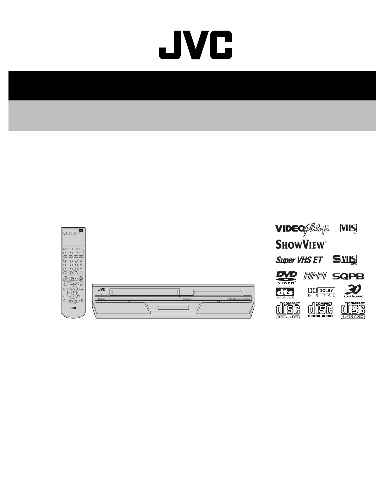
(3) It solders to two short circuit sections on the substrate of a pick-up.
(4) After removing the flexible wire from the connector (CN101
(5) Short-circuit the laser diode by soldering the land which is provided at the center of the flexible wire for the pickup.
After completing the repair, remove the solder to open the circuit.
), short-circuit the flexible wire by the metal clip.
Pick-up
Short circuit
* Please refer to the SECTION3 DISASSEMBLY method for details.
CN101
DVD SERVO CONTROL BOARD
(No.YD002)1-7
Page 4

SECTION 2
SPECIFIC SERVICE INSTRUCTIONS
2.1 Different table of feature
The following table indicates main different points between models HR-XV3EK, HR-XV31EK,HR-XV32EK, HR-XV3EX, HR-XV31EX,
HR-XVS30EK, and HR-XVS30EX.
HR-XV3EK HR-XV31EK HR-XV32EK HR-XV3EX HR-XV31EX HR-XVS30EK HR-XVS30EX
POWER PLUG 3PIN
BODY COLOR PURE SILVER
FRONT PANEL
COVER
REMOCON
COLOUR
VHS PAL/NTSC PB
S-VHS NOT USED
S-VHS ET NOT USED ←←←←USED ←
SQPB USED ←←←←NOT USED ←
RECORDING &
PLAYBACK SPEED
FRONT INPUT VIDEO,AUDIO
REAR L-1 INPUT SCART IN /
COMPORNENT
VIDEO OUT
BROADCASTING
STANDARD
STEREO
DECODER
RF OUT CH/RF OUT
SYSTEM[INITIAL]
VCR PLUS+ VIDEOPLUS+ ←←SHOWVIEW ← VIDEOPLUS+ SHOWVIEW
VPS/PDC NOT USED
OSD LANGUAGES VCR:ENGLISH
WMA(CD-R/RW) NOT USED
ILLUMINATION
COLOR
USED NOT USED USED ← NOT USED USED ←
GRAY ← BLACK GRAY ←←←
on PAL TV with
HiFi
SP/LP ←←←←SP/LP/EP ←
(L/R)
OUT(RGB)
NOT USED ←←←←DVD:Y/Pb/Pr ←
I ←←B/G,D/K ← I B/G,D/K
NICAM ←←NICAM/A2 ← NICAM NICAM/A2
22-69CH,OFF
[AUTO]/I
DVD:ENGLISH/
FRENCH/
GERMANY
BLUE NOT USED BLUE ← NOT USED BLUE ←
←←CEE ← 3PIN CEE
← BLACK PURE SILVER ←←←
←←PAL/MESECAM
(MANUAL) /
NTSC PB on
PAL TV with HiFi
← PAL/NTSC PB
on PAL TV with
HiFi
PAL/MESECAM
(MANUAL) /
NTSC PB on
PAL TV with HiFi
←←←←USED ←
←←←←S-VIDEO,
VIDEO,AUDIO
(L/R)
←←←←SCART IN / OUT
(Y/C,RGB)
←←22-69CH,OFF
[AUTO]/G,K
← 22-69CH,OFF
[AUTO]/I
←
←
22-69CH,OFF
[AUTO]/G,K
←←USED ← NOT USED USED
←←VCR:13
LANGUAGES
DVD:ENGLISH/
FRENCH/
GERMANY
← VCR:ENGLISH
DVD:ENGLISH/
FRENCH/
GERMANY
VCR:13
LANGUAGES
DVD:ENGLISH/
FRENCH/
GERMANY
←←←←USED ←
NOTE :
Mark ← is same as left.
1-8 (No.YD002)
Page 5
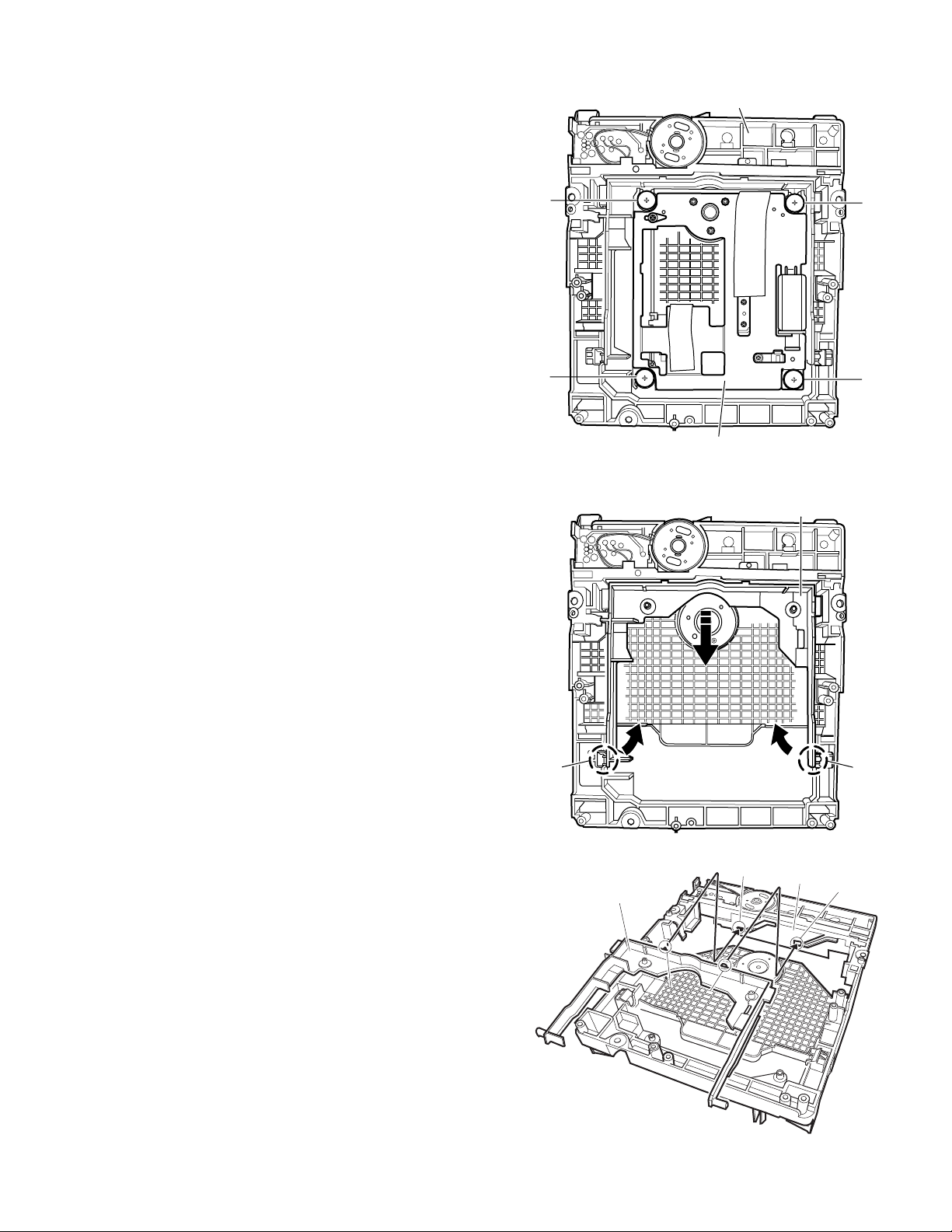
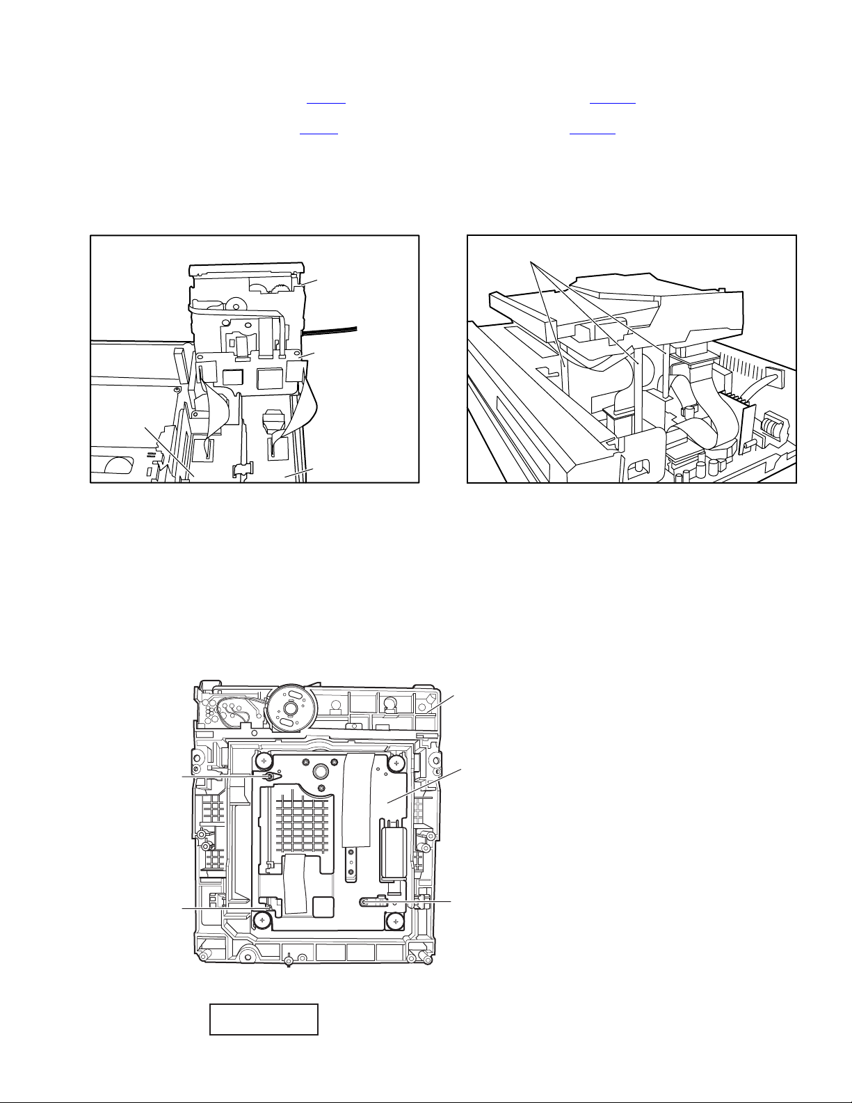
2.2 Service position
This unit has been designed so that the Mechanism an d Main
board assemblies can be removed together from the bottom
chassis. Before diagnosing or servicing the circuit boards, take
out the major parts from the bottom chassis.
2.2.1 How to set the "Service position"
(1) Refer to the disassembly procedure and perform the disas-
sembly of the major parts before removing the Mechanism
assembly.
(2) Remove the screws that fix the Mechanism, Regulator
board assembly to the bottom chassis. If any other screws
are used to fix the boards, remove them also.
(3) Remove the combined Mechanism,Regulator borad and
Main board assemblies.
(4) If any other major parts are used, remove them also.
(5) Connect the wires an d connectors of the major parts that
have been removed in steps (1) to (4). (Refer to Fig. 2-2a.)
(6) Place the combined Mechanism, Main board and other
board assemblies upside down.
(7) Insert the power cord plug into the power outlet and then
proceed with the diagnostics and servicing of the board as-
sembly.
Notes:
• Before inserting the power cord plug into the power out-
let, make sure that none of the electrical parts are able
to short-circuit between the workbench and the board
assembly.
• For the disassembly procedure of the major par ts and
details of the precautions to be taken, see "Removing
the major parts".
• If there are wire connections from the Main board an d
Mechanism assemblies to the other major parts, be sure
to remove them (including wires connected to the major
parts) first before performing step (2).
• When carrying out diagnosis and repair of the Main
board assembly in the "Service position", be sure to
ground both the Main board and Mechanism assemblies. If they are improperly grounded, there may be
noise on the playback picture or FDP counter display
may move even when the mechanism is kept in an inoperative status.
• In order to diagnose the playback or recording of the
cassette tape, set the Mechanism assembly to the required mode before placing it upside do wn. If the mechanism mode is changed (including ejection) while it is in
an upside down position the tape inside may be damaged.
• For some models, the mechanism and board assem-
blies are attached by connectors only. When carrying
out a diagnosis or repair of the boards in the "Service
position", make sure that the connectors are not disconnected.
Regulator board assembly
TP111 D.FF
TP4001 CTL.P
TP106 PB FM
TP2253 A.PB FM
TP2254 A.REC FM
Display board assembly
Main board assembly
Jack board assembly
Fig.2-2a
2.3 Jig RCU mode
This unit uses the following two modes for receiving remote control codes.
(1) User RCU mode:Ordinary mode for use by the user.
(2) Jig RCU mode: Mode for use in production and servicing.
When using the Jig RCU, it is required to set th e VCR to the Jig
RCU mode (the mode in which codes from the Jig RCU can be
received). As both of the above two modes are stored in the EEPROM, it is required to set the VCR back to the User RCU mode
each time that an adjustment is made or to check that the necessary operations have been completed.These modes can be set
by the operations described below.
Note:
• Confirm the RCU mode when exchanged parts. Since
some SERVICE PARTS sets the VCR to the Jig RCU
mode as initial setting. Therefore please set the VCR to
the user RCU mode after replacing the EEPROM.
User RCU mode
CH
Jig RCU mode
CH
(ޓnot displayed)
Fig.2-3a User/Jig RCU mode
2.3.1 Setting the Jig RCU mode
(1) Turn on the power.
(2) Press the following remocon keys continuously within 2
seconds " SET UP MENU " → " 2 " → " 8 " → " OK ".
When the VCR is set to the Jig RCU mode, the symbols
( " : " ) in the time display of the FDP are turned off.
(Refer to Fig.2-3a)
(No.YD002)1-9
Page 6
2.3.2 Setting the User RCU mode
(1) Turn off the power.
(2) Press the "REC" and "PAUSE" buttons of the VCR si mul-
taneously. Alternatively, transmit the code "80" from the Jig
RCU.
2.4 Mechanism service mode
This model has a unique function to enter the mechanism into every operation mode without loading of any cassette tape. This
function is called the "Mechanism service mode".
2.4.1 How to set the "Mechanism service mode"
(1) Set the VCR to the Jig RCU mode (the mode in which
codes from the Jig RCU can be received)
(2) Transmit the code "E5" from the Jig RCU.
(3) Release the lug of th e Cassette holder and then slid e the
Cassette holder toward the direction where the Cassette
holder is loaded by manually.
(4) The cassette holder lowers and, when the loading has
completed, the mechanism enters the desired mode.
When the VCR is set to the Mechanism service mode, the
symbols ("Timer") in the FDP (LED) are blinked.
2.4.2 How to exit from the "Mechanism service mode"
(1) Unplug the power cord plug from the power outlet.
2.5 Maintenance and inspection
2.5.1 Cleaning
Regular cleaning of the transport system parts is desirable but
practically impossible. So make it a rule to carry out cleaning of
the tape transport system whenever the machine is serviced.
When the video head, tape guide and/or brush get soiled, the
playback picture may appear inferior or at worst disappear, resulting in possible tape damage.
Note:
• Absolutely avoid sweeping the upper drum vertically as
this will cause damage to the video head.
(1) When cleaning the upper drum (especially the video head),
soak a piece of closely woven cloth with alcohol and while
holding the cloth onto the upper drum by the fingers, turn
the upper drum counterclockwise.
(2) To clean the parts of the tap e transport system other than
the upper drum, use a piece of closely woven cloth or a cot-
ton swab soaked with alcohol.
(3) After cleaning, make sure that the cleaned parts are com-
pletely dry before using the cassette tape.
2.5.2 Lubrication
With no need for periodical lubrication, you have only to lubricate
new parts after replacement. If any oil or grease on contact parts
is soiled, wipe it off and newly lubricate the parts.
Note:
• See the "mechanism assembly" diagram of the "parts
list" for the lubricating or greasing spots, and for the
types of oil or grease to be used.
2.5.3 Suggested servicing schedule for main components
The following table indicates the suggested perio d for such service measures as cleaning, lubrication and replacement. In practice, the indicated periods will vary widely according to
environmental and usage conditions. However, the indicated
components should be inspected when a set is b rought for service and the maintenance work performed if necessary. Also
note that rubber parts may deform in time, even if the set is not
used.
System Parts name
Operation hours
1000H 2000H
Drum assembly C,X X
A/C head C,X C,X
Pinch roller arm assembly C C
Tape
transport
Full erase head C C
Tension arm assembly C C
Capstan motor (Shaft) C C
Guide arm assembly C C
Capstan motor X
Capstan brake assembly X
Main brake assembly X
Drive
Belt (Capstan) X X
Loading motor X
Clutch unit X
Worm gear X
Control plate X
Other Rotary encoder X
C : Cleaning
X : Inspection or Replacement if necessary
1-10 (No.YD002)
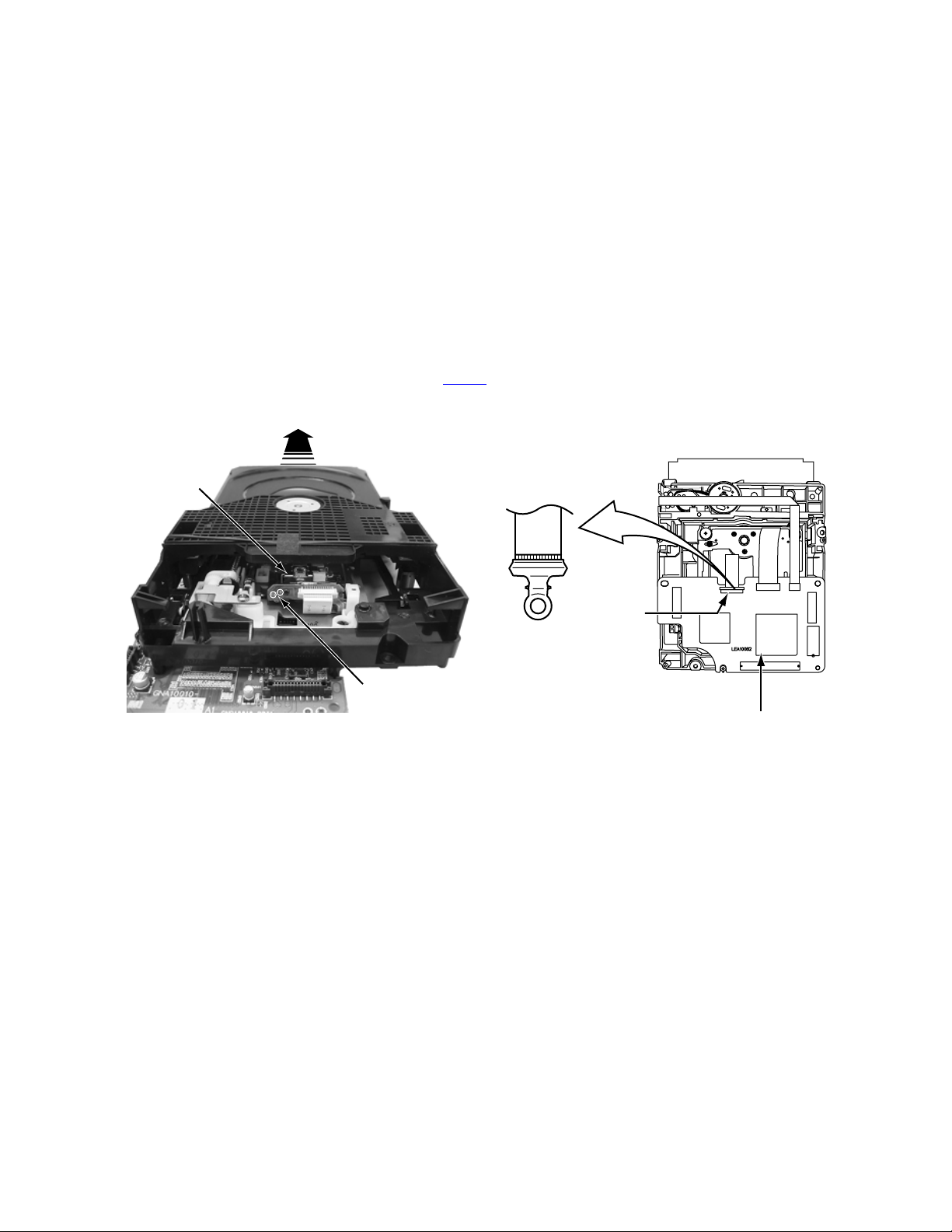
A/C head
Video heads
Fig.2-6a
Page 7
SECTION 3
DISASSEMBLY
3.1 Removing the major parts
3.1.1 Destination of connectors
Two kinds of double-arrows in connection tables respectively
show kinds of connector/wires.
: The connector of the side to remove
CONN. No. PIN No.CONNECTOR
WR2a
WR2b
Main CN101
Main CN103
Destination of connectors
CONN. No. PIN No.CONNECTOR
WR2a
WR2b
WR2c
WR3a
WR3b
CN5302
(CN501)
CN7301
(CN502)
WR6a
WR6b
Main
Main
Main
Main
Drum
assembly
Regulator
Main
Regulator
Regulator
3.1.2 How to read the procedure table
This table shows the steps for disassembly of the externally furnished parts and board assemblies. Reverse these steps when
re-assembling them.
Step/
Loc No.
[1] Top cover 3-1a
Part Name
Bracket 2(S1c)
: Wire: Flat wire : Board to board (B-B)
Digital CN761
Digital CN762
CN7104
CN3102
CN3103
CN2001
CN5302
CN7301
CN5303
CN5301
Jack
Display
Display
A/C head
Main
DVD
servo control
DVD
servo control
Main
Main
Fig.
No.
4(S1a),(S1b),3(L1a), <Note 1a>
2(SD1a),(P1a),(W1a),
CN1(WR1a),
----------------------------------------
CN7191
CN7003
CN7004
CN1
CN501
CN502
CN5313
CN5311
Point Note
40
10
11
14
14
6
9
22
22
11
11
3.1.3 Disassembly procedure
Step/
Loc No.
[1]
[2]
[3]
[4]
[5]
[6]
[7]
Part Name
Top cover
Front panel assembly
(Display board assembly)
(Jack board assembly)
Mechanism assembly
(Drum assembly)
(Inertia plate)
(Roller arm assembly)
DVD unit
(Bracket)
Rear cover
Regulator board assembly
Main board assembly
Fig.
No.
3-1d
3-1a
3-1d
3-1b
3-1c
3-1d
3-1d
3-1d
3-1d
3-1d
Point Note
6(S1a)
4(L2a),5(L2b),2(S2a)
CN7104(WR2a),
CN3102(WR2b),
CN3103(WR2c),
CN2001(WR3a)
3(S3a),(S3b)
--------------------------
CN(WR3b)
(S3c),(S3d),(S3e)
--------------------------
4(L3a)
--------------------------
(P3a),(L3b)
3(S4a),(L4a),(S4b)
2(S4c),CN5302(CN501)
CN7301(CN502)
7(S5a),(S5b),3(L5a)
3(S6a)
CN5303(WR6a),
CN5301(WR6b)
2(S7a)
<Note 2a>
<Note 2b>
<Note 2a>
<Note 3a>
<Note 3b>
<Note 3c>
<Note 2a>
<Note 2a>
• Be careful not to damage the connector and wire etc. during
connection and disconnection.
• When connecting the flat wire to the connector, be careful with
the flat wire direction.
<Note 2b>
• When reattaching the Front panel assembly, make sure that
the door opener of the Side frame (R) is lowered in position prior to the reinstallation.
• When reattaching the Front panel assembly, pay careful attention
to the switch lever of the Front panel assembly not to make it
touch the switch knob of the Main board assembly from the side.
• When reattaching the Front pa nel assembly, lift the Ca ssette
door slightly.
(1) (2) (3) (4) (5)
(1) Order of steps in Procedure
When reassembling, perform the step(s) in the reverse order.
These numbers are also used as the identification (loca-
tion) No. of parts Figures.
(2) Part name to be removed or installed.
(3) Fig. No. showing procedure or part location.
(4) Identification of part to be removed, unhooked, un locked,
released, unplugged, unclamped or unsoldered.
P= Spring, W= Washer, S= Screw, L= Locking tab, SD=
Solder, CN**(WR**)= Remove the wire (WR**) from the
connector (CN**).
Note:
• The bracketed ( ) WR of the connector symbol are
assigned nos. in priority order and do not correspond to those on the spare parts list.
(5) Adjustment information for installation
Door
opener
Side
frame(R)
Switch
knob
Switch
lever
Fig.3-1a
<Note 3a>
• When reattaching the Mechanism assembly, secure the
screws (S3a to S3b) in the order of 1,2,3.
<Note 3b>
• When reattaching the Mechanism assembly, b e sure to align
the phase of the Rotary encoder on the Main board assembly.
• When reattaching the Mechanism assembly, set the “Mechanism assembling mode”. [See “MECHANISM ASSEMBLY
SERVICE MANUAL (No. 86700)”.]
• When reattaching the Mechanism assembly to the Main board
assembly, take care not to damage the sensors and switch on
the Main board assembly.
(No.YD002)1-11
Page 8
<Note 3c>
• When reattaching the Drum assembly, secure the screws (S3c
to S3e) in the order of c, d, e.
Mechanism
assembly
(S3d)
(S3c)
(S3e)
(S3d)
(S3e)
Drum
assembly
<Note 3c>
<NOTE>
Attach the Drum assembly appropriately,
since the installation state of the Drum assembly
influences the FM WAVEFORM LINEARITY
greatly.
(S3c)
HOOK
Fig.3-1b
• When handling the drum assembly alone, hold it by the motor
or shaft. Be careful not to touch other parts, especially the video heads. Also take care not to damage the connectors.
Shaft
Motor
Video heads
Fig.3-1c
1-12 (No.YD002)
Page 9
HOLD PART OF ROLLER ARM ASS'Y
WHILE ATTACHING INERTIA PLATE.
INERTIA PLATE SHOULD BE ATTACHED
SO AS TO SER SMALL DIAMETER OF
CENTRAL ROUND HOLE ABOVE.
POSITION ROLLER'S INSTALLATION
HOLE IN THE "A" PART.
INSERT ROLLER UNTIL THE "b"
PART OF ROLLER'S HOOK IOCK
UP TO THE "B" PART.
HITCH THE "c" PART OF SPRING
TO THE "C" PART.
(L3a)
"C"
"A"
Roller arm assembly
(P3a)"c"
(L3b)"b"
"B"
[3]Inertia plate
[3]Roller arm assembly
(S1a)
[1]Top cover
(S1a)
(S1a)
(L2b)
Cassete door
<Note2b>
[3] Mechanism assembly
(S3a)
3
(S7a)
[7]Main board assembly
(L2a)
(S3a)
1
f
(S2a)
(L2a)
[2]Front panel assembly
f
(S3c)
(S3d)
(S1a)
[3]Drum assembly
(S3a)
2
b
(S3b)
(L5a)
(S5a)
(S5a)
(S5b)
(S5a)
(S5a)
(S5a)
(S5a)
(S5a)
(S3e)
(S7a)
Terminal board assembly
2D Digital board assembly
<Phase alignment>
.
Accord the position of V gap on R.ENCORDER and PWB silk
.
Accord the position of Boss on R.ENCORDER and PWB silk
JS3001JS3001
(L5a)
(S4b)
(S4a)
[5]Rear cover
(L5a)
(S4a)
[4]DVD unit
(S4c)
CN7301
(S4a)
(L4a)
[4]Bracket
CN502
DVD servo control board assembly
CN501
(S6a)
CN5302
(S4c)
(S6a)
(S6a)
[6]Regulator board assembly
Jack board assembly
CN7191
(WR2a)
<Note2a>
(L2b)
Bottom side
Top side
(L2b)
(WR2b)
<Note2b>
Display board assembly
(WR2c)
<Note2b>
CN7004
CN7003
Jack board assembly
Fig.3-1d
CN7104
CN7191
(WR3b)
<Note2b>
CN2001
(WR3a)
<Note2b>
CN3102
CN5001
(WR6a)
<Note2b>
CN5303 CN5301
CN5311CN5313
(WR6b)
<Note2b>
CN3103
A
(No.YD002)1-13
Page 10
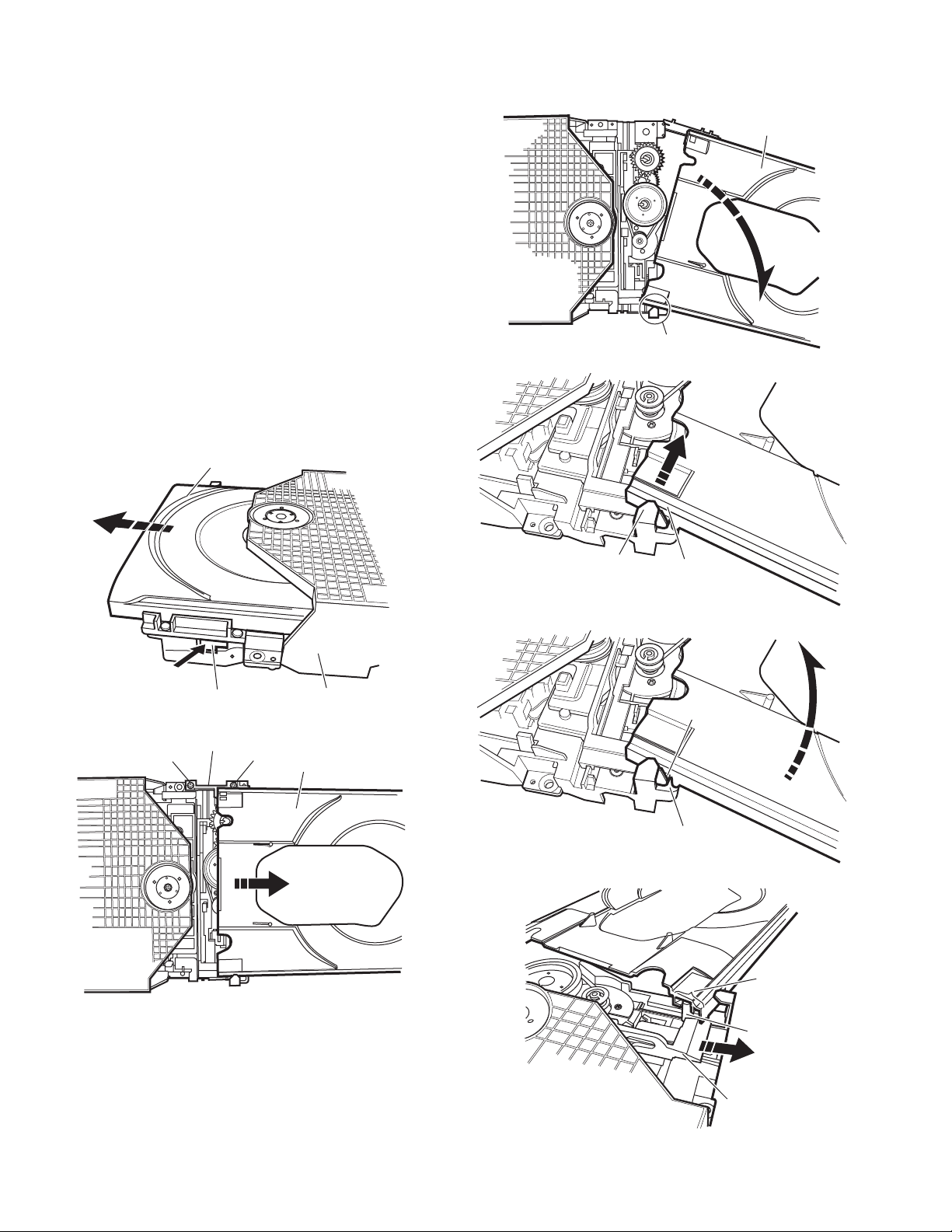
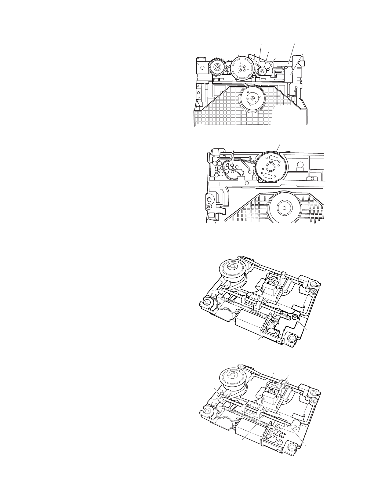
3.2 Loading mechanism assembly
Projection of the tray
3.2.1 Removing the tray (See Figure 3-2a, Figure 3-2b, Figure 3-2c, Figure 3-2d, Figure 3-2e, Figure 3-2f)
(1) Push a of the slide ca m on the ho le in the right side of the
loading base by using a driver until it stops. (See Figure 32a.)
(2) The tray comes out. Pull the tray in a front direction until it
stops.
(3) Remove the two screws A attaching the slide bracket. (See
Figure 3-2b.)
(4) Tilt the tray in a directi on of the arrow around the point in
the left rear part of the tray. (See Figure 3-2c.)
(5) The rail of the tray is removed from b of the loading base.
Then, remove the tray upward. (See Figure 3-2d.)
Attaching the tray:
Engage c of the loading base to the projection of the tray while
tilting the tray to the left. Turn the tray in a direction of the arrow, and attach the slide bracket. (See Figure 3-2e.)
Note:
Prior to the procedure above, move the slide cam in a direction
of the arrow so that d of the slide cam can be inserted in e of
the tray. (See Figure 3-2f.)
Tray
The point in the left rear part
Fig.3-2c
Tray
Push
Slide cam part a
Slide bracket
A
Fig.3-2a
Fig.3-2b
A
Loading base
Tray
Loading base part b
Rail of the tray
Fig.3-2d
Projection of the tray
Loading base part c
Fig.3-2e
Part e
1-14 (No.YD002)
Part d
Slide cam
Fig.3-2f
Page 11
3.2.2 Removing the traverse mechanism assembly (See Figure 3-2g)
f
Shaft
Reverse the loading mechanism assembly. Remove the four
screws B attaching the traverse mechanism assembly. Remove
the traverse mechanism assembly upward.
Loading mechanism assembly
3.2.3 Removing the elevator (See Figure 3-2h and Figure 3-2j)
• Prior to the following procedure, remove the traverse mechanism assembly.
(1) Remove the two arms of the el evator from the two parts f
by moving the arms in a direction of the arrow.
(2) Pull out the elevator in a rear direction.
Attaching the elevator:
Engage the two holes g to the two shafts on the front part of
the elevator. And then, attach the elevator.
B
B
B
B
Traverse mechanism assembly
Fig.3-2g
Elevator
Part f
Fig.3-2h
g
Slide cam
Elevator
Shaft
Fig.3-2j
(No.YD002)1-15
Part
g
Page 12
3.2.4 Removing the loading motor (See Figure 3-2k and Figure 3-2l)
• Prior to the following procedure, remove the tray, the traverse
mechanism assembly, and the elevator.
(1) Remove the belt from the pulley.
(2) Remove two screws C attaching the loading motor.
(3) Remove two solders h on the switch board.
Switch board
Pulley
Part h
Belt
Pulley
C
Fig.3-2k
Loading base
Slide cam
C
Loading motor
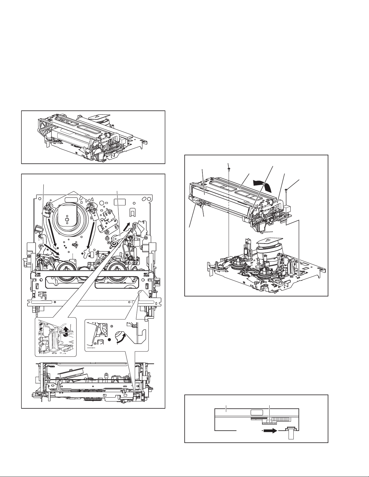
3.3 Traverse mechanism assembly
3.3.1 Removing the pickup (See Figure 3-3a, Figure 3-3b)
• Prior to the following procedure, remove the traverse mechanism assembly.
(1) Remove one screw D attaching the plate.
(2) Remove the plate and the leaf spring.
(3) Lift i of the shaft 1, and pull out the shaft 1 from j.
(4) Remove k of the pickup from the shaft 2.
Attaching the pickup:
(1) Engage k of the pickup to the shaft 2.
(2) Insert the shaft 1 in j, and attach the shaft 1 to i.
(3) Attach the leaf spring, and then a ttach the p late. Fix the
leaf spring and the plate by using the screw D.
Fig.3-2l
D
Leaf spring
Plate
Fig.3-3a
Shaft 2
Part k
Part j
1-16 (No.YD002)
Shaft 1
Part i
Fig.3-3b
Page 13
SECTION 4
ADJUSTMENT
4.1 Before adjustment
4.1.1 Precaution
• The adjustments of this unit include the mechanism com-
patibility and electrical adjustments. During the performance of this work, be sure to observe the precautions for
each type of adjustment.
• If there is a reference to a signal input method in the signal
column of the adjustment chart, “Ext. S-input” means the
Y/C separated video signal and “Ext. input” means the
composite video signal input.
• Unless otherwise specified, all measuring points and
adjustment parts are located on the Main board.
4.1.2 Required test equipments
• Color (colour) television or monitor
• Oscilloscope: wide-band, dual-trace, triggered delayed sweep
• Signal generator: RF / IF sweep / marker
• Signal generator: stairstep, color (colour) bar [PAL]
• Recording tape
• Digit-key remote controller(provided)
4.1.3 Required adjustment tools
: Used --- : Not used
Mechanism
compatibility
adjustment
Roller driver
Jig RCU ---
Back tension cassette gauge ---
Alignment tape(MHPE) ---
Alignment tape(MHPE-L)
Alignment tape(MHP-L)
Roller driver
PTU94002
Jig RCU
PTU94023B
---
Back tension cassette gauge
Electrical
adjustment
---
PUJ48076-2
4.1.4 Color (colour) bar signal,Color (colour) bar pattern
Colour bar signal [PAL]
White(100%)
White(75%)
0.7 V
1V
0.3 V
Horizontal sync
Yellow
Cyan
Green
Magenta
Red
VU
V(R-Y)
U(B-Y)
Blue
Burst
Colour bar pattern [PAL]
(75%)
Cyan
White
Yellow
0.3 V
V
White
U Black
100%
Green
Magenta
Red
Blue
4.1.5 Switch settings
When adjusting this unit, set the VCR mode and switches
as described below.
• When using the Jig RCU, it is required to set the VCR to the
Jig RCU mode. (See "SECTION 2 SPECIFIC SERVICE INSTRUCTIONS")
Jig RCU
[Data transmitting method]
Depress the " "( 3 ) button
after the data code is set.
CUSTOM CODE
43: A CODE
DATA CODE
INITIAL MODE
Fig.4-1a Jig RCU [PTU94023B]
• Set the switches as shown below unless otherwise specified
on the relevant adjustment chart. The switches that are not listed below can be set as desired.
If the VCR is not equipped with the functions detailed below ,
setup is not required.
AUTO PICTURE/VIDEO CALIBRATION/
B.E.S.T./D.S.P.C.
PICTURE CONTROL/SMART PICTURE NORMAL/NATURAL
VIDEO STABILIZER OFF
TBC ON
Digital 3R ON
VIDEO NAVIGATION/TAPE MANAGER OFF
BLUE BACK OFF
OFF
Alignment tape
(SP, stairstep, PAL)
MHPE
CD-DA test disc
CTS-1000
Alignment tape
(LP, stairstep, PAL)
MHPE-L
DVD test disc
VT-501
4.1.6 Manual tracking mode (Auto tracking ON/OFF) set-
ting
(1) In order to set to the manual tracking mode during ta pe
playback, press the “SP/EP(LP)”button on the remote control unit.
• Each press of the button switches the auto tracking ON
or OFF.
• When the manual tracking mode is set, the tracking is
placed at the center position.
(2) Press “channel +/-” to adjust the tracking manually.
(No.YD002)1-17
Page 14
4.1.7 EVR Adjustment
Some of the electrical adjustments require the adjustment performed by the EVR system. The main unit have EEPROMs for
storing the EVR adjustment data and user setups.
Notes:
• In the EVR adjustment mode, the value is varied with the
channel buttons (+, –). The adjusted data is stored when
the setting mode changes (from PB to STOP, when the
tape speed is changed, etc.). Take care to identify the
current mode of each adjustment item when making an
adjustment.
• When changing the address setting in the EVR adju st-
ment mode, use the Jig RCU or the remote controller
having numeric keypad with which a numeric code can
be directly input.
The remote control code of the Jig RCU corresponds to
each of the digit keys on the remote controller as follows.
Digit-key0123456789
Code 20 21 22 23 24 25 26 27 28 29
• As the counter indication and remaining tape indication
are not displayed FDP during the EVR adjustment
mode, check them on the TV monitor screen.
• When performing the EVR adjustment, confirm th at the
FDP indication is changed to the EVR mode, as shown
below.
FDP
Fig.4-1b EVR mode
4.2 Mechanism compatibility adjustment [VHS SECTION]
Notes:
• Although compatibility adjustment is very important, it
is not necessary to perform this as part of the normal
servicing work. It will be required when you have replaced the A/C head, drum assembly or any pa rt of the
tape transport system.
• To prevent damaging the alignment tape in the compatibil-
ity adjustment, prepare a cassette tape (for self-recording/
playback), perform a test on it by transporting it and making sure that the tape is not bent by the tape transport
mechanisms such as in the guide rollers.(See Fig.4-2b.)
4.2.1 Tension pole position
Notes:
• This adjustment must be performed every time the ten-
sion band is replaced.
Signal (A) • Back tension cassette gauge [PUJ48076-2]
Mode (B1)
Adjustment part (F) • Adjust pin [Mechansim assembly]
Specified value (G) • 25 - 51 gfcm (2.45 - 5 x 10
(B2)
•PB
• Eject end
-
3
Nm)
(1) Play back the back tension cassette gauge (A).
(2) Check that the indicated value on the left side gauge is
within the specified value (G).
(3) If the indicated value is not within the specified value (G),
perform the adjustment in a following procedure.(See
Fig.4-2a.)
a) Remove the top frame, cassette holder and side
frames (L/R) all together. (refer to the SERVICE
MANUAL No.86700 [MECHANISM ASSEMBLY].)
b) Rotate the loading motor gear to move the control
plate so that the triangular stamping to the left of the
“P”stamping is aligned with the stamping (a) on the
main deck. This positioning is mode (B1).
c) Adjust by turning the adjustment pin so th at th e ti p of
the tension arm is aligned with the stamping (b) on
the main deck.
d) Rotate the reel di sk (S) by about one turn clockwise
and make sure that the round hole of the adjustment
pin is located in the “OK” range. If it is outside this
range, restart the adjustment from the beginning.
After completion of the adjustment, rotate the loading gear
motor to return it to the mode (B2) position.
1-18 (No.YD002)
TENSION ARM
Stamping(b)
OK
ADJUST PIN
CONTROL PLATE
Stamping(a)
NG
Fig.4-2a
Page 15
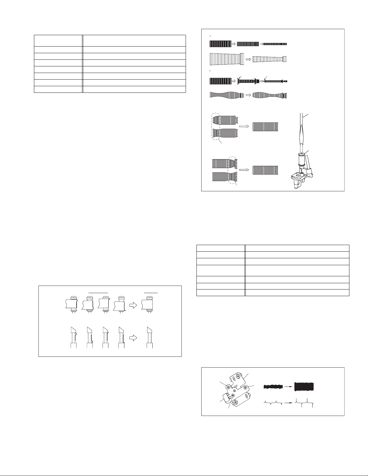
4.2.2 FM waveform linearity
Signal (A1)
Mode (B) • PB
Equipment (C) • Oscilloscope
Measuring point (D) • TP106 (PB. FM)
External trigger (E) • TP111 (D.FF)
Adjustment part (F) • Guide roller [Mechanism assembly]
Specified value (G) • Flat V.PB FM waveform
Adjustment tool (H) • Roller driver [PTU94002]
• Alignment tape(SP, stairstep, PAL) [MHPE]
(A2)
• Alignment tape(LP, stairstep, PAL) [MHPE-L]
(1) Play back the alignment tape (A1).
(2) Apply the external trigger signal to D.FF (E), to observe
the V.PB FM waveform at the measuring point (D).
(3) Set the VCR to the manual tracking mode.
(4) Make sure that there is no significant level drop of the V.PB
FM waveform caused by the tracking operation, with its
generally parallel and linear variation ensured. Perform the
following adjustments when required. (See Fig. 4-2c.)
(5) Reduce the V.PB FM waveform by th e tracking operation.
If a drop in level is found on the left side, turn the guide roll-
er of the pole base assembly (supply side) with the roller
driver to make the V.PB FM waveform linear.
If a drop in level is on the right side, likewise turn the guide
roller of the pole base assembly (take-up side) with the
roller driver to make it linear. (See Fig. 4-2c.)
(6) Make sure that the V.PB FM waveform varies in parallel
and linearly with the tracking operation again. When re-
quired, perform fine-adjustment of the guide roller of the
pole base assembly (supply or take-up side).
(7) Unload the cassette tape once, play back the alignment
tape (A1) again and confirm the V.PB FM waveform.
(8) After adjustment, confirm that the tape wrinkling does not
occur at the roller upper or lower limits. (See Fig. 4-2b.)
[Perform adjustment step (9) only for the models equipped
with SP mode and EP (or LP) mode.]
[Perform adjustment step (9) only for the models
equipped with SP mode and EP (or LP) mode.]
(9) Repeat steps (1) to (8) by using the alignment tape (A2).
Improper
(a)
GUIDE ROLLER
(b)
GUIDE POLE
Proper
Fig.4-2b
Proper waveform variation
Improper waveform variation
A
C
Up Down
B
D
Roller driver
Guide roller
(supply side)
Fig.4-2c
4.2.3 Height and tilt of the A/C head
Note:
• Set a temporary level of the height of the A/C head in ad-
vance to make the adjustment easier after the A/C head
has been replaced. (Refer to the SERVICE MANUAL
No.86700 [MECHANISM ASSEMBLY].)
Signal (A) • Alignment tape(SP, stairstep, PAL) [MHPE]
Mode (B) • PB
Equipment (C) • Oscilloscope
Measuring point (D1)
External trigger (E) • TP111 (D.FF)
Adjustment part (F) • A/C head [Mechanism assembly]
Specified value (G) • Maximum waveform
• AUDIO OUT terminal
(D2)
• TP4001 (CTL. P)
(1) Play back the alignment tape (A).
(2) Apply the external trigger signal to D.FF (E), to observe the
AUDIO OUT waveform and Control pulse waveform at the
measuring points (D1) and (D2) in the ALT mode.
(3) Set the VCR to the manual tracking mode.
(4) Adjust the AUDIO OUT waveform and Control pulse wave-
form by turning the screws (1), (2) and (3) little by little until
both waveforms reach maximum. The screw (1)
and (3) are for adjustment of tilt and the screw (2) for azi-
muth.
Head base
(2)
(1)
AUDIO OUT
A/C head
CTL. P
(3)
Fig.4-2d
(No.YD002)1-19
Page 16
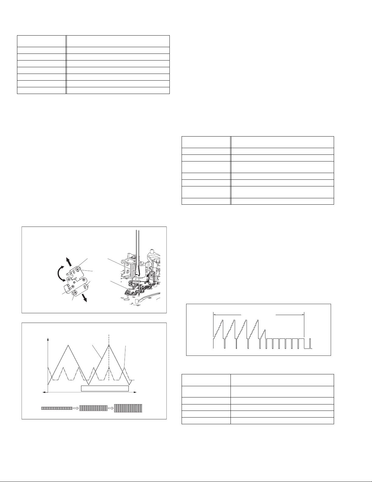
4.2.4 A/C head phase (X-value)
Signal (A1)
Mode (B) • PB
Equipment (C) • Oscilloscope
Measuring point (D) • TP106 (PB. FM)
External trigger (E) • TP111 (D.FF)
Adjustment part (F) • A/C head base [Mechanism assembly]
Specified value (G) • Flat V.PB FM waveform
Adjustment tool (H) • Roller driver [PTU94002]
• Alignment tape(SP, stairstep, PAL) [MHPE]
(A2)
• Alignment tape(LP,stairstep,PAL) [MHPE-L]
(1) Play back the alignment tape (A1).
(2) Apply the external trigger signal to D.FF (E), to observe the
V.PB FM waveform at the measuring point (D).
(3) Set the VCR to the manual tracking mode.
(4) Loosen the screws (4) and (5), then set the Roller driver to
the innermost projected part of the A/C head. (See Fig. 4-
2e.)
(5) Rotate the roller driver so that the A/C head comes closest
to the capstan. From there, move the A/C head back grad-
ually toward the drum until the point where the FM wave-
form is maximized for the second time, and then
tighten the screws (4) and (5) temporarily.
(6) Play an alignment tape (A2) and set to the manual-tracking
mode.
(7) Fine-adjust A/C head base position to maximize the FM
waveform, and then tighten the screws (4) and (5) firmly.
(8) Play alignment tapes (A1) and (A2) and confirm that the FM
waveforms are maximized when the tracking is at the cen-
ter position.
To the drum
Toward the capstan
Toward the drum
A/C head
Screw (5)
Roller driver
Screw (4)
Head base
To the capstan
Fig.4-2e
Alignment tape
[SP, stairstep]
played with the
SP head
Waveform output
X-value adjustment point
Drum side Control head position Capstan side
Alignment tape
[EP(LP), stairstep]
played with the
EP(LP) head
Maximum
Fig.4-2f
4.3 Electrical adjustment [VHS SECTION]
Note:
The following adjustment procedures are not only necessary
after replacement of consumable mechanical parts or board
assemblies, but are also provided as references to be referred
to when servicing the electrical circuitry.
In case of trouble with the electrical circuitry, always begin a
service by identifying the defective points by using the measuring instruments as described in the following electrical adjustment procedures. After this, proceed to the repair,
replacement and/or adjustment. If the required measuring instruments are not available in the field, do not change the adjustment parts (variable resistor, etc.) carelessly.
4.3.1 Servo circuit
4.3.1.1 Switching point
Signal (A1)
Mode (B) • PB
Equipment (C) • Oscilloscope
Measuring point (D) • VIDEO OUT terminal (75 ohm terminated)
External trigger (E) • TP111 (D.FF)
Adjustment part (F) • Jig RCU: Code “5A”
Specified value (G) • 6.5±0.5H (VHS models)
Adjustment tool (H) • Jig RCU [PTU94023B]
• Stairstep signal
(A2)
• Alignment tape(LP,stairstep,PAL) [MHPE-L]
• TP106 (PB. FM)
• 7.5±0.5H (S-VHS models)
(1) Play back the signal (A1) of the alignment tape (A2).
(2) Apply the external trigger signal to D.FF (E) to observe the
VIDEO OUT waveform and V.PB FM waveform at the mea-
suring points (D1) and (D2).
(3) Set the VCR to the manual tracking mode.
(4) Adjust tracking so that the V.PB FM waveform becomes
maximum.
(5) Set the VCR to the Auto adjust mode by transmitting the
code (F) from the Jig RCU. When the VCR enters the stop
mode, the adjustment is completed.
(6) If the VCR enters the eject mode, repeat steps (1) to (5)
again.
(7) Play back the alignment tape (A2) a gain, confirm that the
switching point is the specified value (G).
Trigger point
Switching point
V.sync
V. rate
Fig.4-3a Switching point
4.3.1.2 Slow tracking preset
Signal (A1)
Mode (B1)
Measuring point (D) • TV-Monitor
Adjustment part (F) • Jig RCU: Code “71”or “72”
Specified value (G) • minimum noise
Adjustment tool (H) • Jig RCU [PTU94023B]
• Ext. input
(A2)
• Color (colour) bar signal [PAL]
• VHS SP
(B2)
•VHS LP
1-20 (No.YD002)
Page 17
(1) Record the signal (A2) in the mode (B1), and play back
the recorded signal.
(2) Set the VCR to the manual tracking mode.
(3) Set the VCR to the FWD slow (+1/6x) mode.
(4) Transmit the code (F) from the Jig RCU to adjust so that the
noise bar becomes the specified value (G) on the TV
monitor in the slow mode.
(5) Set the VCR to the Stop mode.
(6) Confirm that the noise bar is (G) on the TV monitor in the
slow mode.
(7) Repeat steps (3) to (6) in the REV slow (-1/6x) mode.
(8) Repeat steps (1) to (7) in the mode (B2).
Note:
• For FWD slow (+1/6x) playback, transmit the code “08”
from the Jig RCU to enter the slow playback mode, and
transmit the code “D0”for REV slow (-1/6x) mode.
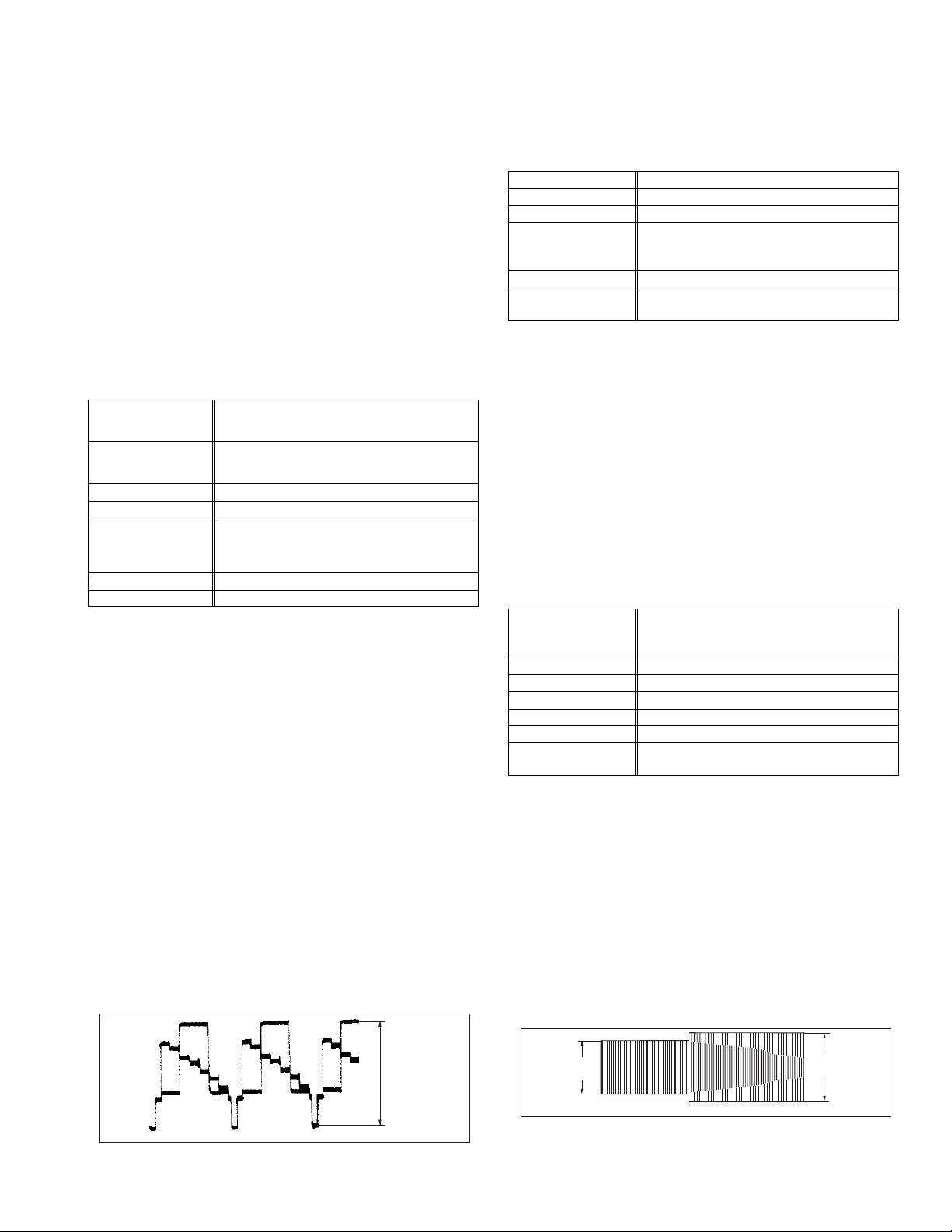
4.3.2 Video circuit
4.3.2.1 EE Y/PB Y (S-VHS) level
Signal (A1)
Mode (B1)
Equipment (C) • Oscilloscope
Measuring point (D) • Y OUT terminal
EVR mode
EVR address
Specified value (G) • 1.00 ± 0.05 Vp-p (75 ohm terminated)
Adjustment tool (H) • Jig RCU [PTU94023B]
• Ext. S-input
(A2)
• Ext. input
(A3)
• Color (colour) bar signal [PAL]
• EE SP
(B2)
•S-VHS SP
(B3)
•VHS SP
(F1)
• Jig code “57”
(F2)
• A : 11
(F3)
• Jig code “21” twice
(F4)
• Jig code “18” or “19” (Channel +/-)
(1) Input the signal (A3) from the input point (A1).
(2) Set the VCR to the mode (B1).
(3) Observe the Y OUT waveform at the measuring point (D).
(4) Set the VCR to the EVR mode by transmitting the code (F1)
from the Jig RCU.
(5) Set the EVR address to (F2) by transmitting the code (F3)
from the Jig RCU.
(6) Transmit the code (F4) from the Jig RCU to adj ust so that
the Y level of the Y OUT waveform becomes the specified
value (G).
(7) Release the EVR mode of the VCR by transmitting the
code (F1) from the Jig RCU again. (When the EVR mode
is released, the adjusted data is memorized.)
(8) Input the signal (A3) from the input point (A2).
(9) Repeat steps (3) to (7) in the mode (B1).
(10) Record the signal (A3) in the mode (B2), and play back the
recorded signal.
(11) Set the VCR to the manual tracking mode.
(12) Repeat steps (3) to (7) in the mode (B2).
(13) Record the signal (A3) in the mode (B3), and play back the
recorded signal.
(14) Set the VCR to the manual tracking mode.
(15) Repeat steps (3) to (7) in the mode (B3).
4.3.3 Syscon circuit
Notes:
• When perform this adjustment, remove the Mechanism
assembly.
4.3.3.1 Timer clock
Signal (A1) • No signal
Mode (B) • EE
Equipment (C) • Frequency counter
Measuring point (D1)
Adjustment part (F) • C3025 (TIMER CLOCK)
Specified value (G) • 1024.008 ± 0.001 Hz
• IC3001 pin 44
• IC3001 pin 103
(D2)
• C3054 + and -
(D3)
(976.5549 ± 0.0010 usec)
(1) Connect the frequency counter to the measuri ng point
(D1).
(2) Connect the short wire between the short point (D2) and
Vcc (5V).
(3) Short the leads of capacitor (D3) once in order to reset
the microprocessor of the Syscon.
(4) Disconnect the short wire between the short point (D2)
and Vcc then connect it again.
(5) Adjust the Adjustment part (F) so that the output frequency
becomes the specified value (G).
4.3.4 Audio circuit [S-VHS models]
Notes:
• GND (Ground) should be taken from the Tuner shield
case.
4.3.4.1 Audio REC FM
Signal (A1)
Mode (B) • S-VHS LP
Equipment (C) • Oscilloscope
Measuring point (D) • TP2253 (A. PB. FM)
External trigger (E) • TP111 (D.FF)
Adjustment part (H) • VR2251 (REC. FM)
Specified value (G1)
• Ext. input
• Audio: No signal
(A2)
• Video: Color (colour) bar signal [PAL]
(A3)
• 600 ± 100 mVp-p
(G2)
• More than 400 mVp-p
(1) Apply the external trigger signal to D.FF (E) to observe the
Audio PB FM waveform at the measuring point (D).
(2) Record the signal (A3) with no audio signal input in the
mode (B), and play back the recorded signal.
(3) Set the VCR to the manual tracking mode.
(4) If the A.PB FM level is not within the specified value (G1),
perform the adjustment in a following procedure.
(5) Adjust the adjustment part(F) so that the A. PB FM level of
the higher channel level becomes the specified value(G1).
(Adjust before recording, then confirm it by playing back.)
(6) If specified value(G1) is not obtai ned, adjust the Adjust-
ment part(F) so that the waveform level of the lower chan-
nel level becomes the specified value(G2).(Adjust before
recording, then confirm it by playing back.)
H. rate
Fig.4-3b EE Y/PB Y lebel
Y level
Specified
value (G2)
Specified
value (G1)
V. rate
Fig.4-3c Audio REC FM
(No.YD002)1-21
Page 18
4.4 Electrical adjustment (DVD SECTION)
4.4.1 Test mode setting method
(1) Press POWER button then press VCR/DVD repeatedly so that the DVD indicatorlights up.
(2) Press the POWER button again to set the stand-by mode.
(3) Transmit the code "FA" from the Jig RCU.
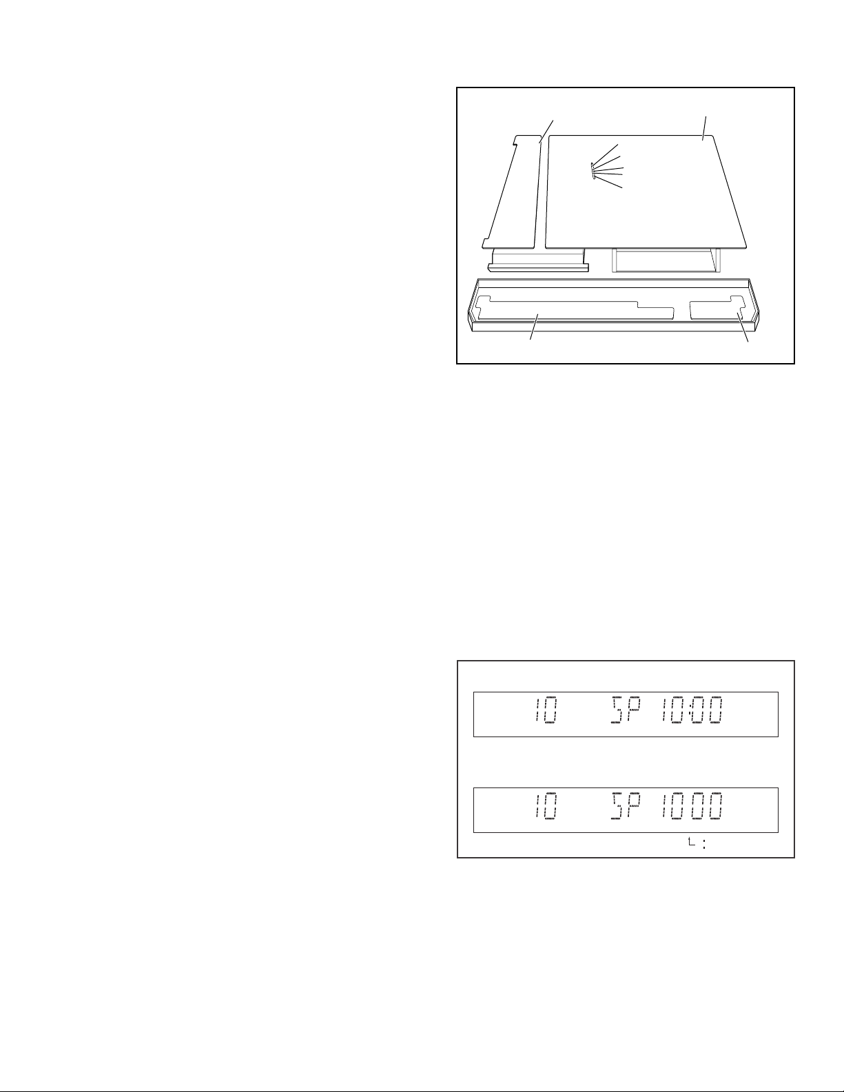
(4) The FDP shows the test mode content in the form of "∗ 0 ∗".
(5) To release test mode, press "POWER" key of the front panel.
(6) Each pressing of "SET UP MENU" key of the remote controller in test mode changes the mode as follows.
**
Becames test mode
Version of firmware
VCRCSDTV
D-S-VHS
CH
FDP becames all lighting
Check mode
Not used
4.4.2 Method of displaying versio n of firmware
(1) Set the main body at test mode.
(2) Press "SET UP MENU" key of the remote controller once. Then, version number and alphabetical letter of the system controller
and the back end are displayed in the FL display as follows:
FDP (Example)
07_19_16
System controller
4.4.3 Initialization method
Please initialize according to the following procedures in the following case:
• Just after you upgrade the firmware.
• After you confirm the symptoms that a customer points out. First Initialize, and then confirm whether the symptoms are improved or
not.
• After servicing, before returning the main body to a customer. (Initialized main body should be returned to a customer.)
(1) Set the main body at test mode.
(2) Press "PAUSE" key of the front panel or transmit the code "6F" from the Jig RCU.
(3) When initialization is completed, the FDP chan ges from "∗0" to "∗00".(T he left "0 " o f "00" is not a lways "0". It shows pa rameter
adjustment status.)
4.4.4 All-initialization method
Please perform all-initialization according to the following procedures in the following case:
• Just after you exchange the pick-up.
• Just after you exchange the spindle motor.
• Just after you exchange the traverse mechanism base.
NOTE:
Please perform all-initialization when you exchange the parts above and also when you remove the parts above.
• Just after the flap adjustment of the pick-up guide shaft
(1) Set the main body at test mode.
(2) Press the "REVERSE SKIP/INDEX ()" key of the remote controller for more than 2 seconds.
(3) When all-initialization is completed, the FDP changes from "∗0" to "∗33".
NOTE:
After all-initialization, be sure to perform optimization adjustment of Front End parameter.
Back end
Front end
1-22 (No.YD002)
Page 19
4.4.5 Optimization adjustment of Front End parameter
Adjustment to optimize Front End parameter must be performed in each mechanism assemb ly of this model for high-speed starting.Please perform optimization according to the following p rocedures just after all-initialization i s completed and when FL display
shows anything except "∗0" (For example when FDP shows "∗1", "∗2", and "∗3") at test mode.
(1) Press "POWER" button of the front panel to tu rn the main body on (not to set the main body at test mode).
(2) Insert the test disc VT-501 or commercial dual-layer DVD software.
(3) Remove the disc when the FL display changes from "READ" to disc information.
(4) Perform the same procedures as in (2) and (3) above by using the test disc CTS-1000 or commercial CD-DA software.
(5) Set the main body at test mode, and check that the FDP shows "∗0".
NOTE:
Status of this adjustment can be judged by the number displayed at test mode as follows:
DVD adjustment CD adjustment FDP at test mode
Adjusted Adjusted ∗0
Not adjusted Adjusted ∗1
Adjusted Not adjusted ∗2
Not adjusted Not adjusted ∗3
NOTE:
As for a disc used for adjustment,
• Disc should be mounted. ("Mounting" means to display "READ" after the disc is inserted and then display the disc information.) Disc need not be played.
• If you do not have test disc either VT-501 (DVD) or CTS-1000 (CD-DA), use a commercial disc (for DVD, dual-layer software) after seeing and checking that the di sc is neit her curved nor foreseen that it may shake at the time of playback.If you
use a disc with bad features, starting time may be slow or disc may not be read.
4.4.6 Display of current value of laser
(1) Set the main body at test mode.
(2) Press "SET UP MENU" key of the remote controller three times. Then, FDP is displayed "CHECK".
(3) The laser current val ue can be switche d between the val ue of CD and that of DVD by pressing the fo llowing key of the remote
controller.
FDP (Example)
2530
The number shown in the FDP shows mA of current value of laser.The first two numbers ("25" in "2530") sho ws current value
of laser at the time of adjustment after the latest all-initialization, 25mA in this example.The last two numbers ("30" in "2530")
shows the present current value of laser, 30mA in this example.The first two numbers ("25" in "2530") usually shows current
value of laser at the time of shipment, so you can see how the product has been deteriorated by comparing the first two numbers
("25" in "2530") and the last two numbers ("30" in "2530").
CD:
The laser current value of 65 mA or less is normal.The laser current value of over 66 mA is not normal. Laser diode of the
pickup has been deteriorated.
DVD:
The laser current value of 80 mA or less is normal.The laser current value of over 81 mA is not normal. Laser diode of the
pickup has been deteriorated.
To return to test mode, press "STOP" button of the front panel.
****
Remote controller "4" key --- Laser of CD
Remote controller "5" key --- Laser of DVD
(No.YD002)1-23
Page 20
4.4.7 Flap adjustment of the pick-up guide shaft
Please perform flap adjustment of the pick-up guide shaft in the following case:
• Just after you exchange the pick-up.
• Just after you exchange the spindle motor.
• Just after you exchange the traverse mechanism base.
NOTE:
Please perform flap adjustment of the pick-up guide shaft when you exchange the parts above and also when you remove the
parts above.
• When the reading accuracy of the signal is bad (There is a block noise in the screen, Screen stops in the outer circumference of a
disc, etc.)
4.4.7.1 Tool for adjustment
* The screwdriver
good on the market
* Test disc
part number : VT-501
*Stud
part number : JIGXVS40 (Note: One of the four studs is not used here.)
* Extension cord
part number : EXTXV521CB
XV-521 CN601
MAIN CONNECT
XV-521 CN503
CONT CONNECT
CN706 XV-521
CONT CONNECT
MAIN CONNECT
CN501 XV-521
CN701 XV-521
XV-521 CN502
CONT CONNECT
Used two set of this part.
MAIN CONNECT
1-24 (No.YD002)
Page 21
4.4.7.2 Preparation for adjustment
(1) Remove the DVD unit.(Refer to the SECTION 3 Removing the major parts)
(2) Connect a extention cord between CN502
of DVD servo control board assembly and CN7301 of Main board assembly. (See
Fig.4-4a)
(3) Connect a extention cord between CN501
of DVD servo control board assembly and CN5302 of Regulator board assembly. (See
Fig.4-4a)
(4) Remove the DVD servo control board assembly attach ed the DVD unit.
(5) Three stud is attached in a DVD unit. (See Fig.4-4b)
NOTE:
The connector of an extended code (right or reverse) since direction of which is also connectable, be careful of the direction which a
relay wire inserts enough It will become the cause of failure if especially a Regulator board side is mistaken.
Stud
DVD unit
CN502
CN501
DVD servo
control board
assembly
Main board
assembly
CN7301 CN7302
Regulator board
assembly
Fig.4-4a Fig.4-4b
4.4.7.3 Adjustment
(1) Set the main body at test mode.
(2) Press the "SET UP MENU" key of the remote controller three times, and the FDP is displayed "CHECK".
(3) Insert a test disc (VT-501), and press the "P LAY" butto n of the front panel.
(4) After a few seconds, press the numeric key "6" of the remote controller. Then, the FDP is displays a jitter value.
(5) Turn the adjustment screws on the underside of the traverse mechanism with screw driver until the maximum jitter value is dis-
played on the FDP. (In this model, a bigger jitter value means a better result.)
NOTE:
• Reference values to judge whether the jitter is allowable or not are displayed, instead of actual jitter values.
• Please be sure to perform "all-initialization" and "optimization adjustment of front end parameter" after adjusting.
Loading mechanism assembly
Screw a
Screw b
FDP (Example)
1241
****
Traverse mechanism assembly
POINT:
Turn the adjustment screws a and b
to the same angle in the right direction.
Screw c
And turn the adjustment screws a and b
to the same angle in the left direction.
Then, turn the screws a and b in either
the right or the left direction to increase
the number of jitter.
Don't turn the adjustment screw c.
Remote controller "6" key-Jitter value
(No.YD002)1-25
Page 22
SECTION 5
TROUBLESHOOTING
5.1 Manually removing the cassette tape
If you cannot remove the cassette tape which is loaded because
of any electrical or mechanical failures, manually remove it by
taking the following steps.
(1) Unplug the power cord plug from the power outlet.
(2) Refer to the di sassembly procedure of the VCR and per-
form the disassembly of the major parts before removing
the mechanism assembly. (See Fig. 5-1a)
Fig.5-1a
Tension arm assembly
Pole base assembly
Pinch roller arm assembly
(3) Unload the pole base assembly by man ually turning the
gear of the loading motor until the pole base assembly is
hidden behind the cassette lid. In doing so, hold the tape by
the hand to keep the slack away from any grease. (See
Fig.5-1b )
In case of mechanical failures, while keeping the tension arm assembly free from tension, pull out the tape
on the pole base assembly. Take the spring(a) of the
pinch roller arm assembly off the hook, and detach it
from the tape.
(4) Remove the screw (a) of the side frame (L/R).
(5) Hold the slack tape and cassette cover togethe r, lift the
cassette tape, top frame, cassette holder and side frames
(L, R) together from the rear and remove them by dis-engaging the hooks (a) and (b).
Screw(a)
Cassette tape
Hook(a)
Cassette holder
Top frame
Side frame(R)
Screw(a)
Spring(a)
Direction of unloading
Fig.5-1b
Side frame(L)
Hook(b)
Fig.5-1c
(6) Take up the slack of the tape into the casse tte. This com-
pletes removal of the cassette tape.
5.2 Manually removing the disk(DVD/CD)
If you cannot remove the disk which is loaded because of any
electrical or mechanical failures, manually remove it by taking the
following steps.
(1) Unplug the power cord plug from the power outlet.
(2) Remove the top cover and front panel assembly .
(Refer to the disassembly procedure and perform th e disassembly of the major parts before removing)
(3) Turn the Middle gear (a) by hand to open the disk tray.(See
Fig. 5-2a)
DVD unit
Middle gear (a)
1-26 (No.YD002)
Unloading
Fig.5-2a
Page 23
5.3 Emergency display function (VHS SECTION)
This unit saves details of the last two emergencies as the EMG
history and allows the status of the VCR and the mechanism o f
each emergency to be shown both on the display and as OSD information.
When using the emergency function, it is required to set the VCR
to the Jig RCU mode.
Jig RCU
[Data transmitting method]
Depress the " " ( 3 ) button
after the data code is set.
CUSTOM CODE
43: A CODE
DATA CODE
INITIAL MODE
Fig.5-3a Jig RCU [PTU94023B]
5.3.1 Displaying the EMG information
The EMG detail of information can be displayed by transmitting
the code "59" from the Jig RCU.
Note:
• The EMG detail information <1><2> show the informa-
tion on the latest EMG.
It becomes “ - - : - - : - - ” when there is no latest EMG
record.
0: 00
E: **
1E: **
1: *1
2: *2
3: 34
4: *5
5: *6
6: *7
7: *8
8: *9
9: *10
Normal display
EMG content display (Latest) See 5.3.4
EMG content display (Previous) See 5.3.4
EMG detail information <1> See 5.3.5
[Deck operation mode]
EMG detail information <1> See 5.3.5
[Mechanism operation mode]
EMG detail information <1> See 5.3.5
[Mechanism sensor information and Mechanism mode position]
EMG detail information <2> See 5.3.6
[Type of the cassette tape in use <1>]
EMG detail information <2> See 5.3.6
[Winding position of the cassette tape in use]
EMG detail information <2> See 5.3.6
[Type of the cassette tape in use <2> (Winding area)]
EMG detail information <3> See 5.3.7
[Previous deck operation mode]
EMG detail information <3> See 5.3.7
[The deck operation mode of the one before the last]
EMG detail information <3> See 5.3.7
[The deck operation mode of the one prior to one above]
EMG display of 7 FDP display model
Fig.5-3b
EMG display of FDP display mode
(1) Transmit the code “59” from the Jig RCU.
The FDP shows the EMG content in the form of “E:**:**”.
<Example 1> E : 01
Latest EMG
<Example 2> E : - -
No EMG record
(2) Transmit the code “59” from the Jig RCU again.
The FDP shows the EMG detail information <1> in the form
of “ *1: *2 : 34 ”.
*1 : Deck operation mode at the moment of EMG
*2 : Mechanism operation mode at the moment of EMG
3- : Mechanism sensor information at the moment of EMG
-4 : Mechanism mode positio n at the moment of EMG
(3) Transmit the code “59” from the Jig RCU once again.
The FDP shows the EMG detail information <2> in the form
of “ *5 : *6 : *7 ”.
*5 : Type of the cassette tape in use <1> .
*6 : Winding position of the cassette tape in use
*7 : Type of the cassette tape in use <2> (Winding area)
(4) Transmit the code “59” from the Jig RCU once again.
The FDP shows the EMG detail information <3> in the form
of “*8 : *9 : *10”.
*8 : Previous deck operation mode at the moment of EMG
*9 : The deck operation mode of the one before the last at
the moment of EMG
*10: The deck operation mode of the one prior to one
above at the moment of EMG
(5) Transmit the code “59” from the Jig RCU once again to re-
set the display.
(No.YD002)1-27
Page 24

5.3.2 Clearing the EMG history
(1) Display the EMG history.
(2) Transmit the code “36” from the Jig RCU.
(3) Reset the EMG display.
5.3.3 Details of the OSD display in the EMG display mode
During the EMG display, the OSD shows the data on the deck
mode, etc. The details of the display contents are as follows.
Notes:
• The display is variable depending on the part No. of the
System Control microcomputer (IC3001) built into the
VCR. In the following, refer to the figure carrying the
same two characters as the top two characters o f the
part number of your IC.
• The sensor information in the OSD display conten ts is
partially different from the mechanism sensor information in EMG detail information <1>.
[For MN* only]
AA BB CC DD EE
FF GG HH I I JJ
KK LL MM NN OO
PP QQ RR SS TT
UU VV WW XX YY
AA : Deck operation mode (See EMG detail information <1>.)
BB : Mechanism operation mode
(See EMG detail of information <1>.)
CC : Mechanism transition flag
DD : Capstan motor control status
EE : Loading motor control status
FF : Sensor information (See sensor information details.)
GG : Capstan motor speed
HH : Key code (JVC code)
I I : Supply reel winding diameter data higher 8 bits.
JJ : Supply reel winding diameter data lower 8 bits.
KK : Mechanism sensor information & mechanism mode posi-
tion(See EMG detail of information <1>.)
LL : Tape speed data higher 8 bits.
MM : Tape speed data lower 8 bits.
NN : Cassette tape type <2> higher 8 bits.
(See EMG detail of information <2>.)
OO : Cassette tape type <2> lower 8 bits.
(See EMG detail of information <2>.)
PP : General data display area
YY : General data display area
*FF:Sensor information details
<Display>
** h
********
Encoder data
(See Mechanism mode sequence.)
Cassette tab present = 1
Cassette tab broken = 0
Cassette absent = 1
Cassette present = 0
Start sensor
End sensor
[For *HD only]
AA BB CC
DD EE FF
GGGG HHHH
I I JJJJ
KKKK LLLL MMMM
ROM No.
AA : Key code (JVC code)
BB : Deck operation mode(See EMG detail information
<1>.)
CC : Mechanism operation mode (See EMG detail informa-
tion <1>.)
DD : Sensor information (See sensor information details.)
EE : Capstan motor speed (Search, double speed)
FF : Tracking value
GGGG : Cassette tape type <2>, 16 bits.
(See EMG detail information <2>.)
HHHH : Supply reel winding diameter data
I I : Capstan motor speed (FF/REW, double speed)
JJJJ : Tape speed data, lower 8 bits.
KKKK : General data display area
LLLL : General data display area
MMMM : General data display area
*DD:Sensor information details
<Display>
** h
********
Encoder data
(See Mechanism mode sequence.)
Remote pause
End sensor
Start sensor
Cassette tab present = 1
Cassette tab broken = 0
[For both MN*/HD*]
Mechanism mode sequence
Mechanism mode - Encoder data
LSA
12345
1110
GND
LSA
LSB
LSC
LSD
No. Position Encoder data
21
Encoder output = Low
or
Trerminal - GND = SHORT
1
EJECT 0 h = 0000
2
EJECT1 1 h = 0001
3
EJECT2 2 h = 0010
4
ULSTOP 3 h = 0011
5
UPPER 4 h = 0100
6
ONSTOP(PLAY) 5 h = 0101
7
FWD/SS 6 h = 0110
8
REV/SS 7 h = 0111
9
OFFSTOP 8 h = 1000
10
FFREW-BRAKE 9 h = 1001
FFREW A h = 1010
11
MIDDLE F h = 1111
12
543
Encoder output = High
or
Trerminal - GND = OPEN
LSD
9876
LSC
LSB
1-28 (No.YD002)
Page 25

5.3.4 EMG content description
Note:
EMG contents “E08/E09” are for the model with Dynamic Drum (DD).
FDP CONTENT CAUSE
E01: Loading EMG
E02:
Unloading EMG
E03: Take Up Reel
Pulse EMG
E04: Drum FG EMG
E05: Cassette Eject
EMG
E06: Capstan FG
EMG
E07: SW Power
Short-Circuit
EMG
E08:
DD Initialized
(Absolute
Position
Sensor) EMG
E09: DD FG EMG
E0A: Supply Reel
Pulse EMG
EU1:
Head clog warning
history
If the mechanism mode does not change to the next mode within 4 seconds after the loading motor starts rotating in the loading direction, while
the mechanism is in the after-loading position (with the tape up against
the pole base), [E:01] is identified and the power is switched OFF.
However, if the tape loading is not completed within 4 seconds after
the loading motor starts rotating in the loading direction, the tape is
simply unloaded and ejected. No EMG data is recorded in this case.
When the mechanism mode cannot be changed to another mode
even when the loading motor has rotated for more than 4 seconds in the unloading direction, [E:02] is identified and the power
is turned off.
When the falling edje of the take-up reel pulse has not been generated for more than 4 seconds in the capstan rotating mode,
[E:03] is identified, the pinch rollers are turned off and stopped,
and the power is turned off. In this case, however, the mechanism should be in position after tape loading. Note that the reel
EMG is not detected during Slow/Frame advance operations.
When the drum FG pulse has not been input for more than 3 seconds in the drum rotating mode, [E:04] is identified, the pinch rollers are turned off and stopped, and the power is turned off.
If the cassette does not reach the eject position within about 0.7
seconds after the cassette housing has started the cassette ejection operation, [E:05] is identified, the drive direction is reversed
to load the tape, the mode is switched to STOP mode with the
pinch roller OFF, and the power is switched OFF.
During the cassette insertion process, the drive direction is reversed
and the cassette is ejected if the tape is not up against the pole
base within about 3 seconds after the start of the cassette pullingin operation. If the cassette does not reach the eject position within
about 0.7 seconds after the drive mode reversal operation, [E:05]
is identified and the power is switched OFF immediately.
When the capstan FG pulse has not been generated for more
than 1 second in the capstan rotating mode, [E:06] is identified,
the pinch rollers are turned off and stopped, and the power is
turned off.However, the capstan EMG is not detected in SLOW/
STILL modes.
Note that, if the part number of the System Control IC begins with
"MN" or "M3", the capstan EMG is not detected even during the
FF/REW operation.
When short-circuiting of the SW power supply with GND has lasted
for 0.5 second or more, [E:07] is identified, all the motors are
stopped and the power is turned off.
When DD tilting does not complete in 4 seconds, [E:08] is identified, the tilt motor is stopped and the power is turned off.
When the DD FG pulse is not generated within 2.5 seconds, [E:09]
is identified, the tilt motor is stopped and the power is turned off.
When the falling edge of the supply reel pulse has not been generated for more than 10 seconds in the capstan rotating mode,
[E:0A] is identified and the cassette is ejected (but the power is
not turned off). In this case, however, the mechanism should be
in the position after tape loading (with the tape up against the pole
base). Also note that the reel EMG is not detected during Slow/
Frame advance operations.
Presupposing the presence of the control pulse output in the PLAY mode, when the value obtained by mixing the two V.FM output channels (without regard
to the A.FM output) has remained below a certain threshold level for more than 10 seconds, [E:U1] is identified and recorded in the emergency history.
During the period in which the head clog is detected, the FDP shows "U:01" and the OSD repeats the "3 seconds of warning display" and the "7 seconds of
noise picture display" alternately.
EMG code : "E:C1" or "E:U1" / FDP : "U:01" / OSD : "Try cleaning tape." or "Use cleaning cassette."
The head clog warning is reset when the above-mentioned threshold has been exceeded for more than 2 seconds or the mode is changed to another mode
than PLAY.
1. The mechanism is locked in the middle of the mode transition during a tape loading operation.
2.
The mechanism overruns during the tape loading operation because the SYSCON cannot recognize
the mechanism mode normally. This problem is due to a cause such as a rotary encoder failure.
3.
Power is not supplied to the loading MDA. (M12V/Vcc/Vref/ICP are disconnected in the middle.)
1.
The mechanism is locked in the middle of mode transition.
2.
Without an eject signal being sent from the SYSCON, unloading is attempted (i.e. Ejection is attempted
while the tape is still inside the mechanism.) because the SYSCON cannot recognize the mechanism
mode normally. This is due to a cause such as a rotary encoder failure. (Mechanism position:
UPPER)
3.
Power is not supplied to the loading MDA. (M12V/Vcc/Vref/ICP are disconnected in the middle.)
1.
The take-up reel pulse is not generated in the FWD transport modes (PLAY/FWD SEARCH/FF,
etc.) because;
1) The idler gear is not meshed with the take-up reel gear because the mechanism mal-functions for
some reason.
2)
The idler gear is meshed with the take-up reel gear, but incapable of winding due to too large
mechanical load (abnormal tension);
3) The reel is rotating normally but an FG pulse is not generated due to the take-up reel sensor failure.
2.
The supply reel pulse is not generated in the REV transport modes (REV SEARCH/REW, etc.)
because;
1) The idler gear is not meshed with the supply reel gear because the mechanism mal-functions for
some reason.
2) The idler gear is meshed with the supply reel gear, but incapable of winding due to too large a
mechanical load (abnormal tension);
3) The reel rotates normally but the FG pulse is not generated due to a supply reel sensor failure.
3.
Power(SW5V) is not supplied to the reel sensor on the tape winding side.
1.
The drum could not start or the drum rotation has stopped due to too large a load on the tape,
because;
1) The tape tension is abnormally high;
2) The tape is damaged or a foreign object (grease, etc.) adheres to the tape.
2.
The drum FG pulse did not reach the System controller CPU because;
1) The signal circuit is disconnected in the middle;
2) The FG pulse generator (hall device) of the drum is faulty.
3.
The drum control voltage (DRUM CTL V) is not supplied to the MDA.
4.
Power (M12V) is not supplied to the drum MDA.
1.
The cassette cannot be ejected due to a failure in the drive mechanism of the housing.
2.
When the housing load increases during ejection, the loading motor is stopped because of lack of
headroom in its drive torque.
Housing load increasing factors: Temperature environment (low temperature, etc.), mechanism
wear or failure.
3.
The sensor/switch for detecting the end of ejection are not functioning normally.
4.
The loading motor drive voltage is lower than specified or power (M12V) is not supplied to the
motor (MDA).
5.
When the user attempted to eject a cassette, a foreign object (or perhaps the user's hand) was
caught in the opening of the housing.
1.
The capstan could not start or the capstan rotation has stopped due to too large a load on the tape,
because;
1) The tape tension is abnormally high (mechanical lock);
2) The tape is damaged or a foreign object (grease, etc.) is adhered to the tape (occurrence of tape
entangling, etc.).
2.
The capstan FG pulse did not reach the System controller CPU because;
1) The signal circuit is disconnected in the middle;
2) The FG pulse generator (MR device) of the capstans is faulty.
3.
The capstan control voltage (CAPSTAN CTL V) is not supplied to the MDA.
4.
Power (M12V, SW5V) are not supplied to the capstan MDA.
1.
The SW 5 V power supply circuit is shorted with GND.
2.
The SW 12 V power supply circuit is shorted with GND.
1. The absolute value sensor is defective. (The soldered parts have separated.)
2. The pull-up resistor at the absolute sensor output is defective. (The soldered parts have separated.)
3. Contact failure or soldering failure of the pins of the connector (board-to-board) to the absolute value
sensor.
4.
The absolute value sensor data is not sent to the System Controller CPU.
1. The FG sensor is defective. (The soldered parts have separated.)
2. The pull-up resistor at the FG sensor output is defective. (The soldered parts have separated.)
3. Contact failure or soldering failure of the pins of the connector (board-to-board) to the FG sensor.
4. The power (5V) to the sensor is not supplied. (Connection failure/soldering failure)
5. The FG pulse is not sent to the System Controller CPU.
6.
The tilt motor is defective. (The soldered parts have separated.)
7. The drive power to the tilt motor is not supplied. (Connection failure/soldering failure)
8. The tilt motor drive MDA - IC is defective.
9. Auto-recovery of the DD tilting cannot take place due to overrun.
The supply reel pulse is not generated in the FWD transport mode (PLAY/FWD SEARCH/FF,
1.
etc.) because;
1) PLAY/FWD or SEARCH/FF is started while the tape in the inserted cassette is cut in the middle;
2) A mechanical factor caused tape slack inside and outside the supply reel side of the cassette shell.
In this case, the supply reel will not rotate until the tape slack is removed by the FWD transport,
so the pulse is not generated until then;
3) The reel is rotating normally but the FG pulse is not generated due to a supply reel sensor failure.
2.
The take-up reel pulse is not generated in the REV transport mode (REV SEARCH/REW, etc.).
1) REV SEARCH/REW is started when the tape in the inserted cassette has been cut in the middle;
2) A mechanical factor caused tape slack inside and outside the take-up reel side of the cassette
shell. In this case, the take up will not rotate until the tape slack is removed by the REV transport,
so the pulse will not be generated until that time;
3) The reel is rotating normally but the FG pulse is not generated due to a take-up reel sensor failure.
3.
The power (SW 5V) to a reel sensor is not supplied.
(No.YD002)1-29
Page 26

5.3.5 EMG detail information <1>
The status (electrical operation mode) of the VCR and the status
(mechanism operation mode/sensor information) of the mechanism in the latest EMG can be confirmed based on the figure in
EMG detail information <1> .
[FDP/OSD display] *1 : *2 : 34
*1 : Deck operation mode at the moment of EMG
*2 : Mechanism operation mode at the moment of EMG
3- : Mechanism sensor information at the moment of EMG
-4 : Mechanism mode position at the moment of EMG
Note:
• For EMG detailed information <1>, the content of the
code that is shown on the displa y (or OSD) differs depending on the parts number of the system contr ol microprocessor (IC3001) of the VCR. The sy stem control
microprocessor parts number starts with two letters, refer these to the corresponding table.
*1 : Deck operation mode
[Common table of MN* and HD]
Display
MN* HD*
00 - Mechanism being initialized
01 00 STOP with pinch roller pressure off (or tape present with P.OFF)
02 01 STOP with pinch roller pressure on
03 - POWER OFF as a result of EMG
04 04 PLAY (Normal playback)
0C 0E REC
10 11 Cassette ejected
20 22 FF
21 - Tape fully loaded, START sensor ON, short FF
22 -
24 26 FWD SEARCH (variable speed) including x2-speed
2C 2E INSERT REC
40 43 REW
42 - Cassette identification REV SEARCH before transition to REW
44 47 REV SEARCH (variable speed)
4C 4C AUDIO DUB
6C 6E INSERT REC (VIDEO + AUDIO)
84 84 FWD STILL / SLOW
85 85 REV STILL / SLOW
8C 8F REC PAUSE
8D - Back spacing
8E - Forward spacing (FWD transport mode with BEST function)
AC AF INSERT REC PAUSE
AD - INSERT REC back spacing
CC CD AUDIO DUB PAUSE
CD - AUDIO DUB back spacing
EC EF INSERT REC (VIDEO + AUDIO) PAUSE
ED - INSERT REC (VIDEO + AUDIO) back spacing
Cassette identification FWD SEARCH before transition to FF
(SPx7-speed)
(SPx7-speed)
Deck operation mode
*2 : Mechanism operation mode
[Table of MN*]
Display
00 Command standby (No command to be executed)
01 Immediate Power OFF after EMG occurrence
02 Loading from an intermediate position during mechanism initialization
03 Unloading due to EMG occurrence during mechanism initialization
04 Ejecting cassette (ULSTOP to EJECT)
05 Inserting cassette (EJECT to ULSTOP)
06 Loading tape (ULSTOP to PLAY)
07 Unloading tape (PLAY to ULSTOP)
08 Transition from pinch roller ON to STOP
09 Transition from pinch roller OFF to STOP (PLAY to OFFSTOP)
0A Transition from pinch roller OFF to STOP at power OFF
0B Transition from pinch roller ON to STOP at power ON
0C Transition to PLAY
0D Transition to Search FF
0E Transition to REC
0F Transition to FWD STILL/SLOW
10 Transition to REV STILL/SLOW
11 Transition to Search REV
12 Transition from FF/REW to STOP
13 Transition to FF
14 Transition to REW
15 Tape end detection processing during loading
16 Short FWD/REV at tape sensor ON during unloading
17 Transition to FF/REW brake mode
Mechanism operation mode
[Table of HD*]
Display
00 STOP with pinch roller pressure off
01 STOP with pinch roller pressure on
02 U/L STOP (or tape being loaded)
04 PLAY (Normal playback)
05 PLAY (x1-speed playback using JOG)
0E REC
11 Cassette ejected
22 FF
26 FWD SEARCH (variable speed) including x2-speed
2E INSERT REC
43 REW
47 REV SEARCH
4C AUDIO DUB
6E INSERT REC (VIDEO + AUDIO)
84 FWD STILL/SLOW
85 REV STILL/SLOW
8F REC PAUSE
AF INSERT REC PAUSE
C7 REV SEARCH (x1-speed reverse playback using JOG)
CD AUDIO DUB PAUSE
EF INSERT REC (VIDEO + AUDIO) PAUSE
F0 Mechanism being initialized
F1 POWER OFF as a result of EMG
F2 Cassette being inserted
F3 Cassette being ejected
F4 Transition from STOP with pinch roller pressure on to STOP with pinch
roller pressure off
F5 Transition from STOP with pinch roller pressure on to PLAY
F6 Transition from STOP with pinch roller pressure on to REC
F7 Cassette type detection SEARCH before FF/REW is being executed
F8 Tape being unloaded
F9 Transition from STOP with pinch roller pressure off to STOP with pinch
roller pressure on
FA Transition from STOP with pinch roller pressure off to FF/REW
FB Transition from STOP with pinch roller pressure off to REC.P (T.REC,etc.)
FC Transition from STOP with pinch roller pressure off to cassette type
detection SEARCH
FD Short REV being executed after END sensor on during unloading
FE Tension loosening being executed after tape loading (STOP with pinch
roller pressure on)
FF Tape being unloaded
Mechanism operation mode
1-30 (No.YD002)
Page 27

3- : Mechanism sensor information
[Common table of MN* and HD*]
Display
REC safety SW
0- Tab broken ON ON ON
1- Tab broken ON
2- Tab broken ON
3- Tab broken ON OFF
4- Tab present ON
5- Tab present
6- Tab present OFF
7- Tab present OFF
8- Tab broken ON ON
9- Tab broken ON
A- Tab broken
B- Tab broken OFF
C- Tab present ON
D- Tab present
E- Tab present OFF
F- Tab present OFF
Tab broken = 0 Sensor ON = 0 Sensor ON = 0
Tab present = 1 sensor OFF = 1 Sensor OFF = 1
Mechanism sensor informatio n
Start sensor End sensor
ON
OFF
OFF
OFF
ON
ON
OFF
OFF
ON
OFF
OFF
ON
OFF
ON
OFF
OFF OFF
Mechansim
position sensor
OFF
ON
OFF
ON
OFF
ON
OFF
ON
OFF
ON
OFF
ON
OFF
ON
-4 : Mechanism mode position
[Common table of MN* and HD*]
Mechanism
sensor
information
Dis-
play
Deck operation mode
-0 Not established
-1 EJECT EJECT position
-2 EJECT-EJECT1 Intermodal position
-3 EJECT1 EJECT1 position
-4 EJECT1-EJECT2 Intermodal position
-5 EJECT2 EJECT2 position
-6 EJECT2-ULSTOP Intermodal position
Even number
(0, 2, 4, 6, 8,
A, C, E)
-7 ULSTOP ULSTOP position
-8 ULSTOP-UPPER Intermodal position
-9 UPPER Loading (unloading) tape
-A UPPER-ONSTOP Intermodal position
-B ONSTOP PLAY position
-C PLAY-FWD/SS Intermodal position
-D FWD/SS
FWD (FWD Still/Slow) position
-E FWD/SS-REV Intermodal position
-F REV
REV (REV Still/Slow) position
-0 REV-OFFSTOP Intermodal position
-1 OFFSTOP Pinch roller OFF position
Odd number
(1, 3, 5, 7, 9,
B, D, F)
-2
OFFSTOP-FFREWB
Intermodal position
-3 FFREWB FF/REW Brake position
-4 FFREWB-FFREW Intermodal position
-5 FFREW FF/REW position
5.3.6 EMG detail information <2>
The type of the cassette tape and the cassette tape winding position can be confirmed based on the figure in EMG detail information <2> .
Note:
• EMG detail information <2> is the reference information
stored using the remaining tape detection functi on of
the cassette tape. As a result, it may not identify cassette correctly when a special cassette tape is used or
when the tape has variable thickness.
*5 : Cassette tape type <1>
Display Cassette tape type <1>
00 Cassette type not identified
16
Large reel/small reel (T-0 to T-15/T-130 to T-210) not classified
82 Small reel, thick tape (T-120) identified/thin tape (T-140) identified
84 Large reel (T-0 to T-60) identified
92
Small reel, thick tape (T-130) identified/thin tape (T-160 to T-210) identified
93
Small reel, thick tape/C cassette (T-0 to T-100/C cassette) not classified
C3
Small reel, thick tape/C cassette (T-0 to T-100/C cassette) being classified
D3
Small reel, thick tape/C cassette (T-0 to T-100/C cassette) being classified
E1 C cassette, thick tape (TC-10 to TC-20) identified
E2 Small reel, thick tape (T-0 to T-100) identified
E9 C cassette, thin tape (TC-30 to TC-40) identified
F1
C cassette, thick tape/thin tape (TC-10 to TC-40) not classified
Notes:
• Cassette tape type <1> is identified a few times during
mode transition and the identification count is variable
depending on the cassette tape type. If an EMG occurs
in the middle of identification, the cassette tape type
may not be able to be identified.
• If other value than those listed in the above table is dis-
played, the cassette tape type is not identified.
*6 : Cassette tape winding position
The cassette tape winding position at the moment of EMG is displayed by dividing the entire tape (from the beginning to the end)
in 21 sections using a hex number from “00” to “14”.
00 : End of winding
14 : Beginning of winding
FF : Tape position not identified
*7 : Cassette tape type <2> (Winding area)
Display
00
04 - 08
05 - 06
05 - 0C
06 - 0C
06 - 0C
07 - 08
09 - 0B
0C - 0D
0D - 0F
0E - 10
10 - 12
10 - 13
11 - 14
12 - 14
13 - 14
13 - 14
13 - 14
13 - 14
15 - 16
16 - 17
17 - 18
19 - 1B
Cassette tape type <2>
Cassette type not identified
C cassette, thick tape TC-10
Small reel, thick tape T-20
C cassette, thick tape TC-20P
C cassette, thin tape TC-40
C cassette, thin tape TC-30
Small reel, thick tape T-40
Small reel, thick tape T-60
Small reel, thick tape T-80(DF-160)
Small reel, thick tape T-90(DF-180)
Small reel, thick tape T-100
Small reel, thin tape T-140
Small reel, thick tape T-120(DF-240)
Small reel, thick tape T-130
Small reel, thin tape T-160
Small reel, thin tape T-210(DF-420)
Small reel, thin tape T-180(DF-360)
Small reel, thin tape T-168
Small reel, thick tape DF-300
Large reel T-20
Large reel T-30
Large reel T-40
Large reel T-60
(Reference) Word data
(Beginning) (End)
(0497 - 0506)(0732 - 0858)
(05A9 - 0661)
(0599 - 05FF)(0AA1 - 0C07)
(0623 - 063D) (0C41 - 0CC3)
(0611 - 0638)(0C0C - 0CB2)
(07CC - 08E5)
(09FD - 0B78)
(0C20 - 0DFC)
(0D31 - 0F3E)
(0E43 - 107F)
(10E1 - 120C)
(1073 - 1313)
(1185 - 1429)
(12D3 - 141F)
(1373 - 14C3)
(1357 - 14C0)
(1395 - 14EE)
(13A8 - 14CE)
(1536 - 1618)
(1647 - 175A)
(1759 - 189C)
(1989 - 1B2F)
Note:
• The values of cassette tape type <2> in the above table
are typical values with representative cassette tapes.
5.3.7 EMG detail information <3>
Three deck operation modes preceding the deck operation mode
in which the EMG occurs may be confirmed based on the figures
in the EMG information detail <3>. For the contents of the displayed information, see the table "Deck operation mode" in section "5.3.5 EMG detail information <1>".
(No.YD002)1-31
Page 28

5.4 Troubleshooting (DVD SECTION)
Press OPEN
/CLOSE key
Is tray
operation
Confirmation of tray drive circuit
N
and circuit in surrounding
correct?
Y
Is the traverse moving
along the innermost
N
perimeter for SW detection?
Y
"NO DISC" message appears
Y
immediately after vertical
movement of the pick-up lens
N
The state that DISC does not rotate continues for
several seconds, and becomes NO DISC or an
error display afterwards.
The rotation of DISC becomes high-speed and
abnormal, and becomes NO DISC or an error
display afterwards.
N
Is focus retraction OK?
FE
OFF
Even when it retracts
correctly, if it is out of focus
and makes repeated retries
with a clicking sound, it is
in error.
ON
See "5.5.4 Focus ON error"
N
in "Check points for
individual errors"
Y
Is tracking retraction OK?
See "5.5.3 Traverse movement error"
in "Check points for individual errors"
See "5.5.2 Disk detection, distinction error"
in "Check points for individual errors"
Y
See "5.5.1 Spindle startup error"
in "Check points for individual errors"
A
Is the inter-layer jump OK?
FE
LO LI
Two layers of DVD only.
N
5.5.8 Inter-layer
jump error
Y
TE
OFF
If TE waveform reappears
or fails to converge after the
TE retraction, it is in error.
Is the spindle servo
locked correctly?
Is the RF OUT waveform
locked correctly?
1-32 (No.YD002)
A
ON
See "5.5.5 Tracking ON error"
N
in "Check points for
individual errors"
Has the disc information
been collected?
Stop will result
N
5.5.7 Address read
error
Y
Y
Check 5.5.9, 5.5.10, 5.5.11, and
See "5.5.6 Spindle CLV error"
N
in "Check points for
individual errors"
Is playback
possible?
Y
N
5.5.12 items in "Check points
for individual errors"
Y
OK !
Fig.5-4a
Page 29

5.5 Check points for each error (DVD SECTION)
5.5.1 Spindle start error
(1) Defective spindle motor
• Are there several ohms resistance between each pin of CN201
(The power supply is turned off and measured.)
• Is the sign wave of about 100mVp-p in the voltage had from each terminal?
[ CN201"10"(H1+),"11"(H1-),"7"(H2+),"8"(H2-),"5"(H3+),"6"(H3-) ]
(2) Defective spindle motor driver (IC251
• Has motor drive voltage of a sine wave or a rectangular wave gone out to each terminal(SM1~3)
of CN201"1,2,3" and IC251"2,4,7"?
• Is FG pulse output from the terminal of IC251
• Is it "L(about 0.9V)" while terminal of IC251
(3) Has the control signal come from servo IC or the microcomputer?
• Is it "L" while the terminal of IC251
Is it "H" while the terminal of IC251
• Is the control signal input to the terminal of IC251
(changes from VHALF voltage while the motor is working.)
• Is the VHALF voltage input to the terminal of IC251"21"(ECR)?
(4) Is the FG signal input to the servo IC?
• Is FG pulse input to the terminal of IC301
5.5.2 Disc Detection, Distinction error (no disc, no RFENV)
• Laser is defective.
• Front End Processor is defective (IC101
• APC circuit is defective. --- Q101,Q102.
• Pattern is defective. --- Lines for CN101
• IC101 --- For signal from IC101 to IC301, is signal output from IC101 "20" (ASOUT) and IC101 "41"(RFENV) and IC101 "22"
(FEOUT)?
)
"24"(FG) according to the rotation of the motor?
"15"(VH) is rotating the motor?
"18"(SBRK) is operating?
"23"(/SPMUTE) is operating?
"22"(EC)?
"69"(FG) according to the rotation of the motor?
).
- All patterns which relate to pick-up and patterns between IC101
"1-2","2-3","1-3"?
5.5.3 Traverse movement NG
(1) Defective traverse driver
• Has the voltage come between terminal of CN101 "2" and "4" ?
(2) Defective BTL driver (IC201)
• Has the motor drive voltage gone out to IC201
(3) Has the control signal come from servo IC or the microcomputer?
• Is it "H" while the terminal of IC201
• TRSDRV Is the signal input? (IC301
(4) TRVSW is the signal input from microcomputer? (IC301
5.5.4 Focus ON NG
• Is FE output ? --- Pattern, IC101
• Is FODRV signal sent ? (R209) --- Pattern, IC301 "115"
• Is driving voltage sent ? IC201
• Mechanical unit is defective.
5.5.5 Tracking ON NG
• When the tracking loop cannot be drawn in, TE shape of waves does not settle.
• Mechanical unit is defective.
Because the self adjustment cannot be normally adjusted, the thing which cannot be normally drawn in is thought.
• Periphery of driver (IC201
Constant or IC it self is defective.
• Servo IC (IC301)
When improperly adjusted due to defective IC.
)
"9"(STBY1) ?
"67")
"13", "14" --- If NG, pattern, driver, mechanical unit .
"17" or "18"?
"56")
(No.YD002)1-33
Page 30

5.5.6 Spindle CLV NG
• IC101
• Does not the input or the output of driver's spindle signal do the grip?
• Has the tracking been turned on?
• Spindle motor and driver is defective.
• Additionally, "IC101
5.5.7 Address read NG
• Besides, the undermentioned cause is thought though specific of the cause is difficult because various factors are thought.
5.5.8 Between layers jump NG (double-layer disc only)
5.5.9 Neither picture nor sound is output
(1) It is not possible search
• Has the tracking been turned on?
• To " Tracking ON NG" in "Check points for each error" when the tracking is not normal.
• Is the feed operation normal?
-- "30"(ARF-), "31(ARF+).
and IC301" and "Mechanism is defective(jitter)", etc. are thought.
Mechanism is defective. (jitter)
IC301
The disc is dirty or the wound has adhered.
Mechanism defective
Defect of driver's IC(IC201
Defect of servo control IC(IC301)
To " traverse movement NG" in "Check points for each error" when it is not normal.Are not there caught of the feeding mechanism etc?
)
5.5.10 Picture is distorted or abnormal sound occurs at intervals of several seconds.
Is the feed operation normal?
Are not there caught of the feeding mechanism etc?
5.5.11 Others
• The image is sometimes blocked, and the image stops.
• The image is blocked when going to outer though it is normal in suroundings in the disk and the stopping sympton increases.
There is a possibility with bad jitter value for such a symptom.
5.5.12 CD During normal playback operation
(1) Is TOC reading normal?
• Displays total time for CD-DA.
• Shifts to double-speed mode for V-CD
(2) Is playback afterwards possible?
(3) When can not do a normal playback
• --:-- is displayed during FL search.
According to [It is not possible to search ] for DVD, check the feed and tracking systems.
• No sound is output although the time is displayed.(CA-DA)
DAC, etc, other than servo.
• The passage of time is not stable, or picture is abnormal.(V-CD)
• The wound of the disc and dirt are confirmed.
1-34 (No.YD002)
Page 31

BOARD INTERCONNECTIONS
5
Page 2-5
Page 2-23
##
4
#
REGULATOR Page 2-6
VIDEO/AUDIO Page 2-7
S-SUB Page 2-9
FMA Page 2-11
SYSCON Page 2-13
TUNER Page 2-15
TERMINAL Page 2-17
ON SCREEN Page 2-19
Page 2-27
Page 2-21
3
NOT USED
2
Page 2-25
Page 2-26
1
p10551001a_rev0
A
BC
DE
2-3 2-4
F
G
Page 32

SWITCHING REGULATOR AND MAIN(REGULATOR) SCHEMATIC DIAGRAMS
!
CN5001
!
!
5
F5001
T2A
/250
4
3
##
R5001
4.7M
1/2W
2
DANGEROUS VOLTAGE
##
VA5001
QAF0026-621
C5001
!
0.068
/250
R5103
68k
D
S
R5110
D5106
MTZJ33D
RD33ES/B4/
R5106
0.27
1W
GROUND POINT FOR
PRIMARY VOLTAGE
##
B5001
##
C5003
100p
/250
MY
220k
R5113
100k
!
Q5101
2SK2632
G
QQR0608-001
QQR0609-001
QQR0610-001
QQR0987-001
R5101
220k
R5102
220k
C5104
/50
1
Q5102
2SD2144S/UV/
Q5103
2SB709A/QR/
2SA1037AK/QR/
C5002
0.022
/250
MY
K5101
QQR0678-001
QQR0621-001
C5107
0.1
C5105
0.018
/50
PC5101
PC123Y22
ON3171/R/
LTV-817M/BC/
!
C5004
0.0022
/250
!
MY
MY
!
/50
D5001
D3SBA60
GBJ4J
C5006
82
/400
R5104 C5102
68k 0.0047
2W /1k
K5102
SHORT
D5101
10ERB40
AU01
D5102
10ERB40
AU01
R5107
1/2W
330
1SS133
1SS270A
R5109
680
C5106
/50
270p
0.15
R5112D5105
220
R5111
680
D5103
1SS133
1SS270A
R5108
2.2k
R5202
1k
C5201
/50
IC5201
MM1431AT
L5431
UTCTL431
C5101
33p
/1k
R5201
220
R5203
1k
T5001
QQS0218-001
QQS0219-001
R5205
12k
!
GROUND POINT FOR
SECONDARY VOL TAGE
R5206
3.3k
R5204
3.3k
D5201
10ERB40
1F4G
LF5002
D5203
##
ERA18-02
1SR153-400
10ERB20
PG104RS
1F4G
##
D5204
ERA18-02
1SR153-400
10ERB20
PG104RS
1F4G
C5203
220
/6.3
D5205
10ERB20
1F4G
D5206
D5207
#
SB240
RK14
21DQ04
D5213
##
D5209
1F4G
AU01Z
1SR153-400
10ERB20
PG104RS
D5210
1F4G
AU01Z
1SR153-400
10ERB20
PG104RS
R5302
##
C5212
180
/25
10ERB20
1F4G
D5208
SB240
RK14
21DQ04
C5208
18
/50
!
QMFZ050-1R5
1k
##
C5213
120 0.01
/35
D5301
MTZJ15C
RD15ES/B3/
D5212
#
SB240
RK14
21DQ04
D5202
#
SB240
RK14
21DQ04
D5214
#
D1FS4A
D5215
#
D1FS4A
D5216
#
D1FS4A
D5218
#
D1FS4A
##
B5305
D5211
##
RB160M-30
D5217
##
RB160M-30
C5207
4.7
/100
D5302
1SS133
1SS270A
D5303
!
MTZJ27C
RD27ES/B3/
!
R5318
47
CP
CP5302
R5305
L5204
##
SHORT
C5301
/50
C5205
390
/16
C5206
L5202
C5204 C5209
560 100
/10 /10
FR
1/4W
MTZJ10B
RD10ES/B2/
Q5315
2SC5739/QP/
2SD2394/EF/
3.3
##
L5201
560
33^
L5205
SHORT
33^
/10
R5317
B5302
##
R5306
2.2 2.2
L5203
C5211
100
/10
C5202
560
/10
47k
C5210
100
/16
33^
R5325
100
R5307
TO MAIN
(REG)
CN5303
DC[+]
DC[-]
-28V
GND
GND
SW12V
SW5V
17V
26V
GND
AL12V
TO MAIN
(REG)
CN5301
48V
AL5.8V
GND
GND
SW3.3V
INTP
FLCSSSPIN0
CPURST
SSPCLK0
SSPOUT0
SW REG
CN5313
DC[+]
DC[-]
-28V
GND
GND
SW12V
SW5V
GND
AL12V
SW REG
CN5311
AL5.8V
GND
GND
SW3.3V
INTP
FLCS-
SSPIN0
CPURST
SSPCLK0
SSPOUT0
SSPOUT0
SSPCLK0
CPURST
SSPIN0
FLCS-
INTP
TO
Q5301
2SD2144S/UV/
2SC3576-JVC
Q5302
R5303
DTA114EKA
1k
NC
NC
UN2111
R5304
Q5303
DTC114EKA
UN2211
1k
##
B5301
TO
C5315
47
/16
R5313R5312
1.2k1k
Q5316
2SD2144S/UV/
2SC3576-JVC
C5316
100
/16
R5314
27k
R5315
27k
Q5308
2SB709A/QR/
2SA1037AK/QR/
2SA1530A/QR/
Q5309
DTC114EKA
UN2211
48V
R5322
680
1/2W
R5324
R5323
560
1/2W
Q5313
2SD601A/QRS/
2SC2412K/QRS/
2SC3928A/QRS/
D5307
1SS133
1SS270A
Q5312
DTA114EKA
UN2111
Q5314
2SC5739/QP/
1k
2SD2394/EF/
Q5307
DTA114EKA
UN2111 2SD1302/ST/
Q5310 R5316
2SD1858/QR/
D5306
RD5.6ES/B3/
10k
MTZJ11C
RD11ES/B3/
C5305
Q5306R5311
C5303D5305
2.2
/50
180
100
/10MTZJ5.6C
C5304
100
/16
R5326
220
SW3.3V
DC[-]
-28V
DC[+]
P.SAVE[L]
48V
AL12V
SW12V
BT2
RF5V
AL5.8V
SW5V
P.CTL[H]
GND
SW-7V
TO
MAIN TERMINAL
TO SYSCON
TO
VIDEO/N.AUDIO
SYSCON, FMA
TUNER,
MAIN TERMINAL,
ON SCREEN
TO SYSCON
TO DVD UNIT
CN501
CN5302
CP
!
CP5301
QMFZ050-1R5
Cont
Cn
GND
C5306
1
/10
C5314D5310
100
/16
Sub
Vin Vo
IC5302
MM1565AF
NC
##
C5307
C5308
470p
2.2
/50
C5309
100
/10
R5319
56
MM1431AT
UTCTL431
L5431
IC5301
Q5311
2SC5739/QP/
R5320
15k
R5321
47k
C5310
100
/10
L5301
C5311
100
/10
22^
L5302
22^
C5312
100
/10
L5303
22^
C5313
100
/10
SGND
S3V
DGND
D3V
SGND
S5V
DGND
D5V
AGND
A5V
MGND
M5V
MGND
M9V
INTP
DGND
FLCSDGND
SSPIN0
CPURST
SSPCLK0
SSPOUT0
1
p20356001a_rev0
A
BC
DE
2-5 2-6
F
G
Page 33

MAIN(VIDEO/N.AUDIO) SCHEMATIC DIAGRAM
R22
2.2k
R21
MY
T2051
PELN0832
PLN0954
QQR0002-001
C2055
10
2.2k
/25
5
TO FMA
Fs
c
NA_PB
NA_REC
GND
TO TUNER
TU_AUDIO
GND
TO REG
SW12V
SW5V
4
3
TO FMA
FMA_CH1
FMA_COM
FMA_CH2
TO DRUM
TO S-SUB
SW12V
CN2001
P/R
A.E
CTL
TO SYSCON
CTL[+]
CTL[-]
CN2002
FE
GND
CN1
K2003
SHORT
K2004
SHORT
C2051
330p
C63 C64
0.01 0.01
R2051
OPEN
3.9k
R2053
C2052
R2052
OPEN
2
TO SYSCON
N.REC[H]
N.REC_ST[H]
SEP[H]
SECAM_DET
TO TUNER
TU_VIDEO
2SC2412K/QRS/
C2053
0.0047
12k0.082
R2054
C2054
0.022
C54
OPEN
L9
OPEN
C52
OPEN OPEN
2SC2412K/QRS/
Q10
2SC2412K/QRS/
2SD601A/QRS/
2SC3928/QRS/
Q2051
R2056
R2055
3.3
R25
C51
OPEN
2SC2412K/QRS/
2SC2412K/QRS/
Q9
56
R26
OPENOPEN
Q8
R2057
47k
Q2052
2SA1037AK/QR/
2SB709A/QR/
2SA1530A/QR/
R2059
47k
Q2054
2SA1576A/QR/
2SB1218A/QR/
2PA1576/R/
OPEN
SECAM_REC_COLOR
PB_FM
Q12
OPEN
B7
SHORT
C56
0.1
TP111
D.FF
C55
K2002
K2001
Q2004
OPEN
R2007
R2005
R2003
4.7
4.7
R2013
12k
C2013
330p
/50
/50
JCP8060
OPEN
TP106
PB.FM
C47
#
R11
R2023
R37
10k
15k
R2022
10k
D2001
1SS133
1SS270A
IC1
18k
15k
100
12k
10k
R2010
R2008
#
Q1
DTC144WKA
C50
#
0.01
/50
1
C2002
L2
#
SHORT
10^
C3
#
47p
R4
#
6.8k
C2001
#
R5
OPEN
10k
X1
QAX0740
/50
4.7
C49
/50
4.7
R1
6.2k
C4
10
/25
C6
C1
0.1 0.1
150p
C5
R2
100
0.1
1.5k
/50
/50
/6.3
OPEN
C14
/50
/50
1
C36
47
C39
C40
0.01
D3
C15
0.1
C10
47
/6.3
R31
2.2k
OPEN
R18
C38
0.01
L15
OPEN
#
C37
4p
0.01
C35
C16
#
0.01
C17
#
0.1
#
C18
0.11
L7
#
QQR0967-001
C34
0.01
C33
10
/25
C29
C26
10
C25
3.3
/50
C24
0.1
C23
#
C21
#
0.01
#
C22
0.1
0.1
C20
L3
C19
0.1
R6
Q2
OPEN
OPEN
B1
#
R7
OPEN
Q4
OPEN
B4
SHORT
R17
OPEN
L5
10^
C31
47
/6.3
330p
C30
0.01
C32
R38
6.8M0.01
/25
0.1
10^
#
B9
Q15
#
2SA1576A/QR/
#
#
R35
R39
100k
820
R20
#
1k
#
L14
100^
#
C75
39p
#
B3
C74
OPEN
Q3
#
2SA1576A/QR/
L6
10^
C27
0.01
#
C73
#
R33
12k
#
L4
R34
10^
5.6k
C28
47p
/50
0.1
C44
C46
0.022
0.0047
C48
C45
0.47
X2
OPEN
L11
OPEN
150^
L1
#
#
C7
#
R3
R12
1k
C8C2
C11
2.2
OPEN
C68
14p
1
C43
OPEN
C9
2.2
/50
C41
#
3.3
R14
1.8k
D4
C12
1
/50
R24
OPEN
B5
OPEN
R23
1k
Q7
R2058
18k
R2060
18k
Q6
OPEN
Q2053
DTC144WUA
PDTC144WU
Q2055
DTC144WKA
UN221E
Q11
OPEN
L10
UN521E
RN1309
R30
OPEN
B8
#
SHORT
R29
OPEN
10^
Q2003
DTA144WKA
UN211E
R28
#
0‘
C66
#
0.01
L2001
SHORT
C61
47
/6.3
C60
Q2001
2SC2412K/QRS/
2SD601A/QRS/
2SC3928A/QRS/
2SC2412K/QRS/
2SD601A/QRS/
2SC3928A/QRS/
0.01
R2018
4.7k
R2019
4.7k
Q13
OPEN
C2004C2003
47
OPEN/6.3
C71
1
/50
C57
0.01
C72
C62
OPEN
C58
C59
Q2002
0.01
0.01
R2021
C2005
4.7
R2015 C2007
R2017
C2009
0.0012
33k
R2014
/50
330 22
/16
C2016
OPEN
C2008
4.7 0.0015
/50
18k
C2017
OPEN
R2016
39k
C2006
0.0068
0.01
SHORT
SHORT
C2010
C2011
C2012
390k
EE[L]
TO SYSCON
MESECAM_DET
CTL2
CTL1
VIDEO_ENV
D.FF
A.MUTE[H]
I2C_DATA_AV
I2C_CLK_AV
TO ON SCREEN
2Fsc
CHARA_DATA
V_TO_OSD
V_FROM_OSD
TO S-SUB
V_FROM_OSD
V_TO_OSD
CHARA_DATA
PB_COLOR
I2C_CLK_AV
I2C_DATA_AV
TO SYSCON
EE[L]
C.SYNC
V.PULSE
S_DET
SECAM[H]
SB_GAIN
TO TERMINAL
GND
IF_SEL_YV_IN
FRONT_V_IN
TU_VIDEO
TO S-SUB
KILLER_DET
Y_TO_SUB
FROM_SUB_EMPH
OPEN
SECAM_DET
GND
1
SW5V
C.SYNC
SECAM_PB_COLOR
V_TO_OSD
SECAM[H]
Fsc
TO_SUB_EMPH
SYNC_OUT
Y_TO_AV
V_FROM_AV
GND
REC_COLOR
VHS[H]
Fsc
p10553001a_rev0
A
BC
DE
2-7 2-8
F
G
Page 34

MAIN(S-SUB) SCHEMATIC DIAGRAMS [HR-XVS30EK, HR-XVS30EX]
TO VIDEO/N.AUDIO
CN511
#
SW5V
SW5V
TO_PS_C
5
4
GND
FROM_PS_C
GND
TO_PS_Y
GND
FROM_PS_Y
SW12V
SW12V
NOT USED
TO 2D DIGITAL
CN1201
CN501
I2C_DATA_AV
I2C_CLK_AV
KILLER_DET
C_FROM_DIGI
Y_FROM_DIGI
EE[L]
V/Y_TO_DIGI
SW5V[2]
C_TO_DIGI
GND
GND
L501
R506
C515
R503
C513
0.01
CH
R505
C516
270p_2%
CH
1k_0.5%
120p_2%
1.5k_0.5%
220p_2%
CH CH
100^
C514
270p_2%
C539
0.01
C519
270p_2%
C523
C524
C525
L505
C531
OPEN
L506
C532
OPEN
OPEN
C528
C529
R510
4.7M
0.1
0.01
R512
470
B505
OPEN
R511
100
Q501
2SA1037AK/QR/
2SB709A/QR/
2SA1530A/QR/
Fsc
C542
OPEN
OPEN
0.01
C522
0.01
10
C521
4.7
0.01
/50
C520
CH
C518
R508
1k_0.5%
2.2
/50/25 /50
2.2
C517
4.7
/50
C510C511
0.01330
/6.3
R507
3.9k_0.5%
3.9k_0.5%
R504
560_0.5%
C509
SW12V
KILLER_DET
VHS[H]
V_FROM_AV
Y_TO_SUB
SYNC_OUT
REC_COLOR
FROM_SUB_EMPH
Y_TO_AV
Fsc
TO_SUB_EMPH
GND
V_TO_OSD
3
C536
0.01
R501
220
C508
0.1
C530
0.01
2.2
C504
C534
#
0.01
IC501
2
TO VIDEO/N.AUDIO
1
EE[L]
I2C_CLK_AV
I2C_DATA_AV
PB_COLOR
CHARA_DATA
V_FROM_OSD
GND
JCP8057
C502
C501
0.01
47
/6.3
L503
B503
SHORT
OPEN
#
C535
1
C503
2.2
/50
/50
C507 C506
0.01
OPEN
L502
10^
B504
OPEN
/50
TO TERMINAL
C_OUT
Y_OUT
GND
REAR2_C_IN
FRONT_C_IN
GND
TO TERMINAL
SW5V
GND
A
BC
DE
2-9 2-10
p20369001a_rev0
F
G
Page 35

MAIN(FMA) SCHEMATIC DIAGRAM
5
TO REG
AL5.8V
SW5V
GND
SW12V
TO TUNER
RF_AUDIO
DEMOD[R]
4
3
TO VIDEO/N.AUDIO
DEMOD[L]
TO TERMINAL
FMA_OUT[R]
FMA_OUT[L]
GND
F.AUDIO[R]
F.AUDIO[L]
DVD_OUT[R]
DVD_OUT[L]
A.IN1[R]
A.IN1[L]
A.IN2[R]
A.IN2[L]
DEC_OUT[R]
DEC_OUT[L]
2Fsc
NA_REC
GND
NA_PB
R2211
2.7k
R2212
2.7k
R2215
0
R2209
680
R2210
Q2203
2SC2412K/QRS/
2SC2412K/QRS/
Q2204
R2213
4.7k
R2214
680
4.7k
Q2201
DTA144WKA
C2216
/16
47
R2218
DTC144WKA
R2220
R2241
R2243
D2201
OPEN
C2217
OPEN
3.3k
R2219
R2235
R2236
R2237
R2238
Q2202
1k
C2228
OPEN
#
#
R2217
4.7k
C2222
0.01
R2216
1.2k
47k
47k
1.2k
2.7k
2.7k
R2254
R2256
#
C2211
C2224
510
R2224
0.047
33
/6.3
4.7k
R2225
2.2k
Q2254
#
DTC114EKA
/25
10
C2210
/25
10
C2209
VR2251
#
REC_FM_ADJ
22k
/25
C2227
10
R2242
6.8k
R2244
6.8k
/25
C2214
10
/25
C2215
10
/25#
C2218
10
/16
C2219
22
R2234
C2220
/25
C2221
C2229
OPEN
C2230
C2231
10
0.022
10
10
/25
/25
100
680
680
R2240
C2233
OPEN
R2239
C2232
0470
OPEN
C2213
OPEN
L2201
C2212
SHORT
/6.3
27k
R2255
Q2253
#
DTC144WKA
C2208
R2257
C2259
R2252
220
C2257
C2256
C2261
100p
C2262
100p
C2251
C2207
C2206
C2205
1SS133
#
10k
Q2252 Q2251
DTC144WKA#DTC144WKA
0.015
OPEN
/50
0.33
R2251
4.7k
D2251
0.01
0.01
C2254C2255
/6.3
470.01
0.01
0.015
/25
10
/25
10
TP2253
R2253
L2252
#
150^
L2251
10^
K2251
OPEN
K2252
OPEN
100
#
K2253
SHORT
#
TP2254
#
#
C2258
180p
C2253
0.01
C2252
0.01
Q2255
#
DTC114EKA
H.REC_ST[H]
BS[H]
A.ENV/ND[L]
A.FF
TO SYSCON
S.CASS[H]
ET_REC[H]
I2C_DATA_AV
I2C_CLK_AV
A.MUTE[H]
H.REC_ST[H]
PAL_PB[H]
A.ENV/ND[L]
A.FF
TO VIDEO/N.AUDIO
GND
FMA_CH2
FMA_CH1
FMA_COM
!
IC2201
2
AN3651FBP
R2230
R2232
1
C2225
R2231 R2233
510 510
3.9k
3.9k
1
C2226
R2201
R2203
R2226
OPEN
B2201
/50
/25
4.7
10
C2202
C2201
R2227
39k
47k
47k
27k
R2205
R2207
R2228
/50
4.7
C2203
R2208R2206R2204R2202
6.8k6.8k6.8k6.8k
47k
47k
27k
R2229
39k
R2222
4.7k
C2204
33
R2223
510
C2223
0.047
/6.3
1
p20368001a_rev0
A
BC
2-11 2-12
DE
F
G
Page 36

MAIN(SYSCON) SCHEMATIC DIAGRAM
TO VIDEO/N.AUDIO
SEP[H]
N.REC_ST[H]
N.REC[H]
I2C_DATA_AV
I2C_CLK_AV
A.MUTE[H]
MESECAM_DET
SECAM[H]
CTL1
CTL2
D.FF
5
4
3
2
C.SYNC
V.PULSE
CTL[+]
CTL[-]
GND
EE[L]
S_DET
SECAM_DET
VIDEO_ENV
SB_GAIN
TO CAPSTAN MDA
CN3001
CAP.M_FG
CAP.M_Vcc
Vcc5V
CAP.M_F/R
LM_VCTL
M_GND
S_GND
Vcc12
CAP.M_VCTL
LM_F/R/S
DRUM_PG/FG
DRUM_VCTL
TO ROTARY ENCODER
JS3001
GND
LSA
LSB
LSC
LSD
TO REG
GND
SW12V
SW5V
GND
AL12V
AL5.8V
P.CTL[H]
P.SAVE[L]
D4001
SHORT
C3039
0
R3091
R3050
0
R3090
DVD[H]
N.REC_ST[H]
I2C_CLK_AV
OSD_CS
R3051
470
R3052
000
R3088
H.REC_ST[H]
S.CLK
4701k1k
R3053
R3054
OPEN
R3086
R3085
LP_SHORT
SP_SHORT
FRONT_Y[H]
MESECAM_DET
SUB_REQ[L]
PAL_PB[H]
P.ON_PULSE
SECAM[H]
I2C_DATA2
I2C_CLK2
A.MUTE[H]
TU_V_MUTE[H]
SYNC_DET[H]
VCC/VCL
OSC2
OSC1
SW2/CH_SW
SW1/CONV_CTL[H]
REC_SAFTY
S.CASS[H]
SUB
TU_FG
SP_FG
0
C3017
R3055
R3056
C3018
C3020
C3021
C3042
C3043
C3044
R3236
R3235
C3038
OPEN
Vss
#
R3083
1k
Vcc
R3081
0
0
R3080
R3079
0
R3078
0
R3077
0
TP3904
MODE
RESET
B3070
OPEN
0.1
C3050
Vss
RES
X1
X2
NMI
TP3906
TP3905
R3063
0
R3060
R3059
R3058
#
R3057
TP3903
TP3908
TP3907
IC3003
24LC***/SN-X
BR24C**F-X
OPEN
OPEN
A2
VSS
100p
100p
OPEN
SDA
SCLWPVCC A0
OPEN
OPEN
R3223
R3224
3.3k
3.3k
C3034
C3035
OPEN
OPEN
R3076
470
470
R3075
R3074
0
R3073
0
R3072
1k
R3071
10k
C3037
R3069
100
12p
C3036
B3971
QAX0527
##
18p
1M
X3002
R3229
C3041
OPEN
Q3901
DTC144W
R3066
4.7k
C3026
30p
0.01
22p
REC_SAFETY
QSW0602-003
S3002
#
S.CASS
QSW0602-003
R3241
R3225
10k
10k
#
C3025
X3001
#
#
C3024
0
0
1k
1k
##
C3022
A1
0.1
4.7k
4.7k
OPEN
C3032
0.047
C3031
/6.3
47
C3030
R3231
1k
R3230
4.7k
OPEN
C3054
RST
VCC
VSS
B3966
##
IC3002
R3062
B3962
##
S3001
R3237
10k
C3027
IC-PST3427U
/25
10
10k
CN3901
##
GND
RESET
FWE
AL5V
SIO
SII
TO FMA
ET_REC[H]
I2C_CLK_AV
I2C_DATA_AV
A.MUTE[H]
A.FF
H.REC_ST[H]
PAL_PB[H]
A.ENV/ND[L]
S.CASS[H]
TO ON SCREEN
P.MUTE[L]
I2C_DATA
I2C_CLK
S.CLK
S.DATA_FR_SYS
SYNC_DET[H]
OSD_CS
TO TUNER
TU_V_MUTE[H]
I2C_CLK
I2C_DATA
SW2/CH_SW
SW1/CONV_CTL[H]
AFC
RF_AGC
TO TERMINAL
I2C_CLK
I2C_DATA
R.PAUSE
P50_I/O
FRONT_Y[H]
P.ON_P
SCR[H]
A.MUTE2[L]
CTL_A
DVD[H]
SYS.COMP.MUTE
10k
OPEN
R4016
/50
C4012
OPEN
R4021
C3071
33
/16
R3253
OPEN
R3252
10k
R3254
OPEN
R3255
OPEN
C4032
OPEN
C4031
OPEN
L4001
!
SHORT
CP3002
SHORT
CP
CP
CP
!
QMFZ050-1R5X-E
CP4001
D3004
D3005
10EDB20
10EDB20
CP
OPEN
CP4002
R3211R3209
R3212
D3002
470k120 120
18k18k
1SS133
R3213
330k
R3219
4.7k
2SC2412K/QRS/
C3007
OPEN
C3008
R3217
10k
R3222
4.7k
C3401
0.01
R3208 R3210
PC3001 PC3002
RPI-304 RPI-304
100p
R3220
100k
Q3005
2SC2412K/QRS/
2SD601A/QRS/
2SC3928A/QRS/
B4001
C3012
OPEN
/6.3
47
R3206 R3207
R3205
12k 18k
180
1/4W
Q3002 Q3003
PTZ-NV16A PTZ-NV16A
D3001
LNB2301L01VI
R3215 R3216
R3214
10k 10k
10k
Q3004
2SC2412K/QRS/
2SD601A/QRS/
2SC3928A/R/
R3218
4.7k
D3003
RD39ES/B3
Q3401
R3402
R3401
270
C3011
3300
/6.3
100
C3402
OPEN
D3401
RD3.6ESB2
MTZJ3.6-T2
QMFZ050-1R5X-E
CP3001
C3004
OPEN
48V
R4001
OPEN
C3014
OPEN
/6.3
C4001
47
DTC114EKA
OPEN
C4002
0.1
OPEN
C4003
/16
22
C4004
R4005
R4007
C3015
R3251
OPEN
R3018
R3242
R3246
R3247
OPEN
C4007
OPEN
5.6k
1k
0.1
6.8k
4.7k
OPEN
TP4001
CTL.P
C4005
0.0022
C4010
0.022
Q4001
R4017
OPEN
R4020
560
R4003
R4004
C4006
47
/6.3
R4006
OPEN
/50
N
C4008
1
C4009
0.056
SHORT
R3011
1K
#
R3012
1k
R3013
1k
R3014
1k
R3015
1k
R3016
1k
R3017
1k
R3019
1k
R3020
1k
R3021
1k
1k
R3022
R3025
4.7k
R3026
4.7k
4.7k
R3027
R4008
1k
C3049
OPEN
R3233
R3234
0.047
1k
0
R4013
C4015
0.001
Vss
CTLREF
560
V.PULSE
CTL[+]
SVss
CTL[-]
CTLBIAS
CTLFB
CTLAMPOUT
CTLSMTIN
CFG
SVcc
AVcc
S_DET
SECAM_DET
VIDEO_ENV
START_SENSOR
END_SENSOR
KEY1
PROTECT
SCR_ID/
KEY2
AFC
RFAGC
A.ENV/ND[L]
AVss FWE
CTL_GAIN
LSA
LSB
LSC
CAP.M_F/R
P50_IN
1k
R3029
1k
R3031 C3033
10k
10k
Q3007
DTC144WKA
100p
C4014
Vcc
DFG
P50_OUT
R.PAUSE/COMPU_IN
1k
0
R3032
R3033
D3007
1SS355
D3008
1SS355
1
0.1
C4011
5.6k
R4015
0
0
0
2.2k
2.7k
10k1k0
QUY153
R4012
D4002
CAPPWM
P.MUTE[L]
DRUMPWM
HD6432194SA***F
HD64F2194CF***
POWER_DET
SB_GAIN[PWM]
4.7k
R3040
0.01
R36
V.FF
P.CTL[H]
0
R3041
R4010
R3042
A.FF
P.SAVE[L]
R4009
Q3008
DTC144WK
C.SYNC
Vss
0
R3044
0
R3096
NC
A.MUTE2[L]
Vcc
COMPU_OUT
C3016
DVD_RGB[H]
K.BUS_DATA_TO_SYS
TP3901
1k
R3046
0.047
R3094
NC
NC
CTL_A
I2C_DATA_AV
K.BUS_DATA_FR_SYSRCS.DATA_FRSYS
K.BUS_CLK
270
001k
TP3902
1k
R3048
R3049
R3047
0
R3106
#
R3104
R3105
R3103
EE[L]
SEP[H]
N.REC[H]
ET_REC[H]
IC3001
LM_F/R/S
LSD
0
4.7k
1.5k
R3035
R3036
R3038
C3040
IC3301
OPEN
1.8k
3.3V 5.0V
TO TERMINAL
TOPEN
TCLOSE
-28V
DC[-]
DC[+]
1
TO REG
TO TERMINAL
CPURST
SSPCLK0
SSPOUT0
SWUPDN
SWOPEN
/LMMUTE
INTP
SSPIN0
FLCS-
OPEN
R3309
R3308
B3305
C3302
OPEN
B3301
R3306
OPEN
B3303
B3304
IC3302
3.3V5.0V
B3302
C3301
R3307
OPEN
1.8k
OPEN
R3303
100
R3304
100
R3301
100
R3302
100
R3305
100
TO DISPLAY
CN7003
CN3102
TOPEN
TCLOSE
REQ[L]
RESET_IN
K_B.CLK
K_B.DATA_FR_SYS
K_B.DATA_TO_SYS
KEY1
KEY2
GND
GND
RC
AL5V
-28V
CN3103
DC3.5V[-]
DC3.5V[+]
AL3.3V
GND[D]
S.C.MUTE
CPURST
INTP
SSPCLK0
SSPIN0
SSPOUT0
FLCSSWUPDN
SWOPEN
/LMMUTE
TO DISPLAY
CN7004
p10552001a_rev0
A
BC
DE
2-13 2-14
F
G
Page 37

MAIN(TUNER) SCHEMATIC DIAGRAM
TU6001
#
5
4
3
OPEN
2
#
TU6001
R6060
R6061
OPEN
OPEN
L6002
#
1^
L6005
#
10^
L6004
#
1^
L6003
#
1^
/6.3
C6718
#
0.01
R6720
5.6k
C6719
10
/16
33
C6012
/16#
0.01
#
C6701
0.001
C6721
C6720
R6721
C6722
#
C6723
C6724
10
#
K6707
R6707
5.6k
OPEN
0.01
600
/16
2.2
#
R6701
3.9k
#
R6702
5.6k
/50#
0.01
C6014
#
0.01
C6054
#
100
R6053
#
100
C6053
#
1k
R6054
#
100
C6013
#
100
R6052
#
100
C6052
#
0
R6050
#
OPEN
C6055
SHORT
L6050
#
10k
R6080
#
1k
R6020
100
C6020
#
1k
R6021
100
C6021
L6001
#
10^
#
330
C6007
/6.3#
0.01
C6008
#
33
C6005
/50#
0.01
C6006
#
D6002
HZ30-2L
AHVSS
AGNDC
NC
NC
NC
SC1_IN_L
SC1_IN_R
VREFTOP
MONO_IN
AVSS
33
#
C6702
0.01
K6701
C6706
#
C6725
#
#
R6703
600
0.01
0.01
47
Q6701
#
2SC3936/BC
#
L6703
3.3^
C6752C6751
0.01330
K6706
R6716
AHVSUP
AVSUP
L6701
600
47
600
K6702
3.3^
C6717
2.2
NC
SC1_OUT_L
ANA_IN-
ANA_IN+
47p
CH CH CH
C6707
##
R6704 C6703
1k 33p
#
C6705
0.001
#
R6705
270
/50
VREF1
SC1_OUT_R
TESTEN
XTAL_IN
8p
C6708
#
R6706
150
12k
0.0022
R6715
C6716
TP
DACM_L
IC6701
MSP3417GQGB8V3
MSP3417G
XTAL_OUTTPD_CTR_OUT1
X6701
QAX0773
8p
C6709
C6704
#
0.01
12k
R6713
DACM_R
0.0022
C6714
R6712R6714
1k1k
2.2
TP
VREF2
D_CTR_OUT0
ADR_SEL
C6715
/50
RESETQCAPL_M
I2C_DA
I2C_CL
STANBYQ TP
DVSS
DVSUP
L6702
3.3^
100k
R6711
0.22
C6713
D6701
K6705
K6704
K6703
1SS133
0.01
C6712
#
0
R6710
600
330
C6753
/6.3
1k
R6709
600
#
10p
C6711
10p
C6710
#
10k
R6708
600
TP
TP
TP
TP
TP
TP
R6030
3.3k
TO REG
GND
RF5V
SW5V
SW12V
BT2
DEMOD[L]
GND
DEMOD[R]
TU_AUDIO
RF_AUDIO
TO FMA
TO VIDEO/N.AUDIO
TO FMA
TO VIDEO/N.AUDIO
TO FMA
R6031
C6037R6032
##
10
/16
R6033
#
TO SYSCON
1
I2C_CLK
I2C_DATA
TU_V_MUTE[H]
RF_AGC
SW1/CONV_CTL[H]
SW2/CH_SW
AFC
C6032
OPEN
Q6032
#
DTC114EKA
100
Q6031
#
DTC114EKA
Q6030
2SA1037AK/QR
TU_VIDEO
GND
RF_VIDEO
TO VIDEO/N.AUDIO
TO MAIN TERMINAL
p10535001a_rev0
A
BC
2-15 2-16
DE
F
G
Page 38

MAIN(TERMINAL) SCHEMATIC DIAGRAM
DEC_OUT[L]
DEC_OUT[R]
A.IN1[R]
A.IN1[L]
GND
CN914
CN7101
GND
TO
TERMINAL(I/O)
A.IN2[L]
A.IN2[R]
GND
FMA_OUT[R]
FMA_OUT[L]
DVD_OUT[L]
GND
DVD_OUT[R]
DVD[H]
A.MUTE2[L]
MAIN(TERMINAL)
03
TO
TERMINAL(I/O)
CN913
CN7102
P50_I/O
SW12V
I2C_CLK
CH+12V
I2C_DATA
AL5V_2
VHS_V_OUT
CTL_A
TU_VIDEO
P.ON_P
RF_V_OUT
SCR[H]
IF_SEL_YV_IN
GND
REAR2_C_IN
GND
CN7103
#
VHS_C_OUT
VHS_Y_OUT
GND
DAC1
GND
DAC0
DAC2
DAC3
SW5V
GND
TO TERMINAL(I/O)
CN915
5
TO VIDEO/AUDIO
IF_SEL_YV_IN
GND
TU_VIDEO
FRONT_V_IN
GND
TO TUNER
RF_VIDEO
TO FMA
DEC_OUT[L]
DEC_OUT[R]
A.IN1[L]
A.IN1[R]
A.IN2[L]
A.IN2[R]
F.AUDIO[L]
F.AUDIO[R]
4
3
DVD_OUT[L]
DVD_OUT[R]
FMA_OUT[L]
FMA_OUT[R]
GND
TO DVD UNIT
CN502
CN7301
AOUTL+
DAC0
AOUTL-
DAC1
AGND
DAC2
AOUTR+
DAC3
AOUTR-
VGND
AGND
SWOPEN
MUTE
SWUPDN
NC
/LMMUTE
DGND
TOPEN
DOUTCNT
TCLOSE
TX
S1OUT
OPEN
C7116
_0.5%
39
R7103
OPEN
R7104
B7301
B7302
OPEN
C7117
_0.5%
39
R7105
OPEN
R7106
OPEN
C7118
_0.5%
39
R7107
OPEN
R7108
/50#
1
C7301
OPEN
C7119
_0.5%
39
R7109
/50#
1
C7302
OPEN
R7110
IC7301
#
LA7151
/50#
4.7
C7303
R7303
#
100
/50#
4.7
C7304
R7304
#
R7302
#
#
L7101
10
µ
OPEN
B7102
B7103
#
/50#
/50#
/25#
1
1
10
C7305
C7306
C7307
Q7301
100
47k
2SC2412K/QRS/
R7301
#
47k
#
R7323
#
DTA144WKA
#
R7324
4.7k
4.7k
Q7302
#
2SC2412K/QRS/
Q7303
#
#
C7111
47
#
#/6.3
C7110
0.01
IC7102
MM1503
#
L7110
10
#
C7107
0.01
#
µ
B7101
OPEN
C7113
#
10
C7106
#
10
R7119
#
75
R7121
#
75
R7120
#
75
/25
/25
R7211
100
TO SW JACK
CN7191
CN7104
#
F.AUDIO[L]
GND
F.AUDIO[R]
GND
FRONT_V_IN
GND
GND
FRONT_Y_IN
GND
FRONT_C_IN
GND
J7202
QNS0100-001
TO S-SUB
REAR2_C_IN
FRONT_C_IN
GND
C_OUT
Y_OUT
GND
C8007
22
R8013
27k
R8014
C8008
22
/16
27k
/16
Q8051
OPEN
R8015
R8016
R8054
47k
820
0.0022
820
2SC2412K/QRS/
Q8052
R8055
R8056
OPEN
OPEN
C8009
R8019
Q8001
2SC2412K/QRS/
Q8002
2SC2412K/QRS/
R8020
C8010
0.0022
R8057
R8017
10k
R8018
10k
Q8053
DTA114EKA
OPEN
C8053
OPEN
R8053
OPEN
OPEN
OPEN
B7501
K7501
#
OPEN
NQR0147 004
R7501
10
B7503
#
#
/6.3
K7502
NGR0147-004
B7502
B7504 IC7501
OPEN 74VHCT08ASJ
C7502C7501
#
0.0147
#
OPEN
B7506
#
B7505
#
R7502
OPEN
R7503
OPEN
C7503
OPEN
R7504
OPEN
C7504
OPEN
L7501
OPEN
L7502
C7506
0.1
R7505
OPEN
µ
1
R7506
K7503
OPEN
OPEN
R7507
100k
C7507
100/5.3
C7505
OPEN
C7508
0.1
J7009
OPEN
J7010
GP1FA352TZ
2
1
TO SYSCON
TCLOSE
TOPEN
/LMMUTE
SWUPDN
SWOPEN
A.MUTE2[L]
V_FROM_OSD
DVD[H]
P50_I/O
I2C_CLK
I2C_DATA
CTL_A
P.ON_P
R.PAUSE
SCR[H]
FRONT_Y[H]
SYS.COMP.MUTE
TO REG
AL12V
GND
AL5.8V
SW12V
SW5V
SW-7V
SW3.3V
D7301
10EDB20
R8002
3.9k
R8004
3.9k
R8051
220
R8003
3.9k
R8005
4.3k
R8001
3.9k
R8006
HA17558AF-X
4.3k
R8007
C8001
0.0033
C8002
0.0033
R8008
R8009
IC8001
R8010
200
C8003
R8011
200
R8012
C8004
4.3k
200
470p
200
470p
4.3k
100
C8051
/16
C8005
470p
C8052
100
C8006
470p
/16
R8052
220
p10555001a_rev0
A
BC
DE
2-17 2-18
F
G
Page 39

MAIN(ON SCREEN) SCHEMATIC DIAGRAM
5
TO REG
GND
L201
1^
R225
3.3k
R223
Q208
OPEN
B206
R224
OPEN
100
Q207
2SA1037AK/QR/
2SA1530A/QR/
R212
330
C222
1
/50
R216
10K
R213
0‘
L206
22^
C209
0.47
L204
10^
4
3
TO VIDEO/N.AUDIO
V_TO_OSD
V_FROM_OSD
2Fsc
CHARA_DATA
TO REG
SW5V
GND
10k
R202
OPEN
R203
OPEN
R204
C201
220
/6.3
LC74776-9791
R201
0‘
C202
OPEN
IC201
SHORT
C204L202
0.01
VDD1
VSS1
RST
XTAL_IN
R226
1k
CDLR
MUTE
R220
OPEN
SEP_OUT
I2C_DATA
CHABLK
LN21
C218
1
/50
SEP_C
SYNC_IN
OSC_IN
OSC_OUT
L203
QQL37CJ-220Z
C217
56p
CVCR
VDD1
SYNC_DET
CS
R208
2.2k
CV_IN
SCLK
VSS2
SDATA
CVOUT
VDD2
R209
6.8k
VDD3
CR_OUT
NC
VCO_R
VCO_IN1
VSS3
R211
5.6K
C214 C215
0.22 0.22
C225
220
/6.3
TO SYSCON
P.MUTE[L]
2
I2C_DATA
I2C_CLK
SYNC_DET[H]
OSD_CS
S.CLK
S.DATA_FR_SYS
B204
B203
D201
D202
D203
SHORT
SHORT
1.5k‘
100
100
R210
1.8k
C213C212
4.70.1
/25
C211C210C208C207C206
OPEN
100p100p33p33p
1
p30111001a_rev0
A
BC
2-19 2-20
DE
F
G
Page 40

2D DIGITAL SCHEMATIC DIAGRAMS [HR-XVS30EK, HR-XVS30EX]
C1212
C1211
47
/6.3
L1203
330^
L1202
180‘
C1215
47
/6.3
IC1201
JCP8036
JCP8057
5
4
C1217
0.1
C1218
0.1
R1210 R1211VR1201
39k 15k
0.5% 0.5%
L1204
C1243
0.01
C1244
4.7
220^
C1220
47
/6.3
R1212
1k
R1215
/25
1k
Q1203
3
LC1201
100^
R1201 R1202
120 100
C1246
47
/6.3
C1201
47
/6.3
2
TO MAIN(S-SUB)
1
CN501
CN1201
I2C_DATA
I2C_CLK
KILLER_DET
C_FROM_DIGI
GND
Y_FROM_DIGI
EE[L]
V/Y_TO_DIGI
SW5V[2]
C_TO_DIGI
GND
Fsc
C1203
OPEN
R1206
560
C1204
OPEN
R1203
R1204
R1205
220
220
1k
100p
C1208
OPEN
C1209
L1201 C1210
1^ 33p
Q1201
2SC1317/RS/
D1201
RD4.3ES/B3/
R1216
OPEN
SHORT
R1223
OPEN
C1222R1213Q1202
OPENOPEN
C1225
OPEN
R1214
82
L1205
SHORT
C1223
OPEN
L1206
SHORT
C1226
OPEN
R1221
OPEN
C1219
1
R1217
75
0.5%
0.001
R1207
5.6k
R1208
IIC_DATA
IIC_CLK
RESET
CMUTE
VSS
VDD
VREF
COUT
IOB
COMP
YOUT AVDD
R1218
300
0.5%
R1220
0‘
C1248
OPEN
12k
SIMLD
IREF
R1225
OPEN
R1226
OPEN
C1228
4.7
PO
AVSS
/25
0.1
C1227
C1213
R1228
OPEN
0.1
AVDD
2SC4081/S/
118
C1214R1209
VCNTRAVSS
CLP
YVIN
Q1205
R1227
OPEN
Q1206
OPEN
R1224
560
C1216
0.1
AVDD
AVSS
C1245
OPEN
0.1
C1230
L1208
SHORT
C1238
OPEN
NC( TEST)
NC( TEST)
AVDD
VRL
0.1
C1231
C1229
0.01
C1239
OPEN
NC( TEST)
VRH
0.1
C1232
Q1204
NC( TEST)
CIN
0.01
C1233
R1222
OPEN
NC( TEST)
NC( TEST)
NC( TEST)
NC( TEST)
FSC_IN
VDD
VSS
NC( TEST)
NC( TEST)
NC( TEST)
NC( TEST)
AVSS
C1237
0.1
C1234
0.1
C1236
0.1
L1207
220^
C1235
47
/6.3
A
BC
DE
2-21 2-22
p20370001a_rev0
F
G
Page 41

TERMINAL(I/O) SCHEMATIC DIAGRAM
5
TO MAIN(TERMINAL)
4
CN7103
CN915
#
REAR_C_IN
VHS_C_OUT
VHS_Y_OUT
DAC1
DAC0
DAC2
DAC3
SW5V
GND
GND
GND
GND
B901
B902
OPEN
3
TO MAIN(TERMINAL)
2
TO MAIN(TERMINAL)
1
CN7102
P50_I/O
SW12V
CH+12V
I2C_CLK
I2C_DATA
AL5V_2
VHS_V_OUT
TU_VIDEO
P.ON_P
RF_V_OUT
SCR[H]
IF_SEL_YV_IN
CN7101
DEC_OUT[L]
DEC_OUT[R]
A.IN1[L]
A.IN1[R]
A.IN2[L]
A.IN2[R]
FMA_OUT[L]
FMA_OUT[R]
DVD_OUT[L]
DVD_OUT[R]
A.MUTE2[L]
CN913
CTL_A
GND
CN914
GND
GND
GND
GND
GND
R937
100
OPEN
R7701
OPEN1/4W
#
C7703
C7733
C980
0.01
R7711
R7705
OPEN
OPEN
OPEN
0‘
R7736
OPEN
C995
OPEN
R7704
L7732
C992
OPEN
R7710
L7704
15^
OPEN
OPEN
L7702
OPEN
OPEN
#
0‘
R7702
OPEN
R7703
L7701
OPEN
C7701
C7702
OPEN
OPEN
C7704
OPEN
C969
R7731
OPEN
OPEN
R7732C970
OPEN
L7731R7735
OPENOPEN
C7731
C7732
OPEN
OPEN
C7734
OPEN
#
#
R7739
C981
/6.3
330
_0.5
75
#
#
C982
R7740
/6.3
330
_0.5
75
#
R7741
_0.5
75
C983
/6.3
330
R7706
C993
OPEN
OPEN
R7707
OPEN
C994
OPEN
R7708
OPEN
L7703
15^
C7706C7705
OPEN
0.001
C7708C7707
0.001
R919
130
Q907
R914
4.7^
L901
4.7^
L902
C902 C903
C904 C905
330p 330p
330p 330p
A.INA.IN A.GND
[L]
[R]
A.OUTA.OUT
[L]
[R]
L904
75
L905
R913
C937 C936C942
C939
10 0.14.7
1
/50/50
/50
/25 /50
D904
MTZJ9.1B
Q903
Q902
R909
75
V.IN V.GND SCRAMBLE
GND GND GND
R904
470k
V.OUTV.GNDR/C G B GND
D901
OPEN
R910
75
C901
330
/6.3
J902
PEMC1177
PEMC1019
PU59592
GND
[H]
AV2/DECODER
75
75
R912
R911
C943
10
/25
R999
10K
C945
10
/25
C946
10
/25
C947
10
/25
C948
10
/25
C949
10
/25
C950
10
/25
C951
10
/25
C952
10
/25
R902
22k
Q901
R901
10k
R903
18k
C944
47
/16
100
R915
100
L903
1^
R918
470p
470p
470p
470p
C908
C909
C906
C907
R916 R926
4.7^
4.7^
10^H
R917
10^H
OPEN
OPEN
OPEN
OPEN
C910
C911
C913
C912
C935
OPEN
#
#
C934
C932
1
0.01
/50/50
L912
OPEN
1k
Q904
C996
0.01
C930C940C941
0.010.10.1
C961
47
R990
27k
Q932
R991
47k
IC901
HA118226F
/6.3
Q908
R920
0‘
D902
180‘
R992 R993
1k 39k
Q933
C953
/50
1
L914
C957
1^
100p
C954
1
/50
C955
/50
1
L916
C959
OPEN
OPEN
C962
0.01
R921
1K
B903
Q909
OPEN
L917
10^
R994
10k
C997
0.01
C956
47
/6.3
C960
0.01
L918
10^
D903
OPEN
R922
75
R924
75
_0.5
OPEN
R923
75
C915
C914
330
330
/6.3
/6.3
L919
10^
C963
C964
47
0.01
/16
J901
PEMC1019
PEMC1177
PU59592
GNDV.GNDV.IN FUNC.SWP50
R925
75
R939
100
Q912
R940
100
L906
4.7^
R927
100
R928
L907
A.INA.IN A.GND
[R]
A.OUT A.OUT
[L]
[R]
L909
L910
4.7^
C920 C921
330p 330p
470p
C922
0‘
R943
C918 C919
330p 330p
[L]
GNDBGNDGGNDR/CV.GNDV.OUTGND
75
_0.5_0.5
C917C916
330330
/6.3/6.3
R945R944
330330
1/2W1/2W
Q913
100
L908
0.22^
OPEN
IC902
BA7623F
0‘
R941
OPEN
C926
C927
R929
10^H
R930
10^H
OPEN
OPEN
C929
C928
Q921
R954
OPEN
OPEN
R956
OPEN
Q922
C968
C967
OPEN
OPEN
L920
OPEN
L911
10^
#
IC903
BA7623F
C965
C966
0.01
47
/6.3
#
R970
#
R968
#
R969
L931
OPEN
R986
OPEN
Q917
Q918
R951
2.2k
R952
2.2k
10k
10k
R960
220
220
R961
R950
R949
OPEN
R959R958
OPENOPEN
0‘
0‘
0‘
R989
OPEN
Q931
OPEN
C991
OPEN
Q919
DTA144W
470p
470p
470p
C924
C925
C923
4.7^
4.7^
0‘
R942
S_IN
S_OUT
S_OUT
J7001
OPEN
J7002J7002J7002
OPENOPENOPEN
#
J7004J7004
OPENOPEN
J7005
J7005J7005
J7007J7007J7007
J7003
OPEN
J7006
OPEN
A
BC
2-23 2-24
DE
p10554001a_rev0
F
G
Page 42

DISPLAY AND SW JACK SCHEMATIC DIAGRAMS
DC3.5V[-]
TO MAIN(SYSCON)
CN3103
DC3.5V[+]
AL3.3V
GND[D]
CN7004
S.C.MUTE
CPURST
INTP
SSPCLK0
SSPIN0
SSPOUT0
FLCS-
SWUPDN
SWOPEN
/LMMUTE
TOPEN
CN7003
TCLOSE
REQ[L]
RESET_IN
K_B.CLK
K_B.DATA_FR_SYS
K_B.DATA_TO_SYS
KEY1
KEY2
GND
B.U_GNDRCAL5V
-29V
TO MAIN(SYSCON)
CN3102
R7020
R7010
10k
10k
0.1
C7009
0.01
C7012
5
P1P2P3P4P5P6P7P8P9
F-
F-
QLF0123-001
QLF0123-001
QLF0123-001
QLF0123-001
DI7001DI7001
DI7001DI7001
4
3
100k
100k
100k
100k
100k
100k
100k
100k
100k
100k
R7089
R7090
R7091
R7088
R7087
R7086
R7085
R7084
R7083
###########
###
R7082
2
100k
R7081
/50
100k
100k
R7080
R7079
P10
100k
R7078
P11
100k
R7077
#
P12
P13
P14
P15
C7007
P93
P92
P91
P90
PC2
PC1
PC0
PB7
PB6
PB5
PB4
PB3
PB2
PB1
PB0
PD7
PD6
PD5
PD4
PD3
PD2
PD1
PD0
VPP
1k
R7001
C7004C7003
R7035
0.04710
1.8k
1G2G3G4G5G6G7G8G9G
/50
10
P82
P81
P80
P97
P96
P95
K.B.CLK
K.B.DATA_TO_SYS
1k
R7002
P05
K.B.DATA_FROM_SYS
P03
P04
1k
R7003
R7004
100k
C7001
100
/6.3
C7002
0.1
P83
P06
P84
VDD
OPEN
P85
OSC2
P86
#
OSC1
10G
11G
12G
13G
F+
F+
P40
P77
P76
P75
P74
P73
P72
P71
P70
P87
IC7001
MN101C35D**
MN101CP35**
VSSXIXO
MMOD
VREF-
PA0
PA1
PA2
PA3
PA4
X7001
QAX0246-001
R7015
4.7k 1.2k
S7006
R7014
2.7k
S7005
R7013
2.2k
S7004
D7021
RD6.8ES/B1
MTZJ6.8A
#
R7052
#
R7053
R7054
#
R7055
#
R7056
#
R7057
#
R7058
#
R7059
#
R7060
#
#
R7061
#
R7062
#
R7063
#
R7064
P62
961
P60
P41
LED2
SYS.COMP.MUTE
CPURST
INTP
SSPCLK0
SSPIN0
SSPOUT0
FLCS-
REQ[L]
SWUPDN
SWOPEN
/LMMUTE
TOPEN
TCLOSE
LED3
LED4
RESET
PA5
PA7
VREF+
P07 LED1
PA6
R7012 R7011
1.8k 1.2k
S7003 S7001S7002
P64P94
P65
P67
P51
P51
P25
P22
P10
100k
100k
100k
100k
100k
100k
100k
100k
100k
100k
100k
100k
100k
R7051
R7048
R7046
R7044
R7042
R7041
R7040
R7039
R7037
R7036
R7026
C7013
0.01
OPEN
10k
R7007
C7017
0.1
0.047
C7006
220
220
1k
1k
1k
1k
1k
1k
1k
1k
1k
0.047
C7005
C7014
0.01
OPEN
R7021
S7010
OPEN
D7006
D7002
SLR-325MC
R7034 R7033R7005
2.2k 2.2k10k
S7012
R7023
R7024
2.2k1.8k
2.7k
##
S7017S7016
S7013S7011
R7022
##
0
1SS355
D7022
R7006
VCC
V.OUT
IC7002
GP1UM281XK
PNA4652M00XB
C7015
0.01
OPEN
R7008
SLA-580BC3
10k
OPEN
#
Q7003
DTC143EKA
UN221L
#
Q7004
DTC143EKA
UN221L
#
#
C7008
0.1
/6.3
220
C7011
GND
R7029
47
D7003
3.3V5.0V
IC7003
SN74HCT08APW
D7199
RD6.2ES/B1
OPEN
FW7002
FW7001
#
#
R7194
#
75
C7196
#
0.01
D7001
SLR-325MC
QND0084-001
QND0085-001
J7194
#
S_IN
D7005
OPEN
R7009
10k
OPEN
#
B7191
C7016
0.01
OPEN
75
R7193
#
QNN0591-001
QNN0592-001
QNN0591-002
J7191J7191
J7191
VIDEO_IN
D7191
SHORT
D7192
QUY153
C7191
OPEN
0~75
R7192R7191
R7028
#
47
D7004
#
SLA-580BC3T3F
C7192
680p
OPEN
C7193
OPEN
L7191
SHORT
R7025
4.7k
AUDIO[R]_INAUDIO[L]_IN
L7193
SHORT
C7195
OPEN
L7194
SHORT
C7194
680p
OPEN
S7015S7014
L7192
SHORT
TO MAIN(TERMINAL)
CN7104
CN7191
#
FRONT_AUDIO[L]
GND
FRONT_AUDIO[R]
GND
FRONT_VIDEO
GND
GND
FRONT_Y
GND
FRONT_C
GND
1
p20338001a_rev0
A
BC
DE
2-25 2-26
F
G
Page 43

DVD SERVO CONTROL SCHEMATIC DIAGRAM
TP125
TP126
TP127
TP128
TP129
TP130
TP111
TP112
TP107
TP108
TP109
TP110
E
F
0.1
C142
0.1
C141
D
K101
TP119
TP42
NQR0129-002X
NQR0129-002X
NQR0339-001X
NQR0339-001X
TP120
TP41
100
NQR0007-002X
TP121
A
B
C
RF
R116
100
C138
0.1
F+
FT+
T-
TP122
TP123
TP124
D101
RB521S-30-X
C139
NI
FM+
FM-
TRVSW
H1H1+
VC+
H2-
H2+
H3H3+
VH
SM2
SM1
SM3
/LMMUTE
SWUPDN
SWOPEN
LM+
LM-
Q101
2SB1424/R/-W
C102
NI
R119
27
R104
C105
47/6.3 47/6.3
22K
R103
33K
R101
DVDLDCUR
R201
47
DGND
5
R117
TP116
TP117
TP118
TP113
TP114
TP115
QGF0523F1-24W
C115
NI
CN101
4
TP31
TP32
TP33
TP34
TP45
TP40
TP39
3
CN201
QGF1016F2-15W
TP44
TP43
TP35
TP36
TP37
TP38
TP49
TP50
TP48
TP46
TP47
K201
K202
K203
K204
CN202
QGF1016F2-05W
2
1
DAB
C
F
E
8.2K
10K
C144
0.01/16
R112
R113
C145
NI
R130
R254
/HFMON
R219
SM2
20K
D5V
47P
C124
TP104
C206
NI
R207
47K
18K
R220
R211
3.9K
C210
NI
R214
10K
SM3
C260
C261
C262
NI
C252
C253
0.1/16
1.8K
C125
AS
TE
R204 R208
27K 22K
R205
27K
C207
24K
R221
6.8K
R222
10K
R212
10K
C216
C212
0.01/16
0.1/16
0.1/16
0.1/16
R251
0.47
R252
2.2
C251
0.1/16
C255
0.015/16
DGND
FE
1
R131
NI
SGND
R108 R109
2.2K 1.8K
C109
0.1/16
LM-
FM+
H2-
H2+
0.1/16
C258
H1-
0.1/16
M9V
DTA144EE-X
T-T+F+
0.1/16
C217
FM-
H1+
C259
R259
C204
0.1/16
10K
Q103
0.1/16
R106
R107
C110
BA5983FM-X
IC251
BA6664FM-X
TP310
R280
3.3K
DGND
27K
27K
220P
24K
R111
SLEEP
C205
120P
R206
30K
IC201
R213
10K
C211
0.022
SM1
/SPMUTE
TBAL
FBAL
FEPEN
CPSCK
SDOUT
Q102
2SB1424/R/-W
JLINE
C103
NI
27
2.2
R105
2.2
R120
22K
R102
C106
S5V
33K
R110
CDLDCUR
M5V
M9V
NI
C203
MGND
VH
C201
R256
47
1
R202
NI
F-
C213 C214
NI NI
LM+
H3-
H3+
C257
C256
0.1/16
MGND
IC101
AN8703FH-V
270P
TP105
390P
C218
1
TP311
C263
0.1/16
R255
D
C
B
A
0.1/16
0.1/16
C111
C112
0.1/16
0.1/16
0.1/16
C126
C127
C128
R209
22K
C208
390P
R230
3.3K
R210
3.9K
R223
9.1K
R216
9.1K
R215
10K
C264
0.01/16
10K
C113
NI
R114
NI
0
RF
0.1/16
C116
TESTSG
0.027/16
C118
RFENV
BDO
OFTR
2.2K 12P
R127
TP103
TP106
TP101
C129
0.0047
ARF-
ARF+
TRDRV
FODRV
/DRVMUTE
TCLOSE
TOPEN
TRSDRV
SBRK
FG
SPDRV
R115
C117
0.047/16
560P
C119
1M
R125
NI
R124
0.1/16
C121
C122
C123
0.1/16
1M
R126
560P
C120
S3.3V
10K
1
R128
1
R129
C137
47/4
C135
47/6.3
S5V
TP102
SGND
R343
ODCIRQ2
ODCIRQ
0.1/16
ADSCIRQ
ACK
D301
RB521S-30-X
TP331
LADD17
LADD16
LADD15
LADD14
LADD13
LADD12
LADD11
LADD10
LADD9
LADD8
LADD7
LADD6
LADD5
LADD4
LA3
LA2
LA1
LA0
SODCCS
PWE0
RDAD7
AD6
AD5
AD4
AD3
AD2
AD1
AD0
C346
0.1/16
R350
NI
C345
0.1
C344
100P
C343
0.1/16
C360
47/4
DGND
STEN
D5V
NI
K304
R341
5.6K
10K
R301
R340
C347
TP314
C352
NI
0
R342
DGND
SRST
STD2
STD1
STD0
C348
0.1/16
47K
47K
47K
TP303
TP304
R304
R303
R302
TP316
TP315
OFTR
BDO
SDOUT
CPSCK
FEPEN
TRVSW
STD5
STD4
STD3
0.1/16
C301
47K
47K
47K
47K
R307
R306
R305
MN103S26EGB-H
0.1100P
C341
TP332
TP320
C342
10K
R344
R338
4.7K
R339
4.7K
27K
R337
C340
0.1/16
C339
0.1/16
TBAL
TP318
TP317
HAGUP
SBRK
STD7
STD6
AVRTM
C303
C302
0.1/16
R308
IC301
27K
R336
FBAL
TRSDRV
SPDRV
TP319
NI
0.1/16
0
FG
/HFMON
TP329
TP330
47K
R309
R310
TP324
TP325
TP326
TP322
C338
0.1/16
R320
1M
TP305
X301
NAX0566-001X
TP321
TP323
SLEEP
STCLK
STVALID
D3.3VD1.8V S3.3V
TP312
TP313
C307 C309
NI NI
K301K302K303
NININI
C304
C306C308
47/447/447/4
DGND
CDLDCUR
OFTR
DVDLDCUR
RFENV
AS
TE
FE
FODRV
TRDRV
ARF+
ARF-
TE
SGND
C305
NI
NININI
47K
NI
R311
C337
0.1/16
680
R345
47K
NI
R317
R316
R315
R314
R313
R312
NI
R318
R319
NI
TP309
TP308
120P
270P
470P
330P
560P
560P
TP307
TP306
C317
C310
0.1/16
C318
0.1/16
0.001
C319
C320
0.001
0.001
C321
C349
C350
0.1/16 0.1/16
C351
100P
TP333
R332
1K 0.1/16
TP327
TP328
C332
0.1
1K
18K
R334
R333
C333
0.1/16
0.1/16
C334
TESTSG
JLINE
560P
C316
C315
C314
C313
C312
C311
R321
47K
R323
47K
R324
47K
R325
12K
R326
47K
TP301
TP302
C322
0.0056
R327
1M
C323
0.001
C324
0.1/16
R328
15K
C325
47P
C326
0.018/16
C327
0.001
R329
47K
R330
47K
R331
47K
C329
0.01/16
C328
0.1/16
C330
C331
0.01/16
A
BC
2-27 2-28
DE
e10048001b_rev0
F
G
Page 44

DVD AV DECODER SCHEMATIC DIAGRAM
X6
ODCIRQ2
0.1/16
JCE8045
470p
TP839
C507
18P
INTP
FLCS-
DOUTCNT
DACDENA
ODCIRQ
470p
C547
IC501
C545
TP865
TP866
0.1/16
NI
NI
R586
R587
TP840
TP863
TP864
SSPIN0
AMUTE
SSPOUT0
R501
47
DAC2CS
SODCCS
DAC1CS
DAC0CS
ADSCIRQ
S1OUT
C540
0.1/16
C582
NI
/DRVMUTE
/SPMUTE
TP532
TP531
TP530
TP529
TP528
TP527
LA0
LA3
LA2
PCS0
470
R550
C536
C548
0.1/16
1.6K
1.6K
R574
R573
C544
0.1/16
C543
C541
0.1/16
C571
C565
NI
NI
NI 0.1/16
NI
NI
K509
K508
K507
D1.8V
K510
LA1
LHLD
LHLDA
470p
470p
C539
CrOUT
CbOUT
YOUT
C564
NI
NI
L501
10
NI
R505
R506
NI
NI
R507
NI
R508
C591
NI
C542
0.1/16
10K
R565
TP881
1.2K
R566
0
R589
1K
R567
1K
R568
1K
R569
10
R570
NI
R571
1K
R572
COUT
C572
0.1/16
C580
NI
C578
0.1/16
C581
220/4
K513
NI
D1.8VD1.8V
C590
NI
RDALE
PWE0
AD0
AD1
R584
3.3K
0.1/16
C558
470p
C559
C560
C561
TP867
TP868
TP869
TP870
TP871
TP872
TP873
TP874
TP875
TP876
TP877
R512
C562
C563
C589
C588
NI
R513
0
VGND
R514
22
470p
470p
0.1/16
470p
NI
NI
AD2
AD3
AD4
AD5
AD6
AD7
PWE1
AD8
AD9
AD10
AD11
AD12
AD13
ACK
SCLK
AD14
AD15
PWE2
AD16
AD17
AD18
AD19
AD20
AD21
AD22
AD23
PWE3
AD24
AD25
AD26
AD27
AD28
AD29
AD30
AD31
SRST
CPURST
STD2
STD3
STD4
STD5
STD6
C592
NI
5
MD10
MD11
MD12
MD13
4
IC505
K501
NQR0339-001X
W986432DH-7
IC511
LM1117MP1.8-X
C550C549
0.1/1647/4
C557
0.1/16
C501
NI
MD0
MD1
MD2
MD3
MD4
MD5
MD6
MD7
DQM0
WECASRASCS0-
MA12
MA13
3
MA10
MA0
MA1
MA2
MD24
MD25
MD26
MD27
MD28
MD29
MD30 MD22
MD31
NI
C594
NI
C595
NI
C513
NI
C522
NI
C525
NI
C526
NI
C530
2
D3.3V
DGND
C511
NI
MD8
MD9
470p
C537
470p
C538
470p
C546
470p
C596
C573
47/4
MD10
MD11
MD12
MD13
MD14
MD15
DQM1
MCLK
CKE
MA9
MA8
MA7
MA6
MA5
MA4
MA3
DQM2DQM3
MD16
MD17
MD18
MD19
MD20
MD21
MD23
D1.8V
MD14
MD15
DQM1
MA9
MA8
MA7
MA6
MA5
MA4
MA3
CKE
MA2
MA1
MA0
MA10
MA12
MA13
CS0-
RASCASWE-
DQM0
DQM2
MD16
MD17
MD18
MD19
MD20
MD21
MD22
MD23
MD24
MD25
MD26
MD27
MD28
C521
0.1
C524 C527
47/4 47/4
D3.3VD1.8V
C593
K502
NI
NI
C584
NI
C585
0.1/16
C512
470p
C514
470p
C515
470p
C516
0.1/16
C517
TP810
0.1/16
C518
0.1/16
C519
470p
C520
0.1/16
C523
470p
C529
NI
K504
NQR0339-001X
C587C586
MD9
MD4
MD5
MD6
MD7
MD8
NINI
TP885
MD29
MD30
MD31
DQM3
R583
TX
STD7
470p
C528
MD3
MD2
100
AIN
C533
0.1/16
MD0
MD1
C532
C531
0.1/16
0.1/16
TP811
TP812
TP884
150
R578
TP883
AOUT0
0
R590
PCMCLK
1500150
R576
BCK
TP878
R575
TP882
LRCLK
1
TP533
STEN
STD0
STD1
STCLK
AVRTM
STVALID
TP912
TP913
C534
C535
TP860
NI
R585
TP861
TP862
0
TP838
R592
R591
SSPOUT1
ADCENA
SSPCLK1
SSPCLK0
R503
NI
X571
NAX0550-001X
C506
15P
A
BC
DE
2-29 2-30
e10048001b_rev0
F
G
Page 45

DVD FLASH ROM SCHEMATIC DIAGRAM
5
AD30
4
AD28
AD26
AD24
AD23
AD22
AD21
AD19
AD17
AD16
AD15
AD14
AD13
AD12
AD11
AD10
AD8
AD7
AD6
AD5
AD3
AD1
PWE0
LA0
LA2
RD-
LHLD
3
DAC0CS
DAC2CS
SODCCS
INTP
DOUTCNT
R502
NI
R520
SW501
NI
0
FCS-
PCS0
2
TP501
TP502
TP503
TP504
TP505
TP506
0
R525
C508
CPURST
IC509
LADD15
LADD14
LADD13
DACDENA
DAC0CS
LADD12
LADD11
LADD10
LADD9
LADD8
LADD19
PWE0
ACK
LADD18
LADD17
LADD7
LADD6
LADD5
LADD4
LA3
LA2
LA1
CN504
NI
SRST
AD31
AD29
AD27
AD25
PWE3
AD20
AD18
PWE2
SCLK
ACK
AD9
PWE1
AD4
AD2
AD0
ALE
LA1
LA3
LHLDA
PCS0
/SPMUTE
DAC1CS
X6
ADSCIRQ
DACDENA
DGND
SST39VF160-7CEK
R518
NI
R516
NI
R517
NI
DGND
C400
0.001
AGND
LADD16
AD15
LADD6
AD6
AD7
AD5
AD14
LADD5
AD6
LADD4
AD13
AD4
AD5
AD16
AD12
LADD16
AD4
AD11
AD3
AD10
AD2
AD9
LADD11
AD1
AD11
AD8
AD10
AD0
RD-
R519
10K
C554
0.1/16
LADD10
LADD9
AD9
FCS-
AD8
LA0
LADD8
AIN
LRCLK
PCMCLK
BCK
ADCENA
R405
NI
AGND
PCMCLK
BCK
AOUT0
LRCLK
SSPCLK1
SSPOUT1
R404
3.3K
AGND
DGND
IC512
74LVC373APW-X
IC513
74LVC373APW-X
IC401
NI
AK4381VT-X
LADD19
AD19
AD18
LADD18
LADD17
AD17
AD7
LADD7
ALE
LADD15
AD15
AD14
LADD14
LADD13
AD13
AD12
LADD12
ALE
TP401
C401
NI
IC402
TP402
TP403
C407
0.1
D3.3V
C583
NI
K519
NQR0339-001X
C566
0.1/16
C569
0.1/16
S3.3V
D401
NI
C403
NI
D402
NI
C402
NI
AGND
A5V
10
R403
C409
C408
220/6.3
220/6.3
AGND
R402
NI
L401
NI
R401
NI
C404
NI
C406
NI
SGND
C405
NI
AGND
TP404
AOUTL+
AOUTLAOUTR+
AOUTR-
INTP
FLCS-
ADCDIN
AGND
MGND
1K
R523
1K
R526
1K
SSPIN0
CPURST
SSPCLK0
SSPOUT0
AOUTL+
COUT
AOUTLYOUT
CbOUT
AOUTR+
CrOUT
AOUTRVGND
SWOPEN
AMUTE
SWUPDN
/LMMUTE
TOPEN
DOUTCNT
TCLOSE
TX
S1OUT
R527
1K
R515
1K
R528
1K
R529
C551
0.1
DGND
C552
NI
C553
NI
C555
NI
SGND
C556
0
C567
0
C568
0
SGND
0.1
C502
0.1
C503
0.1
C505
0.1SGNDDGNDMGND S GNDDGND
C504
0.1
C509
0.1
C510
0.1
S3.3V D3.3V M 5VA5VD5VS5V
DGND
AGND
0
K562
0
K563
0
K564
0
K565
0
K566
0
K567
0
K568
0
K569
0
K570
SGND
K556
K557
K558
K559
K561
K555
K560
K554
DGND
NI
NQR0129-002X
NQR0129-002X
NI
R509
NI
R510
NI
R511
0
NQR0129-002X
NQR0129-002X
NQR0129-002X
NQR0129-002X
M9V
TP509
CN501
QGB2027L1-22X
TO SW REG
CN5302
TP537
TP538
TP539
TP540
TP511
TP512
TP513
TP514
DGND
R593
R594
VGND
TP404
TP546
TP526
TP525
TP524
TP548
TP515
TP541
TP520
TP519
TP534
TP535
DGND
TP518
TP508
TP510
TP536
TP507
0
0
DGND
TO MAIN
TP545
TP523
AGND
(TERMINAL)
TP544
TP543
TP542
TP521
TP522
CN7301
CN502
QGB2027L1-22X
R524
NI
DGND
1
e10048001b_rev0
A
BC
2-31 2-32
DE
F
G
Page 46

REGULATOR, JACK AND DISPLAY CIRCUIT BOARDS
<28> DISPLAY
LPB10206-001D
C7009
CN7003
R7020
R7010
C7014
C7013
R7029
D7003
R7008
Q7003
C7015
S7001
IC7003
CN7004
C7005
C7006
R7007
<01> REGULATOR
LPB10206-001D
S7002
C7008
S7016
R7022
R7023
R7024
R7012
S7003
S7017
R7011
L5204
L5205
R7021
S7010
R5325
R7013
Q5315
S7004
B5302
S7011
D5310
R7014
C5314
C5307
CP5302
D7006
D7002
S7005
R7015
L5202
C5209
CP5301
C5308
C5309
IC5302
CN5301
R7048
R7005
R7033
R7034
S7006
Q5311
C5306
S7012
R7046
R5319
CN5303
R7035
R7026
R5320
R7001
R7003
C7001
R7044
C7017
R5321
IC5301
C5210
C5211
R7002
R7042
C5310
X7001
R7036
R7040
C5313
L5203
C5301
R7037
R7004
R7039
R7041
C7002
C5311
L5303
L5302
L5201
L5301
CN5302
C5206
D5215
D5216
C5202
C5312
D5302
C7004
D5207
C5208
R5307
C7003
C5213
C5205
C7007
C5212
D5202
D5303
R7051
B5305
R5318
C5204
D5218
D5217
D5213
D5301
D5210
D5204
D5208
IC7001
D7021
R5302
R5306
D5211
D5205
D5212
C5207
D5214
C5203
S7013
D5206
D5201
R5317
R5205
R5305
C5201
R7052
R5204
R5206
R7053
IC5201
R7054
R5202
R5203
R7055
R5201
R7056
D5209
D5203
PC5101
R7057
R5111
R7058
R7059
R7060
C5004
R7061
T5001
C5106
R7062
R5109
D5103
D5102
R5108
R7063
D5105
R5112
R7064
R5107
W7060
W7006
D5101
K5101
Q5102
W7053
DI7001
DANGEROUS VOLTAGE
K5102
Q5101
C5105
Q5103
R5110
R5101
R5102
C5107
R7077
R5104
C5102
C5101
D5106
R5113
R7078
R5106
R7079
R7080
D5001
C5104
R7081
C5006
R5103
R7082
R7083
CN5001
R7084
R7085
C5002
R7086
LF5002
F5001
R7087
R7088
FC5002
FC5001
R5001
R7089
C5003
R7090
C5001
R7091
VA5001
B5001
IC7002
<36> JACK
LPB10206-001D
CN7191
C7011
D7022
C7012
R7006
S7014
D7004
Q7004
S7015
R7009
C7016
R7025
R7028
D7005
J7194
D7199
C7194
FW7002
C7195
D7001
R7194
B7191
R7191
C7196
D7191
R7192
D7192
J7191
L7192
C7193
C7192
R7193
WR7192
C7191
FW7001
WR7191
L7194
L7193
L7191
COMPONENT PARTS LOCATION GUIDE <REGULATOR> LPB10206-001C COMPONENT PARTS LOCATION GUIDE <DISPLAY> LPB10206-001C
REF.NO. LOCATION REF.NO. LOCATION REF.NO. LOCATION REF.NO. LOCATION REF.NO. LOCATION REF.NO. LOCATION REF.NO. LOCATION REF.NO. LOCATION
CAPACITOR
C5001 A D 4O
C5002 A D 3N
C5003 A D 5O
C5004 A D 5L
C5006 A D 4N
C5101 A D 3M
C5102 A D 2M
C5104 A D 5M
C5105 A D 4L
C5106 B C 4L
C5107 A D 5M
C5201 A D 4J
C5202 A D 4H
C5203 A D 5I
C5204 A D 3I
C5205 A D 3H
C5206 A D 3H
C5207 A D 1J
C5208 A D 4H
C5209 A D 2D
C5210 A D 4F
C5211 A D 4F
C5212 A D 1I
C5213 A D 1H
C5301 B C 5F
C5306 B C 3E
C5307 B C 3D
C5308 B C 3D
C5309 A D 3E
C5310 A D 2F
C5311 A D 2G
C5312 A D 3G
C5313 A D 3G
C5314 A D 2D
CONNECTOR
CN5001 A D 5N
CN5301 A D 5D
CN5302 A D 2H
CN5303 A D 5F
DIODE
D5001 A D 2N
D5101 A D 2L
D5102 A D 3L
D5103 A D 5K
D5105 A D 5L
D5106 A D 5M
D5201 A D 4I
D5202 A D 4I
D5203 A D 1J
D5204 A D 2I
D5205 A D 3I
D5206 A D 3I
D5207 A D 4I
D5208 A D 2I
D5209 A D 1J
D5210 A D 4I
D5211 B C 3I
D5212 A D 4I
D5213 B C 2I
D5214 B C 4I
D5215 B C 4H
D5216 B C 4H
D5217 B C 2I
D5218 B C 4I
D5301 A D 3I
D5302 A D 5H
D5303 A D 5H
D5310 A D 2D
IC
IC5201 A D 5J
IC5301 A D 2F
IC5302 B C 3D
COIL
L5201 A D 4G
L5202 A D 1E
L5203 A D 4F
L5204 A D 2C
L5205 A D 3B
L5301 A D 2H
L5302 A D 3G
L5303 A D 3G
TRANSISTOR
Q5101 A D 3L
Q5102 A D 4L
Q5103 B C 5M
Q5311 A D 2E
Q5315 A D 2C
RESISTOR
R5001 A D 5O
R5101 A D 4M
R5102 A D 5M
R5103 A D 5N
R5104 A D 2L
R5106 A D 5M
R5107 A D 5L
R5108 B C 5K
R5109 B C 4L
R5110 B C 4L
R5111 B C 4K
R5112 B C 5L
R5113 B C 5M
R5201 B C 5J
R5202 B C 4J
R5203 B C 5J
R5204 B C 5J
R5205 B C 5J
R5206 B C 5J
R5302 B C 5I
R5305 B C 5I
R5306 B C 5I
R5307 B C 5H
R5317 B C 1J
R5318 A D 4I
R5319 B C 2F
R5320 B C 2F
R5321 B C 2F
R5325 B C 2C
OTHER
CP5301 A D 2E
CP5302 A D 3D
F5001 A D 4O
FC5001 A D 4O
FC5002 A D 3O
K5101 A D 3L
K5102 A D 1M
LF5002 A D 2O
PC5101 A D 4K
T5001 A D 2K
VA5001 A D 3P
CAPACITOR
C7001 A D 9B
C7002 B C 9C
C7003 A D 11C
C7004 B C 10C
C7005 B C 2A
C7006 B C 2A
C7007 A D 11A
C7008 B C 3C
C7009 B C 2E
C7011 A D 20C
C7012 B C 19A
C7013 B C 2D
C7014 B C 2D
C7015 B C 1C
C7017 B C 9B
CONNECTOR
CN7003 A D 1E
CN7004 A D 2A
DIODE
D7002 A D 7C
D7003 A D 1C
D7006 A D 7C
D7021 A D 12A
D7022 B C 19A
IC
IC7001 B C 10B
IC7002 A D 19B
IC7003 B C 3C
TRANSISTOR
Q7003 B C 2C
Q7004 B C 21A
RESISTOR
R7001 B C 8C
R7002 B C 8C
R7003 B C 8C
R7004 B C 9C
R7005 A D 8B
R7006 B C 19A
R7007 B C 2A
R7008 B C 1C
R7010 B C 1D
R7011 A D 4B
R7012 B C 4B
R7013 B C 6B
R7014 B C 7B
R7015 A D 7B
R7020 B C 1D
R7021 A D 5B
R7022 B C 4C
R7023 B C 4C
R7024 B C 4D
R7026 B C 8B
R7029 B C 1D
R7033 A D 8A
R7034 A D 7A
R7035 B C 8C
R7036 A D 9A
R7037 B C 9A
R7039 B C 9A
R7040 B C 9A
R7041 B C 9A
R7042 B C 9A
R7044 B C 9A
R7046 B C 8A
R7048 B C 7C
R7051 B C 11A
R7052 B C 12A
R7053 B C 13A
R7054 B C 13A
R7055 B C 13A
R7056 B C 13A
R7057 B C 13A
R7058 B C 13A
R7059 B C 14A
R7060 B C 14A
R7061 B C 14A
R7062 B C 14A
R7063 B C 14A
R7064 B C 14A
R7077 B C 15A
R7078 B C 16A
R7079 B C 16A
R7080 B C 16A
R7081 B C 16A
R7082 B C 16A
R7083 B C 16A
R7084 B C 17A
R7085 B C 17A
R7086 B C 17A
R7087 B C 17A
R7088 B C 17A
R7089 B C 17A
R7090 B C 18A
R7091 B C 18A
OTHER
DI7001 A D 15B
FW7002 A D 22B
S7001 A D 2C
S7002 A D 3B
S7003 A D 4B
S7004 A D 6B
S7005 A D 7B
S7006 A D 8B
S7010 A D 5B
S7011 A D 6C
S7012 A D 8C
S7013 A D 13C
S7016 A D 3C
S7017 A D 5C
X7001 A D 9C
2-33 2-34
Page 47

MAIN CIRCUIT BOARD
<03> MAIN
LPB10215-001B
C7507
R8015
W16
J7010
C7508
R7507
K7501
R7501
C7502
B7502
R8019
R5322
K7502
R8020
Q8002
CN5311 CN5313
Q5316
B7501
C8009
R5326
C7506
B7503
Q8001
R8053
R8018
R8013
C5305
Q5314
Q5310
C5315
CN3103
R7505
C7504
R7504
L7502
C8007
Q5313
C5304
K7503
B7504
R8016
C5316
B7505
R8052
R8057
D7301
L7501
R7502
IC7501
B7506
R8017
C8010
C8008
R5323
Q5306
D3004
J7009
C7505
C7503
R5316
D3401
R7506
Q8053
C8053
R8014
D3003
R7503
C7501
R5303
R5324
Q5307
R3218
C3014
D5306
C3402
C8052
IC8001
R5311
R5312
R225
ZZ1
D203
D202
D201
Q302
Q8052
C8051
R5313
R3219
C3401
C8004
Q5301
Q5302
C5303
R3220
R3401
Q208
B206
R223
R316
R314
R8011
C8005 C8006
R8012
R8051
D5305
Q5309
R5314
R3402
CN3102
C320
Q8051
R8009
R8007
R8010
R8008
R5304
Q5312
Q3004
Q3401
R224
R315
C8003
Q5303
R5315
ZZ7
C3011
Q207
C216
C225
R8005
R8006
Q5308
W75
R212
L204
W46
R8056
R8054
R8001
B5301
W50
R313
W44
R8055
C8001
R8002
C8002
D5307
B505
C213
R312
C318
W28
R7109
R7110
C7119
R8003
W76
C542
R211
C212
C301
R321
W38
R8004
C319
C321
R301
CN501
R210
R328
R326
R327
C303
R302
C323
C302
Q312
R7108
R7107
C7118
CN7301
W77
R209
C215
C304
B301
R204
L303
R329
C322
W27
R511
R512
C305
Q501
R203
R303
C307
L206
C214
C316
C211
W55
C315
C317
R311
L302
L301
Q311
W26
R7106
R7105
C7117
R7103
R7104
C7116
W23
W65
R213
C210
C308
C217
C208
R202
R310
R306
R304
W63
L203
W51
C209
C309
R309
C314
C218
C207
C312
C310
Q301
C311
IC301
W43
R305
R208
C313
L201
IC201
C206
R216
R226
W48
TP2254
CN511
C201
R308
W66
W54
R307
D3005
R3304
W73
R220
C204
ZZ4
C202
L202
R3241
R3302
R3303
W67
C222
TP111
TP4001
TP106
TP2253
S3002
W56
Q3002
C3301
R3306
R201
B204
B203
B3301
R3301
R3305
C3007
C3012
W12
R3255
IC3302
CP4002
Q3007
B3302
R3307
B3303
R3237
R3254
Q3008
D3008
R3234
R3308
R3206
R3233
W3
R3222
D3007
W4
CP4001
Q3005
R3309
B3304
L4001
C4031
CP3002
C3004
R3217
R4020
B4001
W2
Q4001
R3214
C4032
W15
W10
C3071
R3215
R3216
W6
CP3001
C4010
R3253
R3252
C
N
R2239
R2214
R2212
Q2055
R2057
R3207
ZZ9
C2203
C2205
C2222
W36
R2240
Q2052
D6701
R6713
C6714
C6715
R2203
R2242
R2244
Q2204
C2055
C6753
R6711
L6702
L6701
R2241
Q2201
R6710
R3225
R2201
R2209
R2211
Q2054
C6716
R6715
R3223
J7202
R7211
ZZ3
R2226
R2204
C2217
R2243
R2213
R2056
K6705
C6713
R3224
C3022
L6003
W70
C2219
C2214
Q2203
C6751
C6752
IC3003
R2202
R2218
C2216
C2215
T2051
C2053
R2054
C6712
S3001
R2227
C2220
R2234
C2228
W34
R2210
L6004
B2201
W20
C6718
R2233
C2226
C2225
R2052
R2053
Q2051
IC6701
R6716
K6706
L6002
C2202
C2201
R2232
R2231
CN2002
R2217
C2218
R2051
C6719
L7101
L6005
R2230
R2237
R2216
W19
C7111
C2231
K6707
C6724
C2054
R2055
K6704
K6703
R6720
C6012
C6005
R2236
R2238
R2235
C2230
C2221
R2219
C2052
C6711
C6707
C7110
IC7102
R6052
C2229
C6037
Q3003
W24
C6710
C6721
B7101
R6030
R6709
X6701
L6050
R6060
R6032
W45
C6032
C3008
R6708
K6702
K6701
R6721
C7107
TU6001
R6061
R6033
W21
C6723
C6720
D6002
C6701
C6725
C6709
C6722
L7110
R6080
R6054
R6702
C6708
W11
R7119
R7120
W8
C7113
L6001
VR2251
R6703
R6705
R6706
C6706
R7121
C6014
C6054
C6053
C6013
C6052
C6055
R6050
C6020
R6020
R6021
C6021
C6008
C6006
C6007
C6704
W14
C6702
C7106
R6053
Q6032
Q6031
R6701
R6704
C6703
R6707
W60
R6031
Q6030
Q6701
C6705
W13
L6703
CN7104
CN7101 CN7102 CN7103
C7302
Q2002
C2017
C2010
K2001
K2002
C55
W47
R11
C47
Q12
C3039
Q3901
C58
C72
C56
W49
W40
C50
C2258
Q2255
C52
R3081
C3031
R3071
B3971
R2019
C59
C49
R2022
R3091
R3090
R3088
R3083
R3080
R2016
C2008
C2016
C60
C3030
C2009
C57
C71
Q7
L10
C64
L2251
R2023
ZZ6
CN3901
C7303
R7303
Q2003
R2014
R22
Q2254
R3076
R3075
R3072
C2006
R2013
Q8
C2254
R3209
R3073
B7301
C7304
L2001
W61
C2007
R2015
R2021
Q10
C63
R21
D2251
C2257
R2253
L2252
Q2252 Q2253
R2254
Q2251
PC3001
R3079
C3034
C3035
R3074
W68
C2255
C2259
R2251
R2256
R3208
R3078
R7304
C7305
C2004
C2005
Q9
CN1
C2252
R2252
C2208
D2201
W18
R3077
C2003
R2206
C2207
K2253
K2252
K2251
R2257
W22
B7302
R2207
C2256
IC2201
R2224
C2224
R2255
Q2202
R2215
C2204
R2208
C2251
C2253
C2210
R2225
R2058
W52
C2209
C2212
C2211
W78
R2222
R2223
R2205
C2206
C2261
C2213
R2060
R2059
R6714
W9
C2223
R2228
C2227
C2233
C2232
L2201
R2220
R6712
C6717
R2229
C2262
B7103
W74
R20
R33
C28
IC1
C24
B8
R30
R4013
R4004
C26
R24
Q7303
W62
R3
C8
C15
W33
R4017
C54
C6
C2
L1
C30
L5
W17
C5
W25
C3033
R3057
R7323
R2
C1
C7
C31
Q11
R3106
Q7301
R7324
B7102
ZZ2
W64
K2004
K2003
C535
C502
PC3002
R3210
R3020
R3025
R3026
C501
C514
C516
R3019
L503
C530
R3018
R508
R3027
R3032
R3046
C3042
C534
R510
C531
C519
R3050
R3047
R3048
C3043
C3044
C536
C529
C528
C521
R3213
R3242
C3020
C3021
R3049
C3017
C539
R3017
C3018
R35
C522
R4007
R4008
R3052
R3053
Q2
C520
L506
C532
R3015
R3016
C524
L505
C4004
R3014
C14
R6
C518
C523
R3205
C4001
R3251
R3013
C3049
C517
R7
C525
C4008
R3012
CN2001
C2051
L501
L502
B504
C511
C506
C503
C504
30
0
1
C510
W32
JS3001
C3040
W59
IC3301
W1
C3302
C508
R3247
R3246
R3044
B3305
D3002
R3022
W41
R505
R3033
R3042
R501
C515
R3041
IC501
C509
R503
R504
R3212
R3040
R3236
C507
R3036
R3235
B503
C513
R3031
R3035
R3038
R506
R507
R3211
R3021
ZZ8
L3
B1
C4006
R3011
R3029
R3051
C18
R4005
C4007
C4003
R3054
B9
C4009
C3016
R3055
R3056
C17
C4002
W69
R2003
C68
Q1
C3
R5
R4
C11
L11
C9
C12
D4
L2
D3
C16
C10
C20
W53
C19
C21
C22
C23
C25
W42
R39
C27
C75
L14
R38
Q15
C29
W35
Q3
B3
C73
C74
W30
R34
L4
ZZ5
C66
R28
D3001
R4021
C4014
C4005
C4015
R4006
R4003
C3015
IC3001
W5
R1
C32
C39
L6
R3105
X3001
R3058
C4
C33
W37
R29
R26
R3104
D4002
C3026
C3024
R3063
R3059
R7301
C2001
C35
C36
B5
R3103
C4012
R4012
C3050
R3229
X3002
R3060
Q7302
C2002
R4001
R4015
C4011
C3036
C3041
R7302
R2010
R2008
C37
R18
W71
R2007
W58
C38
L15
R31
W31
Q6
B3070
R3069
B3962
C7306
R2005
C2012
L7
Q13
D4001
R36
C3037
C3025
R3062
X2
C40
R17
R4010
C3027
R3066
C7307
W57
B4
R25
C51
R23
R4009
W72
C2011
C43
C34
R3096
C3032
R3231
C7301
Q2001
C62
X1
R14
C41
B7
R4016
R3085
IC3002
R2017
R37
C45
W39
L9
D2001
Q2004
C61
C46
Q4
Q2053
R3094
R3086
W7
R3230
B3966
IC7301
R12
C48
W29
C3054
R2018
C2013
C44
C3038
2-35 2-36
Page 48

COMPONENT PARTS LOCATION GUIDE <MAIN> LPB10215-001B
REF.NO. LOCATION REF.NO. LOCATION REF.NO. LOCATION REF.NO. LOCATION REF.NO. LOCATION REF.NO. LOCATION REF.NO. LOCATION REF.NO. LOCATION REF.NO. LOCATION
CAPACITOR
C1 B C 15M
C2 B C 15M
C3 B C 14M
C4 A D 15N
C5 B C 15N
C6 B C 15N
C7 B C 15M
C8 B C 14M
C9 A D 13M
C10 A D 14L
C11 B C 13N
C12 A D 13M
C14 A D 12M
C15 B C 14L
C16 B C 13M
C17 B C 13M
C18 B C 13M
C19 B C 14L
C20 B C 14L
C21 B C 14L
C22 B C 14L
C23 B C 14L
C24 B C 14K
C25 A D 14K
C26 A D 15K
C27 B C 14K
C28 B C 14I
C29 B C 14J
C30 B C 15K
C31 A D 15J
C32 B C 15J
C33 A D 15J
C34 B C 16I
C35 B C 15J
C36 A D 15J
C37 B C 16J
C38 B C 16K
C39 A D 15J
C40 B C 16J
C41 B C 16J
C43 A D 16K
C44 A D 16K
C45 B C 16K
C46 B C 16K
C47 A D 16J
C48 B C 16J
C49 A D 17J
C50 B C 17J
C51 B C 16H
C52 B C 17H
C54 B C 14H
C55 B C 17L
C56 B C 17L
C57 B C 17L
C58 B C 17M
C59 B C 17M
C60 B C 17M
C61 A D 16L
C62 A D 16L
C63 B C 17K
C64 B C 17K
C66 B C 14H
C68 B C 14N
C71 A D 17L
C72 B C 17L
C73 B C 14J
C74 B C 14I
C75 B C 14J
C201 A D 6N
C202 B C 6N
C204 B C 6M
C206 B C 5M
C207 B C 5M
C208 B C 5M
C209 B C 5M
C210 B C 5M
C211 B C 5M
C212 B C 4M
C213 A D 4M
C214 B C 4M
C215 B C 4M
C216 A D 4N
C217 B C 5N
C218 A D 5N
C222 A D 6N
C225 A D 4M
C301 B C 4K
C302 A D 4K
C303 B C 4K
C304 B C 4K
C305 B C 4K
C307 B C 4K
C308 B C 5K
C309 B C 5K
C310 B C 5K
C311 B C 5L
C312 B C 5L
C313 A D 5L
C314 B C 5L
C315 A D 5L
C316 B C 5L
C317 B C 5L
C318 B C 4K
C319 A D 4L
C320 B C 3L
C321 B C 4L
C322 B C 4L
C323 A D 4K
C501 A D 11L
C502 B C 11K
C503 A D 10L
C504 A D 10L
C506 A D 11L
C507 B C 11L
C508 B C 10I
C509 B C 11J
C510 B C 10I
C511 A D 10L
C513 B C 11J
C514 B C 11I
C515 B C 11I
C516 B C 11I
C517 A D 13K
C518 A D 13K
C519 B C 12I
C520 A D 12K
C521 B C 12I
C522 A D 12K
C523 B C 12I
C524 A D 12K
C525 B C 12J
C528 B C 12K
C529 B C 12K
C530 B C 12K
C531 B C 12J
C532 B C 12K
C534 B C 12M
C535 A D 11L
C536 B C 12L
C539 B C 12I
C542 B C 4O
C2001 A D 15M
C2002 A D 15M
C2003 A D 18N
C2004 B C 18M
C2005 A D 18M
C2006 B C 17M
C2007 A D 17N
C2008 A D 17M
C2009 B C 17M
C2010 B C 17M
C2011 A D 16M
C2012 A D 16M
C2013 B C 17M
C2016 B C 17M
C2017 B C 17N
C2051 B C 11M
C2052 A D 21J
C2053 B C 20G
C2054 B C 20H
C2055 A D 19G
C2201 A D 20L
C2202 A D 20M
C2203 A D 19M
C2204 A D 18N
C2205 A D 19L
C2206 A D 19L
C2207 B C 18M
C2208 B C 18K
C2209 A D 18K
C2210 A D 18K
C2211 A D 18J
C2212 A D 19J
C2213 B C 19J
C2214 A D 19I
C2215 A D 20I
C2216 A D 20J
C2217 B C 20J
C2218 A D 20J
C2219 A D 20J
C2220 A D 20J
C2221 B C 20K
C2222 B C 19J
C2223 B C 18N
C2224 B C 18J
C2225 B C 20L
C2226 B C 20L
C2227 A D 19K
C2228 B C 20J
C2229 B C 20K
C2230 A D 21K
C2231 A D 20K
C2232 B C 19J
C2233 B C 19J
C2251 B C 18L
C2252 B C 18L
C2253 B C 18L
C2254 A D 17J
C2255 B C 18K
C2256 B C 18L
C2257 B C 18J
C2258 B C 17I
C2259 A D 18J
C2261 B C 19L
C2262 B C 19L
C3004 B C 9I
C3007 B C 7H
C3008 B C 21I
C3011 A D 3C
C3012 A D 8E
C3014 A D 3C
C3015 B C 14E
C3016 B C 13C
C3017 B C 12C
C3018 B C 12C
C3020 B C 12C
C3021 B C 12C
C3022 B C 19B
C3024 B C 15B
C3025 A D 16B
C3026 B C 15C
C3027 A D 16C
C3030 A D 17C
C3031 B C 17C
C3032 B C 16D
C3033 B C 15E
C3034 B C 18C
C3035 B C 17C
C3036 B C 15C
C3037 B C 16C
C3038 B C 16D
C3039 B C 17D
C3040 B C 10D
C3041 B C 15B
C3042 B C 11C
C3043 B C 11C
C3044 B C 12C
C3049 B C 13D
C3050 B C 15C
C3054 B C 16C
C3071 A D 9J
C3301 B C 6B
C3302 B C 10B
C3401 B C 3B
C3402 A D 3B
C4001 A D 12E
C4002 B C 13E
C4003 B C 13E
C4004 A D 12F
C4005 B C 13F
C4006 A D 13F
C4007 B C 13E
C4008 A D 13F
C4009 B C 13E
C4010 B C 9G
C4011 B C 15E
C4012 A D 15E
C4014 B C 14F
C4015 B C 14E
C4031 A D 8J
C4032 B C 9J
C5303 A D 3E
C5304 A D 2F
C5305 A D 2D
C5315 A D 2C
C5316 A D 2B
C6005 A D 21O
C6006 B C 22M
C6007 A D 22J
C6008 B C 22M
C6012 A D 21P
C6013 B C 22O
C6014 B C 22P
C6020 B C 22N
C6021 B C 22M
C6032 B C 21J
C6037 A D 21J
C6052 B C 22O
C6053 B C 22P
C6054 B C 22P
C6055 B C 22O
C6701 B C 22F
C6702 B C 22E
C6703 B C 22E
C6704 B C 22F
C6705 B C 22F
C6706 B C 22E
C6707 B C 21E
C6708 B C 22E
C6709 B C 21E
C6710 B C 21F
C6711 B C 21F
C6712 B C 20F
C6713 B C 19E
C6714 B C 19D
C6715 A D 19D
C6716 B C 19C
C6717 A D 19C
C6718 B C 20C
C6719 A D 20C
C6720 A D 21C
C6721 B C 21C
C6722 A D 21D
C6723 B C 21D
C6724 A D 21H
C6725 B C 21F
C6751 A D 20C
C6752 B C 20C
C6753 A D 19E
C7106 A D 22B
C7107 B C 21B
C7110 B C 21B
C7111 A D 21B
C7113 A D 21B
C7116 B C 4H
C7117 B C 4H
C7118 B C 4H
C7119 B C 4H
C7301 A D 16O
C7302 A D 17O
C7303 A D 17O
C7304 A D 18O
C7305 A D 18O
C7306 A D 16O
C7307 A D 16O
C7501 A D 2M
C7502 B C 1N
C7503 A D 2O
C7504 B C 2O
C7505 B C 2P
C7506 B C 2O
C7507 A D 1P
C7508 B C 1P
C8001 B C 3H
C8002 B C 3G
C8003 B C 3H
C8004 B C 3G
C8005 B C 3H
C8006 B C 3G
C8007 A D 2H
C8008 A D 2G
C8009 B C 1H
C8010 B C 2G
C8051 A D 3G
C8052 A D 2H
C8053 B C 2H
CONNECTOR
CN1 A D 18L
CN501 A D 5O
CN511 A D 6E
CN2001 A D 11N
CN2002 A D 21K
CN3001 A D 9J
CN3102 A D 4A
CN3103 A D 1B
CN3901 A D 17A
CN5311 A D 1E
CN5313 A D 1G
CN7101 A D 17P
CN7102 A D 14P
CN7103 A D 5P
CN7104 A D 22D
CN7301 A D 4H
DIODE
D3 A D 14M
D4 A D 14M
D201 A D 3L
D202 A D 3L
D203 A D 3L
D2001 A D 16H
D2201 A D 18H
D2251 A D 18J
D3001 A D 14G
D3002 A D 11E
D3003 A D 3D
D3004 A D 2C
D3005 A D 5D
D3007 B C 8D
D3008 B C 8D
D3401 A D 2B
D4001 A D 16E
D4002 A D 15E
D5305 A D 3F
D5306 A D 2C
D5307 A D 4E
D6002 A D 21P
D6701 A D 19E
D7301 A D 2F
IC
IC1 B C 15L
IC201 A D 6M
IC301 A D 4L
IC501 B C 11J
IC2201 B C 19K
IC3001 B C 14D
IC3002 B C 16C
IC3003 B C 20B
IC3301 B C 10B
IC3302 B C 7B
IC6701 B C 20E
IC7102 B C 21B
IC7301 A D 16O
IC7501 B C 2M
IC8001 B C 2H
COIL
L1 A D 15M
L2 A D 14M
L3 A D 13M
L4 A D 14I
L5 A D 15J
L6 A D 15I
L7 A D 16J
L9 A D 16H
L10 A D 17K
L11 A D 14N
L14 A D 14J
L15 A D 16J
L201 A D 5N
L202 A D 6M
L203 A D 5M
L204 A D 4M
L206 A D 5N
L301 A D 4K
L302 A D 5K
L303 A D 5L
L501 A D 10M
L502 A D 11L
L503 A D 12M
L505 A D 12J
L506 A D 12K
L2001 A D 18N
L2201 A D 19J
L2251 A D 17J
L2252 A D 18J
L4001 A D 8J
L6001 A D 22I
L6002 A D 21P
L6003 A D 20O
L6004 A D 20O
L6005 A D 20O
L6050 A D 21N
L6701 A D 19C
L6702 A D 19C
L6703 A D 22E
L7101 A D 20B
L7110 A D 21B
L7501 A D 2O
L7502 A D 2O
TRANSISTOR
Q1 B C 14N
Q2 B C 12L
Q3 B C 14J
Q4 B C 16J
Q6 B C 16H
Q7 B C 17L
Q8 B C 17L
Q9 B C 18L
Q10 B C 18M
Q11 B C 15H
Q12 B C 16J
Q13 B C 16H
Q15 B C 14J
Q207 B C 4N
Q208 B C 4N
Q301 B C 5J
Q302 B C 3K
Q311 B C 5J
Q312 B C 4J
Q501 B C 4O
Q2001 B C 16N
Q2002 B C 17N
Q2003 B C 17N
Q2004 B C 16N
Q2051 B C 20G
Q2052 B C 19G
Q2053 B C 16H
Q2054 B C 19G
Q2055 B C 19G
Q2201 B C 19H
Q2202 B C 18H
Q2203 B C 20H
Q2204 B C 19H
Q2251 B C 18H
Q2252 B C 18I
Q2253 B C 18I
Q2254 B C 17I
Q2255 B C 17H
Q3002 A D 7H
Q3003 A D 21H
Q3004 B C 3C
Q3005 B C 8E
Q3007 B C 8E
Q3008 B C 8E
Q3401 B C 3B
Q3901 B C 17C
Q4001 B C 9G
Q5301 A D 3F
Q5302 B C 3F
Q5303 B C 3F
Q5306 A D 2F
Q5307 B C 3D
Q5308 B C 3D
Q5309 B C 3D
Q5310 A D 2C
Q5312 B C 3F
Q5313 B C 2F
Q5314 A D 2D
Q5316 A D 2C
Q6030 B C 22H
Q6031 B C 21H
Q6032 B C 22I
Q6701 B C 22F
Q7301 B C 15O
Q7302 B C 15O
Q7303 B C 14O
Q8001 B C 2H
Q8002 B C 1H
Q8051 B C 3H
Q8052 B C 3H
Q8053 B C 2H
RESISTOR
R1 B C 15M
R2 B C 15N
R3 B C 14N
R4 B C 14M
R5 B C 14M
R6 B C 13M
R7 B C 12J
R11 B C 16J
R12 B C 16K
R14 B C 16J
R17 B C 16J
R18 B C 15J
R20 B C 14J
R21 B C 18K
R22 B C 17K
R23 B C 16H
R24 B C 14H
R25 B C 16H
R26 B C 15H
R28 B C 14H
R29 B C 15H
R30 B C 14H
R31 B C 16J
R33 B C 14J
R34 B C 14I
R35 B C 12M
R36 B C 16E
R37 B C 16L
R38 B C 14J
R39 B C 14K
R201 B C 6L
R202 B C 5M
R203 B C 4M
R204 B C 4M
R208 B C 5M
R209 B C 4M
R210 B C 4M
R211 B C 4N
R212 B C 4N
R213 B C 5N
R216 B C 6M
R220 B C 6M
R223 B C 4N
R224 B C 4N
R225 B C 4N
R226 B C 5M
R301 B C 4K
R302 B C 4K
R303 B C 4K
R304 B C 5J
R305 B C 5K
R306 B C 5K
R307 B C 5L
R308 B C 5L
R309 B C 5L
R310 B C 5L
R311 B C 5L
R312 B C 4L
R313 B C 3K
R314 B C 3K
R315 B C 3K
R316 B C 3L
R321 B C 4K
R326 B C 4L
R327 B C 4L
R328 B C 4L
R329 B C 4L
R501 B C 11J
R503 B C 11I
R504 B C 11I
R505 B C 10I
R506 B C 11I
R507 B C 11I
R508 B C 12I
R510 B C 12K
R511 B C 4O
R512 B C 4O
R2003 B C 14N
R2005 B C 16N
R2007 B C 15N
R2008 B C 16N
R2010 B C 16N
R2013 B C 17M
R2014 B C 17M
R2015 B C 18M
R2016 B C 17N
R2017 B C 16N
R2018 B C 17N
R2019 B C 17N
R2021 B C 18M
R2022 B C 17H
R2023 B C 17H
R2051 B C 20H
R2052 B C 20H
R2053 B C 20H
R2054 B C 20G
R2055 B C 20G
R2056 A D 19G
R2057 B C 19G
R2058 B C 19G
R2059 B C 19G
R2060 B C 19G
R2201 B C 19M
R2202 B C 20M
R2203 B C 19M
R2204 B C 19M
R2205 B C 19M
R2206 B C 19M
R2207 B C 18M
R2208 B C 19M
R2209 B C 19I
R2210 B C 20H
R2211 B C 19H
R2212 B C 19H
R2213 B C 20H
R2214 B C 19H
R2215 B C 18G
R2216 B C 20J
R2217 B C 20J
R2218 B C 20J
R2219 B C 20K
R2220 B C 19H
R2222 B C 18N
R2223 B C 18M
R2224 B C 18J
R2225 B C 18J
R2226 B C 19M
R2227 B C 20M
R2228 B C 19M
R2229 B C 19M
R2230 B C 20L
R2231 B C 20L
R2232 B C 20L
R2233 B C 20L
R2234 B C 20J
R2235 B C 21L
R2236 B C 21L
R2237 B C 20L
R2238 B C 21L
R2239 B C 19J
R2240 B C 19J
R2241 B C 19J
R2242 B C 19J
R2243 B C 19J
R2244 B C 19J
R2251 B C 18J
R2252 B C 18K
R2253 B C 18J
R2254 B C 18H
R2255 B C 18J
R2256 B C 18J
R2257 B C 18K
R3011 B C 13E
R3012 B C 13E
R3013 B C 13E
R3014 B C 12E
R3015 B C 12E
R3016 B C 12E
R3017 B C 12E
R3018 B C 11E
R3019 B C 11E
R3020 B C 11E
R3021 B C 11E
R3022 B C 11D
R3025 B C 11D
R3026 B C 11D
R3027 B C 12D
R3029 B C 13D
R3031 B C 11D
R3032 B C 11D
R3033 B C 11D
R3035 B C 11C
R3036 B C 11C
R3038 B C 11C
R3040 B C 11C
R3041 B C 11C
R3042 B C 10C
R3044 B C 10C
R3046 B C 11C
R3047 B C 11C
R3048 B C 12C
R3049 B C 12C
R3050 B C 12C
R3051 B C 13C
R3052 B C 12C
R3053 B C 12C
R3054 B C 13C
R3055 B C 13C
R3056 B C 13C
R3057 B C 15C
R3058 B C 15B
R3059 B C 15B
R3060 B C 15B
R3062 B C 15B
R3063 B C 15B
R3066 B C 16C
R3069 B C 16C
R3071 B C 17C
R3072 B C 17C
R3073 B C 17C
R3074 B C 17C
R3075 B C 17C
R3076 B C 17C
R3077 B C 17D
R3078 B C 17D
R3079 B C 17D
R3080 B C 17D
R3081 B C 17D
R3083 B C 17D
R3085 B C 16D
R3086 B C 16D
R3088 B C 17D
R3090 B C 17E
R3091 B C 17E
R3094 B C 16E
R3096 B C 16E
R3103 B C 15F
R3104 B C 15F
R3105 B C 15F
R3106 B C 15F
R3205 A D 12G
R3206 B C 8H
R3207 B C 19E
R3208 B C 18D
R3209 B C 17E
R3210 B C 11E
R3211 B C 11E
R3212 B C 11E
R3213 B C 12E
R3214 B C 9F
R3215 B C 9F
R3216 B C 9F
R3217 B C 9F
R3218 B C 2D
R3219 B C 3D
R3220 B C 3C
R3222 B C 8E
R3223 B C 19B
R3224 B C 19B
R3225 B C 19B
R3229 B C 15C
R3230 B C 16C
R3231 B C 16C
R3233 B C 8D
R3234 B C 8D
R3235 B C 11B
R3236 B C 11B
R3237 B C 8B
R3241 B C 6D
R3242 B C 12E
R3246 B C 11E
R3247 B C 11E
R3251 B C 13E
R3252 B C 9K
R3253 B C 9K
R3254 B C 8G
R3255 B C 8G
R3301 B C 6B
R3302 B C 6A
R3303 B C 6B
R3304 B C 6B
R3305 B C 7A
R3306 B C 6B
R3307 B C 7B
R3308 B C 7A
R3309 B C 8B
R3401 B C 3B
R3402 B C 3B
R4001 B C 15F
R4003 B C 14E
R4004 B C 14E
R4005 B C 13E
R4006 B C 13E
R4007 B C 12F
R4008 B C 12D
R4009 B C 16E
R4010 B C 16E
R4012 B C 15E
R4013 B C 14F
R4015 B C 15F
R4016 B C 16E
R4017 B C 14F
R4020 B C 8E
R4021 B C 14F
R5303 B C 3F
R5304 B C 3F
R5311 B C 3E
R5312 B C 3D
R5313 B C 3D
R5314 B C 3D
R5315 B C 3D
R5316 A D 2D
R5322 A D 1G
R5323 A D 2F
R5324 B C 3F
R5326 B C 2C
R6020 B C 22N
R6021 B C 22N
R6030 B C 21G
R6031 B C 22J
R6032 B C 21K
R6033 B C 21J
R6050 B C 22O
R6052 B C 21N
R6053 B C 22N
R6054 B C 22N
R6060 B C 21L
R6061 B C 22L
R6080 B C 21N
R6701 B C 22F
R6702 B C 22F
R6703 B C 22F
R6704 B C 22F
R6705 B C 22F
R6706 B C 22F
R6707 B C 22E
R6708 B C 21F
R6709 B C 21F
R6710 B C 19E
R6711 B C 19E
R6712 B C 19D
R6713 B C 19D
R6714 B C 19C
R6715 B C 19C
R6716 B C 20D
R6720 B C 21C
R6721 B C 21C
R7103 B C 4H
R7104 B C 4H
R7105 B C 4H
R7106 B C 4H
R7107 B C 4H
R7108 B C 4H
R7109 B C 4H
R7110 B C 4H
R7119 B C 22D
R7120 B C 22D
R7121 B C 22C
R7211 B C 20P
R7301 B C 15O
R7302 B C 15O
R7303 B C 17O
R7304 B C 18O
R7323 B C 15O
R7324 B C 15O
R7501 B C 2N
R7502 B C 2N
R7503 B C 2N
R7504 B C 2O
R7505 B C 2O
R7506 B C 2P
R7507 B C 1O
R8001 B C 4H
R8002 B C 4G
R8003 B C 4H
R8004 B C 4G
R8005 B C 3H
R8006 B C 3G
R8007 B C 3H
R8008 B C 3G
R8009 B C 3H
R8010 B C 3G
R8011 B C 3H
R8012 B C 3G
R8013 B C 2H
R8014 B C 2G
R8015 B C 1H
R8016 B C 2G
R8017 B C 2H
R8018 B C 2H
R8019 B C 1H
R8020 B C 1H
R8051 A D 3G
R8052 A D 2H
R8053 B C 2H
R8054 B C 4H
R8055 B C 3H
R8056 B C 3H
R8057 B C 2H
OTHER
CP3001 A D 9I
CP3002 B C 9I
CP4001 A D 8J
CP4002 B C 8J
J7009 A D 2Q
J7010 A D 1Q
J7202 A D 20P
JS3001 A D 10F
K2001 B C 17M
K2002 B C 17M
K2003 B C 11N
K2004 B C 11N
K2251 B C 18L
K2252 B C 18L
K2253 B C 18L
K6701 B C 21E
K6702 B C 21E
K6703 B C 21F
K6704 B C 21F
K6705 B C 20E
K6706 B C 20C
K6707 B C 21H
K7501 B C 1N
K7502 B C 1M
K7503 B C 2P
PC01031 B C 3P
PC01035 B C 22A
PC3001 A D 17E
PC3002 A D 11E
S3001 A D 20B
S3002 A D 6D
T2051 A D 20G
TP106 A D 6K
TP111 A D 6L
TP2253 A D 6K
TP2254 A D 6J
TP3901 B C 13C
TP3902 B C 13C
TP3903 B C 15B
TP3904 B C 17B
TP3905 B C 15C
TP3906 B C 13C
TP3907 B C 15C
TP3908 B C 15B
TP4001 A D 6K
TU6001 A D 22P
VR2251 A D 22H
X1 A D 16K
X2 A D 16K
X3001 A D 15C
X3002 A D 15C
X6701 A D 22E
SWITCH AND DVD SERVO CONTROL CIRCUIT BOARDS
2-37 2-38
<98> SWITCH
LEB10070-001A
<99> DVD SERVO CONTROL
LEB10082-001B
R528
R526
C252
C502
IC511
R525
C504
C550
R523
C549
R527
R251
C511
R255
R529
C264
R254
C255
R280
C556
C256
C567
C546
R256
R259
C568
C557
C573
C537
C251
C508
C253
R252
C402
C596
C527
C405
D402
C520
C401
D401
C519
C585
C517
C516
C515
C512
C529
C587
C523
C518
C524
C404
C514
C593
R401
C521
K504
R405
IC401
C584
C257
C586
K502
C259
C592
C528
C263
C258
C582
C533
C260
R590
C261
C531
R576
R578
K507
R505
C262
C406
R507
C213 C214
C217
C571
K508
C409
K509
C534
R506
IC201 IC251
C547
R508
IC402
C565
R584
-FOIL SIDE-
126
114
116
119
C552
K555
R318
R311
R306
R303
R323
TP308
TP309
R316
R312
R308
R309
R305
C301
R302
R315
R301
C314
313
C318
C319
TP502
C553
TP912
110
111
109
R327
C309
C311
R317
108
C350
306
307
TP913
113
R328
C312
107
C325
C313
130
128
C351
TP105
R326
R321
129
C328
IC301
127
C327
TP331
125
R329
R330
TP301
C317
115
118
TP302
C322
C345
K559
K558
K557
K556
K554
K570
K569
K568
K567
K566
R594
R593
TP525
TP524
TP523
TP522
TP521
TP535
TP520
TP515
TP526
TP519
TP541
CN502
TP534
TP548
TP404
TP542
544
TP330
K304
K560
R524
TP546
545
543
TP329
R341
C348
R319
R314
R310
R307
R304
R340
R583
K561
R313
C544
C564
TP112
R350
C360
K510
C548
120
C344
R550
C403
103
C323
C343
L401
C555
106
C578
C408
R402
C142
312
R230
C540
C541
C580
C539
C536
R404
CN101
SW501
R220
L501
R202
R219
R574
C400
R591
C326
R573
C558
R592
TP314
C543
R403
R502
C559
C591
C407
Q102
R572
C581
C560
C218
101
333
R520
R104 R105
R101
R569
C212
C216
R116
328
C332
R342
R103
C103
K513
R514
R223
C532
C102
R568
C572
R215
R216
R222
R333
R345
C352
R119
R120
R589
C590
R214
R212
R575
R320
C337
Q101
R110
R567
C210 C211
R210
R585
102
326
C338
TP315
C554
R213
R211
R221
C535
305
TP303
TP316
C106
R102
R586
R117
R331
327
R344
R111
R106
R107
C204
R206 R207
C545
R332
322
317
C342
TP304
C109
C205 C206
R519
R587
K101
C331
X301
325
C341
R109
C110
C562
C563
R204 R205
R208 R209
IC509
TP121
C138
C329
C330
TP104
324
874
868
R339
IC101
C561
C115
D101
321
R513
323
875
873
872
870
R338
C105
C333
R108
C589
C207 C208
R518
TP122
TP123
117
C334
R566
876
871
869
R336
R337
TP318
TP332
-COMPONENT SIDE-
R112
C144
C145
R114
C116
C117
C118
R115
R124
R509
C310
K565
K303
D301
C304
K301
K562
C583
C347
R511
C305
R131
C137
K563
K564
R130
C307
K302
R113
R128
C111 C112
C306
C141
C302
C588
C124
C125
C126
IC512
C127
C128
C119
C321
C569
C129
C320
R126
R125
C123
C349
IC513
R127
C324
C120
C121 C122
C113
C316
R325
C346
R516
R517
C315
R324
C566
C303
C308
K519
R343
<99> DVD SERVO CONTROL
LEB10082-001B
CN201
41
42
C201
TP124
Q103
R334
R565
877
867
C339
TP320
C139
C542
C340
X571
R570
R571
IC501
TP528
R512
37
39
35
36
38
43
44
45
881
402
403
CN504
R501
R503
C506
C507
31
32
R201
TP47
TP46
TP861
838
TP882
TP862
TP50
TP860
TP878
TP311
TP883
TP812
TP811
TP884
TP48
TP511
TP885
TP401
33
34
40
C203
863
864
866
840
865
839
R129
TP505
TP531
R510
C135
TP49
C510
R515
C551
C509
C503
TP537
TP518
TP310
TP503
TP508
TP510
TP512
TP514
TP506
TP810
CN202
C505
C538
TP319
IC505
CN501
TP530
TP504
TP529
TP533
TP538
TP532
TP527
539 540
536
507
513
509
501
C513 C522 C525 C526 C530
C594 C595
C501
Page 49

TERMINAL AND 2D DIGITAL CIRCUIT BOARDS
<06> TERMINAL
LPB10216-001B
J7002
W8
R7701
J7001
R7703
C7702
C7701
R7704
C7704
R7702
W11
C7703
R7705
L7701
L7702
J7006
J7007
C7707
C7708
R7706
C7706
R7710
C7705
R7711
R7707
R7708
L7703
L7704
C994
C995
R950
R949
Q931
J7004
J7003
R986
C7732
C7734
R7731
Q917 Q918
C993
R952
R951
C7733
R7732
L7732
C992
C991
L7731
C7731
R7736
C970
Q921
R989
R7735
CN914
C969
J7005
W7
R954
Q922
R956
R959
R958
R7739
R7740
R7741
C967
L920
C982
C981
C983
L931
C980
C968
R968
Q919
R969
C955
R970
IC903
L919
R937
L918
C997
CN913
C997
C961
R994
R994
C954
R901
C959
C953
C957
Q933
Q901
L916
Q933
R903
C962
L914
W1
R902
Q903
IC901
R991
R993
D904
Q932
Q932
C996
R991
R993
C996
Q902
R992
R992
R990
C944
C930
R990
C956
W10
R904
C960
L912
L917
C952
C951
C939
C934
C940
C950
C947
C937
C943
C935
R999
C946
C942
R961
R960
C945
C928
C949
C948
R930 C929
R929
C913
C912
R916
L909
R917
R928
C927
L907
L910
C925
C922
C920
C923
C924
C904
C903
L905
L904
C909
C907
W5
C908
C936
L902
C906
R915
C911
R913
W6
R926
L903
C910
B903
C921
C918 C919
R914
L901
L906
Q909
L908
C905
C902
R912
C926
R925
R927
J901
J902
C932
Q904
R921
C941
R922
R924
R911
W9
R918
Q908
R909
Q907
D901
R920
R923
D902
D903
R919
W14
R939
C901
R910
R941
R943
R942
Q912
C964
R944
C963
B902
B901
W2
W3 W4
CN915
C917
IC902
C966
L911
C965
W13
C916
W12
C915
R940
Q913
C914
R945
COMPONENT PARTS LOCATION GUIDE <TERMINAL> LPB10216-001B
REF.NO. LOCATION
CAPACITOR
C901 A D 17C
C902 B C 14C
C903 B C 13C
C904 B C 13C
C905 B C 14C
C906 B C 13C
C907 B C 13C
C908 B C 13C
C909 B C 13C
C910 B C 14D
C911 B C 13C
C912 B C 12C
C913 B C 12C
C914 A D 19C
C915 A D 19C
C916 A D 18C
C917 A D 17C
C918 B C 14E
C919 B C 13E
C920 B C 13E
C921 B C 14E
C922 B C 13D
C923 B C 13D
C924 B C 13D
C925 B C 13D
C926 B C 14E
C927 B C 13E
REF.NO. LOCATION
C928 B C 11E
C929 B C 11E
C930 B C 9C
C932 A D 14A
C934 B C 10B
C935 B C 10B
C936 A D 13B
C937 A D 10B
C939 A D 10B
C940 A D 10C
C941 A D 15A
C942 A D 11C
C943 A D 10C
C944 A D 9B
C945 A D 11D
C946 A D 11D
C947 A D 10D
C948 A D 11D
C949 A D 11D
C950 A D 10D
C951 A D 10D
C952 A D 10E
C953 A D 8C
C954 A D 8C
C955 A D 7E
C956 A D 10B
C957 B C 8C
C959 B C 8D
REF.NO. LOCATION
C960 B C 10C
C961 A D 8C
C962 B C 8D
C963 A D 17B
C964 B C 17B
C965 B C 18C
C966 A D 18B
C967 B C 6E
C968 A D 6E
C969 A D 5E
C970 B C 4E
C980 A D 6C
C981 A D 6D
C982 A D 6C
C983 A D 6B
C991 A D 4D
C992 B C 4D
C993 A D 4D
C994 B C 3E
C995 A D 3D
C996 B C 9B
C997 B C 8C
C7701 B C 1C
C7702 B C 1C
C7703 B C 1B
C7704 B C 1B
C7705 B C 3B
C7706 B C 3C
REF.NO. LOCATION
C7707 B C 3B
C7708 B C 2B
C7731 B C 4B
C7732 B C 4C
C7733 B C 4B
C7734 B C 4B
CONNECTOR
CN913 A D 7A
CN914 A D 4A
CN915 A D 16A
DIODE
D901 A D 16C
D902 A D 16B
D903 A D 16D
D904 A D 9A
IC
IC901 B C 9C
IC902 B C 18C
IC903 B C 6C
COIL
L901 A D 14C
L902 A D 13C
L903 A D 13C
L904 A D 13B
REF.NO. LOCATION
L905 A D 13C
L906 A D 14E
L907 A D 13E
L908 A D 13E
L909 A D 12D
L910 A D 13E
L911 A D 18A
L912 A D 10B
L914 A D 9C
L916 A D 8C
L917 A D 10A
L918 A D 7C
L919 A D 7B
L920 A D 6E
L931 A D 6E
L7701 A D 2C
L7702 A D 2B
L7703 A D 3C
L7704 A D 3B
L7731 A D 4C
L7732 A D 4B
TRANSISTOR
Q901 B C 8E
Q902 B C 9E
Q903 B C 9E
Q904 B C 14B
Q907 B C 15B
REF.NO. LOCATION
Q908 B C 15B
Q909 B C 14B
Q912 B C 17C
Q913 B C 19C
Q917 B C 3B
Q918 B C 3C
Q919 B C 6B
Q921 B C 4E
Q922 B C 5E
Q931 B C 3D
Q932 B C 9C
Q933 B C 8C
RESISTOR
R901 B C 8E
R902 B C 9E
R903 B C 9E
R904 B C 9E
R909 B C 15C
R910 B C 17C
R911 B C 15B
R912 B C 14B
R913 B C 14B
R914 B C 14D
R915 B C 13C
R916 A D 12B
R917 A D 12C
R918 B C 15B
REF.NO. LOCATION
R919 A D 16B
R920 B C 16B
R921 B C 15B
R922 B C 15E
R923 B C 16D
R924 B C 15D
R925 B C 14D
R926 B C 14D
R927 B C 14E
R928 B C 13E
R929 A D 12E
R930 A D 12E
R937 A D 7A
R939 B C 17C
R940 B C 19C
R941 B C 17C
R942 B C 17C
R943 B C 18C
R944 A D 17B
R945 A D 19B
R949 B C 3B
R950 B C 3B
R951 B C 4B
R952 B C 4B
R954 B C 5D
R956 B C 5E
R958 A D 5E
R959 A D 6E
REF.NO. LOCATION
R960 B C 11E
R961 B C 11E
R968 B C 6D
R969 B C 6D
R970 B C 6D
R986 B C 4D
R989 A D 4D
R990 B C 9B
R991 B C 9B
R992 B C 9C
R993 B C 9B
R994 B C 8C
R999 B C 11D
R7701 B C 1E
R7702 B C 1E
R7703 B C 1D
R7704 B C 1C
R7705 B C 2B
R7706 B C 2E
R7707 B C 3E
R7708 B C 3D
R7710 B C 3C
R7711 B C 3B
R7731 B C 4E
R7732 B C 4E
R7735 B C 4B
R7736 B C 4B
R7739 B C 5D
REF.NO. LOCATION
R7740 B C 5C
R7741 B C 5B
OTHER
J901 A D 14D
J902 A D 14C
J7001 A D 1E
J7002 A D 1C
J7003 A D 4E
J7004 A D 4B
J7005 A D 5C
J7006 A D 2E
J7007 A D 2C
PC08 B C 21P
<05> 2D DIGITAL
LPB10162-001C
R1209
C1212
C1214 C1216
C1213
R1208
R1207
R1204
R1203
R1223
R1205
C1223
C1243
R1212
C1204
W1251
R1221
R1213
R1211
Q1203
C1217
C1222
R1215
C1226
C1203
R1214
C1218
R1217
Q1202
C1219
R1216
R1210
C1227
C1208
C1225
IC1201
C1238
Q1206
C1236
C1230
R1224
R1218
Q1204
R1227
C1237
Q1205
C1234
C1231
C1229
C1232
R1225
R1226
C1209
R1220
R1206
C1248
R1201
R1202
R1222
C1239
C1245
R1228
C1210
COMPONENT PARTS LOCATION GUIDE <2D DIGITAL> LPB10162-001C
REF.NO. LOCATION
CAPACITOR
C1201 A D 4C
C1211 A D 1D
C1215 A D 1D
C1220 A D 3B
C1228 A D 3B
C1233 A D 4C
C1235 A D 4D
C1244 A D 3A
C1246 A D 4B
C1203 B C 2A
C1204 B C 1A
C1208 B C 3A
C1209 B C 4A
C1210 B C 5A
C1212 B C 2D
C1213 B C 2D
C1214 B C 2E
C1216 B C 2E
C1217 B C 2C
C1218 B C 2C
C1219 B C 2C
C1222 B C 2B
C1223 B C 1B
C1225 B C 2A
C1226 B C 2B
C1227 B C 3C
C1229 B C 4C
REF.NO. LOCATION
C1230 B C 3C
C1231 B C 3C
C1232 B C 4C
C1234 B C 4D
C1236 B C 3D
C1237 B C 3E
C1238 B C 3B
C1239 B C 4B
C1243 B C 2B
C1245 B C 4B
C1248 B C 4A
CONNECTOR
CN1201 A D 4A
DIODE
D1201 A D 4C
IC
IC1201 B C 3D
COIL
L1201 A D 4B
L1202 A D 1D
L1203 A D 4E
L1204 A D 3B
L1205 A D 1B
L1206 A D 2B
L1207 A D 4D
REF.NO. LOCATION
L1208 A D 3B
TRANSISTOR
Q1201 A D 4C
Q1202 B C 2B
Q1203 B C 3B
Q1204 B C 3B
Q1205 B C 3C
Q1206 B C 3B
RESISTOR
R1201 B C 4C
R1202 B C 4C
R1203 B C 1B
R1204 B C 1B
R1205 B C 1B
R1206 B C 4A
R1207 B C 1D
R1208 B C 2D
R1209 B C 2D
R1210 B C 2B
R1211 B C 2C
R1212 B C 2B
R1213 B C 2B
R1214 B C 2C
R1215 B C 3B
R1216 B C 2A
R1217 B C 2C
REF.NO. LOCATION
R1218 B C 3C
R1220 B C 3A
R1221 B C 2C
R1222 B C 4B
R1223 B C 1C
R1224 B C 3C
R1225 B C 3B
R1226 B C 4B
R1227 B C 3B
R1228 B C 4B
OTHER
LC1201 A D 4B
VR1201 A D 1E
2-39 2-40
Page 50

VOLTAGE CHARTS
<SW.REG>
MODE
REC PLAY
PIN NO.
IC5201
1 2.4 2.4
2 0 0
3 4.6 4.6
IC5301
1 2.4 2.4
2 0 0
3 4.0 4.0
IC5302
1 5.0 5.0
2 1.0 1.3
3 0 0
4 3.4 3.4
5 5.0 5.1
6 0 0
7 5.6 5.6
Q5101
D 304.4 305.0
S 0 0
G 2.7 2.6
Q5102
E 0 0
C 2.7 2.6
B 0 0
Q5103
E 2.7 2.6
C 0 0
B 11.3 11.2
Q5311
E 3.2 3.3
C 3.5 3.5
B 4.0 4.0
Q5315
E 9.1 9.1
C 11.7 11.7
B 9.7 9.7
CN5301
1 47.2 47.0
2 5.6 5.6
3 0 0
4 0 0
5 3.3 3.2
6 3.0 3.0
7 3.2 3.2
8 3.0 3.0
9 3.0 3.0
10 3.2 3.2
11 0 0
CN5302
1 0 0
2 3.2 3.2
3 0 0
4 3.2 3.2
5 0 0
6 4.8 4.8
7 0 0
8 5.0 5.0
9 0 0
10 5.0 5.0
11 0 0
12 5.0 5.0
13 0 0
14 9.1 9.1
15 3.0 3.0
16 0 0
17 3.2 3.2
18 0 0
19 3.0 3.0
20 3.0 3.0
21 3.2 3.2
22 0 0
CN5303
1 -16.6 -16.5
2 -21.5 -21.4
3 -28.0 -27.9
4 0 0
5 0 0
6 10.6 10.6
7 5.1 5.1
8 0.2 0
9 0 0
10 0 0
11 11.7 11.7
<MAIN>
MODE
REC PLAY
PIN NO.
IC1
1 0.1 0.1
2 0.1 0.2
3 0.1 0
4 0.1 0.3
5 0.1 0.2
6 0.1 0
7 0.1 2.8
8 0.1 0.3
9 0.1 0.3
10 0.1 0.3
11 0.2 0.2
12 0.2 0.2
13 0.2 0.2
14 0.2 0.2
15 0.2 0.2
16 0.1 0.3
17 0.2 2.8
18 1.9 0.3
19 0.2 2.8
20 0.2 0
21 0 2.8
22 0.2 5.0
23 2.3 0.3
24 0.2 2.8
25 0 0
26 3.0 2.7
27 1.5 1.6
28 0.3 0.3
29 2.0 1.8
30 2.9 0.3
31 0.2 0
32 0.2 2.3
33 2.1 2.1
34 3.0 2.9
35 3.0 2.9
36 0.2 0.2
37 0.2 2.9
38 0.2 2.2
39 1.4 1.5
40 0.2 2.1
41 0.2 2.6
42 0.2 2.0
43 2.2 2.1
44 0.2 0
45 3.1 3.1
46 3.1 3.1
47 5.0 5.0
48 0.2 0.1
49 0.2 3.3
50 5.0 5.0
51 0.2 2.1
52 5.0 5.0
53 2.6 2.6
54 0 0
55 0 2.0
56 0 0
57 2.2 0.1
58 0.2 2.1
59 0.2 5.0
60 0.2 5.0
61 0 4.2
62 2.3 0.2
63 2.2 2.1
64 2.3 2.3
65 2.3 2.3
66 2.3 2.3
67 0.3 0.5
68 1.2 2.4
69 1.9 1.9
70 2.7 1.9
71 0 2.2
72 0.1 0.2
73 4.5 4.5
74 4.5 0.2
75 2.8 2.8
76 2.2 2.2
77 2.8 2.9
78 0 2.3
79 0.2 5.0
80 0 2.5
81 4.9 4.7
82 0 0
83 0 1.8
84 5.0 5.0
85 2.4 2.3
86 2.4 0.2
87 2.4 2.3
88 0 0.3
89 0 2.3
90 0 0.3
91 0 2.3
92 5.0 0.2
93 0.2 0
94 2.5 2.5
95 2.5 2.5
96 2.5 2.5
97 0 0.3
98 2.3 2.6
99 0 0
100 2.6 2.6
IC201
1 0 0
2 2.7 2.7
3 4.9 4.9
4 0 0
5 3.9 4.2
6 2.5 2.5
7 2.5 2.5
8 5.0 5.0
9 3.3 3.3
10 4.4 4.4
11 4.7 4.7
12 5.0 5.0
MODE
REC PLAY
PIN NO.
13 2.8 2.7
14 2.8 2.7
15 0 0
16 1.2 1.1
17 0 0
18 5.0 5.1
19 2.3 2.0
20 0 0
21 2.3 1.8
22 0.5 0.4
23 5.0 5.0
24 3.0 2.9
25 2.5 2.5
26 5.0 5.0
27 - 4.1
28 3.6 3.6
29 5.0 5.0
30 5.0 5.0
IC501
1 0.1 2.9
2 0.2 0
3 2.8 5.0
4 0.2 3.1
5 0 0.1
6 0 0.1
7 0.1 2.7
8 0.1 2.4
9 0 4.6
10 0.2 4.5
11 0.1 5.0
12 0.2 0.1
13 0 2.8
14 2.4 2.4
15 0 0
16 2.3 2.3
17 2.7 2.7
18 0.2 2.9
19 0 0
20 0 0
21 0 0
22 0 0
23 0 0
24 0 2.3
25 0 0
26 2.3 2.4
27 2.3 2.4
28 2.3 0
29 2.3 2.4
30 3.6 3.6
31 2.3 2.3
32 2.3 2.4
33 3.4 3.4
34 0 5.0
35 0 0
36 2.4 2.1
37 2.7 2.7
38 2.8 2.8
39 2.8 2.8
40 0 2.9
41 1.5 1.6
42 1.9 2.4
43 2.3 0.1
44 2.4 0
45 0.1 0
46 0.1 0
47 2.3 0.1
48 0.1 0.1
49 2.8 0.1
50 4.3 0.1
51 2.8 2.8
52 2.8 0.1
53 0 0.1
54 0.5 2.7
55 4.3 4.4
56 2.8 2.8
IC2201
1 2.4 2.4
2 0 0
3 2.4 0
4 0.2 0
5 0 0
6 2.5 2.5
7 2.0 0
8 0 0
9 0 0
10 0 0
11 0 0
12 2.0 2.0
13 0 0
14 0 0
15 0 0
16 2.5 2.5
17 0.5 0.6
18 2.5 2.5
19 2.5 0
20 2.5 1.5
21 2.5 0
22 2.6 0.7
23 0 0
24 0 0.7
25 5.0 5.0
26 2.6 0
27 0 2.4
28 4.3 2.4
29 4.0 1.8
30 3.8 0
31 0.2 2.0
32 2.5 2.5
33 2.5 2.5
34 0.5 0.7
35 2.5 2.5
36 0 0
37 1.7 1.7
38 0 0
MODE
REC PLAY
PIN NO.
39 0 0
40 5.0 5.0
41 0 0
42 4.6 4.5
43 0.2 4.5
44 0.2 3.2
45 0 0
46 4.9 4.9
47 2.5 2.5
48 2.5 2.5
49 0.3 0.3
50 0.5 0.5
51 0 0
52 0 0
53 4.5 4.5
54 0 0
55 0.2 0
56 0 0
57 0.2 4.5
58 10.6 10.7
59 4.6 4.6
60 0 0
61 0.1 2.5
62 2.4 2.4
63 4.6 4.5
64 4.8 4.5
IC3001
1 2.7 0.1
2 0.2 0.1
3 0.2 0.1
4 0.2 0.1
5 0.3 0.2
6 0.2 0.1
7 0.2 2.4
8 2.5 0
9 0.2 0.1
10 0.2 0.1
11 0 0
12 0.3 0.1
13 0.2 0
14 0.2 0
15 4.7 0
16 0.2 0
17 0.1 0.1
18 0.2 0.1
19 4.8 4.8
20 0.3 2.4
21 4.5 0.1
22 4.2 0
23 0.2 0.1
24 0 4.8
25 0 0.1
26 0.2 0.1
27 0.2 0.1
28 0.2 0
29 4.8 4.8
30 0 0
31 4.9 4.9
32 0.6 0.6
33 0 0
34 0 0
35 2.5 2.5
36 4.8 4.8
37 0 0
38 0 3.9
39 0 0
40 0 0
41 4.8 4.8
42 4.8 4.8
43 0 0
44 0 0
45 4.9 4.9
46 4.7 4.7
47 0 0.1
48 4.4 4.4
49 4.5 4.5
50 4.5 4.5
51 2.9 2.8
52 4.7 4.7
53 4.5 4.5
54 0 55 - 56 4.6 4.6
57 0 0
58 4.8 4.9
59 4.1 4.1
60 0.3 0.3
61 0 0
62 0 0
63 0 0
64 1.4 1.5
65 0.7 0.8
66 4.9 4.9
67 2.4 2.4
68 0 0
69 2.4 2.4
70 0 4.8
71 4.9 4.9
72 0 5.0
73 0 4.7
74 4.8 0
75 4.4 4.9
76 4.5 4.9
77 0 0
78 0 0
79 4.8 0
80 3.5 4.6
81 0 0
82 4.9 4.9
83 0 0
84 0 0
85 0 0
86 4.6 4.6
87 0 0
MODE
REC PLAY
PIN NO.
88 4.7 0
89 0 0
90 4.8 0
91 0 0
92 0 0
93 0 0
94 0 0
95 0 0
96 0 4.9
97 0 0
98 0 0.3
99 0 2.4
100 2.3 2.4
101 2.5 2.6
102 2.5 2.6
103 4.9 4.9
104 0 0
105 4.9 0
106 0 0
107 0 4.9
108 1.4 1.4
109 4.9 4.9
110 0 0
111 0 0
112 2.4 2.5
IC3002
1 4.8 4.9
2 4.8 4.9
3 0 0.2
4 0 0
IC3003
1 0 0
2 0 0
3 0 0
4 0 0
5 4.5 4.9
6 4.5 4.9
7 0 0
8 4.9 4.9
IC6701
1 4.2 4.3
2 1.5 1.5
3 0.3 1.5
4 0 0
5 2.0 2.0
6 2.0 2.0
7 0.3 0.3
8 0 0
9 0.2 0.1
10 5.0 5.1
11 5.0 5.1
12 4.4 4.9
13 0.3 4.9
14 0.5 0.3
15 0.4 0.4
16 0.4 0.4
17 0.6 0.4
18 0.4 0.5
19 5.0 5.0
20 0 0
21 0.5 0.4
22 4.3 4.3
23 0.2 0.2
24 0.2 0.3
25 0 0
26 0 0
27 0 0
28 0.2 0.3
29 0 0
30 2.3 2.4
31 2.4 2.4
32 0.2 0.3
33 4.7 4.7
34 3.8 3.8
35 0 0
36 2.4 2.4
37 0.2 0.3
38 0.2 0.1
39 0.2 0.3
40 2.3 2.4
41 2.4 2.4
42 2.6 0.3
43 2.3 2.4
44 0 0
IC7102
1 0 0
2 1.2 1.2
3 5.0 5.0
4 2.1 2.2
5 0 0
6 1.9 1.9
IC8001
1 0 0
2 1.2 0.1
3 1.2 1.2
4 -7.5 -7.5
5 1.2 1.2
6 1.2 1.2
7 0 0
8 10.0 10.0
Q1
E 0 0
C 0 0
B 4.3 4.3
Q7
E 2.4 2.3
C 2.4 2.3
B 0 0
Q8
E 2.4 2.3
C 2.4 2.3
B 0 0
Q9
E 0 0
MODE
REC PLAY
PIN NO.
C 0 0
B 0.7 0.7
Q10
E 0 0
C 0 0
B 0.7 0.7
Q207
E 3.0 3.0
C 0 0
B 2.3 2.4
Q501
E 3.6 3.0
C 0 0
B 3.0 2.4
Q2001
E -12.9 0
C 0 0
B -20.8 0.7
Q2002
E -12.7 0
C 0 0
B -20.7 0.7
Q2003
E 5.1 5.1
C -20.7 5.0
B 4.9 0
Q2051
E 0 0
C 7.9 0.2
B 0.4 0.2
Q2052
E 10.7 10.7
C 10.3 0
B 9.9 10.6
Q2053
E 0 0
C 0 10.6
B 4.9 0
Q2054
E 10.3 0.3
C 9.9 0.2
B 9.5 0
Q2055
E 0 0
C 0 0
B 4.8 0
Q2201
E 5.6 5.6
C 5.5 0
B 0 5.6
Q2202
E 0 0
C 0 5.6
B 4.8 0
Q2203
E 0 0
C 0 0
B 0.7 0
Q2204
E 0 0
C 0 0
B 0.7 0
Q2251
E 0 0
C 4.2 4.2
B 0 0
Q2252
E 0 0
C 4.2 4.2
B 0 0
Q2253
E 0 0
C 0 0
B 4.2 4.2
Q2254
E 0 0
C 0 0
B 0 0
Q2255
E 0 0
C 0 0
B 4.8 0
Q3002
1 4.7 4.7
2 0 0
Q3003
1 4.4 4.4
2 0 0
Q3004
E 0 0
C 0 0
B 0.7 0.7
Q3005
E 4.9 4.9
C 5.6 5.6
B 5.6 5.5
Q3007
E 0 0
C 4.6 4.7
B 0 0
Q3008
E 0 0
C 0 0
B 0 0
Q3401
E 3.1 3.0
C 5.6 5.6
B 3.7 3.7
Q4001
E 0 0
C 0 0
B 4.8 4.7
Q5301
E -16.7 -16.6
MODE
REC PLAY
PIN NO.
C -16.6 -16.6
B -15.9 -15.9
Q5302
E 5.6 5.6
C 5.4 5.5
B 0.5 0.5
Q5303
E 0 0
C 0 0
B 4.4 4.4
Q5306
E 10.6 10.6
C 11.7 11.7
B 11.3 11.3
Q5307
E 47.2 47.0
C 47.2 47.0
B 0 0
Q5308
E 31.3 31.3
C 31.2 31.3
B 30.6 30.6
Q5309
E 0 0
C 0 0
B 4.8 4.8
Q5312
E 5.6 5.6
C 5.5 5.5
B 0.5 0.5
Q5313
E -8.2 -8.2
C -8.2 -8.1
B -7.5 -7.4
Q5314
E 5.1 5.1
C 5.6 5.6
B 5.8 5.8
Q5316
E 4.9 5.0
C 5.6 5.6
B 5.6 5.6
Q6030
E 4.9 0.7
C 0 0
B 4.3 0
Q6031
E 0 0
C 4.3 0
B 0 4.7
Q6032
E 0 0
C 0 0
B 0 4.7
Q8001
E 0 0
C 0 0
B -0.1 -0.1
Q8002
E 0 0
C 0 0
B -0.2 -0.1
Q8052
E 0 0
C 4.9 5.0
B 0 0
Q8053
E 4.9 4.9
C -0.1 -0.1
B 4.9 4.9
TU6001
26 4.9 4.9
27 0 0
28 4.4 4.4
29 4.9 4.9
30 4.4 4.4
31 2.9 2.9
32 31.2 31.2
33 4.5 4.5
34 0 0
35 0 0
36 4.4 4.9
37 4.5 4.9
39 4.9 4.9
40 0 0
41 31.2 31.2
42 0 0
43 0 0
44 4.1 4.1
45 0.1 0.3
46 3.1 3.1
47 0 0
48 2.4 2.5
49 4.3 1.7
CN1
1 0 0
2 0 0
3 0 0
4 2.4 2.3
5 2.4 2.2
6 2.4 2.2
7 2.6 0
8 2.5 0
9 2.5 0
CN2001
1 0 0
2 0 0
3 0 0
4 0 0
5 2.1 2.4
6 2.4 2.5
CN2002
1 0 0
2 0 0
MODE
REC PLAY
PIN NO.
CN3001
1 2.5 2.5
2 11.7 11.7
3 5.0 5.0
4 0 0
5 9.9 10.0
6 0 0
7 0 0
8 11.7 11.7
9 2.5 2.5
10 2.5 2.5
11 1.3 1.3
12 2.5 2.5
CN3102
1 -27.9 -27.9
2 4.9 4.9
3 4.8 4.8
4 0 0
5 0 0
6 4.8 4.8
7 4.8 4.9
8 4.7 4.9
9 0 0
10 2.8 2.9
11 3.0 3.0
12 2.2 2.9
13 0 0
14 0 0
CN3103
1 0 0
2 0 0
3 0 0
4 3.2 3.2
5 0 0
6 3.1 3.0
7 3.2 3.2
8 3.0 3.0
9 3.0 3.0
10 0 0
11 0 0
12 3.1 3.1
13 -16.7 -16.7
14 -21.4 -21.4
CN5311
1 47.2 47.0
2 5.6 5.6
3 0 0
4 0 0
5 3.3 3.2
6 3.0 3.0
7 3.2 3.2
8 3.0 3.0
9 3.0 3.0
10 3.2 3.2
11 0 0
CN5313
1 -16.6 -16.5
2 -21.5 -21.4
3 -28.0 -27.9
4 0 0
5 0 0
6 10.6 10.6
7 5.1 5.1
8 0.2 0
9 0 0
10 0 0
11 11.7 11.7
CN7101
1 0 0
2 0 0
3 0 0
4 0 0
5 0 0
6 0 0
7 0 0
8 0 0
9 0 0
10 0 0
11 0 0
12 0 0
13 0 0
14 0 0
15 0 0
16 0 4.9
CN7102
1 4.7 4.7
2 10.7 10.6
3 10.7 10.6
4 4.4 4.8
5 4.5 4.9
6 4.9 4.9
7 2.9 2.9
8 0 0
9 4.9 0.7
10 0 0
11 2.8 2.9
12 0 0
13 2.7 1.8
14 0 0
CN7103
1 0 0
2 0 0
3 2.5 2.4
4 2.1 2.3
5 0 0
6 0.4 0.4
7 0 0
8 0.4 0.4
9 0.5 0.5
10 0.4 0.4
11 5.0 5.0
12 0 0
CN7104
1 0 0
MODE
REC PLAY
PIN NO.
2 0 0
3 0 0
4 0 0
5 0 0
6 0 0
7 0 0
8 0 0
9 0 0
10 0 0
11 0 0
CN7301
1 2.4 2.3
2 0.4 0.4
3 2.3 2.4
4 0.4 0.5
5 0 0
6 0.5 0.7
7 2.4 2.4
8 0.3 0.4
9 2.4 2.4
10 0 0
11 0 0
12 0 0
13 0 0
14 0 0
15 0.2 0.1
16 0 0
17 0 0
18 0 0
19 3.2 3.2
20 0 0
21 1.6 1.6
22 0 0
<DISPLAY>
MODE
REC PLAY
PIN NO.
IC7001
1 2.9 2.8
2 0 0
3 2.8 2.8
4 0 0
5 0 0
6 0 0
7 0 0
8 3.0 3.0
9 1.4 1.4
10 1.4 1.4
11 0 0
12 0 0
13 3.0 3.0
14 0 0
15 0 0
16 0 0
17 0 0
18 0 0
19 0 0
20 0 0
21 0 0
22 0 0
23 0 0
24 3.0 3.0
25 0 0
26 3.0 3.0
27 0 0
28 0 0
29 2.6 2.6
30 0 0
31 0 0
32 0 0
33 0 0
34 0 0
35 0 0
36 2.1 2.1
37 3.2 3.2
38 0 0
39 3.0 0
40 0 0
41 3.2 0
42 3.0 3.0
43 0 0
44 3.0 3.0
45 0 0
46 0 0
47 0 0
48 0 0
49 0 0
50 0 0
51 2.6 2.6
52 -26.0 -25.9
53 -25.6 -25.5
54 -25.6 -25.5
55 -25.8 -25.7
56 -25.8 -25.7
57 -25.8 -25.7
58 -25.8 -25.7
59 -25.8 -25.7
60 -25.8 -25.7
61 -25.8 -25.7
62 -25.8 -25.7
63 -25.8 -25.7
64 -25.8 -25.7
65 -27.6 -25.8
66 -27.6 -27.6
67 -27.6 -27.6
68 -27.6 -27.6
69 -27.7 -27.6
70 -27.7 -27.6
71 -27.6 -27.6
72 -27.6 -27.6
73 0 0
74 0 0
75 0 0
76 0 0
77 - -
MODE
REC PLAY
PIN NO.
78 -27.6 -27.6
79 -27.6 -27.6
80 -27.6 -27.6
81 - 82 -10.8 83 -10.8 -20.4
84 - 85 -22.6 -22.6
86 -27.6 -27.6
87 -27.6 -25.1
88 -25.2 -25.1
89 - 90 - 91 - 92 0 0
93 0 0
94 0 0
95 0 0
96 0 0
97 0 0
98 0 0
99 0 0
100 -27.9 -27.8
IC7002
1 4.8 4.8
2 4.8 4.8
3 0 0
IC7003
1 4.8 4.8
2 4.8 4.8
3 4.8 4.8
4 2.9 2.9
5 4.8 4.8
6 4.6 4.7
7 0 0
8 4.8 4.8
9 4.8 0
10 4.8 4.8
11 4.8 4.8
12 4.8 4.8
13 4.8 4.8
14 4.8 4.8
Q7003
E 0 0
C 0 0
B 2.6 2.5
Q7004
E 0 0
C 0 0
B 2.5 2.5
CN7003
1 0 0
2 0 0
3 2.2 2.9
4 3.0 3.0
5 2.8 2.9
6 0 0
7 4.7 4.9
8 4.8 4.9
9 4.8 4.8
10 0 0
11 0 0
12 4.8 4.8
13 4.9 4.9
14 -27.9 -27.9
CN7004
1 -21.4 -21.4
2 -16.7 -16.7
3 3.1 3.0
4 0 0
5 0 0
6 3.0 3.0
7 3.0 3.0
8 3.2 3.2
9 3.1 3.0
10 0 0
11 3.2 3.2
12 0 0
13 0 0
14 0 0
<JACK>
MODE
REC PLAY
PIN NO.
CN7191
1 0 0
2 0 0
3 0 0
4 0 0
5 0 0
6 0 0
7 0 0
8 0 0
9 0 0
10 0 0
11 0 0
<2D DIGITAL>
MODE
REC PLAY
PIN NO.
IC1201
1 0.9 0.9
2 0 0
3 3.3 3.2
4 0 1.6
5 1.4 0
6 0 0
7 3.2 3.2
8 0.6 0.6
9 2.5 2.5
10 1.6 1.5
11 0 0
12 3.2 3.2
13 0 0
14 0 0
15 0 0
16 0 0
17 0 0
18 3.3 3.3
19 1.7 1.7
20 0 0
21 0 0
22 0 0
23 0 0
24 0 0
25 0 0
26 0 0
27 0 0
28 3.3 3.3
29 0 0
30 1.0 1.0
31 1.5 1.4
32 1.0 1.0
33 0 0
34 4.5 0
35 4.5 0
36 0 3.3
37 0 4.1
38 0 0
39 3.3 0
40 0.9 0.9
41 0.3 0.5
42 0 0
43 1.8 1.7
44 0.3 0.1
Q1201
E 3.5 3.5
C 4.8 4.8
B 4.2 4.2
Q1202
E 1.2 1.2
C 0 0
B 0.5 0.5
Q1203
E 0 0.8
C 0 0
B 0.4 0.1
Q1204
E 0 2.0
C 4.8 4.7
B 0.5 0
Q1205
E 1.4 1.0
C 4.8 4.7
B 2.0 1.6
CN1201
1 2.2 2.1
2 0 0
3 0.5 2.7
4 5.0 5.0
5 3.0 2.5
6 0 4.9
7 3.3 3.0
8 0 0
9 2.8 2.8
10 0 4.2
11 4.5 4.5
12 4.5 4.5
<TERMINAL I/O>
MODE
REC PLAY
PIN NO.
IC901
1 2.4 2.4
2 0 0
3 2.1 2.1
4 0 0
5 2.4 2.4
6 0 0.8
7 2.9 2.9
8 0 0
9 2.4 2.4
10 0 0
11 0 0
12 2.9 2.9
13 3.8 3.8
14 3.9 3.9
15 2.3 2.3
16 5.0 5.0
17 2.3 2.3
18 5.0 0
19 0 2.4
20 0 0
21 2.4 2.4
22 0 2.9
23 4.1 4.1
24 0 1.7
25 0 0
26 2.2 2.2
27 0 0
28 0 1.8
29 2.2 2.2
30 5.0 5.0
31 2.0 2.0
32 0 0
33 0 2.3
34 0 4.1
35 2.6 2.6
36 2.8 2.8
37 2.2 2.2
38 8.9 8.9
39 2.2 2.2
40 2.2 2.2
41 4.4 4.4
42 4.4 4.4
43 4.4 4.4
44 4.5 4.5
45 4.4 4.4
46 4.4 4.5
47 4.5 4.5
48 4.4 4.4
49 4.4 4.4
50 0 0
51 2.2 2.2
52 1.8 1.8
53 1.8 1.8
54 0 0
55 1.5 1.5
56 1.5 1.5
IC902
1 0 0
2 1.5 0
3 1.5 0
4 2.4 2.4
5 5.0 5.0
6 2.4 2.4
7 1.5 1.5
8 1.5 1.5
IC903
1 0 0
2 2.4 2.4
3 1.5 0
4 1.5 1.5
5 5.0 5.0
6 1.5 1.5
7 1.5 0
8 2.4 0
Q901
E 0 0
C 10.5 10.5
B 0 0
Q902
E 10.0 9.9
C 10.5 10.5
B 10.5 10.5
Q903
E 0 0
C 10.5 10.4
B 0 0
Q904
E 0 0
C 0 0
B 0 4.1
Q907
E 0 -0.1
C -0.2 -0.1
B 0 0
Q908
E 0 2.9
C -0.2 -0.1
B 4.1 4.1
Q912
E 3.1 3.1
C 0 0
B 2.4 2.4
Q913
E 3.6 3.6
C 0 0
B 2.9 2.9
Q917
E 0 0
C 0 0
B -0.1 -0.1
MODE
REC PLAY
PIN NO.
Q918
E 0 0
C 0 0
B -0.1 -0.1
Q919
E 4.9 4.9
C -0.1 0
B 4.9 0
Q932
E 2.4 2.4
C 0 0
B 3.1 3.1
Q933
E 2.4 2.4
C 0 0
B 1.7 1.7
CN913
1 4.7 4.7
2 10.7 10.6
3 10.7 10.6
4 4.4 4.8
5 4.5 4.9
6 4.9 4.9
7 2.9 2.9
8 0 0
9 4.9 0.7
10 0 0
11 2.8 2.9
12 0 0
13 2.7 1.8
14 0 0
CN914
1 0 0
2 0 0
3 0 0
4 0 0
5 0 0
6 0 0
7 0 0
8 0 0
9 0 0
10 0 0
11 0 0
12 0 0
13 0 0
14 0 0
15 0 0
16 0 4.9
CN915
1 0 0
2 0 0
3 2.5 2.4
4 2.1 2.3
5 0 0
6 0.4 0.4
7 0 0
8 0.4 0.4
9 0.5 0.5
10 0.4 0.4
11 5.0 5.0
12 0 0
<DVD>
MODE
DC (V
PIN NO.
IC101
1 0
2 4.4
3 3.7
4 4.4
5 0
6 1.7
7 1.7
8 1.9
9 3.3
10 0
11 3.3
12 3.3
13 3.3
14 3.3
15 0
16 1.7
17 1.5
18 1.7
19 1.7
20 0
21 1.7
22 0
23 1.7
24 0.9
25 1.7
26 0
27 0
28 4.9
29 1.7
30 0
31 0
32 0
33 0
34 0
35 0.9
36 3.3
37 1.3
38 0.9
39 3.3
40 3.3
41 1.7
42 1.7
43 1.7
44 1.0
45 1.7
46 2.1
47 2.1
48 2.1
49 2.1
50 2.1
51 2.1
52 2.1
53 2.1
54 2.1
55 4.9
56 2.1
57 2.1
58 2.1
59 2.1
60 2.1
61 0
62 2.1
63 2.1
64 1.6
IC201
1 1.7
2 1.7
3 1.7
4 1.7
5 1.7
6 1.7
7 1.7
8 0
9 3.2
10 5.0
11 2.5
12 2.5
13 2.5
14 2.5
15 4.3
16 4.3
17 4.3
18 4.3
19 9.2
20 0
21 0
22 1.7
23 1.7
24 1.7
25 0
26 0
27 1.7
28 9.2
29 1.7
30 9.2
)
IC251
1 0.8
2 0.8
3 0.8
4 0.8
5 0
6 0
7 0.8
8 0
9 5.0
10 5.0
11 5.0
12 5.0
13 5.0
14 5.0
15 0
16 0
17 0
18 0
19 5.0
20 5.0
21 1.67
22 1.67
23 0
24 3.3
25 5.0
26 0
27 9.2
28 9.2
29 0
30 0
IC301
1 0
2 2.9
3 3.3
4 0
5 3.3
6 3.3
7 2.7
8 0
9 0
10 0
11 3.3
12 3.3
13 3.3
14 0
15 1.4
16 0.3
17 1.4
18 1.7
19 0
20 1.9
21 0
22 2.2
23 2.2
24 1.7
25 1.5
26 1.5
27 1.5
28 1.5
29 1.5
30 0.5
31 3.3
32 0
33 3.3
34 3.3
35 3.3
36 3.3
37 0
38 0
39 0
40 0
41 0
42 0
43 1.0
44 0
45 1.5
46 0
47 3.3
48 0
49 3.1
50 3.1
51 3.3
52 3.3
53 0.9
54 1.0
55 3.1
56 3.1
57 3.3
58 1.9
59 0
60 0
61 0.8
62 0.8
63 0.7
64 1.6
MODE
PIN NO.
DC (V
)
MODE
DC (V
PIN NO.
65 1.7
66 1.7
67 1.7
68 1.7
69 3.3
70 3.1
71 1.0
72 3.1
73 1.0
74 3.1
75 1.0
76 1.7
77 0
78 3.3
79 1.7
80 0
81 0
82 0.8
83 2.1
84 1.7
85 0
86 1.4
87 1.4
88 3.3
89 0
90 1.6
91 1.6
92 1.2
93 1.6
94 0
95 0.7
96 1.6
97 1.7
98 1.6
99 3.3
100 0.7
101 0.7
102 0
103 1.4
104 2.1
105 2.1
106 1.7
107 0.7
108 0.7
109 3.3
110 1.7
111 1.7
112 0
113 0
114 1.7
115 1.7
116 3.3
117 1.7
118 1.7
119 1.7
120 1.7
121 2.1
122 1.7
123 2.1
124 1.0
125 3.3
126 0
127 0
128 0
129 0
130 0
131 2.5
132 0
133 0
134 0
135 0
136 1.7
137 3.3
138 0
139 3.3
140 0
141 0
142 0
143 3.3
144 0
145
146 1.7
147 3.3
148
149 0
150 0
151 0
152 1.7
153 0
154 1.7
155 0
156 3.3
157 0
158 0
159 0
160 0
)
MODE
DC (V
PIN NO.
161 0
162 3.3
163 0
164 0
165 0
166 0
167 0
168 0
169 3.3
170 0
171 0
172 3.3
173 0
174 4.9
175 4.9
176 3.3
IC401
1 0
2 1.8
3 1.8
4 0
5 3.3
6 3.3
7 0
8 0
9 1.9
10 1.3
11 1.5
12 1.3
13 0
14 0
15 0
16 0
IC402
1 1.5
2 1.3
3 0.7
4 1.3
5 2.6
6 2.5
7 2.6
8 2.6
9 1.4
10 1.3
11 1.5
12 1.2
13 0
14 1.7
15 1.7
16 1.7
IC501
1 3.2
2 0.5
3 0.4
4 1.8
5 0.4
6 0
7 0.4
8 0.4
9 0
10 3.2
11 0
12 0
13 0
14 0
15 2.0
16 1.3
17 0
18 0.4
19 3.2
20 1.4
21 1.7
22 1.7
23 0
24 3.2
25 0.5
26 2.5
27 3.2
28 1.2
29 0
30 0
31 0
32 2.0
33 1.3
34 1.7
35 2.2
36 3.1
37 3.2
38 0
39 3.2
40 0
41 0
42 0
43 0.7
44 3.2
45 0.7
)
MODE
DC (V
PIN NO.
46 0.5
47 0
48 0.5
49 0
50 0.4
51 0.4
52 0.4
53 3.2
54 0.4
55 0.4
56 0.4
57 0
58 0.4
59 0.4
60 0.4
61 0.5
62 3.2
63 0.5
64 3.2
65 1.0
66 1.1
67 0
68 1.5
69 0
70 1.9
71 0
72 0
73 0
74 0
75 3.2
76 1.5
77 1.7
78 1.7
79 1.7
80 0
81 0
82 0
83 0
84 1.2
85 0
86 3.2
87 0
88 1.7
89 0
90 0
91 1.2
92 0
93 0
94 0.6
95 0.7
96 0
97 0
98 1.7
99 0.9
100 0
101 1.7
102 3.2
103 0
104 0
105 0
106 0
107 3.2
108 1.7
109 0
110 0
111 1.0
112 1.0
113 3.1
114 0.4
115 0.4
116 1.3
117 3.1
118 0.8
119 1.3
120 1.8
121 0
122 0
123 0
124 0
125 3.2
126 0
127 0
128 0
129 0
130 0
131 0
132 0
133 0
134 0
135 1.8
136 0
137 0
138 0
139 0
140 3.2
141 0
MODE
)
PIN NO.
142 0
143 0
144 0
145 3.2
146 0
147 0
148 0
149 0
150 0
151 0
152 0
153 0
154 3.2
155 0
156 3.2
157 0
158 0
159 1.7
160 1.7
161 3.2
162 0
163 0
164 0
165 0
166 0
167 0
168 0
169 3.2
170 3.2
171 0
172 0
173 0
174 0
175 0
176 0
177 0
178 0
179 0
180 0
181 3.2
182 3.2
183 0
184 0
185 3.2
186 0
187 0
188 0
189 3.2
190 0
191 0
192 1.7
193 3.2
194 0.6
195 2.9
196 3.2
197 3.2
198 3.2
199 3.2
200 3.2
201 0
202 3.2
203 3.2
204 0
205 3.4
206 3.2
207 3.2
208 3.3
209 3.3
210 3.2
211 3.3
212 1.7
213 3.2
214 3.2
215 0
216 0
217 3.2
218 0
219 3.2
220 3.2
221 0
222 3.2
223 3.2
224 3.2
225 0
226 0
227 0.8
228 0
229 0.8
230 0
231 0.8
232 0.6
233 3.2
234 0.6
235 0.8
236 1.0
237 0
DC (V
MODE
)
PIN NO.
238 0.4
239 0.8
240 0.8
IC505
1 3.2
2 0.8
3 3.2
4 0.8
5 0.8
6 0
7 0.6
8 0.6
9 3.2
10 0.8
11 1.0
12 0
13 0.4
14 0
15 3.2
16 0
17 3.2
18 0
19 3.2
20 2.2
21 0
22 2.0
23 1.3
24 0
25 1.2
26 2.5
27 0.5
28 1.0
29 3.2
30 0
31 0.4
32 0
33 0.4
34 0.4
35 3.2
36 0.4
37 0.4
38 0
39 0.5
40 0.5
41 3.2
42 3.2
43 3.2
44 0
45 0.4
46 0
47 0.4
48 0.4
49 3.2
50 0.4
51 0.5
52 0
53 0.5
54 0.7
55 3.2
56 0.7
57 0.6
58 0
59 0
60 1.7
61 1.4
62 0.4
63 1.3
64 1.3
65 2.0
66 0
67 3.2
68 1.7
69 0
70 0
71 0
72 0
73 0
74 0
75 3.2
76 0.4
77 0.4
78 0
79 0
80 0.4
81 3.2
82 0.5
83 0.8
84 0
85 0.8
86 0
IC509
1 0
2 0
3 0
4 0
5 0
DC (V
)
MODE
DC (V
PIN NO.
6 0
7 0
8 0
9 0
10 0
11 3.2
12 0
13 0
14 0
15 0
16 0
17 0
18 0
19 0
20 0
21 0
22 0
23 0
24 3.2
25 0
26 3.2
27 0
28 3.2
29 0
30 0
31 0
32 0
33 0
34 0
35 0
36 0
37 3.2
38 0
39 0
40 0
41 0
42 0
43 0
44 0
45 0
46 0
47 0
48 0
IC511
1 0
2 1.8
3 3.2
IC512
1 0
2 0
3 0
4 0
5 0
6 0
7 0
8 0
9 0
10 0
11 0
12 0
13 0
14 0
15 0
16 0
17 0
18 0
19 0
20 3.2
IC513
1 0
2 0
3 0
4 0
5 0
6 0
7 0
8 0
9 0
10 0
11 0
12 0
13 0
14 0
15 0
16 0
17 0
18 0
19 0
20 3.2
)
2-41 2-42
Page 51

VIDEO BLOCK DIAGRAM(1
IC501-43
WF9 IC501-12
)
WF8
IC501-3
IC501-5
WF10 IC501-14
WF11 IC501-16
WF12 IC501-18
WF13 IC501-36
WF14 IC501-40
WF15
WF16
WF17 IC501-47
IC501-42
WF18 IC501-49
WF18
WF19 IC501-54
WF20IC501-47
0 3 MAIN(S-SUB,TERMIANL
WF16
WF17
43
Y
44
45
46
WF18
NOT
USED
NOT
USED
C
NOT
USED
WF19
47
49
50
51
52
53
54
55
56
Y
C
C
C
WF20
)
Y
42 41 40 39 38
REC
SSEP
SW11
PB
GCL
DIG OSD
VHS[H]
SW10
PRE
LPF1
SP[H]
D13
CH1-C
PB
REC
SW17 SW1
CH2-C
NOT
USED
PRE
LPF2
C
D1*D14*D15
1
WF8
PB[H]
PAL[H]
REC/PB 0.66Vp-p
0.2V/20µsec/DIV
Y
C
WF15
WF14
++
36
37
BG CR ADJATT
BF BF
Y
SW5
CONV CONV
SW4REC+
PB*+1dB
SW3
SW2
POSLPF1POSLPF2
ATT ATT
SW19
4
SW5V
SW7
C
VCA
SW8
DIGDIG
Y
CL2 CL2
COMP
6
WF9
EXT IN
+6
NOT
USED
SW9
SW13
OSD OSD
SW14
YFBC
YMUTE VMUTECMUTE
85
CONV CONV
DIG OSD
PB*0dB
+1dB
DIG DIG
REC PB
C
YC MUTE Y-OUT C-OUT
3
DC
REGEN
LIM2
VIDEO
NC
PBREC
SW12
FIL FIL
FILDIG
OSDOSD
Y
Y
C
C
Y
3335 32 30 2931
LIM1
SW18
䌒䌅䌃䋪
ACC:ON ACC:OFF
EXT IN VIDEO
SW6
CK
FILDIG
OSD
OSD
SW15
OSDOSD
SW16
DAT ACLK
97
10
C
C
C
+
+
SUB-EMPH
PB+
䌒䌅䌃䋪
DIG OSD
C MUTE
VFBC
C
WF10
+
+
+
D15
D9
PB
12 13
REC
PB
REC
+
ATT
RECPB
TRAP
ATT
CHARA_DATA
+
INPB-Y
PB
REC
NVHS
SVHS
V-OUT
14
SP
EP
REC/PB 0.6Vp-p
0.2V/20µsec/DIV
(
Y/C
IC1201
com/CNR
PS
REC
FSC_IN
YVIN
CIN
10
19
5
C
Y
Y
C
IC501
Y/C(&SEP MIX
ONLY USED FOR
S-VHS MODEL
28
EQ
27
EQ
26
25
NC
24
OUT
22
21
20
FILTERFILTER
18
WF13
+
17
16
WF12
15
WF11
REC/PB 1.7Vp-p
0.5V/20µsec/DIV
3L
COMB
Y
COMB
PB
Y
&SEP MIX
REC
PB
REC
PB
Y
)
)
IIC_DATA
IIC_CLK
COUT
YOUT
VREF
BUF
REC/PB 1.45Vp-p
0.5V/20µsec/DIV
34
35
41
44
40
Q1204
C
Y
Y
05
ONLY USED FOR
S-VHS MODEL
NOT
USED
VR1201
D/A LEVEL ADJ
Q1205
BUF
C
C
Y
REC/PB 2.3Vp-p
0.5V/20µsec/DIV
DIGITAL2D
BUF
Q1202
Q1203
BUF
Y
C
C
Y
C
CN7102
CN7103
C
Y
Cb
CN7301
4
8
2
4
5
7
9
11
13
4
6
8
9
10
REC 0.66Vp-p
PB 0.6Vp-p
0.2V/20µsec/DIV
VFROMAV
Y
REC COLOR
C
TO_SUB_EMPH
FROM_SUB_EMPH
I2C_DATA_AV
IF_SEL_YV_IN
FRONT_V_IN
I2C DATA
I2C CLK
V FROM OSD
VHS_V_OUT
IF_SEL_YV_IN
REAR2_C_IN
1
VHS_C_OUT
3
VHS_Y_OUT
TO
ON SCREEN
V_TO_OSD
CHARA_DATA
TO
TUNER
RF_VIDEO
C/Cv/Y
2
Y/G/Cv
6
Cb/B/Cv
Cr/R/C
VHS(H)
Y TO SUB
SYNC_OUT
YTOAV
I2C_CLK_AV
PB COLOR
TU_VIDEO
I2C_CLK
I2C_DATA
TU_VIDEO
RF_V_OUT
DAC1
DAC0
DAC2
DAC3
TO
DVD UNIT
CN502
Y
Cr
6
PB 1.3Vp-p
0.5V/20µsec/DIV
Y
Y
C
C
Cb
SW/JACK3
Y
C
Cr
REC/PB 2.3Vp-p
0.5V/20µsec/DIV
CN1201
I2C_DATA
12
I2C_CLK
11
C
Y
Y
9
7
5
3
1
C_FROM_DIGI
Y_FROM_DIGI
V/Y_TO_DIGI
C_TO_DIGI
Fsc
CN501
C
Y
C
C
C
REC 0.39Vp-p
0.2V/20µsec/DIV
Y
1 3 5 7 9
C
C
Y
REC 0.66Vp-p
0.2V/20µsec/DIV
C
Y
11
12
Y
VHS MODEL
C
PB 1.75Vp-p
0.5V/20µsec/DIV
Y
REC 0.5Vp-p
0.2V/20µsec/DIV
C
Y
CN7104
7
0.5V/20µsec/DIV
FRONT_V_IN
REC 1.7Vp-p
Y
CN7191
5
1
FRONT_Y(H)
Y
C
IC7102
1
4
2
6
Y
FRONT_Y_IN
4
FRONT_C_IN
2
8
10
Y
C
ONLY USED FOR
S-VHS MODEL
1
3
4
2
C
Y
Fsc
TO
SYSCON
PB 1.6Vp-p
0.5V/20µsec/DIV
a
b
c
d
e
f
g
h
i
j
k
l
m
n
o
p
q
r
s
t
u
v
w
x
y
z
aa
ab
J7191
FRONT
VIDEO IN
J7194
FRONT
S IN
2-43 2-44
Page 52

VIDEO BLOCK DIAGRAM(2
VHS(H)
a
b
c
d
e
f
g
h
i
j
k
l
m
n
o
p
q
r
s
t
u
v
w
x
y
z
aa
ab
VFROMAV
Y
TO SUB
SYNC_OUT
REC COLOR
Fsc
YTOAV
TO_SUB_EMPH
FROM_SUB_EMPH
I2C_DATA_AV
I2C_CLK_AV
IF_SEL_YV_IN
PB COLOR
FRONT_V_IN
TU_VIDEO
TO
TUNER
TO
SYSCON
I2C_CLK
I2C_DATA
VHS_V_OUT
TU_VIDEO
RF_V_OUT
IF_SEL_YV_IN
REAR2_C_IN
VHS_C_OUT
VHS_Y_OUT
TU_VIDEO
DAC1
DAC0
DAC2
DAC3
V.PULSE
SB_GAIN
C
CN913
CN915
Y
Y
C
Y
Y
Y
4
5
7
9
11
13
1
3
4
6
8
9
10
Y
C
C
Y
C
Y
Cr
Y
Cb
)
MAIN (VIDEO/N. AUDIO)03
TO
FMA/DEMOD
Fsc
L7
SECAM
DELAY
+SSEQ
24
FILTER
5859
2fsc
Y
CHROMA
ACC DET
P
R
21
CLPF2
MAIN
CONV2
SW31
PR
ATT
-10dB
Y
ACC
SW
4PHASE
C
VIDEO AGC
C
H
4
ATT
-10dB
Y
DOWN
CONV
ACC
DET
+
SW32
R
P
4.43PAL
MPAL CONV.
DELAY
C
C
H
H
2
3
-10dB
CONV1
ATT
SW33
MAIN
SW16
C
H
1
C
DISCRI
CLPF1
RP
C
ATT
-4dB
ATT
-6dB
15161719
LCVCO
SW30
P
VCA
R
RP
SW29
L-DET
P
C
SW28
R
SW15
Y-L PF
GCL
SW14
ET LPF
PC
SW18
SW52
P
R
R
ATP
35PinGCL
GCL
26
23
WF3
WF1
53 55 57
CLOCK DRIVER
DAT A
CLK
SW27
R*L-SECAM
CCD-
CONT
MODE
CONTROL
CCD BLOCK
KINSEKI
MSM7470 Series
Y-CC D
C-CCD
CCD
LPF
RP
SW51
P
EXT
INT
SW26
LPF
DO
GCL
GCL
DO/REC
R*SDECK
GCL
R*SVHS
NP
C.K
CONV
6dBAMP
SQPB EQ
SQPB
SQPB
SW19
C-SQUELCH
SW24
SW23
YNR
V-AMP
SQUE
LCH
SW21
R*SDECK
SYNC
SEP
R*SDECK
PG
PILOT
PILOT
B.D
ERASE
ADD
BPF
SW17
SVHS+L-SECAM
N.L.
DE-EMPH
SVHS+L-SECAM
SW20
R
P
N.L.
DEH
EMPH
HP-NC
TRAP-NC
CLEAR
VIDEO ALC
/ FBC
SYNC
R*SDECK
SW22
PG
AGC DET
0.5Vp-p
R*SDECK
27
Y
Y
Y
C
WF2
Y
48
51
49
46
45
WF5
74
73
43
42
Y
C
Y
Y
Y
C
Y
40
38
37
35
34
33
36
25
28
C
Y
Y
C
31
29
WF4
NOT
USED
x1
70
APC
SQPB
DEMO
SUB LPF
71
KILLER
䌃䋭䌁䌃䌃䋺䌏䌎
ACC
SW34
P
REC TRAP
HiFi TRAP
ACC
P-EQ
FM AGC
DET
P
R
PB AGC+APL
MAIN
12
SW
CR DET
REC
APC
SW35
SW36
L-SECAM
MIX LEVEL
ADJUST
L-SECAM
B.E
䌒䌅䌃
TRAP
:ON
SW37
R
䌒䌅䌃
TRAP
:OFF
SW38
SD
SW25
SD
LPF
SW11
R
SW13
P
14
SW39
L-SECAM
LPF
L-SECAM
+
2MLPF
P
R
HPF
629
TRAP
S-DET
10
Q1
X-TAL
VCO/OSC
PB
APC
SW
CHROMA
C.K
+
C-ACC:THROUGH
FH HPF
CTL TRAP
C
DELAY
DL
SQPB
SW12
G-EQ
DLIM
REC FBC+ALC
DE EMPHASIS
72
CCD
CONT
REC
AFC
C
C
SQPB
DO DET
57 PIN
3.3k ADD
MESECAM
DET
NOT
USED
77 78
7665 67 6963
WF6
TP111
B-Y INVERT
C
O
M
P
TANK
ENVDET
HPF
DET DET
SP2
SP2
SW42
CH2
CH1
REC
MUTE
SW40
EXT
INT
EXT
INT
SW8
P
SW9
R
SP1
VC
SW41
SP
SP2
SP
SW43
CH2
CH1
EXT
SP1
REC
FILTER
FM MOD
FO/DEV ADJ
MAIN EMPHASIS
CARRIER OFFSET
W.C/D. C
SW10
SW44
SP1
SW45
SW46
SP2
SW47
SP1
SW48
SW49
D.FF
D. FF
80
81
82
83
85
86
87
WF7
89
90
CN1
6
5
4
3
2
1
8
7
6
5
4
3
2
1
U.DRUM
VIDEO
HEAD
8
SP CH2
7
6
SP CH1
5
4
LP/EP_CH2
3
2
LP/EP_CH1
1
91
TO
20
SYSCON
S_DET
8
9
IC1
(
VIDEO & AUDIO
SIGNAL PROCESSOR
)
TO
ON SCREEN
2Fsc
TO
SYSCON
C.SYNC
TO
SYSCON
D. FF
TO
SYSCON
MESECAM_DET
VIDEO_ENV
Y
TERMINAL (I/O)06
18
20
Y/V.IN
V.G ND
C/R
V.O UT
19
Y
393736
40
CLAMP/
BIAS
BG
LPF
LPF
LPF
C
51
52
CLAMP
53
CLAMP
55
BUF
56
BUF
BUF
BUF
BUF
3
4578
1
Cb
Y
NOT
USED
31
29
35
33
CLAMP
CLAMP
-6
-6
LPF
LPF
BUF
BUF
BUF
9
12
28
GCL
25
26
GCL
24
CLAMP
22
-6
21
BUF
BUF
BUF
BUF
DATA
CLK
NOT
19
USED
Y
17
15
NOT
USED
13
14
IC901
C
Cr
Y
Cb
Y
Q913
BUF
C
Q912
BUF
15
J902
BG
AV2 IN/DECODER
7
11
IC902
4
3
2
6
7
8
IC903
4
3
2
6
7
8
18
20
Y/V.IN
V.G ND
C/R
V.O UT
19
15
Cr
C
BG
11
J901
AV1 IN/OUT
7
Y
Cb
Y
Cb
Cr
WF1 IC1-17 IC1-24 IC1-26 IC1-29 IC1-43
REC 0.72Vp-p
0.2V/20µsec/DIV
6
5
6
5
4
3
2
1
WF2 WF3 WF4 WF5 WF6
REC 0.5Vp-p
0.2V/20µsec/DIV
REC 0.38Vp-p
0.2V/20µsec/DIV
PB 1.7Vp-p
0.5V/20µsec/DIV
REC 0.66Vp-p
PB 0.6Vp-p
0.2V/20µsec/DIV
J7002
VHS
LINE OUT
ONLY USED FOR
S-VHS MODEL
Y
J7005
DVD
PB
COMPONENT
OUT
PR
REC/PB 0.4Vp-p
0.2V/5msec/DIV
TP111
D.FF
WF7
REC 1.6Vp-p
0.5V/20µsec/DIV
IC1-86
2-45 2-46
Page 53

AUDIO BLOCK DIAGRAM
TP2253
A.PB.FM
WF4
PB 0.5Vp-p
0.5mV/20µsec/DIV
WF7
REC 0.2Vp-p
AUDIO HEAD
U.DRUM
CN1
50mV/0.5ms/DIV
FMA_CH1
9
9
789
101112
101112
FMA_CH2
SYSCON
TO
H.REC_ST(H)
PAL_PB(H)
SYSTEM CONTROL BLOCK DIAGRAM
A. ERASE
21
A/C HEAD
4
3
CN2001
3
4
REC/PB
6
7
2
1
TO
FMA
TO
VIDEO/N. AUDIO
)
H
(
A.MUTE
I2C_CLK_AV
I2C_DATA_AV
H.REC_ST(H)
PAL_PB(H)
I2C_DATA_AV
I2C_CLK_AV
)
H
(
A.MUTE
)
H
(
N.REC
N.REC_ST(H)
TO
I2C_DATA
TUNER
I2C_CLK
TO
TERMINAL
I2C_CLK
I2C_DATA
TO
V_TO_OSD
VIDEO/N.AUDIO
V_FROM_OSD
BUF
Q207
F. ERASE
Q2051
OSC
FULL ERASE HEAD
CN2002
5
1
6
TRANS
2
T2051
A.MUTE(H)
N.REC(H)
N.REC_ST(H)
I2C_CLK_AV
I2C_DATA_AV
Q2052-Q2055
SW
POWER
REC 1.12Vp-p
0.5mV/20msec/DIV
WF3
WF6 IC1-98
IC1-6
0.1V/1msec/DIV
REC/PB 0.34Vp-p
WF5 IC1-2
IC2201-9
10mV/1msec/DIV
WF1 IC2201-53WF2 IC2201-21
PB/REC 30mVp-p
IC2201
)
27
DACM_L
IC6701
FMA, TERMINAL, TUNER
,
VIDEO/N. AUDIO
(
ANA_IN1+
2
MAIN
R
L
30
3
SW/JACK
CN7104
9
CN7191
1
11
47
SIF OUT
TU6001
ANT IN
63
657
4
3
J7191
)
)
L
R
(
(
FRONT
F_AUDIO IN
F_AUDIO IN
EXT4_IN(L)
51
52
26
DACM_R
MONO_IN
43
46
AUDIO OUT
ANT OUT
5mV/1ms/DIV
REC/PB 13mVp-p
50mV/1ms/DIV
REC/PB 0.15Vp-p
EXT4_IN(R)
TV_IN(L)
TV_IN(R)
8
13
TERMINAL(I/O)
60
22
DEC_OUT(L)
64
1
CN7101
DEC_OUT(L)
DEC_OUT(R)
1
CN914
21
24
CH1
CH2
COM
DEC_OUT(R)
EXT1_IN(L)
EXT1_IN(R)
9
14
63
L
R
5
2
4
A_IN1(L)
A_IN1(R)
5
4
2
WF4
TP2253
A.PB.FM
WF3
EXT2_IN(R)
EXT2_IN(L)
15
10
WF1
R
8
7
A_IN2(L)
A_IN2(R)
FMA_OUT(R)
7
8
Q2255
EXT3_IN(L)
EXT3_IN(R)
4
2
L
10
11
FMA_OUT(L)
10
11
SW
29
30
PB_FM_IN
BS_IN(R)
1
3
42
CLK
PRE_OUT
BS_IN(L)
WF2
36
43
DAT A
MUTE_CTL
LINE_OUT(R)
53
57
R
61
45
fsc_IN
NORMAL_OUT
LINE_OUT(L)
62
L
TO
L
R
NORMAL_IN
MUTE
CONTROL
1
IC8001
3
1
CN7301
AOUTL+
DVD FLASH
ROM
(Q2201-
AMP
2
3
AOUTL-
IC901
Q2204)
7
AMP
5
6
7
9
AOUTR-
AOUTR+
43
LPF&
48
NOT
WF6
46
AMP
USED
X1
CV_IN
S_DETS_DET
D.FF
100
D.FF
24
SYNC_IN
V.PULSEV.PULSE
110
19
CVOUT
SCLK
CS
9
11
10
52
51
53
S.CLK
OSD_CS
VIDEO_ENV
EE(L)
98
13
107
EE ( L)
VIDEO_ENV
TO
VIDEO/N. AUDIO
WF7
SDATA
SYNC_DET
8
72
SYNC_DET(H)
S.DATA_FRSYS
C.SYNC
C.SYNC
WF5
WF7
IC3001-1 IC3001-98 IC3001-17
CTL.P
TP4001
CN3001-11
DRUM_PG/FG
WF2WF1 WF3 WF4 WF5 WF6 IC3001-19
CN3001-1
CAP.M_FG
REC/PB 2.1Vp-p
1.0V/20µsec/DIV
REC/PB 2.1Vp-p
1.0V/20µsec/DIV
REC/PB4.8Vp-p
1.0V/20µsec/DIV
REC 3.6Vp-p
1.0V/10msec/DIV
PB 3.8Vp-p
1.0V/5msec/DIV
REC/PB 4.6Vp-p
1.0V/0.2msec/DIV
REC/PB 4.6Vp-p
1.0V/0.5msec/DIV
FILTER
94
95
A.MUTE
53
-
SP ON
R
NOT
USED
DET
+
96
+
REC ON
PRE AMP
P
VCA
69 71
WF5
FILTER
WF7
97
98
ON
)
LP
(
EP
REC
)
X3002
MAIN SYSTEM
CLOCK
(10MHz)
X3001
69
67
OSC2(OUT)
65
X1
OSC1(IN)
)
EQ
VIDEO/N.AUDIO SIGNAL PROCESSOR
(
IC1
C3025
TIMER CLOCK
)
32kHz
TIMER CLOCK
(
+5V
64
X2
SWSAFETYRECS3001
58
REC_SAFETY
S.CASS SWS3002
57
S.CASS(H)
Q3002
START
SENSOR
14
START_SENSOR
Q3003
END
SENSOR
15
79
)
H
(
PAL_PB
END_SENSOR
88
4950105
)
H
(
I2C_DATA_AV
H.REC_ST
I2C_CLK_AV
74
90
)
H
(
A.MUTE
)
IC3003
SDA
SCL
SERIAL MEMORY
5
6
(
76
)
)
H
H
(
(
N.REC
N.REC ST
75
I2C_DATA2
I2C_CLK2
IC201
( ON SCREEN )
27
I2C_DATA
WF6
5
21
LN21
62431 79
CTL(+)
CTL(-)
CTL. P
TP4001
CTL_AMP_OUT
631
WF3
11
WF4
SP FG
54
PC3001
SUPPLY
TU FG
55
PC3002
TAKE UP
SENSOR
CFG
CAP_M_F/R
CAP_PWM
LM_F/R/S
DFG
SYSTEM CONTROL MICRO PROCESSOR
(
IC3001
4
A.GND
2
A.OUT(L)
1
A.OUT(R)
2
A.IN(R)
1
3
A.OUT(R)
R
L
)
SYSCON, VPS/PDC SLICER
(
6
A.IN(L)
J901
(AV1 IN/OUT)
L
R
4
6
A.GND
A.IN(L)
J902
(AV2 IN/DECODER)
3
A.OUT(L)
A.IN(R)
8
WF1
28
10135108
DRUM_PWM
102
WF2
SENSOR
LSB
LSD
LSC
LSA
26
27
25
36
MAIN
30
CN3001
149
11
CAP.M FG
CAP.M F/R
1
57
10
12
LM F/R/S
DRUM VCTL
CAP.M VCTL
DRUM PG/FG
9
11
4
12
10
L2
L1
M
M
LOADING MOTOR
3in1MDA
CAP MOTOR
55
45
42
AMP
LPF&
L
)
L
(
AUDIO
R
214
)
R
(
J7007
LINE_OUT
AUDIO
DRUM MOTOR
58
49
R
L
D PG-
21
D PG+
M
12
JS3001
2
LSA
ROTARY
4
3
5
LSD
LSB
LSC
ENCODER
5
6
CN2001
( + )HEADCTL
( - )HEADCTL
1
2
CN1
HEADA/C
2
1
HEADA/C
CTL
2-47 2-48
Page 54

CPU PIN FUNCTION
<SYSCON IC3001>
PIN NO.
1 CTL[+] - CTL(+) SIGNAL
2 SVss - GND
3 CTL[-] IN/OUT CTL(-) SIGNAL
4 CTLBIAS - CTL BIAS VOLTAGE
5 CTLFB IN CTL PULSE FEEDBACK
6 CTL_AMP_OUT OUT CTL PULSE OUTPUT
7 CTLSMTIN OUT CTL PULSE OUTPUT
8 CFG IN CAPSTAN FG PULSE INPUT
9 SVcc - SYSTEM POWER
10 Avcc IN/OUT SYSTEM POWER
11 S_DET IN DETECTION OF VIDEO SYNC SIGNAL (DETECED:H)
12 SECAM_DET IN SECAM MODE DETECT
13 VIDEO_ENV IN
14 START_SENSOR IN START SENSOR
15 END_SENSOR IN END SENSOR
16 KEY1 IN OPERATION CONTROL SIGNAL
17 PROTECT IN DETECTION SIGNAL FOR SW POWER SUPPLY
18 SCR_ID/ IN SCRAMBLE CONTROL INPUT (SCRAMBLE:H)
19 KEY2 IN OPERATION CONTROL SIGNAL
20 AFC IN TUNING CHECK
21 RF_AGC IN
22 A.ENV/ND[L] IN AUDIO PB FM ENV.INPUT/NON HiFi MODE:L
23 Avss - GND
24 CTL_GAIN OUT CONTROL AMP OUT FREQUENCY RESPONSE SWITCHING
25 LSA IN MECHANISM MODE DETECT (A)
26 LSB IN MECHANISM MODE DETECT (B)
27 LSC IN MECHANISM MODE DETECT (C)
28 CAP.M_F/R OUT CAPSTAN MOTOR REVERSE CONTROL (FWD:L/REV:H)
29 RC IN REMOTE CONTROL DATA INPUT
30 NC - NC
31 P50_IN IN CONTROL SIGNAL FOR TV LINK
32 R.PAUSE/COMPU_IN IN REMOTE PAUSE INPUT/AV COMPULINK INPUT
33 P50_OUT OUT CONTROL SIGNAL FOR TV LINK
34 NC - NC
35 LM_F/R/S OUT LOADING MOTOR DRIVE
36 LSD IN MECHANISM MODE DETECT (D)
37 NC - NC
38 SB_GAIN[PWM] OUT
39 NC - NC
40 POWER_DET IN
41 P.CTL[H] OUT CONTROL SIGNAL FOR SWITCHING POWER SUPPLY
42 P.SAVE[L] OUT POWER SAVE MODE:H
43 Vss - GND
44 COMPU_OUT OUT AV COMPULINK OUTPUT
45 Vcc - SYSTEM POWER
46 K.BUS_DATA_TO_SYS IN SERIAL DATA TRANSFERMER OUTPUT FOR DVD CPU
47 K.BUS_DATA_FR_SYS OUT SERIAL DATA TRANSFERMER OUTPUT FOR DVD CPU
48 K.BUS_CLK OUT SERIAL DATA TRANSFERMER CLOCK FOR DVD CPU
49 12C_DATA_AV IN/OUT SERIAL DATA TRANSFER OUTPUT FOR AD IC
50 12C_CLK_AV OUT SERIAL DATA TRANSFER CLOCK FOR AD IC
51 OSD_CS OUT ONSCREEN IC CHIP SELECT
52 S.DATA_FR_SYS OUT
53 S.CLK OUT SERIAL DATA TRANSFERMER CLOCKFOR ONSCREEN IC
54 SP_FG IN
55 TU_FG IN
56 SUB_RESET OUT DVD CPU RESET
LABEL IN/OUT FUNCTION
AUTO TRACKING DTECT/INPUT THE AVERAGE OF PLAYBACK VIDEO SIGNAL
CHANGES IN ATS+IC OUTPUT AS CAUSED BY CHANGES IN RECEIVER SENSITIVITY WHEN
THE SAME CHANNEL IS RECEIVED MORE THAN ONCE ARE INPUT.
VOLTAGE CONTROL SIGNAL FOR VIDEO FREQUENCY RESPONSE
DETECTION SIGNAL FOR POWER DOWN OF AC POWER SUPPLY
SERIAL DATA TRANSFER OUTPUT FROM THE FDP DRIVER TO THE ON-SCREEN
DETECTION SIGNAL FOR SUPPLY REEL ROTATION/TAPE REMAIN
DETECTION SIGNAL TAKE-UP REEL ROTATION/TAPE REMAIN
PIN NO.
57 S.CASS[H] IN S.CASS DETECT
58 REC_SAFETY IN REC SAFETY SWITCH DETECT (SW ON:L)
59 SW1/CONV_CTL[H] OUT TUNER SYSTEM MODE:H
60 SW2/CH_SW IN TUNER SYSTEM MODE:L/CHANNEL SWITCHING SIGNAL
61 NC - NC
62 FWE OUT FLASH WRITE ENABLE
63 NMI - NOT USED
64 X2 - TIMER CLOCK(32kHz)
65 X1 - TIMER CLOCK(32kHz)
66 RES - RESET TERMINAL(RESET ON:L)
67 OSC1[IN] - MAIN SYSTEM CLOCK(10MHz)
68 Vss - GND
69 OSC2[OUT] - MAIN SYSTEM CLOCK(10MHz)
70 VCC/VCL - SYSTEM POWER
71 MODE - NOT USED
72 SYNC_DET[H] IN DETECTION OF VIDEO SYNC SIGNAL (DETECTED:H)
73 TU_V_MUTE[H] OUT TUNER VIDEO CONTROL (MUTE:H)
74 A.MUTE[H] OUT AUDIO MUTE CONTROL (MUTE:H)
75 12C_CLK2 OUT SERIAL DATA TRANSFER CLOCK FOR MEMORY IC
76 12C_DATA2 IN/OUT SERIAL DATA TRANSFER OUTPUT FOR MEMORY IC
77 SECAM[H] IN SECAM MODE:H
78 P.ON_PULSE OUT POWER ON /OFF PULSE
79 PAL_PB[H] OUT PAL FM (PB ON:H)
80 SUB_REQ[L] OUT DVD CPU RESET
81 MESECAM_DET OUT MESECAM:H
82 Vcc - SYSTEM POWER
83 FRONT_Y[H] OUT FRONT S-INPUT:H
84 Vss - GND
85 SP_SHORT OUT MODE SELECT
86 LP_SHORT OUT MODE SELECT
87 NC - NC
88 H.REC_ST[H] OUT HiFi AUDIO SOUND RECORDING START
89 NC - NC
90 N.REC_ST[H] OUT NORMAL AUDIO SOUND RECORDING START
91 DVD[H] OUT DVD MODE:H
92 NC - NC
93 NC - NC
94 CTL_A OUT AV1 OUTPUT SWITCH CONTROL
95 DVD_RGB[H] - NC
96 A.MUTE2[L] OUT AUDIO MUTE CONTROL(MUTE ON:H)
97 NC - NC
98 C.SYNC IN COMPOSITE SYNC INPUT
99 A.FF OUT AUDIO FF OUTPUT
100 V.FF OUT
101 CAPPWM OUT CAPSTAN MOTOR CONTROL
102 DRUMPWM IN DRUM MOTOR CONTROL
103 P.MUTE[L] OUT PICTURE MUTE CONTROL(MUTE ON:H)
104 SEP[H] IN Y/C SEPARATE INPUT MODE: H
105 N.REC[H] OUT NORMAL AUDIO REC MODE CONTROL SIGNAL (REC:H)
106 ET_REC[H] OUT S-VHS ET REC MODE:H
107 EE[L] OUT EE MODE:L
108 DFG IN DRUM FG PULSE INPUT
109 Vcc - SYSTEM POWER
110 V.PULSE OUT V.PULSE ADDITION TIMING CONTROL
111 Vss - GND
112 CTLREF - CTL REFERENCE VOLTAGE
LABEL IN/OUT FUNCTION
ROTATION DETECTION SIGNAL FOR DRUM MOTOR/TIMING CONTROL SIGNAL FOR REC
2-49
Page 55

D-S-VHS
S-
D-
VHS
VCR
VCR
CS
CS
DTV
DTV
CH
CH
REMOTE CONTROLLER SCHEMATIC DIAGRAM
LCD
617789
R8 R6
R7
VDD
R5
C4
12345
VDD
646362616059585756555453525150
1
COM1
COM2
COM3
COM0
BIAS
2
VLC0
VLC1
3
VLC2
4
P30/LCDCL
5
P31/SYNC
6
7
P32
8
P33
9
VSS
10
P50
11
P51
12
P52
13
P53
14
P60/KR0
15
P61/KR1
P62/KR2
16
XT1
XT2
RESETICX2X1VDD
P63/KR3
171819202122232425262728293031
R10
101112
1314151618192021222324
S4
S5S0S2S1S3S8S7
S6
U1
P00/INT4
P01/SCK
P02/SO/SB0
VDD
X1
(4MHz)
S9
S10
P03/SI/SB1
P10/INT0
49
S11
P11/INT1
P12/INT2/T11/T12
P13/T10
32
VDD
S16/P93
S17/P92
S18/P91
S19/P90
S20/P83
S21/P82
S22/P81
S23/P80
P23/BUZ
P22/PCL/PT02
P21/PT01
P20/PT00
SW1
252728
26
S12
48
S13
47
S14
46
S15
45
44
43
42
41
40
39
38
37
36
R3
35
34
33
VDD
R9
VIDEO
TV
VDD
J5
J6
J3
J4
J1
J2
3V
D1
R1
MODEL
LP21036-006
LP21036-007
LP21036-008
Q1
R2
OPTION
VDD
C1
48
45 44 43 47 46
42 39 41 37 38 40
33
36 32 34 35 31
30 29 28 23 24 27
25 21
262019
22
18
12 17 11 16 15
14 13 105098
12 543
49
J1 J2 J3 J4 J5 J6
7
6
NOTE :
1. All parts shown in this schematic are ciritical for sefety.
2. This schematic is only for reference.
Avoid replacing individual parts.
Replace the entire unite only.
(
)
LP21036-030A
㧝㧜
㧝㧝
㧝㧞
㧝㧟
㧝㧠
㧝㧡
㧝㧢
㧝㧣
㧝㧤
㧝㧥
㧞㧜
㧞㧝
㧞㧞
㧞㧟
㧞㧠
㧞㧡
㧞㧢
㧞㧣
㧞㧤
㧞㧥
㧟㧜
㧟㧝
㧟㧞
㧟㧟
㧟㧠
㧟㧡
㧟㧢
㧟㧣
㧟㧤
㧟㧥
㧠㧜
㧠㧝
㧠㧞
㧠㧟
㧠㧠
㧠㧡
㧠㧢
㧠㧣
㧠㧤
㧟㧠㧗㧟㧞
㧟㧠㧗㧟㧢
DVD
㧝
POWER
2
㧟
PROG/G CODE
㧠
Normal/3x/5x/TOP MENU
㧡
TRANSFER/DVD MENU
㧢
TV/VCR
START+/REPEAT MODE
㧣
㧤
STOP+/DISPLAY
DATE+/SUBTITLE
㧥
CH+
START-/ZOOM
STOP-/TITLE
DATE-/ANGLE
CH1
2
3
TIMER
4
5
6
PROG.CHECK/RETURN
7/VPS/PDC
8
9/EVERYWEEK
3D PHONIC
10/CANCEL/(SKIP
0/11
12/(MEMORY)/+10
SOUND SELECT/TV MUTE
REW/
PLAY/
FF/
REC/
STOP/
PAUSE/
VISS-REW-/
UP/
VISS-REW+/
LEFT/
OK
RIGHT/
MENU
DOWN/
QUICK REVIEW
DISPLAY
TV VOLTV VOL+
CM/DVD QUALITY㧠㧥
VTR㧡㧜
REC+PLAY
REC+PAUSE
KEY NAMEKEY No.
)
FDP GRID ASSIGNMENT AND ANODE CONNECTION
13G Bar
12G 11G
10G 9G 8G 7G 6G
2-50
P1
P2
P3
P4
P5
P6
P7
P8
P9
P10
P11
P12
P13
P14
P15
13G 12G
a
b
f
h
j
k
Bar Col Col Col Dp Col Dp Col
g
m
c
e
r
p
n
d
Col
11G 10G 9G 8G 7G 6G 5G 4G 3G 2G 1G
a
a
a
a
a
a
a
a
a
a
b
b
b
b
b
b
b
b
b
b
f
f
f
f
f
f
f
f
f
f
h
h
h
h
h
h
h
h
h
h
j
j
j
j
j
j
j
j
j
j
k
k
k
k
k
k
k
k
k
k
g
g
g
g
g
g
g
g
g
g
m
m
m
m
m
m
m
m
m
m
c
c
c
c
c
c
c
c
c
c
e
e
e
e
e
e
e
e
e
e
r
r
r
r
r
r
r
r
r
r
p
p
p
p
p
p
p
p
p
p
n
n
n
n
n
n
n
n
n
n
d
d
d
d
d
d
d
d
d
d
Bar5GDp4GCol3GDp2GCol
a
b
f
h
a
kh
j
f
b
j
k
mg
ce
g
nr
c
e
p
d
d
(2G-12G)
1G
a
j
f
g
d
(2G-12G)
kh
b
ce
Page 56
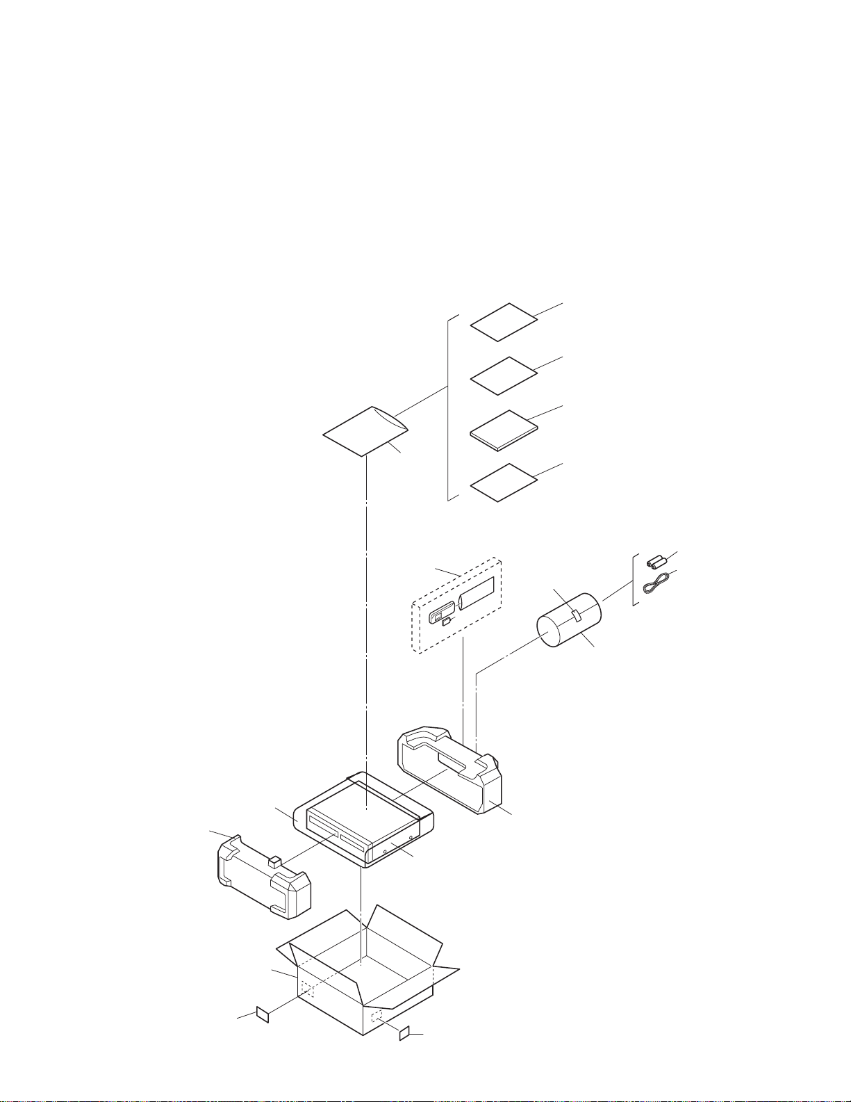
PARTS LIST
SAFETY PRECAUTION
Parts identified by the symbol are critical for safety. Replace only with specified part numbers.
BEWARE OF BOGUS PARTS
Parts that do not meet specifications may cause trouble in regard to safety and performance. We recommend that genuine
JVC parts be used.
1. EXPLODED VIEW
1.1 PACKING AND ACCESSORY ASSEMBLY <M1>
The instruction manual to be provided with this product will differ according to the destination.
313
317
310
302
303
311
316
316A
FINAL ASSY<M2>
305
308
306
ADHESIVE TAPE
309
302
315
301
SPEC OF BARCODE
(No.YD002)3-1
Page 57

1.2 F INAL ASSEMBLY <M2>
505
506
504
506
506
595
596
594
DVD SERVO CONTROL BOARD ASSY
<99>
597
TRAVERSE
MECHANISM ASSY
<M5>
591
592
592
BACK SIDE
591
591
MECHANISM ASSY
<M4>
522
524
MAIN
BOARD ASSY<03>
540
505
553
552
530
Grease
JVS-1003
LOADING
MECHANISM
ASSY
<M6>
522
516
515
527
527
527
517
527
527
527
527
i
m
DVD UNIT<M5>, <M6>,<98>,<99>
i
i
515
507
550
520
520
d
L
P
*
*
*
*
*
A
508
520
B
514
522
j
j
f
e
521
521
521
523
i
i
524
TERMINAL BOARD
ASSY<06>
C
1
0
0
6
U
T
J
S
3
0
0
1
511
N
C
2D DIGITAL
BOARD ASSY<05>
542
501D
501E
503
503
3-2(No.YD002)
501
515
529
541
i
510
i
525
518
501A
501B
f
f
501C
f
f
518
501F
501D
i
h
a
a
a
a
i
i
526
509
545
546
h
REGULATOR BOARD ASSY
525
m
525
<01>
532
Page 58

CN7104
right side
DRAWING FROM DIRECTION
After Assembling FRONT PANEL
548
JACK BOARD ASSY parts surface
CN7191
A/C HEAD
D
CN7104
D
JACK BOARD ASSY
CN7191
502
502
CN7191
WR1
NOTE) INSERT FFC WIRE TO THE CONNECTOR BEFORE
ATTACHING TO FRONT PANEL.
back side
502
6
CN2001
BOTTOM SIDE
TOP SIDE
502
CN511
WR3
CN3102
C
CN5311
CN3103
back side
CN5313
A
WR2
right side
CN5001
CN5303
CN5301
502
502
CN5302
Wire lets the bottom of BRACKET(DVD) pass.
CN1601
After Assembling FRONT PANEL
CN7004
CN7003
WR3 WR2
CN3103CN3102
DRAWING FROM DIRECTION
DRAWING FROM DIRECTION
Connect the FJ CONN
when assembling
REGULATOR BOARD ASSY.
CN5311
/CN5313
NOTE) FJ CONN should be insert as follows.
CN5301
/CN5303
OK
CN
FRONT PWB
CN7003
FRONT PWB
CN7004
C
A
NG
CN
1. Insert direction of FCC WIRE as follows.
right side
electrode side
2. FFC WIRE and DRUM FPC WIRE should be insert as follows.
3. Insert direction of POWER CORD.
4. Insert the wire to even the root of connector completely
at the same time as inserting each wire.
OK
90
CN
U/U(C)/JPN
WHITE LINE
NEUTRAL
Thing which to be
SPACER
placed with
SPACERS and
to be fixed.
SIN TWIST WIRE
SPACER
DVD SERVO CONTROL
BOARD ASSY
back side
supporting side
NG
CN
except U/U(C)/JPN
BLUE
NEUTRAL
CN5001
It solders SIN TWIST WIRE with DVD SERVO
CONTROL BOARD ASSY.
SPACER
SPACER
SPACER should be stuck high cohesive
sheet side (transparent film side) to IC.
FITTING ASSY
TRAY
CN
Z-Z SECTION
DRAWING FROM DIRECTION
Z
Z
Z
Z
A
ONLY THIS PORTION IS PUSHED
WHEN ATTACHING DVD UNIT.
FIG.4
THE POSITION OF 512 HEAT SINK AND 544
SHEET REFERS TO FIGURE BELOW.
FIG.2
512
TERMINAL BOARD ASSY
CN5001
549
UP
parts surface
J7007
Attach the character "UP"
in the table side.
FIG.3
543
k
544
511
531
k
k
k
513
531
513
FIG 5
DVD UNIT
DRAWING
FROM DIRECTION
B
FIG.1
(No.YD002)3-3
Page 59

1.3 MECHANISM ASSEMBLY <M4>
112
AA
124
127
128
126
AA
110
AA
118
77
76
134
AA
122
130
121
74
105
88
BB
90
89
21
4
AA
BB
BB
BB
BB
90
72
71
AA
73
75
37
AA
78
89
38
AA
36
107
AA
Not used
79
137
151
123
125
126
119
107
111
115
80
105
117
26
86
AA
83
81
AA
56
52
58
161
55
53
91
1
39
3
AA
120
82
31
30
113
112
116
114
A/C HEAD
BOARD ASSY <12>
WR2
57
58
42
50
44
49
WR1
51
85
PMD0044A-C,PMD0047A-C
Classification Part No. Symbol in drawing
Grease KYODO-SH-JB AA
3-4(No.YD002)
102
AA
69
70
AA
96
94
Oil COSMO-HV56 BB
AA
23B
AA
64
65
23
23A
WR3
67
62
59
AA
68
AA
84
61
60
63
66
48
AA
95
93
15
22
AA
24
18
19
20
LOADING MOTOR
BOARD ASSY <55>
16
AA
18B
18A
87
AA
AA
46
47
NOTE:The section marked in AA and BB
indicate lubrication and greasing areas.
Page 60

1.4 TRAVERSE MECHANISM ASSEMBLY <M5>
Grease
=JVG-31N
=CFD-4007ZY2
=PG-641
=1401C
< Back side >
27
26
25
16
17
24
23
6
5
A
15
14
13
18
12
19
A
10.5mm
+
-
2
0.1mm
+
0.1mm
-
28
28
63.3mm
22
21
20
4
11
8
11
9
3
7
10
EXL-V10-11C
1
(No.YD002)3-5
Page 61

1.5 LOADING MECHANISM ASSEMBLY <M6>
18
20
19
17
14
22
16
3
5
21
Grease
JVG-31N
4
JVS-1003
13
1
12
0.10mm
-
+
11
(All circumferences)
10
8
9
7.95mm
Back side
7
a
b
6
SWITCH BOARD
ASSY
a
b
ELM-J2-2C
3-6(No.YD002)
Page 62

2. PARTS LIST
PACKING AND ACCESSORY ASSEMBLY <M1>
Symbol No.
301 LP31296-004A PACKING CASE
301 LP31296-002A PACKING CASE
301 LP31296-003A PACKING CASE
301 LP31296-001A PACKING CASE
302 LP31295-001B CUSHION ASSY
303 PQM30021-95 POL Y BAG
305 LYT0194-001B Q.CARD
306 QAM0002-001 RF CABLE
306 PEAC0300-02 RF CABLE
308 ------------ BATTERY R6 TYPE(x2)
309 QPC02202230P POLY BAG 22cm x 22cm
310 LPT0868-001A INST.BOOK (ENGLISH)
310 LPT0865-001A INST.BOOK (ENGLISH)
310 LPT0864-001A INST.BOOK (ENGLISH)
310 LPT0864-002A INST.BOOK (GERMANY)
310 LPT0864-003A INST.BOOK (FRENCH)
310 LPT0864-004A INST.BOOK (DUCH)
310 LPT0864-005A INST.BOOK (SPANISH)
310 LPT0864-006A INST.BOOK (ITALIAN)
310 LPT0864-007A INST.BOOK (DANISH)
310 LPT0864-008A INST.BOOK (FINNISH)
310 LPT0864-009A INST.BOOK (SWEDISH)
310 LPT0864-010A INST.BOOK (NORWEGIAN)
310 LPT0864-011A INST.BOOK (PORTUGUESE)
310 LPT0864-012A INST.BOOK (GREEK)
310 LPT0864-013A INST.BOOK (CZECH)
310 LPT0864-014A INST.BOOK (POLISH)
310 LPT0864-015A INST.BOOK (HUNGARIAN)
310 LPT0880-001A INST.BOOK (ENGLISH)
310 LPT0880-002A INST.BOOK (GERMANY)
310 LPT0880-003A INST.BOOK (FRENCH)
310 LPT0880-004A INST.BOOK (DUCH)
310 LPT0880-005A INST.BOOK (SPANISH)
310 LPT0880-006A INST.BOOK (ITALIAN)
310 LPT0880-007A INST.BOOK (DANISH)
310 LPT0880-008A INST.BOOK (FINNISH)
310 LPT0880-009A INST.BOOK (SWEDISH)
310 LPT0880-010A INST.BOOK (NORWEGIAN)
310 LPT0880-011A INST.BOOK (PORTUGUESE)
310 LPT0880-012A INST.BOOK (GREEK)
310 LPT0880-013A INST.BOOK (CZECH)
310 LPT0880-014A INST.BOOK (POLISH)
310 LPT0880-015A INST.BOOK (HUNGARIAN)
310 LPT0861-001A INST.BOOK (ENGLISH)
310 LPT0860-001A INST.BOOK (ENGLISH)
310 LPT0860-002A INST.BOOK (GERMANY)
310 LPT0860-003A INST.BOOK (FRENCH)
310 LPT0860-004A INST.BOOK (DUCH)
310 LPT0860-005A INST.BOOK (SPANISH)
310 LPT0860-006A INST.BOOK (ITALIAN)
310 LPT0860-007A INST.BOOK (DANISH)
310 LPT0860-008A INST.BOOK (FINNISH)
310 LPT0860-009A INST.BOOK (SWEDISH)
310 LPT0860-010A INST.BOOK (NORWEGIAN)
310 LPT0860-011A INST.BOOK (PORTUGUESE)
310 LPT0860-012A INST.BOOK (GREEK)
310 LPT0860-013A INST.BOOK (CZECH)
310 LPT0860-014A INST.BOOK (POLISH)
310 LPT0860-015A INST.BOOK (HUNGARIAN)
311 QPC02503530P POLY BAG 25cm x 35cm
311 QPC02503530P POLY BAG 25cm x 35cm(x2)
313 BT-54013-7 WARRANTY CARD
315 LP41135-001A STICKER(CARTON) (x2)
316 LP21036-036A REMOCON
316 LP21036-035A REMOCON
316A LP40254-004A COVER(BATTERY)
316A LP40254-008A COVER(BATTERY)
317 BT-54008-6 GUARANTY CARD
Part No. Part Name Description Local
A,D
B,E
F,G
A,B,C,F
A,B,D,E,F,G
A,C
A,B,C,F
D,E,G
D,E,G
F,G
A,B,D,E,F,G
A,B,D,E,F,G
A,B,C,F
MODEL MARK
HR-XV3EK
HR-XV31EK
HR-XV32EK
HR-XV3EX
MODEL MARK
A
HR-XV
HR-XVS30EK
B
HR-XVS30EX
C
D
31EX
E
F
G
FINAL ASSEMBLY <M2>
Symbol No.
C
C
B
D
D
D
D
D
D
D
D
D
D
D
D
D
D
D
E
E
E
E
E
E
E
E
E
E
E
E
E
E
E
F
G
G
G
G
G
G
G
G
G
G
G
G
G
G
G
C
C
501 LP10490-013A FRONT PANEL ASSY
501 LP10492-007C FRONT PANEL ASSY
501 LP10490-017A FRONT PANEL ASSY
501 LP10490-012A FRONT PANEL ASSY
501 LP10492-009C FRONT PANEL ASSY
501 LP10490-008A FRONT PANEL ASSY
501 LP10490-007A FRONT PANEL ASSY
501A LP21181-003A CASSETTE DOOR
501A LP21181-001A CASSETTE DOOR
501A LP21188-002A CASSETTE DOOR
501A LP21181-002A CASSETTE DOOR
501B PQ46448 TORSION SPRING
501C LP31269-002A
501C LP31271-002A
501D PU60109 CATCHER (x2)
501E LP21191-013A DOOR(L)
501E LP21191-017A DOOR(L)
501E LP21191-012A DOOR(L)
501E LP21191-008A DOOR(L)
501E LP21191-007A DOOR(L)
501F LP21192-005A DOOR(R)
501F LP21192-003A DOOR(R)
502 QYTDSF2608Z TAP SC REW
503 LP40990-001A SPECIAL SCREW
503 LP40990-001A SPECIAL SCREW FRONT PANEL
504 LP10488-004B TOP COVER
504 LP10488-002B TOP COVER
505 QYSBSG3006M TAP SCREW
505 QYSBSG3006N TAP SCREW
506 QYSBSG3006M TAP SCREW
506 QYSBSG3006N TAP SCREW
507 LP31261-003A FITTING ASSY
507 LP31261-001A FITTING ASSY
507 LP31261-002A FITTING ASSY
508 LP41077-001A LABEL(CAUTIO N)
509 LP31288-006A STICKER(TOP)
509 LP31288-005A STICKER(TOP)
509 LP31288-002A STICKER(TOP)
509 LP31288-001A STICKER(TOP)
510 LP10489-001B BOTTOM CHASSIS
511 LP21177-001B BRACKET(DVD)
512 LP21182-001A HEAT SINK
513 QYSDST3006Z TAP SCREW
514 LP40769-001A SPACER
515 LP40990-001A SPECIAL SCREW
516 LP21178-012A REAR COVER
516 LP21178-009A REAR COVER
517 QYSBSG3006M TAP SCREW
518 LP31348-001A FOOT (x2)
520 QYSBSG3010Z TAP SCREW
521 QYSPSPD3008Z SCREW
522 LP40980-001A SPECIAL SCREW MECHANISM(x3)
523 LP40990-001A SPECIAL SCREW HOUSING
524 LP40990-001A SPECIAL SCREW MAIN(x2)
525 LP40990-001A SPECIAL SCREW REGULATOR(x3)
526 LP40696-008A HOLDER(PWB) (x2)
527 QYTDSF3008M TAP SCREW
527 QYTDSF3008M TAP SCREW
529 QMP51K0-170-K POWER CORD 1.7m BLACK
529 QMP4A10-170 POWER CORD 1.7m BLACK
530 PDV2539B DRUM FINAL ASSY
530 PDV2544A DRUM FINAL ASSY
531 LP30002-0E5A SPACER (x2)
532 LP41120-001A STICKER(FRONT)
540 PQ21623-2-5 EARTH PLATE(RF)
541 PQ44695-1-1 EARTH PLATE
542 LP40990-001A SPECIAL SCREW EARTH PLATE
543 LP40983-001A SHIELD TIGHT
544 LP31306-001A SHEET(SHIELD)
545 QQR0491-002 CORE FILTER
546 PU43192-4 BINDER
548 LP31337-001A EARTH PLATE
549 LP31345-001A EARTH PLATE
550 QUB221-10A4XL SIN TWIST WIRE DVD UNIT
552 LP40370-001F ROLLER ARM ASSY
Part No. Part Name Description Local
A,D
B,E
F,G
ORNAMENT(C.DOOR)
ORNAMENT(C.DOOR)
M2.6 x 8mm DISPLAY JACK(x9)
FRONT PANEL(x2)
M3 x 6mm TOP SIDE(x2) C
3mm x 6mm TOP SIDE(x2) A,B,D,E,F,G
M3 x 6mm TOP REAR(x6) C
3mm x 6mm TOP REAR(x6) A,B,D,E,F ,G
3mm x 6mm HEAT SINK(x2)
BRACKET(DVD)(x3)
M3 x 6mm REAR COVER
3mm x 10mm DVD UNIT(x3)
3mm x 8mm DRUM(x3)
M3 x 8mm JACK(x6)
M3 x 8mm JACK(x7)
B,E
A,C,D,F,G
A,C,D,F,G
A,D,F,G
B,E
A,C,D,F,G
A,B,D,E,F ,G
A,D
F,G
A,B,C
D,E
A,B,C,D,E
F,G
A,B,C,D,E
F,G
A,B,C,F
D,E,G
A,B,C,D,E
F,G
F,G
F,G
A
B
C
D
E
F
G
C
A
C
D
F
G
C
C
C
F
G
(No.YD002)3-7
Page 63

Symbol No.
Part No. Part Name Description Local
Symbol No.
MODEL MARK
HR-XV3EK
HR-XV31EK
HR-XV32EK
HR-XV3EX
MODEL MARK
A
HR-XV
HR-XVS30EK
B
HR-XVS30EX
C
D
31EX
Part No. Part Name Description Local
E
F
G
553 PQ45160 INERTIA PLATE
591 LE40900-003A INSULATOR (x4)
592 LE40901-001A SPECIAL SCREW (x4)
594 QYSDSF2608Z SCREW
2.6mm x 8mm(x4)
595 QUQ110-0518BF FFC WIRE
596 LE30001-034A SPACER
597 VYSH101-034 SPACER
WR1 QUQ112-0714CG FFC WIRE
WR1 QUQ112-1115CG FFC WIRE
WR2 QUQ112-1414CG FFC WIRE
WR3 QUQ112-1422CG FFC WIRE
JACK CN7191-MAIN CN7104 A,B,C,D,E
JACK CN7191-MAIN CN7104 F,G
DISLAY CN7004-MAIN CN3103
DISPLAY CN7003-MAIN CN3102
MECHANISM ASSEMBLY <M4>
Symbol No.
1 LP21039-001X MAIN DECK ASSY
3 LP40097-002E GUIDE POLE CAP
4 NAH0004-001 FE HEAD
15 LP30958-001B LOADING GEAR BASE
16 QYTPST2620Z TAP SCREW
18 LP40798-001A LOADING GEAR(SUPPLY) ASSY
18A LP21040-001A LOADING GEAR(SUPPLY)
18B LP40799-001A LOADING ARM(SUPPLY) ASSY
19 LP40837-001A TORSION SPRING(SUPPLY)
20 LP40903-002B FIXING PLATE
21 LP40806-001D POLE BASE ASSY(SUPPLY)
22 LP30959-001B LOADING GEAR
23 LP40802-001C LOADING GEAR(TAKE UP) ASSY
23A LP21041-001D LOADING GEAR(TAKE UP)
23B LP40803-001A LOADING ARM(TAKE UP) ASSY
24 LP40838-001A TORSION SPRING(TAKE UP)
26 LP40808-001E POLE BASE ASSY(TAKE UP)
30 LP31020-005A ARM BASE
31 QYTDST2606Z TAP SCREW 2.6mm x 6mm
36 LP21055-001G TAKE UP LEVER
37 LP40943-001A TENSION SPRING
38 LP40859-001D TAKE UP HEAD
39 LP30961-001C LID GUIDE
42 LP40810-001C PINCH ROLLER ARM ASSY
44 LP40840-001D TORSION SPRING
46 LP30963-001C PRESS LEVER
47 PQM30017-24 SLIT WASHER
48 LP40930-002F S-SWITCH
49 LP40813-001D GUIDE ARM ASSY
50 LP40841-001A TORSION SPRING
51 LP30002-090A SPACER
52 NAH0003-001 AC HEAD
53 LP30965-001A HEAD BASE
55 LP40842-001D COMPRESSION SPRING
56 QYTDST2006M TAP SCREW M2 x 6mm
57 LP41036-001A A/C ADJ.SCREW (x2)
58 QYTDST2606Z TAP SCREW
59 QAR0289-001 LOADING MOTOR
60 QYTPSP3003Z SCREW 3mm x 3mm(x2)
61 LP21056-002J MOTOR BRACKET
62 QYTPST2620Z TAP SCREW 2.6mm x 20mm
63 LP40814-001B WORM BEARING
64 LP21044-001E CONTROL CAM
65 PQM30017-24 SLIT WASHER
66 LP40815-001A WORM GEAR
67 LP40816-001B HELICAL GEAR
68 LP40817-001A CONNECT GEAR
69 LP10400-001L CONTROL PLATE
70 LP40843-001A TORSION SPRING
71 LP40818-001B TENSION ARM ASS Y
72 LP40844-001F TENSION SPRING
73 LP21045-001E TENSION ARM BAS E
74 LP40821-001A TENSION BAND ASSY
75 LP30967-001B BAND HOLDER-1
76 LP30968-001C BAND HOLDER-2
77 LP40822-002B ADJUST PIN
78 LP31000-005E TENSION ARM LEVE R
79 LP21046-001C MAIN BRAKE(TAKE UP)
80 LP40824-001A BAND BRAKE ASSY
Part No. Part Name Description Local
2.6mm x 20mm(x2)
2.6mm x 6mm(x2)
F,G
F,G
F,G
F,G
A,B,C,D,E
81 LP30969-002B BRAKE LEVER
82 LP30003-033B TENSION SPRING
83 LP30003-035B TENSION SPRING
84 LP40825-001B CAPSTAN BRAKE ASSY
85 QAR0267-002 CAPSTAN MOTOR
86 QYTPSG2606Z TAP SCREW
87 LP30005-010A BELT
2.6mm x 6mm(x3)
CAPSTAN MOTOR
88 LP30970-001A IDLER ARM
89 LP40828-004A IDLER GEAR 1 (x2)
90 LP40829-002A IDLER GEAR 2 (x2)
91 LP31014-002A WIRE HOLDER
93 LP40934-001B CLUTCH UNIT
94 PQM30017-47 SLIT WASHER
95 LP30973-001A DIRECT GEAR
96 LP40939-001A COMPRESSION SPRING
102 LP30974-001C CHANGE LEVER
105 LP21049-001A REEL DISK (x2)
107 LP30017-004A SPACER REEL DISK(x2)
110 LP10401-001L SIDE FRAME(L)
111 LP10402-001M SIDE FRAME(R)
112 QYTDST2606Z TAP SCREW
2.6mm x 6mm(x2)
113 LP40917-001D TORSION SPRING
114 LP30976-001E SIDE PLATE
115 LP30977-002D LIMIT PLATE
116 LP40846-001C LIMIT SPRING
117 LP31100-002A DRIVE LEVER
118 LP30978-001B DRIVE ARM(L)
119 LP30979-001R DRIVE ARM(R)
120 LP40847-001B TORSION SPRING
121 LP30980-001E CONNECT PLATE
122 LP10403-001C SIDE HOLDER(L)
123 LP10404-001E SIDE HOLDER(R)
124 LP30983-001B LOCK LEVER(L)
125 LP30984-001B LOCK LEVER(R)
126 LP40924-001D TENSION SPRING (x2)
127 LP40972-001A EARTH SPRING(1)
128 LP40857-001B EARTH SPRING(2)
130 LP30981-001G CASSETTE HOLDER ASSY
134 LP21051-002C REC SAFETY LEVER
137 LP21052-001K TOP FRAME
151 LP30985-002M DOOR OPENER
161 LP40993-001A TAPE GUIDE
WR1 WJT0117-001A E-CARD WIRE DRUM
WR2 WJT0067-001B E-CARD WIRE
WR3 WJS0022-001A E-FL/RB WIRE
A/C HEAD CN2001
LOADING MOTOR
TRAVERSE MECHANISM ASSEMBLY <M5>
Symbol No.
1 LE20697-003A MECHA BASE
2 LE20699-002A SPINDLE BASE
3 QYSDST2604M TAP SCREW
4 LE40931-001A SHAFT
5 LV33991-001A ADJUST SPRING
6 QYSPSFU2040M TAP SCREW M2 x 4mm
7 LE20698-003A FEED HOLDER
8 QAR0215-001 FEED MOTOR
9 LV41510-001A FEED GEAR T
10 QYSPSPU2040M TAP SCREW M2 x 4mm(x2)
11 QYSDST2604M TAP SCREW
12 QAL0507-001 PICK UP
13 LE20700-001A SW ACTUATOR
14 LE31067-002A LEAD SPRING
15 QYSPSFU1740Z TAP SCREW M1.7 x 4mm(x2)
16 LE40929-001A SW.LEVER
17 QYSPSFU1740Z TAP SCREW M 1.7 x 4mm
18 QUQ105-24X8AC FFC
19 LE40931-001A SHAFT
20 LE40855-001A FEED GEAR E
21 LE40918-001A LEAD SCREW
22 LE40930-001A FEED GEAR M
23 LE40928-001A THURUST SPRING
24 LE40927-001A PLATE
25 QYSDST2614Z TAP SCREW M2.6 x 14mm
Part No. Part Name Description Local
2.6mm x 4mm(x2)
2.6mm x 4mm(x2)
3-8(No.YD002)
Page 64

Symbol No.
Part No. Part Name Description Local
Symbol No.
MODEL MARK
HR-XV3EK
HR-XV31EK
HR-XV32EK
HR-XV3EX
MODEL MARK
A
HR-XV
HR-XVS30EK
B
HR-XVS30EX
C
D
31EX
E
F
G
Part No. Part Name Description Local
26 QAR0284-001 SPINDLE MOTOR
27 QYSPSPU1740Z TAP SCREW M1.7 x 4mm(x3)
28 LE40858-002A SPECIAL SCREW (x3)
LOADING MECHANISM ASSEMBLY <M6>
Symbol No.
Part No. Part Name Description Local
1 LE10275-006A LOADING BASE
3 LE31043-001A PULLEY GEAR
4 LE31042-001A MIDDLE GEAR
5 LE20665-002A SLIDE CAM
6 LE20666-003A ELEVATOR
7 LE10276-002A TRAY
8 LE31045-001A BUSHING
9 LE40898-001A SHAFT
10 QYSSSF2008Z TAP SCREW M2 x 8mm
11 QAR0197-001 MOTOR
12 LV42087-002A MOT OR PULLEY
13 QYSPSPU1730Z SCREW FOR MOTOR(x2)
14 QYSDSF2008Z TAP SCREW M2 x 8mm(x2)
16 LE40897-001A BELT
17 LE31046-003A CLAMPER
18 LV42930-003A MAGNET
19 LE40899-001A YOKE
20 LE40906-001A SPECIAL SCREW
21 LE31044-001A IDLE GEAR
22 LE40937-002A LEAF SPRING
REGULATOR BOARD ASSEMBLY <01>
Symbol No.
PW1 LPA10206-11C1 REGULATOR BOARD ASSY
PW1 LPA10206-14B1 REGULATOR BOARD ASSY
PW1 LPA10206-09C1 REGULATOR BOA RD ASSY
IC5201 UTCTL431-T IC
IC5201 or MM1431AT-T IC
IC5201 or L5431-T IC
IC5201 or TL431/A/-T IC
IC5301 UTCTL431-T IC
IC5301 or MM1431AT-T IC
IC5301 or L5431-T IC
IC5301 or TL431/A/-T IC
IC5302 MM1565AF-X IC
Q5101 2SK2632-CB14 POWER MOS FET
Q5102 2SD2144S/UV/-T TRANSISTOR
Q5103 2SB709A/QR/-X TRANSISTOR
Q5103 or 2SA1037AK/QR/-X TRANSISTOR
Q5311 2SC5739/QP/ TRANSISTOR
Q5315 2SC5739/QP/ TRANSISTOR
Q5315 or 2SD2394/EF/ TRANSISTOR
D5001 D3SBA60 DIODE
D5001 or GBJ4J BRIDGE DIODE
D5101 10ERB40-T2 FR DIODE
D5101 or AU01-T2 SI DIODE
D5102 10ERB40-T2 FR DIODE
D5102 or AU01-T2 SI DIODE
D5103 1SS133-T2 DIODE
D5103 or 1SS270A-T2 SI DIODE
D5105 1SS133-T2 DIODE
D5105 or 1SS270A-T2 SI DIODE
D5106 MTZJ33D-T2 Z DIODE
D5106 or RD33ES/B4/-T2 Z DIODE
D5201 10ELS2-T2 FR DIODE
D5201 or AU01Z-T2 FR DIODE
D5201 10ERB40-T2 FR DIODE
D5201 or 1F4G-T2 FR DIODE
D5205 1F4G-T2 FR DIODE
Part No. Part Name Description Local
A,C,D
B,E
F,G
A,B,C,E,F,G
D5205 or 10ERB20-T2 FR DIODE
D5206 1F4G-T2 FR DIOD E
D5206 or 10ERB20-T2 FR DIODE
D5208 SB240-F26 SB DIODE
D5208 or RK14LF-B2 SBD
D5208 or 21DQ04-F SBD
D5209 PG104RS-T2 FR DIODE
D5209 or 10ERB20-T2 FR DIODE
D5209 or 1F4G-T2 FR DIODE
D5209 or AU01Z-T2 FR DIODE
D5209 or 1SR153-400-T2 FR DIODE
D5210 PG104RS-T2 FR DIODE
D5210 or 10ERB20-T2 FR DIODE
D5210 or 1F4G-T2 FR DIODE
D5210 or AU01Z-T2 FR DIODE
D5210 or 1SR153-400-T2 FR DIODE
D5214 D1FS4A-X SB DIODE
F,G
D5215 D1FS4A-X SB DIODE
D5216 D1FS4A-X SB DIODE
D5301 MTZJ15C-T2 Z DIODE
D5301 or RD15ES/B3/-T2 Z DIODE
D5302 1SS133-T2 DIODE
D5302 or 1SS270A-T2 SI DIODE
D5303 MTZJ27C-T2 Z DIODE
D5303 or RD27ES/B3/-T2 Z DIODE
D5310 MTZJ10B-T2 Z DIODE
D5310 or RD10ES/B2/-T2 Z DIODE
PC5101 PC123Y22 PHOTO COUPLER
C5001 QFZ9077-683 MPP CAPACITOR 0.068uF 257V M
C5002 QFZ9051-223 MM CAPACITOR 0.022uF 250V M
C5004 QCZ9079-222 C CAPACITOR
2200pF AC250V M
C5006 QEZ0374-826 E CAPACITOR 82uF 400V M
C5101 QCZ0336-330Z C CAPACITOR 33pF 1kV J
C5102 QCZ0333-472 C CAPACITOR 4700pF 1kV K
C5104 QETN1HM-105Z E CAPACITOR 1uF 50V M
C5105 QFLC1HJ-183Z M CAPACITOR 0.018uF 50V J
C5106 NCB31HK-271X C CAPA CITOR 270pF 50V K
C5107 QFVF1HJ-104Z MF CAPACITOR 0.1uF 50V J
C5201 QFVF1HJ-154Z MF CAPACITOR 0.15uF 50V J
C5202 QEMU1AM-567Z E CAPACITOR 560uF 10V M
C5203 QEMX0JM-227Z E CAPACITOR 220uF 6.3V M
C5204 QEMU1AM-567Z E CAPACITOR 560uF 10V M
C5205 QEMU1CM-397Z E CAPA CITOR 390uF 16V M
C5206 QEMU1AM-567Z E CAPACITOR 560uF 10V M
C5207 QETN2AM-475Z E CAPACITOR 4.7uF 100V M
C5208 QEMU1HM-186Z E CAPA CITOR 18uF 50V M
C5209 QETN1AM-107Z E CAPACITOR 100uF 10V M
C5210 QETN1CM-107Z E CAPACITOR 100uF 16V M
C5211 QETN1AM-107Z E CAPACITOR 100uF 10V M
C5301 NCB31EK-103X C CAPACITOR 0.01uF 25V K
C5306 NCF31AZ-105X C CAPACITOR 1uF 10V Z
C5307 NCB31HK-471X C CAPA CITOR 470pF 50V K
C5309 QETN1AM-107Z E CAPACITOR 100uF 10V M
C5310 QETN1AM-107Z E CAPACITOR 100uF 10V M
C5311 QETN1AM-107Z E CAPACITOR 100uF 10V M
C5312 QETN1AM-107Z E CAPACITOR 100uF 10V M
C5313 QETN1AM-107Z E CAPACITOR 100uF 10V M
C5314 QETN1CM-107Z E CAPACITOR 100uF 16V M
R5101 QRE141J-224Y C RESISTOR 220kΩ 1/4W J
Ω
R5102 QRE141J-224Y C RESISTOR 220k
R5103 QRE141J-683Y C RESISTOR 68k
1/4W J
Ω
1/4W J
R5104 QRG02GJ-683 OMF RESISTOR 68kΩ 2W J
Ω
R5106 QRT01DJ-R27X MF RESISTOR 0.27
R5107 QRE121J-331Y C RESISTOR 330
R5108 NRSA63J-222X MG RESISTOR 2.2k
R5109 NRSA63J-681X MG RESISTOR 680
1W J
Ω
1/2W J
Ω
1/16W J
Ω
1/16W J
R5110 NRSA63J-224X MG RESISTOR 220kΩ 1/16W J
Ω
R5111 NRSA63J-681X MG RESISTOR 680
R5112 NRSA63J-221X MG RESISTOR 220
1/16W J
Ω
1/16W J
R5113 NRSA63J-104X MG RESISTOR 100kΩ 1/16W J
D
D
R5201 NRSA63J-221X MG RESISTOR 220
R5202 NRSA63J-102X MG RESISTOR 1k
Ω
1/16W J
Ω
1/16W J
R5203 NRSA63J-102X MG RESISTOR 1kΩ 1/16W J
Ω
R5204 NRSA63D-332X MG RESISTOR 3.3k
R5205 NRSA63D-123X MG RESISTOR 12k
1/16W D
Ω
1/16W D
(No.YD002)3-9
Page 65

Symbol No.
Part No. Part Name Description Local
Symbol No.
MODEL MARK
HR-XV3EK
HR-XV31EK
HR-XV32EK
HR-XV3EX
MODEL MARK
A
HR-XV
HR-XVS30EK
B
HR-XVS30EX
C
D
31EX
Part No. Part Name Description Local
E
F
G
R5206 NRSA63D-332X MG RESISTOR 3.3kΩ 1/16W D
R5302 NRSA63J-102X MG RESISTOR 1kΩ 1/16W J
R5305 NRSA63J-3R3X MG RESISTOR 3.3Ω 1/16W J
R5306 NRSA63J-2R2X MG RESISTOR 2.2Ω 1/16W J
R5307 NRSA63J-2R2X MG RESISTOR 2.2Ω 1/16W J
Ω
R5317 NRSA63J-473X MG RESISTOR 47k
R5318 QRZ9005-470X FUSI RESISTOR 47Ω 1/4W G
1/16W J
R5319 NRSA63J-560X MG RESISTOR 56Ω 1/16W J
R5320 NRSA63D-153X MG RESISTOR 15kΩ 1/16W D
R5321 NRSA63D-473X MG RESISTOR 47kΩ 1/16W D
R5325 NRSA63J-101X MG RESISTOR 100Ω 1/16W J
L5201 PELN1184 CHOKE COIL
L5202 PELN1184 CHOKE COIL
L5203 PELN1184 CHOKE COIL
L5301 QQL29BJ-220Z P COIL 22uH J
L5302 QQL231J-220Y COIL 22uH J
L5303 QQL231J-220Y COIL 22uH J
T5001 QQS0219-001 SW TRANSF
CN5001 QGA7901C3-02 CONNECTOR W-B (1-2)
CN5301 QGB1231L1-11 CONNECTOR B-B (1-11)
CN5302 QGB2027MA-22 CONNECTOR B-B (1-22)
CN5303 QGB1231L1-11 CONNECTOR B-B (1-11)
CP5301 QMFZ050-1R5X-E FUSE 1.5A 125V
CP5302 QMFZ050-1R5X-E FUSE 1.5A 125V
F5001 QMF51W2-2R0-J8 FUSE 2A AC250V
FC5001 QNG0020-001Z FUSE CLIP
FC5002 QNG0020-001Z FUSE CLIP
HS1 LP40621-001A HEAT SINK FOR Q5101
HS1 QZW0106-001 HEAT SINK FOR Q5101
K5101 QQR0678-001Z FERRITE BEADS
LF5002 QQR0608-001 LINE FILTER
OT1 QYTDST3008Z TAP SCREW
M3 x 8mm FOR Q5101
MAIN BOARD ASSEMBLY <03>
Symbol No.
PW1 LPA10215-12A MAIN BOARD ASSY
PW1 LPA10215-04B MAIN BOARD ASSY
PW1 LPA10215-03B MAIN BOARD ASSY
PW1 LPA10215-11A MAIN BOARD ASSY
PW1 LPA10215-02B MAIN BOARD ASSY
PW1 LPA10215-01B MAIN BOARD ASSY
IC1 JCP8060-MSA IC
IC201 LC74776-9791 IC
IC501 JCP8058-2 IC
IC2201 AN3651FBP IC
IC3001 HD6432194SAD55F IC(MCU)
IC3001 or HD64F2194CFD55 IC(MCU)
IC3002 IC-PST3427U-X IC
IC3003 LPN0833-007A-07 IC(EEPROM)
IC3003 LPN0833-005A-05 IC(EEPROM)
IC3003 LPN0833-004A-14 IC(EEPROM)
IC3003 LPN0833-008A-18 IC(EEPROM)
IC3003 LPN0833-002A-02 IC(EEPROM)
IC3003 LPN0833-001A-11 IC(EEPROM)
IC6701 MSP3417GQGB8V3X IC
IC6701 or MSP3417G-X IC
IC7102 MM1503XN-X IC
IC8001 HA17558AF-X IC
IC8001 or RC4558D-X IC
Q1 DTC144WKA-X DIGI TRANSISTOR
Q1 or UN221E-X TRANSTSTOR
Q7 2SC2412K/QRS/-X TRANSISTOR
Q7 or 2SD601A/QRS/-X TRANSISTOR
Q7 or 2SC3928A/QRS/-X TRANSISTOR
Q8 2SC2412K/QRS/-X TRANSISTOR
Q8 or 2SD601A/QRS/-X TRANSISTOR
Q8 or 2SC3928A/QRS/-X TRANSISTOR
Q9 2SC2412K/QRS/-X TRANSISTOR
Q9 or 2SD601A/QRS/-X TRANSISTOR
Part No. Part Name Description Local
*(REFER TO BELOW)
*(REFER TO BELOW)
*(REFER TO BELOW)
*(REFER TO BELOW)
*(REFER TO BELOW)
*(REFER TO BELOW)
A,B,C,D,E
F,G
B
A,C
D
E
F
G
F,G
B
A,C
D
E
F
G
F,G
F,G
F,G
Q9 or 2SC3928A/QRS/-X TRANSISTOR
Q10 2SC2412K/QRS/-X TRANSISTOR
Q10 or 2SD601A/QRS/-X TRANSISTOR
Q10 or 2SC3928A/QRS/-X TRANSISTOR
Q207 2SA1037AK/QR/-X TRANSISTOR
Q207 or 2SB709A/QR/-X TRANSISTOR
Q207 or 2SA1530A/QR/-X TRANSISTOR
Q501 2SA1037AK/QR/-X TRANSISTOR
Q501 or 2SB709A/QR/-X TRANSISTOR
Q501 or 2SA1530A/QR/-X TRANSISTOR
Q2001 2SC2412K/QRS/-X TRANSISTOR
Q2001 or 2SD601A/QRS/-X TRANSISTOR
Q2001 or 2SC3928A/QRS/-X TRANSISTOR
Q2002 2SC2412K/QRS/-X TRANSISTOR
Q2002 or 2SD601A/QRS/-X TRANSISTOR
Q2002 or 2SC3928A/QRS/-X TRANSISTOR
Q2003 DTA144WKA-X TRANSISTOR
Q2003 or UN211E-X DIGI TRANSISTOR
Q2051 2SC2412K/QRS/-X TRANSISTOR
Q2051 or 2SD601A/QRS/-X TRANSISTOR
Q2051 or 2SC3928A/QRS/-X TRANSISTOR
Q2052 2SA1037AK/QR/-X TRANSISTOR
Q2052 or 2SB709A/QR/-X TRANSISTOR
Q2052 or 2SA1530A/QR/-X TRANSISTOR
Q2053 DTC144WKA-X DIGI TRANSISTOR
Q2053 or UN221E-X TRANSTSTOR
Q2054 2SA1037AK/QR/-X TRANSISTOR
Q2054 or 2SB709A/QR/-X TRANSISTOR
Q2054 or 2SA1530A/QR/-X TRANSISTOR
Q2055 DTC144WKA-X DIGI TRANSISTOR
Q2055 or UN221E-X TRANSTSTOR
Q2201 DTA144WKA-X TRANSISTOR
Q2201 or UN211E-X DIGI TRANSISTOR
Q2202 DTC144WKA-X DIGI TRANSISTOR
Q2202 or UN221E-X TRANSTSTOR
Q2203 2SC2412K/QRS/-X TRANSISTOR
Q2203 or 2SD601A/QRS/-X TRANSISTOR
Q2203 or 2SC3928A/QRS/-X TRANSISTOR
Q2204 2SC2412K/QRS/-X TRANSISTOR
Q2204 or 2SD601A/QRS/-X TRANSISTOR
Q2204 or 2SC3928A/QRS/-X TRANSISTOR
Q2251 DTC144WKA-X DIGI TRANSISTOR
Q2251 or UN221E-X TRANSTSTOR
Q2252 DTC144WKA-X DIGI TRANSISTOR
Q2252 or UN221E-X TRANSTSTOR
Q2253 DTC144WKA-X DIGI TRANSISTOR
Q2253 or UN221E-X TRANSTSTOR
Q2254 DTC114EKA-X TRANSISTOR
Q2254 or UN2211-X TRANSISTOR
Q2255 DTC114EKA-X TRANSISTOR
Q2255 or UN2211-X TRANSISTOR
Q3002 PTZ-NV16A IC(PHOTO SENSOR
Q3003 PTZ-NV16A IC(PHOTO SENSOR
Q3004 2SC2412K/QRS/-X TRANSISTOR
Q3004 or 2SD601A/QRS/-X TRANSISTOR
Q3004 or 2SC3928A/QRS/-X TRANSISTOR
Q3005 2SC2412K/QRS/-X TRANSISTOR
Q3005 or 2SD601A/QRS/-X TRANSISTOR
Q3005 or 2SC3928A/QRS/-X TRANSISTOR
Q3007 DTC144WKA-X DIGI TRANSISTOR
Q3007 or UN221E-X TRANSTSTOR
Q3008 DTC144WKA-X DIGI TRANSISTOR
Q3008 or UN221E-X TRANSTSTOR
Q3401 2SC2412K/QRS/-X TRANSISTOR
Q3401 or 2SD601A/QRS/-X TRANSISTOR
Q3401 or 2SC3928A/QRS/-X TRANSISTOR
Q4001 DTC114EKA-X TRANSISTOR
Q4001 or UN2211-X TRANSISTOR
Q5301 2SD2144S/UV/-T TRANSISTOR
Q5301 or 2SC3576-JVC-T TRANSISTOR
Q5302 DTA114EKA -X DIGI TRANSISTOR
Q5302 or UN2111-X TRANSISTOR
Q5303 DTC114EKA-X TRANSISTOR
Q5303 or UN2211-X TRANSISTOR
Q5306 2SD1302/ST/-T TRANSISTOR
Q5307 DTA114EKA -X DIGI TRANSISTOR
Q5307 or UN2111-X TRANSISTOR
Q5308 2SB709A/QR/-X TRANSISTOR
F,G
F,G
F,G
F,G
F,G
F,G
F,G
F,G
F,G
F,G
F,G
F,G
F,G
F,G
3-10(No.YD002)
*The VCR goes to jig RCU mode after replacing the EEPROM and the VCR does not accept some RCU command.
Therefore please set the VCR to the user RCU mode after replacing the EEPROM.
The method of setting the VCR to the user RCU mode is written on the service manual.
Page 66

Symbol No.
Part No. Part Name Description Local
Symbol No.
MODEL MARK
HR-XV3EK
HR-XV31EK
HR-XV32EK
HR-XV3EX
MODEL MARK
A
HR-XV
HR-XVS30EK
B
HR-XVS30EX
C
D
31EX
E
F
G
Part No. Part Name Description Local
Q5308 or 2SA1037AK/QR/-X TRANSISTOR
Q5308 or 2SA1530A/QR/-X TRANSISTOR
Q5309 DTC114EKA-X TRANSISTOR
Q5309 or UN2211-X TRANSISTOR
Q5312 DTA114EK A-X DIGI TRANSISTOR
Q5312 or UN2111-X TRANSISTOR
Q5313 2SC2412K/QRS/-X TRANSISTOR
Q5313 or 2SD601A/QRS/-X TRANSISTOR
Q5313 or 2SC3928A/QRS/-X TRANSISTOR
Q5314 2SC5739/QP/ TRANSISTOR
Q5314 or 2SD2394/EF/ TRANSISTOR
Q5316 2SD2144S/UV/-T TRANSISTOR
Q5316 or 2SC3576-JVC-T TRANSISTOR
Q6030 2SA1037AK/QR/-X TRANSISTOR
Q6030 or 2SB709A/QR/-X TRANSISTOR
Q6030 or 2SA1530A/QR/-X TRANSISTOR
Q6031 DTC114EKA-X TRANSISTOR
Q6031 or UN2211-X TRANSISTOR
Q6032 DTC114EKA-X TRANSISTOR
Q6032 or UN2211-X TRANSISTOR
Q8001 2SC2412K/QRS/-X TRANSISTOR
Q8001 or 2SD601A/QRS/-X TRANSISTOR
Q8001 or 2SC3928A/QRS/-X TRANSISTOR
Q8002 2SC2412K/QRS/-X TRANSISTOR
Q8002 or 2SD601A/QRS/-X TRANSISTOR
Q8002 or 2SC3928A/QRS/-X TRANSISTOR
Q8052 2SC2412K/QRS/-X TRANSISTOR
Q8052 or 2SD601A/QRS/-X TRANSISTOR
Q8052 or 2SC3928A/QRS/-X TRANSISTOR
Q8053 DTA114EK A-X DIGI TRANSISTOR
Q8053 or UN2111-X TRANSISTOR
D201 QRE141J-152Y C RESISTOR 1.5kΩ 1/4W J
D202 QRE141J-101Y C RESISTOR 100Ω 1/4W J
D203 QRE141J-101Y C RESISTOR 100Ω 1/4W J
D2001 1SS133-T2 DIODE
D2001 or 1SS270A-T2 SI DIODE
D2251 1SS133-T2 DIODE
D2251 or 1SS270A-T2 SI DIODE
D3001 LNB2301L01VI LED
D3002 1SS133-T2 DIODE
D3002 or 1SS270A-T2 SI DIODE
D3003 RD33ES/B3/-T2 Z DIODE
D3003 or MTZJ33C-T2 Z DIODE
D3004 10EDB20-T2 SI DIODE
D3004 or 1A3G-T2 SI DIODE
D3005 10EDB20-T2 SI DIODE
D3005 or 1A3G-T2 SI DIODE
D3007 1SS355-X SI DIODE
D3008 1SS355-X SI DIODE
D3401 RD3.6ES/B2/-T2 Z DIODE
D3401 or MTZJ3.6B-T2 Z DIODE
D5305 MTZJ11C-T2 Z DIODE
D5305 or RD11ES/B3/-T2 Z DIODE
D5306 MTZJ5.6C-T2 Z DIODE
D5306 or RD5.6ES/B3/-T2 Z DIODE
D5307 1SS133-T2 DIODE
D5307 or 1SS270A-T2 SI DIODE
D6002 HZ30-2L-T2 Z DIODE
D6002 or HZ30-2LTD Z DIODE
D6701 1SS133-T2 DIODE
D6701 or 1SS270A-T2 SI DIODE
D7301 10EDB20-T2 SI DIODE
D7301 or 1A3G-T2 SI DIODE
PC3001 RPI-304J IC(PHOTO SENSOR)
PC3002 RPI-304J IC(PHOTO SENSOR)
C1 NDC31HJ-151X C CAPACITOR 150pF 50V J
C2 NDC31HJ-470X C CAPACITOR 47pF 50V J
C2 NDC31HJ-4R0X C CAPACITOR 4pF 50V J
C3 NDC31HJ-470X C CAPACITOR 47pF 50V J
C4 QEKJ1EM-106Z E CAPACITOR 10uF 25V M
C5 NCB31CK-104X C CAPACITOR 0.1uF 16V K
C6 NCB31CK-104X C CAPACITOR 0.1uF 16V K
C7 NCB31CK-104X C CAPACITOR 0.1uF 16V K
C8 NCF31AZ-105X C CAPACITOR 1uF 10V Z
C9 QEKJ1HM-225Z E CAPACITOR 2.2uF 50V M
A,B,C,D,E
C10 QEKJ0JM-476Z E CAPACITOR 47uF 6.3V M
C11 NCF31AZ-105X C CAPACITOR 1uF 10V Z
C12 QEKJ1HM-105Z E CAP ACITOR 1uF 50V M
C14 QEKJ1HM-105Z E CAP ACITOR 1uF 50V M
C15 NCB31CK-104X C CAPACITOR 0.1uF 16V K
C16 NCB31EK-103X C CAPACITOR 0.01uF 25V K
C17 NCB31CK-104X C CAPACITOR 0.1uF 16V K
C18 NCB31CK-104X C CAPACITOR 0.1uF 16V K
F,G
A,B,C,D,E
F,G
C19 NCB31CK-104X C CAPACITOR 0.1uF 16V K
C20 NCB31CK-104X C CAPACITOR 0.1uF 16V K
C21 NCB31EK-103X C CAPACITOR 0.01uF 25V K
C22 NCB31CK-104X C CAPACITOR 0.1uF 16V K
C23 NCB31CK-104X C CAPACITOR 0.1uF 16V K
F,G
A,B,C,D,E
F,G
C24 NCB31CK-104X C CAPACITOR 0.1uF 16V K
C25 QEKJ1HM-335Z E CAP ACITOR 3.3uF 50V M
C26 QEKJ1EM-106Z E CAPACITOR 10uF 25V M
C27 NCB31EK-103X C CAPACITOR 0.01uF 25V K
C30 NDC31HJ-331X C CAPACITOR 330pF 50V J
C31 QEKJ0JM-476Z E CAPACITOR 47uF 6.3V M
C32 NCB31EK-103X C CAPACITOR 0.01uF 25V K
C33 QEKJ1EM-106Z E CAPACITOR 10uF 25V M
C34 NCB31EK-103X C CAPACITOR 0.01uF 25V K
C35 NCB31EK-103X C CAPACITOR 0.01uF 25V K
C36 QEKJ1HM-105Z E CAP ACITOR 1uF 50V M
C37 NDC31HJ-4R0X C CAPACITOR 4pF 50V J
C38 NCB31EK-103X C CAPACITOR 0.01uF 25V K
C39 QEKJ0JM-476Z E CAPACITOR 47uF 6.3V M
C40 NCB31EK-103X C CAPACITOR 0.01uF 25V K
C41 NCB31CK-104X C CAPACITOR 0.1uF 16V K
C41 NCB31EK-473X C CAPACITOR 0.047uF 25V K
A,B,C,D,E
F,G
C43 QEKJ1HM-335Z E CAP ACITOR 3.3uF 50V M
C44 QEKJ1HM-225Z E CAP ACITOR 2.2uF 50V M
C45 NCB31EK-472X C CAPACITOR 4700pF 25V K
C46 NCB31CK-104X C CAPACITOR 0.1uF 16V K
C47 QEKJ1HM-474Z E CAP ACITOR 0.47uF 50V M
C48 NCB31EK-223X C CAPACITOR 0.022uF 25V K
C49 QEKJ1HM-475Z E CAP ACITOR 4.7uF 50V M
C56 NCB31CK-104X C CAPACITOR 0.1uF 16V K
C57 NCB31EK-103X C CAPACITOR 0.01uF 25V K
C58 NCB31EK-103X C CAPACITOR 0.01uF 25V K
C59 NCB31EK-103X C CAPACITOR 0.01uF 25V K
C60 NCB31HK-103X C CAPACITOR 0.01uF 50V K
C61 QEKC0JM-476Z E CAP ACITOR 47uF 6.3V M
C62 QCBB1HK-103Y C CAPACITOR 0.01uF 50V K
C63 NCB31EK-103X C CAPACITOR 0.01uF 25V K
C64 NCB31EK-103X C CAPACITOR 0.01uF 25V K
C71 QEKJ1HM-105Z E CAP ACITOR 1uF 50V M
C73 NRSA63J-0R0X M G RESISTOR 0Ω 1/16W J
F,G
C201 QEKJ0JM-227Z E CAPACITOR 220uF 6.3V M
C204 NCB31EK-103X C CAPACITOR 0.01uF 25V K
C206 NDC31HJ-330X C CAPACITOR 33pF 50V J
C207 NDC31HJ-330X C CAPACITOR 33pF 50V J
C209 NCB31AK-474X C CAPACITOR 0.47uF 10V K
C210 NDC31HJ-101X C CAPACITOR 100pF 50V J
C211 NDC31HJ-101X C CAPACITOR 100pF 50V J
C212 NCB31CK-104X C CAPACITOR 0.1uF 16V K
C213 QEKJ1EM-475Z E CAPACITOR 4.7uF 25V M
C214 NCB31AK-224X C CAPACITOR 0.22uF 10V K
C215 NCB31AK-224X C CAPACITOR 0.22uF 10V K
C217 NDC31HJ-560X C CAPACITOR 56pF 50V J
C218 QEKJ1HM-105Z E CAP ACITOR 1uF 50V M
C222 QEKJ1HM-105Z E CAP ACITOR 1uF 50V M
C225 QEKJ0JM-227Z E CAPACITOR 220uF 6.3V M
C501 QEKJ0JM-476Z E CAPACITOR 47uF 6.3V M
C502 NCB31EK-103X C CAPACITOR 0.01uF 25V K
C503 QEKJ1HM-225Z E CAP ACITOR 2.2uF 50V M
C504 QEKJ1HM-225Z E CAP ACITOR 2.2uF 50V M
C507 NCB31EK-103X C CAPACITOR 0.01uF 25V K
C508 NCB31CK-104X C CAPACITOR 0.1uF 16V K
C509 NCB31EK-103X C CAPACITOR 0.01uF 25V K
F,G
F,G
C510 NCB31EK-103X C CAPACITOR 0.01uF 25V K
C511 QEKJ0JM-337Z E CAPACITOR 330uF 6.3V M
C513 NDC31HG-221X C CAPACITOR 220pF 50V G
C514 NDC31HG-271X C CAPACITOR 270pF 50V G
C515 NDC31HG-121X C CAPACITOR 120pF 50V G
C516 NDC31HG-271X C CAPACITOR 270pF 50V G
C517 QEKJ1HM-475Z E CAP ACITOR 4.7uF 50V M
C518 QEKJ1HM-225Z E CAP ACITOR 2.2uF 50V M
F,G
F,G
F,G
F,G
F,G
F,G
F,G
F,G
F,G
F,G
F,G
F,G
F,G
F,G
F,G
(No.YD002)3-11
Page 67

Symbol No.
Part No. Part Name Description Local
Symbol No.
MODEL MARK
HR-XV3EK
HR-XV31EK
HR-XV32EK
HR-XV3EX
MODEL MARK
A
HR-XV
HR-XVS30EK
B
HR-XVS30EX
C
D
31EX
Part No. Part Name Description Local
E
F
G
C519 NDC31HG-271X C CAPACITOR 270pF 50V G
C520 QEKJ1HM-225Z E CAP A CITOR 2.2uF 50V M
C521 NCB31EK-103X C CAPACITOR 0.01uF 25V K
C522 QEKJ1HM-475Z E CAP A CITOR 4.7uF 50V M
C523 NCB31EK-103X C CAPACITOR 0.01uF 25V K
C524 QEKJ1EM-106Z E CAPACITOR 10uF 25V M
C525 NCB31EK-103X C CAPACITOR 0.01uF 25V K
C528 NCB31CK-104X C CAPACITOR 0.1uF 16V K
C529 NCB31EK-103X C CAPACITOR 0.01uF 25V K
C530 NCB31EK-103X C CAPACITOR 0.01uF 25V K
C536 NCB31EK-103X C CAPACITOR 0.01uF 25V K
C539 NCB31EK-103X C CAPACITOR 0.01uF 25V K
C2001 QEKJ1HM-475Z E CAPACITOR 4.7uF 50V M
C2002 QEKJ1HM-105Z E CAPACITOR 1uF 50V M
C2003 QEKJ0JM-476Z E CAPACITOR 47uF 6.3V M
C2005 QEKJ1HM-475Z E CAPACITOR 4.7uF 50V M
C2006 NCB31EK-682X C CAPACITOR 6800pF 25V K
C2007 QEKJ1CM-226Z E CAPACITOR 22uF 16V M
C2008 QEKJ1HM-475Z E CAPACITOR 4.7uF 50V M
C2009 NCB31HK-122X C CAPA CITOR 1200pF 50V K
C2010 NCB31HK-152X C CAPA CITOR 1500pF 50V K
C2011 QEKJ1HM-475Z E CAPACITOR 4.7uF 50V M
C2012 QEKJ1HM-475Z E CAPACITOR 4.7uF 50V M
C2013 NDC31HJ-331X C CAPACITOR 330pF 50V J
C2051 NDC31HJ-331X C CAPACITOR 330pF 50V J
C2052 QFV91HJ-823Z MF CAPACITOR 0.082uF 50V J
C2053 NCB31HK-472X C CAPA CITOR 4700pF 50V K
C2054 NCB31EK-223X C CAPACITOR 0.022uF 25V K
C2055 QEKJ1EM-106Z E CAPACITOR 10uF 25V M
C2201 QEKJ1EM-106Z E CAPACITOR 10uF 25V M
C2202 QEKJ1HM-475Z E CAPACITOR 4.7uF 50V M
C2203 QEKJ1HM-475Z E CAPACITOR 4.7uF 50V M
C2204 QEKJ0JM-336Z E CAPACITOR 33uF 6.3V M
C2205 QEKJ1EM-106Z E CAPACITOR 10uF 25V M
C2206 QEKJ1EM-106Z E CAPACITOR 10uF 25V M
C2207 NCB31EK-153X C CAPACITOR 0.015uF 25V K
C2208 NCB31EK-153X C CAPACITOR 0.015uF 25V K
C2209 QEKJ1EM-106Z E CAPACITOR 10uF 25V M
C2210 QEKJ1EM-106Z E CAPACITOR 10uF 25V M
C2211 QEKJ0JM-336Z E CAPACITOR 33uF 6.3V M
C2212 QEKJ0JM-476Z E CAPACITOR 47uF 6.3V M
C2214 QEKJ1EM-106Z E CAPACITOR 10uF 25V M
C2215 QEKJ1EM-106Z E CAPACITOR 10uF 25V M
C2216 QEKJ1CM-476Z E CAPACITOR 47uF 16V M
C2218 QEKJ1EM-106Z E CAPACITOR 10uF 25V M
C2219 QEKJ1CM-226Z E CAPACITOR 22uF 16V M
C2220 QEKJ1EM-106Z E CAPACITOR 10uF 25V M
C2221 NCB31EK-223X C CAPACITOR 0.022uF 25V K
C2222 NCB31EK-103X C CAPACITOR 0.01uF 25V K
C2223 NCB31CK-473X C CAPA CITOR 0.047uF 16V K
C2224 NCB31CK-473X C CAPA CITOR 0.047uF 16V K
C2225 NCB30JK-105X C CAPACITOR 1uF 6.3V K
C2226 NCB30JK-105X C CAPACITOR 1uF 6.3V K
C2227 QEKJ1EM-106Z E CAPACITOR 10uF 25V M
C2230 QEKJ1EM-106Z E CAPACITOR 10uF 25V M
C2231 QEKJ1EM-106Z E CAPACITOR 10uF 25V M
C2251 NCB31EK-103X C CAPACITOR 0.01uF 25V K
C2252 NCB31EK-103X C CAPACITOR 0.01uF 25V K
C2253 NCB31EK-103X C CAPACITOR 0.01uF 25V K
C2254 QEKJ0JM-476Z E CAPACITOR 47uF 6.3V M
C2255 NCB31EK-103X C CAPACITOR 0.01uF 25V K
C2256 NCB31EK-103X C CAPACITOR 0.01uF 25V K
C2257 NCB31EK-103X C CAPACITOR 0.01uF 25V K
C2258 NDC31HJ-181X C CAPACITOR 180pF 50V J
C2259 QEKJ1HM-334Z E CAPACITOR 0.33uF 50V M
C2261 NDC31HJ-101X C CAPACITOR 100pF 50V J
C2262 NDC31HJ-101X C CAPACITOR 100pF 50V J
C3008 NDC31HJ-101X C CAPACITOR 100pF 50V J
C3011 QETL0JM-338 E CAPA CITOR 3300uF 6.3V M
C3012 QEKJ0JM-476Z E CAPACITOR 47uF 6.3V M
C3015 NCB31CK-104X C CAPACITOR 0.1uF 16V K
C3016 NCB31EK-473X C CAPACITOR 0.047uF 25V K
C3020 NDC31HJ-101X C CAPACITOR 100pF 50V J
C3021 NDC31HJ-101X C CAPACITOR 100pF 50V J
C3022 NCB31EK-104X C CAPACITOR 0.1uF 25V K
C3024 NDC31HJ-120X C CAPACITOR 12pF 50V J
C3025 QAT3725-300Z TRIM CAPACITOR
30pF ,TIMER CLOCK
C3026 NCB31EK-103X C CAPACITOR 0.01uF 25V K
F,G
F,G
F,G
F,G
F,G
F,G
F,G
F,G
F,G
F,G
F,G
F,G
C3027 QEKJ1EM-106Z E CAPACITOR 10uF 25V M
C3030 QEKJ0JM-476Z E CAPACITOR 47uF 6.3V M
C3031 NCB31CK-473X C CAPACITO R 0.047uF 16V K
C3033 NCB31EK-473X C CAPACITOR 0.047uF 25V K
C3036 NDC31HJ-180X C CAPACITOR 18pF 50V J
C3037 NDC31HJ-120X C CAPACITOR 12pF 50V J
C3040 NCB31EK-103X C CAPACITOR 0.01uF 25V K
C3050 NCF31EZ-104X C CAPACITOR 0.1uF 25V Z
C3071 QEKJ1CM-336Z E CAPACITOR 33uF 16V M
C3401 NCB31EK-103X C CAPACITOR 0.01uF 25V K
C4002 NCF31EZ-104X C CAPACITOR 0.1uF 25V Z
C4004 QEKJ1CM-226Z E CAPACITOR 22uF 16V M
C4005 NCB21HK-222X C CAPACITO R 2200pF 50V K
C4006 QEKJ0JM-476Z E CAPACITOR 47uF 6.3V M
C4008 QEQF1HM-105Z E CAPACITOR 1uF 50V M
C4009 NRSA63J-0R0X MG RESISTOR 0Ω 1/16W J
C4010 NCB31EK-223X C CAPACITOR 0.022uF 25V K
C4011 NCB31CK-104X C CAPACIT O R 0.1uF 16V K
C4012 QEKJ1HM-105Z E CAPACITOR 1uF 50V M
C4014 NDC31HJ-101X C CAPACITOR 100pF 50V J
C4015 NCB31HK-102X C CAPACITO R 1000pF 50V K
C5303 QETN1HM-225Z E CAPACITOR 2.2uF 50V M
C5304 QETN1CM-107Z E CAPACITOR 100uF 16V M
C5305 QETN1AM-107Z E CAPACITOR 100uF 10V M
C5315 QEKJ1CM-476Z E CAPACITOR 47uF 16V M
C5316 QEKJ1CM-107Z E CAPACITOR 100uF 16V M
C6005 QEKJ1HM-474Z E CAPACITOR 0.47uF 50V M
C6037 QEKJ1CM-106Z E CAPACITOR 10uF 16V M
C6707 NDC31HJ-470X C CAPACITOR 47pF 50V J
C6708 NDC31HJ-8R0X C CAPACITOR 8pF 50V J
C6709 NDC31HJ-8R0X C CAPACITOR 8pF 50V J
C6713 NCF31CZ-224X C CAPACIT O R 0.22uF 16V Z
C6714 NCB31HK-222X C CAPACITO R 2200pF 50V K
C6715 QEKJ1HM-225Z E CAPACITOR 2.2uF 50V M
C6716 NCB31HK-222X C CAPACITO R 2200pF 50V K
C6717 QEKJ1HM-225Z E CAPACITOR 2.2uF 50V M
C6719 QEKJ1CM-106Z E CAPACITOR 10uF 16V M
C6720 QEKJ1CM-106Z E CAPACITOR 10uF 16V M
C6721 NCB31HK-103X C CAPACITO R 0.01uF 50V K
C6723 NCB31HK-103X C CAPACITO R 0.01uF 50V K
C6725 NCB31HK-103X C CAPACITO R 0.01uF 50V K
C6751 QEKJ0JM-337Z E CAPACITOR 330uF 6.3V M
C7106 QEKJ1EM-106Z E CAPACITOR 10uF 25V M
C7110 NCB31EK-103X C CAPACITOR 0.01uF 25V K
C7111 QEKJ0JM-476Z E CAPACITOR 47uF 6.3V M
C7113 QEKJ1EM-106Z E CAPACITOR 10uF 25V M
F,G
F,G
F,G
F,G
C7506 NCB31CK-104X C CAPACITOR 0.1uF 16V K
C7507 QEKJ0JM-107Z E CAPACITOR 100uF 6.3V M
C7508 NCB31CK-104X C CAPACITOR 0.1uF 16V K
C8001 NCB31HK-332X C CAPACITO R 3300pF 50V K
C8002 NCB31HK-332X C CAPACITO R 3300pF 50V K
C8003 NDC31HJ-471X C CAPACITOR 470pF 50V J
C8004 NDC31HJ-471X C CAPACITOR 470pF 50V J
C8005 NDC31HJ-471X C CAPACITOR 470pF 50V J
C8006 NDC31HJ-471X C CAPACITOR 470pF 50V J
C8007 QEKJ1CM-226Z E CAPACITOR 22uF 16V M
C8008 QEKJ1CM-226Z E CAPACITOR 22uF 16V M
C8009 NCB31HK-222X C CAPACITO R 2200pF 50V K
C8010 NCB31HK-222X C CAPACITO R 2200pF 50V K
C8051 QEKJ1CM-107Z E CAPACITOR 100uF 16V M
C8052 QEKJ1CM-107Z E CAPACITOR 100uF 16V M
Ω
R1 NRSA63J-622X MG RESISTOR 6.2k
R2 NRSA63J-152X MG RESISTOR 1.5k
R3 NRSA63J-472X MG RESISTOR 4.7kΩ 1/16W J
R3 NRSA63J-101X MG RESISTOR 100Ω 1/16W J
R4 NRSA63J-682X MG RESISTOR 6.8kΩ 1/16W J
R11 NRSA63J-273X MG RESISTOR 27kΩ 1/16W J
R11 NRSA63J-822X MG RESISTOR 8.2kΩ 1/16W J
1/16W J
Ω
1/16W J
A,B,C,D,E
F,G
F,G
A,B,C,D,E
F,G
R12 NRSA63J-102X MG RESISTOR 1kΩ 1/16W J
R14 NRSA63J-182X MG RESISTOR 1.8k
1/16W J
F,G
Ω
R21 NRSA63J-222X MG RESISTOR 2.2kΩ 1/16W J
R22 NRSA63J-222X MG RESISTOR 2.2kΩ 1/16W J
Ω
R36 NRSA63J-472X MG RESISTOR 4.7k
R37 NRSA63J-153X MG RESISTOR 15k
1/16W J
Ω
1/16W J
R38 NRSA63J-685X MG RESISTOR 6.8MΩ 1/16W J
Ω
R201 NRSA63J-0R0X MG RESISTOR 0
R202 NRSA63J-103X MG RESISTOR 10k
1/16W J
Ω
1/16W J
3-12(No.YD002)
Page 68

Symbol No.
Part No. Part Name Description Local
Symbol No.
MODEL MARK
HR-XV3EK
HR-XV31EK
HR-XV32EK
HR-XV3EX
MODEL MARK
A
HR-XV
HR-XVS30EK
B
HR-XVS30EX
C
D
31EX
E
F
G
Part No. Part Name Description Local
R208 NRSA63J-222X MG RESISTOR 2.2kΩ 1/16W J
R209 NRSA63J-682X MG RESISTOR 6.8kΩ 1/16W J
R210 NRSA63J-182X MG RESISTOR 1.8kΩ 1/16W J
R211 NRSA63J-562X MG RESISTOR 5.6kΩ 1/16W J
R212 NRSA63J-331X MG RESISTOR 330Ω 1/16W J
R213 NRSA63J-0R0X MG RESISTOR 0Ω 1/16W J
R216 NRSA63J-103X MG RESISTOR 10k
Ω
1/16W J
R223 NRSA63J-101X MG RESISTOR 100Ω 1/16W J
R225 NRSA63J-332X MG RESISTOR 3.3kΩ 1/16W J
R226 NRSA63J-102X MG RESISTOR 1kΩ 1/16W J
R501 NRSA63J-221X MG RESISTOR 220Ω 1/16W J
R503 NRVA63D-152X CMF RESISTOR 1. 5kΩ 1/16W D
R504 NRVA63D-561X CMF RESISTOR 560Ω 1/16W D
R505 NRVA63D-102X CMF RESISTOR 1kΩ 1/16W D
R506 NRVA63D-392X CMF RESISTOR 3. 9kΩ 1/16W D
R507 NRVA63D-392X CMF RESISTOR 3. 9kΩ 1/16W D
R508 NRVA63D-102X CMF RESISTOR 1kΩ 1/16W D
R510 NRSA63J-475X MG RESISTOR 4.7MΩ 1/16W J
R511 NRSA63J-101X MG RESISTOR 100Ω 1/16W J
R512 NRSA63J-471X MG RESISTOR 470Ω 1/16W J
R2003 NRSA63J-101X MG RESISTOR 100Ω 1/16W J
R2005 NRSA63J-153X MG RESISTOR 15k
Ω
1/16W J
R2007 NRSA63J-183X MG RESISTOR 18kΩ 1/16W J
R2008 NRSA63J-103X MG RESISTOR 10kΩ 1/16W J
R2010 NRSA63J-123X MG RESISTOR 12kΩ 1/16W J
R2013 NRSA63J-123X MG RESISTOR 12kΩ 1/16W J
R2014 NRSA63J-394X MG RESISTOR 390kΩ 1/16W J
R2015 NRSA63J-331X MG RESISTOR 330Ω 1/16W J
R2016 NRSA63J-393X MG RESISTOR 39kΩ 1/16W J
R2017 NRSA63J-183X MG RESISTOR 18kΩ 1/16W J
R2018 NRSA63J-472X MG RESISTOR 4.7kΩ 1/16W J
R2019 NRSA63J-472X MG RESISTOR 4.7kΩ 1/16W J
R2021 NRSA63J-333X MG RESISTOR 33kΩ 1/16W J
R2022 NRSA63J-103X MG RESISTOR 10kΩ 1/16W J
R2023 NRSA63J-103X MG RESISTOR 10kΩ 1/16W J
R2053 NRSA63J-392X MG RESISTOR 3.9kΩ 1/16W J
R2054 NRSA63J-123X MG RESISTOR 12kΩ 1/16W J
R2055 NRSA63J-3R3X MG RESISTOR 3.3Ω 1/16W J
R2056 QRE141J-560Y C RESISTOR 56Ω 1/4W J
R2057 NRSA63J-473X MG RESISTOR 47kΩ 1/16W J
R2058 NRSA63J-183X MG RESISTOR 18kΩ 1/16W J
R2059 NRSA63J-473X MG RESISTOR 47kΩ 1/16W J
R2060 NRSA63J-183X MG RESISTOR 18kΩ 1/16W J
R2201 NRSA63J-473X MG RESISTOR 47kΩ 1/16W J
R2202 NRSA63J-682X MG RESISTOR 6.8kΩ 1/16W J
R2203 NRSA63J-473X MG RESISTOR 47kΩ 1/16W J
R2204 NRSA63J-682X MG RESISTOR 6.8kΩ 1/16W J
R2205 NRSA63J-473X MG RESISTOR 47kΩ 1/16W J
R2206 NRSA63J-682X MG RESISTOR 6.8kΩ 1/16W J
Ω
R2207 NRSA63J-473X MG RESISTOR 47k
1/16W J
R2208 NRSA63J-682X MG RESISTOR 6.8kΩ 1/16W J
R2209 NRSA63J-681X MG RESISTOR 680
R2210 NRSA63J-472X MG RESISTOR 4.7k
Ω
1/16W J
Ω
1/16W J
R2211 NRSA63J-272X MG RESISTOR 2.7kΩ 1/16W J
R2212 NRSA63J-272X MG RESISTOR 2.7k
R2213 NRSA63J-472X MG RESISTOR 4.7k
Ω
1/16W J
Ω
1/16W J
R2214 NRSA63J-681X MG RESISTOR 680Ω 1/16W J
R2215 NRSA63J-0R0X MG RESISTOR 0
Ω
1/16W J
R2216 NRSA63J-122X MG RESISTOR 1.2kΩ 1/16W J
Ω
R2217 NRSA63J-472X MG RESISTOR 4.7k
R2218 NRSA63J-332X MG RESISTOR 3.3k
1/16W J
Ω
1/16W J
R2219 NRSA63J-122X MG RESISTOR 1.2kΩ 1/16W J
Ω
R2220 NRSA63J-102X MG RESISTOR 1k
R2222 NRSA63J-472X MG RESISTOR 4.7k
1/16W J
Ω
1/16W J
R2223 NRSA63J-511X MG RESISTOR 510Ω 1/16W J
Ω
R2224 NRSA63J-511X MG RESISTOR 510
R2225 NRSA63J-472X MG RESISTOR 4.7k
R2226 NRSA63J-273X MG RESISTOR 27k
R2227 NRSA63J-393X MG RESISTOR 39k
1/16W J
Ω
1/16W J
Ω
1/16W J
Ω
1/16W J
R2228 NRSA63J-273X MG RESISTOR 27kΩ 1/16W J
Ω
R2229 NRSA63J-393X MG RESISTOR 39k
R2230 NRSA63J-392X MG RESISTOR 3.9k
1/16W J
Ω
1/16W J
R2231 NRSA63J-471X MG RESISTOR 470Ω 1/16W J
Ω
R2232 NRSA63J-392X MG RESISTOR 3.9k
R2233 NRSA63J-471X MG RESISTOR 470
1/16W J
Ω
1/16W J
R2234 NRSA63J-101X MG RESISTOR 100Ω 1/16W J
Ω
R2235 NRSA63J-681X MG RESISTOR 680
R2236 NRSA63J-272X MG RESISTOR 2.7k
1/16W J
Ω
1/16W J
R2237 NRSA63J-681X MG RESISTOR 680Ω 1/16W J
R2238 NRSA63J-272X MG RESISTOR 2.7kΩ 1/16W J
R2239 NRSA63J-471X MG RESISTOR 470Ω 1/16W J
R2240 NRSA63J-471X MG RESISTOR 470Ω 1/16W J
F,G
F,G
F,G
R2241 NRSA63J-473X MG RESISTOR 47kΩ 1/16W J
Ω
R2242 NRSA63J-682X MG RESISTOR 6.8k
R2243 NRSA63J-473X MG RESISTOR 47k
1/16W J
Ω
1/16W J
R2244 NRSA63J-682X MG RESISTOR 6.8kΩ 1/16W J
R2251 NRSA63J-472X MG RESISTOR 4.7kΩ 1/16W J
R2252 NRSA63J-221X MG RESISTOR 220Ω 1/16W J
F,G
F,G
F,G
F,G
F,G
F,G
F,G
F,G
F,G
F,G
R2253 NRSA63J-101X MG RESISTOR 100Ω 1/16W J
R2254 NRSA63J-103X MG RESISTOR 10kΩ 1/16W J
R2255 NRSA63J-273X MG RESISTOR 27kΩ 1/16W J
R2256 NRSA63J-222X MG RESISTOR 2.2kΩ 1/16W J
R3011 NRSA63J-102X MG RESISTOR 1kΩ 1/16W J
R3012 NRSA63J-102X MG RESISTOR 1kΩ 1/16W J
R3013 NRSA63J-102X MG RESISTOR 1kΩ 1/16W J
R3014 NRSA63J-102X MG RESISTOR 1kΩ 1/16W J
R3015 NRSA63J-102X MG RESISTOR 1kΩ 1/16W J
R3016 NRSA63J-102X MG RESISTOR 1kΩ 1/16W J
Ω
R3017 NRSA63J-102X MG RESISTOR 1k
R3018 NRSA63J-682X MG RESISTOR 6.8k
1/16W J
Ω
1/16W J
F,G
F,G
R3019 NRSA63J-102X MG RESISTOR 1kΩ 1/16W J
R3020 NRSA63J-102X MG RESISTOR 1kΩ 1/16W J
R3021 NRSA63J-102X MG RESISTOR 1kΩ 1/16W J
R3022 NRSA63J-102X MG RESISTOR 1kΩ 1/16W J
R3025 NRSA63J-472X MG RESISTOR 4.7kΩ 1/16W J
R3026 NRSA63J-472X MG RESISTOR 4.7kΩ 1/16W J
R3027 NRSA63J-472X MG RESISTOR 4.7kΩ 1/16W J
R3029 NRSA63J-102X MG RESISTOR 1kΩ 1/16W J
R3031 NRSA63J-102X MG RESISTOR 1kΩ 1/16W J
R3032 NRSA63J-102X MG RESISTOR 1kΩ 1/16W J
R3033 NRSA63J-0R0X MG RESISTOR 0Ω 1/16W J
R3035 NRSA63J-0R0X MG RESISTOR 0Ω 1/16W J
R3036 NRSA63J-472X MG RESISTOR 4.7kΩ 1/16W J
R3038 NRSA63J-152X MG RESISTOR 1.5kΩ 1/16W J
R3040 NRSA63J-472X MG RESISTOR 4.7kΩ 1/16W J
R3041 NRSA63J-0R0X MG RESISTOR 0Ω 1/16W J
R3042 NRSA63J-102X MG RESISTOR 1kΩ 1/16W J
R3044 NRSA63J-0R0X MG RESISTOR 0Ω 1/16W J
R3046 NRSA63J-102X MG RESISTOR 1kΩ 1/16W J
R3047 NRSA63J-102X MG RESISTOR 1kΩ 1/16W J
R3048 NRSA63J-102X MG RESISTOR 1kΩ 1/16W J
R3049 NRSA63J-0R0X MG RESISTOR 0Ω 1/16W J
R3050 NRSA63J-0R0X MG RESISTOR 0Ω 1/16W J
R3051 NRSA63J-102X MG RESISTOR 1kΩ 1/16W J
R3052 NRSA63J-471X MG RESISTOR 470Ω 1/16W J
R3053 NRSA63J-471X MG RESISTOR 470Ω 1/16W J
R3054 NRSA63J-102X MG RESISTOR 1kΩ 1/16W J
Ω
R3055 NRSA63J-102X MG RESISTOR 1k
1/16W J
R3056 NRSA63J-102X MG RESISTOR 1kΩ 1/16W J
R3057 NRSA63J-0R0X MG RESISTOR 0
R3057 NRSA63J-102X MG RESISTOR 1kΩ 1/16W J
Ω
1/16W J
A,B,C,D,E
F,G
R3058 NRSA63J-102X MG RESISTOR 1kΩ 1/16W J
R3059 NRSA63J-0R0X MG RESISTOR 0
R3060 NRSA63J-0R0X MG RESISTOR 0
Ω
1/16W J
Ω
1/16W J
R3062 NRSA63J-103X MG RESISTOR 10kΩ 1/16W J
R3063 NRSA63J-0R0X MG RESISTOR 0
Ω
1/16W J
R3066 NRSA63J-472X MG RESISTOR 4.7kΩ 1/16W J
Ω
R3069 NRSA63J-101X MG RESISTOR 100
R3071 NRSA63J-103X MG RESISTOR 10k
1/16W J
Ω
1/16W J
R3072 NRSA63J-102X MG RESISTOR 1kΩ 1/16W J
Ω
R3073 NRSA63J-0R0X MG RESISTOR 0
R3074 NRSA63J-0R0X MG RESISTOR 0
1/16W J
Ω
1/16W J
R3075 NRSA63J-471X MG RESISTOR 470Ω 1/16W J
Ω
R3076 NRSA63J-471X MG RESISTOR 470
R3077 NRSA63J-0R0X MG RESISTOR 0
R3078 NRSA63J-0R0X MG RESISTOR 0
R3079 NRSA63J-0R0X MG RESISTOR 0
1/16W J
Ω
1/16W J
Ω
1/16W J
Ω
1/16W J
R3080 NRSA63J-102X MG RESISTOR 1kΩ 1/16W J
Ω
R3081 NRSA63J-0R0X MG RESISTOR 0
R3083 NRSA63J-102X MG RESISTOR 1k
1/16W J
Ω
1/16W J
F,G
R3085 NRSA63J-0R0X MG RESISTOR 0Ω 1/16W J
Ω
R3086 NRSA63J-0R0X MG RESISTOR 0
R3088 NRSA63J-0R0X MG RESISTOR 0
1/16W J
Ω
1/16W J
R3090 NRSA63J-0R0X MG RESISTOR 0Ω 1/16W J
Ω
R3091 NRSA63J-0R0X MG RESISTOR 0
R3094 NRSA63J-0R0X MG RESISTOR 0
1/16W J
Ω
1/16W J
(No.YD002)3-13
Page 69

Symbol No.
Part No. Part Name Description Local
Symbol No.
MODEL MARK
HR-XV3EK
HR-XV31EK
HR-XV32EK
HR-XV3EX
MODEL MARK
A
HR-XV
HR-XVS30EK
B
HR-XVS30EX
C
D
31EX
Part No. Part Name Description Local
E
F
G
R3096 NRSA63J-0R0X MG RESISTOR 0Ω 1/16W J
R3103 NRSA63J-0R0X MG RESISTOR 0Ω 1/16W J
R3104 NRSA63J-0R0X MG RESISTOR 0Ω 1/16W J
R3105 NRSA63J-0R0X MG RESISTOR 0Ω 1/16W J
R3106 NRSA63J-0R0X MG RESISTOR 0Ω 1/16W J
R3205 QRE141J-181Y C RESISTOR 180Ω 1/4W J
R3206 NRSA63J-123X MG RESISTOR 12k
Ω
1/16W J
R3207 NRSA63J-183X MG RESISTOR 18kΩ 1/16W J
R3208 NRSA63J-121X MG RESISTOR 120Ω 1/16W J
R3209 NRSA63J-183X MG RESISTOR 18kΩ 1/16W J
R3210 NRSA63J-121X MG RESISTOR 120Ω 1/16W J
R3211 NRSA63J-183X MG RESISTOR 18kΩ 1/16W J
R3212 NRSA63J-474X MG RESISTOR 470kΩ 1/16W J
R3213 NRSA63J-334X MG RESISTOR 330kΩ 1/16W J
R3214 NRSA63J-103X MG RESISTOR 10kΩ 1/16W J
R3215 NRSA63J-103X MG RESISTOR 10kΩ 1/16W J
R3216 NRSA63J-103X MG RESISTOR 10kΩ 1/16W J
R3217 NRSA63J-103X MG RESISTOR 10kΩ 1/16W J
R3218 NRSA63J-472X MG RESISTOR 4.7kΩ 1/16W J
R3219 NRSA63J-472X MG RESISTOR 4.7kΩ 1/16W J
Ω
R3220 NRSA63J-104X MG RESISTOR 100k
R3222 NRSA63J-472X MG RESISTOR 4.7k
1/16W J
Ω
1/16W J
R3223 NRSA63J-472X MG RESISTOR 4.7kΩ 1/16W J
R3224 NRSA63J-472X MG RESISTOR 4.7kΩ 1/16W J
R3225 NRSA63J-103X MG RESISTOR 10kΩ 1/16W J
R3229 NRSA63J-105X MG RESISTOR 1MΩ 1/16W J
R3230 NRSA63J-472X MG RESISTOR 4.7kΩ 1/16W J
R3231 NRSA63J-102X MG RESISTOR 1kΩ 1/16W J
R3233 NRSA63J-103X MG RESISTOR 10kΩ 1/16W J
R3234 NRSA63J-103X MG RESISTOR 10kΩ 1/16W J
R3235 NRSA63J-332X MG RESISTOR 3.3kΩ 1/16W J
R3236 NRSA63J-332X MG RESISTOR 3.3kΩ 1/16W J
R3237 NRSA63J-103X MG RESISTOR 10kΩ 1/16W J
R3241 NRSA63J-103X MG RESISTOR 10kΩ 1/16W J
R3242 NRSA63J-472X MG RESISTOR 4.7kΩ 1/16W J
R3253 NRSA63J-103X MG RESISTOR 10kΩ 1/16W J
R3301 NRSA63J-101X MG RESISTOR 100Ω 1/16W J
R3302 NRSA63J-101X MG RESISTOR 100Ω 1/16W J
R3303 NRSA63J-101X MG RESISTOR 100Ω 1/16W J
R3304 NRSA63J-101X MG RESISTOR 100Ω 1/16W J
R3305 NRSA63J-101X MG RESISTOR 100Ω 1/16W J
R3306 NRSA63J-182X MG RESISTOR 1.8kΩ 1/16W J
R3307 NRSA63J-182X MG RESISTOR 1.8kΩ 1/16W J
R3308 NRSA63J-182X MG RESISTOR 1.8kΩ 1/16W J
R3401 NRSA63J-101X MG RESISTOR 100Ω 1/16W J
R3402 NRSA63J-271X MG RESISTOR 270Ω 1/16W J
R4003 NRSA63J-561X MG RESISTOR 560Ω 1/16W J
R4004 NRSA63J-561X MG RESISTOR 560Ω 1/16W J
R4005 NRSA63J-562X MG RESISTOR 5.6kΩ 1/16W J
Ω
R4007 NRSA63J-102X MG RESISTOR 1k
1/16W J
R4008 NRSA63J-102X MG RESISTOR 1kΩ 1/16W J
R4009 NRSA63J-102X MG RESISTOR 1k
R4010 NRSA63J-103X MG RESISTOR 10k
Ω
1/16W J
Ω
1/16W J
R4012 NRSA63J-222X MG RESISTOR 2.2kΩ 1/16W J
R4013 NRSA63J-0R0X MG RESISTOR 0
R4015 NRSA63J-562X MG RESISTOR 5.6k
Ω
1/16W J
Ω
1/16W J
R4017 NRSA63J-102X MG RESISTOR 1kΩ 1/16W J
R5303 NRSA63J-102X MG RESISTOR 1k
Ω
1/16W J
R5304 NRSA63J-102X MG RESISTOR 1kΩ 1/16W J
Ω
R5311 NRSA63J-103X MG RESISTOR 10k
R5312 NRSA63J-102X MG RESISTOR 1k
1/16W J
Ω
1/16W J
R5313 NRSA63J-122X MG RESISTOR 1.2kΩ 1/16W J
Ω
R5314 NRSA63J-273X MG RESISTOR 27k
R5315 NRSA63J-273X MG RESISTOR 27k
1/16W J
Ω
1/16W J
R5316 QRE141J-181Y C RESISTOR 180Ω 1/4W J
Ω
R5322 QRE121J-681Y C RESISTOR 680
R5323 QRE121J-561Y C RESISTOR 560
R5324 NRSA63J-102X MG RESISTOR 1k
R5326 NRSA63J-221X MG RESISTOR 220
1/2W J
Ω
1/2W J
Ω
1/16W J
Ω
1/16W J
R6020 NRSA63J-102X MG RESISTOR 1kΩ 1/16W J
Ω
R6021 NRSA63J-102X MG RESISTOR 1k
R6030 NRSA63J-332X MG RESISTOR 3.3k
1/16W J
Ω
1/16W J
R6031 NRSA63J-101X MG RESISTOR 100Ω 1/16W J
Ω
R6032 NRSA63J-0R0X MG RESISTOR 0
R6050 NRSA63J-0R0X MG RESISTOR 0
1/16W J
Ω
1/16W J
R6052 NRSA63J-102X MG RESISTOR 1kΩ 1/16W J
Ω
R6053 NRSA63J-102X MG RESISTOR 1k
R6080 NRSA63J-103X MG RESISTOR 10k
1/16W J
Ω
1/16W J
R6707 NRSA63J-330X MG RESISTOR 33Ω 1/16W J
R6708 NRSA63J-103X MG RESISTOR 10kΩ 1/16W J
R6709 NRSA63J-102X MG RESISTOR 1kΩ 1/16W J
R6710 NRSA63J-0R0X MG RESISTOR 0Ω 1/16W J
F,G
R6711 NRSA63J-104X MG RESISTOR 100kΩ 1/16W J
Ω
R6712 NRSA63J-102X MG RESISTOR 1k
R6713 NRSA63J-123X MG RESISTOR 12k
1/16W J
Ω
1/16W J
R6714 NRSA63J-102X MG RESISTOR 1kΩ 1/16W J
R6715 NRSA63J-123X MG RESISTOR 12kΩ 1/16W J
R6716 NRSA63J-470X MG RESISTOR 47Ω 1/16W J
R6720 NRSA63J-562X MG RESISTOR 5.6kΩ 1/16W J
R6721 NRSA63J-562X MG RESISTOR 5.6kΩ 1/16W J
R7103 NRVA63D-390X CMF RESISTOR 39Ω 1/16W D
R7104 NRSA63J-152X MG RESISTOR 1.5kΩ 1/16W J
R7105 NRVA63D-390X CMF RESISTOR 39Ω 1/16W D
R7106 NRSA63J-751X MG RESISTOR 750Ω 1/16W J
R7107 NRVA63D-390X CMF RESISTOR 39Ω 1/16W D
R7108 NRSA63J-751X MG RESISTOR 750Ω 1/16W J
R7109 NRVA63D-390X CMF RESISTOR 39Ω 1/16W D
R7110 NRSA63J-751X MG RESISTOR 750Ω 1/16W J
Ω
R7211 NRSA63J-101X MG RESISTOR 100
R7507 NRSA63J-104X MG RESISTOR 100k
1/16W J
Ω
1/16W J
R8001 NRSA63J-392X MG RESISTOR 3.9kΩ 1/16W J
R8002 NRSA63J-392X MG RESISTOR 3.9kΩ 1/16W J
R8003 NRSA63J-392X MG RESISTOR 3.9kΩ 1/16W J
R8004 NRSA63J-392X MG RESISTOR 3.9kΩ 1/16W J
R8005 NRSA63J-472X MG RESISTOR 4.7kΩ 1/16W J
R8006 NRSA63J-472X MG RESISTOR 4.7kΩ 1/16W J
R8007 NRSA63J-472X MG RESISTOR 4.7kΩ 1/16W J
R8008 NRSA63J-472X MG RESISTOR 4.7kΩ 1/16W J
R8009 NRSA63J-201X MG RESISTOR 200Ω 1/16W J
R8010 NRSA63J-201X MG RESISTOR 200Ω 1/16W J
R8011 NRSA63J-201X MG RESISTOR 200Ω 1/16W J
R8012 NRSA63J-201X MG RESISTOR 200Ω 1/16W J
R8013 NRSA63J-273X MG RESISTOR 27kΩ 1/16W J
R8014 NRSA63J-273X MG RESISTOR 27kΩ 1/16W J
R8015 NRSA63J-821X MG RESISTOR 820Ω 1/16W J
R8016 NRSA63J-821X MG RESISTOR 820Ω 1/16W J
R8017 NRSA63J-103X MG RESISTOR 10kΩ 1/16W J
R8018 NRSA63J-103X MG RESISTOR 10kΩ 1/16W J
R8051 QRE141J-221Y C RESISTOR 220Ω 1/4W J
R8052 QRE141J-221Y C RESISTOR 220Ω 1/4W J
R8054 NRSA63J-473X MG RESISTOR 47kΩ 1/16W J
VR2251 QVP0039-223Z TRIM RESISTOR 22kΩ REC FM
L1 QQL071J-151Y COIL 150uH J
F,G
F,G
L3 QQL29BJ-100Z P COIL 10uH J
L5 QQL29BJ-100Z P COIL 10uH J
L6 QQL29BJ-100Z P COIL 10uH J
L7 QQR0967-001 CHOKE COIL
L10 QQL29BJ-100Z P COIL 10uH J
L201 QQL29BK-1R0Z P COIL 1uH K
L203 QQL37CJ-220Z COIL 22uH J
L204 QQL29BJ-100Z P COIL 10uH J
L206 QQL071J-220Y COIL 22uH J
L501 QQL29BJ-101Z P COIL 100uH J
L502 QQL29BJ-100Z P COIL 10uH J
F,G
F,G
L2251 QQL29BJ-100Z P COIL 10uH J
L2252 QQL29BJ-151Z P COIL 150uH J
L4001 QQL231J-1R0Y COIL 1uH J
L6001 QQL29BJ-100Z P COIL 10uH J
L6002 QQL29BK-1R0Z P COIL 1uH K
L6004 QQL29BK-1R0Z P COIL 1uH K
L6005 QQL29BJ-100Z P COIL 10uH J
L6701 QQL29BJ-3R3Z P COIL 3.3uH J
L6702 QQL29BJ-3R3Z P COIL 3.3uH J
L7101 QQL29BJ-100Z P COIL 10uH J
F,G
L7502 QQL29BK-1R0Z P COIL 1uH K
T2051 PELN0832 OSC TRANS
B1 NRSA63J-0R0X MG RESISTOR 0Ω 1/16W J
B3 NRSA63J-0R0X MG RESISTOR 0Ω 1/16W J
A,B,C,D,E
F,G
B4 NRSA63J-0R0X MG RESISTOR 0Ω 1/16W J
Ω
B7 NRSA63J-0R0X MG RESISTOR 0
B206 NRSA63J-0R0X MG RESISTOR 0
1/16W J
Ω
1/16W J
A,B,C,D,E
B3301 NRSA63J-0R0X MG RESISTOR 0Ω 1/16W J
Ω
B3302 NRSA63J-0R0X MG RESISTOR 0
B3303 NRSA63J-0R0X MG RESISTOR 0
1/16W J
Ω
1/16W J
3-14(No.YD002)
Page 70

Symbol No.
Part No. Part Name Description Local
Symbol No.
MODEL MARK
HR-XV3EK
HR-XV31EK
HR-XV32EK
HR-XV3EX
MODEL MARK
A
HR-XV
HR-XVS30EK
B
HR-XVS30EX
C
D
31EX
E
F
G
Part No. Part Name Description Local
B3304 NRSA63J-0R0X MG RESISTOR 0Ω 1/16W J
B3305 NRSA63J-0R0X MG RESISTOR 0Ω 1/16W J
B7101 NRSA63J-0R0X MG RESISTOR 0Ω 1/16W J
B7102 NRSA63J-0R0X MG RESISTOR 0Ω 1/16W J
B7301 NRSA63J-0R0X MG RESISTOR 0Ω 1/16W J
Ω
B7302 NRSA63J-0R0X MG RESISTOR 0
1/16W J
CN1 QGF1201C2-09 CONNECTOR FFC/FPC (1-9)
CN2001 QGF1207C1-06 CONNECTOR FFC/FPC (1-6)
CN2002 QGB2532J1-02 CONNECTOR B-B (1-2)
CN3001 QGB2032M4-12 CONNECTOR B-B (1-12)
CN3102 QGF1207C1-14 CONNECTOR FFC/FPC (1-14)
CN3103 QGF1207C1-14 CONNECTOR FFC/FPC (1-14)
CN5311 QGB1231M1-11 CONNECTOR B-B (1-11)
CN5313 QGB1231M1-11 CONNECTOR B-B (1-11)
CN7101 QGB2024K1-16S CONNECTOR B-B (1-16)
CN7102 QGB2024K1-14S CONNECTOR B-B (1-14)
CN7103 QGB2024K1-08S CONNECTOR B-B (1-8)
CN7103 QGB2024K1-12S CONNECTOR B-B (1-12)
CN7104 QGF1207C1-07 CONNECTOR FFC/FPC (1-7)
CN7104 QGF1207C1-11 CONNECTOR FFC/FPC (1-11)
CN7301 QGB2027MB-22 CONNECTOR B-B (1-22)
CP3002 NMFZ012-1R0X-M FUSE 1A 50V
CP4002 NMFZ012-1R0X-M FUSE 1A 50V
J7010 GP1FA352TZ OPT TRANSMITTER
J7202 QNS0100-001 3.5 JACK R.PAUSE
JS3001 QSW0954-003 ROT ARY ENCODER
K2001 NRSA63J-0R0X MG RESISTOR 0Ω 1/16W J
K2002 NRSA63J-0R0X MG RESISTOR 0Ω 1/16W J
K2003 NRSA63J-0R0X MG RESISTOR 0Ω 1/16W J
K2004 NRSA63J-0R0X MG RESISTOR 0Ω 1/16W J
K2253 NRSA63J-0R0X MG RESISTOR 0Ω 1/16W J
K6701 NQR0129-003X FERRITE BEADS
K6702 NQR0129-003X FERRITE BEADS
K6703 NQR0129-003X FERRITE BEADS
K6704 NQR0129-003X FERRITE BEADS
K6705 NQR0129-003X FERRITE BEADS
K6706 NQR0129-003X FERRITE BEADS
K7501 NQR0147-004X FERRITE BEADS
K7502 NQR0147-004X FERRITE BEADS
OT1 LP31158-001A BOSS(MECHA) 1
OT2 LP31185-001A BOSS(MECHA) 2 (x2)
S3001 QSW0602-004 PUSH SWITCH REC.SAFETY
S3002 QSW0602-004 PUSH SWITCH S.CASSETTE
SD1 LP31179-001A SHILD PLATE(PRE/REC)
TU6001 QAU0323-001 TUNER
W1 NRSA63J-0R0X MG RESISTOR 0Ω 1/16W J
W2 NRSA63J-0R0X MG RESISTOR 0Ω 1/16W J
W3 NRSA63J-0R0X MG RESISTOR 0Ω 1/16W J
W4 NRSA63J-0R0X MG RESISTOR 0Ω 1/16W J
Ω
W5 NRSA63J-0R0X MG RESISTOR 0
1/16W J
W6 NRSA63J-0R0X MG RESISTOR 0Ω 1/16W J
W7 NRSA63J-0R0X MG RESISTOR 0
W8 NRSA63J-0R0X MG RESISTOR 0
Ω
1/16W J
Ω
1/16W J
W10 NRSA63J-0R0X MG RESISTOR 0Ω 1/16W J
W11 NRSA63J-0R0X MG RESISTOR 0
W12 NRSA63J-0R0X MG RESISTOR 0
Ω
1/16W J
Ω
1/16W J
W13 NRSA63J-0R0X MG RESISTOR 0Ω 1/16W J
W14 NRSA63J-0R0X MG RESISTOR 0
Ω
1/16W J
W15 NRSA63J-0R0X MG RESISTOR 0Ω 1/16W J
Ω
W16 NRSA63J-0R0X MG RESISTOR 0
W17 NRSA63J-0R0X MG RESISTOR 0
1/16W J
Ω
1/16W J
W18 NRSA63J-0R0X MG RESISTOR 0Ω 1/16W J
Ω
W19 NRSA63J-0R0X MG RESISTOR 0
W20 NRSA63J-0R0X MG RESISTOR 0
1/16W J
Ω
1/16W J
W21 NRSA63J-0R0X MG RESISTOR 0Ω 1/16W J
Ω
W22 NRSA63J-0R0X MG RESISTOR 0
W23 NRSA63J-0R0X MG RESISTOR 0
W24 NRSA63J-0R0X MG RESISTOR 0
W25 NRSA63J-0R0X MG RESISTOR 0
1/16W J
Ω
1/16W J
Ω
1/16W J
Ω
1/16W J
W26 NRSA63J-0R0X MG RESISTOR 0Ω 1/16W J
Ω
W27 NRSA63J-0R0X MG RESISTOR 0
W28 NRSA63J-0R0X MG RESISTOR 0
1/16W J
Ω
1/16W J
W29 NRSA63J-0R0X MG RESISTOR 0Ω 1/16W J
Ω
W30 NRSA63J-0R0X MG RESISTOR 0
W31 NRSA63J-0R0X MG RESISTOR 0
1/16W J
Ω
1/16W J
W32 NRSA63J-0R0X MG RESISTOR 0Ω 1/16W J
Ω
W33 NRSA63J-0R0X MG RESISTOR 0
W34 NRSA63J-0R0X MG RESISTOR 0
1/16W J
Ω
1/16W J
A,B,C,D,E
A,B,C,D,E
A,B,C,D,E
W35 NRSA63J-0R0X MG RESISTOR 0Ω 1/16W J
W36 NRSA63J-0R0X MG RESISTOR 0Ω 1/16W J
W37 NRSA63J-0R0X MG RESISTOR 0Ω 1/16W J
W38 NRSA63J-0R0X MG RESISTOR 0Ω 1/16W J
W39 NRSA63J-0R0X MG RESISTOR 0Ω 1/16W J
Ω
W40 NRSA63J-0R0X MG RESISTOR 0
W41 NRSA63J-0R0X MG RESISTOR 0
1/16W J
Ω
1/16W J
W42 NRSA63J-0R0X MG RESISTOR 0Ω 1/16W J
W43 NRSA63J-0R0X MG RESISTOR 0Ω 1/16W J
W44 NRSA63J-0R0X MG RESISTOR 0Ω 1/16W J
W45 NRSA63J-0R0X MG RESISTOR 0Ω 1/16W J
W46 NRSA63J-0R0X MG RESISTOR 0Ω 1/16W J
W47 NRSA63J-0R0X MG RESISTOR 0Ω 1/16W J
W48 NRSA63J-0R0X MG RESISTOR 0Ω 1/16W J
W49 NRSA63J-0R0X MG RESISTOR 0Ω 1/16W J
W50 NRSA63J-0R0X MG RESISTOR 0Ω 1/16W J
W51 NRSA63J-0R0X MG RESISTOR 0Ω 1/16W J
F,G
W52 NRSA63J-0R0X MG RESISTOR 0Ω 1/16W J
W53 NRSA63J-0R0X MG RESISTOR 0Ω 1/16W J
F,G
W54 NRSA63J-0R0X MG RESISTOR 0Ω 1/16W J
Ω
W55 NRSA63J-0R0X MG RESISTOR 0
W56 NRSA63J-0R0X MG RESISTOR 0
1/16W J
Ω
1/16W J
W57 NRSA63J-0R0X MG RESISTOR 0Ω 1/16W J
W58 NRSA63J-0R0X MG RESISTOR 0Ω 1/16W J
W59 NRSA63J-0R0X MG RESISTOR 0Ω 1/16W J
W60 NRSA63J-0R0X MG RESISTOR 0Ω 1/16W J
W61 NRSA63J-0R0X MG RESISTOR 0Ω 1/16W J
W62 NRSA63J-0R0X MG RESISTOR 0Ω 1/16W J
W63 NRSA63J-0R0X MG RESISTOR 0Ω 1/16W J
W64 NRSA63J-0R0X MG RESISTOR 0Ω 1/16W J
W65 NRSA63J-0R0X MG RESISTOR 0Ω 1/16W J
W66 NRSA63J-0R0X MG RESISTOR 0Ω 1/16W J
W67 NRSA63J-0R0X MG RESISTOR 0Ω 1/16W J
W70 NRSA63J-0R0X MG RESISTOR 0Ω 1/16W J
W73 NRSA63J-0R0X MG RESISTOR 0Ω 1/16W J
W75 NRSA63J-0R0X MG RESISTOR 0Ω 1/16W J
W76 NRSA63J-0R0X MG RESISTOR 0Ω 1/16W J
W77 NRSA63J-0R0X MG RESISTOR 0Ω 1/16W J
WR1 QUB370-16A4A4 SIN TWIST WIRE
WR2 QUB370-14A4A4 SIN TWIST WIRE
X1 QAX0740-001 CRYSTAL 4.433619MHz
X3001 QAX0445-001 CRYSTAL 32.768kHz
F,G
X3002 QAX0527-001 CRYSTAL 10.000000MHz
X6701 QAX0773-001Z CRYSTAL 18.432000MHz
2D DIGITA L BOARD ASSEMBLY <05>
Symbol No.
PW1 LPA10162-07A 2D DIGITAL BOARD ASSY
IC1201 JCP8036 IC
IC1201 or JCP8057 IC
Q1201 2SC1317/RS/-T TRANSISTOR
Q1202 2SA1576A/QR/-X TRANSISTOR
Q1202 or 2PA1576/R/-X TRANSISTOR
Q1203 2SA1576A/QR/-X TRANSISTOR
Q1203 or 2PA1576/R/-X TRANSISTOR
Q1204 2SC4081/QRS/-X TRANSISTOR
Q1204 or 2PC4081/R/-X TRANSISTOR
Q1205 2SC4081/S/-X TRANSISTOR
D1201 RD4.3ES/B3/-T2 Z DIODE
C1201 QEKJ0JM-476Z E CAPACITOR 47uF 6.3V M
C1208 NDC21HJ-101X C CAPACITOR 100pF 50V J
C1210 NDC21HJ-330X C CAPACITOR 33pF 50V J
C1211 QEKJ0JM-476Z E CAPACITOR 47uF 6.3V M
C1212 NCB21HK-102X C CAPA CITOR 1000pF 50V K
C1213 NCF21EZ-104X C CAPACITOR 0.1uF 25V Z
C1214 NCF21CZ-105X C CAPACITOR 1uF 16V Z
C1215 QEKJ0JM-476Z E CAPACITOR 47uF 6.3V M
C1216 NCF21EZ-104X C CAPACITOR 0.1uF 25V Z
C1217 NCF21EZ-104X C CAPACITOR 0.1uF 25V Z
Part No. Part Name Description
Local
F,G
F,G
F,G
F,G
F,G
F,G
F,G
F,G
F,G
F,G
F,G
F,G
F,G
F,G
F,G
F,G
F,G
F,G
F,G
F,G
F,G
F,G
(No.YD002)3-15
Page 71

Symbol No.
Part No. Part Name Description
Local
Symbol No.
MODEL MARK
HR-XV3EK
HR-XV31EK
HR-XV32EK
HR-XV3EX
A
B
C
D
Part No. Part Name Description
MODEL MARK
HR-XV
31EX
HR-XVS30EK
HR-XVS30EX
Local
E
F
G
C1218 NCF21EZ-104X C CAPACITOR 0.1uF 25V Z
C1219 NCF21CZ-105X C CAPACITOR 1uF 16V Z
C1220 QEKJ0JM-476Z E CAPACITOR 47uF 6.3V M
C1227 NCB21EK-104X C CAPACITOR 0.1uF 25V K
C1228 QEKJ1EM-475Z E CAPACITOR 4.7uF 25V M
C1229 NCB21HK-103X C CAPACITOR 0.01uF 50V K
C1230 NCF21EZ-104X C CAPACITOR 0.1uF 25V Z
C1231 NCF21EZ-104X C CAPACITOR 0.1uF 25V Z
C1232 NCF21EZ-104X C CAPACITOR 0.1uF 25V Z
C1233 QDYB1CM-103Y C CAPACITOR 0.01uF 16V M
C1234 NCF21EZ-104X C CAPACITOR 0.1uF 25V Z
C1235 QEKJ0JM-476Z E CAPACITOR 47uF 6.3V M
C1236 NCF21EZ-104X C CAPACITOR 0.1uF 25V Z
C1237 NCF21EZ-104X C CAPACITOR 0.1uF 25V Z
C1243 NCB21HK-103X C CAPACITOR 0.01uF 50V K
C1244 QEKJ1EM-475Z E CAPACITOR 4.7uF 25V M
C1246 QEKJ0JM-476Z E CAPACITOR 47uF 6.3V M
R1201 NRSA02J-121X MG RESISTOR 120Ω 1/10W J
R1202 NRSA02J-101X MG RESISTOR 100Ω 1/10W J
R1203 NRSA02J-221X MG RESISTOR 220Ω 1/10W J
R1204 NRSA02J-221X MG RESISTOR 220Ω 1/10W J
R1205 NRSA02J-102X MG RESISTOR 1kΩ 1/10W J
R1206 NRSA02J-561X MG RESISTOR 560Ω 1/10W J
R1207 NRSA02J-562X MG RESISTOR 5.6kΩ 1/10W J
R1208 NRSA02J-123X MG RESISTOR 12kΩ 1/10W J
R1209 NRSA02J-180X MG RESISTOR 18Ω 1/10W J
R1210 NRVA02D-393X CMF RESISTOR 39kΩ 1/10W D
R1211 NRVA02D-153X CMF RESISTOR 15kΩ 1/10W D
R1212 NRSA02J-102X MG RESISTOR 1kΩ 1/10W J
R1214 NRSA02J-910X MG RESISTOR 91Ω 1/10W J
R1215 NRSA02J-102X MG RESISTOR 1kΩ 1/10W J
R1217 NRVA02D-750X CMF RESISTOR 75Ω 1/10W D
R1218 NRVA02D-301X CMF RESISTOR 300Ω 1/10W D
R1220 NRSA02J-0R0X MG RESISTOR 0Ω 1/10W J
R1222 NRSA02J-471X MG RESISTOR 470Ω 1/10W J
R1224 NRSA02J-561X MG RESISTOR 560Ω 1/10W J
L1201 QQL071J-1R0Y COIL 1uH J
L1202 QRE141J-181Y C RESISTOR 180Ω 1/4W J
L1203 QQL29BJ-331Z P COIL 330uH J
L1204 QQL29BJ-221Z P COIL 220uH J
L1207 QQL29BJ-221Z P COIL 220uH J
BK1 LP40425-001A BRACKET(PWB)
CN1201 QGG2502K1-12 CONNECTOR (1-12)
LC1201 QQL29BJ-101Z P COIL 100uH J
SD1 LP31098-001B SHIELD CASE(DEG)
W1251 NRSA02J-0R0X MG RESISTOR 0Ω 1/10W J
TERMINAL BOARD ASSEMBLY <06>
Symbol No.
PW1 LPA10216-02B TERMINAL BOARD ASSY
PW1 LPA10216-01B TERMINAL BOARD ASSY
IC901 HA118226F IC
IC902 BA7623F-X SOP IC
IC903 BA7623F-X SOP IC
Q901 2SC2412K/QRS/-X TRANSISTOR
Q901 or 2SD601A/QRS/-X TRANSISTOR
Q901 or 2SC3928A/QRS/-X TRANSISTOR
Q902 2SC2412K/QRS/-X TRANSISTOR
Q902 or 2SD601A/QRS/-X TRANSISTOR
Q902 or 2SC3928A/QRS/-X TRANSISTOR
Q903 DTC144WKA-X DIGI TRANSISTOR
Q903 or UN221E-X TRANSTSTOR
Q904 DTC144WKA-X DIGI TRANSISTOR
Q904 or UN221E-X TRANSTSTOR
Q907 2SA1037AK/QR/-X TRANSISTOR
Q907 or 2SB709A/QR/-X TRANSISTOR
Q907 or 2SA1530A/QR/-X TRANSISTOR
Q908 2SA1037AK/QR/-X TRANSISTOR
Part No. Part Name Description
F,G
F,G
F,G
F,G
F,G
F,G
F,G
F,G
F,G
F,G
F,G
F,G
F,G
F,G
F,G
F,G
F,G
F,G
F,G
F,G
F,G
F,G
F,G
F,G
F,G
F,G
F,G
F,G
F,G
F,G
F,G
F,G
F,G
F,G
F,G
F,G
F,G
F,G
F,G
F,G
F,G
F,G
F,G
F,G
F,G
F,G
Local
A,B,C,D,E
F,G
F,G
Q908 or 2SB709A/QR/-X TRANSISTOR
Q908 or 2SA1530A/QR/-X TRANSISTOR
Q912 2SA1037AK/QR/-X TRANSISTOR
Q912 or 2SB709A/QR/-X TRANSISTOR
Q912 or 2SA1530A/QR/-X TRANSISTOR
Q913 2SA1037AK/QR/-X TRANSISTOR
Q913 or 2SB709A/QR/-X TRANSISTOR
Q913 or 2SA1530A/QR/-X TRANSISTOR
Q917 2SC2412K/QRS/-X TRANSISTOR
Q917 or 2SD601A/QRS/-X TRANSISTOR
Q917 or 2SC3928A/QRS/-X TRANSISTOR
Q918 2SC2412K/QRS/-X TRANSISTOR
Q918 or 2SD601A/QRS/-X TRANSISTOR
Q918 or 2SC3928A/QRS/-X TRANSISTOR
Q919 DTA144WKA-X TRANSISTOR
Q919 or UN211E-X DIGI TRANSISTOR
Q932 2SA1037AK/QR/-X TRANSISTOR
Q932 or 2SB709A/QR/-X TRANSISTOR
Q932 or 2SA1530A/QR/-X TRANSISTOR
Q933 2SA1037AK/QR/-X TRANSISTOR
Q933 or 2SB709A/QR/-X TRANSISTOR
Q933 or 2SA1530A/QR/-X TRANSISTOR
D902 QRE141J-181Y C RESISTOR 180Ω 1/4W J
D904 MTZJ9.1B-T2 Z DIODE
D904 or RD9.1ES/B2/-T2 Z DIODE
C901 QEKJ0JM-337Z E CAPACITOR 330uF 6.3V M
C902 NDC31HJ-331X C CAPACITOR 330pF 50V J
C903 NDC31HJ-331X C CAPACITOR 330pF 50V J
C904 NDC31HJ-331X C CAPACITOR 330pF 50V J
C905 NDC31HJ-331X C CAPACITOR 330pF 50V J
C906 NCB31HK-471X C CAPACITOR 470pF 50V K
C907 NCB31HK-471X C CAPACITOR 470pF 50V K
C908 NCB31HK-471X C CAPACITOR 470pF 50V K
C909 NCB31HK-471X C CAPACITOR 470pF 50V K
C914 QEKJ0JM-337Z E CAPACITOR 330uF 6.3V M
C915 QEKJ0JM-337Z E CAPACITOR 330uF 6.3V M
C916 QEKJ0JM-337Z E CAPACITOR 330uF 6.3V M
C917 QEKJ0JM-337Z E CAPACITOR 330uF 6.3V M
C918 NDC31HJ-331X C CAPACITOR 330pF 50V J
C919 NDC31HJ-331X C CAPACITOR 330pF 50V J
C920 NDC31HJ-331X C CAPACITOR 330pF 50V J
C921 NDC31HJ-331X C CAPACITOR 330pF 50V J
C922 NCB31HK-471X C CAPACITOR 470pF 50V K
C923 NCB31HK-471X C CAPACITOR 470pF 50V K
C924 NCB31HK-471X C CAPACITOR 470pF 50V K
C925 NCB31HK-471X C CAPACITOR 470pF 50V K
C930 NCB31HK-103X C CAPACITOR 0.01uF 50V K
C932 QEKJ1HM-105Z E CAPACITOR 1uF 50V M
C934 NCB31HK-103X C CAPACITOR 0.01uF 50V K
C936 QEKJ1HM-104Z E CAPACITOR 0.1uF 50V M
C937 QEKJ1EM-106Z E CAPACITOR 10uF 25V M
C939 QEKJ1HM-105Z E CAPACITOR 1uF 50V M
C940 QEKJ1HM-105Z E CAPACITOR 1uF 50V M
C941 QEKJ1HM-105Z E CAPACITOR 1uF 50V M
C942 QEKJ1HM-475Z E CAPACITOR 4.7uF 50V M
C943 QEKJ1HM-105Z E CAPACITOR 1uF 50V M
C944 QEKJ1CM-476Z E CAPACITOR 47uF 16V M
C945 QEKJ1HM-105Z E CAPACITOR 1uF 50V M
C946 QEKJ1HM-105Z E CAPACITOR 1uF 50V M
C947 QEKJ1HM-105Z E CAPACITOR 1uF 50V M
C948 QEKJ1EM-106Z E CAPACITOR 10uF 25V M
C949 QEKJ1EM-106Z E CAPACITOR 10uF 25V M
C950 QEKJ1HM-105Z E CAPACITOR 1uF 50V M
C951 QEKJ1HM-105Z E CAPACITOR 1uF 50V M
C952 QEKJ1HM-105Z E CAPACITOR 1uF 50V M
C953 QEPF1HM-105Z E CAPACITOR 1uF 50V M
C954 QEKJ1HM-105Z E CAPACITOR 1uF 50V M
C955 QEKJ1HM-105Z E CAPACITOR 1uF 50V M
C956 QEKJ0JM-476Z E CAPACITOR 47uF 6.3V M
C957 NDC31HJ-101X C CAPACITOR 100pF 50V J
C960 NCB31HK-103X C CAPACITOR 0.01uF 50V K
C961 QEKJ0JM-476Z E CAPACITOR 47uF 6.3V M
C962 NCB31HK-103X C CAPACITOR 0.01uF 50V K
C963 QEKJ1CM-476Z E CAPACITOR 47uF 16V M
C964 NCB31HK-103X C CAPACITOR 0.01uF 50V K
C965 NCB31HK-103X C CAPACITOR 0.01uF 50V K
F,G
F,G
3-16(No.YD002)
Page 72

Symbol No.
Part No. Part Name Description
Local
Symbol No.
MODEL MARK
HR-XV3EK
HR-XV31EK
HR-XV32EK
HR-XV3EX
MODEL MARK
A
HR-XV
HR-XVS30EK
B
HR-XVS30EX
C
D
31EX
Part No. Part Name Description
E
F
G
Local
C966 QEKJ0JM-476Z E CAPACITOR 47uF 6.3V M
C980 QDYB1CM-103Y C CAPACITOR 0.01uF 16V M
C981 QEKJ0JM-337Z E CAPACITOR 330uF 6.3V M
C982 QEKJ0JM-337Z E CAPACITOR 330uF 6.3V M
C983 QEKJ0JM-337Z E CAPACITOR 330uF 6.3V M
C996 NCB31HK-103X C CAPACITOR 0.01uF 50V K
C997 NCB31HK-103X C CAPACITOR 0.01uF 50V K
C7706 NCB31HK-102X C CAPACITO R 1000pF 50V K
C7708 NCB31HK-102X C CAPACITO R 1000pF 50V K
R901 NRSA63J-103X MG RESISTOR 10k
Ω
1/16W J
R902 NRSA63J-223X MG RESISTOR 22kΩ 1/16W J
R903 NRSA63J-183X MG RESISTOR 18kΩ 1/16W J
R904 NRSA63J-474X MG RESISTOR 470kΩ 1/16W J
R909 NRSA63J-750X MG RESISTOR 75Ω 1/16W J
R910 NRSA63J-750X MG RESISTOR 75Ω 1/16W J
R911 NRSA63J-750X MG RESISTOR 75Ω 1/16W J
R912 NRSA63J-750X MG RESISTOR 75Ω 1/16W J
R913 NRSA63J-750X MG RESISTOR 75Ω 1/16W J
R914 NRSA63J-101X MG RESISTOR 100Ω 1/16W J
Ω
R915 NRSA63J-101X MG RESISTOR 100
1/16W J
R916 QQL231J-100Y COIL 10uH J
R917 QQL231J-100Y COIL 10uH J
R918 NRSA63J-102X MG RESISTOR 1k
Ω
1/16W J
R919 QRE141J-131Y C RESISTOR 130Ω 1/4W J
R920 NRSA63J-0R0X MG RESISTOR 0Ω 1/16W J
R921 NRSA63J-102X MG RESISTOR 1kΩ 1/16W J
R922 NRSA63J-750X MG RESISTOR 75Ω 1/16W J
R923 NRSA63J-750X MG RESISTOR 75Ω 1/16W J
R924 NRSA63D-750X MG RESISTOR 75Ω 1/16W D
R925 NRSA63D-750X MG RESISTOR 75Ω 1/16W D
R926 NRSA63D-750X MG RESISTOR 75Ω 1/16W D
R927 NRSA63J-101X MG RESISTOR 100Ω 1/16W J
R928 NRSA63J-101X MG RESISTOR 100Ω 1/16W J
R929 QQL231J-101Y COIL 100uH J
R930 QQL231J-101Y COIL 100uH J
R937 QRE141J-101Y C RESISTOR 100Ω 1/4W J
R939 NRSA63J-101X MG RESISTOR 100Ω 1/16W J
R940 NRSA63J-101X MG RESISTOR 100Ω 1/16W J
R941 NRSA63J-0R0X MG RESISTOR 0Ω 1/16W J
R942 NRSA63J-0R0X MG RESISTOR 0Ω 1/16W J
R943 NRSA63J-0R0X MG RESISTOR 0Ω 1/16W J
R944 QRE121J-331Y C RESISTOR 330Ω 1/2W J
R945 QRE121J-331Y C RESISTOR 330Ω 1/2W J
R949 NRSA63J-103X MG RESISTOR 10kΩ 1/16W J
R950 NRSA63J-103X MG RESISTOR 10kΩ 1/16W J
R951 NRSA63J-222X MG RESISTOR 2.2kΩ 1/16W J
R952 NRSA63J-222X MG RESISTOR 2.2kΩ 1/16W J
R960 NRSA63J-221X MG RESISTOR 220Ω 1/16W J
Ω
R961 NRSA63J-221X MG RESISTOR 220
1/16W J
R968 NRSA63J-0R0X MG RESISTOR 0Ω 1/16W J
R969 NRSA63J-0R0X MG RESISTOR 0Ω 1/16W J
R970 NRSA63J-0R0X MG RESISTOR 0Ω 1/16W J
R990 NRSA63J-273X MG RESISTOR 27kΩ 1/16W J
R991 NRSA63J-473X MG RESISTOR 47k
R992 NRSA63J-102X MG RESISTOR 1k
Ω
1/16W J
Ω
1/16W J
R993 NRSA63J-393X MG RESISTOR 39kΩ 1/16W J
R994 NRSA63J-103X MG RESISTOR 10k
Ω
1/16W J
R999 NRSA63J-103X MG RESISTOR 10kΩ 1/16W J
Ω
R7710 NRSA63J-0R0X MG RESISTOR 0
R7711 NRSA63J-0R0X MG RESISTOR 0
1/16W J
Ω
1/16W J
R7739 NRSA63D-750X MG RESISTOR 75Ω 1/16W D
R7740 NRSA63D-750X MG RESISTOR 75Ω 1/16W D
R7741 NRSA63D-750X MG RESISTOR 75Ω 1/16W D
L901 QQL071J-4R7Y COIL 4.7uH J
L902 QQL071J-4R7Y COIL 4.7uH J
L903 QQL071J-1R0Y COIL 1uH J
L904 QQL071J-4R7Y COIL 4.7uH J
L905 QQL071J-4R7Y COIL 4.7uH J
L906 QQL071J-4R7Y COIL 4.7uH J
L907 QQL071J-4R7Y COIL 4.7uH J
L908 QQL231J-R22Y COIL 0.22uH J
L909 QQL071J-4R7Y COIL 4.7uH J
L910 QQL071J-4R7Y COIL 4.7uH J
L911 QQL29BJ-100Z P COIL 10uH J
L914 QQL071J-1R0Y COIL 1uH J
L917 QQL29BJ-100Z P COIL 10uH J
F,G
F,G
F,G
L919 QQL29BJ-100Z P COIL 10uH J
L7703 QQL071J-150Y COIL 15uH J
L7704 QQL071J-150Y COIL 15uH J
F,G
L918 QQL29BJ-100Z P COIL 10uH J
Ω
B903 NRSA63J-0R0X MG RESISTOR 0
1/16W J
CN913 QGB2024J1-14S CONNECTOR B-B (1-14)
CN914 QGB2024J1-16S CONNECTOR B-B (1-16)
CN915 QGB2024J1-08S CONNECTOR B-B (1-8)
CN915 QGB2024J1-12S CONNECTOR B-B (1-12)
A,B,C,D,E
F,G
J901 QNZ0627-001 21P CONNECTOR AV1
J902 QNZ0627-001 21P CONNECTOR AV2
J7005 QNN0599-002 PIN JACK CY/PB/PR
F,G
J7007 QNN0295-002 PIN JACK AV.OUT
TB1 QNZ0431-001Z EARTH TERMINAL
W1 NRSA63J-0R0X MG RESISTOR 0Ω 1/16W J
W2 NRSA63J-0R0X MG RESISTOR 0Ω 1/16W J
W3 NRSA63J-0R0X MG RESISTOR 0Ω 1/16W J
W4 NRSA63J-0R0X MG RESISTOR 0Ω 1/16W J
W5 NRSA63J-0R0X MG RESISTOR 0Ω 1/16W J
Ω
W6 NRSA63J-0R0X MG RESISTOR 0
W7 NRSA63J-0R0X MG RESISTOR 0
1/16W J
Ω
1/16W J
W8 NRSA63J-0R0X MG RESISTOR 0Ω 1/16W J
W9 NRSA63J-0R0X MG RESISTOR 0Ω 1/16W J
W10 NRSA63J-0R0X MG RESISTOR 0Ω 1/16W J
W11 NRSA63J-0R0X MG RESISTOR 0Ω 1/16W J
W12 NRSA63J-0R0X MG RESISTOR 0Ω 1/16W J
W13 NRSA63J-0R0X MG RESISTOR 0Ω 1/16W J
W14 NRSA63J-0R0X MG RESISTOR 0Ω 1/16W J
A/C HEAD BOARD ASSEMBLY <12>
Symbol No.
Part No. Part Name Description Local
PW1 LPA10158-01A1 A/ C H E AD B O AR D ASSY
DISPLAY BOARD ASSEMBLY <28>
Symbol No.
PW1 LPA10206-11C2 DISPLAY BOARD ASSY
PW1 LPA10206-14B2 DISPLAY BOARD ASSY
PW1 LPA10206-09C2 DISPLAY BOARD ASSY
F,G
F,G
F,G
IC7001 MN101C35DJD IC(MCU)
IC7001 or MN101CP35DJD IC(MCU)
IC7002 GP1UM281XK IR DETECT UNIT 38kHz
IC7002 or PNA4652M00XB IR DETECT UNIT 38kHz
IC7003 SN74HCT08APW-X IC
Q7003 DTC143EKA-X DIGI TRANSISTOR
Q7003 or UN221L-X DIGI TRANSISTOR
Q7004 DTC143EKA-X DIGI TRANSISTOR
Q7004 or UN221L-X DIGI TRANSISTOR
F,G
F,G
F,G
D7002 SLR-325MC-T LED
D7002 or LTL-816GE-T LED
D7003 SLA-580BC3T3F LED
D7021 RD6.8ES/B1/-T2 Z DIODE
D7021 or MTZJ6.8A-T2 Z DIODE
C7001 QEKJ0JM-107Z E CAPACITOR 100uF 6.3V M
C7002 NCF21EZ-104X C CAPACITOR 0.1uF 25V Z
C7003 QEKJ1HM-106Z E CAPACITOR 10uF 50V M
C7008 NCF21EZ-104X C CAPACITOR 0.1uF 25V Z
C7009 NCF21EZ-104X C CAPACITOR 0.1uF 25V Z
C7011 QEKJ0JM-476Z E CAPACITOR 47uF 6.3V M
C7017 NCF21EZ-104X C CAPACITOR 0.1uF 25V Z
R7001 NRSA02J-102X MG RESISTOR 1k
R7002 NRSA02J-102X MG RESISTOR 1k
R7003 NRSA02J-102X MG RESISTOR 1k
Part No. Part Name Description Local
A,C,D
B,E
F,G
A,C,D,F,G
A,C,D,F,G
A,C,D,F,G
A,C,D,F,G
A,C,D,F,G
Ω
1/10W J
Ω
1/10W J
Ω
1/10W J
(No.YD002)3-17
Page 73

Symbol No.
Part No. Part Name Description Local
Symbol No.
MODEL MARK
HR-XV3EK
HR-XV31EK
HR-XV32EK
HR-XV3EX
Part No. Part Name Description Local
MODEL MARK
A
HR-XV
HR-XVS30EK
B
HR-XVS30EX
C
D
31EX
E
F
G
R7005 QRE141J-103Y C RESISTOR 10kΩ 1/4W J
R7006 NRSA02J-0R0X MG RESISTOR 0Ω 1/10W J
R7007 NRSA02J-103X MG RESISTOR 10kΩ 1/10W J
R7010 NRSA02J-103X MG RESISTOR 10kΩ 1/10W J
R7011 QRE141J-122Y C RESISTOR 1.2kΩ 1/4W J
R7012 NRSA02J-182X MG RESISTOR 1.8k
R7013 NRSA02J-222X MG RESISTOR 2.2k
R7014 NRSA02J-272X MG RESISTOR 2.7kΩ 1/10W J
R7015 QRE141J-472Y C RESISTOR 4.7kΩ 1/4W J
R7020 NRSA02J-103X MG RESISTOR 10kΩ 1/10W J
R7021 QRE141J-122Y C RESISTOR 1.2kΩ 1/4W J
R7022 NRSA02J-182X MG RESISTOR 1.8kΩ 1/10W J
R7023 NRSA02J-222X MG RESISTOR 2.2kΩ 1/10W J
R7024 NRSA02J-272X MG RESISTOR 2.7kΩ 1/10W J
R7026 NRSA02J-102X MG RESISTOR 1kΩ 1/10W J
R7029 NRSA02J-470X MG RESISTOR 47Ω 1/10W J
R7033 QRE141J-222Y C RESISTOR 2.2kΩ 1/4W J
R7034 QRE141J-222Y C RESISTOR 2.2kΩ 1/4W J
R7035 NRSA02J-182X MG RESISTOR 1.8kΩ 1/10W J
R7036 QRE141J-102Y C RESISTOR 1kΩ 1/4W J
R7037 NRSA02J-102X MG RESISTOR 1k
R7039 NRSA02J-102X MG RESISTOR 1k
R7040 NRSA02J-102X MG RESISTOR 1kΩ 1/10W J
R7041 NRSA02J-102X MG RESISTOR 1kΩ 1/10W J
R7042 NRSA02J-102X MG RESISTOR 1kΩ 1/10W J
R7044 NRSA02J-102X MG RESISTOR 1kΩ 1/10W J
R7046 NRSA02J-102X MG RESISTOR 1kΩ 1/10W J
R7048 NRSA02J-221X MG RESISTOR 220Ω 1/10W J
R7051 NRSA02J-221X MG RESISTOR 220Ω 1/10W J
R7052 NRSA02J-104X MG RESISTOR 100kΩ 1/10W J
R7053 NRSA02J-104X MG RESISTOR 100kΩ 1/10W J
R7054 NRSA02J-104X MG RESISTOR 100kΩ 1/10W J
R7055 NRSA02J-104X MG RESISTOR 100kΩ 1/10W J
R7056 NRSA02J-104X MG RESISTOR 100kΩ 1/10W J
R7057 NRSA02J-104X MG RESISTOR 100kΩ 1/10W J
R7058 NRSA02J-104X MG RESISTOR 100kΩ 1/10W J
R7059 NRSA02J-104X MG RESISTOR 100kΩ 1/10W J
R7060 NRSA02J-104X MG RESISTOR 100kΩ 1/10W J
R7061 NRSA02J-104X MG RESISTOR 100kΩ 1/10W J
R7062 NRSA02J-104X MG RESISTOR 100kΩ 1/10W J
R7063 NRSA02J-104X MG RESISTOR 100kΩ 1/10W J
R7064 NRSA02J-104X MG RESISTOR 100kΩ 1/10W J
R7077 NRSA02J-104X MG RESISTOR 100kΩ 1/10W J
R7078 NRSA02J-104X MG RESISTOR 100kΩ 1/10W J
R7079 NRSA02J-104X MG RESISTOR 100kΩ 1/10W J
R7080 NRSA02J-104X MG RESISTOR 100kΩ 1/10W J
R7081 NRSA02J-104X MG RESISTOR 100kΩ 1/10W J
R7082 NRSA02J-104X MG RESISTOR 100kΩ 1/10W J
R7083 NRSA02J-104X MG RESISTOR 100kΩ 1/10W J
R7084 NRSA02J-104X MG RESISTOR 100k
R7085 NRSA02J-104X MG RESISTOR 100kΩ 1/10W J
R7086 NRSA02J-104X MG RESISTOR 100k
R7087 NRSA02J-104X MG RESISTOR 100k
R7088 NRSA02J-104X MG RESISTOR 100kΩ 1/10W J
R7089 NRSA02J-104X MG RESISTOR 100k
R7090 NRSA02J-104X MG RESISTOR 100k
R7091 NRSA02J-104X MG RESISTOR 100kΩ 1/10W J
R7099 QRE141J-182Y C RESISTOR 1.8k
CN7003 QGF1201F2-14 CONNECTOR FFC/FPC (1-14)
CN7004 QGF1201F2-14 CONNECTOR FFC/FPC (1-14)
DI7001 QLF0123-001 FL TUBE
FW7002 QUM023-06A4A4 PARA RIBON WIRE
FW7002 QUM025-06A4A4 PARA RIBON WIRE
HD1 PQ34949-1-1 FDP HOLDER(L)
HD2 PQ34950-1-1 FDP HOLDER(R)
S7001 QSW0456-002Z TACT SWITCH OPEN
S7002 QSW0456-002Z TACT SWITCH SAT CONTROL
S7003 QSW0456-002Z TACT SWITCH CH+
S7004 QSW0456-002Z TACT SWITCH FF
S7005 QSW0456-002Z TACT SWITCH REW
S7006 QSW0456-002Z TACT SWITCH REC
S7010 QSW0456-002Z TACT SWITCH CHS7011 QSW0456-002Z TACT SWITCH PLAY
S7012 QSW0456-002Z TACT SWITCH STOP
S7013 QSW0456-002Z TACT SWITCH VHS/DVD
S7016 QSW0456-002Z TACT SWITCH PLAY
S7017 QSW0456-002Z TACT SWITCH STOP
Ω
1/10W J
Ω
1/10W J
Ω
1/10W J
Ω
1/10W J
Ω
1/10W J
Ω
1/10W J
Ω
1/10W J
Ω
1/10W J
Ω
1/10W J
Ω
1/4W J
A,C,D,F,G
B,E
B,E
A,C,D,F,G
B,E
B,E
A,C,D,F,G
A,C,D,F,G
X7001 QAX0246-001Z C RESONATOR 8.00MHz
JACK BOARD ASSEMBLY <36>
Symbol No.
PW1 LPA10206-11C3 JACK BOARD ASSY
PW1 LPA10206-14B3 JACK BOARD ASSY
PW1 LPA10206-09C3 JACK BOARD ASSY
D7001 SLR-325MC-T LED
D7001 or LTL-816GE-T LED
D7004 SLA-580BC3T3F LED
C7192 NCB31HK-681X C CAPACITO R 680pF 50V K
C7193 NCB31HK-681X C CAPACITO R 680pF 50V K
C7194 NCB31HK-681X C CAPACITO R 680pF 50V K
C7195 NCB31HK-681X C CAPACITO R 680pF 50V K
C7196 NRSA02J-0R0X MG RESISTOR 0Ω 1/10W J
R7025 NRSA02J-472X MG RESISTOR 4.7kΩ 1/10W J
R7028 NRSA02J-470X MG RESISTOR 47Ω 1/10W J
R7191 NRSA02J-750X MG RESISTOR 75Ω 1/10W J
R7192 NRSA02J-0R0X MG RESISTOR 0Ω 1/10W J
R7193 NRSA02J-750X MG RESISTOR 75Ω 1/10W J
R7194 NRSA02J-750X MG RESISTOR 75Ω 1/10W J
L7191 QRE141J-101Y C RESISTOR 100Ω 1/4W J
L7192 QRE141J-101Y C RESISTOR 100Ω 1/4W J
L7193 QRE141J-101Y C RESISTOR 100Ω 1/4W J
CN7191 QGF1201F2-07 CONNECTOR FFC/FPC (1-7)
CN7191 QGF1201F2-11 CONNECTOR FFC/FPC (1-11)
J7191 QNN0591-001 PIN JACK AV IN
J7194 QND0084-001 S JACK S VIDEO
S7014 QSW0456-002Z TACT SWITCH POWER
S7015 QSW0456-002Z TACT SWITCH EJECT
Part No. Part Name Description Local
LOADING MOTOR BOARD ASSEMBLY <55>
Symbol No.
PW1 LPA10158-01A2
Part No. Part Name Description Local
LOADING MOTOR BOARD ASSY
SWITCH BOARD ASSEMBLY <98>
Symbol No.
CN1 QGF1016F3-05 CONNECTOR FFC/FPC (1-5)
S1 QSW1007-001 DETECT SWITCH DET SW
Part No. Part Name Description Local
DVD SERVO CONTROL BOARD ASSEMBLY <99>
Symbol No.
IC101 AN8703FH-V IC
IC201 BA5983FM-X IC
IC251 BA6664FM-X IC Motor driver
IC251 BA6679FM-X LSI
IC301 MN103S26EDC-H IC
IC301 or MN103S26EGB-H IC
IC402 AK4381VT-X IC
IC501 JCE8045 IC
IC501 or NDV8601VWA-BE IC
IC501 NDV8604VWA IC
Part No. Part Name Description Local
A,C,D
B,E
F,G
A,C,D,F,G
F,G
A,C,D,F,G
F,G
F,G
A,B,C,D,E
F,G
F,G
A,B,C,D,E
F,G
A,B,C,D,E
A,B,C,D,E
F,G
3-18(No.YD002)
Page 74

Symbol No.
Part No. Part Name Description Local
Symbol No.
MODEL MARK
HR-XV3EK
HR-XV31EK
HR-XV32EK
HR-XV3EX
MODEL MARK
A
HR-XV
HR-XVS30EK
B
HR-XVS30EX
C
D
31EX
E
F
G
Part No. Part Name Description Local
IC501 or NDV8611VWA IC
IC505 K4S643232F-TC60 IC
IC505 or K4S643232E-TC60 IC
IC505 or W986432DH-7 IC
IC505 or HY57643220CT55 IC
IC505 or HY57643220CT7 IC
IC509 SST39VF160H0CA1 IC (FLASH) (SERVICE)
IC509 AT49LV1614H0E40 IC (FLASH) (SERVICE)
IC511 LM1117MP1.8-X IC
IC512 74LCX373MTC-X IC(DIGITAL)
IC512 or 74LCX373MTC-X IC(DIGITAL)
IC512 or 74LVC373APW-X IC(DIGITAL)
IC512 SN74LVC373APW-X IC(DIGITAL)
IC513 74LCX373MTC-X IC(DIGITAL)
IC513 or 74LCX373MTC-X IC(DIGITAL)
IC513 or 74LVC373APW-X IC(DIGITAL)
IC513 SN74LVC373APW-X IC(DIGITAL)
Q101 2SB1424/R/-W TRANSISTOR
Q101 or KTA1001/Y/-X TRANSISTOR
Q102 2SB1424/R/-W TRANSISTOR
Q102 or KTA1001/Y/-X TRANSISTOR
Q103 DTA144EE-X DIGI TRANSISTOR
D101 RB521S-30-X SB DIODE
D101 1SS400-X SI DIODE
D301 RB521S-30-X SB DIODE
C105 NEA70JM-476X E CAPACITOR 47uF 6.3V M
C106 NEA70JM-476X E CAPACITOR 47uF 6.3V M
C109 NCB31CK-104X C CAPACITOR 0.1uF 16V K
C110 NCS31HJ-221X C CAPACITOR 220pF 50V J
C110 NDC31HJ-221X C CAPACITOR 220pF 50V J
C111 NCF31CZ-104X C CAPACITOR 0.1uF 16V Z
C112 NCF31CZ-104X C CAPACITOR 0.1uF 16V Z
C116 NCB31CK-104X C CAPACITOR 0.1uF 16V K
C117 NCB31CK-473X C CAPACITOR 0.047uF 16V K
C118 NCB31CK-273X C CAPACITOR 0.027uF 16V K
C119 NCB31HK-561X C CAPACITOR 560pF 50V K
C120 NCB31HK-561X C CAPACITOR 560pF 50V K
C121 NCB31CK-104X C CAPACITOR 0.1uF 16V K
C122 NCS31HJ-120X C CAPACITOR 12pF 50V J
C122 NDC31HJ-120X C CAPACITOR 12pF 50V J
C123 NCF31CZ-104X C CAPACITOR 0.1uF 16V Z
C124 NCS31HJ-470X C CAPACITOR 47pF 50V J
C124 NDC31HJ-470X C CAPACITOR 47pF 50V J
C125 NCB31HK-271X C CAPACITOR 270pF 50V K
C126 NCF31CZ-104X C CAPACITOR 0.1uF 16V Z
C127 NCF31CZ-104X C CAPACITOR 0.1uF 16V Z
C128 NCF31CZ-104X C CAPACITOR 0.1uF 16V Z
C129 NCB31HK-472X C CAPACITOR 4700pF 50V K
C135 NEA70JM-476X E CAPACITOR 47uF 6.3V M
C137 NEA70GM-476X E CAPACITOR 47uF 4V M
C138 NCF31CZ-104X C CAPACITOR 0.1uF 16V Z
C141 NCF31CZ-104X C CAPACITOR 0.1uF 16V Z
C142 NCF31CZ-104X C CAPACITOR 0.1uF 16V Z
C144 NCB31CK-103X C CAPACITOR 0.01uF 16V K
C204 NCF31CZ-104X C CAPACITOR 0.1uF 16V Z
C205 NCS31HJ-121X C CAPACITOR 120pF 50V J
C205 NDC31HJ-121X C CAPACITOR 120pF 50V J
C207 NCB31HK-391X C CAPACITOR 390pF 50V K
C208 NCB31HK-391X C CAPACITOR 390pF 50V K
C211 NCB31HK-223X C CAPACITOR 0.022uF 50V K
C212 NCB31CK-103X C CAPACITOR 0.01uF 16V K
C216 NCB30JK-105X C CAPACITOR 1uF 6.3V K
C217 NCF31CZ-104X C CAPACITOR 0.1uF 16V Z
C218 NCB30JK-105X C CAPACITOR 1uF 6.3V K
C251 NCF31CZ-104X C CAPACITOR 0.1uF 16V Z
C253 NCF31CZ-104X C CAPACITOR 0.1uF 16V Z
C255 NCB31CK-153X C CAPACITOR 0.015uF 16V K
C256 NCB31CK-104X C CAPACITOR 0.1uF 16V K
C257 NCF31CZ-104X C CAPACITOR 0.1uF 16V Z
C258 NCF31CZ-104X C CAPACITOR 0.1uF 16V Z
C259 NCF31CZ-104X C CAPACITOR 0.1uF 16V Z
C260 NCF31CZ-104X C CAPACITOR 0.1uF 16V Z
C261 NCF31CZ-104X C CAPACITOR 0.1uF 16V Z
C262 NCF31CZ-104X C CAPACITOR 0.1uF 16V Z
C263 NCF31CZ-104X C CAPACITOR 0.1uF 16V Z
A,B,C,D,E
A,B,C,D,E
A,B,C,D,E
A,B,C,D,E
A,B,C,D,E
A,B,C,D,E
A,B,C,D,E
A,B,C,D,E
F,G
C264 NCB31CK-103X C CAPACITOR 0.01uF 16V K
C301 NCF31CZ-104X C CAPACITOR 0.1uF 16V Z
C302 NCF31CZ-104X C CAPACITOR 0.1uF 16V Z
C303 NCF31CZ-104X C CAPACITOR 0.1uF 16V Z
C304 NEA70GM-476X E CAPACIT OR 47uF 4V M
C306 NEA70GM-476X E CAPACIT OR 47uF 4V M
C308 NEA70GM-476X E CAPACIT OR 47uF 4V M
F,G
C310 NCF31CZ-104X C CAPACITOR 0.1uF 16V Z
C311 NCB31HK-561X C CAPACITOR 560pF 50V K
C312 NCB31HK-561X C CAPACITOR 560pF 50V K
F,G
C313 NCB31HK-561X C CAPACITOR 560pF 50V K
C314 NCB31HK-331X C CAPACITOR 330pF 50V K
F,G
C315 NCB31HK-471X C CAPACITOR 470pF 50V K
C316 NCB31HK-271X C CAPACITOR 270pF 50V K
F,G
F,G
C317 NCS31HJ-121X C CAPACITOR 120pF 50V J
C317 NDC31HJ-121X C CAPACITOR 120pF 50V J
C318 NCF31CZ-104X C CAPACITOR 0.1uF 16V Z
A,B,C,D,E
F,G
C319 NCB31HK-102X C CAPACITOR 1000pF 50V K
C320 NCB31HK-102X C CAPACITOR 1000pF 50V K
C321 NCB31HK-102X C CAPACITOR 1000pF 50V K
C322 NCB31HK-562X C CAPACITOR 5600pF 50V K
C323 NCB31HK-102X C CAPACITOR 1000pF 50V K
C324 NCF31CZ-104X C CAPACITOR 0.1uF 16V Z
C325 NCS31HJ-470X C CAPACITOR 47pF 50V J
C325 NDC31HJ-470X C CAPACITOR 47pF 50V J
F,G
C326 NCB31CK-183X C CAPACITOR 0.018uF 16V K
A,B,C,D,E
F,G
C327 NCB31HK-102X C CAPACITOR 1000pF 50V K
C328 NCF31CZ-104X C CAPACITOR 0.1uF 16V Z
C329 NCB31CK-103X C CAPACITOR 0.01uF 16V K
C330 NCB31CK-104X C CAPACITOR 0.1uF 16V K
C331 NCB31CK-103X C CAPACITOR 0.01uF 16V K
C332 NCF31CZ-104X C CAPACITOR 0.1uF 16V Z
F,G
C333 NCB31CK-104X C CAPACITOR 0.1uF 16V K
C334 NCB31CK-104X C CAPACITOR 0.1uF 16V K
C337 NCF31CZ-104X C CAPACITOR 0.1uF 16V Z
C338 NCF31CZ-104X C CAPACITOR 0.1uF 16V Z
C339 NCB31CK-104X C CAPACITOR 0.1uF 16V K
C340 NCB31CK-104X C CAPACITOR 0.1uF 16V K
C341 NCF31CZ-104X C CAPACITOR 0.1uF 16V Z
C342 NCS31HJ-101X C CAPACITOR 100pF 50V J
C342 NDC31HJ-101X C CAPACITOR 100pF 50V J
A,B,C,D,E
F,G
C343 NCF31CZ-104X C CAPACITOR 0.1uF 16V Z
F,G
C344 NCS31HJ-101X C CAPACITOR 100pF 50V J
C344 NDC31HJ-101X C CAPACITOR 100pF 50V J
A,B,C,D,E
F,G
C345 NCF31CZ-104X C CAPACITOR 0.1uF 16V Z
F,G
C346 NCF31CZ-104X C CAPACITOR 0.1uF 16V Z
C347 NCF31CZ-104X C CAPACITOR 0.1uF 16V Z
C348 NCB31CK-104X C CAPACITOR 0.1uF 16V K
C349 NCF31CZ-104X C CAPACITOR 0.1uF 16V Z
C350 NCF31CZ-104X C CAPACITOR 0.1uF 16V Z
C351 NCS31HJ-101X C CAPACITOR 100pF 50V J
A,B,C,D,E
C360 NEA70GM-476X E CAPACIT OR 47uF 4V M
C400 NCB31HK-102X C CAPACITOR 1000pF 50V K
C407 NCF31CZ-104X C CAPACITOR 0.1uF 16V Z
C408 NEA70JM-227X E CAPACITOR 220uF 6.3V M
C409 NEA70JM-227X E CAPACITOR 220uF 6.3V M
C502 NCF31CZ-104X C CAPACITOR 0.1uF 16V Z
C503 NCF31CZ-104X C CAPACITOR 0.1uF 16V Z
C504 NCF31CZ-104X C CAPACITOR 0.1uF 16V Z
F,G
C505 NCF31CZ-104X C CAPACITOR 0.1uF 16V Z
C506 NDC31HJ-150X C CAPACITOR 15pF 50V J
C507 NDC31HJ-180X C CAPACITOR 18pF 50V J
C508 NCF31CZ-104X C CAPACITOR 0.1uF 16V Z
C509 NCF31CZ-104X C CAPACITOR 0.1uF 16V Z
C510 NCF31CZ-104X C CAPACITOR 0.1uF 16V Z
C512 NCF31CZ-104X C CAPACITOR 0.1uF 16V Z
C514 NCS31HJ-471X C CAPACITOR 470pF 50V J
C515 NCS31HJ-471X C CAPACITOR 470pF 50V J
C516 NCS31HJ-471X C CAPACITOR 470pF 50V J
C517 NCF31CZ-104X C CAPACITOR 0.1uF 16V Z
C518 NCF31CZ-104X C CAPACITOR 0.1uF 16V Z
C519 NCF31CZ-104X C CAPACITOR 0.1uF 16V Z
C520 NCS31HJ-471X C CAPACITOR 470pF 50V J
C521 NCF31CZ-104X C CAPACITOR 0.1uF 16V Z
C523 NCF31CZ-104X C CAPACITOR 0.1uF 16V Z
C524 NEA70GM-476X E CAPACIT OR 47uF 4V M
C527 NEA70GM-476X E CAPACIT OR 47uF 4V M
C528 NCS31HJ-471X C CAPACITOR 470pF 50V J
(No.YD002)3-19
Page 75

Symbol No.
Part No. Part Name Description Local
Symbol No.
MODEL MARK
HR-XV3EK
HR-XV31EK
HR-XV32EK
HR-XV3EX
MODEL MARK
A
HR-XV
HR-XVS30EK
B
HR-XVS30EX
C
D
31EX
Part No. Part Name Description Local
E
F
G
C529 NCS31HJ-471X C CAPACITOR 470pF 50V J
C531 NCF31CZ-104X C CAPACITOR 0.1uF 16V Z
C532 NCF31CZ-104X C CAPACITOR 0.1uF 16V Z
C533 NCF31CZ-104X C CAPACITOR 0.1uF 16V Z
C534 NCF31CZ-104X C CAPACITOR 0.1uF 16V Z
C535 NCS31HJ-471X C CAPACITOR 470pF 50V J
C536 NCS31HJ-471X C CAPACITOR 470pF 50V J
C537 NCS31HJ-471X C CAPACITOR 470pF 50V J
C538 NCS31HJ-471X C CAPACITOR 470pF 50V J
C539 NCS31HJ-471X C CAPACITOR 470pF 50V J
C540 NCF31CZ-104X C CAPACITOR 0.1uF 16V Z
C541 NCF31CZ-104X C CAPACITOR 0.1uF 16V Z
C542 NCB31CK-104X C CAPACITOR 0.1uF 16V K
C543 NCF31CZ-104X C CAPACITOR 0.1uF 16V Z
C544 NCF31CZ-104X C CAPACITOR 0.1uF 16V Z
C545 NCF31CZ-104X C CAPACITOR 0.1uF 16V Z
C546 NCS31HJ-471X C CAPACITOR 470pF 50V J
C547 NCS31HJ-471X C CAPACITOR 470pF 50V J
C548 NCF31CZ-104X C CAPACITOR 0.1uF 16V Z
C549 NEA70GM-476X E CAPACIT OR 47uF 4V M
C550 NCF31CZ-104X C CAPACITOR 0.1uF 16V Z
C551 NCB31CK-104X C CAPACITOR 0.1uF 16V K
C554 NCF31CZ-104X C CAPACITOR 0.1uF 16V Z
C556 NRSA63J-0R0X MG RESISTOR 0Ω 1/16W J
C557 NCF31CZ-104X C CAPACITOR 0.1uF 16V Z
C558 NCF31CZ-104X C CAPACITOR 0.1uF 16V Z
C559 NCS31HJ-471X C CAPACITOR 470pF 50V J
C560 NCS31HJ-471X C CAPACITOR 470pF 50V J
C561 NCS31HJ-471X C CAPACITOR 470pF 50V J
C562 NCF31CZ-104X C CAPACITOR 0.1uF 16V Z
C563 NCS31HJ-471X C CAPACITOR 470pF 50V J
C566 NCF31CZ-104X C CAPACITOR 0.1uF 16V Z
C567 NRSA63J-0R0X MG RESISTOR 0Ω 1/16W J
C568 NRSA63J-0R0X MG RESISTOR 0Ω 1/16W J
C569 NCF31CZ-104X C CAPACITOR 0.1uF 16V Z
C572 NCF31CZ-104X C CAPACITOR 0.1uF 16V Z
C573 NEA70GM-476X E CAPACIT OR 47uF 4V M
C578 NCF31CZ-104X C CAPACITOR 0.1uF 16V Z
C581 NEA70GM-227X E CAPACIT OR 220uF 4V M
C596 NCS31HJ-471X C CAPACITOR 470pF 50V J
R101 NRSA63J-333X MG RESISTOR 33kΩ 1/16W J
R102 NRSA63J-223X MG RESISTOR 22kΩ 1/16W J
R103 NRSA63J-223X MG RESISTOR 22kΩ 1/16W J
R104 NRS125J-270X MG RESISTOR 27Ω 1/2W J
R105 NRS125J-270X MG RESISTOR 27Ω 1/2W J
R106 NRSA63J-273X MG RESISTOR 27kΩ 1/16W J
R107 NRSA63J-273X MG RESISTOR 27kΩ 1/16W J
R108 NRSA63J-222X MG RESISTOR 2.2kΩ 1/16W J
Ω
R109 NRSA63J-182X MG RESISTOR 1.8k
1/16W J
R110 NRSA63J-333X MG RESISTOR 33kΩ 1/16W J
R111 NRVA63D-243X CMF RESISTOR 24k
R112 NRSA63J-822X MG RESISTOR 8.2k
Ω
1/16W D
Ω
1/16W J
R113 NRSA63J-103X MG RESISTOR 10kΩ 1/16W J
R115 NRSA63J-0R0X MG RESISTOR 0
R116 NRSA63J-101X MG RESISTOR 100
Ω
1/16W J
Ω
1/16W J
R117 NRSA63J-101X MG RESISTOR 100Ω 1/16W J
R119 NRSA63J-2R2X MG RESISTOR 2.2
Ω
1/16W J
R120 NRSA63J-2R2X MG RESISTOR 2.2Ω 1/16W J
Ω
R125 NRSA63J-105X MG RESISTOR 1M
R126 NRSA63J-105X MG RESISTOR 1M
1/16W J
Ω
1/16W J
R127 NRSA63J-222X MG RESISTOR 2.2kΩ 1/16W J
Ω
R128 NRS125J-1R0X MG RESISTOR 1
R129 NRS125J-1R0X MG RESISTOR 1
1/2W J
Ω
1/2W J
R130 NRSA63J-182X MG RESISTOR 1.8kΩ 1/16W J
Ω
R201 NRSA63J-470X MG RESISTOR 47
R202 NRS125J-1R0X MG RESISTOR 1
R204 NRSA63J-273X MG RESISTOR 27k
R205 NRSA63J-273X MG RESISTOR 27k
1/16W J
Ω
1/2W J
Ω
1/16W J
Ω
1/16W J
R206 NRSA63J-303X MG RESISTOR 30kΩ 1/16W J
Ω
R207 NRSA63J-473X MG RESISTOR 47k
R208 NRSA63J-223X MG RESISTOR 22k
1/16W J
Ω
1/16W J
R209 NRSA63J-223X MG RESISTOR 22kΩ 1/16W J
Ω
R210 NRSA63J-392X MG RESISTOR 3.9k
R211 NRSA63J-392X MG RESISTOR 3.9k
1/16W J
Ω
1/16W J
R212 NRSA63J-103X MG RESISTOR 10kΩ 1/16W J
Ω
R213 NRSA63J-103X MG RESISTOR 10k
R214 NRSA63J-103X MG RESISTOR 10k
1/16W J
Ω
1/16W J
R215 NRSA63J-103X MG RESISTOR 10kΩ 1/16W J
R216 NRSA63J-912X MG RESISTOR 9.1kΩ 1/16W J
R219 NRSA63J-183X MG RESISTOR 18kΩ 1/16W J
R220 NRSA63J-243X MG RESISTOR 24kΩ 1/16W J
R221 NRSA63J-682X MG RESISTOR 6.8kΩ 1/16W J
Ω
R222 NRSA63J-103X MG RESISTOR 10k
R223 NRSA63J-912X MG RESISTOR 9.1k
1/16W J
Ω
1/16W J
R230 NRSA63J-332X MG RESISTOR 3.3kΩ 1/16W J
R251 NRS125J-R47X MG RESISTOR 0.47Ω 1/2W J
R252 NRSA63J-2R2X MG RESISTOR 2.2Ω 1/16W J
R254 NRSA63J-203X MG RESISTOR 20kΩ 1/16W J
R255 NRSA63J-103X MG RESISTOR 10kΩ 1/16W J
R256 NRSA63J-470X MG RESISTOR 47Ω 1/16W J
R259 NRSA63J-103X MG RESISTOR 10kΩ 1/16W J
R280 NRSA63J-332X MG RESISTOR 3.3kΩ 1/16W J
R301 NRSA63J-473X MG RESISTOR 47kΩ 1/16W J
R302 NRSA63J-473X MG RESISTOR 47kΩ 1/16W J
R303 NRSA63J-473X MG RESISTOR 47kΩ 1/16W J
R304 NRSA63J-473X MG RESISTOR 47kΩ 1/16W J
R305 NRSA63J-473X MG RESISTOR 47kΩ 1/16W J
Ω
R306 NRSA63J-473X MG RESISTOR 47k
R307 NRSA63J-473X MG RESISTOR 47k
1/16W J
Ω
1/16W J
R308 NRSA63J-0R0X MG RESISTOR 0Ω 1/16W J
R309 NRSA63J-473X MG RESISTOR 47kΩ 1/16W J
R313 NRSA63J-473X MG RESISTOR 47kΩ 1/16W J
R317 NRSA63J-473X MG RESISTOR 47kΩ 1/16W J
R320 NRSA63J-105X MG RESISTOR 1MΩ 1/16W J
R321 NRSA63J-473X MG RESISTOR 47kΩ 1/16W J
R323 NRSA63J-473X MG RESISTOR 47kΩ 1/16W J
R324 NRSA63J-473X MG RESISTOR 47kΩ 1/16W J
R325 NRSA63J-123X MG RESISTOR 12kΩ 1/16W J
R326 NRSA63J-473X MG RESISTOR 47kΩ 1/16W J
R327 NRSA63J-105X MG RESISTOR 1MΩ 1/16W J
R328 NRSA63J-153X MG RESISTOR 15kΩ 1/16W J
R329 NRSA63J-473X MG RESISTOR 47kΩ 1/16W J
R330 NRSA63J-473X MG RESISTOR 47kΩ 1/16W J
R331 NRSA63J-473X MG RESISTOR 47kΩ 1/16W J
R332 NRSA63J-102X MG RESISTOR 1kΩ 1/16W J
R333 NRSA63J-183X MG RESISTOR 18kΩ 1/16W J
R334 NRSA63J-102X MG RESISTOR 1kΩ 1/16W J
R336 NRSA63J-273X MG RESISTOR 27kΩ 1/16W J
R337 NRSA63J-273X MG RESISTOR 27kΩ 1/16W J
R338 NRSA63J-472X MG RESISTOR 4.7kΩ 1/16W J
R339 NRSA63J-472X MG RESISTOR 4.7kΩ 1/16W J
R340 NRSA63J-103X MG RESISTOR 10kΩ 1/16W J
R341 NRSA63J-562X MG RESISTOR 5.6kΩ 1/16W J
R342 NRSA63J-0R0X MG RESISTOR 0Ω 1/16W J
R343 NRSA63J-103X MG RESISTOR 10kΩ 1/16W J
R344 NRSA63J-103X MG RESISTOR 10kΩ 1/16W J
Ω
R345 NRSA63J-681X MG RESISTOR 680
1/16W J
R403 NRSA63J-100X MG RESISTOR 10Ω 1/16W J
R404 NRSA63J-332X MG RESISTOR 3.3k
R501 NRSA63J-470X MG RESISTOR 47
Ω
1/16W J
Ω
1/16W J
R511 NRSA63J-0R0X MG RESISTOR 0Ω 1/16W J
R512 NRSA63J-0R0X MG RESISTOR 0
R513 NRSA63J-0R0X MG RESISTOR 0
Ω
1/16W J
Ω
1/16W J
R514 NRSA63J-220X MG RESISTOR 22Ω 1/16W J
R515 NRSA63J-102X MG RESISTOR 1kΩ 1/16W J
R516 NRSA63J-0R0X MG RESISTOR 0Ω 1/16W J
R518 NRSA63J-0R0X MG RESISTOR 0Ω 1/16W J
R519 NRSA63J-103X MG RESISTOR 10kΩ 1/16W J
R520 NRSA63J-0R0X MG RESISTOR 0Ω 1/16W J
Ω
R523 NRSA63J-102X MG RESISTOR 1k
R524 NRSA63J-0R0X MG RESISTOR 0
1/16W J
Ω
1/16W J
R525 NRSA63J-0R0X MG RESISTOR 0Ω 1/16W J
Ω
R526 NRSA63J-102X MG RESISTOR 1k
R527 NRSA63J-102X MG RESISTOR 1k
R528 NRSA63J-102X MG RESISTOR 1k
R529 NRSA63J-102X MG RESISTOR 1k
1/16W J
Ω
1/16W J
Ω
1/16W J
Ω
1/16W J
R550 NRSA63J-471X MG RESISTOR 470Ω 1/16W J
Ω
R565 NRSA63J-103X MG RESISTOR 10k
R566 NRVA63D-122X CMF RESISTOR 1.2k
1/16W J
Ω
1/16W D
R567 NRVA63D-102X CMF RESISTOR 1kΩ 1/16W D
Ω
R568 NRVA63D-102X CMF RESISTOR 1k
R569 NRVA63D-102X CMF RESISTOR 1k
1/16W D
Ω
1/16W D
R570 NRSA63J-100X MG RESISTOR 10Ω 1/16W J
Ω
R572 NRVA63D-102X CMF RESISTOR 1k
R573 NRSA63J-162X MG RESISTOR 1.6k
1/16W D
Ω
1/16W J
A,B,C,D,E
F,G
F,G
A,B,C,D,E
3-20(No.YD002)
Page 76

Symbol No.
Part No. Part Name Description Local
R574 NRSA63J-162X MG RESISTOR 1.6kΩ 1/16W J
R575 NRSA63J-151X MG RESISTOR 150Ω 1/16W J
R576 NRSA63J-151X MG RESISTOR 150Ω 1/16W J
R578 NRSA63J-151X MG RESISTOR 150Ω 1/16W J
R583 NRSA63J-101X MG RESISTOR 100Ω 1/16W J
Ω
R584 NRSA63J-332X MG RESISTOR 3.3k
R589 NRSA63J-0R0X MG RESISTOR 0
1/16W J
Ω
1/16W J
R590 NRSA63J-0R0X MG RESISTOR 0Ω 1/16W J
R591 NRSA63J-0R0X MG RESISTOR 0Ω 1/16W J
R592 NRSA63J-0R0X MG RESISTOR 0Ω 1/16W J
R593 NRSA63J-0R0X MG RESISTOR 0Ω 1/16W J
R594 NRSA63J-0R0X MG RESISTOR 0Ω 1/16W J
L501 NQL044K-100X COIL 10uH K
CN101 QGF0523F1-24W CONNECTOR FFC/FPC (1-24)
CN201 QGF1016F2-15W CONNECTOR FFC/FPC (1-15)
CN202 QGF1016F2-05W CONNECTOR FFC/FPC (1-5)
CN501 QGB2027L1-22X CONNECTOR B-B (1-22)
CN502 QGB2027L1-22X CONNECTOR B-B (1-22)
Ω
K101 NRSA02J-151X MG RESISTOR 150
1/10W J
K101 NRSA02J-470X MG RESISTOR 47Ω 1/10W J
K201 NQR0129-002X FERRITE BEADS
K202 NQR0129-002X FERRITE BEADS
K203 NQR0339-001X FERRITE BEADS
K204 NQR0339-001X FERRITE BEADS
K501 NQR0339-001X FERRITE BEADS
K504 NQR0339-001X FERRITE BEADS
K519 NQR0339-001X FERRITE BEADS
K555 NQR0129-002X FERRITE BEADS
K556 NQR0129-002X FERRITE BEADS
K557 NQR0129-002X FERRITE BEADS
K558 NQR0129-002X FERRITE BEADS
K559 NQR0129-002X FERRITE BEADS
K560 NQR0129-002X FERRITE BEADS
K562 NRSA63J-0R0X MG RESISTOR 0Ω 1/16W J
K563 NRSA63J-0R0X MG RESISTOR 0Ω 1/16W J
K564 NRSA63J-0R0X MG RESISTOR 0Ω 1/16W J
K565 NRSA63J-0R0X MG RESISTOR 0Ω 1/16W J
K566 NRSA63J-0R0X MG RESISTOR 0Ω 1/16W J
K567 NRSA63J-0R0X MG RESISTOR 0Ω 1/16W J
K568 NRSA63J-0R0X MG RESISTOR 0Ω 1/16W J
K569 NRSA63J-0R0X MG RESISTOR 0Ω 1/16W J
K570 NRSA63J-0R0X MG RESISTOR 0Ω 1/16W J
X301 NAX0566-001X C RESONATOR 16.934MHz
X571 NAX0550-001X CRYSTAL 27.000MHz
A,B,C,D,E
MODEL MARK
HR-XV3EK
HR-XV31EK
HR-XV32EK
HR-XV3EX
MODEL MARK
A
HR-XV
HR-XVS30EK
B
HR-XVS30EX
C
D
31EX
E
F
G
F,G
(No.YD002)3-21
 Loading...