

Page 1
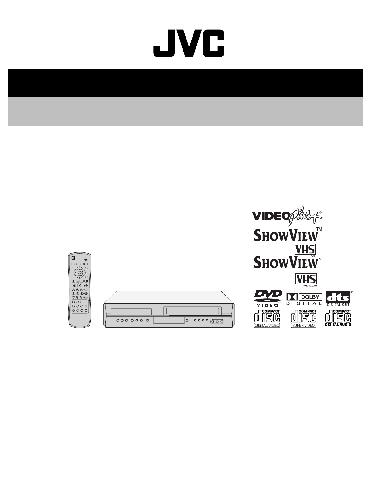
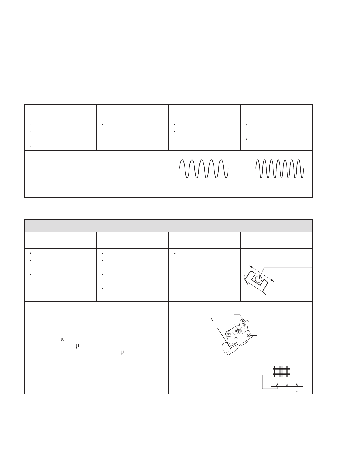
SERVICE MANUAL
DVD PLAYER & VIDEO CASSETTE RECORDER
YD06820055
HR-XV28SEF,HR-XV28SEK,
HR-XV28SER,HR-XV28SEU,
HR-XV28SEY,HR-XV28SEZ
(EK model)
(EU, EY, EZ models)
(EF, ER models)
(EF model)
HR-XV28SEF,HR-XV28SEK,HR-XV28SER,HR-XV28SEU,HR-XV28SEY,HR-XV28SEZ [D5PV0]
TABLE OF CONTENTS
1 PRECAUTION. . . . . . . . . . . . . . . . . . . . . . . . . . . . . . . . . . . . . . . . . . . . . . . . . . . . . . . . . . . . . . . . . . . . . . . . . 1-3
2 SPECIFIC SERVICE INSTRUCTIONS . . . . . . . . . . . . . . . . . . . . . . . . . . . . . . . . . . . . . . . . . . . . . . . . . . . . . . 1-6
3 DISASSEMBLY . . . . . . . . . . . . . . . . . . . . . . . . . . . . . . . . . . . . . . . . . . . . . . . . . . . . . . . . . . . . . . . . . . . . . . . 1-9
4 ADJUSTMENT . . . . . . . . . . . . . . . . . . . . . . . . . . . . . . . . . . . . . . . . . . . . . . . . . . . . . . . . . . . . . . . . . . . . . . . 1-10
5 TROUBLESHOOTING . . . . . . . . . . . . . . . . . . . . . . . . . . . . . . . . . . . . . . . . . . . . . . . . . . . . . . . . . . . . . . . . . 1-37
COPYRIGHT © 2005 Victor Company of Japan, Limited
No.YD068
2005/5
Page 2
SPECIFICATION
HR-XV28SEF HR-XV28SEK HR-XV28SER/SEU/SEY/SEZ
General
Power requirement AC 200V - 240V, 50 Hz
Power consumption 17 W
Dimensions (approx.) 430 × 78.5 × 265 mm (w/h/d)
Mass (approx.) 4.2 kg
Operating temperature 5°C to 35°C (41°F to 95°F)
Operating humidity 5 % to 90 %
Timer 24 hours display type
RF Modulator - UHF 22-68 (Adjustable)
System
Laser Semiconductor laser, wavelength 650 nm
Video Head system Double azimuth 6 heads, helical scanning.
Signal system PAL
Frequency response DVD (PCM 96 kHz): 8 Hz to 44 kHz, DVD (PCM 48 kHz): 8 Hz to 22 kHz, CD: 8 Hz to 20 kHz
Signal-to-noise ratio More than 100 dB (ANALOG OUT connectors only)
Harmonic distortion Less than 0.008%
Dynamic range More than 100 dB (DVD), More than 95 dB (CD)
Inputs (VCR)
Audio -6.0 dBm, more than 10 kΩ (SCART), -6.0 dBm, more than 47 kΩ (RCA)
Video 1.0 V (p-p), 75 Ω, unbalanced (SCART/RCA)
Outputs (DVD)
VIDEO OUT 1 Vp-p 75 Ω, sync negative
Audio output (digital audio) 0.5 V (p-p), 75 Ω, RCA jack × 1
Audio output (analog audio) 2.0 Vrms (1 kHz, 0 dB), 600 Ω, RCA jack (L, R) x 1/SCART (TO TV)
Outputs (VCR/DVD)
Audio -6.0 dBm, less than 1 kΩ (SCART)
Video 1.0 V (p-p), 75 Ω, unbalanced (SCART)
• Designs and specifications are subject to change without notice.
• Manufactured under license from Dolby Laboratories. "Dolby", "Pro Logic" and the double-D symbol are trademarks of Dolby Laboratories.
• DTS and DTS Digital Out are trademarks of Digital Theater Systems, Inc.
• SHOWVIEW is a trademark of Gemstar Development Corporation. The SHOWVIEW system is manufactured under license from
Gemstar Development Corporation.(EF/ER/EU/EY/EZ models)
• VIDEO Plus+ and PlusCode are registered trademarks of Gemstar Development Corporation. The VIDEO Plus+ system is manufactured under license from Gemstar Development Corporation.(EK model)
1-2 (No.YD068)
Page 3
SECTION 1
r
PRECAUTION
1.1 SAFTY PRECAUTIONS
Prior to shipment from the factory, JVC products are strictly inspected to conform with the recognized product safety and electrical codes of the countries in which they are to be
sold.However,in order to maintain such compliance, it is equally
important to implement the following precautions when a set is
being serviced.
1.1.1 Precautions during Servicing
(1) Locations requiring special caution are denoted by labels
and inscriptions on the cabinet, chassis and certain parts of
the product.When performing service, be sure to read and
comply with these and other cautionary notices appearing
in the operation and service manuals.
(2) Parts identified by the symbol and shaded ( ) parts
are critical for safety.
Replace only with specified part numbers.
NOTE :
Parts in this category also include those specified to
comply with X-ray emission standards for products
using cathode ray tubes and those specified for
compliance with various regulations regarding spurious radiation emission.
(3) Fuse replacement caution notice.
Caution for continued protection against fire hazard.
Replace only with same type and rated fuse(s) as specified.
(4) Use specified internal wiring. Note especially:
• Wires covered with PVC tubing
• Double insulated wires
• High voltage leads
(5) Use specified insulating materials for hazardous live parts.
Note especially:
• Insulation Tape
• PVC tubing
•Spacers
• Insulation sheets for transistors
•Barrier
(6) When replacing AC primary side components (transformers,
power cords, noise blocking capacitors, etc.) wrap ends of
wires securely about the terminals before soldering.
Consequently, when servicing these products, replace the
cathode ray tubes and other parts with only the specified
parts. Under no circumstances attempt to modify these circuits.Unauthorized modification can increase the high voltage value and cause X-ray emission from the cathode ray
tube.
(12) Crimp type wire connectorIn such cases as when replacing
the power transformer in sets where the connections between the power cord and power trans former primary lead
wires are performed using crimp type connectors, if replacing the connectors is unavoidable, in order to prevent safety hazards, perform carefully and precisely according to the
following steps.
• Connector part number :E03830-001
• Required tool : Connector crimping tool of the proper
type which will not damage insulated parts.
• Replacement procedure
a) Remove the old connector by cutting the wires at a
point close to the connector.Important : Do not reuse a connector (discard it).
cut close to connector
Fig.1-1-3
b) Strip about 15 mm of the insulation from the ends
of the wires. If the wires are stranded, twist the
strands to avoid frayed conductors.
15 mm
Fig.1-1-4
c) Align the lengths of the wires to be connected. In-
sert the wires fully into the connector.
Metal sleeve
Fig.1-1-1
(7) Observe that wires do not contact heat producing parts
(heatsinks, oxide metal film resistors, fusible resistors, etc.)
(8) Check that replaced wires do not contact sharp edged or
pointed parts.
(9) When a power cord has been replaced, check that 10-15
kg of force in any direction will not loosen it.
Power cord
Fig.1-1-2
(10) Also check areas surrounding repaired locations.
(11) Products using cathode ray tubes (CRTs)In regard to such
products, the cathode ray tubes themselves, the high voltage circuits, and related circuits are specified for compliance with recognized codes pertaining to X-ray emission.
Connector
Fig.1-1-5
d) As shown in Fig.1-1-6, use the crimping tool to
crimp the metal sleeve at the center position. Be
sure to crimp fully to the complete closure of the
tool.
1.2
5
2
.0
5.5
Crimping tool
Fig.1-1-6
e) Check the four points noted in Fig.1-1-7.
Not easily pulled free
Wire insulation recessed
more than 4 mm
Crimped at approx. cente
of metal sleeve
Conductors extended
Fig.1-1-7
(No.YD068)1-3
Page 4
1.1.2 Safety Check after Servicing
Examine the area surrounding the repaired location for damage
or deterioration. Observe that screws, parts and wires have been
returned to original positions, Afterwards, perform the following
tests and confirm the specified values in order to verify compliance with safety standards.
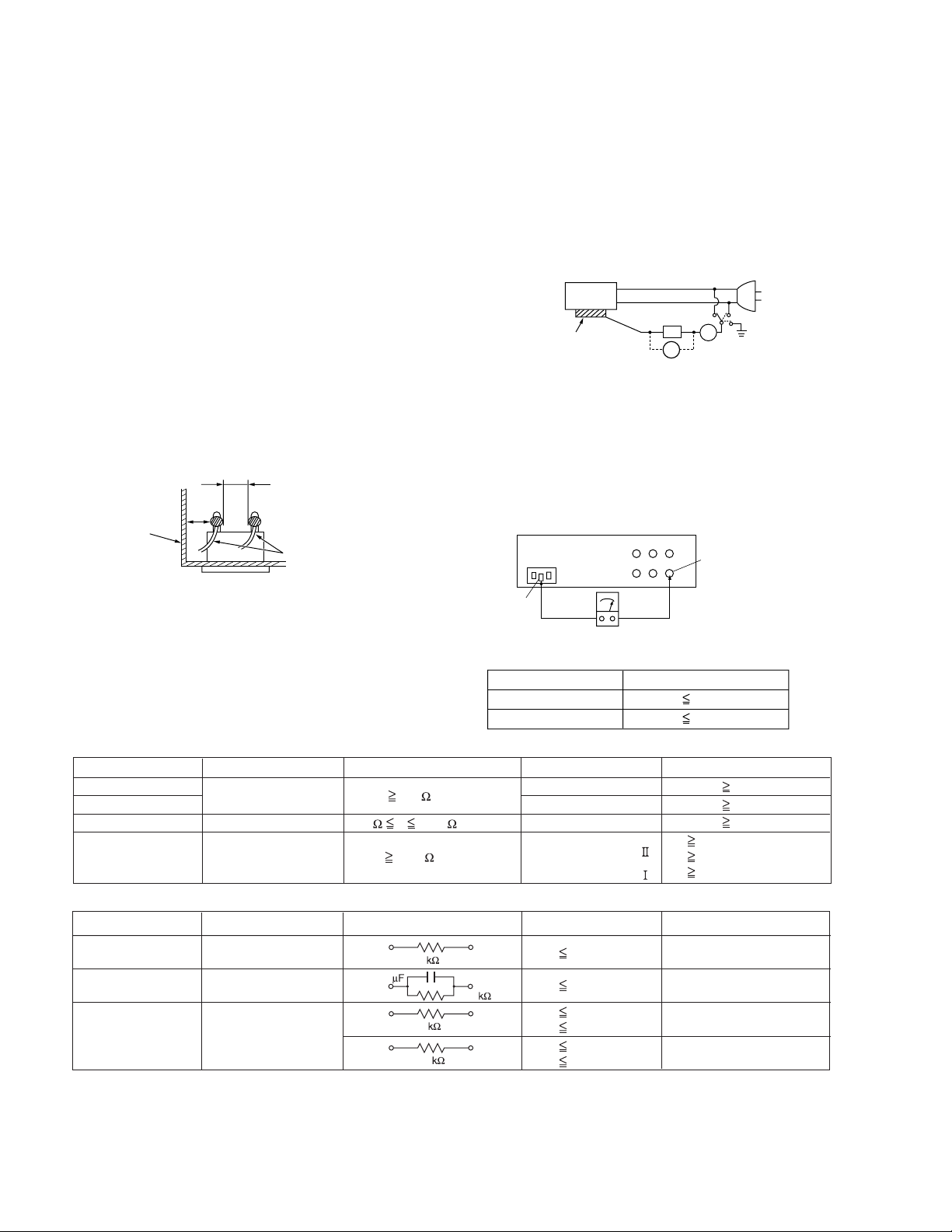
(1) Insulation resistance test
Confirm the specified insulation resistance or greater between power cord plug prongs and externally exposed
parts of the set (RF terminals, antenna terminals, video and
audio input and output terminals, microphone jacks, earphone jacks, etc.).See table 1 below.
(2) Dielectric strength test
Confirm specified dielectric strength or greater between
power cord plug prongs and exposed accessible parts of
the set (RF terminals, antenna terminals, video and audio
input and output terminals, microphone jacks, earphone
jacks, etc.). See Fig.1-1-11 below.
(3) Clearance distance
When replacing primary circuit components, confirm specified clearance distance (d), (d') between soldered terminals, and between terminals and surrounding metallic
parts. See Fig.1-1-11 below.
d
Chassis
d'
Power cord
primary wire
Fig.1-1-8
(4) Leakage current test
Confirm specified or lower leakage current between earth
ground/power cord plug prongs and externally exposed accessible parts (RF terminals, antenna terminals, video and
audio input and output terminals, microphone jacks, earphone jacks, etc.).
Measuring Method : (Power ON)Insert load Z between
earth ground/power cord plug prongs and externally exposed accessible parts. Use an AC voltmeter to measure
across both terminals of load Z. See Fig.1-1-9 and following Fig.1-1-12.
ab
Externally
exposed
accessible part
Z
V
c
A
Fig.1-1-9
(5) Grounding (Class 1 model only)
Confirm specified or lower grounding impedance between
earth pin in AC inlet and externally exposed accessible
parts (Video in, Video out, Audio in, Audio out or Fixing
screw etc.).Measuring Method:
Connect milli ohm meter between earth pin in AC inlet and
exposed accessible parts. See Fig.1-1-10 and grounding
specifications.
AC inlet
Earth pin
Exposed accessible part
MIlli ohm meter
Grounding Specifications
Region
USA & Canada
Europe & Australia
Grounding Impedance (Z
Z 0.1 ohm
Z 0.5 ohm
)
Fig.1-1-10
AC Line Voltage
100 V
100 to 240 V
110 to 130 V
110 to 130 V
200 to 240 V
Region
Japan
USA & Canada
Europe & Australia
Insulation Resistance (R
R 1 M /500 V DC
1 M R 12 M /500 V DC
R 10 M /500 V DC
)
Dielectric Strength
AC 1 kV 1 minute
AC 1.5 kV 1 minute
AC 1 kV 1 minute
AC 3 kV 1 minute
AC 1.5 kV 1 minute
(
Class
(
Class
Clearance Distance (d), (d'
d, d' 3 mm
d, d' 4 mm
d, d' 3.2 mm
d 4 m m
)
d' 8 m m (Power cord
d' 6 m m (Primary wire
)
Fig.1-1-11
AC Line Voltage
100 V
110 to 130 V
110 to 130 V
220 to 240 V
Region
Japan
USA & Canada
Europe & Australia
Load Z
1
0.15
1.5
2
50
Leakage Current (i)
i 1 mA rms
i 0.5 mA rms
i 0.7 mA peak
i 2 mA dc
i 0.7 mA peak
i 2 mA dc
a, b, c
Exposed accessible parts
Exposed accessible parts
Antenna earth terminals
Other terminals
Fig.1-1-12
NOTE :
These tables are unofficial and for reference only. Be sure to confirm the precise values for your particular country and locality.
)
)
)
1-4 (No.YD068)
Page 5
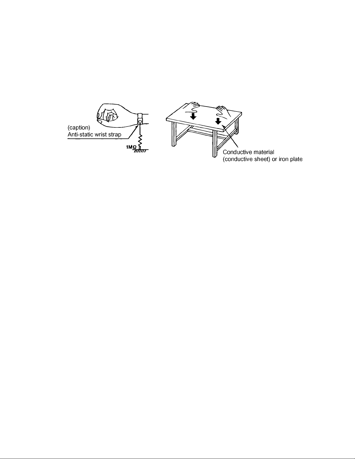
1.2 Preventing static electricity
Electrostatic discharge (ESD), which occurs when static electricity stored in the body, fabric, etc. is discharged, can destroy the laser
diode in the traverse unit (optical pickup). Take care to prevent this when performing repairs.
1.2.1 Grounding to prevent damage by static electricity
Static electricity in the work area can destroy the optical pickup (laser diode) in devices such as DVD players.
Be careful to use proper grounding in the area where repairs are being performed.
(1) Ground the workbench
Ground the workbench by laying conductive material (such as a conductive sheet) or an iron plate over it before placing the
traverse unit (optical pickup) on it.
(2) Ground yourself
Use an anti-static wrist strap to release any static electricity built up in your body.
(3) Handling the optical pickup
• In order to maintain quality during transport and before installation, both sides of the laser diode on the replacement optical
pickup are shorted. After replacement, return the shorted parts to their original condition.
(Refer to the text.)
• Do not use a tester to check the condition of the laser diode in the optical pickup. The tester's internal power source can easily
destroy the laser diode.
(No.YD068)1-5
Page 6
SECTION 2
SPECIFIC SERVICE INSTRUCTIONS
2.1 DIFFERENT TABLE OF FEATURE
The following table indicates main different points between models HR-XV28SEF, HR-XV28SEK, HR-XV28SER, HR-XV28SEU and
HR-XV28SEY/EZ.
MODEL NAME HR-XV28SEF HR-XV28SEK HR-XV28SER
SCART CABLE PROVIDED ← OPTIONAL
BROADCASTING SYSTEM PAL B/G, SECAM L PAL I, I/I, B/G, SECAM D/K, K1 ←
RF OUT CH/RF OUT
SYSTEM [INITIAL]
OSD LANGUAGES
REGIONAL CODE REGIONAL CODE : 2 ← REGIONAL CODE : 5
MODEL NAME HR-XV28SEU HR-XV28SEY/EZ
SCART CABLE OPTIONAL ←
BROADCASTING SYSTEM PAL I, I/I, B/G, SECAM D/K, K1 ←
RF OUT CH/RF OUT
SYSTEM [INITIAL]
OSD LANGUAGES
REGIONAL CODE REGIONAL CODE : 2 ←
Note:
Mark ← is same as left.
ENGLISH/GERMANY/FRENCH/
ITALIAN/SPANISH/DUTCH
ENGLISH/GERMANY/ITALIAN/
SPANISH/GREEK/PORTU-
NOT USED 22-68CH,[36CH]/I 22-68CH,[36CH]/K
ENGLISH/GERMANY/ITALIAN/
SPANISH/GREEK/PORTU-
GUESE
22-68CH,[36CH]/G ←
ENGLISH/POLISH/CZECH/
HUNGARIAN/SWEDISH/GER-
GUESE
MANY
ENGLISH/RUSSIAN
1-6 (No.YD068)
Page 7
2.2 SERVICE INFORMATION FOR EEPROM IC SETTING(VCR)
EEPROM option code No. setting EEPROM option code No. setting procedure
NAME HEX BINARY
OPT0 00 00000000
OPT1 00 00000000
OPT2 00 00000000
OPT3 00 00000000
OPT4 00 00000000
OPT5 00 00000000
12/26 - 00 V00 -COM Ver.
ID : LG
VERSION : 05 ROM
DATE : 02.17.05 Correction Ver.
MODEL NAME HEX BINARY
HR-XV28SEU OPT0 00 00000000
OPT1 54 00000000
OPT2 60 00000000
OPT3 47 00000000
OPT4 03 00000000
OPT5 0B 00000000
HR-XV28SEK OPT0 00 00000000
OPT1 54 00000000
OPT2 21 00000000
OPT3 87 00000000
OPT4 0D 00000000
OPT5 0B 00000000
HR-XV28SEZ OPT0 00 00000000
OPT1 54 00000000
OPT2 63 00000000
OPT3 47 00000000
OPT4 0D 00000000
OPT5 0B 00000000
HR-XV28SEY OPT0 00 00000000
OPT1 54 00000000
OPT2 63 00000000
OPT3 47 00000000
OPT4 0B 00000000
OPT5 0B 00000000
HR-XV28SER OPT0 09 00000000
OPT1 54 00000000
OPT2 A3 00000000
OPT3 47 00000000
OPT4 0D 00000000
OPT5 0B 00000000
HR-XV28SEF OPT0 00 00000000
OPT1 5C 00000000
OPT2 E8 00000000
OPT3 47 00000000
OPT4 01 00000000
OPT5 0B 00000000
WR : OK I : EXIT MOVE :
EDIT :
1. DETECT NEW EEPROM (OPTION EDIT
SCREEN)
- Eeprom EDIT screen automatically appears if
replacing Eeprom.
- Setup option data using the cursor Up/Down key
of a remote control.
(Setup upon BOM depending on OPT0~OPT5
model)
Since an initial remote control is set to LG for LG
model, appropriately set optiona data using the
cursor Up/Down key.
2. EEPROM WRITED AND EEPROM INITIAL
- Writes data on EEPROM by using REMOCON
"OK" + FRONT PLAY KEY FOR MORE THAN 5
SECONDS.
3. PG ADJUST
1) Payback the SP standard tape
2) Press the "OK" key on the Remote controller
and the "PLAY" key on the Front Panel the
same time, then it goes in to Tracking initial
mode.
3) Repeat the above step(No.2), then it finishes
the PG adjusting automatically.
4) Stop the playback, then it goes out to PG
adjusting mode after mony the PG data.
4. BUYER SELECTION
- Font ejection key + open/close key for more than
5 seconds.
- Option code is displayed in TV
- First byte of OPTO is changed whenever front
eject key + open/close key.
- JVC remote conroller No.0.
(No.YD068)1-7
Page 8
2.3 SERVICE INFORMATION FOR EEPROM (DVD)
POWER ON
DVD LOGO Status (NO Disk status)
DETECT NEW EEPROM
(OPTION EDIT SCREEN)
Remote control
Pause key 1 4 7 2 in order.
Press number 0~9, Press charater
A~F (1~6 for a while)
Use arrow key ( ) to move
to approprite position and make
changes
Press pause key once
Change will be applied when power
OFF ON.
MODEL
NAME HEX HEX HEX HEX HEX HEX
OPT 1 44 47 50 53 52 42
OPT 2 45 42 4C 45 55 45
OPT 3 00 00 00 00 00 00
OPT 4 D3 D3 D3 D3 D3 D3
OPT 5 12 12 12 12 12 12
OPT 6 05 05 05 05 05 05
OPT 7 30 30 30 30 30 30
OPT 8 00 00 00 00 00 00
OPT 9 00 00 00 00 00 00
OPT A 00 00 00 00 00 00
OPT B 80 80 80 80 80 80
OPT C 00 00 00 00 0A 00
OPT D 00 00 00 00 00 00
OPT E 00 00 00 00 00 00
OPT F 00 00 00 00 00 00
OPT G 00 00 00 00 00 00
HR-XV28SEU HR-XV28SEK HR-XV28SEZ HR-XV28SEY HR-XV28SER HR-XV28SEF
* OPTION
NTSC model does not have VCR option and use DVD option B~F as VCR option. (only DVD exist)
PAL model has another separate VCR option. (Both VCR and DVD exist)
1-8 (No.YD068)
Page 9

SECTION 3
DISASSEMBLY
This service manual does not describe DISASSEMBLY.
(No.YD068)1-9
Page 10
SECTION 4
ADJUSTMENT
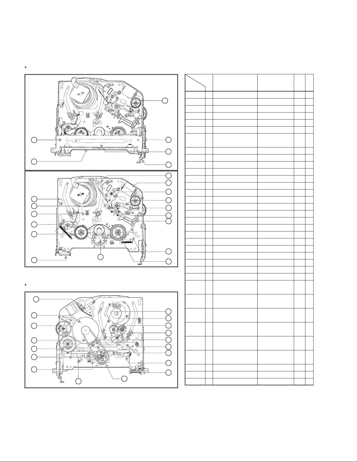
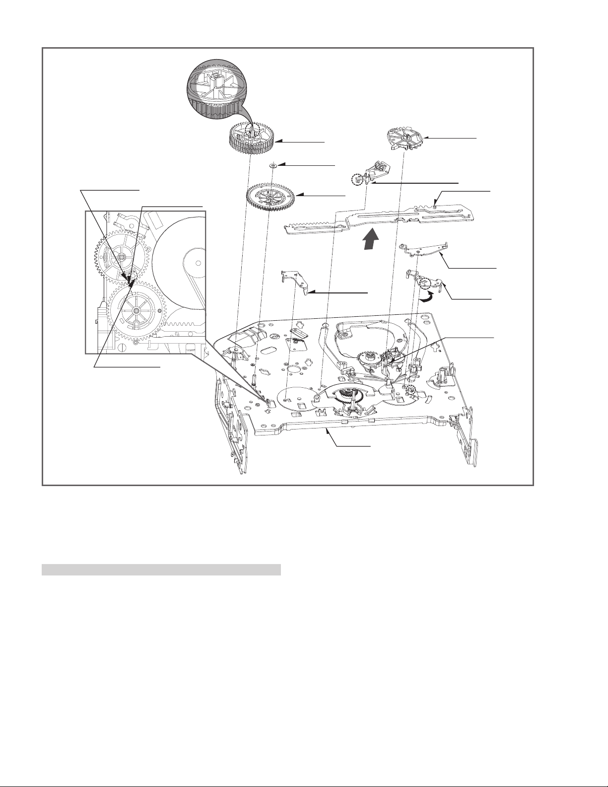
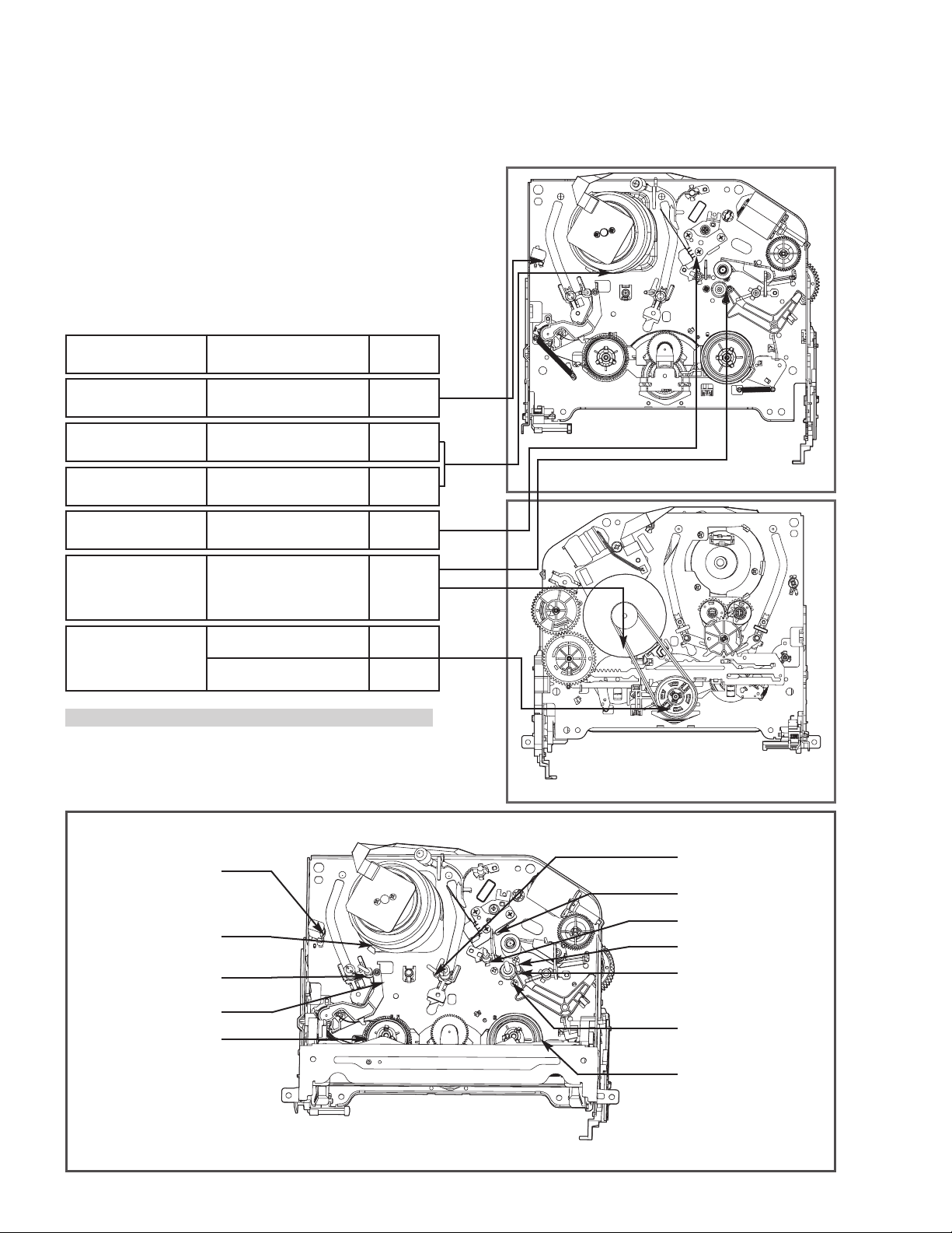
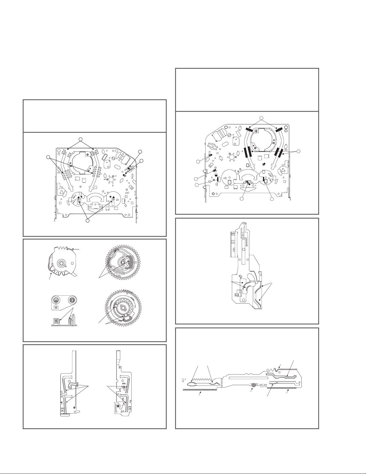
4.1 POSITION DRAWING OF DECK MECHANISM PARTS (VCR)
Top View
9
2
6
11
1
33
14
15
7
35
4
3
5
10
8
12
18
16
17
19
13
15
Bottom View
20
21
24
21
24
23
22
30
NOTE : Assembly order is a reverse of
disassembly order.
26
32
31
31
32
25
34
28
27
29
Order Of Dis-
assembled
Parts firstly
Disassembled
1
Drum Assembly
2
Plate Top
2
2,3
2,3,4
2,3,4,5
2,3
2,3
2,3,13,14
17
17
17,18
21,22
21
21,22,23,
24,25,26
21,22,23,
24,25,26,27
21,22,23,
24,25,26,27
21,22,23,
24,25,26,27
25
2,3,14,
25,31
25,31
2,3,14
3
Holder Assembly CST
4
Gear Assembly Rack F/L
5
Opener Door
6
Arm Assembly F/L
7
Lever Assembly S/W
8
Motor Assembly L/D
9
Gear Wheel
10
Arm Assembly Cleaner
11
Head F/E
12
Base Assembly A/C Head
13
Brake Assembly T
14
Arm Assembly Tension
15
Reel S / Reel T
16
Base Assembly P4
17
Opener Lid
18
Arm Assembly Pinch
19
Arm T/up
20
Supporter, capstan
21
Belt Capstan/Motor Capstan
22
Lever F/R
23
Clutch Assembly D37
24
Gear Drive/Gear Cam
25
Gear Sector
26
Brake Assembly Capstan
27
Plate Slider
28
Lever Tension
29
Lever Spring
30
Lever Brake
Gear Assembly P2/
31
Gear Assembly P3
Base Assembly P2
32
/Base Assembly P3
33
Base Loading
34
Base Tension
35
Arm Assembly Idler Jog
T:Top, B:Bottom
Part
Ref.
Fixing Type
Draw-
ings
3 screws
2 hooks
6 chasses
1 hook
Chassis Hole
Chassis Hole
Chassis Hole,
1 hook
1 screw
2 hooks
Chassis Embossing
Chassis Embossing
1 screw
1 hook
1 hook
Shaft
Chassis Embossing
Chassis Embossing
Shaft
1 hook
Chassis Hole
3 screws
Ta b
Washer
Washer/Hook
Hook
Chassis Hole
Chassis Guide
1 Hook
1 Hook
1 Hook
Bass
6 Chasses
3 Hooks
Chassis Embossing
Locking Tab
A-1
A-2
A-2
A-2
A-2
A-2
A-2
A-3
A-3
A-3
A-3
A-3
A-4
A-4
A-4
A-5
A-5
A-5
A-5
A-6
A-6
A-6
A-6
A-7
A-7
A-7
A-7
A-7
A-7
A-7
A-8
A-8
A-8
A-9
A-9
Posi
tion
T
T
T
T
T
T
T
T
T
T
T
T
T
T
T
T
T
T
T
B
B
B
B
B
B
B
B
B
B
B
B
B
B
B
B
(1) For assembly, check the assembly mode is accurate.
(2) Parts firstly disassembled indicate parts firstly disassembled
in disassembly of related parts.
1-10 (No.YD068)
Page 11
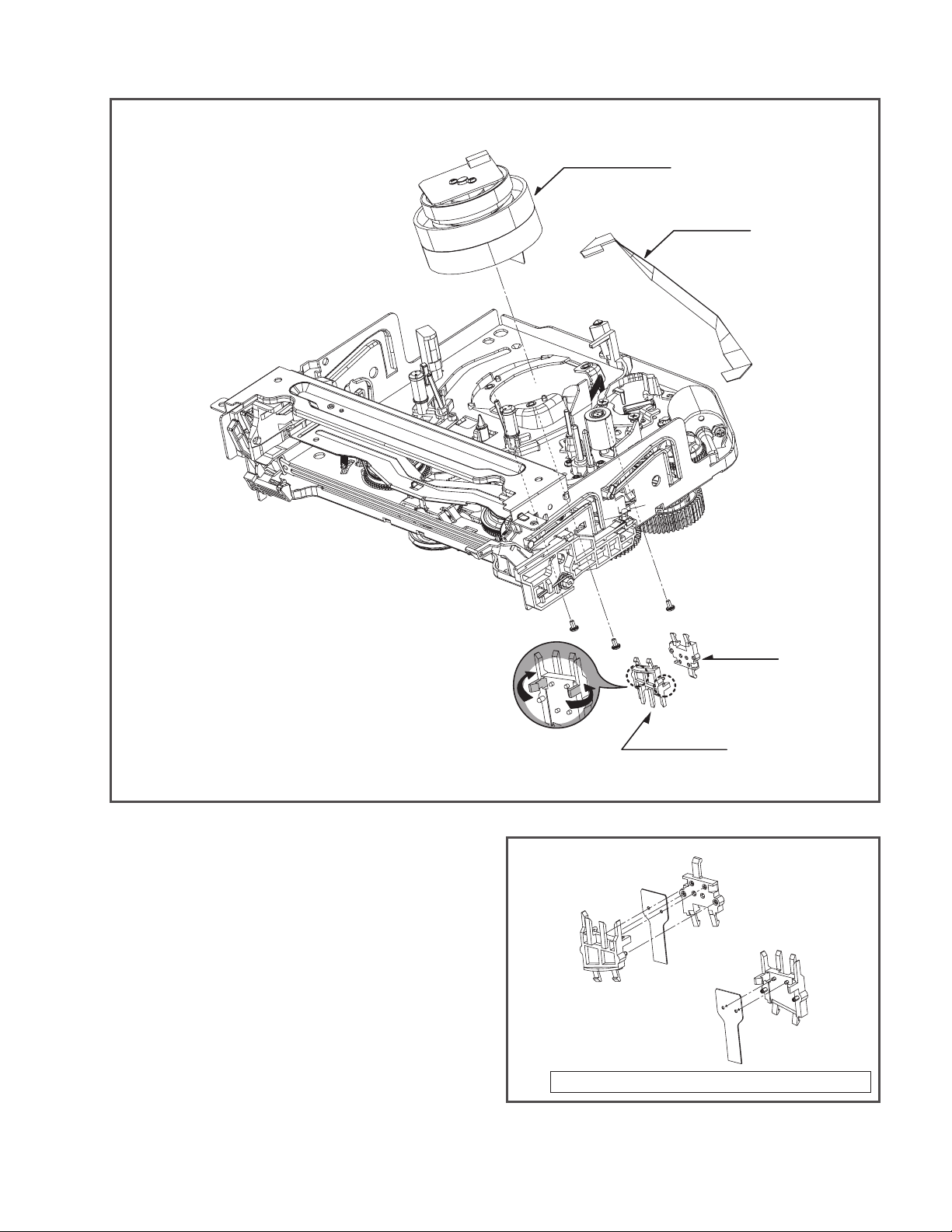
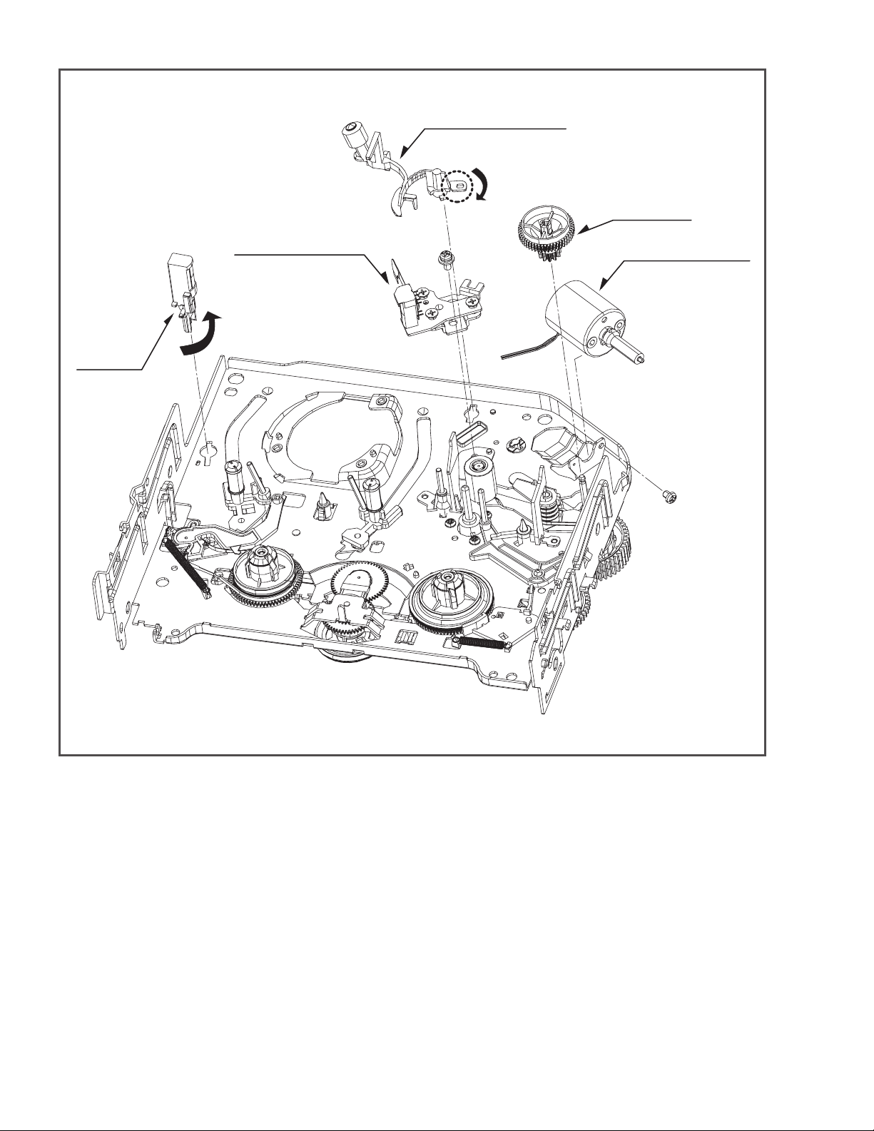
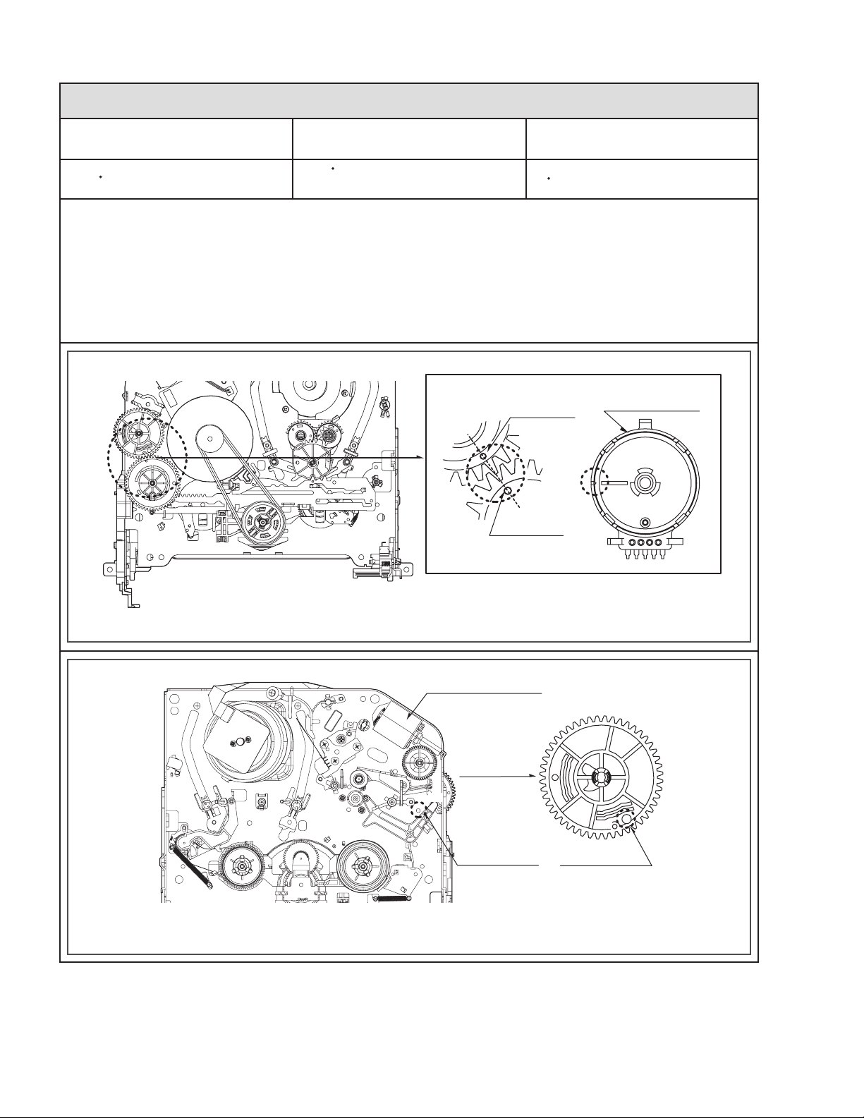
4.2 DISASSEMBLY AND ASSEMBLY OF DECK MECHANISM (VCR)
Drum Assembly
Cable Flat
1. Disassembly of Drum Assembly
(Figure A-1)
1) Separate cable flat from the Drum FPC and the Capstan
Motor.
2) Release 3 screws (S1) on the bottom side of the chassis,
and separate the drum assembly.
3) Release the hooks (H1, H2) and separate both the holder
FPC and the Cap FPC (disassemble if necessary).
(S1)
H2
Fig. A-1
Cautions in assembly of FPC
Holder FPC
(S1)
(S1)
Cap, FPC
H1
Holder FPC
Cap FPC
Drum FPC
Assembly shape seen in the reverse direction
(No.YD068)1-11
Page 12
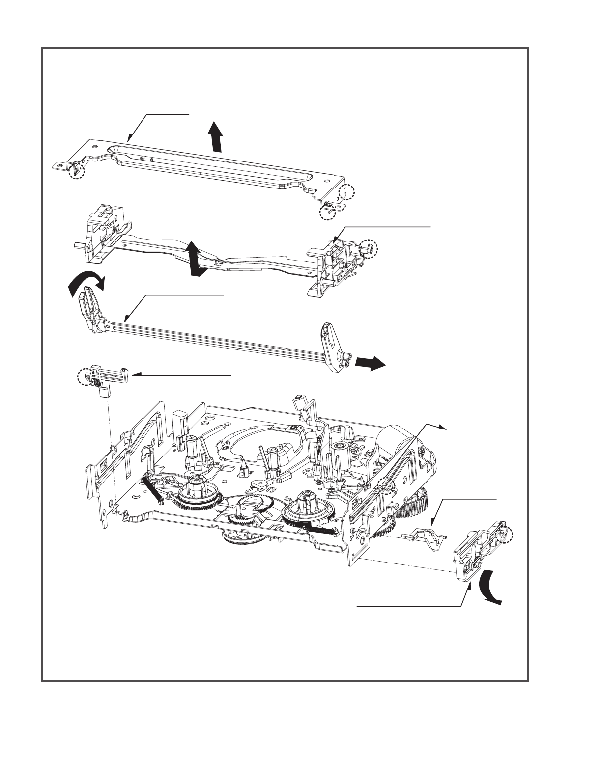
Plate Top
(Fig. A-2-1)
(H4)
(B')
Arm Assembly F/L
(Fig. A-2-5)
Lever Assembly S/W
(Fig. A-2-6)
(B)
(C)
Holder Assembly CST
(Fig. A-2-2)
(E)
(E)
1-12 (No.YD068)
Fig. A-2
Gear Assembly Rack F/L
(Fig. A-2-3)
Opener Door
(Fig. A-2-4)
(A)
(H3)
(B)
Page 13
2. Disassembly of Plate Top (Fig. A-2-1)
1) Separate the right part while leaning back the (B) part of
the plate top toward the arrow direction.
2) Separate the left part while leaning back the (B f) part of
the plate top toward the arrow direction.
(Tool used: Tool such as (-) driver, auger, etc with pointed
or flat end)
CAUTIONS
Assemble while pressing the (C), (C') part after corresponding them as in drawing.
(C')
(C)
(B')
(B)
3. Holder Assembly CST (Fig. A-2-2)
1) Firstly separate the left part from the groove on the (D)
part of chassis while moving the holder assembly CST
toward the arrow direction.
Holder Assembly CST
(D)
Chassis
4. Disassembly of Gear Assembly
Rack F/L (Fig. A-2-3)
1) Separate the hook (H3) while leaning ahead the hook (3)
after moving the gear assembly rack F/L toward the arrow
(A) direction.
2) Separate the gear assembly rack F/L toward the arrow (B)
direction.
CAUTIONS
For the assembly, correspond the gear part of gear assembly
rack F/L to the gear drive.
Gear Rack F/L
Gear Drive
5. Opener Door (Fig. A-2-4)
1) Separate the opener door ahead from the guide hole of
chassis while turning it clockwise.
6. Arm Assembly F/L (Fig. A-2-5)
1) Firstly separate the left part of the arm assembly F/L from
the groove of chassis while pushing the arm assembly F/L
toward the arrow direction.
2) Separate the right part from the groove of chassis.).
2) Separate the right part from each groove of chassis
CAUTIONS
Assemble by inserting the left part after firstly inserting the
(E) part of the holder assembly CST into the groove on the
(E') part of chassis.
7. Lever Assembly S/W (Fig. A-2-6)
1) Separate the lever assembly S/W while pushing it toward
the arrow direction after removing the hook (4) on the left
side of chassis.
Chassis
(H4)
(No.YD068)1-13
Page 14
Base Assembly A/C Head
(Fig. A-3-5)
(A)
Arm Assembly Cleaner
(Fig. A-3-3)
(A)
(S5)
(H5)
Gear Wheel
(Fig. A-3-2)
Motor Assembly L/D
(Fig. A-3-1)
Head F/E
(Fig. A-3-4)
(C1)
(S4)
Fig. A-3
8. Motor Assembly L/D (Fig. A-3-1)
1) Take the connector (C1) connected to the Capstan motor
PCB out.
2) Remove a screw (S4) of the chassis (S4) and step back ward, and disassemble it while holding it up.
9. Gear Wheel (Fig. A-3-2)
1) Release the hook (H5) of the gear wheel and disassemble
it upward.
1-14 (No.YD068)
10. Arm Assembly Cleaner (Fig. A-3-3)
1) Separate the (A) part of Fig. A-3-1 from the embossing of
chassis, and hold it up while turning it anti-clockwise.
11. Head F/E (Fig. A-3-4)
1) Separate the (A) part of the head F/E from the embossing of chassis, and hold it up while turning it anti-clockwise.
12. Base Assembly A/C Head (Fig. A-3-5)
1) Release a screw (S5) and disassemble while holding it up.
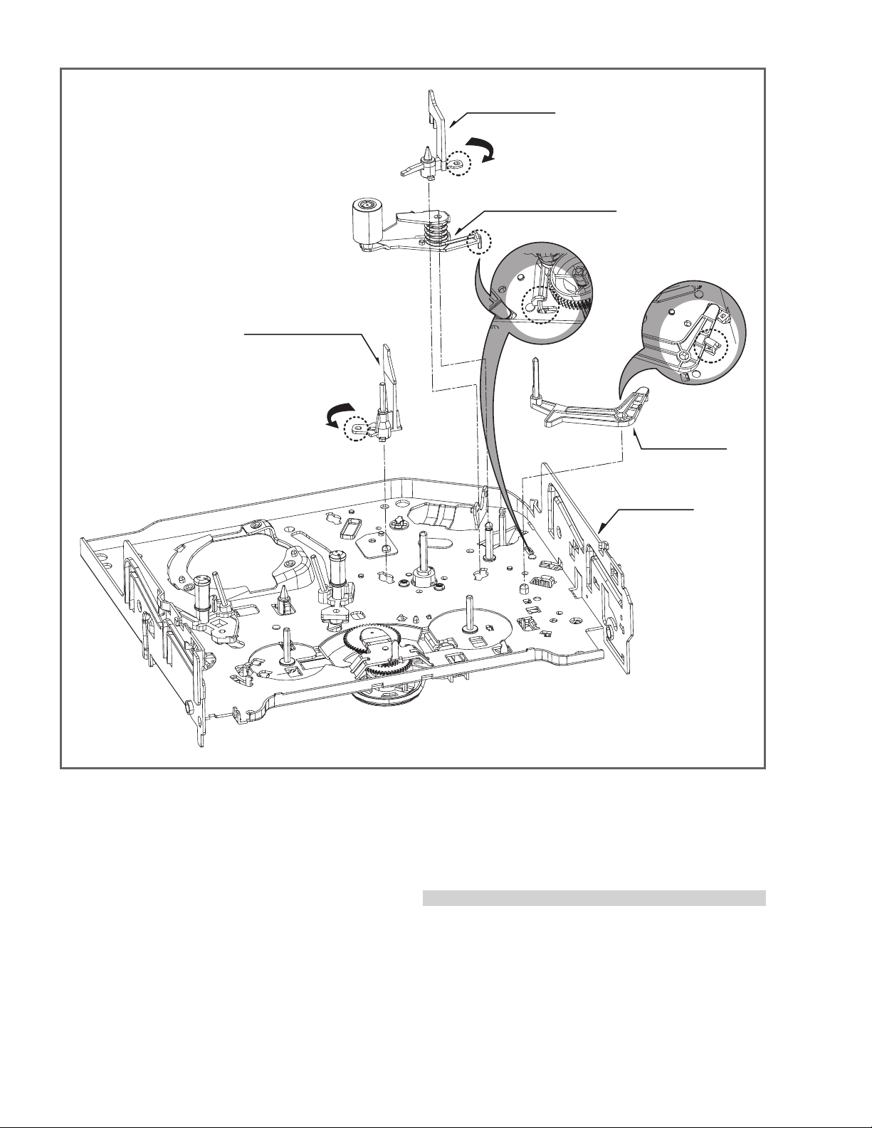
Page 15
Arm Assembly Tension
(Fig. A-4-2)
Spring Tension
(H7)
Reel T
(Fig. A-4-3)
Reel S
(Fig. A-4-3)
(H8)
Spring Tension
Fig. A-4
Brake Assembly T
(Fig. A-4-1)
(H6)
13. Brake Assembly T (Fig. A-4-1)
1) Release the spring tension from the lever spring hook
(H6).
2) Disassemble the brake assembly T while holding it
upward.
14. Arm Assembly Tension (Fig. A-4-2)
1) Release the spring tension the hook (H7) from the arm
assembly tension.
2) After releasing the hook (H8) of the base tension, separate
it while holding it up.
CAUTIONS
Spring used for both brake assembly T and arm assembly
tension is used (2EA used).
15. Reel S/Reel T (Fig. A-4-3)
1) Disassemble the reel S/ reel T while holding it up (compa rison between Reel S and Reel T)
Reel S Reel T
(No.YD068)1-15
Page 16
(Fig. A-5-2)
(B)
Opener Lid
Arm Assembly Pinch
(Fig. A-5-3)
(C)
Base Assembly P4
(Fig. A-5-1)
(A)
(C)
(H9)
Arm T/up
(Fig. A-5-4)
Chassis
16. Base Assembly P4 (Fig. A-5-1)
1) Release the (A) part of the base assembly P4 from the
embossing of chassis.
2) Hold the base assembly P4 up while turning it anti-clock wise.
17. Opener Lid (Fig. A-5-2)
1) Release the (B) part of the opener lid from the embossing
of chassis.
2) Disassemble the opener lid upward while turning it anticlo ckwise.
1-16 (No.YD068)
Fig. A-5
18. Arm Assembly Pinch (Fig. A-5-3)
1) Hold the arm assembly pinch up.
19. Arm T/up (Fig. A-5-4)
1) Turn the arm T/up to release the anchor jaw (H9) part of
chassis and then hold it upward.
CAUTIONS
For the assembly, check the (C) part of the arm assembly
pinch is assembled as in drawing.
- REVERSE THE MECHANISM.
Page 17
Suppoter Capstan
(Fig. A-6-1)
Motor Capstan
(L1)
Lever F/R
(Fig. A-6-4)
Belt Capstan
(Fig. A-6-2)
(Fig. A-6-3)
Washer(W1)
Clutch Assembly D37
(Fig. A-6-5)
(L1)
(S6)
Fig. A-6
20. Supporter, Capstan (Fig. A-6-1)
1) Turn the supporter and Capstan by 90 deg. clockwise
with a driver for disassembly.
21. Belt Capstan (Fig. A-6-2) /
Motor Capstan (Fig. A-6-3)
1) Separate the belt Capstan.
2) Undo 3 screws (S6) on the bottom side of chassis and dis assemble it upward.
Chassis
22. Lever F/R (Fig. A-6-4)
1) Release the locking tab (L1) and then disassemble it
upward.
23. Clutch Assembly D37 (Fig. A-6-5)
1) Remove the washer (W1) and then disassemble it
upward.
(No.YD068)1-17
Page 18
(H10)
(Fig. A-7-2)
(W2)
Gear Cam
Washer (W2)
(H11)
Gear Sector
(Fig. A-7-3)
Gear Cam Hole(B)
Gear Cam Hole(C)
Gear Drive Hole(A)
Gear Drive
(Fig. A-7-1)
Lever Brack
(Fig. A-7-8)
(L2)
Chassis
Brake Assembly Capstan
(Fig. A-7-4)
(Fig. A-7-5)
(Fig. A-7-6)
(B)
(Fig. A-7-7)
3 6
Plate Slider
Lever Tension
Lever spring
Base Loading
Fig. A-7
24. Gear Drive (Fig. A-7-1)/Gear Cam (Fig. A-7-2)
1) Remove the washer (W2) and then disassemble the
gear drive.
2) Release the hook (H10) of the gear cam and then disas semble it upward.
CAUTIONS
For the assembly, adjust both the gear driver hole (A) and
the gear cam hole (B) straightly and then correspond the
gear cam hole (C) to the chassis hole.
25. Gear Sector (Fig. A-7-3)
1) Release the hook (H11) of the gear sector and then hold
the gear sector upward.
26. Brake Assembly Capstan (Fig. A-7-4)
1) Release the locking tab (L2) on the bottom side of the
plate slider and then disassemble it upward.
27. Plate Slider (Fig. A-7-5)
1) Disassemble the plate slider while holding it up.
28. Lever Tension (Fig. A-7-6)
1) Release the lever tension from the guide (A) of chassis
while turning it anti-clockwise.
2) Disassemble the lever tension while holding it up.
29. Lever Spring (Fig. A-7-7)
1) Release the (B) part of the lever spring from the guide
(A) of chassis while turning it anti-clockwise.
2) Disassemble the lever tension while holding it up.
30. Lever Brake (Fig. A-7-8)
1) Disassemble the lever brake while holding it up.
1-18 (No.YD068)
Page 19
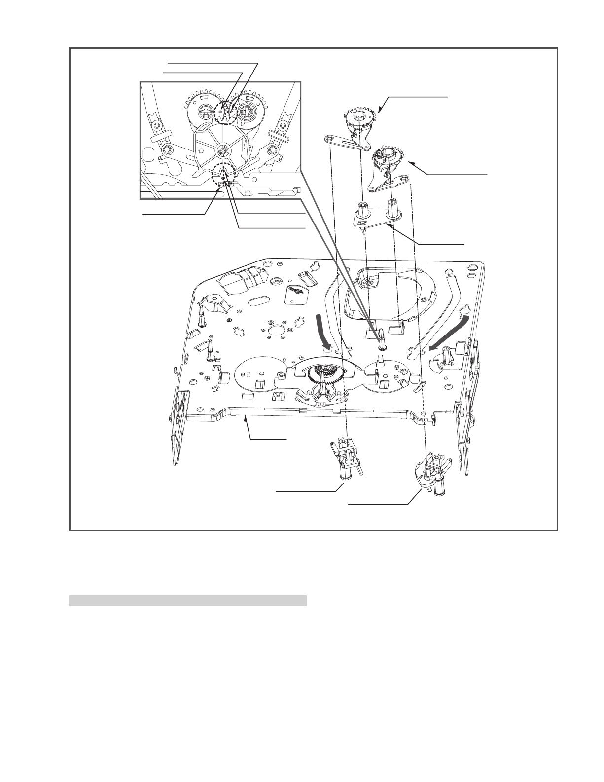
Gear assembly P2 Hole
Gear assembly P3 Hole
Lever Tension Boss
Gear sector (A)
Plate slider Hole(B)
(H12)
(H14)
Gear Assembly P3
(Fig. A-8-2)
Gear Assembly P2
(Fig. A-8-1)
(H13)
Base Loading
(Fig. A-8-5)
Chassis
Base Assembly P3
(Fig. A-8-4)
31. Gear Assembly P2 (Fig. A-8-1)/
Gear Assembly P3 (Fig. A-8-2)
1) Hold the gear assembly P2 upward.
2) Hold the gear assembly P3 upward.
CAUTIONS
For the assembly, check the holes of both the gear assembly P2 and the P3 are adjusted straightly, and then correspond the gear section groove (A) to the plate slider hole (B).
(B)
(A)
Base Assembly P2
(Fig. A-8-3)
Fig. A-8
32. Base Assembly P2 (Fig. A-8-3)/
Base Assembly P3 (Fig. A-8-4)
1) Disassemble the base assembly P2 downward while mov ing it toward the arrow (A) direction along with the guide
hole of chassis.
2) Disassemble the base assembly P2 downward while mov ing it toward the arrow (B) direction along with the guide
hole of chassis.
33. Base Loading (Fig. A-8-5)
1) Release 3 hooks (H12, 13, 14) of the base loading, and
then disassemble them upward.
- REVERSE THE MECHANISM.
(No.YD068)1-19
Page 20
Base Tension
(Fig. A-9-1)
(A)
Arm Assembly Idler Jog
(Fig. A-9-2)
(B) (C)
(D)
34. Base Tension (Fig. A-9-1)
1) Release the (A) part of the base tension from the
embossing of chassis.
2) Hold the base tension upward while turning it anti-clock wise.
Chassis
Fig. A-9
35. Arm assembly Idler Jog (Fig. A-9-2)
1) Push both (B), (C) parts in Fig. A-9-2 toward the arrow
direction.
2) Disassemble the arm assembly idler upward.
CAUTIONS
Take care to ensure that the (D) part in the drawing is not
hung to chassis in disassembly.
1-20 (No.YD068)
Page 21
4.3 DECK MECHANISM ADJUSTMENT (VCR)
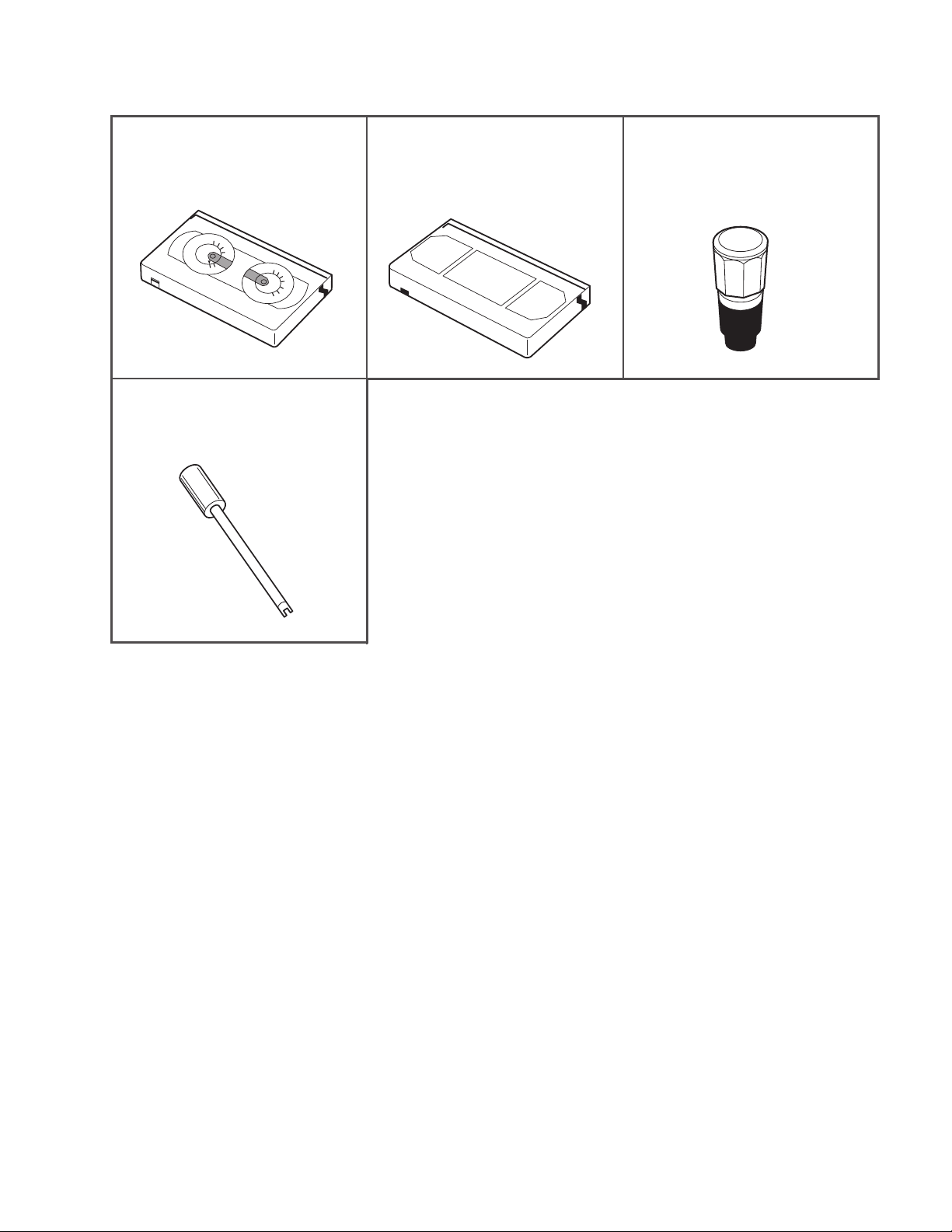
4.3.1 Tools and Fixfures for Service
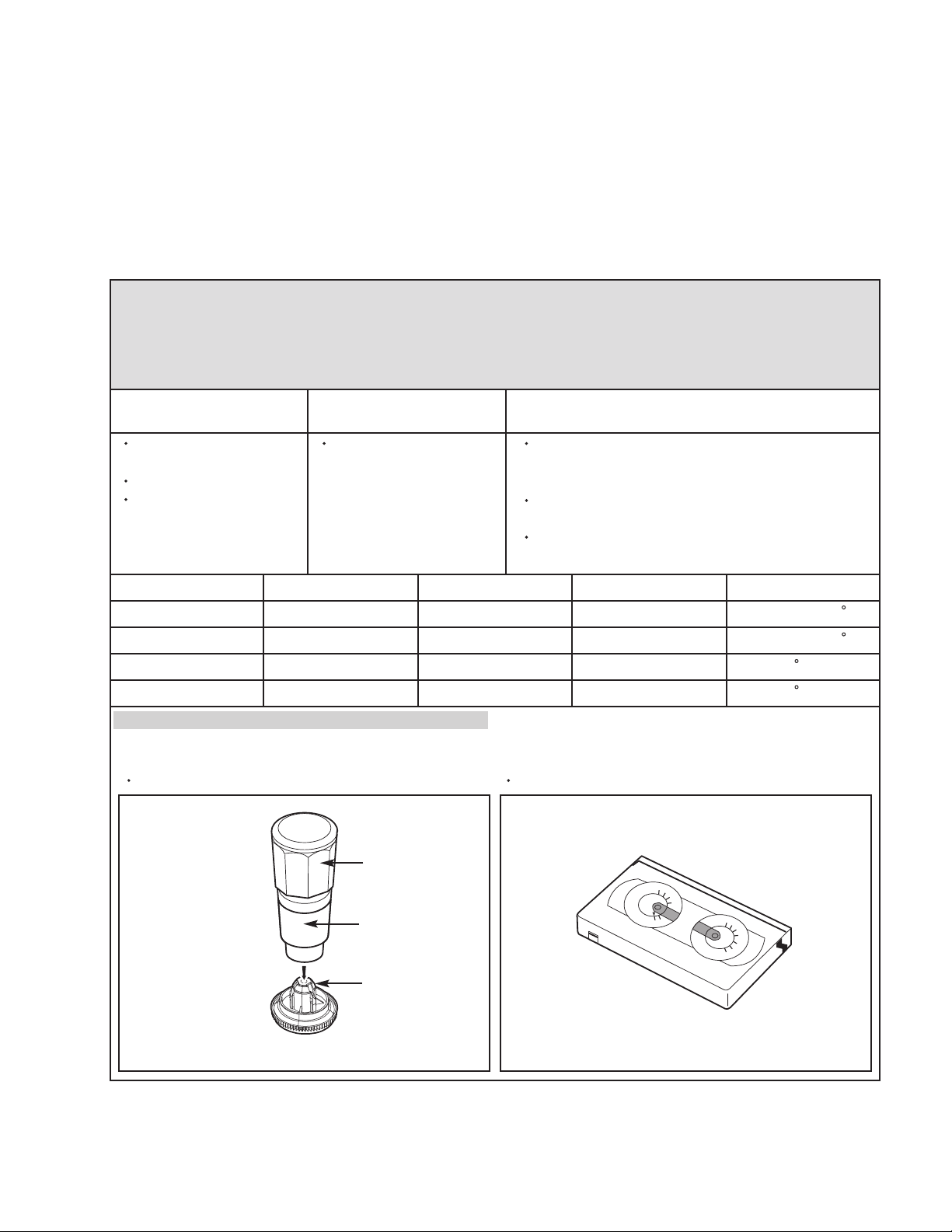
1. Cassette Torque Meter
1. PUJ42881
1.
300
S
-
T
2
50
H
V
-
20
0
K
R
15
0
S
SRK
VIDEO
CASSETTE
H
V
T
-
-
K
T
R
0
TORQUE
S
50
0
METER
VHT-303
50
15
0
2
00
25
0
300
5. Post Height Adjusting Driver
(Roller driver)
PTU94002
2. Alignment Tape
NTSC: MHP
PAL: MHPE
3. Torque Gauge
3. PUJ48075-2
(No.YD068)1-21
Page 22
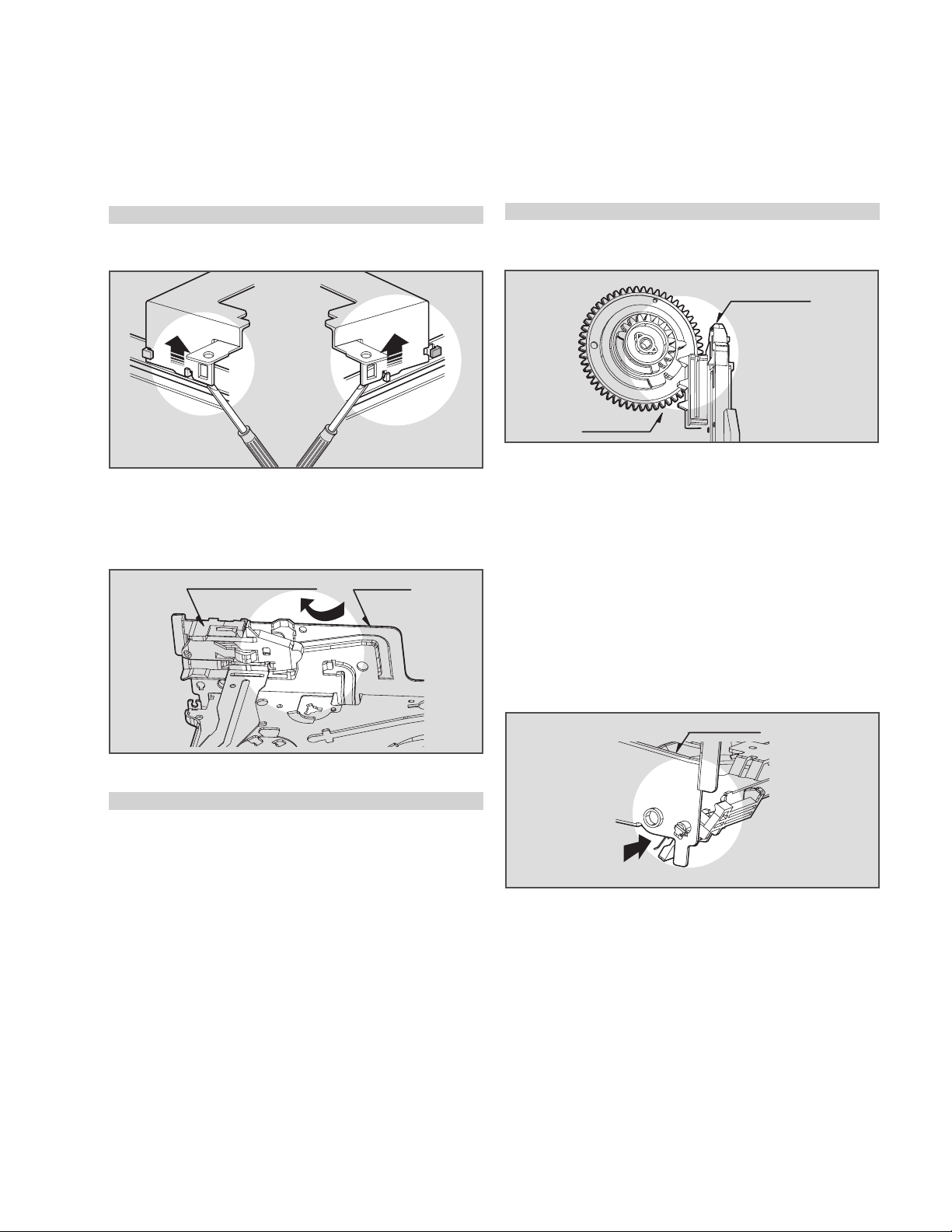
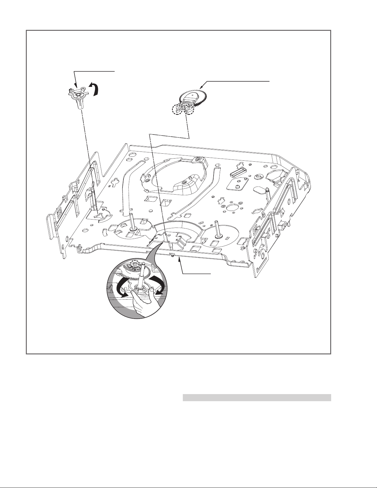
4.3.2 Mechanism Assembly Mode Check
Purpose of adjustment : To make tools normally operate by positioning tools accurately.
Fixtures and tools used VCR (VCP) status Checking Position
Blank Tape (empty tape)
Eject Mode
(with cassette withdrawn)
1) Turn the VCR on and take the tape out by pressing the
eject button.
2) Separate both top cover and plate top, and check both
the hole (A) of gear cam and the hole (A') of chassis co rrespond (Fig. C-2).
3) If it is done as in the paragraph 2): Turn the gear cam as
in No.2) after mantling the motor assembly L/D.
CHECK DIAGRAM
Mechanism and Mode Switch
4) Undo the screw fixing the deck and the main frame, and
separate the deck assembly. Check both the hole (A) of
gear cam and the hole (A') of chassis correspond (Fig.
C-1).
5) Check the mode S/W on the main P.C. board locates at
a proper position as in (B) of the Fig. (C-1).
6) Connect the deck to the main P.C. board and perform all
types of test.
Gear Cam
(C)
Gear Drive
(B)
Mode S/W
BOTTOM VIEW
TOP VIEW
Fig. C-1
Fig. C-2
Correspondence of the gear cam hole (O)
and the gear drive hole (O)
Motor Assembly L/D
Gear Cam
(A')
(A)
Chassis Hole
Gear Cam Hole
1-22 (No.YD068)
Page 23
4.3.3 Previous Preparation for Deck Adjustment
(Preparation to load the VCR (VCP) with cassette tape not inserted)
(1) Take the power cord from the consent.
(2) Separate the top cover and the plate assembly top.
(3) Insert the power cord into again.
(4) Turn the VCR (VCP) on and load the cassette while push-
ing the lever stopper of the holder assembly CST back-
If doing so, proceeding to the stop mode is done. In this status,
input signals of all modes can be received. However, operation
of the Rewind and the Review is impossible since the take-up
reel remains at stop status and so cannot detect the reel pulse
(however, possible for several seconds).
ward. In this case, clog both holes on the housing rail part
of chassis to prevent detection of the end sensor.
4.3.4 Torque Measuring
Purpose of Measuring : To measure and check the reel torque on the take-up part and the
supply part that performs basic operation of the VCR (VCP) for
smoothly forwarding the tape.
Measure and check followings when the tape is not smoothly
wound or the tape velocity is abnormally proceeded:
VCR (VCP) status Measuring methodFixtures and tools used
Torque Gauge
(600 g.cm ATG)
Torque Gauge Adaptor
Cassette Torque Meter
Play (FF) or Review
(REW) Mode
Try to operate the VCR (VCP) per mode with the
tape not inserted (See 4.3.3 Prior Preparation for
Deck Adjustment).
Measure after adhering and fixing the torque
gauge adaptor to the torque gauge (Fig. C-3-1)
Read scale of the supply or take-up part of the
cassette torque meter (Fig. C-3-2).
Item
Fast forward Torque
Rewind Torque
Play Take-Up Torque
Review Torque
Fast Forward
Rewind
Play
Review
Mode Instruments Reel Measured Measuring Value
Torque Gauge
Torque Gauge
Cassette Torque Meter
Cassette Torque Meter
Take-Up Reel
Supply Reel
Take-Up Reel
Supply Reel
NOTE
Adhere the torque gauge adaptor to the torque gauge for measuring the value.
Cassette Torque MeterTorque Gauge (600g.cm ATG)
Torque Gauge
Torque Gauge
Adaptor
More than 400g cm
More than 400g cm
40~100g cm
40~210g cm
300
S
-
T
250
H
V
-
200
K
R
150
S
SRK
VIDEO
CASSETTE
H
V
T
-
-
K
T
R
TORQUE
50
0
METER
VHT-303
0
S
50
150
200
250
300
Reel Table
Fig. C-3-2Fig. C-3-1
(No.YD068)1-23
Page 24
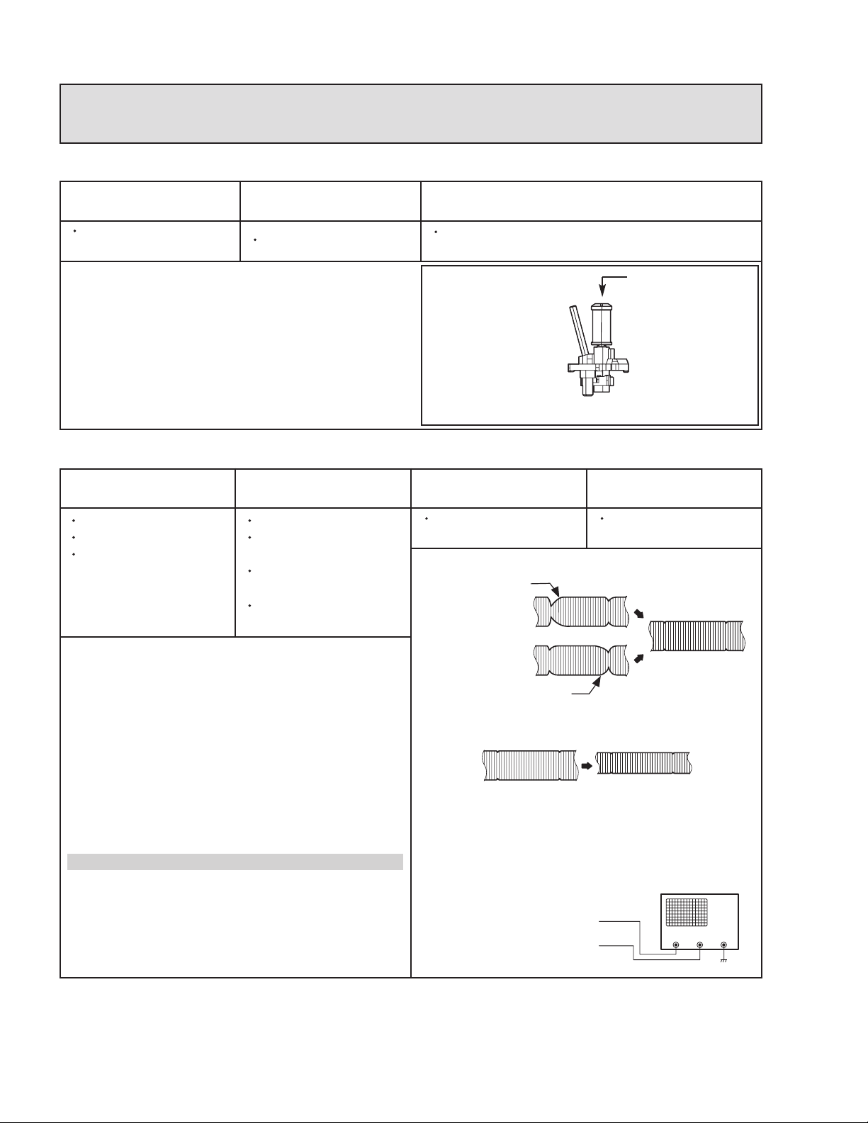
4.3.5 Guide Roller Height Adjustment
Purpose of adjustment : To ensure that the bottom surface of the tape can travel along with
the tape lead line of the lower drum by constantly and adjusting
and maintaining the height of the tape.
4.3.5.1 Prior Adjustment
Fixtures and tools used VCR (VCP) status Adjustment position
Post Height Adjusting
Driver
Play or Review Mode
Adjustment Procedure
1) Travel the tape and check the bottom surface of the
tape travels along with the guide line of the lower drum.
2) If the tape travels toward the lower part of guide line on
the lower drum, turn the guide roller height adjusting
screw to the left
3) If it travels to the upper part, turn it to the right.
4) Adjust the height of the guide roller to ensure that the
tape is guided on the guide line of the lower drum at the
inlet/outlet of the drum. (Fig. C-4-1)
4.3.5.2 Fine Adjustment
Fixtures and tools used
Oscilloscope
Alignment tape
Post height adjusting
driver
Measuring tools and
connection position
CH-1: PB RF Envelope
CH-2: NTSC : SW 30Hz
PAL : SW 25Hz
Head switching output
point
RF Envelope output
point
The guide roller height adjusting screw on the
supply guide roller and the take-up guide roller
ADJUSTMENT DIAGRAM
Fig. C-4-1
GUIDE ROLLER
HEIGHT
ADJUSTMENT SCREW
VCR (VCP) status Adjustment position
Play the standard test
tape.
Guide roller height
adjusting screw
Waveform
P2 POST ADJUSTMENT
1) Play the Alignment tape after connecting the probe of
oscilloscope to the RF envelope output point and the
head switching output point.
2) Tracking control (playback) : Locate it at the center
(Set the RF output to the maximum value via the tracking
control when such adjustment is completed after the
drum assembly is replaced.)
3) Height adjusting screw: Flatten the RF waveform.
(Fig. C-4-2)
4) Move the tracking control (playback) to the right/left.
(Fig. C-4-3)
5) Check the start and the end of the RF output reduction
width are constant.
CAUTIONS
There must exist no crumpling and folding of the tape due
to excess adjustment or insufficient adjustment.
P3 POST ADJUSTMENT
Fig. C-4-2
When the tracking control
locates at the center.
Fig. C-4-2
Connection Diagram
RF ENVELOPE OUTPUT POINT
HEAD RF SWITCHING OUTPUT POINT
Flatten the waveform by
lightly turning the guide
roller height adjustment
screw.
When turning the tracking
control to both sides.
OSCILLOSCOPE
CH-1 CH-2
1-24 (No.YD068)
Page 25
4.3.6 Audio/Control (A/C) Head Adjustment
Purpose of adjustment : To ensure that audio and control signals can be recorded and
played according to the contract tract by constantly maintaining
distance between tape and head, and tape tension between the P3
post and the P4 post.
4.3.6.1 Prior Adjustment (performed only when no audio output appears in play of the standard test tape)
Fixtures and tools used VCR (VCP) status Adjustment position
Blank Tape
Driver (+) Type 5mm
Play the blank tape
Adjustment Procedure/Adjustment Diagrams
1) Basically use the A/C head assembly adjusted as in
SPEC.
2) Check there is crumpling and folding of the tape around
the A/C head. If it is, Turn and adjust the tilt adjusting
screw to ensure that the tape corresponds to the bottom
guide of the P4, and recheck the tape path after proceed ing play for 4-5 seconds.
8.3
A/C Head Base
Tilt adjusting screw (C)
Height adjusting screw (B)
Azimuth adjusting screw (A)
3) Where the tape bottom is not equal to Fig. C-5-3, Adjust
the height by using the height adjusting screw (B) and
then readjust it by using the tilt adjusting screw (C).
CAUTIONS
Always check the height of the A/C head since most ideal
height of A/C head can be obtained when the bottom part
of the tape is away 0.2 ~ 0.25mm from the bottom part of
the A/C head.
A/C Head
P4
Tape
0.2~0.25mm
Tape
Azimuth
Adjustment
Screw(A)
Fig. C-5-1
X-Value Adjustment
Hole
Fixed Screw
A/C Head Assembly
Fig. C-5-2
Fig. C-5-3
Tilt Adjustment
Screw(C)
Height Adjustment
Screw(B)
(No.YD068)1-25
Page 26
4.3.6.2 Tape Path Check between Pinch Roller and Take up Guide (Check in the Rev Mode)
1) Check the tape pass status between the pinch roller and the
take-up guide.(Check there is crumpling of the tape pass and
folding of the take-up guide.)
(1) When holding of the take-up guide bottom occurs
Turn the tilt adjusting screw (C) clockwise and travel it stably to ensure there is no crumbling or folding of the tape.
(2) When holding of the take-up guide top occurs
Turn the tilt adjusting screw (C) anti-clockwise and travel it
stably to ensure there is no crumbling or folding of the tape.
4.3.6.3 Fine Adjustment (Azimuth Adjustment)
2) Check there is folding of the tape at the bottom or top of the
take-up guide in cutting-off the REV mode
CAUTIONS
If the RF waveform is changed after adjusting the A/C head,
perform fine adjustment to ensure the RF waveform is flatened.
Fixtures and tools used Connection position VCR (VCP) status Adjustment position
Oscilloscope
Standard test tape
(only for SP)
Driver (+) Type 4mm
Adjustment Procedure
1) Connect the probe of Oscilloscope to the audio output
jack.
2) Ensure that Audio 1KHz, 7KHz output is flattened at the
maximization point by adjusting the Azimuth adjusting
screw (A).
4.3.7 X-Value Adjustment
Audio Output Jack Play the Alignment tape
1KHz, 7KHz.
1KHz
A: Maximum
Fig. C-5-4
Azimuth Adjusting
Screw (A)
Height Adjusting Screw
(B)
B: Minimum
Purpose of adjustment : To maintain compatibility with other VCR (VCP).
Fixtures and tools used Connection position VCR (VCP) status Adjustment position
Oscilloscope
Standard test tape
(only for SP)
Driver (+) Type 4mm
CH-1: PB RF Envelope
CH-2: NTSC ; SW 30Hz
PAL:SW 25Hz
Head switching output
point
RF Envelope output
point
Play the Alignment tape
Left
Grove of Base A/C
Right
7KHz
Adjustment Procedure
1) After releasing the auto tracking, lightly turn the fixing
screw. Turn the (+) type driver on the X-dis-tance adju sting hole to the right or left. Adjust the RF envelope
level to the maximum point and then fix the fixing screws.
2) For the 31 m head, adjust it with the SP tape recorded
in the width of 31 m since the head travels on the tape
track only for SP with the width of 58 m.
1-26 (No.YD068)
Connection Diagram
X-value Adjusting Hole
Fixing Screw
Azimuth
Adjustment
Screw(A)
Fig. C-6
RF ENVELOPE OUTPUT POINT
HEAD RF SWITCHING OUTPUT POINT
Tilt Adjusting Screw (C)
Height Adjusting
Screw (B)
OSCILLOSCOPE
CH-2CH-1
Page 27
4.3.8 Adjustment after Drum Assembly (Video Heads)
Purpose of adjustment : To adjust and stabilize the height change, X-distance change, etc
depending on the guide roller after assembling the drum.
Fixtures and tools used Connection position VCR (VCP) status Adjustment position
Oscilloscope
Alignment tape
(only for SP)
Post Height Adjusting
Driver
Driver (+) Type 5mm
CH-1: PB RF Envelope
CH-2: NTSC : SW 30Hz
PAL:SW 25Hz
Head switching output
point
RF Envelope output
point
Checking/Adjustment Procedure
1) Play the blank tape and check whether the guide roller
crumbles or wrinkles the tape and adjust it if necessary.
2) Check that the RF envelope output waveform is flat, and
adjust the height of the guide roller while playing the
alignment tape.
3) Adjust the switching point.
4) Check the RF envelope output is the maximum when
the tracking control locates at the center. If not maximum,
set up to ensure that RF envelope output becomes the
maximum by turning the (+) type driver on the base A/C
groove.
4.3.9 Check of Traveling Device after Deck Assembly
4.3.9.1 Audio, RF Normalization Time (Locking Time) Check in Play after CUE or REV
Play the blank tape.
Play the Alignment tape.
Connection Diagram
RF ENVELOPE OUTPUT POINT
HEAD RF SWITCHING OUTPUT POINT
Waveform
V1/V MAX = 0.7
V1/V MAX = 0.8
RF ENVELOPE OUTPUT
Fine adjustment of
guide roller
Switching Point
Tracking Preset
X-value
OSCILLOSCOPE
CH-2CH-1
V2V1V1
Fixtures and tools used Measuring standard Connection position VCR (VCP) status
Oscilloscope
Alignment tape
(Colour bar)
Stop Watch
RF Locking Time: Within
5 seconds
Audio Locking Time :
Within 10 seconds
CH-1: PB RF Envelope
CH-2: Audio output
RF Envelope output
point
Play the Alignment
tape (Colour bar)
Audio output jack
Checking Procedure
1) Check that locking time of the RF and Audio waveform is
fallen within the measuring standard in conversion of the
play mode from the CUE or the REV mode.
4.3.9.2 Check of Tape Curl and Jam Status
2) Readjust the paragraph 4.3.6 and 4.3.7 if it deviates
from the standard.
Fixtures and tools used Fixtures and tools used Fixtures and tools used
E-240 Tape
E-160 Tape
Checking Procedure
1) Check there is no abnormality of every traveling post
status.
2) There must be no abnormal operation of the counter in
There must be no jam or curl at the
first, middle and end position of tape.
occurrence of folding of the bottom tape. There must be
not abnormality of audio signal in damage of the top tape.
3) If there is abnormality, readjust the adjustment paragraph
4.3.5 and 4.3.6.
Travel the tape at the position
of its first and end.
(No.YD068)1-27
Page 28
4.4 PROTECTION, MAINTENANCE AND CHECK OF VIDEO FUNCTION (VCR)
4.4.1 Checking Points prior to Repair
Following abnormal phenomena may be repaired by removal of
foreign materials and oil supply. Check oiling is required at the
checking set or cleaning status is complete.
Determine that necessity of checking and repair the set exists after checking the using period of the set together with the user. In
this case, followings must be checked:
Phenomena
Color beat Pollution of Full-Erase Head o
S/N, Color Faded Pollution of Video Head o
Horizontal, Vertical Jitte o
Poor Sound, Low Sound o
No tape wound or tape
wound loosely.
FF or REW impossible,
or slow turning
Tape loosely wound in
REV or Unloading
Checking Points and
Cause
Pollution of Video Head or
Tape Transport System
Pollution of Audio/Control
Head
Pollution of Pinch Roller or
Belt Capstan Belt
Deterioration of Clutch
Assembly D37 Torque
Pollution of Drum and
Traveling Device
Replace-
ment
o
o
Fig. C-9-3
CAUTIONS
If operation of the position with (O) mark is abnormal even
after removing cause, replace it with substitute product since
it shows damage or wearing.
F/E Head
Video Head
Fig. C-9-1 TOP VIEW
A/C Head
Pinch Roller
Belt Capston
Clutch
Assembly A37
Fig. C-9-2 BOTTOM VIEW
* No. (1) ~ (12) shows sequence that the tape moves from the supply reel to the take-up reel.)
(3) F/E Head
(5) Drum Assembly
(Video Head)
(4) Base Assembly P2
(2) Tension Post
(1) Supply Reel
Fig. C-9-3 Tape Transport System
1-28 (No.YD068)
(6) Base Assembly
P3
(7) A/C Head
(8) P4 Post
(10) Pinch Roller
(11) Take-up Guide
Post
(9) Capstan Shaft
(12) Take-up Reel
Page 29
4.4.2 Essential Check and Repair
Recording density of the video is far higher than the audio.
Therefore video parts are very precise so as to allow only error
of 1/1000mm or so in order to maintain compatibility with other
videos.
If one of these parts is polluted or old, same phenomena will
appear as they are damaged.
To maintain clear screen, regular check, replacement of old and
damaged parts and oil supply, etc are essential.
4.4.3 Regular Check and Repair
Check and repair schedule is not constant since they vary depending on method that the consumer uses video and environment where the video is installed at.
However, for the video used by common household, good screen
will be maintained if regular check and repair per 1,000 hour is
performed. The following chart shows relationship between using time and checking time:
Time
Requiring
Checking
Average
hours used
per day
One hour
Two hours
Three hours
About
1 year
About
18 months
About
3 years
4.4.4 Tools for Check and Repair
(1) Grease: Floil G-3114 (KANTO) or equivalent grease
(Green)
(2) Grease: Kanto G-754, PL-433 (Yellow)
(3) Alcohol (Isopropyl Alcohol)
(4) Cleaning Patch (cloth)
4.4.5 Maintenance Process
4.4.5.1 Removal of Foreign Material
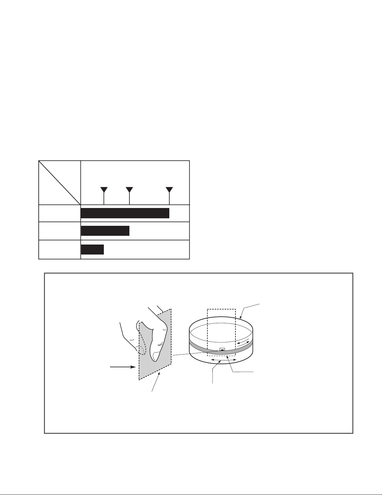
(1) Removal of foreign material from video head (Fig. C-9-4)
Firstly try to use a cleaning tape.
Use a cleaning patch if foreign materials are not removed
with the cleaning tape due to severe dirty of the head.
Soak the cleaning patch in alcohol and put it to the head tip.
Smoothly turn the drum (turning cylinder) to the right or left
(In this case, the cleaning patch must not be moved verti-
cally).
After completely drying the head, test the traveling status
of the tape.
If alcohol (Isopropyl Alcohol) remains at the video head, the
tape may be damaged when this solution touches with the
head surface.
Never use a cloth bar (commercial sale)
(2) Wipe the tape transport system and the drive system with
the cleaning patch soaked in alcohol (Isopropyl Alcohol)
when removing foreign materials from them.
1) The part touched with the traveling tape is called as tape
transport system. The drive system consists of parts to
travel the tape.
2) Care must be exercised so that unreasonable force to
change the pattern will be applied to the tape transport
system during removal of foreign materials.
Cleaning Patch
(Cloth)
Soak alcohol
(Isopropyl Alcohol).
Drum
(Turning Cylinder)
Head Tip
Smoothly turn the drum (turning
cylinder) touching the soft surface
to the head tip surface.
Fig. C-9-4
(No.YD068)1-29
Page 30
4.4.5.2 Grease Applications
(1) Grease Application Method
Apply grease by using a cloth swab or brush. Care must be
exercised so that excess quantity should not be used. If the
excessive quantity is applied, wipe it with the gauze soaked
in alcohol (Isopropyl Alcohol).
(1) Inner Side Surface and Top
Surface of Loading Path
(2) Stable Adhesion Part of Base
P2, P3
(3) Arm Pinch Shaft
2
(4) Gear Wheel Shaft
(5) Reel S. T. Shaft
(1) (2) (3) (4): KG-684G
(Green)
(5): PL-433 (Yellow)
(2) Regular Grease Application
Apply grease to the designated application position every
500 hour.
NOTE: POSITION OF GREASE APPLICATION
(1) Inner Side Surface and Top
Surface of Loading Path
(2) Stable Adhesion Part of Base
P2, P3 Coil
(3) Gear Cam Shaft
(4) Gear Drive Shaft
(5) Clutch Shaft Groove
Guide Part on the Plate Slider
(6)
Side Wall (Left)
(7)
Guide Part on the Plate Slider
Side Wall (Right)
(1) (2) (3) (4) (5) (6) (7): KG 684G (Green)
2
Gear Part
1
5
Chassis (TOP)
Cam Part
(PL-433.Yellow)
Gear Part
(PL-433.Yellow)
Gear Sector Gear Cam
Base Loading Gear Drive
Cam Part Side Application
(KG-684G.Green)
Boss Part Side Wall
(PL-433.Yellow)
Gear Part Side Application
(PL-433.Yellow)
4
3
3
4
6
5
7
1
Chassis (Bottom)
Cam Part
(KG-684G , GREEN)
Cam Part
(KG-684G , GREEN)
Gear Rack F/L
1-30 (No.YD068)
Inner Surface of
Guide Rail
(KG-684G.Green)
Chassis (L) Chassis (R)
Lever, Brake Driving Cam Part
Side Wall Guide Part
Lever F/R Driving Part
Plate Slider
Lever Tension Driving Cam Part
Gear Sector Driving Part
Lever, Spring Driving Part
Side Wall Guide Part
Page 31

Lever, F/R, Base, Tension GEAR AY, P2 & P3
LEVER, F/R
Clutch Contact Part
(PL-433, Yellow)
Tension Arm Party
Hinge Part (PL-433, Yellow)
BASE, TENSION
PL-433
(No.YD068)1-31
Page 32

4.5 ELECTRICAL ADJUSTMENT PROCEDURES (VCR)
4.5.1 Servo Adjustment
1) PG Adjustment
Test Equipment
a) OSCILLOSCOPE
b) Alignment tape (SP, stairstep)
Adjustment And Specification
MODE MEASUREMENT POINT ADJUSTMENT POINT SPECIFICATION
PLAY
V.Ou t
H/SW(TP)
R/C TRK JIG KEY 6.5 0.5H
Adjustment Procedure
a) Insert the Alignment Tape and play.
Note - Adjust the distance of X, pressing the Tracking(+) or Tracking(-) when the "ATR" is blink after the
Alignment Tape is inserted.
b) Connect the CH1 of the oscilloscope to the H/SW(TP) and CH2 to the Video Out for the VCR.
c) Trigger the mixed Combo Video Signal of CH2 to the CH1 H/SW(TP) and then check the distance (time
difference), which is from the selected A(B) Head point of the H/SW(TP) signal to the starting point of
the vertical synchronized signal, to 6.5H 0.5H (412 s, 1H=63 s).
PG Adjustment Method
a-1) Playback the Alignment tape
b-2) Press the "OK(ENTER)" key on the Remote controller and the "REC" key on the Front Panel the same
time, then it goes in to Tracking initial mode.
c-3) Repeat the above step(No.b-2), then it finishes the PG adjusting automatically.
d-4) Stop the playback, then it goes out to PG adjusting mode after mony the PG data.
CONNECTION
WAVEFORM
H/SW
(TP)
V.Out
OSCILLOSCOPE
CH1 CH2
R/C KEY
V.outH/SW
(TP)
H/SW
6.5H(412 s)
Composite
VIDEO
1-32 (No.YD068)
Page 33

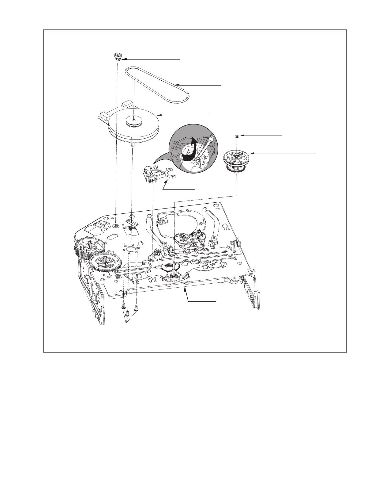
4.6 DECK MECHANISM PARTS LOCATION (DVD)
Top View (With Tray)
Top View (Withou
t Tray)
Procedure
Starting No.
1
Main Base
Clamp Assembly
1
1, 2
1, 2, 3
1, 2, 3, 4
1
1, 6
1, 2, 6
1, 2, 6, 8
1, 2, 6, 8, 9
1, 2, 7
1, 2, 7
1, 2
1, 2 ,13
1, 2, 13, 14
1, 2, 7, 12, 13, 14
1, 2, 13
1, 2, 7, 12, 13,
14, 15, 16, 17
2
Disc
3
Plate Clamp
4
Magnet Clamp
5
Clamp Upper
6
Tray Disc
Base Assembly Sled
7
8
Gear Feed
Gear
9
Middle
10
Gear Rack
11
Rubber Rear
Frame Assembly
12
Up/Down
13
Belt Loading
14
Gear Pulley
15
Gear Loading
16
Guide Up/Down
PWB Assembly
17
Loading
18
Base Main
Parts Fixing Type
4 Screws,
1 Connector
1 Locking Tabs
1 Screw
1 Screw
1 Locking Tab
1 Locking Tab
1 Locking Tab
1 Hook
2Screw
2 Locking Tabs
Disass
embly
Bottom
Bottom
Figure
5-1
5-1
5-1
5-1
5-1
5-2
5-3
5-3
5-3
5-3
5-3
5-4
5-4
5-4
5-4
5-4
5-4
5-4
Bottom View
Note
When reassembling, perform the procedure in
reverse order.
The "Bottom" on Disassembly column of above
Table indicates the part should be disassembled
at the Bottom side.
(No.YD068)1-33
Page 34

PLATE CLAMP
MAGNET CLAMP
CLAMP UPPER
MAIN BASE
DISC CLAMP ASSEMBLY
TRAY DISC
HOLDER
(Fig. A)
BASE MAIN
1.Main Base (Fig. 5-1)
1-1. Clamp Assembly Disc
1) Place the Clamp Assembly Disc as Fig. (A)
2) Lift up the Clamp Assembly Disc in direction of
arrow(A).
3) Separate the Clamp Assembly Disc from the Holder
Clamp.
1-1-1. Plate Clamp
1) Turn the Plate Clamp to counterclockwise direction
and then lift up the Plate Clamp.
1-1-2. Magnet Clamp
1-1-3.Clamp Upper
BASE MAIN
LEVER
BASE MAIN
BOTTOM SIDE VIEW
Fig. 5-2Fig. 5-1
2. Tray Disc (Fig. 5-2)
1) Insert and push a Driver in the emergency eject
hole(A) at the right side, or put the Driver on the
Lever(B) of the Gear Emergency and pull the Lever(B)
in direction of arrow so that the Tray Disc is ejected
about 15~20mm.
2) Pull the Tray Disc until it is separated from the Base
Main completely.
1-34 (No.YD068)
Page 35

GEAR RACK
RUBBER DAMPER
(S3)
PINION GEAR
MIDDLE GEAR
SCREW INSERTION TORGUE CONTROL
(800gf DOWN)
RUBBER DAMPER
Distinguish upper and
lower sides
(Assemble with care)
RUBBER DAMPER
Distinguish upper and
lower sides
(Assemble with care)
BASE PU
GEAR RACK
SPINDLE MOTOR ASSEMBLY
3.Base Assembly Sled (Fig. 5-3)
1) Release 4 Screw(S2).
2) Disconnect the FFC Connector(C1)
3-1. Gear Feed
3-2. Gear Middle
RUBBER DAMPER
GENERAL PICK UP ASSEMBLY
Fig. 5-3
(S2)
3-3. Gear Rack
1) Release the Scerw(S3)
4. Rubber Rear (Fig. 5-3)
(S2)
(No.YD068)1-35
Page 36

GUIDE UP/DOWN
GEAR PULLEY
SCREW INSERTION
TORGUE CONTROL
(800gf DOWN)
GUIDE UP/DOWN
GEAR LOADING
(L4)
BELT LOADING
BASE MAIN
(A)
(L5)
FIG. (A)
(B)
PWB ASSEMBLY LOADING
(A)
(B)
(C)
(C2)
(S5)
(A)
(B)
GUIDE UP/DOWN
(L3)
(L6)
(L6)
BASE MAIN
(H1)
(S4)
UP/DOWN FRAME ASSEMBLY
FIG. (B)
GUIDE UP/DOWN
FIG. (C)
5. Frame Assembly Up/Down (Fig. 5-4)
Note
Put the Base Main face down(Bottom Side)
1) Release the screw(S4)
2) Unlock the Locking Tab(L3) in direction of arrow and
then lift up the Frame Assembly Up/Down to separate
it from the Base Main.
Note
When reassembling move the Guide Up/Down in direction
of arrow(C) until it is positioned as Fig.(C).
When reassembling insert (A) portion of the Frame Assembly Up/Down in the (B) portion of the Guide Up/Down
as Fig.(B)
6. Belt Loading(Fig. 5-4)
Note
Put the Base Main on original position(Top Side)
7. Gear pulley (Fig. 5-4)
1) Unlock the Locking Tab(L4) in direction of arrow(B) and
then separate the Gear Pulley from the Base Main.
Fig. 5-4
8. Gear Loading (Fig. 5-4)
9. Guide Up/Down (Fig. 5-4)
1) Move the Guide Up/Down in direction of arrow(A) as
Fig.(A)
2) Push the Locking Tab(L5) down and then lift up the
Guide Up/Down to separate it from the Base Main.
Note
When reassembling place the Guide Up/Down as Fig.(C)
and move it in direction arrow(B) until it is locked by the
Locking Tab(L5). And confirm the Guide Up/Down as Fig.(A)
10. PWB Assembly Loading (Fig. 5-4)
Note
Put the Base Main face down(Bottom Side)
1) Release 1 Screws(S5)
2) Unlock the Loading Motor (C2) from the Hook (H1) on
the Base Main.
3) Unlock 2 Locking Tabs(L6) and separate the PWB
Assembly Loading from the Base Main.
11. Base Main(Fig. 5-4)
1-36 (No.YD068)
Page 37

SECTION 5
TROUBLESHOOTING
5.1 ELECTRICAL TROUBLESHOOTING GUIDE (VCR PART)
5.1.1 Power(SMPS) CIRCUIT
(1) No 5.3VA
No 5.3VA
YES
Is the FR101
Normal?
YES
Is the BD101
Normal?
YES
Is the R101
Normal?
YES
Is Vcc (9V - 18V) supplied to IC101 Pin2?
YES
Are the D125
normal?
Is there about 2.5V
at the IC103 Pin1?
YES
NO
NO
NO
NO
NO
NO
Replace the FR101
(Use the same ICW)
Replace the
BD101
Replace the R101
Is the D102
normal?
Replace the R125
Replace the IC103
Check or Replace
the D102
Is the D123
normal?
YES
Is the D124
Normal?
YES
Is the D121
Normal?
YES
Power Line of Main
PCB is short
NO
NO
NO
Replace the D123
Replace the D124
Replace the D121
(No.YD068)1-37
Page 38

(2) No 5.0V_D
(3) No 5.0V_T
No 5.0V_D
YES
Is the Vcc(5.3V) supplied to Q165 Emittor?
YES
Is the Q162 Base
'H'?
YES
Check or Replace
the Q165
(4) No 3.3V
No 3.3V
YES
NO
NO
Check or Replace
the D125
Check the PWR CTL
"H" signal from -com
No 5.0V_T
YES
Is the Vcc(5.3V) supplied to Q163 Emittor?
YES
Is the Q162 Base
'H'?
YES
Check or Replace
the Q163
(5) No 33V
No 33V
YES
NO
NO
Check or Replace
the D125
Check the PWR CTL
"H" signal from -com
Is there about 3.8V
at the IC131 pin1?
YES
Is there about 3.3V~5V
at the IC131 pin4?
YES
Check the IC131
and Replace
NO
NO
Check or Replace
the D123
Check the PWR CTL
"H" signal from -com
Is the Vcc(33V) supplied to Q161 Emittor?
YES
Is the Q162 Base
'H'?
YES
Check or Replace
the Q161
NO
NO
Check or Replace
the D121
Check the PWR CTL
"H" signal from -com
1-38 (No.YD068)
Page 39

(6) No Motor_Vcc (To Cap, Drum Motor )
(7) No REG 12V
No Motor_Vcc
YES
Is the Vcc(14V)
supplied to C134?
YES
Check or Replace
the Cap / Drum
NO
Check or Replace
the D124
No REG 12V
YES
Is the Vcc(14V) supplied
NO
to Q165 Collector?
YES
Is the Vcc(14V) sup-
NO
plied to Q165 Base?
YES
Check or Replace
the Q165
Check or Replace
the D124
Check the PWR CTL
"H" signal from -com
(No.YD068)1-39
Page 40

5.1.2 SYSTEM/KEY CIRCUIT
(1) AUTO STOP
Auto Stop
YES
Does the SW25 waveform
appear at the IC501
Pin23?
NO
Check the Drum Motor
signal.
YES
Do the T-UP Reel Pulses
NO NO
appear at the IC501 Pin3?
YES
Replace the IC501. Check the Power Circuit.
Do T/UP Reel Pulses
appear at the Q514 Base
terminal?
YES YES
Replace the T/UP Reel
Sensor (RS501).
Does 5.0V appear at the
RS501?
(2) The unstable loading of a Cassette tape
The unstable loading of a
Cassette tape
YES
Is 12V applied to the
PMC01 Pin8?
NO
Check the Power.
NO
YES
Does the "H" signal appear
at the IC501 Pin32 during
NO
inserting the CST ?
YES YES
Does the "L" signal appear
at the IC501 Pin19 during
inserting the CST?
YES
NO
Check the CST SW and
the peripheral circuitry.
Check the Deck
Mechanism.
Caution : Auto stop can occur because Grease or Oil is dried up
Is 5.0V applied to the
R544 ?
NO
Refer to SMPS 5.3VA
troubleshooting.
Check the IC501
Pins 86, 87, 88, 89.
1-40 (No.YD068)
Page 41

5.1.3 SERVO CIRCUIT
(1) Unstable Video in PB MODE
Unstable Video in
PB Mode.
YES
Does the Noise level of the
screen change
periodically?
YES
Does the CFG waveform
appear at the IC501
Pin67?
YES
On tracking do the CTL
pulses move?
YES
Does the Video Envelope
waveform appear at the
IC501 Pin82?
YES
Replace the IC501.
(2) When the Drum Motor
doesn't run.
When the Drum Motor
doesn't run,
YES
Does 12V appear at the
PMC01 Pin8?
YES
Does 2.8V appear at the
PMC01 Pin12?
YES
Check the connector
(PMC01) and the Drum
Motor Ass'y.
NO
NO
NO
NO
Replace the IC501.
Refer to "When the Y signal
doesn't appear on the
screen in PB Mode".
Refer to "(2)
No 12VA of Power section"
Do the Drum PWM Pulses
appear at the IC501
Pin34?
YES
Aren't the foil patterns and
the Components between
IC501 Pin34 and PMC01
Pin12 short?
YES
Do the DFG Pulses appear
at the IC501 Pin104?
YES
Do the Drum PWM Pulses
appear at the IC501
Pin34?
NO
NO
NO
Do the DFG Pulses appear
at the PMC01 Pin11?
YES
NO
Replace the Cap M.
Aren't the foil patterns and
the Components between
IC501 Pin 104 and PMC01
Pin11 short?
Replace the IC501.
Aren't the connecting patterns and the Components
between IC501 Pin34 and PMC01 Pin12 short?
(No.YD068)1-41
Page 42

(3) When the Capstan Motor doesn't run,
When the Capstan Motor doesn't run,
Does 12VA appear at the PMC01?
YES
Does 2.8V appear at the PMC01?
YES
Check the PMC01 and the Capstan
Motor Ass'y.
Aren't the foil patterns and Components
between IC501 Pin33 and PMC01
Pin9 short?
Does the CFG signal come into the
IC501 Pin67?
NO
NO
YES
YES
Refer to "SMPS(CAPSTAN/12Volt)
Trouble Shooting".
Does the PWM signal appear at the
IC501 Pin33?
NO
Does the CFG signal appear at the
PMC01 Pin1?
NO
Check the Capstan Motor Ass'y.
YES
Does the Capstan PWM signal appear at
the IC501 Pin33?
YES
Aren't the foil patterns and Components
between IC501 Pin33 and PMC01
Pin9 short?
(4) KEY doesn't working
KEY doesn't working.
Is 5V applied to the IC501
NO
Pin36?
YES
Does LED or FLD change
when a function button is
NO
pressed?
NO
Aren't the foil patterns and component
between IC501 Pin67 and PMC01
Pin1 short?
NO
Replace the IC501.
Refer to "SMPS 5.3VA
Trouble Shooting".
Replace the defective
switches.
1-42 (No.YD068)
Page 43

5.1.4 Y/C CIRCUIT
(1) No Video in EE Mode,
No Video in EE Mode
Does the Video signal
appear at the IC301 Pin48?
YES
Is 5V applied to the IC301
Pins18, 24, 42, 55, 72, 91?
YES
Does the Video signal
appear at the IC301 Pin65?
YES
Does the Video signal
appear at the IC501 Pin47?
YES
Does the Video signal appear
at the Emitter terminal of the
Q309?
NO
NO
Check the 19Pin of Tuner.
Check the 5.0VT, 5.3VA
Line. (Power Circuit)
NO NO
Is I2C BUS signal applied to
the IC301 Pins68, 69?
YES
NO
Chck the path of the signal
between the IC301 Pin65
and IC501 Pin49.
NO
Does the 12VT, 5.3VA
appear at the Emitter
NO
terminal of the Q309.
YES
Check the System Circuit.
(Refer to 'SYSTEM I
2
C BUS
CHECK Trouble Shooting')
Check C316. (AGC)
YES
Replace the IC301.
Replace the Q309.
Check the 12VT, 5.4VA
Line. (Power Circuit)
(No.YD068)1-43
Page 44

(2) When the Y(Luminance) signal doesn't appear on the screen in PB Mode,
Is 5.0VT, 5.3VA applied to the
IC301 Pins24, 42, 55, 72, 91?
YES
Is the I2C Bus siganl applied
to the IC301 Pins68, 69 ?
YES
Is the I2C Bus siganl applied
to the IC301 Pins68, 69 ?
YES
NO
Check the line of the 5.0VT,
5.3VA Line. (Power Circuit)
NO
Refer to 'SYSTEM I
2
C BUS
CHECK Trouble Shooting'.
NO NO
Is the V.H.S/W signal
applied to the IC301 Pin70?
YES
Is V.H.S/W "H" about 3.4V
NO
at the IC301 Pin70?
YES
Clean the Drum.
NO
Check the System Circuit.
(IC501 Pin23)
Check the V.H.S/W level.
(Check R303, R304)
Replace the IC301.
Does the Y(Luminance) RF
signal appear at the IC301
Pin79?
YES
Is the Y(Luminance) Video
waveform showed up at
theIC301 Pin43?
YES
Replace the IC301.
NO
NO
Check the path of the
Y(Luminance) RF signal.
(Check the C312)
Check the path of the
Y(Luminance) RF signal.
(Check C327)
YES
YES
1-44 (No.YD068)
Page 45

(3) When the C(Color) signal doesn't appear on the screen in PB Mode,
Is 5.0VT/5.3VA applied to the
IC301 Pins24, 42, 55, 72, 91.
YES
Is the Color Rotary signal
applied to the IC301
Pin70?
YES
Is Color Rotary "H"
about 3.4V?
YES
Does the Color signal
appear at the IC301
Pin25 ?
YES
NO
Check the line of the 5.0VT/
5.3VA Line. (Power Circuit)
NO
Check the Color Rotary
Circuit. (IC501 Pin98 )
NO
Check the Color Rotary
level. (Check the R303)
NO NO
Does the X301(4.43MHZ)
oscillate?
Does the Color signal
NO
appear at the IC301 Pin21?
Replace the X301.
Check the Color Pass.
YES
Replace the IC301.Replace the IC301.
(No.YD068)1-45
Page 46

(4) When the Video signal doesn't appear on the screen in REC Mode,
Is the EE signal normal?
YES
Is 5.0VT/5.3VA applied to the
IC301 Pins24,42,55,72,91?
YES
Does PB Mdoe operate
normally?
YES
Does the RF signal appear
at the IC301 Pin78?
YES
NO
NO
NO
NO
Check EE Mode.
Check the line of the 5.0VT/
5.3VA Line.(Power Circuit)
Check PB Mode.
Is the REC 'H' signal
(about 4V) applied to the
IC301 Pin80?
YES
Check REC Luminance
Pass & Color Pass.
NO
YES
Check the System of REC
'H'. (the IC501 Pin27
/ the D301)
Replace the IC301.
Does the REC RF signal
appear at the IC301
Pins88,89,94,95?
YES
Check the Drum &
Drum Connector
NO
Check the circuit of the
IC301 Pins85, 86.
YES
1-46 (No.YD068)
Page 47

5.1.5 Hi-Fi CIRCUIT
(A) No Sound(EE Mode)
YES
No Sound.
Check the TU Audio of IC801
Pins2, 3.
Check the DVD Audio of IC801
Pins4, 5.
Check the AV1 Audio of IC801
Pins6, 7.
Check the AV2 Audio of IC801
Pins8, 9.
Check the AV3 Audio of IC801
Pins10, 11.
Check the Vcc of IC801 Pins34, 40,
IC802 Pin13.
NO
NO
NO
NO
NO
YES
NO
Check the IC751 Pins30, 31.
Check the DVD Audio OUT.
(JK902 DVD_A_L_L/R).
Check the Scart1 Jack.
(SC901 Scart1 Audio in Pins2, 6).
Check the Scart2 Jack.
(SC901 Scart2 Audio in Pins2, 6).
Check the front Jack.
Check the Power 5.0V, 12VT.
YES
Check the IIC Clock and DATA at
IC801 Pins42, 43.
YES
YES
YES
Check the JK902, SC901.
NO
NO
NO
Check the IC501 Pins17, 18.
Replace IC801.Check the Audio of IC801 Pins16, 17.
Replace IC802.Check the Audio of IC802 Pins1, 14.
(No.YD068)1-47
Page 48

(B) Hi-Fi Playback
PB mode
No Sound.
YES
YES
Check the Vcc of IC801
NO
(Pins34, 40)
YES
Check the Hi-Fi Selection switch.
NO
(IC801 Pin41) and the Tape quality.
YES
Is the RF Envelope at
NO
IC801 Pin44 over 2Vp-p?
YES
Check IC801 Pin42(Data),
NO
Pin43(Clock)
YES
Do Audio Signals appear at
NO
IC801 Pin16(L-CH), 17(R-CH)?
YES
Do Audio Signals appear at
NO
IC802 Pin10(L-CH), 16(R-CH)?
YES
Check Power 5.0V, 12VT.
Check IC501 Pin26
(A.H/SW)
Check the parts of -COM
(IC501 Pins17, 18)
Check the Connection at
P3D01 Pins7, 9.
Check the A.IN line of
IC802(C850, C852)
Do Audio Signals appear at
IC802 Pins11, 16?
Do Audio Signals appear at
JK902?
1-48 (No.YD068)
NO NO
Check the Vcc of IC802
Pin13.
YES YES
Replace IC802.
NO
Check the Jack(JK902)
Check Power.
Page 49

(C)
Hi-Fi REC.
It can't be recorded Hi-Fi Audio
signal.
YES
YES
Check Vcc of IC801.(Pins34, 40)
YES
Check IC801 Pin42(Data), Pin43(CLOCK).
YES
Do Audio signals appear at IC801
Pins16, 17?
YES
Do FM Audio signals appear at IC801
Pin36?
YES
Check the Contact Point of Drum
Connector if good then Replace the Drum.
NO
NO
NO
NO
Check Power 5V, 12V.
Check ports of -COM.
(IC501 pins 17, 18)
Check Audio input signal of IC801
Pins2, 3(TU.A.), 4, 5(DVD.A.),
6, 7(AVI.A.), 8, 9(AV2.A.), 10, 11(AV3.A.).
Replace IC801.
(No.YD068)1-49
Page 50

5.1.6 Tuner/IF CIRCUIT
(A) No Picture on the TV screen
No picture on the TV
screen
YES
Does the Video signal at
the TU701 Pin19.
YES
Is 33VT applied to TU701
Pin17?
YES
Is 5VT applied to TU701
Pin4?
YES
Does the Clock signal
appear at TU701 Pin12?
YES
Does the data signal
appear at TU701 Pin13?
YES
Replace Tuner.
NONO
NO
NO
NO
Hi-Fi REC.
Check 5V line.
Check the lIC Clock Signal
of -COM Pin18.
Check the lIC Data Signal
of -COM Pin17.
Does Sync appear at
NO
IC501 Pin111.
YES
Does the Video signal at
NO
the IC501 Pin47.
YES
Does the Video signal at
NO
the IC301 Pin61.
YES
Does the Video signal at
NO
the IC903 Pin6.
YES
Check the signal flow from IC903
Pins26, 27 to SC901 Pin19.
Check the signal flow from
TU701 Pin19 to IC301 Pin48.
Check the signal from IC301
Pin65 to IC501 Pin49.
Check the signal from IC501
Pin47 to IC301 Pin56.
Check the signal from IC903
Pin6 to IC301 Pin61.
1-50 (No.YD068)
Page 51

(B) No Sound
No Sound.
YES
Check the Vcc of IC751 Pins1, 11, 19,
22, 33.
YES
Check the Tuner SiF signal at IC751
Pin2.
YES
Check the oscillator of IC751 Pins5, 6.
YES
Check the Audio of IC751 Pins30, 31.
YES
Check the Audio of IC801 Pins2, 3.
YES
NO
NO
NO
NO
NO
Check 5.0V Line.
Check the Tuner SIF of TU701 Pin22.
Replace X751
Check the IIC Clock and Data at IC751
Pins12, 13.
Check the signal flow from IC751
Pins30, 31 to IC801 Pins2, 3.
Check the Audio of IC801 Pins16, 17.
YES
Check the Audio of IC802 Pins3, 5.
YES
Check the Signal flow from IC802
Pins3, 5, SC901 Pins1, 3.
NO
NO
Check the IIC Clock and Data at IC801
Pins42, 43.
Check the signal flow from IC801
Pins16, 17 to IC802 Pins11, 16.
(No.YD068)1-51
Page 52

5.2 MECHANISM TROUBLESHOOTING GUIDE (VCR PART)
5.2.1 Deck Mechanism
A.
No Auto Rewind operates.
YES
Is output of the end sensor “H”?
“H”: 3.5V or less
“L”: 0.7V –1V or less
NO
YES
Is voltage at both ends of the
IR LED 0.8V-1.5?
YES
Is the Syscon checked?
B.
No F/R operates.
YES
Is the current mode an F/R
mode?
NO
NO
Is the end sensor Vcc applied at
5V?
YES
Replace the end sensor.
Replace the LED.
Check the assembly position of
the Mode S/W.
NO
Check the Syscon power supply.
YES
Does the Capstan motor rotate?
YES
Does the T/up and the supply
reel Operate?
YES
Check the Syscon circuit.
1-52 (No.YD068)
NO
Is normal voltage applied at the
Vcc1 and the Vcc2 of the
Capstan motor?
YES
Is the Vctl terminal voltage of the
Capstan Motor applied at more
than 4V?
YES
Replace the Capstan motor.
NO
Check the Servo, Power
circuit.
Page 53

C.
Auto Stop operates.
(PLAY/CUE/REV)
Check the assembly mode.
Check the spring pinch.
Does the pinch roller attached to
the Capstan shaft turn in operation of the Play/Cue/Rev.
YES
Does the T/UP or the supply
reel pulse occur?
YES
Check the Syscon, -com.
D.
No cassette loading is done.
Insert the cassette.
NO
NO
Is output of the DFG, DPG
normal?
YES
Check the Servo, Syscon.
Replace the reel sensor.
NO
Replace the drum motor.
YES
Is operation of the lever
assembly S/W normal?
YES
Does output of the CST IN S/W
change?
(In insertion of the REC tape:
"L"_"H"_"L")
(In insertion of the REC prevention tape:
"L"_"H"_"L"_"H")
YES
Check the Syscon circuit.
NO
NO
NO
Check the holder assembly CST.
Is the CST IN S/W normal?
YES
Check the Syscon circuit.
NO
Replace the CST IN S/W.
(No.YD068)1-53
Page 54

E.
No tape winding is done in
play.
Is the pinch roller attached to the
Capstan shaft in operation of play?
YES
Does the T/up reel operate?
YES
Does the Capstan motor turn?
YES
Does the drum motor turn?
YES
Is the DPG, DFG normal?
NO
NO
NO
Check the assembly mode?
Is the Capstan belt hung?
YES
Check the clutch and the idler
assembly.
Is normal voltage applied to the
capstan motor Vcc1, Vcc2?
YES
Is the Vctl terminal voltage of
the Capstan motor applied at
more than 4V?
NO
Hang the Capstan belt.
NO
Check the Servo, power circuit.
YES
Are the T/up and the reel sensor
normal?
YES
Check the Syscon circuit.
NO
YES
Replace the Capstan motor.
Is the Vcc voltage of the drum
motor normal?
YES
Is the Vctl terminal voltage of the
drum motor at more than 2.3V?
YES
Replace the drum motor.
NO
Check the Syscon circuit.
NO
Check the Syscon circuit.
1-54 (No.YD068)
Page 55

5.2.2 Front Loading Mechanism
A.
No cassette insert is done.
Does the lever assembly
switch operate?
YES
Is the Vcc of the main P.C.B
assembly?
YES
Is voltage between the cassette
switch terminal and the GND on
the main P.C.B assembly?
YES
Check the mode switch position
and the Syscon circuit.
NO
NO
NO
Is the lever assembly switch
spring normal?
NO
Add or replace the lever
assembly switches spring.
YES
Does the CST IN switch
operate normally?
NO
Replace the F/L switch.
YES
Check the Syscon circuit.
Check the power circuit.
Is there short between the cassette switch terminal
and the GND on the main P.C.B assembly?
YES
Replace the main P.C.B assembly or remove the short part.
NO
Replace the CST IN switch.
B.
No cassette eject is done.
Does the L/D motor turn in reverse?
YES
Does the lever assembly switch operate?
YES
Does the arm assembly F/G operate?
YES
Does the opener door operate?
NO
Check the L/D motor and the drive IC.
NO
Replace the lever assembly switch.
NO
Replace the arm assembly F/L
NO
Replace the opener door.
(No.YD068)1-55
Page 56

C.
No safe adherence of tape is done.
Is cassette insert done?
YES
Does the opener lid operate?
YES
Does the gear rack F/L operate?
NO
NO
YES
Does the opener door operate?
YES
Does the arm assembly F/L operate?
YES
Does the L/D motor operate?
NO
NO
Replace the opener lid.
Replace the gear rack F/L.
Check the assembly status of the
opener door.
Replace the arm assembly F/L.
YES
Does the holder assembly cassette move
same as the arm assembly F/L?
YES
Replace the front loading mechanism
assembly.
1-56 (No.YD068)
NO
Check power supply of the L/D motor.
NO
Check the assembly status of the
holder assembly cassette.
Page 57

5.3 ELECTRICAL TROUBLESHOOTING GUIDE (DVD PART)
5.3.1 System operation flow
Power On
1. 8032 initializes SERVO, DSP & RISC registers
2. Write RISC code to SDRAM
3. Reset RISC
Show LOGO
Yes
Tray Close to Closed position
SLED Moves to Inner Position
1. Judge whether have disc and disc type
2. Jump to related disc reading procedure
Tray Closed?
No
SLED at Inner
Side?
No
Recieve
OPEN/ CLOSE
Key?
Yes
No
1. Execute Pressed Key & IR Key
2. Systemoperati on Routi ne Loop
1. Stop Playback & Open Tray
2. Display tray open message & LOGO
No
Receive
CLOSE Key?
Yes
(No.YD068)1-57
Page 58

5.3.2 SYSTEM Test flow
TEST
Check the AC Voltage
Power PCBA(110V or 220V)
YES
Switch on the Power PCBA
Is the DC Voltage
outputs OK?
(5V,1.8V,3.3V,8V,12V)
YES
Make sure the main PCBA don't
short on VCCs and switch it on.
NO
NO
Replace power PCBA or
AC transformer.
Repair or Replace Power PCBA
Is 3.3V and 1.8V DC
outputs normal on main
PCBA?
YES
Connect to PC CN601 Cable and
update the FLASH memory code.
Update FLASH
successfully?
YES
A
NO
NO
Check the regulators or related diodes.
1. Check 27MHz system clock.
2. Check system reset circuit.
3. Check FLASH R/W enable signal PRD,RWR.
4. Check CN601 SIGNALS.
5. Check FLASH Memory related circuit.
1-58 (No.YD068)
Page 59

A
RESET or Power On.
Show LOGO?
YES
NO
Flash Memory operates
properly?
YES
SDRAM works properly?
YES
ZR36868 VIDEO outputs
properly?
YES
Have TV signal output?
YES
Check AV cable connection
to TV set.
NO
NO
NO
NO
Check connection lines between FLASH
& ZR36868 and the FLASH access time
whether is suitable or not.
Check connection lines between SDRAM
& ZR36868 and the SDRAM is damaged.
Check the related circuit of ZR36868
Check the filtering and amp circuit of
TV signal.
Does Tray move
inside when it is not
at closed position?
YES
B
NO NO
Normal TROUT &TRIN
signals?
YES
Normal TRCLOSE &
TROPEN signal?
YES
Normal LOAD+ & LOAD-
signal?
YES
Check the cable connection between
main PCBA and loader.
NO
NO
Check the load OPEN & CLOSE switch
Check the Tray control IO pins on
MT1389 & BA5954
Check the Tray control amplifying
circuit on Motor driver.
(No.YD068)1-59
Page 60

B
Does
the SLED move
to inner side when it is at
outter position?
NO NO
Motor Driver STBY
Pin is High?
Check the connection line of
STBY signal.
YES
Do not put in disc and tray close.
YES
Is SLED_S
DC Level higher
than 1.4V?
YES
SLED+ and
outpup
SEDL-
properly?
YES
Check the cable connection with
MECHA.
NO
NO
Check the related circuit of
SLED_S.
Check the amp circuit on motor
driver.
Optical Lens has
movements for searching
Focus?
YES
C
NO NO
Check cable connect on with
pick-up head.
Proper
FOCUS_S outputs
to motor driver?
YES
Proper FACT- & FACT+
outputs?
YES
NO
Check FFOCUS_S connection on
ZR36868 and motor dirver.
Check the amp circuit on motor
dirver.
1-60 (No.YD068)
Page 61

C
Laser turns on when
reading disc?
YES
Put disc in? Laser off
YES
Disc ID is correct?
YES
NO NO
NO
NO
DVD_LD or CD_LD output
Collector voltage of
power transistor is OK?
Check cable connection between
transistor ouput and pick-up head.
Check DVD_LD & CD_LD signal
properly?
YES
YES
NO
Check the laser power circuit
on ZR36868 and connecting to
power transistor.
Check the related circuit on
laser power transistor
Does spindle rotate?
YES
D
NO NO
Check the cable connection
between spindle and main PCBA.
Proper
SPINDLE_S signal on
ZR36868
YES
MOT_SPDL-
& MOT_SPDL+ output
properly?
YES
NO
Check SPINDLE_S related
circuit on ZR36868
Check the spindle control
amp circuit of motor driver.
(No.YD068)1-61
Page 62

D
YES
Focus ON OK?
YES
Track On OK?
YES
NO
NO
Proper signals on
A,B,C,D of ZR36868
YES
Check FOCUS_S signal
on ZR36868
Properly
TRACK_S signal
on ZR36868?
YES
TACT+ & TACToutput properly?
YES
Check cable connection on
pick-up head.
NO
NO
NO
Check connections between
ZR36868 and Pick-up head.
Check the TRACK_S
connection on ZR36868
and motor dirver.
Check the tracking control
amp circuit on motor
driver.
Disc is play ?
YES
E
NO
Check RF & VC signal waveform.
1-62 (No.YD068)
Page 63

E
Normal Audio output
when disc playba
Normal IR.VFD & Front
pannel key functions
TEST EN
ck?
YES
?
YES
D
NO
NO
Audio DAC received
correct data stream?
YES
Normal Audio DAC
out?
YES
Check Audio filter,amplify,mute
.
circuit
Communications between
IR.VFD Front pannel key & ZR36868
is normally
?
YES
Check the cable connection on
Front pannel
.
NO
NO
NO
Check connection between
ZR36868 & Audio
Check the related
circuit of Audio
Check communication lines on
ZR36868.
DAC.
DAC.
(No.YD068)1-63
Page 64

5.4 DETAILS AND WAVEFORMS ON SYSTEM TEST AND DEBUGGING
5.4.1 SYSTEM 27MHz CLOCK, RESET, FLASH R/W SIGNAL
1) ZR36868 main clock is at 27MHz(X501)
1.0V, 27MHz
2) ZR36868 reset is low active
FIG 1-1
5.3VA
PWR_CTL_H
M_RESET(FRONT)
1-64 (No.YD068)
FIG 1-2
Page 65

3) CN601 waveform during procedure(Downloading)
FIG 1-3
DUPTDO
DUPRDO
4) Flash R/W enable signal during download(Downloading)
FIG 1-4
FRD
FWR
(No.YD068)1-65
Page 66

5.4.2 SDRAM CLOCK
5.4.3 TRAY OPEN/CLOSE SIGNAL
DCLK = 135MHz, Vp-p=2.2, Vmax=2.7V
FIG 2-1
1) Tray open/close waveform
OPEN
CLOSE
FIG 3-1
1-66 (No.YD068)
Page 67

5.4.4 SLED CONTROL RELATED SIGNAL (NO DISC CONDITION)
FIG 4-1
5.4.5 LENS CONTROL RELATED SIGNAL(NO DISC CONDITION)
SLED_S(2.0V/1.4V/1.0V)
SLED+(4.7V/4.0V/2.6V)
SLED-(5.3V/4.0V/3.0V)
FIG 5-1
FOCUS_S(1.5V/1.4V/1.3V)
FACT+(4.0V/3.6V/3.2V)
FACT-(4.0V/3.6V/3.2V)
(No.YD068)1-67
Page 68

5.4.6 LASER POWER CONTROL RELATED SIGNAL(NO DISC CONDITION)
FIG 6-1
MD_CD(0V/180mV)
MD_LD(5.0V//3.5V)
DVD_LD(5.0V/3.6V)
5.4.7 DISC TYPE JUDGEMENT WAVEFORM
F+
FE
RFL
FIG 7-1 (DVD)
1-68 (No.YD068)
Page 69

FIG 7-2 (DVD)
F+
FE
RFL
F+
FIG 7-3 (CD)
FE
RFL
(No.YD068)1-69
Page 70

5.4.8 FOCUS ON WAVEFORM
F+
FE
RFL
FIG 7-4 (CD)
FIG 8-1 (DVD)
FOCUS_S
FACT+
FACT-
1-70 (No.YD068)
Page 71

FIG 8-2 (CD)
5.4.9 SPINDLE CONTROL WAVEFORM (NO DISC CONDITION)
FOCUS_S
FACT+
FACT-
SPINDLE_S
FIG 9-1
MOT_SPDL-(3.6V/2.4V)
MOT_SPDL+(3.6V/4.8V)
(No.YD068)1-71
Page 72

5.4.10 TRACKING CONTROL RELATED SIGNAL(System checking)
FIG 10-1(DVD)
TRACK_S
TACT-
TACT+
FIG 10-2(CD)
TRACK_S
TACT-
TACT+
1-72 (No.YD068)
Page 73

5.4.11 ZR36868 AUDIO OPTICAL AND COAXIAL OUTPUT(SPDIF)
FIG 11-1
5.4.12 ZR36868 VIDEO OUTPUT WAVEFORM
1) 100%
FIG 12-1
(No.YD068)1-73
Page 74

2) COMPOSITE VIDEO SIGNAL
FIG 12-2
5.4.13 ZR36868 AUDIO OUTPUT TO AUDIO DAC
FIG 13-1
1-74 (No.YD068)
Page 75

5.4.14 AUDIO OUTPUT FROM AUDIO DAC
FIG 14-1
(No.YD068)1-75
Page 76

Victor Company of Japan, Limited
AV & MULTIMEDIA COMPANY DIGITAL VIDEO STORAGE CATEGORY 12, 3-chome, Moriya-cho, kanagawa-ku, Yokohama, kanagawa-prefecture, 221-8528, Japan
(No.YD068)
Printed in Japan
VPT
Page 77

PARTS LIST
[HR-XV28SEF,HR-XV28SEK,HR-XV28SER,
HR-XV28SEU,HR-XV28SEY,HR-XV28SEZ]
* SAFETY PRECAUTION
Parts identified by the symbol are critical for safety. Replace only with
specified part numbers.
* BEWARE OF BOGUS PARTS
Parts that do not meet specifications may cause trouble in regard to safety
and performance. We recommend that genuine JVC parts be used.
* (x_) in a description column shows the number of the used part.
- Contents -
Exploded view of general assembly and parts list ..................... 3-2
VHS mechanism assembly and parts list................................... 3-4
DVD mechanism assembly and parts list................................... 3-7
Electrical parts list ...................................................................... 3-9
Packing materials and accessories parts list ........................... 3-22
(No.YD068)3-1
Page 78

Exploded view of general assembly and parts list
25
0
463
463
Block No. M1MM
463
285
A43
DVD unit
286
283
463
Key board
assembly <02>
284
457
Deck/mecha
assembly
469
2
61
470
471
Power board
assembly <01>
324
VCR
main
28
8
323
265
274
465
463
board
assembly
<03>
469
3-2(No.YD068)
261
452
A44
261
330
300
261
Page 79

MODEL
HR-XV28SEF
HR-XV28SEKAB
MARK
MODEL
HR-XV28SER
HR-XV28SEUCD
MARK
MODEL
HR-XV28SEY
HR-XV28SEZEF
General assembly
Block No. [M][1][M][M]
Symbol No. Part No. Part Name Description Local
250 LG-3110R-V024B CASE VBW8024 PRESS TOP A288G B:3/S:
261 LG-5040R-0069S RUBBER CCD 05 NEW SILICON OTHER 2T (3(x4)
265 LG-4930R-0384A HOLDER POWER CORD
274 LG-3300R-V075A PLATE ONE BOARD SLIM PRESS A/V JACK
283 LG-3580R-V145A DOOR VCR VJ90 MOLD CST JVC COMBI
284 LG-442-681A SPRING DOOR
285 LG-3580R-T192A DOOR VCR VJ90 MOLD TRAY JVC COMBI
286 LG-4970R-0146A SPRING PLATE DR4000 SPRING
288 LG-4930R-0573A HOLDER VCR V9500 MOLD POWER PWB
300 LG-6410RBHV02E POWER CORD HIT-102/H03VHH2-F (ST-HS:80MM) B
300 LG-6410RCHP02D POWER CORD HIT-102/H03VHH2-F (ST-HS:80MM) A,C,D,E,F
323 LG-3111R-0089E CASE ASSEMBLY PRE AMP SLIM COMBI C-CORE A NO
324 LG-4930R-0472A HOLDER VCR ONE BOARD SLIM MOLD HIPS 6(x2)
330 LG-3140R-V010A CHASSIS ONE BOARD PRESS SECC 0.8T
452 LG-1SZZR-0098A SCREW/DRAWING + 2 D3.0 L10.0 MSWR3/FZMCY-1 3(x4)
457 LG-1SZZR-0098E SCREW/DRAWING + 2 D3.0 L12.0 MSWR3/FZMCW-1 3(x4)
463 LG-1SZZR-0098G SCREW/DRAWING + 2 D3.0 L8.0 MSWR3/FZMCW-1 3C(x8)
465 LG-1SZZR-0097K SCREW/DRAWING + 2 D3.0 L10.0 MSWR3/FZB 3 CR(x2)
469 LG-1SZZR-0098J SCREW/DRAWING + 2 D3.0 L6.5 MSWR3/FZMCY-1 3(x4)
470 LG-1SZZR-0098K SCREW/DRAWING + 2 D3.0 21MM MSWR3/FZMCY-1 3C(x2)
471 LG-1SZZR-0098L SCREW/DRAWING + 2 D3.0 L16.0 MSWR3/FN SILVER
A43 LG-3721R-F432C PANEL ASSEMBLY/FRONT VCR VJ9033SZ.NA3FJJ COMBI A
A43 LG-3721R-F432B PANEL ASSEMBLY/FRONT VCR VJ9033SZ.NA3FJJ COMBI B
A43 LG-3721R-F432A PANEL ASSEMBLY/FRONT VCR VJ9033SZ.NA3FJJ COMBI C,D,E,F
A44 LG-3141R-V027L CHASSIS ASSEMBLY 2005 COMBI DVD+VCR 4HD HI-FI P
MARK
(No.YD068)3-3
Page 80

VHS mechanism assembly and parts list
Block No. M2MM
100
A21
102
A23
031
079
011
017
022
A01
003
012
004
008
006
013
016
Not used
007
409
014
015
009
405
027
028
029
021
116
3-4(No.YD068)
115
A24
024
406
109
054
031
054A
A22
Page 81

BACK SIDE
051
518
055
060
080
056
058
052
517
061
052A
064
A11
077
A12
023
078
076
410
(No.YD068)3-5
Page 82

MODEL
HR-XV28SEF
HR-XV28SEKAB
MARK
MODEL
HR-XV28SER
HR-XV28SEUCD
MARK
HR-XV28SEY
HR-XV28SEZEF
VHS mechanism
Block No. [M][2][M][M]
Symbol No. Part No. Part Name Description Local
003 LG-4930R-0449A HOLDER DECK/MECHA FPCB(6CH) - D37C MO
004 LG-5006R-0045A CAP DECK/MECHA FPCB - D37C MOLD
008 LG-6850R-HG18Y CABLE/FLAT P=1.25 FFC UL2896(0.05X0.8) 7
009 LG-4260R-0056A ARM DECK/MECHA T/UP OTHER - D37
011 LG-4261R-0040A ARM ASSEMBLY DECK/MECHA TENSION - D37
012 LG-3041R-M037A BASE ASSEMBLY P2 -D37
013 LG-3041R-M038A BASE ASSEMBLY P3 - D37
014 LG-3041R-M039A BASE ASSEMBLY P4 - D37
015 LG-5870R-0007A OPENER DECK/MECHA LID OTHER - D37
016 LG-3041R-M036D BASE ASSEMBLY A/C HEAD (ALPS) - D37 (DUMMY H
017 LG-4408R-0005A REEL DECK/MECHA S OTHER - D37
021 LG-4421R-M002A BRAKE ASSEMBLY T - D37
022 LG-6520D00004B HEAD(CIRC) ST ST FE HEAD FOR D37 13.5
023 LG-3040R-M056A BASE LOADING OTHER - D37
024 LG-4261R-0042A ARM ASSEMBLY DECK/MECHA IDLER(N) - D37
027 LG-4470R-0133A GEAR DECK/MECHA WHEEL OTHER - D37
028 LG-4408R-0006A REEL DECK/MECHA T OTHER - D37
029 LG-4261R-0037A ARM ASSEMBLY DECK/MECHA PINCH - D37 (CHON P
031 LG-4970R-0175A SPRING COIL TENSION - D37(x2)
051 LG-4400R-0005A BELT CAPSTAN
052 LG-4680R-A015A MOTOR(MECH) CAPSTAN F2QVB66 SANKYO FOR D37
052A LG-4980R-0029A SUPPORTER DECK/MECHA CAPSTAN OTHER - D37
054 LG-4470R-0136A GEAR DECK/MECHA RACK F/L OTHER - D3
054A LG-4970R-0171A SPRING COIL RACK F/L - D37
055 LG-4470R-0140A GEAR DECK/MECHA DRIVE OTHER - D37
056 LG-4470R-0139A GEAR DECK/MECHA CAM OTHER - D37
058 LG-4421R-M001A BRAKE ASSEMBLY CAPSTAN -D37
060 LG-4510R-0065A LEVER DECK/MECHA F/R OTHER - D37
061 LG-4265R-0007A CLUTCH ASSEMBLY DECK/MECHA D37(N)
064 LG-4470R-0141A GEAR DECK/MECHA SECTOR OTHER - D37
076 LG-4510R-0063A LEVER DECK/MECHA SPRING OTHER - D37
077 LG-3300R-M203A PLATE SLIDER OTHER - D37
078 LG-4510R-0062A LEVER DECK/MECHA TENSION OTHER - D37
079 LG-3040R-M057A BASE TENSION OTHER - D37
080 LG-4510R-0064A LEVER DECK/MECHA BRAKE OTHER - D37
100 LG-3301R-M193A PLATE ASSEMBLY TOP - D37
102 LG-4970R-0173A SPRING COIL STOPPER - D37
109 LG-5870R-0008A OPENER DECK/MECHA DOOR OTHER - D37
115 LG-4510R-0070A LEVER DECK/MECHA SWITCH(C) OTHER - D
116 LG-4970R-0163A SPRING COIL D35S SWITCH
405 LG-1MPC0301270 SCREW MACHINE/PAN HEAD + D3.0 L3.5 SWRCH18A/FZW
406 LG-1MEC0302018 SCREW MACHINE/PAN HEAD SPR W + D3.0 L6.0 MSWR3/FZY(x3)
409 LG-1SZZR-0032B SCREW/DRAWING + 1 D2.6 L5.0 SWRCH18A/FZY TAP
410 LG-1APF0262218 SCREW TAP TITE(B)/PAN HEAD + D2.6 L6.8 MSWR3/FZY(x3)
517 LG-1WZZR-0004D WASHER/DRAWING STOPPER
518 LG-1WZZR-0004A WASHER/DRAWING STOPPER
A01 LG-6723R-0603F DRUM(CIRC) ASSEMBLY DECK/MECHA (9P6S) D37-6CH PAL
A11 LG-4471R-0017A GEAR ASSEMBLY DECK/MECHA P3 - D37
A12 LG-4471R-0015A GEAR ASSEMBLY DECK/MECHA P2 - D37
A21 LG-4931R-0084A HOLDER ASSEMBLY DECK/MECHA CST - D37
A22 LG-4471R-0016A GEAR ASSEMBLY DECK/MECHA RACK F/L - D37
A23 LG-4261R-0038A ARM ASSEMBLY DECK/MECHA F/L - D37
A24 LG-4511R-0005A LEVER ASSEMBLY SWITCH(C) - D37
MODEL
MARK
3-6(No.YD068)
Page 83

DVD mechanism assembly and parts list
Block No. M3MM
A01
012
019
026
013
017
439
014
435
015
018
015B
012
440
016
030
432
439
A02
020
032
010
024
A03
036
430
439
025
021
431
435
035A
035
430
012A
(No.YD068)3-7
Page 84

MODEL
HR-XV28SEF
HR-XV28SEKAB
MARK
MODEL
HR-XV28SER
HR-XV28SEUCD
MARK
HR-XV28SEY
HR-XV28SEZEF
DVD mechanism
Block No. [M][3][M][M]
Symbol No. Part No. Part Name Description Local
010 LG-6850R-JW23Z CABLE/FLAT P=1.0 FFC UL2896(0.035X0.7) 23
012 LG-5040R-0083A RUBBER DVD DP-6/ DP-8 FRONT RIGHT 20(x2)
012A LG-5040R-0110A RUBBER DVD REAR DP8 RIGHT 20 OTHER BL(x2)
013 LG-4400R-0006B BELT DECK/MECHA DP2-5/ DP7C/DP7A OT
014 LG-4470R-0154A GEAR DECK/MECHA DP8 PULLEY MOLD
015 LG-4681R-A015A MOTOR ASSEMBLY DECK/MECHA LOADING DP-9 SH
015B LG-4560R-0008A PULLEY MOTOR
016 LG-6871R-9294A PWB(PCB) ASSEMBLY/TOTAL DP-9C LOADING
017 LG-4470R-0176A GEAR DVD DP-9 LOADING MOLD
018 LG-4974R-0067A GUIDE DVD DP-9C UP/DOWN MOLD
019 LG-3210R-M008A FRAME DP-9C UP/DOWN MOLD
020 LG-3040R-M064A BASE MAIN DP-9C MOLD
021 LG-4681R-B009B MOTOR ASSEMBLY DECK/MECHA DP9 FEEDING
024 LG-4470R-0179A GEAR DVD DP-9 PINION MOLD
025 LG-4470R-0178A GEAR DVD DP-9 MIDDLE MOLD
026 LG-3390R-0030A TRAY DVD DP-9C DISK MOLD
030 LG-4470R-0180A GEAR DVD DP-9 RACK MOLD
032 LG-6200J000090 FILTER(CIRC)/EMC ZSHT1228-0730T-K TDK ST
035 LG-6871R-9295A PWB(PCB) ASSEMBLY/TOTAL DP-9C FEEDING
035A LG-6850R-GK09Z CABLE/FLAT P=1.0 FFC UL2896(0.05X0.65) 11
036 LG-4370R-0136A SHAFT DVD PU/ DR-02 SUS-420J2 OTHER
430 LG-1SZZR-0064B SCREW/DRAWING + 1 D1.7 L7.0 SWCH18A/BZN DP8(x2)
431 LG-1SZZR-0062A SCREW/DRAWING + 1 D1.7 L4.5 SWCH18A/NI DP8 P
432 LG-1SZZR-0072A SCREW/DRAWING + 1 D1.7 L4.5 SWRCH18A/FZY DP8
435 LG-1SZZR-0011A SCREW/DRAWING MACHINE(x4)
439 LG-1SZZR-0075A SCREW/DRAWING + 1 D1.7 L10.0 SWRCH18A/FZW DP(x3)
440 LG-1SZZH-1007B SCREW/DRAWING + D2.0 6MM SWRCH16A/ZNBK 4MM 1
A01 LG-4861R-0016B CLAMP ASSEMBLY DISC DP7 - SH
A02 LG-3041R-D024A BASE ASSEMBLY MAIN DP-9C
A03 LG-3041R-M068A BASE ASSEMBLY SLED DP-9C (DI)
MODEL
MARK
3-8(No.YD068)
Page 85

Electrical parts list
Power board
Block No. [0][1]
Symbol No.
A47
A47 LG-6871R-4925A
PW101 LG-561-292B
IC101
IC102 PZ0ILI817000B SENSOR
IC102 or
IC103 LG-0IKE431000A IC/KEC KIA431 3 PIN TP - -
IC103 or LG-0ISS431000A
IC131
IC131 or
Q161
Q162
Q162 or
Q163
Q163 or
Q164
Q164 or
Q165
Q165 or
Q166
Q166 or
BD101 S1WB/A/60-4101 BRIDGE DIODE
BD101 or
D101 ERA22-10 DIODE/RECTIFIERS
D102
D102 or
D121
D121 or
D123
D123 or
D123 or
D124
D124 or
D125
D127 1SS133-T2 SI DIODE
ZD102
ZD151
ZD151 or
Part No. Part Name Description Local
LG-6871R-
4925C
LG0IPMGIH005A
LG6500RDB010A
LG0IPMGKE006B
LG0IPMGGM002A
LG0TR126809BA
LG0TR319809AC
LG0TR534309BA
LG0TR928009AD
LG0TR127309AA
LG0TR534309BA
LG0TR534409AA
LG0TR928009AD
LG0TR127309AA
LG0TR232809AB
LG0TR320509AB
LG0DRRE00060A
LG0DR104009BA
LG0DRGF00239A
LG0DR104009BA
LG0DRGF00239A
LG0DR810040BA
LG0DR158220AA
LG0DRGF00210A
LG0DSGF00040A
LG0DSDI00110A
LG0DRSD00210A
LG0DZ202609AA
LG0DZ132609AB
LG0DZ132609BB
PWB(PCB)
ASSEMBLY/TOTAL
PWB(PCB)
ASSEMBLY/TOTAL
CONNECTOR(CIRC)
/DRAWING
IC/POWER
MANAGEMENT
SENSOR
IC/SAMSUNG
ELECTRONICS
IC/POWER
MANAGEMENT
IC/POWER
MANAGEMENT
TRANSISTOR/
BIPOLARS
TRANSISTOR
TRANSISTOR/
BIPOLARS
TRANSISTOR
TRANSISTOR
TRANSISTOR/
BIPOLARS
TRANSISTOR 2SC5344Y TP
TRANSISTOR
TRANSISTOR
TRANSISTOR
TRANSISTOR
DIODE/RECTIFIERS
DIODE/RECTIFIERS
DIODE/RECTIFIERS
DIODE/RECTIFIERS
DIODE/RECTIFIERS
DIODE/RECTIFIERS
DIODE/RECTIFIERS
DIODE/RECTIFIERS
DIODE/SWITCHING
DIODE/SWITCHING
DIODE/RECTIFIERS
DIODE/ZENER
DIODE/ZENERS
DIODE/ZENER
2005 COMBI ZORAN
CIS SMPS DI
2005 COMBI ZORAN
PAL SMPS D I C
GP390 LGC 3P 3.96
STRAIGHT SN
ICE3B0565J INFINEON
PC123YN2J00F SHARP
KIA78R33PI CU KEC 4P
KSA928A-Y/TO-92L TP
KSA928A-Y/TO-92L TP
SHINDENGEN - 600V -
RECTRON BK NON 6
ERA22-10 KFLB/TP /R
RL104F TP RECTRON -
FR104E GULF TP NON
RL104F TP RECTRON -
FR104E GULF TP NON
ERC81-004L22 BK FUJI
1N5822 BK RECTRON
UF5402-M11 GULF BK
D3S6M SHINDENGEN
8PIN/DIP S
LTV-817B/PHOTO
COUPLER(LITEON)
PHOTOCOUPLE
KA431AZ (LM431AZ)
G9133 GMT 4PIN/TO
KTA1268-BL TP KEC
UF3003 DIODES BK
UZ-20BSB 26MM TP
GDZJ13A 26MM TP
UZ-13BSA 26MM TP
TO-220IS
220F-4L ST 1
KTC3198-TP-BL
(KTC1815)KEC
2SC5343-L TP AUK
SAMSUNG TO
KTA1273-TP-Y
(KTA966A)KEC
2SC5343-L TP AUK
SAMSUNG TO
KTA1273-TP-Y
(KTA966A)KEC
KSC2328A-Y TP
SAMSUNG TO-92L
KTC3205-TP-Y
(KTC2236A)KEC
S1WBA60 BK
DB105-C-S-V50
T/P/FUJI
400V 1A 30
400V 1A 30A
400V 1A 30
400V 1A 30A
DO201AD 4
DO201AD 40V
1N5822 GULF BK
DO201AD 40V 3A
DO201AD 200
DO201AD 200V
BK AX14 60V 1
1SS133 TP ROHM
KOREA - - - - -
PYUNG CHANG D
GRANDE DO34 0
PYUNG CHANG
TO92 -
TO92 -
A,B,D,
E,F
MODEL
HR-XV28SEF
HR-XV28SEKAB
Symbol No.
ZD152
ZD152 or
C
C101 LG-624-088L
C102 LG-624-088L
C103
C103
C104
C105
C106 LG-624-087G CAPACITOR
C107
C108 QETC1HM-105Z E CAPACITOR
C109
C111
C121 LG-624-087D
C124
C126 LG-624-085D CAPACITOR
C127
C128
C134
C137
C138 LG-624-082H CAPACITOR
C143
C158 QET61CM-106Z E CAPACITOR
C159
C160
C161
C162
C164 QET61CM-106Z E CAPACITOR
C166
R100 QRE121J-155Y C RESISTOR
R104
R105
R109
R136 QRD161J-104Y C RESISTOR
R141 QRD161J-221 C RESISTOR
R142 QRD161J-222Y C RESISTOR
R143 QRE141J-102Y C RESISTOR 1K OHM 1/6 W 5% TA26
R144
R145
R146 QRD161J-271Y C RESISTOR
R154 QRE141J-102Y C RESISTOR 1K OHM 1/6 W 5% TA26
Part No. Part Name Description Local
LG-
0DZ102609BB
LG-
0DZ100009HA
LG0CE686CV610
LG0CE686CU611
LG0CN1040K948
LG0CQ1031Y519
LG0CN1030K518
LG0CE3366H638
LG0CG1020U630
LG0CE477BH630
LG0CE108BF630
LG0CE228BF630
LG0CE227CH618
LG0CE3376D638
LG0CQ1042K409
LG0CE4754K638
LG0CE4754K638
LG0CE4754K638
LG0CE4776D638
LG0CN223AK948
LG0RS5602K619
LG0RD0102F608
LG0RS0750K619
LG0RN3301F408
LG0RN2701F408
MARK
MODEL
HR-XV28SER
HR-XV28SEUCD
DIODE/ZENERS
DIODE/ZENERS
CAPACITOR/
DRAWING
CAPACITOR/
DRAWING
CAPACITOR/FIXED
ELECTROLYTIC
CAPACITOR/FIXED
ELECTROLYTIC
CAPACITOR/FIXED
TUBULAR(HIGH D
CAPACITOR/FIXED
FILM
CAPACITOR/TUBULAR
(HIGH DIELEC)
CAPACITOR/FIXED
ELECTROLYTIC
CAPACITOR/SEMI
CERAMIC
CAPACITOR/FIXED
CERAMIC(HIGH D
CAPACITOR/
AL.ELECTROLYTIC
CAPACITOR/FIXED
ELECTROLYTIC
CAPACITOR/FIXED
ELECTROLYTIC
CAPACITOR/FIXED
ELECTROLYTIC
CAPACITOR/
ELECTROLYTIC
CAPACITOR/FIXED
FILM
CAPACITOR/FIXED
ELECTROLYTIC
CAPACITOR/FIXED
ELECTROLYTIC
CAPACITOR/FIXED
ELECTROLYTIC
CAPACITOR/FIXED
ELECTROLYTIC
CAPACITOR/
TUBULAR(HIGH DIELEC)
RESISTOR/FIXED
METAL OXIDE FIL
RESISTOR/FIXED
CARBON FILM
RESISTOR/FIXED
METAL OXIDE FIL
RESISTOR/FIXED
METAL FILM
RESISTOR/FIXED
METAL FILM
MARK
ELECTRONICS 0.1UF/2
ELECTRONICS 0.1UF/2
68UF SHL/SD 400V 20%
33UF SMS/SG 25V 20%
2200UF KME TYPE 16V
220UF SHL/SD 25V 20%
330UF SMS 10V M FM5
0.1UF S 50V 5% PE TP5
4.7UF SRA/SS 50V 20%
4.7UF SRA/SS 50V 20%
4.7UF SRA/SS 50V 20%
0.022UF 50V Z F TA26 S
1.5M OHM 1/2 W 5.00%
56K OHM 2 W 5.00% TR
10 OHM 1/6 W 5% TA26
0.75 OHM 2 W 5.00% TR
MODEL
HR-XV28SEY
HR-XV28SEZEF
UZ-10BSB 26MM TP
PYUNG CHANG D
UZ-10BM TP PYUNG
CHANG - 0.5W
435D SUNIL
435D SUNIL
68UF SHL,SD 450V M
0.1UF D 50V 80%/-20%
0.01UF D 630V 10% PE
HIGH-VOL 68PF/1KV
0.01UF 50V K B TA26
1.0M SRA/SS50V M
1000PF 400V M E(Z5U)
HI-VOL 470P/1KVDC
470UF KME TYPE 25V
1000UF KME 16V M
10M SRA 16V M FM5
470UF SMS/SG 10V
10M SRA 16V M FM5
100K OHM 1/6 W 5%
220 OHM 1/6 W 5%
2.2K OHM 1/6 W 5%
3.3K OHM 1/6 W 1%
2.7K OHM 1/6 W 1%
270 OHM 1/6 W 5%
FL BULK
FL BK7.5
F(Y5V) TA
NI TP5
SMPS SAMHWA
FM5 TP(5)
FM5 TP 5
SMPS SAMHWA
M FM5 BULK
CE 47UF/50V KME
(SMPS)
FM5 BULK
20% FM5 BU
FL TP 5
CE 1000UF/10V
SHL(10*12.5)T/P
20% FM5 TP 5
TP5
TP(5)
FM5 TP 5
FM5 TP 5
FM5 TP 5
TP(5)
MF10
TA2 6
TA2 6
TA2 6
TA2 6
TA2 6
TA2 6
R
MARK
A,B,D,
E,F
C
(No.YD068)3-9
Page 86

Symbol No.
R155 QRD161J-183Y C RESISTOR
R156 QRE141J-102Y C RESISTOR 1K OHM 1/6 W 5% TA26
R157 QRE141J-331Y C RESISTOR
R163 QRD161J-472Y C RESISTOR
R164 QRD161J-472Y C RESISTOR
R165 QRD161J-472Y C RESISTOR
R166 QRD161J-562Y C RESISTOR
R168 QRD161J-562Y C RESISTOR
R172 QRE141J-102Y C RESISTOR 1K OHM 1/6 W 5% TA26
R174 QRE141J-331Y C RESISTOR
L102 LG-616-145G
L124 LG-633-088G COIL/CHOKE 22MH TOKO 5MM TP
L127 LG-633-088G COIL/CHOKE 22MH TOKO 5MM TP
L128
T101
BC101 LG-636-004C FILTER(CIRC)/EMC
FR101
PPM01
V101 LG-656-004C
Part No. Part Name Description Local
FILTER(CIRC)/
DRAWING
LG6140RCC003H
LG6170RNGW12P
LG0RF0221K634
LG-6630RBF03M
COIL/RF
TRANSFORMER/
SMPS[COIL]
RESISTOR/
VARIABLE[CARBON FILM]
CONNECTOR (CIRC)/
BOARD TO BOAR
VAR IST OR/
DRAWING
18K OHM 1/6 W 5%
330 OHM 1/6 W 5%
4.7K OHM 1/6 W 5%
4.7K OHM 1/6 W 5%
4.7K OHM 1/6 W 5%
5.6K OHM 1/6 W 5%
5.6K OHM 1/6 W 5%
330 OHM 1/6 W 5%
SHT LFSQ2215V4-
CHOKE COIL 22 UH
8X8 5 PIE SAM
EER2828 15 PIN
SOOJUNG/SAMWHA
BEAD CORE
BFS3550R2FD8/R T/P
2.2 OHM 2 W 5% MF15
JE121-13 JAE EUN 13P
SAMHWA 4.O CUT
2.54MM
SVC681D-10A
Key board
Block No. [0][2]
Symbol No.
A50
A50
R5J1 QRE141J-152Y C RESISTOR
R5J2 QRD161J-122 C RESISTOR
R5J3 QRE141J-152Y C RESISTOR
R5J4 QRD161J-222Y C RESISTOR
R5J5 QRD161J-332Y C RESISTOR
R5J6 QRE141J-123Y C RESISTOR
CN501
SW507 LG-556-213C
SW507 or
SW507 or
SW508 LG-556-213C
SW508 or
SW508 or
SW509 LG-556-213C
SW509 or
SW509 or
SW510 LG-556-213C
Part No. Part Name Description Local
LG-6871R-
7960D
LG-6871R-
7960D
LG-6631RE007T
LG6600RRT001R
LG6600RRT001G
LG6600RRT001G
LG6600RRT001R
LG6600RRT001R
LG6600RRT001G
PWB(PCB)
ASSEMBLY/TOTAL
PWB(PCB)
ASSEMBLY/TOTAL
CONNECTOR
ASSEMBLY
SWITCH/
DETECTOR
SWITCH/TACT
SWITCH/TACT
SWITCH/
DETECTOR
SWITCH/TACT
SWITCH/TACT
SWITCH/
DETECTOR
SWITCH/TACT
SWITCH/TACT
SWITCH/
DETECTOR
05 COMBI PAL MAIN
KEY TOOL JVC
05 COMBI PAL MAIN
KEY TOOL JVC
1.5K OHM 1/6 W 5%
1.2K OHM 1/6 W 5%
1.5K OHM 1/6 W 5%
2.2K OHM 1/6 W 5%
3.3K OHM 1/6 W 5%
12K OHM 1/6 W 5%
8283-02/9073-02ST
2PIN 60M/M P
THV10912B TACT DC
12 V 5-0 A V
SKHVBG3910-AA
FORWARD 12V DC 5
EVQ 213 09K
MATSUSHITA 15V DC
THV10912B TACT DC
12 V 5-0 A V
EVQ 213 09K
MATSUSHITA 15V DC
SKHVBG3910-AA
FORWARD 12V DC 5
THV10912B TACT DC
12 V 5-0 A V
SKHVBG3910-AA
FORWARD 12V DC 5
EVQ 213 09K
MATSUSHITA 15V DC
THV10912B TACT DC
12 V 5-0 A V
TA2 6
TA2 6
TA2 6
TA2 6
TA2 6
TA2 6
TA2 6
TA2 6
04220
TA2 6
TA2 6
TA2 6
TA2 6
TA2 6
TA2 6
MODEL
HR-XV28SEF
HR-XV28SEKAB
Symbol No.
SW510 or
SW510 or
SW511 LG-556-213C
SW511 or
SW511 or
SW512 LG-556-213C
SW512 or
SW512 or
SW513 LG-556-213C
SW513 or
SW513 or
Part No. Part Name Description Local
LG6600RRT001R
LG6600RRT001G
LG6600RRT001G
LG6600RRT001R
LG6600RRT001G
LG6600RRT001R
LG6600RRT001G
LG6600RRT001R
MARK
MODEL
HR-XV28SER
HR-XV28SEUCD
SWITCH/TACT
SWITCH/TACT
SWITCH/
DETECTOR
SWITCH/TACT
SWITCH/TACT
SWITCH/
DETECTOR
SWITCH/TACT
SWITCH/TACT
SWITCH/
DETECTOR
SWITCH/TACT
SWITCH/TACT
MARK
MODEL
HR-XV28SEY
HR-XV28SEZEF
SKHVBG3910-AA
FORWARD 12V DC 5
EVQ 213 09K
MATSUSHITA 15V DC
THV10912B TACT DC
12 V 5-0 A V
EVQ 213 09K
MATSUSHITA 15V DC
SKHVBG3910-AA
FORWARD 12V DC 5
THV10912B TACT DC
12 V 5-0 A V
EVQ 213 09K
MATSUSHITA 15V DC
SKHVBG3910-AA
FORWARD 12V DC 5
THV10912B TACT DC
12 V 5-0 A V
EVQ 213 09K
MATSUSHITA 15V DC
SKHVBG3910-AA
FORWARD 12V DC 5
VCR main board
Block No. [0][3]
Symbol No.
A46 LG-3501R-9320T BOARD ASSEMBLY
A46 LG-3501R-9320YBOARD ASSEMBLY
A46 LG-3501R-9320XBOARD ASSEMBLY
A46
A46
A46 LG-3501R-9320VBOARD ASSEMBLY
IC201
IC202
IC301
IC3S1
IC401 LG-0IPRPTI064A IC/PERIPHERALS
IC402
IC402 or
IC501
IC503 LG-0IAL241600B IC/ATMEL AT24C16 - - - -
IC503 or
IC504 LG-0IKE703100A IC/KEC
IC504 or LG-0ISS753100A
IC505 LG-0IKE704200B IC/KEC
IC5F1
IC5F1 or
IC601
IC602
IC605 LG-0ISS240210A
IC605 or
IC751 LG-0IIT341700C IC/ITT
IC801
Part No. Part Name Description Local
LG-3501R9320U
LG-3501R9320W
LG0ILNRRH039A
LG0ILNRUC003A
LG0ILNRSA005B
LG0ILNRSA007B
LG0ILNRUC001A
LG0ILNRAU017A
LG0IMCR02041A
LG0ICS241600B
LG0ILNRPY001B
LG0IPRPG5001B
LG0ILNRZR002B
LG0IMMREB006C
LG0IMMRSE002A
LG0IPH960500A
BOARD ASSEMBLY
BOARD ASSEMBLY
IC/LINEAR
IC/LINEAR
IC/LINEAR
IC/LINEAR
IC/LINEAR
IC/LINEAR
IC/MICRO
CONTROLLER
IC/CATALYST
IC/SAMSUNG
ELECTRONICS
IC/LINEAR
IC/PERIPHERALS
IC/LINEAR
IC/MEMORIES
IC/SAMSUNG
ELECTRONICS
IC/MEMORIES
IC/PHILIPS
VCR MAIN VJ9033CSZ
NA7BJJ ZORA
VCR MAIN VJ9033CP1Z
VCR MAIN VJ9033CP4Z
VCR MAIN VJ9033CP1Z
VCR MAIN VJ9033CP2Z
VCR MAIN VJ9033CP2Z
LM358L UTC 8PIN/SOP
LA70100M-TRM SANYO
PCM1753DBQR TEXAS
MC4580 UTC 8PIN/SOP
KA7531Z TO-92 TP 3.1V
PT6955 PTC 24PIN SOP
NA4UJJ ZOR
NA3RJJ ZOR
NA3GJJ ZOR
NA8SJJ ZOR
NA8PJJ ZOR
BA5888FP ROHM
28PIN/HSOP R/TP
R/TP OPAMP
LA71750EM SANYO
100PIN QFP TRA
30PIN SOP R
INSTRUMENT 1
R/TP 2CH O
S4580 AUK KOREA
8PIN/SOP R/TP
MN101D10FLC
MATSUSHITA 100PIN
CAT24WC16P 8P DIP
ST 16K SERIA
KIA7031P 3P 3.1V
RESET(TAPING)
KIA7042P 3P 4.2V
RESET(TAPING)
LG5-6955 LED DRIVER
M12L16161A-7T ESMT
MSP3417G-QG-B8-V3
TDA9605H QFP44 BK
R/TP LED
G-FIVE 24P
ZR36868ELCG B1
ZORAN 208PIN/QF
50PIN/TSOP
S524A40X21-SCT0
SOP8 TP EEPROM
S-24CC02A-J8T1G
SEIKO 8PIN/SOP
44 QFP TRAY
HIFI AMP+HIF
MARK
A
B
C
D
E
F
A
RESET
3-10(No.YD068)
Page 87

Symbol No.
Part No. Part Name Description Local
IC802 MM1231XF-X IC/PERIPHERALS
IC803
IC604A
IC604A
IC604A
IC604A
RC501
RS501
RS502
LG0IPMGUC006A
LG-6957R796AH
LG-6957R796AG
LG-6957R796AE
LG-6957R796AF
LG6712R1938EA
LG6500RAB008A
LG6500RAB008A
Q201 2SA1037K/QR/-X
Q202 2SA1037K/QR/-X
Q203
Q204
Q205
Q206
Q207
Q208
Q302
Q303
Q304
Q305
Q306
Q309
Q311
Q403
Q404
LG0TRKE80068A
LG0TRKE80068A
LG0TRKE80067A
LG0TRKE80067A
LG0TR150409AC
LG0TR387509AC
LG0TR150409AC
LG0TR387509AC
LG0TR387509AC
LG0TR150409AC
LG0TR534409AA
LG0TR150409AC
LG0TR534409AA
LG0TR103009AC
LG0TR103009AC
Q405 2SA1037K/QR/-X
Q501
Q503
Q503 or
Q503 or
Q504
Q505
Q506
Q601
Q602
Q603
Q7S1
Q7S2
Q801
Q802
Q804
LG0TR387509AC
LG0TR928009AD
LG0TR127709AB
LG0TR127309AA
LG0TR150409AC
LG0TR150409AC
LG0TR387509AC
LG0TR390409DA
LG0TR390409DA
LG0TR390409DA
LG0TR387509AC
LG0TR103009AA
LG0TRKE80067A
LG0TRKE80067A
LG0TR320509AB
IC/POWER
MANAGEMENT
PROGRAM
PROGRAM
PROGRAM
PROGRAM
SENSOR(REMOTE)
SENSOR
SENSOR
TRANSISTOR/
BIPOLARS
TRANSISTOR/
BIPOLARS
TRANSISTOR/
BIPOLARS
TRANSISTOR/
BIPOLARS
TRANSISTOR/
BIPOLARS
TRANSISTOR/
BIPOLARS
TRANSISTOR
TRANSISTOR
TRANSISTOR
TRANSISTOR
TRANSISTOR
TRANSISTOR
TRANSISTOR 2SC5344Y TP
TRANSISTOR
TRANSISTOR 2SC5344Y TP
TRANSISTOR
TRANSISTOR
TRANSISTOR/
BIPOLARS
TRANSISTOR
TRANSISTOR
TRANSISTOR/
BIPOLARS
TRANSISTOR
TRANSISTOR
TRANSISTOR
TRANSISTOR
TRANSISTOR
TRANSISTOR
TRANSISTOR
TRANSISTOR
TRANSISTOR
TRANSISTOR/
BIPOLARS
TRANSISTOR/
BIPOLARS
TRANSISTOR
MM1231XF MITSUMI
16PIN SOP ST
LD1117A-1.8V UTC
TO252 R/TP 1.
DVD PROGRAM
HV9C8000020 VJ9033
DVD PROGRAM
HV968000050 VJ9033
DVD PROGRAM
HV9E8000020 VJ9033
DVD PROGRAM
HV9D8000020 VJ9033
TSOP2238AY VISHAY
38KHZ LGEDI
KIT-3001A REEL
SENSOR KODENSHI
KIT-3001A REEL
SENSOR KODENSHI
2SA1037K-Q CHIP TP
2SA1037K-Q CHIP TP
KTA1531T-Y GRADE
KTA1531T-Y GRADE
KTC3531T KEC R/TP
KTC3531T KEC R/TP
KTA1504-GR-T1(ASG)
CHIP KTC3875S-GR-
KTA1504-GR-T1(ASG)
CHIP KTC3875S-GR-
CHIP KTC3875S-GR-
KTA1504-GR-T1(ASG)
KTA1504-GR-T1(ASG)
KRA103S-T1(PC)22-22
KRA103S-T1(PC)22-22
2SA1037K-Q CHIP TP
CHIP KTC3875S-GR-
KSA928A-Y/TO-92L TP
STB1277LY-AT TP TO-9
KTA1504-GR-T1(ASG)
KTA1504-GR-T1(ASG)
CHIP KTC3875S-GR-
2N3904S NPN SOT-23
2N3904S NPN SOT-23
2N3904S NPN SOT-23
CHIP KTC3875S-GR-
KTC3531T KEC R/TP
KTC3531T KEC R/TP
ROHM - -
ROHM - -
KEC R/TP TSM
KEC R/TP TSM
TSM 20V 1A
TSM 20V 1A
CHIP KEC
T1(ALG) KEC
CHIP KEC
T1(ALG) KEC
T1(ALG) KEC
CHIP KEC
CHIP KEC
CHIP KEC
CHIP KEC
ROHM - -
T1(ALG) KEC
SAMSUNG TO
AUK KOREA
KTA1273-TP-Y
(KTA966A)KEC
CHIP KEC
CHIP KEC
T1(ALG) KEC
TP KEC
TP KEC
TP KEC
T1(ALG) KEC
CHIP KRC103S-
T1(NC)22-22 KEC
TSM 20V 1A
TSM 20V 1A
KTC3205-TP-Y
(KTC2236A)KEC
B,D
E,F
MODEL
HR-XV28SEF
HR-XV28SEKAB
Symbol No.
Q806
Q807
A
C
Q808
Q902
Q903
Q905
Q906
Q907
Q908
Q909
Q910
Q914
Part No. Part Name Description Local
LG0TR103009AC
LG0TR150409AC
LG0TR150409AC
LG0TR387509AC
LG0TR387509AC
LG0TR150409AC
LG0TR150409AC
LG0TR103009AC
LG0TR103009AA
LG0TR103009AA
LG0TR150409AC
LG0TR387509AC
MARK
D301 1SS133-T2 SI DIODE
D401
D401 or
D503
D504
LED501
ZD501
ZD502
ZD503
ZD504
ZD505
ZD506
ZD801
ZD802
ZD803
LG0DD181009AA
LG0DSRM00118A
LG0DR104009AB
LG0DR104009AB
LG6301R3U011A
LG0DZ562609BB
LG0DZ562609BB
LG0DZ562609BB
LG0DZ562609BB
LG0DZ562609BB
LG0DZ562609BB
LG0DZ622609AB
LG0DZKE00018A
LG0DZKE00018A
C201 QET61CM-107Z E CAPACITOR
C202
C204
C205
C206
C207
LG0CH1104K942
LG0CH1104K942
LG0CH1104K942
LG0CH1104K942
LG0CH1104K942
C208 QET61CM-476 E CAPACITOR
C209 QET61CM-476 E CAPACITOR
C210
A
A
C211 NDC31HJ-101X C CAPACITOR
C212
C213
C214
C215
LG0CH1104K942
LG0CH1472K562
LG0CH1104K942
LG0CE4775C638
LG0CH1104K942
MODEL
HR-XV28SER
HR-XV28SEUCD
TRANSISTOR
TRANSISTOR
TRANSISTOR
TRANSISTOR
TRANSISTOR
TRANSISTOR
TRANSISTOR
TRANSISTOR
TRANSISTOR
TRANSISTOR
TRANSISTOR
TRANSISTOR
DIODE/DRAWING
DIODE/SWITCHING
DIODE/RECTIFIERS
DIODE/RECTIFIERS
LED ASSEMBLY
DIODE/ZENER
DIODE/ZENER
DIODE/ZENER
DIODE/ZENER
DIODE/ZENER
DIODE/ZENER
DIODE/ZENER
DIODE/ZENERS
DIODE/ZENERS
CAPACITOR/FIXED
CERAMIC(TEMP.C
CAPACITOR/FIXED
CERAMIC(TEMP.C
CAPACITOR/FIXED
CERAMIC(TEMP.C
CAPACITOR/FIXED
CERAMIC(TEMP.C
CAPACITOR/FIXED
CERAMIC(TEMP.C
CAPACITOR/FIXED
CERAMIC(TEMP.C
CAPACITOR/FIXED
CERAMIC(TEMP.C
CAPACITOR/FIXED
CERAMIC(TEMP.C
CAPACITOR/FIXED
ELECTROLYTIC
CAPACITOR/FIXED
CERAMIC(TEMP.C
MARK
F3C5-2GWB EVERLIGHT
470UF SR/SV 6.3V 20%
MODEL
HR-XV28SEY
HR-XV28SEZEF
KRA103S-T1(PC)22-22
KTA1504-GR-T1(ASG)
KTA1504-GR-T1(ASG)
CHIP KTC3875S-GR-
CHIP KTC3875S-GR-
KTA1504-GR-T1(ASG)
KTA1504-GR-T1(ASG)
KRA103S-T1(PC)22-22
KTA1504-GR-T1(ASG)
CHIP KTC3875S-GR-
DIODE CHIP KDS181-
DAP202K T146 ROHM
CHIP KEC
CHIP KEC
CHIP KEC
T1(ALG) KEC
T1(ALG) KEC
CHIP KEC
CHIP KEC
CHIP KEC
CHIP KRC103S-
T1(NC)22-22 KEC
CHIP KRC103S-
T1(NC)22-22 KEC
CHIP KEC
T1(ALG) KEC
1SS133 TP ROHM
KOREA - - - - -
T1(A3) KEC
R/TP SMD 80V
RL104 R. TP GULF
SEMICONDUCTOR
RL104 R. TP GULF
SEMICONDUCTOR
UNIVERSAL
UZ-5.6BSB 26MM TP
PYUNG CHANG
UZ-5.6BSB 26MM TP
PYUNG CHANG
UZ-5.6BSB 26MM TP
PYUNG CHANG
UZ-5.6BSB 26MM TP
PYUNG CHANG
UZ-5.6BSB 26MM TP
PYUNG CHANG
UZ-5.6BSB 26MM TP
PYUNG CHANG
UZ-6.2BSA 26MM TP
PYUNG CHANG
Z02W7.5V KEC R/TP
SOT23 250MW
Z02W7.5V KEC R/TP
SOT23 250MW
100U SRA 16V M FM5
0.1UF 50V 80%/-20%
0.1UF 50V 80%/-20%
0.1UF 50V 80%/-20%
0.1UF 50V 80%/-20%
0.1UF 50V 80%/-20%
47UF SRA/SS 16V 20%
47UF SRA/SS 16V 20%
0.1UF 50V 80%/-20%
100PF 50V 5% NP0
4700PF 50V 10%
X7R(X) 1608 R/T
0.1UF 50V 80%/-20%
TP(5)
Y5V(F) 1608
Y5V(F) 1608
Y5V(F) 1608
Y5V(F) 1608
Y5V(F) 1608
FM5 TP 5
FM5 TP 5
Y5V(F) 1608
1608 R/TP
Y5V(F) 1608
FM5 TP 5
0.1UF 50V 80%/-20%
Y5V(F) 1608
MARK
B,C,D,
E,F
B,C,D,
E,F
(No.YD068)3-11
Page 88

Symbol No.
Part No. Part Name Description Local
C216 NDC31HJ-101X C CAPACITOR
C219
C220
LG0CH1104K942
LG0CH1104K942
CAPACITOR/FIXED
CERAMIC(TEMP.C
CAPACITOR/FIXED
CERAMIC(TEMP.C
C221 QET61CM-476 E CAPACITOR
C302 QET61CM-226 E CAPACITOR
C303
LG0CH1122K562
CAPACITOR/FIXED
CERAMIC(TEMP.C
C304 QET61CM-476 E CAPACITOR
C305
C306
LG0CH1103K512
LG0CH1102K512
CAPA/CHIP CERAMIC
M/L H.D F/S
CAPACITOR/FIXED
CERAMIC(TEMP.C
C307 QETC1HM-105Z E CAPACITOR
C308
C309
LG0CQ2231N409
LG0CH4271K412
CAPACITOR/FIXED
FILM
CAPACITOR/FIXED
CERAMIC(HIGH D
C310 NDC31HJ-221X C CAPACITOR
C311 QET61CM-476 E CAPACITOR
C312
LG0CH1103K512
CAPA/CHIP CERAMIC
M/L H.D F/S
C314 QET61CM-106Z E CAPACITOR
C315 QETC1HM-225Z E CAPACITOR
C316 QET61CM-106Z E CAPACITOR
C317
C318
C319
LG0CH1103K512
LG0CE1053K638
LG0CH1103K512
CAPA/CHIP CERAMIC
M/L H.D F/S
CAPACITOR/
AL.ELECTROLYTIC
CAPA/CHIP CERAMIC
M/L H.D F/S
C320 QETC1HM-105Z E CAPACITOR
C321
C322
LG0CH4680K412
LG0CE1063F638
CAPACITOR/FIXED
CERAMIC(HIGH D
CAPACITOR/
AL.ELECTROLYTIC
C323 QET61CM-106Z E CAPACITOR
C324
LG0CE4754K638
CAPACITOR/FIXED
ELECTROLYTIC
C325 QET61CM-106Z E CAPACITOR
C326
C327
C328
C329
C330
LG0CH1103K512
LG0CE1053K638
LG0CH1103K512
LG0CH1103K512
LG0CH1104K512
CAPA/CHIP CERAMIC
M/L H.D F/S
CAPACITOR/
AL.ELECTROLYTIC
CAPA/CHIP CERAMIC
M/L H.D F/S
CAPA/CHIP CERAMIC
M/L H.D F/S
CAPACITOR/FIXED
CERAMIC(TEMP.C
C331 QET61CM-226 E CAPACITOR
C333 QET61CM-476 E CAPACITOR
C334
C335
LG0CH1103K512
LG0CH1103K512
CAPA/CHIP CERAMIC
M/L H.D F/S
CAPA/CHIP CERAMIC
M/L H.D F/S
C336 QET61CM-476 E CAPACITOR
C337 QETC1HM-105Z E CAPACITOR
C338
LG0CH1473K562
CAPACITOR/FIXED
CERAMIC(TEMP.C
C339 QETC1HM-105Z E CAPACITOR
C340
C341
LG0CH1473K562
LG0CH1223K942
CAPACITOR/FIXED
CERAMIC(TEMP.C
CAPACITOR/FIXED
CERAMIC(TEMP.C
100PF 50V 5% NP0
0.1UF 50V 80%/-20%
0.1UF 50V 80%/-20%
47UF SRA/SS 16V 20%
22UF SRA/SS 16V 20%
47UF SRA/SS 16V 20%
0.0100UF 50V K B 1608
0.022UF D 100V 5% PE
47UF SRA/SS 16V 20%
0.0100UF 50V K B 1608
10M SRA 16V M FM5
2.2UF SRA/SS 50V 20%
10M SRA 16V M FM5
0.0100UF 50V K B 1608
0.0100UF 50V K B 1608
68PF 50V 5% NP0 1608
10M SRA 16V M FM5
4.7UF SRA/SS 50V 20%
10M SRA 16V M FM5
0.0100UF 50V K B 1608
0.0100UF 50V K B 1608
0.0100UF 50V K B 1608
0.1UF 50V 10% B(5YP)
22UF SRA/SS 16V 20%
47UF SRA/SS 16V 20%
0.0100UF 50V K B 1608
0.0100UF 50V K B 1608
47UF SRA/SS 16V 20%
0.022UF 50V 80%/-20%
1608 R/TP
Y5V(F) 1608
Y5V(F) 1608
FM5 TP 5
FM5 TP 5
1200PF 50V 10%
X7R(X) 1608 R/T
FM5 TP 5
R/TP
1000PF 50V 10%
B(5YP) 1608 R/T
1.0M SRA/SS50V M
FM5 TP(5)
TP5
270PF 50V 5% NP0
1608 R/TP
220PF 50V 5% NP0
1608 R/TP
FM5 TP 5
R/TP
TP(5)
FM5 TP 5
TP(5)
R/TP
1.0M SRE/SE50V M
FM5 TP(5)
R/TP
1.0M SRA/SS50V M
FM5 TP(5)
R/TP
10M SRE/SE 16V M
FM5 TP(5)
TP(5)
FM5 TP 5
TP(5)
R/TP
1.0M SRE/SE50V M
FM5 TP(5)
R/TP
R/TP
1608 R/TP
FM5 TP 5
FM5 TP 5
R/TP
R/TP
FM5 TP 5
1.0M SRA/SS50V M
FM5 TP(5)
47000PF 50V 10%
X7R(X) 1608 R/
1.0M SRA/SS50V M
FM5 TP(5)
47000PF 50V 10%
X7R(X) 1608 R/
Y5V(F) 16
Symbol No.
C342
C343
C345
MODEL
HR-XV28SEF
HR-XV28SEKAB
Part No. Part Name Description Local
LG0CH1104K512
LG0CH1473K562
LG0CH1473K562
MARK
HR-XV28SER
HR-XV28SEUCD
CAPACITOR/FIXED
CERAMIC(TEMP.C
CAPACITOR/FIXED
CERAMIC(TEMP.C
CAPACITOR/FIXED
CERAMIC(TEMP.C
C346 QET61CM-476 E CAPACITOR
C347
LG0CE1053K638
CAPACITOR/
AL.ELECTROLYTIC
C348 QETC1HM-105Z E CAPACITOR
C349 QET61CM-476 E CAPACITOR
C350
LG0CH1104K512
CAPACITOR/FIXED
CERAMIC(TEMP.C
C351 NDC31HJ-221X C CAPACITOR
C353 QETC1HM-105Z E CAPACITOR
C355
LG0CH1104K512
CAPACITOR/FIXED
CERAMIC(TEMP.C
C356 QETC1HM-105Z E CAPACITOR
C357 QETC1HM-105Z E CAPACITOR
C358
LG0CH4680K412
CAPACITOR/FIXED
CERAMIC(HIGH D
C359 QETC1HM-105Z E CAPACITOR
C360
C361
LG0CH1102K512
LG0CH1223K942
CAPACITOR/FIXED
CERAMIC(TEMP.C
CAPACITOR/FIXED
CERAMIC(TEMP.C
C362 QET61CM-476 E CAPACITOR
C363
C366
C367
C368
C370
C371
C372
C374
C375
C376
LG0CH1103K512
LG0CH1103K512
LG0CH1104K512
LG0CH1822K562
LG0CH4820K412
LG0CH4820K412
LG0CH4820K412
LG0CH1104K512
LG0CH1104K512
LG0CH1103K512
CAPA/CHIP CERAMIC
M/L H.D F/S
CAPA/CHIP CERAMIC
M/L H.D F/S
CAPACITOR/FIXED
CERAMIC(TEMP.C
CAPACITOR/FIXED
CERAMIC(TEMP.C
CAPACITOR/FIXED
CERAMIC(HIGH D
CAPACITOR/FIXED
CERAMIC(HIGH D
CAPACITOR/FIXED
CERAMIC(HIGH D
CAPACITOR/FIXED
CERAMIC(TEMP.C
CAPACITOR/FIXED
CERAMIC(TEMP.C
CAPA/CHIP CERAMIC
M/L H.D F/S
C388 QET61CM-476 E CAPACITOR
C3S1
C3S2
LG0CH1103K562
LG0CH1103K562
CAPACITOR/FIXED
CERAMIC(TEMP.C
CAPACITOR/FIXED
CERAMIC(TEMP.C
C3S3 QETC1HM-105Z E CAPACITOR
C3S4 QETC1HM-105Z E CAPACITOR
C3S5
C3S6
LG0CH1104K942
LG0CH1103K562
CAPACITOR/FIXED
CERAMIC(TEMP.C
CAPACITOR/FIXED
CERAMIC(TEMP.C
C3S7 QETL1HM-474 E CAPACITOR
C3S8
C3S9
LG0CH1103K562
LG0CH1103K562
CAPACITOR/FIXED
CERAMIC(TEMP.C
CAPACITOR/FIXED
CERAMIC(TEMP.C
C3T1 QETL1HM-474 E CAPACITOR
C3T2
C3T3
LG0CQ2222K409
LG0CQ2222K409
CAPACITOR/FIXED
FILM
CAPACITOR/FIXED
FILM
C3T4 QETC1HM-225Z E CAPACITOR
MODEL
MARK
0.1UF 50V 10% B(5YP)
47UF SRA/SS 16V 20%
47UF SRA/SS 16V 20%
0.1UF 50V 10% B(5YP)
0.1UF 50V 10% B(5YP)
68PF 50V 5% NP0 1608
0.022UF 50V 80%/-20%
47UF SRA/SS 16V 20%
0.0100UF 50V K B 1608
0.0100UF 50V K B 1608
0.1UF 50V 10% B(5YP)
82PF 50V 5% NP0 1608
82PF 50V 5% NP0 1608
82PF 50V 5% NP0 1608
0.1UF 50V 10% B(5YP)
0.1UF 50V 10% B(5YP)
0.0100UF 50V K B 1608
47UF SRA/SS 16V 20%
0.01UF 50V 10% X7R(X)
0.01UF 50V 10% X7R(X)
0.01UF 50V 10% X7R(X)
0.47M SRA 50V M FM5
0.01UF 50V 10% X7R(X)
0.01UF 50V 10% X7R(X)
0.47M SRA 50V M FM5
2.2UF SRA/SS 50V 20%
MODEL
HR-XV28SEY
HR-XV28SEZEF
1608 R/TP
47000PF 50V 10%
X7R(X) 1608 R/
47000PF 50V 10%
X7R(X) 1608 R/
FM5 TP 5
1.0M SRE/SE50V M
FM5 TP(5)
1.0M SRA/SS50V M
FM5 TP(5)
FM5 TP 5
1608 R/TP
220PF 50V 5% NP0
1608 R/TP
1.0M SRA/SS50V M
FM5 TP(5)
1608 R/TP
1.0M SRA/SS50V M
FM5 TP(5)
1.0M SRA/SS50V M
FM5 TP(5)
R/TP
1.0M SRA/SS50V M
FM5 TP(5)
1000PF 50V 10%
B(5YP) 1608 R/T
Y5V(F) 16
FM5 TP 5
R/TP
R/TP
1608 R/TP
8200PF 50V 10%
X7R(X) 1608 R/T
R/TP
R/TP
R/TP
1608 R/TP
1608 R/TP
R/TP
FM5 TP 5
1608 R/T
1608 R/T
1.0M SRA/SS50V M
FM5 TP(5)
1.0M SRA/SS50V M
0.1UF 50V 80%/-20%
FM5 TP(5)
Y5V(F) 1608
1608 R/T
TP(5)
1608 R/T
1608 R/T
TP(5)
2200PF S 50V 5% PE
2200PF S 50V 5% PE
TP5
TP5
FM5 TP 5
MARK
A
A
A
A
A
A
A
A
A
A
A
A
A
3-12(No.YD068)
Page 89

Symbol No.
C3T5
Part No. Part Name Description Local
LG0CH1103K562
CAPACITOR/FIXED
CERAMIC(TEMP.C
C3T6 QET61CM-476 E CAPACITOR
C3T7
C401
C402
LG0CH1103K562
LG0CH1104K942
LG0CE4775C638
CAPACITOR/FIXED
CERAMIC(TEMP.C
CAPACITOR/FIXED
CERAMIC(TEMP.C
CAPACITOR/FIXED
ELECTROLYTIC
C403 QET61CM-107Z E CAPACITOR
C405 QET61CM-106Z E CAPACITOR
C406 QET61CM-226 E CAPACITOR
C407 QET61CM-107Z E CAPACITOR
C408 QET61CM-226 E CAPACITOR
C409 NDC31HJ-101X C CAPACITOR
C410 NDC31HJ-101X C CAPACITOR
C411 NDC31HJ-101X C CAPACITOR
C412 NDC31HJ-101X C CAPACITOR
C413 QET61CM-107Z E CAPACITOR
C414 QET61CM-226 E CAPACITOR
C415 QET61CM-226 E CAPACITOR
C418
C501
C502
C503
LG0CH1104K942
LG0CE4775C638
LG0CE4764C638
LG0CH4470K412
CAPACITOR/FIXED
CERAMIC(TEMP.C
CAPACITOR/FIXED
ELECTROLYTIC
CAPACITOR/
ELECTROLYTIC
CAPA/CHIP CERAMIC
M/L T.C F/S
C504 QETC1HM-105Z E CAPACITOR
C505
C506
LG0CE4764C638
LG0CH1223K942
CAPACITOR/
ELECTROLYTIC
CAPACITOR/FIXED
CERAMIC(TEMP.C
C507 QET61CM-106Z E CAPACITOR
C508
C509
C510
LG0CH1104K942
LG0CH1103K562
LG0CH1104K942
CAPACITOR/FIXED
CERAMIC(TEMP.C
CAPACITOR/FIXED
CERAMIC(TEMP.C
CAPACITOR/FIXED
CERAMIC(TEMP.C
C511 QETA1CM-336 E CAPACITOR
C512
C513
LG0CH1105F942
LG0CH1102K512
CAPACITOR/FIXED
CERAMIC(TEMP.C
CAPACITOR/FIXED
CERAMIC(TEMP.C
C514 NDC31HJ-270X C CAPACITOR
C515 NDC31HJ-270X C CAPACITOR
C516
C517
C518
C520
LG0CH1223K942
LG0CH1103K562
LG0CH1222K512
LG0CH1102K512
CAPACITOR/FIXED
CERAMIC(TEMP.C
CAPACITOR/FIXED
CERAMIC(TEMP.C
CAPACITOR/FIXED
CERAMIC(TEMP.C
CAPACITOR/FIXED
CERAMIC(TEMP.C
C522 QET61CM-226 E CAPACITOR
C523 QET61CM-226 E CAPACITOR
C524 QET61CM-107Z E CAPACITOR
C525
C526
LG0CH1105F942
LG0CE4764J638
CAPACITOR/FIXED
CERAMIC(TEMP.C
CAPACITOR/
AL.ELECTROLYTIC
0.01UF 50V 10% X7R(X)
47UF SRA/SS 16V 20%
0.01UF 50V 10% X7R(X)
0.1UF 50V 80%/-20%
470UF SR/SV 6.3V 20%
100U SRA 16V M FM5
10M SRA 16V M FM5
22UF SRA/SS 16V 20%
100U SRA 16V M FM5
22UF SRA/SS 16V 20%
100PF 50V 5% NP0
100PF 50V 5% NP0
100PF 50V 5% NP0
100PF 50V 5% NP0
100U SRA 16V M FM5
22UF SRA/SS 16V 20%
22UF SRA/SS 16V 20%
0.1UF 50V 80%/-20%
470UF SR/SV 6.3V 20%
47M SRA 6.3V M FM5
47P 50V J COG 1.6X0.8
1.0M SRA/SS50V M
47M SRA 6.3V M FM5
0.022UF 50V 80%/-20%
10M SRA 16V M FM5
0.1UF 50V 80%/-20%
0.01UF 50V 10% X7R(X)
0.1UF 50V 80%/-20%
33M SRA 16V M FM5
1000000PF 16V 80%/-
27PF 50V 5% NP0 1608
27PF 50V 5% NP0 1608
0.022UF 50V 80%/-20%
0.01UF 50V 10% X7R(X)
22UF SRA/SS 16V 20%
22UF SRA/SS 16V 20%
100U SRA 16V M FM5
1000000PF 16V 80%/-
47UF SRA/SS 35V M
1608 R/T
FM5 TP 5
1608 R/T
Y5V(F) 1608
FM5 TP 5
TP(5)
TP(5)
FM5 TP 5
TP(5)
FM5 TP 5
1608 R/TP
1608 R/TP
1608 R/TP
1608 R/TP
TP(5)
FM5 TP 5
FM5 TP 5
Y5V(F) 1608
FM5 TP 5
TP(5)
R/TP
FM5 TP(5)
TP(5)
Y5V(F) 16
TP(5)
Y5V(F) 1608
1608 R/T
Y5V(F) 1608
TP(5)
20% Y5V(F)
1000PF 50V 10%
B(5YP) 1608 R/T
R/TP
R/TP
Y5V(F) 16
1608 R/T
2200PF 50V 10%
B(5YP) 1608 R/T
1000PF 50V 10%
B(5YP) 1608 R/T
FM5 TP 5
FM5 TP 5
TP(5)
20% Y5V(F)
FM5 TP 5
MODEL
HR-XV28SEF
HR-XV28SEKAB
Symbol No.
A
A
A
C534
C535
C543
C544
C545
C546
C547
C551
C552
Part No. Part Name Description Local
LG0CE4754K638
LG0CE4754K638
LG0CH1222K512
LG0CH1473H942
LG0CH1333K562
LG0CE4764J638
LG0CH1103K562
LG0CH1333K562
LG0CH1103K562
MARK
C553 NDC31HJ-270X C CAPACITOR
C554
C556
C558
C567
C568
C570
C571
C581
C583
C584
C5B2
C5G2
C5G3
C5K8
LG0CH1223K942
LG0CH1102K512
LG0CH1102K512
LG0CH1102K512
LG0CH1102K512
LG0CH4150K412
LG0CH4150K412
LG0CH1103K562
LG0CH1223K942
LG0CH1223K942
LG0CH1103K562
LG0CE1086C638
LG0CH1103K562
LG0CH4470K412
C5L1 QET61CM-106Z E CAPACITOR
C5L2
C5L3
C5L6
LG0CH1102K512
LG0CH1102K512
LG0CH1102K512
C5R1 QET61CM-106Z E CAPACITOR
C5R2
LG0CH4681K412
C5S1 NDC31HJ-101X C CAPACITOR
C601
C602
C603
LG0CH1122K562
LG0CH1273F562
LG0CH1273F562
C604 NDC31HJ-221X C CAPACITOR
C605
C606
C607
C608
C609
C610
C611
LG0CH1103K562
LG0CH1103K562
LG0CH1103K562
LG0CH1104K942
LG0CH1102K562
LG0CH1102K562
LG0CH1104K942
MODEL
HR-XV28SER
HR-XV28SEUCD
CAPACITOR/FIXED
ELECTROLYTIC
CAPACITOR/FIXED
ELECTROLYTIC
CAPACITOR/FIXED
CERAMIC(TEMP.C
CAPA/CHIP CERAMIC
M/L H.D F/S
CAPACITOR/FIXED
CERAMIC(TEMP.C
CAPACITOR/
AL.ELECTROLYTIC
CAPACITOR/FIXED
CERAMIC(TEMP.C
CAPACITOR/FIXED
CERAMIC(TEMP.C
CAPACITOR/FIXED
CERAMIC(TEMP.C
CAPACITOR/FIXED
CERAMIC(TEMP.C
CAPACITOR/FIXED
CERAMIC(TEMP.C
CAPACITOR/FIXED
CERAMIC(TEMP.C
CAPACITOR/FIXED
CERAMIC(TEMP.C
CAPACITOR/FIXED
CERAMIC(TEMP.C
CAPA/CHIP CERAMIC
M/L T.C F/S
CAPA/CHIP CERAMIC
M/L T.C F/S
CAPACITOR/FIXED
CERAMIC(TEMP.C
CAPACITOR/FIXED
CERAMIC(TEMP.C
CAPACITOR/FIXED
CERAMIC(TEMP.C
CAPACITOR/FIXED
CERAMIC(TEMP.C
CAPACITOR/FIXED
ELECTROLYTIC
CAPACITOR/FIXED
CERAMIC(TEMP.C
CAPA/CHIP CERAMIC
M/L T.C F/S
CAPACITOR/FIXED
CERAMIC(TEMP.C
CAPACITOR/FIXED
CERAMIC(TEMP.C
CAPACITOR/FIXED
CERAMIC(TEMP.C
CAPACITOR/FIXED
CERAMIC(HIGH D
CAPACITOR/FIXED
CERAMIC(TEMP.C
CAPACITOR/FIXED
CERAMIC(TEMP.C
CAPACITOR/FIXED
CERAMIC(TEMP.C
CAPACITOR/FIXED
CERAMIC(TEMP.C
CAPACITOR/FIXED
CERAMIC(TEMP.C
CAPACITOR/FIXED
CERAMIC(TEMP.C
CAPACITOR/FIXED
CERAMIC(TEMP.C
CAPACITOR/FIXED
CERAMIC(TEMP.C
CAPACITOR/FIXED
CERAMIC(TEMP.C
CAPACITOR/FIXED
CERAMIC(TEMP.C
MARK
4.7UF SRA/SS 50V 20%
4.7UF SRA/SS 50V 20%
0.01UF 50V 10% X7R(X)
0.01UF 50V 10% X7R(X)
27PF 50V 5% NP0 1608
15P 50V J COG 1.6X0.8
15P 50V J COG 1.6X0.8
0.01UF 50V 10% X7R(X)
0.01UF 50V 10% X7R(X)
0.01UF 50V 10% X7R(X)
47P 50V J COG 1.6X0.8
0.01UF 50V 10% X7R(X)
0.01UF 50V 10% X7R(X)
0.01UF 50V 10% X7R(X)
MODEL
HR-XV28SEY
HR-XV28SEZEF
FM5 TP 5
FM5 TP 5
2200PF 50V 10%
B(5YP) 1608 R/T
0.0470UF 25V Z Y5V(F)
47UF SRA/SS 35V M
1608 R/T
0.033UF 50V 10%
X7R(X) 1608 R/
FM5 TP 5
1608 R/T
0.033UF 50V 10%
X7R(X) 1608 R/
1608 R/T
R/TP
0.022UF 50V 80%/-20%
Y5V(F) 16
1000PF 50V 10%
B(5YP) 1608 R/T
1000PF 50V 10%
B(5YP) 1608 R/T
1000PF 50V 10%
B(5YP) 1608 R/T
1000PF 50V 10%
B(5YP) 1608 R/T
R/TP
R/TP
1608 R/T
0.022UF 50V 80%/-20%
0.022UF 50V 80%/-20%
Y5V(F) 16
Y5V(F) 16
1608 R/T
1000000000 PF SMS/
SG 6.3V M FM
1608 R/T
R/TP
10M SRA 16V M FM5
1000PF 50V 10%
B(5YP) 1608 R/T
1000PF 50V 10%
B(5YP) 1608 R/T
1000PF 50V 10%
B(5YP) 1608 R/T
10M SRA 16V M FM5
680PF 50V 5% NP0
100PF 50V 5% NP0
1200PF 50V 10%
X7R(X) 1608 R/T
0.027UF 1608 16V 10%
0.027UF 1608 16V 10%
220PF 50V 5% NP0
TP(5)
TP(5)
1608 R/TP
1608 R/TP
X7R R/TP
X7R R/TP
1608 R/TP
1608 R/T
1608 R/T
1608 R/T
0.1UF 50V 80%/-20%
Y5V(F) 1608
1000PF 50V 10%
X7R(X) 1608 R/T
1000PF 50V 10%
X7R(X) 1608 R/T
0.1UF 50V 80%/-20%
Y5V(F) 1608
MARK
(No.YD068)3-13
Page 90

Symbol No.
C612
C613
Part No. Part Name Description Local
LG0CE2274C638
LG0CH1104K942
CAPACITOR/
ELECTROLYTIC
CAPACITOR/FIXED
CERAMIC(TEMP.C
C614 QET61CM-107Z E CAPACITOR
C615
LG0CH1104K942
CAPACITOR/FIXED
CERAMIC(TEMP.C
C616 QET61CM-107Z E CAPACITOR
C618 QET61CM-107Z E CAPACITOR
C621
C622
C623
C624
C625
C626
C627
C628
C629
C630
C631
C632
C633
C634
C637
C638
C639
C640
C641
LG0CH4150K412
LG0CH4150K412
LG0CH1103K562
LG0CH1103K562
LG0CH1103K562
LG0CH1103K562
LG0CH1103K562
LG0CH1103K562
LG0CH1103K562
LG0CH1105F942
LG0CH1103K562
LG0CH1103K562
LG0CH1103K562
LG0CH1103K562
LG0CH1103K562
LG0CH1103K562
LG0CH1103K562
LG0CH1103K562
LG0CH1103K562
CAPA/CHIP CERAMIC
M/L T.C F/S
CAPA/CHIP CERAMIC
M/L T.C F/S
CAPACITOR/FIXED
CERAMIC(TEMP.C
CAPACITOR/FIXED
CERAMIC(TEMP.C
CAPACITOR/FIXED
CERAMIC(TEMP.C
CAPACITOR/FIXED
CERAMIC(TEMP.C
CAPACITOR/FIXED
CERAMIC(TEMP.C
CAPACITOR/FIXED
CERAMIC(TEMP.C
CAPACITOR/FIXED
CERAMIC(TEMP.C
CAPACITOR/FIXED
CERAMIC(TEMP.C
CAPACITOR/FIXED
CERAMIC(TEMP.C
CAPACITOR/FIXED
CERAMIC(TEMP.C
CAPACITOR/FIXED
CERAMIC(TEMP.C
CAPACITOR/FIXED
CERAMIC(TEMP.C
CAPACITOR/FIXED
CERAMIC(TEMP.C
CAPACITOR/FIXED
CERAMIC(TEMP.C
CAPACITOR/FIXED
CERAMIC(TEMP.C
CAPACITOR/FIXED
CERAMIC(TEMP.C
CAPACITOR/FIXED
CERAMIC(TEMP.C
C642 QET61CM-476 E CAPACITOR
C643 QET61CM-476 E CAPACITOR
C644
LG0CH1104K942
CAPACITOR/FIXED
CERAMIC(TEMP.C
C645 QET61CM-476 E CAPACITOR
C646
C647
C648
C649
C650
C651
C652
C653
C654
C660
C662
C664
C673
LG0CH1104K942
LG0CH1103K562
LG0CH1103K562
LG0CH1103K562
LG0CH1103K562
LG0CH1103K562
LG0CH1103K562
LG0CH1103K562
LG0CH4010K012
LG0CH1104K942
LG0CH1104K942
LG0CH1103K562
LG0CE4775C638
CAPACITOR/FIXED
CERAMIC(TEMP.C
CAPACITOR/FIXED
CERAMIC(TEMP.C
CAPACITOR/FIXED
CERAMIC(TEMP.C
CAPACITOR/FIXED
CERAMIC(TEMP.C
CAPACITOR/FIXED
CERAMIC(TEMP.C
CAPACITOR/FIXED
CERAMIC(TEMP.C
CAPACITOR/FIXED
CERAMIC(TEMP.C
CAPACITOR/FIXED
CERAMIC(TEMP.C
CAPACITOR/FIXED
CERAMIC(HIGH D
CAPACITOR/FIXED
CERAMIC(TEMP.C
CAPACITOR/FIXED
CERAMIC(TEMP.C
CAPACITOR/FIXED
CERAMIC(TEMP.C
CAPACITOR/FIXED
ELECTROLYTIC
220M SRA 6.3V M FM5
0.1UF 50V 80%/-20%
100U SRA 16V M FM5
0.1UF 50V 80%/-20%
100U SRA 16V M FM5
100U SRA 16V M FM5
15P 50V J COG 1.6X0.8
15P 50V J COG 1.6X0.8
0.01UF 50V 10% X7R(X)
0.01UF 50V 10% X7R(X)
0.01UF 50V 10% X7R(X)
0.01UF 50V 10% X7R(X)
0.01UF 50V 10% X7R(X)
0.01UF 50V 10% X7R(X)
0.01UF 50V 10% X7R(X)
1000000PF 16V 80%/-
0.01UF 50V 10% X7R(X)
0.01UF 50V 10% X7R(X)
0.01UF 50V 10% X7R(X)
0.01UF 50V 10% X7R(X)
0.01UF 50V 10% X7R(X)
0.01UF 50V 10% X7R(X)
0.01UF 50V 10% X7R(X)
0.01UF 50V 10% X7R(X)
0.01UF 50V 10% X7R(X)
47UF SRA/SS 16V 20%
47UF SRA/SS 16V 20%
0.1UF 50V 80%/-20%
47UF SRA/SS 16V 20%
0.1UF 50V 80%/-20%
0.01UF 50V 10% X7R(X)
0.01UF 50V 10% X7R(X)
0.01UF 50V 10% X7R(X)
0.01UF 50V 10% X7R(X)
0.01UF 50V 10% X7R(X)
0.01UF 50V 10% X7R(X)
0.01UF 50V 10% X7R(X)
1PF 50V O.25 PF NP0
0.1UF 50V 80%/-20%
0.1UF 50V 80%/-20%
0.01UF 50V 10% X7R(X)
470UF SR/SV 6.3V 20%
TP(5)
Y5V(F) 1608
TP(5)
Y5V(F) 1608
TP(5)
TP(5)
R/TP
R/TP
1608 R/T
1608 R/T
1608 R/T
1608 R/T
1608 R/T
1608 R/T
1608 R/T
20% Y5V(F)
1608 R/T
1608 R/T
1608 R/T
1608 R/T
1608 R/T
1608 R/T
1608 R/T
1608 R/T
1608 R/T
FM5 TP 5
FM5 TP 5
Y5V(F) 1608
FM5 TP 5
Y5V(F) 1608
1608 R/T
1608 R/T
1608 R/T
1608 R/T
1608 R/T
1608 R/T
1608 R/T
1608 R/TP
Y5V(F) 1608
Y5V(F) 1608
1608 R/T
FM5 TP 5
Symbol No.
C674
C675
C702
C703
C703
C704
C706
C707
C709
C710
C712
C712
C713
C714
C715
C715
C716
C717
C717
C718
C719
C720
C721
C722
C722
C723
C723
C726
C726
C727
C728
C728
MODEL
HR-XV28SEF
HR-XV28SEKAB
Part No. Part Name Description Local
LG0CH4010K012
LG0CH1104K942
LG0CE4775C638
LG0CH1103K512
LG0CH1103K562
LG0CH1102K512
LG0CH4330K412
LG0CH4680K412
LG0CH1104K942
LG0CE4754K638
LG0CH1103K512
LG0CH1103K562
LG0CH4560K412
LG0CH4560K412
LG0CH4050K012
LG0CH4050K172
LG0CH4100K412
LG0CH1103K512
LG0CH1103K562
LG0CE4764C638
LG0CE4764C638
LG0CH1392K512
LG0CH1392K512
LG0CH1103K512
LG0CH1103K562
LG0CH1103K512
LG0CH1103K562
LG0CH1103K512
LG0CH1103K562
LG0CE4764C638
LG0CH1103K512
LG0CH1103K562
MARK
HR-XV28SER
HR-XV28SEUCD
CAPACITOR/FIXED
CERAMIC(HIGH D
CAPACITOR/FIXED
CERAMIC(TEMP.C
CAPACITOR/FIXED
ELECTROLYTIC
APA/CHIP CERAMIC
M/L H.D F/S
CAPACITOR/FIXED
CERAMIC(TEMP.C
CAPACITOR/FIXED
CERAMIC(TEMP.C
CAPACITOR/FIXED
CERAMIC(HIGH D
CAPACITOR/FIXED
CERAMIC(HIGH D
CAPACITOR/FIXED
CERAMIC(TEMP.C
CAPACITOR/FIXED
ELECTROLYTIC
APA/CHIP CERAMIC
M/L H.D F/S
CAPACITOR/FIXED
CERAMIC(TEMP.C
CAPACITOR/FIXED
CERAMIC(HIGH D
CAPACITOR/FIXED
CERAMIC(HIGH D
CAPACITOR/FIXED
CERAMIC(HIGH D
CAPACITOR/FIXED
CERAMIC(HIGH D
CAPACITOR/FIXED
CERAMIC(HIGH D
CAPA/CHIP CERAMIC
M/L H.D F/S
CAPACITOR/FIXED
CERAMIC(TEMP.C
CAPACITOR/
ELECTROLYTIC
CAPACITOR/
ELECTROLYTIC
CAPACITOR/FIXED
CERAMIC(TEMP.C
CAPACITOR/FIXED
CERAMIC(TEMP.C
CAPA/CHIP CERAMIC
M/L H.D F/S
CAPACITOR/FIXED
CERAMIC(TEMP.C
CAPA/CHIP CERAMIC
M/L H.D F/S
CAPACITOR/FIXED
CERAMIC(TEMP.C
CAPACITOR/FIXED
CERAMIC(TEMP.C
CAPACITOR/FIXED
CERAMIC(TEMP.C
CAPACITOR/
ELECTROLYTIC
CAPA/CHIP CERAMIC
M/L H.D F/S
CAPACITOR/FIXED
CERAMIC(TEMP.C
C729 QETF1HM-335Z E CAPACITOR
C732 QET61CM-106Z E CAPACITOR
C751
C752
C752
LG0CE4764C638
LG0CH1103K512
LG0CH1103K562
CAPACITOR/
ELECTROLYTIC
CAPA/CHIP CERAMIC
M/L H.D F/S
CAPACITOR/FIXED
CERAMIC(TEMP.C
C7M3 NDC31HJ-270X C CAPACITOR
C7M5
LG0CH1105F942
CAPACITOR/FIXED
CERAMIC(TEMP.C
C7M6 NDC31HJ-270X C CAPACITOR
C7S1 QETA1CM-336 E CAPACITOR
C7S2 QET61CM-106Z E CAPACITOR
MODEL
MARK
470UF SR/SV 6.3V 20%
0.0100UF 50V K B 1608
0.01UF 50V 10% X7R(X)
33PF 50V 5% NP0 1608
68PF 50V 5% NP0 1608
4.7UF SRA/SS 50V 20%
0.0100UF 50V K B 1608
0.01UF 50V 10% X7R(X)
56PF 50V 5% NP0 1608
56PF 50V 5% NP0 1608
10PF 50V 5% NP0 1608
0.0100UF 50V K B 1608
0.01UF 50V 10% X7R(X)
0.0100UF 50V K B 1608
0.01UF 50V 10% X7R(X)
0.0100UF 50V K B 1608
0.01UF 50V 10% X7R(X)
0.0100UF 50V K B 1608
0.01UF 50V 10% X7R(X)
0.0100UF 50V K B 1608
0.01UF 50V 10% X7R(X)
3.3UF SRA/SS 50V 20%
0.0100UF 50V K B 1608
0.01UF 50V 10% X7R(X)
27PF 50V 5% NP0 1608
27PF 50V 5% NP0 1608
MODEL
HR-XV28SEY
HR-XV28SEZEF
1PF 50V O.25 PF NP0
0.1UF 50V 80%/-20%
1608 R/TP
Y5V(F) 1608
FM5 TP 5
R/TP
1608 R/T
1000PF 50V 10%
B(5YP) 1608 R/T
R/TP
R/TP
0.1UF 50V 80%/-20%
Y5V(F) 1608
FM5 TP 5
R/TP
1608 R/T
R/TP
R/TP
5PF 50V O.25 PF NP0
5PF 50V 0.5 PF N750
1608 R/TP
1608 R/TP
R/TP
R/TP
1608 R/T
47M SRA 6.3V M FM5
47M SRA 6.3V M FM5
3900PF 50V 10%
B(5YP) 1608 R/T
3900PF 50V 10%
B(5YP) 1608 R/T
TP(5)
TP(5)
R/TP
1608 R/T
R/TP
1608 R/T
R/TP
1608 R/T
47M SRA 6.3V M FM5
TP(5)
R/TP
1608 R/T
FM5 TP 5
10M SRA 16V M FM5
47M SRA 6.3V M FM5
TP(5)
TP(5)
R/TP
1608 R/T
R/TP
1000000PF 16V 80%/-
20% Y5V(F)
R/TP
33M SRA 16V M FM5
10M SRA 16V M FM5
TP(5)
TP(5)
MARK
B,C,D,
E,F
B,C,D,
E,F
B,C,D,
E,F
B,C,D,
E,F
B,C,D,
E,F
B,C,D,
E,F
B,C,D,
E,F
B,C,D,
E,F
B,C,D,
E,F
B,C,D,
E,F
B,C,D,
E,F
B,C,D,
E,F
A
A
A
A
A
A
A
A
A
A
A
3-14(No.YD068)
Page 91

Symbol No.
C802
C803
C804
C805
Part No. Part Name Description Local
LG0CH1104K942
LG0CH1104K942
LG0CH1104K942
LG0CH1104K942
CAPACITOR/FIXED
CERAMIC(TEMP.C
CAPACITOR/FIXED
CERAMIC(TEMP.C
CAPACITOR/FIXED
CERAMIC(TEMP.C
CAPACITOR/FIXED
CERAMIC(TEMP.C
C806 QET61CM-106Z E CAPACITOR
C807 QETL1HM-474 E CAPACITOR
C810
C811
LG0CH1105F942
LG0CH1105F942
CAPACITOR/FIXED
CERAMIC(TEMP.C
CAPACITOR/FIXED
CERAMIC(TEMP.C
C812 QET61CM-106Z E CAPACITOR
C813
C814
LG0CH1682K512
LG0CE4763F638
CAPACITOR/FIXED
CERAMIC(TEMP.C
CAPACITOR/FIXED
ELECTROLYTIC
C815 QET61CM-106Z E CAPACITOR
C816 QET61CM-106Z E CAPACITOR
C817 QET61CM-106Z E CAPACITOR
C818
C819
LG0CE4763F638
LG0CH1682K512
CAPACITOR/FIXED
ELECTROLYTIC
CAPACITOR/FIXED
CERAMIC(TEMP.C
C820 QET61CM-106Z E CAPACITOR
C821
LG0CH1103K562
CAPACITOR/FIXED
CERAMIC(TEMP.C
C822 QET61CM-476 E CAPACITOR
C823
C824
LG0CH1104K942
LG0CH1103K562
CAPACITOR/FIXED
CERAMIC(TEMP.C
CAPACITOR/FIXED
CERAMIC(TEMP.C
C825 QET61CM-476 E CAPACITOR
C826
C828
C829
LG0CH1103K562
LG0CE4754K638
LG0CE4754K638
CAPACITOR/FIXED
CERAMIC(TEMP.C
CAPACITOR/FIXED
ELECTROLYTIC
CAPACITOR/FIXED
ELECTROLYTIC
C830 QET61CM-106Z E CAPACITOR
C831 QET61CM-106Z E CAPACITOR
C832 QET61CM-106Z E CAPACITOR
C833 QET61CM-106Z E CAPACITOR
C850 QET61CM-106Z E CAPACITOR
C851 QET61CM-106Z E CAPACITOR
C852 QET61CM-106Z E CAPACITOR
C853 QET61CM-106Z E CAPACITOR
C856 QET61CM-476 E CAPACITOR
C870
C871
C884
C885
LG0CH1104K942
LG0CH1104K942
LG0CH1104K942
LG0CH1104K942
CAPACITOR/FIXED
CERAMIC(TEMP.C
CAPACITOR/FIXED
CERAMIC(TEMP.C
CAPACITOR/FIXED
CERAMIC(TEMP.C
CAPACITOR/FIXED
CERAMIC(TEMP.C
C887 QET61CM-106Z E CAPACITOR
C888 QET61CM-106Z E CAPACITOR
C889
LG0CH1104K942
CAPACITOR/FIXED
CERAMIC(TEMP.C
C890 QET61CM-106Z E CAPACITOR
0.1UF 50V 80%/-20%
Y5V(F) 1608
0.1UF 50V 80%/-20%
Y5V(F) 1608
0.1UF 50V 80%/-20%
Y5V(F) 1608
0.1UF 50V 80%/-20%
Y5V(F) 1608
10M SRA 16V M FM5
0.47M SRA 50V M FM5
1000000PF 16V 80%/-
1000000PF 16V 80%/-
10M SRA 16V M FM5
6800PF 50V 10%
B(5YP) 1608 R/T
47UF SRE/SE 16V 20%
10M SRA 16V M FM5
10M SRA 16V M FM5
10M SRA 16V M FM5
47UF SRE/SE 16V 20%
6800PF 50V 10%
B(5YP) 1608 R/T
10M SRA 16V M FM5
0.01UF 50V 10% X7R(X)
47UF SRA/SS 16V 20%
0.1UF 50V 80%/-20%
0.01UF 50V 10% X7R(X)
47UF SRA/SS 16V 20%
0.01UF 50V 10% X7R(X)
4.7UF SRA/SS 50V 20%
4.7UF SRA/SS 50V 20%
10M SRA 16V M FM5
10M SRA 16V M FM5
10M SRA 16V M FM5
10M SRA 16V M FM5
10M SRA 16V M FM5
10M SRA 16V M FM5
10M SRA 16V M FM5
10M SRA 16V M FM5
47UF SRA/SS 16V 20%
0.1UF 50V 80%/-20%
0.1UF 50V 80%/-20%
0.1UF 50V 80%/-20%
0.1UF 50V 80%/-20%
10M SRA 16V M FM5
10M SRA 16V M FM5
0.1UF 50V 80%/-20%
10M SRA 16V M FM5
TP(5)
TP(5)
20% Y5V(F)
20% Y5V(F)
TP(5)
FM5 TP 5
TP(5)
TP(5)
TP(5)
FM5 TP 5
TP(5)
1608 R/T
FM5 TP 5
Y5V(F) 1608
1608 R/T
FM5 TP 5
1608 R/T
FM5 TP 5
FM5 TP 5
TP(5)
TP(5)
TP(5)
TP(5)
TP(5)
TP(5)
TP(5)
TP(5)
FM5 TP 5
Y5V(F) 1608
Y5V(F) 1608
Y5V(F) 1608
Y5V(F) 1608
TP(5)
TP(5)
Y5V(F) 1608
TP(5)
B,C,D,
E,F
B,C,D,
E,F
B,C,D,
E,F
B,C,D,
E,F
Symbol No.
C891
MODEL
HR-XV28SEF
HR-XV28SEKAB
Part No. Part Name Description Local
LG0CH1104K942
MARK
HR-XV28SER
HR-XV28SEUCD
CAPACITOR/FIXED
CERAMIC(TEMP.C
C892 QET61CM-106Z E CAPACITOR
C902
C904
C911
C912
LG0CE4775F638
LG0CE4775F638
LG0CH1104K942
LG0CH1104K942
CAPACITOR/FIXED
ELECTROLYTIC
CAPACITOR/FIXED
ELECTROLYTIC
CAPACITOR/FIXED
CERAMIC(TEMP.C
CAPACITOR/FIXED
CERAMIC(TEMP.C
C913 NDC31HJ-220X C CAPACITOR
C916
C917
C919
C921
C938
LG0CH1102K512
LG0CH1102K512
LG0CH1102K512
LG0CH1102K512
LG0CH1103K562
CAPACITOR/FIXED
CERAMIC(TEMP.C
CAPACITOR/FIXED
CERAMIC(TEMP.C
CAPACITOR/FIXED
CERAMIC(TEMP.C
CAPACITOR/FIXED
CERAMIC(TEMP.C
CAPACITORFIXED
CERAMIC(TEMP.C
C943 NDC31HJ-101X C CAPACITOR
C944 NDC31HJ-101X C CAPACITOR
C945
C946
LG0CQ3921N449
LG0CQ3921N449
CAPACITOR/FIXED
FILM
CAPACITOR/FIXED
FILM
C948 QET61CM-476 E CAPACITOR
C950
C971
C974
C975
C976
LG0CH4151K412
LG0CE4775C638
LG0CE1053K638
LG0CE1053K638
LG0CE1053K638
CAPA/CHIP CERAMIC
M/L T.C F/S
CAPACITOR/FIXED
ELECTROLYTIC
CAPACITOR/
AL.ELECTROLYTIC
CAPACITOR/
AL.ELECTROLYTIC
CAPACITOR/
AL.ELECTROLYTIC
C978 QETC1HM-105Z E CAPACITOR
C979
C980
C981
C983
C984
C985
LG0CE1053K638
LG0CE1053K638
LG0CE1053K638
LG0CE4775C638
LG0CE4775C638
LG0CE4775C638
CAPACITOR/
AL.ELECTROLYTIC
CAPACITOR/
AL.ELECTROLYTIC
CAPACITOR/
AL.ELECTROLYTIC
CAPACITOR/FIXED
ELECTROLYTIC
CAPACITOR/FIXED
ELECTROLYTIC
CAPACITOR/FIXED
ELECTROLYTIC
C987 QET61CM-476 E CAPACITOR
C989
R204
LG0CH1104K942
LG0RH0332C622
CAPACITOR/FIXED
CERAMIC(TEMP.C
RESISTOR/METAL
GLAZED(CHIP)
R216 NRSA63J-221X MG RESISTOR
R217
LG0RH0331C622
RESISTOR/METAL
GLAZED(CHIP)
R218 NRSA63J-221X MG RESISTOR
R219
LG0RH0471C622
RESISTOR/METAL
GLAZED(CHIP)
R220 NRSA63J-472X MG RESISTOR
R221 NRSA63J-472X MG RESISTOR
R222
R223
LG0RH0101C622
LG0RH3901C622
RESISTOR/METAL
GLAZED(CHIP)
RESISTOR/METAL
GLAZED(CHIP)
R228 NRSA63J-472X MG RESISTOR
R229
LG0RH4702C622
RESISTOR/METAL
GLAZED(CHIP)
MODEL
MARK
22P 50V J COG 1.6X0.8
0.01UF 50V 10% X7R(X)
470UF SR/SV 6.3V 20%
470UF SR/SV 6.3V 20%
470UF SR/SV 6.3V 20%
470UF SR/SV 6.3V 20%
4.7K OHM 1 / 16 W 1608
4.7K OHM 1 / 16 W 1608
3.9K OHM 1 / 16 W 1608
4.7K OHM 1 / 16 W 1608
47K OHM 1 / 16 W 1608
MODEL
HR-XV28SEY
HR-XV28SEZEF
0.1UF 50V 80%/-20%
Y5V(F) 1608
10M SRA 16V M FM5
470UF SR/SV 16V 20%
470UF SR/SV 16V 20%
0.1UF 50V 80%/-20%
0.1UF 50V 80%/-20%
TP(5)
FM5 TP 5
FM5 TP 5
Y5V(F) 1608
Y5V(F) 1608
R/TP
1000PF 50V 10%
B(5YP) 1608 R/T
1000PF 50V 10%
B(5YP) 1608 R/T
1000PF 50V 10%
B(5YP) 1608 R/T
1000PF 50V 10%
B(5YP) 1608 R/T
1608 R/T
100PF 50V 5% NP0
1608 R/TP
100PF 50V 5% NP0
3900PF D 100V 5% PP
3900PF D 100V 5% PP
47UF SRA/SS 16V 20%
1608 R/TP
TP5
TP5
FM5 TP 5
150P 50V J COG
1.6X0.8 R/TP
FM5 TP 5
1.0M SRE/SE50V M
FM5 TP(5)
1.0M SRE/SE50V M
FM5 TP(5)
1.0M SRE/SE50V M
FM5 TP(5)
1.0M SRA/SS50V M
FM5 TP(5)
1.0M SRE/SE50V M
FM5 TP(5)
1.0M SRE/SE50V M
FM5 TP(5)
1.0M SRE/SE50V M
FM5 TP(5)
FM5 TP 5
FM5 TP 5
FM5 TP 5
47UF SRA/SS 16V 20%
0.1UF 50V 80%/-20%
33 OHM 1 / 16 W 1608
220 OHM 1 / 16 W 1608
3.3 OHM 1 / 16 W 1608
220 OHM 1 / 16 W 1608
4.7 OHM 1 / 16 W 1608
FM5 TP 5
Y5V(F) 1608
5.00% D
5.00% D
5.00% D
5.00% D
5.00% D
5.00% D
5.00% D
1 OHM 1 / 16 W 1608
5.00% D
5.00% D
5.00% D
5.00% D
MARK
A
(No.YD068)3-15
Page 92

Symbol No.
Part No. Part Name Description Local
R232 NRSA63J-682X MG RESISTOR
R233
R238
R239
LG0RH2002C622
LG0RH0101C622
LG0RH0101C622
RESISTOR/METAL
GLAZED(CHIP)
RESISTOR/METAL
GLAZED(CHIP)
RESISTOR/METAL
GLAZED(CHIP)
R243 NRSA63J-221X MG RESISTOR
R244 NRSA63J-221X MG RESISTOR
R245 NRSA63J-221X MG RESISTOR
R246 NRSA63J-221X MG RESISTOR
R247 NRSA63J-103X MG RESISTOR
R248 NRSA63J-103X MG RESISTOR
R251 NRSA63F-101X MG RESISTOR
R252 NRSA63F-101X MG RESISTOR
R254
LG0RH4703C622
RESISTOR/METAL
GLAZED(CHIP)
R255 NRSA63J-102X MG RESISTOR
R258
R259
LG0RH0101C622
LG0RH0101C622
RESISTOR/METAL
GLAZED(CHIP)
RESISTOR/METAL
GLAZED(CHIP)
R260 NRSA63J-102X MG RESISTOR
R261 NRSA63J-472X MG RESISTOR
R262 NRSA63J-563X MG RESISTOR
R263 NRSA63J-102X MG RESISTOR
R264
R270
LG0RH4703C622
LG0RH2203C622
RESISTOR/METAL
GLAZED(CHIP)
RESISTOR/METAL
GLAZED(CHIP)
R301 NRSA63J-563X MG RESISTOR
R302 NRSA63J-103X MG RESISTOR
R303
LG0RH1802C622
RESISTOR/METAL
GLAZED(CHIP)
R304 NRSA63J-103X MG RESISTOR
R305 NRSA63J-103X MG RESISTOR
R306 NRSA63J-103X MG RESISTOR
R307 NRSA63J-222X MG RESISTOR
R308 NRSA63J-472X MG RESISTOR
R309 NRSA63J-102X MG RESISTOR
R310 NRSA63J-472X MG RESISTOR
R311 NRSA63J-102X MG RESISTOR
R312
R313
LG0RH6802C622
LG0RH1800C622
RESISTOR/METAL
GLAZED(CHIP)
RESISTOR/METAL
GLAZED(CHIP)
R314 NRSA63J-103X MG RESISTOR
R315 NRSA63J-101X MG RESISTOR
R316 NRSA63J-101X MG RESISTOR
R317 NRSA63J-562X MG RESISTOR
R318
LG0RH3901C622
RESISTOR/METAL
GLAZED(CHIP)
R319 NRSA63J-561X MG RESISTOR
R320
LG0RH1800C622
RESISTOR/METAL
GLAZED(CHIP)
6.8K OHM 1 / 16 W 1608
20K OHM 1 / 16 W 1608
1 OHM 1 / 16 W 1608
1 OHM 1 / 16 W 1608
220 OHM 1 / 16 W 1608
220 OHM 1 / 16 W 1608
220 OHM 1 / 16 W 1608
220 OHM 1 / 16 W 1608
10K OHM 1 / 16 W 1608
10K OHM 1 / 16 W 1608
100 OHM 1 / 16 W 1608
100 OHM 1 / 16 W 1608
470K OHM 1 / 16 W
1K OHM 1 / 16 W 1608
1 OHM 1 / 16 W 1608
1 OHM 1 / 16 W 1608
1K OHM 1 / 16 W 1608
4.7K OHM 1 / 16 W 1608
56K OHM 1 / 16 W 1608
1K OHM 1 / 16 W 1608
470K OHM 1 / 16 W
220K OHM 1 / 16 W
56K OHM 1 / 16 W 1608
10K OHM 1 / 16 W 1608
18K OHM 1 / 16 W 1608
10K OHM 1 / 16 W 1608
10K OHM 1 / 16 W 1608
10K OHM 1 / 16 W 1608
2.2K OHM 1 / 16 W 1608
4.7K OHM 1 / 16 W 1608
1K OHM 1 / 16 W 1608
4.7K OHM 1 / 16 W 1608
1K OHM 1 / 16 W 1608
68K OHM 1 / 16 W 1608
180 OHM 1 / 16 W 1608
10K OHM 1 / 16 W 1608
100 OHM 1 / 16 W 1608
100 OHM 1 / 16 W 1608
5.6K OHM 1 / 16 W 1608
3.9K OHM 1 / 16 W 1608
560 OHM 1 / 16 W 1608
180 OHM 1 / 16 W 1608
5.00% D
5.00% D
5.00% D
5.00% D
5.00% D
5.00% D
5.00% D
5.00% D
5.00% D
5.00% D
1.00% D
1.00% D
1608 5.00% D
5.00% D
5.00% D
5.00% D
5.00% D
5.00% D
5.00% D
5.00% D
1608 5.00% D
1608 5.00% D
5.00% D
5.00% D
5.00% D
5.00% D
5.00% D
5.00% D
5.00% D
5.00% D
5.00% D
5.00% D
5.00% D
5.00% D
5.00% D
5.00% D
5.00% D
5.00% D
5.00% D
5.00% D
5.00% D
5.00% D
Symbol No.
MODEL
HR-XV28SEF
HR-XV28SEKAB
Part No. Part Name Description Local
MARK
HR-XV28SER
HR-XV28SEUCD
R321 NRSA63J-122X MG RESISTOR
R322 NRSA63J-822X MG RESISTOR
R324
LG0RH3303C622
RESISTOR/METAL
GLAZED(CHIP)
R325 NRSA63J-122X MG RESISTOR
R326 NRSA63J-123X MG RESISTOR
R327 NRSA63J-562X MG RESISTOR
R328
LG0RH2700C622
RESISTOR/METAL
GLAZED(CHIP)
R329 NRSA63J-123X MG RESISTOR
R330 NRSA63J-103X MG RESISTOR
R331 NRSA63J-472X MG RESISTOR
R332
LG0RH4702C622
RESISTOR/METAL
GLAZED(CHIP)
R333 NRSA63J-332X MG RESISTOR
R334
LG0RH2701C622
RESISTOR/METAL
GLAZED(CHIP)
R335 NRSA63J-682X MG RESISTOR
R336 NRSA63J-104X MG RESISTOR
R337 NRSA63J-182X MG RESISTOR
R338
R339
R340
LG0RH2700C622
LG0RH2700C622
LG0RH1802C622
RESISTOR/METAL
GLAZED(CHIP)
RESISTOR/METAL
GLAZED(CHIP)
RESISTOR/METAL
GLAZED(CHIP)
R342 NRSA63J-102X MG RESISTOR
R343 NRSA63J-102X MG RESISTOR
R345 NRSA63J-122X MG RESISTOR
R347 NRSA63J-101X MG RESISTOR
R348
LG0RH1504C622
RESISTOR/METAL
GLAZED(CHIP)
R349 NRSA63J-182X MG RESISTOR
R350 NRSA63J-103X MG RESISTOR
R351
LG0RH8203C622
RESISTOR/METAL
GLAZED(CHIP)
R352 NRSA63J-331X MG RESISTOR
R353 NRSA63J-331X MG RESISTOR
R356 NRSA63J-102X MG RESISTOR
R361 NRSA63J-0R0X MG RESISTOR
R365 NRSA63J-122X MG RESISTOR
R366 NRSA63J-0R0X MG RESISTOR
R375 NRSA63J-122X MG RESISTOR
R3S1 NRSA63J-102X MG RESISTOR
R3S3
R3S4
LG0RH2204C622
LG0RH4702C622
RESISTOR/METAL
GLAZED(CHIP)
RESISTOR/METAL
GLAZED(CHIP)
R403 NRSA63J-471X MG RESISTOR
R404 NRSA63J-103X MG RESISTOR
R405
R406
LG0RH5101C622
LG0RH5101C622
RESISTOR/METAL
GLAZED(CHIP)
RESISTOR/METAL
GLAZED(CHIP)
R407 NRSA63J-562X MG RESISTOR
MODEL
MARK
1.2K OHM 1 / 16 W 1608
8.2K OHM 1 / 16 W 1608
1.2K OHM 1 / 16 W 1608
12K OHM 1 / 16 W 1608
5.6K OHM 1 / 16 W 1608
270 OHM 1 / 16 W 1608
12K OHM 1 / 16 W 1608
10K OHM 1 / 16 W 1608
4.7K OHM 1 / 16 W 1608
47K OHM 1 / 16 W 1608
3.3K OHM 1 / 16 W 1608
2.7K OHM 1 / 16 W 1608
6.8K OHM 1 / 16 W 1608
1.8K OHM 1 / 16 W 1608
270 OHM 1 / 16 W 1608
270 OHM 1 / 16 W 1608
18K OHM 1 / 16 W 1608
1.2K OHM 1 / 16 W 1608
100 OHM 1 / 16 W 1608
1.5M OHM 1 / 16 W 1608
1.8K OHM 1 / 16 W 1608
10K OHM 1 / 16 W 1608
330 OHM 1 / 16 W 1608
330 OHM 1 / 16 W 1608
1.2K OHM 1 / 16 W 1608
1.2K OHM 1 / 16 W 1608
2.2M OHM 1 / 16 W 1608
47K OHM 1 / 16 W 1608
470 OHM 1 / 16 W 1608
10K OHM 1 / 16 W 1608
5100 OHM 1 / 16 W 1608
5100 OHM 1 / 16 W 1608
5.6K OHM 1 / 16 W 1608
MODEL
HR-XV28SEY
HR-XV28SEZEF
5.00% D
5.00% D
330K OHM 1 / 16 W
1608 5.00% D
5.00% D
5.00% D
5.00% D
5.00% D
5.00% D
5.00% D
5.00% D
5.00% D
5.00% D
5.00% D
5.00% D
100K OHM 1 / 16 W
1608 5.00% D
5.00% D
5.00% D
5.00% D
5.00% D
1K OHM 1 / 16 W 1608
1K OHM 1 / 16 W 1608
5.00% D
5.00% D
5.00% D
5.00% D
5.00% D
5.00% D
5.00% D
820K OHM 1 / 16 W
1608 5.00% D
5.00% D
5.00% D
1K OHM 1 / 16 W 1608
0 OHM 1 / 16 W 1608
5.00% D
5.00% D
5.00% D
0 OHM 1 / 16 W 1608
5.00% D
5.00% D
1K OHM 1 / 16 W 1608
5.00% D
5.00% D
5.00% D
5.00% D
5.00% D
5.00% D
5.00% D
5.00% D
MARK
A
A
A
3-16(No.YD068)
Page 93

Symbol No.
Part No. Part Name Description Local
R408 NRSA63J-472X MG RESISTOR
R409 NRSA63J-153X MG RESISTOR
R410 NRSA63J-682X MG RESISTOR
R411 NRSA63J-102X MG RESISTOR
R412 NRSA63J-682X MG RESISTOR
R413 NRSA63J-153X MG RESISTOR
R414 NRSA63J-221X MG RESISTOR
R415 NRSA63J-221X MG RESISTOR
R416 NRSA63J-102X MG RESISTOR
R417 NRSA63J-102X MG RESISTOR
R418 NRSA63J-102X MG RESISTOR
R419 NRSA63J-102X MG RESISTOR
R420 NRSA63J-102X MG RESISTOR
R422 NRSA63J-100X MG RESISTOR
R423
R424
R425
LG0RH0472C622
LG0RH0472C622
LG0RH0472C622
RESISTOR/METAL
GLAZED(CHIP)
RESISTOR/METAL
GLAZED(CHIP)
RESISTOR/METAL
GLAZED(CHIP)
R501 NRSA63J-101X MG RESISTOR
R502 NRSA63J-101X MG RESISTOR
R504 NRSA63J-102X MG RESISTOR
R505 NRSA63J-102X MG RESISTOR
R506
LG0RH2701C622
RESISTOR/METAL
GLAZED(CHIP)
R507 NRSA63J-471X MG RESISTOR
R508
R509
LG0RH2701C622
LG0RH2702C622
RESISTOR/METAL
GLAZED(CHIP)
RESISTOR/METAL
GLAZED(CHIP)
R510 NRSA63J-472X MG RESISTOR
R511 NRSA63J-0R0X MG RESISTOR
R512 NRSA63J-102X MG RESISTOR
R517 NRSA63J-472X MG RESISTOR
R518 NRSA63J-472X MG RESISTOR
R520 NRSA63J-101X MG RESISTOR
R521 NRSA63J-472X MG RESISTOR
R522 NRSA63J-102X MG RESISTOR
R523 NRSA63J-103X MG RESISTOR
R525 NRSA63J-562X MG RESISTOR
R526 NRSA63J-562X MG RESISTOR
R528 NRSA63J-472X MG RESISTOR
R529 NRSA63J-103X MG RESISTOR
R531 NRSA63J-103X MG RESISTOR
R534 NRSA63J-105X MG RESISTOR
R537
R539
LG0RH1203C622
LG0RH4703C622
RESISTOR/METAL
GLAZED(CHIP)
RESISTOR/METAL
GLAZED(CHIP)
4.7K OHM 1 / 16 W 1608
15K OHM 1 / 16 W 1608
6.8K OHM 1 / 16 W 1608
1K OHM 1 / 16 W 1608
6.8K OHM 1 / 16 W 1608
15K OHM 1 / 16 W 1608
220 OHM 1 / 16 W 1608
220 OHM 1 / 16 W 1608
1K OHM 1 / 16 W 1608
1K OHM 1 / 16 W 1608
1K OHM 1 / 16 W 1608
1K OHM 1 / 16 W 1608
1K OHM 1 / 16 W 1608
10 OHM 1 / 16 W 1608
47 OHM 1 / 16 W 1608
47 OHM 1 / 16 W 1608
47 OHM 1 / 16 W 1608
100 OHM 1 / 16 W 1608
100 OHM 1 / 16 W 1608
1K OHM 1 / 16 W 1608
1K OHM 1 / 16 W 1608
2.7K OHM 1 / 16 W 1608
470 OHM 1 / 16 W 1608
2.7K OHM 1 / 16 W 1608
27K OHM 1 / 16 W 1608
4.7K OHM 1 / 16 W 1608
0 OHM 1 / 16 W 1608
1K OHM 1 / 16 W 1608
4.7K OHM 1 / 16 W 1608
4.7K OHM 1 / 16 W 1608
100 OHM 1 / 16 W 1608
4.7K OHM 1 / 16 W 1608
1K OHM 1 / 16 W 1608
10K OHM 1 / 16 W 1608
5.6K OHM 1 / 16 W 1608
5.6K OHM 1 / 16 W 1608
4.7K OHM 1 / 16 W 1608
10K OHM 1 / 16 W 1608
10K OHM 1 / 16 W 1608
1M OHM 1 / 16 W 1608
120K OHM 1 / 16 W
470K OHM 1 / 16 W
5.00% D
5.00% D
5.00% D
5.00% D
5.00% D
5.00% D
5.00% D
5.00% D
5.00% D
5.00% D
5.00% D
5.00% D
5.00% D
5.00% D
5.00% D
5.00% D
5.00% D
5.00% D
5.00% D
5.00% D
5.00% D
5.00% D
5.00% D
5.00% D
5.00% D
5.00% D
5.00% D
5.00% D
5.00% D
5.00% D
5.00% D
5.00% D
5.00% D
5.00% D
5.00% D
5.00% D
5.00% D
5.00% D
5.00% D
5.00% D
1608 5.00% D
1608 5.00% D
Symbol No.
MODEL
HR-XV28SEF
HR-XV28SEKAB
Part No. Part Name Description Local
MARK
HR-XV28SER
HR-XV28SEUCD
R542 NRSA63J-222X MG RESISTOR
R544 NRSA63J-472X MG RESISTOR
R545 NRSA63J-0R0X MG RESISTOR
R546 NRSA63J-562X MG RESISTOR
R547 NRSA63J-123X MG RESISTOR
R548 NRSA63J-104X MG RESISTOR
R550 NRSA63J-221X MG RESISTOR
R553 NRSA63J-221X MG RESISTOR
R555 NRSA63J-221X MG RESISTOR
R556 NRSA63J-223X MG RESISTOR
R557
LG0RH2702C622
RESISTOR/METAL
GLAZED(CHIP)
R558 NRSA63J-223X MG RESISTOR
R561 NRSA63J-0R0X MG RESISTOR
R562 NRSA63J-0R0X MG RESISTOR
R563 NRSA63J-562X MG RESISTOR
R564
LG0RH2702C622
RESISTOR/METAL
GLAZED(CHIP)
R566 NRSA63J-472X MG RESISTOR
R567 NRSA63J-102X MG RESISTOR
R568 NRSA63J-0R0X MG RESISTOR
R569 NRSA63J-0R0X MG RESISTOR
R570 NRSA63J-472X MG RESISTOR
R575 NRSA63J-472X MG RESISTOR
R576 NRSA63J-472X MG RESISTOR
R577 NRSA63J-472X MG RESISTOR
R578 NRSA63J-472X MG RESISTOR
R579 NRSA63J-563X MG RESISTOR
R580 NRSA63J-222X MG RESISTOR
R581 NRSA63J-103X MG RESISTOR
R582 NRSA63J-153X MG RESISTOR
R583 NRSA63J-103X MG RESISTOR
R584 NRSA63J-102X MG RESISTOR
R585 NRSA63J-220X MG RESISTOR
R588 NRSA63J-682X MG RESISTOR
R592 NRSA63J-103X MG RESISTOR
R593 NRSA63J-103X MG RESISTOR
R599
LG0RH2700C622
RESISTOR/METAL
GLAZED(CHIP)
R5B3 NRSA63J-102X MG RESISTOR
R5B4 NRSA63J-102X MG RESISTOR
R5C5 NRSA63J-102X MG RESISTOR
R5C6 NRSA63J-102X MG RESISTOR
R5C7 NRSA63J-102X MG RESISTOR
R5C9 NRSA63J-102X MG RESISTOR
MODEL
MARK
2.2K OHM 1 / 16 W 1608
4.7K OHM 1 / 16 W 1608
5.6K OHM 1 / 16 W 1608
12K OHM 1 / 16 W 1608
22K OHM 1 / 16 W 1608
27K OHM 1 / 16 W 1608
22K OHM 1 / 16 W 1608
5.6K OHM 1 / 16 W 1608
27K OHM 1 / 16 W 1608
4.7K OHM 1 / 16 W 1608
4.7K OHM 1 / 16 W 1608
4.7K OHM 1 / 16 W 1608
4.7K OHM 1 / 16 W 1608
4.7K OHM 1 / 16 W 1608
4.7K OHM 1 / 16 W 1608
56K OHM 1 / 16 W 1608
2.2K OHM 1 / 16 W 1608
10K OHM 1 / 16 W 1608
15K OHM 1 / 16 W 1608
10K OHM 1 / 16 W 1608
6.8K OHM 1 / 16 W 1608
10K OHM 1 / 16 W 1608
10K OHM 1 / 16 W 1608
MODEL
HR-XV28SEY
HR-XV28SEZEF
5.00% D
5.00% D
0 OHM 1 / 16 W 1608
5.00% D
5.00% D
5.00% D
100K OHM 1 / 16 W
1608 5.00% D
220 OHM 1 / 16 W 1608
220 OHM 1 / 16 W 1608
220 OHM 1 / 16 W 1608
5.00% D
5.00% D
5.00% D
5.00% D
5.00% D
5.00% D
0 OHM 1 / 16 W 1608
0 OHM 1 / 16 W 1608
5.00% D
5.00% D
5.00% D
5.00% D
5.00% D
1K OHM 1 / 16 W 1608
0 OHM 1 / 16 W 1608
0 OHM 1 / 16 W 1608
5.00% D
5.00% D
5.00% D
5.00% D
5.00% D
5.00% D
5.00% D
5.00% D
5.00% D
5.00% D
5.00% D
5.00% D
5.00% D
1K OHM 1 / 16 W 1608
22 OHM 1 / 16 W 1608
5.00% D
5.00% D
5.00% D
5.00% D
5.00% D
270 OHM 1 / 16 W 1608
1K OHM 1 / 16 W 1608
1K OHM 1 / 16 W 1608
1K OHM 1 / 16 W 1608
1K OHM 1 / 16 W 1608
1K OHM 1 / 16 W 1608
1K OHM 1 / 16 W 1608
5.00% D
5.00% D
5.00% D
5.00% D
5.00% D
5.00% D
5.00% D
MARK
(No.YD068)3-17
Page 94

Symbol No.
Part No. Part Name Description Local
R5D1 NRSA63J-102X MG RESISTOR
R5D2 NRSA63J-102X MG RESISTOR
R5D3 NRSA63J-102X MG RESISTOR
R5D4 NRSA63J-102X MG RESISTOR
R5D5 NRSA63J-0R0X MG RESISTOR
R5G1
LG0RH4702C622
RESISTOR/METAL
GLAZED(CHIP)
R5G2 NRSA63J-101X MG RESISTOR
R5G3 NRSA63J-101X MG RESISTOR
R5G4 NRSA63J-101X MG RESISTOR
R5K1 NRSA63J-681X MG RESISTOR
R5K2
LG0RH8200C622
RESISTOR/METAL
GLAZED(CHIP)
R5K3 NRSA63J-122X MG RESISTOR
R5K4 NRSA63J-152X MG RESISTOR
R5K5 NRSA63J-222X MG RESISTOR
R5K9 NRSA63J-750X MG RESISTOR
R5R7 NRSA63J-331X MG RESISTOR
R5R8 NRSA63J-102X MG RESISTOR
R5S1 NRSA63J-0R0X MG RESISTOR
R601 NRSA63J-153X MG RESISTOR
R602 NRSA63J-103X MG RESISTOR
R603 NRSA63J-103X MG RESISTOR
R604
R605
LG0RH3902C622
LG0RH2002C422
RESISTOR/METAL
GLAZED(CHIP)
RESISTOR/METAL
GLAZED(CHIP)
R606 NRSA63J-0R0X MG RESISTOR
R609
R610
R611
R612
R613
LG0RH0752C422
LG0RH0752C422
LG0RH0752C422
LG0RH0752C422
LG0RJ3920C477
RESISTOR/METAL
GLAZED(CHIP)
RESISTOR/METAL
GLAZED(CHIP)
RESISTOR/METAL
GLAZED(CHIP)
RESISTOR/METAL
GLAZED(CHIP)
RESISTOR/METAL
GLAZED(CHIP)
R614 NRSA63J-750X MG RESISTOR
R615 NRSA63J-104X MG RESISTOR
R616
LG0RH2203C622
RESISTOR/METAL
GLAZED(CHIP)
R619 NRSA63J-100X MG RESISTOR
R620 NRSA63J-472X MG RESISTOR
R621 NRSA63J-222X MG RESISTOR
R622 NRSA63J-222X MG RESISTOR
R628 NRSA63J-472X MG RESISTOR
R632 NRSA63J-472X MG RESISTOR
R633 NRSA63J-472X MG RESISTOR
R634 NRSA63J-0R0X MG RESISTOR
R636 NRSA63J-0R0X MG RESISTOR
R638 NRSA63J-472X MG RESISTOR
1K OHM 1 / 16 W 1608
1K OHM 1 / 16 W 1608
1K OHM 1 / 16 W 1608
1K OHM 1 / 16 W 1608
0 OHM 1 / 16 W 1608
47K OHM 1 / 16 W 1608
100 OHM 1 / 16 W 1608
100 OHM 1 / 16 W 1608
100 OHM 1 / 16 W 1608
680 OHM 1 / 16 W 1608
820 OHM 1 / 16 W 1608
1.2K OHM 1 / 16 W 1608
1.5K OHM 1 / 16 W 1608
2.2K OHM 1 / 16 W 1608
75 OHM 1 / 16 W 1608
330 OHM 1 / 16 W 1608
1K OHM 1 / 16 W 1608
0 OHM 1 / 16 W 1608
15K OHM 1 / 16 W 1608
10K OHM 1 / 16 W 1608
10K OHM 1 / 16 W 1608
39K OHM 1 / 16 W 1608
20K OHM 1 / 16 W 1608
0 OHM 1 / 16 W 1608
75 OHM 1 / 16 W 1608
75 OHM 1 / 16 W 1608
75 OHM 1 / 16 W 1608
75 OHM 1 / 16 W 1608
392 OHM 1/16 W 1%
75 OHM 1 / 16 W 1608
100K OHM 1 / 16 W
220K OHM 1 / 16 W
10 OHM 1 / 16 W 1608
4.7K OHM 1 / 16 W 1608
2.2K OHM 1 / 16 W 1608
2.2K OHM 1 / 16 W 1608
4.7K OHM 1 / 16 W 1608
4.7K OHM 1 / 16 W 1608
4.7K OHM 1 / 16 W 1608
0 OHM 1 / 16 W 1608
0 OHM 1 / 16 W 1608
4.7K OHM 1 / 16 W 1608
5.00% D
5.00% D
5.00% D
5.00% D
5.00% D
5.00% D
5.00% D
5.00% D
5.00% D
5.00% D
5.00% D
5.00% D
5.00% D
5.00% D
5.00% D
5.00% D
5.00% D
5.00% D
5.00% D
5.00% D
5.00% D
5.00% D
1.00% D
5.00% D
1.00% D
1.00% D
1.00% D
1.00% D
1608 R/TP
5.00% D
1608 5.00% D
1608 5.00% D
5.00% D
5.00% D
5.00% D
5.00% D
5.00% D
5.00% D
5.00% D
5.00% D
5.00% D
5.00% D
Symbol No.
R639
R640
MODEL
HR-XV28SEF
HR-XV28SEKAB
Part No. Part Name Description Local
LG0RH2001C622
LG0RH2001C622
MARK
HR-XV28SER
HR-XV28SEUCD
RESISTOR/METAL
GLAZED(CHIP)
RESISTOR/METAL
GLAZED(CHIP)
R641 NRSA63J-122X MG RESISTOR
R642 NRSA63J-472X MG RESISTOR
R643 NRSA63J-472X MG RESISTOR
R646 NRSA63J-472X MG RESISTOR
R648 NRSA63J-472X MG RESISTOR
R661 NRSA63J-472X MG RESISTOR
R670
R671
LG0LC11608D01
LG0LC11608D01
INDUCTOR/CHIP
INDUCTOR/CHIP
R682 NRSA63J-472X MG RESISTOR
R683
LG0RH2001C622
RESISTOR/METAL
GLAZED(CHIP)
R684 NRSA63J-103X MG RESISTOR
R685 NRSA63J-122X MG RESISTOR
R686
LG0RH2001C622
RESISTOR/METAL
GLAZED(CHIP)
R687 NRSA63J-0R0X MG RESISTOR
R688 NRSA63J-0R0X MG RESISTOR
R689
R690
LG0RH0752C422
LG0LC0200001B
RESISTOR/METAL
GLAZED(CHIP)
INDUCTOR/CHIP
R705 NRSA63J-221X MG RESISTOR
R706 NRSA63J-221X MG RESISTOR
R707 NRSA63J-102X MG RESISTOR
R710 NRSA63J-332X MG RESISTOR
R711 NRSA63J-332X MG RESISTOR
R712 NRSA63J-472X MG RESISTOR
R713 NRSA63J-562X MG RESISTOR
R715 NRSA63J-222X MG RESISTOR
R716 NRSA63J-102X MG RESISTOR
R717 NRSA63J-101X MG RESISTOR
R718 NRSA63J-101X MG RESISTOR
R7M1 NRSA63J-102X MG RESISTOR
R7M2 NRSA63J-221X MG RESISTOR
R7M4 NRSA63J-102X MG RESISTOR
R7M5 NRSA63J-221X MG RESISTOR
R7S1 NRSA63J-223X MG RESISTOR
R801
R802
R803
R804
R805
R806
LG0RH3304C622
LG0RH3302C622
LG0RH2701C622
LG0RH3902C622
LG0RH2701C622
LG0RH3302C622
RESISTOR/METAL
GLAZED(CHIP)
RESISTOR/METAL
GLAZED(CHIP)
RESISTOR/METAL
GLAZED(CHIP)
RESISTOR/METAL
GLAZED(CHIP)
RESISTOR/METAL
GLAZED(CHIP)
RESISTOR/METAL
GLAZED(CHIP)
R807 NRSA63J-471X MG RESISTOR
MODEL
MARK
1.2K OHM 1 / 16 W 1608
4.7K OHM 1 / 16 W 1608
4.7K OHM 1 / 16 W 1608
4.7K OHM 1 / 16 W 1608
4.7K OHM 1 / 16 W 1608
4.7K OHM 1 / 16 W 1608
4.7K OHM 1 / 16 W 1608
10K OHM 1 / 16 W 1608
1.2K OHM 1 / 16 W 1608
220 OHM 1 / 16 W 1608
220 OHM 1 / 16 W 1608
3.3K OHM 1 / 16 W 1608
3.3K OHM 1 / 16 W 1608
4.7K OHM 1 / 16 W 1608
5.6K OHM 1 / 16 W 1608
2.2K OHM 1 / 16 W 1608
100 OHM 1 / 16 W 1608
100 OHM 1 / 16 W 1608
220 OHM 1 / 16 W 1608
220 OHM 1 / 16 W 1608
22K OHM 1 / 16 W 1608
3.3M OHM 1 / 16 W 1608
33K OHM 1 / 16 W 1608
2.7K OHM 1 / 16 W 1608
39K OHM 1 / 16 W 1608
2.7K OHM 1 / 16 W 1608
33K OHM 1 / 16 W 1608
470 OHM 1 / 16 W 1608
MODEL
HR-XV28SEY
HR-XV28SEZEF
2K OHM 1 / 16 W 1608
2K OHM 1 / 16 W 1608
5.00% D
5.00% D
5.00% D
5.00% D
5.00% D
5.00% D
5.00% D
5.00% D
HB-1M1608-121JT
CERATECH R/TP
HB-1M1608-121JT
CERATECH R/TP
5.00% D
2K OHM 1 / 16 W 1608
5.00% D
5.00% D
5.00% D
2K OHM 1 / 16 W 1608
0 OHM 1 / 16 W 1608
0 OHM 1 / 16 W 1608
75 OHM 1 / 16 W 1608
5.00% D
5.00% D
5.00% D
1.00% D
HB-1M1608-800JT
CERATECH R/TP
5.00% D
5.00% D
1K OHM 1 / 16 W 1608
5.00% D
5.00% D
5.00% D
5.00% D
5.00% D
5.00% D
1K OHM 1 / 16 W 1608
5.00% D
5.00% D
5.00% D
1K OHM 1 / 16 W 1608
5.00% D
5.00% D
1K OHM 1 / 16 W 1608
5.00% D
5.00% D
5.00% D
5.00% D
5.00% D
5.00% D
5.00% D
5.00% D
5.00% D
5.00% D
MARK
B,C,D,
E,F
B,C,D,
E,F
B,C,D,
E,F
B,C,D,
E,F
A
3-18(No.YD068)
Page 95

Symbol No.
Part No. Part Name Description Local
R808 NRSA63J-103X MG RESISTOR
R809
LG0RH1802C622
RESISTOR/METAL
GLAZED(CHIP)
R810 NRSA63J-101X MG RESISTOR
R811 NRSA63J-101X MG RESISTOR
R812 NRSA63J-102X MG RESISTOR
R821 NRSA63J-222X MG RESISTOR
R822 NRSA63J-104X MG RESISTOR
R823 NRSA63J-222X MG RESISTOR
R824 NRSA63J-104X MG RESISTOR
R825 NRSA63J-222X MG RESISTOR
R826 NRSA63J-222X MG RESISTOR
R834 NRSA63J-0R0X MG RESISTOR
R835 NRSA63J-104X MG RESISTOR
R836 NRSA63J-0R0X MG RESISTOR
R837 NRSA63J-104X MG RESISTOR
R842 NRSA63J-0R0X MG RESISTOR
R850 NRSA63J-103X MG RESISTOR
R851
LG0RH3302C622
RESISTOR/METAL
GLAZED(CHIP)
R852 NRSA63J-822X MG RESISTOR
R853 NRSA63J-0R0X MG RESISTOR
R854
LG0RH3302C622
RESISTOR/METAL
GLAZED(CHIP)
R855 NRSA63J-103X MG RESISTOR
R856 NRSA63J-822X MG RESISTOR
R857 NRSA63J-332X MG RESISTOR
R858 NRSA63J-332X MG RESISTOR
R859 NRSA63J-0R0X MG RESISTOR
R863 NRSA63J-101X MG RESISTOR
R864 NRSA63J-101X MG RESISTOR
R867 NRSA63J-0R0X MG RESISTOR
R868 NRSA63J-0R0X MG RESISTOR
R875 NRSA63J-472X MG RESISTOR
R876 NRSA63J-472X MG RESISTOR
R881 NRSA63J-472X MG RESISTOR
R882 NRSA63J-472X MG RESISTOR
R891 NRSA63J-472X MG RESISTOR
R892 NRSA63J-332X MG RESISTOR
R893 NRSA63J-472X MG RESISTOR
R901 NRSA63J-123X MG RESISTOR
R902 NRSA63J-103X MG RESISTOR
R903 NRSA63J-750X MG RESISTOR
R904 NRSA63J-561X MG RESISTOR
R905 NRSA63J-561X MG RESISTOR
10K OHM 1 / 16 W 1608
18K OHM 1 / 16 W 1608
100 OHM 1 / 16 W 1608
100 OHM 1 / 16 W 1608
1K OHM 1 / 16 W 1608
2.2K OHM 1 / 16 W 1608
100K OHM 1 / 16 W
2.2K OHM 1 / 16 W 1608
100K OHM 1 / 16 W
2.2K OHM 1 / 16 W 1608
2.2K OHM 1 / 16 W 1608
0 OHM 1 / 16 W 1608
100K OHM 1 / 16 W
0 OHM 1 / 16 W 1608
100K OHM 1 / 16 W
0 OHM 1 / 16 W 1608
10K OHM 1 / 16 W 1608
33K OHM 1 / 16 W 1608
8.2K OHM 1 / 16 W 1608
0 OHM 1 / 16 W 1608
33K OHM 1 / 16 W 1608
10K OHM 1 / 16 W 1608
8.2K OHM 1 / 16 W 1608
3.3K OHM 1 / 16 W 1608
3.3K OHM 1 / 16 W 1608
0 OHM 1 / 16 W 1608
100 OHM 1 / 16 W 1608
100 OHM 1 / 16 W 1608
0 OHM 1 / 16 W 1608
0 OHM 1 / 16 W 1608
4.7K OHM 1 / 16 W 1608
4.7K OHM 1 / 16 W 1608
4.7K OHM 1 / 16 W 1608
4.7K OHM 1 / 16 W 1608
4.7K OHM 1 / 16 W 1608
3.3K OHM 1 / 16 W 1608
4.7K OHM 1 / 16 W 1608
12K OHM 1 / 16 W 1608
10K OHM 1 / 16 W 1608
75 OHM 1 / 16 W 1608
560 OHM 1 / 16 W 1608
560 OHM 1 / 16 W 1608
5.00% D
5.00% D
5.00% D
5.00% D
5.00% D
5.00% D
1608 5.00% D
5.00% D
1608 5.00% D
5.00% D
5.00% D
5.00% D
1608 5.00% D
5.00% D
1608 5.00% D
5.00% D
5.00% D
5.00% D
5.00% D
5.00% D
5.00% D
5.00% D
5.00% D
5.00% D
5.00% D
5.00% D
5.00% D
5.00% D
5.00% D
5.00% D
5.00% D
5.00% D
5.00% D
5.00% D
5.00% D
5.00% D
5.00% D
5.00% D
5.00% D
5.00% D
5.00% D
5.00% D
B,C,D,
E,F
B,C,D,
E,F
B,C,D,
E,F
B,C,D,
E,F
B,C,D,
E,F
B,C,D,
E,F
B,C,D,
E,F
B,C,D,
E,F
B,C,D,
E,F
B,C,D,
E,F
B,C,D,
E,F
Symbol No.
MODEL
HR-XV28SEF
HR-XV28SEKAB
Part No. Part Name Description Local
MARK
HR-XV28SER
HR-XV28SEUCD
R906 NRSA63J-561X MG RESISTOR
R907 NRSA63J-561X MG RESISTOR
R909 NRSA63J-102X MG RESISTOR
R910 NRSA63J-102X MG RESISTOR
R913 NRSA63J-750X MG RESISTOR
R914 NRSA63J-750X MG RESISTOR
R919
R920
R921
LG0RH0682C622
LG0RH2700C622
LG0RH2701C622
RESISTOR/METAL
GLAZED(CHIP)
RESISTOR/METAL
GLAZED(CHIP)
RESISTOR/METAL
GLAZED(CHIP)
R933 NRSA63J-750X MG RESISTOR
R934 NRSA63J-750X MG RESISTOR
R950 NRSA63J-750X MG RESISTOR
R951 NRSA63J-750X MG RESISTOR
R952 NRSA63J-750X MG RESISTOR
R953 NRSA63J-750X MG RESISTOR
R954 NRSA63J-750X MG RESISTOR
R956 NRSA63J-221X MG RESISTOR
R963 NRSA63J-0R0X MG RESISTOR
R967 NRSA63J-0R0X MG RESISTOR
R970 NRSA63J-0R0X MG RESISTOR
R973 NRSA63J-750X MG RESISTOR
R974 NRSA63J-750X MG RESISTOR
R975 NRSA63J-750X MG RESISTOR
R984
R985
LG0RH1500C422
LG0RH1500C422
RESISTOR/METAL
GLAZED(CHIP)
RESISTOR/METAL
GLAZED(CHIP)
R986 NRSA63J-750X MG RESISTOR
R998
LG0RH8200C622
RESISTOR/METAL
GLAZED(CHIP)
R999 NRSA63J-102X MG RESISTOR
R9A1 NRSA63J-0R0X MG RESISTOR
R9A2 NRSA63J-0R0X MG RESISTOR
L202
L205
L301
L303
L304
L305
L307
L308
L3S1
L503
L504
L505
LG6200HJC102A
LG6200HJC102A
LG0LR0102J0N5
LG0LR0102J0N5
LG0LR0102J0N5
LG0LR1000K035
LG0LR0102J0N5
LG0LR0392K035
LG0LR0102K035
LG0LR1000J0N5
LG0LR0102J0N5
LG0LR0122K035
FILTER(CIRC)/EMC
FILTER(CIRC)/EMC
INDUCTOR/RADIAL
LEAD
INDUCTOR/RADIAL
LEAD
INDUCTOR/RADIAL
LEAD
INDUCTOR/RADIAL
LEAD
INDUCTOR/RADIAL
LEAD
INDUCTOR RADIAL
LEAD
INDUCTOR RADIAL
LEAD
INDUCTOR/RADIAL
LEAD
INDUCTOR/RADIAL
LEAD
INDUCTOR RADIAL
LEAD
MODEL
MARK
2.7K OHM 1 / 16 W 1608
MODEL
HR-XV28SEY
HR-XV28SEZEF
560 OHM 1 / 16 W 1608
560 OHM 1 / 16 W 1608
1K OHM 1 / 16 W 1608
1K OHM 1 / 16 W 1608
75 OHM 1 / 16 W 1608
75 OHM 1 / 16 W 1608
68 OHM 1 / 16 W 1608
270 OHM 1 / 16 W 1608
5.00% D
5.00% D
5.00% D
5.00% D
5.00% D
5.00% D
5.00% D
5.00% D
5.00% D
75 OHM 1 / 16 W 1608
75 OHM 1 / 16 W 1608
75 OHM 1 / 16 W 1608
75 OHM 1 / 16 W 1608
75 OHM 1 / 16 W 1608
75 OHM 1 / 16 W 1608
75 OHM 1 / 16 W 1608
220 OHM 1 / 16 W 1608
0 OHM 1 / 16 W 1608
0 OHM 1 / 16 W 1608
0 OHM 1 / 16 W 1608
75 OHM 1 / 16 W 1608
75 OHM 1 / 16 W 1608
75 OHM 1 / 16 W 1608
150 OHM 1 / 16 W 1608
150 OHM 1 / 16 W 1608
75 OHM 1 / 16 W 1608
820 OHM 1 / 16 W 1608
1K OHM 1 / 16 W 1608
0 OHM 1 / 16 W 1608
0 OHM 1 / 16 W 1608
5.00% D
5.00% D
5.00% D
5.00% D
5.00% D
5.00% D
5.00% D
5.00% D
5.00% D
5.00% D
5.00% D
5.00% D
5.00% D
5.00% D
1.00% D
1.00% D
5.00% D
5.00% D
5.00% D
5.00% D
5.00% D
HB-1M2012-102JT
CERATECH TP
HB-1M2012-102JT
CERATECH TP
10UH 5% TP 3X5 TR5 -
10UH 5% TP 3X5 TR5 -
10UH 5% TP 3X5 TR5 -
100UH 10% TP 6 X 6
TR5 -
10UH 5% TP 3X5 TR5 -
39M K 6X6 L5 TP
10M K 6X6 L5 TP A
100UH 5% TP 3X5 TR5
10UH 5% TP 3X5 TR5 -
12M K 6X6 L5 TP
MARK
(No.YD068)3-19
Page 96

Symbol No.
L5F1
L5F2
L5G2
L5V1
L601
L602
L603
L604
L605
L607
L608
L609
L610
L611
L612
L613
L615
L616
L617
L618
L619
L620
L621
L623
L701
L702
L704
L705
L801
L802
L901
L902
L903
L904
L905
L906
L907
L908
L909
L910
L916
L917
Part No. Part Name Description Local
LG0LA1000K018
LG0LA1000K018
LG0LR4700K035
LG0LR0102J0N5
LG6200HJC102A
LG6200HJC102A
LG6200HJC102A
LG6200RJC002A
LG0LC11608D01
LG6200HJC102A
LG0LCCE00030A
LG6200RJC002A
LG6200RJC003A
LG0LCCE00041A
LG0LCCE00041A
LG6200HJC102A
LG0LCCE00041A
LG0LCCE00041A
LG0LCCE00041A
LG0LCCE00041A
LG0LCCE00041A
LG0LCCE00041A
LG6200HJC102A
LG0RH0562C422
LG0LR1000K035
LG0LR0102K035
LG0LR0102K035
LG0LR0102K035
LG0LR1000K035
LG0LR1000K035
LG0LCCE00004E
LG0LCCE00004E
LG0LCCE00004E
LG0LCCE00004E
LG0LCCE00004E
LG0LCCE00004E
LG0LCCE00004E
LG0LCCE00004E
LG0LCCE00004E
LG0LCCE00004E
LG0LCCE00004E
LG0LCCE00004E
INDUCTOR AXIAL
LEAD
INDUCTOR AXIAL
LEAD
INDUCTOR RADIAL
LEAD
INDUCTOR/RADIAL
LEAD
FILTER(CIRC)/EMC
FILTER(CIRC)/EMC
FILTER(CIRC)/EMC
FILTER(CIRC)/EMC
INDUCTOR/CHIP
FILTER(CIRC)/EMC
INDUCTOR/CHIP
FILTER(CIRC)/EMC
FILTER(CIRC)/EMC
INDUCTOR/CHIP
INDUCTOR/CHIP
FILTER(CIRC)/EMC
INDUCTOR/CHIP
INDUCTOR/CHIP
INDUCTOR/CHIP
INDUCTOR/CHIP
INDUCTOR/CHIP
INDUCTOR/CHIP
FILTER(CIRC)/EMC
RESISTOR/METAL
GLAZED(CHIP)
INDUCTOR/RADIAL
LEAD
INDUCTOR RADIAL
LEAD
INDUCTOR RADIAL
LEAD
INDUCTOR RADIAL
LEAD
INDUCTOR/RADIAL
LEAD
INDUCTOR/RADIAL
LEAD
INDUCTOR/CHIP
INDUCTOR/CHIP
INDUCTOR/CHIP
INDUCTOR/CHIP
INDUCTOR/CHIP
INDUCTOR/CHIP
INDUCTOR/CHIP
INDUCTOR/CHIP
INDUCTOR/CHIP
INDUCTOR/CHIP
INDUCTOR/CHIP
INDUCTOR/CHIP
100M K 2.3X3.4 L5 TP
100M K 2.3X3.4 L5 TP
470M K 6X6 L5 TP
10UH 5% TP 3X5 TR5 -
HB-1M2012-102JT
CERATECH TP
HB-1M2012-102JT
CERATECH TP
HB-1M2012-102JT
CERATECH TP
HB-1S1608-300
CERATECH TP
HB-1M1608-121JT
CERATECH R/TP
HB-1M2012-102JT
CERATECH TP
HB-1T1608-301JT
CERATECH R/TP
HB-1S1608-300
CERATECH TP
HB-1S1608-121
CERATECH TP
HB_1M1608_301JT
CERATECH R/TP
HB_1M1608_301JT
CERATECH R/TP
HB-1M2012-102JT
CERATECH TP
HB_1M1608_301JT
CERATECH R/TP
HB_1M1608_301JT
CERATECH R/TP
HB_1M1608_301JT
CERATECH R/TP
HB_1M1608_301JT
CERATECH R/TP
HB_1M1608_301JT
CERATECH R/TP
HB_1M1608_301JT
CERATECH R/TP
HB-1M2012-102JT
CERATECH TP
56 OHM 1 / 16 W 1608
100UH 10% TP 6 X 6
1.00% D
TR5 -
10M K 6X6 L5 TP
10M K 6X6 L5 TP
10M K 6X6 L5 TP
100UH 10% TP 6 X 6
100UH 10% TP 6 X 6
FI-C2012-103KJT
(10UH) CERATEC
FI-C2012-103KJT
(10UH) CERATEC
FI-C2012-103KJT
(10UH) CERATEC
FI-C2012-103KJT
(10UH) CERATEC
FI-C2012-103KJT
(10UH) CERATEC
FI-C2012-103KJT
(10UH) CERATEC
FI-C2012-103KJT
(10UH) CERATEC
FI-C2012-103KJT
(10UH) CERATEC
FI-C2012-103KJT
(10UH) CERATEC
FI-C2012-103KJT
(10UH) CERATEC
FI-C2012-103KJT
(10UH) CERATEC
FI-C2012-103KJT
(10UH) CERATEC
TR5 -
TR5 -
Symbol No.
L918
L923
L924
L925
L926
L927
L928
L929
MODEL
HR-XV28SEF
HR-XV28SEKAB
MARK
Part No. Part Name Description Local
LG0LCCE00004E
LG6200HJC102A
LG6200HJC102A
LG6200HJC102A
LG6200HJC102A
LG0LCCE00004L
LG0LCCE00004L
LG0LCCE00004L
MODEL
HR-XV28SER
HR-XV28SEUCD
INDUCTOR/CHIP
FILTER(CIRC)/EMC
FILTER(CIRC)/EMC
FILTER(CIRC)/EMC
FILTER(CIRC)/EMC
INDUCTOR/CHIP
INDUCTOR/CHIP
INDUCTOR/CHIP
BC91 LG-636-004C FILTER(CIRC)/EMC
BC92 LG-636-004C FILTER(CIRC)/EMC
CN201
CN202
LG-6630RFB10W
LG-6630RFB10K
CN603 LG-561-036A
CN605
CS501
ES501
ES502
LG6630B60E913
LG6600M000026
LG-4931R0085C
LG-4931R0085C
CONNECTOR
(CIRC)/FFC/FPC
CONNECTOR
(CIRC)/FFC/FPC
CONNECTOR
(CIRC)/WAFER
CONNECTOR (CIRC)/
BOARD TO BOAR
SWITCH/PUSH
HOLDER
ASSEMBLY
HOLDER
ASSEMBLY
J333 NRSA63J-0R0X MG RESISTOR
J503 NRSA63J-0R0X MG RESISTOR
J602 NRSA63J-0R0X MG RESISTOR
J603 NRSA63J-0R0X MG RESISTOR
J604 NRSA63J-0R0X MG RESISTOR
J701 NRSA63J-0R0X MG RESISTOR
J701 NRSA63J-152X MG RESISTOR
J702 NRSA63J-0R0X MG RESISTOR
J702 NRSA63J-152X MG RESISTOR
J802 NRSA63J-0R0X MG RESISTOR
J8H1 NRSA63J-0R0X MG RESISTOR
J8H2 NRSA63J-0R0X MG RESISTOR
J8H3 NRSA63J-0R0X MG RESISTOR
J8H4 NRSA63J-0R0X MG RESISTOR
J904 NRSA63J-0R0X MG RESISTOR
J907 NRSA63J-0R0X MG RESISTOR
J908 NRSA63J-0R0X MG RESISTOR
J911 NRSA63J-0R0X MG RESISTOR
JK5L1 LG-6612J00053A JACK/RCA
JK902 LG-6612J00050F JACK/RCA
LD501
MS501
MS501 or
LG-4931R0089C
LG6600JR3002D
LG6600JR3002E
P3D01 LG-561-234S
P3D02
LG6630R5S008J
HOLDER
ASSEMBLY
SWITCH/MODE
SWITCH/MODE
CONNECTOR
(CIRC)/FFC/FPC
CONNECTOR(CIRC)
/DRAWING
MARK
1.5K OHM 1 / 16 W 1608
1.5K OHM 1 / 16 W 1608
ATT-10dB YUQIU RCA-
06(11)FM22.5H-BTR-SH
MODEL
HR-XV28SEY
HR-XV28SEZEF
FI-C2012-103KJT
(10UH) CERATEC
HB-1M2012-102JT
CERATECH TP
HB-1M2012-102JT
CERATECH TP
HB-1M2012-102JT
CERATECH TP
HB-1M2012-102JT
CERATECH TP
1UH / CHIP2012
CERATECH R/TP
1UH / CHIP2012
CERATECH R/TP
1UH / CHIP2012
CERATECH R/TP
BEAD CORE
BFS3550R2FD8/R T/P
BEAD CORE
BFS3550R2FD8/R T/P
00-6232-023-006-800
ELCO 23PIN
00-6232-011-006-800
ELCO 11P 1
MA V 8283-0212 WH
JE117-D22T-13 JAE
MPU12970MLB0 VCR
VCR DECK/MECHA
VCR DECK/MECHA
0 OHM 1 / 16 W 1608
0 OHM 1 / 16 W 1608
0 OHM 1 / 16 W 1608
0 OHM 1 / 16 W 1608
0 OHM 1 / 16 W 1608
0 OHM 1 / 16 W 1608
ELCO
EUN 13P 2.54
CST IN S/W MI
END(S)
END(S)
5.00% D
5.00% D
5.00% D
5.00% D
5.00% D
5.00% D
5.00% D
0 OHM 1 / 16 W 1608
5.00% D
5.00% D
0 OHM 1 / 16 W 1608
0 OHM 1 / 16 W 1608
0 OHM 1 / 16 W 1608
0 OHM 1 / 16 W 1608
0 OHM 1 / 16 W 1608
0 OHM 1 / 16 W 1608
0 OHM 1 / 16 W 1608
0 OHM 1 / 16 W 1608
0 OHM 1 / 16 W 1608
DPAE-0385 DOOWON
5.00% D
5.00% D
5.00% D
5.00% D
5.00% D
5.00% D
5.00% D
5.00% D
5.00% D
RGB 2004 CO
910A-05-01
VCR DECK/MECHA
SSS-51MD-3 SHINMEI
MMS01080ZMBO MIC
GF120-9S-TS-A LG
END(S)
5VDC 1MA D3
5VDC 1MA D37
CABLE 9P 1.25
(LF)(SN)
MARK
B,C,D,
E,F
B,C,D,
E,F
A
A
3-20(No.YD068)
Page 97

Symbol No.
Part No. Part Name Description Local
P3D03 LG-561-251B
PMC01
SC901
LG6630BK01612
LG6612M00006A
SW501 LG-556-213C
SW502 LG-556-213C
SW503 LG-556-213C
SW504 LG-556-213C
SW505 LG-556-213C
TU701
TU701
X301
X501
X502
X601
LG6700PFPL07A
LG6700PFPL07F
LG6212AA2443Z
LG6212AA2143F
LG-6202RDA01B
LG6212AA2271F
X751 LG-529-021Q
CONNECTOR(CIRC)
/DRAWING
CONNECTOR (CIRC)/
BOARD TO BOAR
GB201-2P-TS-B(LGC)
JE612-A2T-12A JAE
EUN 12P 2.0M
JACK/SCART DSAM-0341 DOOWON
SWITCH/
DETECTOR
SWITCH/
DETECTOR
SWITCH/
DETECTOR
SWITCH/
DETECTOR
SWITCH/
DETECTOR
TUNER
TUNER
RESONATOR/
CRYSTAL
RESONATOR/
CRYSTAL
RESONATOR/
CRYSTAL
RESONATOR/
CRYSTAL
RESONATOR/
CRYSTAL
THV10912B TACT DC
12 V 5-0 A V
THV10912B TACT DC
12 V 5-0 A V
THV10912B TACT DC
12 V 5-0 A V
THV10912B TACT DC
12 V 5-0 A V
THV10912B TACT DC
12 V 5-0 A V
TADM-S101D(SECAM/
LGIT) LG INOT
TADM-M101D(GKI/
LGIT) LG INOTEK
HC-49S CSC/KITELCO
4.433619MHZ
HC-49U KYUNGIL
14.31818MHZ +/-
CFS-308 CITIZEN
32.768KHZ +/-
HC-49S KITELCO
27MHZ +/- 20 PP
49U BUBANG
18432000HZ 30PPM 16
B,C,D,
E,F
MODEL
HR-XV28SEF
HR-XV28SEKAB
MARK
MODEL
HR-XV28SER
HR-XV28SEUCD
MARK
MODEL
HR-XV28SEY
HR-XV28SEZEF
MARK
A
(No.YD068)3-21
Page 98

Packing materials and accessories parts list
The instruction manual to be provided with this product will differ according to the destination.
OPTIONAL PARTS
810
CABLE ASS'Y
808
BATTERY
REMOTE CONTROLLER
900
ASSEMBLY
811
812
INSTRUCTION ASSEMBLY
801
Block No. M4MM
806
COAXIAL CABLE
821
COAXIAL CABLE
PLUG ASS'Y 1WAY
PLUG ASS'Y 2WAY
803
PACKING, CASING
802
BOX
PACKING, CASING
803
3-22(No.YD068)
Page 99

MODEL
HR-XV28SEF
HR-XV28SEKAB
MARK
MODEL
HR-XV28SER
HR-XV28SEUCD
MARK
MODEL
HR-XV28SEY
HR-XV28SEZEF
Packing and accessories
Block No. [M][4][M][M]
Symbol No. Part No. Part Name Description Local
801 LG-3835RV0031Y INSTRUCTION ASSEMBLY VCR VJ9033SZ.NA7BJJ JVC GER/DU A
801 LG-3835RV0031V INSTRUCTION ASSEMBLY VCR VJ9033SZ.NA7BJJ JVC GER/DU B
801 LG-3835RV0031S INSTRUCTION ASSEMBLY VCR VJ9033SZ.NA7BJJ JVC GER/DU C
801 LG-3835RV0031X INSTRUCTION ASSEMBLY VCR VJ9033SZ.NA7BJJ JVC GER/DU D
801 LG-3835RV0031U INSTRUCTION ASSEMBLY VCR VJ9033SZ.NA7BJJ JVC GER/DU E
801 LG-3835RV0031T INSTRUCTION ASSEMBLY VCR VJ9033SZ.NA7BJJ JVC GER/DU F
802 LG-3890R-C299U BOX VJ9033CSZ NA7BJJ SWW3-A A
802 LG-3890R-C299V BOX VJ9033CSZ NA7BJJ SWW3-A B
802 LG-3890R-C299W BOX VJ9033CSZ NA7BJJ SWW3-A C
802 LG-3890R-C310M BOX VJ9033CSZ NA7BJJ SWW3-A D,E,F
803 LG-3920R-E168A PACKING VCR COMBIV9 130 COMBI
806 LG-6850R-CAA2H CABLE/COAXIAL RF PAL DOUBLE SHIELD DT_HY_HIT
808 - BATTERY/MANGANESE AAAM(R03) SEOTONG 1-5 V - 1PA
810 LG-6851R-0054B CABLE ASSEMBLY PAL RF 1.2M FREE OF CD_PB_HG H A,B
810 LG-6851R-0055B CABLE ASSEMBLY PAL RF 1.2M FREE OF CD_PB_HG H C,D,E,F
811 LG-6850R-PAA2F CABLE/COAXIAL 1 WAY COAXIAL DT_HY_HIT_SEIL C,D,E,F
812 LG-6850R-PBA2H CABLE/COAXIAL SCART TO SCART 21 PIN DT_HY_HI C,D,E,F
821 LG-6850R-SUA2F CABLE/COAXIAL SCART TO SCART 21 PIN DT_HY_HI A,B
900 LG-6711R1P081F REMOTE CONTROLLER ASSEMBLY N6 VJ9033P1Z NA3GJJ JVC W/SHOW
MARK
(No.YD068)3-23
 Loading...