

Page 1
SERVICE MANUAL
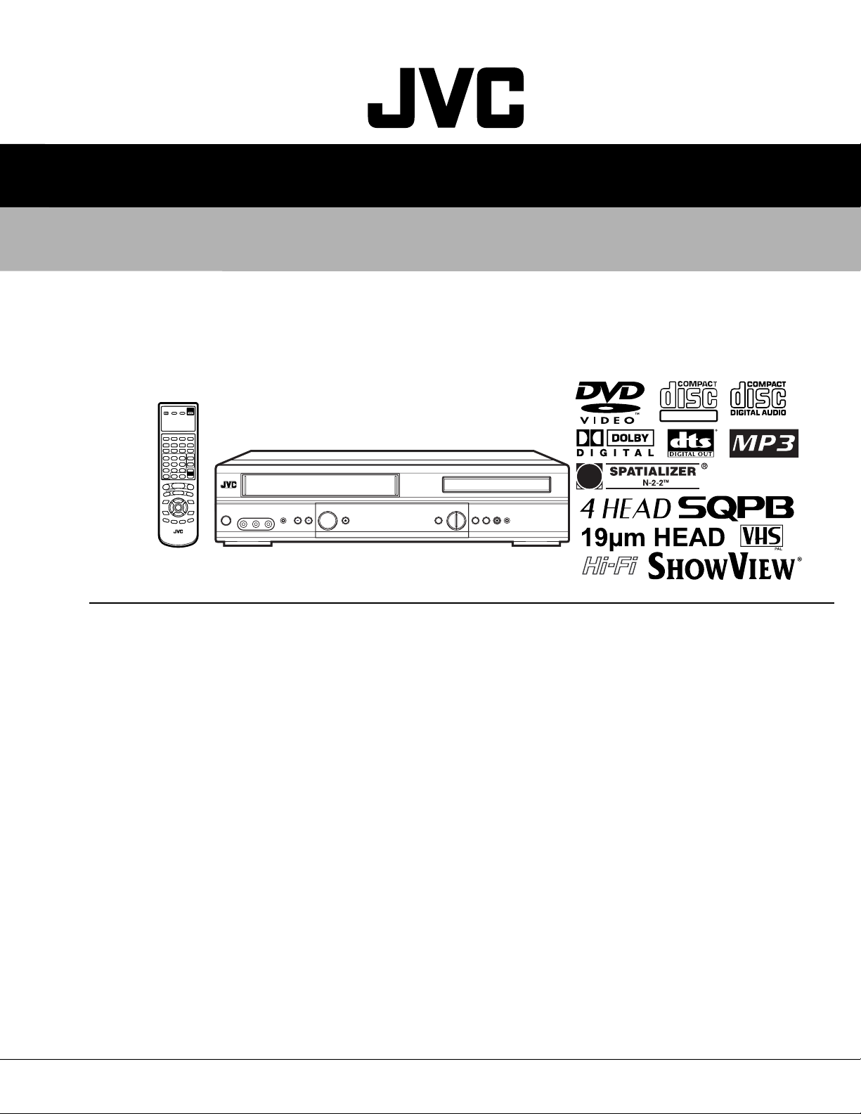
DVD PLAYER Hi-Fi VIDEO CASSETTE RECORDER
HR-XV1EK, HR-XV1EU-C,
HR-XV1EU-S, HR-XV1EU-Y
DIGITAL VIDEO
SPECIFICATIONS
GENERAL
Power supply:
Power consumption:
Weight:
Dimensions:
Input Level:
Output Level:
Hi-Fi Frequency Response:
Hi-Fi Dynamic Range:
VCR section
Video Head:
Audio Track:
Channel covevage:
RF Channel Output:
F.FWD/REW Time at 25˚C:
(The specifications shown pertain specifically to the model HR-XV1EU-C.)
AC 230V 50Hz
Operation: 22W
Stand by: 5W
4.5 kg
Width : 430 mm
Height: 99 mm
Depth : 310.5 mm
SCART-socket:
Audio IN jack: 500 mV, 50 kΩ
SCART-socket:
Audio OUT jack: 500 mV, 1 kΩ
20Hz to 20,000Hz
More than 75dB
4 Rotary Heads
Hi-Fi Sound - 2 Tracks /
MONO Sound - 1 Track
2-12, X, Y, Z, S1-S41, 21-69
UHF channel 36 (23 to 69)
Approx. 1minute and 48 seconds
(with E-180 Cassette Tape)
VIDEO: 1 Vp-p, 75Ω
AUDIO: 500 mV, 50 kΩ
VIDEO: 1 Vp-p, 75Ω
AUDIO: 500 mV, 1 kΩ
DVD section
Signal system:
Applicable disc:
Audio characteristics:
Frequency response:
S/N Ratio:
Harmonic distortion:
Wow and flutter:
Dynamic range:
Output:
Pickup:
ACCESSORIES:
PAL
DVD (12cm, 8cm), CD (12cm, 8cm)
DVD: 4Hz - 22KHz
CD: 4Hz - 20KHz
90dB
1%
Below Measurable Level
90dB
Audio : (RCA) 500 mV, 1Kohm
Digital Audio : 0.5Vp-p/75 ohm
CD : Wavelength: 775 - 805 nm
Maximum output power: 0.5 mW
DVD : Wavelength: 640 - 660 nm
Maximum output power: 1.0 mW
Remote control x 1
75 ohm Coaxial Cable x 1
Battery (UM-3) x 2
This service manual is printed on 100% recycled paper.
COPYRIGHT © 2002 VICTOR COMPANY OF JAPAN, LTD
V14PV1
No.82927
June 2002
Page 2

TABLE OF CONTENTS
Section Title Page Section Title Page
Important Safety Precautions
HOW TO IDENTIFY MODELS
INSTRUCTIONS
DISASSEMBLY INSTRUCTIONS
1.
REMOVAL OF MECHANICAL PARTS AND P.C.BOARDS .....
1-1 TOP CABINET AND FRONT CABINET................... 1-1
1-2 FLAP .........................................................................1-1
1-3 DECK CD AND DVD PCB ........................................1-1
1-4 POWER PCB ............................................................1-2
1-5 VCR DECK ...............................................................1-2
1-6 VCR PCB ..................................................................1-2
2. REMOVAL OF VCR DECK PARTS................................1-3
2-1 TOP BRACKET.........................................................1-3
2-2 CASSETTE HOLDER ASS’Y....................................1-3
2-3 CASSETTE SIDE L/R ...............................................1-3
2-4 LINK UNIT ................................................................ 1-3
2-5 LINK LEVER / FLAP LEVER ....................................1-3
2-6 LOADING MOTOR / WORM.....................................1-4
2-7 TENSION ASS’Y.......................................................1-4
2-8 T BRAKE ARM / T BRAKE BAND.............................1-5
S REEL / T REEL / IDLER ARM ASS’Y / IDLER GEAR ....
2-9
CASSETTE OPENER / PINCH ROLLER BLOCK / P5 ARM ASS’Y.
2-10
2-11 A/C HEAD ...............................................................1-6
2-12 FE HEAD ................................................................1-6
2-13 CYLINDER UNIT ASS’Y .........................................1-6
2-14 CAPSTAN DD UNIT................................................ 1-7
MAIN CAM / PINCH ROLLER CAM / JOINT GEAR ...
2-15
2-16 LOADING GEAR S/T UNIT.....................................1-7
2-17
CLUTCH ASS’Y / RING SPRING / CLUTCH LEVER / CLUTCH GEAR ..
CASSETTE GUIDE POST / INCLINED BASE S/T UNIT / P4 CAP..
2-18
REMOVAL AND INSTALLATION OF FLAT PACKAGE IC ..
3.
REMOVAL.......................................................................1-9
INSTALLATION .............................................................1-10
KEY TO ABBREVIATIONS ............................................. 1-11
SERVICE MODE LIST..................................................... 1-13
WHEN “N” IS ALWAYS BEING DISPLAYED ON THE TV MONITOR .
PARENTAL CONTROL - RATING LEVEL 4-DIGIT SECURITY CODE CANNCELLATION .
WHEN REPLACING EEPROM(MEMORY) IC ................1-14
PREVENTIVE CHECKS AND SERVICE INTERVALS....1-15
CONFIRMATION OF HOURS USED ..............................1-15
CLEANING ......................................................................1-15
SERVICING FIXTURES AND TOOLS............................. 1-16
MECHANISM ADJUSTMENT PARTS LOCATION GUIDE..
MECHANICAL ADJUSTMENT ....................................... 1-17
TAPE REMOVAL METHOD AT NO POWER SUPPLY . 1-17
DISC REMOVAL METHOD AT NO POWER SUPPLY..1-17
1. CONFIRMATION AND ADJUSTMENT ........................1-17
1-1
CONFIRMATION AND ADJUSTMENT OF TENSION POST POSITION .
1-2 CONFIRMATION OF PLAYBACK TORQUE AND
BACK TENSION TORQUE DURING PLAYBACK.. 1-17
1-3 CONFIRMATION OF VSR TORQUE...................... 1-17
1-4 CONFIRMATION OF REEL BRAKE TORQUE.......1-18
2. CONFIRMATION AND ADJUSTMENT OF TAPE
RUNNING MECHANISM .........................................1-18
2-1 GUIDE ROLLER .....................................................1-18
CONFIRMATION AND ADJUSTMENT OF AUDIO/CONTROL HEAD ....
2-2
2-3
TAPE RUNNING ADJUSTMENT(X-VALUE ADJUSTMENT) .....
ELECTRICAL ADJUSTMENT .........................................1-20
1. BASIC ADJUSMENT ...................................................1-20
1-1 SWITCHING POINT ...............................................1-20
1-1
1-5
1-6
1-7
1-8
1-8
1-9
1-13
1-13
1-16
1-17
1-19
1-19
The following table lists the differing points between models HR-XV1EK, HR-XV1EU-C, HR-XV1EU-S and HR-XV1EU-Y.
ITEM
BROADCASTING STANDARD
POWER SOURCE 230~240V,50Hz 230V,50Hz
AUTO TUNER SETTING
SCENE REPLAY NOT USED USED
GUIDE CH. SET USED NOT USED
DECODER(AV2) NOT USED USED
VPS NOT USED USED
CATV NOT USED USED
INSTRUCTION LANGUAGE
Notes: Mark
MODEL
is same as left.
HR-XV1EK
I B/G
NOT USED USED
ENGLISH
HR-XV1EU-C HR-XV1EU-S HR-XV1EU-Y
EN, FR, GE, DU, GR GE, FR, IT, SP, PT GE, SW, NO, DA, FI
ELECTRICAL ADJUSTMENT PARTS LOCATION GUIDE..
IC DESCRIPTION ............................................................1-21
SERVO TIMING CHART .................................................1-34
MECHANISM TIMING CHART........................................ 1-35
TROUBLE SHOOTING GUIDE ....................................... 1-36
(VCR SECTION) ........................................................... 1-36
(DVD SECTION) ........................................................... 1-60
CHARTS AND DIAGRAMS
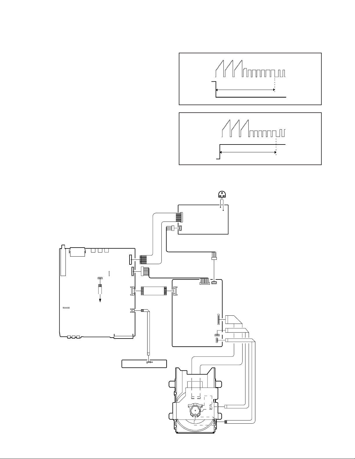
INTERCONNECTION DIAGRAM ...................................2-1
READ CHANNEL SCHEMTAIC DIAGRAM ....................2-3
DSP SCHEMATIC DIAGRAM......................................... 2-5
MPEG SCHEMATIC DIAGRAM ..................................... 2-7
MEMORY SCHEMATIC DIAGRAM ................................2-9
AUDIO/VIDEO SCHEMATIC DIAGRAM ...................... 2-11
SYSCON1 SCHEMATIC DIAGRAM .............................2-13
Y/C/AUDIO/HEAD AMP SCHEMATIC DIAGRAM ........2-15
MICOM SCHEMATIC DIAGRAM.................................. 2-17
TUNER\/JACK SCHEMATIC DIAGRAM ...................... 2-19
REGULATOR SCHEMATIC DIAGRAM........................ 2-21
DISPLAY SCHEMATIC DIARAM.................................. 2-23
HI-FI/DEMODULATOR SCHEMATIC DIAGRAM .........2-25
DVD IN/OUT SCHEMATIC DIAGRAM .........................2-27
SUB MICOM/OSD/VPS SCHEMATIC DIAGRAM ........2-29
POWER SCHEMATIC DIAGRAM ................................ 2-31
OPERATION SCHEMATIC DIAGRAM .........................2-33
PRINTED CIRCUIT BOARDS VCR(INSERTED PARTS) ......
PRINTED CIRCUIT BOARDS VCR(CHIP MOUNTED PARTS) ...
PRINTED CIRCUIT BOARDS DVD ..............................2-39
PRINTED CIRCUIT BOARDS POWER / OPERATION..
WAVEFORMS .............................................................. 2-42
DVD BLOCK DIAGRAM ............................................... 2-45
Y/C/AUDIO/HEAD AMP BLOCK DIAGRAM .................2-47
MICOM BLOCK DIAGRAM........................................... 2-49
REGULATOR BLOCK DIAGRAM................................. 2-51
DISPLAY/OPERATION BLOCK DIAGRAM.................. 2-53
TUNER/JACK/HI-FI/21PIN/OSD BLOCK DIAGRAM.... 2-55
DVD IN/OUT BLOCK DIAGRAM ..................................2-57
POWER BLOCK DIAGRAM ......................................... 2-59
SUB MICOM/OSD/VPS BLOCK DIAGRAM .................2-61
PARTS LIST
3.1 PACKING AND ACCESSORY ASSEMBLY<M1> ....... 3-1
3.2 FINAL ASSEMBLY<M2>............................................. 3-2
3.3 MECHANISM ASSEMBLY<M4> ................................. 3-4
3.4 ELECTRICAL PARTS LIST......................................... 3-7
POWER BOARD ASSEMBLY<01>................................. 3-7
VCR BOARD ASSEMBLY<03>........................................3-7
DVD BOARD ASSEMBLY<50>......................................3-13
OPERATION BOARD ASSEMBLY<28> ........................3-16
REFERENCE
GENERAL SPECIFICATIONS [HR-XV1EK] ...................4-1
GENERAL SPECIFICATIONS [HR-XV1EU-C] ...............4-7
1-20
2-35
2-37
2-41
Page 3
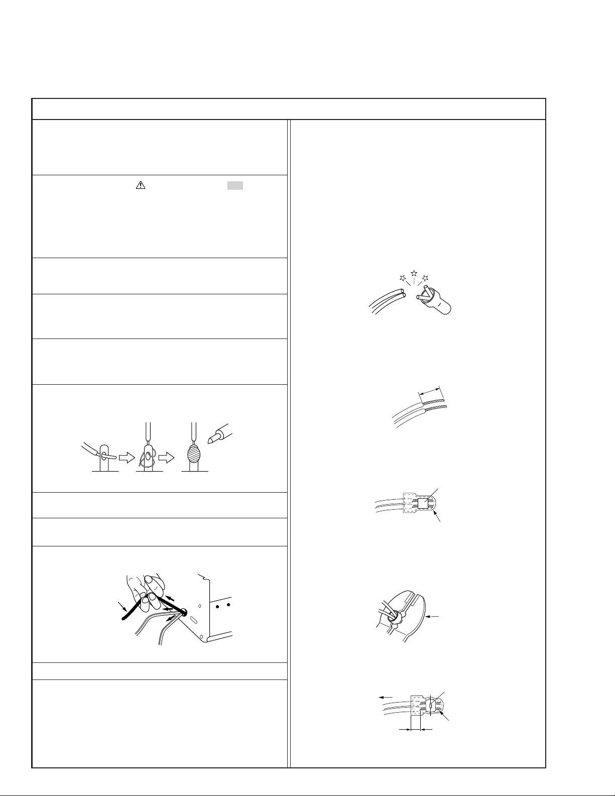
Important Safety Precautions
cut close to connector
Prior to shipment from the factory, JVC products are strictly inspected to conform with the recognized product safety and electrical codes
of the countries in which they are to be sold. However, in order to maintain such compliance, it is equally important to implement the
following precautions when a set is being serviced.
v
Precautions during Servicing
1. Locations requiring special caution are denoted by labels and
inscriptions on the cabinet, chassis and certain parts of the
product. When performing service, be sure to read and comply with these and other cautionary notices appearing in the
operation and service manuals.
2. Parts identified by the
critical for safety.
Replace only with specified part numbers.
Note: Parts in this category also include those specified to com-
ply with X-ray emission standards for products using
cathode ray tubes and those specified for compliance
with various regulations regarding spurious radiation
emission.
3. Fuse replacement caution notice.
Caution for continued protection against fire hazard.
Replace only with same type and rated fuse(s) as specified.
4. Use specified internal wiring. Note especially:
1) Wires covered with PVC tubing
2) Double insulated wires
3) High voltage leads
5. Use specified insulating materials for hazardous live parts.
Note especially:
1) Insulation Tape 3) Spacers 5) Barrier
2) PVC tubing 4) Insulation sheets for transistors
6. When replacing AC primary side components (transformers,
power cords, noise blocking capacitors, etc.) wrap ends of
wires securely about the terminals before soldering.
symbol and shaded ( ) parts are
12. Crimp type wire connector
In such cases as when replacing the power transformer in sets
where the connections between the power cord and power
transformer primary lead wires are performed using crimp type
connectors, if replacing the connectors is unavoidable, in order to prevent safety hazards, perform carefully and precisely
according to the following steps.
1) Connector part number : E03830-001
2) Required tool : Connector crimping tool of the proper type
which will not damage insulated parts.
3) Replacement procedure
(1) Remove the old connector by cutting the wires at a point
close to the connector.
Important : Do not reuse a connector (discard it).
Fig.3
(2) Strip about 15 mm of the insulation from the ends of
the wires. If the wires are stranded, twist the strands to
avoid frayed conductors.
15 mm
Fig.1
7. Observe that wires do not contact heat producing parts
(heatsinks, oxide metal film resistors, fusible resistors, etc.)
8. Check that replaced wires do not contact sharp edged or
pointed parts.
9. When a power cord has been replaced, check that 10-15 kg of
force in any direction will not loosen it.
Power cord
Fig.2
10. Also check areas surrounding repaired locations.
11. Products using cathode ray tubes (CRTs)
In regard to such products, the cathode ray tubes themselves,
the high voltage circuits, and related circuits are specified for
compliance with recognized codes pertaining to X-ray emission.
Consequently, when servicing these products, replace the cathode ray tubes and other parts with only the specified parts.
Under no circumstances attempt to modify these circuits.
Unauthorized modification can increase the high voltage value
and cause X-ray emission from the cathode ray tube.
Fig.4
(3) Align the lengths of the wires to be connected. Insert
the wires fully into the connector.
Metal sleeve
Connector
Fig.5
(4) As shown in Fig.6, use the crimping tool to crimp the
metal sleeve at the center position. Be sure to crimp fully
to the complete closure of the tool.
1.25
2.0
5.5
Fig.6
(5) Check the four points noted in Fig.7.
Not easily pulled free
Wire insulation recessed
more than 4 mm
Fig.7
Crimping tool
Crimped at approx. center
of metal sleeve
Conductors extended
1
S40888-01
Page 4
v
d'
d
Chassis
Power cord,
primary wire
Safety Check after Servicing
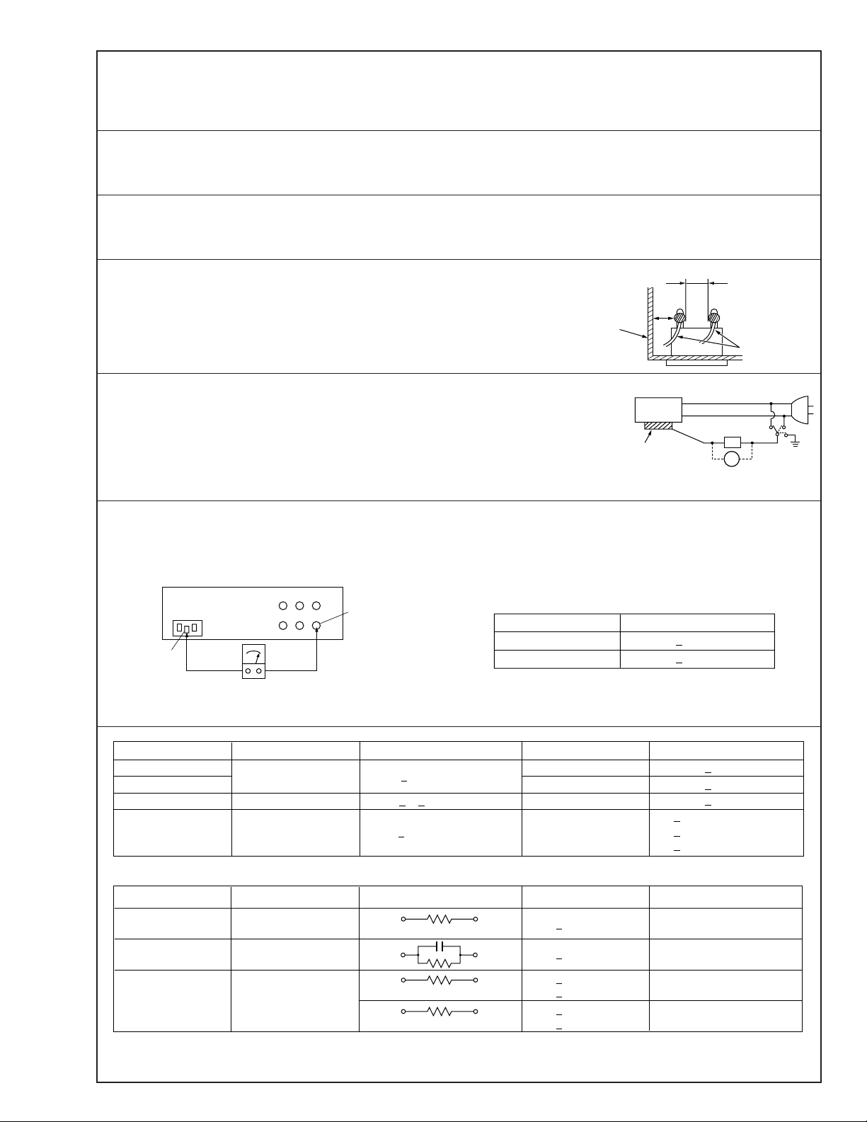
Examine the area surrounding the repaired location for damage or deterioration. Observe that screws, parts and wires have been
returned to original positions, Afterwards, perform the following tests and confirm the specified values in order to verify compliance with safety standards.
1. Insulation resistance test
Confirm the specified insulation resistance or greater between power cord plug prongs and
externally exposed parts of the set (RF terminals, antenna terminals, video and audio input
and output terminals, microphone jacks, earphone jacks, etc.). See table 1 below.
2. Dielectric strength test
Confirm specified dielectric strength or greater between power cord plug prongs and exposed
accessible parts of the set (RF terminals, antenna terminals, video and audio input and output
terminals, microphone jacks, earphone jacks, etc.). See table 1 below.
3. Clearance distance
When replacing primary circuit components, confirm specified clearance distance (d), (d’) between soldered terminals, and between terminals and surrounding metallic parts. See table 1
below.
Fig. 8
4. Leakage current test
Confirm specified or lower leakage current between earth ground/power cord plug prongs
and externally exposed accessible parts (RF terminals, antenna terminals, video and audio
input and output terminals, microphone jacks, earphone jacks, etc.).
Measuring Method : (Power ON)
Insert load Z between earth ground/power cord plug prongs and externally exposed accessible parts. Use an AC voltmeter to measure across both terminals of load Z. See figure 9 and
following table 2.
Externally
exposed
accessible part
Z
V
Fig. 9
ab
c
5. Grounding (Class 1 model only)
Confirm specified or lower grounding impedance between earth pin in AC inlet and externally exposed accessible parts (Video in,
Video out, Audio in, Audio out or Fixing screw etc.).
Measuring Method:
Connect milli ohm meter between earth pin in AC inlet and exposed accessible parts. See figure 10 and grounding specifications.
AC inlet
Earth pin
AC Line Voltage
100 V
100 to 240 V
110 to 130 V
110 to 130 V
200 to 240 V
Exposed accessible part
Milli ohm meter
Fig. 10
Region
Japan
USA & Canada
Europe & Australia R 10 MΩ/500 V DC
Region Load Z
Insulation Resistance (R)
≤
R 1 MΩ/500 V DC
≥≥
1 MΩ R 12 MΩ/500 V DC
≤
Table 1 Specifications for each region
Grounding Specifications
Region
USA & Canada
Europe & Australia
Dielectric Strength
AC 1 kV 1 minute
AC 1.5 kV 1 miute
AC 1 kV 1 minute
AC 3 kV 1 minute
AC 1.5 kV 1 minute
(Class 2)
(Class 1)
Grounding Impedance (Z)
≤
Z 0.1 ohm
≤
Z 0.5 ohm
Clearance Distance (d), (d')
≤
d, d' 3 mm
≤
d, d' 4 mm
≤
d, d' 3.2 mm
≤
d 4 mm
≤
d' 8 mm (Power cord)
≤
d' 6 mm (Primary wire)
a, b, cLeakage Current (i)AC Line Voltage
100 V
110 to 130 V
110 to 130 V
220 to 240 V
Note: These tables are unofficial and for reference only. Be sure to confirm the precise values for your particular country and locality.
Japan
USA & Canada
Europe & Australia
Table 2 Leakage current specifications for each region
1 kΩ
0.15 µF
1.5 kΩ
2 kΩ
50 kΩ
2
≤
i 1 mA rms Exposed accessible parts
≤
i 0.5 mA rms
≤
i 0.7 mA peak
≤
i 2 mA dc
≤
i 0.7 mA peak
≤
i 2 mA dc
Exposed accessible parts
Antenna earth terminals
Other terminals
S40888-01
Page 5

HOW TO IDENTIFY MODELS
How to recognize from the appearance of the model concerned is written below.
Please distinguish from several contents currently printed on the rating label.
REAR SIDE
MODEL NAME
DVD PLAYER/VIDEO CASSETTE RECORDER
MODEL NO. HR-XV1EK
230-240V
POWER CONSUMPTION : 22W
WARNING SHOCK HAZARD-DO NOT OPEN.
VIDEO Plus+ and PlusCode are registered trademarks
of Gemstar Development Corporation.
The VIDEO Plus+ system is manufactured under license
from Gemstar Development Corporation.
Manufactured under license from Dolby Laboratories. "Dolby" and the double-D symbol are trademarks of
Dolby Laboratories. Confidential unpublished works.
Apparatus Claims of U.S. Patent Nos. 4,631,603;4,577,216;4,819,098 and 4,907,093 licensed for limited
viewing uses only.
"DTS" and "DTS Digital Out" are trademarks of Digital Theater Systems, lnc.
VICTOR COMPANY OF JAPAN,LTD. ASSEMBLED IN U.K.
Serial NO.
50Hz
'
1992-1997 Dolby Laboratories. All rights reserved.
CLASS 1
LASER PRODUCT
RATING LABEL
HR-XV1EK HR-XV1EU-C
DVD PLAYER/VIDEO CASSETTE RECORDER
230-240
POWER CONSUMPTION : 22W
WARNING : SHOCK HAZARD-DO NOT OPEN.
VIDEO Plus+ and PlusCode are registered trademarks
of Gemstar Development Corporation.
The VIDEO Plus+ system is manufactured under license
from Gemstar Development Corporation.
Manufactured under license from Dolby Laboratories. "Dolby" and the double-D symbol are trademarks of
Dolby Laboratories. Confidential unpublished works.
Apparatus Claims of U.S. Patent Nos. 4,631,603;4,577,216;4,819,098 and 4,907,093 licensed for limited
viewing uses only.
"DTS" and "DTS Digital Out" are trademarks of Digital Theater Systems, lnc.
VICTOR COMPANY OF JAPAN,LTD. ASSEMBLED IN U.K.
Serial NO.
MODEL NO. HR-XV1EK
V 50Hz
CLASS 1
LASER PRODUCT
'
1992-1997 Dolby Laboratories. All rights reserved.
7225380017
HR-XV1EU-S HR-XV1EU-Y
7225380017
Page 6
DISASSEMBLY INSTRUCTIONS
1.
REMOVAL OF MECHANICAL PARTS
AND P.C. BOARDS
1-1:
TOP CABINET AND FRONT CABINET
(Refer to Fig. 1-1)
1.
Remove the 5 screws 1.
2.
Remove the Top Cabinet in the direction of arrow (A).
3.
Disconnect the following connector: (CP681).
4.
Unlock the 8 supports 2.
5.
Remove the Front Cabinet in the direction of arrow (B).
6.
Remove the 3 screws 3.
7.
Remove the Operation PCB in the direction of arrow (C).
Top Cabinet
1
(A)
Front Cabinet
(B)
2
2
2
2
3
3
2
2
2
3
(C)
CP681
2
1-2: FLAP (Refer to Fig. 1-2)
1.2.Open Flap to 90˚ and flex in direction of arrow (A), at the
same time slide in direction of arrow (B).
Then lift in direction of arrow (C).
1
1
1
1
Operation PCB
Fig. 1-1
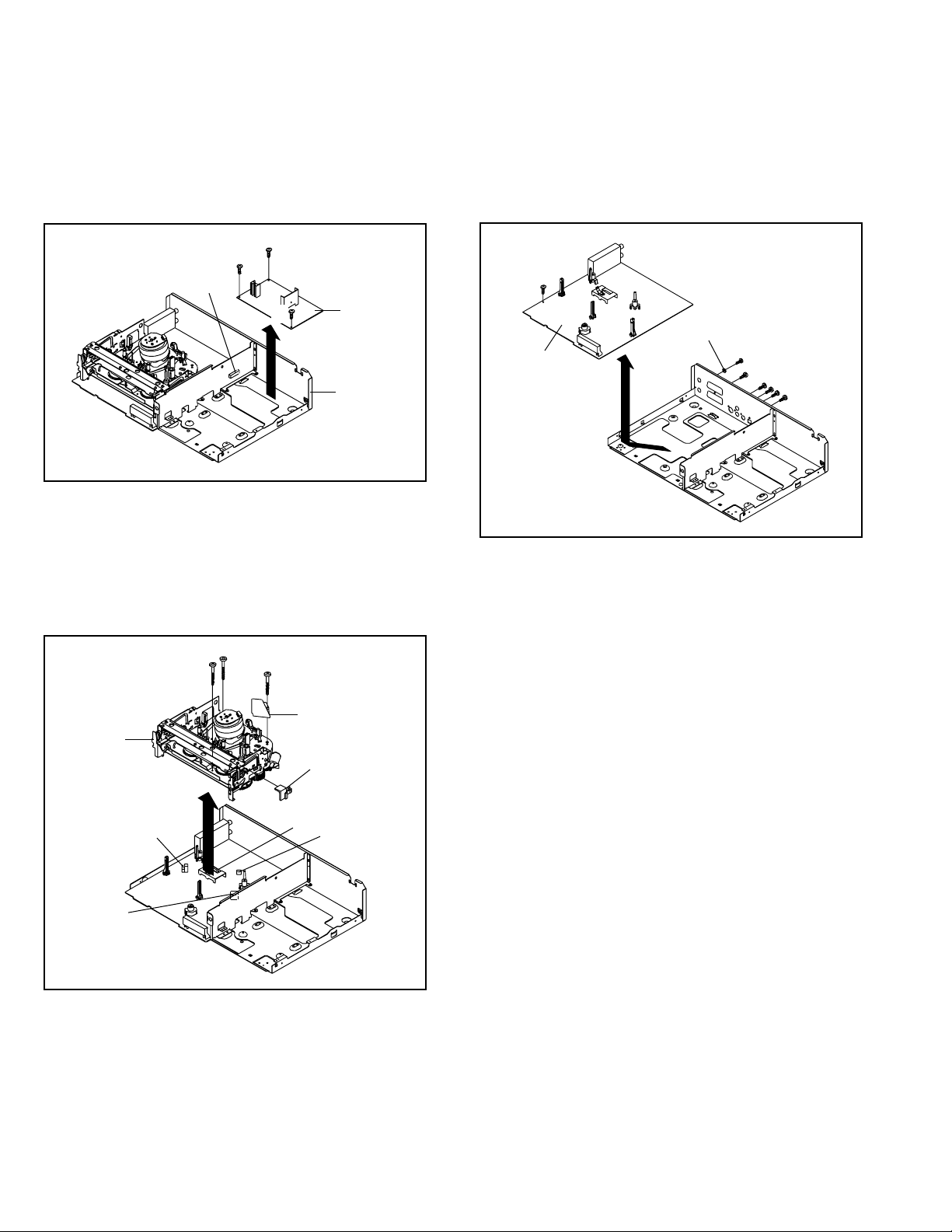
1-3: DECK CD AND DVD PCB (Refer to Fig. 1-3)
1.
Make the short circuit on the position as shown Fig. 1-3
using a soldering. If you remove the Deck CD with no
soldering, the Laser may be damaged.
2.
Disconnect the following connectors: (CP503,CP8001
and CP8002).
3.
Remove the 4 screws 1.
4.
Remove the Deck Angle in the direction of arrow (A).
5.
Remove the 2 screws 2.
6.
Remove the Front-DVD Shield in the direction of arrow
(B).
7.
Remove the 4 screws 3.
8.
Disconnect the following connectors: (CP2601, CP2602
and CP2603).
9.
Remove the Deck CD in the direction of arrow (C).
10.
Remove the 4 screws 4.
11.
Remove the DVD PCB in the direction of arrow (D).
Pick Up PCB
3
3
(C)
4
3
3
Deck Angle
1
1
4
CP2602
Make the sort circuit
using a soldering.
DVD PCB
Deck CD
Front-DVD Shield
2
2
(B)
CP2603
1
CP2601
4
1
(D)
4
(C)
(B)
(A)
Flap
Fig. 1-2
CP8001
(A)
CP503
CP8002
Fig. 1-3
NOTE
When the installation of the Deck CD, remove all the soldering on the short circuit position after the connection of Pick
Up PCB and DVD PCB connector.
1-1
Page 7
DISASSEMBLY INSTRUCTIONS
1-4: POWER PCB (Refer to Fig. 1-4)
1.
Disconnect the following connector: (CP1701).
2.
Remove the 3 screws 1.
3.
Remove the Power PCB in the direction of arrow.
1
1
CP1701
1
Power PCB
Bottom Plate
1-5: VCR DECK (Refer to Fig. 1-5)
1.
Unlock the 2 supports 1 and remove the Top Holder.
2.
Remove the 3 screws 2.
3.
Disconnect the following connectors: (CP101, CP102,
CP103 and CP3001).
4.
Remove the AC Head Cover and VCR Deck in the
direction of arrow.
Fig. 1-4
1-6: VCR PCB (Refer to Fig. 1-6)
1.
Remove the screw 1 and Fiber Washer.
2.
Remove the 6 screws 2.
3.
Remove the VCR PCB in the direction of arrow.
2
Fiber Washer
VCR PCB
1
2
2
2
2
2
Fig. 1-6
VCR Deck
CP3001
CP103
2
2
2
AC Head Cover
Top Holder
1
1
CP101
CP102
Fig. 1-5
1-2
Page 8
DISASSEMBLY INSTRUCTIONS
2. REMOVAL OF VCR DECK PARTS
2-1: TOP BRACKET (Refer to Fig. 2-1)
Extend the 2 supports 1.
1.
Slide the 2 supports 2 and remove the Top Bracket.
2.
NOTE
After the installation of the Top Bracket, bend the suppor t
1.
1 so that the Top Bracket is fixed.
Top Bracket
1
Top Bracket
2
Main Chassis
2
Main Chassis
2-2: CASSETTE HOLDER ASS'Y (Refer to Fig. 2-2)
1.
Move the Cassette Holder Ass'y to the front side.
2.
Push the Locker R to remove the Cassette Side R.
3.
Remove the Cassette Side L.
Cassette Side R
Main Chassis
1
Locker R
Fig. 2-1
NOTE
In case of the Locker R installation, check if the two
1.
positions of Fig. 2-3-B are correctly locked.
When you install the Cassette Side R, be sure to move
2.
the Locker R after installing.
Locker R
Check if these
Cassette Side R
positions are locked.
2-4: LINK UNIT (Refer to Fig. 2-4)
1.
Set the Link Unit to the Eject position.
2.
Unlock the support 1.
3.
Remove the (A) side of the Link Unit first, then remove
the (B) side.
Main Chassis
Link Unit
Fig. 2-3-B
Link Unit
Cassette Side L
Main Chassis
2-3: CASSETTE SIDE L/R (Refer to Fig. 2-3-A)
1.
Remove the Locker Spring.
2.
Unlock the 4 supports 1 and then remove the Cassette
Side L/R.
3.
Unlock the support 2 and then remove the Locker R.
Locker Spring
1
1
2
Cassette Side R
Cassette Holder
Locker R
1
1
Cassette Side L
Fig. 2-2
(A)
(B)
Link Unit
Main Chassis
2-5: LINK LEVER/FLAP LEVER (Refer to Fig. 2-5)
1.
Extend the support 1.
2.
Remove the Link Lever.
3.
Remove the Flap Lever.
1
Flap Lever
Link Lever
Fig. 2-4
Fig. 2-5
Fig. 2-3-A
1-3
Page 9
DISASSEMBLY INSTRUCTIONS
2-6: LOADING MOTOR/WORM (Refer to Fig. 2-6-A)
1.
Remove the screw 1.
2.
Remove the Loading Motor.
3.
Remove the Worm.
Loading Motor
Worm
Main Chassis
• Screw Torque: 3 ± 0.5kgf•cm
1
Fig. 2-6-A
NOTE
1.
In case of the Worm installation, check if the value of the
Fig. 2-6-B is correct.
2.
In case of the Loading Motor installation, hook the wire on
the Cassette Opener as shown Fig. 2-6-C.
3.
When installing the wires between Capstan DD Unit and
Loading Motor, connect them correctly as shown Fig. 2-6-D.
19.2 ± 0.1mm
2-7: TENSION ASS’Y (Refer to Fig. 2-7-B)
Turn the Pinch Roller Cam clockwise so that the Tension
1.
Holder hook is set to the position of Fig. 2-7-A to move
the T ension Arm Ass’y .
2.
Remove the Tension Spring.
3.
Unlock the 2 supports 1 and remove the Tension Band.
4.
Unlock the support 2 and remove the Tension Arm Ass’y.
5.
Unlock the support 3 and remove the Tension Connect.
6.
Float the hook 4 and turn it clockwise then remove the
Tension Holder.
T ension Arm Ass’y
Fig. 2-7-A
1
Tension Connect
Tension Spring
2
4
1
3
Tension Holder
Tension Band
T ension Arm Ass’y
1-4
Loading Motor
-
+
Safety surface for pressing
of the insert.
Pink
White
Fig. 2-6-B
Loading Motor
Cassette Opener
Fig. 2-6-C
Capstan DD Unit
L2
L1
Fig. 2-6-D
Fig. 2-7-B
NOTE
1.
In case of the Tension Band installation, note the direction of the installation. (Refer to Fig. 2-7-C)
2.
In case of the Tension Band installation, install correctly
as Fig. 2-7-D.
3.
In case of the Tension Connect installation, install as the
circled section of Fig. 2-7-E.
Tension Connect
Tension Band
Fig. 2-7-C
Page 10
[OK]
[NG]
Tension Connect
Tension Connect
Tension Connect
DISASSEMBLY INSTRUCTIONS
NOTE
1.
Take care not to damage the gears of the S Reel and T
Tension Band
Tension Band
Fig. 2-7-D
Reel.
2.
The Polyslider Washer may be remained on the back of
the reel.
3.
Take care not to damage the shaft.
4.
Do not touch the section “A” of S Reel and T Reel. (Use
gloves.) (Refer to Fig. 2-9-A) Do not adhere the stains
on it.
5.
When you install the reel, clean the shaft and grease it
(FG-84M). (If you do not grease, noise may be heard in
FF/REW mode.)
6.
After installing the reel, adjust the height of the reel.
(Refer to MECHANICAL ADJUSTMENT)
Main Chassis
Fig. 2-7-E
2-8: T BRAKE ARM/T BRAKE BAND (Refer to Fig. 2-8-A)
Remove the T Brake Spring.
1.
Turn the T Brake Arm clockwise and bend the hook
2.
section to remove it.
Unlock the 2 supports 1 and remove the T Brake Band.
3.
T Brake Band
Hook section
1
1
T Brake Arm
T Brake Spring
Fig. 2-8-A
NOTE
1. In case of the T Brake Band installation, install correctly
as Fig. 2-8-B.
Idler Gear
Idler Arm Ass’y
S Reel
(A)
(B)
T Reel
1
(A)
1
Fig. 2-9-A
NOTE
1.2.In case of the S Reel and T Reel installation, check if the
correct parts are installed. (Refer to Fig. 2-9-B)
In case of the Idler Arm Ass’y installation, install correctly
as Fig. 2-9-C. And also set it so that the section “B” of
Fig. 2-9-A is placed under the Main Chassis tab.
[OK]
[NG]
T Brake Band
T Brake Band
T Brake Arm
T Brake Arm
Fig. 2-8-B
2-9: S REEL/T REEL/IDLER ARM ASS’Y/IDLER GEAR
(Refer to Fig. 2-9-A)
1.
Remove the S Reel and T Reel.
2.
Remove the 2 Polyslider W ashers 1.
3.
Remove the Idler Arm Ass’y and Idler Gear.
[OK]
[NG]
Clutch Gear
Clutch Gear
Big Hole
(S Reel)
Small Hole
(T Reel)
Fig. 2-9-B
Idler Arm Ass’y
Idler Arm Ass’y
Fig. 2-9-C
1-5
Page 11
DISASSEMBLY INSTRUCTIONS
2-10: CASSETTE OPENER/PINCH ROLLER BLOCK/P5
ARM ASS’Y (Refer to Fig. 2-10-A)
1.2.Unlock the support 1 and remove the Cassette Opener.
Remove the Pinch Roller Block and P5 Arm Ass’y.
1
Cassette Opener
Pinch Roller Block
P5 Arm Ass’y
Main Chassis
Fig. 2-10-A
NOTE
1.2.Do not touch the Pinch Roller. (Use gloves.)
In case of the Pinch Roller Block and the Pinch Roller
Cam installation, install correctly as Fig. 2-10-B.
Pinch Roller Block
P5 Arm Ass’y
Can be seen the hole of the
Main Cam.
Can be seen the hole of
the Pinch Roller Cam.
Fig. 2-10-B
2-11: A/C HEAD (Refer to Fig. 2-11-A)
1.
Remove the screw 1.
2.
Remove the A/C Head Base.
3.
Remove the 3 screws 2.
4.
Remove the A/C Head and A/C Head Spring.
NOTE
1.
Do not touch the A/C Head. (Use gloves.)
2.
When you install the A/C Head Spring, install as shown in
Fig. 2-11-B.
3.
When you install the A/C Head, tighten the screw (1) first,
then tighten the screw (2), finally tighten the screw (3).
(3)
(1)
2
2
(2)
2
A/C Head
Spring Position
Fig. 2-11-B
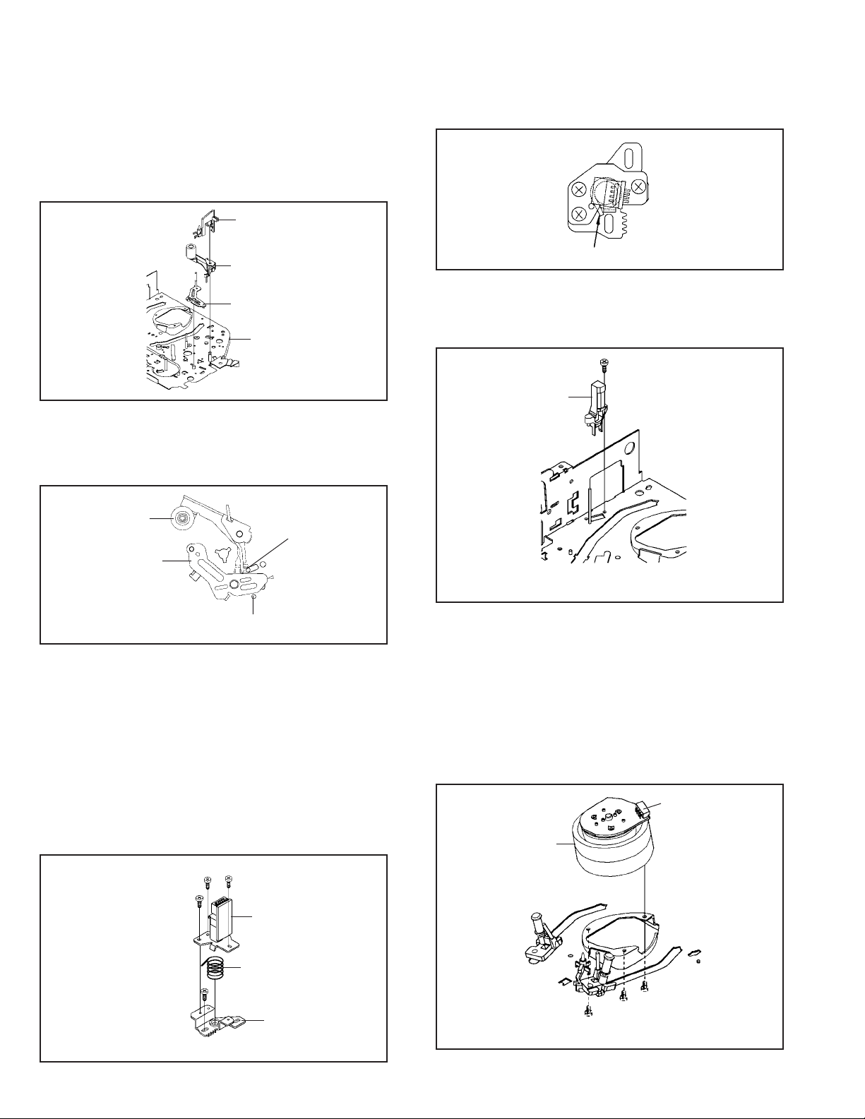
2-12: FE HEAD (RECORDER ONLY) (Refer to Fig. 2-12)
1.2.Remove the screw 1.
Remove the FE Head.
1
FE Head
• Screw Torque: 5 ± 0.5kgf•cm
• The FE Head is not installed on the Video Cassette Player.
Fig. 2-12
2-13: CYLINDER UNIT ASS’Y (Refer to Fig. 2-13)
1.
Disconnect the following connector:
(CD2001)
2.
Remove the 3 screws 1.
3.
Remove the Cylinder Unit Ass’y.
NOTE
1. When you install the Cylinder Unit Ass’y, tighten the
screws from (1) to (3) in order while pulling the Ass’y
toward the left front direction.
CD2001
Cylinder Unit Ass’y
• Screw Torque: 5 ± 0.5kgf•cm (Screw 1)
1-6
A/C Head Spring
1
A/C Head Base
• Screw Torque: 3 ±
0.5kgf•cm
(2)
(1)
1
(3)
1
1
Fig. 2-13
Fig. 2-11-A
Page 12
DISASSEMBLY INSTRUCTIONS
2-14: CAPSTAN DD UNIT (Refer to Fig. 2-14-A)
1.
Remove the Capstan Belt.
2.
Remove the 3 screws 1.
3.
Remove the Capstan DD Unit.
Capstan Belt
Capstan DD Unit
1
1
1
• Screw Torque: 4 ± 0.5kgf•cm
Fig. 2-14-A
NOTE
1. In case of the Capstan DD Unit installation, apply the
silicon bond (TSE3843-W) on the position Fig. 2-14-B
correctly. (If no silicon bond applied, abnormal noise will
be heard on the deck operation.)
(Refer to Fig. 2-14-B, C)
Applied position of
silicon bond
2-15: MAIN CAM/PINCH ROLLER CAM/JOINT GEAR
(Refer to Fig. 2-15-A)
1.2.Remove the E-Ring 1, then remove the Main Cam.
Remove the E-Ring 2, then remove the Pinch Roller
Cam and Joint Gear.
1
Main Cam
2
Pinch Roller Cam
Joint Gear
Fig. 2-15-A
NOTE
1. In case of the Pinch Roller Cam and Main Cam installation, install them as the circled section of Fig. 2-15-B so
that the each markers are met. (Refer to Fig. 2-15-B)
And also can be seen the Main Chassis hole through the
Main Cam maker hole.
Pinch Roller Cam
Marker
Main Cam
Be careful not to apply the silicon
bond to the Pinch Roller.
Capstan DD Unit
Silicon Bond
Main Chassis
Fig. 2-14-B
Fig. 2-14-C
Fig. 2-15-B
2-16: LOADING GEAR S/T UNIT (Refer to Fig. 2-16-A)
1.2.Remove the E-Ring 1 and remove the Main Loading
Gear.
Remove the Main Rod, Tension Lever, Loading Arm S
Unit and Loading Arm T Unit.
1
Main Rod
Tension Lever
Main Loading Gear
Loading Arm T Unit
Loading Arm S Unit
Fig. 2-16-A
1-7
Page 13
DISASSEMBLY INSTRUCTIONS
NOTE
1. When you install the Loading Arm S Unit, Loading Arm T
Unit and Main Loading Gear, align each marker. (Refer
to Fig. 2-16-B)
Marker
Main Loading Gear
Marker
Loading Arm T Unit Loading Arm S Unit
Fig. 2-16-B
2-17: CLUTCH ASS’Y/RING SPRING/CLUTCH LEVER/
CLUTCH GEAR (Refer to Fig. 2-17-A)
1.
Remove the Polyslider Washer 1.
2.
Remove the Clutch Ass’y and Ring Spring.
3.
Remove the Clutch Lever.
4.
Remove the Coupling Gear, Coupling Spring and Clutch
Gear.
1
Clutch Ass’y
Ring Spring
2-18: CASSETTE GUIDE POST/INCLINED BASE S/T
UNIT/P4 CAP (Refer to Fig. 2-18-A)
1.
Remove the P4 Cap.
2.
Unlock the support 1 and remove the Cassette Guide
Post.
3.
Remove the Inclined Base S Unit and Inclined Base T
Unit.
1
Inclined Base S
Unit Inclined Base T
Cassette Guide Post
Unit
P4 Cap
Fig. 2-18-A
NOTE
1.
Do not touch the roller of Guide Roller.
2.
In case of the P4 Cap installation, install it with parallel
for “A” and “B” of Fig. 2-18-B.
In case of the Cassette Guide Post installation, install
3.
correctly as the circled section of Fig. 2-18-C.
Coupling Gear
Coupling Spring
Clutch Gear
Clutch Lever
Fig. 2-17-A
NOTE
1. In case of the Clutch Ass’y installation, install it with
inserting the spring of the Clutch Ass’y into the dent of the
Coupling Gear. (Refer to Fig. 2-17-B)
Clutch Ass’y
Coupling Gear
Fig. 2-17-B
“A” “B”
P4 Cap
[OK]
Cassette Guide Post
[NG]
Cassette Guide Post
Cassette Opener
Fig. 2-18-B
Fig. 2-18-C
1-8
Page 14
DISASSEMBLY INSTRUCTIONS
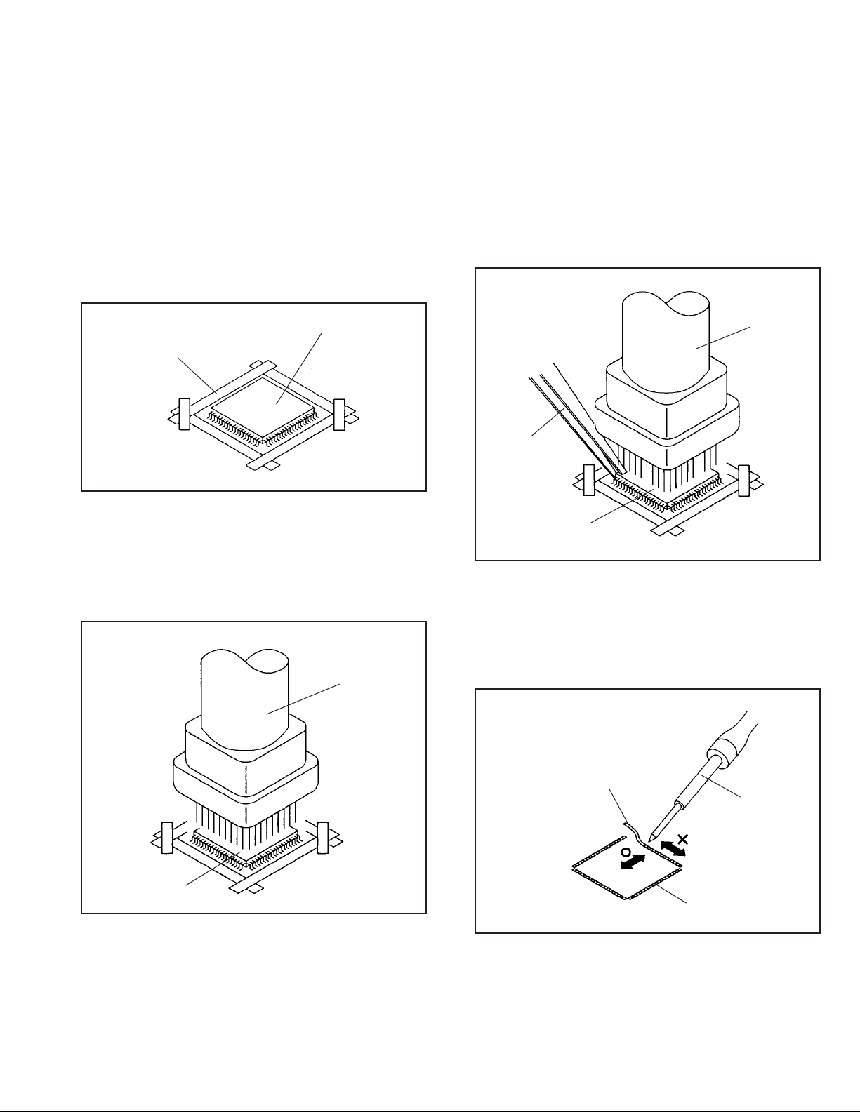
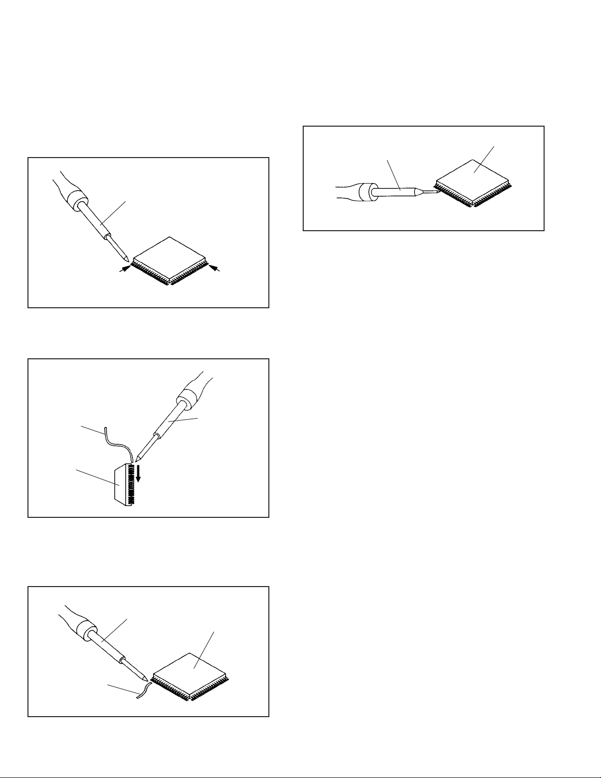
3. REMOVAL AND INSTALLATION OF FLAT
PACKAGE IC
REMOVAL
1. Put the Masking Tape (cotton tape) around the Flat
Package IC to protect other parts from any damage.
(Refer to Fig. 3-1.)
NOTE
Masking is carried out on all the parts located within
10 mm distance from IC leads.
Masking T ape
(Cotton Tape)
2. Heat the IC leads using a blower type IC desoldering
machine. (Refer to Fig. 3-2.)
NOTE
Do not add the rotating and the back and forth directions force on the IC, until IC can move back and forth
easily after desoldering the IC leads completely.
IC
Fig. 3-1
Blower type IC
desoldering machine
3. When IC starts moving back and forth easily after
desoldering completely, pickup the corner of the IC using
a tweezers and remove the IC by moving with the IC
desoldering machine. (Refer to Fig. 3-3.)
NOTE
Some ICs on the PCB are affixed with glue, so be
careful not to break or damage the foil of each IC
leads or solder lands under the IC when removing it.
Blower type IC
desoldering machine
Tweezers
IC
4.5.Peel off the Masking Tape.
Absorb the solder left on the pattern using the Braided
Shield Wire. (Refer to Fig. 3-4.)
NOTE
Do not move the Braided Shield Wire in the vertical
direction towards the IC pattern.
Fig. 3-3
Braided Shield Wire
Soldering Iron
IC
Fig. 3-2
IC pattern
Fig. 3-4
1-9
Page 15
DISASSEMBLY INSTRUCTIONS
INSTALLATION
1. Take care of the polarity of new IC and then install the
new IC fitting on the printed circuit pattern. Then solder
each lead on the diagonal positions of IC temporarily.
(Refer to Fig. 3-5.)
Soldering Iron
Solder temporarily Solder temporarily
Fig. 3-5
2. Supply the solder from the upper position of IC leads
sliding to the lower position of the IC leads.
(Refer to Fig. 3-6.)
4. When bridge-solder ing between terminals and/or the
soldering amount are not enough, resolder using a Thintip Soldering Iron. (Refer to Fig. 3-8.)
IC
Thin-tip Soldering Iron
Fig. 3-8
5. Finally, confirm the soldering status on four sides of the
IC using a magnifying glass.
Confirm that no abnormality is found on the soldering
position and installation position of the parts around the
IC. If some abnormality is found, correct by resoldering.
NOTE
When the IC leads are bent during soldering and/or
repairing, do not repair the bending of leads. If the
bending of leads are repaired, the pattern may be
damaged. So, be always sure to replace the IC in this
case.
Solder
IC
Supply soldering
from upper position
to lower position
Soldering Iron
Fig. 3-6
3. Absorb the solder left on the lead using the Braided
Shield Wire. (Refer to Fig. 3-7.)
NOTE
Do not absorb the solder to excess.
Soldering Iron
IC
Braided Shield Wire
1-10
Fig. 3-7
Page 16

A
A/C
ACC
AE
AFC
AFT
AFT DET
AGC
AMP
ANT
A.PB
APC
ASS’Y
AT
AUTO
A/V
B
BGP
BOT
BPF
BRAKE SOL
BUFF
B/W
C
C
CASE
CAP
CARR
CH
CLK
CLOCK (SY-SE)
COMB
CONV
CPM
CTL
CYL
CYL-M
CYL SENS
D
DATA (SY-CE)
dB
DC
DD Unit
DEMOD
DET
DEV
E
E
EF
EMPH
ENC
ENV
EOT
EQ
EXT
F
F
FBC
FE
FF
FG
FL SW
FM
FSC
FWD
G
GEN
GND
H
H.P.F
KEY TO ABBREVIATIONS
:
Audio/Control
:
Automatic Color Control
:
Audio Erase
:
Automatic Frequency Control
:
Automatic Fine Tuning
:
Automatic Fine Tuning Detect
:
Automatic Gain Control
:
Amplifier
:
Antenna
:
Audio Playback
:
Automatic Phase Control
:
Assembly
:
All Time
:
Automatic
:
Audio/Video
:
Burst Gate Pulse
:
Beginning of Tape
:
Bandpass Filter
:
Brake Solenoid
:
Buffer
:
Black and White
:
Capacitance, Collector
:
Cassette
:
Capstan
:
Carrier
:
Channel
:
Clock
:
Clock (Syscon to Servo)
:
Combination, Comb Filter
:
Converter
:
Capstan Motor
:
Control
:
Cylinder
:
Cylinder-Motor
:
Cylinder-Sensor
:
Data (Syscon to Servo)
:
Decibel
:
Direct Current
:
Direct Drive Motor Unit
:
Demodulator
:
Detector
:
Deviation
:
Emitter
:
Emitter Follower
:
Emphasis
:
Encoder
:
Envelope
:
End of Tape
:
Equalizer
:
External
:
Fuse
:
Feed Back Clamp
:
Full Erase
:
Fast Forward, Flipflop
:
Frequency Generator
:
Front Loading Switch
:
Frequency Modulation
:
Frequency Sub Carrier
:
Forward
:
Generator
:
Ground
:
High Pass Filter
H.SW
Hz
I
IC
IF
IND
INV
K
KIL
L
L
LED
LIMIT AMP
LM, LDM
LP
L.P.F
LUMI.
M
M
MAX
MINI
MIX
MM
MOD
MPX
MS SW
NC
N
NR
OSC
O
OPE
PB
P
PB CTL
PB-C
PB-Y
PCB
P. CON
PD
PG
P-P
R
R
REC
REC-C
REC-Y
REEL BRK
REEL S
REF
REG
REW
REV, RVS
RF
RMC
RY
S. CLK
S
S. COM
S. DATA
SEG
SEL
SENS
SER
SI
SIF
SO
SOL
SP
STB
SW
:
Head Switch
:
Hertz
:
Integrated Circuit
:
Intermediate Frequency
:
Indicator
:
Inverter
:
Killer
:
Left
:
Light Emitting Diode
:
Limiter Amplifier
:
Loading Motor
:
Long Play
:
Low Pass Filter
:
Luminance
:
Motor
:
Maximum
:
Minimum
:
Mixer, mixing
:
Monostable Multivibrator
:
Modulator, Modulation
:
Multiplexer, Multiplex
:
Mecha State Switch
:
Non Connection
:
Noise Reduction
:
Oscillator
:
Operation
:
Playback
:
Playback Control
:
Playback-Chrominance
:
Playback-Luminance
:
Printed Circuit Board
:
Power Control
:
Phase Detector
:
Pulse Generator
:
Peak-to Peak
:
Right
:
Recording
:
Recording-Chrominance
:
Recording-Luminance
:
Reel Brake
:
Reel Sensor
:
Reference
:
Regulated, Regulator
:
Rewind
:
Reverse
:
Radio Frequency
:
Remote Control
:
Relay
:
Serial Clock
:
Sensor Common
:
Serial Data
:
Segment
:
Select, Selector
:
Sensor
:
Search Mode
:
Serial Input
:
Sound Intermediate Frequency
:
Serial Output
:
Solenoid
:
Standard Play
Serial Strobe
:
:
Switch
1-11
Page 17

S
SYNC
SYNC SEP
T
TR
TRAC
TRICK PB
TP
U
UNREG
V
V
VCO
VIF
VP
V. P B
VR
V.REC
VSF
VSR
VSS
V-SYNC
VT
X
X’TAL
Y
Y/C
KEY TO ABBREVIATIONS
:
Synchronization
:
Sync Separator, Separation
:
Transistor
:
Tracking
:
Trick Playback
:
Test Point
:
Unregulated
:
Volt
:
Voltage Controlled Oscillator
:
Video Intermediate Frequency
:
Vertical Pulse, Voltage Display
:
Video Playback
:
Variable Resistor
:
Video Recording
:
Visual Search Fast Forward
:
Visual Search Rewind
:
Voltage Super Source
:
Vertical-Synchronization
:
Voltage Tuning
:
Crystal
:
Luminance/Chrominance
1-12
Page 18
SERVICE MODE LIST
This unit provided with the following SERVICE MODES so you can repair, examine and adjust easily.
To enter to the SERVICE MODE function, press and hold both buttons simultaneously on the main unit or on the main unit and on
the remote control for more than a standard time (second).
Set Key
CH UP
CH UP STOP 2
CH UP PLAY 2
CH DOWN POWER 2
Set Key OperationsRemocon Key
REC 5 2
REC 6 2
STOP 1 3
Set Key
FF 2
Standard Time
(seconds)
Standard Time
(seconds)
Operations
PLAY/REC total hours are displayed on the FIP.
Refer to the “PREVENTIVE CHECKS AND SERVICE INTERVALS”
(CONFIRMATION OF HOURS USED).
Can be checked of the INITIAL DATA of MEMORY IC.
Refer to the “WHEN REPLACING EEPROM (MEMORY) IC”.
Adjust the SWITHCHING POINT automatically.
Refer to the “ELECTRICAL ADJUSTMENT” (SWITHCHING POINT).
Initialization of the factory on VCR.
NOTE: Do not use this for the normal servicing.
If you set a factory initialization, the memories are reset such as
the clock setting, the channel setting, and PLAY/REC total hours.
VCR operation mode at no connection of DVD.
Refer to the “PREPARATION FOR SERVICING”
NOTE: Although the DVD is connected, the DVD mode cannot be selected.
Initialization of the factory on DVD.
NOTE:
DVD Write mode.
Refer to the “RE-WRITE FOR DVD FIRMWARE”.
NOTE: The function will only work at the DVD stop mode.
Check for the firmware version.
Refer to the “RE-WRITE FOR DVD FIRMWARE”.
NOTE: The function will only work at the DVD stop mode.
The function will only work without the setting of DVD disc at DVD
mode.
Do not use this for the normal servicing.
Do not use this for the normal servicing.
Do not use this for the normal servicing.
<NOTE> WHEN "N" IS ALWAYS BEING DISPLAYED ON THE TV MONITOR.
(REMOTE CONTROLLER FORMAT)
This product is usable the remote controller which is used by DVD+VHS of the other brand.
If "N" is always being displayed on the TV monitor, can not control from provided remote controller since this product is
other brand format.
• How to return a JVC format.
Turn off the power of the set and push the CHANNEL+ button and the REC button of the set simultaneously.
PARENTAL CONTROL - RATING LEVEL
4-DIGIT SECURITY CODE CANCELLATION
If the stored 4-digit security code in the Rating Level menu needs to be cancelled, please follow the steps below.
1.
Turn on the power, and set to the DVD stop mode.
2.
Press the SET UP button to display the DVD menu.
3.
Press the SET +/- button to select the "Operation" menu.
4.
Press the TV/VCR PR +/- button to select the Parental Lock, then press the OK button.
5.
Press the TV/VCR PR +/- button to select the ON or OFF, then press the OK button.
6.
Press the STOP button four times on the remote control, then press the OK button.
The 4-digit security code is cleared.
7.
Press the SET UP button to disappear the DVD menu.
1-13
Page 19
WHEN REPLACING EEPROM (MEMORY) IC
If a service repair is undertaken where it has been required to change the MEMORY IC, the following steps should be taken to
ensure correct data settings while making reference to TABLE 1.
NOTE: No need setting for after INI FD.
Table 1
INI +0 +1 +2 +3 +4 +5 +6 +7 +8 +9 +A +B +C +D +E +F
C0 --- --- --- --- 8B C9 D2 01 FF FF FF FF F1 54 07 8A
D0 1B 17 81 00 01 FF 03 01 71 9F 02 02 42 35 23 5B
E0 76 5E 08 F8 09 FB B2 9A 92 8C 51 5F 09 F0 05 F3
F0
B2 2F 9C 42 42 80 3D 08 08 7E 04 3A AA --- --- ---
[For HR-XV1EK]
INI +0 +1 +2 +3 +4 +5 +6 +7 +8 +9 +A +B +C +D +E +F
B0 --- --- --- --- --- --- --- --- --- 8B C9 D2 01 00 00 00
C0 B2 17 00 00 00 F1 54 51 00 51 B2 9F
D0 DB 60 01 08 00 FF 00 00 71 9F 82 02 42 35 23 5B
E0
76 5E 08 F0 09 FB 00 00 00 00 00 5F 09 F0 05 F3
F0 13 2F 9F 42 42 80 3D 68 08 89 04 3A AA --- --- ---
[For HR-XV1EU-C, HR-XV1EU-Y]
INI +0 +1 +2 +3 +4 +5 +6 +7 +8 +9 +A +B +C +D +E +F
B0 --- --- --- --- --- --- --- --- --- 8B C9 D2 01 00 00 00
C0 B2 17 00 00 00 F1 54 51 00 51 B2 9F
D0 DB E0 8D 08 00 FF 00 00 71 9F 82 02 42 35 23 5B
E0
76 5E 08 F0 09 FB 00 00 00 00 00 5F 09 F0 05 F3
F0 13 2F 9F 42 42 80 3D 68 08 89 04 3A AA --- --- ---
[For HR-XV1EU-S]
Turn on the POWER.
1.
Press both CH UP button on the set and the FF button on the set for more than 2 seconds.
2.
ADDRESS and DATA will appear on FIP as Fig 1.
ADDRESS is now selected and should “blink”. Using the SET + or - button on the remote,
3.
step through the ADDRESS until required ADDRESS to be changed is reached.
Press OK to select DATA. When DATA is selected, it will “blink”.
4.
Again, step through the DATA using SET + or - button until required DATA value has been
5.
selected.
Pressing OK will take you back to ADDRESS for further selection if necessary.
6.
Repeat steps 3 to 6 until all data has been checked.
7.
When satisfied correct DATA has been entered, turn POWER off (return to STANDBY
8.
MODE) to finish DATA input.
The unit will now have the correct DATA for the new MEMORY IC.
8E 06 8A
97
8E 06 8A
97
ADDRESS DATA
Fig. 1
1-14
Page 20
PREVENTIVE CHECKS AND SERVICE INTER VALS
The following standard table depends on environmental conditions and usage.
Parts replacing time does not mean the life span for individual parts.
Also, long term storage or misuse may cause transformation and aging of rubber parts.
The following list means standard hours, so the checking hours depends on the conditions.
Time
Parts Name
Audio Control Head
Full Erase Head
(Recorder only)
Capstan Belt
Pinch Roller
Capstan DD Unit
Loading Motor
Tension Band
T Brake Band
Clutch Ass’y
Idler Arm Ass’y
Capstan Shaft
Tape Running
Guide Post
Cylinder Unit
500
hours
1,000
hours
1,500
hours
2,000
hours
2,500
hours
CONFIRMATION OF HOURS USED
PLAY/REC total hours can be checked on the FIP.
Total hours are displayed in 16 system of notation.
NOTE: If you set a factory initialization, the total hours is
reset to “0”.
1.
Turn on the POWER.
2.
While pressing the CH UP button on the set, press the FF button on the set for
more than 2 seconds.
3.
Adjust the ADDRESS to "FD" by SET + or - button and read the DATA.
(This DATA becomes the thousands digit and hundreds digit value of the following
formula.)
4.
Adjust the ADDRESS to "FE" by SET + or - button and read the DATA.
(This DATA becomes the tens digit and ones digit value of the following formula.)
5.
After the confirmation of using hours, turn off the power.
CLEANING
NOTE
After cleaning the heads with isopropyl alcohol, do not
run a tape until the heads dry completely. If the heads are
not completely dry and alcohol gets on the tape, damage
may occur.
1. AUDIO CONTROL HEAD
Clean the Audio Control Head with the cotton stick
soaked by alcohol. Clean the full erase head in the same
manner. (Refer to the figure below.)
2. TAPE RUNNING SYSTEM
When cleaning the tape transport system, use the gauze
moistened with isopropyl alcohol.
3. CYLINDER
Wrap a piece of chamois around your finger. Dip it in
isopropyl alcohol. Hold it to the cylinder head softly.
Turn the cylinder head counterclockwise to clean it (in the
direction of the arrow). (Refer to the figure below.)
NOTE
Do not exert force against the cylinder head. Do not move
the chamois upward or downward on the head.
Use the chamois one by one.
Notes
Clean those parts in
contact with the tape.
Clean the rubber, and parts
which the rubber touches.
Replace when rolling
becomes abnormal.
Clean the Head
ADDRESS DATA
PLAY/REC total hours.
= (16 x 16 x 16 x thousands digit value)
+ (16 x 16 x hundreds digit value)
+ (16 x tens digit value)
+ (ones digit value)
: Clean
: Check it and if
necessary, replace it.
Audio Control Head
Cylinder Head
1-15
Page 21
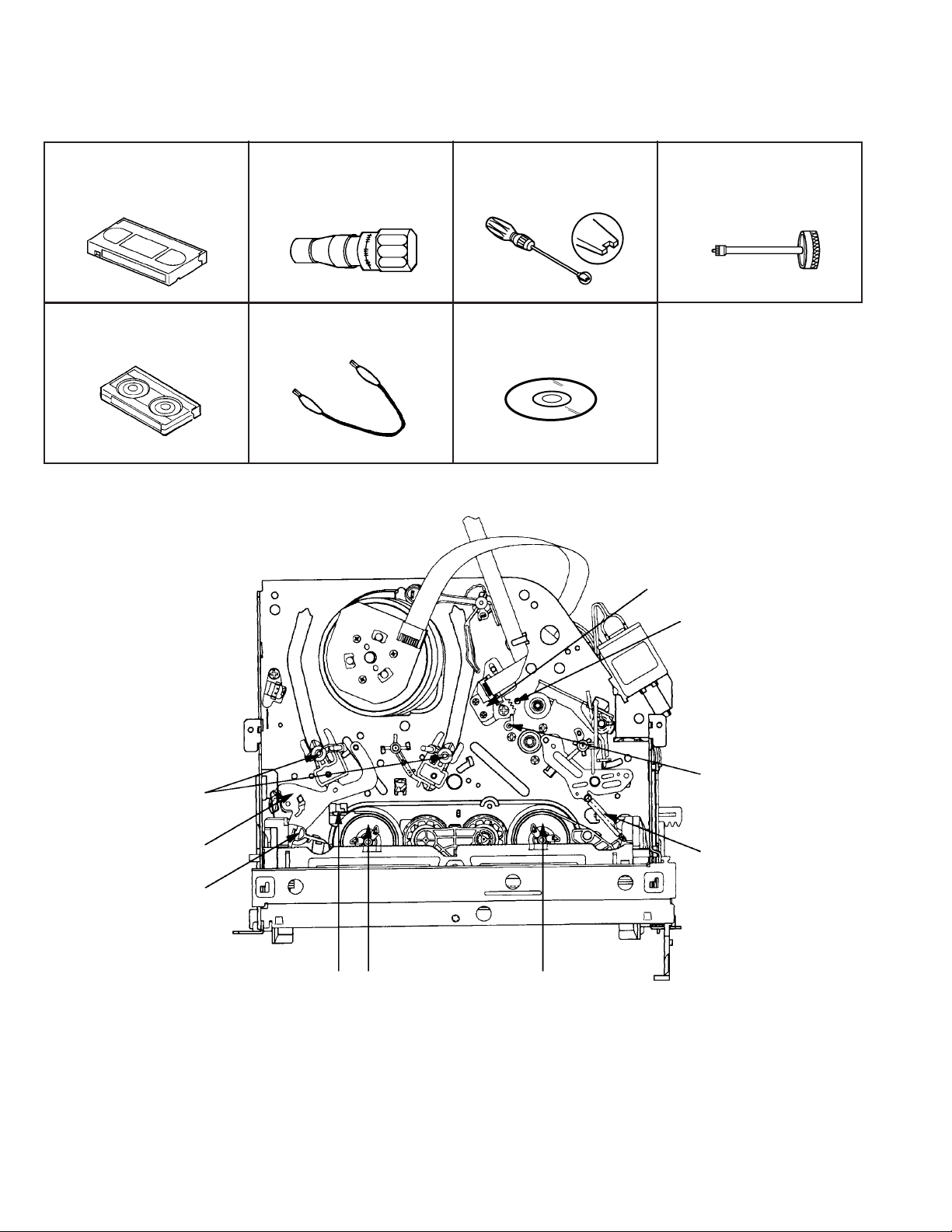
SERVICING FIXTURES AND TOOLS
VHS Alignment Tape
MHPE & MHPE-L
Torque Tape Short Jumper
PUJ48076-2
Torque Gauge
PUJ48075-2
MECHANISM ADJUSTMENT PARTS LOCATION GUIDE
Roller Driver
PTU94002-2
X-JG176 Up-Date Disc
X-JG153 X Value Adjustment
Screwdriver
4
5
6
3
2
1
10
Tension Connect
1.
T ension Arm
2.
Guide Roller
3.
Audio/Control Head
4.
X value adjustment driver hole
5.
P4 Post
6.
T Brake Spring
7.
T Reel
8.
S Reel
9.
Adjusting section for the Tension Arm position
10.
89
7
1-16
Page 22
MECHANICAL ADJUSTMENTS
TAPE REMOVAL METHOD AT NO POWER
SUPPLY
1.
Remove the Top Cabinet, Front Cabinet and DVD Block.
(Refer to item 1 of the DISASSEMBLY INSTRUCTIONS.)
2.
Remove the screw 1 of the Deck Chassis and remove the
Loading Motor. (Refer to Fig. 2)
3.
Rotate the Pinch Roller Cam in the direction of the arrow by
hand to slacken the Video Tape.
4.
Rotate the Clutch Ass'y either of the derections to wind the
Video Tape in the Cassette Case.
5.
Repeat the above step 3~4. Then take out the Video
Cassette from the Deck Chassis.
Be careful not to scratch on the tape.
Loading Motor
Screw 1
Capstan DD Unit
Pinch Roller Cam
Main Cam
Main Chassis (Front Side)
Clutch Ass'y
1. CONFIRMATION AND ADJUSTMENT
Read the following NOTES before starting work.
• Place an object which weighs between 450g~500g on the
Cassette Tape to keep it steady when you want to make
the tape run without the Cassette Holder. (Do not place
an object which weighs over 500g.)
1-1: CONFIRMATION AND ADJUSTMENT OF TENSION
POST POSITION
1.
Set to the PLAY mode.
2.
Adjust the adjusting section for the Tension Arm position
so that the Tension Arm top is within the standard line of
Main Chassis.
3.
While turning the S Reel clockwise, confirm that the edge
of the Tension Arm is located in the position described
above.
Standard line of Main Chassis
T ension Arm
0.5mm (Adjusting range)
Adjusting section for the
Tension Arm position
Fig. 1-1-A
DISC REMOVAL METHOD AT NO POWER
SUPPLY
1.
Remove the Top Cabinet and Front Cabinet. (Refer to item
1 of the DISASSEMBLY INSTRUCTIONS.)
Rotate the gear of Deck CD section in the direction of the
2.
arrow by hand, remove the disc from Deck CD.
Gear
Deck CD
Tension Band
The Tension Arm top will
move to the inside direction
of the Main Chassis.
Bend
The Tension Arm top will
move to the outside direction
of the Main Chassis.
Fig. 1-1-B
1-2: CONFIRMATION OF PLAYBACK TORQUE AND
BACK TENSION TORQUE DURING PLAYBACK
1.
After confirmation and adjustment of Tension Post
position (Refer to item 1-1), load the cassette type
torque tape and set to the PLAY mode.
2.
Confirm that the right meter of the torque tape indicates
50~90gf•cm during playback in SP mode.
3.
Confirm that the left meter of the torque tape indicates
25~40gf•cm during playback in SP mode.
1-3: CONFIRMATION OF VSR TORQUE
1.2.Install the Torque Gauge on the S Reel. Set to the Picture
Search (Rewind) mode. (Refer to Fig.1-2-B)
Then, confirm that it indicates 120~180gf•cm.
NOTE
Install the Torque Gauge on the reel disk firmly. Press the
REW button to turn the reel disk.
1-17
Page 23
MECHANICAL ADJUSTMENTS
1-4: CONFIRMATION OF REEL BRAKE TORQUE
(S Reel Brake) (Refer to Fig. 1-2-B)
1.
Once set to the Fast Forward mode then set to the Stop
mode. While, unplug the AC cord when the Pinch Roller
Block is on the position of Fig. 1-2-A.
2.
Move the Idler Ass’y from the S Reel.
3.
Install the Torque Gauge on the S Reel. Turn the Torque
Gauge clockwise.
4.
Then, confirm that it indicates 60~100gf•cm.
(T Reel Brake) (Refer to Fig. 1-2-B)
1.
Once set to the Fast Forward mode then set to the Stop
mode. While, unplug the AC cord when the Pinch Roller
Block is on the position of Fig. 1-2-A.
2.
Move the Idler Ass’y from the T Reel.
3.
Install the Torque Gauge on the T reel. Turn the Torque
Gauge counterclockwise.
4.
Then, confirm that it indicates 30~50gf•cm.
Stop at this position.
The position at
STOP mode.
Capstan DD Unit
The position at FF mode.
Cassette Holder Ass’y
Pinch Roller Block
Cassette Opener
Fig. 1-2-A
2. CONFIRMA TION AND ADJUSTMENT OF
TAPE RUNNING MECHANISM
Tape Running Mechanism is adjusted precisely at the
factory. Adjustment is not necessary as usual. When you
replace the parts of the tape running mechanism because of
long term usage or failure, the confirmation and adjustment
are necessary.
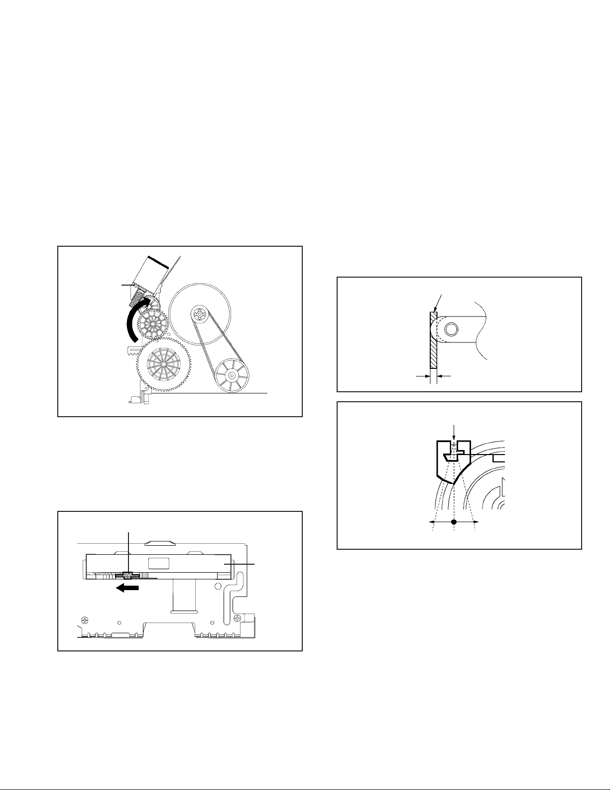
2-1: GUIDE ROLLER
1.
Playback the VHS Alignment Tape (MHPE).
2.
Connect CH-1 of the oscilloscope to TP102 (Envelope)
and CH-2 to TP101 (SW Pulse).
3.
Press and hold the Tracking-Auto button on the remote
control more than 2 seconds to set tracking to center.
4.
Trigger with SW Pulse and observe the envelope. (Refer
to Fig. 2-1-A)
5.
When observing the envelope, adjust the Roller Driver
(PTU94002-2) slightly until the envelope will be flat.
Even if you press the Tracking Button, adjust so that
flatness is not moved so much. (Refer to Fig. 2-1-B)
6.
Adjust so that the A : B ratio is better than 3 : 2 as shown
in Fig. 2-1-C, even if you press the Tracking Button to
move the envelope (The envelope waveform will begin to
decrease when you press the Tracking Button).
7.
Adjust the PG shifter during playback.
(Refer to the ELECTRICAL ADJUSTMENTS)
NOTE
After adjustment, confirm and adjust A/C head.
(Refer to item 2-2)
Torque Gauge
Torque Gauge
S Reel
T Reel
Fig. 1-2-B
NOTE
If the torque is out of the range, replace the following parts.
Check item
1-3
1-4
S Reel side:
Replacement Part
Idler Ass’y/Clutch Ass’y
S Reel/Tension Band/Tension
Connect/Tension Arm Ass’y
T Reel side:
T Reel/T Brake Band//T Brake
Spring/T Brake Arm
CH-1
Envelope
(TP102)
CH-2
SW Pulse (TP101)
Improper Proper
(a) Guide roller
(b) P4 Cap
Entrance
Max
CH-1
CH-2
Track
Track
A : B ≥ 3 : 2
Fig. 2-1-A
Fig. 2-1-B
Exit
MaxA B
Fig. 2-1-C
1-18
Page 24
MECHANICAL ADJUSTMENTS
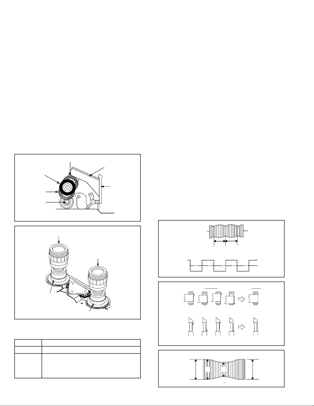
2-2: CONFIRMATION AND ADJUSTMENT OF A UDIO/
CONTROL HEAD
When the Tape Running Mechanism does not work well,
adjust the following items.
1.
Playback the VHS Alignment Tape (MHPE).
2.
Confirm that the reflected picture of stamp mark is
appeared on the tape prior to P4 Post as shown in Fig. 2-
2-A.
a)
When the reflected picture is distorted, turn the screw
1 clockwise until the distortion is disappeared.
b)
When the reflected picture is not distorted, turn the
screw 1 counterclockwise until little distortion is
appeared, then adjust the a).
3.
Turn the screw 2 to set the audio level to maximum.
4.
Confirm that the bottom of the Audio/ Control Head and
the bottom of the tape is shown in Fig. 2-2-C.
c)
When the height is not correct, turn the screw 3 to
adjust the height. Then, adjust the 1~3 again.
Audio/Control Head
Reflected picture of
Stamp Mark
P4 Cap
2-3: TAPE RUNNING ADJUSTMENT
(X VALUE ADJUSTMENT)
1.
Confirm and adjust the position of the Tension Post.
(Refer to item 1-1)
2.
Adjust the Guide Roller. (Refer to item 2-1)
3.
Confirm and adjust the Audio/Control Head.
(Refer to item 2-2)
4.
Connect CH-1 of the oscilloscope to TP101, CH-2 to
TP102 and CH-3 to Audio Out.
5.
Playback the VHS Alignment Tape (MHPE).
6.
Press and hold the Tracking-Auto button on the remote
control more than 2 seconds to set tracking to center.
7.
Set the X Value adjustment driver (X-JG153) to the 4 of
Fig. 2-2-B. At first, turn the Audio/Control Head position
fully toward the capstan side. Then adjust X Value to turn
it back gradually toward the cylinder side and stop on the
second peak point position of the envelope.
Play MHPE
Waveform output
X-value adjustment point
Drum side Control head position Capstan side
Audio/Control Head
3
2
Audio/Control Head
Tape
Stamp Mark
1
4
Fig. 2-2-A
Fig. 2-2-B
0.25±0.05mm
Fig. 2-2-C
Maximum
8.
Perform tracking operation and confirm the envelope is
maximum on the tracking center position.
9.
Playback the VHS Alignment Tape (MHPE-L).
10.
Perform tracking operation and confirm the envelope is
maximum on the tracking center position. If envelope is
not maximum, should be fine-tune the X-VALUE.
Fig. 2-3
1-19
Page 25
ELECTRICAL ADJUSTMENTS
Read and perform this adjustment when repairing the
circuits or replacing electrical parts or PCB assemblies.
1. BASIC ADJUSTMENT
1-1: SWITCHING POINT
CONDITIONS
MODE-PLAYBACK
Input Signal-Alignment Tape (MHPE)
INSTRUCTIONS
Connect CH-1 on the oscilloscope to TP101 and CH-2 to
1.
pin 19 of J8005.
Playback the alignment tape. (MHPE)
2.
Press and hold the Tracking-Auto button on the remote
3.
control more than 2 seconds to set tracking to center.
Press both CH UP button on the set and the STOP button
4.
on the set for more than 2 seconds.
ELECTRICAL ADJUSTMENT PARTS LOCATION GUIDE (Connector Connections)
AC IN
POWER PCB
6.5H
6.5H
CH-2
CH-1
Fig. 1-1-A
CH-2
CH-1
Fig. 1-1-B
J8005
TU301
TP102 (ENVELOPE)
TP101 (SWITCHING PULSE)
J8004
J8007
J8006
VCR PCB
J8002
J8003
CP102
CD102
A/C HEAD
J8001
TP3001
(SERVICE MODE)
V651
CP1701
CP8001
CP8002
CP653
CD651
CP681
OPERATION PCB
CD8002
CD502
CP503
CD503
CP8502
CP502
CD8501
DVD PCB
CP2601
CP2603
CD8502
CP2602
CD4001
CD2601
CD2603
1-20
DECK CD
Page 26

IC DESCRIPTION
DVD PCB OEC6069A (IC1001)
PIN NAME I/O DESCRIPTION
D0 to D7 I/O Data: 0 to 7 for data bus
D8 to D15 I/O Data: 8 to 15 for data bus
A0 to A7 O Address: 0 to 7 for address bus
A8 to A15 O Address: 8 to 15 for address bus
A16 to A23 O Address: 16 to 23 for address bus
RDX O Read: Strobe signal for reading external memory
WRX O Write LL: Strobe signal for writing data on pins D0 to D7
RASOX O Row address strobe 0: Outputs /RAS strobe for DRAM if address is within specified address area
ROMC5X O Chip select 2: Outputs "low" if address is within specified address area
ZRC5X O Chip select 3: Outputs "low" if address is within specified address area
TBFC5X O Port 84: Output port (output "high" when initialized)
SVCEX O Chip select 5: Outputs "low" if address is within specified address area
WAITX I Wait: Signal used to request CPU bus wait
LCA50X O Lower column address strobe 0: Outputs lower CAS strobe for DRAM if address is within specified address area
UCA50X O Upper Column address strobe 0: Outputs upper CAS strobe for DRAM if address is within specified address area
OEOX O Output enable 0: Outputs read enable signal for DRAM
WEOX O Write enable 0: Outputs erite enable signal for DRAM
NMI_INH O Port B0: Output port (output "high" when initialized)
PGBSX O Port B1: Output port (output "high" when initialized)
CVSX O Port B2: Output port (output "high" when initialized)
S2X O Port B3: Output port (output "high" when initialized)
S1X O Port B4: Output port (output "high" when initialized)
PROMCK O Timer output 1: 8-bit timer 0 or 1 output
PROMDA O Timer output 3: 8-bit timer 2 or 3 output
WP I/O Port D0: I/O port
I45INTX I/O Port D1: I/O port
DMFG I/O Port D5: I/O port
CTS I/O Port E0: I/O port
TBFINTX I/O Port E1: I/O port
DISKWOI I/O Port E2: I/O port
SVINTX I/O Port E5: I/O port
DSTBX I/O Port E6: I/O port
DSPSO O Serial send data 0
DSPSI I Serial receive data 0
DSPCK I/O Port F2: I/O port
TXD O Serial send data 1
RXD I Serial receive data 1
RTS I Serial data receive enable 1
AN0 to AN7 I Analog input: Input to 10-bit AD converter
DAOUT0 O DA output 0: Output form 8-bit DA converter 0
DAOUT1 O DA output 1: Output form 8-bit DA converter 1
LOMN O Terminal count 0: Outputs "high" strobe when counter value of micro-DMA channel 0 is "0"
LOMP O Terminal count 1: Outputs "high" strobe when counter value of micro-DMA channel 1 is "1"
I45RSTH O Terminal count 2: Outputs "high" strobe when counter value of micro-DMA channel 2 is "0"
SVRSTX O Terminal count 3: Outputs "high" strobe when counter value of micro-DMA channel 3 is "0"
LSRDVD I/O Port H4: I/O port (schmitt input)
SCLK I/O Port: I/O port
SO I/O Port: I/O port
DACSOX I/O Port: I/O port
PLLCSX I/O Port: I/O port
NTPLX I/O Port: I/O port
VSW I
AM0, 1 I Address mode: Selects external Data Bus width
TEST0, 1 I Test: Input "low" when using
CLK O Clock output: Outputs system clock
X1/X2 I/O Oscillator connecting pin
RESET I Reset: Initializes LSI (with pull-up resistor) (schmitt input)
Non-maskable interrupt request pin: Interrupt request pin with falling edge
Can also be operated at rising edge by program. (schmitt input)
1-21
Page 27
IC DESCRIPTION
DVD PCB OEC6069A (IC1001)
PIN NAME I/O DESCRIPTION
VREFH I Pin for reference voltage input to AD converter ("high" level)
VREFL I Pin for reference voltage input to AD converter ("low" level)
DAREFH I Pin for reference voltage input to DA converter ("high" level)
DAREFL I Pin for reference voltage input to DA converter ("low" level)
ADVCC - Power supply pin for 10-bit AD converter
ADVSS - GND pin for 10-bit AD converter (0V)
DAVCC - Power supply pin for 8-bit DA converter
DAVSS - GND pin for 8-bit DA converter (0V)
CLVCC - Power supply pin for clock doubler
CLVSS - GND pin-for clock doubler
DVCC - Power supply pin ( + 5V)
DVSS - GND pin (0V)
1-22
Page 28
IC DESCRIPTION
DVD PCB OEC6068A (IC2001)
PIN NO. PIN NAME I/O DESCRIPTION
1 ASLCN O
2 ASLCO O
3 DVSS -
4ROO
5 DVDD 6 DVR O
7LOO
8 DVSS -
9 XVSS 10 Xl I
11 XO O
12 XVDD 13 TESM0 14 TESM1 15 TESM2 16 VDD3 17 VSS3 18 VPFC O
19 TEST0 I
20 VLPFI I
21 VLPFO O
22 VSS3 23 MON0
24 MON1
25 MON2
26 MON3
27 MON4
28 MON5
29 MON6
30 MON7
31 MON8
32 MON9
33 VDD3 34 NC
35 NC
36 TEST1 I
37 FLGA I/O
38 FLGB I/O
39 VSS3 40 /RST I
41 /MA I
42 /MRD I
43 /MWR I
44 /MCE I
45 /MINT O
46 MD0
47 MD1
48 MD2
49 MD3
50 MD4
51 MD5
52 MD6
53 MD7
54 VDD5 55 NC
56 NC
Data slice negative output
Analog data slice output
( Using Difference input, Digital or Analog slice data output )
DAC-only ground
R-channel output signal
DAC-only power supply
Amp reference signal output
L-channel output signal
DAC-only power ground
Oscillator-only ground
Crystal oscillator input
Crystal oscillator output
Oscillator-only power supply
Test pin
Test pin
Test pin
3.3V digital power supply
3.3V digital ground
Clock PLL block phase / frequency comparator output
Test mode pin
VCO filter input for the clock PLL
VCO filter output for the clock PLL
3.3V digital ground
O
Test monitor
3.3V digital power supply
-
Test mode pin
General-purpose l/O or flag monitor
General-purpose l/O or flag monitor
3.3V digital ground
Reset pin
Microcomputer address enable signal
Microcomputer data read signal
Microcomputer data write signal
Microcomputer chip enable signal
Microcomputer interrupt signal
I/O
Microcomputer data bus
5V power supply
-
-
1-23
Page 29
IC DESCRIPTION
DVD PCB OEC6068A (IC2001)
PIN NO. PIN NAME I/O DESCRIPTION
57 SMCK O
58 VMCK O
59 VDD3 60 PD0 O
61 VSS5 62 PD1
63 PD2
64 PD3
65 PD4
66 VSS3 67 PD5
68 PD6
69 PD7
70 PD8
71 /PSYC O
72 /PDRQ O
73 PDCK O
74 VDD5 75 TESM3 76 DIGI I
77 TESM4 78 VDD3 79 BA0
80 BA1
81 BA2
82 BA3
83 VSS5 84 BA4
85 BA5
86 BA6
87 BA7
88 BA8
89 VDD3 90 /BOE O
91 /BRAS O
92 /BCAS O
93 /BWL O
94 /BWU O
95 VDD5 96 BD0
97 BD1
98 BD2
99 BD3
100 BD4
101 BD5
102 BD6
103 BD7
104 BD8
105 VSS3 106 BD9
107 BD10
108 BD11
109 BD12
110 VSS5 111 BD13
112 BD14
113 BD15
22M block clock output
Data output block (signal processing block) clock output
3.3V digital power supply
DVD/CD data output
5V ground
O
DVD/CD data ground
3.3V digital ground
O
DVD/CD data output
DVD data sector sync signal
DVD data transfer block
DVD data transfer clock
5V power supply
Test pin
1-bit DAC Digital In input
Test pin
3.3V digital power supply
O
External RAM address output
5V ground
O
External RAM address output
3.3V digital power supply
External RAM / OE signal
External RAM /RAS signal
External RAM /CAS signal
External RAM Lower / WE signal
External RAM Upper / WE signal
5V power supply
I/O
External RAM data input / output
3.3V digital ground
I/O
External RAM data input / output
5V ground
I/O
External RAM data input / output
1-24
Page 30
IC DESCRIPTION
DVD PCB OEC6068A (IC2001)
PIN NO. PIN NAME I/O DESCRIPTION
114 NC
115 NC
116 VDD3 117 PLCK I/O
118 TESM5 119 TESM6 120 TESM7 121 TESM8 122 VSS3 123 CFC1 O
124 CFC2 O
125 PPW O
126 PESV I
127 PVSS 128 PESP O
129 PDOP1 O
130 PDON1 O
131 PDOP2 O
132 PDON2 O
133 LPFN I
134 LPFO O
135 PVREF 136 VCOREF I
137 VCOF I
138 PVDD 139 SLCO1 I/O
140 TESM9 141 TEST2 I
142 RFCD I
143 RFDVD I
144 AVDD 145 RFCT I
146 RFZI I
147 TEZI I
148 AWIN I
149 AVSS 150 FEI I
151 TEI I
152 RFSB I
153 RFRP I
154 AVSS 155 TESM10 156 EXTAD I
157 VREF 158 FOO O
159 TRO O
160 AVDD 161 AWCTL O
162 FMO O
163 DMO O
164 TEBC O
165 FEBC O
166 DPDC O
167 EQBC O
168 ANMON O
169 /DFCT O
-
-
3.3V digital power supply
PLL block clock input / output
Test pin
Test pin
Test pin
Test pin
3.3V digital ground
VCO frequency control signal
VCO frequency control signal
Phase comparator offset adjusting voltage output
Phase comparator offset adjusting voltage input
3.3V PLL block-only ground
Phase comparator offset adjusting signal output
DVD/CD phase control signal (positive)
DVD/CD phase control signal (negative)
DVD/CD phase control signal (positive)
DVD/CD phase control signal (negative)
Data PLL low-pass filter inverted input
Data PLL low-pass filter output
Data PLL block-only reference power supply
VCO reference
VCO automatic adjusting filter output
3.3V PLL block-only power supply
Data slice 6-bit DAC output (Using Difference Input, RFOn signal input)
Test pin
Test mode pin
CD RF signal input (Using Difference Input, RFOp signal input)
DVD RF signal input (Using Difference Input, RFOp signal input)
3.3V analog block-only power supply
RFRP center voltage input (latched at zero cross)
RFRP signal input (latched at zero-cross)
Tracking error signal input (latched at zero-cross)
Active-wide PLL control signal input
3.3V analog block-only ground
Focus error signal input
Tracking error signal input
RF level or subbeam signal summing input
RFRP signal input
3.3V analog block-only ground
Test pin
General-purpose external ADC input
Analog block-only reference power supply: 1 .65V
Focus EQ outputs
Tracking EQ output
3.3V analog block-only power supply
Active-wide PLL control output
Feed EQ output
Disc EQ output
Tracking balance control signal
Focus balance control signal
DPD error signal's pit depth adjusting signal
D Input(CDRF wideband boost adjusting signal
General-purpose PWM output
Black dot detection signal
1-25
Page 31

IC DESCRIPTION
DVD PCB OEC6068A (IC2001)
PIN NO. PIN NAME I/O DESCRIPTION
170 VRCK O
171 VSS3 172 SCD O
173 SCL O
174 SCB O
175 FGIN I
176 ASLCP O
RF EQ response control clock
3.3V digital ground
Head amp serial data
Head amp serial data latch pulse
Head amp serial data clock
Disc FG signal input (with self-biasing circuit)
Data Slice positive output
1-26
Page 32

IC DESCRIPTION
DVD PCB OEC6067A (IC2603)
PIN NO. PIN NAME I/O DESCRIPTION
1 GND 2 P2TP I
3 P2TN I
4 LDO2 O
5 MDI2 I
6 VrD O
7 Vrfi 8 Vdd I Vdd Terminal
9DPAC
10 DPBD
11
12
13 SCB I
14 SCL I
15 SCD I
16 VRCK I
17 VCKF 18 VccP 19 LVL O
20 TEO O
21 FEO O
22 DFTN I DPD Defect Terminal
23 Vcc 24 NC 25 RPZ O
26 RPO O
27 RPB 28 RPP 29 RFOn O
30 RFOp O
31 VccR -
32 RFS I
33 TEB I
34 FEB I
35 DPDB I
36 Vcc2 37 NC 38 NC 39 GND2 40 TCC1 I
41 RFDC 42 VrA O
43 EQB I
44 EQF I Band Width Control for RF EQ
45 MDI1 I LD Monitor Terminal
46 LDO1 O
47 P1TN I
48 P1TP I
49 P1FN I
50 P1FP I
DPD1
DPD2
GND Terminal
TE + Input (CD)
TE - Input (CD)
LD Drive Terminal
LD Monitor Terminal
Digital VREF
Filter Capacitance for Reference
DPD AC Coupling
Capacitance 1
DPD AC Coupling
Capacitance 2
DPD Integration
Capacitance 1
DPD Integration
Capacitance 1
Bus Line (Bit Clock)
Bus Line (Latch Signal)
Bus Line (Serial Data)
Reference Clock Input
Time Constant Correcting Capacitance
Vcc Terminal
Sub-Beam Adder Signal Output
TE Output
FE Output
Vcc T erminal
RF Ripple Output 2
RF Ripple Output 1
Bottom of RF Ripple
Peak of RF Ripple
RF Signal Output (differential output)
RF Signal Output (differential output)
Vcc Terminal
RF Output
Slice Level Control
TE Balance Control
FE Balance Control
DPD Offset Control
Vcc Terminal
-
-
Time Constant. Adjustment Terminal
Capacitance for DC Feedback (RF)
Analog VREF
Boost Control for RF EQ
LD Drive Terminal
TE - Input (DVD)
TE + Input (DVD)
FE - Input (DVD)
FE + Input (DVD)
1-27
Page 33

IC DESCRIPTION
DVD PCB OEC6067A (IC2603)
PIN NO. PIN NAME I/O DESCRIPTION
51 LDP2 I
52 P1DI I
53 P1CI I
54 P1BI I
55 P1AI I
56 GNDR 57 LDP2 I
58 P2AI I
59 P2BI I
60 P2CI I
61 P2DI I
62 GNDS - GND Terminal
63 P2FP I
64 P2FN I
APC Polarity 1
D Input (DVD)
C Input (DVD)
B Input (DVD)
A Input (DVD)
GND Terminal
APC Polarity 2
A Input (CD)
B Input (CD)
C Input (CD)
D Input (CD)
FE + Input (CD)
FE - Input (CD)
1-28
Page 34

IC DESCRIPTIONS
g
C
VCR PCB OEC7078B (IC3001)
Pin No. Pin Name I/O Description
1 MSSW B I Input terminal(B) of mecha state sensor.
2 MSSW A I Input terminal(A) of mecha state sensor.
3 KEY-A I Key A input.
4 KEY-B I Key B input.
5 AFT-SC I AFT S Curve input for tuner.
6 EOT I Tape end sensor input signal.
7 A-ENV I Input terminal of audio envelope.
8 V-ENV I Input terminal of video RF envelope.
N.C. O
9
10 BOT I Tape start sensor input signal.
11 CAP FWD O Capstan forward and backward command.
12 CAP LIMIT O Switch the maximum output current of the Capstan Motor.
13 D.V SYNC O Intative V-SYNC signal output during the special playback.
14 REMOCON IN I Input the infrared remote control.
15 N.C. O Not used.
16 S-DET-H O Output "H" when S detection by PAL SP.
17 DVD_RESET O Output terminal of DVD reset.
18 V.HEAD SW O Output terminal of Head Switch.(video)
19 A.HEAD SW O Output terminal of Head Switch.(audio)
20 POWER ON H O For control the user power switch ON/OFF.
21 CENTER LED O Center LED(EOT/BOT).
22 A.MUTE-H O
23 N.C. O Not used.
24 N.C. O Not used.
25 FF/REW L O Output "L" when fast forwarding or rewinding.
26 CAP ON O Control the Capstan Motor rotation direction.
27 FL_CS O CS for FL driver IC control.
28 DVD_MUTE O MUTE terminal for DVD when power ON/OFF .
29 NA REC-H O Control the Bias OSC for audio head.
30 VV-H O If the EE/VV is "VV" ,output"H".
31 DVD_POWER_A O Control terminal of DVD POWER(3.3V).
32 N.C. O Not used.
33 N.C. O Not used.
34 N.C. - Not used.
35 N.C. - Not used.
36 CLKSEL - 5V.
37 VCC - 5V.
38 X IN I Connect the main crystal(12 MHz).
39 X OUT O Connect the main crystal(12 MHz).
40 VSS - Ground.
41 XC IN I Subclock pulse(32.768 KHz).
42 XC OUT O Subclock pulse(32.768 KHz).
43 RESET I Input terminal of reset signal.
44 SERVICE 1 I Setting of service mode 1.
45 SERVICE 2 I Setting of service mode 2.
46 SUB_CS O Submicom communication control CS.
47 LDM_CTL O Control terminal of the Loading Motor.
48 N.C. O Not used.
49 SUB_RESET O Control submicom RESET.
50 LED-SEG1 O
AGC_DET I Detection terminal AGC voltage of TUNER.
[For HR-XV1EK]
In case of initial setting "AUTO_SETUP" is AGC_DET.
The others are N.C..
N.C.:Output "L".
between E-E and V-V during the special playback.
ontrol the LED display unit(SEG1).
1-29
Page 35

IC DESCRIPTIONS
VCR PCB OEC7078B (IC3001) [For HR-XV1EK]
Pin No. Pin Name I/O Description
51 LEM-SEG2 O Control the LED display module(SEG2)
52 LEM-SEG3 O Control the LED display module(SEG3)
53 LEM-SEG4 O Control the LED display module(SEG4)
54 LEM-SEG5 O Control the LED display module(SEG5)
55 LEM-SEG6 O Control the LED display module(SEG6)
56 LEM-SEG7 O Control the LED display module(SEG7)
57 LEM-SEG8 O Control the LED display module(SEG8)
58 LEM-SEG9 O Control the LED display module(SEG9)
59 LEM-SEG10 O Control the LED display module(SEG10)
60 LEM-GRID1 O Control the LED display module(GRID1)
61 LEM-GRID2 O Control the LED display module(GRID2)
62 LEM-GRID3 O Control the LED display module(GRID3)
63 LEM-GRID4 O Control the LED display module(GRID4)
64 LEM-GRID5 O Control the LED display module(GRID5)
65 SUB_DATA_OUT O Output the Data of Submicom.
66 SUB_DATA_IN I Input the Data of Submicom.
67 SUB_CLK O Output the Clock of Submicom.
68 CG-DATA O Output the Data of OSD IC.
69 CG-CS O Output the CS signal of OSD IC.
70 CG-CLK O Output the Clock of OSD IC.
71 IIC-CLK O Clock output to IIC.
72 IIC-SDA I/O DATA input/output to IIC.
73 32K MONI O Output 32.768KHz monitor(16.384KHz output) to check the clock.
74 Hi-Fi MUTE O Control the Hi-Fi IC.
75 V-REC-ST O Control the Head Amp for video and Hi-Fi audio.
76 PICTURE CTL O Output pulse to conrol the Y/C IC for sharpness.
77 CAP-CTL O Output servo of the capstan motor.
78 CYL-CTL O Output pulse to conrol the drum motor
79 REEL-S I Input terminal of reel sensor supply.
80 REEL-T I Input terminal of reel sensor take up.
81 TAB SW I Input of TAB SW
82 P.FAIL I Input for the detection of power interruption.
83 N.C. I Not used.
84 C SYNC I Input Compound synchronized signal.
85 CFG I Input terminal for Capstan FG signal detection.
86 N.C. O Not used.
87 DFPG I Input terminal for compounded PG and FG signal of Drum motor.
88 AMP VSS - Ground.
89 AMP V.OUT O Output the analogue Amp standard voltage.
90 AMP V.IN I Input the analogue Amp standard voltage.
91 CTL- I/O Input and output terminal of CTL AMP.
92 CTL+ I/O Input and output terminal of CTL AMP.
93 CTL SW OUT O Output terminal of CTL AMP positive.
94 CTL AMP IN I Input terminal of CTL AMP.
95 AMP C - AC Ground of CTL AMP.
96 CTL VSS - Connect the VSS.
97 CTL AMP OUT I/O Output terminal of CTL AMP circuit.
98 AMP VCC - 5V .
99 A VCC - Voltage terminal for general circuit.
100 SQPB-H I Distinction input terminal of SQPB
1-30
Page 36

IC DESCRIPTION
g
VCR PCB OEC7079B (IC3001) [For HR-XV1EU-C/S/Y]
Pin No. Pin Name I/O Description
1 MSSW B I Input terminal(B) of mecha state sensor.
2 MSSW A I Input terminal(A) of mecha state sensor.
3 KEY-A I Key A input.
4 KEY-B I Key B input.
5 AFT-SC I AFT S Curve input for tuner.
6 EOT I Tape end sensor input signal.
7 A-ENV I Input terminal of audio envelope.
8 V-ENV I Input terminal of video RF envelope.
PERI_CTL and AGC are changed by Initial setting.
9 PERI_CTL or AGC I
10 BOT I Tape start sensor input signal.
11 CAP FWD O Capstan forward and backward command.
12 CAP LIMIT O Switch the maximum output current of the Capstan Motor.
13 D.V SYNC O Intative V-SYNC signal output during the special playback.
14 REMOCON IN I Input the infrared remote control.
15 SECAM IN I Input the color system SECAM.
16 S-DET-H O Output "H" when S detection by PAL SP.
17 DVD_RESET O Output terminal of DVD reset.
18 V.HEAD SW O Output terminal of Head Switch.(video)
19 A.HEAD SW O Output terminal of Head Switch.(audio)
20 POWER ON H O For control the user power switch ON/OFF.
21 CENTER LED O Center LED(EOT/BOT).
22 A.MUTE-H O
23 SECAM-H O Control Y/C IC at SECAM .
24 SP-H O Output High when SP on EE screen. The other is Low.
25 FF/REW L O Output "L" when fast forwarding or rewinding.
26 CAP ON O Control the Capstan Motor rotation direction.
27 FL_CS O CS for FL driver IC control.
28 DVD_MUTE O MUTE terminal for DVD when power ON/OFF .
29 NA REC-H O Control the Bias OSC for audio head.
30 VV-H O
31 DVD_POWER_A O Control terminal of DVD POWER(3.3V).
32
33 N.C. O Not used.
34 N.C. - Not used.
35 N.C. - Not used.
36 CLKSEL - 5V.
37 VCC - 5V.
38 X IN I Connect the main crystal(12 MHz).
39 X OUT O Connect the main crystal(12 MHz).
40 VSS - Ground.
41 XC IN I Subclock pulse(32.768 KHz).
42 XC OUT O Subclock pulse(32.768 KHz).
43 RESET I Input terminal of reset signal.
44 SERVICE 1 I Setting of service mode 1.
45 SERVICE 2 I Setting of service mode 2.
46 SUB_CS O Submicom communication control CS.
47 LDM_CTL O Control terminal of the Loading Motor.
48 ZERO MUTE I MUTE terminal for DVD when power ON/OFF .
49 SUB_RESET O
50 LEM-SEG1 O
N.C. or
PERI_CTL-L
PERI_CTL : Control the 21 pin IC output.
AGC : Detection terminal AGC voltage of TUNER.
This pin output the HIGH to mute the sound at the switching point
between E-E and V-V durin
If the EE/VV is "VV" ,output"H".
N.C. and PERI_CTL-L are changed by Initial setting.
I/O
In case of ATS is PERI_STL-L.
The others are N.C..
Control submicom RESET.
Control the LED display module(SEG1)
the special playback.
1-31
Page 37

IC DESCRIPTION
g
g
VCR PCB OEC7079B (IC3001) [For HR-XV1EU-C/S/Y]
Pin No. Pin Name I/O Description
51
52
53
54
55
56
57
58
59
60 LEM-GRID1 O
61 LEM-GRID2 O Control the LED display module(GRID2)
62 LEM-GRID3 O Control the LED display module(GRID3)
63 LEM-GRID4 O Control the LED display module(GRID4)
64 LEM-GRID5 O Control the LED display module(GRID5)
65 SUB_DATA_OUT O Output the Data of Submicom.
66
67
68 CG-DATA O Output the Data of OSD IC.
69 CG-CS O Output the CS signal of OSD IC.
70 CG-CLK O Output the Clock of OSD IC.
71 IIC-CLK O Clock output to IIC.
72 IIC-SDA I/O DATA input/output to IIC.
73 32K MONI O Output 32.768KHz monitor(16.384KHz output) to check the clock.
74 Hi-Fi MUTE O Control the Hi-Fi IC.
75 V-REC-ST O Control the Head Amp for video and Hi-Fi audio.
76 PICTURE CTL O Output pulse to conrol the Y/C IC for sharpness.
77 CAP-CTL O Output servo of the capstan motor.
78 CYL-CTL O Output pulse to conrol the drum motor.
79 REEL-S I Input terminal of reel sensor supply.
80 REEL-T I Input terminal of reel sensor take up.
81 TAB SW I Input of TAB SW .
82 P.FAIL I Input for the detection of power interruption.
83 N.C. I Not used.
84 C SYNC I Input Compound synchronized signal.
85 CFG I Input terminal for Capstan FG signal detection.
86 N.C. O Not used.
87 DFPG I Input terminal for compounded PG and FG signal of Drum motor.
88 AMP VSS - Ground.
89 AMP V.OUT O Output the analogue Amp standard voltage.
90 AMP V.IN I Input the analogue Amp standard voltage.
91 CTL- I/O Input and output terminal of CTL AMP.
92 CTL+ I/O Input and output terminal of CTL AMP.
93 CTL SW OUT O Output terminal of CTL AMP positive.
94 CTL AMP IN I Input terminal of CTL AMP.
95 AMP C - AC Ground of CTL AMP.
96 CTL VSS - Connect the VSS.
97 CTL AMP OUT I/O Output terminal of CTL AMP circuit.
98 AMP VCC - 5V.
99 A VCC - Voltage terminal for general circuit.
100
LEM-SEG2
LEM-SEG3
LEM-SEG4
LEM-SEG5
LEM-SEG6
LEM-SEG7
LEM-SEG8
LEM-SEG9
LEM-SEG10
SUB_DATA_IN
SUB_CLK
MESECAM-M/
SQPR-H
O Control the LED display module(SEG2)
O Control the LED display module(SEG3)
O Control the LED display module(SEG4)
O Control the LED display module(SEG5)
O Control the LED display module(SEG6)
O Control the LED display module(SEG7)
O Control the LED display module(SEG8)
O Control the LED display module(SEG9)
Control the LED display module(SEG10)
O
Initial settin
Control the LED display module(GRID1)
Initial settin
I Input the Data of Submicom.
O Output the Clock of Submicom.
I Distinction input terminal of MESCAM and SQPB.
is FLD : FLD POWER ON/OFF terminal.
is FLD : VCR LED for a drive.
1-32
Page 38

IC DESCRIPTIONS
VCR PCB OEC7080A (IC3005)
Pin No. Pin Name I/O Description
1 D3 O DVD LED.
2 D4 O VCR LED.
3 D5 I Not used. (GND)
4 D6 I Not used. (GND)
5 D7 I Not used. (GND)
6 SCK I Input synchronized clock for VCR Communication.
7 SOUT O Output serial I/O for VCR Communication.
8 SIN I Input serial I/O for VCR Communication.
9 RESET - Input reset.
10 CNVSS - GND.
11 XOUT O 4MHz oscillation.
12 XIN I 4MHz oscillation.
13 VSS - GND.
14 VDD - VDD.
15 VDCE - GND.
16 INT0 I Input software UART for VCR Communication.
17 P31 I Not used. (GND)
18 AIN0 I Not used. (GND)
19 AIN1 I Not used. (GND)
20 AIN2 I Not used. (GND)
21 AIN3 I Not used. (GND)
22 P00 I Not used. (GND)
23 P01 I Not used. (GND)
24 P02 I Not used. (GND)
25 P03 I Not used. (GND)
26 P10 I Not used. (GND)
27 P11 I Not used. (GND)
28 P12 I Not used. (GND)
29 P13 I Not used. (GND)
30 D0 O Output software UART for VCR Communication.(TK)
31 D1 I Input software UART for VCR Communication.(RX)
32 D2 I Input CS.
1-33
Page 39

VCR PCB IC3001
DPG 87 PIN
DFG 87 PIN
SERVO TIMING CHART
24 Cycle
H. SW. P 18 PIN
V-SYNC (E-E) 84 PIN
REC CTL (REC)
97 PIN
V-SYNC (TRICK PB)
13 PIN
• WAVEFORM CHANGES DEPENDED ON THE TAPE SPEED
CH 1
CH 2
1-34
Page 40

O
C
Y
MECHANISM TIMING CHART
Please see the list below for the operational timing and the mode sensor output of the main parts on each mechanism modes.
MECHANISM MODE UNLOAD STOP3
Mode Dealing
Directions
Revolutional Angle of
MAIN CAM
Moving Quantity of
MAIN ROD (mm)
MS-2
HIGH
LOW
HIGH
MODE MS-1
SENSOR
utput
EJECT
0
STBY
15
3
206.3100
180
LOW
INCLINED BASE S/T UNIT
PINCH ROLLER BLOCK
P5 ARM ASS'Y (T BRAKE:LOW)
TENSION LEVER
TENSION ARM ASS'
(S REEL BRAKE)
VSR
S BRAKE:LOW
255
26.5
PRESS
PRESS
P5-ON (T BRAKE HIGH)
BRAKE-ON
PBF.SLOW
S BRAKE:HIGH
FF/REWSTOP2
323.8303.7272.2226.4
38.53529.521.5
TENSION CONNECT
(S REEL BRAKE)
T BRAKE ARM
(T REEL BRAKE)
LUTCH LEVER
LINK UNIT
FLAP LEVER
BRAKE-ON
BRAKE-ON
CLUTCH-ON
UP
BRAKE-ON
DIRECT
PRESS
1-35
Page 41

(VCR SECTION)
POWER DOES NOT TURN ON
TROUBLESHOOTING GUIDE
Does display light?
YES
Is there voltage at
pin 20 of IC 3001?
NO
Check IC3001.
NO
YES
Is the voltage at pin 14
of CP502 about 5.2V?
YES
Check IC3001.
NO
Check pin 13 of T501
and peripheral circuit.
Check Q506, Q504.
1-36
Page 42

THE POWER SUPPLY CUT
Inserting a cassette
and push play button.
TROUBLESHOOTING GUIDE
Does the power cut
after 3 seconds?
NO
Does the power cut
after about 6 seconds?
NO
Does intermittently
the power cut?
NO
Check the POWER BLOCK.
YES
YES
YES
Check CAPSTAN DD UNIT
and CYLINDER UNIT.
Check Q3006, Q3007
and CAPSTAN BELT.
Check Q3006, Q3007, IC3001
and sag of CAPSTAN BELT.
1-37
Page 43

AUDIO SHAKES
TROUBLESHOOTING GUIDE
Is AUDIO HEAD
scratched?
NO
At playback, is input about
4.5Vp-p of a rectangular
wave at pin 85 of IC3001?
YES
At playback, is pin 5 of
CP3001 3.5V?
YES
Check AUDIO BLOCK.
YES
NO
NO
Change AUDIO HEAD.
Change CAPSTAN DD UNIT.
Check IC3001.
1-38
Page 44

The CASSETTE TAPE
CAN NOT BE INSERTED
TROUBLESHOOTING GUIDE
When a CASSETTE can
not inserted, is pin 10 of
IC3001 5V ?
YES
When a CASSETTE is
inserted, is pin 8 of
CP3001 12.6V ?
NO
When a CASSETTE is
inserted, is pin 47 of
IC3001 5V ?
YES
Check circuit of loading motor.
NO
YES
NO
Check LED of DECK,
PHOTO SENSOR.
Change
LOADING MOTOR.
Change IC3001.
1-39
Page 45

When inserting a CASSETTE,
it ejects immediately.
TROUBLESHOOTING GUIDE
Does another CASSETTE
insert?
YES
Does SW3001 and
REC LEVER
correctly set ?
YES
After inserting
CASSETTE, is pin 81
of IC3001 0V ?
YES
Check IC3001.
NO
NO
NO
Defective CASSETTE
or cassette loading
block.
Correctly SW3001
and REC LEVER set.
Check SW3001.
1-40
Page 46

Can not FF/REW
TROUBLESHOOTING GUIDE
At FF/REW, does voltage
at pin 11 of IC3001
change?
YES
Check DECK MECHANISM.
WHEN PLAYBACK, FF OR REW
MODE IS ACTIVE , UNIT STOPS
IMMEDIATELY
Does CAPSTAN DD
MOTOR rotate?
YES
NO
NO
Check line of IC3001
at pin 3 and pin 4.
Refer to section "CAPSTAN
DD MOTOR NOT
ROTAING".
Is there REEL SENSOR
PULSE signal at pin 79
and pin 80 of IC3001?
YES
Change IC3001.
NO
Check Q3006 and Q3007.
1-41
Page 47

TAPE loading is ok, but
unloads immediately.
TROUBLESHOOTING GUIDE
Does CYLINDER
rotate?
YES
Is there HEAD SW
PULSE at TP101?
YES
NO
NO
Is the voltage
at pin 8 of CP3001
12.6V?
YES
At play, is the voltage
at pin 12 of CP3001 2.6V?
YES
Change CYLINDER unit.
NO
Is PG PULSE signal
inputted to pin 18
of IC3001?
YES
NO
NO
Check power block.
Check Q3006 and Q3007.
Change IC3001.
1-42
Page 48

At play,the picture
jitters vertical minutely
TROUBLESHOOTING GUIDE
Is FG wave of CP3001
at pin 11 5V?
5V
YES
Is pin 12 of CP3001 2.6V?
YES
Change CYLINDER MOTOR
Auto tracking
does not operate
NO
NO
Change
CYLINDER MOTOR.
Change IC3001.
In auto tracking, is the
voltage at pin 8 of IC3001
more than DC 0.2V?
YES
CHANGE IC3001.
NO
Does the CLT pulse
signal (about 2.5Vp-p)
appear at pin 97 of IC3001?
2.5Vp-p
YES
NO
Check CONTROL HEAD.
1-43
Page 49

TROUBLESHOOTING GUIDE
AT PLAY, PICTURE JITTERS
HORIZONTALLY
NO
Does a noise on the picture
appear?
YES
By adjusting the MANUAL
TRACKING UP/DOWN
BUTTONS, will the line
disappear?
YES
Is a height of GUIDE POST
maximum?
YES
Is SWITCHING POINT
adjustment 6.5H?
NO
NO
NO
Check P/B ENVELOPE.
The height of GUIDE
POST readjust.
Adjust SWITCHING POINT
1-44
YES
Is a wave of PB-Y unusual?
YES
Change IC1001.
NO
Change IC101.
Page 50

AT PLAYBACK, THE PICTURE
DOES NOT APPEAR
TROUBLESHOOTING GUIDE
Is E-E appearing on
the MONITOR TV?
YES
Is there FM signal at pin
78 and 79 of IC101?
YES
Is there video signal
at pin 52 of IC101?
YES
Check IC4501.
NO
NO
NO
Is the voltage of IC101 at
pin 12, 36, 61, 90 and 96
5V?
YES
Check video out line and
IC101.
NO
Check POWER BLOCK.
Check connection of the
CYLINDER.
Change IC101.
1-45
Page 51

AT PLAYBACK, THE COLOR
DOES NOT APPEAR
TROUBLESHOOTING GUIDE
Does composite signal
appear at pin 52 of
IC101?
YES
Check pin 21 and 19 of
IC4501.
NO COLER DURING SELF
RECORDING AND PLAYBACK
Does VIDEO signal appear
at pin 31 of IC101?
NO
NO
Change IC101.
Check TU301, J8005,
circuit around it.
YES
Does COLOR signal at pin
52 of IC101?
YES
Check pin 21 and pin 19 of IC4501.
NO
Change IC101.
1-46
Page 52

AT PLAYBACK AND RECORDING,
CYLINDER MOTOR UNLOAD
TROUBLESHOOTING GUIDE
Is the voltage at pin 8 of
CP3001 about DC12.6V?
YES
In playback, is at pin 12 of
CP3001 about DC2.6V?
YES
Change CYLINDER MOTOR.
PLAYBACK PICTURE IS NOISY
(EVEN AFTER CLEANING HEADS)
Is FM signal at pin 79 of
IC101 270 mVp-p ?
NO
NO
NO
Check at 12.6V line,
power block.
Check IC3001.
Check CYLINDER.
YES
Is FM signal at pin 8 of IC3001
more than 1V?
NO
Is VIDEO output at the emitter
of IC4501 2Vp-p, and are
there any noises?
YES
Change J8005.
YES
NO
Perform the interchange
able adjustment of DECK.
Check IC101 and IC4501.
1-47
Page 53

NO COLER DURING SELF
RECORDING AND PLAYBACK
TROUBLESHOOTING GUIDE
Does VIDEO signal appear
at pin 31 of IC101?
YES
Does COLOR signal at pin
52 of IC101?
YES
Check pin 21 and pin 19 of IC4501.
NO
NO
Check TU301, J8005,
circuit around it.
Change IC101.
1-48
Page 54

AT PLAY, AUDIO DOES NOT
APPEAR
TROUBLESHOOTING GUIDE
At E-E, does audio appear?
YES
Does AUDIO signal
appear at pin 2 of IC101
6mVp-p?
YES
Does AUDIO signal
appear at pin 11 of IC101
1Vp-p?
YES
Check AUDIO HEAD for DEBRIS
STAINS. Check the connector from
AUDIO HEAD is fully inseted into
CP102. Replace IC101.
NO
NO
NO
Refer to section "E-E
DOES NOT APPEAR".
Check C117 and peripheral
circuit.
Change IC101.
1-49
Page 55

THE AUDIO CAN NOT
RECORD
TROUBLESHOOTING GUIDE
Is bias level at L104 OK?
YES
Is there audio signal
at pin 5 of CP102?
YES
Is there audio signal
at pin 11 of IC101?
NO
NO
NO
Is the voltage at pin 2
of L104 5V?
YES
Is the voltage at pin 29
of IC3001 about 5V?
L104 is broken or shorted.
NO
NO
Check POWER circuit.
Change IC3001.
Check the circuit between
pin 4 of IC101 to pin 5 of
CP102.
Change IC101.
YES
Check lead wire of A/C HEAD
and CONNECTOR.
1-50
Page 56

THE CASSETTE INSERT, BUT
THE TAPE DOES NOT MOVE
TROUBLESHOOTING GUIDE
Does the mode
appear at display?
YES
Does operate with
remote control?
YES
Check operation PCB.
NO
NO
Check LOADING MOTOR
and MODE SENSOR
RELATION DEPARTMENT.
Check IC3001.
1-51
Page 57

CAPSTAN DD MOTOR NOT
ROTATING
TROUBLESHOOTING GUIDE
In playback, is there voltage
at pin 2 of CP3001 12V?
YES
Is the voltage at pin 8 of
CP3001 5V?
YES
In playback, Check the
voltage at pin 5 of CP1003
is 2V or at pin 77 of IC1002 is
2.5V?
YES
In playback, is there voltage
at pin 9 of CP3001 2.5V?
NO
NO
NO
NO
Check POWER BLOCK.
Check POWER BLOCK.
Change IC3001.
Check pin 77, 78 of IC3001
and peripheral circuit.
1-52
YES
Does DD MOTOR rorate now?
If not, Replace DD
MOTOR.
Page 58

RECORDING MECHANISM WORKS,
BUT NO VIDEO RECORD FROM
INPUT JACK OR TUNER
TROUBLESHOOTING GUIDE
Is there video signal at
pin 31of IC101?
YES
Does the VIDEO signal
appear at pin 52 of
IC101?
YES
Check CYLINDER UNIT and
circuit around of CP101.
NO
NO
Check circuit of video signal
from VIDEO IN or
TUNER to IC3001.
Change IC101.
1-53
Page 59

E-E DOES NOT APPEAR
(THE PICTURE DOES NOT
APPEAR FROM TUNER)
TROUBLESHOOTING GUIDE
Does normality AU
DIO JACK CONNECT?
YES
Are there the voltage of
MB(5V), PB(5V), TU(32V)
of TU301?
YES
Check the picture.
Is there video signal at
pin 24 of TU301?
YES
NO
NO
NO
Connection is done over again.
Check POWER BLOCK.
Change TU301.
1-54
Is there video signal at
pin 28 of IC101?
YES
Is there video
waveform at pin 52 of
IC101?
YES
Check pin19 and 21
of IC4501?
YES
Check pin 7 of IC8001.
NO
NO
NO
Change IC101.
Check IC101.
Change IC4501.
Page 60

E-E AUDIO(MONO)
DOES NOT APPEAR
TROUBLESHOOTING GUIDE
Is the voltage at pin 40
of IC701 5V?
YES
Is the voltage at pin 34
of IC701 12V?
YES
Does audio signal
appear at pin 36, 37, 42
and 43 of IC8001?
YES
Does audio signal appear
at pin 21 of IC701?
YES
NO
NO
NO
NO
Check POWER BLOCK.
Check POWER BLOCK.
Check J8005 and peripheral
circuit.
Change IC701.
Does audio signal appear
at pin 22 of IC701?
YES
Does audio signal appear
at pin 15 and 18 of
IC701?
YES
Check circuit around of J8005
and IC8001.
NO
NO
Check IC101.
Change IC701.
1-55
Page 61

E-E AUDIO (STEREO)
DOES NOT APPEAR
TROUBLESHOOTING GUIDE
Is the voltage at pin 40
of IC701 5V?
YES
Is the voltage at pin
34 of IC701 12V?
YES
Is there video signal at
pin 10, 11 of IC701?
YES
Is there video signal at
pin 15, 18 of IC701?
YES
NO
NO
NO
NO
Check POWER BLOCK.
Check POWER BLOCK.
Change IC101.
Change IC701.
1-56
Check circuit around of J8005
and IC8001.
Page 62

TUNER AUDIO(MONO)
DOES NOT APPEAR
TROUBLESHOOTING GUIDE
Does E-E AUDIO
(MONO) appear?
YES
Does audio signal
appear at pin 38 of
IC801?
YES
Does audio signal appear
at pin 1 and 2 of IC801?
YES
Does audio signal
appear at pin 15 and
18 of IC701?
YES
NO
NO
NO
NO
Refer to section "E-E AUDIO
(MONO) DOES NOT APPEAR".
Check pin 21 of TU301.
Change IC801.
Change IC701.
Check J8005 and peripheral
circuit.
1-57
Page 63

TUNER AUDIO(STEREO)
DOES NOT APPEAR
TROUBLESHOOTING GUIDE
Does signal appear at
pin 25 of IC801?
YES
Refer to section "TUNER AUDIO
(MONO) DOES NOT APPEAR".
PB AUDIO (Hi-Fi)
DOES NOT APPEAR
Does E-E AUDIO
(STEREO) appear?
YES
Does NORMAL PB
AUDIO appear?
NO
NO
NO
Change TU301.
Refer to section "E-E AUDIO
(STEREO) DOES NOT APPEAR".
Refer to section "AT PLAY,
AUDIO DOES NOT APPEAR".
1-58
YES
Is there audio signal at
pin 35, 37 of IC701?
YES
Is there audio signal at
pin 15, 18 of IC701?
YES
Check circuit around of J8005.
NO
NO
Check circuit of HEAD AMP
and CYLINDER UNIT.
Change IC701.
Page 64

Hi-Fi AUDIO
CAN NOT RECORD
TROUBLESHOOTING GUIDE
Does E-E AUDIO appear?
YES
AT state of video recording,
is there audio signal at pin 10
and 11 of IC701?
YES
Is there audio signal at
pin 15, 18 of IC701?
YES
At recording and play, is
there signal at pin 7, 8
and 9 of CP101?
YES
NO
NO
NO
NO
Refer to section "E-E AUDIO
(MONO) DOES NOT APPEAR".
Check circuit around of J8004,
J8006 and TU301.
Change IC701.
Check CYLINDER UNIT.
Check IC101.
1-59
Page 65

(DVD SECTION)
Deck does not accept
open/close
TROUBLESHOOTING GUIDE
Is the DVD
display out ?
YES
Can it open and close
it manually? (*1)
YES
Is there OSD display ?
NO
Refer to section "DVD screen without
NO
YES
at pin 7, 8 and 20 of IC2602
going out".
Change DVD LOADER.
Is the voltage
8V?
YES
Check IC2602 ,CP2603
and peripheral circuit.
1-60
NO
Change DVD LOADER
NO
Check POWER BLOCK
*1:Turn GEAR of DVD DECK front lower part,
to open and close TRAY manually
Page 66

DVD screen without going out
TROUBLESHOOTING GUIDE
Is there video signal at
pin 27 of IC8504?
NO
Is there waveform
at pin 102, 103, 105 and
106 of IC4001?
NO
Is there waveform
at pin 120 of IC4001?
YES
YES
YES
NO
Is X8501 oscillating?
YES
Check IC8001
and peripheral circuit.
Check IC8504
and peripheral circuit.
NO
Change X8501.
Are there waveform
at line HA1-HA17?
NO
Change IC4006.
YES
Change IC8501.
Change IC4001.
1-61
Page 67

Do not playback DVD
TROUBLESHOOTING GUIDE
Does display "Please
Check Disc" after reading
?
NO
Are there oscillate
at pin 29, 30 of IC2603 ?
YES
Are there waveform
at line of DVD DATA 0-7 ?
YES
NO
YES
Is the voltage
at pin 6 of IC2603
about 1V?
NO
Check IC2603
and peripheral circuit.
Check IC4001 and
peripheral circuit.
YES
Change DVD LOADER
Check IC2603
and peripheral circuit.
1-62
NO
Check IC2001
and peripheral circuit.
Page 68

DVD/CD ANALOG AUDIO
DOES NOT APPEAR
TROUBLESHOOTING GUIDE
Are there waveform
at pin 136, 139 and 141
of IC4001?
YES
Are there waveform
at pin 20, 23 of IC8503?
YES
Is the voltage at pin 3
of CP8502 about 5V?
YES
NO
NO
NO
Are there waveform
at line of DVD DATA 0-7?
NO
Check IC2001
and peripheral circuit.
YES
Change IC8503.
Check IC8004
and peripheral circuit.
Change IC4001.
Check IC8503
and peripheral circuit.
1-63
Page 69

No digital audio on playback
TROUBLESHOOTING GUIDE
Is there waveform
at pin 13 of CD8501?
NO
Is the Analog Audio
Sound?
YES
Change IC2001.
YES
NO
Check OS8001 and peripheral
circuit of J8001.
Refer to section "DVD/CD
ANALOG AUDIO DOES NOT
APPEAR".
1-64
Page 70

NO PLAYBACK PICTURE
OF Y.U.V OUT
TROUBLESHOOTING GUIDE
Is there Y.U.V waveform at
pin 16, 18, 20 of IC8504?
NO
Are there signals at pin
4, 11 and 13 of IC8504?
NO
Refer to section "DVD screen
without going out".
YES
YES
Is there Y.U.V
waveform at pin 1, 8
and 12 of CP8002?
NO
Check circuit around of CP8002.
YES
Check circuit around of J8005.
Check circuit around of IC8504.
1-65
Page 71

No playback picture of
S-VIDEO jack
TROUBLESHOOTING GUIDE
Are there Y signal at pin 23
and C signal at pin 25 of
IC8504?
NO
Is the voltage at pin
1 of IC8504 about 8V?
YES
Are there signals at pin
4, 11 and 13 of IC8504?
NO
YES
NO
YES
Check D8501 and circuit
around of D8502.
Check circuit around of Q8508.
Check circuit around of IC8504.
1-66
Refer to section "DVD screen
without going out".
Page 72

S1~S
S
69
<Reference>
GENERAL SPECIFICATIONS [HR-XV1EK]
G-1 Outline of the product DVD VIDEO PLAYER & VHS Player / Recorder
G-2 DVD System Color System PAL
G-3 VCR System VHS Player / Recorder
System Video System PAL
G-4 Tuning Broadcasting System U.K./I.R. System I/I
System Tuner and System 1Tuner
G-5 Power Power Source AC 230~240V 50Hz
G-6 Regulation Safety BEAB
G-7 Temperature Operation 5oC - 40oC
G-8
Operating Humidity
Disc DVD, CD-DA, CD-R/RW, VIDEO CD
Disc Diameter 120 mm , 80 mm
Deck Disc Loading System Front Disc Lording
Pick up 1-Lens 2-Beams System
Playback time (Max) DVD 1-Layer 135min (4.7GB)
Search speed Fwd 2-100 times / 4 step (DVD)
Slow speed Fwd 1/8-1/2 times (DVD, VIDEO CD)
Hi-Fi STEREO Yes
NTSC PB(PAL60Hz) Yes
Deck DECK OVD-7
Heads Video Head 4Head
FM Audio Head 2Head
Audio /Control Mono/Yes
Erase(Full T rac k Erase) Y es
T ape Rec PAL SP/LP
Speed NTSC -
Play PAL SP/LP
Fast Forward / Rewind Time (Approx.) at 25oC FF:1'48"/REW:1'48"
Forward/Reverse NTSC or PAL-M SP=3x, 5x
Picture Search PAL or SECAM SP/LP=5x, 7x / 7x, 13x
Frame Advance 1/10
Slow Speed 1/5, 1/10,1/30
Receive CH Destination I.R. + CCIR Hyper
Intermediate Picture(FP) 39.5MHz
Frequency Sound(FS) 33.5MHz
Preset CH 80CH
RF Converter Output Yes
Channel 23~69 CH
Level/Impedance 73 dBu / 75 Ohm
Sound Selector No
Stereo/Dual TV Sound NICAM
Tuner Sound Muting Yes
Power Consumption 22 W at 230V 50Hz
Protector Power Fuse Yes
Motor 3 Motors
DVD 2-Layer 245min (8.5GB)
CD 74min
VIDEO CD 74min
4-8 times / 2 step (CD)
Actual 2-70 times (DVD)
Actual 2-70 times (DVD)
Actual 1/7-1/2 times (DVD, VIDEO CD)
Actual --
Loading System Front
Motor 3
NTSC SP
with Cassette E-180
Tuning System F-Synth
Input Impedance VHF/UHF 75 OHM
CH Coverage
FP-FS 6.0MHz
DC Stand by 5 W at 230V 50Hz
Per Year -- W
Radiation CE
Storage -20oC - 60oC
5-15 times / 2 step (VIDEO CD)
4-12times (CD)
4-18times (VIDEO CD)
Rev 2-100 times / 4 step (DVD)
4-8 times / 2 step (CD)
5-15 times / 2 step (VIDEO CD)
4-12times (CD)
4-18times (VIDEO CD)
Rev --
IreE2~E4,X~Z+2,
Less then 80% RH
11~S41,E21~E
10,E5~E12,
4-1
Page 73

(
)
<Reference>
GENERAL SPECIFICATIONS [HR-XV1EK]
G-9 Signal Video Signal Output Level 1 V p-p/75 ohm (DVD,VCR)
RGB Signal Output Level 0.7V p-p / 75 ohm
Audio Signal Input Level Microphone -
(0dB=0.775Vrms) Output Level Line -3.8 dBm/ 1k ohm(DVD,VCR)
Hi-Fi Audio Signal Dynamic Range : More than 75dB
G-10 On Screen
Display Menu T ype Icon
(DVD)
Menu Yes
Picture Y es
Output Sound Yes
Language Y es
Display Yes
Operational Yes
Initial Setup Yes
Open Yes
Close Yes
No disc Yes
Reading Yes
Play Yes
Still/Pause Yes
Stop Yes
Prohibit Mark Yes
Step Yes
Skip+ Yes
Skip- Yes
Random Yes
Repeat Yes
A-B Repeat Yes
Slow+ ## Yes
Slow- ## No
Search+ ## Yes
Search- ## Yes
Resume Yes
Title No. Yes
Chapter No. Yes
Track No. Yes
Time Yes
Sub Title No. Y es
Angle No. Yes
Audio No. Yes
Zoom Yes
Enter Yes
Exit Yes
Bit Rate Yes
Memory Yes
Screen Saver Yes
E.A.M Yes
S/N Ratio (Weighted) 65 dB(DVD) 53 dB(VCR)
Horizontal Resolution 500 Lines (DVD) 240 Lines(VCR at SP)
Input Level Line -3.8 dBm/ 50k ohm(VCR)
Digital Output Level 0.5 V p-p / 75 ohm(DVD)
S/N Ratio at (Weighted) 90dB(DVD) 42dB(VCR at SP)
Harmonic Distortion
Typical
Frequency Response : DVD Mode at DVD 4 Hz - 22 KHz
Frequency Response 20Hz ~20kHz
Wow And Flutter : Less than 0.01 %Wrms
Channel Separation : More than 60 dB
Harmonic Distortion : Less than 0.01
TV Shape Yes
PAL/Auto No
Video Out Select Yes
Audio Out Select Yes
Dynamic Range Control Yes
Karaoke V ocal Y es
On-Screen Language Yes
Disc Menu Language Yes
Audio Language Yes
Subtitle Language Yes
On-Screen Displays Yes
Background Yes
Screen Saver Yes
Pause/Still Yes
Parental Lock Yes
Title Stop Yes
PBC Yes
On-Screen Displays Yes
TV Shape Yes
Audio Out Select Yes
1KHz
DVD Mode at VIDEO CD 4 Hz - 20 KHz
DVD Mode at CD 4 Hz - 20 KHz
VCR Mode at SP 100Hz - 10 KHz
VCR Mode at LP 100Hz - 5 KHz
VCR Mode at SLP -
0.1% (DVD) 1.5% (VCR at SP)
4-2
Page 74

y
)
C
,FF(Cue),
),S
<Reference>
GENERAL SPECIFICATIONS [HR-XV1EK]
On Screen Menu Yes
Display(VCR) Menu Type Character
G-CODE(or SHOWVIEW or PLUSCODE)No. Entry Yes
NICAM 1/2,NICAM Off,Audio Output Yes
Stereo,Audio Output,Bilingual No
Pla
/Stop/FF/Rew/Rec/OTR/T-Rec/Pause/Eject/Tape In (Symbol Mark
Others
G-11 OSD Language DVD OSD Eng Ger Fre
G-12 Clock,Timer Calendar 1990/1/1 ~ 2081/12/31
and Timer Timer Events 8 Program/ 1 Month
Back-up One Touch Recording Max Time SP:5Hours LP:10 Hours
G-13 Display DISPLAY Yes
OTPB Valid Time No
Timer Back-up (at Power Off Mode) 30 Min
ATS No
Timer Rec Set Yes
VCR Extension No
VCR Set-Up Yes
CH Set-Up Yes
Pin Code Registration No
System Set-Up Yes
VCR OSD Eng Ger Fre
Auto Repeat On/Off Yes
Scene Repeat No
Audio Dubbing No
NICAM Auto/Off Yes
Audio Mix On/Off Yes
Color System No
Sharpness Yes
BBE On/Off No
CH T uning Y es
Auto Tuning No
CH Mapping No
Guide CH Set Yes
Clock Set Yes (Calendar 24H)
Language Yes
AV2 DEC/AV No
CH/AV Yes
Clock/Date Yes
Repeat No
Pin Code No
Tape Counter Yes
Index Yes
Hotel Lock No
Tape Speed Yes
Manual Tracking (Bar Setting) Yes
Hi-Fi Yes
S-Repeat/SR-R/SR-Play No
VPS No
PDC Yes
TEST Signal Yes
DISPLAY type LED Module (Green, "Rec" &Timer symbol = Red)
lock/Counter,CH,Timer Rec,OTR, Play
Rec
VCR Yes
DVD Y es
CD Yes
Clock
Counter VCR Yes (hour:min)
Counter Remain No
Play Yes
Stop No
Rec Yes
FF / Cue No
REW /Review No
Pause/Still Yes
OTR No
T-Rec Yes
Chapter No
TITLE No
TRACK Yes
Repeat No
Hi-Fi No
SP No
LP No
SLP No
CH Yes
RF Output CH Yes
Auto Tuning Y es
Eject Yes
Tape In Yes
Remocon Custom Code Yes
Rew(Rev
top,ATR,Eject
AM
PM
DVD Yes (hour:min)
CD Yes (min:sec)
Yes
Yes (24h)
No
No
No
4-3
Page 75

<Reference>
GENERAL SPECIFICATIONS [HR-XV1EK]
G-14 Remote Unit RC-FO
Control Glow in Dark Remocon Yes
Format JVC
Custom Code 43,53(DVD,VCR), 03(TV)
Power Source Voltage(D.C) 3V
Total Keys 50 Key
Keys Power Yes
Slide SW TV / VCR&DVD Select Yes
UM size x pcs UM-3 x 2 pcs
VCR Yes
DVD Y es
1Yes
2Yes
3Yes
4Yes
5Yes
6Yes
7Yes
8Yes
9Yes
0/AV Yes
DVD MENU Yes
MEMORY Yes
RETURN Yes
OPEN/CLOSE Yes
CLOCK / COUNTER Yes
SUB TITLE/A TR Yes
ANGLE/COUNTER RESET Yes
ZERO RETURN Yes
PLAY MODE/SPEED Yes
ZOOM Yes
TITLE Yes
REPEAT A-B Yes
PROGRAM/G-CODE Yes
T-REC Yes
TV Vol.+ Y es
TV Vol.- Yes
TV/VCR Yes
TV Input Yes
FF(Cue)/SEARCH+ Yes
REW(Review)/SEARCH- Yes
PLAY Yes
STOP Yes
PAUSE/STILL Yes
REC/OTR Yes
SKIP+ / INDEX+ Yes
SKIP- / INDEX- Yes
UP/CH+ Yes
DOWN/CH- Yes
LEFT/ SET- / TRACKING- Yes
RIGHT/ SET+ / TRACKING+ Yes
SELECT/ENTER Yes
SET UP MENU/ VCR MENU Yes
CLEAR/CANCEL Yes
DISPLAY/CALL Yes
AUDIO / AUDIO SELECT Yes
SLOW(Forward) Yes
CM SKIP(Skip search) Yes
4-4
Page 76

<Reference>
GENERAL SPECIFICATIONS [HR-XV1EK]
G-15 Features Auto Power Off No
(DVD) Parental Lock Yes
Features Auto Head Cleaning No
(VCR) Auto Tracking Yes
G-16 Accessories Owner's Manual Yes
Video CD Playback Yes
MP3 Playback Yes
Digital Out Dolby Digital Yes
Down Mix Out (Dolby Digital, MPEG1,MPEG2) Yes
Self Diagnostic No
Spatializer (N-2-2)
Screen Saver
Frame Advance Yes
One Touch Replay (10 Sec reverse) No
Index Search Yes
HQ (VHS Standard High Quality) Yes
Auto Power On, Auto Play, Auto Rewind, Auto Eject Yes
Auto Repeat Yes
Auto Power Off No
VIDEO PLUS+(SHOWVIEW,G-CODE) Yes
ATS No
Auto Set Up (CH Auto Set-Up/Auto Clock) Yes
PDC Yes
VPS No
Reverse Slow No
One T ouch Playback No
Picture Control(Sharpness) Yes
Channel Lock No
Hotel Lock No
Anti Theft No
Audio Dubbing No
Remote Control Code 1/2 Yes
BBE Audio No
Rec END Search No
SQPB(PAL SP MODE) Yes
CATV No
CM Skip(30sec x 6 Times) Yes
Remote Control Unit Yes
Dew Cation Sheet No
Battery Yes
Tape Rewinder No
Safety Tip No
Toll Free Insert Sheet No
Quick Set-Up Sheet No
Information Sheet No
75 Ohm Coaxial Cable Yes (0.9m)
U/V Mixer No
DC Car Cord (Center+) No
Guarantee Card European Guarantee Yes
Warning Sheet No
Circuit Diagram No
Antenna Change Plug No
Service Facility List No
Important Safeguard No
Dew/AHC Caution Sheet No
AC Plug Adapter No
AC Cord No
AV Cord (2Pin-1Pin) No
Registration Card No
21pin Cable No
300 ohm to 75 ohm Antenna Adapter No
PCM Yes
DTS Yes
MPEG1,MPEG2 Yes
Yes
Yes
Language English
w/Guarantee Card No
UM size x pcs UM-3 x 2 pcs
type Single shield
1Year Guarantee Yes
4-5
Page 77

g
<Reference>
GENERAL SPECIFICATIONS [HR-XV1EK]
G-17 Interface Switch Front Power Yes
Rear Attenuator No
Volume Phones Volume No
Terminals Front Video In RCA x1(Yellow)
Rear Video Output No
Indicator LED Power No
G-18 Set Size Approx. W x D x H (mm) 430 x 310.5 x 99
G-19 Weight Net (Approx.) 4.5 kg( 9.9lbs)
G-20 Carton Master Carton No
Gift Box Yes
Drop Test Natural Dropping At
G-21
Cabinet Material
Container Stuffing 1,623 Sets/40' container
Play Yes
Eject (VCR) Yes
Stop Yes
Rec/OTR Yes
Open/Close (DVD) Yes
CH + Yes
CH - Yes
FF/ Search(>>) Yes
Rew/Search(<<) Yes
Still/Pause No
Shuttle(Search/REV/FWD) No
DVD/VCR Yes
Input Select No
Main Power SW No
Video/RGB Selector No
RF Out(Slide SW) No
Main Power SW No
Mic Volume No
Echo Volume No
Rec/OTR No
Audio In RCA x 2(Stereo, White/Red)
Audio Output RCA x 2(Stereo, White/Red)
Video Input No
Audio Input No
Optical Digital Audio Out (Option) Yes
Euro Scart 2SCART
S-Video Output Yes (DVD Signal Only)
Ext Speaker No
VHF/UHF Antenna Input/Output DIN Type
AC Inlet No
Rec No
T-Rec No
TV/VCR No
DVD Yes (GREEN)
VCR Yes (GREEN)
Surround No
Level Meter No
Gross (Approx.) 5.5 kg( 12.1lbs)
Content --- Sets
Material --- / --Dimensions W x D x H(mm) --Description of Origin ---
Material Single/Brown
W/Color Phote Label No
Dimensions W x D x H(mm) 500 x 430 x 180
Pulp Package No
Design As Per BUYER 's
Description of Origin No
Height (cm) 80 cm
Cabinet Front PS 94HB
Coaxial x 1 (Digital Audio,DVD Signal Only)
1 Corner / 3 Ed
es / 6 Surfaces
4-6
Page 78

<Reference>
GENERAL SPECIFICATIONS [HR-XV1EU-C]
G-1 Outline of the product DVD VIDEO PLAYER & VHS Player / Recorder
G-2 DVD System Color System PAL
G-3 VCR System VHS Player / Recorder
System Video System PAL
Disc DVD, CD-DA, CD-R/RW, VIDEO CD
Disc Diameter 120 mm , 80 mm
Deck Disc Loading System Front Disc Loading
Motor 3 Motors
Pick up 1-Lens 2-Beams System
Playback time (Max) DVD 1-Layer 135min (4.7GB)
DVD 2-Layer 245min (8.5GB)
CD 74min
VIDEO CD 74min
Search speed Fwd 2-100 times / 4 step (DVD)
4-8 times / 2 step (CD)
5-15 times / 2 step (VIDEO CD)
Actual 2-70 times (DVD)
4-12times (CD)
4-18times (VIDEO CD)
Rev 2-100 times / 4 step (DVD)
4-8 times / 2 step (CD)
5-15 times / 2 step (VIDEO CD)
Actual 2-70 times (DVD)
4-12times (CD)
4-18times (VIDEO CD)
Slow speed Fwd 1/8-1/2 times (DVD, VIDEO CD)
Actual 1/7-1/2 times (DVD, VIDEO CD)
Rev --
Actual --
Hi-Fi STEREO Yes
NTSC PB(PAL60Hz) Yes
Deck DECK OVD-7
Loading System Front
Motor 3
Heads Video Head 4Head
FM Audio Head 2Head
Audio /Control Mono/Yes
T ape Rec PAL SP/LP
Speed NTSC -
Fast Forward / Rewind Time (Approx.) at 25oC FF:1'48"/REW:1'48"
Forward/Reverse NTSC or PAL-M SP=3x, 5x
Picture Search PAL or SECAM SP/LP=5x, 7x / 7x, 13x
Frame Advance 1/10
Slow Speed 1/5, 1/10,1/30
G-4 Tuning Broadcasting System CCIR System BG
System Tuner and System 1Tuner
Receive CH Destination Oscar(W/HYPER)
Intermediate Picture(FP) 38.9
Frequency Sound(FS) 33.4
Preset CH 80CH
RF Converter Output Yes
Stereo/Dual TV Sound G.ST/NICAM DUAL
Tuner Sound Muting Yes
G-5 Power Power Source AC 230V 50Hz
Power Consumption 22 W at 230V 50Hz
Protector Power Fuse Yes
G-6 Regulation Safety SEMKO
G-7 Temperature Operation 5oC - 40oC
G-8 Operating Humidity Less then 80% RH
Erase(Full T rac k Erase) Y es
Play PAL SP/LP
Channel 23~69 CH
Level/Impedance 73 dBu / 75 Ohm
Sound Selector No
NTSC SP
with Cassette E-180
Tuning System F-Synth
Input Impedance VHF/UHF 75 OHM
CH Coverage
FP-FS 5.5 MHz
DC -
Stand by 5 W at 230V 50Hz
Per Year -- W
Radiation CE
Storage -20oC - 60oC
E2~E4, X~Z+2, S1~S10, E5 E12 S11 S41 E21 E69
MHz
MHz
4-7
Page 79

y
<Reference>
GENERAL SPECIFICATIONS [HR-XV1EU-C]
G-9 Signal Video Signal Output Level 1 V p-p/75 ohm (DVD,VCR)
RGB Signal Output Level 0.7V p-p / 75 ohm
Audio Signal Input Level Microphone -
(0dB=0.775Vrms) Output Level Line -3.8 dBm/ 1k ohm(DVD,VCR)
Hi-Fi Audio Signal Dynamic Range : More than 75dB
G-10 On Screen
Display Menu T ype Icon
(DVD)
Menu Yes
Picture Yes
Output Sound Yes
Language Yes
Display Yes
Operational Yes
Initial Setup Yes
Open Yes
Close Yes
No disc Yes
Reading Yes
Play Yes
Still/Pause Yes
Stop Yes
Prohibit Mark Yes
Step Yes
Skip+ Yes
Skip- Yes
Random Yes
Repeat Yes
A-B Repeat Yes
Slow+ ## Yes
Slow- ## No
Search+ ## Yes
Search- ## Yes
Resume Yes
Title No. Yes
Chapter No. Yes
Track No. Yes
Time Yes
Sub Title No. Yes
Angle No. Yes
Audio No. Yes
Zoom Yes
Enter Yes
Exit Yes
Bit Rate Yes
Memory Yes
Screen Saver Yes
E.A.M Yes
S/N Ratio (Weighted) 65 dB(DVD) 53 dB(VCR)
Horizontal Resolution 500 Lines (DVD) 240 Lines(VCR at SP)
Input Level Line -3.8 dBm/ 50k ohm(VCR)
Digital Output Level 0.5 V p-p / 75 ohm(DVD)
S/N Ratio at (Weighted) 90dB(DVD) 42dB(VCR at SP)
Harmonic Distortion (1KHz)
T
Frequency Response : DVD Mode at DVD 4 Hz - 22 KHz
Frequency Response 20Hz ~20kHz
Wow And Flutter : Less than 0.01 %Wrms
Channel Separation : More than 60 dB
Harmonic Distortion : Less than 0.01
TV Shape Yes
PAL/Auto No
Video Out Select Yes
Audio Out Select Yes
Dynamic Range Control Yes
Karaoke V ocal Y es
On-Screen Language Yes
Disc Menu Language Yes
Audio Language Yes
Subtitle Language Yes
On-Screen Displays Yes
Background Yes
Screen Saver Yes
Pause/Still Yes
Parental Lock Yes
Title Stop Yes
PBC Yes
On-Screen Displays Yes
TV Shape Yes
Audio Out Select Yes
pical
DVD Mode at VIDEO CD 4 Hz - 20 KHz
DVD Mode at CD 4 Hz - 20 KHz
VCR Mode at SP 100Hz - 10 KHz
VCR Mode at LP 100Hz - 5 KHz
VCR Mode at SLP -
0.1% (DVD) 1.5% (VCR at SP)
4-8
Page 80

y
)
,FF(Cue),
),S
<Reference>
GENERAL SPECIFICATIONS [HR-XV1EU-C]
On Screen Menu Yes
Display(VCR) Menu Type Character
G-CODE(or SHOWVIEW or PLUSCODE)No. Entry Yes
NICAM 1/2,NICAM Off,Audio Output Yes
Stereo,Audio Output,Bilingual Yes
Pla
/Stop/FF/Rew/Rec/OTR/T-Rec/Pause/Eject/Tape In (Symbol Mark
Others
G-11 OSD Language DVD OSD Eng Ger Fre
G-12 Clock,Timer Calendar 1990/1/1 ~ 2081/12/31
and Timer Timer Events 8 Program/ 1 Month
Back-up One Touch Recording Max Time SP:5Hours LP:10 Hours
G-13 Display DISPLAY Yes
OTPB Valid Time No
Timer Back-up (at Power Off Mode) 30 Min
ATS Yes
Timer Rec Set Yes
VCR Extension Yes
VCR Set-Up Yes
CH Set-Up Yes
Pin Code Registration No
System Set-Up Yes
VCR OSD Eng Ger Fre
Auto Repeat On/Off Yes
Scene Repeat Yes
Audio Dubbing No
NICAM Auto/Off Yes
Audio Mix On/Off Yes
Color System No
Sharpness Yes
BBE On/Off No
CH T uning Yes
Auto Tuning No
CH Mapping Yes
Guide CH Set No
Clock Set Yes (Calendar 24H)
Language Yes
AV2 DEC/AV Yes
CH/AV Yes
Clock/Date Yes
Repeat No
Pin Code No
Tape Counter Yes
Index Yes
Hotel Lock No
Tape Speed Yes
Manual Tracking (Bar Setting) Yes
Hi-Fi Yes
S-Repeat/SR-R/SR-Play Yes
VPS Yes
PDC Yes
TEST Signal Yes
DISPLAY type LED Module (Green, "Rec" &Timer symbol = Red)
Clock/Counter,CH,Timer Rec,OTR, Play
Rec
VCR Yes
DVD Yes
CD Yes
Clock
Counter VCR Yes (hour:min)
Counter Remain No
Play Yes
Stop No
Rec Yes
FF / Cue No
REW /Review No
Pause/Still Yes
OTR No
T-Rec Yes
Chapter No
TITLE No
TRACK Yes
Repeat No
Hi-Fi No
SP No
LP No
SLP No
CH Yes
RF Output CH Yes
Auto Tuning Y es
Eject Yes
Tape In Yes
Remocon Custom Code Yes
Rew(Rev
top,ATR,Eject
Yes
Yes (24h)
AM
PM
DVD Yes (hour:min)
CD Yes (min:sec)
No
No
No
4-9
Page 81

<Reference>
GENERAL SPECIFICATIONS [HR-XV1EU-C]
G-14 Remote Unit RC-FO
Control Glow in Dark Remocon Yes
G-15 Features Auto Power Off No
(DVD) Parental Lock Yes
Format JVC
Custom Code 43,53(DVD,VCR), 03(TV)
Power Source Voltage(D.C) 3V
Total Keys 50 Key
Keys Power Yes
Slide SW TV / VCR&DVD Select Yes
Video CD Playback Yes
MP3 Playback Yes
Digital Out Dolby Digital Yes
Down Mix Out (Dolby Digital, MPEG1,MPEG2) Yes
Self Diagnostic No
Spatializer (N-2-2)
Screen Saver
Frame Advance Yes
One Touch Replay (10 Sec reverse) No
UM size x pcs UM-3 x 2 pcs
VCR Yes
DVD Yes
1Yes
2Yes
3Yes
4Yes
5Yes
6Yes
7Yes
8Yes
9Yes
0/AV Yes
DVD MENU Yes
MEMORY Yes
RETURN Yes
OPEN/CLOSE Yes
CLOCK / COUNTER Yes
SUB TITLE/A TR Yes
ANGLE/COUNTER RESET Yes
ZERO RETURN Yes
PLAY MODE/SPEED Yes
ZOOM Yes
TITLE Yes
REPEAT A-B Yes
PROGRAM/G-CODE Yes
T-REC Yes
TV Vol.+ Yes
TV Vol.- Yes
TV/VCR Yes
TV Input Yes
FF(Cue)/SEARCH+ Yes
REW(Review)/SEARCH- Yes
PLAY Yes
STOP Yes
PAUSE/STILL Yes
REC/OTR Yes
SKIP+ / INDEX+ Yes
SKIP- / INDEX- Yes
UP/CH+ Yes
DOWN/CH- Yes
LEFT/ SET- / TRACKING- Yes
RIGHT/ SET+ / TRACKING+ Yes
SELECT/ENTER Yes
SET UP MENU/ VCR MENU Yes
CLEAR/CANCEL Yes
DISPLAY/CALL Yes
AUDIO / AUDIO SELECT Yes
SLOW(Forward) Yes
CM SKIP(Skip search) Yes
PCM Yes
DTS Yes
MPEG1,MPEG2 Yes
Yes
Yes
4-10
Page 82

<Reference>
GENERAL SPECIFICATIONS [HR-XV1EU-C]
Features Auto Head Cleaning No
(VCR) Auto Tracking Y es
Index Search Yes
HQ (VHS Standard High Quality) Yes
Auto Power On, Auto Play, Auto Rewind, Auto Eject Yes
Auto Repeat Yes
Auto Power Off No
VIDEO PLUS+(SHOWVIEW,G-CODE) Yes
ATS Yes
Auto Set Up (CH Auto Set-Up/Auto Clock) No
PDC Ye s
VPS Ye s
Reverse Slow No
One T ouch Playback No
Picture Control(Sharpness) Yes
Channel Lock No
Hotel Lock No
Anti Theft No
Audio Dubbing No
Remote Control Code 1/2 Yes
BBE Audio No
Rec END Search No
SQPB(PAL SP MODE) Yes
CATV Yes
CM Skip(30sec x 6 Times) Yes
G-16 Accessories Owner's Manual Yes
Language English/German/French/Dutch/Greek
w/Guarantee Card No
Remote Control Unit Yes
Dew Cation Sheet No
Battery Yes
UM size x pcs UM-3 x 2 pcs
Tape Rewinder No
Safety Tip No
Toll Free Insert Sheet No
Quick Set-Up Sheet No
Information Sheet No
75 Ohm Coaxial Cable Yes (0.9m)
U/V Mixer No
DC Car Cord (Center+) No
Guarantee Card Yes
Warning Sheet No
Circuit Diagram No
Antenna Change Plug No
Service Facility List No
Important Safeguard No
Dew/AHC Caution Sheet No
AC Plug Adapter No
AC Cord No
AV Cord (2Pin-1Pin) No
Registration Card No
21pin Cable No
300 ohm to 75 ohm Antenna Adapter No
type Single shield
4-11
Page 83

<Reference>
GENERAL SPECIFICATIONS [HR-XV1EU-C]
G-17 Interface Switch Front Power Yes
Rear Attenuator No
Volume Phones Volume No
Terminals Front Video In RCA x1(Yellow)
Rear Video Output No
Play Yes
Eject (VCR) Yes
Stop Yes
Rec/OTR Yes
Open/Close (DVD) Yes
CH + Yes
CH - Yes
FF/ Search(>>) Yes
Rew/Search(<<) Yes
Still/Pause No
Shuttle(Search/REV/FWD) No
DVD/VCR Yes
Input Select No
Main Power SW No
Video/RGB Selector No
RF Out(Slide SW) No
Main Power SW No
Mic Volume No
Echo Volume No
Rec/OTR No
Audio In RCA x 2(Stereo, White/Red)
Audio Output RCA x 2(Stereo, White/Red)
Video Input No
Audio Input No
Optical Digital Audio Out (Option) Yes
Euro Scart 2SCART
S-Video Output Yes (DVD Signal Only)
Ext Speaker No
VHF/UHF Antenna Input/Output DIN Type
AC Inlet No
Indicator LED Power No
Rec No
T-Rec No
TV/VCR No
DVD Yes (GREEN)
VCR Yes (GREEN)
Surround No
Level Meter No
G-18 Set Size Approx. W x D x H (mm) 430 x 310.5 x 99
G-19 Weight Net (Approx.) 4.5 kg( 9.9lbs)
Gross (Approx.) 5.5 kg( 12.1lbs)
G-20 Carton Master Carton No
Content --- Sets
Material --- / --Dimensions W x D x H(mm) --Description of Origin ---
Gift Box Yes
Material Single/Brown
W/Color Phote Label No
Dimensions W x D x H(mm) 500 x 430 x 180
Pulp Package No
Design As Per BUYER 's
Description of Origin No
Drop Test Natural Dropping At
Height (cm) 80 cm
Container Stuffing 1,623 Sets/40' container
G-21 Cabinet Material Cabinet Front PS 94HB
Coaxial x 1 (Digital Audio,DVD Signal Only)
1 Corner / 3 Edges / 6 Surfaces
4-12
Page 84

SCHEMATIC DIAGRAMS
DVD PLAYER Hi-Fi VIDEO CASSETTE RECORDER
HR-XV1EK, HR-XV1EU-C,
HR-XV1EU-S, HR-XV1EU-Y
SPECIFICATIONS
GENERAL
Power supply:
Power consumption:
Weight:
Dimensions:
Input Level:
Output Level:
Hi-Fi Frequency Response:
Hi-Fi Dynamic Range:
VCR section
Video Head:
Audio Track:
Channel covevage:
RF Channel Output:
F.FWD/REW Time at 25˚C:
CD-ROM No.SML200207
DIGITAL VIDEO
(The specifications shown pertain specifically to the model HR-XV1EU-C.)
AC 230V 50Hz
Operation: 22W
Stand by: 5W
4.5 kg
Width : 430 mm
Height: 99 mm
Depth : 310.5 mm
SCART-socket:
Audio IN jack: 500 mV, 50 kΩ
SCART-socket:
Audio OUT jack: 500 mV, 1 kΩ
20Hz to 20,000Hz
More than 75dB
4 Rotary Heads
Hi-Fi Sound - 2 Tracks /
MONO Sound - 1 Track
2-12, X, Y, Z, S1-S41, 21-69
UHF channel 36 (23 to 69)
Approx. 1minute and 48 seconds
(with E-180 Cassette Tape)
VIDEO: 1 Vp-p, 75Ω
AUDIO: 500 mV, 50 kΩ
VIDEO: 1 Vp-p, 75Ω
AUDIO: 500 mV, 1 kΩ
DVD section
Signal system:
Applicable disc:
Audio characteristics:
Frequency response:
S/N Ratio:
Harmonic distortion:
Wow and flutter:
Dynamic range:
Output:
Pickup:
ACCESSORIES:
PAL
DVD (12cm, 8cm), CD (12cm, 8cm)
DVD: 4Hz - 22KHz
CD: 4Hz - 20KHz
90dB
1%
Below Measurable Level
90dB
Audio : (RCA) 500 mV, 1Kohm
Digital Audio : 0.5Vp-p/75 ohm
CD : Wavelength: 775 - 805 nm
Maximum output power: 0.5 mW
DVD : Wavelength: 640 - 660 nm
Maximum output power: 1.0 mW
Remote control x 1
75 ohm Coaxial Cable x 1
Battery (UM-3) x 2
This schematic diagrams is printed on 100% recycled paper.
COPYRIGHT © 2002 VICTOR COMPANY OF JAPAN, LTD
V14PV1
No.82927SCH
June 2002
Page 85

Page 86

A B C D E F G H
A B C D E F G H
2
1
3
4
5
6
7
8
2
1
3
4
5
6
7
8
8
7
6
5
4
3
2
1
CP2601
23
22
21
20
19
2
1
18
17
16
15
14
13
12
11
10
9
8
7
6
5
4
3
CP2602
13
12
11
10
9
8
7
6
4
5
3
2
1
CP8001
54321
CP653_1
54321
CP681_1
14
13
12
11
10
9
8
7
6
4
5
3
2
1
CP1701
14
13
12
11
10
9
8
7
6
4
5
3
2
1
CP502_1
22
11
7654321
18
17
16
15
14
13
12
11
10
9
8
7
6
4
5
3
2
1
CP8502
18
17
16
15
14
13
12
11
10
9
8
7
6
4
5
3
2
1
CP8002
12
11
10
9
8
7
6
5
4
3
2
1
12
11
10
9
8
7
6
5
4
3
2
1
9
8
7
6
4
5
3
2
1
CP101
65432
1
65432
1
6
5
4
3
2
1
CP2603
6
5
4
3
2
1
6
5
4
3
2
1
OF PRINTING AND SUBJECT TO CHANGE WITHOUT NOTICE
THE TIMETHIS INTERCONNECTION DIAGRAM IS THE LATEST ATNOTE:
CP501
12
21
BLUE
BROWN
CD501_6
230-240V_50Hz
Vout
B+
GND
OS651
1
2
3
1
101112131415161718
19
2 20
21
22232425262728
29
3
30
313233343536373839
4
404142
56789
TU301
1
10
11
12
13
14
15
16
17
18
19
2
20
21
22
23
24
2526
2728
3
4
5
6
7
8
9
H
E
J8006
FRONT AV JACK
AUDIO L
1
2
H
E
J8007
FRONT AV JACK
VIDEO
1
2
H
E
J8001
COAXIAL
1
2
HNC
E
J8004
FRONT AV JACK
AUDIO R
1
23
H1H2
E
J8002
AUDIO OUT
1
23
J8003
Y/C SEPA
12
34
56
OS8001
OPT TRNSFORMER
1
2
3
DESCRIBED IN PARTS LIST ONLY
CRITICAL FOR SAFETY,USE ONES
ARESINCE THESE PARTS MARKED BYCAUTION:
DANS LA NOMENCLATURE DES PIECES
N’UTILISER QUE CELLS DECRITES
DANGEREUSES AN POINT DE VUE SECURITE
ETANTLES PIECES REPAREES PAR UNATTENTION:
INTERCONNECTION DIAGRAM
MOTOR_GNDMOTOR_GND
POWER_ON_HPOWER_ON_H
CP102
CYL_CTL
CYL_FG/PG
LDM_CTL
CAP_CTL
LD/CY_VCO
MOTOR_GND
I_LIMIT
CAP/M/F/R
CAP_VCO
CAP_FG
P.CON+5V_D
P.CON+5V_A
P.CON+9V_A
MOTOR_GND MOTOR_GND
P.CON+9V_A
P.CON+5V_D
P.CON+5V_A
CP503
COMMAND TRANSMITTER
TM601
NC
NC
NC
VMB252
VCR PCB
PCB010
GND
GND
GND
GND
GND
GND
GND
CVBS
AUDIO-L
AUDIO-R
ZERO
DVD RESET
C(CVBS)
Y(G)
RGB-H
DVD U(B)
DVD V(R)
DVD Y(G)
DVD RESET
AUDIO-L
AUDIO-R
GND
GND
GND
GND
GND
GND
GND
CVBS
ZERO
Y(G)
C(CVBS)
DVD U(B)
DVD V(R)
DVD Y(G)
RGB-H
AT+5.2V
OPERATION PCB
DVD LED DVD LED
FFC
CD651
543215
432
1
PCB270
VEA970
GND
KEY-B
KEY-A
GND
KEY-B
KEY-A
FULL ERASE HEAD ASS’Y
H5002
FE HEAD (GND)
FE HEAD (HOT)
CP103
SW1
SW2
DVD_G
DVD_B
DVD_R
DVD RGB H
J8005
DECORDER/PERITEL
TV-L/VCR-H PERI CTL_L
NC
NC
NC
NC
NC
NCNC
NC
DEC.VIDEO IN
DEC.VIDEO OUT
DEC.A.IN(L)
DEC.A.OUT(L)
DEC.A.IN(R)
DEC.A.OUT(R)
GND
GND
GND
GND
GND
GND
GND
GND
A.OUT(R)
GND
GND
VIDEO IN
VIDEO OUT
GND
GND
GND
GND
A.IN(L)
GND
GND
A.IN(R)
A.OUT(L)
NC
NC
TU(MD)
SCL
V.IN
MB
SDA
BB
A.IN
NC
PB
AGC
TU
NC
+B
SDA
SCL
NC
AS
NC
NC
SIF
A.OUT
V.OUT
AFT
CD8502
P.CON+9V
P.CON+9V
P.CON+9V
P.CON+9V
CD2601
FFC
8
7
6
5
4
3
2
1
8
7
6
5
4
3
2
1
6
5
4
3
2
1
FFC
CD2603
6
5
4
3
2
1
6
5
4
3
2
1
FMN
FMP
GND
LMT
DMN
DMP
VCC
DMFG
FMN
FMP
GND
LMT
DMN
DMP
VCC
DMFG
M GND
LDMP
TOPN
LDMN
TGL5
M GND
LDMP
TOPN
LDMN
TGL5
VCC
RF
LD2
MDN2
VDR2
GND
GND
GND
GND
TUNER+32V
P.FAIL
UNREG+3.3V
MOTOR+12V
AT+5.2V
LED AT+5.2V
GND
GND
UNREG+3.3V
AT+5.2V
AT+13V
TUNER+32V
P.FAIL
UNREG+3.3V
MOTOR+12V
AT+5.2V
LED AT+5.2V
GND
GND
UNREG+3.3V
AT+5.2V
AT+13V
VREF
VCC
F0
E0
A0
D0
C0
B0
F+
T-
T+
F-
VCC
GND
LD
MDN
VDR
GND
VCC
RF
LD2
VREF
VCC
F0
E0
A0
D0
C0
B0
F+
T-
T+
F-
VCC
GND
LD
MDN
VDR
MDN2
VDR2
GND
CD4001
CD8501
PCB130
DVD PCB
VMA249
P.CON+D5V
SPDIF-134
P.CON+3.3V
P.CON+3.3V
GND
P.CON+D5V
GND
GND
RX
TX
GND
P.CON+D5V
SPDIF-134
P.CON+3.3V
P.CON+3.3V
GND
P.CON+D5V
GND
GND
RX
TX
GND
13
12
11
10
9
8
7
6
5
4
3
2
1
CD8002
FFC
18
17
18
17
9
16
15
14
13
12
11
10
6
5
4
3
2
1
8
7
9
16
15
14
13
12
11
10
8
7
DRIVE
DVD
SLED MOTOR
SPINDLE MOTOR
LOADING MOTOR
OPTICAL PICK-UP
LM
CD102
CP3001
PCB240
3
2
1
5
4
6
9
8
7
7654321
FFC
7654321
3
2
1
5
4
6
9
8
7
FPC
3
2
1
5
4
6
3
2
1
5
4
6
AE HEAD(-)
CTL-
CTL+
AUDIO REC
AUDIO PB
AE HEAD(+)
FFC
AE
AE HEAD(+)
AE HEAD(-)
CTL-
CTL+
AUDIO REC
AUDIO PB
H5001
HEAD AUDIO CONTROL ASS’Y
AUDIO
CONTROL
CYLINDER UNIT
POWER PCB
VPA152
WHITERED
M101
LOADING MOTOR
LM
D-U OUT
D-V OUT
D-W OUT
D-COM
M-GND
D-PG OUT
D-PG GND
EP/LP HEAD
SP HEAD
HI-FI HEAD
EP/LP COM
SP COM
HF2 (L)
HF1 (R)
HF COM
SP-CH2 (L)
SP-CH1 (R)
UN4001
EP/LP-CH2 (L)
EP/LP-CH1 (R)
CAPSTAN DD UNIT
M2001
VCC
GND
OGVCC
MR
FG SENSOR
ROTOR
MAGNETCOIL
MAIN
LOGIC
SWITCH
OUT
HALL
SENSOR
IN
HALL
VCC
HALL
SECTION 2
CHARTS AND DIAGRAMS
2-1 2-2
Page 87

A B C D E F G H
R2601
0
Q2601
KRC102SRTK
0
C2601
0.1 F
SW.
R2603
10K
10K
PROTECT
HN1C03F_B
000
Q2602
123
0 0.7 0.3 0.5
R2608
4.7
C2606
0.1 F
C2603
0.1 F
C2602
0.1 F
1SS368
D2602
JG2601
R2609
JG2602
2.3
3.0
3.0
456
91
R2610
3.3
R2611
1SS368
D2601
DVD/LD DRIVER
Q2603
HN1B01F_Y
3.3
456
-1.2
-1.2
91
R2607
R2641
R2613 4.7
R2614 4.7
4.8
4.2
123
4.8
CD/LD DRIVER
Q2604
HN1B01F_Y
456
JG2603
JG2604
1K
R2615
47K
5.1
5.0
123
5.1
C2607
2.2
(21-25)
2.2M
R2612
R2616
47K
F
R2617
2.2M
R2618
10
R2619
C2609
1F
47K
R2621
10
C2610
C2608
0.1 F
8
5.0
7
FROM/TO DECK
CP2602
(CD4001)
04_6232_123_015
23
VCC
22
RF
21
LD2
20
MDN2
19
6
5
4
VDR2
18
GND
17
VREF
16
VCC
15
F0
14
E0
13
A0
12
D0
11
C0
10
B0
9
F+
8
T-
7
T+
6
F-
5
VCC
4
GND
3
LD
2
MDN
1
VDR
DVD
DECK
DK4001
TU2120R
4.7K
R2642
5
C2615_1
EQF
MIDI2
10010V MH7
R2624
5.6K
C2616
VRA
EQB
VRO
VRFJL
6
789
C2617
F
1
(21-25)
2.2
49
2.2
50515253545556575859
5.1
2.3
2.3
2.3
2.3
0
5.1
2.3
2.3
2.3
6061626364
2.3
0
2.2
2.2
R2622
47K
C2613
0.1 F
R2623
47K
2.2 2.2 5.0 0.3 3.1 2.4 2.1 2.4 4.2 0 0 2.1 5.1 1.9 1.6 1.7
MDI1
LDD1
P1TN
P1TP
P1FP
49 P1FN
LDP1
P1DI
P1CI
P1BI
P1AI
GNDR
LDP2
P2AI
P2BI
P2CI
P2DI
GNDS
P2FP
GND
P2TP
P2TN
1 10111213141516
2.20 2.2 3.6 0.2 1.7 1.3 3.3 2.3 2.3 3.6 3.6 0 0 0 2.3
LDO2
2
3
F
2.2
(21-25)
C2618
RFDC
RF_AMP IC
IC2603
OEC6067A
VDD
2.2 (21-25)F
C2619
R2629
0.001 B
C2620
F
2.2
TCC1
DPAC
(21-25)
10K
1 (21-25)F
C2621
A+3V
GND2
DPB0
R2630
C2622
F
1
100K
C2623
0.1 F
NC
DPO1
(21-25)
0.001 B
NCNC
C2625
NC
DPO2
0.001 B
VCC2
33 TEB
17 VCKF64 P2FN
BCB
C2639_1
DPO0
SCL
10010V MH7
FEB
SCO
VCCR
RF OP
RF ON
VCCS
DFTN
VCCP
333435363738394404142434445464748
1.6
AFS
RPP
RPB
RPO
RPZ
NC
FED
TED
LVL
VRC
C2640
0.022 B
5.1
1.8
50
30 31 32
1.8
51
3.7
2.9
C2631
0.001 B
2.3
1.7
R2637
1K
2.1
NC
5.1
3.2
1.7
1.7
20 21 22 23 24 25 26 27 28 29
2.6
5.1
1.5
17 18 19
0.1 F
C2629
C2630
0.001 B
R2635
4.7K
W261
0
C2633
220P CH
C2632
0.1 F
C2634
0.1 F
C2635
0.0022 B
C2638
0.1 F
READ CHANNEL SCHEMATIC DIAGRAM
(DVD PCB)
FROM/TO DSP
A_GND
GND
VRFD
A+3V
RFCD_DVD
SLCD1
RFZI
TEZI
R2638
3.3K
R2639
10K
FEI
TEI
RESB
RFRP
FOO
TRO
FMO
DMO
TEBC
FEBC
DPDC
EQBC
DFCT
VRCK
SCO
SCL
SCB
DMFG
ASLCO
RESET
D_GND
GND
FROM/TO SYSCON1
PUDET2
LSRDVD
LVL
DMFG
LDMN
LDMP
RESET
TOPN
TCLS
LMT
PUDET1
8
7
6
5
4
3
CD2603 2H060806
2
CD2601 2H081006
1
FFC(1.25P)
FFC(1.25P)
FROM AUDIO/VIDEO
VDD+5V_A
M+8V
M_GND
DANGEREUSES AN POINT DE VUE SECURITE
N’UTILISER QUE CELLS DECRITES
DANS LA NOMENCLATURE DES PIECES
CRITICAL FOR SAFETY,USE ONES
DESCRIBED IN PARTS LIST ONLY
PCB130
VMA249
ETANTLES PIECES REPAREES PAR UNATTENTION:
ARESINCE THESE PARTS MARKED BYCAUTION:
FROM/TO DECK
CP2603
IMSA-9604S-06Z14
M_GND
6
LDMP
5
TOPN
4
LDMN
3
TGL5
2
1
FROM/TO DECK
CP2601
04_6232_108_015
FMN
8
FMP
7
GND
6
LMT
5
DMN
4
DMP
3
VCC
2
DMFG
1
100
R2626
100
(21-25)
F
C2614
VOL(+)
GND
2.2
0.1 F
VOL(-)
POWVCC34
F
(21-25)
2.2
29
POWVCC12
MUTE2
C2604
0.1 F
INVERTER IC
IC2601 TC7S04F
0.1 5.1
123
GND
VCC
2.9
45
NC
C2605
2.2
(21-25)
1.3
F
0
NC
3.45.9 4.7 4.6 0 0 8.9 0 8.9
VO2(-)
VO2(+)
VO1(-)
VO1(+)VO4(+)
VO4(-)
VO3(+)
15 16 17 18 19220 21 22 23 24 25 26 27 28
4.7 4.7 4.5 4.6 0 8.9 5.1 0 1.7
VO3(-)
C2611
C2612
R2628
1.7 2.0 5.1 2.3 5.1 5.1
IN1
IN2
MUTE1
IN4
RGND
REG-P
01.8 1.2
4.3 4.9 1.7
4.3
100
1.5K
R2631
820
R2632
R2625
PAEVCC
IN3
R2627
100
330456789
LOCONT
REG-B
4.33.3
C2624_1
11011121314
FWD
REV
RVCC
BIAS
REG.
Q2605
2SA1213_Y
10010V MH7
R2633
MOTOR DRIVER IC
IC2602 BA5813FM
R2634
C2626
0.1 B
2K +-1%
2.2K
C2628
0
W262
R2636
0.1 B
4.7
NOTE:THIS SCHEMATIC DIAGRAM IS THE LATEST AT THE TIME
THE DC VOLTAGE AT EACH PART WAS
NOTE:
MEASURED WITH THE DIGITAL TESTER
DURING PLAYBACK
OF PRINTING AND SUBJECT TO CHANGE WITHOUT NOTICE
The Parts Number,value and rated voltage etc.in
Note :
the Schematic Diagram are for references only.
When replacing the parts,refer to the Parts List.
A B C D E F G H
2-3 2-4
3
2
1
Page 88

A B C D E F G H
The Parts Number,value and rated voltage etc.in
DSP SCHEMATIC DIAGRAM
DPD9
DPD15
DPD14
DPD13
8
7
(DVD PCB)
R2027
22K +-1%
R2029 33K
+-1%
R2032 22K
+-1%
R2034 33K
R2036 330K
+-1%
C2031
150P
CH
R2038
VSS
DQ16
MSM5416258B-30
D-RAM IC
18K
DQ1
VCC
IC2002
5.1 2.5 2.5 2.5 2.5 5.1 2.5 2.5 2.5 2.5 0 0 4.8 3.9 0 0.6 0.6 0.6 0.6 5.1
C2036
0.1 F
DPD0
DPD1
DPD12
DQ14
DQ15
DQ2
DQ3
56789
DPD2
DPD3
DQ13
DQ4
C2040
DPD11
DPD10
VSS
DQ12
VCC
DQ5
DPD4
DPD5
0.1 F
DPD8
DQ9
DQ10
DQ11
DQ6
DQ7
DQ8
10 13 141 15 16 17 18 192 20 21 22
DPD6
DPD7
/BWU
/BWL
/BCAS
/BRAS
/BWL
NC
32353637383944041424344
NC
NC
NC NC NC
/BDE
/LCAS
NC
/BCAS
/UCES
/WE
/BWU
/BDE
/DE
/RAS
/BRAS
DPA7
DPA6
DPA5
DPA4
R2006 1K
00.60.60.60.600.34.64.602.52.52.52.502.52.52.52.50
2324252627282933031
A4
A5
A6
A7
A8
NC
A0
A1
A2
DPA0
DPA1
DPA2
VSS
A3
VCC
C2049
10P CH
C2048
0.1 F
DPA3
Note :
the Schematic Diagram are for references only.
When replacing the parts,refer to the Parts List.
8
7
6
5
4
3
2
1
F
DPD2
DPD1
2.5
2.4
BO1
BO2
BO3
TEST1
0
3.205.105.1
DPD0
2.5
BO0
FLGA
(21-25)
C2042 1
4.8
5.1
VDD2
FLGB
R2033 1K
R2028 1K
R2030 2.2K
0.2
1.3
1.7
133134135136137138139140141142143144145146147148149150151152153154155156157158159160161162163164165166167168169170171172173174175176
1.7
PDON2
1.7
PVREF
1.0
VCOREF
1.0
VCOF
3.3
PVOO
3.8
SLCO1
2.5
NC
SLCO2
3.3
TEST2
1.8
RFCD
1.8
RFDVD
3.3
F
AVDD
1.7
RFCT
1.7
RFZI
1.7
TEZI
1.7
AWIN
0
AVSS
1.7
FEI
1.7
TEI
1.7
RFSB
1.7
RFRP
0
AVSS
1.7
TEPI
1.7
EXTED
1.7
VREF
1.7
FOO
1.7
TRO
3.3
AVDD
1.0
AWCTL
1.7
FMO
2.3
DMO
1.7
TEBC
1.7
FEBC
2.0
DPDC
2.5
EQBC
0.8
ANMON
3.2
/DFCT
1.6
VRCK
0
VSS1
1.0
SCO
0
SCL
0
SCB
1.3
1.7
ASLCN
110
1.7
1.601.6
C2029
C2028
0.1 B
0.1 B
1.7
PDON1
PDOP2
133
134
175
176
ASLC0
DVSSR0DVDD
R2031 100
R2035 3.3K
1.7
PESP
PDOP1
LPFN
LPFO
FGIN
ASLCP
5
6
3.2
1.6
NC NC NC
C2030 0.01 B
R2037 33K
2.0
2.001.7
PESV
PVSS
DVRL0DVSS
7
8
0
1.6
R2039 10K
W201 0
W202 0
NC
NC
EHAO
PXO
C2037
NCNC
3.2
1.70001.401.5
NC
VDD1
PLCK
EHAI
CKSE
VDD1
VSS1
VPFC
0
0
3.2
1.6
10K
R2044
R2045
0.1 F
NCNCNC
1.7
PSS
PSE
PPW
VSS1
CFC1
CFC2
XVSSXIXO
XVDD
PXI
11 12 13 14 15 16 17 18 192 20212223 24
0
2.3
1.0
3.203.2
R2042 1M
C2035
100P CH
NC
TEST0
3.2
R2046
470K
10K
DPD15
DPD14
2.4
2.400
BO15
IC2001
OEC6068A
VLPF1
1.3
1.6
BO14
DSP IC
VLPF0
DPD9
DPD8
DPD7
DPD6
DPD5
DPD4
DPD13
DPD12
DPD11
DPD10
2.402.4
2.4
2.4
2.402.4
BO9
VSS1
BO10
BO11
BO12
VSS1
BO13
VSS1
MON0
MON1
MON2
MON3
MON4
MON5
25 26 27 28 29330 31 32 33 34 35 36 37 38 39440 41 42 43 44
1.203.203.203.2
NC NC NC NCNC NC NC
4.7K
R2047
C2038
0.015 B
C2039
3.2
R2048
0.001 B
DPD3
2.4
2.4
2.4
2.4
2.4
101102103104105106107108109110111112113114115116117118119120121122123124125126127128129130131132
100
BO4
BO5
BO6
BO7
BO8
RFSBOK
MON7
MON8
MON9
VDD1NCNC
0
0
0
3.2
3.2
NCNC NC NC NC
1K
C2041
0.1 F
W207
R2004 10K
C2020
0.1 F
0.1 F
R2009
47K
R2016 100
C2023 0.1 B
R2026 2.2K
R2011 22K
R2012 10K
R2013 10K
R2014 10K
R2008
C2021
0.1 F
W206
W205
0
0
R2010
10K
100
4.7K
R2020
C2025
0.015 B
C2024 100P CH
C2027 2.2
(21-25)
W204
0
R2018 2.2K
R2021 10K
R2022 10K
R2023 10K
R2024 10K
R2015 3.3K
C2026
0.1 F
10K
R2019
C2011
1
F
(21-25)
C2018
2.2
F
(21-25)
C2007
2.2
(21-25)
R2005 47K
C2019 0.1 F
F
C2008 0.1 B
C2010
W208
0
C2015
C2014
0.1 F
0.1 F
FROM/TO READ CHANNEL
A_GND
GND
VRFD
A+3V
RFCD_DVD
SLCD1
RFZI
TEZI
3.3K
R2001
FEI DVDSOS
TEI DVDERR
RESB DVDDAT7
RFRP DVDDAT6
FOO DVDDAT1
TRO DVDDAT0
FMO
DMO
TEBC
FEBC
DPDC
EQBC
DFCT
VRCK
SCO
SCL
SCB
DMFG
ASLCO HD0
RESET
D_GND
GND
C2001
330P
C2004 0.001 B
C2005 0.001 B
C2002
0.001 B
C2003 0.022 B
CH
SERVO SHUT DOWN
Q2001
2SC3326_B
1.901.7
R2002
C2060
0.1 B
C2006
0.001 B
22K
/BWU
VSS1
4.6
4.6
/BWL
BA8
BA78887
MD04546
/MDNT
/RST
2.4
R2049 3.3K
/BCAS
/MA
4.0
/BRAS
/MRD
1.7
0.3
VSS2
VDD1
BUFXG
DIGI
/PDAK
VDD2
PDCK
/PDRQ
/PSYC
VSS1
VSS2
VDD1
VMCK
SMCK
VDD2
5.1
F
C2044 1
3.2
89990919293949596979899
/BOE
BA6
BA5
BA4
BA3
BA2
BA1
BA0
PD8
PD7
PD6
PD5
PD4
PD3
PD2
PD1
PD0
NC
NC
MD7
MD6
MD5
MD4
MD3
MD2
MD1
/MWR
5.1
VDD1
/MCE
(21-25)
0
0.7
0.7
0.7
0.7
0
0.6
0.6
0.6
80 81 82 83 84 85 86 87 88
0.7
3.2
5.1
0
0
5.1
2.6
3.3
5.1
5.1
70 71 72 73 74 75 76 77 78 79
0.9
0.9
0.9
0
0.9
0.9
0.9
0.9
0
0.9
60 61 62 63 64 65 66 67 68 69
3.2
2.7
2.6
0.1
56 57 58 59
0.2
55
5.1
2.5
2.2
2.2
51 52 53 54
2.2
50
2.3
2.0
2.6
1.9
5.1
45 46 47 48 49
NC
C2045_1
NC
NC
NC
NC
DPA7
DPA6
DPA5
DPA4
DPA3
DPA2
DPA1
DPA0
10010V MH7
HD7
HD6
HD5
HD4
HD3
HD2
HD1
HD0
R2050
4.7K
W203
0
R2052 10K
C2047
1
(21-25)
C2046
0.1 F
C2050
0.1 F
C2051
0.1 F
F
52
NOTE:THIS SCHEMATIC DIAGRAM IS THE LATEST AT THE TIME
FROM AUDIO/VIDEO
D_GND
GND
VDD+5V
VDD+3.3V
A_GND
GND
SCLK2
TO MPEG
DVDSTB
DVDVALID
DVDDAT5
DVDDAT4
DVDDAT3
DVDDAT2
FROM/TO SYSCON1
HD7
HD6
HD5
HD4
HD3
HD2
HD1
DNT
MWR
MRD
HA8
SVCEX
DISKWDI
FCSEAR
THE DC VOLTAGE AT EACH PART WAS
NOTE:
MEASURED WITH THE DIGITAL TESTER
DURING PLAYBACK
OF PRINTING AND SUBJECT TO CHANGE WITHOUT NOTICE
PCB130
VMA249
6
5
4
3
2
1
A B C D E F G H
2-5 2-6
Page 89

A B C D E F G H
8
7
6
5
4
3
2
FROM DSP
DVDSTB
DVDSOS
DVDERR
DVDVALID
DVDDAT0
DVDDAT1
DVDDAT2
DVDDAT3
DVDDAT4
DVDDAT5
DVDDAT6
DVDDAT7
FROM/TO SYSCON1
HD15
HD14
HD13
HD12
HD11
HD10
HD9
HD8
HD7
HD6
HD5
HD4
HD3
HD2
HD1
HD0
HA4
HA3
HA2
HA1
MWR
MPGCS#
MRD
MPGIRQ#
I45RSTX
V_SYNC
GND
REG
Q4001
2SA1213_Y
2.5
3.2
2.5
2.5 0 3.2
123
EXT
2.5V REG. IC
VOUT
IC4002 S-816A25AMC
R4009
3.9 1/4W
1N4005-EIC
D
+
D4001
MPEG SCHEMATIC DIAGRAM
GNDA
DVDSTB
DVDSOS
DVDDAT7
DVDDAT6
DVDDAT5
DVDDAT4
DVDDAT3
DVDDAT2
DVDDAT1
DVDDAT0
MPEG+1.8V VDD+3.3VMPEG
NC NC NC
0.90.90.90.90.90.90.90.9
DVDDA2
RAD1
0
DVDDA1
DVDDA0
DVDREQ
GND
RAD7
RAD0
51 52 53 54 55 56 57 58 59
0
0
110
IDLE
3.2
C4005
0.1 F
HD15
HD14
HD13
HD12
HD11
GNDP
HD10
C4006
0.1 F
VSS
ON/OFF
Vref
VIN
45
3.22.5
C4003
2.2
F
(21-25)
C4004_1
10010V MH7
C4007_1
10010V MH7
C4008
0.1 F
HD9
GNDC
HD8 DAC_C
HD7
HD6 DAC_D
HD5
HD4
HD3
HD2
HD1
HD0
HA4
HA3
HA2
HA1 MD0
MWR MD15
MPGCS#
MRD MD14
MPGIRQ# MD13
C4010
0.1 F
3.2
3.2
2.6
2.8
6
2.0
2.1
2.2
9
0
2.0
11
1.7
12
2.5
0
1.7
3.2
2.5
171819 220212223242526272829 330313233343536373839 440
2.8
3.2
2.2
2.2
2.3
2.0
2.6
1.9
3.2
2.4
2.5
2.6
2.5
5.1
5.1
1.7
1.6
0
3.2
NC
5.1
3.2
3.4
NC
0
DVDDA6
DVDDA7
DVDDA5
DVDDA4
HWIO
VDDP
1
HTYPE
HD15
HD14
HD13
HD12
HD11
GND
HD10
VDOC
HD9
GND
HD8
VDOP
HD7
HD6
VDDIP
HD5
HD4
HD3
HD2
HD1
HD0
VDDP
HA3
HA2
HA1
HA0
HWR
HCS
VDDC
HRD
GND
HROY
HIRQ
VDDP
40 GND
HACK
RAD3
RAD5
RAD4
41 42 43 44 45 46 47 48 49550
0.5 0.5 0 1.7 0.2 0 3.1 3.1
DVDDA3
H0RD
VOOP
RAD2
RAD6
3.2 0.5 0.5 0.3 0.2 3.2 0.7 3.0 3.2 3.0 3.0 0.1 1.3 3.2 1.4 1.7 3.2 1.6 1.1
DVDVALID
DVDSTRB
DVDVALIO
RAD8
VDDP
DVDERR
DVDSOS
RAD10
DVDERR
RAD9
1.805.15.13.32.6
GND
RAD11
GPS1
GND
NCNCNC
00
GND
RAMCS0
(DVD PCB)
ABCLK
ALRCLK
100
R4003
100
R4004
1.63.21.61.7
0
0
VDDP
ABCK
VDDC
GPS0
MPEG IC
IC4001
ZR36732
VDDP
RAMCS1
RAMRAS
60 61 62 63 64 65 66 67 68 69770 71 72 73 74 75 76 77 78 79880
ALRCK
RAMCAS
RAMWE
AOUT2
VDDC
1.7
G+6DB
SPDIF
VDDP
PCLK
GPIO
VDDP
R4005
53
SPDIF
RDA8
R4010
4.7K
100
AGND
AMCLK
VDDAM
GND
VDDP
RDA7
ASDATA0
AOUT1
AOUT0
RAMDQM
GND
0 3.7 3.2 1.4 0 1.8 0 1.2
TEST
RDA9
GND
GND
NCNC
VCLKX2
RDA6
C4020
VDDP
RDA10
0.1 F
SCNENABL
120
81
RDA5
GNDA
I45RSTX
R4002
RESTX
GCLK
RDA12
VDDP
10K
AGND
CVBS-G-Y
RDA11
1.73.205.103.21.7003.21.701.603.21.1
12112212312412512612712812913130131132133134135136137138139141401411421431441451461471481491515015115215315415515615715815916160
STBYX
PLLCFG0
GCLK1
VDDC
PLLCFG
GND
AIN
ICEMODE
VREF
VGND
VGND
RSET
VGND
C-B-U
Y-R-V
VDDD
CVBS-C
VGND
CSYNC
VDDIP
VDDP
HSYNC
VDDP
VSYNC
VCLK
RDA0
RDA15
VDDP
RDA1
RDA14
GND
RDA2
RDA13
VDDP
RDA3
RDA4
00.5 0.5 0.5
GNDP
GNDC
VDDA
X0
GND
FI
GND
GND
GND
10K
R4006
2.3
120
1.7
NC
0
2.5
1.7
3.2
0
0.1
3.2
1.0
NC
0
110 111 112 113 114 115 116 117 118 119
0
1.2
0
0.9
0.8
3.2
0.8
0.7
0
101 102 103 104 105 106 107 108 109
0.3
100
NC
3.2
3.2
0
1.6
NC
3.0
NC
3.2
3.2
1.6
NC
1.3
0.9
90 91 92 93 94 95 96 97 98 99
3.2
1.3
1.2
0
1.4
2.4
3.2
1.2
2.1
81 82 83 84 85 86 87 88 89
54
B8502
55
R4015
47K
R4011
1.2K +-1%
56
57
58
59
R4012
22K +-1%
R4013
1.2K +-1%
C4029
100010V YK
C4031
0.1 F
C4033
0.1 F
DAC_B
DAC_A
FCM2012H-102T04
MD1
MD2
MD3
MD12
The Parts Number,value and rated voltage etc.in
Note :
the Schematic Diagram are for references only.
When replacing the parts,refer to the Parts List.
FROM/TO AUDIO/VIDEO
GCLK
GCLK1
VDD+3.3V
SPDIF
ABCLK
ALRCLK
ASDATA0
G+6DB
DAC_A
DAC_B
DAC_C
DAC_D
GND_A
GND
FROM/TO MEMORY
MA4
MA3
MA5
MA2
MA6
MA1
MA7
MA0
MA8
MA10
MA9
MA11
MCS0#
MCSO#1
MRAS#
MPCLK
MCAS#
MWE#
MDQM
MD8
MD7
MD9
MD6
MD10
MD5
MD11
MD4
MD12
MD3
MD13
MD2
MD14
MD1
MD15
MD0
VDD+3.3VMPEG
D
GND
8
7
6
5
4
3
2
C4012
0.1 F
100
R4001
MA4
MA3
MA5
MA2
MA6
MA1
MA7
1
THE DC VOLTAGE AT EACH PART WAS
NOTE:
MEASURED WITH THE DIGITAL TESTER
DURING PLAYBACK
MA0
MA8
MA10
MA9
MCS0#
MA11
NOTE:THIS SCHEMATIC DIAGRAM IS THE LATEST AT THE TIME
MRAS#
MCSO#1
MCAS#
MWE#
MDQM
MPCLK
MD8
MD7
OF PRINTING AND SUBJECT TO CHANGE WITHOUT NOTICE
MD9
MD6
MD10
MD5
MD11
MD4
DIGITAL AUDIO SIGNAL(PB)
PCB130
VMA249
1
A B C D E F G H
2-7 2-8
Page 90

A B C D E F G H
The Parts Number,value and rated voltage etc.in
MEMORY SCHEMATIC DIAGRAM
8
R4021 10K
R4022 10K
R4023 10K
R4024 10K
R4025 10K
R4026 10K
R4027 10K
R4028 10K
R4029 10K
R4030 10K
7
R4031 10K
(DVD PCB)
Note :
the Schematic Diagram are for references only.
When replacing the parts,refer to the Parts List.
8
7
6
5
4
3
2
FROM/TO SYSCON1
LCAS
UCAS
OE
RAS
WE
FLASHCS
MRD
MWR
HD8
HD9
HD10
HD11
HD12
HD13
HD14
HD15
HD7
HD6
HD5
HD4
HD3
HD2
HD1
HD0
HA19
HA18
HA17
HA16
HA15
HA14
HA13
HA12
HA11
HA10
HA9
HA8
HA7
HA6
HA5
HA4
HA3
HA2
HA1
FROM/TO MPEG
MA4
MA3
MA5
MA2
MA6
MA1
MA7
MA0
MA8
MA10
MA9
MA11
MCS0#
MCSO#1
MRAS#
MPCLK
MCAS#
MWE#
MDQM
MD8
MD7
MD9
MD6
MD10
MD5
MD11
MD4
MD12
MD3
MD13
MD2
MD14
MD1
MD15
MD0
VDD+3.3VMPEG
GND
SD-RAM IC
SD-RAM IC
IC4003 MSM56V16160F-8
0
VSS VCC
50
MD15 MD0
MD14 MD1 HD15 HD0
MD13 MD2 HD13 HD2
MD12 MD3 HD12 HD3
MD11 MD4 HD11 HD4
MD10 MD5 HD10 HD5
MD9 MD6 HD8 HD7
MD8 MD7
R4016 10K
R4017 10K
R4018 10K
R4019 10K
R4020 10K
D
MDQM MWE# LCAS
60
MPCLK MCAS# UCAS WE
MA9 MA11 HA8 HA1
MA8 MA10 HA7 HA2
MA7 MA0 HA6 HA3
MA6 MA1 HA5 HA4
MA5 MA2
MA4 MA3
W406
0
(21-25)
L4001
15uH
1.7
1.1
0
1.3
1.8
3.2
1.2
1.1
0
0.2
40 41 42 43 44 45 46 47 48 49
1.1
3.2
0
NC NC
0
1.7
3.2
0.2
NC
33 34 35 36 37 38 39
0.2
0.2
0.5
30 31 32
0.5
0.5
0.5
26 27 28 29
MEMORY_3.3V
DQ15
DQ14
VSSQ
DQ13
DQ12
VCCQ
DQ11
DQ10
VSSQ
DQ9
DQ8
VCCQ
UDQM
CLK
CKE
NC
A9
A8
A7
A6
A5
A4
VSS
C4037
0.1 F
DQ0
DQ1
VSSQ
DQ2
DQ3
VCCQ
DQ4
DQ5
VSSQ
DQ6
DQ7
VCCQ
LDQM
WEX
CASX
RASX
CSX
BS
A10
VCC
3.2
110111213141516171819 2202122232425
1.2
1.2
3
0
4
1.2
5
1.1
6789
3.2
1.1
1.1
0
1.1
0.1
3.2
0
3.3
3.1
3.1
3.0
3.0
0.6
1.7
0.4
A0
0.4
A1
0.4
A2
0.5
A3
3.20
C4038
MD15 MD0
MD14 MD1
MD13 MD2
MD12 MD3
MD11 MD4
MD10 MD5
MD9 MD6
MD8 MD7
MDQM
MDQM MWE#
MPCLK MCAS#
MRAS# OE RAS
MCS0#
MA9 MA11
MA8 MA10
MA7 MA0
MA6 MA1
MA5 MA2
MA4 MA3
10016V KA
IC4004 MSM56V16160F-8
0
VSS
50
0.5
DQ15
1.3
DQ14
0
VSSQ
1.1
DQ13
1.8
DQ12
3.2
VCCQ
1.3
DQ11
1.1
DQ10
0
VSSQ
1.6
DQ9
40 41 42 43 44 45 46 47 48 49
1.1
DQ8
3.2
VCCQ
0
NC
NC
NC
0
UDQM
1.7
CLK
3.2
CKE
0.2
NC
NC
33 34 35 36 37 38 39
0.2
A9
0.2
A8
0.5
A7
30 31 32
0.5
A6
0.5
A5
0.5
A4
0
VSS
26 27 28 29
C4041
0.1 F
VCC
DQ0
DQ1
VSSQ
DQ2
DQ3
VCCQ
DQ4
DQ5
VSSQ
DQ6
DQ7
VCCQ
LDQM
WEX
CASX
RASX
CSX
A10
VCC
3.2
110111213141516171819 2202122232425
1.1
1.1
3
0
4
1.1
5
1.4
6789
3.2
1.1
1.1
0
1.3
1.1
3.2
0
3.3
3.1
3.2
3.1
3.0
0.6
BS
1.7
0.4
A0
0.4
A1
0.4
A2
0.6
A3
3.2
MCSO#1
HD14 HD1
HD9 HD6
MDQM
MRAS#
R4007
D-RAM IC
IC4005
0
VSS
2.6
DQ16
2.8
DQ15
2.1
DQ14
2.1
DQ13
40 41 42 43 44
0
VSS
2.2
DQ12
2.0
DQ11
4.5
DQ10
1.6
DQ9
0
NC
NC
32 35 36 37 38 39
4.9
/LCAS
4.9
/UCES
30 31
5.0
/DE
0
A8
2.4
A7
2.9
A6
2.8
A5
2.6
A4
0
VSS
23 24 25 26 27 28 29
1K
C4044
0.1 F
MSM5416258B-30
VCC
DQ1
DQ2
DQ3
DQ4
VCC
DQ5
DQ6
DQ7
DQ8
NC
NC
/WE
/RAS
NC
A0
A1
A2
A3
VCC
C4045
0.1 F
HA17 HA16
5.1
1.9
2.6
3
2.0
4
2.3
56789
5.1
2.2
2.2
2.8
2.5
101314 11516171819 2202122
0
NC
0
NC
5.1
4.8
0
NC
2.5
2.6
2.5
2.4
5.1
HD15 HA13
HD7 HA12
HD14 HA11
HD6 HA10
HD13 HA9
HD5
HD12
HD4 MWR
HD11
HD3
HD10
HD2 HA19
HD9 HA18
HD1 HA8
HD8 HA7
HD0 HA6
MRD HA5
FLASHCS HA3
HA1 HA2
FLASH IC
IC4006 MBM29F800BA-55
1.7
A16 A15
5.1
BYTE
0
GND
3.0
DQ15
2.5
DQ7
2.8
DQ14
2.7
DQ6
2.1
DQ13
2.2
DQ5
40 41 42 43 44 45 46 47 48
2.1
DQ12
2.2
DQ4
5.1
VCC
2.2
DQ11
2.3
DQ3
2.0
DQ10
2.0
DQ2
2.5
DQ9
2.6
DQ1
1.6
DQ8
30 31 32 33 34 35 36 37 38 39
1.8
DQ0
1.6
OEX
0
GND
1.0
CEX
2.5 2.6
25 26 27 28 29
R4034
10K
A14
A13
A12
A11
A10
WEX
RPX
RY/BY
A18
A17
8M
110111213141516171819 22021222324
3
4
56789
A9
A8
NC
NC
NC
0.2
NC
A7
A6
A5
A4
A3
A2
A1A0
1.9
2.4
HA15
3.1
HA14
2.1
2.3
2.3
2.5
2.2
0
NC
0.5
NC
5.1
5.1
0
NC
NC
1.8
NC
1.4
1.3
2.4
2.9
2.8
2.6
2.4
HA4
2.5
6
5
4
3
2
C4048
220P CH
1
FROM AUDIO/VIDEO
VDD+5V
PCB130
W403
0 (32-16)
NOTE:THIS SCHEMATIC DIAGRAM IS THE LATEST AT THE TIME
OF PRINTING AND SUBJECT TO CHANGE WITHOUT NOTICE
THE DC VOLTAGE AT EACH PART WAS
NOTE:
MEASURED WITH THE DIGITAL TESTER
DURING PLAYBACK
VMA249
A B C D E F G H
2-9 2-10
1
Page 91

A B C D E F G H
The Parts Number,value and rated voltage etc.in
AUDIO/VIDEO SCHEMATIC DIAGRAM
(DVD PCB)
8
Note :
the Schematic Diagram are for references only.
When replacing the parts,refer to the Parts List.
8
7
6
5
4
3
2
1
FROM/TO SYSCON1
M+8V
M_GND
RSTOX
SI2
SO2
VDD+3.3V
VDD+5V
VDD+5V_A
GND
AT+5V
DACSOX
DACDATA
DACCLK
RGBON
RSTX
TO MEMORY
VDD+5V
TO DSP
GND
GND
VDD+5V
VDD+3.3V
SCLK2
TO READ CHANNEL
M_GND
M+8V
VDD+5V_A
FROM/TO MPEG
VDD+3.3V
GCLK
GCLK1
SPDIF
ABCLK
ALRCLK
ASDATA0
G+6DB
DAC_A
DAC_B
DAC_C
DAC_D
GND
A_GND
D_GND
GND_A
DACDATA
DACCLK
DACSOX G+6DB
RSTX
ALRCLK
ABCLK
ASDATA0
B8501
FCM2012H-102T04
TC7SH08FU
2INOUT AND GATE IC
IC8501
5.1 2.3
RGBON
CAUTION: DIGITAL TRANSISTOR
05.12.3
123
GND
IN_A
IN_BVCC
OUT
45
R8548 100
W851
DAC_A
DAC_D
DAC_C
DAC_B
0.7
R8501
C8502
33P CH
C8503
33P CH
1.3
75 +-1%
R8503
0
R8502
C8504
20P CH
C8501
2.2 (21-25)F
2.2K
VIDEO BUFFER
Q8501
KTA1504S_Y_RTK
2.2K
R8505
1.5
0.8
VIDEO BUFFER
KTA1504S_Y_RTK
0
75 +-1%
1.5
0.8
R8504
75 +-1%
W858
X8501
R8508
150
100WT02706
HC-49-US
R8515
R8507
W869
(21-25)
0.9
75 +-1%
R8509
1.5
VIDEO BUFFER
KTA1504S_Y_RTK
0
100
2.2K
Q8505
C8510
0.1 F
Q8502
2.2K
R8506
VIDEO BUFFER
Q8503
KTA1504S_Y_RTK
0
R8544
100
CAUTION: DIGITAL TRANSISTOR
R8516
100
R8512
220
R8513
100
R8517
4.7K
R8546
100
10K
R8511
61
C8505
0.1 F
C8506_1
C8509
0.1 F
R8545
10010V MH7
KRC102SRTK
ATDIO DAC/PLL CLOCK GNERATOR IC
5.1
5.1
5.1
1.6
1.6
1.1
5.1
0
2.6
NC
2.3
100
2.5
2.5
2.6
3.4
C8511_1
1016V MH7
C8512_1
1016V MH7
C8513
1016V KA
C8507_1
1016V MH7
C8508_1
1016V MH7
RGB CTL
Q8507
3.9
IC8503 AD1959YRSRL
11011121314
CCLK
2
CLATCH
3456789
RSTX
LRCK
BCLK
SDATA
DVDD
DGND
SCLKO
MCLK
XOUT
XIN
SCLK1
SCLK2 PVDD
C8514
0.1 F
8.2
0
NOTE:
CDATA
MUTE
ZERO
FILTB
AVDD
OUTL
AGND
FILTR
DUTR
AGND
LF1
LF0
PGND
R8518
10K
C8515
0.1 F
R8519
10K
C8516_1
10010V
THE DC VOLTAGE AT EACH PART WAS
MEASURED WITH THE DIGITAL TESTER
DURING PLAYBACK
5.1
0
0
3.2
10010V MH7
C8517
0.1 F
R8520
680
R8521
680
VCC2
VOUT
PS1
COUT
VEE2
YOUT1
VEE2
VEE2
YOUT2
VEE2
CBOUT
PS2
CROUT
C8523
0.0018 MM
C8524
0.0033 MM
C8525
0.0018 MM
C8526
0.0033 MM
8.2
5.0
0
NC
3.9
0
5.1
0
0
5.0
20 21 22 23 24 25 26 27 28
0
3.9
0.1
NC
17 18 19
3.9
15 16
5.1
2.4
0
2.4
2.4
20 21 22 23 24 25 26 27 28
0
2.9
1.9
0
5.1
15 16 17 18 19
C8520_1
VIDEO DRIVER IC
IC8504 MM1540AFBE
8.2
11011121314
VCC
5.4
2
VIN
5.7
3456789
YCMIX
4.4
CIN
0
CLP
4.8
YIN1
6.8
MUTE1
5.7
MUTE2
4.7
YIN2
4.1
GND
MH7
4.5
CBIN
0
D/S
4.4
CRIN
00
VEE1 VEE2
AUDIO_GND
R8514
10K
C8519_1
1016V MH7
AUDIO GAIN CONTROL
Q8510
AUDIO GAIN CONTROL
0
AUDIO GAIN CAONTROL
8.9
9.2
456
8.2
9.0 9.2
C8528
100010V YK
123
KRA102SRTK
5.1
5.1
5.1
KRA102SRTK
2SC3326_B
8.2
123
D8502
1SS226
Q8511
Q8513
HN1C03F_B
C8521_1
1016V MH7
C8529
0.1 F
10010V MH7
C8522
C8518_1
NOTE:THIS SCHEMATIC DIAGRAM IS THE LATEST AT THE TIME
OF PRINTING AND SUBJECT TO CHANGE WITHOUT NOTICE
0.1 F
R8510
150 +-1%
R8522
R8523
75 +-1%
R8540
75 +-1%
R8541
75 +-1%
R8542
75 +-1%
AUDIO GAIN CONTROL
Q8509
KTC3875S_Y_RTK
0
10010V MH7
C8539_1
75 +-1%
123
5.1
D8501
1SS226
C8542
R8525
5.1K +-0.5%
AUDIO GAIN CONTROL
Q8512
2SC3326_B
2.42.4
0
10K
R8527
05.1
10K
R8528
10K
R8529
0
10K
R8530
0
2.4 2.4
R8526
5.1K +-0.5%
REG.
Q8508
R8524 680
W856
0
D8503
1SS226
123
0.01 B
5.1K +-0.5%
R8532
5.1K
+-0.5%
D8504
1SS226
123
R8531
CVBS
Y_1
Y_2
W855
W857
SI2
SO2
B8503
FCM2012H-102T04
L8501
CR
15uH
62
W854
(21-25)
63
64
C
W861
C8543
0
0.01 B
C8537
0.1 F
RGBON
W866
0 (21-25)
W867
0 (21-25)
SPDIF
RSTOX
ZERO
AUDIO_L
AUDIO_R
GND_A
VCC+9V
65
66
67
68
69
CB
70
D8505
1SS226
123
PLAYBACK LUMINANCE SIGNAL
PLAYBACK COLOR SIGNAL
FROM POWER
CD8502
(CP3605)
CU262501
P.CON+5V_D
P.CON+5V A
P.CON+9V A
FROM/TO DVD IN/OUT
CD8501 CU2D3001
P.CON+D5V
P.CON+D5V
FROM/TO DVD IN/OUT
CP8502
IMSA-9604S-18Z13
GND
GND
MOTOR GND
(CP8001)
TX
RX
GND
GND
P.CON+9V
P.CON+9V
GND
P.CON+3.3V
P.CON+3.3V
GND
SPDIF-134
W5T29X7.5X19
(CP8002)
Y(G)
GND
C(CVBS)
GND
CVBS
GND
DVD U(B)
GND
DVD V(R)
GND
DVD Y(G)
GND
AUDIO-L
GND
AUDIO-R
ZERO
DVD RESET
RGB-H
L8507
1
2
3
4
5
6
1
2
3
4
5
6
7
8
9
10
11
12
13
FFC(1.25P)
CD8002 2H0I1801
18
17
16
15
14
13
12
11
10
9
8
7
6
5
4
3
2
1
PCB130
VMA249
DIGITAL AUDIO SIGNAL(PB)
AUDIO SIGNAL(PB)
7
6
5
4
3
2
1
PLAYBACK VIDEO SIGNAL
A B C D E F G H
2-11 2-12
Page 92

A B C D E F G H
The Parts Number,value and rated voltage etc.in
SYSCON1 SCHEMATIC DIAGRAM
8
(DVD PCB)
Note :
the Schematic Diagram are for references only.
When replacing the parts,refer to the Parts List.
8
TOPN
CVSX
R1039
PUDET1
R1040 1K
2.4
PUDET1
S2X
5.1
5.1
0
1K
PUDET2
FCSEAR
R1041 1K
R1042 1K
1.7
5.0
PUDET2
S1X
5.1
5.0
NR1001CAY16-101-J-4R
5.1
LCAS
LVL
R1044 2.2K
2.7
FCSERR
LCA50X
5.0
UCAS
LDMN
LDMP
LSRDVD
I45RSTX
DACDATA
DACSOX
DACCLK
NC
R1047 10K
R1050 100
R1049 100
NCNCNCNCNC
5.1
5.1
0
5.1
0
5.1
5.1
5.1
0
0.3
DVSS
SBADD
SVRSTX
OEC6069A
UCA50X
OEOXNCWEOX
52 53 54 55 56 57 58 59660 61 62 63 64 65 66 67 68 69770 71 72
51
5.0
5.1
5.105.1
NC
OE
WE
LOMN
I45RSTX
MICON IC
IC1001
DVSS
NC
0
5.0
LOMP
LSRDVD
SVCEX
TBFC5X
5.1
5.1
NR1002 CAY16-101-J-4R
SVCEX
MPGCS#
NC
NC
NC
NTPLX
PLLCSX
ZRC5X
ROMC5X
RASOXNCDVCCNCNCNCNCNCWRX
1.0
4.8
5.1
5.1
1.6
NC NC NC NC NCNC
C1013
FLASHCS
RAS
NOTE:THIS SCHEMATIC DIAGRAM IS THE LATEST AT THE TIME
NR1003 CAY16-101-J-4R
0.4
5.1
5.1
5.1
A0
SO
SCLK
DVCC
DACSOX
3.705.1
5.1
0.1 F
OF PRINTING AND SUBJECT TO CHANGE WITHOUT NOTICE
HA1
2.5
A1
5.1
R1058 100
MWR
HA2
HA3
2.5
2.6
A2
109
73
RDX
DVSSD0D1
1.701.9
R1060 100
MRD
HA4
HA5
HA6
NR1004 CAY16-101-J-4R
2.8
2.6
2.4
10911110111112113114115116117118119121201211221231241251261271281291313013113213313413513613713813914140141142143144
A5A4A3
A7
DVSS
A6
A8
A9
A10
A11
A12
A13
A14
A15
DVCC
A16
A17
A18
A19
A20
A21
NC
NC
DVSS
DVCC
DVSS
D15
D14
D13
D12
D11
D10
D9
D8
DVCC
D7
D6
D3
D5
D4
D2
2.5
2.0
NR1005 CAY16-101-J-4R
HD0
HD1
HD2
HA7
HD3
3.0
0
2.4
2.3
2.5
2.3
2.3
2.1
101102 103104 105106 107108
3.1
100
2.5
CAY16-101-J-4R
5.1
1.9
1.7
1.2
1.4
CAY16-101-J-4R
4.7
NC
4.7
NC
5.1
NC
5.1
NC
90 91 92 93 94 95 96 97 98 99
0
5.1
0
CAY16-101-J-4R
2.6
2.8
2.1
2.1
2.2
2.0
2.5
80 81 82 83 84 85 86 87 88 89
1.6
CAY16-101-J-4R
5.1
2.5
2.8
2.2
2.2
CAY16-101-J-4R
2.3
73 74 75 76 77 78 79
NR1006
CAY16-101-J-4R
NR1007
NR1008
NR1009
NR1010
NR1011
W102
0
HA8
HA9
HA10
HA11
HA12
HA13
HA15
HA17
HA18
HD15
HD11
HD10
HD9
HD8
HD7
HD6
HD5
HD4
V_SYNC COTROL IC
V_SYNC VSYNC
R1095
22K
C1018
0.1 F
5.1 5.0 5.1 5.1
Y1
VCC
/G
A1
IC1006 TC7W241FU
5.1 3.2 5.1 0
Y2GGND
1234
7
VDD+5V
C1025_1
10010V MH7
RSTOX1
6
C1027_1
10010V MH7
C1028
0.1 F
10016V KA
C1029
C1019
0.0022 B
C1020
10016V KA
C1021
0.1 F
C1022
10016V KA
RSTX
5678
A2
C1030
0.1 F
CAUTION: DIGITAL TRANSISTOR
FROM/TO READ CHANNEL
PUDET2
LVL
DMFG
LDMN
RESET
TOPN
TCLS
PUDET1
FROM/TO AUDIO/VIDEO
M+8V
M_GND
VDD+3.3V
VDD+5V
VDD+5V_A
SI2
SO2
DACSOX
DACCLK
RGBON
RSTX
AT+5V
GND
PCB130
VMA249
5
4
3
2
1
0
ADVSS
VREFL
DAVSS
DAVCC
NC
AM1
RESETNCDVCC
0
RGBON
R1034 10K
5.1
5.1
5.1
KRA102SRTK
LMT
TCLS
R1035 10KR1036 10K
R1037 10K
5.1
5.1
5.1
TCLS
VREFH
BOOTX
PUHQME
NMI_INH
RGBSX
5.1
5.105.1
5.1
D1/ASP_CONTROL
Q1003
D1/ASP_COTROL
Q1004
KRA102SRTK
1K
R1038
TOPN
5.1
NCNC
2.2K
2.2K
R1003
R1012
1234
A0 VCC
A1
A2
A3
2.2K
R1005
10K
R1006
100
R1009 100
R1010 100
R1011 100
2.2K
5.1
0.1
TEST
5.1
SCL
5.1
5678
SDA
R1014
R1015
R1013 10K
0
C1007
0.1 F
R1022
0.1 F
R1026 100
R1027 100
R1025
4.7K
10K
SO2
SI2
R1028 10K
R1029 10K
VSYNC
R1099
4.7K
RSTOX
RSTOX1
W101
C1003
4.7K
R1016
4.7K
10K
10K
R1017
R1018 10K
R1021 4.7K
R1024 4.7K
R1001
EEPROM IC
IC1002 S-24C01BFJ-TB
FROM/TO DSP
7
6
5
4
3
2
HD7
HD6
HD5
HD4
HD3
HD2
HD1
HD0
DISKWDI
FCSEAR
SVCEX
MRD
MWR
DNT
HA8
FROM/TO MPEG
HD15
HD14
HD13
HD12
HD11
HD10 LSRDVD
HD9
HD8
HD7
HD6
HD5 LDMP
HD4
HD3
HD2
HD1
HD0 LMT
HA4
HA3
HA2
HA1
MWR
MPGCS#
MRD
MPGIRQ#
I45RSTX
V_SYNC
GND
FROM/TO MEMORY
LCAS
UCAS
OE
RAS
WE
FLASHCS
MRD
MWR
HD8
HD9
HD10
HD11
HD12
HD13
HD14
HD15
HD7
HD6
HD5
HD4
HD3
HD2
HD1
HD0
HA19
HA18 RSTOX
HA17
HA16
HA15
HA14
HA13 DACDATA
HA12
HA11
HA10
HA9
HA8
HA7
HA6
HA5
HA4
HA3
HA2
HA1
0
0
0
0
R1002
MPGIRQ# HA14
DMFG HA16
CTS HA19
TXD HD14
RXD HD13
RTS HD12
R1030 1K
R1031 1K
W103
5.1 5.1
IN_B VCC
IC1005 TC7S08F
RESET AND_GATE IC
5.1 5.1 0
C1009 0.001 B
5.1
0
0
NC
0
NC
5.1
5.1
5.1
0.1
5.1
0
NC
0
NC
3.0
0
NC
0
5.1
5.1
3.2
5.1
NC
5.1
5.1
5.1
5.1
5.1
5.1
5.1
0
5.1
5.1
5.1
5.1
2.5
NC
0
0
0
1.8
NC
5.1
0
RESET
45
OUT
GND
IN_A
123
R1033 10K
C1010 0.001 B
0
0
5.1
5.1
110
DAREFH
ADVCC
DAREFL
DAOUT0
143
DAOUT1
144
DVCC
PROMCK
PROMDA
8
WP
9
I45INTX
NC
NC
DMFG
NC
DVSS
CTS
1516171819 220212223242526272829 330313233343536
TBFINTX
DISKWOI
NC
SVINTX
DSTBX
DSPSO
DSPSI
DSPCK
TXD
RXD
RTS
DVCC
VSYNC
WAITX
AM0
CLK
TEST0
35
TEST1
36 CLVCC
CLVSS
DVSSX1X2
37 38 39440 41 42 43 44 45 46 47 48 49550
0
2.2
2.405.1
71
0
W104
123
X1001
1002T00901
C1011
C1012
4P CH
4P CH
1
THE DC VOLTAGE AT EACH PART WAS
NOTE:
MEASURED WITH THE DIGITAL TESTER
DURING PLAYBACK
A B C D E F G H
2-13 2-14
Page 93

A B C D E F G H
8
FROM/TO VCR SYSCON
PICTURE_CTL
DUMMY_V.SYNC
A_MUTE/TRICK-H
7
MSECAM-M/AGC/S.DET
FROM TUNER/JACK
6
FROM/TO HI-FI/DEMODULATOR
NORMAL_A_IN
NORMAL_A_OUT
5
FROM REGULATOR
TO SUB MICON/OSD/VPS
EE/VV_V_OUT
FROM/TO CYL
4
CP101 TOC-C09X-A1
HF1 (R)
9
HF_COM
8
HF2 (L)
7
SP-CH1 (R)
6
SP_COM
5
SP-CH2 (L)
4
EP/LP-CH1 (R)
3
EP/LP_COM
2
EP/LP-CH2 (L)
1
3
FROM/TO HEAD AUDIO CONTROL
CP102
IMSA-9604S-06Z14
AE HEAD(-)
1
AE HEAD(+)
2
CTL-
3
CTL+
4
AUDIO REC
5
2
AUDIO PB
6
TO
FULL ERASE HEAD
CP103
TMC-T02X-E1
FE HEAD(GND)
1
FE HEAD(HOT)
2
1
V.H_SW
NA_REC-H
SYNC
IIC_DATA
IIC_CLK
ENV.DET
CTL+
CTL-
S.DET-H
SWD_VIDEO
FRONT_V_IN
TU_V_OUT
HF_COM
P.CON+5V
2FSC
Y/C/AUDIO/HEAD AMP
SCHEMATIC DIAGRAM
(VCR PCB)
2.250V KA
C148
0.47 B
C146
1K
X101
SW29
SP
EP
SW2
P
R
SW3
BAND
GAP
C147
R120
2.2K
C145
470P CH
0.1 B
27K
R118
100CT4R407
REC
MUTE
R
VCA
REC ON
3
2
7
NC NC
1016V KA
R117
10K
C149
X TAL VCO/OSD CR DET 2FSC
ME
SECAM
DET
SW28
L SECAM
L SECAM
SW7P
629
TRAP
SW4
SW6
1
8
9
W869
C150
R119
NORMAL_A_IN
C143
W886
NC
TP102
V.ENV
C119
0.001 B
H.SW
Y/C/AUDIO/CCD
TP101
/HEAD AMP IC
NC
C118
V.H_SW SYNC
0.001 B
5
HF1
HF2
GND
ENV.DET
SP-L
SP_COM
SP-R
P.CON+5V
EP-L
EP_COM
22uH 0305
L105
C126
C120 0.1 F
476.3V KA
EP-R
MSECAM-M/AGC/S.DET
A_MUTE/TRICK-H
L106
P.CON+5V SWD_VIDEO
HF1
HF_COM
HF2
SP-R
SP_COM TU_V_OUT
SP-L
EP-R
EP_COM
EP-L
100uH 0305
C125
0.033 B
C123 0.01 F
C127
0.1 F
C131
1B
W860
C107
C128
C132
0.01 F
C121
0.01 F
C122
0.01 F
1B
C129
IC101
HA118217F
C130
3.350V KA
C124
0.01 F
C133
0.01 F
C134
0.01 F
C135
0.01 F
0.01 F
C136
476.3V KA
C137
R113
0.01 B
2.6
1.1
2.4
0.9
0
2.2
2.2
2.2
2.2
4.9
0
0
0
0
0.5
4.9
0
4.9
0.9
2.5
270K
R114
8.2K
R115
1016V KA
4
R116
C139
0.01 F
1B
C141
80
818283848586878889
90919293949596979899
100
HEAD SW1
LIMITTER
KILLER
DET OUT
ENV
HPF
DET
HA GND
SW32
SW33
SW34
SW35
HA VCC
SW36
SW37
SW38
SW39
DET
AVCC
MUTE
110
L107
0.22uH
L108
COMP
SP2
SP1
EP2
EP1
L109
0.22uH
C140
HEAD SW2
DET
DET
+
-
SP1
-
+
EP2
+
-
EP1
-
+
EP ONSW1
REC EQ
4
0.22uH
C142
0.001 B
SP2
SW40
A.GND
TANC
SW30
CH2
CH1
VCA
SW31
CH2
CH1
FROM
MESECAM
DET
+
PRE
AMP
SP ON
5
4.750V KA
180
R112
18K 1/4W
C144
470P CH
PB SW
0
Q106
0.7
KTC3198
0
PB SW
Q107
0
KTC3198
0.7
0
C189
CTL-
CTL+
C192
820P CH
C117
47K
R107
6
47P CH
W801
R101
2.2K
NA_REC-H
NORMAL AUDIO
REC ST SW
Q102
KTC3203_Y
THE DC VOLTAGE AT EACH PART WAS
NOTE:
MEASURED WITH THE DIGITAL TESTER
DURING PLAYBACK
4.6
4.9
OSC
4.9
3.3
R105
4.6
0
0
C106
3310V KA
C108
Q104
KTC3203_Y
R106
10K
C109
0.0047 B
0.01 B
C111
0.01 B
L103
P.CON+5V
1
2
34
COIL,BIAS OSC
1616003
100uH 0305
22010V YK
C113
L104
6
5
1016V KA
C116
220P B
PB SW
Q105
KRA103SRTK
4.9
0.022100V MMTV
C115
P.CON+5V
NOTE:THIS SCHEMATIC DIAGRAM IS THE LATEST AT THE TIME
R109
5.6K
R110
4.9
4.7K
0.5
D101
1SS133
R111
4.7K
NA_REC-H
OF PRINTING AND SUBJECT TO CHANGE WITHOUT NOTICE
2FSC
P.CON+5V
L113
2FSCVCO
REC
APC
1/21/2 DOWN
SW20
HPF
S
DL
SQPB
C167
C158
5P
CH
C159
0.022 B
DO
PB
APC
ACC
C.K B.E
SQPB
MAIN
EMPH
CARRIER
OFFSET
W.C/DC
6.8K
180P CH
1.5K
476.3V KA
L112
C162
22uH
C163
12uH
R125
FH SYNC
COLOR
KILLER
ID DET
CTL TRAP
HPF
FHTRAP
P
R
DLIM
DEMO
SUB LPF
MAIN
DE EMPH
0.1 B
R126
3
0.1 B
C152
0.022 B
4.750V KA
C154
717273747576777879
70
C GND
PB/REC REC
AFCDISCRI
CONV.
2FL VCO
4PHASE GEN
SW27
SW5
2.4 2.4 4.9 1.2 1.2 3.0 0.6 3.1 2.0 2.8 1.9
PHASE SW
P
2M LPF
R
SEP
COMP SW19
MIX
LEVEL
LPF
ADJ
+
PEQFM
AGC
DET
1M HPF
7M HPF
LAG LERD
LPF
FM MOD
FO/DEV
ADJ
S-DET
YVCC
11 12 13 14 15 16 17 18 192 20 21 22 23 24 25 26 27 28 293 30
226.3V KA
C155
R122
C156
1016V KA
C153
R123
C164
0.1 F
L111
820
22K
C151
R121
C157
476.3V KA
0.1 F
C161
0305
4.750V KA
C165
4.7K
KIL
SERIAL CONT
INTERFACE
ACC
APCSWDELAY CLPH
DET
SW18
TRAP
G
DO
EQ
DET
NL
EMPH
FBC/ALC
SW10
P
Y LPF
SW9
SW11
R127
5.6K
C188
36P CH
220uH
IIC_DATA
R134
0.001 B
3.24.22.25.05.05.01.42.82.5NC2.11.91.71.72.12.14.72.82.10
SW26
SW25
EDGE
DELAY
NL
DE EMPH
R
PR
C166
2.2M
1/4W
91P CH
DTC143EKA
0
5.5
IIC_CLK
100
100
R135
C169
CVCC
P
R
R
DL
P
SW23
CLAMP
0.1 F
C168
R132
4.7K
COMPOUND
Q110
0
0.1 B
C170
0.01 B
W852
NTSC/PAL
VCA
N-P CONT
LEVEL DET1
CCD
-
LPF
LEVEL DET2
+
CLPH
SW24
R
MAIN
CONV2
MAIN
+
CONV1
SW22
P
R
R
P
P
SW21
R
BPF
Y APA
SW16
R
D.E.
N.C. VCC=5V
P
SW14
YNR
REC
DO
DO
RP
SW12
SW15
CLAMP
PR
C172
0.1 F
0.1 F
C171
0
5.15
0
COMPOUND
Q108
DTC143EKA
2
0.1 F
C173
W881
6dB AMP 6dB AMP
OUT
C SQUELCH
PULSE
GEN
C.K
LMIT
WHAITH
N P
B.D
SW17
P
R
REC
AGC DEL
PB ALC
VIDEO AGC
ATT ATT ATT
(-10dB) (-10dB) (-10dB)
LPF
1B
3.350V KA
C174
C175
5.1200
COMPOUND
Q113
DTC143EKA
C177
FEED BACK
VIDEO ALC
CLOCK
DEIVER
C
CCD
MODE
CONT
SW115
CH3 CH1
CH2
YGND AGC
47P CH
0.018 B
7
L110
0305
100uH
NORMAL_A_OUT
P.CON+5V
CAUTION: DIGITAL TRANSISTOR
PICTURE_CTL
S.DET-H
CAUTION: DIGITAL TRANSISTOR
EE/VV_V_OUT
0.1 B
W882
SYNC.SEP.
CLEAR SYNC
SQUELCH
CLAMP
Y
CCD
CCD
C179
DUMMY_V.SYNC
1K
4.86
L124
100uH 0305
R144
2.8
AMP
Q111
KTC3875S_Y_RTK
2.07
R146
2.2K
C204
P.CON+5V
1
R148
1.8K
0.1 B
C201_1
0.01 F
C203
476.3V KA
C205_1
2.072.080
123
0.01 F
C190
180P CH
45
02.72.82.02.12.83.30.12.15.03.0
515253545556575859660616263646566676869
C186
0.3
50
0.01 F
0
R145
10 1/4W
SINGLE SW IC
4.864.85
IC102 TC7SB384FU
0
0
1.9
0
CCD
GND
C183
2.6
0.01 F
4.9
2.0
4.9
4.9
40 41 42 43 44 45 46 47 48 49
3.0
4.9
0.1
4.9
3.0
0
0
C187
476.3V KA
C194
C193
0.01 F
L116
P.CON+5V
100uH
0305
1016V KA
0
2.8
31 32 33 34 35 36 37 38 39
1016V KA
2.802.11.52.13.12.42.72.20.62.52.62.52.802.502.52.5
C184
C181
1B
C191
FRONT_V_IN
150V KA
2.250V KA
PCB010
VMB252
The Parts Number,value and rated voltage etc.in
Note :
the Schematic Diagram are for references only.
When replacing the parts,refer to the Parts List.
A B C D E F G H
2-15 2-16
8
7
6
5
4
3
2
1
Page 94

A B C D E F G H
MICON SCHEMATIC DIAGRAM
8
7
6
5
4
FROM/TO REGULATOR
(S/S)
GND
MOTOR_GND
AT+5.2V
P.CON+5V
DVD_POWER_A IIC_DATA
VCR_POWER_ON-H
POWER_FAIL AFT_S.CURVE
AT+5V[M-CON] AGC
CAP_VCO
AT+12.6V
27K
R3019
R3015
X3002
R3009
R3010
100DA32R01
R3008
100
27K
R3011
100CT01207
470
10M
R3055
10K
1M
R3013
10K
C3011
NC
NC
5.1
0.1 F
1.1
5.1
5.1
4.5
2.5
5.1
SEG_1
FROM/TO DECK
CP3001
TMC-J12P-B2
1
CAP_VCO
2
3
CAP/M/F/R
4
I_LIMIT
5
6
7
LD/CY_VCO
8
9
10
CYL_FG/PG
11
CYL_CTL
12
CAP_FG
VCC
GND[M]
GND
CAP_CTL
LDM_CTL
BOT SENSOR
Q3001
ST-304L
5.1
0
R3001
330K
SW3001
TAB SW
C3002
5.1
0
R3003
LSA-1144EAU
33035V YK
W807
EOT SENSOR
Q3002
ST-304L
D3001
220K
CENT SW
Q3003
KRC103SRTK
R3006
3.3K 1/4W
C3038
R3005
47K 1/4W
LNA2702L010R
R3004
270 1/4W
0.1
5.1
0
0.1 F
CAP_FG
CAP_F/R
CAP_LIMIT
CAP_CTL
CYL_FG/PG
CYL_CTL
EOT
BOT
TAB_SW
CENT_LED
DVD_POWER_A
C3008
18P CH
C3009
18P CH
C3010
18P CH
X3001
C3007
18P CH
RESET
R3007
SUB_CS
SUB_RESET
SERVICE 1
TP3001
NC
10K
NA_REC-H
DUMMY_V.SYNC
NC
5.1 0 2.6 5.1 0 5.1 5.1 2.6 2.6 5.1 5.1 3.5 0 0 0 0.9 4.2 0 4.3 5.1 5.1 4.8 4.8
5.0
DVD_POWER_A
313233343536373839
0
NC/PERI_CTL-L
0
DVD_POWER_C
0
NC
0
NC
CLKSEL
5.1
VCC
2.4
X IN
2.4
X OUT
0
40414243444546474849
VSS
XC IN
1.2
XC OUT
5.1
RESET
SERVICE1
SERVICE2
SUB_CS
LDM CTL
0
ZERO MUTE
SUB_RESET
0
SEG 1
50
51 52 53 54 55 56 57 58 59660 61 62 63 64 65 66 67 68 69770 71 72 73 74 75 76 77 78 79880
1.0 2.0 3.0 3.0 4.0 0 2.0 5.0 3.0 4.1 4.1 4.1 4.1 4.1 5.1 5.1
SEG_2
SEG_3
DVD_MUTE
NC
FL_CS
29 30NA_REC-H
51 SEG 2
52
53
SEG 5
SEG_4
SEG_5
CAP_ON
CAP_ON
DVD_MUTE28
VV-H
SEG 3
SEG 4
SEG 6
SEG_6
FF/REW-L
SEG 7
SEG_7
NC
SP-H
SEG 8
SEG_8
0000
3
R3017
R3018
47K 1/4W
REEL-S
REEL-T
2
4.9
Q3004
RPI-352C40N
MS_SEN B
3.8
MSSW_A
MSSW_B
4.9
23
1
4
4.8
R3012
MS_SEN A
Q3005
RPI-352C40N
3.8 4.9
33K
23
1
4
4.82.6
100
R3014
R3016
33K
120 1/4W
2.4 1.2 1.2 0
2
REEL SENSOR
34
Q3006 RPI-303
17 18
1
2
34
REEL SENSOR
Q3007 RPI-303
47K 1/4W
R3020
1
04.904.9
1
The Parts Number,value and rated voltage etc.in
Note :
the Schematic Diagram are for references only.
When replacing the parts,refer to the Parts List.
THE DC VOLTAGE AT EACH PART WAS
NOTE:
MEASURED WITH THE DIGITAL TESTER
DURING PLAYBACK
A B C D E F G H
(VCR PCB)
CENT_LED
A_MUTE/TRICK-H
NC
A.MUTE
SECAM_H
SEG 9
SEG 10
SEG_10
SEG_9
1G/VCR/T-REC_LED
1.3 1.3 5.1
5678
SDA
VSS A2
0000
V.H_SW
HIFI_H.SW
VCR_POWER_ON-H
18K
R3021
AH SW
CENT LED
GRID1
VH SW
POWER ON-H A
SYSCON/SOFTWARE/SERVO IC
GRID3
GRID4
GRID2
2G/DUB/REC_LED
3G/TV/VCR_LED
4G/T_SHT_LED
0
SCL
TEST
VCC
A1
A0
1234
NOTE:THIS SCHEMATIC DIAGRAM IS THE LATEST AT THE TIME
2-17 2-18
REM_IN
S.DET-H
DVD_RESET
00
S.DET-H
SECAM_IN
DVD_RESET
IC3001
OEC7078B (HR-XV1EK)
OEC7079B (HR-XV1EU)
SUB_CLK
SUB DATA OUT
SUB DATA IN
GRID5
SUB_DATA_OUT
SUB_DATA_IN
IIC_DATA
W808
IC3099
EEP ROM IC
S-24C08ADPA-01
SUB_CLK
5G/CS/BS_LED
BOT
CAP_F/R
CAP_LIMIT
1K
R3022
R3024
1K 1/4W
0
111213141516171819 220212223242526272829 330
9
CAP_LIMIT
CG_CS
R3025
CG_CS
CAP_FWD
CG-CLK
1K
R3026
CG_CLK
R3028
1K
IIC_CLK
BOT
IIC-CLK
01.21.30
100
R3029
IIC_DATA
REMOCON
D.V SYNC
CG-DATA
5.0 0 0 0
CG_DATA
IIC_CLK
W809
ENV.DET
HIFI_ENV.DET
V.ENV
A.ENV
PERI_CTL/AGC
MSSW_B
1
2
MSSW_A
3 KEY-A
100 MSECAM-M/AGC /
MSECAM-M/S.DET
78 CYL CTL
79
REEL-S
80 REEL-T
HIFI REC MUTE
IIC-SDA
32KHz MONITER
NC
R3030
3.3K
R3031
5.6K
1/4W
100
HIFI_REC_MUTE
EOT
EOT
V.REC ST-H
R3032
RESET
C3016
OF PRINTING AND SUBJECT TO CHANGE WITHOUT NOTICE
KEY-B
AFT_S.CURVE
4
5
KEY-B
AFT SC
PICTURE_CTL
CAP CTL
R3035
R3034
1K
C3015
PICTURE_CTL
0.47 F
C3022
KEY-A
MSSW_A
A VCC
AMP VCC
CTL AMP OUT
CTL VSS
AMP C
CTL AMP IN
CTL SW OUT
CTL +
CTL -
AMP V.IN
AMP V.OUT
AMP VSS
C SYNC
P.FAIL
TAB_SW
4.94.92.52.60.55.1
33K
22K
150V KA
REEL-S
W887
NC
0.047F5.5V
MSSW_B
110
DFG
CFG
REEL-T
R3040
C3028
AGC
W876
0
100
5.1
5.1
2.5
0
2.6
2.6
0
R3038 560
00
0
2.6
90 91 92 93 94 95 96 97 98 99
2.6
0
1.3
0
2.2
0.3
0
5.2
5.1
81 82 83 84 85 86 87 88 89
CLOCK
TP3002
NC
C3018
0.1 B
R3037
4.7K
R3036
CYL_CTL
CAP_CTL
SYSTEM RESET IC
R3033
47K
18K 1/4W
1016V KA
MSECAM-M/AGC/S.DET
W810
C3024
0.1 F
C3021
C3029
0.0039 B
C3030
C3019
1016V KA
C3031
R3041 560
C3020
C3032
4.750V KA
R3039
10K
R3054
10K
C3027
C3023
0.0039 B
C3025
0.0068 B
22K
C3026
0.0033 B
CAP_ON
IC3004 PST3231NR
123
5.1
5.1
D3002
1SS133
C3033
0.1 F
1016V KA
0.1 F
476.3V KA
150P CH
476.3V KA
FF/REW SW
0.1 F
TAB_SW
00
C3036
0.0022 B
POWER_FAIL
Q3008
KRC103SRTK
5.1
0
0
5.1
0
0
FF/REW SW
Q3009
KRC103SRTK
10K
R3043
R3044
CAP_FG
C3034
NCNC
45
GNDINOUT
0
CAUTION: DIGITAL TRANSISTOR
C3037
1K 1/4W
R3045
1K 1/4W
CYL_FG/PG
8
FROM/TO TUNER/JACK
IIC_CLK
FROM/TO SUB MICON/OSD/VPS
SUB_CS
SUB_CLK
SUB_DATA_IN
SUB_DATA_OUT
SUB_RESET
IIC_CLK
IIC_DATA
CG_CS
CG_CLK
CG_DATA
GND
7
6
FROM/TO Y/C/AUDIO/HEAD AMP
V.H_SW
PICTURE_CTL
NA_REC-H
0.001 B
DUMMY_V.SYNC
A_MUTE/TRICK-H
IIC_DATA
IIC_CLK
ENV.DET
MSECAM-M/AGC/S.DET
CTL+
CTL-
SYNC
S.DET-H
5
4
FROM/TO DISPLAY
KEY-A
KEY-B
REM_IN
1G/VCR/T-REC_LED
2G/DUB/REC_LED
3G/TV/VCR_LED
4G/T_SHT_LED
5G/CS/BS_LED
SEG_1
SEG_2
SEG_3
SEG_4
SEG_5
SEG_6
SEG_7
SEG_8
SEG_9
SEG_10
FROM/TO HI-FI/DEMODULATOR
HIFI_REC_MUTE
HIFI_ENV.DET
HIFI_H.SW
IIC_CLK
IIC_DATA
TO DVD IN/OUT
DVD_RESET
DVD_MUTE
PCB010
VMB252
3
2
1
Page 95

A B C D E F G H
TUNER/JACK SCHEMATIC DIAGRAM
J8002
AUDIO OUT
MSP-242V2-01PBSN
OPT TRNSFORMER
8
OS8001 GP1FA550TZ
GND
VCC
INPUT
123
J8001
COAXIAL
MSP-251V-05PBSN
E
1
2
H
34
C8006
476.3V KA
220P CH
R8002
68
R8003
10
C8005
100P CH
D AUDIO
DRIVER
Q8001
KTA1504S_Y_RTK
B8001
W4BRH3.5X6X1
C8010
0.1 F
D AUDIO DRIVER
120
Q8002
R8005
KTC3875S_Y_RTK
1.1 1.1
0 5.1
1.5 1.5
R8006
100
R8007
10
C8018
0.022 B
C8020
L8003
P.CON+5V
476.3V KA
100uH
C8026
0.001 B
R8009
PERI_A_OUT-L
C8003
0.1 F
C8004
100uH
L8001
7
C8002
0.1 F
D8001
MTZJ6.8B
SPDIF-134
6
IIC_CLK
IIC_DATA
FSS_OUT
RGB-H
TUNER/DVD_VIDEO
1K
R8004
R8001
4.7K
5
R8070
1.8K 1/4W
C8007
1.3 1.2 11.2 0.2 2.1 0 5.5 5.5 11.7 2.1 4.9 5.5 5.5 0 0.2 2.2 2.2 1.6 0 0 5.5 5.5
DATA
CLOCK
4
CLAMP
Control Vcc
EXT CTL3
(L,M,H)
FCC_Control
MUTE
CB
A
SW3
MUTE
D
BC
A
SW2
MUTE
CB
A
SW1
6dB
AMP
AMP
6dB
LPF
LPF
DR
DR
0.5V)
-
+
75OHM
75OHM
(5V
23 24 25 26 27 28 29330 31 32 33 34
3
3306.3V YK
47P CH
C8102
C8008
0
W901
C8118
2
0.01 B
L8002
AT+5.2V
PERI_VIDEO_IN
C8009
100uH 0305
PERI_VIDEO_OUT
0.1 B
DEC_V_OUT
CLAMP
C8021
0.01 B
C8012
0.01 B
CLAMP
3306.3V YK
C8011 0.01 B
DEC_V_IN
DEC_A-L
C8013
C8014
110K100K
Serial Control
0.5V)
+
Always Vcc
(5V
L8004
AT+5.2V
C8015
1B
47016V YK
-
100uH 0305
DEC_A-R
1B
AMP
C8016 150V KA
DEC_A_OUT-L
AT+12V
L8005
100uH
+
Vcc 12V
To REF DC
(12V 0.5V)
AMP
C8023
150V KA
C8017
DEC_A_OUT-R
DVD_V_OUT
DVD_V_OUT
0305
0.01 B
C8019
CLAMP
0.2,4,6dB
Gin CTL
0.1 B
W813
C80271BC8029
10.5V_REG
To Audio Vcc
C8025 150V KA
DEC_A_IN-L
DVD_A_OUT-L
C8028 150V KA
DEC_A_IN-R
DVD_A_OUT-R
1B
MUTE
C
B
A
SW3L
MUTE
D
C
B
A
SW2L
MUTE
C
B
A
SW1L
NC
EXT CTL4
35 36 37 38 39
NC
1
A B C D E F G H
J8003
Y/C SEPA
MDC-070V
E
1
23
H1H2
L8006
R8010
C8031
0.001 B
470
R8013
0.27uH
15
D8004
MTZJ10B
470
0.1 B
C8035
OSD_VIDEO
0.01 B
C8036
C_OUT
SWD_VIDEO
150V KANP
C8040
PERI_A_OUT-R
C8030
150V KA
NC NC NC NC
CLAMP
PWRSAV
AUMUTE
(Power Save CTL)
C8033 150V KA
PERI_A_IN-R
(0.6dB)
Gin CTL
C8038 150V KA
SWD_A-L
(EXT MUTE CTL)
BUF
BUF
BUF
C8032
PERI_A_IN-L
Video SW3
LPF
LPF
150V KA
4
56789
BUF
LPF
AMP
LPF
LPF
BUF
BUF
100K OHM
40 41 42 43 44
C8041 150V KA
SWD_A-R
TUNER/DVD_VIDEO
56
12
34
EXT CTL2
D8005
MUTE
C
B
A
MUTE
C
B
MUTE
C
B
A
C8045 150V KA
EXT CTL1
SW3R
D
A
SW2R
SW1R
AMP
PERI_A_OUT-L
MTZJ10B
C8043
HIFI_A_OUT-L
C8047
BUF
BUF
BUF
C8048
PERI_A_OUT-R
L8007
R8015
Y_OUT
LPF
LPF
AMP
0.2,4,6dB
Gin CTL
0.27uH
2.2
4706.3V YK
1B
C8049
4.94.94.90 4.94.94.95.55.54.55.55.504.94.95.12.002.12.15.12.2
150V KA
HIFI_A_OUT-R
110111213141516171819 2202122
100K OHM
C8067
DEC_A_OUT-R
DEC_A_OUT-L
C8116
10uH
75
33P CH
C8057
R8021
10P CH
R8028
75
L8017
75
R8027
75
R8036
10K
1uH
39
38
404142
18
17
19
21
29
R8034
10K
R8030
680
1B
DEC_V_OUT
DEC_V_IN
DEC_A_IN-R
DEC_A_IN-L
P.CON+5V
DVD RGB H OUT
RGB-H
PERI_A_IN-L
PERI_A_IN-R
PERI_VIDEO_IN
PERI_VIDEO_OUT
PERI_A_OUT-L
PERI_A_OUT-R
D8006
1SS133
Q8003
DTC144EKA
0.2
DVD RGB H OUT
Q8004
KRA102SRTK
4.7
-0.2
4.7
R8068
10K
D8007
R8029
4.7
-0.2
1SS133
75
L8011
R8022
C8062
DVD_R
DVD_G TU_A_OUT
DVD_B
FSS_OUT
C8051
4706.3V YK
C8059
4706.3V YK
C8053
4706.3V YK
R8017
2.2
R8032
2.2
R8023
2.2
W861
W863
R8031
10K 1/4W
L8016
P.CON+9V
IC8001 LA73026VAV SWITCHES IC
100uH 0305
4.9
10K
R8018
10K
R8019
FRONT_A_IN-L FRONT_V_IN
FRONT_A_IN-R
+32V
AT+12V
P.CON+9V
FROM REGULATOR
9.3
4.2
R8020
AT+5.2V
P.CON+5V
9.3
4.9
4.2
MIXER
Q8005
KTC3199_Y
4.7K
L8010
10uH
GND
MIXER
Q8006
KTC3875S_Y_RTK
R8025
R8026
4.7K
R8024
L8009
10uH
FROM/TO VCR SYSCON
10K
10K
C8052
IIC_DATA
C8060
0.001 B
IIC_CLK
AFT_S.CURVE
C8054
4.750V KA
0.001 B
FRONT AV JACK
AUDIO R
100
R8075
C8039
J8004 MSP-281V3-A
IC8003 BA3308F
W/ALC DUAL PRE-AMP IC
1.8 0 0NC00
R8074
0.1 B
10K 1/4W
HNC
23
1
E
FRONT AV JACK
AGC
SIF_OUT
TU_A_OUT
FRONT_A_IN-L
470P CH
R8035
680
353637
34
16
131415
NC NC
C8068
470P CH
30
470P CH
W862
L8015
10uH
R8033
180
C8065
1016V KA
NC
000
NC
121314
NC
INPUT1
OUTPUT1
GND
2
1
34567
C8075
H
2
1
AUDIO L
E
SWD_A-L
SWD_A-R
FRONT AV JACK
HIFI_A_OUT-L
HIFI_A_OUT-R
J8006 MSP-281V1-B
FRONT_A_IN-R
313233
101112
R8040
31
R8041
1.8 0 0
NCNC
2216V KA
R8044
H
VIDEO
E
J8007 MSP-281V4-B
DEC_A-L
DEC_A-R
R8043
680
R8045
C8073
NC
NCNCNCNCNCNC
29
28
30
10K
680
R8037
3.9K
1.8
1011
NF2
NF1
VCC
ALC
9.3 1.8
100K
C8080
2
C8072
1
C8078
470P CH
10K
470P CH
C8081
470P CH
25
27
26
4
56789
C8082
470P CH
32
C8079
470P CH
NC
89
NC
INPUT2
NC
OUTPUT2
NC
4716V YK
C8083
0.022 B
100P CH
75 1/4W
R8038
DVD_V_OUT
DVD_A_OUT-L
FROM DVD IN/OUT
3
DVD_A_OUT-R
222324
220
1
R8042
C8069
DVD_R
SPDIF-134
FROM/TO HI-FI/DEMODULATOR
2-19 2-20
(VCR PCB)
DECORDER/PERITEL
J8005 035_0_8183_00
R8046
18K
180
3310V KA
DVD_G
DVD_B
Y_OUT
C_OUT
C302
AT+5.2V
C301
1016V KA
P.CON+5V
PERI_VIDEO_OUT
+32V
AGC
IIC_CLK
IIC_DATA
C303
100P CH
SIF_OUT
AFT_S.CURVE
TU_V_OUT
CAUTION: DIGITAL TRANSISTOR
CAUTION: DIGITAL TRANSISTOR
OSD_VIDEO
TO Y/C/AUDIO/HEAD AMP
FROM SUB MICON/OSD/VPS
C310_1
1006.3V YK
R302
10K
W883
W877
1K 1/4W
W865
TU_V_OUT
SWD_VIDEO
FRONT_V_IN
0.01 F
R303
C305
C304
1006.3V YK
C306
0.022 B
C307
100P CH
8
10006.3V YK
C308
R304
R305
100K
2526
1
BB
2
A.IN
3
SDA
4
MB
TU301 TCMI0600PD08D
SCL
5
6
1K
V.IN
7
TU(MD)
8
AGC
9
NC
NC
10
AS
11
SCL
12
SDA
13
PB
14
+B
15
NC
NC
16
TU
17
NC
NC
18
NC
NC
7
6
220P CH
5
19
NC
SW1
SW2
20
NC
A.OUT
21
SIF
22
AFT
23
V.OUT
24
2728
CRITICAL FOR SAFETY,USE ONES
DESCRIBED IN PARTS LIST ONLY
4
ARESINCE THESE PARTS MARKED BYCAUTION:
3
DANGEREUSES AN POINT DE VUE SECURITE
N’UTILISER QUE CELLS DECRITES
DANS LA NOMENCLATURE DES PIECES
THE DC VOLTAGE AT EACH PART WAS
NOTE:
MEASURED WITH THE DIGITAL TESTER
DURING PLAYBACK
ETANTLES PIECES REPAREES PAR UNATTENTION:
2
NOTE:THIS SCHEMATIC DIAGRAM IS THE LATEST AT THE TIME
OF PRINTING AND SUBJECT TO CHANGE WITHOUT NOTICE
PCB010
VMB252
1
The Parts Number,value and rated voltage etc.in
Note :
the Schematic Diagram are for references only.
When replacing the parts,refer to the Parts List.
Page 96

A B C D E F G H
The Parts Number,value and rated voltage etc.in
REGULATOR SCHEMATIC DIAGRAM
8
7
5.2
5.0
P.CON+5V SW
Q1703
5.9
KTC3209_Y
5.2 5.2
P.CON+5V SW
Q1702
5.9
6
KTC3209_Y
5
FROM/TO POWER
CP1701
(CP502_1)
52147-1410
1
2
MOTOR+12V
3
MOTOR_GND
4
AT+13V
5
AT+5.2V
6
AT+5.2V
7
UNREG+3.3V
8
4
9
10
11
12
13
14
UNREG+3.3V
POWER_ON_H
P.FAIL
TUNER+32V
LED AT+5.2V
GND
GND
NC
3
11.813.5
12V REG.
Q1701
C1703
12.4
KTC3203_Y
D1703
1SS133
1016V KA
D1702
MTZJ12B
C1714
47016V YK
R1703
10K 1/4W
R1706
R1707
W818
W890
180 1/2W
390 1/4W
4.1
3.9K 1/4W
1.8
3.3V CTL
Q1705
KTC3875S_
Y_RTK
2.2K
R1708
R1709
3.3V OUT
Q1706
KTA1241_Y
3.5
3.5
1.2
3.4
3.3V CTL
Q1707
KTC3875S_
Y_RTK
P.CON+12V SW
Q1708
KTC3209_Y
13.5
R1711
D1708
2235V YK
C1707
4.1
1.9
1.2
1/4W
100
C1708
MTZJ13B
13.2
12.6
R1712
R1713
2
R1714
R1715
R1716
150V YK
220 1/4W
10K 1/4W
(VCR PCB)
100
+-1%
820
C1710
1.2K
+-1%
P.ON SW
Q1709
0
KRC103SRTK
0
13.6
W822
CAP_VCO
R1722
5.2 5.1
R1721
Q1714
W821
2.2K 1/2W
4.5
1K
0
0
1/4W
5.2
AT+12.6V
MOTOR_GND
AT+5.2V
P.CON+5V
P.CON+12V
P.CON+5V_DH
AT+5V[M-CON]
POWER_FAIL
DVD_POWER_A
P.CON+3.3V
POWER_FAIL
AT+5.2V_VCC
P.CON+9V
P.CON+12V
AT+5.2V
AT+12V
+32V
D1711
1N4005-EIC
M-CON +5V SW
Q1713 KTA1271_Y
1006.3V YK
C1713
YK
4706.3V YK
4706.3V
C1711
P.ON SW
Q1711
0
KRC103SRTK
5.1
0
P.CON+9V SW
Q1712
22K 1/4W
R1717
D1709
KTC3209_Y
1SS133
12.6 9.3
D1710
MTZJ10B
9.9
M-CON POWER SW
KRC103SRTK
1050V YK
C1712
R1720
560 1/4W
Note :
TO HI-FI/DEMODULATOR
AT+12V
P.CON+5V
GND
TO DISPLAY
AT+5.2V_VCC
AT+5.2V
GND
TO Y/C/AUDIO/HEAD AMP
P.CON+5V
GND
FROM/TO VCR SYSCON
CAP_VCO
AT+12.6V
AT+5V[M-CON]
AT+5.2V
P.CON+5V
POWER_FAIL
MOTOR_GND
VCR_POWER_ON-H
GND
DVD_POWER_A
TO DVD IN/OUT
AT+5.2V
P.CON+9V
P.CON+5V_DH
P.CON+3.3V
GND
P.CON+12V
TO TUNER/JACK
GND
P.CON+5V
AT+5.2V
AT+12V
P.CON+9V
+32V
TO SUB MICON/OSD/VPS
GND
P.CON+5V
AT+5.2V
the Schematic Diagram are for references only.
When replacing the parts,refer to the Parts List.
8
7
6
5
4
3
2
PCB010
CAUTION: DIGITAL TRANSISTOR
THE DC VOLTAGE AT EACH PART WAS
1
NOTE:
MEASURED WITH THE DIGITAL TESTER
DURING PLAYBACK
NOTE:THIS SCHEMATIC DIAGRAM IS THE LATEST AT THE TIME
OF PRINTING AND SUBJECT TO CHANGE WITHOUT NOTICE
DANGEREUSES AN POINT DE VUE SECURITE
N’UTILISER QUE CELLS DECRITES
DANS LA NOMENCLATURE DES PIECES
ETANTLES PIECES REPAREES PAR UNATTENTION:
CRITICAL FOR SAFETY,USE ONES
DESCRIBED IN PARTS LIST ONLY
ARESINCE THESE PARTS MARKED BYCAUTION:
VMB252
1
A B C D E F G H
2-21 2-22
Page 97

A B C D E F G H
The Parts Number,value and rated voltage etc.in
DISPLAY SCHEMATIC DIAGRAM
8
V651 ELF-4M6SDRVGWB
(VCR PCB)
Note :
the Schematic Diagram are for references only.
When replacing the parts,refer to the Parts List.
8
7
FROM SUB MICON/OSD/VPS
SEG1 SW
Q653
KRC103SRTK
0 2.9
1G SW
Q654
0
KTA1504S_Y_RTK
4.4
1.3
4.8
6
R654
5
SEG2 SW
Q655
KRC103SRTK
0
1.0
820
R656
2.1
SEG3 SW
Q656
KRC103SRTK
0
2.0
180
1.0
2G SW
Q657
KTA1504S_Y_RTK
4.8
R659
R658
180
R660
0.64.4
SEG4 SW
Q658
KRC103SRTK
0
4.0
820
180
1.4
SEG5 SW
Q659
KRC103SRTK
0
4.0
R663
180
R664
2.1
3G SW
Q660
KTA1504S_Y_RTK
3.04.4
SEG6 SW
4.8
0
R662
4.0
820 1/4W
180
Q661
KRC103SRTK
R665
0.6 1.5
180
4
Q651
DVD/HDD LED SW
KRA103SRTK
FROM/TO OPERATION
3
CP653_1
IMSA-9604S-05Z13
1
DVD_LED
2
GND
3
AT+5.2V
4
KEY-A
5
KEY-B
DVD_LED
5.1
5.20
SEG_1
1G/VCR/T-REC_LED
SW651
VCR EJECT
SEG_2
R655
2.7K
POWER
SKHVBED010
SEG_3
SW652
2G/DUB/REC_LED
R657
1.8K
SKHVBED010
VCR/DVD(HDD)
SW653
SEG_4
R661
1.5K
SKHVBED010
SEG_5
CH UP
SW654
3G/TV/VCR_LED
SW655
CH DOWN
SKHVBED010
SEG_6
SKHVBED010
R666
10K
R667
KEY-A
KEY-B
R668
180
KTA1504S_Y_RTK
10K
1101112131415 23456789
R669
180
4G SW
Q662
4.8
R670
R674
SEG7 SW
Q663
KRC103SRTK
2.7
0
4.4
8201/4W
SEG_7
4G/T_SHT_LED
180
R675
180
SEG8 SW
Q664
KRC103SRTK
0.6
4.0
0
5G SW
Q665
KTA1504S_Y_RTK
1.4 4.4
4.9
0
R678
SEG_8
5G/CS/BS_LED
SEG9 SW
Q666
KRC103SRTK
0.1 0
5.0
820
SEG_9
SEG10 SW
Q667
KRC103SRTK
0.1
5.0
SEG_10
0
OS651
PIC-37043LO
Vout
GND
5.0
1
0
2
5.0
B+
3
VCR_LED
C655
D652
R652
100 1/4W
1006.3V YK
D656
1N4005-EIC
R651
330
LTL-1CHGE-002A
REM_IN
VCR_LED
DVD_LED
VCR_LED
FROM/TO VCR SYSCON
1G/VCR/T-REC_LED
2G/DUB/REC_LED
3G/TV/VCR_LED
4G/T_SHT_LED
5G/CS/BS_LED
SEG_1
SEG_2
SEG_3
SEG_4
SEG_5
SEG_6
SEG_7
SEG_8
SEG_9
SEG_10
REM_IN
KEY-B
KEY-A
FROM REGULATOR
GND
AT+5.2V_VCC
AT+5.2V
7
6
5
4
3
2
THE DC VOLTAGE AT EACH PART WAS
NOTE:
MEASURED WITH THE DIGITAL TESTER
DURING PLAYBACK
NOTE:THIS SCHEMATIC DIAGRAM IS THE LATEST AT THE TIME
OF PRINTING AND SUBJECT TO CHANGE WITHOUT NOTICE
CAUTION: DIGITAL TRANSISTOR
CAUTION: DIGITAL TRANSISTOR
PCB010
VMB252
1
2
1
A B C D E F G H
2-23 2-24
Page 98

A B C D E F G H
The Parts Number,value and rated voltage etc.in
HI-FI/DEMODULATOR SCHEMATIC DIAGRAM
8
(VCR PCB)
Note :
the Schematic Diagram are for references only.
When replacing the parts,refer to the Parts List.
8
7
FROM REGULATOR
P.CON+5V
AT+12V
GND
FROM/TO VCR SYSCON
HIFI_REC_MUTE
HIFI_ENV.DET
HIFI_H.SW
IIC_CLK
IIC_DATA
FROM/TO Y/C/AUDIO/HEAD AMP
NORMAL_A_IN
NORMAL_A_OUT
HF1
HF2
HF_COM
FROM/TO TUNER/JACK
FRONT_A_IN-L
FRONT_A_IN-R
SWD_A-L
SWD_A-R
HIFI_A_OUT-L
HIFI_A_OUT-R
DEC_A-L
DEC_A-R
TU_A_OUT
SIF_OUT
FROM DVD IN/OUT
DVD_A_OUT-L
DVD_A_OUT-R
6
W843
W844
C825
47P SL
150V KA
W834
SIF1
TP2
C822
VREF1
NICAM
10 11
NC
C824
0.01 B
23242526272829330313233
TEST1
VDDA2
VSSA2
ADDR2
IREF
TEST2
XTAL0
XTALI
VTUNE
ADDR1
PCLK
W835
SIF2
TP1
47P CH
0
W837
4.8
0
20 21 22
0
W841
W838
W839
C809
476.3V KA
C835
0.1 B
2.3
R812
10K
C828
22P CH
X801
100CT02401
C832
22P CH
R816
39K
W840
0
3.0
3.6
4.7
0
4.8
NC
12 13 14 15 16 17 18 19
W836
5
W827
4.8 4.8 2.5 1.2 1.3 4.8 0 4.8 2.4 2.4 2.4
0
NC
343536373839
SYSCLK
4.8
C804
0.1 B
W826
4
C802
150V KA
C801
C805
476.3V KA
0.01 B
W825
W828
3
NICAM IC
IC801
TDA9874H
C807
VDDD4
0
VSSD4
0
NC
P1
2.4
MONOIN
2.4
NC
EXTIR
2.4
NC
EXTIL
4041424344
2.4
VREF2
0
NC
P2
4.8
VDDA3
VSSA3
0
2.4 0.3 4.8 0 4.8 4.8
C808
0.01 B
0.01 B
C810
NCNCNC
WS
SCK
OUTR
OUTL
2
1
2.250V KA
C812
2.250V KA
SCL
SDO
SDA
VSSD1
VSSA1
VDDA1
4
56789
W831
W830
C816
C815
0.1 B
0.1 B
W829
W868
W832
C837
0.1 B
VDDD3
VDDD1
VSSD3
VSSD2
4.804.800
C820
0.1 F
C821
CRESET
VDDD2
W833
L802
22uH 0305
R814
8.2K
L801
2.7uH
0.033 B
R815
39K
C833
IIC_DATA
IIC_CLK
SIF_OUT
D801
MA367
C836
0.33 B
C712
0.0068 B
476.3V KA
1016V KA
C711
C713
C715
2.2
F
22016V YK
C709
C708
L702
100uH
HF1 NORMAL_A_IN
0305
HF_COM DEC_A-R
HF2 DEC_A-L
L701
100uH
HIFI_H.SW
HIFI_REC_MUTE
HIFI_ENV.DET
0305
R702
10K
TP701
NC
C701
0.1 F
C703
C702
0.1 F
476.3V KA
C705
0.01 B
IIC_DATA
IIC_CLK
W845
R705
W846
0.1
11.6
0.6
0.6
0.6
0.1 F
C710
0
470
0
4.9
0.9
1.2
1.3
4.2
HI-FI/AUDIO/
CANAL SW IC
IC701
TDA9605H
2.7K
R707
R706
33K
3.8 3.9 3.9 0.8 3.8 0 0.8 3.93.9
343536373839
4041424344
3.8 3.9 3.9 3.9 3.9 3.9 3.9
passive s-by
playback
amplification
HID
HF AGC
record current
RM
M +
ratiocarrier
record-mute
HID
noise
5th order
suppr.
audio LPF detector
audio
clipper
noise
5th order
suppr.
audio LPF
audio
compressor
clipper
expandor
RM
HID
I C2Hifi detector
DOC
AUTN
SAP
TUL
TUR
11 011
2
3.8 3.83.83.8
NC
50V KA
1016V KA
C714
R708
39K +-1%
3.9 3.9
active s-by
compressor
expandor
Iref
level
detector
BPF
HF
1.3MHz
limiter
1.4MHz
HF LPF
level
BPF
detector
1.7MHz
HF
1.8MHz
limiter
HF LPF
rectifier
W+FM
24pin
CCA
23pin
rectifier
W+FM
detector
32pin
CCA
33pin
env.select(pb)
A
DCL
DCR
vol.
Dub
L
left
E1L
4
56789
NC
NC
SupplyVref
1.3MHz
1.4MHz
1.7MHz
1.8MHz
N
M
A
PLL
CCO
PLL
CCO
AUNT
L
R
+
M
vol.
+
right
E1R
C717
150V KA
C716
output
select
C723
0.0068 B
476.3V KA
decoder
select
select
E2R
150V KA
R709
C722
park
hold
park
hold
auto
mute
MUTE
R711
33K
M
C724
2.7K
23242526272829330313233
M
+1db 12V
DCL
DCR
selectline
C725
1016V KA
1016V KA
3.8
4.6
20 21 22
6.1
6.1
0
6.1
6.1
C726
150V KA
C727
1016V KA
C728
10
16V KA
C729
C730
150V KA
C731
1016V KA
1016V KA
NORMAL_A_OUT
HIFI_A_OUT-R
HIFI_A_OUT-L
0
NC
0
NC
M
3.9
REC
mute
NC
12 13 14 15 16 17 18 19
0
1016V KA
C720
1016V KA
C718
TUL
E1L
SAP
TUR
E1R
SAP
L
R
E2L
+
+
E2R
+
Dub
M
M
nomal
++
SAP
E2L
TUL
TUR
INPUT
SELECT
E2L
E2R
150V KA
C721
150V KA
C719
7
6
5
4
3
47K
2
TUNER_AUDIO-R
TUNER_AUDIO-L
TU_A_OUT
1
THE DC VOLTAGE AT EACH PART WAS
NOTE:
MEASURED WITH THE DIGITAL TESTER
DURING PLAYBACK
NOTE:THIS SCHEMATIC DIAGRAM IS THE LATEST AT THE TIME
OF PRINTING AND SUBJECT TO CHANGE WITHOUT NOTICE
R714
TUNER_AUDIO-L
TUNER_AUDIO-R
R715
47K
R717
47K
47K
R718
R716
DVD_A_OUT-L
R721
R719
10K
R720
10K
10K
DVD_A_OUT-R
SWD_A-L
SWD_A-R
R712
10K
47K
R710
FRONT_A_IN-L
47K
180K
R701
FRONT_A_IN-R
R713
180K
PCB010
VMB252
2
1
A B C D E F G H
2-25 2-26
Page 99

A B C D E F G H
The Parts Number,value and rated voltage etc.in
DVD IN/OUT SCHEMATIC DIAGRAM
Note :
the Schematic Diagram are for references only.
8
(VCR PCB)
When replacing the parts,refer to the Parts List.
8
7
FROM/TO AUDIO/VIDEO
CP8001
(CD8501)
A2001WV2-13P
1
TX
2
RX
3
GND
4
GND
5
P.CON+9V
6
6
5
4
P.CON+9V
7
P.CON+D5V
8
P.CON+D5V
9
GND
10
P.CON+3.3V
11
P.CON+3.3V
12
GND
13
SPDIF-134
FROM/TO AUDIO/VIDEO
CP8002
(CD8502)
IMSA-9604S-18Z13
1
Y(G)
GND
2
C(CVBS)
3
GND
4
CVBS
5
GND
6
7
DVD U(B)
GND
8
9
DVD V(R)
10
GND
11
DVD Y(G)
12
GND
13
AUDIO-L
14
GND
15
AUDIO-R
16
ZERO
17
DVD RESET
18
RGB-H
FFC
CD80012S0I2001
NC
C8117
0.01 F
B8005
W4BRH3.5X6X1
C8084
W803
W850
10016V YK
3
W851
P.CON+9V
P.CON+5V_DH
P.CON+3.3V
SPDIF-134
C8085
4706.3V YK
ZERO_MUTE
DVD_RESET
Y_OUT
C_OUT
DVD_B
DVD_R
DVD_G
TX
RX
AT+5.2V
ZERO_MUTE
DVD_MUTE
R8067
DVD_V_OUT
R8047
4.7K
R8048
4.7K
150
C8087
C8088
2.250V NA
2.250V NA
C8089
C8090
820P CH
R8049
100K 1/4W
R8051
100K
820P CH
R8052
1K
R8053
R8054
10K
C8091
10K
1K
3310V KA
R8050
C8092
0.0015 B
R8055
10K
6.1
0
A_GND
5678
6.1
R8056
10K
C8093
0.0015 B
C8094
100P CH
C8095
+
-
100P CH
R8059
6.2 6.2
+
12.56.26.2
R8058
R8057
18K
18K
12K
R8060
4.7K
R8061
1234
VCC
R8062
4.7K
12K
C8096
IC8004 NJM4580MAMP IC
C8097
C8098
2.250V KA
C8099
2216V KA
2216V KA
C8100
2.250V KA
C8101
0.1 F
R8063
33016V YK
P.CON+12V
10 1/4W
W866
36
W867
37
DVD_A_OUT-L
DVD_A_OUT-R
MUTE SW.
Q8013
KRA101SRTK
5.2
1.8
R8076
1K 1/4W
R8077
1K 1/4W
5.1
MUTE SW.
KRC103SRTK
C8115
Q8012
4.750V KA
R8082
3.3K
0
D8010
4.6
1SS133
0
D8009
1SS133
KTC3875S
0
0
KTC3875S
MUTE SW
Q8015
Y_RTK
0.7
MUTE SW
Q8014
Y_RTK
0
0.7
0
TO TUNER/JACK
SPDIF-134
DVD_R
DVD_G
DVD_B
Y_OUT
C_OUT
DVD_A_OUT-L
DVD_A_OUT-R
DVD_V_OUT
FROM/TO SUB MICON/OSD/VPS
RX
TX
FROM VCR SYSCON
DVD_RESET
DVD_MUTE
FROM REGULATOR
P.CON+9V
P.CON+3.3V
P.CON+12V
P.CON+5V_DH
AT+5.2V
GND
FROM HI-FI/DEMODULATOR
DVD_A_OUT-L
DVD_A_OUT-R
7
6
5
4
3
2
THE DC VOLTAGE AT EACH PART WAS
NOTE:
MEASURED WITH THE DIGITAL TESTER
DURING PLAYBACK
NOTE:THIS SCHEMATIC DIAGRAM IS THE LATEST AT THE TIME
OF PRINTING AND SUBJECT TO CHANGE WITHOUT NOTICE
CAUTION: DIGITAL TRANSISTOR
CAUTION: DIGITAL TRANSISTOR
PCB010
VMB252
1
2
1
A B C D E F G H
2-27 2-28
Page 100

A B C D E F G H
SUB MICON/OSD/VPS SCHEMATIC DIAGRAM
The Parts Number,value and rated voltage etc.in
Note :
the Schematic Diagram are for references only.
8
(VCR PCB)
7
150V KA
10K
R4502
C4501_1
0.001 Y
C4503
6
C4505
10P
CH
C4507
R4505
150V KA
L4503
22uH
390
R4513
470
1/4W
5
RST
Vdd1
OSD/VPS/PDC IC
X’talIN
Vss1
IC4501_1 LC74775M-9839
1 101112131415
0 2.8 5.1 5.1 3.0 2.5 2.6 5.1 0.2 4.9 4.9 5.2 3.1 3.1 0
SDA
CDLR
X’talOUT
330456789
NC NC
CTRL1
SEPout
CS2
SEPc
SCLK2
SYNin
DOUT
Vdd1
SYNCldg
CVcr
CS1
CVin
SCLK
C4511
476.3V KA
BUFFER
Q4501
KTA1504S_Y_RTK
0 3.1
2.4
2.15.1
Vss2
CVout
SIN
Vdd2
C4514
0.1 F
R4514
10 1/4W
Vdd3
CPout
4
10K
R4508
L4502
33uH
C4504
33P CH
W856
3
CG_DATA
CG_CLK
CG_CS
IIC_DATA
L4501
R4503
2FSC
39uH
100
W857
IIC_CLK
C4506
C4508
22P CH
22P CH
C4512
0.1 F
R4509
100
NCNCNCNC
171819220212223242526272829
1.305.202.12.05.13.002.53.85.1 2.6
NC
VCO IN
R4510
R4511
C4515
16
2.7K
VCORVss3
L4506
476.3V KA
100uH
22uH
L4505
0305
100
C4516
4.750V YK
P.CON+5V
OSD_VIDEO
EE/VV_V_OUT
R4512
5.6K
P.CON+5V
C4517_1
0.001 Y
TX
RX
SUB_CS
DVD_LED
VCR_LED
SUB_CLK
SUB_DATA_IN
SUB_DATA_OUT
SUB_RESET
R3046
220
R3048
220
R3047
220
SUB MICON IC
IC3005
OEC7080A
R3049
220
R3050
P13
15
16
XIN
X3003
05.1 5.1
P12
VDCE
P30/INT0
VSS
EFOMC4004T4
C3039
4.5 00 00
5.1
1
D3
0.3
2
D4
0
D5
0
45678
D6/CNTR0
0
D7/CNTR1
5.1
P20/SCK
5.1
P21/SOUT
5.1
P22/SIN
4.7K
5.1 0 2.5 2.3 0 5.1 0 5.1
47K
C3040
R3051
D0
D1
RESET9
CNVSS10
XOUT
10 11 12 13 14 15 16
9
123
0.01 B
P11
P0325D232
AIN3/CMP1+
AIN2/CMP1-
AIN1/CMP0+
AIN0/CMP0-
VDD
0.1 B
P10
P31/INT1
R3052
4.7K
25262728293303132
0
P02
0
P01
0
P00
0
0
20 21 22 23 24
0
0
0
17 18 19
AT+5.2V
When replacing the parts,refer to the Parts List.
FROM REGULATOR
GND
P.CON+5V
AT+5.2V
FROM Y/C/AUDIO/HEAD AMP
EE/VV_V_OUT
2FSC
TO DISPLAY
DVD_LED
VCR_LED
TO TUNER/JACK
OSD_VIDEO
FROM/TO DVD IN/OUT
TX
RX
FROM/TO VCR SYSCCON
SUB_CS
SUB_RESET
SUB_DATA_OUT
SUB_DATA_IN
SUB_CLK
IIC_DATA
IIC_CLK
CG_DATA
CG_CLK
CG_CS
GND
8
7
6
5
4
3
2
THE DC VOLTAGE AT EACH PART WAS
NOTE:
MEASURED WITH THE DIGITAL TESTER
DURING PLAYBACK
NOTE:THIS SCHEMATIC DIAGRAM IS THE LATEST AT THE TIME
OF PRINTING AND SUBJECT TO CHANGE WITHOUT NOTICE
PCB010
VMB252
1
2
1
A B C D E F G H
2-29 2-30
 Loading...