

JRC NJG1308F Datasheet
NJG1308F
DRIVER-AMPLIFIER GaAs MMIC
NJG1308F
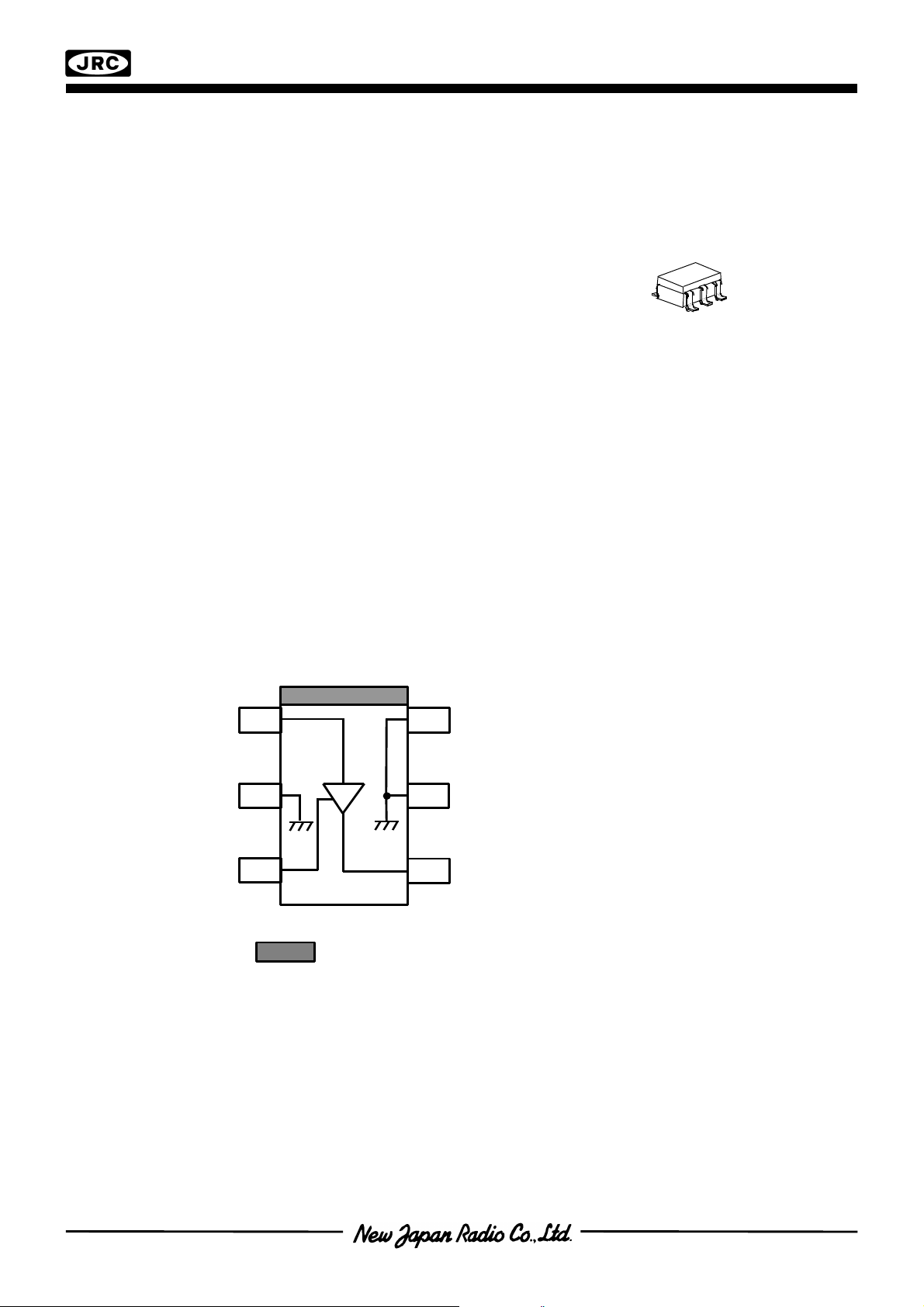
Pin connection
nGENERAL DESCRIPTION nPACKAGE OUTLINE
NJG1308F is a GaAs MMIC Driver-Amplifier for 800MHz-
1.9 GHz band of Cellular phone System.
It features a low current consumption and a high gain.
Small MTP6 package is adopted.
nFEATURES
lLow supply voltage operation +3.0V typ.
lLow current consumption 15mA typ. @P
lHigh gain 18dB typ. @f=938MHz
16dB @f=1441MHz
14dB @f=1900MHz
lPout at 1dB Gain Compression point +12dBm typ. @f=938MHz
+11dBm typ. @f=1441/1900MHz
lpackage MTP6
nPIN CONFIGURATION
=+8dBm
out
F TYPE
(Top View)
1
2
3
Note: is a package orientation mark.
6
1.RF
2.GND
5
3.BPC
4.RF
5.GND
6.GND
4
in
out
& V
DD

NJG1308F
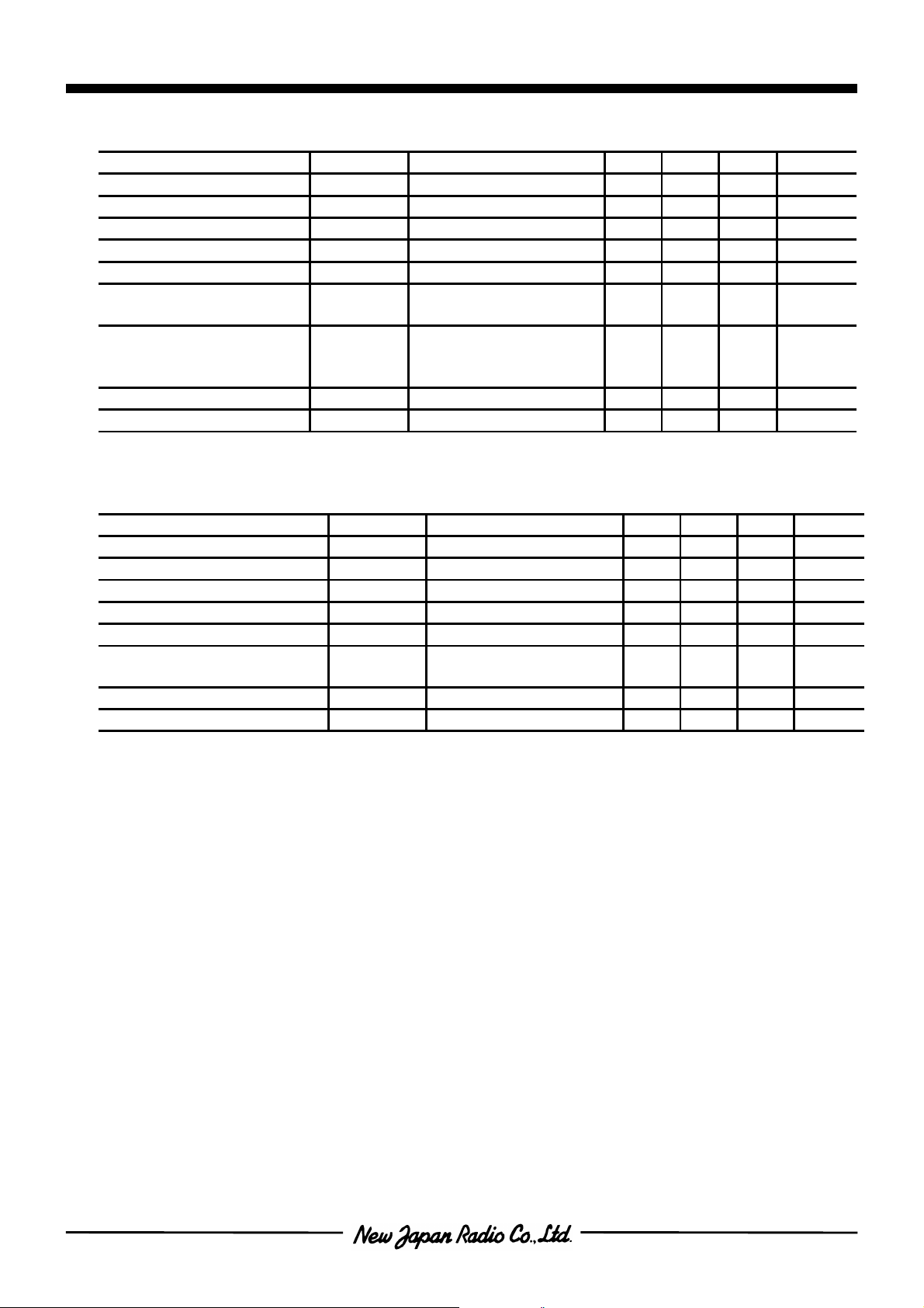
nABSOLUTE MAXIMUM RATINGS
(Ta=+25°C, Zs=Zl=50Ω)
PARAMETER SYMBOL CONDITIONS RATINGS UNITS
Drain Voltage V
Input Power P
Power Dissipation P
Operating Temperature T
Storage Temperature T
DD
opr
stg
in
D
VDD=3V 15 dBm
6 V
300 mW
-40~+85 °C
-55~+150 °C
nELECTRICAL CHARACTERISTICS 1(Application circuit 1)
(Ta=+25°C, Zs=Zl=50Ω)
PARAMETER SYMBOL CONDITIONS MIN TYP MAX UNITS
Operating Frequency Freq VDD=3.0V 915 938 960 MHz
Drain Voltage V
Operating Current I
DD
DD
VDD=3.0V, P
=+8dBm - 15 21 mA
out
2.7 3.0 5.0 V
Small Signal Gain Gain VDD=3.0V, Pin=-10dBm 15 18 21 dB
Gain Flatness G
Pout at 1dB Gain
Compression point
flat
P
-1dB
Adjacent Channel
Leakage Power
P
acp
(PDC Regulation)
Input VSWR VSWR
Output VSWR VSWR
VDD=3.0V, Pin=-10dBm - 0.5 - dB
VDD=3.0V - +12 - dBm
VDD=3.0V, P
offset=50kHz
=+8dBm
out
- -60 - dBc
Pin;π/4 DQPSK
VDD=3.0V - 1.5 -
i
VDD=3.0V - 1.5 -
o
nELECTRICAL CHARACTERISTICS 2 (Application circuit 2)
(Ta=+25°C, Zs=Zl=50Ω)
PARAMETER SYMBOL CONDITIONS MIN TYP MAX UNITS
Operating Frequency freq VDD=3.0V 1429 1441 1453 MHz
Drain Voltage V
Operating Current I
DD
DD
VDD=3.0V, P
=+8dBm - 15 21 mA
out
2.7 3.0 5.0 V
Small Signal Gain Gain VDD=3.0V, Pin=-10dBm 13 16 19 dB
Gain Flatness G
Pout at 1dB Gain
Compression point
flat
P
-1dB
Adjacent Channel
Leakage Power
P
acp
(PDC Regulation)
Input VSWR VSWR
Output VSWR VSWR
VDD=3.0V, Pin=-10dBm - 0.5 - dB
VDD=3.0V - +11 - dBm
VDD=3.0V, P
offset=50kHz
=+8dBm
out
- -60 - dBc
Pin; π/4 DQPSK
VDD=3.0V - 1.5 -
i
VDD=3.0V - 1.5 -
o
NJG1308F
nELECTRICAL CHARACTERISTICS 3 (Application circuit 3)
(Ta=+25°C, Zs=Zl=50Ω)
PARAMETER SYMBOL CONDITIONS MIN TYP MAX UNITS
Operating Frequency freq VDD=3.0V 1890 1900 1920 MHz
Drain Voltage V
Operating Current I
DD
DD
VDD=3.0V, P
=+8dBm - 15 21 mA
out
2.7 3.0 5.0 V
Small Signal Gain Gain VDD=3.0V, Pin=-10dBm 11 14 17 dB
Gain Flatness G
Pout at 1dB Gain
Compression point
flat
P
-1dB
Adjacent Channel
Leakage Power
P
acp
(PHS Regulation)
Input VSWR VSWR
Output VSWR VSWR
VDD=3.0V, Pin=-10dBm - 0.5 - dB
VDD=3.0V - +11 - dBm
VDD=3.0V, P
offset=600kHz
=+8dBm
out
- -60 - dBc
Pin; π/4 DQPSK
VDD=3.0V - 1.5 -
i
VDD=3.0V - 1.5 -
o
nELECTRICAL CHARACTERISTICS 4 (Application Circuit 4)
(Ta=+25°C, Zs=Zl=50Ω)
PARAMETER SYMBOL CONDITIONS MIN TYP MAX UNITS
Operating Frequency freq VDD=3.0V 1750 1765 1780 MHz
Supply Voltage V
Operating Current I
DD
DD
VDD=3.0V, P
=+8dBm - 15 - mA
out
2.7 3.0 5.0 V
Power Gain Gain VDD=3.0V, Pin=-10dBm - 14 - dB
Gain Flatness G
Pout at 1dB
Compression point
flat
P
-1Db
Input VSWR VSWR
Output VSWR VSWR
VDD=3.0V, Pin=-10dBm - 0.5 - dB
VDD=3.0V - +11 - dBm
VDD=3.0V - 1.5 -
I
VDD=3.0V - 1.5 -
o

NJG1308F
nTYPICAL CHARACTERISTICS 1 (Application Circuit 1)
 Loading...