

JRC NJG1301V Datasheet
NJG1301V
MEDIUM POWER AMPLIFIER GaAs MMIC
NJG1301V
V Type
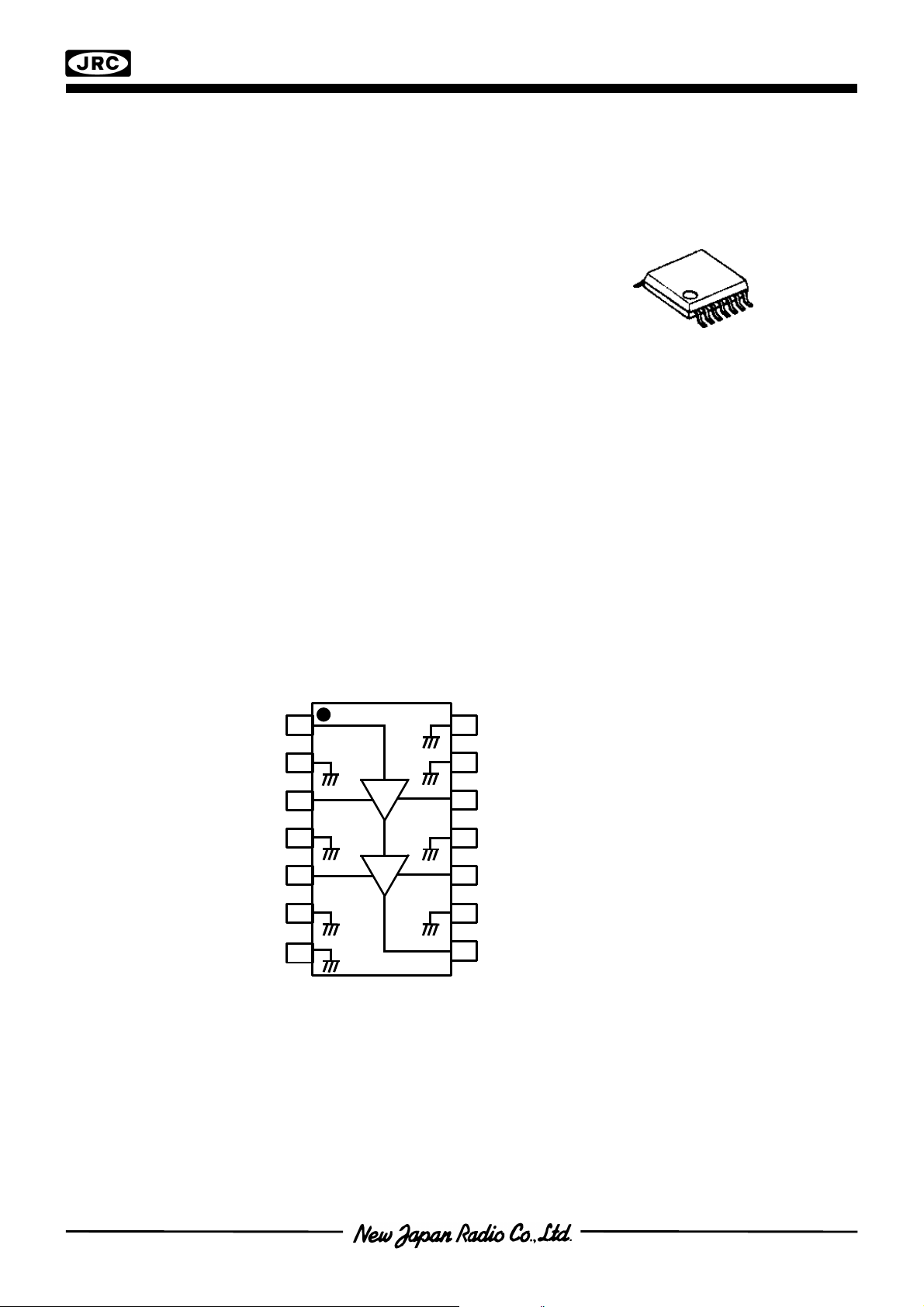
nGENERAL DESCRIPTION nPACKAGE OUTLINE
NJG1301V is a medium power amplifier which is
designed for use of output stage of Japanese
PHS and digital wireless phone.
NJG1301V features low operating voltage, high
efficiency, and comes with, internal input and output matching
circuit and very small SSOP package. This amplifier is operated
up to 21dBm output level with very low noise generation.
nFEATURES
lLow operating voltage +3.0V typ.
lLow current consumption 185mA typ. @f=1.9GHz, P
lLow distortion (ACP) -60dBc typ. @f=1.9GHz, P
lReduction of redact parasitic oscillation
lInput and output internal matching circuits
lPackage SSOP14
nPIN CONFIGURATION
=21dBm
out
=21dBm
out
(Top View)
1
2
3
4
5
6
7
14
13
12
11
10
9
8
Pin connection
1.RFin8.RF
2.GND 9.GND
3.V
GG1
4.GND 11.GND
5.V
GG2
6.GND 13.GND
7.GND 14.GND
10.V
12.V
out
DD2
DD1
- 1 -
NJG1301V
nABSOLUTE MAXIMUM RATINGS
DD1,VDD2
GG1,VGG2
(Ta=+25°C, Zs=Zl=50Ω)
PARAMETER SYMBOL CONDITIONS RATINGS UNITS
Drain Voltage V
Gate Voltage V
Input Power P
Power Dissipation P
Operating Temperature T
Storage Temperature T
in
D
opr
stg
V
GG1,VGG2
V
DD1,VDD2
V
DD1,VDD2
=-0.9V 6 V
=-3.0V -4 V
=-3.0V, V
At on PCB boad
GG1,VGG2
=-0.9V 10 dBm
600 mW
-30~+85 °C
-40~+150 °C
nELECTRICAL CHARACTERISTICS
(Ta=25°C, Zs=Zl=50Ω)
PARAMETER SYMBOL CONDITIONS MIN TYP MAX UNITS
Operating Freq. freq V
Drain Voltage V
Gate Voltage V
Idle Current *1 I
Operating Current *1 I
Gate Current *2 I
DD1,2
GG1,2
idle
DD
GG
Small Signal Gain Gain V
Gain Flatness G
Pout at 1dB Gain
Compression point
Adjacent Channel
Leakage Power 1
Adjacent Channel
Leakage Power 2
Input VSWR VSWR
flat
P
-1dB
P
1
acp
P
2
acp
i
Load VSWR Tolerance -
=3.0V 1.89 - 1.92 GHz
DD1,2
2.9 3.0 5.0 V
V
=3.0V, I
DD1,2
V
=3.0V, RF No signal 165 170 175 mA
DD1,2
V
=3.0V, P
DD1,2
V
=3.0V, P
DD1,2
=3.0V, I
DD1,2
V
=3.0V, I
DD1,2
V
=3.0V 21 22 - dBm
DD1,2
V
=3.0V, P
DD1,2
offset=600kHz, Pin; π/4 DQPSK
V
=3.0V, P
DD1,2
offset=900kHz, Pin; π/4 DQPSK
V
=3.0V - - 2.2
DD1,2
V
=3.0V, P
DD1,2
Load VSWR=4:1, All phase
=170mA -1.25 -0.9 -0.6 V
idle
=21dBm 170 185 195 mA
out
=21dBm -150 -70 - uA
out
=170mA 20 23 26 dB
idle
=170mA 0 0.5 1.0 dB
idle
=21dBm
out
=21dBm
out
=21dBm
out
- -60 -55 dBc
- -65 -60 dBc
Parasitic Osc. vs Fundamental
Signal Level -60dBc Max.
- 2 -
*1: Total current of V
*2: Total current of V
terminal and V
DD1
terminal and V
GG1
terminal
DD2
terminal
GG2
NJG1301V
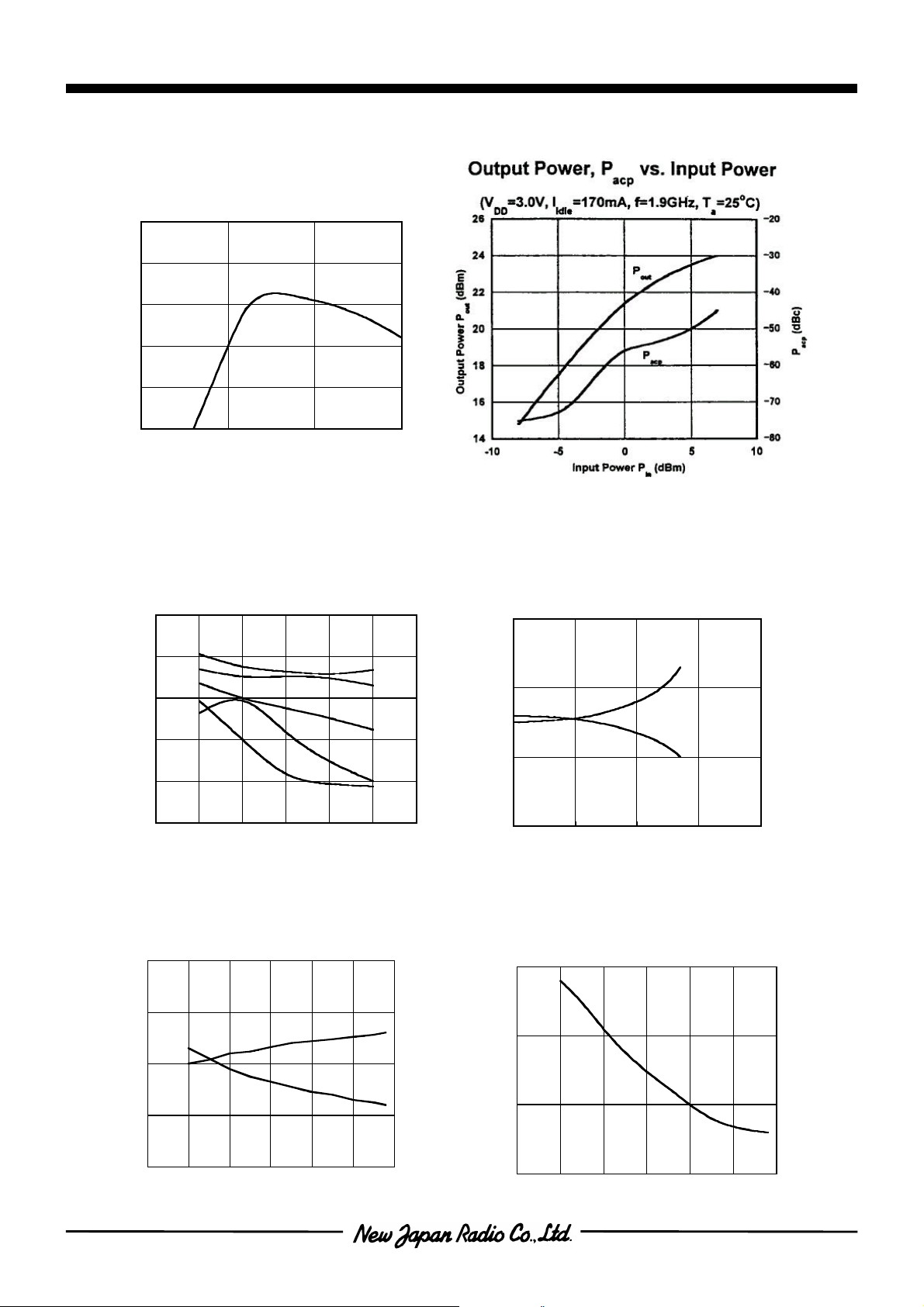
nTYPICAL CHARACTERISTICS
-20
idle
Operating Current vs. Ambient Temperature
acp
Gain vs. Frequency
(VDD=3.0V, IDD=170mA, VGG=-0.71V, Ta=25oC )
40
30
20
Gain (dB)
10
0
-10
0.0 1.0 2.0 3.0
Frequency f (GHz)
P
vs. Operating Current vs. V
acp
(P
=21dBm ,f=1.9GHz, Ta=25oC)
-50
-55
-60
(dBc)
acp
-65
P
-70
-75
140 150 160 170 180 190 200
Gain, P
(VDD=3.0V, I
28
26
24
Gain (dBm)
22
out
Operating Current IDD (mA)
vs. Ambient Temperature
=170mA, P
idle
=21dBm, f=1.9GHz)
out
P
acp
Gain
VDD=2.9V
4.0V
3.0V
3.3V
5.0V
-55
-60
DD
(dBc)
acp
P
Operating Current, Gate Current
vs. Input Power
(VDD=3.0V, I
250
(mA)
200
DD
150
Operating Current I
100
-10 -5 0 5 10
(VDD=3.0V, I
190
(mA)
185
DD
180
Operating Current I
=170mA, f=1.9GHz ,Ta=25oC)
I
DD
I
Input Power Pin (dBm)
=170mA, P
idle
=21dBm, f=1.9GHz)
out
10
0
( uA)
GG
GG
-10
Gate Current I
20
-40 -20 0 20 40 60 80
Ambient Temperature Ta (oC)
-65
175
-40 -20 0 20 40 60 80
Ambient Temperature Ta (oC)
- 3 -
 Loading...