


NJG1106KB2
-
800MHz BAND LNA GaAs MMIC
n
GENERAL DESCRIPTION
NJG1106KB2 is a low noise amplifier GaAs MMIC
designed for 800MHz band cellular phone handsets.
This amplifier provides low noise figure of 1.3dB and
low current consumption of 3mA at low supply voltage
of 2.7V.
NJG1106KB2 includes internal self-bias circuit and
input DC blocking capacitor in a ultra small and ultra
thin package of FLP6-B2.
n
FEATURES
lLow voltage operation +2.7V typ.
lLow current consumption 2.5mA typ.
lSmall signal gain 17dB typ. @f=820MHz
lLow noise figure 1.3dB typ. @f=820MHz
lHigh Input IP3 -4dBm typ. @f=820.0+820.1MHz
lHigh Output IP3 +13dBm typ. @f=820+820.1MHz
lUltra small & ultra thin package FLP6-B2 (Mount Size: 2.1x2.0x0.75mm)
n
PIN CONFIGURATION
n
PACKAGE OUTLINE
NJG1106KB2
KB2 Type
(Top View)
4
5
AM P
6
Note: Specifications and description listed in this catalog are subject to change without prior notice.
3
2
1
PIN CONNECTION
1.RF
2.GND
3.EXTCAP
4.GND
5.GND
6.RF
Package orientation mark
out
in
- 1
NJG1106KB2
n
ABSOLUTE MAXIMUM RATINGS
PARAMETER SYMBOL CONDITIONS RATINGS UNITS
(Ta=+25°C, Zs=Zl=50Ω)
Drain Voltage V
DD
6.0 V
Input Power Pin VDD=2.7V +15 dBm
Power Dissipation P
Operating Temp. T
Storage Temp. T
n
ELECTRICAL CHARACTERISTICS
D
opr
stg
Tj=125°C, mount on PCB
FR4 20X20X0.2mm
450 mW
-40 ~ +85 °C
-55 ~ +125 °C
(VDD=2.7V, f=820MHz, Ta=+25°C, Zs=Zl=50Ω)
PARAMETER SYMBOL CONDITIONS MIN TYP MAX UNITS
Operating frequency freq 800 820 1000 MHz
Drain voltage V
Operating current I
DD
DD
RF OFF - 2.5 3.4 mA
2.5 2.7 5.5 V
Small signal gain Gain 15.0 17.0 19.0 dB
Gain flatness G
flat
f=810~885MHz - 0.5 1.0 dB
Noise figure NF - 1.3 1.5 dB
Pout at 1dB gain
compression point
Input 3rd order
Intercept point
Output 3rd order
Intercept point
RF Input port
VSWR
RF Output port
VSWR
P
-1dB
VDD=2.7V, f=820MHz -4.0 0.0 - dBm
IIP3 f=820.0+820.1MHz -8.0 -4.0 - dBm
OIP3 f=820.0+820.1MHz +9.0 +13.0 - dBm
VSWR
VSWR
VDD=2.7V, f=820MHz - 1.5 2.0
i
VDD=2.7V, f=820MHz - 1.5 2.0
o
- 2 -
NJG1106KB2
n
TERMINAL INFORMATION
Pin Function Description
RF output and voltage supply pin. External matching circuits and a bypass
1 RFout
2,4,5 GND
3 EXTCAP
6 RFin
capacitor is required. L4 is a RF choke inductor and C1 is a DC blocking
capacitor. These elements are used as output matching circuit. C2 is a bypass
capacitor. (Please refer to “RECOMMENDED CIRCUIT”)
Ground pin. To keep good RF grounding performance, please use multiple via
holes to connect with ground plane and this pin.
An external bypass capacitor is required. (Please refer to “RECOMMENDED
CIRCUIT”)
RF input pin. A DC blocking capacitor is not required. An external matching circuit
is required. (Please refer to “RECOMMENDED CIRCUIT”)
- 3 -
NJG1106KB2
n
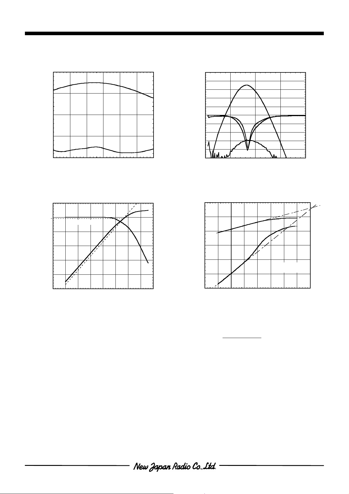
TYPICAL CHARACTERISTICS
NJG1106KB2 Gain,NF vs. Freq
VDD=2.7V,IDD=2.9mA,Ta=25oC
20
Gain
15
10
Gain (dB)
5
NF
0
700 750 800 850 900 950 1000
freq (GHz)
NJG1106KB2 Pout,Gain vs. Pin
VDD=2.7V, IDD=2.9mA, Freq=820MHz, Ta=25oC
5
0
-5
Gain
P-1dB=-0.5dBm
3.0
2.5
2.0
1.5
1.0
20
15
NJG1106KB2 S11,S21,S12,S22 vs. Freq
25
20
15
10
NF (dB)
-5
-10
S11,S21,S22 (dB)
-15
-20
-25
VDD=2.7V, IDD=2.9mA, Freq=820+820.1MHz, Ta=25oC
20
-20
VDD=2.7V, IDD=2.9mA, Ta=25oC
S21
5
0
0 500 1000 1500 2000
S11
S22
S12
Freq (GHz)
NJG1106KB2 Pout,IM3 vs. Pin
0
Pout
50
40
30
20
10
0
-10
-20
-30
-40
-50
S12 (dB)
-10
Pout (dBm)
-15
-20
-25
-45 -40 -35 -30 -25 -20 -15 -10 -5
Pout
Pin (dBm)
10
5.0
Gain (dB)
-40
Pout (dBm)
-60
-80
-100
-45 -40 -35 -30 -25 -20 -15 -10 -5
IM3
OIP3=+13.7dBm
IIP3=-4.1dBm
Pin (dBm)
Equations of OIP3 and IIP3
=3OIP
3IM-Pout×3
2
Gain-3OIP=3IIP @ Pin=-40dBm
- 4 -
 Loading...