

Page 1
2 REV.
INSTRUCTION
MANUAL
RECEIVER
o+
O*
@
flrytnadioCo.,Ild.
Page 2
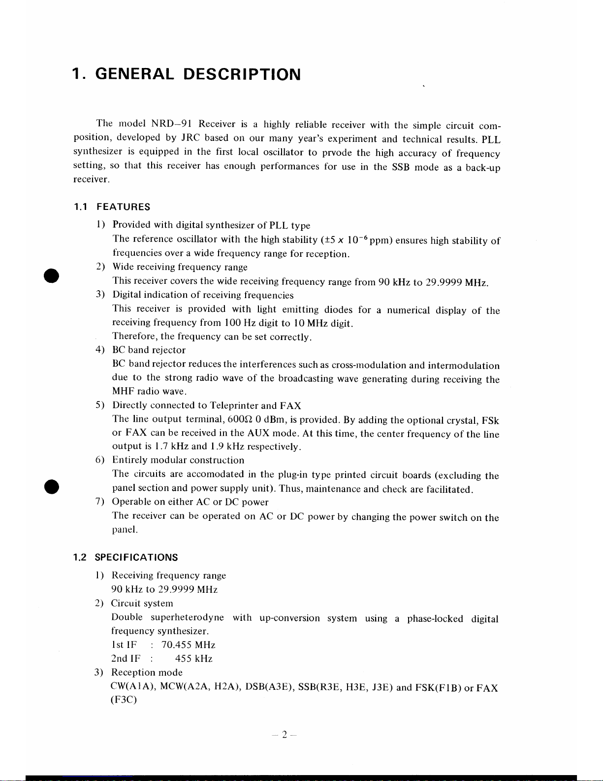
MODEL
NRD-91
RECEIVER
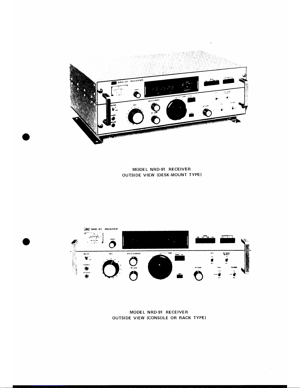
OUTSIDE
VIEW
(DESK-MOUNT
TYPE)
#
û
o
o
ôffiË
MODEL NRD-91 RECEIVER
OUTSIDE VIEW
(CONSOLE
OR
RACK TYPE)
ô
Page 3
CONTENTS
CAUTION
1. GENERAL
DESCRIPTION
1.1
FEATURES
1.2
SPEC|F|CAT|ONS
. . . . . .
2.
COMPOSTTTON
2.1
STANDARDCOMPOSITION
2.2
oPTtONS
2
2
2
5
5
5
3.
INSTALLATION
3.1
INSTALLATION
3.2
ANTI-INDUCTION
OF THE
TRANSMITTING
WAVE
3.3
CONNECTION
OF EXTERNAL
LINES
3.4
HOW
TO
MOUNT
AUX
CRYSTAL
OPE RATION
4.1
OPERATION PANEL
4.2
OPERATINGPROCEDURES
4.2.1
Basic
Operation
of
SSB Reception
4.2.2
Basic Operation
of
CW
Reception
4.2.3
Operation
of DSB
Reception
4.2.4
Operation
of FSK
Reception
4.2.5
Operation
of FAX
Reception
. .
.
4.2.6
Further
Operation
CIRCUIT DESCRIPTION
5.1
RECEIVING SECTION
5.2
LOCAL SIGANL
GENERATOR
SECTION
5.3
PANEL
SECTION
5.4
POWER
SUPPLY
SECTION
MAINTENANCE
6.1
GENERAL
6.2
GENERAL MAINTENANCE
AND CHECK
.
6.3 TROUBLESHOOTING
6.3.1 Decline of the
Sensitivity
6
6
6
6
9
l0
l0
t2
l3
l3
l3
t4
t4
l5
t6
t6
l6
t7
l8
t9
t9
t9
20
20
4.
5.
6.
-l-
Page 4
6.3
.2 No
Sound . . .
2L
6.3.3
NoiseandBeat
....
.21
6.3.4 Interference by the
Transmitter
of
Your
Station
22
6.3.5
Intermodulation
23
Appendixed Drawings
Parts Arrangements
Block
Diagram
Outline
Drawing
Circuit
Diagrams
Speaker
Unit
-ll-
Page 5
CAUTION
l. Read
this instruction
manual thoroughly before turning on
this receiver.
2.
When
connecting
the BK cable and
other cables, refer to Fig. 3.3 of
Paragraph
3.3.
3. When the
transmitting
waves are strongly
induced in the receiving antenna, take the
counter-
measure
described
in Paragraph 3.2.
4.
Do not turn
semifixed
resistors, high frequency transformers, trimmer capacitors, etc.
mounted
on
the
printed
circuit board
unless
absolutely
necessary,
because
they
are all
preadjusted
at the
factory.
5.
If
the
MHz
knob
is set at inadequate
position,
the
receiver is muted.
Therefore, the
MHz
knob must be
set
correctlv.
6. This
receiver
has low-voltage-operable
ICs and transistors. Be sure to turn
off both
power
switohes
when connecting
or removing the
printed
circuit board and cables to external
equipments.
1. If
the
AUX
mode
is
selected at a condition
where
additional
crystal
is
not
provided,
the
receiver operates
actually
in the DSB mode even though the AUX
mode
is indicated on the
front
panel.
8. The
illumination
of LEDS
(Receiving
frequency,
Mode
and Bandwidth
indicators) is
gradually
reduced as
turning
f-DlMMEil
knob
counterclockwise.
Finally they
fade
out
completely
at the minimum
position.
().
When
the ntode
is
except
SSB
and Frequency
Display
shows
the tiequency
between
000.0kH2
and 001.4kH2,
MHz
LED
displays the
frequerlcy
obtained by adding
lMHz to
the
display
of MHz Selector
Switch.
In
such
a case, Receiver
receives the frequency dis-
played
by LED.
10. When
the rnode
is except SSB,
the upper
limit of
the received
fiequency
to
be
displayed
is
3000
| .4kHz
and
the
lower limit
is
001
.5
kHz.
-l-
Page 6
1.
GENERAL
DESCRIPTION
The
model
NRD-91
Receiver
is a highly
reliable
receiver
with the
simple
circuit
com-
position,
developed
by JRC
based
on
our many
year's
experiment
and
technical
results.
PLL
syuthesizer
is equipped
in
the first
local
oscillator
to
prvode
the high
accuracy
of
frequency
setting,
so that
this receiver
has
enough
performances
for
use
in the
SSB mode
as a
back-up
receiver.
1.1 FEATURES
I
)
Provided
with
digital
synthesizer
of PLL
type
The reference
oscillator
with
the high
stability
(t5
x
l0-6ppm)
ensures
high
stability
of
fiequencies
over
a
wide frequency
range
for
reception.
2)
Wide
receiving frequency
range
This receiver
covers
the wide
receiving
frequency
range
from
90 kHz
to 29.9999
MHz.
3)
Digital
indication
of
receiving
frequencies
This receiver
is
provided
with
light
emitting
diodes
for
a numerical
display
of the
receiving
frequency
from
100
Hz
digit
to l0
MHz
digit.
Therefore,
the frequency
can be set
correctly.
4)
BC band
rejector
BC band rejector
reduces
the interferences
such
as
cross-modulation
and intermodulation
due to
the
strong radio
wave
of
the
broadcasting
wave
generating
during
receiving
the
MHF
radio
wave.
5) Directly
connected
to
Teleprinter
and FAX
The line output
terminal,
600St
0 dBm,
is
provided.
By
adding the
optional
crystal, FSk
or
FAX
can be received
in
the
AUX mode.
At this time,
the
center
frequency
of
the line
output
is 1.7
kHz
and l.9 kHz
respectively.
6) Entirely
modular
construction
The
circuits are accomodated
in
the
plug-in
type
printed
circuit
boards
(excluding
the
panel
section
and
power
supply
unit).
Thus, maintenance
and
check are
facilitated.
1)
Operable
on
either
AC or
DC
power
The receiver
can be
operated
on
AC
or DC
power
by changing
the
power
switch
on
the
panel.
1.2
SPECIFICATIONS
I ) Receiving frequency
range
9O kHz
to 29.9999
MHz
2)
Circuit system
Double
superheterodyne
with
up-conversion
system
using
a
phase-locked
digital
frequency
synthesizer.
I st
lF- : 7 0.45
5 MHz
2nd IF
:
455 kHz
3)
Reception
mode
CW(AlA),
MCW(A2A,
HzA),
DSB(A3E),
SSB(R3E, H3E,
J3E)
and FSK(FlB)
or FAX
(F3C)
,2-
Page 7
1)
But
FSK and
FAX are
option.
4)
Receiving
frequency
indication
{
Light
emitting
diode
for six-digit
numerical
display
(
I 0
MHz- to
100
Hz- digit)
5)
Tuning
method
Continuous
tuning
with MHz
knob,
UP/DOWN
switch
and TUNE
knob
of l}kHzl
rotation
(minimum
steP:
100 Hz)
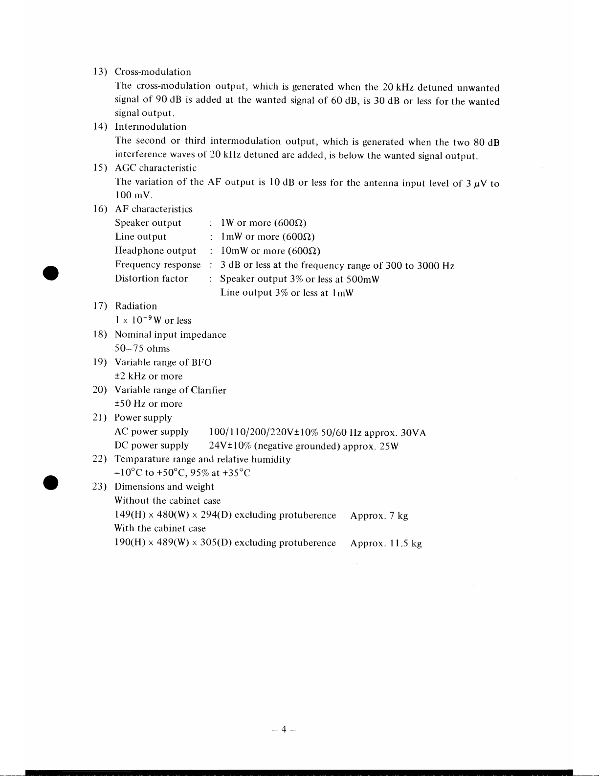
6) Sensitivity
------_-_
Mode
Receivùg
-----
frequency
AIA
A3E
J3E
90-
199.9
kHz
2O
pY
or
less 60
pV
or
less
200-
1599.9
kHz
l0
pV
or
less
30
pV
or
less
1.6-29.9999
MHz
2
pY
or
less
6
pV
or
less
3
pV
or less
15çt
standard
signal
generator
is
directly
connected
to
the
antenna
terminal
S/N
20
dB,
Output 100
rnW,
Bandwidth
3 kHz,
400 Hz
30%
modulation.
Selectivity
-\!tenuation
BandwidÈ=--=-
6 dB
bandwidth
60
dB
bandwidth
6
kHz
4.4
kHz
or
more
l0
kHz
or
less
3
kHz 2-2.6
kHz
6 kHz
or
less
0.5
kHz
0.5-
1.0
kHz
3 kHz
or less
8)
Frequency
stability
I hour
after
l5-1rilute
preheating
t
10 x l0-6
or
less,
but
under
the
condition
where
the
receiving
frequency
is 1.6
MHz or
more
in
the SSB
mode.
9)
Image
rejection
ratio
60 dB
or
more
)
l0)
IF
rejection
ratio
60
dB
or
n-lore
I l)
Spurious
response
60
dB or
more
12) Blocking
The
input
level
of
the
unwanted
signal
is more
than
l0 mV
which
suppress
the
output
level
of
the
wanted
signal
by 3
dB,
under
a condition
where
the
unwanted
signal
is
separated
by
2OkHz
or
more
from
the
wanted
signal
of l0pV.
(SSB
mode,3kHz,
AGC
ON)
!
't
'.
1
-'"
r
û''1
i._;-
\
.'J
'!."1
.
!
I.
d'l
o,t t,g
1,'i:
-3-
Page 8
l3)
Cross-modulation
The cross-modulation
output,
which
is
generated
when
the 20 kHz
detuned
unwanted
signal
of 90
dB
is added
at the
wanted
signal
of
60 dB,
is
30 dB
or
less fbr
the
wanted
signal
or"rtput.
I4)
Interrnodulation
The
second or
third intermodulation
output,
which
is
generated
when
the
two 80
dB
interference
waves of 20
kHz
detuned
are
added,
is
below
the wanted
signal
output.
l5)
AGC
characteristic
The variation
of the
AF or-rtput
is l0
dB
or less
for
the
antenna
input
level
of
3
pV
to
100
rnV.
l6)
AF characteristics
Speaker output
Line output
Headphone
output
Frequency
response
Distortion
factor
l1)
Radiation
I x
lO-eW
or less
l8)
Norninal input
impedance
50-75
ohrns
l9)
Variable range
of BFO
!2
kRz
or more
20)
Variable range
of
Clarifier
t50
Hz or
more
2l)
Power
supply
AC
power
supply
100/110/200
l220Ytl0%
50160
Hz
approx. 30vA
DC
power
supply
24V!10'/o
(negative
grounded)
approx. 25W
22)
Temparature range
and
relative
humidity
-10"C
to
+50oC,
9s%
at
+35oC
23)
Dimensions
and
weight
Without the
cabinet case
149(H) x 480(W) x
294(D)
excluding
protuberence
Approx. j ke
With the
cabinet case
190(H) x 489(w) x
305(D) excluding
protuberence
Approx. I1.5
kg
lW or more
(6000)
l
mW
or more
(6004)
lOmW
or more
(6004)
3 dB or
less at
the frequency
range
of 300 to
3000
Hz
Speaker output
3% or
less
at
500mW
Line output
3%
or less
at I mW
-
4-
Page 9
2. COMPOS|TION
2.1
STANDARD COMPOSITION
The composition
of
this
receiver
depends
on its
type,
that is, desk-mount
type or rack
type.
*
Spare
parts
include:
One
each
of BK
relay,
and
fuses.
2.2 OPTIONS
Remarks
Provided
for
only the
desk-mount
type
600a lw
Provided
for
only the
desk-mount
type
t
NRD-9
I
MPBX I
083 2
NVA-92
'ZCJDOOOO5
MPKCO3
I 08
M-P_7
6ZXJD5IO43
Receiver
Cabinet case
Speaker
Power cable
BK cable
Instruction manuâl
ANT Connector
Spare
parts
Test data
Item
Model or
code Remarks
Headphones
I
ST-3
|
600 ohms
DC
power
cable
MPKCOI74I I For
DC24V
Extension card
fbr maintenance I CMH-330
|
Used for
checking
each
PC
boad
| |
in
operation
Additional
cr1'stal
| |
Crystal to
be mounted
in
the
AUX
position
In case of FSK 456.7 kHz
In
case
of
FAX
456.9 kHz
-5--
Page 10

3.
INSTALLATION
3.1
INSTALLATION
(
I
)
When installing the receiver
on the
l9-inch
standard
rack,
place
the
guide
bolt
provided
on the
side
of
the
chassis
on
the rails,
and
push
the receiver
to the
inside
of the rack.
Then, flx
the receiver
in
position
by
screwing
the
5-rnm
screws
through
the mounting
holes
at two
positions
of
both
left
and right
sides
of the front
panel.
(2)
When installing
the
receiver
on the
desk,
Llse
the special
cabinet
(optionally
available
on
separate order).
Attaclt the slide rails
(supplied
with
the
cabinet
case) onto
left
and right
sides
of
chassis
of the receiver
and mount
the receiver
in the
cabinet
case.
Fix
the receiver
to the
cabinet
case
by
screwing
the 5-mm
screws
through
four mounting
holes
on
the front
panel.
3.2 ANTI-INDUCTION
OF THE
TRANSMITTING
WAVE
When the receiver
is operated
with
a
paired
transmitter,
it sometimes
happens
that
the
transmitting
wave of own
station is
induced
in
the receiving
antenna.
When
the induction
current
of the
transmitting
waves is
I ampere
or less,
the receiver
is
protected
by the built-in
input
protective
circuit.
But if the
induction
current
exceeds
I
anlpere, the input
circuit
of
the receiver
may
be
burnt out.
When
the
receiving
antenna suf-fers
fiom
such
an excessive
induction
current, move
the
receiving
antenna
as
far
as
possible
trom
the
transmitting
antenna, or
insert
the anti-inducer
in
series
betweetr
the receiving
autenna
and
antenna input
connector
as shown in Fig.3.l.
Receiving
antenna
l00v
60w 100v
I
60w
I
PL1
01 PL1
02
|
l/\l
i- ç?(e}
-{çf-'-_----_--..
a-f
#to'
Q
-
to
tne[Àtrtrlconnecter
rl
ll
L_
__J
AW-01
'18
Anti-inducer
Fig. 3.1
Protection
of the
Receiver
by the
Anti-inducer
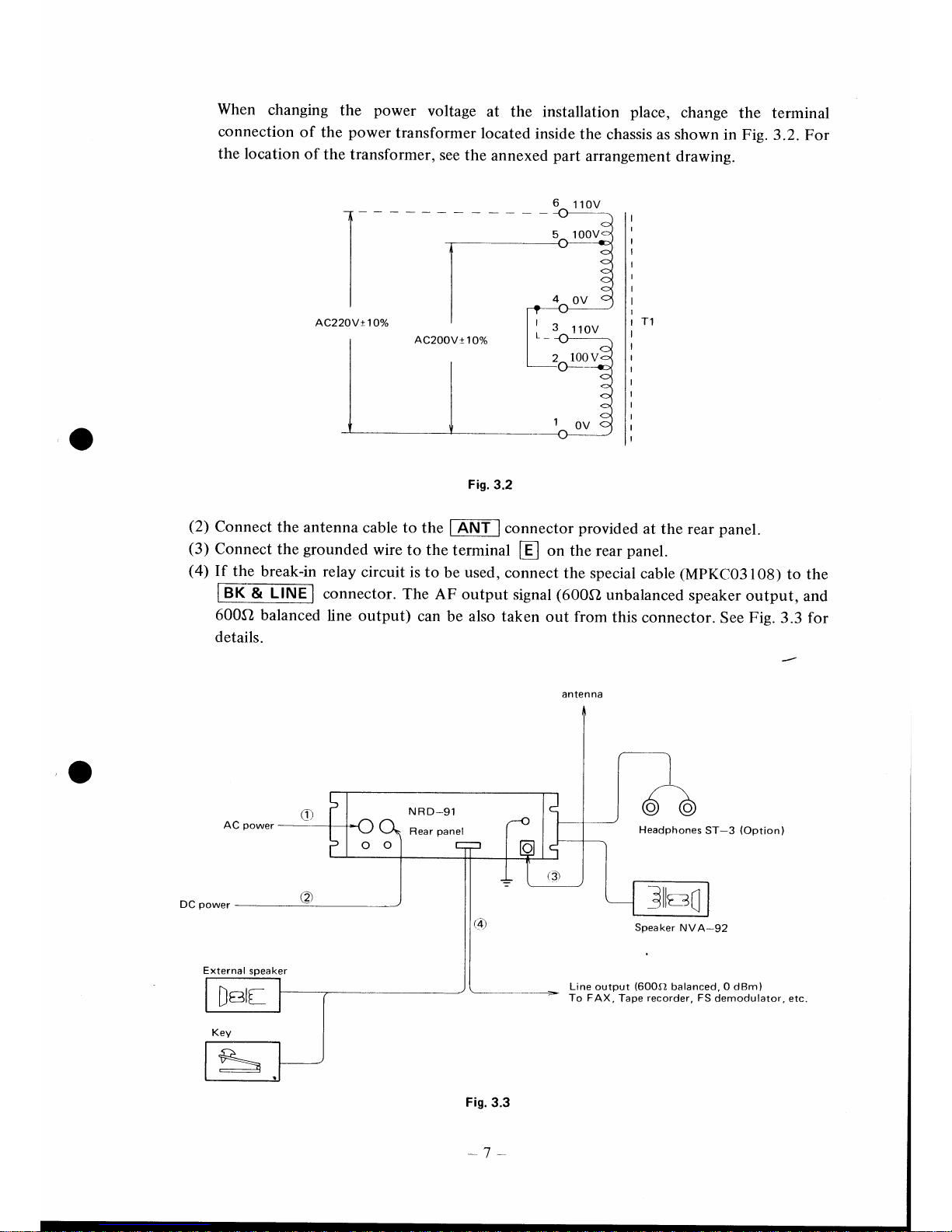
3.3 CONNECTION
OF
EXTERNAL
LINES
(l)
This
receiver is
operable
in either
ACl00tlO%
(50/60
Hz)
or
DC24V!lO%.
For AC
operation, conrlect the
AC
power
cable to
[nC
tO()Vl
located
on
the
rear
panel
of the
nrair-t
tratne.
For DCI
operation,
connect
the
DC
power
cable
MPKCQ|74I
(option)
to
LO_.9_?4
located
on the rear
panel
of
the main frame.
-
6,
Page 11
o
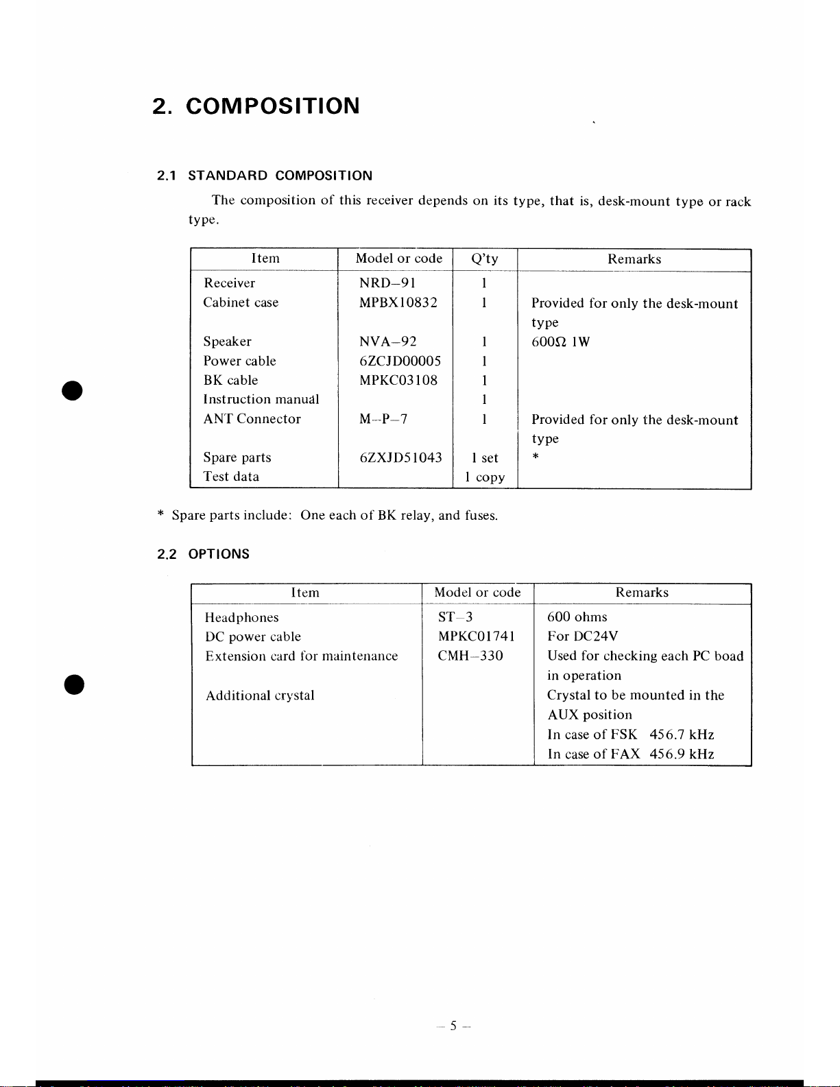
When
changing
the
power
voltage
at the
installation
place,
change
the terminal
connection
of
the
power
transformer
located
inside
the
chassis as shown
in Fig.
3.2. For
the
location
of the
transformer,
see the
annexed
part
arrangement
drawing.
Fis.3.2
(2)
Connect
the
antenna
cable to
the | ,ANT-I
connector
provided
at the
rear
panel.
(3)
Connect
the
grounded
wire
to the
terminal
H
on the rear
panel.
(4)
If the
break-in
relay
circuit
is to
be used,
connect the
special
cable
(MPKCO3
108)
to
the
tBK
&
Lin[Êl
connector.
The AF
output
signal
(600S,
unbalanced
speaker
output,
and
600O
balanced
line
output)
can be
also taken
out
from
this connector.
See Fig.
3.3 for
details.
AC
power
Headphones
ST*3
(Option)
DC
power
I
I
I
I
I
I
rT1
I
I
I
I
I
I
I
I
1Oo/o
I
I
I
I
I
20vAC2
o
E xterna
I
Speaker
NVA-92
Line
output
(600f,l
balanced, 0 dBm)
To FAX.
Tape
recorder,
FS demodulator,
etc.
Fis.3.3
-7
-,
AC200Vr
l Oolo
NRD-91
Rear
panel
?lt- rr
9ilL5t I
\
Page 12
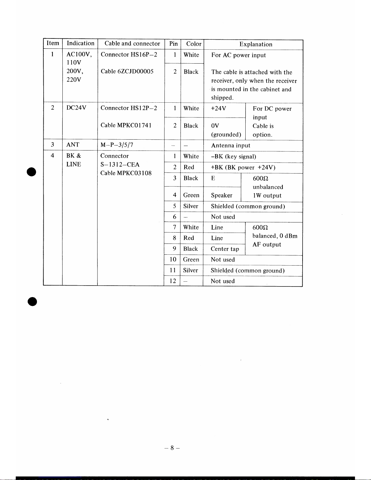
Item
Indication
Cable
and connector
Pin
Color
Explanation
I
AC
I OOV,
r
t0v
200v,
220V
Connector
HS l6P-2
Cable 6ZCJDO0005
I
White For
AC
power
input
The cable
is attached
with the
receiver,
only
when
the receiver
is mounted
in
the cabinet
and
shipped.
2
Black
2
DCz4V
Connector
HS l2P-2
Cable
MPKCO
17
4l
I
White
+24V
For DC
power
input
Cable is
option.
2
Black
OV
(grounded)
3
ANT
M-P-3ls
17
Antenna
input
4
BK&
LINE
Connector
S- 13
I2-CEA
Cable
MPKCO3l08
I
White
-BK
(key
signal)
2
Red
+BK
(BK
power +24Y)
3 Black
E
600s}
unbalanced
lW
output
4
Green
Speaker
5 Silver
Shielded
(common
ground)
6
Not used
7
White
Line
600s,
balanced, 0
dBm
AF output
8 Red
Line
9
Black
Center tap
l0
Green Not
used
ll Silver
Shield.ed
(common
ground)
t2
Not
used
-8-
Page 13
3.4
HOW
TO MOUNT
AUX CRYSTAL
By
adding the crystal to
the AUX mode
position,
the center frequency
of the
line
output can be 1.7 kHz
in case of FSK reception
and I .9
kHz
in FAX
reception
when setting
the frequency
indication
on the
panel
to the wanted receiving frequency,
and
this line
output
can be connected to FS demodulator
or FAX.
The
frequency
of the crystal is
456.7
kHz in FSK reception
and
456.9kH2
in FAX reception.
Since
this receiver
has one
AUX crystal
space,
one of FSK, FAX
or other
desirable
mode is
available.
Please
inform us
of
your
desirable
mode or the
frequency
of the
crystal
when ordering.
Mount
the crystal according to
the
following
procedures.
I
. Insert the crystal into
AUX
(X3)
on CMH
-379
IF
2nd
unit and solder it.
2.
Connect two holes
(AUX)
positioned
near
the
connector
(PlO)
on the
same unit by
means of the
leading wire.
3.
Connect
the speaker and
turn
on the
power.
If
the beat
sound comes out through
the speaker when
setting the
mode
to AUX, the
crystal is mounted
correctly.
Note) The beat
sound can
be easily
known
by
comparing
the noise
in AUX mode
with the noise
in DSB
mode, because the noise increases when
changing the
mode
from
DSB
to AUX.
-9 -
Page 14
4.
OPERATION
4.1
OPERATION
PANEL
[Jmll
runo-sr
lnecrtven
|
| | rr^hr
i:i
!:,
,='11
k-3,--
- |
r
MH,
'-
'-rH,
BANDW'FT"
J
BFO & CLARIFIER
ON
REJECT
0t
OFF
OFF
RF
GAIN
AF
GAIN
AGC
I
pOWER
PEAKER
sr-ow$
/orl
g
OFF/ T
DC
No.
Control
Function
I
Meter
Indicating
the
strength
of the receiving
waves
or
level
of the
AF output
(line
output)
2
DIMMER
knob
Used
for
adjusting
the
brightness
of all LE,Ds.
Adjust
the
brightness
by this knob
according
to
the
circumstance.
LEDs
fade
out
if this knob
is turned
fully
counterclockwise.
Keep
this
in
your
mind
when
using
this receiver.
3
Receiving
frequency
indicator
Displaying
the
receiving
numbers.
In
case of
SSB
displayed
and
in
case of
frequency
is
displayed.
frequency
by
6-digit
numerical
mode,
the
carrier frequency
is
modes
other
than
SSB, the assigned
4
BANDWIDTH
indicator
Displaying
the
bandwidth
of the IF filter
specified
by
the
BANDWIDTH
A
selector
switch
(one
of
0.5 kIHz,3
klHz
and 6 kHz)
5 MODE
indicator
Displaying
the
mode
specified
by the
MODE
switch@
(one
of
SSB, CW,
DSB
and
AUX)
-
l0
-
Page 15
No.
Control
Function
6
MODE selector Used for selecting the
reception *oà.
(one
of
SSB, CW, DSB
and AUX).
When
changing the mode from
one of
AUX,
DSB
and CW to
SSB,
the
frequency obtained
by
subtracting
1.5 kHz from
the
original
frequency
is displayed
on the
frequency indicatorO
. This
is
because that the
carrier
frequency
is displayed in case of SSB
reception.
Since AUX
is option,
make
a special order if
necessary.
If this AUX
mode
is specified when the optional crystal is not mounted,
actual reception mode is DSB even though
the AUX mode
is
indicated by the
MODE
indicator.
1 BANDWIDTH
selector
Selecting the bandwidth of
the
IF
filter
(intermediate
frequency)
(one
of
0.5 kHz,3
kHz
and
6
kHz).
8
METER selector
switch
Selecting
the
content
to be indicated
for
the meter(D.
When
setting this switch to
S,
turning
RF
GAIN
@
fully
clock-
wise, and
setting
the AGC
switch @ to FAST or
SLOW,
the meter
pointer
indicates the
relative signal
strength of
the
HF input of the
receiver.
When
setting
this switch to
LINE, the meter indicates
the line output level
(6000
balanced).
9 SPEAKER
jack
Used
for
connecting
the
special speaker,
NVA-92
or the
speaker
of 600C1 impedance.
l0 PHONES
jack
Used for
connecting
headphone
of 600C2
the optional headphones,
ST-3 or the
impedance.
ll
MHz selector
Used for setting the MHz
digit of the receiving
frequency.
The full rotation
of this knob
covers 30 bands
(
I MHz
step).
t2
BFO & CLARIFIER
knob
Serving
as BFO
adjustment
knob in
case of
CW mode.
This
knob
can vary the frequency of
45 5
kHz
beat oscillator
(BFO)
by more
than
t2
kIIz.
Therefore,
the tone
of the
telegraph signal
can be adjusted.
This
knob
also serves
as a
fine
adjustment knob
(CLARI-
FIER) of
the
receiving tiequency
in SSB
and AUX modes.
This can vary the
center
frequency
of
the oscillating
fiequency by more
than
t50
Hz.
l3 RF GAIN
knob
is
Gain controller
for
the RF
amplifier and IF amplifier.
It
recommended
to adjust according to
the
strength
of
the
receiving
signal for
obtaining the optimum volume.
t4 TUNE
knob Used for
setting the receiving frequency in 100 Hz
steps.
The
full rotation
changes the
receiving frequency
by l0 kHz.
l5
UP/DOWN
switch
Fast forward
switch of the receiving frequency.
While
pressing
UP
(or
DOWN),
the
fiequency
increases
(or
decreases) at a speed
of approx. 125 kHz/second.
-
ll
-
Page 16
No.
Control
Function
t6 LOCK
switch
Used for
locking
the set frequency
electrically
so
as not
to
be
changed
by
careless misoperation.
By setting
this
switch
to the locked
condition
(pressed),
the
receiving
frequency
will
not
be changed
even
though operating
the TUNE
knob
@
and UP/DOWN
switch
@
.
f'or
releasing
the locked
condition,
press
this
switch
again.
l1
AF GAIN
knob
This is a volume
adjustment
knob for
the speaker
or
headphones.
And this
knob
does
not
af'fect the level
of
the
line
output
(600O
balanced) on
the
rear
panel
of
the
receiver.
t8
Attenuator
switch Used for
selecting
the
ON
or
OFF
condition
of the 20
dB
HF
attenuator for
the receiver
input.
Set this
switch
to ON
for
the
better reception
when
the signal is received
at the
near distance
and the desired
signal is interfered
due
to
the
strong neighboring
signals
etc.
But usually,
set this
switch
to the OFF
position.
t9
AGC
switch
Used for
selecting
the
ON or
OFF condition
of the
AGC
circuit
and selecting
the discharging
time
constant.
The FAST
position
is
for
the reception
of DSB
signals,
and the
SLOIV
position
is normally
f
or
the reception
of
CW or
SSB
signal
affected
by
fading.
By setting
this switch
to OFF,
the
AGC circuit
remains
inoperative
and signals
are saturated.
Thus,
control
the
gain
by
the RF GAIN
knob
@
for
the best
receiving
condition.
20
BC BAND
REJECTOR
Set this switch
to
ON
for
the
better reception
when
the
cross-modulation
or
intermodulation
due
to the strong
radio
wave
of the
broadcasting
wave
(525
to 1605
kHz)
interferes
the MHF
reception.
2l POWER
switch
Used for
turning
ON or
OFF the
power.
Also used for
selecting
AC or DC
power
supply.
4.2 OPERATING
PROCEDURES
Before turning
on the
power
switch,
check the following items.
(
I ) Power
voltage check
The
label, which shows the nominal
power
voltage,
is
placed
above the
power
connector
located on the
rear
panel
of
the receiver.
Check
that the
power
voltage
to be
used
is
within the
range of the nominal
value
!lO%.
(2)
Antenna
system check
Check that each connecting
part
of the
antenna cable to
be connected
to
this
receiver
is
firmly
connected. When the antenna
coupler
and antenna
changer are used,
check that
they are correctly
set
*-t2-
Page 17

(3)
Check
of the connectors
on the
rear
panel
Check
that
each connector
and
grounded
wire on the
rear
iranel
of the receiver are
surely
connected.
(4)
Connect
the speaker
or
heaclphone
to
lspeaKf
nl or
IFHONES-I
jack.
4.2.1
Basic Operation
of SSB
Reception
(l)
Set the
tAF
GÀlN
I
knob
to the
position
where the
knob is
turned clockwise
by 4 or 5
graduations
fiom the mininlum
position.
(2)
Set thr
FQ@
switch
to
[Ac]
in
case of the AC
power
supply, or to
E
in case
of
the
DC
power
supply.
(3)
Press ttre
lSSe-l
button
amons
the
ltvtôOf l
switches.
(4)
Set the
desired
receiving
fiequency
by using the
IMHil
knob,
I-UPIDôW-NI
switch and
FÙnel
knob.
(5)
Set
the
t
slow
I
(6)
After
hearing
the desired signal, turn
the
tAFGÀiNl
knob
and
set it for
an
optimum
sound
volume.
(7)
Adjust the BFO & CLARIFIERknob so
as to
set
the tone
the
most natural
to hear.
knob to the maximum
position
and
turn the AGC
switch to
(8)
When the
received radio
wave is not strongly
affected by
fading,
turn the
FF
GAINI
knob slightly counterclockwise and
IAF
GAIN-l knob slightly
clockwise so
as to obtain
the
best S/N
of the
reception
voice.
4.2.2
Basic
Operation of CW
Reception
(Morse
Telegraph)
(
I ) Set tn.
[11tQA|Nl
knob to 4 or 5
graduations.
(2)
Press the
ltw I
button
amons ilre
lrvrooe
I
switches.
(3)
Set the
desired receiving
frequency
by using
the
lMHll
knob,
ttre
IÙP/DOWN-I
switch
utro
lîulrtr
I
knob.
(4)
Press
ttre
lo.s
kHl button
among
th.
M
switches.
(5)
Set the
FFGAINI
knob
almost
to
the center
position
and the
trGôl
switch
to
desired signal, set the volume to the optimum level by
adjusting the
BFO & CLARIFIERknob, set the tone
the
most
pleasant
to hear.
(8)
Adjurt
Inf
Gatwl
nn6
[RF
CÀitrtl so that
S/N
of
the
receiving signal
will be
the best.
(9)
When the
receiving wave is
affected by
fading
or the strong wave
and
weak
wave
are
received
reciprocally, set the
tÀGC-l
switch
to
I-SLôWI
or
|FÀST I
and
turn
the
f
RF
GAINl
knob slightly clockwise.
4.2.3 Operation of
DSB Reception
(l)
Press the
IDSBI
button amons
I
MODTI
switches, and
i6
kHtl
button amons
BANDWIDTH I switches.
(2)
Set the
l-RF
GÂlNl
knob
to the
maximum
position
and set
the
tAGC-l
switch
to
(3)
Set the desired
receiving frequency by using the
f
MHI knob,
IUF/DOWN
lswitch
and
(6)
When
hearing the
Erc4l$
knob
(7)
BV
adjusting
the
knob.
-
t3
-
Page 18
(a)
Bv
adjusting the I AF GAINI knob,
set
the volume
to the optimum
level.
(5)
In case of
strong interference,
press
the
F
kHA button among
BANDWIDTH
switches.
4.2.4 Operation of FSK
Reception
A teleprinter and
FS demodulator
are adaptative
to this receiver
to receive
a
FSK
signal.
Receive
the
FSK
signal in the
following
procedures.
But this mode
is option.
(l)
Press
tn. I nuXl button amons f MoDEl
switches.
(2)
Select the
proper
BANDWIDTH
button in accordance
with
the
frequency
shift width
signal under
reception.
In
case of
the narrow
band
and
modulation speed of
an FSK
direct
printing
telegraph, select
W
and the f RF
CÂiN-l knob
to
the maximum
position
(4)
Set the desired
receiving frequency
by using
th.
[@
knob,
trFDôWNl
switch
and
truNEl
knob.
(5)
After
receiving
the siganl,
adjust tne
[-Âf
GÂt[l knob so
as to
obtain
the
desired
volume,
as
required.
Set the
t
MEaER-l
switch located
on
Adjust
the BFO
&
CLARIFIER
demodulator
deflects
maximumly
and LEDs
of
both MARK
and
SPACE
blink
in
the
sarne
brightness.
Note)
When
perfbrming
the
teletype
communication
by connecting
this receiver
to
the narrow
band direct
printing
terminal, be sure not
to change
the
BANDWIDÏHafter the circuit is connected once. Otherwise, it may happen
that the
phase
is out due to the difference of the
delay
time of the
filter.
4.2.5
Operation
of
FAX
Reception
A
radio facsimile
equipment
is
also adaptative
to
this receiver
to receive
the FAX
signal.
Receive
the
FAX
signal in the following
procedures.
But this mode
is
also option.
(l)
Press
ttre I nUX I button
amons
IMODEI
switches.
(2)
Select the
proper
BANDWIDTH
button in accordance
with the modulation
speed and
frequency
shift width of the
FAX
signal under
reception.
In
case
of the
broad band
facsimile such as weather facsimile,
etc.,
press
F
kHtl
(3)
Set the I AGCI switch
to
tFÂST-l
and
the
FF
GAIN
I
knob
to the
maximum
position
(fully
clockwise).
(4)
Set the
desired receiving
frequency
by using
the
IMHz
I
knob,
I
UffiôWN
I
switch
and
tTut\i-trI
knob.
(5)
After
receiving
the signal,
adjust
11s
l-Af
Celw
Tknob
so
as to
obtain
the desired
volume,
as
required.
(6)AdjusttheknobsothatLEDsfortuning,locatedonthefront
panel
of the facsimile recorder,
[îU
NFTI
ut O
fîulUF2l
wiil
light
the most brilliantly
(3)
Set the
fÀcC-l
switch to
(fully
clockwise).
(6)
(7)
the
front
panel
of the FS
demodulator
to
fTUNtrl.
knob
so that
the
FUruEt
meter
of
the
FS
in the same brightness.
-14 -
Page 19
4.2.6
FurtherOperation
(
I
)
Operation
of ATT.
The
receiving antenna
catches
many kinds
of
radio wave from
the strong
one
to weak
one.
If many strong waves arrive at the high frequency stage
of
the
receiver,
interferences such as
intermodulation,
blocking,
cross-modulation and
so
on
arise, so
that sometimes
the desired radio waves cannot be received
well. Also, when
the
partner
station is
located very
close
to
your
station,
the
sound
is distorted because
the
AGC
circuit cannot
control
such a strong
radio
wave.
In
such a
case, by setting J ,Â1T I to
N,
the
receiving
condition
is
greatly
improved. If
p
meter deflects,
the desired
radio wave can
be received
even
though
l-AT1-l
is set to
trt.
Especially,
when
receiving the
radio wave below
1.6 MHz,
it is recommended to always set
IATTI
to
@
except
at the
stand-by condition.
(2)
Operation
of BC BAND
REJECT
While
receiving
the MHF
band
(below
3 MHz), many other radio waves may be received
besides the
radio wave
of the desired station. These
are
called
cross-modulation
and
intermodulation
interferences due
to
the
strong radio wave of
the broadcasting wave
(525
to
1605
kHz). In
such
a condition, by setting
BC
BAND
REJECT switch to
@,
an
eliminator
filter
located at
the
ANT
input
circuit
operates so
as
to reject such
interferences,
so
that the receiving condition
will be remarkably improved. When the
desired wave
is
comparatively
strong,
use
the above-described
IATT-I
together with
BC BAND
REJECT
(3)
Operation
of AGC
switch
The
discharging
time constant
at the
position
of AGC
tSLôVln
is set to 3 sec.
so
as to
suppress
the noise
between
communications
in SSB
mode enough
for the
pleasant
communication.
When
receiving
the
radio wave affected
by moderate
fading,
the
ISLOW
I
position
seems
to
give
better
result.
However,
the weak
signal
promptly
after
that the strong
signal
is received may not
be
able
to hear since
the
gain
is not recovered
yet.
Therefbre, when
communicating
with
the
ship at a
far distance
and the one at a near distance
by turns, set
the
l-ÂGCl
switch
to
fF-Àsr-].
€5?*rl
ïeû4_
lri,.rb
i;
f
||,r''h'{3
#\
i7
Ëi
s
6
\fsff
't
*\:$f
'!:
.r
il
i
|
*.
^ 4 ir if
| 5'li lr
t-
.
*r
t-
-
t5
-
Page 20
5.
CIRCUIT
DESCRIPTION
Refer to
the
annexed
blockdiagram
for
the
circuit
composition
of the receiver.
This
receiver
is
composed
of
receiving,
local signal
generator,
panel
and
power
supply
sections.
5.1 RECEIVING
SECTION
The
receiving
system is
an
up-conversion
type double-superheterodyne
with
a first
intermediate
frequency
of 70.455
MHz
and a second
intermediate
frequency
of
455 kHz.
A
signal
frequency
of 90 kHz
to 29.9999
MHz
is supplied
to
the RF
input filter
after
passing
through
the BK relay
and
the input
protection
circuit.
The
signal
thus
supplied
passes
through
the 35 MHz
LPF
and is
supplied
to one
of the seven filter
circuits,
depending
on
the operating frequency.The
signal
is
then fed
into
the lst
Mix. in
whichthereceiving
signal
is
mixed
with
the first
local signal
of 70.545
to
100.4549
MHz
and is thereby
converted into
the first
IF
of
70.455 MHz.
The
converted output
passes
through
the
crystal
filter with
a
center
frequency
of
70.455
MHz
and a bandwidth
of l2kHz,
and
then is
amplified
by
the
lst
IF
AMP.
Then the
siganl is supplied
to
the
2nd
IF
in which
the
amplified
signal
is mixed with
the 2nd
local
frequency
signal of
70 MHz
and is thereby
converted into a 2nd
IF of 455 kHz.
The
converted
output
passes
through
one selected
out
of three filters with
bandwidth
of 6 kHz,
3
kHz
and 0.5
kHz
and
the filtered
signal
is
amplified
by the 455
kHz
IF AMP.
2
r'J
The amplifed receiving
signal is
supplied
to
the
AGC circuit
and demodulator
circuit
respectively.
The AGC voltage for
automatic
gain
control is
applied
to the lst
IF
AMP
(70.455
kHz)
and 2nd
IF AMP
(455
kHz.).
In case of
DSB detection,
the demodulator
circuit takes out the
carrier component
from
the receiving frequency
signal
and operates
as
a synchronous detector.
In
case
of
other than
DSB detection,
the BFO
signal supplied
from
the
BFO circuit and the demodulator
circuit operates
as
a
product
detector.
The demodulated output
is supplied
to
AF
AMP and LINE
AMP respectively.
AF AMP
is
a AF
power
amplifier for
speaker
and headphones.
The
gain
is
adjusted
by
IC
for
electronic volume
placed
on the fbrmer
stage
of
AF
AMP according
to the DC
voltage
supplied fiom
AF GAIN
controller
on the front
panel.
The
LINE AMP output
is supplied
to
[BRE-
LINEI
connector
on the rear
panel
and
used for
connecting to the tape recorder,
FAX,
FSK
demodulator,
etc.
The LINE
AMP
output is approx. 0
dBm which
is not
affected by
the AF
GAIN
controller
on
the
front
panel.
The BK circuit is
provitled
for
protecting
from
burning due
to the inducation
of
own
station's transmitting
radio
wave.
This BK
circuit
is controlled
by the
external
+BK
and
-BK
(keying
signal). When
-BK
line becomes 0V
(keyed),
the BK circuit
operates for
grounding
the
antenna terminal.
At
the same time,
since
the AGC circuit is
controlled,
the
gain
of the
receiver
is reduced
and
the speaker
output does not
appear
(muting
condition).
5.2 LOCAL SIGANL GENERATOR
SECTION
The
local signal
generator
section
is composed
of the lst local
oscillator,2nd
local
oscillator
and BFO circuit.
-16-
Page 21
5.2.1
lst Local
Oscillator
,
This
circuit
is single-loop
synthesizer
which
generates
the
signal
of
70.545
to I 0O.4S4g
MHz
(
100
Hz
step)
corresponding
to the
receiving
frequency
from
90
kHz
to 29
.9999 MHz
and
provides
that
frequency
to
lst
mixer.
The
circuit consists
of
variable
divider,
phase
comparator
and VCO.
Furthermore
the
variable divider
is
composed
of
integer
part
and fraction.
For
frequency
data,
digits
of
lOMHz
to l00kHz
are
preset
in the
integer
part
and
digits
of l0kHz
to 100H2
in
the
fraction.
The reference
frequency
is
12.5
kHz
obtained
by dividing
the standard
signal
of
5 MHz
by
400.
The
phase
comparator
compares
the
phase
between
this reference
signal
and
variable divider
output
and
VCO
is
controlled
by the
DC
voltage
corresponding
to
that
phase
difference.
5.2.2
2nd
Local
Oscillator
This
circuit
feeds
the
signal
of
70 MHz
to the 2nd
mixer.
This
circuit is
composed
of
analogue
type
phase
comparator,
70
MHz
variable
crystal
oscillator
(VXO)
and
LPF.
These
are in the
phase-lock
loop
(PLL).
The
phase
comparator
compares
directly
the
phases
between
the
standard
signal
of
5 MHz
and
70 MHz,
and
the 70
MHz
variable
crystal
oscillator
is
controlled by
the DC
voltage
corresponding
to
that
phase
difference.
Usually
in PLL,
the
phases
are compared
between
5 MHz
obtained
by dividingT0
MHz
signal
by 14
atrd
the
standard
signal
of
5 MHz.
But in
this
circuit,
by
comparing
the
pulse
of
the
wavetbrm of
the 5 MHz
standard
signal
(the
pulse
width
is I
12
cycle of
70 MHz)
and
70
MHz
signal
every l4
cycles of
the waveform
of 70 MHz
signal,
the
phases
of
5 MHz
standard
signal
and 70 MHz
siganl
are directly
compared.
5.2.3 BFO
Circuit
This
circuit operates in
CIV,
SSB
or
AUX
mode,
and
provides
the
BFO
signal
to
the
productdetector.ThefiequencyoftheBFosignalcanbeadjustedbythe@
CLARIFIEE
knob.
In
case of CW mode,
the frequency
of
455
kHz
can
be varied
by more
than
+2kHz,in
SSB
mode,
the
frequency
of
456.5
kHz
can be varied
by
more
than
+50
Hz,
and in
AUX
mode
(option),
the frequency
of xxxx
kHz
can
be
varied
by more
than
150
Hz.
xxxx
rneans
456.7 in
FSK
mode and 45
6.9 in
FAX
mode.
This
circuit operates
as the clarifier
in
SSB
and AUX
modes.
5.3
PANEL
SECTION
The
panel
section is
composed of liequency
indicator
circuit,
mode
and bandwidth
indicator
circuit, S meter
and controls.
They
are mounted
on one
printed
circuit
board.
The
frequency
indicator
circuit consists
of 6-digit
numerical
LEDs for
the
receiving
frequency
set by ttre
I
rvtHZ
knob u"o
lTUlVe I
knob.
Since bandwidth
and mode selector
switches
are
non-locked
type, the
switch
information is
latched,
and according
to this
latched output,
LEDs
for
bandwidth
and mode
light
up. At
the
same
time, this
output
controls the
IF
filter
selector
circuit in
the receiving
section and BFO
selector circuit
in the local
signal
generator
section.
S meter indicates
the
AGC
voltage
when
the
-t7-
switch
on the front
panel
is
set to
Page 22

S
and the
line output
when
set to
tÏNtrI.
The MHz
knob
is
used
for
setting
the l0 MHz
and I
MHz
digits
bf tne receiving
frequency.
The MHz digit
information
is
sent
out in
BCD
code from
this
switch
and this
output is
set to l0
MHz
and I
MHz digits
of
the up/down
counter.
The
lTÙNEl
knob
is
provided
for
setting
the
receiving
frequency
in 100
Hz
steps.
This knob
is
connected
to
the
circuit so
called rotary
encoder
or
pulse
generator
which
generates
50
pulses
for
one
full
"
rotation.
Pulse
doubler
circuit makes
this 50
pulses
double electrically,
so that
100
pulses
are
generated
for
one full
turn.
These
pulses
are connected
to the
100
Hz
digit
of the
up/down
counter. Therefore, for
the f-ull
turn
of this knob,
100
(pulses)
x
100
Hz,
so that
full rotation
can
vary
up
to
l0
kHz.
rumOWNl
switch is
provided
for
fast forward
for
the receiving
frequency.
By
setting
this
switch
to
fq,
the up/down
counter
operates
as the up counter.
And
the
multivibrator
output
is connected
to the 100
Hz digit
of
the counter,
thus
the
receiving
frequency
is
increased.
By
setting this
switch
to I DOWN
l,
the
counter operates
as the
down
counter
and
the receiving
frequency
is
decreased.
The frequency
increasing
or
decreasing
speed
by the
|ÙFDOWNI
switch is
set to appro x.
125
kHzlsecond.
The
lLôôKl
switch is
provided
for
locking
the set receiving frequency
so
as
not to
be
changed
by
careless misoperation.
When
this
switch is
set to
ON
(pushed
condition),
the
pulse
output
from
the
fTUtUelknob
and
multi-vibrator
output
generated
by the
IUPDOWNI
switch
are
prohibited
to be applied
to
the
counter. Therefore,
the
ITUNE
I
knob
and
rumôWNl
switch
will not operate.
The
FjMMEEI
knob is
provided
for
controlling the
brightness
of LED
by changing
the
power
voltage
applied to
LED on
the front
panel (frequency
indicator,
mode
and
band
width
indicators).
5.4
POWER
SUPPLY
SECTION
The
power
supply
section
converts
the external
AC
power
or DC
power
to
+17V,
+l5V
and
+5V
DC required
in each
circuit
and
+5V
for
dimmer.
+l7V
is
used in
the analogue
circuit
and
+5V
in the
logic
circuit.
+15V
is
a special
power
for
audio
power
arnp
(AF
AMP.) IC.
+5V
for
dimmer,
which
is controlled
by the
lDlMfvtEnl
knob
on
the
fiont
panel,
changes within
the range
from
approx. 0 to
+5V.
-
l8
-
Page 23

6.
MAINTENANCE
6.1
GENERAL
Circuits
are
mounted
on the
plug-in
type
PC
board,
excluding the
power
supply
section,
panel
section
and VCO
(CGA-
I
2), thus
facilitating
repair and replacement
of defective
sections.
The
special
tools
(option)
are
available
for removing
plug-in
type
PC
board.
But
when
the special
tools
are not
available,
remove the
PC
board
with
picking
up the both
ends
of the
upper side
of the
PC board with
the long nose
plyers,
etc.
At this time, be sure
not
to damage
the
PC
board
and
aluminum
part
of the
main
frame.
The
panel
unit is coupled
with
the chassis through
three connectors
and
hence de-
mountable
with
ease.
This
receiver
can be
taken
to the
following
pieces;
PC
board
unit, top cover, bottom
cover,
handles
attached
to the
right
and
left
sides
on
the
front, front
panel
and
main chassis.
It
is
essential
for keeping
the
equipment always
in
the
best
operating condition
and
performing
the
proper
maintenance
and check
to know
the basic
operating
principle
and
correct
operating
condition
of the
equipment,
ordinarily.
6.2
GENERAL
MAINTENANCE
AND CHECK
Table 6.1
shows
the
general
maintenance and
check
using
tester
and some
tools.
Table 6.1
Maintenance
and
Check
No.
Item
Maintenance
and check
I
Cleaning
For
cleaning
the
panel
surface,
knobs,
switches,
top
cover
and
bottom
cover,
wipe
off
the stain
with
a soft
cloth
or
silicon
cloth.
For the inside
of the set,
remove
the dust with
a brush
or
cleaner.
Since
no
gear
is equipped,
lubrication
is not
required.
2
Looseness
of
parts
Check
whether
screws
and
nuts
are
loosened,
knobs,
switches
and
volumes
are
loosened,
connectors
are
loosened
relays and
ICs are
inserted
into sockets
surely,
or
not.
Fasten
them
firmly
and
attach
them surely.
3
Fuses
When
fuses for the
power
supply
blow,
check
the cause
careful-
ly and
replace them.
l-ampere
glass-tube
fuse
is
used
for AC
power
and
3-ampere
glass-tube
fuse for DC
power (included
in the spare
parts
set)
4
Printed
circuit
board
Remove
the
plug-in
type
printed
circuit
board
from the
main
chassis
and
check whether
the
parts
mounted
on
the
PC
board
discolor
or are
burnt or
not.
When
replacing
parts,
use
the
spare
parts.
When replacing
the
part
excluded
in
the
spare
parts,
give
an
order
for
parts
to
the sales
agent
or service
station
of
JRC.
5
DC
voltage
Check
the
DC voltage of
means
of
the tester.
The
+5V.
the
POWER
unit
(CBD-351)
by
standard
values are
+17V,
+15V
and
-19-
Page 24
6.3 TROUBLESHOOTING
Troubles
may happen
sometimes
while
using
a receiver
for
a
long
p.rioO.
Some
troubles
are due
to the receiver
itself,
but
some of
them
may
be caused
by reasons
other
than
the
receiver.
'Ihus,
even
if
the receiver
is under
a trouble
conclition,
do not
conclude
that the
trouble
is
due to the receiver
without
checking
the cause
by
yourself.
Check
whether
the
trouble
is
due
to the receiver
itself or
due
to
the
external
problems
according
to the
trouble-
shooting befbre
contacting
with
JRC
or JRC's
sales
agent or
service
station.
The
inspecting
methods fbr
typical
troubles
are
described
below.
6.3.1
Decline
of
the
sensitivity
The
word
"Sensitivity"
is used
ambiguously
among
users.
In
this
section,
the
decline
of
sensitivity means
not only
that the
sound
volume
is not
large
but
also
that
S/N
of the
output
signal of the receiver
reduces.
Explanation
For
some constant high
frequency
input
signal,
the
sound
does
not
depend
on
the
performance
of the receiver.
This
depends
only
on the
gain
from
the input
stage to
the
AF
output
stage
of
the
receiver.
For
example,
"the
former
receiver
could
produce
the
sound
loudly
enough
with
RF GAIN
set to 8
graduation
and AF GAIN
to
2. But
the
present
receiver
can't
produce
the sound loudly
with
the
same
gain
settings,
unlike
the
former
receiver.
This
receiver
has very
bad
sensitivity."
This
doesn't
make
sense
at
all. The effectiveness
of RF GAIN
volume
and AF
GAIN
volume
for
the
setting
graduation
is different
among makers.
Even
in case of the
same model receivers,
there
are
some differences.
Also, even
though
the distance from
the
partner
station
and
frequency
are the
same, the
wave
strength
varies largely
depending on
ttre
year,
season,
time, etc.
Thus, in
order
to compare
the
sensitivity
of the receivers,
S/N of
the receiver
must
be compared
between
receivers
under
the
following
condition:
Connect
the same
antennas
to the receivers
to
be
compared,
and receive
the
same frequency
at the
same time,
by
setting the
speaker
sound volume
to the almost
same level.
Checking
procedure
(
1) Check whether the receiver
is
misoperated
or
not.
Check
whether ATT
is
set
to ON,
or not. Receive
the radio
wave in other
frequency
band. When
the
sensitivity
is very
bad
in the
special band,
receive
that radio
wave by
other receiver,
if
possible.
If
the
difference
is
remarkable
between
receivers
when receiving
the
same
signal in
the
same time
by the
same antenna, it
can conclude that
the
trouble
is
due to the receiver
itself. If
that
diff'erence
is not remarkable, that
is not
the
trouble
of the receiver
itself. This
difference
depends on variation
in
receivers.
(2)
When the
sensitivity
reduces
even
if the frequency
band is
changed,
start the check from
the antentra system. When
an antenna
multi-coupler
or
antenna changer
is inserted
between the antenna
and
receiver,
connect the
antenna
directly to
the receiver.
If
the
sensitivity is still bad, connect
another antenna
to the receiver.
If
the
sensitivity is
greatly
improved
when connecting
the antenna
directly to
the receiver,
check
the
cable, antenna
multi-coupler
and
antenna changer
successively.
-
20-
Page 25

(3)
When
it is
conflnned that
the receiver
RF input filter
circuit CFL-184
andlor
itself
is bad, replace
the BK
relay
of
the receiver,
RF
AMP
CAF-I9I.
6.3.2 No
sound
The sound
does not
come through
the
speaker
even
though
the
speaker
is connected
to
the
receiver
correctly,
and no defects
have
been
found
in the
speaker
and indications
of the
receiver.
In
such a case,
check the receiver
in the following
procedures.
Checking
procedure
(
I
)
Rernove
the
E!!&TE
connector from
the receiver.
If
the sound colnes out
through
the
speaker,
-tsK
is
grounded
somewhere
in the
BK
line.
Check
wirings of otherreceivers,
transmitters
and
consoles
to
which
-BK
line
is
connected
in
parallel.
(2)
Lock-out check
of the
synthesizer
Take
out the receiver
liom
the
cabinet
case or rack,
and check
LEDs from
the
top after
turning on
the
power.
LEDs
can be visually
checked
through
the hole
on
the top
cover
of the receiver.
If LED
are off,
it
is correct. But
if
LED light,
the
synthesizer
is locked
out. But the following
case is
not
abnormal condition:
After
changing
the receiver
frequency,
LED light until the
synthesizer
is locked.
6.3.3
Noise and beat
Even though changing the receiving
frequency
band,
noise or
beat
sound comes
through
the speaker. But that
noise is evidently
not external
noise.
Especially,
in case of
small ship,
many
kinds
of
electronic equipments
are concentrated
in the
small
room,
so
that
the
mutual
interference
may happen
among
equipments.
In many
cases, the receiver
suffers intert-erence.
When
the mutual
interference
arises,
search
the
surrounding
for
the source
of
noise. Especially,
when
mounting
a new electronic
equipment,
you
must check
whether the new equipment
gives
the noise
interference
to the receiver
or
not.
Checking
procedure
(
I ) Investigation of the
source of noise
At
first,
set the
receiver
to
such a condition
where the
noise
comes out
through
the
speaker.
Turn ofT the
power
of the equipments
other than
the receiver
successively. If
the noise
stops
when turning off the
power
of some equipment,
it
is considered
that the
equipment is the source
of
the noise.
Sometimes,
the
power
supply
itself may
generate
the high
frequetrcy noise,
not the
electronic
erluipment.
In
such a case, use
the
other
power
supply line.
(2)
Investigation of the
route of
noise
After
checking the noise source, the
route
of the noise must
be investigated.
The
noise
routes
are
largely
classified as
shown in the figure.
*2t-
Page 26

Y
i t-"^--'^----.-
F...;l
l^*'*l
The
noise
goes
directly
to the receiver
The
noise
goes
to the antenna
By removing
the antenna,
connecting
the receiver to
other
antenna, using the
other
power
supply line
and moving
the installation
place,
the
route can be found.
(3)
Countermeasure
Basically,
the countermeasure must
be
taken
at the noise
source
side.
In
any
cases,
all
equipments
must be
grounded.
If
the equipment is
surely
grounded
by
means of
the
wide copper board, the noise interference may
be
resolved. Also, a
line filter which
suppresses
the HF noise is very effective
at
the
power
supply
wire. After
finding
the
noise
source and noise
route,
please
examine
the trouble and ask the countermeasure to
the maker
or sales agent of that
equipment
which is of the noise
source.
O
6.3.4
Interference
by
the transmitter of
your
station
At the station where
many radio equipments are installed,
when some
transmitter
transmits the radio
wave,
the
receiver
may catch the noise in
spite
of
that the frequency
is
different.
It
is a
rule
that
the receiver is muted
by
using
-BK
signal
while transmitting.
But when
performing
the
simultaneous
transmission and reception
because
of the duplex
communication,
it
is important to
separate
transmitting
antenna
and
receiving
antenna as
far
as
possible.
Even
though
the antennas
are
located
at same
distance
from
the
transmitting
antenna, the receiving antenna
located
not in
parallel
to the
transmitting
antenna
has less
interference.
Generally,
the interference
depends on the
difference between the
receiving
frequency
and transmitting
frequency. The
bigger the difference
is,
the less the interference is.
Also,
the degree of the
interference
depends on the
performance
of
the
antenna
multi-coupler,
protective
diode,
etc.
Noise
source
The
noise
goes
to the
via
the
power
cable.
.,.\
-
z-z-
-
Page 27
Checking
procedure
(
I
)
Connect
other
antenna
Change
the receiving antenna to other antenna
placed
at the
position
as
far
as
possible
from
the transmitting antenna
which
interferes
the
receiver.
(2)
When
the antenna
multi-coupler
is
used, connect the antenna directly to the receiver.
(3)
When
the
arrester-diode
is mounted
in
the antenna
system,
add the
same
diodes
in series
so
as to increase
the
number of
the
diodes.
(See paragraph
6.3.5.)
When
the interference
does not disappear even
after
checking
with
the above
procedures,
no countermeasure is effective.
Thus,
leave the record
for the
degree of interference,
combination of
the
transmitting frequency
and receiving
frequency for future conve-
nience, and avoid
such a combination of
frequencies with the
strong
interference. The
receiver itself
is designed so
as
to
amplify
enough even a signal
of I
pV,
so
that
it can
not
be avoided
that
the some extent of interference occllrs in
the
simultaneous
transmis-
sion and reception
when antenna installation
places
cannot be separated enough
in
the
small
ship,
etc.
6.3.5
Intermodulation
While
receiving
some
frequency, it sometimes
happen to
hear
such several
signal
as
cannot
be
radiated by
that frequency.
This
phenomenon
is
caused by intermodulation.
Checking
procedure
(1)
When the antenna
multi-coupler is
connected to the
antenna
for receiver, connect
the
antenna directly
to
the receiver.
If
the
above
phenomenon
disappears, it
can
be
considered
that
the intermodulation
arises at the
antenna
multi-coupler.
(2)
When the
phenomenon
does not
disappear
even
though the
receiver is connected
to the
antenna
directly,
check whether arrester-diode
is inserted on
the way of
the
feeder
line,
or not.
If
inserted,
remove that arrester-diode and
then
receive the
signal
(at
this time,
do not operate the
transmitter).
If the
phenomenon
disappears by
removing the arrester-diode,
add arrester-diodes
more
or
replace
them
with other type
protecting
element.
(3)
When
the
phenomenon
does
not
disappear
even
though the
receiver
is connected
to the
antenna directly and the arrester-diodes are removed,
this
is
caused by
the
characteristics
of the receiver.
At
first, remove
the arrester-diodes CD22 to
CD27
mounted on the
input
filter
circuit
(CFL-I84).
When the
phenomenon
does
not
disappear
still
now,
Y
I
|
?_._
r--'---r
VT
++
YT
++
?
,7+7
-23
-
Page 28

turn on the
attenuator
of the receiver.
Explanation
Intermodulation
Some
radio waves
with different
frequencies are
frequency-converted
due
to the
antenna
multi-coupler,
arrester-diodes and
the non-linearity
of amplifiers and
mixers
in the
receiver. This
frequency-converted radio wave
equal to the
receiving frequency
and interferes
the
reception.
This
phenomenon
is
called intermodulation.
For
example,
assuming
that
the receiving
frequency
fn
is
3855
kHz, and other strong
interference
wave
fu,
is 3925 kHz,
f'=2fu,
-
frr.
If
fu, , in which a relation of 3855
kHz=7850
kHz - fu2 exists
(in
this case,
3995
kHz), is very strong, the
mixed signal of 3925
kHz
and 3995
kHz
will be
heard through the
receiver which
is
set
to
3855
kHz.
-24-
Page 29

',
1"
't
I
f*cFL-184
n
I
!
T
+-CAF-191
F'ILTtrR
RF
AMP
i<-QMtI-379
TF.2ND
OSC
CGA
_T2
VCO
ir-
cGA
-e8
*
:l
$
:!
,4
I,OO
P
1
CBD-556
POWER
ffi
,t:i
f
ffiHilff
R1
#r
T1
TOP
PARTS
ARRANGEMENT
Page 30

I
I
J
-
I
r
I
I
I
a
t
BOTTOM
PARTS
ARRANGEMENT
Page 31
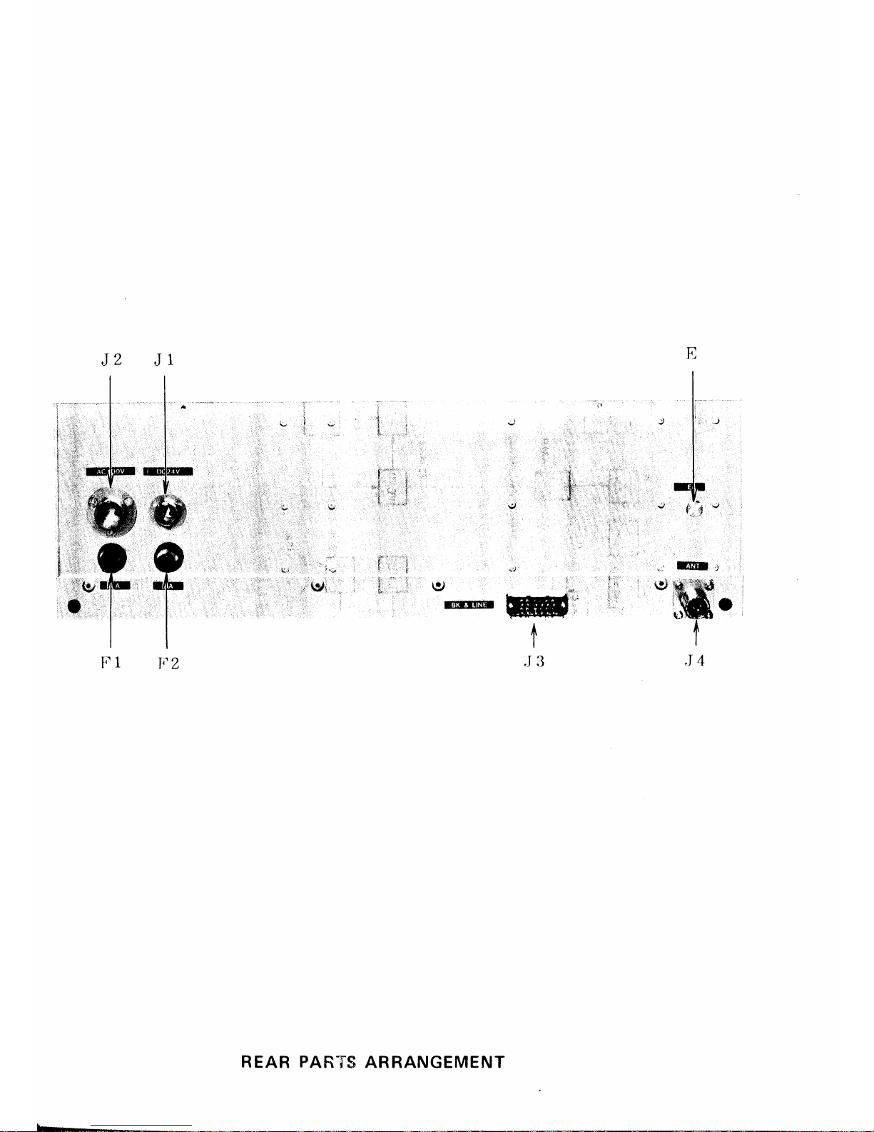
I
,5
vtû:
rX
tt,
o
,::,
','
,
1,,'.
ril,;, ;..,i)
ili-,,,',',.
,
'
fr::
,,
l;G
,t'wi.'
fi.f
.''-.1
{r
,:'t
:
1
lo,r:;',
l.l
'
.J
:lr
tt'r,'
.
i
rl'!.
'0,
,
uJ
.""
.'*lmMi.,
ô
I
t3
REAR PARTS
ARRANGEMENT
Page 32

--f----r
--{
r'-l
l-i
I
I
_J
@@o
r--l
Ttl
-ltt
totot
lol$l
|_|t
.lll
fl
tl
,l
J
CIFI EO
RATICE
I
?
4
8
l?
-t
I
I
nl
lt
ol
LJol
Fl
'llqI
EI
..-,
I
WEIGHT
7
ks
APPROVED
H Pl.,n't,:/:u'
)EClgeTTE
172
scatt
NRD-9I
RECEIVER','tE
OUTLINE
DRAWING
SHTEÏ
I{0.
CH
ECKTD
\:
'Zle
DESICIIED DRAWI{
fu
E'-/L A2
DRAWTT{G
ilo.
î a \t l-
:-\
'7
1 Â 1
\-r\-rt\\JlJl
llllltll
llllllll@
fopar]fudioh"Ifr.
5t7
Page 33

r6ffiræ
REAR
VIEW
tffiÉl
^rno-
er
REcE
rvER
-
roo€
-
ICIûùr
IPEF
EIE
otl6
I
J
t6
e.g
""ô*"Âffi
g-:P:
RF oAtN
\ltt\ )Ill
AF
'AIN
oFF
Aoc
oFF
powER
O
Vffi
O
'-i,9, "'P
"ôi,_.
PHOiIES
o
"ô^
D
SPtCIFtt0
TOLERAI'ICE
+l
t2
*4
+8
+12
0ntt,r5t0il
sPEctFtE0
0T0
t6
ovB
16
ro
50
oTrR
50
ro
250
ora
250
n
1000
or8
t000
r0
3000
UtILTSS
OTHERT{ISE
3rd Anglc
Systrm Dimcnsion
mm
Page 34

(R
EAR-}-
(FRONT)
UNDER INSTALLATION
-l
rn
o
o
T
l
o
d
4-O6
MOU
NTI
NG
HOLE
465
L2
-l|tl
I
I
-l
,ECI
FI EO
LERANCI
TI
LZ
L4
iB
rt2
WEiGHT
ll.5ks
NRD-9I RECEIVER'I"E
OUTLINE DRAWING
DTSIGNID
DRAWN
/^1
\-/
'J
II
tl
ORAWING
IIO
N
R,D,1.J,5,3,
lttrll
@
/ryrnadbh.-ûH.
Page 35

Frrr-6r|
l--â@v-l
@
@
E-Q9ËL:J
@
@
'
lT.--l
rE-ii-rFaE=,
REAR VIEW
ffil
Nno- er REoE
rvER
raooE
t6
e.E
tta Cf o- lux
IEEÉ
É-E
o, la
..'ôi,,..
PHONES
@
"ô"
o
RF
OAIN
0
ATT
BC BANO
REJECT
gl
9{
tT t\|
UU
OFF
OFF
AOC POWER
'ffË
sl-orY
u
oFF
u
ofF
oc
UI{LESS
OT|1ERITISE
SPECI FIEO
0lrEilsloil
sPEctFlE0ÏOLERANCE
0ro
16
*I
oYEÎ
16
ro
50
*2
ov8
50
To
250
+4
iln
250
ro
t000
+8
ofEi
t000
T0
3000
+12
3rd
Angle
System
Dimension mm
Page 36

@o
@
TF
AM?
BK
til
METER
RECT
AF Al,lP
BFO
AMP
SSB AUX
AGC
LINE
AYP
MEÎER
A},IP
Ll-r
6
AF AUP
et€
Soqo
@
tst MX 70À5sr4lz IF AMP
IF
AMP
AGC
LOCAL
AMP
0.54 5 to
).4549 MHz
lPr{oNEsl
I
sPEAKERI
iBK
&
LINEI
BK
LINE
our
+
I r-O
ffil
lccNTl
lcouPL.H
456.5
kHz
t
5A Hz
(appr-ox
)
-.<-=o.<l
DCr4"l
IJA I
BAIDwIDTH
(kFtù
LI
MITER
:1
;
nn I
;
rl
t\
lk
x
1:
r
-r
I
lkx
+5V
+t5v
I
+l1V
A
I
RECEIVER
iITLi
BLCCK
DII\GRAV1
CH ECKED
DESIGNTD DRAWN
t)
N,
AOù
RD
-/
i
DRAIryING
NC
@
Qryt
&.,ûH.
Page 37

\1 2
3
4
A
B
c
l|ÂHz
ffi
t@1 |
eokHz
to
525
kHz
to
I I -l | |
ze.qese
MHz
2odÛ
35MHz
|
605
kHz
l, f*l\'-u"'4l*1, |
3SHHz
I
AH'"-'4-{îÆ{
leNrl
æ----.|.
u
Eu:.
J
._*æ
#ffiffil"Lm'l
,...,.r
@
'aue[
l*i'*l
r**"*l
,13:;2iq'i*,
-
xlM xtOM
I
I
ffi
5
i.4hz
*r
*_T_
TC*C
_
t2.5kHz
, I ,
,
û
=
-
r*
l
rli
L-sMHz
@#
[
#
/t\
xt00k
xlM
x/01
^T* 'l,,*
''T
.'Tou
'i" "i",
'
DI
SPLAY I
11#
@@trjrâ
lpol"Nl
@
lLocl<l
D
a
=
a
ARRANGE IIO
3rd Angle
System Dimensron
Page 38

I
lEKEi.nEl
l-A
Nrl
trl
\f4
J lo
\T
l7
PcNs-3lST-r.5C (E'Ël
Pl5
Pln
PCN6
-3
I PT-
t.5
DS
c
D
E-328
DI SPLAY
ru
J
tÀ
I
tl-
J5
È
iL
=
I
IL
4
LJ
r7
J
O-
I
rl
rlz
I
+
s'r'
[s-:--l
j
F
s
!
N
uo-
(vl
I
2
-u> -
-t
coNr
I
SI_IASSIS
TITLÊ
CONNECTION
DIAGRAM
SHEET
NO.
DTSIGNED
DRAVIN
DDO
O
N,
R,D,-
,q
,1,
, r ,
,
Ittttrtrrl
@
fry'n
h-ûH.
Page 39

Ll
2
3
4
A
B
c
IDEÏI
-Æ\+
if" Y/ct
I ar
J-
e'
To.oll
,rr7
Foovl
m
zfrr rz
di'*-
leoo,'t$lÉ
tr.l
.,ir-elL-1
lo
J1
b
5
!
3
t
t
lO v
(-
I
fe+
l'
tov
rtl0V
l(
t roov !
-
- -
--l
\ll r,+'
âl' E
r
ill
tur4b
,lii
à li tt"+'
7li ç" , l,^
,___+:--Tn
I
tllll
l|tl
llllcBD-s56
PolvER
||l
| | | |
.rra
à*- llll t;r
o
DI M . CONT
r1:l^
r
r
o-
û-
oO-
F-
7o
50
U
ARRANGE
IIO.
a/,
z
ô
=
U
CE
3rd
Angle
System
Dimension
mm
Page 40
c)
w
::
+ trv
I
t--f
--r
t
I
K
1.^.. tL
î., {.:-?.""-,il-., T"t'*
ff&
L3),*
*':':ï:r'*L
L
1S15BE
;
+
r'v
I
|-*--J
c4
I
+*
crl
- -
lCz |
o.t.tt
|
-l
loo/^
,ti
O. l.,u
,?h
ir7 ,ln
t.
+
5v
I
L-$'---.i
c6
I
+tÇt?
ïcr I
o-ty
T
-ï
tooV.
m
a.1y
7m
7n
7717
zscr;i;"
@"bo rrp::
'
2t
Q"-+5v
\Z
î
rsrsoB
| *î3'3"u
Prs-lq
DIMMER CONT
c13
{
[3
lorj'u
L-
'vv
prg-r,r,
r?,?z
nn
rc
l.?
IC3.
5I
-
31
52P
st
-3052P
MDBWOI
IBI
MPPCO?IB7A
r.l
f\)
(^)
s
Page 41

(^)
1
o-
f
8_
o
a
o
(+
o
3
I
3
o
:t
I
o
:t
\
I
3
N
L
...
t\)
t\
LÈ-
È-tf
r
ta.
fc)
ô
RrvtstoNs
I
(f
m
AC
zZV
IN
AC
22V TN
GNI)
AC lOY
IN
AC
IOV
I.N
G
irl
C>
DC
?4V
IN
DC
?4V
OU
T
DC
2+V
IN
MDB
\
ôE
És
S=
s
(-/)
C)
rr'lc)rrl
zûl
'l
oo
I
2pl
Z
\-J
I
H;
I
--{
u\
|
50
|
zal
r3
|
onl
nl
'-1
\il
=l
Page 42

ZMHz
LPF
t
L
6.
t t2
6.8rll;;-
l?
9tH
82
IC
I
TD52003P
Rt9
roo
k
MDNW045A6
MPPCO9IglB
FILTER
OUT
LESS
TI{AN
7l4Hz
/+
3 MHz
3-
5MHz
5
-
?
MHZ
'7
-
10
MHz
c??
220
3-5
MHz BPF
L2,7
_-_
L28
5
-1
MHz
L35
BPF
srrLffi
L36
1."r\
-C21
'r
?000 |
FN
0.01rr
T
'
llt|
c57
-
u.v t11
,1+
c4l
c69
0. 0 17.r
680
c49
68C
P5-'l
r:
-È
P5-1
1
È?'7
1r^H
L3{J
f
t
O0
r.
l''i
a}) r<
cll6
c68
ta t1
T
ll
C66.r
c65
sao
I
82 7n r
c6'7
LIU
h
c70
a.01r;.'
c8?
4.O17
i^
tO
Mt+z
BPF
L43
L44
1rH
Â
0.68^lH
;H
L46
t O O/rH
L67
,
loolH
atlE,
o.otV
7fi
220
|
I
/7n
3T'T
J
c81
f
zzo
I
m]
c80
r80
c89
csl
??o
3eo
c78
120
i0
^
17
MHz
L5?
BPF
L53
O.ryr^H-
c83
.!
0.o1/t
*
L55 C99
1aH
0- o
l7,r
+t-r
cçe
\' I
3309'
I
croo
=
O.01r
I
'tm
14
0
lrlt
cro4
cro6 crog
I'I
*
3O M
Hz
B
P
F
100 t20
too
L64
-
--
L65
- - -
'.ffi,,ff-pi_
à',î",
?i
i:l-?l:':
7',,^+
ï.#,,* !J
'
h #
t.u'1
+:i'L
t;!o
ur
#
,à':
i.sr
I
t'rt
f
iI
t92
|
22o
ln
i*?3:I
ids
f33T
r5o
tih
T
in
10q
r50
t0 - 17 MHz
17
-30
MHz
P5
-l
o.o14J
,rv
c2s
o:l
t
r
L68
I
ro/lË
r
L69
r
4.7opB
Cr
L-
IBL
RF
TNPUT
FtL
TrTLt
CONNECTION DIAGRAM
CH ECKED
DESIGNED DRAIYI{
DRAfVll{G
1{0.
DDO
O
N,R,D,-,9t
1,
I
i I
I i i
@
Qapt-fudio&.-Cfl,.
Page 43

c
cre
o.1l
RF
INPUT
,t5,.1.
i
^.
35MHz
LPF
L
I LZ
0.33pH
O.77pH
rnnr.'7
I
n,
czl
ti E
c?e
1000
680
c44
tË;
c46
c4t
rooo
680
68t
HffiF
C45
-J-
C4,l
L,
.i-
C4t
cDs
i
Lll
't
41O/"H
L4
4.'?vH
6.BrP,
c6
.J-
33oo
7
.F
t
L17
L8
--i{3.3^H -ÆÂ
t0rrH
x
1-4
DS2-M-DC12V
r6
-r-a'l-
diL
-rqT
33
1
7m
cD6
L5
.t
-=10^t1,,Z'ir-
L6
8.?
cD'7
$e
eô
R 1 } R2
s6
{s6
,n|
Rt2
tK
I
I
T
a
I
crT
s6 l
j177
"\2,
+
"ri:
t
2?
4
z
c26
0.01a.7
'
,1v
1r1
?70
'
zoooJ
s6c
T_:r
s6
\r \
L?3
a';zc 9l
Lz5
loo,i,tH
('a.'/-u
/
è.7y
î /'n
z tb?1
e43
O.O1^r'''|p
'
,7,
R5
c59
loo
c51
?arl
2"O
cD8
c5E
R6
c77
1OO
c74
4Jo
t80
a.ot4
fi,
i'-n O
I
, I ?A
R7
cB5
1oo
Cg7
220
150
cD
l0
414
ffi
REJECT
cD29
vo?J
Cto?
râ8
cto4
cro6
?20
t00
t20
crra
J
0. o1/
T
,n
cD20
VOTJ
cD21
voTJ
tç?
t01H
L58
4'7OpH
Rr0
1-2U
vvll
CD5-18
M1301
cD28
J
Bz-o5o
R9
too
clt9
o.otp
f
tm
:
CD72-2'1
M
1402
ATT
P6
_8
RELAY
CONT
tl
v
P6-2-7.9,
'11.13,14
P5-Z-4.
12-14
P6-10
P6-12
t3
ôr ôt
;? tçr
$o.ot+
L'7c^
11:!
4
r-lffil-T-{F
I r^cn I
J
,if".
t,
333
ï
r,^. Gr:t-, C{:r"i
.
gJ
'
'
t
o
c,.,
L,i
,[
'
z
.'t.,u
,!
z.z "u
ARRANGE I{0.
@
=
ô
CE
Êr tl0
3rd
Angle
System
Dimension
mm
Page 44

P?-
13
TR3
G)
2sKtq2A-BL
V
I
I
r<Z
h
3sK4s-B
|
7V7
lnrr
-vre
lu
TLTT5
T;
I ::i':-
'trg
,<: 1
LH2g?
cral
,,-{ | -coz
L-4
Rt3
Rl4
c66
Ls cD3
ru
L;:r-jdiilff lra----.'"
ts'-s.8e
#*' F-r
680 680 0.0rt'33_9*H
's's88
Rt3
Rt4
C66
Ls CD3
c'st.tr
{|l | ).
ê(l
ï--re1,
r:
-!2êjlrÉ
i-
lR?
ns i
lctT
C
i2."k)
1,,
rn,
I
CzZ
c24
lF
OUT
flrlir\'
f+tk
I
*
|j+-,i
i
lf
l-ç
RAi+
*l
f.rul
zza
j
c26 F
L
*
,L'op4-
:tlkl'---'
L
L]:tx .1 | l'/.'i"L'-'
4,t
L";*-+^ttr"|
,..,0
220
Rts
!
Czs
net
I i=i'.nrrf
l
SkHz
sso3
I lfil:? | l^^"
2zo
z2o
I
I l ' -:'zt] h lÎpl^ TÊ T.r
Rtc
R2o
c30
cDs
I
?.?!l ? -
I
l'000
t000i
lroo0
toool
ç | lt00 | |
* ** | i-, I l"c#
R10 10.01/r
-.,
s
='l
R6
220
o.ottt
| |
cos
'îiea
- -Ig-
rY
Ê
6.i---
-Lt
T
t-1r,...-l - -)-Fl T
i.
dl
/,!
| |
'i
glê
i
l":::l
ri
i
roô
tkl
l* I l#l
*
*yr"
t,,b'o*ïrl#.0'rl
ea_e
rt
A
ç6_r- l l
3kHz
cs,
A -r,s I I t', 2' l ig
E-lu'sxnzlt4t
l
r
330
-\:/
,â I I
g33
Ifï:__l-ï-x--:T-[__:l
r.ï@ | |
,:;;,*,1
----+
*----'l,-f,*r:3
|
ps-g
r-'.:
I
!
rcs6
L zzs
l/PHli rrnn-nl-
n 'i L-
T tl
LH297
3a----r4
'l)
|
I'
1
TR?
|
2SCr2s4
lcsr4
tjiffi
à:É" lllrl t'ryn" ;'*giÉ
i
I
T
oo
l.l.lr]
ro,
1 i
r
j-
/t I 16
|
i'"
,'^
r1+7
--^t fcszr1o,,lt---fl 1
i
L
[Tf
[;F +ilt-a;;;
EBBBBBBBBBBBBBBBtooo I r :
Ll1
=C41
471tH
)p1000
MDHW006rt
MPPC
O9
'888
.oÊi
3a----)
R2l
2.2k
c3t
t
OIL
ë'rra
c3s
CAtr_lq1RF
AMP
TITLE
CONNECTION
DIAGRAM
CH
ECXED
DESIGNED DRAWN
DDOO
NrR:Dr-
t9t11
i i
r i
@
A6part-fudioco,ûH.
Page 45

/)
1
2
3
4
A
B
c
D
E
r-?-
P,*,
I ïr,r+.,
g
g
"'"r"fÆl_,
g
g
ff*é3sK4'
_- f.iri,offi
,,,
f9,,.,',,FJ
,-I3qrçl
Jrlin,
[ffi.;
RFrNpur"ffixaz+;-oe
irf =t*1ffir-dlffi,,q
Kr
r^ru
sH,##i#ii'ittffi;wiffic'
| +trI
c3
cst
L-,.+
_Fncqi
iiL_-_-.j
L
;.----i
|
*ri#i
,
rs-o àà
lô.4{1;{"T=.u,
|
;rt|;'ti
,:;l.la--L-l;,iooo
I l'"'l
rnl-t
I r---- +-_.i*"*-
u31o
l,:: i
*3'::',
c'6
+
'tltl
i"'
j-1
v/
looo
L
,*^
i.;
I B;:1^
Â7s6
l;à:
p8-,h7,
li
I
+r7v
rti
'^,1,':=':I
'sîY
'*
'*
*
|
l,
no
1@=
''17
rô, =-
caz
i
'
[
'-n'i
,rJJl'r*, ,"Ji.tr-r-#1
i
rsf
LocAL
Pi-q
,oîF
,tt8
Arr:r;"\, I I
|-os4s-
ruTl-i
'oo^s4eMHz
:::+
ffiry='t
*t::;l_rfl î*i
+t\'-'Y
lf I Tâ=r I i
T,?Â1'*llL
**lt;hl
i
i
-,r?
,rs7
|
I
Lâ< | i
'8fll
n"'3lo"l
-.l
,iô'd
I
-lç
i,îË[
f
''='u"'
'rJr-Î:';-':,*:::,,i
,ti 'jT
77D
'7'7
E
*t.tt'-
*
ARRAilGT
1{O
U)
=
C''
gJ
É
G Elo
3rd
Angle System
Dimension
mm
Page 46

Nt6913P
*
crs
I
O.Olrr
n,
R15
.n,14:.
tim
"Il
?'-o.kcoa
cos
CD9
RY2
cD39
Rt52
c5,7
C58
ô ôlrr
0.Ols
"-r
,/
+5v
xut
5
MHz
IC
r2
HD74LS?3P
IC
13
S
N ?4LS3'ON
D.,^
ct3
.,3"i"fib
IR22
4.7n
2W
Plt-
Pto
-t3
I
AF+15V
AF
OUT
4'7
0
clt
O. O
1rr
c14
rf
0.014
L9
4.?nH
P:âr€7,
c19
O.O33
rr
c2o
l;
IAT-
R r"
l8
o
rk
c23
o.o-l3a
R93
3
rok
L'
R9?
\, oo
150
c26
a?p
r80
tfiFilEÎ
c45
1y
c45
R62
o
c"3
l1t
;c6e
t
O_O
lu
rf---tRqs
lOk
L{
^.
Rv5
R9?
lok
took
tffi]
f*n"-<
fi?
ilt-l?
Atr
I
AF
?
AF 3
LINE OUT
R65
5-rk
Pll:9
LINE
OUT
Ptl-
I
CT
ttt
crtnr
AGc
aec
MO
Plo
-r4
?1t
-4
LTNE
M
O
. tu".
pn-
ro
Rt9
lok
+
-l
I
|
,lr
Cao
O.
1g
c29
22oy
z8
?or
2
c?4
L
tzoo
$
c27
o.33y
r
R23
3k
Plt-
14
nra
rcot$:
z-zk
'
;
c25
lOlt ctoS
7lO
I
R
t26
r
cP??
s.sl.
TR9
2SC'I8r
5
-Y
R12'l
4r7k
@
-
-T-3-
R63
1
00k
\-uJl
ly
4.1k
T4
c'4Ê
HJD52
lorr
4
R40
).bK
+
Rl24
r0k
L+5
22t^
R125
look
lÈrrt
l5\t
*rBi,
c,I4
R98
10
p
CD24
tQk
+-
cD23
ç75
to/
R99
10k
-r
,v
R90
100
cD38
Rroo
1k
^BFO
1
Pll-n
cD40
Plo-
g
BFO
BFO
_.r
cD
36
FXI
î
TR.li
RrrB
25C1gl5_Y
1ok
1k
?
3
r.5L
l
'l
a^^\-
l/
ab
rvz
-0501
R
r5r
10k
'1
/717
cou
/fù
L)O
v.v
t/J
RV6
_
rox
14551
Pg-?
Æ
.r.l5''J-'
REF 12.5kHz
OUT
r6
1
5-Y
TR
I"
2SAr0
|
5
cl8'
.J
Rl r9
roo
Rl14
tk
ïîr:
Rt
l5
tm
r
cfiz
-
la4
MDYWOr542
MPPCU^9I9OC
6'r
I
C
M
H
-
379
IF.
?nd
O
SC
TrTLt
CO
NNECTION
DIAGRAM
H
ECKED
DISIGNID DRAIVN
DDOO
NlRlDl-t9t1,
I
i I i
@
AapaiQadioAo.-til.
Page 47

)
)
o
\-.,,-
A
B
2
3
I "D
rRr
o'c
I
|
2scr81s-Y
l^"1.
rz
I
ot'
-,,
l"'"=,
l
o,,-'
-
i+rzv
.-
r J:#r
I
ffï
t
Err,.E*,,
1 1
l=,"
11
l
l ||F'+*È*t3iffi.+l;i' r,.
|:::
'tr;;H
| | ||l;f}"t*
*
|
:,:
o[*-.,o,o
r.:;;"1
|
|
lllxnF"fl
I
1î'1
..-=+
-
mU I E
(J-
p,o-1
j
=D'"jLJ
I lrg*mi=
/
+
B
K
--,.*f
.,r,
* ,,1
,ru,1r_rl,rl
#T*Ër"iÉ
-BK.."É:f1
ffi
lffrfi','u'',*;"<p'lh
;f.til
lF'
P'o_,,
?"ï
ï,rfr.'"#
BKRErATcottt
l
-f
c
w
o&l_
,==
sE
try-'1
.':d'r'F
Pro-r'
'c'tPfr
| +ffi
AUX
+
A'lk
P9-t4 P
hu
xl
cDl5
cDt6
cDt"
a*r^a-
?oMHz OUf
?
<
Jrro
."u"J'â'?'
*
ù'*'
"'"*f','T+.î,
.:;l'
-*
ief;!i"
n'
l+h#'+#tl*;l;h'b
tli
'ou
T
,t
a
rooé
#.
ï:
#,t#,Fr#*
,,,, rc,? rc,a,
4
,D",,
0-o1
cto
A'lo
à
-{T
Cll l,
O.Olzrr
l'
în
|*'ol
lz.7r
E
tE
.q
g;f
iri
7*
c+l I
c+z
7177
"r
)-oIf
lo.o1/t
+
-
'Rl8
TRl9
Lr:
r81s-Y
2scrsrs-Y
T#{s
Olr,;cnOÏ'4'
l--t_t|H
ti îi
3à
lF4il rî I H, l
,*,
I
at+le{.
)rh
i
5606ll
ii
|
'
l"Fi;3
Ti'l
/N
csr
ll
J+
c.otA
ll
;.r":dl,i
ll :'or-l
-T-l-T
ffi
leof
lii +
4'7k?
| i i
h
tttl
rl
)-
i TRI6
5-Y
zscrBr5-Y
(
J;ffi
l -* rfr fzz
e-!i
Ç
i_
'l.,:f8lî
i.,.Hfl'-S
'Li,L,Ll'.'Ë
l
i#'338
tnTm
ccs
i ,7r 1
rooo
|
!.^_-_
i:i-
I
iJt'l
*
ccq
h
tooo
D
ARRANGE NO.
6
z
O
+E\/
-;
tOtr
-
I
cE6
CAl
CAB
tO.Olt
0.Olg
0.01r^
IC
5 NJ
M29OzN
CD
l8-?2.35
ISV
14?B
wz'050
wLO65
rc 6
NJM4558 D
,CD8.26.36
I
C7,8 T
C40498 P
cD3l
É,
GND
"p
L4rxltce11ell
x
3
I I
rce
1C40118P
cD3,l
wz15Q
Ptt-.'
5
L
I
ns x1455.?kHzl
+ss.
esr<nzl
I
F
A x
1456.9
kHzl
45
7.
05kHzl
rc14 SN?4HOON
CDt-
5.
?,
9
I
tz-tt.zz.ztl
rst5Bg
n-:0,:2,::l
61
310
3rd
An(le
System Dimension mm
Page 48

/â\
RtB
n
2.2
o\î,
Pt2-3
l-q;{rc
LooP I
7i
ç;,f
our
,lD
€
I xJ
2SCt254
Rsl
c42
1000
{
.C1o
'33
o€
(
+4)
tc2
+l
c44
,*
c45
224
qûtt
rcoa T
,2>
RVl
500
RÆ
220
:47
2lL
cD4
'ilse8
o
n+9
ls
f3
1.7k
{_
_t
2i3
+5V
)7l.Ls27P
)'l4lÂ04P
LrJlSSAN
l4560BP
T2
LH32e
1)Ê
27
Rg
lK
c,8
taoo
E
R14
3.3k
t2v
R'9
c2t
3.3k
4;7tt
:-c34
ta-oIlL
R32
s
1^l
c23
C24
0.0ltL
0.0
tP
c36
Pt4-l
+t'l
V
P14-13
t2:5kH-z
REF
Pt4-ts
yc0
Pt4-tl
MLITE
Rrr
! cr'|
47
?
t000
-:Ë
Ri6
u;"'
\tk
I
vaz
,
o/'
)rtoPx;
c
r03
,ol
E
cs7
Rt3
J.5X
R'5
r00
IQ
to,'H
22r
ntZ
i
cào
+.
6.8k
F
tooo
-:
Æ
c33
0.out
€
€
c29
tOlL
**rTî
t*t
^,'i
|ntpsynv
2sKtgzA
-BL
rà
Y
o?
R34
410
Ké'
1k
FE
Q35
041/L
4.'7*
R26
,R
R44
IM:
ùi-
R47
*'270
+5V<
R48
4.'tk
lCf{
f--
*
x
l0 kHz
-3
1
tli
+5v
VDD
MDEW
00565
MPPC09tSgc
4i
t
c65
t000
'oog
|'golÏrl'Tol
É:È?È?Ë:
cololÈ.l(o
)^'^r^l
x;rF;x;
x
100
Hz
4t
1t t4, 13
t2, ll
6i
rRg
Ir.//cæ=:
t3tt2tu\
i
i
t r-'a r< F<
l.rl-r,l4l
lllll?l
l;, l
rfnlt+rl
lc62lc63lC64l
l1000lt000llml
Irôl.ilNl
olô+o+c
t-2'4-8
x
lkHz
TC4O3OBP
CGA-98
LOOP
1
TITLI
CONNECTION
DIAGRAM
DTSIGNTD
DRAIVN
D
N
DOO
rR:D;-
tQt1
:
I I
r i
@@
Qryn-tudioh,Iil.
:5029
BP
Page 49

tct4-21,2q
1c30,32
LOOPl
IN
+5V
0v
vco
1
vc03
vca2
17
-30l,lth
l0
-lTltlhz
7
*l0l4{z
5
-
TllH.z
3
-
SMliz
2
-
3MHz
LESS THAN
2
MHz
l1
LT
PQ-'s
lw
PU-to,Q,t4 *
Pt2-7
CDs
tsr588
c2
o.ol
lt
c3
t6
lc8-r0
Ict2,t3
IC3-5
r}tl
!s
16
18
t4
tl
+5V
F1 l*
vr
;'
zztLî-
-2,4
i
c9
P12
c6
c7
tot
tl
CA
tr
e4l
O,Ol,J
c5
t/L
c2
o.o
I
c6q,71,,14,75
1l
cr04
l0tt
cr05
0.0Ip
\r
r-q
1i
tol
c38
.-i
î,
1
1?
ç,1,,
t-
*
R3?
tok
o.oVT
R3ç
t0L
c3g
a.ctra
*
R4l
r0k
I
c47
22r
R42
CDz
r0k
rst5a8
l0 MHz
114H2
f00kHz
I
\Z
(l
I
lz
I
lo
[8
('
lz
I
lo
(e
ce3-ee
T'f TITTT
0,0 1 lt
,,+t>rt/rrt|,r*'
P13-6
Pt3-'7
Pt3-2
P'3-
3
P13-4
PE-5
Pt3-t,
Pr3-r0
P13-g
Pr3
-8
a<2-
-
VJJÇ-
tooo
*
*
F=Cs6
*
*iooo
c.49
+
t0o0
t
=Csz cs4
*toæ ,o00
c5s
t000
totL
E
r(22
rc26,n
It23-25
tC28
c76^34
C84-fl,
g0-ç2
;
0.0ltL
VDD
c70,72,73,88,99
0.01
lL
TR8
2SAr015-Y
J, J,ï,
c4
c43
0.01y
O-oty
-t
ril
0l/t
RVl
500
(
+4)
414416t416
1t 7
tI
I
1
I
1C3r
MB85r6
TR6
2SA10 f 5-Y
TR,7
2SA
'O'5_Y
L6
ty!
-A'0-+-=-
l+ |
ç-
a/+
Ç
ll
,r|7
r*
c44 C45
22.tL oolr'
i"l"'î
Ra
'"-"
,z tt'1
TR
2SAr0
+SV
+
A
t5
+Sv
=ct06
| 0.022tL
1777
€
nat
*-
270
ARRATIGI
tIO
6
=
I
v,
CE
HAt7723G
HArT5ssPS
HD74LS26
P
TC4550BP
?4LSI68PC
ïD6 |
02P
?4LS
I68AN
TC40 t'l4BP
HD74LS27P
HD74
LSO4P
HD74I-SO4P
MC4044P
c4560BP HD7.4LS73P
74lsr58AN
c4560BP
40r6BP
cs02g
BP
c,00
ro00
cl0l
t000
3rd
Angle
System
Dimension
Page 50

/\
L
o.X*n".
cq
0.01/4
SELg'O
(
LA-40taA)
,00e
x
A.1
kHz
x lk{z
x
l0 kHz
x
l}OkHz x I
MHz x 10
MHz
cr5
l14!
R37
68k
Pl6-14
^)
|--.'.
I
pte-23^r
lf- .7 -aJ'
ooro
T T
13
rczs.x
1c27,28
:=
-
rc2q
l+
tol
I
;771
Pt6-25o
g
?t6-26o
4
?t6
-2'l
2
?t6-29
I
l0 MHz
tMHz
to0kHz
l0tHz
0-l
kHz
4
.,
I
I
4
l
ffi
tt6t414
z,t3
8 7
7
f
r;;'
cD
1-
5
fna:
J 100
Rt6-2,1
r1
F
4
2
I
&
4
2
I
cD7-13
AA554IK
R.+0
2.2k
aD20
1St588
R.:1
t
5.5K
n6-t4
r-€
*
+
C3g
t4-
,1,,1
lrl
470k
rn2{ I
I
rsrssB
i
2
ii
2
;1
A
4r
-1
--l
ql
ilr--
t-
IT
ï_ï
!toFF! |
ilô
L-? ss
*r.022/-L
)
4r70k
n
t5
I
ulJ
/O
+l
*ctl
68k
tQl
ant-
I
|
't'+tÈ
i
æ
A
i?)
--.r{
bl',ii T
E+?
t*71
R34
t.2k ,
RV4
BlK
s7
S8
IDIMMERI
-
I
kH;l
lLoc^llE
@
@
MDLW02380
MPPC0g'92
D
cD3
3
t4l
cD2
I
I
0
À
6
U
6?'
I
lo
t\
t_J
S
CDE_328
DISPLAY
TITLE
CONNICTICN
DIAGRAM
CH ICKED
DESIGNED DRAIYN
DDOO
N,R,D,
-
tet
l;
i
i
i r
@
Qryt
bh-Iu,
Page 51

/.-+-
(
/
urSbÈn
ûry\
r*
"
r\Gc
5w"
tn,)
\wo
c
ûL-
e-
c\M'
ET!-
3-
s/
Lo"
rh
,
-F"T*/\
a
,t-
I
c'w'
à-L
u,,vn'-
,
120
Fert
--
lr?
+5
y
+5V
L'
P16-30)t
to/.H
+5V
cDa
rcr-6
,s597
11
tol
IC1-|Z
rct3-,6
rcn.,8
Ictq LC20.2l
Ic22
IC23 IC2S.X
lct
,4 t6
'l,lz,13
I
cD?3
1SS97
c)22
fss97
R43
100
LSB
6
kH.
3
kH.
p|n-
0.5kHz
f
AUx
4
DSB
oLJz
cw C3
SSB
Ptl
-'1
ATî
f
AFl
AFz9,HL1
AF3
RFr
#u
RF
2 cn1-æ
RF
3
aY:3?
AF
OUT
LI
NE
Pt1-2A
RVl
B'OK
lBFo
& cLARri
St3
S,4 Sl5
ffi
I
RV2
A5K
tRr
GArN-l
DC
DC
AC
AC
P,s_
t
Prs-3
Sl
E'NA
3^I.t
E
lsPFiKfr IPHoN€s]
16
t4 |
28
tG
t4
878t487
c5
c6
c'l
A.OUI
0.0t/
0,alt
-c
Rf4
tw
lll lï
il | 1?
l.lllt
te"Àij
I ô |
RV3
6trFlb I
BtoK
-s5-
hF
eAA
I
Arrl
a
z
a
>
IC |
-
6,
HD74
LS
47
P 7C 20.21
TC45t0BP
1c27.28
I
TC4o73
BP
tc?
-t2
TC45
60BP
L
e?2 TC40t3BP
rc2q
lrcaoor
BP
IC13* r
6
TC40rtBP
I
C23
TC4030BP
ict7,
,E
T
C404I BP
I
c?À
TD
62003
P
tctg
]rCsOl0P
r
c2s.26
T
C4044BP
ARRANGT
NO
3rd
Anglle
System
Dimension
mm
Page 52

c?>
1U
q*
ÀJ
o
À-
b
C!
('l
3
N
o
tn
9;
!N
o
I1
J
tçt lEl
L]J
IIJ
HH
.\o
J
3
'!
O
u
m
rl
E
3
rn
-t
frl
t
I
"f
o
H
i
I
I
H
H
'-l
t-t l
l?lo
-'
lz
|
-l--
[5-|
*o--
lxJ
trï
.*To---t
ututu
iH
EË: A
2
ô
2
-
2
{
=
2
D;U
rm
oo
e)rr,
n-rn
7N
L,,
T
\.
.r
:
 Loading...