

Page 1

Intel NetStructure® MPCBL0010 Single Board Computer
Technical Product Specification
October 2006
Order Number: 304120
Page 2

INFORMATION IN THIS DOCUMENT IS PROVIDED IN CONNECTION WITH INTEL® PRODUCTS. NO LICENSE, EXPRESS OR IMPLIED, BY ESTOPPEL OR
OTHERWISE, TO ANY INTELLECTUAL PROPERTY RIGHTS IS GRANTED BY THIS DOCUMENT. EXCEPT AS PROVIDED IN INTEL'S TERMS AND CONDITIONS
OF SALE FOR SUCH PRODUCTS, INTEL ASSUMES NO LIABILITY WHATSOEVER, AND INTEL DISCLAIMS ANY EXPRESS OR IMPLIED WARRANTY, RELATING
TO SALE AND/OR USE OF INTEL PRODUCTS INCLUDING LIABILITY OR WARRANTIES RELATING TO FITNESS FOR A PARTICULAR PURPOSE,
MERCHANTABILITY, OR INFRINGEMENT OF ANY PATENT, COPYRIGHT OR OTHER INTELLECT UAL PROPERTY RIGHT.
Intel may make changes to specifications and product descriptions at any time, without notice. Intel products are not intended for use in nuclear,
medical, life saving, or life sustaining applications.
Designers must not rely on the absence or characteristics of any features or instructions marked “reserved” or “un defined.” Intel reserves these for
future definition and shall have no responsibility whatsoever for conflicts or incompatibilities arising from future changes to them.
The Intel NetStructure® MPCBL0010 Single Board Computer may contain design defects or errors known as errata which may cause the product to
deviate from published specifications. Current characterized errata are available on request.
Contact your local Intel sales office or your distributor to obtain the latest specifications and before placing your product order.
Intel, Intel logo, Intel Ne tStructu re, Inte l NetBur st, and Intel X eo n, are tr ade marks or registere d tra demarks o f Intel Corpor ation or its subsidiaries in the
United States and other countries .
*Other names and brands may be claimed as the property of others.
**Hyper-Threading Technology requires a computer system with an Intel® Pentium® 4 processor supporting Hyper-Threading Technology and an HT
Technology enabled chipset, BIOS and operating system. Performance will vary depending on the specific hardware and software you use. See http:/ /
www.intel.com/info/hyperthreading/ for more information including details on which processors support HT Technology.
Copyright © Intel Corporation, 2006. Al l rights reserved.
Intel NetStructure® MPCBL0010 Single Board Computer
Technical Product Specification October 2006
2 Order Number: 304120
Page 3

—MPCBL0010
Contents
1.0 Introduction............................................................................................................ 12
1.1 Document Organization......................................................................................12
1.2 Glossary ..........................................................................................................13
2.0 Feature Overview ....................................................................................................15
2.1 Application .......................................................................................................15
2.2 Functional Description..................................................................... .. ... ..............15
2.2.1 Low Voltage Intel
2.2.2 Chipset.................................................................................................16
2.2.2.1 Memory Controller Hub..............................................................17
2.2.2.2 I/O Controller Hub ....................................................................17
2.2.2.3 64-Bit PCI Hub ..................... .. .. .. ............................. ... ..............17
2.2.3 Memory (J10, J12) ............................... .. ................................................17
2.2.4 I/O.......................................................................................................18
2.2.4.1 I/O Controller Hub ....................................................................18
2.2.4.2 Real-Time Clock........................................................................18
2.2.4.3 Timers.....................................................................................18
2.2.4.4 Gigabit Ethernet .......................................................................19
2.2.4.5 10/100 Fast Ethernet ................................................................19
2.2.4.6 USB 2.0...................................................................................19
2.2.4.7 Serial Ports..............................................................................19
2.2.5 AdvancedMC (AMC) Connector (J18, J19) .................................................. 19
2.2.6 Firmware Hubs.......................... .. .. .............................. .. .........................20
2.2.6.1 FWH0 (Main BIOS) ....................................................................20
2.2.6.2 FWH1 (Backup/Recovery BIOS) ..................................................21
2.2.6.3 Flash ROM Backup Mechanism....................................................21
2.2.7 Onboard Power Supplies..........................................................................21
2.2.7.1 Power Feed Fuses..................................................................... 21
2.2.7.2 ORing Diodes and Circuit Breaker Protection.................................21
2.2.7.3 Isolated -48 V to +12 V, 12 V Suspend, 5 V, 3.3 V Suspend, 1.8 V, and
1.5 V Converters21
2.2.7.4 Processor Voltage Regulator Module (VRM)................................... 22
2.2.7.5 IPMC Subsystem Standby Power.................................................22
2.2.7.6 Other On-board Supplies ...........................................................22
2.2.7.7 Other Suspend Power................................................................22
2.2.8 IPMC ....................................................................................................22
2.2.9 Telecom Clock .......................................................................................22
2.2.10 AdvancedMC Direct Connect .............................. .. ... ................................. 23
2.2.11 AdvancedTCA Compliance........................................................................24
3.0 Operating the Unit................................................................................................... 25
3.1 Jumpers...........................................................................................................25
3.2 AdvancedMC Filler Panels ...................................................................................27
3.3 Installing Memory .............................................................................................28
3.4 Installing and Extracting the SBC ........................................................................29
3.4.1 Chassis Installation.................................................................................30
3.4.2 Chassis Extraction..................................................................................30
3.5 AdvancedMC Module Installation and Extraction.....................................................32
3.6 BIOS Configuration............................................................................................32
3.7 Remote Access Configuration..............................................................................32
3.8 Software Updates..............................................................................................32
3.8.1 BIOS Updates........................................................................................ 33
3.8.2 Loading\Saving Custom BIOS Configuration...............................................33
®
Xeon™ Processor ........................................................16
October 2006 Technical Product Specification
Order Number: 304120 3
Intel NetStructure® MPCBL0010 Single Board Computer
Page 4

MPCBL0010—
3.8.2.1 Synchronizing BIOS Image and Settings from FWH0 (Main) to FWH1
(Backup)33
3.8.2.2 Copying BIOS.bin from the SBC ..................................................34
3.8.2.3 Saving BIOS.bin to the SBC........................................................34
3.8.2.4 flashlnx Command Line Options.................................................35
3.8.3 IPMC Firmware Updates................................... .. .............................. .. ......35
3.8.3.1 IPMC Firmware Upgrade Using the KCS Interface...........................35
3.9 Digital Ground to Chassis Ground Connectivity.......................................................36
4.0 Specifications ..........................................................................................................37
4.1 Mechanical Specifications....................................................................................37
4.1.1 Board Outline.................................................................... .. ...................37
4.1.2 Backing Plate and Top Cover.................................................................. ..37
4.2 Environmental Specifications...............................................................................37
4.3 Reliability Specifications......................................................................................38
4.3.1 Mean Time Between Failure (MTBF) Specifications.......................................38
4.3.1.1 Environmental Assumptions............................... .. .. .. ...................38
4.3.1.2 General Assumptions.................................................................38
4.3.1.3 General Notes...........................................................................39
4.3.2 Power Requirements ............................. ............................. .....................39
4.3.3 Power Consumption ................................ .. ............................. .. ... ............39
4.4 Weight.............................................................................................................39
5.0 Connectors and LEDs ...............................................................................................40
5.1 Backplane Connectors .............................................. .. .. .............................. .. ......43
5.1.1 Power Distribution Connector (P10)...........................................................43
5.1.2 AdvancedTCA Data Transport Connector (J23)............................................44
5.1.3 AdvancedTCA Data Transport Connector (J20)............................................46
5.1.4 Alignment Blocks....................................................................................46
5.2 On-Board Connectors.........................................................................................47
5.2.1 POST Code Connector (J13) .....................................................................47
5.2.2 Extended IPT700 Debug Port Connector (J25).............................................47
5.3 Front Panel Connectors.......................................................................................48
5.3.1 Ethernet 10/100 Debug Connector (J3)......................................................48
5.3.2 USB Connector (J4).................................................................................49
5.3.3 Serial Port Connector (J5)........................................................................49
5.3.4 AdvancedMC* Connectors (J18, J19)................................................. ........50
5.4 LEDs................................................................................................................52
5.4.1 POST LED Codes.....................................................................................55
5.5 Reset Button.....................................................................................................56
6.0 BIOS Features..........................................................................................................57
6.1 Introduction......................................................................................................57
6.2 BIOS Flash Memory Organization.........................................................................57
6.3 Complementary Metal-Oxide Semiconductor (CMOS)..............................................57
6.4 Redundant BIOS Functionality .............................................................................57
6.5 Legacy USB Support...........................................................................................58
6.5.1 Language Support ............................................................................ ......58
6.6 Recovering BIOS Data........................................................................................58
6.7 Boot Options.....................................................................................................58
6.7.1 CD-ROM and Network Boot ......................................................................59
6.7.2 Booting without Attached Devices .............................................................59
6.8 Fast Booting Systems............................ .. .............................. .. .. .........................59
6.8.1 Quick Boot.............................................................................................59
6.9 BIOS Security Features ................................................ .. .. .............................. ....59
6.10 Remote Access Configuration ..............................................................................60
®
Intel NetStructure
Technical Product Specification October 2006
4 Order Number: 304120
MPCBL0010 Single Board Computer
Page 5

—MPCBL0010
7.0 BIOS Setup..............................................................................................................62
7.1 Introduction .....................................................................................................62
7.2 Main Menu .......................................................................................................62
7.3 Advanced Menu.................................................................................................63
7.3.1 CPU Configuration Sub-Menu ...................................................................64
7.3.2 IDE Configuration Sub-Menu....................................................................65
7.3.2.1 Primary IDE Master/Slave Configuration Options...........................67
7.3.3 SuperIO Configuration Sub-Menu ...................................... .. .. .. .................68
7.3.4 ACPI Configuration Sub-Menu ..................................................................69
7.3.4.1 Advanced ACPI Configuration Sub-Menu ......................................70
7.3.4.2 Chipset ACPI Configuration Sub-Menu..........................................70
7.3.5 System Management Sub-Menu ...............................................................71
7.3.6 Event Log Configuration Sub-Menu........................................ ...................72
7.3.6.1 PCI Express Error Masking Configuration Sub-Menu....................... 73
7.3.7 MPS Configuration Sub-Menu...................................................................74
7.3.8 AdvancedTCA* Channel Routing (PICMG*) Sub-Menu.................................. 74
7.3.9 On-board Devices Configuration Sub-Menu................................................75
7.3.10 PCI Express* Configuration Sub-Menu.......................................................76
7.3.11 Remote Access Configuration Sub-Menu....................................................77
7.3.12 IPMI Configuration Sub-Menu............... ............................. .. .. .. .................78
7.3.13 USB Configuration Sub-Menu....................... .. .. ........................................80
7.3.13.1 USB Mass Storage Device Configuration.......................................81
7.4 PCIPnP Menu....................................................................................................81
7.5 Boot Menu........................................................................................................82
7.5.1 Boot Settings Configuration Sub-Menu ......................................................82
7.5.2 Boot Device Priority Sub-Menu......................... .. .............................. .. .. .. ..83
7.5.3 Hard Disk Drives Sub-menu........................... .. .. .. .............................. .. .. ..84
7.5.4 OS Load Timeout Timer Sub-Menu............................................................84
7.6 Security Menu...................................................................................................85
7.7 Chipset Menu....................................................................................................85
7.7.1 Northbridge Configuration Sub-Menu ........................................................86
7.7.2 Spread Spectrum Clocking Mode Sub-Menu ...............................................87
7.8 Exit Menu.........................................................................................................87
8.0 Error Messages........................................................................................................89
8.1 BIOS Error Messages.........................................................................................89
8.2 Port 80h POST Codes .........................................................................................89
9.0 Addressing .............................................................................................................. 93
9.1 PCI Configuration Map .......................................................................................93
9.2 FPGA Registers .................................................................................................95
9.3 IPMC Addresses .............................................................................................. 103
9.3.0.1 PwrBtn usage............................................ .. .. ......................... 105
10.0 Hardware Management Overview.......................................................................... 115
10.1 Intelligent Platform Management Controller (IPMC).............................................. 115
10.2 Sensor Data Record (SDR) ............................................................................... 117
10.3 System Event Log (SEL)................................................................................... 121
10.4 IPMB Link Sensor ............................................................................................ 126
10.5 Field Replaceable Unit (FRU) Information............................................................ 126
10.6 Customizable FRU Area.................................................................................... 127
10.6.1 LinuxCustFru Utility Usage..................................................................... 127
10.6.2 FRU Customer Area ............................................................................ .. 127
10.7 E-Keying........................................................................................................ 130
10.8 OEM IPMI Commands ........................................ .. ............................. ... ............ 130
10.8.1 Reset BIOS Flash Type............................ .. ............................. ... ............ 131
October 2006 Technical Product Specification
Order Number: 304120 5
Intel NetStructure® MPCBL0010 Single Board Computer
Page 6

MPCBL0010—
10.8.2 Board Device Channel Port Selection Identifiers ........................................131
10.8.2.1 SetBoardDeviceChannelPortSelection.........................................132
10.8.2.2 GetBoardDeviceChannelPortSelection.........................................133
10.8.2.3 GetBoardDevicePossibleSelection...............................................133
10.8.3 Set Control State.................................................................................. 134
10.8.4 Get Control State..................................................................................134
10.8.5 Controls Identifier Table ........................................................................134
10.9 Hot Swap Process............................................................................................135
10.9.1 Hot Swap LED......................................................................................136
10.10 AdvancedMC Module Activation..........................................................................136
10.10.1Pre-Defined Resources for AdvancedMC Modules.......................................137
10.11 Temperature and Voltage Sensors......................................................................137
10.11.1Processor Events ..................................................................................139
10.11.2DIMM Memory Events................... .. .............................. .. .......................139
10.11.3System Firmware Progress (POST Error)..................................................139
10.11.4Critical Interrupts .................................................................................139
10.11.5System ACPI Power State ........................................... ...........................139
10.11.6 IPMB Link Sensor..................................................................................140
10.11.7 FRU Hot Swap ......................................................................................140
10.12 Reset .............................................................................................................140
10.12.1 Warm Reset.........................................................................................141
10.12.2 Hard Reset ..........................................................................................141
10.13 Field Replaceable Unit (FRU) Information ............................................................141
10.14 IPMC Firmware Code................................... .. .............................. .....................142
11.0 Serial Over LAN (SOL)............................................................................................145
11.1 References......................................................................................................145
11.2 SOL Architecture .............................................................................................145
11.2.1 SOL Implementation .............................................................................145
11.2.2 Architectural Components......................................................................147
11.2.2.1 IPMC .....................................................................................147
11.2.2.2 Ethernet Controller............................................. .....................147
11.3 Theory of Operation.........................................................................................147
11.3.1 Front Panel Serial Port or Rear Transition Module ......................................147
11.3.2 Serial Over LAN....................................................................................147
11.4 Serial Over LAN Client......................................................................................148
11.5 Reference Configuration Script ..........................................................................148
11.6 Supported Usage Model....................................................................................149
11.6.1 Configuring the Blade for SOL.................................................................149
11.7 Reference Script (reference_cfg)........................................................................ 150
11.7.1 SOL Configuration Reference Script (reference_cfg)...................................150
11.7.2 Default Behavior...................................................................................150
11.7.3 SOL User Information............................................................................150
11.7.4 LAN Parameters....................................................................................150
11.7.5 SOL Parameters ...................................................................................151
11.7.6 Channel Parameters..............................................................................151
11.7.7 Command Line Options..........................................................................151
11.8 Setting up a Serial Over LAN Session..................................................................152
11.8.1 Target Blade Setup ...............................................................................152
11.8.1.1 BIOS Configuration..................................................................152
11.8.1.2 Operating System Configuration......................... .. .. .. .................153
11.8.1.3 sbcutils RPM Installation...........................................................155
11.8.1.4 Execute the reference_cfg Script...............................................155
11.8.2 Client Blade Setup ................................................................................157
11.8.2.1 Configure the Ethernet Port ......................................................157
11.8.2.2 Installing ipmitool....................................................................158
®
Intel NetStructure
Technical Product Specification October 2006
6 Order Number: 304120
MPCBL0010 Single Board Computer
Page 7

—MPCBL0010
11.8.2.3 Start an SOL Session............................................................... 158
11.8.2.4 Checking SOL Configuration ..................................................... 158
11.8.2.5 Ending an SOL Session............................................................ 159
11.9 Operating Systems for SOL Client (ipmitool) ....................................................... 160
12.0 Telecom Clock ....................................................................................................... 161
12.1 Functional Description.......................................... .. .............................. .. .. .. ...... 161
12.2 Interface Description ....................................................................................... 162
12.2.1 AdvancedTCA Backplane Interface.......................................................... 162
12.2.2 AdvancedMC Interface ................................................. .. ....................... 162
12.2.3 Reset/Interrupt Interface ...................................................................... 162
12.2.4 LPC Interface....................................................................................... 162
12.3 Function Description........................................................................................ 162
12.3.1 Redundant Reference Clock Selection...................................................... 162
12.3.2 PLL Clock Generation............................................................................ 162
12.3.3 Recovered Clock Selection.............................................. ....................... 163
12.3.4 Configuration....................................................................................... 163
12.3.4.1 Operational Configuration ........................................................ 163
12.3.5 Alarm Handling.................................................................................... 163
12.4 Telecom Clock API ........................................................................................... 164
12.4.1 TRANSMIT CLOCK ................................................................................ 164
12.4.2 Enable/Disable Transmission Clock ......................................................... 164
12.4.3 Recovered Clock.................. ............................. .............................. .. .... 165
12.4.4 Automatic Switchover ........................................................................... 165
12.4.5 Automatic Switchover Mode................................................................... 165
12.4.6 Select Reference Clock.......................................................................... 166
12.4.7 Reference Frequency for PLL.................... .. .. .............................. .. .......... 166
12.4.8 Primary/Secondary Redundant Clock....................................................... 166
12.4.9 Corner Frequency................................................................................. 167
12.4.10 PLL Operating Mode.............................................................................. 167
12.4.11Reference Clock Alignment ............................................. .. ..................... 167
12.4.12 Hardware Reset ................................................................................... 167
12.4.13Read Alarm States........................... ... ............................. .. .. .. ............... 168
12.4.14Read New Events ...................... .. .............................. ........................... 168
12.4.15Read the Current Reference Clock .............................................. ............ 169
12.4.16sysfs Interface..................................................................................... 169
12.5 Telecom Clock Registers................................................................................... 170
13.0 Maintenance.......................................................................................................... 177
13.1 Supervision .................................................................................................... 177
13.2 Diagnostics..................................................................................................... 177
13.2.1 In-Target Probe (ITP) ....................................................................... .. .. 177
14.0 Thermals ............................................................................................................... 178
15.0 Component Technology ......................................................................................... 179
16.0 Warranty Information ........................................................................................... 180
®
16.1 Intel NetStructure
Compute Boards and Platform Products Limited Warranty......... 180
16.2 Returning a Defective Product (RMA) ................................................................. 180
16.3 For the Americas............................................................................................. 180
16.3.1 For Europe, Middle East, and Africa (EMEA).............................................. 181
16.3.2 For Asia and Pacific (APAC).................................................................... 181
16.3.3 Limitation of Liability and Remedies........................................................ 181
17.0 Customer Support ................................................................................................. 183
17.1 Customer Support........................................................................................... 183
17.2 Technical Support and Return for Service Assistance............................................ 183
October 2006 Technical Product Specification
Order Number: 304120 7
Intel NetStructure® MPCBL0010 Single Board Computer
Page 8

MPCBL0010—
17.3 Sales Assistance..............................................................................................183
17.4 Product Code Summary....................................................................................183
18.0 Certifications .........................................................................................................184
19.0 Agency Information—Class B .................................................................................185
19.1 North America (FCC Class B).......................... ................................ ...................185
19.2 Canada – Industry Canada (ICES-003 Class B) (English and French-translated) .......185
19.3 Japan VCCI Class B..........................................................................................185
19.4 Korean Class B................................................................................................186
19.5 Australia, New Zealand.....................................................................................186
20.0 Safety Warnings ....................................................................................................187
20.1 Mesures de Sécurité.........................................................................................188
20.2 Sicherheitshinweise..........................................................................................189
20.3 Norme di Sicurezza..........................................................................................190
20.4 Instrucciones de Seguridad...............................................................................191
20.5 Chinese Safety Warning....................................................................................192
A Reference Documents ............................................................................................193
B List of Supported Commands (IPMI v1.5 and PICMG 3.0).......................................195
Figures
1 MPCBL0010 Block Diagram........................................................................................16
2 AdvancedMCA Direct Connect Switch Block Diagram......................................................24
3 Jumpers..................................................................................................................25
4 Jumper/Connector Locations......................................................................................26
5 AdvancedMC Filler Panel............................. .. .............................. .. .. .. .........................27
6 Memory Top Cover Installed ......................................................................................28
7 Empty DIMM Sockets................................................................................................28
8 Memory Installed................................................. ... ............................. .....................29
9 Digital Ground and Chassis Ground Isolated (Default)....................................................36
10 Connector Locations..................................................................................................41
11 Front Panel.................................... ... .. ............................. .............................. .. ........42
12 Power Distribution Connector (Zone 1) P10..................................................................43
13 Data Transport Connector (Zone 2) J23.......................................................................45
14 Ethernet 10/100 Debug Connector............................................ ... ............................. ..48
15 USB Connector (J4) ...................................................... .. .. .............................. .. ........49
16 Serial Port Connector (J5)............................... ...........................................................49
17 DB-9 to RJ-45 Pin Translation ....................................................................................50
18 AdvancedMC* Connector...........................................................................................52
19 Front Panel LEDs (Option 1).......................................................................................53
20 Front Panel B LEDs (Option 2)....................................................................................53
21 Example POST LED Codes............................... .............................. .............................56
22 IPMC Block Diagram ...............................................................................................116
23 AdvancedMC Direct Connect Switch Block Diagram .....................................................132
24 Hot Swap Process...................................................................................................135
25 Warm Reset Block Diagram......................................................................................141
26 IPMC Firmware Code Process ...................................................................................143
27 SOL Block Diagram........................................ .. .............................. .. .......................146
28 Reference Script Running on a Remote Node, Communicating over the LAN ...................149
29 BIOS Configuration of SOL Target Blade....................................................................153
30 Configuration for RHEL............................................................................................154
31 Block Diagram of the Telecom Clock..........................................................................161
32 Power vs. Flow Rate................................................................................................178
®
Intel NetStructure
Technical Product Specification October 2006
8 Order Number: 304120
MPCBL0010 Single Board Computer
Page 9

—MPCBL0010
Tables
1 Supported Memory Configurations...................................... .. .. ....................................18
2 Jumper Definitions ...................................................................................................26
3 Suggested Method of BIOS Image Synchronization prior to BIOS Upgrade ....................... 33
4 Flashlnx Utility Command Line Options........................................................................35
5 Environmental Specifications ..................................................................................... 37
6 Reliability Estimate Data ...........................................................................................38
7 Power Requirements.................................................................................................39
8 Total Measured Power...............................................................................................39
9 Weight ...................................................................................................................39
10 On-board and Backplane Connector Assignments .........................................................41
11 Front Panel Connector Assignments............................................................................42
12 Power Distribution Connector (Zone 1) P10 Pin Assignments..........................................44
13 AdvancedTCA Data Transport Connector (Zone 2) J23 Pin Assignments...........................46
14 AdvancedTCA* Data Transport Connector (Zone 2) J20 Pin............................................46
15 POST Code Connector Pin Assignments.......................................................................47
16 Ethernet 10/100 Debug Connector Pin Assignments......................................................48
17 Ethernet 10/100 Debug Connector LED Operation ........................................................48
18 USB Connector (J4) Pin Assignments..........................................................................49
19 Serial Port Connector (J5) Pin Assignments..................................................................50
20 AdvancedMC* Connector Pin Assignments...................................................................51
21 Front Panel LED Descriptions.....................................................................................54
22 Ethernet 10/100 Debug Connector LED Operation ........................................................55
23 Supervisor and User Password Functions.....................................................................60
24 Function Key Escape Code Equivalents........................................................................60
25 BIOS Setup Program Menu Bar..................................................................................62
26 BIOS Setup Program Function Keys............................................................................62
27 Main Menu ..............................................................................................................63
28 Advanced Menu .......................................................................................................64
29 CPU Configuration Sub-Menu......................................... .. .. .. .............................. .. .. .... 65
30 IDE Configuration Sub-Menu......................................................................................66
31 IDE Master/Slave Sub-Menu......................................................................................67
32 SuperIO Configuration Sub-Menu...............................................................................69
33 ACPI Configuration Sub-Menu............................................................... .. .. .................70
34 Advanced ACPI Configuration Sub-Menu......................................................................70
35 Chipset ACPI Configuration Sub-Menu.........................................................................71
36 System Management Sub-Menu.................................................................................72
37 Event Log Configuration Sub-Menu.............................................................................73
38 PCI Express Error Masking Configuration Sub-Menu......................................................73
39 MPS Configuration Sub-Menu.....................................................................................74
40 AdvancedTCA Channel Routing (PICMG) Sub-Menu.......................................................75
41 On-board Devices Configuration Sub-Menu.................................................................. 76
42 Option ROM Configuration Options..............................................................................76
43 PCI Express* Configuration Sub-Menu ........................................................................77
44 Remote Access Configuration Sub-Menu......................................................................78
45 IPMI Configuration Sub-Menu ....................................................................................79
46 LAN Configuration Sub-Menu.....................................................................................79
47 USB Configuration Sub-Menu.....................................................................................80
48 USB Mass Storage Device Configuration......................................................................81
49 PCIPnP Menu.................................. .. .. ......................................................... ............81
50 Boot Menu ..............................................................................................................82
51 Boot Settings Configuration Sub-Menu........................................................................82
52 Boot Device Priority Sub-Menu...................................................................................83
53 Hard Disk Drive Sub-Menu ........................................................................................84
October 2006 Technical Product Specification
Order Number: 304120 9
Intel NetStructure® MPCBL0010 Single Board Computer
Page 10

MPCBL0010—
54 OS Load Timeout Timer Sub-Menu..............................................................................85
55 Security Menu..........................................................................................................85
56 Chipset Menu...........................................................................................................86
57 Northbridge Chipset Configuration ..............................................................................86
58 Spread Spectrum Clocking Mode Configuration .............................................................87
59 Exit Menu................................................................................................................87
60 BIOS Error Messages ................................................................................................89
61 Bootblock Initialization Code Checkpoints ....................................................................90
62 POST Code Checkpoints ............................................................................................90
63 DIM Code Checkpoints ...................................................... .. .............................. ........92
64 ACPI Runtime Checkpoints.........................................................................................92
65 PCI Configuration Map...............................................................................................93
66 FPGA Register Legend...............................................................................................95
67 FPGA Register Overview............................................................................................96
68 POST Codes 00:80h..................................................................................................96
69 Extended POST Codes 0081h.....................................................................................96
70 FPGA Version 0A00h .................................................................................................97
71 Debug LED 0A01h ....................................................................................................97
72 FWUM 0A02h...........................................................................................................98
73 Development Features 0A04h .......................................... .. .............................. ..........98
74 Telecom Clock Register 0 0A08h.................................................................................99
75 Telecom Clock Register 1 0A09h...............................................................................100
76 Telecom Clock Register 2 0A0Ah...............................................................................100
77 Telecom Clock Register 3 0A0Bh............................................................................... 101
78 Transmission Frequency Selection.............................................................................101
79 Telecom Clock Register 4 0A0Ch...............................................................................101
80 Telecom Clock Register 5 0A0Dh ..............................................................................102
81 Telecom Clock Register 6 0A0Eh...............................................................................102
82 Telecom Clock Register 7 0A0Fh...............................................................................103
83 IPMC Register Legend .............................................................................................103
84 SBC Control 00h...................................... .. ............................. .............................. ..104
85 SBC Status 01h.......................... .............................. ..............................................106
86 POST Code Low 02h................................................................................................ 106
87 POST Code High 03h...............................................................................................106
88 LED Color Control 06h.............................. .. ............................. ... .. ...........................106
89 LED Control 07h.....................................................................................................106
90 AdvancedMC B1 Control & Status 10h .......................................................................107
91 AdvancedMC B1 Control & Status 11h .......................................................................107
92 AMC B2 Control & Status 12h...................................................................................108
93 AdvancedMC B2 Control & Status 13h .......................................................................108
94 CPU 0 VIDs 18h .....................................................................................................109
95 CPU 0 Status 19h...................................................................................................109
96 ADC Grab Control 20h.............................................................................................109
97 ADC1 and ADC2 Grab Data 21-22h...........................................................................110
98 Fabric Control 1 24h ...............................................................................................110
99 Fabric Control 2 25h ...............................................................................................111
100 Reset Source 27h.............................. .. ............................. .............................. .. ......111
101 Firmware Hub Control 28h.......................................................................................111
102 Reset Events 29h ............................................................... .. .. .............................. ..111
103 Crosspoint Switch Control 2Ah..................................................................................112
104 Crosspoint Switch Ports Register...............................................................................113
105 Crosspoint Switch Data 2Bh.....................................................................................113
106 Miscellaneous Controls and Status 2Dh......................................................................113
107 IPMC POST Codes FEh........................................ .. ... ............................. .. .................113
108 Version FFh ...........................................................................................................114
®
Intel NetStructure
Technical Product Specification October 2006
10 Order Number: 304120
MPCBL0010 Single Board Computer
Page 11

—MPCBL0010
109 Hardware Sensors.................................................................................................. 117
110 OEM Sensor Types ................................................................................................. 120
111 OEM Event/Reading Type........................................................................................ 121
112 SEL Events Supported ................................... .. .............................. .. ....................... 121
113 FRU Multi-Record Data for CPU/RAM/PMC/BIOS Version Information............................. 126
114 Reset BIOS Flash Type............................................................................................ 131
115 Channel Port Selection Identifiers............................................................................. 131
116 SetBoardDeviceChannelPortSelection........................................................................ 132
117 GetBoardDeviceChannelPortSelection........................................................................ 133
118 GetBoardDevicePossibleSelection ............................................................................. 133
119 Set Control State................................................................................................... 134
120 Get Control State...................................... .. .............................. .. ........................... 134
121 Controls Identifier.................................................................................................. 135
122 Hot Swap LED Signals................. .. ... ............................. .............................. ............ 136
123 Sensors and Thresholds (Version SDR 040) ............................ .. ................................. 138
124 Reset Actions ........................................................................................................ 140
125 SOL Configuration Reference Script Command-line Options.......................................... 151
126 Module Transmission Frequency Selection ................................................................. 164
127 Automatic Switchover Values................................................................................... 165
128 Switchover Mode Values ......................................................................................... 166
129 Received Reference Clock Values........... .. .. .. .............................. .. .. ........................... 166
130 Reference Frequency PLL Values .............................................................................. 166
131 Primary/Secondary Redundant Clock Values .............................................................. 166
132 Corner Frequency Values ................................... ... .. ............................. .. ................. 167
133 PLL Operating Mode Values ..................................................................................... 167
134 Hardware Reset Values........................................................................................... 168
135 Alarm State Values................................................................................................. 168
136 New Event Values .................................................................................................. 168
137 Reference Clock Values........................................................................................... 169
138 Telecom Clock API Function Mapping for the sysfs Interface......................................... 169
139 FPGA Register Legend............................................................................................. 170
140 FPGA Register Overview.......................................................................................... 170
141 Telecom Clock Register 0 0A08h ....................... .............................. ......................... 171
142 Telecom Clock Register 1 0A09h ....................... .............................. ......................... 171
143 Telecom Clock Register 2 0A0Ah.................................... .. .. .............................. ........ 172
144 Telecom Clock Register 3 0A0Bh.................................... .............................. .. .......... 173
145 Transmission Frequency Selection............................................................................ 173
146 Telecom Clock Register 4 0A0Ch................................ .. ............................. ............... 173
147 Telecom Clock Register 5 0A0Dh............................................................... ... ............ 174
148 Telecom Clock Register 6 0A0Eh ....................... .. ... ............................. ..................... 174
149 Telecom Clock Register 7 0A0Fh........ ....................................................................... 174
150 FPGA/PLD Serial Link Bit Definition........................................................................... 176
151 Hardware Monitoring Components............................................................................ 177
152 Product Codes ..................... ............................. ... ............................. ..................... 183
153 IPMI 1.5 Supported Commands................................................................................ 195
154 PICMG 3.0 IPMI Supported Commands ..................................................................... 197
October 2006 Technical Product Specification
Order Number: 304120 11
Intel NetStructure® MPCBL0010 Single Board Computer
Page 12

Revision History
Date Revision Description
Updated to include the following:
-- new Chapter 11, “Serial over LAN”
-- CMOS_CLR jumper change
-- new sensor threshold data
September 2006 002
March 2006 001 Intial release of this document.
-- change to sensor name, Temp CPLD Area
-- new section 3.8.2.1 for other flashInx command options
-- new information about using ipmitool in section 3.8.3
-- corrected duplicate section names in 4.3.2 and 4.3.3
-- new note in section 6.7 to clarify additional boot options
-- new sysfs interface subsection 12.4.15 in Chapter 12, “Telecom Clock”
MPCBL0010—
®
Intel NetStructure
Technical Product Specification October 2006
12 Order Number: 304120
MPCBL0010 Single Board Computer
Page 13

1.0 Introduction
1.1 Document Organization
This document provides technical specifications related to the Intel NetStructure®
MPCBL0010 Single Board Computer (SBC). The MPCBL0010 SBC is designed following
the standards of the Advanced Telecommunications Compute Architecture
(AdvancedTCA*) Design Guide for high availability, switched network computing. This
document is intended for support during system product development and while
sustaining a product. It specifies the architecture, design requirements, external
requirements, board functionality, and design limitations of the MPCBL0010 Single
Board Computer (SBC).
The focus of each section in this document can be summarized as follows:
Chapter 1.0, “Introduction” gives an overview of the information contained in this
document as well as a glossary of acronyms and important terms.
MPCBL0010—Introduction
Chapter 2.0, “Feature Overview” introduces the key features of the MPCBL0010.
Chapter 3.0, “Operating the Unit” provides basic instructions for configuring and
upgrading the MPCBL0010.
Chapter 4.0, “Specifications” contains the mechanical, environmental, and reliability
specifications for the MPCBL0010.
Chapter 5.0, “Connectors and LEDs” includes an illustration of LEDs, connector
locations, connector descriptions, and pinout tables.
Chapter 6.0, “BIOS Features” provides an introduction to the Intel/AMI BIOS, and the
System Management BIOS, stored in flash memory on the MPCBL0010.
Chapter 7.0, “BIOS Setup” describes the interactive menu system of the BIOS setup
program.
Chapter 8.0, “Error Messages” lists BIOS error messages, Port 80h POST codes, and
provides a brief description of each.
Chapter 9.0, “Addressing” lists the PCI devices and the buses on which they reside, as
well as FPGA registers.
Chapter 10.0, “Hardware Management Overview” provides a detailed overview of the
IPMI implementation based on PICMG* 3.0 and IPMI v1.5 specifications in the
MPCBL0010.
Chapter 11.0, “Serial Over LAN (SOL)”provides detailed information about Serial over
LAN (SOL), including architecture, theory of operations, use cases, configuration, and
installation.
Chapter 12.0, “Telecom Clock” describes the operations of the telecom clock, its
various interfaces, and the API used by the telecom clock module.
®
Intel NetStructure
Technical Product Specification October 2006
12 Order Number: 304120
MPCBL0010 Single Board Computer
Page 14

Introduction—MPCBL0010
Chapter 13.0, “Maintenance” includes supervision and diagnostics information.
Chapter 14.0, “Thermals” describes pressure drop curves versus the flow rate in
accordance with PICMG 3.0 Specification..
Chapter 15.0, “Component Technology” lists the major components used on the
MPCBL0010.
Chapter 16.0, “Warranty Information” provides warranty information for Intel
NetStructure
Chapter 17.0, “Customer Support” provides information on how to contact customer
support.
Chapter 18.0, “Certifications” and Chapter 19.0, “Agency Information—Class B”
document the regulatory requirements the MPCBL0010 is designed to meet.
Chapter 19.0, “Agency Information—Class B” contains precautions to avoid personal
injury and prevent damage to this product or products to which it is connected.
Appendix A, “Reference Documents” provides a list of datasheets, standards, and
specifications for the technology designed into the MPCBL0010.
Appendix B, “List of Supported Commands (IPMI v1.5 and PICMG 3.0)” provides lists of
commands supported by IPMI v1.5 and PICMG Specification 3.0.
1.2 Glossary
ACPI Advanced Configuration and Power Interf ace.
AdvancedMC* Advanced Mezzanine Card. The AdvancedMC is a modular add-
AdvancedTCA Advanced Telecommunications Compute Architecture
AMC Advanced Mezzanine Card. See AdvancedMC.
BIOS Basic Input/Output Subsystem. ROM code that initializes the
Blade An assembled PCB card that plugs into a chassis.
DIMM Dual Inline Memory Module. A small card with memory on it that
EEPROM Electrically Erasable Programmable Read-Only Memory.
Fabric Board A board capable of moving packet data between Node Boards
Fabric Slot A slot supporting a link port connection to/from each Node Slot
FRED Field Recovery Device
FWUM Firmware Upgrade Manager used for upgrading IPMI firmware.
Hyper-Threading Technology
2
I
C* Inter-IC (Integr ated Circuit). Two- wire interface commonly used
®
products.
on card that extends the functionality of the SBC.
computer and performs some basic functions.
is used with the MPCBL0010.
via the ports of the backplane. This is sometimes referred to as
a switch.
and/or out of the chassis.
†
(HT Technology)
Allows a single physical processor, to appear as two logical
processors to a HT Technology-aware operating system.
to carry management data.
October 2006 Technical Product Specification
Order Number: 304120 13
Intel NetStructure® MPCBL0010 Single Board Computer
Page 15

MPCBL0010—Introduction
IBA Intel® Boot Agent. The Intel Boot Agent is a software product
that allows your networked client computer to boot using a
program code image supplied by a remote server.
IDE Integrated Device Electronics. Common, low-cost disk interface.
IPMB Intelligent Platform Management Bus. Physical two-wire
medium to carry IPMI.
IPMC Intelligent Platform Management Controller . ASIC on baseboard
responsible for low-level system management.
IPMI Intelligent Platform Management Interface. Progr amming model
for system management.
KCS Keyboard Controller Style interface.
LPC Bus Low Pin Count Bus. Legacy I/O bus that replaces ISA and X-bus.
See the Low Pin Count (LPC) Interface specification.
MTBF Mean Time Between Failure. A reliability measure based on the
probability of failure.
NEBS National Equipment Building Standards. Telco standards for
equipment emissions, thermal, shock, contaminants, and fire
suppression requirements.
NMI Non-Maskable Interrupt. Low-level PC interrupt.
Node Board A board capable of providing and/or receiving packet data to/
from a Fabric Board via the ports of the networks. The term is
used interchangeably with SBC.
MPCBL0010 Single Board Computer.
Node Slot A slot supporting port connections to/from Fabric Slot(s). A
Node slot is intended to accept a Node Board.
PCB Printed Circuit Board.
Physical Port A port that physically exists. It is supported by one of many
physical (PHY) type components.
PLL Phase-locked Loop.
ROM Read-Only Memory.
SATA Serial ATA (Advanced Technology Attachment). A physical
storage interface.
SBC Single Board Computer. This term is used interchangeably with
Node Board.
SEL System Event Log. Action logged by management controller.
ShMC Shelf Management Controller.
SMBus System Management Bus. Similar to I
2
C.
SMI System Management Interrupt. Low-level PC interrupt which
can be initiated by chipset or management controller. Used to
service IPMC or handle things like memory errors.
SMS, SMSC Standard Microsystems Corporation*.
SOL Serial over LAN
USB Universal Serial Bus. General-purpose peripheral interconnect,
operating at 1-12 Mbps.
®
Intel NetStructure
Technical Product Specification October 2006
14 Order Number: 304120
MPCBL0010 Single Board Computer
Page 16

Feature Overview—MPCBL0010 SBC
2.0 Feature Overview
2.1 Application
The Advanced Telecommunications Compute Architecture (AdvancedTCA*) standards
define open architecture modular computing components for a carrier-grade,
communications network infrastructure. The goals of the standards are to enable
blade-based modular platforms to be:
•cost effective
• high-density
• high-availability
• scalable
These systems use a fabric I/O network for connecting multiple, independent processor
boards, I/O nodes (e.g., line cards), and I/O devices (e.g., storage subsystem).
The MPCBL0010 Single Board Computer (SBC) is designed according to the
AdvancedTCA Design Guide for High Availability, Switched Network Computing.
2.2 Functional Description
This topic defines the architecture of the MPCBL0010 SBC through descriptions of
functional blocks. Figure 1 shows the functional blocks of the MPCBL0010 SBC. The
MPCBL0010 SBC is a hot-swappable SBC with backplane connections to gigabit
Ethernet networks.
The SBC incorporates an Intelligent Platform Management Controller that monitors
critical functions of the board, responds to commands from the shelf manager, and
reports events.
Power is supplied to the MPCBL0010 SBC through two redundant -48 V power supply
connections. Power for on-board hardware management circuitry is provided through a
standby converter. This converter is fed by the diode OR'd -48 V supply from the
backplane.
The SBC has provision for the addition of two AdvancedMC* devices and also offers one
USB port and one service terminal interface (serial port). An overview of each block is
shown in Figure 1.
October 2006 Technical Product Specification
Order Number: 304120 15
Intel NetStructure® MPCBL0010 Single Board Computer
Page 17
Figure 1. MPCBL0010 Block Diagram
MPCBL0010 SBC—Feature Overview
33 MHz LPC
(4MB/s)
Intel® E7520
Intel® E7520
Intel® E7520
Intel® E7520
Intel® E7520
Intel® E7520
Firmware Hub
Firmware Hub
(FWH1)
(FWH1)
PCI Express x8
Telecom
Telecom
Clock
Clock
IPMB-A
IPMB-B
FPGA
IPMC
AGTL
800 MHz
82546GB
Switch
Switch
VSC3108
VSC3108
Front Panel
LEDs
LEDs
RJ-45
RJ-45
10/100
10/100
Port
USB Port
USB Port
RJ-45
RJ-45
Serial
Serial
Port
Optional
Thirdparty
AMC
Optional
Thirdparty
AMC
Port
Port
AMC
AMC
AMC
AMC
FPGA
FPGA
Firmware Hub
Firmware Hub
(FWH0)
(FWH0)
Two
Two
Two
Two
240-pin DIMM
240-pin DIMM
240-pin DIMM
240-pin DIMM
Sockets
Sockets
Sockets
Sockets
DDR2 400
DDR2 400
DDR2 400
DDR2 400
Registered
Registered
Registered
Telecom
Clock
SATA
Registered
DIMMs
DIMMs
DIMMs
DIMMs
82551
82551
10/100
10/100
Ethernet
Ethernet
Intel®
Intel®
6300ESB
6300ESB
64b/400MHz
64b/400MHz
HI 1.5 266 MB/s
PCI 32b/33MHz
PCI Express x8
PCI Express x8
c
BMC
BMC
H8/2168
H8/2168
2.2.1 Low Voltage Intel® Xeon™ Processor
VRM
PCI-X 133 MHz
82546GB
Anvik II
Anvik II
GbE
GbE
VRM
LV Intel® Xeon™
LV Intel® Xeon™
2.8 GHz
2.8 GHz
6700PXH
6700PXH
82546GB
82546GB
Anvik II
Anvik II
GbE
GbE
Switch
Switch
VSC3108
VSC3108
On-board
On-board
Power
Power
Supplies
Supplies
and Hot
and Hot
Swap
Swap
Circuitry
Circuitry
Zone 1
Backplane
J20
Zone 2
J23
Zone 2
P10
The MPCBL0010 SBC supports a single Low Voltage Intel® Xeon™ processor. This LV
Xeon processor with 800 MHz system bus is designed for high-performance. Based on
the Intel® NetBurst™ microarchitecture and Hyper-Threading Technology† (HT
Technology), it is binary-compatible with previous Intel
processors.
Low Voltage Xeon processors require their package case temperatures to be operated
below an absolute maximum specification. If the chassis ambient temperature exceeds
a level whereby the processor thermal cooling subsystem can no longer maintain the
specified case temperature, the processor will automatically enter a mode called
Thermal Monitor to reduce its case temperature. Thermal Monitor controls the
processor temperature by modulating the internal processor core clocks and reducing
internal power dissipation and it does not require any interaction by the operating
system or application. Once the case temperature has reached a safe operating level,
the processor will return to its non-modulated operating frequency.
See the Low Voltage Xeon processor datasheet, referenced in Appendix A, “Reference
Documents”, for further details.
2.2.2 Chipset
The MPCBL0010 SBC uses the Intel® E7520 chipset, which consists of the following
major components:
•Intel
•Intel
®
E7520 Memory Controller Hub (MCH)
®
6300ESB I/O Controller Hub (ICH)
®
Architecture (IA-32)
®
Intel NetStructure
Technical Product Specification October 2006
16 Order Number: 304120
MPCBL0010 Single Board Computer
Page 18

Feature Overview—MPCBL0010 SBC
•Intel® 6700PXH 64-bit PCI Hub
A brief overview is provided here and detailed component information can be found in
each device’s respective documentation.
2.2.2.1 Memory Controller Hub
The architecture of the Intel
required for performance servers, with configuration options facilitating optimization of
the platform for workloads characteristic of communication, presentation, storage,
performance computation, or database applications. To accomplish this optimization,
the MCH has numerous Reliability, Availability, Serviceability, Usability, and
Manageability (RASUM) features on multiple interfaces.
The front side bus supports a base system bus frequency of 200 MHz. The address and
request interface is double-pumped to 400 MHz while the 64-bit data interface (+
parity) is quad-pumped to 800 MHz. This arrangement provides a matched system bus
address and data bandwidths of 6.4 GBytes/s. The MCH provides an integrated
memory controller for direct connection to registered DDR2-400 memory.
The MCH is compatible with PCI Express* Interface Specification, Rev 1.0a. The MCH
provides three configurable x8 PCI Express interfaces, each with a max theoretical
bandwidth of 4 GBytes. The MCH supports PCI Express Hot Swap. The MCH is a root
class component as defined in the PCI Express Interface Specification, Rev1.0a.
®
E7520 MCH provides the performance and feature set
The MCH connects with the 6300ESB ICH through a dedicated Hub Interface 1.5 that
supports a peak bandwidth of 266 MByte/s using a x4 base clock of 66 MHz.
2.2.2.2 I/O Controller Hub
The Intel®6300ESB ICH provides legacy function support similar to that of previous
ICH-family devices, but with extensions in Serial ATA technology and 32-bit/33 MHz
PCI-X support. The 6300ESB ICH also includes integrated USB 2.0 and USB 1.0
support, an LPC interface, a system management interface, a power management
interface, integrated IOxAPIC and 8259 interrupt controllers, and an integrated DMA
controller.
2.2.2.3 64-Bit PCI Hub
The Intel® 6700PXH PCI Hub provides the connection between a PCI Express interface
and two independent PCI bus interfaces configurable for standard PCI 2.3 protocol, as
well as the enhanced high-frequency PCI-X 1.0b protocol. The 6700PXH provides
configurable support for 32- or 64-bit PCI devices.
The MPCBL0010 SBC implements four gigabit Ethernet interfaces by means of two
high-speed Intel
®
82546GB Dual Port Gigabit Ethernet controllers. These controllers
are connected to the 6700PXH through a shared PCI-X interface. One controller is
connected to the base interface and the other to the fabric interface on the
AdvancedTCA backplane to support PICMG 3.0 and 3.1 specifications.
2.2.3 Memory (J10, J12)
The memory subsystem is designed to support Double Data Rate2 (DDR2)
Synchronous Dynamic Random Access Memory (SDRAM) using the E7520 MCH. The
MCH provides two independent DDR channels, which support DDR2-400 DIMMs. The
peak bandwidth of each DDR2 branch channel is 3.2 GByte/s (8 bytes x 400 MT/s) with
DDR2-400. The two DDR2 channels from the MCH operate in lock step; the effective
overall peak bandwidth of the DDR2 memory subsystem is 6.4 GByte/s for DDR2 400.
October 2006 Technical Product Specification
Order Number: 304120 17
Intel NetStructure® MPCBL0010 Single Board Computer
Page 19

MPCBL0010 SBC—Feature Overview
Note: Two 25-degree 240-pin DIMMs theoretically support memory configurations up to 8
GBytes of PC2-3200 registered DDR2-400 SDRAM, but only memory configurations of 2
GBytes and 4 GBytes have been validated.
Table 1. Supported Memory Configurations
Total Memory J10 J12
2 GBytes 1 GByte DDR2-400 DIMM 1 GByte DDR2-400 DIMM
4 GBytes 2 GBytes DDR2-400 DIMM 2 GBytes DDR2-400 DIMM
®
Note: See the Intel NetStructure
MPCBL0010 High-Performance Single Board Computer
Compatibility Report, available on the Intel web site, for a complete list of validated
memory.
Memory scrubbing is supported and enabled on the MPCBL0010 SBC as described in
the Intel E7520 chipset datasheet. There is no additional configuration or driver
support required. The memory subsystem is periodically checked and cleansed as the
scrubbing process repeats itself over and over. If a correctable memory error is found it
is fixed automatically and a "Correctable ECC" event is sent to the SEL. If uncorrectable
memory errors are found, an "Uncorrectable ECC" event is sent to the SEL.
2.2.4 I/O
2.2.4.1 I/O Controller Hub
The 6300ESB ICH includes integrated USB 2.0 and USB Classic support, SATA, an LPC
interface, a system management interface, a power management interface, integrated
IOxAPIC and 8259 interrupt controllers, and an integrated DMA controller.
See the 6300ESB ICH product-specific documentation as noted in Appendix A,
“Reference Documents”for further details.
2.2.4.2 Real-Time Clock
The MPCBL0010 SBC real-time clock is integrated into the ICH. It is derived from a
32.768 kHz crystal with the following specifications:
• Frequency tolerance @ 25 ºC: ±20 ppm
• Frequency stability: maximum of -0.04ppm/(ΔºC)
•Aging ΔF/f (1st year @ 25º C): ±3 ppm
• ±20ppm from 0-55º C and aging 1 ppm/year
The real-time clock is powered by a 0.22 F SuperCap capacitor when main power is not
applied to the board. This capacitor powers the real-time clock for a minimum of two
hours while external power is removed from the MPCBL0010 SBC.
2.2.4.3 Timers
The 6300ESB ICH provides three timers. Each is implemented as a single counter with
its own comparator and value register. Each timer’s counter increases monotonically.
Each individual timer can generate an interrupt when the value in its value register
matches the value in the main counter. Some of the timers can be enabled to generate
a periodic interrupt.
2
The registers associated with these timers are mapped to a memory space (much like
the I/O APIC). However, this memory space is not implemented as a standard PCI
function. The BIOS reports to the operating system the location of the register space.
®
Intel NetStructure
Technical Product Specification October 2006
18 Order Number: 304120
MPCBL0010 Single Board Computer
Page 20

Feature Overview—MPCBL0010 SBC
The hardware may support an assignable decode space; however, the BIOS will set this
space prior to handing it over to the OS. It is not expected that the OS will move the
location of these timers once the space is set by the BIOS.
In the 6300ESB ICH, one timer block is implemented. The timer block has one counter
and three timers (comparators). Various capabilities registers indicate the number of
timers and the capabilities of each.
2.2.4.3.1 Timer Accuracy
The timers are accurate over any 1 ms period to within 0.005% of the time specified in
the timer resolution fields. Within any 100 ms period, the timer will report a time that is
up to two ticks too early or too late. Each tick is less than or equal to 100 ns, so this
represents an error of less than 0.2%. The timer is monotonic. It will not return the
same value on two consecutive reads (unless the counter has rolled over and reached
the same value). The main counter will be clocked by the 14.31818 MHz clock,
synchronized into the 66.666 MHz domain. This method results in a non-uniform duty
cycle on the synchronized clock, but it does have the correct average period. The main
counter will be as accurate as the 14.3818 MHz clock.
2.2.4.4 Gigabit Ethernet
The MPCBL0010 SBC implements four gigabit Ethernet interfaces. Two of these
interfaces are routed to the AdvancedTCA base interface and operate in copper mode,
and the other two are optionally routed to the AdvancedTCA fabric interface in SERDES
mode on the AdvancedTCA backplane to support PICMG 3.0 and 3.1 specifications.
These four GbE interfaces are connected through the Intel 6700PXH and use the Intel®
82546GB Dual Port Gigabit Ethernet Controller.
2.2.4.5 10/100 Fast Ethernet
A single 10/100 Fast Ethernet port is routed to the front panel of the SBC and may be
used as a debug Ethernet port. This Ethernet interface is connected to the 6300ESB
ICH through the Intel® 82551ER 10BASE-T/100BASE-TX Ethernet Controller.
2.2.4.6 USB 2.0
The MPCBL0010 SBC has one USB connector that supports USB 2.0 and 1.1. This
connector enables the daisy chaining of as many as 127 devices per interface. USB
supports Plug and Play and Hot Swapping operations (OS level) which allows USB
devices to be automatically attached, configured, and detached, without rebooting.
USB devices such as a floppy drive or a CD-ROM drive can be used as boot devices for
the MPCBL0010 SBC.
2.2.4.7 Serial Ports
The MPCBL0010 SBC supports two serial ports and is software compatible with
NS16C550. Serial port 1 is routed to the front panel RJ-45 connector for normal
operation. Serial port 2 is routed to the IPMC.
2.2.5 AdvancedMC (AMC) Connector (J18, J19)
The MPCBL0010 SBC has two single-width, full-height AdvancedMC* slots. The
AdvancedMC slots are connected to the E7520 MCH with PCI Express x8 to each slot.
Each AdvancedMC slot has an opening in the front panel of the SBC that exposes the I/
O connectors of the add-in AdvancedMCs.
The MPCBL0010 SBC does not support double-width, half-height, or stacked half-height
AdvancedMC modules.
October 2006 Technical Product Specification
Order Number: 304120 19
Intel NetStructure® MPCBL0010 Single Board Computer
Page 21

MPCBL0010 SBC—Feature Overview
In addition to the PCI Express connections to the AdvancedMC slots, SATA and
AdvancedTCA zone 2 telecom clock signals are also connected to each AdvancedMC
slot. The MPCBL0010 SBC features a two-channel bus master PCI SATA interface
through the 6300ESB ICH. Each channel supports one device and is available through
the AdvancedMC module slots.
Each of these x8 PCI Express ports routed to the AdvancedMC connectors can train with
a link width of x8, x4, or x1. The PCI Express raw bit-rate on the data pins of 2.5 Gbit/
s results in the bandwidth per pair of 250 MBytes/s given the 8/10 encoding used to
transmit data across this interface. The result is a maximum theoretical realized
bandwidth on an x8 PCI Express port of 2 GByt es/s in each direction or an aggregate of
4 GBytes/s.
The MPCBL0010 SBC supports AdvancedMC modules with a maximum power
consumption of 20 watts for each AdvancedMC slot, and it has independent hot swap
circuitry for +12 V and +3.3 V connections.
Note: Do not operate the MPCBL0010 SBC without filler panels or AdvancedMC modules
installed. The AdvancedMC module slots should not be left open or uncovered when the
MPCBL0010 SBC is in use. The two slot filler panels included with the SBC are provided
to optimize cooling and radiated emissions for the SBC.
Note: Shipping the MPCBL0010 SBC with third party AdvancedMC modules installed may
cause damage to the SBC or AdvancedMCs. Shipping damage that occurs to the
MPCBL0010 SBC due to AdvancedMC modules installed during shipment may not be
covered by the SBC product warranty.
2.2.6 Firmware Hubs
The MPCBL0010 SBC supports two 8 Mbit (1 MByte) BIOS flash ROMs (Firmware
Hubs):
•Primary BIOS flash ROM (FWH0)
• Recovery BIOS flash ROM (FWH1)
The flash is allocated for BIOS and firmware use.
The SBC boots from the primary flash ROM under normal circumstances. During the
boot process, if the BIOS (or IPMC) determines that the contents of the primary flash
ROM are corrupted, a hardware mechanismautomatically changes the flash device
select logic to the recovery flash ROM and restarts the boot process.
Each flash component has a separately write-protected boot block that prevents
erasure when the device is upgraded.
Flash ROM BIOS updates can be performed by an end user locally, or a network
administrator over the LAN via telnet. The SBC should have a local copy of the flash
update utility and the BIOS data files, or have the capability to copy the flash update
utility and BIOS data files onto a local drive from the network. The flash update utility
has a command line interface to specify the path and the file name of the BIOS data
files. After completing the BIOS ROM update, users should shutdown and reset the SBC
for the new BIOS ROM to take effect.
2.2.6.1 FWH0 (Main BIOS)
The BIOS executes code off of the flash ROM and performs checksum validation of its
operational code. This checksum occurs in the BIOS boot block. The BIOS image is also
stored in FWH0 firmware hub. During a BIOS update, the BIOS image is stored in FWH0
only. FWH0 also stores the factory default CMOS settings and user-configured CMOS
settings.
®
Intel NetStructure
Technical Product Specification October 2006
20 Order Number: 304120
MPCBL0010 Single Board Computer
Page 22

Feature Overview—MPCBL0010 SBC
2.2.6.2 FWH1 (Backup/Recovery BIOS)
The FWH1 firmware hub stores the recovery BIOS. In the event of a checksum failure
on the main BIOS operational code, the BIOS requests the BMC to switch firmware
hubs, so that the board can boot up from FWH1 for recovery.
2.2.6.3 Flash ROM Backup Mechanism
The on-board Intelligent Platform Management Controller (IPMC) manages which of the
two BIOS flash ROMs is used during the boot process. The IPMC monitors the boot
progress and can change the flash ROM selection and reset the processor.
The Intelligent Platform Management Controller sets the ID for both firmware hub
(FWH) devices. The default state is to configure the main firmware hub (FWH) ROM
device ID to be the boot device; the backup FWH is assigned the next ID. The backup
FWH responds to the address range just below the main FWH ROM in high memory.
Boot accesses are directed to the FWH with ID = 0; unconnected ID pins are pulled low
by the FWH device. In this way the IPMC can select which flash ROM is used for the
boot process.
2.2.7 Onboard Power Supplies
The main power supply rails on the MPCBL0010 SBC are powered from dual-redundant
-48 V power supply inputs from the AdvancedTCA backplane power connector (P10).
There are also dual redundant, limited current, make-last-break-first (MLBF) power
connections.
2.2.7.1 Power Feed Fuses
As required by the PICMG 3.0 specification, the MPCBL0010 SBC provides fuses on
each -48 V power feed and on the RTN connections as well. The fuses on the return
feeds are critical to preventing overcurrent situations if an ORing diode in the return
path fails and there is a voltage potential difference between the A and B return paths.
2.2.7.2 ORing Diodes and Circuit Breaker Protection
The two -48 V power sources are ORed together. A current limiting FET switch is
connected between the ORed -48 V sources and the primary DC-DC converters. The
FET switch provides three functions:
• A mechanism to electrically connect/disconnect the SBC to/from the two -48 V
inputs.
• A soft-on function.
• An electronic over-current circuit breaker feature.
2.2.7.3 Isolated -48 V to +12 V, 12 V Suspend, 5 V, 3.3 V Suspend, 1.8 V, and
1.5 V Converters
These converters provide DC isolation between the -48 V and -48 V return connections
and all of the derived DC power on the MPCBL0010 SBC. A 12 V rail provides up to 10 A
of current mainly for processor VRM and the two AdvancedMC slots. A 5 V output
provides up to 2 A of current mainly for USB. The 3.3 V suspend provides the main 3.3
V when back end power is enabled. Up to 6 A of 3.3 V is provided when board is full on.
The converter’s 1.8 V output provides up to 25 A of current, and the 1.5 V provides up
to 18 A of current. The 12 V suspend and 3.3 V suspend outputs are always enabled.
When the board is in the suspend state, no more than 10 W is drawn from the -48 V
input (as specified in PICMG 3.0). All other outputs are enabled under IPMC control.
October 2006 Technical Product Specification
Order Number: 304120 21
Intel NetStructure® MPCBL0010 Single Board Computer
Page 23

Current values here indicate the maximum that can be delivered by design and do not
reflect the current actually provided on the MPCBL0010 SBC. Additionally, each
converter has design margin. The maximum current that can be drawn by the SBC in
operation is 200 Watts, conforming with the AdvancedTCA 3.0 specification.
2.2.7.4 Processor Voltage Regulator Module (VRM)
The Voltage Regulator Module (VRM) provides core power to the Low Voltage Xeon
processor. The input to the VRM is connected to the +12 V power rail.
The VRM controller is designed to support the processor core voltages selected by the
voltage identification (VID) pins on the processor. The VRM is disabled until all other
voltage converters indicate “power good.” The voltage regulator module is designed to
support one Low Voltage Xeon at up to 60 A of current.
2.2.7.5 IPMC Subsystem Standby Power
The IPMC subsystem standby power is 3.3 V suspend, as described in Section 2.2.7.3.
2.2.7.6 Other On-board Supplies
The 2.5 V power rail is derived from the 3.3 V rail using a standard buck converter. This
rail is limited to 3 A of current. Vtt for the CPU is derived from the 1.5 V rail using a
linear regulator.
MPCBL0010 SBC—Feature Overview
2.2.7.7 Other Suspend Power
The 5 V suspend is derived from the 12 V suspend using a linear regulator at < 1 A.
The 1.8 VSB and 1.5 VSB are derive d from the 3.3 V suspend using linear regulators all
at < 1 A.
2.2.8 IPMC
The MPCBL0010 SBC uses the Renesas* H8S/2168 for the Intelligent Platform
Management Controller (IPMC). The IPMC provides a management subsystem for
monitoring, event logging, and recovery control. The IPMC serves as the gateway for
management applications to access the platform hardware. Some of the key features
are:
• Compliant with PICMG 3.0 and IPMI v1.5 rev 1.1
• Automatic rollback capability if an upgrade fails
• Upgradeable from the IPMI KCS interface
• Support for AdvancedMC via IPMB-L
• Supports initiation of a graceful shutdown on the host CPU and ShMC notification
insertion and removal.
2.2.9 Telecom Clock
The MPCBL0010 SBC supports a telecom clock synchronization circuit. This circuit uses
the Zarlink* ZL30410 Multi-Service Line Card PLL and a PLD that act as a clock
multiplexer on inputs and outputs. The clock can be synchronized to any of the
AdvancedTCA backplane clocks, CLK1A/B and CLK2A/B. Any of the output clocks can be
routed to the AdvancedMC CLKA and CLKB signals.
®
Intel NetStructure
Technical Product Specification October 2006
22 Order Number: 304120
MPCBL0010 Single Board Computer
Page 24

Feature Overview—MPCBL0010 SBC
Control and status registers are implemented in the FPGA. States are synchronized
between the FPGA and the PLD through a 33MHz full-duplex synchronous serial link.
The FPGA being attached to the main processor as well as the IPMC allows for
flexibility, and accesses to the control/status registers are simple and fast.
The PLL and clock buffers are not powered in the suspend well and stop working when
the SBC is powered down.
The following frequencies can be selected individually for an AdvancedMC module:
•8 kHz
• 1.544 MHz
• 2.048 MHz
• 4.096 MHz
• 6.312 MHz
• 8.192 MHz
• 8.592 MHz
• 11.184 MHz
• 19.44 MHz
• 34.368 MHz
• 44.735 MHz
For more information on the telecom clock, see Section 12.0, “Telecom Clock”.
2.2.10 AdvancedMC Direct Connect
The AdvancedMC Direct Connect feature on the MPCBL0010 SBC enables connections
from the AdvancedMC module directly to the AdvancedTCA backplane zone 2 fabric
interface through a cross-point switch. This connection can be used instead of the onboard gigabit Ethernet connection that is normally routed to the AdvancedTCA fabric
interface. Figure 2 displays the possible connection paths. Each intersecting dot in the
diagram represents a programmable switch setting that can be set using IPMI OEM
commands or through the BIOS configuration. This feature is compatible with the
AdvancedMC .2 R1.0 specification.
October 2006 Technical Product Specification
Order Number: 304120 23
Intel NetStructure® MPCBL0010 Single Board Computer
Page 25
Figure 2. AdvancedMCA Direct Connect Switch Block Diagram
MPCBL0010 SBC—Feature Overview
2.2.11 AdvancedTCA Compliance
The MPCBL0010 SBC conforms to the following specifications:
—PICMG 3.0 R2.0
— PICMG 3.1 R1.0 (Ethernet/Fiber Channel over AdvancedTCA)
— AdvancedMC.0 R1.0
— AdvancedMC.1 R1.0
— AdvancedMC.2 R1.0
— AdvancedMC.3 R1.0
—ACPI R1.0
!"
®
Intel NetStructure
Technical Product Specification October 2006
24 Order Number: 304120
MPCBL0010 Single Board Computer
Page 26
Operating the Unit—MPCBL0010 SBC
3.0 Operating the Unit
3.1 Jumpers
The MPCBL0010 SBC contains several jumper posts that allow the user to configure
certain options not configurable through the BIOS setup utility. Figure 3 shows the
placement of the MPCBL0010 SBC jumpers. The MPCBL0010 SBC is shipped preconfigured and jumper positions do not generally need to be altered.
Figure 3. Jumpers
Figure 4 shows the jumper locations on the SBC. Table 2 gives definitions for each of
these jumpers.
October 2006 Technical Product Specification
Order Number: 304120 25
Intel NetStructure® MPCBL0010 Single Board Computer
Page 27
Figure 4. Jumper/Connector Locations
14
MPCBL0010 SBC—Operating the Unit
Table 2. Jumper Definitions
Name
JP3 VT100 Mode Enabled (default) Disabled
JP5 Clear CMOS Clear CMOS Normal operation (default)
JP6 IPMC Override for
MPCBL0010 SBC
(posts 1-2)
JP6 IPMC Override for
AdvancedMC
(posts 3-4)
JP7 POST code
(posts 1-2)
Function with Jumper
Present (On)
B5440-02
Function with Jumper
Removed (Off)
SBC Activation Override.
This setting is used when there is not
an AdvancedTCA shelf manager to
activate the MPCBL0010 SBC. Setting
this jumper allows the SBC to power
up without a shelf manager.
Require AdvancedTCA shelf manager
to activate MPCBL0010 SBC (default).
AdvancedMC Activation Override.
This setting is used when there is not
an AdvancedTCA shelf manager
capable of activating the AdvancedMC
modules installed in the MPCBL0010
SBC. Setting this jumper allows the
AdvancedMCs to power up without
shelf manager support.
Require AdvancedTCA shelf manager
to activate AdvancedMC modules
installed in the MPCBL0010 SBC
(default).
POST code to IPMC POST code to BIOS (default)
®
Intel NetStructure
Technical Product Specification October 2006
26 Order Number: 304120
MPCBL0010 Single Board Computer
Page 28
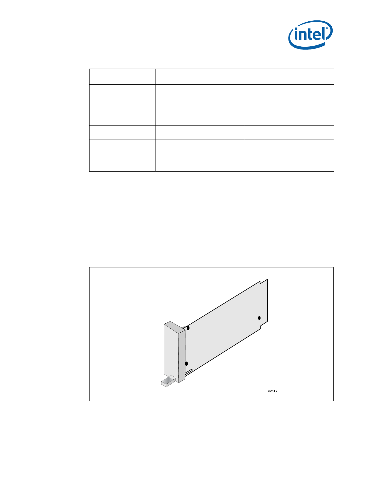
Operating the Unit—MPCBL0010 SBC
Table 2. Jumper Definitions (Continued)
Name
JP7 IPMC Override
(posts 3-4)
JP8 FPGA Config User PROM (default)
JP10 Test Mode
JP11 AdvancedMC PCIExpress Reference Clock
Override
Note: Jumpers JP2, JP1, JP4, JP9, and JP12 are reserved for future use.
Function with Jumper
Present (On)
IPMC is completely disabled and
always in RESET mode.
This setting can be used to allow the
MPCBL0010 SBC to boot if the IPMC
firmware is corrupted or nonfunctional.
Test Mode (for manufacturing
purposes only).
Override AdvancedMC E-Keying and
provide PCI-Express Reference Clock
to the AdvancedMC connectors.
3.2 AdvancedMC Filler Panels
AdvancedMC* filler panels are used to optimize cooling and reduce radiated emissions
when AdvancedMC modules are not installed in theMPCBL0010 SBC AdvancedMC
module slots. Do not operate the MPCBL0010 SBC without filler panels or AdvancedMC
modules installed. AdvancedMC module slots should not be left open or uncovered
when the MPCBL0010 SBC is in use.
The MPCBL0010 SBC uses full-height, half-width AdvancedMC filler panels such as
Schroff* part number # 20849-024 (http://www.schroff.us/).
Function with Jumper
Removed (Off)
Normal IPMC operation (default)
Factory PROM (for manufacturing
purposes only)
Normal (default)
Use normal AdvancedMC E-keying
(default)
Figure 5. AdvancedMC Filler Panel
B5441-01
October 2006 Technical Product Specification
Order Number: 304120 27
Intel NetStructure® MPCBL0010 Single Board Computer
Page 29
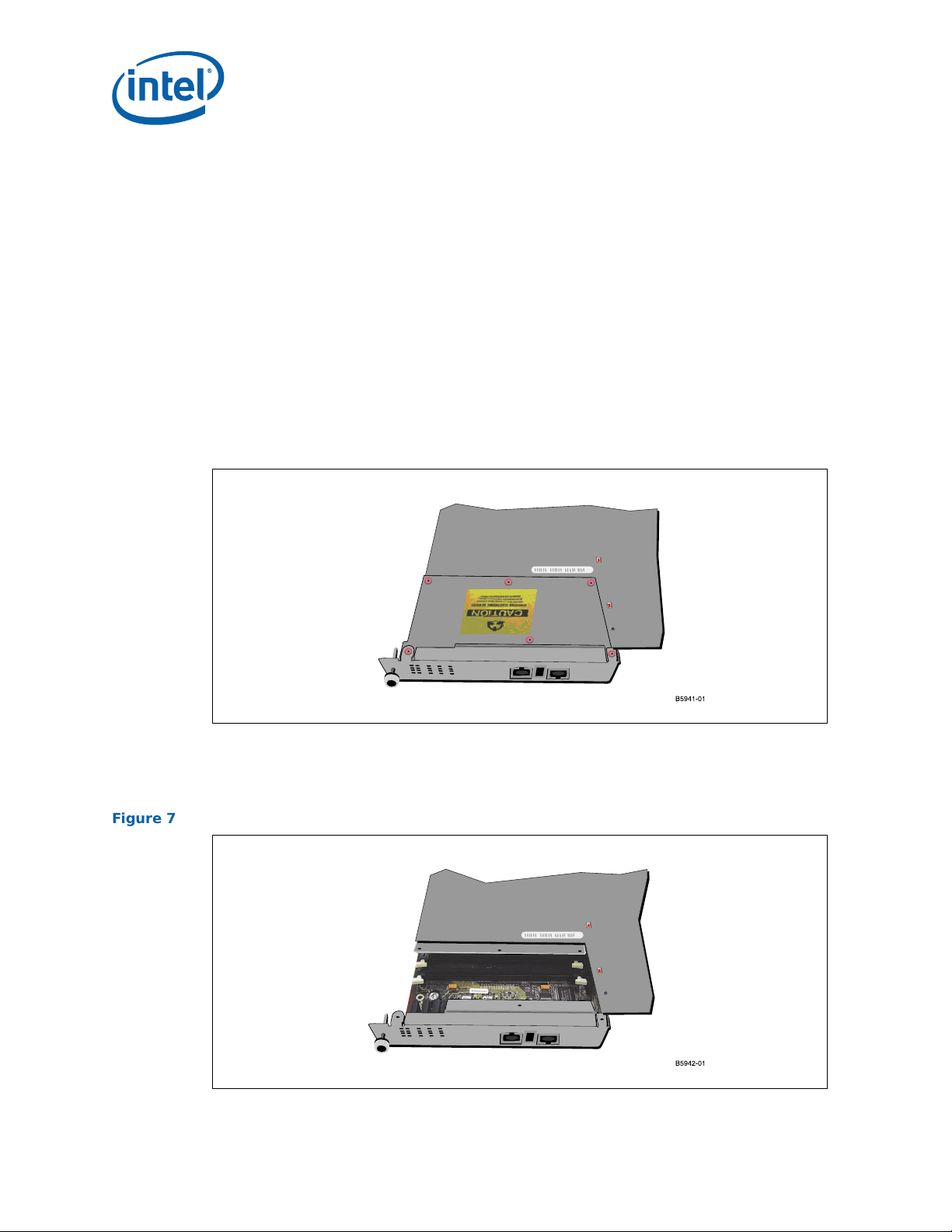
MPCBL0010 SBC—Operating the Unit
3.3 Installing Memory
DDR2-400 DIMMs must be installed in matched pairs. Memory DIMMs of 1 GBytes or 2
GBytes are supported for a total of 2 Gbytes (2x1 Gbyte) or 4 Gbytes (2x2 Gbytes) of
system memory. Matched pairs in this case means a pair of DIMMs equal in speed,
density, and technology. Preferably, the same vendor and part number for both pairs.
See the MPCBL0010 SBC Compatibility Report on the Intel web site for a list of
approved memory part numbers and vendors.
To install memory:
Caution: Electrostatic discharge (ESD) can damage components. Install the memory in an ESD-
controlled area. If such an area is not available, wear an antistatic wrist strap or touch
the surface of the antistatic package before handling the SBC and memory.
1. Remove all six screws pictured in Figure 6 from the memory access panel on the
MPCBL0010 SBC top cover.
Figure 6. Memory Top Cover Installed
B5941-01
2. Remove the cover.
Figure 7. Empty DIMM Sockets
B5942-01
®
Intel NetStructure
Technical Product Specification October 2006
28 Order Number: 304120
MPCBL0010 Single Board Computer
Page 30
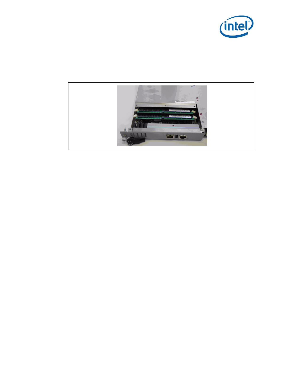
Operating the Unit—MPCBL0010 SBC
3. Insert two matched pair DIMMs.
Warning: Using excessive force to install memory can damage the DIMM socket and/or circuit
board.
Figure 8. Memory Installed
4. Reinstall the cover.
5. Reinstall the six cover screws.
Note: Should any of the cover screws get lost in this process, the specifcations for them are:
• Flat head Phillips screws countersunk M2.5 x 3.4
• Steel with Precote* 80 (pink) coating all around
3.4 Installing and Extracting the SBC
The ability to replace SBCs without affecting the operation of the chassis is a major
element of the PICMG AdvancedTCA standard. This Hot Swap functionality requires a
faceplate ejector handle designed to the PICMG specifications. The new handle has two
important functions:
• Activate the Hot Swap microswitch on the chassis. The handle does this by
sliding inward at the start of the extraction procedure.
• Operate within a narrow range of motion. The handle is designed to provide
clearance from other chassis components (cables, cable trays, PEMs, etc.) that
would otherwise interfere with handle movement in some installations. It also
allows clearance for AdvancedMCs to be installed or removed while the SBC is
operating in the chassis. This is accomplished through a ratcheting mechanism
where the handle is connected to the latching cam (See the illustration in
Section 3.4.1, “Chassis Installation”).
Please review the procedures below before attempting to install or remove the
MPCBL0010 SBC from an AdvancedTCA chassis.
October 2006 Technical Product Specification
Order Number: 304120 29
Intel NetStructure® MPCBL0010 Single Board Computer
Page 31

3.4.1 Chassis Installation
1. Insert the MPCBL0010 SBC into the chassis with the latching cams at a 75º angle.
This will set the latching cams into the installation position. Move the latching cam
by pressing the handle inward to free the latching cam for rotation.
MPCBL0010 SBC—Operating the Unit
2. While holding inward pressure on the handle, slide the MPCBL0010 SBC into the
chassis. Begin rotating the latching cam back to 0º allowing the cam to assist with
insertion. As the SBC is inserted, the AdvancedTCA backplane connectors are
mated to the SBC. If necessary, use your thumbs to apply pressure to the SBC
faceplate near the handles to make sure the SBC is fully inserted.
Caution: Do not apply pressure to the AdvancedMC faceplate, as this could damage the
connectors at the rear of the AdvancedMC module.
3. Once the SBC is installed, rotate the handles into the vertical position.
3.4.2 Chassis Extraction
The AdvancedTCA Hot Swap switch is activate d by pushing in the lower handle (or the
left handle when the SBC is mounted in the horizontal position). When the handle is
pushed inward, a small metal slider will activate the Hot Swap switch.
Note: The ratcheting function of the handle allows the handle to be moved without affecting
Intel NetStructure
Technical Product Specification October 2006
30 Order Number: 304120
the position of the latching cam that holds the SBC in the chassis (see illustration in
®
MPCBL0010 Single Board Computer
Page 32

Operating the Unit—MPCBL0010 SBC
Section 3.4.1). T o rotate the cam, the handle must be pushed in towards the SBC when
moving the handle up or down.
1. Rotate the lower handle to the horizontal position, and push in to disengage the Hot
Swap switch (position 1a to 1b). Wait for the Hot Swap LED on the faceplate to turn
solid blue.
2. With the handles pushed in, simultaneously pivot the top handle up and the bottom
handle down. Using the handles, rotate the latching cam to their farthest point of
travel. This is the pitch line— the farthest the handles can be moved without
hitting the cable tray or other chassis component.
Note: The handles must be pushed in for the latching cam rotation to occur.
3. Release the handles to allow the ratchet mechanisms to disengage from the cams,
and reposition the handles to the horizontal position (the cams will remain at an
angle to the horizontal).
October 2006 Technical Product Specification
Order Number: 304120 31
Intel NetStructure® MPCBL0010 Single Board Computer
Page 33

MPCBL0010 SBC—Operating the Unit
4. Simultaneously push both handles in again and rotate until the handles are at their
farthest point of travel. Repeat this process until the SBC faceplate is clear of the
chassis. At this point the SBC can be removed from the chassis.
3.5 AdvancedMC Module Installation and Extraction
To install or remove an AdvancedMC* module into the MPCBL0010 SBC, simply move
the SBC handle from the vertical to the horizontal position. This will move the handle
out of the way of the AdvancedMC slot and allow modules to be inserted or removed.
Note: Do not push the SBC handle inward because this will activate the Hot Swap switch.
Refer to the AdvancedMC manufacturer user ma nual for other considerations specific to
the AdvancedMC module you are using .
3.6 BIOS Configuration
In most cases, the BIOS defaults will provide the correct configuration to use the
board. See Chapter 7.0, “BIOS Setup” for a complete list of BIOS options.
3.7 Remote Access Configuration
Console redirection to the serial port is enabled by default. This setting will redirect the
text output of the BIOS and operating system to the RJ-45 serial port on the
MPCBL0010 SBC. Remote access using serial console redirection allows users to
monitor the boot process and run the BIOS setup from a remote serial terminal. The
default settings used for console redirection to the serial port are 115,200, n, 8, 1, and
no flow control. See Chapter 5.0, “Connectors and LEDs” for the pin connection of this
interface.
3.8 Software Updates
It is important to use compatible BIOS, FPGA, and IPMC firmware versions. Since all
the software and hardware versions are exchanging specific information, they must be
in synch. Always follow the documentation instructions included with the software
updates.
®
Intel NetStructure
Technical Product Specification October 2006
32 Order Number: 304120
MPCBL0010 Single Board Computer
Page 34

Operating the Unit—MPCBL0010 SBC
You can download software updates for the MPCBL0010 SBC from this Intel web site:
http://www.intel.com/design/telecom/products/cbp/atca/9445/overview.htm
3.8.1 BIOS Updates
At times, new BIOS images will be released to the Intel web site which may add
additional features to the SBC. The BIOS update release package contains the BIOS
ROM image, as well as the flash update utilities. The BIOS update release package also
contains detailed instructions about how to update the BIOS.
3.8.2 Loading\Saving Custom BIOS Configuration
The CMOS settings, together with the BIOS binary image, can be copied to a file with a
file name specified by the user. This allows the user to save BIOS settings from one
SBC and then load the settings onto several other SBCs. The flashlnx utility used to
perform this function is included in the BIOS update release package on the Intel web
site.
3.8.2.1 Synchronizing BIOS Image and Settings from FWH0 (Main) to FWH1 (Backup)
Prior to upgrading the main BIOS (FWH0), a user can create a mirror image where all
the operational codes and CMOS settings will be copied to a redundant BIOS Flash
device. Preserving a copy of the old BIOS image prior to updating the main BIOS is
suggested in case the FWH0 update fails.
The syntax ./flashlnx -m can be used to initiate this transfer. See the suggested
method in Table 3.
Table 3. Suggested Method of BIOS Image Synchronization prior to BIOS Upgrade
BIOS Image Command Behavior
FWH0
FWH0
Image N
Image N
FWH1
FWH1
Image N-1
Image N-1
FWH0
FWH0
Image N
Image N
FWH1
FWH1
Image N
Image N
Note: N = BIOS version
./flashlnx –m
• This is the original FWH images before an
upgrade.
• FWH0 has Image N installed, which is a newer
image than what is installed in FWH1, which is
Image N-1.
• The user can initiate a BIOS update while the
OS is running.
• When this command is executed, the Image N
in FWH0 (BIOS codes + CMOS settings) is
synchronized to FWH1. Image N has now been
copied to the backup FWH1 BIOS image.
• No reboot is needed for this operation.
October 2006 Technical Product Specification
Order Number: 304120 33
Intel NetStructure® MPCBL0010 Single Board Computer
Page 35

MPCBL0010 SBC—Operating the Unit
Table 3. Suggested Method of BIOS Image Synchronization prior to BIOS Upgrade
FWH0
FWH0
Image N+1
Image N+1
FWH1
FWH1
Image N
Image N
Note: N = BIOS version
./flashlnx –b Pxx-xxxx
• When this command is initiated, the FWH0
image will be updated to the latest version
(Image N+1).
• The latest version of the BIOS will take effect
after the user initiates a reset.
• If a checksum error is detected on FWH0 after
a reboot, it will automatically switch to FWH1
and regain normal operation.
3.8.2.2 Copying BIOS.bin from the SBC
1. Copy the flashlnx utility to an SBC running Linux with custom BIOS CMOS settings
that will be used to update other SBCs.
2. Issue the command “./flashlnx -r -afff00000 -s1048576 BIOS.bin” to copy the
BIOS with the customized CMOS settings to the same directory from which flashlnx is
executed. All user-preferred settings (including the BIOS image) will be saved in the
file named BIOS.bin.
Note: “BIOS.bin” is a generic file name used here to illustrate the command line used to
perform the operation. You may wish to use the BIOS version as the file name instead
of BIOS.bin.
3.8.2.3 Saving BIOS.bin to the SBC
1. Copy the flashlnx utility and BIOS.bin to the SBC running Linux.
2. Execute “chmod +x flashlnx” to change the file attribute to an executable form.
3. Execute “./flashlnx -b -zc BIOS.bin” to copy the BIOS.bin file to the firmware
hub (FWH) and CMOS.
4. Upon completion, perform a reset to ensure the new CMOS settings and BIOS are
loaded.
Note: To ensure that the BIOS.bin file is not corrupted, Intel strongly suggests performing
these steps before major deployment of any SBCs running in a live network
environment.
®
Intel NetStructure
Technical Product Specification October 2006
34 Order Number: 304120
MPCBL0010 Single Board Computer
Page 36

Operating the Unit—MPCBL0010 SBC
3.8.2.4 flashlnx Command Line Options
Table 4 lists the command line parameter switches and features supported by the BIOS
flash utility.
Table 4. Flashlnx Utility Command Line Options
Command Line Parameter Description
-b [option] bios_image
where possible [option] values are:
• -z - do not clear the CMOS
• -zc - update the CMOS from image
-i [bios_image] Display BIOS system information
-r [options] bin_image
where possible [option] values are:
• -aAddress - physical address in hex
• -pPage - page number in decimal
• -sSize - image size in decimal
-m
-b cmos_image Backup current CMOS settings to a file
-r cmos_image Restore CMOS settings from a file
-q Force non-interactive mode (assumes “yes” for all prompts)
Program a BIOS image to primary fimware hub (FWH0)
Read the flash image and store to a file
Mirror image where all the operational codes and CMOS settings
are copied from FWH0 to FHW1 (redundant BIOS flash device)
3.8.3 IPMC Firmware Updates
Periodically, new IPMC firmware with additional features will be released to the Intel
web site. The IPMC firmware is upgraded using the KCS interface. The IPMC firmware
update release package contains the IPMC firmware as well as the update utility. The
update release package also contains detailed instructions about how to update the
IPMC firmware.
3.8.3.1 IPMC Firmware Upgrade Using the KCS Interface
The KCS interface is the communication mechanism between the host processor on the
MPCBL0010 SBC and the IPMC controller. A firmware update utility is available. It takes
a hex file to be updated as input from the command line. It can also verify that updates
are completed successfully by reading back data written to the flash memory.
The utility typically takes around two minutes to complete the update over the KCS
interface. After the firmware update is completed, the controller goes through a reset
and boots up with the new firmware. IPMC communication is temporarily lost during
the update, but the host processor is not reset when going through a firmware update,
so the operating system and applications running on the host processor are not
interrupted.
Updating the IPMC firmware requires using ipmitool 1.8.8 or later. Download ipmitool
from http://ipmitool.sourceforge.net/
1. Download and compile ipmitool 1.8.8 or later for your Linux system.
2. Download the IPMC firmware file from the MPCBL0010 SBC product web site
specified in Section 3.8, “Software Updates”
3. Run the following commands to update the IPMC firmware to the newly downloaded
version:
October 2006 Technical Product Specification
Order Number: 304120 35
Intel NetStructure® MPCBL0010 Single Board Computer
Page 37

MPCBL0010 SBC—Operating the Unit
# ipmitool fwum download <IPMI FW file>.bin
# ipmitool fwum upgrade <IPMI FW file>.bin
4. To verify that the upgrade worked properly, run the following command:
# ipmitool fwum status
The output of this command should show the “last known good” version to be
the same as the version just upgraded to. The “previous good” version
should show the previous version before the upgrade.
5. To roll back the lat upgraded version, run the following command:
# ipmitool fwum rollback
Note: You can also use Get Device ID IPMI to verify the current reported version of the
IPMI firmware.
3.9 Digital Ground to Chassis Ground Connectivity
The default grounding for the MPCBL0010 SBC is that digital ground is isolated from the
chassis ground. To connect the digital ground to the chassis ground, install a stainless
steel M2.5 x 6 Phillips pan head screw into the hole next to the AdvancedTCA K1
alignment block (circled in red in Figure 9) on the MPCBL0010 SBC. The screw must be
tightened to 4 lb. per in.
Note: Digital ground is also called logic ground. Chassis ground is also known as shelf ground.
Figure 9. Digital Ground and Chassis Ground Isolated (Default)
B5442-01
®
Intel NetStructure
Technical Product Specification October 2006
36 Order Number: 304120
MPCBL0010 Single Board Computer
Page 38

Specifications—MPCBL0010 SBC
4.0 Specifications
This section defines the Intel NetStructure® MPCBL0010 Single Board Computer
operating and storage environments. It also documents the procedures followed to
determine the reliability of the MPCBL0010 SBC.
4.1 Mechanical Specifications
4.1.1 Board Outline
The MPCBL0010 SBC form factor is mechanically compliant to PICMG 3.0 specification
of 322.25 mm x 280.00 mm (12.687" x 11.024"). The board pitch is 6HP, and the PCB
thickness is 2.0 mm (+/-0.2 mm).
4.1.2 Backing Plate and Top Cover
The MPCBL0010 SBC has a rugged metal backing plate that forms a single-piece
faceplate. This backing plate is made of stainless steel (SS304) and is approximately
0.65 mm thick on bottom, and 1.0 mm thick at the faceplate. The top cover is made
from stainless steel (SS304) and is approximately 0.65 mm thick. A removable cutout
is provided in the top cover for easy access to memory modules.The solid backing plate
and top cover provides PCB stiffening, enhanced EMI protection from adjacent boards,
and protection during flame tests.
Caution: Removing the backing plate can damage the components on the board and may void
the warranty. No user-serviceable parts are available under the PCB. Do not remove
the face plate/backing plate.
4.2 Environmental Specifications
The MPCBL0010 SBC meets the board-level specifications as specified in the Intel
Environmental Standards Handbook – Telco Specification, Document #A78805-01. The
test methodology is a combination of Intel and NEBs test requirements with the intent
that the product will pass pure system-level NEBs testing. Intel will not be completing
NEBs testing on the SBC. The following table summarizes environmental limits, both
operating and nonoperating.
Table 5. Environmental Specifications (Sheet 1 of 2)
Parameter Conditions Detailed Specification
Temperature
(Ambient)
Airflow Operating 30 cubic feet per minute (CFM) minimum
Humidity
Operating 0 to 55° C
Storage -40 to 70° C
Operating 15%-90% (non-condensing) at 55° C
Storage 5%-95% (non-condensing) at 40° C
October 2006 Technical Product Specification
Order Number: 304120 37
Intel NetStructure® MPCBL0010 Single Board Computer
Page 39

MPCBL0010 SBC—Specifications
Table 5. Environmental Specifications (Sheet 2 of 2)
4000 m (13123 ft.)
Note: May require additional cooling above 1800 m (5905 ft.)
Sine sweep:
• 5 to 100 Hz: 1G @ 0.25 Octave/minute
• 100 to 500 Hz: 1G @ 1 Octave/minute
Random profile:
• 5 Hz @ 0.01 g2 /Hz to 20 Hz @ 0.02 g2 /Hz (slope up)
• 20 Hz to 500 Hz @ 0.02 g2 /Hz (flat)
• 3.13 g RMS, 10 minutes per axis for all 3 axes
5 to 50 Hz: 0.5G @ 0.1 Octave/minute
50 to 500 Hz: 3G @ 0.25 Octave/minute.
Altitude
Unpackaged Vibration
Shock
Operating
Storage 15000 m (49212 ft.)
Operating
Storage
Operating 30G/11 ms half sine
Storage 50G, 170 inches/second trapezoidal
4.3 Reliability Specifications
4.3.1 Mean Time Between Failure (MTBF) Specifications
Calculation Type: MTBF/FIT Rate
Standard: Telcordia* Standard SR-332 Issue 1
Methods: Method I, Case I, Quality Level II
The calculation results were generated using the references and assumptions listed.
This report and its associated calculations supersede all other released MTBF and
Failure in Time (FIT) calculations of earlier report dates. The reported failure r ates do
not represent catastrophic failure. Catastrophic failure rates will vary based on
application environment and features critical to the intended function.
Table 6. Reliability Estimate Data
Reliability Measure Value
Failure Rate (FIT) 8967 failures in 10
MTBF 111,513 hours
4.3.1.1 Environmental Assumptions
• Failure rates are based on a 40° C ambient temperature.
• Applied component stress levels are 50 percent (voltage, current, and/or power).
• Ground, fixed, controlled environment with an environmental adjustment factor
equal to 1.0.
4.3.1.2 General Assumptions
• Component failure rates are constant.
• Board-to-system interconnects included within estimates.
• Non-electrical components (screws, mechanical latches, labels, covers, etc.) are
not included within estimations.
• Printed circuit board is considered to have a 0 FIT rate.
9
hours
®
Intel NetStructure
Technical Product Specification October 2006
38 Order Number: 304120
MPCBL0010 Single Board Computer
Page 40

Specifications—MPCBL0010 SBC
4.3.1.3 General Notes
• Method I, Case I = Based on parts count. Equipment failure is estimated by totaling
device failures rates and quantities used.
• Quality Level II = Devices purchased to specifications, qualified devices, vendor lotto-lot controls for AQLs and DPMs.
• Where available, direct component supplier predictions or actual FIT rates have
been used.
• The SBC MTBF does not include addition of the AdvancedMC cards. The product
MTBF could be significantly impacted by adding AdvancedMC cards. Please contact
the AdvancedMC card manufacturer for specific component and relevant
operational MTBF information.
4.3.2 Power Requirements
The power consumed by the MPCBL0010 SBC is dependent on the configuration.
Table 7 shows typical consumption values.
Table 7. Power Requirements
Operating Modes Voltage
Normal -43 VDC to -72 VDC
Degraded -38 VDC to < -43 VDC
Non-Operating 0 VDC to < -38VDC, -72VDC to -75VDC
Note: These voltages assume a 1 V round trip drop on power signals between
shelf power input terminals and board/module slots.
Note: IPMC is powered with input voltage as low as -36 V.
4.3.3 Power Consumption
Table 8. Total Measured Power
Memory Power
4 Gbytes (two 2 Gbyte DIMMs) Max power = < 160 watts
4.4 Weight
Table 9 shows packaged and unpackaged weight.
Table 9. Weight
Configuration Weight Comments
Packaged
Unpackaged
7 lb 6 0z
3.35 kg
5 lb 6 oz
2.44 kg
Includes MPCBL0010 SBC, AMC filler panels,
and packaging material. Does not include
DIMMs.
Includes MPCBL0010 SBC and AMC filler
panels. Does not include DI MMs.
October 2006 Technical Product Specification
Order Number: 304120 39
Intel NetStructure® MPCBL0010 Single Board Computer
Page 41

5.0 Connectors and LEDs
Connectors along the rear edge of AdvancedTCA* server blades are divided into three
distinct zones, as described in Section 2.3 of the PICMG 3.0 specification:
• Zone 1 for system management and power distribution
• Zone 2 for data fabric
• Zone 3 for the rear transition module (not used on the MPCBL0010 SBC)
As shown in Figure 10, the MPCBL0010 SBC includes several connectors to interface
with application-specific devices. Some of the connectors are available at the front
panel as shown in Figure 11. A detailed description and pinout for each connector is
found in the following sections.
MPCBL0010 SBC—Connectors and LEDs
®
Intel NetStructure
Technical Product Specification October 2006
40 Order Number: 304120
MPCBL0010 Single Board Computer
Page 42

Connectors and LEDs—MPCBL0010 SBC
Figure 10. Connector Locations
14
Table 10. On-board and Backplane Connector Assignmen ts
Backplane
Connectors
J10, J12 Memory Socket
J13 POST Code (factory use only)
J25 Extend ITP700 (see Chapter 12 Maintenance)
J20 AdvancedTCA Telecom Clockz (Zone 2)
J23 AdvancedTCA Base and Fabric Interfaces (Zone 2)
P10 AdvancedTCA Power and IPMB
Description
B5440-02
October 2006 Technical Product Specification
Order Number: 304120 41
Intel NetStructure® MPCBL0010 Single Board Computer
Page 43

Figure 11. Front Panel
MPCBL0010 SBC—Connectors and LEDs
Table 11. Front Panel Connector Assignments
Front Panel
Connectors
J3 10/100 Ethernet Debug Port
J4 USB 2.0
J5 Serial Port (RJ-45)
J18, J19 AdvancedMC Connectors
Description
B5444-01
®
Intel NetStructure
Technical Product Specification October 2006
42 Order Number: 304120
MPCBL0010 Single Board Computer
Page 44

Connectors and LEDs—MPCBL0010 SBC
5.1 Backplane Connectors
5.1.1 Power Distribution Connector (P10)
Zone 1 consists of P10, a blue 34-pin Positronic* header connector that provides the
following signals:
• Two -48 VDC power feeds (four signals each; eight signals total)
• Two IPMB ports (two signals each, four signals total)
• Geographic address (eight signals)
• 5.55 A allocated to the MPCBL0010 SBC on the -48 VDC redundant power feeds -this is equivalent to 200 Watts at the minimum input voltage (-36 VDC)
The connector used is Positronic* part number VPB30W8M6200A1. Figure 12 shows the
mechanical drawing of the connector. The pin assignments are given in Table 12.
Figure 12. Power Distribution Connector (Zone 1) P10
20.90
[0.823] MAX
46.10
[1.815] MAX
4.10
[0.161] MAX
B0900-01
October 2006 Technical Product Specification
Order Number: 304120 43
Intel NetStructure® MPCBL0010 Single Board Computer
Page 45

MPCBL0010 SBC—Connectors and LEDs
Table 12. Power Distribution Connector (Zone 1) P10 Pin Assignments
Pin Signal Description Pin Signal Description
1 NCt No Connection 18 Unused No Connection
2 NC No Connection 19 Unused No Connectiont
3 NC No Connectiont 20 Unused No Connection
4 NC No Connection 21 Unused No Connection
5 GA0 Geographic Addr Bit 0 22 Unused No Connection
6 GA1 Geographic Addr Bit 1 23 Unused No Connection
7 GA2 Geographic Addr Bit 2 24 Unused No Connection
8 GA3 Geographic Addr Bit 3 25 EMI_GND EMI Chassis Ground
9 GA4 Geographic Addr Bit 4 26 LOGIC_GND Gnd Ref for Card Logic
10 GA5 Geographic Addr Bit 5 27 ENABLE_B Enb DC-DC conv, B Feed
11 GA6 Geographic Addr Bit 6 28 VRTN_A -48 V Return, Feed A
12 GA7/P Geo Adr Bit 7 (Odd Parity) 29 VRTN_B -48 V Return, Feed B
13 IPMB_CLK_A IPMB Bus A Clock 30 - 48 V_EARLY_A -48 V In, Feed A Precharge
14 IPMB_DAT_A IPMB Bus A Data 31 -48 V_EARLY_B -48 V In, Feed B Precharge
15 IPMB_CLK_B IPMB Bus B Clock 32 ENABLE_A Enb DC-DC conv, A Feed
16 IPMB_DAT_B IPMB Bus B Data 33 -48V_A -48 V Input, Feed A
17 Unused No Connection 34 -48V_B -48 V Input, Feed B
5.1.2 AdvancedTCA Data Transport Connector (J23)
Zone 2 includes one 120-pin HM-ZD connector, labeled J23, with 40 differential pairs.
This data transport connector provides the following signals:
• Two 10/100/1000BASE-T/TX Ethernet base channels (four differential signal pairs
each, 16 signals total).
• Two 1000BASE-BX Ethernet fabric channels (four differential signal pairs each,
eight signals total).
The connector used is AMP*/Tyco* part number 1469001-1. Figure 13 shows a face
view of the connector. The pinout of this connector complies with the AdvancedTCA 3.0
specification.
®
Intel NetStructure
Technical Product Specification October 2006
44 Order Number: 304120
MPCBL0010 Single Board Computer
Page 46

Connectors and LEDs—MPCBL0010 SBC
Figure 13. Data Transport Connector (Zone 2) J23
HG FG DG BG
HG FE DC BA
1
2
3
4
5
6
7
8
9
10
The following naming convention describes the signals on this connector. Signal
direction is defined from the perspective of the MPCBL0010 SBC.
B0899-01
P[C]dxp
Where:
P = Prefix (B=Base interface [Gigabit Ethernet], F= Fabric interface [Gigabit Ethernet])
C = Channel (1-2)
d = direction (Tx = Transmit, Rx = Receive)
x = port number (0-1)
p = polarity (+, -)
Note: A port is two differential pairs, one Tx and one Rx.
The BG, DG, FG, and HG (G for Ground) columns contain the ground shields for the
four columns of differential pairs. They have been omitted from the pinout tables below
for simplification. All pins in the BG, DG, FG, and HG columns are connected to logic
ground.
October 2006 Technical Product Specification
Order Number: 304120 45
Intel NetStructure® MPCBL0010 Single Board Computer
Page 47

MPCBL0010 SBC—Connectors and LEDs
Table 13. AdvancedTCA Data Transport Connector (Zone 2) J23 Pin Assignments
Pin A B C D E F G H
1 No Connect No Connect No Connect No Connect No Connect No Connect No Connect No Connect
2
F[2]Tx0+ F[2]Tx0- F[2]Rx0+ F[2]Rx0- F[2]Tx1+ F[2]Tx1- F[2]Rx1+ F[2]Rx13 No Connect No Connect No Connect No Connect No Connect No Connect No Connect No Connect
4
F[1]Tx0+ F[1]Tx0- F[1]Rx0+ F[1]Rx0- F[1]Tx1+ F[1]Tx1- F[1]Rx1+ F[1]Rx15
B[1]Tx0+ B[1]Tx0- B[1]Rx0+ B[1]Rx0- B[1]Tx1+ B[1]Tx1- B[1]Rx1+ B[1]Rx16
B[2]Tx0+ B[2]Tx0- B[2]Rx0+ B[2]Rx0- B[2]Tx1+ B[2]Tx1- B[2]Rx1+ B[2]Rx17 No Connect No Connect No Connect No Connect No Connect No Connect No Connect No Connect
8 No Connect No Connect No Connect No Connect No Connect No Connect No Connect No Connect
9 No Connect No Connect No Connect No Connect No Connect No Connect No Connect No Connect
10 No Connect No Connect No Connect No Connect No Connect No Connect No Connect No Connect
Indicates used extended fabric (Gigabit Ethernet) ports
Indicates used base (Gigabit Ethernet) channels
5.1.3 AdvancedTCA Data Transport Connector (J20)
The MPCBL0010 SBC implementation of the telecom clock uses the J20 connector to
connect to the three separate and redundant clock buses on the AdvancedTCA
backplane. The Zone 2 J20 connector consists of one 120-pin HM-ZD connector with 40
differential pairs.
Table 14. AdvancedTCA* Data Transport Connector (Zone 2) J20 Pin
Pin A B C D E F G H
1 CLK1A+ CLK1A- CLK1B+ CLK1B- CLK2A+ CLK2A- CLK2B+ CLK2B2 No Connect No Connect No Connect No Connect CLK3A+ CLK3A- CLK3B+ CLK3B3 No Connect No Connect No Connect No Connect No Connect No Connect No Connect No Connect
4 No Connect No Connect No Connect No Connect No Connect No Connect No Connect No Connect
5 No Connect No Connect No Connect No Connect No Connect No Connect No Connect No Connect
6 No Connect No Connect No Connect No Connect No Connect No Connect No Connect No Connect
7 No Connect No Connect No Connect No Connect No Connect No Connect No Connect No Connect
8 No Connect No Connect No Connect No Connect No Connect No Connect No Connect No Connect
9 No Connect No Connect No Connect No Connect No Connect No Connect No Connect No Connect
10 No Connect No Connect No Connect No Connect No Connect No Connect No Connect No Connect
5.1.4 Alignment Blocks
The MPCBL0010 SBC implements the K1 and K2 alignment blocks at the top of Zone 2
and Zone 3, as required in Section 2.4.4 of the PICMG 3.0 specification. The Zone 2
alignment block is assigned a keying value of 11, and uses a Tyco* 1469373 or a Tyco
1469268 component (or equivalent). The Zone 3 alignment block has a solid face and is
used to ensure that rear transition modules (RTMs) with protruding connectors are not
plugged into the MPCBL0010 SBC or vice versa; the component used for this is either a
Tyco 1469374 or a Tyco 1469275-2 (or equivalent).
®
Intel NetStructure
Technical Product Specification October 2006
46 Order Number: 304120
MPCBL0010 Single Board Computer
Page 48

Connectors and LEDs—MPCBL0010 SBC
5.2 On-Board Connectors
5.2.1 POST Code Connector (J13)
The 8-bit content of I/O address 80h is serialized into a proprietary protocol and the
output sent to the J13 connector. In manufacturing, a display board is used to
deserialize and display the POST code value on 7-segment LEDs modules.
Table 15. POST Code Connector Pin Assignments
Pin Signal
1 VCC3
2 Post:Data
3 Post:Clock
4GND
5.2.2 Extended IPT700 Debug Port Connector (J25)
An Extended ITP700 port connection is included to facilitate debug and BIOS/software
development efforts. This JTAG connection to the processors utilizes voltage signaling
levels that are specific to the Low Voltage Intel® Xeon™ Processor family. These levels
must not be exceeded or processor damage may occur. See the Debug Port Design
Guide listed in Appendix A, “Reference Documents” for more information.
October 2006 Technical Product Specification
Order Number: 304120 47
Intel NetStructure® MPCBL0010 Single Board Computer
Page 49

MPCBL0010 SBC—Connectors and LEDs
5.3 Front Panel Connectors
5.3.1 Ethernet 10/100 Debug Connector (J3)
A single Ethernet port interface is provided on the front edge of the card using an RJ-45
style shielded connector (Tyco* RJ714-CL2). This port can be used for debug or
management. See Figure 10 for its position on the board.
Note: When using the Ethernet 10/100 Debug Connector, you must use shielded category 5
cabling.
Figure 14. Ethernet 10/100 Debug Connector
Table 16. Ethernet 10/100 Debug Connector Pin Assignments
Pin Signal
1TX+
2TX3RX+
4 No Connect
5 No Connect
6RX7 No Connect
8 No Connect
Table 17. Ethernet 10/100 Debug Connector LED Operation
LED Function
Off: No Link
LNK
SPD
Amber: Link
Amber-blink: Link & Activity
Off: 10Mb/s
Green: 100Mb/s
®
Intel NetStructure
Technical Product Specification October 2006
48 Order Number: 304120
MPCBL0010 Single Board Computer
Page 50

Connectors and LEDs—MPCBL0010 SBC
5.3.2 USB Connector (J4)
The MPCBL0010 SBC has one USB connector that supports 2.0 and 1.1 USB. USB
connector J4 is available at the front panel. See Figure 10for its position on the board.
Figure 15. USB Connector (J4)
Table 18. USB Connector (J4) Pin Assignments
Pin Signal
1+5V
2-DATA
3+DATA
4GND
5.3.3 Serial Port Connector (J5)
A single serial port interface is provided on the front edge of the card using an RJ-45
style shielded connector. See Figure 10 for its position on the board. This connector is
an 8-pin RJ-45.
Figure 16. Serial Port Connector (J5)
Optional Top Ground Tabs
Optional Side
Ground tabs
(2 places)
.724 REF.
Shielded Modular Jack Assembly
molex
18.39t
.512
13.00
.120
3.05
REF.
(outside)
REF.
.120
3.05
REF.
.128
3.25
.427
10.85
.829
21.05
.120
3.05
B0902-01
October 2006 Technical Product Specification
Order Number: 304120 49
Intel NetStructure® MPCBL0010 Single Board Computer
Page 51

Table 19. Serial Port Connector (J5) Pin Assignments
Pin Signal
1RTS
2DTR
3TXD
4GND
5GND
6RXD
7DSR
8CTS
Figure 17. DB-9 to RJ-45 Pin Translation
MPCBL0010 SBC—Connectors and LEDs
5.3.4 AdvancedMC* Connectors (J18, J19)
There is a single AMC B+ connector for each AdvancedMC slot. Connector J18
corresponds to AMC designator B1. Connector J19 corresponds to AMC designator B2.
The connectors and pinouts are defined by the industry standard specifications AMC.0
R1.0, AMC.1 R1.0, AMC.2 R1.0, and AMC.3 R1.0. The AdvancedMC slots are available
from the front panel. See Figure 10 for their positions on the board.
Note: Do not operate the MPCBL0010 SBC without AdvancedMC module filler panels or
AdvancedMC modules installed. The AdvancedMC module slots should not be open or
uncovered when the MPCBL0010 SBC is in use in order to meet cooling and radiated
emmission requirements.
Table 20 on the following page lists the AdvancedMC connector pin assignments.
®
Intel NetStructure
Technical Product Specification October 2006
50 Order Number: 304120
MPCBL0010 Single Board Computer
Page 52

MPCBL0010 SBC—Connectors and LEDs
Table 20. AdvancedMC* Connector Pin Assignments
Pin Signal
1GND
2PWR1
3PS1#
4 MP_3V3
5GA0
6NC
7GND
8NC
9PWR2
10 GND
11 PORT0_RXP
12 PORT0_RXN
13 GND
14 PORT0_TXP
15 PORT0_TXN
16 GND
17 GA1
18 PWR3
19 GND
20 PORT1_RXP
21 PORT1_RXN
22 GND
23 PORT1_TXP
24 PORT1_TXN
25 GND
26 GA2
27 PWR4
28 GND
MB_Rx2+
29
30
31 GND
32
33
34 GND
35 NC
36 NC
37 GND
38 NC
39 NC
(SATA)
MB_Rx2-
(SATA)
MB_Tx2+
(SATA)
MB_Tx2-
(SATA)
Pin Signal
40 GND
41 ENABLE
42 PWR5
43 GND
44 MB_Rx4+
45 MB_Rx446 GND
47 MB_Tx4+
48 MB_Tx449 GND
50 MB_Rx5+
51 MB_Rx552 GND
53 MB_Tx5+
54 MB_Tx555 GND
56 IPMI_CLK
57 PWR6
58 GND
59 MB_Rx6+
60 MB_Rx661 GND
62 MB_Tx6+
63 MB_Tx664 GND
65 MB_Rx7+
66 MB_Rx767 GND
68 MB_Tx7+
69 MB_Tx770 GND
71 IPMI_DATA
72 PWR7
73 GND
74 +CLKA
75 -CLKA
76 GND
77 +CLKB
78 -CLKB
79 GND
80 +CLKC
Pin Signal
81 -CLKC
82 GND
83 GND
84 PWR8
85 GND
86 GND
87 MB_Tx888 MB_Tx8+
89 GND
90 MB_Rx891 MB_Rx8+
92 GND
93 MB_Tx994 MB_Tx9+
95 GND
96 MB_Rx997 MB_Rx9+
98 GND
99 MB_Tx10100 MB_Tx10+
101 GND
102 MB_Rx10103 MB_Rx10+
104 GND
105 NC
106 NC
107 GND
108 MB_Rx11109 MB_Rx11+
110 GND
111 MB_Tx12112 MB_Tx12+
113 GND
114 MB_Rx12115 MB_Rx12+
116 GND
117 NC
118 NC
119 GND
120 NC
121 NC
Pin Signal
122 GND
123 NC
124 NC
125 GND
126 NC
127 NC
128 GND
129 NC
130 NC
131 GND
132 NC
133 NC
134 GND
135 NC
136 NC
137 GND
138 NC
139 NC
140 GND
141 NC
142 NC
143 GND
144 NC
145 NC
146 GND
147 NC
148 NC
149 GND
150 NC
151 NC
152 GND
153 NC
154 NC
155 GND
156 NC
157 NC
158 GND
159 NC
160 NC
161 GND
162 NC
Pin Signal
163 NC
164 GND
165 TCLK
166 TMS
167 RST
168 TDO
169 TDI
170 GND
NC NC
NC NC
Note:
NC = No Connection
October 2006 Technical Product Specification
Order Number: 304120 51
Intel NetStructure® MPCBL0010 Single Board Computer
Page 53

Figure 18. AdvancedMC* Connector
MPCBL0010 SBC—Connectors and LEDs
Caution: Do not ship the MPCBL0010 SBC with third party AdvancedMC modules installed.
Damage that occurs to the MPCBL0010 SBC during shipment from AdvancedMC
modules installed is not covered by the MPCBL0010 SBC product warranty.
5.4 LEDs
The MPCBL0010 SBC provides several LEDs to indicate status. The LEDs can be driven
to display red, green or amber color. There are two different possible MPCBL0010
faceplates as shown in Figure 19 and Figure 20. The LEDs are labeled slightly differenly
on each, but the fucntionality is the same on both. The status for each LED when lit is
defined in Table 21.
®
Intel NetStructure
Technical Product Specification October 2006
52 Order Number: 304120
MPCBL0010 Single Board Computer
Page 54

Connectors and LEDs—MPCBL0010 SBC
Figure 19. Front Panel LEDs (Option 1)
Figure 20. Front Panel B LEDs (Option 2)
FABRIC
U0
BASE
HDD
HLT
IPM
OOS
21
U1
H/S
21
U2
B5445-01
October 2006 Technical Product Specification
Order Number: 304120 53
Intel NetStructure® MPCBL0010 Single Board Computer
Page 55

Table 21. Front Panel LED Descriptions (Sheet 1 of 2)
LED Function
H/S
Hot Swap (AdvancedTCA-Blue).
The LED’s default IPMC behavior can be overridden with AdvancedTCA FRU LED Control commands.
Off / Blue
MPCBL0010 SBC—Connectors and LEDs
OOS
HLT
U0
Base 1 GbE Link
Base 1 GbE Speed
Base 2 GbE Link
Base 2 GbE Speed
Fabric 1 GbE Link
Fabric 2 GbE Link
Out of Service (AdvancedTCA-LED1).
Amber: The IPMC is not responding.
Amber-blink: The IPMC firmware is being upgraded.
Off: The IPMC is running OK.
The LED’s default IPMC behavior can be overridden with AdvancedTCA FRU LED Control commands.
Off / Red / Amber
Health (AdvancedTCA-LED2).
The SBC health is based on an aggregation of IPMI sensors, like board temperature and voltage.
Green - The SBC is healthy.
Red - The SBC is not healthy.
The LED’s default IPMC behavior can be overridden with AdvancedTCA FRU LED Control commands.
Off / Green / Red / Amber
Hearbeat / User Defined 0 (AdvancedTCA-LED3).
This LED is user-defined and off by default. The LED’s default IPMC behavior can be overridden with
AdvancedTCA FRU LED Control commands.
Off / Amber
Gigabit Ethernet Base Interface 1 Activity and Status.
Off: No Link
Green: Link
Green-blink: Link & Activity
Gigabit Ethernet Base Interface 1 Speed.
Off: 10Mb/s
Green: 100Mb/s
Amber: 1000Mb/s
Gigabit Ethernet Base Interface 2 Activity and Status.
Off: No Link
Green: Link
Green-blink: Link & Activity
Gigabit Ethernet Base Interface 2 Speed.
Off: 10Mb/s
Green: 100Mb/s
Amber: 1000Mb/s
Gigabit Ethernet Fabric Interface 1 Activity and Status.
Off: No Link
Green: Link
Green-blink: Link & Activity
Gigabit Ethernet Fabric Interface 2 Activity and Status.
Off: No Link
Green: Link
Green-blink: Link & Activity
®
Intel NetStructure
Technical Product Specification October 2006
54 Order Number: 304120
MPCBL0010 Single Board Computer
Page 56

Connectors and LEDs—MPCBL0010 SBC
Table 21. Front Panel LED Descriptions (Sheet 2 of 2)
LED Function
This LED has two functions. The LED will display POST codes in the event the SBC fails to boot. Once the
HDD
IPM
U1
SBC has booted and passed BIOS POST, this LED will indicate hard disk activity.
Hard Disk activity
Green-blink: Activity
POST Codes.
Off / Green / Red / Amber
See Section , “” on page 55 for more detail.
IPMC Status.
Slow Blink Green: IPMC Heartbeat.
Fast Blink Green: There is traffic on the KCS interface of the IPMC.
Slow Blink Red: The KCS interface request attention from the SMS or SMM.
Fast Blink Red: There is traffic on the IPMB interface of the IPMC.
It is not possible to override the behavior of this LED.
Off / Green / Red / Amber
User Defined (AdvancedTCA USER1).
By default this LED is off.
The LED’s default IPMC behavior can be overr i dden with AdvancedTCA FRU LED Control commands.
Off / Green / Red / Amber
U2
User Defined (AdvancedTCA USER2).
By default this LED is off.
The LED’s default IPMC behavior can be overr i dden with AdvancedTCA FRU LED Control commands.
Off / Green / Red / Amber
Table 22. Ethernet 10/100 Debug Connector LE D Operation
LED Function
LNK
Off: No Link
Amber: Link
Amber-blink: Link & Activity
SPD
Off: 10Mb/s
Green: 100Mb/s
5.4.1 POST LED Codes
The HDD LED uses a blinking sequence to display the current POST (Power On Self
Test) code value. If the boot process succeeds, the POST code is irrelevant and the
BIOS will change the state of the HDD LED to display hard disk activity just before the
October 2006 Technical Product Specification
Order Number: 304120 55
Intel NetStructure® MPCBL0010 Single Board Computer
Page 57

operating system launches. If the boot sequence fails or the CPU hangs, the HDD
(POST) LED will remain operational in POST code mode and repeat indefinitely the last
POST code blink sequence as defined below:
1. Blink simultaneously amber and green one time: start of the sequence.
2. Blink amber 0-15 times while green stays off.
3. Blink green 0-15 times while amber stays off.
4. Repeat the sequence (see step 1).
Amber (A) is the first or most significant digit of the POST code value in hexadecimal,
while green (G) is the second digit (i.e., POST code value is AGh). Some examples are
shown in Figure 21.
Figure 21. Example POST LED Codes
MPCBL0010 SBC—Connectors and LEDs
Note: See Section 8.2, “Port 80h POST Codes” for explanations of the codes.
5.5 Reset Button
The Reset button is located in a small recessed hole near the serial port connector on
the front panel. The Reset button is an input to the IPMC to requ est a cold reset. There
are IPMI commands to reset the board and change power states through the software.
The Reset button is a last resort because someone must be physically present at the
chassis to reset the board. The Reset button location on the front panel is shown in
Figure 11.
®
Intel NetStructure
Technical Product Specification October 2006
56 Order Number: 304120
MPCBL0010 Single Board Computer
Page 58

BIOS Features—MPCBL0010 SBC
6.0 BIOS Features
6.1 Introduction
The MPCBL0010 SBC uses an Intel/AMI* BIOS, which is stored in flash memory and
updated using a disk-based program. In addition to the BIOS and BIOS setup program,
the flash memory contains POST and Plug and Play support.
The BIOS displays a message during POST identifying the type of BIOS and a revision
code. Refer to the Specification Update on the Documentation tab of the MPCBL0010
SBC web site at http://www.intel.com/design/telecom/products/cbp/atca/9445/
overview.htm for the latest default settings.
6.2 BIOS Flash Memory Organization
The MPCBL0010 SBC contains two firmware hub (FWH) devices . (See Figure 1) The
first is the Primary FWH, which holds the BIOS code that executes during POST. The
second is the Backup FWH, which recovers the system when the Primary FWH is
corrupted. The N82802AC FWH includes an 8 Mbit (1024 KByte) symmetrical flash
memory device. Internally , the device is grouped into sixteen 64-KByte blocks that are
individually erasable, lockable, and unlockable.
6.3 Complementary Metal-Oxide Semiconductor (CMOS)
CMOS RAM is a nonvolatile storage that stores data needed by the BIOS. The data
consists of certain onboard configurable settings, including time and date. CMOS
resides in the 6300ESB ICH and is powered by the Supercap when the blade is power
off. The settings in the BIOS setup menu are stored in the CMOS RAM and are often
called CMOS settings.
6.4 Redundant BIOS Functionality
MPCBL0010 SBC hardware has two flash banks for BIOS where redundant copies are
stored. BIOS bank selection logic is connected to the IPMC, and the IPMC firmware
allows selection of the BIOS bank.
By default, firmware selects BIOS bank 0. BIOS executes code off this flash and
performs checksum validation of its operational code. This checksum occurs in the boot
block of the BIOS. If the boot block detects a checksum failure in the remainder of the
BIOS, it notifies the IPMC of the failure.
In case of failure, the IPMC firmware:
1. Asserts the RESET pin on the processor
2. Switches the flash bank
3. De-asserts the RESET pin on the processor, allowing BIOS to execute off the second
flash bank
An application running on a non-Plug and Play operating system can obtain the SMBIOS
information.
October 2006 Technical Product Specification
Order Number: 304120 57
Intel NetStructure® MPCBL0010 Single Board Computer
Page 59

MPCBL0010 SBC—BIOS Features
6.5 Legacy USB Support
Legacy USB support enables USB devices such as keyboards, mice, and hubs to be
used even when the operating system’s USB drivers are not yet available. Legacy USB
support is used to access the BIOS Setup program and install an operating system that
supports USB. Legacy USB support is set to Enabled by default.
Note: Legacy USB support is for keyboards, mice and hubs only. Other USB devices are not
supported in legacy mode except bootable devices like CD-ROM drives and floppy disk
drives.
Legacy USB support operates as follows:
1. When you apply power to the computer, legacy support is disabled.
2. POST begins.
3. Legacy USB support is enabled by the BIOS, allowing you to use a USB keyboard.
4. POST completes.
5. The operating system loads. USB keyboards and mice are recognized and may be
used to configure the operating system. Keyboards and mice are not recognized
during this period if Legacy USB support was set to Disabled in the BIOS Setup
program.
6. After the operating system loads the USB drivers, all legacy and non-legacy USB
devices are recognized by the operating system. Legacy USB support from the
BIOS is no longer used.
T o install an operating system that supports USB, verify that Legacy USB support in the
BIOS Setup program is set to Enabled and follow the operating system’s installation
instructions.
6.5.1 Language Support
English is the only supported language.
6.6 Recovering BIOS Data
Some types of failure can destroy the BIOS. For example, the data can be lost if a
power outage occurs while the BIOS is being updated in flash memory. The BIOS can
be recovered from the backup BIOS FWH. Recovery mode is active when BIOS
checksum fails and notifies the IPMC to failover to the backup BIOS automatically.
6.7 Boot Options
In the BIOS Setup program, the user can choose to boot from available boot devices,
with each boot device having options for removable media, CD-ROM, AdvancedMC*
hard drive, or by a network boot through any of the four Gigabit Ethernet (GbE)
adapters. In every POST, the BIOS detects all available boot devices, then displays
them on the boot order screen, with the exception of the IBA, which displays even if
the LAN cable is not connected.
The default settings are:
• 1st Boot Device: removable media
• 2nd Boot Device: CD-ROM
• 3rd Boot Device: hard drive
• 4th Boot Device: IBA2 - Intel® Boot Agent (IBA) 0309
®
Intel NetStructure
Technical Product Specification October 2006
58 Order Number: 304120
MPCBL0010 Single Board Computer
Page 60

BIOS Features—MPCBL0010 SBC
• 5th Boot Device: IBA1 - Intel® Boot Agent (IBA) 0308
®
• 6th Boot Device: IBA2 - Intel
• 7th Boot Device: IBA2 - Intel
Boot Agent (IBA) 0311
®
Boot Agent (IBA) 0310
Note: Additional boot devices may appear in the above list if there are other bootable devices
connected to the board (for example, USB devices or AdvancedMC devices).
6.7.1 CD-ROM and Network Boot
Booting from CD-ROM is supported in compliance with the “El T orito” bootable CD-ROM
format specification. Under the Boot menu in the BIOS setup program, USB CD-ROM is
listed as a boot device (removable media). Boot devices are defined in priority order.
Accordingly, if there is not a bootable CD in the CD-ROM drive, the system attempts to
boot from the next defined drive.
The network can be selected as a boot device. This Intel
®
Boot Agent (IBA) selection
allows booting from the onboard LANs if connected to a network.
6.7.2 Booting without Attached Devices
For use in embedded applications, the BIOS has been designed so that after passing
the POST, the operating system loader is invoked even if a video adapter (via
AdvancedMC), keyboard, or mouse are not present:
6.8 Fast Booting Systems
6.8.1 Quick Boot
Use of the following BIOS setup program settings reduces the POST execution time.
In the Boot Menu:
• Disable Option - ROM(s) if customer configuration does not use IBA(PXE) boot
• Enable Quick Boot - bypasses memory count and the search for a removable drive
Note: Quick Boot is enabled by default. The boot time may be so fast that some drives might
not be initialized at all. If this occurs, it is possible to introduce a programmable delay
ranging from 0 to 35 seconds using the BIOS setup program, IDE Configuration
Submenu, Advanced Menu, IDE Detect Time Out feature.
6.9 BIOS Security Features
The BIOS includes security features that restrict access to the BIOS Setup program and
booting the computer. A supervisor password and a user password can be set for the
BIOS setup program and for booting the computer, with the following restrictions:
• The supervisor password gives unrestricted access to view and change all the setup
options in the BIOS setup program. This is the supervisor mode.
• The user password gives restricted access to view and change setup options in the
BIOS setup program. This is the user mode.
• If only the supervisor password is set, pressing the Enter key at the password
prompt of the BIOS setup program allows the user restricted access to setup.
October 2006 Technical Product Specification
Order Number: 304120 59
Intel NetStructure® MPCBL0010 Single Board Computer
Page 61

• If both the supervisor and user passwords are set, users can enter either the
supervisor password or the user password to access setup. Access to setup
corresponds to which password is entered.
• Setting the user password restricts who can boot the computer. The password
prompt is displayed before the computer is booted. If only the supervisor password
is set, the computer boots without asking for a password. If both passwords are
set, the user can enter either password to boot the computer.
Table 23 shows the effects of setting the supervisor password and user password. This
table is for reference only and is not displayed on the screen.
Table 23. Supervisor and User Password Functions
MPCBL0010 SBC—BIOS Features
Password Set Supervisor Mode User Mode
None
Supervisor and
user
Supervisor only
User only
Any user can
change all options
Can change all
options
Can change all
options
Can't get into
supervisor mode
until user password is cleared.
Any user can change
all options
Based on user
access level: No
Access, View Only,
Limited, Full Access
Based on user
access level: No
Access, View Only,
Limited, Full Access.
Can change all
options
Password to
Enter Setup
None None
If password check option is
Supervisor or
user
Supervisor (for
supervisor
mode) or enter
only (for user
mode)
User
set to Setup then no
password required. Otherwise
requires either supervisor or
user password.
If password check option is
set to Setup then no
password required. Otherwise
requires either supervisor
password or enter only.
If password check option is
set to Setup then no
password required. Otherwise
requires user password.
Password During Boot
6.10 Remote Access Configuration
Remote access using serial console redirection allows users to monitor the MPCBL0010
SBC boot process and run the MPCBL0010 SBC BIOS setup from a remote serial
terminal. Connection is made directly through a serial port.
The console redirection feature is useful in cases where it is necessary to communicate
with a processor board in an embedded application without video support.
Note: The default settings used for console redirection to the serial port are 115,200, n, 8, 1,
and no flow control.
Table 24 shows the escape code sequences that may be useful for things like BIOS
setup if function keys cannot be sent directly from a terminal application:
Table 24. Function Key Escape Code Equivalents (Sheet 1 of 2)
Key Escape Sequence Note
F1 ESC OP
F2 ESC OQ
F3 ESC OR
F4 ESC OS To enter BIOS Setup
F5 ESC OT
F6 ESC OU
F7 ESC OV
®
Intel NetStructure
Technical Product Specification October 2006
60 Order Number: 304120
MPCBL0010 Single Board Computer
Page 62

BIOS Features—MPCBL0010 SBC
Table 24. Function Key Escape Code Equivalents (Sheet 2 of 2)
Key Escape Sequence Note
F8 ESC OW
F9 ESC OX
F10 ESC OY To save and exit Setup
F11 ESC OZ
F12 ESC OI PXE boot
October 2006 Technical Product Specification
Order Number: 304120 61
Intel NetStructure® MPCBL0010 Single Board Computer
Page 63

7.0 BIOS Setup
7.1 Introduction
The MPCBL0010 SBC BIOS is based on AMIBIOS8*. The BIOS Setup program can be
used to view and change the BIOS settings for the SBC. The BIOS Setup program is
accessed by pressing the <DEL> key (or F4 on a remote keyboard) after the Power -On
Self- Test (POST) begins and before the operating system boot begins. Table 25 lists the
BIOS Setup program menu features.
Table 25. BIOS Setup Program Menu Bar
Main Advanced PCIPnP Boot Security Chipset Exit
Allocates
resources for
hardware
components.
Table 26 lists the function keys available for menu screens.
Configures
advanced
features
available
through the
chipset.
Configures
PCI Plug and
Play features.
Selects boot
options and
power supply
controls.
Sets
passwords
and security
features.
MPCBL0010 SBC—BIOS Setup
Saves or
Configures
MCH and ICH
features.
discards
changes to
Setup
program
options.
Table 26. BIOS Setup Program Function Keys
BIOS Setup Program
Function Key
<←> or <→> Selects a different menu screen (moves the cursor left or right).
<↑ > or <↓> Selects an item (moves the cursor up or down).
<Tab> Selects a field (not implemented).
<Enter> Executes command or selects the sub-menu.
<F10> Saves the current values and exits the BIOS Setup program.
<Esc> Exits the menu.
7.2 Main Menu
To access this menu, select Main on the menu bar at the top of the screen.
Main Advanced PCIPnP Boot Security Chipset Exit
Description
®
Intel NetStructure
Technical Product Specification October 2006
62 Order Number: 304120
MPCBL0010 Single Board Computer
Page 64

BIOS Setup—MPCBL0010 SBC
Table 27 describes the Main menu. This menu reports processor and memory
information and is used for configuring the system date and system time.
Table 27. Main Menu
Feature Options Description
BIOS ID
PLD Information FPGA Version Programmable Logic Device Version Information.
Processor
System Memory Size Size Displays installed memory size.
System Time Hour/minute/second Specifies the current time.
System Date
Version
Build Date
ID
Type
Speed
Count
Day of week
Month/day/year
7.3 Advanced Menu
Displays the BIOS version, build date, and ID.
Reports processor type, speed, and count.
Specifies the current date.
To access this menu, select Advanced on the menu bar at the top of the screen.
Main Advanced PCIPnP Boot Security Chipset Exit
CPU Configuration
IDE Configuration
SuperIO Configuration
ACPI Configuration
System Management
Event Log Configuration
MPS Configuration
ATCA Channel Routing (PICMG)
On-board Devices Configuration
PCI Express Configuration
Remote Access Configuration
IPMI Configuration
USB Configuration
Warning: Setting the wrong values in the sections that follow may cause the system to
malfunction.
Do not modify the settings unless you are familiar with the items. To restore factory
defaults, go to “Exit > Load Optimal Defaults”.
Table 28 describes the Advanced menu. This menu sets advanced features that are
available through the chipset.
October 2006 Technical Product Specification
Order Number: 304120 63
Intel NetStructure® MPCBL0010 Single Board Computer
Page 65

Table 28. Advanced Menu
Feature Options Description
CPU Configuration
IDE Configuration
SuperIO Configuration
ACPI Configuration
System Management
Event Log Configuration
MPS Configuration
ATCA Channel Routing
(PICMG)
On-Board Device
Configuration
PCI Express Configuration
Remote Access
Configuration
IPMI Configuration
USB Configuration
Select to display
sub-menu
Select to display
sub-menu
Select to display
sub-menu
Select to display
sub-menu
Select to display
sub-menu
Select to display
sub-menu
Select to display
sub-menu
Select to display
sub-menu
Select to display
sub-menu
Select to display
sub-menu
Select to display
sub-menu
Select to display
sub-menu
Select to display
sub-menu
MPCBL0010 SBC—BIOS Setup
Display CPU details, Enable/Disable Hyper-Threading**
technology.
Display the primary IDE master and primary IDE slave
drive.
Set parallel port address/interrupt.
Enable/Disable ACPI support for OS, Enable/Disable
additional ACPI 2.0 tables.
Displays FRU, board, product, IPMI device, and firmware
information.
Enable/Disable error logging.
Configure Multi-Processor Table.
Select either the on-board GbE Fabric port, or the
AdvancedMC port for routing to AdvancedTCA backplane.
Enable / Disable On-board devices.
Configure PCI Express support.
Enable/Disable remote access.
IPMI configuration including server monitoring and event
log.
Enable/Disable USB devices.
7.3.1 CPU Configuration Sub-Menu
To access this sub-menu, select Advanced on the menu bar, then CPU Configuration.
Main Advanced PCIPnP Boot Security Chipset Exit
CPU Configuration
IDE Configuration
SuperIO Configuration
ACPI Configuration
System Management
Event Log Configuration
MPS Configuration
ATCA Channel Routing (PICMG)
On-board Devices Configuration
PCI Express Configuration
®
Intel NetStructure
Technical Product Specification October 2006
64 Order Number: 304120
MPCBL0010 Single Board Computer
Page 66

BIOS Setup—MPCBL0010 SBC
Main Advanced PCIPnP Boot Security Chipset Exit
Remote Access Configuration
IPMI Configuration
USB Configuration
Table 29 shows the sub-menu options for configuring the CPU.
Table 29. CPU Configuration Sub-Menu
Feature Options Description
Manufacturer Display CPU Manufacturer.
Brand String Display CPU Brand String.
Frequency Display CPU Frequency.
FSB Speed Displays Front Side Bus Speed.
Cache L1 Displays L1 Cache size.
Cache L2 Displays L2 Cache size.
Ratio Status Displays Ratio Status (14=2.8 Ghz).
Ratio Actual Value Displays Ratio Value.
Max CPUIP Value Limit
Thermal Monitor
Execute Disable Bit
Hardware Prefetcher
Adjacent Cache Line
Prefetcher
Hyper-Threading
Technology
Note: Bold text indicates default setting.
Disabled
Enabled
Disabled
TM1
Disabled
Enabled
Disabled
Enabled
Disabled
Enabled
Disabled
Enabled
This should be enabled to boot legacy operating systems
that do not support extended CPUID functions.
CPU Thermal Monitor. Modulates clock to compensate for
high temperature condition.
Note: Failures that occur due to Thermal Monitor
When disabled, force XD feature flag to return 0.
Enable/Disable Hardware Prefetcher.
Enable/Disable Adjacent Cache Line Prefetcher.
Enable/Disable Hyper-Threading.
Disabled may void warranty.
7.3.2 IDE Configuration Sub-Menu
To access this sub-menu, select Advanced on the menu bar, then IDE Configuration.
Main Advanced PCIPnP Boot Security Chipset Exit
CPU Configuration
IDE Configuration
SuperIO Configuration
ACPI Configuration
System Management
October 2006 Technical Product Specification
Order Number: 304120 65
Intel NetStructure® MPCBL0010 Single Board Computer
Page 67

Main Advanced PCIPnP Boot Security Chipset Exit
Event Log Configuration
MPS Configuration
ATCA Channel Routing (PICMG)
On-board Devices Configuration
PCI Express Configuration
Remote Access Configuration
IPMI Configuration
USB Configuration
Table 30 shows the IDE configuration options.
Table 30. IDE Configuration Sub-Menu
Feature Options Description
Disabled
IDE Configuration
S-ATA Running Enhanced
Mode
P-ATA Channel Selection
S-ATA Ports Definition
Primary IDE Master
Primary IDE Slave
Secondary IDE Master
Secondary IDE Slave
Third IDE Master
Fourth IDE Master
P-ATA Only
S-ATA Only
P-ATA & S-ATA
Yes
No
Primary
Secondary
Both
P0-3rd./P1-
4th
P0-4th./P1-3rd
MPCBL0010 SBC—BIOS Setup
Selects IDE mode.
Sets S-ATA Running Enhanced Mode.
Selects P-ATA Channel.
Selects S-ATA Ports.
Display the primary IDE master drive.While entering setup,
BIOS auto detects the presence of IDE devices. This displays
the status of the auto detection of IDE devices.
Display the primary IDE slave drive.While entering setup, BIOS
auto detects the presence of IDE devices. This displays the
status of the auto detection of IDE devices.
Display the primary IDE master drive.While entering setup,
BIOS auto detects the presence of IDE devices. This displays
the status of the auto detection of IDE devices.
Display the primary IDE master drive.While entering setup,
BIOS auto detects the presence of IDE devices. This displays
the status of the auto detection of IDE devices.
Display the primary IDE master drive.While entering setup,
BIOS auto detects the presence of IDE devices. This displays
the status of the auto detection of IDE devices.
Display the primary IDE master drive.While entering setup,
BIOS auto detects the presence of IDE devices. This displays
the status of the auto detection of IDE devices.
®
Intel NetStructure
Technical Product Specification October 2006
66 Order Number: 304120
MPCBL0010 Single Board Computer
Page 68

BIOS Setup—MPCBL0010 SBC
Table 30. IDE Configuration Sub-Menu (Continued)
Feature Options Description
Hard Disk Write Protect
IDE Detect Time Out
Note: Bold text indicates default setting.
Disabled
Enabled
0
5
10
15
20
25
30
35
Enable/Disable Hard Disk device write protection. This is
effective only if the device is accessed through BIOS.
Select the time out value for detecting ATA/ATAPI device(s).
7.3.2.1 Primary IDE Master/Slave Configuration Options
Table 31 shows the IDE Master/Slave configuration options.
Table 31. IDE Master/Slave Sub-Menu
Feature Options Description
Device Display IDE device.
Vendor Display IDE vendor name.
Size Display IDE device size.
LBA Mode Display IDE LBA Mode status.
Block Mode Display IDE Block Mode status.
PIO Mode Display PIO Mode status.
Async DMA Display Async DMA status.
Ultra DMA Display Ultra DMA-5 status.
S.M.A.R.T Display S.M.A.R.T status.
Not installed
Type
LBA/Large Mode
Block (Multi-Sector
Transfer)
PIO Mode
Auto
CDROM
ARMD
Disabled
Auto
Disabled
Auto
Auto
0/1/2/3/4
Select the type of IDE device connected.
Disable: Disable LBA ModeAuto: Enable the LBA Mode if the
device supports it and the devices is not already formatted with
LBA Mode disable.
Disable: The data transfer from and to the device occurs one
sector at a time. Auto: The data transfer from and to the
device occurs multiple sectors at a time if the device supports
it.
Select PIO Mode.
October 2006 Technical Product Specification
Order Number: 304120 67
Intel NetStructure® MPCBL0010 Single Board Computer
Page 69

Table 31. IDE Master/Slave Sub-Menu (Continued)
Feature Options Description
Auto
SWDMA0
SWDMA1
SWDMA2
MWDMA0
DMA Mode
32 Data Transfer
Note: Bold text indicates default setting.
MWDMA1
MWDMA2
UDMA0
UDMA1
UDMA2
UDMA3
UDMA4
Disabled
Enabled
Select DMA Mode:
Auto: Auto detected
SWDMAn: SingleWordDMAn
MWDMAn: MultiWordDMAn
UDMAn: UltraDMAn
Enable/Disable 32-bit Data Transfer.
7.3.3 SuperIO Configuration Sub-Menu
MPCBL0010 SBC—BIOS Setup
To access this sub-menu, select Advanced on the menu bar, then SuperIO
Configuration.
Main Advanced PCIPnP Boot Security Chipset Exit
CPU Configuration
IDE Configuration
SuperIO Configuration
ACPI Configuration
System Management
Event Log Configuration
MPS Configuration
ATCA Channel Routing (PICMG)
On-board Devices Configuration
PCI Express Configuration
Remote Access Configuration
IPMI Configuration
USB Configuration
Table 32 shows SuperIO configuration options.
®
Intel NetStructure
Technical Product Specification October 2006
68 Order Number: 304120
MPCBL0010 Single Board Computer
Page 70

BIOS Setup—MPCBL0010 SBC
5
Table 32. SuperIO Configuration Sub-Menu
Feature Options Description
Disabled
3F8/IRQ4
ICH Serial Port1 Address
ICH Serial Port2 Address
PLD POD Devicer
Parallel Port Address
Parallel Port Mode
Parallel Port IRQ
Note: Bold text indicates default setting.
2F8/IRQ3
3E8/IRQ4
2E8/IRQ3
Disabled
3F8/IRQ4
2F8/IRQ3
3E8/IRQ4
2E8/IRQ3
Disabled
Enabled
Disabled
378
278
3BC
Normal
Bi-Directional
ECP
EPP
ECP & EPP
IRQ5
IRQ7
Set serial port 1 address and interrupt.
Set serial port 2 address and interrupt.
Enable to use on-board LPT port to program PLD with POD
device.
Select Parallel Port Addre ss
Set the parallel port mode.
Set parallel port interrupt.
7.3.4 ACPI Configuration Sub-Menu
To access this sub-menu, select Advanced on the menu bar, then ACPI
Configuration.
Main Advanced PCIPnP Boot Security Chipset Exit
CPU Configuration
IDE Configuration
SuperIO Configuration
ACPI Configuration
System Management
Event Log Configuration
MPS Configuration
ATCA Channel Routing (PICMG)
On-board Devices Configuration
PCI Express Configuration
October 2006 Technical Product Specification
Order Number: 304120 69
Intel NetStructure® MPCBL0010 Single Board Computer
Page 71

Main Advanced PCIPnP Boot Security Chipset Exit
Remote Access Configuration
IPMI Configuration
USB Configuration
Table 33 shows ACPI configuration options.
Table 33. ACPI Configuration Sub-Menu
Feature Options Description
Advanced ACPI
Configuration
Chipset ACPI
Configuration
Configure advanced ACPI options.
Configure ACPI chipset options.
7.3.4.1 Advanced ACPI Configuration Sub-Menu
MPCBL0010 SBC—BIOS Setup
To access this sub-menu, select Advanced on the menu bar, select ACPI
Configuration, then Advanced ACPI Configuration.
Table 34 shows Advanced ACPI configuration options.
Table 34. Advanced ACPI Configuration Sub-Menu
Feature Options Description
ACPI 2.0 Support
ACPI APIC support
AMI OEMB table
Headless Mode
Note: Bold text indicates default setting.
No
Yes
Disabled
Enabled
Disabled
Enabled
Disabled
Enabled
Enable RSDP pointers to 64-bit fixed system description tables.
Include ACPI APIC table pointer to RSDT pointer list.
Include OEMB table to R(X)SDT pointer lists.
Enable/Disable Headless operation mode through ACPI.
7.3.4.2 Chipset ACPI Configuration Sub-Menu
To access this sub-menu, select Advanced on the menu bar, select ACPI
Configuration, then Chipset ACPI Configuration.
Table 35 shows ACPI configuration options.
®
Intel NetStructure
Technical Product Specification October 2006
70 Order Number: 304120
MPCBL0010 Single Board Computer
Page 72

BIOS Setup—MPCBL0010 SBC
Table 35. Chipset ACPI Configuration Sub-Menu
Feature Options Description
APIC ACPI SCI IRQ
Note: Bold text indicates default setting.
Disabled
Enabled
Enable/Disable APIC ACPI SCI interrupt.
7.3.5 System Management Sub-Menu
To access this sub-menu, select Advanced on the menu bar, then System
Management.
Main Advanced PCIPnP Boot Security Chipset Exit
CPU Configuration
IDE Configuration
SuperIO Configuration
ACPI Configuration
System Management
Event Log Configuration
MPS Configuration
ATCA Channel Routing (PICMG)
On-board Devices Configuration
PCI Express Configuration
Remote Access Configuration
IPMI Configuration
USB Configuration
Table 36 shows the System Management information.
October 2006 Technical Product Specification
Order Number: 304120 71
Intel NetStructure® MPCBL0010 Single Board Computer
Page 73

Table 36. System Management Sub-Menu
Feature Options Description
Board Product Name Displays Board Product Name.
Board Serial Number Displays Board Serial Number.
Board Part Number Displays Board Part Number.
Product Name Displays Product Name.
Product Part/Model Displays Product Part/Model.
Product Version Number Displays Product Version Number.
Product Serial Number Displays Product Serial Number.
IPMI Version Displays IPMI Version.
Device ID Displays Device ID.
Device Revision Displays Device Revision.
Firmware Revision Displays Firmware Revision.
SDR Revision Displays Sensor Data Record Revision.
FWUM Firmware Version Displays Firmware Update Manager Version.
MPCBL0010 SBC—BIOS Setup
7.3.6 Event Log Configuration Sub-Menu
To access this sub-menu, select Advanced on the menu bar, then Event Log
Configuration.
Main Advanced PCIPnP Boot Security Chipset Exit
CPU Configuration
IDE Configuration
SuperIO Configuration
ACPI Configuration
System Management
Event Log Configuration
MPS Configuration
ATCA Channel Routing (PICMG)
On-board Devices Configuration
PCI Express Configuration
Remote Access Configuration
IPMI Configuration
USB Configuration
Table 37 shows event log configuration options.
®
Intel NetStructure
Technical Product Specification October 2006
72 Order Number: 304120
MPCBL0010 Single Board Computer
Page 74

BIOS Setup—MPCBL0010 SBC
Table 37. Event Log Configuration Sub-Menu
Feature Options Description
View Event Log View all unread events.
Mark all events as read Option to Mark all events as read.
Clear Event Log Discard all events in the log.
ECC Event Logging
Hub Interface Event
Logging
System Bus Event Logging
Memory Buffer Event
Logging
PCI Error Logging
PCI Express Error Logging
PCI Express Error Masking Selects sub-menu
Machine-Check Exception
Action
Note: Bold text indicates default setting.
Disabled
Enabled
Disabled
Enabled
Disabled
Enabled
Disabled
Enabled
Disabled
Enabled
Disabled
Enabled
Restart
Execution
Reboot System
Enable/Disable fatal error event logging.
Enable/Disable Hub Interface error logging.
Enable/Disable System Bus error logging.
Enable/Disable Memory Buffer error logging.
Enable/Disable PCI error events.
Enable/Disable PCI Express error events.
Specifies what the machine-check exception handler should do
when program execution cannot be restarted reliably.
Note: The event log reports both correctable memory errors (single bit) and
uncorrectable memory errors (double-bit or multi-bit). However, some doublebit errors are correctable and some are not. If a double-bit error occurs that is
correctable, it will be logged as a correctable error (single bit).
7.3.6.1 PCI Express Error Masking Configuration Sub-Menu
To access this sub-menu, select Advanced on the menu bar, select Event Log
Configuration, then PCI Express Error Masking.
Table 38 shows PCI Express Error Masking options.
Table 38. PCI Express Error Masking Configuration Sub-Menu
Feature Options Description
Mask Duplicate Errors
Mask Unsupported
Request
Note: Bold text indicates default setting.
No
Yes
No
Yes
Mask same errors if they are found in successive SMI
interrupts.
Unsupported Request Errors can be masked when set to ‘ yes’.
If set to ‘no’, the default mask used is based on chipset
recommendations.
October 2006 Technical Product Specification
Order Number: 304120 73
Intel NetStructure® MPCBL0010 Single Board Computer
Page 75

7.3.7 MPS Configuration Sub-Menu
To access this sub-menu, select Advanced on the menu bar, then MPS
Configuration.
Main Advanced PCIPnP Boot Security Chipset Exit
CPU Configuration
IDE Configuration
SuperIO Configuration
ACPI Configuration
System Management
Event Log Configuration
MPS Configuration
ATCA Channel Routing (PICMG)
On-board Devices Configuration
PCI Express Configuration
Remote Access Configuration
IPMI Configuration
USB Configuration
MPCBL0010 SBC—BIOS Setup
Table 39 shows MPS Configuration options.
Table 39. MPS Configuration Sub-Menu
Feature Options Description
MPS Revision
Note: Bold text indicates default setting.
1.1
1.4
Configures the Multiprocessor Specification
revision level. Some operating systems will
require 1.1 for compatibility reasons.
7.3.8 AdvancedTCA* Channel Routing (PICMG*) Sub-Menu
To access this sub-menu, select Advanced on the menu bar, then AdvancedTCA
Channel Routing (PCMIG).
Main Advanced PCIPnP Boot Security Chipset Exit
CPU Configuration
IDE Configuration
SuperIO Configuration
ACPI Configuration
System Management
Event Log Configuration
®
Intel NetStructure
Technical Product Specification October 2006
74 Order Number: 304120
MPCBL0010 Single Board Computer
Page 76

BIOS Setup—MPCBL0010 SBC
MPS Configuration
ATCA Channel Routing (PICMG)
On-board Devices Configuration
PCI Express Configuration
Remote Access Configuration
IPMI Configuration
USB Configuration
Table 40 shows MPS Configuration options.
Table 40. AdvancedTCA Channel Routing (PICMG) Sub-Menu
Feature Options Description
Actual LAN A Port State
Fabric LAN A Port Setting
Actual LAN B Port State
Fabric LAN B Port Setting
Actual AdvancedMC B1
Port 0 State
AdvancedMC B1 Port 0
Setting
Actual AdvancedMC B1
Port 1 State
AdvancedMC B1 Port 1
Setting
Actual AMC B2 Port 0
State
AMC B2 Port 0 Setting
Actual AMC B2 Port 1
State
AMC B2 Port 1 Setting
Note: Bold text indicates default setting.
Note: To enable ports to the AdvancedT CA backplan e, you ne ed E-key gr anting from the Advan cedTCA shelf
manager. If the shelf manager rejects the request, the ports will not be enabled even though the
BIOS has configured them.
Disabled
Fabric Ch1 Port
0
Disabled
Fabric Ch2 Port
0
Disabled
Fabric Ch1 Port 1
Disabled
Fabric Ch2 Port 1
Disabled
Fabric Ch1 Port 0
Disabled
Fabric Ch2 Port 0
Displays port state based on E-key granting from the
AdvancedTCA shelf manager.
Select built-in GbE LAN port A to go to AdvancedTCA
backplane Fabric Channel 1, Port 0.
Displays port state based on E-key granting from the
AdvancedTCA shelf manager.
Select built-in GbE LAN port B to go to AdvancedTCA
backplane Fabric Channel 2, Port 0.
Displays port state based on E-key granting from the
AdvancedTCA shelf manager.
Select AdvancedMC B1 GbE LAN port 0 to go to
AdvancedTCA backplane Fabric Channel 1, Port 1.
Displays port state based on E-key granting from the
AdvancedTCA shelf manager.
Select AdvancedMC B1 GbE LAN port 1 to go to
AdvancedTCA backplane Fabric Channel 2, Port 1.
Displays port state based on E-key granting from the
AdvancedTCA shelf manager.
Select AdvancedMC B2 GbE LAN port 0 to go to
AdvancedTCA backplane Fabric Channel 1, Port 0.
Displays port state based on E-key granting from the
AdvancedTCA shelf manager.
Select AdvancedMC B2 GbE LAN port 1 to go to
AdvancedTCA backplane Fabric Channel 2, Port 0.
7.3.9 On-board Devices Configuration Sub-Menu
To access this sub-menu, select Advanced on the menu bar, then On-board Devices
Configuration.
October 2006 Technical Product Specification
Order Number: 304120 75
Intel NetStructure® MPCBL0010 Single Board Computer
Page 77

MPCBL0010 SBC—BIOS Setup
Main Advanced PCIPnP Boot Security Chipset Exit
CPU Configuration
IDE Configuration
SuperIO Configuration
ACPI Configuration
System Management
Event Log Configuration
MPS Configuration
ATCA Channel Routing (PICMG)
On-board Devices Configuration
PCI Express Configuration
Remote Access Configuration
IPMI Configuration
USB Configuration
Table 41 shows On-board Devices Configuration options.
Table 41. On-board Devices Configuration Sub-Menu
Feature Options Description
On-board Dual-Ethernet 1 Select Dual-Ethernet 1 for configuration (Base).
On-board Dual-Ethernet 2 Select Dual-Ethernet 2 for configuration (Fabric).
Note: Bold text indicates default settings.
Table 42. Option ROM Configuration Options
Feature Options Description
On-board Dual-Ethernet 1
Option ROM Function A
On-board Dual-Ethernet 1
Option ROM Function B
On-board Dual-Ethernet 2
Option ROM Function A
On-board Dual-Ethernet 2
Option ROM Function B
Note: Bold text indicates default settings.
Disabled
Enabled
Disabled
Enabled
Disabled
Enabled
Disabled
Enabled
Enable/Disable ROM option for IBA GE Slot 0308
AdvancedTCA Base Channel 1.
Enable/Disable ROM option for IBA GE Slot 0309
AdvancedTCA Base Channel 2.
Enable/Disable ROM option for IBA GE Slot 0310
AdvancedTCA Fabric Port 0.
Enable/Disable ROM option for IBA GE Slot 0311
AdvancedTCA Fabric Port 1.
7.3.10 PCI Express* Configuration Sub-Menu
To access this sub-menu, select Advanced on the menu bar, then PCI Express
Configuration.
®
Intel NetStructure
Technical Product Specification October 2006
76 Order Number: 304120
MPCBL0010 Single Board Computer
Page 78

BIOS Setup—MPCBL0010 SBC
Main Advanced PCIPnP Boot Security Chipset Exit
CPU Configuration
IDE Configuration
SuperIO Configuration
ACPI Configuration
System Management
Event Log Configuration
MPS Configuration
ATCA Channel Routing (PICMG)
On-board Devices Configuration
PCI Express Configuration
Remote Access Configuration
IPMI Configuration
USB Configuration
Table 43 shows PCI Express configuration options.
Table 43. PCI Express* Configuration Sub-Menu
Feature Options Description
PCI Express Port 4 - AMC B2
Hot Plug Support - AMC B2
PCI Express Port 6 - AMC B1
Hot Plug Support - AMC B1
Note: Bold text indicates default setting.
Note: SATA AdvancedMC hard disk drive modules do not support Hot Add or Hot Swap , ev en if it is enabled
in the BIOS.
Disabled
Enabled
Disabled
Enabled
Disabled
Enabled
Disabled
Enabled
Enable/Disable PCI Express port 4 fo r AMC B2.
Enable/Disable Hot Plug suppor t for AMC B2.
Enable/Disable PCI Express port 6 fo r AMC B1.
Enable/Disable Hot Plug suppor t for AMC B1.
7.3.11 Remote Access Configuration Sub-Menu
To access this sub-menu, select Advanced on the menu bar, then Remote Access
Configuration.
Main Advanced PCIPnP Boot Security Chipset Exit
CPU Configuration
IDE Configuration
SuperIO Configuration
ACPI Configuration
October 2006 Technical Product Specification
Order Number: 304120 77
Intel NetStructure® MPCBL0010 Single Board Computer
Page 79

Main Advanced PCIPnP Boot Security Chipset Exit
System Management
Event Log Configuration
MPS Configuration
ATCA Channel Routing (PICMG)
On-board Devices Configuration
PCI Express Configuration
Remote Access Configuration
IPMI Configuration
USB Configuration
Table 44 shows remote access configuration options.
Table 44. Remote Access Configuration Sub-Menu
Feature Options Description
Remote Access
Serial Port Number
Serial Port Base Address Displays selected serial port base address.
Serial Port Mode
Flow Control
Redirection after BIOS
POST
Terminal Type
VT-UTF8 Combo Key
Support
Notes:
1. Bold text indicates the default setting.
2. To use the Serial over LAN (SOL) feature described in Chapter 11.0, “Serial Over LAN (SOL)”, the
following settings must be used:
- Remote Access = Enabled
- Serial Port Number = COM2
- Flow Control = Hardware
- Redirection after BIOS POST = Always
Disabled
Enabled
COM1
COM2
115200 8,N,1
57600 8,N,1
38400 8,N,1
19200 8,N,1
9600 8,N,1
None
Hardware
Software
Always
Disabled
Boot Loader
ANSI
VT-100
VT-UTF8
Disabled
Enabled
Enable / Disable Remote Access function.
Selects serial port for remote access.
Configures the serial port bits per second, data bits, parity,
stop bits, and flow control.
Enables and configures flow control type.
Specifies when redirection should occur.
Specifies the target terminal type.
Enabled VT-UTF8 combination key support for ANSI and VT100 terminals.
MPCBL0010 SBC—BIOS Setup
7.3.12 IPMI Configuration Sub-Menu
To access this sub-menu, select Advanced on the menu bar, then IPMI
Configuration.
®
Intel NetStructure
Technical Product Specification October 2006
78 Order Number: 304120
MPCBL0010 Single Board Computer
Page 80

BIOS Setup—MPCBL0010 SBC
Main Advanced PCIPnP Boot Security Chipset Exit
CPU Configuration
IDE Configuration
SuperIO Configuration
ACPI Configuration
System Management
Event Log Configuration
MPS Configuration
ATCA Channel Routing (PICMG)
On-board Devices Configuration
PCI Express Configuration
Remote Access Configuration
IPMI Configuration
USB Configuration
Table 45 shows the IPMI configuration options.
Table 45. IPMI Configuration Sub-Menu
Feature Options Description
Set LAN Configuration
Status of IPMC Displays IPMI device status.
KCS-SMS IRQ
BIOS Watch Dog TImer
Action
Disable BIOS Watchdog
Timer
Note: Bold text indicates default setting.
Disabled
IRQ11
No Action
Reset System
Power Cycle
Table 46 shows the LAN configuration options.
Table 46. LAN Configuration Sub-Menu
Feature Options Description
Active LAN Channel
IP Address IP address used by SOL
Subnet Mask Subnet Mask used by SOL
01
02
Use this sub-menu to configrue LAN settings used by the SOL
feature as described in Chapter 11.0, “Serial Over LAN (SOL)”.
For more details, see Table 46
Selects the Management Controller IRQ for the System
Management Software (SMS).
Configures the IPMC to reset or power down if the BIOS/POST
fails.
Disables the BIOS/POST watchdog timer (for current session
only).
To use the SOL feature, channel 01 must be used
October 2006 Technical Product Specification
Order Number: 304120 79
Intel NetStructure® MPCBL0010 Single Board Computer
Page 81

Table 46. LAN Configuration Sub-Menu
Feature Options Description
Gateway Address Gateway address used by SOL
MAC Address
Note: Bold text indicates default setting.
This is a read-only field that displays the MAC address of the
network interface that will be used for SOL
7.3.13 USB Configuration Sub-Menu
To access this sub-menu, select Advanced on the menu bar, then USB Configuration.
Main Advanced PCIPnP Boot Security Chipset Exit
CPU Configuration
IDE Configuration
SuperIO Configuration
ACPI Configuration
System Management
Event Log Configuration
MPS Configuration
ATCA Channel Routing (PICMG)
On-board Devices Configuration
PCI Express Configuration
Remote Access Configuration
IPMI Configuration
USB Configuration
MPCBL0010 SBC—BIOS Setup
Table 47 shows USB configuration options.
Table 47. USB Configuration Sub-Menu
Feature Options Description
USB Devices Enabled
Disabled
USB Function
Legacy USB Support
USB 2.0 Controller
®
Intel NetStructure
Technical Product Specification October 2006
80 Order Number: 304120
MPCBL0010 Single Board Computer
2 USB Ports
All USB Ports
Disabled
Enabled
Disabled
Enabled
Displays currently attached USB devices that have been
detected.
Enables USB controllers.
Enable legacy USB support. Auto option disables legacy
support if no USB devices are detected.
Enable USB 2.0 Controller.
Page 82

BIOS Setup—MPCBL0010 SBC
Table 47. USB Configuration Sub-Menu (Continued)
Feature Options Description
USB 2.0 Controller Mode
BIOS EHCI Hand-Off
Note: Bold text indicates default setting.
FullSpeed
HiSpeed
Disabled
Enabled
Configures USB 2.0 for HiSpeed (480 Mbps), or FullSpeed (12
Mbps).
Enables work-around for operating systems without EHCI
hand-off support.
7.3.13.1 USB Mass Storage Device Configuration
Table 48 shows USB Mass Storage Device Configuration options.
Table 48. USB Mass Storage Device Configuration
Feature Options Description
Device # Display USB Mass Storage device(s) Name.
Auto
Emulation Type
Note: Bold text indicates default setting.
Floppy
Forced FDD
Hard Disk
CDROM
If Auto, USB devices less than 530 MByte are emulated as
floppy and remaining as hard drive. Forced FDD option can be
used to force a HDD formatted drive to boot as FDD (Ex. ZIP
drive).
7.4 PCIPnP Menu
To access this menu, select PCIPnP from the menu bar at the top of the screen.
Main Advanced PCIPnP Boot Security Chipset Exit
Table 49 shows PCI Plug and Play* options.
Table 49. PCIPnP Menu
Feature Options Description
Clear NVRAM
PCI Latency TImer
Allocate IRQ to PCI VGA
Note: Bold text indicates default setting.
No
Yes
32
64
96
128
160
192
224
248
No
Yes
Clear NVRAM during system boot.
Value in units of PCI clocks for the PCI device latency
timer.
No = Does not assign PCI request to VGA even if VGA
request IRQ.
Yes = Assigns IRQ to VGA.
October 2006 Technical Product Specification
Order Number: 304120 81
Intel NetStructure® MPCBL0010 Single Board Computer
Page 83

7.5 Boot Menu
To access this menu, select Boot from the menu bar at the top of the screen.
Main Advanced PCIPnP Boot Security Chipset Exit
Table 50 shows options for setting the boot features and boot sequence.
Table 50. Boot Menu
Feature Options Description
Boot Settings
Configuration
Boot Device Priority Select to display sub-menu Specifies boot device priority.
Hard Disk Drives Select to display sub-menu Displays detected hard disk drives.
OS Load Timeout Timer Select to display sub-menu Specifies OS Load Action.
MPCBL0010 SBC—BIOS Setup
Boot Settings Configuration
Boot Device Priority
Hard Disk Drives
OS Load Timeout Timer
Select to display sub-menu Set boot options.
7.5.1 Boot Settings Configuration Sub-Menu
To access this sub-menu, select Boot on the menu bar, then Boot Settings
Configuration.
Main Advanced PCIPnP Boot Security Chipset Exit
Boot Settings Configuration
Boot Device Priority
Hard Disk Drives
OS Load Timeout Timer
Table 51 shows Boot Settings Configuration options.
Table 51. Boot Settings Configuration Sub-Menu (Sheet 1 of 2)
Feature Options Description
Quick Boot
Quiet Boot
AddOn ROM Display
Mode
Disabled
Enabled
Disabled
Enabled
Force BIOS
Keep Current
Disable/Enable the BIOS to skip certain tests while booting, to
decrease the time needed to boot the system.
Enabled = Display normal POST messages.
Disabled = Displays OEM logo.
Set display mode for Option ROM.
®
Intel NetStructure
Technical Product Specification October 2006
82 Order Number: 304120
MPCBL0010 Single Board Computer
Page 84

BIOS Setup—MPCBL0010 SBC
Table 51. Boot Settings Configuration Sub-Menu (Sheet 2 of 2)
Feature Options Description
Bootup Num-Lock
PS/2 Mouse Support
Wait For ‘F1’ If Error
Hit ‘DEL’ Message
Display
Interrupt 19 Capture
Soft Reset
Retry Boot Sequence
Save CMOS in Flash
Note: Bold text indicates default setting.
Off
On
Disabled
Enabled
Auto
Disabled
Enabled
Disabled
Enabled
Disabled
Enabled
Disabled
Enabled
Disabled
Enabled
Disabled
Enabled
Set power-on state for num-lock.
Set support for PS/2 mouse.
Disable/enable waiting for F1 key to be pressed if error occurs.
Display “Press DEL to run Setup” in POST.
Disable/enable the ability for option ROMs to trap interrupt 19.
Enable/Disable soft reset support
Retries boot sequence unt il a successful boot occurs.
Saves CMOS contents into flash memory
7.5.2 Boot Device Priority Sub-Menu
To access this sub-menu, select Boot on the menu bar, then Boot Device Priority.
Main Advanced PCIPnP Boot Security Chipset Exit
Boot Settings Configuration
Boot Device Priority
Hard Disk Drives
OS Load Timeout Timer
Table 52 shows Boot Device Priority options.
Table 52. Boot Device Pr iority Sub-Menu
Feature Options Description
st
1
Boot Device Displays detected boot devices Set the first boot device.
nd
2
Boot Device Displays detected boot devices Set the second boot device.
3rd Boot Device Displays detected boot devices Set the third boot device.
October 2006 Technical Product Specification
Order Number: 304120 83
Intel NetStructure® MPCBL0010 Single Board Computer
Page 85

Table 52. Boot Device Priority Sub-Menu (Continued)
Feature Options Description
4th Boot Device Displays detected boot devices Set the fourth boot device.
5th Boot Device Displays detected boot devices Set the fifth boot device.
Note: A device only shows as an option if it is installed and detected by the BIOS during boot. The
factory default for boot device priority is as follows:
1. USB device
2. SATA hard disk on AdvancedMC
3. PXE on GbE 1
4. PXE on GbE 2
5. PXE on GbE 3
6. PXE on GbE 4
7.5.3 Hard Disk Drives Sub-menu
To access this sub-menu, select Boot on the menu bar, then Hard Disk Drives.
Main Advanced PCIPnP Boot Security Chipset Exit
Boot Settings Configuration
Boot Device Priority
Hard Disk Drives
OS Load Timeout Timer
MPCBL0010 SBC—BIOS Setup
Table 53 shows Hard Disk Drives options.
Table 53. Hard Disk Drive Sub-Menu
Feature Options Description
st
1
Drive Displays detected hard drives Set the first hard drive.
nd
2
Drive Displays detected hard drives Set the second hard drive.
Note: A device only shows as an option if it is installed and detected by the BIOS during boot.
7.5.4 OS Load Timeout Timer Sub-Menu
To access this sub-menu, select Boot on the menu bar, then OS Load Timeout Timer.
Main Advanced PCIPnP Boot Security Chipset Exit
Boot Settings Configuration
Boot Device Priority
Hard Disk Drives
OS Load Timeout Timer
Table 54 shows OS Load Timeout Timer options.
®
Intel NetStructure
Technical Product Specification October 2006
84 Order Number: 304120
MPCBL0010 Single Board Computer
Page 86

BIOS Setup—MPCBL0010 SBC
Table 54
Table 54. OS Load Timeout Timer Sub-Menu
Feature Options Description
Disabled
OS Load Action
Note: Bold text indicates default setting.
Reset System
Power Down
Power Cycle
7.6 Security Menu
To access this menu, select Security from the menu bar at the top of the screen.
Main Advanced PCIPnP Boot Security Chipset Exit
Specifies the action to take upon
timeout.
Supervisor Password
User Password
Change Supervisor Password
Change User Password
Boot Sector Virus Protection
Table 55 shows passwords and security features.
Table 55. Security Menu
Feature Options Description
Supervisor Password
User Password
Change Supervisor
Password
Change User Password Set the user password.
Boot Sector Virus
Protection
Note: Bold text indicates default setting.
7.7 Chipset Menu
To access this menu, select Chipset from the menu bar at the top of the screen.
Disabled
Enabled
Display the Supervisor Password status.
Installed/Not Installed.
Display the Supervisor Password status.
Installed/Not Installed.
Set the supervisor password.
Disable/enable boot sector virus protection.
October 2006 Technical Product Specification
Order Number: 304120 85
Intel NetStructure® MPCBL0010 Single Board Computer
Page 87

Main Advanced PCIPnP Boot Security Chipset Exit
Table 56 describes the sub-menus used to select chipset features.
Table 56. Chipset Menu
Feature Options Description
Northbridge
Configuration
Spread Spectrum
Clocking Mode
Note: Bold text indicates default setting.
MPCBL0010 SBC—BIOS Setup
NorthBridge Configuration
Spread Spectrum Clocking
Mode
Select to display sub-menu Set Northbridge options.
Enabled
Disabled
Enables / Disables Spread Spectrum
Clocking for EMI control.
7.7.1 Northbridge Configuration Sub-Menu
To access this menu, select Chipset from the menu bar and then NorthBridge
Configuration.
Main Advanced PCIPnP Boot Security Chipset Exit
NorthBridge Configuration
Spread Spectrum Clocking
Mode
Table 57 shows the sub-menu used for configuring the Northbridge options.
Table 57. Northbridge Chipset Configuration
Feature Options Description
Memory Remap Feature
Memory Mirroring/Sparring Disabled Disables Memory Mirroring.
DMA Controller
DDR2 Refresh
Note: Bold text indicates default setting.
Disabled
Enabled
Disabled
Enabled
Auto
7.8uS
3.9uS
Enables / Disables remapping of overlapped
PCI memory above the total physical limit.
Enable / Disable DMA Controller.
Specifies DDR2 refresh rate. A higher refresh
rate (7.8uS) may be required when operating
in high temperature environments with certain
types of DIMMs. The default Auto setting uses
the memory SEEPROM (SPD) byte 12 Refresh
Rate/T ype to determine the appropriate setting.
®
Intel NetStructure
Technical Product Specification October 2006
86 Order Number: 304120
MPCBL0010 Single Board Computer
Page 88

BIOS Setup—MPCBL0010 SBC
7.7.2 Spread Spectrum Clocking Mode Sub-Menu
To access this menu, select Chipset from the menu bar and then Spread Spectrum
Clocking Mode.
Main Advanced PCIPnP Boot Security Chipset Exit
NorthBridge Configuration
Spread Spectrum Clocking
Mode
Table 58 describes the Spread Spectrum Clocking Mode options.
Table 58. Spread Spectrum Clocking Mode Configuration
Feature Options Description
Spread Spectrum Clocking
Mode
Note: Bold text indicates default setting.
Disabled
Enabled
Enables / Disables Spread Spectrum Clocking
for EMI control.
7.8 Exit Menu
To access this menu, select Exit from the menu bar at the top of the screen.
Main Advanced PCIPnP Boot Security Chipset Exit
Table 59 describes the options under the Exit menu.
Table 59. Exit Menu
Feature Options Description
Save Changes and Exit Exit system setup after saving changes.
Discard Changes and Exit Exit system setup without saving changes.
Discard Changes Discard changes without exiting.
Load Optimal Defaults Load optimal default values.
Save Changes and Exit
Discard Changes and Exit
Discard Changes
Load Optimal Defaults
Load FailSafe Defaults
Load Custom Defaults
Save Custom Defaults
October 2006 Technical Product Specification
Order Number: 304120 87
Intel NetStructure® MPCBL0010 Single Board Computer
Page 89

Table 59. Exit Menu (Continued)
Feature Options Description
Load FailSafe Defaults Load failsafe default values.
Load Custom Defaults Load custom BIOS configuration
Save Custom Defaults Save custom BIOS configuration
MPCBL0010 SBC—BIOS Setup
®
Intel NetStructure
Technical Product Specification October 2006
88 Order Number: 304120
MPCBL0010 Single Board Computer
Page 90

Error Messages—MPCBL0010 SBC
8.0 Error Messages
8.1 BIOS Error Messages
Table 60 lists BIOS error messages and gives an explanation of the message.
Table 60. BIOS Error Messages
Error Message Explanation
Timer Error
CMOS Battery Low
CMOS Settings Wrong
CMOS Checksum Bad
RAM R/W test failed
CMOS Date/Time Not Set
System Event Log is Full Error message indicates the System Event Log storage is full.
Refresh timer test failed
KBC BAT Test failed Error message indicates that Keyboard controller BAT test has failed.
This timer resides in ICH. Error message indicates an error while programming
the count register of the timer . This may indicate a problem with the timer in ICH.
BIOS will report this error message when status bit (RTC_REGD.Bit7) in ICH is
low. This bit is hard-wired to RTC power, so it will be low when the voltage in
SuperCAP is low.
BIOS will load default value after it detects CMOS corruption. Error message is
triggered if BIOS fails to load the default value to CMOS.
CMOS contents failed the checksum check. Error message indicates that the
CMOS data has been changed by a program other than the BIOS or the CMOS is
not retaining data due to hardware malfunction.
Error message indicates BIOS fail to read/write to memory content during RAM R/
W test. RAM R/W test is executed during POST.
Error message indicates BIOS has detected an invalid value in date & time
register. (e.g., Invalid date = 50h or invalid month = 13h).
This timer is a counter based on 82C54 which provides memory refresh request
signal periodically. Memory content need to be refreshed to compensate for the
gradual leakage of charge from the capacitors which stores the data.
Notes: If “Wait for F1 Error” was enabled under the BIOS setup screen and any of the above error messages
are displayed, the BIOS will wait for user input before proceeding with the boot up. The only exceptions
are:
— CMOS Checksum BAD
— Clear CMOS Jumper enabled
BIOS setting “Wait for F1 Error” is not enabled by default.
8.2 Port 80h POST Codes
During the POST, the BIOS generates diagnostic progress codes (POST-codes) to I/O
port 80h. If the POST fails, execution stops and the last POST code generated is left at
port 80h. This code is useful for determining the point where an error occurred.
Table 61 through Table 64 give descriptions of the POST codes generated by the BIOS.
They define the uncompressed INIT code checkpoints, the boot block recovery code
checkpoints, and the runtime code uncompressed in F000 shadow RAM.
Note: Some codes are repeated in the tables because they apply to more than one operation.
October 2006 Technical Product Specification
Order Number: 304120 89
Intel NetStructure® MPCBL0010 Single Board Computer
Page 91

Table 61. Bootblock Initialization Code Checkpoints
Checkpoint Description
Before D1
D1
D0 Go to flat mode with 4 GByte limit and GA20 enabled. Verify the bootblock checksum.
D2
D3
D4 Test base 512 KByte memory. Adjust policies and cache first 8 GBytes. Set stack.
D5
D6
D7
D8 The Runtime module is uncompressed into memory. CPUID information is stored in memory.
D9
DA
E1-E8
EC-EE
Early chipset initialization is done. Early super I/O initialization is done, including RTC and
keyboard controller. NMI is disabled.
Perform keyboard controller BAT test. Check if waking up from power management suspend
state. Save power-on CPUID value in scratch CMOS.
Disable CACHE before memory detection. Execute full memory sizing module. Verify that flat
mode is enabled.
If memory sizing module not executed, start memory refresh and do memory sizing in
Bootblock code. Do additional chipset initialization. Re-enable CACHE. Verify that flat mode is
enabled.
Bootblock code is copied from ROM to lower system memory and control is given to it. BIOS
now executes out of RAM.
Both key sequence and OEM-specific methods are checked to determine if BIOS recovery is
forced. Main BIOS checksum is tested. If BIOS recovery is necessary, control flows to
checkpoint E0.
Restore CPUID value back into register. The Bootblock-Runtime interface module is moved to
system memory and control is given to it. Determine whether to execute serial flash.
Store the Uncompressed pointer for future use in PMM. Copying Main BIOS into memory.
Leaves all RAM below 1 MByte Read-Write including E000 and F000 shadow areas but closing
SMRAM.
Restore CPUID value back into register. Give control to BIOS POST (ExecutePOSTKernel). See
Table 62, “POST Code Checkpoints” on page 90 for more information.
OEM memory detection/configuration error. This range is reserved for chipset vendors and
system manufacturers. The error associated with this v alue may different from on e platform to
the next.
MPCBL0010 SBC—Error Messages
Table 62. POST Code Checkpoints
Checkpoint Description
03
04
05 Initializes the interrupt controlling hardware (generally PIC) and interrupt vector table.
06
08
C0 Early CPU Init Start -- Disable Cache - Init Local APIC.
C1 Set up bootstrap processor information.
C2 Set up bootstrap processor for POST.
C5 Enumerate and set up application predecessors.
C6 Re-enable cache for bootstrap processor.
®
Intel NetStructure
Technical Product Specification October 2006
90 Order Number: 304120
MPCBL0010 Single Board Computer
Disable NMI, parity, video for EGA, and DMA controllers. Initialize BIOS, POST, runtime data
area. Also initialize BIOS modules on POST entry and GPNV area. Initialized CMOS as
mentioned in the kernel variable.
Check CMOS diagnostic byte to determine if battery power is OK and CMOS checksum is OK.
Verify CMOS checksum manually by reading storage area. If the CMOS checksum is bad,
update CMOS with power-on default values and clear passwords. Initialize status register A.
Initializes data variables that are based on CMOS setup questions. Initializes both the 8259
compatible PICs in the system.
Do R/W test to CH-2 count reg. Initialize CH-0 as system timer. Install the POSTINT1Ch
handler. Enable IRQ-0 in PIC for system timer interrupt. Traps INT1Ch vector to
“POSTINT1ChHandlerBlock.”
Initializes the CPU. The BAT test is being done on KBC. Program the keyboard controller
command byte is being done after Auto detection of KB/MS using AMI KB-5.
Page 92

Error Messages—MPCBL0010 SBC
Table 62. POST Code Checkpoints (Continued)
Checkpoint Description
C7 Early CPU Init Exit.
0A Initializes the 8042-compatible Keyboard Controller.
0B Detects the presence of PS/2 mouse.
0C Detects the presence of Keyboard in KBC port.
0E
13 Early POST initialization of chipset registers.
24 Uncompress and initialize any platform specific BIOS modules.
30 Initialize System Management Interrupt.
2A Initializes different devices through DIM.
2C
2E Initializes all the output devices.
31
33 Initializes the silent boot module. Set the window for displaying text information.
37
38 Initializes different devices through DIM.
39 Initializes DM AC-1 & DMAC-2.
3A Initialize RTC date/time.
3B
3C Mid POST initialization of chipset registers.
40
50
52
60 Initializes NUM-LOCK status and programs the KBD typematic rate.
75 Initialize Int-13 and prepare for IPL detection.
78 Initializes IPL devices controlled by BIOS and option ROMs.
7A Initializes remaining option ROMs.
7C Generate and write contents of ESCD in NVRam.
84 Log errors encountered during POST.
85 Display errors to the user and gets the user response for error.
87 Execute BIOS setup if needed.
8C Late POST initialization of chipset registers.
8D Build ACPI tables (if ACPI is supported).
8E Program the peripheral parameters. Enable/Disable NMI as selected.
90 Late POST initialization of system management interrupt.
A0 Check boot password if installed.
Testing and initialization of different Input Devices. Also, update the Kernel Variables . Traps
the INT09h vector, so that the POST INT09h handler gets control for IRQ1. Uncompress all
available language, BIOS logo, and Silent logo modules.
Initializes different devices. Detects and initializes the video adapter installed in the system
that have optional ROMs.
Allocate memory for ADM module and uncompress it. Give control to ADM module for
initialization. Initialize language and font modules for ADM. Activate ADM module.
Displaying sign-on message, CPU information, setup key message, and any OEM-specific
information.
T est for total memory installed in the system. Also, c heck for DEL or ESC keys to limit memory
test. Display total memory in the system.
Detect different devices (Parallel ports, serial ports , and coprocessor i n CPU, etc.) success fully
installed in the system and update the BDA, EBDA, etc.
Programming the memory hole or any kind of implementation that needs an adjustment in
system RAM size if needed.
Updates CMOS memory size from memory found in memory test. Allocates memory for
Extended BIOS Data Area from base memory.
October 2006 Technical Product Specification
Order Number: 304120 91
Intel NetStructure® MPCBL0010 Single Board Computer
Page 93

Table 62. POST Code Checkpoints (Continued)
Checkpoint Description
A1 Clean-up work needed before booting to OS.
A2
A4 Initialize runtime language module.
A7
A8 Prepares CPU for OS boot, including final MTRR values.
A9 Waits for user input at config display if needed.
AA Uninstalls POST INT1Ch vector and INT09h vector. Deinitializes the ADM module.
AB Prepares BBS for Int 19 boot.
AC End of POST initialization of chipset registers.
B1 Saves system context for ACPI.
00 Passes control to OS Loader (typically INT19h).
61-70
T akes care of runtime image prepar ation for different BIOS modules. Fill the free area in F000h
segment with 0FFh. Initializes the Microsoft IRQ Routing Table. Prepares the runtime language
module. Disables the system configuration display if needed.
Displays the system configuration screen if enabled. Initialize the CPUs before boot, which
includes the programming of the MTRRs.
OEM POST Error. This range is reserved for chipset vendors & system manufacturers. The error
associated with this value may be different from one platform to the next.
MPCBL0010 SBC—Error Messages
Table 63. DIM Code Checkpoints
Checkpoint Description
Initializes different buses and performs the following functions:
• Function 0: Reset, Detect, and Disable - Disables all device nodes, PCI devices, and
PnP ISA cards. Assigns PCI bus numbers.
2A
38
• Function 1: Static Device Initialization - initializes all static devices that include
manual configured onboard peripherals, memory and I/O decode windows in PCI-PCI
bridges, and noncompliant PCI devices. Reserves static resources.
• Function 2: Boot Output Device Initialization - Searches for and initializes any PnP,
PCI, or AGP video devices.
Initializes different buses and performs the following functions:
• Function 3: Boot Input Device Initialization - Searches for and configures PCI input
devices and detects if system has standard keyboard controller.
• Function 4: IPL Device Initialization - searches for and configures all PnP and PCI
boot devices.
• Function 5: General Device Initialization - Configures all onboard peripherals that are
set to automatic configuration and configures all remaining PnP and PCI devices.
Table 64. ACPI Runtime Checkpoints
Checkpoint Description
AC First ASL check point. Indicates the system is running in ACPI mode.
AA System is running in APIC mode.
01, 02, 03, 04, 05 Entering sleep state S1, S2, S3, S4, or S5.
10, 20, 30, 40, 50 Waking from sleep state S1, S2, S3, S4, or S5.
®
Intel NetStructure
Technical Product Specification October 2006
92 Order Number: 304120
MPCBL0010 Single Board Computer
Page 94

Addressing—MPCBL0010 SBC
9.0 Addressing
9.1 PCI Configuration Map
Table 65 lists the PCI devices and the bus on which they reside.
Table 65. PCI Configuration Map
ID
SEL#
BUS#DEV
0 0 8086h 3590h 0
0 1 8086h 3591h 0
0 1 8086h 3594h 0 E7520 – DMA Controller
0 2 8086h 3595h 0
0 3 8086h 3596h 0
0 4 8086h 3597h 0
0 5 8086h 3598h 0
0 6 8086h 3599h 0
0 7 8086h 359Ah 0
0 7 8086h 359Bh 0
0 28 8086h 25Aeh 0
0 29 8086h 25A9h 0
0 29 8086h 25Aah 1
0 29 8086h 25Abh 4
0 29 8086h 25Ach 5
0 29 8086h 25Adh 7
0 30 8086h 25A1h 0
0 31 8086h 25A2h 0
0 31 8086h 25A1h 1
V. ID D. ID
#
Funct
#
Description PCI Description
E7520 – Memory Controller
Hub
E7520 – Memory Error
Reporting
E7520 – Host-to-PCI Express
A Bridge (x8 or x4)
E7520 – Host-to-PCI Express
A1 Bridge (x4 only)
E7520 – Host-to-PCI Express
B Bridge (x8 or x4) –
(Support Hot-Plug)
E7520 – Host-to-PCI Express
B1 Bridge (x4 only)
E7520 – Host-to-PCI Express
C Bridge (x8 or x4) –
(Support Hot-Plug)
E7520 – Host-to-PCI Express
C1 Bridge (x4 only)
E7520 – Extended
Configuration Registers
i6300ESB ICH – HUB
Interface to PCI-X Bridge
i6300ESB ICH – USB UHCI
Controller #1
i6300ESB ICH – USB UHCI
Controller #2
i6300ESB ICH – Watchdog
Controller
i6300ESB ICH – IOAPIC bus
B
i6300ESB ICH – USB EHCI
Controller
i6300ESB ICH – HUB
Interface to PCI Bridge
i6300ESB ICH – LPC
Interface
i6300ESB ICH – IDE
Controller
Bridge, host-bridge,
multi-function
Bridge, host-bridge,
multi-function
System peripheral,
non-specific, singlefunction
Bridge, PCI-to-PCI,
single-function, type 1
header
Bridge, PCI-to-PCI,
single-function, type 1
header
Bridge, PCI-to-PCI,
single-function, type 1
header
Bridge, PCI-to-PCI,
single-function, type 1
header
Bridge, PCI-to-PCI,
single-function, type 1
header
Bridge, PCI-to-PCI,
single-function, type 1
header
October 2006 Technical Product Specification
Order Number: 304120 93
Intel NetStructure® MPCBL0010 Single Board Computer
Page 95

Table 65. PCI Configuration Map (Continued)
MPCBL0010 SBC—Addressing
ID
SEL#
AD17 1 1 8086h 1229h 0 i82551er
AD17 3 1 8086h 1079h 0 I82546GB
AD17 3 1 8086h 1079h 1 I82546GB
AD18 3 2 8086h 1079h 0 I82546GB
AD18 3 2 8086h 1079h 1 I82546GB
BUS#DEV
0 31 8086h 25A3h 2
0 31 8086h 25A4h 3
2 0 8086h 0329h 0
2 0 8086h 0326h 1 i6700PXH – I/OxAPIC-A
2 0 8086h 032Ah 2
2 0 8086h 0327h 3 i6700PXH – I/OxAPIC-B
4
[0f17]
6
[06Oe]
V. ID D. ID
#
Funct
#
Description PCI Description
i6300ESB ICH – Serial-ATA
Controller
i6300ESB ICH – SMBus
Controller
i6700PXH – PCI-Express to
PCI Bridge (P2P-A)
i6700PXH – PCI-Express to
PCI Bridge (P2P-B)
AMC B2
AMC B1
The AdvancedMC* configuration as it relates to the PCI Configuration Map can be
confusing. The following additional information regarding the AMC configuration should
help clarify the configuration:
• BUS 0 is the internal MCH and ICH device.
• BUS 1 is assigned to the secondary side of the PCI-to-PCI bridge 0:1e.0 (ICH bus
32bit/33MHz).
• BUS 2 to 4 is assigned to the secondary side of the PCI Express Port A of the MCH
(PCI to PCI bridge 0:2.0). (Connected to PXH).
• BUS 5 is assigned to the secondary side of the PCI-to-PCI bridge 0:1c.0 (ICH bus
PCI-X, no connect on MPCBL0010 SBC).
• BUS 6 to 0Eh is assigned to the secondary side of the PCI Express Port C of the
MCH (PCI to PCI bridge 0:6.0). (Connected to AMC B1)
• BUS 0Fh to 17h is assigned to the secondary side of the PCI Express Port B of the
MCH (PCI to PCI bridge 0:4.0). (Connected to AMC B2)
The hot plug devices (which can be added after the system has booted) will have a bus
number based on the PCI BUS 0 scan order. At boot-up, Linux uses the bus number
assigned by the BIOS while in POST. The PCI-Express Hot Plug driver uses the resource
(BUS, IO, MEM) configured by the BIOS on the PCI Express root port.
The tree listing from Linux, with some comments, is:
®
Intel NetStructure
Technical Product Specification October 2006
94 Order Number: 304120
MPCBL0010 Single Board Computer
Page 96

Addressing—MPCBL0010 SBC
# lspci -t
-[00]-+-00.0
+-00.1
+-02.0-[02-04]--+-00.0-[04]- | \-00.2-[03]--+-01.0 (i82546GB, base ch 1)
| +-01.1 (i82546GB, base ch 2)
| +-02.0 (i82546GB, fabric port 0)
| \-02.1 (i82546GB, fabric port 1)
+-04.0-[0f-17]-- (AMC B2)
+-06.0-[06-0e]-- (AMC B1)
+-1c.0-[05]- +-1d.0
+-1d.1
+-1d.4
+-1d.5
+-1d.7
+-1e.0-[01]----01.0 (i82551 Debug LAN)
+-1f.0
+-1f.1
\-1f.3
9.2 FPGA Registers
This section describes the Field Programmable Gate Array (FPGA) register settings.
Note: Unused bits are reserved. To ensure compatibilit y with other products and upgr ades to
this product, do not modify unused bits.
Table 66. FPGA Register Legend
Symbol Description
U Unchanged (stays unchanged after reset)
X Not Defined
NU Not Used
October 2006 Technical Product Specification
Order Number: 304120 95
Intel NetStructure® MPCBL0010 Single Board Computer
Page 97

Table 67. FPGA Register Overview
80h POST Code low byte
81h POST Code high byte
A00h FPGA Version
A01h Debug LED Control
A02h Firmware Update Manager (manufacturing use only)
A03h Reserved for IPMI Controller
A04h Development Features
A05-A07h Reserved
A08h Telecom Clock Register 0: Configuration
A09h Telecom Clock Register 1: Configuration
A0Ah Telecom Clock Register 2: Configuration & Status
A0Bh Telecom Clock Register 3: Configuration
MPCBL0010 SBC—Addressing
A0Ch Telecom Clock Register 4: Reset and Test Modes
A0Dh Telecom Clock Register 5: PLD Version
A0Eh Telecom Clock Register 6: Alarms
A0Fh Telecom Clock Register 7: Interrupt Number
A10-A12h Telecom Clock Extensions
A13-A1Fh Reserved
Table 68. POST Codes 00:80h
AddressActionD7D6D5D4D3D2D1D0
Read POST Code
0x080
Write POST Code
Reset 00h
POST codes are captured in this register as they are written.
Table 69. Extended POST Codes 0081h
AddressActionD7D6D5D4D3D2D1D0
Read POST Code
0x081
Write POST Code
Reset 00h
POST codes are captured in this register as they are written.
®
Intel NetStructure
Technical Product Specification October 2006
96 Order Number: 304120
MPCBL0010 Single Board Computer
Page 98

Addressing—MPCBL0010 SBC
Note: POST codes are not always 16-bit and the high byte in register 81h could be unrelated
to the content of register 80h. Also, only a 16-bit Write to I/O 80h will write to I/O
81h. An 8-bit Write to I/O 81h is ignored.
Table 70. FPGA Version 0A00h
AddressActionD7D6D5D4D3D2D1D0
0xA00
Read
Write NU
Reset Version
Reserved
Version
Version: Programmable logic version.
Table 71. Debug LED 0A01h
AddressActionD7D6D5D4D3D2D1D0
Read MfgFlag RJ45 EnHD EnPost EnClk Green0 Amber0 Red0
0xA01
Write MfgFlag RJ45 EnHD EnPost EnClk Green0 Amber0 Red0
Reset0/NA1010000
EnHD: Setting this bit uses LED Amber0 for displaying hard disk activity.
EnPost: Enables using the debug LED to display the last POST code of the boot. The
BIOS clears this bit prior to the operating system launch.
EnClk: Enables telecom clock monitoring on the debug LED. EnHD and EnPost must be
cleared. When the LED is green, both clocks are present. When the LED is amber, only
one clock is present. When the LED is re d, no cloc k is pr esent or the Telco Clock PLD is
not initialized. This is a debug mode.
Green0/Red0/Amber0: Debug LED 0. Used as a debug LED or to display POST codes
(default during boot) or hard disk activity (default following boot) or as an end-user
status/debug LED.
RJ45: This bit tells the FPGA which LEDs should reflect LAN activity; RJ-45 LEDs or
grouped LEDs. The BIOS should set this bit as soon as possible to reflect the
configuration of the fabric LAN. This should be set to 0 if the LAN goes to the fabric.
MfgFlag: A memory element used by the BIOS and test software in manufacturing.
Note: Tthis bit is cleared on a power-up, but is not affected by a reset
The Debug LED is amber/green when in Reset (this is hardware). As soon as the FPGA
is programmed, the LED is amber and is enabled for POST code display. If the BIOS
fails, it is possible to read the POST code. If the BIOS succeeds, it disables the POST
code and enables HD activity on the green LED. If needed, the application software can
then disable hard disk activity reporting and directly control the bi-color LED for status
reporting.
To read the 8-bit POST code:
• Both colors: Start of POST sequence.
• Amber blink: This is the high nibble. 0 to 15 blinks represent hexadecimal 0 to F.
• Green blink: This is the low nibble. 0 to 15 blinks represent hexadecimal 0 to F.
October 2006 Technical Product Specification
Order Number: 304120 97
Intel NetStructure® MPCBL0010 Single Board Computer
Page 99

Table 72. FWUM 0A02h
Address Action D7 D6 D5 D4 D3 D2 D1 D0
0xA02
Reset: FWUM reset -- the power-up state of this bit will be 0 under normal operating
conditions
Mode: FWUM mode pin
UART: Set this bit to connect UART1 to the FWUM for programing.
RollBack: Set to 1 for manual rollback (in conjunction with DoProg); Leave at 0 for
normal operation.
DoProg: Set to 1 then to 0 to start programming the IPMC with the new code.
Status:
1: FWUM Ready
MPCBL0010 SBC—Addressing
Read NU NU Status DoProg Roll-back UART Mode Reset
Write NU NU NU DoProg Roll-back UART Mode Reset
Reset NUNUNU 0 0 0 1 0
0: FWUM Busy
Table 73. Development Features 0A04h
AddressActionD7D6D5D4D3D2D1D0
Read Minor Version NU PCB SSC1 SSC0
0xA04
WriteNUNUNUNUNUNUSSC1SSC0
ResetNUNUNUNUNUNU1 1
Minor Version: Minor version with no impact on the IPMC -- for development minor
version tracking.
SSC0: Special Serial Connection bit 0
SSC1: Special Serial Connection bit 1
SSC1/SSC0:
01: Float the FW_RXD pin; use this to program the FWUM.
10: Connect FW_RXD and FW_TXD to an RJ-45 RS-232 port
00: Connect B1 to ICH UART1
PCB: PCB version.
These bits define a special connections between serial devices that are meaningless
under normal operation. They are for development and/or manufacturing facilities.
Leave these bits in their default state for normal operation.
Minor Version: Minor version with no impact on the IPMC; for development minor
version tracking.
SSC0: Special Serial Connection bit 0
®
Intel NetStructure
Technical Product Specification October 2006
98 Order Number: 304120
MPCBL0010 Single Board Computer
Page 100

Addressing—MPCBL0010 SBC
SSC1: Special Serial Connection bit 1
SSC1/SSC0:
01: Float the FW_RXD pin -- use this to program the FWUM
10: Connect FW_RXD and FW_TXD to an RJ-45 RS-232 port
00: Connect B1 to ICH UART1
PCB: PCB version.
These bits define special connections between serial devices that are meaningless
under normal operation. They are for development and/or manufacturing facilities.
Leave these bits in their default state for normal operation.
Table 74. Telecom Clock Register 0 0A08h
AddressActionD7 D6D5D4D3D2D1D0
Read HWMODE HO_LOS MS2 MS1 REFALIGN FCS E3DS3 E3DS30C3
0xA08
Write HWMODE HO_LOS MS2 MS1 REFALIGN FCS E3DS3 E3DS30C3
Reset0 0 000 000
HWMODE: Enables automatic switching by hardware
HO_LOS: Switch criteria in hardware (HW) mode.When set, use PLL holdover
detection as the switch criteria.When cleared, use loss of clock (internal to PLD) as the
switch criteria.
MS2/MS1: PLL Mode selection:
MS[2..1] = 00: Normal operation
MS[2..1] = 01: Holdover mode
MS[2..1] = 10: Free-run mode
MS[2..1] = 11: Reserved
REFALIGN: Reference clock phase alignment; changing this bit from 0 to 1 starts the
alignment.
FCS: Filter characteristics of the PLL:
0: 12 Hz filter without phase slope limitation
1: 6 Hz filter with phase slope limited to 41 ns per 1.326 ms.
E3DS3/E3DS3OC3: These bits select the transmission clock frequency when
TXREFx_SEL[2..0]=111 in telecom clock register 3.
E3DS3OC3 = 0, E3DS3 = 1: 8.592 MHz
E3DS3OC3 = 0, E3DS3 = 0: 11.184 MHz
E3DS3OC3 = 1, E3DS3 = 1: 34.368 MHz
E3DS3OC3 = 1, E3DS3 = 0: 44.736 MHz
October 2006 Technical Product Specification
Order Number: 304120 99
Intel NetStructure® MPCBL0010 Single Board Computer
 Loading...