

Intel LT430TX User Manual

LT430TX
ATX Motherboard
Technical Product Specification
April, 1997
Order Number 677032-001
The LT430TX ATX motherboard may contain design defects or errors known as errata which may cause the product to deviate from published specifications. Current
characterized errata are documented in the LT430TX ATX Motherboard Specification Update.

Revision History
Revision
-001
printed on
recycled paper
Revision History Date
Production Review. 10 April 97
This product specification applies only to standard LT430TX motherboards with BIOS
identifier LT430TX0.86A.
Changes to this specification will be published in the LT430TX Motherboard Specification
Update before being incorporated into a revision of this document.
Information in this document is provided in connection with Intel products. No license, express or implied, by estoppel or
otherwise, to any intellectual property rights is granted by this document. Except as provided in Intel’s Terms and Conditions of
Sale for such products, Intel assumes no liability whatsoever, and Intel disclaims any express or implied warranty, relating to
sale and/or use of Intel products including liability or warranties relating to fitness for a particular purpose, merchantability, or
infringement of any patent, copyright or other intellectual property right. Intel products are not intended for use in medical, life
saving, or life sustaining applications.
Intel retains the right to make changes to specifications and product descriptions at any time, without notice.
The LT430TX motherboard may contain design defects or errors known as errata which may cause the product to deviate from
published specifications. Current characterized errata are available on request.
Contact your local Intel sales office or your distributor to obtain the latest specifications before placing your product order.
†
Third-party brands and names are the property of their respective owners.
Copies of documents which have an ordering number and are referenced in this document, or other Intel literature, may be
obtained from:
Intel Corporation
P.O. Box 7641
Mt. Prospect, IL 60056-7641
or call in North America 1-800-879-4683, Europe 44-0-1793-431-155, France 44-0-1793-421-777,
Germany 44-0-1793-421-333, other Countries 708-296-9333.
Copyright 1997, Intel Corporation. All Rights Reserved.
.

Contents
1 Motherboard Description
1.1 Overview......................................................................................................................7
1.2 Motherboard Manufacturing Options ...........................................................................9
1.3 Form Factor ...............................................................................................................10
1.4 I/O Shield...................................................................................................................11
1.5 Microprocessor ..........................................................................................................12
1.5.1 Microprocessor Upgrade .............................................................................12
1.6 Memory......................................................................................................................13
1.6.1 Main Memory...............................................................................................13
1.6.2 Second Level Cache ...................................................................................1 4
1.7 Chipset.......................................................................................................................14
1.7.1 430TX System Controller (MTXC)...............................................................14
1.7.2 430TX PCI ISA IDE Xcelerator (PIIX4)........................................................15
1.7.3 Universal Serial Bus (USB) Support............................................................16
1.7.4 IDE Support.................................................................................................16
1.8 Super I/O Controller...................................................................................................17
1.8.1 Serial Ports..................................................................................................18
1.8.2 Parallel Port.................................................................................................18
1.8.3 Floppy Controller.........................................................................................18
1.8.4 Keyboard and Mouse Interface ...................................................................18
1.8.5 Infrared Support ..........................................................................................19
1.9 Management Extension Component..........................................................................19
1.10 Wake on LAN Header................................................................................................19
1.11 Graphics Subsystem..................................................................................................20
1.11.1 Graphics Controller......................................................................................20
1.11.2 VESA/ATI Multimedia Channel Connector ..................................................21
1.12 Audio Subsystem.......................................................................................................21
1.12.1 Yamaha OPL4-ML.......................................................................................22
1.12.2 Audio Drivers and Utilities............................................................................22
1.12.3 Audio Connectors........................................................................................22
1.12.4 CD-ROM Audio Connector..........................................................................22
1.13 Motherboard Connectors...........................................................................................23
1.13.1 Power Supply Connector.............................................................................28
1.13.2 Front Panel Connectors...............................................................................29
1.13.3 Back Panel Connectors...............................................................................32
1.14 Add-in Board Expansion Connectors.........................................................................35
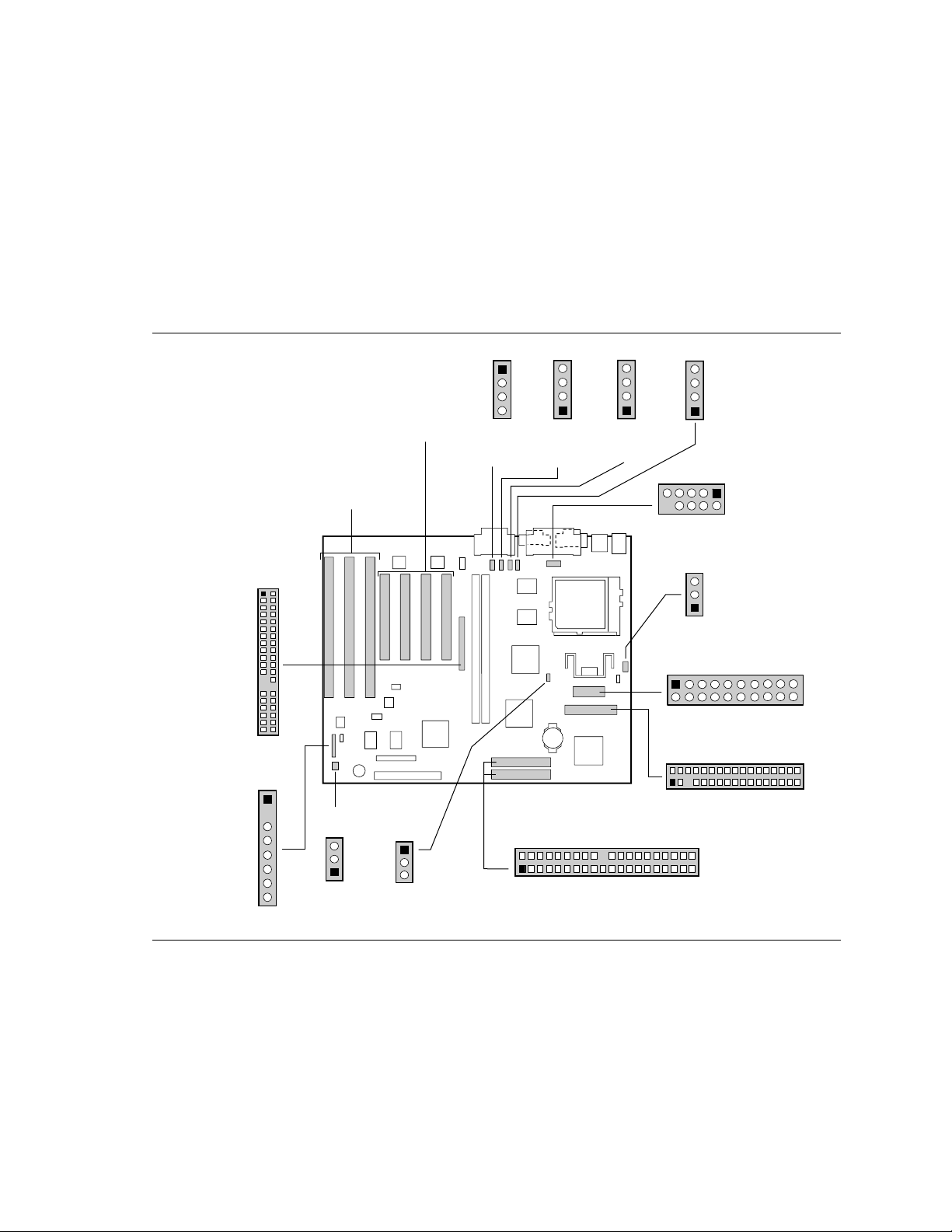
1.15 Jumper Settings.........................................................................................................38
1.15.1 Processor Configuration (J9C1-C, D)..........................................................39
1.15.2 Password Clear (J9C1-A)............................................................................ 40
1.15.3 Clear CMOS (J9C1-A)................................................................................. 40
1.15.4 BIOS Setup Access (J9C1-B)......................................................................40
1.15.5 BIOS Recovery (J8A1) ................................................................................40
1.15.6 Processor Voltage (J6M2)...........................................................................40
iii

Contents
1.16 Reliability ...................................................................................................................41
1.17 Environmental............................................................................................................41
1.18 Power Consumption...................................................................................................41
1.18.1 Power Supply Considerations......................................................................42
1.19 Regulatory Compliance..............................................................................................42
1.19.1 Safety..........................................................................................................42
1.19.2 EMI..............................................................................................................4 3
1.19.3 Product Certification Markings.....................................................................43
2 Motherboard Resources
2.1 Memory Map..............................................................................................................45
2.2 DMA Channels...........................................................................................................45
2.3 I/O Map......................................................................................................................46
2.4 PCI Configuration Space Map ...................................................................................48
2.5 Interrupts....................................................................................................................48
2.6 PCI Interrupt Routing Map.........................................................................................49
3 BIOS and Setup Program
3.1 Introduction................................................................................................................51
3.1.1 BIOS Flash Memory Organization...............................................................51
3.1.2 BIOS Upgrades ...........................................................................................51
3.1.3 Plug and Play: PCI Auto-configuration .......................................................52
3.1.4 PCI IDE Support..........................................................................................52
3.1.5 ISA Plug and Play .......................................................................................53
3.1.6 ISA Legacy Devices ....................................................................................53
3.1.7 Desktop Management Interface ..................................................................53
3.1.8 Advanced Power Management ...................................................................54
3.1.9 Language Support.......................................................................................54
3.1.10 Boot Options................................................................................................54
3.1.11 OEM Logo or Scan Area .............................................................................55
3.1.12 USB Support ...............................................................................................55
3.1.13 BIOS Setup Access Jumper........................................................................5 5
3.1.14 Recovering BIOS Data................................................................................55
3.2 BIOS Setup Program................................................................................................. 56
3.2.1 Overview of the Setup Menu Screens.........................................................56
3.2.2 Main Menu...................................................................................................57
3.2.3 Primary/Secondary IDE Master/Slave Configuration Submenus.................58
3.2.4 Advanced Menu ..........................................................................................60
3.2.5 Security Menu..............................................................................................64
3.2.6 Power Menu ................................................................................................65
3.2.7 Boot Menu...................................................................................................6 5
3.2.8 Exit Menu ....................................................................................................67
4 Error Messages
4.1 BIOS Error Messages................................................................................................69
4.2 Port 80h POST Codes...............................................................................................71
iv

LT430TX ATX Motherboard Technical Product Specification
5 Specifications and Online Support
5.1 Specifications.............................................................................................................77
5.2 Online Support...........................................................................................................78
Figures
1. Motherboard Components...........................................................................................8
2. Motherboard Dimensions...........................................................................................10
3. Back Panel I/O Shield Dimensions ............................................................................11
4. Motherboard Connectors...........................................................................................23
5. Front Panel I/O Connectors.......................................................................................29
6. Back Panel I/O Connectors........................................................................................32
7. Jumper Locations ......................................................................................................38
Tables
1. ATI-264GT Rage II+ Maximum Refresh Rates at Different Resolutions....................21
2. Optional CD-ROM Audio Connector (J2G2) ..............................................................24
3. Optional ATAPI Audio Connector (J2G1)...................................................................24
4. Optional Line-In Audio Input Connector (J2H3).........................................................24
5. Optional Telephony Connector (J2H4).......................................................................24
6. Serial Port 2 Header (J2J1) .......................................................................................24
7. CPU Fan Connector (J6M1).......................................................................................25
8. Optional Alternate CPU Fan Connector (J6M1).........................................................25
9. Optional Wake on LAN Header (J6J1).......................................................................25
10. Floppy Drive Connector (J7L2)..................................................................................25
11. GPIO Header (J9A1)..................................................................................................26
12. PCI IDE Connectors (J9H1, J10H1)...........................................................................26
13. Chassis Fan Connector (J9A2)..................................................................................2 6
14. Optional VESA/ATI Multimedia Channel Connector (J5F1)....................................... 27
15. Power Supply Connector (J7L1)................................................................................28
16. Front Panel I/O Connectors.......................................................................................30
17. PS/2
18. USB Connectors........................................................................................................33
19. Parallel Port Connector..............................................................................................33
20. Serial Port 1 Connector..............................................................................................33
21. Optional VGA Video Monitor Connector ....................................................................34
22. Optional MIDI / Game Port Connector.......................................................................34
23. PCI Bus Connectors ..................................................................................................35
24. ISA Bus Connectors ..................................................................................................36
25. Jumper Settings.........................................................................................................39
26. Jumper Settings for Processor and Bus Frequencies................................................3 9
27. Motherboard Environmental Specifications................................................................41
28. DC Voltage ................................................................................................................41
29. Power Usage for a Static Windows
30. Memory Map..............................................................................................................45
†
Keyboard and Mouse Connectors...................................................................33
†
95 Desktop .......................................................42
v

Contents
31. DMA Channels...........................................................................................................45
32. I/O Map......................................................................................................................46
33. PCI Configuration Space Map ...................................................................................48
34. Interrupts....................................................................................................................48
35. PCI Interrupt Routing Map.........................................................................................49
36. Flash Memory Organization.......................................................................................5 1
37. Recommendations for Configuring an ATAPI Device ................................................52
38. Overview of the Setup Menu Screens .......................................................................56
39. BIOS Error Messages................................................................................................69
40. Port 80h Codes..........................................................................................................71
41. Compliance with Specifications..................................................................................77
vi

1 Motherboard Description
1.1 Overview
The LT430TX motherboard supports Pentium® processors and Pentium processors with MMX
technology. The motherboard features:
• ATX form factor
®
• Socket 7 Pentium OverDrive
Main Memory
• Two 168-pin DIMM sockets
• Support for up to 256 MB of:
extended data out (EDO) memory
unbuffered 4-clock synchronous DRAM (SDRAM) memory
• Up to 64 MB of main memory cacheable
Second Level Cache Memory
• 512 KB pipeline burst static RAM (PBSRAM) soldered to the motherboard
• Optional 256 KB pipeline burst static RAM (PBSRAM) soldered to the motherboard
processor socket
Chipset and PCI/IDE Interface
• Intel 82430TX PCIset
• Integrated PCI bus mastering controller
• Two fast IDE interfaces
• Support for up to four IDE drives or devices
• Support for LS-120 removable media IDE drives
• Support for Ultra DMA - 33 drives
I/O Features
• PC87307VUL I/O controller
• Integrates standard I/O functions: floppy drive interface, one multimode parallel port, two
FIFO serial ports, keyboard and mouse controller, IrDA
• Support for two Universal Serial Bus (USB) interfaces
• Expansion Slots
Standard version (without video option):
Three PCI
Two ISA
One shared PCI/ISA
With optional video subsystem:
Three PCI
Three ISA
†
-compatible interface
7
Motherboard Description
Audio Subsystem
• Optional Yamaha OPL3-SA3 3-D audio codec soldered to the motherboard
• Optional OPL4-ML wavetable synthesizer soldered to the motherboard
Video Subsystem
• Optional ATI†-264GT Rage II+ 3-D graphics controller
• Optional VESA
†
/ATI Multimedia Channel connector
Other features
• Plug and Play compatible
• Support for Advanced Power Management
Software drivers and utilities are available from Intel.
JJ
HH
GG
FF
EE
DD
C
D
II
Sec.
Pri.
AA
W T
Y V R
UXBB ZCC
G
FBA
E
H
I
J
K
L
M
N
O
P
Q
S
OM06162
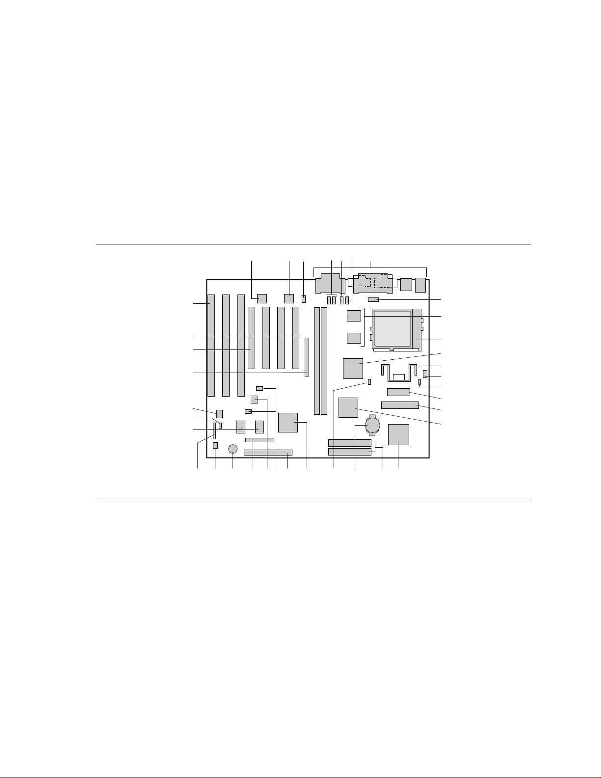
Figure 1. Motherboard Components
8

LT430TX ATX Motherboard Technical Product Specification
A Optional Yamaha OPL3-SA3 audio codec S IDE connectors
B Optional Yamaha OPL4-ML component T Battery
†
C Optional Wavetable upgrade header U Optional Wake on LAN
D Optional CD-ROM audio connectors V Optional ATI-264GT Rage II+ graphics controller
E Optional Line-in audio input connector W Front panel header
F Optional Telephony connector X Optional Wavetable daughter card headers
G Back panel I/O connectors Y Optional Management Extension component
(LM78)
H Serial port 2 header Z Configuration jumper block
I 512 KB PBSRAM cache
(Option of 256 KB)
J Socket 7 Pentium processor socket BB Chassis Fan connector
K 82371AB MTXC system controller CC GPIO header
L Linear voltage regulator DD 2 MB of SGRAM video memory
M CPU Fan connector EE BIOS recovery jumper
N Processor voltage jumper FF 2 Mbit TSOP flash memory device
O Power connector GG Optional VESA/ATI Multimedia Channel connector
P Floppy drive connector HH PCI connectors
Q 82430TX PIIX4 PCI ISA IDE Xcelerator II DIMM sockets
R PC87307VUL I/O controller JJ ISA connectors
AA Onboard speaker
header
1.2 Motherboard Manufacturing Options
• ATI-264GT Rage II+ 3-D graphics controller with 2 MB of SGRAM
• VESA/ATI Multimedia Channel connector
• Unshrouded floppy disk and IDE controller connectors
• Wake on LAN header
• Management Extension component (LM78)
• Yamaha OPL4-ML component
• Wavetable daughter card headers
• Wavetable upgrade header
• Yamaha OPL3-SA3 audio codec
• 256 KB PBSRAM cache
9
Motherboard Description
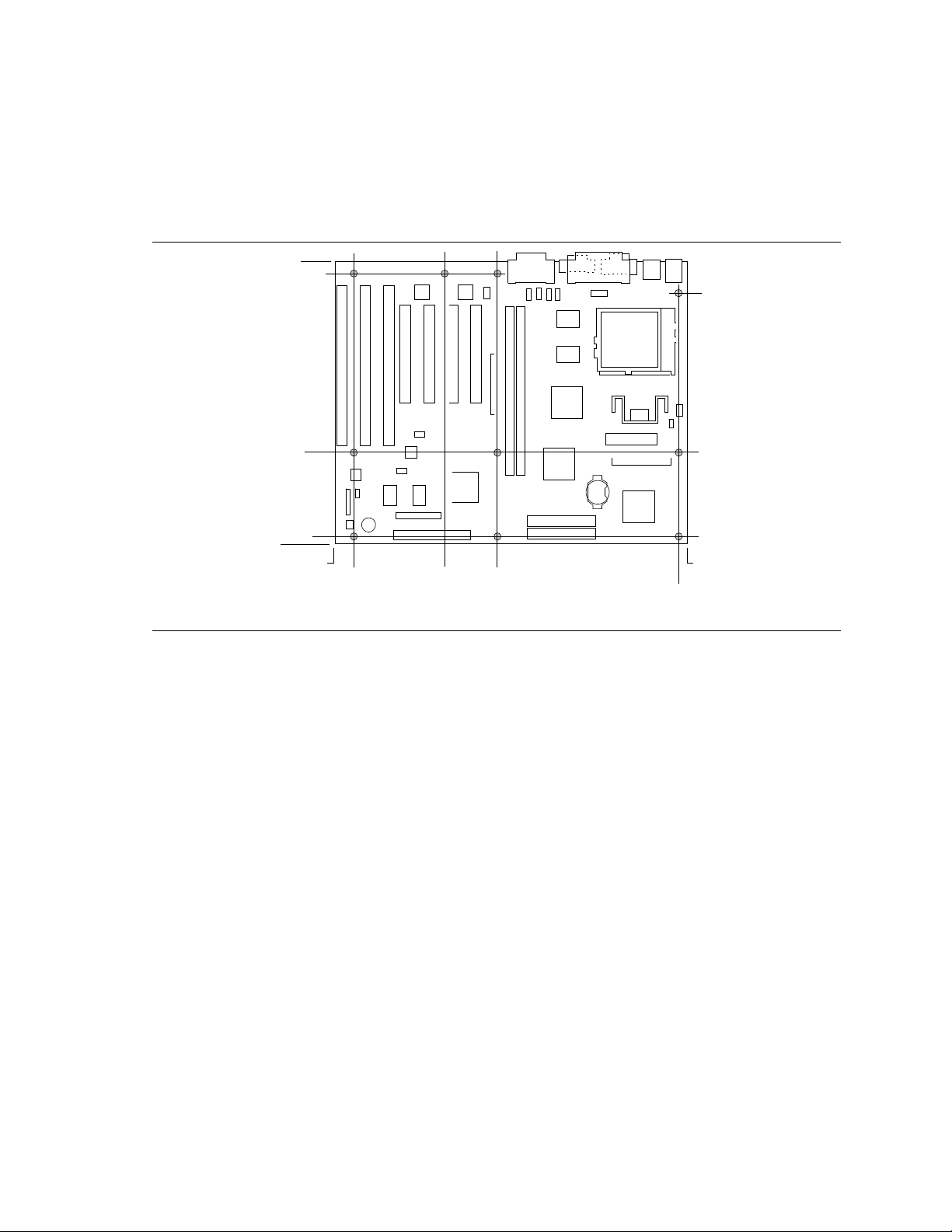
1.3 Form Factor
The motherboard is designed to fit into a standard ATX form factor chassis. Figure 2 illustrates the
form factor for the motherboard. The locations of the I/O connectors and mounting holes are in
strict compliance with the ATX specification (see Section 5.1).
9.04
8.95
8.05
2.85
0.25
0.0
0.65
0.0
3.10
4.90
Figure 2. Motherboard Dimensions
11.35
11.10
OM06161
10
LT430TX ATX Motherboard Technical Product Specification
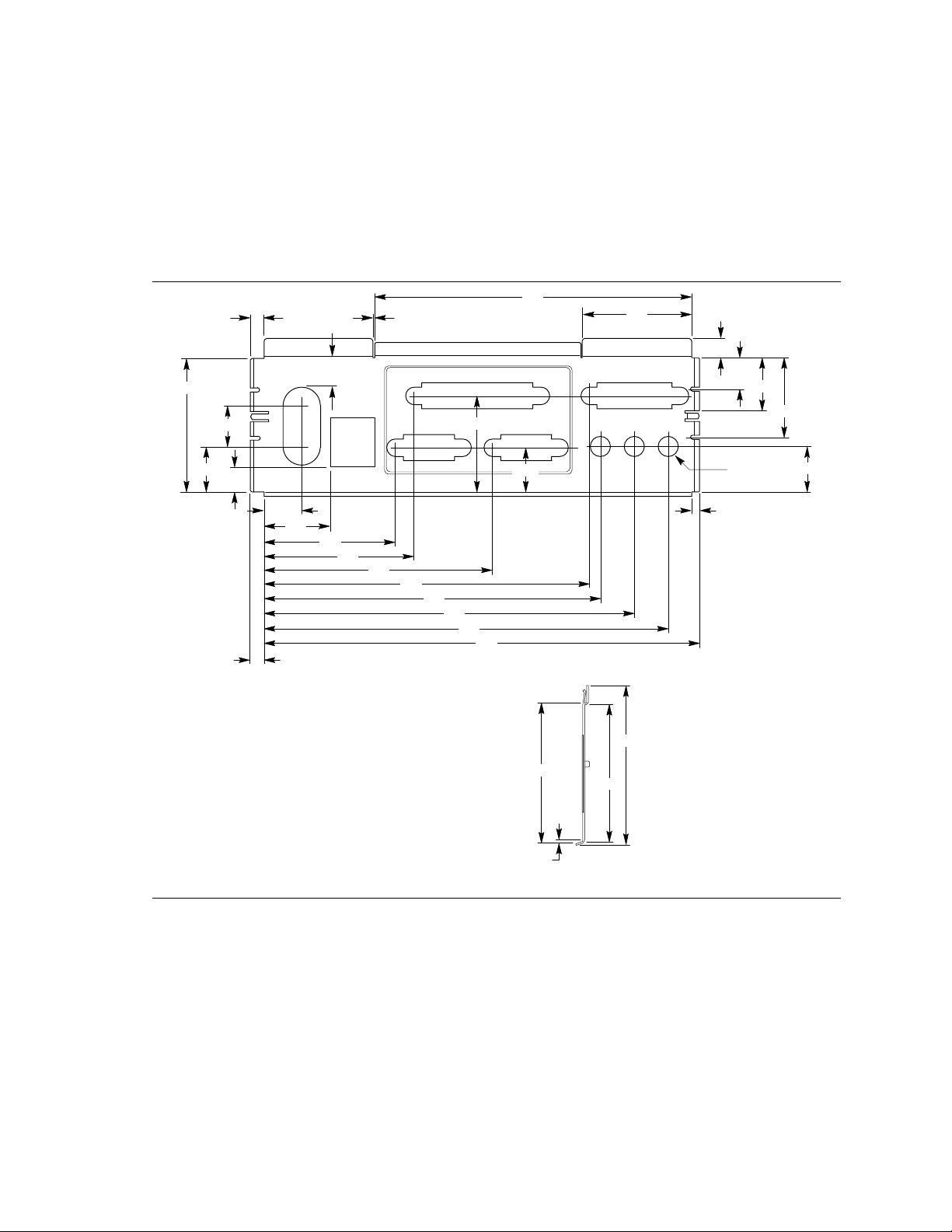
Left-end View
OM05669
Note: Material = 0.010 ±.0.001 Thick Stainless Steel, Half Hard
0.671
1.955
0.597
0.553
1.911
2.184
3.327
4.735
4.899
5.391
5.883
6.533
0.193
0.768
0.295
0.458
1.158
0.666
4.610
1.590
0.200
1.407
0.133
0.120
2.055
2.326
2.023
0.050
0.652
0.395
0.990
0.306 Dia (3)
0.478
1.4 I/O Shield
The back panel I/O shield for the LT430TX motherboard must meet specific dimensional and
material requirements. Computers based on this motherboard need the back panel I/O shield in
order to pass certification testing. Figure 3 shows the critical dimensions for the I/O shield and
indicates the position of each cutout. The example shown is Intel chassis-specific and will not
necessarily work with other chassis types.
Figure 3. Back Panel I/O Shield Dimensions
11
Motherboard Description
OM05908
1.5 Microprocessor
The motherboard supports:
• Pentium processors operating at 90, 100, 120, 133, 150, 166, and 200 MHz
• Pentium processors with MMX technology operating at 166 and 200 MHz
An onboard voltage regulator derives the necessary voltage from the computer’s power supply and
enables use of standard or VRE-specified processors. The motherboard automatically detects the
type of processor (Pentium processor or Pentium processor with MMX technology).
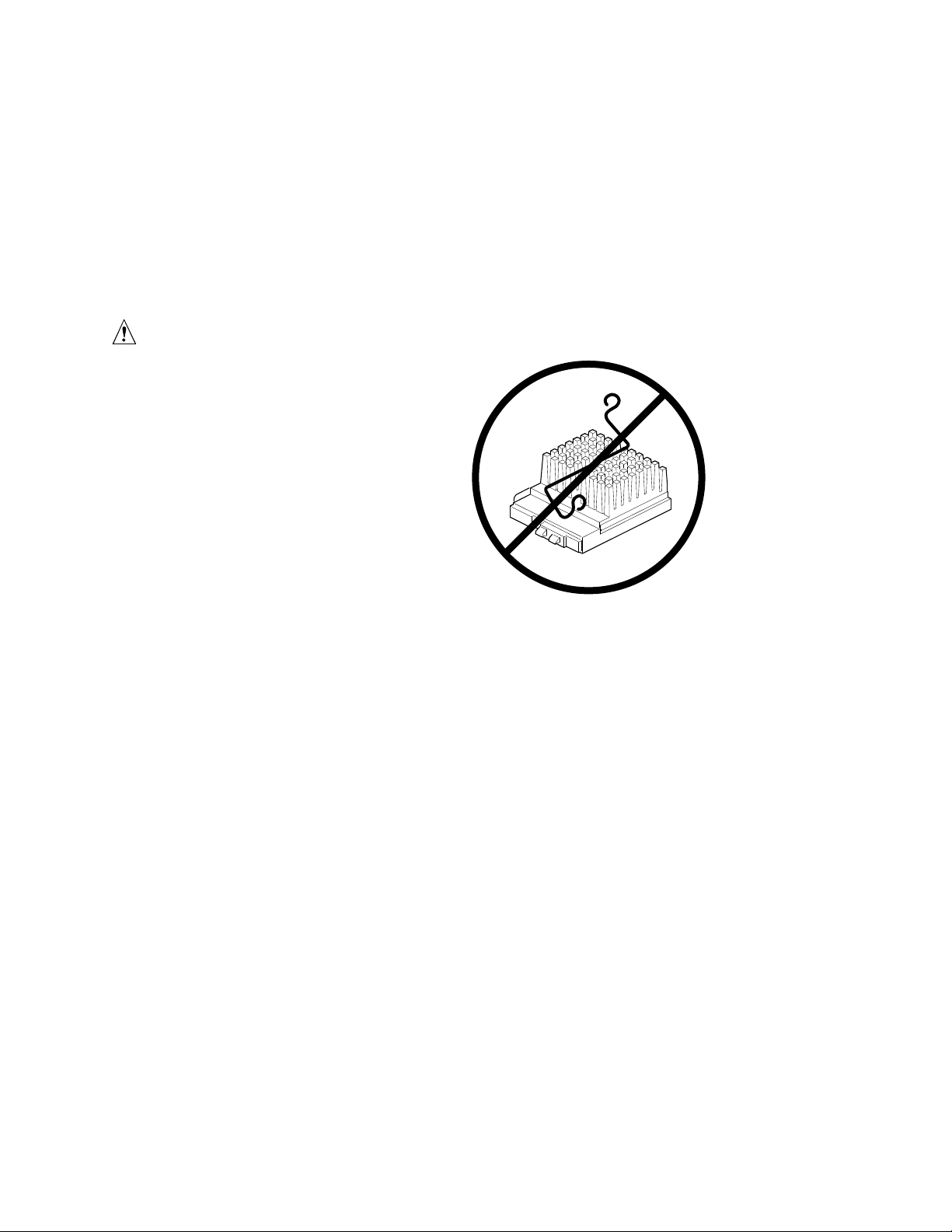
CAUTION
If you use clips to secure a heat sink
to the processor, do not use bail-wire
style heat sink clips, such as the type
shown in the figure to the right.
These clips have been known to
damage the motherboard when
installed or removed incorrectly.
1.5.1 Microprocessor Upgrade
The motherboard has a 321-pin Socket 7 zero insertion force (ZIF) microprocessor socket.
Socket 7 supports upgrades to higher performance Pentium OverDrive processors not supported by
Socket 5.
12

LT430TX ATX Motherboard Technical Product Specification
1.6 Memory
1.6.1 Main Memory
The motherboard has two 168-pin DIMM sockets. Memory can be installed in one or two sockets.
Minimum memory size is 8 MB. Maximum memory size is 256 MB. The BIOS automatically
detects memory type, size, and speed so no jumper settings are required.
The motherboard supports the following:
• 168-pin 3.3 V DIMMs with tin-plated contacts
• 60 and 66 MHz bus speeds
• 60 ns 3.3 V EDO DRAM
• 60 ns unrestricted CAS Latency 2 unbuffered 4-clock 3.3 V SDRAM
• Caching for the first 64 MB of main memory
• 64-bit data path
• Single- or double-sided DIMMs in the following sizes:
DIMM size Type Configuration Technology
8 MB 60 ns EDO 1M x 64 16 Mbit
16 MB 60 ns EDO 2M x 64 16 Mbit
32 MB 60 ns EDO 4M x 64 16 Mbit
64 MB 60 ns EDO 8M x 64 16 Mbit
8 MB CAS Latency 2 SDRAM 1M x 64 16 Mbit
16 MB CAS Latency 2 SDRAM 2M x 64 16 Mbit
32 MB CAS Latency 2 SDRAM 4M x 64 16 Mbit
64 MB CAS Latency 2 SDRAM 8M x 64 64 Mbit
128 MB CAS Latency 2 SDRAM 16M x 64 64 Mbit
Memory type, size, and speed can vary between sockets, so EDO and SDRAM can be installed on
the same motherboard. Parity (x 72) DIMMs can be installed but are not recommended for the
following reasons:
• The motherboard does not provide parity checking or ECC
• Parity DIMMs cause excessive capacitive loading on memory data and address lines
1.6.1.1 EDO DRAM
EDO DRAM improves memory read performance by holding the memory data valid until the next
CAS# falling edge, unlike fast page mode DRAM, which tri-states the memory data when CAS#
negates to precharge for the next memory cycle. With EDO DRAM, the CAS# precharge overlaps
the data-valid time, which allows CAS# to negate earlier while still satisfying the memory datavalid window.
13

Motherboard Description
1.6.1.2 SDRAM
Synchronous DRAM (SDRAM) is designed to improve main memory performance. Unlike fast
page or EDO DRAM, SDRAM is synchronous with the memory clock. This simplifies the timing
design and increases memory speed because all timing is dependent on the number of memory
clock cycles. SDRAM DIMM modules should meet the Intel “4-clock 66 MHz 64-bit unbuffered
SDRAM DIMM, V. 1.0” specification.
CAUTION
The board does not support SDRAM DIMMs with an n x 4 DRAM base due to loading anomalies.
For example, a DIMM that uses sixteen 16 Mbit x 4 devices should not be used.
NOTE
✏
The LT430TX supports unbuffered, 4-clock 3.3 V SDRAM DIMMs only. Buffered, 5 V, or 2-clock
SDRAM DIMMs should not be used.
1.6.2 Second Level Cache
The 512 KB direct-mapped write-back L2 cache consists of two 64K x 32 global write enable
(GWE) pipeline burst static RAMs (PBSRAMs) and a 32K x 8 external tag SRAM. These devices
are soldered to the motherboard.
The 256KB L2 cache substitutes two 32K x 32 PBSRAMs.
1.7 Chipset
The Intel 82430TX PCIset consists of the TX System Controller (MTXC) device and the PCI ISA
IDE Xcelerator (PIIX4) device.
1.7.1 430TX System Controller (MTXC)
The MTXC integrates the cache and main memory DRAM control functions and provides bus
control to handle transfers between the processor, cache, main memory, and the PCI bus. The
MTXC allows PCI masters to achieve full PCI bandwidth by using the snoop ahead feature. For
increased system performance the MTXC integrates posted write and read prefetch buffers. The
MTXC comes in a 324-pin MBGA package that features:
• Microprocessor interface control
• Integrated L2 write-back cache controller
Supports pipeline burst SRAM
64 MB maximum DRAM cacheability
Direct mapped organization—write back only
Cache hit read/write cycle timings at 3-1-1-1
Back to back read/write cycles at 3-1-1-1-1-1-1-1
14

LT430TX ATX Motherboard Technical Product Specification
• Integrated DRAM controller
8 MB to 256 MB main memory
64-Mbit DRAM/SDRAM technology support
3.3 V EDO and unbuffered synchronous DRAM support
Non-parity (x64) support only
• Fully synchronous minimum latency PCI bus interface
PCI compliance (see Section 5.1 for compliance level)
30 and 33 MHz bus speeds
PCI to DRAM data throughput at greater than 100 MB/sec
Up to four PCI masters in addition to the PIIX4
• Power management control
Provides PCI CLKRUN# signal to control memory clock on the PCI bus (on/off)
Internal clock control (gated off if no host or PCI bus activity)
1.7.2 430TX PCI ISA IDE Xcelerator (PIIX4)
The Intel 430TX PCI ISA IDE Xcelerator (PIIX4) is a multifunction PCI device implementing a
PCI to ISA bridge, PCI IDE functionality, a Universal Serial Bus (USB) host/hub function, and
Enhanced Power Management. The PIIX4 comes in a 324-pin MBGA package that features:
• Multifunction PCI to ISA bridge
Supports the PCI bus at 30 and 33 MHz
PCI compliant (see Section 5.1 for compliance level)
Full ISA or extended I/O (EIO) bus support
• USB controller
Two USB ports (see Section 5.1 for compliance level)
Supports legacy keyboard and mouse
Supports UHCI design guide revision 1.1 interface
• Integrated dual-channel enhanced IDE interface
Support for up to four IDE devices
PIO Mode 4 transfers at up to 14 MB/sec
Supports “Ultra DMA/33” synchronous DMA mode transfers up to 33 MB/sec
Integrated 8 x 32-bit buffer for bus master PCI IDE burst transfers
Bus master mode
• Enhanced DMA controller
Two 8237-based DMA controllers
Supports PCI DMA with three PC/PCI channels and distributed DMA protocols
Fast type-F DMA for reduced PCI bus usage
• Interrupt controller based on 82C59
Support for 15 interrupts
Programmable for edge/level sensitivity
15

Motherboard Description
• Power management logic
Sleep/resume logic
Supports thermal alarm
Support for Wake On Modem through Ring Indicate input
Support for Wake on LAN through LID input
• Real-Time Clock
256 byte battery-backed CMOS SRAM
Includes date alarm
• 16-bit counters/timers based on 82C54
1.7.3 Universal Serial Bus (USB) Support
The motherboard features two USB ports. The ports permit the direct connection of two USB
peripherals without an external hub. If more devices are required, an external hub can be
connected to either of the built-in ports. The motherboard fully supports the standard universal
host controller interface (UHCI) and uses standard software drivers that are UHCI-compatible.
Features of the USB include:
• Self-identifying, hot pluggable peripherals
• Automatic mapping of function to driver and configuration
• Support for isochronous and asynchronous transfer types over the same set of wires
• Support for up to 127 physical devices
• Guaranteed bandwidth and low latencies appropriate for telephony, audio, and other
applications
• Error handling and fault recovery mechanisms built into protocol
NOTE
✏
Computers that have an unshielded cable attached to the USB port might not meet FCC Class B
requirements, even if no device or a low speed USB device is attached to the cable. Use shielded
cable that meets the requirements for full speed devices.
1.7.4 IDE Support
The motherboard has two independent bus mastering PCI IDE interfaces that support PIO Mode 3,
PIO Mode 4, ATA-33 (Ultra DMA-33), and ATAPI (e.g., CD-ROM) devices. The BIOS supports
Logical Block Addressing (LBA) and Extended Cylinder Head Sector (ECHS) translation modes.
IDE device transfer rate and translation mode are automatically detected by the BIOS.
Normally, programmed I/O operations require a substantial amount of processor bandwidth;
however, in multi-tasking operating systems like Windows
mastering IDE can be devoted to other tasks while disk transfers are occurring.
†
95, the bandwidth freed by bus
16

LT430TX ATX Motherboard Technical Product Specification
1.7.4.1 LS-120 Support
LS-120 MB Diskette technology enables users to store 120 MB of data on a single, 3.5-inch
removable diskette. LS-120 technology is backward (both read and write) compatible with
1.44 MB and 720 KB DOS-formatted diskettes and is supported by Windows 95 and
†
Windows NT
operating systems.
The LT430TX motherboard allows connection of an LS-120 compatible drive and a standard
3.5-inch diskette drive. The LS-120 drive can be configured as a boot device, if selected in the
BIOS setup utility.
NOTE
✏
If you connect an LS-120 drive to an IDE connector and configure it as the "A" drive and
configure a standard 3.5-inch floppy as a "B" drive, the standard floppy must be connected to the
floppy drive cable's "A" connector (the connector at the end of the cable).
1.8 Super I/O Controller
The PC87307VUL Super I/O Controller from National Semiconductor is an ISA Plug and Play
compatible (see Section 5.1 for compliance level), multifunction I/O device that provides the
following features:
• Serial ports:
Two 16450/16550A-software compatible UARTs
Send/receive 16-byte FIFO
Four 8-bit DMA options for the UART with Slow Infrared Support (USI)
Ring indicator support for both serial ports
• Multimode bidirectional parallel port
Standard mode, IBM
†
and Centronics† compatible
Enhanced Parallel Port (EPP) mode with BIOS and driver support
High-speed Extended Capabilities Port (ECP) mode
• Floppy disk controller
DP8473 and N82077 compatible
16 byte FIFO
PS/2
†
diagnostic register support
CMOS disk input and output logic
High performance digital data separator (DDS)
PC-AT
†
and PS/2 drive mode support
• Keyboard and mouse controller
Industry standard 8042A compatible
General purpose microcontroller
8 bit internal data bus
• Support for an IrDA and Consumer IR-compliant infrared interface
By default, the I/O controller interfaces are automatically configured during boot up. The I/O
controller can also be manually configured in the Setup program.
17

Motherboard Description
1.8.1 Serial Ports
The motherboard has one 9-pin D-Sub serial port connector located on the back panel, and one
keyed 10-pin header located on the motherboard for cabling to the back panel. The 16540 and
16550A compatible UARTs support data transfers at speeds up to 921.6 Kbits/sec, while the
extended UART mode supports data rates up to 1.5 Mbits/sec.
1.8.2 Parallel Port
The connector for the multimode bidirectional parallel port is a 25-pin D-Sub connector located on
the back panel of the motherboard. In the Setup program, there are four options for parallel port
operation:
• Compatible (standard mode)
• Bidirectional (PS/2-compatible)
• Bidirectional Enhanced Parallel Port (EPP) (see Section 5.1 for EPP specification compliance
level)
• Bidirectional Extended Capabilities Port (ECP)
1.8.3 Floppy Controller
The I/O controller is software compatible with the DP8473 and N82077 floppy drive controllers
and supports both PC-AT and PS/2 modes. In the Setup program, the floppy interface can be
configured for the following floppy drive capacities and sizes:
• 360 KB, 5.25-inch
• 1.2 MB, 5.25-inch
• 720 KB, 3.5-inch
• 1.2 MB, 3.5-inch (driver required)
• 1.25/1.44 MB, 3.5-inch
• 2.88 MB, 3.5-inch
1.8.4 Keyboard and Mouse Interface
PS/2 keyboard and mouse connectors are located on the back panel of the motherboard.
The 5 V lines to these connectors are protected with a PolySwitch
fuse, reestablishes the connection after an over-current condition is removed. While this device
eliminates the possibility of having to replace a fuse, power to the computer should be turned off
before connecting or disconnecting a keyboard or mouse.
NOTE
✏
You can plug the mouse and keyboard into either connector.
The keyboard controller contains the Phoenix Technologies
which provides the traditional keyboard and mouse control functions, and also supports Power
On/Reset password protection. A Power On/Reset password can be specified in the Setup
program.
†
circuit that, like a self-healing
†
keyboard and mouse controller code,
18

LT430TX ATX Motherboard Technical Product Specification
The keyboard controller also supports software reset (<Ctrl><Alt><Del>). This key sequence
resets the computer’s software by jumping to the beginning of the BIOS code and running the
Power-on Self Test (POST).
1.8.5 Infrared Support
The motherboard has a 6-pin header that supports Hewlett Packard† HSDL-1000 compatible
infrared (IR) transmitters/receivers. In the Setup program, Serial Port 2 can be directed to a
connected IR device. The connection can be used to transfer files to or from portable devices like
laptops, PDAs, and printers. The Infrared Data Association (IrDA) specification supports data
transfers of 115 Kbits/sec at a distance of 1 meter. See Section 5.1 for IrDA specification
compliance level.
1.8.5.1 Consumer Infrared Support
The motherboard has a dedicated signal pin that supports Consumer Infrared (IR) devices (remote
controls). The signal pin supports receive only. Consumer IR devices can be used to control
telephony functions and multimedia operations like volume and CD track changes. In this mode,
data rates of up to 685.57 Kbits/sec are supported. A software and hardware interface is needed to
use this feature.
1.9 Management Extension Component
The optional Management Extension component (National Semiconductor LM78) provides lowcost instrumentation capabilities designed to reduce the total cost of owning a PC when used with
LANDesk
include:
• An integrated ambient temperature sensor
• Fan speed sensors
• Power supply voltage monitoring to detect levels above or below acceptable values
• Registers for storing POST hardware test results and error codes
• Remote reset capabilities from a remote peer or server through LANDesk Client Manager,
When suggested ratings for temperature, fan speed, or voltage are exceeded, an interrupt is
activated. The Management Extension component (LM78) connects to the ISA bus as an 8-bit I/O
mapped device.
®
Client Manager. The hardware implementation is a single-chip ASIC. Features
Version 3.0 and service layers (when available)
19

Motherboard Description
1.10 Wake on LAN Header
The optional header, at location J6J1, is used to implement the Wake on LAN feature. Connect
this header to a PCI LAN adapter that supports the Wake on LAN feature. The adapter monitors
network traffic. When the adapter detects a Magic Packet
LAN header to wake up the computer. This signal can wake up the computer only when the AC
power cord is still plugged into the socket and the computer is turned off. Wake on LAN can be
enabled through the Boot menu in the Setup program.
†
, it asserts a signal through the Wake on
CAUTION
The computer’s power supply must provide sufficient +5 VSB current to the LAN adapter; without
enough +5 VSB current, the Wake on LAN feature will not function. Check the adapter’s
documentation for +5 VSB requirements.
1.11 Graphics Subsystem
The optional onboard graphics subsystem features the ATI-264GT Rage II+ graphics controller.
1.11.1 Graphics Controller
The optional ATI-264GT Rage II+ provides the following features:
• Drawing coprocessor that operates concurrently with the host processor
• Video coprocessor that enables simultaneous display of 24 bits per pixel (bpp) video and 8 bpp
graphics
†
• VGA
• PCI compliant
• Support for power management
• Support for VESA Display Data Channel (DDC2B)
• Video scaler, color space converter, true color palette
• Triple-clock synthesizer
• Support for ATI multimedia feature connector
• 3-D graphics capability
• PCI Bus Master
1.11.1.1 Video Memory
The motherboard supports 2 MB of 60 ns SGRAM for video memory, soldered to the board.
There are no upgrade options for video memory.
and VESA compatibility
20

LT430TX ATX Motherboard Technical Product Specification
16-bit Color
(64K Colors)
160
160
160
160
160
1.11.1.2 Resolutions and Refresh Rates
Table 1. ATI-264GT Rage II+ Maximum Refresh Rates at Different Resolutions
2 MB Memory Maximum Refresh Rate (Hz) At:
4-bit Color
Resolution
640 x 480 160 160
800 x 600 160 160
1024 x 768 160 160
1152 x 864 160 160
1280 x 1024 160 160
(16 Colors)
8-bit Color
(256 Colors)
24-bit Color
(16M Colors)
160
160
not supported
not supported
not supported
1.11.1.3 Graphics Drivers and Utilities
Graphics drivers and common graphics utilities are available for Windows 3.x, Windows 95, and
Windows NT. Drivers and utilities are available from Intel’s World Wide Web site (see
Section 5.2).
1.11.2 VESA/ATI Multimedia Channel Connector
The motherboard has an optional 40-pin VESA/ATI Multimedia Channel connector that uses 26
pins for the VESA standard bus and 12 pins for the ATI Enhanced Visual Architecture bus. The
connector features a shared frame buffer interface and a Local Peripheral Bus (LPB) with a
bidirectional interface that supports video companion devices like MPEG/live video decoders.
1.12 Audio Subsystem
The optional onboard audio subsystem features the Yamaha OPL† YMF715, a 100-pin SQFP audio
chip. It integrates a 16-bit audio codec, OPL3 FM synthesis and its DAC, 3-D enhanced stereo
controller, and an interface for MPU-401 and a joystick. The YMF715 provides all the digital
audio and analog mixing functions needed for recording and playing sound on personal computers.
It features the following:
• Integrated 3-D enhanced stereo controller including all required analog components
• Stereo analog-to-digital and digital-to-analog converters
• Analog mixing, anti-aliasing, and reconstruction filters
• Support for 16-bit address decode
• Line, microphone, mono, and modem inputs
• ADPCM, A-law or µlaw digital audio compression/decompression
• Full digital control of all mixer and volume control functions
• Software switching between rear panel Mic In and Line In connectors
21

Motherboard Description
• Plug and Play compatibility
• Sound Blaster
†
and Windows Sound System compatibility
• Pin compatible with the Yamaha YMF711
The following table shows the IRQ, DMA channel, and base I/O address options for the audio
subsystem. These options are automatically chosen by the Plug and Play interface, so there are no
default settings.
IRQ
Resource
Sound Blaster
(DMA playback, DMA shared with
Windows Sound System capture)
Windows Sound System
(DMA playback)
MPU-401
(IRQ shared with Sound Blaster)
MIDI / Game Port 201h
†
AdLib
(Options)
5
7
9
10
11
5
7
9
10
11
DMA channel
(Options)
0
1
3
0
1
3
I/O Address
(Options)
220h
240h
220-280h
530h
E80h
530-F48h
330h
300h
300-334h
201-211h
388h
388-3F8h
1.12.1 Yamaha OPL4-ML
The optional Yamaha OPL4-ML wavetable is a ROM table containing live instrument sound
samples. Wave synthesis results in richer and more realistic sounds then that of FM synthesis.
1.12.2 Audio Drivers and Utilities
Audio software and utilities are available from Intel’s World Wide Web site (see Section 5.2).
1.12.3 Audio Connectors
The board has these optional audio connectors:
• Back panel audio jacks (Line In, Line Out, Mic In)
• CD-ROM audio connector (either standard CD or optional ATAPI styles provided)
• Telephony connector (ATAPI style only)
• Line-in audio input connector (ATAPI style only)
1.12.4 CD-ROM Audio Connector
An optional 1 x 4-pin connector is available for connecting the audio output of an internal
CD-ROM connector to the audio subsystem’s mixer. The connector is compatible with most
cables supplied with ATAPI CD-ROM headers designed to connect to audio add-in cards.
22
LT430TX ATX Motherboard Technical Product Specification
1.13 Motherboard Connectors
Figure 4 shows the connectors on the motherboard.
The following connectors are optional:
• CD-ROM Audio J2G2
• Line-In Audio J2H3
• Wake on LAN J6J1
• VESA/ATI Multimedia Channel J5F1
VESA/ATI
Multimedia
Channel
(Optional)
J5F1
1
272528
40
39
J9A1
1
8
GPIO
ISA Connectors(3)
J4A1, J4B1
J4B2
2
Chassis
Fan
3
1
J9A2
PCI Connectors(4)
J4C1, J4D1
J4E1, J4E2
J6J1
1
Wake
3
on LAN
(Optional)
J2G2
1
4
CD-ROM
Audio
(Optional)
J2G1
4
1
ATAPI
Audio
(Optional)
J2H3
4
1
Line-In
Audio
(Optional)
J2H4
4
1
Serial Port 2
9
8
CPU
Fan
Telephony
(Optional)
1
2
J2J1
3
1
J6M1
J7L1
1
11
Sec.
Pri.
2
139
J9H1-Secondary
J10H1-Primary
234
1335
IDE(2)
Power
J7L2
Floppy
4020
10
20
OM06160
Figure 4. Motherboard Connectors
23

Motherboard Description
Pin
2
4
6
8
10
Table 2. Optional CD-ROM Audio
Connector (J2G2)
Pin Signal Name
1 Ground
2 CD audio left channel
3 Ground
4 CD audio right channel
Table 3. Optional ATAPI Audio Connector
(J2G1)
Pin Signal Name
1 CD audio left channel
2 Ground
3 Ground
4 CD audio right channel
Table 4. Optional Line-In Audio Input
Connector (J2H3)
Pin Signal Name
1 Left channel audio in
2 Ground
3 Ground
4 Right channel audio in
Table 5. Optional Telephony Connector
(J2H4)
Pin Signal Name
1 Mono output
2 Ground
3 Ground
4 MIC input
Table 6. Serial Port 2 Header (J2J1)
Pin Signal Name
1 DCD#
3 Serial In
5 Serial Out
7 DTR#
9 Ground
Signal Name
DSR#
RTS#
CTS#
RI#
Key
24
 Loading...