

Page 1

L- and H-Tile Transceiver PHY User Guide
Subscribe
Send Feedback
UG-20055 | 2021.03.29
Latest document on the web: PDF | HTML
Page 2

Contents
Contents
1. Overview........................................................................................................................ 7
1.1. L-Tile/H-Tile Layout in Intel Stratix 10 Device Variants................................................ 8
1.1.1. Intel Stratix 10 GX/SX H-Tile Configurations..................................................8
1.1.2. Intel Stratix 10 TX H-Tile and E-Tile Configurations.......................................10
1.1.3. Intel Stratix 10 MX H-Tile and E-Tile Configurations...................................... 12
1.2. L-Tile/H-Tile Counts in Intel Stratix 10 Devices and Package Variants.......................... 14
1.3. L-Tile/H-Tile Building Blocks...................................................................................16
1.3.1. Transceiver Bank Architecture....................................................................17
1.3.2. Transceiver Channel Types........................................................................ 17
1.3.3. GX and GXT Channel Placement Guidelines..................................................19
1.3.4. GXT Channel Usage..................................................................................19
1.3.5. PLL and Clock Networks............................................................................ 20
1.3.6. Ethernet Hard IP......................................................................................23
1.3.7. PCIe Gen1/Gen2/Gen3 Hard IP Block..........................................................25
1.4. Overview Revision History.....................................................................................28
2. Implementing the Transceiver PHY Layer in L-Tile/H-Tile............................................ 30
2.1. Transceiver Design IP Blocks................................................................................. 30
2.2. Transceiver Design Flow........................................................................................31
2.2.1. Select the PLL IP Core.............................................................................. 31
2.2.2. Reset Controller ......................................................................................32
2.2.3. Create Reconfiguration Logic..................................................................... 32
2.2.4. Connect the Native PHY IP Core to the PLL IP Core and Reset Controller..........32
2.2.5. Connect Datapath ................................................................................... 33
2.2.6. Modify Native PHY IP Core SDC..................................................................33
2.2.7. Compile the Design.................................................................................. 33
2.2.8. Verify Design Functionality........................................................................ 33
2.3. Configuring the Native PHY IP Core........................................................................ 34
2.3.1. Protocol Presets.......................................................................................35
2.3.2. GXT Channels..........................................................................................36
2.3.3. General and Datapath Parameters .............................................................36
2.3.4. PMA Parameters...................................................................................... 39
2.3.5. PCS-Core Interface Parameters..................................................................42
2.3.6. Analog PMA Settings Parameters................................................................47
2.3.7. Enhanced PCS Parameters ........................................................................53
2.3.8. Standard PCS Parameters......................................................................... 57
2.3.9. PCS Direct Datapath Parameters............................................................... 61
2.3.10. Dynamic Reconfiguration Parameters........................................................ 61
2.3.11. Generation Options Parameters................................................................64
2.3.12. PMA, Calibration, and Reset Ports.............................................................64
2.3.13. PCS-Core Interface Ports.........................................................................67
2.3.14. Enhanced PCS Ports............................................................................... 74
2.3.15. Standard PCS Ports................................................................................ 80
2.3.16. Transceiver PHY PCS-to-Core Interface Reference Port Mapping.................... 86
2.3.17. IP Core File Locations............................................................................104
2.4. Using the Intel Stratix 10 L-Tile/H-Tile Transceiver Native PHY Intel Stratix 10 FPGA
IP Core.......................................................................................................... 106
L- and H-Tile Transceiver PHY User Guide
2
Send Feedback
Page 3

Contents
2.4.1. PMA Functions....................................................................................... 108
2.4.2. PCS Functions........................................................................................110
2.4.3. Deterministic Latency Use Model.............................................................. 145
2.4.4. Debug Functions.................................................................................... 153
2.5. Implementing the PHY Layer for Transceiver Protocols.............................................163
2.5.1. PCI Express (PIPE)................................................................................ 163
2.5.2. Interlaken............................................................................................ 213
2.5.3. Ethernet............................................................................................... 220
2.5.4. CPRI....................................................................................................226
2.6. Unused or Idle Transceiver Channels.....................................................................232
2.7. Simulating the Native PHY IP Core........................................................................235
2.7.1. How to Specify Third-Party RTL Simulators ............................................... 235
2.7.2. Scripting IP Simulation............................................................................237
2.7.3. Custom Simulation Flow..........................................................................239
2.8. Implementing the Transceiver Native PHY Layer in L-Tile/H-Tile Revision History......... 242
3. PLLs and Clock Networks............................................................................................ 249
3.1. PLLs................................................................................................................. 251
3.1.1. ATX PLL................................................................................................ 251
3.1.2. fPLL......................................................................................................266
3.1.3. CMU PLL............................................................................................... 273
3.2. Input Reference Clock Sources............................................................................278
3.2.1. Dedicated Reference Clock Pins...............................................................279
3.2.2. Receiver Input Pins.................................................................................281
3.2.3. PLL Cascading as an Input Reference Clock Source..................................... 282
3.2.4. Reference Clock Network.........................................................................282
3.2.5. Core Clock as an Input Reference Clock.....................................................282
3.3. Transmitter Clock Network...................................................................................283
3.3.1. x1 Clock Lines....................................................................................... 283
3.3.2. x6 Clock Lines....................................................................................... 284
3.3.3. x24 Clock Lines......................................................................................286
3.3.4. GXT Clock Network.................................................................................289
3.3.5. HCLK Network....................................................................................... 291
3.4. Clock Generation Block....................................................................................... 292
3.5. FPGA Fabric-Transceiver Interface Clocking............................................................ 294
3.6. Double Rate Transfer Mode..................................................................................295
3.7. Transmitter Data Path Interface Clocking...............................................................295
3.8. Receiver Data Path Interface Clocking...................................................................297
3.9. Channel Bonding................................................................................................299
3.9.1. PMA Bonding......................................................................................... 299
3.9.2. PMA and PCS Bonding.............................................................................300
3.9.3. Selecting Channel Bonding Schemes.........................................................301
3.9.4. Skew Calculations.................................................................................. 302
3.10. PLL Cascading Clock Network.............................................................................302
3.11. Using PLLs and Clock Networks.......................................................................... 304
3.11.1. Non-bonded Configurations....................................................................304
3.11.2. Bonded Configurations.......................................................................... 308
3.11.3. Implementing PLL Cascading..................................................................311
3.11.4. Mix and Match Example.........................................................................312
3.12. PLLs and Clock Networks Revision History............................................................315
Send Feedback
L- and H-Tile Transceiver PHY User Guide
3
Page 4

Contents
4. Resetting Transceiver Channels.................................................................................. 319
4.1. When Is Reset Required? ................................................................................... 319
4.2. Transceiver PHY Reset Controller Intel Stratix 10 FPGA IP Implementation................. 320
4.3. How Do I Reset?................................................................................................ 321
4.3.1. Recommended Reset Sequence................................................................321
4.3.2. Transceiver Blocks Affected by Reset and Power-down Signals......................332
4.4. Using PCS Reset Status Port................................................................................ 332
4.5. Using Transceiver PHY Reset Controller Intel Stratix 10 FPGA IP............................... 332
4.5.1. Parameterizing Transceiver PHY Reset Controller Intel Stratix 10 FPGA IP.......334
4.5.2. Transceiver PHY Reset Controller Intel Stratix 10 FPGA IP Parameters............334
4.5.3. Transceiver PHY Reset Controller Intel Stratix 10 FPGA IP Interfaces............. 336
4.5.4. Transceiver PHY Reset Controller Intel Stratix 10 FPGA IP Resource Utilization340
4.6. Using a User-Coded Reset Controller.....................................................................340
4.6.1. User-Coded Reset Controller Signals......................................................... 341
4.7. Combining Status or PLL Lock Signals with User Coded Reset Controller.................... 342
4.8. Resetting Transceiver Channels Revision History.....................................................343
5. Intel Stratix 10 L-Tile/H-Tile Transceiver PHY Architecture........................................ 344
5.1. PMA Architecture................................................................................................344
5.1.1. Transmitter PMA.....................................................................................344
5.1.2. Receiver PMA.........................................................................................346
5.2. Enhanced PCS Architecture..................................................................................354
5.2.1. Transmitter Datapath..............................................................................354
5.2.2. Receiver Datapath..................................................................................361
5.2.3. RX KR FEC Blocks...................................................................................367
5.3. Intel Stratix 10 Standard PCS Architecture............................................................ 367
5.3.1. Transmitter Datapath..............................................................................368
5.3.2. Receiver Datapath..................................................................................373
5.4. Intel Stratix 10 PCI Express Gen3 PCS Architecture................................................ 387
5.4.1. Transmitter Datapath..............................................................................388
5.4.2. Receiver Datapath..................................................................................389
5.4.3. PIPE Interface........................................................................................390
5.5. PCS Support for GXT Channels.............................................................................390
5.6. Square Wave Generator...................................................................................... 390
5.7. PRBS Pattern Generator...................................................................................... 391
5.8. PRBS Pattern Verifier.......................................................................................... 392
5.9. Loopback Modes................................................................................................ 392
5.10. Intel Stratix 10 L-Tile/H-Tile Transceiver PHY Architecture Revision History............... 394
6. Reconfiguration Interface and Dynamic Reconfiguration............................................ 396
6.1. Reconfiguring Channel and PLL Blocks...................................................................397
6.2. Interacting with the Reconfiguration Interface........................................................397
6.2.1. Reading from the Reconfiguration Interface............................................... 399
6.2.2. Writing to the Reconfiguration Interface.................................................... 399
6.3. Multiple Reconfiguration Profiles...........................................................................400
6.3.1. Configuration Files..................................................................................401
6.3.2. Embedded Reconfiguration Streamer........................................................ 403
6.4. Arbitration.........................................................................................................405
6.5. Recommendations for Dynamic Reconfiguration......................................................407
6.6. Steps to Perform Dynamic Reconfiguration............................................................ 407
6.6.1. Channel Reconfiguration..........................................................................409
L- and H-Tile Transceiver PHY User Guide
4
Send Feedback
Page 5

Contents
6.6.2. PLL Reconfiguration................................................................................ 410
6.7. Direct Reconfiguration Flow................................................................................. 411
6.8. Native PHY IP or PLL IP Core Guided Reconfiguration Flow....................................... 412
6.9. Reconfiguration Flow for Special Cases..................................................................413
6.9.1. Switching Transmitter PLL....................................................................... 414
6.9.2. Switching Reference Clocks..................................................................... 416
6.9.3. Reconfiguring Between GX and GXT Channels............................................ 420
6.10. Changing Analog PMA Settings.......................................................................... 420
6.11. Ports and Parameters........................................................................................421
6.12. Dynamic Reconfiguration Interface Merging Across Multiple IP Blocks...................... 426
6.13. Embedded Debug Features................................................................................ 428
6.13.1. Native PHY Debug Master Endpoint (NPDME)............................................428
6.13.2. Optional Reconfiguration Logic............................................................... 429
6.14. Timing Closure Recommendations...................................................................... 430
6.15. Unsupported Features.......................................................................................432
6.16. Transceiver Register Map................................................................................... 433
6.17. Reconfiguration Interface and Dynamic Revision History........................................ 433
7. Calibration.................................................................................................................. 435
7.1. Reconfiguration Interface and Arbitration with PreSICE (Precision Signal Integrity
Calibration Engine).......................................................................................... 437
7.2. Calibration Registers...........................................................................................438
7.2.1. Avalon Memory-Mapped Interface Arbitration Registers............................... 438
7.2.2. User Recalibration Enable Registers.......................................................... 438
7.2.3. Capability Registers................................................................................439
7.2.4. Rate Switch Flag Register........................................................................442
7.3. Power-up Calibration.......................................................................................... 443
7.4. Background Calibration....................................................................................... 444
7.5. User Recalibration.............................................................................................. 446
7.5.1. Recalibrating a Duplex Channel (Both PMA TX and PMA RX)......................... 446
7.5.2. Recalibrating the PMA RX Only in a Duplex Channel.................................... 447
7.5.3. Recalibrating the PMA TX Only in a Duplex Channel.....................................447
7.5.4. Recalibrating a PMA Simplex RX Without a Simplex TX Merged into the
Same Physical Channel........................................................................... 448
7.5.5. Recalibrating a PMA Simplex TX Without a Simplex RX Merged into the
Same Physical Channel........................................................................... 448
7.5.6. Recalibrating Only a PMA Simplex RX in a Simplex TX Merged Physical
Channel................................................................................................ 449
7.5.7. Recalibrating Only a PMA Simplex TX in a Simplex RX Merged Physical
Channel................................................................................................ 449
7.5.8. Recalibrating the fPLL............................................................................. 450
7.5.9. Recalibrating the ATX PLL........................................................................ 450
7.5.10. Recalibrating the CMU PLL When it is Used as a TX PLL..............................450
7.6. Calibration Revision History................................................................................. 451
A. Logical View of the L-Tile/H-Tile Transceiver Registers.............................................. 452
A.1. ATX_PLL Logical Register Map..............................................................................452
A.1.1. ATX PLL Calibration................................................................................ 452
A.1.2. Optional Reconfiguration Logic ATX PLL- Capability..................................... 453
A.1.3. Optional Reconfiguration Logic ATX PLL- Control & Status............................ 453
A.1.4. Embedded Streamer (ATX PLL)................................................................ 453
A.1.5. Updating ATX PLL Fractional Multiply Factor (K) Value................................. 454
Send Feedback
L- and H-Tile Transceiver PHY User Guide
5
Page 6

Contents
A.2. CMU_PLL Logical Register Map.............................................................................454
A.2.1. CDR/CMU and PMA Calibration................................................................. 455
A.2.2. Optional Reconfiguration Logic CMU PLL- Capability.....................................455
A.2.3. Optional Reconfiguration Logic CMU PLL- Control & Status........................... 456
A.2.4. Embedded Streamer (CMU PLL)............................................................... 456
A.3. FPLL Logical Register Map................................................................................... 457
A.3.1. fPLL Calibration......................................................................................457
A.3.2. Optional Reconfiguration Logic fPLL-Capability............................................458
A.3.3. Optional Reconfiguration Logic fPLL-Control & Status...................................458
A.3.4. Embedded Streamer (fPLL)......................................................................458
A.4. Channel Logical Register Map.............................................................................. 459
A.4.1. Transmitter PMA Logical Register Map....................................................... 460
A.4.2. Receiver PMA Logical Register Map........................................................... 461
A.4.3. Pattern Generators and Checkers............................................................. 466
A.4.4. Loopback.............................................................................................. 469
A.4.5. Optional Reconfiguration Logic PHY- Capability........................................... 469
A.4.6. Optional Reconfiguration Logic PHY- Control & Status..................................470
A.4.7. Embedded Streamer (Native PHY)............................................................ 471
A.4.8. Static Polarity Inversion.......................................................................... 472
A.4.9. Reset................................................................................................... 472
A.4.10. CDR/CMU and PMA Calibration............................................................... 473
A.5. Logical View Register Map of the L-Tile/H-Tile Transceiver Registers Revision History... 474
L- and H-Tile Transceiver PHY User Guide
6
Send Feedback
Page 7

UG-20055 | 2021.03.29
Send Feedback
1. Overview
Intel® Stratix® 10 devices offer up to 144 transceivers with integrated advanced highspeed analog signal conditioning and clock data recovery circuits for chip-to-chip,
chip-to-module, and backplane applications.
The Intel Stratix 10 devices contain a combination of GX, GXT, or GXE channels, in
addition to the hardened IP blocks for PCI Express* and Ethernet applications.
The Intel Stratix 10 device introduces several transceiver tile variants to support a
wide variety of protocol implementations. These transceiver tile variants are L-tiles, Htiles, and E-tiles. This user guide describes both the L- and H-tile transceivers. For
Intel Stratix 10 devices that only contain E-tiles, refer to the E-Tile Transceiver PHY
User Guide.
Table 1. Transceiver Tile Variants—Comparison of Transceiver Capabilities
Feature L-Tile H-Tile E-Tile
Maximum Transceiver
Data Rate (Chip-to-
chip)
Maximum Transceiver
Data Rate
(Backplane)
Number of
Transceiver Channels
(per tile)
Hard IP (per tile) PCIe*—Gen3 x16
(1)
GX
—17.4 Gbps
(1)
GXT
—26.6 Gbps
GX—12.5 Gbps
GXT—12.5 Gbps
GX—16 per tile
GXT—8 per tile
Total—24 per tile (4
banks, 6 channels per
bank)
GX—17.4 Gbps
GXT—28.3 Gbps
GX—8 per tile
GXT—16 per tile
Total—24 per tile (4 banks, 6
channels per bank)
PCIe—Gen3 x16, SR-IOV (4
PF, 2K VF)
Ethernet—100GbE MAC
(2)
GXE
—57.8 Gbps Pulse Amplitude
Modulation 4 (PAM4)/28.9 Gbps Non-
return to zero (NRZ)
GXE—24 individual channels per tile
Ethernet—100GbE MAC and RS (528,
514)-FEC, 4 per tile
Ethernet—KP-FEC, 4 per tile
Ethernet—10/25GbE MAC and RS
(528, 514)-FEC, 24 per tile
In all Intel Stratix 10 devices, the various transceiver tiles connect to the FPGA fabric
using Intel EMIB (Embedded Multi-Die Interconnect Bridge) technology.
Related Information
• L-Tile/H-Tile Building Blocks on page 16
• See AN 778: Intel Stratix 10 Transceiver Usage for transceiver channel placement
guidelines for L-tiles and H-tiles.
(1)
Refer to the L-Tile/H-Tile Building Blocks section for further descriptions of GX and GXT
channels.
(2)
Refer to the E-Tile Transceiver PHY User Guide for a full description of GXE channels.
Intel Corporation. All rights reserved. Agilex, Altera, Arria, Cyclone, eASIC, Intel, the Intel logo, MAX, Nios,
Quartus and Stratix words and logos are trademarks of Intel Corporation or its subsidiaries in the U.S. and/or
other countries. Intel warrants performance of its FPGA and semiconductor products to current specifications in
accordance with Intel's standard warranty, but reserves the right to make changes to any products and services
at any time without notice. Intel assumes no responsibility or liability arising out of the application or use of any
information, product, or service described herein except as expressly agreed to in writing by Intel. Intel
customers are advised to obtain the latest version of device specifications before relying on any published
information and before placing orders for products or services.
*Other names and brands may be claimed as the property of others.
ISO
9001:2015
Registered
Page 8

HSSI_2_1
Tile 1K-N
HSSI_2_0
Package Substrate
EMIBEMIB
EMIBEMIB
Core Fabric
®
Channel
5
4
3
2
1
0
5
4
3
2
1
0
5
4
3
2
1
0
5
4
3
2
1
0
Bank
1N
1M
1L
1K
EMIB
Tile 4K-N
EMIB
Tile 4G-J
HSSI_1_1
Tile 4C-F
HSSI_0_1
Tile 1C-F
HSSI_0_0
Tile 1G-J
HSSI_1_0
UG-20055 | 2021.03.29
• Intel Stratix 10 GX/SX Device Overview
• Intel Stratix 10 MX (DRAM System-in-Package) Device Overview
• Intel Stratix 10 TX Device Overview
• Intel Stratix 10 DX Device Overview
• E-Tile Transceiver PHY User Guide
• Intel FPGA IP for Transceiver PHY—Support Center
1.1. L-Tile/H-Tile Layout in Intel Stratix 10 Device Variants
Intel Stratix 10 GX/SX device variants support both L- and H-Tiles. Intel Stratix 10 TX
and MX device variants support both H- and E-Tiles.
Intel Stratix 10 devices are offered in a number of different configurations based on
layout. There is a maximum of six possible locations for a tile. The following figure
maps these layouts to the corresponding transceiver tiles and banks.
Figure 1. Intel Stratix 10 Tile Layout
1. Overview
1.1.1. Intel Stratix 10 GX/SX H-Tile Configurations
The Intel Stratix 10 GX FPGAs meet the high-performance demands of highthroughput systems with up to 10 teraflops (TFLOPs) of floating-point performance.
Intel Stratix 10 GX FPGAs also provide transceiver support up to 28.3 Gbps for chipmodule, chip-to-chip, and backplane applications.
The Intel Stratix 10 SX SoCs features a hard processor system with 64 bit quad-core
ARM* Cortex*-A53 processor available in all densities, in addition to all the features of
Intel Stratix 10 GX devices.
L- and H-Tile Transceiver PHY User Guide
8
Send Feedback
Page 9
L-Tile/H-Tile
(24 Channels)
HSSI_0_0
Package Substrate
EMIB
Core Fabric
®
GX/SX 400 HF35 (F1152)
GX/SX 650 HF35 (F1152)
GX/SX 2500 HF55 (F2912E)
GX/SX 2800 HF55 (F2912E)
L-Tile/H-Tile
(24 Channels)
HSSI_2_0
L-Tile/H-Tile
(24 Channels)
HSSI_0_0
Package Substrate
EMIBEMIB
Core Fabric
®
GX/SX 850 NF43 (F1760A)
GX/SX 1100 NF43 (F1760A)
GX/SX 1650 NF43 (F1760A)
GX/SX 2100 NF43 (F1760A)
GX/SX 2500 NF43 (F1760A)
GX/SX 2800 NF43 (F1760A)
GX 1660 NF43 (F1760A)
GX 2110 NF43 (F1760A)
L-Tile/H-Tile
(24 Channels)
HSSI_2_1
L-Tile/H-Tile
(24 Channels)
HSSI_0_1
L-Tile/H-Tile
(24 Channels)
HSSI_2_0
L-Tile/H-Tile
(24 Channels)
HSSI_0_0
Package Substrate
EMIBEMIB
EMIBEMIB
Core Fabric
®
GX/SX 1650 UF50 (F2397B)
GX/SX 2100 UF50 (F2397B)
GX/SX 2500 UF50 (F2397B)
GX/SX 2800 UF50 (F2397B)
1. Overview
UG-20055 | 2021.03.29
Figure 2. Intel Stratix 10 GX/SX Device with 1 H-Tile (24 Transceiver Channels)
Figure 3. Intel Stratix 10 GX/SX Device with 2 H-Tiles (48 Transceiver Channels)
Figure 4. Intel Stratix 10 GX/SX Device with 4 H-Tiles (96 Transceiver Channels)
Send Feedback
L- and H-Tile Transceiver PHY User Guide
9
Page 10
EMIBEMIBEMIB
EMIBEMIB
EMIBEMIB
H-tile
(12 Channels)
T2
H-tile
(12 Channels)
T1
H-tile
(12 Channels)
T4
H-tile
(12 Channels)
T3
Package Substrate
Core Fabric Core Fabric
GX 10200 NF74 (F4938)
Dedicated
REFCLK
refclk1
refclk1
refclk1
refclk0
refclk0
0
1
2
3
3
4
4
Channel Bank
1MU12
1LU12
1KU12
5
0
1
1
0
refclk0
Dedicated
REFCLK
refclk1
refclk1
refclk1
refclk0
refclk0
0
1
2
3
3
4
4
Channel Bank
1EU10
1DU10
1CU10
5
0
1
1
0
refclk0
Dedicated
REFCLK
refclk1
refclk1
refclk1
refclk0
refclk0
0
1
2
3
3
4
4
Channel Bank
1MU22
1LU22
1KU22
5
0
1
1
0
refclk0
Dedicated
REFCLK
refclk1
refclk1
refclk1
refclk0
refclk0
0
1
2
3
3
4
4
Channel Bank
1EU20
1DU20
1CU20
5
0
1
1
0
refclk0
H-Tile
(24 Channels)
HSSI_0_0
Package Substrate
EMIB
Core Fabric
®
E-Tile
(24 Channels)
HSSI_0_1
EMIB
TX 850 NF43 (F1760C)
TX 1100 NF43 (F1760C)
Channel
23
22
21
20
19
18
17
16
15
14
13
12
11
10
9
8
7
6
5
4
3
2
1
0
Channel
5
4
3
2
1
0
5
4
3
2
1
0
5
4
3
2
1
0
5
4
3
2
1
0
Bank
1F
1E
1D
1C
1. Overview
UG-20055 | 2021.03.29
Figure 5. Intel Stratix 10 GX 10M Device with 4 H-Tiles (48 Transceiver Channels)
1.1.2. Intel Stratix 10 TX H-Tile and E-Tile Configurations
The Intel Stratix 10 TX FPGAs deliver the most advanced transceiver capabilities in the
industry by combining H-Tile and E-Tile transceivers.
Figure 6. Intel Stratix 10 TX Device with 1 E-Tile and 1 H-Tile (48 Transceiver
Channels)
L- and H-Tile Transceiver PHY User Guide
10
Send Feedback
Page 11

E-Tile
(24 Channels)
HSSI_2_1
E-Tile
(24 Channels)
HSSI_2_0
H-Tile
(24 Channels)
HSSI_0_0
Package Substrate
EMIBEMIB
EMIB
Core Fabric
®
TX 850 SF50 (F2397C)
TX 1100 SF50 (F2397C)
E-Tile
(24 Channels)
HSSI_2_1
E-Tile
(24 Channels)
HSSI_2_0
H-Tile
(24 Channels)
HSSI_0_0
Package Substrate
EMIBEMIB
EMIB
Core Fabric
®
TX 1650 UF50 (F2397C)
E-Tile
(24 Channels)
HSSI_0_1
EMIB
TX 2100 UF50 (F2397C)
TX 2500 UF50 (F2397C)
TX 2800 UF50 (F2397C)
E-Tile
(24 Channels)
HSSI_2_1
E-Tile
(24 Channels)
HSSI_1_1
E-Tile
(24 Channels)
HSSI_0_1
E-Tile
(24 Channels)
HSSI_2_0
E-Tile
(24 Channels)
HSSI_1_0
H-Tile
(24 Channels)
HSSI_0_0
Package Substrate
EMIBEMIBEMIB
EMIBEMIBEMIB
Core Fabric
TX 2500 YF55 (F2912B)
TX 2800 YF55 (F2912B)
1. Overview
UG-20055 | 2021.03.29
Figure 7. Intel Stratix 10 TX Device with 2 E-Tiles and 1 H-Tile (72 Transceiver
Channels)
Figure 8. Intel Stratix 10 TX Device with 3 E-Tiles and 1 H-Tile (96 Transceiver
Channels)
Figure 9. Intel Stratix 10 TX Device with 5 E-Tiles and 1 H-Tile (144 Transceiver
Channels)
Send Feedback
L- and H-Tile Transceiver PHY User Guide
11
Page 12
H-Tile
(24 Channels)
HSSI_0_0
Package Substrate
EMIB
Core Fabric
®
MX 2100 NF53 (F2597B)
H-Tile
(24 Channels)
HSSI_2_0
EMIB
HBM2
HBM2
4 GByte
4 GByte
H-Tile
(24 Channels)
HSSI_2_0
Package Substrate
EMIBEMIB
Core Fabric
®
MX 1650 UF53 (F2597A)
HBM2
H-Tile
(24 Channels)
HSSI_2_1
H-Tile
(24 Channels)
HSSI_0_1
EMIBEMIB
HBM2
MX 2100 UF53 (F2597A)
H-Tile
(24 Channels)
HSSI_0_0
4 GByte
4 GByte
1. Overview
UG-20055 | 2021.03.29
Note: 1. No package migration available between GX/SX and TX device families (H-Tile and
E-Tile)
2. Migration available within GX/SX from L-Tile to H-Tile variants
1.1.3. Intel Stratix 10 MX H-Tile and E-Tile Configurations
The Intel Stratix 10 MX devices combine the programmability and flexibility of Intel
Stratix 10 FPGAs and SoCs with 3D stacked high-bandwidth memory 2 (HBM2). The
DRAM memory tile physically connects to the FPGA using Intel Embedded Multi-Die
Interconnect Bridge (EMIB) technology.
Figure 10. Intel Stratix 10 MX Device with 2 H-Tiles (48 Transceiver Channels) and 2
HBM2
Figure 11. Intel Stratix 10 MX Device with 4 H-Tiles (96 Transceiver Channels) and Two
4 GB HBM2
L- and H-Tile Transceiver PHY User Guide
12
Send Feedback
Page 13

H-Tile
(24 Channels)
HSSI_2_0
Package Substrate
EMIBEMIB
Core Fabric
®
MX 1650 UF53 (F2597C)
HBM2
H-Tile
(24 Channels)
HSSI_2_1
H-Tile
(24 Channels)
HSSI_0_1
EMIBEMIB
HBM2
MX 2100 UF53 (F2597C)
H-Tile
(24 Channels)
HSSI_0_0
8 GByte
8 GByte
E-Tile
(24 Channels)
HSSI_2_0
Package Substrate
EMIBEMIB
Core Fabric
®
MX 1650 UF55 (F2912)
HBM2
E-Tile
(24 Channels)
HSSI_2_1
EMIBEMIB
HBM2
MX 2100 UF55 (F2912)
E-Tile
(24 Channels)
HSSI_0_1
H-Tile
(24 Channels)
HSSI_0_0
4 GByte
4 GByte
1. Overview
UG-20055 | 2021.03.29
Figure 12. Intel Stratix 10 MX Device with 4 H-Tiles (96 Transceiver Channels) and Two
8 GB HBM2
Figure 13. Intel Stratix 10 MX Device with 3 E-Tiles, 1 H-Tile (96 Transceiver Channels)
and 2 HBM2
Send Feedback
L- and H-Tile Transceiver PHY User Guide
13
Page 14

1. Overview
UG-20055 | 2021.03.29
1.2. L-Tile/H-Tile Counts in Intel Stratix 10 Devices and Package Variants
Table 2. L-Tile/H-Tile Counts in Intel Stratix 10 GX/SX Devices (HF35, NF43, UF50,
HF55, NF74)
The number in the Intel Stratix 10 GX/SX Device Name column indicates the device's Logic Element (LE) count
(in thousands LEs).
Intel Stratix 10 GX/SX
Device Name
GX 400/ SX 400 1
GX 650/ SX 650 1
GX 850/ SX 850 2
GX 1100/ SX 1100 2
GX 1650/ SX 1650 2 4
GX 2100/ SX 2100 2 4
GX 2500/ SX 2500 2 4 1
GX 2800/ SX 2800 2 4 1
GX 1660 2
GX 2110 2
GX 10200 4
F1152
HF35
(35x35 mm2)
F1760A
NF43
(42.5x42.5
mm2)
F2397B
UF50
(50x50 mm2)
F2912E
HF55
(55x55 mm2)
F4938
NF74
(70x74 mm2)
Table 3. H- and E-Tile Counts in Intel Stratix 10 TX Devices (HF35, NF43, SF50, UF50,
YF55)
The number in the Intel Stratix 10 TX Device Name column indicates the device's Logic Element (LE) count (in
thousands LEs).
Cell legend: H-Tile count, E-Tile count
Intel Stratix 10 TX Device
Name
TX 850 — 1, 1 1, 2 —
TX 1100 — 1, 1 1, 2 —
TX 1650 — — 1, 3 —
TX 2100 — — 1, 3 —
TX 2500 — — 1, 3 1, 5
TX 2800 — — 1, 3 1, 5
F1152
HF35
(35x42.5 mm2)
F1760C
NF43
(42.5x42.5 mm2)
F2397C
SF50, UF50
(50x50 mm2)
F2912B
YF55
(55x55 mm2)
L- and H-Tile Transceiver PHY User Guide
14
Send Feedback
Page 15

1. Overview
UG-20055 | 2021.03.29
Table 4. H- and E-Tile Counts in Intel Stratix 10 MX Devices (NF53, UF53, UF55)
The number in the Intel Stratix 10 MX Device Name column indicates the device's Logic Element (LE) count (in
thousands LEs).
Cell legend: H-Tile count, E-Tile count
Intel Stratix 10 MX Device
Name
MX 1650 4, 0 — 4, 0 1, 3
MX 2100 4, 0 2, 0 4, 0 1, 3
F2597A
UF53
(52.5x52.5 mm2)
F2597B
NF53
(52.5x52.5 mm2)
F2597C
UF53
(52.5x52.5 mm2)
F2912
UF55
(55x55 mm2)
Send Feedback
L- and H-Tile Transceiver PHY User Guide
15
Page 16
PMA Ch 0
PMA Ch 1
PMA Ch 2
PMA Ch 3
PMA Ch 4
PMA Ch 5
PCS Ch 0
PCS Ch 1
PCS Ch 2
PCS Ch 3
PCS Ch 4
PCS Ch 5
fPLL 0
ATX PLL 0
fPLL 1
ATX PLL 1
x6 Clock
Network
x24 Clock
Network
Transceiver Bank 3 (2)
refclk1
refclk0
PMA Ch 0
PMA Ch 1
PMA Ch 2
PMA Ch 3
PMA Ch 4
PMA Ch 5
PCS Ch 0
PCS Ch 1
PCS Ch 2
PCS Ch 3
PCS Ch 4
PCS Ch 5
fPLL 0
ATX PLL 0
fPLL 1
ATX PLL 1
x6 Clock
Network
Transceiver Bank 2
refclk1
refclk0
PMA Ch 0
PMA Ch 1
PMA Ch 2
PMA Ch 3
PMA Ch 4
PMA Ch 5
PCS Ch 0
PCS Ch 1
PCS Ch 2
PCS Ch 3
PCS Ch 4
PCS Ch 5
fPLL 0
ATX PLL 0
fPLL 1
ATX PLL 1
x6 Clock
Network
Transceiver Bank 1 (2)
refclk1
refclk0
PMA Ch 0
PMA Ch 1
PMA Ch 2
PMA Ch 3
PMA Ch 4
PMA Ch 5
PCS Ch 0
PCS Ch 1
PCS Ch 2
PCS Ch 3
PCS Ch 4
PCS Ch 5
fPLL 0
ATX PLL 0
fPLL 1
ATX PLL 1
x6 Clock
Network
Transceiver Bank 0
refclk1
refclk0
PCIe Gen3
x16 Hard IP
Ch0 PCS FIFO
Ch1 PCS FIFO
Ch2 PCS FIFO
Ch3 PCS FIFO
Ch4 PCS FIFO
Ch5 PCS FIFO
Ch0 Core FIFO
Ch1 Core FIFO
Ch2 Core FIFO
Ch3 Core FIFO
Ch4 Core FIFO
Ch5 Core FIFO
EMIB
FPGA Fabric
L-Tile/H-Tile
PCS Core Interface
Ethernet 100G
Hard IP
Ch0 Core FIFO
Ch1 Core FIFO
Ch2 Core FIFO
Ch3 Core FIFO
Ch4 Core FIFO
Ch5 Core FIFO
Ch0 Core FIFO
Ch1 Core FIFO
Ch2 Core FIFO
Ch3 Core FIFO
Ch4 Core FIFO
Ch5 Core FIFO
Ch0 Core FIFO
Ch1 Core FIFO
Ch2 Core FIFO
Ch3 Core FIFO
Ch4 Core FIFO
Ch5 Core FIFO
Ch0 PCS FIFO
Ch1 PCS FIFO
Ch2 PCS FIFO
Ch3 PCS FIFO
Ch4 PCS FIFO
Ch5 PCS FIFO
Ch0 PCS FIFO
Ch1 PCS FIFO
Ch2 PCS FIFO
Ch3 PCS FIFO
Ch4 PCS FIFO
Ch5 PCS FIFO
Ch0 PCS FIFO
Ch1 PCS FIFO
Ch2 PCS FIFO
Ch3 PCS FIFO
Ch4 PCS FIFO
Ch5 PCS FIFO
(1)
1. The Ethernet Hard IP is only for H-Tile devices.
2. GXT channels for L-Tile devices are only in Banks 1 or 3.
Note:
= GXT clock network
Legend
UG-20055 | 2021.03.29
1.3. L-Tile/H-Tile Building Blocks
Figure 14. High Level Block Diagram of L-Tile/H-Tile in Intel Stratix 10 Devices
1. Overview
L- and H-Tile Transceiver PHY User Guide
16
Send Feedback
Page 17

GX - Channel 5
GXT Channel 4
GXT Channel 3
GX Channel 2
GXT Channel 1
GXT Channel 0
fPLL
fPLL
ATX
ATX
1. Overview
UG-20055 | 2021.03.29
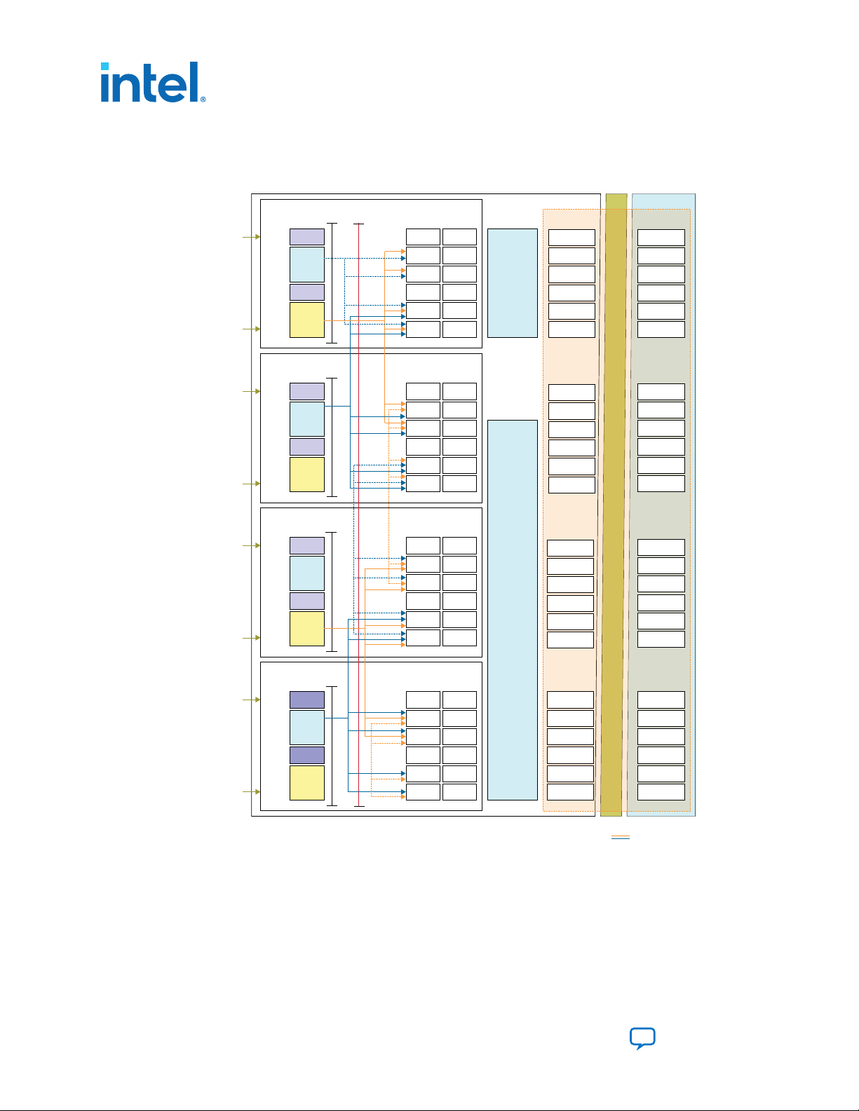
1.3.1. Transceiver Bank Architecture
Each L-Tile/H-tile transceiver tile contains four transceiver banks. The transceiver
channels are grouped into transceiver banks, where each bank has six channels.
These six channels are a combination of GX and GXT channels which you can
configure in the following ways:
• All six channels as GX channels
• Channels 0, 1, 3, and 4 as GXT channels. L-Tile supports GXT channels in banks 1
and 3. H-Tile supports GXT channels in banks 0, 1, 2, and 3.
• All six channels as a mix of GX and GXT channels; for example, two GX channels
and four GXT channels on H-Tile Devices. On L-Tile devices, you can use a
maximum of four channels in a bank when any channel is configured as a GXT
channel.
Each channel can also run in any of the following operational modes:
• Duplex (default)—Specifies a single channel that supports both transmission and
reception
• Transmitter (TX) Simplex—Specifies a single channel that supports only
transmission
• Receiver (RX) Simplex—Specifies a single channel that supports only reception
Each transceiver bank contains two Advanced Transmit (ATX) PLLs, two fractional PLLs
(fPLL), and two Clock Multiplier Unit (CMU) PLLs.
Figure 15. Transceiver Banks in the L-Tile/H-Tile
Related Information
PLLs and Clock Networks on page 249
1.3.2. Transceiver Channel Types
Each transceiver has a Physical Coding Sublayer (PCS) and a Physical Medium
Attachment (PMA). Additionally, each transceiver has loopback modes and internal
pattern generator and verifier blocks for debugging.
1.3.2.1. GX Channel
Each GX transceiver channel has four types of PCS blocks that together support
continuous datarates up to 17.4 Gbps. The various PCS blocks contain data processing
functions such as encoding or decoding, scrambling or descrambling, word alignment,
frame synchronization, FEC, and so on.
Send Feedback
L- and H-Tile Transceiver PHY User Guide
17
Page 18

Figure 16. GX Transceiver Channel in TX/RX Duplex Mode
Standard PCS
PCIe Gen3 PCS
Enhanced PCS
Transceiver
Tile
Transmitter PCS
Transmitter PMA
Serializer
Standard PCS
PCIe Gen3 PCS
Enhanced PCS
Receiver PCS
Receiver PMA
DeserializerCDR
from FPGA fabric
to FPGA fabric
PCS Direct
PCS Direct
TX
PCS
FIFO
RX
PCS
FIFO
Table 5. PCS Types Supported by GX Transceiver Channels
1. Overview
UG-20055 | 2021.03.29
PCS Type
Standard PCS
Enhanced
PCS
PCIe Gen3
PCS
PCS Direct 17.4 Gbps
-2 Speed Grade -3 Speed Grade -1 Speed Grade -2 Speed Grades -3 Speed Grade
10.81344 Gbps
L-Tile Production H-Tile Production
12 Gbps
(3)
or
(4)
9.8304 Gbps
(4)
10.81344 Gbps
12 Gbps
17.4 Gbps
8 Gbps
(3)
or
(4)
10.81344 Gbps
12 Gbps
(3)
or
(4)
9.8304 Gbps
(4)
Note: Use the L-Tile/H-Tile Transceiver Native PHY Intel Stratix 10FPGA IP Parameter Editor
to determine the datarate limitations of your selected PCS configuration.
Refer to Table 12 on page 38 for a definition of the PCS Direct mode.
1.3.2.2. GXT Channel
Each GXT transceiver channel has two types of PCS blocks that together support
continuous datarates up to 28.3 Gbps for H-Tile and 26.6 Gbps for L-Tile. Use PCS
Direct or Enhanced PCS to implement a GXT channel.
Refer to the Intel Stratix 10 Device Datasheet for more details on transceiver
specifications.
(3)
The 12 Gbps data rate at the receiver is only supported when the RX word aligner mode
parameter is set to Manual.
(4)
This data rate is only supported when Byte Serializer and Deserializer mode is enabled.
L- and H-Tile Transceiver PHY User Guide
18
Send Feedback
Page 19

Standard PCS
PCIe Gen3 PCS
Enhanced PCS
Transceiver
Tile
Transmitter PCS
Transmitter PMA
Serializer
Standard PCS
PCIe Gen3 PCS
Receiver PCS
Receiver PMA
DeserializerCDR
from FPGA fabric
to FPGA fabric
PCS Direct
Enhanced PCS
PCS Direct
TX
PCS
FIFO
RX
PCS
FIFO
1. Overview
UG-20055 | 2021.03.29
Figure 17. GXT Transceiver Channel in TX/RX Duplex Mode
Table 6. PCS Types Supported by GXT Transceiver Channels
PCS Type
Enhanced
PCS
PCS Direct 26.6 Gbps No GXT 28.3 Gbps 26.6 Gbps No GXT
-2 Speed Grade -3 Speed Grade -1 Speed Grade -2 Speed Grades -3 Speed Grade
L-Tile Production H-Tile Production
26.6 Gbps No GXT 28.3 Gbps 26.6 Gbps No GXT
Note: Use the Native PHY IP Parameter Editor to determine the datarate limitations of your
selected PCS configuration.
Related Information
Intel Stratix 10 Device Datasheet
1.3.3. GX and GXT Channel Placement Guidelines
Refer to AN 778: Intel Stratix 10 Transceiver Usage for detailed information on this
section.
Related Information
AN 778: Intel Stratix 10 Transceiver Usage
1.3.4. GXT Channel Usage
Intel Stratix 10 L-Tile/H-Tile transceivers support GXT channels.
Send Feedback
L- and H-Tile Transceiver PHY User Guide
19
Page 20
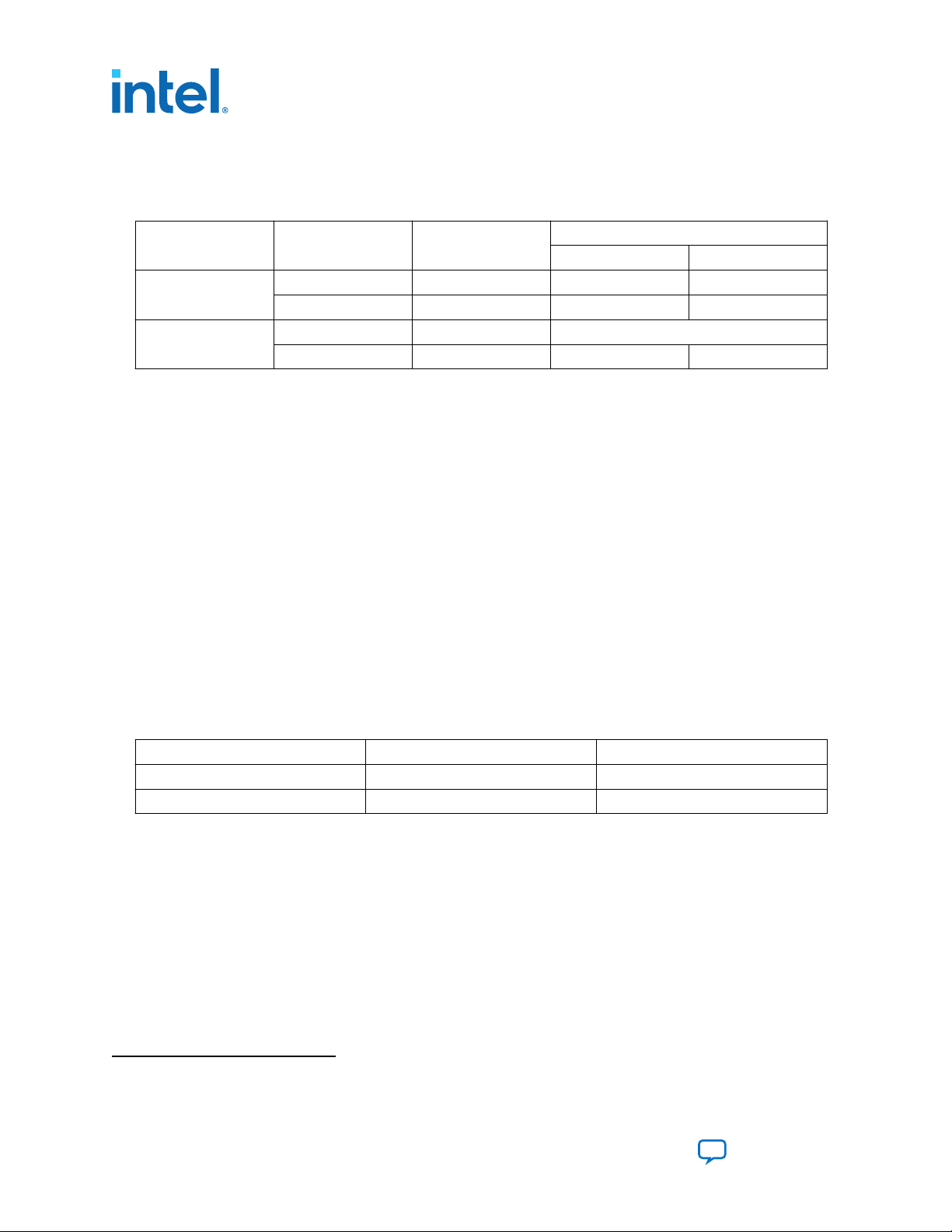
Table 7. Channel Types
There are a total of 24 channels available per tile. You can configure them as either GX channels or as a
combination of GX and (up to 16) GXT channels provided that the total does not exceed 24. You can use GXT
channels as a GX channel, but they are subject to all of the GX channel placement constraints.
Tile Channel Type
L-Tile
H-Tile
An ATX PLL can serve as the transmit PLL for up to six GXT channels.
Refer to AN 778: Intel Stratix 10 Transceiver Usage for detailed information about this
section.
Related Information
• Intel Stratix 10 Device Datasheet
• AN 778: Intel Stratix 10 Transceiver Usage
UG-20055 | 2021.03.29
Number of Channels
per Tile
GX Up to 24 17.4 Gbps 12.5 Gbps
(5)
GXT
GX Up to 24 17.4 Gbps
(5)
GXT
Up to 8 26.6 Gbps 12.5 Gbps
Up to 16 28.3 Gbps 28.3 Gbps
Chip-to-Chip Backplane
Channel Capability
1. Overview
1.3.5. PLL and Clock Networks
There are two different types of clock networks to distribute the high speed serial
clock to the channels:
• Transceiver clock network that supports GX channels and allows a single TX PLL to
drive up to 24 bonded channels in a tile.
• High Performance clock network that allows a single ATX PLL to drive up to 6 GXT
channels in unbonded configurations.
Table 8. Channel Type Supported by Different Clock Networks
Clock Network Clock Lines Channel Type Support
Standard x1, x6, x24 GX
High Performance PLL Direct Connect GXT
1.3.5.1. PLLs
1.3.5.1.1. Transceiver Phase-Locked Loops
Each transceiver channel in Intel Stratix 10 devices has direct access to three types of
high performance PLLs:
• Advanced Transmit (ATX) PLL
• Fractional PLL (fPLL)
• Channel PLL / Clock Multiplier Unit (CMU) PLL.
(5)
If you use GXT channel data rates, the V
L- and H-Tile Transceiver PHY User Guide
20
CCR_GXB
and V
CCT_GXB
voltages must be set to 1.12 V.
Send Feedback
Page 21

1. Overview
UG-20055 | 2021.03.29
These transceiver PLLs along with the Master or Local Clock Generation Blocks (CGB)
drive the transceiver channels.
Related Information
PLLs on page 251
For more information about transceiver PLLs in Stratix 10 devices.
Advanced Transmit (ATX) PLL
The ATX PLL is the transceiver channel’s primary transmit PLL. It can operate over the
full range of supported datarates required for high datarate applications. An ATX PLL
supports both integer frequency synthesis and coarse resolution fractional frequency
synthesis (when configured as a cascade source).
Fractional PLL (fPLL)
A fractional PLL (fPLL) is an alternate transmit PLL used for generating lower clock
frequencies for lower datarate applications. fPLLs support both integer frequency
synthesis and fine resolution fractional frequency synthesis. Unlike the ATX PLL, you
can also use the fPLL to synthesize frequencies that can drive the core through the
FPGA fabric clock networks.
Channel PLL (CMU/CDR PLL)
A channel PLL is located within each transceiver channel. The channel's primary
function is clock and data recovery in the transceiver channel when you use the PLL in
clock data recovery (CDR) mode. You can use the channel PLLs of channel 1 and 4 as
transmit PLLs when configured in clock multiplier unit (CMU) mode. You cannot
configure the channel PLLs of channel 0, 2, 3, and 5 in CMU mode; therefore, you
cannot use them as transmit PLLs. You cannot use the receiver channel when you use
it as a Channel PLL/CMU.
1.3.5.1.2. Clock Generation Block (CGB)
Intel Stratix 10 devices include the following types of clock generation blocks (CGBs):
• Master CGB
• Local CGB
Transceiver banks have two master CGBs. The master CGB divides and distributes
bonded clocks to a bonded channel group. The master CGB also distributes nonbonded clocks to non-bonded channels across the x6/x24 clock network.
Each transceiver channel has a local CGB. The local CGB divides and distributes nonbonded clocks to the corresponding PCS and PMA blocks.
Send Feedback
L- and H-Tile Transceiver PHY User Guide
21
Page 22
Tile 2
8 reference
clock pins
per tile
Transceiver Bank 3
Transceiver Bank 2
Transceiver Bank 0
Transceiver Bank 1
Transceiver Bank 3
Transceiver Bank 2
Transceiver Bank 0
Transceiver Bank 1
Transceiver Bank 3
Transceiver Bank 2
Transceiver Bank 0
Transceiver Bank 1
Tile 1
Tile 0
8 reference
clock pins
per tile
8 reference
clock pins
per tile
1. Overview
UG-20055 | 2021.03.29
1.3.5.2. Input Reference Clock Sources
• Eight dedicated reference clocks available per transceiver tile
— Two reference clocks per transceiver bank
— You must route multiple copies of reference clocks on the PCB to span beyond
a transceiver tile
• Reference clock network
— Reference clock network does not span beyond the transceiver tile
— There are two regulated reference clock networks for better performance per
tile that any reference clock pin can access
• You can use unused receiver pins as additional reference clocks
Note: Unused receiver pins used as reference clocks can only be used within the same tile.
Figure 18. Reference Clock Network
For the best jitter performance, place the reference clock as close as possible to the
transmit PLL. Use the reference clock in the same triplet of the bank as the transmit
PLL.
1.3.5.3. Transceiver Clock Network
1.3.5.3.1. x1 Clock Lines
The ATX PLL, fPLL, or CMU PLL can access the x1 clock lines. The x1 clock lines allow
the TX PLL to drive multiple transmit channels in the same bank in non-bonded mode.
For more information, refer to the x1 Clock Lines section.
L- and H-Tile Transceiver PHY User Guide
22
Related Information
x1 Clock Lines on page 283
Send Feedback
Page 23

1. Overview
UG-20055 | 2021.03.29
1.3.5.3.2. x6 Clock Lines
The ATX PLL or fPLL can access the x6 clock lines through the master CGB. The x6
clock lines allow the TX PLL to drive multiple bonded or non-bonded transmit channels
in the same bank.
For more information, refer to the x6 Clock Lines section.
Related Information
x6 Clock Lines on page 284
1.3.5.3.3. x24 Clock Lines
Route the x6 clock lines onto x24 clock lines to allow a single ATX PLL or fPLL to drive
multiple bonded or non-bonded transmit channels in multiple banks in an L-/H-Tile.
1.3.5.3.4. GXT Clock Network
The GXT Clock Network allows the ATX PLL to drive up to six GXT channels in nonbonded mode.
The top ATX PLL in a bank can drive:
• Channels 0, 1, 3, 4 in the bank
• Channels 0, 1 in the bank above in the same H-Tile
The bottom ATX PLL in a bank can drive:
• Channels 0, 1, 3, 4 in the bank
• Channels 3, 4 in the bank below in the same H-Tile
Related Information
GXT Clock Network on page 289
1.3.6. Ethernet Hard IP
1.3.6.1. 100G Ethernet MAC Hard IP
The 100G Ethernet MAC Hard IP block implements an Ethernet stack with MAC and
PCS layers, as defined in the www.ieee802.org/3/.
Note: This Hard IP only apples to Intel Stratix 10 H-Tile devices.
• Supported Protocols
— 100G MAC + PCS Ethernet x4 lanes
• Modes
— MAC + PCS
— PCS only
— PCS66 (encoder/scrambler bypass)
— Loopbacks
— AN/LT with soft logic: dynamic switching
Send Feedback
L- and H-Tile Transceiver PHY User Guide
23
Page 24

1. Overview
UG-20055 | 2021.03.29
• Requires a soft Auto Negotiation / Link Training (AN/LT) logic implemented in the
core fabric. Implement the AN/LT logic, or use a MAC IP.
Note: Auto negotiation (AN) is an exchange in which link partners to determine the highest
performance datarate that they both support. Link training (LT) is the process that
defines how a receiver (RX) and a transmitter (TX) on a high-speed serial link
communicate with each other to tune their PMA settings.
The protocol specifies how to request the link partner TX driver to adjust TX
deemphasis, but the standard does not state how or when to adjust receiver
equalization. The manufacturer determines how they adjust their receiver
equalization. The algorithm for RX settings is different between tiles.
1.3.6.2. 100G Configuration
The Ethernet Hard IP uses 5 channels in the top transceiver bank of the tile. Channels
0, 1, 3 and 4 send or receive data at 25 Gbps. Channel 2 bonds the 4 transceiver
channels and it cannot be used for other purposes.
L- and H-Tile Transceiver PHY User Guide
24
Send Feedback
Page 25

fPLL
fPLL
fPLL
fPLL
fPLL
fPLL
fPLL
fPLL
ATXPLL
ATXPLL
ATXPLL
ATXPLL
ATXPLL
ATXPLL
ATXPLL
ATXPLL
GX Channel 5
GXT Channel 4
GXT Channel 3
GX Channel 2
GXT Channel 1
GXT Channel 0
GX Channel 5
GXT Channel 4
GXT Channel 3
GX Channel 2
GXT Channel 1
GXT Channel 0
GX Channel 5
GXT Channel 4
GXT Channel 3
GX Channel 2
GXT Channel 1
GXT Channel 0
GX Channel 5
GXT Channel 4
GXT Channel 3
GX Channel 2
GXT Channel 1
GXT Channel 0
GXT Channel 3
GXT Channel 2
100G Ethernet HIP
GXT Channel 1
GXT Channel 0
EMIB GX Channel 5
EMIB GXT Channel 4
EMIB GXT Channel 3
EMIB GX Channel 2
EMIB GXT Channel 1
EMIB GXT Channel 0
EMIB GX Channel 5
EMIB GXT Channel 4
EMIB GXT Channel 3
EMIB GX Channel 2
EMIB GXT Channel 1
EMIB GXT Channel 0
EMIB GX Channel 5
EMIB GXT Channel 4
EMIB GXT Channel 3
EMIB GX Channel 2
EMIB GXT Channel 1
EMIB GXT Channel 0
EMIB GX Channel 5
EMIB GXT Channel 4
EMIB GXT Channel 3
EMIB GX Channel 2
EMIB GXT Channel 1
EMIB GXT Channel 0
1. Overview
UG-20055 | 2021.03.29
Figure 19. 100G Configuration
1.3.7. PCIe Gen1/Gen2/Gen3 Hard IP Block
The PCIe Hard IP is an IP block that provides multiple layers of the protocol stack for
PCI Express. The Intel Stratix 10 Hard IP for PCIe is a complete PCIe solution that
includes the Transaction, Data Link, and PHY/MAC layers. The Hard IP solution
contains dedicated hard logic that connects to the transceiver PHY interface. Each
transceiver tile contains a PCIe Hard IP block supporting PCIe Gen1, Gen2, or Gen3
protocols with x1, x2, x4, x8, and x16 configurations. x1, x2, and x4 configurations
result in unusable channels. The Hard IP resides at the bottom of the tile, and is 16
channels high. Additionally, the block includes extensible VF (Virtual Functions)
Send Feedback
L- and H-Tile Transceiver PHY User Guide
25
Page 26
interface to enable implementation of up to 2K VFs via the SRIOV-w (Single-Root I/O
PCIe Hard IP x1
7 Channels
Unusable
PCIe x1
PCIe Hard IP x2
6 Channels
Unusable
PCIe x2
PCIe Hard IP x4
4 Channels
Unusable
PCIe x4
PCIe Hard IP x8
PCIe x8
PCIe Hard IP x16
PCIe x16
Transceiver Tile Transceiver Tile Transceiver Tile Transceiver Tile Transceiver Tile
0 0 0 0 0
15
23
23 23 23 23
8
8 8
7 7
8
1
3
4
1
7
2
7
16 Channels
Usable
16 Channels
Usable
16 Channels
Usable
16 Channels
Usable
8 Channels
Usable
16
Virtualization) bridge. The following table and figure show the possible PCIe Hard IP
channel configurations, the number of unusable channels, and the number of channels
available for other protocols.
Table 9. PCIe Hard IP Channel Configurations Per Transceiver Tile
1. Overview
UG-20055 | 2021.03.29
PCIe Hard IP Configuration Number of Unusable Channels
PCIe x1 7 16
PCIe x2 6 16
PCIe x4 4 16
PCIe x8 0 16
PCIe x16 0 8
Number of Channels Available for
Figure 20. PCIe Hard IP Channel Configurations Per Transceiver Tile
Other Protocols
The table below maps all transceiver channels to PCIe Hard IP channels in available
tiles.
Table 10. PCIe Hard IP Channel Mapping Across all Tiles
Bottom Left
Tile Bank
Number
Top Left Tile
Bank Number
Tile Channel
Sequence
23 — 5 1F 1N 4F 4N
22 — 4 1F 1N 4F 4N
21 — 3 1F 1N 4F 4N
20 — 2 1F 1N 4F 4N
19 — 1 1F 1N 4F 4N
18 — 0 1F 1N 4F 4N
L- and H-Tile Transceiver PHY User Guide
26
PCIe Hard IP
Channel
Index within
I/O Bank
Bottom Right
Tile Bank
Number
Top Right Tile
Bank Number
continued...
Send Feedback
Page 27

1. Overview
UG-20055 | 2021.03.29
Tile Channel
Sequence
17 — 5 1E 1M 4E 4M
16 — 4 1E 1M 4E 4M
15 15 3 1E 1M 4E 4M
14 14 2 1E 1M 4E 4M
13 13 1 1E 1M 4E 4M
12 12 0 1E 1M 4E 4M
11 11 5 1D 1L 4D 4L
10 10 4 1D 1L 4D 4L
9 9 3 1D 1L 4D 4L
8 8 2 1D 1L 4D 4L
7 7 1 1D 1L 4D 4L
6 6 0 1D 1L 4D 4L
5 5 5 1C 1K 4C 4K
4 4 4 1C 1K 4C 4K
3 3 3 1C 1K 4C 4K
2 2 2 1C 1K 4C 4K
1 1 1 1C 1K 4C 4K
0 0 0 1C 1K 4C 4K
PCIe Hard IP
Channel
Index within
I/O Bank
Bottom Left
Tile Bank
Number
Top Left Tile
Bank Number
Bottom Right
Tile Bank
Number
Top Right Tile
Bank Number
The PCIe Hard IP block includes extensible VF (Virtual Functions) interface to enable
the implementation of up to 2K VFs via the SRIOV-2 (Single-Root I/O Virtualization)
bridge.
In network virtualization, single root input/output virtualization or SR-IOV is a network
interface that allows the isolation of the PCI Express resources for manageability and
performance reasons. A single physical PCI Express is shared on a virtual environment
using the SR-IOV specification. The SR-IOV specification offers different virtual
functions to different virtual components, such as a network adapter, on a physical
server machine.
Related Information
http://www.design-reuse.com/articles/32998/single-root-i-o-virtualization.html
Send Feedback
L- and H-Tile Transceiver PHY User Guide
27
Page 28

1.4. Overview Revision History
1. Overview
UG-20055 | 2021.03.29
Document
Version
2021.03.29 • Removed H-tile information for Intel Agilex™ devices in the Overview section.
• Removed the footnote to PCIe—Gen3 x16 for H-tile in the Transceiver Tile Variants—Comparison of
Transceiver Capabilities table.
• Removed the H-Tile in Intel Agilex Devices section.
2020.10.22 Made the following change:
• Clarified that H-tiles in Intel Agilex devices do not support speed grade -1 and thus have a
maximum GXT transceiver data rate of 26.6 Gbps.
2020.10.05 Made the following changes:
• Added the "Intel Stratix 10 GX 10M Device with 4 H-Tiles (48 Transceiver Channels)" figure.
• Added the Intel Stratix 10 GX 10M Device to the "L-Tile/H-Tile Counts in Intel Stratix 10 GX/SX
Devices (HF35, NF43, UF50, HF55, NF74)" table.
• Added H-Tile in Intel Agilex Devices.
• Removed the H-tile hard IP 50G variant.
2020.03.03 Made the following changes:
• Updated the Intel Stratix 10 TX devices in the "Intel Stratix 10 TX Device with 1 E-Tile and 1 H-Tile
(48 Transceiver Channels)" figure and the "H- and E-Tile Counts in Intel Stratix 10 TX Devices
(HF35, NF43, SF50, UF50, YF55)" table.
• For GX Standard PCS data rates in GX Channel, added 12 Gbps and the note, "The 12 Gbps data
rate at the receiver is only supported when the RX word aligner mode parameter is set to
Manual.
2019.03.22 Made the following change:
• Changed the data rate for E-tile Non-Return to Zero (NRZ) to 28.9 Gbps.
• Changed 60 GXE channels/device for PAM-4 to 57.8 Gbps.
• Updated plan of record devices.
• Updated device configuration drawings.
2018.07.06 Made the following changes:
• Changed the GXT data rate limit for L-Tile to 26.6 Gbps in the "Channel Types" table.
• Changed the data rate limit for -2 speed grades on both L-Tile and H-Tile to 26.6 Gbps in the "PCS
Types Supported by GXT Type Transceiver Channels" table.
• Clarified the number of reference clocks pins in the "Reference Clock Network" figure.
• Changed the standard PCS data rates for L-Tile and H-Tile devices in the "PCS Types Supported by
GX Transceiver Channels" table.
• Changed the backplane data rate for L-Tile GX channels in the "Channel Types" table.
2018.03.16 Made the following changes:
• Added the operational modes description for channels in the "Transceiver Bank Architecture"
section.
• Added PCS Direct to the "GX Transceiver Channel in TX/RX Duplex Mode" figure.
• Added a cross-reference to the "General and Datapath Parameters" table in the "GX Channel"
section.
• Added PCS Direct to the "PCS Types Supported by GX Type Transceiver Channels" table.
• Changed the description in the "GXT Channel" section.
• Added PCS Direct to the "GXT Transceiver Channel in TX/RX Duplex Mode" figure.
• Updated ATX PLL description stating "An ATX PLL supports both integer frequency synthesis and
coarse resolution fractional frequency synthesis (when configured as a cascade source)".
• Removed the NF48 package from the "L-Tile/H-Tile Counts in Intel Stratix 10 GX/SX Devices (HF35,
NF43, UF50, HF55)" table.
2017.08.11 Made the following changes:
• Added the "Transceiver Tile Variants—Comparison of Transceiver Capabilities" table.
• Removed the "H-Tile Transceivers" section.
• Added description to the "L-Tile/H-Tile Layout in Stratix 10 Device Variants" section.
Changes
continued...
L- and H-Tile Transceiver PHY User Guide
28
Send Feedback
Page 29
1. Overview
UG-20055 | 2021.03.29
Document
Version
• Added the "Stratix 10 Tile Layout" figure.
• Changed the package and tile counts in the "H- and E-Tile Counts in Intel Stratix 10 MX Devices
(NF43, UF53, UF55)" table.
• Added separate datarate support for L-Tile and H-Tile in the "PCS Types Supported by GX Type
Transceiver Channels" table.
2017.06.06 Made the following changes:
• Removed CEI 56G support from the "Stratix 10 Transceiver Protocols, Features, and IP Core
Support" table.
• Added tile names based on the thermal models to the figures in the "Stratix 10 GX/SX H-Tile
Configurations" section.
• Added tile names based on the thermal models to the figures in the "Stratix 10 TX H-Tile and E-Tile
Configurations" section.
• Added tile names based on the thermal models to the figures in the "Stratix 10 MX H-Tile and E-Tile
Configurations" section.
• Changed the number of GXT channels that the ATX PLL can support as a transmit PLL in the "GXT
Channel Usage" section.
• Changed the number of GXT channels an ATX PLL can support in the "GXT Channel Usage" section.
• Removed a note in the "Input Reference Clock Sources" section.
2017.03.08 Made the following changes:
• Changed all the notes in the "GXT Channel Usage" section.
• Changed all the notes in the "PLL Direct Connect Clock Network" section.
2017.02.17 Made the following changes:
• Completely updated the "GXT Channel Usage" section.
2016.12.21 Initial release.
Changes
Send Feedback
L- and H-Tile Transceiver PHY User Guide
29
Page 30

Transceiver
PLL IP Core
Master/Local
Clock
Generation
Block
Reset Ports
Analog and Digital
Reset Bus
Non-Bonded and
Bonded Clocks
Note:
Transceiver PHY Reset
Controller Intel Stratix 10
FPGA IP (1)
Legend:
Intel generated IP block
User created IP block
MAC IP Core /
Data Generator /
Data Analyzer
Parallel Data Bus
(1) You can either design your own reset controller or use the Transceiver PHY Reset Controller Intel Stratix 10 FPGA IP core.
Resets the transceiver channels
Provides a clock source to clock networks that drive the
transceiver channels. In Intel Stratix 10 devices, the PLL IP Core
is seperate from the Native PHY IP Core
This block can be either a MAC IP core, or a frame generator/
analyzer or a data generator/analyzer
Controls the PCS and PMA
configurations and transceiver channels functions
for all communication protocols
L-Tile/H-Tile Transceiver
Native PHY Intel Stratix 10
FPGA IP
UG-20055 | 2021.03.29
Send Feedback
2. Implementing the Transceiver PHY Layer in L-Tile/HTile
2.1. Transceiver Design IP Blocks
The following figure shows all the design blocks involved in designing and using Intel
Stratix 10 transceivers.
Figure 21. Intel Stratix 10 Transceiver Design Fundamental Building Blocks
Intel Corporation. All rights reserved. Agilex, Altera, Arria, Cyclone, eASIC, Intel, the Intel logo, MAX, Nios,
Quartus and Stratix words and logos are trademarks of Intel Corporation or its subsidiaries in the U.S. and/or
other countries. Intel warrants performance of its FPGA and semiconductor products to current specifications in
accordance with Intel's standard warranty, but reserves the right to make changes to any products and services
at any time without notice. Intel assumes no responsibility or liability arising out of the application or use of any
information, product, or service described herein except as expressly agreed to in writing by Intel. Intel
customers are advised to obtain the latest version of device specifications before relying on any published
information and before placing orders for products or services.
*Other names and brands may be claimed as the property of others.
Related Information
Resetting Transceiver Channels on page 319
ISO
9001:2015
Registered
Page 31

Generate the Native PHY IP Core
Connect Transceiver Datapath to MAC IP Core or to a Data Generator / Analyzer
Select PLL IP Core
Generate the Stratix 10 Transceiver PHY Reset Controller IP Core
or create your own User-Coded Reset Controller
Compile Design
Verify Design Functionality
Generate PLL IP Core
Configure the Native PHY IP Core
Select Native PHY IP Core
Configure the PLL IP Core
Connect PHY IP Core to PLL IP Core and Reset Controller , and connect reconfiguration logic via Avalon memory-mapped interface
Create reconfiguration logic
(if needed)
Assign pins to top level I/O’s and modify IP SDC file for Native PHY IP core
(2)
Note:
(2) Select analog parameter settings. Implementation information will be available in the future release of this user guide.
(1)
(1)
(1)
(1)
(1)
(1)
(1) For more information refer to the “Introduction to Intel FPGA IP Cores” chapter in the “Quartus Prime Standard Edition Handbook Volume 1: Design and Synthesis”
2. Implementing the Transceiver PHY Layer in L-Tile/H-Tile
UG-20055 | 2021.03.29
2.2. Transceiver Design Flow
Figure 22. Transceiver Design Flow
Related Information
Introduction to Intel FPGA IP Cores
2.2.1. Select the PLL IP Core
Intel Stratix 10 transceivers have the following three types of PLL IP cores:
• Advanced Transmit (ATX) PLL IP core.
• Fractional PLL (fPLL) IP core.
• Channel PLL / Clock Multiplier Unit (CMU) PLL IP core.
Select the appropriate PLL IP for your design. For additional details, refer to the PLLs
and Clock Networks chapter.
Refer to Introduction to Intel FPGA IP Cores in the Intel Quartus® Prime handbook for
details on instantiating, generating and modifying IP cores.
Related Information
• PLLs and Clock Networks on page 249
Send Feedback
L- and H-Tile Transceiver PHY User Guide
31
Page 32

• Introduction to Intel FPGA IP Cores
2.2.2. Reset Controller
There are two methods to reset the transceivers in Intel Stratix 10 devices:
• Use the Intel Stratix 10 Transceiver PHY Reset Controller IP Core.
• Create your own reset controller that follows the recommended reset sequence.
Related Information
Resetting Transceiver Channels on page 319
2.2.3. Create Reconfiguration Logic
Dynamic reconfiguration is the ability to dynamically modify the transceiver channels
and PLL settings during device operation. To support dynamic reconfiguration, your
design must include an Avalon® memory-mapped interface master that can access the
dynamic reconfiguration registers using the Avalon memory-mapped interface.
The Avalon memory-mapped interface enables PLL and channel reconfiguration. You
can dynamically adjust the PMA parameters, such as differential output voltage swing,
and pre-emphasis settings. This adjustment can be done by writing to the Avalon
memory-mapped interface reconfiguration registers through the user-generated
Avalon memory-mapped interface master.
2. Implementing the Transceiver PHY Layer in L-Tile/H-Tile
UG-20055 | 2021.03.29
For detailed information on dynamic reconfiguration, refer to Reconfiguration Interface
and Dynamic Reconfiguration chapter.
Related Information
Reconfiguration Interface and Dynamic Reconfiguration on page 396
2.2.4. Connect the Native PHY IP Core to the PLL IP Core and Reset Controller
Connect the PHY IP, PLL IP core, and the reset controller. Write the top level module to
connect all the IP blocks.
All of the I/O ports for each IP, can be seen in the <phy instance name>.v file or <phy
instance name>.vhd, and in the <phy_instance_name>_bb.v file.
For more information about description of the ports, refer to the ports tables in the
PLLs, Using the Transceiver Native PHY IP Core, and Resetting Transceiver Channels
chapters.
Related Information
Resetting Transceiver Channels on page 319
L- and H-Tile Transceiver PHY User Guide
32
Send Feedback
Page 33

2. Implementing the Transceiver PHY Layer in L-Tile/H-Tile
UG-20055 | 2021.03.29
2.2.5. Connect Datapath
Connect the transceiver PHY layer design to the Media Access Controller (MAC) IP core
or to a data generator/analyzer or a frame generator/analyzer. Assign pins to all I/O's
using the Assignment Editor or Pin Planner, or updating the Intel Quartus Prime
Settings File (.qsf).
1. Assign FPGA pins to all the transceiver and reference clock I/O pins. For more
details, refer to the Intel Stratix 10 Device Family Pin Connection Guidelines.
2. All of the pin assignments set using the Pin Planner and the Assignment Editor
are saved in the <top_level_project_name>.qsf file. You can also directly modify
the Intel Quartus Prime Settings File (.qsf).
Related Information
• Intel Quartus Prime Pro Edition User Guide: Getting Started
For more information about the Assignment Editor and Pin Planner
• Intel Stratix 10 Device Family Pin Connection Guidelines
2.2.6. Modify Native PHY IP Core SDC
IP SDC is a new feature of the Native PHY IP core.
IP SDC is produced for any clock that reaches the FPGA fabric. In transceiver
applications where the tx_clkouts and rx_clkouts (plus some more) are routed to
the FPGA fabric, these clocks have SDC constraints on them in the Native PHY IP core.
2.2.7. Compile the Design
To compile the transceiver design, add the <phy_instancename>.ip files for all the
IP blocks generated using the IP Catalog to the Intel Quartus Prime project library.
Related Information
Intel Quartus Prime Pro Edition User Guide: Design Compilation
2.2.8. Verify Design Functionality
Simulate your design to verify the functionality of your design. For more details, refer
to the Intel Quartus Prime Pro Edition User Guide: Debug Tools.
Related Information
• Simulating the Native PHY IP Core on page 235
• System Debugging Tools Overview section of the Intel Quartus Prime Pro Edition
User Guide: Debug Tools
• Debugging Transceiver Links section of the Intel Quartus Prime Pro Edition User
Guide: Debug Tools
Send Feedback
L- and H-Tile Transceiver PHY User Guide
33
Page 34

FPGA Fabric
Transmit and Receive Clocks
Reset Signals
Transmit Parallel Data
Receive Parallel Data
Reconfiguration
Registers
Enhanced PCS
Standard PCS
PCIe Gen3
PCS
Transmit
PMA
Receive
PMA
PCS-Direct
Nios II
Calibration
Transmit Serial Data
Receive Serial Data
Calibration Signals
PCS-Core Interface
2. Implementing the Transceiver PHY Layer in L-Tile/H-Tile
2.3. Configuring the Native PHY IP Core
This section describes the use of the Intel-provided Transceiver Native PHY IP core.
This Native PHY IP core is the primary design entry tool and provides direct access to
Intel Stratix 10 transceiver PHY features.
Use the Native PHY IP core to configure the transceiver PHY for your protocol
implementation. To instantiate the IP, select the Intel Stratix 10 device family, click
Tools ➤ IP Catalog to select your IP core variation. Use the Parameter Editor to
specify the IP parameters and configure the PHY IP for your protocol implementation.
To quickly configure the PHY IP, select a preset that matches your protocol
configuration as a starting point. Presets are PHY IP configuration settings for various
protocols that are stored in the IP Parameter Editor. Presets are explained in detail
in the Presets section below.
You can also configure the PHY IP by selecting an appropriate Transceiver
Configuration Rule. The transceiver configuration rules check the valid combinations
of the PCS and PMA blocks in the transceiver PHY layer, and report errors or warnings
for any invalid settings.
Use the Native PHY IP core to instantiate one of the following PCS options:
• Standard PCS
• Enhanced PCS
• PCIe Gen3 PCS
• PCS Direct
UG-20055 | 2021.03.29
Based on the Transceiver Configuration Rule that you select, the PHY IP core selects
the appropriate PCS. Refer to the How to Place Channels for PIPE Configuration
section or the PCIe solutions guides on restrictions on placement of transceiver
channels next to active banks with PCI Express interfaces that are Gen3 capable.
After you configure the PHY IP core in the Parameter Editor, click Generate HDL to
generate the IP instance. The top level file generated with the IP instance includes all
the available ports for your configuration. Use these ports to connect the PHY IP core
to the PLL IP core, the reset controller IP core, and to other IP cores in your design.
Figure 23. Native PHY IP Core Ports and Functional Blocks
L- and H-Tile Transceiver PHY User Guide
34
Send Feedback
Page 35

2. Implementing the Transceiver PHY Layer in L-Tile/H-Tile
UG-20055 | 2021.03.29
Figure 24. Native PHY IP Core Parameter Editor
Note: Although the Intel Quartus Prime Pro Edition software provides legality checks, the
supported FPGA fabric to PCS interface widths and the supported datarates are
pending characterization.
Related Information
• How to Place Channels for PIPE Configurations on page 206
• Intel Stratix 10 Avalon Memory-Mapped Interface Hard IP for PCIe Design
Example User Guide
• Intel Stratix 10 Avalon Memory-Mapped Interface Interface for PCI Express
Solutions User Guide
• Intel Stratix 10 Avalon Streaming Interface Hard IP for PCIe Design Example User
Guide
• Intel Stratix 10 Avalon Streaming Interface and Single Root I/O Virtualization (SR-
IOV) Interface for PCI Express Solutions User Guide
2.3.1. Protocol Presets
You can select preset settings for the Native PHY IP core defined for each protocol. Use
presets as a starting point to specify parameters for your specific protocol or
application.
To apply a preset to the Native PHY IP core, double-click the preset name. When you
apply a preset, all relevant options and parameters are set in the current instance of
the Native PHY IP core. For example, selecting the Interlaken preset enables all
parameters and ports that the Interlaken protocol requires.
Selecting a preset does not prevent you from changing any parameter to meet the
requirements of your design. Any changes that you make are validated by the design
rules for the transceiver configuration rules you specified, not the selected preset.
Note:
Send Feedback
Selecting a preset clears any prior selections you have made so far.
L- and H-Tile Transceiver PHY User Guide
35
Page 36

2.3.2. GXT Channels
You can instantiate up to 16 GXT channels per H-tile and up to eight GXT channels per
L-Tile using a Intel Stratix 10 L-/H-Tile Native PHY IP instance.
Set the following parameters:
• Set the VCCR_GXB and VCCT_GXB supply voltage for the transceiver
parameter to 1_1V.
• Set the TX channel bonding mode parameter to Not Bonded.
•
Set the datarate parameter between 17400 and 25800 (L-Tile, and 28300 (HTile).
•
Set the number of channels between 1 and 16.
Because each ATX PLL's tx_serial_clk_gt can connect up to 2 GXT channels, you must
instantiate one to eight ATX PLLs. Be aware of the GXT channel location and connect
the appropriate ATX PLL’s tx_serial_clk_gt port to the Native PHY IP Core's
tx_serial_clk port.
Refer to Using the ATX PLL for GXT Channels section for more details.
Refer to AN 778: Intel Stratix 10 Transceiver Usage for more information about
transceiver channel placement guidelines for both L- and H-Tiles.
2. Implementing the Transceiver PHY Layer in L-Tile/H-Tile
UG-20055 | 2021.03.29
Related Information
• Using the ATX PLL for GXT Channels on page 255
• AN 778: Intel Stratix 10 Transceiver Usage
2.3.3. General and Datapath Parameters
You can customize your instance of the Native PHY IP core by specifying parameter
values. In the Parameter Editor, the parameters are organized in the following
sections for each functional block and feature:
• General, Common PMA Options, and Datapath Options
• TX PMA
• RX PMA
• Standard PCS
• Enhanced PCS
• PCS Direct Datapath
• PCS-Core Interface
• Analog PMA Settings (Optional)
• Dynamic Reconfiguration
• Generation Options
L- and H-Tile Transceiver PHY User Guide
36
Send Feedback
Page 37

2. Implementing the Transceiver PHY Layer in L-Tile/H-Tile
UG-20055 | 2021.03.29
Table 11. General, Common PMA Options, and Datapath Options
Parameter Value Description
Message level for rule
violations
error
warning
Specifies the messaging level to use for parameter rule violations.
Selecting error causes all rule violations to prevent IP generation.
Selecting warning displays all rule violations as warnings in the
message window and allows IP generation despite the violations.
(6)
Use fast reset for
simulation
VCCR_GXB and
VCCT_GXB supply
voltage for the
Transceiver
Transceiver Link Type sr, lr Selects the type of transceiver link. SR-Short Reach (Chip-to-chip
Transceiver channel
type
Transceiver
configuration rules
PMA configuration
rules
Transceiver mode TX/RX Duplex
On/Off When enabled, the IP disables reset staggering in simulation. The
1_0V, 1_1V
GX, GXT Specifies the transceiver channel variant.
User Selection Specifies the valid configuration rules for the transceiver.
Basic
SATA/SAS
GPON
TX Simplex
RX Simplex
(7)
reset behavior in simulation is different from the reset behavior in
the hardware.
Selects the V
transceiver.
communication), LR-Long Reach (Backplane communication).
This parameter specifies the configuration rule against which the
Parameter Editor checks your PMA and PCS parameter settings
for specific protocols. Depending on the transceiver configuration
rule selected, the Parameter Editor validates the parameters and
options selected by you and generates error messages or warnings
for all invalid settings.
To determine the transceiver configuration rule to be selected for
your protocol, refer to Transceiver Protocols using the Intel Stratix
10 H-Tile Transceiver Native PHY IP Core table for more details
about each transceiver configuration rule.
This parameter is used for rule checking and is not a preset. You
need to set all parameters for your protocol implementation.
Note: For a full description of the Transceiver Configuration Rule
Parameter Settings, refer to Table 12 on page 38 in this
section.
Specifies the configuration rule for the PMA.
Select Basic for all other protocol modes except for SATA, and
GPON.
SATA (Serial ATA) can be used only if the Transceiver
configuration rule is set to Basic/Custom (Standard PCS).
Select GPON only if the Transceiver configuration rule is set to
Basic (Enhanced PCS).
Specifies the operational mode of the transceiver.
• TX/RX Duplex : Specifies a single channel that supports both
transmission and reception.
• TX Simplex : Specifies a single channel that supports only
transmission.
• RX Simplex : Specifies a single channel that supports only
reception.
The default is TX/RX Duplex.
CCR_GXB
and V
supply voltage for the
CCT_GXB
continued...
(6)
Although you can generate the PHY with warnings, you may not be able to compile the PHY in
Intel Quartus Prime Pro Edition.
(7)
Refer to the Intel Stratix 10Device Datasheet for details about the minimum, typical, and
maximum supply voltage specifications.
Send Feedback
L- and H-Tile Transceiver PHY User Guide
37
Page 38

2. Implementing the Transceiver PHY Layer in L-Tile/H-Tile
Parameter Value Description
Number of data
channels
Data rate < valid transceiver
Enable datapath and
interface
reconfiguration
Enable simplified data
interface
Enable double rate
transfer mode
Enable PIPE EIOS RX
Protection
1 – 24 Specifies the number of transceiver channels to be implemented.
The default value is 1.
datarate >
On/Off When you turn this option on, you can preconfigure and
On/Off
Specifies the datarate in megabits per second (Mbps).
dynamically switch between the Standard PCS, Enhanced PCS, and
PCS direct datapaths. You cannot enable the simplified data
interface option if you intend on using this feature to support
channel reconfiguration.
The default value is Off.
By default, all 80-bits are ports for the tx_parallel_data and
rx_parallel_data buses are exposed. You must understand the
mapping of data and control signals within the interface. Refer to
the Enhanced PCS TX and RX Control Ports section for details
about mapping of data and control signals.
When you turn on this option, the Native PHY IP core presents a
simplified data and control interface between the FPGA fabric and
transceiver. Only the sub-set of the 80-bits that are active for a
particular FPGA fabric width are ports.
You cannot enable simplified data interface when double rate
transfer mode is enabled.
The default value is Off.
On/Off When selected, the Native PHY IP core splits the PCS parallel data
On/Off This feature is available for Gen 2 and Gen 3 PCIe PIPE interface
into two words and each word is transferred to and from the
transceiver interface at twice the parallel clock frequency and half
the normal width of the fabric core interface.
You cannot enable simplified data interface when double rate
transfer mode is enabled.
selectable in Transceiver configuration rules. When selected,
the Native PHY IP core improves the fault-tolerance and
compatibility. You need to enable Enable dynamic
reconfiguration and connect clock and reset.
When selected, Intel recommends using these commands to
enable physical simulation models:
• In ModelSim: vlog –sv +define
+USE_PMA_ORORA_MODELS
• In VCS: vcs –lcs +define+USE_PMA_ORORA_MODELS
UG-20055 | 2021.03.29
Table 12. Transceiver Configuration Rule Parameters
Transceiver Configuration Setting Description
Basic/Custom (Standard PCS) Enforces a standard set of rules within the Standard
Basic/Custom w /Rate Match (Standard PCS) Enforces a standard set of rules including rules for
CPRI (Auto) Enforces rules required by the CPRI protocol. The
L- and H-Tile Transceiver PHY User Guide
38
PCS. Select these rules to implement custom
protocols requiring blocks within the Standard PCS
or protocols not covered by the other configuration
rules.
the Rate Match FIFO within the Standard PCS.
Select these rules to implement custom protocols
requiring blocks within the Standard PCS or
protocols not covered by the other configuration
rules.
receiver word aligner mode is set to Auto. In Auto
mode, the word aligner is set to deterministic
latency.
continued...
Send Feedback
Page 39

2. Implementing the Transceiver PHY Layer in L-Tile/H-Tile
UG-20055 | 2021.03.29
Transceiver Configuration Setting Description
CPRI (Manual) Enforces rules required by the CPRI protocol. The
GbE Enforces rules that the 1 Gbps Ethernet (1 GbE)
GbE 1588 Enforces rules for the 1 GbE protocol with support
Gen1 PIPE Enforces rules for a Gen1 PCIe PIPE interface that
Gen2 PIPE Enforces rules for a Gen2 PCIe PIPE interface that
Gen3 PIPE Enforces rules for a Gen3 PCIe PIPE interface that
Basic (Enhanced PCS) Enforces a standard set of rules within the
Interlaken Enforces rules required by the Interlaken protocol.
10GBASE-R Enforces rules required by the 10GBASE-R protocol.
10GBASE-R 1588 Enforces rules required by the 10GBASE-R protocol
10GBASE-R w/KR FEC Enforces rules required by the 10GBASE-R protocol
40GBASE-R w/KR FEC Enforces rules required by the 40GBASE-R protocol
Basic w/KR FEC Enforces a standard set of rules required by the
PCS Direct Enforces rules required by the PCS Direct mode. In
receiver word aligner mode is set to Manual. In
Manual mode, logic in the FPGA fabric controls the
word aligner.
protocol requires.
for Precision time protocol (PTP) as defined in the
IEEE 1588 Standard.
you can connect to a soft MAC and Data Link Layer.
you can connect to a soft MAC and Data Link Layer.
you can connect to a soft MAC and Data Link Layer.
Enhanced PCS. Select these rules to implement
protocols requiring blocks within the Enhanced PCS
or protocols not covered by the other configuration
rules.
with 1588 enabled. This setting can also be used to
implement CPRI protocol version 6.0 and later.
with KR FEC block enabled.
with the KR FEC block enabled.
Enhanced PCS when you enable the KR FEC block.
Select this rule to implement custom protocols
requiring blocks within the Enhanced PCS or
protocols not covered by the other configuration
rules.
this configuration the data flows through the PCS
channel, but all the internal PCS blocks are
bypassed. If required, the PCS functionality can be
implemented in the FPGA fabric.
Related Information
• Enhanced PCS TX and RX Control Ports on page 77
• Intel Stratix 10 Device Datasheet
2.3.4. PMA Parameters
You can specify values for the following types of PMA parameters:
TX PMA:
Send Feedback
L- and H-Tile Transceiver PHY User Guide
39
Page 40

• TX Bonding Options
• TX PLL Options
• TX PMA Optional Ports
RX PMA:
• RX CDR Options
• RX PMA Optional Ports
Table 13. TX Bonding Options
Parameter Value Description
TX channel bonding
mode
PCS TX channel
bonding master
Actual PCS TX channel
bonding master
PCS reset sequence Independent
Not bonded
PMA only bonding
PMA and PCS bonding
Auto, 0 to <number of
channels> -1
0 to <number of
channels> -1
Simultaneous
2. Implementing the Transceiver PHY Layer in L-Tile/H-Tile
UG-20055 | 2021.03.29
Selects the bonding mode to be used for the channels specified.
Bonded channels use a single TX PLL to generate a clock that drives
multiple channels, reducing channel-to-channel skew. The following
options are available:
Not bonded: In a non-bonded configuration, only the high speed
serial clock is expected to be connected from the TX PLL to the
Native PHY IP core. The low speed parallel clock is generated by the
local clock generation block (CGB) present in the transceiver
channel. For non-bonded configurations, because the channels are
not related to each other and the feedback path is local to the PLL,
the skew between channels cannot be calculated.
PMA only bonding: In PMA bonding, the high speed serial clock is
routed from the transmitter PLL to the master CGB. The master CGB
generates the high speed and low parallel clocks and the local CGB
for each channel is bypassed. Refer to the Channel Bonding section
for more details.
PMA and PCS bonding : In a PMA and PCS bonded configuration,
the local CGB in each channel is bypassed and the parallel clocks
generated by the master CGB are used to clock the network. The
master CGB generates both the high and low speed clocks. The
master channel generates the PCS control signals and distributes to
other channels through a control plane block.
The default value is Not bonded.
Refer to Channel Bonding section in PLLs and Clock Networks
chapter for more details.
This feature is only available if PMA and PCS bonding mode has
been enabled. Specifies the master PCS channel for PCS bonded
configurations. Each Native PHY IP core instance configured with
bonding must specify a bonding master. If you select Auto, the
Native PHY IP core automatically selects a recommended channel.
The default value is Auto. Refer to the PLLs and Clock Networks
chapter for more information about the TX channel bonding master.
This parameter is automatically populated based on your selection
for the PCS TX channel bonding master parameter. Indicates the
selected master PCS channel for PCS bonded configurations.
Selects whether PCS tx/rx_digitalreset is asserted and
deasserted independently or simultaneously. Selecting independent
staggers the assertion and deassertion of the PCS reset of each
transceiver channel one after the other. The independent setting is
recommended for PCS non-bonded configurations. Selecting
simultaneous, simultaneously asserts and deasserts all the PCS
resets of each transceiver channel. Simultaneous setting is required
for the following operations:
• PCS bonding configuration
• When multiple channels need to be released from reset at the
same time. Example: Interlaken is non-bonded but requires the
channels to be out of reset at the same time.
L- and H-Tile Transceiver PHY User Guide
40
Send Feedback
Page 41

2. Implementing the Transceiver PHY Layer in L-Tile/H-Tile
UG-20055 | 2021.03.29
Table 14. TX PLL Options
TX PLL Options are only available if you have selected non bonded for TX channel bonding mode. The note on
the bottom of the TX PLL Options tab in the GUI indicates the required output clock frequency of the external
TX PLL IP instance.
Parameter Value Description
TX local clock division
factor
Number of TX PLL
clock inputs per
channel
Initial TX PLL clock
input selection
1, 2, 4, 8 Specifies the value of the divider available in the transceiver
1, 2, 3 , 4 Specifies the number of TX PLL clock inputs per channel. Use this
0 to <number of TX
PLL clock inputs> -1
channels to divide the TX PLL output clock to generate the correct
frequencies for the parallel and serial clocks.
parameter when you plan to dynamically switch between TX PLL
clock sources. Up to four input sources are possible.
Specifies the initially selected TX PLL clock input. This parameter is
necessary when you plan to switch between multiple TX PLL clock
inputs.
Table 15. TX PMA Optional Ports
Parameter Value Description
Enable
tx_pma_iqtxrx_clkout port
Enable tx_pma_elecidle
port
On/Off
On/Off
Enables the optional tx_pma_iqtxrx_clkout output clock. This
clock can be used to cascade the TX PMA output clock to the input
of a PLL.
Enables the tx_pma_elecidle port. When you assert this port,
the transmitter is forced into an electrical idle condition. This port
has no effect when the transceiver is configured for PCI Express.
Table 16. RX CDR Options
Parameter Value Description
Number of CDR
reference clocks
Selected CDR
reference clock
Selected CDR
reference clock
frequency
PPM detector
threshold
1 - 5 Specifies the number of CDR reference clocks. Up to 5 sources are
0 to <number of CDR
reference clocks> -1
< datarate dependent > Specifies the CDR reference clock frequency. This value depends on
100
300
500
1000
possible.
The default value is 1.
Specifies the initial CDR reference clock. This parameter determines
the available CDR references used.
The default value is 0.
the datarate specified.
You should choose a lane datarate that results in a standard board
oscillator reference clock frequency to drive the CDR reference clock
and meet jitter requirements. Choosing a lane datarate that
deviates from standard reference clock frequencies may result in
custom board oscillator clock frequencies, which may be
prohibitively expensive or unavailable.
Specifies the PPM threshold for the CDR. If the PPM between the
incoming serial data and the CDR reference clock exceeds this
threshold value, the CDR declares lose of lock.
The default value is 1000.
Send Feedback
L- and H-Tile Transceiver PHY User Guide
41
Page 42

Table 17. RX PMA Optional Ports
Parameters Value Description
Enable
rx_pma_iqtxrx_clkout
port
Enable rx_pma_clkslip
port
Enable
rx_is_lockedtodata
port
Enable
rx_is_lockedtoref port
Enable
rx_set_lockedtodata
port and
rx_set_lockedtoref
ports
Enable PRBS (Pseudo
Random Bit Sequence)
verifier control and
status ports
Enable rx_seriallpbken
port
On/Off
On/Off
On/Off
On/Off
On/Off
On/Off
On/Off
2. Implementing the Transceiver PHY Layer in L-Tile/H-Tile
UG-20055 | 2021.03.29
Enables the optional rx_pma_iqtxrx_clkout output clock. This
clock can be used to cascade the RX PMA output clock to the input
of a PLL.
Enables the optional rx_pma_clkslip control input port.
When asserted, causes the deserializer to either skip one serial bit
or pauses the serial clock for one cycle to achieve word alignment.
Enables the optional rx_is_lockedtodata status output port.
This signal indicates that the RX CDR is currently in lock to data
mode or is attempting to lock to the incoming data stream. This is
an asynchronous output signal.
Enables the optional rx_is_lockedtoref status output port.
This signal indicates that the RX CDR is currently locked to the
CDR reference clock. This is an asynchronous output signal.
Enables the optional rx_set_lockedtodata and
rx_set_lockedtoref control input ports. You can use these
control ports to manually control the lock mode of the RX CDR.
These are asynchronous input signals.
Enables the optional rx_prbs_err, rx_prbs_clr, and
rx_prbs_done control ports. These ports control and collect
status from the internal PRBS verifier.
Enables the optional rx_seriallpbken control input port. The
assertion of this signal enables the TX to RX serial loopback path
within the transceiver. This is an asynchronous input signal.
Related Information
• PLLs and Clock Networks on page 249
• Channel Bonding on page 299
• Transceiver PHY PCS-to-Core Interface Reference Port Mapping on page 86
2.3.5. PCS-Core Interface Parameters
This section defines parameters available in the Native PHY IP core GUI to customize
the PCS to core interface. The following table describes the available parameters.
Based on the selection of the Transceiver Configuration Rule , if the specified settings
violate the protocol standard, the Native PHY IP core Parameter Editor prints error
or warning messages.
Table 18. PCS-Core Interface Parameters
Parameter Range Description
General Interface Options
Enable PCS reset
status ports
On / Off Enables the optional TX digital reset and RX digital reset release
status output ports including:
continued...
L- and H-Tile Transceiver PHY User Guide
42
Send Feedback
Page 43

2. Implementing the Transceiver PHY Layer in L-Tile/H-Tile
UG-20055 | 2021.03.29
Parameter Range Description
•
•
•
•
•
•
•
The PCS reset status ports help you to debug on why the
transceiver native phy does not come out of reset. You can use
these ports to debug common connectivity issues, such as the tx/
rx_coreclkin being undriven, incorrect frequency, or FIFOs not
being set properly.
Please refer to the "Debugging with the PCS reset status ports"
section for more detail.
TX PCS-Core Interface FIFO
TX Core Interface FIFO
Mode
TX FIFO partially full
threshold
Phase-Compensation
Register
Interlaken
Basic
0-31 Specifies the partially full threshold for the PCS TX Core FIFO. Enter
The TX PCS FIFO is always operating in Phase Compensation mode.
The selection range specifies one of the following modes for the TX
Core FIFO:
• Phase Compensation: The TX Core FIFO compensates for the
• Register: This mode is limited to PCS Direct with interface
• Interlaken: The TX Core FIFO acts as an elastic buffer. In this
• Basic: The TX Core FIFO acts as an elastic buffer. This mode
Refer to the Special TX PCS Reset Release Sequence section to see
if you need to implement a special reset release sequence in your
top-level code.
the value at which you want the TX Core FIFO to flag a partially full
status.
tx_transfer_ready: Status port to indicate when TX channel
is ready for data transfer. When TX PCS channels are bonded,
only the transfer ready status of the master channel is used.
rx_transfer_ready: Status port to indicate when RX channel
is ready for data transfer. When RX PCS channels are bonded,
only the transfer ready status of the master channel is used.
osc_transfer_en: Status port to indicate when internal
oscillator clock is ready for data transfer.
tx_fifo_ready: Status port to indicate when TX FIFO is ready
for data transfer.
rx_fifo_ready: Status port to indicate when RX FIFO is ready
for data transfer.
tx_digitalreset_timeout: Status port to indicate when TX
PCS digital reset release has timeout but the TX PCS channel is
still not ready for data transfer.
rx_digitalreset_timeout: Status port to indicate when RX
PCS digital reset release has timeout but the RX PCS channel is
still not ready for data transfer.
clock phase difference between the read clock tx_clkout and
the write clocks tx_coreclkin or tx_clkout.
widths of 40 bits or less. The TX Core FIFO is bypassed. You
must connect the write clock tx_coreclkin to the read clock
tx_clkout. The tx_parallel_data, tx_control and
tx_enh_data_valid are registered at the FIFO output. Assert
tx_enh_data_valid port 1'b1 at all times.
mode, there are additional signals to control the data flow into
the FIFO. Therefore, the FIFO write clock frequency does not
have to be the same as the read clock frequency. You can
control writes to the FIFO with tx_fifo_wr_en. By monitoring
the FIFO flags, you can avoid the FIFO full and empty
conditions. The Interlaken frame generator controls reading of
the data from the TX FIFO.
allows driving write and read side of FIFO with different clock
frequencies. Monitor FIFO flag to control write and read
operations. For additional details refer to Enhanced PCS FIFO
Operation section.
continued...
Send Feedback
L- and H-Tile Transceiver PHY User Guide
43
Page 44

2. Implementing the Transceiver PHY Layer in L-Tile/H-Tile
UG-20055 | 2021.03.29
Parameter Range Description
TX FIFO partially
empty threshold
Enable tx_fifo_full port On / Off Enables the tx_fifo_full port. This signal indicates when the TX
Enable tx_fifo_empty
port
Enable tx_fifo_pfull
port
Enable tx_fifo_pempty
port
Enable tx_dll_lock port On/Off Enables the transmit delay locked-loop port. This signal is
RX PCS-Core Interface
FIFO Mode
0-31 Specifies the partially empty threshold for the PCS TX Core FIFO.
On / Off Enables the tx_fifo_empty port. This signal indicates when the
On / Off Enables the tx_fifo_pfull port. This signal indicates when the TX
On / Off Enables the tx_fifo_pempty port. This signal indicates when the
RX PCS-Core Interface FIFO
Phase-Compensation
Phase-Compensation
- Register
Phase Compensation
- Basic
Register
Register - Phase
Compensation
Register - Basic
Interlaken
10GBASE-R
Enter the value at which you want the TX Core FIFO to flag a
partially empty status.
Core FIFO is full. This signal is synchronous to tx_coreclkin.
TX Core FIFO is empty. This is an asynchronous signal.
Core FIFO reaches the specified partially full threshold. This signal
is synchronous to tx_coreclkin.
Core TX FIFO reaches the specified partially empty threshold. This
is an asynchronous signal.
synchronous to tx_clkout.
Specifies one of the following modes for PCS RX FIFO:
• Phase Compensation: This mode places both the RX PCS FIFO
and RX Core FIFO in Phase Compensation mode. It
compensates for the clock phase difference between the read
clocks rx_coreclkin or tx_clkout and the write clock
rx_clkout.
• Phase Compensation-Register: This mode places the RX PCS
FIFO in Phase Compensation mode and the RX Core FIFO in
Register Mode. The RX Core FIFO's read clock rx_coreclkin
and write clock rx_clkout are tied together. With double rate
transfer mode disabled, this mode is limited to Standard PCS
PMA widths combinations of 8, 10, 16, or 20 with byte
serializer/deserializer disabled and Enhanced PCS with Gearbox
Ratios of 32:32 or 40:40 and PCS Direct with interface widths of
40-bits or less. Additional configurations can be supported with
double rate transfer mode enabled.
• Phase Compensation-Basic: This mode places the RX PCS
FIFO in Phase Compensation mode and the RX Core FIFO in
Basic Mode. This mode can only be used with Enhanced PCS
and PCS Direct. The RX Core FIFO in Basic mode acts as an
elastic buffer or clock crossing FIFO similar to Interlaken mode
where the rx_coreclkin and rx_clkout can be
asynchronous and of different frequencies. You must implement
a FSM that monitors the FIFO status flags and manage the FIFO
read and write enable in preventing the FIFO overflow and
underflow conditions.
• Register : This mode is limited to PCS Direct with interface
widths of 40 bits or less. The RX PCS FIFO and RX Core FIFO is
bypassed. The FIFO's read clock rx_coreclkin and write clock
rx_clkout are tied together. The rx_parallel_data,
rx_control, and rx_enh_data_valid are registered at the
FIFO output.
• Register-Phase Compensation: This mode places the RX PCS
FIFO in Register mode and the RX Core FIFO in Phase
Compensation mode. This mode is limited to Standard PCS PMA
widths combinations of 8, 10, 16, or 20 with byte serializer/
deserializer disabled and Enhanced PCS with Gearbox Ratios of
32:32 or 40:40 and PCS Direct with interface widths of 40-bits
or less.
continued...
L- and H-Tile Transceiver PHY User Guide
44
Send Feedback
Page 45

2. Implementing the Transceiver PHY Layer in L-Tile/H-Tile
UG-20055 | 2021.03.29
Parameter Range Description
• Register-Basic: This mode places the RX PCS FIFO in Register
mode and the RX Core FIFO in Basic mode. This mode can only
be used with Enhanced PCS with Gearbox Ratios of 32:32 or
40:40 and PCS Direct with interface widths of 40-bits or less.
The RX Core FIFO in Basic mode acts as an elastic buffer or
clock crossing FIFO similar to Interlaken mode where the
rx_coreclkin and rx_clkout can be asynchronous and of
different frequencies. You must implement a FSM that monitors
the FIFO status flags and manage the FIFO read and write
enable in preventing the FIFO overflow and underflow
conditions.
• Interlaken: Select this mode for the Interlaken protocol. To
implement the deskew process, you must implement an FSM
that controls the FIFO operation based on FIFO flags. In this
mode the FIFO acts as an elastic buffer.
• 10GBASE-R: In this mode, data passes through the FIFO after
block lock is achieved. OS (Ordered Sets) are deleted and Idles
are inserted to compensate for the clock difference between the
RX PMA clock and the fabric clock of +/- 100 ppm for a
maximum packet length of 64000 bytes.
Note: The fifo status flags are for Interlaken and Basic mode only.
They should be ignored in all other cases.
RX FIFO partially full
threshold
RX FIFO partially
empty threshold
Enable RX FIFO
alignment word
deletion (Interlaken)
Enable RX FIFO control
word deletion
(Interlaken)
Enable rx_data_valid
port
Enable rx_fifo_full port On / Off Enables the rx_fifo_full port. This signal is required when the RX
Enable rx_fifo_empty
port
0-63 Specifies the partially full threshold for the PCS RX Core FIFO. The
default value is 5.
0-63 Specifies the partially empty threshold for the PCS RX Core FIFO.
The default value is 2.
On / Off When you turn on this option, all alignment words (sync words),
including the first sync word, are removed after frame
synchronization is achieved. If you enable this option, you must
also enable control word deletion.
On / Off When you turn on this option, Interlaken control word removal is
enabled. When the Enhanced PCS RX Core FIFO is configured in
Interlaken mode, enabling this option, removes all control words
after frame synchronization is achieved. Enabling this option
requires that you also enable alignment word deletion.
On / Off Enables the rx_data_valid port. When asserted, this signal
indicates when there is valid data on the RX parallel databus.
Core FIFO is operating in Interlaken or Basic mode and indicates
when the RX Core FIFO is full. This is an asynchronous signal.
On / Off Enables the rx_fifo_empty port. This signal indicates when the
RX Core FIFO is empty. This signal is synchronous to
rx_coreclkin.
Enable rx_fifo_pfull
port
Enable rx_fifo_pempty
port
Enable rx_fifo_del port
(10GBASE-R)
On / Off Enables the rx_fifo_pfull port. This signal indicates when the RX
Core FIFO has reached the specified partially full threshold that is
set through the Native PHY IP core PCS-Core Interface tab. This
is an asynchronous signal.
On / Off Enables the rx_fifo_pempty port. This signal indicates when the
RX Core FIFO has reached the specified partially empty threshold
that is set through the Native PHY IP core PCS-Core Interface
tab. This signal is synchronous to rx_coreclkin.
On / Off Enables the optional rx_fifo_del status output port. This signal
indicates when a word has been deleted from the RX Core FIFO.
This signal is only used for 10GBASE-R transceiver configuration
rule. This is an asynchronous signal.
continued...
Send Feedback
L- and H-Tile Transceiver PHY User Guide
45
Page 46

Parameter Range Description
Enable rx_fifo_insert
port (10GBASE-R)
Enable rx_fifo_rd_en
port
Enable
rx_fifo_align_clr port
(Interlaken)
On / Off Enables the rx_fifo_insert port. This signal indicates when a word
On / Off Enables the rx_fifo_rd_en input port. This signal is enabled to
On / Off Enables the rx_fifo_align_clr input port. Only used for
Table 19. TX Clock Options
Parameter Range Description
Selected tx_clkout
clock source
Enable tx_clkout2
port
Selected tx_clkout2
clock source
TX pma_div_clkout
division factor
Selected tx_coreclkin
clock network
Enable tx_coreclkin2
port
PCS clkout
PCS clkout x2
pma_div_clkout
On/ Off
PCS clkout
PCS clkout x2
pma_div_clkout
Disabled
1, 2, 33, 40, 66
Dedicated Clock
Global Clock
On/ Off Enable this clock port to provide a fifo read clock when you have double
2. Implementing the Transceiver PHY Layer in L-Tile/H-Tile
UG-20055 | 2021.03.29
has been inserted into the Core FIFO. This signal is only used for
10GBASE-R transceiver configuration rule. This signal is
synchronous to rx_coreclkin.
read a word from the RX Core FIFO. This signal is synchronous to
rx_coreclkin and is required when the RX Core FIFO is operating
in Interlaken or Basic mode.
Interlaken. This signal is synchronous to rx_clkout.
Specifies the tx_clkout output port source.
Data rate must be equal or higher than 5 Gbps if tx_pma_div_clkout is
selected as the clock source for tx_clkout2.
Enables the tx_clkout2 port.
You must enable tx_clkout2 port in order to make a selection for this
parameter.
Specifies the tx_clkout2 output port source.
You must select the pma_div_clkout under selected tx_clkout clock
source or tx_clkcout2 clock source option in order to enable a selection
for this parameter.
Selects the divider that generates the appropriate pma_div_clkout
frequency that the tx_clkout or tx_clkout2 ports use.
Example:
For 10.3125 Gbps datarate, if the divider value 33 is selected, the
pma_div_clkout resulting frequency is 156.25MHz.
Specifies the clock network used to drive the tx_coreclkin input.
Select “Dedicated Clock” if the tx_coreclkin input port is being driven by
either tx/rx_clkout or tx/rx_clkout2 from the transceiver channel.
Select “Global Clock” if the tx_coreclkin input port is being driven by the
Fabric clock network. You can also select “Global Clock” if tx_coreclkin is
being driven by tx/rx_clkout or tx/rx_clkout2 via the Fabric clock
network.
rate transfer enabled with a PMA width of 20 without byte serialization.
Table 20. RX Clock Options
Parameter Range Description
Selected rx_clkout
clock source
Enable rx_clkout2 port On/ Off
Selected rx_clkout2
clock source
L- and H-Tile Transceiver PHY User Guide
46
PCS clkout
PCS clkout x2
pma_div_clkout
PCS clkout
PCS clkout x2
Specifies the rx_clkout output port source.
Enables the rx_clkout2 port.
You must enable rx_clkout2 port in order to make a selection for this
parameter.
continued...
Send Feedback
Page 47

2. Implementing the Transceiver PHY Layer in L-Tile/H-Tile
UG-20055 | 2021.03.29
Parameter Range Description
RX pma_div_clkout
division factor
pma_div_clkout
Disabled
1, 2, 33, 40, 66
Specifies the rx_clkout2 output port source.
You must select the pma_div_clkout under selected rx_clkout clock
source or selected rx_clkcout2 clock source option in order to enable a
selection for this parameter.
Selects the divider that generates the appropriate pma_div_clkout
frequency that the rx_clkout port uses.
Example:
For 10.3125Gbps datarate, if the divider value 33 is selected, the
pma_div_clkout resulting frequency is 156.25MHz.
Selected rx_coreclkin
clock network
Dedicated Clock
Global Clock
Specifies the clock network used to drive the rx_coreclkin input.
Select “Dedicated Clock” if the rx_coreclkin input port is being driven
by either tx/rx_clkout or tx/rx_clkout2 from the transceiver
channel.
Select “Global Clock” if the rx_coreclkin input port is being driven by
the Fabric clock network. You can also select “Global Clock” if
rx_coreclkin is being driven by tx/rx_clkout or tx/rx_clkout2 via
the Fabric clock network.
Table 21. Latency Measurements Options
Parameter Range Description
Enable latency measurement
ports
On/ Off Enables latency measurement ports:
tx_fifo_latency_pulse, rx_fifo_latency_pulse
tx_pcs_fifo_latency_pulse, rx_pcs_fifo_latency_pulse,
latency_sclk
Related Information
• How to Enable Low Latency in Basic (Enhanced PCS) on page 145
• Enhanced PCS FIFO Operation on page 128
• Using PCS Reset Status Port on page 332
• Special TX PCS Reset Release Sequence on page 328
2.3.6. Analog PMA Settings Parameters
In older device families, such as Intel Arria® 10 and Stratix V, you can only set the
analog PMA settings through the Assignment Editor or the Quartus Settings File (QSF).
However, for Intel Stratix 10 transceivers, you can also set them through the Native
PHY IP Parameter Editor. There is also an option to provide sample QSF assignments
for the settings chosen through the Native PHY IP Parameter Editor. Use this method
when you need to modify one or two individual settings, or want to modify the
settings without regenerating the IP.
Send Feedback
L- and H-Tile Transceiver PHY User Guide
47
Page 48

2. Implementing the Transceiver PHY Layer in L-Tile/H-Tile
UG-20055 | 2021.03.29
You can specify values for the following types of analog PMA settings parameters in
the Native PHY IP Parameter Editor:
• TX analog PMA settings:
— TX PMA analog mode rules
— Output swing level (VOD)
— Use default TX PMA analog settings
— Pre-emphasis first pre-tap polarity
— Pre-emphasis first pre-tap magnitude
— Pre-emphasis first post-tap polarity
— Pre-emphasis first post-tap magnitude
— Slew rate control
— On-chip termination
— High-speed compensation
• RX analog PMA settings:
— Use default RX PMA analog settings
— RX adaptation mode
— CTLE AC Gain
— CTLE EQ Gain
— VGA DC Gain
— RX on-chip termination
Note: Even if you do not select the Use default TX PMA analog settings and Use default
RX PMA analog settings options in the Intel Stratix 10 device Native PHY IP, you can
use these default settings as a starting point to tune the transceiver link. The on-chip
termination settings are chosen by the Intel Quartus Prime software based on data
rate when the Use default TX PMA analog settings and Use default RX PMA
analog settings options are enabled. You can compile your Intel Quartus Prime
design and inspect the fitter results to determine the default TX and RX termination
settings for your Native PHY variant.
Note: The following settings can not be set through the Native PHY IP Parameter Editor. You
must set these through the Intel Quartus Prime Pro Edition Assignment Editor:
•
REFCLK I/O Standard
•
REFCLK Termination
• TX serial pin I/O Standard
• RX serial pin I/O Standard
To improve performance, Intel Stratix 10 FPGAs use a High Speed Differential I/O.
Select High Speed Differential I/O as the I/O standard for the Intel Stratix 10
transmitter and receiver pins in the Intel Quartus Prime Pro Edition Assignment Editor
or Quartus Settings File (.qsf). The pin assignments in the .qsf always take
precedence over the settings selected in the Native PHY IP Parameter Editor.
L- and H-Tile Transceiver PHY User Guide
48
Send Feedback
Page 49

2. Implementing the Transceiver PHY Layer in L-Tile/H-Tile
UG-20055 | 2021.03.29
The syntax is as follows:
set_instance_assignment -name IO_STANDARD "HIGH SPEED
DIFFERENTIAL I/O" -to <serial TX/RX pin name> -entity <name of
the top-level file>
Refer to the Dedicated Reference Clock Settings section for details on the I/O standard
and termination settings for the dedicated reference clock.
To verify that the pin assignments in the .qsf are recognized by Intel Quartus Prime
Pro Edition, check the status in the Assignment Editor.
• Ok means that the assignment is recognized; thus, the Intel Quartus Prime Pro
Edition fitter compilation uses the assignment.
• ? means that the assignment is not recognized; thus, the Intel Quartus Prime Pro
Edition fitter compilation ignores the assignment.
Figure 25. Example Pin Assignment Status in the Intel Quartus Prime Pro Edition
Assignment Editor
Table 22. TX Analog PMA Settings Options
Parameter Value Description
TX PMA analog mode rules User Selection
(cei_11100_lr to
xfp_9950)
Use default TX PMA analog settings On/Off Selects whether to use default or custom TX PMA
Output Swing Level (VOD) 17 to 31 Selects the transmitter programmable output
Selects the analog protocol mode to pre-select the TX
pin swing settings (VOD, Pre-emphasis, and slew
rate). After loading the pre-selected values in the GUI,
if one or more of the individual TX pin swing settings
need to be changed, then select the Provide sample
QSF assignments option to modify the settings
through the QSF.
analog settings.
differential voltage swing. (Use the Intel Stratix 10 L-
Tile/H-Tile Pre-emphasis and Output Swing Estimator
to see how changing VOD affects your signal.)
Note: Although the GUI displays a range of 0-31, you
must not select values lower than 17.
Syntax:
set_instance_assignment -name HSSI_PARAMETER
"pma_tx_buf_vod_output_swing_ctrl=<value>" -to
<serial TX pin name>
set_instance_assignment -name HSSI_PARAMETER
"pma_tx_buf_powermode_ac_tx_vod_no_jitcomp =
TX_VOD_NO_JITCOMP_AC_L0" -to <serial TX pin name>
set_instance_assignment -name HSSI_PARAMETER
"pma_tx_buf_powermode_dc_tx_vod_no_jitcomp =
powerdown_tx_vod_no_jitcomp" -to <serial TX pin
name>
set_instance_assignment -name HSSI_PARAMETER
"pma_tx_buf_powermode_ac_tx_vod_w_jitcomp =
TX_VOD_W_JITCOMP_AC_L20" -to <serial TX pin name>
continued...
Send Feedback
L- and H-Tile Transceiver PHY User Guide
49
Page 50

Parameter Value Description
Pre-Emphasis First Pre-Tap
Polarity
neg (-)
pos (+)
2. Implementing the Transceiver PHY Layer in L-Tile/H-Tile
UG-20055 | 2021.03.29
set_instance_assignment -name HSSI_PARAMETER
"pma_tx_buf_powermode_dc_tx_vod_w_jitcomp=
TX_VOD_W_JITCOMP_DC_L20" -to <serial TX pin name>
Note:
For powerdown_tx_vod_no_jitcomp, if the
reference clock is paused or not available
during operation, both TX buffer positive and
negative pins are equal to the TX output
common mode voltage (VOCM). For the VOCM
value, refer to the Intel Stratix 10 Device Data
Sheet.
Selects the polarity of the first pre-tap for preemphasis. (Use the Intel Stratix 10 L-Tile/H-Tile Pre-
emphasis and Output Swing Estimator to see how
changing pre-emphasis affects your signal.)
Syntax:
set_instance_assignment -name HSSI_PARAMETER
"pma_tx_buf_pre_emp_sign_pre_tap_1t=fir_pre_1t_<v
alue>" -to <serial TX pin name>
set_instance_assignment -name HSSI_PARAMETER
"pma_tx_buf_powermode_ac_pre_tap =
TX_PRE_TAP_AC_ON" -to <serial TX pin name>
set_instance_assignment -name HSSI_PARAMETER
"pma_tx_buf_powermode_dc_pre_tap =
TX_PRE_TAP_DC_ON" -to <serial TX pin name>
Pre-Emphasis First Pre-Tap
Magnitude
Pre-Emphasis First Post-Tap
Polarity
Pre-Emphasis First Post -Tap
Magnitude
0 to 15 (0 to -6 dB
gain for positive sign,
and 0 to 6 dB gain for
negative sign)
neg (-)
pos (+)
0 to 24 (0 to -14 dB
gain for positive sign,
and 0 to 14 dB gain for
negative sign)
Selects the magnitude of the first pre-tap for preemphasis. (Use the Intel Stratix 10 L-Tile/H-Tile Pre-
emphasis and Output Swing Estimator to see how
changing pre-emphasis affects your signal.)
Syntax:
set_instance_assignment -name HSSI_PARAMETER
"pma_tx_buf_pre_emp_switching_ctrl_pre_tap_1t=<va
lue>" -to <serial TX pin name>
Selects the polarity of the first post-tap for preemphasis. (Use the Intel Stratix 10 L-Tile/H-Tile Pre-
emphasis and Output Swing Estimator to see how
changing pre-emphasis affects your signal.)
Syntax:
set_instance_assignment -name HSSI_PARAMETER
"pma_tx_buf_pre_emp_sign_1st_post_tap=fir_post_1t
_<value>" -to <serial TX pin name>
set_instance_assignment -name HSSI_PARAMETER
"pma_tx_buf_compensation_posttap_en=enable" -to
<serial TX pin name>
set_instance_assignment -name HSSI_PARAMETER
"pma_tx_buf_compensation_en=enable" -to <serial
TX pin name>
set_instance_assignment -name HSSI_PARAMETER
"pma_tx_buf_powermode_ac_post_tap =
TX_POST_TAP_W_JITCOMP_AC_ON" -to <serial TX pin
name>
set_instance_assignment -name HSSI_PARAMETER
"pma_tx_buf_powermode_dc_post_tap =
TX_POST_TAP_W_JITCOMP_DC_ON" -to <serial TX pin
name>
Selects the magnitude of the first post-tap for preemphasis. (Use the Intel Stratix 10 L-Tile/H-Tile Pre-
emphasis and Output Swing Estimator to see how
changing pre-emphasis affects your signal.)
Syntax:
set_instance_assignment -name HSSI_PARAMETER
"pma_tx_buf_pre_emp_switching_ctrl_1st_post_tap=<
value>" -to <serial TX pin name>
continued...
L- and H-Tile Transceiver PHY User Guide
50
Send Feedback
Page 51

2. Implementing the Transceiver PHY Layer in L-Tile/H-Tile
UG-20055 | 2021.03.29
Parameter Value Description
Slew Rate Control 0 (slowest) - 5
(fastest)
Selects the slew rate of the TX output signal. Valid
values span from slowest to the fastest rate.
Syntax:
set_instance_assignment -name HSSI_PARAMETER
"pma_tx_buf_slew_rate_ctrl=slew_r<value>" -to
<serial TX pin name>
On-Chip Termination • r_r1 (100Ω)
• r_r2 (85Ω)
Selects the on-chip TX differential termination
according to the on-board trace impedance at the TX
output pin.
Syntax:
set_instance_assignment -name HSSI_PARAMETER
"pma_tx_buf_term_sel=<value>" -to <serial TX pin
name>
High Speed Compensation enable/disable Enables the power-distribution network (PDN) induced
inter-symbol interference (ISI) compensation in the TX
driver. When enabled, it reduces the PDN- induced ISI
jitter, but increases the power consumption.
Syntax:
set_instance_assignment -name HSSI_PARAMETER
"pma_tx_buf_compensation_en=<value>" -to <serial
TX pin name>
disable is only for PCIe Gen1 and Gen2 mode.
Refer to the "Parameters for the Native PHY IP Core in
PIPE Gen1, Gen2, Gen3 Modes - Analog PMA Settings"
table for details.
Table 23. RX Analog PMA Settings Options
Parameter Value Description
RX PMA analog mode rules User Selection
(analog_off to
user_custom)
Use default RX PMA analog
settings
RX adaptation mode • Manual CTLE,
On/Off Selects whether to use default or custom RX PMA
Manual VGA, DFE
Off
• Adaptive CTLE,
Adaptive VGA,
DFE Off
• Adaptive CTLE,
Adaptive VGA, AllTap Adaptive DFE
• Adaptive CTLE,
Adaptive VGA, 1Tap Adaptive DFE
• ctle_dfe_mode_2
(Adaptive mode
for PCIe Gen3)
Selects the analog protocol mode rules to pre-select
the RX pin swing settings (VOD, Pre-emphasis, and
Slew Rate).
analog settings.
Note: When you disable this setting by selecting Off,
you should select one of the available options
in the Native PHY IP Parameter Editor as the
PMA analog settings.
Select manual CTLE if you intend to tune the analog
front end of all the transceiver channels by sweeping
combinations of the TX and RX EQ parameters
together.
Select one of the adaptive modes based on your
system loss characteristics if you intend to use the
Adaptation engine in the RX PMA.
Only use ctle_dfe_mode_2 for PCIe Gen3.
When using any of the adaptive modes, refer to the
PMA Functions section for more information about how
to reconfigure across modes, and how to start and
stop adaptation.
continued...
Send Feedback
L- and H-Tile Transceiver PHY User Guide
51
Page 52

Parameter Value Description
RX On-chip Termination Supported:
• r_r2 (85 Ω)
• r_r4 (100 Ω)
• r_unused (OFF)
Unsupported:
• r_r1 (80 Ω)
• r_r3 (91 Ω)
• r_r5 (103.5 Ω)
• r_r6 (108.5 Ω)
2. Implementing the Transceiver PHY Layer in L-Tile/H-Tile
UG-20055 | 2021.03.29
Specifies the on-chip termination value for the
receiver according to the on-board trace impedance at
the RX input pin.
Note: To set RX On-chip Termination to OFF, use
direct write via Avalon memory-mapped
interface. Refer to the RX Bandwidth Selection
table for the register address.
Syntax:
set_instance_assignment -name HSSI_PARAMETER
"pma_rx_buf_term_sel=<value>" -to <serial RX pin
name>
CTLE AC Gain 0 to 15 (-2 dB at the
peak to +10 dB at the
peak)
CTLE EQ Gain 0 to 47 (0 dB to 16 dB) Specifies the CTLE equalization setting.
VGA DC Gain 0 to 31 ( -5 dB to +7
dB)
Specifies the CTLE broadband gain.
Syntax:
set_instance_assignment -name HSSI_PARAMETER
"pma_rx_buf_ctle_ac_gain=<value>" -to <serial RX
pin name>
Syntax:
set_instance_assignment -name HSSI_PARAMETER
"pma_rx_buf_ctle_eq_gain=<value>" -to <serial RX
pin name>
Specifies the VGA Gain for the receiver.
Syntax:
set_instance_assignment -name HSSI_PARAMETER
"pma_rx_buf_vga_dc_gain=<value>" -to <serial RX
pin name>
Table 24. Sample QSF Assignment Option
Parameter Value Description
Provide sample QSF assignments On/Off Selects the option to provide QSF assignments to the
above configuration, in case one or more individual
values need to change. The sample QSF assignments
list has different sets of attributes depending on the
enabled blocks in the currently-selected analog PMA
settings.
Related Information
• Native PHY IP Core Parameter Settings for PIPE on page 184
See the "Parameters for the Native PHY IP Core in PIPE Gen1, Gen2, Gen3
Modes - Analog PMA Settings" table.
• PMA Functions on page 108
• Dedicated Reference Clock Pins on page 279
• RX Bandwidth Selection on page 461
Provides the register address to set RX On-chip Termination to OFF.
• Intel Stratix 10 Device Family Pin Connection Guidelines
• Intel Stratix 10 L-Tile/H-Tile Pre-emphasis and Output Swing Estimator
• Intel Stratix 10 Device Data Sheet
L- and H-Tile Transceiver PHY User Guide
52
Send Feedback
Page 53

2. Implementing the Transceiver PHY Layer in L-Tile/H-Tile
UG-20055 | 2021.03.29
2.3.7. Enhanced PCS Parameters
This section defines parameters available in the Native PHY IP core GUI to customize
the individual blocks in the Enhanced PCS.
The following tables describe the available parameters. Based on the selection of the
Transceiver Configuration Rule , if the specified settings violate the protocol
standard, the Native PHY IP core Parameter Editor prints error or warning
messages.
Note: For detailed descriptions about the optional ports that you can enable or disable, refer
to the Enhanced PCS Ports section.
Table 25. Enhanced PCS Parameters
Parameter Range Description
Enhanced PCS / PMA
interface width
FPGA fabric /Enhanced
PCS interface width
Enable 'Enhanced PCS'
low latency mode
32, 40, 64 Specifies the interface width between the Enhanced PCS and the
PMA.
32, 40, 64, 66, 67 Specifies the interface width between the Enhanced PCS and the
FPGA fabric.
The 66-bit FPGA fabric to PCS interface width uses 64-bits from the
TX and RX parallel data. The block synchronizer determines the
block boundary of the 66-bit word, with lower 2 bits from the
control bus.
The 67-bit FPGA fabric to PCS interface width uses the 64-bits from
the TX and RX parallel data. The block synchronizer determines the
block boundary of the 67-bit word with lower 3 bits from the control
bus.
On/Off Enables the low latency path for the Enhanced PCS. When you turn
on this option, the individual functional blocks within the Enhanced
PCS are bypassed to provide the lowest latency path from the PMA
through the Enhanced PCS. When enabled, this mode is applicable
for GX transceiver channels. Intel recommends not enabling it for
GXT transceiver channels..
Table 26. Interlaken Frame Generator Parameters
Parameter Range Description
Enable Interlaken
frame generator
Frame generator
metaframe length
Enable Frame
Generator Burst
Control
Enable tx_enh_frame
port
Enable
tx_enh_frame_diag_st
atus port
Enable
tx_enh_frame_burst_e
n port
Send Feedback
On / Off Enables the frame generator block of the Enhanced PCS.
5-8192 Specifies the metaframe length of the frame generator. This
On / Off Enables frame generator burst. This determines whether the
On / Off
On / Off
On / Off
metaframe length includes 4 framing control words created by the
frame generator.
frame generator reads data from the TX FIFO based on the input
of port tx_enh_frame_burst_en.
Enables the tx_enh_frame status output port. When the
Interlaken frame generator is enabled, this signal indicates the
beginning of a new metaframe. This is an asynchronous signal.
Enables the tx_enh_frame_diag_status 2-bit input port.
When the Interlaken frame generator is enabled, the value of this
signal contains the status message from the framing layer
diagnostic word. This signal is synchronous to tx_clkout.
Enables the tx_enh_frame_burst_en input port. When burst
control is enabled for the Interlaken frame generator, this signal is
asserted to control the frame generator data reads from the TX
FIFO. This signal is synchronous to tx_clkout.
L- and H-Tile Transceiver PHY User Guide
53
Page 54

2. Implementing the Transceiver PHY Layer in L-Tile/H-Tile
Table 27. Interlaken Frame Synchronizer Parameters
Parameter Range Description
Enable Interlaken
frame synchronizer
Frame synchronizer
metaframe length
Enable rx_enh_frame
port
Enable
rx_enh_frame_lock
port
Enable
rx_enh_frame_diag_st
atus port
On / Off When you turn on this option, the Enhanced PCS frame
synchronizer is enabled.
5-8192 Specifies the metaframe length of the frame synchronizer.
On / Off Enables the rx_enh_frame status output port. When the
Interlaken frame synchronizer is enabled, this signal indicates the
beginning of a new metaframe. This is an asynchronous signal.
On / Off Enables the rx_enh_frame_lock output port. When the
Interlaken frame synchronizer is enabled, this signal is asserted to
indicate that the frame synchronizer has achieved metaframe
delineation. This is an asynchronous output signal.
On / Off Enables therx_enh_frame_diag_status output port. When the
Interlaken frame synchronizer is enabled, this signal contains the
value of the framing layer diagnostic word (bits [33:32]). This is a
2 bit per lane output signal. It is latched when a valid diagnostic
word is received. This is an asynchronous signal.
Table 28. Interlaken CRC32 Generator and Checker Parameters
Parameter Range Description
Enable Interlaken TX
CRC-32 Generator
Enable Interlaken TX
CRC-32 generator error
insertion
Enable Interlaken RX
CRC-32 checker
Enable rx_enh_crc32_err
port
On / Off When you turn on this option, the TX Enhanced PCS
datapath enables the CRC32 generator function. CRC32 can
be used as a diagnostic tool. The CRC contains the entire
metaframe including the diagnostic word.
On / Off When you turn on this option, the error insertion of the
interlaken CRC-32 generator is enabled. Error insertion is
cycle-accurate. When this feature is enabled, the assertion
of tx_control[8] or tx_err_ins signal causes the CRC
calculation during that word is incorrectly inverted, and
thus, the CRC created for that metaframe is incorrect.
On / Off Enables the CRC-32 checker function.
On / Off When you turn on this option, the Enhanced PCS enables
the rx_enh_crc32_err port. This signal is asserted to
indicate that the CRC checker has found an error in the
current metaframe. This is an asynchronous signal.
UG-20055 | 2021.03.29
Table 29. 10GBASE-R BER Checker Parameters
Parameter Range Description
Enable
rx_enh_highber port
(10GBASE-R)
Enable
rx_enh_highber_clr_c
nt port (10GBASE-R)
Enable
rx_enh_clr_errblk_cou
nt port
(10GBASE-R&FEC)
L- and H-Tile Transceiver PHY User Guide
54
On / Off Enables the rx_enh_highber port. For 10GBASE-R transceiver
configuration rule, this signal is asserted to indicate a bit error
rate higher than 10 -4 . Per the 10GBASE-R specification, this
occurs when there are at least 16 errors within 125 μs. This is an
asynchronous signal.
On / Off Enables the rx_enh_highber_clr_cnt input port. For the
10GBASE-R transceiver configuration rule, this signal is asserted
to clear the internal counter. This counter indicates the number of
times the BER state machine has entered the "BER_BAD_SH"
state. This is an asynchronous signal.
On / Off Enables the rx_enh_clr_errblk_count input port. For the
10GBASE-R transceiver configuration rule, this signal is asserted
to clear the internal counter. This counter indicates the number of
the times the RX state machine has entered the RX_E state. For
continued...
Send Feedback
Page 55

2. Implementing the Transceiver PHY Layer in L-Tile/H-Tile
UG-20055 | 2021.03.29
Parameter Range Description
protocols with FEC block enabled, this signal is asserted to reset
the status counters within the RX FEC block. This is an
asynchronous signal.
Table 30. 64b/66b Encoder and Decoder Parameters
Parameter Range Description
Enable TX 64b/66b
encoder (10GBASE-R)
Enable RX 64b/66b
decoder (10GBASE-R)
Enable TX sync header
error insertion
On / Off When you turn on this option, the Enhanced PCS enables
the TX 64b/66b encoder.
On / Off When you turn on this option, the Enhanced PCS enables
the RX 64b/66b decoder.
On / Off When you turn on this option, the Enhanced PCS supports
cycle-accurate error creation to assist in exercising error
condition testing on the receiver. When error insertion is
enabled and the error flag is set, the encoding sync header
for the current word is generated incorrectly. If the correct
sync header is 2'b01 (control type), 2'b00 is encoded. If the
correct sync header is 2'b10 (data type), 2'b11 is encoded.
Table 31. Scrambler and Descrambler Parameters
Parameter Range Description
Enable TX scrambler
(10GBASE-R/
Interlaken)
TX scrambler seed
(10GBASE-R/
Interlaken)
Enable RX descrambler
(10GBASE-R/
Interlaken)
On / Off Enables the scrambler function. This option is available for the
User-specified 58-bit
value
On / Off Enables the descrambler function. This option is available for Basic
Basic (Enhanced PCS) mode, Interlaken, and 10GBASE-R
protocols. You can enable the scrambler in Basic (Enhanced PCS)
mode when the block synchronizer is enabled and with 66:32,
66:40, or 66:64 gear box ratios.
You must provide a non-zero seed for the Interlaken protocol. For
a multi-lane Interlaken Transceiver Native PHY IP, the first lane
scrambler has this seed. For other lanes' scrambler, this seed is
increased by 1 per each lane. The initial seed for 10GBASE-R is
0x03FFFFFFFFFFFFFF. This parameter is required for the
10GBASE-R and Interlaken protocols.
(Enhanced PCS) mode, Interlaken, and 10GBASE-R protocols. You
can enable the descrambler in Basic (Enhanced PCS) mode with
the block synchronizer enabled and with 66:32, 66:40, or 66:64
gear box ratios.
Table 32. Interlaken Disparity Generator and Checker Parameters
Parameter Range Description
Enable Interlaken TX
disparity generator
Enable Interlaken RX
disparity checker
Enable Interlaken TX
random disparity bit
Send Feedback
On / Off When you turn on this option, the Enhanced PCS enables
the disparity generator. This option is available for the
Interlaken protocol.
On / Off When you turn on this option, the Enhanced PCS enables
the disparity checker. This option is available for the
Interlaken protocol.
On / Off Enables the Interlaken random disparity bit. When enabled,
a random number is used as disparity bit which saves one
cycle of latency.
L- and H-Tile Transceiver PHY User Guide
55
Page 56

2. Implementing the Transceiver PHY Layer in L-Tile/H-Tile
UG-20055 | 2021.03.29
Table 33. Block Synchronizer Parameters
Parameter Range Description
Enable RX block
synchronizer
Enable
rx_enh_blk_lock port
On / Off When you turn on this option, the Enhanced PCS enables the RX
On / Off
block synchronizer. This options is available for the Basic
(Enhanced PCS) mode, Interlaken, and 10GBASE-R protocols.
Enables the rx_enh_blk_lock port. When you enable the block
synchronizer, this signal is asserted to indicate that the block
delineation has been achieved.
Table 34. Gearbox Parameters
Parameter Range Description
Enable TX data bitslip On / Off When you turn on this option, the TX gearbox operates in bitslip
Enable TX data polarity
inversion
Enable RX data bitslip On / Off When you turn on this option, the Enhanced PCS RX block
Enable RX data
polarity inversion
Enable tx_enh_bitslip
port
Enable rx_bitslip port On / Off Enables the rx_bitslip port. When RX bit slip is enabled, the
On / Off When you turn on this option, the polarity of TX data is inverted.
On / Off When you turn on this option, the polarity of the RX data is
On / Off Enables the tx_enh_bitslip port. When TX bit slip is enabled,
mode. The tx_enh_bitslip port controls number of bits which TX
parallel data slips before going to the PMA.
This allows you to correct incorrect placement and routing on the
PCB.
synchronizer operates in bitslip mode. When enabled, the
rx_bitslip port is asserted on the rising edge to ensure that RX
parallel data from the PMA slips by one bit before passing to the
PCS.
inverted. This allows you to correct incorrect placement and
routing on the PCB.
this signal controls the number of bits which TX parallel data slips
before going to the PMA.
rx_bitslip signal is asserted on the rising edge to ensure that
RX parallel data from the PMA slips by one bit before passing to
the PCS. This port is shared between Standard PCS and Enhanced
PCS.
Table 35. KR-FEC Parameters
Parameter Range Description
Enable RX KR-FEC
error marking
Error marking type 10G, 40G Specifies the error marking type (10G or 40G).
Enable KR-FEC TX
error insertion
KR-FEC TX error
insertion spacing
L- and H-Tile Transceiver PHY User Guide
56
On/Off When you turn on this option, the decoder asserts both sync bits
On/Off Enables the error insertion feature of the KR-FEC encoder. This
User Input (1 bit to 15
bit)
(2'b11) when it detects an uncorrectable error. This feature
increases the latency through the KR-FEC decoder.
feature allows you to insert errors by corrupting data starting a bit
0 of the current word.
Specifies the spacing of the KR-FEC TX error insertion.
continued...
Send Feedback
Page 57

2. Implementing the Transceiver PHY Layer in L-Tile/H-Tile
UG-20055 | 2021.03.29
Parameter Range Description
Enable tx_enh_frame
port
Enable rx_enh_frame
port
Enable
rx_enh_frame_diag_st
atus port
On/Off Enables the tx_enh_frame port. Asynchronous status flag
output of the TX KR-FEC that signifies the beginning of the
generated KR-FEC frame.
On/Off Enables the rx_enh_frame port. Asynchronous status flag
output of the RX KR-FEC that signifies the beginning of the
received KR-FEC frame.
On/Off Enables the rx_enh_frame_diag_status port. Asynchronous
status flag output of the RX KR-FEC that indicates the status of
the current received KR-FEC frame.
• 00: No error
• 01: Correctable error
• 10: Uncorrectable error
• 11: Reset condition/pre-lock condition
Related Information
Enhanced PCS Ports on page 74
2.3.8. Standard PCS Parameters
This section provides descriptions of the parameters that you can specify to customize
the Standard PCS.
For specific information about configuring the Standard PCS for these protocols, refer
to the sections of this user guide that describe support for these protocols.
Table 36. Standard PCS Parameters
Note: For detailed descriptions of the optional ports that you can enable or disable, refer to the
Parameter Range Description
Standard PCS/PMA
interface width
FPGA fabric/Standard
TX PCS interface width
FPGA fabric/Standard
RX PCS interface width
Enable 'Standard PCS'
low latency mode
Standard PCS Ports section.
8, 10, 16, 20 Specifies the data interface width between the Standard PCS and
the transceiver PMA.
8, 10, 16, 20, 32, 40 Shows the FPGA fabric to TX PCS interface width. This value is
automatically determined by the current configuration of individual
blocks within the Standard TX PCS datapath.
8, 10, 16, 20, 32, 40 Shows the FPGA fabric to RX PCS interface width. This value is
automatically determined by the current configuration of individual
blocks within the Standard RX PCS datapath.
On / Off Enables the low latency path for the Standard PCS. Some of the
functional blocks within the Standard PCS are bypassed to provide
the lowest latency. You cannot turn on this parameter while using
the Basic/Custom w/Rate Match (Standard PCS) specified for
Transceiver configuration rules.
Table 37. Byte Serializer and Deserializer Parameters
Parameter Range Description
TX byte serializer mode Disabled
Serialize x2
Serialize x4
Specifies the TX byte serializer mode for the Standard PCS.
The transceiver architecture allows the Standard PCS to
operate at double or quadruple the data width of the PMA
serializer. The byte serializer allows the PCS to run at a
continued...
Send Feedback
L- and H-Tile Transceiver PHY User Guide
57
Page 58

2. Implementing the Transceiver PHY Layer in L-Tile/H-Tile
Parameter Range Description
lower internal clock frequency to accommodate a wider
range of FPGA interface widths. Serialize x4 is only
applicable for PCIe protocol implementation.
RX byte deserializer
mode
Disabled
Deserialize x2
Deserialize x4
Specifies the mode for the RX byte deserializer in the
Standard PCS. The transceiver architecture allows the
Standard PCS to operate at double or quadruple the data
width of the PMA deserializer. The byte deserializer allows
the PCS to run at a lower internal clock frequency to
accommodate a wider range of FPGA interface widths.
Deserialize x4 is only applicable for PCIe protocol
implementation.
Table 38. 8B/10B Encoder and Decoder Parameters
Parameter Range Description
Enable TX 8B/10B
encoder
Enable TX 8B/10B
disparity control
Enable RX 8B/10B
decoder
On / Off When you turn on this option, the Standard PCS enables the
TX 8B/10B encoder.
On / Off When you turn on this option, the Standard PCS includes
disparity control for the 8B/10B encoder. You can force the
disparity of the 8B/10B encoder using the tx_forcedisp
control signal.
On / Off When you turn on this option, the Standard PCS includes
the 8B/10B decoder.
UG-20055 | 2021.03.29
Table 39. Rate Match FIFO Parameters
Parameter Range Description
RX rate match FIFO mode Disabled
Basic 10-bit PMA
Basic 20-bit PMA
GbE
PIPE
PIPE 0ppm
RX rate match insert/
delete -ve pattern (hex)
RX rate match insert/
delete +ve pattern (hex)
Enable rx_std_rmfifo_full
port
Enable
rx_std_rmfifo_empty port
PCI Express Gen3 rate
match FIFO mode
User-specified 20 bit
pattern
User-specified 20 bit
pattern
On / Off
On / Off
Bypass
0 ppm
600 ppm
Specifies the operation of the RX rate match FIFO in the Standard
PCS.
Rate Match FIFO in Basic (Single Width) Mode
Rate Match FIFO Basic (Double Width) Mode
Rate Match FIFO for GbE
Transceiver Channel Datapath for PIPE
Specifies the -ve (negative) disparity value for the RX rate match
FIFO as a hexadecimal string.
Specifies the +ve (positive) disparity value for the RX rate match
FIFO as a hexadecimal string.
Enables the optional rx_std_rmfifo_full port.
Enables the rx_std_rmfifo_empty port.
Specifies the PPM tolerance for the PCI Express Gen3 rate match
FIFO. It is bypassed by default.
L- and H-Tile Transceiver PHY User Guide
58
Send Feedback
Page 59

2. Implementing the Transceiver PHY Layer in L-Tile/H-Tile
UG-20055 | 2021.03.29
Table 40. Word Aligner and Bitslip Parameters
Parameter Range Description
Enable TX bitslip On / Off When you turn on this option, the PCS includes the bitslip
Enable
tx_std_bitslipboundaryse
l port
RX word aligner mode bitslip
RX word aligner pattern
length
RX word aligner pattern
(hex)
Number of word
alignment patterns to
achieve sync
Number of invalid words
to lose sync
Number of valid data
words to decrement error
count
Enable fast sync status
reporting for
deterministic Latency SM
Enable
rx_std_wa_patternalign
port
Enable
rx_std_wa_a1a2size port
Enable
rx_std_bitslipboundaryse
l port
Enable rx_bitslip port On / Off
On / Off
manual (FPGA Fabric
controlled)
synchronous state
machine
deterministic latency
7, 8, 10, 16, 20, 32, 40 Specifies the length of the pattern the word aligner uses for
User-specified Specifies the word alignment pattern up to 16 characters in
0-255 Specifies the number of valid word alignment patterns that
0-63 Specifies the number of invalid data codes or disparity
0-255 Specifies the number of valid data codes that must be
On / Off
On / Off
On / Off
On / Off
function. The outgoing TX data can be slipped by the
number of bits specified by the
tx_std_bitslipboundarysel control signal.
Enables the tx_std_bitslipboundarysel control signal.
Specifies the RX word aligner mode for the Standard PCS.
The word aligned width depends on the PCS and PMA width,
and whether or not 8B/10B is enabled.
Refer to "Word Aligner" for more information.
alignment.
Refer to "RX Word Aligner Pattern Length" table in "Word
Aligner". It shows the possible values of "Rx Word Aligner
Pattern Length" in all available word aligner modes.
hex.
must be received before the word aligner achieves
synchronization lock. The default is 3.
errors that must be received before the word aligner loses
synchronization. The default is 3.
received to decrement the error counter. If the word aligner
receives enough valid data codes to decrement the error
count to 0, the word aligner returns to synchronization lock.
When enabled, the rx_syncstatus asserts high
immediately after the deserializer has completed slipping
the bits to achieve word alignment. When it is not selected,
rx_syncstatus asserts after the cycle slip operation is
complete and the word alignment pattern is detected by the
PCS (i.e. rx_patterndetect is asserted). This parameter
is only applicable when the selected protocol is CPRI (Auto).
Enables the rx_std_wa_patternalign port. When the
word aligner is configured in manual mode and when this
signal is enabled, the word aligner aligns to next incoming
word alignment pattern.
Enables the optional rx_std_wa_a1a2size control input
port.
Enables the optional rx_std_bitslipboundarysel
status output port.
Enables the rx_bitslip port. This port is shared between
the Standard PCS and Enhanced PCS.
Send Feedback
L- and H-Tile Transceiver PHY User Guide
59
Page 60

2. Implementing the Transceiver PHY Layer in L-Tile/H-Tile
UG-20055 | 2021.03.29
Table 41. Bit Reversal and Polarity Inversion
Parameter Range Description
Enable TX bit reversal On / Off When you turn on this option, the 8B/10B Encoder reverses
Enable TX byte reversal On / Off When you turn on this option, the 8B/10B Encoder reverses
Enable TX polarity
inversion
Enable tx_polinv port On / Off
Enable RX bit reversal On / Off When you turn on this option, the word aligner reverses RX
Enable rx_std_bitrev_ena
port
Enable RX byte reversal On / Off When you turn on this option, the word aligner reverses the
Enable
rx_std_byterev_ena port
On / Off
On / Off When you turn on this option and assert the
On / Off When you turn on this option and assert the
TX parallel data before transmitting it to the PMA for
serialization. The transmitted TX data bit order is reversed.
The normal order is LSB to MSB. The reverse order is MSB
to LSB.
TX bit reversal ports are not available but can be changed
via soft registers. RX bit reversal ports are available.
the byte order before transmitting data. This function allows
you to reverse the order of bytes that were erroneously
swapped. The PCS can swap the ordering of either one of
the 8- or 10-bit words, when the PCS/PMA interface width is
16 or 20 bits. This option is not valid under certain
Transceiver configuration rules.
TX byte reversal ports are not available but can be changed
via soft registers. RX bit reversal ports are available.
When you turn on this option, the tx_std_polinv port
controls polarity inversion of TX parallel data to the PMA.
When you turn on this parameter, you also need to turn on
the Enable tx_polinv port.
When you turn on this option, the tx_polinv input control
port is enabled. You can use this control port to swap the
positive and negative signals of a serial differential link, if
they were erroneously swapped during board layout.
parallel data. The received RX data bit order is reversed.
The normal order is LSB to MSB. The reverse order is MSB
to LSB.
When you enable Enable RX bit reversal, you must also
enable Enable rx_std_bitrev_ena port.
rx_std_bitrev_ena control port, the RX data order is
reversed. The normal order is LSB to MSB. The reverse
order is MSB to LSB.
byte order, before storing the data in the RX FIFO. This
function allows you to reverse the order of bytes that are
erroneously swapped. The PCS can swap the ordering of
either one of the 8- or 10-bit words, when the PCS / PMA
interface width is 16 or 20 bits. This option is not valid
under certain Transceiver configuration rules.
When you enable Enable RX byte reversal, you must also
select the Enable rx_std_byterev_ena port.
rx_std_byterev_ena input control port, the order of the
individual 8- or 10-bit words received from the PMA is
swapped.
continued...
L- and H-Tile Transceiver PHY User Guide
60
Send Feedback
Page 61

2. Implementing the Transceiver PHY Layer in L-Tile/H-Tile
UG-20055 | 2021.03.29
Parameter Range Description
Enable RX polarity
inversion
Enable rx_polinv port On / Off
Enable
rx_std_signaldetect port
On / Off
On / Off When you turn on this option, the optional
Table 42. PCIe Ports
Parameter Range Description
Enable PCIe dynamic
datarate switch ports
Enable PCIe electrical
idle control and status
ports
Enable PCIe
pipe_hclk_in and
pipe_hclk_out ports
On / Off
On / Off
On / Off
When you turn on this option, the pipe_rate, pipe_sw, and
pipe_sw_done ports are enabled. You should connect these ports
to the PLL IP core instance in multi-lane PCIe Gen2 and Gen3
configurations. The pipe_sw and pipe_sw_done ports are only
available for multi-lane bonded configurations.
When you turn on this option, the pipe_rx_eidleinfersel and
pipe_rx_elecidle ports are enabled. These ports are used for
PCI Express configurations.
When you turn on this option, the pipe_hclk_in, and
pipe_hclk_out ports are enabled. These ports must be
connected to the PLL IP core instance for the PCI Express
configurations.
When you turn on this option, the rx_std_polinv port
inverts the polarity of RX parallel data. When you turn on
this parameter, you also need to enable Enable rx_polinv
port.
When you turn on this option, the rx_polinv input is
enabled. You can use this control port to swap the positive
and negative signals of a serial differential link if they were
erroneously swapped during board layout.
rx_std_signaldetect output port is enabled. This signal
is required for the PCI Express protocol. If enabled, the
signal threshold detection circuitry senses whether the
signal level present at the RX input buffer is above the
signal detect threshold voltage that you specified.
Related Information
• Standard PCS Ports on page 80
• Intel Stratix 10 Standard PCS Architecture on page 367
• Intel Stratix 10 (L/H-Tile) Word Aligner Bitslip Calculator
Use this tool to calculate the number of slips you require to achieve alignment
based on the word alignment pattern and length.
2.3.9. PCS Direct Datapath Parameters
Table 43. PCS Direct Datapath Parameters
Parameter Range Description
PCS Direct interface width 8, 10, 16, 20, 32, 40, 64 Specifies the data interface width between the FPGA
Fabric width and the transceiver PMA.
2.3.10. Dynamic Reconfiguration Parameters
Dynamic reconfiguration allows you to change the behavior of the transceiver channels
and PLLs without powering down the device.
Send Feedback
L- and H-Tile Transceiver PHY User Guide
61
Page 62

Each transceiver channel and PLL includes an Avalon memory-mapped interface slave
for reconfiguration. This interface provides direct access to the programmable address
space of each channel and PLL. Because each channel and PLL includes a dedicated
Avalon memory-mapped interface slave, you can dynamically modify channels either
concurrently or sequentially. If your system does not require concurrent
reconfiguration, you can parameterize the Transceiver Native PHY IP to share a single
reconfiguration interface.
You can use dynamic reconfiguration to change many functions and features of the
transceiver channels and PLLs. For example, you can change the reference clock input
to the TX PLL. You can also change between the Standard and Enhanced datapaths.
To enable Intel Stratix 10 transceiver toolkit capability in the Native PHY IP core, you
must enable the following options:
• Enable dynamic reconfiguration
• Enable Native PHY Debug Master Endpoint
• Enable capability registers
• Enable control and status registers
• Enable PRBS (Pseudo Random Binary Sequence) soft accumulators
Table 44. Dynamic Reconfiguration
2. Implementing the Transceiver PHY Layer in L-Tile/H-Tile
UG-20055 | 2021.03.29
Parameter Value Description
Enable dynamic
reconfiguration
Enable Native PHY
Debug Master
Endpoint
Separate
reconfig_waitrequest
from the status of
AVMM arbitration with
PreSICE
Share reconfiguration
interface
Enable
rcfg_tx_digitalreset_re
lease_ctrl port
On/Off When you turn on this option, the dynamic reconfiguration
On/Off When you turn on this option, the Transceiver Native PHY IP
On/Off
On/Off When you turn on this option, the Transceiver Native PHY IP
On/Off
interface is enabled.
includes an embedded Native PHY Debug Master Endpoint
(NPDME) that connects internally to the Avalon memory-mapped
interface slave for dynamic reconfiguration. The NPDME can
access the reconfiguration space of the transceiver. It can perform
certain test and debug functions via JTAG using the System
Console. This option requires you to enable the Share
reconfiguration interface option for configurations using more
than one channel.
When enabled, the reconfig_waitrequest does not indicate
the status of Avalon memory-mapped interface arbitration with
PreSICE. The Avalon memory-mapped interface arbitration status
is reflected in a soft status register bit. This feature requires that
the Enable control and status registers feature under
Optional Reconfiguration Logic be enabled.
presents a single Avalon memory-mapped interface slave for
dynamic reconfiguration for all channels. In this configuration, the
upper [n-1:11] address bits of the reconfiguration address bus
specify the channel. The channel numbers are binary encoded.
Address bits [10:0] provide the register offset address within the
reconfiguration space for a channel.
Enables the rcfg_tx_digitalreset_release_ctrl port that
dynamically controls the TX PCS reset release sequence. This port
usage is mandatory when reconfiguring to or from Enhanced PCS
Configurations with TX PCS Gearbox ratios of either 32:67, 40:67,
and 64:67.
L- and H-Tile Transceiver PHY User Guide
62
Send Feedback
Page 63

2. Implementing the Transceiver PHY Layer in L-Tile/H-Tile
UG-20055 | 2021.03.29
Table 45. Optional Reconfiguration Logic
Parameter Value Description
Enable capability
registers
Set user-defined IP
identifier
Enable control and
status registers
Enable PRBS (Pseudo
Random Binary
Sequence) soft
accumulators
On/Off Enables capability registers that provide high level information about the
configuration of the transceiver channel.
User-defined Sets a user-defined numeric identifier that can be read from the
user_identifier offset when the capability registers are enabled.
On/Off Enables soft registers to read status signals and write control signals on the
PHY interface through the embedded debug.
On/Off Enables soft logic for performing PRBS bit and error accumulation when the
hard PRBS generator and checker are used.
Table 46. Configuration Files
Parameter Value Description
Configuration file
prefix
Generate
SystemVerilog
package file
Generate C header file On/Off When you turn on this option, the Transceiver Native PHY IP
Generate MIF (Memory
Initialize File)
<prefix> Here, the file prefix to use for generated configuration files is
specified. Each variant of the Transceiver Native PHY IP should use
a unique prefix for configuration files.
On/Off When you turn on this option, the Transceiver Native PHY IP
generates a SystemVerilog package file,
reconfig_parameters.sv. This file contains parameters defined
with the attribute values required for reconfiguration.
generates a C header file, reconfig_parameters.h. This file
contains macros defined with the attribute values required for
reconfiguration.
On/Off When you turn on this option, the Transceiver Native PHY IP
generates a MIF, reconfig_parameters.mif. This file contains the
attribute values required for reconfiguration in a data format.
Table 47. Configuration Profiles
Parameter Value Description
Enable
multiple
reconfigurati
on profiles
Enable
embedded
reconfigurati
on streamer
Generate
reduced
reconfigurati
on files
Number of
reconfigurati
on profiles
(8)
For more information on timing closure, refer to the Reconfiguration Interface and Dynamic
On/Off When enabled, you can use the GUI to store multiple configurations. This information is
used by Quartus to include the necessary timing arcs for all configurations during timing
driven compilation. The Native PHY generates reconfiguration files for all of the stored
profiles. The Native PHY also checks your multiple reconfiguration profiles for
consistency to ensure you can reconfigure between them. Among other things this
checks that you have exposed the same ports for each configuration.
On/Off Enables the embedded reconfiguration streamer, which automates the dynamic
reconfiguration process between multiple predefined configuration profiles. This is
optional and increases logic utilization. The PHY includes all of the logic and data
necessary to dynamically reconfigure between pre-configured profiles.
On/Off When enabled, The Native PHY generates reconfiguration report files containing only the
attributes or RAM data that are different between the multiple configured profiles. The
reconfiguration time decreases with the use of reduced .mif files.
1-8 Specifies the number of reconfiguration profiles to support when multiple reconfiguration
profiles are enabled.
Reconfiguration chapter.
Send Feedback
L- and H-Tile Transceiver PHY User Guide
(8)
continued...
63
Page 64

2. Implementing the Transceiver PHY Layer in L-Tile/H-Tile
Parameter Value Description
Store
current
configuratio
n to profile
Store
configuratio
n to selected
profile
Load
configuratio
n from
selected
profile
Clear
selected
profile
Clear all
profiles
Refresh
selected
profile
0-7 Selects which reconfiguration profile to store/load/clear/refresh, when clicking the
relevant button for the selected profile.
- Clicking this button saves or stores the current Native PHY parameter settings to the
profile specified by the Selected reconfiguration profile parameter.
- Clicking this button loads the current Native PHY with parameter settings from the
stored profile specified by the Selected reconfiguration profile parameter.
- Clicking this button clears or erases the stored Native PHY parameter settings for the
profile specified by the Selected reconfiguration profile parameter. An empty profile
defaults to the current parameter settings of the Native PHY.
- Clicking this button clears the Native PHY parameter settings for all the profiles.
- Clicking this button is equivalent to clicking the Load configuration from selected
profile and Store configuration to selected profile buttons in sequence. This
operation loads the Native PHY parameter settings from stored profile specified by the
Selected reconfiguration profile parameter and subsequently stores or saves the
parameters back to the profile.
UG-20055 | 2021.03.29
Related Information
Reconfiguration Interface and Dynamic Reconfiguration on page 396
2.3.11. Generation Options Parameters
Table 48. Generation Options
Parameter Value Description
Generate parameter
documentation file
On/Off When you turn on this option, generation produces a Comma-
Separated Value (.csv ) file with descriptions of the Transceiver
Native PHY IP parameters.
2.3.12. PMA, Calibration, and Reset Ports
This section describes the PMA and calibration ports for the Transceiver Native PHY IP
core.
In the following tables, the variables represent these parameters:
• <n>—The number of lanes
• <d>—The serialization factor
• <s>—The symbol size
• <p>—The number of PLLs
L- and H-Tile Transceiver PHY User Guide
64
Send Feedback
Page 65

2. Implementing the Transceiver PHY Layer in L-Tile/H-Tile
UG-20055 | 2021.03.29
Table 49. TX PMA Ports
Name Direction Clock Domain Description
tx_serial_data[<n>
-1:0]
tx_serial_clk0
tx_bonding_clocks[
<n><6>-1:0]
tx_serial_clk1
tx_serial_clk2
tx_serial_clk3
tx_serial_clk4
tx_pma_iqtxrx_clko
ut
tx_pma_elecidle[<n
>-1:0]
Input N/A This is the serial data output of the TX PMA.
Input Clock This is the serial clock from the TX PLL. The frequency of this
Input Clock This is a 6-bit bus which carries the low speed parallel clock
Optional Ports
Inputs Clocks These are the serial clocks from the TX PLL. These additional
Output Clock This port is available if you turn on Enable tx_
Input Asynchronous
(9)
FSR
clock depends on the datarate and clock division factor. This
clock is for non bonded channels only. For bonded channels
use the tx_bonding_clocks clock TX input.
per channel. These clocks are outputs from the master CGB.
Use these clocks for bonded channels only.
ports are enabled when you specify more than one TX PLL.
pma_iqtxrx_clkout port in the Transceiver Native PHY
IP core Parameter Editor. This output clock can be used to
cascade the TX PMA output clock to the input of a PLL in the
same tile.
When you assert this signal, the transmitter is forced to
electrical idle. This port has no effect when you configure the
transceiver for the PCI Express protocol.
Table 50. RX PMA Ports
Name Direction Clock Domain Description
rx_serial_data[<n>
Input N/A Specifies serial data input to the RX PMA.
-1:0]
rx_cdr_refclk0
rx_cdr_refclk1–
rx_cdr_refclk4
rx_pma_iqtxrx_clko
ut
rx_pma_clkslip
rx_is_lockedtodat
a[<n>-1:0]
(9)
For a detailed description of FSR and SSR signals, please go to the Asynchronous Data
Input Clock Specifies reference clock input to the RX clock data recovery
Input Clock Specifies reference clock inputs to the RX clock data recovery
Output Clock This port is available if you turn on Enable rx_
Input Clock
(9)
SSR
Output
rx_clkout
(CDR) circuitry.
Optional Ports
(CDR) circuitry. These ports allow you to change the CDR
datarate.
pma_iqtxrx_clkout port in the Transceiver Native PHY IP
core Parameter Editor. This output clock can be used to
cascade the RX PMA output clock to the input of a PLL.
When asserted, causes the deserializer to either skip one serial
bit or pauses the serial clock for one cycle to achieve word
alignment.
When asserted, indicates that the CDR PLL is in locked-to-data
mode. When continuously asserted and does not switch
between asserted and deasserted, you can confirm that it is
actually locked to data.
Transfer section in the Other Protocols chapter.
continued...
Send Feedback
L- and H-Tile Transceiver PHY User Guide
65
Page 66

Name Direction Clock Domain Description
rx_is_lockedtoref[
<n>-1:0]
rx_set_locktodata[
<n>-1:0]
rx_set_locktoref[<
n>-1:0]
rx_prbs_done[<n>-1
:0]
rx_prbs_err[<n>-1:
0]
rx_prbs_err_clr[<n
>-1:0]
rx_std_signaldetec
t[<n>-1:0]
2. Implementing the Transceiver PHY Layer in L-Tile/H-Tile
UG-20055 | 2021.03.29
Output
Input Asynchronous This port provides manual control of the RX CDR circuitry.
Input Asynchronous This port provides manual control of the RX CDR circuitry.
Output
Output
Input
Output Asynchronous When enabled, the signal threshold detection circuitry senses
rx_clkout
rx_coreclkin
or rx_clkout
(9)
SSR
rx_coreclkin
or rx_clkout
(9)
SSR
rx_coreclkin
or rx_clkout
(9)
SSR
When asserted, indicates that the CDR PLL is in locked-toreference mode.
When asserted, the CDR switches to the lock-to-data mode.
Refer to the Manual Lock Mode section for more details.
When asserted, the CDR switches to the lock-to-reference
mode. Refer to the Manual Lock Mode section for more details.
When asserted, indicates the verifier has aligned and captured
consecutive PRBS patterns and the first pass through a
polynomial is complete.
When asserted, indicates an error only after the
rx_prbs_done signal has been asserted. This signal gets
asserted for three parallel clock cycles for every error that
occurs. Errors can only occur once per word.
When asserted, clears the PRBS pattern and deasserts the
rx_prbs_done signal.
whether the signal level present at the RX input buffer is above
the signal detect threshold voltage. This signal is required for
the PCI Express, SATA and SAS protocols.
Table 51. RX PMA Ports-PMA QPI Options
Name Direction Clock Domain Description
rx_seriallpbken[<n
>-1:0]
Input Asynchronous
SSR
(10)
Table 52. Calibration Status Ports
Name Direction Clock Domain Description
tx_cal_busy[<n>-1:0]
rx_cal_busy[<n>-1:0]
Output Asynchronous
Output Asynchronous
SSR
SSR
(9)
(9)
This port is available if you turn on Enable rx_seriallpbken
port in the Transceiver Native PHY IP core Parameter
Editor. The assertion of this signal enables the TX to RX
serial loopback path within the transceiver. This signal can be
enabled in Duplex or Simplex mode. If enabled in Simplex
mode, you must drive the signal on both the TX and RX
instances from the same source. Otherwise the design fails
compilation.
When asserted, indicates that the initial TX
calibration is in progress. For both initial and
manual recalibration, this signal is asserted
during calibration and deasserts after calibration
is completed. You must hold the channel in
reset until calibration completes.
When asserted, indicates that the initial RX
calibration is in progress. For both initial and
manual recalibration, this signal is asserted
during calibration and deasserts after calibration
is completed.
(10)
For a detailed description of FSR and SSR signals, please go to the Asynchronous Data
Transfer section in the Other Protocols chapter.
L- and H-Tile Transceiver PHY User Guide
66
Send Feedback
Page 67

2. Implementing the Transceiver PHY Layer in L-Tile/H-Tile
UG-20055 | 2021.03.29
Table 53. Reset Ports
Name Direction Clock Domain
tx_analogreset[<n>-1:
0]
tx_digitalreset[<n>-1
:0]
rx_analogreset[<n>-1:
0]
rx_digitalreset[<n>-1
:0]
tx_analogreset_stat
[<n>-1:0]
rx_analogreset_stat
[<n>-1:0]
tx_digitalreset_stat
[<n>-1:0]
rx_digitalreset_stat
[<n>-1:0]
tx_dll_lock
rcfg_tx_digitalreset_
release_ctrl[<n>-1:0]
(14)
Input Asynchronous Resets the PMA TX portion of the transceiver
Input Asynchronous Resets the PCS TX portion of the transceiver
Input Asynchronous Resets the PMA RX portion of the transceiver
Input Asynchronous Resets the PCS RX portion of the transceiver
Output Asynchronous TX PMA reset status port.
Output Asynchronous RX PMA reset status port.
Output Asynchronous TX PCS reset status port.
Output Asynchronous RX PCS reset status port.
Output Asynchronous TX PCS delay locked loop status port. This port
Optional Reset Port
Input Asynchronous This port usage is mandatory when reconfiguring
(11)
PHY.
(12)
PHY.
PHY.
(13)
PHY.
is available when the RX Core FIFO is operating
in Interlaken or Basic mode.
to or from Enhanced PCS Configurations with TX
PCS Gearbox ratios of either 67:32, 67:40, and
67:64.
Description
Related Information
• Transceiver PHY Reset Controller Intel Stratix 10 FPGA IP Interfaces on page 336
• Asynchronous Data Transfer on page 143
• Manual Lock Mode on page 353
2.3.13. PCS-Core Interface Ports
This section defines the PCS-Core interface ports common to the Enhanced PCS,
Standard PCS, PCIe Gen3 PCS, and PCS Direct configurations.
(11)
Although the reset ports are not synchronous to any clock domain, Intel recommends that you
synchronize the reset ports with the system clock.
(12)
For non-bonded configurations: there is one bit per TX channel. For bonded configurations:
there is one bit per PHY instance.
(13)
For non-bonded configurations: there is one bit per RX channel. For bonded configurations:
there is one bit per PHY instance.
(14)
For rcfg_tx_digitalreset_release_ctrl timing diagrams, refer to the "Special TX PCS
Reset Release Sequence" under Resetting Transceiver Channels chapter.
Send Feedback
L- and H-Tile Transceiver PHY User Guide
67
Page 68

Figure 26. PCS-Core Interface Ports
SerializerSerializer
TX PMA TX Enhanced PCS
TX Standard PCS
TX PCIe Gen3 PCS
TX PCS Direct
TX
PCS
FIFO
Deserializer
RX PMA
RX Enhanced PCS
RX Standard PCS
RX PCIe Gen3 PCS
RX PCS Direct
RX
PCS
FIFO
CDR
Clock Generation
Block
TX Serial Data
Clocks
tx_analogreset
(from Reset Controller)
tx_serial_clk0
rx_analogreset
(to Reset Controller)
RX Serial Data
Clocks
tx_analogreset_stat
Shift
Register
Shift
Register
Shift
Register
TX
Core
FIFO
RX
Core
FIFO
tx_parallel_data
rx_parallel_data
tx_cal_busy
rx_cal_busy
(1)
Optional Ports (1)
CDR Control
Optional Ports
PRBS
Bitslip
(1)
EMIB
Note:
1. The number of ports reflected may be greater than shown. Refer to the port description table for enhanced PCS, standard PCS,
PCS direct, and PCI Express PIPE interface.
Stratix 10 L-Tile/H-Tile Transceiver Native PHY
Nios II Hard
Calibration IP
rx_analogreset_stat
(from Reset Controller)
Digital Reset
tx/rx_digitalreset
tx/rx_digitalreset_stat
(to Reset Controller)
(from Reset Controller)
(to Reset Controller)
2. Implementing the Transceiver PHY Layer in L-Tile/H-Tile
UG-20055 | 2021.03.29
Each transceiver channel's transmit and receive 80-bit parallel data interface active
and inactive ports depends on specific configuration parameters such as PMA width,
FPGA Fabric width, and whether double rate transfer mode is enabled or disabled. The
labeled inputs and outputs to the PMA and PCS modules represent buses, not
individual signals. In the following tables, the variables represent the following
parameters:
• <n>—The number of lanes
• <d>—The serialization factor
Table 54. TX PCS: Parallel Data, Control, and Clocks
tx_parallel_data[
<n>80-1:0]
L- and H-Tile Transceiver PHY User Guide
68
• <s>— The symbol size
• <p>—The number of PLLs
Name Direction Clock Domain Description
Input Synchronous to
the clock driving
the write side of
the FIFO
(tx_coreclkin
or tx_clkout)
TX parallel data inputs from the FPGA fabric to the TX PCS. If
you select Enable simplified data interface in the
Transceiver Native PHY IP core Parameter Editor,
tx_parallel_data includes only the bits required for the
configuration you specify.
continued...
Send Feedback
Page 69

2. Implementing the Transceiver PHY Layer in L-Tile/H-Tile
UG-20055 | 2021.03.29
Name Direction Clock Domain Description
unused_tx_paralle
Input
tx_clkout
l_data
tx_control[<n><3>
-1:0] or
tx_control[<n><8>
-1:0]
tx_word_marking_b
it
tx_coreclkin
tx_coreclkin2
tx_clkout
tx_clkout2
Input Synchronous to
the clock driving
the write side of
the FIFO
(tx_coreclkin
or tx_clkout)
Input Synchronous to
the clock driving
the write side of
the FIFO
(tx_coreclkin
ortx_clkout)
Input Clock The FPGA fabric clock. Drives the write side of the TX FIFO. For
Input Clock Enable this clock port to provide a fifo read clock when you
Output Clock User has the option to select the clock source for this port
Output Clock User has the option to select the clock source for this port
The data ports that are not active must be set to logical state
zero. To determine which ports are active, refer to Transceiver
PHY PCS-to-Core Interface Port Mapping section.
Port is enabled, when you enable Enable simplified data
interface. Connect all of these bits to 0. When Enable
simplified data interface is not set, the unused bits are a
part of tx_parallel_data. Refer to Transceiver PHY PCS-toCore Interface Port Mapping to identify the ports you need to
set to logical state zero.
The tx_control ports have different functionality depending
on the Enhanced PCS transceiver configuration rule selected.
When Enable simplified data interface is not set,
tx_control is part of tx_parallel_data.
Refer to the Enhanced PCS TX and RX Control Ports section for
more details.
Refer to Transceiver PHY PCS-to-Core Interface Port Mapping
section for port mappings of tx_control ports based on
specific configurations.
This port is required if double rate transfer mode is enabled. A
logic state of Zero on this port indicates the data on
tx_parallel_data bus contains the Lower Significant Word.
A logic state of One on this port indicates the data on
tx_parallel_data bus contains the Upper Significant Word.
Note that Enable simplified data interface must be disabled
for double rate transfer mode to be enabled and therefore,
tx_word_marking bit always appears as part of
tx_parallel_data.
Refer to Transceiver PHY PCS-to-Core Interface Port Mapping
section for port mappings of tx_word_marking_bit.
the Interlaken protocol, the frequency of this clock could be
from datarate/67 to datarate/32. Using frequency lower than
this range can cause the TX FIFO to underflow and result in
data corruption.
have double rate transfer enabled with a PMA width of 20
without byte serialization.
between PCS clkout, PCS clkout x2, and pma_div_clkout. A
valid clock source must be selected based on intended
configuration.
PCS clkout is a parallel clock generated by the local CGB for non
bonded configurations, and master CGB for bonded
configurations. This clocks the blocks of the TX PCS. The
frequency of this clock is equal to the datarate divided by
PCS/PMA interface width. PCS clkout x2 is a parallel clock
generated at twice the frequency of PCS clkout for double
transfer rate mode configurations. The frequency of
pma_div_clkout is the divided version of the TX PMA parallel
clock.
between PCS clkout, PCS clkout x2, and pma_div_clkout. A
valid clock source must be selected based on intended
configuration. In some cases, double rate transfer and bonding,
for example, you may be required to enable this port for data
transfer across the EMIB.
PCS clkout is a parallel clock generated by the local CGB for non
bonded configurations, and master CGB for bonded
configurations. This clocks the blocks of the TX PCS. The
continued...
Send Feedback
L- and H-Tile Transceiver PHY User Guide
69
Page 70

2. Implementing the Transceiver PHY Layer in L-Tile/H-Tile
UG-20055 | 2021.03.29
Name Direction Clock Domain Description
frequency of this clock is equal to the datarate divided by
PCS/PMA interface width. PCS clkout x2 is a parallel clock
generated at twice the frequency of PCS clkout for double
transfer rate mode configurations. The frequency of
pma_div_clkout is the divided version of the TX PMA parallel
clock.
Table 55. RX PCS-Core Interface Ports: Parallel Data, Control, and Clocks
Name Direction Clock Domain Description
rx_parallel_data[<n
>80-1:0]
unused_rx_parallel_
data
rx_control[<n>
<8>-1:0]
rx_word_marking_bit
rx_coreclkin
rx_clkout
Output Synchronous
to the clock
driving the
read side of
the FIFO
(rx_coreclk
in or
rx_clkout)
Output
Output Synchronous
rx_clkout
to the clock
driving the
read side of
the FIFO
(rx_coreclk
in or
rx_clkout)
Output Synchronous
to the clock
driving the
read side of
the FIFO
(rx_coreclk
in or
rx_clkout)
Input Clock The FPGA fabric clock. Drives the read side of the RX FIFO. For
Output Clock User has the option to select the clock source for this port
RX parallel data from the RX PCS to the FPGA fabric. If you
select, Enable simplified data interface in the Transceiver
Native PHY IP GUI, rx_parallel_data includes only the bits
required for the configuration you specify. Otherwise, this
interface is 80 bits wide.
To determine which ports are active for specific transceiver
configurations, refer to Transceiver PHY PCS-to-Core Interface
Port Mapping. You can leave the unusual ports floating or not
connected.
This signal specifies the unused data ports when you turn on
Enable simplified data interface. When simplified data
interface is not set, the unused ports are a part of
rx_parallel_data. To determine which ports are active for
specific transceiver configurations, refer to Transceiver PHY
PCS-to-Core Interface Port Mapping. You can leave the unused
data outputs floating or not connected.
The rx_control ports have different functionality depending
on the Enhanced PCS transceiver configuration rule selected.
When Enable simplified data interface is not set, rx_control
is part of rx_parallel_data.
Refer to the Enhanced PCS TX and RX Control Ports section for
more details.
To determine which ports are active for specific transceiver
configurations, refer to Transceiver PHY PCS-to-Core Interface
Port Mapping.
This port is required if double rate transfer mode is enabled. A
logic state of Zero on this port indicates the data on
rx_parallel_data bus contains the Lower Significant Word.
A logic state of One on this port indicates the data on
rx_parallel_data bus contains the Upper Significant Word.
Note that Enable simplified data interface must be disabled
for double rate transfer mode to be enabled and therefore,
rx_word_marking bit always appears as part of
rx_parallel_data.
Refer to Transceiver PHY PCS-to-Core Interface Port Mapping
section for port mappings of rx_word_marking_bit.
Interlaken protocol, the frequency of this clock could range
from datarate/67 to datarate/32.
between PCS clkout, PCS clkout x2, and pma_div_clkout. A
valid clock source must be selected based on intended
configuration.
The PCS clkout is the low speed parallel clock recovered by the
transceiver RX PMA, that clocks the blocks in the RX PCS. The
frequency of this clock is equal to datarate divided by
PCS/PMA interface width. PCS clkout x2 is a parallel clock
generated at twice the frequency of PCS clkout for double
continued...
L- and H-Tile Transceiver PHY User Guide
70
Send Feedback
Page 71

2. Implementing the Transceiver PHY Layer in L-Tile/H-Tile
UG-20055 | 2021.03.29
Name Direction Clock Domain Description
rx_clkout2
Output Clock User has the option to select the clock source for this port
Table 56. TX PCS-Core Interface FIFO
Name Direction Clock Domain Description
tx_fifo_wr_en[<n>-1:0]
tx_enh_data_valid[<n>1:0]
tx_fifo_full[<n>-1:0]
tx_fifo_pfull[<n>-1:0]
tx_fifo_empty[<n>-1:0]
tx_fifo_pempty[<n>-1:0
]
Input Synchronous to
the clock driving
the write side of
the FIFO
(tx_coreclkin
or tx_clkout)
Input Synchronous to
the clock driving
the write side of
the FIFO
(tx_coreclkin
or tx_clkout)
Output Synchronous to
the clock driving
the write side of
the FIFO
(tx_coreclkin
or tx_clkout)
Output Synchronous to
the clock driving
the write side of
the FIFO
tx_coreclkin
or tx_clkout
Output Asynchronous When asserted, indicates that the TX Core FIFO is empty.
Output Asynchronous When asserted, indicates that the TX Core FIFO has
transfer rate mode configurations. The frequency of
pma_div_clkout is the divided version of the RX PMA
parallel clock.
between PCS clkout, PCS clkout x2, and pma_div_clkout. A
valid clock source must be selected based on intended
configuration.
The PCS clkout is the low speed parallel clock recovered by the
transceiver RX PMA, that clocks the blocks in the RX PCS. The
frequency of this clock is equal to datarate divided by
PCS/PMA interface width. PCS clkout x2 is a parallel clock
generated at twice the frequency of PCS clkout for double
transfer rate mode configurations. The frequency of
pma_div_clkout is the divided version of the RX PMA
parallel clock.
Assertion of this signal indicates that the TX data is valid.
For Basic and Interlaken, you need to control this port
based on TX Core FIFO flags so that the FIFO does not
underflow or overflow.
Refer to Enhanced PCS FIFO Operation for more details.
Assertion of this signal indicates that the TX data is valid.
For transceiver configuration rules using 10GBASE-R,
10GBASE-R 1588, 10GBASE-R w/KR FEC, 40GBASE-R
w/KR FEC, Basic w/KR FEC, or double rate transfer mode,
you must control this signal based on the gearbox ratio.
You must also use this signal instead of tx_fifo_wr_en
whenever the transceiver Enhanced PCS gearbox is not
set to a 1:1 ratio such as 66:40 or 64:32 as an example,
except in the case of when the RX Core FIFO is configured
in Interlaken or Basic mode in which case, you must use
tx_fifo_wr_en instead.
Refer to Enhanced PCS FIFO Operation for more details.
Assertion of this signal indicates the TX Core FIFO is full.
Because the depth is always constant, you can ignore this
signal for the phase compensation mode.
Refer to Enhanced PCS FIFO Operation for more details.
This signal gets asserted when the TX Core FIFO reaches
its partially full threshold that is set through the Native
PHY IP core PCS-Core Interface tab. Because the depth
is always constant, you can ignore this signal for the
phase compensation mode.
Refer to Enhanced PCS FIFO Operation for more details.
This signal gets asserted for 2 to 3 clock cycles. Because
the depth is always constant, you can ignore this signal
for the phase compensation mode.
Refer to Enhanced PCS FIFO Operation for more details.
reached its specified partially empty threshold that is set
through the Native PHY IP core PCS-Core Interface tab.
When you turn this option on, the Enhanced PCS enables
the tx_fifo_pempty port, which is asynchronous. This
continued...
Send Feedback
L- and H-Tile Transceiver PHY User Guide
71
Page 72

Name Direction Clock Domain Description
Table 57. RX PCS-Core Interface FIFO
Name Direction Clock Domain Description
rx_data_valid[<n>-1:0]
rx_enh_data_valid[<n>1:0]
rx_fifo_full[<n>-1:0]
rx_fifo_pfull[<n>-1:0]
rx_fifo_empty[<n>-1:0]
rx_fifo_pempty[<n>-1:0
]
rx_fifo_del[<n>-1:0]
rx_fifo_insert[<n>-1:0
]
Output Synchronous to
the clock driving
the read side of
the FIFO
rx_coreclkin or
rx_clkout
Output Synchronous to
the clock driving
the read side of
the FIFO
rx_coreclkin or
rx_clkout
Output Asynchronous When asserted, indicates that the RX Core FIFO is full.
Output Asynchronous When asserted, indicates that the RX Core FIFO has
Output Synchronous to
the clock driving
the read side of
the FIFO
rx_coreclkin or
rx_clkout
Output Synchronous to
the clock driving
the read side of
the FIFO
rx_coreclkin or
rx_clkout
Output Synchronous to
the clock driving
the read side of
the FIFO
rx_coreclkin or
rx_clkout
Output Synchronous to
the clock driving
the read side of
2. Implementing the Transceiver PHY Layer in L-Tile/H-Tile
UG-20055 | 2021.03.29
signal gets asserted for 2 to 3 clock cycles. Because the
depth is always constant, you can ignore this signal for
the phase compensation mode.
Refer to Enhanced PCS FIFO Operation for more details.
When asserted, indicates that rx_parallel_data is
valid. Discard invalid RX parallel data when
rx_data_valid signal is low.
Refer to Enhanced PCS FIFO Operation for more details.
When asserted, indicates that rx_parallel_data is
valid. Discard invalid RX parallel data when
rx_enh_data_valid is low. You must use this signal
instead of rx_data_valid whenever the transceiver
Enhanced PCS gearbox is not set to a 1:1 ratio such as
66:40 or 64:32 as an example, except in the case of
when the RX Core FIFO is configured in Interlaken or
Basic mode in which case, you must use
rx_data_valid instead.
Refer to Enhanced PCS FIFO Operation for more details.
This signal gets asserted for 2 to 3 clock cycles.Because
the depth is always constant, you can ignore this signal
for the phase compensation mode.
Refer to Enhanced PCS FIFO Operation for more details.
reached its specified partially full threshold. This signal
gets asserted for 2 to 3 clock cycles. Because the depth
is always constant, you can ignore this signal for the
phase compensation mode.
Refer to Enhanced PCS FIFO Operation for more details.
When asserted, indicates that the RX Core FIFO is empty.
Because the depth is always constant, you can ignore
this signal for the phase compensation mode.
Refer to Enhanced PCS FIFO Operation for more details.
When asserted, indicates that the RX Core FIFO has
reached its specified partially empty threshold. Because
the depth is always constant, you can ignore this signal
for the phase compensation mode.
Refer to Enhanced PCS FIFO Operation for more details.
When asserted, indicates that a word has been deleted
from the RX Core FIFO. This signal gets asserted for 2 to
3 clock cycles. This signal is used for the 10GBASE-R
protocol.
When asserted, indicates that a word has been inserted
into the RX Core FIFO. This signal is used for the
10GBASE-R protocol.
continued...
L- and H-Tile Transceiver PHY User Guide
72
Send Feedback
Page 73

2. Implementing the Transceiver PHY Layer in L-Tile/H-Tile
UG-20055 | 2021.03.29
Name Direction Clock Domain Description
the FIFO
rx_coreclkin or
rx_clkout
rx_fifo_rd_en[<n>-1:0]
Input Synchronous to
the clock driving
the read side of
the FIFO
rx_coreclkin or
rx_clkout
rx_fifo_align_clr[<n>1:0]
Input Synchronous to
the clock driving
the read side of
the FIFO
rx_coreclkin or
rx_clkout
(15)
FSR
Table 58. Latency Measurement/Adjustment
Name Direction Clock Domain Description
latency_sclk
tx_fifo_latency_pulse
tx_pcs_fifo_latency_p
ulse
rx_fifo_latency_pulse
rx_pcs_fifo_latency_p
ulse;
Input clock Latency measurement input reference clock.
Output
Output
Output
Output
tx_coreclkin
tx_clkout
rx_coreclkin
rx_clkout
For RX Core FIFO Interlaken and Basic configurations,
when this signal is asserted, a word is read from the RX
Core FIFO. You need to control this signal based on RX
Core FIFO flags so that the FIFO does not underflow or
overflow.
When asserted, the RX Core FIFO resets and begins
searching for a new alignment pattern. This signal is only
valid for the Interlaken protocol. Assert this signal for at
least 4 cycles.
Latency pulse of TX core FIFO from latency
measurement.
Latency pulse of TX PCS FIFO from latency
measurement.
Latency pulse of RX core FIFO from latency
measurement.
Latency pulse of RX PCS FIFO from latency
measurement.
Related Information
• Special TX PCS Reset Release Sequence on page 328
• How to Enable Low Latency in Basic (Enhanced PCS) on page 145
• Transceiver PHY PCS-to-Core Interface Reference Port Mapping on page 86
• Enhanced PCS TX and RX Control Ports on page 77
• Asynchronous Data Transfer on page 143
(15)
For a detailed description of FSR and SSR signals, please go to the Asynchronous Data
Transfer section.
Send Feedback
L- and H-Tile Transceiver PHY User Guide
73
Page 74

2.3.14. Enhanced PCS Ports
SerializerSerializer
TX PMA T X Enhanced PCS
TX Standard PCS
TX PCIe Gen3 PCS
TX PCS Direct
TX
PCS
FIFO
Deserializer
RX PMA
RX Enhanced PCS
RX Standard PCS
RX PCIe Gen3 PCS
RX PCS Direct
RX
PCS
FIFO
CDR
Clock Generation
Block
TX Serial Data
Clocks
tx_analogreset
(from Reset Controller)
tx_serial_clk0
rx_analogreset
(from Reset Controller)
RX Serial Data
Clocks
Shift
Register
Shift
Register
Shift
Register
TX
Core
FIFO
RX
Core
FIFO
tx_parallel_data
rx_parallel_data
tx_cal_busy
rx_cal_busy
(1)
CDR Control
Optional Ports
PRBS
Bitslip
(1)
EMIB
Note:
1. The number of ports reflected may be greater than shown. Refer to the port description table for enhanced PCS, standard PCS,
PCS direct, and PCI Express PIPE interface.
Stratix 10 L-Tile/H-Tile Transceiver Native PHY
Optional Ports (1)
Nios II Hard
Calibration IP
tx_analogreset_stat
rx_analogreset_stat
(from Reset Controller)
Digital Reset
tx/rx_digitalreset
tx/rx_digitalreset_stat
Figure 27. Enhanced PCS Interfaces
The labeled inputs and outputs to the PMA and PCS modules represent buses, not individual signals.
2. Implementing the Transceiver PHY Layer in L-Tile/H-Tile
UG-20055 | 2021.03.29
Table 59. Interlaken Frame Generator, Synchronizer, and CRC32
tx_enh_frame[<n>-1:0]
tx_err_ins
In the following tables, the variables represent these parameters:
• <n>—The number of lanes
• <d>—The serialization factor
• <s>— The symbol size
• <p>—The number of PLLs
Output
Input
tx_clkout
tx_coreclki
Name Direction Clock Domain Description
n
Asserted for 2 or 3 parallel clock cycles to indicate the
beginning of a new metaframe.
For the Interlaken protocol, you can use this bit to insert
the synchronous header and CRC32 errors if you have
turned on Enable simplified data interface.
When asserted, the synchronous header for that cycle word
L- and H-Tile Transceiver PHY User Guide
is replaced with a corrupted one. A CRC32 error is also
inserted if Enable Interlaken TX CRC-32 generator
error insertion is turned on. The corrupted sync header is
2'b00 for a control word, and 2'b11 for a data word. For
74
continued...
Send Feedback
Page 75

2. Implementing the Transceiver PHY Layer in L-Tile/H-Tile
UG-20055 | 2021.03.29
Name Direction Clock Domain Description
tx_dll_lock
tx_enh_frame_diag_stat
Output
Input
tx_clkout
tx_clkout
us[2<n>-1:0]
tx_enh_frame_burst_en[
Input
tx_clkout
<n>-1:0]
rx_enh_frame[<n>-1:0]
rx_enh_frame_lock[<n>1:0]
Output
Output
rx_clkout
rx_clkout
(16)
SSR
CRC32 error insertion, the word used for CRC calculation
for that cycle is incorrectly inverted, causing an incorrect
CRC32 in the Diagnostic Word of the Metaframe.
Note that a synchronous header error and a CRC32 error
cannot be created for the Framing Control Words because
the Frame Control Words are created in the frame
generator embedded in TX PCS. Both the synchronous
header error and the CRC32 errors are inserted if the
CRC-32 error insertion feature is enabled in the Transceiver
Native PHY IP Core GUI.
User should monitor this lock status when the TX Core FIFO
is configured in Interlaken or Basic mode of operation.
For tx_dll_lock timing diagrams, refer to the Special TX
PCS Reset Release Sequence under Resetting Transceiver
Channels chapter.
.
Drives the lane status message contained in the framing
layer diagnostic word (bits[33:32]). This message is
inserted into the next diagnostic word generated by the
frame generator block. This bus must be held constant for 5
clock cycles before and after the tx_enh_frame pulse. The
following encodings are defined:
• Bit[1]: When 1, indicates the lane is operational. When
0, indicates the lane is not operational.
• Bit[0]: When 1, indicates the link is operational. When
0, indicates the link is not operational.
If Enable frame burst is enabled, this port controls frame
generator data reads from the TX FIFO to the frame
generator. It is latched once at the beginning of each
Metaframe. If the value of tx_enh_frame_burst_en is 0,
the frame generator does not read data from the TX FIFO
for current Metaframe. Instead, the frame generator inserts
SKIP words as the payload of Metaframe. When
tx_enh_frame_burst_en is 1, the frame generator reads
data from the TX FIFO for the current Metaframe. This port
must be held constant for 5 clock cycles before and after
the tx_enh_frame pulse.
When asserted, indicates the beginning of a new received
Metaframe. This signal is pulse stretched.
When asserted, indicates the Frame Synchronizer state
machine has achieved Metaframe delineation. This signal is
pulse stretched.
rx_enh_frame_diag_stat
us[2 <n>-1:0]
rx_enh_crc32_err[<n>-1
:0]
(16)
For a detailed description of FSR and SSR signals, please go to the Asynchronous Data
Output
Output
rx_clkout
(16)
SSR
rx_clkout
(16)
FSR
Drives the lane status message contained in the framing
layer diagnostic word (bits[33:32]). This signal is latched
when a valid diagnostic word is received in the end of the
Metaframe while the frame is locked. The following
encodings are defined:
• Bit[1]: When 1, indicates the lane is operational. When
0, indicates the lane is not operational.
• Bit[0]: When 1, indicates the link is operational. When
0, indicates the link is not operational.
When asserted, indicates a CRC error in the current
Metaframe. Asserted at the end of current Metaframe. This
signal gets asserted for 2 or 3 cycles.
Transfer section.
Send Feedback
L- and H-Tile Transceiver PHY User Guide
75
Page 76

Table 60. 10GBASE-R BER Checker
Name Direction Clock Domain Description
rx_enh_highber[<n>-1:0
]
rx_enh_highber_clr_cn
t[<n>-1:0]
rx_enh_clr_errblk_coun
t[<n>-1:0] (10GBASE-R
and FEC)
Output
Input
Input
rx_clkout
SSR
rx_clkout
SSR
rx_clkout
SSR
Table 61. Block Synchronizer
Name Direction Clock Domain Description
rx_enh_blk_lock<n>-1:0
]
Output
rx_clkout
SSR
(16)
(16)
(16)
(16)
2. Implementing the Transceiver PHY Layer in L-Tile/H-Tile
UG-20055 | 2021.03.29
When asserted, indicates a bit error rate that is greater
than 10 -4. For the 10GBASE-R protocol, this BER rate
occurs when there are at least 16 errors within 125 µs.
This signal gets asserted for 2 to 3 clock cycles.
When asserted, clears the internal counter that indicates
the number of times the BER state machine has entered
the BER_BAD_SH state.
When asserted the error block counter resets to 0.
Assertion of this signal clears the internal counter that
counts the number of times the RX state machine has
entered the RX_E state. In modes where the FEC block is
enabled, the assertion of this signal resets the status
counters within the RX FEC block.
When asserted, indicates that block synchronizer has
achieved block delineation. This signal is used for
10GBASE-R and Interlaken.
Table 62. Gearbox
Name Direction Clock Domain Description
rx_bitslip[<n>-1:0]
tx_enh_bitslip[<n>-1:0
]
Table 63. KR-FEC
Name Direction Clock Domain Description
tx_enh_frame[<n>-1:0]
rx_enh_frame[<n>-1:0]
rx_enh_frame_diag_stat
us[2<n>-1:0]
Related Information
• ATX PLL IP Core - Parameters, Settings, and Ports on page 260
• CMU PLL IP Core - Parameters, Settings, and Ports on page 275
• fPLL IP Core - Parameters, Settings, and Ports on page 269
Input
Input
Output
Output
Output
rx_clkout
(16)
SSR
rx_clkout
(16)
SSR
Asynchronous
rx_clkout
(16)
SSR
rx_clkout
(16)
SSR
The rx_parallel_data slips 1 bit for every positive edge
of the rx_bitslip input. Keep the rx_bitslip pulse
high for at least 200 ns and each pulse 400 ns apart to
ensure the data is slipped. The maximum shift is <
pcswidth -1> bits, so that if the PCS is 64 bits wide, you
can shift 0-63 bits.
The value of this signal controls the number of bits to slip
the tx_parallel_data before passing to the PMA.
Asynchronous status flag output of TX KR-FEC that signifies
the beginning of generated KR FEC frame
Asynchronous status flag output of RX KR-FEC that
signifies the beginning of received KR FEC frame
Asynchronous status flag output of RX KR-FEC that
indicates the status of the current received frame.
• 00: No error
• 01: Correctable Error
• 10: Un-correctale error
• 11: Reset condition/pre-lock condition
L- and H-Tile Transceiver PHY User Guide
76
Send Feedback
Page 77

2. Implementing the Transceiver PHY Layer in L-Tile/H-Tile
UG-20055 | 2021.03.29
• Ports and Parameters on page 421
• Transceiver PHY Reset Controller Intel Stratix 10 FPGA IP Interfaces on page 336
• Special TX PCS Reset Release Sequence on page 328
• Enhanced PCS TX and RX Control Ports on page 77
• Asynchronous Data Transfer on page 143
2.3.14.1. Enhanced PCS TX and RX Control Ports
This section describes the tx_control and rx_control bit encodings for different
protocol configurations.
When Enable simplified data interface is ON, all of the unused ports shown in the
tables below, appear as a separate port. For example: It appears as
unused_tx_control/ unused_rx_control port.
Note: When using double rate transfer, refer to the Transceiver PHY PCS-to-Core Interface
Reference Port Mapping section.
Enhanced PCS TX Control Port Bit Encodings
Table 64. Bit Encodings for Interlaken
Name Bit Functionality Description
tx_control
[1:0] Synchronous header The value 2'b01 indicates a data word. The value
[2] Inversion control A logic low indicates that the built-in disparity
[7:3] Unused
[8] Insert synchronous header error or
CRC32
2'b10 indicates a control word.
generator block in the Enhanced PCS maintains
the Interlaken running disparity.
You can use this bit to insert synchronous header
error or CRC32 errors. The functionality is similar
to tx_err_ins. Refer to tx_err_ins signal
description in Interlaken Frame Generator,
Synchronizer and CRC32 table for more details.
Table 65. Bit Encodings for 10GBASE-R , 10GBASE-R 1588, 10GBASE-R with KR FEC
Name Bit Functionality
tx_control
[0]
[1]
[2]
[3]
[4]
[5]
XGMII control signal for parallel_data[7:0]
XGMII control signal for parallel_data[15:8]
XGMII control signal for parallel_data[23:16]
XGMII control signal for parallel_data[31:24]
XGMII control signal for parallel_data[39:32]
XGMII control signal for parallel_data[47:40]
continued...
Send Feedback
L- and H-Tile Transceiver PHY User Guide
77
Page 78

2. Implementing the Transceiver PHY Layer in L-Tile/H-Tile
UG-20055 | 2021.03.29
Name Bit Functionality
[6]
[7]
[8] Unused
XGMII control signal for parallel_data[55:48]
XGMII control signal for parallel_data[63:56]
Table 66. Bit Encodings for Basic (Enhanced PCS) with 66-bit word, Basic with KR FEC,
40GBASE-R with KR FEC
For Basic (Enhanced PCS) with 66-bit word, Basic with KR FEC, 40GBASE-R with KR FEC, the total word length
is 66-bit with 64-bit data and 2-bit synchronous header.
Name
tx_control
Bit Functionality Description
[1:0] Synchronous header The value 2'b01 indicates a data word. The value
2'b10 indicates a control word.
[8:2] Unused
Table 67. Bit Encodings for Basic (Enhanced PCS) with 67-bit word
In this case, the total word length is 67-bit with 64-bit data and 2-bit synchronous header and inversion bit for
disparity control.
Name Bit Functionality Description
tx_control
[1:0] Synchronous header The value 2'b01 indicates a data word. The value
2'b10 indicates a control word.
[2] Inversion control A logic low indicates that built-in disparity
generator block in the Enhanced PCS maintains
the running disparity.
Enhanced PCS RX Control Port Bit Encodings
Table 68. Bit Encodings for Interlaken
Name Bit Functionality Description
rx_control
[1:0] Synchronous header The value 2'b01 indicates a data
[2] Inversion control A logic low indicates that the built-
[3] Payload word location A logic high (1'b1) indicates the
[4] Synchronization word location A logic high (1'b1) indicates the
[5] Scrambler state word location A logic high (1'b1) indicates the
[6] SKIP word location A logic high (1'b1) indicates the
word. The value 2'b10 indicates a
control word.
in disparity generator block in the
Enhanced PCS maintains the
Interlaken running disparity. In the
current implementation, this bit is
always tied logic low (1'b0).
payload word location in a
metaframe.
synchronization word location in a
metaframe.
scrambler word location in a
metaframe.
SKIP word location in a metaframe.
continued...
L- and H-Tile Transceiver PHY User Guide
78
Send Feedback
Page 79

2. Implementing the Transceiver PHY Layer in L-Tile/H-Tile
UG-20055 | 2021.03.29
Name Bit Functionality Description
[7] Diagnostic word location A logic high (1'b1) indicates the
[8] Synchronization header error, metaframe error,
or CRC32 error status
[9] Block lock and frame lock status A logic high (1'b1) indicates that
diagnostic word location in a
metaframe.
A logic high (1'b1) indicates
synchronization header error,
metaframe error, or CRC32 error
status.
block lock and frame lock have
been achieved.
Table 69. Bit Encodings for 10GBASE-R , 10GBASE-R 1588, 10GBASE-R with KR FEC
Name Bit Functionality
rx_control
[0]
[1]
[2]
[3]
[4]
[5]
[6]
[7]
[9:8] Unused
XGMII control signal for parallel_data[7:0]
XGMII control signal for parallel_data[15:8]
XGMII control signal for parallel_data[23:16]
XGMII control signal for parallel_data[31:24]
XGMII control signal for parallel_data[39:32]
XGMII control signal for parallel_data[47:40]
XGMII control signal for parallel_data[55:48]
XGMII control signal for parallel_data[63:56]
Table 70. Bit Encodings for Basic (Enhanced PCS) with 66-bit word, Basic with KR FEC,
40GBASE-R with KR FEC
For Basic (Enhanced PCS) with 66-bit word, Basic with KR FEC, 40GBASE-R with KR FEC, the total word length
is 66-bit with 64-bit data and 2-bit synchronous header.
Name
rx_control
Bit Functionality Description
[1:0] Synchronous header The value 2'b01 indicates a data word. The value
2'b10 indicates a control word.
[7:2] Unused
[9:8] Unused
Table 71. Bit Encodings for Basic (Enhanced PCS) with 67-bit word
In this case, the total word length is 67-bit with 64-bit data and 2-bit synchronous header and inversion bit for
disparity control.
Name
rx_control
Bit Functionality Description
[1:0] Synchronous header The value 2'b01 indicates a data word. The value
2'b10 indicates a control word.
[2] Inversion control A logic low indicates that built-in disparity
generator block in the Enhanced PCS maintains
the running disparity.
Related Information
• Enhanced PCS Ports on page 74
Send Feedback
L- and H-Tile Transceiver PHY User Guide
79
Page 80

SerializerSerializer
TX PMA TX Enhanced PCS
TX Standard PCS
TX PCIe Gen3 PCS
TX PCS Direct
TX
PCS
FIFO
Deserializer
RX PMA
RX Enhanced PCS
RX Standard PCS
RX PCIe Gen3 PCS
RX PCS Direct
RX
PCS
FIFO
CDR
Clock Generation
Block
TX Serial Data
Clocks
tx_analogreset
(from Reset Controller)
tx_serial_clk0
rx_analogreset
(from Reset Controller)
RX Serial Data
Clocks
tx_analogreset_stat
Shift
Register
Shift
Register
Shift
Register
TX
Core
FIFO
RX
Core
FIFO
tx_parallel_data
rx_parallel_data
tx_cal_busy
rx_cal_busy
(1)
CDR Control
Optional Ports
PRBS
Bitslip
(1)
EMIB
Note:
1. The number of ports reflected may be greater than shown. Refer to the port description table for enhanced PCS, standard PCS,
PCS direct, and PCI Express PIPE interface.
Stratix 10 L-Tile/H-Tile Transceiver Native PHY
Optional Ports (1)
Nios II Hard
Calibration IP
Digital Reset
tx/rx_digitalreset
tx/rx_digitalreset_stat
rx_analogreset_stat
(from Reset Controller)
2. Implementing the Transceiver PHY Layer in L-Tile/H-Tile
• Transceiver PHY PCS-to-Core Interface Reference Port Mapping on page 86
2.3.15. Standard PCS Ports
Figure 28. Transceiver Channel using the Standard PCS Ports
Standard PCS ports appear if you have selected either one of the transceiver configuration modes that use the
Standard PCS .
UG-20055 | 2021.03.29
In the following tables, the variables represent these parameters:
• <n>—The number of lanes
• <w>—The width of the interface
• <d>—The serialization factor
• <s>— The symbol size
• <p>—The number of PLLs
Table 72. Rate Match FIFO
rx_std_rmfifo_full[<n
>-1:0]
L- and H-Tile Transceiver PHY User Guide
80
Name Direction Clock Domain Description
Output Asynchronous
(17)
SSR
Rate match FIFO full flag. When asserted the rate match
FIFO is full. You must synchronize this signal. This port is
only used for GigE mode.
continued...
Send Feedback
Page 81

2. Implementing the Transceiver PHY Layer in L-Tile/H-Tile
UG-20055 | 2021.03.29
Name Direction Clock Domain Description
rx_std_rmfifo_empty[<
n>-1:0]
rx_rmfifostatus[<2*n>
Output Asynchronous
Output Asynchronous Indicates FIFO status. The following encodings are defined:
SSR
(17)
-1:0]
Table 73. 8B/10B Encoder and Decoder
Name Direction Clock Domain Description
tx_datak
tx_forcedisp[<n>(<w>/
<s>-1:0]
Input tx_clkout
Input Asynchronous
Rate match FIFO empty flag. When asserted, match FIFO is
empty. You must synchronize this signal. This port is only
used for GigE mode.
• 2'b00: Normal operation
•
2'b01: Deletion, rx_std_rmfifo_full = 1
•
2'b10: Insertion, rx_std_rmfifo_empty = 1
• 2'b11: Full.
If simplified data interface is disabled, rx_rmfifostatus
is a part of rx_parallel_data. For most configurations,
rx_rmfifostatus corresponds to
rx_parallel_data[14:13]. Refer to section Transceiver
PHY PCS-to-Core Interface Reference Port Mapping to
identify the port mappings to rx_parallel_data for your
specific transceiver configurations.
tx_datak is exposed if 8B/10B enabled and simplified data
interface is set.When 1, indicates that the 8B/10B encoded
word of tx_parallel_data is control. When 0, indicates that
the 8B/10B encoded word of tx_parallel_data is data.
For most configurations with simplified data interface
disabled, tx_datak corresponds to
tx_parallel_data[8].
For PMA width of 10-bit with double rate transfer mode
disabled or PMA width of 20-bit with double rate transfer
mode enabled and the Byte Serializer is enabled, tx_datak
corresponds to tx_parallel_data[8] and
tx_parallel_data[19].
For PMA width of 20-bit with double rate transfer mode is
disabled and Byte Serializer enabled, tx_datak corresponds
to tx_parallel_data[8], tx_parallel_data[19],
tx_parallel_data[48], and tx_parallel_data[59].
If simplified data interface is disabled, rx_rmfifostatus is
a part of rx_parallel_data. For most configurations,
rx_rmfifostatus[1:0] corresponds to
rx_parallel_data[14:13]. Refer to section Transceiver
PHY PCS-to-Core Interface Reference Port Mapping to
identify the port mappings to rx_parallel_data for your
specific transceiver configurations.
tx_forcedisp is only exposed if 8B/10B, 8B/10B disparity
control, and simplified data interface has been enabled. This
signal allows you to force the disparity of the 8B/10B
encoder. When "1", forces the disparity of the output data to
the value driven on tx_dispval. When "0", the current
running disparity continues.
For most configurations with simplified data interface
disabled, tx_forcedisp corresponds to
tx_parallel_data[9].
continued...
(17)
For a detailed description of FSR and SSR signals, please go to the Asynchronous Data
Transfer section.
Send Feedback
L- and H-Tile Transceiver PHY User Guide
81
Page 82

Name Direction Clock Domain Description
tx_dispval[<n>(<w>/
<s>-1:0]
rx_datak[<n><w>/
<s>-1:0]
Input Asynchronous
Output
rx_clkout rx_datak is exposed if 8B/10B is enabled and simplified
2. Implementing the Transceiver PHY Layer in L-Tile/H-Tile
UG-20055 | 2021.03.29
For PMA width of 10-bit with double rate transfer mode
disabled or PMA width of 20-bit with double rate transfer
mode enabled and the Byte Serializer is enabled,
tx_forcedisp corresponds to tx_parallel_data[9]
and tx_parallel_data[20].
For PMA width of 20-bit with double rate transfer mode is
disabled and Byte Serializer enabled, tx_forcedisp
corresponds to tx_parallel_data[9],
tx_parallel_data[20], tx_parallel_data[49], and
tx_parallel_data[60].
If simplified data interface is disabled, rx_rmfifostatus is
a part of rx_parallel_data. For most configurations,
rx_rmfifostatus corresponds to
rx_parallel_data[14:13]. Refer to section Transceiver
PHY PCS-to-Core Interface Reference Port Mapping to
identify the port mappings to rx_parallel_data for your
specific transceiver configurations.
tx_dispval is exposed if 8B/10B, 8B/10B disparity control,
and simplified data interface has been enabled. Specifies the
disparity of the data. When 0, indicates positive disparity,
and when 1, indicates negative disparity.
For most configurations with simplified data interface
disabled, tx_dispval corresponds to
tx_parallel_data[10].
For PMA width of 10-bit with double rate transfer mode
disabled or PMA width of 20-bit with double rate transfer
mode enabled and the Byte Serializer is enabled,
tx_forcedisp corresponds to tx_parallel_data[10]
and tx_parallel_data[21].
For PMA width of 20-bit with double rate transfer mode is
disabled and Byte Serializer enabled, tx_dispval
corresponds to tx_parallel_data[10],
tx_parallel_data[21], tx_parallel_data[50], and
tx_parallel_data[61].
If simplified data interface is disabled, rx_rmfifostatus is
a part of rx_parallel_data. For most configurations,
rx_rmfifostatus corresponds to
rx_parallel_data[14:13]. Refer to section Transceiver
PHY PCS-to-Core Interface Reference Port Mapping to
identify the port mappings to rx_parallel_data for your
specific transceiver configurations.
data interface is set. When 1, indicates that the 8B/10B
decoded word of rx_parallel_data is control. When 0,
indicates that the 8B/10B decoded word of
rx_parallel_data is data.
For most configurations with simplified data interface
disabled, rx_datak corresponds to
rx_parallel_data[8].
For PMA width of 10-bit with double rate transfer mode
disabled or PMA width of 20-bit with double rate transfer
mode enabled and the Byte Serializer is enabled, rx_datak
corresponds to rx_parallel_data[8] and
rx_parallel_data[24].
For PMA width of 20-bit with double rate transfer mode is
disabled and Byte Serializer enabled, rx_datak corresponds
to rx_parallel_data[8], rx_parallel_data[24],
rx_parallel_data[48], and tx_parallel_data[64].
continued...
L- and H-Tile Transceiver PHY User Guide
82
Send Feedback
Page 83

2. Implementing the Transceiver PHY Layer in L-Tile/H-Tile
UG-20055 | 2021.03.29
Name Direction Clock Domain Description
rx_errdetect[<n><w>/
<s>-1:0]
Output Synchronous to
the clock
driving the
read side of the
FIFO
(rx_coreclki
n or
rx_clkout)
rx_disperr[<n><w>/
<s>-1:0]
Output Synchronous to
the clock
driving the
read side of the
FIFO
(rx_coreclki
n or
rx_clkout)
If simplified data interface is disabled, rx_rmfifostatus is
a part of rx_parallel_data. For most configurations,
rx_rmfifostatus corresponds to
rx_parallel_data[14:13]. Refer to section Transceiver
PHY PCS-to-Core Interface Reference Port Mapping to
identify the port mappings to rx_parallel_data for your
specific transceiver configurations.
When asserted, indicates a code group violation detected on
the received code group. Used along with rx_disperr
signal to differentiate between code group violation and
disparity errors. The following encodings are defined for
rx_errdetect/rx_disperr:
• 2'b00: no error
• 2'b10: code group violation
• 2'b11: disparity error.
For most configurations with simplified data interface
disabled, rx_errdetect corresponds to
rx_parallel_data[9].
For PMA width of 10-bit with double rate transfer mode
disabled or PMA width of 20-bit with double rate transfer
mode enabled and the Byte Deserializer is enabled,
rx_errdetect corresponds to rx_parallel_data[9]
and rx_parallel_data[25].
For PMA width of 20-bit with double rate transfer mode is
disabled and Byte Deserializer enabled, rx_errdetect
corresponds to rx_parallel_data[9],
rx_parallel_data[25], rx_parallel_data[49],
and rx_parallel_data[65].
If simplified data interface is disabled, rx_rmfifostatus is
a part of rx_parallel_data. For most configurations,
rx_rmfifostatus corresponds to
rx_parallel_data[14:13]. Refer to section Transceiver
PHY PCS-to-Core Interface Reference Port Mapping to
identify the port mappings to rx_parallel_data for your
specific transceiver configurations.
When asserted, indicates a disparity error on the received
code group.
For most configurations with simplified data interface
disabled, rx_disperr corresponds to
rx_parallel_data[11].
For PMA width of 10-bit with double rate transfer mode
disabled or PMA width of 20-bit with double rate transfer
mode enabled and the Byte Deserializer is enabled,
rx_disperr corresponds to rx_parallel_data[11] and
rx_parallel_data[27].
For PMA width of 20-bit with double rate transfer mode is
disabled and Byte Deserializer enabled, rx_disperr
corresponds to rx_parallel_data[11],
rx_parallel_data[27], rx_parallel_data[51], and
rx_parallel_data[67].
If simplified data interface is disabled, rx_rmfifostatus is
a part of rx_parallel_data. For most configurations,
rx_rmfifostatus corresponds to
rx_parallel_data[14:13]. Refer to section Transceiver
PHY PCS-to-Core Interface Reference Port Mapping to
identify the port mappings to rx_parallel_data for your
specific transceiver configurations.
continued...
Send Feedback
L- and H-Tile Transceiver PHY User Guide
83
Page 84

Name Direction Clock Domain Description
rx_runningdisp[<n><w>
/<s>-1:0]
rx_patterndetect[<n><
w>/<s>-1:0]
rx_syncstatus[<n><w>/
<s>-1:0]
2. Implementing the Transceiver PHY Layer in L-Tile/H-Tile
UG-20055 | 2021.03.29
Output Synchronous to
the clock
driving the
read side of the
FIFO
(rx_coreclki
n or
rx_clkout)
When high, indicates that rx_parallel_data was received
with negative disparity. When low, indicates that
rx_parallel_data was received with positive disparity.
For most configurations with simplified data interface
disabled, rx_runningdisp corresponds to
rx_parallel_data[15].
For PMA width of 10-bit with double rate transfer mode
disabled or PMA width of 20-bit with double rate transfer
mode enabled and the Byte Deserializer is enabled,
rx_runningdisp corresponds to rx_parallel_data[15]
and rx_parallel_data[31].
For PMA width of 20-bit with double rate transfer mode is
disabled and Byte Deserializer enabled, rx_runningdisp
corresponds to rx_parallel_data[15],
rx_parallel_data[31], rx_parallel_data[55], and
rx_parallel_data[71].
If simplified data interface is disabled, rx_rmfifostatus is
a part of rx_parallel_data. For most configurations,
rx_rmfifostatus corresponds to
rx_parallel_data[14:13]. Refer to section Transceiver
PHY PCS-to-Core Interface Reference Port Mapping to
identify the port mappings to rx_parallel_data for your
specific transceiver configurations.
Output Asynchronous When asserted, indicates that the programmed word
alignment pattern has been detected in the current word
boundary.
Refer to "Word Alignment Using the Standard PCS" section
for more details.
For most configurations with simplified data interface
disabled, rx_patterndetect corresponds to
rx_parallel_data[12].
For PMA width of 10-bit with double rate transfer mode
disabled or PMA width of 20-bit with double rate transfer
mode enabled and the Byte Deserializer is enabled,
rx_patterndetect corresponds to
rx_parallel_data[12] and rx_parallel_data[28].
For PMA width of 20-bit with double rate transfer mode is
disabled and Byte Deserializer enabled, rx_patterndetect
corresponds to rx_parallel_data[12],
rx_parallel_data[28], rx_parallel_data[52], and
rx_parallel_data[68].
If simplified data interface is disabled, rx_rmfifostatus is
a part of rx_parallel_data. For most configurations,
rx_rmfifostatus corresponds to
rx_parallel_data[14:13]. Refer to section Transceiver
PHY PCS-to-Core Interface Reference Port Mapping to
identify the port mappings to rx_parallel_data for your
specific transceiver configurations.
Output Asynchronous When asserted, indicates that the conditions required for
synchronization are being met.
Refer to "Word Alignment Using the Standard PCS" section
for more details.
rx_syncstatus is bus dependent on the width of the
parallel data. For example, when the parallel data width is
32 bits, then rx_syncstatus is a 4 bit bus. The final
expected value is 1'hf, indicating the control character is
identified at the correct location in the 32 bit parallel word.
For most configurations with simplified data interface
disabled, rx_syncstatus corresponds to
rx_parallel_data[10].
L- and H-Tile Transceiver PHY User Guide
84
Send Feedback
Page 85

2. Implementing the Transceiver PHY Layer in L-Tile/H-Tile
UG-20055 | 2021.03.29
Name Direction Clock Domain Description
Table 74. Word Aligner and Bitslip
Name Direction Clock Domain Description
tx_std_bitslipboundary
sel[5 <n>-1:0]
rx_std_bitslipboundary
sel[5 <n>-1:0]
rx_std_wa_patternalig
n[<n>-1:0]
rx_std_wa_a1a2size[<n>
-1:0]
Input Asynchronous
Output Synchronous
SSR
to
(17)
rx_clkout
Input Asynchronous
Input Asynchronous
SSR
SSR
(17)
(17)
For PMA width of 10-bit with double rate transfer mode
disabled or PMA width of 20-bit with double rate transfer
mode enabled and the Byte Deserializer is enabled,
rx_syncstatus corresponds to rx_parallel_data[10]
and rx_parallel_data[26].
For PMA width of 20-bit with double rate transfer mode is
disabled and Byte Deserializer enabled, rx_syncstatus
corresponds to rx_parallel_data[10],
rx_parallel_data[26], rx_parallel_data[50], and
rx_parallel_data[66].
If simplified data interface is disabled, rx_rmfifostatus is
a part of rx_parallel_data. For most configurations,
rx_rmfifostatus corresponds to
rx_parallel_data[14:13]. Refer to section Transceiver
PHY PCS-to-Core Interface Reference Port Mapping to
identify the port mappings to rx_parallel_data for your
specific transceiver configurations.
Bitslip boundary selection signal. Specifies the number of
bits that the TX bit slipper must slip.
This port is used in deterministic latency word aligner mode.
It reports the number of bits that the RX block slipped to
achieve deterministic latency.
This port is enabled when you place the word aligner in
manual mode. In manual mode, you align words by
asserting rx_std_wa_patternalign. When the PCS-PMA
Interface width is 10 bits, rx_std_wa_patternalign is
level sensitive. For all the other PCS-PMA Interface widths,
rx_std_wa_patternalign is positive edge sensitive.
You can use this port only when the word aligner is
configured in manual or deterministic latency mode.
When the word aligner is in manual mode, and the PCS-PMA
interface width is 10 bits, this is a level sensitive signal. In
this case, the word aligner monitors the input data for the
word alignment pattern, and updates the word boundary
when it finds the alignment pattern.
For all other PCS-PMA interface widths, this signal is edge
sensitive.This signal is internally synchronized inside the
PCS using the PCS parallel clock and should be asserted for
at least 2 clock cycles to allow synchronization.
Used for the SONET protocol. Assert when the A1 and A2
framing bytes must be detected. A1 and A2 are SONET
framing alignment overhead bytes and are only used when
the PMA data width is 8 or 16 bits.
The 2 alignment markers valid status is captured in the 2 bit
of rx_std_wa_ala2size signal. When both the markers
are matched, then the value of the signal is 2'b11.
If simplified data interface is disabled, rx_rmfifostatus
is a part of rx_parallel_data. For most configurations,
rx_rmfifostatus corresponds to
rx_parallel_data[14:13]. Refer to section Transceiver
continued...
Send Feedback
L- and H-Tile Transceiver PHY User Guide
85
Page 86

2. Implementing the Transceiver PHY Layer in L-Tile/H-Tile
Name Direction Clock Domain Description
rx_bitslip[<n>-1:0]
Input Asynchronous
SSR
(17)
Table 75. Bit Reversal and Polarity Inversion
Name Direction Clock Domain Description
rx_std_byterev_ena[<n>
-1:0]
rx_std_bitrev_ena[<n>1:0]
tx_polinv[<n>-1:0]
rx_polinv[<n>-1:0]
Input Asynchronous
Input Asynchronous
Input Asynchronous
Input Asynchronous
SSR
SSR
SSR
SSR
(17)
(17)
(17)
(17)
UG-20055 | 2021.03.29
PHY PCS-to-Core Interface Reference Port Mapping to
identify the port mappings to rx_parallel_data for your
specific transceiver configurations.
Used when word aligner mode is bitslip mode. When the
Word Aligner is in either Manual (FPGA Fabric width
controlled), Synchronous State Machine or Deterministic
Latency ,the rx_bitslip signal is not valid and should
be tied to 0. For every rising edge of the rx_std_bitslip
signal, the word boundary is shifted by 1 bit. Each bitslip
removes the earliest received bit from the received data.
This control signal is available when the PMA width is 16 or
20 bits. When asserted, enables byte reversal on the RX
interface. Use this when the MSB and LSB byte order of
data packet from transmitter is inverted order than
receiver.
When asserted, enables bit reversal on the RX interface. Bit
order may be reversed if external transmission circuitry
transmits the most significant bit first. When enabled, the
receiver receives all words in the reverse order. The bit
reversal circuitry operates on the output of the word
aligner.
When asserted, the TX polarity bit is inverted. Only active
when TX bit polarity inversion is enabled.
When asserted, the RX polarity bit is inverted. Only active
when RX bit polarity inversion is enabled.
Related Information
• ATX PLL IP Core - Parameters, Settings, and Ports on page 260
• fPLL IP Core - Parameters, Settings, and Ports on page 269
• CMU PLL IP Core - Parameters, Settings, and Ports on page 275
• Ports and Parameters on page 421
• Transceiver PHY Reset Controller Intel Stratix 10 FPGA IP Interfaces on page 336
• Transceiver PHY PCS-to-Core Interface Reference Port Mapping on page 86
• Asynchronous Data Transfer on page 143
• Word Alignment Using the Standard PCS on page 110
• Intel Stratix 10 (L/H-Tile) Word Aligner Bitslip Calculator
Use this tool to calculate the number of slips you require to achieve alignment
based on the word alignment pattern and length.
2.3.16. Transceiver PHY PCS-to-Core Interface Reference Port Mapping
This section lists the following tables for the PCS-to-Core port interface mappings of
all the supported configurations for the Enhanced PCS, Standard PCS, and PCS-Direct
configurations when Simplified Data Interface is disabled or unavailable. For the port
interface mappings for PCIe Gen1-Gen3, refer to the PCIe Express chapter. Refer to
L- and H-Tile Transceiver PHY User Guide
86
Send Feedback
Page 87

SerializerSerializer
TX PMA TX Enhanced PCS
TX Standard PCS
TX PCIe Gen3 PCS
TX PCS Direct
TX
PCS
FIFO
Deserializer
RX PMA
RX Enhanced PCS
RX Standard PCS
RX PCIe Gen3 PCS
RX PCS Direct
RX
PCS
FIFO
CDR
Clock Generation
Block
Nios II Hard
Calibration IP
TX Serial Data
Clocks
tx_analogreset (2)
tx_serial_clk0
rx_analogreset (3)
RX Serial Data
Clocks
tx_analogreset_stat
rx_analogreset_stat (3)
Digital Reset
tx/rx_digitalreset
tx/rx_digitalreset_stat
Shift
Register
Shift
Register
Shift
Register
TX
Core
FIFO
RX
Core
FIFO
tx_parallel_data
rx_parallel_data
tx_cal_busy
rx_cal_busy
(1)
Optional Ports (1)
CDR Control
Optional Ports
PRBS
Bitslip
(1)
EMIB
Note:
1. The number of ports reflected may be greater than shown. Refer to the port description table for enhanced PCS, standard PCS,
PCS direct, and PCI Express PIPE interface.
Stratix 10 L-Tile/H-Tile Transceiver Native PHY
2. This signal goes into the Reset Controller.
3. This signal comes from the Reset Controller.
2. Implementing the Transceiver PHY Layer in L-Tile/H-Tile
UG-20055 | 2021.03.29
these tables when mapping certain port functions to tx_parallel_data and
rx_parallel_data. The Intel Stratix 10L-/ H-Tile Transceiver PHY PCS-to-Core
interface has a maximum 80-bit width parallel data bus per channel which includes
data, control, word marker, PIPE, and PMA and PCS status ports depending on the
PCS/datapath enabled and transceiver configurations.
Note: When Simplified Data Interface is enabled, some ports go through the slow shift
registers (SSR) or fast shift registers (FSR). Refer to the Asynchronous Data Transfer
section for more details about FSR and SSR.
Figure 29. PCS-Core Port Interface
Related Information
• Standard PCS Ports on page 80
• PCS-Core Interface Ports on page 67
• PCI Express (PIPE) on page 163
• PMA, Calibration, and Reset Ports on page 64
Send Feedback
• Enhanced PCS Ports on page 74
• Asynchronous Data Transfer on page 143
L- and H-Tile Transceiver PHY User Guide
87
Page 88

SerializerSerializer
TX PMA T X Enhanced PCS
TX Standard PCS
TX PCIe Gen3 PCS
TX PCS Direct
TX
PCS
FIFO
Deserializer
RX PMA
RX Enhanced PCS
RX Standard PCS
RX PCIe Gen3 PCS
RX PCS Direct
RX
PCS
FIFO
CDR
Clock Generation
Block
TX Serial Data
Clocks
tx_analogreset
(from Reset Controller)
tx_serial_clk0
rx_analogreset
(from Reset Controller)
RX Serial Data
Clocks
Shift
Register
Shift
Register
Shift
Register
TX
Core
FIFO
RX
Core
FIFO
tx_parallel_data
rx_parallel_data
tx_cal_busy
rx_cal_busy
(1)
CDR Control
Optional Ports
PRBS
Bitslip
(1)
EMIB
Note:
1. The number of ports reflected may be greater than shown. Refer to the port description table for enhanced PCS, standard PCS,
PCS direct, and PCI Express PIPE interface.
Stratix 10 L-Tile/H-Tile Transceiver Native PHY
Optional Ports (1)
Nios II Hard
Calibration IP
tx_analogreset_stat
rx_analogreset_stat
(from Reset Controller)
Digital Reset
tx/rx_digitalreset
tx/rx_digitalreset_stat
2. Implementing the Transceiver PHY Layer in L-Tile/H-Tile
2.3.16.1. PCS-Core Interface Ports: Enhanced PCS
Figure 30. PCS-Core Interface Port: Enhanced PCS
UG-20055 | 2021.03.29
Note:
In the following table, the tx_parallel_data and rx_parallel_data mappings
shown are for a single channel. To determine the mappings for multi-channel designs,
the user must scale the single channel mappings with the appropriate channel
multipliers. For example, data[31:0] maps to tx_parallel_data[31:0] and
rx_parallel_data[31:0] for single channel designs. For multi-channel designs,
data[31:0] for every channel would map to
Table 76. Simplified Data Interface=Disabled, Double-Rate Transfer=Disabled
TX Port Function TX Port RX Port Function RX Port
data[31:0] tx_parallel_data[31:0] data[31:0] rx_parallel_data[31:0]
tx_fifo_wr_en tx_parallel_data[79] rx_prbs_err rx_parallel_data[35]
L- and H-Tile Transceiver PHY User Guide
88
tx_parallel_data[<n-1>80+31:<n-1>80] and
rx_parallel_data[<n-1>80+31:<n-1>80], where <n> is the channel number.
Configuration-1, PMA Width-32, FPGA Fabric width-32
rx_prbs_done rx_parallel_data[36]
rx_data_valid rx_parallel_data[79]
continued...
Send Feedback
Page 89

2. Implementing the Transceiver PHY Layer in L-Tile/H-Tile
UG-20055 | 2021.03.29
TX Port Function TX Port RX Port Function RX Port
Configuration-2, PMA Width-40, FPGA Fabric width-40
data[39:0] tx_parallel_data[39:0] data[39:0] rx_parallel_data[39:0]
tx_fifo_wr_en tx_parallel_data[79] rx_data_valid rx_parallel_data[79]
Configuration-3, PMA Width-32/40/64, FPGA Fabric width-64/66/67
data[31:0] tx_parallel_data[31:0] data[31:0] rx_parallel_data[31:0]
data[63:32] tx_parallel_data[71:40] data[63:32] rx_parallel_data[71:40]
tx_control[3:0] tx_parallel_data[35:32] rx_control[3:0] rx_parallel_data[35:32]
tx_control[8:4] tx_parallel_data[76:72] rx_control[9:4] rx_parallel_data[77:72]
tx_enh_data_valid tx_parallel_data[36] rx_enh_data_valid rx_parallel_data[36]
tx_fifo_wr_en tx_parallel_data[79] rx_data_valid rx_parallel_data[79]
Note:
In the following table, the tx_parallel_data and rx_parallel_data mappings
shown are for a single channel. To determine the mappings for multi-channel designs,
the user must scale the single channel mappings with the appropriate channel
multipliers. For example, data[31:0] maps to tx_parallel_data[31:0] and
rx_parallel_data[31:0] for single channel designs. For multi-channel designs,
data[31:0] for every channel would map to
tx_parallel_data[<n-1>80+31:<n-1>80] and
rx_parallel_data[<n-1>80+31:<n-1>80], where <n> is the channel number.
Table 77. Simplified Data Interface=Disabled, Double-Rate Transfer=Enabled
TX Port Function TX Port RX Port Function RX Port
Configuration-4, PMA Width-32, FPGA Fabric width-16
data[15:0] tx_parallel_data[15:0]
(lower word)
data[31:16] tx_parallel_data[15:0]
(upper word)
tx_word_marking_bit=0 tx_parallel_data[19]
(lower word)
tx_word_marking_bit=1 tx_parallel_data[19]
(upper word)
tx_fifo_wr_en tx_parallel_data[79]
(lower and upper word)
Configuration-5, PMA Width-40, FPGA Fabric width-20
data[19:0] tx_parallel_data[19:0]
(lower word)
data[39:20] tx_parallel_data[19:0]
(upper word)
tx_word_marking_bit=0 tx_parallel_data[39]
(lower word)
tx_word_marking_bit=1 tx_parallel_data[39]
(upper word)
data[15:0] rx_parallel_data[15:0]
(lower word)
data[31:16] rx_parallel_data[15:0]
(upper word)
rx_word_marking_bit=0 rx_parallel_data[39]
(upper word)
rx_word_marking_bit=1 rx_parallel_data[39]
(lower word)
rx_data_valid rx_parallel_data[79]
(lower and upper word)
data[19:0] rx_parallel_data[19:0]
(lower word)
data[39:20] rx_parallel_data[19:0]
(upper word)
rx_word_marking_bit=0 rx_parallel_data[39]
(lower word)
rx_word_marking_bit=1 rx_parallel_data[39]
(upper word)
continued...
Send Feedback
L- and H-Tile Transceiver PHY User Guide
89
Page 90

2. Implementing the Transceiver PHY Layer in L-Tile/H-Tile
UG-20055 | 2021.03.29
TX Port Function TX Port RX Port Function RX Port
tx_fifo_wr_en tx_parallel_data[79]
(lower and upper word)
Configuration-6, PMA Width-32/40/64, FPGA Fabric width-32
data[31:0] tx_parallel_data[31:0]
(lower word)
data[63:32] tx_parallel_data[31:0]
(upper word)
tx_control[3:0] tx_parallel_data[35:32]
(lower word)
tx_control[8:4] tx_parallel_data[36:32]
(upper word)
tx_word_marking_bit=0 tx_parallel_data[39]
(lower word)
tx_word_marking_bit=1 tx_parallel_data[39]
(upper word)
tx_enh_data_valid tx_parallel_data[36]
(lower and upper word)
tx_fifo_wr_en tx_parallel_data[79]
(lower and upper word)
rx_data_valid rx_parallel_data[79]
(lower and upper word)
data[31:0] rx_parallel_data[31:0]
(lower word)
data[63:32] rx_parallel_data[31:0]
(upper word)
rx_control[3:0] rx_parallel_data[35:32]
(lower word)
rx_control[9:4] rx_parallel_data[37:32]
(upper word)
rx_word_marking_bit=0 rx_parallel_data[39]
(lower word)
rx_word_marking_bit=1 rx_parallel_data[39]
(upper word)
rx_enh_data_valid rx_parallel_data[36]
(lower and upper word)
rx_data_valid rx_parallel_data[79]
(lower and upper word)
L- and H-Tile Transceiver PHY User Guide
90
Send Feedback
Page 91

SerializerSerializer
TX PMA TX Enhanced PCS
TX Standard PCS
TX PCIe Gen3 PCS
TX PCS Direct
TX
PCS
FIFO
Deserializer
RX PMA
RX Enhanced PCS
RX Standard PCS
RX PCIe Gen3 PCS
RX PCS Direct
RX
PCS
FIFO
CDR
Clock Generation
Block
TX Serial Data
Clocks
tx_analogreset
(from Reset Controller)
tx_serial_clk0
rx_analogreset
(from Reset Controller)
RX Serial Data
Clocks
tx_analogreset_stat
Shift
Register
Shift
Register
Shift
Register
TX
Core
FIFO
RX
Core
FIFO
tx_parallel_data
rx_parallel_data
tx_cal_busy
rx_cal_busy
(1)
CDR Control
Optional Ports
PRBS
Bitslip
(1)
EMIB
Note:
1. The number of ports reflected may be greater than shown. Refer to the port description table for enhanced PCS, standard PCS,
PCS direct, and PCI Express PIPE interface.
Stratix 10 L-Tile/H-Tile Transceiver Native PHY
Optional Ports (1)
Nios II Hard
Calibration IP
Digital Reset
tx/rx_digitalreset
tx/rx_digitalreset_stat
rx_analogreset_stat
(from Reset Controller)
2. Implementing the Transceiver PHY Layer in L-Tile/H-Tile
UG-20055 | 2021.03.29
2.3.16.2. PCS-Core Interface Ports: Standard PCS
Figure 31. PCS-Core Interface Ports: Standard PCS
Note:
Table 78. Simplified Data Interface=Disabled, Double-Rate Transfer=Disabled
TX Port Function TX Port RX Port Function RX Port
In the following table, the tx_parallel_data and rx_parallel_data mappings
shown are for a single channel. To determine the mappings for multi-channel designs,
the user must scale the single channel mappings with the appropriate channel
multipliers. For example, data[31:0] maps to tx_parallel_data[31:0] and
rx_parallel_data[31:0] for single channel designs. For multi-channel designs,
data[31:0] for every channel would map to
tx_parallel_data[<n-1>80+31:<n-1>80] and
rx_parallel_data[<n-1>80+31:<n-1>80], where <n> is the channel number.
Configuration-7, PMA Width-8, 8B10B-NA, Byte Serializer-Disabled
data[7:0] tx_parallel_data[7:0] data[7:0] rx_parallel_data[7:0]
rx_std_wa_a1a2size rx_parallel_data[8]
rx_syncstatus rx_parallel_data[10]
rx_patterndetect rx_parallel_data[12]
L- and H-Tile Transceiver PHY User Guide
Send Feedback
continued...
91
Page 92

2. Implementing the Transceiver PHY Layer in L-Tile/H-Tile
UG-20055 | 2021.03.29
TX Port Function TX Port RX Port Function RX Port
rx_data_valid rx_parallel_data[79]
Configuration-8, PMA Width-8, 8B10B-NA, Byte Serializer-Enabled
data[7:0] tx_parallel_data[7:0] data[7:0] rx_parallel_data[7:0]
data[15:8] tx_parallel_data[18:11] data[15:8] rx_parallel_data[23:16]
rx_std_wa_a1a2size rx_parallel_data[8], [24]
rx_syncstatus rx_parallel_data[10], [26]
rx_patterndetect rx_parallel_data[12], [28]
rx_data_valid rx_parallel_data[79]
Configuration-9, PMA Width-10, 8B10B-Disabled, Byte Serializer-Disabled
data[9:0] tx_parallel_data[9:0] data[9:0] rx_parallel_data[9:0]
rx_syncstatus rx_parallel_data[10]
rx_disperr rx_parallel_data[11]
rx_patterndetect rx_parallel_data[12]
rx_rmfifostatus[0] rx_parallel_data[13]
rx_rmfifostatus[1] rx_parallel_data[14]
rx_runningdisp rx_parallel_data[15]
rx_data_valid rx_parallel_data[79]
Configuration-10, PMA Width-10, 8B10B-Disabled, Byte Serializer-Enabled
data[9:0] tx_parallel_data[9:0] data[9:0] rx_parallel_data[9:0]
data[19:10] tx_parallel_data[20:11] data[25:16] rx_parallel_data[25:16]
rx_syncstatus rx_parallel_data[10], [26]
rx_disperr rx_parallel_data[11], [27]
rx_patterndetect rx_parallel_data[12], [28]
rx_rmfifostatus[0] rx_parallel_data[13], [29]
rx_rmfifostatus[1] rx_parallel_data[14], [30]
rx_runningdisp rx_parallel_data[15], [31]
rx_data_valid rx_parallel_data[79]
Configuration-11, PMA Width-10, 8B10B-Enabled, Byte Serializer-Disabled
data[7:0] tx_parallel_data[7:0] data[7:0] rx_parallel_data[7:0]
tx_datak tx_parallel_data[8] rx_datak rx_parallel_data[8]
tx_forcedisp tx_parallel_data[9] rx_errdetect rx_parallel_data[9]
tx_dispval tx_parallel_data[10] rx_syncstatus rx_parallel_data[10]
rx_disperr rx_parallel_data[11]
rx_patterndetect rx_parallel_data[12]
continued...
L- and H-Tile Transceiver PHY User Guide
92
Send Feedback
Page 93

2. Implementing the Transceiver PHY Layer in L-Tile/H-Tile
UG-20055 | 2021.03.29
TX Port Function TX Port RX Port Function RX Port
rx_rmfifostatus[0] rx_parallel_data[13]
rx_rmfifostatus[1] rx_parallel_data[14]
rx_runningdisp rx_parallel_data[15]
rx_data_valid rx_parallel_data[79]
Configuration-12, PMA Width-10, 8B10B-Enabled, Byte Serializer-Enabled
data[7:0] tx_parallel_data[7:0] data[7:0] rx_parallel_data[7:0]
data[15:8] tx_parallel_data[18:11] data[15:8] rx_parallel_data[23:16]
tx_datak tx_parallel_data[8], [19] rx_datak rx_parallel_data[8], [24]
tx_forcedisp tx_parallel_data[9], [20] rx_errdetect rx_parallel_data[9], [25]
tx_dispval tx_parallel_data[10], [21] rx_syncstatus rx_parallel_data[10], [26]
rx_disperr rx_parallel_data[11], [27]
rx_patterndetect rx_parallel_data[12], [28]
rx_rmfifostatus[0] rx_parallel_data[13], [29]
rx_rmfifostatus[1] rx_parallel_data[14], [30]
rx_runningdisp rx_parallel_data[15], [31]
rx_data_valid rx_parallel_data[79]
Configuration-13, PMA Width-16, 8B10B-NA, Byte Serializer-Disabled
data[7:0] tx_parallel_data[7:0] data[7:0] rx_parallel_data[7:0]
data[15:8] tx_parallel_data[18:11] data[15:8] rx_parallel_data[23:16]
rx_std_wa_a1a2size rx_parallel_data[8], [24]
rx_syncstatus rx_parallel_data[10], [26]
rx_patterndetect rx_parallel_data[12], [28]
rx_data_valid rx_parallel_data[79]
Configuration-14, PMA Width-16, 8B10B-NA, Byte Serializer-Enabled
data[7:0] tx_parallel_data[7:0] data[7:0] rx_parallel_data[7:0]
data[15:8] tx_parallel_data[18:11] data[15:8] rx_parallel_data[23:16]
data[23:16] tx_parallel_data[47:40] data[23:16] rx_parallel_data[47:40]
data[31:24] tx_parallel_data[58:51] data[31:24] rx_parallel_data[63:56]
rx_std_wa_a1a2size rx_parallel_data[8], [24],
[48], [64]
rx_syncstatus rx_parallel_data[10], [26],
[50], [66]
rx_patterndetect rx_parallel_data[12], [28],
[52], [68]
rx_data_valid rx_parallel_data[79]
Configuration-15, PMA Width-20, 8B10B-Disabled, Byte Serializer-Disabled
continued...
Send Feedback
L- and H-Tile Transceiver PHY User Guide
93
Page 94

2. Implementing the Transceiver PHY Layer in L-Tile/H-Tile
UG-20055 | 2021.03.29
TX Port Function TX Port RX Port Function RX Port
data[9:0] tx_parallel_data[9:0] data[9:0] rx_parallel_data[9:0]
data[19:10] tx_parallel_data[20:11] data[19:10] rx_parallel_data[25:16]
rx_syncstatus rx_parallel_data[10], [26]
rx_disperr rx_parallel_data[11], [27]
rx_patterndetect rx_parallel_data[12], [28]
rx_rmfifostatus[0] rx_parallel_data[13], [29]
rx_rmfifostatus[1] rx_parallel_data[14], [30]
rx_runningdisp rx_parallel_data[15], [31]
rx_data_valid rx_parallel_data[79]
Configuration-16, PMA Width-20, 8B10B-Disabled, Byte Serializer-Enabled
data[9:0] tx_parallel_data[9:0] data[9:0] rx_parallel_data[9:0]
data[20:11] tx_parallel_data[20:11] data[19:10] rx_parallel_data[25:16]
data[49:40] tx_parallel_data[49:40] data[29:20] rx_parallel_data[49:40]
data[60:51] tx_parallel_data[60:51] data[39:30] rx_parallel_data[65:56]
rx_syncstatus rx_parallel_data[10], [26],
[50], [66]
rx_disperr rx_parallel_data[11], [27],
[51], [67]
rx_patterndetect rx_parallel_data[12], [28],
[52], [68]
rx_rmfifostatus[0] rx_parallel_data[13], [29],
[53], [69]
rx_rmfifostatus[1] rx_parallel_data[14], [30],
[54], [70]
rx_runningdisp rx_parallel_data[15], [31],
[55], [71]
rx_data_valid rx_parallel_data[79]
Configuration-17, PMA Width-20, 8B10B-Enabled, Byte Serializer-Disabled
data[7:0] tx_parallel_data[7:0] data[7:0] rx_parallel_data[7:0]
data[15:8] tx_parallel_data[18:11] data[15:8] rx_parallel_data[23:16]
tx_datak tx_parallel_data[8], [19] rx_datak rx_parallel_data[8], [24]
tx_forcedisp tx_parallel_data[9], [20] rx_errdetect rx_parallel_data[9], [25]
tx_dispval tx_parallel_data[10], [21] rx_syncstatus rx_parallel_data[10], [26]
rx_disperr rx_parallel_data[11], [27]
rx_patterndetect rx_parallel_data[12], [28]
rx_rmfifostatus[0] rx_parallel_data[13], [29]
rx_rmfifostatus[1] rx_parallel_data[14], [30]
continued...
L- and H-Tile Transceiver PHY User Guide
94
Send Feedback
Page 95

2. Implementing the Transceiver PHY Layer in L-Tile/H-Tile
UG-20055 | 2021.03.29
TX Port Function TX Port RX Port Function RX Port
rx_runningdisp rx_parallel_data[15], [31]
rx_data_valid rx_parallel_data[79]
Configuration-18, PMA Width-20, 8B10B-Enabled, Byte Serializer-Enabled
data[7:0] tx_parallel_data[7:0] data[7:0] rx_parallel_data[7:0]
data[18:11] tx_parallel_data[18:11] data[15:8] rx_parallel_data[23:16]
data[23:16] tx_parallel_data[47:40] data[23:16] rx_parallel_data[47:40]
data[31:24] tx_parallel_data[58:51] data[31:24] rx_parallel_data[63:56]
tx_datak tx_parallel_data[8], [19],
[48], [59]
tx_forcedisp tx_parallel_data[9], [20],
[49], [60]
tx_dispval tx_parallel_data[10],
[21], [50], [61]
rx_datak rx_parallel_data[8], [24],
[48], [64]
rx_errdetect rx_parallel_data[9], [25],
[49], [65]
rx_syncstatus rx_parallel_data[10], [26],
[50], [66]
rx_disperr rx_parallel_data[11], [27],
[51], [67]
rx_patterndetect rx_parallel_data[12], [28],
[52], [68]
rx_rmfifostatus[0] rx_parallel_data[13], [29],
[53], [69]
rx_rmfifostatus[1] rx_parallel_data[14], [30],
[54], [70]
rx_runningdisp rx_parallel_data[15], [31],
[55], [71]
rx_data_valid rx_parallel_data[79]
Note:
In the following table, the tx_parallel_data and rx_parallel_data mappings
shown are for a single channel. To determine the mappings for multi-channel designs,
the user must scale the single channel mappings with the appropriate channel
multipliers. For example, data[31:0] maps to tx_parallel_data[31:0] and
rx_parallel_data[31:0] for single channel designs. For multi-channel designs,
data[31:0] for every channel would map to
tx_parallel_data[<n-1>80+31:<n-1>80] and
rx_parallel_data[<n-1>80+31:<n-1>80], where <n> is the channel number.
Table 79. Simplified Data Interface=Disabled, Double-Rate Transfer=Enabled
TX Port Function TX Port RX Port Function RX Port
Configuration-19, PMA Width-8, 8B10B-NA, Byte Serializer-Enabled
data[7:0] tx_parallel_data[7:0]
(lower word)
data[15:8] tx_parallel_data[7:0]
(upper word)
tx_word_marking_bit=0 tx_parallel_data[39]
(lower word)
Send Feedback
data[7:0] rx_parallel_data[7:0]
(lower word)
data[15:8] rx_parallel_data[7:0]
(upper word)
L- and H-Tile Transceiver PHY User Guide
continued...
95
Page 96

2. Implementing the Transceiver PHY Layer in L-Tile/H-Tile
UG-20055 | 2021.03.29
TX Port Function TX Port RX Port Function RX Port
tx_word_marking_bit=1 tx_parallel_data[39]
(upper word)
rx_syncstatus rx_parallel_data[10]
(lower and upper word)
rx_patterndetect rx_parallel_data[12]
(lower and upper word)
rx_word_marking_bit=0 rx_parallel_data[39]
(lower word)
rx_word_marking_bit=1 rx_parallel_data[39]
(upper word)
rx_data_valid rx_parallel_data[79]
(lower and upper word)
Configuration-20, PMA Width-10, 8B10B-Disabled, Byte Serializer-Enabled
data[9:0] tx_parallel_data[9:0]
(lower word)
data[19:10] tx_parallel_data[9:0]
(upper word)
tx_word_marking_bit=0 tx_parallel_data[39]
(lower word)
tx_word_marking_bit=1 tx_parallel_data[39]
(upper word)
data[9:0] rx_parallel_data[9:0]
(lower word)
data[19:10] rx_parallel_data[9:0]
(upper word)
rx_syncstatus rx_parallel_data[10]
(lower and upper word)
rx_disperr rx_parallel_data[11]
(lower and upper word)
rx_patterndetect rx_parallel_data[12]
(lower and upper word)
rx_rmfifostatus[0] rx_parallel_data[13]
(lower and upper word)
rx_rmfifostatus[1] rx_parallel_data[14]
(lower and upper word)
rx_runningdisp rx_parallel_data[15]
(lower and upper word)
rx_word_marking_bit=0 rx_parallel_data[39]
(lower word)
rx_word_marking_bit=1 rx_parallel_data[39]
(upper word)
rx_data_valid rx_parallel_data[79]
(lower and upper word)
Configuration-21, PMA Width-10, 8B10B-Enabled, Byte Serializer-Enabled
data[7:0] tx_parallel_data[7:0]
(lower word)
data[15:8] tx_parallel_data[7:0]
(upper word)
tx_datak tx_parallel_data[8]
(lower and upper word)
tx_forcedisp tx_parallel_data[9]
(lower and upper word)
tx_dispval tx_parallel_data[10]
(lower and upper word)
data[7:0] rx_parallel_data[7:0]
(lower word)
data[15:8] rx_parallel_data[7:0]
(upper word)
rx_datak rx_parallel_data[8]
(lower and upper word)
code_violation_status
(18)
rx_parallel_data[9]
(lower and upper word)
rx_syncstatus rx_parallel_data[10]
(lower and upper word)
continued...
L- and H-Tile Transceiver PHY User Guide
96
Send Feedback
Page 97

2. Implementing the Transceiver PHY Layer in L-Tile/H-Tile
UG-20055 | 2021.03.29
TX Port Function TX Port RX Port Function RX Port
tx_word_marking_bit=0 tx_parallel_data[39]
(lower word)
tx_word_marking_bit=1 tx_parallel_data[39]
(upper word)
Configuration-22, PMA Width-16, 8B10B-NA, Byte Serializer-Disabled
data[7:0] tx_parallel_data[7:0]
(lower word)
data[15:8] tx_parallel_data[7:0]
(upper word)
tx_word_marking_bit=0 tx_parallel_data[39]
(lower word)
tx_word_marking_bit=1 tx_parallel_data[39]
(upper word)
Configuration-23, PMA Width-16, 8B10B-NA, Byte Serializer-Enabled
data[7:0] tx_parallel_data[7:0]
(lower word)
data[15:8] tx_parallel_data[18:11]
(lower word)
data[23:16] tx_parallel_data[7:0]
(upper word)
rx_disperr rx_parallel_data[11]
(lower and upper word)
rx_patterndetect rx_parallel_data[12]
(lower and upper word)
rx_rmfifostatus[0] rx_parallel_data[13]
(lower and upper word)
rx_rmfifostatus[1] rx_parallel_data[14]
(lower and upper word)
rx_runningdisp rx_parallel_data[15]
(lower and upper word)
rx_word_marking_bit=0 rx_parallel_data[39]
(lower word)
rx_word_marking_bit=1 rx_parallel_data[39]
(upper word)
rx_data_valid rx_parallel_data[79]
(lower and upper word)
data[7:0] rx_parallel_data[7:0]
(lower word)
data[15:8] rx_parallel_data[7:0]
(upper word)
rx_syncstatus rx_parallel_data[10]
(lower and upper word)
rx_patterndetect rx_parallel_data[12]
(lower and upper word)
rx_word_marking_bit=0 rx_parallel_data[39]
(lower word)
rx_word_marking_bit=1 rx_parallel_data[39]
(upper word)
rx_data_valid rx_parallel_data[79]
(lower and upper word)
data[7:0] rx_parallel_data[7:0]
(lower word)
data[15:8] rx_parallel_data[23:16]
(lower word)
data[23:16] rx_parallel_data[7:0]
(upper word)
continued...
(18)
Asserts when the 8b10b decoder detects a code error. Deasserts when the 8b10b decoder
does not detect a code error.
Send Feedback
L- and H-Tile Transceiver PHY User Guide
97
Page 98

2. Implementing the Transceiver PHY Layer in L-Tile/H-Tile
UG-20055 | 2021.03.29
TX Port Function TX Port RX Port Function RX Port
data[31:24] tx_parallel_data[18:11]
(upper word)
data[31:24] rx_parallel_data[23:16]
(upper word)
tx_word_marking_bit=0 tx_parallel_data[39]
(lower word)
tx_word_marking_bit=1 tx_parallel_data[39]
(upper word)
rx_word_marking_bit=0 rx_parallel_data[39]
(lower word)
rx_word_marking_bit=1 rx_parallel_data[39]
(upper word)
rx_data_valid rx_parallel_data[79]
(lower and upper word)
Configuration-24, PMA Width-20, 8B10B-Disabled, Byte Serializer-Disabled
data[9:0] tx_parallel_data[9:0]
(lower word)
data[19:10] tx_parallel_data[9:0]
(upper word)
tx_word_marking_bit=0 tx_parallel_data[39]
(lower word)
tx_word_marking_bit=1 tx_parallel_data[39]
(upper word)
data[9:0] rx_parallel_data[9:0]
(lower word)
data[19:10] rx_parallel_data[9:0]
(upper word)
rx_syncstatus rx_parallel_data[10]
(lower and upper word)
rx_disperr rx_parallel_data[11]
(lower and upper word)
rx_patterndetect rx_parallel_data[12]
(lower and upper word)
rx_rmfifostatus[0] rx_parallel_data[13]
(lower and upper word)
rx_rmfifostatus[1] rx_parallel_data[14]
(lower and upper word)
rx_runningdisp rx_parallel_data[15]
(lower and upper word)
rx_word_marking_bit=0 rx_parallel_data[39]
(lower word)
rx_word_marking_bit=1 rx_parallel_data[39]
(upper word)
rx_data_valid rx_parallel_data[79]
(lower and upper word)
Configuration-25, PMA Width-20, 8B10B-Disabled, Byte Serializer-Enabled
data[19:0] tx_parallel_data[9:0],
[20:11] (lower word)
data[39:20] tx_parallel_data[9:0],
[20:11] (upper word)
tx_word_marking_bit=0 tx_parallel_data[39]
(lower word)
data[19:0] rx_parallel_data[9:0],
[25:16] (lower word)
data[39:20] rx_parallel_data[9:0],
[25:16] (upper word)
rx_syncstatus rx_parallel_data[10],
[26] (lower and upper
word)
tx_word_marking_bit=1 tx_parallel_data[39]
(upper word)
rx_disperr rx_parallel_data[11],
[27] (lower and upper
word)
continued...
L- and H-Tile Transceiver PHY User Guide
98
Send Feedback
Page 99

2. Implementing the Transceiver PHY Layer in L-Tile/H-Tile
UG-20055 | 2021.03.29
TX Port Function TX Port RX Port Function RX Port
Configuration-26, PMA Width-20, 8B10B-Enabled, Byte Serializer-Disabled
data[7:0] tx_parallel_data[7:0]
(lower word)
data[15:8] tx_parallel_data[7:0]
(upper word)
tx_datak tx_parallel_data[8]
(lower and upper word)
tx_forcedisp tx_parallel_data[9]
(lower and upper word)
tx_dispval tx_parallel_data[10]
(lower and upper word)
tx_word_marking_bit=0 tx_parallel_data[39]
(lower word)
tx_word_marking_bit=1 tx_parallel_data[39]
(upper word)
rx_patterndetect rx_parallel_data[12],
[28] (lower and upper
word)
rx_rmfifostatus[0] rx_parallel_data[13],
[29] (lower and upper
word)
rx_rmfifostatus[1] rx_parallel_data[14],
[30] (lower and upper
word)
rx_runningdisp rx_parallel_data[15],
[31] (lower and upper
word)
rx_word_marking_bit=0 rx_parallel_data[39]
(lower word)
rx_word_marking_bit=1 rx_parallel_data[39]
(upper word)
rx_data_valid rx_parallel_data[79]
(lower and upper word)
data[7:0] rx_parallel_data[7:0]
(lower word)
data[15:8] rx_parallel_data[7:0]
(upper word)
rx_datak rx_parallel_data[8]
(lower and upper word)
code_violation_status
(18)
rx_parallel_data[9]
(lower and upper word)
rx_syncstatus rx_parallel_data[10]
(lower and upper word)
rx_disperr rx_parallel_data[11]
(lower and upper word)
rx_patterndetect rx_parallel_data[12]
(lower and upper word)
rx_rmfifostatus[0] rx_parallel_data[13]
(lower and upper word)
rx_rmfifostatus[1] rx_parallel_data[14]
(lower and upper word)
rx_runningdisp rx_parallel_data[15]
(lower and upper word)
rx_word_marking_bit=0 rx_parallel_data[39]
(lower word)
rx_word_marking_bit=1 rx_parallel_data[39]
(upper word)
rx_data_valid rx_parallel_data[79]
(lower and upper word)
continued...
Send Feedback
L- and H-Tile Transceiver PHY User Guide
99
Page 100

2. Implementing the Transceiver PHY Layer in L-Tile/H-Tile
UG-20055 | 2021.03.29
TX Port Function TX Port RX Port Function RX Port
Configuration-27, PMA Width-20, 8B10B-Enabled, Byte Serializer-Enabled
data[7:0] tx_parallel_data[7:0]
(lower word)
data[15:8] tx_parallel_data[18:11]
(lower word)
data[23:16] tx_parallel_data[7:0]
(upper word)
data[31:24] tx_parallel_data[18:11]
(upper word)
tx_datak tx_parallel_data[8],
[19] (lower and upper
word)
tx_forcedisp tx_parallel_data[9],
[20] (lower and upper
word)
tx_dispval tx_parallel_data[10],
[21] (lower and upper
word)
tx_word_marking_bit=0 tx_parallel_data[39]
(lower word)
data[7:0] rx_parallel_data[7:0]
(lower word)
data[15:8] rx_parallel_data[23:16]
(lower word)
data[23:16] rx_parallel_data[7:0]
(upper word)
data[31:24] rx_parallel_data[23:16]
(upper word)
rx_datak rx_parallel_data[8],
[24] (lower and upper
word)
code_violation_status
(18)
rx_parallel_data[9],
[25] (lower and upper
word)
rx_syncstatus rx_parallel_data[10],
[26] (lower and upper
word)
rx_disperr rx_parallel_data[11],
[27] (lower and upper
word)
tx_word_marking_bit=1 tx_parallel_data[39]
(upper word)
rx_patterndetect rx_parallel_data[12],
[28] (lower and upper
word)
rx_rmfifostatus[0] rx_parallel_data[13],
[29] (lower and upper
word)
rx_rmfifostatus[1] rx_parallel_data[14],
[30] (lower and upper
word)
rx_runningdisp rx_parallel_data[15],
[31] (lower and upper
word)
rx_word_marking_bit=0 rx_parallel_data[39]
(lower word)
rx_word_marking_bit=1 rx_parallel_data[39]
(upper word)
rx_data_valid rx_parallel_data[79]
(lower and upper word)
L- and H-Tile Transceiver PHY User Guide
100
Send Feedback
 Loading...