

Page 1

Intel® IXF1104 4-Port Gigabit Ethernet
Media Access Controller
Datasheet
The Intel® IXF1104 is a four-port Gigabit MAC that supports IEEE 802.3 10/100/1000 Mbps
applications. The IXF1104 suppor ts a System Packet Interface Phase 3 (SPI3) syste m interface
to a network processor or ASIC, and co ncurrently supports copper and fiber physi cal layer
devices (PHYs).
The copper PHY interface implements t he Gigabit Media Independent Interface (GMII) and the
Reduced Gigabit Media Indep ende nt Interface (RGMII) as defined in Version 1.2a of the
Hewlett-Packard* specification. RGMII has the benefit of reducing th e PHY interface pin count
for high-port-count applications.
The fiber PHY interface implements an internal Serializer/Deserializer (SerDes) on each port to
allow direct connection to optical modules. The integration of the SerDes functionalit y reduce s
PCB area requirement s a nd system cost.
Product Features
4 Independent Ethernet MAC Ports which
support 3 interfaces for Copp er or Fiber
Physical layer connectivity.
—IEEE 8 0 2.3 compliant
— R MON Statistics
—Independent Enable/Disable of any port
Copper Mode:
—RGMII for 10/100/1000 Mbps
connections
—GMII for 1000 Mbps full-duplex
connectivity
—IEEE 802.3 MDIO interface
Fiber Mode:
—Integrated SerDes interfac e for direct
connection to opt ical modules for
1000BASE-X connectivity
—Supports IEEE 802.3 fiber auto-
negotiation including forced mode
—Small Form Factor Pluggable (SFP)
Transceiver MSA compatible
System P acket Interface Level 3 (SPI3)
—Capable of data transfers at 4 Gbps in
both SPI3 modes:
32-bit Multi-PHY mode (133 Mhz )
4 x 8bit Single-PHY mode (125 Mhz)
Operating Temperature Ranges:
MIN MAX
Copper Mode: -40°C +85°C
Fiber Mode: 0°C +70°C
Flexible 32/16/8-bit CPU interface
Programmable Packet handling
—Filter packets with errors
—Filter broadcas t, multicast, unicast and
VLAN packets
—Automaticall y pad transmitted packets
less than the minimum frame size
—Remove CRC from packets received
Performance Monitoring and Diagnostics
—CRC calculation and error detection
—Detection of length error, runt or overly
large pack e ts
—Counters for dropped and errored
packets
—Loopback modes
—JTAG- and boundary-scan-capable
IEEE 802.3 Complaint Flow Control
—Loss-less flow control for up to 9.6 KB
packets and 5 km of fiber
—Jumbo frame support for 9. 6 KB packets
Internal 32 KB receive FIFO and 10 KB
transmit FIFOs per chan n el
552-ball Ceramic Ball Grid Array (CBGA)
—1.8 V core, 2.5 V RGMII, GMII, OMI,
and 3.3 V SPI3 and CPU
—.18 µ CMOS process technology
Product Ordering Number:
HFIXF1104CE.B0 853714
Document Number: 278757
Revision Number: 007
Page 2

Applications
Load Balancing Sy stems
MultiService Switch
Web Caching Appliances
Intelli gent Backplane Interfaces
Edge Router
Base Station Controller
Redundant Line Cards
Base Tran sceiver Station
Serving GRPS Support Node (SGSN)
General Packet Radio Services (GGSN)
Packet Data Serving Note (PDSN)
Digital S ubscri be r L ine Ac ces s Mul tip lex er
(DSLAM)
Cable Modem Termination System
(CMTS)
INFORMATION IN THIS DOCUMENT IS PROVIDED IN CONNECTION WITH INTEL® PRODUCTS. NO LICENSE, EXPRESS OR IMPLIED, BY
ESTOPPEL OR OTHERWISE, TO ANY INTELLECTUAL PROPERTY RIGHTS IS GRANTED BY THIS DOCUMENT. EXCEPT AS PROVIDED IN
INTEL'S TERMS AND CONDITIONS OF SALE FOR SUCH PRODUCTS, INTEL ASSUMES NO LIABILITY WHA TSOEVER, AND INTEL DISCLAIMS
ANY EXPRESS OR IMPLIED WARRANTY, RELATING TO SALE AND/OR USE OF INTEL PRODUCTS INCLUDING LIABILITY OR WARRANTIES
RELATING TO FITNESS FOR A PARTICULAR PURPOSE, MERCHANTABILITY, OR INFRINGEMENT OF ANY PATENT, COPYRIGHT OR OTHER
INTELLECTUAL PROPERTY RIGHT. Intel products are not intended for use in medical, life saving, life sustaining, critical control or safety sy ste m s, o r
in nuclear facility applications.
Intel may make changes to specifications and product descriptions at any time, without notice.
Designers must not rely on the absence or characteristics of any features or instructions marked “reserved” or “undefined.” Intel reserves these for
future definition and shall have no responsibility whatsoever for conflicts or incompatibilities arising from future changes to them.
®
The Intel
published specifications. Current characterized errata are available on request.
Contact your local Intel sales office or your distributor to obtain the latest specifications and before placing your product order.
Copies of documents which have an ordering number and are referenced in this document, or other Intel literature may be obtained by calling
1-800-548-4725 or by visiting Intel's website at http://www.intel.com.
AnyPoint, AppChoice, BoardWatch, BunnyPeople, CablePort, Celeron, Chips, CT Media, Dialogic, DM3, EtherExpress, ETOX, FlashFile, i386, i486,
i960, iCOMP, InstantIP, Intel, Intel Centrino, Intel logo, Intel386, Intel486, Intel740, IntelDX2, IntelDX4, IntelSX2, Intel Create & Share, Intel GigaBlade,
Intel InBusiness, Intel Inside, Intel Inside logo, Intel NetBurst, Intel NetMerge, Intel NetStructure, Intel Play, Intel Play logo, Intel SingleDriver, Intel
SpeedStep, Intel StrataFlash, Intel TeamStation, Intel Xeon, Intel XScale, IPLink, Itanium, MCS, MMX, MMX logo, Optimizer logo, OverDrive,
Paragon, PC Dads, PC Parents, PDCharm, Pentium, Pentium II Xeon, Pentium III Xeon, Performance at Y our Command, RemoteExpress, SmartDie,
Solutions960, Sound Mark, StorageExpress, The Computer Inside., The Journey Inside, TokenExpress, VoiceBrick, VTune, and Xircom are
trademarks or registered trademarks of Intel Corporation or its subsidiaries in the United States and other countries.
*Other names and brands may be claimed as the property of others.
Copyright © 2004, Intel Corporation
IXF1104 Media Access Controller may contain design defects or errors known as errata which may cause the product to deviate from
2 Datasheet
Document Number: 278757
Revision Number: 007
Revision Date: March 25, 2004
Page 3

Contents
Contents
1.0 Introduction..................................................................................................................................19
1.1 What You Will Find in This Document ................................................................................19
1.2 Related Documents............................................................................................................19
2.0 General Description ....................................................................................................................20
3.0 Ball Assign ments and Ball List Tables......................................................................................22
3.1 Ball Assignments................................................................................................................22
3.2 Ball List Tables...................................................................................................................23
3.2.1 Balls Listed in Alphabetic Order by Signal Name ..................................................23
3.2.2 Balls Listed in Alphabetic Order by Ball Location ..................................................29
4.0 Bal l Assignm ents and Sign al Descrip tions ..............................................................................36
4.1 Naming Conventions ..........................................................................................................36
4.1.1 Signal Name Conventions .....................................................................................36
4.1.2 Regi ste r Ad d ress Conventions ..............................................................................36
4.2 Interface Signal Groups.............................................................. .............. ....... ............ .......37
4.3 Signal Description Tables.................................................................. ............ .............. .......38
4.4 Ball Usage Summary..........................................................................................................56
4.5 Multiplexed Ball Connections.............................................................................................. 57
4.5.1 GMII/RGMII/SerDes/OMI Multiplexed Ball Connections................................. .......57
4.5.2 SPI3 MPHY/SPHY Ball Connections.....................................................................58
4.6 Ball State During Reset ......................................................................................................60
4.7 Powe r Su p ply Se q uen cing.... ..............................................................................................62
4.7.1 Power-Up Sequence........................................................... .. ....... ....... ..... ....... .......62
4.7.2 Power-Down Sequence.........................................................................................62
4.8 Pul l-Up/Pull-Down Ball Guide li n e s................................................................. .....................63
4.9 Analog Power Filtering........................................................................................................63
5.0 Function al Descriptions.............................................................................................................. 65
5.1 Me dia Access Controller (MAC) .........................................................................................65
5.1.1 Features for Fiber and Copper Mode ............................................................. .......66
5.1.1.1 Padding of Undersized Frames on Transmit .........................................66
5.1.1.2 Automatic CRC Generation ...................................................................66
5.1.1.3 Filtering of Receive Packets ..................................................................66
5.1.1.4 CRC Error Detection..............................................................................68
5.1.2 Flow Cont ro l..................................................... ......................................................68
5.1.2.1 802.3x Flow Control (Full-Duplex Operation)......................................... 69
5.1.3 Mixed- Mode Operation ..........................................................................................74
5.1.3.1 Configuration of the IXF1104.............................................. ...................74
5.1.3.2 Key Configuratio n Registers ............ ......................................................74
5.1.4 Fiber Mo d e..... ........................................................................................................75
5.1.4.1 Fiber Auto-Negotiation...........................................................................76
5.1.4.2 Determining If Link Is Established in Auto-Negotiation Mode................76
5.1.4.3 Fiber Forced Mode .................................................................................76
5.1.4.4 Determination of Link Establishment in Forced Mode ...........................76
5.1.5 Copper Mode................................................................... ......................................76
Datasheet 3
Document Number: 278757
Revision Number: 007
Revision Date: March 25, 2004
Page 4

Contents
5.1.5.1 Speed.....................................................................................................77
5.1.5.2 Duplex....................................................................................................77
5.1.5.3 Copper Auto-Negotiation .......................................................................77
5.1.6 Jumbo Packet Support ..........................................................................................77
5.1.6.1 Rx Statistics...........................................................................................78
5.1.6.2 TX Statistics...........................................................................................78
5.1.6.3 Loss-less Flow Contro l............... ............................................................78
5.1.7 Packet Buffer Dimensions ........ .............................................................................79
5.1.7.1 TX and RX FIFO Operation ...................................................................79
5.1.8 RMON Statis tics Support..... ..................................................................................79
5.1.8.1 Conventions...........................................................................................81
5.1.8.2 IXF1104 Advantages .............................................................................82
5.2 SPI3 In te rface..................................................................................................................... 82
5.2.1 MPHY Operatio n ....................................................................................................83
5.2.1.1 SPI3 RX Round Robin Data Transmission ............................................ 83
5.2.2 MPHY Logical Timing ............................................................................................83
5.2.2.1 Transmit Timin g.....................................................................................84
5.2.2.2 Receive Timing ......................................................................................84
5.2.2.3 Clock Rates... .........................................................................................86
5.2.2.4 Parity...................................................................................................... 86
5.2.2.5 SPHY Mode...........................................................................................86
5.2.2.6 SPHY Logical Timing.............................................................................87
5.2.2.7 Transmit Timin g (S PHY)........................................................................87
5.2.2.8 Receive Timing (SPHY).........................................................................87
5.2.2.9 SPI3 Flow Control..................................................................................90
5.2.3 Pre-Pending Function....................................................... ....... ....... ....... ............ ....92
5.3 Gigabit Media Independent Interface (GMII) ......................................................................92
5.3.1 GMII Signal Multiplexing............................................ ............................................93
5.3.2 GMII Interface Signal Definition......................................................................... ....93
5.4 Reduced Gigabit Media Independent Interface (RGMII) ....................................................95
5.4.1 Multiplexing of Data and Control.......................................................................... ..95
5.4.2 Timing Specifics.....................................................................................................96
5.4.3 TX_ER and RX_ER Coding...... .............................................................................96
5.4.3.1 In-Band Statu s.......................................................................................98
5.4.4 10/100 Mbp s Func tionality.......... ...........................................................................98
5.5 MDIO Control and Interface........................................................ ........................................98
5.5.1 MDIO Address.......................................................................................................99
5.5.2 MDIO Register Descriptions..................................................................................99
5.5.3 Clear When Done................................................... ...............................................99
5.5.4 MDC Generation ....................................................................................................99
5.5.4.1 MDC High-Frequency Operation ...........................................................99
5.5.4.2 MDC Low-Frequency Operation..................................... ............ ...........99
5.5.5 Management Frames...........................................................................................100
5.5.6 Single MDI Command Operation.........................................................................100
5.5.7 MDI State Machi n e....... .......................................................................................100
5.5.8 Autoscan Operation.............................................................................................102
5.6 SerDes Interface...............................................................................................................102
5.6.1 Features...............................................................................................................102
5.6.2 Functional Description.........................................................................................102
5.6.2.1 Transmitter Operational Overview.......................................................103
5.6.2.2 Transmitter Programmable Driver-Power Levels.................................103
4 Datasheet
Document Number: 278757
Revision Number: 007
Revision Date: March 25, 2004
Page 5

Contents
5.6.2.3 Receiver Operational Overview ...........................................................104
5.6.2.4 Selective Power-Down.........................................................................104
5.6.2.5 Receiver Jitter Tolerance.....................................................................104
5.6.2.6 Transmit Jitter ......................................................................................105
5.6.2.7 Receive Jitte r.......................................................................................105
5.7 Optical Module Interface...................................................................................................106
5.7.1 IXF1104-Supported Optical Module Interface Signals.........................................1 06
5.7.2 Func tional Descriptions ......... ..............................................................................107
5.7.2.1 High-Speed Serial Interface.................................................................107
5.7.2.2 Low-Speed Status Signaling Interface................................................. 107
5.7.3 I²C Module Configuration Interface................................................................... ...109
5.7.3.1 I
5.7.3.2 I
5.7.3.3 I
2
C Control and Data Registers............................................................109
2
C Read Operation..............................................................................109
2
C Write Operation ..............................................................................110
5.7.3.4 I²C Protocol Spec ifics...........................................................................111
5.7.3.5 Port Protocol Operation .......................................................................111
5.7.3.6 Clock and Data Transitions..................................................................111
5.8 LED In te rface....................................................................................................................114
5.8.1 Modes o f Oper a tion .............................................................................................114
5.8.2 LED Interface Signal Description.......................................... ..... ....... .. .......... .. .....114
5.8.3 Mode 0: Detailed Operation.................................................................................1 15
5.8.4 Mode 1: Detailed Operation.................................................................................1 16
5.8.5 Power-On, Reset, Initialization ............................................................................117
5.8.6 LED DATA Decodes............................................................................................117
5.8.6.1 LED Signaling Behavior.......................................................................118
5.9 CPU Inte r face ...................................................................................................................119
5.9.1 Func tional Description.... .....................................................................................120
5.9.1.1 Read Access........ ................................................................................120
5.9.1.2 Write Access........................................................................................1 20
5.9.1.3 CPU Timing Parameters......................................................................121
5.9.2 Endian..................................................................................................................121
5.10 TAP Interfa c e (JTAG ).......................................................................................................122
5.10.1 TAP State Machin e........... ...................................................................................122
5.10.2 Instruction Register and Supported Instructions..................................................123
5.10.3 ID Register........................................................................................................... 1 24
5.10.4 Boundary Scan Register........................ ..............................................................124
5.10.5 Bypass Register...................................................................................................124
5.11 Loopbac k Modes ..............................................................................................................124
5.11.1 SPI3 Interfac e Loopback .....................................................................................124
5.11.2 Line Side Interface Loopback..............................................................................1 25
5.12 Clocks...............................................................................................................................126
5.12.1 System Interface Reference Clocks.....................................................................126
5.12.1.1 CLK125................................................................................................127
5.12.2 SPI3 Rec eive and Transm it Clocks ........................................................... ..........127
5.12.3 RGMII Clocks.......................................................................................................127
5.12.4 MDC Clock...........................................................................................................127
5.12.5 JTAG Clock..........................................................................................................128
5.12.6 I
2
C Clock..................................... .........................................................................128
5.12.7 LED Clock..................................................................................................... .......128
Datasheet 5
Document Number: 278757
Revision Number: 007
Revision Date: March 25, 2004
Page 6

Contents
6.0 Applications...............................................................................................................................129
6.1 Change Port Mode Initialization Sequence.......................................................................129
7.0 Electrical Specifications ...........................................................................................................131
7.1 DC Speci fi c a ti o n s.............................................................................................................132
7.1.1 Undershoot / Overshoot Specifications ................................................. ............ ..134
7.1.2 RGMII Elec tr i c a l Chara c te ristics........ ..................................................................134
7.2 SPI3 AC Ti mi ng Spe c i fications.........................................................................................136
7.2.1 Receive In te rface Timing.......... ...........................................................................136
7.2.2 Transmit Interface Timing....................................................................................138
7.3 RGMII AC Ti mi ng Spe c i fication........................................................................................140
7.4 GMII AC Timi n g Spe cification......... ..................................................................................141
7.4.1 1000 Base-T Operation .......................................................................................141
7.4.1.1 1000 BASE-T Transmit Interface.........................................................141
7.4.1.2 1000BASE-T Receiv e In te rface...........................................................142
7.5 SerDes AC Timing Specification.......................................................................................143
7.6 MDIO AC Timing Specification.........................................................................................144
7.6.1 MDC High-Speed Operation Timing....................................................................144
7.6.2 MDC Low-Speed Operation Timing.....................................................................144
7.6.3 MDIO AC Timing..................................................................................................145
7.7 Optical Module and I
7.7.1 I
2
C Interface Timing.............................................................................................146
2
C AC Timing Specifi ca tion .............................................................146
7.8 CPU AC Timing Specification........................................................................................... 148
7.8.1 CPU Interface Read Cycle AC Timing.................................................................148
7.8.2 CPU Interface Write Cycle AC Timing.................................................................148
7.9 Transmit Pause Control AC Timing Specification.............................................................150
7.10 JTAG AC Timing Specifi ca tion .........................................................................................151
7.11 System AC Timing Specification.......................................................................................152
7.12 LED AC Timing Specification............................................................................................153
8.0 Register Set................................................................................................................................154
8.1 Docu ment Structure..........................................................................................................154
8.2 Graphical Representation................................................................................... .......... .. ..154
8.3 Per Port Registers............................................................................................................155
8.4 Register Map ....................................................................................................................155
8.4.1 MAC Control Registers........................................................................................162
8.4.2 MAC RX Statistics Register Overview.................................................................173
8.4.3 MAC TX Statistics Register Overview .................................................................177
8.4.4 PHY Autoscan Registers.....................................................................................180
8.4.5 Global Status and Configuration Register Overview ...........................................187
8.4.6 RX FIFO Register Overview................................................................................192
8.4.7 TX FIFO Register Overview........ .........................................................................202
8.4.8 MDIO Register Overview.....................................................................................210
8.4.9 SPI3 Register Overview............................................. ..........................................212
8.4.10 SerDes Register Overview..................................................................................219
8.4.11 Optical Module Register Overview ......................................................................221
9.0 M ech anical Speci fications........................................................................................................223
9.1 Overview ...........................................................................................................................223
9.1.1 Features...............................................................................................................223
6 Datasheet
Document Number: 278757
Revision Number: 007
Revision Date: March 25, 2004
Page 7

Contents
9.2 Package Specifics for the IXF1104...................................................................................223
9.3 Package Information.........................................................................................................224
9.3.1 Example Package Marking......................... ....... ....... .......... ....... ....... .. ............ .....226
10.0 Product Ordering Information ..................................................................................................227
Figures
1 Block Diagram ............................................................................................................................20
2 Internal Architecture....................................................................................................................21
3Intel
4 Interface Signals . .......................................................................................................................37
5 Power Supply Sequencing.... ......................................................................................................62
6 Analog Power Supply Filter Network .................................................... ......................................64
7 Packet Buffering FIFO................................................................................................................70
8 Ethernet Fram e Forma t..............................................................................................................70
9 PAUSE Frame Format................................................................................................................71
10 Transmit Pause Control Inter fa ce...............................................................................................73
11 MPHY Transmit Logical Timing............................. .....................................................................84
12 MPHY Receive Logical Timing...................................................................................................85
13 MPHY 32-Bit Interface................................................................................................................85
14 SPHY Transmit Logical Timing...................................................... ................... ................... .......87
15 SPHY Re ce ive Logical Timing....................................................................................................88
16 SPHY Connection for Two IXF1104 Ports (8-Bit Interface)........................................................89
17 MAC GMII Interconnect..............................................................................................................93
18 RGMII Interface.......................................................................................................................... 95
19 TX_CTL Behavior............................................................................ ...........................................97
20 RX_ C TL Be h av ior...... .................................................................................................................97
21 Management Frame Structure (Single-Frame Format) ............................................................1 00
22 MDI State..................................................................................................................................1 01
23 Se r De s Receiver Jitter Tolerance........ ......................................................................... ............105
24 I
25 Data Validity Timing..................................................................................................................1 12
26 Start and Stop Definition Timing...............................................................................................112
27 Ackn o w l e d ge Ti mi n g.. ...............................................................................................................113
28 Random Read...........................................................................................................................114
29 Mode 0 Timing..........................................................................................................................115
30 Mode 1 Timing..........................................................................................................................117
31 Read Timing Diagram - Asynchronous Interface....................................................... ...............120
32 W rite Timing Diagram - Asynchronous Interface......................................................................121
33 SPI3 Interface Loopback Path........................................................................................ ..........125
34 Line Side Interface Loopback Path.................................. ............ ............ ....... ......... ............ .....126
35 SPI3 Receive Interface Timing.................................................................................................136
36 SPI3 Transmit Interface Timing................................................................................................138
37 RGMII Interface Timing.............................................................................................................140
38 1000BASE-T Transmit Interface Timing ...................................................................................141
39 1000BASE-T Receive Interface Timing....................................................................................142
40 SerDes Timing Diagram...........................................................................................................143
41 MDC High-Speed Operation Timing.........................................................................................144
42 MDC Low-Speed Operation Timing..........................................................................................1 44
®
IXF1104 552-Ball CBGA Assignments (Top View).......... .................................................22
2
C Random Read Transaction .................................................................................. ...............1 10
Datasheet 7
Document Number: 278757
Revision Number: 007
Revision Date: March 25, 2004
Page 8

Contents
43 MDIO Write Timing Diagram ....................................................................................................145
44 MDIO Rea d Timin g Diag r a m....................................................................................................145
45 Bus Tim in g Diag ra m.......... ....................................................................................................... 146
46 Write Cycle Diagram.................................................................................................................146
47 CPU Interface Read Cycle AC Timing......................................................................................148
48 CPU Interface Write Cycle AC Timing ......................................................................................148
49 Pause Control Interface Timing....... .........................................................................................150
50 JTAG AC Timing.......................................................................................................................151
51 System Reset AC Timing.........................................................................................................152
52 LED AC Inter fa ce Ti mi n g............ ..............................................................................................153
53 Memory Overview Diagram ...................................................................................................... 154
54 Regi ste r Overview Diagram.......... ............................................................................................155
55 CBGA Package Diagram.......................... ....... ..... ....... ....... ..... ....... .. .......... ....... .. ....... .......... .. ..224
56 CBGA Package Side View Diagram.........................................................................................225
57 Intel
®
IXF1104 Example Package Marking ..............................................................................226
58 Orde r ing Information – Sample ......... .......................................................................................227
Tables
1 Ball List in Alphanumeric Order by Signal Name.......................................... ....... ....... ............ ....23
2 Ball List in Alphanume ric Order by Ball Location........................................................................29
3 SPI3 Interface Signal Descriptions.............................................................................................38
4 SerDes Interface Signal Descriptions......................................................................... .......... .. ....46
5 GMII Interface Signal Descriptions.............................................................................................47
6 RGMII Interface Signal Descriptions ..........................................................................................49
7 CPU Interface Signal Descriptions ........................................................................... .. ............ ....50
9 Optical Module Interface Signal Descript ions. ............................................................................52
8 Transmit Pause Control Interface Signal Descriptions...............................................................52
10 MDIO Interface Signal Descriptions ...........................................................................................53
11 LED Interface Signal Descriptions........................ .. .......... ....... .. ....... ..... ....... ..... ....... .. .......... .. ....54
12 JTAG Interface Signal Descriptions............................................................................................54
13 System Interface Signal Descriptions.................................................................. ....... .......... ......54
14 Power Su p ply Signal Descriptions..............................................................................................55
15 Ball Usage Summary..................................................................................................................56
16 Line Side Interface Multiplexed Balls ..........................................................................................57
17 SPI3 MPHY/SPHY Interface.......................................................................................................58
18 Definition of Output and Bi-directional Balls During Hardware Reset.........................................60
19 Power Supply Sequencing .................................................................... ....... ....... ..... ....... ....... ....63
20 Pull-Up/Pull-Down and Unused Ball Guid e li n e s........................................... ..............................63
21 Analog Power Balls ....................................................................................................................64
22 CRC Errored Packets Drop Enable Behavior.............................................................................68
23 Valid Decodes for TXPAUSEADD[2:0].......................................................................................73
24 Operational Mode Configuration Registers................................................................................75
25 RMON Additional Statistics ............................................................................ ............................ 80
26 GMII Interface Signal Definitions................................................................................................94
27 RGMII Signal Definitions ...................................................... ......................................................96
28 TX_ER and RX_ER Coding Description.....................................................................................96
29 SerDes Driver TX Power Levels...............................................................................................103
30 IXF1104-to-SFP Optical Module Interface Connections........................ ..... ....... .. ....... .......... .. ..106
31 LED Interface Signal Descriptions........................ .. .......... ....... .. ....... ..... ....... ..... ....... .. .......... .. ..115
32 Mode 0 Clock Cycle to Data Bit Relationship...........................................................................116
8 Datasheet
Document Number: 278757
Revision Number: 007
Revision Date: March 25, 2004
Page 9

Contents
33 Mode 1 Clock Cycle to Data Bit Relationship ...........................................................................1 17
34 LED_DATA# Decodes..............................................................................................................118
35 LED Behavior (Fiber Mode)......................................................................................................1 18
36 LED Behavior (Copper Mode) ..................................................................................................119
37 Byte Swapper Behavior......................................... ...................................................................1 22
38 Instruction Register Description................................................................................................123
39 Absolute Maximum Ratings......................................................................................................131
40 Recommended Operating Conditions.......................................................................................132
41 Intel® IXF1104 MAC DC Specifications ......................................................... .. ..... ....... ..... .......133
42 SerDes Transmit Characteristics..............................................................................................133
43 Intel® IXF1104 MAC SerDes Receive Characteristics................................................. ..... .. .....134
44 Undershoot / Overshoot Limits.................................................................................................134
45 RGMII Power............................................................................................................................135
46 SPI3 Receive Interface Signal Parameters ..............................................................................137
47 SPI3 Transmit Interface Signal Parameters .............................................................................139
48 RGMII Interface Timing Parameters.........................................................................................1 40
49 GMII 1000BASE-T Trans mit Signal Parameters............................................................... .......141
50 GMII 1000BASE-T Receive Signal Parameters .............................. .........................................1 42
51 SerDes Timing Parameters ......................................................................................................143
52 MDIO Timing Parameters.........................................................................................................145
2
53 I
C AC Timing Characteristics..................................................................................................146
54 CPU Interface Write Cycle AC Signal Parameters...................................................................149
55 Transmit Pause Control Inter fa ce Ti mi n g Para me ter s..............................................................150
56 JTAG AC Timing Parameters ...................................................................................................151
57 System Reset AC Timing Parameters......................................................................................152
58 LED Interface AC Timing Parameters......................................................................................153
59 MAC Control Registers ($ Port Index + Offset) ........................... ....... ..... .. ..... .. ....... ..... ..... .. .....155
60 MAC RX Statistics Registers ($ Port Index + Offset)................................................................ 1 56
61 MAC TX Statistics Registers ($ Port Index + Offset) ................................................................157
62 PHY Autoscan Registers ($ Port Index + Offset)......................................................................158
63 Global Status and Configuration Registers ($ 0x500 - 0X50C)................................................158
64 RX FIFO Registers ($ 0x580 - 0x5 BF)......................................................................................1 58
65 TX FIF O Registers ($ 0x600 - 0x63E)......................................................................................159
66 MDIO Registers ($ 0x680 - 0x683)............................................................ ....... ....... ..... ....... .....160
67 SPI3 Registers ($ 0x700 - 0 x716).............................................................................................160
68 SerDes Registers ($ 0x780 - 0x798) .................................................................. ......................161
69 Optical Module Registers ($ 0x799 - 0x79F) ....................................................................... .....161
70 Station Address ($ Port_Index +0x00 – +0x01)........ ................................................................162
71 Desired Duplex ($ Port_Index + 0x02).....................................................................................162
72 FD FC Type ($ Port_Index + 0x03) ....... ...................................................................................162
73 Collision Distance ($ Port_Index + 0x05) .................................................................................1 63
74 Co ll ision Threshold ($ Port_Index + 0x06) ...............................................................................163
75 FC TX Timer Value ($ Port_Index + 0x07) ...............................................................................163
76 FD FC Add r e ss ( $ Port_ Index + 0x08 – + 0x09) .... ..................................................................163
77 IPG Receive Time 1 ($ Port_Index + 0x0A) .............................................................................164
78 IPG Receive Time 2 ($ Port_Index + 0x0B) .............................................................................164
79 IPG Transmit Time ($ Port_Index + 0x0C) ............................................................................... 1 64
80 Pause Threshold ($ Port_Index + 0x0E) ..................................................................................1 65
81 Max Frame Size (Addr: Port_Index + 0x0F)............................................................................. 165
82 MAC IF Mode and RGMII Speed ($ Port_Index + 0x10)..........................................................166
Datasheet 9
Document Number: 278757
Revision Number: 007
Revision Date: March 25, 2004
Page 10

Contents
83 Flush TX ($ Port_Index + 0x11)............................................................................. ...................166
84 FC Enable ($ Port_Index + 0x12).............................................................................................167
85 FC Back Pressure Length ($ Port_Index + 0x13)..................................................................... 167
86 Short Runts Threshold ($ Port_Index + 0x14).......................................................................... 168
87 Discard Unknown Control Frame ($ Port_Index + 0x15)..........................................................168
88 RX Config Word ($ Port_Index + 0x16).................. ..... ....... ....... ....... .......... .. ....... ....... .......... ....168
89 TX Config Word ($ Port_Index + 0x17)....................................................................................169
90 Diverse Config Write ($ Port_Index + 0x18)....................... ....... ....... ............ ....... ....... .......... ....170
91 RX Packet Filter Control ($ Port_Index + 0x19) ........................................... ....... ....... .......... .. ..171
92 Port Multicast Address ($ Port_Index +0x1A – +0x1B) ............................................................172
93 MAC RX Statistics ($ Port_Index + 0x20 – + 0x39)..................................................................173
94 MAC TX Statistics ($ Port_Index +0x40 – +0x58)....................... .............................................177
95 PHY Control ($ Port Index + 0x60)................................................................. ..........................180
96 PHY Status ($ Port Index + 0x61) ............................................................................................181
97 PHY Identification 1 ($ Port Index + 0x62) ...............................................................................182
98 PHY Identification 2 ($ Port Index + 0x63) ...............................................................................182
99 Auto-Negotiation Advertisement ($ Port Index + 0x64) ............................................................183
100 Auto-Negotiation Link Partner Base Page Ability ($ Port Index + 0x65)...................................184
101 Auto-Negotiation Expansion ($ Port Index + 0x66) ..................................................................185
102 Auto-Negotiation Next Page Transmit ($ Po rt Index + 0x67) ...................................................186
103 Port Enable ($0x500)................................................................................................................187
104 Inte r fa ce Mod e ($0 x5 0 1)..........................................................................................................187
105 Link LED Enable ($0x502) ..................................................................................... ...................188
106 MAC Soft Reset ($0x505).........................................................................................................188
107 MDIO Soft Reset ($ 0 x5 0 6)........... ............................................................................................189
108 CPU Interface ($0x508)................................. ....... ....... ....... ....... ....... .......... ....... ....... ....... .........189
109 LED Contro l ($ 0 x5 0 9)................................................ ...............................................................189
110 LED Flash Rate ( $ 0 x5 0A ).........................................................................................................190
111 LED Fault Disable ($0x50B).....................................................................................................190
112 JTAG ID ($0x50C).................................................................................................................... 191
113 RX FIFO High Watermark Port 0 ($0x580)............................................................ ...................192
114 RX FIFO High Watermark Port 1 ($0x581)............................................................ ...................192
115 RX FIFO High Watermark Port 2 ($0x582)............................................................ ...................192
116 RX FIFO High Watermark Port 3 ($0x583)............................................................ ...................193
117 RX FIFO Low Watermark Port 0 ($0x58A)............................................................................... 193
118 RX FIFO Low Watermark Port 1 ($0x58B)............................................................................... 193
119 RX FIFO Low Watermark Port 2 ($0x58C) ...............................................................................194
120 RX FIFO Low Watermark Port 3 ($0x58D) ...............................................................................194
121 RX FIFO Overflow Frame Drop Counter Ports 0 - 3 ($0x594 – 0x597)....................................194
122 RX FIFO Port Reset ($0x59E)..................................................................................................195
123 RX FIFO Errored Frame Drop Enable ($0x59F) .......................................................................195
124 RX FIFO Overflow Event ($0x5A0) ..........................................................................................196
125 RX FIFO Errored Frame Drop Counter Ports 0 - 3 ($0x5A2 - 0x5A5)......................................197
126 RX FIFO SPI3 Loopback Enable for Ports 0 - 3 ($0x5B2) .......................................................198
127 RX FIFO Padding and CRC Strip Enable ($0x5B3) ..................................................... ............199
128 RX FIFO Transfer Threshold Port 0 ($0x5B8)..........................................................................200
129 RX FIFO Transfer Threshold Port 1 ($0x5B9)..........................................................................200
130 RX FIFO Transfer Threshold Port 2 ($0x5BA) .........................................................................201
131 RX FIFO Transfer Threshold Port 3 ($0x5BB) .........................................................................201
132 TX FIFO High Watermark Ports 0 - 3 ($0x600 – 0x603) ..........................................................202
10 Datasheet
Document Number: 278757
Revision Number: 007
Revision Date: March 25, 2004
Page 11

Contents
133 TX FIF O Low Water mar k Register Ports 0 - 3 ($0x60A – 0x60D)......................... ...................203
134 TX FIFO MAC Threshold Register Ports 0 - 3 ($0x614 – 0x617).............................................204
135 TX FIF O Overflow/Underflow/Out of Sequence Event ($0x61E)..............................................205
136 Loop RX Data to TX FIFO (Line-Side Loopback) Ports 0 - 3 ($0x6 1F) ...................................206
137 TX FIFO Port Reset ($0x620)..................... .. ..... ....... ..... .. ....... ..... ....... ..... .. ....... ..... .. .......... .. .....206
138 TX FIFO Overflow Frame Drop Counter Ports 0 - 3 ($0x621 – 0x624)............................... .....207
139 TX FIFO Errored Frame Drop Counter Ports 0 - 3 ($0x625 – 0x629) ......................................208
140 TX FIFO Occupancy Counte r for Ports 0 - 3 ($0x62D – 0x630)...............................................2 09
141 TX FIFO Port Drop Enable ($0x63D)....................................................... .. ....... ..... .. ..... ....... .....209
142 MDI O Si ngl e Comma nd ($ 0x 680). ............................................................................................210
143 MDIO Single Read and Write Data ($0x681)............................................................................210
144 Autoscan PHY Address Enable ($0x682)................................................................................. 2 11
145 MDI O Cont r o l ($0 x 6 83).............................................................................................................211
146 SPI3 Transmit and Global Configuration ($0x700)............................................. ......................2 12
147 SPI3 Receive Configuration ($0x701)......................................................................................214
148 Add re ss Pa r ity Error Packet Drop Counter ($0x7 0 A)................................... ............................218
149 TX Driver Power Level Ports 0 - 3 ($0x784).............................................................................219
150 TX and RX Power-Down ($0x787) ...........................................................................................219
151 RX Signal Detect Level Ports 0 - 3 ($ 0x793) ............................................................................219
152 Clock and Interface Mode Change Enable Ports 0 - 3 ($0x794)..............................................2 20
153 Optical Module Status Ports 0-3 ($0x799) . ...............................................................................221
154 Optical Module Control Ports 0 - 3 ($0x79A)........................................... .. ....... ....... ..... ....... .....221
2
155 I
C Control Ports 0 - 3 ($0x79B)............ .......................................................................... .........222
2
156 I
C Data Ports 0 - 3 ($0x79F)................................................................................................... 222
157 Product Information ....................................................... ....... ....... ............ ....... ....... ....... ............2 27
Datasheet 11
Document Number: 278757
Revision Number: 007
Revision Date: March 25, 2004
Page 12

Contents
Revision History
Page # Description
All Globally replaced GBIC with Optical Module Interface.
All Globally edited signal names.
Globally changed SerDes and PLL analog power ball names as follows:
TXAVTT and RXAVTT changed to AVDD1P8_2
TXAV25 and RXAV25 changed to AVDD2P5_2
All
PLL1_V DD A and PLL2_V DD A changed to AVDD1P8_1
PLL3_VDDA changed t o AVDD2P5_1
PLL1_GNDA, PLL2_GNDA, and PLL3_GNDA changed to GND
Reworded and rearranged the Product Features section on page one
1
Changed Jumbo frame support from “10 kbytes” to “9.6 KB”.
20 Changed heading to S ection 2.0, “General Desc ription” [w as Section 2.0 , “Block Diagram”].
22/36
Revers ed sections as follows:
Section 3.0, “Ball Assignments and B all List Tables”
Section 4.0, “Ball Assignments and Signal Descriptions”
Modified Table 1 “Ball List in Alphanume ric Order by Signal Name”:
Changed A10 from VCC to VDD
Changed C12 from VCC to VDD
Changed D11 from VCC to VDD
Changed J20 from GND to VDD
23
Revision Number: 007
Revision Date: March 25, 2004
(Sheet 1 of 5)
Changed Ball A1 from NC to No Pad.
Changed Balls A2, A3, A22, A23, A24, B1, B2, B23, B24, C1, C24, AB1, AB24, AC1, AC2, AC23,
AC24, AD1, AD2, AD3, AD22, AD23, AD24 from NC to No Ball.
Modified Table 2 “Ball List in Alphanumeric Order by Ba ll Location”
Changed A10 from VCC to VDD
Changed C12 form VCC to VDD
Changed D11 from VCC to VDD
Changed J20 from GND to VDD
29
Changed Ball A1 from NC to No Pad.
Changed Balls A2, A3, A22, A23, A24, B1, B2, B23, B24, C1, C24, AB1, AB24, AC1, AC2, AC23,
AC24, AD1, AD2, AD3, AD22, AD23, AD24 from NC to No Ball.
Updated Figure 4 “Interface Signals” [modified SPI3 interface signals and added MPHY and SP HY
37
categories; modif ied signal names].
Broke old T able 1, “IXF1104 Signal Descriptions” into the following:
38
Table 3 “SPI3 Interface Signal Descriptions” on page 38 through Table 14 “Power Supply Signal
Descriptions” on page 55
Modified Table 3 “SPI3 Interface Signal Descriptions” on page 38 [edited description for DTPA;
38
added text to TFCLK description; added text to RFCLK description].
Modified T able 6 “RGMII Interface Signal Descriptions” [Added Ball Designators; added notes
49
under descriptions].
50 Modified Table 7 “CPU Interface Signal Descriptions” [UPX_DATA[16]: deleted J10, added M10].
52 Modified Table 9 “Optical Module Interf ace Signal Descriptions” [added Ball Designators].
53 Modified Table 10 “MDIO Interface Signal Descriptions” [moved note from MDC to MDIO].
Modified Table 14 “Power Supply Signal Descripti ons” [added Ball Designators A4, A 21, and AD21
55
to GND; added AVDD1P8_1, AVDD1P8_2, AVDD2P5_1, and AVDD2P5_2].
12 Datasheet
Document Number: 278757
Revision Number: 007
Revision Date: March 25, 2004
Page 13

Contents
Revision Number: 007
Revision Date: March 25, 2004
Page # Description
Modified Section 4.3, “Signal Description Tables” [changed heading from “Signal Naming
38
Conven tions; adde d ne w head in gs Section 4.1.1, “Signal Name Conventions” and Section 4.1.2,
“Register Address Conventions”; and added/enhanced material under headin gs.
Added ne w Section 4.5, “Multiplexed Ball Connections” with Table 16 “Line Side Interface
57
Multip le xe d Balls” and Table 17 “SPI3 MPHY/SPHY Interface”.
Modified Sectio n 4 .7 , “ Pow er S u pply Se qu en cing ” [c ha nged la ng ua ge unde r thi s se ct io n and a dde d
62
Section 4.7.1, “Power-Up Sequence” and Sec ti on 4.7.2, “Power -D o w n Seq ue nce”].
Modified Table 5 “Power Supply Sequencing” [deleted 3.3 V S upplies Stable; changed Apply 1.8 V
62
to VDD, AVDD1P8_1, and AVDD1P8_2; changed Apply 2.5 V to AVDD2P5_1 and AVDD2P5_2].
Modified T able 18 “Definition of Output and Bi-dir ectional Balls During Hardware Reset” [changed
60
comments for Optical Modules].
Modified Table 20 “Pull-Up/Pull-Down and Unused Ball Guidelines” [cha ng ed TR ST _L to p ul l- d own ;
63
added MDIO, UPX_RDY_L, I
Added ne w Section 4.9, “Analog Power Filtering” [including Figure 6 “Analog Power Supply Filter
63
Network” on page 64 and Table 21 “Analog Power Balls” on page 64].
Modified/edited text under Section 5.1, “Media Access Controller (MAC)” [rearranged and created
65
new bullets].
66 Modified first paragraph under Section 5.1.1.1, “Padding of Under s ized Frames on Transmit”.
66 Modified entire Section 5.1.1.3, “Filtering of Receive Packets”.
67 Added new Section 5.1.1.3.6, “Filter CRC Error Packets”.
68 Added note under Table 22 “CRC Errored Packets Drop Enable Behavior”.
Added ne w Section 5.1.2, “Flow Control” including Figure 7 “Packet Buffer in g FIFO”, Figure 8
68
“Ethernet Frame Format”, and Figure 9 “PAUSE Frame Format”.
Replaced Section 5.1.2.1.5, “Transmit Pause Control Interface” [added Tabl e23 “ Valid Decode s f or
72
TXPAUSEADD[2:0]” and mo di fied Table 10 “Transmit Pause Control Interface”.
73 Modified Figure 10 “Transmit Pause Control Interface”
74 Added note under Section 5.1.3.1 , “Configuration of the IXF1104 ”.
75 Added table not e to Table 24 “Operational Mode Configuration Registers”.
76 Added note under Section 5.1.4.3, “Fiber Forced Mode”.
78 Modified Section 5.1.6.2, “TX Statistics” [added text to third senten ce in first parag ra ph ].
Modified Section 5.1.6.3, “Loss-less Flow Cont rol” [changed “two kilometers” to “five kilometers” in
78
last sentence.
79 Modified Section 5.1.7.1.2, “RX FIFO” [changed 10 KB to 9.6 KB; added text to last paragraph].
82 Rewrote/replaced Section 5.2, “SPI3 Interface”.
85 Edited signal names in Figure 13 “MPHY 32-Bit Interface”.
89 Edited signal names in Figure 16 “SPHY Connection for Two IXF1104 Ports (8-Bit Interface)”.
Added ne w Section 5.2.2.9, “SPI3 Flow Control”.
90
[Removed old “Packet-Level and Byte-Level Transfers” section.}
93 Modified Figure 17 “MAC GMII Interconnect” [edited signal names].
Removed old Section 5.3.3 Electrical Requirements and Table 27 “Electrical Requirements” –
NA
changed Input high current Max from 40 to 15 and Input low curren t Min from -600 to -15.
95 Added a note under Section 5.4, “Red uced Gigabit M edia Independent Interface (RGMII)”.
95 Modified Figure 18 “RGMII Interface” [edited signal names].
97 Modified Figure 19 “TX_CTL Behavior” [changed signal names].
(Sheet 2 of 5)
2
C_DATA_ 3:0, and TX_DISABLE_3:0].
Datasheet 13
Document Number: 278757
Revision Number: 007
Revision Date: March 25, 2004
Page 14

Contents
Revision Number: 007
Revision Date: March 25, 2004
(Sheet 3 of 5)
Page # Description
97 Modified Figure 20 “RX_CTL Behavior” [changed signal names].
Modified Section 5.5, “MDIO Control and Interface” [changed 3.3 us to 3.3 ms in fourth paragraph,
98
third se nt en ce].
102
Modif ied/replaced all text under Section 5.6, “SerDes Interface” on page 102 [added Table29
“SerDes Driver TX Power Levels”].
NA Removed old Section 5.6.2.4 AC/DC Coupling.
NA Removed old Section 5.6.2.9 System Ji tter.
106 Modified Table 30 “IXF1104-to -SFP Optical Module Interface Connections” [edited signal names].
106
Modified/replaced text and deleted old “Figure 19. Typical GBIC Module Functional Diagram” under
Section 5.7, “Optical Module Interface”].
107 Modified second sentence under S ec tio n 5. 7. 2 .2 .1, “MOD_DE F _0 :3 ”.
108 Modified second sentence under S ec tio n 5. 7. 2 .2 .3, “RX_LOS_ 0 : 3”.
108 Removed third paragraph under Section 5.7.2.2.7, “RX_LO S_INT”.
109 Modifie d f ir st an d se co nd paragra ph s un de r Section 5.7.3, “I²C Module Configuration Interface”.
110 Modified Section 5.7.3.3, “I2C Write Operation” [edited portions of text].
115
118
Modified T able 31 “LED Interface Signal Descriptions” [changed 0.5 MHz to 720 Hz f or LED_CLK
under Signal Description].
Modified Table 35 “LED Behavior (Fiber Mode)” [changed links under Description to “Link LED
Enable ($0x502)”].
NA Removed old Figure 30 “CPU – External and Internal Connections”.
122 Modified Table 37 “Byte Sw apper Behavior” [edit ed /ad ded new value s] .
122 Modif ied second paragraph under Section 5.10, “TAP Interface (JTAG)”
125 Modified Figure 33 “SPI3 Interface Loopback Path ”.
125 Added note under Section 5.11.2, “Line Side Interfa ce Loopback”.
126 Modified Figure 34 “Line Side Interface Loopback Path”.
126 Changed Section 5.12, “Clocks” [from GBIC output clock to I
128 Changed Section 5.12.6, “I2C Clock” [from GBIC Clock to I
2
C Clock].
2
C Clock].
129 Added new Section 6.0, “Applications”.
Modified Table 39 “Absolute Maximum Ratings” [changed SerDes analog power to AVDD1P8_2
131
and AVDD2P5_2; changed “PLL1_VDDA and PLL2_VDDA to AVDD1P8_1; changed PLL3_VDDA
to AVDD2P5_1.
Modified Table 40 “Recommended Operating Conditions” [changed SerDes analog power to
132
AVDD1P8_2 and AVDD2P5_2; changed “ PLL1_VDDA and PLL2_VDDA to AVDD1P8_ 1; changed
PLL3_VDDA to AVDD2P5_1.
133
141
142
145
Modified Table 42 “SerDes Transmit Characteristics” [included SerDes power driver level
information].
Modified Table 49 “GMII 1000BASE-T Transmit Signal Parameters” (changed Min values f or t1 and
t2.
Modified Table 50 “GMII 1000BASE-T Receive Signal Parameters” (changed Min values for t1 and
t2.
Replaced old MDIO Timing diagram and table with Figure 43 “M DIO Write Timing Diagram”, Figure
44 “MDIO Read Timing Diagram”, an d Table 52 “MDIO Timing Parameters”.
14 Datasheet
Document Number: 278757
Revision Number: 007
Revision Date: March 25, 2004
Page 15

Revision Number: 007
Revision Date: March 25, 2004
Page # Description
Broke up the old Register Map into Table 59 “MAC Control Registers ($ Port Index + Offset)”,
Table 60 “MAC RX Statistics Registers ($ Port Index + Offset)”, Table 61 “MAC TX Statistics
155
158 Edited Table 63 “Global Status and Configuration Registers ($ 0x500 - 0X50C)” [no offset].
158 Edited Table 64 “RX FIFO Registers ($ 0x580 - 0x5BF)” [no offset].
159 Edited Table 65 “TX FIFO Registers ($ 0x600 - 0x63E)” [no offset].
160 Edited Table 66 “MDIO Registers ($ 0x680 - 0x683)” [no offset].
160 Edited Table 67 “SPI3 Registers ($ 0x700 - 0x716)” [no offset].
161 Edited Table 68 “SerDes Registers ($ 0x780 - 0x798)” [no offset].
161 Edited Table 69 “Optical Module Registers ($ 0x799 - 0x79F)” [no offset].
162
166
167 Modified Table 84 “FC Enable ($ Port_Index + 0x12) ” [changed description for bits 1:0].
168
169
170
171
173
177
192
194
195
197
198
200
Regist ers ($ Port Index + Offset)”, Table 62 “PHY Autoscan Registers ($ Port Index + Offset)”,
Table 63 “Glo bal Status and Configuration Registers ($ 0x500 - 0X50C)”, Ta bl e 64 “RX FIFO
Registers ($ 0x580 - 0x 5BF)”, Table 65 “TX FIFO Registers ($ 0x600 - 0x63E)”, Table 66 “MDIO
Registers ($ 0x680 - 0x683)”, Table 67 “SPI3 Registers ($ 0x700 - 0x716)”, Table 68 “SerD es
Registers ($ 0x780 - 0x798)”, and Table 69 “Optical Module Registers ($ 0x799 - 0x79F)”.
Modified T able 71 “Desired Duplex ($ Port_Index + 0x02)” [changed 100 Mbps to 1000 Mbps in
register description.
Modified Table 82 “MAC IF Mode and RGMII Speed ($ Port _Index + 0x10)” [Added text to register
description.]
Modified Table 88 “RX Config Word ($ Port_Index + 0x16)” [edited Register Desc ription text;
change d description and type for bits 13:12].
Modified Table 89 “TX Config Word ($ Port_Index + 0x17)” [edited description and type fo r bits 14,
13:12.
Modified Table 90 “Diverse Config Write ($ Port_Index + 0x18)” [edited description and type for bits
18:8; cha n ge d bit s 3:1 to R es erv e d; ad de d tabl e note 2].
Renamed/modified Table 91 “RX P ac k et Fil t e r Co ntrol ($ Port_In de x + 0x19 ) ” [old register name added RX to heading; added table note 2].
Modified Table 93 “MAC RX Statistics ($ Port_Index + 0x20 – + 0x39)” [added note to
RxPauseMacControlReceivedCounter description; edited note 3 and added note 4].
Modified T able 94 “MAC TX Statistics ($ Port_Index +0x40 – +0x58)” [changed “15 26 -ma x” to “ 1 523
- max fra me size” for Txpkts1519toMaxOctets descript ion].
Modified T able 113 “RX FIFO High Watermark Port 0 ($0x580)”, Tabl e114 “RX F IFO High
Watermark Port 1 ($0x581)”, Table 115 “RX FIFO High Watermark Port 2 ($0x582)”, and Table 116
“RX FIFO High Watermark Port 3 ($0x583)” [changed bits 11:0 description].
Renamed and modi fie d Table 121 “RX FIFO Overflow Frame D rop Counter Ports 0 - 3 ($0x594 –
0x597)”
[old register name: RX FIFO Number of Frames Removed Ports 0 to 3; renamed bit names to
match register names; removed “This register gets updated after one cycle of sw reset is applied”
under D escription] .
Modified T able 123 “RX FIFO Errored Frame Drop Enable ($0x59F)” [renamed bit names to match
register name].
Renamed/modified T able 125 “RX FIFO Errored Frame Drop Counter Ports 0 - 3 ($0x5A2 - 0x5A5)”
on page 197 [older register name: RX FIFO Dropped Packet Counter for Ports 0 to 3; renamed bit
names to match register name].
Modified T able 126 “RX FIF O SPI 3 Loopback Enable for Ports 0 - 3 ($0x5B2)” [renamed heading
and bit name; changed description and type for bits 7:0].
Renamed Table 128 “RX FIFO Transfer Threshold Port 0 ($0x5B8)” on page 200 [from “RX FIFO
Jumbo Packet Size; changed bit names an d edited/adde d text under description].
(Sheet 4 of 5)
Contents
Datasheet 15
Document Number: 278757
Revision Number: 007
Revision Date: March 25, 2004
Page 16

Contents
Revision Number: 007
Revision Date: March 25, 2004
(Sheet 5 of 5)
Page # Description
206
207
208
Modified Table 136 “Loop RX Data to TX FIFO (Line-Side Loopback) Ports 0 - 3 ($0x61F )”
[renamed heading and bit name].
Modified Table 138 “TX FIFO Overflow Frame Drop Counter Ports 0 - 3 ($0x621 – 0x624)”
[renamed from TX FIFO Number of Frames Removed Ports 3 - 0].
Modified Table 139 “TX FIFO Errored Frame Drop Counter Ports 0 - 3 ($0x625 – 0x629)” [renamed
from TX FIFO Number of Dr opped Packets Ports 0-3 and text under the description].
209 Modified Table 141 “TX FIFO Port Drop Enable ($0x63D)” [changed description for bits 3:0].
210
Modified Table 142 “MDIO Single Command ($0x680)” [changed default; changed description and
default for bits 9:8; changed default for bits 4:0].
211 Modified Table 144 “Autoscan PHY Address Enable ($0x682)” [added note to register description].
212
214
Modified Table 146 “SPI3 Transmit and Global Configuration ($0x700)” [broke out bits 19:16, 7:4,
and 3:0 and changed description te xt].
Modified Table 147 “SPI3 Receive Configuration ($0x701)” [broke out bits and modified all text
adding SPHY and MPHY modes].
Modified Table 152 “Cloc k and Interface Mode Change Enable Ports 0 - 3 ( $0x794)” [deleted
220
second paragraph of the Register Description; renamed bits to match caption; changed text under
Description].
221 Added note under Section 8.4.11, “Optical Module Register Overview”.
221 Modified Table 153 “Optical Module Status Ports 0-3 ($0x799)” [edited register description].
221 Modified Table 154 “Optical Module Control Ports 0 - 3 ($0x79A)” [changed register description].
NA Removed/Reserved Table 190 “TX and RX AC/DC Coupling Selection ($7x780)”.
Deleted old Figure 19, “Typical GBIC Module Functional Diagram” under Section 5.7, “Optical
NA
Module Interface”.
NA Removed old Section 5.1.1.5, “Pause Command Frames. ”
180(old)
Removed ol d Table 1 3. TX FI FO Mini F r ame S ize for MAC and Padd in g Ena bl e Por t 0 t o 3 R egi st er
(Addr: 0x63E) and replaced with Reserved.
Revision Number: 006
Revision Date: August 21, 2003
(Sheet 1 of 2)
Page # Description
19 Modified Table 1 “Intel
®
IXF1104 Signal Descriptions”
53 Modified Section 5.1.1.1, “Padding of Undersized Frames on Transmit”.
60 Modified text for etherStatsCollision in Table 9 “RMON Additional St atistics”.
®
87 M o dif ie d Table 17 “Intel
IXF1104-to-Optical Module Interface Connections”
65 Modified first paragraph under Section 5.3.1.2, “Clock Rates”.
87 Modified Section 5.8.2.1, “High-Speed Seri al Interfac e”.
100 Modified Figure 27 “Microprocessor — External and Internal Connections”.
110 Changed PECL to LVDS under Section 6.1, “DC Specifications”.
113 Modified table note 4 in Table 32 “SPI3 Receive Interface Signal Parameters”.
119 Modifie d Table 3 7 “ SerDes Timing Pa ram eters”.
125 Modif ie d Table 4 0 “ Mi c roprocess or Interface Wr ite Cy cl e AC Signal Parameters”.
16 Datasheet
Document Number: 278757
Revision Number: 007
Revision Date: March 25, 2004
Page 17

Contents
Revision Number: 006
Revision Date: August 21, 2003
Page # Description
140
Modif ied Table 53 “IPG Receive and Transmit Time Register (Addr: Port_Index + 0x0A – +
0x0C)”.
143 Modified Table 60 “S hort Runts Threshold Register (Addr: Port_Index + 0x14)”.
143 Modified Table 61 “D iscard Unknown Control Frame Register (A ddr: Port_In dex + 0x15)”.
143 Modified Table 62 “RX Config Word Register Bi t Definition (Addr: Port_Index + 0x16)”.
145 Modified Table 64 “DiverseConfigWrite Register (Add r: Port_Index + 0x18)”.
148 Modified Table 67 “RX Statistics Regis ters (Addr: Port_Index + 0x20 – + 0x39)”.
163 Modified Table 82 “Microprocessor Interfa c e Register (Addr: 0x508)”.
164 Modified Table 84 “LED Flash Rate Register (Add r: 0x50A)”.
169 Modified Table 93 “RX FIFO Errored Frame Drop Enable Register (Addr: 0x59F)”.
170 Modified Table 96 “RX FIFO Loopback Enable for Ports 0 - 3 Registe r (Addr: 0x5B2)”.
171 Added Table 98 “RX FIFO Jumbo Packet Size 0-3 Register (Addr: 0x5B8 – 0x5BB”.
172 Added Table 99 “RX FIFO Jumbo Packet Size Port 0 Register B it Definitions (Addr: 0x5B8)”.
172 Added T able 100 “RX FIFO Jumbo Packet Size Port 1 Register Bit Definitions (Addr: 0x5B9)”.
172 Added T able 101 “RX FIFO Jumbo Packet Size Port 2 Register Bit Definitions (Addr: 0x5BA)”.
172 Added T able 102 “RX FIFO Jumbo Packet Size Port 3 Register Bit Definitions (Addr: 0x5BB)”.
178
Modified Table 110 “TX FIFO Number of Dropped Packets Register Ports 0-3 (Addr: 0x625 –
0x629)”.
177 Modified Table 108 “TX FIFO Port Reset Register (Addr: 0x620)”.
177 Modified Table 108 “TX FIFO Port Reset Register (Addr: 0x620)”.
177 Modified Table107 “Loop RX Data to TX FIFO Register Ports 0 - 3 (Addr: 0x61F)”.
179
Added Table 111 “TX FIFO Occupancy Counter for Ports 0 - 3 Registers (Addr: 0x62D –
0x630)”.
180 Added Table 112 “TX FIFO Port Drop Enable Register (Addr: 0x63D)”.
181 Modified Table 114 “MDI Single Command Register (Addr: 0x680)”.
186 Added Table 122 “Tx an d Rx Power-Down Register (Addr: 0x787)”.
194 Replaced Figure 53 “Intel
(Sheet 2 of 2)
®
IXF1104 Example Package Marking”.
Revision Date: April 30, 2003
Revision 005
Page # Description
Initial ex te rna l release.
Revisions 001 through 004
Revision Date: April 2001 – December 2002
Page # Description
Internal releases.
Datasheet 17
Document Number: 278757
Revision Number: 007
Revision Date: March 25, 2004
Page 18

Contents
18 Datasheet
Document Number: 278757
Revision Number: 007
Revision Date: March 25, 2004
Page 19

IXF1104 4-Port Gigabit Ethernet Media Access Controller
1.0 Introduction
This document contains information on the Intel® IXF1104 4-Port 10/100/1000 Mbps Ethernet
Media Access Controller (MAC).
1.1 What You W ill Find in This Document
This document co ntains the following sections :
• Section 2.0, “General Description” on page 20 provides the block diagram system
architecture.
• Section 3.0, “Ball Assignments and Ball List Tables” on page 22 shows the signal naming
methodology and signal descriptions.
• Section 4.0, “Ball Assignments and Signal Descriptions” on pa ge 36 illustrates and lists the
IXF1104 bal l grid diagram with two ball list tables ( by si gnal name and ball location)
• Section 5.0, “Fun ctional Descriptions” on page 65 gives detailed information about the
operation of the IXF1104 including general features, and interface types and descriptions.
• Sect io n 7.0, “E l e c trical S p e c if ications” on page 131 provides information on the product-
operating parameters, electrical specifications, and timing parameters.
• Section 8.0, “Register Set” on page 154 illustrates and lists the memory map, detailed
descriptions , default values for the register set, and detailed information on each register.
• Section 9.0, “Mechanical Specifications” on pag e 223 illustrates the packaging information.
• Section 10.0, “Pro duct Ordering Information” on page 227 provides ordering information.
1.2 Related Documents
Document
®
Intel
IXF1104 Media Access Controller Design and La yout Guide 278696
®
IXF1104 Media Access Controller Thermal Design Considerations 278751
Intel
®
Intel
IXF1104 Media Access Controller Development Kit Manual 278785
®
IXF1104 Media Ac cess Controller Specification Update 278756
Intel
Document
Number
Datasheet 19
Document Number: 278757
Revision Number: 007
Revision Date: March 25, 2004
Page 20
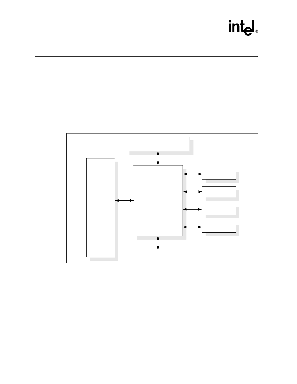
IXF1104 4-Port Gi gab it Ethernet Media Access Controller
1
2.0 General Description
The IXF1104 provides up to a 4.0 Gbps interface to four individual 10/100/1000 Mbps full-duplex
or 10/100 Mbps half-duplex-capable Ethernet Media Access Controllers (MACs). The network
proce ssor is supported through a System Packet Interface Phase 3 (SPI3) media interface. The
following PHY interfaces are selected on a per-port basis:
• Serializer /Deserializer (SerDes) with Optical Module Interface support
• Gigabit Media Indepe ndent Interface (GMII)
• Reduced Gigabit Media Independent Interface (RGMII).
Figure 1 illustrates the IXF1104 block diagram.
Figure 1. Block Diag ram
CPU
uP IF
PHY 1 Devic e
PHY 2 Devic e
®
Intel
IXF1104 M AC
SPI3
Se rD e s /RGMI I/GMI I In t e r fa ce
PHY 3 Devic e
PHY 4 Devic e
Forw ardi n g Engi ne/N etwork Processor
MDIO
B3175-0
20 Datasheet
Document Number: 278757
Revision Number: 007
Revision Date: March 25, 2004
Page 21

Figure 2 illustrates the IXF1104 internal architecture.
1
Figure 2. Internal Architecture
IXF1104 4-Port Gigabit Ethernet Media Access Controller
SPI3 Interface
CPU Interface RMON Statistics
PLLs
Packet
Buffer
Packet
Buffer
Packet
Buffer
Packet
Buffer
MDIO OMI
TX
RX
TX
RX
TX
RX
TX
RX
Clock Control Block Clock Register Block
10/100/1000 MAC
10/100/1000 MAC
10/100/1000 MAC
10/100/1000 MAC
RGMII/GMII Inte rface
PMA Layer SerDes
RGMII/GMII Inte rface
PMA Layer SerDes
RGMII/GMII Inte rface
PMA Layer SerDes
RGMII/GMII Inte rface
PMA Layer SerDes
B3176-0
Datasheet 21
Document Number: 278757
Revision Number: 007
Revision Date: March 25, 2004
Page 22
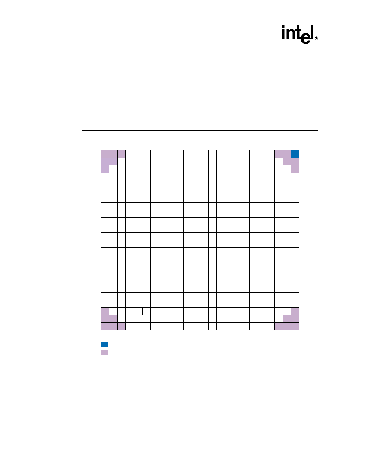
IXF1104 4-Port Gi gab it Ethernet Media Access Controller
3.0 Ball Assignments and Ball List T abl es
3.1 Ball Assignments
See Figure 3, Table 1 “Ball List in Alphanumeric Order by Signal Name” on page 23, and Table 2
“Ball List in Alphanumeric Order by Ball Location” on page 29 for the IXF1104 ball assignments.
Figure 3. Intel
®
IXF1104 552-Ball CBGA Assignments (Top View)
AD AC AB AA Y W V U T R P N M L K J H G F E D C B A
AD1
1
AC2
2
AC3AD3
3
4
5
6
7
8
AD8
9
10
11
12
13
14
15
16
17
18
19
20
21
22
23
24
W7Y7AA7AB7AC7AD7
V7 U7 T7 R7 P7 N7 M7 L7 K7 J7 H7 G7 F7 E7 D7 G7 B7 A7
M8
T8
U8
V8
W8Y8AA8AB8AC8
T9
U9
V9
W9Y9AA9AB9AC9AD9
T10
U10
V10
W10Y10AA10AB10AC10AD10
T11
U11
V11
W11Y11AA11AB11AC11AD11
T12
U12
V12
W12Y12AA12AB12AC12AD12
T13
U13
V13
W13Y13AA13AB13AC13AD13
T14
U14
V14
W14Y14AA14AB14AC14AD14
T15
U15
V15
W15Y15AA15AB15AC15AD15
T16
U16
V16
W16Y16AA16AB16AC16AD16
T17
U17
V
17
W17Y17AA17AB17AC17AD17
T18
U18
V18
W18Y18AA18AB18AC18AD18
T19
U19
V19
W19Y19AA19AB19AC19AD19
T20
U20
V20
W20Y20AA20AB20AC20AD20
T21
U21
V21
W21Y21AA21AB21AC21AD21
T22
U22
V22
W22
AA22AB22AC22AD22
Y22
T23
U23
V23
W23Y23AA23AB23AC23AD23
T24
U24
V24
W24Y24AA24AB24AC24AD24
R10
R11
R12
R13
R14
R15
R16
R17
R18
R19
R20
R21
R22
R23
R24
N9
P9
R9
N10
P10
N11
P11
N12
P12
N13
P13
N14
P14
N15
P15
N16
P16
N17
P17
N18
P18
N19
P19
N20
P20
N121
P21
N22
P22
N23
P23
N24
P24
M9
M10
M11
M12
M13
M14
M15
M16
M17
M18
M19
M20
M21
M22
M23
M24
L10
L11
L12
L13
L14
L15
L16
L17
L18
L19
L20
L21
L22
L23
L24
K8
L8
K9
L9
K10
K11
K12
K13
K14
K15
K16
K17
K18
K19
K20
K21
K22
K23
K24
N8
P8
R8
J10
J11
J12
J13
J14
J15
J16
J17
J18
J19
J20
J21
J22
J23
J24
G8
H8
J8
J9
G9
H9
G10
H10
G11
H11
G12
H12
G13
H13
G14
H14
G15
H15
G16
H16
G17
H17
G18
H18
G19
H19
G20
H20
G21
H21
G22
H22
G23
H23
G24
H24
AD AC AB AA Y W V U T R P N M L K J H G F E D C B A
= No Pad (A1)
= No Ball (A2, A3, A22, A23, A24, B1, B2, B23, B24, C1, C24, AB1, AB24, AC1, AC2, AC23, AC24, AD1, AD2, AD3,
AD22, AD23, AD24)
F10
F11
F12
F13
F14
F15
F16
F17
F18
F19
F20
F21
F22
F23
F24
A1
B1C1D1E1F1G1H1J1K1L1M1N1P1R1T1U1V1W1Y1AA1AB1AC1
1
A2B2C2D2E2F2G2H2J2K2L2M2N2P2R2T2U2V2W2Y2AA2AB2AD2
2
A3B3C3D3E3F3G3H3J3K3L3M3N3P13R3T3U3V3W3Y3AA3AB3
3
A4B4C4D4E4F4G4H4J4K4L4M4N4P4R4T4U4V4W4Y4AA4AB4AC4AD4
4
A5B5C5D5E5F5G5H5J5K5L5M5N5P5R5T5U5V5W5Y5AA4AB5AC5AD5
5
A6B6C6D6F6F6G6H6J6K6L6M6N6P6R6T6U6V6W6Y6AA6AB6AC6AD6
6
7
F8
F9
E10
E11
E12
E13
E14
E15
E16
E17
E18
E19
E20
E21
E22
E23
E24
C8
D8
E8
C9
D9
E9
C10
D10
C11
D11
C12
D12
C13
D13
C14
D14
C15
D15
C16
D16
C17
D17
C18
D18
C19
D19
C20
D20
C21
D21
C22
D22
C23
D23
C24
D24
B28
B9
B10
B11
B12
B13
B14
B15
B16
B17
B18
B19
B20
B21
B22
B23
B24
A8
A9
A10
A11
A12
A13
A14
A15
A16
A17
A18
A19
A20
A21
A22
A23
A24
B1458-01
8
9
10
11
12
13
14
15
16
17
18
19
20
21
22
23
24
22 Datasheet
Document Number: 278757
Revision Number: 007
Revision Date: March 25, 2004
Page 23

IXF1104 4-Port Gi gab it Ethernet Media Access Controller
3.2 Ball List Tables
3.2.1 Balls Listed in Alphabetic Order by Signal Name
Table 1 shows the ball locations and signa l names arranged in alphanumeric order by signa l name.
The following table notes relate to Table 1 and Table 2:
1. GMII Ball Connection:
See T able 16 for connection in RGMII or fiber mode.
2. SPI3 Ball Connection:
See T able 17 for proper SPHY and MPHY connection.
3. Fiber Mode Ball Connection:
See T able 16 for use in RGMII and GMII (copper mode).
Tab le 1. Ba ll Li st in Alp hanumeric Orde r by Signal Name
Signal Name
AVDD1P8_1 A5
AVDD1P8_1 A20
AVDD1P8_2 T23
AVDD1P8_2 AB16
AVDD2P5_1 AD20
AVDD2P5_2 R18
AVDD2P5_2 U14
CLK125 AD19
1
COL_0
1
COL_1
1
COL_2
1
COL_3
1
CRS_0
1
CRS_1
1
CRS_2
1
CRS_3
DTPA_0
DTPA_1
DTPA_2
DTPA_3
2
2
2
2
GND B6
GND B10
GND B15
GND B19
Ball
Location
AB6
AB10
AD15
AB17
AA5
AA9
AB15
AC16
D3
L1
A9
J7
Signal Name
GND D4
GND D8
GND D12
GND D13
GND D17
GND D21
GND F2
GND F6
GND F10
GND F15
GND F19
GND F23
GND H4
GND H8
GND H12
GND H13
GND H17
GND H21
GND J10
GND J15
GND K2
GND K6
GND K9
GND K11
Ball
Location
Signal Name
GND K14
GND K16
GND K19
GND K23
GND L10
GND L12
GND L13
GND L15
GND M4
GND M8
GND M11
GND M14
GND M17
GND M21
GND N4
GND N8
GND N11
GND N14
GND N17
GND N21
GND P10
GND P12
GND P13
GND P15
Ball
Location
23 Datasheet
Document Number: 278757
Revision Number: 007
Revision Date: March 25, 2004
Page 24

IXF1104 4-Port Gigabit Ethernet Media Access Controller
Signal Name
GND R2
GND R6
GND R9
GND R11
GND R14
GND R16
GND R19
GND R23
GND T10
GND T15
GND U4
GND U8
GND U12
GND U13
GND U17
GND U21
GND W2
GND W6
GND W10
GND W15
GND W19
GND W23
GND AA4
GND AA8
GND AA12
GND AA13
GND AA17
GND AA21
GND AC6
GND AC10
GND AC15
GND AC19
GND AC14
GND L20
GND L5
GND R7
GND AB12
GND A4
Ball
Location
Signal Name
Ball
Location
GND A21
GND AD21
2
C_CLK L23
I
2
C_DATA_0
I
2
C_DATA_1
I
2
C_DATA_2
I
2
C_DATA_3
I
3
3
3
3
L24
M24
N24
P24
LED_CLK K24
LED_DATA M22
LED_LATCH L22
MDC
MDIO
4
4
W24
V21
MOD_DEF_INT N22
NC D24
NC E12
NC F11
NC G15
NC H7
NC H18
NC J21
NC K7
NC K18
NC K20
NC K22
NC L18
NC L19
NC L21
NC M7
NC M18
NC M20
NC N3
NC N18
NC P2
NC P4
NC P6
NC P7
NC P8
NC P17
Signal Name
NC P18
NC R5
NC R10
NC R12
NC R13
NC R15
NC R20
NC T6
NC T7
NC T8
NC T9
NC T21
NC T22
NC U5
NC U7
NC U9
NC U11
NC U18
NC V9
NC V10
NC V11
NC V13
NC AB18
NC AD4
NC AD5
No Ball A2
No Ball A3
No Ball A22
No Ball A23
No Ball A24
No Ball B1
No Ball B2
No Ball B23
No Ball B24
No Ball C1
No Ball C24
No Ball AB1
No Ball AB24
Ball
Location
Datasheet 24
Document Number: 278757
Revision Number: 007
Revision Date: March 25, 2004
Page 25

IXF1104 4-Port Gi gab it Ethernet Media Access Controller
Signal Name
No Ball AC1
No Ball AC2
No Ball AC23
No Ball AC24
No Ball AD1
No Ball AD2
No Ball AD3
No Ball AD22
No Ball AD23
No Ball AD24
No Pad A1
2
PTPA
RDAT_0
RDAT_1
RDAT_2
RDAT_3
RDAT_4
RDAT_5
RDAT_6
RDAT_7
RDAT_8
RDAT_9
RDAT_10
RDAT_11
RDAT_12
RDAT_13
RDAT_14
RDAT_15
RDAT_16
RDAT_17
RDAT_18
RDAT_19
RDAT_20
RDAT_21
RDAT_22
RDAT_23
RDAT_24
RDAT_25
2
2
2
2
2
2
2
2
2
2
2
2
2
2
2
2
2
2
2
2
2
2
2
2
2
2
Ball
Location
B11
A15
A14
B14
C14
C13
D14
E14
F14
A17
C17
D16
E16
F16
E17
E18
F18
B20
B22
C20
C21
C22
D22
E22
E21
G18
G19
Signal Name
RSX
2
2
2
2
2
2
2
2
2
2
2
2
2
2
2
2
2
2
2
2
2
2
2
2
2
2
2
2
2
2
2
2
2
2
1
1
1
1
RDAT_26
RDAT_27
RDAT_28
RDAT_29
RDAT_30
RDAT_31
RENB_0
RENB_1
RENB_2
RENB_3
REOP_0
REOP_1
REOP_2
REOP_3
RERR_0
RERR_1
RERR_2
RERR_3
RFCLK
RMOD0
RMOD1
RPRTY_0
RPRTY_1
RPRTY_2
RPRTY_3
RSOP_0
RSOP_1
RSOP_2
RSOP_3
RVAL_0
RVAL_1
RVAL_2
RVAL_3
RX_DV_0
RX_DV_1
RX_DV_2
RX_DV_3
Ball
Location
G20
G21
G22
G23
G24
F24
A13
A18
C19
E24
C16
D18
C23
J19
A16
G17
D20
H20
A19
G14
G13
E15
G16
E20
F20
B16
C18
E23
J18
E13
C15
B18
E19
F22
V5
AB11
Y24
V18
Signal Name
RX_ER_0
RX_ER_1
RX_ER_2
RX_ER_3
RX_LOS_INT
RXC_0
RXC_1
RXC_2
RXC_3
3
3
3
3
3
3
3
3
1
1
1
1
1
1
1
1
1
1
1
1
1
1
1
1
1
1
1
1
1
1
1
1
1
RX_N_0
RX_N_1
RX_N_2
RX_N_3
RX_P_0
RX_P_1
RX_P_2
RX_P_3
RXD0_0
RXD0_1
RXD0_2
RXD0_3
RXD1_0
RXD1_1
RXD1_2
RXD1_3
RXD2_0
RXD2_1
RXD2_2
RXD2_3
RXD3_0
RXD3_1
RXD3_2
RXD3_3
RXD4_0
RXD4_1
RXD4_2
RXD4_3
RXD5_0
Ball
Location
1
1
1
1
3
W5
Y12
AA22
U20
P19
R22
U22
R24
V24
P22
V22
T24
U24
V4
AD11
AA24
V23
V8
Y9
Y20
Y17
V7
Y11
Y21
Y18
W7
W11
Y22
Y19
Y7
W9
Y23
W18
Y6
AD10
W22
T16
Y5
25 Datasheet
Document Number: 278757
Revision Number: 007
Revision Date: March 25, 2004
Page 26

IXF1104 4-Port Gigabit Ethernet Media Access Controller
Signal Name
1
RXD5_1
RXD6_1
RXD7_1
STPA
1
1
1
1
1
1
1
1
1
1
2
RXD5_2
RXD5_3
RXD6_0
RXD6_2
RXD6_3
RXD7_0
RXD7_2
RXD7_3
Ball
Location
AC11
V20
T17
AB5
AA11
V19
T18
AC5
Y10
W20
T19
C11
SYS_RST_L AD12
TADR0
TADR1
2
2
A11
A12
TCLK J22
TDAT0
TDAT1
TDAT2
TDAT3
TDAT4
TDAT5
TDAT6
TDAT7
TDAT8
TDAT9
TDAT10
TDAT11
TDAT12
TDAT13
TDAT14
TDAT15
TDAT16
TDAT17
TDAT18
TDAT19
TDAT20
TDAT21
2
2
2
2
2
2
2
2
2
2
2
2
2
2
2
2
2
2
2
2
2
2
B3
C2
C3
D1
C4
C5
B5
C6
F1
G1
G2
H1
J1
J2
J3
H3
E5
E6
E7
E8
E9
E10
Signal Name
2
TDAT22
2
TDAT23
2
TDAT24
2
TDAT25
2
TDAT26
2
TDAT27
2
TDAT28
2
TDAT29
2
TDAT30
2
TDAT31
TDI J24
TDO H24
TFCLK
TMOD0
TMOD1
2
2
2
2
2
2
2
2
2
2
2
2
2
2
2
TENB_0
TENB_1
TENB_2
TENB_3
TEOP_0
TEOP_1
TEOP_2
TEOP_3
TERR_0
TERR_1
TERR_2
TERR_3
TMS H22
TPRTY_0
TPRTY_1
TPRTY_2
TPRTY_3
2
2
2
2
TRST_L J23
TSOP_0
TSOP_1
TSOP_2
TSOP_3
2
2
2
2
TSX E1
Ball
Location
F9
C8
G4
G5
G6
G7
G8
G9
F5
F7
B7
E2
C9
J4
A7
F3
E4
H5
A8
K1
E11
J8
D7
A6
D9
D5
G3
B9
J6
C7
E3
C10
J5
Signal Name
TX_EN_0
TX_EN_1
TX_EN_2
TX_EN_3
TX_ER_0
TX_ER_1
TX_ER_2
TX_ER_3
1
1
1
1
1
1
1
1
TX_FAULT_INT
3
TX_N_0
3
TX_N_1
3
TX_N_2
3
TX_N_3
3
TX_P_0
3
TX_P_1
3
TX_P_2
3
TX_P_3
1
TXC_0
1
TXC_1
1
TXC_2
1
TXC_3
1
TXD0_0
1
TXD0_1
1
TXD0_2
1
TXD0_3
1
TXD1_0
1
TXD1_1
1
TXD1_2
1
TXD1_3
1
TXD2_0
1
TXD2_1
1
TXD2_2
1
TXD2_3
1
TXD3_0
1
TXD3_1
1
TXD3_2
1
TXD3_3
1
TXD4_0
3
Ball
Location
AB2
Y8
AC22
V12
W1
AD6
AD17
AB13
P23
Y14
AD14
Y16
AD18
Y13
AD13
W16
AC18
AA1
AD7
AC20
AB14
Y1
AC7
AB20
V14
Y2
AB7
AB21
V15
Y3
AB9
AB22
V16
AA3
AD9
AB23
V17
AB3
Datasheet 26
Document Number: 278757
Revision Number: 007
Revision Date: March 25, 2004
Page 27

IXF1104 4-Port Gi gab it Ethernet Media Access Controller
Signal Name
1
TXD4_1
1
TXD4_2
1
TXD4_3
1
TXD5_0
1
TXD5_1
1
TXD5_2
1
TXD5_3
1
TXD6_0
1
TXD6_1
1
TXD6_2
1
TXD6_3
1
TXD7_0
1
TXD7_1
1
TXD7_2
1
TXD7_3
Ball
Location
AA7
AD16
AA14
AC3
AB8
AB19
Y15
AB4
AD8
AA20
AA16
Y4
AC9
AA18
W14
TXPAUSE_ADD0 N20
TXPAUSE_ADD1 P20
TXPAUSE_ADD2 P21
TXPAUSEFR T20
UPX_ADD0 P3
UPX_ADD1 N1
UPX_ADD2 P1
UPX_ADD3 R1
UPX_ADD4 T1
UPX_ADD5 U1
UPX_ADD6 V1
UPX_ADD7 V2
UPX_ADD8 V3
UPX_ADD9 U3
UPX_ADD10 T3
UPX_BADD0 T2
UPX_BADD1 W3
UPX_CS_L R3
UPX_DATA0 L2
UPX_DATA1 K3
UPX_DATA2 L3
UPX_DATA3 M3
UPX_DATA4 L4
Signal Name
Ball
Location
UPX_DATA5 N5
UPX_DATA6 M5
UPX_DATA7 K5
UPX_DATA8 P5
UPX_DATA9 L6
UPX_DATA10 L7
UPX_DATA11 N7
UPX_DATA12 L8
UPX_DATA13 H9
UPX_DATA14 J9
UPX_DATA15 N10
UPX_DATA16 M10
UPX_DATA17 K10
UPX_DATA18 G10
UPX_DATA19 H11
UPX_DATA20 G11
UPX_DATA21 K12
UPX_DATA22 G12
UPX_DATA23 K13
UPX_DATA24 H14
UPX_DATA25 K15
UPX_DATA26 N15
UPX_DATA27 M15
UPX_DATA28 J16
UPX_DATA29 H16
UPX_DATA30 J17
UPX_DATA31 L17
UPX_RD_L V6
UPX_RDY_L M1
UPX_WIDTH0 U16
UPX_WIDTH1 T5
UPX_WR_L T4
VDD D6
VDD D10
VDD D15
VDD D19
VDD F4
VDD F21
Signal Name
VDD H10
VDD H15
VDD J11
VDD J14
VDD K4
VDD K8
VDD K17
VDD K21
VDD L9
VDD L11
VDD L14
VDD L16
VDD P9
VDD P11
VDD P14
VDD P16
VDD R4
VDD R8
VDD R17
VDD R21
VDD T11
VDD T14
VDD U10
VDD U15
VDD W4
VDD W21
VDD AA6
VDD AA10
VDD AA15
VDD AA19
VDD C12
VDD D11
VDD J20
VDD A10
VDD2 B4
VDD2 B8
VDD2 B12
VDD2 D2
Ball
Location
27 Datasheet
Document Number: 278757
Revision Number: 007
Revision Date: March 25, 2004
Page 28

IXF1104 4-Port Gigabit Ethernet Media Access Controller
Signal Name
VDD2 F8
VDD2 F12
VDD2 H2
VDD2 H6
VDD2 J12
VDD2 M2
VDD2 M6
VDD2 M9
VDD2 M12
VDD3 B13
VDD3 B17
VDD3 B21
VDD3 D23
VDD3 F13
VDD3 F17
VDD3 H19
VDD3 H23
VDD3 J13
VDD3 M13
VDD3 M16
VDD3 M19
VDD3 M23
VDD4 N13
VDD4 N16
VDD4 N19
VDD4 N23
VDD4 T13
VDD4 U19
VDD4 U23
VDD4 W13
VDD4 W17
VDD4 AA23
VDD4 AC13
VDD4 AC17
VDD4 AC21
VDD5 N2
VDD5 N6
VDD5 N9
Ball
Location
Signal Name
VDD5 N12
VDD5 T12
VDD5 U2
VDD5 U6
VDD5 W8
VDD5 W12
VDD5 AA2
VDD5 AC4
VDD5 AC8
VDD5 AC12
Ball
Location
Datasheet 28
Document Number: 278757
Revision Number: 007
Revision Date: March 25, 2004
Page 29

IXF1104 4-Port Gi gab it Ethernet Media Access Controller
3.2.2 Balls Listed in Alphabetic Order by Ball Location
Table 2 shows the ball locations and signa l names arranged in order by ball location.
Table 2. Ball List in Alphanumeric Order by Ball Location
Ball
Location
Signal Name
A1 No Pad
A2 No Ball
A3 No Ball
A4 GND
A5 AVDD1P8_1
A6 TMOD0
A7 TEOP_0
A8 TERR_0
A9 DTPA_2
A10 VDD
A11 TADR0
A12 TADR1
A13 RENB_0
A14 RDAT_1
A15 RDAT_0
A16 RERR_0
A17 RDAT_8
A18 RENB_1
A19 RFCLK
A20 AVDD1P8_1
A21 GND
A22 No Ball
A23 No Ball
A24 No Ball
B1 No Ball
B2 No Ball
B3 TDAT0
B4 VDD2
B5 TDAT6
B6 GND
B7 TENB_0
B8 VDD2
B9 TPRTY_2
Ball
Location
Signal Nam e
B10 GND
B11 PTPA
2
B12 VDD2
B13 VDD3
B14 RDAT_2
2
2
2
2
B15 GND
B16 RSOP_0
B17 VDD3
B18 RVAL_1
2
2
2
B19 GND
2
2
2
2
2
2
2
2
2
B20 RDAT_16
B21 VDD3
B22 RDAT_17
B23 No Ball
B24 No Ball
C1 No Ball
C2 TDAT1
C3 TDAT2
C4 TDAT4
C5 TDAT5
C6 TDAT7
C7 TSOP_0
C8 TDAT23
C9 TENB_2
C10 TSOP_2
C11 STPA
2
C12 VDD
C13 RDAT_4
2
C14 RDAT_3
C15 RVAL_0
2
C16 REOP_0
C17 RDAT_9
2
C18 RSOP_1
C19 RENB_2
2
2
2
2
2
2
2
2
2
2
2
2
2
2
2
2
2
2
2
Ball
Location
Signal Name
C20 RDAT_18
C21 RDAT_19
C22 RDAT_20
C23 REOP_2
C24 No Ball
D1 TDAT3
D2 VDD2
D3 DTPA_0
D4 GND
D5 TPRTY_0
D6 VDD
D7 TFCLK
D8 GND
D9 TMOD1
D10 VDD
D11 VDD
D12 GND
D13 GND
D14 RDAT_5
D15 VDD
D16 RDAT_10
D17 GND
D18 REOP_1
D19 VDD
D20 RERR_2
D21 GND
D22 RDAT_21
D23 VDD3
D24 NC
E1 TSX
E2 TENB_1
E3 TSOP_1
E4 TEOP_2
E5 TDAT16
2
2
2
2
2
2
2
2
2
2
2
2
2
2
2
2
2
2
29 Datasheet
Document Number: 278757
Revision Number: 007
Revision Date: March 25, 2004
Page 30

IXF1104 4-Port Gigabit Ethernet Media Access Controller
Ball
Location
Signal Name
E6 TDAT17
E7 TDAT18
E8 TDAT19
E9 TDAT20
E10 TDA T21
E11 TERR_2
E12 NC
E13 RSX
E14 RDAT_6
E15 RPRTY_0
E16 RDAT_11
E17 RDAT_13
E18 RDAT_14
E19 RVAL_2
E20 RPRTY_2
E21 RDAT_23
E22 RDAT_22
E23 RSOP_2
E24 RENB_3
F1 TDAT8
F2 GND
F3 TEOP_1
F4 VDD
F5 TDAT30
F6 GND
F7 TDAT31
F8 VDD2
F9 TDAT22
F10 GND
F11 NC
F12 VDD2
F13 VDD3
F14 RDAT_7
F15 GND
F16 RDAT_12
F17 VDD3
F18 RDAT_15
F19 GND
Ball
Location
2
2
2
2
2
2
F20 RPRTY_3
F21 VDD
F22 RVAL_3
F23 GND
F24 RDAT_31
G1 TDAT9
G2 T DAT10
2
2
2
2
2
2
2
2
2
2
2
2
2
G3 TPRTY_1
G4 T DAT24
G5 T DAT25
G6 T DAT26
G7 T DAT27
G8 T DAT28
G9 T DAT29
G10 UPX_DATA18
G11 UPX_DATA20
G12 UPX_DATA22
G13 RMOD1
G14 RMOD0
G15 NC
G16 RPRTY_1
2
G17 RERR_1
G18 RDAT_24
2
G19 RDAT_25
G20 RDAT_26
2
G21 RDAT_27
G22 RDAT_28
2
G23 RDAT_29
G24 RDAT_30
H1 TDAT11
Signal Name
2
2
2
2
2
2
2
2
2
2
2
2
2
2
2
2
2
2
2
2
2
2
2
2
H2 VDD2
H3 TDAT15
2
H4 GND
H5 TEOP_3
2
H6 VDD2
2
2
H7 NC
2
H8 GND
H9 UPX_DATA13
Ball
Location
Signal Name
H10 VDD
H11 UPX_DATA19
H12 GND
H13 GND
H14 UPX_DATA24
H15 VDD
H16 UPX_DATA29
H17 GND
H18 NC
H19 VDD3
H20 RERR_3
H21 GND
H22 TMS
H23 VDD3
H24 TDO
J1 TDAT12
J2 TDAT13
J3 TDAT14
J4 TENB_3
J5 TSOP_3
J6 TPRTY_3
J7 DTPA_3
J8 TERR_3
J9 UPX_DATA14
J10 GND
J11 VDD
J12 VDD2
J13 VDD3
J14 VDD
J15 GND
J16 UPX_DATA28
J17 UPX_DATA30
J18 RSOP_3
J19 REOP_3
J20 VDD
J21 NC
J22 TCLK
J23 TRST_L
2
2
2
2
2
2
2
2
2
2
2
Datasheet 30
Document Number: 278757
Revision Number: 007
Revision Date: March 25, 2004
Page 31

IXF1104 4-Port Gi gab it Ethernet Media Access Controller
Ball
Location
Signal Name
J24 TDI
K1 TERR_1
K2 GND
K3 UPX_DATA1
K4 VDD
K5 UPX_DATA7
K6 GND
K7 NC
K8 VDD
K9 GND
K10 UPX_DATA17
K11 GND
K12 UPX_DATA21
K13 UPX_DATA23
K14 GND
K15 UPX_DATA25
K16 GND
K17 VDD
K18 NC
K19 GND
K20 NC
K21 VDD
K22 NC
K23 GND
K24 LED_CLK
L1 DTPA_1
L2 UPX_DATA0
L3 UPX_DATA2
L4 UPX_DATA4
L5 GND
L6 UPX_DATA9
L7 UPX_DATA10
L8 UPX_DATA12
L9 VDD
L10 GND
L11 VDD
L12 GND
L13 GND
Ball
Location
Signal Nam e
L14 VDD
2
L15 GND
L16 VDD
L17 UPX_DATA31
L18 NC
L19 NC
L20 GND
L21 NC
L22 LED_LATCH
2
L23 I
L24 I
C_CLK
2
C_DATA_0
3
M1 UPX_RDY_L
M2 VDD2
M3 UPX_DATA3
M4 GND
M5 UPX_DATA6
M6 VDD2
M7 NC
M8 GND
M9 VDD2
M10 UPX_DATA16
M11 GND
M12 VDD2
M13 VDD3
M14 GND
2
M15 UPX_DATA27
M16 VDD3
M17 GND
M18 NC
M19 VDD3
M20 NC
M21 GND
M22 LED_DATA
M23 VDD3
M24 I
2
C_DATA_1
3
N1 UPX_ADD1
N2 VDD5
N3 NC
Ball
Location
Signal Name
N4 GND
N5 UPX_DATA5
N6 VDD5
N7 UPX_DATA11
N8 GND
N9 VDD5
N10 UPX_DATA15
N11 GND
N12 VDD5
N13 VDD4
N14 GND
N15 UPX_DATA26
N16 VDD4
N17 GND
N18 NC
N19 VDD4
N20 TXPAUSE_ADD0
N21 GND
N22 MOD_DEF_INT
N23 VDD4
2
N24 I
C_DATA_2
P1 UPX_ADD2
P2 NC
P3 UPX_ADD0
P4 NC
P5 UPX_DATA8
P6 NC
P7 NC
P8 NC
P9 VDD
P10 GND
P11 VDD
P12 GND
P13 GND
P14 VDD
P15 GND
P16 VDD
P17 NC
3
31 Datasheet
Document Number: 278757
Revision Number: 007
Revision Date: March 25, 2004
Page 32

IXF1104 4-Port Gigabit Ethernet Media Access Controller
Ball
Location
Signal Name
P18 NC
P19 RX_LOS_INT
P20 TXPAUSE_ADD1
P21 TXPAUSE_ADD2
P22 RX_P_0
P23 TX_FAULT_INT
P24 I2C_DATA_3
R1 UPX_ADD3
R2 GND
R3 UPX_CS_L
R4 VDD
R5 NC
R6 GND
R7 GND
R8 VDD
R9 GND
R10 NC
R11 GND
R12 NC
R13 NC
R14 GND
R15 NC
R16 GND
R17 VDD
R18 AVDD2P5_2
R19 GND
R20 NC
R21 VDD
R22 RX_N_0
R23 GND
R24 RX_N_2
T1 UPX_ADD4
T2 UPX_BADD0
T3 UPX_ADD10
T4 UPX_WR_L
T5 UPX_WIDTH1
T6 NC
T7 NC
Ball
Location
Signal Name
T8 NC
3
T9 NC
T10 GND
T11 VDD
3
3
3
T12 VDD5
T13 VDD4
T14 VDD
T15 GND
T16 RXD4_3
T17 RXD5_3
T18 RXD6_3
T19 RXD7_3
1
1
1
1
T20 TXPAUSEFR
T21 NC
T22 NC
T23 AVDD1P8_2
T24 RX_P_2
3
U1 UPX_ADD5
U2 VDD5
U3 UPX_ADD9
U4 GND
U5 NC
U6 VDD5
U7 NC
U8 GND
U9 NC
U10 VDD
U11 NC
3
U12 GND
U13 GND
3
U14 AVDD2P5_2
U15 VDD
U16 UPX_WIDTH0
U17 GND
U18 NC
U19 VDD4
U20 RX_ER_3
1
U21 GND
Ball
Location
Signal Name
U22 RX_N_1
U23 VDD4
U24 RX_P_3
V1 UPX_ADD6
V2 UPX_ADD7
V3 UPX_ADD8
V4 RXC_0
V5 RX_DV_0
V6 UPX_RD_L
V7 RXD1 _0
V8 RXD0 _0
V9 NC
V10 NC
V11 NC
V12 TX_EN_3
V13 NC
V14 TXD0_3
V15 TXD1_3
V16 TXD2_3
V17 TXD3_3
V18 RX_DV_3
V19 RXD6_2
V20 RXD5_2
V21 MDIO
V22 RX_P_1
V23 RXC_3
V24 RX_N_3
W1 TX_ER_0
W2 GND
W3 UPX_BADD1
W4 VDD
W5 RX_ER_0
W6 GND
W7 RXD2_0
W8 VDD5
W9 RXD3_1
W10 GND
W11 RXD2_1
3
3
1
1
1
1
1
1
1
1
1
1
1
1
4
3
1
3
1
1
1
1
1
Datasheet 32
Document Number: 278757
Revision Number: 007
Revision Date: March 25, 2004
Page 33

IXF1104 4-Port Gi gab it Ethernet Media Access Controller
Ball
Location
Signal Name
W12 VDD5
W13 VDD4
W14 TXD7_3
W15 GND
W16 TX_P_2
W17 VDD4
W18 RXD3_3
W19 GND
W20 RXD7_2
W21 VDD
W22 RXD4_2
W23 GND
W24 MDC
Y1 TXD0_0
Y2 TXD1_0
Y3 TXD2_0
Y4 TXD7_0
Y5 RXD5 _0
Y6 RXD4 _0
Y7 RXD3 _0
Y8 TX_EN_1
Y9 RXD0_1
Y10 RXD7_1
Y11 RXD1_1
Y12 RX_ER_1
Y13 TX_P_0
Y14 TX_N_0
Y15 TXD5_3
Y16 TX_N_2
Y17 RXD0_3
Y18 RXD1_3
Y19 RXD2_3
Y20 RXD0_2
Y21 RXD1_2
Y22 RXD2_2
Y23 RXD3_2
Y24 RX_DV_2
AA1 TXC_0
Ball
Location
Signal Nam e
AA2 VDD5
AA3 TXD3_0
1
AA4 GND
AA5 CRS_0
3
AA6 VDD
AA7 TXD4_1
1
AA8 GND
AA9 CRS_1
1
AA10 VDD
AA11 RXD6_1
1
AA12 GND
1
1
1
1
1
AA13 GND
4
1
1
1
1
1
1
1
1
1
1
1
1
3
3
1
3
1
1
1
1
1
1
1
1
1
AA14 TXD4_3
AA15 VDD
AA16 TXD6_3
AA17 GND
AA18 TXD7_2
AA19 VDD
AA20 TXD6_2
AA21 GND
AA22 RX_ER_2
AA23 VDD4
AA24 RXC_2
AB1 No Ball
AB2 TX_EN_0
AB3 TXD4_0
AB4 TXD6_0
AB5 RX D6_0
AB6 COL_0
AB7 TXD1_1
AB8 TXD5_1
AB9 TXD2_1
AB10 COL_1
AB11 RX_DV_1
AB12 GND
AB13 TX_ER_3
AB14 TXC_3
AB15 CRS_2
1
1
1
1
1
1
1
1
1
1
1
1
1
1
1
1
1
1
1
Ball
Location
Signal Name
AB16 AVDD1P8_2
AB17 COL_3
AB18 NC
AB19 TXD5_2
AB20 TXD0_2
AB21 TXD1_2
AB22 TXD2_2
AB23 TXD3_2
AB24 No Ball
AC1 No Ball
AC2 No Ball
AC3 TXD5_0
AC4 VDD5
AC5 RXD7_0
AC6 GND
AC7 TXD0_1
AC8 VDD5
AC9 TXD7_1
AC10 GND
AC11 RXD5_1
AC12 VDD5
AC13 VDD4
AC14 GND
AC15 GND
AC16 CRS_3
AC17 VDD4
AC18 TX_P_3
AC19 GND
AC20 TXC_2
AC21 VDD4
AC22 TX_EN_2
AC23 No Ball
AC24 No Ball
AD1 No Ball
AD2 No Ball
AD3 No Ball
AD4 NC
AD5 NC
1
1
1
1
1
1
1
1
1
1
1
1
3
1
1
33 Datasheet
Document Number: 278757
Revision Number: 007
Revision Date: March 25, 2004
Page 34

IXF1104 4-Port Gigabit Ethernet Media Access Controller
Ball
Location
Signal Name
AD6 TX_ER_1
AD7 TXC_1
AD8 TXD6_1
AD9 TXD3_1
AD10 RXD4_1
AD11 RXC_1
AD12 SYS_RST_L
AD13 TX_P_1
AD14 TX_N_1
AD15 COL_2
AD16 TXD4_2
AD17 TX_ER_2
AD18 TX_N_3
AD19 CLK125
AD20 AVDD2P5_1
AD21 GND
AD22 No Ball
AD23 No Ball
AD24 No Ball
1
1
1
1
1
1
3
3
1
1
1
3
Datasheet 34
Document Number: 278757
Revision Number: 007
Revision Date: March 25, 2004
Page 35

IXF1104 4-Port Gi gab it Ethernet Media Access Controller
35 Datasheet
Document Number: 278757
Revision Number: 007
Revision Date: March 25, 2004
Page 36

IXF1104 4-Port Gi gab it Ethernet Media Access Controller
4.0 Ball Assignments and Signal Descriptions
4.1 N amin g C on ve nt io ns
4.1.1 Signal Name Conventions
Signal names beg in with a Signal Mnem onic, and can also contain one or more of the followi ng
designations: a differential pair designation, a serial designation, a port designation (RGMII
interface), and an active low designation. Signal naming conve ntions are as follows:
Differential Pair + Port Design at ion. The positive and negative compo nents of differential pairs
tied to a specific port are designated by the Signal Mnemonic, immediately followed by an
underscore and either P (positive component) or N (negative component), and an underscore
followed by the port designation. For example, SerDes interface signals for port 0 are ident ified as
TX_P_0 and TX_N_0.
Serial Design ation . A set of signals that are not tied to any specific port are designated by the
Signal Mnemoni c, follo wed by a bracketed serial designation. For example, the set of 11 CPU
Address Bus signals is identified as UPX_ADD[10:0].
Port Designation. Individual signals that apply to a particular port are designated by the Signal
Mnemonic, immediately followed by an underscore and the Port Designation. For example,
RGMII Transmit Control signals are identified as TX_CTL_0, TX_CTL_1, TX_CTL_2, and so on.
Port Bus Designatio n. A set of bus signals that apply to a particular port are designated by the
Signal Mnemonic, immediately followed by a bracketed bus designation, followed by an
underscore and the port desi gnation. For example, RGMII transmit da ta bus signals are identified
as TD[3:0]_0, TD[3:0]_1, TD[3:0]_2, and so on.
Active Low Designation. A control input or indicator output that is active Low is designated by a
final suf fi x cons isti ng of an unde rscore fol lowe d by an upper ca se “L” . For e xample , the CPU cycl e
complete id entifier is shown as UPX_RDY_L.
4.1.2 Register Address Conventions
Registers located in on-chip memory are accessed using a reg ister address, which is provided in
Hex notation. A Register Address is indicated by the dollar si gn ($), followed by the memory
location in Hex.
36 Datasheet
Document Number: 278757
Revision Number: 007
Revision Date: March 25, 2004
Page 37

IXF1104 4-Port Gigabit Ethernet Media Access Controller
4.2 Inter face Signal Groups
This section describes the IXF1104 signals in groups according to the associated interface or
function. Figure 4 shows the various interfaces available on the IXF1104.
Figure 4. Interface Signals
SPI3
Interface
JTA G
Interface
MDIO
Interface
Pause
Control
Interface
CPU
Interface
LED
Interface
TDAT[7:0]_0:3
TFCLK
TENB_0: 3
TERR_0:3
TPR TY _0:3
TSOP_0:3
TEOP_0:3
TADR[1:0]
DTPA_0: 3
PTPA
RDAT[7:0]_0:3
RFCLK
RENB_0:3
RVAL_0:3
RERR_0:3
RPRTY_0:3
RSOP_0: 3
REOP_0: 3
MPHYSPHY
TDA T[ 31: 0]
TFCLK
TENB_0
TERR_0
TPRTY_0
TMOD[1:0]
TSX
TSOP_0
TEOP_0
TADR [1:0]
DTPA_0:3
STPA
PTPA
RD AT[31: 0]
RFCLK
RENB_0
RVAL_0
RERR_0
RPRTY_0
RMOD[1:0]
RSX
RSOP_0
REOP_0
TMS
TDO
TCLK
TRST_L
MDIO
MDC
TXPAUSEADD [2:0]
TXPAUSEF R
UPX_WIDTH[1:0]
UPX_D ATA[31:0]
UPX_ADD [10:0]
UPX_BADD [1: 0]
UPX_WR_L
UPX_RD_L
UPX_CS_L
UPX_RD Y_L
LED_CLK
LED_DATA
LED _LATC H
TDI
Intel® IXF1104
Media A ccess
Controller
GMII RGMII
TXC_0:3
TXD[7: 0] _0
TXD[7: 0] _1 T D [3:0] _1
TXD[7: 0] _2 T D [3:0] _2
TXD[7: 0] _3
TX_EN_0:3
TX_ER_0:3
RXC _0:3 R XC _0: 3
RXD[7:0]_3
RXD[7:0]_2
RXD[7:0]_0
RX_D V_0:3
RX_ER_0:3
CRS_0:3
COL_0:3
* D at a and cloc k bal ls are s ha red f or
GMII and RGMII Interf aces
RX_P/N_0:3
TX_P/N_0:3
TX_D ISABLE_0: 3
MOD _DEF_0:3
TX_FAU LT_0:3
RX_LOS_0: 3
TX_FAU LT_IN T
RX_LOS_I N T
MOD _DEF_INT
2
I
C_CLK
2
I
C_DATA_0:3
** T h ese opt ica l m odule signals
ar e m ult iplex ed on t he G M I I balls .
SYS_RES_L
CLK125
TXC _0:3
TD[3:0]_0
TD[3:0]_3
TX_C TL_0:3
RD[3:0]_0
RD[3:0]_1
RD[3:0]_2RXD[7:0]_1
RD[3:0]_3
RX_C T L_0:3
GMII and
RGMII
In terfaces*
SerDes
In terface
Optical
Module
In terface
Si gn al s*
*
System
In terface
B3181-01
Datasheet 37
Document Number: 278757
Revision Number: 007
Revision Date: March 25, 2004
Page 38

IXF1104 4-Port Gi gab it Ethernet Media Access Controller
4.3 Signal Description Ta bles
The I/O signals, power supplies, or ground returns associated with each IXF1104 connection ball
are desc rib ed in Table 3 through Tab le 14.
Table 3. SPI3 Interface Signal Descript ions (Sheet 1 of 8)
Signal Name
MPHY SPHY
TDAT31
TDAT30
TDAT29
TDAT28
TDAT27
TDAT26
TDAT25
TDAT24
TDAT23
TDAT22
TDAT21
TDAT20
TDAT19
TDAT18
TDAT17
TDAT16
TDAT15
TDAT14
TDAT13
TDAT12
TDAT11
TDAT10
TDAT9
TDAT8
TDAT7
TDAT6
TDAT5
TDAT4
TDAT3
TDAT2
TDAT1
TDAT0
TFCLK TFCLK D7 Input
TDAT7_3
TDAT6_3
TDAT5_3
TDAT4_3
TDAT3_3
TDAT2_3
TDAT1_3
TDAT0_3
TDAT7_2
TDAT6_2
TDAT5_2
TDAT4_2
TDAT3_2
TDAT2_2
TDAT1_2
TDAT0_2
TDAT7_1
TDAT6_1
TDAT5_1
TDAT4_1
TDAT3_1
TDAT2_1
TDAT1_1
TDAT0_1
TDAT7_0
TDAT6_0
TDAT5_0
TDAT4_0
TDAT3_0
TDAT2_0
TDAT1_0
TDAT0_0
Ball
Designator
F7
F5
G9
G8
G7
G6
G5
G4
C8
F9
E10
E9
E8
E7
E6
E5
H3
J3
J2
J1
H1
G2
G1
F1
C6
B5
C5
C4
D1
C3
C2
B3
Type Standard Description
Input
Input
Input
Input
3.3 V
LVTTL
3.3 V
LVTTL
3.3 V
LVTTL
3.3 V
LVTTL
3.3 V
LVTTL
Transmit D ata Bu s.
Carries payload data to the IXF1104 egress
path.
Mode
32-bit Multi-PHY
4 x 8 Single- PHY
Transmit D ata Bu s.
Carries payload data to the IXF1104 egress
path.
Mode
32-bit Multi-PHY
4 x 8 Single- PHY
Transmit D ata Bu s.
Carries payload data to the IXF1104 egress
path.
Mode
32-bit Multi-PHY
4 x 8 Single- PHY
Transmit D ata Bu s.
Carries payload data to the IXF1104 egress
path.
Mode
32-bit Multi-PHY
4 x 8 Single- PHY
Transmit C loc k.
TFCLK is the clock associated with all
transmit signals. Dat a and control lines are
samp le d on the r is in g edge of TFCLK
(freque ncy operation range 90 - 133 MHz).
Bits
[31:24]
[7:0] for port 3
Bits
[23:16]
[7:0] for port 2
Bits
[15:8]
[7:0] for port 1
Bits
7:0]
[7:0] for port 0
38 Datasheet
Document Number: 278757
Revision Number: 007
Revision Date: March 25, 2004
Page 39

IXF1104 4-Port Gigabit Ethernet Media Access Controller
Tabl e 3. SPI3 Interface Signal Description s (Sheet 2 of 8)
Signal Name
MPHY SPHY
TPRTY_0 TPRTY_0
TPRTY_1
TPRTY_2
TPRTY_3
TENB_0 TENB_0
TENB_1
TENB_2
TENB_3
TERR_0 TERR_0
TERR_1
TERR_2
TERR_3
TSOP_0 TSOP_0
TSOP_1
TSOP_2
TSOP_3
TEOP_0 TEOP_0
TEOP_1
TEOP_2
TEOP_3
Ball
Designator
D5
G3
B9
J6
B7
E2
C9
J4
A8
K1
E11
J8
C7
E3
C10
J5
A7
F3
E4
H5
Type Standard Description
T ransmit Parity.
TPRTY indicate s odd parit y for the TDAT
bus. TPRTY is valid on ly when a channe l
asserts either TENB or TSX. Odd parity is
the default configuration; however, even
parity can be selected (see Table 146 “SPI3
Transmit and Global Configuration
($0x70 0)” on page 212).
32-bit Multi- PHY mode: TPRTY_0 is the
parity bit covering all 32 bits.
4 x 8 Single-PHY mode: TPRTY_0:3 bits
correspond to the respective TDAT[3:0]_n
channels.
T ransmit Write Enable.
TENB_0:3 asserted causes an attach ed
PHY to process TDAT[n], TMOD, TSOP,
TEOP an d TER R si gn als.
32-bit Multi- PHY mode: TENB_0 is the
enable bit for al l 32 bits .
4 x 8 Single-PHY mode: TENB_0:3 bits
correspond to the respective TDAT[3:0]_n
channels and their associated c ontrol and
status signals.
T ransmit Erro r.
TERR indicates that there is an error in the
current packet. TERR is valid when
simultaneously as serted with TEOP and
TENB.
32-bit Multi- PHY mode: TERR_0 is the bit
asserted for all 32 bits.
4 x 8 Single-PHY mode: Each bit of
TERR_0:3 corresponds to the respective
TDAT[3:0]_n channel.
T ransmit Start-of-Packet.
TSOP indicates the start of a packe t an d is
valid when asserted simultaneously with
TENB.
32-bit Multi- PHY mode: TSOP_0 is the bit
asserted for all 32 bits.
4 x 8 Single-PHY mode:
TSOP_0:3 corresponds to the respective
TDAT[3:0]_n channel.
T ransmit End-of-Packet.
TEOP indicates the end of a packet and is
valid when asserted simultaneously with
TENB.
32-bit Multi- PHY mode: TEOP_0 is the bit
asserted for all 32 bits.
4 x 8 Single-PHY mode: Each bit of
TEOP_0:3 corresponds to the respective
TDAT[3:0]_n channel.
Input
Input
Input
Input
Input
3.3 V
LVTTL
3.3 V
LVTTL
3.3 V
LVTTL
3.3 V
LVTTL
3.3 V
LVTTL
Each bit of
Datasheet 39
Document Number: 278757
Revision Number: 007
Revision Date: March 25, 2004
Page 40

IXF1104 4-Port Gi gab it Ethernet Media Access Controller
Table 3. SPI3 Interface Signal Descript ions (Sheet 3 of 8)
Signal Name
MPHY SPHY
TMOD1
TMOD0
TSX NA E1 Input
TADR1
TADR0
NA
TADR1
TADR0
Ball
Designator
D9
A6
A12
A11
Type Standard Description
Input
Input
3.3 V
LVTTL
3.3 V
LVTTL
3.3 V
LVTTL
TMOD[1:0] Transmit Word Modulo.
32-bit Multi-PHY mode: TMOD[1:0]
indicate s the val id da ta byte s of TDA T [31:0 ].
During transmission, TMOD[1:0] should
always be “00” until the last double word is
transferred on TDAT[31:0]. TMOD[1:0]
specifies the valid bytes of TDAT when
TEOP is asserted:
TMOD[1:0] – Valid Bytes of TDAT
00 =4 bytes [31:0]
01 =3 bytes [31:8]
10 =2 bytes [31:16]
11 = 1 byte [31:24]
TENB must be asserted simultaneously for
TMOD[1: 0] to be valid .
4 x 8 Singl e-PHY mode: MOD[1:0] is not
required.
Transmit St art of Transfer.
32-bit Multi-PHY mode: TSX asserted with
TENB = 1 indicates that the PHY address is
present on TDA T[7:0]. The valid values on
TDAT[7:0] ar e 3, 2, 1, an d 0. Wh en
TENB = 0, TSX is not used by the PHY
device.
NOTE: Only TDAT[1:0] are relevant; all
other bits are “Don’t Care”.
4 x 8 Singl e-PHY mode: TSX is not used.
TADR[1:0] Transmit PHY Address.
The value on TADR[1:0] selects one of the
PHY ports that drives the PTPA signal after
the rising edge of TFCLK.
40 Datasheet
Document Number: 278757
Revision Number: 007
Revision Date: March 25, 2004
Page 41

IXF1104 4-Port Gigabit Ethernet Media Access Controller
Tabl e 3. SPI3 Interface Signal Description s (Sheet 4 of 8)
Signal Name
MPHY SPHY
DTPA_0
DTPA_1
DTPA_2
DTPA_3
STPA NA C11 Output
DTPA_0
DTPA_1
DTPA_2
DTPA_3
Ball
Designator
D3
L1
A9
J7
Type Standard Description
Output
3.3 V
LVTTL
3.3 V
LVTTL
DTPA_0:3 Dir ect Transmit Packet
Available.
A direct status indication for transmit FIFOs
of ports 0:3.
When Hig h, DTP A in dica tes that the amo unt
of data in the TX FIFO is below the TX FIFO
High watermark. When the High watermark
is crossed, DTPA transitions Low to indicate
that the TX FIFO is almost full. It stays Low
until the amount of data in the TX FIFO
goes back below the TX FIFO Low
watermark. At this point, DTPA transitions
High to indicate that the programmed
number of bytes are now available for data
transfers.
NOTE: For more information, see
Table 132 “TX FIFO High
Watermark Ports 0 - 3 ($0x600 –
0x603)” on page 202 and T able 133
“TX FIFO Low Watermark Register
Ports 0 - 3 ($0x60A – 0x60D)” on
page 203.
DTPA is updated on the rising edge of
TFCLK.
Select ed -P H Y Trans mit Packet Available.
STPA is only meaningful in a 32-bi t multiPHY mode.
STPA is a direct status indication for
transmit FIFOs of ports 0:3.
When Hi gh , S TPA indi cate s t h at t he am ount
of data in the TX FIFO, specified by the
lates t in-band address, is below the
TX FIFO High watermark. When the High
watermar k i s cros sed , S T PA transi tion s Lo w
to indicate the TX FIFO is almost full. It
stays Low until the amo unt of data in t he
TX FIFO goes back below the TX FIFO Low
watermark. At this point, STPA transitions
High to indicate that the programmed
number of bytes are now available for data
transfers.
NOTE: For more information, see
STPA provides the status indication for the
select ed port to avoid FIFO overflows while
polling is performed. The port reported by
STPA is updated on the following ri s ing
edge of TFCLK after TSX is sampled as
asserted. STPA is updated on the rising
edge of TFCLK.
Table 132 “TX FIFO High
Watermark Ports 0 - 3 ($0x600 –
0x603)” on page 202 and T able 133
“TX FIFO Low Watermark Register
Ports 0 - 3 ($0x60A – 0x60D)” on
page 203.
Datasheet 41
Document Number: 278757
Revision Number: 007
Revision Date: March 25, 2004
Page 42

IXF1104 4-Port Gi gab it Ethernet Media Access Controller
Table 3. SPI3 Interface Signal Descript ions (Sheet 5 of 8)
Signal Name
MPHY SPHY
PTPA PTPA B11 Output
RDAT31
RDAT30
RDAT29
RDAT28
RDAT27
RDAT26
RDAT25
RDAT24
RDAT23
RDAT22
RDAT21
RDAT20
RDAT19
RDAT18
RDAT17
RDAT16
RDAT15
RDAT14
RDAT13
RDAT12
RDAT11
RDAT10
RDAT9
RDAT8
RDAT7_3
RDAT6_3
RDAT5_3
RDAT4_3
RDAT3_3
RDAT2_3
RDAT1_3
RDAT0_3
RDAT7_2
RDAT6_2
RDAT5_2
RDAT4_2
RDAT3_2
RDAT2_2
RDAT1_2
RDAT0_2
RDAT7_1
RDAT6_1
RDAT5_1
RDAT4_1
RDAT3_1
RDAT2_1
RDAT1_1
RDAT0_1
Ball
Designator
F24
G24
G23
G22
G21
G20
G19
G18
E21
E22
D22
C22
C21
C20
B22
B20
F18
E18
E17
F16
E16
D16
C17
A17
Type Standard Description
Output
Output
Output
3.3 V
LVTTL
3.3 V
LVTTL
3.3 V
LVTTL
3.3 V
LVTTL
Polled-PHY Transmit Packet Available.
PTPA allows th e polling of t he port selected
by the TADR address bus.
When High, PTPA indicates that the amount
of data i n t he TX F IFO i s be low th e TX FIF O
High watermark. When the High watermark
is crossed, PTPA transitions Low to indicate
that the TX FIFO is almost full. It stays Low
until the amount data in the TX FIFO goes
back belo w the TX FIFO Low wat erm ar k. At
this poin t, PTPA transitions Hig h to indic at e
that the programmed number of bytes are
now ava ilable for data t ran sfers.
NOTE: For more information, see
The port r eported by PTPA is updated on
the following rising edge of TFCLK after the
port address on TADR is sampled by the
PHY device.
PTPA is updated on the rising edge of
TFCLK.
Receive Data Bus.
RDAT carries payload data and in-band
addres ses from the IX F1104.
Mode
32-bit Multi-PHY
4 x 8 Single- PHY
Receive Data Bus.
RDAT carries payload data and in-band
addres ses from the IX F1104.
Mode
32-bit Multi-PHY
4 x 8 Single- PHY
Receive Data Bus.
RDAT carries payload data and in-band
addres ses from the IX F1104.
Mode
32-bit Multi-PHY
4 x 8 Single- PHY
T able 132 “TX FIFO High
Watermark Ports 0 - 3 ($0x600 –
0x603)” on page 202 and Table 133
“TX FIFO Low Watermark Register
Ports 0 - 3 ($0x60A – 0x60D)” on
page 203.
Bits
[31:24]
[7:0] for port 3
Bits
[23:16]
[7:0] for port 2
Bits
[15:8]
[7:0] for port 1
42 Datasheet
Document Number: 278757
Revision Number: 007
Revision Date: March 25, 2004
Page 43

IXF1104 4-Port Gigabit Ethernet Media Access Controller
Tabl e 3. SPI3 Interface Signal Description s (Sheet 6 of 8)
Signal Name
MPHY SPHY
RDAT7
RDAT6
RDAT5
RDAT4
RDAT3
RDAT2
RDAT1
RDAT0
RFCLK RFCLK A19 Input
RPRTY_0 RPRTY_0
RENB_0 RENB_0
RDAT7_0
RDAT6_0
RDAT5_0
RDAT4_0
RDAT3_0
RDAT2_0
RDAT1_0
RDAT0_0
RPRTY_1
RPRTY_2
RPRTY_3
RENB_1
RENB_2
RENB_3
Ball
Designator
F14
E14
D14
C13
C14
B14
A14
A15
E15
G16
E20
F20
A13
A18
C19
E24
Type Standard Description
Output
Output
Input
3.3 V
LVTTL
3.3 V
LVTTL
3.3 V
LVTTL
3.3 V
LVTTL
Receive D ata Bus.
RDAT carries payload data and in-band
addresses from the IXF1104.
Mode
32-bit Multi-PHY
4 x 8 Single- PH Y
Receive Clock.
RFCLK is the clock associated with al l
receiv e si gn als . D ata and controls are
driven on the rising edge of RFCLK
(freq uency operation range 90 - 133 M Hz).
Receive Parity.
RPRTY indicates odd parity for the RDAT
bus. RPRTY is valid only when a channel
asserts RENB or RSX. Odd parity is the
default configuration; however, even parity
can be selected (see Table 147 on
page 214).
32-bit Multi- PHY mode: RPRTY_0 is the
parity bit for all 32 bits.
4 x 8 Single-PHY mode: Each bit of
RPRTY_0:3 corresponds to the respective
RDAT[3:0]_n channel.
Receive Read Enable.
The RENB signal controls the flow of data
from the receive FIFOs. During data
transfer, RVAL must be monitored as it
indicates if the RDAT[31:0 ], RPRT Y,
RMOD[1:0], RSOP , REOP, RERR, and RSX
are valid. The system m ay de-assert REN B
at any time if it is unable to accept data from
the IXF1104. When RENB is sampled Low,
a read is performed from the receive F IFO
and the RDAT[31:0], RPRTY, RMOD[1:0],
RSOP, REOP, RERR, RSX and RVAL
signa ls are updated o n the following rising
edge of RFCLK.
When RENB is sampled High by the PHY
device, a read is not performed, and the
RDAT[31:0], RPRTY, RMOD[1:0], RSOP,
REOP, RERR, RSX, and RVAL signals
remain unchanged on the following rising
edge of RFCLK.
32-b it Mu lti- PH Y Mo de: RENB_0 covers all
receive bits.
4 x 8 Single-PHY Mode: The RENB_0:3
bits correspond to the per-port data and
control signals.
Bits
[7:0]
[7:0] for port 0
Datasheet 43
Document Number: 278757
Revision Number: 007
Revision Date: March 25, 2004
Page 44

IXF1104 4-Port Gi gab it Ethernet Media Access Controller
Table 3. SPI3 Interface Signal Descript ions (Sheet 7 of 8)
Signal Name
MPHY SPHY
RERR_0 RERR_0
RERR_1
RERR_2
RERR_3
RVAL_0 RVAL_0
RVAL_1
RVAL_2
RVAL_3
RSOP_0 RSOP_0
RSOP_1
RSOP_2
RSOP_3
Ball
Designator
A16
G17
D20
H20
C15
B18
E19
F22
B16
C18
E23
J18
Type Standard Description
Receive Error.
RERR indicates that the current packet is in
error. RERR is only asserted when REOP is
asserted. Conditions that can cause RERR
to be set include FIFO overflow, CRC error,
code error, and runt or giant packets.
NOTE: RERR can only be set fo r these
Output
Output
Output
3.3 V
LVTTL
3.3 V
LVTTL
3.3 V
LVTTL
RERR is considered valid only when RV AL
is asserted.
32-bit Multi-PHY mode: RERR_0 covers
all 32 bits.
4 x 8 Singl e-PHY mode: T he RERR_0:3
bits correspond to the RDAT[7:0]_n
channels.
(n = 0, 1, 2, or 3)
Receive D ata Valid.
RVAL indicates the validity of the receive
data signals. RVAL is Low between
transfers and assertion of RSX. It is also
Low when the IXF1104 pauses a transfer
due to an empty receive FIFO. When a
transfer is paused by holding RENB High,
RVAL holds its value unchan ge d, although
no new data is present on RDAT[31:0] unti l
the transfer resumes. When RVAL is High,
the RDAT[31:0], RMOD[1:0], RSOP, REOP,
and RERR signals are valid. When RVAL is
Low, the RDAT[31:0], RMOD[1:0], RSOP,
REOP, and RERR signals are invalid and
must be disregarded.
The RSX signal is valid only when RVAL is
Low.
32-bit Multi-PHY mode: RVAL_0 covers all
receive bits.
4 x 8 Singl e-PHY mode: The RVAL_0:3
bits co rrespond to the per-port data and
contr o l si gn al s.
Receive Start of Packet.
RSOP indicates the start of a packet when
asserted with RVAL.
32-bit Multi-PHY mode: RSOP_0 covers
all 32 bits.
4 x 8 Singl e-PHY mode: The RSOP_0:3
bits correspond to the RDAT[7:0]_n
channels.
conditions if bit 0 in the “SPI3
Receive Configuration ($0x701)” is
set to 1.
44 Datasheet
Document Number: 278757
Revision Number: 007
Revision Date: March 25, 2004
Page 45

IXF1104 4-Port Gigabit Ethernet Media Access Controller
Tabl e 3. SPI3 Interface Signal Description s (Sheet 8 of 8)
Signal Name
MPHY SPHY
REOP_0 REOP_0
RMOD1
RMOD0
RSX NA E13 Output
REOP_1
REOP_2
REOP_3
NA
Ball
Designator
C16
D18
C23
J19
G13
G14
Type Standard Description
Output
Output
3.3 V
LVTTL
3.3 V
LVTTL
3.3 V
LVTTL
Receive End of Packet.
REOP in dicates the end of a packet when
asserted with RVAL.
32-bit Multi- PHY mode: REOP_0 covers
all 32 bits.
4 x 8 Single-PHY mode: The REOP_0:3
bits correspond to the RDAT[7:0]_n
channels.
Receive Word Modulo :
32-bit Multi- PHY mode: RMOD[1:0]
indicates the valid bytes of data in
RDAT[ 31:0] . During transmission, RMOD is
always “00”, except when the last doubleword is transferred on RDAT[31:0].
RMOD[1:0] specifies the valid packet data
bytes on RDAT[31:0] when REOP is
asserted.
RMOD[1:0] Valid Byte s of RDAT
00 =4 bytes [31:0]
01 =3 bytes [31:8]
10 =2 bytes [31:16]
11 = 1 byte [31:24]
4 x 8 Single-PHY mode: RMOD[1:0] is not
required.
RMOD is considered valid only when RVAL
is simultaneously asserted.
RENB must be asserted for RMOD[1:0] to
be valid.
Receive Start of Transfer.
32-bit Multi- PHY mode: RSX indicates
when th e in -ban d po rt a dd ress i s p re se nt o n
the RDAT bus. When RSX is High and
RVAL = 0, the value of RDAT[7:0] is the
address of the receive FIFO to be selected.
Subsequent data transfers on RDAT are
from the FIFO specified by this in- band
addres s. Values of 0, 1, 2, and 3 selec t the
corresponding port. RSX is ignored when
RVAL is de-asserted.
4 x 8 Single-PHY mode: RSX is ignored.
Datasheet 45
Document Number: 278757
Revision Number: 007
Revision Date: March 25, 2004
Page 46

IXF1104 4-Port Gi gab it Ethernet Media Access Controller
Table 4. SerDes Interface Signal Descriptions
Signal Name Ball Designato r Type Standard Descri ptio n
TX_P_0
TX_P_1
TX_P_2
TX_P_3
TX_N_0
TX_N_1
TX_N_2
TX_N_3
RX_P_0
RX_P_1
RX_P_2
RX_P_3
RX_N_0
RX_N_1
RX_N_2
RX_N_3
Y13
AD13
W16
AC18
Y14
AD14
Y16
AD18
P22
V22
T24
U24
R22
U22
R24
V24
Output SerDes Transmit Differential Output, Positive.
Output SerDes Transmit Differential Output, Negative.
Input SerDes Receive Differential Input, Positive.
Input SerDes Receive Differential Input, Negative.
1. Internally terminated differentially with 100 Ω.
1
1
46 Datasheet
Document Number: 278757
Revision Number: 007
Revision Date: March 25, 2004
Page 47

IXF1104 4-Port Gigabit Ethernet Media Access Controller
Table 5. GMII Interface Signal Descriptions (Sheet 1 of 2)
Signal Name Ball Designator Type Standard Description
TXD7_0
TXD6_0
TXD5_0
TXD4_0
TXD3_0
TXD2_0
TXD1_0
TXD0_0
TXD7_1
TXD6_1
TXD5_1
TXD4_1
TXD3_1
TXD2_1
TXD1_1
TXD0_1
TXD7_2
TXD6_2
TXD5_2
TXD4_2
TXD3_2
TXD2_2
TXD1_2
TXD0_2
TXD7_3
TXD6_3
TXD5_3
TXD4_3
TXD3_3
TXD2_3
TXD1_3
TXD0_3
TX_EN_0
TX_EN_1
TX_EN_2
TX_EN_3
TX_ER_0
TX_ER_1
TX_ER_2
TX_ER_3
TXC_0
TXC_1
TXC_2
TXC_3
NOTE: Refer to the RGMII interface for shared dat a and clock signals.
Y4
AB4
AC3
AB3
AA3
Y3
Y2
Y1
AC9
AD8
AB8
AA7
AD9
AB9
AB7
AC7
AA18
AA20
AB19
AD16
AB23
AB22
AB21
AB20
W14
AA16
Y15
AA14
V17
V16
V15
V14
AB2
Y8
AC22
V12
W1
AD6
AD17
AB13
AA1
AD7
AC20
AB14
Output
Output
Output
Output
2.5 V
CMOS
2.5 V
CMOS
2.5 V
CMOS
2.5 V
CMOS
T ransmit Data.
Each bus carries eight data bits [7:0] of
the transmitted data stream to the PHY
device.
RGMII Mode: When a port is
configured in copper mode and the
RGMII interface is selected, only bits
TXD[3:0]_n are used. The data is
transmitted on both edges of TXC_0:3.
Fiber Mode: The fol lowing signals
have multiplexed functions when a port
is configured in fiber mode:
TXD4_n: TX_D ISA BLE _0 :3
T ransmit Enable.
TX_EN indicates that va lid data is
being dri ve n on the corres p on di ng
Transmit Data: TXD_0, TXD_1, TXD_2,
and TXD_3.
Transmit Error:
TX_ER indicates a transmit error in the
corresponding Transmit Data: TXD_0,
TXD_1, TXD_2, and TXD_3.
Source Synchronous Transmit
Clock.
This clock is supplied synchronous t o
the transmit data bus in either RGMII or
GMII mode.
NOTE: Shares the same b al l s as RXC
on the RGMII interface.
Datasheet 47
Document Number: 278757
Revision Number: 007
Revision Date: March 25, 2004
Page 48

IXF1104 4-Port Gi gab it Ethernet Media Access Controller
Table 5. GMII Interface Signal Descriptio ns (Sheet 2 of 2)
Signal Name Ball Designator Type Standard Description
RXD7_0
RXD6_0
RXD5_0
RXD4_0
RXD3_0
RXD2_0
RXD1_0
RXD0_0
RXD7_1
RXD6_1
RXD5_1
RXD4_1
RXD3_1
RXD2_1
RXD1_1
RXD0_1
RXD7_2
RXD6_2
RXD5_2
RXD4_2
RXD3_2
RXD2_2
RXD1_2
RXD0_2
RXD7_3
RXD6_3
RXD5_3
RXD4_3
RXD3_3
RXD2_3
RXD1_3
RXD0_3
RX_DV_0
RX_DV_1
RX_DV_2
RX_DV_3
RX_ER_0
RX_ER_1
RX_ER_2
RX_ER_3
CRS_0
CRS_1
CRS_2
CRS_3
RXC_0
RXC_1
RXC_2
RXC_3
NOTE: Refer to the RGMII interface for shared dat a and clock signals.
AC5
AB5
Y5
Y6
Y7
W7
V7
V8
Y10
AA11
AC11
AD10
W9
W11
Y11
Y9
W20
V19
V20
W22
Y23
Y22
Y21
Y20
T19
T18
T17
T16
W18
Y19
Y18
Y17
V5
AB11
Y24
V18
W5
Y12
AA22
U20
AA5
AA9
AB15
AC16
V4
AD11
AA24
V23
Input
Input
Input
Input
Input
2.5 V
CMOS
2.5 V
CMOS
2.5 V
CMOS
2.5 V
CMOS
2.5 V
CMOS
Receive Data:
Each bus carries eight data bits [7:0] of
the received data st ream.
RGMII Mode: When a port ID is
configured in copper mode and the
RGMII interface is selected, only bits
RXD[3:0]_n are used to receive data.
Fiber Mode: The following signa ls
have mul tip le xe d func ti on s when a port
is configured in fiber mode:
RXD4_n: MOD_DEF_0:3
RXD5_n: TX_FAULT_0:3
RXD6_n: RX_LOS_0:3
Receive Data Valid.
RX_DV indicates that valid data is
being driven on Receive Data:
RXD[7:0]_n.
Receive Error.
RX_ER indicates an error in Receive
Data: RXD[7:0]_n.
Carrier Sense.
CRS indicates the PHY device has
detecte d a ca rr ie r.
Receiver Reference Clock.
RXC operates at:
125 MHz for 1 Gigabit
NOTE: Shares the s ame ba ll s a s RXC
on the RGMII interface.
48 Datasheet
Document Number: 278757
Revision Number: 007
Revision Date: March 25, 2004
Page 49

IXF1104 4-Port Gigabit Ethernet Media Access Controller
Table 6. RGMII Interface Signal Descri ption s (Sheet 1 of 2)
Signal Name
TXC_0
TXC_1
TXC_2
TXC_3
TD3_0
TD2_0
TD1_0
TD0_0
TD3_1
TD2_1
TD1_1
TD0_1
TD3_2
TD2_2
TD1_2
TD0_2
TD3_3
TD2_3
TD1_3
TD0_3
TX_CTL_0
TX_CTL_1
TX_CTL_2
TX_CTL_3
RXC_0
RXC_1
RXC_2
RXC_3
Ball
Designator
AA1
AD7
AC20
AB14
AA3
Y3
Y2
Y1
AD9
AB9
AB7
AC7
AB23
AB22
AB21
AB20
V17
V16
V15
V14
AB2
Y8
AC22
V12
V4
AD11
AA24
V23
Type Standard Description
Source Synchronous Transmit Clock.
This cloc k is sup plied sync h ronous to the t ran smit
data bus in either RGMII or GMII mode.
Tran sm it Da t a.
Bits [3:0] are clocked on the rising edge of TXC.
Bits [7:4] are clocked on the falling edge of TXC.
NOTE: Shares dat a signals TXD[3 :0]_n with the
Transmit Control.
TX_CT L is T X_ EN on t he r is ing ed ge of TX C an d a
logi cal derivative of TX_EN and TX_ER on the
fall ing edge of TXC.
NOTE: TX_CTL multiplexes with TX_EN_n on the
Receiver Reference Clock.
Opera tes at:
125 MHz for 1 Gigabit
25 MHz for 10 0 Mb ps
2.5 MHz f or 10 Mbps
NOTE: Shares the same balls as RXC on the
Output
Output
Output
Input
2.5 V
CMOS
2.5 V
CMOS
2.5 V
CMOS
2.5 V
CMOS
GMII interface.
GMII interface.
GMII interface.
Datasheet 49
Document Number: 278757
Revision Number: 007
Revision Date: March 25, 2004
Page 50

IXF1104 4-Port Gi gab it Ethernet Media Access Controller
Table 6. RGMII Interface Signal Descri ptions (Sheet 2 of 2)
Signal Name
RD3_0
RD2_0
RD1_0
RD0_0
RD3_1
RD2_1
RD1_1
RD0_1
RD3_2
RD2_2
RD1_2
RD0_2
RD3_3
RD2_3
RD1_3
RD0_3
RX_CTL_0
RX_CTL_1
RX_CTL_2
RX_CTL_3
Ball
Designator
Y7
W7
V7
V8
W9
W11
Y11
Y9
Y23
Y22
Y21
Y20
W18
Y19
Y18
Y17
V5
AB11
Y24
V18
Type Standard Description
Receive Data.
Bits [3:0] are clocked on the risin g edge of RXC.
Bits [7:4] are clocked on the falling edge of RXC.
NOTE: Shares balls with RXD[3:0]_0 on the GMII
interface.
Receive Control.
RX_CTL is RX_DV on the rising edge of RXC and
a logic al de riv ative of RX_DV and RERR on the
falling edge of RXC.
NOTE: RX_CTL shares th e same b alls as RX_DV
on the GMII interface.
Input
Input
2.5 V
CMOS
2.5 V
CMOS
Table 7. CPU Interface Signal Descriptions (Sheet 1 of 2)
Signal Name
UPX_ADD10
UPX_ADD9
UPX_ADD8
UPX_ADD7
UPX_ADD6
UPX_ADD5
UPX_ADD4
UPX_ADD3
UPX_ADD2
UPX_ADD1
UPX_ADD0
UPX_BADD1
UPX_BADD0
Ball
Designator
T3
U3
V3
V2
V1
U1
T1
R1
P1
N1
P3
W3
T2
Type Standard Description
Input 3.3 V LVTTL
Input 3.3 V LVTTL
UPX_ADD is the address bus from the
microprocessor.
16-bit mode: The data word select uses
UPX_BADD1.
8-bit mo de: UPX_BADD [1:0] select s t he indi vidu al
bytes.
50 Datasheet
Document Number: 278757
Revision Number: 007
Revision Date: March 25, 2004
Page 51

IXF1104 4-Port Gigabit Ethernet Media Access Controller
Table 7. CPU Interface Signal Descriptions (Sheet 2 of 2)
Signal Name
UPX_DATA31
UPX_DATA30
UPX_DATA29
UPX_DATA28
UPX_DATA27
UPX_DATA26
UPX_DATA25
UPX_DATA24
UPX_DATA23
UPX_DATA22
UPX_DATA21
UPX_DATA20
UPX_DATA19
UPX_DATA18
UPX_DATA17
UPX_DATA16
UPX_DATA15
UPX_DATA14
UPX_DATA13
UPX_DATA12
UPX_DATA11
UPX_DATA10
UPX_DATA9
UPX_DATA8
UPX_DATA7
UPX_DATA6
UPX_DATA5
UPX_DATA4
UPX_DATA3
UPX_DATA2
UPX_DATA1
UPX_DATA0
UPX_CS_L R3 Inp ut 3.3 V LVTTL Chip Select. Active Low.
UPX_WR_L T4 Input 3.3 V LVTTL Write Strobe. Active Low.
UPX_RD_L V 6 Input 3 .3 V LVTTL Read Strobe. Ac tive Low.
Ball
Designator
L17
J17
H16
J16
M15
N15
K15
H14
K13
G12
K12
G11
H11
G10
K10
M10
N10
J9
H9
L8
N7
L7
L6
P5
K5
M5
N5
L4
M3
L3
K3
L2
Type Standard Description
Data bus.
Input/
Output
3.3 V LV TTL
32-bit mo de : Uses [31:0]
16-bit mo de : Uses [15:0]
8-bit mode: Uses [7:0]
Cycle comp lete indic at or.
Active Low.
UPX_RDY_L M1
UPX_WIDTH1
UPX_WIDTH0
T5
U16
Open
Drain
Output*
Input 3.3 V LVTTL
3.3 V LV TTL
NOTE: An external pull-up resistor is required for
NOTE: *D ua l-m od e I/O
Data bus width select.
UPX_WIDTH[1:0] specifies the CPU bus width.
proper operation.
Normal operati on: Open drai n output
Boundary Scan Mode: Standard CMOS
output
UPX_WIDTH[1:0]
00
01
1x
Mode
8-bit
16-bit
32-bit
Datasheet 51
Document Number: 278757
Revision Number: 007
Revision Date: March 25, 2004
Page 52

IXF1104 4-Port Gi gab it Ethernet Media Access Controller
Table 8. Transmit Pause Control Interface Signal Descriptions
Signal Name
TXPAUSEADD2
TXPAUSEADD1
TXPAUSEADD0
TXPAUSEFR T20 Input
Ball
Designator
P21
P20
N20
Type Standard Description
Input
2.5 V
CMOS
2.5 V
CMOS
TXPAUSEADD[2:0] is the port selection address
for pause frame insertion.
TX Pause Interface Strobe.
Table 9. Optical Module Interface S ignal Descripti ons (Sheet 1 of 2)
Signal Name
TX_DISABLE_0
TX_DISABLE_1
TX_DISABLE_2
TX_DISABLE_3
MOD_DEF_0
MOD_DEF_1
MOD_DEF_2
MOD_DEF_3
RX_LOS_0
RX_LOS_1
RX_LOS_2
RX_LOS_3
TX_FAULT_0
TX_FAULT_1
TX_FAULT_2
TX_FAULT_3
RX_LOS_INT P19
Ball
Designator
AB3
AA7
AD16
AA14
Y6
AD10
W22
T16
AB5
AA11
V19
T18
Y5
AC11
V20
T17
Type Standard Description
Transmit D isa ble:
TX_DISABLE_0:3 outputs disable the Optical
Module Interface transmitter. An external pull-up
resistor usually resident in an optical module is
Open
Drain
Output*
Input
Input
Input
Open
Drain
Output*
2.5 V
CMOS
2.5 V
CMOS
2.5 V
CMOS
2.5 V
CMOS
2.5 V
CMOS
required for proper operation.
NOTE: These signals are multiplexed with the
NOTE: *Dual-mode I/O
MOD_DEF_0:3 inputs determine when an
Optical Module Interface is present.
NOTE: These signals are multiplexed with the
RX_LOS_0:3 inputs determine when the Optical
Module Interface receiver loses synchronization.
NOTE: These signals are multiplexed with the
TX_FAULT_0:3 inputs determine an Optical
Module Interface transmitter fault.
NOTE: These signals are multiplexed with the
Receiver Los s of S igna l Inte rr upt .
RX_LOS_INT is an open drain interrupt output to
signal an RX_LOS cond ition.
NOTE: An external pull-up resistor is required
NOTE: *Dual-mode I/O
TXD[4]_n bits of the GMII Interface
Normal operation: Open drain output
Boundary Scan Mode: Standard CMOS
output
RXD[4]_n bits of the GMII interface.
RXD[6]_n bits of the GMII interface.
RXD[5]_n bits of the GMII Interface.
for proper operation.
Normal operation: Open drain output
Boundary Scan Mode: Standard CMOS
output
52 Datasheet
Document Number: 278757
Revision Number: 007
Revision Date: March 25, 2004
Page 53

IXF1104 4-Port Gigabit Ethernet Media Access Controller
Tabl e 9. Optical Module Interface Signal Descrip tions (Sheet 2 of 2)
Signal Name
Ball
Designator
Type Standard Description
Open
TX_FAULT_INT P23
Drain
Output*
Open
MOD_DEF_INT N22
Drain
Output*
2
I
C_CLK L23 Output
2
I
C DATA_0
2
I
C DATA_1
2
I
C DATA_2
2
I
C DATA_3
L24
M24
N24
P24
Input/
Open
Drain
Output*
2.5 V
CMOS
2.5 V
CMOS
2.5 V
CMOS
2.5 V
CMOS
Transmitter Fault Interrupt.
TX_FAULT_INT is an open drain interrupt output
that sign als a TX_FAULT conditio n.
NOTE: An external pull-up resistor is
required for proper operation.
NOTE: *Dual-mode I/O
Normal operation: O pen drain output
Boundary Scan Mode: Standard CMOS
output
Module Defi niti on Inte r rupt .
MOD_DEF_INT is an open drain interrupt output
that sign als a MOD_D EF co ndition.
NOTE: An external pull-up resistor is
required for proper operation.
NOTE: *Dual-mode I/O
Normal operation: O pen drain output
Boundary Scan Mode: Standard CMOS
output
2
I
C_CLK is the clock used for the I2C bus
interface.
2
C Data Bus.
I
2
I
C DATA_0:3 are the data I/Os for the I2C bus
interface.
NOTE: An external pull-up resistor is
required for proper operation.
NOTE: *Dual-mode I/O
Normal operation: Input/ open drain
output
Boundary Scan Mode: Standard CMOS
output
Table 10. MDIO Interface Signal Descriptions
Signal Name
Ball
Designator
MDIO V21
MDC W24 Output
Type Standard Description
MDIO is the management data input and output.
Input/
Output
2.5 V
CMOS
2.5 V
CMOS
NOTE: An external pull-up resistor is required for
MDC is the management clock to external d evices.
proper operation .
Datasheet 53
Document Number: 278757
Revision Number: 007
Revision Date: March 25, 2004
Page 54

IXF1104 4-Port Gi gab it Ethernet Media Access Controller
Table 11. LED Interface Signal Descriptions
Signal Name
LED_CLK K24 Output
LED_DATA M22 Output
LED_LATCH L22 Output
Ball
Designator
Typ e Standard Description
Table 12. JTAG Interface Signal Descriptions
Signal Name
TCLK J22 Input
TMS H22 Input
TDI J24 Input
TDO H24 Output
TRST_L J23 Input
Ball
Designator
Typ e Standard Description
2.5 V
CMOS
2.5 V
CMOS
2.5 V
CMOS
2.5 V
CMOS
2.5 V
CMOS
2.5 V
CMOS
2.5 V
CMOS
2.5 V
CMOS
LED_CLK is the clock output for the LED block.
LED_DATA is the data output for the LED block.
LED_LATCH is the latch enable for the LED block.
JTAG Test Clock
Test Mode Select
Test Data Input
Test Data Output
Test Rese t; res e t input for JTAG test
Table 13. System Interface Signal Descriptions
Signal Name
CLK125 AD19 Input
SYS_RES_L AD12 Input
Ball
Designator
Typ e Standard Description
2.5 V
CMOS
2.5 V
CMOS
CLK125 is the input clock to PLL; 125 MHz +/50 ppm
SYS_RES_L is the system hard reset (active Low).
54 Datasheet
Document Number: 278757
Revision Number: 007
Revision Date: March 25, 2004
Page 55

IXF1104 4-Port Gigabit Ethernet Media Access Controller
Table 14. Power Supply Signal Descriptions
Signal Name Ball Designator Type Standard Description
F6
M8
R6
W2
B8
M2
N6
U2
B6
D4
D17
F10
H4
H17
K2
K14
L5
L15
M11
N4
N17
P13
R7
R16
T15
U13
W6
W23
AA13
AC6
AC19
D6
D19
H15
K4
L9
P9
R4
T11
W4
AA15
B12
H2
M6
B21
H19
M16
N19
U23
AC13
N9
U6
AC4
A21
A4
F2
K9
B4
F8
B19
D13
F23
H13
J15
K11
K23
L13
M21
N14
P12
R14
T10
U12
W19
AA12
AB12
AC15
C12
D15
H10
J20
K21
L16
P16
R21
U15
AA10
F12
B17
F17
M13
N16
U19
AA23
AA2
B15
D12
F19
H12
J10
K19
L12
M4
GND
AVDD1P8_1 A5 A20 Input 1.8 V Analog 1.8 V supply
AVDD1P8_2 AB16 T23 Input 1.8 V Analog 1.8 V supply
AVDD2P5_1 AD20 Input 2.5 V Analog 2.5 V supply
AVDD2P5_2 U14 R18 Input 2.5 V Analog 2.5 V supply
VDD
VDD2
VDD3
VDD4
VDD5
M17
N11
P10
R2
R11
R23
U8
U21
W15
AA8
AA21
AC14
A10
D11
F21
J14
K17
L14
P14
R17
U10
AA6
J12
M12
B13
F13
J13
M23
N13
T13
W17
AC21
N2
T12
W12
AC12
B10
D8
D21
F15
H8
H21
K6
K16
L10
L20
M14
N8
N21
P15
R9
R19
U4
U17
W10
AA4
AA17
AC10
AD21
D10
F4
J11
K8
L11
P11
R8
T14
W21
AA19
D2
H6
M9
D23
H23
M19
N23
W13
AC17
N12
W8
AC8
Input – Digital ground
Input 1.8 V Digital 1.8 V supply
Input 3.3 V Digital 3.3 V supply
Input 3.3 V Digital 3.3 V supply
Input 2.5 V Digital 2.5 V supply
Input 2.5 V Digital 2.5 V supply
Datasheet 55
Document Number: 278757
Revision Number: 007
Revision Date: March 25, 2004
Page 56

IXF1104 4-Port Gi gab it Ethernet Media Access Controller
4.4 Ball Usage Summary
Table 15. Ball Usage Summary
Type Quantity
Inputs 158
Outputs 126
Bi-directional 37
T otal Signals 321
Power 75
Ground 82
No Connects 74
Total 552
56 Datasheet
Document Number: 278757
Revision Number: 007
Revision Date: March 25, 2004
Page 57

IXF1104 4-Port Gigabit Ethernet Media Access Controller
4.5 Multiplexed Ball Connections
4.5.1 GMII/RGMII/SerDes/OMI Multiplexed Ball Connections
Table 16 lists the balls used for the li ne-side interfaces (GMII, RGMII, SerDes/OMI) and provides
a guide to connect these balls. Some of these balls are multiplexed depending on the mode of
operation selected for that port.
Note: Do not connect any balls marked as unused (NC).
Table 16. Line Side Interface Multiplexed Balls (Sheet 1 of 2)
Copper Mode Fiber Mode
GMII Signal RGMII Signal
TXC_0:3 TXC_0:3 NC NC AA1 AD7 AC20 AB14
TXD[3:0]_0
TXD[3:0]_1
TXD[3:0]_2
TXD[3:0]_3
TXD4_0:3 NC TX_DISABLE_0:3
TXD[7:5]_0
TXD[7:5]_1
TXD[7:5]_2
TXD[7:5]_3
TX_EN_0:3 TX_CTL_0:3 NC NC AB2 Y8 AC22 V12
TX_ER_0:3 NC NC NC W1 AD6 AD17 AB13
RXC_0:3 RXC_0:3 GND GND V4 AD11 AA24 V23
RXD[3:0]_0
RXD[3:0]_1
RXD[3:0]_2
RXD[3:0]_3
RXD4_0:3 GND MOD_DEF_0:3
RXD5_0:3 GND TX_FAULT_0:3
RXD6_0:3 GND RX_LOS_0:3
RXD7_0:3 GND GND GND AC5 Y10 W20 T19
RX_DV_0:3 RX_CTL_0:3 GND GND V5 AB11 Y24 V18
RX_ER_0:3 GND GND GND W5 Y12 AA22 U20
CRS_0:3 GND GND GND AA5 AA9 AB15 AC16
COL_0:3 GND GND GND AB6 AB10 AD15 AB17
GND GND RX_P_0:3 GND P22 V22 T24 U24
GND GND RX_N _0:3 GND R22 U22 R24 V24
NC NC TX_P_0:3 NC Y1 3 AD13 W16 AC18
NC NC TX_N_0:3 NC Y14 AD14 Y16 AD18
1. An external pull-up resistor is required with most optical modules.
2. An open drain I/O, external 4.7 k Ω pull-up re sistor is required.
TD[3:0]_0
TD[3:0]_1
TD[3:0]_2
TD[3:0]_3
NC NC NC
RD[3:0]_0
RD[3:0]_1
RD[3:0]_2
RD[3:0]_3
Optical Module/
SerDes Signal
NC NC
GND GND
1
Unused Port Ball Designator
AA3
AD9
AB23
V17
2
1
1
NC AB3 AA7 AD16 AA14
Y4
AC9
AA18
W14
Y7
W9
Y23
W18
GND Y6 AD10 W22 T16
GND Y5 AC11 V20 T17
GND AB5 AA11 V19 T18
Y3
AB9
AB22
V16
AB4
AD8
AA20
AA16
W7
W11
Y22
Y19
Y2
AB7
AB21
V15
AC3
AB8
AB19
Y15
V7
Y11
Y21
Y18
Y1
AC7
AB20
V14
V8
Y9
Y20
Y17
Datasheet 57
Document Number: 278757
Revision Number: 007
Revision Date: March 25, 2004
Page 58

IXF1104 4-Port Gi gab it Ethernet Media Access Controller
Table 16. Line Side Interface Multiplexed Balls (Sheet 2 of 2)
Coppe r Mode Fiber Mode
GMII Signal R GMII Signa l
NC NC TX_FAULT_INT
NC NC RX_LOS_INT
NC NC MOD_DEF_INT
Optical Modul e/
SerDes Signal
2
2
2
MDC MDC NC NC W24
2
MDIO
NC NC I
NC NC I
MDIO
2
NC NC V21
2
C_CLK NC L23
2
C_DATA_0:3
2
1. An external pull-up resistor is required with most optical modules.
2. An open drain I/O, external 4.7 k Ω pull-up resistor is required.
4.5.2 SPI3 MPHY/SPHY Ball Connections
Table 17 lists the balls used for the SPI3 Interface and provides a guide to connect these balls in
MPHY and SPHY mode.
Unused Port Ball Designator
NC P23
NC P19
NC N22
NC L24 M24 N24 P24
Table 17. SPI3 MPHY/SPHY Interface (Sheet 1 of 3)
SPI3 Signals
MPHY SPHY
TDAT[31:24] TDAT[7:0]_3
TDAT[23:16] TDAT[7:0]_2
TDAT[15:8] TDAT[7:0]_1
TDAT[7:0] TDAT[7:0]_0
F7
G7F5G6G9G5
C8
E8
H3
H1
C6
D1
TFCLK TFCLK D7
TPRTY_0 TPRTY_0 D5
GND TPRTY_1 G3
GND TPRTY_2 B9
GND TPRTY_3 J6
TENB_0 TENB_0 B7
VDD2 TENB_1 E2
VDD2 TENB_2 C9
VDD2 TENB_3 J4
Ball Number Comments
F9E7E10E6E9
J3G2J2
B5C3C5
G1
C2
G8
G4
MPHY: Consists of a single 32-bit data
E5
bus
SPHY: Separate 8-bit data bus for each
J1
Ethernet port
F1
C4
B3
To achiev e maximum bandwidth, set
TFCLK as follows:
MPHY: 133 Mh z
SPHY: 125 Mhz.
MPHY: Use TPRTY_0 as the TPRTY
signal.
SPHY: Each port has its own dedicated
TPRTY_n signal.
MPHY: Use TENB_0 as the TENB
signal.
SPHY: Each port has its own dedicated
TENB_n signal.
58 Datasheet
Document Number: 278757
Revision Number: 007
Revision Date: March 25, 2004
Page 59

IXF1104 4-Port Gigabit Ethernet Media Access Controller
Table 17. S PI3 MPHY/ SPHY In terface (Sheet 2 of 3)
SPI3 Signals
MPHY SPHY
TERR_0 TERR_0 A8
GND TERR_1 K1
GND TERR_2 E11
GND TERR_3 J8
TSOP_0 TSOP_0 C7
GND TSOP_1 E3
GND TSOP_2 C10
GND TSOP_3 J5
TEOP_0 TEOP_0 A7
GND TEOP_1 F3
GND TEOP_2 E4
GND TEOP_3 H5
TMOD[1:0] GND D9 A6
TSX GND E1
T ADR[1:0] TADR[1:0] A12 A11 Used to address port for PTPA signal.
PTPA PTPA B11
DTPA_0:3 DTPA_0:3 D3 L1 A9 J7
STPA NC C11 STPA is only applic able in MPHY mode.
RDAT[31:24] RDAT[7:0]_3
RDAT[23:16] RDAT[7:0]_2
RDAT[15:8] RDAT[7:0]_1
RDAT[7:0] RDAT[7:0]_0
RFCLK RFCLK A19
RPRTY_0 RPRTY_0 E15
NC RPRTY_1 G16
NC RPRTY_2 E20
NC RPRTY_3 F20
RENB_0 RENB_0 A13
VDD2 RENB_1 A18
VDD2 RENB_2 C19
VDD2 RENB_3 E24
F24
G21
E21
C21
F18
E16
F14
C14
Ball Number Comments
MPHY: Use TERR _ 0 as the T ER R
signal.
SPHY: Each port has its own dedicated
TERR_n signal
MPHY: Use TSOP _ 0 as the TS O P
signal.
SPHY: Each port has a dedicated
TSOP_n signal.
MPHY: Use TEOP _ 0 as the TE O P
signal.
SPHY: Each port has a dedicated
TEOP_n signal.
TSX and TM OD[1 : 0] ar e on ly app lic abl e
in MPHY mode.
PTPA can be used in MPHY and SPHY
modes.
DTPA is available on a per-port basis in
both MPHY and SPHY modes.
G24
G20
E22
C20
E18
D16
E14
B14
G23
G19
D22
B22
E17
C17
D14
A15
G22
G18
C22
MPHY: Consists of a single 32 bit data
B20
bus.
SPHY: Separate 8-bit data bus for each
F16
Ethernet port.
A17
C13
A14,
To achieve maximum bandwidth, set
RFCLK as follows:
MPHY: 133 Mhz.
SPHY: 125 Mhz.
MPHY: Use RPRTY_0 as the RPRTY
signal.
SPHY: Each port has a dedicated
RPRTY_n signal.
MPHY: Use RENB_0 as the RENB
signal.
SPHY: Each port has a dedicated
RENB_n signal
Datasheet 59
Document Number: 278757
Revision Number: 007
Revision Date: March 25, 2004
Page 60

IXF1104 4-Port Gi gab it Ethernet Media Access Controller
Table 17. SPI3 MPHY/SPHY Interface (Sheet 3 of 3)
SPI3 Signals
Ball Number Comments
MPHY SPHY
RERR_0 RERR_0 A16
NC RERR_1 G17
NC RERR_2 D20
NC RERR_3 H20
RVAL_0 RVAL_0 C15
NC RVAL_1 B18
NC RVAL_2 E19
NC RVAL_3 F22
RSOP_0 RSOP_0 B16
NC RSOP_1 C18
NC RSOP_2 E23
NC RSOP_3 J18
REOP_0 REOP_0 C16
NC REOP_1 D18
NC REOP_2 C23
NC REOP_3 J19
RMOD[1:0] NC G13 G14
RSX NC E13
MPHY: Use RERR_0 as the RERR
signal.
SPHY: Each port has a dedicated
RERR_n signal
MPHY: Use RVAL_0 as the RVAL
signal.
SPHY: Each port has a dedicated
RVAL_n signal.
MPHY: Use TSOP_0 as the TSOP
signal.
SPHY: Each port has a dedicated
TSOP_n si gn al .
MPHY: Use TEOP_0 as the TEOP
signal.
SPHY: Each port has a dedicated
TEOP_n si gn al .
RSX and RMOD[1:0] are applicable
only in MPHY mode.
4.6 Ball State During Reset
Table 18. Definition of Output and Bi-directional Balls During Hardware Reset (Sheet 1 of 2)
Interface Ball Name Ball Reset State Comment
DTPA_0:3 0x0 –
STPA 0x0 –
PTPA 0x0 –
RDAT[31:0] 0x00000000 –
RVAL_0:3 0x0 –
SPI3
NOTE: Z = High impedance.
60 Datasheet
RERR_0:3 0x0 –
RPRTY_0:3 0 x0 –
RMOD[1:0] 0x0 –
RSX 0x0 –
RSOP_0:3 0x0 –
REOP_0:3 0x0 –
Document Number: 278757
Revision Number: 007
Revision Date: March 25, 2004
Page 61

IXF1104 4-Port Gigabit Ethernet Media Access Controller
Table 18. Defi nition of Output and Bi-directional Balls During Hardware Rese t (Sheet 2 of 2)
Interface Ball Name Ball Reset State Comment
JTAG TDO 0x0 –
MDIO
CPU
LED
GMII/RGMII
RGMII TX_CTL_0:3 High Z
SerDes
Optical Module
NOTE: Z = High impedance.
MDIO High Z Bi-directional
MDC 0x0 –
UPX_DATA[31:0] High Z Bi-directional
UPX_RDY_L 0X1 Open-drain output, requires an external pull-up
LED_CLK 0x0 –
LED_DATA 0x0 –
LED_LATCH 0x0 –
TXC_0: 3 High Z
TXD[7:0]_0 High Z
TXD[7:0]_1 High Z
TXD[7:0]_2 High Z
TXD[7:0]_3 High Z
TX_EN_0:3 High Z
TX_ER_0:3 High Z
Fiber mode is the default. Copper interfaces are
disabled.
Fiber mode is the default.
Bit 4 is dri v en by the optical module as MOD_DEF_0.
Fiber mode is the default.
Bit 4 is dri v en by the optical module as MOD_DEF_1.
Fiber mode is the default.
Bit 4 is dri v en by the optical module as MOD_DEF_2.
Fiber mode is the default.
Bit 4 is dri v en by the optical module as MOD_DEF_3.
Fiber mode is the default.
Copper in ter f ac es ar e di sa bl ed.
Fiber mode is the default.
Copper in ter f ac es ar e di sa bl ed.
Fiber mode is the default.
Copper in ter f ac es ar e di sa bl ed.
TX_P_0:3 0x0 –
TX_N_0:3 0x0 –
TX_FAULT_INT High Z Open-drain output, requires external pull-up.
RX_LOS_INT High Z Open-drain output, requires exter nal pull-up.
MOD_DEF_INT High Z Open-drain output, requires exter nal pull-up.
2
I
C_CLK 0x1 –
2
I
C_DATA_0:3 0xF Open-drain output, requires external pull-up.
Datasheet 61
Document Number: 278757
Revision Number: 007
Revision Date: March 25, 2004
Page 62

IXF1104 4-Port Gi gab it Ethernet Media Access Controller
4.7 Power Supply Sequencing
Follow the power-up and power-down sequences described in this section to ensure correct
IXF1104 operation. The sequence described in Section 4.7 covers all IXF1104 digital and analog
supplies.
Caution: Failure to follow the seque nce described in this section might damage the IXF1104.
4.7.1 Power-Up Sequence
Ensure that the 1.8 V analog and digital supplies are applied and stable prior to application of the
2.5 V analog and digital supplies.
4.7.2 Power-Down Sequence
Remove the 2. 5 V suppli es prior t o removi ng the 1 .8 V power supp lie s (the reverse of the po wer -up
sequence).
Caution: Damage can occur to the ESD structur es within the analog I/Os if the 2.5 V digital and analog
supplies exceed the 1.8 V digital and analog supplies by more than 2.0 V during power-up or
power-down.
Figure 5 and Table 19 provide the IXF1104 power supply sequencing.
Figure 5. Power Sup pl y Se quencing
1.8 V Supplies Stable
t=0
Apply VDD, AVDD1P8_1, and
AVDD1P8_2
NOTE: The 3.3 V suppl y (VDD2 and VDD3) can be applied at any point during this sequence.
2.5 V Supplies Stable
Time
Sys_Res
Apply VDD4, VDD5,
AVDD2P5_1 and AVDD2P5_2
62 Datasheet
Document Number: 278757
Revision Number: 007
Revision Date: March 25, 2004
Page 63

Table 19. Power Supply Sequencing
IXF1104 4-Port Gigabit Ethernet Media Access Controller
Power Supply Powe r-U p Ord er
VDD, AVDD1P8_1,
AVDD1P8_2
VDD4, VDD5,
AVDD2P5_1,
AVDD2P5_2
1. The value of 10 µs given is a nominal value only. The exact time difference between the application of the 2.5 V analog
supply is determined by a number of factors, depending on the power management method used. To avoid damage to the
IXF1104, the TXAV25 supply must not exceed the VDD supply by more than 2 V at any time during the power-u p or
power-down sequence.
NOTE: The 3.3 V supply (VDD2 and VDD3) can be applied at any point during this sequence.
First 0 1.8 V supplies
Second 10 µs 2.5 V supplies
Time Delta to
Next Supply
1
4.8 Pull-Up/Pull-Down Ball Guidelines
The signals shown in Table 20 require the add ition of a pull-up or pull-down resistor to the board
design for normal oper ation. Any balls marked as unused (NC) should be unconnected.
Table 20. Pull-Up/Pull-Down and Unused Ball Guidelines
Pin Name Pull-Up/Pull-Down Com m en ts
TX_FAULT_INT Pull-up 4.7 k Ω to 2.5 V. Optical module signal with open-drain I/O.
RX_LOS_INT Pull-up 4.7 k Ω to 2.5 V. Optical module signal with open-drain I/O.
MOD_D EF_INT P ull - up 4.7 k Ω to 2.5 V. Optical module signal with open-drain I/O.
TDI Pull-up 10 k Ω to 3.3 V. JTAG test pin.
TDO Pull-up 10 k Ω to 3.3 V. JTAG test pin.
TMS Pull-up 10 k Ω to 3.3 V. JTAG test pin.
TCLK Pull-up 10 k Ω to 3.3 V. JTAG test pin.
TRST_L Pull-down 10 k Ω to 3.3 V. JTAG test pin.
MDIO Pull-up 4.7 k Ω to 2.5 V
UPX_RDY_L Pull-up 4.7 k Ω to 3.3 V
2
C_DATA_0:3 P ull-up 4.7 k Ω to 2.5 V
I
TX_DISABLE_0:3 Pull-up 4.7 k Ω to 2.5 V
Notes
4.9 Analog Po wer Filtering
Figure 21 illustrates an analo g power supply filter network and Table 21 lists the an al o g po w er
balls.
Datasheet 63
Document Number: 278757
Revision Number: 007
Revision Date: March 25, 2004
Page 64

IXF1104 4-Port Gi gab it Ethernet Media Access Controller
ll
Figure 6. Analog Po we r S up pl y Filte r Ne twork
2.5 or 1.8 V
VDD
0.1 µF
Table 21. Analog Power Balls
Signal Name
AVDD1P8_1 A5 A20
AVDD2P5_1 AD20
AVDD1P8_2 AB16 T23
AVDD2P5_2 U14 R18
Ball
Designator
R
Analog
Power Ba
0.1 µF
Comments
Need to provide a filter (see Figure 6).
R: A VDD1P8_1 and AVDD2P5_1 = 5.6 Ω resistor.
Need to provide a filter (see Figure 6).
R: A VDD1P8_2 and AVDD2P5_2 = 1.0 Ω resistor.
64 Datasheet
Document Number: 278757
Revision Number: 007
Revision Date: March 25, 2004
Page 65

IXF1104 Quad-Port 10/100/1000 Mbps Ethernet Media Access Controller
5.0 Functional Descriptions
5.1 Media Access Controller (MAC)
The IXF1104 main functional block consists of four independent 10/100/1000 Mbps Ethernet
MACs, which support interfaces for fiber and copper connectivity.
• Copper Mode:
— RGMII for 10/100/1000 Mbps full-duplex opera tion and 10/100 Mbps half-duplex
operation
— GMII for 1000 Mbps full-duplex operation
• Fiber Mode:
— Integrated SerDes/OMI interface for direct connection to optical module s
— 1000 Mbps full-duplex operation in fi ber mode
The following features support copper and fiber modes:
• Programmable Options:
— Automatic padding of transmitted packets that are less th an the minimum frame size
— Broadca s t, mu lt icast, and unicast addr es s fi lt er i ng o n fra m e s re ce iv ed
— Filter and drop packets with errors
— Pre-padded RX frames with two bytes (aligns the Ethernet payload on SPI3 and in
network proces sor memories)
— Remove CRC from RX f rames
— Append CRC to transmit ted frames
• Performance Monitoring and Diagnostics:
— Loopback modes
— Detection of runt and overly large packets
— Cyclic Redundancy Check (CRC) calculation and error detection
— RMON statistics for dropped packets, pack ets with errors, etc.
• Compliant with IEEE Spec 802.3x standard for flo w control
— Receive and execute PAUSE Command Frames
• Support for non-standard packet sizes up to 10 KB including loss-les s fl ow control
Note: The IXF1104 does not support 10/ 100 Mbps operation when configured in GMII mode
The MAC is fully integrated, designed for use with Ethernet 802.3 frame types, and compliant to
all of the IEEE 802 .3 MAC r equirements.
The MAC adds preamble and Start-of-Frame Delimiter (SFD) to all frames sent to it (transmit
path) and removes preamble and SFD on all frames rec eived by it (receive path). A CRC check is
also applied to all transmit and receive packets . CRC is optionally appended to transmit packets.
Datasheet 65
Document Number: 278757
Revision Number: 007
Revision Date: March 25, 2004
Page 66

IXF1104 Quad-Port 10/100/1000 Mbps Ethernet Media Access Controller
CRC is removed optionally from receive packets after validation, and is not forwarded to SPI3.
Packets wit h a bad CRC are marked, counted in the statistics block, and may be optionally
dropped. A bad packet m ay be signaled with RERR on the SPI3 interface if it is not dropped.
The MAC operates only in full-duplex mode at 1000 Mbps rates on both SerDes and GMII
interface connections. The MAC is capable of operation at 1000 Mbps, full-duplex in RGMII
mode, and at full-du plex and half-duplex operation for 10/100Mbps links .
5.1.1 Features for Fiber and Copper Mode
Section 5.1.1.1 through Section 5. 1.1.4 cover MAC functions that are independe nt of the line-side
interface.
5.1.1.1 Padding of Undersized Frames on Transmit
The padding feature allows Ethernet frames smaller than 64 bytes to be transf erred from the SPI3
interface to the TX MAC and padded up to 64 bytes automatically by the MAC. This featur e is
enabled by setting bit 7 of the “Diverse Config Write ($ Port_Index + 0x18)".
Note: When the user selects the padding function, the MAC core adds an automatically calculated CRC
to the end of the tran smitted packet.
5.1.1.2 Automatic CRC Generation
Automatic CRC Gene ration is used in con juncti on with the pa dding fea ture to ge nerate and appen d
a correct CRC to a ny tran smit f rame . Thi s feat ure is enab led by setti ng bit 6 of th e “Di ver se Conf i g
Write ($ Port_Index + 0x18)".
5.1.1.3 Filte r ing o f R eceive Packets
This feature allows the MAC to filt er receive packets under various conditions and drop the
packets through an interaction with the Receive FIFO control.
5.1.1.3.1 Filte r on U nicast Pack et Match
This feature is enabled when bit 0 of the “RX Packet Filter Control ($ Port_Index + 0x19)" = 1 .
Any frame received in t his mode tha t does not matc h the S ta tion Addre ss ( MAC address ) i s marked
by the MAC to be dropped. The fra me is dro pped if the appropriate bit in the “RX FIFO Errored
Frame Drop Enable ($0x59F)" = 1. Otherwise, the frame is sent out the SPI3 interface and may
optionally be signaled with an RERR (see bit 0 in “SPI3 Receive Configuration ($0x701)” on
page 214).
When bit 0 of the “RX Packet Filter Control ($ P ort_I ndex + 0x19)" = 0, all unic ast f rame s are s ent
out the SPI3 inter face.
Note: The VLAN filter overrides t he unicast filter. Therefore, a VLAN frame cannot be filtered based on
the unicast address.
66 Datasheet
Document Number: 278757
Revision Number: 007
Revision Date: March 25, 2004
Page 67

IXF1104 Quad-Port 10/100/1000 Mbps Ethernet Media Access Controller
5.1. 1.3.2 Filter on Mult i cast Packet Ma tch
This feat u r e is en ab l ed w he n bi t 1 o f the “RX Packet Filter Control ($ Port_Index + 0x19)" = 1.
Any frame received in this mode that does not match the Port Multicast Addr ess (reserved
multicast a ddress recogni zed by MAC) i s marked by the MAC to be droppe d. The frame i s dr opped
if the appropriate bit in the “RX FIFO Errored Frame Drop Enable ($0x59F)" = 1. Otherwise, the
frame is sent out the SPI3 interface and may optionally be signaled with an RERR (see bit 0 in
“SPI3 Receive Configuration ($0x701)” on page 214).
When bit 1 of the “RX Packet Filter Control ($ Port_Index + 0x19)" = 0, all multic ast frames are
sent out the SPI3 interface.
5.1.1.3.3 Filter Broadcast Packets
This feat u r e is en ab l ed w he n bi t 2 o f the “RX Packet Filter Control ($ Port_Index + 0x19)" = 1.
Any broadcast frame received in this mode is marked by the MAC to be dropped. The fr ame is
dropped if the appropri ate bit in the “RX FIFO Errored Frame Drop Enable ($0x59F)" = 1.
Otherwise, the fra me is sent out the SPI3 interface and may optionally be signaled with an RERR
(see bit 0 in “SPI3 Receive Configuration ($0x701)” on page 214).
When bit 2 of the “RX Packet Filter Control ($ Port_Index + 0x19)" = 0, all broadcast frames are
sent out the SPI3 interface.
5.1.1.3.4 Filter VLAN Packets
This feat u r e is en ab l ed w he n bi t 3 o f the “RX Packet Filter Control ($ Port_Index + 0x19)" = 1.
VLAN frames received in this mode are marked by the MAC to be dropped. The frame is dropped
if the appropriate bit in the “RX FIFO Errored Frame Drop Enable ($0x59F)" = 1. Otherwise, the
VLAN frame is sent out t he SPI3 in terfac e and may opt ionall y be si gnaled wi th a n RERR (see bit 0
in “SPI3 Receive Configuration ($0x701)” on page 214).
When bit 3 of the “RX Packet Filter Control ($ Port_Ind ex + 0x19)" = 0, all VLAN frames are sent
out the SPI3 interface.
5.1.1.3.5 Filter Pause Packets
This feat u r e is en ab l ed w he n bi t 4 o f the “RX Packet Filter Control ($ Port_Index + 0x19)" = 0.
Pause frames receive d in this mode are marke d by the MAC to be dro pped. The fra me is droppe d if
the appropriate bit in the “RX FIFO Errored Frame Drop Enable ($0x59F)" = 1. Otherwise, the
pause frame is sent out the SPI3 interface and may optiona lly be signaled with an RERR (see bit 0
in “SPI3 Receive Configuration ($0x701)” on page 214).
When bit 4 of the “RX Packet Filter Control ($ Port_Index + 0x19)" = 1, all pause frames are sent
out the SPI3 interface.
Note: Pause packets are not filtered if flow control is disabled in the “FC Enable ($ Port_Index + 0x12)”.
5.1.1.3.6 Filter CRC Error Packets
This feat u r e is en ab l ed w he n bi t 5 o f the “RX Packet Filter Control ($ Port_Index + 0x19)” = 0.
Frames receiv ed with an errored CRC are marked as bad f ram es and may optionally be dropped in
the RX FIFO. Otherwise, the frames are sent to the SPI3 interface and may be optionally signaled
with an RERR (see Table 22 “CRC Errored Packets Drop Ena ble Behavior” on page 68).
Datasheet 67
Document Number: 278757
Revision Number: 007
Revision Date: March 25, 2004
Page 68

IXF1104 Quad-Port 10/100/1000 Mbps Ethernet Media Access Controller
When the CRC Error Pass Filter bit = 0 (“RX Packet Filter Control ($ Port_Index + 0x19)”), it
takes precedence over the other filter bits. Any packet ( Pause, Unicast, Multicast or Broadcast
packet) with a CRC error will be mar k ed as a bad frame when th e CRC Error Pass Filter bit = 0.
Table 22. CRC Errored Packets Drop Enable Behavior
CRC Error
Pass
1xx
001
000
01x
1. See Table 91 “RX Packet Filter Control ($ Port_Index + 0x19)” on page 171.
2. See Table 123 “RX FIFO Errored Frame Drop Enable ($0x59F)” on page 195.
3. See Table 147 “SPI3 Receive Configuration ($0x701)” on page 214.
NOTE: x = “DON’T CARE”
RX FIFO Errored-
1
Frame Drop
Enable
2
RERR
Enable
Actions
3
When CRC Errored PASS = 1, CRC errored packets
are not filtered and are passed to the SPI3 interface.
They are not marked as bad, cannot be dropped, and
cannot be signaled with RERR.
Packets are marked as bad but not dropped in the
RX FIFO. These packets are sent to the SPI3
interface, and are s ignaled with an RERR to the
switch o r Network Processor.
Packets are marked as bad but not dropped in the
RX FIFO. These packets are sent to the SPI3
interface, and are not signaled w ith an RERR.
CRC errored packets are marked as bad, dropped in
the RX FIFO, and never appear at the SPI3 interface.
NOTE: Packet sizes above the RX FIFO Transfer
Threshold (see Table 128 through Ta bl e 13 1)
cannot be dropped in th e RX FIFO and are
passed to the SPI3 interface. These packets
can optionally be signaled with RER R on the
SPI3 interface if the RERR Enable bit = 1.
5.1.1.4 CRC Error Detection
Frames re ceived by th e MAC are check ed for a correc t C RC. When an in co r rect CRC is det ected
on a received fr ame, the RX FCSError RMON statistic counter is incremented for each CRC
errored frame. Received frames with CRC errors may optionally be dropped in the RX FIFO (refer
to Section 5.1.1.3.6, “Filter CRC Error Packets” on pa ge 67). Otherwise, the frames are sent to the
SPI3 interfac e an d may be dropped by the switch or system controller.
Frames tr ansmitt ed by th e M A C are also checked f or co r r ec t CR C. When an in co r r ec t C RC is
detected on a tra nsmitt ed frame, the TX CRCError RMON stat isti c counter is in cremente d for e ach
incorrect frame.
5.1.2 Flow Control
Flow Control is an IEEE 802.3x-defined mechanism for one network node to request that its link
partner take a temporary “Pause” in packet transmission. This allows the requesting network node
to prevent FIFO over runs and dropped pa ckets, by managing incoming traffic to fit its available
memory. The temporary pause allows the device to process packets already received or in trans it,
thus freeing up the FIFO space allocated to those packets.
68 Datasheet
Document Number: 278757
Revision Number: 007
Revision Date: March 25, 2004
Page 69

IXF1104 Quad-Port 10/100/1000 Mbps Ethernet Media Access Controller
The IXF1104 MAC im plements the IEEE 802 .3x standa rd RX FIFO thr eshol d-based F low Control
in copper and fiber modes. When appropriately programmed, the MAC can both generate and
respond to IEEE standard pa use frames in full-duplex operation. The IXF1104 also supports
externally triggered flow control through the Transmit Pause Control interface.
In half-duplex operation, the MAC generates collisions instead of sending pause frames to manage
the incoming tr affic from the link partner
5.1.2.1 802.3x Flow Control (Full-Duplex Operation)
The IEEE 802.3x standard ide ntifies four options related to system flow control:
• No Pause
• Symmetric Pause (both direc tions)
• Asymmetric Pause (Rec eive direction only)
• Asymmetric Pause (T ransmit direction only)
The IXF1104 s upport s all fo ur opt ion s on a per-p ort b asis. Bit s 2:0 of t he “ FC Enab le ($ P ort_Inde x
+ 0x12)” on page 167 provide programmable control for enabl ing or disa bling flow cont rol in each
direction inde pendently.
The IEEE 802.3x f low control mechanism is accomplished within the MAC sublaye r, and is based
on RX FIFO thresholds called wate rmarks. The RX FIFO level rises and falls as packets are
received and processed. When the RX FIFO reaches a watermark (either exceeding a High or
dropping below a Low after exc eeding a High), the IXF1104 control sublayer signals an internal
state machine to tran smit a PAUSE frame. The FIFOs automatically generate PAUSE frames ( also
calle d co n trol fram e s ) to in itiate th e fo ll o w ing:
• Halt the link partner whe n the High watermark is rea ched.
• Restart the link partner when the data stored in the FIFO falls below the Low wat ermark.
Figure 7 illustrates the IEEE 802.3 FIFO flow control functions.
Datasheet 69
Document Number: 278757
Revision Number: 007
Revision Date: March 25, 2004
Page 70

IXF1104 Quad-Port 10/100/1000 Mbps Ethernet Media Access Controller
M
Figure 7. Packet Buffering FIFO
SPI3 Interface
High Watermark
AC Transfer Threshold
TX FIFO
Data Flow
TX Side
MAC
MDI
Low Watermark
High Watermark
Low Watermark
RX FIFO
Data Flow
RX Side
MAC
RX FIFO High
TXPAUSEFR (External
Strobe)
802.3 Flow
Control
802.3x Pause Frame Generation
B3231-01
5.1.2.1.1 Pause Frame For mat
PAUSE frames are MAC control frames that are padded to the minimum size (64 bytes). Figure 8
and Figur e 9 illustrate th e fr ame forma t and co n tents.
Figure 8. Ethernet Frame Fo rmat
Number of bytes
Note: 64 Byte Minimum / 1518 bytes Maximum
61 46 6 2 46-1500
Preamble
S
DA SA Data FCS
F
D
Type/
Length
Ethernet Frame
B2277-01
70 Datasheet
Document Number: 278757
Revision Number: 007
Revision Date: March 25, 2004
Page 71

IXF1104 Quad-Port 10/100/1000 Mbps Ethernet Media Access Controller
Figure 9. PAUSE Frame Format
46
Number of bytes
Note: In the Intel
The RX interface of the MAC will process this as the pause multicast or the MAC address.
61 4662
DA* or
S
01-80-
Preamble
®
IXF1104 architecture, the TX block of the MAC sets this as the pause multicast address.
F
C2-00-
D
00-01
SA 88-08 FCS
22
Pause
Opcode
(00-01)
64 Bytes
Pause
Length
42
Pad
(with 0s)
B3218-01
An IEEE 802.3 MAC PAUSE frame is identified by detecting all of the following:
• OpCode of 00-01
• Length/Type field of 88-08
• DA matching the unique multicast address (01-80-C2-00-00-01)
XOFF. A PAUSE frame inf orms the link partner to ha lt trans miss ion for a specified le ngth of time.
The PauseLength octets specify the duration of the no-transmit period. If this time is greater than
zero, the link partner must stop sending any further packets until this time has elapsed. This is
referred to as XOFF.
XON. The MAC continues to transmit PAUSE frames with the specified Pause Length as long as
the FIFO level exceeds the threshold. If the FIFO level falls below the threshold before the Pause
Length time expir es , the MAC sends another PAUSE frame with the Pause Length time specif ied
as zero. This is referred to as XON and informs the link partner to resume normal transmiss ion of
packets.
5.1.2.1.2 Pause Settings
The MAC must send PAUSE frames repeatedly to maintai n the link partner in a Pause state. The
following two inter-related variables control this process:
• Pause Length is the amount of time, measured in multiple s of 512 bi t times, that the MAC
requests the link part ner to halt tra ns mi ssion for.
• Pause Threshold is the amount of time, measured in multiples of 512 bit times, prior to the
expiration of the Pause Length that the MAC transmits another Pause frame to maintain the
link partner in the pause state.
The transmitt ed Pause Length in the IXF1104 is set by the “FC TX Timer Value ($ Port_Index +
0x07)” on page 163.
The IXF1104 PAUSE frame transmissi on interval is set by the “Pause Threshold ($ Port_Index +
0x0E)” on page 165.
Datasheet 71
Document Number: 278757
Revision Number: 007
Revision Date: March 25, 2004
Page 72

IXF1104 Quad-Port 10/100/1000 Mbps Ethernet Media Access Controller
5.1.2.1.3 Response to Rece i ved PAUSE Comm a nd Frames
When Flow Control is ena bled in the receive direction (bit 0 in the “FC Enable ($ P ort_Index +
0x12)"), the IXF1104 responds to PAUSE Command frames received from the link partner as
follows:
1. The IXF1104 checks the entire frame to verify that it is a valid PAUSE control frame
addressed to the Multicast Address 01-80-C2- 00-00-01 (as specified in IEEE 802.3, Annex
31B) or ha s a Destinations Address matching the address programmed in the “St ation Addre ss
($ Port_Index +0x00 – +0x01)" .
2. If the P AUSE fr ame is valid, the transmit side of the IXF1104 pauses for the required number
of PAUSE Quanta, as specified in IEEE 802.3, Clause 31.
3. PAUSE does not begin until completion of the frame currently being transmitted.
The IXF1104 response to valid received PAUSE frames is independent of the PAUSE frame filter
settings. Refer to Section 5.1.1.3.5, “Filter Pause Packets” on page 67 for additional details.
Note: Pause packets are not filtered if flow control is disabled in bit 0 of the “FC Enabl e ($ Port_Index +
0x12)”.
5.1.2.1.4 Half-D u plex Oper ati o n
Trans mit flow control is implemented only in half-duplex operation. Upon entering the flow
control state, the MAC generates a collision for all subs equent receive packets until exiting the
flow contr ol state. Any receive packet in progress when the MAC en ters the flow control state will
not be collided with but could be lost due if there is insufficient FIFO depth to comp lete packet
reception. Bit 2 of the “FC Enable ($ Port_Index + 0x12)" enables the transmit flow control
function.
5.1.2.1.5 Transmit Pau se Control In terface
The Transmit Pause Control interface allows an external device to trigger the generation of pause
frames. The Transmit Pause Control interfa ce is completely asynchronous. It consists of three
address signals (TXPAUSEADD[2:0]) and a strobe si gnal (TXPAUSEFR). The required address
for this interf ace operation is placed on the TXPAUSEADD[2:0] signals and the TXPAUSEFR is
pulsed High and returned Low. Refer to Figure 10 “Transmit Pause Con trol Interface” on page 73
and Table 55 “Transmit Pause Control Interface Timing Parameters” on page 150. Table 23 shows
the valid decodes for the TXPAUSEADD[2:0] si gnals. Figure 10 illustrates the transmit pause
control interface.
Note: Flow control must be enabled in the “FC E nable ($ Port_Index + 0x12)” for Transmit Pause
Control int erface operation.
Note: There are two additional decodes provided tha t allow the user to generate ei ther an XOFF frame or
XON frame from all ports simultaneou sl y.
The default pau se quanta for each port is he ld by the “FC TX T imer Value ($ Port _Index + 0x0 7)").
The default value of this register is 0x05E after reset is applied.
72 Datasheet
Document Number: 278757
Revision Number: 007
Revision Date: March 25, 2004
Page 73

IXF1104 Quad-Port 10/100/1000 Mbps Ethernet Media Access Controller
Table 23. Valid Decodes for TXPAUSEADD[2:0]
TXPAUSEADD_2:0 Operation of TX Pause Control Interface
0x0
0x1
0x2
0x3
0x4
0x5 to 0x6
0x7
Transmits a PAUSE frame on every port with a pause_time = ZERO (XON)
(Cancels all previous pause commands).
Transmits a PAUSE frame on port 0 with pause_time equal to the value programmed
in the port 0
Transmits a PAUSE frame on port 1 with pause_time equal to the value programmed
in the port 1
Transmits a PAUSE frame on port 2 with pause_time equal to the value programmed
in the port 2
Transmits a PAUSE frame on port 3 with pause_time equal to the value programmed
in the port 3
Reserved. Do not use these addresses. The TX Pause Control inter face will not
operate under thes e conditions.
Transmits a PAUSE frame on every port with pause_time equal to the value
programmed in the
(XOFF).
“FC TX Timer Value ($ Port_Index + 0x07)" (XOFF).
“FC TX Timer Value ($ Port_Index + 0x07)" (XOFF).
“FC TX Timer Value ($ Port_Index + 0x07)" (XOFF).
“FC TX Timer Value ($ Port_Index + 0x07)" (XOFF).
Figure 10. Transmit Pause Control Interface
TXPAUSEFR
TXPAUSEADD0
“FC TX Timer Value ($ Port_Index + 0x07)" f or each port
TXPAUSEADD1
TXPAUSEADD2
This example shows the following conditions:
Strobe 1:
Port 0: Transmit Pause Packet (XOFF)
Strobe 2:
All Ports: Transmit Pause Packet with pause_time = 0 (XON)
Strobe 3:
Port 3: Transmit Pause Packet (XOFF)
B3234-01
Datasheet 73
Document Number: 278757
Revision Number: 007
Revision Date: March 25, 2004
Page 74

IXF1104 Quad-Port 10/100/1000 Mbps Ethernet Media Access Controller
5.1.3 Mixed-Mode Operation
The Intel® IXF1104 giv es the user the op tio n of config uring each po rt for 10 /100 Mbps hal f-dupl ex
copper, 10/100/1000 Mbps full-duplex copper, or 1000 Mbps full-dupl ex fiber operation. This
gives the I n tel
opera ting at the same time within a single device. (Refer to Figure 16 “Line Side Interface
Multiplexed Balls” on page 57.)
®
IXF1104 the ability to support both copper and fiber operation line-side interfac es
The Intel
®
IXF1104 provides complete flexibility in line-side connectivity by offering RGMII,
integr at ed S er Des, and GMI I .
5.1.3.1 Configuration of the IXF1104
The memory maps (Table 59 “MAC Control Registers ($ Port Index + Offset)” on page 155
through Table 69 “Optical Module Registe rs ($ 0x799 - 0x79F)” on page 161) are lo gically split
into the following two distinct regions:
• Per-Port Registers
• Global Registers
To achieve a desired configuration for a giv en port, the relevant per-port regi st ers mu st be
configured corr ectly by the user. The Table 59 through Table 69 also co n tain register s that affect
the operation of all ports, such as the SPI3 interface configuration.
See Section 8.0, “Regis ter Set” on page 154 for a complete de scription of IXF1104 configuration
and status registers. The Register Maps (Table 59 through Table 69) present a summary of
important configuration registers.
Note: The initialization sequence provided in Secti on 6.1, “Change Port Mode Initialization Sequence”
on pag e 1 29 must be followed for proper configuration of the IXF1104.
5.1.3.2 Key Configuration Registers
The following ke y registers select the operational mode of a given port:
74 Datasheet
Document Number: 278757
Revision Number: 007
Revision Date: March 25, 2004
Page 75

IXF1104 Quad-Port 10/100/1000 Mbps Ethernet Media Access Controller
Table 24. Operational Mode Configuration Registers
Regist er Na me
“Desi red D upl ex
($ Port_Index +
0x02)"
“MAC IF Mode
and RGMII
Speed ($
Port_ Index +
0x10)"
“Port Enable
($0x500)"
“Interf ac e Mode
($0x501)"
“Clock and
Interf ac e Mo de
Change Enable
Ports 0 - 3
($0x794)"
The initialization sequence provided in Section 6.1, “Change Port Mode Initialization
NOTE:
Register
Address
0x002 – Port 0
0x082 – Por t 1
0x102 – Port 2
0x182 – Port 3
0x010 – Port 0
0x090 – Por t 1
0x1 10 – Port 2
0x190 – Port 3
0x500
Bit 0 – Port 0
Bit 1 – Port 1
Bit 2 – Port 2
Bit 3 – Port 3
0x501
Bit 0 – Port 0
Bit 1 – Port 1
Bit 2 – Port 2
Bit 3 – Port 3
0x794
Bit 0 – Port 0
Bit 1 – Port 1
Bit 2 – Port 2
Bit 3 – Port 3
The “Desired Duplex ($ Port_Index + 0x02)” on page 162 de fines
whether a port is to be co nfigured for full-duplex or half-duplex
operation.
NOTE: Half-duplex op erat i on is o nl y v al id for 10/ 1 00 sp eeds w h ere t he
RGMII lin e interface ha s been selec te d.
The “MAC IF Mode and RGMII Speed ($ Port_Index + 0x10)” on
page 166 determines the MAC operational freq uency and mode for a
given p ort.
NOTE: Set the “Clock and Interface Mod e Change Enable Ports 0 - 3
($0x794)” on page 220 to 0x0 prior to any change in the
register value. This e nsures that a change in the MAC clo ck
frequency is controlled correctly. If the “Clo c k an d Inte r fa c e
Mode Change Enable Ports 0 - 3 ($0x794)" is not us ed
correctly, the IXF1104 may not be configured to the proper
mode.
Each “Port Enab le ( $0x 500) " bit relates to a port. Set the appropriate bit
to 0x1 to enable a port. This should be the last step in the configuration
process for a port.
The “Interface Mode ($0x501)" selects whether a port operates with a
copper (RGMII or GMII) line-side interface an i ntegrated SerDes fiber
line-side interface.
For copper operation for a gi ven port, set the relevant bit to 0x1.
For fiber operation for a given port, set the relevant bit to 0x0.
NOTE: All ports are configured for fiber operation in the IXF1104
default mode of operation.
The “Clock and Interface Mode Change Enable Ports 0 - 3 ($0x794)"
indicates to an internal clock generator when to sample the new value
of the “MAC IF Mode and RGMII Speed ($ Port_Index + 0x10)" and the
“Inter face Mode ($0x501)" (copper/fiber).
When any of these two configur ation values are changed for a port, the
corresponding bits must be kept in this register under reset by writing
0x0 to the relevant bit.
Description
Sequence” on page 129 must be followed for proper configuration of the IXF1104.
5.1.4 Fiber Mode
When the IXF1104 is configured for fiber mode, the TX Data path from the MAC is an internal
10-bit interfa ce as descri bed in the IEEE 802.3z specific at ion. It is co nnecte d direct ly t o an intern al
SerDes block for serialization/deserialization and transmission/reception on the fiber medium to
and from the link partner.
The MAC contains all of t he PCS (8B /10B enc oding an d 10B/ 8B decod ing) require d to enco de and
decode the data. The MAC also supports auto-negotiation per the I EE E 802. 3z specification via
access to the “TX Config Word ($ Port _Ind ex + 0x17)", “RX Config Word ($ Port_Inde x + 0x16 )" ,
and “Diverse Config Write ($ Port_Index + 0x18)".
Datasheet 75
Document Number: 278757
Revision Number: 007
Revision Date: March 25, 2004
Page 76

IXF1104 Quad-Port 10/100/1000 Mbps Ethernet Media Access Controller
When configured for fiber mode, the full set of Optical Module interface c ontrol and status signals
is presented through re-use of GMII signals on a per-port basis (see Table 4.5 “Multiplexed Ball
Connections” on page 57). Fiber mode supports only full-dupl ex Gigabit operation.
5.1.4.1 Fiber Auto-Negotiation
Auto-negotiatio n is pe rformed by using t he “ TX Config Word ($ Port_Index + 0 x17)", “RX Co nfig
Word ($ Port_Index + 0x16)", and “Diverse Config Write ($ Port_Index + 0x18)". When
autoneg_enable (“Diverse Config Wr ite ($ Port_Index + 0x18)") is set, the IXF1104 performs
hardw a re-defin ed auto-ne go t iation with the “TX Config Word ($ Port_Index + 0x17)" used as an
“Auto-Negotiation Advertisement ($ Port Index + 0x64)" and the “RX Config Word ($ Port_Index
+ 0x16)" used as an “Auto-Negotiation Link Partner Base Page Ability ($ Port Index + 0x65)".
Note: While the MAC supports auto-negotiat ion functions , the IXF1104 doe s not automatical ly configur e
the MAC or other devic e blocks to be consistent with the auto-negotiation results. This
configurati on is done by the user and system soft ware .
5.1.4.2 Determining If Link Is Established in Auto-Negotiation Mode
A valid link is established when the AN_complete bit is set and the RX_Sync bit reports that
synchroniz ation has occ urred. Bot h register bit s are loc ated in the “RX Config Word ($ Port_Index
+ 0x16)".
If the link goes down a fter auto-negotiation is compl eted, RX_Sync indicates that a loss of
synchroniz ation oc curr ed. The IXF1 10 4 resta rts au to-negot ia tion and attempts to reest abl ish a li nk.
Once a link is reestablished, the AN_complete bit is set and the RX_Sync bit shows that
synchroniz ation has occurred.
To manually restart auto-ne gotiation, bit 5 of the “Diverse Config Write ($ Port_Index + 0x18)”
(AN_enable) must be de-asserted, then re-asserted.
5.1.4.3 Fiber Forced Mode
The MAC fiber operation c an be forc ed to opera te at 100 0 Mbps full- duple x without comple tion of
the auto-negotiation function. In this mode, the MAC RX path must achieve s ynchronization with
the link partne r. Once achieved, the MAC TX path is enabled to allow data transmission. This
forced mode is limited to operation with a link partner that operates with a full-duplex link at
1000 Mbps.
5.1.4.4 Determination of Link Establishment in Forced Mode
When the IXF1104 is in forced mode operation, the “RX Config Word ($ Port_Index + 0x16)” bit
20 RX Sync indicates when synchronization occurs and a valid link establishes.
Note: The RX Sync bit indicates a loss of synchronization when the link is down.
5.1.5 Copper Mode
In copper mode, the IXF1 104 transmits data on the egress path of the RGMII or GMII inte rface,
depending on the port configuration defined by the user. The copper MAC receives data on the
ingress path of the RGMII or GMII interface, depending on the port configuration defined by the
76 Datasheet
Document Number: 278757
Revision Number: 007
Revision Date: March 25, 2004
Page 77

user. The RGMII interface supports operation at 10/100/1000 Mbps when a full-duplex link is
established, and supports 10/100 Mbps when a half-duplex link is established. The GMII interface
only supports a 1000 Mbps full-duplex link.
5.1.5.1 Speed
The copper MAC supports 10 Mbp s, 100 Mbps, and 1000 Mbps. All required speed adjustments,
clocks, etc., are supplied by the MAC. The operating speed of the MAC is programmable through
the “MAC IF Mode and RGMII Speed ($ Port_Index + 0x10)" (MAC_IF_Mode). The IXF1104
speed sett ing must be programmed by the sys tem software to match the speed of the attached PHY
for proper IXF1 104 operation.
Note: When the IXF1104 is configured to use the GMII interfa ce, the only mode of operation that is
supported is 1000 Mbps full-d uplex.
If 10/100 Mbps operation is required in either full-dupl ex or ha lf-duplex, the IXF1104 must be
confi gu red to use the R G M I I interface.
5.1.5.2 Duplex
The MAC supports full-duplex or half-duplex depending on the line-side interface that is
configured by the “MAC IF Mode and RGMII Speed ($ Port_Index + 0x10)" (MAC_IF_Mode).
The duplex of the MAC is set in the “Desired Duplex ($ Port_Index + 0x02)” on page 162. The
IXF1104 duplex setting must be programmed by the system software to match the attached PHY
duplex for proper IXF1104 operation.
IXF1104 Quad-Port 10/100/1000 Mbps Ethernet Media Access Controller
5.1.5.3 Copper Auto-Negotiation
In the copper MAC, auto-negotiation and all other controls of the PHY devices are achieved
through the MDIO interface, an d are independent of the MAC controller. See Section 5.5, “MDIO
Control and Interface ” on page 98 for further operation details .
Note: In copper mode, auto-negotiat ion is accompli shed by the att ached PHY, not the IXF110 4. Thus , the
IXF1104 doe s not automatically configure the MAC or other blocks in the device to be con sistent
with a tt a ch ed P H Y auto- n eg o ti at i on r esu l ts. This must be ac co mplish ed by th e us er an d sys t em
software.
5.1.6 Jumbo Packet Support
The IXF1104 supports jumbo frames. The jum bo frame length is dependent on the application and
the IXF1104 design is optimized for a 9.6 KB jumbo frame length. Larger lengths can be
programmed, but limited system performance may lead to data loss during certain flow-control
conditions
The value programmed into the“Max Frame Size (Addr: Port_Index + 0x0F)" determi n es the
maximum length f rame size th e MAC can re ceive or tra nsmi t withou t a ctiva ting a ny error c oun ters,
and without truncation.
The“Max Frame Size (Addr: Port_Index + 0x0F)" bits 13:0 set the frame length. The default value
programmed into thi s regist er is 0x05EE (1518). The value is int ernall y adjus ted by +4 if the frame
has a VLAN tag. The overall programmable maximum is 0x3FFF or 16383 bytes.
Datasheet 77
Document Number: 278757
Revision Number: 007
Revision Date: March 25, 2004
Page 78

IXF1104 Quad-Port 10/100/1000 Mbps Ethernet Media Access Controller
The register should be programmed to 0x2667 for the 9.6 KB length jumbo frame, optim ized for
the IXF1 104. The RMON counters are also implemented for jumbo frame support as follows:
5.1.6.1 Rx Statistic s
• RxOctetsTotalOK (Addr: Port_Index + 0x20)
• RxPkts1519toMaxOctets (Addr: Port_Index + 0x2B)
• RxFCSErrors (Addr: Port_Index + 0x2C)
• RxDatatError (Addr: Port_Index = 0x02E)
• RxAlignErrors ( Addr: P ort_Index + 0x2F)
• RxLongErrors (Addr: Port_Index + 0x30)
• RxJabberErrors (Addr: Port_Index + 0x31)
• RxVeryLongErrors (Addr: Port_Index + 0x34)
5.1.6.2 TX Statistic s
• OctetsTransmittedOK (Addr: Port_Index + 0x40)
• TxPkts1519toMaxOctets (Addr: Port_Index + 0x4B)
• TxExcessiveLe ngthDrop (Addr: Port_Index + 0x53)
• TxCRCError (Addr: Port_Index + 0x56)
The IXF1104 checks the CRC for all legal-length jumbo frames (frames between 1519 and the
Max Frame Size). On transmission, the MAC can be program me d to append the CRC to the frame
or check the CRC and increment the appropriate counter. On reception, the MAC transmits these
frames across the SPI3 i nterface (jumb o f rames above the s etting in the “RX FIFO Transfer
Threshold Port 0 ($0x5B8)” with a bad CRC cannot be dropp ed and are sent across the SPI3
interface). If the receive frame has a bad CRC, the appr opriate counter is in cr emented and the
RxERR flag is assert ed on th e S PI 3 re ceive inter f a ce.
Jumbo frames also impact flow control. The maxim um frame size needs to be taken into account
when determining the FIFO watermarks. The current transmission must be completed before a
Pause frame is transmitted (needed when the receiver FIFO High watermark is exceeded). If the
current trans m ission is a jumbo frame, the delay may be significant and increase data loss due to
insufficient available FIFO space.
5.1.6.3 Loss-less Flow Control
The IXF1104 s upports loss-less flow control when the size of a Jumbo packet is restricted to
9.6 k bytes. If this conditi on is met, th e IXF1 104 has suff icien t memory resourc es al locat ed to each
MAC port to ensure that, if both the IXF1104 and link partner are required to send Pause packets
simultaneo us ly during jumbo packet transfers across a medium of five kilometers of fiber, no
packet data should be lost due to FIFO overflows.
78 Datasheet
Document Number: 278757
Revision Number: 007
Revision Date: March 25, 2004
Page 79

IXF1104 Quad-Port 10/100/1000 Mbps Ethernet Media Access Controller
5.1.7 Packet Buffer Dimensions
5.1.7.1 TX and RX FIFO Operation
5.1.7.1.1 TX FIFO
The IXF1104 TX FIFOs are imple me nted with 10 KB for each channel. This provides enough
space for at least one maximum size (10 KB) packet per-port storage and ensures that no under-run
conditions occur, assuming that the sending devi ce can supply data at the required data rate.
A transfer to MAC Threshold para meter, which is user -programmable, determines when the FIFO
signals to the MAC that it has data to s end. This is configured for specific block size s , and the user
must ensure that an under-run does not occur. Also, the threshold can be set above th e maxim um
size of a normal Ethernet packet. This causes the FIFO to send only data to the MAC when this
threshold is exceeded or when the End-of-Packet marker is received. This second condition
elimin ates the possib ility of under - run, except when the controlling switch device fails. It ca n ,
however, cause idle times on the media.
5.1. 7.1.2 RX FI F O
The IXF1104 RX FIFOs are provisioned so that each port has its own 32 KB of memory space .
This is enough memory to ens ure that there is never an over -run on any channel while transferring
normal Ethernet frame size data.
The FIFOs automatic ally generate Pause control frames to halt the link partner when the High
watermark is re ache d an d to r esta rt th e lin k par tne r whe n the da ta store d in t he FI FO fall s below th e
low-watermark. The RX and TX FIFOs have been sized to support lossless flow control with
9.6 KB packets. The RX FIFO has a programmable tr ansfer threshold that sets the thresh old at
which packets becom e “c ut through” and starts transiti oning to the SPI3 interface before the EOP
is rece iv ed. Packets si zes below this threshold are treated as “store an d forward.” Once a pa ck et
size exceeds th e RX FIFO trans fer thres hold, i t can no lon ger be dropped by the RX FIFO even if it
is marked to be dropped by the MAC.
5.1.8 RMON Statistics Support
The IXF1104 supplies RMON statistics through the CPU interface. T hese statistics a re available in
the form of counter v alues that can be accesse d at specific addresses in the register maps (Table 59
through Table 69). Once read, these counters automatically reset and begin counting from zero. A
separate set of RMON statistics is available for each MAC device in the IXF1104.
Implementation of the RMON Statistics block is simil ar to the functionality provided by existing
Intel switch and router products. This implementation allows th e IXF1104 to provide all of the
RMON Statistics group as defined by RFC2819. The IXF1104 supports the RMON RFC2819
Group 1 statistics counters. Table 25 notes the differences and a dditional statistics registers
supported by the IXF1104 that are outside the scope of the RMON RFC2819 docum ent.
Datasheet 79
Document Number: 278757
Revision Number: 007
Revision Date: March 25, 2004
Page 80

IXF1104 Quad-Port 10/100/1000 Mbps Ethernet Media Access Controller
Table 25. RMO N Additional Statistics (Sheet 1 of 2)
RMON Etherne t Statistics
Group 1 Statistics
etherStatsindex Integer 32 NA NA NA
etherStatsDataSource
etherStatsDropEvents
etherStatsOctets
etherStatsPkts Counter32
etherStatsBroadcastPkts Counter32 RxBCPkts/TxBCPkts Counter 32
etherStatsMulticastPkts Counter32 RxMCPkts/TxMCPkts Counter 32 See table note 2
etherStatsCRCAlignErrors Counter32
etherStatsUndersizedPkts Counter32
etherStatsOversizePkts Counter32
NOTE: The RMON specification requires that this is, “The total number of events where packets were dropped
by the probe due to a lack of resources. This number is not necessarily the number of packets dropped;
it is the number of times this condition is detected." The “RX FIFO Overflow Frame Drop Counter Ports 0
- 3 ($0x594 – 0x597)" and “TX FIFO Overflow Frame Drop Counter Ports 0 - 3 ($0x621 – 0x624)" in the
IXF1104 support this and incr ement when ei ther an RX FIFO or TX FIFO overflows. If any IXF1104
programmable packet filtering is enabled, the “RX FIFO Errored Frame Drop Counter Ports 0 - 3 ($0x5A2
- 0x5A5) " an d “TX FIFO Errored Frame Drop Counter Ports 0 - 3 ($0x625 – 0x629)" increment w i th eve r y
frame removed in addition to the existing frames counted due to FIFO overflow.
Type
Object
identifier
Counter
32
Counter
32
IXF1104-Equivalent
Statistics
NA NA NA
RX Number of Frames
Removed/
TX Number of Frames
Removed
RxOctetsTotalOK
RxOctetsBad
OctetsTransmittedOK
OctetsTransmittedBad
RxUCPkts/TxUCPkts
RxBCPkts/TxBCPkts
RxMCPkts/TxMCPkts
RxAlignErrors
RxFCSErrors
TxCRCError
RxRuntErrors
RxShortErrors
Rx Statistics ONLY
RxLongErrors
TxExcessiveLength Drop
Type
Counter 32 See table note 1
Counter 32
Counter 32
Counter 32
Counter 32
Counter 32
Definition of RMON
Versus IXF1104
Documentation
The IXF1104 has two
counters for receive
and tra nsm it that us e
different naming
conventions for the
total Octets and
Octets Bad. These
counters must be
combined to meet
the RMON definition
for this statistic.
The IXF1104 has
three counters for the
etherStatsPkts that
must be combined to
give the total packets
as defined by the
RMON specification.
Same as RMON
specification
The IXF1104 has two
counters for the
alignment and CRC
errors for the RX side
only.
The IXF1104 has a
CRC Error counter
for the TX side.
The IXF1104 has two
counters, one for
Runt errors and one
for ShortErrors.
Same as RMON
specification
80 Datasheet
Document Number: 278757
Revision Number: 007
Revision Date: March 25, 2004
Page 81

IXF1104 Quad-Port 10/100/1000 Mbps Ethernet Media Access Controller
Table 25. RM ON Add itional Statistics (Sheet 2 of 2)
RMON Ethernet Statistics
Group 1 Statistics
etherStatsFragments Counter32 RuntErrors Counter 32
etherStatsJabbers Counter 32 JabberErrors Counter 32
etherStatsCollisions Counter32
etherStatsPkts64Octets Counter32
etherStatsPkts65to127Octets Counter32
etherStatsPkts128to255Octets Counter32
etherStatsPkts256to511Octets Counter32
etherStatsPkts512to1023Octets Counter32
etherStatsPkts1023to1518Octets Counter32
etherStatOwner
etherStatsStatus
NOTE: The RMON specification requires that this is, “The total number of events where packets were dropped
by the probe due to a lack of resources. This number is not necessarily the number of packets dropped;
it is the number of times this condition is detected." The “RX FIFO O verf l ow Fr ame Dr op C ou nter Por ts 0
- 3 ($0x594 – 0x597)" and “TX FIFO Ov erflow Frame Drop Counter Ports 0 - 3 ($0x621 – 0x624)" in the
IXF1104 support this and incr ement when either an RX FIFO or TX FIFO overf lows. If any IXF1104
program mab le p ac ket fi lt eri ng is en ab le d, t he “RX FIFO Errored Frame Drop Counter Ports 0 - 3 ($0x5A2
- 0x5A5)" and “TX FIFO Erro r ed Fr ame Dro p Co un ter Por t s 0 - 3 ( $0x 625 – 0x6 29 )" increment with every
frame removed in addition to the existing frames counted due to FIFO overflow.
Type
Owner
String
Entry
Status
IXF1104-Equivalent
Statistics
TxSingleCollision
TxMultipleCollision
TxLateCollision
TxTotalCollision
RxPkts64Octets/
TxPkts64Octets
RxPkts65to127Octets/
TxPkts65to127Octets
RxPkts128to255Octets/
TxPkts128to255Octets
RxPkts256to511Octets/
TxPkts256to511Octets
RxPkts512to1023Octets/
TxPkts512to1023Octets
RxPkts1023to1518Octets/
TxPkts1023to1518Octets
NA NA NA
NA NA NA
Type
Counter 32
Counter 32
Counter 32
Counter32
Counter32
Counter32
Counter32
Definition of RMON
Versus IXF1104
Documentation
Same as RMON
specification
Same as RMON
specification
The TxTotalColli s ion
count value is
equiva lent to the
RMON specification
minus the
TxLateCollision
Same as RMON
specification
Same a RMON
specification
Same a RMON
specification
Same a RMON
specification
Same a RMON
specification
Same as RMON
specification
5.1.8.1 Conventions
The following conventions are used throughout the RMON Management Informati on Base (MIB)
and its companion documents.
• Good Packets: E rror-free packets that have a valid frame length. For example, on Etherne t,
good packets are error-free packets that are between 64 and 1518 octets long. They follow the
form defined in IEEE 802.3, Section 3.2.
• Bad Packet s: Ba d packe ts a re pack ets that hav e proper fr aming a nd reco gnized as packe ts, b ut
contain errors within the packet or have an invalid length. For example, on Ethernet, bad
packets have a valid preamble and SFD, but have a bad CRC, or are either shorter than 64
octets or longer than 1518 octets.
Datasheet 81
Document Number: 278757
Revision Number: 007
Revision Date: March 25, 2004
Page 82

IXF1104 Quad-Port 10/100/1000 Mbps Ethernet Media Access Controller
5.1.8.2 IXF1104 Advantages
The following lists additional IXF1104 registers that support features not documented in RMON:
• MAC (flow) control frames
• VLAN Tagged
• Sequence Errors
• Symbol Errors
• CRC Error
These additi onal counters allow for differentiation beyond standard RMON probes.
Note: In fiber mode, a packet transfer with an invalid 10-bit symbol does not always update the s tatistics
registers correctly.
• Behavior: T he IXF1104 8B10B decoder substitutes a valid code word octet in its place. The
packet transfer is aborted and marked as bad. The new internal length of th e packet is equal to
the byte position where the invalid symbol was. No packet fragme nts are seen at the next
packet transfer.
• Issue: If the invalid 10-bit code is inserted in a byte position of 64 or greater, expected RX
statistics are reported. However , if the invalid code is inserted in a byte position of less than
64, expe ct ed RX st at is t i cs ar e n o t sto r ed.
5.2 SPI3 Interface
The IXF1104 SP I 3 Interface is implemented to the System Packet Inte rface Level 3 (SPI3)
Physical Layer Interface standard. The interface function allows the IXF1104 MAC blocks to
interface to higher-layer network processors or switch fabric.
The transmit interface allows data flows from a network processor or switch fabric device to the
IXF1104. The receive interface allows data to flow from the IXF1104 to the network processor or
switc h f ab r ic device .
This interf ac e rec eives and transmits data between the MAC and the Net work P r oce ssor with
compliant S P I3 interfaces. The SPI3 interface operation is defined in the OIF-SPI3-01.0 (ava ilable
from the Optical Internet Working Fo rum [www.oiforum.com]). The OIF specification defines
operation for the transfer of data at data rates of up to 3.2 Gbps when operating at a frequency of
104 MHz. The IXF1 104 defines operation for the transfer of dat a at data rates of up to 4.256 Gbps
when operating at a maximum fr eque ncy of 133 MHz in MPHY mode and 125 MHz in SPHY
Mode.
There is no guarant ee of the number of bytes available since the size of packets is variable. An
IXF1104 port-transmit packet available status is provided on signals DTPA, STPA or PTPA,
indicating the TX FIFO is nearly full.
In the receive direction, RVAL indicates if valid data is available on the receiv e dat a bus and is
defined so that dat a transfers can be aligned with packet boundaries.
The SPI3 interfac e supports the following two modes of operation:
• MPHY or 32 bit mode (one 32-bit data bus)
82 Datasheet
Document Number: 278757
Revision Number: 007
Revision Date: March 25, 2004
Page 83

IXF1104 Quad-Port 10/100/1000 Mbps Ethernet Media Access Controller
• SPHY or 4 x 8 mode (four individual 8-bit data buses)
5.2.1 MPHY Operation
The MPHY operati on mode is se lect ed wh en bit 21 of the“SP I3 T r ansmit and Global Confi gurati on
($0x700)” is set to 0 and bi t 7 of the “SPI3 Receive Configuration ($0x701)" is set to 1.
Data Path
The IXF1104 SPI3 interface has a single 32-bit data path in the MPHY configuration mode (see
Figure 13). The bus interface is point-to-point (one output driving only one input load), so a 32-bit
data bus would support only one IXF1104.
To support variable-length pac kets, the RMOD[1:0]/TMOD[1:0] signals are defined to specify
valid bytes in the 32-bit data bus structure. Each double-w ord must contain four valid bytes of
packet data until the last double-word of the packet t r ans f er, which is marked with the end of
packet REOP/TEOP si gnal. This last double-word of the trans f er contains up to four valid bytes
specified by the RMOD[1:0]/TMOD[1:0] signals.
The IXF1104 port selection is performed using in-band addressing. In the transmit directi on, the
network processor device selects an IXF1104 port by sending the address on the TDAT[1:0] bus
marked with the TSX signal a ctive and TENB signal inactive. All subse quent TDAT[1:0] bus
operations marked wit h th e TSX signal inactive and the TENB active are packet data for the
specified port.
In the receive direction, the IXF1104 specifies the selected port by sending the address on the
RDAT[1:0] bus marked with th e RSX sig nal active and RVAL signal inactiv e. All subseque nt
RDAT[1:0] bus operations marked with RSX inactive and RVAL active are packet dat a from the
specified port.
Note: See Table 17 “SPI3 MPHY/SPHY Interface” on page 58 for a complete list of the MPHY mode
signals. The cont rol s ignals with the port designator for Port 0 are the only ones used in MPHY
mode and they apply to all 4 ports. Table 3 “SPI3 Interface Signal Descriptions” on page 38
provides a comprehensive list of SPI3 signal descriptions.
5.2.1.1 SPI3 RX Round Robin Data Transmission
The IXF1104 us es a round-robin protocol to service each of the 4 ports dependent upon the enable
status of the po rt and if th ere is data a vaila ble to be taken from the RX FI FO. The round robin ord er
goes from port 0, port 1, port 2, port 3, and back to port 0. A port is skipped and the next port is
serviced if it has no available tran smit data. The data transfer bursts are user-configurable burs t
lengths of 64, 128, or 256 bytes. The IXF1104 also has a configurable pause interva l between data
transfer bursts on the receive side of the interface. The RX SPI3 burst lengths and the pause
interval can be set in the “SPI3 Receive Configuration ($0x701)").
5.2.2 MPHY Logical Timing
The SPI3 interface AC timing for MPHY can be found in Section 7.2, “SPI3 AC Timing
Specifications” on page 136. Logical timing in the following diagrams illustrates all signals
associ at ed w it h MP HY m o d e.
Datasheet 83
Document Number: 278757
Revision Number: 007
Revision Date: March 25, 2004
Page 84

IXF1104 Quad-Port 10/100/1000 Mbps Ethernet Media Access Controller
5.2.2.1 Transmit Timing
In MPHY mode a packet transmi ssion starts with the TSX signal indica ting port address
information is on the data bus. The next clock cycle TENB and TSOP indicate present data on the
bus is the fi rst word i n th e pack et and a ll s ubsequ ent cl ocks will con tain va lid da ta as long as TENB
is active or until TEOP is asserted. Data transmission can be temporally halted when TENB goes
high then resume d when TENB is low. The valid bytes in the final word, during an active TEOP,
are indi ca te d by stat e o f TM O D [1 :0 ] .
Figure 11. MPHY Transmit Lo gi c al Tim in g
TFCLK
TENB
TSOP
TEOP
TMOD[1:0]
TERR
TSX
TDAT[31:0]
TPRTY
1
TPA
1. Applies to all transmit pack et available signals (STPA, PTPA, DTPA_0:3).
5.2.2.2 Receive Timing
A packet is received when RSX indicates port address information on the data bus followed by
RSOP to indicate the data bus contains the fi rst word of a packet. All subseque nt data is valid only
while RVAL is High and until REOP is asserted. Receive data can be temporarily halted when
RENB is de-assert ed a nd starts again on the second rising edge of RFCLK following the assertion
of RENB. RMOD indicates the number of valid bytes in the last transfer when REOP is asserted.
0000 B1-B4 B5-B8 B41-B44 B45-B48 B49-B52 B53-B56 B57
B0001
B3216-01
84 Datasheet
Document Number: 278757
Revision Number: 007
Revision Date: March 25, 2004
Page 85

IXF1104 Quad-Port 10/100/1000 Mbps Ethernet Media Access Controller
Figure 12. MPHY Receive Logical Timing
TFCLK
RENB
RSX
RSOP
REOP
RERR
RMOD[1:0]
RDAT[31:0]
RPRTY
RVAL
0000 B1-B4 B5-B8 B9-B12 B13-B16 B45-B48 B52-B55 B56-B57 B0001
Figure 13. MPHY 32-Bit Interface
B3217-01
Network Processor
TFCLK
TENB
TDAT[31:0]
TMOD[1:0]
TPRTY
TSOP
TEOP
TERR
TSX
DTPA_0:3
STPA
PTPA
TADR[1:0]
RFCLK
RENB
RDAT[31:0]
RMOD[1:0]
RPRTY
RVAL
RSOP
REOP
RERR
RSX
SPI3 Bus
IXF1104 MPHY
Mode
TFCLK
TENB_0
TDAT[31:0]
TMOD[1:0]
TPRTY_0
TSOP_0
TEOP_0
TERR_0
TSX
DTPA_0:3
STPA
PTPA
TADR[1:0]
RFCLK
RENB_0
RDAT[31:0]
RMOD[1:0]
RPRTY
RPRTY_0
RVAL_0
RSOP_0
REOP_0
RERR_0
RSX
Line-Side Interface
Port 0
Port 1
Port 2
Port 3
Transceiver
Transceiver
Transceiver
Transceiver
B0660-02
Datasheet 85
Document Number: 278757
Revision Number: 007
Revision Date: March 25, 2004
Page 86

IXF1104 Quad-Port 10/100/1000 Mbps Ethernet Media Access Controller
5.2.2.3 Cloc k R ates
In MPHY mode, the TFCLK and RFCLK can be independent of each other. TFCLK and RFCLK
should be common to the IXF1104 and the Network Processor. The IXF1104 requires a single
clock source for the transmit path and a single clock source for the receive path.
To allow all four IXF1104 ports to operate at 1 Gbps, the IXF1104 is designed to allow this
interface to b e ov ercloc ked. This all ows ope ration f or data trans fer at d ata ra tes of up to 4. 256 Gbp s
when operating at an overcl ocked frequency of 133 MHz.
Note: MPHY mode operates at a maximum clock frequency of 133 MHz (TFCLK and RFCLK).
5.2.2.4 Parity
The IXF1104 ca n be odd or even (the IXF1104 is odd by default) when calculating parity on the
data bus. This can be cha nged to accommodate even parity if desire d, and can be set for transmit
and receive independently. The RX Parity is set in bit 12 of the “SPI3 Receive Configuration
($0x701)” and the TX Parity is set in bit 4 of the “SPI3 Transmit and Global Configuration
($0x700)”.
5.2.2.5 SPH Y M o d e
The SPHY operation mode is selected when bit 21 of the Table 146 “SPI3 Transmit and G lobal
Configuration ($0x700)” on page 212 is set to 1. The SPHY mode is the default operation for the
IXF1104 SPI3 interface.
5.2.2.5.1 Data Path
The IXF1104 SPI3 interface has fou r 8-bit data paths that ca n support four independent 8-bit pointto-point connections in SPHY mode (see Figure 16). Since each MAC port has it s own de dicated
8-bit SPI 3 data bus, each port has it own status signal (unlike MPHY). See the For a detaile d list of
all the signal s re fer to the SPI3 pin multiplexing table.. ..
Furthermore s ince each port has it own dedicated bus the in band port addressing is not needed.
The 8 bit data bus elim inates the need to have separate control signals determine the number of
valid bytes on an EOP.Therefore TSX, RSX, TMOD[1:0] RMOD[1:0] are not used in SPHY m ode.
Note: See Table 17 “SPI3 MPHY/SPHY Interface” on page 58 for a complete list of the SPHY mode
signals. Unlike MPHY mode, each port has a dedicated control signal associated with each of the
per-po rt 8-bit data buses. Table 3 “SPI3 Interface Signal Descriptions” on page 38 provides signal
descriptions for all SPI3 signals.
5.2.2.5.2 Receive Data Transmission
Packets are transmitted on each port as they become available from the RX FIFO. The burst length
is determine d by the s etting of per port burst size and the B2B pause settings in the “SPI3 Receive
Configuration ($0x701)". If the B2B pause setting is zero pause cycles inserted, then the entire
packet will be burs t without any pauses unless the Network Process or de-asserts RENB. If the
B2B_Pa use s et tin g call s fo r the in ser tio n of two pa us e cy cl es on a por t , th ese a re i ns ert ed a fte r ea ch
data burst for that port. The data bursts are user configurable for each port in the “SP I3 R ec ei v e
Configuration ($0x701)".
86 Datasheet
Document Number: 278757
Revision Number: 007
Revision Date: March 25, 2004
Page 87

IXF1104 Quad-Port 10/100/1000 Mbps Ethernet Media Access Controller
5.2.2.6 SPHY Logical Timing
SPI3 interfa ce AC timing for SPHY c an be found in Sec tion 7.2 , “SPI3 AC T im ing Specif ic ations ”
on page 136. Logical timi ng in the following diagrams illustrates all signals as sociated with SPHY
mode. SPHY mode is similar to MP HY mode exce pt the following signals are not used:
• TMOD[1:0]
• RMOD[1:0]
• TSX
• RSX
• Address Data appearing on the data bus
5.2.2.7 Transmit Timing (SPHY)
Packet tra nsmission starts when TE NB and TSOP indicate prese nt data on the bus is the first word
in the packet. All s ubsequent clocks will contain valid data as long as TENB is active or until
TEOP is asserted. Dat a trans miss ion can be tempor all y halte d when TENB goes hig h the n resumed
when TE NB is low.
Figure 14. SPHY Transmit Logical Timing
TFCLK
TENB
TSOP
TEOP
TERR
TDAT[7:0]_n
TPRTY
DTPA_n
B1 B2 B3 B60 B61 B62 B63 B64
5.2.2.8 Receive Timing (SPHY)
A packet is received when RSOP is asserted to in d i cate the data bus co n tains the first word of the
packet. A ll subsequent data is valid only while RVAL is high and until REOP is asserted. Receive
data can be temporarily halted when RENB is de-asserted and sta rts again on the second rising
edge of RFCLK following the assertion of RENB. When REOP is asserted RMOD indicates the
number of valid bytes in the last transfer.
B3249-01
Datasheet 87
Document Number: 278757
Revision Number: 007
Revision Date: March 25, 2004
Page 88

IXF1104 Quad-Port 10/100/1000 Mbps Ethernet Media Access Controller
Figure 15. SPHY Receive Logical Timing
RFCLK
RENB
RSOP
REOP
RERR
RDAT[7:0]_n
RPRTY
RVAL
B1 B2 B3 B4 B62 B63 B64
B3250-01
88 Datasheet
Document Number: 278757
Revision Number: 007
Revision Date: March 25, 2004
Page 89

IXF1104 Quad-Port 10/100/1000 Mbps Ethernet Media Access Controller
Figure 16. SPHY Connection for Two IXF1104 Ports (8-Bit Interface)
Network Processor
TFCLK
TENB[0]
TDAT[7:0][0]
TPRTY[0]
TSOP[0]
TEOP[0]
TERR[0]
DTPA[0]
RFCLK
RENB[0]
RDAT[7:0][0]
RPRTY[0]
RVAL[0]
RSOP[0]
REOP[0]
RERR[0]
PTPA
TADR[1:0]
TFCLK
TENB[1]
TDAT[7:0][1]
TPRTY[1]
TSOP[1]
TEOP[1]
TERR[1]
DTPA[1]
RFCLK
RENB[1]
RDAT[7:0][1]
RPRTY[1]
RVAL[1]
RSOP[1]
REOP[1]
RERR[1]
SPI3 Bus
®
Intel
Port 0
TFCLK
TENB_0
TDAT[7:0]_0
TPRTY_0
TSOP_0
TEOP_0
TERR_0
DTPA_0
RFCLK
RENB_0
RDAT[7:0]_0
RPRTY_0
RVAL_0
RSOP_0
REOP_0
RERR_0
SPI3
Flow Control
PTPA
TADR[1:0]
Port 1
TFCLK
TENB_1
TDAT[7:0]_1
TPRTY_1
TSOP_1
TEOP_1
TERR_1
DTPA_1
RFCLK
RENB_1
RDAT[7:0]_1
RPRTY_1
RVAL_1
RSOP_1
REOP_1
RERR_1
IXF1104
Line-Side
Interface
Line-Side
Interface
Port 0
Port 1
Transceiver
Transceiver
B0659-02
5.2. 2.8.1 Clo ck Rates
The TFCLK and RFCLK can be independent of eac h other in SPHY mode operation. TFCLK and
RFCLK should be common to all the Net work P r oce ssor devices. The IXF1104 requires an
individual single clock source for the device trans mit path and a single clock source for the device
receive path.
The IXF1104 allows this interface to be overclocked so that all four IXF1104 ports can operate at
1 Gbps. This allows data transfer at data rat es of up to 4.0 Gbps when operating at an overclocked
frequency of 125 MHz.
Note: SPHY operates at a maximum frequency of 125Mhz.
Datasheet 89
Document Number: 278757
Revision Number: 007
Revision Date: March 25, 2004
Page 90

IXF1104 Quad-Port 10/100/1000 Mbps Ethernet Media Access Controller
5.2.2.8.2 Parity
The IXF1104 can be odd or eve n (the IXF1104 defaults to odd) when c alculating parity on the data
bus. This can be changed to accommodate even parity if desired, and can be set for transm it and
receive port s independently. The RX and T X parity sense bits have a direct relationship to the port
parity in SPHY mode.
The per po r t RX parity is s e t in th e “SPI3 Receive Configuration ($0x7 01)" an d the per port TX
Parity is set in the “SPI3 Transmit and Globa l Configuration ($0x700)".
5.2.2.9 SPI3 Flow Control
The SPI3 packet interfa ce support s transm it and re ceive data t ransfers at cloc k rate s independe nt of
the line bit rate. As a result, the IXF1104 supports packet rate decoupling using internal FIFOs.
These FIFOs are 10 KB per port in the transmit direction (egress from the IXF1104 to the line
interfaces) and 32 KB per port in the receive direction (ingress to the IXF1 104 from the line
interfaces).
Control signals are provided to the network processor and the IXF1104 to allow eith er one to
exercise flo w control. Sinc e the bus i nte rface is point- to-poin t, the rec eive i nterfac e of the IXF1 104
pushes data to the link-laye r device. For the transm it interface, the packet available status
gran ul arity is byte- based.
5.2.2.9.1 RX SPI3 Flow Control
In the receive d irect ion, when the IXF1 10 4 has s tored a n end-of-pa cket (a complet e smal l packet or
the end of a larg er pac ket) or some predefined number of bytes in its rece ive FIFO, it sends the inband address foll owed by FIFO data to the link-layer device (in MPHY mode). The dat a on the
interface bus is marked with the valid signal (RVAL) asserted. The network processor device can
pause the data fl ow by de-asserting the Receive Read Enable (RENB) signal.
RENB_0:3
RENB_0:3 control s the flow of data from the IXF1104 RX FIFOs. In SPHY mode, there is a
dedicated RENB for each port. In MPHY mode, RENB_0 is used as the global signal covering all
ports. When RENB is sampled Low, the network processor can ac ce pt data. A read is performed
from the RX FIFO and the RDAT, RPRTY, RMOD[1:0], RSOP, REOP, RERR, RSX, and RVAL
signals are updated on the following rising edge of RFCLK.
RENB can be asserted Hi gh by th e Network Proc essor at any time if it is una ble to a ccept any more
data. When the RENB is sampled High by the IXF1104, a read of the RX FIFO is not performed,
and the RDAT, RPRTY, RMOD[1:0], RSOP, REOP, RERR, RSX and RVAL signals remain
unchanged on the following rising edge of RFCLK.
5.2.2.9.2 TX SPI3 Flow Con tr ol
In the transmit direction, when the IXF1104 has space for some predefined number of bytes in its
transmit FIFO, it informs the Network Processor device by asserting one of the Transm it Packet
Available (TPA ) signals. The Network Processor device writes the in-band address followed by
packet data to t he IXF1 104 us ing an e nable signa l (TE NB). The ne twork proces sor devic e moni tor s
the TPA signals for a High-to-Low transition, which in dicates that the transmit FIFO is almost f u ll
(the number of bytes left in the FIFO is user-selectable by setting the “TX FIFO High Watermark
Ports 0 - 3 ($0x600 – 0x603)", and suspends data transfer to avoid an overflow. The Networ k
Processor device can pause the data flow by de-asserting the enable signal (TENB).
90 Datasheet
Document Number: 278757
Revision Number: 007
Revision Date: March 25, 2004
Page 91

IXF1104 Quad-Port 10/100/1000 Mbps Ethernet Media Access Controller
The IXF1104 provides the following three types of TPA signals:
• Dedicated per port Direct Transmit Packet Available (DTPA)
• Selected-PHY Transmit Packet Available (STPA), which is based on the current in-band port
address in MPHY mode.
• Polle d- PH Y Transmit pa cket Available (PTPA), which prov i d es F I F O in f or mation on th e p ort
select ed by th e TADR[ 1 :0 ] sig n al s .
The following three TPA signals (DTPA_0:3, STP A, and PTPA) provide flow contro l bas ed on the
programmable TX FIFO High and Low watermarks. Refer to Table 132 “TX FIFO High
Watermark Ports 0 - 3 ($0x600 – 0x603)” on page 202 and Ta ble 133 “TX FIFO Low W atermark
Register Ports 0 - 3 ($0x60A – 0x60D)” on page 203 for more information.
DTPA_0:3:
A direct status indication for the TX FIFOs of ports [0:3]. When DTPA is High, it indicates the
amount of data in the TX FIFO is below the TX FIFO High watermark. When the High watermark
is crossed, DTPA transitions Low to indi cate the TX FIFO is almost full. It stays low until the
amount data in the TX FIFO goes bac k below the TX FIFO Low watermark. At this point, DTPA
transitions High to indicate the programmed number of bytes are now availa ble for data transfers.
DTPA_0:3 is updated on the risi ng edge of the TFCLK.
STPA:
STPA provides TX FIFO status for the curren tly selected port in MPHY mode. When High, STPA
indicates that the amount of data in the TX FIFO for the port sele cted, specified by the latest inband address, is below the TX FIFO High watermark. When the High watermark is crossed, STPA
transitions Low to indicate the TX FIFO is a lm ost full. It stays Low until the amount of data in the
TX FIFO goes back below the TX FIFO Low watermar k. At this point, STPA transitions High to
indicate the pr ogrammed number of bytes are now available for data tr ansfers.
The port reported by STPA is updated on the rising edge of TFCLK after TSX is sampled a s
asserted. STPA is updated on the rising edge of TFCLK.
Note: STPA is only used when the IXF1104 is configured for MPHY mode of operation.
PTPA:
PTPA provides status of the TX FIFO based on the port selected by the TADR[1:0] address bus.
When High, PTPA indicates that the amount of data in the TX FIFO for the port selected is below
the TX FIFO High watermark. When the High watermark is crossed, PTPA transitions Low to
indicat e the TX FIFO is almost full. It stays Low until the amount of data in the TX FIFO goes
back below the TX FIF O Low watermark. PTPA then transitions High to indicate the programmed
number of bytes are now avail able for data transfers.
The port reported by PTPA is updated on the rising edge of TFCLK after the TADR{1:0] port
address is sampled.
PT PA is updated on the rising edge of TFCLK.
Datasheet 91
Document Number: 278757
Revision Number: 007
Revision Date: March 25, 2004
Page 92

IXF1104 Quad-Port 10/100/1000 Mbps Ethernet Media Access Controller
5.2.3 Pre-Pending Func tion
The IXF1104 im plements a pre-pending feature to allow 1518-byte Ethernet packets to be prepadded with two additional bytes of data so that the packet becomes low-word aligned. The 2-byte
pre-pend value is all zeros and is inserted before the destination address of the packet being prepended. This va lue is fixed and cannot be changed.
This function is enabled by writing the appropriate data to the “RX FIFO Padding and CRC Strip
Enable ($0x5B3)" for each port.
A standard 1518-byte Ethernet packet occupies 379 long words (four bytes) with two additional
bytes left over (1518/4 = 379.5). To eliminate the memory-management problems for a network
processor or swit ch fabric, the two remaining bytes are dealt with by the addition of two bytes to
the start of a packet. This results in a standard 1518- byte Ethernet packet received by the IXF1104
being forwarded to the hig her-layer device as a 380-long-word packet. The upper-layer device is
responsible for stripping the additional two bytes.
This feature was add ed to the IXF110 4 t o assi st in t he des ign of high er -l ayer memory mana gement.
The additio n of the two ext ra bytes is not the default opera tion of the IXF110 4 a nd must be enable d
by the user . The defa ult opera tion of the IXF1 104 SPI3 receive int erface forward s da ta exactl y as it
is received by the IXF1104 line interface.
5.3 Gigabit Media Independent Interface (GMII)
The IXF1104 s upports a subset of the GMII interface standard as defined in IEEE 802.3 2000
Edition for 1 Gbps operation only. This subset is limited to operation at 1000 Mbps full-duplex.
The GMII Interface operates as a source synchronous interface only and does not accept a TXC
clock provide d by a PHY device when ope rating at 10/100 Mbps speeds.
Note: The RGMII interface must be used for applications that require 10/100/1000 Mbps operation.
The IXF1104 does NOT support 10/100 Mbps copper PHY devices that are implemented using the
MII Interface.
Note: MII operation is not supported by the IXF1104.
The user can select GMII, RGMII, or Optica l Module/SerDes functionality on a per-port basis.
This mode of operation is c ontrolled through a configuration re gister.
While IEEE 802 .3 specifies 3.3 V operation of GMII devices, most P HYs use 2.5 V signaling. The
IXF1104 provides a 2.5 V drive and is 3.3 V-tolerant on inputs.
92 Datasheet
Document Number: 278757
Revision Number: 007
Revision Date: March 25, 2004
Page 93

IXF1104 Quad-Port 10/100/1000 Mbps Ethernet Media Access Controller
1
Figure 17. MAC GMII Interconnect
TXC_3:0
TXD[7:0]_0
TXD[7:0]_1
TXD[7:0]_2
TXD[7:0]_3
TX_EN_3:0
TX_ER_3:0
IXF1104
®
Intel
RXC_3:0
RXD[7:0]_0
RXD[7:0]_1
RXD[7:0]_2
RXD[7:0]_3
Media Access Controller
RX_EN_3:0
RX_ER_3:0
CRS_3:0
COL_3:0
5.3.1 GMII Signal Multiplexing
The GMII balls are reassigned when using the RGMII mode or fiber mode. Table 16 “Line Side
Interface Mult iplexed Balls” on page 57 specifies the multiplexing of GMII balls in these modes.
See Section 5 .1. 3, “Mi xed-Mode Operat ion” on page74 for prope r confi gurati on of the IXF 1 104 i n
GMII mode.
TXC_3:0
TXD[7:0]_0
TXD[7:0]_1
TXD[7:0]_2
TXD[7:0]_3
TX_EN_3:0
TX_ER_3:0
RXC_3:0
RXD[7:0]_0
RXD[7:0]_1
RXD[7:0]_2
RXD[7:0]_3
RX_EN_3:0
RX_ER_3:0
CRS_3:0
COL_3:0
Quad PHY Device
B3203-0
5.3.2 GMII Interface Signal Definition
Table 26 “GMII Interface Signal Definitions” on page 94 provides the GMII interface signal
definitions . For information on 1000BASE-T GMII transmit and receive timing diagrams and
tables, please refer to Table 49 “GMII 1000BASE-T Transmit Sign al Parameters” on page 141,
Figure 38 “1000BASE-T Transmit Interface Ti mi ng” on page 141, Figure 39 “100 0BAS E-T
Receive Interface Timing” on page 142, and Table 50 “GMII 1000BASE-T Recei ve Signal
Parameters” on page 142
Datasheet 93
Document Number: 278757
Revision Number: 007
Revision Date: March 25, 2004
Page 94

IXF1104 Quad-Port 10/100/1000 Mbps Ethernet Media Access Controller
Table 26. GMII Interface Signal Definitions
IXF1104
Signal
TXC_0
TXC_1
TXC_2
TXC_3
TXD[7:0]_0
TXD[7:0]_1
TXD[7:0]_2
TXD[7:0]_3
TX_EN_0
TX_EN_1
TX_EN_2
TX_EN_3
TX_ER_0
TX_ER_1
TX_ER_2
TX_ER_3
RXC_0
RXC_1
RXC_2
RXC_3
RXD[7:0]_0
RXD[7:0]_1
RXD[7:0]_2
RXD[7:0]_3
RX_DV_0
RX_DV_1
RX_DV_2
RX_DV_3
RX_ER_0
RX_ER_1
RX_ER_2
RX_ER_3
CRS_0
CRS_1
CRS_2
CRS_3
COL_0
COL_1
COL_2
COL_3
GMII Standard
Signal
GTX_CLK IXF1104
TXD[7:0] IXF1104
TX_EN IXF1104
TX_ER IXF1104
RX_CLK PHY
RXD<3:0> PHY
RX_DV PHY
RX_ER PHY
CRS PHY
COL PHY
Source Description
Transmit Reference Clock:
125 MHz for G igabit oper ation.
MII operation for 10/100 Mbps operation is not
supported.
Transmit Data Bus:
Width of this synchronous output bus varies with the
speed/mode of operation. In 1000 Mbps mode, all 8
bits are used.
Transmit Enable:
Synchronous input that indicates Valid data is being
driven on the TXD[7:0] data bus.
Transmit Error:
Synchronous input to PHY causes the transmission of
error sy mbols in 1000 Mbps links.
Receive Clock:
Continuous reference clock is 125 MHz +/– 100 ppm.
Receive Data Bus:
Width of the bus varies with the speed and mode of
operation. In 1000 Mbps mode, all 8 bits are driven by
the PHY device.
Note: MII operati on at 10/100 Mbps is not supported.
Receive Data Valid:
This si gnal is asserted when valid data is present on
the corresponding RXD bus.
Receive Error:
In 1000 Mbps mode, asserted when error symbols or
carrier extension symbols are received.
Always sy nchronous to RX _CLK.
Carrier Sense:
Asserted when valid activity is detected at the lineside in terface.
Collision:
Asserted when a collision is de te cte d an d rem ains
asserted for the duration of the collision event. In fullduplex mode, the PHY should force this signal Low.
94 Datasheet
Document Number: 278757
Revision Number: 007
Revision Date: March 25, 2004
Page 95

IXF1104 Quad-Port 10/100/1000 Mbps Ethernet Media Access Controller
1
5.4 Reduced Gigabit Media Independent Interface (RGM II)
The IXF1104 su pports the RGMII interface standard as defined in the RGMII Vers ion 1.2
speci fi cation. T h e R G M II in t er f ace is an alternativ e to the IEE E 8 02 .3u MII in t er f ac e .
The RGMII interface is intended as an alter n ative to the IEEE 802.3u MII and the IE EE 802.3z
GMII. The principle objec tive of the RGMII is to reduce the number of balls (from a maximum of
28 balls to 12 balls) requi red to interconnect the MAC and the PHY. This reduction is both co steffective and technology-independ ent. To accomplish this objective, the data paths and all
associated control signals are reduced, control signals are multiplexed together, and both edges of
the clock are used.
• 1000 Mbps operation – clocks operate at 125 MHz
• 100 Mbps operation – clocks operate at 25 MHz
• 10 Mbps operation – clock s operate at 2.5 MHz.
Note: The IXF1104 RGMII interface is mul tiplexed with signals from the GMII interface. See Table 16
“Line Side In terface Multiplexed Balls” on page 57 for detailed information.
Figure 18. RGMII Interface
TXC_3:0
TXD[3:0]_3
TXD[3:0]_2
TXD[3:0]_1
TXD[3:0]_0
TX_CTL_3:0
IXF1104
®
Intel
RXC_3:0
RXD[3:0]_3
RXD[3:0]_2
RXD[3:0]_1
Media Access Controller
RXD[3:0]_0
RX_CTL_3:0
5.4.1 Multiplexing of Data and Control
Multiplexing of data and control information is achi eved by utilizing both edges of the refer enc e
clocks and sendin g the lower four bi ts on th e risi ng ed ge and the uppe r four b its on t he fall ing edge .
Control signals are multiplexed into a single clock cycle using the same technique. For further
information on ti mi ng parameters, see Figure 37 “RGMII Interface Timing” on page 140 and
Table 48 “RGMII Interface Timing Parameters” on page 140.
TXC_3:0
TXD[3:0]_3
TXD[3:0]_2
TXD[3:0]_1
TXD[3:0]_0
TX_CTL_3:0
RXC_3:0
RXD[3:0]_3
RXD[3:0]_2
RXD[3:0]_1
RXD[3:0]_0
RX_CTL_3:0
Quad PHY Device
B3203-0
Datasheet 95
Document Number: 278757
Revision Number: 007
Revision Date: March 25, 2004
Page 96

IXF1104 Quad-Port 10/100/1000 Mbps Ethernet Media Access Controller
5.4.2 Timi ng Sp ecifi cs
The IXF1104 RGMII complies with RGMII Rev1.2a requirements. Table 27 provides the timing
specifics.
5.4.3 TX_ER and RX_ER Coding
To reduce interface power, the transmit error condition (TX_ER) and the receive error c ondition
(RX_ER) are encoded on the RGMII interface to minimize transitions duri ng norm al network
operation (refer to Table 28 on page 96 for the encoding method). Ta ble 27 provides signal
definitions for RGMII.
Table 27. RGM II Signal Definitions
IXF1104
Signal
TXC_0:3 TXC MAC
TD[3:0]_n TD<3:0> MAC
TX_EN TX_CTL MAC
RXC_0:3 RXC PHY
RD[3:0]_n RD<3:0> PHY
RX_DV RX_CTL PHY
RGMII
Standard
Signal
Source Description
Depending on speed, the transmit reference clock is 125 MHz, 25 MHz,
or 2.5 MHz +/– 50ppm.
Contains register bits 3:0 on the rising ed ge of TXC and re gister bit s 7:4
on the falling edge of TXC.
TXEN is on the le ading edge of TXC .
TX_EN xor TX_ER is on the falling edge of TXC.
Continuous reference clock is 125 MHz, 25 MHz, or 2.5 MHz +/– 50
ppm.
Contains register bits 3:0 on the leading edge of RXC and register bits
7:4 on the trailing edge of RXC.
RX_DV is on the leading edge of RXC.
RX_DV or RX ER R is the fall in g edge of RXC.
The value of RGMII_TX_ER and RGMII_TX _EN ar e val id at the rising edge of the clock while
TX_ER is pr es ented on the fallin g edge of the clock. RX_ER coding behaves in the same way (see
Table 28, F igure 19, and Figure 20).
Table 28. TX_ER and RX_ER Coding Description
Condition Description
Receiving valid frame,
no errors
Receiving valid frame,
with errors
Receiving invalid frame
(or no frame)
Transmitting valid frame,
no errors
Transmit t in g va li d f ram e
with errors
Transmit ting invalid
frame (or no fram e)
NOTE: Refer to Figure 19 for TX_CTL behavior, and Figure 20 for RX_CTL behavior.
RX_DV = tr ue
Logic High on rising ed ge of RXC
RX_DV = tr ue
Logic High on rising ed ge of RXC
RX_DV = false
Logic Lo w on rising edge of RX C
TX_EN = true
Logic High on rising edge of TXC
TX_EN = true
Logic High on rising edge of TXC
TX_EN = false
Logic Lo w on rising edge of TXC
RX_ER = false
Logic High on the falling edge of RXC
RX_ER = true
Logic Low on the falling edge of RXC
RX_ER = false
Logic Low on the falling edge of RXC
TX_ER =fals e
Logic High on the falling edge of TXC
TX_ER = true
Logic Low on the falling edge of TXC
TX_ER = false
Logic l ow on the falling edge of TXC
96 Datasheet
Document Number: 278757
Revision Number: 007
Revision Date: March 25, 2004
Page 97

IXF1104 Quad-Port 10/100/1000 Mbps Ethernet Media Access Controller
Figure 19. TX_CTL Behavior
TXC_0:3
(at Transmitter)
Valid Frame
TD[3:0]_0:3
TX_CTL_0:3
TXC_0:3
(at Transmitter)
TD[3:0]_0:3
TX_CTL_0:3
Figure 20. RX_CTL Behavior
RXC_0:3
(at PHY)
RD[3:0]_0:3
TD[3:0]
TX_EN=True TX_ER=False TX_EN=False TX_ER=False
TD[7:4]
End-of-Frame
Frame with Error
TD[3:0]
TX_EN=True TX_ER=False
TD[7:4]
TX_EN=False TX_ER=False
End-of-Frame
Valid Frame
RD[3:0]
RD[7:4]
B0616-02
RX_CTL_0:3
RX_DV=True RX_ER=False RX_DV=False RX_ER=False
End-of-Frame
Frame with Error
RXC_0:3
(at PHY)
RD[3:0]_0:3
RX_CTL_0:3
RD[3:0]
RX_DV=True RX_ER=True
RD[7:4]
RX_DV=False RX_ER=False
End-of-Frame
B3237-01
Datasheet 97
Document Number: 278757
Revision Number: 007
Revision Date: March 25, 2004
Page 98

IXF1104 Quad-Port 10/100/1000 Mbps Ethernet Media Access Controller
5.4.3.1 In-Band Status
Carrier Sense (CRS) is generated by the PHY when a packet is received from the network
interface. CRS is indicate d when:
• RXDV = true.
• RXDV = false, RXERR = true, and a value of FF exists on the RXD[7:0] bits simulta neously.
• Carrier Extend, Carrier Extend Error, or False Carrier occurs (please reference the Hewlett-
Packard* Version 1.2a RGMII Specification for details.).
Carrier Extend and Carrier Extend Error are applicable to Gigabit speeds only. Collision is
determined at the MAC by the as sertion of TXEN being true while either CRS or RXDV are true.
The PHY w ill not assert CRS as a result of TXEN being true.
5.4.4 10/100 Mbps Functionality
The RGMII i nterface implements the 10/100 Mbps Ethernet Media Independent Interfa ce (MII) by
reducing the clock ra te to 25 MHz for 100 Mbps operation and 2.5 MHz for 10 Mbps. The TXC is
generated by the MAC and the RXC is generated by th e PH Y. During packet reception, the RXC is
stretched on ei ther the positive or negative pulse to a cc ommodate transition from the free-running
clock to a data-s ynchronous clock domain. When the speed of the PHY changes , a similar
stretching of t he po siti ve or nega tive pu lses is allo wed. No glitc hing of the cl ocks is a llowed d uring
speed transitions.
This interface operates at 10 Mbps and 100 Mbps speeds in the same manner as 1000 Mbps spee d,
although the data may be duplicated on the falling edge of the appropriate clock. The MAC holds
TX_CTL Low until it is operating at the same speed as the PHY.
Note: The IXF1104 does not support 10/100 Mbps operation when configured in GMII mode
5.5 MDIO Control and Interface
The IXF1104 supports the IEEE 802.3 MII Management Interface, also known as the Management
Data Input/Output (MDIO) Interface. This interface allows the IXF1104 to monitor and control
each of the PHY devices that are connect ed to the four ports of IXF1104 when those ports are in
copper mode.
The MDIO Master Interfa ce bl ock is impl emente d once in t he IXF1 1 04. The MDIO I nterfa ce blo ck
contains the logic through which the user accesses the registers in PHY devices connected to the
MDIO/MDC interface, which is controlled by each port.
The MDIO Master Interface block supports the management frame format, specified by IEEE
802.3, clause 22.2.4.5. This block also supports single MDI access through the CPU interface and
an autoscan mode. Autos can allows the MDIO mast er to read all 32 regist ers of the per - port coppe r
PHYs and stor e the contents in the IXF1104. This provide s external-CPU-ready acces s to the PHY
register c ontents through a single CPU read without the latency of waiting on the low-speed serial
MDIO data bus for each regi ster access.
Scan of a single register with low-frequency operation takes approximately 25.6 µs. Scan of a 32register block takes approximately 820 µs, or 3.3 ms for all four ports. Autoscan data is not valid
until approximately 19.2 µs after enabling scan. These numbers scale by 7/50 for high-frequency
operation.
98 Datasheet
Document Number: 278757
Revision Number: 007
Revision Date: March 25, 2004
Page 99

IXF1104 Quad-Port 10/100/1000 Mbps Ethernet Media Access Controller
5.5.1 MDIO Address
The 5-bit PHY address for the MDIO transactions can be set in the “MDIO Single Command
($0x680)". Bit s 5:2 of the PHY address are fixed to a value of 0. Bits 1 and 0 are programmable in
bits 9 and 8 of “MDIO Single Command ($0x680)".
5.5.2 MDIO Register Descriptions
For complete information on the MDI registers, refer to the Table 142 “MDIO Single Command
($0x680)” on page 210, Table 143 “MDIO Single Read and Write Data ($0x681)” on page 210,
Table 144 “Autoscan PHY Address Enable ($0x682)” on page 211, and Table 145 “MDIO Control
($0x683)” on page 211.
5.5.3 Clear When Done
The MDI Command register bit , in the “MDIO Single Command ($0x 680)", clears upon command
completion and is set by the user to start the requested single MDIO Read or Write operatio n. T h is
bit is cleared automatically upon operation completion.
5.5.4 MDC Generation
The MDC clock is used for the MDIO/MDC in terface. The frequency of the MDC clock is
selectable by setting bit 0, MDC Speed, in an IXF1104 configuration register (see Table 145
“MDIO Control ($0x683)” on page 211).
5.5.4.1 MDC High-Frequency Operation
The high-frequency MDC is 18 MHz, derived from the 125-MHz sys tem clock by dividi ng the
frequency by 7.
The duty cycle is as follows:
• MDC High duration: 3 x (1/125 MHz) = 3 x 8 ns = 24 ns
• MDC Low duration: 4 x (1/125 MHz) = 4 x 8 ns = 32 ns
• MDC runs continuously after reset
Refer to Figure 41 “MDC High-Speed Operation Timing” on page 144 for the high-frequency
MDC timing diagram.
5.5.4.2 MDC Low-Frequency Operation
The low-frequency MDC is 2.5 MHz, which is derived from the 125-MHz system clock by
dividing the fr equency by 50.
The duty cycle is as follows:
• MDC High duration: 25 x (1/125 MHz) = 25 x 8 ns = 200 ns
• MDC Low duration: 25 x (1/125 MHz) = 25 x 8 ns = 200 ns
• MDC runs continuously after reset
Datasheet 99
Document Number: 278757
Revision Number: 007
Revision Date: March 25, 2004
Page 100

IXF1104 Quad-Port 10/100/1000 Mbps Ethernet Media Access Controller
Refer to Figure 42 “MDC Low-Speed Operation Timing” on page 144 for the low frequency MDC
timing diagram.
5.5.5 Management Frames
The Mana ge m e n t Int er f a ce serialize s the ex t er n al re gi st er ac cess inform at io n in to th e f o rm at
specified by IEEE 802.3, Section 22.2.4.5 (see Figure 21).
Figure 21. Management Frame Structure (Sing le-Frame Fo rm at)
Preamble
32 Bits
First Bit Transmitted Last Bit Transmitted
Start
2 Bits
Op Code
2 Bits
PHY Addr
5 Bits
5.5.6 Single MDI Command Operation
The Management Data Interface is accessed through the “MDIO Single Command ($0x680)" and
the “MDIO Single Read and Write Data ($0x681)". A single management frame is sent by setting
Register 0, bit 20 to logic 1, an d is automatically cleared when the frame is complet ed.
The Write data is first set up in Register 1, bits 15:0 for Write operation. Register 0 is initialized
with the appropria te cont rol inf ormation (s tart, op code, etc. ) and Regis ter 0, bit 20 is set to logic 1.
Register 0, bit 20 is reset to logic 0 when the frame is complete.
The steps are identical for Read operation except that in Register 1, bits 15:0, the data is ignored.
The data received from the MDIO is read by the CPU interface from Register 1, bits 31:16.
5.5.7 MDI State Machine
The MDI State Machine seq u ences the information sent to it by the M D IO control regis ters and
keeps track of the current sequence bit count, enabling or disabling the MDIO driver output (see
Figure 22.
REG Addr
5 Bits
Turnaround
2 Bits
Data
16 Bits
100 Datasheet
Document Number: 278757
Revision Number: 007
Revision Date: March 25, 2004
 Loading...