


IQ80960RM/RN Evaluation
Platform
Board Manual
February 1999
Order Number: 273160-004

Information in this document is provided in connection with Intel products. No license, express or implied, by estoppel or otherwise, to any intellectual
property rights is granted by this document. Except as provided in Intel’s Terms and Conditions of Sale for such products, Intel assumes no liability
whatsoever, and Intel disclaims any express or implied warranty, relating to sale and/or use of Intel products including liability or warranties relating to
fitness for a particular purpose, merchantability, or infringement of any patent, copyright or other intellectual property right. Intel products are not
intended for use in medical, life saving, or life sustaining applications.
Intel may make changes to specifications and product descriptions at any time, without notice.
Designers must not rely on the absence or characteristics of any features or instructions marked "reserved" or "undefined." Intel reserves these for
future definition and shall have no responsibility whatsoever for conflicts or incompatibilities arising from future changes to them.
The IQ80960RM/RN may contain design defects or errors known as errata which may cause the product to deviate from published specifications.
Current characterized errata are available on request.
Contact your local Intel sales office or your distributor to obtain the latest specifications and before placing your product order.
Copies of documents which have an ordering number and are referenced in this document, or other Intel literature may be obtained by calling 1-800-
548-4725 or by visiting Intel’s website at http://www.intel.com.
Copyright © Intel Corporation, 1999
*Third-party brands and names are the property of their respective owners.
IQ80960RM/RN Evaluation Platform Board Manual

Contents
1 Introduction............................... ....... ....... ........ ....... ........................................ ....... ...........................1-1
1.1 i960
1.2 Software Development Tools.....................................................................................................1-3
1.3 IxWorks Software Development Toolset....................................................................................1-4
1.4 CTOOLS Software Development Toolset..................................................................................1-5
1.5 About This Manual.....................................................................................................................1-6
1.6 Notational-Conventions .............................................................................................................1-7
1.7 Technical Support......................................................................................................................1-8
2 Getting Star te d....... ....... ............... .............. ..................... .............. ............... .............. .............. ........2-1
2.1 Pre-I ns ta llation Consid e r a tions............................... .............. ..................... .............. ..................2-1
2.2 Software Installation..................................................................................................................2-1
2.3 Hardware Installation........ ..................... .............. ............... .............. .............. .............. .............2-2
2.4 Creating and Downloading Executable Files............................................................................ .2-3
®
RM/RN I/O Processor and IQ80960RM/RN Features.....................................................1-3
1.3.1 IxWorks Real-Time Operating System .........................................................................1-4
1.3.2 TORNADO Build Tools.................................................................................................1-4
1.3.3 TORNA DO Te st and Debug Tools ...............................................................................1-4
1.4.1 CT OOLS and the MON960 Debug Monitor..................................................................1-5
1.4.1.1 MON960 Host Communications...................................................................1-5
1.4.1.2 Terminal Emulation Method.........................................................................1-5
1.4.1.3 Host Debugger Interface (HDI) Method .......................................................1-5
1.7.1 Intel Customer Electronic Mail Support ........................................ ....... ..... ....... ..... ....... .1-8
1.7.2 Intel Customer Support Contacts..................................................................................1-8
1.7.3 Related Inform a tion ................................ ............... .............. .............. .............. .............1-9
2.2.1 Installing Software Development Tools ........................................................................2-1
2.3.1 Battery Backup .............................................................................................................2-2
2.3.2 Installing the IQ80960RM/RN Platforms in the Host System........................... ..... ....... .2-2
2.3.3 Verify IQ809 60RM/RN Platform is Functional ..............................................................2-2
2.4.1 Sam ple Downl oad and Execution Using GDB9 60........................................................2-3
3 Hardware Refere n ce..... ............... .............. .............. ..................... ............... .............. .............. ........3-1
3.1 Power Requirements .................................................................................................................3-1
3.2 SDRAM......................................................................................................................................3-1
3.2.1 SDRAM Performance...................................................................................................3-2
3.2.2 Upgrading SDRAM .......................................................................................................3-3
3.3 Flash ROM.................................................................................................................................3-3
3.3.1 Flash ROM Programming.............................................................................................3-3
3.4 Console Se rial Port.............................. .............. .............. ...................... .............. ......................3-4
3.5 Secondary PCI Bus Expansion Connectors ..............................................................................3-4
3.5.1 PCI Slots Power Availability..........................................................................................3-4
3.5.2 Inte rrupt and IDSEL Routing.........................................................................................3-5
3.6 Battery Backup..........................................................................................................................3-5
3.7 Loss of Fan Detect.....................................................................................................................3-5
3.8 Logic Analyzer Headers................................................. ....... ....... ....... ....... ....... ....... .......... ........3-6
3.9 JTAG Header.................................. .............. ...................... .............. .............. .............. . ............3-7
3.10 User LEDs .................................................................................................................................3-8
3.10.1 User LEDs During Initialization.....................................................................................3-8
IQ80960RM/RN Evaluation Platform Board Manual iii

4 i960® RM/RN I/O Processor Overview............................................................................................4-1
4.1 CPU Memory Map........................... ..................... .............. .............. ............... .............. ....... .....4-2
4.2 Local Interrupts ..........................................................................................................................4-3
4.3 CPU Counter/Timers................................ .............. ............... ..................... .............. .................4-5
4.4 Primary PCI Interface................................................................................................................4-5
4.5 Secondary PCI Interface .................................................. ....... ....... ....... ....... ....... ..... ....... ..........4-5
4.6 DMA Channels ..........................................................................................................................4-6
4.7 Application Accelerator Unit ......................................................................................................4-6
4.8 Performance Monitor Unit..........................................................................................................4-7
5 MON960 Support for IQ80960RM/RN.............................................................................................5-1
5.1 Secondary PCI Bus Expansion Connectors........................................................................... ...5-1
5.2 MON960 Components...............................................................................................................5-1
5.2.1 MON 960 Init ialization . .................................................................................................. 5- 1
5.2.2 80960JT Core Initialization........................................... ....... ..... ....... ....... ..... ....... ....... ...5-2
5.2.3 Memory Controller Initialization....................................................................................5-2
5.2.4 SDRAM Initialization.....................................................................................................5-2
5.2.5 Primary PCI Interface Initialization................................................................................5-3
5.2.6 Primary ATU Initialization.............................................................................................5-3
5.2.7 PCI-to-PCI Bridge Initialization.....................................................................................5-4
5.2.8 Secondary ATU Initialization ....................................................................... .. .......... .....5-4
5.3 MON960 Kernel.........................................................................................................................5-5
5.4 MON960 Extensions..................................................................................................................5-5
5.4.1 Secondary PCI Initialization................................................. .......... ....... ......... .......... .....5-5
5.4.2 PCI BIOS Routines .......................................................................................................5-6
5.4.2.1 sysPCIBIOSPresent.....................................................................................5-6
5.4.2.2 sysFindPCIDevice........................................................................................5-7
5.4.2.3 sysFindPCIClassCode.................................................................................5-7
5.4.2.4 sysGenerateSpecialCycle............................................................................5-8
5.4.2.5 sysReadConfigByte......................................................................................5-8
5.4.2.6 sysReadConfigWord....................................................................................5-9
5.4.2.7 sysReadConfigDword ..................................................................................5-9
5.4.2.8 sysWriteConfigByte....................................................................................5-10
5.4.2.9 sysWriteConfigWord..................................................................................5-10
5.4.2.10 sysWriteConfigDword.................................................................................5-11
5.4.2.11 sysGetIrqRoutingOptions...........................................................................5-11
5.4.2.12 sysSetPCIIrq..............................................................................................5-12
5.4.3 Additional MON960 Commands .............................................................................. ...5-12
5.4.3.1 print_pci Utili ty........ ........ ..................... .............. .............. ...................... .....5-12
5.5 Diagnostics / Example Code...................................................................................................5-12
5.5.1 Board Level Diagnostics................................................................ ....... .. ....... .......... .. .5-12
5.5.2 Secondary PCI Diagnostics..................................................................................... ...5-12
A Bill of Materials............................................................................................................... A-1
B Schematics.....................................................................................................................B-1
C PLD Code...... ............................ ............... ............................ .............. ............................C-1
D Recycling the Battery.....................................................................................................D-1
iv IQ80960RM/RN Evaluation Platform Board Manual

Figures
1-1 IQ80960RM/IQ80960RN Platform Functional Block Diagram...................................................1-1
1-2 IQ80960RN Platform Physical Diagram ....................................................................................1-2
3-1 LED Register Bitmap .................................................................................................................3-8
4-1 i960
4-2 IQ80960RM/RN Platform Memory Map.....................................................................................4-2
4-3 i960
4-4 i960
4-5 Applicatio n Accelerator Unit.......................................................................................................4-7
®
RM/RN I/O Processor Block Diagram..............................................................................4-1
®
RM/RN I/O Processor Interrupt Controller Connections..................................................4-4
®
RM/RN I/O Processor DMA Con troller ............................................................................4-6
Tables
1-1 Document Information.................................. ............................. .............. .............. ....................1-9
1-2 Cyclone Contacts............................ .............. ............................. ............................ ....................1-9
3-1 IQ80960RN Platform Power Requirements.......................................................................... . ....3-1
3-2 IQ80960RM Platform Power Requirements .............................................................................. 3-1
3-3 SDRAM Perform ance ................................................................................................................3-2
3-4 SDRAM Configura tions..............................................................................................................3-3
3-5 UART Register Addresses.........................................................................................................3-4
3-6 Secondary PCI Bus Interrupt and IDSEL Routing .....................................................................3-5
3-7 Logic Analyzer Header Definitions.............................................................................................3-6
3-8 JTAG Header Pinout.. .............. ............................ ............... ............................ ...........................3-7
3-9 Switch S1 Settings.....................................................................................................................3-7
3-10 Start-up LEDs MON960.............................................................................................................3-8
3-11 IQ80960RM/RN Connectors and LEDs....................................... .. ..... ..... .. ..... .. ....... ..... ..... .. ..... .3-9
5-1 Initialization Modes ........................................................ ......... ....... ............ ............ ....................5-3
A-1 IQ80960RN Bill of Mate rials ..................................................................................................... A-1
A-2 IQ80960RM Bill of Materials .....................................................................................................A-5
B-1 IQ80960RN Schematics List..................................................................................................... B-1
B-2 IQ80960RM Schematics List....................................................................................................B-2
IQ80960RM/RN Evaluation Platform Board Manual v

Introduction
This manual describes the IQ80960RM and IQ80960RN eva luation platforms for Intel’s i960®
RM/RN I/O processor. The i960 RM/RN I/O processors combine an 80960JT core with two PCI
bus interfaces, as well as a memory controller, DMA channels, an interrupt controller interface, and
2
C serial bus. The difference between the two processors is that the 80960RN utilizes 64-bit
an I
primary PCI and secondary P CI bus es while the 80960RM utilizes both a 32-bit primary and
secondary PCI bus . The IQ8096 0RM a nd IQ80960RN pl at forms are full-l ength PCI adapte r boards
and are 8.9” in height to ac commodate four standard PCI connectors on the secondary PCI bus.
The boards can be installed in any PCI host system that complies with the PCI Local Bus
Specificati on Revision 2.1. PCI devices can be connected to the secondary bus to build powerful
intelligent I/O subsystems.
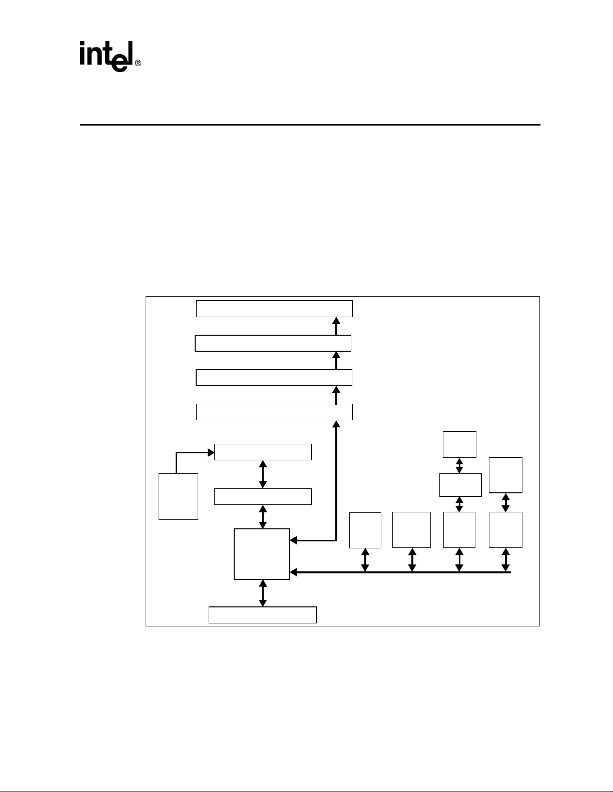
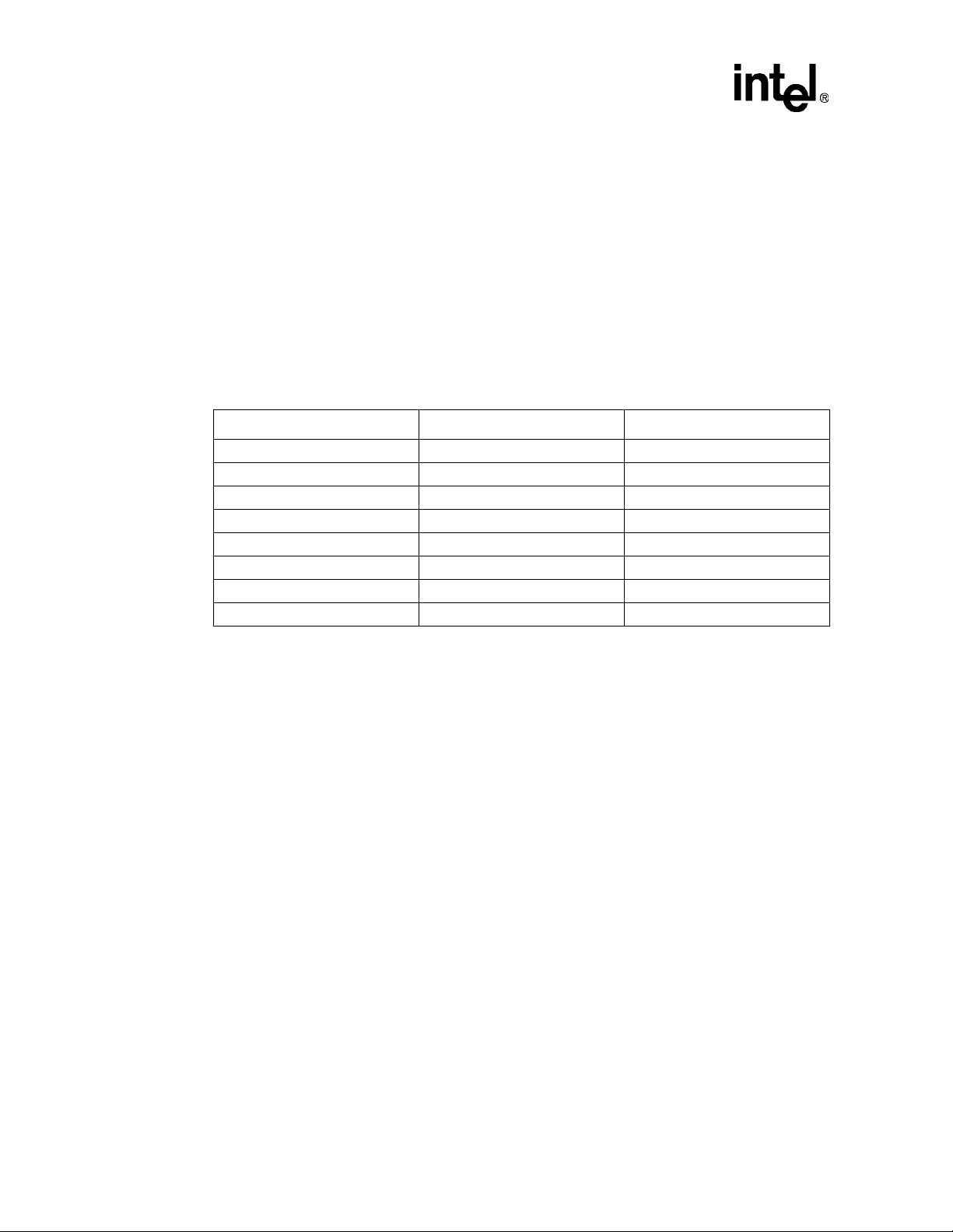
Figure 1-1. IQ80960RM/IQ80960RN Platform Functional Block Diagram
Secondary PCI Slot 4
Secondary PCI Slot 3
Secondary PCI Slot 2
1
Battery
Backup
Support
Secondary PCI Slot 1
SDRAM (x72)
Logic Analyzer Interface
i960® RM/RN
I/O Processor
Primary PCI Bus 32/64-bits
Secondary PCI
Bus 32/64-bits
ROM Bus
Flash
ROM
Logic
Analyzer
Interface
Console
Port
RS-232
Serial Port
UART
User
LED
LED
Registe r
IQ80960RM/RN Evaluation Board Ma nual 1-1
Introduction
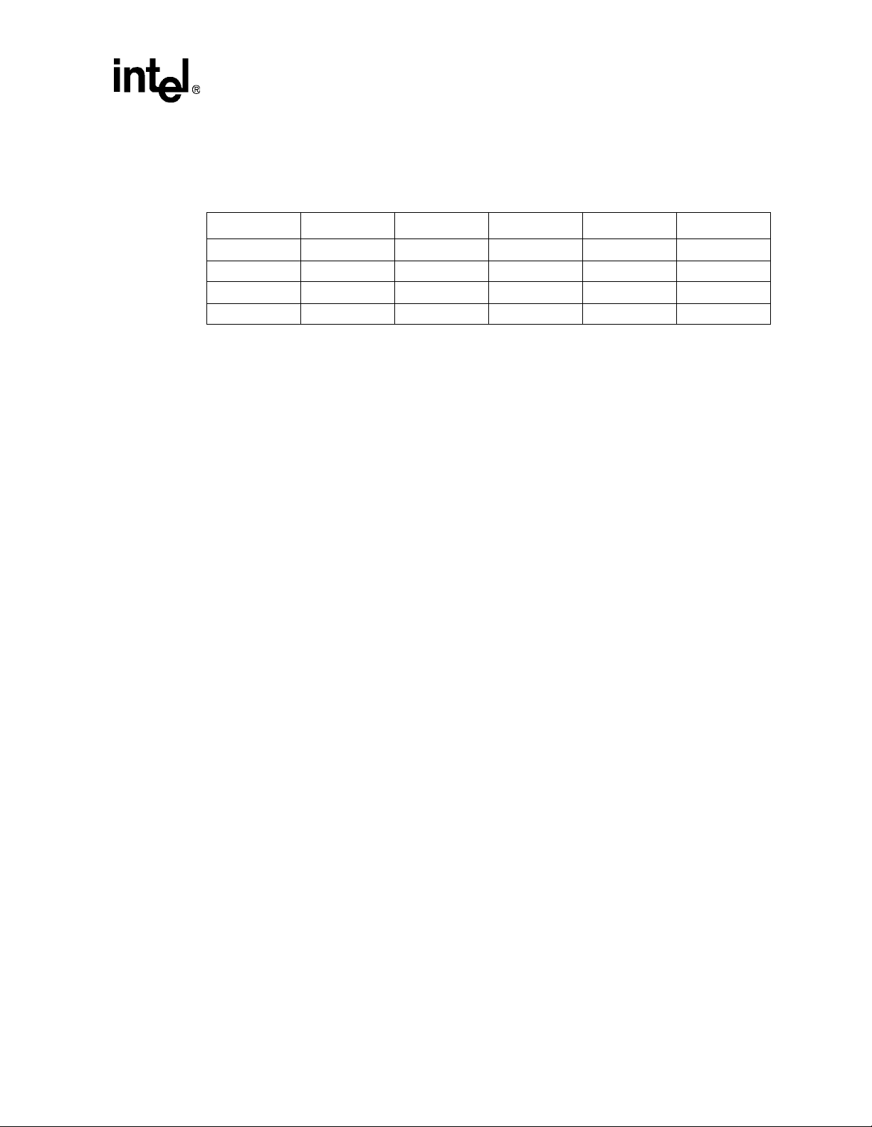
Figure 1-2. IQ80960RN Platform Physical Diagram
64-Bit Secondar y PCI Slots
J4
J3
J2
J1
J5
J8 J9 J10 J11 J12
U9
Logic Analyzer Connectors
i960
U15
168-Pin SDRAM DIMM Socket
RS-232 Serial Port
Flash Memory
SW1
1 2 3 4
OFF
J6
U11
®
64-Bit PCI
CR1 CR2
CR3 CR4 CR5
JTAG Port
NiCd Batteries
J7
1-2 I Q80960RM/RN Evaluation Board Manu al

Introduction
1.1 i960® RM/RN I/O Processor and IQ80960RM/RN Features
The i960 RM/RN I/O processor serves as the mai n component of a high performance , PCI-based
intelligent I/O subsystem. The IQ80960RM and IQ80960RN pla tforms allow the developer to
connect PCI devices to the i960 RM/RN I/O processors using the four secondary PCI expansion
connectors. The features of the IQ80960RM and IQ80960RN platforms are enumerated below and
shown in Figure 1-1 and Figu re 1-2.
• i960 RM/RN I/O processor
• Modified PCI long-card form factor
• 64-bit or 32-bit primary PCI bus interface (80960RM 32-bit only)
• 64-bit or 32-bit secondary PCI bus connected to the pri mary P CI interface with a PCI-to-PCI
bridge (80960RM 32-bit only)
• DMA channels on both PCI buses
2
• I
C Serial Bus
• 168-pin, 3.3V DIMM socket supporting 16 to 128 Mbytes of Synchronous DRAM organized
x72 to support Error Correction Code (ECC) and clocked at 66 MHz (ships with 16 M/ECC
installed)
• Serial console port based on 16C550 UART
• Eight user-programmable LEDs
• 3 Indicator LEDs: processor has passed self-test, 3.3 V is supplied to SDRAM, and 3.3 V is
supplied to sec ondary PCI slots
• Flash ROM, 2 Mbytes
• Logic analyzer connectors for SDRAM bus, ROM bus and secondary PCI arbitration signals
• Fan heatsink monitor circuit
• Battery bac kup for SDRAM
• JTAG header
1.2 Software Development Tools
A number of software development tools are availab le for the i960® processor family1. This
man ua l provi d es in f orma ti o n on two so f t w a re developme n t toolsets: Wind Ri ver Sys tem’s
Tornado* for I
through the inf ormation in this chapter and in Chapter 2 to gain a general understanding of how to
use your tools with thi s boa rd.
0* and Intel’s CTOOLS. If you are using other software development tools, read
2
1. To view the electronic tools catalog, access http://developer.intel.com/design/develop.htm/ from the web.
IQ80960RM/RN Evaluation Board Ma nual 1-3

Introduction
1.3 Tornado* for I20* Software Development Toolset
T orna do for I
compiler, assembler, linker, and debugger. It also features a real-time operating system.
0 is a complete toolset featuring an integrated development environment including a
2
1.3.1 IxWorks* Real-Time Operating System
The IQ80960RM/RN platforms are equipped with Wind River Systems, Inc.’s IxWorks*. IxWorks
provides for the elements of the I
protocols, and executive modules for configuration and control. IxWorks also allows for the
writing of basic devi ce drivers and provides NOS-to-driver independence. TORNADO for I
provides a visual environment for building, testing and debugging of I
O standard: an event-driven driver framework, host message
2
1.3.2 TORNADO Build Tools
TORNADO for I2O includes a coll ection of supporting tools tha t provide a complete development
tool chain. These include the compiler, assembler, linker and bina ry utilities. Als o provided is a n
O module builder, which crea tes I2O-loadable modules .
I
2
1.3.3 TORNADO Test and Debug Tools
TORNADO for I2O test and deb ug t ools i nclude th e dynamic l oader, the CrossWi nd∗ debugger , the
WindSh* interactive shell, and a system browser.
The dynamic loader allows for interactive loading, testing, and replacement of individu al object
modules that comprise a driver.
O drivers.
2
O
2
CrossWind is an extended version of GDB960. Using it you can debug I
breakpoints on desired I
locals, stack frame, memory and so on.
WindSh allows you to commun icate to the IQ80960RM/RN platform via an RS-232 serial port.
The IQ80960RM/RN pla tform supports port speeds from 300 to 115,200 bps. The shell can be
used to:
• control and monitor I
O components. A variety of windows display source code, registers,
2
O drivers
2
O drivers by setting
2
• format, send and receiv e d river messages
• examine hardware registe rs
• run automated I
The shell also provides essential debugging capabilities; including brea kpoints, single stepping,
stack checking, and disassembly.
O test suites
2
1-4 I Q80960RM/RN Evaluation Board Manu al

1.4 CTOOLS Software Development Too ls et
Intel’s i960 processor software development toolset, CTOOLS, features advanced
C/C++ - language compilers for the i960 processor family. CTOOLS development toolset is
available for Windows* 95/NT-based systems and a variety of UNIX workstation hosts. These
products provide execution pr ofiling and instruction scheduling optimizat ions and include an
assembler, a linker, and utilities designed for embedded proc essor software developm ent.
1.4.1 CTOOLS and the MON960 Debug Monitor
In place of IxWorks, the IQ80960RM/RN platform can be equippe d with Intel’s MON960, an
on-board softwa re monitor that allows you to execute and debug programs written for i960
processors in a non-I
step, memory display, and other useful functions for runnin g and de bugging a program.
The IQ80960RM/RN platform works with the source-level debuggers provided with CTOOLS,
including GDB960 (command line version) and GDB960V (GUI version).
1.4.1.1 MON960 Host Communications
MON960 allows you to communicate and download programs developed for the IQ80960RM/RN
platform across a host system’s s erial port or PCI interface. The IQ80960RM/RN platform supports
two methods of communication: terminal emulation and Host Debugger Interface (HDI).
2
O environment. The monitor provides program download, bre akpoint, single
Introduction
1.4.1.2 Terminal Emulation Method
Terminal emulation software on your host system can communicate to MON960 on the
IQ80960RM/RN platform via an RS-232 serial port. The IQ80960RM/RN platform s upports port
speeds from 300 to 115,200 bps. Serial downl oads to MON960 require that the terminal emulation
software support th e XMODEM proto col.
Configure the serial port on the host system for 300-115,200 baud, 8 bits, one stop bit, no parity
with XON/XOFF flow control.
1.4.1.3 Host Debugger Interface (HDI) Method
You may use a source-l evel debugger, such as Intel’s GDB960 a nd GDB960V to establish seria l or
PCI communications with the IQ80960RM/RN platform. The MON960 Host Debugger Interface
(HDI) provides a defined mess aging layer between MON960 and the debugger. For more
information on this interface, see the MON960 Debug Monitor User’s Manual (484290).
HDI connection requests cannot be detected by MON960 if the user has already initiated a
connection using a terminal emula tor. In this case, the IQ80960RM/RN platform must be reset
before the debugger can connect to MON960.
1.5 SPI610 JTAG Emulation System
The SPI610 JTAG Emulation System from Spectrum Digital, Inc. is included in the
IQ80960RM/RN development kit. It fur nishes the default host development environment-toevaluation board communication link based on the i960 RM/R N I/O processor JTAG interface.
IQ80960RM/RN Evaluation Board Ma nual 1-5
Introduction
Refer to the SPI610 Referen ce Manual for JTAG emulation system installation and operation for
both the Tornado and CTOOLS environment. Op tionally, evaluation board serial port
communications can be used for thi s com municati on link (s ee Secti on 1.3.3, “TORNADO Test and
Debug Tools” on page 1-4).
1.6 About Thi s M a nu a l
A brief description of the contents of this manual follows.
Chapter 1, “Introduction”
Chapter 2, “Getting Started”
Chapter3, “Hardware
Refere nce”
Chapter 4, “i960® RM/RN
I/O Processor Overview”
Chapter 5, “MON960
Support for IQ80960RM/RN”
AppendixA, “Bill of
Materials”
AppendixB, “Schematics”
AppendixC, “PLD Code”
AppendixD, “Recycling the
Battery”
Introduces the IQ80 960RM
chapter also describes Intel’s CTOOLS* and WindRiver Systems Ix Works*
software development tools, and defines notational-conventions and related
documentation.
Provid es st ep-b y-s te p i ns tru ct ions fo r in st al li ng t he IQ8 09 60R M or I Q80 96 0RN
platform in a host system and downloading and executing an application
program. This chapter also describes Intel’s software development tools, the
MON960 Debug Monitor, IxWORKS, software installation, and hardware
configuration.
Descri bes the locations of connector s, switches and LEDs on the IQ80960RM
and IQ80960RN platforms. Header pinouts and register descriptions are also
provided in this chapter.
Presents an overview of the capabilities of the i960 RM/RN I/O proc essor and
includes the CPU memory map.
Describes a number of features added to MON960 to support application
development on the i960 RM/RN I/O processor.
Shows complete parts list IQ80960RM and IQ80960RN Evaluation Platforms.
Complete set of schematics for the IQ80960RM and IQ80960RN Evaluation
Platforms.
Example PLD code used on IQ80960RM and IQ80960RN evaluation boards
for SDRAM battery backup.
Information on the RBRC program and the locations of participating recycling
centers.
and IQ80960RN Evaluation Board feat ures. This
1-6 I Q80960RM/RN Evaluation Board Manu al

1.7 Notational-Conventions
The following notation conventions are consistent with other i960 RM/RN I/O processor
documentation and general indust ry standards.
Introduction
# or overbar
Bold Indicates user entry and/or c ommands.
Italics Indicates a reference to related docum ents; also used to show emphasis.
Courier font I ndicates code examples and file di rectories and names.
Asterisks (*) On non-Intel company and product names, a tra iling asterisk indicates
UPPERCASE In text, signal na mes are shown in uppe rcase. When several sig nals shar e
Designations for
hexadecimal and
binary numbers
In code examples the pound sym bol (#) is appended to a signal name to
indicate that the signal is active. Normal ly inverted clock signals are
indicate d with an overbar above the signal name (e.g., RAS).
PLD signal names are in bold lowercase letters (e.g., h_off, h_on).
the item is a tra d emark or register ed trademark. Such brand s and names
are the property of their respective owners.
a common name, each signal is represented by the signal name followed
by a numbe r; the group is represented by the signal name followed by a
variable (n). In code example s, signal names are shown in the case
required by the software development tool in us e.
In text, instead of using subscripted “base” designators (e.g., FF
leading “0x” (e.g., 0xFF) hexadecimal numbers are represented by a
string of hex digi ts followed by th e letter H. A zero prefix is added to
numbers that begin with A through F. (e.g . , FF is shown as 0FFH.) In
examples of actual code, “0x” is used. Decimal and binary numbers are
represented by their customary notations. (e.g. , 255 is a decimal number
and 1111 1111 is a binary number. In some cases, the letter B is added to
binary numbers for clari ty.)
16
) or
1.8 Technical Support
Up-to-date product and technical information is available electronically from:
• Intel’s World-Wide Web (WWW) Locatio n: http://www.intel.com
• IQ80960RM and IQ80960RN Produc t Information: http://developer.intel.com/d es ign/i960
For technical assistance, electronic m ail (e-mail) pro v id es the fastest route to reach engineers
specializing in IQ80960RM and IQ80960RN issues. Posting messages on the Embedded
Microprocessor Forum at http://support.intle.com/newsgroups / is also a direct rout e for
IQ80960RM and IQ80960RN technical assistance. See Section 1.8.2.
Within the United States and Canada you may contact the Intel Technical Support Hotline. See
Section 1.8.1 for a list of customer support sources for the US and other geographical area s.
IQ80960RM/RN Evaluation Board Ma nual 1-7
Introduction
1.8.1 Intel Customer Electronic Mail Supp ort
For direct support from engineer s specia li ng in i960® Microprocessor issues send e-mail in english
to 960tools@intel.com.
Questions and other messages may be posted to the Embedded Microprocessor Forum at
http://support.intel.com/newsgroups/.
1.8.2 Intel Cus to mer Su pp or t Con ta ct s
Contact Intel Corporation for technical assistance for the IQ80960RM/RN evaluation platform.
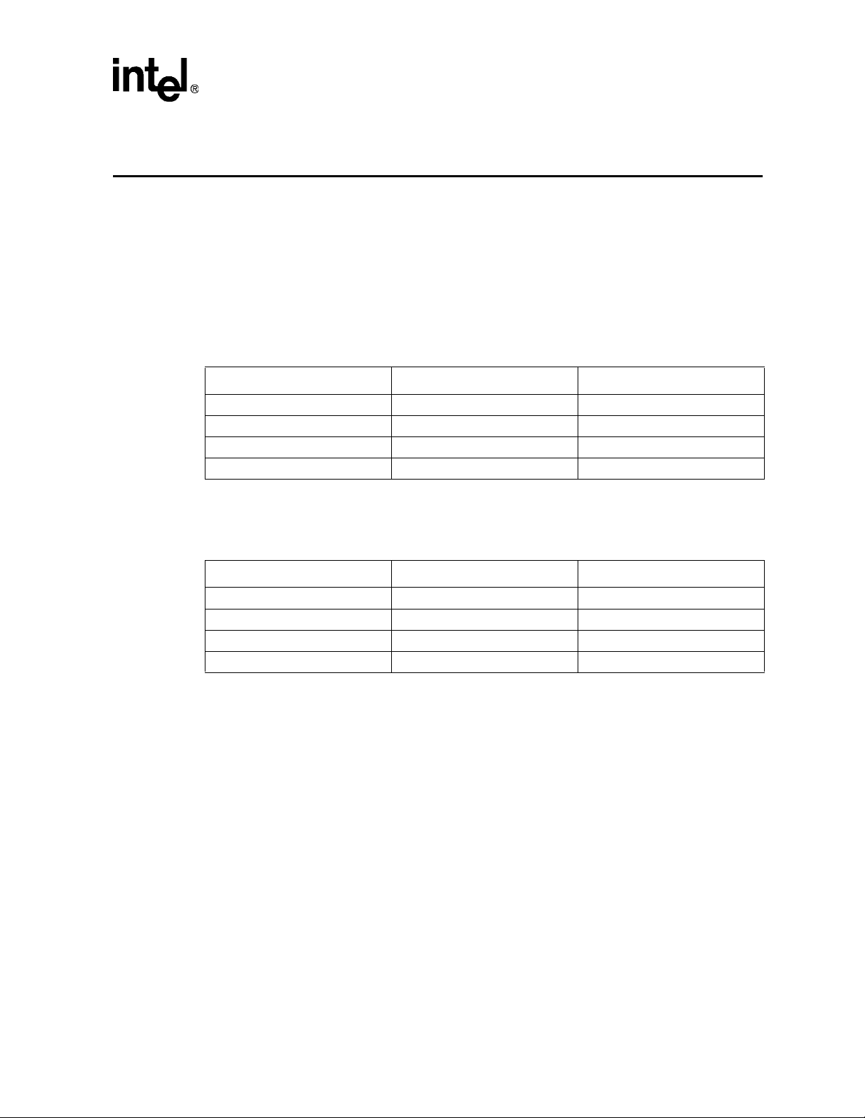
Country Literature Customer Suppo rt Number
United States 800-548-4725 800-628-8686
Canada 800-468-8118 or 303-297-7763 800-628-8686
Europe Contact local distributor Contact local distri butor
Australia Contact local distributor Contac t local distribu tor
Israel Contact local distributor Contact local distributor
Japan Contact local distributor Contact local distributor
1-8 I Q80960RM/RN Evaluation Board Manu al
1.8.3 Related Information
T o orde r printe d manua ls fro m Intel, c ontac t your loc al sales re prese ntati ve or Intel L iteratur e Sal es
(1-800-548-4725 ).
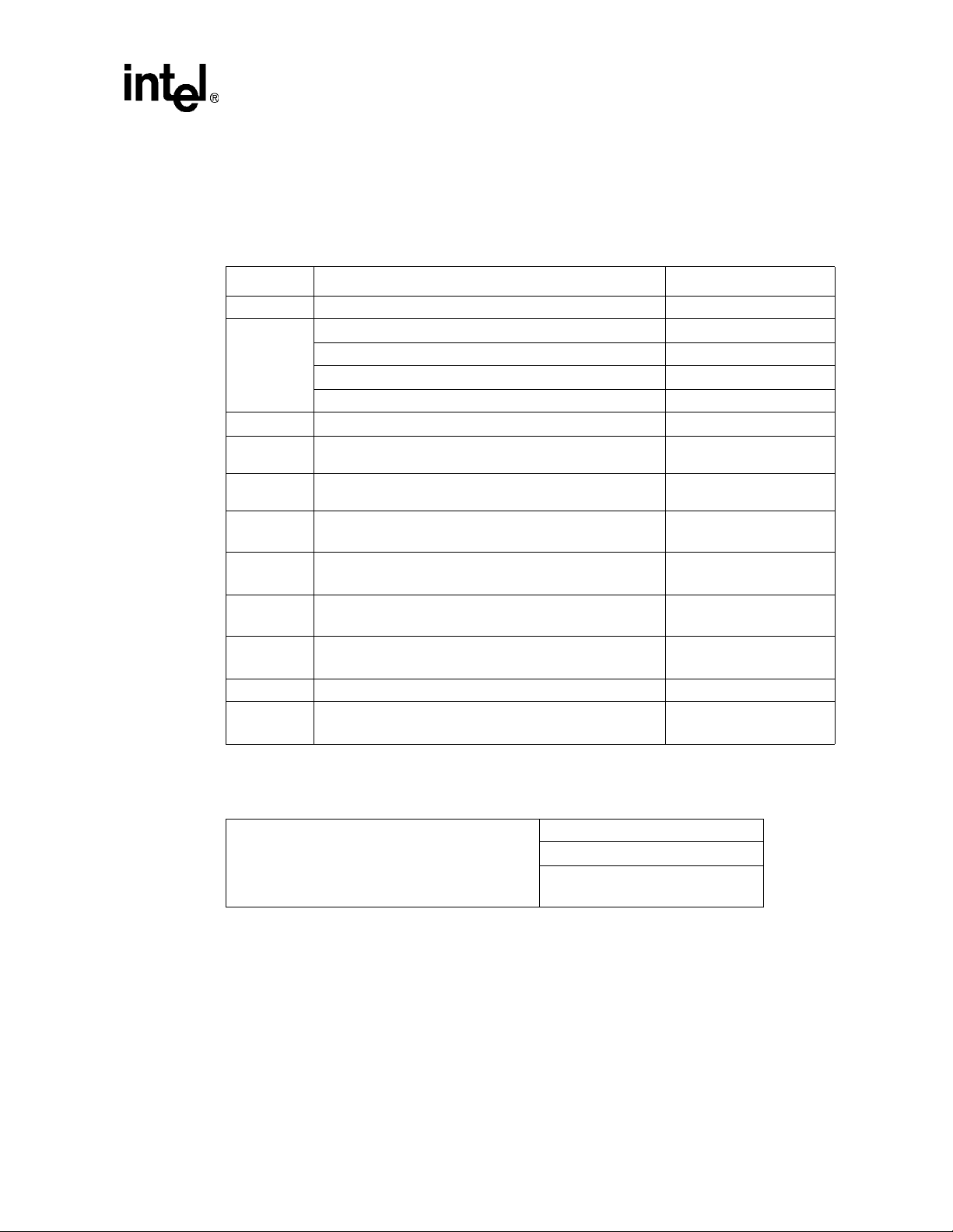
Table 1-1. Document Information
Product Document Name Compan y/ Order #
Introduction
All
80960RM/RN
Developers’ Insight CD-ROM
i
960®
RM/RN I /O Processor Developer’s Manual
80960RM I/O Processor
80960RN I/O Processor
i
960®
RM/RN I/O Processor Design Guide
MON960 Debug Monitor User’s Guide
PCI Local Bus Specification
Writing I2O Device Drivers in IxWorks
IxWorks Reference Manual
VxWorks Programmer’s Guide
Tornado User’s Guide
Tornado for I2O
Tornado for I2O Compact Disk
SP610 Em ulation System Reference Manual
Data Sheet Intel # 273156
Data Sheet Intel # 273157
Revision2.1
Rev. 1.0 #TDK-12380-ZC-00
Intel # 273000
Intel # 273158
Intel # 273139
Intel #484290
PCI Special Interest Group
1-800-433-5177
Wind River Systems, Inc.
#DOC-1173-8D-02
Wind River Systems, Inc.
#DOC-1173-8D-03
Wind River Systems, Inc.
#DOC-11045-ZD-01
Wind River Systems, Inc.
#DOC-1116-8D-01
Wind River Systems, Inc.
#DOC-12381-8D-00
Spectrum Dig ita l Inc.
# 503715
Contact Cyclo ne Microsystems for additional information about their products and literature:
Table 1-2. Cyclone Contacts
Phone: 203-786-5536
Cyclone Microsystems
25 Science Park
New Haven CT 06511
IQ80960RM/RN Evaluation Board Ma nual 1-9
F AX: 203-786-5025
e-mail: info@cyclone.com
WWW: http://www.cyclone.com


Getting Started
This chapter conta ins in struc tio ns for ins tall ing the IQ80 960RM/ RN platfor m in a host s yste m and,
how to download and execute an application program using Wind River System’s IxWorks∗ or
Intel’s CTOOLS software development toolsets.
2.1 Pre-Installation Considerations
This section pr ovides a general overview of the components required to develop and exec ute a
program on the IQ80960RM/RN platform. IQ80960RM/RN evaluation boards support two
software development toolsets, Wind River System’s IxWorks and Intel’s CTOOLS.
IxWorks is a complete toolset featuri ng an integrated developmen t environment including a
compiler, assembler, linker, and debugger . It al so features a real-time operati ng system. If you are
using the IxWorks operating system with th e T O RNADO* development environment, refer to the
Wind River Systems, Inc. doc umentation referenced in Sectio n 1.8.3.
CTOOLS is a complete C/C++-language software-development toolset for developing embedded
applications to run on i960 processors. It contains a C/C++ compiler, the gcc960 and ic960 compiler
driver programs, an assembler, runtime libraries, a collection of software-development tools and
utilities, and printed and on-line documentation. The MON960 Debug Monitor User’s Guide fully
describes the components of MON960, including MON960 commands, the Host Debugger Interface
Library (HDIL), and the MONDB.EXE utility. If you are using MON960 and the CTOOLS toolset,
refer to section Section 2.2.1, “Installing Software Development Tools” on page 2-1.
2
See Chapter 1 for more information on the IxWorks and CTOOLS features.
The IQ80960RM/RN evaluation boards are supplied with IxWorks intelligent real-time operating
system pre-loaded into the on-board Flash. You also have the option of installing the MON960
debug monitor, which is required if you are using the CTOOLS debugging tools, GDB960,
GDB960V, or MONDB. Sec ti o n 3.3.1 descr ibes the Fla sh ROM pro gramming util it y, which allows
you to load MON960 onto the platform or re-load IxWorks.
2.2 Software Installation
2.2.1 Installing Software Development Tools
If you haven’t done so already, install your development software as described in its manuals. All
references in this manual to CTOOL S or CrossWind assume that the default directories were
selected dur ing installation. If this is not the case, substitute the appropriate path for the defa ult
path wherever fil e loc ations are referenced in this manual.
IQ80960RM/RN Evaluation Board Ma nual 2-1

Getting Started
2.3 Hardware Installation
Follow these in st ructions to get your new IQ80960RM/RN platform running. Be sure all items on
the checklist were provided with your IQ80960RM/RN.
Warning: Static charges can severely damage th e IQ80960RM/RN platforms. Be sure you are properly
grounded before re moving the IQ80960RM/RN platform from the anti-sta tic bag.
2.3.1 Battery Bac ku p
Battery backup is provided to save any information in SDRAM during a power failure . Th e
IQ80960RM/RN platform contains four AA NiCd bat teries, a charging circuit and a regul ator
circuit. The batte ries installed in the IQ80960RM/RN platform are rated at 600 mA/Hr.
SDRAM technology provides a simple way of enabling data preservation through the self-refresh
command. When the processor receives an active Primary PCI reset it issues the self-refresh
command and drives the SCKE signals low. Upon seeing this condition, a PAL on the
IQ80960RM/RN platform holds SCKE low before the processor loses power. The batteries
maintain power to the SDRAM and the PAL to ensure self-refresh mode. When the PAL detects
PRST# returning to ina ctive state, the PAL releases the hold on SCKE.
The battery circuit can be disabled by removing the batteries. LED CR4 indicates when the SDRAMs
have sufficient power. If the batteries remain in the evaluation platform when it is depowered and/or
removed from the chassis, the batteries will maintain the SDRAM for approximately 30 hours. Once
power is again applied, the batteries will be fully charged in about 4 hours.
2.3.2 Installing the IQ80960RM/RN Platforms in the Host System
If you are installing the IQ80960RM/RN platform for the first time, visually inspect the board for
any damage that may have oc curred during shipment. If there are visible defects, return the board
for repl acement. Follow the host system manufacturer’s instructions for in stalling a PCI adapter.
The IQ80960RM/RN pl atform is a full-length PCI adapter and requires a PCI slot th at i s free from
obstructions. The IQ80960RM/RN platform is ta ller than specifie d in the PCI Local Bus
Specification Revision 2.1. The extended height of the board will require you to kee p the cover off
of your PC. Refer to Chapt er 3 for physical dimensions of the board.
2.3.3 Verify IQ80960RM/RN Platform is Functional
These instruct ions ass ume that you have alrea dy install ed the I Q80960RM/RN pla tfor m in the host
system as described in Section 2.3.2.
1. To connect the serial port for communicati ng with and downloading to the IQ80960RM/RN
platform, conne ct the RS-232 cable (provided with the IQ80960RM/RN) from a free serial
port on the host syst em to the phone jack-s tyle connector on the IQ80960RM/RN platform.
2. Upon power-up, the red FAIL LED turns off, indicating that the processor has passed its self-test.
3. If you have IxWorks installed in the flash R OM, the user LEDs dis play the bi na ry pattern 99H.
In the IxWorks development environment, raw serial input/output is not used. Instead , the
Wind DeBug (WDB) protocol is run over the serial port, to a llow communication with
Tornado development tools. If t he terminal emu lation package is running at 115,200 baud, the
letters “W DB_READY” display prior to launching in the WDB serial protocol.
2-2 I Q80960RM/RN Evaluation Board Manu al

4. If you have MON960 installed in the fl as h ROM, press <ENTER> on a termin al con nec te d to
the IQ80960RM/RN platform to bring up the MON960 prompt. MON960 automatically
adjusts its baud rat e to match that of the te rmi nal at start-u p. At ba ud rates other than 9600, it
may be necessary to press <ENTER> several times.
2.4 Creating and Downloading Executable Files
To download code to the IQ80960RM/RN pla tform running IxWorks, consult Wind River
documentation on the s upplied TORNADO for I
IQ80960RM/RN platform, your compiler produces an ELF-format object file.
To download code to the IQ80960RM/RN platform running CTOOLS, consult the CTOOL S
documentation for information regarding compiling, linking, and downloading applications.
During a download, MON960 check s the link address stored in the ELF file, and stores the file at
that locati on on the IQ80960RM/RN platform. If the executa ble file is linked to an invalid address
on the IQ80960RM/RN platform, MON960 aborts the download.
2.4.1 Sample Download and Executio n Using GDB960
This example shows you how to us e GBD960 to download and exec ute a file named myapp via
the serial port.
O CD-ROM. T o download code to the
2
Getting Started
• Invoke GDB960. From a Windows 95/NT command prompt, issue the command:
gdb960 -r com2 myapp
This command establ ishes communication and downloads the fil e myapp.
• To execute the program, enter the command from the GDB960 comm and prompt:
(gdb960) run
More information on the GDB960 commands mentioned in this section can be found in the
GDB960 User’s Manu al.
IQ80960RM/RN Evaluation Board Ma nual 2-3

Hardware Reference
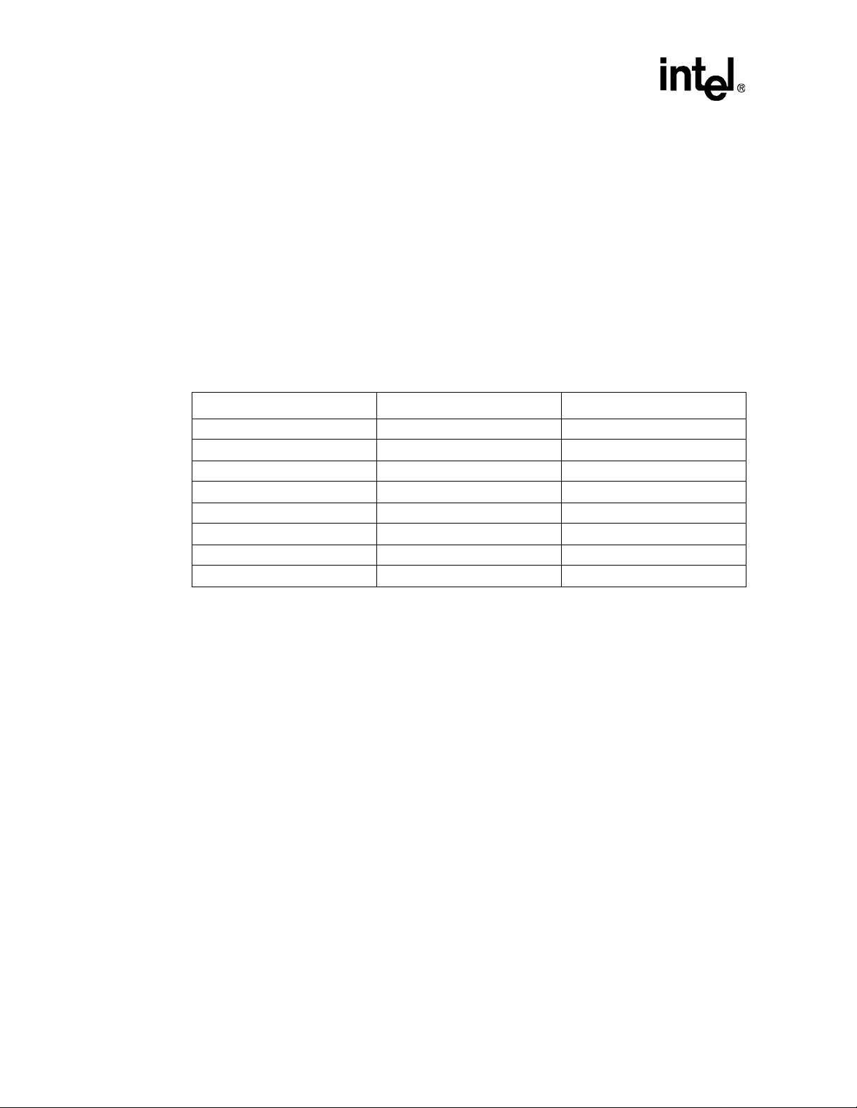
3.1 Power Requirements
The IQ80960RM/RN platform draws power from the PCI bus. The power requirements of the
IQ80960RM/RN platforms are shown in Table 3-1 and Table 3-2. The number s do not include the
power required by a PCI card(s) mounted on one or more of the IQ80960RM/RN platforms’ f ou r
expansion slot s.
Table 3-1. IQ80960RN Platform Power Requirements
Voltage Typical Current Maximum Current
+3.3 V 0 V* 0 V*
+5 V 1.45 A 1.96 A
+12 V 286 mA 485 mA
-12 V 1 mA 1 mA
NOTE: Does not include the pow er required by a PCI card(s) mounted on the IQ80960RN platform.
* +3.3V for 80960RN Processor created on board from +5V.
Table 3-2. IQ80960RM Platform Power Requirements
3
NOTE: Does not include the pow er required by a PCI card(s) mounted on the IQ80960RM pla tform.
* +3.3V for 80960RM Processor created on board from +5V.
3.2 SDRAM
The IQ80960RM/RN platform is equipped with a 168-pin DIMM socket formatted to accept +3.3V
synchronous DRAM with or without Error Correction Code (ECC). T he socket will acc ept SDRAM
from 8 Mbytes to 128 Mbytes. 128 Mbyte SDRAMs are available in both x64 and x72 configurations.
Note that 8 Mbyte SDRAMs are only for x64 or non-ECC memory. The SDRAM is accessible from
either of the PCI buses, via the ATUs, and the local bus on the IQ80960RM/RN platform.
Voltage Typical Current Maximum Current
+3.3 V 0 V* 0 V*
+5 V 1.32 A 1.86 A
+12 V 284 mA 485 mA
-12 V 1 mA 1 mA
IQ80960RM/RN Evaluation Board Ma nual 3-1
Hardware Reference
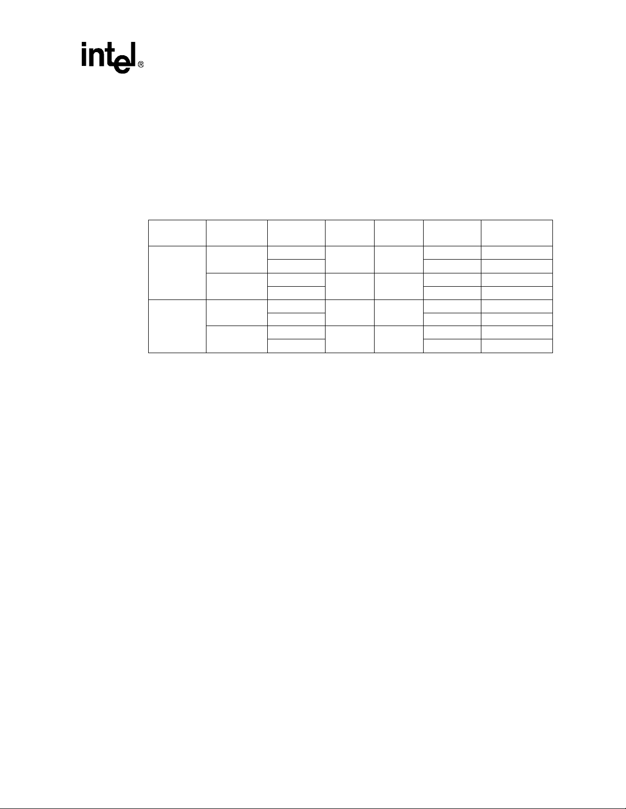
3.2.1 SDRAM Performance
The IQ80960RM/RN pla tform uses 72-bit SDRAM with ECC or 64-bit SDRAM without ECC.
SDRAM allows zero data-to-data wait state operation at 66 MHz. The memory controller unit
(MCU ) of the i 96 0
of four enables sea mless read/write bursting of long data streams, as long as the MCU does not
cross the page boundary. Page boundaries are naturally aligned 2 Kbyte blocks. 72-bit SDRAM
with ECC allows a maximum throughput of 528 Mbytes per second.
Both 16 Mbit and 64 Mbit SDRAM devices are supporte d. The MCU keeps two pages per ba nk
open simulta neous ly for 16 Mbit de vices a nd 4 pages pe r ba nk for 64 Mb it device s. Si multa neous ly
open pages allo w for greate r performanc e for seq uentia l access , dist ribute d acros s multipl e in ternal
bus transactions. Table 3-3 shows read and write examples of a single 8 byte access and for a
multiple 40 byte access.
Table 3-3. SDRAM Performance
Read Pag e Hit (8 by te s) 7 76 Mby tes /s ec
Read Page Miss (8 bytes) 12 44 Mbytes/sec
Read Pa ge Hit (40 bytes) 11 240 Mbytes/sec
Read Page Miss (40 bytes) 16 165 Mbytes/sec
Write Page Hit (8 bytes) 4 132 Mbytes/sec
Write Page Miss (8 bytes) 8 66 Mbytes/sec
Write Page Hit (40 bytes) 8 330 Mbytes/sec
Write Page Miss (40 bytes) 12 220 Mbytes/sec
®
RM/RN I/O processor supports SDRAM burst lengt hs of four. A burst length
Cycle Type T able Clocks Performance Bandwidth
Note that if ECC is enabled and you attempt a partial write — less than 64 bits — you will incur a
penalty. Because ECC is enabled, the MCU will translate the write into a read-modify-write
transaction. Therefore, for a single byte write the clock count will be 1 1.
3-2 I Q80960RM/RN Evaluation Board Manu al
3.2.2 Upgrading SDRAM
The IQ80960RM/RN is equipped with 16 Mbytes of SDRAM with ECC inserted in the 168-pin
DIMM socket. The memory may be expanded by inserting up to a 128 Mbyte module into the
DIMM socket. The various memory c ombinations are shown in Table 3-4. Only 168-pin +3.3V
SDRAM modules with or witho ut ECC rated at 10 ns should be used on the IQ80960R M/RN
platform. The column labeled ECC dete rmines if that parti cular memory configuration c an be used
with ECC.
Table 3-4. SDRAM Configurations
Hardware Reference
SDRAM
Technology
16 Mbit
64 Mbit
SDRAM
Arrangement
2M x 8
1M x 16
8M x 8
4M x 16
# Banks Row Column ECC
1
2 Yes 32 Mb yt es
1
2 No 16 Mbyt es
1
2 Yes 128 Mbytes
1
2 No 64 Mbyt es
3.3 Flash ROM
An E28F016S5 (2 Mbytes) Flash ROM is included on the IQ80960RM/RN platform. This Fl ash
ROM contains IxWorks* and may be used to store user ap plications.
3.3.1 Flash ROM Programming
Two types of Fl ash ROM programming exist on the IQ80960RM/RN platform. The first is normal
application development programming. T his occurs using IxWorks to download new software and
the 80960JT core to writ e the new code to the Flash ROM. During this time the boot sec tors
(containing IxWorks) are write protected.
11 9
11 8
12 9
12 8
Total Memory
SIze
Yes 1 6 Mb yt es
No 8 Mbytes
Yes 6 4 Mb yt es
No 3 2 Mbytes
The second type of Flash ROM progra m mi ng is loading the boot sectors. You will not be required
to load the boot sectors except:
• To load MON960
• To load a new rele ase of IxWorks
• To change between the check build and the fre e build of IxWorks
The following steps are required to program the Flash ROM boot sectors:
1. Set switch S1 #’s 1 and 2 to the on position.
2. Reset the board by cycling power on the workstation.
3. Run the Intel DOS-based flash utility to program the Flash ROM boot sectors.
4. Set switch S1 #’s 1 and 2 to the off position.
5. Reset the board by cycling power on the workstation.
IQ80960RM/RN Evaluation Board Ma nual 3-3
Hardware Reference
3.4 Console Serial Port
The console seria l port on the IQ80960RM/ RN platform, based on a 16C550 UART, is capable of
operation from 300 to 115,200 bps. The port is connected to a phone jack-style plug on the
IQ80960RM/RN platform. The DB25 to RJ-45 cable included w ith the IQ80960RM/RN can be
used to connect the console port to any standard RS-232 port on the host system.
The UART on the IQ80960RM/RN platform is clock ed with a 1.843 MHz clock, and may be
programmed to use thi s clo ck with its in te rnal baud rate coun ters. Th e UAR T regi ste r address es are
shown in Table 3-5; refer to the 16C550 device data book for a detailed description of the registers
and device operat ion. Note that some UART addresses refer to different registers depending on
whether a read or a write is being per f orm ed.
Tab le 3-5. UART Register Addresses
Address Read Register Write Register
E000 0000H Receive Holding Register Transmit Holding Register
E000 0001H Unused Interrupt Enable Register
E000 0002H Interrupt Status Register FIFO Control Register
E000 0003H Unused Line Control Register
E000 0014H Unused Modem Control Register
E000 0015H Line Status Register Unused
E000 0016H Modem Status Register Unused
E000 0017H Scratchpad Register Scratchpad Register
3.5 Secondary PCI Bus Expansion Connectors
Four PCI Expansion Slots are available on the IQ80960RM/RN platform. The IQ80960 RM
supports 32-b it P CI expansion and the IQ80960RN supports 64-bit PCI expans ion. The slots ar e
designed for +5V PCI signall ing and accommodate PCI cards with +5V or univers al s ignalling
capabilities.
3.5. 1 PCI Slots Power A vailabili ty
Power from the Primary PCI bus, +3.3V, +5V, +12V, and –12V, is routed to the Secondary P CI bus
expansion sl ots. +3.3V is only available at the secondary PCI slots if the host system makes +3.3V
available on the Primary PCI slots. LED CR5 indicates if this power is available.
3-4 I Q80960RM/RN Evaluation Board Manu al
3.5.2 Interrupt and IDSEL Routing
Table 3-6. Secondary PCI Bus Interrupt and IDSEL Routing
Connector IDSEL INTA# INTB# INTC# INTD#
J11 SAD16 SINTA# SINTB# SINTC# SINTD#
J12 SAD17 SINTB# SINTC# SINTD# SINTA#
J13 SAD18 SINTC# SINTD# SINTA# SINTB#
J14 SAD19 SINTD# SINTA# SINTB# SINTC#
3.6 Battery Backup
Battery backu p is provided to save any information in SDRAM during a power failure. The
IQ80960RM/RN platform contains four AA NiCd batteries, a charging circuit and a regulator
circuit. The batteries installed in the IQ80960RM/RN pla tform are rated at 600 mA/H r.
SDRAM technology pro vides a simple way of enabling data preservation though the self-refresh
command. When the processor receives an active Primary PCI reset it will issue the sel f-refresh
command and drive the SCKE signals low. Upon seeing this condition a PAL on the
IQ80960RM/RN platfor m will hol d SCKE low before the proce ssor los es power. The batteries will
maintain power to the SDRAM and the PAL to ensure self-refresh mode. When the PAL sees
PRST# r et ur n i n g to in active st at e th e PAL wi ll re lease the h ol d on SC K E .
Hardware Reference
The battery circuit can be disabled by removing the batteries. LED CR4 indicates when the
SDRAMs have suff icient power . If the batteries remain in the evaluation platf orm when it is
depowered and/or removed from the chassis, the batteries will maintain the SDRAM for
approximately 30 hours. Once power is again applied, the batteries will be fully charged in about
four hours.
3.7 Loss of Fan Detect
The i960 RM/RN I/O processor can be cooled by an active he at sink mounted on top. T he fan
provides a square wave output that is monitored by a comparator circuit on the IQ80960RM/RN
platform. The frequency of the fan output is appr oxim ately 9K RPM. If the frequency fall s below
approximately 8K RPM the circuit will provide an interrupt to the processor. This is an evaluation
board feature intended as an example of system hardware monitoring, sin ce the IQ80960RM/RN
platf o r m does no t ship with a heatsin k .
Note: When using a passive heat sink, the proces so r never sees an interrupt from not having a fan.
IQ80960RM/RN Evaluation Board Ma nual 3-5

Hardware Reference
3.8 Logic Analyzer Headers
There are five logic analyzer connectors on the IQ80960RM/RN platform. The connectors are
Mictor type, AMP part # 76705 4-1. Hewl ett-Pa ckard a nd Tektronix manufac ture an d sell i nte rfaces
to these connectors. The logic analyzer connectors al low for interfacing to the SDRAM and ROM
buses along with secondary PCI arbitration signals. Table 3-7 shows the connectors and the pin
assignm e nt s fo r each.
Table 3-7. Logic Analyzer Header Definitions
PIN J9 J11 J12 J10 J8
3 SDRAMCLK
4 DQ15 SDQM7 DQ31 RAD15
5 DQ14 SDQM6 DQ30 RAD14
6 DQ13 SDQM5 DQ29 RAD13
7 DQ12 SDQM4 DQ28 RAD12
8 DQ11 SDQM3 DQ27 RAD11
9 DQ10 SDQM2 DQ26 RAD10
10 DQ9 SDQM1 DQ25 RAD9
11 DQ8 SDQM0 DQ24 RAD8
12 DQ7 SCB 7 DQ23 RAD7
13 DQ6 SCB 6 DQ22 RAD6
14 DQ5 SCB 5 DQ21 RAD5
15 DQ4 SCB 4 DQ20 RAD4
16 DQ3 SCB3 DQ19 SCE0# RAD3
17 DQ2 SCB2 DQ18 SCE1# RAD2
18 DQ1 SCB 1 DQ17 SBA1 RAD1
19 DQ0 SCB 0 DQ16 SBA0 RAD0
20 DQ32 SA0 DQ48 SREQ0# RAD16
21 DQ33 SA1 DQ49 SREQ1#
22 DQ34 SA2 DQ50 SREQ2#
23 DQ35 SA3 DQ51 SREQ3# RALE
24 DQ36 SA4 DQ52 SREQ4# RCE0#
25 DQ37 SA5 DQ53 SREQ5# RCE1#
26 DQ38 SA6 DQ54 SGNT0# ROE#
27 DQ39 SA7 DQ55 SGNT1# RWE#
28 DQ40 SA8 DQ56 SGNT2#
29 DQ41 SA9 DQ57 SGNT3# I_RST#
30 DQ42 SA10 DQ58 SGNT4#
31 DQ43 SA11 DQ59 SGNT5#
32 DQ44 DQ60
33 DQ45 SWE# DQ61
34 DQ46 SCAS# DQ62
35 DQ47 SRAS# DQ63
36 P_PCICLK RALE
3-6 I Q80960RM/RN Evaluation Board Manu al
3.9 JTAG Header
The JTAG header allows debugging hardware to be quic kly and easily connected to some of the
IQ80960RM/RN proc essor’s logic signals.
The JTAG header is a 16-pin header. A 3M connector (part number 2516-6002UG) is required to
connect to this header. The pinout for the JTAG header is shown in Table 3-8. The header and
connector are keyed using a tab on the connector and a slot on the header to ensure proper installation.
Hardware Reference
Each signal in the JTAG header is pa ired with its own ground connection to avoid the noise problems
associated with long ribbon cables. Signal descriptions are found in the i960
Developer’s Manual, 80960RM I/O Processor Data Sheet and the 80960RN I/O Process or Data Sheet.
Table 3-8. JTAG Header Pinout
Pin Signal Input/Output to 80960RM/RN Pin Signal
1 TRST# IN 2 GND
3 TDI IN 4 GND
5 TDO OUT 6 GND
7TMS IN 8GND
9TCK IN 10GND
11 LCDINIT# IN 12 GND
13 I_RST# OUT 14 GND
15 PWRVLD OUT 16 GND
Table 3-9 describes switch setti ng options and defaults. These switch settings are sampled at
Primary PCI Reset. See Table 5-1 “Initialization Modes” on page 5-3 for processor initialization
configurations .
Table 3-9. Switch S1 Settings
Position Name Description Default
S1-1 RST_MODE#
S1-2 RETRY
S1-3 32BITMEM_EN#
a
S1-4
a. This switch is active for IQ80960RN ONLY.
32BITPCI_EN#
®
RM/RN I/O Pr oces sor
Determines if the processor is to be held in reset.
ON = hold in rest
OFF = allows processor initializati on
Deter m ines if the Primary PCI interface will be disabled.
ON = allows Primary PCI configuration cycles to occur
OFF = retries all Primary PCI configuration cycles
Notifies Memory Controller of the SDRAM width.
ON = Memory Controller utilizes 32-bit SDRAM access protocol
OFF = Memory Contoller utilizes 64-bit SDRAM access protocol
Determines whether Secondary PCI bus is a 32- or 64-bit bus.
ON = indicates Secondary PCI bus is a 32-bit bus
OFF = indicates Secondary P CI bus is a 64-bit bus
OFF
OFF
OFF
OFF
IQ80960RM/RN Evaluation Board Ma nual 3-7

Hardware Reference
3.10 User LEDs
The IQ80 960RM /RN plat form has a bank of eight user -prog rammable LEDs, locat ed on the upper e dge of
the adapter board. These LEDs are controlled by a write-only register and used as a debugging aid during
development. Software can control the state of the user LEDs by writing to the LED Register, located at
E004 0000H. Each of the eight bits of this register correspond to one of the user LEDs. Clearing a bit in the
LED Register by writing a “0” to it turns the corresponding LED “on”, while setting a bit by writing a “1”
to it turns the corresponding LED “off”. Resetting the IQ80960RM/RN platform results in clearing the
register and turning all the LEDs “on”. The LED Register bitmap is shown in Figure 3-1.
The user LEDs are numbered in de scending order from left to right, with LED7 being on the left
when looking at the component side of the adapter.
Figure 3-1. LED Register Bitmap
76543210
User LED 7
User LED 6
User LED 5
User LED 4
User LED 3
User LED 2
User LED 1
User LED 0
3.10.1 User LEDs During Initialization
MON960 indicate s the progress of its hardware initialization on the user LEDs. In the event that
initia lization should fail for s ome reason, the number of lit LEDs can be used to determine the
cause of th e failure . Table 3-10 lists the tes ts that correspond to each lit LED.
Tab le 3-10. Start-up LEDs MON960
LEDs Tests
LED 0 SDRAM serial EEPROM checksum validated
LED 1 UART walking ones test passed
LED 2 DRAM walking ones test passed
LED 3 DRAM multiword test passed
LED 4 Hardware initializat ion started
LED 5 Flash ROM initialized
LED 6 PCI-to-PCI Bridge initialized
LED 7 UART int ernal loopback test passed
3-8 I Q80960RM/RN Evaluation Board Manu al

Table 3-11 lists the connectors and LEDs.
Ta ble 3-11. IQ80960RM/RN Connectors and LEDs
Item Description
J1-J4 Secondary PCI bus expansion connector
J5 168-pin SDRAM DIMM socket
J6 JT AG connector
J7 Serial port connector
J8 Logic analyzer connector for flash ROM bus
J10 Logic analyzer connector for Secondary PCI bus arbitrat ion signals
J9, J11, J12 Logic analyzer connecto r for access to SDRAM bus
J13 Active heatsink connector for example fan monitor circuit
CR1, CR2 Eight user LEDs
CR3 Self-test fail LED
CR4 Battery backup SDRAM, 3.3 V available
CR5 Indicates host system providing 3.3 V to Secondary PCI bus connectors
S1 DIP switch (Table 3-9)
Hardware Reference
IQ80960RM/RN Evaluation Board Ma nual 3-9


i960® RM/RN I/O Processor Overview
4
This chapter desc ribes the features and operation of the processor on the IQ80960 RM/RN
platform. For more detail, refer to the i960
Figure 4-1. i960
®
RM/RN I/O Processor Developer’s Manual.
®
RM/RN I/O Processor Block Diagram
Local Memory
(SDRAM, Flash)
80960 Core
Processor
Memory
Controller
Messaging
Unit
Two DMA
Channels
Bus
Interface
Unit
64-bit Internal Bus
Address
Translat ion
Unit
I2C Serial Bus
I2C Bus
Interface
Application
Accelerator
One DMA
Channel
Internal
Arbitration
Address
Translation
Unit
PCI to PCI
64-bit/32-bit Primary PCI Bus
Performance
Monitoring
Unit
IQ80960RM/RN Evaluation Board Ma nual 4-1
Bridge
64-bit/32-bit Secondary PCI Bus
Secondary
PCI
Arbitration

i960® RM/RN I/O Processor Overview
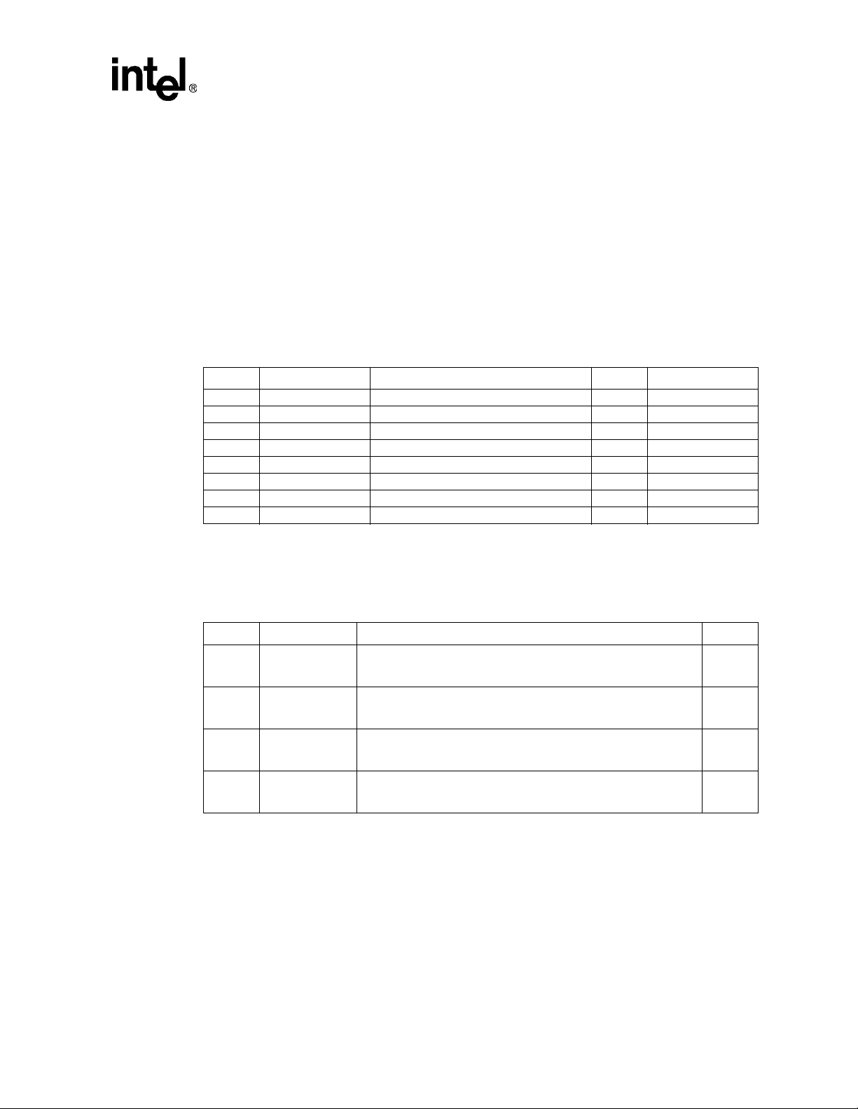
4.1 CPU Memory Map
The memory map for the IQ80960RM/RN platform is shown in Figure 4-2. All addresses below
9002 0000H on the IQ80960RM/RN platform are reserved for various functions of the i960
RM/RN I/O processor, a s shown on the memory map. Doc ument ation for t hese areas , as we ll as t he
processor memory m apped registe rs at FF00 0000 H and the IBR , can be f ound i n the i 960
I/O Pro ce ssor Dev eloper’s Manual.
Figure 4-2. IQ80960RM/RN Platform Memory Map
®
RM/RN
F000 0000H
E000 0000H
B000 0000H
A000 0000H
9002 0000H
8000 0000H
0000 2000H
0000 1900H
0000 0800H
0000 0400H
0000 0000H
Flash RO M
and
Processor Registers
On-board Devices
Reserved
DRAM
Reserved
ATU Outbound
Translation Windows
ATU Outbound
Direct Addressing Window
Reserved
Peripheral
Memory Mapped Registers
Reserved
Processor Internal Data RAM
Processor
Memory Mapped
Registers
Flash ROM
Reserved
LED Register
(write only)
UART
FF00 0000H
FEE0 0000H
F000 0000H
E004 0000H
E000 0000H
4-2 I Q80960RM/RN Evaluation Board Manu al

4.2 Local Interrupts
The i960 RM/RN I/O processor is built around an 80960JT core, which has seven external interrupt
lines designated XINT0# through XINT5# and NMI#. In the i960 RM/RN I/O processor, these
interrupt lines are not directly connected to external interrupts, but pass through a layer of internal
interrupt routing logic. Figure 4-3 shows the interrupt connections on the i960 RM/RN I/O processor.
XINT0# through XINT3# on the 80960JT core can be us ed to re ce ive PCI interrupt s from the
secondary PCI bus, or thes e interrupts can be passed through to the primary PCI interface,
depending on the setting of the XINT Select bit of the PCI Interrupt Routing Select Register in the
i960 RM/RN I/O processor. On the IQ80960RM/RN platform, XINT0# through XINT3# are
configured to receive interrupts from the secondary PCI bus.
XINT4# and XINT5# on the i960 RM/RN I/O processor may be connected to interrupt sources
external to the proc essor. On the IQ80960RM/RN platfor m, XINT4# is connec ted to th e loss of fan
detect and XINT5# is conne cte d to the 16C550 UART.
XINT6#, XINT7# receive interrupt s from internal sources . NMI# receives interrupts from internal
sources an d from an external source. Since all of these interrupts accept signal s from multiple
sources, a status register is provided for each of them to allow service routine s to identify the
source of the interrupt. Each of the possible interrupt sources is assigned a bit position in the sta tus
register. The interrupt sources for these lines are shown in Figure 4-3. On the IQ80960RM/RN
platform, the NMI# interrupt is not connected to any external interrupt source and receives
interrupts onl y from the internal devices on the i960 RM/RN I/O proc es s or. Note that all error
conditions result in an NMI# interrupt.
i960® RM/RN I/O Processor Overview
IQ80960RM/RN Evaluation Board Ma nual 4-3

i960® RM/RN I/O Processor Overview
Figure 4-3. i960® RM/RN I/O Processor Interrupt Controller Connections
P_INTB# Output
P_INTC# Output
P_INTD# Output
P_INTA# Output
i960®RN/RM I/O Processor
S_INTA#/XINT0#
S_INTB#/XINT1#
S_INTC#/XINT2#
S_INTD#/XINT3#
XINT4#
(Loss of Fan)
XINT5# (UART)
NMI# (N/C)
S_INTD# Select bit
S_INTC# Select bit
S_INTB# Select bit
S_INTA# Select bit
m
u
x
m
u
x
m
u
x
m
u
x
DMA Channel 0 Interrupt Pending
DMA Channel 1 Interrupt Pending
DMA Channel 2 Interrupt Pending
Performance Monitor Unit Interrupt Pending
Application Accelerator Interrupt Pending
I2C Bus Interface Unit Interrupt Pending
Messaging Unit Interrupt Pending
Primary ATU/Start BIST Interrupt Pending
Primary PCI Bridge Interface Error
Secondary PCI Bridge Interface Error
Bus Interface Unit Error
Primary ATU Error
Secondary ATU Error
Memory Controller Unit Error
DMA Channel 0 Error
DMA Channel 1 Error
DMA Channel 2 Error
Application Accelerator Unit Error
Messag ing Unit Er ro r
80960 Outbound Doorbell 0
80960 Outbound Doorbell 1
80960 Outbound Doorbell 2
80960 Outbound Doorbell 3
Latch
XINT6 Interrupt
Latch
XINT7 Interrupt
Latch
NMI Interrupt
XINT0#
XINT1#
XINT2#
XINT3#
XINT4#
XINT5#
XINT6#
XINT7#
NMI#
i960 Core
Processor
4-4 I Q80960RM/RN Evaluation Board Manu al

4.3 CPU Counter/Timers
The i960 RM/RN I/O processor is equipped with two on-chip counter/timers which are clocked
with the i960 RM/ RN I/O process or clock s ignal. The i 960 RM/RN I/ O proc essor re ceives its c lock
from the primary PCI interface clock, generated by the motherbo ard. Most motherboards generat e
a 33 MHz clock signal, although the PCI specification requires a clock frequency between 0 and
33 MHz. The timers can be prog rammed for single-shot or continuous mode, and can generate
interrupts to the proc es s or when the countdown expires.
4.4 Primary PCI Interface
The primary P CI interface on the IQ80960RM/RN platform provides the i960 RM/RN I/O
processor with a connection to the PCI bus on the host system. Only the PCI-to-PCI bridge unit on
the i960 RM/RN I/O proc essor i s dire ctly c onnect ed to the primary P CI interf ace. Devices i nstall ed
on the expansion sl ots are connected to the PCI bus via the bridge unit on the i960 RM/RN I/O
processor. The PCI-to-PCI bridge accepts Type 1 configuratio n cyc les destined for devices on the
secondary bus, and will forward them as Type 0 or Type 1 con f iguration cycles, or as special
cycles. The IQ80960RN pla tform interfac es to a 64-bit PCI bus and the IQ80960RM platform
interfaces to a 32-bit PCI bus.
i960® RM/RN I/O Processor Overview
4.5 Secondary PCI Interface
The secondary PCI interface provided by the i960 RM/RN I/O processor is used to connect PCI
cards via the expansion slots to the host system’s PCI bus. PCI cards are attached to the
IQ80960RM/RN platform with a standard PCI connector and may contain up to four separate PCI
devices. The i960 RM/RN I/O processor provides PCI-to-PCI bridge functionality to map installed
PCI devices onto the host P CI bus , and supports tr ans action forwarding in both directions across
the bridge. PCI devi ces connected via the expansion slots can therefore act as masters or slaves on
the host sys tem’s PCI bus. Additional PC I-to- PCI bri dge devi ces are suppor ted by t he i960 R M/RN
I/O processor on its second ary PCI interface and can be designed into add-on PCI cards. In
addition, the i960 RM/RN I/O processor supports “private” PCI devices on its secondary bus.
Private device s are hidden from in itialization code on the host system, and are configure d and
accessed dire ctly by the i960 RM/RN I/O processor. These devices are not part of the normal PCI
address space, but they can act as PCI bus mast ers and transfer dat a to and from other PCI devi ce s
in the system.
Unless designated as private devices, PCI devices installed on the se condary PCI interface of the
IQ80960RM/RN platform are mapped into the system-wide PCI address space by configuration
software running on the host system. No logical distinction is made at the system level between
devices on the prim ary PCI bus and devices on secondary buses; all transaction forwarding is
handled transparently by the PCI-to-PCI bridge. Configuration cycles and read and write accesses
from the host are forwarded through the PCI-to-PCI bridge un it of the i960 RM/RN I/O processor.
Master read and write cycles from devices on the secondary PCI bus are also forwarded to the h ost
bus by the PCI-to-PCI bridge unit.
IxWORKS allows secondary PCI devices to be configured as Public or Private. Public devices are
configured by the PCI host. Private devices are configured by the IxWORKS kerne l and the
device-speci fic HDM.
IQ80960RM/RN Evaluation Board Ma nual 4-5

i960® RM/RN I/O Processor Overview
4.6 DMA Channels
The i960 RM/RN I/O processor features three independent DMA channels, two of which operate
on the primary PCI interface, whereas the remaining one operates on the secondary PCI interface.
All three of the DMA channel s c onnect to the i960 RM/RN I/O proc es s or’s local bus and can be
used to transfe r data from PCI devices to memory on the IQ80960RM/RN platform. Support for
chaining, and scatter/gather is built into all three channels. The DMA can address the entire 2
bytes of address sp ace on the PCI bus and 2
®
Figure 4-4. i960
RM/RN I/O Processor DMA Controller
Primary PCI Bus
32
bytes of address space on the internal bus.
DMA Channel 0
64
DMA Channel 1
PCI to PCI Bridge
DMA Channel 2
Secondary PCI Bus
4.7 Application Accelerator Unit
The Application Accelerat or provides low-latency , high-throughput data transfer cap ability
between the AA unit and 80960 local memory. It executes data transf ers to and from 80960 local
memory and a lso provides the nec essary programming interface. The Application Ac celerator
performs the following functions:
• Transfers data (read) from memory c ontroller
• Performs an optiona l boolean operati on (XOR) on rea d data
• Tr ansfers data (write) to memory controller
The AA uni t fe at u r es:
• 128-byte, a rranged as 8-byte x 16-deep store queue
• Utilizati on of the 80960RN/RM proces sor memory controll er interface
32
• 2
addressing range on the 80960 local memory interface
80960
Local Bus
• Hardware support for unaligned data transfers for the internal bus
• Full progra mmability from the i960 core processor
• Support for automatic data chaining for gathering and scattering of data blocks
4-6 I Q80960RM/RN Evaluation Board Manu al

Figure 4-5 shows a simplif ied connection of the Application Accelerator to the i960 RM/RN I/O
Processor Internal Bus.
Figure 4-5. Application Accelerator Unit
Application Accelerator Unit
Data Queue
Boolea n U ni t
i960® RM/RN I/O Processor Overview
Packing/
Unpacking
Unit
4.8 Performance Monitor Unit
The Performance Monitoring features aid in measuring and monito ring various system parameters
that contribute to the overall performance of the processor. The monitoring facility is generic ally
referred to as PMON – Performance Moni toring. The facility is model specific, not architectural;
its inte n d ed use is to gath er p erformance measurements that can b e u sed to retune/refine code for
better system level performance.
The PMON facility provided on the i960 RM/RN I/O processor co mprises:
• One dedicated global Time Stamp counter, and
• Fourteen (14) Programmab le Event counters
The global time sta mp c ounter is a dedicated, free running 32-bit counter.
The progr a m m ab le event coun t er s are 3 2- b i ts w i de . Ea ch co un t er can be progr am m e d to obs e r v e
an event from a defined set of events. An event consists of a set of parameters which define a start
condition and a stop condit ion. The monitored events are selec ted by programming an event select
register (ESR).
80960
Bus Interface
64-bit
Internal Bus
IQ80960RM/RN Evaluation Board Ma nual 4-7


MON960 Support for IQ80960RM/RN
5
This chapter discusses a number of additions that have been made to MON960 to support the
IQ80960RM/RN in an optional non-I
MON960, see the MON960 Debug Monitor User’s Guide. The IQ80960RM/RN evaluation
platform ships with IxWorks* from Wind River Systems installed in flash firmware. To use
CTOOLS and MON960 instead of IxWorks, you need to download MON960 into the onboard
Flash. See Chapter 2 for more information on updating the onboard Flash. See Chapter1 for
descriptions of both IxWorks and CTOOLS.
2
O capacity. For complete documentation on the operation of
5.1 Secondary PCI Bus Expansion Connectors
The IQ80960RM/RN pl atform con tains four secon dary PCI bus expan sion c onnect ors to g ive us ers
access to the secondary PCI bus of the i960
perform secondary PCI bus ini tialization including the establishment of a secondary PCI bus
address map. Routines compatible with the PCI Local Bus Specification Revision 2.1 allow the
software on the IQ80960RM/RN platform to search for devices on the secondary PCI bus and read
and write the configuration space of those devices.
®
RM/RN I/O proce ssor. Extensions to MON960
5.2 MON960 Components
The remaining sect ions of this chapter assume that MON960 is installed in the onboard Flash,
replacing IxWorks. The IQ80960RM/RN optional MON960 debug monitor consists of four main
components:
• Initialization firmware • MON960 extensions
• MON 9 60 kernel • Diagnostics/example code
These four components togeth er are refe rred to as MON960.
5.2.1 MON960 Initia lizat ion
At initialization, MON960 puts the IQ80960RM/RN platform into a known, func tional state that
allows the host processor to perform PCI initialization. Once in this state, the MON960 kernel and
the MON960 extensions can load and execute correctl y. Initialization is performed after a RESET
condition. MON960 initialization encompasses all m ajor portions of the i960 RM/RN I/O
processor and IQ8 0960RM/RN pl at form includi ng 80 960JT core ini tial izati on, Memory C ontr oll er
initial ization, SDRAM initialization, Primary PCI Address Translation Unit (ATU) initialization,
and PCI-to-PC I Br idge Unit initialization.
The IQ80960RM/RN pl atform is desig ned to use th e Conf igur ation Mode of the i96 0 RM/RN I/O
processor. Conf igu ration Mode all ows th e 8 0960 JT core to in itia li ze an d cont rol the i nit iali za tion p roc ess
before the PCI host conf igur es t he i 960 RM/ RN I/O proc essor. By u ti lizi ng Confi gura tion Mode , t he user
IQ80960RM/RN Evaluation Board Ma nual 5-1

MON960 Support for IQ80960RM/RN
is give n the ability to initialize the P CI configuration re gisters to values other than the default power-up
values. Confi gura tion Mode giv es the use r maximu m flexi bilit y to cu stomiz e the way in which the i960
RM/RN I/O process or and IQ80960 RM/RN plat form appea r to th e PCI host confi gurati on soft ware.
5.2.2 80960JT Core Initialization
The 80960JT core begins the initialization process by reading its Initial Memory Image (IMI) from
a fixed address in the boot ROM (FEFF FF30H in the i960 address space). The IMI include s the
Initialization Boot Record (IBR), the Process Control Block (P RCB), and seve r al system data
structures. The I BR provides initial configuration information for the core and integrated
peripheral s, pointers to the system data structures and the first instruction to be executed after
processor initialization, and checksum words that the processor uses in its self-test routine. In
addition to the IBR and PRCB, the required data str uctures are the:
• System Procedure Table
• Control Table
• Interrupt Table
• Fault Table
• User Stack (application dependent)
• Supervisor Stack
• Interrupt Stack
5.2.3 Memory Controller Initialization
Since the i960 RM/RN I/O processor Memory Cont roller is integral to the design and opera tion of
the IQ80960RM/RN platform, the operat ional parameters for Bank 0 and Bank 1 are established
immediately after processor core initialization. Memory Bank 0 is associated with the ROM on the
IQ80960RM/RN pla tform. Memory Bank 1 is associated with the UART and the LED Control
Register. Parameters such as Bank Base Address, Read Wait States, and Write W ait States must be
established to ensure the prope r operation of the IQ80960RM/RN platform. The Memory
Controll er is initialized so as to be consistent with the IQ8096 0RM/RN platform memory map
show n in Figure 4-2.
5.2.4 SDRAM Initializatio n
SDRAM initialization includes setting operational parameters for the SDRAM controller, and sizing
and clearing the installed SDRAM configuration. To configure the system properly, Presence Detect
data is read from the EEPROM of the SDRAM module, using the 80960RM/RN I
Unit. Presence Detect data includes the number and size of SDRAM banks present on the installed
module. On power-up, 64 bytes of Presence Detect data are read and validated. The SDRAM
controller is then configured by setting the base address of SDRAM, the boundary limits for each
SDRAM bank, the refresh cycle interval, and the output buffer drive strength. Once the SDRAM
controller is configured, the SDRAM is cleared in preparation for the C language runtime
environment. The actual SDRAM size is stored for later use (e.g., to establish the size of the
IQ80960RM/RN platform PCI Slave image). The SDRAM controller is initialized to be consistent
with the IQ80960RM/RN platform memory map shown in Figure 4-2.
2
C Bus Interface
5-2 I Q80960RM/RN Evaluation Board Manu al

5.2.5 Primary PCI Interface Initialization
The IQ80960RM/RN platform is a multi-function PCI device. O n the primary PCI bus, two
functions (from a PCI Configuration Space standpoint) are supported.
• Function 0 is the PCI-t o-P CI Bridge of the i960 RM/RN I/O process or, which optionally
provides access capability between the primary P CI bus and the secondary PCI bus.
• Function 1 i s the Primary ATU which provides acc es s capability between the primary PC I bus
and the local i960 bus.
The platform can be initiali zed into one of four modes. Modes 0 and 3 are described below.
Table 5-1. Initializa tion Modes
MON960 Support for IQ80960RM/RN
RST_MODE#/
SW1-1
0/ON 0/ON Mode 0 Accepts Transactions Held in Reset
0/ON 1/OFF Mode 1 Retries All Configuration T ransactions Held in Reset
1/OFF 0/ON Mode 2 Accept s Transa c tions I nit ia liz e s
1/OFF 1/OFF Mode 3 (default) Retries All Configuration Transactions Initi alizes
RETRY/
SW1-2
Initialization
Mode
When the IQ80960RM/RN is operatin g in Mode 0, the proc es sor core is held in reset, allowing
register defau lts t o be us ed on the Primary PCI int erfac e. This mode is u sed to program the onboard
Flash with e ither IxWORKS* or MON960.
When the IQ80960RM/RN pla tform is ope ratin g in Mode 3, the Conf igura tion Cyc le Dis able bi t in
the Extended Bridge Control Reg is ter (EBCR) is set after IQ80960RM/RN processor reset. In this
mode, the IQ80960RM/RN platform sends PCI Retries when the PCI host attempts to access the
platform’s Configuration Space. This mode allows the IQ80960R M/RN proc essor t ime to i nitia lize
its internal registers. The processor remains in this mode until the Configuration Cycle Disable bit
in the Extended Br idge Control Re gister (EBCR) is cleared. For this reason, and to prevent PCI
host problems, Pri ma ry PCI initialization occurs at the earliest possible opportunity after Memory
and SDRAM controller initialization.
5.2.6 Primary ATU Initialization
Primary ATU (Bridge) initialization includes initialization by the 80960JT core and initialization
by the PCI host processor. Local initialization occurs fir st and consists mainly of esta blishing the
operational parameter s for access to the loca l IQ80960RM/RN pla tfor m bus. The Primary Inboun d
ATU Limit Register (PIALR) is ini tialized to establish the block size of memory required by the
Primary ATU. The PIALR value is based on the installed SDRAM configuration. The Primary
Inbound ATU Trans late Value Registe r (PIATVR) is i nitia lized to est ablis h th e transl ati on value for
PCI-to - Local accesses . The PIATVR value is set t o reference the base of local SDRAM. The
Primary Outbound Memory Window Value Register (POMWVR) is initialized to establish the
translation value for Local-to-PCI accesses. The POMWVR value remain s at its default value of
“0” to allow the IQ80960RM/RN platform to access the start of the PCI Memory add r es s ma p,
which is typically occupied by PCI host memo ry. Likewise, the Primary Outbound I/O Window
Value Register (POIOWVR) remains at its defa ult value of “0” to allow the IQ80960RM/RN
platform to access the start of the PCI I/O address map. PCI Doorbell-related pa ramet ers are also
established to allow for communication between the IQ80960RM/RN platform and a PCI bus
master using the doorbell mechanism.
Primary PCI Interface
i960 Core
Processor
IQ80960RM/RN Evaluation Board Ma nual 5-3

MON960 Support for IQ80960RM/RN
By default, Primary Outbound Configuration Cycle parameters are not established. The A TU
Configuration Register (ATUCR) is initialized to establish the operational parameters for the
Doorbell Unit and ATU interrupts (both primary and secondary), and to enable the primary and
secondary ATUs. The PCI host is responsible for allocating PCI address space (Memo r y, Memory
Mapped I/O, and I/O), and assigning the PCI Base addresses for the IQ80960RM/RN platform.
5.2.7 PCI-to-PCI Bridge Initialization
PCI-to-PCI Bridge initialization includes initialization by the 80960JT core and initialization by the
PCI host processor. Local initialization occurs first and consists mainly of establishing the operational
parameters for the secondary PCI interface of the PCI-to-PCI bridge. On the IQ80960RM/RN
platform, the secondary PCI bus is configured to consist of private devices (not visible to PCI host
configuration cycles). To support a private secondary PCI bus, the Secondary IDSEL Select Register
(SISR) is initialized to prevent the secondary PCI address bits [20:16] from being asserted during
conversion of PCI Type 1 configuration cycles on the primary PCI bus to PCI Type 0 configuration
cycles on the secondary PCI bus. Secondary PCI bus masters are prevented from initiating
transactions that will be forwarded to the primary PCI interface. The PCI host is responsible for
assigning and initializing the PCI bus numbers, allocating PCI address space (Memory, Memory
Mapped I/O, and I/O), and assigning the IRQ numbers to valid interrupt routing values.
5.2.8 Secondary ATU Initialization
Secondary ATU (Bridge) initialization consists mainly of establishing the operational para me ters
for access between the local IQ80960RM/RN platform bus and the secondary PCI devices. The
Secondary Inbound ATU Base Address Register (SIABAR) is initialized to establish the PCI base
address of IQ80960RM/RN platform local memory from the secondary PCI bus. By convention,
the secondary PCI base addre ss for access to IQ80960RM/RN pla tform local memory is “0”. The
Secondary Inbound ATU Limit Register (SIALR) is ini tialized to establish the block size of
memory required by the secondary ATU. The SIALR value is based on the ins talled SDRAM
configuration. The Secondary Inbound ATU Tr anslate Value Register (SIA TVR) is initialized to
establish the translation value for Secondary PCI-to-Local acces ses. The SIATVR value is set to
reference the base of loca l S DRAM. T he Secondary Outbound Memory Window Value Register
(SOMWVR) is ini tialized to establish the translation value for Local-to-Secondary PCI accesses.
The SOMWVR value is left at its default value of “0” to allow the IQ80960R M/RN platform to
access the start of the PCI Memory address map. Likewise, the Seconda ry Outbound I/O Window
Valu e R e g i ster (SOIO WV R) is left at its defaul t value of “0” to allow th e IQ 8 0 96 0 R M /R N
platfo rm to access the start of the PCI I/O address map.
On the se condary PCI bus, the IQ80960RM/RN platform assumes the duties of PCI host and, as
such, is requir ed to configure the devices of the secondary PCI bus. Secondary Outbound
Configuration Cycle paramet ers are establi shed during secondary PCI bus configurat ion.
Secondary PCI bus con f iguration is accomplished via MON960 Extens ion routines.
5-4 I Q80960RM/RN Evaluation Board Manu al

5.3 MON960 Kernel
The MON960 Kernel (monitor) provides the IQ80960RM/RN user with a software platform on
which application software can be developed and run. The monitor provides several features available
to the IQ80960RM/RN user to speed application development. Among the available features are:
• Communication with a terminal or terminal emula tion package on a hos t computer through a
serial cable with automatic baud rate detection
• Communication with a software debugger such as GDB960 (available from Intel) using the
Host Debugger Interface (HDI) softwa re interface
• Communication with the host comput er via the primary PCI bus
• Downloads of ELF obje ct fil es vi a t he prim ary PCI bus or vi a the ser ial co nsole port at rat es up
to 115,200 baud
• Downloads of ELF object files via the primary PCI bus
• On-board erasure and prog rammi ng of Intel 28F016S5 Flash ROM
• Memory display and modification c apability
• Breakpoint and single-step capability to support debugging of user code
• Disassembly of i960 processor instructions
MON960 Support for IQ80960RM/RN
5.4 MON960 Extensions
The monitor has been ext ended to include the secondary PCI bus initialization and also the BIOS
routines whic h are contained in the PCI BIOS Specification Revision 2.1.
5.4.1 Secondary PCI Initialization
MON960 extensions are res ponsible for initializing the devices on the secondary PCI bus of the
IQ80960RM/RN platform . Secondary PCI ini tialization involves allocating address spaces
(Memory , Me mory Ma pped I/O, and I/ O), assigni ng PCI ba se a ddresse s, as signing IR Q val ues, a nd
enabling PCI mastership. MON960 does not support devices containing PCI-to-P CI bridges and
hierar chical buses.
IQ80960RM/RN Evaluation Board Ma nual 5-5

MON960 Support for IQ80960RM/RN
5.4.2 PCI BIOS Routines
MON960 includes PCI BIOS rout ines to aid appli cation software initiali zation of the secondary
PCI bus. The supporte d BIOS functions ar e described in the subsections that follow.
sysPCIBIOSPresent
sysFindPCIDevice
sysFINDPCIClassCode
sysGenerateSpecialCycle
sysReadConfigByte
sysReadConfigWord
sysReadConfigDword
sysWriteConfigByte
sysWriteConfigWord
sysWriteConfigDword
sysGetIrqRoutingOptions
sysSetPCIIrq
These functions preserve, as closely as possible, the parameters and return values described in the
PCI Local Bus Specification Revision 2.1. Functions that return multiple values do so by filling in
the fields of a struct ure pa ssed by the calling r outine.
You can access these functions via a calls instruction. The system call indices are de fined in the
MON 9 60 s o ur ce file PCI_BIOS.H. The function prototypes are defined in the IQRP_ASM.H
file.
5.4.2.1 sysPCIBIOSPresent
This fun ction a llo ws th e call er t o det erm ine whet her the P CI BIOS in te rfac e fun cti on set is pr ese nt,
and the cu rrent interface version level. It also provides information about the hardware mechanism
used for accessing co nfigur ation space and whethe r or not the hard ware supp orts genera tion of PCI
Special Cycle s.
Calling convention:
int sysPCIBIOSPresent (
PCI_BIOS_INFO *info
);
Return values:
This function always returns SUCCESSFUL.
5-6 I Q80960RM/RN Evaluation Board Manu al

5.4.2.2 sysFindPCIDevice
This functio n returns the loca tion of PCI devices that have a specific Device ID and Vendor ID.
Given a Vendor ID, a Device ID, and an Index, the function returns the Bus Number, Device
Number, and Funct ion Number of t he Nt h Device/F uncti on whose Vendor ID and Device ID mat ch
the input parameters.
Calling softw are can find all devices having the same Vendor ID and Device ID by making
successive calls to this function starting with the index set to “ 0”, and incrementing the index until
the function return s DEVICE_NOT_FOUND. A return value of BAD_VENDOR_ID indicates that
the Vendor ID value passed had a value of all “1” s.
Calling convention:
int sysFindPCIDevice (
int device_id,
int vendor_id,
int index
);
MON960 Support for IQ80960RM/RN
Return values:
This function returns SUCCESSFUL if the indicated device is located, DEVICE_NOT_FOUND if
the indicate d device cannot be loc ated, or BAD_VENDOR_ID if the ven dor_id value is illegal.
5.4.2.3 sysFindPCIClassCode
This functio n r eturns the location of PCI devices that have a specif ic Class Code. Given a Class
Code and an Index, t he f unction returns the Bus Num ber , Device Num ber , and Funct ion Numbe r of
the Nth Device/Function whose Class Code matches the input parameters.
Calling software can find all devices having the sa me Class Code by making successive calls to
this functi on sta rti ng with t he i ndex set to “ 0”, a nd incre menti ng the i ndex unt il t he functio n returns
DEVICE_NOT_FOUND.
Calling convention:
int sysFindPCIClassCode (
int class_code,
int index
);
Return values:
This function returns SUCCESSFUL when the indicated device is located, or
DEVICE_NOT_FOUND when the indicated device cannot be located.
IQ80960RM/RN Evaluation Board Ma nual 5-7

MON960 Support for IQ80960RM/RN
5.4.2.4 sysGenerateSpecialCycle
This function a llows for genera tion of PCI S peci al Cycles . The gen erate d specia l cycl e is bro adcast
on a spec if i c P CI Bu s in the syst em.
PCI Special Cycles are not supported on the IQ80960RM/RN platform secondary PCI bus.
Calling convention:
int sysGenerateSpecialCycle (
int bus_number,
int special_cycle_data
);
Return values:
Since PCI Special Cycles are not supported by the IQ80960RM/RN platform, this function always
returns FUNC_NOT_SUPPORTED.
5.4.2.5 sysReadConfigByte
This function allows the caller to read individual bytes from the configuration space of a specific
device.
Calling convention:
int sysReadConfigByte (
int bus_number,
int device_number,
int function_number,
int register_number, /* 0,1,2,...,255 */
UINT8 *data
);
Return values:
This function returns SUCCESSFUL when the indicated byte was read correctly, or ERROR when
there is a problem with the parameters.
5-8 I Q80960RM/RN Evaluation Board Manu al

5.4.2.6 sysReadConfigWord
This function allows the caller to re ad individual shorts (16 bits) from the configuration space of a
specific device. The Regist er Number parameter must be a multi ple of t wo (i.e., bit 0 must be set to “0”).
Calling convention:
int sysReadConfigWord (
int bus_number,
int device_number,
int function_number,
int register_number, /* 0,2,4,...,254 */
UINT16 *data
);
Return values:
This function returns SUCCESSFUL when the indicated word was read correctly, or ERROR when
there is a p ro b l em with the par am e t er s.
MON960 Support for IQ80960RM/RN
5.4.2.7 sysReadConfigDword
This function allows the caller to read individual longs (32 bits) from the configuration space of a
specific device. The Register Number parameter must be a multiple of four (i.e., bits 0 and 1 must
be set to “0”) .
Calling convention:
int sysReadConfigDword (
int bus_number,
int device_number,
int function_number,
int register_number, /* 0,4,8,...,252 */
UINT32 *data
);
Return values:
This function returns SUCCESSFUL when t he indicated long was read correctly, or E RROR when
there is a p ro b l em with the par am e t er s.
IQ80960RM/RN Evaluation Board Ma nual 5-9

MON960 Support for IQ80960RM/RN
5.4.2.8 sysWriteConfigByte
This function allows the caller to w r ite in d iv id ual b ytes to th e configuration space of a specific device.
Calling convention:
int sysWriteConfigByte (
int bus_number,
int device_number,
int function_number,
int register_number, /* 0,1,2,...,255 */
UINT8 *data
);
Return values:
This function returns SUCCESSFUL when the indicated byte was written correctly, or ERROR
when there is a problem with the parameters.
5.4.2.9 sysWriteCo nfigWord
This function allows the calle r to writ e individual shorts (16 bits ) to the confi guration space of a specific
device. The Register Number parameter must be a multiple of two (i.e., bit 0 must be set to “0”).
Calling convention:
int sysWriteConfigWord (
int bus_number,
int device_number,
int function_number,
int register_number, /* 0,2,4,...,254 */
UINT16 *data
);
Return values:
This function returns SUCCESSFUL when the indicated word was written correctly, or ERROR
when there is a problem with the parameters.
5-10 IQ80960RM/RN Evaluation Board Manu al

5.4.2.10 sysWriteConfigDword
This functio n allows the caller to write individual longs (32 bits) to the configuration space of a
specific device. The Register Number parameter must be a multiple of four (i.e., bits 0 and 1 must
be set to “0”) .
Calling convention:
int sysWriteConfigDword (
int bus_number,
int device_number,
int function_number,
int register_number, /* 0,4,8,...,252 */
UINT32 *data
);
Return values:
MON960 Support for IQ80960RM/RN
This function returns SUCCESSFUL when the indicated long was written correctly, or ERROR
when the re is a problem with the p arameters.
5.4.2.11 sysGetIrqRoutingOpt ion s
The PCI Interrupt routing fabric on the IQ80960RM/RN platform is not reconfigurable (fixed
mapping relationships); therefore, this function is not supported.
Calling convention:
int sysGetIrqRoutingOptions (
PCI_IRQ_ROUTING_TABLE *table
);
Return values:
This function always returns FUNC_NOT_SUPP ORTED.
IQ80960RM/RN Evaluation Board Ma nual 5-11

MON960 Support for IQ80960RM/RN
5.4.2.12 sysSetPCIIrq
The PCI Interrupt rout ing fabric on the IQ80960RM/RN platform is not reconfigurable (fix ed
mapping relationships); therefore, this function is not supported.
Calling convention:
int sysSetPCIIrq (
int int_pin,
int irq_num,
int bus_dev
);
Return values:
This function always returns FUNC_NOT_SUPPORTED.
5.4.3 Additional MON960 Commands
The following commands have been added to the UI int erfa ce of MON960 to support the
IQ80960RM/RN platform.
5.4.3.1 print_pci Utility
A print _pc i c omma nd to MON96 0 i s acc es se d thro ug h t he MON9 60 com ma nd pro mpt . This c omm and
displays the contents of the PCI configuration space on a selected adapter on the secondary PCI interface or
on the i960 RM/RN I/O processor itself. For more information on the meaning of the fields in PCI
configuration space, refer to the PCI Local Bus Specification Revision 2.1. The syntax of this command is:
pp <bus number> <device number> <function number>
5.5 Diagnostics / Example Code
IQ80960RM/RN platform diagnostic routines serve a twofold purpose: to verify proper hardware operation
and to provide example code for users who need similar functions in their applications. Diagnostic routines
fall into two categories: board level diagnostics and PCI expansion module diagnostics.
5.5.1 Board Level Diagnostics
Board level diagnostics exercise all basic areas of the IQ80960RM/RN platform. Diagnostic routines
include SDRAM tests, UART tests, LED tests, internal timer tests, I
Primar y PCI bus t e sts ex erci se the pri ma ry ATU, th e PCI Do orbe ll un it, and t he PC I DMA con tr oll er.
Interru pts fr om bot h loca l and PC I sour ces a re gen erated and h andled. The PC I bus t ests r equire an ex terna l
test suite running on a PC to verify complete functionality of the IQ80960RM/RN platform.
2
C bus test s, an d pri mary PC I bus te sts .
5.5.2 Secondary PCI Diagnostics
Secondary PCI diagno st ics exercise the seconda ry P CI bus , thereby confirming hardware
functionality, as well as illustrating the use of the P CI BIOS routines present in MON960.
5-12 IQ80960RM/RN Evaluation Board Manu al

Bill of Materials A
This appendix identifies all components on the IQ80960RN Evaluation Platform ( Table A-1), and
8
Table A-1. IQ80960RN Bill of Materials (Sheet 1 of 4)
the IQ80960RM Evaluation Platform (Table A-2).
Item Qty Location Part Description Manufacturer Manufacturer Part #
1 1 U13 IC/SM 74ALS32 SOIC-14
2 1 U6 IC/SM 74ALS04 SOIC
3 1 U3 IC/SM 74ABT273 SOIC
4 2 U1,U2 IC/SM 74ABT573 SOIC
5 1 U16 IC/SM 74ALS08 SOIC
6 1 U5 IC / SM 1488A SOIC
7 1 U7 IC / SM 1489A SOIC
8 1 Q1 IC/SM Si9430DY SOIC-8 Siliconix Si9430DY
9 1 U9 IC/SM LVCMOS Fanout Buffr SSOP Motorola MPC9140
10 1 U10 IC/SM LM339 SO IC -1 4
11 1 U8 IC/SM MAX1651CSA SO IC-8 Maxim MAX1651C SA
12 1 U14 IC/SM MAX712CSE SOIC-16 Maxim MAX712CSE
13 1 U17 IC/SM MAX767CAP SOIC Maxim MAX767CAP
14 1 U15 PROCESSOR (from Intel) 80 960RN Intel
15 1 U12 VLSI I/O UART 16C550 PLCC
16 1 C65 CAP SM, 0.47 µF (1206) Phi lip s Philips 12062F 474Z9BB 0
C2, C3,
C10, C11,
C18, C19,
17 15
C26, C27,
C55, C58,
C61, C68,
C77, C83,
C96
CAP SM, 0.01 µF (0805) Kemet C0805C103K5RAC
National
Semiconductor
National
Semiconductor
Texas
Instruments
Texas
Instrumen ts
National
Semiconductor
National
Semiconductor
National
Semiconductor
National
Semiconducto r
Texas
Instruments
DM74ALS32M
DM74ALS04BM
SN74ABT273DW
SN74ABT573DW
DM74ALS08M
DS1488M
DS1489AM
LM339 M
TL16C550AFN
IQ80960RM/RN Evaluation Board Ma nual A-1

Bill of Mat er ials
Tab le A-1. IQ80960RN Bill of Materials (Sheet 2 of 4)
Item Qty Location Part Description Manufacturer Manufacturer Part #
C1, C4, C5,
C6, C7, C8,
C9, C12,
C13, C14,
C15, C16,
C17, C20,
C21, C22,
C23, C24,
C25, C28,
C29, C30,
C31, C32,
C33, C34,
C35, C36,
C37, C38,
C39, C40,
C41, C42,
C43, C44,
C45, C46,
C48, C49,
18 81
19 1 C110 CAP SM, 18 pF (0805) Kemet C0805C180J5GAC
20 2 R27, R28 R/SM 1/10 W 5% 1 ohm (0805) Dale CRCW0805100JT
21 1 R60 R/SM 1/10 W 5% 10 ohm (0805) Dale CRCW08051000JT
22 3
23 4
24 2 R24, R32 R/SM 1/10 W 5% 100 Kohm (0805) Dale CRCW08051003FRT
25 1 R20 R/SM 1/10 W 1% 150 ohm (0805) Dale CRCW08051500FRT
26 3
27 1 R18 R/SM 1/10 W 5% 1.6 Kohm (0805) Dale CRCW0805162JT
28 2 R50, R51 R/SM 1/10 W 5% 22 ohm (0805) Dale CRCW0805220JT
29 1 R34 R/SM 1/10 W 5% 22 Kohm (0805) Dale CRCW0805223JT
30 1 R37 R/SM 1/10 W 5% 24 ohm (0805) Dale CRCW0805240JT
C50, C51,
C53, C59,
C62, C66,
C67, C69,
C70, C71,
C73, C79,
C80, C81,
C85, C86,
C87, C94,
C95, C97,
C98, C99,
C100, C101,
C102, C103,
C104, C105,
C106, C107,
C108, C109,
C1 11, C112,
C11 3, C1 15,
C11 6, C1 14,
C11 7, C120,
C121
R25, R61,
R62
R35, R39,
R58, R59
R14, R41,
R42
CAP SM, 0.1 µF (0805) Philips 08052R104K8BB2
R/SM 1/10 W 5% 1 Kohm (0805) Dale CRCW08051001FRT
R/SM 1/10 W 5% 10 Kohm (0805) Dale CRCW08051002FRT
R/SM 1/10 W 5% 1.5 Kohm (0805) Dale CRCW0805152JT
A-2 I Q80960RM/RN Evaluation Board Manu al

Table A-1. IQ80960RN Bill of Materials (Sheet 3 of 4)
Item Qty Location Part Description Manufacturer Manufacturer Part #
31 1 R47 R/SM 1/10 W 5% 2.4 Kohm (0805) Dale CRCW0805242JT
32 2 R2, R57 R/SM 1/10 W 5% 2.7 Kohm (0805) Dale CRCW0805272JT
33 1 R19 R/SM 1/10 W 5% 330 ohm (0805) Dale CRCW0805331JT
34 1 R29 R/SM 1/10 W 5% 36 ohm (0805) Dale CRCW0805360JT
35 1 R17 R/SM 1/10 W 5% 470 ohm (0805) Dale CRCW 0805 471JT
36 2 R48, R49 R/SM 1/10 W 1% 4.7 Kohm (0805) Dale CRCW08054701FRT
37 1 R53 R/SM 1/10 W 5% 47 Kohm (0805) Dale CRCW0805473JT
38 1 R26 R/SM 1/10 W 5% 68 Kohm (0805) Dale CRCW0805683JT
39 4
40 5
41 4
42 1 J5 CONN DIMM 168P/RAng/Socket/TH Molex 73790-0059
43 1 J7 CONN TJ6 PCB 6/6 LP thru hole KYCON GM-N-66
44 1 J13 CONN/FAN ASSY/Socket/ThruHole AMP 173981-03
45 1 J6 CONN Hdr 16 pin/w shell, pcb AMP 103308-3
46 4
47 1 L1 Inductor/SM 47µH 20% C oilcraft D03340P-473
48 1 L2 Inductor/SM 3.3 µH 20% Coilcraft D0331 6P - 33 2
49 1 S1 Switch/SM DIP4 Mors# DHS-4S Mors DHS-4S
50 1 U4 OSC 1.8432 MHz 1/2 - Thru hole Kyocera KH0HC1CSE 1.843
51 1 U18 Clock Chip CY7B9910-7SC Cypress CY7B9910-7SC
52 1 CR5 LED Green
53 1 CR3 LED-Red
54 1 CR4 LED Green LP
55 2 CR1, CR2 LED-Red-Small Group Dialight 555-4001
56 2 Q2, Q3 Transistor/SM N-Channel Harris RFD16N05LSM
57 1 Q4 Transistor 2N6109 (Thru Hole) Motorola 2N6109
58 1 U19 SOCKET PLCC20 LP Surface Mount AMP 822269-1
60 8
61 1 U19 PALLV16V8Z -20JI AMD PALLV16V 8Z-20JI
62 1 U11 MEM Flash E28F016S5-090 TSOP Intel E28F016S5-090
R30, R43,
R54, R56
J8, J9, J10,
J11, J12
J1, J2, J3,
J4
Z1, Z2, Z3,
Z4
BT1, BT2,
BT3, BT4,
BT5, BT6,
BT7, BT8
R/SM 1/8 W 5% 10 ohm chip 1206 Dale CRCW1206100FT
CONN SM/TH Mictor 43P Recptcl AMP 767054-1
CONN PCI 64BIT 5 V/PCB ThruHole AMP 145166-4
Jumper JUMP2X1 Molex 22-54-1402
Battery Clips /PC/Snap-In/A A K e ysto ne #92
Hewlett
Packard
Hewlett
Packard
Hewlett
Packard
Bill of Materials
HLMP-3507$010
HLMP3301$010
HLMP4740#010
IQ80960RM/RN Evaluation Board Ma nual A-3

Bill of Mat er ials
Tab le A-1. IQ80960RN Bill of Materials (Sheet 4 of 4)
Item Qty Location Part Description Manufacturer Manufacturer Part #
BT1, BT2,
63 8
64 1 U15 HeatSink/Fan Assy 80960RM/RN Panasonic UDQFNBEOIF
65 1 C84 CAP SM, 0.22 µF (1206 ) P hi lips 120 62 E224M9BB 2
66 3
67 4
68 1 C63 CAP TANT SM 33 µF, 10 V (7343) Sprague 293D336X9016D2T
69 4
70 1 C47 CAP TANT SM 22 µF, 20 V (7343) Sprague 293D226X9020D2T
71 1 C74 CAP TANT SM 1 µF, 16 V (3216) Sprague 293D105X0016A2T
72 2 C52, C54 CAP TANT SM 10 µF, 25/35 V Sprague 293D1060025D2T
73 1 C56 CAP TANT SM 100 µF 10 V (7343) AVX TPSD107K010R0100
74 1 C64 CAP TANT SM 330 µF 6.3 V (7343 AVX TPSE337K063R0100
75 3
76 1 R46 Res/SM 1 W 1% 0.012 ohm (2512) Dale WSL-2512-R012
77 1 R21 Res/SM 1 W 1% 0.05 ohm (2512) Dale WSL-2512-R050
78 1 R52 Resistor/SM 1/2 W 5% 100 ohm Beckmen BCR 1/2 101 JT
79 16
80 2 R40, R55 Resistor Pk SM RNC4R8P 22 ohm CTS 742083220JTR
81 2 R15, R16 Resistor Pk SM RNC4R8P 470 ohm CTS 742083471JTR
82 1 R13 Resistor Pk SM RNC4R8P 1.5 Kohm CTS 742083152JTR
83 2 R22, R23 Resistor Pk SM RNC4R8P 30 ohm CTS 742083300JTR
84 1 CR9 Diode CMPSH 3 Surface Mount
85 2 CR6, CR7 Diode SM / MBRS340T3 Motorola MBRS340T3
86 1 CR8 Diode/SM 1N4001 (CMR1-02)
87 1 J5 SDRAM, DIMM, ECC, 2Mx72, 16 MB Unigen UG52S7408GSG
88 2 U20, U 21 IC/SM TL77 02BCD
BT3, BT4,
BT5, BT6,
BT7, BT8
C60, C75,
C78
C89, C90,
C91, C93
C57, C76,
C88, C92
C82, C1 18 ,
C119
R1, R3, R4,
R5, R6, R7,
R8, R9,
R10, R1 1,
R12, R33,
R36, R38,
R44, R45,
Battery AA NiCd @ 600 mA/Hour SAFT NIC-AA-600-SAFT
CAP TANT SM 220 µF, 10 V (7343) AVX TPSE227K010R010
CAP TANT SM 47 µF, 16 V (7343) AVX TPSD476K016R015
CAP TANT SM 4.7 µF, 35 V (7343) Sprague 293D475X9035D2T
CAP SM, 0.047 µF (08 05) Kemet C0805C473K5RAC
Resistor Pk SM RNC4R8P 2.7 Kohm CTS 742083272JTR
Central
Semiconductor
Central
Semiconductor
Texas
Instruments
CMPSH3
CMR1-02
TL7702 BC D
A-4 I Q80960RM/RN Evaluation Board Manu al

Ta bl e A-2. IQ80960RM Bill of Materials (Sheet 1 of 5)
Item Qty Location Part Description Manufacturer Manufacturer Part #
Bill of Materials
1 1 U13 IC/SM 74ALS32 SOIC-14
2 1 U6 IC/SM 74ALS04 SOIC
3 1 U3 IC/SM 74ABT273 SOIC
4 2 U1, U2 IC/SM 74ABT573 SOIC
5 1 U16 IC/SM 74ALS08 SOIC
6 1 U5 IC / SM 1488A SOIC
7 1 U7 IC / SM 1489A SOIC
8 1 Q1 IC/SM Si9430DY SOIC-8 Siliconix Si9430DY
9 1 U9 IC/SM LVCMOS Fanout Buffr SSOP Motorola MPC9140
10 1 U1 0 IC/SM LM 33 9 SO IC - 1 4
11 1 U8 IC/SM MAX1651CSA SO IC-8 Maxim MAX1651C SA
12 1 U14 IC/SM MAX712CSE SOIC-16 Maxim MAX712CSE
13 1 U17 IC/SM MAX767CAP SOIC Maxim MAX767CAP
14 1 U15 PROCESSOR (frm Intel) i960RM Intel
15 1 U12 VLSI I/O UART 16C550 PLCC
16 1 C65 CAP SM, 0.47 µF (1206) Phi lip s Philips 12062F 474Z9BB 0
C2, C3,
C10, C11,
C18, C19,
17 15
C26, C27,
C55, C58,
C61, C68,
C77, C83,
C96
CAP SM, 0.01 µF (0805) Kemet C0805C103K5RAC
National
Semiconductor
National
Semiconductor
Texas
Instruments
Texas
Instruments
National
Semiconductor
National
Semiconductor
National
Semiconductor
National
Semiconducto r
Texas
Instruments
DM74ALS32M
DM74ALS04BM
SN74ABT273DW
SN74ABT573DW
DM74ALS08M
DS1488M
DS1489AM
LM339 M
TL16C550AFN
IQ80960RM/RN Evaluation Board Ma nual A-5

Bill of Mat er ials
Tab le A-2. IQ80960RM Bill of Materials (Sheet 2 of 5)
Item Qty Location Part Description Manufacturer Manufacturer Part #
C1, C4, C5,
C6, C7, C8,
C9, C12,
C13, C14,
C15, C16,
C17, C20,
C21, C22,
C23, C24,
C25, C28,
C29, C30,
C31, C32,
C33, C34,
C35, C36,
C37, C38,
C39, C40,
C41, C42,
C43, C44,
C45, C46,
C48, C49,
18 81
19 1 C110 CAP SM, 18 pF(0805) Kemet C0805C180J5GAC
20 2 R27, R28 R/SM 1/10 W 5% 1 ohm (0805) Dale CRCW0805100JT
21 1 R60 R/SM 1/10 W 5% 10 ohm (0805) Dale CRCW08051000JT
22 3
23 12
24 2 R24, R32 R/SM 1/10 W 5% 100 Kohm (0805) Dale CRCW08051003FRT
25 1 R20 R/SM 1/10 W 1% 150 ohm (0805) Dale CRCW08051500FRT
26 3
27 1 R18 R/SM 1/10 W 5% 1.6 Kohm (0805) Dale CRCW0805162JT
C50, C51,
C53, C59,
C62, C66,
C67, C69,
C70, C71,
C73, C79,
C80, C81,
C85, C86,
C87, C94,
C95, C97,
C98, C99,
C100, C101,
C102, C103,
C104, C105,
C106, C107,
C108, C109,
C1 11, C112,
C11 3, C1 14,
C11 5, C1 16,
C11 7, C120,
C121
R25, R61,
R62
R5, R6, R7
R8, R9,
R10, R1 1,
R12, R35,
R39, R58,
R59
R14, R41,
R42
CAP SM, 0.1 µF (0805) Philips 08052R104K8BB2
R/SM 1/10 W 5% 1 Kohm (0805) Dale CRCW08051001FRT
R/SM 1/10 W 5% 10 Kohm (0805) Dale CRCW08051002FRT
R/SM 1/10 W 5% 1.5 Kohm (0805) Dale CRCW0805152JT
A-6 I Q80960RM/RN Evaluation Board Manu al

Ta bl e A-2. IQ80960RM Bill of Materials (Sheet 3 of 5)
Item Qty Location Part Description Manufacturer Manufacturer Part #
28 2 R50, R51 R/SM 1/10 W 5% 22 ohm (0805) Dale CRCW0805220JT
29 1 R34 R/SM 1/10 W 5% 22 Kohm (0805) Dale CRCW0805223JT
30 1 R37 R/SM 1/10 W 5% 24 ohm (0805) Dale CRCW0805240JT
31 1 R47 R/SM 1/10 W 5% 2.4 Kohm (0805) Dale CRCW0805242JT
32 1 R57 R/SM 1/10 W 5% 2.7 Kohm (0805) Dale CRCW0805272JT
33 1 R19 R/SM 1/10 W 5% 330 ohm (0805) Dale CRCW0805331JT
34 1 R29 R/SM 1/10 W 5% 36 ohm (0805) Dale CRCW0805360JT
35 1 R17 R/SM 1/10 W 5% 470 ohm (0805) Dale CRCW 0805 471JT
36 2 R48, R49 R/SM 1/10 W 1% 4.7 Kohm (0805) Dale CRCW08054701FRT
37 1 R53 R/SM 1/10 W 5% 47 Kohm (0805) Dale CRCW0805473JT
38 1 R26 R/SM 1/10 W 5% 68 Kohm (0805) Dale CRCW0805683JT
39 4
40 5
41 4
42 1 J5 CONN DIMM 168P/RAng/Socket/TH Molex 73790-0059
43 1 J7 CONN TJ6 PCB 6/6 LP thru hole KYCON GM-N-66
44 1 J13 CONN/FAN ASSY/Socket/ThruHole AMP 173981-03
45 1 J6 CONN Hdr 16 pin/w shell, pcb AMP 103308-3
46 4
47 1 L1 Inductor/SM 47 µH 20% Coilcraft D03340P-473
48 1 L2 Inductor/SM 3.3 µH 20% Coilcraft D0331 6P - 33 2
49 1 S1 Switch/SM DIP4 Mors# DHS-4S Mors DHS-4S
50 1 U4 OSC 1.8432 MHz 1/2 - Thru hole Kyocera KH0HC1CSE 1.843
51 1 U18 Clock Chip CY7B9910-7SC Cypress CY7B9910-7SC
52 1 CR5 LED Green
53 1 CR3 LE D-Red
54 1 CR4 LED Green LP
55 2 CR1, CR2 LED-Red-Small Group Dialight 555-4001
56 2 Q2, Q3 Transistor/SM N-Channel Harris RFD16N05LSM
57 1 Q4 Transistor 2N6109 (Thru Hole) Motorola 2N6109
58 1 U19 SOCKET PLCC20 LP Surface Mount AMP 822269-1
60 1 U11 SOCKET / SM / TSOP / 40 pin Meritec 980020-40-02
R30, R43,
R54, R56
J8, J9, J10,
J11, J12
J1, J2, J3,
J4
Z1, Z2, Z3,
Z4
R/SM 1/8 W 5% 10 ohm chip 1206 Dale CRCW1206100FT
CONN SM/TH Mictor 43P Recptcl AMP 767054-1
CONN PCI Slot 5V/PCB T hruHole AMP 145154-4
Jumper JUMP2X1 Molex 22-54-1402
Hewlett
Packard
Hewlett
Packard
Hewlett
Packard
Bill of Materials
HLMP-3507$010
HLMP3301$010
HLMP4740#010
IQ80960RM/RN Evaluation Board Ma nual A-7

Bill of Mat er ials
Tab le A-2. IQ80960RM Bill of Materials (Sheet 4 of 5)
Item Qty Location Part Description Manufacture r Ma nufacturer Part #
BT1, BT2,
61 8
62 1 U19 PALLV16V8Z-20JI A MD PALLV16V8Z-20JI
63 1 U11 MEM Flash E28 F016S5-090 TSOP Intel E28F016S5- 090
64 8
65 1 U15 HeatSink/Fan Assy 80960RN/RM Panasonic UDQFNBEOIF
66 3 C84 CAP SM, 0.22 µF (1206 ) P hi lips 120 62 E224M9BB 2
67 3
68 4
69 1 C63 CAP TANT SM 33 µF, 10 V (7343) Sprague 293D336X9016D2T
70 4
71 1 C47 CAP TANT SM 22 µF, 20 V (7343) Sprague 293D226X9020D2T
72 1 C74 CAP TANT SM 1 µF, 16 V (3216) Sprague 293D105X0016A2T
73 2 C52, C54 CAP TANT SM 10 µF, 25/35 V Sprague 293D1060025D2T
74 1 C56 CAP TANT SM 100 µF 10 V (7343) AVX TPSD107K010R0100
75 1 C64 CAP TANT SM 330 µF 6.3 V (7343) AVX TPSE337K063R0100
76 3
77 1 R46 Res/SM 1 W 1% 0.012 ohm (2512) Dale WSL-2512-R012
78 1 R21 Res/SM 1 W 1% 0.05 ohm (2512) Dale WSL-2512-R050
79 1 R52 Resistor/SM 1/2 W 5% 100 ohm Beckmen BCR 1/2 101 JT
80 7
81 2 R40, R55 Resistor Pk SM RNC4R8P 22 ohm CTS 742083220JTR
82 2 R15, R16 Resistor Pk SM RNC4R8P 470 ohm CTS 742083471JTR
83 1 R13 Resistor Pk SM RNC4R8P 1.5 Kohm CTS 742083152JTR
84 2 R22, R23 Resistor Pk SM RNC4R8P 30 ohm CTS 742083300JTR
85 1 CR9 Diode CMPSH 3 Surface Mount
86 2 CR6, CR7 Diode SM / MBRS340T3 Motorola MBRS340T3
87 1 CR8 Diode/SM 1N4001 (CMR1-02)
88 1 J5 SDRAM, DIMM, ECC, 2Mx72, 16 MB Unigen UG52S7408GSG
BT3, BT4,
BT5, BT6,
BT7, BT8
BT1, BT2,
BT3, BT4,
BT5, BT6,
BT7, BT8
C60, C75,
C78
C89, C90,
C91, C93
C57, C76,
C88, C92
C82, C1 18 ,
C119
R1, R31,
R33, R36,
R38, R44,
R45
Battery Clips/PC/Snap-In/AA Keystone #92
Battery AA NiCd @ 600 mA/Hour SAFT NIC-AA-600-SAFT
CAP TANT SM 220 µF, 10 V (7343) AVX TPSE227K010R010
CAP TANT SM 47 µF, 16 V (7343) AVX TPSD476K016R015
CAP TANT SM 4.7 µF, 35 V (7343) Sprague 293D475X9035D2T
CAP SM, 0.047 µF (08 05) Kemet C0805C473K5RAC
Resistor Pk SM RNC4R8P 2.7 Kohm CTS 742083272JTR
Central
Semiconductor
Central
Semiconductor
CMPSH3
CMR1-02
A-8 I Q80960RM/RN Evaluation Board Manu al

Ta bl e A-2. IQ80960RM Bill of Materials (Sheet 5 of 5)
Item Qty Location Part Description Manufacturer Manufacturer Part #
Bill of Materials
89 2 U20, U21 IC/SM TL7702BCD
Texas
Instruments
TL7702BCD
IQ80960RM/RN Evaluation Board Ma nual A-9

Bill of Mat er ials
A-10 IQ80960RM/RN Evaluation Board Manu al

Schemati cs B
This appendix inc ludes schematics for the IQ80960RN (Table B-1) and IQ80960RM (Table B-2).
Table B-1. IQ80960RN Schematics List
Page Schematic Title
B-2 Decoupling and 3.3V Power
B-3 Primary PCI Interface
B-4 Memory Controller
B-5 Flash ROM, UART, & LEDs
B-6 Logic Analyzer I/F
B-7 SDRAM 168-Pin DIMM
B-8 Secondary PCI/960 Core
B-9 Secondary PCI Bus 1/2
B-10 Secondary PCI Bus 3/4
B-11 SPCI Pull-ups
B-12 Battery/Monitor
IQ80960RM/RN Evaluation Board Ma nual B-1

A
220uF
CAPT7343
21
+3V
NOTE: PINS 3-7 ARE VIAS
C86
21
CAP0805
0.1uF
CR9
2 3
CMPSH3
+5V
21
C60
CAPT7343
220uF
MAX767CAP
RFD16N05L
213
17
19
BST
VCC114VCC215VCC3
10
Q3
DH
3
34567
R46
1 2
COIL-SMT2
3.3uH
L2
1 2
18
LX
ON/OFF#
21
0.012
1W 1%
CR6
Q2
RFD16N05L
213
16
DL
REF2SS9SYNC
8
C78
220uF
CAPT7343
C75
MBRS340T3
1 2
13
PGND
GND15GND26GND37GND411GND5
4
1
20
FB
CS
U17
B
C
D
BREV
1
TP1
Sheet of
4/14/98 01 11
80960RN
DECOUPLING & 3.3V POWER
Title:
Name:
Date:
25 SCIENCE PARK
NEW HAVEN, CT 06511
CYCLONE MICROSYSTEMS
R54
1 2
1/8W 5%
+5V
10
21
C88
4.7uF
CAPT7343
21
C84
0.22uF
CAP1206
21
C83
0.01uF
CAP0805
C40
C39
C38
C37
C36
C35
C34
C33
2 1
0.1uF
CAP0805
0.1uF
2 1
CAP0805
2 1
0.1uF
2 1
CAP0805
0.1uF
CAP0805
2 1
0.1uF
CAP0805
2 1
0.1uF
2 1
CAP0805
0.1uF
CAP0805
0.1uF
2 1
CAP0805
SDRAM DECOUPLING
RAM3V {04,06,11}
C91
2 1
CAPT7343
P33V {02,04,08,09}
SPCI DECOUPLING
C90
2 1
CAPT7343
+5V
47uF
47uF
C28
2 1
C32
2 1
0.1uF
CAP0805
C31
0.1uF
CAP0805
2 1
2 1
0.1uF
CAP0805
0.1uF
CAP0805
2 1
0.1uF
2 1
CAP0805
C24
C25
2 1
0.1uF
2 1
CAP0805
0.1uF
CAP0805
0.1uF
CAP0805
0.1uF
2 1
CAP0805
C23
0.1uF
2 1
CAP0805
2 1
0.1uF
2 1
CAP0805
C16
C17
2 1
0.1uF
2 1
CAP0805
0.1uF
CAP0805
C15
0.1uF
CAP0805
0.1uF
2 1
CAP0805
0.1uF
2 1
CAP0805
2 1
2 1
0.1uF
CAP0805
CAP0805
2 1
2 1C90.1uF
CAP0805
CAP0805
C14
C13
C12
C22
C21
C20
C30
C29
C6
0.1uF
2 1C50.1uF
2 1C40.1uF
2 1C80.1uF
CAP0805
CAP0805
CAP0805
C1
0.1uF
2 1C70.1uF
CAP0805
1 2 3 4 5 6 7 8
IC DECOUPLING
A
C116
C111
C105
0.1uF
CAP0805
C45
0.1uF
CAP0805
C79
0.1uF
CAP0805
2 1
2 1
2 1
0.1uF
CAP0805
0.1uF
CAP0805
0.1uF
CAP0805
C109
C46
C67
2 1
2 1
CAP0805
C72
0.1uF
2 1
2 1
CAP0805
C41
0.1uF
2 1
2 1
CAP0805
0.1uF
CAP0805
0.1uF
CAP0805
0.1uF
CAP0805
0.1uF
2 1
CAP0805
C81
0.1uF
2 1
CAP0805
C42
0.1uF
2 1
CAP0805
C103
C66
2 1
0.1uF
2 1
2 1
2 1
CAP0805
C99
0.1uF
CAP0805
C62
0.1uF
CAP0805
CAP0805
2 1
CAP0805
2 1
CAP0805
C108
C114
C115
C112
0.1uF
C106
C107
2 1
0.1uF
2 1
CAP0805
C70
C80
2 1
0.1uF
2 1
CAP0805
C93
C85
47uF
2 1
2 1
CAPT7343
+5V +3V +3V
0.1uF
0.1uF
0.1uF
C113
0.1uF
2 1
2 1
CAP0805
CAP0805
C59
C69
0.1uF
2 1
2 1
CAP0805
CAP0805
C73
C49
2 1
0.1uF
2 1
CAP0805
CAP0805
B
0.1uF
0.1uF
0.1uF
C117
0.1uF
2 1
C48
2 1
C
CAP0805
C43
0.1uF
CAP0805
0.1uF
2 1
CAP0805
C87
C71
C44
C50
0.1uF
2 1
CAP0805
0.1uF
2 1
CAP0805
2 1
0.1uF
2 1
CAP0805
0.1uF
CAP0805
2 1
0.1uF
CAP0805
1 2 3 4 5 6 7 8
D

A
B
C
D
BREV
PPCI
21
+12V
C95
0.1uF
21
21
CONNPCI_A
TRST#
1
CAP0805
C89
CAPT7343
47uF
C94
CAP0805
0.1uF
+12V
2
+5V18+5V210+5V3
INTA#7INTC#
TDI3TMS
5
6
4
9
+5V +5V
CONNPCI_A
C/BE7#63GND1
65
64
PC/BE7#
CONNPCI_B
GND167GND2
64
63
PC/BE6# PC/BE5#
GND113GND2
12
11
C/BE5#
66
66
PC/BE4#
141915
+5V1
C/BE4#65C/BE6#
PAR64
68
67
PAD63 PAD62
RST#
16
PRST# PPAR64
AD62
+5V4
AD5870AD60
GND272GND3
71
69
+5V1
AD6168AD63
70
72
69
PAD59 PAD58
GND3
GNT#
20
18
17
PGNT# PAD61
AD5473AD56
74
AD5771AD59
GND376GND4
73
+3V1
AD30
21
PAD28 PAD55 PAD54
75
75
23
+5V2
AD5374AD55
AD2622AD28
24
GND4
AD5076AD52
GND481GND5
77
78
AD4977AD51
78
AD24
IDSEL
25
26
J15
6
8
11
+5V3
AD3885AD40
AD4282AD44
AD4679AD48
84
86
83
80
PAD40
+5V2
79
+3V2
27
PAD22 PAD47 PAD46
AD4580AD47
GND585GND6
81
82
AD2028AD22
GND5
29
30
AD4183AD43
84
PAD41
PAD39 PAD38
J15
CONNPCI_A
+3V1
AD16
AD18
33
32
34
31
AD32
AD3488AD36
GND690GND793GND8
91
89
87
AD3786AD39
87
PAD37
FRAME#35GND137GND2
PAD36
+5V390AD3389AD35
88
36
PAD35 PAD34
TRDY#
PAD33
92
PAD32
GND794GND8
91
92
93
+3V2
STOP#
39
38
PSTOP#
U16
U16
94
RST# {11}
J14
+5V
GND3
PAR
SBO#40SDONE
42
43
41
44
AD15
10K
45
+3V3
R58
1 2
1
PRST#
1/10W 5%
AD1146AD13
47
PAD13
3
U16
GND4
48
SPARES
4
5
10K
74ALS08
2
Z3
JUMP1X2
1 2
AD952C/BE0#
49
PAD9
R39
1 2
1/10W 5%
74ALS08
9
+3V4
53
U16
74ALS08
10
12
13
+5V161+5V262+5V3
AD0
AD2
AD454AD6
GND5
59
58
57
55
56
PAD2
74ALS08
PRIMARY PCI INTERFACE
80960RN
Title:
Name:
25 SCIENCE PARK
CYCLONE MICROSYSTEMS
J15
REQ64#
60
Sheet of
4/14/98 02 11
Date:
NEW HAVEN, CT 06511
AD23
GND7
28
C20
P_IRDY
L3
PIRDY#
PAD21 PAD20 PAD45
P_CLK
P_TRDY
L2
PTRDY#
AD1929AD21
30
PAD19 PAD44
P_STOP
M5
PSTOP#
J14
+3V2
31
P33V PAD18 PAD43 PAD42
P_IDSELN3P_PAR
H3
PPAR
PIDSEL
AD17
32
P_REQ
E6
PREQ# PAD17 PAD16
CONNPCI_B
+3V1
C/BE2#37DEVSEL#
GND138GND2
IRDY#39LOCK#40PERR#42SERR#
36
33
34
35
P33V PTRDY#
PDEVSEL#
P_GNT
P_LOCK
P_RST
A7
B7
M4
RST# PFRAME#
PGNT# PC/BE2# P33V
PLOCK# PIRDY#
PLOCK# P33V
P_AD0
U1
P_AD1
U2
P_AD2
U3
P_AD3
T1
P_AD4
T3
P_AD5
T4
P_AD6
T5
P_AD7
R1
P_AD8
R3
P_AD9
R5
P_AD10
P1
P_AD11
P3
P_AD12
P4
P_AD13
P5
P_AD14
N1
P_AD15
N2
P_AD16
K3
P_AD17
K4
P_AD18
K5
P_AD19
J1
P_AD20
J2
P_AD21
J3
P_AD22
J5
P_AD23
H1
P_AD24
H5
P_AD25
G1
P_AD26
G2
P_AD27
G3
P_AD28
E5
P_AD29
A6
P_AD30
C6
P_AD31
D6
41
PPERR#
+3V243+3V3
P33V PPAR
PSERR#
PAD0
PAD1
PAD2
PAD3
PAD4
PAD5
PAD6
PAD7
PAD8
PAD9
PAD10
PAD11
PAD12
PAD13
PAD14
PAD15
PAD16
PAD17
PAD18
PAD19
PAD20
PAD21
PAD22
PAD23
PAD24
PAD25
PAD26
PAD27
PAD28
PAD29
PAD30
PAD31
C/BE1#
44
PC/BE1# PAD15
45
PAD14 P33V
AD14
AD1047AD12
GND349GND4
48
46
PAD12 PAD11
PAD10
CLK_960
876
RNC4R8P
AD752AD8
54
53
P33V PAD6
PAD8 PC/BE0#
PAD7 P33V
LOGIC_CLK {05}
54
321
13
FB
CY7B9910-7
REF23TEST
3FS1
CLK
+3V4
PAD5 PAD4
R55
Q7
56
PAD3
22
RNC4R8P
AD355AD5
57
GND5
58
PAD1 PAD0
CLKA {08}
876
1
CONNPCI_B
AD2920AD31
21
PAD29 P33V PAD56
W3
GND6
22
PAD27 PAD26 PAD53
M3
P_PERR
P_PAR64
AD2523AD27
24
PAD25 PAD52
M1
P_SERR
+3V1
25
26
P33V PAD24 PAD51 PAD50
PC/BE3# PIDSEL PAD49
PREQ64#
U5
V5
P_REQ64
P_ACK64
P_FRAME
L5
C/BE3#
27
PAD23 P33V PAD48
P33V
+5V16+5V2
-12V
GND1
3
5
TD TD
INTB#8INTD#9PRSNT1#11PRSNT2#
7
PINTB# PINTC#
TCK4TDO
1
2
+5V N12V +5V
C104
21
CAP0805
0.1uF
C102
21
CAP0805
0.1uF
C101
21
CAP0805
0.1uF
C100
21
CAP0805
0.1uF
C98
21
CAP0805
0.1uF
C97
21
CAP0805
0.1uF
PINTD#
GND213GND315GND417GND5
12
10
AG2
PAD32
AG3
PAD33
AF1
PAD34
AF3
PAD35
AF4
PAD36
AF5
PAD37
AE1
PAD38
AE2
PAD39
AE3
PAD40
AE5
PAD41
AD1
PAD42
AD3
PAD43
AD4
PAD44
AD5
PAD45
AC1
PAD46
AC2
PAD47
AC3
PAD48
AC5
PAD49
AB1
PAD50
AB3
PAD51
AB4
PAD52
AB5
PAD53
AA1
PAD54
AA2
PAD55
AA3
PAD56
AA5
PAD57
Y1
PAD58
Y3
PAD59
Y4
PAD60
Y5
PAD61
W1
PAD62
W2
PAD63
14
+5V3
CLK
REQ#
19
16
18
PAD31 PAD30 PAD57
PREQ# PAD60
E8
E7
P_AD32
P_AD33
P_INTAD8P_INTB
P_INTCC7P_INTD
P_AD34
P_AD35
P_AD36
P_AD37
P_AD38
P_AD39
P_AD40
P_AD41
P_AD42
P_AD43
P_AD44
P_AD45
P_AD46
P_AD47
P_AD48
U15
i960RN
P_AD49
P_AD50
P_AD51
P_AD52
P_AD53
P_AD54
P_AD55
P_AD56
P_AD57
P_AD58
P_AD59
P_AD60
P_AD61
P_AD62
P_AD63
PRIMARY PCI SIGNALS
P_C/BE0N5P_C/BE1K1P_C/BE2H4P_C/BE3W5P_C/BE4V1P_C/BE5V3P_C/BE6V4P_C/BE7L1P_DEVSEL
R2
1 2 3 4 5 6 7 8
PC/BE0# PINTA#
PC/BE1# PINTB#
PC/BE2# PINTC#
PC/BE3# PINTD#
PC/BE4#
PC/BE5# PPAR64
PC/BE6# PPERR#
PC/BE7# PSERR#
PFRAME# PACK64#
PPCI PINTA#
PDEVSEL#
+5V161+5V262+5V3
ACK64#
AD1
59
60
PACK64# PREQ64#
CLKB {08}
3
2
CLKC {09}
CLKD {09}
54
7Q08Q110Q211Q315Q416Q518Q619
J14
22
R40
U18
1 2 3 4 5 6 7 8
A
B
C
D

A
DCLKIN
DRAMCLK_LA {05}
DCLK0 {06}
DCLK1 {06}
DCLK2 {06}
DCLK3 {06}
B
C
D
BREV
Sheet of
MEMORY CONTROLLER
4/14/98 03 11
80960RN
Title:
Name:
Date:
+3V
RNC4R8P
876
4
OUT05OUT1
MPC9140/CDC318
CLKIN38OE
11
R57
1 2
1/10W 5%
2.7K
12
R29
DCLKOUT
8
1/10W 5%
321
R23
30
RNC4R8P
5 4
OUT29OUT313OUT414OUT517OUT618OUT731OUT832OUT9
36
876
321
R22
30
5 4
35
OUT1036OUT1140OUT1241OUT1344OUT1445OUT1521OUT1628OUT17
SCLK24SDA
25
SCL {06,07}
SDA {06,07}
RAD {04,05}
SEL_LED# {04}SM2 RAD1/32BITPCI_EN#
8
25 SCIENCE PARK
SELUART# {04}
3
U13
1
U9
ROMA18
ROMA {04}
R42
1 2
1/10W 5%
1 2
1.5K
JUMP1X2
Z2
IOW# {04}
U13
9
10
6
U13
74ALS32
2
74ALS32
U6
5
RWE#
13 12
4
74ALS32
74ALS04
12
11
U6
IOR# {04}
U13
13
11 10
74ALS32
74ALS04
Z1
1 2
TP2
RAD4/STEST
JUMP1X2
1
RAD0
R41
1 2
1.5K
CYCLONE MICROSYSTEMS
1/10W 5%
NEW HAVEN, CT 06511
SCB7
SCB6
SCB5
K32
K30
V31
W32
K31
K28
V30
W30
DQ32
E22
DQ32
DQ33
B23
DQ33
DQ34
E23
DQ34
DQ35
C24
DQ35
DQ36
E24
DQ36
DQ37
B25
DQ37
DQ38
E25
DQ38
DQ39
C26
DQ39
DQ40
A27
DQ40
DQ41
C27
DQ41
DQ42
A28
DQ42
DQ43
G32
DQ43
DQ44
H31
DQ44
DQ45
H28
DQ45
DQ46
J30
DQ46
DQ47
J28
DQ47
DQ48
W28
DQ48
DQ49
Y31
DQ49
DQ50
Y28
DQ50
DQ51
AA30
DQ51
DQ52
AA28
DQ52
DQ53
AB31
DQ53
DQ54
AB28
DQ54
DQ55
AC30
DQ55
DQ56
AC28
DQ56
DQ57
AD31
DQ57
DQ58
AD28
DQ58
DQ59
AE30
DQ59
DQ60
AE28
DQ60
DQ61
AF31
DQ61
DQ62
AF28
DQ62
DQ63
AH32
DQ63
12
24
R37
1/10W 5%
1 2 3 4 5 6 7 8
SDRAM {05,06}
DCLKOUT
SCB7
DCLKOUT
E21
A22
SCB5
SCB6
U15
i960RN
DCLKIN
DCLKIN
SCB3
SCB4
MEMORY CONTROLLER
SA10
SA11
T32
R28
SA11 SCB4
SA10 SCB3
21
18pF
SCB2
SA9
R29
SA9 SCB2
C110
CAP0805
SCB1
SA8
R30
SA8 SCB1
SCB0
SA7
R32
SA7 SCB0
D20
A20
ROE
RWE
SA4
SA5
SA6
P31
P30
P28
SA6
SA5 ROE#
SA4 RWE#
A
C19
RCE0
SA3
P32
SA3 RCE0#
E19
RCE1
SA2
N28
SA2 RCE1#
B19
RALE
SA1
N29
SA1 RALE
ONCE#
C21
D18
E18
A19
ONCE
RAD14
RAD15
RAD16
SBA0
SBA1
SA0
SRAS
T31
T30
N30
N32
SA0
SBA0 RAD16
SBA1 RAD15
SRAS# RAD14
B
C18
RAD13
SCAS
L30
SCAS# RAD13
A18
RAD12
SWE
L32
SWE# RAD12
E17
RAD11
SCE0
M30
SCE0# RAD11
RAD9 RCE1#
E15
C15
RAD9
RAD10
SCKE0
SCE1
T28
M28
SCE1# RAD10
12
R50
SCKE0 {06,11}
RAD8
RAD7
D14
E14
A15
RAD7
RAD8
SCKE1
U32
V32
SM7 RAD6/RST_MODE#
22
R51
1/10W 5%
C13
E13
A14
C14
RAD5
RAD3/RETRY
RAD4/STEST
RAD6/RST_MODE#
RAD2/32BITMEM_EN#
SDQM3
SDQM4
SDQM5
SDQM6
SDQM7
L28
U28
U29
M31
SM6 RAD5
SM5 RAD4/STEST
SM4 RAD3/RETRY
SM3 RAD2/32BITMEM_EN#
12
22
1/10W 5%
SCKE1 {06,11}
B13
A13
RAD0
RAD1/32BITPCI_EN#
SDQM0
SDQM1
SDQM2
L29
U30
M32
SM1 RAD0
SM0
C
DQ0
DQ1
DQ2
DQ3
DQ4
DQ5
DQ6
DQ7
DQ8
DQ9
DQ10
DQ11
DQ12
DQ13
DQ14
DQ15
DQ16
DQ17
DQ18
DQ19
DQ20
DQ21
DQ22
DQ23
DQ24
DQ25
DQ26
DQ27
DQ28
DQ29
DQ30
DQ31
D22
DQ0
A23
DQ1
C23
DQ2
A24
DQ3
D24
DQ4
A25
DQ5
C25
DQ6
A26
DQ7
E26
DQ8
B27
DQ9
E27
DQ10
C28
DQ11
H32
DQ12
H30
DQ13
J32
DQ14
J29
DQ15
W29
DQ16
Y32
DQ17
Y30
DQ18
AA32
DQ19
AA29
DQ20
AB32
DQ21
AB30
DQ22
AC32
DQ23
AC29
DQ24
AD32
DQ25
AD30
DQ26
AE32
DQ27
AE29
DQ28
AF32
DQ29
AF30
DQ30
AG32
DQ31
RAD6/RST_MODE#
876
SWDIP4
123
876
RNC4R8P
1
RAD3/RETRY
RAD1/32BITPCI_EN#
RAD2/32BITMEM_EN#
5
S1
4
54
3
2
1.5K
R13
1 2 3 4 5 6 7 8
D

A
B
C
D
BREV
3
OUTA6OUTB
1488
IN1A4IN1B5IN2B9IN3A10IN3B12IN4A13IN4B
2
+5V
16C550
13
TXD
D7
CONNJ6-6P
8
OUTC11OUTD
37
36
RTS
DTR38OP135OP2
12354
+5V
J7
6
470
R15
3
2
1
RNC4R8P
U5
U6
1
2
3
1489A
11
40
41
CTS
RXD
DSR
A2
2D03D14D25D36D47D58D69
4
U7
42
43
RI
CD
31A030A129
10
RXCLK
+5V
5
1489A
17
BAUDOUT
CS2
16
U7
6
18
32
27
19
XTAL1
XTAL2
TXRDY
RXRDY
CS015CS125IOR21IOW39RST
IOR20IOW
14
24
74ALS04
9 8
+5V
33
26
INT
DDIS
U12
AS
28
470
R16
3
2
1
RNC4R8P
21Q52Q63Q94Q125Q156Q167Q19
74ABT273
31D42D73D8
RAD9 LED0
RAD10 LED1
CR1
21
CR1
5 4
43
6
CR1
7
65
8
CR1
87
CR2
21
5 4
CR2
43
6
7
CR2
65
8
CR2
87
4D135D146D177D188D11CLK1CLR
RAD11 LED2
RAD12 LED3
RAD13 LED4
RAD14 LED5
RAD15 LED6
LED4SM
LED4SM
LED4SM
LED4SM
LED4SM
LED4SM
LED4SM
LED4SM
8Q
RAD16 LED7
LED0
LED1
LED2
LED3
LED4
LED5
LED6
LED7
U3
9
SPARES
1489A
+5V
21
CR3
LED RED
12
R17
1/10W 5%
U6
5 6
10
8
470
74ALS04
13
U7
12
11
1489A
RAM3V {01,06,11}
21
CR4
LED GREEN LP
12
R18
1.6K
1/10W 5%
U7
P33V {01,02,08,09}
21
CR5
LED GREEN
12
R19
330
1/10W 5%
Sheet of
4/14/98 04 11
FLASH ROM, UART, & LEDS
80960RN
Title:
Name:
Date:
25 SCIENCE PARK
NEW HAVEN, CT 06511
CYCLONE MICROSYSTEMS
5
O
OSC1.8432MHz
E/D
1
RAD16
RAD15
RAD14
RAD13
RAD12
RAD11
RAD10
SELUART# {03}
U4
ROMA {03}
191Q182Q173Q164Q155Q146Q137Q12
74ABT573
21D32D43D54D65D76D87D9
IOR# {03}
8Q
8D11LE1OC
U6
74ALS04
1 2
IOW# {03}
I_RST# {05,07} IRQUART# {07}RAD6/RST_MODE# ROMA20
191Q182Q173Q164Q155Q146Q137Q12
U1
74ABT573
21D32D43D54D65D76D87D9
+12V
11
VPP
E28F016S5
A20
40
ROMA20
36
ROMA19
ROMA18
RY/BY
ROMA17
8Q
8D11LE1OC
I_RST# {05,07}
12
RP
ROMA16
ROMA15
ROMA14
U2
ROMA13
ROMA12
14
ROMA11
ROMA10
A1013A118A127A136A145A154A163A172A181A19
A9
ROMA9
RAD8
SEL_LED# {03}
RAD7
RAD5
RAD4/STEST
RAD6/RST_MODE#
D7
21A320A419A518A617A716A815
RAD3/RETRY RAD16
A2
22
RAD2/32BITMEM_EN# RAD15
+5V
A1
RAD1/32BITPCI_EN# RAD14
24A023
RAD0 RAD13
RAD12
R59
1 2
10K
U6
3 4
WE
38
RWE# RAD11
1/10W 5%
Z4
FAIL# {07}
25D026D127D228D332D433D534D635
CE37OE
9
ROE# RAD9
1 2
RCE0# RAD10
74ALS04
U11
JUMP1X2
RAD9 ROMA9
RAD12 ROMA12
RAD11 ROMA11
RAD10 ROMA10
RALE
RAD5 ROMA19
RAD4/STEST ROMA18
RAD3/RETRY ROMA17
B
RAD16 ROMA16 RAD9
RAD15 ROMA15 RAD2/32BITMEM_EN#
RAD14 ROMA14 RAD1/32BITPCI_EN#
RAD13 ROMA13 RAD0
1 2 3 4 5 6 7 8
RAD {03,05}
A
RALE
1 2 3 4 5 6 7 8
C
D

A
B
C
D
BREV
MICTOR
MICTOR
CLK0
MICTOR
CLK0
CLK0
39
GND140GND241GND342GND443GND5
SCE1#
SBA1
CLK1
36
RALE
CLK1
36
SBA0
LOGIC_CLK {02}
CLK1
36
I_RST# {04,07}
SGNT5#
SGNT4#
SGNT3#
SGNT2#
SPCI {07,08,09,10}
SGNT1#
SGNT0#
2524232221
39
GND140GND241GND342GND443GND5
2524232221
SREQ5#
SREQ4#
SREQ3#
39
GND140GND241GND342GND443GND5
2524232221
4
563
789
10
11121314151617181935343332313029282726
4
563
789
10
11121314151617181935343332313029282726
SCE0#
4
563
789
10
11121314151617181935343332313029282726
SREQ2#
SREQ1#
J8
20
J10
20
SREQ0#
J12
20
Sheet of
4/14/98 05 11
LOGIC ANALYZER I/F
80960RN
Title:
Name:
Date:
25 SCIENCE PARK
NEW HAVEN, CT 06511
CYCLONE MICROSYSTEMS
39
DQ40 SA8 DQ56
DQ39 SA7 DQ55 RWE#
DQ38 SA6 DQ54 ROE#
GND140GND241GND342GND443GND5
2524232221
39
GND140GND241GND342GND443GND5
2524232221
DQ37 SA5 DQ53 RCE1#
DQ36 SA4 DQ52 RCE0#
MICTOR
CLK0
DRAMCLK_LA {03}
MICTOR
CLK0
4
4
DQ15 SM7 DQ31 RAD15
563
563
DQ14 SM6 DQ30 RAD14
DQ13 SM5 DQ29 RAD13
DQ3 SCB3 DQ19 RAD3/RETRY
DQ2 SCB2 DQ18 RAD2/32BITMEM_EN#
DQ1 SCB1 DQ17 RAD1/32BITPCI_EN#
DQ0 SCB0 DQ16 RAD0
CLK1
36
CLK1
36
DQ47 SWE# DQ63
789
10
11121314151617181935343332313029282726
789
10
11121314151617181935343332313029282726
DQ9 SM1 DQ25 RAD9
DQ8 SM0 DQ24 RAD8
DQ7 SCB7 DQ23 RAD7
DQ6 SCB6 DQ22 RAD6/RST_MODE#
DQ5 SCB5 DQ21 RAD5
DQ12 SM4 DQ28 RAD12
DQ11 SM3 DQ27 RAD11
DQ10 SM2 DQ26 RAD10
DQ4 SCB4 DQ20 RAD4/STEST
DQ46 SCAS# DQ62
DQ45 SRAS# DQ61
DQ44 DQ60
DQ43 SA11 DQ59
DQ42 SA10 DQ58
DQ41 SA9 DQ57
1 2 3 4 5 6 7 8
SDRAM {03,06} RAD {03,04}
A
B
C
DQ35 SA3 DQ51 RALE
DQ34 SA2 DQ50
DQ33 SA1 DQ49
J11
20
J9
20
DQ32 SA0 DQ48 RAD16
1 2 3 4 5 6 7 8
D

1
2
3
4
5
6
7
8
CREV
Sheet of
SDRAM 168-PIN DIMM
2/4/99 6 11
80960RN
Title:
Name:
Date:
159
160
161
DQ61
DQ62
DQ63
A1
117
118A3119A5120A7121A9122
162
GND9
DCLK3 {03}
163
164
CLK3
NC11
BA0
165
166
167
168
SA0
SA1
SA2
VCC8
J5
A11
CLK1
NC4
VCC4
123
125
126
124
25 SCIENCE PARK
NEW HAVEN, CT 06511
CYCLONE MICROSYSTEMS
SCKE0 {03,11}
136
128
129
127
130M6131
132
M7
CS3
NC5
CKE0
GND5
SDRAM-DIMM168P
85
GND1
VCC1
DQ3287DQ3388DQ3489DQ3591DQ3692DQ3793DQ3894DQ3995DQ4097DQ4198DQ4299DQ43
90
86
133
VCC5
137
134
135
CB6
CB7
NC6
NC7
138
96
GND6
GND2
148
106
GND7
CB5
149
107
DQ53
GND3
152
150
151
DQ54
DQ55
GND8
NC1
NC2
VCC3
108
109
110
153
111
DQ56
CAS
154
DQ57
112M4113
157
155
156
158
DQ58
DQ59
DQ60
VCC7
CS1
GND4
M5
RAS
114
116
115
147
145
146
143
139
140
141
142
144
NC8
NC9
VCC6
DQ45
101
102
DQ52
VCC2
NC10
CB4
DQ46
DQ47
105
103
104
DQ48
DQ49
DQ50
DQ51
DQ44
100
SDRAM {03,05}
RAM3V {01,04,11}
45
43
46M247
44
M3
CS2
NC448NC550NC651NC7
GND5
SDRAM-DIMM168P
GND1
DQ03DQ1
DQ2
DQ3
1
2
4
5
DQ0 DQ32
DQ1 SCE0# DQ33 SCE1#
DQ2 SM2 DQ34 SM6
DQ3 SM3 DQ35 SM7
52
49
CB253CB3
VCC6
DQ6
VCC1
DQ48DQ510DQ711DQ813DQ9
9
6
7
DQ4 DQ36
DQ5 DQ37
DQ6 DQ38
DQ7 SCB2 DQ39 SCB6
DQ8 SCB3 DQ40 SCB7
54
55
DQ1656DQ1757DQ1858DQ19
GND6
GND2
12
14
DQ9 DQ16 DQ41 DQ48
DQ10 DQ17 DQ42 DQ49
DQ20 DQ52
61
59
60
NC862NC9
DQ20
VCC7
VCC2
DQ1015DQ1116DQ1217DQ1319DQ1420DQ15
18
DQ11 DQ18 DQ43 DQ50
DQ12 DQ19 DQ44 DQ51
DQ13 DQ45
DQ14 DQ46
DQ15 DQ47
SCB4
DQ21 DQ53
DQ22 DQ54
DQ23 DQ55
SCKE1 {03,11}
63
64
65
DQ2166DQ2267DQ2369DQ2470DQ2571DQ2672DQ2774DQ2875DQ29
CKE1
GND768GND8
CB022CB1
GND3
NC1
NC2
VCC3
21
SCB0
SCB1 SCB5
WE
23
28M029
24
25
26
27
SM0 DQ25 SM4 DQ57
SWE# DQ24 SCAS# DQ56
SM1 DQ26 SM5 DQ58
76
DQ3077DQ31
78
GND9
SA9
DCLK2 {03}
79
80
CLK2
NC1081NC11
SDA {03,07}
SCL {03,07} DCLK1 {03}
83
82
SCL
SDA
84
VCC9
SRAS#
DQ28 DQ60
73
VCC8
J5
A0
CS0
GND4
M1
NC3
33
30
32
31
SA0 DQ29 SA1 DQ61
SCE0# DQ27 SCE1# DQ59
A10
38
34A235A436A637A839
SA2 DQ30 SA3 DQ62
SA4 DQ31 SA5 DQ63
SA6 SA7
SA8
SA10 SBA0
SBA1 SA11
BA1
VCC441VCC5
40
42
CLK0
DCLK0 {03}
SCKE0 {03,11}
5
6
RESET
RESET
7
SENSE
RESIN3CT1REF
2
12
R61
U20
1K
1/10W 5%
21
C120
0.1uF
CAP0805
TL7702BCD
+3V
C118
21
CAP0805
0.047uF
A B C D E F G H
1
2
3
+3V
6
RESET
TL7702BCD
RESIN3CT1REF
SENSE
2
7
SCKE1 {03,11}
5
RESET
12
R62
1/10W 5%
4
U21
C121
21
CAP0805
0.1uF
1K
C119
21
CAP0805
0.047uF
A B C D E F G H
5
6
7
8

A
SDA {03,06}
SCL {03,06}SGNT2# SFRAME#
B
I_RST# {04,05}
+3V
876
RNC4R8P
54
2.7K
R36
3
2
1
C12
A12
B11
C8
A8
SCL
SDA
C11
E11
TDI
TCK
TMS
TDO
TRST
A21
LCDINIT
JTAG HEADER
A11
I_RST
2
J6
1
C
10
3 4
5 6
7 8
HEAD16SH
9
11 12
13 14
15 16
R14
1 2
1/10W 5%
1.5K
D
BREV
BREV
Sheet of
Sheet of
4/14/98 07 11
4/14/98 07 11
SECONDARY PCI/960 CORE
80960RN
80960RN
Title:
Name:
Date:
Title:
Name:
Date:
25 SCIENCE PARK
25 SCIENCE PARK
NEW HAVEN, CT 06511
NEW HAVEN, CT 06511
CYCLONE MICROSYSTEMS
CYCLONE MICROSYSTEMS
SAD32
SAD33
SAD34
SAD35
SAD36
SAD37
SAD38
SAD39
SAD40
SAD41
SAD42
SAD43
SAD44
SAD45
SAD46
SAD47
SAD48
SAD49
SAD50
SAD51
SAD52
SAD53
SAD54
SAD55
SAD56
SAD57
SAD58
SAD59
SAD60
SAD61
SAD62
SAD63
+5V
RNC4R8P
AH1
AH3
AH4
AJ2
AJ5
AK5
AM5
AH6
AK6
AL6
AM6
AH7
AJ7
AK7
AM7
AH8
AK8
AL8
AM8
AH9
AJ9
AK9
AM9
AH10
AK10
AL10
AM10
AH11
AJ11
AK11
AM11
AH12
876
SC/BE0#
AH17
S_AD32
S_AD33
S_AD34
S_AD35
S_AD36
S_AD37
S_AD38
S_AD39
S_AD40
S_AD41
S_AD42
S_AD43
S_AD44
S_AD45
S_AD46
S_AD47
S_AD48
S_AD49
S_AD50
S_AD51
S_AD52
S_AD53
S_AD54
S_AD55
S_AD56
S_AD57
S_AD58
S_AD59
S_AD60
S_AD61
S_AD62
S_AD63
54
321
SC/BE1#
AJ19
AM21
AH24
S_C/BE0
S_C/BE1
S_C/BE2
S_C/BE3
U15
i960RN
SECONDARY PCI SIGNALS
S_REQ0
S_REQ1
AL26
AH27
R3
AL12
AM12
S_C/BE4
S_REQ2
AK27
AH28
2.7K
RNC4R8P
AH13
S_C/BE5
S_REQ3
AL28
AJ13
S_C/BE6
S_C/BE7
S_REQ4
S_REQ5
AJ29
876
2
1
AK13
S_REQ64
S_GNT0
AM26
3
AM13
AK21
S_ACK64
S_GNT1
AJ27
AM27
54
AJ21
S_IRDY
S_FRAME
S_GNT2
S_GNT3
AK28
AH21
S_TRDY
S_GNT4
AM28
R44
AL20
S_STOP
S_GNT5
AK29
U15
i960RN
2.7K
S_INTA/XINT0C9S_INTB/XINT1E9S_INTC/XINT2
B9
SINTA#
SINTB#
SDEVSEL#
AM20
AM19
AK26
S_RST
S_SERR
S_DEVSEL
S_PAR
S_PAR64
AK19
AK12
JX CORE/I2C/JTAG
S_INTD/XINT3
XINT4
XINT5
A10
C10
D10
SINTC#
SINTD#
IRQFAN# {11}
IRQUART# {04}
SPERR#
SLOCK#
AK20
AH20
S_LOCK
S_PERR
VCC5REF
VCCPLL1
VCCPLL2
AH14
AK14
AL14
AM14
AH15
AJ15
AK15
AM15
AJ17
AK17
AM17
AH18
AK18
AL18
AM18
AH19
AH22
AK22
AL22
AM22
AH23
AJ23
AK23
AM23
AK24
AL24
AM24
AH25
AJ25
AK25
AM25
AH26
VCCPLL3
E20
C22
B15
D26
C57
21
CAPT7343
4.7uF
C61
21
CAP0805
0.01uF
12
10
R30
1/8W 5%
SAD0
SAD1
SAD2
SAD3
SAD4
SAD5
SAD6
SAD7
SAD8
SAD9
SAD10
SAD11
SAD12
SAD13
SAD14
SAD15
SAD16
SAD17
SAD18
SAD19
SAD20
SAD21
SAD22
SAD23
SAD24
SAD25
SAD26
SAD27
SAD28
SAD29
SAD30
SAD31
C76
21
12
R52
100
1/2W 5%
+5V
+3V
CAPT7343
4.7uF
C77
21
CAP0805
0.01uF
12
R43
10
1/8W 5%
C92
21
CAPT7343
4.7uF
C96
21
CAP0805
0.01uF
12
R56
10
1/8W 5%
NMI
FAIL
A9
E12
FAIL# {04}
S_AD0
S_AD1
S_AD2
S_AD3
S_AD4
S_AD5
S_AD6
S_AD7
S_AD8
S_AD9
S_AD10
S_AD11
S_AD12
S_AD13
S_AD14
S_AD15
S_AD16
S_AD17
S_AD18
S_AD19
S_AD20
S_AD21
S_AD22
S_AD23
S_AD24
S_AD25
S_AD26
S_AD27
S_AD28
S_AD29
S_AD30
S_AD31
1 2 3 4 5 6 7 8
SPCI {05,08,09,10}
SREQ0# SC/BE2#
SREQ1# SC/BE3#
SREQ2# SC/BE4#
SREQ3# SC/BE5#
SREQ4# SC/BE6#
SREQ5# SC/BE7#
SGNT0# SREQ64#
SGNT1# SACK64#
SGNT3# SIRDY#
SGNT4# STRDY#
SGNT5# SSTOP#
SPAR SSERR#
SPAR64 SRST#
1 2 3 4 5 6 7 8
A
B
C
D

A
SPCI CONN 1
B
C
SPCI CONN 2
D
BREV
Sheet of
SECONDARY PCI BUS 1/2
4/14/98 08 11
80960RN
Title:
Name:
Date:
+5V +5V
SC/BE7#
A63
A64
GND1
C/BE7
CONNPCI_64
GND9
B64
B63
CONNPCI_64
A66
A67
A65
+5V1
C/BE5
PAR64
GND10
C/BE4
C/BE6
B67
B66
B65
SC/BE4#
P33V {01,02,04,09}
SFRAME# SPAR64
A33
A32
A34
+3V1
AD16
FRAME
AD17
GND6
C/BE2
B32
B34
B33
A68
B68
A35
B35
AD62
AD63
GND1
IRDY
A69
GND2
AD61
B69
STRDY# SAD61
A36
TRDY
+3V5
B36
A70
AD60
+5V4
B70
A37
GND2
DEVSEL
B37
A71
B71
A38
B38
AD58
AD59
STOP
GND7
A72
B72
A39
B39
GND3
AD57
+3V2
LOCK
A73
AD56
GND11
B73
A40
SDONE
PERR
B40
A74
AD54
AD55
B74
SAD55 SAD54
A41
SBO
+3V6
B41
A75
B75
A42
B42
+5V2
AD53
GND3
SERR
A76
AD52
GND12
B76
SPAR SAD52
A43
PAR
+3V7
B43
A77
B77
A44
B44
AD50
AD51
AD15
C/BE1
A78
B78
A45
B45
GND4
AD49
+3V3
AD14
A79
B79
A46
B46
AD48
+5V5
AD13
GND8
A80
B80
A47
B47
AD46
AD47
AD11
AD12
A81
B81
A48
B48
GND5
AD45
GND4
AD10
A82
AD44
GND13
B82
A49
AD09
GND9
B49
A83
AD42
AD43
B83
SAD43 SAD42
A84
B84
+5V3
AD41
A85
AD40
GND14
B85
A52
C/BE0
AD08
B52
SAD56
A91
A89
A88
A86
A87
A90
A93
A92
A94
AD32
AD34
AD36
AD38
GND6
GND7
GND8
J1
+5V6
AD33
AD35
AD37
AD39
B86
A53
+3V4
AD07
B53
GND15
B90
A57
AD02
GND10
B57
GND16
B91
B94
B92
B93
A59
A61
A58
A60
+5V1
+5V2
AD00
REQ64
+5V4
+5V5
AD01
ACK64
B59
B61
B58
B60
B88
B89
B87
A55
A54
A56
AD04
AD06
GND5
+3V8
AD03
AD05
B54
B56
B55
A63
CONNPCI_64
B63
A62
+5V3
J1
+5V6
B62
A65
A64
GND1
C/BE5
C/BE7
GND9
C/BE6
B64
B65
SC/BE6# SC/BE5#
P33V {01,02,04,09}
A33
A32
+3V1
AD16
CONNPCI_64
AD17
C/BE2
B32
B33
A66
A67
+5V1
C/BE4
B67
B66
SFRAME# SC/BE4#
A35
A34
FRAME
GND6
B34
B35
PAR64
GND10
GND1
IRDY
A68
AD62
AD63
B68
STRDY# SAD63 SAD62
A36
TRDY
+3V5
B36
A69
GND2
AD61
B69
A37
GND2
DEVSEL
B37
A70
B70
A38
B38
AD60
+5V4
STOP
GND7
A71
B71
A39
B39
AD58
AD59
+3V2
LOCK
A72
GND3
AD57
B72
A40
SDONE
PERR
B40
A73
AD56
GND11
B73
A41
SBO
+3V6
B41
A74
B74
A42
B42
AD54
AD55
GND3
SERR
A75
+5V2
AD53
B75
SPAR SAD53
A43
PAR
+3V7
B43
A76
AD52
GND12
B76
A44
AD15
C/BE1
B44
A77
AD50
AD51
B77
A45
+3V3
AD14
B45
A78
B78
A46
B46
GND4
AD49
AD13
GND8
A79
B79
A47
B47
AD48
+5V5
AD11
AD12
SAD44
A84
A83
A82
A80
A81
+5V3
AD42
AD44
AD46
GND5
AD41
AD43
AD45
AD47
GND13
B84
B83
B81
B80
B82
A49
A48
A52
AD09
GND4
C/BE0
AD08
AD10
GND9
B52
B48
B49
A85
AD40
GND14
B85
A53
+3V4
AD07
B53
A89
A88
A86
A87
AD36
AD38
GND6
+5V6
AD37
AD39
B88
B89
B87
B86
A57
A55
A54
A56
AD04
AD06
GND5
+3V8
AD03
AD05
B54
B56
B55
B57
A90
AD34
AD35
B90
A58
AD02
GND10
B58
GND7
AD33
AD00
AD01
A91
B91
A59
B59
AD32
GND15
+5V1
+5V4
25 SCIENCE PARK
NEW HAVEN, CT 06511
CYCLONE MICROSYSTEMS
A93
A92
A94
GND8
J2
GND16
B94
B92
B93
A61
A62
A60
+5V2
+5V3
REQ64
J2
+5V5
+5V6
ACK64
B61
B62
B60
1 2 3 4 5 6 7 8
SPCI {05,07,09,10}
+12V
N12V
+5V +5V +5V +5V
SAD17 SAD16 SC/BE6# SC/BE5#
SC/BE2#
STRST# {09,10}
A2
A1
+12V
TRST
CONNPCI_64
-12V
TCK
B1
B2
STCK {09,10}
A
SIRDY# SAD63 SAD62
STMS {09,10}
STDI {09,10}
A5
A4
A3
TDI
TMS
GND6
TDO
B5
B3
B4
SPERR# SAD56
P33V {01,02,04,09}
SINTA# SDEVSEL# SAD60
A9
A6
A7
INTA
INTC
+5V1A8+5V2
+5V5B6+5V6
INTB
INTDB9PRSNT1
B7
B8
SINTB# SINTC# SSTOP# SAD59 SAD58
SINTD# SLOCK# SAD57
C26
2 1
SSERR# SAD53
A10
A11
+5V3
B10
B11
0.01uF
CAP0805
A12
PRSNT2
B12
C27
GND1
GND7
2 1
SC/BE1# SAD15 SAD51 SAD50
A13
GND2
GND8
B13
SAD14 SAD49
A14
B14
0.01uF
CAP0805
SRST# SAD13 SAD48
A15
RST
GND9
B15
SAD12 SAD11 SAD47 SAD46
SGNT0# SAD10 SAD45
A16
A17
+5V4
CLK
B16
B17
CLKA {02}
GNT
GND10
A18
GND3
REQ
B18
SREQ0# SAD9 SAD44
A20
A19
AD30
+5V7
AD31
B19
B20
SAD31 SAD30 SAD41
SAD8 SC/BE0# SAD40
P33V {01,02,04,09}
SAD28 SAD7 SAD39 SAD38
A21
A23
A22
+3V1
AD26
AD28
AD27
AD29
GND11
B23
B21
B22
SAD29
SAD27 SAD26 SAD6 SAD37
B
SAD24 SAD3 SAD35 SAD34
A25
A24
A26
AD24
GND4
IDSEL
+3V3
AD25
C/BE3
B25
B24
B26
SAD25 SAD5 SAD4 SAD36
SC/BE3# SAD16 SAD2 SAD33
P33V {01,02,04,09}
A27
+3V2
AD23
B27
SAD23 SAD1 SAD0 SAD32
SAD22
A28
AD22
GND12
B28
A29
A30
AD20
GND5
AD19
AD21
B30
B29
SAD21 SAD20 SACK64# SREQ64#
SAD19
SAD18
A31
AD18
+3V4
B31
+12V
J1
CONNPCI_64
N12V
SAD17 SAD16 SC/BE7#
SC/BE2#
STRST# {09,10}
STMS {09,10}
A2
A3
A1
TMS
+12V
TRST
-12V
GND6
TCK
B1
B3
B2
STCK {09,10}
SIRDY# SPAR64
P33V {01,02,04,09}
STDI {09,10}
SINTB# SDEVSEL# SAD61
A5
A4
A6
TDI
INTA
+5V1A8+5V2
+5V5B6+5V6
TDO
B5
B4
C
A7
INTC
INTB
B7
SINTC# SINTD# SSTOP# SAD60
SPERR# SAD57
A9
INTDB9PRSNT1
B8
SINTA# SLOCK# SAD59 SAD58
C18
2 1
SSERR# SAD55 SAD54
A10
A11
+5V3
B10
B11
0.01uF
CAP0805
A12
GND1
GND7
PRSNT2
B12
C19
2 1
SC/BE1# SAD15 SAD52
A13
GND2
GND8
B13
CAP0805
SAD14 SAD51 SAD50
A14
B14
0.01uF
SRST# SAD13 SAD49
A15
RST
GND9
B15
SAD12 SAD11 SAD48
SGNT1# SAD10 SAD47 SAD46
A16
A17
+5V4
CLK
B16
B17
CLKB {02}
A18
GNT
GND10
B18
SREQ1# SAD9 SAD45
GND3
REQ
SAD28 SAD7 SAD40
SAD24 SAD3 SAD36
SAD22 SAD32
SAD18
A21
A22
A20
A19
+3V1
AD28
AD30
+5V7
AD29
AD31
GND11
B19
B21
B20
B22
SAD31 SAD30 SAD43 SAD42
SAD29 SAD8 SC/BE0# SAD41
A23
AD26
AD27
B23
SAD27 SAD26 SAD6 SAD39 SAD38
A24
GND4
AD25
B24
SAD25 SAD5 SAD4 SAD37
A27
A31
A29
A28
A25
AD24
+3V3
B25
A26
IDSEL
C/BE3
B26
SC/BE3# SAD17 SAD2 SAD35 SAD34
+3V2
AD23
B27
SAD23 SAD1 SAD0 SAD33
B28
AD22
GND12
B29
SAD21 SAD20 SACK64# SREQ64#
AD20
AD21
A30
GND5
AD19
B30
SAD19
AD18
J2
+3V4
B31
1 2 3 4 5 6 7 8
D

A
SPCI CONN 3
B
C
SPCI CONN 4
D
BREV
Sheet of
SECONDARY PCI BUS 3/4
4/14/98 09 11
80960RN
Title:
Name:
Date:
+5V +5V
SC/BE7#
A63
A64
GND1
C/BE7
CONNPCI_64
GND9
B64
B63
CONNPCI_64
A66
A67
A65
+5V1
C/BE5
PAR64
GND10
C/BE4
C/BE6
B67
B66
B65
SC/BE4#
P33V {01,02,04,08}
SFRAME# SPAR64
A33
A32
A34
+3V1
AD16
FRAME
AD17
GND6
C/BE2
B32
B34
B33
A68
B68
A35
B35
AD62
AD63
GND1
IRDY
A69
GND2
AD61
B69
STRDY# SAD61
A36
TRDY
+3V5
B36
A71
A70
AD60
+5V4
B70
B71
A37
A38
GND2
DEVSEL
B38
B37
AD58
AD59
STOP
GND7
A72
B72
A39
B39
GND3
AD57
+3V2
LOCK
A73
AD56
GND11
B73
A40
SDONE
PERR
B40
A74
AD54
AD55
B74
SAD55 SAD54
A41
SBO
+3V6
B41
A75
B75
A42
B42
+5V2
AD53
GND3
SERR
A76
AD52
GND12
B76
SPAR SAD52
A43
PAR
+3V7
B43
A77
B77
A44
B44
AD50
AD51
AD15
C/BE1
A78
B78
A45
B45
GND4
AD49
+3V3
AD14
SAD56
A66
A70
A65
A64
+5V1
C/BE5
C/BE7
GND9
C/BE4
C/BE6
B64
B66
B65
SC/BE6# SC/BE5#
P33V {01,02,04,08}
SFRAME# SC/BE4#
A33
A32
A34
+3V1
AD16
FRAME
AD17
GND6
C/BE2
B32
B34
B33
A67
PAR64
GND10
B67
A35
GND1
IRDY
B35
A68
AD62
AD63
B68
STRDY# SAD63 SAD62
A36
TRDY
+3V5
B36
A69
GND2
AD61
B69
A37
GND2
DEVSEL
B37
B70
A38
B38
AD60
+5V4
STOP
GND7
A84
A86
A85
A83
A82
A80
A79
A81
+5V3
AD38
AD40
AD42
AD44
AD46
AD48
GND5
+5V5
AD45
AD47
B79
B81
B80
A47
A46
A48
AD11
AD13
GND4
AD10
AD12
GND8
B48
B47
B46
B82
A49
B49
GND13
B83
SAD43 SAD42
AD09
GND9
AD43
AD39
AD41
GND14
B86
B84
B85
A53
A52
+3V4
C/BE0
AD07
AD08
B53
B52
A87
B87
A54
B54
GND6
AD37
AD06
+3V8
A91
A89
A88
A90
AD32
AD34
AD36
GND7
+5V6
AD33
AD35
GND15
B88
B90
B89
B91
A58
A57
A55
A56
AD00
AD02
AD04
GND5
AD01
AD03
AD05
GND10
B58
B56
B55
B57
A63
A93
A92
A94
GND1
GND8
J3
CONNPCI_64
GND16
B63
B94
B92
B93
A59
A61
A62
A60
+5V1
+5V2
+5V3
REQ64
J3
CONNPCI_64
+5V4
+5V5
+5V6
ACK64
B59
B61
B62
B60
A71
B71
A39
B39
AD58
AD59
+3V2
LOCK
A72
GND3
AD57
B72
A40
SDONE
PERR
B40
A73
B73
A41
B41
A74
AD56
GND11
B74
A42
SBO
+3V6
B42
AD54
AD55
GND3
SERR
A75
+5V2
AD53
B75
SPAR SAD53
A43
PAR
+3V7
B43
A76
B76
A44
B44
A77
AD52
GND12
B77
A45
AD15
C/BE1
B45
AD50
AD51
+3V3
AD14
A78
B78
A46
B46
GND4
AD49
AD13
GND8
SAD44
A84
A83
A82
A80
A79
A81
+5V3
AD42
AD44
AD46
AD48
GND5
+5V5
B79
A47
AD11
AD12
B47
AD47
B80
A48
GND4
AD10
B48
B81
A49
B49
AD45
AD09
GND9
B82
GND13
B83
AD43
B84
A52
B52
AD41
C/BE0
AD08
A85
AD40
GND14
B85
A53
+3V4
AD07
B53
A89
A88
A86
A87
AD34
AD36
AD38
GND6
+5V6
AD35
AD37
AD39
B88
B89
B87
B86
A57
A55
A54
A56
AD02
AD04
AD06
GND5
+3V8
AD03
AD05
GND10
B54
B56
B55
B57
A90
B90
A58
B58
GND7
AD33
AD00
AD01
A91
AD32
GND15
B91
A59
+5V1
+5V4
B59
A92
B92
A60
B60
REQ64
ACK64
25 SCIENCE PARK
NEW HAVEN, CT 06511
CYCLONE MICROSYSTEMS
A93
A94
GND8
J4
GND16
B94
B93
A61
A62
+5V2
+5V3
J4
+5V5
+5V6
B61
B62
1 2 3 4 5 6 7 8
SPCI {05,07,08,10}
+12V
+5V N12V +5V +5V +5V
SAD17 SAD16 SC/BE6# SC/BE5#
SC/BE2#
STRST# {08,10}
A2
A1
+12V
TRST
CONNPCI_64
-12V
TCK
B1
B2
STCK {08,10}
A
SIRDY# SAD63 SAD62
STMS {08,10}
STDI {08,10}
A4
A3
TDI
TMS
GND6
TDO
B3
B4
P33V {01,02,04,08}
SINTC# SDEVSEL# SAD60
A5
A6
A7
INTA
INTC
+5V1A8+5V2
+5V5B6+5V6
INTB
INTDB9PRSNT1
B5
B7
B8
SINTB# SLOCK# SAD57
SINTD# SINTA# SSTOP# SAD59 SAD58
C10
SPERR# SAD56
A9
2 1
A10
+5V3
B10
CAP0805
SSERR# SAD53
A11
PRSNT2
B11
C11
0.01uF
A12
B12
GND1
GND7
2 1
SC/BE1# SAD15 SAD51 SAD50
A13
GND2
GND8
B13
CAP0805
SAD14 SAD49
A14
B14
0.01uF
SRST# SAD13 SAD48
A15
RST
GND9
B15
SAD12 SAD11 SAD47 SAD46
SGNT2# SAD10 SAD45
A16
A17
+5V4
CLK
B16
B17
CLKC {02}
A18
GNT
GND10
B18
SREQ2# SAD9 SAD44
GND3
REQ
A19
B19
SAD8 SC/BE0# SAD40
P33V {01,02,04,08}
A21
A20
+3V1
AD30
+5V7
AD29
AD31
B21
B20
SAD31 SAD30 SAD41
SAD29
B
SAD28 SAD7 SAD39 SAD38
A22
AD28
GND11
B22
A23
AD26
AD27
B23
SAD27 SAD26 SAD6 SAD37
A24
GND4
AD25
B24
SAD25 SAD5 SAD4 SAD36
SAD24 SAD3 SAD35 SAD34
SAD22
A27
A28
A25
A26
+3V2
AD22
AD24
IDSEL
+3V3
AD23
GND12
C/BE3
B25
B27
B28
B26
SAD23 SAD1 SAD0 SAD32
SC/BE3# SAD18 SAD2 SAD33
P33V {01,02,04,08}
A29
A30
AD20
GND5
AD19
AD21
B30
B29
SAD21 SAD20 SACK64# SREQ64#
SAD19
SAD18
A31
AD18
+3V4
B31
+12V
J3
CONNPCI_64
N12V
SAD17 SAD16 SC/BE7#
SC/BE2#
STRST# {08,10}
STMS {08,10}
A2
A3
A1
TMS
+12V
TRST
-12V
GND6
TCK
B1
B3
B2
STCK {08,10}
SIRDY# SPAR64
P33V {01,02,04,08}
STDI {08,10}
SINTD# SDEVSEL# SAD61
A5
A4
A6
TDI
INTA
+5V1A8+5V2
+5V5B6+5V6
TDO
B5
B4
A7
INTC
INTB
B7
SINTA# SINTB# SSTOP# SAD60
C
SPERR# SAD57
A9
INTDB9PRSNT1
B8
SINTC# SLOCK# SAD59 SAD58
2 1
A10
+5V3
B10
CAP0805
SSERR# SAD55 SAD54
A11
PRSNT2
B11
C3
SAD14 SAD51 SAD50
SAD12 SAD11 SAD48
SC/BE1# SAD15 SAD52
SRST# SAD13 SAD49
SGNT3# SAD10 SAD47 SAD46
A16
A12
A13
A14
A17
A15
RST
GNT
+5V4
GND1
GND2
CLK
GND8
B13
CAP0805
B14
0.01uF
B15
GND9
B16
B17
CLKD {02}
GND10
GND7
B12
2 1C20.01uF
A18
GND3
REQ
B18
SREQ3# SAD9 SAD45
SAD28 SAD7 SAD40
SAD24 SAD3 SAD36
SAD22 SAD32
SAD18
A21
A22
A20
A19
+3V1
AD28
AD30
+5V7
AD29
AD31
GND11
B19
B21
B20
B22
SAD31 SAD30 SAD43 SAD42
SAD29 SAD8 SC/BE0# SAD41
A23
AD26
AD27
B23
SAD27 SAD26 SAD6 SAD39 SAD38
A24
GND4
AD25
B24
SAD25 SAD5 SAD4 SAD37
A27
A31
A29
A28
A25
AD24
+3V3
B25
A26
IDSEL
C/BE3
B26
SC/BE3# SAD19 SAD2 SAD35 SAD34
+3V2
AD23
B27
SAD23 SAD1 SAD0 SAD33
AD22
GND12
B28
A30
AD20
GND5
AD19
AD21
B30
B29
SAD21 SAD20 SACK64# SREQ64#
SAD19
AD18
J4
+3V4
B31
1 2 3 4 5 6 7 8
D

A
876
54
876
B
876
54
54
C
876
D
BREV
Sheet of
SPCI PULL-UPS
4/14/98 10 11
80960RN
Title:
Name:
Date:
25 SCIENCE PARK
NEW HAVEN, CT 06511
CYCLONE MICROSYSTEMS
54
+5V +5V
+5V
RNC4R8P
RNC4R8P
876
SAD32 SAD52
SAD33 SAD53
876
321
321
SAD34 SAD54
54
SAD35 SAD55
R4
3
3
SAD46 SC/BE6#
54
SAD47 SC/BE7#
54
2.7K
12
R2
2.7K
1/10W 5%
876
54
321
SAD50
SAD51
54
2.7K
R8
2.7K
R9
RNC4R8P
SAD48 SPAR64
SAD49
876
R5
321
321
SAD42 SAD62
54
SAD43 SAD63
54
2.7K
RNC4R8P
2
1
876
2.7K
R10
RNC4R8P
2
1
SAD44 SC/BE4#
SAD45 SC/BE5#
876
R6
321
321
SAD38 SAD58
54
SAD39 SAD59
2.7K
RNC4R8P
876
2.7K
R11
RNC4R8P
SAD40 SAD60
SAD41 SAD61
54
876
R7
2.7K
RNC4R8P
876
2.7K
R12
RNC4R8P
SAD36 SAD56
SAD37 SAD57
+5V
54
876
1 2 3 4 5 6 7 8
SPCI {05,07,08,09}
RNC4R8P
1
STMS
2
STDI
3
STRST#
STCK
321
SIRDY#
SDEVSEL#
2.7K
R45
RNC4R8P
SSTOP#
SSERR#
R1
2.7K
RNC4R8P
STRDY#
SFRAME#
321
SPERR#
SLOCK#
2.7K
R38
RNC4R8P
SREQ0#
SREQ1#
321
SREQ2#
SREQ3#
2.7K
R33
RNC4R8P
SREQ4#
SREQ5#
321
SACK64#
SREQ64#
2.7K
R31
1 2 3 4 5 6 7 8
A
B
C
D

A
SCKE0 {03,06}
12F013F114F215F316F417F518F619
U19
1I02I13I24I35I46I57I68I79
PART # 101-1950-01
SCKE1 {03,06}
F7
I811I9
RST# {02}
RAM3V {01,04,06}
20
VCC
PALLV16V8Z-20JI
21
21
100uF
C56
C53
CAP0805
0.1uF
R21
1 2
1W 1%
0.05
CAPT7343H
76543
3
2
1
SI9430
4
B
7
Q1
6
5
RAM3V {01,04,06}
21
21
47uH
L1
1 2
8
C63
33uF
330uF
C64
CR7
CAPT7343
CAPT7343H
MBRS340T3
1 2
C
SPARES
D
BREV
Sheet of
BATTERY/MONITOR
4/14/98 11 11
80960RN
Title:
Name:
13
U10
LM339
-
11+10
+5V
14
U10
9+8
LM339
-
Date:
25 SCIENCE PARK
NEW HAVEN, CT 06511
CYCLONE MICROSYSTEMS
6CS7
21
10uF
R26
1 2
68K
REF
4
C52
CAPT7343
BT6
BATT_HLDR
1
2
BT3
BATT_HLDR
1
2
TEMP
7
1/10W 5%
1
EXT
2FB8
BT2
BATT_HLDR
1
2
+
8
FASTCHG
TLO
6
11CC13
22K
OUT
U8
GND
BT7
BATT_HLDR
1
2
+
12
BATT-
GND
21
R34
1 2
1/10W 5%
C51
21
0.1uF
BT8
BATT_HLDR
1
2
BT1
BATT_HLDR
1
2
U14
C68
CAP0805
0.01uF
CAP0805
R28
1 2
1
1/10W 5%
R60
1 2
10
R27
1 2
1/10W 5%
1
1/10W 5%
IRQFAN# {07}
R47
1 2
1/10W 5%
2.4K
R32
1 2
1/10W 5%
CAP0805
0.047uF
1/10W 5%
1
U10
7+6
LM339
-
C47
21
CAPT7343
22uF
2
U10
LM339
-
5+4
NOTE: VCC FOR LM339 IS +5V
C65
21
CAP1206
0.47uF
R35
1 2
1/10W 5%
10K
R48
1 2
1/10W 5%
4.7K
R24
1 2
1/10W 5%
100K
C58
R53
1 2
21
1/10W 5%
47K
+5V
FAN CONN
0.01uF
1
FAN
J13
GND3PWR
2
CAP0805
21
100K
C82
R49
1 2
4.7K
1 2 3 4 5 6 7 8
5
V+
BATTERY
MAX1651
SHDN
3
BT5
BATT_HLDR
1
2
+
CR8
12
2
Q4
1
2N6109
3
21
150
C55
R20
1 2
CAP0805
0.01uF
1/10W 5%
R25
1 2
1K
+12V
1/10W 5%
14
DRV
MAX712
THI
5
CMR1-02
V+
15
2
BATT+
21
21
1
1uF
VLIMIT
16
CAPT3216
C74
10uF
C54
BT4
BATT_HLDR
1
2
+
3
PGM04PGM19PGM210PGM3
REF
CAPT7343
1 2 3 4 5 6 7 8
A
B
C
D

Ta bl e B-2. IQ80960RM Schemati cs List
Page Schematic Title
B-14 Decoupli ng and 3.3V Power
B-15 Primary PCI Interface
B-16 Memory Controller
B-17 Flash ROM, UART, & LEDs
B-18 Logi c Analyzer I/F
B-19 SDRAM 168-Pin DIMM
B-20 Secondary PCI/960 Core
B-21 Secondary PCI Bus 1/2
B-22 Secondary PCI Bus 3/4
B-23 Battery/Monitor
Schematics
IQ80960RM/RN Evaluation Board Ma nual B-13

A
220uF
CAPT7343
C86
0.1uF
34567
R46
1 2
COIL-SMT2
3.3uH
L2
1 2
CAP0805
18
LX
ON/OFF#
3
0.012
1W 1%
2
21
21
CR6
Q2
RFD16N05L
1
16
DL
REF2SS9SYNC
8
C78
220uF
CAPT7343
C75
MBRS340T3
1 2
3
13
PGND
GND15GND26GND37GND411GND5
4
1
20
FB
CS
U17
+3V
NOTE: PINS 3-7 ARE VIAS
21
CR9
2 3
CMPSH3
+5V
21
C60
CAPT7343
220uF
MAX767CAP
RFD16N05L
213
17
19
BST
VCC114VCC215VCC3
10
Q3
DH
B
C
D
BREV
1
TP1
Sheet of
4/14/98 01 10
80960RM
DECOUPLING & 3.3V POWER
Title:
Name:
Date:
25 SCIENCE PARK
NEW HAVEN, CT 06511
CYCLONE MICROSYSTEMS
R54
1 2
1/8W 5%
+5V
10
21
C88
4.7uF
CAPT7343
21
C84
0.22uF
CAP1206
21
C83
0.01uF
CAP0805
C40
C39
C38
C37
C36
C35
C34
C33
2 1
0.1uF
CAP0805
0.1uF
2 1
CAP0805
2 1
0.1uF
2 1
CAP0805
0.1uF
CAP0805
0.1uF
2 1
CAP0805
2 1
0.1uF
CAP0805
2 1
0.1uF
CAP0805
2 1
0.1uF
CAP0805
SDRAM DECOUPLING
RAM3V {04,06,10}
C91
2 1
CAPT7343
P33V {02,04,08,09}
SPCI DECOUPLING
C90
2 1
CAPT7343
+5V
47uF
47uF
C28
2 1
C32
2 1
0.1uF
CAP0805
0.1uF
CAP0805
0.1uF
2 1
CAP0805
C31
0.1uF
2 1
CAP0805
2 1
0.1uF
2 1
CAP0805
C24
C25
2 1
0.1uF
2 1
CAP0805
0.1uF
CAP0805
0.1uF
CAP0805
0.1uF
2 1
CAP0805
C23
0.1uF
2 1
CAP0805
2 1
0.1uF
2 1
CAP0805
C16
C17
2 1
0.1uF
2 1
CAP0805
0.1uF
CAP0805
0.1uF
CAP0805
0.1uF
2 1
CAP0805
C15
0.1uF
2 1
CAP0805
2 1
2 1
0.1uF
CAP0805
CAP0805
2 1
CAP0805
2 1C90.1uF
CAP0805
C14
C13
C12
C22
C21
C20
C30
C29
2 1C40.1uF
2 1C80.1uF
CAP0805
CAP0805
C6
0.1uF
2 1C50.1uF
CAP0805
C1
0.1uF
2 1C70.1uF
CAP0805
1 2 3 4 5 6 7 8
IC DECOUPLING
A
C116
C111
C105
0.1uF
0.1uF
0.1uF
C109
0.1uF
2 1
2 1
CAP0805
CAP0805
C45
C46
0.1uF
2 1
2 1
CAP0805
CAP0805
C67
C79
2 1
0.1uF
2 1
CAP0805
CAP0805
0.1uF
0.1uF
0.1uF
C112
C72
C41
2 1
2 1
2 1
0.1uF
CAP0805
0.1uF
CAP0805
0.1uF
CAP0805
C115
C81
C42
2 1
CAP0805
2 1
CAP0805
2 1
CAP0805
0.1uF
0.1uF
0.1uF
C114
C103
C66
2 1
2 1
2 1
C108
0.1uF
CAP0805
C99
0.1uF
CAP0805
C62
0.1uF
CAP0805
2 1
2 1
2 1
C106
C107
2 1
0.1uF
2 1
CAP0805
CAP0805
C70
C80
2 1
0.1uF
2 1
CAP0805
CAP0805
C93
C85
47uF
2 1
2 1
CAP0805
CAPT7343
+5V +3V +3V
0.1uF
CAP0805
0.1uF
CAP0805
0.1uF
CAP0805
C113
0.1uF
2 1
2 1
CAP0805
CAP0805
C59
C69
0.1uF
2 1
2 1
CAP0805
CAP0805
C73
C49
2 1
0.1uF
2 1
CAP0805
CAP0805
B
0.1uF
0.1uF
0.1uF
C117
0.1uF
2 1
C48
2 1
C
CAP0805
C43
0.1uF
CAP0805
2 1
2 1
0.1uF
CAP0805
0.1uF
CAP0805
C50
0.1uF
2 1
CAP0805
2 1
0.1uF
CAP0805
2 1
0.1uF
CAP0805
2 1
0.1uF
CAP0805
1 2 3 4 5 6 7 8
C87
C71
C44
D

PPCI
+12V
21
21
A
C89
CAPT7343
47uF
C94
CAP0805
0.1uF
B
RST# {10}PAD27 PAD26
R39
1 2
1/10W 5%
10K
3
U16
74ALS08
1
2
R58
1 2
10K
1/10W 5%
Z3
JUMP1X2
1 2
+5V
SPARES
C
6
8
11
U16
U16
74ALS08
4
5
9
U16
74ALS08
10
74ALS08
12
13
D
BREV
Sheet of
PRIMARY PCI INTERFACE
4/14/98 02 10
80960RM
Title:
Name:
Date:
25 SCIENCE PARK
NEW HAVEN, CT 06511
CYCLONE MICROSYSTEMS
+3V2
AD23
PAD22
28
PPAR
AD2028AD22
GND5
29
30
AD1929AD21
GND7
30
PAD21 PAD20
PAD19
P_GNT
P_REQB7P_RST
A7
E6
PGNT#
PREQ#
RST#
J15
AD18
31
J14
+3V2
31
P33V PAD18
M4
PLOCK#
P_LOCK
CONNPCI_A
+3V1
AD16
FRAME#35GND137GND2
TRDY#
33
32
34
36
PFRAME#
CONNPCI_B
+3V1
AD17
C/BE2#37DEVSEL#
GND138GND2
IRDY#39LOCK#40PERR#42SERR#
36
32
33
34
35
P33V PTRDY#
PAD17 PAD16
PIRDY#
PC/BE2# P33V
P_AD0
U1
P_AD1
U2
P_AD2
U3
P_AD3
T1
P_AD4
T3
P_AD5
T4
P_AD6
T5
P_AD7
R1
P_AD8
R3
P_AD9
R5
P_AD10
P1
P_AD11
P3
P_AD12
P4
P_AD13
P5
P_AD14
N1
P_AD15
N2
P_AD16
K3
P_AD17
K4
P_AD18
K5
P_AD19
J1
P_AD20
J2
P_AD21
J3
P_AD22
J5
P_AD23
H1
P_AD24
H5
P_AD25
G1
P_AD26
G2
P_AD27
G3
P_AD28
E5
P_AD29
A6
P_AD30
C6
P_AD31
D6
STOP#
38
PSTOP#
PDEVSEL#
PAD0
PAD1
PAD2
PAD3
PAD4
PAD5
PAD6
PAD7
PAD8
PAD9
PAD10
PAD11
PAD12
PAD13
PAD14
PAD15
PAD16
PAD17
PAD18
PAD19
PAD20
PAD21
PAD22
PAD23
PAD24
PAD25
PAD26
PAD27
PAD28
PAD29
PAD30
PAD31
39
PLOCK# P33V
+3V2
41
41
PPERR#
GND3
PAR
SBO#40SDONE
42
43
+3V243+3V3
P33V PPAR
PSERR#
AD15
44
C/BE1#
44
PC/BE1# PAD15
45
45
PAD14 P33V
+3V3
AD1146AD13
47
PAD13
AD14
GND349GND4
46
PAD12 PAD11
RNC4R8P
AD952C/BE0#
GND4
49
48
PAD9
AD1047AD12
48
PAD10
CLK_960
876
+3V4
53
AD752AD8
54
53
P33V PAD6
PAD8 PC/BE0#
PAD7 P33V
LOGIC_CLK {05}
54
321
13
FB
CY7B9910-7
REF23TEST
3FS1
CLK
+3V4
55
PAD5 PAD4
R55
Q7
AD454AD6
22
AD2
GND5
57
56
PAD2
AD355AD5
GND5
56
57
PAD3
RNC4R8P
58
58
PAD1 PAD0
CLKA {08}
876
1
CONNPCI_A
P33V
21
+12V
+5V18+5V210+5V3
INTA#7INTC#
TDI3TMS
TRST#
2
5
6
+5V16+5V2
INTB#8INTD#9PRSNT1#11PRSNT2#
5
7
PINTB# PINTC#
PINTD#
9
11
10
4
1
C95
CAP0805
0.1uF
CONNPCI_B
-12V
GND1
TCK4TDO
1
3
2
+5V N12V +5V
21
21
21
21
21
21
0.1uF
0.1uF
0.1uF
0.1uF
C98
0.1uF
C97
0.1uF
C104
C102
C101
C100
TD TD
CAP0805
CAP0805
CAP0805
CAP0805
CAP0805
CAP0805
+5V4
GND113GND2
RST#
16
12
141915
PRST#
CLK
GND213GND315GND417GND5
16
12
14
E8
R2
+3V1
AD2622AD28
AD30
GND3
GNT#
18
17
PGNT#
+5V3
REQ#
19
18
PREQ#
E7
P_INTAD8P_INTB
P_INTCC7P_INTD
U15
i960RM
P_C/BE0N5P_C/BE1K1P_C/BE2H4P_C/BE3L1P_DEVSEL
GND4
21
23
20
24
PAD28 PRST#
AD2523AD27
AD2920AD31
GND6
24
21
22
PAD31 PAD30
PAD29 P33V
PAD25
M3
M1
P_PERR
P_SERR
PRIMARY PCI SIGNALS
P_FRAME
P_IRDY
L5
L3
L2
AD24
25
26
+3V1
25
26
P33V PAD24
PC/BE3# PIDSEL
C20
P_CLK
P_STOP
P_TRDY
M5
IDSEL
27
C/BE3#
27
PAD23 P33V
P_IDSELN3P_PAR
H3
1 2 3 4 5 6 7 8
PIRDY#
PIDSEL
PTRDY#
PPCI PINTA#
PC/BE0# PINTA#
PC/BE1# PINTB#
PC/BE2# PINTC#
PC/BE3# PINTD#
PFRAME# PPERR#
PDEVSEL# PSERR#
PSTOP#
+5V161+5V262+5V3
AD0
REQ64#
59
60
+5V161+5V262+5V3
ACK64#
AD1
59
60
CLKB {08}
3
2
CLKC {09}
CLKD {09}
54
7Q08Q110Q211Q315Q416Q518Q619
J15
J14
22
R40
U18
1 2 3 4 5 6 7 8
A
B
C
D

A
DCLKIN
DRAMCLK_LA {05}
DCLK0 {06}
DCLK1 {06}
DCLK2 {06}
DCLK3 {06}
B
C
D
BREV
Sheet of
MEMORY CONTROLLER
4/14/98 03 10
80960RM
Title:
Name:
Date:
+3V
RNC4R8P
876
4
OUT05OUT1
MPC9140/CDC318
CLKIN38OE
R57
11
1 2
1/10W 5%
2.7K
12
R29
DCLKOUT
8
1/10W 5%
321
R23
30
RNC4R8P
5 4
OUT29OUT313OUT414OUT517OUT618OUT731OUT832OUT9
36
876
321
R22
30
5 4
35
OUT1036OUT1140OUT1241OUT1344OUT1445OUT1521OUT1628OUT17
SCLK24SDA
25
SCL {06,07}
SDA {06,07}
RAD {04,05}
SEL_LED# {04}SM2 RAD1
8
25 SCIENCE PARK
SELUART# {04}
3
U13
1
U9
ROMA18
ROMA {04}SCE0# RAD11
R42
1 2
1/10W 5%
1 2
1.5K
JUMP1X2
Z2
IOW# {04}
U13
9
10
6
U13
74ALS32
2
74ALS32
U6
5
RWE#
13 12
4
74ALS32
74ALS04
12
11
U6
IOR# {04}
U13
13
11 10
74ALS32
74ALS04
Z1
1 2
TP2
RAD4/STEST
JUMP1X2
1
RAD0
R41
1 2
1.5K
CYCLONE MICROSYSTEMS
1/10W 5%
NEW HAVEN, CT 06511
SCB7
SCB6
SCB5
K32
K30
V31
W32
K31
K28
V30
W30
DQ32
E22
DQ32
DQ33
B23
DQ33
DQ34
E23
DQ34
DQ35
C24
DQ35
DQ36
E24
DQ36
DQ37
B25
DQ37
DQ38
E25
DQ38
DQ39
C26
DQ39
DQ40
A27
DQ40
DQ41
C27
DQ41
DQ42
A28
DQ42
DQ43
G32
DQ43
DQ44
H31
DQ44
DQ45
H28
DQ45
DQ46
J30
DQ46
DQ47
J28
DQ47
DQ48
W28
DQ48
DQ49
Y31
DQ49
DQ50
Y28
DQ50
DQ51
AA30
DQ51
DQ52
AA28
DQ52
DQ53
AB31
DQ53
DQ54
AB28
DQ54
DQ55
AC30
DQ55
DQ56
AC28
DQ56
DQ57
AD31
DQ57
DQ58
AD28
DQ58
DQ59
AE30
DQ59
DQ60
AE28
DQ60
DQ61
AF31
DQ61
DQ62
AF28
DQ62
DQ63
AH32
DQ63
12
24
R37
1/10W 5%
1 2 3 4 5 6 7 8
SDRAM {05,06}
DCLKOUT
SCB7
DCLKOUT
E21
A22
SCB5
SCB6
U15
i960RM
DCLKIN
DCLKIN
SCB3
SCB4
MEMORY CONTROLLER
SA10
SA11
T32
R28
SA11 SCB4
SA10 SCB3
21
18pF
SCB2
SA9
R29
SA9 SCB2
C110
CAP0805
SCB1
SA8
R30
SA8 SCB1
SCB0
SA7
R32
SA7 SCB0
D20
A20
ROE
RWE
SA4
SA5
SA6
P31
P30
P28
SA6
SA5 ROE#
SA4 RWE#
A
C19
RCE0
SA3
P32
SA3 RCE0#
E19
RCE1
SA2
N28
SA2 RCE1#
B19
RALE
SA1
N29
SA1 RALE
ONCE#
C21
D18
E18
A19
ONCE
RAD14
RAD15
RAD16
SBA0
SBA1
SA0
SRAS
T31
T30
N30
N32
SA0
SBA0 RAD16
SBA1 RAD15
SRAS# RAD14
B
C18
RAD13
SCAS
L30
SCAS# RAD13
A18
RAD12
SWE
L32
SWE# RAD12
E17
RAD11
SCE0
M30
RAD9 RCE1#
E15
C15
RAD9
RAD10
SCKE0
SCE1
T28
M28
SCE1# RAD10
12
R50
SCKE0 {06,10}
RAD8
RAD7
D14
E14
A15
RAD7
RAD8
SCKE1
U32
V32
SM7 RAD6/RST_MODE#
22
R51
1/10W 5%
C13
E13
A14
C14
RAD5
RAD3/RETRY
RAD4/STEST
RAD6/RST_MODE#
RAD2/32BITMEM_EN#
SDQM3
SDQM4
SDQM5
SDQM6
SDQM7
L28
U28
U29
M31
SM6 RAD5
SM5 RAD4/STEST
SM4 RAD3/RETRY
SM3 RAD2/32BITMEM_EN#
12
22
1/10W 5%
SCKE1 {06,10}
B13
RAD1
SDQM2
U30
A13
RAD0
SDQM1
M32
SM1 RAD0
SDQM0
L29
SM0
DQ0
D22
DQ0
DQ1
A23
DQ1
DQ2
C23
DQ2
DQ3
A24
DQ3
DQ4
D24
DQ4
DQ5
A25
DQ5
DQ6
C25
DQ6
DQ7
A26
DQ7
DQ8
E26
DQ8
DQ9
B27
DQ9
DQ10
E27
DQ10
DQ11
C28
DQ11
DQ12
H32
DQ12
DQ13
H30
DQ13
DQ14
J32
DQ14
DQ15
J29
DQ15
DQ16
W29
DQ17
DQ18
DQ19
DQ20
DQ21
DQ22
DQ23
DQ24
DQ25
DQ26
DQ27
DQ28
DQ29
DQ30
DQ31
DQ16
Y32
DQ17
Y30
DQ18
AA32
DQ19
AA29
DQ20
AB32
DQ21
AB30
DQ22
AC32
DQ23
AC29
DQ24
AD32
DQ25
AD30
DQ26
AE32
DQ27
AE29
DQ28
AF32
DQ29
AF30
DQ30
AG32
DQ31
RAD6/RST_MODE#
876
SWDIP4
123
876
RNC4R8P
1
RAD3/RETRY
RAD2/32BITMEM_EN#
5
S1
4
54
3
2
1.5K
R13
1 2 3 4 5 6 7 8
C
D

A
B
C
D
BREV
3
OUTA6OUTB
1488
IN1A4IN1B5IN2B9IN3A10IN3B12IN4A13IN4B
2
+5V
16C550
13
TXD
D7
CONNJ6-6P
8
OUTC11OUTD
37
36
RTS
DTR38OP135OP2
12354
+5V
J7
6
470
R15
3
2
1
RNC4R8P
U5
U6
1
2
3
1489A
11
40
41
CTS
RXD
DSR
A2
2D03D14D25D36D47D58D69
4
U7
42
43
RI
CD
31A030A129
10
RXCLK
+5V
5
1489A
17
BAUDOUT
CS2
16
U7
6
18
32
27
19
XTAL1
XTAL2
TXRDY
RXRDY
CS015CS125IOR21IOW39RST
IOR20IOW
14
24
74ALS04
9 8
+5V
33
26
INT
DDIS
U12
AS
28
470
R16
3
2
1
RNC4R8P
21Q52Q63Q94Q125Q156Q167Q19
74ABT273
31D42D73D8
RAD9 LED0
RAD10 LED1
CR1
21
CR1
5 4
43
6
CR1
7
65
8
CR1
87
CR2
21
CR2
5 4
43
6
7
CR2
65
8
CR2
87
4D135D146D177D188D11CLK1CLR
RAD11 LED2
RAD12 LED3
RAD13 LED4
RAD14 LED5
RAD15 LED6
LED4SM
LED4SM
LED4SM
LED4SM
LED4SM
LED4SM
LED4SM
LED4SM
8Q
RAD16 LED7
LED0
LED1
LED2
LED3
LED4
LED5
LED6
LED7
U3
9
SPARES
1489A
+5V
21
CR3
LED RED
12
R17
1/10W 5%
U6
5 6
10
8
470
74ALS04
13
U7
12
11
1489A
RAM3V {01,06,10}
21
CR4
LED GREEN LP
12
R18
1.6K
1/10W 5%
U7
P33V {01,02,08,09}
21
CR5
LED GREEN
12
R19
330
1/10W 5%
Sheet of
4/14/98 04 10
FLASH ROM, UART, & LEDS
80960RM
Title:
Name:
Date:
25 SCIENCE PARK
NEW HAVEN, CT 06511
CYCLONE MICROSYSTEMS
5
O
OSC1.8432MHz
E/D
1
RAD16
RAD15
RAD14
RAD13
RAD12
RAD11
RAD10
SELUART# {03}
U4
ROMA {03}
191Q182Q173Q164Q155Q146Q137Q12
74ABT573
21D32D43D54D65D76D87D9
IOR# {03}
8Q
8D11LE1OC
U6
74ALS04
1 2
IOW# {03}
I_RST# {05,07} IRQUART# {07}RAD6/RST_MODE# ROMA20
191Q182Q173Q164Q155Q146Q137Q12
U1
74ABT573
21D32D43D54D65D76D87D9
+12V
11
VPP
E28F016S5
A20
40
ROMA20
36
ROMA19
ROMA18
RY/BY
ROMA17
8Q
8D11LE1OC
I_RST# {05,07}
12
RP
ROMA16
ROMA15
ROMA14
U2
ROMA13
ROMA12
14
ROMA11
ROMA10
A1013A118A127A136A145A154A163A172A181A19
A9
ROMA9
RAD8
SEL_LED# {03}
RAD7
RAD5
RAD4/STEST
RAD6/RST_MODE#
D7
21A320A419A518A617A716A815
RAD3/RETRY RAD16
+5V
A2
22
RAD2/32BITMEM_EN# RAD15
A1
RAD1 RAD14
24A023
RAD0 RAD13
R59
1 2
10K
U6
RAD12
38
RWE# RAD11
1/10W 5%
3 4
FAIL# {07}
CE37OE
WE
9
Z4
1 2
RCE0# RAD10
74ALS04
25D026D127D228D332D433D534D635
U11
ROE# RAD9
JUMP1X2
RAD13 ROMA13 RAD0
RAD12 ROMA12
RAD11 ROMA11
RAD9 ROMA9
RAD10 ROMA10
RAD5 ROMA19
RAD4/STEST ROMA18
RAD3/RETRY ROMA17
RAD16 ROMA16 RAD9
RAD15 ROMA15 RAD2/32BITMEM_EN#
RAD14 ROMA14 RAD1
RALE
1 2 3 4 5 6 7 8
RAD {03,05}
A
B
RALE
1 2 3 4 5 6 7 8
C
D

A
B
C
D
BREV
MICTOR
MICTOR
CLK0
MICTOR
CLK0
CLK0
39
GND140GND241GND342GND443GND5
SCE1#
SBA1
CLK1
36
RALE
CLK1
36
SBA0
LOGIC_CLK {02}
CLK1
36
SGNT5#
SGNT4#
SGNT3#
SPCI {07,08,09}
I_RST# {04,07}
SGNT2#
SGNT1#
SGNT0#
2524232221
39
GND140GND241GND342GND443GND5
2524232221
SREQ5#
SREQ4#
SREQ3#
39
GND140GND241GND342GND443GND5
2524232221
4
563
789
10
11121314151617181935343332313029282726
4
563
789
10
11121314151617181935343332313029282726
SCE0#
4
563
789
10
11121314151617181935343332313029282726
SREQ2#
SREQ1#
J8
20
J10
20
SREQ0#
J12
20
Sheet of
4/14/98 05 10
LOGIC ANALYZER I/F
80960RM
Title:
Name:
Date:
25 SCIENCE PARK
NEW HAVEN, CT 06511
CYCLONE MICROSYSTEMS
39
DQ40 SA8 DQ56
DQ39 SA7 DQ55 RWE#
DQ38 SA6 DQ54 ROE#
GND140GND241GND342GND443GND5
2524232221
39
GND140GND241GND342GND443GND5
2524232221
DQ37 SA5 DQ53 RCE1#
DQ36 SA4 DQ52 RCE0#
MICTOR
CLK0
DRAMCLK_LA {03}
MICTOR
CLK0
4
4
DQ15 SM7 DQ31 RAD15
563
563
DQ14 SM6 DQ30 RAD14
DQ13 SM5 DQ29 RAD13
DQ3 SCB3 DQ19 RAD3/RETRY
DQ2 SCB2 DQ18 RAD2/32BITMEM_EN#
DQ1 SCB1 DQ17 RAD1
DQ0 SCB0 DQ16 RAD0
36
36
CLK1
CLK1
DQ47 SWE# DQ63
789
10
11121314151617181935343332313029282726
789
10
11121314151617181935343332313029282726
DQ9 SM1 DQ25 RAD9
DQ8 SM0 DQ24 RAD8
DQ7 SCB7 DQ23 RAD7
DQ6 SCB6 DQ22 RAD6/RST_MODE#
DQ5 SCB5 DQ21 RAD5
DQ12 SM4 DQ28 RAD12
DQ11 SM3 DQ27 RAD11
DQ10 SM2 DQ26 RAD10
DQ4 SCB4 DQ20 RAD4/STEST
DQ46 SCAS# DQ62
DQ45 SRAS# DQ61
DQ44 DQ60
DQ43 SA11 DQ59
DQ42 SA10 DQ58
DQ41 SA9 DQ57
1 2 3 4 5 6 7 8
SDRAM {03,06} RAD {03,04}
A
B
C
DQ35 SA3 DQ51 RALE
DQ34 SA2 DQ50
DQ33 SA1 DQ49
J11
20
J9
20
DQ32 SA0 DQ48 RAD16
1 2 3 4 5 6 7 8
D

1
2
3
4
5
6
7
8
CREV
Sheet of
SDRAM 168-PIN DIMM
2/4/99 6 10
80960RM
Title:
Name:
Date:
SCKE0 {03,10}
136
128
129
127
130M6131
132
M7
CS3
NC5
CKE0
GND5
SDRAM-DIMM168P
GND1
85
43
GND5
SDRAM-DIMM168P
GND1
1
VCC1
DQ3287DQ3388DQ3489DQ3591DQ3692DQ3793DQ3894DQ3995DQ4097DQ4198DQ4299DQ43
90
86
45
46M247
44
M3
CS2
NC448NC550NC651NC7
VCC1
DQ03DQ1
DQ2
DQ3
6
2
4
5
DQ0 DQ32
DQ1 SCE0# DQ33 SCE1#
DQ2 SM2 DQ34 SM6
DQ3 SM3 DQ35 SM7
137
134
135
133
CB6
CB7
NC6
NC7
VCC5
52
49
CB253CB3
VCC6
DQ6
DQ48DQ510DQ711DQ813DQ9
9
7
DQ4 DQ36
DQ5 DQ37
DQ6 DQ38
DQ7 SCB2 DQ39 SCB6
DQ8 SCB3 DQ40 SCB7
138
139
140
141
142
DQ48
DQ49
DQ50
GND6
GND2
96
100
54
55
DQ1656DQ1757DQ1858DQ19
GND6
GND2
DQ1015DQ1116DQ1217DQ1319DQ1420DQ15
12
14
DQ9 DQ16 DQ41 DQ48
DQ10 DQ17 DQ42 DQ49
DQ11 DQ18 DQ43 DQ50
DQ12 DQ19 DQ44 DQ51
DQ51
DQ44
143
VCC6
DQ45
101
59
VCC7
DQ13 DQ45
144
102
DQ20 DQ52
60
18
DQ52
VCC2
DQ20
VCC2
148
147
145
146
149
NC8
DQ46
103
150
NC9
NC10
DQ53
DQ54
GND7
CB4
CB5
GND3
NC1
DQ47
105
106
107
108
104
SCB4
DQ21 DQ53
DQ22 DQ54
SCKE1 {03,10}
63
64
61
65
NC862NC9
DQ2166DQ2267DQ2369DQ2470DQ2571DQ2672DQ2774DQ2875DQ29
CKE1
GND768GND8
CB022CB1
GND3
NC1
21
23
24
DQ14 DQ46
DQ15 DQ47
SCB0
SCB1 SCB5
151
DQ55
NC2
109
DQ23 DQ55
NC2
25
152
110
26
GND8
VCC3
VCC3
153
DQ56
CAS
111
WE
27
SWE# DQ24 SCAS# DQ56
154
DQ57
112M4113
28M029
SM0 DQ25 SM4 DQ57
155
SM1 DQ26 SM5 DQ58
DQ58
M5
M1
156
114
30
SCE0# DQ27 SCE1# DQ59
DQ59
CS1
CS0
157
VCC7
RAS
115
SRAS#
73
VCC8
NC3
31
158
116
DQ28 DQ60
32
DQ60
GND4
GND4
162
159
160
161
DQ61
DQ62
DQ63
GND9
A1
117
118A3119A5120A7121A9122
78
76
DQ3077DQ31
GND9
A0
33
34A235A436A637A839
SA0 DQ29 SA1 DQ61
SA2 DQ30 SA3 DQ62
SA4 DQ31 SA5 DQ63
SA6 SA7
DCLK3 {03}
163
164
CLK3
NC11
BA0
SA9
DCLK2 {03}
79
80
CLK2
NC1081NC11
A10
38
SA8
SA10 SBA0
165
123
SBA1 SA11
SA0
A11
BA1
166
167
SA1
SA2
CLK1
VCC4
125
124
SDA {03,07}
SCL {03,07} DCLK1 {03}
83
82
SCL
SDA
VCC441VCC5
40
168
VCC8
J5
NC4
126
84
VCC9
J5
CLK0
42
DCLK0 {03}
25 SCIENCE PARK
NEW HAVEN, CT 06511
CYCLONE MICROSYSTEMS
SDRAM {03,05}
RAM3V {01,04,10}
SCKE0 {03,10}
5
6
RESET
RESET
7
SENSE
RESIN3CT1REF
2
12
R61
1K
1/10W 5%
U20
C120
21
CAP0805
0.1uF
TL7702BCD
+3V
C118
21
CAP0805
0.047uF
A B C D E F G H
+3V
6
RESET
TL7702BCD
RESIN3CT1REF
SENSE
2
7
SCKE1 {03,10}
5
RESET
12
R62
1/10W 5%
U21
C121
21
CAP0805
0.1uF
1K
C119
21
CAP0805
0.047uF
A B C D E F G H
1
2
3
4
5
6
7
8

A
SDA {03,06}
SCL {03,06}SGNT2# SDEVSEL#
B
I_RST# {04,05}
+3V
876
RNC4R8P
54
2.7K
R36
3
2
1
C12
A12
B11
C8
A8
SCL
SDA
C11
E11
TDI
TCK
TMS
TDO
TRST
A21
LCDINIT
JTAG HEADER
A11
I_RST
2
J6
1
C
10
3 4
5 6
7 8
HEAD16SH
9
11 12
13 14
15 16
R14
1 2
1/10W 5%
1.5K
D
BREV
BREV
Sheet of
Sheet of
4/14/98 07 10
4/14/98 07 10
SECONDARY PCI/960 CORE
80960RM
80960RM
Title:
Name:
Date:
Title:
Name:
Date:
25 SCIENCE PARK
25 SCIENCE PARK
NEW HAVEN, CT 06511
NEW HAVEN, CT 06511
CYCLONE MICROSYSTEMS
CYCLONE MICROSYSTEMS
+5V
RNC4R8P
876
U15
i960RM
2.7K
R44
S_INTA/XINT0C9S_INTB/XINT1E9S_INTC/XINT2
B9
SINTA#
SLOCK#
AK20
AH20
S_LOCK
S_PERR
S_GNT5
AK19
AK29
JX CORE/I2C/JTAG
SINTB#
SINTC#
S_PAR
S_INTD/XINT3
XINT4
A10
C10
D10
SINTD#
IRQFAN# {10}
S_AD0
S_AD1
S_AD2
S_AD3
S_AD4
S_AD5
S_AD6
S_AD7
S_AD8
S_AD9
S_AD10
S_AD11
S_AD12
S_AD13
S_AD14
S_AD15
S_AD16
S_AD17
S_AD18
S_AD19
S_AD20
S_AD21
S_AD22
S_AD23
S_AD24
S_AD25
S_AD26
S_AD27
S_AD28
S_AD29
S_AD30
S_AD31
NMI
XINT5
A9
E12
IRQUART# {04}
AH14
AK14
AL14
AM14
AH15
AJ15
AK15
AM15
AJ17
AK17
AM17
AH18
AK18
AL18
AM18
AH19
AH22
AK22
AL22
AM22
AH23
AJ23
AK23
AM23
AK24
AL24
AM24
AH25
AJ25
AK25
AM25
AH26
FAIL
FAIL# {04}
SAD0
SAD1
SAD2
SAD3
SAD4
SAD5
SAD6
SAD7
SAD8
SAD9
VCC5REF
VCCPLL1
E20
C22
SAD10
SAD11
SAD12
SAD13
SAD14
SAD15
SAD16
SAD17
SAD18
SAD19
SAD20
SAD21
SAD22
SAD23
SAD24
SAD25
SAD26
SAD27
SAD28
SAD29
SAD30
SAD31
VCCPLL2
B15
D26
VCCPLL3
C76
21
12
R52
100
1/2W 5%
+5V
+3V
CAPT7343
4.7uF
C77
21
CAP0805
0.01uF
12
R43
10
1/8W 5%
C92
21
CAPT7343
4.7uF
C96
21
CAP0805
0.01uF
12
R56
10
1/8W 5%
C57
21
CAPT7343
4.7uF
C61
21
CAP0805
0.01uF
12
10
R30
1/8W 5%
54
321
AH17
AJ19
S_C/BE0
S_REQ0
AL26
AH27
R3
AM21
S_C/BE1
S_C/BE2
S_REQ1
S_REQ2
AK27
2.7K
AH24
S_C/BE3
S_REQ3
AH28
876
RNC4R8P
3
2
1
SIRDY#
AK21
AJ21
AL20
AH21
S_IRDY
S_TRDY
S_STOP
S_FRAME
U15
i960RM
SECONDARY PCI SIGNALS
S_REQ4
S_REQ5
S_GNT0
S_GNT1
AL28
AJ29
AJ27
AM26
54
AM20
AM19
S_SERR
S_DEVSEL
S_GNT2
S_GNT3
AK28
AM27
AK26
S_RST
S_GNT4
AM28
1 2 3 4 5 6 7 8
SPCI {05,08,09}
SREQ0# SC/BE0#
SREQ1# SC/BE1#
SREQ2# SC/BE2#
SREQ3# SC/BE3#
SREQ4#
SREQ5# SFRAME#
SGNT0# STRDY#
SGNT1# SSTOP#
SGNT3# SSERR#
SGNT4# SRST#
SGNT5# SPERR#
SPAR
1 2 3 4 5 6 7 8
A
B
C
D

A
B
C
D
BREV
P33V {01,02,04,09}
A33
A32
+3V1
AD16
CONNPCI_32
AD17
C/BE2
B32
B33
SAD17 SAD16
SC/BE2#
+5V
SFRAME#
A35
A34
GND1
FRAME
GND6
IRDY
B34
B35
SIRDY#
876
RNC4R8P
STMS
STRDY#
A39
A37
A38
A36
+3V2
TRDY
STOP
GND2
+3V5
GND7
DEVSEL
LOCK
B36
B38
B37
B39
P33V {01,02,04,09}
A40
SDONE
PERR
B40
SPERR# STDI
321
STRST#
A41
SBO
+3V6
B41
54
STCK
SPAR
A42
A43
GND3
SERR
B43
B42
SSERR#
PAR
+3V7
A44
AD15
C/BE1
B44
SC/BE1# SAD15
R1
A45
B45
SAD14
+3V3
AD14
+5V
876
54
2.7K
RNC4R8P
321
SIRDY#
STRDY#
SFRAME#
SDEVSEL#
A53
A52
C/BE0
AD08
B53
B52
SAD8 SC/BE0#
+3V4
AD07
A54
B54
A49
A47
A46
A48
AD09
AD11
AD13
GND4
AD10
AD12
GND8
GND9
B48
B47
B46
B49
SAD12 SAD11
AD06
+3V8
876
54
2.7K
R45
RNC4R8P
321
SSTOP#
SPERR#
SLOCK#
+5V
12
R11
10K
1/10W 5%
A59
A61
A62
A58
A57
A55
A56
A60
+5V1
+5V2
+5V3
AD00
AD02
AD04
GND5
REQ64
J1
CONNPCI_32
+5V4
+5V5
+5V6
AD01
AD03
AD05
GND10
ACK64
B59
B61
B62
B58
B56
B55
B57
B60
SAD1 SAD0
12
R12
10K
1/10W 5%
+5V
2.7K
R38
P33V {01,02,04,09}
SFRAME#
A33
A32
A34
+3V1
AD16
FRAME
AD17
GND6
C/BE2
B32
B34
B33
SAD17 SAD16
SC/BE2#
876
RNC4R8P
1
SREQ0#
STRDY#
A35
A37
A36
TRDY
GND1
+3V5
IRDY
B36
B37
B35
SIRDY#
P33V {01,02,04,09}
2
SREQ1#
A38
STOP
GND2
GND7
DEVSEL
B38
3
A39
B39
+3V2
LOCK
54
SREQ3#
A40
A41
SDONE
PERR
B41
B40
SPERR#
SBO
+3V6
2.7K
R33
SPAR
A42
A43
GND3
SERR
B43
B42
SSERR#
PAR
+3V7
A44
AD15
C/BE1
B44
SC/BE1# SAD15
RNC4R8P
A45
A46
+3V3
AD14
B45
B46
SAD14
876
SREQ4#
SREQ5#
A47
A48
AD11
AD13
AD12
GND8
B48
B47
SAD12 SAD11
GND4
AD10
321
A49
B49
AD09
GND9
54
2.7K
R31
+5V
A52
B52
C/BE0
AD08
A53
+3V4
AD07
B53
A58
A57
A55
A54
A56
AD00
AD02
AD04
AD06
GND5
+3V8
AD01
AD03
AD05
GND10
B54
B58
B56
B55
B57
SAD1 SAD0
+5V
SECONDARY PCI BUS 1/2
80960RM
Title:
Name:
25 SCIENCE PARK
NEW HAVEN, CT 06511
CYCLONE MICROSYSTEMS
12
R9
10K
1/10W 5%
A59
A61
A62
A60
+5V1
+5V2
+5V3
REQ64
J2
+5V4
+5V5
+5V6
ACK64
B59
B61
B62
B60
12
R10
10K
1/10W 5%
Sheet of
4/14/98 08 10
Date:
SPCI {05,07,09}
1 2 3 4 5 6 7 8
+12V
N12V
+5V +5V +5V +5V
STRST# {09}
A2
A1
+12V
TRST
CONNPCI_32
-12V
TCK
B1
B2
STCK {09}
STMS {09}
A4
A3
TMS
GND6
B3
B4
STDI {09}
SINTA# SDEVSEL#
A5
A6
TDI
INTA
+5V1A8+5V2
+5V5B6+5V6
TDO
B5
A7
B7
SINTB# SINTC# SSTOP#
A10
A12
A13
A9
A11
INTC
+5V3
GND1
INTDB9PRSNT1
B8
SINTD# SLOCK#
C26
2 1
B10
CAP0805
PRSNT2
B11
C27
0.01uF
B12
GND7
2 1
B13
INTB
SPCI CONN 1
A14
GND2
GND8
B14
0.01uF
CAP0805
SRST# SAD13
A15
RST
GND9
B15
SGNT0# SAD10
A16
A17
+5V4
CLK
B16
B17
CLKA {02}
A18
GNT
GND10
B18
SREQ0# SAD9
GND3
REQ
A19
B19
P33V {01,02,04,09}
A21
A20
+3V1
AD30
+5V7
AD29
AD31
B21
B20
SAD31 SAD30
SAD29
SAD28 SAD7
A22
B22
AD28
GND11
A23
AD26
AD27
B23
SAD27 SAD26 SAD6
A24
GND4
AD25
B24
SAD25 SAD5 SAD4
SAD24 SAD3
SAD22
A27
A28
A25
A26
+3V2
AD22
AD24
IDSEL
+3V3
AD23
GND12
C/BE3
B25
B27
B28
B26
SAD23
SC/BE3# SAD16 SAD2
P33V {01,02,04,09}
A29
A30
AD20
AD21
B30
B29
SAD21 SAD20 SSERR#
SAD19
GND5
AD19
SAD18
A31
AD18
+3V4
B31
+12V
J1
CONNPCI_32
N12V
STRST# {09}
A2
A1
+12V
TRST
-12V
TCK
B1
B2
STCK {09}
STMS {09}
A4
A3
TMS
GND6
B3
B4
STDI {09}
SINTB# SDEVSEL#
A5
A6
TDI
INTA
+5V1A8+5V2
+5V5B6+5V6
TDO
B5
A7
B7
SINTC# SINTD# SSTOP#
A10
A12
A13
A9
A11
INTC
+5V3
GND1
INTDB9PRSNT1
B8
SINTA# SLOCK# SREQ2#
C18
2 1
B10
CAP0805
PRSNT2
B11
C19
0.01uF
GND7
B12
B13
2 1
INTB
SPCI CONN 2
A14
GND2
GND8
B14
0.01uF
CAP0805
SRST# SAD13
A15
RST
GND9
B15
SGNT1# SAD10
A16
A17
+5V4
CLK
B16
B17
CLKB {02}
GNT
GND10
A18
B18
SREQ1# SAD9
GND3
REQ
SAD28 SAD7
SAD24 SAD3
SAD22
SAD18
A21
A22
A20
A19
+3V1
AD28
AD30
+5V7
AD29
AD31
GND11
B19
B21
B20
B22
SAD31 SAD30
SAD29 SAD8 SC/BE0#
A23
AD26
AD27
B23
SAD27 SAD26 SAD6
A24
GND4
AD25
B24
SAD25 SAD5 SAD4
A27
A31
A29
A28
A25
AD24
+3V3
B25
A26
IDSEL
C/BE3
B26
SC/BE3# SAD17 SAD2
+3V2
AD23
B27
SAD23
AD22
GND12
B28
AD20
AD21
B29
SAD21 SAD20
A30
GND5
AD19
B30
SAD19
AD18
J2
+3V4
B31
1 2 3 4 5 6 7 8
A
B
C
D

A
P33V {01,02,04,08}
STRDY#
SFRAME#
SPAR
B
+5V
12
R7
10K
1/10W 5%
P33V {01,02,04,08}
SFRAME#
STRDY#
C
SPAR
D
BREV
Sheet of
SECONDARY PCI BUS 3/4
4/14/98 09 10
80960RM
Title:
Name:
Date:
25 SCIENCE PARK
NEW HAVEN, CT 06511
CYCLONE MICROSYSTEMS
+5V
12
R5
10K
1/10W 5%
+12V
N12V
+5V +5V +5V +5V
A33
A32
+3V1
AD16
CONNPCI_32
AD17
C/BE2
B32
B33
SAD17 SAD16
SC/BE2#
STRST# {08}
A2
A1
+12V
TRST
CONNPCI_32
-12V
TCK
B1
B2
A35
A34
FRAME
GND6
B34
B35
SIRDY#
STMS {08}
A4
A3
TMS
GND6
B3
B4
GND1
IRDY
STDI {08}
TDI
TDO
A39
A37
A38
A36
+3V2
TRDY
STOP
GND2
+3V5
GND7
DEVSEL
LOCK
B36
B38
B37
B39
P33V {01,02,04,08}
SINTC# SDEVSEL#
A5
A6
A7
INTA
INTC
+5V1A8+5V2
+5V5B6+5V6
INTB
INTDB9PRSNT1
B5
B7
B8
A40
SDONE
PERR
B40
SPERR#
A9
A41
B41
A10
B10
SBO
+3V6
+5V3
A42
A43
GND3
SERR
B43
B42
SSERR#
A12
A11
PRSNT2
B12
B11
PAR
+3V7
GND1
GND7
A44
AD15
C/BE1
B44
SC/BE1# SAD15
A13
GND2
GND8
B13
A45
+3V3
AD14
B45
SAD14
A14
B14
A46
AD13
GND8
B46
SRST# SAD13
A15
RST
GND9
B15
A47
AD11
AD12
B47
SAD12 SAD11
A16
+5V4
CLK
B16
A48
GND4
AD10
B48
SGNT2# SAD10
A17
GNT
GND10
B17
A49
B49
A18
B18
AD09
GND9
GND3
REQ
A20
A19
AD30
+5V7
AD31
B19
B20
A53
A55
A54
A52
+3V4
AD04
AD06
C/BE0
+3V8
AD05
AD07
AD08
B54
B55
B53
B52
SAD8 SC/BE0#
P33V {01,02,04,08}
SAD28 SAD7
A21
A23
A22
A24
+3V1
AD26
AD28
GND4
AD25
AD27
AD29
GND11
B24
B23
B21
B22
A56
GND5
AD03
B56
SAD24 SAD3
A25
AD24
+3V3
B25
A57
AD02
GND10
B57
A26
IDSEL
C/BE3
B26
A58
AD00
AD01
B58
SAD1 SAD0
+5V
A27
+3V2
AD23
B27
A59
+5V1
+5V4
B59
R8
SAD22
A28
AD22
GND12
B28
A60
B60
12
A29
B29
REQ64
ACK64
AD20
AD21
A61
A62
+5V2
+5V3
+5V5
+5V6
B61
B62
10K
1/10W 5%
SAD18
A31
A30
AD18
GND5
+3V4
AD19
B31
B30
J3
CONNPCI_32
+12V
J3
CONNPCI_32
A33
A32
+3V1
AD16
AD17
C/BE2
B32
B33
SAD17 SAD16
SC/BE2#
STRST# {08}
A2
A1
+12V
TRST
-12V
TCK
B1
B2
A35
A34
FRAME
GND6
B34
B35
SIRDY#
STMS {08}
A4
A3
TMS
GND6
B3
B4
GND1
IRDY
STDI {08}
TDI
TDO
A39
A37
A38
A36
+3V2
TRDY
STOP
GND2
+3V5
GND7
DEVSEL
LOCK
B36
B38
B37
B39
P33V {01,02,04,08}
SINTD# SDEVSEL#
A5
A6
A7
INTA
INTC
+5V1A8+5V2
+5V5B6+5V6
INTB
INTDB9PRSNT1
B5
B7
B8
A40
A41
SDONE
PERR
B41
B40
SPERR#
A10
A9
B10
SBO
+3V6
+5V3
A42
A43
GND3
SERR
B43
B42
SSERR#
A12
A11
PRSNT2
B12
B11
PAR
+3V7
GND1
GND7
A44
AD15
C/BE1
B44
SC/BE1# SAD15
A13
GND2
GND8
B13
A45
+3V3
AD14
B45
SAD14
A14
B14
A46
AD13
GND8
B46
SRST# SAD13
A15
RST
GND9
B15
A47
AD11
AD12
B47
SAD12 SAD11
A16
+5V4
CLK
B16
A48
GND4
AD10
B48
SGNT3# SAD10
A17
GNT
GND10
B17
A49
B49
A18
B18
AD09
GND9
GND3
REQ
A53
A54
A52
+3V4
AD06
C/BE0
+3V8
AD07
AD08
B54
B53
B52
SAD28 SAD7
A21
A23
A22
A20
A19
+3V1
AD26
AD28
AD30
+5V7
AD27
AD29
AD31
GND11
B19
B23
B21
B20
B22
A55
B55
A24
B24
AD04
AD05
GND4
AD25
A56
B56
SAD24 SAD3
A25
B25
GND5
AD03
AD24
+3V3
A57
AD02
GND10
B57
A26
IDSEL
C/BE3
B26
A58
B58
SAD1 SAD0
+5V
A27
B27
AD00
AD01
+3V2
AD23
A59
+5V1
+5V4
B59
R6
SAD22
A28
AD22
GND12
B28
A60
B60
12
A29
B29
REQ64
ACK64
AD20
AD21
A61
A62
+5V2
+5V3
+5V5
+5V6
B61
B62
10K
1/10W 5%
SAD18
A31
A30
AD18
GND5
+3V4
AD19
B31
B30
J4
J4
SPCI {05,07,08}
1 2 3 4 5 6 7 8
STCK {08}
A
SINTD# SINTA# SSTOP#
SINTB# SLOCK#
C11
C10
2 1
0.01uF
2 1
CAP0805
SPCI CONN 3
0.01uF
CAP0805
CLKC {02}
SREQ2# SAD9
SAD31 SAD30
SAD29
B
SAD27 SAD26 SAD6
SAD25 SAD5 SAD4
SAD23
SAD21 SAD20
SC/BE3# SAD18 SAD2
P33V {01,02,04,08}
SAD19
N12V
STCK {08}
SINTA# SINTB# SSTOP#
SINTC# SLOCK#
C3
2 1C20.01uF
2 1
CAP0805
SPCI CONN 4
C
0.01uF
CAP0805
CLKD {02}
SREQ3# SAD9
SAD31 SAD30
SAD29 SAD8 SC/BE0#
SAD27 SAD26 SAD6
SAD25 SAD5 SAD4
SAD23
SAD21 SAD20
SAD19
SC/BE3# SAD19 SAD2
1 2 3 4 5 6 7 8
D

A
SCKE0 {03,06}
12F013F114F215F316F417F518F619
U19
1I02I13I24I35I46I57I68I79
PART # 101-1950-01
SCKE1 {03,06}
F7
I811I9
RST# {02}
RAM3V {01,04,06}
20
VCC
PALLV16V8-10JC
21
21
100uF
C56
C53
CAP0805
0.1uF
R21
1 2
1W 1%
0.05
CAPT7343H
76543
3
2
1
SI9430
4
B
7
Q1
6
5
RAM3V {01,04,06}
21
21
47uH
L1
1 2
8
C63
33uF
330uF
C64
CR7
CAPT7343
CAPT7343H
MBRS340T3
1 2
C
SPARES
D
BREV
Sheet of
BATTERY/MONITOR
4/14/98 10 10
80960RM
Title:
Name:
13
U10
LM339
-
11+10
+5V
14
U10
9+8
LM339
-
Date:
25 SCIENCE PARK
NEW HAVEN, CT 06511
CYCLONE MICROSYSTEMS
6CS7
21
10uF
R26
1 2
68K
REF
4
C52
CAPT7343
BT6
BATT_HLDR
1
2
BT3
BATT_HLDR
1
2
TEMP
7
1/10W 5%
1
EXT
2FB8
BT2
BATT_HLDR
1
2
+
8
FASTCHG
TLO
6
11CC13
22K
OUT
U8
GND
BT7
BATT_HLDR
1
2
+
12
BATT-
GND
21
R34
1 2
1/10W 5%
C51
21
0.1uF
BT8
BATT_HLDR
1
2
BT1
BATT_HLDR
1
2
U14
C68
CAP0805
0.01uF
CAP0805
R28
1 2
1
1/10W 5%
R60
1 2
1/10W 5%
10
1
R27
1 2
1/10W 5%
IRQFAN# {07}
R47
1 2
1/10W 5%
2.4K
R32
1 2
1/10W 5%
CAP0805
0.047uF
1/10W 5%
1
U10
7+6
LM339
-
C47
21
CAPT7343
22uF
2
U10
LM339
-
5+4
NOTE: VCC FOR LM339 IS +5V
C65
21
CAP1206
0.47uF
R35
1 2
1/10W 5%
10K
R48
1 2
1/10W 5%
4.7K
R24
1 2
1/10W 5%
100K
C58
R53
1 2
21
1/10W 5%
47K
+5V
FAN CONN
0.01uF
1
FAN
J13
GND3PWR
2
CAP0805
21
100K
C82
R49
1 2
4.7K
1 2 3 4 5 6 7 8
5
V+
BATTERY
MAX1651
SHDN
3
BT5
BATT_HLDR
1
2
+
CR8
12
2
Q4
1
2N6109
3
21
150
C55
R20
1 2
CAP0805
0.01uF
1/10W 5%
R25
1 2
1K
+12V
1/10W 5%
14
DRV
MAX712
THI
5
CMR1-02
V+
15
2
BATT+
21
21
1
1uF
VLIMIT
16
CAPT3216
C74
C54
10uF
BT4
BATT_HLDR
1
2
+
3
PGM04PGM19PGM210PGM3
REF
CAPT7343
1 2 3 4 5 6 7 8
A
B
C
D


PLD Code C
MODULE BATT
//TITLE SDRAM Battery Backup Enable
//PATTERN 101-1809-01
//REVISION
//AUTHOR J. Neumann
//COMPANY Cyclone Microsystems Inc.
//DATE 10/30/97
//CHIP PALLV16V8Z-20JI
// 1/20/98 Modify target device to PALLV16V8Z-20JI
//Initial release.
PRSTn PIN 9;//Primary PCI reset
SCKE0 PIN 13; //SDRAM bank 0 clock enable
SCKE1 PIN 16; //SDRAM bank 1 clock enable
OUT0 PIN 14; //SCKE0 output enable
OUT1 PIN 17; //SCKE1 output enable
EQUATIONS
// If SDRAM clock enable goes low, SDRAM clock enable
// must be held low to e n su r e that the SD R A M is he ld in auto refr esh mode.
// Reset going high will release the hold on SCKE.
END
OUT0 = SCKE0.PIN & PRSTn //SCKE is the set term, PRSTn is the reset term
# SCKE0.PIN & OUT0.PIN
# !SCKE0.PIN & PRSTn;
SCKE0 = 0;
SCKE0.OE = !OUT0; //When OUT = 0, SCKE is grounded
//When OUT = 1, SCKE is high impedance
OUT1 = SCKE1.PIN & PRSTn
# SCKE1.PIN & OUT1.PIN
# !SCKE1.PIN & PRSTn;
SCKE1 = 0;
SCKE1.OE = !OUT1;
IQ80960RM/RN Evaluation Board Ma nual C-1


Recycling the Battery D
The IQ80960RM/RN platform contains four AA NiCd batteries. Ea ch battery has the logo of the
Rechar geable Battery Rec ycling Corporation (R BRC) stamped on it. The recycling fees have been
prepaid on these bat teries. Do not dispose of a rechargeab le battery wit h regular trash in a landfill.
Rechargeable batter ies contain toxic chemicals and metals that are harmful to the environment .
Improperly disposing of rechargeable batteries is also illegal. The RBRC logo on a battery is a
verification that recycling fee s have been prepaid to the RBRC and such a battery can be recycled
at no additional cost to the user . The RBRC is a non- profit corporation that pr omotes the recycling
of rechargea ble batteries, including NiCd batteries.
Information on the RBRC program and the loc ations of participating recycling centers can be
obtained by t eleph oning 1-8 00-8-B ATTER Y (in t he USA), and foll owing the re corded inst ruction s.
The information obtained from this telephone number is update d frequently, since the RBRC
program is growing, the new recycling locations are being added regularly.
IQ80960RM/RN Evaluation Board Ma nual D-1

 Loading...