

Page 1

Intel® IXD1110 Demo Board
Development Kit Manual
June 2003
Document Number: 250807
Revision Number: 003
Revision Date: June 27, 2003
Page 2

INFORMATION IN THIS DOCUMENT IS PROVIDED IN CONNECTION WITH INTEL® PRODUCTS. NO LICENSE, EXPRESS OR IMPLIED, BY
ESTOPPEL OR OTHERWISE, TO ANY INTELLECTUAL PROPERTY RIGHTS IS GRANTED BY THIS DOCUMENT. EXCEPT AS PROVIDED IN
INTEL'S TERMS AND CONDITIONS OF SALE FOR SUCH PRODUCTS, INTEL ASSUMES NO LIABILITY WHATSOEVER, AND INTEL DISCLAIMS
ANY EXPRESS OR IMPLIED WARRANTY, RELATING TO SALE AND/OR USE OF INTEL PRODUCTS INCLUDING LIABILITY OR WARRANTIES
RELATING TO FITNESS FOR A PARTICULAR PURPOSE, MERCHANTABILITY, OR INFRINGEMENT OF ANY PATENT, COPYRIGHT OR OTHER
INTELLECTUAL PROPERTY RIGHT. Intel products are not intended for use in medical, life saving, life sustaining applications.
Intel may make changes to specifications and product descriptions at any time, without notice.
Designers must not rely on the absence or characteristics of any features or instructions marked “reserved” or “undefined.” Intel reserves these for
future definition and shall have no responsibility whatsoever for conflicts or incompatibilities arising from future changes to them.
®
The Intel
Current characterized errata are available on request.
Contact your local Intel sales office or your distributor to obtain the latest specifications and before placing your product order.
Copies of documents which have an ordering number and are referenced in this document, or other Intel literature may be obtained by calling
1-800-548-4725 or by visiting Intel's website at http://www.intel.com.
AnyPoint, AppChoice, BoardWatch, BunnyPeople, CablePort, Celeron, Chips, CT Media, Dialogic, DM3, EtherExpress, ETOX, FlashFile, i386, i486,
i960, iCOMP, InstantIP, Intel, Intel Centrino, Intel logo, Intel386, Intel486, Intel740, IntelDX2, IntelDX4, IntelSX2, Intel Create & Share, Intel GigaBlade,
Intel InBusiness, Intel Inside, Intel Inside logo, Intel NetBurst, Intel NetMerge, Intel NetStructure, Intel Play, Intel Play logo, Intel SingleDriver, Intel
SpeedStep, Intel StrataFlash, Intel TeamStation, Intel Xeon, Intel XScale, IPLink, Itanium, MCS, MMX, MMX logo, Optimizer logo, OverDrive,
Paragon, PC Dads, PC Parents, PDCharm, Pentium, Pentium II Xeon, Pentium III Xeon, Performance at Your Command, RemoteExpress, SmartDie,
Solutions960, Sound Mark, StorageExpress, The Computer Inside., The Journey Inside, TokenExpress, VoiceBrick, VTune, and Xircom are
trademarks or registered trademarks of Intel Corporation or its subsidiaries in the United States and other countries.
*Other names and brands may be claimed as the property of others.
Copyright © 2003, Intel Corporation
IXF1110 may contain design defects or errors known as errata which may cause the product to deviate from published specifications.
2 Development Kit Manual
Document Number: 250807
Revision Number: 003
Revision Date: June 27, 2003
Page 3

Contents
Contents
1.0 Introduction......................................................................................................................... 7
1.1 About This Kit.....................................................................................................................7
1.2 Additional Equipment Required..........................................................................................7
1.3 About This Demo Board .....................................................................................................8
1.3.1 Features .................................................................................................................8
1.3.2 Component Location and Description ..................................................................9
2.0 Quick Start........................................................................................................................11
2.1 Setup..................................................................................................................................11
3.0 Typical Test Setup............................................................................................................12
4.0 CPU Daughter Card ......................................................................................................... 13
4.1 CPU FPGA ........................................................................................................................14
4.2 IXF1110 Register Modifications on Startup .....................................................................14
5.0 IXF1110 Software.............................................................................................................15
5.1 PC Requirements...............................................................................................................15
5.2 Installing the IXF1110 Software .......................................................................................16
5.3 Changing the IP Address of the CPU Daughter Card (Optional)......................................16
6.0 Optional Configurations.................................................................................................... 18
6.1 Reset Jumper JP2...............................................................................................................18
6.1.1 Standard Operation .............................................................................................18
6.2 JTAG Test Signals.............................................................................................................18
7.0 LEDs................................................................................................................................. 19
8.0 Test Points ....................................................................................................................... 20
8.1 Reset Test Points ...............................................................................................................20
8.2 IXF1110 Input Clock Test Points......................................................................................20
8.3 GBIC Test Points...............................................................................................................20
8.4 Mictor Connectors.............................................................................................................21
8.5 Power and Ground Test Points..........................................................................................22
8.6 Unused Test Points............................................................................................................24
9.0 Board Schematics ............................................................................................................ 25
10.0 Bill of Materials ................................................................................................................. 38
Development Kit Manual 3
Document Number: 250807
Revision Number: 003
Revision Date: June 27, 2003
Page 4

Contents
Figures
Tables
1Intel
2 Typical Test Setup ............................................................................................. 12
3Intel
4Intel
5Intel
6Intel
7Intel
8Intel
9Intel
10 Intel
11 Intel
12 Intel
13 Intel
14 Intel
15 Intel
16 Intel
1Intel
®
IXD1110 Demo Board (Top View)............................................................... 9
®
IXF1110 CPU Daughter Card.................................................................... 13
®
IXD1110 Demo Board Power (Revision A1) ............................................. 25
®
IXD1110 Digital Power .............................................................................. 26
®
IXD1110 Analog Power ............................................................................. 27
®
IXD1110 Control........................................................................................ 28
®
IXD1110 SerDes GBIC Ports 0-2 .............................................................. 29
®
IXD1110 SerDes GBIC Ports 3-5 .............................................................. 30
®
IXD1110 SerDes GBIC Ports 6-8 .............................................................. 31
®
IXD1110 SerDes GBIC Port 9 ................................................................... 32
®
IXD1110 SPI4-2 ........................................................................................ 33
®
IXD1110 LEDs........................................................................................... 34
®
IXD1110 CPU Interface Control ................................................................ 35
®
IXD1110 CPU Connectors ........................................................................ 36
®
IXD1110 CPU Logic Probe Connectors .................................................... 37
®
IXD1110 Demo Board Principal Components ............................................. 9
2 Pinout for DB-9–to–RJ-45 Connector ................................................................. 14
3 JTAG Test Signals (JP1)..................................................................................... 18
4 IXF1110 LED Behavior ....................................................................................... 19
5Intel
6Intel
®
IXF1110 Reset Test Points ....................................................................... 20
®
IXF1110 Differential Input Clock Test Points............................................. 20
7 GBIC Test Points ................................................................................................ 20
8 Mictor Connector Test Points .............................................................................. 21
9 Power Test Points ............................................................................................... 22
10 Ground Test Points ............................................................................................. 23
11 Unused Test Points............................................................................................. 24
12 Intel
®
IXD1110 Demo Board Bill of Materials (Rev. A1)...................................... 38
4 Development Kit Manual
Document Number: 250807
Revision Number: 003
Revision Date: June 27, 2003
Page 5
Revision History
Page # Description
11 Added second bullet under Section 2.0, “Quick Start”.
13 Modified Figure 3, “Intel
16 Added Section 5.3, “Changing the IP Address of the CPU Daughter Card (Optional)”.
18 Added note under Section 6.2, “JTAG Test Signals”.
18 Modified pin 8 description in Table 3, “JTAG Test Signals (JP1)”.
19 Modified Table 4, “IXF1110 LED Behavior”.
Page Number Description
14 Modified bulleted list under Section 4.2, “IXF1110 Register Modifications on Startup”.
Revision 003
Rev. Date: June 27, 2003
®
IXF1110 CPU Daughter Card”.
Revision Number: 002
Revision Date: July 31, 2002
Contents
Page Number Description
Initial release.
Revision Number: 001
Revision Date: May 31, 2002
Development Kit Manual 5
Document Number: 250807
Revision Number: 003
Revision Date: June 27, 2003
Page 6

Contents
6 Development Kit Manual
Document Number: 250807
Revision Number: 003
Revision Date: June 27, 2003
Page 7

1.0 Introduction
This document describes all the necessary requirements, settings, and procedures for evaluating the
®
Intel
IXF1110 10-Port 1000 Mbps Ethernet Media Access Controller (MAC) using the
®
Intel
IXD1110 demo board. For immediate operation, refer to Section 2.0, “Quick Start” on
page 11. For optional configurations, see Section 6.0, “Optional Configurations” on page 18.
IXD1110 Demo Board
The IXD1110 demo board kit includes a CPU daughter card that attaches to the underside of the
board. Through the CPU daughter card, the Intel
MAC Demonstration Software (included on the CD) provides access to all IXF1110 registers and
RMON statistics.
Additional sections include information about LEDs, test points, board schematics, and a bill of
materials.
Note: For comprehensive information in evaluating the IXF1110 using the IXD1110 demo board, use the
IXF1110 Demonstration Software Help File and the IXF1110 Datasheet (document number
250210) in conjunction with this document.
®
IXF1010/IXF1110 10-Port 100/1000 Ethernet
1.1 About This Kit
The IXD1110 demo board kit includes the following:
• IXD1110 demo board with CPU daughter card
• IXF1110 Demonstration Software CD (includes a software help file)
• SPI4-2 loopback connector
• IXD1110 Demo Board Development Kit Manual
1.2 Additional Equipment Required
The following additional equipment is required for board setup:
• Packet Generator with 1000BASE-SX capabilities
• 3.3 V DC power supply with 6A current capability
• 2.5 V DC power supply with 6A current capability
• 1.8 V DC power supply with 6A current capability
• One to ten fiber cables (for data transmission)
• Two CAT5-UTP cables (for IXF1110 software)
• DB-9–to–RJ-45 converter [optional] (for IXF1110 software)
• PC (for IXF1110 software) (see Section 5.1, “PC Requirements” on page 15)
• GBIC SFP modules [up to 10] (Agilent* HFBR-5710L)
Development Kit Manual 7
Document Number: 250807
Revision Number: 003
Revision Date: June 27, 2003
Page 8

IXD1110 Demo Board
1.3 About The IXD1110 Demo Board
The IXD1110 demo board provides a working platform for the evaluation of the IXF1110 in
1000 Mbps fiber optic applications. All ten network ports provide a 1000BASE-SX connection
through the GBIC Small Form Factor Pluggable (SFP) modules (not included).
The IXD1110 demo board contains one IXF1110 device, one SPI4-2 interface connector, ten GBIC
SFP connectors, and one plug-in CPU daughter card. The SPI4-2 interface connector allows for
loopback connection.
Note: In loopback mode, the board cannot be tested or used with other devices or equipment.
Connection can be made to an alternate SPI4-2 device or to another IXD1010 or IXD1110 demo
board utilizing a SPI4-2 connector board. In these modes, the SPI4-2 interface can be tested for
lengths greater than that in loopback mode.
The attached CPU daughter card uses the IXF1110 CPU interface to access all registers and RMON
statistics through the supplied IXF1110 software.
1.3.1 Features
The following is a list of IXD1110 demo board features and evaluation capabilities:
• Ten IEEE 802.3 compliant 1000BASE-SX MAC ports
• SPI4-2 interface
— Capable of data transfers up to 12.8 Gbps
— Supports SPI4-2 loopback mode (default)
— Can be connected to another SPI4-2 device (optional)
For example, a SPI4-2 enabled daughter card (FPGAs, bridges, etc.)
• SerDes interface with GBIC SFP modules not included
• Motorola* MCP860 32-bit CPU
— Mounted on the daughter card, which is attached to the bottom side of the demo board
(see Figure 2)
• Access to all supported registers for full evaluation
• Access to all RMON statistics registers
• Broadcast, multicast, and unicast address filtering capability
• Independent port enable/disable
• Programmable option to filter packets with errors
• Compliance with IEEE 802.3x flow control standard
8 Development Kit Manual
Document Number: 250807
Revision Number: 003
Revision Date: June 27, 2003
Page 9
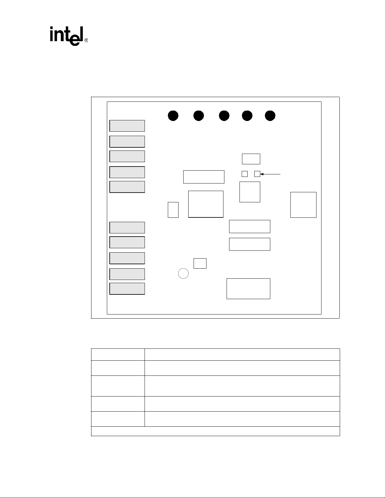
1.3.2 Component Location and Description
Figure 1 illustrates the top view of the IXD1110 demo board.
Figure 1. Intel
®
IXD1110 Demo Board (Top View)
IXD1110 Demo Board
GBIC SFP
Connectors
Port 0
Port 1
Port 2
Port 3
Port 4
Port 5
Port 6
Port 7
Port 8
Port 9
GND 1.8 V IXF 2.5 V IXF 3.3 V 2.5 V
JP1
J
T
A
G
ResetS1JP2
GND
Mictor Connector
Probe D
®
Intel
IXF1110
EPROM
FPGA
Mictor Connector
Probe C
Mictor Connector
Probe A
Intel® IXF1110
LEDs
SMB Connectors
SPI4-2
Connector
Table 1 provides a list of the various principal components found on the IXD1110 demo board.
Table 1. Intel® IXD1110 Demo Board Principal Components
Component Description
IX F1110
10-port Gigabit MAC that supports IEEE 802.3 1000 Mbps applications. Refer to the
IXF1110 Datasheet for additional information.
The IXF1110 uses a serial interface consisting of three signals to provide LED data to
IXF1110 LEDs
an external driver. This interface provides the data for 30 separate direct drive LEDs
and allows three LEDs per MAC port. Refer to Section 7.0, “LEDs” on page 19.
JP1
JP2
This jumper provides access to the JTAG test signals. Refer to Section 6.2, “JTAG
Test Signals” on page 18.
This reset jumper is required for proper board operation. Refer to Section 6.1, “Reset
Jumper JP2” on page 18 for more information.
1. For evaluation of the signals provided by the Mictor connector, use the corresponding logic analyzer probe.
Development Kit Manual 9
Document Number: 250807
Revision Number: 003
Revision Date: June 27, 2003
Page 10
IXD1110 Demo Board
Table 1. Intel® IXD1110 Demo Board Principal Components (Continued)
Component Description
S1 Reset Switch: This switch resets the entire board when pressed.
SPI4-2 Interface
Connector
Mictor Connectors A,
C, and D
GBIC Connectors These connectors allow for SFP modules (Agilent* HFBR-5710L).
FPGA
EPROM EPROM is used to program the FPGA.
1
1. For evaluation of the signals provided by the Mictor connector, use the corresponding logic analyzer probe.
Allows a loopback connection when the loopback module is installed. This connector
can also interface with alternate SPI4-2 connections.
Provide access to selected IXF1110 signals. Refer to Section 8.4, “Mictor Connectors”
on page 21 for more information.
Converts the IXF11110 asynchronous CPU signals into a synchronous format. Refer
to Section 4.1, “CPU FPGA” on page 14 for more information.
10 Development Kit Manual
Document Number: 250807
Revision Number: 003
Revision Date: June 27, 2003
Page 11

2.0 Quick Start
The quick-start procedure allows for IXF1110 1000 Mbps SerDes data transfer evaluation in the
following interfaces:
• IXF1110 SPI4-2 loopback data transfer
2
• I
C signals
• CPU interface
2.1 Setup
The following quick-start procedure uses the IXIA* 1600T packet generator to evaluate the
IXD1110 demo board. All ports on the IXF1110 are set to a default setting of 1000 Mbps
full-duplex (see Figure 2, “Typical Test Setup” on page 12).
1. Set reset jumper JP2 to the HRESET position.
2. Jumper pins 6 and 8 of JP1.
3. Install optic modules on all ten ports.
4. Connect the IXF1110 optic modules to the external ports on the IXIA* 1600T LM1000SX
cards.
5. Verify that the CPU daughter card is installed on the bottom of the board.
6. Verify that the SPI4-2 loopback module is connected to the SPI4-2 connector.
IXD1110 Demo Board
7. Connect the 1.8 V DC power supply to BN1 (“1.8 V IXF”).
8. Connect the 2.5 V DC power supply to BN4 (“2.5 V IXF”) and BN5 (“2.5 V”).
9. Connect the 3.3 V DC power supply to BN6 (“3.3 V”).
10. Connect all power supply return lines to ground BN3 (“GND”).
11. With the board properly configured, proceed in the following order:
a. Apply +1.8 V DC power
b. Apply +2.5 V DC power
c. Apply+3.3 V, DC power
d. Press reset switch S1
12. Once the CPU Daughter Card has completed autoboot, the board is ready for evaluation of
standard packets (64 - 1518 bytes) at 1000 Mbps full-duplex on all ports.
13. To access registers and RMON statistics, install the IXF1110 software. Instructions are
provided in Section 5.2, “Installing the IXF1110 Software” on page 16. This allows the user to
change the default settings of the IXF1110 and configure the device for other modes of
operation.
14. Proceed with evaluation as desired.
Note: The IXF1110 software modifies some of the IXF1110 registers on power-up. For a complete list of
registers modified, please refer to Section 4.2, “IXF1110 Register Modifications on Startup” on
page 14.
Development Kit Manual 11
Document Number: 250807
Revision Number: 003
Revision Date: June 27, 2003
Page 12
IXD1110 Demo Board
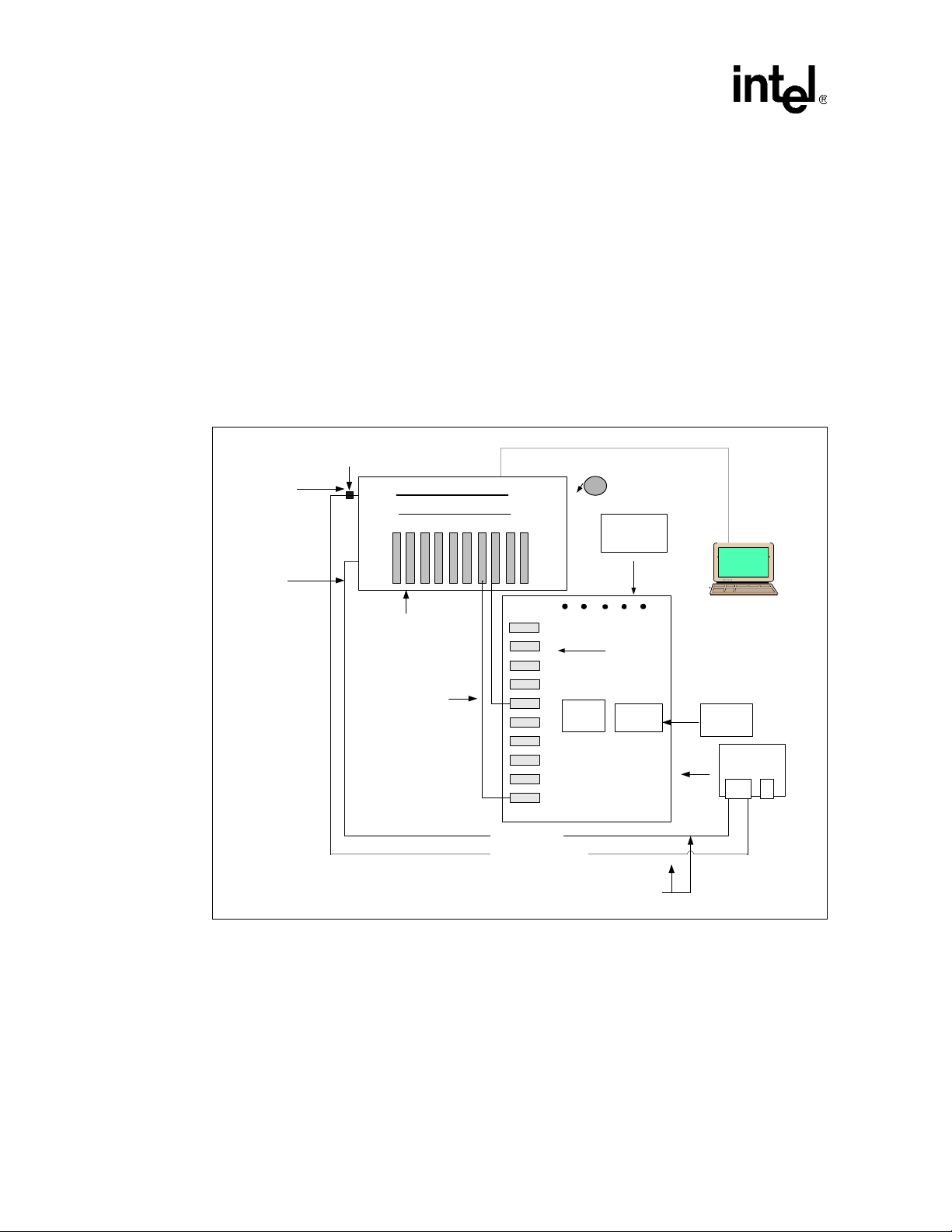
3.0 Typical Test Setup
Figure 2 shows a typical test setup for standard operation of the IXF1110 (see Section 2.0, “Quick
Start” on page 11 for step-by-step details). The IXD1110 demo board can be connected to an
IXIA* 1600T packet generator with LM1000SX cards for evaluation of the board. Each port can be
connected to the IXIA* box with fiber cables. For IXF1110 software use, connect CAT5-UTP
cables to the ports shown on the CPU daughter card. One of the cables connects to the COM port
on the IXIA* box by using a DB-9–to–RJ-45 connector. The other cable connects to the network
port on the IXIA* box. Refer to Figure 2 and Section 5.2, “Installing the IXF1110 Software” on
page 16 for proper installation.
Note: The IXF1110 evaluation software can be run from the IXIA or an added PC connected to the CPU
daughter card.
Figure 2. Typical Test Setup
Connect to
COM port
DB-9-to-RJ- 45
Connector
Connect To
Network Port
Advanced Multi-port Performance Tester
Fiber Connectors
IXIA* 1600T
Demo Software
Power
Supplies
Monitor
for IXIA
LM1000SX
Cards
Cables
Fiber
GBIC SFP
Modules
IXF1110
Intel® IXD1110
TCP/IP connection
UTP to Serial Connection
®
Intel
SPI4-2
Connector
Demo Board
CAT5 UTP
SPI4-2
Loop-back
CPU Daughter
Card
B1895
12 Development Kit Manual
Document Number: 250807
Revision Number: 003
Revision Date: June 27, 2003
Page 13

4.0 CPU Daughter Card
The IXD1110 demo board uses the Embedded Planet* RPX Classic LF (CLLF_BW31), a singleboard computer that uses the Motorola* MPC860 CPU. This card attaches to the underside of the
board and is used to interface with the IXF1110 CPU interface. Figure 3 provides a top-level view
of the CPU daughter card.
Figure 3. Intel
®
IXF1110 CPU Daughter Card
IXD1110 Demo Board
CPU Daughter
Card
IP Address located on
the side of the connector
RJ-45 #1 10Mbps
Ethernet Connection
RJ-45 #2 Serial
Connection
Not Used
The IXF1110 software requires the proper connections to the daughter card as follows:
Note: For full operation of the IXF1110 software, RJ-45 #1 and #2 (see Figure 3) must be connected to a
PC.
• RJ-45 #1 (10 Mbps Ethernet): Requires the following connection (this connection gives access
to the GUI):
— CAT5-UTP cable (connected to the CPU daughter card)
— Network port on a PC (connected to the CAT5-UTP cable), installed with IXF1110
software
• RJ-45 #2 (Serial): Requires a connection that gives access to the HyperTerminal interface of
the IXF1010 software (refer to Section 5.2, “Installing the IXF1110 Software” on page 16 for
complete setup information).
• Table 2 provides the DB-9–to–RJ-45 connector pinout for connection to a PC COM port.
Only three pins are used for the DB-9–to–RJ-45 connector.
Table 2. Pinout for DB-9–to–RJ-45 Connector
RJ-45 Pin Number DB-9 Pin Number
45
53
62
Development Kit Manual 13
Document Number: 250807
Revision Number: 003
Revision Date: June 27, 2003
Page 14

IXD1110 Demo Board
For more information on the HyperTerminal and GUI interfaces, please refer to the IXF1110
Software Help File.
4.1 CPU FPGA
The IXD1110 demo board has a Field Programmable Gate Array (FPGA) that allows the
Motorola* CPU, which requires a synchronous interface, to interoperate with the asynchronous
IXF1110 CPU interface.
For additional information regarding the IXF1110 CPU interface, refer to the IXF1110 Datasheet.
4.2 IXF1110 Register Modifications on Startup
The Motorola* CPU automatically modifies some of the IXF1110 registers on startup to put the
board in a 1000 Mbps evaluation mode. The following registers are modified from default settings
on startup:
• TX FIFO Highwater Mark Ports 0-9 are set to 0x00000BB8
• RX FIFO Errored Frame Drop Enable is set to 0x000003FF
• MAC Transfer Threshold Ports 0-9 are set to 0x000003E8
• Diverse Config Ports 0-9 are set to 0x0000112D
• LED Control is set to 0x00000003
For additional information on these registers, please refer to the IXF1110 Datasheet.
14 Development Kit Manual
Document Number: 250807
Revision Number: 003
Revision Date: June 27, 2003
Page 15

5.0 IXF1110 Software
The IXF1110 software allows access to the following register blocks through the Graphical User
Interface (GUI) or the Serial Monitor (HyperTerminal) interface:
• MAC Control
• MAC RX Statistics
• MAC TX Statistics
• Global Status and Configuration
• RX Block
• TX Block
• SPI4-2 Block
• SerDes Block
• GBIC Block
For additional information on all of the registers, please refer to the IXF1110 Datasheet or On-Line
Help.
IXD1110 Demo Board
Note: For help on using IXF1110 software, refer to the On-Line Help included in the software provided
with the IXD1110 demo board.
5.1 PC Requirements
The following is a list of the minimum PC requirements for installation of the IXF1110 software:
®
• Intel
• 128 MB RAM
• 16 MB Video Card
• Serial port
• Microsoft* Windows 98, 2000 operating system
Note: Microsoft* Windows 95, ME, NT, and XP have not been tested.
• Microsoft* Windows HyperTerminal
• 1024 x 768 minimum viewing resolution
Pentium® II 400 MHz or equivalent
Development Kit Manual 15
Document Number: 250807
Revision Number: 003
Revision Date: June 27, 2003
Page 16

IXD1110 Demo Board
5.2 Installing the IXF1110 Software
For proper installation of the IXF1110 software, follow these steps:
1. Verify that the CAT5-UTP cable is connected between the PC and the IXF1110 CPU daughter
card. This allows access to the GUI interface. Refer to Section 4.0, “CPU Daughter Card” on
page 13 for detailed installation instructions.
2. (Optional) The following connection is required to access the HyperTerminal interface:
— CAT5-UTP cable (connected to a CPU daughter card)
— DB-9–to–RJ-45 connector (connected to a CAT5-UTP cable)
— DB-9–to–RJ-45 connector (connected to a COM port on a PC installed with IXF1110
software)
For more information, refer to Section 4.0, “CPU Daughter Card” on page 13 for detailed
instructions.
3. Insert the CD into the PC.
4. If your system supports Autorun, follow the on-screen instructions.
5. If your system does not support Autorun, select Run... from the Start menu. The Run dialog
opens.
6. Select setup.exe from the CD in the Open: window (click Browse... to find setup.exe if not
already in the window).
7. Click OK.
8. Follow the on-screen instructions.
9. Locate the IXD1110 demo board IP address that is located on the CPU daughter card. The IP
address is required each time the GUI is opened.
10. Start the IXF1110 software GUI by double clicking the desktop icon.
Note: The IXF1110 software includes online documentation that describes how to run the GUI and
HyperTerminal interfaces. Refer to the quick-start section of the IXF1110 Demonstration Software
Help File for additional instructions on use of these interfaces.
5.3 Changing the IP Address of the CPU Daughter Card (Optional)
The CPU daughter card comes with a default IP address, which is listed on a sticker attached to the
daughter card. The GUI uses this IP address to locate the IXD1110 demo board. The IP address
may need to be changed depending on the PC or network to which the board is attached. Use the
following procedure to permanently change the IP Address of the CPU daughter card:
1. Ensure the IXD1110 demo board has been set up correctly (see Section 2.0, “Quick Start” on
page 11).
2. Open the HyperTerminal on the PC to which the CPU daughter card serial port is attached, and
configure the relevant COM port with the following settings:
• Speed: 9600 Baud
• Databits: 8
16 Development Kit Manual
Document Number: 250807
Revision Number: 003
Revision Date: June 27, 2003
Page 17

IXD1110 Demo Board
• Parity: None
• Stops bits: 1
• Flow Control: None
3. Press the reset button switch SW1. The following message appears on the HyperTerminal:
MPC8xx PlanetCore Boot Loader v2.00
Copyright 2001 Embedded Planet. All rights reserved.
DRAM available size = 16 MB
wvCV
DRAM OK
Autoboot in 2 seconds.
ESC to abort, SPACE or ENTER to go.
4. Press the ESC key to stop the Autoboot. The following message appears on the
HyperTerminal:
Autoboot aborted.
>
5. Type the following at the > prompt:
> set ip 10.254.21.34 (Changes the IP address to the value entered)
> store (Permanently changes the IP address)
> reset (Restarts the IXD1110 demo board)
Once the Autoboot is complete, the GUI can access the IXD1110 demo board using the newly
programmed IP address.
Development Kit Manual 17
Document Number: 250807
Revision Number: 003
Revision Date: June 27, 2003
Page 18

IXD1110 Demo Board
6.0 Optional Configurations
6.1 Reset Jumper JP2
6.1.1 Standard Operation
The Reset Jumper JP2 is required for standard operation of the IXD1110 demo board. Use the
HRESET position for standard operation.
The POR position is not recommended for standard operation of the IXD1110 demo board. This
configuration only affects the CPU operation, and does not affect IXF1110 operation. The only
difference between HRESET and POR is that POR also resets the CPU PLLs and state machines.
This difference is seen when reset is asserted by pressing switch S1. For more information on the
POR position of JP2, refer to Table 12 (MPC860 Reset Responses) of the Motorola* MPC860 CPU
Datasheet.
6.2 JTAG Test Signa ls
The boundary scan test port for the IXF1110 is accessed using JP1 for board-level testing. Table 3
describes JTAG test signals.
Note: For normal IXD1110 demo board operation, connect TRST_N pin 8 on JP1 to ground by
jumpering pins 6 and 8 of JP1.
Table 3. JTAG Test Signals (JP1)
Jumper
JP1
Pin
Number
2,4,6 GND – Connect to system ground
Symbol
1 TDI AC18 Test Data Input
3 TDO Y24 Test Data Output
5 TMS T16 Test Mode Select
7 TCLK AA29 Test Clock
8 TRST N18 Test Reset (jumper pins 6 and 8)
IXF1110 Ball
Designator
Description
18 Development Kit Manual
Document Number: 250807
Revision Number: 003
Revision Date: June 27, 2003
Page 19

7.0 LEDs
Table 4 describes the behavior of the Link LED - Amber, Link LED - Green, and Activity LED for
the IXF1110.
Table 4. IXF1110 LED Behavior
Type Status Description
IXD1110 Demo Board
Off
Amber On
RxLED
TxLED
NOTES:
1. The LED behavior table assumes the port is enabled in the Port Enable Register (Addr: 0x500) and the
LEDs are enabled in the LED Control Register (Addr: 0x509). If a port is not enabled, all the LEDs for that
port will be off. If the LEDs are not enabled, all of the LEDs will be off.
2. For a detailed description of the LED interface and register information, refer to the IXF1110 Datasheet.
Amber Blinking
Green On
Green Blinking
Off
Green Blinking
Synchronization has occurred but no packets are being
received and the Link LED Enable Register (Addr:
0x502) is not set.
RX Synchronization has not occurred or no optical
signal exists.
Port has remote fault and the LED Fault Disable
Register (Addr: 0x50B) is not set. Based on remote
fault bit setting received in Rx_Config word.
RX Synchronization has occurred and the Link LED
Enable Register (Addr: 0x502) bit is set.
RX Synchronization has occurred and port is receiving
data.
Port is not transmitting data or the Link LED Enable
Register (Addr: 0x502)” is not set.
Port is transmitting data and the Link LED Enable
Register (Addr: 0x502)” bit is set.
Development Kit Manual 19
Document Number: 250807
Revision Number: 003
Revision Date: June 27, 2003
Page 20

IXD1110 Demo Board
8.0 Test Points
8.1 Reset Test Points
Two test points allow evaluation of the IXF1110 reset signals. TP21 allows IXF1110 Sys_Res
signal monitoring. DTP3 allows board reset signal monitoring. The board Sys_Res
monitored on both test points if it is asserted by Switch S1 or the CPU. The reset is seen at TP21 if
an IXF1110 reset is issued by the software interface.
can be
Table 5. Intel
®
IXF1110 Reset Test Points
Test Point Symbol
TP21 Sys_Res
DTP3 Sys_Res
NOTE: DTP = Differential Test Point, TP = Test Point
IXF1110 Ball
Designator
Y4 System reset for IXF1110
– Board reset
8.2 IXF1110 Input Clock Test Points
The IXF1110 requires input clocks of 50 and 125 MHz. There are two test points that allow the
user to monitor those signals (see Tab le 6).
Table 6. Intel® IXF1110 Differential Input Clock Test Points
Test Point Symbol
DTP1 CLK125 AA5 125 MHz input clock for IXF1110
DTP2 CLK50 C21 50 MHz input clock for IXF1110
NOTE: DTP = Differential Test Point
IXF1110 Ball
Designator
8.3 GBIC Test Points
Description
Description
Table 7 lists GBIC test points that allow evaluation of the I2C clock, which is connected to all of
the GBIC modules, and the I
2
C Data pins for each of the ten ports. For more information on the I2C
interface, refer to the IXF1110 Datasheet.
Table 7. GBIC Test Points (Sheet 1 of 2)
Test Point Symbol
DTP6 I
DTP7 I
DTP8 I
DTP9 I
DTP10 I
NOTE: DTP = Differential Test Point
2
C_CLK L19 I2C_CLK for IXF1110
2
C_DATA_0 G22 I2C_DATA_0 for IXF1110
2
C_DATA_1 G23 I2C_DATA_1 for IXF1110
2
C_DATA_2 J24 I2C_DATA_2 for IXF1110
2
C_DATA_3 F22 I2C_DATA_3 for IXF1110
IXF1110 Ball
Designator
Description
20 Development Kit Manual
Document Number: 250807
Revision Number: 003
Revision Date: June 27, 2003
Page 21

Table 7. GBIC Test Points (Sheet 2 of 2)
IXD1110 Demo Board
Test Point Symbol
DTP11 I2C_DATA_4 E23 I2C_DATA_4 for IXF1110
2
DTP12 I
DTP13 I
DTP14 I
DTP15 I
DTP16 I
NOTE: DTP = Differential Test Point
C_DATA_5 H24 I2C_DATA_5 for IXF1110
2
C_DATA_6 G20 I2C_DATA_6 for IXF1110
2
C_DATA_7 E22 I2C_DATA_7 for IXF1110
2
C_DATA_8 G24 I2C_DATA_8 for IXF1110
2
C_DATA_9 F24 I2C_DATA_9 for IXF1110
IXF1110 Ball
Designator
8.4 Mictor Connectors
Table 8 provides a detailed list of the Mictor Connector test points that are available using Mictor
Connectors and that are designed for easy use with the Tektronix* P6434 Mass Termination Probe.
Using these connectors with a Tektronix* logic analyzer allows the probing of the signals in
Table 8.
Table 8. Mictor Connector Test Points (Sheet 1 of 2)
Probe ACPU Data
Bus
A0(0) uPx_Data0 B3 C0(0) TA – D0(0) –
A0(1) uPx_Data1 A4 C0(1) Start_XFER – D0(1) –
A0(2) uPx_Data2 B9 C0(2) RD/~WR – D0(2) –
A0(3) uPx_Data3 A7 C0(3) Gen_PCsN – D0(3) –
A0(4) uPx_Data4 C12 C0(4) – D0(4) –
A0(5) uPx_Data5 E11 C0(5) CsN – D0(5) –
A06) uPx_Data6 C13 C0(6) Bus_request – D0(6) –
A0(7) uPx_Data7 A8 C0(7) Bus_Busy – D0(7) –
A1(0) uPx_Data8 A10 C1(0) Bus_Grant – D1(0) –
A1(1) uPx_Data9 A9 C1(1) – D1(1) –
A1(2) uPx_Data10 E12 C1(2) uPx_RdyN C22 D1(2) –
A1(3) uPx_Data11 A11 C1(3) – D1(3) –
A1(4) uPx_Data12 G12 C1(4) uPx_CsN F20 D1(4) –
A1(5) uPx_Data13 E10 C1(5) uPx_WrN A18 D1(5) –
A1(6) uPx_Data14 F11 C1(6) uPx_RdN H14 D1(6) POR –
A1(7) uPx_Data15 D7 C1(7) – D1(7) HRESET –
A2(0) uPx_Data16 D14 C2(0) uPx_Add0 J1 D2(0) –
A2(1) uPx_Data17 C14 C2(1) uPx_Add1 G4 D2(1) –
A2(2) uPx_Data18 F14 C2(2) uPx_Add2 F3 D2(2) –
1. For evaluation of the signals provided by the Mictor connector, use the corresponding logic analyzer probe.
IXF1110
Ball
Designator
Probe
C
Address
Bus and
Other
Description
IXF1110
Ball
Designator
Probe
D
Pause I/F
and Reset
Signals
IXF1110
Ball
Designator
Development Kit Manual 21
Document Number: 250807
Revision Number: 003
Revision Date: June 27, 2003
Page 22

IXD1110 Demo Board
Table 8. Mictor Connector Test Points (Sheet 2 of 2)
Probe ACPU Data
A2(3) uPx_Data19 A12 C2(3) uPx_Add3 H1 D2(3) –
A2(4) uPx_Data20 A15 C2(4) uPx_Add4 E3 D2(4) –
A2(5) uPx_Data21 G13 C2(5) uPx_Add5 E2 D2(5) –
A2(6) uPx_Data22 B16 C2(6) uPx_Add6 G1 D2(6) –
A2(7) uPx_Data23 E15 C2(7) uPx_Add7 C3 D2(7) –
A3(0) uPx_Data24 G14 C3(0) uPx_Add8 F5 D3(0) –
A3(1) uPx_Data25 A16 C3(1) uPx_Add9 F1 D3(1) –
A3(2) uPx_Data26 C17 C3(2) uPx_Add10 C2 D3(2) –
A3(3) uPx_Data27 A17 C3(3) – D3(3)
A3(4) uPx_Data28 B18 C3(4) – D3(4)
A3(5) uPx_Data29 A21 C3(5) – D3(5)
A3(6) uPx_Data30 B22 C3(6) – D3(6)
A3(7) uPx_Data31 C23 C3(7) IRQ – D3(7)
CLK_
0
CLK_
1
1. For evaluation of the signals provided by the Mictor connector, use the corresponding logic analyzer probe.
Bus
Bus_CLK –
–Q1–
IXF1110
Ball
Designator
Probe
CLK_
3
Address
Bus and
C
Other
–Q0––
IXF1110
Ball
Designator
Probe
D
CLK_
2
Pause I/F
and Reset
Signals
TxPause
Add3
TxPause
Add2
TxPause
Add1
TxPause
Add0
TxPause
Fr
––
IXF1110
Ball
Designator
K1
J2
G2
G3
J7
8.5 Power and Ground Test Points
Table 9 provides the power and ground test points that allow the monitoring of voltages at various
points on the board.
Table 9. Power Test Points (Sheet 1 of 2)
Test Point Symbol Description
TP2 Vdd_1P8_IXF 1.8 V for IXF1110
TP3 Vdd_2P5_IXF 2.5 V for IXF1110
TP4 TxA25_A SerDes Tx Block A 2.5 V
TP5 PLL1_aVdd 1.8 V for PLL1
TP6 PLL2_aVdd 1.8 V for PLL2
TP8 PLL3_aVdd 2.5V for PLL3
TP9 TxA25_C SerDes Tx Block C 2.5 V
TP19 Vdd_2P5 2.5 V rest of the board
NOTE: TP = Test Point
22 Development Kit Manual
Document Number: 250807
Revision Number: 003
Revision Date: June 27, 2003
Page 23

Table 9. Power Test Points (Sheet 2 of 2)
Test Point Symbol Description
TP20 Vdd_3P3 3.3 V rest of the board
TP22 TxAVTT_A SerDes Tx Block A 1.8 V
TP23 TxAVTT_B SerDes Tx Block B 1.8 V
TP24 RxAVTT_C SerDes Rx Block C 1.8 V
TP25 RxA25_A SerDes Rx Block A 2.5 V
TP26 RxAVTT_A SerDes Rx Block A 1.8 V
TP27 TxA25_B SerDes Tx Block B 2.5 V
TP28 RxA25_B SerDes Rx Block B 2.5 V
TP29 RxAVTT_B SerDes Rx Block B 1.8 V
TP30 TxAVTT_C SerDes Tx Block C 1.8 V
TP31 RxA25_C SerDes Rx Block C 2.5 V
NOTE: TP = Test Point
Table 10 lists the various ground test points provided on the IXD1110 demo board.
IXD1110 Demo Board
Table 10. Ground Test Points
Test Point Symbol Description
TP10
TP11
TP12
TP13
TP14
TP15
TP16
TP17
NOTE: TP = Test Point
GND Ground Test Points
Development Kit Manual 23
Document Number: 250807
Revision Number: 003
Revision Date: June 27, 2003
Page 24

IXD1110 Demo Board
8.6 Unused Test Points
The unused test points are for internal testing only and are not designed for evaluation of the
IXF1110 device. Table 11 provides a list of the unused test points.
Table 11. Unused Test Points
Test Points Description
J29
J30
J31
J32
J33
J34
TP1
J29, J30, 31, J32, J33, J34, and TP1 are not
designated for IXF1110 evaluation
24 Development Kit Manual
Document Number: 250807
Revision Number: 003
Revision Date: June 27, 2003
Page 25

9.0 Board Schematics
D
C
B
A
Figure 4. Intel® IXD1110 Demo Board Power (Revision A1)
1
2
1
TP17
1
TP16
1
TP15
1
TP14
1
TP13
1
TP12
1
TP11
Ground Test Points
1
TP10
IXD1110 Demo Board
A1
of
13 14Friday, May 24, 2002
1
GND
Intel Communications Group
IXD1110 - FX DEMO Board
9750 Goethe Road
Sacramento, CA 95827
Title
Size Document Number Rev
Board Power
B
Date: Sheet
2
C261
1.0uF
+
Vdd_1P8_IXF
C260
+
C259
+
C266
3
C265
1
BN1
BANANA
Vdd_1P8_IXF - Digital 1.8V
GND
100uF
10uF
.001uF
0.1uF
C271
1.0uF
+
C270
Vdd_2P5_IXF
+
C269
+
C276
C275
1
BN4
BANANA
Vdd_2P5_IXF - Digital 2.5V
GND
100uF
10uF
.001uF
0.1uF
X = DO NOT INSTALL
3
Power: IXF1110
1
4
5
TP19
C274
1.0uF
+
C273
+
C272
+
C278
C277
BANANA
100uF
10uF
.001uF
0.1uF
BN3
GND
1
BANANA
GND
Vdd_2P5
1
BN5
Vdd_2P5 - Digital 2.5V
1
TP20
C281
1.0uF
+
GND
C280
Vdd_3P3
+
100uF
C279
10uF
+
C283
.001uF
C282
0.1uF
1
BN6
BANANA
Vdd_3P3 - Digital 3.3V
Vdd_3P3
Vdd_3P3 Caps
C290
C289
C288
C287
C286
C285
C284
0.01uF
0.01uF
0.01uF
0.01uF
0.01uF
0.01uF
0.01uF
4
5
GND
Power: GBIC & Board ICs
D
C
B
A
Development Kit Manual 25
Document Number: 250807
Revision Number: 003
Revision Date: June 27, 2003
Page 26

IXD1110 Demo Board
D
C
B
A
Figure 5. Intel® IXD1110 Digital Power
IXD1110 - FX DEMO Board
9750 Goethe Road
Sacramento, CA 95827
Title
Size Document Number Rev
C168
0.01uF
C166
0.01uF
C165
0.01uF
C164
0.01uF
C163
0.01uF
C162
0.01uF
C157
0.01uF
C156
0.01uF
A1
of
12 14Friday, May 24, 2002
1
IXF1110 Digital Power
B
Date: Sheet
2
X = DO NOT INSTALL
3
C194
0.01uF
C193
0.01uF
C192
1
P10
P12
P13
P15R2R6R9R11
R14
R16
R19
R23
T10
T15U4U8
U12
U13
U17
U21
M14
M17
M21N4N8
N11
N14
N17
2
M11
GND
N21
GND
GND
GND
GND
GND
GND
GND
GND
GND
GND
GND
GND
GND
GND
GND
GND
GND
GND
GND
GND
GND
GND
W2
W6
W10
W15
W19
W23
AA8
AA12
AA13
AA17
AC6
AC10
AC15
AC19
AB17
Y12
AB10
Y13
AC11
R10V2T9L6T8W7Y8
AB7
AC7
AA7
Y18
V13
V16
Y16
GND
GND
GND
GND
GND
GND
GND
GND
GND
GND
GND
GND
GND
GND
GND
GND
GND
GND
GND
GND
GND
GND
GND
GND
GND
GND
GND
GND
GND
GND
GND
GND
GND
AA14
GND
GND
GND
GND
GND
GND
GND
Digital Power (2.5 V)
Vdd2
Vdd2
Vdd2
Vdd2
Vdd2
Vdd2
Vdd2
Vdd2
Vdd2
Vdd2
Vdd2
Vdd2
Vdd2
Vdd2
Vdd2
Vdd2
Vdd2
Vdd2
Vdd2
Vdd2
Vdd2
Vdd2
Vdd2
Vdd2
Vdd2
Vdd2
Vdd2
Vdd2
Vdd2
Vdd2
Vdd2
Vdd2
Vdd2
Vdd2
Vdd2
Vdd2
Vdd2
Vdd2
Vdd2
Vdd2
Vdd2
Vdd2
Vdd2
Vdd2
Vdd2
Vdd2
Vdd2
Vdd2
Vdd2
Vdd2
Vdd2
Vdd2
GND
GND
GND
GND
GND
GND
GND
GND
GND
U1F
B4
1
TP3
Vdd_2P5_IXFVdd_1P8_IXF
3
F8
B8
D2
H2
H6
M2M6M9
J12
F12
B12
B13
B17
B21
D23
J13
F13
F17
H19
H23
N2N6N9
M12
M13
M16
M19
M23
U2
U6
W8
T12
T13
N12
N13
N16
N19
N23
U19
U23
AA2
AC4
W12
W13
W17
AA23
W5
AB6
AC8
AC12
AC13
AC17
AC21
GND
L3
T7
P1
U7
R1
R3
M3
AA3
0.01uF
C191
0.01uF
GND
C190
0.01uF
C189
0.01uF
GND
C188
0.01uF
Intel Communications Group
C187
0.01uF
C186
0.01uF
C185
0.01uF
C184
0.01uF
IXF1110
C183
0.01uF
C182
0.01uF
GND
C181
0.01uF
C180
0.01uF
C179
0.01uF
C155
C178
0.01uF
C177
0.01uF
GNDGND
C176
0.01uF
R1269 0
R1267 0
B6
B10
B15
B19D8D12
D13
D17F2F6
F10
F15
F19
F23H4H8
H12
H13
H17
H21
J10
J15K2K6K9K11
K14
K16
K19
K23
L10
L12
L13
L15M4M8D4D21
AA4
AA21
G10
Y15
D22
J23
J21
M18
K20
K24
L24
T23
P23
GND
GND
GND
GND
GND
GND
GND
GND
GND
GND
GND
GND
GND
GND
GND
GND
GND
GND
GND
GND
GND
GND
GND
GND
GND
GND
GND
GND
GND
GND
GND
GND
GND
GND
GND
GND
GND
GND
GND
GND
GND
GND
GND
GND
GND
GND
GND
GND
GND
4
Digital Power(1.8 V)
Vdd
Vdd
Vdd
Vdd
Vdd
Vdd
Vdd
Vdd
Vdd
Vdd
Vdd
Vdd
Vdd
Vdd
Vdd
Vdd
Vdd
Vdd
Vdd
Vdd
Vdd
Vdd
Vdd
Vdd
Vdd
Vdd
Vdd
Vdd
Vdd
Vdd
Vdd
Vdd
Vdd
Vdd
Vdd
Vdd
Vdd
Vdd
Vdd
Vdd
AA15
AA19
Vdd
J4
K3
E21
D11
AB4
R1139 10K
U1E
1
TP2
5
F4
D6
F21
D10
D15
D19
H10
D
L9
K4
K8
P9
R4
R8
J11
J14
L11
L14
L16
K17
K21
P11
P14
H15
P16
W4
T11
T14
R17
R21
U10
U15
AA6
W21
AA10
C
GND
Vdd
Vdd
GND
GND
GND
K5
D20
AB23
AB21
AC20
AD21
R1277 0
R1271 10K
R1273 10K
B
D5
C4
T21
P24
R24
V3
W3
GND
GND
GND
GND
GND
GND
GND
GND
GND
GND
GND
GND
GND
GND
GND
GND
GND
Y3
Y2
T17
T19
T18
P21
U16
W20
IXF1110
Vdd_2P5_IXF
C175
C174
C173
C172
C171
C170
C169
0.01uF
0.01uF
0.01uF
0.01uF
0.01uF
0.01uF
0.01uF
0.01uF
C153
0.01uF
C152
0.01uF
C151
0.01uF
C150
0.01uF
4
C148
0.01uF
C147
0.01uF
C145
0.01uF
IXF1110 - Power Caps
C144
0.01uF
C143
0.01uF
GND
Vdd_1P8_IXF
A
GND
5
26 Development Kit Manual
Document Number: 250807
Revision Number: 003
Revision Date: June 27, 2003
Page 27

Figure 6. Intel® IXD1110 Analog Power
5
3
D
C
B
A
1
U23B
IXD1110 Demo Board
A1
U23C
SN74LV08AD
8
3Y
3A
3B
9
10
6
2Y
2A
2B
4
5
SN74LV08AD
U23D
11
4Y
4A
4B
SN74LV08AD
12
13
GND
of
14 14Friday, May 24, 2002
1
2
3
U1G
TP22
1
1
FB9 1
Vdd_1P8_IXF
C132
0.01uF
4
TP4
TP5
Analog Power
C301
C300
Vdd_1P8_IXF
FB4 5.6
1
Block A
TxA25_A
TxAVTT_A PLL1_aVdd
P22
V18 D1
N22
0.01uF
0.01uF
GND
TP25
1
C134
0.01uF
GND
C133
0.1uF
TP6
E1
PLL1_aGND
PLL Power - 1.8 V
Serdes Power - 2.5V
RxA25_A
RxAVTT_A
P18
C309
TP26
1
FB13 1
C308
Vdd_1P8_IXF
C307
0.01uF
C136
0.01uF
C135
0.1uF
D24
PLL2_aGND
GND
Vdd_2P5_IXF
1
TP8
Vdd_1P8_IXF
1
FB5 5.6
E24
PLL2_aVdd
Block B Block C
TxA25_B
TxAVTT_B
RxAVTT_B
RxA25_B
V10
V11
V14
V15
C303
TP23
1
FB10 1
Vdd_1P8_IXF
C311
0.01uF
C302
0.01uF
0.01uF
TP28
1
0.01uF
0.01uF
GND
TP27
1
FB7 5.6
Y1
PLL3_aVdd
GND
C140
0.01uF
C139
0.1uF
TxA25_C
TxAVTT_C
P7
N3
TP29
1
FB16 1
Vdd_1P8_IXF
C313
0.01uF
AA1
RxA25_C
P3
V6
C315
C314
GND
PLL3_aGND
RxAVTT_C
0.01uF
0.01uF
TP9
GND
1
IXF1110
Vdd_1P8_IXF
TP24
TP31
TP30
1
Vdd_1P8_IXF
C142
1
Vdd_2P5_IXF
FB17 1
0.01uF
IXF1110 Analog Power
IXD1110 - FX DEMO Board
Intel Communications Group
9750 Goethe Road
Sacramento, CA 95827
B
Title
Size Document Number Rev
Date: Sheet
2
C305
0.01uF
GND
C304
0.01uF
FB11 1
0.01uF
C319
GND
0.01uF
FB18 1
C318
1
C317
0.01uF
C316
0.01uF
GND
X = DO NOT INSTALL
4
FB3 1
C131
0.01uF
Vdd_2P5_IXF
5
D
FB12 1
C306
0.01uF
Vdd_2P5_IXF
GND
FB14 1
C310
0.01uF
Vdd_2P5_IXF
GND
C
FB15 1
C312
0.01uF
Vdd_2P5_IXF
GND
Development Kit Manual 27
FB8 1
C141
Vdd_2P5_IXF
GND
0.01uF
GND
B
A
Document Number: 250807
Revision Number: 003
Revision Date: June 27, 2003
Page 28

IXD1110 Demo Board
D
C
B
A
Figure 7. Intel® IXD1110 Control
IXD1110 - FX DEMO Board
9750 Goethe Road
Sacramento, CA 95827
Title
Size Document Number Rev
3
1Y
1A
1B
U23A
1
2
A1
of
214Friday, May 24, 2002
1
IXF1110 - Control
B
Date: Sheet
2
X = DO NOT INSTALL
3
SN74LV08AD
+
+
|
DTP1
DIFF TP
LED_CLK 8
LED_CLK
reset_n 8,9
reset_n
LED_LATCH 8
uPx_RdyN 9,11
uPx_RdyN
LED_LATCH
HRESET 10,11
POR 10,11
HRESET
POR
I2C_CLK 3,4,5,6
I2C_CLK
CLK125
Vdd_3P3
C1 0.01uF
TxPauseFR
J7G3G2J2K1
TxPauseFr
4
VCC
E/D
U3
1
J21 SMB
R1 42
Vdd_3P3
TxPauseAdd0
TxPauseAdd3
TxPauseAdd1
TxPauseAdd2
TxPauseAdd0
TxPauseAdd1
TxPauseAdd2
TxPauseAdd3
234
1
3
CLK
GND
2
Vdd_3P3
R1266
5
SM7744DSV-125.0M
4.7k
R2 X
Vdd_2P5
R3
4.7k
IRQ
B11
B14
G15
RX_LOS_Int
MOD_DEF_Int
TX_FAULT_Int
GND GNDGND
GND
R7
R6
R5
R4
I2C_CLK
L19
I2C_CLK
CLK50
Vdd_3P3
10K
10K
10K
10K
+
|
DTP6
4
C2 0.01uF
U4
1
JTAG PORT
12
34
JP1
GND
DIFF TP
AC18
Y24
T16
TDI
TDO
VCC
E/D
56
TMS
LED_DATA 8
1
LED_DATA
IRQ 10,11
2
IRQ
3
DTP2
234
J22 SMB
R8 42
GND
78
HEADER 4X2
AA24
N18
TCLK
TRST
|
5
1
3
CLK
GND
SM7744HSV-50.0M
2
LED_CLK
LED_DATA
R9 50
A20
A19
LED_CLK
LED_DATA
DIFF TP
GND
R11 X
GND
LED_LATCH
K18
LED_LATCH
GND
GND
POWER
Vdd_3P3 Vdd_3P3
Vdd_3P3Vdd_3P3
TP21
CLK125
AA5
CLK125
HRESET
POR
123
JP2
SN74HC05
SN74HC05
DTP3
SN74HC05
C3
+
S1
10uF
+
RESET
HEADER 3
Note: this board
requires a jumper
|
DIFF TP
on JP2 to work
properly.
Intel Communications Group
GND
GND
reset_n
LED
R15
220
D1
LED
U5C
5 6
R377
10K
U5B
3 4
R14
10K
U5A
1 2
R13
10K
D2
LL4148
1
CLK50
C21
Y4
CLK50
Sys_Res
R1141
4
5
TxPauseAdd0
TxPauseAdd1
TxPauseFR
TxPauseAdd09,11
TxPauseFR9,11
TxPauseAdd19,11
uPx_CsN
uPx_WrN
uPx_CsN9,11
uPx_WrN9,11
TxPauseAdd3
TxPauseAdd2
TxPauseAdd29,11
TxPauseAdd39,11
uPx_RdN
uPx_RdN9,11
uP_Add7
uP_Add8
F5
C3
uPx_Add7
uPx_Add8
uPx_Add9
uP_Add9
uP_Add10
F1
C2
uPx_Add10
uP_Data0
B3A4B9
uPx_Data0
uPx_Data1
uPx_Data[31:0]9,10,11
GBIC
Interface
uP_Data1
uP_Data2
uPx_Data2
Pause
Control
uP_Add0
uP_Add1
uP_Add2
uP_Add3
uP_Add4
uP_Add5
J1
G4
uPx_Add0
uPx_Add1
uPx_Add[10:0]10,11
F3
E3
H1
uPx_Add3
uPx_Add2
uPx_Add4
uP_Add6
E2
G1
uPx_Add5
uPx_Add6
U1A
D
uP_Data3
uP_Data4
A7
E11
C12
uPx_Data5
uPx_Data4
uPx_Data3
CPU
Interface
uP_Data5
uP_Data6
uP_Data7
A8
C13
uPx_Data6
uPx_Data7
C
JTAG
uP_Data8
uP_Data9
A10A9E12
uPx_Data10
uPx_Data9
uPx_Data8
Interface
uP_Data10
uP_Data11
A11
uPx_Data11
uP_Data12
uP_Data13
uP_Data14
F11
E10
G12
uPx_Data14
uPx_Data13
uPx_Data12
uP_Data15
uP_Data16
uP_Data17
D7
D14
C14
uPx_Data17
uPx_Data16
uPx_Data15
LED
Interface
uP_Data18
uP_Data19
uP_Data20
F14
A12
A15
uPx_Data19
uPx_Data20
uPx_Data18
uPx_Data21
uP_Data21
uP_Data22
B16
E15
G13
uPx_Data22
uPx_Data23
uP_Data23
uP_Data24
uP_Data25
A16
C17
G14
uPx_Data25
uPx_Data26
uPx_Data24
uP_Data26
uP_Data27
uP_Data28
A17
B18
uPx_Data29
uPx_Data27
uPx_Data28
System
Interface
uP_Data29
uP_Data30
uP_Data31
A21
B22
C23
uPx_Data31
uPx_Data30
B
uP_Cs
F20
uPx_CsN
uP_Wr
A18
uPx_WrN
uP_Rd
H14
uPx_RdN
uP_Rdy
C22
R16 0
uPx_RdyN
U5D
9 8
IXF1110
U5E
SN74HC05
Vdd_2P5
11 10
U8K
SN74HC05
U5F
A
10K
13 12
IXF1110 Software
Reset
reset_n
138
IXF0_reset_n
EP1K30TC144-1-IXF-FX
SN74HC05
GND
28 Development Kit Manual
Document Number: 250807
Revision Number: 003
Revision Date: June 27, 2003
4
5
Page 29

Figure 8. Intel® IXD1110 SerDes GBIC Ports 0-2
5
3
D
C
B
A
1
IXD1110 Demo Board
A1
of
314Friday, May 24, 2002
1
I2C Data 0-2
I2C_DATA_0_IXF0
I2C_DATA_1_IXF0
U8B
I2C_DATA_2_IXF0
EP1K30TC144-1-IXF-FX
7
143
144
2
Vdd_3P3
1uH
L1
C6
0.1uF
3
Vdd_3P3
4
VccT
TX_Fault
TX_Disable
J1
2
3
18
R34
X
R33
4.7k
R32
4.7k
R31
4.7k
R30
4.7k
TD+
1uH
L2
GND
TD-
19
1
151617
20
VeeT
VccR
RD+
13
VeeT
VeeT
C8
+
C10
C7
+
C9
RD-
12
10uF
0.1uF
10uF
0.1uF
14
VeeR
VeeR
VeeR
MOD_DEF_2
MOD_DEF_1
45678
91011
VeeR
MOD_DEF_0
RX_rate
GND GND GND GND GND
RX_LOS
HFBR-5710L
Vdd_3P3
SerDes\GBIC - Ports 0-2
IXD1110 - FX DEMO Board
Intel Communications Group
9750 Goethe Road
Sacramento, CA 95827
B
Title
Size Document Number Rev
I2C_DATA_0
I2C_DATA_1
I2C_DATA_2
C18
151617
20
VeeT
VccR
RD+
13
10uF
+
C20
0.1uF
C17
10uF
+
C19
0.1uF
1
14
VeeT
VeeT
VeeR
VeeR
VeeR
MOD_DEF_2
MOD_DEF_1
RD-
45678
12
C13
10uF
TD+
1uH
L4
GND
TD-
19
151617
20
VeeT
VccR
RD+
13
+
C15
C12
+
C14
1
VeeT
VeeT
12
Vdd_3P3
1uH
L3
C11
0.1uF
VccT
TX_Fault
TX_Disable
J2
2
3
18
R40
X
R39
4.7k
R38
4.7k
R37
4.7k
R36
4.7k
14
VeeR
RD-
0.1uF
10uF
0.1uF
91011
VeeR
VeeR
VeeR
MOD_DEF_2
MOD_DEF_1
MOD_DEF_0
45678
RX_rate
RX_LOS
GNDGNDGNDGNDGND
HFBR-5710L
Vdd_3P3
Vdd_3P3
1uH
1uH
L6
L5
C16
0.1uF
GND
VccT
TX_Fault
TX_Disable
TD+
J3
R46
R45
R44
R43
R42
TD-
2
3
18
19
X
4.7k
4.7k
4.7k
4.7k
Date: Sheet
2
X = DO NOT INSTALL
GND GND GND GND GND
91011
VeeR
MOD_DEF_0
RX_rate
RX_LOS
HFBR-5710L
4
Mod_Def0
RxN0
U22
RxN0
DTP7
I2C_DATA_0
I2C_DATA_0
I2C_CLK
G22
N24
I2C_DATA_0
+
|
Rx_Los0
L22
MOD_DEF0
SerDes/GBIC - Port 0
DIFF TP
GND
Rx_Los0
IXF1110
R41
X
RxP1
Port 1
RxN1
U20
RxN1
I2C_CLK
I2C_DATA_1
G23
Y21
MOD_DEF1
I2C_DATA_1
|
DTP8
I2C_DATA_1 Mod_Def1
Rx_Los1
V17
Rx_Los1
SerDes/GBIC - Port 1
+
IXF1110
DIFF TP
GND
B
TxP1
TxN1
Tx_Fault1
RxP1
V23
M22
Y19
Y20
T20
TxP1
TxN1
TX_Fault_1
TX_Disable_1
U1I
C
TxN0
Tx_Fault0
TxP0
RxP0
R35
X
M24
K22
V20
V21
T22
TxP0
TxN0
RxP0
TX_Fault_0
TX_Disable_0
U1H
I2C_CLK
5
I2C_CLK2,4,5,6
Port 0
D
Development Kit Manual 29
TxP2
Tx_Fault2
TxN2
V22
W22
Y17
AC22
TxP2
TxN2
TX_Fault_2
TX_Disable_2
U1J
RxP2
R47
U24
RxP2
Port 2
X
RxN2
T24
RxN2
DTP9
A
I2C_DATA_2
I2C_CLK
Mod_Def2
J24
AA16
MOD_DEF2
I2C_DATA_2
+
|
I2C_DATA_2
Rx_Los2
AD18
Rx_Los2
SerDes/GBIC - Port 2
IXF1110
DIFF TP
GND
Document Number: 250807
Revision Number: 003
Revision Date: June 27, 2003
Page 30

IXD1110 Demo Board
D
C
B
A
Figure 9. Intel® IXD1110 SerDes GBIC Ports 3-5
1
A1
of
414Friday, May 24, 2002
1
I2C Data 3-5
I2C_DATA_3_IXF0
I2C_DATA_4_IXF0
U8C
I2C_DATA_5_IXF0
8
EP1K30TC144-1-IXF-FX
9
10
2
Vdd_3P3
1uH
1uH
L8
L7
C21
0.1uF
GND
3
Vdd_3P3
4
VccT
TX_Fault
TX_Disable
TD+
TD-
J4
2
3
18
R52
R51
R50
R49
R48
19
X
4.7k
4.7k
4.7k
4.7k
Tx_Fault3
TxN3
TxP3
151617
20
VccR
RD+
13
RxP3
VeeT
C23
10uF
+
C25
C22
+
C24
1
VeeT
VeeT
12
RxN3
0.1uF
10uF
0.1uF
14
VeeR
VeeR
MOD_DEF_2
RD-
45678
I2C_DATA_3
91011
VeeR
VeeR
MOD_DEF_1
MOD_DEF_0
I2C_CLK
Mod_Def3
GNDGND GND
GNDGND
RX_rate
RX_LOS
Rx_Los3
HFBR-5710L
Vdd_3P3
Vdd_3P3
1uH
L9
J5
R58
X
R57
4.7k
R56
4.7k
R55
4.7k
R54
4.7k
C26
VccT
TX_Fault
2
Tx_Fault4
0.1uF
TX_Disable
TD+
3
18
TxP4
19
TxN4
1uH
L10
GND
TD-
RxP4
1
151617
20
VeeT
VccR
RD+
13
VeeT
VeeT
C28
+
C30
C27
+
C29
RxN4
12
10uF
0.1uF
10uF
0.1uF
14
VeeR
RD-
45678
I2C_DATA_4
I2C_DATA_3
I2C_DATA_4
91011
VeeR
VeeR
VeeR
MOD_DEF_2
MOD_DEF_1
MOD_DEF_0
Mod_Def4
I2C_CLK
RX_rate
RX_LOS
Rx_Los4
I2C_DATA_5
GNDGND GND
GNDGND
HFBR-5710L
SerDes\GBIC - Ports 3- 5
IXD1110 - FX DEMO Board
Intel Communications Group
9750 Goethe Road
Sacramento, CA 95827
B
Title
Size Document Number Rev
Date: Sheet
C33
10uF
TD+
1uH
L12
GND
TD-
19
TxN5
151617
20
VeeT
VccR
RD+
13
RxP5
+
C35
0.1uF
C32
10uF
+
C34
0.1uF
1
91011
14
VeeT
VeeT
VeeR
VeeR
VeeR
VeeR
MOD_DEF_2
MOD_DEF_1
MOD_DEF_0
RD-
45678
12
I2C_DATA_5
Mod_Def5
I2C_CLK
RxN5
Vdd_3P3
1uH
L11
C31
0.1uF
VccT
TX_Fault
TX_Disable
J6
2
3
18
R64
X
Vdd_3P3
R63
4.7k
R62
4.7k
R61
4.7k
R60
4.7k
TxP5
Tx_Fault5
2
GNDGND GND
X = DO NOT INSTALL
GNDGND
3
RX_rate
RX_LOS
HFBR-5710L
4
Rx_Los5
AB12
U14
TX_Fault_4
TX_Disable_4
TxP4
AB11
TxN4
R59
AB13
RxP4
X
AB14
E23
RxN4
I2C_DATA_4
Port 4
AC14
MOD_DEF4
|
DTP11
I2C_DATA_4
AB15
SerDes/GBIC - Port 4
+
Rx_Los4
DIFF TP
B
IXF1110
GND
W11
U1M
R53
X
Y23
Y22
R15
U18
W24
V24
R12
F22
M20
TxP3
TxN3
RxP3
RxN3
TX_Fault_3
TX_Disable_3
U1K
I2C_CLK
5
I2C_CLK2,3,5,6
Port 3
D
I2C_DATA_3
|
DTP10
I2C_DATA_3
MOD_DEF3
SerDes/GBIC - Port 3
+
DIFF TP
Rx_Los3
IXF1110
GND
W14
U1L
C
AD12
AA18
TxP5
TX_Fault_5
TX_Disable_5
AD11
TxN5
R65
AD13
RxP5
X
AD14
H24
RxN5
DTP12
I2C_DATA_5
Port 5
A
U11
MOD_DEF5
I2C_DATA_5
+
|
DIFF TP
V12
Rx_Los5
SerDes/GBIC - Port 5
IXF1110
GND
30 Development Kit Manual
Document Number: 250807
Revision Number: 003
Revision Date: June 27, 2003
5
Page 31

Figure 10. Intel® IXD1110 SerDes GBIC Ports 6-8
5
3
D
C
B
A
1
IXD1110 Demo Board
A1
of
514Friday, May 24, 2002
1
I2C Data 6-8
I2C_DATA_6_IXF0
I2C_DATA_7_IXF0
U8D
111213
I2C_DATA_8_IXF0
EP1K30TC144-1-IXF-FX
2
Vdd_3P3
1uH
L13
C36
3
Vdd_3P3
4
VccT
TX_Fault
TX_Disable
J7
2
3
R70
X
R69
4.7k
R68
4.7k
R67
4.7k
R66
4.7k
Tx_Fault6
0.1uF
18
TxP6
TD+
TD-
19
TxN6
1uH
L14
GND
151617
VccR
RD+
13
RxP6
C38
10uF
+
C40
C37
+
C39
1
20
VeeT
VeeT
VeeT
12
RxN6
0.1uF
10uF
0.1uF
14
VeeR
VeeR
MOD_DEF_2
RD-
45678
I2C_DATA_6
91011
VeeR
VeeR
MOD_DEF_1
MOD_DEF_0
Mod_Def6
I2C_CLK
RX_rate
RX_LOS
Rx_Los6
GNDGND GND
GNDGND
HFBR-5710L
Vdd_3P3
Vdd_3P3
J8
R76
R75
R74
R73
R72
I2C_DATA_6
I2C_DATA_7
I2C_DATA_8
Intel Communications Group
C48
151617
20
VeeT
VccR
RD+
13
RxP8
10uF
+
C50
0.1uF
C47
10uF
+
C49
0.1uF
1
14
VeeT
VeeT
VeeR
VeeR
MOD_DEF_2
RD-
45678
12
I2C_DATA_8
I2C_CLK
RxN8
C43
10uF
+
C45
1uH
1uH
L16
C42
TD+
TxN7
GND
TD-
19
151617
20
VeeT
VccR
RD+
13
RxP7
+
C44
1
VeeT
VeeT
12
RxN7
L15
C41
0.1uF
VccT
TX_Fault
TX_Disable
2
3
18
X
4.7k
4.7k
4.7k
4.7k
TxP7
Tx_Fault7
0.1uF
10uF
0.1uF
14
VeeR
RD-
45678
I2C_DATA_7
91011
VeeR
VeeR
VeeR
MOD_DEF_2
MOD_DEF_1
MOD_DEF_0
I2C_CLK
Mod_Def7
RX_rate
RX_LOS
Rx_Los7
GNDGND GND
GNDGND
HFBR-5710L
Vdd_3P3
Vdd_3P3
1uH
1uH
L18
L17
C46
0.1uF
GND
VccT
TX_Fault
TX_Disable
TD+
J9
R82
R81
R80
R79
R78
TD-
2
3
18
19
X
4.7k
4.7k
4.7k
4.7k
TxN8
Tx_Fault8
TxP8
IXD1110 - FX DEMO Board
9750 Goethe Road
Sacramento, CA 95827
Title
Size Document Number Rev
GNDGND GND
GNDGND
91011
VeeR
VeeR
MOD_DEF_1
MOD_DEF_0
RX_rate
RX_LOS
HFBR-5710L
Mod_Def8
Rx_Los8
SerDes\GBIC - Ports 6-8
B
Date: Sheet
2
X = DO NOT INSTALL
4
R83
T3U3P8V7V5
TxP8
TxN8
RxP8
X
V4T2G24
RxN8
I2C_DATA_8
Port 8
A
R7
MOD_DEF8
SerDes/GBIC - Port 8
|
DTP15
I2C_DATA_8
Rx_Los8
+
IXF1110
DIFF TP
GND
R71
X
AB9
AC9W9U9
AB16
AC16Y9G20
T4
TxP6
TxN6
RxP6
RxN6
TX_Fault_6
I2C_CLK
5
I2C_CLK2,3,4,6
TX_Disable_6
U1N
Port 6
D
MOD_DEF6
I2C_DATA_6
DTP13
I2C_DATA_6
SerDes/GBIC - Port 6
|
Rx_Los6
+
IXF1110
DIFF TP
AC5
U1O
GND
C
Development Kit Manual 31
AD9
AA9
TX_Fault_7
TX_Disable_7
TxP7
AD10
TxN7
R77
AD16
RxP7
X
AD15
E22
RxN7
Port 7
AB2
MOD_DEF7
I2C_DATA_7
DTP14
AC3
Rx_Los7
SerDes/GBIC - Port 7
+
|
I2C_DATA_7
B
IXF1110
DIFF TP
TX_Fault_8
TX_Disable_8
U1P
GND
Document Number: 250807
Revision Number: 003
Revision Date: June 27, 2003
Page 32

IXD1110 Demo Board
D
C
B
A
Figure 11. Intel® IXD1110 SerDes GBIC Port 9
1
A1
of
614Friday, May 24, 2002
1
I2C Data 9
I2C_DATA_9_IXF0
U8E
2
Vdd_3P3
3
R88
Vdd_3P3
R87
R86
R85
4
R84
C53
10uF
+
C55
0.1uF
10uF
0.1uF
14
VeeR
RD-
45678
91011
VeeR
VeeR
VeeR
MOD_DEF_2
MOD_DEF_1
MOD_DEF_0
RX_rate
RX_LOS
GNDGNDGND
GND GND
HFBR-5710L
1uH
1uH
L20
C52
TD+
GND
TD-
19
151617
20
VeeT
VccR
RD+
13
+
C54
1
VeeT
VeeT
12
L19
C51
0.1uF
VccT
TX_Fault
TX_Disable
J10
2
3
18
X
4.7k
4.7k
4.7k
4.7k
14
I2C_DATA_9
I2C_CLK_IXF0
142
I2C_CLK
EP1K30TC144-1-IXF-FX
SerDes/GBIC Port 9
IXD1110 - FX DEMO Board
Intel Communications Group
9750 Goethe Road
Sacramento, CA 95827
B
Title
Size Document Number Rev
Date: Sheet
2
X = DO NOT INSTALL
3
4
TxN9
Tx_Fault9
TxP9
RxP9
T5U5L2
L4
Y6
TxP9
TxN9
I2C_CLK
5
I2C_CLK2,3,4,5
D
TX_Fault_9
TX_Disable_9
U1Q
RxN9
R89
X
Y5P2F24
RxP9
Port 9
I2C_DATA_9
RxN9
I2C_DATA_9
DTP16
I2C_CLK
Mod_Def9
L1
MOD_DEF9
+
|
I2C_DATA_9
C
Rx_Los9
Rx_Los9
SerDes/GBIC - Port 9
DIFF TP
GND
IXF1110
B
A
32 Development Kit Manual
Document Number: 250807
Revision Number: 003
Revision Date: June 27, 2003
5
Page 33

Figure 12. Intel® IXD1110 SPI4-2
D
C
B
A
1
IXD1110 Demo Board
A1
of
714Friday, May 24, 2002
1
2A2B2G1A1B
5242325141
TDat_P_9
TDat_N_9
2A2B2G1A1B
22
12221
TDat_P_0
TDat_N_0
TDat_N_7
TDat_P_7
TDat_P_7
TDat_N_7
TDat_N_3
TDat_P_3
11
TDat_N_5
TDat_P_5
TDat_P_6
TDat_P_6
1G
31
1G
1
TDat_N_6
TDat_P_5
TDat_N_6
HM-Zd-40(P)
GND
HM-Zd-40(P)
GND
TDat_P_4
TDat_N_5
TDat_P_5
TDat_P_4
TDat_N_5
40A
J28D
120
RDat_P_4
RDat_N_4
30A
J28C
9080708979
RDat_P_0
RDat_N_0
TDat_N_4
TDat_P_3
TDat_N_4
40B
40G
110
100
RDClk_P
30B
30G
RDat_P_2
TDat_N_3
TDat_P_3
TDat_N_3
39A
39B
119
109
RDClk_N
29A
29B
RDat_N_2
TDat_P_2
TDat_P_2
38A
39G
99
118
RDat_P_9
RDat_N_9
28A
29G
8878688777
69
RDat_N_7
RDat_P_7
TDat_P_1
TDat_N_2
TDat_N_2
38B
38G
10898117
28B
28G
TDat_N_1
TDat_P_1
TDat_N_1
RDat_P_10
RDat_P_14
37A
37B
37G
97
107
RDat_N_10
27A
27B
27G
67
RDat_N_14
TDat_N_0
TDat_P_0
J6
J5
TDat_P_0
TDat_N_0
36A
36B
116
10696115
RDat_P_12
RDat_N_12
26A
26B
8676668575
RDat_N_13
RDat_P_13
TCtl_P
33B
33A
34A
34B
34G
36G
35A
35B
35G
94
95
103
113
114
104
105
TSClk
TDat_P_6
TDat_N_6
TDat_P_10
TDat_N_10
23B
23A
24A
24B
24G
26G
25A
25B
25G
64
65
TDat_P_11
TDat_N_11
TDat_N_14
TDat_P_14
TCtl_N
TCtl_P
TSTAT1
R150 0
TDClk_P
TCtl_N
TDClk_N
M10D3E4E6E5
N10
TCTL_P
TCTL_N
TDClk_P
TDClk_N
33G
93
23G
6373838474
TSTAT1
3G3B3A4A4B
TDat_P_13
RCtl_N
16625
RDat_N_15
TDat_P_15
TDat_P_11
TDat_N_11
TDat_P_11
TDat_N_11
5G
35
TDat_P_12
TDat_N_13
5G
5
15
TDat_N_15
TDat_P_8
TDat_P_10
TDat_N_10
TDat_P_10
TDat_N_10
4G
34
TDat_N_12
TDat_P_4
4G
4
14
TDat_N_8
TDClk_P
TDat_N_9
TDat_P_9
TDat_P_9
TDat_N_9
3343535444
TDat_N_4
3G3B3A4A4B
3
132324
TDClk_N
TDat_P_8
TDat_N_8
TDat_P_8
TDat_N_8
6A6B6G5A5B
8A8B8G7A7B
9G
5848385747
39
RDat_P_6
RDat_N_5
9G
9
28
RSClk
RDat_N_1
TDat_P_14
TDat_N_14
TDat_P_14
TDat_N_14
RDat_P_8
RDat_N_6
8A8B8G7A7B
18827
RDat_P_11
TDat_N_13
TDat_P_13
TDat_P_13
TDat_N_13
7G
5646365545
37
RCtl_P
RDat_N_8
6A6B6G5A5B
7G
7
26
17
RDat_P_15
RDat_N_11
TDat_P_12
TDat_N_12
TDat_P_12
TDat_N_12
10A
10B
10G9A9B
J28B
6050405949
2
3
RDat_N_3
RDat_P_3
RDat_P_5
10A
10B
10G9A9B
J28A
3020102919
RSTAT0
RSTAT1
RDat_P_1
TDat_N_15
TDat_P_15
G11C9J9H7E8E9B7L5C7L8G5F7G9B5H3
H11D9K10J8E7F9C8M5C6L7H5G6H9C5J3
TDat_P_15
TDat_N_15
32A
32B
32G
112
10292111
TDat_P_7
TDat_N_7
22A
22B
22G
8272628171
TSTAT0
TSTAT1
TSClk
TSTAT0
R152 0
R151 0
C11
TSClk
TSTAT0
31A
31B
101
TDat_P_2
TDat_N_2
21A
21B
TDat_P_1
TDat_N_1
31G
91
21G
61
HM-Zd-40(P)
GNDGND
HM-Zd-40(P)
IXF1110 SPI-4 Phase 2
IXD1110 - FX DEMO Board
Intel Communications Group
9750 Goethe Road
Sacramento, CA 95827
B
Title
Size Document Number Rev
Date: Sheet
2
X = DO NOT INSTALL
3
SPI-4 Phase 2 - TX
U1B
4
RDat_N_15
RDat_P_15
K12
K13
RDat_P_15
RDat_N_15
RDat_P_14
RDat_N_14
F16
G16
RDat_P_14
RDat_N_14
RDat_N_13
RDat_P_13
E13
E14
RDat_P_13
RDat_N_13
RDat_N_12
RDat_P_12
A13
A14
RDat_P_12
RDat_N_12
RDat_P_11
RDat_N_11
J16
K15
RDat_P_11
RDat_N_11
RDat_N_10
RDat_P_10
G17
G18
RDat_P_10
RDat_N_10
RDat_P_9
RDat_N_9
D18
E18
RDat_P_9
RDat_N_9
RDat_P_8
RDat_N_8
C16
D16
RDat_P_8
RDat_N_8
RDat_P_7
RDat_N_7
M15
N15
RDat_P_7
RDat_N_7
RDat_P_6
RDat_N_6
E16
E17
RDat_P_6
RDat_N_6
RDat_P_5
RDat_N_5
L17
L18
RDat_P_5
RDat_N_5
RDat_P_4
RDat_N_4
J18
J19
RDat_P_4
RDat_N_4
RDat_P_3
RDat_N_3
G21
H20
RDat_P_3
RDat_N_3
RDat_P_2
RDat_N_2
F18
G19
RDat_P_2
RDat_N_2
RDat_P_1
RDat_N_1
B20
C20
RDat_P_1
RDat_N_1
RDat_N_0
RDat_P_0
E19
E20
RDat_P_0
RDat_N_0
RCtl_P
H16
RCTL_P
RCtl_N
H18
RCTL_N
RDClk_N
RDClk_P
C18
C19
RDClk_P
RDClk_N
RSTAT1
J20
RSTAT1
RSTAT0
L20
RSClk
RSTAT0
IXF1110
4
J17
RSClk
U1C
5
D
C
SPI-4 Phase 2 - RX
B
IXF1110
A
Development Kit Manual 33
Document Number: 250807
Revision Number: 003
Revision Date: June 27, 2003
5
Page 34

IXD1110 Demo Board
5
3
D
C
B
A
Figure 13. Intel® IXD1110 LEDs
A1
84.5
LED
D15
R168
Vdd_2P5
R167
R166
R165
R164
R163
R162
84.5
LEDA
D14
84.5
LED
D13
84.5
LED
D12
84.5
84.5
84.5
84.5
LEDA
D11
LED
D10
LED
D9
1
2
RxLEDG_5
TxLEDG_5
RxLEDA_6
RxLEDG_6
TxLEDG_6
RxLEDA_7
RxLEDG_7
TxLEDG_7
1512345679
QF
QA
QB
QE
QC
QD
QG
LED2_DATA_0
QH
QH
Vdd_2P5
R185
R184
R183
R182
R181
R180
R179
R178
84.5
84.5
84.5
84.5
84.5
84.5
84.5
84.5
LED
D16
R169
D32
D31
D30
D29
D28
D27
D26
D25
LEDA
LED
LED
LEDA
LED
LED
LEDA
LED
RxLEDA_0
RxLEDG_0
TxLEDG_0
RxLEDA_1
RxLEDG_1
TxLEDG_1
RxLEDA_2
RxLEDG_2
1512345679
QF
QA
QB
QE
QC
QD
QH
QG
QH
IXF1110 Ports 0-9 LEDs
IXD1110 - FX DEMO Board
Intel Communications Group
9750 Goethe Road
Sacramento, CA 95827
B
Title
Size Document Number Rev
of
814Friday, May 24, 2002
1
Date: Sheet
2
X = DO NOT INSTALL
SER
SRCLK
SRCLR
RCLK
G
U11
1411101213
LED_CLK
reset_n
LED1_DATA_0
LEDA
3
LED_DATA
LED_CLK
LED_CLK2
LED_DATA2
Vdd_2P5
reset_n
reset_n2,9
LED_LATCH
LED_LATCH2
4
5
R161
R160
R159
R158
R157
R156
D8
84.5
LED
D7
84.5
LED
D6
84.5
LEDA
D5
84.5
LED
D4
84.5
LED
D3
84.5
RxLEDG_9
TxLEDG_9
1512345679
QA
QB
QC
SER
SRCLK
U10
1411101213
LED_DATA
reset_n
LED_CLK
LED_LATCH
TxLEDG_8
RxLEDA_9
QE
QD
SRCLR
LED_LATCH
RxLEDA_8
RxLEDG_8
QF
QH
QG
RCLK
G
MM74HC595M
GND
R364
22
R363
22
LED1_DATA_0
QH
MM74HC595M
GND
R362
22
R361
22
C295
C294
C293
C292
10pF
10pF
10pF
10pF
GND
D24
R177
Vdd_2P5
R176
R175
R174
R173
R172
R171
R170
84.5
D23
84.5
D22
84.5
D21
84.5
D20
84.5
D19
84.5
D18
84.5
D17
84.5
GND
GND
GND
U13
LED
LEDA
LED
LED
LEDA
LED
LED
LEDA
U12
SER
SRCLK
SRCLR
RCLK
G
1411101213
LED_LATCHLED_LATCH
LED_CLK
LED3_DATA_0
reset_n
TxLEDG_2
RxLEDA_3
RxLEDG_3
TxLEDG_3
RxLEDA_4
RxLEDG_4
TxLEDG_4
RxLEDA_5
1512345679
QF
QA
QB
QE
QC
QD
QH
QG
SER
SRCLK
SRCLR
RCLK
G
1411101213
LED2_DATA_0
LED_CLK
reset_n
MM74HC595M
GND
R368
22
R367
22
LED3_DATA_0
QH
MM74HC595M
GND
R366
22
R365
22
C299
C298
C297
C296
10pF
10pF
10pF
10pF
GND
GNDGND
4
GND
D
34 Development Kit Manual
C
B
A
Document Number: 250807
Revision Number: 003
Revision Date: June 27, 2003
Page 35

Figure 14. Intel® IXD1110 CPU Interface Control
D
C
B
A
IXD1110 Demo Board
IXD1110 - FX DEMO Board
9750 Goethe Road
Sacramento, CA 95827
Title
Size Document Number Rev
6
nCASC
GND
5
EPC1PC8
GND
5
NC7SZ125M5
GND
A1
of
914Friday, May 24, 2002
1
CPU I/F Control
B
Date: Sheet
2
GND
X = DO NOT INSTALL
3
4
5
C109
0.22uF
+
GND
1
61525405258668493
GND
GND
GND
Power
VCC_CKLK
U8J
5316507585
Vdd_2P5
2
3
4
5
Vdd_3P3
R219
R218
R217
R216
104
56
GND
GND
GND
GND
GND
GND
GND
GND
+2.5V
VCCINT
VCCINT
VCCINT
VCCINT
VCCINT
VCCINT
103
127
1K
1K
1K
1K
105341
4
TDI
TCK
TMS
TDO
IXF1110 & CPU Interfaces
U8A
10K
R220
Vdd_3P3
1
TP1
D
123
129
1395739
124
126
GND
GND
Vdd_3P3
BUS_CLK 10,11
BUS_CLK
5569726570686779787380818283868788899091929596979899100
GND
GND
bus_clk
GND
VCCIO
VCCIO
5
2445617194
Start_XFER 10,11
RD/~WR 10,11
TA 10,11
Start_XFER
RD/~WR
Bus_Busy
TA
TS_n
TA_n
RD_WR_n
426059
NC
GND_CKLK
+3.3V
VCCIO
VCCIO
VCCIO
Bus_Busy 10,11
Bus_Request 10,11
Bus_Grant 10,11
Bus_Grant
Bus_Request
Bus_busy_n
Bus_grant_n
Bus_request_n
128
136
137
NCNCNCNCNCNCNC
VCCIO
VCCIO
VCCIO
115
134
R116 0
GENP_CsN 10,11
CsN 10,11
GENP_CsN
CsN
IXF_Sel
IXF_CsN
GenP_CsN
141
EP1K30TC144-1-IXF-FX
GND
uPx_Data[31:0] 2,10,11
uPx_Data8
uPx_Data1
uPx_Data0
uPx_Data3
uPx_Data4
uPx_Data2
uPx_Data9
uPx_Data7
uPx_Data5
uPx_Data6
cpu_DATA0
cpu_DATA1
cpu_DATA2
cpu_DATA3
cpu_DATA4
cpu_DATA5
cpu_DATA6
cpu_DATA7
cpu_DATA8
CPU Bus Interface
uPx_Data11
uPx_Data10
cpu_DATA9
cpu_DATA10
cpu_DATA11
IXF1110 Interface
nCONFIG
CONF_DONE
nSTATUS
DCLK
DATA0
nCEO
MSEL0
MSEL1
nCE
uPx_RdyN_1
uPx_RdyN_0
uPx_RdN
uPx_WrN
uPx_CsN_0
74235
CONF_DONE
nSTATUS
nCONFIG
107
DCLK
108
DATA0
3
77
76
Vdd_3P3
106
R1264
Vdd_3P3
17
GND
1K
uPx_RdyN
R1265
22
uPx_RdyN2,11
1K
C
202118
R223 50
R222 50
uPx_RdN
uPx_WrN
uPx_WrN2,11
uPx_RdN2,11
uPx_CsN_1
19
R224 50
uPx_CsN
uPx_CsN2,11
uPx_Data12
uPx_Data15
uPx_Data14
uPx_Data13
cpu_DATA12
cpu_DATA13
cpu_DATA14
cpu_DATA15
IXF0_TxPauseFR
135
R226 50
TxPauseFR
TxPauseFR2,11
uPx_Data17
uPx_Data16
101
cpu_DATA16
IXF0_TxPauseAdd0
133
132
R227 50
R228 50
TxPauseAdd0
TxPauseAdd1
TxPauseAdd02,11
C113
C108
+
C112
C107
+
C111
C106
+
Vdd_2P5 Vdd_3P3
FPGA Caps
uPx_Data18
uPx_Data21
uPx_Data19
uPx_Data25
uPx_Data23
uPx_Data20
uPx_Data24
uPx_Data22
102
109
110
111
112
113
114
116
cpu_DATA17
cpu_DATA18
cpu_DATA19
cpu_DATA20
cpu_DATA21
cpu_DATA22
cpu_DATA23
cpu_DATA24
IXF0_TxPauseAdd1
IXF0_TxPauseAdd2
IXF0_TxPauseAdd3
IXF1_TxPauseFR
4143444647
131
130
R229 50
R230 50
TxPauseAdd2
TxPauseAdd3
TxPauseAdd12,11
TxPauseAdd22,11
TxPauseAdd32,11
C117
0.22uF
0.022uF
+
C121
0.22uF
0.022uF
C116
0.22uF
0.022uF
+
C120
0.22uF
0.022uF
C115
0.22uF
0.022uF
+
C119
0.22uF
0.022uF
C114
0.22uF
C110
0.022uF
+
C118
0.022uF
uPx_Data26
uPx_Data30
uPx_Data28
uPx_Data27
uPx_Data29
uPx_Data31
117
118
119
120
121
122
cpu_DATA25
cpu_DATA26
cpu_DATA27
cpu_DATA28
cpu_DATA29
cpu_DATA30
cpu_DATA31
IXF1_TxPauseAdd0
IXF1_TxPauseAdd1
IXF1_TxPauseAdd2
IXF1_TxPauseAdd3
B
J25 SMB
234
GND
Vdd_3P3Vdd_3P3
reset_n 2,8
reset_n
54
reset
clk_in
I2C_CLK_IXF0_OUT
EP1K30TC144-1-IXF-FX
125
140
R378 50
R360
10K
1
5
Intel Communications Group
R237
R236
GND GND
0.01uF
10K
10K
C291
U22
8
7
U18
0.01uF
5
123 4
GND
1
DATA
VCC
VCC
OE
3
nSTATUS DATA0
234
J26 SMB
GND
VCC
OE
A
I2C_CLK_OUT
DCLK
2
DCLK
nCS
4
CONF_DONE
1
I2C_CLK_BUF
R358 50
GND Y
A
C122
Vdd_3P3
Development Kit Manual 35
Document Number: 250807
Revision Number: 003
Revision Date: June 27, 2003
Page 36

IXD1110 Demo Board
D
C
B
A
Figure 15. Intel® IXD1110 CPU Connectors
A1
of
10 14Friday, May 24, 2002
1
CPU Connectors
IXD1110 - FX DEMO Board
B
Title
Size Document Number Rev
Date: Sheet
2
X = DO NOT INSTALL
3
uPx_Add7
uPx_Add9
A28
A27
A26
A20
A225VA24
A19
A21
A235VA25
B28
B27
B26
uPx_Add8
uPx_Add6
uPx_Add10
uPx_Add1
uPx_Add5
uPx_Add3
A25
A24
A23
A26
B25
B24
B23
uPx_Add2
uPx_Add4
A28
A27
uPx_Add0
uPx_Data[31:0] 2,9,11
uPx_Data27
uPx_Data25
uPx_Data31
uPx_Data29uPx_Data30
A22
A21
A20
A19
A18
A17
A16
5V
D0D2D4
D6
A30
GND
A29
A315VD1D3D5D7GNDD9D11
B22
B21
B20
B19
B18
B17
B16
uPx_Data24
uPx_Data28
uPx_Data26
uPx_Data[31:0]2,9,11
uPx_Data19
uPx_Data21
uPx_Data23
A15
A14
A13
D8
D10
D12
B15
B14
B13
uPx_Data22
uPx_Data20
uPx_Data17
uPx_Data11
uPx_Data15
uPx_Data13
uPx_Data9
A12
A11
A10A9A8A7A6A5A4A3A2
D14
D16
D18
D20
GND
D13
D15
GND
D17
D19
B9B8B7B6B5B4B3B2B1
B12
B11
B10
uPx_Data16
uPx_Data12
uPx_Data18
uPx_Data14
uPx_Data10
uPx_Data7
D22
GND
D21
D23
uPx_Data8
uPx_Data5
uPx_Data3
D24
D26
D28
GND
D25
D27
uPx_Data6
uPx_Data4
uPx_Data1
A1
D30
DL_DX_L
D29
D31
uPx_Data2
uPx_Data0
Intel Communications Group
9750 Goethe Road
Sacramento, CA 95827
AMP_179031-5_P1
GND
A36
B36
GND
CS7
A35
A34
A8
A10
GNDA9A11
B35
B34
uPx_Add[10:0] 2,11
A33
A32
A31
A30
A29
A12
A14
A16
A18
GND
A13
A15
GND
A17
B33
B32
B31
B30
B29
uPx_Add[10:0]2,11
RD/~WR 9,11
1
RD/~WR
A60
WE0
HRESET
B60
R238 50
A59
A58
A57
A55
A56
A54
A53
A52
WE2
GND
GND
BSA0
BSA2
GPLA0
GPLA2
RD/~WR
WE1
WE3
BSA1
BSA3
GND
GPLA1
GPLA3
GPLA5
B59
B58
B57
B56
B55
B54
B53
B52
HRESET
HRESET2,11
GND
P1A
2
C130
0.01uF
C129
0.01uF
C128
0.01uF
Vdd_3P3
FB1
FB2
FAIR-RITE
FAIR-RITE
C127
C126
C125
0.01uF
0.01uF
0.01uF
3
A51
A50
A49
A48
5V
BDIP
BURST
BADDR28
GND
BADDR29BI5VBGTSIZ15VBB
B51
B50
B49
B48
Bus_Request 9,11Bus_Grant9,11
Start_XFER
Bus_Request
A47
A46
A45
A44
5V
BR
TSIZ0_REG
B47
B46
B45
B44
R240 50
Bus_Busy
Bus_Grant
Start_XFER 9,11
TA 9,11
GENP_CsN 9,11
GENP_CsN
TA
R243 50
A43
A42
A41
A40
A39
A38
A37
TS
TA
CS0
CS2
CS4
CS6
GND
RETRY
TEA
GND
CLKOUT
GND
CS1
CS3
CS5
B43
B42
B41
B40
B39
B38
B37
R245 50
CsN
BUS_CLK
CsN9,11
BUS_CLK9,11
Bus_Busy9,11
C124
0.01uF
0.01uF
A60
A59
A0A2A4
GND
POR
GNDA1A3A5A7
B60
B59
POR2,11
A58
B58
A57
B57
A55
A56
A54
A6
AT0/MII_CRS
B56
B55
B54
IRQ 2,11
A53
A52
A51
A50
IRQ0
IRQ2
DP0/IRQ3
DP2/IRQ5
AT2/MII_TXEN
AT1/MII_MDIO
DP1/IRQ4
DP3/IRQ6
AT3/MII_COL
IRQ1
B53
B52
B51
B50
GND
A49
A48
A47
A46
A45
A44
A43
A42
A41
A40
A39
A38
A37
A36
A35
A34
A33
A32
A31
A30
A29
A28
A27
A26
A25
A24
A23
A22
A21
A20
A19
A18
A17
A16
A15
A14
A13
A12
A11
PE0
GND
IRQ3
GND
B49
B48
PD8
PD6
GND
GND
PD14
PD12
PD15
GND
PD13
GND
B47
B46
B45
B44
PD4
GND
GND
GND
GND
PD10
PD11
GND
PD9
GND
PD7
GND
PD5
GND
B43
B42
B41
B40
B39
B38
B37
B36
C
5V
PC8
PC6
PC4
GND
GND
PC14
PC12
PC10
PD3
GND
PC15
PC13
PC11
PC9
PC7
PC55VPB31
B35
B34
B33
B32
B31
B30
B29
B28
GND
PB30
PB28
PB26
PB24
PB22
PB20
PB18
PB16
PB29
PB27
GND
PB25
PB23
PB21
GND
PB19
B27
B26
B25
B24
B23
B22
B21
B20
B19
B18
B
PB145VPA12
PB17
PB155VPA13
B17
B16
B15
PA1
PA7
GND
PA3
GND
B14
B13
B12
B11
A10A9A8A7A6A5A4A3A2
PA5
GND
GND
PA8
GND
PA9
B9B8B7B6B5B4B3B2B1
B10
A1
PA6
PA4
PA2
PA0
GND
GND
GND
FL_FX
GND
PA14
GND
PA15
GND
PA10
GND
PA11
AMP_179031-5_P2
GND GND
A
C123
4
P2A
5
D
36 Development Kit Manual
Document Number: 250807
Revision Number: 003
Revision Date: June 27, 2003
4
5
Page 37

Figure 16. Intel® IXD1110 CPU Logic Probe Connectors
D
C
B
A
1
IXD1110 Demo Board
A1
of
11 14Friday, May 24, 2002
1
2
CPU I/F Logic Probe Connectors
IXD1110 - FX DEMO Board
Intel Communications Group
9750 Goethe Road
Sacramento, CA 95827
B
Title
Size Document Number Rev
Date: Sheet
2
X = DO NOT INSTALL
HRESET
POR
IRQ
TxPauseAdd3
TxPauseAdd2
TxPauseAdd0
TxPauseAdd1
TxPauseFR
POR2,10
IRQ2,10
HRESET2,10
3
4
uPx_Data1
uPx_Data2
uPx_Data0
uPx_Data4
uPx_Data5
uPx_Data3
TxPauseFR2,9
TxPauseAdd02,9
uPx_Data7
uPx_Data6
uPx_Data8
TxPauseAdd22,9
TxPauseAdd12,9
TxPauseAdd32,9
uPx_Data10
uPx_Data11
uPx_Data12
uPx_Data13
uPx_Data14
uPx_Data15
uPx_Data17
uPx_Data19
uPx_Data18
uPx_Data16
uPx_Data22
uPx_Data21
uPx_Data20
uPx_Data23
uPx_Data24
uPx_Data25
uPx_Data27
uPx_Data26
uPx_Data29
uPx_Data28
uPx_Data31
uPx_Data30
PROBE D:
IXF1110 Pause
I/F Signals
PROBE C: Address
Bus & IXF1110
Signals
HRESET
POR
381
GNDGND
GND GND
Q0 CLK_2
U21D P6434 Probe
2 37
3 36
381
GNDGND
GND GND
GND GND
CLK_3 Q1
U20C P6434 Probe
2 37
3 36
35
D1_5
D1_6
D1_7
D3_5
D3_6
D3_7
4
TxPauseFR
TxPauseAdd1
TxPauseAdd0
uPx_WrN
uPx_RdN
35
C1_5
C1_6
C1_7
C3_5
C3_6
C3_7
4
IRQ
D1_2
D1_3
D1_4
D3_2
D3_3
D3_4
98765
10
TxPauseAdd3
TxPauseAdd2
uPx_RdyN
uPx_CsN
C1_2
C1_3
C1_4
C3_2
C3_3
C3_4
98765
10
uPx_Add9
uPx_Add10
28293031323334
D1_0
D1_1
D3_0
D3_1
11
Bus_Grant
28293031323334
C1_0
C1_1
C3_0
C3_1
11
uPx_Add8
27
D0_6
D0_7
D2_6
D2_7
12
Bus_Request
Bus_Busy
27
C0_6
C0_7
C2_6
C2_7
12
uPx_Add5
uPx_Add7
uPx_Add6
D0_3
D0_4
D0_5
D2_3
D2_4
D2_5
GenP_CsN
RD/~WRuPx_Data2
C0_3
C0_4
C0_5
C2_3
C2_4
C2_5
uPx_Add2
uPx_Add4uPx_Data20
uPx_Add3
20212223242526
D0_0
D0_1
D0_2
D2_0
D2_1
D2_2
19181716151413
TA
Start_XFER
20212223242526
C0_0
C0_1
C0_2
C2_0
C2_1
C2_2
19181716151413
uPx_Add0
uPx_Add1
GND
43
GND
42
GND
41
GND
GND
40
GND
39
GND
43
GND
42
GND
41
GND
40
GND
39
3
4
uPx_Data[31:0]2,9,10
uPx_Data4
uPx_Data10
uPx_Data11
uPx_Data15
uPx_Data9
Bus_Grant
CsN
Bus_Busy
GenP_CsN
RD/~WRTAStart_XFER
uPx_Add4
uPx_Add9
uPx_Add3
uPx_Add8 uPx_Data9
uPx_Add1
uPx_Add0
uPx_Add7
uPx_Add5
uPx_Add2
uPx_Add6
uPx_Add10
uPx_RdN
uPx_WrN
5
uPx_WrN2,9
uPx_Add[10:0]2,10
uPx_RdN2,9
D
uPx_RdyN
uPx_CsN
uPx_CsN2,9
uPx_RdyN2,9
Bus_Request
Bus_Request9,10
Bus_Busy9,10
BUS_CLK
GND
CsN9,10
Bus_Grant9,10
GenP_CsN9,10
RD/~WR9,10
Start_XFER9,10
TA9,10
BUS_CLK9,10
C
PROBE A: Data Bus
381
U19A P6434 Probe
B
GNDGND
2 37
35
GND GND
CLK_0 CLK_1
3 36
4
BUS_CLK
uPx_Data31
uPx_Data14
uPx_Data13
A1_5
A1_6
A1_7
A3_5
A3_6
A3_7
uPx_Data29
uPx_Data30
uPx_Data12
A1_2
A1_3
A1_4
A3_2
A3_3
A3_4
98765
uPx_Data27
uPx_Data28
uPx_Data26
uPx_Data8uPx_Data24
28293031323334
A1_0
A1_1
A3_0
A3_1
11
10
uPx_Data25
uPx_Data6
uPx_Data7
uPx_Data5
27
A0_5
A0_6
A0_7
A2_5
A2_6
A2_7
12
uPx_Data21 CsN
uPx_Data22
uPx_Data23
uPx_Data3
uPx_Data1
A0_2
A0_3
A0_4
A2_2
A2_3
A2_4
uPx_Data18
uPx_Data19
uPx_Data17
uPx_Data0
20212223242526
A0_0
A0_1
A2_0
A2_1
19181716151413
uPx_Data16
GND
43
GND
42
GND
41
GND
GND GND
40
GND
39
A
Development Kit Manual 37
Document Number: 250807
Revision Number: 003
Revision Date: June 27, 2003
5
Page 38

IXD1110 Demo Board
10.0 Bill of Materials
Table 12. Intel® IXD1110 Demo Board Bill of Materials (Rev. A1)
Reference Designator Description Manufacturer
BN1, 3-6
C1-2, 122-132, 134, 136-138, 140-145,
147-148, 150-153, 155-157, 162-166,
168-194, 300-319
C3, 7-8, 12-13, 17-18, 22-23, 27-28, 3233, 37-38, 42-43, 47-48, 52-53
C6, 9-11, 14-16, 19-21, 24-26, 29-31, 3436, 39-41, 44-46, 49-51, 54-55, 133, 135,
139, 265, 275, 277, 282
C106-109, 114-117
C110-113, 118-121
C259, 269, 272, 279
C260, 270, 273, 280
C261, 271, 274, 281
C266, 276, 278, 283
C292-299
D1, 3-4, 6-7, 9-10, 12-13, 15-16, 18-19,
21-22, 24-25, 27-28, 30-31
D2
D5, 8, 11, 14, 17, 20, 23, 26, 29, 32
DTP1-3, 6-16 HEADER 2X1 Berg 68000-240-2
FB1-2 FBEAD Fair-Rite 2961666671
FB3, 8-18
FB4, 5, 7
J1-10
1.
Third-party brands and names are the property of their respective owners.
CONN BANANA
NUT SILVER
CAP .01UF 16V
CER 10% X7R
(0603)
CAP 10UF 16V
TANT SIZE B
(CASEB)
CAP 0.1UF 16V
X7R (0603)
CAP 0.22UF 35V
TANT (CASEA)
CAP .022UF 25V
10% CER (0603)
SMD
CAP 10UF 16V
TANT (CASEC)
CAP 100UF 25V
ELEC FC RADIAL
CAP 1.0UF 25V
TANT (CASEA)
CAP 1000PF 50V
X7R (0603)
CAP 10PF +/-
0.5PF 50V NPO
(0603) SMD
DIODE GREEN
LED SS TYPE
LOW CUR SMD
DIODE LL4148
SMD ( )
DIODE AMBER
LED SS TYPE
LOW CUR SMD
RES 1.0 OHM 1/
8W 1% (0805) SMD
RES 5.6 OHM 1/
8W 1% (0805) SMD
HOST CONN FOR
HFBR-5701L
1
EF Johnson 108-0740-001
Panasonic ECJ-1VB1C103K
Vishay 293D106X9016B
Panasonic ECJ-1VB1C104K
Panasonic ECS-H1VY224R
Panasonic ECU-V1E223KBV
Kemet T491C106K016AS
Panasonic EEU-FC1E101S
Panasonic ECS-T1EY105R
Panasonic ECJ-1VB1H102K
Panasonic ECJ-1VC1H100D
Panasonic LNJ308G8LRA
Diodes, Inc. LL4148
Panasonic LNJ408K8ZRA
Panasonic ERJ-6RQF1R0V
Panasonic ERJ-6RQF5R6V
AMP 1367073-1
Part Number
38 Development Kit Manual
Document Number: 250807
Revision Number: 003
Revision Date: June 27, 2003
Page 39

IXD1110 Demo Board
Table 12. Intel® IXD1110 Demo Board Bill of Materials (Rev. A1) (Continued)
Reference Designator Description Manufacturer
1
Part Number
J1-10
J1-10
J1-10
J25-26
J28
JP1 HEADER 4X2 Berg C9192-280-4
JP2 HEADER 3X1 Berg 68000-240-3
L1-20
P1-2
R1, 8
R2, 11, 34-35, 40-41, 46-47, 52-53, 5859, 64-65, 70-71, 76-77, 82-83, 88-89
R3, 30-33, 36-39, 42-45, 48-51, 54-57,
60-63, 66-69, 72-75, 78-81, 84-87, 1266
R4-7, 13-14, 220, 236-237, 360, 377,
379-389, 1139, 1141, 1271, 1273
R9, 116, 222-224, 226-230, 238, 240,
243, 245, 358, 378, 390
R15
R16, 150-152, 1267, 1269, 1277
R156-185
R216-219, 1264, 1265
R361-368
S1
TP1 HEADER 1X1 Berg 68000-240-1
1.
Third-party brands and names are the property of their respective owners.
MISC BOTTOM
EMI CAGE FOR
HFBR-5710L
MISC TOP EMI
CAGE FOR HFBR5710L
IC FIBER MODULE
HFBR-5710
CONN SMB
STRAIGHT JACK
RECPT
HEADER 40 DIFF
PAIR 120 PIN
INDUCTOR 1UH
SMD (1206)
CONN PLUG
ASSY 120 POS
.8MM FHBB
RES 42.2 OHM 1/
16W 1% (0603)
RES 4.75K 1/16W
1% (0603)
RES 10K 1/16W
1% (0603)
RES 49.9 OHM 1/
16W 1% (0603)
RES 221 OHM 1/
16W 1% (0603)
RES 0 OHM 1/16W
5% (0603) SMD
RES 84.5 OHM 1/
16W 1% (0603)
SMD
RES 1.00K 1/16W
1% (0603)
RES 22.1 OHM 1/
16W 1% (0603)
SWITCH SPST
MOM KEY J-LEAD
SMD
AMP 1367034-1
AMP 1367035-1
Agilent HFBR-5710L
Johnson
Components
AMP 1469002-1
TDK
AMP 179031-5
Panasonic ERJ-3EKF42R2V
NOT INSTALLED
Panasonic ERJ-3EKF4751V
Panasonic ERJ-3EKF1002V
Panasonic ERJ-3EKF49R9V
Panasonic ERJ-3EKF2210V
Panasonic ERJ-3GEY0R00V
Panasonic ERJ-3EKF84R5V
Panasonic ERJ-3EKF1001V
Panasonic ERJ-3EKF22R1V
C&K Components KT11P2JM
131-3711-201
MLF3216A1R0KT00
0
Development Kit Manual 39
Document Number: 250807
Revision Number: 003
Revision Date: June 27, 2003
Page 40

IXD1110 Demo Board
Table 12. Intel® IXD1110 Demo Board Bill of Materials (Rev. A1) (Continued)
Reference Designator Description Manufacturer
1
Part Number
TP2-17, 19-21
U1
U3
U4
U5
U8
U10-13
SOCKET FOR U18
U18
U19-21
LATCH HOUSING FOR U19-21
U22
U23
Third-party brands and names are the property of their respective owners.
1.
TESTPOINT
SILVER LOOP
(SMD)
IC MAC IXF1110 10
PORT
OSC 125 MHZ 3.3V
4 PIN SMD
OSC 50.0 MHZ
3.3V 4 PIN SMD
IC LOGIC 74HC05
HEX INVERTER W/
OD 14 PIN SOP
IC FPGA
EP1K30TC144-1
IC LOGIC
74HC595 8 BIT
SHIFT REGISTER
16 PIN SOIC
SOCKET 8 PIN DIP
GOLD
IC MEM PROM
EPC1PC8 ALTERA
8 PIN DIP (DIP8)
CONN 38 PIN
MICTOR PLUG
CONNECTOR ( )
MISC LATCH
HOUSING FOR
MICTOR RECPT
IC LOGIC
NC7SZ125
SINGLE TRISTATE
BUFFER SOT23
IC LOGIC 74LV08
QUAD 2-INPUT
AND GATE 14 SOP
Components Corp.
(Lab stock-reel)
Intel IXF1110
Pletronics SM7744DSV-125.0M
Pletronics SM7744HSV-50.0M
Texas Instruments SN74HC05D
Altera EP1K30TC144-1
Fairchild
Semiconductor
MILL--Max
Manufacturing Corp
Altera EPC1PC8
AMP 2-767004-2
Precision
Interconnect
Fairchild
Semiconductor
Texas Instruments SN74LV08AD
TP-108-02
MM74HC595M
110-93-308-41-001
105-1089-00
NC7SZ125M5
40 Development Kit Manual
Document Number: 250807
Revision Number: 003
Revision Date: June 27, 2003
 Loading...