

Intel Itanium 800 (80541KZ8004M) Itanium Software Developer’s Manual Volume 2: System Architecture (2.2)

Intel® Itanium® Architecture
Software Developer’s Manual
Volume 2: System Architecture
Revision 2.2
January 2006
Document Number: 245318-005

THIS DOCUMENT IS PROVIDED “AS IS” WITH NO WARRANTIES WHATSOEVER, INCLUDING ANY WARRANTY OF MERCHANTABILITY,
FITNESS FOR ANY PARTICULAR PURPOSE, OR ANY WARRANTY OTHERWISE ARISING OUT OF ANY PROPOSAL, SPECIFICATION OR
SAMPLE.
®
INFORMATION IN THIS DOCUMENT IS PROVIDED IN CONNECTION WITH INTEL
ESTOPPEL OR OTHERWISE, TO ANY INTELLECTUAL PRO PERTY RIGHTS IS GRANTED BY THIS DOCUMENT. EXCEPT AS PROVIDED IN
INTEL'S TERMS AND CONDITIONS OF SALE FOR SUCH PRODUCTS, INTEL ASSUMES NO LIABILITY WHATSOEV ER, AND INTEL DISCLAIMS
ANY EXPRESS OR IMPLIED WARRANTY, RELATING TO SALE AND/OR USE OF INTEL PRODUCTS INCLUDING LIABILITY OR WARRANTIES
RELATING T O FITNESS FOR A PARTICULAR PURPOSE, MERCHANTABILITY, OR INFRINGEMENT OF ANY PATENT, COPYRIGHT OR OTHER
INTELLECTUAL PROPERTY RIGHT. INTEL PRODUCTS ARE NOT INTENDED FOR USE IN MEDICAL, LIFE SAVING, OR LIFE SUSTAINING
PRODUCTS. NO LICENSE, EXPRESS OR IMPLIED, BY
APPLICATIONS.
Intel may make changes to specifications and product descriptions at any time, without notice.
Designers must not rely on the absence or characteristics of any features or instructions marked "reserved" or "undef ined." Intel reserves these for
future definition and shall have no responsibility whatsoever for conflicts or incompatibilities arising from future changes to them.
processors based on the Itanium architecture may cont a in design defect s or errors know n as errat a which may cause t he product to deviate f rom
Intel
published specifications. Current characterized errata are available on request.
Contact your local Intel sales office or your distributor to obtain the latest specifications and before placing your produ ct order.
Copies of documents which have an order number and are referenced i n this document, or other Intel literature, may be obtained by calling
1-800-548-4725, or by visiting Intel's website at http://www.intel.com.
Intel, Intel486, Itanium, Pentium, VT une and MMX ar e trademar ks or registe red trademarks of I ntel Corporat ion or it s subsidiari es in the Uni ted States
and other countries.
Copyright © 2000-2005, Intel Corporation. All rights reserved.
*Other names and brands may be claimed as the property of others.
ii Volume 2: Intel® Itanium® Architecture Software Developer’s Manual

Contents
Part I: System Architecture Guide
1 About this Manual .................................................................................................................. 2:1
1.1 Overview of Volume 1: Application Architecture.......................................................... 2:1
1.1.1 Part 1: Application Architecture Guide ........................................................... 2:1
1.1.2 Part 2: Optimization Guide for the Intel
1.2 Overview of Volume 2: System Architecture............................................................... 2:2
1.2.1 Part 1: System Architecture Guide................................................... ... ... ........ 2:2
1.2.2 Part 2: System Programmer’s Guide ... ... ... .... ... ... ... ... .... ... ... ... .... .................... 2:3
1.2.3 Appendices..................................................................................................... 2:4
1.3 Overview of Volume 3: Instruction Set Reference....................................................... 2:4
1.3.1 Part 1: Intel
1.3.2 Part 2: IA-32 Instruction Set Descriptions....................................................... 2:4
1.4 Terminology................................................................................................................. 2:5
1.5 Related Documents..................................................................................................... 2:5
1.6 Revision History .......................................................................................................... 2:6
®
Itanium® Instruction Set Descriptions ....................................... 2:4
®
Itanium® Architecture..................... 2:2
2Intel
3 System State and Programming Model.............................................................................. 2:15
4 Addressing and Protection ................. ... .... ... ... ... .... ... ... ... .... ... ... ... ...................................... 2:41
®
Itanium® System Environment..................................................... ... ... .... ... ... ... ... .... .. 2:11
2.1 Processor Boot Sequence......................................................................................... 2:11
2.2 Intel
3.1 Privilege Levels ......................................................................................................... 2:15
3.2 Serialization............................................................................................................... 2:15
3.3 System State............................................................................................................. 2:17
3.4 Processor Virtualization............................................................................................. 2:38
4.1 Virtual Addressing ..................................................................................................... 2:41
®
Itanium® System Environment Overview ........................................................ 2:12
3.2.1 Instruction Serialization ....................... ....................................................... .. 2:16
3.2.2 Data Serialization ......................................................................................... 2:16
3.2.3 Definition of In-flight Resources ................................................................. .. 2:17
3.3.1 System State Overview.............................................................. ... ... ... ... .... .. 2:18
3.3.2 Processor Status Register (PSR)................................................................. 2:20
3.3.3 Control Registers.......................................................................................... 2:26
3.3.4 Global Control Registers .................................. ... ... ... .... ... ... ... .... ... ... ... ... .... .. 2:28
3.3.5 Interruption Control Registers ............................................................. ... .... .. 2:31
3.3.6 External Interrupt Control Registers............................................................. 2:37
3.3.7 Banked General Registers ........................................................................... 2:37
4.1.1 Translation Lookaside Buffer (TLB).............................................................. 2:43
4.1.2 Region Registers (RR) ................................................................................. 2:53
4.1.3 Protection Keys ............................................................................................ 2:54
4.1.4 Translation Instructions ................................................................................ 2:55
4.1.5 Virtual Hash Page Table (VHPT).................................................................. 2:56
Volume 2: Intel® Itanium® Architecture Software Developer’s Manual iii

4.1.6 VHPT Hashing...............................................................................................2:59
4.1.7 VHPT Environment........................................................................................2:61
4.1.8 Translation Searching ......................... ... ... ... .... ... ... ... ... .................................2:63
4.1.9 32-bit Virtual Addressing...............................................................................2:65
4.1.10 Virtual Aliasing...............................................................................................2:66
4.2 Physical Addressing...................................................................................................2:66
4.3 Unimplemented Address Bits.....................................................................................2:67
4.3.1 Unimplemented Physical Address Bits..........................................................2:67
4.3.2 Unimplemented Virtual Address Bits.............................................................2:68
4.3.3 Instruction Behavior with Unimplemented Addresses...................................2:68
4.4 Memory Attributes......................................................................................................2:69
4.4.1 Virtual Addressing Memory Attributes...........................................................2:69
4.4.2 Physical Addressing Memory Attributes........................................................2:70
4.4.3 Cacheability and Coherency Attribute...........................................................2:71
4.4.4 Cache Write Policy Attribute..........................................................................2:72
4.4.5 Coalescing Attribute......................................................................................2:72
4.4.6 Speculation Attributes ...................................................................................2:73
4.4.7 Sequentiality Attribute and Ordering .............................................................2:75
4.4.8 Not a Thing Attribute (NaTPage)...................................................................2:79
4.4.9 Effects of Memory Attributes on Memory Reference Instructions.................2:79
4.4.10 Effects of Memory Attributes on Advanced/Check Loads .............................2:80
4.4.11 Memory Attribute Transition..........................................................................2:81
4.5 Memory Datum Alignment and Atomicity...................................................................2:86
5 Interruptions......................................................................................................................... 2:89
5.1 Interruption Definitions ...............................................................................................2:89
5.2 Interruption Programming Model................................................................................2:91
5.3 Interruption Handling during Instruction Execution.....................................................2:92
5.4 PAL-based Interruption Handling...............................................................................2:95
5.5 IVA-based Interruption Handling................................................................................2:95
5.5.1 Efficient Interruption Handling .......................................................................2:96
5.5.2 Non-access Instructions and Interruptions....................................................2:97
5.5.3 Single Stepping......................................................... ... .... .............................2:98
5.5.4 Single Instruction Fault Suppression............................................. ... ... ... ... ....2:98
5.5.5 Deferral of Speculative Load Faults ..............................................................2:98
5.6 Interruption Priorities................................................................................................2:102
5.6.1 IA-32 Interruption Priorities and Classes.....................................................2:105
5.7 IVA-based Interruption Vectors................................................................................2:106
5.8 Interrupts..................................................................................................................2:108
5.8.1 Interrupt Vectors and Priorities....................................................................2:112
5.8.2 Interrupt Enabling and Masking...................................................................2:113
5.8.3 External Interrupt Control Registers.......... ... .... ... ... ... ... ...............................2:115
5.8.4 Processor Interrupt Block.................... ... ... ... .... ... ... .....................................2:121
5.8.5 Edge- and Level-sensitive Interrupts...........................................................2:125
6 Register Stack Engine ....................................................................................................... 2:127
6.1 RSE and Backing Store Overview............................................................................2:127
6.2 RSE Internal State....................................................................................................2:129
iv Volume 2: Intel® Itanium® Architecture Software Developer’s Manual

6.3 Register Stack Partitions......................................................................................... 2:130
6.4 RSE Operation .................................... ... ... .... ... ... ... .... ... ... ....................................... 2:131
6.5 RSE Control ........... ... ....................................................... ....................................... 2:132
6.5.1 Register Stack Configuration Register ....................................................... 2:132
6.5.2 Register Stack NaT Collection Register..................................................... 2:133
6.5.3 Backing Store Pointer Application Registers.............................................. 2:134
6.5.4 RSE Control Instructions............................................................................ 2:135
6.5.5 Bad PFS used by Branch Return ........................ ... ... .... ... ... ... .... ... ... ... ... .... 2:136
6.6 RSE Interruptions................................................................... .... ... ... ... .... ... ... ... ....... 2:137
6.7 RSE Behavior on Interruptions................................................................................ 2:139
6.8 RSE Behavior with an Incomplete Register Frame................................................. 2:139
6.9 RSE and ALAT Interaction...................................................................................... 2:139
6.10 Backing Store Coherence and Memory Ordering ................................................... 2:140
6.11 RSE Backing Store Switches .................................................................................. 2:140
6.11.1 Switch from Interrupted Context................................................................. 2:141
6.11.2 Return to Interrupted Context..................................................................... 2:141
6.11.3 Synchronous Backing Store Switch ........................................................... 2:141
6.12 RSE Initialization .......................... .... ... ... ... .... ... ... ... ................................................. 2:142
7 Debugging and Performance Monitoring......................................................................... 2:143
7.1 Debugging............................................................................................................... 2:143
7.1.1 Data and Instruction Breakpoint Registers................................................. 2:144
7.1.2 Debug Address Breakpoint Match Conditions............................................ 2:146
7.2 Performance Monitoring.......................................................................................... 2:147
7.2.1 Generic Performance Counter Registers ................................................... 2:148
7.2.2 Performance Monitor Overflow Status Registers (PMC[0]..PMC[3]).......... 2:151
7.2.3 Performance Monitor Events...................................................................... 2:153
7.2.4 Implementation-independent Performance Monitor Code Sequences....... 2:154
8 Interruption Vector Descriptions ...................................................................................... 2:157
8.1 Interruption Vector Descriptions................................................................. ... ... ... .... 2:157
8.2 ISR Settings ............................................................................................................ 2:157
8.3 Interruption Vector Definition..................... .... ... ....................................................... 2:158
9 IA-32 Interruption Vector Descriptions ............................................................................ 2:203
9.1 IA-32 Trap Code...................................................................................................... 2:203
9.2 IA-32 Interruption Vector Definitions ....................................................................... 2:203
10 Itanium
®
Architecture-based Operating Syst em In te rac tion Mo d el
with IA-32 Applications...................................................................................................... 2:229
10.1 Instruction Set Transitions............................. ... ... ... .... ... ... ....................................... 2:229
10.2 System Register Model .......................................... .... ... ... ... .................................... 2:229
10.3 IA-32 System Segment Registers ........................................................................... 2:231
10.3.1 IA-32 Current Privilege Level ..................................................................... 2:232
10.3.2 IA-32 System EFLAG Register................................................................... 2:233
10.3.3 IA-32 System Registers.............................................................................. 2:236
10.4 Register Context Switch Guidelines for IA-32 Code................................................ 2:242
10.4.1 Entering IA-32 Processes.......... ... .... .......................................................... 2:243
Volume 2: Intel® Itanium® Architecture Software Developer’s Manual v

10.4.2 Exiting IA-32 Processes..............................................................................2:243
10.5 IA-32 Instruction Set Behavior Summary.................................................................2:244
10.6 System Memory Model.............................................................................................2:250
10.6.1 Virtual Memory References.........................................................................2:251
10.6.2 IA-32 Virtual Memory References...............................................................2:251
10.6.3 IA-32 TLB Forward Progress Requirements...............................................2:251
10.6.4 Multiprocessor TLB Coherency....... .... ... ... ... .... ... ... .....................................2:252
10.6.5 IA-32 Physical Memory References............................................................2:252
10.6.6 Supervisor Accesses...................................................................................2:253
10.6.7 Memory Alignment ......................................................................................2:253
10.6.8 Atomic Operations.......................................................................................2:254
10.6.9 Multiprocessor Instruction Cache Coherency............ ... .... ... ... ... .... ... ... ... ... ..2:255
10.6.10 IA-32 Memory Ordering...............................................................................2:255
10.7 I/O Port Space Model...............................................................................................2:258
10.7.1 Virtual I/O Port Addressing..........................................................................2:259
10.7.2 Physical I/O Port Addressing.......................................................................2:260
10.7.3 IA-32 IN/OUT instructions ...........................................................................2:261
10.7.4 I/O Port Accesses by Loads and Stores......................................................2:262
10.8 Debug Model............................. ... ... .... ... ....................................................... ... ... ... ..2:263
10.8.1 Data Breakpoint Register Matching.................. ... ... ... ... .... ... ... ... .... ... ... ... ... ..2:263
10.8.2 Instruction Breakpoint Register Matching....................................................2:264
10.9 Interruption Model ....................................................................................................2:264
10.9.1 Interruption Summary..................................................................................2:265
10.9.2 IA-32 Numeric Exception Model..................................................................2:267
10.10 Processor Bus Considerations for IA-32 Application Support..................................2:267
10.10.1 IA-32 Compatible Bus Transactions............................................................2:268
11 Processor Abstraction Layer............................................................................................ 2:269
11.1 Firmware Model...................................... ... ... .... ... ... ... .... ...........................................2:269
11.1.1 Processor Abstraction Layer (PAL) Overview.............................................2:272
11.1.2 Firmware Entrypoints ..................................................................................2:273
11.1.3 PAL Entrypoints...................... ... ... ... .... ... ... ... .... ... ........................................ 2:273
11.1.4 SAL Entrypoints...................... ... ... ... .... ... ... ... .... ... ........................................ 2:274
11.1.5 OS Entrypoints................................................. ... ... ... ... .... ... ... ... .... ... ... ... ... ..2:274
11.1.6 Firmware Address Space............................................................................2:274
11.2 PAL Power On/Reset....................................................... ... ... ..................................2:279
11.2.1 PALE_RESET.............................................................................................2:279
11.2.2 PALE_RESET Exit State........................................... ... ...............................2:280
11.2.3 PAL Self-test Control Word.........................................................................2:285
11.3 Machine Checks.......................................................................................................2:286
11.3.1 PALE_CHECK.............................................................................................2:286
11.3.2 PALE_CHECK Exit State ............................................................................2:288
11.3.3 Returning to the Interrupted Process ..........................................................2:295
11.4 PAL Initialization Events .. .... ... ... ... ... .... ... ... ... .... ... .....................................................2:296
11.4.1 PALE_INIT ..................................................................................................2:296
11.4.2 PALE_INIT Exit State..................................................................................2:296
11.5 Platform Management Interrupt (PMI)......................................................................2:300
11.5.1 PMI Overview..............................................................................................2:300
vi Volume 2: Intel® Itanium® Architecture Software Developer’s Manual

11.5.2 PALE_PMI Exit State ................................................................................. 2:301
11.5.3 Resume from the PMI Handler......................... ... ... ... .... ... ... ... .................... 2:303
11.6 Power Management................................................................................................ 2:303
11.6.1 Power/Performance States (P-states)........................................................ 2:304
11.7 PAL Virtualization Support ...................................................................................... 2:310
11.7.1 Virtual Processor Descriptor (VPD)............................................................ 2:311
11.7.2 Interruption Handling in a Virtual Environment........................................... 2:315
11.7.3 PAL Intercepts in Virtual Environment . ...... .... ............................................. 2:318
11.7.4 Virtualization Optimizations........................................................................ 2:320
11.8 PAL Glossary .......................................................................................................... 2:330
11.9 PAL Code Memory Accesses and Restrictions....................................................... 2:332
11.10 PAL Procedures ...................................................................................................... 2:332
11.10.1 PAL Procedure Summary........................................................................... 2:334
11.10.2 PAL Calling Conventions............................................................................ 2:337
11.10.3 PAL Procedure Specifications.................................................................... 2:344
11.11 PAL Virtualization Services ..................................................................................... 2:463
11.11.1 PAL Virtualization Service Invocation Convention...................................... 2:463
11.11.2 PAL Virtualization Service Specifications................................................... 2:465
Part II: System Programmer’s Guide
1 About the System Programmer’s Guide .......................................................................... 2:479
1.1 Overview of the System Programmer’s Guide ........................................................ 2:479
1.2 Related Documents................................................................................................. 2:481
2 MP Coherence and Synchronization................................................................................ 2:483
2.1 An Overview of Intel
®
Itanium® Memory Access Instructions ................................. 2:483
2.1.1 Memory Ordering of Cacheable Memory References................ ... ... ... ... .... 2:483
2.1.2 Loads and Stores ....................................................................................... 2:484
2.1.3 Semaphores............................................................................................... 2:484
2.1.4 Memory Fences... ... ... ... ... .... ... ... ... ....................................................... ....... 2:486
2.2 Memory Ordering in the Intel
®
Itanium® Architecture.............................................. 2:486
2.2.1 Memory Ordering Executions..................................................................... 2:486
2.2.2 Memory Attributes ............................... ....................................................... 2:499
2.2.3 Understanding Other Ordering Models: Sequential
Consistency and IA-32 ............................................................................... 2:500
2.3 Where the Intel
®
Itanium® Architecture Requires Explicit Synchronization ............ 2:500
2.4 Synchronization Code Examples ............................................................................ 2:501
2.4.1 Spin Lock....................................................... ... ... ... ... ................................. 2:501
2.4.2 Simple Barrier Synchronization.................................................................. 2:502
2.4.3 Dekker’s Algorithm ..................................................................................... 2:504
2.4.4 Lamport’s Algorithm ................................................................................... 2:505
2.5 Updating Code Images............................................................................................ 2:507
2.5.1 Self-modifying Code................................................................................... 2:507
2.5.2 Cross-modifying Code................................................................................ 2:508
2.5.3 Programmed I/O......................................................................................... 2:509
2.5.4 DMA ........................................................................................................... 2:511
2.6 References.............................................................................................................. 2:511
Volume 2: Intel® Itanium® Architecture Software Developer’s Manual vii

3 Interruptions and Serialization.......................................................................................... 2:513
3.1 Terminology..............................................................................................................2:513
3.2 Interruption Vector Table..........................................................................................2:514
3.3 Interruption Handlers................................................................................................2:515
3.3.1 Execution Environment ...............................................................................2:515
3.3.2 Interruption Register State ..........................................................................2:516
3.3.3 Resource Serialization of Interrupted State.................................................2:517
3.3.4 Resource Serialization upon rfi ...................................................................2:518
3.4 Interruption Handling................................................................................................2:518
3.4.1 Lightweight Interruptions.............................................................................2:519
3.4.2 Heavyweight Interruptions...........................................................................2:519
3.4.3 Nested Interruptions.................................................................. .... ... ... ... ... ..2:521
4 Context Management......................................................................................................... 2:523
4.1 Preserving Register State across Procedure Calls ..................................................2:523
4.1.1 Preserving General Registers.....................................................................2:524
4.1.2 Preserving Floating-point Registers............................................................2:525
4.2 Preserving Register State in the OS ........................................................................2:525
4.2.1 Preservation of Stacked Registers in the OS..............................................2:526
4.2.2 Preservation of Floating-point State in the OS....... ... ... .... ... ........................2:527
4.3 Preserving ALAT Coherency....................................................................................2:528
4.4 System Calls ............................................................................................................2:528
4.4.1 epc/Demoting Branch Return......................................................................2:529
4.4.2 break/rfi .......................................................................................................2:529
4.4.3 NaT Checking for NaTs in System Calls.....................................................2:530
4.5 Context Switching.....................................................................................................2:530
4.5.1 User-level Context Switching ......................................................................2:530
4.5.2 Context Switching in an Operating System Kernel......................................2:532
5 Memory Management ........................................................................................................ 2:533
5.1 Address Space Model..............................................................................................2:533
5.1.1 Regions.......................................................................................................2:533
5.1.2 Protection Keys...................................................... ... ... .... ... ... ... .... ... ... ... ... ..2:535
5.2 Translation Lookaside Buffers (TLBs)......................................................................2:537
5.2.1 Translation Registers (TRs) ................... ... ... .... ... ... ... ... .... ... ... ... .... ... ... ... ... ..2:537
5.2.2 Translation Caches (TCs) ...................... ... ... .... ... ... ... ... .... ... ... ... .... ... ... ... ... ..2:539
5.3 Virtual Hash Page Table ..........................................................................................2:542
5.3.1 Short Format ...............................................................................................2:543
5.3.2 Long Format................................................................................................2:544
5.3.3 VHPT Updates ............................................................................................2:544
5.4 TLB Miss Handlers...................................................................................................2:545
5.4.1 Data/Instruction TLB Miss Vectors..............................................................2:545
5.4.2 VHPT Translation Vector.............................................................................2:546
5.4.3 Alternate Data/Instruction TLB Miss Vectors...............................................2:547
5.4.4 Data Nested TLB Vector .............. ... .... ... ... ... ...............................................2:548
5.4.5 Dirty Bit Vector ............................................................................................2:548
5.4.6 Data/Instruction Access Bit Vector..............................................................2:548
5.4.7 Page Not Present Vector.............................................................................2:548
viii Volume 2: Intel® Itanium® Architecture Software Developer’s Manual

5.4.8 Data/Instruction Access Rights Vector....................................................... 2:548
5.5 Subpaging............................................................................................................... 2:549
6 Runtime Support for Control and Data Speculation....................................................... 2:551
6.1 Exception Deferral of Control Speculative Loads.......................................... ... ... .... 2:551
6.1.1 Hardware-only Deferral .............................................................................. 2:552
6.1.2 Combined Hardware/Software Deferral...................................................... 2:552
6.1.3 Software-only Deferral..... .... ... ... ... .............................................................. 2:552
6.2 Speculation Recovery Code Requirements ............................................................ 2:552
6.3 Speculation Related Exception Handlers................................................................ 2:553
6.3.1 Unaligned Handler...................................................................................... 2:553
7 Instruction Emulation and Other Fault Handlers ............................................................ 2:555
7.1 Unaligned Reference Handler................................................................................. 2:555
7.2 Unsupported Data Reference Handler.................................................................... 2:556
7.3 Illegal Dependency Fault......................................................................................... 2:556
7.4 Long Branch. ... .... ... .................................................... ... ... ... ... .... ... ... ... .................... 2:557
8 Floating-point System Software ......... ... .... ... ... ... .... ... ... ... .... ... ... ... ... .... ... ... ... .... ... ... .......... 2:559
8.1 Floating-point Exceptions in the Intel
®
Itanium® Architecture................................. 2:559
8.1.1 Software Assistance Exceptions (Faults and Traps).................................. 2:559
8.1.2 The IEEE Floating-point Exception Filter.................................................... 2:562
8.2 IA-32 Floating-point Exceptions .............................................................................. 2:564
9 IA-32 Application Support ................................................................................................. 2:565
9.1 Transitioning between Intel
®
Itanium® and IA-32 Instruction Sets.......................... 2:566
9.1.1 IA-32 Code Execution Environments ......................................................... 2:566
9.1.2 br.ia ............................................................................................................ 2:566
9.1.3 JMPE.......................................................................................................... 2:567
9.1.4 Procedure Calls between Intel
®
Itanium® and IA-32 Instruction Sets........ 2:567
9.2 IA-32 Architecture Handlers .................................................................................... 2:568
9.3 Debugging IA-32 and Itanium
®
Architecture-based Code........................................ 2:570
9.3.1 Instruction Breakpoints..................... ... ... ... .... ............................................. 2:570
9.3.2 Data Breakpoints........................................................................................ 2:570
9.3.3 Single Step Traps....................................................................................... 2:571
9.3.4 Taken Branch Traps................................................................................... 2:571
10 External Interrupt Architecture ......................................................................................... 2:573
10.1 External Interrupt Basics ......................................................................................... 2:573
10.2 Configuration of External Interrupt Vectors ............................................................. 2:573
10.3 External Interrupt Masking ...................................................................................... 2:574
10.3.1 PSR.i .......................................................................................................... 2:574
10.3.2 IVR Reads and EOI Writes......................................................................... 2:575
10.3.3 Task Priority Register (TPR)....................................................................... 2:575
10.3.4 External Task Priority Register (XTPR)...................................................... 2:575
10.4 External Interrupt Delivery....................................................................................... 2:575
10.5 Interrupt Control Register Usage Examples............................................................ 2:577
10.5.1 Notation...................................................................................................... 2:577
Volume 2: Intel® Itanium® Architecture Software Developer’s Manual ix

10.5.2 TPR and XPTR Usage Example.................................................................2:577
10.5.3 EOI Usage Example....................................................................................2:578
10.5.4 IRR Usage Example............................................... ... ... .... ... ... ... .... ... ... ... .....2:579
10.5.5 Interval Timer Usage Example....................................................................2:579
10.5.6 Local Redirection Example..................... ... ... .... ... ... .....................................2:580
10.5.7 Inter-processor Interrupts Layout and Example..........................................2:581
10.5.8 INTA Example.............................................................................................2:582
11 I/O Architecture .................................................................................................................. 2:583
11.1 Memory Acceptance Fence (mf.a)...........................................................................2:583
11.2 I/O Port Space..........................................................................................................2:584
12 Performance Monitoring Support..................................................................................... 2:587
12.1 Architected Performance Monitoring Mechanisms...................................................2:587
12.2 Operating System Support.......................................................................................2:588
13 Firmware Overview ............................................................................................................ 2:591
13.1 Processor Boot Flow Overview................................................................................2:591
13.1.1 Firmware Boot Flow ....................................................................................2:591
13.1.2 Operating System Boot Steps.....................................................................2:593
13.2 Runtime Procedure Calls .........................................................................................2:596
13.2.1 PAL Procedure Calls..................................................................... ... ... ... ... ..2:596
13.2.2 SAL Procedure Calls..................................................................... ... ... ... ... ..2:598
13.2.3 EFI Procedure Calls ....................................................................................2:598
13.2.4 Physical and Virtual Addressing Mode Considerations...............................2:598
13.3 Event Handling in Firmware.....................................................................................2:599
13.3.1 Machine Check Abort (MCA) Flows ....................................... ... .... ... ... ... ... ..2:599
13.3.2 INIT Flows................................................. ... .... ... ........................................2:602
13.3.3 PMI Flows....................................................................................................2:603
13.3.4 P-state Feedback Mechanism Flow Diagram..............................................2:604
A Code Examples ..................................................................................................................2:607
A.1 OS Boot Flow Sample Code ............................ ... ... ... .... ... ... ... ... .... ... ... ... .... ... ... ... .....2:607
Figures
Part I: System Architecture Guide
2-1 System Environment Boot Flow ..............................................................................................2:12
2-2 Intel
3-1 System Register Model ...........................................................................................................2:19
3-2 Processor Status Register (PSR)............................................................................................2:20
3-3 Default Control Register (DCR – CR0)....................................................................................2:28
3-4 Interval Time Counter (ITC – AR44)........................................................................................2:29
3-5 Interval Timer Match Register (ITM – CR1) ............................................................................2:29
3-6 Interruption Vector Address (IVA – CR2) ......................................... ... ....................................2:30
3-7 Page Table Address (PTA – CR8) ..........................................................................................2:31
3-8 Interruption Status Register (ISR – CR17)..............................................................................2:32
3-9 Interruption Instruction Bundle Pointer (IIP – CR19)...............................................................2:33
x Volume 2: Intel® Itanium® Architecture Software Developer’s Manual
®
Itanium® System Environment......................................................................................2:13

3-10 Interruption Faulting Address (IFA – CR20)......................................................... ... ... ... ... .... .. 2:34
3-11 Interruption TLB Insertion Register (ITIR) .............................................................................. 2:35
3-12 Interruption Instruction Previous Address (IIPA – CR22)....................................................... 2:36
3-13 Interruption Function State (IFS – CR23)............................................................................... 2:36
3-14 Interruption Immediate (IIM – CR24)................ ... ... .... ... ... ... .... ... ... ... ... .... ... ... ... .... ... ... ... ... .... .. 2:37
3-15 Interruption Hash Address (IHA – CR25)......................................................... .... ... ... ... ... .... .. 2:37
3-16 Banked General Registers ..................................................................................................... 2:38
4-1 Virtual Address Spaces.......................................................................................................... 2:42
4-2 Conceptual Virtual Address Translation for References ......................................... ... ... ... .... .. 2:43
4-3 TLB Organization .......................................... ... ... ... .... ... ... ... .... ............................................... 2:43
4-4 Conceptual Virtual Address Searching for Inserts and Purges.............................................. 2:47
4-5 Translation Insertion Format .................................................................................................. 2:49
4-6 Translation Insertion Format – Not Present ........................................................................... 2:51
4-7 Region Register Format ......................................................................................................... 2:53
4-8 Protection Key Register Format ............................................................................................. 2:54
4-9 Virtual Hash Page Table (VHPT) ........................................................................................... 2:56
4-10 VHPT Short Format................................................................................................................ 2:58
4-11 VHPT Not-present Short Format............................................................................................ 2:58
4-12 VHPT Long Format ................................................................................................................ 2:58
4-13 VHPT Not-present Long Format............................................................................................. 2:59
4-14 Region-based VHPT Short-format Index Function.................. ... ... ... ... .... ... ... ... .... ... ... ... ... .... .. 2:60
4-15 VHPT Long-format Hash Function ......................................................................................... 2:61
4-16 TLB/VHPT Search.................................................................................................................. 2:64
4-17 32-bit Address Generation using addp4................................................................................. 2:66
4-18 Physical Address Bit Fields.................................................................................................... 2:67
4-19 Virtual Address Bit Fields ....................................................................................................... 2:68
4-20 Physical Addressing Memory................................................................................................. 2:70
4-21 Addressing Memory Attributes ............................................................................................... 2:71
5-1 Interruption Classification........................................... ... ... ... .... ... ... ......................................... 2:91
5-2 Interruption Processing .................................................... ... .... ... ... ... ... .... ... ... ... .... ... ... ... ......... 2:93
5-3 Interrupt Architecture Overview............................................................................................ 2:108
5-4 PAL-based Interrupt States.................................................................................................. 2:111
5-5 External Interrupt States....................................................................................................... 2:111
5-6 Local ID (LID – CR64).......................................................................................................... 2:116
5-7 External Interrupt Vector Register (IVR – CR65) ................................................................. 2:117
5-8 Task Priority Register (TPR – CR66)................................................................................... 2:117
5-9 End of External Interrupt Register (EOI – CR67)................................................................. 2:118
5-10 External Interrupt Request Register (IRR0-3 – CR68, 69, 70, 71).......................... ... ... ... .... 2:118
5-11 Interval Timer Vector (ITV – CR72)...................................................................................... 2:118
5-12 Performance Monitor Vector (PMV – CR73)........................................................................ 2:119
5-13 Corrected Machine Check Vector (CMCV – CR74)............................................................. 2:119
5-14 Local Redirection Register (LRR – CR80,81) ...................................................................... 2:120
5-15 Processor Interrupt Block Memory Layout ........................................................................... 2:122
5-16 Address Format for Inter-processor Interrupt Messages...................................................... 2:123
5-17 Data Format for Inter-processor Interrupt Messages ........................................................... 2:123
6-1 Relationship Between Physical Registers and Backing Store.............................................. 2:128
6-2 Backing Store Memory Format............................................................................................. 2:128
6-3 Four Partitions of the Register Stack.................................................................................... 2:130
7-1 Data Breakpoint Registers (DBR) ........................................................................................ 2:144
7-2 Instruction Breakpoint Registers (IBR)................................................................................. 2:144
7-3 Performance Monitor Register Set....................................................................................... 2:148
7-4 Generic Performance Counter Data Registers (PMD[4]..PMD[p])....................................... 2:149
Volume 2: Intel® Itanium® Architecture Software Developer’s Manual xi

7-5 Generic Performance Counter Configuration Register (PMC[4]..PMC[p])............................2:149
7-6 Performance Monitor Overflow Status Registers (PMC[0]..PMC[3]).....................................2:152
7-7 Performance Monitor Interrupt Service Routine (Implementation Independent)...................2:155
7-8 Performance Monitor Overflow Context Switch Routine.......................................................2:156
9-1 IA-32 Trap Code....................................................................................................................2:203
9-2 IA-32 Trap Code....................................................................................................................2:203
9-3 IA-32 Intercept Code .............................................................................................................2:224
10-1 IA-32 System Segment Register Descriptor Format (LDT, GDT, TSS) ................................2:231
10-2 IA-32 EFLAG Register ..........................................................................................................2:233
10-3 Control Flag Register (CFLG, AR27) ....................................................................................2:236
10-4 Virtual Memory Addressing ...................................................................................................2:250
10-5 Physical Memory Addressing................................................................................................2:253
10-6 I/O Port Space Model............................................................................................................2:258
10-7 I/O Port Space Addressing....................................................................................................2:259
11-1 Firmware Model ........................................... ....................................................... .... ... ... ........2:270
11-2 Firmware Services Model................................. ... ... ... .... ... ... ... .... ... ... ... ... .... ... ... ... ..................2:271
11-3 Firmware Entrypoints Logical Model .....................................................................................2:273
11-4 Firmware Address Space.... ... ... ... .... ... ... ....................................................... ... ... .... ... ... ........2:275
11-5 Firmware Address Space with Processor-specif ic PAL_A Components...............................2:276
11-6 Firmware Interface Table ................. ... ... ... ... .... ... ... ... .... ... ... ..................................................2:278
11-7 Firmware Interface Table Entry.............................................................................................2:278
11-8 SALE_ENTRY State Parameter............................................................................................2:282
11-9 Geographically Significant Processor Identifier................................ ... ... .... ... ... ... .... ... ... ... ... ..2:284
11-10 Self Test State Parameter.....................................................................................................2:284
11-11 Self-test Control Word...........................................................................................................2:285
11-12 Processor State Parameter...................................................................................................2:289
11-13 Processor Min-state Save Area Layout.................................................................................2:292
11-14 Processor State Saved in Min-state Save Area..... ... .... ... .....................................................2:294
11-15 SALE_ENTRY State Parameter............................................................................................2:295
11-16 Processor State Parameter...................................................................................................2:297
11-17 SALE_ENTRY State Parameter............................................................................................2:299
11-18 PMI Entrypoints.....................................................................................................................2:300
11-19 Power States.........................................................................................................................2:303
11-20 Power and Performance Characteristics for P-states............................................. ... ... ... ... ..2:305
11-21 Example of a P-state Transition Policy .................................................................................2:306
11-22 Computation of performance_index ......................................................................................2:309
11-23 Int erac tion of P-states with HALT State . ... ... .... ... ... ... .... ... ... ... .... ... ... ... ... ...............................2:310
11-24 Virtualization Acceleration Control (vac) ...............................................................................2:314
11-25 Virtualization Disable Control (vdc).......................................................................................2:314
11-26 PAL Virtualization Int ercept Handoff Opcode (GR25)...........................................................2:320
11-27 operation Parameter Layout..................................................................................................2:350
11-28 config_info_1 Return Value...................................................................................................2:353
11-29 config_info_2 Return Value...................................................................................................2:355
11-30 config_info_1 Return Value...................................................................................................2:358
11-31 config_info_2 Return Value................................................................................................
...2:358
11-32 config_info_3 Return Value...................................................................................................2:359
11-33 cache_protection Fields........................................................................................................2:359
11-34 Layout of line_id Return Value..............................................................................................2:360
11-35 Layout of proc_n_cache_info1 Return Value........................................................................2:363
11-36 Layout of proc_n_cache_info2 Return Value........................................................................2:363
11-37 Layout of line_id Return Value..............................................................................................2:366
11-38 Layout of platform_info Input Parameter...............................................................................2:368
xii Volume 2: Intel® Itanium® Architecture Software Developer’s Manual

11-39 I/O Size and Type Information Layout.................................................................................. 2:386
11-40 Layout of power_buffer Return Value................................................................................... 2:388
11-41 Layout of log_overview Return Value................................................................................... 2:392
11-42 Layout of proc_n_log_info1 Return Value............................................................................ 2:392
11-43 Layout of proc_n_log_info2 Return Value............................................................................ 2:393
11-44 Pending Return Parameter...................................................................................................2:394
11-45 level_index Layout................................................................................................................ 2:398
11-46 cache_check Layout............................................................................................................. 2:401
11-47 tlb_check Layout .............................................. ... ... .... ... ....................................................... 2:402
11-48 bus_check Layout ................................................................................................................ 2:403
11-49 reg_file_check Layout .......................................................................................................... 2:404
11-50 uarch_check Layout ............................................................................................................. 2:406
11-51 err_type_info ........................................................................................................................ 2:407
11-52 resources Return Value........................................................................................................ 2:409
11-53 err_struct_info – Cache.............................................. .......................................................... 2:410
11-54 capabilities Vector for Cache................................................................................................ 2:411
11-55 Buffer Pointed to by err_data_buffer – Cache...................................................................... 2:412
11-56 err_struct_info – TLB................. .... ................................................... ... .... ... ... ....................... 2:412
11-57 capabilities Vector for TLB ................................................................................................... 2:413
11-58 Buffer Pointed to by err_data_buffer – TLB.......................................................................... 2:414
11-59 err_struct_info – Register File ....................... ... ... ... .... ...................................................... .... 2:414
11-60 capabilities Vector for Register File...................................................................................... 2:415
11-61 Buffer Pointed to by err_data_buffer – Register File............................................................ 2:416
11-62 err_struct_info – Bus/Processor Interconnec t ............... ....................................................... 2:416
11-63 capabilities Vector for Bus/Processor Interconnect.............................................................. 2:416
11-64 Layout of attrib Return Value................................................................................................ 2:420
11-65 Layout of pm_info Return Value........................................................................................... 2:423
11-66 Layout of pstate_buffer Entry............................................................................................... 2:434
11-67 Layout of dd_info Parameter................................................................................................2:435
11-68 Layout of hints Return Value................................................................................................ 2:438
11-69 Layout of test_info Argument ...............................................................................................2:444
11-70 Layout of test_param Argument........................................................................................... 2:445
11-71 Layout of min_pal_ver and current_pal_ver Return Values................................................. 2:447
11-72 Layout of tc_info Return Value.............................................................................................2:448
11-73 Layout of vm_info_1 Return Value....................................................................................... 2:450
11-74 Layout of vm_info_2 Return Value....................................................................................... 2:451
11-75 Layout of TR_valid Return Value ......................................................................................... 2:452
Part II: System Programmer’s Guide
2-1 Intel® Itanium® Ordering Semantics..................................................................................... 2:488
2-2 Interaction of Ordering and Accesses to Sequential Locations............................................ 2:499
2-3 Why a Fence During Context Switches is Required in the Intel
2-4 Spin Lock Code.................................................................................................................... 2:502
2-5 Sense-reversing Barrier Synchronization Code ................................................................... 2:503
2-6 Dekker’s Algorithm in a 2-way System............. .................................................................... 2:504
2-7 Lamport’s Algorithm ............................................................................................................. 2:506
2-8 Updating a Code Image on the Local Processor.................................................................. 2:507
2-9 Supporting Cross-modifying Code without Explicit Serialization.......................................... 2:508
2-10 Updating a Code Image on a Remote Processor................................................................. 2:510
5-1 Self-mapped Page Table...................................................................................................... 2:544
5-2 Subpaging ............................................................................................................................ 2:549
Volume 2: Intel® Itanium® Architecture Software Developer’s Manual xiii
®
Itanium® Architecture...... 2:501

8-1 Overview of Floating-point Exception Handling in the Intel® Itanium® Architecture..............2:561
13-1 Firmware Model ........................................... ....................................................... .... ... ... ........2:592
13-2 Control Flow of Boot Process in a Multiprocessor Configuration ..........................................2:594
13-3 Correctable Machine Check Code Flow................................................................................2:600
13-4 Uncorrectable Machine Check Code Flow............................................................................2:600
13-5 INIT Flow...............................................................................................................................2:603
13-6 Flowchart Showing P-state Feedback Policy ........................................................................2:605
Tables
Part I: System Architecture Guide
3-1 Processor Status Register Instructions ................................................................................2:20
3-2 Processor Status Register Fields.........................................................................................2:21
3-3 Control Registers..................................................................................................................2:26
3-4 Control Register Instructions................................................................................................2:27
3-5 Default Control Register Fields ............................................................................................2:28
3-6 Page Table Address Fields..................................................................................................2:31
3-7 Interruption Status Register Fields............ ........................................................... ... ... ... ... ....2:32
3-8 ITIR Fields............................................................................................................................2:35
3-9 Interruption Function State Fields ........................................................................................2:36
3-10 Virtualized Instructions........................................ ... .... ... ... ... .... ... ..........................................2:39
4-1 Purge Behavior of TLB Inserts and Purges..........................................................................2:47
4-2 Translation Interface Fields..................................................................................................2:49
4-3 Page Access Rights .............................................................................................................2:51
4-4 Architected Page Sizes ........................................................................................................2:52
4-5 Region Register Fields.........................................................................................................2:53
4-6 Protection Register Fields ....................................................................................................2:54
4-7 Translation Instructions ........................................................................................................2:55
4-8 VHPT Long-format Fields.....................................................................................................2:59
4-9 TLB and VHPT Search Faults..............................................................................................2:64
4-10 Virtual Addressing Memory Attribute Encodings..................................................................2:69
4-11 Physical Addressing Memory Attribute Encodings...............................................................2:70
4-12 Permitted Speculation..........................................................................................................2:74
4-13 Register Return Values on Non-faulting Advanced/Speculative Loads ...............................2:74
4-14 Ordering Semantics and Instructions...................................................................................2:76
4-15 Ordering Semantics..............................................................................................................2:77
4-16 ALAT Behavior on Non-faulting Advanced/Check Loads.....................................................2:81
5-1 ISR Settings for Non-access Instructions.............................................................................2:97
5-2 Programming Models................................................................................................. ... ... ....2:99
5-3 Exception Qualification.................................. ... ... ... .... ... ... ... .... ... ... ... ....................................2:99
5-4 Qualified Exception Deferral...............................................................................................2:101
5-5 Spontaneous Deferral ............... .... ... ... ... ... ....................................................... .... ... ... ... .....2:101
5-6 Interruption Priorities........................................ ... ... .... ... ... ... .... ... ... ... ..................................2:102
5-7 Interruption Vector Table (IVT)...........................................................................................2:106
5-8 Interrupt Priorities, Enabling, and Masking.........................................................................2:112
5-9 External Interrupt Control Registers...................................................................................2:115
5-10 Local ID Fields....................................................................................................................2:116
5-11 Task Priority Register Fields ..............................................................................................2:117
5-12 Interval Timer Vector Fields ...............................................................................................2:119
5-13 Performance Monitor Vector Fields....................................................................................2:119
5-14 Corrected Machine Check Vector Fields............................................................................2:119
xiv Volume 2: Intel® Itanium® Architecture Software Developer’s Manual

5-15 Local Redirection Register Fields...................................................................................... 2:121
5-16 Address Fields for Inter-processor Interrupt Messages..................................................... 2:123
5-17 Data Fields for Inter-processor Interrupt Messages .......................................................... 2:124
6-1 RSE Internal State............................................................................................................. 2:129
6-2 RSE Operation Instructions and State Modification .......................................................... 2:132
6-3 RSE Modes (RSC.mode) .................................................................................................. 2:133
6-4 Backing Store Pointer Application Registers.............. ... ... .... ... ... ... ... .... ............................. 2:135
6-5 RSE Control Instructions................................................................................................... 2:136
6-6 RSE Interruption Summary................................................................................................ 2:138
7-1 Debug Breakpoint Register Fields (DBR/IBR)................................................................... 2:145
7-2 Debug Instructions............................................................................................................. 2:145
7-3 Generic Performance Counter Data Register Fields......................................................... 2:149
7-4 Generic Performance Counter Configuration Register Fields (PMC[4]..PMC[p]).............. 2:149
7-5 Reading Performance Monitor Data Registers.................................................................. 2:150
7-6 Performance Monitor Instructions...................................................................................... 2:151
7-7 Performance Monitor Overflow Register Fields (PMC[0]...PMC[3]) .............. .... ... ... ... ... .... 2:153
8-1 Writing of Interruption Resources by Vector...................................................................... 2:158
8-2 ISR Values on Interruption ................................................................................................ 2:159
8-3 ISR.code Fields on Intel
®
Itanium® Traps......................................................................... 2:161
8-4 Interruption Vectors Sorted Alphabetically ........................................................................ 2:162
9-1 Intercept Code Definition........................ .... ... ... ... .... ... ... ... ................................................. 2:224
9-2 Segment Prefix Override Encodings ................................................................................. 2:224
9-3 Gate Intercept Trap Code Identifier................................................................................... 2:225
9-4 System Flag Intercept Instruction Trap Code Instruction Identifier.................................... 2:226
10-1 IA-32 System Register Mapping........................................................................................ 2:230
10-2 IA-32 System Segment Register Fields (LDT, GDT, TSS)................................................ 2:231
10-3 IA-32 EFLAG Field Definition ............................................................................................ 2:234
10-4 IA-32 Control Register Field Definition .............................................................................. 2:237
10-5 IA-32 Instruction Summary.................. ... .... ... ... ... .... ... ... ... .... ... ... ... ... .... ... ... ... .... ... ... ... ... .... 2:244
10-6 Instruction Cache Coherency Rules.................................................................................. 2:255
10-7 IA-32 Load/Store Sequentiality and Ordering.................................................................... 2:256
10-8 IA-32 Interruption Vector Summary................................................................................... 2:265
10-9 IA-32 Interruption Summary .............................................................................. ... ... ... ... .... 2:265
11-1 FIT Entry Types................................................................................................................. 2:279
11-2 GR38 Reset Layout................ .... ...................................................... .... ... ... ... .... ................2:281
11-3 function Field Values......................................................................................................... 2:282
11-4 status Field Values............................................................................................................ 2:282
11-5 Geographically Significant Processor Identifier Fields ...................................................... 2:284
11-6 state Field Values................... .... ... ... ... ... .... ... ... ... .... ... ... ... ................................................. 2:284
11-7 Processor State Parameter Fields..................................................................................... 2:289
11-8 Software Recovery Bits in Processor State Parameter..................................................... 2:291
11-9 function Field Values......................................................................................................... 2:295
11-10 Processor State Parameter Fields..................................................................................... 2:298
11-11 function Field Values......................................................................................................... 2:299
11-12 PMI Events and Priorities..................................................................................................2:300
11-13 PMI Message Vector Assignments.................................................................................... 2:301
11-14 Virtual Processor Descriptor (VPD)................................................................................... 2:312
11-15 Virtualization Acceleration Control (vac) Fields................................................................. 2:314
11-16 Virtualization Disable Control (vdc) Fields......................................................................... 2:315
11-17 IVA Settings after PAL Virtualization-related Procedures and Services............................ 2:316
11-18 PAL Virtualization Intercept Handoff Cause (GR24) ......................................................... 2:319
11-19 Virtualization Accelerations Summary............................................................................... 2:321
Volume 2: Intel® Itanium® Architecture Software Developer’s Manual xv

11-20 Detection of Virtual External Interrupts... ... .... ... ... ... ....................................................... .....2:322
11-21 Synchronization Requirements for Virtual External Interrupt Optimization ........................2:322
11-22 Interruptions when Virtual External Interrupt Optimization is Enabled ...............................2:322
11-23 Synchronization Requirements for Interruption Control Register Read Optimization ........2:323
11-24 Interruptions when Interruption Control Register Read Optimization is Enabled...............2:323
11-25 Synchronization Requirements for Interruption Control Register Write Optimization . ... ... ..2:324
11-26 Interruptions when Interruption Control Register Write Optimization is Enabled ...............2:324
11-27 Synchronization Requirements for MOV-from-PSR Optimization......................................2:325
11-28 Interruptions when MOV-from-PSR Optimization is Enabled.............................................2:325
11-29 Synchronization Requirements for MOV-from-CPUID Optimization ..................................2:325
11-30 Interruptions when MOV-from-CPUID Optimization is Enabled.........................................2:326
11-31 Synchronization Requirements for Cover Optimization......................................................2:326
11-32 Interruptions when Cover Optimization is Enabled ............................................................2:326
11-33 Interruptions when Bank Switch Optimization is Enabled ..................................................2:327
11-34 Virtualization Disables Summary................... .....................................................................2:327
11-35 PAL Procedure Index Assignment .....................................................................................2:333
11-36 PAL Cache and Memory Procedures.................................................................................2:334
11-37 PAL Processor Identification, Features, and Configuration Procedures............................2:334
11-38 PAL Machine Check Handling Procedures ........................................................................2:335
11-39 PAL Power Information and Management Procedures....... .... ... ... ... ... .... ... ... ... .... ... ... ... ... ..2:335
11-40 PAL Processor Self Test Procedures.................................................................................2:336
11-41 PAL Support Procedures....................................................................................................2:336
11-42 PAL Virtualization Support Procedures..............................................................................2:336
11-43 State Requirements for PSR..............................................................................................2:338
11-44 Definition of Terms.............................................................................................................2:340
11-45 System Register Conventions....... ... ... ... ... .... ... ... ... .... ... ... ... ...............................................2:340
11-46 General Registers – Static Calling Convention ..................................................................2:341
11-47 General Registers – Stacked Calling Conventions ............................................................2:341
11-48 Application Register Conventions ......................................................................................2:343
11-49 Processor Brand Information Requested ...................................... ... ..................................2:345
11-50 Processor Bus Features.....................................................................................................2:346
11-51 cache_type Encoding.........................................................................................................2:349
11-52 Cache Line State when inv = 0................................................... ... ... ... .... ... ... ... .... ... ... ... ... ..2:350
11-53 Cache Line State when inv = 1................................................... ... ... ... .... ... ... ... .... ... ... ... ... ..2:351
11-54 Cache Memory Attributes.................................... ... .... ... ... ... .... ... ... ... ... .... ... ... ... .... ... ...........2:354
11-55 Cache Store Hints.................................................. .... ... ... ... .... ... ........................................2:354
11-56 Cache Load Hints...................................... .... ... ... ....................................................... ........2:354
11-57 PAL_CACHE_INIT level Argument Values ........................................................................2:356
11-58 PAL_CACHE_INIT restrict Argument Values.....................................................................2:356
11-59 method Values .................... ... ... .... ... ... ... ... .... ... ....................................................... ...........2:359
11-60 t_d Values .............. .................................................... ... ... ... .... ... ... ... ..................................2:359
11-61 part Input Values ................................................................................................................2:361
11-62 part Input Values and corresponding data Return Values..................................................2:361
11-63 mesi Return Values................ ... .... ...................................................... .... ... ... ... .... ..............2:361
11-64 part
Input Values................................................................................................................2:366
11-65 mesi Return Values................ ... .... ...................................................... .... ... ... ... .... ..............2:366
11-66 Interpretation of data Input Field ........................................................................................2:367
11-67 IA-32 System Environment Entry Parameters....................................................................2:372
11-68 MP Information Table.........................................................................................................2:374
11-69 SAL I/O Intercept Table......................................................................................................2:374
11-70 IA-32 Resources at IA-32 System Environment Entry .......................................................2:375
11-71 Register Values at IA-32 System Environment Termination..............................................2:376
xvi Volume 2: Intel® Itanium® Architecture Software Developer’s Manual

11-72 Hardware policies returned in cur_policy........................................................................... 2:382
11-73 PAL_GET_PSTATE type Argument.................................................................................. 2:384
11-74 I/O Detail Pointer Description............................................................................................ 2:386
11-75 I/O Type Definition............................................ ... ....................................................... ....... 2:386
11-76 I/O Size Definition... ... .... ... ... ... .... ...................................................... .... ... ... ... .... ................ 2:386
11-77 Pending Return Parameter Fields..................................................................................... 2:394
11-78 info_index Values.......... ... ... ... .... ... ... ... ....................................................... ... .................... 2:398
11-79 level_index Fields................................ ... .... ... .................................................... ... ... ... ... .... 2:399
11-80 err_type_index Values....................................................................................................... 2:399
11-81 error_info Return Format when info_index = 2 and err_type_index = 0............................ 2:400
11-82 cache_check Fields....................... ... ... ....................................................... ... .... ... ... ... ... .... 2:401
11-83 tlb_check Fields................................................................................................................. 2:402
11-84 bus_check Fields.............................................. ....................................................... .......... 2:403
11-85 reg_file_check Fields......................................................................................................... 2:405
11-86 uarch_check Fields............................................................................................................ 2:406
11-87 err_type_info...................................................................................................................... 2:408
11-88 resources Return Value..................................................................................................... 2:409
11-89 err_struct_info – Cache..................................................................................................... 2:410
11-90 capabilities Vector for Cache............................................................................................. 2:411
11-91 Buffer Pointed to by err_data_buffer – Cache............... ... .... ... ... ....................................... 2:412
11-92 err_struct_info – TLB......................................................................................................... 2:412
11-93 capabilities Vector for TLB................................................................................................. 2:413
11-94 Buffer Pointed to by err_data_buffer – TLB.......................................... ... ... ... .... ... ... .......... 2:414
11-95 err_struct_info – Register File........................................................................................... 2:414
11-96 capabilities Vector for Register File................................................................................... 2:415
11-97 Buffer Pointed to by err_data_buffer – Register File.................................................. ... .... 2:416
11-98 err_struct_info – Bus/Processor Interconnect................................................................... 2:416
11-99 capabilities Vector for Bus/Processor Interconnect........................................................... 2:416
11-100 control_word Layout.......................................................................................................... 2:421
11-101 pm_info Fields................................................................................................................... 2:423
11-102 pm_buffer Layout............................................................................................................... 2:423
11-103 Processor Features........................................................................................................... 2:430
11-104 Values for ddt Field............................................................................................................ 2:435
11-105 info_request Return Value................................................................................................. 2:437
11-106 RSE Hints Implemented....................................................................................................
2:438
11-107 Processor Hardware Sharing Policies............................................................................... 2:439
11-108 notify_platform Layout....................................................................................................... 2:442
11-109 vp_env_info – Virtual Environment Information Parameter............................................... 2:454
11-110 config_options – Global Configuration Options................................................................. 2:457
11-111 Format of pal_proc_vector................................................................................................. 2:459
11-112 PAL Virtualization Services ...............................................................................................2:463
11-113 State Requirements for PSR for PAL Virtualization Services..................... ... .... ... ... ... ... .... 2:464
11-114 Virtual Processor Settings in Architectural Resources for
PAL_VPS_RESUME_NORMAL and PAL_VPS_RESUME_HANDLER........................... 2:466
11-115 vhpi – Virtual Highest Priority Pending Interrupt................................................................ 2:471
Part II: System Programmer’s Guide
2-1 Intel® Itanium® Architecture Provides a Relaxed Ordering Model..................................... 2:488
2-2 Acquire and Release Semantics Order Intel
2-3 Loads May Pass Stores to Different Locations................. .... ............................................. 2:489
2-4 Loads May Not Pass Stores in the Presence of a Memory Fence.................................... 2:490
Volume 2: Intel® Itanium® Architecture Software Developer’s Manual xvii
®
Itanium® Memory Operations.................... 2:489

2-5 Dependencies Do Not Establish MP Ordering (1)..............................................................2:491
2-6 Memory Ordering and Data Dependency...........................................................................2:491
2-7 Memory Ordering and Data Dependency Through a Predicate Register...........................2:492
2-8 Memory Ordering and Data and Control Dependencies ....................................................2:492
2-9 Memory Ordering and Control Dependency.......................................................................2:493
2-10 Store Buffers May Satisfy Loads if the Stored Data is Not Yet Globally Visible.................2:493
2-11 Preventing Store Buffers from Satisfying Local Loads..... ... .... ... ... ... ... .... ... ... ... .... ... ... ... ... ..2:495
2-12 Bypassing to a Semaphore Operation ...............................................................................2:496
2-13 Bypassing from a Semaphore Operation ...........................................................................2:497
2-14 Enforcing the Same Visibility Order to All Observers in a Coherence Domain ..................2:497
2-15 Intel
®
Itanium® Architecture Obeys Causality ....................................................................2:498
2-16 Potential Pipeline Behaviors of the Branch at x from Figure 2-9........................................2:509
3-1 Interruption Handler Execution Environment (PSR and RSE.CFLE Settings)...................2:515
4-1 Preserving Intel
®
Itanium® General and Floating-point Registers......................................2:523
4-2 Register State Preservation at Different Points in the OS..................................................2:526
5-1 Comparison of VHPT Formats ...........................................................................................2:543
6-1 Speculation Recovery Code Requirements .......................................................................2:553
9-1 IA-32 Vectors that need Itanium
®
Architecture-based OS Support....................................2:569
xviii Volume 2: Intel® Itanium® Architecture Software Developer’s Manual

Part I: System Architecture Guide


2
About this Manual 1
The Intel® Itanium® architecture is a unique combination of innovative features such as explicit
parallelism, predication, speculation and more. The architecture is designed to be highly scalable to
fill the ever increasing performance requirements of various server and workstation market
segments. The Itanium architecture features a revolutionary 64-bit instruction set architecture (ISA)
which applies a new processor architecture technology called EPIC, or Explicitly Parallel
Instruction Computing. A key feature of the Itanium architecture is IA-32 instruction set
compatibility.
The Intel
description of the programming environment, resources, and instruction set visible to both the
application and system programmer. In addition, it also describes how programmers can take
advantage of the features of the Itanium architecture to help them optimize code.
®
Itanium® Architecture Software Developer’s Manual provides a comprehensive
1.1 Overview of Volume 1: Application Architecture
This volume defines the Itanium application architecture, including application level resources,
programming environment, and the IA-32 application interface. This volume also describes
optimization techniques used to generate high performance software.
1.1.1 Part 1: Application Architecture Guide
Chapter 1, “About this Manual” provides an overview of all volum es in the Intel® Itanium®
Architecture Software Developer’s Manual.
Chapter 2, “Introduction to the Intel
architecture.
Chapter 3, “Execution Environment” describes the Itanium register set used by applications and the
memory organization models.
®
Itanium® Architecture” provides an overview of the
Chapter 4, “Application Programming Model” gives an overview of the behavior of Itanium
application instructions (grouped into related functions).
Chapter 5, “Floating-point Programming Model” describes the Itanium floating-point architecture
(including integer multiply).
Chapter 6, “IA-32 Application Execution Model in an Intel
describes the operation of IA-32 instructions within the Itanium System Environment from th e
perspective of an application programmer.
Volume 2: About this Manual 2:1
®
Itanium® System Environment”

1.1.2 Part 2: Optimization Guide for the Intel® Itanium
Architecture
Chapter 1, “About the Optimization Guide” gives an overview of the optimization guide.
®
Chapter 2, “Introduction to Program ming for the Intel
overview of the application programming environment for the Itanium architecture.
Chapter 3, “Memory Reference” discusses features and optimizations related to control and data
speculation.
Chapter 4, “Predication, Control Flow, and Instruction Stream” describes optimization features
related to predication, control flow, and branch hints.
Chapter 5, “Software Pipelining and Loop Support” provides a detailed discussion on optimizing
loops through use of software pipelining.
Chapter 6, “Floating-point Applications” discusses current performance limitations in
floating-point applications and features that address these limitations.
®
Itanium® Architecture” provides an
1.2 Overview of Volume 2: System Architecture
This volume defines the Itanium system architecture, including system level resources and
programming state, interrupt model, and processor firmware interface. This volume also provides a
useful system programmer's guide for writing high performance system software.
1.2.1 Part 1: System Architecture Guide
Chapter 1, “About this Manual” provides an overview of all volum es in the Intel® Itanium®
Architecture Software Developer’s Manual.
Chapter 2, “Intel
execution of Itanium architecture-based operating systems running IA-32 or Itanium
architecture-based applications.
Chapter 3, “System State and Programming Model” describes the Itanium architectural state which
is visible only to an operating system.
Chapter 4, “Addressing and Protection” defines the resources available to the operating system for
virtual to physical address translation, virtual aliasing, physical addressing, and memory ordering.
Chapter 5, “Interruptions” describes all interruptions that can be generated by a processor based on
the Itanium architecture.
Chapter 6, “Register Stack Engine” describes the architectural mechanism which automatically
saves and restores the stacked subset (GR32 – GR 127) of the general register file.
Chapter 7, “Debugging and Performance Monitoring” is an overview of the performance
monitoring and debugging resources that are available in the Itanium architecture.
2:2 Volume 2: About this Manual
®
Itanium® System Environment” introduces the environment designed to support

Chapter 8, “Interruption Vector Descriptions” lists all interruption vectors.
Chapter 9, “IA-32 Interruption Vector Descriptions” lists IA-32 exceptions, interrupts and
intercepts that can occur during IA-32 instruction set execution in the Itanium System
Environment.
Chapter 10, “Itanium
Applications” defines the operation of IA-32 instructions within the Itanium System Environment
from the perspective of an Itanium architecture-based operating system.
Chapter 11, “Processor Abstraction Layer” describes the firmware layer which abstracts processor
implementation-dependent features.
®
Architecture-based Operating System Interaction Model with IA-32
1.2.2 Part 2: System Programmer’s Guide
Chapter 1, “About the System Programmer’s Guide” gives an introduction to the second section of
the system architecture guide.
Chapter 2, “MP Coherence and Synchronization” describes m ulti processing synchronization
primitives and the Itanium memory ordering model.
Chapter 3, “Interruptions and Serialization” describes how the processor serializes execution
around interruptions and what state is preserved and made available to low-level system code when
interruptions are taken.
Chapter 4, “Context Management” describes how operating systems need to preserve Itanium
register contents and state. This chapter also describes system architecture mechanisms that allow
an operating system to reduce the number of registers that need to be spilled/filled on interruptions,
system calls, and context switches.
Chapter 5, “Memory Management” introduces various memory management strategies.
Chapter 6, “Runtime Support for Control and Data Speculation” describes the operating system
support that is required for control and data speculation.
Chapter 7, “Instruction Emulation and Other Fault Handlers” descri bes a variety of instruction
emulation handlers that Itanium architecture-based operating systems are expected to support.
Chapter 8, “Floating-point System Software” discusses how processors based on the Itanium
architecture handle floating-point numeric exceptions and how the software stack provides
complete IEEE-754 compliance.
Chapter 9, “IA-32 Application Support” describes the support an Itanium architecture-based
operating system needs to provide to host IA-32 applications.
Chapter 10, “External Interrupt Architecture” describes the external interrupt architecture with a
focus on how external asynchronous interrupt handling can be controlled by software.
Chapter 11, “I/O Architecture” describes the I/O architecture with a focus on platform issues and
support for the existing IA-32 I/O port space.
Chapter 12, “Performance Monitoring Supp ort ” describes the performance monitor architecture
with a focus on what kind of support is needed from Itanium architecture-based operating systems.
Volume 2: About this Manual 2:3

Chapter 13, “Firmware Overview” introduces the firmware model, and how various firmware
layers (PAL, SAL, EFI) work together to enable processor and system initialization, and operating
system boot.
1.2.3 Appendices
Appendix A, “Code Examples” provides OS boot flow sample code.
1.3 Overview of Volume 3: Instruction Set Reference
This volume is a comprehensive reference to the Itanium instruction set, including instruction
format/encoding.
1.3.1 Part 1: Intel® Itanium® Instruction Set Descriptions
Chapter 1, “About this Manual” provides an overview of all volum es in the Intel® Itanium®
Architecture Software Developer’s Manual.
Chapter 2, “Instruction Reference” provides a detailed description of all Itanium instructions,
organized in alphabetical order by assembly language mnemonic.
Chapter 3, “Pseudo-Code Functions” provides a table of pseudo-code functions which are used to
define the behavior of the Itanium instructions.
Chapter 4, “Instruction Formats” describ es the encoding and instruction format instructions.
Chapter 5, “Resource and Dependency Semantics” summarizes the dependency rules that are
applicable when generating code for processors based on the Itanium architecture.
1.3.2 Part 2: IA-32 Instruction Set Descriptions
Chapter 1, “Base IA-32 Instruction Reference” provides a detailed description of all base IA-32
instructions, organized in alphabetical order by assembly language mnemonic.
Chapter 2, “IA-32 Intel
description of all IA-32 Intel
of multimedia intensive applications. Organized in alphabetical order by assembly language
mnemonic.
Chapter 3, “IA-32 SSE Instruction Reference” provides a detailed description of all IA-32
Streaming SIMD Extension (SSE) instructions designed to increase performance of multimedia
intensive applications, and is organized in alphabetical order by assembly language mnemonic.
®
MMX™ Technology Instruction Reference” provides a detailed
®
MMX™ technology instructions designed to increase performance
2:4 Volume 2: About this Manual

1.4 Terminology
The following definitions are for terms related to the Itanium architecture and will be used
throughout this document:
Instruction Set Architecture (ISA) – Defines application and system level resources. These
resources include instructions and registers.
Itanium Architecture – The new ISA with 64-bit instruction capabilities, new performanceenhancing features, and support for the IA-32 instruction set.
IA-32 Architecture – The 32-bit and 16-bit Intel architecture as described in the IA-32 Intel
Architecture Software Developer’s Manual.
Itanium System Environment – The operating system environment that supports the execution of
both IA-32 and Itanium architecture-based code.
IA-32 System Environment – The operating system privileged environment and resources as
defined by the IA-32 Intel
®
Architecture Software Developer’s Manual. Resources include virtual
paging, control registers, debugging, performance monitoring, machine checks, and the set of
privileged instructions.
Itanium Architecture-based Firmwar e – The Processor Abstraction Layer (PAL) and System
Abstraction Layer (SAL).
Processor Abstraction Layer (PAL) – The firmware layer which abstracts processor features that
are implementation dependent.
System Abstraction Layer (SAL) – The firmware layer which abstracts system features that are
implementation dependent.
1.5 Related Documents
The following documents can be downloaded at the Intel’s Developer Site at
http://developer.intel.com:
®
• Intel
• Intel
• IA-32 Intel
• Intel
Itanium® 2 Processor Reference Manual for Software Development and
Optimization – This document (Document number 251110) describes model-specific
architectural features incorporated into the Intel
based on the Itanium architecture.
®
Itanium® Processor Reference Manual for Software Development – This document
(Document number 245320) describes model-specific architectural features incorporated into
the Intel
®
Itanium® processor, the first processor based on the Itanium architecture.
®
Architecture Software Developer’s Manual – This set of manuals describes the
Intel 32-bit architecture. They are available from the Intel Literature Department by calling
1-800-548-4725 and requesting Document Numbers 243190, 243191and 243192.
®
Itanium® Software Conventions and Runtime Architecture Guide – This document
(Document number 245358) defines general information necessary to compile, link, and
execute a program on an Itanium architecture-based operating system.
®
®
Itanium® 2 processor, the second processor
Volume 2: About this Manual 2:5

• Intel® Itanium® Processor Family System Abstraction Layer Specification – This document
(Document number 245359) specifies requirements to develop platform firmware for Itanium
architecture-based systems.
• Extensible Firmware Interface Specification – This document defines a new model for the
interface between operating systems and platform firmware.
1.6 Revision History
Date of
Revision
December 2005 2.2 Added TF instruction in Vol 3 Ch 2.
Revision
Number
Description
Updated IA-32 CPUID I-page in Vol 4 Ch 2.
Add support for the absence of INIT, PMI, and LINT pins in Vol 2, Part I,
Section 5.8.
Add text to "ev" field of Vol 2, Section 7.2.1 T able 7.4 to define a PMU external
notification mechanism as implementation dependent.
Extensions to PAL procedures to support data poisoning in Vol 2, Part I, Ch
11.
Virtualization Addendum - Requires that processors have a way to
enable/disable vmsw instruction in Vol 2, Part I, Sections 2.2, 3.4 and 11.9.3.
Change the description of CR[IFA] and CR[ITIR] to provide hardware the
option of checking them for reserved values on a write. Also mention this
option in the description of the Translation Insertion Format.
Addition of new return status to PAL_TEST_PROC in Vol 2, Part I, Ch 11.
Fix small holes in INTA/XTP definition in Vol 2, Part I, Sections 5.8.4.3 and
5.8.4.4.
Virtualization Addendum - Unimplemented Virtual Address Checking in Vol 3
Ch 2.
Fix small discrepancies in the cmp8xchg16 definition in Vol 3 Ch 2.
Change rules about overlapping inserts to allow Itanium 2 behavior in Vol 2,
Part I, Section 4.1.8.
Update PAL_BUS_GET/SET_FEATURES bit 52 definition in Vol 2 Ch 11.
Allow register fields in CR.LID register to be read-only and CR.LID checking
on interruption messages by processors optional. See Vol 2, Part I, Ch 5
“Interruptions” and Section 11.2.2 PALE_RESET Exit State for details.
Relaxed reserved and ignored fields checkings in IA-32 application registers
in Vol 1 Ch 6 and Vol 2, Part I, Ch 10.
Introduced visibility constraints between stores and local purges to ensure
TLB consistency for UP VHPT update and local purge scenarios. See Vol 2,
Part I, Ch 4 and description of
Architecture extensions for processor Power/Performance states (P-states).
See Vol 2 PAL Chapter for details.
Introduced Unimplemented Instruction Address fault.
Relaxed ordering constraints for VHPT walks. See Vol 2, Part I, Ch 4 and 5 for
details.
Architecture extensions for processor virtualization.
All instructions which must be last in an instruction group results in undefined
behavior when this rule is violated.
Added architectural sequence that guarantees increasing ITC and PMD
values on successive reads.
ptc.l instruction in Vol 3 for details.
2:6 Volume 2: About this Manual

Date of
Revision
December 2005
(Continued)
October 2002 2.1 Added New fc.i Instruction (Sections 4.4.6.1 and 4.4.6.2, Part I, Vol. 1;
Revision
Number
2.2 Addition of PAL_BRAND_INFO, PAL_GET_HW_POLICY,
PAL_MC_ERROR_INJECT, PAL_MEMORY_BUFFER,
PAL_SET_HW_POLICY and PAL_SHUTDOWN procedures.
Allows IPI-redirection feature to be optional.
Undefined behavior for 1-byte accesses to the non-architected regions in the
IPI block.
Modified insertion behavior for TR overlaps. See Vol 2, Part I, Ch 4 for details.
“Bus parking” feature is now optional for PAL_BUS_GET_FEATURES.
FR32-127 is now preserved in PAL calling convention.
New return value from PAL_VM_SUMMARY procedure to indicate the
number of multiple concurrent outstanding TLB purges.
Performance Monitor Data (PMD) registers are no longer sign-extended.
New memory attribute transition sequence for memory on-line delete. See Vol
2, Part I, Ch 4 for details.
Added 'shared error' (se) bit to the Processor State Parameter (PSP) in
PAL_MC_ERROR_INFO procedure.
Clarified PMU interrupts as edge-triggered.
Modified ‘proc_number’ parameter in PAL_LOGICAL_TO_PHYSICAL
procedure.
Modified pal_copy_info alignment requirements.
New bit in PAL_PROC_GET_FEATURES for variable P-state performance.
Clarified descriptions for check_target_register and
check_target_register_sof.
Various fixes in dependency tables in Vol 3 Ch 5.
Clarified effect of sending IPIs to non-existent processor in Vol 2, Part I, Ch 5.
Clarified instruction serialization requirements for interruptions in Vol 2, Part II,
Ch 3.
Updated performance monitor context switch routine in Vol 2, Part I, Ch 7.
Sections 4.3.3, 4.4.1, 4.4.5, 4.4.7, 5.5.2, and 7.1.2, Part I, Vol. 2; Sections 2.5,
2.5.1, 2.5.2, 2.5.3, and 4.5.2.1, Part II, Vol. 2; and Sections 2.2, 3, 4.1, 4.4.6.5,
and 4.4.10.10, Part I, Vol. 3).
Added New Atomic Operations ld16,st16,cmp8xchg16 (Sections 3.1.8,
3.1.8.6, 4.4.1, 4.4.2, and 4.4.3, Part I, Vol. 1; Section 4.5, Part I, Vol. 2; and
Sections 2.2, 3, 5.3.2, and 5.4, Part I, Vol. 3).
Added Spontaneous NaT Generation on Speculative Load (Sections 5.5.5
and 11.9, Part I, Vol. 2 and Sections 2.2 and 3, Part I, Vol. 3).
Added New Hint Instruction (Section 2.2, Part I, Vol. 3).
Added Fault Handling Semantics for lfetch.fault Instruction (Section 2.2,
Part I, Vol. 3).
Added Capability for Allowing Multiple PAL_A_SPEC and PAL_B Entries in
the Firmware Interface Table (Section 11.1.6, Part I, Vol. 2).
Added BR1 to Min-state Save Area and Clarified Alignment (Sections 1 1.3.2.3
and 11.3.3, Part I, Vol. 2).
Added New PAL Procedures: PAL_LOGICAL_TO_PHYSICAL and
PAL_CACHE_SHARED_INFO (Section 11.9.1, Part I, Vol. 2).
Added Op Fields to PAL_MC_ERROR_INFO (Section 11.9, Part I, Vol. 2).
Added New Error Exit States (Section 11.2.2.2, Part I, Vol. 2).
Added Performance Counter Standardization (Sections 7.2.3 and 11.6, Part I,
Vol. 2).
Modified CPUID[4] for Atomic Operations and Spontaneous Deferral
(Section 3.1.11, Part I, Vol. 1).
Description
Volume 2: About this Manual 2:7

Date of
Revision
October 2002
(continued)
December 2001 2.0 Volume 1:
Revision
Number
2.1 Modified PAL_FREQ_RATIOS (Section 11.2.2, Part I, Vol. 2).
Modified PAL_VERSION (Section 11.9, Part I, Vol. 2).
Modified PAL_CACHE_INFO Store Hints (Section 11.9, Part I, Vol. 2).
Modified PAL_MC_RESUME (Sections 11.3.3 and 11.4, Part I, Vol. 2).
Modified IA_32_Exception (Debug) IIPA Description (Section 9.2, Part I,
Vol. 2).
Clarified Predicate Behavior of alloc Instruction (Section 4.1.2, Part I, Vol. 1
and Section 2.2, Part I, Vol. 3).
Clarified ITC clocking (Section 3.1.8.10, Part I, Vol. 1; Section 3.3.4.2, Part I,
Vol. 2; and Section 10.5.5, Part II, Vol. 2).
Clarified Interval Time Counter (ITC) Fault (Section 3.3.2, Part I, Vol. 2).
Clarified Interruption Control Registers (Section 3.3.5, Part I, Vol. 2).
Clarified Freeze Bit Functionality in Context Switching and Interrupt
Generation (Sections 7.2.1, 7.2.2, 7.2.4.1, and 7.2.4.2, Part I, Vol. 2).
Clarified PAL_BUS_GET/SET_FEATURES (Section 11.9.3, Part I, Vol. 2).
Clarified PAL_CACHE_FLUSH (Section 11.9, Part I, Vol. 2).
Clarified Cache State upon Recovery Check (Section 11.2, Part I, Vol. 2).
Clarified PALE_INIT Exit State (Section 11.4.2, Part I, Vol. 2).
Clarified Processor State Parameter (Section 11.4.2.1, Part I, Vol. 2).
Clarified Firmware Address Space at Reset (Section 11.1, Part I, Vol. 2).
Clarified PAL PMI, AR.ITC, and PMD Register Values (Sections 11.3, 11.5.1,
and 11.5.2, Part I, Vol. 2).
Clarified Invalid Arguments to PAL (Section 11.9.2.4, Part I, Vol. 2).
Clarified itr/itc Instructions (Section 2.2, Part I, Vol. 3).
Faults in ld.c that hits ALAT clarification (Section 4.4.5.3.1).
IA-32 related changes (Section 6.2.5.4, Section 6.2.3, Section 6.2.4, Section
6.2.5.3).
Load instructions change (Section 4.4.1).
Volume 2:
Class pr-writers-int clarification (Table A-5).
PAL_MC_DRAIN clarification (Section 4.4.6.1).
VHPT walk and forward progress change (Section 4.1.1.2).
IA-32 IBR/DBR match clarification (Section 7.1.1).
ISR figure changes (pp. 8-5, 8-26, 8-33 and 8-36).
PAL_CACHE_FLUSH return argument change - added new status return
argument (Section 11.8.3).
PAL self-test Control and PAL_A procedure requirement change - added new
arguments, figures, requirements (Section 11.2).
PAL_CACHE_FLUSH clarifications (Section 11).
Non-speculative reference clarification (Section 4.4.6).
RID and Preferred Page Size usage clarification (Section 4.1).
VHPT read atomicity clarification (Section 4.1).
IIP and WC flush clarification (Section 4.4.5).
Revised RSE and PMC typographical errors (Section 6.4).
Revised DV table (Section A.4).
Description
2:8 Volume 2: About this Manual

Date of
Revision
December 2001
(continued)
July 2000 1.1 Volume 1:
Revision
Number
2.0 Memory attribute transitions - added new requirements (Section 4.4).
MCA for WC/UC aliasing change (Section 4.4.1).
Bus lock deprecation - changed behavior of DCR ‘lc’ bit (Section 3.3.4.1,
Section 10.6.8, Section 11.8.3).
PAL_PROC_GET/SET_FEATURES changes - extend calls to allow
implementation-specific feature control (Section 11.8.3).
Split PAL_A architecture changes (Section 11.1.6).
Simple barrier synchronization clarification (Section 13.4.2).
Limited speculation clarification - added hardware-generated speculative
references (Section 4.4.6).
PAL memory accesses and restrictions clarification (Section 11.9).
PSP validity on INITs from PAL_MC_ERROR_INFO clarification (Section
11.8.3).
Speculation attributes clarification (Section 4.4.6).
PAL_A FIT entry, PAL_VM_TR_READ, PSP, PAL_VERSION clarifications
(Sections 11.8.3 and 11.3.2.1).
TLB searching clarifications (Section 4.1).
IA-32 related changes (Section 10.3, Section 10.3.2, Section 10.3.2, Section
10.3.3.1, Section 10.10.1).
IPSR.ri and ISR.ei changes (Table 3-2, Section 3.3.5.1, Section 3.3.5.2,
Section 5.5, Section 8.3, and Section 2.2).
Volume 3:
IA-32 CPUID clarification (p. 5-71).
Revised figures for extract, deposit, and alloc instructions (Section 2.2).
RCPPS, RCPSS, RSQRTPS, and RSQRTSS clarification (Section 7.12).
IA-32 related changes (Section 5.3).
tak, tpa change (Section 2.2).
Processor Serial Number feature removed (Chapter 3).
Clarification on exceptions to instruction dependency (Section 3.4.3).
Volume 2:
Clarifications regarding “reserved” fields in ITIR (Chapter 3).
Instruction and Data translation must be enabled for executing IA-32
instructions (Chapters 3,4 and 10).
FCR/FDR mappings, and clarification to the value of PSR.ri after an RFI
(Chapters 3 and 4).
Clarification regarding ordering data dependency.
Out-of-order IPI delivery is now allowed (Chapters 4 and 5).
Content of EFLAG field changed in IIM (p. 9-24).
PAL_CHECK and PAL_INIT calls – exit state changes (Chapter 11).
PAL_CHECK processor state parameter changes (Chapter 11).
PAL_BUS_GET/SET_FEATURES calls – added two new bits (Chapter 11).
PAL_MC_ERROR_INFO call – Changes made to enhance and simplify the
call to provide more information regarding machine check (Chapter 11).
PAL_ENTER_IA_32_Env call changes – entry parameter represents the entry
order; SAL needs to initialize all the IA-32 registers properly before making
this call (Chapter 11).
PAL_CACHE_FLUSH – added a new cache_type argument (Chapter 11.
PAL_SHUTDOWN – removed from list of PAL calls (Chapter 11).
Clarified memory ordering changes (Chapter 13).
Clarification in dependence violation table (Appendix A).
Description
Volume 2: About this Manual 2:9

Date of
Revision
July 2000
(continued)
January 2000 1.0 Initial release of document.
Revision
Number
1.1 Volume 3:
fmix instruction page figures corrected (Chapter 2).
Clarification of “reserved” fields in ITIR (Chapters 2 and 3).
Modified conditions for alloc/loadrs/flushrs instruction placement in bundle/
instruction group (Chapters 2 and 4).
IA-32 JMPE instruction page typo fix (p. 5-238).
Processor Serial Number feature removed (Chapter 5).
Description
2:10 Volume 2: About this Manual

2
Intel® Itanium® System Environment 2
As described in Section 2.1, “Operating Environments” on page 1:11, the Itanium architecture
features two full operating system environments: the IA-32 System Environment supports IA-32
operating systems, and the Itanium System Environment supports Itanium architecture-based
operating systems. The architectural model also supports a mixture of IA-32 and Itanium
architecture-based application code within an Itanium architecture-based operating system.
The system environment determines the set of processor system resources seen by the operating
system. These resources include: virtual memory management, physical memory attributes,
external interrupt mechanisms, exception and interrupt delivery, machine check architectures,
debug, performance monitoring, control registers, and the set of privileged instructions.
The choice of system environment is made when a processor boots, and is described in Section 2.1,
“Processor Boot Sequence” on page 2:11. Section 2.2 in this chapter defines the Itanium System
Environment.
2.1 Processor Boot Sequence
Figure 2-1 shows the defined boot sequence. Unlike IA-32 processors, which power up in 32-bit
Real Mode, processors in the Itanium processor family power up in the Itanium System
Environment running Itanium architecture-based code. Processor initialization, testing, memory,
and platform initialization/testing are performed by processor firmware. Mechanisms are provided
to execute Real Mode IA-32 boot BIOSs and device drivers during the boot sequence. After the
boot sequence, a determination is made by boot software to continue executing in Itanium Sy stem
Environment (for example to boot an Itanium architecture-based operating systems) or to enter the
IA-32 operating system environment through the PAL_ENTER_IA_32_ENV firmware call. Refer
to Chapter 11, “Processor Abstraction Layer” for details.
Volume 2: Intel® Itanium® System Environment 2:11

Figure 2-1. System Environment Boot Flow
Intel® Itanium®
System Environment
Processor
Reset
Test & Initialization
(Intel® Itanium®
Instructions)
Platform Test &
Initialization
(Intel® Itanium® or
IA-32 Instructions)
IA-32_boot?
Itanium® architecture-based
OS Boot
(Intel® Itanium
Instructions & IA-32
Instructions)
®
IA-32 System Environment
Firmware Call to PAL_ENTER_IA_32_ENV
Yes
No
IA-32 OS Boot
(IA-32 Instructions
Only)
2.2 Intel® Itanium® System Environment Overview
The Itanium System Environment is designed to support execution of Itanium architecture-based
operating systems running IA-32 or Itanium architecture-based applications. IA-32 applications
can interact with Itanium architecture-based operating systems, applications and libraries within
this environment. Both IA-32 application level code and Itanium instructions can be executed by
the operating system and user level software. The entire machine state, including the IA-32 general
registers and floating-point registers, segment selectors and descriptors is accessible to Itanium
architecture-based code. As shown in Figure 2-2, all major IA-32 operating modes are fully
supported.
2:12 Volume 2: Intel® Itanium® System Environment

Figure 2-2. Intel
®
Itanium® System Environment
®
Intel
Real Mode VM86 Protected Mode
IA-32 Real Mode
Instructions and Instructions and Instructions and
Segmentation
Interruption &
Intercepts
IA-32 VM86
Segmentation
Paging & Interruption
Handling in the
Intel
®
Itanium® Architecture
IA-32 PM
Segmentation
Itanium
Architecture
Intel® Itanium
Instructions
In the Itanium system environment, Itanium architecture operating system resources supersede all
IA-32 system resources. Specifically, the IA-32 defined set of control, test, debug, machine check
registers, privilege instructions, and virtual paging algorithms are replaced by the Itanium
architecture system resources. When IA-32 code is running on an Itanium architecture-based
operating system, the processor directly executes all performance critical but non-sensitive IA-32
application level instructions. Accesses to sensitive system resources (interrupt flags, control
registers, TLBs, etc.) are intercepted into the Itanium architecture-based operating system. Using
this set of intervention hooks, an Itanium architecture-based operating system can emulate or
virtualize an IA-32 system resource for an IA-32 application, OS, or device driver.
®
®
The Itanium system architecture features are presented in the following chapters:
• Chapter 3, “System State and Programming Model” describes system resources.
• Chapter 4, “Addressing and Protection” describes the virtual memory architecture.
• Chapter 5, “Interruptions” defines the interrupt and exception architecture.
• Chapter 6, “Register Stack Engine” describes the register stack engine.
• Chapter 7, “Debugging and Performance Monitoring” describes debug and performance
monitoring hooks.
• Chapter 8, “Interruption Vector Descriptions” describes interruption handler entry points.
Additional support for IA-32 applications in the Itanium system environment is defined by
chapters:
• Chapter 9 describes IA-32 interruption handler entry points.
• Chapter 10, “Itanium®Architecture-based Operating System Interaction Model with IA-32
Applications”describes how IA-32 applications interact with Itanium architecture-based
operating systems.
Volume 2: Intel® Itanium® System Environment 2:13

2:14 Volume 2: Intel® Itanium® System Environment

2
System State and Programming Model 3
This chapter describes the architectural state visible only to an operating system and defines system
state programming models. It covers the functional descriptions of all the system state registers,
descriptions of individual fields in each register, and their serialization requirements. The virtual
and physical memory management details are des cribed in Chapter 4, “Addressing and Protection.”
Interruptions are described in Chapter 5, “Interruptions.”
Note: Unless otherwise noted, references to “interruption” in this chapter refer to IVA-based
interruptions. See “Interruption Definitions” on page 2:8 9.
3.1 Privilege Levels
Four privilege levels, numbered from 0 to 3, are provided to control access to system instructions,
system registers and system memory areas. Level 0 is the most privileged and level 3 the least
privileged. Application instructions and registers can be accessed at any privilege level. System
instructions and registers defined in this chapter can only be accessed at privilege level 0;
otherwise, a Privilege Operation fault is raised. The processor maintains a Current Privilege Level
(CPL) in the cpl field of the Processor Status Register (PSR). CPL can only be modified by
controlled entry and exit points managed by the operating system. Virtual memory protection
mechanisms control memory accesses based on the Privilege Level (PL) of the virtual page and the
CPL.
3.2 Serialization
For all application and system level resources, apart from the control register file, the processor
ensures values written to a register are observed by instructions in subsequent instruction groups.
This is termed data dependency. For example, writes to general registers, floating-point and
application registers are observed by subsequent reads of the same register. (See “Control
Registers” on page 2:26 for control register serialization requirements.) For modifications of
application level resources with side effects, the side effects are ensured by the processor to be
observed by subsequent instruction groups. This is termed implicit serialization. Application
registers (ARs), with the exception of the Interval Time Counter, the User Mask, when modified by
sum, rum, and mov to psr.um, and the Current Frame Marker (CFM), are implicitly serialized. PMD
registers have special serialization requirements as described in “Generic Performance Counter
Registers” on page 2:148. All other application-level resources (GRs, FRs, PRs, BRs, IP, CPUID)
have no side effects and so need not be serialized.
To avoi d serialization overhead in privileged operating system code, system register resources are
not implicitly serialized. The processor does not ensure modification of registers with side effects
are observed by subsequent instruction groups. For system register resources other than control
registers, the processor ensures data dependencies are honored (reads see the results of prior writes
to the same register). See Section 3.3.3, “Control Registers” and Table 3-3 on page 2:26 for control
register serialization requirements. This approach simplifies hardware and allows for more efficient
Volume 2: System State and Programming Model 2:15

software operations. For example, during a low level context switch where there is no immediate
use of loaded system registers, these registers can be loaded without any serialization overhead. To
ensure side effects are observed before a dependent instruction is fetched or executed, two
serialization operations are provided: instruction serialization and data serialization.
3.2.1 Instruction Serialization
Instruction serialization ensures that modifications to processor resources are observed before
subsequent instruction group fetches are re-initiated. Software must use an instruction serialization
operation before any instruction group that is dependent upon the modified system resource.
Resource side effects may be observed at any point before the explicit serialization operation.
Modification of the following system resources (if the modification affects instruction fetching)
require instruction serialization: RR, PKR, ITR, ITC, IBR, PMC, PMD, PSR bits as defined in
“Processor Status Register (PSR)” on page 2:20 and Control Registers as defined in “Control
Registers” on page 2:26.
The instructions Return from Interruption (
explicit instruction serialization.
An interruption performs an implicit instruction serialization operation , so the fi rst instruction
group in the interruption handler will observe the serialized state.
Instruction Serialization Example:
mov ibr[reg]= reg // move to instruction debug register
;; // end of instruction group
srlz.i // ensure subsequent instruction fetches observe
// modification
;; // end of instruction group
inst // dependent instruction
Note: The serializing instruction, the instruction to be serialized, and any operations dependent
on the serialization must be in three separate instruction groups.
3.2.2 Data Serialization
Data serialization ensures that modifications to processor resources affecting both execution and
data memory accesses are observed. Software must issue a data serialize operation prior to the
instruction dependent upon the modified resource. Data serialization can be issued within the same
instruction group as the dependent instruction. Resource side effects may be observed at any point
before the explicit serialization operation.
rfi) and Instruction Serialize (srlz.i) perform
Modification of the following system resources require data serialization: RR, PKR, DTR, DTC,
DBR, PMC, PMD, PSR bits as defined in “Processor Status Register (PSR)” on page 2:20 and
Control Registers as defined in “Control Registers” on page 2:26.
The control registers are different from the general registers and other registers. Most control
registers require an explicit data serialization between the writing of a control register and the
reading of that same control register. (See Table 3-3 on page 2:26 for serialization requirements for
specific control registers.)
2:16 Volume 2: System State and Programming Model

The Data Serialize (srlz.d) instruction performs explicit data serialization. Instruction
serialization operations (
rfi, srlz.i, and interruptions) also perform a data serialization
operation.
Data Serialization Example:
mov rr[reg] = reg //move into region register
;; //end of instruction group
srlz.d //serialize region register modification
ld //perform a dependent load
The serializing instruction and the instruction to be serialized (the one writing the resource) must be
in two different instruction groups. Operations dependent on the serialization and the serialization
can be in the same instruction group, but the
srlz instruction must be before the dependent
instruction slot.
3.2.3 Definition of In-flight Resources
When the value of a resource that requires an explicit instruction or data serialization is changed by
one or more writers, that resource is said to be in-flight until the required serialization is
performed. There can be multiple in-flight values if multiple writers have occurred since the last
serialization.
An instruction that reads an in-flight resource will see one of the in-flight values or the state prior to
any of the unserialized writers. However, whether such a reader sees the original or one of the
in-flight values is not predictable.
For a reader of an in-flight resource, this definition includes (but is not limited to) the following
possible outcomes:
• The reader of an in-flight resource may see the most-recently-serialized value or any of the
in-flight values each time it is executed
does not guarantee that the same writer’s value will be seen by that reader the next time.
• Multiple readers of an in-flight resource may see different values
most-recently-serialized value or any of the in-flight values, independent of what other readers
may see.
• If a single execution of an instruction reads an in-flight resource more than once during its
execution, each read may see a different value.
Thus, the only way to guarantee that the latest value is seen by a reader is to perform the required
serialization.
3.3 System State
The architecture provides a rich set of system register resources for process control, interruptions
handling, protection, debugging, and performance monitoring. This section gives an overv iew of
these resources.
– seeing the value from a particular writer one time
– each may see the
Volume 2: System State and Programming Model 2:17

3.3.1 System State Overview
Figure 3-1 shows the set of all defined privileged system register resources. Application state as
defined in “Application Register State” on page 1:21 is also accessible.
• Processor Status Register (PSR) – 64-bit register that maintains control information for the
currently running process. See “Processor Status Register (PSR)” on page 2:20 for complete
details.
• Control Registers (CR) – This register name space contains several 64-bit registers that
capture the state of the processor on an interruption, enable system-wide features, and specify
global processor parameters for interruptions and memory management. See “Control
Registers” on page 2:26 for complete information.
• Interrupt Registers – These registers provide the capability of masking external interrupts,
reading external interrupt vector numbers, programming vector numbers for internal processor
asynchronous events and external interrupt sources. For complete information, see “Interrupts”
on page 2:108.
• Interval Timer Facilities – A 64-bit interval timer is provided for privileged and
non-privileged use and as a time base for performance measurements. Timing facilities are
defined in detail in “Interval Time Counter and Match Register (ITC – AR44 and ITM – CR1)”
on page 2:29.
• Debug Breakpoint Registers (DBR/IBR) – 64-bit Data and 64-bit Instruction Breakpoint
Register pairs (DBR, IBR) can be programmed to fault on reference to a range of virtual and
physical addresses generated by either Itanium or IA-32 instructions. See “Debugging” on
page 2:143 for details. The minimum number of DBR register pairs and IBR regi ster pair s is 4
in any implementation. On some implementations, a hardware debugger may use two or more
of these register pairs for its own use; see “Data and Instruction Breakpoint Registers” on
page 2:144 for details.
• Performance Monitor Configuration/Data Registers (PMC/PMD) – Multiple performance
monitors can be programmed to measure a wide range of user, operating system, or processor
performance values. Performance monitors can be programmed to measure performance
values from either IA-32 or Itanium instructions. Performance monitors are defined in
“Performance Monitoring” on page 2:147 . The minim um num ber of generic PMC/PMD
register pairs in any implementation is 4.
• Banked General Registers – A set of 16 banked 64-bit general purpose registers, GR 16-GR
31, are available as temporary storage and register context when operating in low level
interruption code. See “Banked General Registers” on page 2:37 for complete details.
• Region Registers (RR) – Eight 64-bit region registers specify the identifiers and preferred
page sizes for multiple virtual address spaces. Refer to “Region Registers (RR)” on page 2:53
for complete information.
• Protection Key Registers (PKR) – At least sixteen 64-bit protection key registers contain
protection keys and read, write, execute permissions for virtual memory protection domains.
Please see the processor-specific documentation for further information on the number of
Protection Key Registers implemented on the Itanium processor. Refer to “Protection Keys”
on page 2:54 for details.
2:18 Volume 2: System State and Programming Model

Figure 3-1. System Register Model
General Registers
63 0
gr
0
gr
1
gr
2
gr
Banked
Reg
16
gr
31
gr
32
gr
127
Advanced Load
Address Table
Region Registers
63
rr
0
rr
1
rr
7
Protection Key Regs
63
pkr
0
pkr
1
pkr
n
Floating-point Registers
NaTs
0
0
cpuid
cpuid
cpuid
Translation Lookaside Buffer
0
itr
itr
itr
0
itc
81
fr
0
fr
1
fr
2
fr
31
fr
32
fr
127
Processor Identifiers
63 0
0
1
n
0
1
n
APPLICATION REGISTER SET
Branch Registers
Predicates
+0.0
+1.0
0
pr
1
0
pr
1
pr
2
pr
15
pr
16
63
br
0
br
1
br
2
br
7
Instruction Pointer
63 0
IP
pr
Current Frame Marker
63
37 0
CFM
User Mask
50
Performance Monitor
Data Registers
63 0
pmd
0
pmd
1
pmd
n
SYSTEM REGISTER SET
Processor Status Register
63 0
63 0
ibr
0
ibr
1
ibr
n
PSR
I/DBR1
dtr
dtr
dtr
dtc
0
1
n
Debug Breakpoint Registers
Performance Monitor
Configuration Registers
63 0
pmc
0
pmc
1
pmc
n
dbr
dbr
dbr
Application Registers
63 0
ar
0
0
ar
7
ar
16
ar
17
ar
18
ar
19
ar
21
ar
24
ar
25
ar
26
ar
27
ar
28
ar
29
ar
30
ar
32
ar
36
ar
40
ar
44
ar
64
ar
65
ar
66
ar
127
cr
cr
cr
cr
0
1
cr
cr
cr
cr
n
cr
cr
cr
cr
cr
cr
...
cr
KR0
KR7
RSC
BSP
BSPSTORE
RNAT
FCR
EFLAG
CSD
SSD
CFLG
FSR
FIR
FDR
CCV
UNAT
FPSR
ITC
PFS
LC
EC
Control Registers
63 0
DCR
0
ITM
1
IVA
2
PTA
8
IPSR
16
ISR
17
IIP
19
IFA
20
ITIR
21
IIPA
22
IFS
23
IIM
24
IHA
25
External
64
Interrupt
Control
Registers
81
• Translation Lookaside Buffer (TLB) – Holds recently used virtual to physical address
mappings. The TLB is divided into Instruction (ITLB), Data (DTLB), Translation Registers
(TR) and Translation Cache (TC) sections. See “Translation Lookaside Buffer (TLB)” on
page 2:43 for complete details. Translation Registers are software managed portions of the
TLB and the Translation Cache section of the TLB is directly managed by the processor.
Volume 2: System State and Programming Model 2:19

3.3.2 Processor Status Register (PSR)
The PSR maintains the current execution environment. The PSR is divided into four overlapping
sections (See Figure 3-2): user m a sk bits (PSR{5:0}), system mask bits (PSR{23:0}), the lower
half (PSR{31:0}), and the entire PSR (PSR{63:0}). PSR fields are defined in Table 3-2 along with
serialization requirements for modification of each field and the state of the field after an
interruption.
Figure 3-2. Processor Sta tus Register (PSR)
31 30 29 28 27 26 25 24 23 22 21 20 19 18 17 16 15 14 13 12 11 10 9 8 7 6 5 4 3 2 1 0
rv rt tb lp db si di pp sp dfh dfl dt rv pk i ic rv mfh mfl ac up be rv
63 62 61 60 59 58 57 56 55 54 53 52 51 50 49 48 47 46 45 44 43 42 41 40 39 38 37 36 35 34 33 32
rv vm ia bn ed ri ss dd da id it mc is cpl
The PSR instructions and their serialization requirements are defined in Table 3-1. These
instructions explicitly read or write portions of the PSR. Other instructions also read and write
portions of the PSR as described in Table 3-2 and Table 5-2.
Table 3-1. Processor Status Register Instructions
Mnemonic Description Operation
sum imm
rum imm
mov psr.um = r
mov r
= psr.um
1
ssm imm
rsm imm
mov psr.l = r
mov r
= psr
1
bsw.0, bsw.1
rfi
a. Based upon the resource being serialized, use data or instruction serialization.
b. All other bits of the PSR read as zero.
Set user mask
from immediate
Reset user
mask from
immediate
Move to user
2
mask
Move from user
mask
Set system
mask from
immediate
Reset system
mask from
immediate
Move to lower
2
PSR
Move from PSR GR[r1] ←PSR{36:35,31:0}
Bank switch PSR{44} ← 0 or 1 B implicit
Return From
Interruption
PSR{5:0} ← PSR{5:0} | imm Mimplicit
PSR{5:0} ← PSR{5:0} & ~imm Mimplicit
PSR{5:0} ← GR[r
GR[r1] ←PSR{5:0} M none
PSR{23:0} ← PSR{23:0} | imm M data/inst
PSR{23:0} ← PSR{23:0} &~imm M data/inst
PSR{31:0} ← GR[r
PSR{63:0} ← IPSR B implicit
system mask
user mask
Instr.
Serialization
Type
] M implicit
2
]Mdata/inst
2
b
Required
a
a
a
M none
The user mask, PSR{5:0}, can be set and cleared by the Set User Mask (
(
rum) and Move to User Mask (mov psr.um=) instructions at any privilege level. For user mask
modifications by
sum, rum and mov, the processor ensures all side effects are observed before
sum), Reset User Mask
subsequent instruction groups.
2:20 Volume 2: System State and Programming Model

The system mask, PSR{23:0}, can be set and cleared by the Set System Mask (ssm) and Reset
System Mask (
rsm) instructions. Software must issue the appropriate serialization operation before
dependent instructions. The system mask instructions are privileged.
The lower half of the PSR, PSR{31:0}, can be written with the Move to Lower PSR (
instruction. Software must issue the appropriate serialization operation before dependent
instructions. The Move to Lower PSR instruction is privileged.
The PSR can be read with the Move from PSR (
PSR{31:0} are written to the target register by Move from PSR. PSR{63:37} and PSR{34:32} can
only be read after an interruption by reading the state in IPSR. The entire PSR is updated from
IPSR by the Return from Interruption (
Both Move from PSR and Return from Interruption are privileged.
Table 3-2. Processor Status Register Fields
Field Bits Description
User Mask = PSR{5:0}
rv 0 reserved
be 1 Big-Endian – When 1, data memory references are
big-endian. When 0, data memory references are little
endian. This bit is ignored for IA-32 data references,
which are always performed little-endian. Instruction
fetches are always performed little endian.
up 2 User Performance monitor enable – When 1,
performance monitors configured as user monitors are
enabled to count events (including IA-32). When 0, user
configured monitors are disabled. See “Performance
Monitoring” on page 2:147 for details.
ac 3 Alignment Check – When 1, all unaligned data memory
references result in an Unaligned Data Reference fault.
When 0, unaligned data memory references may or
may not result in a Unaligned Data Reference fault. See
“Memory Datum Alignment and Atomicity” on page 2:86
for details. Unaligned semaphore references also result
in a Unaligned Data Reference fault, regardless of the
state of PSR.ac. For IA-32 instructions, if PSR.ac is 1
an unaligned IA-32 data memory reference raises an
IA_32_Exception(AlignmentCheck) fault. When 0,
additional IA-32 control bits as defined in Section
10.6.7, “Memory Alignment” also generate alignment
checks.
mfl 4 Lower (f2 .. f31) floating-point registers written – This bit
is set to one when an Intel Itanium instruction
completes that uses register f2..f31 as a target register.
This bit is sticky and only cleared by an explicit write of
the user mask. When leaving the IA-32 instruction set,
PSR.mfl is set to 1 if PSR.dfl is 0, otherwise PSR.mfl is
unmodified.
mfh 5 Upper (f32 .. f127) floating-point registers written – This
bit is set to one when an Intel Itanium instruction
completes that uses register f32..f127 as a target
register. This bit is sticky and only cleared by an explicit
write of the user mask. PSR.mfh is unmodified by IA-32
instruction set execution.
System Mask = PSR{23:0}
mov psr.l=)
mov =psr) instruction. Only PSR{36:35} and
rfi) instruction. An rfi also implicitly serializes the PSR.
Interruption
State
DCR.be data
unchanged data
0 data
unchanged data
unchanged data
Serialization
Required
a
a
b
inst
a
a
a
Volume 2: System State and Programming Model 2:21

Table 3-2. Processor Status Register Fields (Continued)
Field Bits Description
ic 13 Interruption Collection – When 1 and an interruption
occurs, the current state of the processor is loaded in
IIP, IPSR, IIM and IFS; and additional registers defined
in “Interruption Vector Descriptions” on page 2:157.
When 0, IIP, IPSR, IIM and IFS are not modified on an
interruption (see “Writing of Interruption Resources by
Vector” on page2:158 for details). When 0, speculative
load exceptions result in deferred exception behavior,
regardless of the state of the DCR and ITLB deferral
bits. Processor operation is undefined if PSR.ic is 0 and
a transition is made to execute IA-32 code.
i 14 Interrupt Bit – When 1 and executing Intel Itanium
instructions, unmasked pending external interrupts will
interrupt the processor by transferring control to the
external interrupt handler. When 0, pending external
interrupts do not interrupt the processor. The effect of
clearing PSR.i via Reset System Mask (
rsm)
instructions is observed by the next instruction.
Toggling PSR.i from one to zero via Move to PSR.l
requires data serialization. When executing IA-32
instructions, external interrupts are enabled if PSR.i
and (CFLG.if is 0 or EFLAG.if is 1). NMI interrupts are
enabled if PSR.i is 1 regardless of EFLAG.if.
pk 15 Protection Key enable – When 1 and PSR.it is 1,
instruction references (including IA-32) check for valid
protection keys. When 1 and PSR.dt is 1, data
references (including IA-32) check for valid protection
keys. When 1 and PSR.rt is 1, protection key checks
are enabled for register stack references. When 0,
neither instruction, data, nor register stack references
are checked for valid protection keys. When PSR.dt,
PSR.rt or PSR.it are 0, PSR.pk is ignored for the
corresponding reference.
rv 12:6, 16reserved
Interruption
State
0 inst/data
Serialization
Required
c
0 clear: implicit
serialization
set: data
unchanged inst/data
d
e
dt 17 Data address Translation – When 1, virtual data
unchanged/0
j
inst/data
c
addresses are translated and access rights checked.
When 0, data accesses use physical addressing.
PSR.dt must be 1 when entering IA-32 code, otherwise
processor operation is undefined.
dfl 18 Disabled Floating-point Low register set – When 1, a
0 data
read or write access to f2 through f31 results in a
Disabled Floating-Point Register fault. When 1, all
IA-32 FP, Intel SSE and Intel MMX technology
instructions raise a Disabled FP Register fault
(regardless whether the instruction actually references
f2-31).
dfh 19 Disabled Floating-point High register set – When 1, a
0 data
read or write access to f32 through f127 results in a
Disabled Floating-Point Register fault. When 1, a
Disabled FP Register fault is raised on the first IA-32
target instruction following a
br.ia or rfi, regardless
whether f32-127 are referenced.
2:22 Volume 2: System State and Programming Model

Table 3-2. Processor Status Register Fields (Continued)
Field Bits Description
sp 20 Secure Performance monitors – Controls the ability of
non-privileged code (including IA-32 code) to read
non-privileged performance monitors. See Table 7-5 on
page 2:150 for values returned by PMD read
instructions. Also, when 0, PSR.up can be modified by
user mask instructions; otherwise, PSR.up is
unchanged by user mask instructions. When 1 or
CFLG.pce is 0, non-privileged IA-32 performance
monitor reads (via
IA_32_Exception(GPFault).
pp 21 Privileged Performance monitor enable – When 1,
monitors configured as privileged monitors are enabled
to count events (including IA-32 events). When 0,
privileged monitors are disabled. See “Performance
Monitoring” on page 2:147 for details.
di 22 Disable Instruction set transition – When 1, attempts to
switch instruction sets via the IA-32
instructions results in a Disabled Instruction Set
Transition fault. This bit doesn’t restrict instruction set
transitions due to interruptions or
si 23 Secure Interval timer – When 1, the Interval Time
Counter (ITC) register is readable only by privileged
code; non-privileged reads result in a Privileged
Register fault. When 0, ITC is readable at any privilege
level. System software can secure the ITC from
non-privileged IA-32 access by setting either PSR.si or
CFLG .tsd to 1. When secured, an IA-32 rdt sc (read time
stamp counter) instruction at any privilege level other
than the most privileged raises an
IA_32_Exception(GPfault)
PSR.l = PSR{31:0}
db 24 Debug Breakpoint fault – When 1, data and instruction
address breakpoints are enabled and can cause an
Data/Instruction Debug fault. When 1, IA-32 instruction
address breakpoints are enabled and can cause an
IA_32_Exception(Debug) fault.When 1, IA-32 data
address breakpoints are enabled and can cause an
IA_32_Exception(Debug) Trap.When 0, address
breakpoint faults and traps are disabled.
lp 25 Lower Privilege transfer trap – When 1, a Lower
Privilege Transfer trap occurs whenever a taken branch
lowers the current privilege level (numerically
increases). This bit is ignored during IA-32 instruction
set execution.
tb 26 Taken Branch trap – When 1, the successful completion
of a taken branch results in a Taken Branch trap.
and interruptions can not raise a Taken Branch trap.
When 1, successful completion of a taken IA-32 branch
results in an IA_32_Exception(Debug) trap.
rdpmc) raise an
jmpe or br.ia
rfi.
rfi
Interruption
State
0 data
DCR.pp inst/data
0 data
0 data
0 inst/data
0 data
0 data
Serialization
Required
e
e
Volume 2: System State and Programming Model 2:23

Table 3-2. Processor Status Register Fields (Continued)
Field Bits Description
rt 27 Register stack Translation – When 1, register stack
accesses are translated and access rights are checked.
When 0, register stack accesses use physical
addressing. PSR.dt is ignored for register stack
accesses. The register stack engine must be in
enforced lazy mode (RSC.mode = 00) when modifying
this bit; otherwise, processor behavior is undefined.
During IA-32 instruction execution this bit is ignored and
the register stack is disabled.
rv 31:28 reserved
PSR{63:0}
f
cpl
33:32 Current Privilege Level –The current privilege level of
the processor (including IA-32). Controls accessibility to
system registers, instructions and virtual memory
pages. A value of 0 is most privileged, a value of 3 is
least privileged. Written by the
instructions. PSR.cpl is unchanged by the
rfi, epc, and br.ret
jmpe and
br.ia instructions. PSR.cpl cannot be updated by any
IA-32 instructions.
is 34 Instruction Set – When 0, Intel Itanium instructions are
executing. When 1, IA-32 instructions are executing.
Written by the
IA-32
jmpe instruction.
mc 35 Machine Check abort mask – When 1, machine check
aborts are masked. When 0, machine check aborts can
be delivered (including IA-32 instruction set execution).
Processor operation is undefined if PSR.mc is 1 and a
transition is made to execute IA-32 code.
it 36 Instruction address Translation – When 1, virtual
instruction addresses are translated and access rights
checked. When 0, instruction accesses use physical
addressing. PSR.it must be 1 when entering IA-32
code, otherwise processor operation is undefined.
id 37 Instruction Debug fault disable – When 1, Instruction
Debug faults are disabled on the first restart instruction
in the current bundle.
1, IA-32 instruction debug faults are disabled for one
IA-32 instruction. PSR.id and EFLAG .rf are set to 0 after
the successful execution of each IA-32 instruction.
da 38 Disable Data Access and Dirty-bit faults – When 1, Data
Access and Dirty-Bit faults are disabled on the first
restart instruction in the current bundle or for the first
mandatory RSE reference following the
Access/Dirty-bit faults are not affected by PSR.da.
dd 39 Data Debug fault disable – When 1, Data Debug faults
are disabled on the first restart instruction in the current
bundle or for the first mandatory RSE reference.
Data Debug traps are not affected by PSR.dd.
ss 40 Single Step enable – When 1, a Single Step trap occurs
following the successful execution of the first restart
instruction in the current bundle. Instruction slots 0, 1,
and 2 can be single stepped. When 1 or EFLAG.tf is 1,
an IA_32_Exception(Debug) trap is taken after each
IA-32 instruction.
rfi and br.ia instructions and the
k
When PSR.id is 1 or EFLAG.rf is
k
rfi.
IA-32
k
IA-32
l
l
Interruption
State
Serialization
Required
unchanged data
0rfi
0rfi
unchanged/1
unchanged/0
0rfi
0rfi
0rfi
0rfi
g
g
h
, br.ia
i
g
rfi
j
g
rfi
g
g
g
g
2:24 Volume 2: System State and Programming Model

Table 3-2. Processor Status Register Fields (Continued)
Field Bits Description
ri 42:41 Restart Instruction – Set on an interruption, indicating
the next instruction in the bundle to be executed. When
Interruption
State
instruction
pointer
Serialization
Required
g
rfi
the next instruction is the L+X instruction of an MLX,
this field is set to the value 1.
When restarting instructions with
rfi, this field in
IPSR specifies which instruction(s) in the bundle are
restarted. The specified and subsequent instructions
are restarted, all instructions prior to the restart point
are ignored.
0 – restart execution at instruction slot 0
1 – restart execution at instruction slot 1
2 – restart execution at instruction slot 2
3 – reserved
Except at an interruption and for the first restart
instruction following an
rfi, the value of this field is
undefined.
This field is set to 0 after any interruption from the IA-32
instruction set and is ignored when IA-32 instructions
are restarted.
ed 43 Exception Deferral – When 1, if the first restart
0rfi
g
instruction in the current bundle is a speculative load,
the operation is forced to indicate a deferred exception
by setting the load target register to NaT or NaTVal. No
memory references are performed, however any
address post increments are performed. If the operation
is a speculative advanced load, the ALAT entry
corresponding to the load address and target register is
purged. If the operation is an
lfetch instruction,
memory promotion is not performed, however any
address post increments are performed. When 0,
exception deferral is not forced on restarted speculative
loads. If the first restart instruction is not a speculative
load or
lfetch instruction, this bit is ignored.
bn 44 register Bank – When 1, registers GR16 to GR31 for
kl
0implicit
m
bank 1 are accessible. When 0, registers GR16 to
GR31 for bank 0 are accessible. Written by
rfi and
bsw instructions.
ia 45 Disable Instruction Access-bit faults – When 1,
Instruction Access-Bit faults are disabled on the first
restart instruction in the current bundle.
Access-bit faults are not affected by PSR.ia.
k
IA-32
l
vm 46 Virtual Machine – When 1, an attempt to execute
0rfi
0rfi
certain instructions results in a Virtualization fault.
Implementation of this bit is optional. If the bit is not
implemented, it is treated as a reserved bit. Written by
the
rfi and vmsw instructions.
rv 63:47 reserved
a. User mask bits are implicitly serialized if accessed via user mask instructions; sum, rum, and move to User
Mask. If modified with system mask instructions;
rsm, ssm and move to PSR.l, software must explicitly
serialize to ensure side effects are observed before dependent instructions.
b. User mask modification serialization is implicit only for monitoring data execution events. Software should
issue instruction serialization operations before monitoring instruction events to achieve better accuracy.
g
g
Volume 2: System State and Programming Model 2:25

c. Requires instruction serialization to guarantee that VHPT walks initiated on behalf of an instruction reference
observe the new value of this bit. Otherwise, data serialization is sufficient to guarantee that the new value is
observed.
d. The effect of masking external interrupts with
does not ensure unmasking interruptions with ssm is immediately observed. Software can issue a data
serialization operation to ensure the effects of setting PSR.i are observed before a given point in program
execution.
e. Requires instruction or data serialization, based on whether the dependent “use” is an instruction fetch access
or data access.
f. CPL can be modified due to interruptions, Return From Interruption (
Branch Return (
g. Can only be modified by the Return From Interruption (
and data serialization operation.
h. Modification of the PSR.is bit by a
i. PSR.mc is set to 1 after a machine check abort or INIT; otherwise, unmodified on interruptions.
j. After an interruption this bit is normally unchanged, however after a PAL-based interruption this bit is set to 0.
k. This bit is set to 0 after the successful execution of each instruction in a bundle except for
it to 1.
l. This bit is ignored when restarting IA-32 instructions and set to zero when
complete and before the first IA-32 instruction starts execution.
m. After an interruption,
bank. For interruptions,
to the bank switch operate on the prior register bank.
br.ret) instructions.
rfi, or bsw the processor ensures register accesses are made to the new register
rfi and bsw, the processor ensures all register accesses and outstanding loads prior
3.3.3 Control Registers
Table 3-3 defines all registers in the control register name space along with serialization
requirements to ensure side effects are observed by subsequent instructions. However, reads of a
control register must be data serialized with prior writes to the same register. The serialization
required column only refers to the side effects of the data value.
rsm is observed by the next instruction. However, the processor
rfi), Enter Privilege Code (epc), and
rfi) instruction. rfi performs an explicit instruction
br.ia instruction set is implicitly instruction serialized.
rfi which may set
br.ia or rfi successfully
Writes to read-only registers (IVR, IRR0-3) result in an Illegal Operation fault, accesses to reserved
registers result in a Illegal Operation fault. Accesses can only be performed by
instructions defined in Table 3-4 at privilege level 0; otherwise, a Privileged Operation fault is
raised.
Table 3-3. Control Registers
Register Name Description
Global
Control
Registers
CR0 DCR Default Control Register inst/data
CR1 ITM Interval Timer Match register data
CR2 IVA Interruption Vector Address inst
CR3-CR7 reserved
CR8 PTA Page Table Address inst/data
CR9-15 reserved
mov to/from
Serialization
Required
a
a
b
2:26 Volume 2: System State and Programming Model

Table 3-3. Control Registers (Continued)
Serialization
Required
d
c
d
d
d
c
d,e
c
c
Interruption
Control
Registers
Register Name Description
CR16 IPSR Interruption Processor Status Register implied
CR17 ISR Interruption Status Register implied
CR18 reserved
CR19 IIP Interruption Instruction Pointer implied
CR20 IFA Interruption Faulting Address implied
CR21 ITIR Interruption TLB Insertion Register implied
CR22 IIPA Interruption Instruction Previous Address implied
CR23 IFS Interruption Function State implied
CR24 IIM Interruption Immediate Register implied
CR25 IHA Interruption Hash Address implied
Reserved CR26-63 reserved
Interrupt
Control
Registers
CR64 LID Local Interrupt ID data
CR65 IVR External Interrupt Vector Register (read only) data
CR66 TPR Task Priority Register data
CR67 EOI End Of External Interrupt data
CR68 IRR0 External Interrupt Request Register 0 (read only) data
CR69 IRR1 External Interrupt Request Register 1 (read only) data
CR70 IRR2 External Interrupt Request Register 2 (read only) data
CR71 IRR3 External Interrupt Request Register 3 (read only) data
CR72 ITV Interval Timer Vector data
CR73 PMV Performance Monitoring Vector data
CR74 CMCV Corrected Machine Check Vector data
a
a
a
a
a
a
a
a
a
a
a
CR75-79 reserved reserved
CR80 LRR0 Local Redirection Register 0 data
CR81 LRR1 Local Redirection Register 1 data
a
a
Reserved CR82-127 reserved reserved
a. Serialization is needed to ensure external interrupt masking, new interval timer match values or new
interruption table addresses are observed before a given point in program execution.
b. Serialization is needed to ensure new values in PTA are visible to the hardware Virtual Hash Page Table
(VHPT) walker before a dependent instruction fetch or data access.
c. These registers are modified by the processor on an interruption or by an explicit move to these registers.
There are no side effects when written.
d. These registers are implied operands to the rfi and/or TLB insert instructions. The processor ensures writes in
previous instruction groups are observed by rfi and/or TLB insert instructions in subsequent instruction
groups. These registers are also modified by the processor on an interruption, subsequent reads return the
results of the interruption. There are no other side effects.
e. IFS written by a
cover instruction followed by a move-from IFS is implicitly serialized.
Table 3-4. Control Register Instructions
Mnemonic Description Operation Format
mov cr3 = r
mov r1 = cr
srlz.i, rfi
srlz.d
Move to control register CR[r
2
Move from control register GR[r
3
Serialize instruction references Ensure side effects are observed by
Serialize data references Ensure side effects are observed by
Volume 2: System State and Programming Model 2:27
] ← GR[r2]M
3
] ← CR[r3]M
1
M
the instruction fetch stream
M
the execute and data streams

3.3.4 Global Control Registers
3.3.4.1 Default Control Register (DCR – CR0)
The DCR specifies default parameters for PSR values on interruption, some additional global
controls, and whether speculative load faults can be deferred. Figure 3-3 and Table 3-5 define and
describe the DCR fields.
Figure 3-3. Default Control Register (DCR – CR0)
63 15 14 13 12 11 10 9 8 7 3 2 1 0
rv dd da dr dx dk dp dm rv lc be pp
49 1111111 5 111
Table 3-5. Default Control Register Fields
Field Bit Description
pp 0 Privileged Performance monitor default – On interruption, DCR.pp is
loaded into PSR.pp.
be 1 Big-Endian default – When 1, Virtual Hash Page Table (VHPT) walker
accesses are performed big-endian; otherwise, little-endian. On
interruption, DCR.be is loaded into PSR.be.
lc 2 IA-32 Lock Check enable – When 1, and an IA-32 atomic memory
reference is defined as requiring a read-modify-write operation external to
the processor under an external bus lock, an IA_32_Intercept(Lock) is
raised. (IA-32 atomic memory references are defined to require an
external bus lock for atomicity when the memory transaction is made to
non-write-back memory or are unaligned across an
implementation-specific non-supported alignment boundary.) When 0,
and an IA-32 atomic memory reference is defined as requiring a
read-modify-write operation external to the processor under external bus
lock, the processor may either execute the transaction as a series of
non-atomic transactions or perform the transaction with an external bus
lock, depending on the processor implementation. Intel Itanium
semaphore accesses ignore this bit. All unaligned Intel Itanium
semaphore references generate an Unaligned Data Reference fault. All
aligned Intel Itanium semaphore references made to memory that is
neither write-back cacheable nor a NaTPage result in an Unsupported
Data Reference fault.
dm 8 Defer TLB Miss faults only (VHPT data, Data TLB, and Alternate Data
TLB faults) – When 1, and a TLB miss is deferred, lower priority Debug
faults may still be delivered. A TLB miss fault, deferred or not, precludes
concurrent Page not Present, Key Miss, Key Permission, Access Rights,
or Access Bit faults. This bit is ignored by IA-32 instructions.
dp 9 Defer Page not Present faults only – When 1, and a Page not Present
fault is deferred, lower priority Debug faults may still be delivered. A Page
not Present fault, deferred or not, precludes concurrent Key Miss, Key
Permission, Access Rights, or Access Bit faults. This bit is ignored by
IA-32 instructions.
dk 10 Defer Key Miss faults only – When 1, and a Key Miss fault is deferred,
lower priority Access Bit, Access Rights or Debug faults may still be
delivered. A Key Miss fault, deferred or not, precludes concurrent Key
Permission faults. This bit is ignored by IA-32 instructions.
dx 11 Defer Key Permission faults only – When 1, and a Key Permission fault is
deferred, lower priority Access Bit, Access Rights or Debug faults may
still be delivered. This bit is ignored by IA-32 instructions.
Serialization
Required
data
inst
data
data
data
data
data
2:28 Volume 2: System State and Programming Model

Table 3-5. Default Control Register Fields (Continued)
Field Bit Description
dr 12 Defer Access Rights faults only – When 1, and an Access Rights fault is
deferred, lower priority Access Bit or Debug faults may still be delivered.
This bit is ignored by IA-32 instructions.
da 13 Defer Access Bit faults only – When 1, and an Access Bit fault is
deferred, lower priority Debug faults may still be delivered. This bit is
ignored by IA-32 instructions.
dd 14 Defer Debug faults – When 1, Data Debug faults on speculative loads are
deferred. This bit is ignored by IA-32 instructions.
rv 7:3,
63:15
reserved reserved
Serialization
Required
data
data
data
For the DCR exception deferral bits, when the bit is 1, and a speculative load results in the specified
fault condition, and the speculative load’s code page exception deferral bit (ITLB.ed) is 1, the
exception is deferred by setting the speculative load target register to NaT or NaTVal. Otherwise,
the specified fault is taken on the speculative load. For a description of faults on speculative loads
see “Deferral of Speculative Load Faults” on page 2:98.
Since DCR.be also controls byte ordering of VHPT references that are the result of instruction
misses, DCR.be requires instruction serialization. Other DCR bits require data serialization only.
3.3.4.2 Interval Time Counter and Match Register (ITC – AR44 and ITM – CR1)
The Interval Time Counter (ITC) and Interval Timer Match (ITM) register support elapsed time
notification, see Figure 3-4 and Figure 3-5.
Figure 3-4. Interval Time Counter (ITC – AR44)
63 0
ITC
64
Figure 3-5. Interval Timer Match Register (ITM – CR1)
63 0
ITM
64
The ITC is a free-running 64-bit counter that counts up at a fixed relationship to the input clock to
the processor. The ITC may be clocked at a somewhat lower frequency than the instruction
execution frequency. This clocking relationship is described in the PAL procedure
PAL_FREQ_RATIOS on page 2:380. The ITC is guaranteed to be clocked at a constant rate, even
if the instruction execution frequency may vary. The ITC counting rate is not affected by power
management mechanisms.
A sequence of reads of the ITC is guaranteed to return ever-increasing values (except for the case
of the counter wrapping back to 0) corresponding to the program order of the reads. Applications
can directly sample the ITC for time-based calculations.
Volume 2: System State and Programming Model 2:29

A 64-bit overflow condition can occur without notification. The ITC can be read at any privilege
level if PSR.si is zero. The timer can be secured from non-privileged access by setting PSR.si to
one. When secured, a read of the ITC by non-privileged code results in a Privileged Register fault.
Writes to the ITC can only be performed at privilege level 0; otherwise, a Privileged Register fault
is raised.
The IA-32 Time Stamp Counter (TSC) is similar to ITC. The ITC can be read by the IA-32
rdtsc
(read time stamp counter) instruction. System software can secure the ITC from non-privileged
IA-32 access by setting either PSR.si or CFLG.tsd to 1. When secured, an IA-32 read of the ITC at
any privilege level other than the most privileged raises an IA_32_Exception(GPfault).
When the value in the ITC is equal to the value in the ITM an Interval Timer Interrupt is raised.
Once the interruption is taken by the processor and serviced by software, the ITC may not
necessarily be equal to the ITM. The ITM is accessible only at privilege level 0; otherwise, a
Privileged Operation fault is raised.
The interval counter can be written, for initialization purposes, by privileged code. The ITC is not
architecturally guaranteed to be synchronized with any other processor’ s interval time counter in an
multiprocessor system, nor is it synchronized with the wall clock. Software must calibrate interval
timer ticks to wall clock time and periodically adjust for drift. In a multiprocessor system, a
processor's ITC is not architecturally guaranteed to be clocked synchronously with the ITC's on
other processors, and may not be clocked at the same nominal clock rate as ITC's on other
processors. The platform firmware provides information on the clocking of processors in a
multiprocessor system.
Modification of the ITC or ITM is not necessarily serialized with respect to instruction execution.
Software can issue a data serialization operation to ensure the ITC or ITM updates and possible
side effects are observed by a given point in program execution. Software must accept a level of
sampling error when reading the interval timer due to various machine stall conditions,
interruptions, bus contention effects, etc. Please see the processor-specific documentation for
further information on the level of sampling error of the Itanium processor.
3.3.4.3 Interruption Vector Address (IVA – CR2)
The IVA specifies the location of the interruption vector table in the virtual address space, or the
physical address space if PSR.it is 0, see Figure 3-6. The size of the vector table is 32K bytes and is
32K byte aligned. The lower 15 bits of the IV A are ignored when written, reads return zeros. All
upper 49 address bits of IVA must be implemented regardless of the size of the physical and virtual
address space. If an unimplemented virtual or physical address (see “Unimplemented Address Bits”
on page 2:67) is loaded into IVA, and an interruption occurs, processor behavior is unpredictable.
See “IVA-based Interruption Vectors” on page 2:106 for a description of an interruption table
layout.
Figure 3-6. Interruption Vector Address (IVA – CR2)
63 15 14 0
IVA ig
49 15
2:30 Volume 2: System State and Programming Model

3.3.4.4 Page Table Address (PTA – CR8)
The PTA anchors the Virtual Hash Page Table (VHPT) in the virtual address space. See “Virtual
Hash Page Ta ble (VHPT)” on page 2:56 for a complete definition of the VHPT. Operating systems
must ensure that the table is aligned on a natural boundary; otherwise, processor operation is
undefined. See Figure 3-7 and Table 3-6 for the PTA field definitions.
Figure 3-7. Page Table Address (PTA – CR8)
63 15 14 9 8 7 2 1 0
base rv vf size rv ve
49 6 1 6 1 1
Table 3-6. Page Table Address Fields
Field Bits Description
ve 0 VHPT Enable – When 1, the processor is enabled to walk the VHPT.
size 7:2 VHPT Size – VHPT table size in power of 2 increments, table size is 2
generates a mask that is logically AND’ed with the result of the VHPT hash function.
Minimum VHPT table size is 32K bytes; otherwise, a Reserved Register/Field fault is
raised (see “Virtual Hash Page Table (VHPT)” on page 2:56). The maximum size is 2
bytes for long format VHPTs, and 2
vf 8 VHPT Format – When 0, 8-byte short format entries are used, when 1, 32-byte long
format entries are used.
base 63:15 VHP T Base virtual address – Defines the starting virtual address of the VHPT table. Base
is logically OR’ed with the hash index produced by the VHPT hash function when
referencing the VHPT. Base must be on 2
undefined. All base address bits of PTA must be implemented regardless of the size of
the physical and virtual address space. If an unimplemented virtual address (see
“Unimplemented Address Bits” on page 2:67) is used by the processor as a page table
base, all VHPT walks generate an Instruction/Data TLB miss (see “Translation Searching”
on page 2:63).
rv 1, 14:9 reserved
52
bytes for short format VHPTs.
size
boundary otherwise processor operation is
size
bytes. Size
61
3.3.5 Interruption Control Registers
Registers CR16 - CR25 record information at the time of an interruption (including from the IA-32
instruction set) and are used by handlers to process the interruption.
The interruption control registers can only be read or written while PSR.ic is 0; otherwise, an
Illegal Operation fault is raised. These registers are only guaranteed to retain their values when
PSR.ic is 0. When PSR.ic is 1, the processor does not preserve their contents.
The contents of the interruption control registers are defined only when the PSR.ic bit is cleared by
an interruption. If the PSR.ic bit is explicitly cleared (e.g., by using
contents of these registers are undefined. If the PSR.ic bit is explicitly set (e.g., by using
mov to PSR), then the contents of these registers are undefined until the PSR.ic bit has been
serialized and an interruption occurs.
IIPA has special behavior in case of an
rfi to a fault. Refer to “Interruption Instruction Previous
Address (IIPA – CR22)” on page 2:35.
Volume 2: System State and Programming Model 2:31
rsm, or mov to PSR), then the
ssm, or

3.3.5.1 Interruption Processor Status Register (IPSR – CR16)
On an interruption and if PSR.ic is 1, the IPSR receives the value of the PSR. The IPSR, IIP and
IFS are used to restore processor state on a Return From Interruption (
rfi). The IPSR has the same
format as PSR, see “Processor Status Register (PSR)” on page 2:20 for details.
3.3.5.2 Interruption Status Register (ISR – CR17)
The ISR receives information related to the nature of the interruption, and is written by the
processor on all interruption events regardless of the state of PSR.ic, except for Data Nested TLB
faults. The ISR contains information about the excepting instruction and its properties such as
whether it was doing a read, write, execute, speculative, or non-access operation, see Figure 3-8
and Table 3-7. Multiple bits may be concurrently set in the ISR, for example, a faulting semaphore
operation will set both ISR.r and ISR.w, and faults on speculative loads will set ISR.sp and ISR.r.
Additional fault- or trap-specific information is available in ISR.code and ISR.vector. Refer to
Section 8.2, “ISR Settings” for complete definition of the ISR field settings.
Figure 3-8. Interruption Status Register (ISR – CR17)
313029282726252423222120191817161514131211109876543210
rv vector code
88 16
63 62 61 60 59 58 57 56 55 54 53 52 51 50 49 48 47 46 45 44 43 42 41 40 39 38 37 36 35 34 33 32
rv ed ei so ni ir rs sp na r w x
20 1 2 111111111
Table 3-7. Interruption Status Register Fields
Field Bits Description
code 15:0 Interruption Code – 16 bit code providing additional information specific to the current
interruption. For IA-32 specific exceptions and software interrupts, contains the IA-32
interruption error code or zero.
vector 23:16 IA-32 exception/interception vector number. For IA-32 exceptions and software
interrupts, contains the IA-32 vector number (e.g., GPFault has a vector number of
13). See Chapter 9, “IA-32 Interruption Vector Descriptions” for details.
x 32 Execute exception – Interruption is associated with an instruction fetch (including
IA-32).
w 33 Write exception – Interruption is associated with a write operation. Both ISR.r and
ISR.w are set for IA-32 read-modify-write instructions.
r 34 Read exception – Interruption is associated with a read operation. Both ISR.r and
na 35 Non-access exception – See Section 5.5.2, “Non-access Instructions and
sp 36 Speculative load exception – Interruption is associated with a speculative load
rs 37 Register Stack – Interruption is associated with a mandatory RSE fill or spill. This bit is
ir 38 Incomplete Register frame – The current register frame is incomplete when the
ni 39 Nested Interruption – Indicates that PSR.ic was 0 or in-flight when the interruption
ISR.w are set for IA-32 read-modify-write instructions.
Interruptions” on page 2:97. This bit is always 0 for interruptions taken in the IA-32
instruction set.
instruction. This bit is always 0 for interruptions taken in the IA-32 instruction set.
always 0 for interruptions taken in the IA-32 instruction set.
interruption occurred. This bit is always 0 for interruptions taken in the IA-32 instruction
set.
occurred. This bit is always 0 for interruptions taken in the IA-32 instruction set.
2:32 Volume 2: System State and Programming Model

Table 3-7. Interruption Status Register Fields (Continued)
Field Bits Description
so 40 IA-32 Supervisor Override – Indicates the fault occurred during an IA-32 instruction set
ei 42:41 Excepting Instruction –
ed 43 Exception Deferral – this bit is set to the value of the TLB exception deferral bit
rv 31:24,
63:44
supervisor override condition (the processor was performing a data memory accesses
to the IDT , GDT, LDT or TSS segments) or an IA-32 data memory access at a privilege
level of zero. This bit is always 0 for interruptions taken while executing Intel Itanium
instructions.
0 – exception due to instruction in slot 0
1 – exception due to instruction in slot 1
2 – exception due to instruction in slot 2
For faults and external interrupts, ISR.ei is equal to IPSR.ri. For traps, ISR.ei defines
the slot of the excepting instruction. Traps on the L+X instruction of an MLX set ISR.ei
to 2. This field is always 0 for interruptions taken in the IA-32 instruction set.
(TLB.ed) for the instruction page containing the faulting instruction. If a translation
does not exist or instruction translation is disabled, or if the interruption is caused by a
mandatory RSE spill or fill, ISR.ed is set to 0. This bit is always 0 for interruptions taken
in the IA-32 instruction set.
reserved
3.3.5.3 Interruption Instruction Bundle Pointer (IIP – CR19)
On an interruption and if PSR.ic is 1, the IIP receives the value of IP. IIP contains the virtual
address (or physical if instruction translations are disabled) of the next instruction bundle or the
IA-32 instruction to be executed upon return from the interruption. For IA-32 instruction addresses,
IIP is zero extended to 64-bits and specifies a byte granular address. For traps and interrupts, IIP
points to the next instruction to execute. For faults, IIP points to the faulting instruction. As shown
in Figure 3-9, all 64-bits of the IIP must be implemented regardless of the size of the physical and
virtual address space supported by the processor model (see “Unimplemented Address Bits” on
page 2:67). IIP also receives byte-aligned IA-32 instruction pointers. The IIP, IPSR and IFS are
used to restore processor state on a Return From Interruption instruction (
Vector Descriptions” on page 2:157 for usages of the IIP.
rfi). See “Interruption
An
rfi to Itanium architecture-based code (IPSR.is is 0) ignores IIP{3:0}, an rfi to IA-32 code
(IPSR.is is 1) ignores IIP{63:32}. Ignored bits are assumed to be zero.
Figure 3-9. Interruption Instruction Bundle Pointer (IIP – CR19)
63 0
IIP
64
Control transfers to unimplemented addresses (see “Unimplemented Address Bits” on page 2:67)
result in an Unimplemented Instruction Address trap or fault. When the trap or fault is delivered,
IIP is written as follows:
• If the trap is taken for an unimplemented virtual address, IIP is written in one of two ways,
depending on the implementation: 1) IIP may be written with the implemented virtual address
bits IP{63:61} and IP{IMPL_VA_MSB:0} only. Bits IIP{60:IMPL_VA_MSB+1} are set to
IP{IMPL_VA_MSB}, i.e., sign-extended. 2) IIP may be written with the full, unimplemented
virtual address from IP.
Volume 2: System State and Programming Model 2:33

• If the trap is taken for an unimplemented physical address, IIP is written in one of two ways,
depending on the implementation: 1) IIP may be written with the physical addressing memory
attribute bit IP{63} and the implemented physical address bits IP{IMPL_PA_MSB:0} only.
Bits IIP{62:IMPL_PA_MSB+1} are set to 0. 2) IIP may be written with the full,
unimplemented physical address from IP.
When an
rfi is executed with an unimplemented address in IIP (an unimplemented virtual address
if IPSR.it is 1, or an unimplemented physical address if IPSR.it is 0), and an Unimplemented
Instruction Address trap is taken, an implementation may optionally leave IIP unchanged
(preserving the unimplemented address in IIP).
Note: Since IP{3:0} are always 0 when executing Itanium architecture-based code, IIP{3:0} will
always be 0 when any interruption is taken from Itanium architecture-based code, with the
exception of an Unimplemented Instruction Address trap on an
optionally be preserved as whatever value it held before executing the
3.3.5.4 Interruption Faulting Address (IFA – CR20)
On an interruption and if PSR.ic is 1, the IFA receives the virtual address (or physical address if
translations are disabled) that raised a fault. IF A reports the faulting address for both instruction and
data memory accesses (including IA-32). For faulting data references (including IA-32), IF A points
to the first byte of the faulting data memory operand. IFA reports a byte granular address. For
faulting instruction references (including IA-32), IFA contains the 16-byte aligned bundle address
(IF A{3:0} are zero) of the faulting instruction. For faulting IA-32 instructions, IIP points to the first
byte of the IA-32 instruction, and is byte granular. In the event of an IA-32 instruct ion spann ing a
virtual page boundary, IA-32 instruction fetch faults are reported as either (1) for faults on the first
page, IFA is set to the bundle address (IFA{3:0}=0) of the faulting instruction and IIP points to the
first byte of the faulting instruction, or (2) for faults on the second page, IFA contains the bundle
address of the second virtual page and IIP points to the first byte of the faulting IA-32 instruction.
The IF A also specifies a translation’s virtual address when a translation entry is inserted into the
instruction or data TLB. See “Interruption Vector Descriptions” on page 2:157 and “Translation
Insertion Format” on page 2: 48 fo r usages of the IFA. As shown in Figure 3-10, all 64-bits of the
IFA must be implemented regardless of the size of the virtual and physical space supported by the
processor model (see “Unimplemented Address Bits” on page 2:67). In some implem e ntati ons, a
mov to IFA instruction may raise an Unimplemented Data Address fault if an unimplemented
virtual address is used.
rfi, where IIP may
rfi.
Figure 3-10. Interruption Faulting Address (IFA – CR20)
63 0
IFA
64
3.3.5.5 Interruption TLB Insertion Register (ITIR – CR21)
The ITIR receives default translation information from the referenced virtual region register on a
virtual address translation fault. See “Interruption Vector Descriptions” on page 2:157 for the fault
conditions that set the ITIR. The ITIR provides additional virtual address translation parameters on
an insertion into the instruction or data TLB. See “Translation Instructions” on page 2:55 for ITIR
usage information. Figure 3-11 and Table 3-8 define the ITIR fields.
2:34 Volume 2: System State and Programming Model

Figure 3-11 . Interruption TLB Insertion Register (ITIR)
63 32 31 8 7 2 1 0
rv/ci key ps rv/ci
32 24 6 2
Table 3-8. ITIR Fields
Field Bits Description
rv/ci 63:32,
1:0
ps 7:2 Page Size – On a TLB insert, specifies the size of the virtual to physical address
key 31:8 protection Key – On a TLB insert specifies a protection key that uniquely tags
Reserved / Check on Insert – On a read these fields may return zeros or the value last
written to them. If a non-zero value is written, a Reserved Register/Field fault may be
raised on the mov to ITIR instruction. If not, a subsequent TLB insert will raise a
Reserved Register Field fault depending on other parameters to the insert. See
“Translation Insertion Format” on page 2:48. On an instruction or data translation fault,
these fields are set to zero.
mapping.
raised on the mov to ITIR instruction. If not, a subsequent TLB insert will raise a
Reserved Register/Field fault. See “Translation Insertion Format” on page 2:48. On an
instruction or data translation fault, this field is set to the accessed region’s page size
(RR.ps).
translations to a protection domain. If non-zero values are written to unimplemented
protection key bits, a Reserved Register/Field fault may be raised on the mov to ITIR
instruction. If not, a subsequent TLB insert will raise a Reserved Register/Field fault
depending on other parameters to the insert. See “Translation Insertion Format” on
page 2:48. On an instruction or data translation fault, this field is set to the accessed
Region Identifier (RR.rid).
If an unsupported page size is written, a Reserved Register/Field fault may be
3.3.5.6 Interruption Instruction Previous Address (IIPA – CR22)
For Itanium instructions, IIPA records the last successfully executed instruction bundle address. For
IA-32 instructions, IIPA records the byte granular virtual instruction address zero extended to
64-bits of the faulting or trapping IA-32 instruction. In the case of a fault, IIPA does not report the
address of the last successfully executed IA-32 instruction, but rather the address of the faulting
IA-32 instruction. IIPA preserves bits 3:0 for byte aligned IA-32 instruction addresses.
The IIPA can be used by software to locate the address of the instruction bundle or IA-32
instruction that raised a trap or the instruction executed prior to a fault or interruption. In the case of
a branch related trap, IIPA points to the instruction bundle which contained the branch instruction
that raised the trap, while IIP points to the target of the branch.
When an instruction successfully executes without a fault, and the PSR.ic bit was 1 prior to
instruction execution, it becomes the “last successfully executed instruction.” On interruptions,
IIPA contains the address of the last successfully executed instruction bundle or IA-32 instruction,
if PSR.ic was 1 prior to the interruption. Note that execution of an
equal to 0, but which sets PSR.ic to 1 does not update IIPA, since PSR.ic was zero prior to
instruction execution.
When PSR.ic is one, accesses to IIP A cause an Illegal Operation fault. When PSR.ic is zero, IIPA is
not updated by hardware and can be read and written by software. This permits low-level code to
preserve IIPA across interruptions.
rfi instruction with PSR.ic
Volume 2: System State and Programming Model 2:35

If the PSR.ic bit is explicitly cleared, e.g., by using rsm, then the contents of IIPA are undefined.
Only when the PSR.ic bit is cleared by an interruption is the value of IIPA defined. It may point at
the instruction which caused a trap, or at the instruction just prior to a faulting instruction, at an
earlier instruction that became defined by some prior interruption, or by a move to IIPA instruction
when PSR.ic was zero.
If the PSR.ic bit is explicitly set, e.g., by using
ssm, then the contents of IIPA are undefined until
the PSR.ic bit has been serialized and an interruption occurs.
During instruction set transitions the following boundary cases exist:
• On faults taken on the first IA-32 instruction after a
br.ia or rfi, IIPA records the faulting
IA-32 instruction address.
•On
br.ia traps, IIPA records the address of the trapping instruction bundle.
• On faults taken on the first Itanium instruction after leaving the IA-32 instruction set, due to a
jmpe or interruption, IIP A contains the address of the jmpe instruction or the interrupted IA-32
instruction.
•On
jmpe Data Debug, Single Step and Taken Branch traps, IIPA contains the address of the
jmpe instruction.
As shown in Figure 3-12, all 64-bits of the IIPA must be implemented regardless of the size of the
physical and virtual address space supported by the processor model (see “Unimplemented Address
Bits” on page 2:67).
Figure 3-12. Interruption Instruction Previous Address (IIPA – CR22)
63 0
IIPA
64
3.3.5.7 Interruption Function State (IFS – CR23)
The IFS register is used to reload the current register stack frame (CFM) on a Return From
Interruption (
rfi). If the IFS is accessed while PSR.ic is 1, an Illegal Operation fault is raised. The
IFS can only be accessed at privilege level 0; otherwise, a Privileged Operation fault is raised. The
IFS.v bit is cleared on interruption if PSR.ic is 1. All other fields are undefined after an
interruption. If PSR.ic is 0, the
cover instruction copies CFM to IFS.ifm and sets IFS.v to 1. See
Figure 3-13 and Table 3-9 for the IFS field definitions.
Figure 3-13. Interruption Function State (IFS – CR23)
63 62 38 37 0
v rv ifm
125 38
Table 3-9. Interruption Function State Fields
Field Bits Description
ifm 37:0 Interruption Frame Marker
v 63 Valid bit, cleared to 0 on interruption if PSR.ic is 1.
rv 62:38 reserved
2:36 Volume 2: System State and Programming Model

3.3.5.8 Interruption Immediate (IIM – CR24)
If PSR.ic is 1, the IIM (Figure 3-14) records the zero-extended immediate field encoded in chk.a,
chk.s, fchkf or break instruction faults. The break.b instruction always writes a zero value and
ignores its immediate field. The IA_32_Intercept vector writes all 64-bits of IIM to indicate the
cause of the intercept. See Table 8-1 on page 2:158 for the value of IIM in other situat ions. For the
purpose of resource dependency, IIM is written as a result of the fault, not by the instruction itself.
Figure 3-14. Interruption Immediate (IIM – CR24)
63 0
Interruption Immediate
64
3.3.5.9 Interruption Hash Address (IHA – CR25)
The IHA (Figure 3-15) is loaded with the address of the Virtual Hash Page Table (VHPT) entry the
processor referenced or would have referenced to resolve a translation fault. The IHA is written on
interruptions by the processor when PSR.ic is 1. Refer to “VHPT Hashing” on page 2:59 for
complete details. See Table 8-1 on page 2:158 for the value of IHA in other situations. All upper 62
address bits of IHA must be implemented regardless of the size of the virtual address space
supported by the processor model (see “Unimplemented Address Bits” on page 2:67). The virtual
address written to IHA by the processor is guaranteed to be an implemented virtual addresses on all
processor models; however, if the address referenced by the VHPT is an unimplemented virtual
address, the value of IHA is undefined.
Figure 3-15. Interruption Hash Address (IHA – CR25)
63 210
Interruption Hash Address ig
62 2
3.3.6 External Interrupt Control Registers
The external interrupt control registers (CR64-81) are defined in “External Interrupt Control
Registers” on page 2:115. They are used to prioritize and deliver external interrupts, send
inter-processor interrupts to other processors and assign interrupt vectors for locally generated
processor interrupts.
3.3.7 Banked General Registers
Banked general registers (see Figure 3-16) provide immediate register context for low-level
interruption handlers (e.g., speculation and TLB miss handlers). Upon interruption, the processor
switches 16 general purpose registers (GR16 to GR31) to register bank 0, register bank 1 contents
are preserved.
When PSR.bn is 1, bank 1 for registers GR16 to GR31 is selected; when 0, bank 0 for registers
GR16 to GR31 is selected. Banks are switched in the following cases:
• An interruption selects bank 0,
•
rfi switches to the bank specified by IPSR.bn, or
Volume 2: System State and Programming Model 2:37

• bsw switches to the specified bank.
On an interruption or bank switch, the processor ensures all prior register accesses (reads and
writes) are performed to the prior register bank. Data values in banked registers are preserved
across bank switches and both banks maintain NaT values when loaded from general registers.
Registers from both banks cannot be addressed at the same time. However, non-banked general
registers (GR0-15, and GR32-127) are accessible regardless of the state of PSR.bn.
Figure 3-16. Banked General Registers
General Registers
63 0
gr
0
gr
1
gr
16
gr
31
gr
32
gr
127
0
NaTs
0
Banked General
Registers
63 0
Volatile Registers
NaTs
0
gr
gr
gr
gr
16
23
24
31
The ALAT register target tracking mechanism (see “Data Speculation” on page 1:59) does not
distinguish the two register banks; from the ALAT’s perspective GR16 in bank 0 is the same
register as GR16 in bank 1.
Operating systems should ensure that IA-32 and Itanium architecture-based application code is
executed within register bank 1. If IA-32 or Itanium architecture-based application code executes
out of register bank 0, the application register state (including IA-32) will be lost on any
interruption. During interruption processing the operating system uses register bank 0 as the initial
working register context.
Usage of these additional registers is determined by software conventions. However, registers
GR24 to GR31, of bank 0, are not preserved when PSR.ic is 1; operating system code can not rely
on register values being preserved unless PSR.ic is 0. While PSR.ic is 1, processor-specific
firmware may use these registers for machine check or firmware interruption handling at any point
regardless of the state of PSR.i. If PSR.ic is 0, GR24 to GR31 can be used as scratch registers for
low-level interruption handlers. Registers GR16 to GR23 are always preserved; operating system
code can rely on the values being preserved.
3.4 Processor Virtualization
Processors in the Itanium Processor Family may optionally implement a mechanism to support
processor virtualization. This includes an additional PSR.vm bit (see Section 3.3.2, “Processor
Status Register (PSR)”), which, when 1, causes certain instructions to take a Virtualization fault
(see Section 5.6, “Interruption Priorities” and “Virtualization vector (0x6100)” on page 2:198).
The set of instructions which are virtualized by PSR.vm are listed in Table 3-10 below.
2:38 Volume 2: System State and Programming Model

Table 3-10. Virtualized Instructions
Class Virtualized Instructions
All privileged instructions
itc.i, itc.d, itr.i, itr.d, ptc.l, ptc.g, ptc.ga, ptc.e,
ptr, tak, tpa, mov rr, mov pkr, mov cr, mov ibr, mov
dbr, mov pmc, mov to pmd, ssm, rsm, mov psr, rfi, bsw
Some non-privileged
instructions (virtualized at
all privilege levels)
Some non-privileged
instructions (virtualized at
privilege level 0)
Reading AR[ITC] with
PSR.si==1 takes
(virtualized at all privilege
levels)
Instructions which write
privileged registers
thash, ttag, mov from cpuid
cover
mov from ar.itc
mov to itc
Processors which support processor virtualization must provide an implementation-dependent
mechanism for disabling the
described on the
vmsw instruction page. When disabled, the vmsw instruction always raises a
Virtualization fault when executed at the most privileged level.
Processor virtualization is largely invisible to system software, and therefore its effects on
virtualized instructions are not discussed in this document, except on the instruction description
pages themselves.
vmsw instruction. When enabled, the vmsw instruction functions as
Volume 2: System State and Programming Model 2:39

2:40 Volume 2: System State and Programming Model

2
Addressing and Protection 4
This chapter defines operating system resources to translate 64-bit virtual addresses into physical
addresses, 32-bit virtual addressing, virtual aliasing, physical addressing, memory ordering and
properties of physical memory. Register state defined to support virtual memory management is
defined in Chapter 3, while Chapter 5 provides complete information on virtual memory faults.
Note: Unless otherwise noted, references to “interruption” in this chapter refer to IVA-based
interruptions. See “Interruption Definitions” on page 2:8 9.
The following key features are supported by the virtual memory model.
• Virtua l Regions are defined to support contemporary operating system Multiple Address Space
(MAS) models of placing each process within a unique address space. Region identifiers
uniquely tag virtual address mappings to a given process.
• Protection Domain mechanisms support the Single Address Space (SAS) model, where
processes co-exist within the same virtual address space.
• Translation Lookaside Buffer (TLB) structures are defined to support high-performance paged
virtual memory systems. Software TLB fill and protection handlers are utilized to defer
translation policies and protection algorithms to the operating system.
• A Virtual Hash Page Table (VHPT) is designed to augment the performance of the TLB. The
VHPT is an extension of the processor’s TLB that resides in memory and can be automatically
searched by the processor. A particular operating system page table format is not dictated.
However, the VHPT is designed to mesh with two comm on translati on structures: the virtual
linear page table and hashed page table. Enabling of the VHPT and the size of the VHPT are
completely under software control.
• Sparse 64-bit virtual addressing is supported by providing for large translation arrays
(including multiple levels of hierarchy similar to a cache hierarchy), efficient translation miss
handling support, multiple page sizes, pinned translations, and mechanisms to promote sharing
of TLB and page table resources.
4.1 Virtual Addressing
As seen by Itanium architecture-based application programs, the virtual addressing model is
fundamentally a 64-bit flat linear virtual address space. 64-bit general registers are used as pointers
into this address space. IA-32 32-bit virtual linear addresses are zero extended into the 64-bit
virtual address space.
As shown in Figure 4-1, the 64-bit virtual address space is divided into eight 2
regions. The region is selected by the upper 3-bits of the virtual address. Associated with each
virtual region is a region register that specifies a 24-bit region identifier (unique address space
number) for the region. Eight out of the possible 2
accessible via the 8 region registers. The region identifier can be considered the high order address
bits of a large 85-bit global address space for a single address space model, or as a unique ID for a
multiple address space model.
Volume 2: Addressing and Protection 2:41
24
virtual address spaces are concurrently
61
byte virtual

Figure 4-1. Virtual Address Spaces
Virtual Address
224 Virtual
Address Spaces
8 Virtual
Regions
261 Bytes
Per Region
63 0
3
1
0
4K to 256M
Pages
By assigning sequential region identifiers, regions can be coalesced to produce larger 62-, 63- or
64-bit spaces. For example, an operating system could implement a 62-bit region for process
private data, 62-bit region for I/O, and a 63-bit region for globally shared data. Default page sizes
and translation policies can be assigned to each virtual region.
Figure 4-2 shows the process of mapping a virtual address into a physical address. Each virtual
address is composed of three fields: the Virtual Region Number, the Virtual Page Number, and the
page offset. The upper 3-bits select the Virtual Region Number (VRN). The least-significant bits
form the page offset. The Virtual Page Number (VPN) consists of the remaining bits. The VRN bits
are not included in the VPN. The page offset bits are passed through the translation process
unmodified. Exact bit positions for the page offset and VPN bits vary depending on the page size
used in the virtual mapping.
On a memory reference (any reference other than an insert or purge), the VRN bits select a Region
Identifier (RID) from 1 of the 8 region registers, the TLB is then searched for a translation entry
with a matching VPN and RID value. The VRN may optionally be used when searching for a
matching translation on memory references (references other than inserts and purges
– see Section
4.1.1.4, “Purge Behavior of TLB Inserts and Purges”). If a matching translation entry is found, the
entry’s physical page number (PPN) is concatenated with the page offset bits to form the physical
address. Matching translations are qualified by page-granular privilege level access right checks
and optional protection domain checks by verifying the translation’ s key is contained within a set of
protection key registers and read, write, execute permissions are granted.
If the required translation is not resident in the TLB, the processor may optionally search the VHPT
structure in memory for the required translation and install the entry into the TLB. If the required
entry cannot be found in the TLB and/or VHPT, the processor raises a TLB Miss fault to request
that the operating system supply the translation. After the operating system installs the translation
in the TLB and/or VHPT, the faulting instruction can be restarted and execution resumed.
Virtual addressing for instruction references are enabled when PSR.it is 1, data references when
PSR.dt is 1, and register stack accesses when PSR.rt is 1.
2:42 Volume 2: Addressing and Protection

Figure 4-2. Conceptual Virtual Address Translation for References
Hash
Region
Registers
rr
0
rr
1
rr
2
Region ID
rr
7
Region ID
24
Search
Key
Virtual Region Number (VRN)
Search
Virtual Page Num (VPN)
VRN
Search
63 61 60
3
Virtual Address
Virtual Page Number (VPN)
Physical Page Num (PPN)
Rights
Translation Lookaside Buffer (TLB)
24
pkr
pkr
pkr
Search
0
Key
1
2
Protection
Rights
Key Registers
62
Physical Page Number (PPN) Offset
Physical Address
0
Offset
0
4.1.1 Translation Lookaside Buffer (TLB)
The processor maintains two architectural TLBs as shown in Figure 4-3, the Instruction TLB
(ITLB) and Data TLB (DTLB). Each TLB services translation requests for instruction and data
memory references (including IA-32), respectively. The Data TLB also services translation
requests for references by the RSE and the VHPT walker. The TLBs are further divided into two
sub-sections; Translation Registers (TR) and Translation Cache (TC).
Figure 4-3. TLB Organization
ITLB
itr
0
itr
1
itr
2
itr
n
itc
In the remainder of this document, the term TLB refers to the combined instruction, data,
translation register, and translation cache structures.
ITR
ITC
dtr
dtr
dtr
dtr
dtc
0
1
2
n
DTLB
DTR
DTC
Volume 2: Addressing and Protection 2:43

The TLB is a local processor resource; installation of a translation or local processor purges do not
affect other processor’s TLBs. Global TLB purges are provided to purge translations from all
processors within a TLB coherence domain in a multiprocessor system.
4.1.1.1 Translation Registers (TR)
The Translation Register (TR) section of the TLB is a fully-associative array defined to hold
translations that software directly manages. Software can explicitly insert a translation into a TR by
specifying a register slot number. Translations are removed from the TRs by specifying a vi rtual
address, page size and a region identifier. Translation registers allow the operating system to “pin”
critical virtual memory translations in the TLB. Examples include I/O spaces, kernel memory areas,
frame buffers, page tables, sensitive interruption code, etc. Instruction fetches for interruption
handlers are performed using virtual addresses; therefore, virtual address ranges containing
software translation miss routines and critical interruption sequences should be pinned or else
additional TLB faults may occur. Other virtual mappings may be pinned for performance reasons.
Entries are placed into a specific TR slot with the Insert Translation Register (
itr) instruction.
Once a translation is inserted, the processor will not replace the translation to make room for other
translations. Local translations can only be removed by software issuing the Purge Translation
Register (
ptr) instruction.
TR inserts and purges may cause other TR and/or TC entries to be removed (refer to Section
4.1.1.4, “Purge Behavior of TLB Inserts and Purges” for details). Prior to inserting a TR entry,
software must ensure that no overlapping translation exists in any TR (including the one being
written); otherwise, a Machine Check abort may be raised, or the processor may exhibit other
undefined behavior. Translation register entries may be removed by the processor due to hardware
or software errors. In the presence of an error, the processor can remove TR entries; notification is
raised via a Machine Check abort.
There are at least 8 instruction and 8 data TR slots implemented on all processor models. Please see
the processor-specific documentation for further information on the number of translation registers
implemented on the Itanium processor. Translation registers support all implemented page sizes
and must be implemented in a single-level fully-associative array. Any register slot can be used to
specify any virtual address mapping. Translation registers are not directly readable.
In some processor models, translation registers are physically implemented as a subsection of the
translation cache array. Valid TR slots are ignored for purposes of processor replacement on an
insertion into the TC. However, invalid TR slots (unused slots) may be used as TC entries by the
processor. As a result, software inserts into previously invalid TR entries may invalidate a TC entry
in that slot.
Implementations may also place a floating boundary between TR and TC entries within the same
structure where any entry above the boundary is considered a TC and any entry below the boundary
a TR. T o maximize TC resources, software should allocate contiguous translation registers starting
at slot 0 and continuing upwards.
2:44 Volume 2: Addressing and Protection

4.1.1.2 Translation Cache (TC)
The Translation Cache (TC) is an implementation-specific structure defined to hold the large
working set of dynamic translations for memory references (including IA-32). Please see the
processor-specific documentation for further information on Itanium processor TC implementation
details. The processor directly controls the replacement policy of all TC entries.
Entries are installed by software into the translation cache with the Insert Data Translation Cache
(
itc.d) and Insert Instruction Translation Cache (itc.i) instructions. The Purge Translation
Cache Local (
specified virtual address range and region identifier. Purges of all ITC/DTC entries matching a
specified virtual address range and region identifier among all processors in a TLB coherence
domain can be globally performed with the Purge Translation Cache Global (
instruction. The TLB coherence domain covers at least the processors on the same local bus on
which the purge was broadcast. Propagation between multiple TLB coherence domains is platform
dependent. Software must handle the case where a purge does not propagate to all processors in a
multiprocessor system. Translation cache purges do not invalidate TR entries.
All the entries in a local processor’s ITC and DTC can be purged of all entries with a sequence of
Purge Translation Cache Entry (
processors.
In all processor models, the translation cache has at least 1 instruction and 1 data entry in addition
to the specified 8 instruction and 8 data translation registers. Implementations are free to implement
translation cache arrays of larger sizes. Implementations may also choose to implement additional
hierarchies for increased performance. At least one translation cache level is required to support all
implemented page sizes. Additional hierarchy levels may or may not be performance optimized for
the preferred page size specified by the virtual region, may be set-associative or fully associative,
and may support a limited set of page sizes. Please see the processor-specific documentation for
further information on the Itanium processor implementation details of the translation cache.
ptc.l) instruction purges all ITC/DTC entries in the local processor that match the
ptc.g, ptc.ga)
ptc.e) instructions. A ptc.e does not propagate to other
The translation cache is managed by both software and hardware. In general, software cannot
assume any entry installed will remain, nor assume the lifetime of any entry since replacement
algorithms are implementation specific. The processor may discard or replace a translation at any
point in time for any reason (subject to the forward progress rules below). TC purges may remove
more entries than explicitly requested. In the presence of a processor hardware error, the processor
may remove TC entries and optionally raise a Corrected Machine Check Interrupt.
In order to ensure forward progress for Itanium architecture-based code, the following rules must
be observed by the processor and software.
• Software may insert multiple translation cache entries per TLB fault, provided that only the
last installed translation is required for forward progress.
• The processor may occasionally invalidate the last TC entry inserted. The processor must
eventually guarantee visibility of the last inserted TC entry to all references while PSR.ic is
zero. The processor must eventually guarantee visibility of the last inserted TC entry until an
rfi sets PSR.ic to 1 and at least one instruction is executed with PSR.ic equal to 1, and
completes without a fault or interrupt. The last inserted TC entry may be occasionally removed
before this point, and software must be prepared to re-insert the TC entry on a subsequent fault.
For example, eager or mandatory RSE activity, speculative VHPT walks, or other interruptions
of the restart instruction may displace the software-inserted TC entry, but when software later
re-inserts the same TC entry, the processor must eventually compl ete the restart instruction to
ensure forward progress, even if that restart instruction takes other faults which must be
Volume 2: Addressing and Protection 2:45

handled before it can complete. If PSR.ic is set to 1 by instructions other than rfi, the
processor does not guarantee forward progress.
• If software inserts an entry into the TLB with an overlapping entry (same or larger size) in the
VHPT, and if the VHPT walker is enabled, forward progress is not guaranteed. See “VHPT
Searching” on page 2:57.
• Software may only make references to memory with physical addresses or with virtual
addresses which are mapped with TRs, or to addresses mapped by the just-inserted translation,
between the insertion of a TC entry, and the execu tion of the instruction with PSR.ic equal to 1
which is dependent on that entry for forward progress. Software may also make repeated
attempts to execute the same instruction with PSR.ic equal to 1. If software makes any other
memory references than these, the processor does not guarantee forward progress.
• Software must not defeat forward progress by consistently displacing a required TC entry
through a global or local translation cache purge.
IA-32 code has more stringent forward progress rules that must be observed by the processor and
software. IA-32 forward progress rules are defined in Section 10.6.3, “IA-32 TLB Forward
Progress Requirements” on page 2:251.
The translation cache can be used to cache TR entries if the TC maintains the instruction vs. data
distinction that is required of the TRs. A data reference cannot be satisfied by a TC entry that is a
cache of an instruction TR entry , nor can an instruction reference be satisfied by a TC entry that is a
cache of a data TR entry. This approach can be useful in a multi-level TLB implementation.
4.1.1.3 Unified Translation Lookaside Buffers
Some processor models may merge the ITC and DTC into a unified translation cache. The
minimum number of unified entries is 2 (1 for instruction, and 1 for data). Processors may service
instruction fetch memory references with TC entries originally installed into the DTC and service
data memory references with translations originally installed in the ITC. To ensure consistent
operation across processor implementations, software is recommended to not install different
translations into the ITC or DTC for the same virtual region and virtual address. ITC inserts may
remove DTC entries. DTC inserts may remove ITC entries. TC purges remove ITC and DTC
entries.
Instruction and data translation registers cannot be unified. DTR entries cannot be used by
instruction references and ITR entries cannot be used by data references. ITR inserts and purges do
not remove DTR entries. DTR inserts and purges do not remove ITR entries.
4.1.1.4 Purge Behavior of TLB Inserts and Purges
Translations contained in the translation caches (TC) and translation registers (TR) are maintained
in a consistent state by ensuring that TLB insertions remove existing overlapping entries before
new TR or TC entries are installed. Similarly, TLB purges that partially or fully overlap with
existing translations may remove all overlapping entries. In this context, “overlap” refers to two
translations with the same region identifier (but not necessarily identical virtual region numbers),
and with partially or fully overlapping virtual address ranges (determined by the virtual address and
the page size). Examples are: two 4K-byte pages at the same virtual address, or an 8K-byte page at
virtual address 0x2000 and a 4K-byte page at 0x3000.
2:46 Volume 2: Addressing and Protection

As described in Section 4.1, “Virtual Addressing” on page 2:41, each TLB may contain a VRN
field, and virtual address bits {63:61} may be used as part of the match for memory references
(references other than inserts and purges). This binding of a translation to the VRN implies that a
lookup of a given virtual address (region identifier/VPN pair) in either the translation cache or
translation registers may result in a TLB miss if a memory reference is made through a different
VRN (even if the region identifiers in the two region registers are identical). Some processor
models may also omit the VRN field of the TLB, causing the TLB search on memory references to
find an entry independent of VRN bits. However, all processor models are required, during
translation cache purge and insert operations, to purge all possible translations matching the region
identifier and virtual address regardless of the specified VRN.
Figure 4-4. Conceptual Virtual Address Searching for Inserts and Purges
Region
Registers
rr
0
rr
1
rr
2
Region ID
rr
7
63 61 60
Virtual Region Number (VRN)
24
3
Virtual Address
Virtual Page Number (VPN)
0
Hash
search
Physical Page Num (PPN)
Rights
Region ID
search
Key
Virtual Page Num (VPN)
VRN
Translation Lookaside Buffer (TLB)
A processor may overpurge translation cache entries; i.e., it may purge a lar g er virtual address
range than required by the overlap. Since page sizes are powers of 2 in size and aligned on that
same power of 2 boundary, pur ged entries can either be a superset of, identical to, or a subset of the
specified purge range.
Table 4-1 defines the purge behavior of the different TLB insert and purge instructions, as well as
VHPT walker inserts.
Table 4-1. Purge Behavior of TLB Inserts and Purges
Case Insert? Purge? Machine Check?
it[cr].[id] overlaps [ID]TC
it[cr].[id] overlaps [DI]TC
it[cr].[id] overlaps [ID]TR May
it[cr].[id] overlaps [DI]TR Must Must not Must not
[ID]VHPT overlaps [ID]TC
[ID]VHPT overlaps [DI]TC Must May Must not
[ID]VHPT overlaps [ID]TR May Must not May
[ID]VHPT overlaps [DI]TR Must Must not Must not
Volume 2: Addressing and Protection 2:47
a
e
j
b
Must
Must May
g
Must
Must not
c
f
h
Must not
Must not
Must
Must Must Must not
d
i
k

Table 4-1. Purge Behavior of TLB Inserts and Purges
Case Insert? Purge? Machine Check?
ptc.l overlaps [ID]TC
ptc.l overlaps [ID]TR Must not Must
ptc.g (local) overlaps [ID]TC
ptc.g (local) overlaps [ID]TR Must not Must
ptc.g (remote) overlaps [ID]TC Must Must not
ptc.g (remote) overlaps [ID]TR Must not Must not
ptc.e overlaps [ID]TC Must Must not
ptc.e overlaps [ID]TR Must not Must not
ptr.[id] overlaps [ID]TC Must Must not
ptr.[id] overlaps [DI]TC May Must not
ptr.[id] overlaps [ID]TR Must Must not
ptr.[id] overlaps [DI]TR Must not Must not
a. Bracketed notation is intended to specify TC and TR overlaps in the same stream, e.g.
ITC.
b. Must Insert: requires that the translation specified by the operation is inserted into a TC or TR as
appropriate. For
exist in the future, with the exception of the relevant forward-progress requirements specified in
Section 4.1.1.2, “Translation Cache (TC)”.
c. Must Purge: requires that all partially or fully overlapped translations are removed prior to the insert or
purge operation.
d. Must not Machine Check: indicates that a processor does not cause a Machine Check abort as a
result of the operation.
e. Bracketed notation is intended to specify TC and TR overlaps in the opposite stream, e.g.
DTC.
f. May Purge: indicates that a processor may remove partially or fully overlapped translations prior to
the insert or purge operation. However, software must not rely on the purge.
g. May Insert: indicates that the translation specified by the operation may be inserted into a TC.
However, software must not rely on the insert.
h. Must not Purge: the processor does not remove (or check for) partially or fully overlapped translations
prior to the insert or purge operation. Software can rely on this behavior.
i. Must Machine Check: indicates that a processor will cause a Machine Check abort if an attempt is
made to insert or purge a partially or fully overlapped translation. The Machine Check abort may not
be delivered synchronously with the TLB insert or purge operation itself, but is guaranteed to be
delivered, at the latest, on a subsequent instruction serialization operation.
j. [ID]VHPT: These represent VHPT walker inserts into ITC and DTC entries, respectively.
k. May Machine Check: indicates that the processor may cause a Machine Check abort if an attempt is
made to insert or purge a partially or fully overlapped translation. The Machine Check abort is
required unless the implementation performs VRN matching on TLB lookups, and the VRN of the
partially or fully overlapped translation does not match the VRN of the insert.
l.
ptc.g (and ptc.ga): two forms of global TLB purges are distinguished: local and remote. The local
form indicates that the
indicates that this is an incoming TLB shoot-down from a remote processor.
itc and VHPT walker inserts, there is no guarantee to software that the entry will
l
N/A
ptc.g or ptc.ga was initiated on the local processor. The remote form
Must Must not
Must Must not
itc.i and
itc.i and
4.1.1.5 Translation Insertion Format
Figure 4-5 shows the register interface to insert entries into the TLB. TLB insertions are performed
by issuing the Insert Translation Cache (
itr.i) instructions. The first 64-bit field containing the physical address, attributes and
permissions is supplied by a general purpose regi ster operand. Additional protection key and page
size information is supplied by the Interruption TLB Insertion Register (ITIR). The Interruption
Faulting Address register (IFA) specifies the virtual address for instruction and data TLB inserts.
2:48 Volume 2: Addressing and Protection
itc.d, itc.i) and Insert Translation Registers (itr.d,

ITIR and IFA are defined in “Control Registers” on page 2:26. The upper 3 bits of IFA (VRN
bits{63:61}) select a virtual region register that supplies the RID field for the TLB entry. The RID
of the selected region is tagged to the translation as it is inserted into the TLB.
Reserved fields or encodings are checked as follows:
• The GR[r] value is checked when a TLB insert instruction is executed, and if reserved fields or
reserved encodings are used, a Reserved Register/Field fault is raised on the TLB insert
instruction. If GR[r]{0} is zero (not-present Translation Insertion Format), the rest of GR[r] is
ignored.
• The RR[vrn] value is checked when a mov to RR instruction is executed, and if reserved fields
or reserved encodings are used, a Reserved Register/Field fault is raised on the mov to RR
instruction.
• The ITIR value is checked either when a mov to ITIR instruction is executed, or when a TLB
insert instruction is executed, depending on the processor implementation. If reserved fields or
reserved encodings are used, a Reserved Register/Field fault is raised on the mov to ITIR or
TLB insert instruction. In implementations where ITIR is checked on a TLB insert instruction,
ITIR{63:32} and ITIR{31:8} may be ignored if GR[r]{0} is zero (not-present Translation
Insertion Format).
• The IFA value is checked either when a mov to IFA instruction is executed, or when a TLB
insert instruction is executed, depending on the processor implementation. If an unimplemeted
virtual address is used, an Unimplemented Data Address fault is raised on the mov to IFA or
TLB insert instruction.
Software must issue an instruction serialization operation to ensure installs into the ITLB are
observed by dependent instruction fetches and a data serialization operation to ensure installs into
the DTLB are observed by dependent memory data references.
Figure 4-5. Translation Insertion Format
63 53 52 51 50 49 32 31 12 11 9 8 7 6 5 4 2 1 0
GR[r] ig ed ci ppn ar pl d a ma ci p
ITIR
IFA vpn
RR[vrn]
rv/ci key ps rv/ci
rv rid ig rv ig
Table 4-2 describes all the translation interface fields.
Table 4-2. Translation Interface Fields
TLB
Field
ci GR[r]{1,51:50} Checked on Insert – Checked on a TLB insert instruction. If reserved fields or
rv/ci ITIR{1:0,63:32} Reserved/Checked on Insert – Depending on implementation, may be
Source
Field
encodings are used, a Reserved Register/Field fault is raised on the TLB
insert instruction.
reserved (checked on a mov to ITIR instruction) or checked on a TLB insert
instruction. If reserved fields or encodings are used, a Reserved
Register/Field fault is raised on the mov to ITIR or TLB insert instruction. In
implementations where ITIR is checked on a TLB insert instruction,
ITIR{63:32} may be ignored if GR[r]{0} is zero (not-present Translation
Insertion Format).
ig
Description
Volume 2: Addressing and Protection 2:49

Table 4-2. Translation Interface Fields (Continued)
TLB
Field
rv RR[vrn]{1,63:32} Reserved – Checked on a mov to RR instruction. If reserved fields or
pGR[r]{0} Present bit – When 0, references using this translation cause an Instruction or
ma GR[r]{4:2} Memory Attribute – describes the cacheability, coherency, write-policy and
aGR[r]{5} Accessed Bit – When 0 and PSR.da is 0, data references to the page cause a
dGR[r]{6} Dirty Bit – When 0 and PSR.da is 0, Intel Itanium store or semaphore
pl GR[r]{8:7} Privilege Level – Specifies the privilege level or promotion level of the page.
ar GR[r]{11:9} Access Rights – page granular read, write and execute permissions and
ppn GR[r]{49:12} Physical Page Number – Most significant bits of the mapped physical address.
ig GR[r]{63:53}
ed GR[r]{52} Exception Deferral – For a speculative load that results in an exception, the
ps ITIR{7:2} Page Size – Page size of the mapping. For page sizes larger than 4K bytes
key ITIR{31:8} Protection Key – Uniquely tags the translation to a protection domain. If a
vpn IFA{63:12} Virtual Page Number – Depending on a translation’s page size, some of the
rid RR[VRN].rid Virtual Region Identifier – On TLB inserts the Region Identifier selected by
Source
Field
IFA{11:0},
RR[vrn]{0,7:2}
Description
encodings are used, a Reserved Register/Field fault is raised on the mov to
RR instruction.
Data Page Not Present fault. Most other fields are ignored by the processor,
see Figure 4-6 for details. This bit is typically used to indicate that the
mapped physical page is not resident in physical memory. The present bit
is not a valid bit. For each TLB entry, the processor maintains an
additional hidden valid bit indicating if the entry is enabled for matching.
speculative attributes of the mapped physical page. See “Memory Attributes”
on page 2:69 for details.
Data Access Bit fault. When 0 and PSR.ia is 0, instruction references to the
page cause an Instruction Access Bit fault. When 0, IA-32 references to the
page cause an Instruction or Data Access Bit fault. This bit can trigger a fault
on reference for tracing or debugging purposes. The processor does not
update the Accessed bit on a reference.
references to the page cause a Data Dirty Bit fault. When 0, IA-32 store or
semaphore references to the page cause a Data Dirty Bit fault. The processor
does not update the Dirty bit on a store or semaphore reference.
See “Page Access Rights” on page 2:51 for complete details.
privilege controls. See “Page Access Rights” on page 2:51 for details.
Depending on the page size used in the mapping, some of the least significant
PPN bits are ignored.
available – Software can use these fields for operating system defined
parameters. These bits are ignored when inserted into the TLB by the
processor.
speculative load’s instruction page TLB.ed bit is one of the conditions which
determines whether the exception must be deferred. See “Deferral of
Speculative Load Faults” on page 2:98 for complete details. This bit is ignored
in the data TLB for data memory references and for IA-32 memory references.
the low-order bits of PPN and VPN are ignored. Page sizes are defined as 2
bytes. See “Page Sizes” on page 2:52 for a list of supported page sizes.
translation’s Key is not found in the Protection Key Registers (PKRs), access
is denied and a Data or Instruction Key Miss fault is raised. See “Protection
Keys” on page 2:54 for complete details. In implementations where ITIR is
checked on a TLB insert instruction, ITIR{31:8} may be ignored if GR[r]{0} is
zero (not-present Translation Insertion Format).
least-significant VPN bits specified are ignored in the translation process.
VPN{63:61} (VRN) selects the region register.
VPN{63:61} (VRN) is used as additional match bits for subsequent accesses
and purges (much like vpn bits).
ps
2:50 Volume 2: Addressing and Protection

The format in Figure 4-6 is defined for not-present translations (P-bit is zero).
Figure 4-6. Translation Insertion Format – Not Present
63 32 31 12 11 8 7 2 1 0
GR[r] ig 0
ITIR
IFA vpn
RR[vrn]
4.1.1.6 Page Access Rights
Page granular access controls use 4 levels of privilege. Privilege level 0 is the most privileged and
has access to all privileged instructions; privilege level 3 is least privileged. Access (including
IA-32) to a page is determined by the TLB.ar and TLB.pl fields, and by the privilege level of the
access, as defined in Table 4-3. RSE fills and spills obt ain their privilege level from RSC.pl; all
other accesses (including IA-32) obtain their privilege level from PSR.cpl. Within each cell, “–”
means no access, “R” means read access, “W” means write access, “X” means execute access, and
“Pn” means promote PSR.cpl to privilege level “n” when an Enter Privileged Code (
instruction is executed.
Table 4-3. Page Access Rights
TLB.ar TLB.pl
0 3 RRRRread only
2
1
0
1 3 RX RX RX RX read, execute
2
1
0
2 3 RW RW RW RW read, write
2
1
0
3 3 RWX RWX RWX RWX read, write, execute
2
1
0
43R
2
1
0
5 3 RX RX RX
2
1
0
3210
–RRR
– –RR
– – –R
– RXRXRX
– –RXRX
– – –RX
– RWRWRW
– –RWRW
– – –RW
– RWX RWX RWX
– –RWXRWX
– – –RWX
–RRW RW
– –RRW
– – – RW
–RXRXRWX
– –RXRWX
– – – RWX
rv/ci key ps rv/ci
ig
rv rid ig rv ig
epc)
Privilege Level
RW RW RW read only / read, write
a
Description
RWX read, execute / read, write, exec
Volume 2: Addressing and Protection 2:51

Table 4-3. Page Access Rights (Continued)
TLB.ar TLB.pl
63RWXRW RW RW read, write, execute / read, write
2
1
0
7 3 XXX
2
1
0
a. RSC.pl, for RSE fills and spills; PSR.cpl for all other accesses.
b. User execute only pages can be enforced by setting PL to 3.
–RWXRW RW
– –RWXRW
– – – RW
XP2 X X RX
XP1 XP1 X RX
XP0 XP0 XP0 RX
Privilege Level
3210
Software can verify page level permissions by the probe instruction, which checks accessibility to
a given virtual page by verifying privilege levels, page level read and write permission, and
protection key read and write permission.
Execute-only pages (TLB.ar 7) can be used to promote the privilege level on entry into the
operating system. User level code would typically branch into a promotion page (controlled by the
operating system) and execute the Enter Privileged Code (
promotes, the next instruction group is executed at the target privilege level specified by the
promotion page. A procedure return branch type (
a
Description
RX exec, promoteb / read, execute
epc) instruction. When epc successfully
br.ret) can demote the current privilege level.
4.1.1.7 Page Sizes
A range of page sizes are supported to assist software in mapping system resources and improve
TLB/VHPT utilization. Typically, operating systems will select a small range of fixed page sizes to
implement virtual memory algorithms. Larger pages may be statically allocated. For example, large
areas of the virtual address space may be reserved for operating system kernels, frame buffers, or
memory-mapped I/O regions. Software may also elect to pin these translations, by placing them in
the translation registers.
Table 4-4 lists insertable and purgeable page sizes that are supported by all processor models.
Insertable page sizes can be specified in the translation cache, the translation registers, the region
registers and the VHPT. Insertable page sizes can also be used as parameters to TLB purge
instructions (
as parameters to TLB purge instructions.
Processors may also support additional insertable and purgeable page sizes. Please see the
processor-specific documentation for further information on the page sizes supported by the
Itanium processor.
Table 4-4. Architected Page Sizes
Insertable yes yes yes yes yes yes yes yes yes yes Purgeable yes yes yes yes yes yes yes yes yes yes yes
ptc.l, ptc.g, ptc.ga or ptr). Page sizes that are purgeable only may only be used
4k 8k 16k 64k 256k 1M 4M 16M 64M 256M 4G
Page Sizes
2:52 Volume 2: Addressing and Protection

Page sizes are encoded in translation entries and region registers as a 6-bit encoded page size field.
Each field specifies a mapping size of 2
unimplemented page sizes are specified to an
Reserved Register/Field fault is raised. If unimplemented page sizes are specified for a TLB purge
instruction an implementation may raise a Machine Check abort, may under-purge translations up
to ignoring the request, or may over-purge translations up to removal of all entries from the
translation cache. If unimplemented page sizes are specified by a
another processor, an implementation may under-purge translations up to ignoring the request, or
may over-purge translations up to removal of all entries from the translation cache. However, it
must not raise a Machine Check abort.
Virtual and physical pages are aligned on the natural boundary of the page. For example, 4K-byte
pages are aligned on 4K-byte boundaries, and 4 M-byte pages on 4 M-byte boundaries.
4.1.2 Region Registers (RR)
Associated with each of the 8 virtual regions is a privileged Region Register (RR). Each register
contains a Region Identifier (RID) along with several other region attributes, see Figure 4-7. The
values placed in the region register by the operating system can be viewed as a collection of process
address space identifiers.
Figure 4-7. Region Register Format
63 32 31 8 7 2 1 0
rv rid ps rv ve
32 24 6 1 1
N
bytes, thus a value of 12 represents a 4K-byte page. If
itc, itr or mov to region register instruction, a
ptc.g or ptc.ga broadcast from
Regions support multiple address space operating systems by avoiding the need to flush the TLB
on a context switch. Sharing between processes is promoted by mapping common global or shared
region identifiers into the region register working set of multiple processes. All IA-32 memory
references are through region register 0.
Table 4-5 describes the region register fields. Region Identifier (rid) bits 0 throug h 17 m ust be
implemented on all processor models. Some processor models may implement additional bits.
Additional implemented bits must be contiguous and start at bit 18. Unimplement e d bits are
reserved. Please see the processor-specific documentation for further information on the size of the
Region Identifier implemented on the Itanium processor.
Table 4-5. Region Register Fields
Field Bits Description
rv 1,63:32 reserved
ve 0 VHPT Walker Enable – When 1, the VHPT walker is enabled for the region. When 0,
disabled.
ps 7:2 Preferred page Size – Selects the virtual address bits used in hash functions for
set-associative TLBs or the VHPT. Encoded as 2
significant performance optimizations for the specified preferred page size for the
region.
rid 31:8 Region Identifier – During TLB inserts, the region identifier from the select region
register is used to tag translations to a specific address space. During TLB/VHPT
lookups, the region identifier is used to match translations and to distribute hash
indexes among VHPT and TLB sets.
a. For more details on the usage of this field, See “VHPT Hashing” on page 2:59.
ps
bytes. The processor may make
a
Volume 2: Addressing and Protection 2:53

Software must issue an instruction serialization operation to ensure writes into the region registers
are observed by dependent instruction fetches and issue a data serialization operation for dependent
memory data references.
4.1.3 Protection Keys
Protection Keys provide a method to restrict permission by tagging each virtual page with a unique
protection domain identifier. The Protection Key Registers (PKR) represent a register cache of all
protection keys required by a process. The operating system is responsible for management and
replacement polices of the protection key cache. Before a memory access (including IA-32) is
permitted, the processor compares a translation’s key value against all keys contained in the PKRs.
If a matching key is not found, the processor raises a Key Miss fault. If a matching Key is found,
access to the page is qualified by additional read, write and execute protection checks specified by
the matching protection key register. If these checks fail, a Key Permission fault is raised. Upon
receipt of a Key Miss or Key Permission fault, software can implement the desired security policy
for the protection domain. Figure 4-8 and Table 4-6 describe the protection key register format and
protection key register fields.
Figure 4-8. Protection Key Register Format
63 32 31 8 7 4 3 2 1 0
rv key rv xd rd wd v
32 24 4 1 1 1 1
Table 4-6. Protection Register Fields
Field Bits Description
v 0 Valid – When 1, the Protection Register entry is valid and is checked by the
processor when performing protection checks. When 0, the entry is ignored.
wd 1 Write Disable – When 1, write permission is denied to translations in the protection
rd 2 Read Disable – When 1, read permission is denied to translations in the protection
xd 3 Execute Disable – When 1, execute permission is denied to translations in the
key 31:8 Protection Key – uniquely tags translation to a given protection domain.
rv 7:4,63:32 reserved
domain.
domain.
protection domain.
Processor models have at least 16 protection key registers, and at least 18-bits of protection key.
Some processor models may implement additional protection key registers and protection key bits.
Unimplemented bits and registers are reserved. Key registers have at least as many implemented
key bits as region registers have rid bits. Additional implemented bits must be contiguous and start
at bit 18. Please see the processor-specific documentation for further information on the number of
protection key registers and protection key bits implemented on the Itanium processor.
Software must issue an instruction serialization operation to ensure writes into the protection key
registers are observed by dependent instruction fetches and a data serialization operation for
dependent memory data references.
2:54 Volume 2: Addressing and Protection

The processor ensures uniqueness of protection keys by checking new valid protection keys against
all protection key registers during the move to PKR instruction. If a valid matching key is found in
any PKR register, the processor invalidates the matching PKR register by setting PKR.v to zero,
before performing the write of the new PKR register. The other fields in any matching PKR remain
unchanged when it is invalidated.
Key Miss and Permission faults are only raised when memory translations are enabled (PSR.dt is 1
for data references, PSR.it is 1 for instruction references, PSR.rt is 1 for register stack references),
and protection key checking is enabled (PSR.pk is one).
Data TLB protection keys can be acquired with the Translation Access Key (
Instruction TLB key values are not directly readable. To acquire instruction key values software
should make provisions to read memory structures.
4.1.4 Translation Instructions
Table 4-7 lists translation instructions used to manage translations. Region registers, protection key
registers and the TLBs are accessed indirectly; the register number is determined by the contents of
a general register.
The processor does not ensure that modification of the translation resources is observed by
subsequent instruction fetches or data memory references. Software must issue an instruction
serialization operation before any dependent instruction fetch and a data serialization operation
before any dependent data memory reference.
Table 4-7. Translation Instructions
Mnemonic Description Operation
mov rr[r3] = r
mov r1 = rr[r
mov pkr[r3] = r
mov r1 = pkr[r
itc.i r
itc.d r
itr.i itr[r
itr.d dtr[r
3
3
] = r
2
] = r
2
probe r1 = r3, r
ptc.l r3, r
ptc.g r3, r
2
2
Move to region
2
register
Move from region
]
3
register
Move to protection key
2
register
Move from protection
]
3
key register
Insert instruction
translation cache
Insert data translation
cache
Insert instruction
3
translation register
Insert data translation
3
register
Probe data TLB for translation M none
2
Purge a translation from local processor instruction and
data translation cache
Globally purge a translation from multiple processor’s
instruction and data translation caches
tak) instruction.
Instr.
Serialization
Type
Requirement
RR[GR[r
GR[r1] = RR[GR[r3]] M none
PKR[GR[r
GR[r1] = PKR[GR[r3]] M none
ITC = GR[r
DTC = GR[r
ITR[GR[r
DTR[GR[r
]] = GR[r2] M data/inst
3
]] = GR[r2] M data/inst
3
], IFA, ITIR M inst
3
], IFA, ITIR M data
3
]] = GR[r3], IFA, ITIR M inst
2
]] = GR[r3], IFA, ITIR M data
2
M data/inst
M data/inst
Volume 2: Addressing and Protection 2:55

Table 4-7. Translation Instructions (Continued)
Mnemonic Description Operation
ptc.ga r
ptc.e r
, r
3
3
ptr.i r3, r
ptr.d r3, r
tak r1 = r
3
thash r1 = r
ttag r1 = r
tpa r1 = r
3
2
2
2
3
3
Globally purge a translation from multiple processor’s
instruction and data translation caches and remove
matching entries from multiple processor’s ALATs
Purge local instruction and data translation cache of all
entries
Purge instruction translation registers M inst
Purge data translation registers M data
Obtain data TLB entry protection key M none
Generate translation’s VHPT hash address M none
Generate translation tag for VHPT M none
Translate a virtual address to a physical address M none
4.1.5 Virtual Hash Page Table (VHPT)
The VHPT is an extension of the TLB hierarchy designed to enhance vi rtual address translation
performance. The processor’s VHPT walker can optionally be configured to search the VHPT for a
translation after a failed instruction or data TLB search. The VHPT walker provides significant
performance enhancements by reducing the rate of flushing the processor’s pipelines due to a TLB
Miss fault, and by providing speculative translation fills concurrent to other processor operations.
Instr.
Serialization
Type
Requirement
M data/inst
M data/inst
The VHPT, resides in the virtual memory space and is configurable as either the primary page table
of the operating system or as a single large translation cache in memory (see Figure 4-9). Since the
VHPT resides in the virtual address space, an additional TLB miss can be raised when the VHPT is
referenced. This property allows the VHPT to also be used as a linear page table.
Figure 4-9. Virtual Hash Page Table (VHPT)
Virtual Address
Region
Registers
rid
ps
Hashing
Function
TLB
vpn
PTA
2
TC
Install
PTA.base
PTA.size
The processor does not manage the VHPT or perform any writes into the table. Software is
responsible for insertion of entries into the VHPT (including replacement algorithms), dirty/access
bit updates, invalidation due to purges and coherency in a multiprocessor system. The processor
does not ensure the TLBs are coherent with the VHPT memory image.
VHPT
Optional Collision Search Chain
Optional Operating System Page Tables
2:56 Volume 2: Addressing and Protection

If software needs to control the entries inserted into the TLB more explicitly, or programs the
VHPT with differing mappings for the same virtual address range, it may need to take additional
action to ensure forward progress. See “VHPT Searching” on page 2:57.
4.1.5.1 VHPT Configuration
The Page Table Address (PTA) register determines whether the processor is enabled to walk the
VHPT, anchors the VHPT in the virtual address space, and controls VHPT size and configuration
information. The VHPT can be configured as either a per-region virtual linear page table structure
(8-byte short format) or as a single large hash page table (32-byte long format). No mixing of
formats is allowed within the VHPT.
To implement a per-region linear page table structure an operating system would typically map the
leaf page table nodes with small backing virtual translations. The size of the table is expanded to
include all possible virtual mappings, effectively creating a large per-region flat page table within
the virtual address space.
To implement a single large hash page table, the entire VHPT is typically mapped with a single
large pinned virtual translation placed in the translation registers and the size of the table is reduced
such that only a subset of all virtual mappings can be resident within the table. Operating systems
can tune the size of the hash page table based on the size of physical memory and operating system
performance requirements.
4.1.5.2 VHPT Searching
When enabled, the processor’s VHPT walker searches the VHPT for a translation after a failed
instruction or data TLB search. The VHPT walker checks only the specific VHPT entry addressed
by the short- or the long-format hash function, as selected by PTA.vf. If additional TLB misses are
encountered during the VHPT access, a VHPT Translation fault is raised. If the region-based
short-format VHPT entry contains no reserved bits or encodings, it is installed into the TLB, and
the processor again attempts to translate the failed instruction or data reference. If the long-format
VHPT entry’s tag specifies the correct region identifier and virtual address, and the entry contains
no reserved bits or encodings, it is installed into the TLB, and the processor again attempts to
translate the failed instruction or data reference. Otherwise the processor raises a TLB Miss fault.
The translation is installed into the TLB even if its VHPT entry is marked as not present (p=0).
Software may optionally search additional VHPT collision chains (associativities) or search for
translations within the operating system’s primary page tables. Performance is optimized by
placing frequently referenced translations within the VHPT structure directly searched by the
processor.
The VHPT walker is optional on a given processor model. Software can neither assume the
presence of a VHPT walker, nor that the VHPT walker will find a translation in the VHPT. The
VHPT walker can abort a search at any time for implementation-specific reasons, even if the
required translation entry is in the VHPT. Operating systems must regard the VHPT walker strictly
as a performance optimization and must be prepared to handle TLB misses if the walker fails.
VHPT walks may be done speculatively by the processor's VHPT walker. Additionally, VHPT
walks triggered by non-speculatively-executed instructions are not requ ired to be done in program
order. Therefore, if the walker is enabled and if the VHPT contains multiple entries that map the
same virtual address range, software must set up these entries such that any of them can be used in
the translation of any part of this virtual address range. Additionally, if software inserts a translation
Volume 2: Addressing and Protection 2:57

into the TLB which is needed for forward progress, and this translation has a smaller page size than
the translation which would have been inserted on a VHPT walk for the same address, then
software may need to disable the VHPT walker in order to ensure forward progress, since this
inserted translation may be displaced by a VHPT walk before it can be used.
4.1.5.3 Region-based VHPT Short Format
The region-based VHPT short format shown in Figure 4-10 uses 8-byte VHPT entries to support a
per-region linear page table configuration. To u s e the short-format VHPT, PTA.vf must be set to 0.
Figure 4-10. VHPT Short Format
63 53 52 51 50 49 12 11 9 8 7 6 5 4 2 1 0
ig ed rv ppn ar pl d a ma rv p
11 1 2 38 3 2 1 1 3 1 1
See “Translation Insertion Format” on page 2:48 for a description of all fields. The VHPT walker
provides the following default values when entries are installed into the TLB.
• Virtual Page Number – implied by the position of the entry in the VHPT. The hashed
short-format entry is considered to be the matching translation.
• Region Identifiers are not specified in the short format. To ensure uniqueness, software must
provide unique VHPT mappings per region. Region identifiers obtained from the referenced
region register are tagged with the translation when inserted into the TLB.
• Page Size – specified by the accessed region’s preferred page size (RR[VA{63:61}].ps)
• Protection Key – specified by the accessed region identifier value (RR[VA{63:61}].rid). As a
result, all implementations must ensure that the number of implemented key bits is greater than
or equal to the number of implemented region identifier bits.
If a translation is marked as not present, ignored fields are usable by software as noted in
Figure 4-11.
Figure 4-11. VHPT Not-present Short Format
63 10
4.1.5.4 VHPT Long Format
The long-format VHPT uses 32-byte VHPT entries to support a single large virtual hash page table.
To use the long-format VHPT, PTA.vf must be set to 1. The long format is a superset of the TLB
insertion format, as noted in Figure 4-12, and specifies full translation information (including
protection keys and page sizes). Additional fields are defined in Table 4-8. The long format is
typically used to build the hash page table configuration.
Figure 4-12. VHPT Long Format
offset 63 52 51 50 49 32 31 12 11 9 8 7 6 5 4 2 1 0
+0 ig ed r v ppn ar pl d a ma rv p
+8
+16 ti tag
ig 0
64
rv key ps rv
64
2:58 Volume 2: Addressing and Protection

Figure 4-12. VHPT Long Format
offset 63 52 51 50 49 32 31 12 11 9 8 7 6 5 4 2 1 0
+24 ig
Table 4-8. VHPT Long-format Fields
Field Offset Description
tag +16 Translation Tag – The tag, in conjunction with the VHPT hash index, is used to
uniquely identify the translation. Tags are computed by hashing the virtual page
number and the region identifier. See “VHPT Hashing” on page 2:59 for details on tag
and hash index generation.
ti +16 Tag Invalid Bit – If one, this bit of the tag indicates an invalid tag. On all processor
implementations, the VHPT walker and the ttag instruction generate tags with the ti
bit equal to 0. A VHPT entry with the ti bit equal to one will never be inserted into the
processor’s TLBs. Software can use the ti bit to invalidate long-format VHPT entries in
memory.
ig +24 available – field for software use, ignored by the processor. Operating systems may
store any value, such as a link address to extend collision chains on a hash collision.
If a translation is marked as not present, ignored fields are usable by software as noted in
Figure 4-13. Also, in some implementations, +8{63:32} and +8{31:8} may be ignored as well.
Figure 4-13. VHPT Not-present Long Format
offset 63 32 31 8 7 2 1 0
+0 ig 0
64
+8
+16 ti tag
+24
For multiprocessor systems, atomic updates of long-format VHPT entries may be ensured by
software as follows:
• Before making multiple non-atomic updates to a VHPT entry in memory, software is required
to set its ti bit to one.
• After making multiple non-atomic updates to a VHPT entry in memory , software may clear its
ti bit to zero to re-enable tag matches.
The updates to the VHPT entry in memory must be constrained to be observable only after the store
that sets the ti bit to one is observable. This can be accomplished with a
performing the updates to the VHPT entry with release stores. Similarly, the clearing of the ti bit
must be constrained to be observable only after all of the updates to the VHPT entry are observable.
This can be accomplished with a
release store.
4.1.6 VHPT Hashing
The processor provides two methods for software to determine a VHPT entry’s address: the
Translation Hash (
page 2:37. The virtual address of the VHPT entry is placed in the IHA register when a VHPT
Translation or TLB fault is delivered. In the long format, IHA can be used as a starting address to
thash) instruction, and the Interruption Hash Address (IHA) register defined on
rv key ps rv
ig
mf instruction, or by
mf instruction, or by performing the clear of the ti bit with a
Volume 2: Addressing and Protection 2:59

scan additional collision chains (associativities) defined by the operating system or to perform a
search in software. The
thash instruction is used to generate a VHPT entry’s address outside of
interruption handlers and provides the same hash function that is used to calculate IHA.
thash produces a VHPT entry’ s address for a given virtual address and region identifier, depending
on the setting of the PTA.vf bit. When PTA.vf=0,
thash returns the region-based short-format
index as defined in “Region-based VHPT Short-format Index” on page 2:60. When PTA.vf=1,
thash returns the long-format hash as defined in “Long-format VHPT Hash” on page 2:60. The
ttag instruction is only useful for long-format hashing, and generates a 64-bit ti/tag identifier that
the processor’s VHPT walker wil l check when it look s up a given virtual address and region
identifier. Software should use the
ttag instruction, and either the thash instruction or the IHA
register when forming translation tags and hash addresses for the long-format VHPT. These
resources encapsulate the implementation-specific long-format hashing functionality and improve
performance.
4.1.6.1 Region-based VHPT Short-format Index
In the region-based short format, the linear page table for each region resides in the referenced
region itself. As a result, the short-format VHPT consists of separate per-region page tables, which
are anchored in each region by PTA.base{60:15}. For regions in which the VHPT is enabled, the
operating system is required to maintain a per-region linear page table. As defined in Figure 4-14,
the VHPT walker uses the virtual address, the region’s preferred page size, and the PT A.s ize field to
compute a linear index into the short-format VHPT.
Figure 4-14. Region-based VHPT Short-format Index Function
Mask = (1 << PTA.size) - 1;
VHPT_Offset = (VA{IMPL_VA_MSB:0} u>> RR[VA{63:61}].ps) << 3;
VHPT_Addr = (VA{63:61} << 61) |
(((PTA.base{60:15} & ~Mask{60:15}) | (VHPT_Offset{60:15} &
Mask{60:15})) << 15) |
VHPT_Offset{14:0};
The size of the short-format VHPT (PTA.size) defines the size of the mapped virtual address space.
The maximum architectural table size in the short format is 2
region (2
61
bytes) using 4Kbyte pages, 2
VHPT entry is 8 bytes = 2
3
bytes large. As a resul t, the maxi mum tabl e size is 2
(61-12)
= 249 pages must be mappable. A short-format
per region. If the short format is used to map an address space smaller than 2
short-format table (PTA.size<52) can be used. Mapping of an address space of 2
pages requires a minimum PTA.size of (n-9).
In the short format, the
Figure 4-14. The
thash instruction returns the region-based short-format index defined in
ttag instruction is not used with the short format. VHPT translation and TLB
miss faults write the IHA register with the region-based short-format index defined in Figure 4-14.
4.1.6.2 Long-format VHPT Hash
The long-format VHPT is a single large contiguous hash table that resides in the region defined by
PTA.base. As defined in Figure 4-15, the VHPT walker uses the virtual address, the region
identifier, the region’s preferred page size, and the PTA.size field to compute a hash index into the
52
bytes per region. To map an entire
(61-12+3)
61
, a smaller
= 252 bytes
n
with 4KByte
2:60 Volume 2: Addressing and Protection

long-format VHPT. PTA.base{63:15} defines the base address and the region of the long-format
VHPT. PTA.size reflects the size of the hash table, and is typically set to a number significantly
smaller than 2
64
; the exact number is based on operating system performance requirements.
Figure 4-15. VHPT Long-format Hash Function
Mask = (1 << PTA.size) - 1;
HPN = VA{IMPL_VA_MSB:0} u>> RR[VA{63:61}].ps;
Hash_Index = tlb_vhpt_hash_long(HPN,RR[VA{63:61}].rid);
// model-specific hash function
VHPT_Offset = Hash_Index << 5;
VHPT_Addr = (PTA.base{63:61} << 61) |
(((PTA.base{60:15} & ~Mask{60:15}) | (VHPT_Offset{60:15}
& Mask{60:15})) << 15) | VHPT_Offset{14:0};
The long-format hash function (
tlb_vhpt_hash_long) and long-format tag generation function
are implementation specific. However, on all processor models the hash and tag functions must
exclude the virtual region number (virtual address bits VA{63: 61}) from the hash and tag
computations. This ensures that a unique 85-bit global virtual address hashes to the same VHPT
hash address, regardless of which region the address is mapped to. All processor implementations
guarantee that the most significant bit of the tag (ti bit) is zero for all valid tags. The hash index and
tag together must uniquely identify a translation. The processor must ensure that the indices into the
hashed table, the region’s preferred page size, and the tag specified in an indexed entry can be used
in a reverse hash function to uniquely regenerate the region identifier and virtual address used to
generate the index and tag. This must be possible for all supported page sizes, implemented virtual
addresses and legal values of region identifiers. A hash function is reversible if using the hash result
and all but one input produces the missing input as the result of the reverse hash function. The
easiest hash function and reverse hash function is a simple XOR of bits. To ensure uniqueness,
software must follow these rules:
1. Software must use only one preferred page size for each unique region identifier at any
given time; otherwise, processor operation is undefined.
2. All tags for translations within a given region must be created with the preferred page size
assigned to the region; otherwise, processor operation is undefined.
3. Software is not allowed to have pages in the VHPT that are smaller than the preferred page
size for the region; otherwise, processor operation is undefined. Software can specify a page
with a page size larger than the preferred page size in the VHPT, but tag values for the entries
representing that page size must be generated using the preferred page size assigned to that
region.
4. To reuse a region identifier with a different preferred page size, software must first ensure
that the VHPT contains no insertable translations for that rid, purge all translations for that
rid from all processors that may have used it, and then update the region register with the
new preferred page size.
4.1.7 VHPT Environment
The processor’s VHP T walker can optionally be configured to search the VHPT for a translation
after a failed instruction or data TLB search. The VHPT walker is enabled for different types of
references under the following conditions:
• Data and non-access references (including IA-32): P TA.ve=1, and RR[VA{63:61}].ve=1, and
PSR.dt=1.
Volume 2: Addressing and Protection 2:61

• Instruction fetches (including IA-32): PTA.ve=1, and RR[VA{63:61}].ve=1, and PSR.dt=1,
and PSR.it=1, and PSR.ic=1.
• RSE references: PTA.ve=1, and RR[VA{63:61}].ve=1, and PSR.dt=1, and PSR.rt=1.
If the walker is not enabled, and an attempt is made to reference the VHPT, an Alternate
Instruction/Data TLB Miss fault is raised. The remainder of this section assumes that the VHPT is
enabled.
Region registers must support all implemented page sizes so software can use IHA,
ttag to manage the VHPT. thash and ttag are defined to operate on all page sizes supported by
thash and
the translation cache, regardless of the VHPT walker’s supported page sizes. The PTA register must
be implemented on processor models that do not implement a VHPT walker. Software must ensure
PTA is initialized and serialized before issuing
ttag, thash, before enabling the VHPT walker or
issuing a reference that may cause a VHPT walk. The minimum VHPT size is 32KBytes
(PTA.size=15), and operating systems must ensure that the VHPT is aligned on the natural
boundary of the structure; otherwise, processor operation is undefined. For example, a 64K-byte
table must be aligned on a 64K-byte boundary.
VHPT walker references to the VHPT are performed at privilege level 0, regardless of the state of
PSR.cpl. VHPT byte ordering is determined by the state of DCR.be. When DCR.be=1, VHPT
walker references are performed using big-endian memory formats; otherwise, VHPT walker
references are little-endian. A long-format VHPT reference is matched against the data break-point
registers as a 32-byte reference.
The VHPT is accessed by the processor only if the VHPT is virtually mapped into cacheable
memory areas. The walker may access the VHPT speculatively, i.e., references may be performed
that are not required by an in-order execution of the program. Any VHPT or TLB faults
encountered during a VHPT walker’s search are not reported until the faulting translation is
required by an in-order execution of the program. If the VHPT is mapped into non-cacheable
memory areas the VHPT is not referenced, and all TLB misses result in an Instruction/Data TLB
Miss fault.
The VHPT walker will abort the search and deliver an Instruction/Data TLB Miss fault if an
attempt is made to install translations that have reserved bits or encodings, or if the translation
mapping the VHPT would have taken one of the following faults: Data Page Not Present, Data NaT
Page Consumption, Data Key Miss, Data Key Permission, Data Access Bit, or Data Debug. The
VHPT walker may abort a search and deliver an Instruction/Data TLB Miss fault at any time for
implementation-specific reasons.
The processor’s VHP T walker is required to read and insert VHPT entries from memory atomically
(an 8-byte atomic read-and-insert for short format, and a 32-byte atomic read-and-insert for long
format). Some implementation strategies for achieving this atomicity are as follows:
• If the walker performs its VHPT read with multiple cache accesses which are not done as an
atomic unit, and if an update to part of the entry that is being installed is made in-between these
multiple reads, the walker must abort the insert and deliver an Instruction/Data TLB Miss.
• If the walker performs its VHPT read and the insertion of th e entry into the TLB as separate
actions, and not as an atomic unit, and if an update to part of the entry that is being installed is
made in-between the read and the insert, the walker must either abort the insert and deliver an
Instruction/Data TLB Miss, or ignore the update and install the complete old entry.
• If the purge address range of a TLB purge operation (
ptc.ga, ptr.i, or ptr.d) overlaps the virtual address the walker is attempting to insert, then
2:62 Volume 2: Addressing and Protection
ptc.l, ptc.e, local or remote ptc.g or

the walker must either abort the insert and deliver an Instruction/Data TLB Miss, or delay the
purge operation until after the walker either completes the insertion or aborts the walk.
The RSE can only raise a VHPT fault on a mandatory RSE spill/fill operation as defined for
successful execution of an
operations may generate speculative VHPT walks provided encountered faults are not reported.
Data TLB Miss faults encountered during a VHPT walk are permitted and, when PSR.ic=1, are
converted into a VHPT Translation fault as defined in the next section.
alloc, loadrs, flushrs, br.ret or rfi instruction. Eager RSE
4.1.8 Translation Searching
The general sequence of searching the TLB and VHPT is shown in Figure 4-16. On a failed TLB
search, if the VHPT walker is disabled for the re ferenced region an Alternate Instruction/Da ta TLB
Miss fault is raised. If the VHPT walker is enable d for the referenced region, the VHPT is accessed
to locate the missing translation. See “VHPT Environment” on page 2:61. If additional TLB misses
are encountered during the VHPT walker’s references, a VHPT Translation fault is raised. If the
VHPT walker does not find the required translation in the VHPT or the search is aborted, an
Instruction/Data TLB Miss fault is raised. Otherwise the entry is loaded into the ITC or DTC.
Provided the above fault conditions are not detected, the processor may load the entry into the ITC
or DTC even if an in-order execution of the program did not require the translation.
See T able 4-1, “Purge Behavior of TLB Inserts and Purges,” on page 2:47 for the purge behavior of
VHPT walker inserts.
After the translation entry is loaded, additional TLB faults are checked; these include in priority
order: Page Not Present, NaT page Consumption, Key Miss, Key Permission, Access Rights,
Access Bit, and Dirty Bit faults. Table 4-9 describes the TLB and VHPT walker related faults.
On a failed TLB/VHPT search, the processor loads interruption registers and translation defaults as
defined in “Interruption Vector Descriptions” on page 2:157 defining the parameters of the
translation fault. Provided the operating system accepts the defaults provided, only the physical
address portion of a TLB entry need be provided on a TLB insert.
Volume 2: Addressing and Protection 2:63

Figure 4-16. TLB/VHPT Search
Alternate Instruction
TLB Miss fault
VHPT Instruction fault
Instruction TLB Miss fault
Faults:
Page Not Present
NaT Page Consumption
Key Miss
Key Permission
Access Rights
Access Bit
Debug
Instruction TLB VHPT Search
Virtual Address
Search TLB
No
Inst VHPT Wa lker En able d
VHPT Walker
TLB Miss
Search VHPT
Failed Search:
T ag M ismatch or
Walker Abort
TC Insert
Fault Checks
Access Memory
Not Found
Yes
Found
No Fault
Found
Unimplemented Data Address fault
Data Nested TLB
fault
Alternate Data
TLB Miss fault
Data Nested TLB
fault
VHPT Data fault
Data Nested TLB
fault
Data TLB Miss
fault
Faults:
Page Not Present
NaT Page Consumption
Key Miss
Key Permission
Access Rights
Dirty Bit
Access Bit
Debug
Unaligned Data Reference
Unsupported Data Reference
0
PSR.ic
1/In-flight
0
PSR.ic
1/In-flight
0
PSR.ic
1/In-flight
Data TLB VHPT Search
Virtual Address
No
Implemented VA?
Search TLB
No
VHPT Walker Enabled
VHPT Walker
TLB Miss
Search VHPT
Failed Search:
Tag Mismatch or
Walker Abort
TC Insert
Fault Checks
Access Memory
Yes
Found
Not Found
Data
Yes
Found
No Fault
Table 4-9. TLB and VHPT Search Faults
Fault Description
VHPT Instruction/Data Raised if there is an additional TLB miss when the VHPT walker
Alternate Instruction/Data
TLB Miss
Instruction/Data TLB Miss Raised when the VHPT walker is enabled, but the processor:
attempts to access the VHPT. Typically used to construct leaf table
mappings for linear page table configurations.
Raised when the VHPT walker is not enabled and an instruction or
data reference causes a TLB miss. For example, the VHPT walker
can be disabled within a given virtual region so region-specific
translation algorithms can be utilized.
• Cannot locate the required VHPT entry, or
• The processor aborts the VHPT search for
implementation-specific reasons, or
• The VHPT walker is not implemented, or
• The referenced region specifies a non-supported VHPT
preferred page size, or
• Reserved fields or unimplemented PPN bits are used in the
translation, or
• The hash address falls into unimplemented virtual address
space, or
• The hash address matches a data debug register.
Instruction/Data TLB Miss handlers are essentially software walkers
of the VHPT.
2:64 Volume 2: Addressing and Protection

Table 4-9. TLB and VHPT Search Faults (Continued)
Fault Description
Data Nested TLB Raised when a Data TLB Miss, Alternate Data TLB Miss, or VHPT
Instruction/Data Page Not Present The referenced translation’s P-bit is 0.
Instruction/Data NaT Page
Consumption
Instruction/Data Key Miss The referenced translation’s permission key is not present in the set
Instruction/Data Key Permission The referenced translation is denied read, write, execute permissions
Instruction/Data Access Rights Page granular read, write, execute and privilege level accesses are
Data Dirty Bit The referenced translation’s Dirty bit is 0 on a store or semaphore
Instruction/Data Access Bit The referenced translation’s Access bit is 0.
Data Translation fault occurs and PSR.ic is 0 and not in-flight (e.g.,
fault within a TLB miss handler). Data Nested TLB faults enable
software to avoid overheads for potential data TLB Miss faults.
A non-speculative load, store, mandatory RSE load/store, execution
on, or semaphore operation accesses a page marked with the
physical memory attribute NaTPage. See “Not a Thing Attribute
(NaTPage)” on page 2:79 for details.
of valid protection key registers.
by the matching protection key registers.
denied.
operation.
4.1.9 32-bit Virtual Addressing
32-bit virtual data addressing is supported in the Itanium instruction set architecture by three
models: zero-extension, sign-extension, and pointer “swizzling.” IA-32 memory references use the
zero-extension model, all IA-32 32-bit virtual linear addresses are zero extended into the 64-bit
virtual address space.
The zero-extension model performs address computations with the
add and shladd instructions
while software ensures that the upper 32-bits are always zeros. This model constrains 32-bit virtual
addressing to virtual region zero. In this model, regions 1 to 7 are accessible only by 64-bit
addressing.
In the sign-extension model, software ensures that the upper 32-bits of a virtual address are always
equal to bit 31. Address computations use the
the 32 bit address space into two halves that are spread into 2
add, shladd, and sxt instructions. This model splits
31
bytes of virtual regions 0 and 7
within the 64-bit virtual address space. In this model, regions 2 to 6 are accessible only by 64-bit
addressing.
The pointer “swizzling” model performs address computations with the
addp4, and shladdp4
instructions. These instructions generate a 32-bit address within the 64-bit virtual address space as
shown in Figure 4-17. The 32-bit virtual address space is divided into 4 sections that are spread into
30
2
bytes of virtual regions 0 to 3 within the 64-bit virtual address space. In this model, regions 4 to
7 are accessible only by 64-bit addressing.
Volume 2: Addressing and Protection 2:65

Figure 4-17. 32-bit Address Generation using addp4
63
In the pointer “swizzling” model, mappings within each region do not necessarily start at offset
zero, since the upper 2-bits of a 32-bit address serve both as the virtual region number and an offset
within each region. Virtual address bits{62:61} do not participate in the address addition, therefore
some regions may be effectively larger than 2
of a carry into bits{62:61}. Note that the conversion is non-destructive: a converted 64-bit pointer
can be used as a 32-bit pointer. Flat 31 or 32 bit address spaces can be constructed by assigning the
same region identifier to contiguous region registers. Branches into another 2
performed by first calculating the target address in the 32-bit virtual space and then converting to a
64-bit pointer by
addp4. Otherwise, branch targets will extend above the 2
the originating region.
4.1.10 Virtual Aliasing
Base
32 31 30 29
63 62 61 60
0
000000
Offset
0
63
32 31 0
+
32 31 0
30
bytes due to the addition of a 32-bit offset and lack
30
-byte region are
30
byte boundary within
Virtual aliasing (two or more virtual pages mapped to the same physical page) is functionally
supported for memory references (including IA-32), however performance may be degraded on
some processor models where the distance between virtual aliases is less than 1 MB. To avoid any
possible performance degradation, software is advised to use aliases whose virtual addresses differ
by an integer multiple of 1 MB. The processor ensures cache coherency and data dependencies in
the presence of an alias. Stores using a virtual alias followed by a load with another alias to the
same physical location see the effects of prior stores to the same physical memory location.
To support advanced loads in the presence of a virtual alias, the processor ensures that the
Advanced Load Address Table (ALAT) is resolved using physical addresses and is coherent with
physical memory. For details, please refer to “Detailed Functionality of the ALAT and Related
Instructions” on page 1:60.
4.2 Physical Addressing
Objects in memory and I/O occupy a common 63-bit physical address space that is accessed using
byte addresses. Accesses to physical memory and I/O may be performed via virtual addresses
mapped to the 63-bit physical address space or by direct physical addressing. Current page table
formats allow for mapping virtual addresses into 50 bits of physical address space (on processor
implementations that support this many physical address bits). Future extensions to the page table
formats will allow larger mappings, up to the full 63 bits of physical address space.
Physical addressing for instruction references (including IA-32) is enabled wh en PSR.it is 0, data
references (including IA-32) when PSR.dt is 0, and register stack references when PSR.rt is 0.
2:66 Volume 2: Addressing and Protection

While software views the physical addressing as being 63-bits, implementations may implement
between 32 and 63 physical address bits. All processor models must implement a contiguous set of
physical address bits starting at bit 32 and continuing upwards. Please see the processor-specific
documentation for further information on the number of physical address bits implemented on the
Itanium processor. Implementations must validate that memory references are performed to
implemented physical address bits. Instruction references to unimplemented physical addresses
result either in an Unimplemented Instruction Address trap on the last valid instruction, or in an
Unimplemented Instruction Address fault on the instruction fetch of the unimplemented address.
Data references to unimplemented physical addresses result in an Unimplemented Data Address
fault. Memory references to unpopulated address ranges result in an asynchronous Machine Check
abort, when the platform signals a transaction time-out. Exact machine check behavior is model
specific.
4.3 Unimplemented Address Bits
Based on the processor model, some physical and/or virtual address bits may not be implemented.
Regardless of the number of implemented address bits, all general purpose, branch, control and
application registers implement all 64 register bits on all processors. Similarly, regardless of the
number of implemented address bits, data and instruction breakpoint registers must implement all
64 address bits and all 56 mask bits on all processors.
4.3.1 Unimplemented Physical Address Bits
As shown in Figure 4-18, a 64-bit physical address consists of three fields: physical memory
attribute (PMA), unimplemented and implemented bits.
Figure 4-18. Physical Address Bit Fields
63 62 IMPL_PA_MSB 0
PMA unimplemented implemented
1 62 - IMPL_PA_MSB IMPL_PA_MSB + 1
All processor models implement at least 32 physical address bits, bits 0 to 31, plus the physical
memory attribute bit. Additional implemented physical bits must be contiguous starting at bit 32.
IMPL_PA_MSB is the implementation-specific position of the most significant implemented
physical address bit. In a processor that implements all physical address bits, IMPL_PA_MSB is
62. Please see the processor-specific documentation for further information on the number of
physical address bits implemented on the Itanium processor.
If unimplemented physical address bits are set by software, an Unimplemented Data Address fault
is raised during the TLB insert instructions (
noted in “VHPT Hashing” on page 2:59, abort the VHPT search if unimplemented or reserved
fields are used. For translations marked as Not-Present (TLB.p is 0), the processor does not check
the validity of PPN and some reserved bits as noted in Figure 4-6.
When a processor model does not implement all physical address bits, the missing bits are defined
to be zero. Physical addresses in which bits PA{62:min(IMPL_PA_MSB+1,62)} are not zero are
considered “unimplemented” physical addresses on that processor model. Physical addresses are
checked for correctness on use by ensuring that PA{62:min(IMPL_PA_MSB+1,62)} bits are zero.
itc, itr). Inserts performed by the VHPT walker, as
Volume 2: Addressing and Protection 2:67

4.3.2 Unimplemented Virtual Address Bits
As shown in Figure 4-19, a 64-bit virtual address consists of three fields: virtual region number
(VRN), unimplemented and implemented bits.
Figure 4-19. Virtual Address Bit Fields
63 6160 IMPL_VA_MSB 0
VRN unimplemented implemented
3 60 - IMPL_VA_MSB IMPL_VA_MSB + 1
All processor models provide three VRN bits in V A{63:61}. IMPL_VA_MSB is the
implementation-specific bit position of the most significant implemented virtual address bit. In
addition to the three VRN bits, all processor models implement at least 51 virtual address bits; i.e.,
the smallest IMPL_VA_MSB is 50. In a processor that implements all 64 virtual address bits
IMPL_VA_MSB is 60. Please see the processor-specific documentation for further information on
the number of virtual address bits implemented on the Itanium processor.
If the PSR.vm bit is implemented, and if PSR.vm is 1, then virtual addresses are treated as though
one additional virtual address bit were unimplemented. If the PSR.vm bit is implemented, at least
52 virtual address bits must be implemented.
When a processor model does not implement all virtual address bits, the missing bits are defined to
be a sign-extension of VA{IMPL_VA_MSB}. Virtual addresses in which bits
VA{60:min(IMPL_VA_MSB+1,60)} do not match VA{IM PL_VA_MSB} are considered
“unimplemented” virtual addresses on that processor model. Virtual addresses are checked for
correctness on use by ensuring that VA{60:min(IMPL_VA_MSB+1,60)} bits are identical to
VA{IMPL_VA_M SB}.
4.3.3 Instruction Behavior with Unimplemented Addresses
The use of an unimplemented address affects instruction execution as described in the bullet list
below. If instruction address translation is enabled, an “unimplemented address” refers to an
unimplemented virtual address. If instruction address translation is disabled, an “unimplemented
address” refers to an unimplemented physical address.
• Non-speculative memory references (non-speculative loads, stores, and semaphores), the
following non-access references:
mandatory RSE operations to unimplemented addresses result in an Unimplemented Data
Address fault.
• Virtual addresses used by instruction and data TLB purge/insert operations are checked, and if
the base address (register r3 of the purge, IFA for inserts) targets an unimplemented virtual
address, a Unimplemented Data Address fault is raised. The page size of the insert or purge is
ignored.
• Speculative loads from unimplemented addresses always return a NaT bit in the target register.
• A non-faulting
probe instruction to an unimplemented address returns zero in the target
register.
•A
tak instruction to an unimplemented address returns one in the target register.
• A non-faulting
lfetch to an unimplemented address is silently ignored.
• Eager RSE operations to unimplemented addresses do not fault.
fc, fc.i, tpa, lfetch.fault, and probe.fault, and
2:68 Volume 2: Addressing and Protection

• Execution of a taken branch, taken chk, or an rfi to an unimplemented address, or execution
of a non-branching slot 2 instruction in a bundle at the upper edge of the implemented address
space (where the next sequential bundle address would be an unimplemented address) results
either in an Unimplemented Instruction Address trap on the branch,
slot 2 instruction, or in an Unimplemented Instruction Address fault on the fetch of the
unimplemented address.
•When
ptc.g or ptc.ga operations place a virtual address on the bus, the virtual address is
sign-extended to a full 64-bit format. If an incoming
ptc.g or ptc.ga presents a virtual
address base that targets an unimplemented virtual address, the upper (unimplemented) virtual
address bits are dropped, and the purge is performed with the truncated address.
• The behavior of executing
vmsw.1 in a bundle whose address will become unimplemented
after PSR.vm is set to 1 is undefined.
4.4 Memory Attributes
When virtual addressing is enabled, memory attributes defining the speculative, cacheability and
write-policies of the virtually mapped physical page are defined by the TLB. When physical
addressing is enabled, memory attributes are supplied as described in “Physical Addressing
Memory Attributes” on page 2:70.
4.4.1 Virtual Addressing Memory Attributes
chk, rfi or non-branching
For virtual memory references, the memory attribute field of each virtual translation describes
physical memory properties as shown in Table 4-10.
Table 4-10. Virtual Addressing Memory Attribute Encodings
Attribute Mnem onic ma Cacheability Write Policy Speculation
Write Back WB 000 Cacheable Write back
Write
Coalescing
Uncacheable UC 100
Uncacheable
Exported
Reserved
Reserved
NaTPage NaTPage 111 Cacheable N/A Speculative N/A
a. The Coherency column in this table refers to multiprocessor coherence on normal, side-effect free memory.
The data dependency rules defined in “Memory Access Ordering” on page 1:68 ensure uni-processor
coherence for the memory attributes listed in each row.
b. WC is not MP coherent w.r.t. any memory attribute, but is uni-processor coherent w.r.t. itself.
c. This memory attribute is reserved for Software use.
c
WC 110
UCE 101
001
010
011
Coalescing Not MP coherent
Uncacheable
Non-coalescing
The attribute UCE is identical to UC except when executing an
enables the exporting of the
fetchadd instruction outside the processor. Support for UCE is
model-specific; see “Effects of Memory Attributes on Memory Reference Instructions” on
page 2:79 for details.
Coherent
Respect to
Non-sequential &
speculative
Sequential &
non-speculative
WB, WBL
UC, UCE
fetchadd instruction. UCE
a
with
b
Volume 2: Addressing and Protection 2:69

Insert TLB instructions (itc, itr) that attempt to insert reserved memory attributes (Table 4-10)
into the TLB raise Reserved Register/Field faults. External system operation is undefined if
software inserts a memory attribute supported by the processor but not supported by the external
system.
If software modifies the memory attributes for a page, it must follow the attribute transition
requirements in Section 4.4.11, “Memory Attribute Transition” on page 2:81.
It is recommended that processor models report a Machine Check abort if the following memory
attribute aliasing is detected:
• Cache hit on an uncacheable page, other than as the target of a local or remote flush cache (
fc.i) instruction (see “Effects of Memory Attributes on Memory Reference Instructions” on
page 2:79).
4.4.2 Physical Addressing Memory Attributes
The selection of memory attributes for physical addressing is selected by bit 63 of the address
contained in the address base register as shown in Figure 4-20 and Table 4-11.
Figure 4-20. Physical Addressing Memory
fc,
63 62
62 0
Attribute
Base Register
Physical Address
Table 4-11. Physical Addressing Memory Attribute Encodings
Bit{63} Mnemonic Cacheability Write Policy Speculation
0 WBL Cacheable Write Back Non-sequential &
1 UC Uncached Non-coalescing Sequential &
a. Coherency here refers to multiprocessor coherence on normal, side-effect free memory.
limited speculation
non-speculative
See “Speculation Attributes” on page 2:73 for a description of physical addressing limited
speculation. Bit{63} is discarded when forming the physical address, effectively creating a
write-back name space and an uncached name space as shown in Figure 4-21.
0
Coherent
a
with
respect to
WBL, WB
UC, UCE
2:70 Volume 2: Addressing and Protection
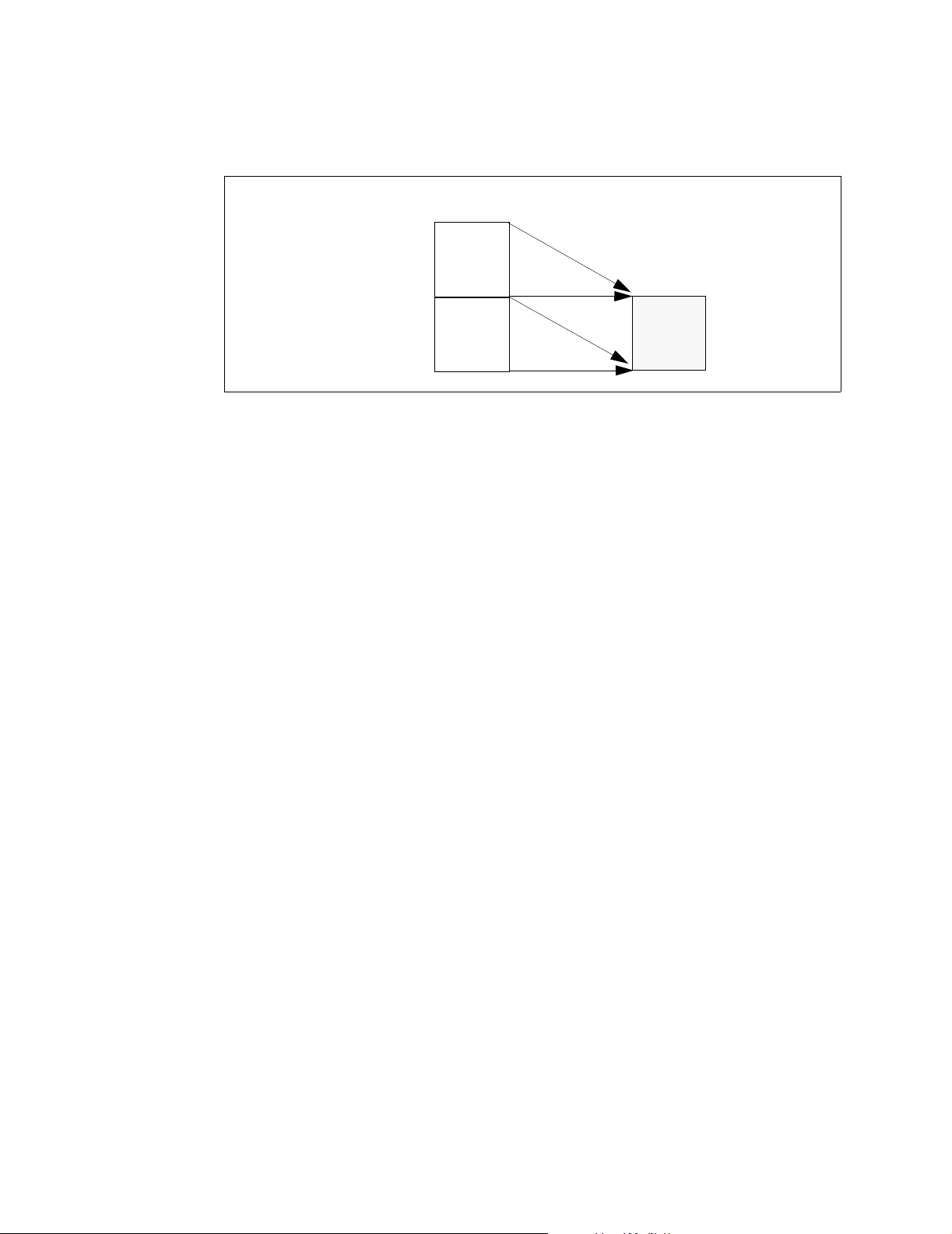
Figure 4-21. Addressing Memory Attributes
64
2
Base Register
64
2
Uncached
Non-speculative
Name Space
Cached Write-back
Limited Speculation
Name Space
UC
63
2
WBL
0
Software must use the correct name space when using physical addressing; otherwise, I/O devices
with side-effects may be accessed speculatively. Physical addressing accesses are ordered only if
ordered loads or ordered stores are used. Otherwise, physical addressing memory references are
unordered.
4.4.3 Cacheability and Coherency Attribute
A page can be either cacheable or uncacheable. If a page is marked cacheable, the processor is
permitted to allocate a local copy of the corresponding physical memory in all levels of the
processor memory/cache hierarchy. Allocation may be modified by the cache control hints of
memory reference instructions.
263 Physical
Address Space
63
2
A page which is cached is coherent with memory; i.e., the processor and memory system ensure
that there is a consistent view of memory from each processor. Processors support multiprocessor
cache coherence based on physical addresses between all processors in the coherence domain
(tightly coupled multiprocessors). Coherency is supported in the presence of virtual aliases,
although software is recommended to use aliases which are an integer multiple of 1 MB apart to
avoid any possible performance degradation.
Processors are not required to maintain coherency between processor local instruction and data
caches for Itanium architecture-based code; i.e., locally initiated Itanium stores may not be
observed by the local instruction cache. Processors are required to maintain coherency between
processor local instruction and data caches for IA-32 code. Instruction caches are also not required
to be coherent with multiprocessor Itanium instruction set originated memory references.
Instruction caches are required to be coherent with multiprocessor IA-32 instruction set originated
memory references. The processor must ensure that transactions from other I/O agents (such as
DMA) are physically coherent with the instruction and data cache.
For non-cacheable references the processor provides no coherency mechanisms; the memory
system must ensure that a consistent view of memory is seen by each processor. See “Coalescing
Attribute” on page 2:72 for a description of coh e rency for the coalescing memory attribute.
Volume 2: Addressing and Protection 2:71

4.4.4 Cache Write Policy Attribute
Write-back cacheable pages need only modify the processor’s copy of the physical memory
location; written data need only be passed to the memory system when the processor’s copy is
displaced, or a Flush Cache (
fc) instruction is issued to flush a virtual address. A cache line can
only be written back to memory if a store, semaphore (successful or not), the
mandatory RSE store, or a
.excl hinted lfetch instruction targeting that line has executed without a
fault. These events enable write-backs. A synchronized
write-backs (after the line has been flushed).
As described in “Invalidating ALAT Entries” on page 1:62, platform visible removal of cache lines
from a processor’s caches (e.g., cache line write-backs or platform visible replacements) cause the
corresponding ALAT entries to be invalidated.
4.4.5 Coalescing Attribute
For uncacheable pages, the coalescing attribute informs the processor that multiple stores to this
page may be collected in a coalescing buffer and issued later as a single larger mer ged transaction.
The processor may accumulate stores for an indefinite period of time. Multiple pending loads may
also be coalesced into a single larger transaction which is placed in a coalescing buffer. Coalescing
is a performance hint for the processor; a processor may or may not implement coalescing.
A processor with multiple coalescing buffers must provide a flush policy that flushes buffers at
roughly equal rate even if some buffers are only partially full. The processor may make coalesced
buffer flushes visible in any order. Furthermore, individual bytes within a single coalesced buffer
may be flushed and made visible in any order.
ld.bias, a
fc instruction disables subsequent
Stores (including IA-32), which are coalesced, are performed out of order; coalescing may occur in
both the space and time domains. For example, a write to bytes 4 and 5 and a write to bytes 6 and 7
may be coalesced into a single write of bytes 4, 5, 6, and 7. In addition, a write of bytes 5 and 6 may
be combined with a write of bytes 6 and 7 into a single write of bytes 5, 6, and 7.
Any release operation (regardless of whether it references a page with a coalescing memory
attribute), or any fence type instruction, forces write-coalesced data to be flushed and made visible
prior to the instruction itself becoming visible. (See Table 4-14 on page 2:76 for a list of release and
fence instructions.) Any IA-32 serializing instruction, or access to an uncached memory type,
forces write-coalesced data to become flushed and made visible prior to itself becoming visible.
Even though IA-32 stores and loads are ordered, the write-coalesced data is not flushed unless the
IA-32 stores or loads are to uncached memory types.
The Flush Cache (
least 32 bytes of the 32-byte aligned address specified by the Flush Cache (
forcing the data to become visible. The Flush Cache (
additional write-coalesced data. The Flush Write buffers (
fc, fc.i) instruction flushes all write-coalesced data whose address is within at
fc, fc.i) instruction,
fc, fc.i) instruction may also flush
fwb) instruction is a “hint” to the
processor to expedite flushing (visibility) of any pending stores held in the coalescing buffer(s),
without regard to address.
No indication is given when the flushing of the stores is completed. An
fwb instruction does not
ensure ordering of coalesced stores, since later stores may be flushed before prior stores. To ensure
prior coalesced stores are made visible before later stores, software must issue a release operation
between stores.
2:72 Volume 2: Addressing and Protection

The processor may at any time flush coalesced stores in any order before explicitly requested to do
so by software.
Coalesced pages are not ensured to be coherent with other processors’ coalescing buffers or caches,
or with the local processor’s caches. Loads to coalesced memory pages by a processor see the
results of all prior stores by the same processor to the same coalesced memory page. Memory
references made by the coalescing buffer (e.g., buffer flushes) have an unordered non-sequential
memory ordering attribute. See “Sequentiality Attribute and Ordering” on page 2:75.
Data that has been read or prefetched into a coalescing buffer prior to execution of an Itanium
acquire or fence type instruction is invalidated by the acquire or fence instruction. (See Table 4-14
for a list of acquire and fence instructions.)
4.4.6 Speculation Attributes
For present pages (TLB.p=1) which are marked with a speculative or a NaTPage memory attribute,
the processor may prefetch instructions (including IA-32), perform address generation and perform
load accesses (including IA-32) without resolving prior control dependencies, including predicates,
branches and interruptions. A page should only be marked speculative if accesses to that page have
no side-effects. For example, many memory-mapped I/O devices have side-effects associated with
reads and should be marked non-speculative. If a page is marked speculative, a processor can read
any location in the page at any time independent of a programmer’s intentions or control flow
changes. As a result, software is required, at all times, to maintain val id page t able attrib utes for t he
ppn, ps and ma fields of all present translations whose memory attribute is speculative or NaTPage.
High-performance operation is only attainable on speculative pages. The speculative attribute is a
hint; a processor may behave non-speculatively.
Prefetches are enabled if a speculative translation exists. Prefetches are asynchronous data and
instruction memory accesses that appear logically to initiate and finish between some pair of
instructions. This access may not be visible to subsequent flush cache (
instructions. This behavior is implementation-dependent.
The processor will not initiate memory references (16-byte instruction bundle fetch es, IA-32
instruction fetches, RSE fills and spills, VHPT references, and data memory accesses) to
non-speculative pages until all previous control dependencies (predicates, branches, and
exceptions) are resolved; i.e., the memory reference is required by an in-order execution of the
program. Additionally, for references to non-speculative pages, the processor:
• May not generate any memory access for a control or data speculative data reference.
• Will generate exactly one memory access for each aligned, non-speculative data reference.
(Misaligned data references may cause multiple memory accesses, although these accesses are
guaranteed to be non-overlapping – each byte will be accessed exactly once.)
• May generate multiple 16-byte memory accesses (to the same address) for each 16-byte
instruction bundle fetch reference.
To ensure virtual and physical accesses to non-speculative pages are performed in program order
and only once per program order occurrence, the rules in Table 4-12 and Table 4-13 are defined.
Software should also ensure that RSE spill/fill transactions are not performed to non-speculative
memory that may contain I/O devices; otherwise, system behavior is undefined.
fc, fc.i) and/or TLB purge
Volume 2: Addressing and Protection 2:73

Table 4-12. Permitted Speculation
Speculative
Advanced
Load (ld.sa)
b
Advanced
Load
(ld.a)
Memory
Attribute
Speculative Yes Yes Yes Yes Yes
Non-speculative Yes Always Fail Always Fail Always Fail Prohibited
Limited Speculation Yes Always Fail Yes Always Fail Limited
a. Includes the faulting form of line prefetch (lfetch.fault).
b. Includes the non-faulting form of line prefetch (lfetch), which does not cause a cache fill if the memory
attribute is non-speculative or limited speculation.
c. Hardware-generated speculative references include non-demand instruction prefetches (including IA-32),
hardware-generated data prefetch references, and eager RSE memory references.
d. The processor may only issue hardware-generated speculative references to a 4K-byte physical page if it is a
verified page.
Load
(ld)
Speculative
a
Load
(ld.s)
Hardware-generated
Speculative
References
d
Table 4-13. Register Return Values on Non-faulting Advanced/Speculative Loads
Memory
Attribute
Speculative Value Nat
Non-speculative N/A Nat
Limited Speculation N/A Nat
a. Speculative or speculative advanced loads that cause deferred exceptions result in failed speculation. The
processor aborts the reference. If the target of the load is a GR, the processor sets the register’s NaT bit to
one. If the target of the load is an FR, the processor sets the target FR to NaTVal. The processor performs all
other side-effects (such as post-increment).
b. Speculative or speculative advanced loads to limited or non-speculative memory pages result in failed
speculation. The processor aborts the reference. If the target of the load is a GR, the processor sets the
register’s NaT bit to 1. If the target of the load is an FR, the processor sets the target FR to NaTVal. The
processor performs all other side-effects (such as post-increment).
c. Advanced loads to non-speculative memory pages always fail. The processor aborts the reference, sets the
target register to zero, and performs all other side-effects (such as post-increment).
Speculative Load
(ld.s)
Success Failure Success Failure Success Failure
a
b
b
Advanced Load
(ld.a)
Value N/a Value NaT
N/A Zero
Value N/a N/a NaT
Speculative Advanced Load
c
N/A NaT
(ld.sa)
c
a
b
b
4.4.6.1 Limited Speculation and the WBL Physical Addressing Attribute
Processors are allowed to reference limited speculation pages (WBL pages) speculatively, in order
to increase performance, but this speculation is limited to prevent speculative references to 4Kbyte
physical pages for which there is no actual memory (which would cause spurious machine checks).
Processors must not make hardware-generated speculative references to a given WBL 4Kbyte page
until a verified reference has been made. Processors may optionally implement storage to hold the
addresses of WBL 4Kbyte pages for which verified references have been made, and may make
subsequent hardware-generated speculative references to these pages. Such pages are termed
verified pages.
A verified reference is an instruction or data reference made to the page by an in-order execution of
the program; that is, a reference which would have been made had the instructions from the
program been fetched and executed one at a time. A hardware-generated speculative reference does
not constitute a verified reference. Hardware-generated speculative references include:
• Instruction fetches when the processor has not yet determined whether prior branches were
predicted correctly
2:74 Volume 2: Addressing and Protection

• Instruction fetches when the processor has not yet determined whether prior instructions will
raise faults or traps
• Data references by instructions when the processor has not yet determined whether prior
branches were predicted correctly
• Data references by instructions when the processor has not yet determined whether prior
instructions will raise faults or traps
• Hardware-generated instruction prefetch references
• Hardware-generated data prefetch references
• Eager RSE data references
For an instruction fetch to constitute a verified reference, it must only be determined that an
in-order execution of the program requires that the IP point to this address, independent of whether
the instruction at this address will subsequently take a fault or interrupt.
For a data reference to constitute a verified reference, the instruction must meet one of the
following requirements:
• It executes without any fault or interrupt
• It takes an Unaligned Data Reference fault
• It takes a Data Debug fault
• It takes an External interrupt, but if it had not taken an External interrupt, it would have met
one of the above qualifications (execute without fault, take an Unaligned Data Reference fault,
or take a Data Debug fault)
Data-speculative loads are treated the same as normal loads, and if an in-order execution of the
program requires the execution of a data speculative load, it constitutes a verified reference.
Control-speculative loads to limited-speculation pages always defer and thus never constitu te
verified references.
It is not necessary for a processor to determine whether a reference will complete without
generating a machine check for it to be a verified reference. If software actually references a
physical address which will cause a machine check, hardware may generate multiple speculative
references to the same page, potentially causing multiple machine checks.
Processors may access verified pages normally, as they would WB pages, including the use of
caching, pipelining and hardware-generate speculative references to improve performance.
Calling the PAL_PREFETCH_VISIBILITY procedure forces the processor to clear the storage
holding the addresses of verified pages.
4.4.7 Sequentiality Attribute and Ordering
Memory ordering is defined in Section 4.4.7, “Memory Access Ordering” on page 1:68. This
section defines additional ordering rules for non-cacheable memory, cache synchronization
(
sync.i) and global TLB purge operations (ptc.g, ptc.ga).
As described in Section 4.4.7, “Memory Access Ordering” on page 1:68, read-after-write,
write-after-write, and write-after-read dependencies to the same memory location (memory
dependency) are performed in program order by the processor. Otherwise, all other memory
references may be performed in any order unless the reference is specifically marked as ordered.
Volume 2: Addressing and Protection 2:75

IA-32 memory references follow a stronger processor consistency memory model. See “IA-32
Memory Ordering” on page 2:255. for IA-32 memory ordering details. Explicit ordering takes the
form of a set of Itanium instructions: ordered load and check load (
ordered store (
synchronization (
st.rel), semaphores (cmpxchg, xchg, fetchadd), memory fence (mf),
sync.i) and global TLB purge (ptc.g, ptc.ga). The sync.i instruction is
ld.acq, ld.c.clr.acq),
used to maintain an ordering relationship between instruction and data caches on local and remote
processors. The global TLB purge instructions maintain multiprocessor TLB coherence.
For VHPT walks, visibility is defined by the memory read(s) which retrieves translation
information, and the associated insertion of the translation into the TLB. VHPT walks are
performed asynchronously with respect to program execution, and each walker VHPT read (which
appears as though it were performed atomically) is made visible at some single point in the
program order. Ordering constraints from Table 4-14 do not prevent VHPT walks from becoming
visible.
Table 4-14 defines a set of “Orderable Instructions” that follow one of four ordering semantics:
unordered, release, acquire or fence. The table defines the ordering semantics and the instructions
of each category. Only these Itanium instructions can be used to establish multiprocessor ordering
relations.
In the following discussion, the terms previous and subsequent are used to refer to the program
specified order. The term visible is used to refer to all architecturally visible effects of performing
an instruction. For memory accesses and semaphores this involves at least reading or writing
memory. For
Visibility of
ALAT lookups (
mf.a, visibility is defined by platform acceptance of previous memory accesses.
sync.i is defined by visibility of previous flush cache (fc, fc.i) operations. For
ld.c, chk.a), visibility is determination of ALAT hit or miss. For global TLB
purge operations, visibility is defined by removal of an address translation from the TLBs on all
processors in the TLB coherence domain. Global TLB purge instructions (
ptc.g and ptc.ga)
follow release semantics on the local processor as well as on remote processors, except with respect
to global purge instructions being executed by that remote processor. For local TLB purge
operations, visibility is defined by removal of an address translation on the local processor. Local
TLB purge instructions (
ptc.l, ptc.e) ensure that all prior stores are made locally visible before
the actual purge operation is performed.
Table 4-14. Ordering Semantics and Instructions
Ordering
Semantics
Unordered instructions may become visible in
any order.
Unordered
Release
2:76 Volume 2: Addressing and Protection
Release instructions guarantee that all
previous orderable instructions are made
visible prior to being made visible themselves.
Description Orderable Intel
ld, ld.s, ld.a, ld.sa, ld.fill,
ldf, ldf.s, ldf.sa, ldf.fill,
ldfp, ldfp.s, ldfp.sa,
st, st.spill,
stf, stf.spill,
mf.a, sync.i,
ld.c, chk.a
cmp8xchg16.rel, cmpxchg.rel,
fetchadd.rel, st.rel, ptc.g,
ptc.ga
®
Itanium® Instructions

Table 4-14. Ordering Semantics and Instructions (Continued)
Ordering
Semantics
Acquire
Fence
Description Orderable Intel
Acquire instructions guarantee that they are
made visible prior to all subsequent orderable
instructions.
Fence instructions combine the release and
acquire semantics into a bi-directional fence;
i.e., they guarantee that all previous orderable
instructions are made visible prior to any
subsequent orderable instruction being made
visible.
cmp8xchg16.acq, cmpxchg.acq,
fetchadd.acq, xchg, ld.acq,
ld.c.clr.acq
mf
®
Itanium® Instructions
Itanium memory accesses to sequential pages occur in program order with respect to all other
sequential pages in the same peripheral domain, but are not necessarily ordered with respect to
non-sequential page accesses. A peripheral domain is a platform-specific collection of uncacheable
addresses. An I/O device is normally contained in a peripheral domain and all sequential accesses
from one processor to that device will be ordered with respect to each other. Sequentiality ensures
that uncacheable, non-coalescing memory references from one processor to a peripheral domain
reach that domain in program order. Sequentiality does not imply visibility.
Inter-Processor Interrupt Messages (8-byte stores to a Processor Interrupt Block address, through a
UC memory attribute) are exceptions to the sequential semantics. IPI's are not ordered with respect
to other IPI's directed at the same processor. Further, fence operations do not enforce ordering
between two IPI's. See Section 5.8.4.2, “Interrupt and IPI Ordering” on page 2:124.
Table 4-15 defines the ordering between unordered, release, acquire and fence type operations to
sequential and non-sequential pages. Table 4-15 defines the minimal ordering requirem ents; an
implementation may enforce more restrictive ordering than required by the architecture. The actual
mechanism for enforcing memory access ordering is implementation dependent.
Table 4-15. Ordering Semantics
First Operation Fence
FenceOOOOOOO
Non-sequential Acquire O O O O O O O
Release O – O – – O –
Unordered O – O – – O –
a
Sequential
a. Except for IPI.
b. “O” indicates that the first and second operation become visible in program order.
c. A dash indicates no ordering is implied.
d. “S” indicates that the first and the second operation reach a peripheral domain in program order.
e. “OS” implies that both “O” and “S” ordering relations apply.
Acquire O O O O OS OS OS
Release O – O – S OS S
Unordered O – O
Table 4-15 establishes an order between operations on a particular processor. For operations to
cacheable write-back memory the order established by these rules is observed by all observers in
the coherence domain.
Second Operation
Non-sequential Sequential
Acquire Release Unordered Acquire Release Unordered
b
c
–
d
S
OS
a
e
S
Volume 2: Addressing and Protection 2:77

For example, when this sequence is executed on a processor:
st [a]
st.rel [b]
and a second processor executes this sequence:
ld.acq [b]
ld [a]
if the second processor observes the store to [b], it will also observe the store to [a].
Unless an ordering constraint from Table 4-15 prevents a memory read
1
from becoming visible, the
read may be satisfied with values found in a store buffer (or any logically equivalent structure).
These values need not be globally visible even when the operation that created the value was a
st.rel. This local bypassing behavior may make accesses of different sizes but with overlapping
memory references appear to complete non-atomically. To ensure that a memory write is globally
observed prior to a memory read, software must place an explicit fence operation between the two
operations.
Aligned
st.rel and semaphore operations
2
from multiple processors to cacheable write-back
memory become visible to all observers in a single total order (i.e., in a particular interleaving; if it
becomes visible to any observer, then it is visible to all observers), except that for
processor may observe (via
The Itanium architecture ensures this single total order only for aligned
operations to cacheable write-back memory. Other memory operations
ld or ld.acq) its own update prior to it being observed globally.
st.rel and semaphore
3
from multiple processors
st.rel each
are not required to become visible in any particular order, unless they are constrained w.r.t. each
other by the ordering rules defined in Table 4-15.
Ordering of loads is further constrained by data dependency. That is, if one load reads a value
written by an earlier load by the same processor (either directly or transitively, through either
registers or memory), then the two loads become visible in program order.
For example, when this sequence is executed on a processor:
st [a] = data
st.rel [b] = a
and a second processor executes this sequence:
ld x = [b]
ld y = [x]
if the second processor observes the store to [b], it will also observe the store to [a].
Also for example, when this sequence is executed on a processor:
st [a]
st.rel [b] = ‘new’
1. This includes all types of loads (ld and ld.acq), and RSE memory reads. Note, however, that the read operation
of semaphores cannot be satisfied with values found in a store buffer.
2. Both acquire and release semaphore forms
3. e.g. unordered stores, loads, ld.acq, or memory operations to pages with attributes other than write-back
cacheable.
2:78 Volume 2: Addressing and Protection

and a second processor executes this sequence:
ld x = [b]
cmp.eq p1 = x, ‘new’
(p1) ld y = [a]
if the second processor observes the store to [b], it will also observe the store to [a].
And for example, when this sequence is executed on a processor:
st [a]
st.rel [b] = ‘new’
and a second processor executes this sequence:
ld x = [b]
cmp.eq p1 = x, ‘new’
(p1) br target
target:
...
ld y = [a]
if the second processor observes the store to [b], it will also observe the store to [a].
The flush cache (
fc, fc.i) instruction follows data dependency ordering. fc and fc.i are ordered
only with respect to previous and subsequent load, store, or semaphore instructions to the same
line, regardless of the specified memory attribute. Subsequent memory operations to the same line
need not wait for prior
fc or fc.i completion before being globally visible. fc and fc.i are not
ordered with respect to memory operations to different lines.
fc.i operations. Instead, the sync.i instruction synchronizes fc and fc.i instructions, and the
sync.i is made visible using an mf instruction.
4.4.8 Not a Thing Attribute (NaTPage)
A NaTPage attribute prevents non-speculative references to a page, and ensures that speculative
references to the page always defer the Data NaT Page Consumption fault. However, as described
in “Speculation Attributes” on page 2:73, the processor may issue memory references to a
NaTPage. As a result, all NaTPages must be backed by a valid physical page.
Speculative or speculative advanced loads to pages marked as a NaTPage cause the deferred
exception indicator (NaT or NaTVal) to be written to the load target register, and the memory
reference is aborted. However, all other effects of the load instruction such as post-increment are
performed. Instruction fetches, loads, stores and semaphores (including IA-32), but except for
Itanium speculative loads, pages marked as NaTPage raise a NaT Page Consumption fault.
A speculative reference to a page marked as NaTPage may still take lower priority faults, if not
explicitly deferred in the DCR. See “Deferral of Speculative Load Faults” on page 2:98.
mf does not ensure visibility of fc and
4.4.9 Effects of Memory Attributes on Memory Reference Instructions
Memory attributes affect the following Itanium instructions.
Volume 2: Addressing and Protection 2:79

• ldfe, stfe: Hardware support for 10-byte memory accesses to a page that is neither a
cacheable page with write-back write policy nor a NaTPage is optional. On processor
implementations that do not support such accesses, an Unsupported Data Reference Fault is
raised when an unsupported reference is attempted.
For extended floating-point loads the fault is delivered only on the normal, advanced, and
check load flavors (
the
ldfe instruction that target pages that are not cacheable with write-back policy always
ldfe, ldfe.a, ldfe.c.nc, ldfe.c.clr). Control speculative flavors of
defer the fault. Refer to “Deferral of Speculative Load Faults” on page 2:98 for details.
•
cmpxchg and xchg: These instructions are only supported to cacheable pages with write-back
write policy.
fault.
cmpxchg and xchg accesses to NaTPages causes a Data NaT Page Consumption
cmpxchg and xchg accesses to pages with other memory attributes cause an
Unsupported Data Reference fault.
•
fetchadd: The fetchadd instruction can be executed successfully only if the access is to a
cacheable page with write-back write policy or to a UCE page.
fetchadd accesses to
NaTPages cause a Data NaT Page Consumption fault. Accesses to pages with other memory
attributes cause an Unsupported Data Reference fault. When accessing a cacheable page with
write-back write policy, atomic fetch and add operation is ensured by the processor
cache-coherence protocol. For highly contended semaphores, the cache line transactions
required to guarantee atomicity can limit performance. In such cases, a centralized “fetch and
add” semaphore mechanism may improve performance. If supported by the processor and the
platform, the UCE attribute allows the processor to “export” the
platform as an atomic “fetch and add.” Effects of the exported
dependent. If exporting of
fetchadd instruction to a UCE page takes an Unsupported Data Reference fault.
• Flush Cache Instructions –
fetchadd instructions is not supported by the processor, a
fc instructions must always be “broadcast” to other processors,
fetchadd operation to the
fetchadd are platform
independent of the memory attribute in the local processor. It is legal to use an uncacheable
memory attribute for any valid address when used as a flush cache (
fc) instruction target. This
behavior is required to enable transitions from one memory attribute to another and in case
different memory attributes are associated with the address in another processor.
• Prefetch instructions –
lfetch and any implicit prefetches to pages that are not cacheable are
suppressed. No transaction is initiated. This allows programs to issue prefetch instructions
even if the program is not sure the memory is cacheable.
4.4.10 Effects of Memory Attributes on Advanced/Check Loads
The ALAT behavior of advanced and check loads is dependent on the memory attribute of the page
referenced by the load. These behaviors are required; advanced and check load completers are not
hints.
All speculative pages have identical behavior with respect to the ALAT. Advanced loads to
speculative pages always allocate an ALAT entry for the register, size, and address tuple specified
by the advanced load. Speculative advanced loads allocate an ALAT entry if the speculative load is
successful (i.e., no deferred exception); if the speculative advanced load results in a deferred
exception, any matching ALAT entry is removed and no new ALA T entry i s allocated. Check loads
with clear completers (
ALAT hit and do not change the state of the ALAT on ALAT miss . Check loads with no-clear
completers (
2:80 Volume 2: Addressing and Protection
ld.c.nc, ldf.c.nc) allocate an ALAT entry on ALAT miss. On ALAT hit, the ALAT
ld.c.clr, ld.c.clr.acq, ldf.c.clr) remove a matching ALA T entry on
 Loading...