

Intel Itanium 2 9052 (NE80549KE025LK) Dual-Core Itanium 2 Reference Manual For Software Developement and Optimization (0.9)

Dual-Core Update
to the Intel® Itanium®2 Processor
Reference Manual
For Software Development and Optimization
Revision 0.9
January 2006
Document Number: 308065-001

Notice: This document contains information on products in the design phase of development. The information here is subject to change without
notice. Do not finalize a design with this information.
INFORMATION IN THIS DOCUMENT IS PROVIDED IN CONNECTION WITH INTEL® PRODUCTS. NO LICENSE, EXPRESS OR IMPLIED, BY
ESTOPPEL OR OTHERWISE, TO ANY INTELLECTUAL PROPERTY RIGHTS IS GRANTED BY THIS DOCUMENT. EXCEPT AS PROVIDED IN
INTEL'S TERMS AND CONDITIONS OF SALE FOR SUCH PRODUCTS, INTEL ASSUMES NO LIABILITY WHATSOEVER, AND INTEL DISCLAIMS
ANY EXPRESS OR IMPLIED WARRANTY, RELATING TO SALE AND/OR USE OF INTEL PRODUCTS INCLUDING LIABILITY OR WARRANTIES
RELATING TO FITNESS FOR A PARTICULAR PURPOSE, MERCHANTABILITY, OR INFRINGEMENT OF ANY PATENT, COPYRIGHT OR OTHER
INTELLECTUAL PROPERTY RIGHT. Intel products are not intended for use in medical, life saving, or life sustaining applications.
Intel may make changes to specifications and product descriptions at any time, without notice.
Designers must not rely on the absence or characteristics of any features or instructions marked “reserved” or “undefined.” Intel reserves these for
future definition and shall have no responsibility whatsoever for conflicts or incompatibilities arising from future changes to them.
The Itanium 2 processor may contain design defects or errors known as errata which may cause the product to deviate from published specifications.
Current characterized errata are available on request.
The code name “Montecito” presented in this document is only for use by Intel to identify a product, technology, or service in development, that has not
been made commercially available to the public, i.e., announced, launched or shipped. It is not a “commercial” name for products or services and is
not intended to function as a trademark.
Contact your local Intel sales office or your distributor to obtain the latest specifications and before placing your product order.
Copies of documents which have an order number and are referenced in this document, or other Intel literature, may be obtained by calling 1-800-
548-4725, or by visiting Intel's web site at http://www.intel.com.
Intel, Itanium, Pentium, VTune and the Intel logo are trademarks or registered trademarks of Intel Corporation or its subsidiaries in the United States
and other countries.
Copyright © 2006, Intel Corporation. All rights reserved.
*Other names and brands may be claimed as the property of others.
2 Reference Manual for Software Development and Optimization

Contents
1 Introduction.........................................................................................................................9
1.1 Terminology...........................................................................................................9
1.2 Related Documentation.........................................................................................9
2 The Dual-Core Itanium 2 Processor.................................................................................11
2.1 Overview .............................................................................................................11
2.1.1 Identifying the Dual-Core Itanium 2 Processor.......................................11
2.1.2 Introducing Montecito.............................................................................12
2.2 New Instructions..................................................................................................14
2.3 Core.....................................................................................................................15
2.3.1 Instruction Slot to Functional Unit Mapping............................................15
2.3.2 Instruction Latencies and Bypasses.......................................................17
2.3.3 Caches and Cache Management Changes ...........................................18
2.4 Threading ............................................................................................................20
2.4.1 Sharing Core Resources........................................................................21
2.4.2 Tailoring Thread Switch Behavior ..........................................................23
2.4.3 Sharing Cache and Memory Resources ................................................24
2.5 Dual Cores ..........................................................................................................25
2.5.1 Fairness and Arbitration .........................................................................27
2.6 Intel® Virtualization Technology ..........................................................................27
2.7 Tips and Tricks....................................................................................................27
2.7.1 Cross Modifying Code............................................................................27
2.7.2 ld.bias and lfetch.excl.............................................................................27
2.7.3 L2D Victimization Optimization...............................................................27
2.7.4 Instruction Cache Coherence Optimization............................................28
2.8 IA-32 Execution...................................................................................................28
2.9 Brand Information................................................................................................28
3 Performance Monitoring...................................................................................................31
3.1 Introduction to Performance Monitoring ..............................................................31
3.2 Performance Monitor Programming Models........................................................31
3.2.1 Workload Characterization.....................................................................32
3.2.2 Profiling ..................................................................................................35
3.2.3 Event Qualification .................................................................................37
3.2.4 References.............................................................................................43
3.3 Performance Monitor State .................................................................................43
3.3.1 Performance Monitor Control and Accessibility......................................46
3.3.2 Performance Counter Registers.............................................................46
3.3.3 Performance Monitor Event Counting Restrictions Overview ................49
3.3.4 Performance Monitor Overflow Status Registers (PMC0,1,2,3).............49
3.3.5 Instruction Address Range Matching .....................................................50
3.3.6 Opcode Match Check (PMC32,33,34,35,36) .........................................53
3.3.7 Data Address Range Matching (PMC41)...............................................56
3.3.8 Instruction EAR (PMC37/PMD32,33,36)................................................57
3.3.9 Data EAR (PMC40, PMD32,33,36)........................................................60
Reference Manual for Software Development and Optimization 3

3.3.10 Execution Trace Buffer (PMC
3.3.11 Interrupts................................................................................................72
3.3.12 Processor Reset, PAL Calls, and Low Power State...............................73
4 Performance Monitor Events............................................................................................75
4.1 Introduction .........................................................................................................75
4.2 Categorization of Events.....................................................................................75
4.2.1 Hyper-Threading and Event Types ........................................................76
4.3 Basic Events .......................................................................................................77
4.4 Instruction Dispersal Events................................................................................77
4.5 Instruction Execution Events...............................................................................78
4.6 Stall Events .........................................................................................................79
4.7 Branch Events.....................................................................................................80
4.8 Memory Hierarchy...............................................................................................81
4.8.1 L1 Instruction Cache and Prefetch Events.............................................83
4.8.2 L1 Data Cache Events ...........................................................................84
4.8.3 L2 Instruction Cache Events ..................................................................86
4.8.4 L2 Data Cache Events ...........................................................................87
4.8.5 L3 Cache Events....................................................................................91
4.9 System Events ....................................................................................................92
4.10 TLB Events..........................................................................................................93
4.11 System Bus Events.............................................................................................95
4.11.1 System Bus Conventions .......................................................................98
4.11.2 Extracting Memory Latency from Montecito Performance Counters......98
4.12 RSE Events.......................................................................................................100
4.13 Hyper-Threading Events ...................................................................................101
4.14 Performance Monitors Ordered by Event Code................................................102
4.15 Performance Monitor Event List........................................................................108
39,42
,PMD
48-63,38,39
)................................65
Figures
2-1 The Montecito Processor ....................................................................................14
2-2 Urgency and Thread Switching...........................................................................23
2-3 The Arbiter and Queues......................................................................................26
3-1 Time-Based Sampling.........................................................................................32
3-2 Itanium® Processor Family Cycle Accounting.....................................................34
3-3 Event Histogram by Program Counter ................................................................36
3-4 Montecito Processor Event Qualification ............................................................ 38
3-5 Instruction Tagging Mechanism in the Montecito Processor...............................39
3-6 Single Process Monitor .......................................................................................42
3-7 Multiple Process Monitor.....................................................................................42
3-8 System Wide Monitor..........................................................................................43
3-9 Montecito Processor Performance Monitor Register Mode ................................45
3-10 Processor Status Register (PSR) Fields for Performance Monitoring ................46
3-11 Montecito Processor Generic PMC Registers (PMC4-15) ..................................47
3-12 Montecito Processor Generic PMD Registers (PMD4-15) ..................................48
4 Reference Manual for Software Development and Optimization

3-13 Montecito Processor Performance Monitor Overflow Status
Registers (PMC0,1,2,3).......................................................................................49
3-14 Instruction Address Range Configuration Register (PMC38)..............................51
3-15 Opcode Match Registers (PMC32,34) ................................................................54
3-16 Opcode Match Registers (PMC33,35) ................................................................54
3-17 Opcode Match Configuration Register (PMC36).................................................55
3-18 Memory Pipeline Event Constraints Configuration Register (PMC41)................57
3-19 Instruction Event Address Configuration Register (PMC37) ...............................58
3-20 Instruction Event Address Register Format (PMD34,35) ....................................58
3-21 Data Event Address Configuration Register (PMC40) ........................................60
3-22 Data Event Address Register Format (PMD32,d3,36) ........................................61
3-23 Execution Trace Buffer Configuration Register (PMC39)....................................65
3-24 Execution Trace Buffer Register Format (PMD48-63, where
PMC39.ds == 0)...................................................................................................67
3-25 Execution Trace Buffer Index Register Format (PMD38)....................................68
3-26 Execution Trace Buffer Extension Register Format (PMD39)
(PMC42.mode=‘1xx) ...........................................................................................68
3-27 IP-EAR Configuration Register (PMC42) ............................................................69
3-28 IP-EAR data format (PMD48-63, where PMC42.mode == 100 and
PMD48-63.ef =0).................................................................................................70
3-29 IP-EAR data format (PMD48-63, where PMC42.mode == 100 and
PMD48-63.ef =1).................................................................................................70
3-30 IP Trace Buffer Index Register Format (PMD38)(PMC42.mode=‘1xx) ...............71
3-31 IP Trace Buffer Extension Register Format (PMD39)
(PMC42.mode=‘1xx) ...........................................................................................71
4-1 Event Monitors in the Itanium® 2 Processor Memory Hierarchy.........................82
4-2 Extracting Memory Latency from PMUs............................................................100
Tables
2-1 Itanium® Processor Family and Model Values....................................................11
2-2 Definition Table ...................................................................................................12
2-3 New Instructions Available in Montecito..............................................................14
2-4 A-Type Instruction Port Mapping.........................................................................15
2-5 B-Type Instruction Port Mapping.........................................................................16
2-6 I-Type Instruction Port Mapping ..........................................................................16
2-7 M-Type Instruction Port Mapping ........................................................................16
2-8 Execution with Bypass Latency Summary ..........................................................18
2-9 Montecito Cache Hierarchy Summary.................................................................19
2-10 PAL_BRAND_INFO Implementation-Specific Return Values .............................28
2-11 Montecito Processor Feature Set Return Values................................................29
3-1 Average Latency per Request and Requests per Cycle
Calculation Example33
3-2 Montecito Processor EARs and Branch Trace Buffer.........................................37
3-3 Montecito Processor Event Qualification Modes.................................................40
3-4 Montecito Processor Performance Monitor Register Set ....................................44
3-5 Performance Monitor PMC Register Control Fields (PMC4-15)..........................46
3-6 Montecito Processor Generic PMC Register Fields (PMC4-15) .........................47
Reference Manual for Software Development and Optimization 5

3-7 Montecito Processor Generic PMD Register Fields............................................48
3-8 Montecito Processor Performance Monitor Overflow Register
Fields (PMC0,1,2,3) ............................................................................................49
3-9 Montecito Processor Instruction Address Range Check by
Instruction Set.....................................................................................................51
3-10 Instruction Address Range Configuration Register Fields (PMC38)...................51
3-11 Opcode Match Registers(PMC32,34) .................................................................54
3-12 Opcode Match Registers(PMC33,35) .................................................................55
3-13 Opcode Match Configuration Register Fields (PMC36)......................................55
3-14 Memory Pipeline Event Constraints Fields (PMC41) ..........................................56
3-15 Instruction Event Address Configuration Register Fields (PMC37) ....................58
3-16 Instruction EAR (PMC37) umask Field in Cache Mode
(PMC37.ct=’1x) ...................................................................................................59
3-17 Instruction EAR (PMD34,35) in Cache Mode (PMC37.ct=’1x)............................59
3-18 Instruction EAR (PMC37) umask Field in TLB Mode (PMC37.ct=00).................59
3-19 Instruction EAR (PMD34,35) in TLB Mode (PMC37.ct=‘00) ...............................60
3-20 Data Event Address Configuration Register Fields (PMC40) .............................60
3-21 Data EAR (PMC40) Umask Fields in Data Cache Mode
(PMC40.mode=00)..............................................................................................61
3-22 PMD32,33,36 Fields in Data Cache Load Miss Mode
(PMC40.mode=00)..............................................................................................62
3-23 Data EAR (PMC40) Umask Field in TLB Mode (PMC40.ct=01).........................63
3-24 PMD32,33,36 Fields in TLB Miss Mode (PMC40.mode=‘01)..............................63
3-25 PMD32,33,36 Fields in ALAT Miss Mode (PMC11.mode=‘1x) ...........................64
3-26 Execution Trace Buffer Configuration Register Fields (PMC39).........................66
3-27 Execution Trace Buffer Register Fields (PMD48-63)
(PMC42.mode=‘000)...........................................................................................67
3-28 Execution Trace Buffer Index Register Fields (PMD38) .....................................68
3-29 Execution Trace Buffer Extension Register Fields (PMD39)
(PMC42.mode=‘1xx) ...........................................................................................69
3-30 IP-EAR Configuration Register Fields (PMC42) .................................................70
3-31 IP-EAR Data Register Fields (PMD48-63) (PMC42.mode=‘1xx) ........................70
3-32 IP Trace Buffer Index Register Fields (PMD38) (PMC42.mode=‘1xx)................71
3-33 IP Trace Buffer Extension Register Fields (PMD39)
(PMC42.mode=‘1xx) ...........................................................................................72
3-34 Information Returned by PAL_PERF_MON_INFO for the
Montecito Processor ...........................................................................................73
4-1 Performance Monitors for Basic Events..............................................................77
4-2 Derived Monitors for Basic Events......................................................................77
4-3 Performance Monitors for Instruction Dispersal Events......................................78
4-4 Performance Monitors for Instruction Execution Events .....................................78
4-5 Derived Monitors for Instruction Execution Events .............................................79
4-6 Performance Monitors for Stall Events................................................................80
4-7 Performance Monitors for Branch Events ...........................................................81
4-8 Performance Monitors for L1/L2 Instruction Cache and
Prefetch Events...................................................................................................83
4-9 Derived Monitors for L1 Instruction Cache and Prefetch Events ........................84
4-10 Performance Monitors for L1 Data Cache Events...............................................84
6 Reference Manual for Software Development and Optimization

4-11 Performance Monitors for L1D Cache Set 0 .......................................................85
4-12 Performance Monitors for L1D Cache Set 1 .......................................................85
4-13 Performance Monitors for L1D Cache Set 2 .......................................................85
4-14 Performance Monitors for L1D Cache Set 3 .......................................................85
4-15 Performance Monitors for L1D Cache Set 4 .......................................................86
4-16 Performance Monitors for L1D Cache Set 6 .......................................................86
4-19 Performance Monitors for L2 Data Cache Events...............................................87
4-20 Derived Monitors for L2 Data Cache Events.......................................................88
4-21 Performance Monitors for L2 Data Cache Set 0 .................................................89
4-22 Performance Monitors for L2 Data Cache Set 1 .................................................89
4-23 Performance Monitors for L2 Data Cache Set 2 .................................................89
4-24 Performance Monitors for L2 Data Cache Set 3 .................................................89
4-25 Performance Monitors for L2 Data Cache Set 4 .................................................90
4-26 Performance Monitors for L2 Data Cache Set 5 .................................................90
4-27 Performance Monitors for L2 Data Cache Set 6 .................................................90
4-28 Performance Monitors for L2 Data Cache Set 7 .................................................90
4-29 Performance Monitors for L2 Data Cache Set 8 .................................................91
4-30 Performance Monitors for L2D Cache - Not Set Restricted ................................91
4-31 Performance Monitors for L3 Unified Cache Events ...........................................91
4-32 Derived Monitors for L3 Unified Cache Events ...................................................92
4-33 Performance Monitors for System Events...........................................................93
4-34 Derived Monitors for System Events...................................................................93
4-35 Performance Monitors for TLB Events ................................................................93
4-36 Derived Monitors for TLB Events ........................................................................94
4-37 Performance Monitors for System Bus Events....................................................95
4-38 Derived Monitors for System Bus Events............................................................97
4-39 Performance Monitors for RSE Events .............................................................100
4-40 Derived Monitors for RSE Events......................................................................101
4-41 Performance Monitors for Multi-thread Events..................................................101
4-42 All Performance Monitors Ordered by Code .....................................................102
Reference Manual for Software Development and Optimization 7

Revision History
Document
Number
308065-001 0.9 • Initial release of the document. January 2006
Revision
Number
Description Date
8 Reference Manual for Software Development and Optimization

1 Introduction
This document is an update to the Intel® Itanium® 2 Processor Reference Manual for Software
Development and Optimization. This update is meant to give guidance on the changes that the dual-
core Intel®Itanium® 2 processor, code named Montecito, brings to the existing Itanium 2
processor family.
1.1 Terminology
The following definitions are for terms that will be used throughout this document:
Term Definition
Dispersal The process of mapping instructions within bundles to functional units
Bundle rotation The process of bringing new bundles into the two-bundle issue
Split issue Instruction execution when an instruction does not issue at the same
Advanced load address table (ALAT) The ALAT holds the state necessary for advanced load and check
Translation lookaside buffer (TLB) The TLB holds virtual to physical address mappings
Virtual hash page table (VHPT) The VHPT is an extension of the TLB hierarchy, which resides in the
Hardware page walker (HPW) The HPW is the third level of address translation. It is an engine that
Register stack engine (RSE) The RSE moves registers between the register stack and the backing
Event address registers (EARs) The EARs record the instruction and data addresses of data cache
window
time as the instruction immediately before it.
operations.
virtual memory space, is designed to enhance virtual address
translation performance.
performs page look-ups from the VHPT and seeks opportunities to
insert translations into the processor TLBs.
store in memory.
misses.
1.2 Related Documentation
The reader of this document should also be familiar with the material and concepts presented in the
following documents:
®
• Intel
• Intel
• Intel
Reference Manual for Software Development and Optimization 9
Itanium®Architecture Software Developer’s Manual, Volume 1: Application
Architecture
®
Itanium®Architecture Software Developer’s Manual, Volume 2: System Architecture
®
Itanium®Architecture Software Developer’s Manual, Volume 3: Instruction Set
Reference
§

Reference Manual for Software Development and Optimization 10

2 The Dual-Core Itanium 2
Processor
2.1 Overview
The first dual-core Itanium 2 processor, code named Montecito, is the fourth generation of the
Itanium 2 processor. Montecito builds on the strength of the previous Itanium 2 processors while
bringing many new key technologies for performance and management to the Itanium processor
family. Key improvements include multiple-cores, multiple-threads, cache hierarchy, and
speculation with the addition of new instructions.
This document describes key Montecito features and how Montecito differs in its implementation
of the Itanium architecture from previous Itanium 2 processors. Some of this information may not
be directly applicable to performance tuning, but is certainly needed to better understand and
interpret changes in application behavior on Montecito versus other Itanium architecture-based
processors. Unless otherwise stated, all of the restrictions, rules, sizes, and capacities described in
this document apply specifically to Montecito and may not apply to other Itanium architecturebased processors. This document assumes a familiarity with the previous Itanium 2 processors and
some of the unique properties and behaviors of those. Furthermore, only differences as they relate
to performance will be included here. Information about Montecito features such as error
protection, Virtualization technology, Hyper-Threading technology, and lockstep support may be
obtained in separate documents.
General understanding of processor components and explicit familiarity with Itanium processor
instructions are assumed. This document is not intended to be used as an architectural reference for
the Itanium architecture. For more information on the Itanium architecture, consult the Intel
Itanium®Architecture Software Developer’s Manual.
2.1.1 Identifying the Dual-Core Itanium 2 Processor
There have now been four generations of the Itanium 2 processor, which can be identified by their
unique CPUID values. For simplicity of documentation, throughout this document we will group
all processors of like model together. Table 2-1details out the CPUID values of all of the Itanium
processor family generations. Table 2-2 lists out all of the varieties of the Itanium processor family
that are available along with their grouping.
Note that the Montecito CPUID family value changes to 0x20.
Table 2-1. Itanium® Processor Family and Model Values
Family Model Description
0x07 0x00 Itanium® Processor
0x1f 0x00 Itanium 2 Processor (up to 3 MB L3 cache)
0x1f 0x01 Itanium 2 Processor (up to 6 MB L3 cache)
0x1f 0x02 Itanium 2 Processor (up to 9 MB L3 cache)
0x20 0x00 Dual-Core Itanium 2 Processor (Montecito)
®
Reference Manual for Software Development and Optimization 11

The Dual-Core Itanium 2 Processor
Table 2-2. Definition Table
Intel® Itanium® 2 Processor 900 MHz with 1.5 MB L3 Cache
Intel® Itanium® 2 Processor 1.0 GHz with 3 MB L3 Cache
Low Voltage Intel® Itanium® 2 Processor 1.0 GHz with 1.5 MB
L3 Cache
Intel® Itanium® 2 Processor 1.40 GHz with 1.5 MB L3 Cache
Intel® Itanium® 2 Processor 1.40 GHz with 3 MB L3 Cache
®
Itanium® 2 Processor 1.60 GHz with 3 MB L3 Cache
Intel
Intel® Itanium® 2 Processor 1.30 GHz with 3 MB L3 Cache
Intel® Itanium® 2 Processor 1.40 GHz with 4 MB L3 Cache
®
Itanium® 2 Processor 1.50 GHz with 6 MB L3 Cache
Intel
Low Voltage Intel® Itanium® 2 Processor 1.30 GHz with 3 MB
L3 Cache
Intel® Itanium® 2 Processor 1.60 GHz with 3 MB L3 Cache at
400 and 533 MHz System Bus (DP Optimized)
Intel® Itanium® 2 Processor 1.50 GHz with 4 MB L3 Cache
Intel® Itanium® 2 Processor 1.60 GHz with 6 MB L3 Cache
Intel® Itanium® 2 Processor 1.60 GHz with 9 MB L3 Cache
®
Itanium® 2 Processor 1.66 GHz with 6 MB L3 Cache
Intel
Intel® Itanium® 2 Processor 1.66 GHz with 9 MB L3 Cache
Individual SKUs TBD Dual-Core Itanium 2 Processor (Montecito)
Processor Abbreviation
Itanium 2 Processor (up to 3 MB L3 cache)
Itanium 2 Processor (up to 6 MB L3 cache)
Itanium 2 Processor (up to 9 MB L3 cache)
2.1.2 Introducing Montecito
Montecito takes the latest Itanium 2 processor core, improves the memory hierarchy and adds an
enhanced form of temporal multi-threading. A full introduction to the Itanium 2 processor is
available elsewhere but a brief review is provided below.
The front-end, with two levels of branch prediction, two TLBs, and a 0 cycle branch predictor,
feeds two bundles of three instructions each into the instruction buffer every cycle. This 8 entry
queue decouples the front-end from the back-end and delivers up to two bundles, of any alignment,
to the remaining 6 stages of the pipeline. The dispersal logic determines issue groups and allocates
up to 6 instructions to nearly every combination of the 11 available functional units (2 integer, 4
memory, 2 floating point, and 3 branch). The renaming logic maps virtual registers into physical
registers. Actual register (up to 12 integer and 4 floating point) reads are performed just before the
instructions execute or requests are issued to the cache hierarchy. The full bypass network allows
nearly immediate access to previous instruction results while final results are written into the
register file (up to 6 integer and 4 floating point).
Montecito preserves application and operating system investments while providing greater
opportunity for code generators to continue their steady performance push without any destructive
disturbance. This is important since even today, three years after the introduction of the first
Itanium 2 processor, compilers are providing significant performance improvements. The block
diagram of the Montecito processor can be found in Figure 2-1.
Montecito provides a second integer shifter and popcounter to help reduce port asymmetries. The
front-end provides better branching behavior for single cycle branches and cache allocation/
reclamation. Finally, Montecito decreases the time to reach recovery code when speculation fails
12 Reference Manual for Software Development and Optimization

The Dual-Core Itanium 2 Processor
thereby providing a lower cost for speculation. All told, nearly every core block and piece of
control logic includes some optimization to improve small deficiencies.
Exposing additional performance in an already capable cache hierarchy is also challenging and
includes additional capacity, improved coherence architecture, and more efficient cache
organization and queuing. Montecito supports three levels of on-chip cache. The first level (L1)
caches are each 4-way set associative caches and hold 16 KB of instruction or data. These caches
are in-order, like the rest of the pipeline, but are non-blocking allowing high request concurrency.
These L1 caches are accessed in a single cycle using pre-validated tags. The data cache is writethrough and dual-ported to support two integer loads and two stores, while the instruction cache
has dual-ported tags and a single data port to support simultaneous demand and prefetch accesses.
While previous generations of the Itanium 2 processor share the second level (L2) cache with both
data and instructions, Montecito provides a dedicated 1 MB L2 cache for instructions. This cache is
8-way set associative with a 128 byte line size and provides the same 7 cycle instruction access
latency as the previous smaller Itanium 2 processor unified cache. A single tag and data port
supports out-of-order and pipelined accesses to provide a high utilization. The separate instruction
and data L2 caches provide more efficient access to the caches compared to Itanium 2 processors
where instruction requests would contend against data accesses for L2 bandwidth against data
accesses and potentially impact core execution as well as L2 throughput.
This previously shared 256 KB L2 cache is now dedicated to data on Montecito with several
micro-architectural improvements to increase throughput. The instruction and data separation
effectively increase the data hit rate. The L2D hit latency remains at 5 cycles for integer and 6
cycles for floating-point accesses. The tag is true 4-ported and the data is pseudo 4-ported with 16byte banks. Montecito removes some of the code generator challenges found in the Itanium 2
processor L2 cache. Specifically, any accesses beyond the first access to miss the L2 in previous
Itanium 2 processors would access the L2 tags periodically until a hit is detected. The repeated tag
accesses consume bandwidth from the core and increase the miss latency. On Montecito, such
misses are suspended until the L2 fill occurs. The fill awakens and immediately satisfies the
request which greatly reduces bandwidth contention and final latency. The Montecito L2D, like
previous generations of the Itanium 2 processor L2, is out-of-order and pipelined with the ability to
track up to 32 requests in addition to 16 misses and their associated victims. However, Montecito
optimizes allocation of the 32 queue entries providing a higher concurrency level than previously
possible.
The third level (L3) cache remains unified as in previous Itanium 2 processors, but is now 12 MB
in size while maintaining the same 14 cycle integer access latency found on the 6 MB and 9 MB
Itanium 2 processors. The L3 uses an asynchronous interface with the data array to achieve this low
latency; there is no clock, only a read or write valid indication. The read signal is coincident with
index and way values that initiate L3 data array accesses. Four cycles later, the entire 128-byte line
is available and latched. This data is then delivered in 4 cycles to either the L2D or L2I cache in
critical byte order.
The L3 receives requests from both the L2I and L2D but gives priority to the L2I request in the rare
case of a conflict. Moving the arbitration point from the L1-L2 in the Itanium 2 processor to the
L2-L3 cache greatly reduces conflicts thanks to the high hit rates of the L2.
The cache hierarchy is replicated in each core to total more than 13.3 MB for each core and nearly
27 MB for the entire processor.
Reference Manual for Software Development and Optimization 13

The Dual-Core Itanium 2 Processor
Figure 2-1. The Montecito Processor
2.2 New Instructions
Montecito is compliant with the latest revisions of the Itanium architecture in addition to the Intel
Itanium Architecture Virtualization Specification Update. As such, Montecito introduces several
new instructions as summarized below:
Table 2-3. New Instructions Available in Montecito
New Instruction Comment
1
fc.i
2
ld16
2
st16
cmp8xchg16
hint@pause
vmsw.0, vmsw.1 On promote pages, these instructions allow cooperative operating systems to obtain and
NOTES:
1. This instruction behaves as the instruction on Montecito
2. This instruction will fault if issued to UC, UCE, or WC memory
3. This instruction will not initiate a thread switch if it is a B type instruction.
Insures that instruction caches are coherent with data caches
AR.csd and the register specified are the targets for this load.
AR.csd and the value in the register specified are written for this store
2
AR.csd and the value in the register specified are written for this exchange if the 8 byte
compare is true.
3
The current thread is yielding resources to the other thread.
give up VMM privilege
14 Reference Manual for Software Development and Optimization

The Dual-Core Itanium 2 Processor
2.3 Core
The Montecito core is very similar to previous generations of the Itanium 2 processor core from a
code generation point of view. The core has new resources; specifically, an additional integer
shifter and popcounter. The core also removes the rarely needed MMU to Memory Address bypass
path. The core also includes many optimizations, from the front-end to the cache hierarchy, that are
transparent to the code generator and legacy code can see improvements without any code change.
2.3.1 Instruction Slot to Functional Unit Mapping
This information is very similar to previous Itanium 2 processors. Changes between Itanium 2
processors and Montecito will be noted with footnotes.
Each fetched instruction is assigned to a functional unit through an issue port. The numerous
functional units share a smaller number of issue ports. There are 11 functional units: eight for nonbranch instructions and three for branch instructions. They are labeled M0, M1, M2, M3, I0, I1, F0,
F1, B0, B1, and B2. The process of mapping instructions within bundles to functional units is
called dispersal.
An instruction’s type and position within the issue group determine which functional unit the
instruction is assigned. An instruction is mapped to a subset of the functional units based upon the
instruction type (i.e. ALU, Memory, Integer, etc.). Then, based on the position of the instruction
within the instruction group presented for dispersal, the instruction is mapped to a particular
functional unit within that subset.
Table 2-4, Table 2-5, Table 2-6 and Table 2-7 show the mappings of instruction types to ports and
functional units.
Note: Shading in the following tables indicates the instruction type can be issued on the port(s).
A-type instructions can be issued on all M and I ports (M0-M3 and I0 and I1). I-type instructions
can only issue to I0 or I1. The I ports are asymmetric so some I-type instructions can only issue on
port I0. M ports have many asymmetries: some M-type instructions can issue on all ports; some can
only issue on M0 and M1; some can only issue on M2 and M3; some can only issue on M0; some
can only issue on M2.
Table 2-4. A-Type Instruction Port Mapping
Instruction
Type
A1-A5 ALU add, shladd M0-M3, I0, I1
A4, A5 Add Immediate addp4, addl M0-M3, I0, I1
A6,A7,A8 Compare cmp, cmp4 M0-M3, I0, I1
A9 MM ALU pcmp[1 | 2 | 4] M0-M3, I0, I1
A10 MM Shift and Add pshladd2 M0-M3, I0, I1
Description Examples Ports
Reference Manual for Software Development and Optimization 15

The Dual-Core Itanium 2 Processor
Table 2-5. B-Type Instruction Port Mapping
Instruction
Type
Description Examples Ports
B1-B5 Branch br B0-B2
B6-8 Branch Predict brp B0-B2
1
B9
Break, nop, thread switch hint hint B0-B2
NOTES:
1. hint.b is treated as a nop.b -- it does not have any impact on multi-thread control in Montecito.
Table 2-6. I-Type Instruction Port Mapping
Instruction
Type
I1 MM Multiply/Shift pmpy2.[l | r],
I2 MM Mix/Pack mix[1 | 2 | 4].[l | r
I3, I4 MM Mux mux1, mux2
I5 Variable Right Shift shr{.u] =ar,ar
I6 MM Right Shift Fixed pshr[2 | 4] =ar,c
I7 Variable Left Shift shl{.u] =ar,ar
I8 MM Left Shift Fixed pshl[2 | 4] =ar,c
1
I9
1
I10
I11-I17
1
MM Popcount popcnt
Shift Right Pair shrp
Extr, Dep
Test Nat
I18 Hint hint.i
I19 Break, Nop break.i, nop.i
I20 Integer Speculation Check chk.s.i
I21-28 Move to/from BR/PR/IP/AR mov =[br | pr | ip | ar]
I29 Sxt/Zxt/Czx sxt, zxt, czx
NOTES:
1. The I1 issue capability is new to Montecito
Description Examples
I Port
I0 I1
pmpyshr2{.u}
pmin, pmax
pshr[2 | 4] =ar,ar
pshl[2 | 4] =ar,ar
extr{.u}, dep{.z}
tnat
mov [br | pr | ip | ar]=
Table 2-7. M-Type Instruction Port Mapping (Sheet 1 of 2)
Instruction
Type
Description Examples
M1, 2, 3 Integer Load ldsz, ld8.fill
M4, 5 Integer Store stsz, st8.spill
16 Reference Manual for Software Development and Optimization
Memory Port
M0 M1 M2 M3

Table 2-7. M-Type Instruction Port Mapping (Sheet 2 of 2)
The Dual-Core Itanium 2 Processor
Instruction
Type
M6, 7, 8 Floating-point Load ldffsz, ldffsz.s, ldf.fill
Floating-point Advanced Load ldffsz.a, ldffsz.c.[clr | nc]
M9, 10 Floating-point Store stffsz, stf.spill
M11, 12 Floating-point Load Pair ldfpfsz
M13, 14, 15 Line Prefetch lfetch
M16 Compare and Exchange cmpxchgsz.[acq | rel]
M17 Fetch and Add fetchaddsz.[acq | rel]
M18 Set Floating-point Reg setf.[s | d | exp | sig}
M19 Get Floating-point Reg getf.[s | d | exp | sig}
M20, 21 Speculation Check chk.s{.m}
M22, 23 Advanced Load Check chk.a[clr | nc]
M24 Invalidate ALAT invala
Mem Fence, Sync, Serialize fwb, mf{.a}, srlz.[d | i],
M25 RSE Control flushrs, loadrs
M26, 27 Invalidate ALAT invala.e
M28 Flush Cache, Purge TC Entry fc, ptc.e
M29, 30, 31 Move to/from App Reg mov{.m} ar=
M32, 33 Move to/from Control Reg mov cr=, mov =cr
M34 Allocate Register Stack Frame alloc
M35, 36 Move to/from Proc. Status Reg mov psr.[l | um]
M37 Break, Nop.m break.m, nop.m
M38, 39, 40 Probe Access probe.[r | w].{fault}
M41 Insert Translation Cache itc.[d | i]
M42, 43 Move Indirect Reg
Insert TR
M44 Set/Reset User/System Mask sum, rum, ssm, rsm
M45 Purge Translation Cache/Reg ptc.[d | i | g | ga]
M46 Virtual Address Translation tak, thash, tpa, ttag
M47 Purge Translation Cache ptc.e
M48 Thread switch hint hint
Description Examples
sync.li
mov{.m} =ar
mov =psr.[l | m]
mov ireg=, move =ireg,
itr.[d | i]
Memory Port
M0 M1 M2 M3
2.3.2 Instruction Latencies and Bypasses
Table 2-8 lists the Montecito processor operation latencies.
Reference Manual for Software Development and Optimization 17

The Dual-Core Itanium 2 Processor
Table 2-8. Execution with Bypass Latency Summary
Consumer (across)
Producer (down)
Adder: add, cmp, cmp4, shrp,
Qual.
Pred.
Branch
Pred.
ALU
n/a n/a 1 1 3 1 n/a n/a n/a 1
Load
Store
Addr
Multi-
media
Store
Data
Fmac Fmisc getf setf
extr, dep, tbit, addp4, shladd,
shladdp4, zxt, sxt, czx, sum,
logical ops, 64-bit immed.
moves, movl, post-inc ops
(includes post-inc stores,
loads, lfetches)
Multimedia n/a n/a 3 4 or 812 3 n/a n/a n/a 3
thash, ttag, tak, tpa, probe
2
getf
2
setf
2
Fmac: fma, fms, fnma, fpma,
n/a n/a 5 6 6 5 n/a n/a n/a 5
n/a n/a n/a n/a n/a 6 6 6 6 n/a
n/a n/a n/a n/a n/a 4 4 4 4 n/a
5 6 6 5
fpms, fpnma, fadd, fnmpy,
fsub, fpmpy, fpnmpy, fmpy,
fnorm, xma, frcpa, fprcpa,
frsqrta, fpsqrta, fcvt, fpcvt
Fmisc: fselect, fcmp, fclass,
n/a n/a n/a n/a n/a 4 4 4 4 n/a
fmin, fmax, famin, famax,
fpmin, fpmax, fpamin, fpcmp,
fmerge, fmix, fsxt, fpack,
fswap, fand, fandcm, for, fxor,
fpmerge, fneg, fnegabs, fpabs,
fpneg, fpnegabs
Integer side predicate write:
1 0 n/a n/a n/a n/a n/a n/a n/a n/a
cmp, tbit, tnat
FP side predicate write: fcmp 2 1 n/a n/a n/a n/a n/a n/a n/a n/a
FP side predicate write: frcpa,
2 2 n/a n/a n/a n/a n/a n/a n/a n/a
fprcpa, frsqrta, fpsqrta
Integer Load
FP Load
3
4
n/a n/a N N+1 N+2 N N N N N
n/a n/a M+1 M+2 M+3 M+1 M+1 M+1 M+1 M+1
IEU2: move_from_br, alloc n/a n/a 2 2 3 2 n/a n/a n/a 2
Move to/from CR or AR
5
Move to pr 1 0 2 2 3 2
Move indirect
6
n/a n/a C C C C n/a n/a n/a C
n/a n/a n/a n/a
n/a n/a D D D D n/a n/a n/a D
NOTES:
1. The MMU to memory address bypass in Montecito does not exist. If code does not account for the missing bypass, the processor will detect the case
and cause a pipeflush to ensure proper separation between the producer and the consumer.
2. Since these operations are performed by the L2D, they interact with the L2D pipeline. These are the minimum latencies but they could be much larger
because of this interaction.
3. N depends upon which level of cache is hit: N=1 for L1D, N=5 for L2D, N=14-15 for L3, N=~180-225 for main memory. These are minimum latencies
and are likely to be larger for higher levels of cache.
4. M depends upon which level of cache is hit: M=5 for L2D, M=14-15 for L3, M=~180-225 for main memory. These are minimum latencies and are
likely to be larger for higher levels of cache. The +1 in all table entries denotes one cycle needed for format conversion.
5. Best case values of C range from 2 to 35 cycles depending upon the registers accessed. EC and LC accesses are 2 cycles, FPSR and CR accesses
are 10-12 cycles.
6. Best case values of D range from 6 to 35 cycles depending upon the indirect registers accessed. LREGS, PKR, and RR are on the faster side being
6 cycle accesses.
2.3.3 Caches and Cache Management Changes
Montecito, like the previous Itanium 2 processors, supports three levels of on-chip cache. Each
core contains a complete cache hierarchy, with nearly 13.3 Mbytes per core, for a total of nearly 27
Mbytes of processor cache.
18 Reference Manual for Software Development and Optimization

Table 2-9. Montecito Cache Hierarchy Summary
The Dual-Core Itanium 2 Processor
Cache
Data Types
Supported
L1D Integer WT 16 KB 64 Bytes 4 VA[11:6] 8 Fills 1/1
L1I Instruction NA 16 KB 64 Bytes 4 VA[11:6] 1 Demand
L2D Integer,
Floating
Point
L2I Instruction NA 1 MByte 128 Bytes 8 PA[16:7] 8 7/10
L3 Integer,
Floating
Point,
Instruction
2.3.3.1 L1 Caches
The L1I and L1D caches are essentially unchanged from previous generations of the Itanium 2
processor.
2.3.3.2 L2 Caches
Level 2 caches are both different and similar to the Itanium 2 processor L2 cache. The previous
Itanium 2 processor L2 shares both data and instructions, while the Montecito has dedicated
instruction (L2I) and data (L2D) caches. This separation of instruction and data caches makes it
possible to have dedicated access paths to the caches and thus eliminates contention and eases
capacity pressures on the L2 caches.
Write
Through/
Write Back
WB 256 KB 128 Bytes 8 PA[14:7] 32 OzQ/
WB 12 MByte 128 Bytes 12 PA[19:7] 8 14/21
Data
Array
Size
Line Size Ways Index Queuing
+ 7
Prefetch
Fills
16 Fills
Minimum
/Typical
Latency
1/1
5/11
The L2I cache holds 1 Mbyte; is eight-way set associative; and has a 128-byte line size-yet has the
same seven-cycle instruction-access latency as the smaller previous Itanium 2 processor unified
cache. The tag and data arrays are single ported, but the control logic supports out-of-order and
pipelined accesses. This large cache greatly reduces the number of instruction accesses seen at the
L3 cache. Any coherence request to identify whether a cache line is in the processor will invalidate
that line from the L2I cache.
The L2D cache has the same structure and organization as the Itanium 2 processor shared 256 KB
L2 cache but with several microarchitectural improvements to increase throughput. The L2D hit
latency remains at five cycles for integer and six cycles for floating-point accesses. The tag array is
true four-ported-four fully independent accesses in the same cycle-and the data array is pseudo
four-ported with 16-byte banks.
Montecito optimizes several aspects of the L2D. In the Itanium 2 processor, any accesses to the
same cache line beyond the first access that misses L2 will access the L2 tags periodically until the
tags detect a hit. The repeated tag accesses consume bandwidth from the core and increase the L2
miss latency. Montecito suspends such secondary misses until the L2D fill occurs. At that point, the
fill immediately satisfies the suspended request. This approach greatly reduces bandwidth
contention and final latency. The L2D, like the Itanium 2 processor L2, is out of order, pipelined,
and tracks 32 requests (L2D hits or L2D misses not yet passed to the L3 cache) in addition to 16
misses and their associated victims. The difference is that Montecito allocates the 32 queue entries
more efficiently, which provides a higher concurrency level than with the Itanium 2 processor.
Reference Manual for Software Development and Optimization 19

The Dual-Core Itanium 2 Processor
Specifically, the queue allocation policy now supports recovery of empty entries. This allows for
greater availability of the L2 OzQ in light of accesses completed out of order.
The L2D also considers the thread identifier when performing ordering such that an ordered
request from one thread is not needlessly ordered against another thread’s accesses.
2.3.3.3 L3 Cache
Montecito's L3 cache remains unified as in previous Itanium 2 processors, but is now 12 MB. Even
so, it maintains the same 14-cycle integer-access best case latency in the 6M and 9M Itanium 2
processors. Montecito's L3 cache uses an asynchronous interface with the data array to achieve this
low latency; there is no clock, only a read or write valid indication. Four cycles after a read signal,
index, and way, the entire 128-byte line is available and latched. The array then delivers this data in
four cycles to either the L2D or L2I in critical-byte order.
Montecito's L3 receives requests from both the L2I and L2D but gives priority to the L2I request in
the rare case of a conflict. Conflicts are rare because Montecito moves the arbitration point from
the Itanium 2 processor L1-L2 to L2-L3. This greatly reduces conflicts because of L2I and L2D's
high hit rates. The I and D arbitration point also reduces conflict and access pressure within the
core; L1I misses go directly to the L2I and not through the core. L2I misses contend against L2D
request for L3 access.
2.3.3.4 Request Tracking
All L2I and L2D requests are allocated to one of 16 request buffers. Requests are sent to the to the
L3 cache and system from these buffers by the tracking logic. A modified L2D victim or partial
write may be allocated to one of 8 write buffers. This is an increase of 2 over the Itanium 2
processor. The lifetime of the L2D victim buffers is also significantly decreased to further reduce
pressure on them. Lastly, the L3 dirty victim resources has grown by 2 entries to 8 in Montecito.
In terms of write coalescing buffers (WCB), Montecito has 4 128B line WCBs in each core. These
are fully shared between threads.
2.4 Threading
The multiple thread concept starts with the idea that the processor has some resources that cannot
be effectively utilized by a single thread. Therefore, sharing under-utilized resources between
multiple threads will increase utilization and performance. The Montecito processor HyperThreading Technology implementation duplicates and shares resources to create two logical
processors. All architectural state and some micro-architectural state is duplicated.
The duplicated architectural state (general, floating point, predicate, branch, application,
translation, performance monitoring, bank, and interrupt registers) allows each thread to appear as
a complete processor to the operating system thus minimizing the changes needed at the OS level.
The duplicated micro-architectural state of the return stack buffer and the advanced load address
table (ALAT) prevent cross-thread pollution that would occur if these resources were shared
between the two logical processors.
The two logical processors share the parallel execution resources (core) and the memory hierarchy
(caches and TLBs). There are many approaches to sharing resources that vary from fixed time
intervals, temporal multi-threading or TMT, to sharing resources concurrently, simultaneous multithreading or SMT. The Montecito Hyper-Threading Technology approach blends both approaches
such that the cores share threads using a TMT approach while the memory hierarchy shares
resources using a SMT approach. The core TMT approach is further augmented with control
20 Reference Manual for Software Development and Optimization

hardware that monitors the dynamic behavior of the threads and allocates core resources to the
most appropriate thread - an event experienced by the workload may cause a switch before the
thread quantum of TMT would cause a switch. This modification of TMT may be termed switchon-event multi-threading.
2.4.1 Sharing Core Resources
Many processors implementing multi-threading share resources using the SMT paradigm. In SMT,
instructions from different threads compete for and share execution resources such that each
functional resource is dynamically allocated to an available thread. This approach allocates
resources originally meant for instruction level parallelism (ILP), but under-utilized in the single
thread case, to exploit thread level parallelism (TLP). This is common in many out-of-order
execution designs where increased utilization of functional units can be attained for little cost.
Processor resources may also be shared temporally rather than symmetrically. In TMT, a thread is
given exclusive ownership of resources for a small time period. Complexity may be reduced by
expanding the time quantum to at least the pipeline depth and thus ensure that only a single thread
owns any execution or pipeline resources at any moment. Using this approach to multi-threading,
nearly all structures and control logic can be thread agnostic allowing the natural behaviors of the
pipeline, bypass, and stall control logic for execution to be leveraged while orthogonal logic
controls and completes a thread switch is added. However, this approach also means that a pipeline
flush is required at thread switch points.
The Dual-Core Itanium 2 Processor
In the core, one thread has exclusive access to the execution resources (foreground thread) for a
period of time while the other thread is suspended (background thread). Control logic monitors the
workload's behavior and dynamically decreases the time quantum for a thread that is not likely to
make progress. Thus, if the control logic determines that a thread is not making progress, the
pipeline is flushed and the execution resources are given to the background thread. This ensures
better overall utilization of the core resources over strict TMT and effectively hides the cost of long
latency operations such as memory accesses.
A thread switch on Montecito requires 15 cycles from initiation until the background thread retires
an instruction. Given the low latency of the memory hierarchy (1 cycle L1D, 5 cycle L2D, and 14
cycle L3) memory accesses are the only potentially stalling condition that greatly exceeds the
thread switch time and thus is the primary switch event.
A thread switch also has other side effects such as invalidating the Prefetch Virtual Address Buffer
(PVAB) and canceling any prefetch requests in the prefetch pipeline.
2.4.1.1 The Switch Events
There are several events that can lead to a thread switch event. Given that hiding memory latency is
the primary motivation for multi-threading, the most common switch event is based on L3 cache
misses and data returns. Other events, such as the time-out and forward progress event, provide
fairness, while the hint events provide paths for the software to influence thread switches. These
events have an impact on a thread's urgency which indicates a thread's ability to effectively use
core resources. Each event is described below:
• L3 Cache Miss - An L3 miss by the foreground thread is likely to cause that thread to stall
waiting for the return from the system interface. Hence, L3 misses can trigger thread switches
subject to thread urgency comparisons. This event decreases the thread’s urgency. Since there
is some latency between when a thread makes a request and when it is determined to be an L3
miss, it is possible to have multiple requests from a thread miss the L3 cache before a thread
switch occurs.
Reference Manual for Software Development and Optimization 21

The Dual-Core Itanium 2 Processor
• L3 Cache Return - An L3 miss data return for the background thread is likely to resolve data
dependences and is an early indication of execution readiness, hence an L3 miss data return
can trigger thread switch events subject to thread urgency comparisons. This event increases
the thread’s urgency
• Time-out - Thread-quantum counters ensure fairness in access to the pipeline execution
resources for each thread. If the thread-quantum expiration occurs when the thread was not
stalled, its urgency is set to a high value to indicate execution readiness prior to the switch
event.
• Switch Hint - The Itanium architecture provides the instruction which can
trigger a thread switch to yield execution to the background thread. This allows software to
indicate when the current thread has no need of the core resources.
• Low-power Mode - When the active thread has entered into a quiesced low-power mode, a
thread switch is triggered to the background thread so that it may continue execution.
Similarly, if both threads are in a quiesced low-power state, and the background thread is
awakened, a thread switch is triggered.
The L3 miss and data return event can occur for several types of accesses: data or instruction,
prefetch or demand, cacheable or uncacheable, or hardware page walker (HPW). A data demand
access includes loads, stores, and semaphores.
The switch events are intended to enable the control logic to decide the appropriate time to switch
threads without software intervention. Thus, Montecito Hyper-Threading Technology is mostly
transparent to the application and the operating system
2.4.1.2 Software Control of Thread Switching
The instruction is used by software to initiate a thread switch. The intent is to allow
code to indicate that it does not have any useful work to do and that its execution resources should
be given to the other thread. Some later event, such as an interrupt, may change the work for the
thread and should awaken the thread.
The instruction forces a switch from the foreground thread to the background
thread. This instruction can be predicated to conditionally initiate a thread switch. Since the current
issue group retires before the switch is initiated, the following code sequences are equivalent:
2.4.1.3 Urgency
Each thread has an urgency which can take on values from 0 to 7. A value of 0 denotes that a thread
has no useful work to perform. A value of 7 signifies that a thread is actively making forward
progress. The nominal urgency is 5 and indicates that a thread is actively progressing. The urgency
of one thread is compared against the other at every L3 event. If the urgency of the currently
22 Reference Manual for Software Development and Optimization

executing thread is lower than the background thread then the L3 event will initiate a thread switch.
Every L3 miss event decrements the urgency by 1, eventually saturating at 0. Similarly, every L3
return event increments the urgency by 1 as long as the urgency is below 5. Figure 2-2 shows a
typical urgency based switch scenario. The urgency can be set to 7 for a thread that is switched out
due to time-out event. An external interrupt directed at the background thread will set the urgency
for that thread to 6 which increases the probability of a thread switch and provide a reasonable
response time for interrupt servicing.
Figure 2-2. Urgency and Thread Switching
The Dual-Core Itanium 2 Processor
2.4.2 Tailoring Thread Switch Behavior
Montecito allows the behavior of the thread switch control logic to be tailored to meet specific
software requirements. Specifically, thread switch control may emphasize overall performance,
thread fairness or elevate the priority of one thread over the other. These different behaviors are
available through a low latency PAL call, PAL_SET_HW_POLICY. This will allow software to
exert some level of control over how the processor determines the best time to switch. Details on
this call and the parameters can be found in the latest Intel®Itanium®Architecture Software
Developer’s Manual and Intel®Itanium®Architecture Software Developer’s Manual Specification
Update.
Reference Manual for Software Development and Optimization 23

The Dual-Core Itanium 2 Processor
2.4.3 Sharing Cache and Memory Resources
The Montecito memory resources that are concurrently or simultaneously shared between the two
threads include the first and second level TLBs, the first, second, and third level caches, and system
interface resources. Each of these structures are impacted in different ways as a result of their
sharing.
2.4.3.1 Hyper-Threading Technology and the TLBs
The instruction in previous Itanium 2 processors would invalidate the entire Translation
Cache (TC) section of the TLB with one instruction. This same behavior is retained for Montecito
with the caveat that a issued on one thread will invalidate the TC of the other thread at the
same time.
The L2I and L2D TLB on the Itanium 2 processor supported 64 Translation Registers (TR).
Montecito supports 32 TRs for each logical processor.
2.4.3.1.1 Instruction TLBs
The replacement algorithms for the L1I and L2I TLB do not consider thread for replacement vector
updating. However, the L2I TLB will reserve one TLB entry for each thread to meet the
architectural requirements for TCs available to a logical processor.
The TLBs support SMT-based sharing by assigning a thread identifier to the virtual address. Thus,
two threads cannot share the same TLB entry at the same time even if the virtual address is the
same between the two threads.
Since the L1I TLB is key in providing a pseudo-virtual access to the L1I cache, using
prevalidation, when a L1I TLB entry is invalidated, the L1I cache entries associated with that page
(up to 4 K) are invalidated. However, the invalidation of a page (and hence cache contents) can be
suppressed when two threads access the same virtual and physical addresses. This allows the two
threads to share much of the L1I TLB and cache contents. For example, T0 inserts a L1I TLB entry
with VA=0 and PA=0x1001000. T0 then accesses VAs 0x000 to 0xFFF which are allocated to the
L1I cache. A thread switch occurs. Now, T1 initiates an access with VA=0. It will miss in the L1I
TLB because the entry with VA=0 belongs to T0. T1 will insert a L1I TLB entry with VA=0 and
PA=0x1001000. The T1 L1I TLB entry replaces the T0 L1I TLB entry without causing an
invalidation. Thus, the accesses performed by T0 become available to T1 with the exception of the
initial T1 access that inserted the L1I TLB page. Since the L1I cache contents can be shared
between two threads and the L1I cache includes branch prediction information, this optimization
allows one thread to impact the branch information contained in the L1I cache and hence branch
predictions generated for each thread.
2.4.3.1.2 Data TLBs
The replacement algorithms for the L1D and L2D TLB do not consider threads for replacement
vector updating. However, the L2D TLB will reserves 16 TLB entries for each thread to meet the
architectural requirements for TCs available to a logical processor.
The TLBs support SMT based sharing by assigning a thread identifier to the virtual address. Thus,
two threads cannot share the same TLB entry at the same time even if the virtual address is the
same between the two threads.
Despite the fact that both the instruction and data L1 TLBs support prevalidation, the L1I TLB
optimization regarding cache contents is not supported in the L1D TLB.
24 Reference Manual for Software Development and Optimization

The Dual-Core Itanium 2 Processor
2.4.3.2 Hyper-Threading Technology and the Caches
The L2I, L2D, and L3 caches are all physically addressed. Thus, the threads can fully share the
cache contents (i.e. an access allocated by T0 can be accessed by both T0 and T1). The queueing
resources for these cache levels are equally available to each thread. The replacement logic also
ignores threads such that T0 can cause an eviction of T1 allocated data and a hit will cause a cache
line to be considered recently used regardless of the thread that allocated or accessed the line.
A thread identifier is provided with each instruction or data cache request to ensure proper ordering
of requests between threads at the L2D cache in addition to performance monitoring and switch
event calculations at all levels. The thread identifier allows ordered and unordered transactions
from T0 pass ordered transactions from T1.
2.4.3.3 Hyper-Threading Technology and the System Interface
The system interface logic also ignores the thread identifier in allocating queue entries and in
prioritizing system interface requests. The system interface logic tracks L3 miss and fills and as
such, uses the thread identifier to correctly signal to the core which thread missed or filled the
cache for L3 miss/return events. The thread identifier is also used in performance monitor event
collection and counting.
The thread identifier can be made visible on the system interface as part of the agent identifier
through a PAL call. This is for informational purposes only as the bit would appear in a reserved
portion of the agent identifier and Montecito does not require the memory controller to ensure
forward progress and fairness based on the thread identifier -- the L2D cache ensures forward
progress between threads.
2.5 Dual Cores
Montecito is the first dual core Itanium 2 processor. The two cores attach to the system interface
through the arbiter, which provides a low-latency path for each core to initiate and respond to
system events.
Figure 2-3 is a block diagram of the arbiter, which organizes and optimizes each core's request to
the system interface, ensures fairness and forward progress, and collects responses from each core
to provide a unified response. The arbiter maintains each core's unique identity to the system
interface and operates at a fixed ratio to the system interface frequency. The cores are responsible
for thread ordering and fairness so the thread identifier to uniquely identify transactions on the
system interface is not necessary. However, the processor can be configured to provide the thread
identifier for informational purposes only.
Reference Manual for Software Development and Optimization 25

The Dual-Core Itanium 2 Processor
Figure 2-3. The Arbiter and Queues
As the figure shows, the arbiter consists of a set of address queues, data queues, and synchronizers,
as well as logic for core and system interface arbitration. Error-Correction Code (ECC) encoders/
decoders and parity generators exist but are not shown.
The core initiates one of three types of accesses, which the arbiter allocates to the following queues
and buffers:
• Request queue. This is the primary address queue that supports most request types. Each core
has four request queues.
• Write address queue. This queue holds addresses only and handles explicit writebacks and
partial line writes. Each core has two write address queues.
• Clean castout queue. This queue holds the address for the clean castout (directory and snoop
filter update) transactions. The arbiter holds pending transactions until it issues them on the
system interface. Each core has four clean castout queues.
• Write data buffer. This buffer holds outbound data and has a one-to-one correspondence with
addresses in the write address queue. Each core has four write data buffers, with the additional
two buffers holding implicit writeback data.
The number of entries in these buffers are small because they are deallocated once the transaction
is issued on the system interface. System interface responses to the transaction are sent directly to
the core where the overall tracking of a system interface request occurs.
Note that there are no core to core bypasses present. Thus, a cache line that is requested by core 0
but exists modified on core 1 will be issued to the system interface, snoop core 1 which provides
the data and a modified snoop result - all of which is seen on the system interface.
The Snoop queue issues snoop requests to the cores and coalesces the snoop response from each
core into a unified snoop response for the socket. If any core is delayed in delivering its snoop
response, the arbiter will delay the snoop response on the system interface.
The arbiter delivers all data returns directly to the appropriate core using a unique identifier
provided with the initial request. It delivers broadcast transactions, such as interrupts and TLB
purges, to both cores in the same way that delivery would occur if each core were connected
directly to the system interface.
26 Reference Manual for Software Development and Optimization

The Dual-Core Itanium 2 Processor
2.5.1 Fairness and Arbitration
The arbiter interleaves core requests on a one-to-one basis when both cores have transactions to
issue. When only one core has requests, its can issue its requests without the other core having to
issue a transaction. Because read latency is the greatest concern, the read requests are typically the
highest priority, followed by writes, and finally clean castouts. Each core tracks the occupancy of
the arbiter's queues using a credit system for flow control. As requests complete, the arbiter
informs the appropriate core of the type and number of deallocated queue entries. The cores use
this information to determine which, if any, transaction to issue to the arbiter.
2.6 Intel® Virtualization Technology
The Montecito processor is the first Itanium 2 processor to implement Intel® Virtualization
Technology. The full specification as well as further information on Intel Virtualization Technology
can be found at:
http://www.intel.com/technology/computing/vptech/.
2.7 Tips and Tricks
2.7.1 Cross Modifying Code
Section 2.5 in Part 2 of Volume 2 of the Intel®Itanium®Architecture Software Developer’s Manual
specifies specific sequences that must be followed when any instruction code may exist in the data
cache. Many violations of this code may have worked in previous Itanium 2 processors, but such
violations are likely to be exposed by the cache hierarchy found in Montecito. Code in violation of
the architecture should be modified to adhere to the architectural requirements.
The large L2I and the separation of the instruction and data at the L2 level also requires additional
time to ensure coherence if using the PAL_CACHE_FLUSH procedure with the I/D coherence
option. Care should be taken to ensure that previously lower cost uses of the
PAL_CACHE_FLUSH call should be replaced with the architecture required code sequence for
ensuring instruction and data consistency.
2.7.2 ld.bias and lfetch.excl
The and instructions have been enhanced on the Montecito processor.
These instructions can now bring in lines into the cache in a state that is ready to be modified if
supported by the memory controller. This feature allows a single or to
prefetch both the source and destination streams. This feature is enabled by default, but may be
disabled by PAL_SET_PROC_FEATURES bit 7 of the Montecito feature_set (18).
2.7.3 L2D Victimization Optimization
Montecito also improves on the behaviors associated with internal cache line coherence tracking.
The number of false L2D victims will drastically reduce on Montecito over previous Itanium 2
processors. This optimization is enabled by default, but may be disabled by
PAL_SET_PROC_FEATURES.
Reference Manual for Software Development and Optimization 27

The Dual-Core Itanium 2 Processor
2.7.4 Instruction Cache Coherence Optimization
Coherence requests of the L1I and L2I caches will invalidate the line if it is in the cache. Montecito
allows instruction requests on the system interface to be filtered such that they will not initiate
coherence requests of the L1I and L2I caches. This will allow instructions to be cached at the L1I
and L2I levels across multiple processors in a coherent domain. This optimization is enabled by
default, but may be disabled by PAL_SET_PROC_FEATURES bit 5 of the Montecito
feature_set (18).
2.8 IA-32 Execution
IA-32 execution on the Montecito processor is enabled with the IA-32 Execution Layer (IA-32 EL)
and PAL-based IA-32 execution. IA-32 EL is OS-based and is only available after an OS has
booted. PAL-based IA-32 execution is available after PAL_COPY_PAL is called and provides IA32 execution support before the OS has booted. All OSes running on Montecito have a requirement
to have IA-32 EL installed. There is no support for PAL-based IA-32 execution in an OS
environment.
IA-32 EL is a software layer that is currently shipping with Itanium architecture-based operating
systems and will convert IA-32 instructions into Itanium processor instructions via dynamic
translation. Further details on operating system support and functionality of IA-32 EL can be found
at http://www.intel.com/cd/ids/developer/asmo-na/eng/strategy/66007.htm.
2.9 Brand Information
One of the newer additions to the Itanium architecture is the PAL_BRAND_INFO procedure. This
procedure, along with PAL_PROC_GET_FEATURES, allows software to obtain processor
branding and feature information. Details on the above functions can be found in the Intel
Itanium®Architecture Software Developer’s Manual.
Below is the table of the implementation-specific return values for PAL_BRAND_INFO.
Montecito will implement all three, however previous implementations of the Intel Itanium 2
processor are all unable to retrieve the processor frequency, so requests for these fields will return 6, information not available. Also, previous Itanium 2 processors cannot return system bus
frequency speed. Implementation-specific values are expected to start at value 16 and continue
until an invalid argument (-2) is returned.
Note: The values returned below are the values that the processor was validated at, which is not
necessarily the values that the processor is currently running at.
Table 2-10. PAL_BRAND_INFO Implementation-Specific Return Values
Value Definition
18 The system bus frequency component (in Hz) of the brand
identification string will be returned in the brand_info return
argument.
17 The cache size component (in bytes) of the brand
identification string will be returned in the brand_info return
argument.
16 The frequency component (in Hz) of the brand identification
string will be returned in the brand_info return argument.
®
28 Reference Manual for Software Development and Optimization

There are other processor features that may not be included in the brand name above. To obtain
information on if that technology or feature has been implemented, the
PAL_PROC_GET_GEATURES procedure should be used. Montecito features will be in the
\
Montecito processor feature_set (18).
Table 2-11. Montecito Processor Feature Set Return Values
Value Definition
The Dual-Core Itanium 2 Processor
18 Hyper-Threading Technology (HT) - This processor
17 Low Voltage (LV) - This processor is a low power SKU
16 Dual-Processor (DP) - This processor is restricted to two
supports Hyper-Threading Technology
processor (DP) systems
§
Reference Manual for Software Development and Optimization 29

The Dual-Core Itanium 2 Processor
30 Reference Manual for Software Development and Optimization

3 Performance Monitoring
3.1 Introduction to Performance Monitoring
This chapter defines the performance monitoring features of the Montecito processor. The
Montecito processor provides 12 48-bit performance counters per thread, 200+ monitorable events,
and several advanced monitoring capabilities. This chapter outlines the targeted performance
monitor usage models and defines the software interface and programming model.
The Itanium architecture incorporates architected mechanisms that allow software to actively and
directly manage performance critical processor resources such as branch prediction structures,
processor data and instruction caches, virtual memory translation structures, and more. To achieve
the highest performance levels, dynamic processor behavior should be able to be monitored and fed
back into the code generation process to better encode observed run-time behavior or to expose
higher levels of instruction level parallelism. These measurements will be critical for
understanding the behavior of compiler optimizations, the use of architectural features such as
speculation and predication, or the effectiveness of microarchitectural structures such as the ALAT,
the caches, and the TLBs. These measurements will provide the data to drive application tuning
and future processor, compiler, and operating system designs.
The remainder of this chapter is divided into the following sections:
• Section 3.2 discusses how performance monitors are used, and presents various Montecito
processor performance monitoring programming models.
• Section 3.3 defines the Montecito processor specific performance monitoring features,
structures and registers.
Chapter 4 provides an overview of the Montecito processor events that can be monitored.
3.2 Performance Monitor Programming Models
This section introduces the Montecito processor performance monitoring features from a
programming model point of view and describes how the different event monitoring mechanisms
can be used effectively. The Montecito processor performance monitor architecture focuses on the
following two usage models:
• Workload Characterization: the first step in any performance analysis is to understand the
performance characteristics of the workload under study. Section 3.2.1 discusses the
Montecito processor support for workload characterization.
• Profiling: profiling is used by application developers and profile-guided compilers.
Application developers are interested in identifying performance bottlenecks and relating them
back to their code. Their primary objective is to understand which program location caused
performance degradation at the module, function, and basic block level. For optimization of
data placement and the analysis of critical loops, instruction level granularity is desirable.
Profile-guided compilers that use advanced features of the Itanium architecture, such as
predication and speculation, benefit from run-time profile information to optimize instruction
schedules. The Montecito processor supports instruction level statistical profiling of branch
mispredicts and cache misses. Details of the Montecito processor’s profiling support are
described in Section 3.2.2
Reference Manual for Software Development and Optimization 31

Performance Monitoring
3.2.1 Workload Characterization
The first step in any performance analysis is to understand the performance characteristics of the
workload under study. There are two fundamental measures of interest: event rates and program
cycle break down.
• Event Rate Monitoring: Event rates of interest include average retired instructions-per-clock
(IPC), data and instruction cache miss rates, or branch mispredict rates measured across the
entire application. Characterization of operating systems or large commercial workloads (e.g.
OLTP analysis) requires a system-level view of performance relevant events such as TLB miss
rates, VHPT walks/second, interrupts/second, or bus utilization rates. Section 3.2.1.1 discusses
event rate monitoring.
• Cycle Accounting: The cycle breakdown of a workload attributes a reason to every cycle
spent by a program. Apart from a program’s inherent execution latency, extra cycles are
usually due to pipeline stalls and flushes. Section 3.2.1.4 discusses cycle accounting.
3.2.1.1 Event Rate Monitoring
Event rate monitoring determines event rates by reading processor event occurrence counters
before and after the workload is run, and then computing the desired rates. For instance, two basic
Montecito processor events that count the number of retired Itanium instructions
(IA64_INST_RETIRED.u) and the number of elapsed clock cycles (CPU_OP_CYCLES) allow a
workload’s instructions per cycle (IPC) to be computed as follows:
• IPC = (IA64_INST_RETIRED.u
CPU_OP_CYCLESt0)
Time-based sampling is the basis for many performance debugging tools (VTune™analyzer, gprof,
WinNT). As shown in Figure 3-1, time-based sampling can be used to plot the event rates over
time, and can provide insights into the different phases that the workload moves through.
Figure 3-1. Time-Based Sampling
On the Montecito processor, many event types, e.g. TLB misses or branch mispredicts are limited
to a rate of one per clock cycle. These are referred to as “single occurrence” events. However, in
the Montecito processor, multiple events of the same type may occur in the same clock. We refer to
such events as “multi-occurrence” events. An example of a multi-occurrence events on the
Montecito processor is data cache read misses (up to two per clock). Multi-occurrence events, such
as the number of entries in the memory request queue, can be used to the derive average number
and average latency of memory accesses. Section 3.2.1.2 and Section 3.2.1.3 describe the basic
Montecito processor mechanisms for monitoring single and multi-occurrence events.
- IA64_INST_RETIRED.ut0) / (CPU_OP_CYCLESt1 -
t1
t1t0
Sample Interval
Time
32 Reference Manual for Software Development and Optimization

Performance Monitoring
3.2.1.2 Single Occurrence Events and Duration Counts
A single occurrence event can be monitored by any of the Montecito processor performance
counters. For all single occurrence events, a counter is incremented by up to one per clock cycle.
Duration counters that count the number of clock cycles during which a condition persists are
considered “single occurrence” events. Examples of single occurrence events on the Montecito
processor are TLB misses, branch mispredictions, and cycle-based metrics.
3.2.1.3 Multi-Occurrence Events, Thresholding, and Averaging
Events that, due to hardware parallelism, may occur at rates greater than one per clock cycle are
termed “multi-occurrence” events. Examples of such events on the Montecito processor are retired
instructions or the number of live entries in the memory request queue.
Thresholding capabilities are available in the Montecito processor’s multi-occurrence counters and
can be used to plot an event distribution histogram. When a non-zero threshold is specified, the
monitor is incremented by one in every cycle in which the observed event count exceeds that
programmed threshold. This allows questions such as “For how many cycles did the memory
request queue contain more than two entries?” or “During how many cycles did the machine retire
more than three instructions?” to be answered. This capability allows microarchitectural buffer
sizing experiments to be supported by real measurements. By running a benchmark with different
threshold values, a histogram can be drawn up that may help to identify the performance “knee” at
a certain buffer size.
For overlapping concurrent events, such as pending memory operations, the average number of
concurrently outstanding requests and the average number of cycles that requests were pending are
of interest. To calculate the average number or latency of multiple outstanding requests in the
memory queue, we need to know the total number of requests (n
requests per cycle (n
occurrence counter, n
/cycle). By summing up the live requests (n
live
is directly measured by hardware. We can now calculate the average
live
number of requests and the average latency as follows:
• Average outstanding requests/cycle = n
• Average latency per request = n
live
/ n
live
total
/ t
An example of this calculation is given in Table 3-1 in which the average outstanding requests/
cycle = 15/8 = 1.825, and the average latency per request = 15/5 = 3 cycles.
Table 3-1. Average Latency per Request and Requests per Cycle
Calculation Example
Time [Cycles]
# Requests In
# Requests Out
n
live
n
live
n
total
1 2 3 4 5 6 7 8
1 1 1 1 1 0 0 0
0 0 0 1 1 1 1 1
1 2 3 3 3 2 1 0
1 3 6 9 12 14 15 15
1 2 3 4 5 5 5 5
) and the number of live
total
/cycle) using a multi-
live
The Montecito processor provides the following capabilities to support event rate monitoring:
• Clock cycle counter
• Retired instruction counter
Reference Manual for Software Development and Optimization 33

Performance Monitoring
• Event occurrence and duration counters
• Multi-occurrence counters with thresholding capability
3.2.1.4 Cycle Accounting
While event rate monitoring counts the number of events, it does not tell us whether the observed
events are contributing to a performance problem. A commonly used strategy is to plot multiple
event rates and correlate them with the measured instructions per cycle (IPC) rate. If a low IPC
occurs concurrently with a peak of cache miss activity, chances are that cache misses are causing a
performance problem. To eliminate such guess work, the Montecito processor provides a set of
cycle accounting monitors, that break down the number of cycles that are lost due to various kinds
of microarchitectural events. As shown in Figure 3-2, this lets us account for every cycle spent by a
program and therefore provides insight into an application’s microarchitectural behavior. Note that
cycle accounting is different from simple stall or flush duration counting. Cycle accounting is
based on the machine’s actual stall and flush conditions, and accounts for overlapped pipeline
delays, while simple stall or flush duration counters do not. Cycle accounting determines a
program’s cycle breakdown by stall and flush reasons, while simple duration counters are useful in
determining cumulative stall or flush latencies.
Figure 3-2. Itanium® Processor Family Cycle Accounting
Inherent Program
Execution Latency
30% 25%
Data Access
Cycles
20% 15% 10%
100% Execution Time
Branch
Mispredicts
I Fetch
Stalls
Other Stalls
001229
The Montecito processor cycle accounting monitors account for all major single and multi-cycle
stall and flush conditions. Overlapping stall and flush conditions are prioritized in reverse pipeline
order, i.e. delays that occur later in the pipe and that overlap with earlier stage delays are reported
as being caused later in the pipeline. The six back-end stall and flush reasons are prioritized in the
following order:
1. Exception/Interruption Cycle: cycles spent flushing the pipe due to interrupts and exceptions.
2. Branch Mispredict Cycle: cycles spent flushing the pipe due to branch mispredicts.
3. Data/FPU Access Cycle: memory pipeline full, data TLB stalls, load-use stalls, and access to
floating-point unit.
4. Execution Latency Cycle: scoreboard and other register dependency stalls.
5. RSE Active Cycle: RSE spill/fill stall.
6. Front End Stalls: stalls due to the back-end waiting on the front end.
Additional front-end stall counters are available which detail seven possible reasons for a front-end
stall to occur. However, the back-end and front-end stall events should not be compared since they
are counted in different stages of the pipeline.
For details, refer to Section 4.6.
34 Reference Manual for Software Development and Optimization

3.2.2 Profiling
Profiling is used by application developers, profile-guided compilers, optimizing linkers, and runtime systems. Application developers are interested in identifying performance bottlenecks and
relating them back to their source code. Based on profile feedback developers can make changes to
the high-level algorithms and data structures of the program. Compilers can use profile feedback to
optimize instruction schedules by employing advanced features of the Itanium architecture, such as
predication and speculation.
To support profiling, performance monitor counts have to be associated with program locations.
The following mechanisms are supported directly by the Montecito processor’s performance
monitors:
• Program Counter Sampling
• Miss Event Address Sampling: Montecito processor event address registers (EARs) provide
sub-pipeline length event resolution for performance critical events (instruction and data
caches, branch mispredicts, and instruction and data TLBs).
• Event Qualification: constrains event monitoring to a specific instruction address range, to
certain opcodes or privilege levels.
These profiling features are presented in Section 3.2.2.1, Section 3.2.2.2 and Section 3.2.3.3.
Performance Monitoring
3.2.2.1 Program Counter Sampling
Application tuning tools like VTune analyzer and gprof use time-based or event-based sampling of
the program counter and other event counters to identify performance critical functions and basic
blocks. As shown in Figure 3-3, the sampled points can be histogrammed by instruction addresses.
For application tuning, statistical sampling techniques have been very successful, because the
programmer can rapidly identify code hot spots in which the program spends a significant fraction
of its time, or where certain event counts are high.
Program counter sampling points the performance analysts at code hot spots, but does not indicate
what caused the performance problem. Inspection and manual analysis of the hot-spot region along
with a fair amount of guess work are required to identify the root cause of the performance
problem. On the Montecito processor, the cycle accounting mechanism (described in
Section 3.2.1.4) can be used to directly measure an application’s microarchitectural behavior.
The interval timer facilities of the Itanium architecture (ITC and ITM registers) can be used for
time-based program counter sampling. Event-based program counter sampling is supported by a
dedicated performance monitor overflow interrupt mechanism described in detail in Section 7.2.2
“Performance Monitor Overflow Status Registers (PMC[0]..PMC[3])” in Volume 2 of the Intel®
Itanium® Architecture Software Developer’s Manual.
Reference Manual for Software Development and Optimization 35

Performance Monitoring
Figure 3-3. Event Histogram by Program Counter
Event
Frequency
Examples:
# Cache Misses
# TLB Misses
To support program counter sampling, the Montecito processor provides the following
mechanisms:
• Timer interrupt for time-based program counter sampling
• Event count overflow interrupt for event-based program counter sampling
• Hardware-supported cycle accounting
Address Space
3.2.2.2 Miss Event Address Sampling
Program counter sampling and cycle accounting provide an accurate picture of cumulative
microarchitectural behavior, but they do not provide the application developer with pointers to
specific program elements (code locations and data structures) that repeatedly cause
microarchitectural “miss events”. In a cache study of the SPEC92 benchmarks, [Lebeck] used
(trace based) cache miss profiling to gain performance improvements of 1.02 to 3.46 on various
benchmarks by making simple changes to the source code. This type of analysis requires
identification of instruction and data addresses related to microarchitectural “miss events” such as
cache misses, branch mispredicts, or TLB misses. Using symbol tables or compiler annotations
these addresses can be mapped back to critical source code elements. Like Lebeck, most
performance analysts in the past have had to capture hardware traces and resort to trace driven
simulation.
Due to the superscalar issue, deep pipelining, and out-of-order instruction completion of today’s
microarchitectures, the sampled program counter value may not be related to the instruction
address that caused a miss event. On a Pentium® processor pipeline, the sampled program counter
may be off by two dynamic instructions from the instruction that caused the miss event. On a
Pentium® Pro processor, this distance increases to approximately 32 dynamic instructions. On the
Montecito processor, it is approximately 48 dynamic instructions. If program counter sampling is
used for miss event address identification on the Montecito processor, a miss event might be
associated with an instruction almost five dynamic basic blocks away from where it actually
occurred (assuming that 10% of all instructions are branches). Therefore, it is essential for
hardware to precisely identify an event’s address.
The Montecito processor provides a set of event address registers (EARs) that record the
instruction and data addresses of data cache misses for loads, the instruction and data addresses of
data TLB misses, and the instruction addresses of instruction TLB and cache misses. A 16 entry
deep execution trace buffer captures sequences of branch instructions and other instructions and
events which causes changes to execution flow. Table 3-2 summarizes the capabilities offered by
the Montecito processor EARs and the execution trace buffer. Exposing miss event addresses to
software allows them to be monitored either by sampling or by code instrumentation. This
36 Reference Manual for Software Development and Optimization

eliminates the need for trace generation to identify and solve performance problems and enables
performance analysis by a much larger audience on unmodified hardware.
Table 3-2. Montecito Processor EARs and Branch Trace Buffer
Event Address Register Triggers on What is Recorded
Performance Monitoring
Instruction Cache Instruction fetches that miss
Instruction TLB (ITLB) Instruction fetch missed L1
Data Cache Load instructions that miss L1
Data TLB
(DTLB)
Execution
Trace
Buffer
the L1 instruction cache
(demand fetches only)
ITLB (demand fetches only)
data cache
Data references that miss
L1 DTLB
Branch Outcomes
rfi, exceptions, failed “chk”
instructions which cause a
change in execution flow
Instruction Address
Number of cycles fetch was in flight
Instruction Address
What serviced L1 ITLB miss: L2 ITLB VHPT
or software
Instruction Address
Data Address
Number of cycles load was in flight.
Instruction Address
Data Address
What serviced L1 DTLB miss: L2 DTLB,
VHPT or software
Source instruction address of the event
Target Instruction Address of the event
Mispredict status and reason for branches
The Montecito processor EARs enable statistical sampling by configuring a performance counter
to count, for instance, the number of data cache misses or retired instructions. The performance
counter value is set up to interrupt the processor after a predetermined number of events have been
observed. The data cache event address register repeatedly captures the instruction and data
addresses of actual data cache load misses. Whenever the counter overflows, miss event address
collection is suspended until the event address register is read by software (this prevents software
from capturing a miss event that might be caused by the monitoring software itself). When the
counter overflows, an interrupt is delivered to software, the observed event addresses are collected,
and a new observation interval can be setup by rewriting the performance counter register. For
time-based (rather than event-based) sampling methods, the event address registers indicate to
software whether or not a qualified event was captured. Statistical sampling can achieve arbitrary
event resolution by varying the number of events within an observation interval and by increasing
the number of observation intervals.
3.2.3 Event Qualification
In the Montecito processor, many of the performance monitoring events can be qualified in a
number of ways such that only a subset of the events are counted using performance monitoring
counters. As shown in Figure 3-4 events can be qualified for monitoring based on instruction
address range, instruction opcode, data address range, event-specific “unit mask” (umask), the
privilege level and instruction set the event was caused by, and the status of the performance
monitoring freeze bit (PMC0.fr). The following paragraphs describes these capabilities in detail.
• Itanium Instruction Address Range Check: The Montecito processor allows event monitoring
to be constrained to a programmable instruction address range. This enables monitoring of
dynamically linked libraries (DLLs), functions, or loops of interest in the context of a large
Itanium architecture-based application. The Itanium instruction address range check is applied
at the instruction fetch stage of the pipeline and the resulting qualification is carried by the
instruction throughout the pipeline. This enables conditional event counting at a level of
granularity smaller than dynamic instruction length of the pipeline (approximately 48
instructions). The Montecito processor’s instruction address range check operates only during
Reference Manual for Software Development and Optimization 37

Performance Monitoring
Itanium architecture-based code execution, i.e. when is zero. For details, see
Section 3.3.5.
Figure 3-4. Montecito Processor Event Qualification
Instruction Address
Instruction Opcode
Data Address
Current Privilege
Level
Current Instruction
Set (Itanium or IA-32)
Performance Monitor
Freeze Bit (PMC0.fr)
Itanium® Instruction
Address Range Check
Itanium Instruction
Opcode Match
Itanium Data Address
Range Check
(Memory Operations Only)
Event Spefic "Unit Mask"Event Did event happen and qualify?
Privilege Level Check
Instruction Set Check
Event Count Freeze
Is Itanium instruction pointer
in IBR range?
Does Itanium opcode match?
Is Itanium data address
in DBR range?
Executing at monitored
privilege level?
Executing in monitored
instruction set?
Is event monitoring enabled?
YES, all of the above are true;
this event is qualified.
000987a
• Itanium Instruction Opcode Match: The Montecito processor provides two independent
Itanium instruction opcode match ranges, each of which match the currently issued instruction
encodings with a programmable opcode match and mask function. The resulting match events
can be selected as an event type for counting by the performance counters. This allows
histogramming of instruction types, usage of destination and predicate registers as well as
basic block profiling (through insertion of tagged NOPs). The opcode matcher operates only
during Itanium architecture-based code execution, i.e. when is zero. Details are
described in Section 3.3.6.
• Itanium Data Address Range Check: The Montecito processor allows event collection for
memory operations to be constrained to a programmable data address range. This enables
selective monitoring of data cache miss behavior of specific data structures. For details, see
Section 3.3.7.
• Event Specific Unit Masks: Some events allow the specification of “unit masks” to filter out
interesting events directly at the monitored unit. As an example, the number of counted bus
transactions can be qualified by an event specific unit mask to contain transactions that
38 Reference Manual for Software Development and Optimization

Performance Monitoring
originated from any bus agent, from the processor itself, or from other I/O bus masters. In this
case, the bus unit uses a three-way unit mask (any, self, or I/O) that specifies which
transactions are to be counted. In the Montecito processor, events from the branch, memory
and bus units support a variety of unit masks. For details, refer to the event pages in Chapter 4
• Privilege Level: Two bits in the processor status register(PSR) are provided to enable selective
process-based event monitoring. The Montecito processor supports conditional event counting
based on the current privilege level; this allows performance monitoring software to break
down event counts into user and operating system contributions. For details on how to
constrain monitoring by privilege level refer to Section 3.3.1
• Instruction Set: The Montecito processor supports conditional event counting based on the
currently executing instruction set (Itanium or IA-32) by providing two instruction set mask
bits for each event monitor. This allows performance monitoring software to break down event
counts into Itanium architecture and IA-32 contributions. For details, refer to Section 3.3.1.
• Performance Monitor Freeze: Event counter overflows or software can freeze event
monitoring. When frozen, no event monitoring takes place until software clears the monitoring
freeze bit (PMC0.fr). This ensures that the performance monitoring routines themselves, e.g.
counter overflow interrupt handlers or performance monitoring context switch routines, do not
“pollute” the event counts of the system under observation. For details refer to Section 7.2.4 of
Volume 2 of the Intel® Itanium® Architecture Software Developer’s Manual.
3.2.3.1 Combining Opcode Matching, Instruction, and Data Address Range
Check
The Montecito processor allows various event qualification mechanisms to be combined by
providing the instruction tagging mechanism shown in Figure 3-5.
Figure 3-5. Instruction Tagging Mechanism in the Montecito Processor
IBRP0
PMC38
IBRP1
PMC38
IBRP2
PMC38
IBRP3
PMC38
Opcode
Matcher0
(PMC32,33,36)
Opcode
Matcher1
(PMC34,35,36)
Opcode
Matcher0
(PMC32,33,36)
Opcode
Matcher1
(PMC34,35,36)
Data Address
Range checkers
DBRs, PMC41)
Event
Event
Memory
Event
i
j
k
Event
Select
.es)
(PMC
i
Privilege
Level &
Instr. Set
Check
(PMC.plm
PMC.ism)
Counter
(Pmdi)
Reference Manual for Software Development and Optimization 39

Performance Monitoring
During Itanium instruction execution, the instruction address range check is applied first. This is
applied separately for each IBR pair (IBRP) to generate 4 independent tag bits which flow down
the machine in four tag channels. Tags in the four tag channels are then passed to two opcode
matchers that combine the instruction address range check with the opcode match and generate
another set of four tags. This is done by combining tag channels 0 and 2 with first opcode match
registers and tag channels 1 and 3 with the second opcode match registers as shown in Figure 3-5.
Each of the 4 combined tags in the four tag channels can be counted as a retired instruction count
event (for details refer to event description “IA64_TAGGED_INST_RETIRED”).
Combined Itanium processor address range and opcode match tags in tag channel 0, qualifies all
downstream pipeline events. Events in the memory hierarchy (L1 and L2 data cache and data TLB
events can further be qualified using a data address DBR RangeTag).
As summarized in Figure 3-5, data address range checking can be combined with opcode matching
and instruction range checking on the Montecito processor. Additional event qualifications based
on the current privilege level can be applied to all events and are discussed in Section 3.2.3.2.
Table 3-3. Montecito Processor Event Qualification Modes
Instruction
Event Qualification
Modes
Address
Range
Check
Enable
(in Opcode
Match)
PMC
32
ad
(1)
.ig_
Instruction
Address
Range
Check
Config
PMC
38
Tag Channel
Opcode Match
Enable
PMC
36
Opcode
Match
PMC
PMC
34,35
32,33
Data Address
Range Check
[PMC41.e_dbrp
PMC41.cfg_dtagj]
(2)
(mem pipe events
only)
j
Unconstrained
Monitoring, channel 0 (all
events)
Unconstrained
Monitoring, channel
(i=0,1,2,3; Limited events
only)
Instruction Address
Range Check only;
channel 0
Opcode Matching only
Channel
i
Data Address Range
Check only
Instruction Address
Range Check and
Opcode Matching,
channel0
Instruction and Data
Address Range Check
Opcode Matching and
Data Address Range
Check
1. For all cases where PMC32.ig_ad is set to 0, PMC32.inv must be set to 0 if address range inversion is not
needed.
2. See column 2 for the value of PMC32.ig_ad bit field.
i
1 x x X [1,11] or [0,xx]
0 ig_ibrpi=1 Chi_ig_OPC=1 X [1,11] or [0,xx]
0 ig_ibrp0=0 Ch0_ig_OPC=1 x [1,00]
0 ig_ibrpi=1 Chi_ig_OPC=0 Desired
Opcodes
1 x x x [1,10]
0 ig_ibrp0=0 Ch0_ig_OPC=0 Desired
Opcodes
0 ig_ibrp0=0 Ch0_ig_OPC=1 x [1,00]
0 x Ch0_ig_OPC=0 Desired
Opcodes
[1,01]
[1,01]
[1,00]
40 Reference Manual for Software Development and Optimization

3.2.3.2 Privilege Level Constraints
Performance monitoring software cannot always count on context switch support from the
operating system. In general, this has made performance analysis of a single process in a multiprocessing system or a multi-process workload impossible. To provide hardware support for this
kind of analysis, the Itanium architecture specifies three global bits (PSR.up, PSR.pp, DCR.pp) and
a per-monitor “privilege monitor” bit (PMCi.pm). To break down the performance contributions of
operating system and user-level application components, each monitor specifies a 4-bit privilege
level mask (PMCi.plm). The mask is compared to the current privilege level in the processor status
register (PSR.cpl), and event counting is enabled if PMCi.plm[PSR.cpl] is one. The Montecito
processor performance monitor control is discussed in Section 3.3.1.
PMC registers can be configured as user-level monitors (PMCi.pm is 0) or system-level monitors
(PMCi.pm is 1). A user-level monitor is enabled whenever PSR.up is one. PSR.up can be
controlled by an application using the “sum”/”rum” instructions. This allows applications to
enable/disable performance monitoring for specific code sections. A system-level monitor is
enabled whenever PSR.pp is one. PSR.pp can be controlled at privilege level 0 only, which allows
monitor control without interference from user-level processes. The pp field in the default control
register (DCR.pp) is copied into PSR.pp whenever an interruption is delivered. This allows events
generated during interruptions to be broken down separately: if DCR.pp is 0, events during
interruptions are not counted; if DCR.pp is 1, they are included in the kernel counts.
As shown in Figure 3-6, Figure 3-7, and Figure 3-8, single process, multi-process, and systemlevel performance monitoring are possible by specifying the appropriate combination of PSR and
DCR bits. These bits allow performance monitoring to be controlled entirely from a kernel level
device driver, without explicit operating system support. Once the desired monitoring
configuration has been setup in a process’ processor status register (PSR), “regular” unmodified
operating context switch code automatically enables/disables performance monitoring.
Performance Monitoring
With support from the operating system, individual per-process breakdown of event counts can be
generated as outlined in the chapter on performance monitoring in the Intel®Itanium®Architecture
Software Developer’s Manual.
3.2.3.3 Instruction Set Constraints
Instruction set constraints are not fully supported in Montecito and the corresponding PMC register
instruction set mask (PMCi.ism) should be set to Itanium architecture only (‘10) to ensure correct
operation. Any other values for these bits may cause undefined behavior.
Reference Manual for Software Development and Optimization 41
Performance Monitoring
Figure 3-6. Single Process Monitor
user-level, cpl=3
(application)
kernel-level, cpl=0
(OS)
interrupt-level, cpl=0
(handlers)
Proc A Proc B Proc C
PSRA.up=1, others 0
PMC.pm=0
PMC.plm=1000
DCR.pp=0 DCR.pp=0
Figure 3-7. Multiple Process Monitor
user-level, cpl=3
(application)
kernel-level, cpl=0
(OS)
user-level, cpl=3
(application)
kernel-level, cpl=0
(OS)
interrupt-level, cpl=0
(handlers)
Proc A Proc B Proc C
PSRA.pp=1, others 0
PMC.pm=1
PMC.plm=1001
user-level, cpl=3
(application)
kernel-level, cpl=0
(OS)
user-level, cpl=3
(application)
kernel-level, cpl=0
(OS)
interrupt-level, cpl=0
(handlers)
Proc A Proc B Proc C
PSRA.pp=1, others 0
PMC.pm=1
PMC.plm=1001
DCR.pp=1
000989
user-level, cpl=3
(application)
kernel-level, cpl=0
(OS)
interrupt-level, cpl=0
(handlers)
Proc A Proc B Proc C
PSR
.up=1, others 0
A/B
PMC.pm=0
PMC.plm=1000
DCR.pp=0 DCR.pp=0
42 Reference Manual for Software Development and Optimization
interrupt-level, cpl=0
(handlers)
Proc A Proc B Proc C
PSR
.pp=1, others 0
A/B
PMC.pm=1
PMC.plm=1001
interrupt-level, cpl=0
(handlers)
Proc A Proc B Proc C
PSR
.pp=1, others 0
A/B
PMC.pm=1
PMC.plm=1001
DCR.pp=1
000990

Figure 3-8. System Wide Monitor
Performance Monitoring
user-level, cpl=3
(application)
kernel-level, cpl=0
(OS)
interrupt-level, cpl=0
(handlers)
Proc A Proc B Proc C
All PSR.up=1
PMC.pm=0
PMC.plm=1000
DCR.pp=0 DCR.pp=0
3.2.4 References
• [gprof] S.L. Graham S.L., P.B. Kessler and M.K. McKusick, “gprof: A Call Graph Execution
Profiler”, Proceedings SIGPLAN’82 Symposium on Compiler Construction; SIGPLAN
Notices; Vol. 17, No. 6, pp. 120-126, June 1982.
• [Lebeck] Alvin R. Lebeck and David A. Wood, “Cache Profiling and the SPEC benchmarks:
A Case Study”, Tech Report 1164, Computer Science Dept., University of Wisconsin Madison, July 1993.
user-level, cpl=3
(application)
kernel-level, cpl=0
(OS)
interrupt-level, cpl=0
(handlers)
Proc A Proc B Proc C
All PSR.pp=1
PMC.pm=1
PMC.plm=1001
user-level, cpl=3
(application)
kernel-level, cpl=0
(OS)
interrupt-level, cpl=0
(handlers)
Proc A Proc B Proc C
All PSR.pp=1
PMC.pm=1
PMC.plm=1001
DCR.pp=1
000991
• [VTune] Mark Atkins and Ramesh Subramaniam, “PC Software Performance Tuning”, IEEE
Computer, Vol. 29, No. 8, pp. 47-54, August 1996.
• [WinNT] Russ Blake, “Optimizing Windows NT(tm)”, Volume 4 of the Microsoft “Windows
NT Resource Kit for Windows NT Version 3.51”, Microsoft Press, 1995.
3.3 Performance Monitor State
Itanium Performance Monitoring architecture described in Volume 2 of the Intel® Itanium
Architecture Software Developer’s Manual defines two sets of performance monitor registers;
Performance Monitor Configuration (PMC) registers to configure the monitoring and Performance
Monitor Data (PMD) registers to provide data values from the monitors. Additionally, the
architecture also allows for architectural as well as model specific registers. Complying with this
architectural definition, Montecito provides both kind of PMCs and PMDs. As shown in Figure 3-9
the Montecito processor provides 12 48-bit performance counters (PMC/PMD
of model-specific monitoring registers.
Table 3-4 defines the PMC/PMD register assignments for each monitoring feature. The interrupt
status registers are mapped to PMC
PMC/PMD
controlled by three configuration registers (PMC
latencies are accessible to software through five event address data registers (PMD
Reference Manual for Software Development and Optimization 43
. The Event Address Registers (EARs) and the Execution Trace Buffer (ETB) are
4-15
. The 12 generic performance counter pairs are assigned to
0,1,2,3
). Captured event addresses and cache miss
37,40,39
pairs), and a set
4-15
®
34,35,32,33,36
)

Performance Monitoring
and a branch trace buffer (PMD
). On the Montecito processor, monitoring of some events can
48-63
additionally be constrained to a programmable instruction address range by appropriately setting
the instruction breakpoint registers (IBR) and the instruction address range check register (PMC38)
and turning on the checking mechanism in the opcode match registers (PMC
opcode match register sets and an opcode match configuration register (PMC36) allow monitoring
of some events to be qualified with a programmable opcode. For memory operations, events can be
qualified by a programmable data address range by appropriate setting of the data breakpoint
registers (DBRs) and the data address range configuration register (PMC41).
Montecito, being a processor capable of running two threads, provides the illusion of having two
processors by providing exactly the same set of performance monitoring features and structures
separately for each thread.
Table 3-4. Montecito Processor Performance Monitor Register Set
Monitoring
Feature
Interrupt Status PMC
Event Counters PMC
Opcode
Matching
Instruction EAR PMC
Data EAR PMC
Branch Trace
Buffer
Instruction
Address Range
Check
Memory Pipeline
Event
Constraints
Retired IP EAR PMC
Configuration
PMC
36
PMC
PMC
PMC
Registers
(PMC)
0,1,2,3
4-15
32,33,34,35,
37
40
39
38
41
42
Data
Registers
(PMD)
none See Section 3.3.3, “Performance Monitor Event Counting
PMD
4-15
none See Section 3.3.6, “Opcode Match Check
PMD
34,35
PMD
32,33,36
PMD
48-63,39
none See Section 3.3.5, “Instruction Address Range Matching”
none See Section 3.3.7, “Data Address Range Matching
PMD
48-63,39
Restrictions Overview”
See Section 3.3.2, “Performance Counter Registers”
(PMC32,33,34,35,36)”
See Section 3.3.8, “Instruction EAR (PMC37/
PMD32,33,36)”
See Section 3.3.9, “Data EAR (PMC40, PMD32,33,36)”
See Section 3.3.10, “Execution Trace Buffer
(PMC
(PMC41)”
See Section 3.3.10.2, “IP Event Address Capture
(PMC42.mode=‘1xx)”
39,42
,PMD
48-63,38,39
Description
)”
32,33,34,35
). Two
44 Reference Manual for Software Development and Optimization

Figure 3-9. Montecito Processor Performance Monitor Register Mode
Performance Monitoring
Perf. Counter Overflow
Status Regs
pmc0
pmc1
pmc2
pmc3
Perf. Counter
Conf. Regs
pmc4
pmc5
.........
pmc15
Instr/Data Addr. Range
Check Conf. Regs
pmc38
pmc41
Instr/Data EAR
Conf. Regs
pmc37
pmc40
OpCode Match
Conf. Regs
pmc32
pmc33
pmc34
pmc35
pmc36
ETB Conf. Reg
pmc39
IP-EAR Conf. Reg
pmc42
Perf. Counter
Data. Regs
pmd4
pmd5
.........
pmd15
Inst/Data EAR
Data. Regs
pmd32
pmd33
pmd34
pmd35
pmd36
ETB/IP-EAR
Data Regs
pmd48
pmd49
.........
pmd63
ETB/IP-EAR Support Regs
pmd38
pmd39
Montecito Processor
Performance Monitoring
Generic Reg. Set
Processor Status Reg.
PSR
Default Conf. Reg.
DCR
Perf. Mon. Vector Reg.
PMV
Montecito Processor
Specific Performance
Monitoring Reg. Set
Reference Manual for Software Development and Optimization 45

Performance Monitoring
3.3.1 Performance Monitor Control and Accessibility
As in other IPF processors, Montecito event collection is controlled by the Performance Monitor
Configuration (PMC) registers and the processor status register (PSR). Four PSR fields (PSR.up,
PSR.pp, PSR.cpl and PSR.sp) and the performance monitor freeze bit (PMC0.fr) affect the
behavior of all performance monitor registers.
Per-monitor control is provided by three PMC register fields (PMCi.plm, PMCi.ism, and
PMCi.pm). Event collection for a monitor is enabled under the following constraints on the
Montecito processor:
Figure 3-10 defines the PSR control fields that affect performance monitoring. For a detailed
definition of how the PSR bits affect event monitoring and control accessibility of PMD registers,
please refer to Section 3.3.2 and Section 7.2.1 of Volume 2 of the Intel® Itanium® Architecture
Software Developer’s Manual.
Table 3-5 defines per monitor controls that apply to PMC
4-15,,32-42
. As defined in Table 3-4 each of
these PMC registers controls the behavior of its associated performance monitor data registers
(PMD). The Montecito processor model-specific PMD registers associated with instruction/data
EARs and the branch trace buffer (PMD
32-39,48-63
) can be read only when event monitoring is
frozen (PMC0.fr is one).
Figure 3-10. Processor Status Register (PSR) Fields for Performance Monitoring
31 30 29 28 27 26 25 24 23 22 21 20 19 18 17 16 15 14 13 12 11 10 9 8 7 6 5 4 3 2 1 0
reserved
63 62 61 60 59 58 57 56 55 54 53 52 51 50 49 48 47 46 45 44 43 42 41 40 39 38 37 36 35 34 33 32
other
ppsp other reserved other upoth rv
reserved other is cpl
Table 3-5. Performance Monitor PMC Register Control Fields (PMC
Field Bits Description
plm 3:0 Privilege Level Mask - controls performance monitor operation for a specific privilege level.
Each bit corresponds to one of the 4 privilege levels, with bit 0 corresponding to privilege
level 0, bit 1 with privilege level 1, etc. A bit value of 1 indicates that the monitor is enabled at
that privilege level. Writing zeros to all plm bits effectively disables the monitor. In this state,
the Montecito processor will not preserve the value of the corresponding PMD register(s).
pm 6 Privileged monitor - When 0, the performance monitor is configured as a user monitor and
enabled by PSR.up. When PMC.pm is 1, the performance monitor is configured as a
privileged monitor, enabled by PSR.pp, and PMD can only be read by privileged software.
Any read of the PMD by non-privileged software in this case will return 0.
NOTE: In PMC37 this field is implemented in bit [4].
ism 25:24 Instruction Set Mask - Should be set to ‘10 for proper operation. Undefined behavior with
other values.
NOTE: PMC37 and PMC39do not have this field.
4-15
)
3.3.2 Performance Counter Registers
The PMUs are not shared between hardware threads. Each hardware thread has its own set of 12
generic performance counter (PMC/PMD
46 Reference Manual for Software Development and Optimization
4-15
) pairs.

Performance Monitoring
Due to the complexities of monitoring in an MT “aware” environment, the PMC/PMD pairs are
split according to differences in functionality. These PMC/PMD pairs can be divided into two
categories; duplicated counters (PMC/PMD
• Banked counters (PMC/PMD
10-15
)and banked counters (PMC/PMD
4-9
10-15
).
): The banked counter capabilities are somewhat limited.
These PMDs cannot increment when their thread is in the background. That is, if Thread 0 is
placed in the background, Thread 0’s PMD10 cannot increment until the thread is brought back
to the foreground by hardware. Due to this fact, the banked counters should not be used to
monitor a thread specific event (.all is set to 0) that could occur when its thread is in the
background (e.g. L3_MISSES).
• Duplicated counters (PMC/PMD
): In contrast, duplicated counters can increment when
4-9
their thread is in the background. As such, they can be used to monitor thread specific events
which could occur even when the thread those events belong to is not currently active.
PMC/PMD pairs are not entirely symmetrical in their ability to count events. Please refer to
Section 3.3.3 for more information.
Figure 3-11 and Table 3-6 define the layout of the Montecito processor Performance Counter
Configuration Registers (PMC
). The main task of these configuration registers is to select the
4-15
events to be monitored by the respective performance monitor data counters. Event selection (),
unit mask (), and MESI fields in the PMC registers perform the selection of these events.
The rest of the fields in PMCs specify under what conditions the counting should be done (,
, ), by how much the counter should be incremented (), and what need to be
done if the counter overflows (, ).
Figure 3-11. Montecito Processor Generic PMC Registers (PMC
PMC
30 27 262524 2322
M E S I all ism ig thres-
4-15
201
161
9
5 8 7 6 5 4 3 0
umask es ig pm oi ev plm
hold
1 2 1 3 4 8 1 1 1 1 4
Table 3-6. Montecito Processor Generic PMC Register Fields (PMC
Field Bits Description
plm 3:0 Privilege Level Mask. See Table 3-5 “Performance Monitor PMC Register Control Fields
ev 4 External visibility - When 1, an external notification (if the capability is present) is
oi 5 Overflow interrupt - When 1, a Performance Monitor Interrupt is raised and the
pm 6 Privilege Monitor. See Table 3-5 “Performance Monitor PMC Register Control Fields
ig 7 Read zero; writes ignored.
es 15:8 Event select - selects the performance event to be monitored.
umask 19:16 Unit Mask - event specific mask bits (see event definition for details)
(PMC4-15).”
provided whenever the counter overflows. External notification occurs regardless of the
setting of the oi bit (see below).
performance monitor freeze bit (PMC0.fr) is set when the monitor overflows. When 0, no
interrupt is raised and the performance monitor freeze bit (PMC0.fr) remains
unchanged. Counter overflows generate only one interrupt. Setting the corresponding
PMC0 bit on an overflow will be independent of this bit.
(PMC4-15).”.
Montecito processor event encodings are defined in Chapter 4, “Performance Monitor
Events.”
4-15
)
) (Sheet 1 of 2)
4-15
Reference Manual for Software Development and Optimization 47

Performance Monitoring
Table 3-6. Montecito Processor Generic PMC Register Fields (PMC
Field Bits Description
threshold 22:20 Threshold -enables thresholding for “multi-occurrence” events.
When threshold is zero, the counter sums up all observed event values. When the
threshold is non-zero, the counter increments by one in every cycle in which the
observed event value exceeds the threshold.
ig 23 Read zero, Writes ignored.
ism 25:24 Instruction Set Mask. See Table 3-5 “Performance Monitor PMC Register Control Fields
all 26 All threads; This bit selects whether or not to monitor just the self thread or both threads.
MESI 30:27 Umask for MESI filtering; Only the events with this capability are affected.
ig 63:31 Read zero; writes ignored.
(PMC4-15).”.
This bit is applicable only for Duplicated counters (PMC4-9)
If 1, events from both threads are monitored; If 0, only self thread is monitored. Filters
(IAR/DAR/OPC) are only associated with the thread they belong to. If filtering of an
event with .all enabled is desired, both of the thread’s filters should be given matching
configurations.
[27] : I; [28] = S; [29] = E; [30] = M
If the counter is measuring an event implying that a cache line is being replaced, the
filter applies to bits in the existing cache line and not the line being brought in.
Also note, for the events affected by MESI filtering, if a user wishes to simply captured
all occurrences of the event the filter must be set to b1111.
Figure 3-12 and Table 3-7 define the layout of the Montecito processor Performance Counter Data
Registers (PMD
). A counter overflow occurs when the counter wraps (i.e a carry out from bit
4-15
46 is detected). Software can force an external interruption or external notification after N events
by preloading the monitor with a count value of 247 - N. Note that bit 47 is the overflow bit and
must be initialized to 0 whenever there is a need to initialize the register.
) (Sheet 2 of 2)
4-15
When accessible, software can continuously read the performance counter registers PMD
without disabling event collection. Any read of the PMD from software without the appropriate
privilege level will return 0 (See “plm” in Table 3-6). The processor ensures that software will see
monotonically increasing counter values.
Figure 3-12. Montecito Processor Generic PMD Registers (PMD
PMD
4-15
6
3
sxt47 ov Count
16 1 47
4
8 47 46 0
Table 3-7. Montecito Processor Generic PMD Register Fields
Field Bits Description
sxt47 63:48 Writes are ignored, Reads return the value of bit 46, so count values appear as sign
ov 47 Overflow bit (carry out from bit 46).
count 46:0 Event Count. The counter is defined to overflow when the count field wraps (carry out
extended.
NOTE: When writing to a PMD, always write 0 to this bit. Reads will return the value of
bit 46. DO NOT USE this field to properly determine whether the counter has
overflowed or not. Use the appropriate bit from PMC0 instead.
from bit 46).
4-15
4-15
)
48 Reference Manual for Software Development and Optimization

Performance Monitoring
3.3.3 Performance Monitor Event Counting Restrictions
Overview
Similar to other Itanium brand products, not all performance monitoring events can be monitored
using any generic performance monitor counters (PMD4-15). The following need to be noted when
determining which counter to be used to monitor events. This is just an overview and further details
can be found under the specific event/event type.
• ER/SI/L2D events can only be monitored using PMD4-9 (These are the events with event
select IDs belong to ‘h8x, ‘h9x, ‘hax, ‘hbx, ‘hex and ‘hfx)
• To monitor any L2D events it is necessary to monitor at least one L2D event in either PMC4 or
PMC6.(See Section 4.8.4 for more information)
• To monitor any L1D events it is necessary to program PMC5/PMD5 to monitor one L1D
event. (See Section 4.8.2 for more information)
• In a MT enabled system, if a “floating” event is monitoring in a banked counter (PMC/PMD
), the value may be incorrect. To insure accuracy, these events should be measured by a
15
duplicated counter (PMC/PMD
4-9
).
• The CYCLES_HALTED event can only be monitored in PMD10. If measured by any other
PMD, the count value is undefined.
3.3.4 Performance Monitor Overflow Status Registers (PMC
As previously mentioned, the Montecito processor supports 12 performance monitoring counters
per thread. The overflow status of these 12 counters is indicated in register PMC0. As shown in
Figure 3-13 and Table 3-8 only PMC0[15:4,0] bits are populated. All other overflow bits are
ignored, i.e. they read as zero and ignore writes.
Figure 3-13. Montecito Processor Performance Monitor Overflow Status Registers (PMC
63 16 15 14 13 12 11 10 9 8 7 6 5 4 3 2 1 0
ig Overflow ig fr
4 3 1
ig (PMC1)
ig (PMC2)
ig (PMC3)
0,1,2,3
0,1,2,3
10-
)
)
Table 3-8. Montecito Processor Performance Monitor Overflow Register Fields (PMC
0,1,2,3
)
(Sheet 1 of 2)
Register Field Bits
PMC
PMC
Reference Manual for Software Development and Optimization 49
fr 0 0 Performance Monitor “freeze” bit - When 1, event monitoring is
0
ig 3:1 - Read zero, Writes ignored.
0
HW
Reset
Description
disabled. When 0, event monitoring is enabled. This bit is set by
hardware whenever a performance monitor overflow occurs and its
corresponding overflow interrupt bit (PMC.oi) is set to one. SW is
responsible for clearing it. When the PMC.oi bit is not set, then
counter overflows do not set this bit.

Performance Monitoring
Table 3-8. Montecito Processor Performance Monitor Overflow Register Fields (PMC
(Sheet 2 of 2)
Register Field Bits
PMC
PMC
PMC
overflow 15:4 0 Event Counter Overflow - When bit n is one, indicate that the PMDn
0
ig 63:16 - Read zero, Writes ignored.
0
ig 63:0 - Read zero, Writes ignored.
1,2,3
HW
Reset
overflowed. This is a bit vector indicating which performance monitor
overflowed. These overflow bits are set on their corresponding
counters overflow regardless of the state of the PMC.oi bit. Software
may also set these bits. These bits are sticky and multiple bits may
be set.
Description
3.3.5 Instruction Address Range Matching
The Montecito processor allows event monitoring to be constrained to a range of instruction
addresses. Once programmed with this constraints, only the events generated by instructions with
their addresses within this range are counted using PMD4-15. The four architectural Instruction
Breakpoint Register Pairs IBRP
these IBR pairs it is possible to define up to 4 different address ranges (only 2 address ranges in
“fine mode”) that can be used to qualify event monitoring.
Once programmed, each of these 4 address restrictions can be applied separately to all events that
are identified to do so. The event, IA64_INST_RETIRED, is the only event that can be constrained
using any of the four address ranges. Events described as prefetch events can only be constrained
using the address range 2 (IBRP1). All other events can only use the first address range (IBRP0)
and this range will be considered as the default for this section.
0-3
(IBR
) are used to specify the desired address ranges. Using
0-7
0,1,2,3
)
In addition to constraint events based on instruction addresses, Montecito processor allows event
qualification based on the opcode of the instruction and the address of the data the memory related
instructions accessed. These are done by applying these constraints to the same 4 instruction
address ranges described in this section. These features are explained in Section 3.3.6 and
Section 3.3.7.
3.3.5.1 PMC
Performance Monitoring Configuration register PMC38 is the main control register for Instruction
Address Range matching feature. In addition to this register, PMC32 also controls certain aspects of
this feature as explained in the following paragraphs.
Figure 3-14 and Table 3-10 describe the fields of register PMC38. For the proper use of instruction
address range checking described in this section, PMC38 is expected to be programmed to 0xdb6 as
the default value.
Instruction address range checking is controlled by the “ignore address range check” bit
(PMC32.ig_ad and PMC38.ig_ibrp0). When PMC32.ig_ad is one (or PMC14.ig_ibrp0 is one), all
instructions are included (i.e. un-constrained) regardless of IBR settings. In this mode, events from
both IA-32 and Itanium architecture-based code execution contribute to the event count. When
both PMC32.ig_ad and PMC38.ig_ibrp0 are zero, the instruction address range check based on the
IBRP0 settings is applied to all Itanium processor code fetches. In this mode, IA-32 instructions are
never tagged, and, as a result, events generated by IA-32 code execution are ignored. Table 3-9
defines the behavior of the instruction address range checker for different combinations of
and PMC32.ig_ad or PMC38.ig_ibrp0.
38
50 Reference Manual for Software Development and Optimization

Performance Monitoring
Table 3-9. Montecito Processor Instruction Address Range Check by Instruction Set
PSR.is
PMC32.ig_ad OR
.ig_ibrp0
PMC
38
0 Tag only Itanium instructions if they match
1 Tag all Itanium and IA-32 instructions. Ignore IBR range.
IBR range
0 (IA-64) 1 (IA-32)
DO NOT tag any IA-32 operations.
The processor compares every Itanium instruction fetch address IP{63:0} against the address range
programmed into the architectural instruction breakpoint register pair IBRP0. Regardless of the
value of the instruction breakpoint fault enable (IBR x-bit), the following expression is evaluated
for the Montecito processor’s IBRP0:
The events which occur before the instruction dispersal stage will fire only if this qualified match
(IBRmatch) is true. This qualified match will be ANDed with the result of Opcode Matcher
PMC
and further qualified with more user definable bits (See Table 3-10) before being
32,33
distributed to different places. The events which occur after instruction dispersal stage, will use this
new qualified match (IBRP0-OpCode0 match).
Figure 3-14. Instruction Address Range Configuration Register (PMC38)
63 14 13 12 11 10 9 8 7 6 5 4 3 2 1 0
reserved fine reser
50 1 2 1 2 1 2 1 2 1 1
ved
ibrp3reser
ved
ibrp2reser
ved
ibrp1reser
ved
ibrp0 reser
ved
Table 3-10. Instruction Address Range Configuration Register Fields (PMC38) (Sheet 1 of 2)
Field Bits Description
ig_ibrp0 1 1: No constraint
0: Address range 0 based on IBRP0 enabled
ig_ibrp1 4 1: No constraint
0: Address range 1 based on IBRP1 enabled
ig_ibrp2 7 1: No constraint
0: Address range2 based on IBRP2 is enabled
Reference Manual for Software Development and Optimization 51

Performance Monitoring
Table 3-10. Instruction Address Range Configuration Register Fields (PMC38) (Sheet 2 of 2)
Field Bits Description
ig_ibrp3 10 1: No constraint
0: address range 3 based on IBRP3 is enabled
fine 13 Enable fine-mode address range checking (non power of 2)
1: IBRP
0: Normal mode
If set to 1, IBRP0 and iIBRP2 define the lower and upper limits for
address range0; Similarly, IBRP1 and IBRP3 define the lower and
upper limits for address range1.
Bits [63:16] of upper and lower limits need to be exactly the same but
could have any value. Bits[15:0] of upper limit needs to be greater than
bits[15:0] of lower limit. If an address falls in between the upper and
lower limits then a match will be signaled only in address ranges 0 or 1.
Any event qualification based on address ranges 2 and 3 are not
defined.
NOTE:
The mask bits programmed in IBRs 1,3,5,7 for bits [15:0] have no
effect in this mode.
When using fine mode address range 0, it is necessary to program
PMC38.ig_ibrp0,ig_ibrp2 to 0. Similarly, when using address range 1, it
is necessary to set PMC38.ig_ibrp1,ig_ibrp3 to 0.
and IBRP
0,2
are paired to define two address ranges
1,3
IBRP0 match is generated in the following fashion. Note that unless fine mode is used, arbitrary
range checking cannot be performed since the mask bits are in powers of 2. In fine mode, two IBR
pairs are used to specify the upper and lower limits of a range within a page (the upper bits of lower
and upper limits must be exactly the same).
The instruction range checking considers the address range specified by IBRPi only if
PMC32.ig_ad(for i=0), PMC38.ig_ibrpi and IBRPi x-bits are all 0s. If the IBRPi x-bits is set, this
particular IBRP would be used for debug purposes as described in IA64 architecture.
3.3.5.2 Use of IBRP0 For Instruction Address Range Check - Exception 1
The address range constraint for prefetch events is on the target address of these events rather than
the address of the prefetch instruction. Therefore IBRP1 must be used for constraining these events.
Calculation of IBRP1 match is the same as that of IBRP0 match with the exception that we use
IBR
Note: Register PMC38 must contain the predetermined value 0x0db6. If software modifies any bits not
listed in Table 3-10 processor behavior is not defined. It is illegal to have PMC41[48:45]=0000 and
PMC32.ig_ad=0 and ((PMC38[2:1]=10 or 00) or (PMC38[5:4]=10 or 00)); this produces
inconsistencies in tagging I-side events in L1D and L2.
instead of IBR
2,3,6
0,1,4
.
52 Reference Manual for Software Development and Optimization

Performance Monitoring
3.3.5.3 Use of IBRP0 For Instruction Address Range Check - Exception 2
The Address Range Constraint for IA64_TAGGED_INST_RETIRED event uses all four IBR
pairs. Calculation of IBRP2 match is the same as that of IBRP0 match with the exception that
IBR
(in non-fine mode) are used instead of IBR0. Calculation of IBRP3 match is the same as that
4,5
of IBRP1 match with the exception that we use IBR
The instruction range check tag is computed early in the processor pipeline and therefore includes
speculative, wrong-path as well as predicated off instructions. Furthermore, range check tags are
not accurate in the instruction fetch and out-of-order parts of the pipeline (cache and bus units).
Therefore, software must accept a level of range check inaccuracy for events generated by these
units, especially for non-looping code sequences that are shorter than the Montecito processor
pipeline. As described in Section 3.2.3.1, the instruction range check result may be combined with
the results of the IA-64 opcode match registers described in Section 3.3.5.4.
(in non-fine mode) instead of IBR
6,7
2,3
3.3.5.4 Fine Mode Address Range Check
In addition to providing coarse address range checking described above, Montecito processor can
be programmed to perform address range checks in the fine mode. Montecito provides the use of
two address ranges for fine mode. The first range is defined using IBRP0 and IBRP2 while the
second is defined using IBRP1 and IBRP3. When properly programmed to use address range 0, all
performance monitoring events that has been indicated to be able to qualify with IBRP0 would
now qualify with this new address range (defined collectively by IBRP0 and IBRP2). Similarly,
when using the address range 1, all events that could be qualified with IBRP1, now get qualified
with this new address range.
.
A user can configure the Montecito PMU to use fine mode address range 0 by following these
steps: (It is assumed that PMCs 32,33,34,35,36,38,41 all start with default settings):
• Program IBRP0 and IBRP2 to define the instruction address range. Note to follow the
programming restrictions mentioned in Table 3-10
• Program PMC32[ig_ad,inv] = ‘00 to turn off default tags injected into tag channel 0
• Program PMC38[ig_ibrp0,ig_ibrp2] = ‘00 to turn on address tagging based on IBRP0 and
IBRP2.
• Program PMC38.fine = 1
Similarly, a user can configure Montecito PMU to use fine mode address range by following the
same steps as above but this time with IBRP1&3. The only exception is that PMC32[ig_ad,inv]
need not to be programmed.
3.3.6 Opcode Match Check (PMC
As shown in Figure 3-5, in the Montecito processor, event monitoring can be constrained based on
the Itanium processor encoding (opcode) of an instruction. Registers PMC
configuring this feature.In Montecito, registers PMC
(Opcode matcher 0 (OpCM0) and Opcode Matcher 1 (OpCM1)). Register PMC36 controls how to
apply opcode range checking to the four instruction address ranges defined by using IBRPs.
3.3.6.1 PMC32,33,34,35
32,33,34,35,36
and PMC
32,33
)
32,33,34,35,36
define 2 opcode matchers
34,35
allow
Figure 3-15, Figure 3-16 and Table 3-11, Table 3-12 describe the fields of PMC
Figure 3-17 and Table 3-14 describes the register PMC36.
Reference Manual for Software Development and Optimization 53
32,33,34,35
registers.

Performance Monitoring
All combinations of bits [51:48] in PMC
necessary to set bits [51:50] to 11. To match all instruction types, bits [51:48] should be set to 1111.
To ensure that all events are counted independent of the opcode matcher, all mifb and all mask bits
of PMC
should be set to one (all opcodes match) while keeping the inv bit cleared.
32,34
Once the opcode matcher constraints are generated, they are ANDed with the address range
constraints available on 4 IBRP channels to form 4 combined address range and opcode match
ranges as described here. The constraints defined by OpCM0 are ANDed with address constraints
defined by IBRP0 and IBRP2 to form combined constraints for channels 0 and 2. Similarly, the
constraints defined by OpCM1 are ANDed with address constraints defined by IBRP1 and IBRP
to form combined constraints for channels 1 and 3.
Figure 3-15. Opcode Match Registers (PMC
63 58 57 56 55 52 51 50 49 48 47 41 40 2 1 0
ig ig_adinv ig m i f b ig mask
6 1 1 4 1 1 1 1 7 41
Table 3-11. Opcode Match Registers(PMC
Field Bits Width
mask 40:0 41 all 1 Bits that mask Itanium® instruction encoding bits. Any of the 41
ig 47:41 7 n/a Reads zero; Writes ignored
b 48 1 1 If 1: match if opcode is an B-slot
f 49 1 1 If 1: match if opcode is an F-slot
i 50 1 1 If 1: match if opcode is an I-slot
m 51 1 1 If 1: match if opcode is an M-slot
ig 55:52 4 n/a Reads zero; writes ignored
inv 56 1 1 Invert Range Check. for tag channel 0
ig_ad 57 1 1 Ignore Instruction Address Range Checking for tag channle0
ig 63:58 4 n/a Reads zero; Writes ignored
HW
Reset
are supported. To match a A-slot instruction, it is
32,34
)
32,34
)
32,34
Description
syllable bits can be selectively masked
If mask bit is set to 1, the corresponding opcode bit is not used
for opcode matching
If set to 1, the address ranged specified by IBRP0 is inverted.
Effective only when ig_ad bit is set to 0.
NOTE: This bit is ignored in PMC
If set to 1, all instruction addresses are considered for events.
If 0, IBRs 0-1 will be used for address constraints.
NOTE: This bit is ignored in PMC
34
34
3
Figure 3-16. Opcode Match Registers (PMC
63 62 61 60 59 58 57 56 55 52 51 50 49 48 47 41 40 2 1 0
33,35
)
ig match
23 41
54 Reference Manual for Software Development and Optimization

Performance Monitoring
Table 3-12. Opcode Match Registers(PMC
Field Bits Width
match 40:0 41 all 1s Opcode bits against which Itanium® instruction encoding to be
ig 63:41 23 n/a Ignored bits
HW
Reset
)
33,35
matched. Each opcode bit has a corresponding bit position here.
3.3.6.2 PMC36
Performance Monitoring Configuration register PMC36 controls whether or not to apply opcode
matching in event qualification. As mentioned earlier, opcode matching is applied to the same four
instruction address ranges defined by using IBRPs.
Figure 3-17. Opcode Match Configuration Register (PMC36)
63 32 31 4 3 2 1 0
ig rsv Ch3
Table 3-13. Opcode Match Configuration Register Fields (PMC36)
Field Bits
Ch0_ig_OPC 0 0 1: Tag channel0 PMU events will not be constrained by opcode
Ch1_ig_OPC 1 0 1: tag channle1 events (IA64_TAGGED_INST_RETIRED.01) won’t be
Ch2_ig_OpC 2 0 1: Tag channel2 events (IA64_TAGGED_INST_RETIRED.10) won’t be
Ch3_ig_OpC 3 0 1: Tag channel3 events (IA64_TAGGED_INST_RETIRED.11) won’t be
rsv 31:4 0xfffffff Reserved. Users should not change this field from reset value
ig 63:32 n/a Ignored bits
HW
Reset
0: Tag channel0 PMU events (including
IA64_TAGGED_INST_RETIRED.00) will be opcode constrained by
OpCM0
constrained by opcode
0: tag channel1 events will be opcode constrained by OpCM1
constrained by opcode
0: Tag channel2 events will be opcode constrained by OpCM0
constrained by opcode
0: Tag channel2 events will be opcode constrained by OpCM1
Description
Description
Ch2_
Ch1_
_ig_
ig_O
ig_O
OPC
PC
PC
1 1 1 1
Ch0_
ig_O
PC
For opcode matching purposes, an Itanium instruction is defined by two items: the instruction type
“itype” (one of M, I, F or B) and the 41-bit encoding “enco{40:0}” defined the Intel®Itanium
®
Architecture Software Developer’s Manual. Each instruction is evaluated against each opcode
match register (OpCM0 and OpCM1) as follows:
Where:
Reference Manual for Software Development and Optimization 55

Performance Monitoring
The IBRP matches are advanced with the instruction pointer to the point where opcodes are being
dispersed. The matches from opcode matchers are ANDed with the IBRP matches at this point.
This produces two opcode match events that are combined with the instruction range check tag
(IBRRangeTag, see Section 3.3.5) as follows:
As shown in Figure 3-5 the 4 tags, Tag(IBRChnli; i=0-3) are staged down the processor pipeline
until instruction retirement and can be selected as a retired instruction count event (see event
description “IA64_TAGGED_INST_RETIRED”). In this way, a performance counter (PMC/
PMD
) can be used to count the number of retired instructions within the programmed range that
4-15
match the specified opcodes.
Note: Register PMC
must contain the predetermined value of 0xfffffff0. If software modifies any bits
36
not listed in Table 3-13 processor behavior is not defined. This is the reset value for PMC36.
3.3.7 Data Address Range Matching (PMC41)
For instructions that reference memory, the Montecito processor allows event counting to be
constrained by data address ranges. The 4 architectural Data Breakpoint Registers (DBRs) can be
used to specify the desired address range. Data address range checking capability is controlled by
the Memory Pipeline Event Constraints Register (PMC41).
Figure 3-18 and Table 3-14 describe the fields of register PMC
corresponding to one of the 4 DBRs to be used), data address range checking is applied to loads,
stores, semaphore operations, and the instruction.
Table 3-14. Memory Pipeline Event Constraints Fields (PMC41) (Sheet 1 of 2)
Field Bits Description
cfgdtag0 4:3 These bits determine whether and how DBRP0 should be used for
constraining memory pipeline events (where applicable)
00: IBR/Opc/DBR - Use IBRP0/OpCM0 and DBRP0 for constraints (i.e.
they will be counted only if their Instruction Address, opcodes and
Data Address matches the IBRP0 programmed into these registers)
01: IBR/Opc - Use IBRP0/OpCM0 for constraints
10: DBR - Only use DBRP0 for constraints
11: No constraints
NOTE: When used in conjunction with “fine” mode (see PMC14
description), only the lower bound DBR Pair (DBRP0 or DBRP1)
config needs to be set. The upper bound DBR Pair config should be
left to no constraint. So if IBRP0,2 are chosen for “fine” mode,
cfgdtag0 needs to be set according to the desired constraints but
cfgdtag2 should be left as 11 (No constraints).
cfgdtag1 12:11 These bits determine whether and how DBRP1 should be used for
constraining memory pipeline events (where applicable); bit for bit
these match those defined for DBRP
cfgdtag2 20:19 These bits determine whether and how DBRP2 should be used for
constraining memory pipeline events (where applicable); bit for bit
these match those defined for DBRP
When enabled ([1,x0] in the bits
41.
0
0
56 Reference Manual for Software Development and Optimization

Performance Monitoring
Table 3-14. Memory Pipeline Event Constraints Fields (PMC41) (Sheet 2 of 2)
Field Bits Description
cfgdtag3 48,28:27 These bits determine whether and how DBRP3 should be used for
en_dbrp0 45 0 - No constraints
en_dbrp0 46 0 - No constraints
en_dbrp0 47 0 - No constraints
en_dbrp0 48 0 - No constraints
constraining memory pipeline events (where applicable); bit for bit
these match those defined for DBRP
1 - Constraints as set by cfgdtag0
1 - Constraints as set by cfgdtag1
1 - Constraints as set by cfgdtag2
1 - Constraints as set by cfgdtag3
0
Figure 3-18. Memory Pipeline Event Constraints Configuration Register (PMC41)
63 49 48 47 46 45 44 29 28 27 26 21 20 19 18 13 12 11 10 5 4 3 2 0
reser
ved
en_dbrp
3 2 1 0
reserved cfg
dtag3
reser
ved
cfg
dtag2
reser
ved
cfg
dtag
reser
ved
1
15 1 1 1 1 16 2 6 2 6 2 6 2 3
DBRPx match is generated in the following fashion. Arbitrary range checking is not possible since
the mask bits are in powers of 2. Although it is possible to enable more than one DBRP at a time
for checking, it is not recommended. The resulting four matches are combined as follows to form a
single DBR match:
cfg
dtag0
reser
ved
Events which occur after a memory instruction gets to the EXE stage will fire only if this qualified
match (DBRPx match) is true. The data address is compared to DBRPx; the address match is
further qualified by a number of user configurable bits in PMC41 before being distributed to
different places. DBR matching for performance monitoring ignores the setting of the DBR r,w,
and plm fields.
In order to allow simultaneous use of some DBRs for Performance Monitoring and the others for
debugging (the architected purpose of these registers), separate mechanisms are provided for
enabling DBRs. DBR bits x and the r/w-bit should be cleared to 0 for the DBRP which is going to
be used for the PMU. PSR.db has no effect when DBRs are used for this purpose.
Note: Register PMC41 must contain the predetermined value 0x2078fefefefe. If software modifies any
bits not listed in Table 3-14 processor behavior is not defined. It is illegal to have
PMC41[48:45]=0000 and PMC32[57]=0 and ((PMC38[2:1]=10 or 00) or (PMC38[5:4]=10 or 00));
this produces inconsistencies in tagging I-side events in L1D and L3.
3.3.8 Instruction EAR (PMC37/PMD
This section defines the register layout for the Montecito processor instruction event address
registers (IEAR). The IEAR, configured through PMC37, can be programmed in one of two modes:
instruction cache and instruction TLB miss collection. EAR specific unit masks allow software to
32,33,36
)
Reference Manual for Software Development and Optimization 57

Performance Monitoring
specify event collection parameters to hardware. Figure 3-19 and Table 3-15 detail the register
layout of PMC37. The instruction address, latency and other captured event parameters are
provided in three PMD registers (PMD
data registers PMD
34,35
.
). Table 3-20 describes the associated event address
32,33,36
Both the instruction and data cache EARs (see Section 3.3.9) report the latency of captured cache
events and allow latency thresholding to qualify event capture. Event address data registers
(PMD
PMD
) contain valid data only when event collection is frozen (PMC0.fr is one). Reads of
32-36
while event collection is enabled return undefined values.
32-36
Figure 3-19. Instruction Event Address Configuration Register (PMC37)
63 16 15 14 13 12 11 5 4 3 0
ig rsv ct umask pm plm
2 2 7 1 4
Table 3-15. Instruction Event Address Configuration Register Fields (PMC37)
Field Bits
plm 3:0 0 See Table 3-5, “Performance Monitor PMC Register Control Fields (PMC4-15)”
pm 4 0 See Table 3-5, “Performance Monitor PMC Register Control Fields (PMC4-15)”
umask 11:5
12:5
ct 13:12 0 cache_tlb bit. Instruction EAR selector. Select instruction cache or TLB stalls
rsv 15:14 0 Reserved bits
ignored 63:16 - Reads are 0; Writes are ignored
HW
Reset
0 Selects the event to be monitored
If [13] = ‘1 then [12:5] are used for umask
if =1x: Monitor demand instruction cache misses
NOTE: ISB hits are not considered misses.
PMD
if =01: Nothing monitored
if =00: Monitor L1 instruction TLB misses
PMD
register interpretation (see Table 3-17)
34,35
register interpretation (see Table 3-17)
34,35
Description
Figure 3-20. Instruction Event Address Register Format (PMD
63 5 4 2 1 0
Instruction Cache Line Address (PMD34) ig. stat
59 3 2
63 13 12 11 0
ig (PMD35) ov latency
51 1 12
34,35
)
When the cache_tlb field (PMC
.ct) is set to 1x, instruction cache misses are monitored. When it
37
is set to 00, instruction TLB misses are monitored. The interpretation of the umask field and
performance monitor data registers PMD
depends on the setting of this bit and is described in
34,35
Section 3.3.8.1 for instruction cache monitoring and in Section 3.3.8.2 for instruction TLB
monitoring.
58 Reference Manual for Software Development and Optimization

3.3.8.1 Instruction EAR Cache Mode (PMC37.ct=’1x)
When PMC37.ct is 1x, the instruction event address register captures instruction addresses and
access latencies for L1 instruction cache misses. Only misses whose latency exceeds a
programmable threshold are captured. The threshold is specified as an eight bit umask field in the
configuration register PMC37. Possible threshold values are defined in Table 3-16.
Performance Monitoring
Table 3-16. Instruction EAR (PMC
umask
Bits 12:5
01xxxxxx >0 (All L1 Misses) 11100000 >=256
11111111 >=4 11000000 >=1024
11111110 >=8 10000000 >=4096
11111100 >=16 other undefined
11111000 >=32 00000000 RAB hit
11110000 >=128
Latency Threshold
[CPU cycles]
As defined in Table 3-17, the address of the instruction cache line missed the L1 instruction cache
is provided in PMD34. If no qualified event was captured, it is indicated in PMD34.stat. The latency
of the captured instruction cache miss in CPU clock cycles is provided in the latency field of
PMD35.
Table 3-17. Instruction EAR (PMD
Register Field Bits Description
PMD34 stat 1:0 Status
Instruction Cache
Line Address
PMD
latency 11:0 Latency in CPU clocks
35
overflow 12 If 1, latency counter has overflowed one or more times
34,35
) umask Field in Cache Mode (PMC37.ct=’1x)
37
umask
Bits 12:5
Latency Threshold
[CPU cycles]
(All L1 misses which hit in RAB)
) in Cache Mode (PMC37.ct=’1x)
x0: EAR did not capture qualified event
x1: EAR contains valid event data
63:5 Address of instruction cache line that caused cache miss
before data was returned
3.3.8.2 Instruction EAR TLB Mode (PMC37.ct=00)
When PMC37.ct is ‘00, the instruction event address register captures addresses of instruction TLB
misses. The unit mask allows event address collection to capture specific subsets of instruction
TLB misses. Table 3-18 summarizes the instruction TLB umask settings. All combinations of the
mask bits are supported.
Table 3-18. Instruction EAR (PMC37) umask Field in TLB Mode (PMC37.ct=00) (Sheet 1 of 2)
ITLB Miss Type PMC.umask[7:5] Description
--- 000 Disabled; nothing will be counted
L2TLB xx1 L1 ITLB misses which hit L2 TLB
VHPT x1x L1 Instruction TLB misses that hit VHPT
Reference Manual for Software Development and Optimization 59

Performance Monitoring
Table 3-18. Instruction EAR (PMC37) umask Field in TLB Mode (PMC37.ct=00) (Sheet 2 of 2)
ITLB Miss Type PMC.umask[7:5] Description
FAULT 1xx Instruction TLB miss produced by an ITLB Miss Fault
ALL 111 Select all L1 ITLB Misses
NOTE: All combinations are supported.
As defined in Table 3-19 the address of the instruction cache line fetch that missed the L1 ITLB is
provided in PMD34. The stat bit [1] indicates whether the captured TLB miss hit in the VHPT or
required servicing by software. PMD34.stat will indicate whether a qualified event was captured. In
TLB mode, the latency field of PMD35 is undefined.
Table 3-19. Instruction EAR (PMD
Register Field Bits Description
PMD
PMD
stat 1:0 Status Bits
34
Instruction Cache
Line Address
latency 11:2 Undefined in TLB mode
35
) in TLB Mode (PMC37.ct=‘00)
34,35
63:5 Address of instruction cache line that caused TLB miss
3.3.9 Data EAR (PMC40, PMD
The data event address configuration register (PMC40) can be programmed to monitor either L1
data cache load misses, FP loads, L1 data TLB misses, or ALAT misses. Figure 3-21 and
Table 3-20 detail the register layout of PMC40. Figure 3-22 describes the associated event address
data registers PMD
TLB, or ALAT monitoring. The interpretation of the umask field and registers PMD
depends on the setting of the mode bits and is described in Section 3.3.9.1 for data cache load miss
monitoring, Section 3.3.9.2 for data TLB monitoring, and Section 3.3.9.3 for ALAT monitoring.
Both the instruction (see Section 3.3.8) and data cache EARsreport the latency of captured cache
events and allow latency thresholding to qualify event capture. Event address data registers
(PMD
PMD
) contain valid data only when event collection is frozen (PMC0.fr is one). Reads of
32-36
while event collection is enabled return undefined values.
32-36
. The mode bits in configuration register PMC40 select data cache, data
32,33,36
00: EAR did not capture qualified event
01: L1 ITLB miss hit in L2 ITLB
10: L1 ITLB miss hit in VHPT
11: L1 ITLB miss produced an ITLB Miss Fault
32,33,36
)
32,33,36
Figure 3-21. Data Event Address Configuration Register (PMC40)
63 26 25 24 23 20 19 16 15 9 8 7 6 5 4 3 0
ig. ism ig umask ig mode pm ig. plm
38 2 4 4 7 2 1 2 4
Table 3-20. Data Event Address Configuration Register Fields (PMC40) (Sheet 1 of 2)
Field Bits
plm 3:0 0 See Table 3-5 “Performance Monitor PMC Register Control Fields (PMC4-15).”
ig 5:4 - Reads 0; Writes are ignored
60 Reference Manual for Software Development and Optimization
HW
Reset
Description

Performance Monitoring
Table 3-20. Data Event Address Configuration Register Fields (PMC40) (Sheet 2 of 2)
Field Bits
pm 6 0 See Table 3-5 “Performance Monitor PMC Register Control Fields (PMC4-15).”
mode 8:7 0 Data EAR mode selector:
ig 15:9 - Reads 0; Writes are ignored
umask 19:16 Data EAR unit mask
ig 23:20 - Reads 0; Writes are ignored
ism 25:24 See Table 3-5 “Performance Monitor PMC Register Control Fields (PMC4-15).”
ig 63:26 - Reads 0; Writes are ignored
HW
Reset
‘00: L1 data cache load misses and FP loads
‘01: L1 data TLB misses
‘1x: ALAT misses
mode 00: data cache unit mask (definition see Table 3-21, “Data EAR (PMC40)
Umask Fields in Data Cache Mode (PMC40.mode=00)”)
mode 01: data TLB unit mask (definition see Table 3-23, “Data EAR (PMC40)
Umask Field in TLB Mode (PMC40.ct=01)”)
Figure 3-22. Data Event Address Register Format (PMD
63 4 3 2 1 0
Instruction Address (PMD36) vl bn slot
60 1 1 2
63 62 61 15 14 13 12 0
ig (PMD33) stat ov latency
2 50 12
63 0
Data Address (PMD32)
64
Description
32,d3,36
)
3.3.9.1 Data Cache Load Miss Monitoring (PMC40.mode=00)
If the Data EAR is configured to monitor data cache load misses, the umask is used as a load
latency threshold defined by Table 3-21.
As defined in Table 3-22, the instruction and data addresses as well as the load latency of a
captured data cache load miss are presented to software in three registers PMD
event was captured, the valid bit in PMD3 is zero.
HPW accesses will not be monitored. and reads from ccv will not be monitored. If an L1D
cache miss is not at least 7 clocks after a captured miss, it will not be captured. Semaphore
instructions and floating point loads will be counted.
Reference Manual for Software Development and Optimization 61
. If no qualified
2,3,17

Performance Monitoring
Table 3-21. Data EAR (PMC40) Umask Fields in Data Cache Mode (PMC40.mode=00)
0000 >= 4 (Any latency) 0110 >= 256
0001 >= 8 0111 >= 512
0010 >= 16 1000 >= 1024
0011 >= 32 1001 >= 2048
0100 >= 64 1010 >= 4096
0101 >= 128 1011.. 1111 No events are captured.
Table 3-22. PMD
Register Fields Bit Range Description
PMD
32
PMD
33
PMD
36
umask
Bits 19:16
32,33,36
Fields in Data Cache Load Miss Mode (PMC40.mode=00)
Data Address 63:0 64-bit virtual address of data item that caused miss
latency 12:0 Latency in CPU clocks
overflow 13 Overflow - If 1, latency counter has overflowed one or
stat 15:14 Status bits;
ig 63:26 Reads 0; Writes are ignored
slot 1:0 Slot bits; If “.vl” is 1, the Instruction bundle slot of memory
bn 2 Bundle bit; If “.vl” is 1 this indicates which of the executed
vl 3 Valid bit;
Instruction Address 63:4 Virtual address of the first bundle in the 2-bundle dispersal
Latency
Threshold
[CPU cycles]
umask
Bits 19:16
more times before data was returned
00: No valid information in PMD32,36 and rest of PMD33
01: Valid information in PMD32,33 and may be in PMD36
NOTE: These bits should be cleared before the EAR is
reused.
instruction
bundles is associated with the captured miss
0: Invalid Address (EAR did not capture qualified event)
1: EAR contains valid event data
NOTE: This bit should be cleared before the EAR is
reused
window which was being executed at the time of the miss.
If “.bn” is 1 then the second bundle contains memory
instruction and 16 should be added to the address.
Latency
Threshold
[CPU cycles]
The detection of data cache load misses requires a load instruction to be tracked during multiple
clock cycles from instruction issue to cache miss occurrence. Since multiple loads may be
outstanding at any point in time and the Montecito processor data cache miss event address register
can only track a single load at a time, not all data cache load misses may be captured. When the
processor hardware captures the address of a load (called the monitored load), it ignores all other
overlapped concurrent loads until it is determined whether the monitored load turns out to be an L1
data cache miss or not. If the monitored load turns out to be a cache miss, its parameters are latched
into PMD
. The processor randomizes the choice of which load instructions are tracked to
32,33,36
prevent the same data cache load miss from always being captured (in a regular sequence of
overlapped data cache load misses). While this mechanism will not always capture all data cache
load misses in a particular sequence of overlapped loads, its accuracy is sufficient to be used by
statistical sampling or code instrumentation.
62 Reference Manual for Software Development and Optimization

3.3.9.2 Data TLB Miss Monitoring (PMC40.mode=‘01)
If the Data EAR is configured to monitor data TLB misses, the umask defined in Table 3-24
determines which data TLB misses are captured by the Data EAR. For TLB monitoring, all
combinations of the mask bits are supported.
As defined in Table 3-24 the instruction and data addresses of captured DTLB misses are presented
to software in PMD
When programmed for data TLB monitoring, the contents of the latency field of PMD33 are
undefined.
Both load and store TLB misses will be captured. Some unreached instructions will also be
captured. For example, if a load misses in L1DTLB but hits in L2 DTLB and is in an instruction
group after a taken branch, it will be captured. Stores and floating-point operations never miss in
L1DTLB but could miss the L2 DTLB or fault to be handled by software.
Note: PMC39 must be 0 in this mode; else the wrong IP for misses coming right after a mispredicted
branch.
Table 3-23. Data EAR (PMC40) Umask Field in TLB Mode (PMC40.ct=01)
. If no qualified event was captured, the valid bit in PMD36 reads zero.
32,36
Performance Monitoring
L1 DTLB Miss
Table 3-24. PMD
Register Field Bit Range Description
PMD
32
PMD
33
PMD
36
Type
--- 000x Disabled; nothing will be counted
L2DTLB xx1x L1 DTLB misses which hit L2 DTLB
VHPT x1xx L1 DTLB misses that hit VHPT
FAULT 1xxx Data TLB miss produced a fault
ALL 111x Select all L1 DTLB Misses
32,33,36
Data Address 63:0 64-bit virtual address of data item that caused miss
latency 12:0 Undefined in TLB Miss mode
ov 13 Undefined in TLB Miss mode
stat 15:14 Status
ig 63:26 Reads 0; Writes are ignored
slot 1:0 Slot bits; If “.vl” is 1, the Instruction bundle slot of memory
bn 2 Bundle bit; If “.vl” is 1 this indicates which of the executed
PMC.umask[19:16] Description
NOTE: All combinations are supported.
Fields in TLB Miss Mode (PMC40.mode=‘01) (Sheet 1 of 2)
00: invalid information in PMD32,36 and rest of PMD33
01: L2 Data TLB hit
10: VHPT hit
11: Data TLB miss produced a fault
NOTE: These bits should be cleared before the EAR is
reused.
instruction.
bundles is associated with the captured miss
Reference Manual for Software Development and Optimization 63

Performance Monitoring
Table 3-24. PMD
Register Field Bit Range Description
32,33,36
Fields in TLB Miss Mode (PMC40.mode=‘01) (Sheet 2 of 2)
vl 3 Valid bit;
0: Invalid Instruction Address
1: EAR contains valid instruction address of the miss
NOTE: It is possible for this bit to contain 0 while
PMD33.stat indicate valid D-EAR data. This can happen
when D-EAR is triggered by an RSE load for which no
instruction address is captured.
NOTE: This bit should be cleared before the EAR is
reused.
Instruction Address 63:4 Virtual address of the first bundle in the 2-bundle dispersal
window which was being executed at the time of the miss.
If “.bn” is 1 then the second bundle contains memory
instruction and 16 should be added to the address.
3.3.9.3 ALAT Miss Monitoring (PMC40.mode=‘1x)
As defined in Table 3-25, the address of the instruction (failing and ) causing an
ALAT miss is presented to software in PMD36. If no qualified event was captured, the valid bit in
PMD36 reads zero. When programmed for ALAT monitoring, the latency field of PMD33 and the
contents of PMD32 are undefined.
Note: PMC39 must be 0 in this mode; else the wrong IP for misses coming right after a mispredicted
branch.
Table 3-25. PMD
Register Field Bit Range Description
PMD
32
PMD
33
PMD
36
32,33,36
Fields in ALAT Miss Mode (PMC11.mode=‘1x)
Data Address 63:0 Undefined in ALAT Miss Mode
latency 12:0 Undefined in ALAT Miss mode
ov 13 Undefined in ALAT Miss mode
stat 15:14 Status bits;
ig 63:26 Reads 0; Writes are ignored
slot 1:0 Slot bits; If “.vl” is 1, the Instruction bundle slot of memory
bn 2 Bundle bit; If “.vl” is 1 this indicates which of the executed
vl 3 Valid bit;
Instruction Address 63:4 Virtual address of the first bundle in the 2-bundle dispersal
00: No valid information in PMD
01: Valid information in PMD
NOTE: These bits should be cleared before the EAR is
reused.
instruction
bundles is associated with the captured miss
0: Invalid Address (EAR did not capture qualified event)
1: EAR contains valid event data
NOTE: This bit should be cleared before the EAR is
reused.
window which was being executed at the time of the miss.
If “.bn” is 1 then the second bundle contains memory
instruction and 16 should be added to the address.
and rest of PMD
32,36
and may be in PMD
32,33
33
36
64 Reference Manual for Software Development and Optimization

Performance Monitoring
3.3.10 Execution Trace Buffer (PMC
The execution trace buffer provides information about the most recent Itanium processor control
flow changes. The Montecito execution trace buffer configuration register (PMC39) defines the
conditions under which instructions which cause the changes to the execution flow are captured,
and allows the trace buffer to capture specific subsets of these events.
In addition to the branches captured in the previous generations of Itanium 2 processor BTB,
Montecito’s ETB captures rfi instructions, exceptions (excluding asynchronous interrupts) and
silently resteered chk (failed chk) events. Passing chk instructions are not captured under any
programming conditions (except when there is another capturable event).
In every cycle in which a qualified change to the execution flow happens, its source bundle address
and slot number are written to the execution trace buffer. This event’s target address is written to
the next buffer location. If the target instruction bundle itself contains a qualified execution flow
change, the execution trace buffer either records a single trace buffer entry (with the s-bit set) or
makes two trace buffer entries: one that records the target instruction as a branch target s-bit
cleared), and another that records the target instruction as a branch source (s-bit set). As a result,
the branch trace buffer may contain a mixed sequence of the source and target addresses.
Note: The setting of PMC42 can override the setting of PMC39. PMC42 is used to configure the Execution
Trace Buffer’s alternate mode: the IP-EAR. Please refer to Section 3.3.10.2.1, “Notes on the IP-
EAR” for more information about this mode. PMC42.mode must be set to 000 to enable normal
branch trace capture in PMD
PMC39’s contents will be ignored.
as described below. If PMC42.mode is set to other than 000,
48-63
39,42
,PMD
48-63,38,39
)
3.3.10.1 Execution Trace Capture (PMC42.mode=‘000)
Section 3.3.10.1.1 through Section 3.3.10.1.3 describe the operation of the Execution Trace Buffer
when configured to capture an execution trace (or “enhanced” branch trace).
3.3.10.1.1 Execution Trace Buffer Collection Conditions
The execution trace buffer configuration register (PMC39) defines the conditions under which
execution flow changes are to be captured. These conditions are given in Figure 3-23 and
Table 3-26, which refer to conditions associated with the branch prediction. These conditions are:
• Whether the target of the branch should be captured
• The path of the branch (not taken/taken), and
• Whether or not the branch path was mispredicted
• Whether or not the target of the branch was mispredicted
• What type of branch should be captured
Note: All instructions eligible for capture are subject to filtering by the “plm” field but only branches are
affected by PMC39’s other filters (tm,ptm,ppm and brt) as well as the Instruction Addr Range and
Opcode Match filters.
Figure 3-23. Execution Trace Buffer Configuration Register (PMC39)
63 16 15 14 13 12 11 10 9 8 7 6 5 4 3 2 1 0
ig brt ppm ptm tm ds pm ig. plm
48 2 2 2 2 1 1 2 4
Reference Manual for Software Development and Optimization 65

Performance Monitoring
Table 3-26. Execution Trace Buffer Configuration Register Fields (PMC39)
Field Bits Description
plm 3:0 See Table 3-5
Note: This mask is applied at the time the event’s source address is captured. Once the
source IP is captured, the target IP of this event is always captured even if the ETB is
disabled.
ig 5:4 Reads zero; writes are ignored
pm 6 See Table 3-5
Note: This bit is applied at the time the event’s source address is captured. Once the
source IP is captured, the target IP of this event is always captured even if the ETB is
disabled.
ds 7 Data selector:
1: reserved (undefined data is captured in lieu of the target address)
0: capture branch target
tm 9:8 Taken Mask:
ptm 11:10 Predicted Target Address Mask:
ppm 13:12 Predicted Predicate Mask:
brt 15:14 Branch Type Mask:
ig 63:16 Reads zero; writes are ignored
11: all Itanium® instruction branches
10: Taken Itanium instruction branches only
01: Not Taken Itanium instruction branches only
00: No branch is captured
11: capture branch regardless of target prediction outcome
10: branch target address predicted correctly
01: branch target address mispredicted
00: No branch is captured
11: capture branch regardless of predicate prediction outcome
10: branch predicted branch path (taken/not taken) correctly
01: branch mispredicted branch path (taken/not taken)
00: No branch is captured
11: only non-return indirect branches captured
10: only return branches will be captured
01: only IP-relative branches will be captured
00: all branches are captured
To summarize, an Itanium instruction branch and its target are captured by the trace buffer if the
following equation is true:
66 Reference Manual for Software Development and Optimization

To capture all correctly predicted Itanium instruction branches, the Montecito execution trace
buffer configuration settings in PMC39 should be: ds=0, tm=11, ptm=10, ppm=10,brt=00.
Either branches whose path was mispredicted can be captured (ds=0, tm=11, ptm=11,
ppm=01,brt=00) or branches with a target misprediction (ds=0, tm=11, ptm=01, ppm=11,brt=00)
can be captured but not both. A setting of ds=0, tm=11, ptm=01, ppm=01,brt=00 will result in an
empty buffer. If a branch’s path is mispredicted, no target prediction is recorded.
Instruction Address Range Matching (Section 3.3.5) and Opcode Matching (Section 3.3.5) may
also be used to constrain what is captured in the execution trace buffer.
3.3.10.1.2 Execution Trace Buffer Data Format (PMC42.mode=‘000)
Performance Monitoring
Figure 3-24. Execution Trace Buffer Register Format (PMD
63 4 3 2 1 0
Address slot mp s
60
Table 3-27. Execution Trace Buffer Register Fields (PMD
Field Bit Range Description
s 0 Source Bit
1: contents of register is the source address of a monitored event (branch, rfi,
exception or failed chk)
0: contents of register is a target or undefined (if PMC39.ds = 1)
mp 1 Mispredict Bit
if s=1 and mp=1: mispredicted event (e.g. target, predicate or back end
misprediction)
if s=1 and mp=0: correctly predicted event
if s=0 and mp=1: valid target address
if s=0 and mp=0: invalid ETB register
rfi/exceptions/failed_chk are all considered as mispredicted events and are encoded
as above.
slot 3:2 if s=0: undefined
if s=1: Slot index of first taken event in bundle
00: Itanium processor Slot 0 source/target
01: Itanium processor Slot 1 source/target
10: Itanium processor Slot 2 source/target
11: this was a not taken event
Address 63:4 if s=1: 60-bit bundle address of Itanium instruction branch
if ds=0 and s=0: 60-bit target bundle address of Itanium instruction branch
48-63
, where PMC39.ds == 0)
48-63
) (PMC
.mode=‘000)
42
2 1 1
The sixteen execution trace buffer registers PMD
captured event sequence. The branch trace buffer registers (PMD
provide information about the outcome of a
48-63
) contain valid data only
48-63
when event collection is frozen (PMC0.fr is one). While event collection is enabled, reads of
PMD
return undefined values. The registers follow the layout defined in Figure 3-24, and
48-63
Table 3-27 contain the address of either a captured branch instruction (s-bit=1) or a branch target
(s-bit=0). For branch instructions, the mp-bit indicates a branch misprediction. An execution trace
register with a zero s-bit and a zero mp-bit indicates an invalid buffer entry. The slot field captures
the slot number of the first taken Itanium instruction branch in the captured instruction bundle. A
slot number of 3 indicates a not-taken branch.
In every cycle in which a qualified Itanium instruction branch retires1, its source bundle address
and slot number are written to the branch trace buffer. If within the next clock, the target instruction
bundle contains a branch that retires and meets the same conditions, the address of the second
Reference Manual for Software Development and Optimization 67

Performance Monitoring
branch is stored. Otherwise, either the branches’ target address (PMC39.ds=0) or details of the
branch prediction (PCM39.ds=1) are written to the next buffer location. As a result, the execution
trace buffer may contain a mixed sequence of the branches and targets.
The Montecito branch trace buffer is a circular buffer containing the last four to eight qualified
Itanium instruction branches. The Execution Trace Buffer Index Register (PMD38) defined in
Figure 3-25 and Table 3-28 identify the most recently recorded branch or target. In every cycle in
which a qualified branch or target is recorded, the execution buffer index (ebi) is post-incremented.
After 8 entries have been recorded, the branch index wraps around, and the next qualified branch
will overwrite the first trace buffer entry. The wrap condition itself is recorded in the full bit of
PMD16. The ebi field of PMD38 defines the next branch buffer index that is about to be written.The
following formula computes the last written branch trace buffer PMD index from the contents of
PMD38:
If both the full bit and the ebi field of PMD38 are zero, no qualified branch has been captured by the
branch trace buffer. The full bit gets set the every time the branch trace buffer wraps from PMD
to PMD48. Once set, the full bit remains set until explicitly cleared by software, i.e. it is a sticky bit.
Software can reset the ebi index and the full bit by writing to PMD38.
PMD39 provides additional information related to the ETB entries.
last-written-PMD-index = 48+ ([ 16*PMD38.full) + (PMC38.ebi - 1)] % 16)
63
Figure 3-25. Execution Trace Buffer Index Register Format (PMD38)
63 6 5 4 3 0
ig full ig ebi
58 1 1 4
Table 3-28. Execution Trace Buffer Index Register Fields (PMD38)
Field Bit Range Description
ebi 3:0 Execution Buffer Index [Range 0..15 - Index 0 indicates PMD48]
ig 4 Reads zero; Writes are ignored
full 5 Full Bit (sticky)
ig 63:6 Reads zero; Writes are ignored
Pointer to the next execution trace buffer entry to be written
if full=1: points to the oldest recorded branch/target
if full=0: points to the next location to be written
if full=1: execution trace buffer has wrapped
if full=0: execution trace buffer has not wrapped
Figure 3-26. Execution Trace Buffer Extension Register Format (PMD39) (PMC42.mode=‘1xx)
63 59 58 55 54 24 23 20 19 16 15 12 11 8 7 4 3 0
pmd63
ext
pmd55
ext
...
pmd58
ext
pmd50
ext
pmd57
ext
pmd49
ext
pmd56
ext
pmd48
ext
4 4 4 4 4 4 4 4
1. In some cases, the Montecito processor execution trace buffer will capture the source (but not the target) address of an excepting branch
instruction. This occurs on trapping branch instructions as well as faulting , and multi-way branches.
68 Reference Manual for Software Development and Optimization

Performance Monitoring
Table 3-29. Execution Trace Buffer Extension Register Fields (PMD39) (PMC42.mode=‘1xx)
Field Bit Range Bits Description
pmd48 ext 3:0 3:2 ignored
Reads zero; writes are ignored
1 bruflush
If PMD48.bits[1:0] = 11,
1 = back end mispredicted the branch and the pipeline was flushed by it
0 = no pipeline flushes are associated with this branch
0 b1
if PMD48.s = 1, then
1 = branch was from bundle 1, add 0x1 to PMD48.bits[63:4]
0 = branch was from bundle 0, no correction is necessary
else, ignore
pmd56 ext 7:4 Same as above for PMD56
pmd49 ext 11:8 Same as above for PMD49
pmd57 ext 15:12 Same as above for PMD57
pmd50 ext 19:16 Same as above for PMD50
pmd58 ext 23:20 Same as above for PMD58
so on so on so on
pmd63 ext 63:60 Same as above for PMD63
3.3.10.1.3 Notes on the Execution Trace Buffer
Although the Montecito ETB does not capture asynchronous interrupts as events, the address of
these handlers can be captured as target addresses. This could happen if, at the target of a captured
event (e.g. taken branch), an asynchronous event is taken before executing any instruction at the
target.
3.3.10.2 IP Event Address Capture (PMC42.mode=‘1xx)
Montecito has a new feature called Instruction Pointer Address Capture (or IP-EAR). This feature
is intended to facilitate the correlation of performance monitoring events to IP values. To do this,
the Montecito’s Execution Trace Buffer (ETB) can be configured to capture IPs of retired
instructions. When a performance monitoring event is used to trigger an IP-EAR freeze, if the IP
which caused the event gets to retirement there is a good chance that IP would be captured in the
ETB. The IP-EAR freezes after a programmable number of cycles following a PMU freeze as
described below
Register PMC42 is used to configure this feature and the ETB registers(PMD
capture the data. PMD38 holds the index and overflow bits for the IP Buffer much as it does for the
ETB.
Note: Setting PMC42.mode to a non-0 value will override the setting of PMC39 (the configuration
register for the normal BTB mode).
Figure 3-27. IP-EAR Configuration Register (PMC42)
63 19 18 11 10 8 7 6 5 4 3 2 1 0
ig delay mode ig pm ig plm
45 8 3 1 1 2 4
48-63,39
) are used to
Reference Manual for Software Development and Optimization 69

Performance Monitoring
Table 3-30. IP-EAR Configuration Register Fields (PMC42)
Field Bits Description
plm 3:0 See Table 3-5, “Performance Monitor PMC Register Control Fields (PMC4-15)”
ig 5:4 Reads zero; Writes are ignored
pm 6 See Table 3-5, “Performance Monitor PMC Register Control Fields (PMC4-15)”
ig 7 Reads zero; Writes are ignored
mode 10:8 IP EAR mode:
delay 18:11 Programmable delay before freezing
ig 63:20 Reads zero; Writes are ignored
000: ETB Mode (IP-EAR not functional; ETB is functional)
100: IP-EAR Mode (IP-EAR is functional; ETB not functional)
The IP_EAR functions by continuously capturing retired IPs in PMD
It captures retired IPs and the elapsed time between retirements. Up to 16 entries can be captured.
The IP-EAR has a slightly different freezing model than the rest of the Performance Monitors. It is
capable of delaying its freeze for a number of cycles past the point of PMU freeze. The user can
program an 8-bit number to determine the number of cycles the freeze will be delayed.
Note: PMD
are not, in fact, 68b registers. Figure 3-28 and Figure 3-29 represent the virtual layout of
48-63
an execution trace buffer entry in IP-EAR mode for the sake of clarity. The higher order bits [6764] for each entry are mapped into PMD39 as described in Table 3-33.
Figure 3-28. IP-EAR data format (PMD
67 66 65 60 59 0
, where PMC42.mode == 100 and PMD
48-63
ef f cycl IP[63:4]
1 1 6 60
Figure 3-29. IP-EAR data format (PMD
67 66 65 60 59 8 7 0
, where PMC42.mode == 100 and PMD48-63.ef =1)
48-63
ef f cycl IP[63:12] Delay
1 6 52 8
Table 3-31. IP-EAR Data Register Fields (PMD
Field Bits Description
as long as it is enabled.
48-63
) (Sheet 1 of 2)(PMC42.mode=‘1xx)
48-63
48-63
.ef =0)
cycl 63:60 Elapsed cycles
4-bit least significant bits of a 6-bit elapsed cycle count from the previous retired IP.
This is a saturating counter and would stay at all 1s when counted up to the maximum
value.
Note: the 2 most significant bits for each entry are found in PMD39. See below.
70 Reference Manual for Software Development and Optimization

Performance Monitoring
Table 3-31. IP-EAR Data Register Fields (PMD
Field Bits Description
IP 59:8 Retired IP value; bits[63:12]
delay 7:0 Delay count
If ef = 1
Indicates the remainder of the delay count
Else
Retired IP value: bits[11:4]
) (Sheet 2 of 2)(PMC42.mode=‘1xx)
48-63
Figure 3-30. IP Trace Buffer Index Register Format (PMD38)(PMC42.mode=‘1xx)
63 6 5 4 3 0
ig full ig ebi
58 1 1 4
Table 3-32. IP Trace Buffer Index Register Fields (PMD38) (PMC42.mode=‘1xx)
Field Bit Range Description
ebi 3:0 IP Trace Buffer Index [Range 0..15 - Index 0 indicates PMD48]
ig 4 Reads zero; Writes are ignored
full 5 Full Bit (sticky)
ig 63:6 Reads zero; Writes are ignored
Pointer to the next IP trace buffer entry to be written
if full=1: points to the oldest recorded IP entry
if full=0: points to the next location to be written
if full=1: IP trace buffer has wrapped
if full=0: IP trace buffer has not wrapped
Figure 3-31. IP Trace Buffer Extension Register Format (PMD39) (PMC42.mode=‘1xx)
63 59 58 55 54 24 23 20 19 16 15 12 11 8 7 4 3 0
pmd63
ext
pmd55
ext
...
pmd58
ext
pmd50
ext
pmd57
ext
pmd49
ext
pmd56
ext
pmd48
ext
4 4 4 4 4 4 4 4
Reference Manual for Software Development and Optimization 71

Performance Monitoring
\
Table 3-33. IP Trace Buffer Extension Register Fields (PMD39) (PMC42.mode=‘1xx)
Field Bit Range Bits Description
pmd48 ext 3:0 3:2 cycl - Elapsed cycles
2-bit most significant bits of a 6-bit elapsed cycle count from the previous
retired IP. This is a saturating counter and would stay at all 1s when
counted up to the maximum value.
1 f - Flush
Indicates whether there has been a pipe flush since the last entry
0 ef - Early freeze
if 1: The current entry is an early freeze case
Early freeze occurs if:
PSR bits causes IP-EAR to become disabled
Thread switch
pmd56 ext 7:4 Same as above for PMD56
pmd49 ext 11:8 Same as above for PMD49
pmd57 ext 15:12 Same as above for PMD57
pmd50 ext 19:16 Same as above for PMD50
pmd58 ext 23:20 Same as above for PMD58
so on so on so on
pmd63 ext 63:60 Same as above for PMD63
3.3.10.2.1 Notes on the IP-EAR
When the IP-EAR freezes due to its normal freeze mechanism (i.e. PMU freeze + delay), it
captures one last entry with “ef”=0. The IP value in this entry could be incorrect since there is no
guarantee that the CPU would be retiring an IP at this particular time. Since this is always the
youngest entry captured in IP_EAR buffer, it should be easier to identify this event.
3.3.11 Interrupts
As mentioned in Table 3-6, each one of registers PMD
conditions are all true:
• PMC
This interrupt is an “External Interrupt” with Vector= 0x3000 and will be recognized only if the
following conditions are true:
• PMV.m=0 and PMV.vector is set up correctly; i.e. Performance Monitor interrupts are not
• PSR.i =1 and PSR.ic=1; i.e. interruptions are unmasked and interruption collection is enabled
• TPR.mmi=0 (i.e. all external interrupts are not masked) and TPR.mic is a value that the
.oi=1 (i.e. overflow interrupt is enabled for PMDi) and PMDi overflows. Note that there
i
is only one interrupt line that will be raised regardless of which PMC/PMD set meets this
condition.
masked and a proper vector is programmed for this interrupt by executing a “
”.
in the Processor Status Register by executing either the “” or “”
instruction.
priority class that Performance Monitor Interrupt belongs to are not masked. For example if
we assign vector 0xD2 to the Performance Monitor Interrupt, according to Table 5-7 “Interrupt
Priorities, Enabling, and Masking” in Volume 2 of the Intel® Itanium® Architecture Software
Developer’s Manual, it will be priority class 13. So any value less than 13 for TPR.mic is okay
for recognizing this interrupt. A “” will write to this register.
will cause an interrupt if the following
4-15
72 Reference Manual for Software Development and Optimization

Performance Monitoring
• There are no higher priority faults, traps, or external interrupts pending.
Interrupt Service routine needs to read IVR register “” in order to figure out the
highest priority external interrupt which needs to be serviced.
Before returning from interrupt service routine, the Performance Monitor needs to be initialized
such that the interrupt will be cleared. This could be done by clearing the PMC.oi and/or reinitializing the PMD which caused the interrupt (you will know this by reading PMC0). In addition
to this, all bits of PMC0 need to be cleared if further monitoring needs to be done.
3.3.12 Processor Reset, PAL Calls, and Low Power State
Processor Reset: On processor hardware reset bits and of all PMC registers are zero, and
PMV.m is set to one. This ensures that no interrupts are generated, and events are not externally
visible. On reset, PAL firmware ensures that the instruction address range check, the opcode
matcher and the data address range check are initialized as follows:
• PMC
• PMC
• PMC
• PMC
32,33,34,35
41
38
36
= 0xffffffffffffffff, (match all opcodes)
= 0x2078fefefefe, (no memory pipeline event constraints)
= 0xdb6, (no instruction address range constraints)
= 0xfffffff0, (no opcode match constraints)
All other performance monitoring related state is undefined.
Table 3-34. Information Returned by PAL_PERF_MON_INFO for the Montecito Processor
PAL_PERF_MON_INFO
Return Value
PAL_RETIRED 8-bit unsigned event type for counting the number of
untagged retired Itanium instructions
PAL_CYCLES 8-bit unsigned event type for counting the number of
running CPU cycles
PAL_WIDTH 8-bit unsigned number of implemented counter bits 48
PAL_GENERIC_PM_PAIRS 8-bit unsigned number of generic PMC/PMD pairs 4
PAL_PMCmask 256-bit mask defining which PMC registers are
populated
PAL_PMDmask 256-bit mask defining which PMD registers are
populated
PAL_CYCLES_MASK 256-bit mask defining which PMC/PMD counters can
count running CPU cycles (event defined by
PAL_CYCLES)
PAL_RETIRED_MASK 256-bit mask defining which PMC/PMD counters can
count untagged retired Itanium instructions (event
defined by PAL_RETIRED)
Description
Montecito
Processor Specific
Value
0x08
0x12
0x3FFF
0x3FFFF
0xF0
0xF0
PAL Call: As defined in the Volume 2 of the Intel® Itanium® Architecture Software Developer’s
Manual, the PAL call PAL_PERF_MON_INFO provides software with information about the
implemented performance monitors. The Montecito processor specific values are summarized in
Table 3-34.
Low Power State: To ensure that monitor counts are preserved when the processor enters low
power state, PAL_LIGHT_HALT freezes event monitoring prior to powering down the processor.
Reference Manual for Software Development and Optimization 73

Performance Monitoring
As a result, bus events occurring during lower power state (e.g. snoops) will not be counted.
PAL_LIGHT_HALT preserves the original value of the PMC0 register.
§
74 Reference Manual for Software Development and Optimization

4 Performance Monitor Events
4.1 Introduction
This chapter describes the architectural and microarchitectural events measurable on the Montecito
processor through the performance monitoring mechanisms described earlier in Chapter 3. The
early sections of this chapter provide a categorized high-level view of the event list, grouping
logically related events together. Computation (either directly by a counter in hardware or
indirectly as a “derived” event) of common performance metrics is also discussed. Each directly
measurable event is then described in greater detail in the alphabetized list of all processor events
in Chapter 4.
The Montecito processor is capable of monitoring numerous events. The majority of events can be
selected as input to any of the PMD
the hexadecimal values shown in the “event code” field of the event list. Please refer to
Section 4.8.2 and Section 4.8.4 for events that have more specific requirements.
4.2 Categorization of Events
Performance related events are grouped into the following categories:
• Basic Events: clock cycles, retired instructions (Section 4.3)
by programming bit [15:8] of the corresponding PMC to
4-15
• Instruction Dispersal Events: instruction decode and issue (Section 4.4)
• Instruction Execution Events: instruction execution, data and control speculation, and memory
operations (Section 4.5)
• Stall Events: stall and execution cycle breakdowns (Section 4.6)
• Branch Events: branch prediction (Section 4.7)
• Memory Hierarchy: instruction and data caches (Section 4.8)
• System Events: operating system monitors (Section 4.9)
• TLB Events: instruction and data TLBs (Section 4.10)
• System Bus Events: (Section 4.11)
• RSE Events: Register Stack Engine (Section 4.12)
• Hyper-Threading Events (Section 4.13)
Each section listed above includes a table providing information on directly measurable events.
The section may also contain a second table of events that can be derived from those that are
directly measurable. These derived events may simply rename existing events or present steps to
determine the value of common performance metrics. Derived events are not, however, discussed
in the systematic event listing in Section 4.15.
Directly measurable events often use the PMC.umask field (See Chapter 3) to measure a certain
variant of the event in question. Symbolic event names for such events include a period to indicate
use of the umask, specified by four bits in the detailed event description (x’s are for don’t-cares).
Reference Manual for Software Development and Optimization 75

Performance Monitor Events
The summary tables in the subsequent sections define events by specifying the following
attributes:
• Symbol Name - Symbolic name used to denote this event.
• Event Code - Hexadecimal value to program into bits [15:8] of the appropriate PMC register in
order to measure this event.
• IAR - Can this event be constrained by the Instruction Address Range registers?
• DAR - Can this event be constrained by the Data Address Range registers?
• OPC - Can this event by constrained by the Opcode Match registers?
• Max Inc/Cyc - Maximum Increment Per Cycle or the maximum value this event may be
increased by each cycle.
• T - Type; Either A for Active, F for Floating, S for Self Floating or C for Causal (check table
Table 4-42 for this information).
• Description - Brief description of the event.
4.2.1 Hyper-Threading and Event Types
The Montecito Processor implements a type of hardware based multi-threading that effectively
allows two threads to coexist within a processor core although only one thread is “active” within
the core’s pipeline at any moment in time. This affects how events are generated. Certain events
may be generated after the thread they belong has become inactive. This also affects how events
are assigned to the threads occupying the same core, which is also dependent upon which PMD the
event was programmed into (see Section 3.3.2 for more information). Certain events do not have
the concept of a “home” thread.
These effects are further complicated by the use of the “.all” field, which allows a user to choose to
monitor a particular event for the thread being programmed to or for both threads (see Table 3-6). It
should be noted that monitoring with .all enabled does not always produce valid results and in
certain cases the setting of .all is ignored. Please refer to the individual events for further
information.
To help decipher these effects, events have been classified by the following types:
• Active - this event can only occur when the thread that generated it is “active” (currently
executing in the processor core’s pipeline) and is considered to be generated by the active
thread. Either type of monitor can be used if .all is not set. Example(s): BE_EXE_BUBBLE
and IA64_INST_RETIRED.
• Causal - this event does not belong to a thread. It is assigned to the active thread. Although it
seems natural to use either type of monitor if .all is not set, due to implementation constraints,
causal events should only be monitored in duplicated counters. There is one exception to this
rule: CPU_OP_CYCLES can be measured in both types of counters. Example(s):
CPU_OP_CYCLES and L2I_SNOOP_HITS.
• Floating - this event belongs to a thread, but could have been generated when its thread was
inactive (or “in the background”). These events should only be monitored in duplicated
counters. If .all is not set, only events associated with the monitoring thread will be captured.
If .all is set, events associated with both threads will be captured during the time the
monitoring thread has been assigned to a processor by the OS. Example(s):
L2D_REFERENCES and ER_MEM_READ_OUT_LO.
76 Reference Manual for Software Development and Optimization

• Self Floating - this is a hybrid event used to better categorize certain BUS and SI (System
Interface) events. If this event was monitored with the .SELF umask, it is a Floating event. If
any other umask is used it is considered Causal. These events should only be monitored in
duplicated counters. Example(s): BUS_IO and SI_WRITEQ_INSERTS.
4.3 Basic Events
Table 4-1 summarizes two basic execution monitors. The Montecito retired instruction count,
IA64_INST_RETIRED, includes both predicated true and predicated off instructions and
instructions, but excludes RSE operations.
Table 4-1. Performance Monitors for Basic Events
Symbol Name
CPU_OP_CYCLES 0x12 Y N Y 1 C CPU Operating Cycles
IA64_INST_RETIRED 0x08 Y N Y 6 A Retired Itanium® Instructions
Event
Code
Performance Monitor Events
I
D
O
A
R
Max
A
P
Inc/CycT Description
R
C
Table 4-2. Derived Monitors for Basic Events
Symbol Name Description Equation
IA64_IPC Average Number of Itanium
Instructions Per Cycle During Itanium
architecture-based Code Sequences
®
4.4 Instruction Dispersal Events
Instruction cache lines are delivered to the execution core and dispersed to the Montecito processor
functional units. The Montecito processor can issue, or disperse, 6 instructions per clock cycle. In
other words, the Montecito processor can issue to 6 instruction slots (or syllables).The following
events are intended to give users an idea of how effectively instructions are dispersed and why they
are not dispersed at full capacity. There are five reasons for not dispersing at full capacity. One is
measured by DISP_STALLED. For every clock that dispersal is stalled, dispersal takes a hit of
6-syllables. The other four reasons are measured by SYLL_NOT_DISPERSED. Due to the way
the hardware is designed, SYLL_NOT_DISPERSED may contain an overcount due to implicit and
explicit bits; although this number should be small, SYLL_OVERCOUNT will provide an accurate
count for it.
The relationship between these events is as follows:
6*(CPU_OP_CYCLES-DISP_STALLED) = INST_DISPERSED +
SYLL_NOT_DISPERSED.ALL - SYLL_OVERCOUNT.ALL
IA64_INST_RETIRED / CPU_OP_CYCLES
Reference Manual for Software Development and Optimization 77

Performance Monitor Events
Table 4-3. Performance Monitors for Instruction Dispersal Events
I
D
Symbol Name
DISP_STALLED 0x49 N N N 1 Number of cycles dispersal stalled
INST_DISPERSED 0x4d Y N N 6 Syllables dispersed from REN to REG
SYLL_NOT_DISPERSED 0x4e Y N N 5 Syllables not dispersed
SYLL_OVERCOUNT 0x4f Y N N 2 Syllables overcounted
Event
Code
O
A
A
P
R
R
C
4.5 Instruction Execution Events
Retired instruction counts, IA64_TAGGED_INST_RETIRED and NOPS_RETIRED, are based on
tag information specified by the address range check and opcode match facilities. A separate event,
PREDICATE_SQUASHED_RETIRED, is provided to count predicated off instructions.
The FP monitors listed in the table capture dynamic information about pipeline flushes and
flush-to-zero occurrences due to floating-point operations. The FP_OPS_RETIRED event counts
the number of retired FP operations.
Max
Inc/Cyc
Description
stage
As Table 4-4 describes, monitors for control and data speculation capture dynamic run-time
information: the number of failed instructions (INST_FAILED_CHKS_RETIRED.ALL),
the number of advanced load checks and check loads (INST_CHKA_LDC_ALAT.ALL), and
failed advanced load checks and check loads (INST_FAILED_CHKA_LDC_ALAT.ALL) as seen
by the ALAT. The number of retired instructions is monitored by the
IA64_TAGGED_INST_RETIRED event, given the appropriate opcode mask. Since the Montecito
processor ALAT is updated by operations on mispredicted branch paths, the number of advanced
load checks and check loads need an explicit event (INST_CHKA_LDC_ALAT.ALL).
Table 4-4. Performance Monitors for Instruction Execution Events
I
D
Symbol Name
ALAT_CAPACITY_MISS 0x58 Y Y Y 2 ALAT Entry Replaced
FP_FAILED_FCHKF 0x06 Y N N 1 Failed fchkf
FP_FALSE_SIRSTALL 0x05 Y N N 1 SIR stall without a trap
FP_FLUSH_TO_ZERO 0x0b Y N N 2 FP Result Flushed to Zero
FP_OPS_RETIRED 0x09 Y N N 6 Retired FP operations
FP_TRUE_SIRSTALL 0x03 Y N N 1 SIR stall asserted and leads to a trap
IA64_TAGGED_INST_RETIRED 0x08 Y N Y 6 Retired Tagged Instructions
INST_CHKA_LDC_ALAT 0x56 Y Y Y 2 Advanced Check Loads
INST_FAILED_CHKA_LDC_ALAT 0x57 Y Y Y 1 Failed Advanced Check Loads
INST_FAILED_CHKS_RETIRED 0x55 N N N 1 Failed Speculative Check Loads
LOADS_RETIRED 0xcd Y Y Y 4 Retired Loads
MISALIGNED_LOADS_RETIRED 0xce Y Y Y 4 Retired Misaligned Load Instructions
MISALIGNED_STORES_RETIRED 0xd2 Y Y Y 2 Retired Misaligned Store Instructions
NOPS_RETIRED 0x50 Y N Y 6 Retired NOP Instructions
Event
Code
O
P
C
Max
Inc/Cyc
A
A
R
R
Description
78 Reference Manual for Software Development and Optimization

Table 4-4. Performance Monitors for Instruction Execution Events
I
D
Symbol Name
Event
Code
O
P
C
Max
Inc/Cyc
A
A
R
R
Performance Monitor Events
Description
PREDICATE_SQUASHED_RETIRED 0x51 Y N Y 6 Instructions Squashed Due to
STORES_RETIRED 0xd1 Y Y Y 2 Retired Stores
UC_LOADS_RETIRED 0xcf Y Y Y 4 Retired Uncacheable Loads
UC_STORES_RETIRED 0xd0 Y Y Y 2 Retired Uncacheable Stores
Table 4-5. Derived Monitors for Instruction Execution Events
Symbol Name Description Equation
ALAT_EAR_EVENTS Counts the number of ALAT
events captured by EAR
CTRL_SPEC_MISS_RATIO Control Speculation Miss Ratio INST_FAILED_CHKS_RETIRED.ALL /
DATA_SPEC_MISS_RATIO Data Speculation Miss Ratio INST_FAILED_CHKA_LDC_ALAT.ALL /
4.6 Stall Events
Montecito processor stall accounting is separated into front-end and back-end stall accounting.
Back-end and front-end events should not be compared since they are counted in different stages of
the pipeline.
Predicate Off
DATA_EAR_EVENTS
IA64_TAGGED_INST_RETIRED[chk.s]
INST_CHKA_LDC_ALAT.ALL
The back-end can be stalled due to five distinct mechanisms: FPU/L1D, RSE, EXE,
branch/exception or the front-end. BACK_END_BUBBLE provides an overview of which
mechanisms are producing stalls while the other back-end counters provide more explicit
information broken down by category. Each time there is a stall, a bubble is inserted in only one
location in the pipeline. Each time there is a flush, bubbles are inserted in all locations in the
pipeline. With the exception of BACK_END_BUBBLE, the back-end stall accounting events are
prioritized in order to mimic the operation of the main pipe (i.e. priority form high to low is given
to: BE_FLUSH_BUBBLE.XPN, BE_FLUSH_BUBBLE.BRU, L1D_FPU stalls, EXE stalls, RSE
stalls, front-end stalls). This prioritization guarantees that the events are mutually exclusive and
only the most important cause, the one latest in the pipeline, is counted.
The Montecito processor’s front-end can be stalled due to seven distinct mechanisms: FEFLUSH,
TLBMISS, IMISS, branch, FILL-RECIRC, BUBBLE, IBFULL (listed in priority from high to
low). The front-end stalls have exactly the same effect on the pipeline so their accounting is
simpler.
During every clock in which the CPU is not in a halted state, the back-end pipeline has either a
bubble or it retires 1 or more instructions, CPU_OP_CYCLES = BACK_END_BUBBLE.all +
(IA64_INST_RETIRED >= 1). To further investigate bubbles occurring in the back-end of the
pipeline the following equation holds true: BACK_END_BUBBLE.all = BE_RSE_BUBBLE.all +
BE_EXE_BUBBLE.all + BE_L1D_FPU_BUBBLE.all + BE_FLUSH_BUBBLE.all +
BACK_END_BUBBLE.fe.
Reference Manual for Software Development and Optimization 79

Performance Monitor Events
Note: CPU_OP_CYCLES is not incremented during a HALT state. If a measurement is set up to match
clock cycles to bubbles to instructions retired (as outlined above) and a halt occurs within the
measurement interval, measuring CYCLES_HALTED in PMD10 may be used to compensate.
Each of the stall events (summarized in Table 4-6) take a umask to choose among several available
sub-events. Please refer to the detailed event descriptions in Section 4.15 for a list of available
sub-events and their individual descriptions.
Table 4-6. Performance Monitors for Stall Events
Symbol Name
BACK_END_BUBBLE 0x00 N N N 1 Full pipe bubbles in main pipe
BE_EXE_BUBBLE 0x02 N N N 1 Full pipe bubbles in main pipe due to
BE_FLUSH_BUBBLE 0x04 N N N 1 Full pipe bubbles in main pipe due to
BE_L1D_FPU_BUBBLE 0xca N N N 1 Full pipe bubbles in main pipe due to
BE_LOST_BW_DUE_TO_FE 0x72 N N N 2 Invalid bundles if BE not stalled for
BE_RSE_BUBBLE 0x01 N N N 1 Full pipe bubbles in main pipe due to
FE_BUBBLE 0x71 N N N 1 Bubbles seen by FE
FE_LOST_BW 0x70 N N N 2 Invalid bundles at the entrance to IB
IDEAL_BE_LOST_BW_DUE_TO_FE 0x73 N N N 2 Invalid bundles at the exit from IB
Event
Code
I
D
O
P
C
Max
Inc/Cyc
Description
Execution unit stalls
flushes
FP or L1D cache
other reasons
RSE stalls
A
A
R
R
4.7 Branch Events
Note that for branch events, retirement means a branch was reached and committed regardless of
its predicate value. Details concerning prediction results are contained in pairs of monitors. For
accurate misprediction counts, the following measurement must be taken:
BR_MISPRED_DETAIL.[umask] - BR_MISPRED_DETAIL2.[umask]
By performing this calculation for every umask, one can obtain a true value for the
BR_MISPRED_DETAIL event.
The method for obtaining the true value of BR_PATH_PRED is slightly different. When there is
more than one branch in a bundle and one is predicted as taken, all the higher number ports are
forced to a predicted not taken mode without actually knowing the their true prediction.
The true OKPRED_NOTTAKEN predicted path information can be obtained by calculating:
BR_PATH_PRED.[branch type].OKPRED_NOTTAKEN - BR_PATH_PRED2.[branch
type].UNKNOWNPRED_NOTTAKEN using the same “branch type” (ALL, IPREL,
RETURN, NRETIND) specified for both events.
Similarly, the true MISPRED_TAKEN predicted path information can be obtained by calculating:
80 Reference Manual for Software Development and Optimization

BR_PATH_PRED.[branch type].MISPRED_TAKEN - BR_PATH_PRED2.[branch
type].UKNOWNPRED_TAKEN using the same “branch type” (ALL, IPREL, RETURN,
NRETIND) selected for both events.
BRANCH_EVENT counts the number of events captured by the Execution Trace Buffer. For
detailed information on the ETB please refer to Section 3.3.10.
Table 4-7. Performance Monitors for Branch Events
Symbol Name
BE_BR_MISPRED_DETAIL 0x61 Y N Y 1 BE branch misprediction detail
BRANCH_EVENT 0x11 Y N Y 1 Branch Event Captured
BR_MISPRED_DETAIL 0x5b Y N Y 3 FE Branch Mispredict Detail
BR_MISPRED_DETAIL2 0x68 Y N Y 2 FE Branch Mispredict Detail
BR_PATH_PRED 0x54 Y N Y 3 FE Branch Path Prediction Detail
BR_PATH_PRED2 0x6a Y N Y 2 FE Branch Path Prediction Detail
ENCBR_MISPRED_DETAIL 0x63 Y N Y 3 Number of encoded branches retired
Event
Code
I
A
R
Performance Monitor Events
D
O
P
C
Max
Inc/Cyc
Description
(Unknown path component)
(Unknown prediction component)
A
R
4.8 Memory Hierarchy
This section summarizes events related to the Montecito processor’s memory hierarchy. The
memory hierarchy events are grouped as follows:
• L1 Instruction Cache and Prefetch Events (Section 4.8.1)
• L1 Data Cache Events (Section 4.8.2)
• L2 Instruction Cache Events (Section 4.8.3)
• L2 Data Cache Events (Section 4.8.4)
• L3 Cache Events (Section 4.8.5)
An overview of the Montecito processor’s three level memory hierarchy and its event monitors is
shown in Figure 4-1. The instruction and the data stream work through separate L1 caches. The L1
data cache is a write-through cache. Two separate L2I and L2D caches serve both the L1
instruction and data caches respectively, and are backed by a large unified L3 cache. Events for
individual levels of the cache hierarchy are described in the Section 4.8.1 through Section 4.8.3.
Reference Manual for Software Development and Optimization 81
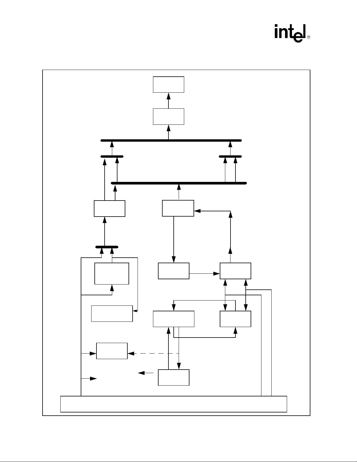
Performance Monitor Events
Figure 4-1. Event Monitors in the Itanium® 2 Processor Memory Hierarchy
BUS
L3_MISSES
L3
L3_REFERENCES
L3_READ_REFERENCES(d)L3_WRITE_REFERENCES(d)
L3_STORE_REFERENCES(d) L3_INST_REFERENCES(d)L2_WB_REFERENCES(d)
L3_DATA_READ_REFERENCES(d)
L2D_MISSES
L2D
L2D_REFERENCES L2I_READS
L1D_READ_MISSES
L1D
(write through)
ITLB_MISSES_FETCH
Store Buffer
L2DTLB_MISSES
L1DTLB
VHPT Walker
(d) = derived counter
L2I_MISSES
L2I
ISB_BUNPAIRS_IN
ISB
L1I_FILLS
DTLB_INSERTS_HPW
L1I
ITLB
ITLB_INSERTS_HPW
L1DTLB_MISSES
L2DTLB
DATA_REFERENCES
Processor Pipeline
L1I_READSL1I_PREFETCHES
82 Reference Manual for Software Development and Optimization

Performance Monitor Events
4.8.1 L1 Instruction Cache and Prefetch Events
Table 4-8 describes and summarizes the events that the Montecito processor provides to monitor
L1 instruction cache demand fetch and prefetch activity. The instruction fetch monitors distinguish
between demand fetch (L1I_READS) and prefetch activity (L1I_PREFETCHES). The amount of
data returned from the L2I to the L1 instruction cache and the Instruction Streaming Buffer is
monitored by two events, L1I_FILLS and ISB_LINES_IN. The L1I_EAR_EVENTS monitor
counts how many instruction cache or L1ITLB misses are captured by the instruction event address
register.
The L1 instruction cache and prefetch events can be qualified by the instruction address range
check, but not by the opcode matcher. Since instruction cache and prefetch events occur early in
the processor pipeline, they include events caused by speculative, wrong-path instructions as well
as predicated-off instructions. Since the address range check is based on speculative instruction
addresses rather than retired instruction addresses, event counts may be inaccurate when the range
checker is confined to address ranges smaller than the length of the processor pipeline (see
Chapter 3 for details).
L1I_EAR_EVENTS counts the number of events captured by the Montecito processor’s
instruction EARs. Please refer to Chapter 3 for more detailed information about the instruction
EARs.
Table 4-8. Performance Monitors for L1/L2 Instruction Cache and Prefetch Events
I
D
Symbol Name
ISB_BUNPAIRS_IN 0x46 Y N N 1 Bundle pairs written from L2I into FE
L1I_EAR_EVENTS 0x43 Y N N 1 Instruction EAR Events
L1I_FETCH_ISB_HIT 0x66 Y N N 1 “Just-in-time” instruction fetch hitting
L1I_FETCH_RAB_HIT 0x65 Y N N 1 Instruction fetch hitting in RAB
L1I_FILLS 0x41 Y N N 1 L1 Instruction Cache Fills
L1I_PREFETCHES 0x44 Y N N 1 L1 Instruction Prefetch Requests
L1I_PREFETCH_STALL 0x67 N N N 1 Why prefetch pipeline is stalled?
L1I_PURGE 0x4b Y N N 1 L1ITLB purges handled by L1I
L1I_PVAB_OVERFLOW 0x69 N N N 1 PVAB overflow
L1I_RAB_ALMOST_FULL 0x64 N N N 1 Is RAB almost full?
L1I_RAB_FULL 0x60 N N N 1 Is RAB full?
L1I_READS 0x40 Y N N 1 L1 Instruction Cache Reads
L1I_SNOOP 0x4a Y Y Y 1 Snoop requests handled by L1I
L1I_STRM_PREFETCHES 0x5f Y N N 1 L1 Instruction Cache line prefetch
L2I_DEMAND_READS 0x42 Y N N 1 L1 Instruction Cache and ISB Misses
L2I_PREFETCHES 0x45 Y N N 1 L2 Instruction Prefetch Requests
Event
Code
O
P
C
Max
Inc/Cyc
Description
in and being bypassed from ISB
requests
A
A
R
R
Reference Manual for Software Development and Optimization 83

Performance Monitor Events
Table 4-9. Derived Monitors for L1 Instruction Cache and Prefetch Events
Symbol Name Description Equation
L1I_MISSES L1I Misses L2I_DEMAND_READS
ISB_LINES_IN Number of cache lines written
from L2I (and beyond) into the
front end
L1I_DEMAND_MISS_RATIO L1I Demand Miss Ratio L2I_DEMAND_READS / L1I_READS
L1I_MISS_RATIO L1I Miss Ratio (L1I_MISSES + L2I_PREFETCHES) /
L1I_PREFETCH_MISS_RATIO L1I Prefetch Miss Ratio L2I_PREFETCHES / L1I_PREFETCHES
L1I_REFERENCES Number of L1 Instruction Cache
reads and fills
ISB_BUNPAIRS_IN/4
(L1I_READS + L1I_PREFETCHES)
L1I_READS + L1I_PREFETCHES
4.8.2 L1 Data Cache Events
Table 4-10 lists the Montecito processor’s L1 data cache monitors. As shown in Figure 4-1, the
write-through L1 data cache services cacheable loads, integer and RSE loads, check loads and
hinted L2 memory references. DATA_REFERENCES is the number of issued data memory
references.
L1 data cache reads (L1D_READS) and L1 data cache misses (L1D_READ_MISSES) monitor the
read hit/miss rate of the L1 data cache. RSE operations are included in all data cache monitors, but
are not broken down explicitly. The DATA_EAR_EVENTS monitor counts how many data cache
or DTLB misses are captured by the Data Event Address Register. Please refer to Section 3.3.9 for
more detailed information about the data EARs.
L1D cache events have been divided into 6 sets (sets 0,1,2,3,4,6; set 5 is reserved). Events from
different sets of L1D Cache events cannot be measured at the same time. Each set is selected by the
event code programmed into PMC5 (i.e. if you want to measure any of the events in this set, one of
them needs to be measured by PMD5). There are no limitations on umasks. Monitors belonging to
each set are explicitly presented in Table 4-10 through Table 4-16.
Table 4-10. Performance Monitors for L1 Data Cache Events
I
D
Symbol Name
DATA_EAR_EVENTS 0xc8 Y Y Y 1 L1 Data Cache EAR Events
L1D_READS_SET0 0xc2 Y Y Y 2 L1 Data Cache Reads
DATA_REFERENCES_SET0 0xc3 Y Y Y 4 Data memory references issued to
L1D_READS_SET1 0xc4 Y Y Y 2 L1 Data Cache Reads
DATA_REFERENCES_SET1 0xc5 Y Y Y 4 Data memory references issued to
L1D_READ_MISSES 0xc7 Y Y Y 2 L1 Data Cache Read Misses
Event
Code
O
P
C
Max
Inc/Cyc
A
A
R
R
Description
memory pipeline
memory pipeline
84 Reference Manual for Software Development and Optimization

4.8.2.1 L1D Cache Events (set 0)
Table 4-11. Performance Monitors for L1D Cache Set 0
Symbol Name
Event
Code
Performance Monitor Events
I
D
O
P
C
Max
Inc/Cyc
Description
A
A
R
R
L1DTLB_TRANSFER 0xc0 Y Y Y 1 L1DTLB misses hit in L2DTLB for
L2DTLB_MISSES 0xc1 Y Y Y 4 L2DTLB Misses
L1D_READS_SET0 0xc2 Y Y Y 2 L1 Data Cache Reads
DATA_REFERENCES_SET0 0xc3 Y Y Y 4 Data memory references issued to
4.8.2.2 L1D Cache Events (set 1)
Table 4-12. Performance Monitors for L1D Cache Set 1
Symbol Name
L1D_READS_SET1 0xc4 Y Y Y 2 L1 Data Cache Reads
DATA_REFERENCES_SET1 0xc5 Y Y Y 4 Data memory references issued to
L1D_READ_MISSES 0xc7 Y Y Y 2 L1 Data Cache Read Misses
Event
Code
4.8.2.3 L1D Cache Events (set 2)
Table 4-13. Performance Monitors for L1D Cache Set 2
Symbol Name
Event
Code
access counted in L1D_READS
memory pipeline
I
D
O
P
C
O
P
C
Max
Inc/Cyc
Max
Inc/Cyc
Description
memory pipeline
Description
A
A
R
R
I
D
A
A
R
R
BE_L1D_FPU_BUBBLE 0xca N N N 1 Full pipe bubbles in main pipe due to
FP or L1D cache
4.8.2.4 L1D Cache Events (set 3)
Table 4-14. Performance Monitors for L1D Cache Set 3
I
D
Symbol Name
LOADS_RETIRED 0xcd Y Y Y 4 Retired Loads
MISALIGNED_LOADS_RETIRED 0xce Y Y Y 4 Retired Misaligned Load Instructions
UC_LOADS_RETIRED 0xcf Y Y Y 4 Retired Uncacheable Loads
Event
Code
Reference Manual for Software Development and Optimization 85
O
P
C
Max
Inc/Cyc
Description
A
A
R
R

Performance Monitor Events
4.8.2.5 L1D Cache Events (set 4)
Table 4-15. Performance Monitors for L1D Cache Set 4
Symbol Name
MISALIGNED_STORES_RETIRED 0xd2 Y Y Y 2 Retired Misaligned Store Instructions
STORES_RETIRED 0xd1 Y Y Y 2 Retired Stores
UC_STORES_RETIRED 0xd0 Y Y Y 2 Retired Uncacheable Stores
Event
Code
4.8.2.6 L1D Cache Events (set 6)
Table 4-16. Performance Monitors for L1D Cache Set 6
Symbol Name
LOADS_RETIRED_INTG 0xd8 Y Y Y 2 Integer loads retired
SPEC_LOADS_NATTED 0xd9 Y Y Y 2 Times ld.s or ld.sa NaT’d
Event
Code
I
D
O
P
C
O
P
C
Max
Inc/Cyc
Max
Inc/Cyc
Description
Description
A
A
R
R
I
D
A
A
R
R
4.8.3 L2 Instruction Cache Events
Table 4-17. Performance Monitors for L2I Cache
Symbol Name
L2I_READS 0x78 Y N Y 1 L2I Cacheable Reads
L2I_UC_READS 0x79 Y N Y 1 L2I uncacheable reads
L2I_VICTIMIZATIONS 0x7a Y N Y 1 L2I victimizations
L2I_RECIRCULATES 0x7b Y N Y 1 L2I recirculates
L2I_L3_REJECTS 0x7c Y N Y 1 L3 rejects
L2I_HIT_CONFLICTS 0x7d Y N Y 1 L2I hit conflicts
L2I_SPEC_ABORTS 0x7e Y N Y 1 L2I speculative aborts
L2I_SNOOP_HITS 0x7f Y N Y 1 L2I snoop hits
Table 4-18. Derived Monitors for L2I Cache (Sheet 1 of 2)
Symbol Name Description Equation
L2I_SNOOPS Number of snoops received by
L2I_FILLS L2I Fills L2I_READS.MISS.DMND +
L2I_FETCHES Requests made to L2I due to
L2I_REFERENCES Instructions requests made to L2I L2I_READS.ALL.ALL
Event
Code
the L2I.
demand instruction fetches.
I
D
O
P
C
Max
Inc/Cyc
L1I_SNOOPS
L2I_READS.MISS.PFTCH
L2I_READS.ALL.DMND
Description
A
A
R
R
86 Reference Manual for Software Development and Optimization

Table 4-18. Derived Monitors for L2I Cache (Sheet 2 of 2)
Symbol Name Description Equation
L2I_MISS_RATIO Percentage of L2I Misses L2I_READS.MISS/L2I_READS.ALL
L2I_HIT_RATIO Percentage of L2I Hits L2I_READS.HIT/L2I_READS.ALL
4.8.4 L2 Data Cache Events
Table 4-19 summarizes the events available to monitor the Montecito processor L2D cache.
Most L2D events have been divided into 8 sets. Only events within two of these sets (or non-L2D
events) can be measured at the same time. These two sets are selected by the event code
programmed into PMC4 and PMC6 (i.e. if you want to measure any of the events in a particular
set, one of these events needs to be measured by PMD4 or PMD6).
Note: The opposite holds true. If PMC4 is not programmed to monitor an L2D event, yet PMC5 or PMC8
are (similarly with PMC6->PMC7/9), PMD values are undefined. Also note that
Any event set can be measured by programming either PMC4 or PMC6. Once PMC4 is
programmed to measure an event from one L2D event set, PMD4, PMD5, and PMD8 can only
measure events from the same L2D event set (PMD5,8 share the umask programmed into PMD4).
Similarly, once PMC6 is programmed to monitor another set (could be the same set as measured by
PMC4), PMD6, PMD7 and PMD9 can measure events from this set only. None of the L2 data
cache events can be measured using PMD10-15.
Performance Monitor Events
Support for the .all bit has the same restrictions as the set restrictions. The value set for “.all” in
PMC4 applies to both the L1D events selected by it. Hence, even though the “.all” values in PMC5
and PMC8 are different from the value in PMC4, PMC4’s value selects the capability. This is same
with PMC6,7,9. Original Montecito documentation claimed that Thread 0 PMC4 .me/.all applied
to PMC4-PMC7 but that is no longer true. This bit is available for both the threads. Hence, it is
possible for one thread’s PMDs to monitor just the events credited for that thread while the other
thread’s PMDs can monitor events for both threads (if PMC4.all is set). Note that some events do
not support .all counting. If .all counting is enabled for events that don’t support it, the resulting
counts will be wrong.
While the L2D events support threading, not all counts have access to exact thread id bit needed.
Each count is labeled with one of ActiveTrue, ActiveApprox, or TrueThrd. ActiveTrue means that
the event is counted with the current active thread, and that thread is the only thread that can see the
event when it is counted. ActiveApprox means the event is counted with the current active thread,
but there are some corner cases were the event may actually be due to the other non-Active thread.
It is assumed in most cases that the error due this approximation will be negligible. TrueThrd
indicates that the L2D cache has knowledge of what thread the count belongs to besides the active
thread indication, and that knowledge is always correct.
Table 4-19. Performance Monitors for L2 Data Cache Events (Sheet 1 of 2)
I
D
Symbol Name
L2D_OZQ_CANCELS0 0xe0 Y Y Y Y 4 L2D OZQ cancels
L2D_OZQ_FULL 0xe1
L2D_OZQ_CANCELS1 0xe2 Y Y Y Y 4 L2D OZQ cancels
Event
Code
0xe3
O
P
C
.all
capable
A
A
R
R
N N N N 1 L2D OZQ is full
Max
Inc/Cyc
Description
Reference Manual for Software Development and Optimization 87

Performance Monitor Events
Table 4-19. Performance Monitors for L2 Data Cache Events (Sheet 2 of 2)
I
D
Symbol Name
Event
Code
O
P
C
.all
capable
A
A
R
R
Max
Inc/Cyc
Description
L2D_BYPASS 0xe4 Y Y Y Y/N 1 L2D Hit or Miss Bypass (.all
L2D_OZQ_RELEASE 0xe5 N N N N 1 Clocks with release ordering
L2D_REFERENCES 0xe6 Y Y Y Y 4 Data RD/WR access to L2D
L2D_L3ACCESS_CANCEL 0xe8 Y Y Y N 1 Canceled L3 accesses
L2D_OZDB_FULL 0xe9 N N N Y 1 L2D OZ data buffer is full
L2D_FORCE_RECIRC 0xea Y Y Y Y/N 4 Forced recirculates
L2D_ISSUED_RECIRC_OZQ_ACC 0xeb Y Y Y Y 1 Count the number of times a
L2DBAD_LINES_SELECTED 0xec Y Y Y Y 4 Valid line replaced when
L2D_STORE_HIT_SHARED 0xed Y Y Y Y 2 Store hit a shared line
L2D_OZQ_ACQUIRE 0xef N N N Y 1 Clocks with acquire ordering
L2D_OPS_ISSUED 0xf0 Y Y Y N 4 Different operations issued by
L2D_FILLB_FULL 0xf1 N N N N 1 L2D Fill buffer is full
L2D_FILL_MESI_STATE 0xf2 Y Y Y Y 1 MESI states of fills to L2D
L2D_VICTIMB_FULL 0xf3 N N N Y 1 L2D victim buffer is full
L2D_MISSES 0xcb Y Y Y Y 1 An L2D miss has been issued
L2D_INSERT_HITS 0xb1 Y Y Y Y 4 Count Number of Times an
L2D_INSERT_MISSES 0xb0 Y Y Y Y 4 Count Number of Times an
support is umask dependent)
attribute existed in L2D OZQ
recirculate issue was
attempted and not preempted
invalid line is available
attribute existed in L2D OZQ
L2D
cache
to the L3, does not include
secondary misses
Inserting Data Request Hit in
the L2D.
Inserting Data Request
Missed in the L2D.
Table 4-20. Derived Monitors for L2 Data Cache Events
Symbol Name Description Equation
L2D_READS L2 Data Read Requests L2D_REFERENCES.READS
L2D_WRITES L2 Data Write Requests L2D_REFERENCES.WRITES
L2D_MISS_RATIO Percentage of L2D Misses L2D_INSERT_MISSES/L2D_REFERENCES
L2D_HIT_RATIO Percentage of L2D Hits L2D_INSERT_HITS/L2D_REFERENCES
L2D_RECIRC_ATTEMPTS Number of times the L2
issue logic attempted to
issue a recirculate
88 Reference Manual for Software Development and Optimization
L2D_ISSUED_RECIRC_OZQ_ACC +
L2D_OZQ_CANCEL_S0.RECIRC

4.8.4.1 L2 Data Cache Events (set 0)
Table 4-21. Performance Monitors for L2 Data Cache Set 0
Symbol Name
Event
Code
Performance Monitor Events
I
D
O
P
C
Max
Inc/Cyc
Description
A
A
R
R
L2D_OZQ_FULL 0xe1
0xe3
L2D_OZQ_CANCELS0 0xe0 Y Y Y 4 L2D OZQ cancels-TrueThrd
L2D_OZQ_CANCELS1 0xe2 Y Y Y 4 L2D OZQ cancels-TrueThrd
L2D_OZQ_FULL is not .all capable.
4.8.4.2 L2 Data Cache Events (set 1)
Table 4-22. Performance Monitors for L2 Data Cache Set 1
Symbol Name
L2D_BYPASS 0xe4 Y Y Y 4 Count L2 Hit bypasses-TrueThread
L2D_OZQ_RELEASE 0xe5 N N N 1 Effective Release is valid in
Event
Code
The L2D_BYPASS count on Itanium 2 processors was too speculative to be useful. It has been
fixed and we now count how many bypasses occurred in a given cycle, rather than signalling a 1
for 1-4 bypasses. The 5 and 7 cycle umasks of L2D_BYPASS and the L2D_OZQ_RELEASE
counts are not .all capable.
4.8.4.3 L2 Data Cache Events (set 2)
N N N 1 L2D OZQ Full-ActiveApprox
I
D
O
P
C
Max
Inc/Cyc
Description
Ozq-ActiveApprox
A
A
R
R
Table 4-23. Performance Monitors for L2 Data Cache Set 2
I
D
Symbol Name
L2D_REFERENCES 0xe6 Y Y Y 4 Inserts of Data Accesses into
Event
Code
O
P
C
Max
Inc/Cyc
Description
Ozq-ActiveTrue
A
A
R
R
4.8.4.4 L2 Data Cache Events (set 3)
L
Table 4-24. Performance Monitors for L2 Data Cache Set 3
I
D
Symbol Name
L2D_L3_ACCESS_CANCEL 0xe8 Y Y Y 1 L2D request to L3 was
L2D_OZDB_FULL 0xe9 N N N 1 L2D OZ data buffer is
Event
Code
Reference Manual for Software Development and Optimization 89
O
P
C
Max
Inc/Cyc
Description
cancelled-TrueThrd
full-AcitveApprox
A
A
R
R

Performance Monitor Events
L2D_L3_ACCESS_CANCEL events are not .all capable.
4.8.4.5 L2 Data Cache Events (set 4)
Table 4-25. Performance Monitors for L2 Data Cache Set 4
Symbol Name
Event
Code
I
D
O
P
C
Max
Inc/Cyc
Description
A
A
R
R
L2D_FORCE_RECIRC 0xea Y Y Y 4 Forced recirculates - ActiveTrue or
L2D_ISSUED_RECIRC_OZQ_ACC 0xeb Y Y Y 1 Ozq Issued Recirculate - TrueThrd
Some umasks of L2D_FORCE_RECIRC are not .all capable.
4.8.4.6 L2 Data Cache Events (set 5)
Table 4-26. Performance Monitors for L2 Data Cache Set 5
Symbol Name
L2D_BAD_LINES_SELECTED 0xec Y Y Y 4 Valid line replaced when invalid line is
L2D_STORE_HIT_SHARED 0xed Y Y Y 2 Store hit a shared line
Event
Code
4.8.4.7 L2 Data Cache Events (set 6)
E
Table 4-27. Performance Monitors for L2 Data Cache Set 6
Symbol Name
Event
Code
ActiveApprox
I
D
O
P
C
O
P
C
Max
Inc/Cyc
Max
Inc/Cyc
Description
available
Description
A
A
R
R
I
D
A
A
R
R
L2D_OZQ_ACQUIRE 0xef N N N 1 Valid acquire operation in
Ozq-TrueThrd
4.8.4.8 L2 Data Cache Events (set 7)
Table 4-28. Performance Monitors for L2 Data Cache Set 7
I
D
Symbol Name
L2D_OPS_ISSUED 0xf0 Y Y Y 4 Different operations issued by
L2D_FILLB_FULL 0xf1 N N N 1 L2D Fill buffer is full-ActiveApprox
Event
Code
L2D_OPS_ISSUED and L2D_FILLB_FULL are not .all capable.
90 Reference Manual for Software Development and Optimization
O
P
C
Max
Inc/Cyc
Description
L2D-TrueThrd
A
A
R
R

4.8.4.9 L2 Data Cache Events (set 8)
Table 4-29. Performance Monitors for L2 Data Cache Set 8
Symbol Name
Event
Code
Performance Monitor Events
I
D
O
P
C
Max
Inc/Cyc
Description
A
A
R
R
L2D_FILL_MESI_STATE 0xf2 Y Y Y 1 Fill to L2D is of a particular MESI
L2D_VICTIMB_FULL 0xf3 N N N 1 L2D victim buffer is full-ActiveApprox
4.8.4.10 L2 Data Cache Events (Not Set Restricted)
These events are sent to the PMU block directly and thus are not set restricted.
Table 4-30. Performance Monitors for L2D Cache - Not Set Restricted
I
D
Symbol Name
L2D_MISSES 0xcb Y Y Y 1 An L2D miss has been issued to the
L2D_INSERT_MISSES 0xb0 Y Y Y 4 An inserting Ozq op was a miss on its
L2D_INSERT_HITS 0xb1 Y Y Y 4 An inserting Ozq op was a hit on its
Event
Code
O
P
C
Max
Inc/Cyc
A
A
R
R
4.8.5 L3 Cache Events
Table 4-31 summarizes the directly-measured L3 cache events. An extensive list of derived events
is provided in Table 4-32.
value. TrueThrd
Description
L3, does not include secondary
misses.
first lookup.
first lookup.
Table 4-31. Performance Monitors for L3 Unified Cache Events
I
D
Symbol Name
L3_LINES_REPLACED 0xdf N N N 1 L3 Cache Lines Replaced
L3_MISSES 0xdc Y Y Y 1 L3 Misses
L3_READS 0xdd Y Y Y 1 L3 Reads
L3_REFERENCES 0xdb Y Y Y 1 L3 References
L3_WRITES 0xde Y Y Y 1 L3 Writes
L3_INSERTS 0xda 1 L3 Cache lines inserted (allocated)
Event
Code
Reference Manual for Software Development and Optimization 91
O
P
C
Max
Inc/Cyc
Description
MESI filtering capability
MESI filtering capability
MESI filtering capability
MESI filtering capability
A
A
R
R

Performance Monitor Events
Table 4-32. Derived Monitors for L3 Unified Cache Events
Symbol Name Description Equation
L3_DATA_HITS L3 Data Read Hits L3_READS.DATA_READ.HIT
L3_DATA_MISS_RATIO L3 Data Miss Ratio (L3_READS.DATA_READ.MISS +
L3_DATA_READ_MISSES L3 Data Read Misses L3_READS.DATA_READ.MISS
L3_DATA_READ_RATIO Ratio of L3 References that are
L3_DATA_READ_REFEREN
CES
L3_INST_HITS L3 Instruction Hits L3_READS.INST_FETCH.HIT
L3_INST_MISSES L3 Instruction Misses L3_READS.INST_FETCH.MISS
L3_INST_MISS_RATIO L3_READS.INST_FETCH.MISS /
L3_INST_RATIO Ratio of L3 References that are
L3_INST_REFERENCES L3 Instruction References L3_READS.INST_FETCH.ALL
L3_MISS_RATIO Percentage Of L3 Misses L3_MISSES/L3_REFERENCES
L3_READ_HITS L3 Read Hits L3_READS.READS.HIT
L3_READ_MISSES L3 Read Misses L3_READS.READS.MISS
L3_READ_REFERENCES L3 Read References L3_READS.READS.ALL
L3_STORE_HITS L3 Store Hits L3_WRITES.DATA_WRITE.HIT
L3_STORE_MISSES L3 Store Misses L3_WRITES.DATA_WRITE.MISS
L3_STORE_REFERENCES L3 Store References L3_WRITES.DATA_WRITE.ALL
L2_WB_HITS L2D Writeback Hits L3_WRITES.L2_WB.HIT
L2_WB_MISSES L2D Writeback Misses L3_WRITES.L2_WB.MISS
L2_WB_REFERENCES L2D Writeback References L3_WRITES.L2_WB.ALL
L3_WRITE_HITS L3 Write Hits L3_WRITES.ALL.HIT
L3_WRITE_MISSES L3 Write Misses L3_WRITES.ALL.MISS
L3_WRITE_REFERENCES L3 Write References L3_WRITES.ALL.ALL
Data Read References
L3 Data Read References L3_READS.DATA_READ.ALL
Instruction References
L3_WRITES.DATA_WRITE.MISS) /
(L3_READS.DATA_READ.ALL +
L3_WRITES.DATA_WRITE.ALL)
L3_READS.DATA_READ.ALL /
L3_REFERENCES
L3_READS.INST_FETCH.ALL
L3_READS.INST_FETCH.ALL /
L3_REFERENCES
4.9 System Events
The debug register match events count how often the address of any instruction or data breakpoint
register (IBR or DBR) matches the current retired instruction pointer
(CODE_DEBUG_REGISTER_MATCHES) or the current data memory address
(DATA_DEBUG_REGISTER_MATCHES). CPU_CPL_CHANGES counts the number of
privilege level transitions due to interruptions, system calls (epc), returns (demoting branch), and
instructions.
92 Reference Manual for Software Development and Optimization

Table 4-33. Performance Monitors for System Events
I
Symbol Name
CPU_CPL_CHANGES 0x13 N N N 1 Privilege Level Changes
DATA_DEBUG_REGISTER_FAULT 0x52 N N N 1 Fault due to data debug reg. Match to
DATA_DEBUG_REGISTER_MATCHES0xc6 Y Y Y 1 Data debug register matches data
SERIALIZATION_EVENTS 0x53 N N N 1 Number of srlz.I instructions
CYCLES_HALTED 0x18 N N N 1 Number of core cycles the thread is in
Event
Code
D
A
A
R
R
Table 4-34. Derived Monitors for System Events
Symbol Name Description Equation
O
P
C
Max
Inc/Cyc
Performance Monitor Events
Description
load/store instruction
address of memory reference
low-power halted state.
NOTE: only PMC/PMD10 pair is
capable of counting this event
CODE_DEBUG_REGISTER_
MATCHES
Code Debug Register Matches IA64_TAGGED_INST_RETIRED
4.10 TLB Events
The Montecito processor instruction and data TLBs and the virtual hash page table walker are
monitored by the events described in Table 4-35.
L1ITLB_REFERENCES and L1DTLB_REFERENCES are derived from the respective
instruction/data cache access events. Note that ITLB_REFERENCES does not include prefetch
requests made to the L1I cache (L1I_PREFETCH_READS). This is because prefetches are
cancelled when they miss in the ITLB and thus do not trigger VHPT walks or software TLB miss
handling. ITLB_MISSES_FETCH and L2DTLB_MISSES count TLB misses.
L1ITLB_INSERTS_HPW and DTLB_INSERTS_HPW count the number of instruction/data TLB
inserts performed by the virtual hash page table walker.
Table 4-35. Performance Monitors for TLB Events
Symbol Name
DTLB_INSERTS_HPW 0xc9 Y Y Y 4 Hardware Page Walker inserts to
HPW_DATA_REFERENCES 0x2d Y Y Y 4 Data memory references to VHPT
L2DTLB_MISSES 0xc1 Y Y Y 4 L2DTLB Misses
L1ITLB_INSERTS_HPW 0x48 Y N N 1 L1ITLB Hardware Page Walker
ITLB_MISSES_FETCH 0x47 Y N N 1 ITLB Misses Demand Fetch
L1DTLB_TRANSFER 0xc0 Y Y Y 1 L1DTLB misses that hit in the
Event
Code
I
D
O
P
C
Max
Inc/Cyc
Description
DTLB
Inserts
L2DTLB for accesses counted in
L1D_READS
A
A
R
R
Reference Manual for Software Development and Optimization 93

Performance Monitor Events
Table 4-36. Derived Monitors for TLB Events
Symbol Name Description Equation
L1DTLB_EAR_EVENTS Counts the number of L1DTLB
L2DTLB_MISS_RATIO L2DTLB miss ratio L2DTLB_MISSES /
L1DTLB_REFERENCES L1DTLB References DATA_REFERENCES_SET0 or
L1ITLB_EAR_EVENTS Provides information on the
L1ITLB_MISS_RATIO L1ITLB miss ratio ITLB_MISSES_FETCH.L1ITLB /
L1ITLB_REFERENCES L1ITLB References L1I_READS
L1DTLB_FOR_L1D_MISS_R
ATIO
events captured by the EAR
number of L1ITLB events
captured by the EAR. This is a
subset of L1I_EAR_EVENTS
Miss Ratio of L1DTLB servicing
the L1D
DATA_EAR_EVENTS
DATA_REFERENCES_SET0 or
L2DTLB_MISSES /
DATA_REFERENCES_SET1
DATA_REFERENCES_SET1
L1I_EAR_EVENTS
L1I_READS
L1DTLB_TRANSFER /
L1D_READS_SET0 or
L1DTLB_TRANSFER /
L1D_READS_SET1
The Montecito processor has 2 data TLBs called L1DTLB and L2DTLB (also referred to as
DTLB). These TLBs are in parallel and the L2DTLB is the larger and slower of the two.The
possible actions for the combination of hits and misses in these TLBs are outlined below:
• L1DTLB_hit=0, L2DTLB_hit=0: If enabled, HPW kicks in and inserts a translation into one
or both TLBs.
• L1DTLB_hit=0, L2DTLB_hit=1: If floating-point, no action is taken; else a transfer is made
from L2DTLB to L1DTLB.
• L1DTLB_hit=1, L2DTLB_hit=0: If enabled, HPW kicks in and inserts a translation into one
or both TLBs.
• L1DTLB_hit=1, L2DTLB_hit=1: No action is taken.
When a memory operation goes down the memory pipeline, DATA_REFERENCES will count it.
If the translation does not exist in the L2DTLB, then L2DTLB_MISSES will count it. If the HPW
is enabled, then HPW_DATA_REFERENCES will count it. If the HPW finds the data in VHPT, it
will insert it in the L1DTLB and L2DTLB (as needed). If the translation exists in the L2DTLB, the
only case that some work is done is when translation does not exist in the L1DTLB. If the operation
is serviced by the L1D (see L1D_READS description), L1DTLB_TRANSFER will count it. For
the purpose of calculating the TLB miss ratios, VHPT memory references have been excluded from
the DATA_REFERENCES event and provided VHPT_REFERENCES for the situations where one
might want to add them in.
Due to the TLB hardware design, there are some corner cases, where some of these events will
show activity even though the instruction causing the activity never reaches retirement (they are
marked so). Since the processor is stalled even for these corner cases, they are included in the
counts and as long as all events that are used for calculating a metric are consistent with respect to
this issue, fairly accurate numbers are expected.
94 Reference Manual for Software Development and Optimization

4.11 System Bus Events
Table 4-40 lists the system bus transaction monitors. Many of the listed bus events take a umask
that qualifies the event by initiator. For all bus events, when “per cycles” is mentioned, SI clock
cycles (bus clock multiplied by bus ratio) are inferred rather than bus clock cycles unless otherwise
specified. Numerous derived events have been included in Table 4-41.
Table 4-37. Performance Monitors for System Bus Events (Sheet 1 of 3)
I
D
Symbol Name
BUS_ALL 0x87 N N N 1 Bus Transactions
ER_BRQ_LIVE_REQ_HI 0xb8 N N N 2 BRQ Live Requests (two
ER_BRQ_LIVE_REQ_LO 0xb9 N N N 7 BRQ Live Requests (three
ER_BRQ_REQ_INSERTED 0xba N N N 1 BRQ Requests Inserted
ER_BKSNP_ME_ACCEPTED 0xbb N N N 1 BacksnoopMe Requests accepted
ER_REJECT_ALL_L1_REQ 0xbc N N N 1 Number of cycles in which the BRQ
ER_REJECT_ALL_L1D_REQ 0xbd N N N 1 Number of cycles in which the BRQ
ER_REJECT_ALL_L1I_REQ 0xbe N N N 1 Number of cycles in which the BRQ
BUS_DATA_CYCLE 0x88 N N N 1 Valid data cycle on the Bus
BUS_HITM 0x84 N N N 1 Bus Hit Modified Line Transactions
BUS_IO 0x90 N N N 1 IA-32 Compatible IO Bus
SI_IOQ_LIVE_REQ_HI 0x98 N N N 1 In-order Bus Queue Requests (one
SI_IOQ_LIVE_REQ_LO 0x97 N N N 7 In-order Bus Queue Requests (three
BUS_B2B_DATA_CYCLES 0x93 N N N 1 Back-to-back bursts of data
SI_CYCLES 0x8e N N N 1 Counts SI cycles
BUS_MEMORY 0x8a N N N 1 Bus Memory Transactions
BUS_MEM_READ 0x8b N N N 1 Full Cache line D/I memory RD, RD
ER_MEM_READ_OUT_HI 0xb4 N N N 2 Outstanding memory RD transactions
Event
Code
O
P
C
Max
Inc/Cyc
A
A
R
R
Performance Monitor Events
Description
most-significant-bit of the 5-bit
outstanding BRQ request count)
least-significant-bit of the 5-bit
outstanding BRQ request count)
into the BRQ from the L2D (used by
the L2D to get itself out of potential
forward progress situations)
was rejecting all L1I/L1D requests (for
the “Big Hammer” forward progress
logic)
was rejecting all L1D requests (for
L1D/L1I forward progress)
was rejecting all L1I requests (for
L1D/L1I forward progress)
Transactions
most-significant-bit of the 4-bit
outstanding IOQ request count)
least-significant-bit of the 4-bit
outstanding IOQ request count)
invalidate, and BRIL
(upper two bits)
Reference Manual for Software Development and Optimization 95

Performance Monitor Events
Table 4-37. Performance Monitors for System Bus Events (Sheet 2 of 3)
I
D
Symbol Name
Event
Code
O
P
C
Max
Inc/Cyc
A
A
R
R
Description
ER_MEM_READ_OUT_LO 0xb5 N N N 7 Outstanding memory RD transactions
BUS_RD_DATA 0x8c N N N 1 Bus Read Data Transactions
BUS_RD_HIT 0x80 N N N 1 Bus Read Hit Clean Non-local Cache
BUS_RD_HITM 0x81 N N N 1 Bus Read Hit Modified Non-local
BUS_RD_INVAL_BST_HITM 0x83 N N N 1 Bus BRIL Burst Transaction Results
BUS_RD_INVAL_HITM 0x82 N N N 1 Bus BIL Transaction Results in HITM
BUS_RD_IO 0x91 N N N 1 IA-32 Compatible IO Read
BUS_RD_PRTL 0x8d N N N 1 Bus Read Partial Transactions
ER_SNOOPQ_REQ_HI 0xb6 N N N 1 ER Snoop Queue Requests (most
ER_SNOOPQ_REQ_LO 0xb7 N N N 7 ER Snoop Queue Requests (three
BUS_SNOOP_STALL_CYCLES 0x8f N N N 1 Bus Snoop Stall Cycles (from any
BUS_WR_WB 0x92 N N N 1 Bus Write Back Transactions
MEM_READ_CURRENT 0x89 N N N 1 Current Mem Read Transactions On
SI_RQ_INSERTS 0x9e N N N 2 SI request queue inserts
SI_RQ_LIVE_REQ_HI 0xa0 N N N 1 SI request queue live requests
SI_RQ_LIVE_REQ_LO 0x9f N N N 7 SI request queue live requests
SI_WRITEQ_INSERTS 0xa1 N N N 2 SI write queue inserts
SI_WRITEQ_LIVE_REQ_HI 0xa3 N N N 1 SI write queue live requests
SI_WRITEQ_LIVE_REQ_LO 0xa2 N N N 7 SI write queue live requests
SI_WAQ_COLLISIONS 0xa4 N N N 1 SI write address queue collisions
SI_CCQ_INSERTS 0xa5 N N N 2 SI clean castout queue inserts
SI_CCQ_LIVE_REQ_HI 0xa7 N N N 1 SI clean castout queue live requests
SI_CCQ_LIVE_REQ_LO 0xa6 N N N 7 SI clean castout queue live requests
SI_CCQ_COLLISIONS 0xa8 N N N 1 SI clean castout queue collisions
SI_IOQ_COLLISIONS 0xaa N N N 1 SI inorder queue collisions (outgoing
(lower three bits)
Transactions
Cache Transactions
in HITM
Transactions
significant bit of 4-bit count)
least-significant-bits or 4-bit count)
agent)
Bus
(most-significant bit)
(least-significant three bits)
(most-significant bit)
(least-significant three bits)
(incoming FSB snoop collides with an
entry in WAQ)
(most-significant bit)
(least-significant three bits)
(incoming FSB snoop collides with an
entry in CCQ)
transaction collides with an entry in
IOQ)
96 Reference Manual for Software Development and Optimization

Performance Monitor Events
Table 4-37. Performance Monitors for System Bus Events (Sheet 3 of 3)
I
D
Symbol Name
SI_SCB_INSERTS 0xab N N N 1 SI snoop coalescing buffer inserts
SI_SCB_LIVE_REQ_HI 0xad N N N 1 SI snoop coalescing buffer live
SI_SCB_LIVE_REQ_LO 0xac N N N 7 SI snoop coalescing buffer live
SI_SCB_SIGNOFFS 0xae N N N 1 SI snoop coalescing buffer coherency
SI_WDQ_ECC_ERRORS 0xaf N N N 1 SI write data queue ECC errors
Event
Code
O
P
C
Max
Inc/Cyc
requests (most-significant bit)
requests (least-significant three bits)
signoffs
A
A
R
R
Table 4-38. Derived Monitors for System Bus Events (Sheet 1 of 2)
Symbol Name Description Equation
Description
BIL_HITM_LINE_RATIO BIL Hit to Modified Line Ratio BUS_RD_INVAL_HITM /
BIL_RATIO BIL Ratio BUS_RD_INVAL / BUS_MEMORY
BRIL_HITM_LINE_RATIO BRIL Hit to Modified Line Ratio BUS_RD_INVAL_BST_HITM /
BUS_ADDR_BPRI Bus transactions used by IO
BUS_BRQ_LIVE_REQ BRQ Live Requests ER_BRQ_LIVE_REQ_HI * 8 +
BUS_BURST Full cache line memory
BUS_HITM_RATIO Bus Modified Line Hit Ratio BUS_HITM / BUS_MEMORY or
BUS_HITS_RATIO Bus Read Hit to Shared Line
BUS_IOQ_LIVE_REQ Inorder Bus Queue Requests SI_IOQ_LIVE_REQ_HI * 8+
BUS_IO_CYCLE_RATIO Bus I/O Cycle Ratio BUS_IO / BUS_ALL
BUS_IO_RD_RATIO Bus I/O Read Ratio BUS_RD_IO / BUS_IO
BUS_MEM_READ_OUTSTA
NDING
BUS_PARTIAL Less than cache line memory
BUS_PARTIAL_RATIO Bus Partial Access Ratio BUS_MEMORY.LT_128BYTE /
BUS_RD_ALL Full cache line memory read
BUS_RD_DATA_RATIO Cacheable Data Fetch Bus
agent.
transactions (BRL, BRIL, BWL)
Ratio
Number of outstanding memory
RD transactions
transactions (BRP, BWP)
transactions (BRL)
Transaction Ratio
BUS_MEMORY or
BUS_RD_INVAL_HITM /
BUS_RD_INVAL
BUS_MEMORY or
BUS_RD_INVAL_BST_HITM /
BUS_RD_INVAL
BUS_MEMORY.*.IO
ER_BRQ_LIVE_REQ_LO
BUS_MEMORY.EQ_128BYTE.*
BUS_HITM / BUS_BURST
BUS_RD_HIT / BUS_RD_ALL or
BUS_RD_HIT / BUS_MEMORY
SI_IOQ_LIVE_REQ_LO
ER_MEM_READ_OUT_HI * 8 +
ER_MEM_READ_OUT_LO
BUS_MEMORY.LT_128BYTE.*
BUS_MEMORY.ALL
BUS_MEM_READ.BRL.*
BUS_RD_DATA / BUS_ALL or
BUS_RD_DATA / BUS_MEMORY
Reference Manual for Software Development and Optimization 97

Performance Monitor Events
Table 4-38. Derived Monitors for System Bus Events (Sheet 2 of 2)
Symbol Name Description Equation
BUS_RD_HITM_RATIO Bus Read Hit to Modified Line
BUS_RD_INSTRUCTIONS Full cache line instruction
BUS_RD_INVAL 0 byte memory read-invalidate
BUS_RD_INVAL_BST Full cache line read-invalidate
BUS_RD_INVAL_BST_MEM
ORY
BUS_RD_INVAL_MEMORY Bus Read Invalidate Line
BUS_RD_INVAL_ALL_HITM Bus Read Invalidate Line
BUS_RD_PRTL_RATIO Bus Read Partial Access Ratio BUS_RD_PRTL / BUS_MEMORY
BUS_WB_RATIO Writeback Ratio BUS_WR_WB / BUS_MEMORY or
CACHEABLE_READ_RATIO Cacheable Read Ratio (BUS_RD_ALL +
Ratio
memory read transactions (BRP)
transactions (BIL)
transactions (BRIL)
Bus Read Invalid Line in Burst
transactions (BRIL) satisfied by
memory
transactions (BIL) satisfied from
memory
transactions (BRIL and BIL)
resulting in HITMs
4.11.1 System Bus Conventions
BUS_RD_HITM / BUS_RD_ALL or
BUS_RD_HITM / BUS_MEMORY
BUS_RD_ALL - BUS_RD_DATA
BUS_MEM_READ.BIL.*
BUS_MEM_READ.BRIL.*
BUS_RD_INVAL_BST BUS_RD_INVAL_BST_HITM
BUS_RD_INVAL BUS_RD_INVAL_HITM
BUS_RD_INVAL_BST_HITM +
BUS_RD_INVAL_HITM
BUS_WR_WB / BUS_BURST
BUS_MEM_READ.BRIL) /
BUS_MEMORY
Table 4-39 defines the conventions that will be used when describing the Montecito processor
system bus transaction monitors in this section, as well as the individual monitor descriptions in
Section 4.15.
Other transactions besides those listed in Table 4-42 include Deferred Reply, Special Transactions,
Interrupt, Interrupt Acknowledge, and Purge TC. Note that the monitors will count if any
transaction gets a retry response from the priority agent.
To support the analysis of snoop traffic in a multiprocessor system, the Montecito processor
provides local processor and remote response monitors. The local processor snoop events
(SI_SCB_INSERTS and SI_SCB_SIGNOFFS) monitor inbound snoop traffic. The remote
response events (BUS_RD_HIT, BUS_RD_HITM, BUS_RD_INVAL_HITM and
BUS_RD_INVAL_BST_HITM) monitor the snoop responses of other processors to bus
transactions that the monitoring processor originated. Table 4-40 summarizes the remote snoop
events by bus transaction.
4.11.2 Extracting Memory Latency from Montecito Performance
Counters
On the Itanium 2 processors, several events were provided to approximate memory latency as seen
by the processor using the following equation:
((BUS_MEM_READ_OUT_HI * 8) + BUS_MEM_READ_OUT_LO) /
(BUS_MEM_READ.BRL.SELF + BUS_MEM_READ.BRIL.SELF)
98 Reference Manual for Software Development and Optimization

Performance Monitor Events
The BUS_MEM_READ_OUT starts counting one bus clock after a request is issued on the system
interface (ADS) and stops incrementing when the request completes its first data transfer or is
retried. In each core cycle after counting is initiated, the number of live requests in that cycle are
added to the count. This count may as high as 15. For ease of implementation, the count is split into
two parts: BUS_MEM_READ_OUT_LO sums up the low order 3 bits of the number of live
requests, while BUS_MEM_READ_OUT_HI sums up the high order bit.
In the above formula, the numerator provides the number of live requests and the denominator
provides the number of requests that are counted. When the live count is divided by the number of
transactions issued, you get an average lifetime of a transaction issued on the system interface (a
novel application of Little’s Law).
The Montecito processor has similar counters: ER_MEM_READ_OUT.{HI,LO}. Using these
events to derive Montecito memory latency will give results that are higher than the true memory
latency seen in Montecito. The main reason for this is the fact that the start and stop point of the
counters are not equivalent between the two processors. Specifically, in Montecito,
ER_MEM_READ_OUT.{HI,LO}events start counting the core clock after a request is sent to the
arbiter. The Montecito ER_MEM_READ_OUT_{HI,LO}events stop counting when the request
receives its first data transfer within the external request logic (after the arbiter). Thus, these events
include the entire time requests spend in the arbiter (pre and post request).
The requests may remain in the arbiter for a long or short time depending on system interface
behaviors. Arbiter queue events SI_RQ_LIVE_REQ.{HI,LO} may be used to reduce the effects of
arbiter latency on the calculations. Unfortunately, these events are not sufficient to successfully
enable a completely equivalent measurement for Itanium 2 processors. The arbiter time back from
FSB to core is fixed for a specific arbiter to system interface ratio. These arbiter events may occur
in a different time domain from core events
The new memory latency approximation formula for Montecito, with corrective events included, is
below:
(ER_MEM_READ_OUT_HI * 8 + ER_MEM_READ_OUT_LO) – (SI_RQ_LIVE_REQ_HI * 8
+ SI_RQ_LIVE_REQ_LO) / ( BUS_MEM_READ)
Note that the Data EAR may be used to compare data cache load miss latency between Madison
and Montecito. However, an access’ memory latency, as measured by the Data EAR or other cycle
counters will be inherently greater on Montecito compared to previous Itanium 2 processors due to
the latency the arbiter adds to both the outbound request and inbound data transfer. Also, the Data
EAR encompasses the entire latency through the processor’s memory hierarchy and queues
without details into time spent in any specific queue.
Even with this improved formula, the estimated memory latency for Montecito will appear greater
than previous Itanium 2 processors. We have not observed any design point that suggests that the
system interface component of memory accesses are excessive on Montecito.
We have observed that snoop stalls and write queue pressure lead to additional memory latency on
Montecito compared to previous Itanium 2 processors, but these are phenomena that impact the
pre-system or post-system interface aspect of a memory latency and are very workload dependant
in their impact. Specifically, the write queues need to be sufficiently filled to cause back pressure
on the victimizing read requests such that a new read request cannot issue to the system interface
because it cannot identify a victim in the L3 cache to ensure its proper allocation. This sever
pressure has only been seen with steady streams of every read requests resulting in a dirty L3
victim. Additional snoop stalls should only add latency to transactions that receive a HITM snoop
response (cache to cache transfers) because non-HITM responses are satisfied by the memory and
memory access should be initiated as a consequence of the initial transaction rather than its snoop
response.
Reference Manual for Software Development and Optimization 99

Performance Monitor Events
The figure below (Figure 4-2) shows the latency is determined using the above calculations on
Itanium 2 and Montecito processors. The red portion of the Montecito diagram shows latency
accounted for by the correction found in the Montecito calculation.
Figure 4-2. Extracting Memory Latency from PMUs
Ita n iu m 2
L o a d I s s u e d t o
c a c h e s
D a t a r e t u r n e d t o
r e g is t e r
L o a d is s u e d o n
s y s t e m in t e r f a c e
T i m e c a l c u la t e d w it h
P M U e v e n t s
D a t a d e li v e r y
s ta r t e d
M o n t e c i t o
L o a d I s s u e d t o
c a c h e s
T i m e i n
A r b it e r
D a t a r e t u r n e d t o
r e g is te r
L o a d is s u e d t o
a r b it e r
D a t a d e li v e r y
s e e n b y e x te r n a l
r e q u e s t l o g ic
4.12 RSE Events
Register Stack Engine events are presented in Table 4-39. The number of current/dirty registers are
split among three monitors since there are 96 physical registers in the Montecito processor.
Table 4-39. Performance Monitors for RSE Events (Sheet 1 of 2)
L o a d is s u e d o n
s y s t e m in t e r f a c e
T i m e c a l c u la t e d
w i t h P M U e v e n t s
D a t a d e li v e r y
s ta r t e d
I
D
Symbol Name
RSE_CURRENT_REGS_2_TO_0 0x2b N N N 7 Current RSE registers
RSE_CURRENT_REGS_5_TO_3 0x2a N N N 7 Current RSE registers
RSE_CURRENT_REGS_6 0x26 N N N 1 Current RSE registers
RSE_DIRTY_REGS_2_TO_0 0x29 N N N 7 Dirty RSE registers
Event
Code
O
P
C
Max
Inc/Cyc
Description
A
A
R
R
100 Reference Manual for Software Development and Optimization
 Loading...