


Intel® Itanium® 2 Processor
Hardware Developer’s Manual
July 2002
Document Number: 251109-001

Information in this document is provided in connection with Intel® products. No license, express or implied, by estoppel or otherwise, to any intellectual
property rights is granted by this document. Except as provided in Intel’s Terms and Conditions of Sale for such products, Intel assumes no liability
whatsoever, and Intel disclaims any express or implied warranty, relating to sale and/or use of Intel products including liability or warranties relating to
fitness for a particular purpose, merchantability, or infringement of any patent, copyright or other intellectual property right. Intel products are not
intended for use in medical, life saving, or life sustaining applications.
Intel may make changes to specifications and product descriptions at any time, without notice.
Designers must not rely on the absence or characteristics of any features or instructions marked “reserved” or “undefined.” Intel reserves these for
future definition and shall have no responsibility whatsoever for conflicts or incompatibilities arising from future changes to them.
The Itanium 2 processor may contain design defects or errors known as errata which may cause the product to deviate from published specifications.
Current characterized errata are available on request.
Contact your local Intel sales office or your distributor to obtain the latest specifications and before placing your product order.
Copies of documents which have an ordering number and are referenced in this document, or other Intel literature may be obtained by calling
1-800-548-4725 or by visiting Intel’s website at http://developer.intel.com/design/litcentr.
Intel and Itanium are trademarks or registered trademarks of Intel Corporation or its subsidiaries in the United States and other countries.
Copyright © 2002, Intel Corporation. All rights reserved.
*Other names and brands may be claimed as the property of others.
I2C is a two-wire communication bus /protocol developed by Phillips. SMBus is a subset of the I2C bus/protocol developed by Intel. Implementation of
the I2C bus/protocol or the SMBus bus/protocol may require licenses from various entities, including Phillips Electronics, N.V. and North American
Phillips Corporation.
ii Intel® Itanium® 2 Processor Hardware Developer’s Manual

Contents
1 Introduction......................................................................................................................1-1
1.1 Itanium
1.2 Processor Abstraction Layer..............................................................................1-1
1.3 Terminology........................................................................................................1-2
1.4 Reference Documents........................................................................................1-2
2 Itanium
2.1 Overview ............................................................................................................2-1
2.2 Instruction Processing........................................................................................2-4
2.3 Execution............................................................................................................2-5
2.4 Control ................................................................................................................2-8
2.5 Memory Subsystem............................................................................................2-8
2.6 IA-32 Execution ................................................................................................2-11
1.4.1 Revision His tor y.......................... .......... ................ .......... ................ ......1-3
®
2.1.1 6-Wide EPIC Core................... ................ .......... ......... ................. ......... .2-1
2.1.2 Processor Pipeline................................................................................2-2
2.1.3 Processor Block Diagram......................................................................2-3
2.2.1 Instructi o n Pre fe tch a nd Fetch ................ .......... ................ .......... ..........2-4
2.2.2 Branch Prediction........................ .......... ................ .......... ................ ......2-5
2.2.3 Dispersal Logic......................................................................................2-5
2.3.1 Floating- Po int Unit (FPU)........................ .......... ................ .......... ..........2-5
2.3.2 Integer Logic. .......... ................. ......... ................. ................ .......... ..........2-6
2.3.3 Register Files ........................................................................................2-6
2.3.4 Register Stack Engine (RSE)................................................................2-7
2.5.1 L1 Instruction Cache.............................................................................2-9
2.5.2 L1 Data Cache ......................................................................................2-9
2.5.3 Unified L2 Cache......................... .......... ................ .......... ................ ......2-9
2.5.4 Unified L3 Cache......................... .......... ................ .......... ................ ......2-9
2.5.5 The Advanced Load Add re ss Tab le (AL AT)........ ................ .......... ........2-9
2.5.6 Translation Lookas ide Buffers (TLBs).. ...............................................2-10
2.5.7 Cache Coheren cy ................................................................................2-10
2.5.8 Write Coalescing.................................................................................2-10
2.5.9 Memory Ordering ................................................................................2-11
®
2 Processor System Bus......... ......... ................. ......... ................. ........1-1
2 Processor Microar ch i te c tu re.. ................. ......... ................. ......... ................. ...2-1
3 System Bus Overvie w........................ ................. ......... ................. ......... ................. ........3-1
3.1 Signaling on the Itanium
3.1.1 Common Clock Signaling............ .......... ................ ................. ......... ......3-1
3.1.2 Source Synchro n ous Si g n al i n g.......... ................. ................ .......... ........3-2
3.2 Signal Overview ......................................................................................... ....... .3-3
3.2.1 Control Signals......................................................................................3-4
3.2.2 Arbitrat ion Signals................ .......... ................ ................. ......... .............3-4
3.2.3 Reque st Signals ....................................................................................3-5
3.2.4 Snoop Signal s .......................................................................................3-5
3.2.5 Response S igna ls .................................................................................3-6
3.2.6 Data Signals................................................................. ....... ............ ......3-7
3.2.7 Defer Signal s........................ .......... ................ .......... ................ .............3-8
3.2.8 Error Signals..........................................................................................3-8
3.2.9 Execution Cont r o l Sig nals........... .......... ................ .......... ................ ......3-9
Intel® Itanium® 2 Processor Hardware Developer’s Manual iii
®
2 Processor System Bus..........................................3-1

3.2.10 IA-32 Compatibility Signals ...................................................................3-9
3.2.11 Platform Signal s........ ......... ................. ......... ................. ................. .....3-10
3.2.12 Diagnostic Signals . ..............................................................................3-10
4 Data Integri ty...................... .......... ................ .......... ................ ................. ......... ...............4-1
4.1 Error Classification.............................................................................................4-1
4.2 Itanium
®
2 Processor System Bus Error Detection............................................4-1
4.2.1 Bus Signals Protected Directly..............................................................4-2
4.2.2 Bus Signals Protected Indirectly . ..........................................................4-2
4.2.3 Unprotected Bus Signals.......................................................................4-3
4.2.4 Itanium
®
2 Processor System Bus Error Code Algorithms ...................4-3
5 Configuration and Initialization........................................................................................5-1
5.1 Configuration Overview......................................................................................5-1
5.2 Configuration Features.......................................................................................5-1
5.2.1 Data Bus Error Checki n g ............. ................ .......... ................ .......... .....5-2
5.2.2 Response/ID Signal Parity Error Checking ...........................................5-2
5.2.3 Address/Reque st Signal Parity Error Checking.....................................5-3
5.2.4 BERR# Assertion for Initiator Bus Errors.............................................. 5-3
5.2.5 BERR# Assertio n for Tar g e t Bu s Err o rs....... .......... ......... ................. .....5-3
5.2.6 BERR# Sampling ..................................................................................5-3
5.2.7 BINIT# Error Assertion..........................................................................5-3
5.2.8 BINIT# Error Sampling..........................................................................5-3
5.2.9 In-Order Queue Pipelining ................................................................. ...5-3
5.2.10 Request Bus Parking Enabled ..............................................................5-3
5.2.11 Symmetric Agent Arbitration ID.............................................................5-4
5.2.12 Clock Frequency Ratios .................................... ....... ....... ..... ....... ....... ...5-5
5.3 Initialization Overview ........................................................................................5-6
5.3.1 Initialization with RESET#.....................................................................5-6
5.3.2 Initialization with INIT............................................................................5-6
6 Test Access Port (TAP)...................................................................................................6-1
6.1 Interface.............................................................................................................6-2
6.2 Accessing The TAP Logic..................................................................................6-2
6.3 TAP Registers................. ................ ................. ......... ................. ......... ...............6-4
6.4 TAP Instructions.............. ......... ................. ......... ................. ................ .......... .....6-4
6.5 Reset Behavior . ..................................................................................................6-5
7 Integration Tools .............................................................................................................7-1
7.1 In-Target Probe (ITP)................................................................... ..... ....... ....... ...7-1
7.2 Logic Analyzer Interface (LAI)............................................................................ 7-1
A Signals Reference..........................................................................................................A-1
A.1 Alphabetical Signals Reference ........................................................................A-1
A.1.1 A[49:3]# ( I/O)........... ......... ................. ......... ................. ................ .........A-1
A.1.2 A20M# (I) ........ ................. .......... ................ ................. ......... ................A-1
A.1.3 ADS# (I/O) ............................................................................................A-1
A.1.4 AP[1:0]# (I/O)....................................................................................... A-1
A.1.5 ASZ[1:0]# (I/O).......... ......... ................. ................. ......... ................. ......A-1
A.1.6 ATTR[3:0] # (I/O)........................... ......... ................. ......... ................. .... A-2
A.1.7 BCLKp/BCLKn (I).................................................................................A-2
A.1.8 BE[7:0]# (I/O)....................................................................................... A-3
iv Intel® Itanium® 2 Processor Hardware Developer’s Manual

A.1.9 BERR# (I/O)................ ......... ................. ......... ................. ................ .....A-3
A.1.10 BINIT# (I/O)....... ................. ................ .......... ................ .......... ..............A-4
A.1.11 BNR# (I/O)............................................................................................A-4
A.1.12 BPM[5:0]# (I/O) ....................................................................................A-4
A.1.13 BPRI# (I)...............................................................................................A-4
A.1.14 BR[0 ]# (I/O) and BR[3:1]# (I)................................................................A-4
A.1.15 BREQ[3:0]# (I/O)..................................................................................A-5
A.1.16 CCL# (I/O) ............................................................................................A-6
A.1.17 CPUPRES# (O)....................................................................................A-6
A.1.18 D[127:0]# (I/O).................................. .. ..... .. .......... .. ..... .. ....... ..... ..... .. .....A-6
A.1.19 D/C# (I/O)............... ................. ......... ................. ......... ................. .........A-6
A.1.20 DBSY# (I/O).................... .......... ................ ................. ......... .................A-6
A.1.21 DBSY_C1# (O)................... ................ .......... ................ .......... ..............A-6
A.1.22 DBSY_C2# (O)................... ................ .......... ................ .......... ..............A-6
A.1.23 DEFER# (I)........................................................................................... A-7
A.1.24 DEN# (I/O)............................................................................................A-7
A.1.25 DEP[15:0]# (I/O)...................................................................................A-7
A.1.26 DHIT# (I)...............................................................................................A-7
A.1.27 DPS# (I/O)................... ................ .......... ................ ................. ......... .....A-8
A.1.28 DRDY# (I/O).........................................................................................A-8
A.1.29 DRDY_C1# (O) ....................................................................................A-8
A.1.30 DRDY_C2# (O) ....................................................................................A-8
A.1.31 DSZ[1:0]# (I/O).....................................................................................A-8
A.1.32 EXF[4:0]# (I/O).....................................................................................A-8
A.1.33 FCL# (I/O)............................ .......... ................ ................. ......... ............A-9
A.1.34 FERR# (O)...........................................................................................A-9
A.1.35 GSEQ# (I).............................................................................................A-9
A.1.36 HIT# (I/O) and HITM# (I/O) ..................................................................A-9
A.1.37 ID[9:0]# (I).......................... ......... ................. ......... ................. ..............A-9
A.1.38 IDS# (I)......... .......... ................. ................ .......... ................ ................. ..A-9
A.1.39 IGNNE# (I)............................................................................................A-9
A.1.40 INIT# (I)................ ................ .......... ................ ................. ......... ............A-9
A.1.41 INT (I).................................................................................................A-10
A.1.42 IP[1:0]# (I)............... ......... ................. ................. ......... ................. .......A-10
A.1.43 LEN[2:0]# (I/O)...................................................................................A-10
A.1.44 LINT[1:0] (I)........................................................................................A-10
A.1.45 LOCK# (I/O) .... ......... ................. ......... ................. ......... ................. .....A-10
A.1.46 NMI (I)................................................................................................A-11
A.1.47 OWN# (I/O) ..................... ................. ......... ................. ......... ...............A-11
A.1.48 PMI# (I)...............................................................................................A-11
A.1.49 PWRGOOD (I).................................................................................... A-11
A.1.50 REQ[5:0]# (I/O) ..................................................................................A-11
A.1.51 RESET# (I).........................................................................................A-12
A.1.52 RP# (I/O)............................................................................................A-12
A.1.53 RS[2:0]# (I).........................................................................................A-13
A.1.54 RSP# (I)...... .......... ................ ................. ......... ................. ......... ..........A-13
A.1.55 SBSY# (I/O)........................................................................................A-13
A.1.56 SBSY_C1# (O)................ .......... ................ ................. ......... ...............A-13
A.1.57 SBSY_C2# (O)................ .......... ................ ................. ......... ...............A-13
A.1.58 SPLCK# (I/O)............................ ................ ................. ......... ...............A-13
A.1.59 STB n[7:0 ]# and STBp[7:0 ]# (I/O) ....................................................... A-14
Intel® Itanium® 2 Processor Hardware Developer’s Manual v

Figures
A.1.60 TCK (I).................. ................. ......... ................. ......... ................. .........A-14
A.1.61 TDI (I)...................... ................ .......... ................ ................. ......... .......A-14
A.1.62 TDO (O) ........ .......... ................ ................. ......... ................. ................A-14
A.1.63 THRMTRIP# (O).......... ................. ......... ................. ......... ................. ..A-14
A.1.64 THRMALERT# (O).............................................................................A-15
A.1.65 TMS (I)........................... ................ .......... ................ .......... ................A-15
A.1.66 TND# (I/O).......................................................................................... A-15
A.1.67 TRDY# (I)...........................................................................................A-15
A.1.68 TRST# (I) ........ ................. .......... ................ .......... ................ ..............A-15
A.1.69 WSNP# (I/O).................. ................ ................. ......... ................. .........A-15
A.2 Signal Summaries...........................................................................................A-15
Tables
2-1 Two Exampl es Illustrating Supported Parallelism ..............................................2-2
2-2 Itanium
2-3 Itanium
2-4 Itanium
2-5 Itanium
®
2 Processor Core Pipeline...................................................................2-3
®
2 Processor Block Diagram.................................................................2-4
®
2 Processor FMAC Units.....................................................................2-6
®
2 Processor Cache Hierarchy .............................................................2-8
3-1 Com mon Clock Latched Protocol.......................................................................3-2
3-2 Source Synchronous Latched Protocol........................................ ....... ............ ...3-3
5-1 BR[3:0]# Physical Interconnection with Four Symmetric Agents .......................5-4
5-2 BR[3:0]# Physical Interconnection with Two Symmetric Agents........................5-5
6-1 Test Access Port Block Diagram........................................................................6-1
6-2 TAP Controller State Diagram............ ................ .......... ................ .......... ............6-2
3-1 Control Signal s..................... ................ ................. ......... ................. ......... .........3-4
3-2 Arbitration Signals ............................................................................................. 3-4
3-3 Request Signals................................................................................................3-5
3-4 Snoop Signals ................................................................................................... 3-5
3-5 Respons e Signals ... ..........................................................................................3-6
3-6 Data Signals.................... ................ ................. ......... ................. ................. ...... 3-7
3-7 STB p[7:0]# and STB n[7:0]# Associations ......................................................... 3-7
3-8 Defer Signals.....................................................................................................3-8
3-9 Error Signals ..................................................................................................... 3-8
3-10 Execution Control Signals.................................................................................3-9
3-11 Platform Signals................... ......... ................. ................ .......... ................ ....... 3-10
3-12 Diagnostic Signals ........................................................................................... 3-10
4-1 Direct Bus Signal Protection ............................................................................. 4-2
5-1 Power-On Configuration Features .................................................................... 5-2
5-2 Itanium
5-3 Itanium
®
2 Processor Bus BREQ[3:0]# Interconnect (4-Way Processors) ....... 5-4
®
2 Processor Bus BREQ[3:0]# Interconnect (2-Way Processors) ....... 5-4
5-4 Arbitration ID Configuration............................................................................... 5-5
5-5 Itanium
5-6 Itanium
5-7 Itanium
6-1 Instructions for the Itanium
®
2 Processor System Bus to Core Frequency Multiplier Configuration 5-5
®
2 Processor Reset State (after PAL)............... ................. ................ ..5-6
®
Processor INIT State............. .......... ................ .......... ................ .........5-6
®
2 Processor TAP Control l e r.......... ......... .............. 6-4
vi Intel® Itanium® 2 Processor Hardware Developer’s Manual

A-1 Address Space Size............ ......... ................. ......... ................. ................. .........A-2
A-2 Effective Memo ry Type Signal Encoding.. ................. ......... ................. ......... .....A-2
A-3 Special Transaction Encoding on Byte Enables................................................A-3
A-5 BR0# (I/O), BR1#, BR2#, BR3# Signals for 2P Rotating Interconnect.............. A-5
A-4 BR0# (I/O), BR1#, BR2#, BR3# Signals for 4P Rotating Interconnect.............. A-5
A-6 BR[3:0]# Signals and Agent IDs........................................................................A-5
A-7 DID[9:0]# En co din g........ ................. ......... ................. ......... ................. ..............A-7
A-8 Extended Function Signals................................................................................A-8
A-9 Length of Data Transfers.................................................................................A-10
A-10 Transaction Types Defined by REQa#/REQb# Signal s ..................................A-12
A-11 STBp[7:0]# and STBn[7:0]# Associatio ns .......................................................A-14
A-12 Output Signals................................................................................................. A-15
A-13 Input Signals....................................................................... .............. ...............A-16
A-14 Input/Output Signals (Single Driver)................................................................ A-17
A-15 Input/Output Signals (Multiple Driver) .............................................................A-18
Intel® Itanium® 2 Processor Hardware Developer’s Manual vii

viii Intel® Itanium® 2 Processor Hardware Developer’s Manual

Introduction 1
The Intel® Itanium® 2 processor, the second in a family of processors based on the Itanium
archit ecture , is de si gn e d to ad d r ess the need s of h igh - pe r f o rm an c e ser v er s an d wo rk s t at io n s. The
Itanium archite cture goes beyond RISC and CISC approaches by employing Explicit ly P arallel
Instruction Computin g (EP I C) , which pairs ex tensive processing resources with intelligent
compilers that enable parallel execution explicit to the processor. Its large internal resources
combine with pre dic atio n and s pecul ation to e nable opt imizat ion for hi gh perfo rmance a ppli cati ons
running on multiple operating systems, including versions of Micro soft Windows*, HP-UX* and
Linux*. The Itanium 2 processor is designed to support very large scal e s ystems, including thos e
employing thousands of processors, to provide the processing power and performance head room
for the most dem anding e nterpri se a nd tech nic al comput ing a pplic ations . SMBus compa tibili ty a nd
comprehensive reliability, availability and servic ea bility (RAS) features make the It anium 2
processor ideal for applicat ions requiring high up-time. For high performance servers and
workstations, the Itanium 2 processor offers outs tanding performance and relia bility for today’s
applications and the scalability to address the growing e-business needs of tomorrow.
1.1 Itanium® 2 Processor System Bus
Most Itanium 2 processor signals us e the Itanium process or’s Assisted Gunning Transceiver Logic
(AGTL+) signaling technology. The termination voltage, V
and is the system bus high reference voltage. The buf fers that drive most of the system bus signals
on the Itanium 2 processor are actively driven to V
improve rise times and reduce noise. These sign als should still be considered open-drain and
require termination to V
the Itani um 2 syst em bus is te rmina te d to V
at each end of the bus. There is also support of off-die termination in whi ch case the termination is
provided by external resistors connected to V
which provides the high lev el. When on-d ie termina tion is enable d,
CTERM
through acti ve term inati on within the bus age nts
CTERM
CTERM
during a low-to-high transition to
CTERM
.
, is generated on the bas eboard
CTERM
AGTL+ inputs use dif f erential receiver s which require a reference signal (V
the recei vers to determine if a signal is a logical 0 or a logical 1. The Itanium 2 processor generates
on-die, thereby eliminating the need for an off-chip reference voltag e s ource.
V
REF
REF
). V
is used by
REF
1.2 Processor Abstraction Layer
The Itanium 2 processor requires implementat ion-specific Processor Abstraction Layer (P AL)
firmware. PAL firm ware support s proc essor in itial izat ion, e rror recov ery, and othe r funct ionali ty. It
provides a consistent interface to system firmware and operating systems across processor
hardware implementations. The Intel
Vo lume 2: System Architecture, de sc r ibes PAL. Platforms must provide access to the firmware
address space and PAL at reset to allow Itanium 2 processors t o initialize .
The System Abstraction Layer (SAL) firmware contains platform-specific firmware to initialize
the platform, boot to an operating system, and provide runtime functionality. Further information
about SAL is available in the It anium Processor Family System Abstract ion L ayer Specification.
Intel® Itanium® 2 Processor Hardware Developer’s Manual 1-1
®
Itanium™ Architecture Softwar e Dev eloper’s Manual,

Introduction
1.3 Terminology
In this document, a ‘#’ symbol after a signal name refers to an active low signal. This means that a
signa l is in the activ e s ta t e (b ased on th e n a m e of the signal) when dr i ve n to a low le v el . F or
example, when RESET# is low, a processor res et has been requested. When NMI is high, a non maskable interrupt has occurred. In the case o f lines where the name does not imply a n active state
but describes part of a binary sequence (such as address or data), the ‘#’ symbol implies that the
signal is inverted. For example, D[3:0] = ‘HLHL’ refers to a hex ‘A’, and D [3:0] # = ‘LHLH’ also
refers to a hex ‘A’ (H = High logic level, L = Low logic level).
In many cases, signa ls are mappe d one -to-one t o physic al pin s with th e same n ames. In othe r cases,
diffe r ent signals are mapped onto the s ame pin. For example, this is th e ca se with the address pins
A[49:3]#. During the first clock, the addres s pi ns are asserted indicating a valid address. The first
clock is indica ted by the lower case a, or just the pin na me its elf: Aa[49:3]# or A[49:3]#. During
the second clock, other information is asserted on the address pins. These si gnals are referenced
either by their functional signal names, such as DID[9:0]#, or by using a lower case b with the pin
name, such as Ab[25:16]#. Note also that several pins have configuration functions at the asserted
to deasserted edge of RESET#.
The term “system bus” refers to the interface between the processor, system core logic and other
bus agents. The s ystem bus is a multiproce ssing inter face to processors , memory and I / O .
A signal name has all capitalized letters, e.g. VCTERM.
A symbol referring to a vol tage level, current le vel, or a time value carries a plain subscript, e.g.
V
, or a capitalized abbreviated subscript, e.g. TCO.
CC,core
1.4 Reference Documents
The reader of this specification should also b e fa mi liar with material and concepts prese nted in the
following doc um ents:
Title Document Number
®
Intel
Itanium® 2 Processor at 1.0 GHz and 900 MHz Datasheet 250945
®
Itanium® 2 Processor Specificat ion Update 251141
Intel
®
Itanium™ Architecture Software Developer’s Manual
Intel
• Volume 1: Application Architecture
• Volume 2: System Architecture
• Volume 3: Instruction Set Reference
®
Itanium® 2 Processor BSDL Model
Intel
®
Itanium® 2 Processor Refe rence Manu al for Software D evelopment and
Intel
Optimization
®
Intel
Itanium™ Processor Family System Abstraction Layer Specification 245359
®
Itanium™ Processor Family Error Handling Guide 249278
Intel
ITP700 Debug Port Design Guid e 249679
System Management Bus Specification http://www.smbus.org/specs
245317
245318
245319
251110
Contact your Inte l representative or ch eck http://developer.intel.com for the latest revision of the
reference documents.
1-2 Intel® Itanium® 2 Process or Hard ware Develop er’s Manual

1.4.1 Revision History
Introduction
Version
Number
001
Description Date
Initial release of this document. July 2002
Intel® Itanium® 2 Processor Hardware Developer’s Manual 1-3

Introduction
1-4 Intel® Itanium® 2 Process or Hard ware Develop er’s Manual

Itanium® 2 Processor
Microarchitecture 2
This chapter provi des an introduction to the Itanium 2 processor microarchitecture. For detaile d
information on Itanium architecture, please refer to the Intel
Developer’s Manual.
2.1 Overview
The Itanium 2 processor is the second implementatio n of the Ita nium Instruction Set Archi tecture
(ISA). The processor employs EPIC design concepts for a tight er coupling between hardware and
software. In this design s tyle, the interface betwe en ha rdware and software is designed to enable
the softwa r e to exploit all available com p ile-time information, and efficiently deliver this
information to the hardware. It addresses several fundamental performance bottlenecks in modern
computers, such a s memory latency, memory address disambi guation, and control flow
dependencies . Th e EPIC c onstructs provide powerful architectural s emantics, and enable the
software to make global optimizations across a large scheduling scope, thereby exposing avail able
Instruction Level Parallel is m (ILP) to the hardware. The hardware takes advantage of this
enhanced ILP, and provide s abunda nt executi on resourc es. Additiona ll y , it foc uses on dynami c runtime optimiza tions to enable the compiled code schedule to flow through at high throughput. This
strategy increases the synergy betwee n hardware and software, and leads to highe r overall
performance.
The Itanium 2 processor provide s a 6-wide, 8-stage deep pipeline running at either 1.0 GHz or 900
MHz. This provides a combination of both abundant resources to exploit ILP as well as increased
frequency for minimizi ng th e latency of e ach instru ction. The resourc es co nsist of s ix integ er units ,
six multimedia units, two load and two store units, three branch units, two extended-precision
floating-point units, and two additional single-precision floating-point units. The hardware
employs dynamic pref etch, branch prediction, a register scoreboard, and non-blocking caches.
Three levels of on-die cache minimize overall mem ory latency. This includes ei ther a 3 MB or
1.5MB L3 cache, accessed at core speed, providing over 32 GB/cycle of data bandwidth. The
system bus is designed for glueless MP support for up to 4 processors per system bus, and can be
used as an effecti ve building block for very large systems. The balan ce d core and memo ry
subsystem provide high performance for a wide range of applications ranging from commercial
workloads to high performance technical computing.
®
Itanium™ Architecture Software
2.1.1 6-Wide EPIC Core
The Itanium 2 processor provides a 6-wide, 8-stage deep pipeline, based on the EPIC desig n. Th e
pipelines utilize the following e xecution units: six Integer ALUs, six Multimedia ALUs, two
Extended Preci sion Flo ati ng-point Units , two add iti onal Singl e Prec isi on Floa ting-poi nt Unit s, two
Load and two Store Units , and three Branch Units. The machine is capable of fetching, issuing,
executing, and ret iring six instructions, or two instructions bundles, per clock.
An instruction bundle contains three instructions and a template indicator, assigned by the
compiler. Each instruction in the bundle is eventually dispersed into one of the execution pipelines
according to its type: ALU Integer (A), Non-ALU Intege r (I), Memory (M), Float ing-point (F),
Branch (B), or Extended (L). The Itani um 2 processor’s increase in execution units more than
Intel® Itanium® 2 Processor Hardware Developer’s Manual 2-1

Itanium® 2 Processor Microarchitecture
triples the dispersal options for the comp iler over the Itanium proces sor. Please refer to the Intel
Itanium™ Architecture Software Developer’s Manual for more information regarding instructions
and bundles , an d th e Intel
®
Itanium® 2 Processor Refer ence Manual for Soft ware Development and
Optimization for more inform ation regarding Itanium 2 processor instruction dispersal.
Figure 2-1 illustrates two examples demonstrating the level of parallel operation supported for
various workloads. For enterpris e and commercial codes, the MII /MBB template combinati on in a
bundle pair provides six instructions or eight parallel ops per clock (two load/store, two generalpurpose ALU ops, two post-increment ALU ops, and two branch instructions). Alternatively, an
MIB/MIB pair allows the same mix of operations, but with one branch hint and one branch op,
instead of two branch ops. For scientific code, the use of the MFI template in each bundle enables
twelve paralle l Ops per clock (loading four double -precision operands to the reg isters, executing
four double-precision flops, two integer ALU ops and two post-increment ALU ops). For digital
content cre ation codes that use singl e pre cision floating-p oint, the SIMD features in th e machine
effecti vely provide the capability to perform up to twenty parallel ops per clock (loading e ight
single precision operands, executing eight single precision FLOPs, two integer ALUs, and two
post-incrementing ALU operations).
Figure 2-1. Two Examples Illustrating Supported Paral le lism
M F I
y
Load 4 DP (8 SP)
Ops via 2 Fld-pair
y
2 ALU Ops (Post
incr.)
M F I
4 DP FLOPS
(8 SP FLOPS)
2 ALU Ops
6 Instructions Provide:
y
12 Parallel Ops/Clock for Scientific Computing
y
20 Parallel Ops/Clock for Digital Content
Creation
®
M I I
2 Loads +
2 ALU Ops
(Post incr.)
Note: SP - Single Precision
2 ALU Ops
DP - Double Precision
2.1.2 Processor Pipeline
The processor hardware is organized into a eight stage core pipeli ne, shown in Figure 2-2, that can
execute up to six in st ructions in parallel pe r clock. The first two pipeline stages perform the
instruction fetch and deliver the instructions into a decoupling buffer in the instruction rotation
(ROT) stage that enables the front-end of th e machine to operate independentl y from the back end.
The bold line in the middle of the core pipeline indicates a point of decoupling. Dispersal and
register rena mi ng are performed in the next two stages, ex pand (EXP) and register rename (REN).
Opera n d d elivery is accompli shed across the regi ster read (REG) stage, w here the register file is
accessed and data is delivered through the bypass network after processing the predicate control.
Finally, the last three stages perform the wide parallel execution followe d by exception
management and retirement. In particular, the exception detection (DET) stage accommodates
branch resolution as well as memory exception management and speculation support.
®
Please see the Intel
Optimization for more inform ation the Itanium 2 processor pipeline.
Itanium® 2 Processor Reference Manual for Software Development and
M B B
2 Branch Insts.
6 Instructions Provide:
y
8 Parallel Ops/Clock for Enterprise and
Internet Applications
001246
2-2 Intel® Itanium® 2 Process or Hard ware Develop er’s Manual

Figure 2-2. Itanium
®
2 Processor Core Pipeline
Itanium® 2 Processor Microarchitecture
Front-end
Pre-fetch/Fetch of 6 Instruct ions /Cloc k
Hierarchy of Branch Predictors
Decoupling Buffer
IPG ROT EXP REN REG EXE DET WRB
Instruction Delivery
Dispersal of 6 Instructions onto 11 Issue Ports
Register Remapping
Register Save Engine
2.1.3 Processor Block Diagram
Figure 2-3 shows a block diagram of the Itanium 2 proce ssor. The function of the processor is
divided into five groups, each summarized below. The following sections give a high-level
description of the operation of each group.
1. Instruction Processing
The instruction processing block contains the logic for instruction prefetch, ins truction fetch,
L1 instruction cache, branch prediction, instruction address generation, instruction buffers,
instruction issue, dispersal and rename.
Execution Core
4 Single Cycle ALU, 2 Load/Stores
Advanced Load Control
Predicate Delivery and Branch
NaT/Exceptions/Retirement
Operand Delivery
Register File Read and Bypass
Register Scoreboard
Predicated Dependencies
001097a
2. Execution
The execution bloc k cons ists of the multimedi a logic, integer ALU execution logic, floatingpoint (FP) execution logic, integer regis ter file, L1 data cache and FP regi ster file.
3. Control
The control block consists of the exception handler and the pipeline control, as well as the
Register St ack Engine (RSE).
4. Memory Subsystem
The memory subsystem con tains the unified L2 cache, on-chip L3 cache, Programmable
Interrupt Controller (PIC), instruction and data Translation Lookaside Buffers (TLB),
Advanced Load Address Table (ALAT) and external system bus interface logic.
5. IA-32 Compatibility Execution Engine
Instructions for IA-32 applications are fetched, decoded and scheduled for execution by the
IA-32 compatibility execution engine.
Intel® Itanium® 2 Processor Hardware Developer’s Manual 2-3
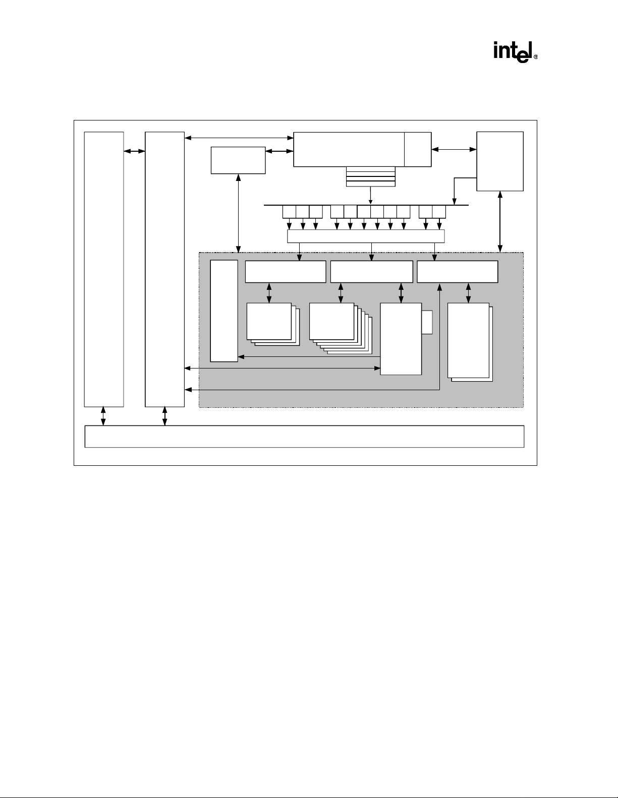
Itanium® 2 Processor Microarchitecture
®
Figure 2-3. Itanium
2 Processor Block Diagram
L1 Instruction Cache
Branch
Prediction
Branch & Predicate
L3 Cache
L2 Cache - Quad Port
NaTs, Exceptions
Scoreboard, Predi cate,
Registers
Branch
Units
Fetch/Pre-fetch Engine
Instruction
Queue
BBB MMI I FF
Register Stack Engine / Re-Mapping
and
MM
128 Integer Registers
Integer
and
MM Units
8 Bundles
Dual-Port
L1
Data
Cache
and
DTLB
ITLB
128 FP Regist ers
ALAT
Floating
Point
Units
IA-32
Decode
and
Control
Bus Controller
2.2 Instruction Processing
2.2.1 Instruction Prefetch and Fe tch
The Itanium 2 processor speculatively prefetches instructions from a pipelined cache into a
decoupling buffer. The Itanium 2 processor uses a sophisticated branch prediction strategy and
compiler hints for speculative prefetches. The ins t ruction sequencing portion of the Itanium 2
processor is responsible for fetching and dispersing instructions to the execution units. The
instruction address generation unit selects the next instruction pointer (IP) . The ins truction pointer
is selected between the next sequent ial address, static and dynamic branch prediction addresses,
instruction a ddresses delivered by the compatibility logic, validated target and address to correct
for mispredicted branches, or the address of exce ption handlers.
The Itanium 2 processor reads two instruction bundle s (three instructions per bundle) from the L1
instruction cache (L1I) and places them in the instru ction buffers. The instruction buffers store
bundles of instructions waiting to be consumed by the execution units. To reduce the effect of
branch predic tion bubbles caused by instruction cache misses, bundles read from the instruction
buf f ers are sent to the inst r u ction issue and renam e logic based on the availability of execu tion
resources.
001096a
2-4 Intel® Itanium® 2 Process or Hard ware Develop er’s Manual

2.2.2 Branch Predi ction
The branch predict ion logi c uses ad vance d predict ion schemes to antici pate t he directi on an d targe t
of each branch read from the ins truct ion cac he. The Ita nium 2 process or featu res a 0-bubbl e branch
prediction algorithm and a backup branch prediction table. Whenever a branch happens, the
branch target will be restored to the instruction pointer generation logic.
The instruction prefetch lo g ic serves as the interface between the L1I and L2 cach e. It prefetches
instructions from L2 before they are needed in order to pre vent L1I mis ses. Prefetchi ng is execut ed
under control of t he c ompiler. If an L1 instruction ca che mis s does occ ur , i t will s tall the instru ction
address generation logic and retrieve the information from the L2 cache. If the ins truction does not
reside in L2 cache, it will proceed to check the L3 cache.
2.2.3 Dispers al Lo g ic
There are twelve te mplates for Itanium instructions. A template contains explicit stop bits to
indicate to th e hardware to stop parallel is su e of su bsequent instructions. There are three
instructions per bundle and the hardware can handle two bundles (i.e. six instructions) per clock.
The dispersal logic sends each instruction to one of the fully pipelined functional units through its
issue ports.
Itanium® 2 Processor Microarchitecture
The instruction buffer holds a maximum of eight instruction bundles. The buffer can present two
bundles to the disp ersal logic every cycl e. In general, instructions are routed to a supporti ng
execution port on a first available basis.
2.3 Execution
The Itanium 2 processor e xecution logic consists of six multimedia units, six integer units, two
floating-point units, three branc h units and four load/store uni ts. The Itanium 2 processor has
general registers and FP registers to manage work in progress. Integer loads are processed by the
L1 data cache but integer stores will be processed by L2. FP l oads and stores are also processed by
the L2 cache. Whenever a lo okup occurs in L1, a speculat ive request is sent to the L2 cac he.
The multimedia engines t r ea t the 64-bit data as 2 x 32-bit, 4 x 16-bit or 8 x 8-bit packed data t ypes .
Three classes of arit hm etic operations can be performed on the packed or Single Instruction
Multiple Data (SIMD) data types: arithmetic, shift and data arra ngement. Meanwhile the integer
engines support up to six non-pa ck ed integer ari thmet ic and logi cal oper ations . Up to six intege r or
multimed ia operations can b e executed each cycle.
2.3.1 Floating-Point Unit (FPU)
The Itanium 2 processor provides high floatin g-point execution bandwidth. The Itanium 2
processor FPU has four pipeline stages. Extra bypa s sing logic allows quick data forwarding from
various FP stages to the FP write back stage. The FP logic also includes an FP Multiply
Accumulate (FMAC) hardware unit, fast rounding logic and support for SIMD formats. The
Itanium 2 processor can i ssue up t o two FP ins t ructio ns, or t wo Intege r multi plica tions , plus two FP
loads and two FP stores (or four FP loa ds) instructions every cl ock c ycle.
Numeric operands are chec ked for possi ble num eric excep tions before the instructi on enter s the FP
pipeline. Results are written back at the end of the pipeline.
Intel® Itanium® 2 Processor Hardware Developer’s Manual 2-5
Itanium® 2 Processor Microarchitecture
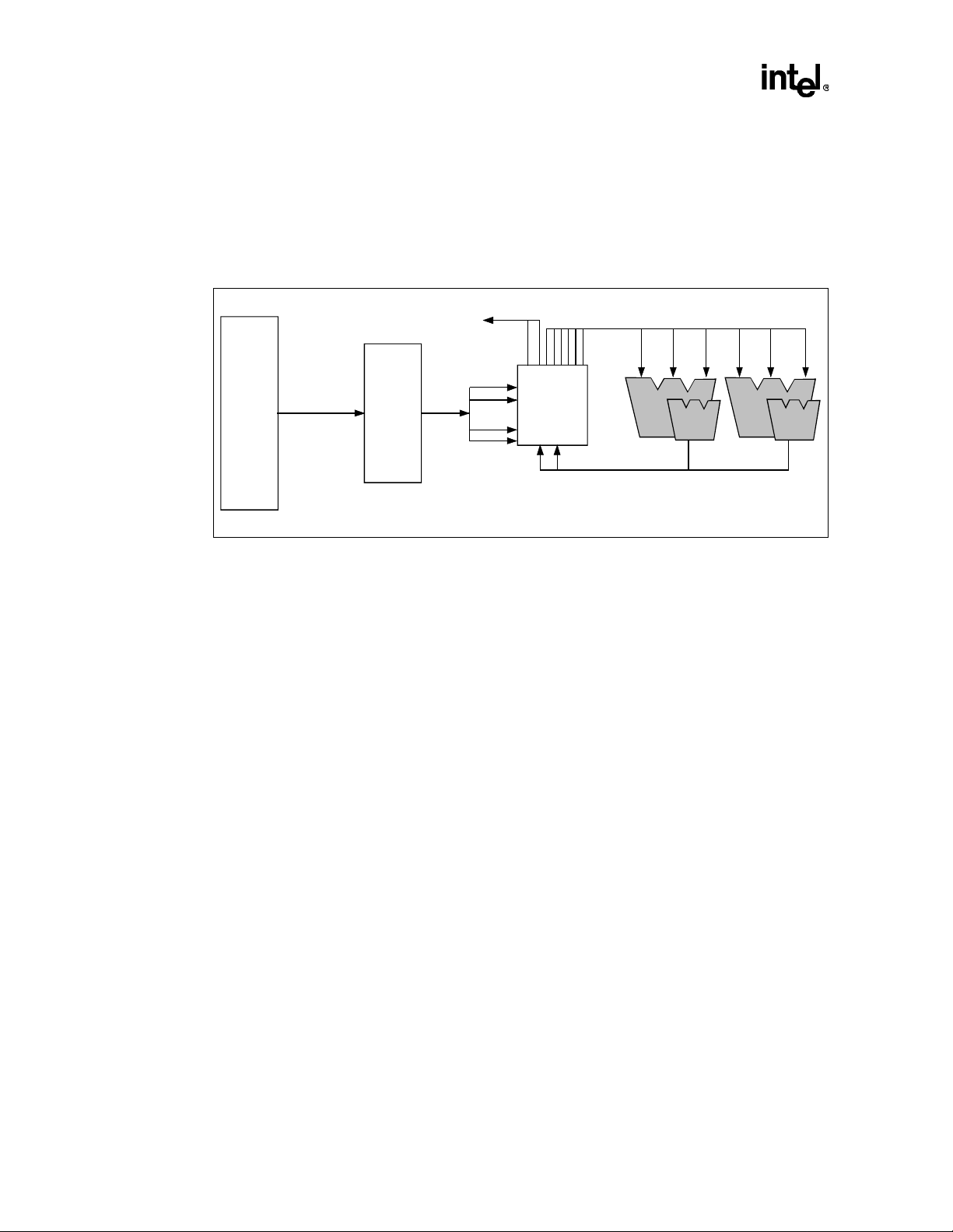
The FPU supports two FMACs that operate on 82-bit values. The FMACs can execute single,
double and dou ble- exten ded precis io n FP ope rations. The FP U has a 128- ent ry FP reg iste r file wi th
eight read and at le as t six write ports. The FP registe rs can support four double prec ision loads
every clock from memory, two 82-bit writebacks from the FMACs and two store ope rations for the
two parallel extended precision FMACs eve ry clock. Refer to Figure 2-4 for a diagram of the
.
Figure 2-4. Itanium
FMAC units.
®
2 Processor FMAC Units
L3
Cache
4 Double-
precision
Ops/Clock
2.3.2 Integer Logic
The six integer execution units execute 64-bit arith me tic, logical, shift and bit-field manipulation
instructions. Additionally it can execute instructions to accelerate operations on
32-bit pointers. Other operations include computing predicates, linear addresses and flag
generation for the IA-32 comp ati ble engine.
The integer logic has six general purpose ALUs and two load and two store ports. The ALUs have
full bypassing capability.
2.3.3 Register Files
2 Stores/Clock
L2
Cache
Even
Odd
4 Double-
precision
Ops/Clock
(2 x ldf-pair)
6 x 82 bits
Register
File
(128-entry
82 bits)
2 x 82 bits
001098a
The Itanium 2 processor implements the massive register resources provided by the Itanium
architec ture. The large number of registers allow many operations to complete without read ing
from or writing to memory. The primary execution registers include: 128 general registers, 128
floating-point registers, 64 predicate registe rs, and 8 branch registers.
2.3.3.1 General Registers
A set of 128 (64-bit) ge neral registers provide the central resource for all in teger and integer
multimedia computation. They are numbered GR0 through GR127, and are available to all
programs at all privilege levels.
The general reg isters are part ition ed into t wo su bsets. Gene ral reg ister s 0 thro ugh 31 are t ermed the
static general registers. Of these, GR0 is special in that it always reads as zero when sourced as an
operand, and attempting to write to GR0 causes an Illegal Operation fault. General registers 32
through 127 are te rme d the stacked general registers. The stacked registers are made availabl e to a
program by allocat ing a register stack frame consist ing of a programmable number of local and
output registers.
2-6 Intel® Itanium® 2 Process or Hard ware Develop er’s Manual

2.3.3.2 Floating-Point Registers
A set of 128 (82-bit) floa ting-point registers are used for all floating-point computation. They are
numbered FR0 through FR127, and are available to all pr ograms at all privilege levels. The
floating-point registers are partitioned into two subsets. Floating-poi nt registers 0 through 31 are
termed the static floating-point registers. Of these, FR0 and FR1 are special. FR0 always reads as
+0.0 when sourced as an operand, and FR1 always reads as +1 .0. When either of these is used as a
destination, a fault is raised.
Floating-point registers 32 through 127 are termed the rotatin g floating-point registers. These
registers can be programmatically renamed to accelerate loops.
2.3.3.3 Predicate Registers
A set of 64 (1-bit) predicate re gisters are used to hold the results of compare instructions. The s e
registers are numbered PR0 through PR63, a nd are available to al l programs at all privilege levels.
These registers are used for conditional ex ec ution of instructions.
The predicate registers are partitione d into two subs ets. Predicate registers 0 through 15 are termed
the static predicate registers. Of these, PR0 always reads as ‘1’ when sourced as an operand, and
when used as a destination, th e r esult is discarded. The static predicate registers are also used in
conditional branching.
Itanium® 2 Processor Microarchitecture
Predicate registers 16 through 63 are termed the rotating predicate registers. These rotating
registers support efficient software pipeline loops.
2.3.3.4 Branch Registers
A set of 8 (64-bit) branch registers are used to hold branching information. They are numbered
BR0 through BR7, and are a v ailable to a ll programs at all privilege levels. The branch registers are
used to s p ec if y th e branch targe t ad d r esses for in d irect branches.
2.3.4 Register Stack Engine (RSE)
The Itanium ISA avoids the spilling and filling of reg is ters at procedure interfaces through a large
register file and a mechanism for accessing the registers through an indirection base. The
indirection mechanism allows stacki ng of register frames and sharing of inter-proc edure variables
through the register file.
When a procedure is called, a new frame of registers is made available to the called procedure
without the need for an explicit save of the caller s’ registers. The old registers remain in the large
on-chip physical register file as long as there is enough physical capacity. When the number of
registers needed overflows the available physical capacity, a state machine called the Register
Stack Engi ne (RSE) saves the regi sters to memory to free up the necessary registers needed f or the
upcoming call. The RSE maintains the illus ion of an infinite number of registers.
On a call r et ur n, th e b ase regi s ter is re st ore d to t he v alu e t hat the ca ll er wa s u sing to acce s s reg ist ers
prior to the call. Often a return is encounte red even before these registers need to be saved, making
it unnecessary to restore them. In cases where the RSE has saved some of the callee’s registers, the
processor stalls on return until the RSE can restore the appropriate number of the callee’s registers.
The Itanium 2 processor im plements the forced lazy mode of the RSE, as described in the Intel
Itanium® 2 Proces sor Reference Manual for Software Development and Op timization.
®
The Intel
Intel® Itanium® 2 Processor Hardware Developer’s Manual 2-7
®
Itanium™ Archit ecture Software Developer’s Manual describes the RSE in more det ail.
Itanium® 2 Processor Microarchitecture
2.4 Control
The control section of the Itanium 2 processor is made up of the exception handler an d pipeline
control. The exception handler imple ments exception prio ritizing. Pipeline control has a
scoreboard to detect register source dependencies and a cache to support data speculation. The
machine stalls only when source operands are not yet available. Pipe line control supports
predicati on via predication regis ters.
The pipeline control section also contains a Performance Monitoring Unit designed to collect data
that can be dumped for analyzing Itanium 2 processor performance.
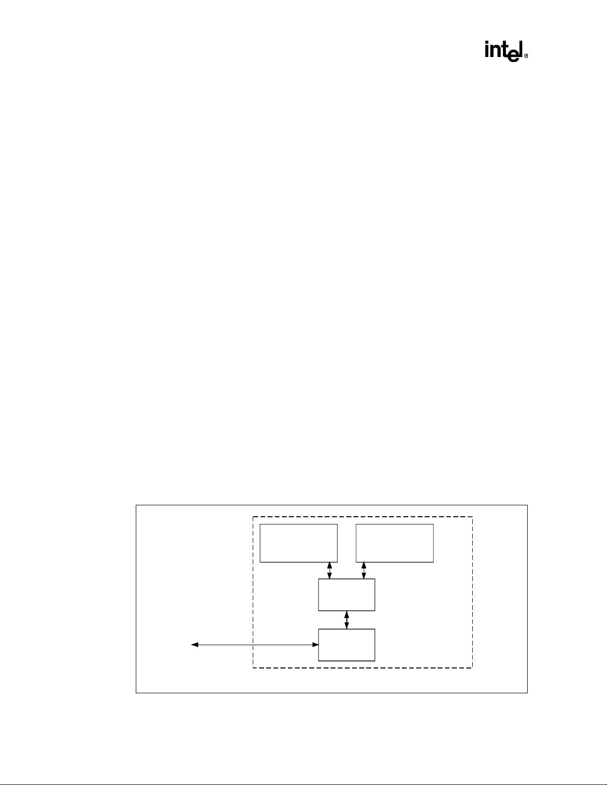
2.5 Memory Subsystem
The main system memory is access ed through the 128-bit syste m bus (refer to Figure 2-5). The
system bus is transaction-oriented and pipelined similar to the Itanium processor system bus. The
memory subsys tem for the Itanium 2 processor cont ains system bus interface logic, the L1D cache,
the L2 cache, the L3 cache, interrupt controller unit, ALAT and TLB.
The Itanium 2 processor supports all non-aligned IA-32 memory accesses. References to memory
in Itanium architecture spanning an 8 byte boundary will result in a n unaligned fault. To avoid
performance degradation associated with unaligned accesses and extra overhead for unaligned data
memory fault handlers, aligned memory ope rands should be used whenever possible.
The L1, L2 and L3 caches are non-blocking. There are separate L1 caches for data and instructions.
The L1 data cache is q u ad p o rted. The L2 cache is a unified cache and co n tains both instr u ctions
and data. It is quad ported and can be accessed at the ful l clock speed of the Itanium 2 processor.
All ports are used when acces s ing instructions in L2 cache, but for data requests one can utilize
either one, two, three or all of the four ports. When a reque st to the L2 cache causes a miss, the
request is quickly forwarded to the L3 cache.
The integrated external interrupt controller interface s to the system bus through the ext ernal bus
logic and receive s both external and internal interrupts from the system bus through its memory
mapped location.
Figure 2-5. Itanium
®
2 Processor Cache Hierarchy
L1I L1D
128b
System Bus
L2
L3
Itanium® 2 Processor
000699a
2-8 Intel® Itanium® 2 Process or Hard ware Develop er’s Manual

2.5.1 L1 Instruction Cache
The Itanium 2 processor L1 instruction (L1I) cache is 16 KB in si ze . It is a single cycle, nonblocking, dual ported 4-wa y set-associative cache mem ory with a 64 byte line si ze (there is no way
prediction). The tag array is dual port ed. One port is for instruction fetches, the other port is shared
among prefetches, snoops, fills, and column invalidates. The data array is also dual ported to
support simult aneous reads (fetches) and fills. The L1I is fully pipeline d and c an del iver two
instruction bundles (six instruct ions) every clock.
The L1I cache is physically indexed and tagged.
2.5.2 L1 Data Cache
The L1 data cache is four-ported (two loads and two stores), 16 KB in size and is non-blocking. It
is organized as 4-way set-associative (no way prediction) with 64 byte line size. It c an support two
concurrent loads and two stores. The L1 data cache only ca che s integer data (does not cache
floating-point load or semaphore load da ta). The L1D cache is write-through with no write
allocation. The L1D cache is physical ly indexed and tagged for loa ds and stores.
Itanium® 2 Processor Microarchitecture
2.5.3 Unifi ed L2 Cache
The unified L2 cache memory is four-ported and supports up to four concurrent accesses via
banking. The L2 cache is 256 KB, 8-way set-associative with a 128 byte line size, made of 16 byte
banks and is non-bloc king and out of order. It has a cache read bandwidth of 64 GB per second.
The L2 cache implement s a write-back with write-al locate policy. It is physically indexed an d
physically tagged.
In addition to servicing all L1I and L1D cache misses, the L2 handles all floating-point memory
accesses (up to four concu rrent floating-point loads per clock). All of the Itanium 2 processor’s
semaph o r e in st r u ct io n s are al s o ha ndled excl u si ve ly by the L2.
2.5.4 Unifi ed L3 Cache
The on chip L3 cache on the Itanium 2 processor is 1.5 MB or 3 MB in size. I t is physically
indexed and phys ically tagged. The L3 cach e is single ported, full y p ipelined non-blocking cache
featuring 12 wa y se t-associative with 128 byte line size. It can su pport 8 outstanding requests, 7 of
which are loads/sto res and 1 is for fil ls. The maximum transfer rate from L3 to core/L 1I/ L1D or L2
is 32 GB/cycle. The L3 protects both tag and data with single bit correc tion and double bit
detection E CC.
2.5.5 The Advanced Load Address Table (ALAT)
A cache s tru cture ca ll ed th e A d v an ce d Load Add r es s Table (AL AT) is used to enab le data
speculation in the Itanium 2 processor. The ALAT keeps information on speculative data loads
issued b y th e mach ine and a ny s tore s tha t ar e al ias ed wit h th es e lo ads . Thi s structure has 32 ent rie s,
is a fully associa tive array that can handle two loads and two stores per cycle . It can provide
aliasin g information for th e ad vance load “check” operations.
Intel® Itanium® 2 Processor Hardware Developer’s Manual 2-9

Itanium® 2 Processor Microarchitecture
2.5.6 Translation Lookaside Buffers ( T LBs)
There are two types of TLBs on the Itanium 2 processor: Data Translation Lookaside Buf fer
(DTLB) and the Instruction Translat ion Lookaside Buff er (IT LB). There are two levels of DTLBs
in the Itanium 2 processor: a L1 DTLB and a L2 DTLB. Only L1D cache loads depend o n the L1
and L2 DTLB hits. Stores and L2/L3 cache hits only de pend on the L2 DTLB hits.
TLB mis ses in eit h er the DTLB or the I TLB are serviced by th e hardware page table walker which
supports the Itanium instruction s et architecture-defined 8B and 32B Virtual Hash Page Table
(VHPT) format. VHPT data is only cached on the L2 and L3 caches, not the L1D.
2.5.6.1 The Data TLB (DTLB)
The first level DTLB (DTLB1) perfo rms virtual to physical addr ess translations for load
transactions that hit in the L1 cache. It has two read ports and one write port. The TLB contains 32
entries and is fully associative. It s upports 4 KB pages, and can also support sub se ts of larger
caches in 4 KB subsec tions.
The second l evel DTLB (DTLB2) handles virtual t o physical address translations for data memory
references during stores, and protection checking on loads. It contains 128 entries and is fully
associative and can support architect ed page sizes from 4 KB to 4 GB. The DTLB2 contains four
ports. Of the 128 entries, 64 can be configured as Translatio n Registers (TR).
2.5.6.2 The Instruction TLB (ITLB)
The first level ITL B (ITLB1) is responsible for virtual to physical address translations to enable
instruction transaction hits in the L 1I cache. It is dual ported, contains 32 entries and is fully
associat ive. It supports 4 KB pages only.
The second level ITLB (IT LB2 ) is res pons ible for virtual to physical address translations for
instruction m emory references that miss the ITLB1. It contains 1 28 entries, is fully associative and
supports page s izes from 4 KB to 4 GB. Of the 128 entries, 64 can be configured as TR.
2.5.7 Cache Coherency
The three-level cache system makes it necessary to maintain the consistency of the data in the
different caches. Every read access to a memory address must always provide the most up-to-date
data at that address. Since the L1 is write-through it maintains a valid bit. The valid bit indicates
whether or not the cache line is valid. The L2 and L3 cache s use the MESI protocol to maintain
cache coh er e n cy.
2.5.8 Write Coalescin g
For increas ed performance of uncacheable references to frame buffers, the Wr ite Coalescing (WC)
memory type coalesces streams of data writes into a single larger bus write transaction. On the
Itanium 2 pr oc essor, WC loads ar e per f o rm ed di r ec tl y fro m m em o ry an d not from the coalescing
buffers.
On the Itanium 2 processor, a separate 2-entry, 128 byte buffer (WCB) is used for WC accesses
exclusively. Each b yte in the line has a valid bit. If all the valid bit s are true, then the line is said to
be full and will be evict ed (flushed) by the processor. Line evictions are initiated in a “first-written-
first-flushed” order even for partially full lines.
2-10 Intel® Itanium® 2 Process or Hard ware Develop er’s Manual

For increased performance to cacheable references to frame buffers or graphic controllers, the
Itani u m 2 processor allows external agents such as a graphics controller to read a line out o f t h e
processor’s cache witho u t altering the state of the cache line.
2.5.9 Memory Or dering
The Itanium 2 proces sor imple ments a relaxe d memory orde ring model t o enhanc e memory sys tem
performance. Memory transactions are ordere d with respect to visibility whereby visibility of a
transaction is defined as a point in time after which no later transactions may affect its operation.
On the Itan ium 2 processor, a tran saction is co n s i de r ed vi si ble when it hi ts th e L 1D ( if th e
instruction is serviceable by L1D), the L2, or the L3, or when it has reached the visibility point on
the system bus.
2.6 IA-32 Execution
The Itanium 2 processor supports IA-32 application binaries. This includes support for running a
mix of IA-32 applications and Itanium-based ap plications on an Itanium-based operating syste m
(OS), in both uniprocessor a nd multiprocessor configurations. The IA-32 engine is designed to
make use of the registers, caches, and execution resources of the EPIC machine. To deliver high
performance on legacy binaries, the IA-32 engine dynamically schedules instructions.
Itanium® 2 Processor Microarchitecture
Intel® Itanium® 2 Processor Hardware Developer’s Manual 2-11

Itanium® 2 Processor Microarchitecture
2-12 Intel® Itanium® 2 Process or Hard ware Develop er’s Manual

System Bus Overv iew 3
This chapter pro vides an overvi ew of the Itani um 2 proce ssor system bus , bus tr ansact ions, and bus
signals. The Itanium 2 processor also supports signals not discussed in this section. For a com plete
signal listing, please refer to the Intel
and Appendix A, “Signals Reference”.
3.1 Signali ng on the Itanium® 2 Processor System Bus
The Itanium 2 processor syst em bus supports common clock signaling as well as source
synchronous data signaling. Section 3.1.1 and Section 3.1.2 describe in detai l the characteristics of
each type of sign aling. The co rrespo nding tim ing figu res us e squ are, tr iangle , and c ircle symbols to
indicate the point at which signals are driven , received, and sampled, respectively. The square
indicates that a signal is driven (asserted or deasser ted) in that cloc k. The triangle indicates that a
signal is received on or before that point. The circle indicates that a signal is sampled (observed,
latched, captured) in that clock. Black bars indicate zero or more clocks are al lowed.
All timing diagrams in this speci f ication show signals as they are asserted o r deasserted. There is a
one-clock del ay in the signal values obser ved by system bus agents. Any signal names that appear
in lowercase letters in brackets {rcnt} are internal signals only, and are not driven to the bus.
Internal state s change one clock after s am pling a bus signal, which is the clock after the bus s ignal
is driven. Uppercase lette rs that appear in brackets represent a group of signals such as the Request
Phase signals [REQUEST]. The timing diagrams sometimes include internal signals to indicate
internal sta tes and show how it affects external signals. Internal states change one clock after
sampling a bus signal. A bus signal is sampled one cl ock after the bus signal is dri ven.
®
Itanium® 2 Processor at 1.0 GHz and 900 MHz Datasheet
3.1.1 Common Clock Signali ng
All signals except the data bus signals on the system bus use a synchronous common clock latched
protocol (1x transf er rate). On the rising edge of the bus clock, all agents on the system bus are
required to drive their active outputs and sample required inputs. No additional logic is located in
the output and input paths betwee n the buf f er and th e la tch s tage, thus keepin g setu p and hold tim es
constant for all bus si gnals following the la tched protocol. The syst em bus requires that (1) every
input be sampled dur ing a valid sampling window on a risin g clock edge and, (2) its eff ect be
driven out no sooner than the next rising clock edge. This approach allows one full cl ock for
driving a signal, flight time, and setup as w ell as at least on e f ull clock at the receiver to compute a
response.
Figure 3-1 illustrates the latched bus protocol as it appe ars on the bus. In later descriptions, the
protocol is desc ribed as “B# is asserted in the clock after A# is observed asserted,” or “B# is
asserted two clocks after A# is asserted .” Note that A# is asserted in T1, but not observed asser ted
until T2. A# has one full clock to propagate (indicated by the straight line with arrows) before it is
observed assert ed. The receivin g age nt uses T 2 to deter mine it s respons e and a sserts B# in T 3 i. e. it
has one full clock cycle from the time it observes A# asserted (at the ri sing edge of T2) to the time
it computes its response (indicated by the curved line with the single ar row) and drives this
response at the rising edge of T3 on B#. Simil arly, an agent observes A# asserted at the rising edge
of T2, and uses the full T2 clock to comput e its respo nse (indi cate d by the lowermos t curved arr ow
during T2). This response would be driven at the rising edge of T3 (not shown in Figure 3-1) on
{c} signals. Although B# is drive n at the ris ing edge of T3, it has the full cloc k T3 to propaga te. B#
is observed asserted in T4.
Intel® Itanium® 2 Processor Hardware Developer’s Manual 3-1

System Bus Overview
Figure 3-1. C om mon Clock Latched Protocol
Full clock allo w ed
for signal propagation
T1 T2 T3 T4
CLK
BCLKp
BCLKn
A#
B#
Assert A#
Latch A#
Full clock allowed
for logic delay s
Assert B#
Change internal state
T5
1100{c}
Latch B#
Signals tha t ar e driv en i n the sa me cl ock by m ultipl e sys t em bus a gents exhibi t a “wired-OR gli tch”
on the ele ctrical low to el ectrica l h ig h tr an si ti o n . To accoun t fo r this sit u ation, th e se s i gn a l state
transitions are specified to have two clocks of settling ti me when deasserted before they can be
safely observed, as shown with B#. The bus signals that must meet this criterion are: BINIT#,
HIT#, HITM # , BN R# , TND #, BERR # .
3.1.2 Source Synchronous Signaling
The data bus operates with a source synchronous latched protocol (2x trans fer rate). The source
synchronous la tched prot ocol (refer to Figure 3-2) sends and latches data with str obes t o allow v ery
high transfe r rate s with reasonable signal f light times. The rest of the sy st em bus always uses the
common clock latched protocol.
The source synchronous latched protocol operates the data bus at twice the “frequency” of the
common clock. Two chunks of data are driven onto the bus in the time it would normally take to
drive one chunk. The worst case flight time is simil ar to the common clock latched protocol, so the
second data tra ns f er m ay be driven before the first is latch ed. On both the rising edge and 50%
point of the bus cl ock, drivers send new data. On both the 25% point and the 75% point of the bus
clock, drivers send centered differential strobes. The receiver captures the data with the strobes
deterministically.
3-2 Intel® Itanium® 2 Process or Hard ware Develop er’s Manual
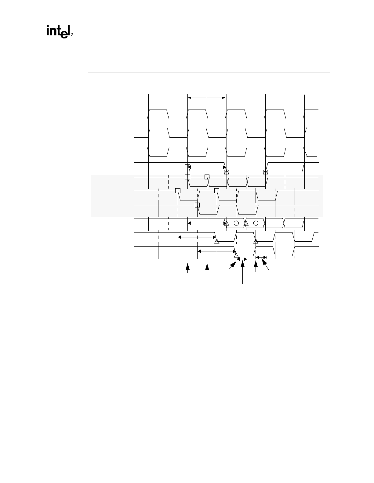
Figure 3-2. So urc e S y nchronous Lat ched Proto col
Full clock allowed
for signal propaga tio n
System Bus Overview
CLK
BCLKp
BCLKn
DRDY#
D# (@driver)
STBp# ( @ driver)
STBn# ( @ driver)
D# (@receiver)
STBp# (@receiver)
STBn# (@receiver)
T1
T2
D1 D2 D3 D4
Capture
Drive D1
Drive D2
T3
D1 D2 D3 D4
D1
Capture
Latch D1
Latch D2
D2
T4
The driver pre-drives S TBp# before driving data. It sends a rising and falling edge on STBp # and
STBn# centered with data. The driver must deassert all strobes after the last data is sent. The
receiver capt ures valid d ata wit h t he dif fe rence of bot h str obe si gnals , async hrono us to the com mon
clock. Data will be latched into the core within one core-cycle after being captured. A signal
synchronous to the common cl ock (DRDY#) indicates to the recei ver that valid data has been sent .
3.2 Signal Overview
This section describes the function of various Itanium 2 processor signals. In this section, the
signals are group ed according to function. For a complete signal list ing, please refer to the Intel
Itanium
Intel® Itanium® 2 Processor Hardware Developer’s Manual 3-3
®
2 Processor at 1.0 GHz and 900 MHz Datasheet.
®

System Bus Overview
3.2.1 Control Signals
The control signals, shown in Table 3-1, ar e us ed to con t r o l ba si c op e r at io n s of th e p r oc essor.
Table 3-1. Control Signals
Signal Function Signal Names
Positive Phase Bus Clock BCLKp
Negative Phase Bus Clock BCLKn
Reset Processor and System Bus Agents RESET#
Power Good PWRGOOD
The Positive Phase Bus Clock (BCLKp) input s ignal is the positive phase of the system bus clock
diffe rent ia l pair. It is also r efe rre d to as CL K in some of th e wa vef orms i n th is ove rvi ew. It specifie s
the bus frequency a nd clock period and is used in the signaling scheme. Each proc essor derives its
internal cl ock from CLK by multiplying the bus freq uenc y by a multiplier determined at
configuration. See Chapter 5, “Configuration and Initialization” for further deta ils.
The Negative Phase Bus Clock (BCLKn) input signa l is the negative phase of the system bus cloc k
differential pair.
The RESET# signal res ets all system bus agents to known states.
Note: The RESET# signal itself does not invalidate the internal caches in th e I tanium 2 processor. A
subsequent PAL call is used to invalidate all internal caches in the Itanium 2 processor. Modified or
dirty cache line s are NOT writ ten back. After RESET# is deasserted, each processor begins
execution at the power-on reset vect or defined during configura tion.
The Power Good (PWRGOOD) input signal must be deasserted during power-on and be as serted
after RESET# is first asserted by the system.
3.2.2 Arbitr ation Signals
The arbitration signals, shown in Table 3-2, are used to arbitrate for ownership of the bus, a
requirement for initiating a bus transaction.
Table 3-2. Arbitration Signals
Signal Function Signal Names
Symmetric Agent Bus Request BREQ[3:0]#, BR[3:0]#
Priority Agent Bus Request BPRI#
Block Next Request BNR#
Lock LOCK#
BR[3:0]# are the physical pins of the processor. All processors assert only BR0#. BREQ[3:0]#
refers to the syste m bus arbitration signals among four processors. BR0# of each of the four
processors is connected to a unique BREQ[3:0]# sign al.
Up to five agent s can simu ltane ously a rbit rate fo r the requ est bu s, one to fou r sy mmetric agents (on
BREQ[3:0]#) and one priority agent (on BPRI#). Processors arbitrate as symmetric agents, while
the priority agent normally arbitrates on behalf of the I/O agents and memory agents. Owning the
request bus is a necessary pre-condition for initiating a transaction.
3-4 Intel® Itanium® 2 Process or Hard ware Develop er’s Manual

The symmetric agents arbitrate for the bus based on a round-robin rotating priority scheme. The
arbit ration is fair and symmetric. A symmetric agent re q u ests the bus by asserting its BR EQ n#
signal. Base d on the values sampled on BREQ[3: 0]#, and the last symmetr ic bus owner, all agents
simultaneously determine the next symmetric bus owner.
The priority agent asks for the bus by asserting BPRI#. The assertion of BPRI# temporarily
overrides, but does not otherwise alter the symmetric arbitration scheme. When BPRI# is sampled
asserted, no symmetric agent issues another unlocked transaction until BPRI# is sampled
deasserted. Th e priority agent is always the next bus owner .
BNR# can be asserted by any bus ag ent to block further transac tions from being issued to the
request bus. It is typic ally asserted when system resources, such as address or data buffers, are
about to become temp orarily busy or filled a nd cannot accommodat e anothe r trans acti on. After bus
initialization, BNR# can be asserted to delay the first transaction until all bus agent s are initia lized.
LOCK# is never asserted or sampled in the Itanium 2 processor system environm ent.
3.2.3 Request Signals
The request signals, shown in Table 3-3, are used to initiate a transaction.
Table 3-3. Request Signals
Signal Fun cti on Signal Nam es
Address Strobe ADS#
Request REQ[5:0]#
Address A[49:3]#
Address Parity AP[1:0]#
Request Parity RP#
System Bus Overview
The assertion of ADS# defines the beginning of the tran sa ction. The REQ[5:0]#, A[49:3]#,
AP[1:0]#, and RP# are valid in the clock that ADS# is asserte d.
In the clock tha t ADS# i s ass erted , the A[ 49:3 ]# sign als pr ovide a n act ive-low a ddress as part o f th e
request. The low three bits of address are mapped into byte enable signals for 0 to 8 byte transfers.
AP[1]# protects the addre s s signals A[49:27]#. AP[0]# protec ts the address signals A[26:3]#. A
parity si gnal on the system bus is cor rect if there are an even numbe r o f electrical ly low signals in
the set consisting of the protected s ignals plus the par ity signal. Parity is computed using voltage
levels, regardless of whether the covered signals are active high or active low .
The Request Parity (RP#) signal protects the request pins REQ[5:0]# and the address strobe,
ADS#.
3.2.4 Snoop Si gn als
The snoop signals, shown in Table 3-4, are used to prov ide snoop results and transaction control to
the system bus agents.
Table 3 -4 . Snoop Signals
Signal Function Signal Names
Purge Global Translation Cache Not Done TND#
Keeping a Non-Modified Cache Line HIT#
Hit to a Modified Cache Line HITM#
Intel® Itanium® 2 Processor Hardware Developer’s Manual 3-5

System Bus Overview
Table 3-4. Snoop Signals (Continued)
Signal Function Signal Names
Defer Transaction Completion DEFER#
Guarantee Sequentiality GSEQ#
The TND# signal may be a sserte d by a bus agen t t o delay compl etion of a Pur ge Global T ransl at ion
Cache (PTC.g) instruction, even after the PTC.g transaction complete s on the system bus.
Software will guarantee that only one PTC.g instr u ction is being executed in the sy stem.
The HIT# and HITM# signals are used to indicate that the line is valid or invalid in the snooping
agent, whether the line is in the mod ified (dirty) state in the caching agent, or whether the
transaction needs to be extended. The HIT# and HITM# signals are used to maintain cache
coherency at the system level.
If the memory agent observes HITM# active, it relinquishes responsibilit y for the data return and
becom es a target for the im p l ic it cache li n e w ri t eb ack. The me m o r y agent mus t merg e th e ca ch e
line being written back with any write data and update memory. The memory agent must also
provide the implicit writeback respons e fo r the transaction.
If HIT# and HITM# are sampled asse rted together, it means that a caching agent is not ready to
indicate snoop status, and it needs to extend the transaction.
The DEFER# signal is deasserted to indicate that the transaction can be guaranteed in-order
completion. An agent asserting ensures proper removal of the transaction from the In-Order Queue
by generating the appropriate response.
The assertion of the GSEQ# signal allows the request ing agent to issue the nex t sequential
uncached writ e eve n though the transaction is not yet visible. By asserting the GSEQ# signal, the
platform also guarantees not to retry the transaction, and accepts respon sibility for ensuring the
sequentiality of the transaction with respect to other uncac hed writes from the same agent.
3.2.5 Response Signals
The response signals, shown in Table 3-5, are used to provide respons e information to the
requesting agent.
Table 3-5. Response Signals
Signal Function Signal Names
Response Status RS[2:0]#
Response Parity RSP#
Target Ready (for writes) TRDY#
Requests initiated in the Request Phase enter the In-Orde r Queue, which is maintained by every
agent. The responding a gent is responsible for completing the transaction at the top of the In-Order
Queue. The responding agent is the agent addressed by the transaction.
For write tr ansactions, TRDY# is asserted by the responding agent to indicate that it is ready to
accept write or writeback data. For write transactions with an implicit writ eback, TRDY# is
asserted twice, first for the write data transfer and then for the implicit writeback data transfer.
The RSP# signal provides parity protection for RS[2:0]#. A parity signal on the syste m bus is
correct if th ere is an even numbe r of low sig nals in the set c onsis ting of t he cover ed sign als pl us the
parity signal. Pari ty is comput ed usi ng voltage level s, regardl ess of whet her the co vered signa ls are
active high or active low.
3-6 Intel® Itanium® 2 Process or Hard ware Develop er’s Manual

3.2.6 Data Signals
The data response signals, shown in Table 3-6, control the transf ers of data on the bus and provide
the data path. All dat a transfers are at the 2x transfer rate.
Table 3-6. Data Signals
Signal Function Signal Names
Data Ready DRDY#, DRDY_C1#, DRDY_C2#
Data Bus Busy DBSY#, DRDY_C1#, DRDY_C2#
Strobe Bus Busy SBSY#, SBSY_C1#, SBSY_C2#
Data D[127:0]#
Data ECC Protection DEP[15:0]#
Positive phase Data Strobe STBp[7:0]#
Negative phase Data Strobe STBn[7:0]#
DRDY# indicates that valid data is on the bus and must be latched. The data bus owner asserts
DRDY# for each clock in which valid dat a is to be transferred. DRDY# can be deasserted to insert
wait states in the Data Phase.
DBSY# holds the data bus before the first DRDY# and between DRDY# assertions for a multiple
clock data transf er. DBSY# need not be asserted for single cl ock data transfers.
System Bus Overview
SBSY# holds the strobe bus bef ore th e first DRDY# and betw een DRDY# assert ions for a multip le
clock data transf er. SBSY# must be asserted for all data trans fers on the bus.
Each of the data bus control signals DBSY#, DRDY#, and SBSY# are replicated on the Itanium 2
processor syste m bus to enable partitioning of data path chips in the system agents. Two copies of
DBSY#, DRDY#, and SBSY# signals are output-only and the thir d copy serves as both input as
well as output.
The D[127:0]# signals provide a 128-bit data path bet ween agents. For partial transf ers, BE[7:0]#
and A[4:3]# determine which bytes of the data bus contain valid data.
The DEP[15:0]# signals provide optional ECC (error correcti ng code) protection for D[127:0]#.
DEP[15:0]# provides valid ECC protection for the entire data bus on each clock, regardless of
which bytes are enabled.
STBp[7:0]# and ST Bn[7:0]# (and DRDY#) ar e used to transfer data at the 2x trans fer rate with the
source synchrono us latche d protoco l. The agent dri ving the data tra nsf er drives th e strob es with the
correspondin g data and ECC signals. The agent receiving the data transfer uses the strobes to
capture valid d ata . Each strobe pair is associated with sixteen data signals and two ECC signa ls as
shown in Table 3-7.
Table 3-7. STBp[7:0]# and STBn[7:0]# Associations
Strobe Signals Data Signals ECC Signals
STBp[7]#, STBn[7]# D[127:112]# DEP[15:14]#
STBp[6]#, STBn[6]# D[111:96]# DEP[13:12]#
STBp[5]#, STBn[5]# D[95:80]# DEP[11:10]#
STBp[4]#, STBn[4]# D[79:64]# DEP[9:8]#
STBp[3]#, STBn[3]# D[63:48]# DEP[7:6]#
STBp[2]#, STBn[2]# D[47:32]# DEP[5:4]#
STBp[1]#, STBn[1]# D[31:16]# DEP[3:2]#
STBp[0]#, STBn[0]# D[15:0]# DEP[1:0]#
Intel® Itanium® 2 Processor Hardware Developer’s Manual 3-7

System Bus Overview
3.2.7 Defer Signals
The defer signals, shown in Table 3-8, are used by a deferring agent to complete a previously
deferred transact ion. Any deferrable transaction (DEN# asserted) may use the deferred response
signals, prov ided the requesting agent supports a deferred response (DPS# asserted).
Table 3-8. Defer Signals
Signal Function Signal Names
ID Strobe IDS#
Tr a n saction ID ID[9:0]#
IDS# is asserted t o begi n the deferred response. ID[9:0]# returns the ID of the deferred transaction
that was sent on DID[9:0]#. Please refer to Appendix A, “Signals Reference” for further detail s.
3.2.8 Error Signals
Table 3-9 lists the error signals on the system bus.
Table 3-9. Error Signals
Sign a l Function Sig nal Names
Bus Initiali zatio n BINIT#
Bus Error BERR#
Therm al Trip THRM TRIP#
Thermal Alert THRMALERT#
BINIT# is used to signal any bus condition that preve nts reliable future operation of the bus.
BINIT# assertion ca n be enabled or disabled as part of the power-on configuration reg is ter (see
Chapter 5, “Configuration and Initializat ion”). If BINIT# assertion is disabled, BINIT# is never
asserted and the error rec overy action is taken only by the processor detecting the error.
BINIT# sampling can be enabled or disabled at power-on reset . If BINIT# sampl ing is disabled,
BINIT# is ignored and no action is taken by the processor even if BINIT# is sampled asserted. If
BINIT# sampling is enabled and BINIT# is sample d asserted, all processor bus state mach ines are
reset. All agents reset th eir rotating I D f or b us arbitration, and internal state inf or mation is lost.
Cache contents are not affected. BINIT# sampling and assertion must be enabled for proper
processor error recovery.
A machine-check ab o r t is taken f o r each BINIT # assertion, configurable at p o w er-on.
BERR# is used to signal any error condition caused by a bus transaction that will not impact the
reliable operation of the bus protocol (for exa mp le, memory data error or non-modified snoop
error). A bus error that causes the assertion of BERR# can be de tected by the processor or by
another bus agent. BERR# assertion can be enabled or disabled at power-on reset. If BERR#
assertion is disabled, BERR# is never asserted. If BERR# asse rtion is enabled, the processor
supports two modes of ope ration, configurabl e at power-on (refer to section 5. 2.6 and 5.2.7 for
further details). If BER R# sampling is disabled, BERR# assertion is ignored and no acti on is taken
by the processor. If BERR# sampling is enabled, and BERR# is sampled asserted, the processor
core is si gn a le d wi th th e m a ch i ne check ex c ep tion.
A machine check exception is taken for each BERR# assertion, configurable at power-on.
3-8 Intel® Itanium® 2 Process or Hard ware Develop er’s Manual

THRMTRIP# is the Ther mal Trip signal. The Itanium 2 proces sor protects its elf from catastrophi c
overheating by using an internal thermal s ens or. This sensor is set well above the normal opera ting
temperature to ensure that there are no f alse trips. Data will be lost if the proces sor goes into
thermal tri p. This is signale d to th e syste m by the ass erti on of the THRMT RIP# pin. Onc e asse rted,
the signal remains asserted until RESET# is asserted by the platform. There is no hysteresis built
into the therma l sensor itself; as long as the case temperature drops below specified maximum, a
RESET# pulse will r eset the processor.
A thermal alert open- drai n signa l, indic ated to the system by the THRMALER T # pin . The signal is
asserted when the measured temperature from th e proc es sor thermal diode equals or exceeds the
temperature threshold data programmed in the high-temp or low-temp registers on the sensor. This
signal can be used by the platform to implement thermal regulation features such as generating an
external int errupt to tell the operating system that the processor core is hea ting up.
3.2.9 Execution Control Signals
The execution cont rol signals, shown in Table 3-10, contains signals that change the execution
flow of the processor.
Table 3-10. Execution Control Signals
Signal Function Signal Names
Initialize Processor INIT#
Platform Management Interrupt PMI#
Programmable Local Interrupts LINT[1:0]
System Bus Overview
INIT# triggers an unmaskable interrupt to the processor. Semantics required for platform
compatibility are supplied in the PAL firmware interrupt service routine. INIT# is usually us ed to
break into hanging or idle processor states.
PMI# is the platform management interrupt pin. It triggers the highest priority interrupt to the
processor. PMI# is usually used by the system to trigger system events that will be handled by
platform specific firmware.
LINT[1:0] are program mable local interrupt pins defined by the interrupt interface.These pins are
disabled after RESET#. LINT[0] is typically software configured as INT, an 8259-compatible
maskable interrupt request signal. LINT[1] is typically software configured as NMI, a nonmaskable interrupt.
3.2.10 IA-32 Compatibility Sign al s
The following signa ls were present for compatibility with IA-32 system environm ents: FERR#,
IGNNE#, and A20M#. As implemented on the Itani um 2 process or, the FERR# signal may be
asserted while running an IA-32 application to indicate an unmasked floating point error, and the
IGNNE# and A20M# signals are ignored.
Intel® Itanium® 2 Processor Hardware Developer’s Manual 3-9

System Bus Overview
3.2.11 Platform Sign al s
The platform signals, shown in Table 3-11, provides signals which support the platform.
Table 3-11. Platform Signals
Signal Function Signal Names
Processor Present CPUPRES#
CPUPRES# can be used to detect the presence of a Itanium 2 processor in a socket. A ground
(GND) level indicates that the part is installed while an open indicates no part is insta lled.
3.2.12 Diagnostic Signals
The diagnostic signals, shown in Table 3-12, provides signals for probing the processor,
monitoring proc es s or performance, and implementing IEEE 1149.1 specification for boundar y
scan.
Table 3-12. Diagnostic Signals
Signal Function Signal Names
Breakpoint / Performance Monitor BPM[5:0]#
Boundary Sca n/Test Access TCK, TDI, TDO, TMS, TR ST #
BPM[5:0]# are the Bre akpoint and Performance Monit or si gnals. These signals can be configured
as outputs from the pro cessor tha t indic ate t he statu s of breakpoi nts and pro gramm able count ers for
monitoring proc es sor events. These signals can be configured as inputs to break program
execution.
Test Clock (TCK) is used to clock activity on the five-signal T est Access Port (TAP). Test Dat a In
(TDI) is used to transfer serial test data into the process or. Test Data Out (TDO) is used to tr ansfer
serial tes t data out of the proc essor. Test Mode Select (TMS) is used to control the seque nce of TAP
controller state changes. Test Reset (TRST#) is used to asynchronously initialize the TAP
controller.
3-10 Intel® Itanium® 2 Process or Hard ware Develop er’s Manual

Data Integrity 4
The Itanium 2 processor supports an advanced machine check architecture to facilitate er ror
detection, containment, correction and recovery. The system bus includes parity prot ec tion for
address, request and response signals, parity or protocol protection on most control signals, and
ECC protection for data signals.
For more information on Machine Check Architecture, see the Itanium™ Processor Fa mi ly Error
Handling Guide.
4.1 Error Classification
The Ita nium 2 proc es sor cla s sifi es e rror s i n t he foll ow ing ca tego ri es, li ste d w it h i ncr ea sing s e ver ity.
An implementation may always choose to report an error in a more severe category to simplify its
logic.
1. Hardware Corrected Error
The err o r can be corrected by t h e p rocessor or the system hardware. The current process
continues without interruptio n.
2. Firmwa re C o rrec t ed Error
The err o r can be corrected by firmware. The current process continues after Machine Check
Abor t (M CA) is s er v i c e d.
3. Recov er able Error w ith L oc a l M C A
The error cannot be corrected e ither by hardware or firmware. Only one agent is affected.
Error handling is left to the OS and recovery may not always be possible.
4. Recoverable Error with Global MCA
The error cannot be corre cted eit her by ha rdware or firmware . Mult ipl e agents on a bus may be
affecte d. Er ror handling is left to the OS and recovery may not always be possible.
5. Non-Recoverable Error with Global MCA
The error cannot be corrected e ither by hardware, firmware or OS. Multipl e ag ents on a bus
may be affe ct ed an d th e system ne ed s to be re sta r ted.
4.2 Itanium® 2 Processor System Bus Error Detection
The major address and dat a pa ths of the Itanium 2 processor system bus are protected by 18 che ck
bits that provi de either parity or ECC protection. Sixteen ECC bits protect the data bus . Single-bit
data errors are automatically corrected. A two-bit parity code protects the address bus.
Three control signal groups are explicitly protected by individual pa rity bits RP#, RSP#, and
IP[1:0]#. Errors on most remaini ng bus signal s can be detected indi rectl y due to a well-define d bus
protocol specification that enables detection of protocol vi olation errors. Errors on a few bus
signals canno t be detected.
An agent is not required to ena ble all data integrity features since each feature is individually
enabled through the power-on configuration. See Chapter 5, “Configuration and Initialization”.
Intel® Itanium® 2 Processor Hardware Developer’s Manual 4-1

Data Integrity
4.2.1 Bus Signa ls Pro te cted Direct ly
Most system bus signals are protected either by parity or by ECC. Table 4-1 shows the parity and
ECC signals an d the s ignals protected by the se parity and ECC signals.
Table 4-1. Direct Bus Signal Protection
Signal(s) Protect(s)
RP# ADS#, REQ[5:0]#
AP[0]# A[26:3]#
AP[1]# A[49:27]#
RSP# RS[2:0]#
IP[0]# IDS#, IDa[9:0]#
IP[1]# IDS# (deasserted), IDb[9:2,0]#
DEP[7:0]# D[63:0]#
DEP[15:8]# D[127:64]#
• Address/Request Bus Signals
A parity error detected on AP[1:0]# or RP# is reported based on the option defined by the
power-on configuration.
— Address/Request Parity Disabled
The agent dete cting the parity e rror ignore s it a nd conti nues nor mal ope ratio n. This option
is normally used in power-on system initialization and s ystem diagnostics .
• Response Signal s
A parity error detected on RSP# is reported by the agent dete cting the error as a nonrecoverable error with global MCA if response parity is enabled.
• Defe rred S i gn al s
A parity error detected on IP[1:0]# is reported by the ag ent detecting the error as a nonrecoverabl e error with global MCA.
• Data Transfer Signals
The Itanium 2 processor data bus can be configured with eithe r no data bus error checking or
ECC. If ECC is sele cted, single-bit errors can be corrected and double-bit errors and poisoned
data can be detected. Corrected s ingle-bit ECC erro rs are continuable errors. Double-bit errors
and poisoned data may cause unrecoverable errors with local MCA.
4.2.2 Bus Signals Protected Indirectly
Some bus signals are not directly protected by parity or ECC. However, they can be indirectly
protected due to a req uirement to foll ow a strict prot ocol. Some processors or other bus agents may
enhance error detection or correction for the bus by checking for protocol violations. P6 family
processor system bus protocol errors are treated as fatal errors unless specifically stated othe rwise.
4-2 Intel® Itanium® 2 Process or Hard ware Develop er’s Manual

Data Integrity
4.2.3 Unprotected Bus Signals
The following Itanium 2 pr oce ssor system bus signals are not protected by ECC or parity:
• BCLK, RESET#, PWRGOOD#, LINT[1:0]#, CPUPRES# and INIT# are not protected.
• The error signals THRMTRIP#, THRMALERT# are not protected.
4.2.4 Itanium® 2 Processor Sy stem Bus Error Code Algor ithms
4.2.4.1 Parity Algorithm
All bus p ar i ty s ignals us e the s ame algor i th m to compu t e co r re c t p ar i ty. A corr ec t pa r it y sig n al is
high if all cov ered signa ls a re high or i f an eve n number of co vered s ignal s are low. A correct parity
signal is low if an odd number of covered signals are low. Parity is computed using vol tage levels,
regardless of whether the covered signals are active-high or active-low. Depending on the number
of covered signals, a parity signal can be viewed as providing “even” or “odd” parity; thi s
specification does not use either term.
4.2.4.2 Itanium® 2 Processor System Bus ECC Algorithm
The Itanium 2 processor system bus uses an ECC code that can correct single-bit errors, dete ct
double-bit errors, send poisoned data, and detect all errors confined to one nibble. System
designers may c hoos e to detect all these errors or a subset of these e rrors . They may also ch oos e to
use the same ECC code in additional system level cac hes, main memory arrays, or I/O subsystem
buffers.
Intel® Itanium® 2 Processor Hardware Developer’s Manual 4-3

Data Integrity
4-4 Intel® Itanium® 2 Process or Hard ware Develop er’s Manual

Configuration and Initialization 5
This chapter desc ribes configuration options and initialization details for the I tanium 2 processor.
A system may contain single or mul tiple Itanium 2 processors with one to four processors on a
single system bus. Multiple system buses on a system are supported.
5.1 Configuration Overview
Itanium 2 processors hav e some configuration options tha t are determined by hardware, and some
that are determined by PAL.
Itanium 2 processors sample their hardware configuration on the asserted-to-deasserted transition
of RESET#. The s ampled i nformat ion configu res t he proc essor a nd o ther bus a gents fo r subseq uent
operation. Thes e configuration options cannot be changed except by another reset. All reset s
reconfigure the bu s agents. Re f er to the Intel
Datasheet for further deta ils.
The Itanium 2 processor ca n also be configured with additional PAL configuration options. These
options can be chang ed by procedure calls to PAL. These options should be changed only after
taking into account synchronizat ion between multiple Itanium 2 processor system bus ag ents.
®
Itanium® 2 Processor at 1.0 GHz and 900 MHz
5.2 Configuration Feature s
Table 5-1 specifies the s ystem bus related configuration features on the Itanium 2 processor. These
configuration features are supported using fields in implement ation specific configuration
registers. Some of these features are set by bus signals during reset (at the asserted-to-deasserted
transition of RESET# signal) and some can be set by PAL.
The column labelled “Name” indicates the bus signa l that affects the configuration field during
reset. For a configuration fe ature, an “N/A” entry in this column indicates that the configuration
field cannot be set by any bus si gnal during reset. The colum n labelled “Value” shows the
recommended bus signa l values for the features. For a configuration feature, a “0” entry in this
column indicates that the bus signal is dea sserted during reset, a “1” entry indicates that the bus
signal is a sserte d du ring res et, and an “N/A” entry indi cate s that the configu rat ion feature cann ot be
set by any bus signal during reset.
The column labelled “PAL Call” indicates the PAL call (if applicable) that allows control over the
config urat ion fe atu re s. F or a con f igu rat ion f e atu re, an “N/A” entry in this colum n indi cate s th at th e
configuration feature cannot be set by a PAL call and no PAL call is defined to read the
configuration field.
The “Control” column in di ca tes the PAL read and w r it e co n tr o l pro vi d ed fo r th e co n f ig u ration
fields. For a configuration feature, a “Read” entry in the column indicates that it can only be read
by PAL, a “Read/Write” indicates that it can be read and modified by the PAL.
The “Default” column indicates the default values for configuration fields after reset. For
configuration features that can be s et by the bus signals, this column indicates the default set by the
corresponding bus signal value indicated in the “Bus Signal Value” column.
Intel® Itanium® 2 Processor Hardware Developer’s Manual 5-1

Configuration and Initialization
Request bus parking feature may have certain performance impact based on the request traffi c
pattern and implementation of the syst em agent. A system can chose to set this feature depending
on its requirement using A15# signal during reset.
Table 5-1. Power-On Configuration Features
Feature
Data Error Checking Enabled N/A N/A
Response/ID Error Checking
Enabled
Address/ Request Error Chec king
Enabled
BERR# Assertion Enabled N/A N/A
BERR# Sampling Enabled N/A N/A
BINIT# Ass ertion Enable d N/A N/A
Cache Line Replacement
Transaction Enabled on
Replacement of Line in E State
Cache Line Replacement
Transaction Enabled on
Replacement of Line in S State
BINIT# Sampling Enabled A10# 0
Request Bus Parking Enabled A15# 0
In-Order Queue Depth of 1 A7# 0 PAL_BUS_GET_FEATURES Read
Output Tristat e Ena bled A[31:28]# 0000 N/A Read D i sab led
Symmetric A rbitration ID
Clock Ratios A[21:17]# 00000 PAL_FREQ_RATIOS Read 2/8
Bus Signals
Name Value
N/A N/A
N/A N/A
N/A N/A
N/A N/A
BR0#,
BR1#,
BR2#,
BR3#
BREQ0#
must be
asserted
P AL Call Control Default
PAL_BUS_SET_FEATURES
for Write control, and
PAL_BUS_GET_FEATURES
for Read control.
PAL_FIXED_ADDR Read
Read/Write Disabled
Disabled i.e.
default IOQ
Depth is 8.
Based on bus
mapping
between
BREQ0# and
BR[3:0]#.
5.2.1 Data Bus Error Checking
The Itanium 2 processor data bus error checking can be enabled or di sabled. After RESET# is
asserted, dat a bus error c heckin g is al ways disa bled. Prior to the tra nsfer of c ontrol fro m PAL to the
system , d ata pa rit y er r or c hec kin g is e nab led . Da ta b us error checking ca n b e en ab led th rou gh a ca ll
to PAL. For more information on this feature, ple ase re fer to the Intel
®
Itanium™ Architecture
Software Developer’s Manual.
5.2.2 Response/ID Signal Parity Error Checking
The Itanium 2 processor system bus supports parity protect ion for the response signals RS[2:0]#
and the tr ansaction ID signals ID[9:0]#. After RESET# is asserted, response signal parity checki ng
is disabled. Prior to the transfer of control from PAL to the s ystem, response parity signal checking
is enabled. Response parity signal checking can be enabled or disabled by a call to PAL.
5-2 Intel® Itanium® 2 Process or Hard ware Develop er’s Manual

Configuration and Initialization
5.2.3 Address/Request Signal Parity Error Checking
The Itanium 2 processor add r ess bus supports parity protec tion on the Request signals , A[49:3]#,
ADS#, and REQ[4:0]#. After RESET# is asserted, request signal parity checking is disabled. Prior
to the transfer of control from PAL to the system, addres s/reque st parity er ror checki ng is enab led.
It can be enabled or disabled through a call to PAL.
5.2.4 BERR# Assertion for Initiator Bus Errors
A Itani u m 2 pro cessor s y ste m b us age n t can be enab l ed to ass e r t th e B ER R# signa l if it det e ct s a
bus error. After RESET# is asserted, BERR# si gnal assertion is disabled for detected errors. It may
be enabled through a call to PAL.
5.2.5 BERR# Assertion for Target Bus Errors
A Itanium 2 processor s ystem bus age nt can be enabled to as sert the BERR# signa l if the address ed
(target) bus agent detects an error. After RESET# is asserted, BERR# signal assertion is disabled
on target bus errors. It may be enabled through a call to PAL.
5.2.6 BERR# Sampling
If the BERR# sampling p olicy is enabled, the BERR# input receiver ca uses a global Machine
Check Abort (MCA). It may be enabled through a call to PAL.
5.2.7 BINIT# Error Assertion
If BINIT# error assertion is enabled, then the Itanium 2 processor system bus agent will assert the
BINIT# signal in res pons e to a bus protocol violation. After RESET# is asserte d, BINIT# signal
assertion is disabled. It may be enabled through a call to PAL.
5.2.8 BINIT# Error Sampling
The BINIT# input receiver is enabled for bus initialization control if A[10]# was sampled assert ed
on the asserted-to-deasserted tra nsition of RESET#.
5.2.9 In-Order Queue Pipel ining
Itanium 2 processor system bus agents are configured to an In-Or der Queue depth of one if A[7]#
is sampled as serted on the as serted to dea ss erted transition of RESET#. If A[7]# is sampled
deasserted on the asserted-to-deasserted transition of RESET#, th e processors default to an InOrder Queue depth of eight. This function cannot be through a call to PAL.
5.2.10 Request Bus Parking Enabled
Itanium 2 p rocessor system bus agents can be configured to park on the request bus whe n idle. The
last proces sor to own the reque st bus will park on an idle request bus if A[15]# is sampled asserted
on the asserted-to-deasserted trans ition of RESET#. No processor will park on the request bus if
A[15]# is sampled deass erted on the asserted-to-d easserted transiti on of RESET#.
Intel® Itanium® 2 Processor Hardware Developer’s Manual 5-3

Configuration and Initialization
5.2.11 Symmetric Agent Arbitration ID
The Itanium 2 processor system bus supports symmetric distributed arbitration among one to four
bus agents. Each pro cessor ide ntifie s its initi al posit ion i n the arb itr ation pri ori ty queue base d on an
agent ID supplied at configuration. The agent ID can be 0, 2, 4, or 6. Each logical processor on a
particular Itanium processor system bus must have a distinct agent ID.
BREQ[3:0]# bus signals are c onnected to the four symmetric agents in a rotating manner as shown
in Table 5-2 and in Figure 5-1. BREQ[3:0]# bus s ignals are c onnect ed to t wo sy mmetric agent s in a
rotating manner as shown in Table 5-2 and in Figure 5-2.Every symmetric agent has one I/O pin
(BR0#) and three input only pins (BR1#, BR2#, and BR3#).
Table 5-2. Itanium
®
2 Processor Bus BREQ[3:0]# Interconnect (4-Way Processors)
Bus Si gnal Agen t 0 Pins Agent 1 Pins Agent 2 Pins Agent 3 Pins
BREQ[0]# BR[0]# BR[3]# BR[2]# BR[1]#
BREQ[1]# BR[1]# BR[0]# BR[3]# BR[2]#
BREQ[2]# BR[2]# BR[1]# BR[0]# BR[3]#
BREQ[3]# BR[3]# BR[2]# BR[1]# BR[0]#
Table 5-3. Itanium® 2 Processor Bus BREQ[3:0]# Interconnect (2-Way Processors)
Bus Si gnal Agent 0 Pins Agent 1 Pins
BREQ[0]# BR[0]# BR[1]#
BREQ[1]# BR[1]# BR[0]#
BREQ[2]# Not Used Not Used
BREQ[3]# Not Used Not Used
Figure 5-1. BR[3:0]# Physical Interconnection with Four Symmetric Agents
Priority
Agent
BPRI#
Agent 0 Agent 1
BR0#
BR1#
BR2#
BR3#
BREQ0#
BREQ1#
BREQ2#
System
Interf ac e Lo gi c
During Reset
BREQ3#
Agent 2
BR1#
BR0#
BR2#
BR3#
BR0#
BR2#
BR1#
BR3#
BR0#
Agent 3
BR1#
BR3#
BR2#
5-4 Intel® Itanium® 2 Process or Hard ware Develop er’s Manual
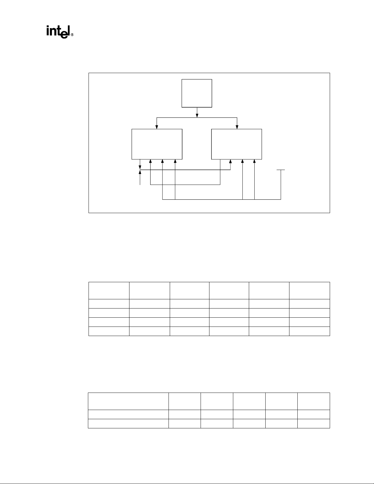
Configuration and Initialization
Figure 5-2. BR[3:0]# Physical Interconnection with Two Symmetric Agents
Priority
Agent
BPRI#
Agent 0 Agent 3
BR0#
BR1#
BR2#
BR3#
BREQ0#
BREQ1#
System
Interface Logic
During Reset
BR0#
BR1#
BR2#
BR3#
001099
At the asserted-to-deasserte d tra ns ition of RESET#, system interface logic is responsible for
asserting the BREQ0# bus signa l. The BREQ[3:1]# bus signals remain deasserted. All process ors
sample their BR[3:1] # pins on the assert ed-to-de asser ted tran siti on of RESET# and determin e their
arbitr a tion ID fr o m th e sample d val u e.
Each physical processor is a logical processor with a distinct arbitration ID and agent ID (refer to
Table 5-4).
Table 5-4. Arbitration ID Config ura tion
BR0# BR1# BR2# BR3# Arbitration ID
LHHH00
HHHL12
HHLH24
HLHH36
1. L and H designate electrical levels.
1
5.2.12 Clock Frequenc y Ratios
Table 5-5 defines the system bus rat io configurations for the Itanium 2 processor.
Table 5-5. Itani um® 2 Processor System Bus to Core Frequency Multiplier Configuration
Ratio of Bus Frequency to
Proces sor Fre que nc y
A[21]# A[20]# A[19]# A[1 8]# A[17]#
Agent ID
Reported
2/9 10110
2/10 10101
Intel® Itanium® 2 Processor Hardware Developer’s Manual 5-5

Configuration and Initialization
5.3 Initialization Overview
The processor and PAL firmware initialize and test the processor on reset.
5.3.1 Initialization with RESET#
The Itanium 2 processor begins initialization upon detection of RESET# signal active. RESET#
signal assertion is not maskable and ig nores all instruction boundaries including both IA-32 and
Itanium instructions.
Table 5-6 shows the architectural stat e initialized by th e proc essor hardware and PAL firmware at
reset. All othe r arch itectural states are unde fined at hardware reset. Refer to the Intel
Arch itectur e Software Developer’s Manual for a detailed description of the reg is ters.
®
Table 5-6. Itanium
Processor Resource Symbol Value Description
Instruction Pointer IP Refer to the Intel
Register Stack
Configuratio n Register
Current Frame Marker CFM sof=96, sol=0, sor=0, rrbs=0 All physical general purpose registers
Translation Register TR Invalid All TLBs are cleared.
Translation Cache TC Invalid All TLBs are cleared.
Caches — Invalid All caches are disabled.
2 Processor Reset State (after P AL)
Architecture Software
Developer’s Manual fo r detai ls.
RSC mode=0 Enforced lazy mode.
5.3.2 Initialization with INIT
The Itanium 2 processor supports an INIT interrupt. INIT can be initiated by either asserting the
INIT# signal or an INIT interrupt mess age. INIT cannot be maske d except when a Machine Check
(MC) is in progress. In this case, the INIT interrupt is he ld pending. INIT is recognized at
instruction boundaries. An INIT interrupt does not disturb any processor architectural states, the
state of the caches, model specific registe rs, or any integer or floatin g-point states.
®
Itanium™
®
Itanium™
SALE_RESET entry point for the
®
Itanium
are available, register state is
undef ined, no locals in the gene ral
register frame, no rotation in the
general register frame, rename base
for FR, GR and PR registers is set to 0.
2 proces sor.
Table 5-7 shows the processor state modified by INIT. Refer to the Intel
®
Itanium™ Architecture
Software Developer’s Manual for a detailed description of the registers.
Table 5-7. Itanium® Processor INIT State
Processor Resource Symbol Value Description
®
Instruct ion Poin te r IP Refer to the Intel
Interruption Instruction
Bundle Pointer
Interruption Processor
Status Register
Interruption Function
State
IPSR Original value of PS R. Value of PSR at the time of INIT.
Architecture Software
Developer’s Manual for details.
IIP Original value of IP. Value of IP at the time of INIT.
IFS v=0 Invalidate IFS.
Itanium™
5-6 Intel® Itanium® 2 Process or Hard ware Develop er’s Manual
PALE_IN IT entry point for the Itanium®
2 processor.

Test Access Port (TAP) 6
This chapter describe s the impl ementation of th e Itan ium 2 pro cessor Test Access Port (TAP) logic.
The TAP complies with the IEEE 1149.1 (JTAG) Specification. Basic f unctionality of the 1 149.1compatible te st logic is described here. For details of the IEEE 114 9.1 Specification, the reader is
referred to the published standard
A simplified bloc k diagra m of t he TAP is shown in Figure 6-1. The Itanium 2 processo r conta ins a n
integrated TAP controller, a Boundary Scan register, four input pins (TDI, TCK, TMS and TRST#)
and one output pin (TDO). The integrated TAP controller consists of an Instruction Register, a
Device ID Register, a Bypass Register and control logic.
For specific boundary scan chain information, please reference the Intel
Boundary Scan Description Language (BSDL) Model.
Figure 6-1. Test Access Port Block Diagram
1
, and to other industry s tandard material on the subject.
®
Itanium® 2 Processor
Boundary Scan Test Register
Control Si gnals
TDI
TMS
TCK
TRST#
1. ANSI/IE EE S td. 1 149 . 1-199 0 (i nclu di ng IEE E S td . 1 14 9.1a- 1 993), “IEEE Standar d Test Access Port a nd Bo unda ry Scan Arc hit ecture, ” IEEE
Press, Piscataway NJ, 1993.
Device Ident i fication
BYPASS Register
Instructio n Decode /
Cont r ol Logic
Instruction Regi st er
Tap Controller
TDO
000701b
Intel® Itanium® 2 Processor Hardware Developer’s Manual 6-1

Test Access Port (TAP)
6.1 Interface
The TAP scan chain is accessed serially through five dedicated pins on the processor package:
• TCK: The TAP clock signal.
• TMS: “Test Mo de S el ect,” which controls the TAP finite state machine.
• TDI: “Test Data Input,” which inputs test instructions and data seriall y.
• TRST#: “Test Reset,” for TAP logic reset.
• TDO: “Test Data Output,” through which test output is read serially.
TMS, TDI and TDO operate synchronously with TCK (which is independent of any other
processor clock). TRST# is an asynchronous input signal.
6.2 Accessing The TAP Logic
The TAP is accessed through an IEEE 1149.1-compliant TAP controller finite state machine. This
finite sta te machine , shown in Figure 6-2, contains a reset state, a run-test/idl e state, and t wo major
branch es . T h ese branch es al lo w ac cess eith er to the TAP Instr u ct io n Register or to on e of th e da ta
registers. The TMS pin is used as the controlling input to traverse this finite state machine. TAP
instructions and test data are loade d serially (in the Shift-IR and Shift-DR states, r espectively)
using the TDI pin. State transitions are made on the rising edge of TCK.
Figure 6-2. TAP Controller State Diagram
Test-Logic-
1
Reset
0
Run-Test/
0
Idle
1 TMS
Select-
DR-Scan
0
11
Capture-DR
0
Shift-DR
Exit1-DR
Pause-DR
00
Exit2-DR
Update-DR
1
0
1
1
0
0
1
1
0
Select-
IR-Scan
0
Capture-IR
0
Shift-IR
1
Exit1-IR
0
Pause-IR
1
Exit2-IR
1
Update-IR
1
1
0
1
0
0
000683
6-2 Intel® Itanium® 2 Process or Hard ware Develop er’s Manual

Test Access Port (TAP)
The following is a brief d escription of each of the states of the TAP controller state machine. Refer
to the IEEE 1149.1 standard for de tailed descriptions of the states and their operation.
• Test-Logic-Reset: In this state , the test lo gi c is disab l ed so th a t th e processor op er ates
normally. In this state, the instruction in the Instructi on Register is for ced to IDCODE.
Regardless of the original state of the TAP Finite State Machine (TAPFSM), it always enters
Test-Logic-Reset whe n the TMS input is held asserted for at least five clocks. The controller
also enters this state immediately when the TR ST# pin is asserted, and automatically upon
power-on. The TAPFSM ca nnot leave this state as long as the TRST# pin is held asserted.
• Run-Test/Idle: A controller state between scan opera tions. Once entered the cont r o ller will
remain in th is state as long as TMS is held low. In this state, activity in se lected test logic
occurs only i n the presence of ce rtain instruct ions. For instructions that do not cause functions
to execut e in this state, all test data registers selected by the current instructions retain their
previou s s t at e.
• Select-IR-Scan: This is a temporary controller state in which all test data registers selected by
the current instruction retain their previous state.
• Capture-IR: In this state, the shift register contained in the Instruction Register loads a fixed
value (of whic h the two le ast s ig nifi cant bi ts are “01”) on the ris ing edge of TCK. The par allel ,
latched output of the Instr uction Register (current instruction) does not chang e in this state.
• Shift-IR: The shift register contained in the Instruction Register is connec ted between TDI
and TDO and is shifted one stage toward its serial output on each rising edge of TCK. The
output arrives at TDO on the falling edge of TCK. The current instruction does not change in
this state.
• Exit-IR: This is a temporary state and the current instruction does not change in this state.
• Pause-IR: Allows shifting of the Instruction Register to be temporarily halted. The current
instruc t ion does not change in this state.
• Exit2-IR: This is a temporary state and the current in struction does not change in this state.
• Update-IR: The instruction which has been shi fted int o the Instructi on Re giste r is la tched i nto
the parallel output of the Instruction Register on the falling edge of TCK. Once th e new
instruction has been latched, it remains the curr ent instruction until the next Update-IR (or
until the TAPFSM is reset).
• Select-DR-Scan: Th is is a tempo r ar y co ntroll er state and all test dat a r eg isters se le ct ed by the
current instruction retain their previous values.
• Capture-DR: In this state, data may be parallel-loaded into test data regis ters selected by the
current instruc tion on the rising edge of TCK. If a test data register selected by the current
instructi on does not have a parallel input, or if capturing is not required for the se lected test,
then the register retains its previous state.
• Shift-DR: The data register connected between TDI and TDO as a result of selection by the
current instruc tion i s shi fted one sta ge towa rd it s seri al outp ut on each r ising edge of TCK. The
output arrives at TDO on the falling edge of TCK. If the data register has a latched parallel
output then the latch value does not change while new data is being shifted in.
• Exit1-DR: This is a temporary state and all data registers selected by the current instruction
retain their pr evious values.
• Pause-DR: Allows shifting of the selected data register to be temporarily halted without
stopping TCK. All registers selected by the current instruction retain their previous values.
Intel® Itanium® 2 Processor Hardware Developer’s Manual 6-3

Test Access Port (TAP)
• Exit2-DR: This is a temporary state and all reg i sters selected by the current instruction retain
their previous val ues.
• Update-DR: Some test data registers may be provided with latch ed par allel outputs to prevent
changes in the parallel output while data is being shifted in the associated shift register path in
response to cer tain instructions. Data is latched into the parallel output of these registe r s fr om
the shift-re gister path on the fall ing edge of TCK.
6.3 TAP Registers
The following is a list of all test registers which can be accessed through the TAP.
1. Boundary Scan Register
The Boundary Scan regis ter consists of several single-bit shif t registers. The boundary scan
register pr ovides a shift register pat h f r om a ll the input to the output pins on the Ita nium 2
processor. Data is transferred from TDI to TDO through the boundary scan register.
2. Bypass Register
The bypass regist er is a one-bit shift register that provides the minimal path length between
TDI and TDO. The bypass registe r is selected when no test operation is being performed by a
component on the board. The bypass register loads a logic zero at the start of a sca n cycle.
3. Device Identificatio n (ID) Regist er
The device ID register contains the manufacturer’s ide ntification code, version number, and
part number. The device ID registe r has a fixed length of 32 bits, as define d by the IEEE
1149.1 specification.
4. Instruction Register
The instruction register contains a four-bit command field to indicate one of the following
instructions: BYPASS, EXTEST, SAMPLE/PRELOAD, IDCODE, HI GHZ, and CLAMP. The
most sign ificant bit of th e I nstruction register is connected to TDI and the least significan t bit
is connected to TDO.
6.4 TAP Instructions
Table 6-1 shows the IEEE 1149.1 Sta ndard defined instructions for the TAP controller. Except for
BYPASS, which is all 1s, all instructions as defined by the IEEE 1149.1 must have an instruction
code of 0000 xxxx.
Table 6-1. Instructions for the Itanium
Instructions
IEEE 1149.1 Standard
BYPASS 1111 1111 FFh
EXTES T 000 0 00 00 00h
SAMP LE/PREL O AD 0000 00 01 01h
Additional
IDCO DE 000 0 00 10 02h
HIGH Z 0000 10 00 08h
CLAMP 0000 1011 0Bh
®
2 Processor TAP Controller
Encoding
(Binary)
Encoding
(Hex)
6-4 Intel® Itanium® 2 Process or Hard ware Develop er’s Manual

Test Access Port (TAP)
• BYPASS: The bypass register contains a single shift-register stage and is used to provide a
minimum length ser ial path between the TDI and TDO pins. This bypass enables the rapi d
movement of test data to and from other components on a system board.
• EXTEST: Th is instruction allows data to be serially loaded into the boundary scan chain
through TDI, and forces the output buffers to driv e the data contained in the boundary sc an
register. This instruction can be used in conjunct ion with SAMPLE/PRELOAD to test the
board-level in terconnect between components.
• SAMPLE/PRELOAD: This i nstructi on a llows data t o be s ampl ed from the in put buf fer s to be
captured in the boundary scan register and serially unloaded from the TDO pin. This
instructi on als o allows data to be pre-loaded into the boundary scan chain prior to selecting
another boundary scan instruction. This instruction can be used in conjunction with the
EXTEST instruct ion to test the board-level interconnect between components.
• IDCODE: This instruction places th e dev ice ID regis ter between TDI and TDO to allow the
device identification value to be shi f ted out to TDO. The register contains the manufacture r’s
identity, part number, and versi on number. Th is instruction is the defa ult instruction after the
TAP has been reset.
• HIGHZ : This instruction places all of the output buffe rs of the component in an inactive drive
state. In th is state , board -le vel te stin g can b e pe rformed wit hout incurri ng t he ris k of damage t o
the component. Duri ng the execution of the HIGHZ instruct ion, the bypass register is pl aced
between TDI and TDO.
• CLAMP: This instruction sele cts the bypass register while the output buf f ers drive the data
contained in the bounda ry scan cha in. Th is ins truct ion pr otect s the rece ivers from the values in
the boundary scan chain while data is being shifted out.
6.5 Reset Behavior
The TAP and its related hardware are reset by transitioning the TAP controller finite state machine
into the Test-Logic-Reset state . The TAP is completely disabled upon reset (i.e. by resetting the
TAP, the processor will function as though the TAP did not exist). Note that there is no logic in the
TAP which responds to the normal processor reset signal . Th e TAP can be transitioned to the TestLogic-Reset state by any one of the following thre e ways:
• Power-on the processo r. This automatically (asynchronously) resets the TAP controller .
• Assert the TRST# pin at any time. This asynchro nously resets the TAP controller.
• Hold the TMS pin high for 5 consecuti ve cycl es of TCK. Th is tra nsiti ons the TAP controller to
the Test-Logic-Reset state.
Intel® Itanium® 2 Processor Hardware Developer’s Manual 6-5

Test Access Port (TAP)
6-6 Intel® Itanium® 2 Process or Hard ware Develop er’s Manual

Integration Tools 7
The Itanium 2 processor supports In-Target Probe (ITP) devices, and Logic Analyzer devices
through a Logic Analyzer Interface (LAI), to allow monitoring of processor and system bus
activity. Each device has its’ own considerations for design and use.
7.1 In-Target Probe (ITP)
The Itanium 2 processor supports the ITP for program execution control, register/memory/IO
access, and breakpo int control . This too l provi des som e of the fu nctions c ommonly as sociat ed with
debuggers and emulat ors. Use of an ITP will not affect high speed ope rations of the processor
signals thereby allowing the system bus to maintain full operating speed.
Please refer to the ITP700 Debug Port Design Guide for more information on the ITP.
7.2 Logic Analyzer Interface (LAI)
A Logic Analyzer Interface (LAI) module provides a way to connect a logic analyzer to signals on
the board. Third party logic analyzer vendors offer a variety of products with bus monitoring
capability.
The Itanium 2 processor sy st em bus can be monitored with logic analyzer equipment. Due to the
complexity of I tan ium 2 mul tip roce sso r sys te ms, the LA I is c rit ical in provi din g th e a bil ity to probe
and capture system bus signals for use in system debug and va lidation. There are two sets of
consideration s to keep in mind when designi ng an Ita nium 2 process or -bas ed syste m that can make
use of an LAI: mechanical considerations an d ele ctrical considerations. Please cons ult your Logic
Analyzer vendor for specific details.
Intel® Itanium® 2 Processor Hardware Developer’s Manual 7-1

Integration Tool s
7-2 Intel® Itanium® 2 Process or Hard ware Develop er’s Manual

Signals Reference A
This appendix provides an alphabetical lis ting of all Itanium 2 processor system bus signa ls . The
tables at the end of this appendix summarize the signals by direction: output, input, and I /O.
For a complete pinout li sting including proc essor specific pins, ple ase refer to the Intel
2 Proces s or at 1.0 GHz and 900 MHz Datasheet.
A.1 Alphabetical Signals Reference
A.1.1 A[49:3]# (I/O)
The Address (A[49:3]#) sig nals, with byte enables, define a 2
space. When ADS# is active, these pins transmit the address of a transaction. These pins are also
used to transmit other transaction rela ted information such as transaction identi fiers and external
functions in the cycle following ADS# assert ion. These signals must conne ct the appropriate pins
of all agents on the Itanium 2 processor syst em bus . The A[49:27]# signals are parity-protect ed by
the AP1# parity signal, and the A[26:3]# signals are parity-protect ed by the AP0# parity signal.
On the active-to-inactive transition of RESET#, the processors sa mpl e the A[49:3]# pins to
determine their power-on configuration.
A.1.2 A20M# (I)
A20M# is ignored in the Itanium 2 process or s ystem environment.
A.1.3 ADS# (I/O)
®
Itanium®
50
Byte phy sical memory ad dress
The Address Strob e (ADS#) signal is asserted to indicate the validity of the transaction address on
the A[49:3]#, REQ[5:0]#, AP[1:0]# and RP#pins. All bus age nts observe the ADS# activation to
begin parity checking, protocol checking, address decode, internal snoop, or deferred reply ID
match operations associated with the new transac tion.
A.1.4 AP[1:0]# (I/O)
The Address Parity (AP[1: 0]#) signals can be driven by the request initiator along with ADS# and
A[49:3]#. AP[1] # covers A[49:27]#, and AP[0]# covers A[26:3]#. A correct parity signal is high if
an even number of covered signals are low and low if an odd num ber of covered signals are low.
This allows parity to be high when all the covered signals are high.
A.1.5 ASZ[1:0]# (I/O)
The ASZ[1:0]# signals ar e the memory address-space size signals. They are driven by the request
initiator during the first Request Phase clock on the REQa[4:3]# pins. The ASZ[1:0]# signals are
valid only when REQa[2:1]# signals equal 01B, 10B, or 11B, indicating a memory access
transaction. The ASZ[1:0]# decode is defined in Table A-1.
Intel® Itanium® 2 Processor Hardware Developer’s Manual A-1

Signals Reference
Table A-1. Address Space Size
ASZ[1:0]#
0 0 Reserved Reserved
0 1 36-bit 0 to (64 GByte - 1)
10 50-bit
1 1 Reserved Reserved
Memory Address
Space
Any memory access tran saction addressing a memory regi on that is less than 64 GB (i.e.
Aa[49:36]# are all zeroes) must set ASZ[1:0]# to 01. Any memory access transaction address ing a
memory region that is equal to or greater than 64 GB (i.e. Aa[49:3 6]# are not all zeroes) must set
ASZ[1:0]# to 10. All observing bus agents that s upport the 64 GByte (36-bit ) address space must
respond to the transaction when ASZ[ 1:0]# equals 01. All observing bus agents that support larger
than the 64 GByte (36-bit) address space must re spond to the transaction when ASZ[1:0]# equals
01 or 1 0.
A.1.6 ATTR[3:0]# (I/O)
The ATTR[3:0]# si gnals are the at tri bute signa ls . The y ar e dri ven by the req uest i nit ia tor d uring the
second clock of the Reque st Phase on the Ab[35:32]# pins. The ATTR[3:0]# signal s are va lid for
all transact ions. The ATTR[3]# signal is reserved. The ATTR[2:0]# are driven based on the
memory type. Please refer to Table A-2.
Table A-2. Effective Memory Type Signal Encoding
Memory Access
Range
64 GByte to
(1 Pbyte –1)
ATTR[2:0]# Description
000 Uncacheable
100 Write Coalescing
101 Write-Through
110 Write-Protect
111 Writeback
A.1.7 BCLKp/BCLKn (I)
The BCLKp and BCLKn dif f erential clock signa ls determine the bus frequency. All agents drive
their outputs and latch their inputs on the different ial crossing of BCLKp and BCLKn on the
signals that are using the common clock latched protocol.
BCLKp and BCLKn indirectly determine the internal clock frequency of the Itanium 2 processor.
Each Itaniu m 2 proces sor derives its internal clock by multiplying the BCLKp and BCLKn
frequency by a ratio that is defined and allowed by the power-on config uration.
A-2 Intel® Itanium® 2 Process or Hard ware Develop er’s Manual

A.1.8 BE[7:0]# (I/O)
The BE[7:0]# signals are the byte-enable signals for partial transactions. They are driven by the
request initiator during the seco nd Request Phase clock on the Ab[15:8]# pins.
For memory or I/O transactions, the byte-enabl e s ignals indicate tha t valid data is requested or
being trans f erre d on the corresponding byte on the 128-bit data bus. BE[0]# indic ates that the least
significa nt byte is valid, and BE[7]# ind icates that the most significant byte is valid. Since
BE[7:0]# specifies the validity of only 8 bytes on the 16 byte wide bus, A[3]# is used to deter mine
which half of the data bus is va lidated by BE[7:0]#.
For special trans act ions ((R EQa[5:0] # = 001000B) a nd (REQb[1:0 ]# = 01B )), the BE[7: 0]# sign als
carry special cycle encodings as defined in Table A-3. All other encodings are reserved.
Table A-3. Special Transaction Encoding on Byte Enables
Special Transaction Byte Enables[7:0]#
NOP 0000 0000
Shutdown 0000 0001
Flush (INVD) 0000 0010
Halt 0000 0011
Sync (WBINVD) 0000 0100
Reserved 0000 010 1
StopGrant Acknowledge 0000 0110
Reserved 0000 01 11
xTPR Update 0000 1000
Signals Reference
For Deferred Reply t r ansactions, BE[7:0]# signals are rese rved. The Defer Phase transfer length is
always the same length as that sp ecified in the Request Phase except the Bus Invalidate Line (BIL)
transaction.
A BIL transaction may return one cache line (128 bytes).
A.1.9 BERR# (I/O)
The Bus Error (BERR#) signal can be asserted to indi ca te a recoverable error with global MCA.
BERR# asserti on conditions are confi gurable at the system le vel. Configuration options enable
BERR# to be driven as follows:
• Asserted by the requesting agent of a bus transaction after it observes an internal error.
• Asserted by any bus agent when it obs erves an error in a bus transaction.
When the bus agent samples an asserted BERR# signal and BERR# sampling is enabled, the
proces s o r ent er s a M ac h in e C he ck H an d le r.
BERR# is a wired-OR signal to all o w multiple bus agents to drive it at the same time.
Intel® Itanium® 2 Processor Hardware Developer’s Manual A-3

Signals Reference
A.1.10 BINIT# (I/O)
If enabled by configuration, the Bus Init ialization (BINIT#) signal is asserted to signal any bus
condition that prevents reliable future operation.
If BINIT# obse r vation is enabled during power-on configuration, a nd BINIT# is sampled asserted,
all bus state mach in e s ar e r eset. All ag e nt s re set their ro t at in g ID s f o r b us a rbi tr ation to th e sa me
state as that after reset, and internal count information is lost. The L2 and L3 caches are not
affected.
If BINIT# observat ion is disabled during power-on configuration, BINIT# is ignored by all bus
agents wit h th e e xcepti on of t he prior ity age nt. The pr iori ty a ge nt mus t handl e t he e rror in a m an ner
that is app r o pr i at e to th e s y st em archit ecture .
BINIT# is a wired-OR signal.
A.1.11 BNR# (I/O)
The Block Next Requ es t (BNR#) signal is used to assert a bus stall by any bus agent that is unable
to accept new bus trans actions to avoid an inter nal transaction queue overflow . During a bus stall,
the current bus owner c annot issue any new transactions.
Since multi ple agents might need to re ques t a bus sta ll at t he same time, BNR# i s a wire- OR signa l.
In order to avoid wire-OR glitches associated with simultaneous edge transitions driven by
multiple drivers, BNR# is asserted and sampled on specific clock edges.
A.1.12 BPM[5:0]# (I/O)
The BPM[5:0]# signals are system support signals used for inserting breakpoints and for
performance monitoring. They can be configur ed as outputs from the processor that indicate
programmable counters used for monitoring performance, or inputs from the processor to indicate
the status of breakpoints.
A.1.13 BPRI# (I)
The Bus Priority-agent Request (BPRI#) signal is used by the priority agent to arbitrate for
ownership of the syste m bus. Observi ng BPRI# ass erted causes all ot her agent s to stop iss uing new
requests, unles s such requests are part of an ongoing locked operation.The priority agent keeps
BPRI# asserted unt il all of its requests are comp leted, then releases the bus by deasserting BPRI #.
A.1.14 BR[0]# (I/O) and BR[3:1]# (I)
BR[3:0]# are the phy si cal bus request pins that dr ive the BREQ[3:0]# signals in the system. The
BREQ[3:0]# signals are interconnected in a rotating manner to individual processor pins.
Table A-4 and Table A-4 give the rotati ng interconnection between the processor and bus signals
for both the 4P and 2P system bus topologies.
A-4 Intel® Itanium® 2 Process or Hard ware Develop er’s Manual

Signals Reference
Table A-4. BR0# (I/O), BR1#, BR2#, BR3# Signals for 4P Rotating Interconnect
Bus Signal Age nt 0 Pins Agent 1 Pins Ag ent 2 Pins Agent 3 Pins
BREQ[0]# BR[0]# BR[3]# BR[2]# BR[1]#
BREQ[1]# BR[1]# BR[0]# BR[3]# BR[2]#
BREQ[2]# BR[2]# BR[1]# BR[0]# BR[3]#
BREQ[3]# BR[3]# BR[2]# BR[1]# BR[0]#
Table A-5. BR0# (I/O), BR1#, BR2#, BR3# Signals for 2P Rotating Interconnect
Bus Signal Age nt 0 Pins Ag ent 3 Pins
BREQ[0]# BR[0]# BR[1]#
BREQ[1]# BR[1]# BR[0]#
BREQ[2]# Not Used Not Used
BREQ[3]# Not Used Not Used
During power- on configuration, the priority agent must assert the BR[0]# bus si gnal. All
symmetric agents sample their BR [3:0]# pins on asserted-to-deasserted transition of RESET#. The
pin on which the agent samples an asserted level determines its agent ID. All agents then configure
their pins to match the appropriate bus signal protocol as shown in Table A-6.
Table A-6. BR[3:0]# Signals and Agent IDs
Pin Sampled
Asserted on RESET#
BR[0]# 0 0
BR[3]# 1 2
BR[2]# 2 4
BR[1]# 3 6
Arbitration ID Agent ID Reported
A.1.15 BREQ[3:0]# (I/O)
The BREQ[3:0]# signals are the symmetric agent arbitration bus signals (called bus request). A
symmetric agent n arbitrates for the bus by asserting its BREQn# signal. Agent n drives BREQn#
as an output and receives the remaining BREQ[3:0]# sig nals as inputs.
The symmetric agents support distributed ar bitration based on a round-robin mechanism. The
rotating ID is an internal state used by all symmetric agents to track the agent with the lowest
priority at the next arbitration event. At power-on, the rotating ID is initialized to three, allowin g
agent 0 to b e the highest priority sy mmetric agent. After a new arbitration event, the r otating ID of
all symmetr ic agents is upda ted to the agent ID of the symmetric owner. This update gives the new
symmetric owner lowest priority in the next arbitration event.
A new arbitration event occurs either when a symmetric agent asserts its BREQn# on an Idle bus
(all BREQ[3:0]# previously deasserted), or the current symmetric owner deasserts BREQn# to
release the bus ownership to a new bus owner n. On a new arbitration event, all symmetric agents
simultaneously determine the new symmetric owner using BREQ[3:0]# and the rotating ID. The
symmetric owner can park on the bus (hold the bus) provided that no other sym metric agent is
requesting its use. The symmetric owner parks by keeping its BREQn# signal asserted. On
sampling BREQn# asserted by another symmetric agent, the symmetric owne r deasserts BREQn#
as soon as possible to re lease the bus. A symmetric owner stops issuing new requests tha t are not
part of an existing locked operation on observing BPRI# asserted.
Intel® Itanium® 2 Processor Hardware Developer’s Manual A-5

Signals Reference
A symmetric agent can deassert BREQn# before it becomes a symmetric owner. A symmetric
agent can reassert BREQn# after keeping it deasserted for one clock.
A.1.16 CCL# (I/O)
CCL# is the Cache Cleanse signal. It is driven on the second clock of the Reque st Phase on the
EXF[2]#/Ab[5]# pi n. CCL # is asserted for Memory W r ite transaction to indi cate that a modified
line in a processor ma y be written to memory without be ing invalidated in its caches.
A.1.17 CPUPRES# (O)
CPUPRES# can be used to detect the presence of a Itanium 2 processor in a socket. A ground
indicates that a Itanium 2 processor is installed, while an open indicates that a Itanium 2 processor
is not installed.
A.1.18 D[127:0]# (I/O)
The Data (D[127:0] #) si gnals provide a 128-bit data path between various system bus agents.
Partial transfers require one data transfer clock with valid data on the byte(s) indicated by asserte d
byte enables BE[7:0]# and A[ 3] #. Data signals that are not valid for a particular transfer must still
have correct ECC (if data bus error checking is enabled). The data driver asserts DRDY# to
indicate a valid data transfer.
A.1.19 D/C# (I/O)
The Data/Code (D/C#) signal is used to indicate data (1) or code (0) on REQa[1]#, only during
Memory Read transactions.
A.1.20 DBSY# (I/O)
The Data Bus Busy (DBSY#) signal is asserted by the agent that is responsible for driving data on
the system bus to indicate that the data bus is in use. The data bus is released after DBSY# is
deasserted.
DBSY# is replicated three times to enab le partitioning of the data paths in the system agents. This
copy of the Data Bus Busy signal (DBSY#) is an input as well as an output.
A.1.21 DBSY_C1# (O)
DBSY# is a copy of the Data Bus Busy signal. This copy of the Data Bus Busy signal
(DBSY_C1#) is an out put only.
A.1.22 DBSY_C2# (O)
DBSY# is a copy of the Data Bus Busy signal. This copy of the Data Bus Busy signal
(DBSY_C2#) is an out put only.
A-6 Intel® Itanium® 2 Process or Hard ware Develop er’s Manual

A.1.23 DEFER# (I)
The DEFER# signal is asserted by an agent to indicate that the t r ansaction cannot be guaranteed inorder completion. Assertion of DEFER# is normally the resp onsibility of the priori ty agent.
A.1.24 DEN# (I/O)
The Defer Enable (DEN#) signal is driven on the bus on the se cond clock of the Request Ph as e on
the Ab[4]# pin. DEN# is asserted to indicate that the transaction can be de ferred by the responding
agent.
A.1.25 DEP[15:0]# (I/O)
The Data Bus ECC Protecti on (DEP[15:0]#) s ignals provide optional ECC protection for Data Bus
(D[127:0]#). They are driven by the agent responsible for driving D[127:0]#. During power-on
configuration, bus agents can be enabled for either ECC checking or no checking.
The ECC error correcting co de can detect and correct single-bit errors and detect double-bit or
nibble errors. Chapter 4, “Data Integrity”, provides more information about ECC.
Signals Reference
A.1.26 DHIT# (I)
The Deferred Hit (DHIT#) signal is dr iven during the Deferred Phase by the deferring age nt. For
read transact ions o n the bus DHIT# ret urns the final c ache status that woul d ha ve been indi ca ted on
HIT# for a transaction which was not deferred. DID[9:0]# (I/O)
DID[9:0]# are Deferred Ident ifier signals. The requesting agent transfers thes e signals by using
A[25:16]#. They are tra nsfer red on Ab[25: 16]# durin g the s econd cloc k of the Req uest Phase o n all
transactions , but Ab[20:16]# is only defined for deferrable transacti ons (DEN# asserted).
DID[9:0]# is also transferred on Aa[25:16]# during the first clock of the Request Phase for
Deferred Reply transac tions.
The deferred ide ntifier defines the token suppli ed by the requesting agent. DID[9]# and DID[8:5]#
carry the agent identifiers of the requesting agents (always valid) and DID[4:0]# carry a transaction
identif i er ass oci at ed with th e re que st ( v ali d o nly with DEN # as s ert ed) . Th i s conf ig ur ati on l im it s the
bus specification to 32 logical bus agents with each one of the bus agents ca pable of making up to
32 requests. Table A-7 shows the DID encodings.
Table A-7. DID[9:0]# Encoding
DID[9]# DID[8:5]# DID[4:0]#
Agent Type Agent ID[3:0] Transaction ID[4:0]
DID[9 ] # in d i ca tes the agen t ty pe . S y mm e tr i c ag e nt s us e 0. Pri o r it y age n ts u se 1. DI D[ 8 : 5] #
indicates the agent ID. Symmetric agents use their arbitration ID. DID[4:0]# indicates the
transa ct ion ID f or an age nt. T he t ran sa ct ion ID mus t be u niqu e fo r all def err abl e t ran sa ct ions i ssue d
by an agent which have not rep orted their snoop results.
The Deferred Reply agent transmits the DID[9:0]# (Ab[25:16]#) signals rec eived during the
original transaction on the Aa[25:16 ] # si gnals during the Deferr ed Re ply transaction. This process
enables the original requesting agent to make an identifier match with the or iginal request that is
awaiting completion.
Intel® Itanium® 2 Processor Hardware Developer’s Manual A-7

Signals Reference
A.1.27 DPS# (I/O)
The Deferred Phase Ena ble (DPS#) signal is driven to the bus on the second clock of the Request
Phase on the Ab[3]# pin . DPS# is asserted if a requesting agent supports transaction completion
using the Deferred Pha se . A requ esting agent that supports the Deferred Phase will always assert
DPS#. A requesting agent that does not support the Deferred Phase will always deassert DPS#.
A.1.28 DRDY# (I/O)
The Data Ready (DRDY#) signal is asserted by the data driver on each data transfer, indicating
valid data on the data bus. In a multi-cycle data transfer, DRDY# can be deasserted to insert idle
clocks.
DRDY # is replicated th r e e times to en a bl e p ar t itioni ng of d ata path s in th e system agen ts. This
copy of the Data Ready signal (DRDY#) is an input as well as an output.
A.1.29 DRDY_C1# (O)
DRDY# is a copy of the Data Ready signal. This copy of the Data Phase data-ready signal
(DRDY_C1#) is an output only .
A.1.30 DRDY_C2# (O)
DRDY# is a copy of the Data Ready signal. This copy of the Data Phase data-ready signal
(DRDY_C2#) is an output only .
A.1.31 DSZ[1:0]# (I/O)
The Data Size (DSZ[1:0]#) signals are transferred on REQb[4:3]# signals in the second clock of
the Request Phas e by the requesting agent. The DSZ[1:0]# signals define th e data transfer
capabili ty of the requesting agent. For the Itanium 2 processor, DSZ# = 01, always.
A.1.32 EXF[4:0]# (I/O)
The Extended Funct ion (EXF[4:0]#) signals are transferred on the A[7:3]# pins by the requesting
agent during the second clock of the Request Ph as e. The signals specify any special functional
requirement associated with the transaction based on the requestor mode or capab ility. The signals
are define d in Table A-8.
Table A-8. Extended Function Si gnals
Extended Function Signal Signal Name Alias Function
EXF[4]# Reserved Reserved
EXF[3]# SPLCK#/FCL# Split Lock / Flush Cache Line
EXF[2]# OWN#/CCL#
EXF[1] # D EN # Defer Enable
EXF[0] # D PS# Deferred Phase Supported
Memory Update Not Needed / Cache
Cleanse
A-8 Intel® Itanium® 2 Process or Hard ware Develop er’s Manual

A.1.33 FCL# (I/O)
The Flush Cache Line (FCL#) signal is driven to the bus on the second c lock of the Request Phas e
on the A[6]# pin. FCL# is assert ed to ind ic ate tha t the memory trans acti on is in itia te d by the glo bal
Flush Cache (FC) instruction.
A.1.34 FERR# (O)
The FERR# signal may be asserted to indicate an unmasked floating point error generated by an
IA-32 application.
A.1.35 GSEQ# (I)
Assertion of the Guaranteed Sequentiality (GS EQ#) signal indicates that the platform guarantees
completion of the tra nsaction without a retry while maintaining seque ntiality.
A.1.36 HIT# (I/O) and HITM# (I/O)
The Snoop Hit (HIT#) and Hit Modified (HITM#) signals convey transa ction snoop operation
results. Any bus ag ent ca n assert both HIT# a nd HITM# toge ther to indi cate that it require s a snoop
stall. The stal l ca n be continued by reasserting HIT# and HITM# together.
Signals Reference
A.1.37 ID[9:0]# (I)
The Trans ac tion ID (ID[9:0]#) signals are driven by the deferring agent. The signals in the two
clocks are referenced IDa[9:0]# and IDb[9:0]#. During both clocks, ID[9:0]# signals are protected
by the IP0# parity sign al for the first clock, and by the IP[ 1]# parity signal on the second clock.
IDa[9:0]# returns the ID of the deferred transaction which was sent on Ab[25:16]# (DID[9:0]#).
A.1.38 IDS# (I)
The ID Strobe (IDS#) signal is asserted to indicate the validity of ID[9:0]# in that clock and the
validity of DHIT# and IP[1: 0]# in the next clock.
A.1.39 IGNNE# (I)
IGNNE# is ignored in the Itanium 2 processor system environment.
A.1.40 INIT# (I)
The Initialization (INIT#) signal triggers an unmasked interrupt to the proc es sor . INIT # is usua lly
used to break into hanging or idle processor states. Semantics required for platform compatibility
are supplied in the PAL firmware interrupt service routine.
Intel® Itanium® 2 Processor Hardware Developer’s Manual A-9

Signals Reference
A.1.41 INT (I)
INT is the 8259-compatible Interrupt Request signal which indicates that an external interrupt has
been generated. The interrupt is maskable. The processor vectors to the interrupt handler after the
current instruction execution has been comp leted. An interrupt acknowledge transactio n is
generated by the processor to obtain the interrupt vector from the interrupt controller.
The LINT[0] pin can be software c onfigured to be used either as the INT signal or another local
interrupt.
A.1.42 IP[1:0]# (I)
The ID Parity (IP[1:0]#) signals are driven on the second clock of the Defer red Phase by the
deferring agent. IP0# protects the IDa[9:0]# and IDS# signals for the first clock, and IP[1]#
protects the IDb[9:2, 0]# and IDS# signals on the second clock.
A.1.43 LEN[2:0]# (I/O)
The Data Length (LEN[2: 0]#) signals are transmi tted using REQb[2:0]# signa ls by the requesting
agent in the second clock of Request Phase. LEN[2 :0]# defines the length of the data transfer
requested by the requesting agent as shown in Table A-9. The LEN[2:0]#, HITM#, and RS[2:0]#
signals together define the length of the actual data tr ans f er.
Table A-9. Length of Data Transfers
LEN[2:0]# Length
000 0 – 8 bytes
001 16 byte s
010 32 byte s
011 64 bytes
100 128 bytes
101 Reserved
110 Reserved
111 Reserved
A.1.44 LINT[1:0] (I)
LINT[1:0] are local interrupt signals. These pins are disabled after RESET#. LINT[0] is typically
software configured as INT, an 8259-compatible maskable interrupt request signal. LINT[1] is
typically software configured as NMI, a non-maskable interrupt. Both signal s ar e asynchronous
inputs.
A.1.45 LOCK# (I/O)
LOCK# is never asserted or sampled in the Itanium 2 process or system environment.
A-10 Intel® Itanium® 2 Process or Hard ware Develop er’s Manual

A.1.46 NMI (I)
The NMI signal is the Non-mask able Interrupt signal. Asserting NMI causes an interrupt with an
internally supplied vector value of 2. An external interrupt-acknowledge transaction is not
generated. If NMI is asserted during the execution of an NMI service routine, it remains pending
and is recognized after the EOI is executed by the NMI service routine. At most, one assertion of
NMI is held pending.
NMI is rising-edge sens itive. Recognit ion of NMI is guaranteed in a specific cl ock if it is asserted
synchronously and meets the setup and hold times . If ass erted asynchronously , ass erted and
deasserted puls e widths of NMI must be a minimum of two clocks. This signa l mu st be s oftware
configured to be used either as NMI or as another local interrupt (LINT1 pin).
A.1.47 OWN# (I/O)
The Guaranteed C ache Line Ownership (OWN#) signal is driven to the bus on the second clock of
the Request P hase on th e Ab[5] # pin. OWN# is asser ted if c ache l ine owne rship i s guara ntee d. This
allows a memory control ler to ignore memory updates due to im plicit writebacks.
A.1.48 PMI# (I)
Signals Reference
The Platform Management Interrupt (PMI#) signal triggers the highest priority interrupt to the
processor. PMI# is usually used by the system to trigger system events that will be handled by
platform specific firmware.
A.1.49 PWRGOOD (I)
The Power Good (PWRGOOD) signal must be deasserted (L) during power-on, and must be
asserted (H) after RESET# is first asserted by the system.
A.1.50 REQ[5:0]# (I/O)
The REQ[5:0]# are the Re quest Command signals. They are asserted by the current bus owner in
both clocks of the Request Phase. In the first cloc k, the REQa[5:0]# signals defi ne the transaction
type to a level of detail that is sufficient to begin a snoop requ es t. In the second clock, REQb[5: 0]#
signals carry additional information to define the complete transaction type. REQb[4:3]# signals
transmit DSZ[1:0]# or the data transfer rate information of the requestor for transactions that
involve data transfer. REQb[2:0]# signals transmit LEN[2:0]# (the data transfer length
information). In both clocks, REQ[5:0] # and ADS# are protected by parity RP#.
All receiving agents obs erve the REQ[5:0]# signals to determine the transaction type and
parti cipate in the transaction as necessary, as shown in Table A-10.
Intel® Itanium® 2 Processor Hardware Developer’s Manual A-11

Signals Reference
Table A-10. Transaction Types Defined by REQa#/REQb# Signals
Transaction
Deferred Reply0000 0 00xxxxx
Reserved 0000 0 10xxxxx
Interrupt
Acknowledge
Special
Transactions
Reserved 0010 0 00DSZ[1:0]#01x
Reserved 0 0 1 0 0 1 0 DSZ[1:0]# 0 x x
Interrupt 0 0 1 0 0 1 0 DSZ[1:0]# 1 0 0
Purge TC 0010 0 10DSZ[1:0]#101
Reserved 0010 0 10DSZ[1:0]#11x
I/O Read 0 1 0 0 0 0 0 DSZ[1:0]# x x x
I/O Write 0 1 0 0 0 1 0 DSZ[1:0]# x x x
Reserved 0110 0 x0DSZ[1:0]#xxx
Memory R ead &
Invalidate
Reserved 0 ASZ[1:0]# 0 1 1 0 DSZ[1:0]# LEN[2:0]#
Memory Read 0 ASZ[1:0]# 1 D/C# 0 0 DSZ[1:0]# LEN[2:0]#
Memory Read
Current
Reserved 1 ASZ[1:0]# 1 1 0 0 DSZ[1:0]# LEN[2:0]#
Memor y Writ e 0 AS Z[1 :0]# 1 WSNP# 1 0 DSZ[1:0]# LEN[2: 0]#
Cache Line
Replacement
5432 1 0543210
0010 0 00DSZ[1:0]#000
0010 0 00DSZ[1:0]#001
0 ASZ[1:0]# 0 1 0 0 DSZ[1:0]# LEN[2:0]#
1 ASZ[1:0]# 1 0 0 0 DSZ[1:0]# LEN[2:0]#
1 ASZ[1:0]# 1 WSNP# 1 0 DSZ[1:0]# 0 0 0
REQa[5:0]# REQb[5:0]#
A.1.51 R ESET # (I)
Asserting the RESET# signal resets all processors to known states and invalidates all caches
without writi ng back Modifi ed (M state) lin es. RESET# must remain assert ed for one micros econd
for a “wa rm” reset; for a power-on reset, RESET# must stay asserted for at least one millisecond
after V
and BCLKp have reached their proper specificat ions. On observing asserted RESET#,
CC
all system bus agents must deasse rt the ir outp uts with in two cloc ks.
A number of bus signals are sa mp led at the asserted-to-de asserted transition of RESET# for the
power-on configuration.
Unless its out puts are tristated during power-on configur ation, after asserted -to-deasserted
transiti on of RESET#, the processor begins program execution at the rese t-vector .
A.1.52 RP# (I/O)
The Request Pari ty (RP#) signal is driven by the requesting agent, and pro vides parity protection
for ADS# and REQ[5:0]#.
A-12 Intel® Itanium® 2 Process or Hard ware Develop er’s Manual

A correct parity signal is high if an even number of covered signals are low and low if an odd
number of covered signals are low . This definition allows parity to be high when all covere d
signals are high.
A.1.53 R S [2 :0 ]# (I)
The Response Status (RS[2:0]#) signa ls are driven by the responding age nt (the agent responsibl e
for com pl e tion of the tr an s a ct io n ) .
A.1.54 RSP# (I)
The Response Parity (RSP #) signal is driven by the responding agent (the agent responsible for
completion of the cu rrent transaction) during assertion of RS[2:0]#, the signals for which RSP#
provides parity protection.
A correct parity signal is high if an even number of covered signals are low and low if an odd
number of covered signals are low. During the Idle state of RS[2:0]# (RS[2:0]#=000), RSP# is also
high since it is not driven by any agent guaranteeing correct parity.
A.1.55 SBSY# (I/O)
Signals Reference
The Strobe Bus Busy (SBSY#) signal is driven by the agent transferring data when it owns the
strobe bus. SBSY# holds the strobe bus before the first DRDY# and between DRDY# assertions
for a multiple clock data transfer. SBSY# is deasserted before DBSY# to allow the next data
transfer agent to predrive the strobes before the data bus is released.
SBSY# is replicat ed thre e time s to enabl e partit ion ing of da ta pat hs in the system age nts. This copy
of the Strobe Bus Busy signal (SBSY#) is an input as wel l as an output.
A.1.56 SBSY_C1# (O)
SBSY# is a copy of the Strobe Bus Busy signal. This copy of the Strobe Bus Busy signal
(SBSY_C1#) is an outp ut only.
A.1.57 SBSY_C2# (O)
SBSY# is a copy of the Strobe Bus Busy signal. This copy of the Strobe Bus Busy signal
(SBSY_C2#) is an outp ut only.
A.1.58 SPLCK# (I/O)
The Split Lock (SPLC K #) signa l is driven in the second cl ock of the Request Phase on th e Ab[6]#
pin of the first tra ns action of a locked operation. It is driven to indicate that the locked opera tion
will consist of four locked tr ansaction s.
Intel® Itanium® 2 Processor Hardware Developer’s Manual A-13

Signals Reference
A.1.59 STBn[7:0]# and STBp[7:0]# (I/O)
STBp[7:0]# and STBn[7:0]# (a nd DRDY#) are used to transfer da ta at the 2x transfe r rate in li eu of
BCLKp. They a re dri ven by the da ta tr ans fer a gent with a tight s kew re lati ons hip with r esp ect to i ts
correspondi ng bus signals, and are used by the rece iving agent to capture valid data in its latches .
This function s like a n indep endent doubl e f requenc y cloc k cons tructe d fro m a falli ng edge of e ither
STBp[7:0]# or STBn[7:0]#. The data is synchronize d by DRDY#. Each strobe pair is associated
with 16 data bus signa ls and 2 ECC signals as shown in Table A-11.
Table A-11. STBp[7:0]# and STBn[7:0]# Associations
Strobe Bits Data Bits ECC Bits
STBp[7]#, STB n[7 ]# D[127:112]# DEP[15:14]#
STBp[6]#, STB n[6 ]# D[111:96 ]# D EP[ 13:1 2]#
STBp[5]#, STB n[5 ]# D[95:80 ]# DEP[11:10]#
STBp[4]#, STB n[4 ]# D[79:64]# DEP[9:8]#
STBp[3]#, STB n[3 ]# D[63:48]# DEP[7:6]#
STBp[2]#, STB n[2 ]# D[47:32]# DEP[5:4]#
STBp[1]#, STB n[1 ]# D[31:16]# DEP[3:2]#
STBp[0]#, STB n[0 ]# D[15:0 ]# D EP[1 :0]#
A.1.60 TCK (I)
The Test Clock (TCK) signal provides the clock input for the IEEE 1149.1 compliant Test Access
Port (TAP).
A.1.61 TDI (I)
The Test Data In (TDI) signal tra nsfers serial test data in to the Itanium 2 processor. TDI provides
the serial input needed for IEEE 1149.1 compliant Te st Access Port (TAP).
A.1.62 TDO (O)
The Test Data Out (TDO) signal transfers serial test data out from the Itanium 2 processor. TDO
provides the serial output needed for IEEE 1149.1 compliant Test Access Port (TAP).
A.1.63 THRMTRIP# (O)
The Thermal Trip (THRMTRIP#) signal prot ects the Itanium 2 processor from catastrophic
overheatin g by use of an interna l therm al sens or . This sensor is set well a bove the normal ope ratin g
temperature to ensure that there are no false trips. Data will be lost if the processor goes into
thermal trip (signaled to the system by the assertion of the THRMTRIP# signal). Once
THRMTRIP# is asserted, the platform must assert RESET# to protect the physical integrity of the
processor.
A-14 Intel® Itanium® 2 Process or Hard ware Develop er’s Manual

A.1.64 THRMALERT# (O)
THRMALERT# is asserted when the measured temperature from the processor thermal diode
equals or exceeds the temperature threshold data programmed in the high-temp (THIGH) or lowtemp (TLOW) registers on the s ensor. This signal can be used by the platform to implement
thermal regulation features.
A.1.65 TMS (I)
The Test Mode Select (TMS) signal is an IEEE 1149.1 compliant Test Access Port (TAP)
specific ation support signal used by debug tools.
A.1.66 TND# (I/O)
The TLB Purge Not Done (TND#) signal is as serted to delay completion of a TLB Purge
instruction, ev en after the T LB P u rge transaction completes on the system bus.
A.1.67 TRDY# (I)
Signals Reference
The Target Ready (T RDY#) sig n al is asser t ed by the targ et to ind i ca te that it is r ea d y to re ce i ve a
write or implicit writeb ack data transfer.
A.1.68 TRST# ( I)
The T AP Reset (TRST#) si gnal is an IE EE 1 149. 1 compl iant Test Access Port (TAP) support signal
used by debug tools.
A.1.69 WSNP# (I/O)
The Write Snoop (WSNP#) signal indic ates that snooping agents will snoop the memory write
transaction
A.2 Signal Summaries
Table A-12 through Table A-15 list attributes of the Itanium 2 processor output, input, and I/O
signals.
T able A-12. Output Signals
Name Active Leve l Clock Signal Group
CPUPRES# Low — Platform
DBSY_C1# Low BCLKp Data
DBSY_C2# Low BCLKp Data
DRDY_C1# Low BCLKp Data
DRDY_C2# Low BCLKp Data
FERR# Low Asynchronous PC Comp atibil ity
Intel® Itanium® 2 Processor Hardware Developer’s Manual A-15

Signals Reference
Table A-12. Output Signals (Continued)
Name Active Level Clock Signal Group
SBSY_C1# Low BCLKp Data
SBSY_C2# Low BCLKp Data
TDO High TCK TAP
THRMTRIP# Low Asynchronous E rror
THRMALERT# Low Asynchronous Error
Table A-13. Input Signals
Name Active Level Clock Signal Group Qualified
BPRI# Low BCLKp Arbitration Always
BR1# Low BCLKp Arbitration Always
BR2# Low BCLKp Arbitration Always
BR3# Low BCLKp Arbitration Always
BCLKp High — Control Always
BCLKn High — Control Always
D/C# Low BCLKp System Bus Request Phase (Mem Rd)
DEFER# Low BCLKp Snoop Snoop Phase
DHIT# Low BCLKp System Bus IDS#+1
GSEQ# Low BCLKp Snoop Snoop Phase
ID[9:0]# Low BCLKp Defer IDS#, IDS#+1
IDS# Low BCLKp Defer Always
INIT# Low Asynch Exec Control Always
INT (LINT0) High Asynch Exec Control
IP[1:0]# Low BCLKp System Bus IDS#+1
NMI (LINT1) Hi gh Asynch E x e c Contr o l
RESET# Low BCLKp Control Always
RS[2:0]# Low BCLKp Response Always
RSP# Low BCLKp Response Always
PMI# Low Asy nc h Exec Contro l
PWRGOOD High Asynch Control —
TCK High — Diagnostic Always
TDI High TCK Diagnostic Always
TMS High TCK Diagnostic Always
TRST# Low Asynch Diagnostic Always
TRDY# Low BCLKp Response Response Phas e
1
1. Synchronous assertion with asserted RS[2:0]# guarantees synchronization.
A-16 Intel® Itanium® 2 Process or Hard ware Develop er’s Manual

Table A-14. Input/Output Signals (Single Driver)
Name Active Level Clock Signal Group Qualified
A[49:3]# Low BCLKp Request ADS#, ADS#+1
ADS# Low BCLKp Request Always
AP[1:0]# Low BCLKp Request ADS#, ADS#+1
ASZ[1:0]# Low BCLKp System Bus ADS#
ATTR[3:0]# Low BCLKp System Bus ADS#+1
BE[7:0]# Low BCLKp System Bus ADS#+1
BR0# Low BCLKp System Bus Always
BPM[5:0]# Low BCLKp Diagnostic Always
CCL# Low BCLKp System Bus ADS#+1
D[127:0]# Low BCLKp Data DRDY#
DBSY# Low BCLKp Data Always
D/C# Low BCLKp System Bus ADS#
DEN# Low BCLKp System Bus ADS#+1
DEP[15:0]# Low BCLKp System Bus DRDY#
DID[9:0]# Low BCLKp System Bus ADS#+1
DRDY# Low BCLKp Data Always
DPS# Low BCLKp System Bus ADS#+1
DSZ[1:0]# Low BCLKp System Bus ADS#+1
EXF[4:0]# Low BCLKp System Bus ADS#+1
FCL# Low BCLKp System Bus ADS#+1
LEN[2:0]# Low BCLKp System Bus ADS#+1
LOCK# Low BCLKp Arbitration Always
OWN# Low BCLKp System Bus ADS#+1
REQ[5:0]# Low BCLKp Request ADS#, ADS#+1
RP# Low BCLKp Request ADS#, ADS#+1
SBSY# Low BCLKp Data Always
SPLCK# Low BCLKp System Bus ADS#+1
STBn[7:0]# Low — Data Always
STBp[7:0]# Low — Data Always
WSNP# Low BCLKp System Bus ADS#
Signals Reference
Intel® Itanium® 2 Processor Hardware Developer’s Manual A-17

Signals Reference
Table A-15. Input/Output Signals (Multiple Driver)
Name Active Level Clock Signal Group Qualified
BNR# Low BCLKp System Bus Always
BERR# Low BCLKp Error Always
BINIT# Low BCLKp Error Always
HIT# Low BCLKp Snoop Snoop Phase
HITM# Low BCLKp Snoop Snoop Phase
TND# Low BCLKp Snoop Always
A-18 Intel® Itanium® 2 Process or Hard ware Develop er’s Manual

Index
A
A[43:3]# .......................................................... 3-5, A-1
A20M# ............. ............... ............ ............... ............. A-1
Address signals .............................................. 3-5, A-1
ADS# .............................................................. 3-5, A-1
Advanced Load Address Table (ALAT) ................... 2-9
AP[1:0]# .......................................................... 4-2, A-1
Arbitration ID ........................................................... 5-4
Arbitration si gnals .............. ...................... ................ 3-4
ASZ[1:0]# ............................................................... A-1
ATTR[7 :0]# ...... ............... ............... ..................... .... A-2
Attribute signals ...................................................... A-2
B
BCLK ....................................................................... 3-4
BCLKN ........................................................... 3-4, A-2
BCLKP ............................................................ 3-4, A-2
BE[7: 0]# .. .. ..... ..... .. ..... ..... ..... .. ..... ..... .. ..... ..... ..... .. .... A-3
BERR# ................................................... 3-8, 5-3, A-3
BINIT# .................................................... 3-8, 5-3, A-4
BNR# .............................................................. 3-4, A-4
Boundary Scan Chain ............................................. 6-1
BPM[5: 0 ]# .................... ......................... ........ 3-10, A-4
BPRI# ............................................................. 3-4, A-4
BR[3:1]# ................................................................. A-4
BR0# ...................................................................... A-4
Branch Prediction .................................................... 2-5
BREQ[3:0]# .................................................... 3-4, A-5
BREQ0# ......................................................... 5-5, A-5
Bus Signal Protection .............................................. 4-2
BYPASS .................................................................. 6-5
Byte Enable signals ............................. .. ............ .. ... A-3
DHIT# ..................................................................... A-7
Diagnostic Signals ................................................ 3-10
DID[7 :0]# .. .. ..... ..... ..... .. ..... ..... ... .... ..... ..... ... .... ..... ... .. A-7
Dispersal Logic ................. ............ ........... ............ ... 2-5
DPS# ...................................................................... A-8
DRDY# ................................... ............... .. ........ 3-7, A-8
DSZ[1: 0]# ... ... ..... ..... .... ... ..... ..... .. ..... ..... ..... .. ..... ..... .. A-8
E
Error C la ssificati on ................ ........................ .......... 4-1
Error C ode Al g or ithms ........ .. ... ................. .............. 4-3
Error C or re c ti ng C o de (E C C ) ........................ .......... 3-7
Error D et e ct io n ... ............................... ...................... 4-1
Error S ig n al s . .. ................................ ........................ 3-8
Execution Control Signals ....................................... 3-9
EXTES T ........ .......... ......... ........ ......... .......... .......... .. 6-5
F
FCL# . ............ .............. ............... ...................... ....... A-9
FERR# ............... .............. ............ ............... ............ A-9
Floating-point Unit (FPU) ........................................ 2-5
G
Global Error .................................................... 4-1, 6-4
GSEQ# ................................................................... A-9
H
HIT# .. .............. ............... ...................... ............ ....... A-9
HITM# . ............... ............ .............. ............... ............ A-9
C
Clock Frequencie s ................... .. ............ ............ .. .... 5-5
Clock Ratios ............................................................ 5-5
Compatibility Signals ............................................... 3-9
Containable Error ............................................ 4-1, 6-4
CPUPRES# ............................................................ A-6
D
D/C# ....................................................................... A-6
D[63: 0]# ...... ........ ......... .......... ........ ......... .......... ...... A-6
Data Bus E rro r Ch e c ki ng ........................... .............. 5 -2
Data Reponse Signals ............................................. 3-6
Data Sig n al s ................ ................................ ............ 3-7
Data Size (DSZ) signals ......................................... A-8
Data Tra n sf e r Si g na l s ..... ........................ ................. 4-2
Data-bus Busy signal ................ ............ .. ............ ... A-6
DBSY# .................... .. .. .. .............................. .. .. 3-7, A-6
DBSY# signal ................ .. .. ......................... .. .......... A-6
Defer Enable signal ................................................ A-7
DEFER# ......................................................... 3-6, A-6
DEN# .............................................................. 3-8, A-7
DEP[7:0]# ....................................................... 3-7, A-7
Intel® Itanium® 2 Processor Hardware Developer’s Manual Index-1
I
IA-32 Co m p a tib il ity S ig n al s ............. ................. ....... 3-9
ID[7:0]# ................................................................... A-9
IDCOD E ........ .......... ......... ........ ......... .......... ....... ..... 6-5
IDS# .. ......... .......... .......... ....... .......... .......... ....... ....... A-9
IGNNE# .................................................................. A-9
INIT# ....................................................... 3-9, 5-6, A-9
Initiali zation ............... ............ ............... .............. ..... 5-6
In-order Queue Pipeli ning ....................................... 5-3
Instruction Buffers ................................................... 2-5
Instruction Fetch ..................................................... 2-4
Instruction Prefetch ................................................. 2-4
Instruction Register ................................................. 6-4
INT .... .............. ...................... ............ ............... ..... A-10
Integration Tools ..................................................... 7-1
Interru p t R e q ues t signal .................... .................... A-10
IP[1:0]# ................................................................. A-10
L
L2 Cache ................................................................ 2-9
L3 Cache ................................................................ 2-9
Latch ed bu s pr o to co l .. ... .. ................................ ....... 3-1

LEN[1:0 ]# ..... ....... ..... ....... ........ ....... ..... ....... ........ ... A-10
LINT[1:0] ....................................................... 3-9, A-10
Local Error ...................................................... 4-1, 6-4
LOCK# .......................................................... 3-4, A-10
M
Memory
Address-space size signals ............................. A-1
Memory Subsystem ................................................. 2-8
N
Non-maskable Int errupt (NMI) signal .................... A-11
O
OWN# ... ............ ............ .......... ............ ............ ...... A-11
P
Parity Al g o ri th m .............. ......................... ................ 4-3
Platfo rm Si g n al s . ................. ......................... ......... 3-10
PMI# ..................................................................... A-11
Proce sso r A b st ra c t io n Lay e r (P A L ) .... .. ... ................ 1-1
PWRGOOD .......................................................... A-11
R
Recoverable Error .......................................... 4-1, 6-4
Regist e r Sta ck Engine (RS E ) ... ... ........................ .... 2-7
REQ[4:0]# ..................................................... 3-5, A-11
Reques t P ar it y (R P # ) sig n al ..... ... .. .......................... 3-5
Reques t S ig n al s ....................... ......................... ...... 3- 5
Reset Behavior ........................................................ 6-5
RESET# .................. .. ............................. ....... 5-6, A-12
RESET# input signal ............................................... 3-4
Response Signals .................................................... 3-6
RP# ....................................................... 3-5, 4-1, A-12
RS[2:0]# ................................................ 4-2, 5-2, A-13
RSP# .................................................... 3-6, 4-1, A-13
S
SBSY# ......................... .. .. ............... ............. . 3-7, A-13
Signal Summaries ................................................. A-15
Snoop Signals ................. ........... ............................. 3-5
Source Synchronous ............................................... 3-2
SPLCK# ................................................................ A-13
STBN[3:0]# ................................................... 3-7, A-14
STBP[3:0]# .................................................... 3-7, A-14
Symmetric-agent Arbitration Bus signal s ................ A-5
System B u s ...... .. ......................... ............................ 1- 1
Arbitra ti on S ig n al s .............................. .............. 3- 4
Control Signals ................................................ 3-4
Data Signals .............................. .. .............. ...... 3-7
Defer Sig n al s ... ... .. ................................ ........... 3-8
Error Signals .................................................... 3-8
Request Signals ............................................... 3-5
Response Signals . ........................................... 3-6
Signaling ..... ............... ............................. ......... 3-1
Snoop Signals ........ .. ........... .. ........................... 3-5
Source Synchronous Signaling ........................ 3-2
T
TCK . ......... .......... .......... ....... .......... .......... ....... ....... A -14
TDI ........................................................................ A-14
TDO ...................................................................... A-14
Test Access Port (TAP) .......................................... 6-1
Instructions ...................................................... 6-4
Regist ers ... .. ..... ..... ..... .. ..... ..... .. ..... ..... ..... .. ..... .. 6-4
TCK . .. ... ........................ ................................ .... 6- 2
TDI .... ............... ...................... ............ .............. 6-2
TDO ................................................................. 6-2
TMS ................................................................. 6-2
TRST# ............................................................. 6-2
THERMTRIP# ............................................... 3-9, A-14
THRMALERT# ...................................................... A-15
TMS ...................................................................... A-15
TND# .... .. ..... ..... ..... .. ..... ..... .. ..... ..... ..... .. ..... ..... .. ..... A-15
Translation Lookaside Buffers (TLBs) ................ .. . 2-10
TRDY# .......................................................... 3-6, A-15
TRST# .. .... ... ..... ..... ..... .. ..... ..... .. ..... ..... ..... .. ..... ..... .. A-1 5
W
Wired-OR glitch ....................................................... 3-2
WSNP# ................................................................. A-15
Index-2 Intel® Itanium® 2 Processor Hardware Developer’s Manual
 Loading...