

Page 1

Intel® 82854 Graphics Memory
Controller Hub (GMCH)
Datasheet
Revision 2.0
June 2005
Order Number: D15343-003
Page 2

INFORMATION IN THIS DOCUMENT IS PROVIDED IN CONNECTION WITH INTEL® PRODUCTS. NO LICENSE, EXPRESS OR IMPLIED, BY
ESTOPPEL OR OTHERWISE, TO ANY INTELLECTUAL PROPERTY RIGHTS IS GRANTED BY THIS DOCUMENT. EXCEPT AS PROVIDED IN
INTEL'S TERMS AND CONDITIONS OF SALE FOR SUCH PRODUCTS, INTEL ASSUMES NO LIABILITY WHATSOEVER, AND INTEL DISCLAIMS
ANY EXPRESS OR IMPLIED WARRANTY, RELATING TO SALE AND/OR USE OF INTEL PRODUCTS INCLUDING LIABILITY OR WARRANTIES
RELATING TO FITNESS FOR A PARTICULAR PURPOSE, MERCHANTABILITY, OR INFRINGEMENT OF ANY PATENT, COPYRIGHT OR OTHER
INTELLECTUAL PROPERTY RIGHT. Intel products are not intended for use in medical, life saving, life sustaining applications.
Intel may make changes to specifications and product descriptions at any time, without notice.
Designers must not rely on the absence or characteristics of any features or instructions marked "reserved" or "undefined." Intel reserves these for
future definition and shall have no responsibility whatsoever for conflicts or incompatibilities arising from future changes to them.
This manual may contain design defects or errors known as errata which may cause the product to deviate from published specifications. Current
characterized errata are available on request.
This manual as well as the software described in it, is furnished under license and may only be used or copied in accordance with the terms of the
license. The information in this document is furnished for informational use only, is subject to change without notice, and should not be construed as a
commitment by Intel Corporation. Intel Corporation assumes no responsibility or liability for any errors or inaccuracies that may appear in this
document or any software that may be provided in association with this document.
Except as permitted by such license, no part of this document may be reproduced, stored in a retrieval system, or transmitted in any form or by any
means without the express written consent of Intel Corporation.
Contact your local Intel sales office or your distributor to obtain the latest specifications and before placing your product order.
Copies of documents which have an ordering number and are referenced in this document, or other Intel literature may be obtained by calling
1-800-548-4725 or by visiting Intel's website at http://www.intel.com.
AnyPoint, AppChoice, BoardWatch, BunnyPeople, CablePort, Celeron, Genuine Intel Processor, Chips, CT Media, Dialogic, DM3, EtherExpress,
ETOX, FlashFile, i386, i486, i960, iCOMP, InstantIP, Intel, Intel Centrino, Intel logo, Intel386, Intel486, Intel740, IntelDX2, IntelDX4, IntelSX2, Intel
Create & Share, Intel GigaBlade, Intel InBusiness, Intel Inside, Intel Inside logo, Intel NetBurst, Intel NetMerge, Intel NetStructure, Intel Play, Intel Play
logo, Intel SingleDriver, Intel SpeedStep, Intel StrataFlash, Intel TeamStation, Intel Xeon, Intel XScale, IPLink, Itanium, MCS, MMX, MMX logo,
Optimizer logo, OverDrive, Paragon, PC Dads, PC Parents, PDCharm, Pentium, Pentium II Xeon, Pentium III Xeon, Performance at Your Command,
RemoteExpress, SmartDie, Solutions960, Sound Mark, StorageExpress, The Computer Inside., The Journey Inside, TokenExpress, VoiceBrick,
VTune, and Xircom are trademarks or registered trademarks of Intel Corporation or its subsidiaries in the United States and other countries.
*Other names and brands may be claimed as the property of others.
Copyright © 2005, Intel Corporation
2 D15343-003
Page 3

Contents
Contents
1.0 Introduction.................................................................................................................................... 11
1.1 Overview............................................................................................................................. 11
1.2 Terminology ........................................................................................................................17
1.3 Reference Documents ........................................................................................................19
2.0 Intel
®
82854 GMCH Overview....................................................................................................... 21
2.1 System Architecture............................................................................................................ 21
2.1.1 Intel
2.2 Processor Host Interface ....................................................................................................22
2.3 GMCH System Memory Interface....................................................................................... 22
2.4 Graphics Features .............................................................................................................. 23
2.5 Display Features................................................................................................................. 23
2.5.1 GMCH Analog Display Port ................................................................................... 23
2.5.2 GMCH Integrated DVO Ports ................................................................................ 23
2.6 Hub Interface ...................................................................................................................... 24
2.7 Address Decode Policies .................................................................................................... 24
2.8 GMCH Clocking ..................................................................................................................25
2.9 System Interrupts................................................................................................................ 26
®
82854 GMCH ............................................................................................... 21
3.0 Signal Description.......................................................................................................................... 27
3.1 Host Interface Signals.........................................................................................................28
3.2 DDR SDRAM Interface .......................................................................................................31
3.3 Hub Interface Signals .........................................................................................................32
3.4 Clocks .................................................................................................................................33
3.5 Internal Graphics Display Signals....................................................................................... 35
3.5.1 Digital Video Output B (DVOB) Port ...................................................................... 35
3.5.2 Digital Video Output C (DVOC) Port...................................................................... 36
3.5.3 Analog CRT Display ..............................................................................................37
3.5.4 General Purpose Input/Output Signals .................................................................. 38
3.6 Voltage References, PLL Power......................................................................................... 39
4.0 Register Description ...................................................................................................................... 41
4.1 Conceptual Overview of the Platform Configuration Structure ........................................... 41
4.2 Nomenclature for Access Attributes ................................................................................... 42
4.3 Standard PCI Bus Configuration Mechanism .....................................................................43
4.4 Routing Configuration Accesses......................................................................................... 43
4.4.1 PCI Bus #0 Configuration Mechanism ................................................................... 43
4.4.2 Primary PCI and Downstream Configuration Mechanism......................................44
4.5 Register Definitions............................................................................................................. 44
4.6 I/O Mapped Registers.........................................................................................................45
4.6.1 CONFIG_ADDRESS – Configuration Address Register........................................ 45
4.6.2 CONFIG_DATA – Configuration Data Register .....................................................47
4.7 VGA I/O Mapped Registers ................................................................................................ 48
4.8 Intel 854 GMCH Host-Hub Interface Bridge Device Registers (Device #0, Function #0) ...49
4.8.1 VID – Vendor Identification Register...................................................................... 51
4.8.2 DID – Device Identification Register ...................................................................... 51
4.8.3 PCICMD – PCI Command Register....................................................................... 52
D15343-003 3
Page 4

®
82854 Graphics Memory Controller Hub (GMCH)
Intel
4.8.4 PCI Status Register ............................................................................................... 53
4.8.5 RID – Register Identification.................................................................................. 54
4.8.6 SUBC – Sub Class Code Register ........................................................................ 54
4.8.7 BCC – Base Class Code Register ......................................................................... 55
4.8.8 HDR – Header Type Register................................................................................ 55
4.8.9 SVID – Subsystem Vendor Identification Register ................................................ 55
4.8.10 SID – Subsystem Identification Register ............................................................... 56
4.8.11 CAPPTR – Capabilities Pointer Register............................................................... 56
4.8.12 CAPID – Capabilities Identification Register (Device #0) ...................................... 57
4.8.13 GMC – GMCH Miscellaneous Control Register (Device #0) ................................. 58
4.8.14 GGC – GMCH Graphics Control Register (Device #0) .......................................... 59
4.8.15 DAFC – Device and Function Control Register (Device #0).................................. 60
4.8.16 FDHC – Fixed DRAM Hold Control Register (Device #0)...................................... 60
4.8.17 PAM(6:0) – Programmable Attribute Map Register (Device #0)............................ 61
4.8.18 SMRAM – System Management RAM Control Register (Device #0) .................... 64
4.8.19 ESMRAMC – Extended System Management RAM Control (Device #0) .............65
4.8.20 ERRSTS – Error Status Register (Device #0) ....................................................... 66
4.8.21 ERRCMD – Error Command Register (Device #0)................................................ 67
4.8.22 SMICMD – SMI Error Command Register (Device #0) ......................................... 68
4.8.23 SCICMD – SCI Error Command Register (Device #0) .......................................... 69
4.8.24 SHIC – Secondary Host Interface Control Register (Device #0) ........................... 70
4.8.25 HEM – Host Error Control, Status, and Observation (Device #0).......................... 71
4.9 Intel 854 GMCH Main Memory Control, Memory I/O Control Registers (Device #0, Function
#1)72
4.9.1 VID – Vendor Identification Register...................................................................... 73
4.9.2 DID – Device Identification Register...................................................................... 73
4.9.3 PCICMD – PCI Command Register....................................................................... 74
4.9.4 PCISTS – PCI Status Register .............................................................................. 75
4.9.5 RID – Revision Identification Register ................................................................... 76
4.9.6 RID – Revision Identification Register ................................................................... 76
4.9.7 BCC – Base Class Code Register ......................................................................... 76
4.9.8 HDR – Header Type Register................................................................................ 77
4.9.9 SVID – Subsystem Vendor Identification Register ................................................ 77
4.9.10 SID – Subsystem Identification Register ............................................................... 77
4.9.11 CAPPTR – Capabilities Pointer Register............................................................... 78
4.9.12 DRB – DRAM Row (0:3) Boundary Register (Device #0) ...................................... 78
4.9.13 DRA – DRAM Row Attribute Register (Device #0) ................................................ 79
4.9.14 DRT – DRAM Timing Register (Device #0) ........................................................... 80
4.9.15 PWRMG – DRAM Controller Power Management Control Register (Device #0).. 83
4.9.16 DRC – DRAM Controller Mode Register (Device #0) ............................................ 85
4.9.17 DTC – DRAM Throttling Control Register (Device #0) .......................................... 88
4.10 Intel 854 GMCH Configuration Process Registers (Device #0, Function #3) ..................... 92
4.10.1 VID – Vendor Identification Register...................................................................... 92
4.10.2 DID – Device Identification Register ...................................................................... 93
4.10.3 PCICMD – PCI Command Register....................................................................... 94
4.10.4 PCISTS – PCI Status Register .............................................................................. 95
4.10.5 RID – Revision Identification Register ................................................................... 96
4.10.6 SUBC – Sub-Class Code Register ........................................................................ 96
4.10.7 BCC – Base Class Code Register ......................................................................... 96
4.10.8 HDR – Header Type Register................................................................................ 97
4 D15343-003
Page 5

4.10.9 SVID – Subsystem Vendor Identification Register................................................. 97
4.10.10 ID – Subsystem Identification Register.................................................................. 97
4.10.11 CAPPTR – Capabilities Pointer Register............................................................... 98
4.10.12 HPLLCC – HPLL Clock Control Register (Device #0) ........................................... 98
4.11 Intel
®
82854 GMCH Integrated Graphics Device Registers (Device #2, Function #0).....100
4.11.1 VID – Vendor Identification Register (Device #2) ................................................101
4.11.2 DID – Device Identification Register (Device #2)................................................. 101
4.11.3 PCICMD – PCI Command Register (Device #2) ................................................. 102
4.11.4 PCISTS – PCI Status Register (Device #2) ......................................................... 103
4.11.5 RID – Revision Identification Register (Device #2) .............................................. 103
4.11.6 CC – Class Code Register (Device #2) ...............................................................104
4.11.7 CLS – Cache Line Size Register (Device #2) ......................................................104
4.11.8 MLT – Master Latency Timer Register (Device #2) ............................................. 104
4.11.9 HDR – Header Type Register (Device #2)........................................................... 105
4.11.10 GMADR – Graphics Memory Range Address Register (Device #2)....................105
4.11.11 MMADR – Memory Mapped Range Address Register (Device #2)..................... 106
4.11.12 IOBAR – I/O Base Address Register (Device #2)................................................ 106
4.11.13 SVID – Subsystem Vendor Identification Register (Device #2) ...........................107
4.11.14 SID – Subsystem Identification Register (Device #2) ..........................................107
4.11.15 ROMADR – Video BIOS ROM Base Address Registers (Device #2)..................107
4.11.16 INTRLINE – Interrupt Line Register (Device #2).................................................. 108
4.11.17 INTRPIN – Interrupt Pin Register (Device #2) .....................................................108
4.11.18 MINGNT – Minimum Grant Register (Device #2) ................................................ 108
4.11.19 MAXLAT – Maximum Latency Register (Device #2)............................................ 109
4.11.20 PMCAP – Power Management Capabilities Register (Device #2).......................109
4.11.21 PMCS – Power Management Control/Status Register (Device #2)..................... 110
5.0 Intel
®
82854 GMCH System Address Map.................................................................................. 111
5.1 System Memory Address Ranges ....................................................................................111
5.2 DOS Compatibility Area....................................................................................................112
5.3 Extended System Memory Area ....................................................................................... 114
5.4 Main System Memory Address Range (0010_0000h to Top of Main Memory) ................115
5.4.1 15 MB-16 MB Window .........................................................................................115
5.4.2 Pre-allocated System Memory............................................................................. 115
5.4.3 System Management Mode (SMM) Memory Range............................................118
5.4.4 System Memory Shadowing ................................................................................119
5.4.5 I/O Address Space............................................................................................... 119
5.4.6 GMCH Decode Rules and Cross-Bridge Address Mapping ................................120
5.4.7 Hub Interface Decode Rules................................................................................ 121
Contents
6.0 Functional Description ................................................................................................................. 123
6.1 Host Interface Overview ...................................................................................................123
6.2 Dynamic Bus Inversion ..................................................................................................... 123
6.2.1 System Bus Interrupt Delivery .............................................................................123
6.2.2 Upstream Interrupt Messages ............................................................................. 124
6.3 System Memory Interface.................................................................................................124
6.3.1 DDR SDRAM Interface Overview ........................................................................124
6.3.2 System Memory Organization and Configuration ................................................ 124
6.3.3 DDR SDRAM Performance Description............................................................... 125
6.4 Integrated Graphics Overview .......................................................................................... 126
D15343-003 5
Page 6

®
82854 Graphics Memory Controller Hub (GMCH)
Intel
6.4.1 3D/2D Instruction Processing .............................................................................. 126
6.4.2 3D Engine............................................................................................................ 127
6.4.3 Raster Engine ...................................................................................................... 130
6.4.4 2D Engine............................................................................................................ 133
6.4.5 Planes and Engines............................................................................................. 134
6.4.6 Hardware Cursor Plane (Native Graphic Mode only) .......................................... 134
6.4.7 Overlay Plane ...................................................................................................... 135
6.4.8 Video Functionality .............................................................................................. 137
6.5 Internal Graphic Display Interface .................................................................................... 138
6.5.1 Pipe A Timing Generator Unit.............................................................................. 138
6.5.2 Blend Function..................................................................................................... 141
6.5.3 Interlaced Video Field display.............................................................................. 141
6.5.4 Interlace support for Video Overlay Window ....................................................... 143
6.5.5 Analog Display Port Characteristics .................................................................... 145
7.0 Power and Thermal Management ............................................................................................... 147
7.1 General Description of Supported CPU States................................................................. 148
7.2 General Description of ACPI States ................................................................................. 148
7.3 Internal Thermal Sensor ................................................................................................... 149
7.3.1 Overview.............................................................................................................. 149
7.3.2 Hysteresis Operation ........................................................................................... 149
7.4 External Thermal Sensor Input ......................................................................................... 150
7.4.1 Usage .................................................................................................................. 150
8.0 Intel
®
82854 GMCH Strap Pins ................................................................................................... 151
8.1 Strapping Configuration .................................................................................................... 151
9.0 Ballout and Package Information................................................................................................. 153
9.1 VCC/VSS Voltage Groups ................................................................................................ 154
9.2 Package Mechanical Information...................................................................................... 164
6 D15343-003
Page 7

Contents
Figures
1 Intel® 854 Chipset system block diagram (Native Graphic mode) ............................................. 16
2 Configuration Address Register.................................................................................................. 45
3 Configuration Data Register .......................................................................................................47
4 PAM Registers............................................................................................................................ 62
5 Simplified View of System Address Map .................................................................................. 111
6 Detailed View of System Address Map.....................................................................................112
7 Intel
®
82854 GMCH Graphics Block Diagram (Native Graphic Mode only) ............................. 126
8 ARIB TR-B15 Plane Resolutions .............................................................................................. 139
9 H, V Parameters ....................................................................................................................... 140
10 Interlaced Timing Using HSYNC and VSYNC for Field1/Field2 Downstream Detection..........140
11 Timing Register Switching ........................................................................................................ 144
12 Intel
13 Intel
14 Intel
15 Intel
®
82854 GMCH Ballout Diagram (Top View) ..................................................................... 153
®
82854 GMCH Micro-FCBGA Package Dimensions (Top View) ..................................... 164
®
82854 GMCH Micro-FCBGA Package Dimensions (Side View) ....................................165
®
82854 GMCH Micro-FCBGA Package Dimensions (Bottom View) ................................ 166
Tables
1 Terms and Descriptions..............................................................................................................17
2 Reference Documents ................................................................................................................ 19
3 DDR SDRAM Memory Capacity ................................................................................................. 22
4 Intel
®
82854 GMCH Interface Clocks ......................................................................................... 25
5 Host Interface Signal Descriptions.............................................................................................. 28
6 DDR SDRAM Interface Descriptions ......................................................................................... 31
7 Hub Interface Signals ................................................................................................................ 32
8 Clock Signals .............................................................................................................................. 33
9 Digital Video Output B (DVOB) Port Signal Descriptions ........................................................... 35
10 Digital Video Output C (DVOC) Port Signal Descriptions ...........................................................36
11 DVOB and DVOC Port Common Signal Descriptions ............................................................... 37
12 Analog CRT Display Signal Descriptions.................................................................................... 37
13 GPIO Signal Descriptions ........................................................................................................... 38
14 Voltage References, PLL Power ................................................................................................39
15 Device Number Assignment .......................................................................................................41
16 Nomenclature for Access Attributes ...........................................................................................42
17 VGA I/O Mapped Register List ...................................................................................................48
18 Index – Data Registers ............................................................................................................... 48
19 GMCH Configuration Space - Device #0, Function#0 ................................................................ 49
20 Attribute Bit Assignment ............................................................................................................. 61
21 PAM Registers and Associated System Memory Segments ...................................................... 63
22 Host-Hub I/F Bridge/System Memory Controller Configuration Space (Device #0, Function#1)72
23 Configuration Process Configuration Space (Device#0, Function #3)........................................ 92
24 Intel
®
82854 GMCH Configurations and Some Resolution Examples: Native Graphics Mode.99
25 Integrated Graphics Device Configuration Space (Device #2, Function#0) ............................ 100
26 System Memory Segments and Their Attributes ......................................................................113
27 Table 33. Pre-allocated System Memory.................................................................................. 115
28 SMM Space Transaction Handling ...........................................................................................119
D15343-003 7
Page 8

®
82854 Graphics Memory Controller Hub (GMCH)
Intel
29 Relation of DBI Bits to Data Bits ............................................................................................... 123
30 Data Bytes on DDR DIMM Used for Programming DRAM Registers....................................... 125
31 Dual Display Usage Model (Native Graphic Mode only) .......................................................... 134
32 DVO Control Data Bits.............................................................................................................. 143
33 Strapping Signals and Configuration ........................................................................................ 151
34 Intel
®
82854 GMCH Straps for Frequency/CPU Configuration ................................................ 152
35 Voltage Levels and Ball Out for Voltage Groups ...................................................................... 154
36 Ballout Table ............................................................................................................................ 155
8 D15343-003
Page 9

Revision History
Date Revision Description
March 2005 1.0 Initial release of this document.
June 2005 2.0
Contents
Add support for Genuine Intel® Processor at 1.2 GHz and
Genuine Intel® Processor at 1.5 GHz technology.
§ §
D15343-003 9
Page 10

®
82854 Graphics Memory Controller Hub (GMCH)
Intel
10 D15343-003
Page 11

1.0 Introduction
This document is the datasheet for the Intel® 82854 Graphics Memory Controller Hub (GMCH).
1.1 Overview
The Intel® 854 chipset is a combination of the Intel® 82854 Graphics Memory Controller Hub
(GMCH) (Graphics Memory Controller Hub) and ICH4-M (I/O Controller Hub). The Intel 854
Chipset is designed to work with the Ultra Low V oltage (ULV) Intel
MHz with 512 KB of on-die L2 cache on an 0.13 micron process, Genuine Intel
GHz, and Genuine Intel
performance, integrated graphics and manages the flow of information. Figure 1 depicts the Intel
854 chipset block diagram.
Processor/Host Bus Support
The Genuine Intel® Processor at 1.2 GHz and Genuine Intel® Processor at 1.5 GHz have the
following key features:
• High performance, low power core
• AGTL+ bus driver technology with integrated AGTL+ termination resistors and low voltage
operation
• Supports Intel Architecture with Dynamic Execution
• 400-MHz, Source-Synchronous processor system bus
• 2x address, 4x data
• On-die, primary 32-Kbyte instruction cache and 32-Kbyte write-back data cache
• On-die, 512-Kbyte second level cache with Advanced Transfer Cache Architecture
• Advanced Branch Prediction and Data Prefetch Logic
• Streaming SIMD Extensions 2 (SSE2)
• Advanced Power Management features
Introduction
®
Celeron® M processor at 600
®
Processor at 1.5 GHz. The Intel® 82854 GMCH provides high-
®
Processor at 1.2
Memory System
Directly supports one DDR SDRAM channel, 64-bits wide
•
• Supports 266/333-MHz DDR SDRAM devices with max of two, double-sided DIMM (four
rows populated) with unbuffered PC2100/PC2700 DDR SDRAM.
• Supports 128-Mbit, 256-Mbit, and 512-Mbit technologies providing maximum capacity of
2 GB with x16 devices
• All supported devices have four banks
• Supports up to 16 simultaneous open pages
• Supports page sizes of 2 kB, 4 kB, 8 kB, and 16 kB. Page size is individually selected for
every row
• UMA support only
D15343-003 11
Page 12

Intel® 82854 Graphics Memory Controller Hub (GMCH)
System Interrupts
Supports Intel 8259 and front side bus interrupt delivery mechanism
•
• Supports interrupts signaled as upstream memory writes from PCI and Hub interface
• MSI sent to the CPU through the system bus
• IOxAPIC in ICH4-M provides redirection for upstream interrupts to the system bus
Video Stream Decoder
• Hardware motion compensation for MPEG2
• All video format decoder (18 ATSC video formats) supported
• Dynamic Bob and Weave support for video streams
• Software DVD at 60 Fields/second and 30 frames/second full screen
• Support for standard definition DVD (i.e., NTSC pixel resolution of 720x480, and so on)
quality encoding at low CPU utilization
Video Overlay
• Single high quality scalable overlay and second Sprite to support second overlay
• Multiple overlay functionality provided via arithmetic stretch BLT (Block Transfer)
• 5-tap horizontal, 3-tap vertical filtered scaling
• Multiple overlay formats
• Direct YUV from overlay to TV-out
• Independent gamma correction
• Independent brightness / contrast/ saturation
• Independent tint/hue support
• Destination colorkeying
• Source chromakeying
12 D15343-003
Page 13

Introduction
Display
Analog display support
•
— 350-MHz integrated 24-bit RAMDAC that can drive a standard progressive scan analog
monitor with pixel resolution up to 1600x1200 at 85 Hz and up to 2048x1536 at 75 Hz
• Dual independent pipe support
— Concurrent: different images and display timings on each display device
— Simultaneous: same images and display timings on each display device
• DVO (DVOB and DVOC) support
— Digital video out ports DVOB and DVOC with 165-MHz dot clock on each 12-bit
interface; two 12-bit channels can be combined to form one dual channel 24-bit interface
with an effective dot clock of 330 MHz
— The combined DVO B/C ports as well as individual DVO B/C ports can drive a variety of
DVO devices (TV-Out Encoders, TMDS and LVDS transmitters, and so on) with pixel
resolution up to 1600x1200 at 85 Hz and up to 2048x1536 at 72 Hz.
— Compliant with DVI Specification 1.0
• Tri-view support through DVO B, C port, and CRT
Internal Graphics Features
• Up to 64 MB of dynamic video memory allocation
• Display image rotation
• Graphics core frequency at 200, 250 MHz
• 2D graphics engine
— Optimized 128-bit BL T engine
— Ten programmable and predefined monochrome patterns
— Alpha Stretch BLT (via 3D pipeline)
— Anti-aliased lines
— Hardware-based BLT Clipping and Scissoring
— 32-bit Alpha Blended cursor
— Programmable 64 x 64 3-color Transparent cursor
— Color Space Conversion
— Three Operand Raster BLTs
— 8-bit, 16-bit, and 32-bit color
— ROP support
— DIB translation and Linear/Tile addressing
— Multiple hardware color cursor support (32-bit with alpha and legacy 2-bpp mode)
— Accompanying I
2
C and DDC channels provided through multiplexed interface
D15343-003 13
Page 14

Intel® 82854 Graphics Memory Controller Hub (GMCH)
• 3D graphics engine
— 3D setup and render engine
— Enhanced Hardware Binning Instruction Set supported
— Zone rendering
— High quality performance texture engine
— Viewpoint transform and perspective divide
— Triangle lists, strips and fans support
— Indexed vertex and flexible vertex formats
— Pixel accurate fast scissoring and clipping operation
— Backface culling support
— Direct 3D support
— Anti-Aliased lines support
— Sprite points support
— Provides the highest sustained fill rate performance in 32-bit color and 24-bit W mode
— High quality performance texture engine
— 266-MegaTexel/s peak performance
— Per pixel perspective corrected texture mapping
— Single pass texture compositing (multi-textures)
— Enhanced texture blending functions
— Twelve level of detail MIP map sizes from 1x1 to 2k x 2k
— Numerous texture formats
— Alpha and Luminance maps
— Texture chromakeying
— Bilinear, trilinear, and anisotropic MIP map filtering
— Cubic environment reflection mapping
— Dot product bump-mapping
— Embossed bump-mapping
— DXTn texture decompression
— FX1 texture compression
— 3D graphics rasterization enhancements
— One Pixel per clock
— Flat and Gouraud shading
— Color alpha blending for transparency
— Vertex and programmable pixel fog and atmospheric effects
— Color specular lighting
— Z Bias support
14 D15343-003
Page 15

— Dithering
— Line and full-scene anti-aliasing
— 16- and 24-bit Z bufferin g
— 16- and 24-bit W buffering
— 8-bit Stencil buffering
— Double and triple render buffer support
— 16- and 32-bit color
— Destination alpha
— Vertex cache
— Optimal 3D resolution supported
— Fast Clear support
— ROP support
Hub Interface to ICH4-M
• 266-MB/s point-to-point Hub interface to ICH4-M
• 66-MHz base clock
Introduction
Graphic Power Management
• Dynamic Frequency Switching
• Memory Self-Refresh during C3
• Intel Display Power Saving Technology
Power Management
• SMRAM space remapping to A0000h (128-kB)
• Supports extended SMRAM space above 256-MB, additional 1-MB TSEG from top of
memory, cacheable (cacheability controlled by CPU)
• APM Rev 1.2 compliant power management
• Supports Suspend to System Memory (S3), Suspend to Disk (S4) and Soft Off (S5)
• ACPI 1.0b, 2.0 support
• Optimized Clock Gating for 3D and Display Engines
• On-Die Thermal Sensor
D15343-003 15
Page 16
Intel® 82854 Graphics Memory Controller Hub (GMCH)
Package
732-pin Micro-FCBGA (37.5 x 37.5 mm)
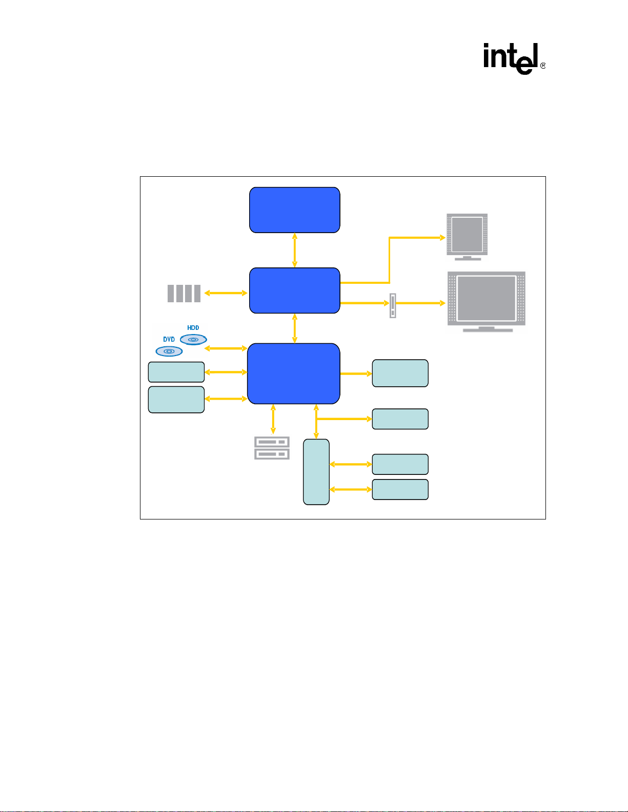
Figure 1. Intel® 854 Chipset system block diagram (Native Graphic mode)
Intel® Celeron® M
Processor
400 MHz
512 MB DD R
Memory Down
6 USB
LAN
PHY
333 MHz
IDE
USB 2.0/1.1
LCI
Intel® 82854
(GMCH)
Intel® 82801DBM
(ICH 4-M)
AC Link
LPC
VGA
DVO
ADD Slot
Audio
Codec
FWH
VGA
TV
PCI Slots
SIO
PS/2
Serial
16 D15343-003
Page 17

1.2 Terminology
Table 1. Terms and Descriptions
Term Description
AGTL+ Advanced Gunning Transceiver Logic + (AGTL+) bus
BLI Backlight Inverter
Core The internal base logic in the Intel
CPU Central Processing Unit
CRT Cathode Ray Tube
DBI Dynamic Bus inversion
DBL Display Brightness Link
DDC Display Data Channel (standard created by VESA)
DPMS Display Power Management Signaling (standard created by VESA)
®
82854 GMCH
Introduction
DVI* Digital Visual Interface is the interface specified by the DDWG (Digital Display
DVMT Dynamic Video Memory Technology
DVO Digital Video Out
EDID Extended Display Identification Data
EIST Enhanced Intel
FSB Front side bus. Connection between Intel
Full Reset A full Intel
GMCH Refers to the GMCH component. Throughout this datasheet, the Intel
HD High definition, typically MP@HL for MPEG2; Resolution supported are 720p,
Host This term is used synonymously with processor
Hub Interface (HI) The proprietary interconnect between the Intel
2
I
C Inter-IC (a two wire serial bus created by Philips)
Working Group) DVI Spec. Rev. 1.0 utilizing only the Silicon Image developed
TMDS protocol
®
SpeedStep® Technology
®
known as the Host interface
®
asserted
Graphics Memory Controller Hub (GMCH) will be referred to as the GMCH.
1080i and 1080p
component. In this document, the Hub interface cycles originating from or
destined for the ICH4-M are generally referred to as “Hub interface cycles.” Hub
cycles originating from or destined for the primary PCI interface on are
sometimes referred to as “Hub interface/PCI cycles”
82854 GMCH Reset is defined in this document when RSTIN# is
82854 GMCH and the CPU. Also
®
82854
®
82854 GMCH and the ICH4-M
IGD Integrated Graphics Device
D15343-003 17
Page 18

Intel® 82854 Graphics Memory Controller Hub (GMCH)
Intel 82801DBM ICH4-M The component contains the primary PCI interface, LPC interface, USB 2.0,
ATA-100, AC’97, and other I/O functions. It communicates with the Intel
®
82854
GMCH over a proprietary interconnect called the Hub interface. Throughout this
datasheet, the Intel 82801DBM ICH4-M component will be referred to as the
ICH4-M
IPI Inter Processor Interrupt
LCD Liquid Crystal Display
MSI Message Signaled Interrupts. MSI allow a device to request interrupt service via
a standard memory write transaction instead of through a hardware signal
Native Graphic Mode The Intel
®
82854 GMCH can support RGB and Dual Independent Display in this
mode
PWM Pulse Width Modulation
SD Standard definition, typically MP@ML for MPEG2
SSC Spread Spectrum Clocking
STB Set Top Box
System Bus Processor-to-Intel
®
82854 GMCH interface. The Enhanced mode of the
Scalable bus is the P6 Bus plus enhancements, consisting of source
synchronous transfers for address and data, and system bus interrupt delivery.
The Intel Celeron M processor implements a subset of Enhanced mode.
UMA Unified Memory Architecture with graphics memory for the IGD inside system
memory
VDL Video Data Link
18 D15343-003
Page 19

1.3 Reference Documents
Table 2. Reference Documents
Document Location
Intel® Celeron® M Processor Datasheet http://www.intel.com/design/mobile/datashts/300302.htm
Introduction
Ultra Low Voltage Intel(R) Celeron(R) M
Processor at 600 MHz Addendum to the
Intel(R) Celeron(R) M Processor Datasheet
Intel® 854 Chipset Platform Design Guide
for Use with Ultra Low Voltage Intel®
Celeron® M Processor at 600 MHz
PCI Local Bus Specification 2.2 http://www.pcisig.com
Intel® 82801DBM I/O Controller Hub 4
Mobile (ICH4-M) Datasheet
Advanced Configuration and Power
Management (ACPI) Specification 1.0b &
2.0
IA-32 Intel® Architecture Software
Developer Manual Volume 3: System
Programming Guide
INTEL® DIGITAL VIDEO OUT (DVO) PORT
HARDWARE EXTERNAL DESIGN
SPECIFICATION (EDS) VER – 2.X
ARIB TR-B15 Operational Guidelines for
Digital Satellite Broadcasting (detailed
Implementation guideline for receiver)
ATSC Standards http://www.atsc.org/standards.html
http://developer.intel.com/design/intarch/datashts/
301753.htm
Please contact your local Intel representative for this
document.
http://developer.intel.com/design/mobile/datashts/
252337.htm
http://www.acpi.info/
http://developer.intel.com/design/pentium4/manuals/
245472.htm
Please contact your local Intel representative for this
document.
http://www.arib.or.jp/english/html/overview/ov/tr_b15.html
D15343-003 19
Page 20

Intel® 82854 Graphics Memory Controller Hub (GMCH)
20 D15343-003
Page 21

2.0 Intel® 82854 GMCH Overview
2.1 System Architecture
The Intel® 82854 GMCH includes a processor interface, DDR SDRAM interface, display
interface, and Hub interface.
Combined with the ULV Intel® Celeron® M Processor or Genuine Intel® Processor, and an ICH4M, it provides many of the functions required to deliver the features below:
• Overall system software platform
• Graphic overlay function for the GUI and 3-D graphics for gaming.
• Soft CODEC function
• STB middleware execution
• New STB embedded applications requiring IA level of high performance.
2.1.1 Intel® 82854 GMCH
The Intel® 82854 GMCH is in a 732-pin Micro-FCBGA package that contains the following
functionality listed below:
• AGTL+ host bus supporting 32-bit host addressing with Enhanced Intel SpeedStep technology
support
• Supports a single channel of DDR SDRAM memory
• System memory supports DDR 266/333 MHz (SSTL_2) DDR SDRAM
• Integrated graphics capabilities: Graphic Core frequency at 200, 250 MHz
• Supports three display ports: one progressive scan analog monitor and two DVO ports.
• Enhanced Power Management Graphics features
Intel® 82854 GMCH Overview
D15343-003 21
Page 22

Intel® 82854 Graphics Memory Controller Hub (GMCH)
2.2 Processor Host Interface
The Intel® 82854 GMCH supports the Intel Celeron M Processor, and Genuine Intel Processor.
Key features of the front side bus (FSB) are:
• Support for a 400-MHz system bus frequency.
• Source synchronous double pumped address (2X)
• Source synchronous quad pumped data (4X)
• Front side bus interrupt delivery
• Low voltage swing Vtt (1.05 ~ 1.55V)
• Dynamic Power Down (DPWR#) support
• Integrates AGTL+ termination resistors on all of the AGTL+ signals
• Supports 32-bit host bus addressing allowing the CPU to access the entire 4 GB of the GMCH
memory address space.
• An 8-deep, In-Order queue
• Support DPWR# signal
• Supports one outstanding defer cycle at a time to any particular I/O interface
2.3 GMCH System Memory Interface
The GMCH system memory controller directly supports the following:
• One channel of PC2100/2700 DIMM DDR SDRAM memory
• DDR SDRAM devices with densities of 128-Mb, 256-Mb, and 512-Mb technology
• Up to 1 GB (512-Mb technology) with two DDR DIMMs
• Up to 2 GB (512-Mb technology) using high density devices with two DDR DIMMs
Table 3. DDR SDRAM Memory Capacity
Technology Width System Memory Capacity
128 Mb 16 256 MB -
256 Mb 16 512 MB -
512 Mb 16 1 GB -
128 Mb 8 256 MB 512 MB
256 Mb 8 512 MB 1 GB
512 Mb 8 1 GB 2 GB
The GMCH system memory interface supports a thermal throttling scheme to selectively throttle
reads and/or writes. Throttling can be triggered either by the on-die thermal sensor, or by preset
write bandwidth limits. Read throttle can also be triggered by an external input pin. The memory
controller logic supports aggressive Dynamic Row Power Down features to help reduce power and
supports Address and Control line tri-stating when DDR SDRAM is in an active power down or in
self refresh state.
System Memory Capacity
with Stacked Memory
22 D15343-003
Page 23

The GMCH system memory architecture is optimized to maintain open pages (up to 16-KB page
size) across multiple rows. As a result, up to 16 pages across four rows is supported. To
complement this, the GMCH will tend to keep pages open within rows, or will only close a single
bank on a page miss. The GMCH supports only four bank memory technologies.
2.4 Graphics Features
The GMCH IGD provides a highly integrated graphics accelerator delivering high performance
2D, 3D, and video capabilities. With its interfaces to UMA using a DVMT configuration, an analog
display, and two digital display ports, the GMCH can provide a complete graphics solution.
The GMCH also provides 2D hardware acceleration for block transfers of data (BLTs). The BLT
engine provides the ability to copy a source block of data to a destination and perform raster
operations (for example, ROP1, ROP2, and ROP3) on the data using a pattern, and/or another
destination. Performing these common tasks in hardware reduces CPU load, and thus improves
performance.
High bandwidth access to data is provided through the system memory interface. The GMCH uses
Tiling architecture to increase system memory efficiency and thus maximize effective rendering
bandwidth. The Intel
rendering technology. The Intel
Cubic filtering.
®
82854 GMCH improves 3D performance and quality with 3D Zone
Intel® 82854 GMCH Overview
®
82854 GMCH also supports Video Mixer rendering, and Bi-
2.5 Display Features
The Intel® 82854 GMCH has three display ports: one analog and two digital. With these interfaces,
the GMCH can provide support for a progressive scan analog monitor and two DVO ports. The
native graphic mode is able to deliver up to two streams of data via the two DVO ports.
2.5.1 GMCH Analog Display Port
The Intel® 82854 GMCH has an integrated 350-MHz, 24-bit RAMDAC that can directly drive a
progressive scan analog monitor pixel resolution up to 1600x1200 at 85-Hz refresh and up to
2048x1536 at 75-Hz refresh. In the native graphic mode, the Analog display port can be driven by
Pipe A or Pipe B.
2.5.2 GMCH Integrated DVO Ports
The Intel® 82854 GMCH provides a digital display channel that is capable of driving a pixel clock
up to 165 MHz.
The GMCH supports three ARIB planes of graphics: Still Picture Plane, Text and Graphic Plane,
and Superimpose Text Plane at a frame rate of 10 fps. A minimum of two displays are supported.
The ARIB plane resolutions supported can be found in Figure 8.
In native graphics mode, the GMCH supports a single display up to 60 fps real time with maximum
resolution of 720 x 480 pixels.
D15343-003 23
Page 24

Intel® 82854 Graphics Memory Controller Hub (GMCH)
2.6 Hub Interface
A proprietary interconnect connects the GMCH to the ICH4-M. All communication between the
GMCH and the ICH4-M occurs over the Hub interface 1.5. The Hub interface runs at 66 MHz
(266-MB/s).
2.7 Address Decode Policies
Host initiated I/O cycles are positively decoded to the GMCH configuration space and
subtractively decoded to the Hub interface. Host initiated system memory cycles are positively
decoded to DDR SDRAM and are again subtractively decoded to the Hub interface, if less than
4 GB. System memory accesses from the Hub interface to DDR SDRAM will be snooped on
the FSB.
24 D15343-003
Page 25

2.8 GMCH Clocking
The GMCH has the following clock input/output pins:
• 400-MHz, spread spectrum, low voltage differential BCLK, BCLK# for front side bus (FSB)
• 66-MHz, 3.3-V GCLKIN for Hub interface buffers
• Six pairs of differential output clocks (SCK[5:0], SCK[5:0]#), 200/266 MHz, 2.5 V for system
memory interface
• 48-MHz, non-Spread Spectrum, 3.3-V DREFCLK for the Display Frequency Synthesis
• 8-MHz or 66-MHz, Spread Spectrum, 3.3-V DREFSSCLK for the Display Frequency
Synthesis
• Up to 148.5 MHz, 1.5-V DVOBCCLKINT for TV-Out mode
• DPMS clock for S1-M
Clock Synthesizer chips are responsible for generating the system host clocks, GMCH display
clocks, Hub interface clocks, PCI clocks, SIO clocks, and FWH clocks. The host target speed is
400 MHz. The GMCH does not require any relationship between the BCLK Host clock and the
66-MHz clock generated for the Hub interface; they are asynchronous to each other. The Hub
interface runs at a constant 66-MHz base frequency . Table 4 indicates the frequency ratios between
the various interfaces that the GMCH supports.
Table 4. Intel® 82854 GMCH Interface Clocks
Intel® 82854 GMCH Overview
Interface Clock Speed
CPU Bus 100 MHz Reference 4 400 8 3200
DDR SDRAM 133 MHz 1:1 Synchronous 2 266 8 2128
166 MHz 1:1 Synchronous 2 333 8 2664
DVO B or DVO C
(Native Graphic
Mode)
DVO B+DVO C
(Native Graphic
Mode)
DAC Interface 350 MHz Asynchronous 1 350 3 1050
Up to 165
MHz
Up to 330
MHz
CPU System
Bus Frequency
Ratio
Asynchronous 2 330 1.5 495
Asynchronous 2 660 3 1980
Samples
Per Clock
Data Rate
(Megasamples/s)
Data
Width
(Bytes)
Peak
Bandwidth
(MB/s)
D15343-003 25
Page 26

Intel® 82854 Graphics Memory Controller Hub (GMCH)
2.9 System Interrupts
The GMCH supports both the legacy Intel 8259 Programmable Interrupt delivery mechanism and
the Intel Celeron M processor FSB interrupt delivery mechanism. The serial APIC Interrupt
mechanism is not supported.
The Intel 8259 Interrupt delivery mechanism support consists of flushing in bound Hub interface
write buffers when an Interrupt Acknowledge cycle is forwarded from the system bus to the Hub
interface.
PCI MSI interrupts are generated as memory writes. The GMCH decodes upstream memory writes
to the range 0FEE0_0000h - 0FEEF_FFFFh from the Hub interface as message based interrupts.
The GMCH forwards the memory writes along with the associated write data to the system bus as
an Interrupt Message transaction. Since this address does not decode as part of main system
memory, the write cycle and the write data do not get forwarded to system memory via the write
buffer . The GMCH provides the response and HTRDY# for all Interrupt Message cycles including
the ones originating from the GMCH. The GMCH also supports interrupt redirection for upstream
interrupt memory writes.
For message based interrupts, system write buffer coherency is maintained by relying on strict
ordering of memory writes. The GMCH ensures that all memory writes received from a given
interface prior to an interrupt message memory write are delivered to the system bus for snooping
in the same order that they occur on the given interface.
26 D15343-003
Page 27

3.0 Signal Description
This section describes the Intel® 82854 GMCH signals. These signals are arranged in functional
groups according to their associated interface. The following notations are used to describe the
signal type.
Notation Description
I Input pin
O Output pin
I/O Bi-directional Input/Output pin
The signal description also includes the type of buffer used for the particular signal:
Buffer Description
AGTL+ Open Drain AGTL+ interface signal. Refer to the AGTL+ I/O
Specification for complete details. The GMCH integrates AGTL+
termination resistors, and supports VTTLF of 1.05 V ± 5%. AGTL+
signals are "inverted bus" style where a low voltage represents a
logical 1.
DVO DVO buffers (1.5-V tolerant)
Hub Compatible to Hub interface 1.5
SSTL_2 Stub Series Termination Logic compatible signals (2.5-V tolerant)
LVTTL Low Voltage TTL compatible signals (3.3-V tolerant)
CMOS CMOS buffers (3.3-V tolerant)
Analog Analog signal interface
Ref Voltage reference signal
Signal Description
Note: System Address and Data Bus signals are logically inverted signals. In other words, the actual
values are inverted from what appears on the system bus. This must be taken into account and the
addresses and data bus signals must be inverted inside the GMCH. All processor control signals
follow normal convention: A 0 indicates an active level (low voltage), and a 1 indicates an active
level (high voltage).
D15343-003 27
Page 28

Intel® 854 Graphics Memory Controller Hub (GMCH)
3.1 Host Interface Signals
Table 5. Host Interface Signal Descriptions
Signal Name Type Description
ADS# I/O
AGTL+
BNR# I/O
AGTL+
BPRI# O
AGTL+
BREQ0# I/O
AGTL+
CPURST# O
AGTL+
DBSY# I/O
AGTL+
Address Strobe: The system bus owner asserts ADS# to indicate the
first of two cycles of a request phase. The GMCH can assert this signal
for snoop cycles and interrupt messages.
Block Next Request: Used to block the current request bus owner from
issuing a new request. This signal is used to dynamically control the CPU
bus pipeline depth.
Bus Priority Request: The GMCH is the only Priority Agent on the
system bus. It asserts this signal to obtain the ownership of the address
bus. This signal has priority over symmetric bus requests and will cause
the current symmetric owner to stop issuing new transactions unless the
HLOCK# signal was asserted.
Bus Request 0#: The GMCH pulls the processor bus BREQ0# signal
low during CPURST#. The signal is sampled by the processor on the
active-to-inactive transition of CPURST#. The minimum setup time for
this signal is 4 BCLKs. The minimum hold time is 2 clocks and the
maximum hold time is 20 BCLKs. BREQ0# should be tristated after the
hold time requirement has been satisfied.
During regular operation, the GMCH will use BREQ0# as an early
indication for FSB Address and Ctl input buffer and sense amp activation.
CPU Reset: The CPURST# pin is an output from the GMCH. The
GMCH asserts CPURST# while RESET# (PCIRST# from ICH4-M) is
asserted and for approximately 1 ms after RESET# is deasserted. The
CPURST# allows the processor to begin execution in a known state.
Note that the ICH4-M must provide CPU strap set-up and hold-times
around CPURST#. This requires strict synchronization between GMCH,
CPURST# deassertion and ICH4-M driving the straps.
Data Bus Busy: Used by the data bus owner to hold the data bus for
transfers requiring more than one cycle.
DEFER# O
AGTL+
DINV[3:0]# I/O
AGTL+
DPSLP# I
CMOS
Defer: GMCH will generate a deferred response as defined by the rules
of the GMCH’s Dynamic Defer policy. The GMCH will also use the
DEFER# signal to indicate a CPU retry response.
Dynamic Bus Inversion: Driven along with the HD[63:0]# signals.
Indicates if the associated signals are inverted or not. DINV[3:0]# are
asserted such that the number of data bits driven electrically low (low
voltage) within the corresponding 16-bit group never exceeds 8.
DINV#
Data Bits
DINV[3]# HD[63:48]#
DINV[2]# HD[47:32]#
DINV[1]# HD[31:16]#
DINV[0]# HD[16:0]#
Deep Sleep #: This signal comes from the ICH4-M device, providing an
indication of C3 and C4 state control to the CPU. Deassertion of this
signal is used as an early indication for C3 and C4 wake up (to active
HPLL). Note that this is a low-voltage CMOS buffer operating on the FSB
VTT power plane.
28 D15343-003
Page 29
Signal Description
DRDY# I/O
AGTL+
HA[31:3]# I/O
HADSTB[1:0]# I/O
HD[63:0]# I/O
HDSTBP[3:0]#
HDSTBN[3:0]#
HIT# I/O
AGTL+
AGTL+
AGTL+
I/O
AGTL+
AGTL+
Data Ready: Asserted for each cycle that data is transferred.
Host Address Bus: HA[31:3]# connects to the CPU address bus. During
processor cycles the HA[31:3]# are inputs. The GMCH drives HA[31:3]#
during snoop cycles on behalf of Hub interface. HA[31:3]# are
transferred at 2x rate. Note that the address is inverted on the CPU bus.
Host Address Strobe: HA[31:3]# connects to the CPU address bus.
During CPU cycles, the source synchronous strobes are used to transfer
HA[31:3]# and HREQ[4:0]# at the 2x transfer rate.
Strobe
Address Bits
HADSTB[0]# HA[16:3]#, HREQ[4:0]#
HADSTB[1]# HA[31:17]#
Host Data: These signals are connected to the CPU data bus.
HD[63:0]# are transferred at 4x rate. Note that the data signals are
inverted on the CPU bus.
Differential Host Data Strobes: The differential source synchronous
strobes are used to transfer HD[63:0]# and DINV[3:0]# at the 4x
transfer rate.
Strobe
Data Bits
HDSTBP[3]#, HDSTBN[3]# HD[63:48]#, DINV[3]#
HDSTBP[2]#, HDSTBN[2]# HD[47:32]#, DINV[2]#
HDSTBP[1]#, HDSTBN[1]# HD[31:16]#, DINV[1]#
HDSTBP[0]#, HDSTBN[0]# HD[15:0]#, DINV[0]#
Hit: Indicates that a caching agent holds an unmodified version of the
requested line. Also, driven in conjunction with HITM# by the target to
extend the snoop window.
HITM# I/O
AGTL+
HLOCK# I/O
AGTL+
HREQ[4:0]# I/O
AGTL+
HTRDY# O
AGTL+
Hit Modified: Indicates that a caching agent holds a modified version of
the requested line and that this agent assumes responsibility for
providing the line. Also, driven in conjunction with HIT# to extend the
snoop window.
Host Lock: All CPU bus cycles sampled with the assertion of HLOCK#
and ADS#, until the negation of HLOCK# must be atomic; that is, no Hub
interface snoopable access to system memory is allowed when HLOCK#
is asserted by the CPU.
Host Request Command: Defines the attributes of the request.
HREQ[4:0]# are transferred at 2x rate. Asserted by the requesting agent
during both halves of the Request Phase. In the first half the signals
define the transaction type to a level of detail that is sufficient to begin a
snoop request. In the second half the signals carry additional information
to define the complete transaction type.
The transactions supported by the GMCH Host Bridge are defined in the
Host Interface section of this document.
Host Target Ready: Indicates that the target of the processor
transaction is able to enter the data transfer phase.
D15343-003 29
Page 30

Intel® 854 Graphics Memory Controller Hub (GMCH)
RS[2:0]# O
AGTL+
Response Status: Indicates the type of response according to the
following the table:
RS[2:0]#
000 Idle state
001 Retry response
010 Deferred response
011 Reserved (not driven by GMCH)
100 Hard Failure (not driven by GMCH)
101 No data response
110 Implicit Write back
111 Normal data response
Response type
30 D15343-003
Page 31

3.2 DDR SDRAM Interface
Table 6. DDR SDRAM Interface Descriptions
Signal Name Type Description
Signal Description
SCS[3:0]# O
SSTL_2
SMA[12:0] O
SSTL_2
SBA[1:0] O
SSTL_2
SRAS# O
SSTL_2
SCAS# O
SSTL_2
SWE# O
SSTL_2
SDQ[63:0] I/O
SSTL_2
Chip Select: These pins select the particular DDR SDRAM
components during the active state.
NOTE: There is one SCS# per DDR-SDRAM Physical DDR DIMM
device row. These signals can be toggled on every rising System
Memory Clock edge (SCMDCLK).
Multiplexed Memory Address: These signals are used to provide the
multiplexed row and column address to the DDR SDRAM.
Bank Select (Memory Bank Address): These signals define which
banks are selected within each DDR SDRAM row. The SMA and SBA
signals combine to address every possible location within a DDR
SDRAM device.
DDR Row Address Strobe: SRAS# may be heavily loaded and
requires tw0 DDR SDRAM clock cycles for setup time to the DDR
SDRAMs. Used with SCAS# and SWE# (along with SCS#) to define the
system memory commands.
DDR Column Address Strobe: SCAS# may be heavily loaded and
requires two clock cycles for setup time to the DDR SDRAMs. Used
with SRAS# and SWE# (along with SCS#) to define the system memory
commands.
Write Enable: Used with SCAS# and SRAS# (along with SCS#) to
define the DDR SDRAM commands. SWE# is asserted during writes to
DDR SDRAM. SWE# may be heavily loaded and requires two clock
cycles for setup time to the DDR SDRAMs.
Data Lines: These signals are used to interface to the DDR SDRAM
data bus.
I/O
SDQS[8:0]
SCKE[3:0] O
SSTL_2
SSTL_2
Data Strobes: Data strobes are used for capturing data. During writes,
SDQS is centered on data. During reads, SDQS is edge aligned with
data. The following list matches the data strobe with the data bytes.
There is an associated data strobe (DQS) for each data signal (DQ) and
check bit (CB) group.
SDQS[7] -> SDQ[63:56]
SDQS[6] -> SDQ[55:48]
SDQS[5] -> SDQ[47:40]
SDQS[4] -> SDQ[39:32]
SDQS[3] -> SDQ[31:24]
SDQS[2] -> SDQ[23:16]
SDQS[1] -> SDQ[15:8]
SDQS[0] -> SDQ[7:0]
Clock Enable: These pins are used to signal a self-refresh or power
down command to the DDR SDRAM array when entering system
suspend. SCKE is also used to dynamically power down inactive DDR
SDRAM rows. There is one SCKE per DDR SDRAM row. These
signals can be toggled on every rising SCK edge.
D15343-003 31
Page 32

Intel® 854 Graphics Memory Controller Hub (GMCH)
SMAB[5,4,2,1] O
SSTL_2
SDM[8:0] O
SSTL_2
RCVENOUT# O
SSTL_2
RCVENIN# O
SSTL_2
3.3 Hub Interface Signals
Table 7. Hub Interface Signals
Signal Name Type Description
HL[10:0] I/O Hub Packet Data: Data signals used for HI read and write operations.
HLSTB I/O Hub Packet Strobe: One of two differential strobe signals used to transmit or
receive packet data over HI.
HLSTB# I/O Hub Packet Strobe Complement: One of two differential strobe signals used
to transmit or receive packet data over HI.
Memory Address Copies: These signals are identical to SMA[5,4,2,1]
and are used to reduce loading for selective CPC(clock-per-command).
These copies are not inverted.
Data Mask: When activated during writes, the corresponding data
groups in the DDR SDRAM are masked. There is one SDM for every
eight data lines. SDM can be sampled on both edges of the data
strobes.
Clock Output: Reserved, NC.
Clock Input: Reserved, NC.
32 D15343-003
Page 33

3.4 Clocks
Table 8. Clock Signals
Signal Name Type Description
Host Processor Clocking
Signal Description
BCLK
BCLK#
System Memory Clocking
SCK[5:0] O
SCK[5:0]# O
DVO/Hub Input Clocking
GCLKIN I
DVO Clocking
DVOBCLK
DVOBCLK#
DVOCCLK
DVOCCLK#
CMOS
SSTL_2
SSTL_2
CMOS
DVO
DVO
I
O
O
Differential Host Clock In: These pins receive a buffered host clock
from the external clock synthesizer. This clock is used by all of the
GMCH logic that are in the Host clock domain (Host, Hub and system
memory). The clock is also the reference clock for the graphics core
PLL. This is a low voltage differential input.
Differential DDR SDRAM Clock: SCK and SCK# pairs are differential
clock outputs. The crossing of the positive edge of SCK and the
negative edge of SCK# is used to sample the address and control
signals on the DDR SDRAM. There are 3 pairs to each DDR DIMM.
Complementary Differential DDR SDRAM Clock: These are the
complimentary differential DDR SDRAM clock signals.
Input Clock: 66-MHz, 3.3-V input clock from external buffer DVO/Hub
interface.
Differential DVO Clock Output: These pins provide a differential pair
reference clock that can run up to 165-MHz.
DVOBC LK corresponds to the primary clock out.
DVOBC LK# corresponds to the primary complementary clock out.
DVOBC LK and DVOB CLK # should be left as NC (“Not Connected”) if
the DVO B port is not implemented.
Differential DVO Clock Output: These pins provide a differential pair
reference clock that can run up to 165-MHz.
DVOCCL K corresponds to the primary clock out.
DVOCCL K# corresponds to the primary complementary clock out.
DVOCCL K and DVOCCL K# should be left as NC (“Not Connected”) if
the DVO C port is not implemented.
DVOBCCLKINT I
DVO
DVOBC Pixel Clock Input/Interrupt: This signal may be selected as
the reference input to either dot clock PLL (DPLL) or may be
configured as an interrupt input. A TV-out device can provide the clock
reference. The maximum input frequency for this signal is 148.5 -MHz.
DVOBC Pixel Clock Input: When selected as the dot clock PLL (DPLL)
reference input, this clock reference input supports SSC clocking for
DVO LVDS devices.
DVOBC Interrupt: When configured as an interrupt input, this interrupt
can support either DVOB or DVOC.
DVOBC CLK INT needs to be pulled down if the signal is NOT used.
D15343-003 33
Page 34

Intel® 854 Graphics Memory Controller Hub (GMCH)
DPMS I
DVO
DAC Clocking
DREFCLK I
LVT TL
Display Power Management Signaling: This signal is used only in
mobile systems to act as the DREFCLK in certain power management
states (i.e., Display Power Down Mode); DPMS Clock is used to
refresh video during S1-M. Clock Chip is powered down in S1-M.
DPMS should come from a clock source that runs during S1-M and
needs to be 1.5 V. So, an example would be to use a 1.5-V version of
SUSCLK from ICH4-M.
Display Clock Input: This pin is used to provide a 48-MHz input clock
to the Display PLL that is used for 2D/Video and DAC.
34 D15343-003
Page 35

3.5 Internal Graphics Display Signals
The IGD has support for DVOB/C interfaces, and an Analog CRT port.Digital Video Output B
(DVOB) Port.
3.5.1 Digital Video Output B (DVOB) Port
Table 9. Digital Video Output B (DVOB) Port Signal Descriptions
Name Type Description
Signal Description
DVOBD[11:0] O
DVO
DVOBHSYNC O
DVO
DVOBVSYNC O
DVO
DVOBBLANK# O
DVO
DVOBFLDSTL I
DVO
DVOB Data: This data bus is used to drive 12-bit RGB data on each edge
of the differential clock signals, DVOBC LK and DVOBC LK# . This provides
24-bits of data per clock period. In dual channel mode, this provides the
lower 12-bits of pixel data.
DVOBD[11:0] should be left as NC (“Not Connected”) if not used.
Horizontal Sync: HSYNC signal for the DVOB interface.
DVOBHSYNC should be left as left as NC (“Not Connected”) if not used.
Vertical Sync: VSYNC signal for the DVOB interface.
DVOBVSYNC should be left as left as NC (“Not Connected”) if the signal
is NOT used when using internal graphics device.
Flicker Blank or Border Period Indication: DVOBBLANK# is a
programmable output pin driven by the GMCH.
When programmed as a blank period indication, this pin indicates active
pixels excluding the border. When programmed as a border period
indication, this pin indicates active pixel including the border pixels.
DVOBBLANK# should be left as left as NC (“Not Connected”) if not used.
TV Field and Flat Panel Stall Signal. This input can be programmed to
be either a TV Field input from the TV encoder or Stall input from the flat
panel.
DVOB TV Field Signal: When used as a Field input, it synchronizes the
overlay field with the TV encoder field when the overlay is displaying an
interleaved source.
DVOB Flat Panel Stall Signal: When used as the Stall input, it indicates
that the pixel pipeline should stall one horizontal line. The signal changes
during horizontal blanking. The panel fitting logic, when expanding the
image vertically, uses this.
DVOBF LDS TL needs to be pulled down if not used.
D15343-003 35
Page 36

Intel® 854 Graphics Memory Controller Hub (GMCH)
3.5.2 Digital Video Output C (DVOC) Port
Table 10. Digital Video Output C (DVOC) Port Signal Descriptions
Name Type Description
DVOCD[11:0] O
DVO
DVOCHSYNC O
DVO
DVOCVSYNC O
DVO
DVOCBLANK# O
DVO
DVOCFLDSTL I
DVO
[Native Graphic Mode]
DVOC Data: This data bus is used to drive 12-bit RGB data on each edge
of the differential clock signals, DVOCC LK and DVOCC LK# . This
provides 24-bits of data per clock period. In dual channel mode, this
provides the upper 12-bits of pixel data.
DVOCD[11:0] should be left as left as NC (“Not Connected”) if not used.
Horizontal Sync: HSYNC signal for the DVOC interface.
DVOCHSYNC should be left as left as NC (“Not Connected”) if not used.
Vertical Sync: VSYNC signal for the DVOC interface.
DVOCVSYNC should be left as left as NC (“Not Connected”) if the signal
is NOT used when using internal graphics device.
Flicker Blank or Border Period Indication: DVOCBLANK# is a
programmable output pin driven by the GMCH.
When programmed as a blank period indication, this pin indicates active
pixels excluding the border. When programmed as a border period
indication, this pin indicates active pixel including the border pixels.
DVOCBLANK# should be left as left as NC (“Not Connected”) if not used.
TV Field and Flat Panel Stall Signal. This input can be programmed to
be either a TV Field input from the TV encoder or Stall input from the flat
panel.
DVOC TV Field Signal: When used as a Field input, it synchronizes the
overlay field with the TV encoder field when the overlay is displaying an
interleaved source.
DVOC Flat Panel Stall Signal: When used as the Stall input, it indicates
that the pixel pipeline should stall one horizontal line. The signal changes
during horizontal blanking. The panel fitting logic, when expanding the
image vertically, uses this.
DVOCF LDS TL needs to be pulled down if not used.
36 D15343-003
Page 37

Table 11. DVOB and DVOC Port Common Signal Descriptions
Name Type Description
Signal Description
DVOBCINTR# I
DVO
ADDID[7:0] I
DVO
DVODETECT I
DVO
DVOBC Interrupt: This pin is used to signal an interrupt, typically used to
indicate a hot plug or unplug of a digital display.
ADDID[7:0]: These pins are used to communicate to the Video BIOS
when an external device is interfaced to the DVO port.
Note: Bit[7] needs to be strapped low when an on-board DVO device is
present. The other pins should be left as NC.
ADDID[0] = 0, Reserve
ADDID[0] = 1, the Intel
Native Graphic Mode
For detail of strapping option, please refer to Table 33.
DVODETECT: This strapping signal indicates to the GMCH whether a
DVO device is present or not. When a DVO device is connected, then
DVODETECT = 0.
3.5.3 Analog CRT Display
Table 12. Analog CRT Display Signal Descriptions
Pin Name Type Description
VSYNC O
CMOS
HSYNC O
CMOS
CRT Vertical Synchronization: This signal is used as the vertical sync signal.
CRT Horizontal Synchronization: This signal is used as the horizontal sync
signal.
®
82854 GMCH is strapped to operate under
RED O
Analog
RED# O
Analog
GREEN O
Analog
GREEN# O
Analog
BLUE
Analog
BLUE#
Analog
O
O
Red (Analog Video Output): This signal is a CRT Analog video output from
the internal color palette DAC. The DAC is designed for a 37.5-Ω equivalent
load on each pin (that is, a 75-Ω resistor on the board, in parallel with the 75-Ω
CRT load).
Red# (Analog Output): Tied to ground.
Green (Analog Video Output): This signal is a CRT analog video output from
the internal color palette DAC. The DAC is designed for a 37.5-Ω equivalent
load on each pin (that is, a 75-Ω resistor on the board, in parallel with the 75- Ω
CRT load).
Green# (Analog Output): Tied to ground.
Blue (Analog Video Output) : This signal is a CRT Analog video output from
the internal color palette DAC. The DAC is designed for a 37.5-Ω equivalent
load on each pin (that is, a 75-ohm resistor on the board, in parallel with the 75Ω CRT load).
Blue# (Analog Output): Tied to ground.
D15343-003 37
Page 38

Intel® 854 Graphics Memory Controller Hub (GMCH)
3.5.4 General Purpose Input/Output Signals
Table 13. GPIO Signal Descriptions
GPIO I/F Total Type Comments
RSTIN# I
CMOS
PWROK I
CMOS
EXTTS_0 I
CMOS
LCLKCTLA O
CMOS
LCLKCTLB O
CMOS
DDCACLK I/O
CMOS
DDCADATA I/O
CMOS
MI2CCLK I/O
DVO
Reset: Primary Reset, Connected to PCIRST# of ICH4-M.
Power OK : Indicates that power to GMCH is stable.
External Thermal Sensor Input: This signal is an active low input to the
GMCH and is used to monitor the thermal condition around the system memory
and is used for triggering a read throttle. The GMCH can be optionally
programmed to send a SERR, SCI, or SMI message to the ICH4-M upon the
triggering of this signal.
SSC Chip Clock Control: Can be used to control an external clock chip with
SSC control.
SSC Chip Data Control: Can be used to control an external clock chip for
SSC control.
CRT DDC Clock: This signal is used as the DDC clock signal between the
CRT monitor and the GMCH.
CRT DDC Data: This signal is used as the DDC data signal between the CRT
monitor and the GMCH.
DVO I2C Clock: This signal is used as the I2C_CLK for a digital display (i.e.
TV-Out Encoder, TMDS transmitter). This signal is tri-stated during a hard
reset.
MI2CDATA I/O
DVO
MDVICLK I/O
DVO
MDVIDATA I/O
DVO
MDDCDATA I/O
DVO
MDDCCLK I/O
DVO
DVO I2C Data: This signal is used as the I2C_DATA for a digital display (i.e.
TV-Out Encoder, TMDS transmitter). This signal is tri-stated during a hard
reset.
DVI DDC Clock: This signal is used as the DDC clock for a digital display
connector (that is, primary digital monitor). This signal is tri-stated during a hard
reset.
DVI DDC Data: The signal is used as the DDC data for a digital display
connector (that is, the primary digital monitor). This signal is tri-stated during a
hard reset.
DVI DDC Clock: The signal is used as the DDC data for a digital display
connector (that is, the secondary digital monitor). This signal is tri-stated during
a hard reset.
DVI DDC Data: The signal is used as the DDC clock for a digital display
connector (that is, the secondary digital monitor). This signal is tri-stated during
a hard reset.
38 D15343-003
Page 39

3.6 Voltage References, PLL Power
Table 14. Voltage References, PLL Power
Signal Name Type Description
Host Processor
HXRCOMP Analog Host R C OMP: Used to calibrate the Host AGTL+ I/O buffers.
HYRCOMP Analog Host RCOMP: Used to calibrate the Host AGTL+ I/O buffers.
Signal Description
HXSWING Analog Host Voltage Swing (RCOMP reference volt age): This signal provides
HYSWING Analog Host Voltage Swing (RCOMP reference voltage): This signal provides
HDVREF[2:0] Ref
Analog
HAVREF Ref
Analog
HCCVREF Ref Analog Host Common Clock (Command input buffer) VREF: Reference
VTTLF Power FSB Power Supply: VTTLF is the low frequency connection from the
VTTHF Power FSB Power Supply: VTTHF is the high frequency supply. It is for direct
System Memory
SMRCOMP Analog System Memory RCOMP: This signal is used to calibrate the memory I/
a reference voltage used by the FSB RCOMP circuit.
a reference voltage used by the FSB RCOMP circuit.
Host Data (input buffer) VREF: Reference voltage input for the data
signals of the Host AGTL+ Interface. Input buffer differential amplifier to
determine a high versus low input voltage.
Host Address (input buffer) VREF: Reference voltage input for the
address signals of the Host AGTL+ Interface. This signal is connected to
the input buffer differential amplifier to determine a high versus low input
voltage.
voltage input for the common clock signals of the Host AGTL+ Interface.
This signal is connected to the input buffer differential amplifier to
determine a high versus low input voltage.
board. This signal is the primary connection of power for GMCH.
connection from an internal package plane to a capacitor placed
immediately adjacent to the GMCH.
NOTE: Not to be connected to power rail.
O buffers.
SMVREF_0 Ref
Analog
SMVSWINGH Ref
Analog
SMVSWINGL Ref
Analog
VCCSM Power Power supply for Memory I/O.
VCCQSM Power Power supply for system memory clock buffers.
VCCASM Power Power supply for system memory logic running at the core voltage
Memory Reference Voltage(Input buffer VREF):Reference voltage
input for Memory Interface.
Input buffer differential amplifier to determine a high versus low input
voltage.
RCOMP reference voltage: This is connected to the RCOMP buffer
differential amplifier and is used to calibrate the I/O buffers.
RCOMP reference voltage: This is connected to the RCOMP buffer
differential amplifier and is used to calibrate the I/O buffers.
(isolated supply, not connected to the core).
D15343-003 39
Page 40

Intel® 854 Graphics Memory Controller Hub (GMCH)
Hub Interface
HLRCOMP Analog Hub Interface RCOMP: This signal is connected to a reference resistor
PSWING Analog RCOMP reference voltage: This is connected to the RCOMP buffer
HLVREF Ref
Analog
VCCHL Power Power supply for Hub interface buffers
DVO
DVORCOMP Analog
Analog
GVREF Ref Analog Input buffer VREF: Input buffer differential amplifier to determine a high
VCCDVO Power Power supply for DVO.
GPIO
VCCGPIO Power Power supply for GPIO buffers
DAC
REFSET Ref
Analog
VCCADAC Power Power supply for the DAC
in order to calibrate the buffers.
differential amplifier and is used to calibrate the buffers.
Input buffer VREF: Input buffer differential amplifier to determine a high
versus low input voltage.
Compensation for DVO: This signal is used to calibrate the DVO I/O
buffers.
versus low input voltage.
Resistor Set: Set point resistor for the internal color palette DAC.
VSSADAC Power Ground supply for the DAC
IGD
VCC1_5 Power Digital power supply.
VCC2_5 Power Digital power supply
VCCA Power Analog power supply.
VSSA Power Ground supply
Clocks
VCCAHPLL Power Power supply for the Host PLL.
VCCAGPLL Power Power supply for the Hub/DVO PLL.
VCCADPLLA Power Power supply for the display PLL A.
VCCADPLLB Power Power supply for the display PLL B.
Core
VCC Power Power supply for the core.
VSS Power Ground supply for the chip.
40 D15343-003
Page 41

Register Description
4.0 Register Description
4.1 Conceptual Overview of the Platform Configuration Structure
The GMCH and ICH4-M are physically connected by a Hub interface. From a configuration
standpoint, the Hub interface is logically PCI bus #0. As a result, all devices internal to the GMCH
and ICH4-M appear to be on PCI bus #0. The system's primary PCI expansion bus is physically
attached to the ICH4-M and from a configuration perspective, appears to be a hierarchical PCI bus
behind a PCI-to-PCI bridge and therefore has a programmable PCI Bus number. Note that the
primary PCI bus is referred to as PCI_A in this document and is not PCI bus #0 from a
configuration standpoint. For the GMCH, the graphics subsystem appears to system software to be
a real PCI bus behind PCI-to-PCI bridges, resident as devices on PC I bu s #0.
The GMCH contains two PCI devices within a single physical component. The configuration
registers for the two devices are mapped as devices residing on PCI bus #0.
Device #0: Host-Hub Interface Bridge/DDR SDRAM Controller. Logically this appears as a PCI
device residing on PCI bus #0. Physically, Device #0 contains the standard PCI registers, DDR
SDRAM registers, the Graphics Aperture Controller registers, HI Control registers and other
GMCH specific registers. Device #0 is divided into the following functions:
Function #0
Configuration registers and Interrupt Control registers
Function #1
Function #3
Device #2: Integrated Graphics Controller. Logically this appears as a PCI device residing on PCI
bus #0. Physically Device #2 contains the Configuration registers for 2D, 3D, and display
functions.
Note: The legacy VGA registers are only supported when the Intel
Native Graphics Mode.
Table 15 shows the Device # assignment for the various internal GMCH devices.
Table 15. Device Number Assignment
Host-Hub interface, DDR SDRAM I/F, Legacy control Device #0
Integrated Graphics Controller (IGD) Device #2
: Host Bridge Legacy registers including Graphics Aperture Control registers, HI
: DDR SDRAM Interface Registers
: Intel Configuration Process Registers
GMCH Function Bus #0, Device#
®
82854 GMCH is strapped into
D15343-003 41
Page 42

Intel® 82854 Graphics Memory Controller Hub (GMCH)
4.2 Nomenclature for Access Attributes
Table 16 provides the nomenclature for the access attributes.
Table 16. Nomenclature for Access Attributes
RO Read Only. If a register is Read Only, Writes to this register have no effect.
R/W Read/Write. A register with this attribute can be Read and Written.
R/W/L Read/Write/Lock. A register with this attribute can be Read, Written, and Locked.
R/WC Read/Write Clear. A register bit with this attribute can be Read and Written.
R/WO Read/Write Once. A register bit with this attribute can be Written to only once
L Lock. A register bit with this attribute becomes Read Only after a Lock bit is set.
Reserved Bits Some of the GMCH registers described in this section contain Reserved bits.
Reserved Registers In addition to Reserved bits within a register, the GMCH contains address locations
Default Value upon a
Reset
However, a Write of a 1 clears (sets to 0) the corresponding bit and a Write of a 0
has no effect.
after power up. After the first Write, this bit becomes Read Only.
These bits are labeled "Reserved”. Software must deal correctly with fields that are
Reserved. On Reads, software must use appropriate masks to extract the defined
bits and not rely on Reserved bits being of any particular value. On Writes,
software must ensure that the values of Reserved bit positions are preserved. That
is, the values of Reserved bit positions must first be Read, Merged with the new
values for other bit positions and then Written back. Note the software does not
need to perform Read, Merge, and Write operations for the Configuration Address
register.
in the configuration space of the Host-Hub Interface Bridge entity that are marked
either "Reserved" or “Intel Reserved”. The GMCH responds to accesses to
“Reserved” address locations by completing the Host cycle. When a “Reserved”
register location is Read, in certain cases, a zero value can be returned
(“Reserved” registers can be 8-bit, 16-bit, or 32-bit in size) or a non-zero value can
be returned. In certain cases, Writes to “Reserved” registers may have no effect on
the GMCH or may cause system failure. Registers that are marked as “Intel
Reserved” must not be modified by system software.
Upon Reset, the GMCH sets all of its internal configuration registers to
predetermined default states. Some register values at Reset are determined by
external strapping options. The default state represents the minimum functionality
feature set required to successfully bring up the system. Hence, it does not
represent the optimal system configuration. It is the responsibility of the system
initialization software (usually BIOS) to properly determine the DDR SDRAM
configurations, operating parameters and optional system features that are
applicable, and to program the GMCH registers accordingly.
S SW Semaphore.
A physical PCI Bus #0 does not exist. The Hub interface and the internal devices in the GMCH and
ICH4-M logically constitute PCI Bus #0 to configuration software.
42 D15343-003
Page 43

4.3 Standard PCI Bus Configuration Mechanism
The PCI Bus defines a slot based “configuration space” that allows each device to contain up to
eight functions with each function containing up to 256, 8-bit configuration registers. The PCI
Specification defines two bus cycles to access the PCI Configuration Space: Configuration Read
and Configuration Write. Memory and I/O spaces are supported directly by the CPU.
Configuration Space is supported by a mapping mechanism implemented within the GMCH. The
PCI 2.2 specification defines two mechanisms to access Configuration Space: Mechanism #1 and
Mechanism #2. The GMCH supports only Mechanism #1.
The Configuration Access Mechanism makes use of the CONFIG_ADDRESS register (at I/O
address 0CF8h though 0CFBh) and CONFIG_DATA register (at I/O address 0CFCh though
0CFFh). To reference a Configuration register a Dword I/O Write cycle is used to place a value
into CONFIG_ADDRESS that specifies the PCI Bus, the device on that bus, the function within
the device, and a specific Configuration register of the device function being accessed.
CONFIG_ADDRESS[31] must be a 1 to enable a Configuration cycle. CONFIG_DATA then
becomes a window into the four Bytes of Configuration Space specified by the contents of
CONFIG_ADDRESS. Any Read or Write to CONFIG_DATA will result in the GMCH translating
the CONFIG_ADDRESS into the appropriate Configuration cycle.
The GMCH is responsible for translating and routing the CPU’s I/O accesses to the
CONFIG_ADDRESS and CONFIG_DATA registers to internal GMCH Configuration registers
and to the Hub interface.
Register Description
4.4 Routing Configuration Accesses
The GMCH supports one bus interface: the Hub interface. PCI Configuration cycles are selectively
routed to this interface. The GMCH is responsible for routing PCI Configuration cycles to the
proper interface. PCI configuration cycles to the ICH4-M internal devices, and Primary PCI
(including downstream devices) are routed to theICH4-M via the Hub interface.
4.4.1 PCI Bus #0 Configuration Mechanism
The GMCH decodes the Bus Number (bits 23:16) and the Device Number fields of the
CONFIG_ADDRESS register. If the Bus Number field of CONFIG_ADDRESS is 0, then the
Configuration cycle is targeting a PCI Bus #0 device.
The Host-Hub Interface Bridge entity within the GMCH is hardwired as Device #0 on PCI Bus #0.
Configuration cycles to any of the GMCH’s internal devices are confined to the GMCH and not
sent over Hub interface. Accesses to disabled GMCH internal devices will be forwarded over the
Hub interface as Type 0 Configuration cycles.
D15343-003 43
Page 44

Intel® 82854 Graphics Memory Controller Hub (GMCH)
4.4.2 Primary PCI and Downstream Configuration Mechanism
If the Bus Number in the CONFIG_ADDRESS is non-zero, the GMCH will generate a T ype 1 Hub
interface Configuration Cycle. A[1:0] of the Hub interface request packet for the Type 1
configuration cycle will be “01”. This Hub interface configuration cycle will be sent over Hub
interface.
If the cycle is forwarded to the ICH4-M via Hub interface, the ICH4-M compares the non-zero Bus
Number with the Secondary bus number and Subordinate bus number registers of it s PCI-to-PCI
bridges to determine if the configuration cycle is meant for Primary PCI, one of the ICH4-M’s Hub
interfaces, or a downstream PCI bus.
4.5 Register Definitions
The GMCH contains four sets of software accessible registers accessed via the Host CPU I/O
Address Space, and they are as follows:
• Control registers: I/O Mapped into the CPU I/O Space, which control access to PCI
Configuration Space via Configuration Mechanism #1 in the PCI 2.2 specification.
• Internal Configuration registers: residing within the GMCH, they are partitioned into two
logical device register sets (“logical” since they reside within the single physical device). The
first register set is dedicated to Host-HI Bridge functionality
configuration, other chip-set operating parameters and optional features). The second register
block is for the integrated graphics functions
.
• Internal Memory Mapped Configuration registers: reside in the GMCH Device #0.
• Internal Memory Mapped Configuration registers, Legacy VGA registers, or blending
function registers: reside in the GMCH Device #2 that controls the Integrated Graphics
Controller.
(that is, DDR SDRAM
The GMCH internal registers (I/O Mapped and Configuration registers) are accessible by the Host
CPU. The registers can be accessed as Byte, Word (16-bit), or Dword (32-bit) quantities, with the
exception of CONFIG_ADDRESS, which can only be accessed as a Dword. All multi-byte
numeric fields use “Little Endian Byte Ordering” (that is, lower addresses contain the least
significant parts of the field).
Reserved Bits
Some of the GMCH registers described in this section contain Reserved bits. These bits are labeled
“Reserved”. Software must deal correctly with fields that are Reserved. On Reads, software must
use appropriate Masks to extract the defined bits and not rely on Reserved bits being any particular
value. On Writes, software must ensure that the values of Reserved bit positions are preserved.
That is, the values of Reserved bit positions must first be Read, Merged with the new values for
other bit positions and then Written back.
Note: The software does not need to perform Read, Merge, and Write operations for the Configuration
Address register.
Default Value upon Reset
Upon a Full Reset, the GMCH sets all of its Internal Configuration registers to a predetermined
default state. Some register values at Reset are determined by external strapping options. The
default state represents the minimum functionality feature set required to successfully bring up the
system. Hence, it does not represent the optimal system configuration. It is the responsibility of the
44 D15343-003
Page 45

Register Description
system initialization software (usually BIOS) to properly determine the DDR SDRAM
configurations, operating parameters, and optional system features that are applicable and to
program the GMCH registers accordingly.
4.6 I/O Mapped Registers
The GMCH contains two registers that reside in the CPU I/O Address Space: the Configuration
Address (CONFIG_ADDRESS) Register and the Configuration Data (CONFIG_DATA) Register.
The Configuration Address Register enables/disables the Configuration Space and determines
what portion of Configuration Space is visible through the Configuration Data window.
4.6.1 CONFIG_ADDRESS – Configuration Address Register
I/O Address:
Default Value:
Access:
Size:
CONFIG_ADDRESS is a 32-bit register that can be accessed only as a Dword. A Byte or Word
reference will “pass through” the Configuration Address Register and the Hub interface, onto the
PCI bus as an I/O cycle. The CONFIG_ADDRESS register contains the Bus Number, Device
Number, Function Number, and Register Number for which a subsequent configuration access is
intended.
Figure 2. Configuration Address Register
0 0 0 0
R
0
0CF8h Accessed as a Dword
00000000h
Read/Write
32 bits
Bit
1 0
27811151623 24 30 31 10
Default
R
Reserved
Register Number
Function Number
Device Numb er
Bus Number
Reserved
Enable
D15343-003 45
Page 46

Intel® 82854 Graphics Memory Controller Hub (GMCH)
Bit Descriptions
31 Configuration Enable (CFGE): When this bit is set to 1, accesses to PCI Configuration Space
are enabled. If this bit is Reset to 0, accesses to PCI Configuration Space are disabled.
30:24 Reserved
23:16 Bus Number: When the Bus Number is programmed to 00h, the target of the Configuration
15:11 Device Number: This field selects one agent on the PCI Bus selected by the Bus Number. When
10:8 Function Number: This field is mapped to A[10:8] during Hub interface Configuration cycles.
7:2 Register Number: This field selects one register within a particular Bus, Device, and Function as
1:0 Reserved
Cycle is a Hub interface agent (GMCH, ICH4-M, and so on.).
The Configuration Cycle is forwarded to Hub interface if the Bus Number is programmed to 00h
and the GMCH is not the target (the device number is >= 2).
the Bus Number field is 00 the GMCH decodes the Device Number field. The GMCH is always
Device Number 0 for the Host-Hub interface bridge entity. Therefore, when the Bus Number =0
and the Device Number=0-1 the internal GMCH devices are selected.
For Bus Numbers resulting in Hub interface Configuration cycles, the GMCH propagates the
device number field as A[15:11].
This allows the configuration registers of a particular function in a multi-function device to be
accessed. The GMCH ignores Configuration cycles to its internal Devices if the function number is
not equal to 0.
specified by the other fields in the Configuration Address register. This field is mapped to A[7:2]
during Hub interface Configuration cycles.
46 D15343-003
Page 47

4.6.2 CONFIG_DATA – Configuration Data Register
Register Description
I/O Address:
Default Value:
Access:
Size:
0CFCh
00000000h
Read/Write
32 bits
CONFIG_DATA is a 32-bit Read/Write window into Configuration Space. The portion of
Configuration Space that is referenced by CONFIG_DATA is determined by the contents of
CONFIG_ADDRESS.
Figure 3. Configuration Data Register
31 0
Configuration Data Window
Bit
0
Default
Bit Descriptions
31:0 Confi gura tion Dat a Wi ndow ( CDW). If bit 31 of CONFIG_ADDRESS is 1, then any I/O access
to the CONFIG_DATA register will be mapped to Configuration Space using the contents of
CONFIG_ADDRESS.
D15343-003 47
Page 48

Intel® 82854 Graphics Memory Controller Hub (GMCH)
4.7 VGA I/O Mapped Registers
If Native Graphics mode is strapped, and Device #2 is enabled, and Function #0 within Device #2
is enabled for VGA, and IO_EN is set within Function #0 then GMCH claims a set of I/O registers
for legacy VGA function. Table 17 lists direct CPU Access registers and Table 18 lists registers
that are Index – Data registers that are used to access Internal VGA registers.
Table 17. VGA I/O Mapped Register List
Name Function Read @ Write @
ST00 VGA Input Status Register 0 3C2h –
ST01 VGA Input Status Register 1 3BAh/3Dah –
FCR VGA Feature Control Register 3CAh 3BAh/3DAh
MSR VGA Miscellaneous Status/Output Register 3CCh 3C2h
Table 18. Index – Data Registers
Name Function Index IO Data IO
SRX Sequencer Registers 3C4 3C5
GRX Graphics Controller Registers 3CE 3CF
ARX Attribute Control Registers 3C0 3C0: Write
3C1: Read
DACMASK Pixel Data Mask Register -- 3C6h
DACSTATE DAC State Register -- 3C7 Read Only
DACRX Palette Read Index Register 3C7 Write Only --
DACWX Palette Write Index Register 3C8 Write Only
DACDATA Palette Data Register 3C9
CRX CRT Registers 3B4/3D4
(MDA/CGA)
3B5/3D5
(MDA/CGA)
48 D15343-003
Page 49

Register Description
4.8 Intel 854 GMCH Host-Hub Interface Bridge Device Registers (Device #0, Function #0)
Table 5 summarizes the configuration space for Device #0, Function#0.
Table 19. GMCH Configuration Space - Device #0, Function#0
Register Name
Vendor Identification VID 00 01 8086h RO
Device Identification DID 02 03 358Ch RO
PCI Command PCICMD 04 05 0006h RO,R/W
PCI Status PCISTS 06 07 0090h RO,R/WC
Revision Identification RID 08 08 02h RO
Sub-Class Code SUBC 0A 0A 00h RO
Base Class Code BCC 0B 0B 06h RO
Header Type HDR 0E 0E 80h RO
Subsystem Vendor
Identification
Subsystem Identification SID 2E 2F 0000h R/WO
Capabilities Pointer CAPPTR 34 34 40h RO
Capability Identification CAPID 40 44 84_A105_0009h RO
GMCH Misc. Control GMC 50 51 0000h R/W
GMCH Graphics Control GGC 52 53 0030h R/W
Device and Function Control DAFC 54 55 0000h R/W
Register
Symbol
SVID 2C 2D 0000h R/WO
Register
Start
Register
End
Default Value Access
Fixed Dram Hole Control FDHC 58 58 00h R/W
Programmable Attribute Map PAM (6:0) 59 5F 00h Each R/W
System Management RAM
Control
Extended System
Management RAM Control
Error Status ERRSTS 62 63 0000h R/WC
Error Command ERRCMD 64 65 0000h R/W
SMI Command SMICMD 66 66 00h R/W
SCI Command SCICMD 67 67 00h R/W
Secondary Host Interface
Control Register
SMRAM 60 60 02h R/W/L
ESMRAMC 61 61 38h R/W/L
SHIC 74 77 00006010h RO, R/W
D15343-003 49
Page 50

Intel® 82854 Graphics Memory Controller Hub (GMCH)
Aperture Translation Table
Base
Host Error Control/Status/
Obs
ATTBASE B8 BB 00000000h RO, R/W
HEM F0 F3 00000000h RO, R/W
50 D15343-003
Page 51

4.8.1 VID – Vendor Identification Register
Register Description
Address Offset:
Default Value:
Access:
Size:
00-01h
8086h
Read only
16 bits
The VID Register contains the vendor identification number. This 16-bit register, combined with
the Device Identification Register, uniquely identifies any PCI device. Writes to this register have
no effect.
Bit Descriptions
15:0 Vendor Identification (VID): This register field contains the PCI standard identification for Intel.
4.8.2 DID – Device Identification Register
Address Offset:
Default Value:
Access:
Size:
This 16-bit register combined with the Vendor Iden tification register uniquely identifies any PCI
device. Writes to this register have no effect.
02-03h
358Ch
Read only
16 bits
Bit Descriptions
15:0 Device Identification (DID): This is a 16-bit value assigned to the GMCH Host-Hub interface
bridge, Device #0.
D15343-003 51
Page 52

Intel® 82854 Graphics Memory Controller Hub (GMCH)
4.8.3 PCICMD – PCI Command Register
Address Offset:
Default Value:
Access:
Size:
04-05h
0006h
Read only, Read/Write
16 bits
Since GMCH Device #0 does not physically reside on PCI_A many of the bits are not
implemented.
Bit Descriptions
15:10 Reserved
9 Fast Back-to-Back Enable (FB2B): This bit controls whether or not the master can do fast back-
8 SERR Enable (SERRE): This bit is a global enable bit for Device #0 SERR messaging. The
to-back Write. Since Device #0 is strictly a target, this bit is not implemented and is hardwired to
0. Writes to this bit position have no affect.
GMCH does not have an SERR# signal, but communicates the SERR# condition by sending an
SERR message to the ICH4-M.
1 = Enable. GMCH is enabled to generate SERR messages over Hub interface for specific
Device #0 error conditions that are individually enabled in the ERRCMD register. The error status
is reported in the ERRSTS and PCISTS registers.
0 = SERR message is not generated by the GMCH for Device #0.
NOTE: This bit only controls SERR messaging for the Device #0. Device #1 has its own SERRE
bit to control error reporting for error conditions occurring on Device #1. The two control bits are
used in a logical OR manner to enable the SERR Hub interface message mechanism.
7 Address/Data Stepping Enable (ADSTEP): Address/data stepping is not implemented in the
6 Parity Error Enable (PERRE): PERR# is not implemented by GMCH and this bit is hardwired to
5 VGA Palette Snoop Enable (VGASNOOP): The GMCH does not implement this bit and it is
4 Memory Write and Invalidate Enable (MWIE): The GMCH will never issue memory write and
3 Special Cycle Enable (SCE): The GMCH does not implement this bit and it is hardwired to a 0.
2 Bus Master Enable (BME): The GMCH is always enabled as a master on HI. This bit is
1 Memory Access Enable (MAE): The GMCH always allows access to main system memory. This
0 I/O Access Enable (IOAE): This bit is not implemented in the GMCH and is hardwired to a 0.
GMCH, and this bit is hardwired to 0. Writes to this bit position have no effect.
0. Writes to this bit position have no effect.
hardwired to a 0. Writes to this bit position have no effect.
invalidate commands. This bit is therefore hardwired to 0. Writes to this bit position will have no
effect.
Writes to this bit position have no effect.
hardwired to a 1. Writes to this bit position have no effect.
bit is not implemented and is hardwired to 1. Writes to this bit position have no effect.
Writes to this bit position have no effect.
52 D15343-003
Page 53

4.8.4 PCI Status Register
Register Description
Address Offset:
Default Value:
Access:
Size:
06-07h
0090h
Read only, Read/WriteClear
16 bits
PCISTS is a 16-bit status register that reports the occurrence of error events on Device #0's PCI
Interface. Bit 14 is Read/Write Clear. All other bits are Read Only. Since GMCH Device #0 does
not physically reside on PCI_A many of the bits are not implemented.
Bit Descriptions
15 Detected Parity Error (DPE): The GMCH does not implement this bit and it is hardwired to a 0.
14 Signaled System Error (SSE): R/WC. This bit is set to 1 when GMCH Device #0 generates an
13 Received Master Abort Status (RMAS): R/WC. This bit is set when the GMCH generates a HI
12 Received Target Abort Status (RTAS): R/WC. This bit is set when the GMCH generates a HI
Writes to this bit position have no effect.
SERR message over HI for any enabled Device #0 error condition. Device #0 error conditions are
enabled in the PCICMD and ERRCMD registers. Device #0 error flags are read/reset from the
PCISTS or ERRSTS registers. Software sets SSE to 0 by writing a 1 to this bit.
request that receives a Master Abort completion packet or Master Abort Special Cycle. Software
clears this bit by writing a 1 to it.
request that receives a Target Abort completion packet or Target Abort Special Cycle. Software
clears this bit by writing a 1 to it. If bit 6 in the ERRCMD is set to a one and an Serr# special cycle
is generated on the HI bus.
11 Signaled Target Abort Status (STAS): The GMCH will not generate a Target Abort HI
10:9 DEVSEL Timing (DEVT): These bits are hardwired to “00”. Writes to these bit positions have no
8 Master Data Parity Error Detected (DPD): PERR signaling and messaging are not implemented
7 Fast Back-to-Back (FB2B): This bit is hardwired to 1. Writes to these bit positions have no
6:5 Reserved
4 Capability List (CLIST): This bit is hardwired to 1 to indicate to the configuration software that
3:0 Reserved
completion packet or Special Cycle. This bit is not implemented in the GMCH and is hardwired to
a 0. Writes to this bit position have no effect.
affect. Device #0 does not physically connect to PCI_A. These bits are set to “00” (fast decode)
so that the GMCH does not limit optimum DEVSEL timing for PCI_A.
by the GMCH therefore this bit is hardwired to 0. Writes to this bit position have no effect.
effect. Device #0 does not physically connect to PCI_A. This bit is set to 1 (indicating fast back-toback capability) so that the GMCH does not limit the optimum setting for PCI_A.
this device/function implements a list of new capabilities. A list of new capabilities is accessed via
register CAPPTR at configuration address offset 34h.
D15343-003 53
Page 54

Intel® 82854 Graphics Memory Controller Hub (GMCH)
4.8.5 RID – Register Identification
Address Offset:
Default Value:
Access:
Size:
08h
02h
Read only
8 bits
This register contains the revision number of the GMCH Device #0. These bits are read only and
writes to this register have no effect.
Bit Descriptions
7:0 Revision Identification Number (RID): This is an 8-bit value that indicates the revision
identification number for the GMCH Device #0.
4.8.6 SUBC – Sub Class Code Register
Address Offset:
Default Value:
Access:
Size:
This register contains the Sub-Class Code for the GMCH Device #0. This code is 00h indicating a
Host Bridge device.
0Ah
00h
Read only
8 bits
Bit Descriptions
7:0 Sub-Class Code (SUBC): This is an 8-bit value that indicates the category of Bridge into which
the GMCH falls. The code is 00h indicating a Host Bridge.
54 D15343-003
Page 55

4.8.7 BCC – Base Class Code Register
Register Description
Address Offset:
Default Value:
Access:
Size:
0Bh
06h
Read only
8 bits
This register contains the Base Class code of the GMCH Device #0. This code is 06h indicating a
Bridge device.
Bit Descriptions
7:0 Base Class Code (BASEC): This is an 8-bit value that indicates the Base Class Code for the
GMCH. This code has the value 06h, indicating a Bridge device.
4.8.8 HDR – Header Type Register
Address Offset:
Default Value:
Access:
Size:
This register identifies the header layout of the configuration space. No physical register exists at
this location.
0Eh
80h
Read only
8 bits
Bit Descriptions
7:0 PCI Header (HDR): This field always returns 80 to indicate that Device #0 is a multifunction
device. If Functions other than 0 are disabled, this field returns a 00 to indicate that the GMCH is a
single function device with standard header layout. Writes to this location have no effect.
4.8.9 SVID – Subsystem Vendor Identification Register
Address Offset:
Default Value:
Access:
Size:
This value is used to identify the vendor of the subsystem.
Bit Descriptions
15:0 Subsystem Vendor ID (SUBVID): This field should be programmed during boot-up to indicate the
vendor of the system board. After it has been written once, it becomes Read Only.
2C-2Dh
0000h
Read/Write Once
16 bits
D15343-003 55
Page 56

Intel® 82854 Graphics Memory Controller Hub (GMCH)
4.8.10 SID – Subsystem Identification Register
Address Offset:
Default Value:
Access:
Size:
2E-2Fh
0000h
Read/Write Once
16 bits
This value is used to identify a particular subs y s tem.
Bit Descriptions
15:0 Subsystem ID (SUBID): This field should be programmed during BIOS initialization. After it has
been written once, it becomes Read Only.
4.8.1 1 CAPPTR – Capabilities Pointer Register
Address Offset:
Default Value:
Access:
Size:
The CAPPTR provides the offset that is the po int er to the location of the first device capability in
the capability list.
34h
40h
Read Only
8 bits
Bit Descriptions
7:0 Pointer to the offset of the first capability ID register block: In this case the first capability is
the Product-Specific Capability, which is located at offset 40h.
56 D15343-003
Page 57

Register Description
4.8.12 CAPID – Capabilities Identification Register (Device #0)
Address Offset:
Default Value:
Access:
Size:
40-44h
chipset independent
Read Only
40 bits
The Capability Identification Register uniquely identifies chipset capabilities as defined in the
table below. The bits in this register are intended to define a capability ceiling for each feature, not
a capability select. The capability selection for each feature is implemented elsewhere. The
mechanism to select the capability for each feature must comprehend these Capability registers and
not allow a selected setting above the ceiling specified in these registers. The BIOS must read this
register to identify the part and comprehend the capabilities specified within when configuring the
effected portions of the GMCH.
The default setting, in most cases, allows the maximum capability. Exceptions are noted in the
individual bits. This register is Read Only. Writes to this register have no effect.
Bit Descriptions
39:37 Capability ID [2:0]:
000: Intel
001-111: Reserved
36:28 Reserved
27:24 CAPREG Version: This field has the value 0001b to identify the first revision of the CAPREG
definition.
®
82854 GMCH
23:16 Cap_length: This field has the value 05h indicating the structure length.
15:0 Reserved
D15343-003 57
Page 58

Intel® 82854 Graphics Memory Controller Hub (GMCH)
4.8.13 GMC – GMCH Miscellaneous Control Register (Device #0)
Address Offset:
Default Value:
Access:
Size:
Bit Descriptions
15:10 Reserved
9 Reserved
8 RRBAR Access Enable—R/W:
1: Enables the RRBAR space.
0: Disable
7:1 Reserved
0 MDA Present (MDAP)—R/W:
This bit should not be set when the VGA Enable bit is not set. If the VGA enable bit is set, then
accesses to IO address range x3BCh–x3BFh are forwarded to Hub interface. If the VGA enable bit
is not set then accesses to IO address range x3BCh–x3BFh are treated just like any other IO
accesses. MDA resources are defined as the following:
Memory: 0B0000h – 0B7FFFh
I/O: 3B4h, 3B5h, 3B8h, 3B9h, 3BAh, 3BFh,
(including ISA address aliases, A[15:10] are not used in decode)
Any I/O reference that includes the I/O locations listed above, or their aliases, will be forwarded to
Hub interface even if the reference includes I/O locations not listed above.
The following table shows the behavior for all combinations of MDA and VGA:
VGA MDA Behavior
0 0 All References to MDA and VGA go to Hub interface (Default)
0 1 Reserved
1 0 All References to VGA go to PCI.
MDA-only references (I/O address 3BF and aliases will go to Hub interface.
1 1 VGA References go to PCI; MDA References go to Hub interface
50-51h
0000h
Read/Write
16 bits
58 D15343-003
Page 59

4.8.14 GGC – GMCH Graphics Control Register (Device #0)
Register Description
Address Offset:
Default Value:
Access:
Size:
Bit Descriptions
15:7 Reserved
6:4 Graphics Mode Select (GMS): This field is used to select the amount of Main system memory
that is pre-allocated to support the Internal Graphics Device in VGA (non-linear) and Native (linear)
modes. The BIOS ensures that system memory is pre-allocated only when Internal Graphics is
enabled.
000: No system memory pre-allocated. Device #2 (IGD) does not claim VGA cycles (Memory and
I/O), and the Sub-Class Code field within Device #2 Function #0 Class Code register is 80.
001: DVMT (UMA) mode, 1 MB of system memory pre-allocated for frame buffer.
010: DVMT (UMA) mode, 4 MB of system memory pre-allocated for frame buffer.
011: DVMT (UMA) mode, 8 MB of system memory pre-allocated for frame buffer.
100: DVMT (UMA) mode, 16 MB of system memory pre-allocated for frame buffer.
101: DVMT (UMA) mode, 32 MB of system memory pre-allocated for frame buffer.
All other combinations reserved.
3 Reserved
2 Device #2 Function #1 Enable/Disable:
1: Disable Function #1 within Device #2.
0: Enable Function #1 within Device #2.
52-53h
0030h
Read/Write
16 bits
1 IGD VGA Disable (IVD): VGA can only be enabled in Naytive Graphics Mode. If strapped in other
0 Reserved
mode, this bit should always set to 1.
1: Disable. Device #2 (IGD) does not claim VGA Memory and I/O Mem cycles, and the Sub-Class
Code field within Device #2 Function #0 Class Code register is 80.
0: Enable. Device #2 (IGD) claims VGA Memory and I/O cycles, the Sub-Class Code within Device
#2 Class Code register is 00.
D15343-003 59
Page 60

Intel® 82854 Graphics Memory Controller Hub (GMCH)
4.8.15 DAFC – Device and Function Control Register (Device #0)
Address Offset:
Default Value:
Access:
Size:
54-55h
0000h
Read/Write
16 bits
This 16-bit register controls the visibility of devices and functions within the GMCH to
configuration software.
Bit Description
15:8 Reserved
7 Device #2 Disab le:
1: Disabled.
0: Enabled.
6:3 Reserved
2 Device #0 Function #3 Disable:
1: Disable Function #3 registers within Device #0 and all associated DDR SDRAM and I/O ranges.
0: Enable Function #3 within Device #0.
1 Reserved
0 Device #0 Function #1 Disable:
1: Disable Function #1 within Device #0.
0: Enable Function #1 within Device #0.
4.8.16 FDHC – Fixed DRAM Hold Control Register (Device #0)
Address Offset:
Default Value:
Access:
Size:
This 8-bit register controls a single fixed DDR SDRAM hole: 15-16 MB.
Bit Description
7 Hole Enable (HEN): This field enables a memory hole in DDR SDRAM space. Host cycles
matching an enabled hole are passed onto ICH4-M through Hub interface. The GMCH will ignore
Hub interface cycles matching an enabled hole.
NOTE: A selected hole is not re-mapped.
0: None
1: 15 MB–16 MB (1MBs)
6:0 Reserved
60 D15343-003
58h
00h
Read/Write
8 bits
Page 61

Register Description
4.8.17 PAM(6:0) – Programmable Attribute Map Register (Device #0)
Address Offset:
Default Value:
Access:
Size:
The GMCH allows programmable DDR SDRAM attributes on 13 Legacy system memory
segments of various sizes in the 640 kB -1 MB address range. Seven Programmable Attribute Map
(PAM) registers are used to support these features. Cacheability of these areas is controlled via the
MTRR registers in the P6 processor. Two bits are used to specify system memory attributes for
each system memory segment. These bits apply to both Host and Hub interface initiator accesses to
the PAM areas. These attributes are:
• RE - Read Enable. When RE = 1, the CPU Read accesses to the corresponding system
memory segment are claimed by the GMCH and directed to main system memory. Conversely,
when RE = 0, the Host Read accesses are directed to PCI0.
• WE - Write Enable. When WE = 1, the Host Write accesses to the corresponding system
memory segment are claimed by the GMCH and directed to main system memory. Conversely,
when WE = 0, the Host Write accesses are directed to PCI0.
The RE and WE attributes permit a system memory segment to be Read Only, Write Only, Read/
Write, or Disabled. For example, if a system memory segment has RE = 1 and WE = 0, the segment
is Read Only.
Each PAM register controls two regions, typically 16 kB in size. Each of these regions has a 4-bit
field. The 4 bits that control each region have the same encoding and are defined in the following
table.
Table 20. Attribute Bit Assignment
59-5Fh
00h Each
Read/Write
4 bits/register, 14 registers
Bits [7, 3]
Reserved
XX00Disabled. DDR SDRAM is disabled and all accesses
XX01Read Only. Reads are forwarded to DDR SDRAM
XX10Write Only. Writes are forwarded to DDR SDRAM
XX11Read/Write. This is the normal operating mode of
Bits [6, 2]
Reserved
Bits [5, 1]WEBits [4, 0]
RE
Description
are directed to Hub interface. The GMCH does not
respond as a Hub interface target for any Read or
Write access to this area.
and Writes are forwarded to Hub interface for
termination. This Write protects the corresponding
DDR SDRAM segment. The GMCH will respond as a
Hub interface target for Read accesses but not for
any Write accesses.
and Reads are forwarded to the Hub interface for
termination. The GMCH will respond as a Hub
interface target for Write accesses but not for any
Read accesses.
main system memory. Both Read and Write cycles
from the host are claimed by the GMCH and
forwarded to DDR SDRAM. The GMCH will respond
as a Hub interface target for both Read and Write
accesses.
D15343-003 61
Page 62

Intel® 82854 Graphics Memory Controller Hub (GMCH)
As an example, consider a BIOS that is implemented on the Expansion bus. During the
initialization process, the BIOS can be shadowed in main system memory to increase the system
performance. When BIOS is shadowed in main system memory, it should be copied to the same
address location. To shadow the BIOS, the attributes for that address range should be set to Writ e
Only. The BIOS is shadowed by first doing a Read of that address. This Read is forwarded to the
Expansion bus. The Host then does a Write of the same address, which is directed to main system
memory. After the BIOS is shadowed, the attributes for that system memory area are set to Read
Only so that all Writes are forwarded to the Expansion bus. Figure 4 and Table 21 show the PAM
registers and the associated attribute bits.
Figure 4. PAM Registers
PAM6
PAM5
PAM4
PAM3
PAM2
PAM1
PAM0
76543210
Reserved
Reserved
Write Enable (R/W)
1=Enable
0=Disable
Read Enable (R/W)
1=Enable
0=Disable
Reserved
Reserved
Offset
5Fh
5Eh
5Dh
5Ch
5Bh
5Ah
59h
REWERE R RWERR
Read Enable (R/W)
1=Enable
0=Disable
Write Enable (R/W)
1=Enable
0=Disable
pam
62 D15343-003
Page 63

Table 21. PAM Registers and Associated System Memory Segments
PAM Reg Attribute Bits System Memory Segment Comments Offset
Register Description
PAM0[3:0]
PAM0[7:4] R R WE RE 0F0000h–0FFFFFh BIOS Area 59h
PAM1[3:0] R R WE RE 0C0000h–0C3FFFh ISA Add-on BIOS 5Ah
PAM1[7:4] R R WE RE 0C4000h–0C7FFFh ISA Add-on BIOS 5Ah
PAM2[3:0] R R WE RE 0C8000h–0CBFFFh ISA Add-on BIOS 5Bh
PAM2[7:4] R R WE RE 0CC000h–0CFFFFh ISA Add-on BIOS 5Bh
PAM3[3:0] R R WE RE 0D0000h–0D3FFFh ISA Add-on BIOS 5Ch
PAM3[7:4] R R WE RE 0D4000h–0D7FFFh ISA Add-on BIOS 5Ch
PAM4[3:0] R R WE RE 0D8000h–0DBFFFh ISA Add-on BIOS 5Dh
PAM4[7:4] R R WE RE 0DC000h–0DFFFFh ISA Add-on BIOS 5Dh
PAM5[3:0] R R WE RE 0E0000h–0E3FFFh BIOS Extension 5Eh
PAM5[7:4] R R WE RE 0E4000h–0E7FFFh BIOS Extension 5Eh
PAM6[3:0] R R WE RE 0E8000h–0EBFFFh BIOS Extension 5Fh
PAM6[7:4] R R WE RE 0EC000h–0EFFFFh BIOS Extension 5Fh
Reserved
59h
For details on overall system address mapping scheme see the Address Decoding section of this
document.
DOS Application Area (00000h-9FFFh)
The DOS area is 640 kB in size and it is further divided into two parts. The 512-kB area at 0 to
7FFFFh is always mapped to the main system memory controlled by the GMCH, while the 128-kB
address range from 080000 to 09FFFFh can be mapped to PCI0 or to main DDR SDRAM. By
default this range is mapped to main system memory and can be declared as a main system
memory hole (accesses forwarded to PCI0) via GMCH's FDHC Configuration register.
Video Buffer Area (A0000h-BFFFFh)
Attribute Bits do not control this 128-kB area. The Host-initiated cycles in this region are always
forwarded to either PCI0 or PCI2 unless this range is accessed in SMM mode. Routing of accesses
is controlled by the Legacy VGA Control Mechanism of the "Virtual" PCI-PCI Bridge Device
embedded within the GMCH.
This area can be programmed as SMM area via the SMRAM register. When the GMCH is strapped
in other mode, or when used as an SMM space, this range can not be accessed from the Hub
interface.
Expansion Area (C0000h-DFFFFh)
This 128-kB area is divided into eight 16-kB segments that can be assigned with different attributes
via PAM Control register as defin ed in Figure 4 and Table 21.
D15343-003 63
Page 64

Intel® 82854 Graphics Memory Controller Hub (GMCH)
Extended System BIOS Area (E0000h-EFFFFh)
This 64-kB area is divided into four 16-kB segments that can be assigned with different attributes
via PAM Control register as defined in Figure 4 and Table 21.
System BIOS Area (F0000h-FFFFFh)
This area is a single 64-kB segment that can be assigned with different attributes via PAM Control
register as defined in Figure 4 and Table 21.
4.8.18 SMRAM – System Management RAM Control Register (Device #0)
Address Offset:
Default Value:
Access:
Size:
60h
02h
Read/Write/Lock, Read Only
8 bits
The SMRAM register controls how accesses to Compatible and Extended SMRAM spaces are
treated. The Open, Close, and Lock Bits function only when G_SMRAME Bit is set to a 1. Also,
the Open Bit must be Reset before the LOCK Bit is set.
Bit Description
7 Reserved
6 SMM Space Open (D_OPEN): When D_OPEN=1 and D_LCK=0, the SMM space DDR
5 SMM Space Closed (D_CLS): When D_CLS = 1 SMM Space, DDR SDRAM is not accessible
4 SMM Space Locked (D_LCK): When D_LCK is set to 1, then D_OPEN is Reset to 0 and
SDRAM is made visible even when SMM decode is not active. This is intended to help BIOS
initialize SMM space. Software should ensure that D_OPEN=1 and D_CLS=1 are not set at the
same time. When D_LCK is set to a 1, D_OPEN is Reset to 0 and becomes Read Only.
to data references, even if SMM decode is active. Code references may still access SMM
space DDR SDRAM. This will allow SMM software to reference “through” SMM space to
update the display even when SMM is mapped over the VGA range. Software should ensure
that D_OPEN=1 and D_CLS=1 are not set at the same time. D_CLS applies to all SMM spaces
(Cseg, Hseg, and Tseg).
D_LCK, D_OPEN, G_SMRAME, C_BASE_SEG, GMS, DRB, DRA, H_SMRAM_EN, TSEG_SZ
and TSEG_EN become Read Only. D_LCK can be set to 1 via a normal Configuration Space
Write but can only be cleared by a Full Reset. The combination of D_LCK and D_OPEN
provide convenience with security. The BIOS can use the D_OPEN function to initialize SMM
space and then use D_LCK to “lock down” SMM space in the future so that no application
software (or BIOS itself) can violate the integrity of SMM space, even if the program has
knowledge of the D_OPEN function.
3 Global SMRAM Enable (G_SMRAME): If set to a 1, then Compatible SMRAM functions is
2:0 Compatible SMM Space Base Segment (C_BASE_SEG)—RO: This field indicates the
enabled, providing 128 kB of DDR SDRAM accessible at the A0000h address while in SMM
(ADS# with SMM decode). To enable Extended SMRAM function this bit must be set to 1, refer
to the section on SMM for more details. Once D_LCK is set, this bit becomes Read Only.
location of SMM space. “SMM DRAM” is not remapped. It is simply “made visible” if the
conditions are right to access SMM space, otherwise the access is forwarded to Hub interface.
C_BASE_SEG is hardwired to 010 to indicate that the GMCH supports the SMM space at
A0000h–BFFFFh.
64 D15343-003
Page 65

Register Description
4.8.19 ESMRAMC – Extended System Management RAM Control (Device #0)
Address Offset:
Default Value:
Access:
Size:
61h
38h
Read/Write/Lock
8 bits
The Extended SMRAM register controls the configuration of Extended SMRAM Space. The
Extended SMRAM (E_SMRAM) Memory provides a Write-Back cacheable SMRAM Memory
Space that is above 1 MB.
Bit Description
7 H_SMRAM_EN (H_SMRAME): Controls the SMM Memory Space location (that is, above 1 MB
6 E_SMRAM_ERR (E_SMERR): This bit is set when CPU accesses the defined DDR SDRAM
5 SMRAM_Cache (SM_CACHE): GMCH forces this bit to 1.
4 SMRAM_L1_EN (SM_L1): GMCH forces this bit to 1.
3 SMRAM_L2_EN (SM_L2): GMCH forces this bit to 1.
or below 1 MB). When G_SMRAME is 1 and H_SMRAME this bit is set to 1, the high SMRAM
Memory Space is enabled. SMRAM accesses from 0FEDA0000h to 0FEDBFFFFh are
remapped to DDR SDRAM address 000A0000h to 000BFFFFh.
Once D_LCK is set, this bit becomes Read Only.
ranges in Extended SMRAM (High system memory and T-segment) while not in SMM Space. It
is software’s responsibility to clear this bit. The software must Write a 1 to this bit to clear it.
2:1 Reserved
0 TSEG_EN (T_EN): Enabling of SMRAM Memory (TSEG, 1 Mbytes of additional SMRAM
Memory) for Extended SMRAM Space only. When G_SMRAME =1 and TSEG_EN = 1, the
TSEG is enabled to appear in the appropriate physical address space.
Once D_LCK is set, this bit becomes Read Only.
D15343-003 65
Page 66

Intel® 82854 Graphics Memory Controller Hub (GMCH)
4.8.20 ERRSTS – Error Status Register (Device #0)
Address Offset:
Default Value:
Access:
Size:
62-63h
0000h
Read/Write Clear
16 bits
This register is used to report various error conditions via Hub Interface Special cycles. An SERR,
SMI, or SCI Error Hub Interface Special cycle may be generated on a zero to one transition of any
of these flags when enabled in the PCICMD/ERRCMD, SMICMD, or SCICMD registers
respectively.
Bit Description
15:14 Reserved
13 FSB Strobe Glitch Detected (FSBAGL): When this bit is set to 1 the GMCH has detected a glitch
12 GMCH Software Generated Event for SMI:
11 GMCH Thermal Sensor Event for SMI/SCI/SERR:
on one of the FSB strobes. Writing a 1 to it clears this bit.
1: This indicates the source of the SMI was a Device #2 Software Event.
0: Software must Write a 1 to clear this bit.
1: Indicates that a GMCH Thermal Sensor trip has occurred and an SMI, SCI or SERR has been
generated. Note that the status bit is set only if a message is sent based on Thermal event
enables in Error Command, SMI Command and SCI Command registers. Note that a Trip Point
can generate one of SMI, SCI or SERR interrupts (two or more per event is illegal). Multiple Trip
Points can generate the same interrupt. If software chooses this mode, then subsequent Trips
may be lost.
0: Software must Write a 1 to clear this status bit. If this bit is set, then an interrupt message will not
be sent on a new Thermal Sensor event.
10 Reserved
9 LOCK to non-DDR SDRAM Memory Flag (LCKF)—R/WC:
1: Indicates that a CPU initiated LOCK cycle targeting non-DDR SDRAM Memory Space occurred.
0: Software must Write a 1 to clear this status bit
8 Received Refresh Timeout—R/WC:
1: This bit is set when 1024 memory core refresh are Queued up.
0: Software must Write a 1 to clear this status bit.
7 DRAM Throttle Flag (DTF)—R/WC:
1: Indicates that the DDR SDRAM Throttling condition occurred.
0: Software must Write a 1 to clear this status bit.
6 Reserved
5 Received Unimplemen ted Special Cycle Hub Interface Completion Packet FLAG (UNSC)—
4:0 Reserved
R/WC:
1: Indicates that the GMCH initiated a Hub interface request that was terminated with an
Unimplemented Special Cycle completion packet.
0: Software must Write a 1 to clear this status bit.
66 D15343-003
Page 67

4.8.21 ERRCMD – Error Command Register (Device #0)
Register Description
Address Offset:
Default Value:
Access:
Size:
64-65h
0000h
Read/Write Clear
16 bits
This register enables various errors to generate a SERR Hub Interface Special cycle. Since the
GMCH does not have a SERR# signal, SERR messages are passed from the GMCH to the ICH4-M
over Hub interface. The actual generation of the SERR message is globally enabled for Device
#0 via the PCI Command register.
Note: An error can generate one and only one Hub Interface Error Special cycle. It is software's
responsibility to make sure that when an SERR error message is enabled for an error condition,
SMI and SCI error messages are disabled for that same error condition.
Bit Description
15:14 Reserved
13 SERR on FSB Strobe Glitch: When this bit is asserted, the GMCH will generate a HI SERR
12 Reserved
11 SERR on GMCH Thermal Sensor Event:
message when a glitch is detected on one of the FSB strobes.
1: The GMCH generates a SERR Hub Interface Special cycle on a Thermal Sensor Trip that
requires an SERR. The SERR must not be enabled at the same time as the SMI/SCI for a
Thermal Sensor Trip event.
0: Software must write a 1 to clear this status bit.
10 Reserved
9 SERR on LOCK to non-DDR SDRAM Memory:
1: The GMCH generates an SERR Hub Interface Special cycle when a CPU initiated LOCK
transaction targeting non-DDR SDRAM Memory Space occurs.
0: Reporting of this condition is disabled.
8 SERR on DDR SDRAM Refresh timeout:
1: The GMCH generates an SERR Hub Interface Special cycle when a DDR SDRAM Refresh
timeout occurs.
0: Reporting of this condition is disabled.
7 SERR on DDR SDRAM Throttle Condition:
1: The GMCH generates an SERR Hub Interface Special cycle when a DDR SDRAM Read or
Write Throttle condition occurs.
0: Reporting of this condition is disabled.
6 SERR on Receiving Target Abort on Hub Interface:
1: The GMCH generates an SERR Hub Interface Special cycle when a GMCH originated Hub
interface cycle is terminated with a Target Abort.
0: Reporting of this condition is disabled.
D15343-003 67
Page 68

Intel® 82854 Graphics Memory Controller Hub (GMCH)
5 SERR on Receiving Unimplemented Special Cycle Hub Interface Completion Packet:
1: The GMCH generates an SERR Hub Interface Special cycle when a GMCH initiated Hub
interface request is terminated with a Unimplemented Special cycle completion packet.
0: Reporting of this condition is disabled.
4:2 Reserved
1 SERR on Multiple-bit ECC Error:
0: This system does not support ECC, this field must be set to 0.
0 SERR on Single-bit ECC Error:
0: This system does not support ECC, this field must be set to 0.
4.8.22 SMICMD – SMI Error Command Register (Device #0)
Address Offset:
Default Value:
Access:
Size:
66h
00h
Read/Write
8 bits
This register enables various errors to generate an SMI Hub Interface Special cycle. When an Error
Flag is set in the ERRSTS register, it can generate a SERR, SMI, or SCI Hub Interface Special
cycle when enabled in the ERRCMD, SMICMD, or SCICMD registers respectively.
Note: An error can generate one and only one Hub Interface Error Special cycle. It is software's
responsibility to make sure that when an SMI Error Message is enabled for an error condition,
SERR, and SCI Error Messages are disabled for that same error condition.
Bit Description
7:4 Reserved
3 SMI on GMCH Thermal Sen sor Trip:
1: An SMI Hub Interface Special cycle is generated by GMCH when the Thermal Sensor Trip
requires an SMI. A Thermal Sensor Trip Point cannot generate more than one special cycle.
2 Reserved
1 SMI on Multiple-bit ECC Error:
0: This system does not support ECC, this field must be set to 0.
0 SMI on Single-bit ECC Error:
0: This system does not support ECC, this field must be set to 0.
68 D15343-003
Page 69

4.8.23 SCICMD – SCI Error Command Register (Device #0)
Register Description
Address Offset:
Default Value:
Access:
Size:
67h
00h
Read/Write
8 bits
This register enables various errors to generate a SCI Hub Interface Special cycle. When an Error
Flag is set in the ERRSTS register, it can generate a SERR, SMI, or SCI Hub Interface Special
cycle when enabled in the ERRCMD, SMICMD, or SCICMD registers respectively.
Note: An error can generate one and only one Hub Interface Error Special cycle. It is software's
responsibility to make sure that when an SCI error message is enabled for an error condition, SERR
and SMI Error Messages are disabled for that same error condition.
Bit Description
7:4 Reserved
3 SCI on GMCH Thermal Sensor Trip:
1: An SCI Hub Interface Special cycle is generated by GMCH when the Thermal Sensor Trip
requires an SCI. A Thermal Sensor Trip Point cannot generate more than one special cycle.
2 Reserved
1 SCI on Multiple-bit ECC Error:
0: This system does not support ECC, this field must be set to 0.
0 SCI on Single-bit ECC Error:
0: This system does not support ECC, this field must be set to 0.
D15343-003 69
Page 70

Intel® 82854 Graphics Memory Controller Hub (GMCH)
4.8.24 SHIC – Secondary Host Interface Control Register (Device #0)
Address Offset:
Default Value:
Access:
Size:
Bit Descriptions
31 Reserved
30 BREQ0# Control of FSB Address and Control bus power management:
0: Disable FSB address and control bus power management.
1: Eisable FSB address and control bus power management.
29:28 Reserved
27 On Die Termination (ODT) Gating Disable:
0: Enable.
1: Disable.
26:7 Reserved
6 FSB Data Bus Power Management Control:
0: FSB Data Bus Power Management disabled (Default).
1: FSB Data Bus Power Management enabled
5 Reserved
74-77h
00006010h
Read Only, Read/Write
32 bits
4:3 DPWR# Control.
00: DPWR# pin is always asserted.
10: DPWR# pin is asserted at least 2 clocks before read data is returned to the processor on the
FSB (2 clocks before DRDY# asserted). This is default setting.
01: DPWR# is always de-asserted.
11: R e s erved
2 C2 state GMCH FSB Interface Power Management Control:
0: Power Management Disabled in C2 state
1: Power Management Enabled in C2 state
1 Reserved.
0 Reserved
70 D15343-003
Page 71

Register Description
4.8.25 HEM – Host Error Control, St atus, and Observation (Device #0)
Address Offset:
Default Value:
Access:
Size:
Bit Description
31 Detected HADSTB1# Glitch (ASTB1GL): This bit is set when the GMCH has detected a glitch
on address strobe HADSTB1#. Software must write a 1 to clear this status bit.
30 Detected HADSTB0# Glitch (ASTB0GL): This bit is set when the GMCH has detected a glitch
on address strobe HADSTB0#. Software must write a 1 to clear this status bit.
29 Detected HDSTB3# Glitch (DSTB3GL): This bit is set when the GMCH has detected a glitch on
data strobe pair HDSTB3#. Software must write a 1 to clear this status bit.
28 Detected HDSTB2# Glitch (DSTB2GL): This bit is set when the GMCH has detected a glitch on
data strobe pair HDSTB2#. Software must write a 1 to clear this status bit.
27 Detected HDSTB1# Glitch (DSTB1GL): This bit is set when the GMCH has detected a glitch on
data strobe pair HDSTB1#. Software must write a 1 to clear this status bit.
F0-F3h
00000000h
Read Only, Read/Write
32 bits
D15343-003 71
Page 72

Intel® 82854 Graphics Memory Controller Hub (GMCH)
4.9 Intel 854 GMCH Main Memory Control, Memory I/O Control Registers (Device #0, Function #1)
The following table shows the GMCH Configuration Space for Device #0, Function #1. See
“Nomenclature for Access Attributes” on page 42 for access nomenclature.
Table 22. Host-Hub I/F Bridge/System Memory Controller Configuration Space (Device #0,
Function#1)
Register Name
Vendor Identification VID 00 01 8086h RO
Device Identification DID 02 03 358Ch RO
PCI Command PCICMD 04 05 0006h RO,R/W
PCI Status PCISTS 06 07 0080h RO,R/WC
Revision Identification RID 08 08 02h RO
Sub-Class Code SUBC 0A 0A 80h RO
Base Class Code BCC 0B 0B 08h RO
Header Type HDR 0E 0E 80h RO
Subsystem Vendor
Identification
Subsystem Identification SID 2E 2F 0000h R/WO
Capabilities Pointer CAPPTR 34 34 00h RO
DRAM Row 0-3 Boundary DRB 40 43 00000000h RW
DRAM Row 0-3 Attribute DRA 50 51 7777h RW
DRAM Timing DRT 60 63 18004425h RW
Register
Symbol
SVID 2C 2D 0000h R/WO
Register
Start
Register
End
Default Value Access
DRAM Controller Power
Management Control
Dram Controller Mode DRC 70 73 00000081h R/W
DRAM Throttle Control DTC A0 A3 00000000h R/W/L
PWRMG 68 6B 00000000h R/W
72 D15343-003
Page 73

4.9.1 VID – Vendor Identification Register
Register Description
Address Offset:
Default Value:
Access:
Size:
00-01h
8086h
Read Only
16 bits
The VID Register contains the vendor identification number. This 16-bit register combined with
the Device Identification Register uniquely identifies any PCI device. Writes to this register have
no effect.
Bit Descriptions
15:0 Vendor Identification (VID): This register field contains the PCI standard identification for Intel.
4.9.2 DID – Device Identification Register
Address Offset:
Default Value:
Access:
Size:
This 16-bit register combined with the Vendor Iden tification register uniquely identifies any PCI
device. Writes to this register have no effect.
02-03h
358Ch
Read Only
16 bits
Bit Descriptions
15:0 Device Identification Number (DID): This is a 16-bit value assigned to the GMCH Host- HI
Bridge Function #1 (358Ch).
D15343-003 73
Page 74

Intel® 82854 Graphics Memory Controller Hub (GMCH)
4.9.3 PCICMD – PCI Command Register
Address Offset:
Default Value:
Access:
Size:
04-05h
0006h
Read Only, Read/Write
16 bits
Since Intel chipset Device #0 does not physically reside on PCI_A, many of the bits are not
implemented.
Bit Descriptions
15:10 Reserved
9 Fast Back-to-Back Enable (FB2B): This bit controls whether or not the master can do fast back-
8 SERR Enable (SERRE): SERR# is not implemented by Function #1 of Device #0 of the GMCH
7 Address/Data Stepping Enable (ADSTEP): Address/data stepping is not implemented in the
6 Parity Error Enable (PERRE): PERR# is not implemented by GMCH and this bit is hardwired to
5 VGA Palette Snoop Enable (VGASNOOP): The GMCH does not implement this bit and it is
to-back Write. Since Device #0 is strictly a target, this bit is not implemented and is hardwired to
0. Writes to this bit position have no affect.
and this bit is hardwired to 0. Writes to this bit position have no effect.
GMCH, and this bit is hardwired to 0. Writes to this bit position have no effect.
0. Writes to this bit position have no effect.
hardwired to a 0. Writes to this bit position have no effect.
4 Memory Write and Invalidate Enable (MWIE): The GMCH will never issue Memory Write and
3 Special Cycle Enable (SCE): The GMCH does not implement this bit and it is hardwired to a 0.
2 Bus Master Enable (BME): The GMCH is always enabled as a master on HI. This bit is
1 Memory Access Enable (MAE): The GMCH always allows access to main system memory. This
0 I/O Access Enable (IOAE): This bit is not implemented in the GMCH and is hardwired to a 0.
Invalidate commands. This bit is therefore hardwired to 0. Writes to this bit position will have no
effect.
Writes to this bit position have no effect.
hardwired to a 1. Writes to this bit position have no effect.
bit is not implemented and is hardwired to 1. Writes to this bit position have no effect.
Writes to this bit position have no effect.
74 D15343-003
Page 75

4.9.4 PCISTS – PCI Status Register
Register Description
Address Offset:
Default Value:
Access:
Size:
06-07h
0080h
Read Only, Read/Write Clear
16 bits
PCISTS is a 16-bit status register that reports the occurrence of error events on Device #0's PCI
Interface. Bit 14 is Read/Write Clear. All other bits are Read Only. Since GMCH Device #0 does
not physically reside on PCI_A, many of the bits are not implemented.
Bit Descriptions
15 Detected Parity Error (DPE): The GMCH does not implement this bit and it is hardwired to a 0.
14 Signaled System Error (SSE): The GMCH does not implement this bit and it is hardwired to a 0.
13 Received Master Abort Status (RMAS): The GMCH does not implement this bit and it is
12 Received Target Abort Status (RTAS): The GMCH does not implement this bit and it is
11 Signaled Target Abort Status (STAS): The GMCH does not implement this bit and it is
10:9 DEVSEL Timing (DEVT): These bits are hardwired to “00”. Writes to these bit positions have no
Writes to this bit position have no effect.
Writes to this bit position have no effect.
hardwired to a 0. Writes to this bit position have no effect.
hardwired to a 0. Writes to this bit position have no effect.
hardwired to a 0. Writes to this bit position have no effect.
affect. Device #0 does not physically connect to PCI_A. These bits are set to “00” (fast decode)
so that the GMCH does not limit optimum DEVSEL timing for PCI_A.
8 Master Data Parity Error Detected (DPD): The GMCH does not implement this bit and it is
7 Fast Back-to-Back (FB2B): This bit is hardwired to 1. Writes to these bit positions have no
6:5 Reserved
4 Capability List (CLIST): This bit is hardwired to 0 to indicate to the configuration software that
3:0 Reserved
hardwired to a 0. Writes to this bit position have no effect.
effect. Device #0 does not physically connect to PCI_A. This bit is set to 1 (indicating fast back-toback capability) so that the GMCH does not limit the optimum setting for PCI_A.
this device/function does not implement new capabilities.
Default Value = 0
D15343-003 75
Page 76

Intel® 82854 Graphics Memory Controller Hub (GMCH)
4.9.5 RID – Revision Identification Register
Address Offset:
Default Value:
Access:
Size:
08h
02h
Read Only
8 bits
This register contains the revision number of the Intel® 82854 GMCH Device #0. These bits are
Read Only and Writes to this register have no effect.
Bit Descriptions
7:0 Revision Identification Number ( RID): This is an 8-bit value that indicates the revision
identification number for the GMCH Device #0.
4.9.6 RID – Revision Identification Register
Address Offset:
Default Value:
Access:
Size:
This register contains the Sub-Class code for the Intel® 82854 GMCH Device #0. This code is 80h
indicating Other Peripheral device.
0Ah
80h
Read Only
8 bits
Bit Descriptions
7:0 Sub-Class Code (SUBC): This is an 8-bit value that indicates the category of Peripheral device
into which the GMCH Function #1 falls. The code is 80h indicating Other Peripheral device.
4.9.7 BCC – Base Class Code Register
Address Offset:
Default Value:
Access:
Size:
This register contains the Base Class code of the Intel® 82854 GMCH Device #0 Function #1. This
code is 08h indicating Other Peripheral device.
Bit Descriptions
7:0 Base Class Code (BASEC): This is an 8-bit value that indicates the Base Class Code for the
GMCH. This code has the value 08h, indicating Other Peripheral device.
0Bh
08h
Read Only
8 bits
76 D15343-003
Page 77

4.9.8 HDR – Header Type Register
Register Description
Address Offset:
Default Value:
Access:
Size:
0Eh
80h
Read Only
8 bits
This register identifies the header layout of the configuration space. No physical register exists at
this location.
Bit Descriptions
7:0 PCI Header (HDR): This field always returns 80 to indicate that Device #0 is a multifunction
device. Reads and Writes to this location have no effect.
4.9.9 SVID – Subsystem Vendor Identification Register
Address Offset:
Default Value:
Access:
Size:
This value is used to identify the vendor of the subsystem.
2C-2Dh
0000h
Read/Write Once
16 bits
Bit Descriptions
15:0 Subsystem Vendor ID (SUBVID): This field should be programmed during boot-up to indicate
the vendor of the system board. After it has been written once, it becomes Read Only.
4.9.10 SID – Subsystem Identification Register
Address Offset:
Default Value:
Access:
Size:
This value is used to identify a particular subsystem.
Bit Descriptions
15:0 Subsystem ID (SUBID): This field should be programmed during BIOS initialization. After it has
been Written once, it becomes Read Only.
2E-2Fh
0000h
Read/Write Once
16 bits
D15343-003 77
Page 78

Intel® 82854 Graphics Memory Controller Hub (GMCH)
4.9.1 1 CAPPTR – Capabilities Pointer Register
Address Offset:
Default Value:
Access:
Size:
34h
00h
Read Only
8 bits
The CAPPTR provides the offset that is the po int er to the location of the first device capability in
the capability list.
Bit Descriptions
7:0 Pointer to the offset of the first capability ID register block: In this case there are no
capabilities, therefore these bits are hardwired to 00h to indicate the end of the capability linked
list.
4.9.12 DRB – DRAM Row (0:3) Boundary Register (Device #0)
Address Offset:
Default Value:
Access:
Size:
The DDR SDRAM Row Boundary Register defines the upper boundary address of each DDR
SDRAM row with a granularity of 32 MB. Each row has its own single-byte DRB register. For
example, a value of 1 in DRB0 indicates that 32 MB of DDR SDRAM has been populated in the
first row. Since the GMCH supports a total of four rows of system memory, DRB0-3 are used. The
registers from 44h-4Fh are Reserved for DRBs 4-15.
40-43h
00h each
Read/Write
8 bits each
Row0: 40h
Row1: 41h
Row2: 42h
Row3: 43h
44h to 4Fh is reserved.
DRB0 = Total system memory in Row0 (in 32-MB increments)
DRB1 = Total system memory in Row0 + Row1 (in 32-MB increments)
DRB2 = Total system memory in Row0 + Row1 + Row2 (in 32-MB increments)
DRB3 = Total system memory in Row0 + Row1 + Row2 + Row3 (in 32-MB increments)
Each Row is represented by a Byte. Each Byte has the following format.
Bit Descriptions
7:0 DDR SDRAM Row Boundary Address: This 8-bit value defines the upper and lower addresses
for each DDR SDRAM row. This 8-bit value is compared against a set of address lines to
determine the upper address limit of a particular row. Also the minimum system memory
supported is 64 MB in 64-Mb granularity; hence bit 0 of this register must be programmed to a
zero.
78 D15343-003
Page 79

4.9.13 DRA – DRAM Row Attribute Register (Device #0)
Register Description
Address Offset:
Default Value:
Access:
Size:
50-51h
77h
Read/Write
8 bits
The DDR SDRAM Row Attribute Register defines the page sizes to be used when accessing
different pairs of Rows. Each Nibble of information in the DRA registers describes the page size
of a pair of Rows:
Row 0, 1: 50h
Row 2, 3: 51h
52h-5Fh: Reserved.
7 6 4 3 2 0
R Row attribute for Row1 R Row Attribute for Row0
7 6 4 3 2 0
R Row attribute for Row3 R Row Attribute for Row2
Bit Description
7Reserved
6:4 Row Attribute for odd-numbered Row: This field defines the page size of the corresponding row.
000: Reserved
001: 4 kB
010: 8 kB
011: 16 kB
111: Not Populated
Others: Reserved
3Reserved
2:0 Row Attribute for even-numbered Row: This field defines the page size of the corresponding row.
000: Reserved
001: 4 kB
010: 16 kB
111: Not Populated
Others: Reserved
D15343-003 79
Page 80

Intel® 82854 Graphics Memory Controller Hub (GMCH)
4.9.14 DRT – DRAM Timing Register (Device #0)
Address Offset:
Default Value:
Access:
Size:
60-63h
18004425h
Read/Write
32 bits
This register controls the timing of the DDR SDRAM controller.
Bit Description
31 DDR Internal Write to Read Command delay (tWTR):
The tWTR is a std. DDR SDRAM timing parameter with a value of 1 CK for CL=2 and 2.5. The
tWTR is used to time RD command after a WR command (to same Row):
0: tWTR is set to 1 Clock (CK), used for DDR SDRAM CL=2 or 2.5
1: Reserved
30 DDR Write Recovery time (tWR):
Write recovery time is a std. DDR timing parameter with the value of 15 ns. It should be set to 2 CK
when DDR200 is used. The tWR is used to time PRE command launch after a WR command,
when DDR SDRAM components are populated.
0: tWR is set to 2 Clocks (CK)
1: tWR is set to 3 Clocks (CK)
29:28 Back To Back Write-Read commands spacing (DDR different Rows/Bank
This field determines the WR-RD command spacing, in terms of common clocks for DDR SDRAM
based on the following formula: DQSS + 0.5xBL + TA (WR-RD) – CL
DQSS: is time from Write command to data and is always 1 CK
BL: is Burst Length and can be set to 4.
TA (WR-RD): is required DQ turn-around, can be set to 1 or 2 CK
CL: is CAS Latency, can be set to 2 or 2.5
Examples of usage:
For BL=4, with single DQ turn-around and CL=2, this field must be set to 2 CK (1+2+1-2)
Encoding CK between WR and RD commands
00: 4
01: 3
10: 2
11: Reserved
):
80 D15343-003
Page 81

Register Description
27:26 Back To Back Read-Write commands spacing (DDR, same or different Rows/Bank): This
25 Back To Back Read-Read commands spacing (DDR, different Rows):
field determines the RD-WR command spacing, in terms of common clocks based on the following
formula: CL + 0.5xBL + TA (RD-WR) – DQSS
DQSS: is time from Write command to data and is always 1 CK
BL: is Burst Length which is set to 4
TA (RD-WR): is required DQ turn-around, can be set to 1, 2 or 3 CK
CL: is CAS latency, can be set to 2 or 2.5
Examples of usage:
For BL=4, with single DQ turn-around and CL=2, this field must be set to 4 CK (2+2+1-1)
Encoding CK between RD and WR commands
00: 7
01: 6
10: 5
11: 4
NOTE: Since reads in DDR SDRAM cannot be terminated by Writes, the Space between
commands is not a function of Cycle Length but of Burst Length.
This field determines the RD-RD Command Spacing, in terms of common clocks based on the
following formula: 0.5xBL + TA(RD-RD)
BL: is Burst Length and can be set to 4.
TA (RD-RD): is required DQ turn-around, can be set to 1 or 2 CK
Examples of usage:
For BL=4, with single DQ turn-around, this field must be set to 3 CK (2+1)
Encoding CK between RD and RD commands
0: 4
1: 3
NOTE: Since a Read to a different row does not terminate a Read, the Space between commands
is not a function of Cycle Length but of Burst Length.
24:15 Reserved
14:12 Refresh Cycle Time (tRFC):
Refresh Cycle Time is measured for a given row from REF command (to perform a refresh) until
following ACT to same row (to perform a Read or Write). It is tracked separately from tRC for DDR
SDRAM.
Current DDR SDRAM spec requires tRFC of 75 ns (DDR266) and 80 ns (DDR200). Therefore, this
field will be set to 8 clocks for DDR200, 10 clocks for DDR266.
Encoding
000: 14 clocks
001: 13 clocks
010: 12 clocks
011: 11 clocks
100: 10 clocks
101: 9 clocks
110: 8 clocks
111: 7 clocks
tRFC
D15343-003 81
Page 82

Intel® 82854 Graphics Memory Controller Hub (GMCH)
11 Activate to Precharge delay (tRAS), MAX:
This bit controls the maximum number of clocks that a DDR SDRAM bank can remain open. After
this time period, the system memory Controller will guarantee to pre-charge the bank. Note that
this time period may or may not be set to overlap with time period that requires a refresh to
happen.
The DDR SDRAM Controller includes a separate tRAS-MAX counter for every supported bank.
With a maximum of four rows and four banks per row, there are 16 counters.
0: 120 micro-seconds
1: Reserved.
10:9 Activate to Precharge delay (tRAS), MIN:
This bit controls the number of DDR SDRAM clocks for tRAS MIN
00: 8 Clocks
01: 7 Clocks
10: 6 Clocks
11: 5 Clocks
8:7 Reserved
6:5 CAS# Latency (tCL):
Encoding
00: 2.5
01: 2
10: Reserved
11: Reserved
DDR SDRAM CL
4 Reserved
3:2 DDR SDRAM RAS# to CAS# Delay (tRCD): This bit controls the number of clocks inserted
1:0 DDR SDRAM RAS# Precharge (tRP): This bit controls the number of clocks that are inserted
between a Row Activate command and a Read or Write command to that row.
Encoding
00: 4 DDR SDRAM Clocks (DDR 333 SDRAM)
01: 3 DDR SDRAM Clocks
10: 2 DDR SDRAM Clocks
11: Reserved
between a row precharge command and an activate command to the same row.
Encoding
00: 4 DDR SDRAM Clocks (DDR 333 SDRAM)
01: 3 DDR SDRAM Clocks
10: 2 DDR SDRAM Clocks
11: Reserved
tRCD
tRP
82 D15343-003
Page 83

Register Description
4.9.15 PWRMG – DRAM Controller Power Management Control Register
(Device #0)
Address Offset:
Default Value:
Access:
Size:
Bit Description
31:24 Reserved
23:20 Row State Control: This field determines the number of clocks the System Memory Controller
will remain in the idle state before it begins pre-charging all pages or powering down rows.
- PDEn: Power Down Enable
- PCEn: Page Close Enable
- TC: Timer Control
PDEn(23)
0 0 XX All Disabled
0 1 XX Reserved
1 0 XX Reserved
1 1 00 Immediate Precharge and Powerdown
1 1 01 Reserved
1 1 10 Precharge and Power Down after 16 DDR
1 1 11 Precharge and Power Down after 64 DDR
: PCEn(22): TC(21:20) Function
68-6Bh
00000000h
Read/Write
32 bits
SDRAM Clocks
SDRAM Clocks
19:16 Reserved
15 Self Refresh GMCH Memory Interface Data Bus Power Management Optimization Enable:
0 = Enable
1 = Disable
14 CS# Signal Drive Control:
0 = Enable CS# Drive Control, based on rules described in DRC bit 12.
1 = Disable CS# Drive Control, based on rules described in DRC bit 12.
13 Self Refresh GMCH Memory Interface Data Bus Power Management:
0 = In Self Refresh Mode GMCH Power Management is Enabled.
1 = In Self Refresh Mode the GMCH Power Management is Disabled.
12 Dynamic Memory Interface Power Management:
0 = Dynamic Memory Interface Power Management Enabled.
1 = Dynamic Memory Interface Power Management Disabled.
11 Rcven DLL shutdown disable:
0 = Normal operation. RCVEN DLL is turned off when the corresponding SO-DIMM is
unpopulated.
1 = RCVEN DLL is turned on irrespective of SO-DIMM population.
D15343-003 83
Page 84

Intel® 82854 Graphics Memory Controller Hub (GMCH)
10 Reserved.
9:1 Reserved
0 Power State S1/S3 Refresh Control:
0 = Normal Operation, Pending refreshes are not completed before entering Self Refresh for S1/
S3.
1 = All Pending Refreshes plus one extra is performed before entering Self Refresh for S1/S3.
84 D15343-003
Page 85

4.9.16 DRC – DRAM Controller Mode Register (Device #0)
Register Description
Address Offset:
Default Value:
Access:
Size:
Bit Description
31:30 Revision Number (REV): Reflects the revision number of the format used for DDR SDRAM
29 In itialization Complete (IC): This bit is used for communication of software state between the
28:24 Reserved
23:22 Numb er of Channels (CHAN): Reflects that GMCH supports only one system memory channel.
21:20 DDIM DDR SDRAM Data Integrity Mode:
register definition (Read Only).
Memory Controller and the BIOS. BIOS sets this bit to 1 after initialization of the DDR SDRAM
Memory Array is complete. Setting this bit to a 1 enables DDR SDRAM Refreshes. On power up
and S3 exit, the BIOS initializes the DDR SDRAM array and sets this bit to a 1. This bit works in
combination with the RMS bits in controlling Refresh state:
Refresh State
IC
0 OFF
1 ON
00: One channel is populated appropriately
Others: Reserved
00: ECC is not supported on this system. Thus, no read-merge-write on partial writes. ECC data
sense-amps are disabled and the data output is tristate (Default).
XX: Reserved
70-73h
00000081h
RO, Read/Write
32 bits
19:16 Reserved
15 RAS Lock-Out Enable: Set to a 1 if all populated rows support RAS Lock-Out. Defaults to 0.
If this bit is set to a 1 the DDR SDRAM Controller assumes that the DDR SDRAM guarantees
tRAS min before an auto precharge (AP) completes (Note: An AP is sent with a Read or a Write
command). Also, the DDR SDRAM Controller does not issue an activate command to the auto precharged bank for tRP.
If this bit is set to a 0 the DDR SDRAM Controller does not schedule an AP if tRAS min is not met.
14:13 Reserved
12 Address Tri-state enable (ADRTRIEN): When set to a 1, the SDRAM Controller will tri-state the
11: 10 Reserved
MA, CMD, and CS# (only when all CKEs are deasserted). Note that when CKE to a row is
deasserted, fast chip select assertion is not permitted by the hardware. CKEs deassert based on
Idle Timer and/or max row count control.
0: Address Tri-state Disabled
1: Address Tri-state Enabled
D15343-003 85
Page 86

Intel® 82854 Graphics Memory Controller Hub (GMCH)
9:7 Refresh Mode Select (RMS): This field determines whether Refresh is enabled and, if so, at what
rate Refreshes will be executed.
000: Refresh disabled
001: Refresh enabled. Refresh interval 15.6 µsec
010: Refresh enabled. Refresh interval 7.8 µsec
011: Reserved.
111: Refresh enabled. Refresh interval 64 clocks (fast refresh mode)
Other: Reserved
Any change in the programming of this field Resets the Refresh counter to zero. This function is for
testing purposes, it allows test program to align refresh events with the test and thus improve
failure repeatability.
86 D15343-003
Page 87

Register Description
6:4 Mode Select (SMS). These bits select the special operational mode of the DDR SDRAM
Interface. The special modes are intended for initialization at power up.
000: Post Reset State – When the GMCH exits Reset (power-up or otherwise), the mode select
field is cleared to 000. Software is not expected to Write this value, however if this value is Written,
there are no side effects (no Self Refresh or any other special DDR SDRAM cycle).
During any Reset sequence, while power is applied and Reset is active, the GMCH deasserts all
CKE signals. After internal Reset is deasserted, CKE signals remain deasserted until this field is
written to a value different than 000. On this event, all CKE signals are asserted.
During Suspend (S3, S4), GMCH internal signal triggers DDR SDRAM Controller to flush pending
commands and enter all rows into Self-Refresh mode. As part of Resume sequence, GMCH will
be Reset , which will clear this bit field to 000 and maintain CKE signals deasserted. After internal
Reset is deasserted, CKE signals remain deasserted until this field is Written to a value different
than 000. On this event, all CKE signals are asserted.
During Entry to other low power states (C3, S1-M), GMCH internal signal triggers DDR SDRAM
Controller to flush pending commands and enter all rows in S1 and relevant rows in C3 (Based on
RPDNC3) into Self-Refresh mode. During exit to Normal mode, the GMCH signal triggers DDR
SDRAM Controller to Exit Self-Refresh and Resume Normal operation without S/W involvement.
001: NOP Command Enable – All CPU cycles to DDR SDRAM result in a NOP command on the
DDR SDRAM interface.
010: All Banks Pre-charge Enable – All CPU cycles to DDR SDRAM result in an All Banks
Precharge command on the DDR SDRAM interface.
011: Mode Register Set Enable – All CPU cycles to DDR SDRAM result in a Mode Register set
command on the DDR SDRAM Interface. Host address lines are mapped to DDR SDRAM
address lines in order to specify the command sent. Host address HA[13:3] are mapped to
Memory address SMA[11,9:0]. SMA3 must be driven to 1 for interleave wrap type.
For Double Data Rate
MA[6:4] needs to be driven based on the value programmed in the CAS# Latency field.
CAS Latency
1.5 Clocks 001
2.0 Clocks 010
2.5 Clocks 110
MA[6:4]
SMA[7] should always be driven to a 0.
SMA[8] Should be driven to a 1 for DLL Reset and 1 for Normal Operation.
SMA[12:9] must be driven to 00000.
BIOS must calculate and drive the correct host address for each row of Memory such that the
correct command is driven on the SMA[12:0] lines. Note that SMAB[5,4,2,1]# are inverted from
SMA[5,4,2,1]; BIOS must account for this.
100: Extended Mode Register Set Enable – All CPU cycles to DDR SDRAM result in an
“Extended Mode register set” command on the DDR SDRAM Interface. Host address lines are
mapped to DDR SDRAM address lines in order to specify the command sent. Host address lines
are mapped to DDR SDRAM address lines in order to specify the command sent. Host address
HA[13:3] are mapped to Memory address SMA[11,9:0]. SMA[0] = 0 for DLL enable and 1 for DLL
disable. All the other SMA lines are driven to 0’s. Note that SMAB[5,4,2,1]# are inverted from
SMA[5,4,2,1]; BIOS must account for this.
101: Reserved
110: CBR Refresh Enable – In this mode all CPU cycles to DDR SDRAM result in a CBR cycle on
the DDR SDRAM interface
111: Normal operation
3:0 Reserved
D15343-003 87
Page 88

Intel® 82854 Graphics Memory Controller Hub (GMCH)
4.9.17 DTC – DRAM Throttling Control Register (Device #0)
Address Offset:
Default Value:
Access:
Size:
A0-A3h
00000000h
Read/Write/Lock
32 bits
Throttling is independent for system memory banks, GMCH Writes, and Thermal Sensor Trips.
Read and Write Bandwidth is measured independently for each bank. If the number of Octal W ords (16 bytes) Read/Written during the window defined below (Global DDR SDRAM Sampling
Window: GDSW) exceeds the DDR SDRAM Bandwidth Threshold, then the DDR SDRAM
Throttling mechanism will be invoked to limit DDR SDRAM Reads/Writes to a lower bandwidth
checked over smaller time windows. The throttling will be active for the remainder of the current
GDSW and for the next GDSW after which it will return to Non-Throttling mode. The throttl ing
mechanism accounts for the actual bandwidth consumed during the sampling window, by reducing
the allowed bandwidth within the smaller throttling window based on the bandwidth consumed
during the sampling period. Although bandwidth from/to inde pendent rows and GMCH Write
bandwidth is measured independently, once Tripped all transactions except high priority graphics
Reads are subject to throttling.
88 D15343-003
Page 89

Bit Description
31:28 DDR SDRAM Throttle Mode (TMODE):
Four bits control which mechanisms for Throttling are enabled in an “OR” fashion. Counterbased Throttling is lower priority than Thermal Trips Throttling when both are enabled and
Tripped. Counter-based trips point Throttling values and Thermal-based Trip Point Throttling
values are specified in this register.
If the counter and thermal mechanisms for either Rank or GMCH are both enabled, Throttle
settings for the one that Trips first is used until the end of the second gdsw.
[Rank Counter, GMCH Write Counter, Rank Thermal Sensor, GMCH Thermal Sensor]
0000 = Throttling turned off. This is the default setting. All Counters are off.
0001 = Only GMCH Thermal Sensor based Throttling is enabled. If GMCH Thermal Sensor is
Tripped, Write Throttling begins based on the setting in WTTC.
0010 = Only Rank Thermal Sensor based Throttling is enabled. When the external SO-DIMM
Thermal sensor is Tripped, DDR SDRAM Throttling begins based on the setting in RTTC.
0011 = Both Rank and GMCH Thermal Sensor based throttling is enabled. When the external
SO-DIMM Thermal Sensor is Tripped DDR SDRAM Throttling begins based on the setting in
RTTC. If the GMCH Thermal Sensor is Tripped, Write Throttling begins based on the setting in
WTTC.
0100 = Only the GMCH Write Counter mechanism is enabled. When the length of write
transfers programmed (GDSW * WCTC) is reached, DRAM throttling begins based on the
setting in WCTC..
0101 = GMCH Thermal Sensor and GMCH Write DDR SDRAM Counter mechanisms are both
enabled. If the GMCH Write DDR SDRAM Counter mechanism threshold is reached, DDR
SDRAM Throttling begins based on the setting in WCTC. If the GMCH Thermal Sensor is
tripped, DDR SDRAM Throttling begins based on the setting in WTTC. If both threshold
mechanisms are tripped, the DDR SDRAM Throttling begins based on the settings in WTTC.
0110 = Rank Thermal Sensor and GMCH Write DDR SDRAM Counter mechanisms are both
enabled. If the GMCH Write DDR SDRAM Counter mechanism threshold is reached, DDR
SDRAM Throttling begins based on setting in WCTC. If the external SO-DIMM Thermal Sensor
is tripped, Rank DDR SDRAM throttling begins based on the setting in RTTC.
0111 = Similar to 0101 for Writes and when the Rank Thermal Sensor is tripped, DDR SDRAM
Throttling begins based on the setting in RTTC.
1000 = Only Rank Counter mechanism is enabled. When the length of read transfers
programmed (GDSW * RCTC) is reached, DRAM throttling begins based on the setting in
RCTC
1001 = Rank Counter mechanism is enabled and GMCH Thermal Sensor based throttling are
both enabled. If GMCH thermal sensor is tripped, write throttling begins based on the setting in
WTTC. If the rank counter mechanism is tripped, DRAM throttling begins based on the setting
in RCTC.
1010 = Rank Thermal Sensor and Rank DDR SDRAM Counter mechanisms are both enabled.
If the rank DDR SDRAM Counter mechanism threshold is reached, DDR SDRAM Throttling
begins based on the setting in RCTC. If the external SO-DIMM Thermal Sensor is tripped,
DRAM Throttling begins based on the setting in RTTC.
1011 = Similar to 1010 and if the GMCH Thermal Sensor is tripped, Write Throttling begins
based on the setting in WTTC.
1111 = Rank and GMCH Thermal Sensor based Throttling and Rank and GMCH Write Counter
based Throttling are enabled. If both the Write Counter and GMCH Thermal Sensor based
mechanisms are tripped, DDR SDRAM Throttling begins based on the setting allowed in WTTC.
If both the Rank Counter and Rank Thermal Sensor based mechanisms are tripped, DDR
SDRAM Throttling begins based on the setting allowed in RTTC.
Register Description
D15343-003 89
Page 90

Intel® 82854 Graphics Memory Controller Hub (GMCH)
27:24 Read Counter Based Power Throttle Control (RCTC): These bits select the Counter based
23:20 Write Counter Based Power Throttle Control (WCTC): These bits select the counter based
Power Throttle Bandwidth Limits for Read operations to system memory.
R/W, RO if Throttle Lock.
0h = 85%
1h = 70%
2h = 65%
3h = 60%
4h = 55%
5h = 50%
6h = 45%
7h = 40%
8h = 35%
9h = 30%
Ah = 20%
B-Fh = Reserved
Power Throttle Bandwidth Limits for Write operations to system memory.
R/W, RO if Throttle Lock
0h = 85%
1h = 70%
2h = 65%
3h = 60%
4h = 55%
5h = 50%
6h = 45%
7h = 40%
8h = 35%
9h = 30%
Ah = 20%
B-Fh = Reserved
19:16 Read Thermal Based Power Throttle Control (RTTC): These bits select the Thermal Sensor
based Power Throttle Bandwidth Limits for Read operations to system memory.
R/W, RO if Throttle Lock.
0h = 85%
1h = 70%
2h = 65%
3h = 60%
4h = 55%
5h = 50%
6h = 45%
7h = 40%
8h = 35%
9h = 30%
Ah = 20%
B-Fh = Reserved
90 D15343-003
Page 91

Register Description
15:12 Write Thermal Based Power Throttle Control (WTTC): These bits select the Thermal based
11 Counter Based Throttle Lock (CTLOCK): This bit secures RCTC and WCTC. This bit defaults
10 Thermal Throttle Lock (TTLOCK): This bit secures the DDR SDRAM Throttling Control
9 Thermal Power Throttle Control fields Enable:
Power Throttle Bandwidth Limits for Write operations to system memory.
R/W, RO if Throttle Lock
0h = 85%
1h = 70%
2h = 65%
3h = 60%
4h = 55%
5h = 50%
6h = 45%
7h = 40%
8h = 35%
9h = 30%
Ah = 20%
B-Fh = Reserved
to 0. Once a 1 is written to this bit, RCTC and WCTC (including CTLOCK) become Read-Only.
register. This bit defaults to 0. Once a 1 is written to this bit, all of the configuration register bits
in DTC (including TTLOCK) except CTLOCK, RCTC and WCTC become Read-Only.
0 = RTTC and WTTC are not used. RCTC and WTCT are used for both Counter and Thermal
based Throttling.
1 = RTTC and WTTC are used for Thermal based Throttling.
8 High Priority Stream Throttling Enable:
Normally High Priority Streams are not Throttled when either the counter based mechanism or
Thermal Sensor mechanism demands Throttling.
0 = Normal operation.
1 = Block High priority streams during Throttling.
7:0 Global DDR SDRAM Sampling Window (GDSW): This 8-bit value is multiplied by 4 to define
the length of time in milliseconds (0–1020) over which the number of Octal Words (16 bytes)
Read/Written is counted and Throttling is imposed. Note that programming this field to 00h
disables system memory throttling.
Recommended values are between 0.25 and 0.75 seconds.
D15343-003 91
Page 92

Intel® 82854 Graphics Memory Controller Hub (GMCH)
4.10 Intel 854 GMCH Configuration Process Registers (Device #0, Function #3)
See “Nomenclature for Access Attributes” on page 42 for access nomenclature. Table 23
summarizes all Device#0, Function #3 registers.
Table 23. Configuration Process Configuration Space (Device#0, Function #3)
Register Name
Vendor Identification VID 00 01 8086h RO
Device Identification DID 02 03 358Ch RO
PCI Command PCICMD 04 05 0006h RO,R/W
PCI Status PCISTS 06 07 0080h RO,R/WC
Revision Identification RID 08 08 02h RO
Sub-Class Code SUBC 0A 0A 80h RO
Base Class Code BCC 0B 0B 08h RO
Header Type HDR 0E 0E 80h RO
Subsystem Vendor Identification SVID 2C 2D 0000h R/WO
Subsystem Identification SID 2E 2F 0000h R/WO
Capabilities Pointer CAPPTR 34 34 00h RO
HPLL Clock Control HPLLCC C0 C1 00h RO
Register
Symbol
Register
4.10.1 VID – Vendor Identification Register
Address Offset:
Default Value:
Access:
Size:
00-01h
8086h
Read Only
16 bits
Start
Register
End
Default Value Access
The VID Register contains the vendor identification number. This 16-bit register combined with
the Device Identification register uniquely identifies any PCI device. Writes to this register have no
effect.
Bit Descriptions
15:0 Vendor Identification (VID): This register field contains the PCI standard identification for
8086h.
92 D15343-003
Page 93

4.10.2 DID – Device Identification Register
Register Description
Address Offset:
Default Value:
Access:
Size:
02-03h
358Ch
Read Only
16 bits
This 16-bit register combined with the Vendor Iden tification register uniquely identifies any PCI
device. Writes to this register have no effect.
Bit Descriptions
15:0 Device Identification Number (DID): This is a 16-bit value assigned to the Intel 854 GMCH
Host-HI Bridge Function #3 (358Ch).
D15343-003 93
Page 94

Intel® 82854 Graphics Memory Controller Hub (GMCH)
4.10.3 PCICMD – PCI Command Register
Address Offset:
Default Value:
Access:
Size:
04-05h
0006h
Read Only, Read/Write
16 bits
Since the Intel® 82854 GMCH Device #0 does not physically reside on PCI_A many of the bits are
not implemented.
Bit Descriptions
15:10 Reserved
9 Fast Back-to-Back Enable (FB2B): This bit controls whether or not the master can do fast back-
8 SERR Enable (SERRE): SERR# is not implemented by Function #1 of Device #0 of the GMCH
7 Address/Data Stepping Enable (ADSTEP): Address/data stepping is not implemented in the
6 Parity Error Enable (PERRE): PERR# is not implemented by GMCH and this bit is hardwired to
5 VGA Palette Snoop Enable (VGASNOOP): The GMCH does not implement this bit and it is
to-back Write. Since Device #0 is strictly a target, this bit is not implemented and is hardwired to
0. Writes to this bit position have no effect.
and this bit is hardwired to 0. Writes to this bit position have no effect.
GMCH, and this bit is hardwired to 0. Writes to this bit position have no effect.
0. Writes to this bit position have no effect.
hardwired to a 0. Writes to this bit position have no effect.
4 Memory Write and Invalidate Enable (MWIE): The GMCH will never issue Memory Write and
3 Special Cycle Enable (SCE): The GMCH does not implement this bit and it is hardwired to a 0.
2 Bus Master Enable (BME): The GMCH is always enabled as a master on HI. This bit is
1 Memory Access Enable (MAE): The GMCH always allows access to Main Memory. This bit is
0 I/O Access Enable (IOAE): This bit is not implemented in the GMCH and is hardwired to a 0.
Invalidate commands. This bit is therefore hardwired to 0. Writes to this bit position will have no
effect.
Writes to this bit position have no effect.
hardwired to a 1. Writes to this bit position have no effect.
not implemented and is hardwired to 1. Writes to this bit position have no effect.
Writes to this bit position have no effect.
94 D15343-003
Page 95

4.10.4 PCISTS – PCI Status Register
Register Description
Address Offset:
Default Value:
Access:
Size:
06-07h
0080h
Read Only, Read/Write Clear
16 bits
PCISTS is a 16-bit status register that reports the occurrence of error events on Device #0's PCI
Interface. Bit 14 is Read/Write clear. All other bits are Read Only. Since GMCH Device #0 does
not physically reside on PCI_A many of the bits are not implemented.
Bit Descriptions
15 Detected Parity Error (DPE): The GMCH does not implement this bit and it is hardwired to a 0.
14 Signaled System Error (SSE): The GMCH does not implement this bit and it is hardwired to a 0.
13 Received Master Abort Status (RMAS): The GMCH does not implement this bit and it is
12 Received Target Abort Status (RTAS): The GMCH does not implement this bit and it is
11 Signaled Target Abort Status (STAS): The GMCH does not implement this bit and it is
10:9 DEVSEL Timing (DEVT): These bits are hardwired to "00". Writes to these bit positions have no
Writes to this bit position have no effect.
Writes to this bit position have no effect.
hardwired to a 0. Writes to this bit position have no effect.
hardwired to a 0. Writes to this bit position have no effect.
hardwired to a 0. Writes to this bit position have no effect.
affect. Device #0 does not physically connect to PCI_A. These bits are set to "00" (fast decode)
so that the GMCH does not limit optimum DEVSEL timing for PCI_A.
8 Master Data Parity Error Detected (DPD): The GMCH does not implement this bit and it is
7 Fast Back-to-Back (FB2B): This bit is hardwired to 1. Writes to these bit positions have no
6:5 Reserved
4 Capability List (CLIST): This bit is hardwired to 0 to indicate to the configuration software that
3:0 Reserved
hardwired to a 0. Writes to this bit position have no effect.
effect. Device #0 does not physically connect to PCI_A. This bit is set to 1 (indicating fast back-toback capability) so that the GMCH does not limit the optimum setting for PCI_A.
this device/function does not implement new capabilities.
D15343-003 95
Page 96

Intel® 82854 Graphics Memory Controller Hub (GMCH)
4.10.5 RID – Revision Identification Register
Address Offset:
Default Value:
Access:
Size:
08h
02h
Read Only
8 bits
This register contains the revision number of the Intel® 82854 GMCH. These bits are Read Only
and Writes to this re gi ster have no effect.
Bit Descriptions
7:0 Revision Identification Number ( RID): This is an 8-bit value that indicates the revision
identification number for the GMCH.
4.10.6 SUBC – Sub-Class Code Register
Address Offset:
Default Value:
Access:
Size:
This register contains the Sub-Class Code for the Intel® 82854 GMCH Device #0. This code is 80h
indicating a peripheral device.
0Ah
80h
Read Only
8 bits
Bit Descriptions
7:0 Sub-Class Code (SUBC): This is an 8-bit value that indicates the category of Bridge into which
GMCH falls. The code is 80h indicating other peripheral device.
4.10.7 BCC – Base Class Code Register
Address Offset:
Default Value:
Access:
Size:
This register contains the Base Class Code of the Intel® 82854 GMCH Device #0 Function #3.
This code is 08h indicating a peripheral device.
Bit Descriptions
7:0 Base Class Code (BASEC): This is an 8-bit value that indicates the Base Class code for the
GMCH. This code has the value 08h, indicating other peripheral device.
0Bh
08h
Read Only
8 bits
96 D15343-003
Page 97

4.10.8 HDR – Header Type Register
Register Description
Address Offset:
Default Value:
Access:
Size:
0Eh
80h
Read Only
8 bits
This register identifies the header layout of the configuration space. No physical register exists at
this location.
Bit Descriptions
7:0 PCI Header (HDR): This field always returns 80 to indicate that Device #0 is a multifunction
device. If Functions other than #0 are disabled this field returns a 00 to indicate that the GMCH is
a single function device with standard header layout. The default is 80 Reads and Writes to this
location have no effect.
4.10.9 SVID – Subsystem Vendor Identification Register
Address Offset:
Default Value:
Access:
Size:
This value is used to identify the vendor of the subsystem.
2C-2Dh
0000h
Read/Write Once
16 bits
Bit Descriptions
15:0 Subsystem Vendor ID (SUBVID): This field should be programmed during boot-up to indicate
the vendor of the system board. After it has been Written once, it becomes Read Only.
4.10.10 ID – Subsystem Identification Register
Address Offset:
Default Value:
Access:
Size:
This value is used to identify a particular subsystem.
Bit Descriptions
7:0 Subsystem ID (SUBID): This field should be programmed during BIOS initialization. After it has
been Written once, it becomes Read Only.
2E-2Fh
0000h
Read/Write Once
16 bits
D15343-003 97
Page 98

Intel® 82854 Graphics Memory Controller Hub (GMCH)
4.10.11 CAPPTR – Capabilities Pointer Register
Address Offset:
Default Value:
Access:
Size:
34h
00h
Read Only
8 bits
The CAPPTR provides the offset that is the po int er to the location of the first device capability in
the capability list.
Bit Descriptions
7:0 Pointer to the offset of the first capability ID register block: In this case there are no
capabilities therefore these bits are hardwired to 00h to indicate the end of the capability-linked
list.
4.10.12 HPLLCC – HPLL Clock Control Register (Device #0)
Address Offset:
Default Value:
Access:
Size:
Bit Descriptions
C0-C1h
00h
Read Only
16 bits
15:11 Reserved
10 HPLL VCO Change Sequence Initiate Bit:
Software must Write a 0 to clear this bit and then Write a 1 to initiate sequence again.
9 Hphase Reset Bit:
1 = Assert
0 = Deassert (default)
8 Reserved
7:2 Reserved
1:0 HPLL Clock Control:
Software is allowed to update this register.
See Table 24.
98 D15343-003
Page 99

Register Description
Table 24. Intel® 82854 GMCH Configurations and Some Resolution Ex amples: Native
Graphics Mode
Straps Read
Through
HPLLCC[2:0]:
D0:F3:Register
Offset C0-C1h,
bits[2:0]
000 400
MHz
111 400
MHz
FSB
Rate
System
Memory
Frequency
266 MHz 200 MHz 1600x1200@85 Hz
333 MHz 250 MHz 1600x1200@85 Hz
GFX Core
Clock(Low)
GFX Core
Clock (High)
DVO Port CRT Port
DCLK = 229- MHz
2048x1536@72 Hz
DCLK = 324 MHz
DCLK = 229 MHz
2048x1536@72 Hz
DCLK = 324 MHz
1600x1200@85-Hz
DCLK = 229 -MHz
2048x1536@75 Hz
DCLK = 340 MHz
1600x1200@85 Hz
DCLK = 229 MHz
2048x1536@75 Hz
DCLK = 340 MHz
D15343-003 99
Page 100

Intel® 82854 Graphics Memory Controller Hub (GMCH)
4.11 Intel® 82854 GMCH Integrated Graphics Device Registers (Device #2, Function #0)
This section contains the PCI configuration registers listed in order of ascending offset address.
Device #2 incorporates Function #0. See “Nomenclature for Access Attributes” on page 42 for
access nomenclature.
Note: C0F0 = Copy of Function #0 and U1F1 = Unique in Function #1.
Table 25. Integrated Graphics Device Configuration Space (Device #2 , Function#0)
Register Name
Vendor Identification VID 00h 01h 8086h RO C0F0
Device Identification DID 02h 03h 358Eh RO C0F0
PCI Command PCICMD 04h 05h 0000h RO,R/W U1F1
PCI Status PCISTS 06h 07h 0090h RO U1F1
Revision Identification RID 08h 08h 02h RO C0F0
Class Code CC 09h 0Bh 030000h RO U1F1
Cache Line Size CLS 0Ch 0Ch 00h RO C0F0
Master Latency Timer MLT 0Dh 0Dh 00h RO C0F0
Header Type HDR 0Eh 0Eh 00h RO C0F0
Graphics Memory
Range Address
Memory Mapped Range
Address
IO Range IOBAR 18h 1Bh 00000001h RO,R/W –
Subsystem Vendor ID SVID 2Ch 2Dh 0000h R/WO C0F0
Subsystem ID SID 2Eh 2Fh 0000h R/ WO C0F0
Register
Symbol
GMADR 10h 13h 00000008h RO,R/W U1F1
MMADR 14h 17h 00000000h RO,R/W U1F1
Address
Offset
Register
End
Default
Value
Access
Regs in
Function#1
Video Bios ROM Base
Address
Interrupt Line INTRLINE 3Ch 3Ch 00h RO in F#1,
Interrupt Pin INTRPIN 3Dh 3Dh 01h RO, Reserved
Minimum Grant MINGNT 3Eh 3Eh 00h RO C0F0
Maximum Latency MAXLAT 3Fh 3Fh 00h RO C0F0
Power Management
Capabilities
Power Management
Control
ROMADR 30h 33h 00000000h RO C0F0
–
R/W
–
In F#1
PMCAP D2h D3h 0221h RO C0F0
PMCS D4h D5h 0000h RO,R/W U1F1
100 D15343-003
 Loading...