

Page 1

Intel® Cyclone® 10 GX FPGA
Development Kit User Guide
Subscribe
Send Feedback
UG-20105 | 2017.12.18
Latest document on the web: PDF | HTML
Page 2

Contents
Contents
1 Overview......................................................................................................................... 4
1.1 General Development Kit Description.........................................................................4
1.2 Recommended Operating Conditions......................................................................... 6
1.3 Handling the Board................................................................................................. 6
2 Getting Started................................................................................................................ 7
2.1 Installing the Quartus Prime Software....................................................................... 7
2.2 Development Kit Package........................................................................................ 8
2.3 Installing the Intel FPGA Download Cable Driver......................................................... 8
3 Development Kit Setup.................................................................................................. 10
3.1 Setting up the Development Kit.............................................................................. 10
3.2 Default Switch and Jumper Settings........................................................................ 10
4 Development Board Components................................................................................... 12
4.1 Board Overview.................................................................................................... 12
4.2 Cyclone 10 GX FPGA............................................................................................. 15
4.3 MAX 10 System Controller......................................................................................19
4.4 FPGA Configuration............................................................................................... 21
4.5 Status and User I/O Elements.................................................................................23
4.5.1 Switches..................................................................................................23
4.5.2 Pushbuttons............................................................................................. 24
4.5.3 LEDs....................................................................................................... 25
4.6 Clocks................................................................................................................. 26
4.7 Memory...............................................................................................................27
4.7.1 EMIF with DDR3........................................................................................27
4.7.2 QSPI Flash............................................................................................... 27
4.8 Power..................................................................................................................27
4.9 Transceivers Interfaces and Communication Ports......................................................29
4.9.1 Transceiver Channels ................................................................................29
4.9.2 PCIe Interface.......................................................................................... 29
4.9.3 SFP+ Interface......................................................................................... 29
4.9.4 USB3.1 Type-C Interface............................................................................30
4.9.5 FPGA Mezzanine Card (FMC) Interface......................................................... 32
4.9.6 10/100/1000Base-T Ethernet Connector.......................................................37
4.9.7 I2C/PMBUS...............................................................................................38
5 Board Test System......................................................................................................... 40
5.1 Preparing the Board.............................................................................................. 41
5.2 Running the Board Test System.............................................................................. 42
5.3 Using the Board Test System.................................................................................. 42
5.3.1 The Configure Menu.................................................................................. 42
5.3.2 The System Info Tab................................................................................. 43
5.3.3 The GPIO Tab........................................................................................... 45
5.3.4 The EPCQ Tab...........................................................................................46
5.3.5 The XCVR Tab...........................................................................................47
5.3.6 The FMC Tab............................................................................................ 50
5.3.7 The DDR3 Tab.......................................................................................... 53
Intel® Cyclone® 10 GX FPGA Development Kit User Guide
2
Page 3

Contents
5.3.8 Power Monitor.......................................................................................... 55
5.3.9 Clock Controller........................................................................................ 57
A Additional Information.................................................................................................. 60
A.1 Safety and Regulatory Information..........................................................................60
A.1.1 Safety Warnings....................................................................................... 61
A.1.2 Safety Cautions........................................................................................ 62
A.2 Compliance and Conformity Statements...................................................................64
B Revision History.............................................................................................................65
B.1 User Guide Revision History................................................................................... 65
Intel® Cyclone® 10 GX FPGA Development Kit User Guide
3
Page 4

UG-20105 | 2017.12.18
1 Overview
The Intel® Cyclone® 10 GX FPGA Development Kit is a complete design environment
that includes both hardware and software you need to develop and evaluate the
performance and features of the Intel Cyclone 10 GX FPGA device.
1.1 General Development Kit Description
This development kit includes a Intel Cyclone 10 GX FPGA device along with the
following components.
Intel Cyclone 10 GX FPGA
• Intel Cyclone 10 GX FPGA device in F780 BGA package
• 780 pin, 29 mm x 29 mm BGA package
• 220K Logic Elements (LEs)
• 12 transceivers capable of 12.5 Gbps data rates
• 284 GPIOs with 118 pairs of LVDS
FPGA Configuration
• Active Serial (ASx4) mode configuration with EPCQ-L
• Fast Passive Parallel (FPP) mode configuration mode by Intel MAX® 10 PFL
• Configuration via PCIe* (CvP) x4 Gen2
Clock Sources
• 50 MHz oscillator, LVCMOS for USB Blaster and Power Intel MAX 10 logic
• 50 MHz oscillator, LVCMOS for PFL control Intel MAX 10 logic
• 24 MHz crystal for USB-Blaster II PHY
• 50 MHz oscillator, LVCMOS for Intel Cyclone 10 GX FPGA core
•
100 MHz oscillator, LVCMOS for Intel Cyclone 10 GX FPGA user_clk
• A programmable oscillator, LVDS for tranceivers: 644.53125 MHz by default, LVDS
to FPGA tranceiver
• Programmable clock generator for FPGA logic
— 21.186 MHz LVDS for EMIF, LVDS to FPGA core
— 125 MHz LVDS for transceiver of USB3.1, LVDS to FPGA transceiver
— 125 MHz for Gigabit Ethernet, LVDS to FPGA core
— 100 MHz for FPGA logic, LVCMOS to FPGA core
• 100 MHz for PCIe system to FPGA transceiver
Intel Corporation. All rights reserved. Intel, the Intel logo, Altera, Arria, Cyclone, Enpirion, MAX, Nios, Quartus
and Stratix words and logos are trademarks of Intel Corporation or its subsidiaries in the U.S. and/or other
countries. Intel warrants performance of its FPGA and semiconductor products to current specifications in
accordance with Intel's standard warranty, but reserves the right to make changes to any products and services
at any time without notice. Intel assumes no responsibility or liability arising out of the application or use of any
information, product, or service described herein except as expressly agreed to in writing by Intel. Intel
customers are advised to obtain the latest version of device specifications before relying on any published
information and before placing orders for products or services.
*Other names and brands may be claimed as the property of others.
ISO
9001:2008
Registered
Page 5

1 Overview
UG-20105 | 2017.12.18
• User-defined reference clock input from FMC card
— 1 for FMC transceiver to FPGA transceiver
— 2 for FMC LA reference to FPGA core
— 2 for FMC clock reference to FPGA core
• One external differential input through SMA, AC coupled
• One single-ended LVCMOS clock output through SMA, DC coupled
Transceiver Interfaces
• 12 transceivers organized in two banks
• 4 channels for PCIe x4 Gen2
• 2 channels for 2 SFP+ supporting 10 GE
• 1 channel for USB3.1 SuperSpeed
• 5 channels for FMC card
Memory Interfaces
• 1 channel of x40 DDR3 @ 933 MHz
Communication Ports
• 10/100/1000Base-T Ethernet port with SGMII (LVDS)
• USB3.1 Type-C supporting SuperSpeed, backward compatible with USB2.0
• 2 SFP+ supporting 10GE
• FMC expansion card:
— 12G SDI: Semtech RDK-12GSRD-ALTRA00 Evaluation Board
— 8G DisplayPort: Bitec FMC DisplayPort Daughter Card
— 6G HDMI 2.0: Bitec FMC HDMI Daughter Card
Pushbuttons
• 3 User Push Buttons
• 1 User Program selecting Pushbutton
• 1 nCONFIG Pushbutton to initiate configuration
• 1 FPGA reset Pushbutton to reset the FPGA logic
Switches
• 4 User DIP Switches
• DIP switch for MSEL
• DIP switch for JTAG chain selection
• DIP switch for clock source selection
Intel® Cyclone® 10 GX FPGA Development Kit User Guide
5
Page 6

LEDs
• 4 User LEDs
• 1 Power LED
• 1 Config Done LED
• PFL Load/Error LED
• PFL Program Number LED
• Ethernet LEDs
• SFP+ LEDs
Heatsink and Fan
Heatsink with fan
Power
• 12 V power input from ATX 2 x 4 power connector
• 12 V external power adaptor input
• 12 V power input from PCIe system
• On/Off Slide Power Switch
• On-board power measurement and management
• Adjustable FMC+ power regulator
• Power Failure Monitor
• Power-off discharge circuit
1 Overview
UG-20105 | 2017.12.18
Dimensions
Full height PCIe add-in card 4.376" (Height) x 7" (Length)
Operating Environment
Ambient Temperature: 0° C to 45° C
1.2 Recommended Operating Conditions
• Recommended ambient operating temperature range: 0° C to 45° C
• Maximum ICC load current: 6 Amp
• Maximum ICC load transient percentage: 30%
• Maximum board power consumption: 75 Watts
1.3 Handling the Board
When handling the board, it is important to observe static discharge precautions.
Note:
Note: This development kit should not be operated in a Vibration environment.
Without proper anti-static handling, the board could be damaged. Use anti-static
handling precautions when handling the board.
Intel® Cyclone® 10 GX FPGA Development Kit User Guide
6
Page 7

UG-20105 | 2017.12.18
2 Getting Started
2.1 Installing the Quartus Prime Software
The Intel Quartus® Prime design software is a multiplatform design environment that
easily adapts to your specific needs in all phases of FPGA, CPLD, and SoC designs. The
Intel Quartus Prime software delivers the highest performance and productivity for
Intel FPGAs, CPLDs, and SoCs.
Design software must enable dramatically increased design productivity in order to
take advantage of devices with multi-million logic elements with increased capabilities
that provide designers with an ideal platform to meet next-generation design
opportunities.
The new Intel Quartus Prime Design Suite® design software includes everything
needed to design for Intel FPGAs, SoCs and CPLDs from design entry and synthesis to
optimization, verification and simulation. The Intel Quartus Prime Design Suite
software includes an additional Spectra-Q® engine that is optimized for Intel Stratix
®
10 and future devices. The Spectra-Q engine enables new levels of design productivity
for next generation programmable devices with a set of faster and more scalable
algorithms, a hierarchical database infrastructure and a unified compiler technology.
Intel Quartus Prime Software
The Intel Quartus Prime Design Suite software is available in three editions based on
specific design requirements: Pro, Standard, and Lite Edition.
The Intel Quartus Prime Pro Edition is optimized to support the advanced features in
Intel's next generation FPGAs and SoCs.
The Intel Cyclone 10 GX FPGA is only supported on Intel Quartus Prime Pro Edition.
There is no paid license fee required for Intel Cyclone 10 GX support in Intel Quartus
Prime Pro Edition.
Included in the Intel Quartus Prime Pro Edition are the Intel Quartus Prime software,
Nios® II EDS and the MegaCore IP Library.
To install Intel's development tools, download the Intel Quartus Prime Pro Edition
software from the Quartus Prime Pro Edition page from the Download Center of Intel's
website.
Related Links
Intel FPGA Download Center
Intel Corporation. All rights reserved. Intel, the Intel logo, Altera, Arria, Cyclone, Enpirion, MAX, Nios, Quartus
and Stratix words and logos are trademarks of Intel Corporation or its subsidiaries in the U.S. and/or other
countries. Intel warrants performance of its FPGA and semiconductor products to current specifications in
accordance with Intel's standard warranty, but reserves the right to make changes to any products and services
at any time without notice. Intel assumes no responsibility or liability arising out of the application or use of any
information, product, or service described herein except as expressly agreed to in writing by Intel. Intel
customers are advised to obtain the latest version of device specifications before relying on any published
information and before placing orders for products or services.
*Other names and brands may be claimed as the property of others.
ISO
9001:2008
Registered
Page 8
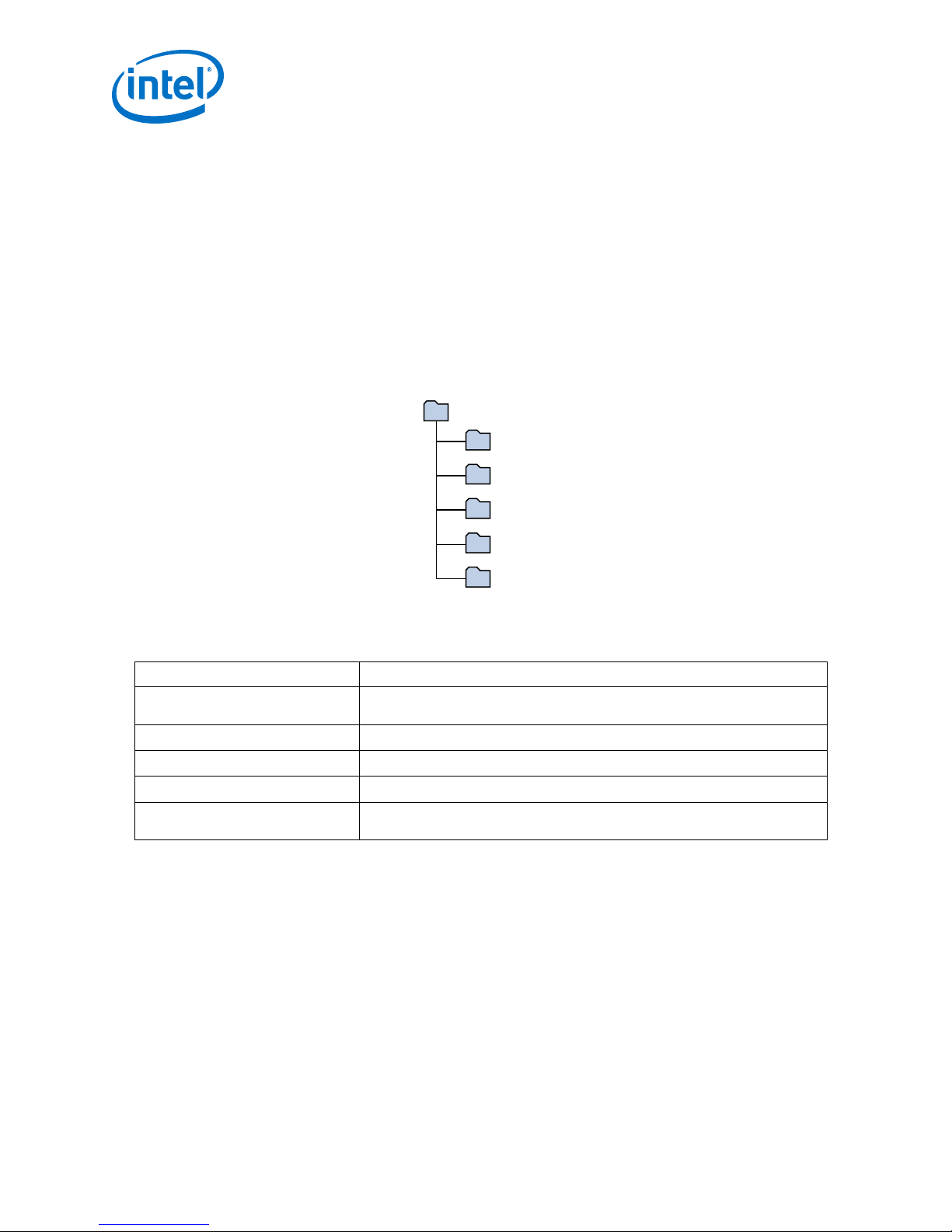
2.2 Development Kit Package
documents
board_design_files
examples
factory_recovery
demos
<package rootdir>
To download the Intel Cyclone 10 GX FPGA Development Kit package, perform the
following steps:
1. Download the development kit package from the Intel Cyclone 10 GX FPGA
Development Kit link on the Intel website.
2. Unzip the Intel Cyclone 10 GX FPGA Development Kit package contents to your
machine's local hard drive.
3. The package creates the directory structure shown in the figure below.
Figure 1. Development Kit Directory Structure
2 Getting Started
UG-20105 | 2017.12.18
Table 1. Directory Structure
2.3 Installing the Intel FPGA Download Cable Driver
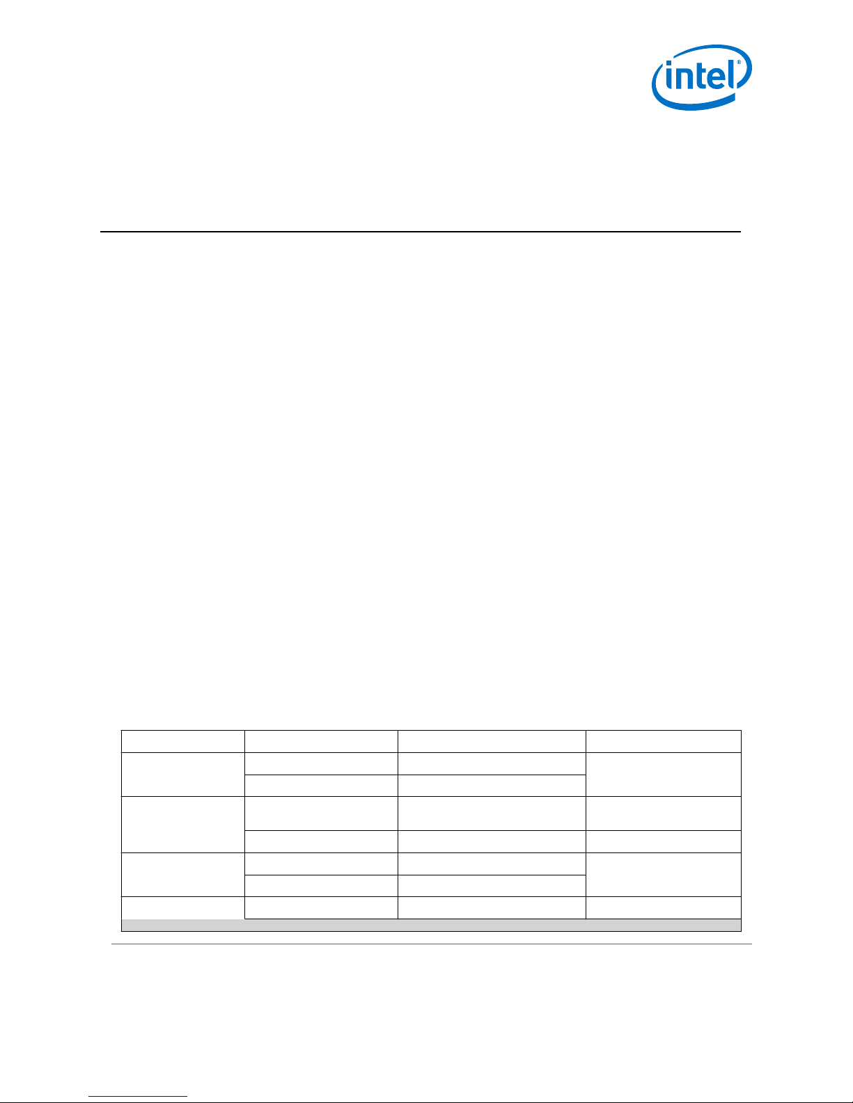
The table below lists the file directory names and a description of their contents
File Directory Name Description of Directory Contents
board_design_files
demos
documents
examples
factory_recovery
Contains schematics, layout, assembly and bill of material board design files. Use
these files as a starting point for a new prototype board design
Contains demonstration applications when available
Contains the development kit documentation
Contains the sample design files for the development kit
Contains the original data programmed onto the board before shipment. Use this
data to restore the board with its original factory contents.
Related Links
Intel Cyclone 10 GX FPGA Development Kit
The Intel Cyclone 10 GX FPGA Development Kit includes embedded Intel FPGA
Download Cable circuits for FPGA programming. However, for the host computer and
board to communicate, you must install the Intel FPGA Download Cable driver on the
host computer.
Installation instructions for the Intel FPGA Download Cable driver for your operating
system are available on the Intel website.
Intel® Cyclone® 10 GX FPGA Development Kit User Guide
8
Page 9

2 Getting Started
UG-20105 | 2017.12.18
On the Intel website, navigate to the Cable and Adapter Drivers Information link to
locate the table entry for your configuration and click the link to access the
instructions.
Intel® Cyclone® 10 GX FPGA Development Kit User Guide
9
Page 10
UG-20105 | 2017.12.18
3 Development Kit Setup
The instructions in this chapter describe how to setup and configure the development
kit
3.1 Setting up the Development Kit
To prepare and apply power to the board, perform the following steps:
The Intel Cyclone 10 GX FPGA Development Kit has two modes of operation:
• Standard PCIe-compliant system:
In this mode, plug the board into an available PCIe slot and connect the standard
2x4 PCIe auxiliary power available from the PC's ATX power supply to the mating
connector on the board (J12), and remove any power supply connected to J13.
The PCIe slot together with the PCIe power is required to power the entire board
with power up to 75 Watt. If ATX power is not connected, ensure that your PCIe
system can provide up to 75 Watt of power through the PCIe slot alone. The
power switch S14 is ignored when the board is used in the PCIe.
• Stand-alone evaluation board:
In this mode, plug the included power supply into the power adapter connector
(J13) and the AC power cord of the power supply into a power outlet. Remove any
ATX power supply that is connected from the 2x4 power connector (J12). The
power switch S14 will power ON/OFF the board.
3.2 Default Switch and Jumper Settings
This section lists the default factory switch settings for the Intel Cyclone 10 GX FPGA
Development Kit
Table 2. DIP Switch Settings
Board Label Switch Default Position Function
S1 S1.1 OPEN/OFF/1 Intel Cyclone 10 GX GX
S1.2 OPEN/OFF/1
S2 S2.1 CLOSE/ON/0 Select clock from Si570 for
S2.2 OPEN/OFF/1 Enable the output of Si570
S3 S3.1 CLOSE/ON/0 Select internal oscillator as
S3.2 CLOSE/ON/0
S5 S5.1 OPEN/OFF/1 Enable FMC card JTAG
Intel Corporation. All rights reserved. Intel, the Intel logo, Altera, Arria, Cyclone, Enpirion, MAX, Nios, Quartus
and Stratix words and logos are trademarks of Intel Corporation or its subsidiaries in the U.S. and/or other
countries. Intel warrants performance of its FPGA and semiconductor products to current specifications in
accordance with Intel's standard warranty, but reserves the right to make changes to any products and services
at any time without notice. Intel assumes no responsibility or liability arising out of the application or use of any
information, product, or service described herein except as expressly agreed to in writing by Intel. Intel
customers are advised to obtain the latest version of device specifications before relying on any published
information and before placing orders for products or services.
*Other names and brands may be claimed as the property of others.
FPGA MSEL
Si53307's output
the PLL reference of Si5332
continued...
ISO
9001:2008
Registered
Page 11
3 Development Kit Setup
UG-20105 | 2017.12.18
Board Label Switch Default Position Function
S5.2 OPEN/OFF/1 Enable Intel Cyclone 10 GX
S6 S6.1 OPEN/OFF/1 Reserved, no function
S6.2 OPEN/OFF/1 Reserved, no function
S9 S9.1 OPEN/OFF/1 User available Digital Input 0
S9.2 OPEN/OFF/1 User available Digital Input 1
S15 S15.1 OPEN/OFF/1 User available Digital Input 2
S15.2 OPEN/OFF/1 User available Digital Input 3
FPGA JTAG
defined
defined
Intel® Cyclone® 10 GX FPGA Development Kit User Guide
11
Page 12
USB 3.1 MUX/DRV
Intel Cyclone 10 GX FPGA
10CX220YF780E5G
Intel FMC LPC+
DDR3 (256M x 40)
EMIF
X40
933 MHz
Micro-USB 2.0
PCI Express
Transceivers X4
Buttons,
Switches, LEDs
X3
EPCQ-L for
Configuration
256 Mbit QSPI
Flash for Nios II
Intel MAX 10
10M08SAU169
On-Board Intel® FPGA
Download Cable II
USB Interface
JTAG Chain
Superspeed Tranceiver
USB 2.0 PHY
ULPI
GigE PHY 88E1111
SGMII LVDS x1
NOR Flash
Intel MAX 10
10M08SAU169 PFL
FPP X16
LVDS X32
CLKIN X2
REFCLK X2
Transceiver X5
USB 3.1
Type C
RJ-45
SFP+
TX/RX
X32
TX/RX
A/B
DP/DM
X4
X4
Oscillators
50M, 100M
Programmable
Transceiver
X4
SMA Clock In
LVDS
AS X4
SMA Clock Out
LVCMOS
QSPI
SFP+
TX/RX
Updated from JTAG Only
XCVR x1
XCVR x1
XCVR x1
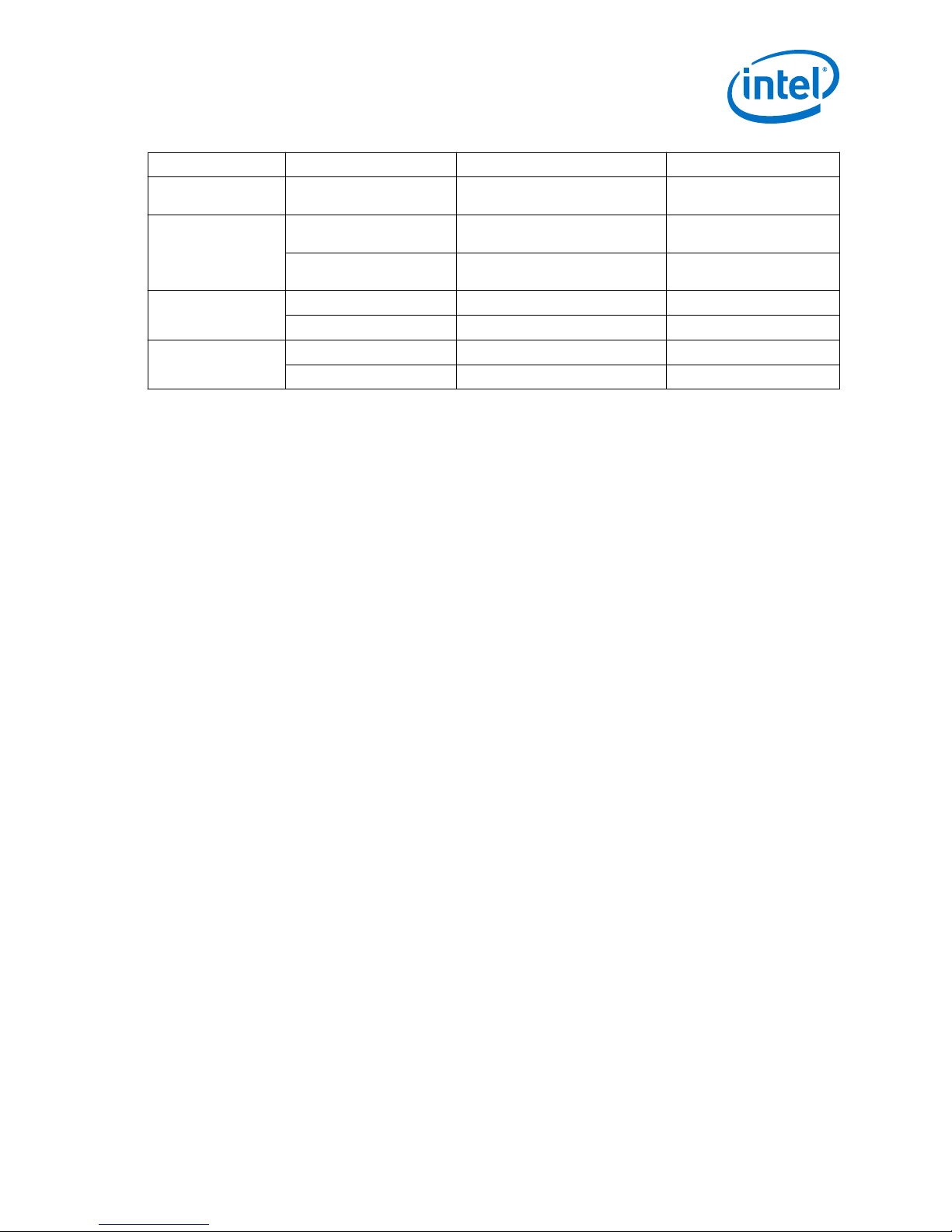
UG-20105 | 2017.12.18
4 Development Board Components
This chapter introduces all major components on the Intel Cyclone 10 GX FPGA
Development Kit.
4.1 Board Overview
Figure 2. Intel Cyclone 10 GX FPGA Developement Kit Block Diagram
There are four sub-systems in this development kit:
• Intel Cyclone 10 GX FPGA and its peripherals
• Configuration with Intel MAX 10 FPGA
• Timing
• Power Supply
Table 3. Board Components Table
Board Reference Type Description
U1 FPGA Intel Cyclone 10 GX FPGA 10CX220YF780E5G, 220K
Intel Corporation. All rights reserved. Intel, the Intel logo, Altera, Arria, Cyclone, Enpirion, MAX, Nios, Quartus
and Stratix words and logos are trademarks of Intel Corporation or its subsidiaries in the U.S. and/or other
countries. Intel warrants performance of its FPGA and semiconductor products to current specifications in
accordance with Intel's standard warranty, but reserves the right to make changes to any products and services
at any time without notice. Intel assumes no responsibility or liability arising out of the application or use of any
information, product, or service described herein except as expressly agreed to in writing by Intel. Intel
customers are advised to obtain the latest version of device specifications before relying on any published
information and before placing orders for products or services.
*Other names and brands may be claimed as the property of others.
Featured Devices
Logic Elements, 12 Transceivers, F780 BGA package
continued...
ISO
9001:2008
Registered
Page 13
4 Development Board Components
UG-20105 | 2017.12.18
Board Reference Type Description
U2 FPGA Intel MAX 10 10M08SAU169C8G for On-board Intel
U3 FPGA Intel MAX 10 10M08SAU169C8G for PFL
U49 Voltage Regulator Enpirion® EM2130L-30A Step-Down DC-DC Switching
U50 Voltage Regulator Enpirion EM2130H – 30A Step-Down DC-DC Switching
U51 Voltage Regulator Enpirion ER2120QI - 2A Synchronous Buck
U52 Voltage Regulator Enpirion ER3105DI - 500mA Wide VIN
U53, U54, U55, U60 Voltage Regulator Enpirion EN6337QI - 3A PowerSoC Voltage Mode
U56 Voltage Regulator Enpirion EN6347QI - 4A PowerSoC Voltage Mode
U62 Voltage Regulator Enpirion ER3110DI - 1A Wide VIN
Configuration and Setup Elements
J9 Embedded Intel FPGA Download Cable II Type-B Micro USB Connector for programming and
J11 10-pin header Optional JTAG direct via 10-pin header for external
S1 DIP-SW:
ON/Closed/0
OFF/Open/1
S7
S12
S13 FPGA Reset Push Button Press this button to reset all registers in the FPGA
D23 Power LED (Green) Power Good LED (All power rails are OK)
D13 Configuration Error LED (Red) Config error status Indicator
FPGA PGM_SEL Push Button
FPGA nCONFIG Push Button
Status Elements
FPGA Download Cable II and Power Management
configuration, clock generator control and power
monitoring
Converter with Integrated Inductor, featuring Digital
Control with PMBus™ v1.2 Compliant Interface,
implements FPGA 0.9V Vcc
Converter with Integrated Inductor, Featuring Digital
Control with PMBus v1.2 Compliant Interface,
implements 3.3V intermediate power bus used by
other lower voltage power rails
Regulator with Integrated MOSFETs, implements 5V
USB VBUS of USB3.1 Type-C interface
Synchronous Buck Regulator, implements local power
supply used by U49 and U50.
Synchronous PWM Buck with Integrated Inductor,
implements 1.03V, 1.5V, and 1.8V power rails to FPGA
Synchronous PWM Buck with Integrated Inductor,
implements voltage adjustable power rail to FPGA and
FMC daughter card
Synchronous Buck Regulator, implements power
supply used by U2 and U3.
debugging the FPGA
download cables
Intel Cyclone 10 GX FPGA Configuration Mode
Press this button to cycle through different PFL loads
Press this button to trigger reconfiguration
ON: Detected Power is Good
OFF: Detected Power is Bad
ON: FPGA configuration failed
OFF: FPGA configured without error
continued...
Intel® Cyclone® 10 GX FPGA Development Kit User Guide
13
Page 14
4 Development Board Components
UG-20105 | 2017.12.18
Board Reference Type Description
D14 Load LED (Green) Config is loading
ON: FPGA configuration is going on
OFF: FPGA configuration has finished
D15 Configuration LED (Green) Config done status Indicator
ON: FPGA configured successfully
OFF: FPGA not configured
General User Input/Output
S8, S10, S11 General user push buttons Three user push buttons. Driven low when pressed.
D19, D20, D21, D22 User LEDs Four user LEDs. Illuminates when driven low.
S9, S15 User DIP Switches 4-bit user DIP switches, low when set to ON
Clocks
U11 50 MHz Oscillator 50 MHz crystal oscillator for logic of two Intel MAX 10
Y4 50 MHz Oscillator 50 MHz crystal oscillator for general purpose logic of
Y1 100 MHz Oscillator 100 MHz crystal oscillator for calibration and
Y2 Programmable Oscillator Programmable Oscillator for Intel Cyclone 10 GX
U7 Clock Buffer 2:1 buffer for reference clock
U64 Programmable clock generator Eight channel Programmable clock generator. 4
Transceiver Interfaces
U16 PCIe x4 Golden Finger PCIe Gen2 x4 endpoint
J5, J6 SFP+ Support 10 GE SFP+ module
J7 FMC 5 Transceivers up to 12.5Gbps
J8 USB Type-C Implements USB3.1 and USB2.0
U26 USB 2:1 MUX TI HD3SS3220 USB Type-C DRP Port Controller with
U65 USB Redriver TI USB1002 USB3.1 10 Gbps Dual-Channel Linear
Memory
U12, U13, U14 DDR3 memory ISSI IS43TR16256A-107MBLI 256Mx16 4Gb DDR3
U4 EPCQ-L Flash EPCQ-L 1024
U58 QSPI Flash ISSI IS25WP256D-RHLE, 256Mbit
Power
J12 PCIe ATX 2x4 Auxiliary power supply of PCIe system
J13 DC-input 4-pin DIN power adaptor
S14 Power Switch Slide switch for power input
FPGA devices, 3.3V LVCMOS
Intel Cyclone 10 GX FPGA, 1.8V LVCMOS
configuration of Intel Cyclone 10 GX FPGA, 1.8V
LVCMOS
FPGA Transceivers, LVDS
outputs are implemented, default frequencies are 125
MHz, 21.186 MHz, 125 MHz and 100 MHz
SuperSpeed 2:1 MUX
Redriver
SDRAM
Intel® Cyclone® 10 GX FPGA Development Kit User Guide
14
Page 15
4 Development Board Components
UG-20105 | 2017.12.18
4.2 Cyclone 10 GX FPGA
The target FPGA device this kit is designed to work with is the Intel Cyclone 10 GX
10CX220YF780E5G FPGA. It is the device with the fastest speed, largest resource and
biggest package in the Intel Cyclone 10 GX FPGA series.
Table 4. Maximum Resource Availability
Feature Count
FPGA Device 10CX220YF780E5G
Logic Elements (LE) 220K
ALM 80,330
Registers 321,320
Memory - M20K 11,740 Kb
Memory - MLAB 1,690
Variable precision DSP block 192
18 x 19 Multiplier 384
Hard Floating-point Arithmetic Yes
PLL (Fractional Synthesis) 4
PLL (I/O) 6
12.5 Gbps Transceiver 12
GPIO 284
LVDS Pair 118
PCIe Hard IP Block 1
Hard Memory Interfaces 2
Package F780 (29 mm x 29 mm)
The table below presents a summary of the Intel Cyclone 10 GX FPGA I/O resource
allocation. I/O Direction is with respect to the FPGA.
Table 5. Cyclone 10 GX FPGA I/O Resources Table
Bank Number Function I/O Type I/O Count Description
Transceiver Clocks
1C
1C
1D
1D
1C/1D
USB_REFCLK
FMC_GBTCLK_M2C
SFP_REFCLK
PCIE_REFCLK
PCIE_TX [0:3]
LVDS input 2 User-defined from
LVDS input 2 644.53125 MHz
LVDS input 2 100 MHz from PCIe,
Transceiver Channels
CML output 8(4p) PCIe Gen2 Transmit
Intel® Cyclone® 10 GX FPGA Development Kit User Guide
2 125 MHz
(adjustable) , AC
FMC, AC
(adjustable), AC
DC
continued...
15
Page 16
4 Development Board Components
UG-20105 | 2017.12.18
Bank Number Function I/O Type I/O Count Description
1C/1D
1D
1D
1D
1D
1C/1D
1C/1D
2A
2A
2L
2L
2J
2A
CSS
CSS
CSS
CSS
2A
CSS
CSS
CSS
CSS
CSS
CSS
CSS
PCIE_RX [0:3]
SFP+_TX [0:1]
SFP+_RX [0:1]
USB31_TX
USB31_RX
FMC_DP_C2M [0:4]
FMC_DP_M2C [0:4]
M10_USB_CLK
C10_REFCLK1
C10_CLK50M
C10_REFCLK2
REFCLK_EMIF
FPGA_RESETn
C10_TCK
C10_TMS
C10_TDI
C10_TDO
C10_CLKUSR
C10_MSEL[0:1]
C10_nSTATUS
C10_CONF_DONE
C10_nCONFIG
C10_CS0n
C10_AS_D [0:3]
C10_DCLK
CML/LVDS input 8(4p) PCIe Gen2 Receive
CML output 4(2p) SFP+ Transmit
CML / LVDS input 4(2p) SFP+ Receive
CML output 2(1p) USB3.1 Trasnsmit
CML/LVDS input 2(1p) USB3.1 Receive
CML output 10(5p) FMC Transmit
CML/LVDS input 10(5p) FMC Receive
Global FPGA Clocks
1.8 V CMOS input 1 30/48 MHz from U2
(MAX10)
LVDS input 2 125 MHz (adjustable)
1.8 V CMOS input 1 50 MHz OSC, free
running
LVCMOS input 2 100 MHz (adjustable)
LVDS input 2 21.186 MHz
(adjustable)
Global FPGA Reset
1.8 V CMOS input 1 From U2 (Intel MAX
10)
JTAG
1.8 V CMOS input 1 From U2 (Intel MAX
10)
1.8V CMOS input 1 From U2 (Intel MAX
10)
1.8 V CMOS input 1 From U2 (Intel MAX
10)
1.8 V CMOS input 1 To U2 (Intel MAX 10)
Configuration
1.8 V CMOS input 1 100 MHz, for
calibration
1.8 V CMOS input 2 From DIP Switch S1
1.8 V CMOS output 1 To U2/U3 (Intel MAX
10)
1.8 V CMOS output 1 To U2/U3 (Intel MAX
10)
1.8 V CMOS input 1 From U2 (Intel MAX
10)
1.8 V CMOS output 1 To U4 (EPCQ-L)
1.8 V CMOS inout 4 To U4 (EPCQ-L)
1.8 V CMOS inout 1 To U4 (EPCQ-L) for
ASx4
continued...
Intel® Cyclone® 10 GX FPGA Development Kit User Guide
16
Page 17
4 Development Board Components
UG-20105 | 2017.12.18
Bank Number Function I/O Type I/O Count Description
2A
2A
2A
FPP [0:15]
CVP_CONFDONE
M10_USB_DATA
[0:7]
2A
M10_USB_ADDR
[0:1]
2A
2A
2A
2A
2A
2A
2A
2A
2J
2J
2J
2J
2J
2J
2J
2J
2J
M10_USB_RDn
M10_USB_WRn
M10_USB_RESETn
M10_USB_FULL
M10_USB_EMPTY
M10_USB_Oen
M10_USB_SCL
M10_USB_SDA
DDR3_A [0:14]
DDR3_BA [0:2]
DDR3_RASn
DDR3_CASn
DDR3_WEn
DDR3_CK
DDR3_CKE [0:1]
DDR3_ODT [0:1]
DDR3_CS [0:1]
From U3 (Intel MAX
10)
for FPPx16
1.8 V CMOS input 16 From U3 (Intel MAX
10)
1.8 V CMOS output 1 To U2 (Intel MAX 10)
UBII Side Bus
1.8 V CMOS input 8 From U2 (Intel MAX
10)
1.8 V CMOS input 2 From U2 (Intel MAX
10)
1.8 V CMOS input 1 From U2 (Intel MAX
10)
1.8 V CMOS input 1 From U2 (Intel MAX
10)
1.8 V CMOS input 1 From U2 (Intel MAX
10)
1.8 V CMOS output 1 From U2 (Intel MAX
10)
1.8 V CMOS output 1 From U2 (Intel MAX
10)
1.8 V CMOS input 1 From U2 (Intel MAX
10)
1.8 V CMOS input 1 From U2 (Intel MAX
10)
1.8 V CMOS inout 1 From U2 (Intel MAX
10)
EMIF
1.5 V SSTL output 15 To U12/U13/U14
DDR3
1.5 V SSTL output 3 To U12/U13/U14
DDR3
1.5 V SSTL output 1 To U12/U13/U14
DDR3
1.5 V SSTL output 1 To U12/U13/U14
DDR3
1.5 V SSTL output 1 To U12/U13/U14
DDR3
1.5 V SSTL output 2 To U12/U13/U14
DDR3
1.5 V SSTL output 2 To U12/U13/U14
DDR3
1.5 V SSTL output 2 To U12/U13/U14
DDR3
1.5 V SSTL output 2 To U12/U13/U14
DDR3
continued...
Intel® Cyclone® 10 GX FPGA Development Kit User Guide
17
Page 18
4 Development Board Components
UG-20105 | 2017.12.18
Bank Number Function I/O Type I/O Count Description
2J
2J/2K
2J/2K
3A/3B
3A/3B
3A/3B
3A/3B
DDR3_RSTn
DDR3_D [0:39]
DDR3_DQS [0:4]
FMC_LA_TX [0:16]
FMC_LA_RX [0:14]
FMC_LA_CC [0:1]
FMCA_CLK_M2C
1.5 V CMOS output 1 To U12/U13/U14
DDR3
1.5 V SSTL inout 40 To U12/U13/U14
DDR3
1.5 V SSTL inout 10 To U12/U13/U14
DDR3
FMC LVDS GPIO
Vadj CMOS inout 34 To J7 (FMC), DC
Vadj CMOS inout 30 To J7 (FMC), DC
Vadj CMOS input 4 From J7 (FMC), DC
Vadj CMOS input 4 From J7 (FMC), DC
[0:1]
3B
3A
3A
2A
2A
2L
2L
2L
2L
2L
2L
2L
2L
2L
2L
PCIe sideband
2L
2L
2L
2A
FMC_PRSN_1V8
FMC_SCL
FMC_SDA
SGMII_TXP/N
SGMII_TXP/N
ETH_MDC_C10
ETH_MDIO_C10
ETH_INTn_C10
ETH_RESETn_C10
SFP_SCL_0
SFP_SDA_0
SFP_INT_0
SFP_SCL_1
SFP_SDA_1
SFP_INT_1
PCIE_WAKEn
PCIE_SMBCLK
PCIE_SMBDAT
PCIE_PERSTn
Vadj CMOS input 1 From J7 (FMC)
Vadj CMOS output 1 To J7 (FMC)
Vadj CMOS inout 1 To J7 (FMC)
10/100/1000 Base-T
LVDS output 2 To U33 (88E1111
PHY), AC
LVDS input 2 To U33 (88E1111
PHY), AC
1.8 V CMOS output 1 To U33 (88E1111 PHY)
1.8 V CMOS inout 1 To U33 (88E1111
PHY), AC
1.8 V CMOS input 1 To U33 (88E1111
PHY), AC
1.8 V CMOS output 1 To U33 (88E1111
PHY), AC
SFP+ sideband
1.8 V CMOS output 1 To J5 (SFP+ 0)
1.8 V CMOS inout 1 To J5 (SFP+ 0)
1.8 V CMOS input 1 To J5 (SFP+ 0)
1.8 V CMOS output 1 To J6 (SFP+ 1)
1.8 V CMOS inout 1 To J6 (SFP+ 1)
1.8 V CMOS input 1 To J6 (SFP+ 1)
1.8 V CMOS input 1 To golden finger,
reserved
1.8 V CMOS output 1 To golden finger
1.8 V CMOS inout 1 To golden finger
1.8 V CMOS input 1 To golden finger
continued...
Intel® Cyclone® 10 GX FPGA Development Kit User Guide
18
Page 19
4 Development Board Components
UG-20105 | 2017.12.18
Bank Number Function I/O Type I/O Count Description
2L
2L
2L
2L
2L
2L
2L
2L
2L
2L
2L
2L
2L
2L
2L
USB_D [0:7]
USB_NXT
USB_DIR
USB_STP
USB_CLK
USB_RESETn
USB_SCL
USB_SDA
USB_PWEN
USB_SW_INTn_1.8V
USB_ID_1.8V
C10_QSPI_CSn
C10_QSPI_RESETn
C10_QSPI_CLK
C10_QSPI_D [0:3]
ULPI (USB 2.0)
1.8 V CMOS inout 8 To U32 (USB
Transceiver)
1.8 V CMOS input 1 To U32 (USB
Transceiver)
1.8 V CMOS input 1 To U32 (USB
Transceiver)
1.8 V CMOS output 1 To U32 (USB
Transceiver)
1.8 V CMOS output 1 60 MHz, REFCLK for
ULPI
1.8 V CMOS output 1 To U32 (USB
Transceiver)
USB3.1 sideband
1.8 V CMOS output 1 To U26 (USB3.1
Transceiver Switch)
1.8 V CMOS inout 1 To U26 (USB3.1
Transceiver Switch)
1.8 V CMOS output 1 To U25 (USB3.1
Transceiver Switch)
1.8 V CMOS input 1 To U26 (USB3.1
Transceiver Switch)
1.8 V CMOS input 1 To U26 (USB3.1
Transceiver Switch)
QSPI Flash
1.8 V CMOS output 1 To U58 (QSPI Flash)
1.8 V CMOS output 1 To U58 (QSPI Flash)
1.8 V CMOS output 1 To U58 (QSPI Flash)
1.8 V CMOS inout 4 To U58 (QSPI Flash)
4.3 MAX 10 System Controller
The highlights of the Intel MAX 10 devices include:
• Internally stored dual configuration flash
• User flash memory
• Instant on support
• Integrated analog-to-digital converter (ADC)
• Single-chip Nios II soft core processor support
Intel MAX 10 devices are the ideal solution for system management, I/O expansion,
communication control planes, industrial, automotive, and consumer applications.
Intel® Cyclone® 10 GX FPGA Development Kit User Guide
19
Page 20
4 Development Board Components
Table 6. Summary of Features for Intel MAX 10 Devices
Feature Description
Technology 55 nm TSMC Embedded Flash (Flash + SRAM) process technology
Packaging • Low cost, small form factor packages—support multiple packaging
technologies and pin pitches
• Multiple device densities with compatible package footprints for seamless
migration between different device densities
• RoHS6-compliant
Core architecture • 4-input look-up table (LUT) and single register logic element (LE)
• LEs arranged in logic array block (LAB)
• Embedded RAM and user flash memory
• Clocks and PLLs
• Embedded multiplier blocks
• General purpose I/Os
Internal memory blocks • M9K—9 kilobits (Kb) memory blocks
• Cascadable blocks to create RAM, dual port, and FIFO functions
User flash memory (UFM) • User accessible non-volatile storage
• High speed operating frequency
• Large memory size
• High data retention
• Multiple interface option
Embedded multiplier blocks • One 18 × 18 or two 9 × 9 multiplier modes
• Cascadable blocks enabling creation of filters, arithmetic functions, and image
processing pipelines
ADC • 12-bit successive approximation register (SAR) type
• Up to 16 analog inputs
• Cumulative speed up to 1 million samples per second (MSPS)
• Integrated temperature sensing capability
Clock networks • Global clocks support
• High speed frequency in clock network
Internal oscillator Built-in internal ring oscillator
PLLs • Analog-based
• Low jitter
• High precision clock synthesis
• Clock delay compensation
• Zero delay buffering
• Multiple output taps
General-purpose I/Os (GPIOs) • Multiple I/O standards support
• On-chip termination (OCT)
• Up to 830 megabits per second (Mbps) LVDS receiver, 800 Mbps LVDS
transmitter
External memory interface (EMIF) Supports up to 600 Mbps external memory interfaces:
• DDR3, DDR3L, DDR2, LPDDR2
• SRAM (Hardware support only)
UG-20105 | 2017.12.18
continued...
Intel® Cyclone® 10 GX FPGA Development Kit User Guide
20
Page 21

System
Intel
MAX 10
FPGA
USB PHY
CY7C68013
HDR2X5
for System Intel
MAX 10 FPGA
FMC
Configuration
Intel MAX 10
FX2 Bus 3.3 V
PD[3:0] (JTAG)
3.3 V
Intel
Cyclone 10
FPGA
JTAG 1.8 V
USB Configuration
1.8 V
JTAG 3.3 V
JTAG 3.3 V
4 Development Board Components
UG-20105 | 2017.12.18
Feature Description
Note: For 600 Mbps performance, –6 device speed grade is required.
Performance varies according to device grade (commercial, industrial, or
automotive) and device speed grade (–6 or –7). Refer to the MAX 10
Device Data Sheet or External Memory Interface Spec Estimator for more
details.
Configuration • Internal configuration
• JTAG
• Advanced Encryption Standard (AES) 128-bit encryption and compression
options
• Flash memory data retention of 20 years at 85 °C
Flexible power supply schemes • Single- and dual-supply device options
• Dynamically controlled input buffer power down
• Sleep mode for dynamic power reduction
Related Links
MAX 10 FPGA Device Overview
4.4 FPGA Configuration
JTAG
The JTAG topology of the board is shown in the figure below. An on-board USB Blaster
is implemented with the Intel MAX 10. It is in the form of a micro-USB type-B
connector (J9).
Figure 3. JTAG topology block diagram
The system Intel MAX 10 device itself can be configured through on-board USB port or
an external USB-Blaster II header. the 2x5 header for Intel MAX 10 is not mounted by
default.
A secondary Intel MAX 10 device is used for PFL configuration mode. This CFG Intel
MAX 10 is configured with on-board USB port.
The Intel Cyclone 10 GX FPGA device is configured with on-board USB port or an
external USB-Blaster II header.
The FMC interface also has a JTAG interface. The FMC JTAG can also be included into
the JTAG chain.
The Intel Cyclone 10 GX device JTAG and FMC JTAG can be put included or isolated
from the JTAG chain by setting a DIP switch S5.
Intel® Cyclone® 10 GX FPGA Development Kit User Guide
21
Page 22

Table 7. JTAG DIP Switch Settings
Intel
Cyclone 10 GX
FPGA
DIPswitch S1
Intel MAX 10
10M08SAU169
SYS/UBII
Intel MAX 10
10M08SAU169
PFL
EPCQ-L
NOR Flash
X32
MSEL
nSTATUS
nCONFIG
CONF_DONE
FPP X16
DCLK
AS X4
Switch Signal Function
S5.1
S5.2
FMC_JTAGEN
C10_JTAGEN
Configuration
The Intel Cyclone 10 GX FPGA device can be configured using different modes. Mode
selection can be done using DIP switch S1.
Table 8. Configuration Mode Settings
4 Development Board Components
UG-20105 | 2017.12.18
ON - Disable JTAG
ON - Disable JTAG
Configuration Scheme V
JTAG-based Configuration ----- ------
AS (x1 and x4) 1.8 Fast 010
PS and FPP (x8, x16, x32) 1.2 / 1.5 / 1.8 Fast 000
(V) Power-On Reset Delay
CCPGM
Standard 011
Standard 001
Table 9. MSEL Switch S1 Definition
Switch Signal Note
S1.1
S1.2
C10_MSEL0 MSEL2 is tied to GND
C10_MSEL1
ON - '0'
Figure 4. FPGA Configuration Scheme Block Diagram
Valid MSEL [2:0]
Use any valid MSEL pin
settings given below
The Intel Cyclone 10 GX FPGA device is configured with two modes: ASx4 or FPP x16.
The AS x4 mode uses an EPCQ-L 1024 to store the image. A dedicated Intel MAX 10
device is used to implement PFL. It interfaces with two pieces of x16 parallel NOR
flash devices to get a x32 bus width. The highest density is 2 Gb. The flash interface
works at 3.3 V and various NOR flashes from different vendors can be used with this
board.
Intel® Cyclone® 10 GX FPGA Development Kit User Guide
22
Page 23

4 Development Board Components
UG-20105 | 2017.12.18
Micron MT28EW01GABA1LPC-0SITES is installed in manufacturing by default. 2 Gb is
provided with the board.
For the Intel Cyclone 10 GX FPGA device, the image size is less than 85 Mb. Multiple
images can be stored and selected by the user. The image to be used can be selected
with a group of Push Buttons and LEDs.
The user can select between the images to be loaded into Intel Cyclone 10 GX FPGA.
• Cycling images by pushing button S7
• CFG Intel MAX 10 device displays current number to be used with LEDs D16-D18
• Initiate the reconfiguration by pushing button S12
The signal definition of these buttons and LEDs are shown below:
Table 10. Program Selection Signals Definition
Switch / LED Signal Note
S7
S12
D16
D17
D18
PGM_SEL
SYS_CONFIG_PB
PGM_LED0
PGM_LED1
PGM_LED2
Select program
Reconfigure
PGM_LED [2:0] indicates the program to be used
Side Bus
A group of Side Bus signals are defined between Intel MAX 10 and Intel Cyclone 10 GX
FPGA device to provide a higher speed access through on-board USB-Blaster. This
interface is reserved in harwdare.
4.5 Status and User I/O Elements
4.5.1 Switches
Power Switch
The Power Switch S14 is at the edge of the card. When the switch stub is at higher
position (marked 'OFF'), the power is OFF.
Note: When the board is inserted into a PCIe slot in computer, the power switch is override.
The board is powered ON/OFF with the PCIe system irrespective of the position of the
power switch.
DIP Switches
The DIP switches are on the bottom side of the board, close to the upper edge.
Intel® Cyclone® 10 GX FPGA Development Kit User Guide
23
Page 24

Table 11. DIP Switch Definition
4 Development Board Components
UG-20105 | 2017.12.18
Board
Reference
S9 S9.1
S9.2
S15 S15.1
S15.2
S6 S6.1
S6.2
S1 S1.1
S1.2
S3 S3.1
S3.2
S2 S2.1
S2.2
S5 S5.1
S5.2
Switch Signal Name Default Value Function
USER_DIP0
USER_DIP1
USER_DIP2
USER_DIP3
CFG_M10_PGM0
CFG_M10_PGM0
C10_MSEL0
C10_MSEL1
Si5340_INSEL0
Si5340_INSEL1
CLKBUF_SEL
Si570_OE
FMC_JTAGEN
C10_JTGEN
1 User available Digital Input
1 User available Digital Input
1 User available Digital Input
1 User available Digital Input
1 Reserved, No Function
1
1 Intel Cyclone 10 GX MSEL
1
0 Input selection for clock
0
0 Set the input source of
1 Enable the output of Si570
1 Enable FMC Card JTAG
1 Enable Intel Cyclone 10 GX
0
1
2
3
generator chip, the Si5332
on this board
[INSEL1, INSEL0] values:
00 - internal oscillator
10- external reference input
from SMB
Set to 00 by default
Si53307
0: Use CLKIN0
1: Use CLKIN1
Fixed to '0'
(Y2)
0: Output disabled
1: Output enabled
Fixed to '1'
0: Isolate FMC card JTAG
from the chain
1: Add FMC Card JTAG into
the chain
FPGA JTAG
0: Isolate FPGA JTAG from
the chain
1: Add FPGA JTAG into the
chain
4.5.2 Pushbuttons
The push buttons are located on the upper right corner of the board.
Intel® Cyclone® 10 GX FPGA Development Kit User Guide
24
Page 25

4 Development Board Components
UG-20105 | 2017.12.18
Table 12. Push Button Definition
Board Reference Signal Name Function
S11
S10
S8
S7
S12
S13
USER_PB2
USER_PB1
USER_PB0
PGM_SEL
SYS_CONFIG_PB
C10_RESETn_PB
User available Pushbutton 2
User available Pushbutton 1
User available Pushbutton 0
PFL Image selection. Use this pushbutton to rotate through
three images.
Trigger reconfiguration to Intel Cyclone 10 GX FPGA. The image
used for configuration is selected with PGM_SEL button and
indicated by PGM_NUM LEDs
Trigger logic reset to Intel Cyclone 10 GX FPGA logic. The state
of the configured logic is reset, the configuration remains
unchanged.
4.5.3 LEDs
The LEDs are on the top side of the board at the upper right corner.
Table 13. Board LED Definition
Board Reference Signal Name Colour Function
D16
D17
D18
D14
D15
D13
D22
D19
D20
D21
D23
PGM_LED0
PGM_LED1
PGM_LED2
LOAD_LED
CFGDONE_LED
ERR_LED
USER_LED3
USER_LED0
USER_LED1
USER_LED2
POK_LED
Green Image 0 is loaded in FPP mode
Green Image 1 is loaded in FPP mode
Green Image 2 is loaded in FPP mode
Green Indicates image is loading
Green Indicates image loading succeeded
Red Indicates image loading failed
Green '0' to light, output from FPGA
Green '0' to light, output from FPGA
Green '0' to light, output from FPGA
Green '0' to light, output from FPGA
Green Indicates power is OK
Intel® Cyclone® 10 GX FPGA Development Kit User Guide
25
Page 26

4.6 Clocks
Si570
2.5 V
Si5332
1.8 V
IN2
Si53307
2.5 V
100 MHz
SFP_REFCLKp
LVDS @ 644.53125 MHz
USB_REFCLKp
LVDS @ 125 MHz
C10_REFCLK2p
LVCMOS @ 100 MHz
OUT1
CLKOUT
FPGA
BANK_1C
BANK_1D
CLKUSR
100 MHz
1.8 V
50 MHz
1.8 V
FMC_CLK
FMC
PCIe
REF
REFCLK_EMIF_P
LVDS @ 21.186 MHz
C10_REFCLK1p
LVDS @ 125 MHz
OUT4
OUT8
OUT7
Figure 5. Clock Distribution
4 Development Board Components
UG-20105 | 2017.12.18
The Intel Cyclone 10 GX FPGA local clocks are generated with Si570 + Si53307 +
Si5332.
Si570 is a programmable oscillator. It is configurable with an I2C interface at address
7'b110_0110. Si53307 is a clock buffer. With Si570 + Si53307, a high frequency
reference clock at frequency up to 725 MHz is available for Intel Cyclone 10 GX FPGA
Transceiver. Other clocks are generated with an programmable clock generator Si5332
at I2C address 7'b110_1010.
Features of Si5332
• Output frequency Range: 5 MHz to 312.5 MHz differential
• Input frequency Range: 10 MHz to 250 MHz differential, 16 MHz to 30 MHz
external crystal
• Embedded 50 MHz crystal option for 8 or 12 port devices
• MultiSynth technology enables any frequency synthesis on any output up to 250
• Highly configurable output path featuring a cross-point multiplexer
MHz
— Up to three independent fractional synthesis output paths
— Up to five independent integer dividers
— The Input Reference Clock
Intel® Cyclone® 10 GX FPGA Development Kit User Guide
26
Page 27

4 Development Board Components
UG-20105 | 2017.12.18
• Low Phase Jitter: 400 fs rms max
• Programmable spread spectrum
• 1.8 V, 2.5 V, 3.3 V core V
• 1.8 V, 2.5 V, 3.3 V differential output
A local free running 100 MHz oscillator is used to generate the reference clock for
calibration. This clock is also used by ASx4 configuration. A free running 50 MHz
oscillator is used to generate a reference clock for FPGA core.
The Intel MAX 10 works with free running 50 MHz oscillator. Adjusting the variable
clocks does not affect the working of the Intel MAX 10 device.
4.7 Memory
4.7.1 EMIF with DDR3
The Intel Cyclone 10 GX FPGA device supports DDR3 memory up to 933 MHz. On this
development kit, a DDR3 x40 at 933 MHz is implemented with DDR3 devices. The
EMIF uses continuous banks in the same column. To achieve 933 MHz speed, EMIF
uses bank 2J and 2K to support 40-bit width at 933 MHz. The signal definition
conforms to the EMIF constraints.
DD
4.7.2 QSPI Flash
Besides the flash memories used by the configuration modules, a user accessible QSPI
Flash device is provided for non-volatile data storage. The device is 256 Mb with 4-bit
data width.
4.8 Power
This development kit is powered by a +12 V power source. The power is one of the
following:
• PCIe golden finger from PCIe system
• ATX 2 x 4 or external AC/DC adaptor.
Attention: The ATX 2x4 and external adaptor cannot be used simultaneously. The ATX 2x4 can
work together with the PCIe system power input to provide power higher than 25 W.
Intel® Cyclone® 10 GX FPGA Development Kit User Guide
27
Page 28

Power Distribution
System Intel MAX 10 (U2)
Configuration Intel MAX 10 (U3)
Flash/ USB PHY
Intel Cyclone 10 GX
VCC/ VCCP/ VCCERAM
SFP+/ FMC/ USB
Intel Cyclone 10 GX
VCCT_GXB/ VCCR_GXB
Intel Cyclone 10 GX
VCCPT/ VCCA_PLL/ VCCH_GXB/ VCCBAT
VCCPGM/ VCCIO/ System Intel MAX 10/
Configuration Intel MAX 10/ Si5332/ USB
Intel Cyclone 10 GX /
DDR3 VCCIO
Intel Cyclone 10 GX /
FMC VCCIO
Si570 /
Si53307
Ethernet PHY
88E1111
USB 3.1 VBAT
EP5348
ETH_2.5V, 0.4 A
EP5348
ETH_1.0V, 0.3 A
EY1501 LDO
Si570_2.5V, 0.3 A
EN6347QI
VIO_ADJ, 4 A
EN6337QI
C10_1.5V, 1.8 A
EV1320
EN_GROUP2
EN_GROUP3
EN_GROUP4
EN_GROUP4
EN_GROUP4
EN_GROUP4
IO_1.8V
3.3 V
EN_GROUP1
EN_GROUP1
ER3110
3.3V_STB, 0.6 A
ES1010
LTC4357
LTC4357
2x4 ATX Connector
PCIe Edge Connector
12V_ATX
PCIe_12V
12V_IN 12 V
FPGA Power UP Sequencing:
VCC/ VCCP/ VCCERAM
VCCR/ VCCT
VCCH/ VCCA_PLL/ VCCPT/ VCCBAT
VCCPGM/ VCCIO
1
2
3
4
FPGA Quick Power DOWN Sequencing:
1234
12 V Adaptor
EM2130_5V
ER2120
USB_5V, 1.5 A
EN6337QI
IO_1.8V, 1 A
EN6337QI
C10_1.8V, 1.6 A
EN6337QI
C10_0.95V, 1.6 A
EM2130H
3.3 V, 12 A
EM2130L
0.9 V, 18 A
ER3105
Figure 6. Power Distribution Scheme
4 Development Board Components
UG-20105 | 2017.12.18
Table 14. Enpirion Power Regulators
Power Group Power Rail Generated From (V) Maximum Current
0 3.3 V for Intel MAX 10 12 0.65 ER3110
5 V for EM2130 12 0.20 ER3105
1 0.9 V 12 16.18 EM2130L
3.3 V 12 12.39 EM2130H
2 0.95 V 3.3 1.53 EN6337
3 1.8 V 3.3 1.54 EN6337
4 1.8 V 3.3 0.75 EN6337
Intel® Cyclone® 10 GX FPGA Development Kit User Guide
1.5 V 3.3 1.83 EN6337
VADJ 3.3 4.00 EN6347
2.5 V for clock 3.3 0.22 EY1501
2.5 V for GigE 3.3 0.40 EP5348
1 V for GigE 3.3 0.30 EP5348
5 V for USB3.1 12 1.50 ER2120
VTT 1.5 0.6 EV1320
Softstart ES1010
28
(A)
Enpirion Part
Page 29

4 Development Board Components
UG-20105 | 2017.12.18
4.9 Transceivers Interfaces and Communication Ports
4.9.1 Transceiver Channels
The Intel Cyclone 10 GX FPGA device has 12 channels of transceivers that work at
12.5 Gbps. The transceivers are organized in two banks, each bank has six channels.
Table 15. Transceiver Channel Allocation
Channel Number (Bank
0
1
2
3
4
5
1C)
4.9.2 PCIe Interface
The PCIe x4 Gen2 Hard IP with CvP is implemented in this development kit. The
position of the PCIe channels is fixed by the hard IP. This development kit is a PCIe
add-in card. The PCIe interface is configured to End-Point.
The PCIe interface has the following signals:
• Transceivers, x4, up to 5 Gbps
•
PCIE_REFCLKp/n, 100 MHz from PCIe system
•
PCIE_SMBUS, 3.3V level-translated to 1.8V with U18
•
PCIE_PERSTn, 3.3V level-translated to 1.8V with U17
•
PCIE_WAKEn, 3.3V level-translated to 1.8V with U17, reserved
Function (Bank 1C) Channel Number (Bank
FMC_DP [0]
FMC_DP [1]
FMC_DP [2]
FMC_DP [3]
PCIe [0]
PCIe [1]
0
1
2
3
4
5
1D)
Function (Bank 1D)
PCIe [2]
PCIe [3]
FMC_DP [4]
SFP+ 1
SFP+ 0
USB3.1
The PCIe width can be selected with Jumper resistors:
• R506 installed, x1 mode
• R507 installed, x4 mode, this is the default mode
There are three power rails from PCIe golden finger connector:
• +12 V, +/- 8 %, up to 75 W, is used as power of the board
• +3.3 V, +/- 9 %, up to 10 W, is not used on this board
• +3.3 Vaux, +/- 9 %, 375 mA max, is not used since wakeup is not supported
4.9.3 SFP+ Interface
Two SFP+ connectors (J5, J6) are provided on the PCIe bracket. Each connector
supports a 10 GE SFP+ hot pluggable module.
Intel® Cyclone® 10 GX FPGA Development Kit User Guide
29
Page 30

4 Development Board Components
Each SFP+ interface has the following signals:
• Transceivers, x1 for each SFP+, up to 12.5 Gbps
• SMBUS (I2C), 3.3V for SFP+ and I/O expander, level-translated 10 1.8V with
U22/U23
• IRQ of I/O expander, 3.3V level-translated to 1.8V with U19
Each SFP+ module has six status/control signals and two LEDs. The FPGA device does
not have enough I/O pins for these signals, hence an I/O expander is used to
implement these I/Os for each SFP+ connector. The I2C I/O expander is on the same
I2C bus as the SFP+ module, and the I2C bus of two SFP+ modules are independent of
each other.
The I/O expander used is TI TCA9534PWR. U20 is for SFP+ 0, with I2C address
7'b010_0000. U21 is for SFP+, with I2C address 7'b010_0000.
The I/O expander has 8 I/Os. The definition of the I/Os is shown in the table below.
The device is controlled with I2C bus.
Table 16. I/O Expander: I/O Definition
I/O Number Signal I/O Type Function
P0
P1
P2
P3
P4
P5
P6
P7
SFP_RLED
SFP_GLED
SFP_TXDIS
SFP_TFLT
SFP_RS1
SFP_RLOS
SFP_RS0
SFP_PRSN
Output Red LED, indicates LOS/ERR,
"0" - ON
Output Green LED, indicates Link,
"0" - ON
Output Tx_Disable, Pulled up,
Transmitter is turned off if
high
Input Tx_Fault, Pulled up,
indicates fault when high
Output Rate Select, Pulled up with
1K resistor
Input Rx_LOS, Pulled up, indicates
LOS when high
Output Rate Select, Pulled up with
1K resistor
Input Mod_ABS, Pulled up, module
in place when low
UG-20105 | 2017.12.18
The I/Os of TCA9534 is in high impedance input mode upon power up. Hence, the
module is placed in TX_Disable mode and the LEDs are off. The status changes on the
I/Os are reported with an IRQ to the FPGA. Each I/O expander has its own dedicated
IRQ signal.
4.9.4 USB3.1 Type-C Interface
A USB3.1 Type-C interface (J8) is provided on the PCIe bracket. The interface supports
SuperSpeed up to 10 Gbps as well as the backward compatible support of USB2.0.
Intel® Cyclone® 10 GX FPGA Development Kit User Guide
30
Page 31

USB
Type C
DRP Port
Controller
Superspeed
2:1 Multiplexer
HD3SS3220
USB 3.1 Redriver
TUSB1002
Superspeed 1
FPGA
Power Switch
TPS25910R
VBUS
Superspeed 2
USB 2.0 PHY
USB3320C
USB DP/DM
CC1/CC2
USB_ID
SMBUS
USB_IRQ
ULPI
Transceiver X1
5 V
USB_PWEN
4 Development Board Components
UG-20105 | 2017.12.18
Figure 7. USB3.1 Type-C Block Diagram
The Type-C connector provides any orientation insertion of the cable. To support this
feature, a Texas Instruments DRP port Controller and SuperSpeed 2:1 MUX
HD3SS3220 is used. The port is configured in DRP mode. The controller detects the
orientation of the plugged cable and multiplexes the transceiver of the FPGA to two
SuperSpeed interfaces. It also determines if the port is an Upstream Facing Port (UFP)
or a Downstream Facing Port (DFP). It controls the power switch to feed the power to
cable when in DFP mode. HD3SS3220 is controlled by the FPGA through a dedicated
I2C bus.
Parameters of USB3.1
2
•
I
C address is 7'b110_0111 by default. It can be changed to 7'b100_0111 by
installing R199 and removing R198
• Port mode is Dual Role Port (DRP) by default. It can be chnaged to DFP if R177 is
installed, or UFP if R178 is installed.
• Current Advertisement is 1.5A
A USB3.1 Redriver TUSB1002 is used to condition the high-speed signal because of
the degradation caused by the 2:1 mux and to support the 10 Gbps SuperSpeed Plus.
The equalization gain and VOD gain of TUSB1002 are set by resistors. The default
settings are:
• EQ for channel 1: 5.5 dB
• EQ for channel 2: 5.5 dB
• VOD Gain: 0 for both channels with linear range 1200 mV.
The resistors are set in pull down mode on the board. Other configurations are
available by changing the pulling resistors. EQ configurations with pin level "1" are not
available.
The power of USB VBUS is controlled with a Texas Instruments power switch
TPS25910. The voltage is 5 V and the maximum current is 1.5 A. The power control
pin to the TPS25910 is connected to the USB_ID output of HD3SS3220. The power is
applied to VBUS only when the port is in DFP mode. The power application can be
controlled by the FPGA too. The USB_PWEN signal is active high because of the NMOS
inverter.
Intel® Cyclone® 10 GX FPGA Development Kit User Guide
31
Page 32

4 Development Board Components
UG-20105 | 2017.12.18
USB_ID pin on HD3SS3220 indicates the port is linked as a power source (DFP), or
dual-role (DRP) acting as source (DFP). USB_ID is connected to the FPGA as well as
TPS25910 and USB3320.
Backward support for USB2.0 is implemented with Microchip's USB3320 USB PHY. It
interfaces with the FPGA through ULPI interface. The reference clock mode for ULPI is
FPGA clock output to USB3320.
4.9.5 FPGA Mezzanine Card (FMC) Interface
A FMC Connector (J7) is provided on the development kit for expansion. The FMC
interface is compatible with the following daughter cards:
• 12G SDI: Semtech RDK-12GSRD-ALTRA00 Evaluation Board
• 8G DisplayPort: Bitec FMC DisplaPort Daughter Card
• 6G HDMI 2.0: Bitec FMC HDMI Daughter Card
Table 17. FMC Signals
Intel Cyclone 10 GX FPGA Development Kit SDI DisplayPort HDMI
Signal V57.1 Name Signal Name Pin Number SDI FMC
Signal Name
FMC_DP_C2M_P0DP0_C2M_P DP0_C2M_P C2 x FMC_TX_P0 GXB_TXp0
DisplayPort
FMC Signal
Name
HDMI FMC
Signal Name
FMC_DP_C2M_N0DP0_C2M_N DP0_C2M_N C3 x FMC_TX_N0 GXB_TXn0
FMC_DP_C2M_P1DP1_C2M_P DP1_C2M_P A22 x FMC_TX_P1 GXB_TXp1
FMC_DP_C2M_N1DP1_C2M_N DP1_C2M_N A23 x FMC_TX_N1 GXB_TXn1
FMC_DP_C2M_P2DP2_C2M_P DP2_C2M_P A26 FMC_GS12181
_IN+
FMC_DP_C2M_N2DP2_C2M_N DP2_C2M_N A27 FMC_GS12181
_IN-
FMC_DP_C2M_P3DP3_C2M_P DP3_C2M_P A30 x FMC_TX_P3 GXB_TXp3
FMC_DP_C2M_N3DP3_C2M_N DP3_C2M_N A31 X FMC_TX_N3 GXB_TXn3
FMC_DP_C2M_P4DP4_C2M_P DP4_C2M_P A34 x x x
FMC_DP_C2M_N4DP4_C2M_N DP4_C2M_N A35 x x x
X DP5_C2M_P DP5_C2M_P A38 x x x
X DP5_C2M_N DP5_C2M_N A39 x x x
X DP6_C2M_P DP6_C2M_P B36 x x x
X DP6_C2M_N DP6_C2M_N B37 x x x
X DP7_C2M_P DP7_C2M_P B32 x x x
FMC_TX_P2 GXB_TXp2
FMC_TX_N2 GXB_TXn2
continued...
Intel® Cyclone® 10 GX FPGA Development Kit User Guide
32
Page 33

4 Development Board Components
UG-20105 | 2017.12.18
Intel Cyclone 10 GX FPGA Development Kit SDI DisplayPort HDMI
Signal V57.1 Name Signal Name Pin Number SDI FMC
Signal Name
X DP7_C2M_N DP7_C2M_N B33 x x x
X DP8_C2M_P DP8_C2M_P B28 x x x
X DP8_C2M_N DP8_C2M_N B29 x x x
X DP9_C2M_P DP9_C2M_P B24 x x x
X DP9_C2M_N DP9_C2M_N B25 x x x
FMC_DP_M2C_P0DP0_M2C_P DP0_M2C_P C6 x FMC_RX_P0 GXB_RXp0
FMC_DP_M2C_N0DP0_M2C_N DP0_M2C_N C7 x FMC_RX_N0 GXB_RXn0
FMC_DP_M2C_P1DP1_M2C_P DP1_M2C_P A2 x FMC_RX_P1 GXB_RXp1
FMC_DP_M2C_N1DP1_M2C_N DP1_M2C_N A3 x FMC_RX_N1 GXB_RXn1
DisplayPort
FMC Signal
Name
HDMI FMC
Signal Name
FMC_DP_M2C_P2DP2_M2C_P DP2_M2C_P A6 FMC_GS12141
FMC_DP_M2C_N2DP2_M2C_N DP2_M2C_N A7 FMC_GS12141
FMC_DP_M2C_P3DP3_M2C_P DP3_M2C_P A10 x FMC_RX_P3 x
FMC_DP_M2C_N3DP3_M2C_N DP3_M2C_N A11 x FMC_RX_N3 x
FMC_DP_M2C_P4DP4_M2C_P DP4_M2C_P A14 x x x
FMC_DP_M2C_N4DP4_M2C_N DP4_M2C_N A15 x x x
X DP5_M2C_P DP5_M2C_P A18 x x x
X DP5_M2C_N DP5_M2C_N A19 x x x
X DP6_M2C_P DP6_M2C_P B16 x x x
X DP6_M2C_N DP6_M2C_N B17 x x x
X DP7_M2C_P DP7_M2C_P B12 x x x
X DP7_M2C_N DP7_M2C_N B13 x x x
X DP8_M2C_P DP8_M2C_P B8 x x x
X DP8_M2C_N DP8_M2C_N B9 x x x
X DP9_M2C_P DP9_M2C_P B4 x x x
X DP9_M2C_N DP9_M2C_N B5 x x x
FMC_GBTCLK_
M2C_P0
FMC_GBTCLK_
M2C_N0
GBTCLK0_M2C_PGTBCLK0_M2C_PD4 CLK_297MHz+
GBTCLK0_M2C_NGTBCLK0_M2C_ND5 CLK_297MHz-
_OUT+
_OUT-
(AC)
(AC)
FMC_RX_P2 GXB_RXp2
FMC_RX_N2 GXB_RXn2
CLK_135_N(DC)DVI_RX_CLKn(
CLK_135_P(DC)DVI_RX_CLKp(
AC)
AC)
continued...
Intel® Cyclone® 10 GX FPGA Development Kit User Guide
33
Page 34

4 Development Board Components
UG-20105 | 2017.12.18
Intel Cyclone 10 GX FPGA Development Kit SDI DisplayPort HDMI
Signal V57.1 Name Signal Name Pin Number SDI FMC
Signal Name
X GBTCLK1_M2C_PGTBCLK1_M2C_PB20 x x x
X GBTCLK1_M2C_NGTBCLK1_M2C_NB21 x x x
LA Bank
FMC_LA_CC_P0LA00_P_CC LA_RX_CLK_P G6 x x x
FMC_LA_CC_N0LA00_N_CC LA_RX_CLK_N G7 x x x
FMC_LA_CC_P1LA01_P_CC LA_TX_CLK_P D8 x x x
FMC_LA_CC_N1LA01_N_CC LA_TX_CLK_N D9 x x x
DisplayPort
FMC Signal
Name
HDMI FMC
Signal Name
FMC_LA_TXP0 LA02_P LA_TX_P0 H7 FMC_GS12141
_GPIO0
FMC_LA_TXN0 LA02_N LA_TX_N0 H8 x x x
FMC_LA_RXP0 LA03_P LA_RX_P0 G9 x x x
FMC_LA_RXN0 LA03_N LA_RX_N0 G10 x x x
FMC_LA_TXP1 LA04_P LA_TX_P1 H10 FMC_GS12141
_GPIO2
FMC_LA_TXN1 LA04_N LA_TX_N1 H11 FMC_GS12141
_GPIO3
FMC_LA_TXP2 LA05_P LA_TX_P2 D11 x x x
FMC_LA_TXN2 LA05_N LA_TX_N2 D12 x x x
FMC_LA_RXP1 LA06_P LA_RX_P1 C10 x x x
FMC_LA_RXN1 LA06_N LA_RX_N1 C11 x x x
FMC_LA_TXP3 LA07_P LA_TX_P3 H13 FMC_GS12181
_GPIO0
FMC_LA_TXN3 LA07_N LA_TX_N3 H14 FMC_GS12181
_GPIO1
FMC_LA_RXP2 LA08_P LA_RX_P2 G12 x x x
FMC_LA_RXN2 LA08_N LA_RX_N2 G13 FMC_LMH1981
_HSYNCn
FMC_LA_TXP4 LA09_P LA_TX_P4 D14 x x x
FMC_LA_TXN4 LA09_N LA_TX_N4 D15 x x x
FMC_LA_RXP3 LA10_P LA_RX_P3 C14 x x x
FMC_LA_RXN3 LA10_N LA_RX_N3 C15 x x x
FMC_LA_TXP5 LA11_P LA_TX_P5 H16 FMC_GS12181
_GPIO2
x x
x x
x x
x x
x x
x x
x x
continued...
Intel® Cyclone® 10 GX FPGA Development Kit User Guide
34
Page 35

4 Development Board Components
UG-20105 | 2017.12.18
Intel Cyclone 10 GX FPGA Development Kit SDI DisplayPort HDMI
Signal V57.1 Name Signal Name Pin Number SDI FMC
Signal Name
FMC_LA_TXN5 LA11_N LA_TX_N5 H17 FMC_GS12181
_GPIO3
FMC_LA_RXP4 LA12_P LA_RX_P4 G15 FMC_LMH1981
_VSYNCn
FMC_LA_RXN4 LA12_N LA_RX_N4 G16 FMC_LMH1981
_VIDEO_FMT
FMC_LA_TXP6 LA13_P LA_TX_P6 D17 x x x
FMC_LA_TXN6 LA13_N LA_TX_N6 D18 x x x
FMC_LA_RXP5 LA14_P LA_RX_P5 C18 x x x
FMC_LA_RXN5 LA14_N LA_RX_N5 C19 x x x
FMC_LA_TXP7 LA15_P LA_TX_P7 H19 x x x
FMC_LA_TXN7 LA15_N LA_TX_N7 H20 FMC_LMH1983
_NO_REF
FMC_LA_RXP6 LA16_P LA_RX_P6 G18 FMC_LMH1981
_FLD2n
FMC_LA_RXN6 LA16_N LA_RX_N6 G19 x AUX_RX_DRV_
FMC_LA_TXP8 LA17_P_CC LA_TX_P8 D20 x x x
FMC_LA_TXN8 LA17_N_CC LA_TX_N8 D21 x x x
FMC_LA_RXP7 LA18_P_CC LA_RX_P7 C22 x x x
FMC_LA_RXN7 LA18_N_CC LA_RX_N7 C23 x x x
FMC_LA_TXP9 LA19_P LA_TX_P9 H22 FMC_LMH1983
_NO_ALIGN
FMC_LA_TXN9 LA19_N LA_TX_N9 H23 FMC_LMH1983
_NO_LOCK
FMC_LA_RXP8 LA20_P LA_RX_P8 G21 FPGA_STATUS1 TX_SCL_FMC DVI_RX_HPD_
FMC_LA_RXN8 LA20_N LA_RX_N8 G22 x RX_SENSE_N_I
FMC_LA_TXP10 LA21_P LA_TX_P10 H25 FMC_GSPI_SCLKRX_SENSE_P_I
FMC_LA_TXN10LA21_N LA_TX_N10 H26 FMC_GSPI_SDINTX_SDA_FMC DVI_RX_CEC_I
FMC_LA_RXP9 LA22_P LA_RX_P9 G24 GSPI_OEn x DVI_RX_5V_N
FMC_LA_RXN9 LA22_N LA_RX_N9 G25 FMC_GSPI_OEnTX_HPD_INV_FMCSCL
DisplayPort
FMC Signal
Name
x x
x x
x x
x x
RX_HDP_FMC x
OUT_FMC
AUX_RX_DRV_
OE_FMC
AUX_RX_DRV_
IN_FMC
NV_FMC
NV_FMC
HDMI FMC
Signal Name
x
x
x
N
DVI_RX_SDA
DVI_RX_SCL
N_N
FMC_LA_TXP11 LA23_P LA_TX_P11 D23 x x SDA
FMC_LA_TXN11LA23_N LA_TX_N11 D24 x x DVI_RX_CEC_
FMC_LA_TXP12 LA24_P LA_TX_P12 H28 FMC_LMH1983
OUT_N
_INIT
Intel® Cyclone® 10 GX FPGA Development Kit User Guide
AUX_TX_DRV_
IN_FMC
DVI_TX_HPD_
N
continued...
35
Page 36

4 Development Board Components
UG-20105 | 2017.12.18
Intel Cyclone 10 GX FPGA Development Kit SDI DisplayPort HDMI
Signal V57.1 Name Signal Name Pin Number SDI FMC
Signal Name
FMC_LA_TXN12LA24_N LA_TX_N12 H29 FMC_FPGA_FLDnTX_CAD_INV_FMCDVI_TX_SDA
DisplayPort
FMC Signal
Name
HDMI FMC
Signal Name
FMC_LA_RXP10LA25_P LA_RX_P10 G27 CLK_RATE_SE
L(PU 3.3V)
FMC_LA_RXN10LA25_N LA_RX_N10 G28 tp AUX_TX_DRV_
FMC_LA_TXP13 LA26_P LA_TX_P13 D26 x x DVI_TX_CEC_
FMC_LA_TXN13LA26_N LA_TX_N13 D27 x x x
FMC_LA_RXP11LA27_P LA_RX_P11 C26 x x x
FMC_LA_RXN11LA27_N LA_RX_N11 C27 x TX_CAD_FPGA x
FMC_LA_TXP14 LA28_P LA_TX_P14 H31 FMC_FPGA_VS
YNCn
FMC_LA_TXN14LA28_N LA_TX_N14 H32 FMC_FPGA_HS
YNCn
FMC_LA_RXP12LA29_P LA_RX_P12 G30 tp x x
FMC_LA_RXN12LA29_N LA_RX_N12 G31 x x x
FMC_LA_TXP15 LA30_P LA_TX_P15 H34 LMK03328_PD
N(PU 3.3V)
FMC_LA_TXN15LA30_N LA_TX_N15 H35 FMC_GSPI_CS
_GS12181
FMC_LA_RXP13LA31_P LA_RX_P13 G33 x x x
AUX_TX_DRV_
OUT_FMC
OE_FMC
HDCP_SCL x
HDCP_SDA x
x x
x x
DVI_TX_SCL
DVI_TX_CEC_I
N_N
OUT_N
FMC_LA_RXN13LA31_N LA_RX_N13 G34 x x x
FMC_LA_TXP16 LA32_P LA_TX_P16 H37 FMC_GSPI_CS
FMC_LA_TXN16LA32_N LA_TX_N16 H38 FMC_GSPI_SD
FMC_LA_RXP14LA33_P LA_RX_P14 G36 x x x
FMC_LA_RXN14LA33_N LA_RX_N14 G37 x x x
FMCA_CLK_M2
C_P0
FMCA_CLK_M2
C_N0
Intel® Cyclone® 10 GX FPGA Development Kit User Guide
36
CLK0_M2C_P CLK_M2C_P0 H4 FMC_AUDIO_C
CLK0_M2C_N CLK_M2C_N0 H5 FMC_AUDIO_C
_GS12141
x x
x x
OUT
Miscellaneous Signals
x x
LK+
x x
LK-
continued...
Page 37

4 Development Board Components
UG-20105 | 2017.12.18
Intel Cyclone 10 GX FPGA Development Kit SDI DisplayPort HDMI
Signal V57.1 Name Signal Name Pin Number SDI FMC
FMCA_CLK_M2
C_P1
FMCA_CLK_M2
C_N1
FMC_PRSNT PRSNT_M2C_L PRSNTN_M2C_LH2 x GND GND
FMC_SCL SCL SCL C30 FMC_I2C_SCL x x
FMC_SDA SDA SDA C31 FMC_I2C_SDA x x
FMC_TMS TMS JTAG_TMS D33 x x x
FMC_TDO TDO JTAG_TDO D31 x loopback Loopback
FMC_TDI TDI JTAG_TDI D30 x
FMC_TCK TCK JTAG_TCK D29 x x x
CLK1_M2C_P CLK_M2C_P1 G2 x x x
CLK1_M2C_N CLK_M2C_N1 G3 x x x
Signal Name
DisplayPort
FMC Signal
Name
4.9.6 10/100/1000Base-T Ethernet Connector
HDMI FMC
Signal Name
A copper Ethernet connector (RJ1) is provided on the PCIe bracket. This interface is
implemented with Marvell 88E1111 10/100/1000Base-T Ethernet PHY.
The interface to FPGA is with SGMII through a pair of LVDS on FPGA. The PHY is
managed with MDC/MDIO management interface. The signals used and hardware
configuration pins of the Marvell device are shown in the table below:
Table 18. JTAG DIP Switch Settings
Hardware
Configuration
Pins
Config0
Config1
Config2
Config3
Config4
Config5
Config6
Connection Bits Bit [2] Bit [1] Bit [0]
GND
GND
VDDO
GND
LED_1000
LED_10
LED_RX
000
000
111
000
100
110
010
The default hardware configuration is
•
Select MDC/MDIO interface. PHY address is 5'b00000.
•
INTn signal is active low
• 50 Ohm termination for SGMII
• Disable fiber/copper auto selection
PHYADR [2:0] = 000
ENA_PAUSE = 0 PHYADR [4:3] = 00
ANEG [3:1] = 111
ANEG [0] = 0 ENA_XC = 0 DIS_125 = 0
HWCFG_MODE [2:0] = 100
DIS_FC = 1 DIS_SLEEP = 1 HWCFG_MODE [3]
= 0
SEL_TWSI = 0 INT_POL = 1 75/50 OHM = 0
Intel® Cyclone® 10 GX FPGA Development Kit User Guide
37
Page 38

• Hardware Configuration mode is "SGMII without Clock with SGMII Auto-Neg to
copper"
• Energy detect is disabled
• Diasble crsoover
• PAUSE is disabled
The registers of the Marvell 88E1111 device can be changed with MDC/MDIO. The
MDC/MDIO is connected to the FPGA device through a level translator.
4.9.7 I2C/PMBUS
The power and various peripherals are managed by I2C/PMBUS. The topology of the
I2C bus is shown in the figure below.
4 Development Board Components
UG-20105 | 2017.12.18
Intel® Cyclone® 10 GX FPGA Development Kit User Guide
38
Page 39

Configuration
Intel MAX 10
EM2130
3.3 V
(110_0000)
EM2130
0.9 V
(110_0110)
LTC2497
I-Sense
(001_0100)
TMP512A
I/V/T-Sense
(101_1100)
I2C
Dongle
HDR4 X1
PMBUS 3.3 V
System
Intel MAX 10
(101_0000)
I2C 3.3 V
Si5340
(111_0100)
Si5332
(110_1010)
Si570
(110_0110)
I2C 1.8 V
Level
Shifter
Intel
Cyclone 10
FPGA
SFP+ 1
(101_0000)
(101_0001)
I/O
Expander
(010_0000)
I2C 1.8 V
Level
Shifter
I2C 3.3 V
USB 3.1
Switch
(110_0111)
I2C 1.8 V
Level
Shifter
3.3 V
SFP+ 1
(101_0000)
(101_0001)
I/O
Expander
(010_0000)
I2C 1.8 V
Level
Shifter
I2C 3.3 V
FMC
Daughter Card
(User Defined)
I2C 1.8 V
Level
Shifter
3.3 V
I2C 2.5 V
4 Development Board Components
UG-20105 | 2017.12.18
Figure 8. I2C Bus Topology
Intel® Cyclone® 10 GX FPGA Development Kit User Guide
39
Page 40

UG-20105 | 2017.12.18
5 Board Test System
The Intel Cyclone 10 GX FPGA Development Kit includes a design example and an
application called the Board Test System (BTS) to test the functionality of this board.
The BTS provides an easy-to-use interface to alter functional settings and observe
results. You can use the BTS to test board components, modify functional parameters,
observe performance and measure power usage.
While using the BTS, you reconfigure the FPGA several times with test designs specific
to the functionality that you are testing. The BTS is also useful as a reference for
designing systems. The BTS communicates over the JTAG bus to a test design running
in the Intel Cyclone 10 GX GX FPGA device.
The figure below shows the Graphical User Interface (GUI) for a board that is in
factory configuration.
Figure 9. BTS GUI
Intel Corporation. All rights reserved. Intel, the Intel logo, Altera, Arria, Cyclone, Enpirion, MAX, Nios, Quartus
and Stratix words and logos are trademarks of Intel Corporation or its subsidiaries in the U.S. and/or other
countries. Intel warrants performance of its FPGA and semiconductor products to current specifications in
accordance with Intel's standard warranty, but reserves the right to make changes to any products and services
at any time without notice. Intel assumes no responsibility or liability arising out of the application or use of any
information, product, or service described herein except as expressly agreed to in writing by Intel. Intel
customers are advised to obtain the latest version of device specifications before relying on any published
information and before placing orders for products or services.
*Other names and brands may be claimed as the property of others.
ISO
9001:2008
Registered
Page 41

5 Board Test System
UG-20105 | 2017.12.18
Figure 10. About BTS
5.1 Preparing the Board
Several designs are provided to test the major board features. Each design provides
data for one or more tabs in the application. The Configure Menu identifies the
appropriate design to download to the FPGA for each tab.
After successful FPGA configuration, the appropriate tab appears that allows you to
exercise the related board features. Highlights appear in the board picture around the
corresponding components.
The BTS communicates over the JTAG bus to a test design running in the FPGA. The
BTS and Power Monitor share the JTAG bus with other applications like the Nios II
debugger and the Signal Tap II Embedded Logic Analyzer. Because the BTS is designed
based on the Intel Quartus Prime software, be sure to close other applications before
you use the BTS.
The BTS relies on the Intel Quartus Prime software's specific library. Before running
the BTS, open the Intel Quartus Prime software to automatically set the environment
variable $QUARTUS_ROOTDIR. The BTS uses this environment variable to locate the
Intel Quartus Prime library. The version of Intel Quartus Prime software set in the
QUARTUS_ROOTDIR environment variable should be newer than version 14.1. For
example, the Development Kit Installer version 15.1 requires that the Intel Quartus
Prime software 14.1 or later version to be installed.
Also, to ensure that the FPGA is configured successfully, you should install the latest
Intel Quartus Prime software that can support the silicon on the development kit. For
this board, we recommend you install Intel Quartus Prime version 17.1.0.240.
Please refer to the README.txt file for more information in the examples
\board_test_system directory.
Intel® Cyclone® 10 GX FPGA Development Kit User Guide
41
Page 42

5 Board Test System
UG-20105 | 2017.12.18
5.2 Running the Board Test System
Before you begin
With the power to the board off, follow these steps:
1. Connect the USB cable to your PC and the board.
2. Check whether the development board swicthes and jumpers are set according to
your preferences.
3. Set the load selector switch (S1) to (OFF OFF) for standard ASx4 mode. The
development kit ships with the EPCQ Flash device preprogrammed with a default
Simple Socket Server Example.
4. Turn on the power to the board. The board loads the design stored in the EPCQ
flash memory into the FPGA.
Note: To ensure operating stability, keep the USB cable connected and the board powered on
when running the demonstration application. The BTS cannot run correctly unless the
USB cable is attached and the board is on.
To run the BTS
1.
Navigate to the <package dir>\examples\board_test_system directory and
run the BoardTestSystem.exe application.
2. A GUI appears, displaying the application tab corresponding to the design running
in the FPGA. If the design loaded in the FPGA is not supported by the BTS GUI,
you will receive a message prompting you to configure your board with a valid BTS
design. Refer to the Configure Menu on configuring your board.
Note:
If some design is running in the FPGA, the BTS GUI loads the design file (.sof) in the
image folder to check the current running design in the FPGA, therefore the design
running in the FPGA must be the same with the design file in the image folder.
5.3 Using the Board Test System
This section describes each control in the BTS.
5.3.1 The Configure Menu
Use the Configure Menu to select the design you want to use. Each design example
tests different board features. Select a design from this menu and the corresponding
tabs become active for testing.
Intel® Cyclone® 10 GX FPGA Development Kit User Guide
42
Page 43

5 Board Test System
UG-20105 | 2017.12.18
Figure 11. The Configure Menu
To configure the FPGA with a test sustem design, perform the following steps:
1. On the Configure menu, click the configure command that corresponds to the
functionality you wish to test.
2. In the dialog box that appears, click Configure to download the corresponding
design to the FPGA.
3. When configuration finishes, the design begins running in the FPGA. The
corresponding GUI application tabs that interface with the design are now
enabled.
If you use the Intel Quartus Prime Programmer for configuration, rather than the BTS
GUI, you may need to restart the GUI.
5.3.2 The System Info Tab
The System Info tab shows the board's current configuration. The tab displays the
contents of the Intel MAX 10 registers, the JTAG chain, the board's MAC address, and
other details stored on the board.
Intel® Cyclone® 10 GX FPGA Development Kit User Guide
43
Page 44

Figure 12. The System Info tab
5 Board Test System
UG-20105 | 2017.12.18
The following sections describe the controls of the System info tab
Board Information
The Board Information control displays static information about your board:
• Board Name: Indicates the official name of the board given by BTS
• Board P/N: Indicates thr part number of the board
• Serial Number: Indicates the serial number of the board
• Board Revision: Indicates the revision of the board
• MAC Address: Indicates MAC Address of the board
System MAX Control
MAX Ver: Indicates the vesion of Intel MAX 10 code currently running on the board.
The Intel MAX 10 code resides in the <package dir>\examples\max10 directory.
Newer revisions of this code may be available on the Intel Cyclone 10 GX FPGA
Development kit link on the Intel website.
The Intel MAX 10 register control allows you to view and change the current Intel MAX
10 register values as described in the table below. Change to the register values with
the GUI take effect immediately.
Intel® Cyclone® 10 GX FPGA Development Kit User Guide
44
Page 45

5 Board Test System
UG-20105 | 2017.12.18
Table 19. MAX 10 Registers
MAX 10 Register Values Description
Configure Resets the system and reloads the FPGA with a design from the CFI flash memory
PSO Sets the Intel MAX 10 PSO register.
PSR Sets the Intel MAX 10 PSR register. Allows PSR to determine the page of flash
PSS Displays the Intel MAX 10 PSS register value. Allows the PSS to determine the
based on the other Intel MAX 10 register values. It works only in FPP mode.
memory to use for FPGA reconfiguration. The numerical values in the list
corresponds to the page of flash memory to load during the FPGA configuration.
page of flash memory to use for FPGA reconfiguration.
JTAG Chain
The JTAG chain shows all the devices currently in the JTAG chain.
Note: System MAX and FPGA should all be present in the JTAG chain when running BTS GUI.
5.3.3 The GPIO Tab
The GPIO tab allows you to interact with all the general purpose user I/O components
on your board. You can read DIP switch settings, turn LEDs on or off and detect push
button presses.
Figure 13. The GPIO Tab
The following sections describe the controls on the GPIO tab.
Intel® Cyclone® 10 GX FPGA Development Kit User Guide
45
Page 46

User DIP Switch
The read-only User DIP Switch control displays the current positions of the switches in
the user DIP switch bank (SW1). Change the switches on the board to see the
graphical display change.
User LEDS
The User LEDs control displays the current state of the user LEDS. Toggle the LED
buttons to turn the board LEDs on or off.
Push Buttons
Read only control displays the current state of the board user push buttons. Press a
push button on the board to see the graphical display change accordingly.
Qsys Memory Map
The Qsys memory map control shows the memory map of the bts_config.sof
design running on your board.
5.3.4 The EPCQ Tab
5 Board Test System
UG-20105 | 2017.12.18
The EPCQ tab allows you to read and write EPCQ flash memory on your board. The
memory table displays the address 0 contents by default after you configure the FPGA.
Note: The EPCQ Tab works only when the board MSEL is configured on AS mode.
Figure 14. The Flash Tab
Intel® Cyclone® 10 GX FPGA Development Kit User Guide
46
Page 47

5 Board Test System
UG-20105 | 2017.12.18
The following sections describe the controls on the Flash tab
Read
Reads the flash memory on your board. To see the flash memory contents, type a
starting address in the text box and click Read. Values starting at the specified
address in the table.
Write
Writes the flash memory on your board. To update the flash memory contents, change
values in the table then press the Enter key and click Write. The application writes the
new values to flash memory and then reads the values back to guarantee that the
graphical display accurately reflects the memory contents.
Random
Starts a random data pattern test to flash memory, limited to the 512K test system
scratch page.
Increase
Starts an incrementing data pattern test to flash memory, limited to the 512K test
system scratch page.
Erase
Erases flash memory of the current sector.
Flash Memory Map
Displays the flash memory map for the development board.
5.3.5 The XCVR Tab
This tab allows you to perform loopback tests on the PCIe and SFP+ ports.
Intel® Cyclone® 10 GX FPGA Development Kit User Guide
47
Page 48

Figure 15. The XCVR Tab
5 Board Test System
UG-20105 | 2017.12.18
Status
Displays the following status information during a loopback test:
• PLL lock: Shows the PLL locked or unlocked state.
• Pattern sync: Shows the pattern synced or not synced state. The pattern is
considered synced when the start of the data sequence is detected.
• Details: Shows the PLL lock, pattern sync status and number of errors for a single
channel.
Port
Allows you to specify which interface to test. The following port tests are available:
Intel® Cyclone® 10 GX FPGA Development Kit User Guide
48
Page 49

5 Board Test System
UG-20105 | 2017.12.18
• PCIe
• SFP+
PMA Setting
Allows you to make changes to the PMA parameters that affect the active transceiver
interface. The following settings are available for analysis:
• Serial Loopback: Routes signals between the transmitter and the receiver.
• VOD: Specifies the voltage output differential of the transmitter buffer.
• Pre-emphasis tap:
— 1st pre: Specifies the amount of pre-emphasis on the pre-tap of the
— 2nd pre: Specifies the amount of pre-emphasis on the second pre-tap of the
— 1st post: Specifies the amount of pre-emphasis on the first post tap of the
— 2nd post: Specifies the amount of pre-emphasis on the second post tap of the
• Equalizer: Specifies the AC gain setting for the receiver equalizer in four stage
mode.
• DC gain: Specifies the DC gain setting for the receiver equalizer in four stage
mode.
• VGA: Specifies the VGA gain value.
transmitter buffer.
transmitter buffer.
transmitter buffer.
transmitter buffer.
Data Type
Specifies the type of data contained in the transactions. The following data types are
available for analysis:
Intel® Cyclone® 10 GX FPGA Development Kit User Guide
49
Page 50

5 Board Test System
UG-20105 | 2017.12.18
• PRBS 7: Selects pseudo-random 7-bit sequences.
• PRBS 15: Selects pseudo-random 15-bit sequences.
• PRBS 23: Selects pseudo-random 23-bit sequences.
• PRBS 31: Selects pseudo-random 31-bit sequences.
• high_freq: Selects highest frequency divide-by-2 data pattern 10101010.
• low_freq: Selects lowest frequency divide-by-33 data pattern.
Error Control
Displays data errors detected during analysis and allows you to insert errors:
• Detected errors: Displays the number of data errors detected in the hardware.
• Inserted errors: Displays the number of errors inserted into the transmit data
stream.
• Insert: Inserts a one-word error into the transmit data stream each time you click
the button. Insert is only enabled during transaction performance analysis.
• Clear: Resets the Detected errors and Inserted errors counters to zeroes.
Run Control
• Start: Initiates the selected ports transaction performance analysis.
Note: Always click Clear before Start.
• Stop: Terminates transaction performance analysis.
• TX and RX performance bars: Show the percentage of maximum theoretical
data rate that the requested transactions are able to achieve.
5.3.6 The FMC Tab
This tab allows you to perform loopback tests on the FMC port.
Intel® Cyclone® 10 GX FPGA Development Kit User Guide
50
Page 51

5 Board Test System
UG-20105 | 2017.12.18
Figure 16. The FMC Tab
The following sections describe controls in the FMC tab.
Status
Displays the following status information during a loopback test:
• PLL Lock: Shows the PLL locked or unlocked state.
• Pattern Sync: Shows the pattern synced or not synced state. The pattern is
considered synced when the start of he data data sequence is detected.
• Details: Shows the PLL lock, pattern sync status and number of errors per
channel.
Intel® Cyclone® 10 GX FPGA Development Kit User Guide
51
Page 52

5 Board Test System
UG-20105 | 2017.12.18
Port
Allows you to specify the interface to test. The following port are available to test:
• XCVR
• CMOS
PMA Settings
Allows you to make changes to the PMA parameters that affect the active transceiver
interface. The following settings are available for analysis:
• Serial Loopback: Routes signals between the transmitter and receiver.
• VOD: Specifies the voltage output differential of the transmitter buffer.
• Pre-emphasis tap:
— 1st pre - Specifies the amount of pre-emphasis on the pre-tap of the
transmitter buffer.
— 2nd pre - Specifies the amount of pre-emphasis on the second pre-tap of the
transmitter buffer.
— 1st post - Specifies the amount of pre-emphasis on the first post tap of the
transmitter buffer.
— 2nd post - Specifies the amount of pre-emphasis on the second post tap of the
transmitter buffer.
• Equalizer: Specifies the AC gain setting for the receiver equalizer in four stage
mode.
• DC gain: Specifies the DC gain setting for the receiver equalizer in four stage
mode.
• VGA: Specifies the VGA gain value.
Figure 17. PMA Settings
Data Type
Specifies the type of data contained in the transactions. The following data types are
available for analysis.
Intel® Cyclone® 10 GX FPGA Development Kit User Guide
52
Page 53

5 Board Test System
UG-20105 | 2017.12.18
• PRBS 7- Selects pseudo-random 7-bit sequences
• PRBS 15- Selects pseudo-random 15-bit sequences
• PRBS 23- Selects pseudo-random 23-bit sequences
• PRBS 31-Selects pseudo-random 31-bit sequences
• high_freq - Selects highest frequency divide-by-2 data pattern 10101010
• low_freq - Selects lowest frequency divide-by-33 data pattern
Error Control
Displays data errors detected during analysis and allows you to insert erros:
• Detected errors - Displays the number of data errors detected in the hardware.
• Inserted errors - Displays the number of errors inserted into the transmit data
stream.
• Insert Error - Inserts a one-word error into the transmit data stream each time
you click the button. Insert Error is only enabled during transaction performance
analysis.
• Clear - Resets the Detected error and Inserted error counters to zeroes.
Run Control
Start - Initiates the selected ports transaction performance analysis.
Note: Always click Clear before Start
Stop - Terminates transaction performance analysis.
TX and RX performance bars - Shows the percentage of maximum theoretical data
rate that the requested transactions are able to achieve.
5.3.7 The DDR3 Tab
This tab allows you to read and write DDR3 memory on your board.
Intel® Cyclone® 10 GX FPGA Development Kit User Guide
53
Page 54

Figure 18. The DDR3 Tab
5 Board Test System
UG-20105 | 2017.12.18
The following sections describe the controls on the DDR3 tab.
Start
Initiates DDR3 memory transaction performance analysis.
Stop
Terminates transaction performance analysis.
Performance Indicators
These controls display current transaction performance analysis information collected
since you last clicked Start:
• Write, Read and Total performance bars: Shows the percentage of maximum
theoretical data rate that the requested transactions are able to achieve.
• Write (MBps), Read(MBps) and Total(MBps): Show the number of bytes of
data analayzed per second.
Error Control
This control displays data errors detected during analysis and allows you to insert
errors:
Intel® Cyclone® 10 GX FPGA Development Kit User Guide
54
Page 55

5 Board Test System
UG-20105 | 2017.12.18
• Detected: Displays the number of data errors detected in the hardware.
• Inserted: Displays the number of errors inserted into the transaction stream.
• Insert: Inserts a one-word error into the transaction stream each time you click
the button. Insert Error is only enabled during transaction performance analysis.
• Clear: Resets the Detected errors and Inserted errors counters to zeroes.
Address Range (Bytes)
Determines the number of bytes to use in each iteration of reads and writes.
5.3.8 Power Monitor
The Power Monitor measures and reports current power information and
communicates with the Intel MAX 10 device on the board through the JTAG bus. A
power monitor circuit attached to the Intel MAX 10 device allows you to measure the
power that the FPGA is consuming.
To start the application, click the Power Monitor icon in the BTS. You can also run the
Power Monitor as a stand-alone application. The PowerMonitor.exe resides in the
<package dir>\examples\board_test_system directory.
Note: You cannot run the stand-alone power application and the BTS simultaneously. Also,
you cannot run power and clock interface at the same time.
Intel® Cyclone® 10 GX FPGA Development Kit User Guide
55
Page 56

Figure 19. Power Monitor Interface
5 Board Test System
UG-20105 | 2017.12.18
The controls on the Power Monitor are described below.
Table 20. Power Monitor GUI
Options Description
Graph Displays the mA power consumption of your board over time. The green line indicates
Table Displays real time values of power rails. It refreshes about every 10 seconds.
Configuration Speed Adjustment: Specifies how often to refresh the graph.
Reset Clears the graph, resets the minimum and maximum values and restarts the Power
Temperature Displays the temperature of the FPGA and the development kit.
Intel® Cyclone® 10 GX FPGA Development Kit User Guide
56
the current value. The red line indicates the maximum value read since the last reset.
The yellow line indicates the minimum value read since the last reset.
It also displays root mean square (RMS) current, maximum and minimum numerical
power readings in mA.
When you click some rail, the power rail will show on the Graph Chart.
Date Record: Record real time voltage, current and power values, and save to a log
file.
Monitor.
Page 57

5 Board Test System
UG-20105 | 2017.12.18
5.3.9 Clock Controller
The Clock Controller application sets the Si5332 programmable oscillators to any
frequency between 5 MHz and 312.5 MHz differential.
The Clock Controller application sets the Si570 programmable oscillators to any
frequency between 10 MHz and 725 MHz.
The Clock Control communicates with the Intel MAX 10 on the board through the JTAG
bus. The programmable oscillator are connected to the Intel MAX 10 device through a
2-wire serial bus.
Figure 20. Clock Controller - Si570
Serial Port Registers
Shows the current values from the Si570 registers for frequency configuration.
Target Frequency (MHz)
Allows you to specify the frequency of the clock. Legal values are between 10 MHz and
725 MHz with eight digits of precision to the right of the decimal point. For example,
421.31259873 is possible within 100 parts per million (ppm). The Target Frequency
control works in conjunction with the Set control.
Intel® Cyclone® 10 GX FPGA Development Kit User Guide
57
Page 58

fXTAL
Shows the calculated internal fixed-frequency crystal based on the serial port register
values.
Default
Sets the frequency for the oscillator associated with the active tab back to its default
value. This can also be accomplished by power cycling the board.
Set
Sets the programmable oscillator frequency for the selected clock to the value in the
Target Frequency control for the programmable oscillators. Frequency changes
might take several milliseconds to take effect. You might see glitches on the clock
during this period. Intel recommends resetting the FPGA logic after changing
frequencies.
Figure 21. Clock Controller - Si5332
5 Board Test System
UG-20105 | 2017.12.18
Si5332 tab displays the same GUI controls for each clock generators. The Si5332 is a
high-performance, low-jitter clock generator capabale of synthesizing five independent
banks for user-programmable clock frequencies up to 312.5 MHz.
Intel® Cyclone® 10 GX FPGA Development Kit User Guide
58
Page 59

5 Board Test System
UG-20105 | 2017.12.18
Note:
Currently, only OUT0 and OUT1 can support fractional synthesis output for this board.
If you want to change the divider setting, you should use Silicon Laboratories'
ClockBuilder tool to generate the register map and use import function on this
application.
The controls of the clock controller are described below:
F_vco
Displays the generating signal value of the voltage-controlled oscillator.
Frequency
Allows you to specify the frequency of the clock MHz.
Divider
Display the divider mode and value currently being used on this board.
Disable
Allows you to disable a single output.
Read
Reads the current frequency setting for the oscillator.
Set
Sets the programmable oscillator frequency for the selected clock to the value in
OUT0, OUT1, OUT4, OUT6 and OUT7 controls for the Si5332. Frequency changes might
take several milliseconds to take effect. You might see glitches on the clock during this
period. Intel recommends resetting the FPGA logic after changing frequencies.
Import
Import register map file generated from Silicon Laboratories ClockBuilder Desktop.
Intel® Cyclone® 10 GX FPGA Development Kit User Guide
59
Page 60

UG-20105 | 2017.12.18
A Additional Information
A.1 Safety and Regulatory Information
ENGINEERING DEVELOPMENT PRODUCT - NOT FOR RESALE OR LEASE
This development kit is intended for laboratory development and engineering use only.
This development kit is designed to allow:
• Product developers and system engineers to evaluate electronic components,
circuits, or software associated with the development kit to determine whether to
incorporate such items in a finished product.
• Software developers to write software applications for use with the end product.
This kit is not a finished product and when assembled may not be resold or otherwise
marketed unless all required Federal Communications Commission (FCC) equipment
authorizations are first obtained.
Operation is subject to the condition that this product not cause harmful interference
to licensed radio stations and that this product accept harmful interference.
Unless the assembled kit is designed to operate under Part 15, Part 18 or Part 95 of
the United States Code of Federal Regulations (CFR) Title 47, the operator of the kit
must operate under the authority of an FCC licenseholder or must secure an
experimental authorization under Part 5 of the United States CFR Title 47.
Safety Assessment and CE mark requirements have been completed, however, other
certifications that may be required for installation and operation in your region have
not been obtained.
Intel Corporation. All rights reserved. Intel, the Intel logo, Altera, Arria, Cyclone, Enpirion, MAX, Nios, Quartus
and Stratix words and logos are trademarks of Intel Corporation or its subsidiaries in the U.S. and/or other
countries. Intel warrants performance of its FPGA and semiconductor products to current specifications in
accordance with Intel's standard warranty, but reserves the right to make changes to any products and services
at any time without notice. Intel assumes no responsibility or liability arising out of the application or use of any
information, product, or service described herein except as expressly agreed to in writing by Intel. Intel
customers are advised to obtain the latest version of device specifications before relying on any published
information and before placing orders for products or services.
*Other names and brands may be claimed as the property of others.
ISO
9001:2008
Registered
Page 61

A Additional Information
UG-20105 | 2017.12.18
A.1.1 Safety Warnings
Power Supply Hazardous Voltage
AC mains voltages are present within the power supply assembly. No user serviceable
parts are present inside the power supply.
Power Connect and Disconnect
The AC power supply cord is the primary disconnect device from mains (AC power)
and used to remove all DC power from the board/system. The socket outlet must be
installed near the equipment and must be readily accessible.
System Grounding (Earthing)
To avoid shock, you must ensure that the power cord is connected to a properly wired
and grounded receptacle. Ensure that any equipment to which this product will be
attached is also connected to properly wired and grounded receptacles.
Intel® Cyclone® 10 GX FPGA Development Kit User Guide
61
Page 62

A Additional Information
UG-20105 | 2017.12.18
Power Cord Requirements
The connector that plugs into the wall outlet must be a grounding-type male plug
designed for use in your region. It must have marks showing certification by an
agency in your region. The connector that plugs into the AC receptacle on the power
supply must be an IEC 320, sheet C13, female connector. If the power cord supplied
with the system does not meet requirements for use in your region, discard the cord
and do not use it with adapters.
Lightning/Electrical Storm
Do not connect/disconnect any cables or perform installation/maintenance of this
product during an electrical storm.
Risk of Fire
To reduce the risk of fire, keep all flammable materials a safe distance away from the
boards and power supply. You must configure the development kit on a flame
retardant surface.
A.1.2 Safety Cautions
Caution: Hot Surfaces and Sharp Edges. Integrated Circuits and heat sinks may be hot if the
system has been running. Also, there might be sharp edges on some boards. Contact
should be avoided.
Thermal and Mechanical Injury
Certain components such as heat sinks, power regulators, and processors may be hot.
Heatsink fans are not guarded. Power supply fan may be accessible through guard.
Care should be taken to avoid contact with these components.
Intel® Cyclone® 10 GX FPGA Development Kit User Guide
62
Page 63

A Additional Information
UG-20105 | 2017.12.18
Cooling Requirements
Maintain a minimum clearance area of 5 centimeters (2 inches) around the side, front
and back of the board for cooling purposes. Do not block power supply ventilation
holes and fan.
Electro-Magnetic Interference (EMI)
This equipment has not been tested for compliance with emission limits of FCC and
similar international regulations. Use of this equipment in a residential location is
prohibited. This equipment generates, uses and can radiate radio frequency energy
which may result in harmful interference to radio communications. If this equipment
does cause harmful interfence to radio or television reception, which can be
determined by turning the equipment on and off, the user is required to take
measures to eliminate this interference.
Telecommunications Port Restrictions
The wireline telecommunications ports (modem, xDSL, T1/E1) on this product must
not be connected to the Public Switched Telecommunication Network (PSTN) as it
might result in disruption of the network. No formal telecommunication certification to
FCC, R&TTE Directive, or other national requirements have been obatined.
Intel® Cyclone® 10 GX FPGA Development Kit User Guide
63
Page 64

A Additional Information
UG-20105 | 2017.12.18
Electrostatic Discharge (ESD) Warning
A properly grounded ESD wrist strap must be worn during operation/installation of the
boards, connection of cables, or during installation or removal of daughter cards.
Failure to use wrist straps can damage components within the system.
Attention: Please return this product to Intel for proper disposition. If it is not returned, refer to
local environmental regulations for proper recycling. Do not dispose of this product in
unsorted municipal waste.
A.2 Compliance and Conformity Statements
CE EMI Conformity Caution
This development board is delivered conforming to relevant standards mandated by
Directive 2014/30/EU. Because of the nature of programmable logic devices, it is
possible for the user to modify the development kit in such a way as to generate
electromagnetic interference (EMI) that exceeds the limits established for this
equipment. Any EMI caused as a result of modifications to the delivered material is the
responsibility of the user of this development kit.
Intel® Cyclone® 10 GX FPGA Development Kit User Guide
64
Page 65

UG-20105 | 2017.12.18
B Revision History
B.1 User Guide Revision History
Table 21. Intel Cyclone 10 GX FPGA Development Kit User Guide Revision History
Date Version Description
December 2017 2017.12.18 Initial Release
Intel Corporation. All rights reserved. Intel, the Intel logo, Altera, Arria, Cyclone, Enpirion, MAX, Nios, Quartus
and Stratix words and logos are trademarks of Intel Corporation or its subsidiaries in the U.S. and/or other
countries. Intel warrants performance of its FPGA and semiconductor products to current specifications in
accordance with Intel's standard warranty, but reserves the right to make changes to any products and services
at any time without notice. Intel assumes no responsibility or liability arising out of the application or use of any
information, product, or service described herein except as expressly agreed to in writing by Intel. Intel
customers are advised to obtain the latest version of device specifications before relying on any published
information and before placing orders for products or services.
*Other names and brands may be claimed as the property of others.
ISO
9001:2008
Registered
 Loading...