

Page 1

CA810 Motherboard Product Guide
Order Number: 738718-001
Page 2

Revision History
Revision Revision History Date
-001 Final version. April 1999
If an FCC declaration of conf orm i ty marking is present on t he board, the following statement appl i es:
FCC Declaration of Conformity
This device complies wi th Part 15 of the FCC Rules. Operati on i s subject to the following two conditions: (1) this device
may not cause harmful interference, and (2) this devic e m ust accept any interference received, including int erference that
may cause undesired operation.
For questions related to the E M C perf ormance of this product, contact:
Intel Corporation
5200 N.E. Elam Young Parkway
Hillsboro, OR 97124
1-800-628-8686
This equipment has been tested and found to comply with the li m i ts for a Class B digital device, pursuant to Part 15 of the
FCC Rules. These limits are designed to provide reasonable protecti on agai nst harmful interference in a residential
installation. This equi pment generates, uses, and c an radi at e radi o frequency energy and, if not ins talled and used in
accordance with the inst ructions, may cause harm ful interference to radio comm uni cations. However, there is no guarantee
that interference will not occur in a parti cular installation. If this equipment does cause harmful interference to radio or
television reception, whi ch can be determined by turning the equipm ent off and on, the user is encouraged to try to correct
the interference by one or more of t he following measures:
• Reorient or relocate the receivi ng antenna.
• Increase the separation between t he equi pment and the receiver.
• Connect the equipment to an outlet on a circuit other than the one t o whi ch the receiver is connect ed.
• Consult the dealer or an experienced radio/ TV technician for help.
Canadian Department of Communications Compliance Statement:
This digital apparatus does not exceed the Class B limi ts for radio noise emissi ons from digital apparatus set out in the
Radio Interference Regulations of the Canadian Department of Communic ations.
Le présent appareil numerique német pas de bruits radioélectriques dépass ant l es limites applicables aux appareils
numériques de la classe B prescrites dans le Réglement s ur l e broul l age radi oél ectrique édicté par le ministére des
Communications du Canada.
Disclaimer
Intel Corporation (Intel) mak es no warranty of any kind with regard t o this material, includi ng, but not limited to, t he i m pl i ed
warranties of merchantability and fitness for a particular purpose. Int el assumes no responsibility for any errors that may
appear in this document. Intel makes no commitm ent to update nor to keep current the inf ormation contained in this
document. No part of this document may be copied or reproduced in any form or by any means without prior wri tten
consent of Intel.
An Intel product, when used i n ac cordance with its associated documentation, is "Year 2000 Capable" when, upon
installation, it accurately stores, di s pl ays, processes, provides, and/or receives dat e data from, into, and between the
twentieth and twenty-first centuries, includi ng l eap year calculations, prov i ded that all other technology used i n combination
with said product properly exchanges date data with it.
†
Third-party brands and trademarks are t he property of their respectiv e owners.
Copyright 1999, Intel Corporation. All Rights Reserved
Page 3

Contents
1 Motherboard Features
Feature Summary.................................................................................................................7
Components......................................................................................................................... 8
Microprocessor.....................................................................................................................9
Main Memory ....................................................................................................................... 9
Graphics Subsystem.......................................................................................................... 10
Intel 82810 GMCH..................................................................................................... 10
GMCH DC-100 (Optional).......................................................................................... 11
Audio Subsystem ............................................................................................................... 12
Creative Sound Blaster AudioPCI 64V Audio Controller ............................................ 12
Crystal Semiconductor CS4297 Stereo Audio Codec ................................................ 12
Audio Connectors...................................................................................................... 12
Audio Drivers and Utilities.......................................................................................... 13
Speaker.............................................................................................................................. 13
LAN Subsystem (Optional)................................................................................................. 13
82559 LAN Controller...................................................................................... 13
Intel
LAN Subsystem Software.......................................................................................... 14
RJ-45 LAN Connector LEDs...................................................................................... 14
PCI Enhanced IDE Interface .............................................................................................. 14
Input/Output (I/O) Controller............................................................................................... 15
Real-Time Clock.................................................................................................................15
USB Support...................................................................................................................... 16
BIOS .................................................................................................................................. 16
82802AB Firmware Hub (FWH)....................................................................... 16
Intel
PCI Auto Configuration.............................................................................................. 16
IDE Auto Configuration.............................................................................................. 16
Security Passwords................................................................................................... 17
Expansion Slots.................................................................................................................. 17
Power Management Features............................................................................................ 17
Wake on LAN Technology.........................................................................................18
Instantly Available Technology .................................................................................. 19
Resume on Ring........................................................................................................ 20
Battery................................................................................................................................ 20
2 Installing and Replacing Motherboard Components
Before You Begin............................................................................................................... 21
How to Install and Remove the Motherboard...................................................................... 22
How to Install a Motherboard Support Standoff.................................................................. 23
How to Remove the Processor........................................................................................... 27
How to Install Memory........................................................................................................ 27
How to Remove Memory....................................................................................................30
How to Replace the Battery................................................................................................ 30
How to Connect IDE Drives................................................................................................ 32
How to Clear the Passwords.............................................................................................. 32
iii
Page 4

CA810 Motherboard Product Guide
How to Set Jumpers........................................................................................................... 33
BIOS Setup Configuration Jumper Block................................................................... 34
USB Port 0 Configuration Jumper Block (Optional) ................................................... 34
3 Using the Setup Program
BIOS Setup Program Modes.............................................................................................. 35
Function Keys..................................................................................................................... 36
Accessing the Setup Program............................................................................................ 36
Upgrading the BIOS .................................................................................................. 37
Obtaining the BIOS Upgrade File .............................................................................. 37
Recording the Current BIOS Settings........................................................................ 37
Creating a Bootable Diskette..................................................................................... 38
Creating the BIOS Upgrade Diskette......................................................................... 38
Upgrading the BIOS........................................................................................................... 39
Recovering the BIOS.......................................................................................................... 39
Changing the BIOS Language............................................................................................ 40
4 Technical Reference
Motherboard Connectors.................................................................................................... 41
Back Panel Connectors............................................................................................. 42
Midboard Connectors................................................................................................ 43
Front Panel Connectors............................................................................................. 44
Motherboard Resources..................................................................................................... 45
Memory Map......................................................................................................................45
DMA Channels...................................................................................................................45
I/O Map..............................................................................................................................46
Interrupts............................................................................................................................ 48
A Error Messages
BIOS Beep Codes.............................................................................................................. 49
BIOS Error Messages ........................................................................................................ 49
B Regulatory and Integration Information
Regulatory Compliance...................................................................................................... 51
Product Certification Markings............................................................................................ 52
Installation Precautions...................................................................................................... 52
Installation Instructions.......................................................................................................53
Ensure Electromagnetic Compatibility (EMC)............................................................ 53
Ensure Chassis and Accessory Module Certifications............................................... 53
Prevent Power Supply Overload................................................................................ 54
Place Battery Marking on the Computer.................................................................... 54
Use Only for Intended Applications............................................................................ 54
Figures
1. Motherboard Components............................................................................................... 8
2. Using the Wake on LAN Technology Connector............................................................ 18
3. Location of Standby Power Indicator LED..................................................................... 19
4. Mounting Screw Holes................................................................................................... 22
iv
Page 5

5. Motherboard Support Standoff in a Standard ATX Chassis........................................... 23
6. Raising the Socket Handle ............................................................................................ 24
7. Inserting the Processor into the Socket......................................................................... 24
8. Closing the Handle........................................................................................................ 25
9. Attaching the Heatsink to the Processor........................................................................ 25
10. Attaching the Fan Heatsink Clip .................................................................................. 26
11. Connecting the Processor Fan Cable to the Processor Fan Connector....................... 26
12. Installing a DIMM......................................................................................................... 29
13. Removing the Battery.................................................................................................. 31
14. Location of Configuration Jumper Block...................................................................... 33
15. Connector Groups....................................................................................................... 41
16. Back Panel Connectors and Indicators........................................................................ 42
17. Midboard Connectors.................................................................................................. 43
18. Front Panel Connectors............................................................................................... 44
Tables
1. Processors Supported by the Motherboard.................................................................... 9
2. Intel 82810 GMCH Refresh Rates................................................................................ 11
3. RJ-45 LAN Connector LEDs........................................................................................ 14
4. Jumper Settings for BIOS Setup Program Modes........................................................ 34
5. USB Port 0 Configuration Jumper Settings.................................................................. 34
6. Setup Menu Screens ................................................................................................... 36
7. Setup Function Keys.................................................................................................... 36
8. System Memory Map................................................................................................... 45
9. DMA Channels............................................................................................................. 45
10. I/O Map ........................................................................................................................ 46
11. Interrupts ..................................................................................................................... 48
12. Beep Codes................................................................................................................. 49
13. BIOS Error Messages.................................................................................................. 49
14. Safety Regulations....................................................................................................... 51
15. EMC Regulations......................................................................................................... 51
Contents
v
Page 6

CA810 Motherboard Product Guide
vi
Page 7

1 Motherboard Features
Feature Summary
Form Factor
Processor
Chipset
Memory
I/O Control
Peripheral Interfaces
Audio
Video
Expansion capabilities
Power Management
BIOS
Other features
MicroATX (9.6 inches by 9.6 inches)
®
Support for Intel
(PPGA) package, with 66-MHz host bus speed
The Intel® 82810 chipset consisting of:
®
• Intel
• Intel
• Intel
• Two 168-pin dual inline memory module (DIMM) sockets
• Support for up to 512 MB of 100-MHz, non-ECC, unbuffered synchronous
• Support for serial presence detect (SPD) and non-SPD DIMMs
SMSC LPC47B272 super I/O controller
• Two serial ports (header only for second serial port)
• Two Universal Serial Bus (USB) ports
• One parallel port
• PS/2
• PS/2 mouse
• Creative Sound Blaster
• Crystal Semiconductor CS4297 AC ’97 stereo audio codec
• Sony/Phillips Digital Interface Format (S/P-DIF) connector with Creative Sound
Intel 82810 Graphics/Memory Controller Hub (integrated in the chipset)
Intel 82810 DC-100 Graphics/Memory Controller Hub (optional)
Four PCI slots
• Supports Advanced Power Management (APM)
• Supports Advanced Configuration and Power Management Interface (ACPI)
• Intel/AMI BIOS
• Intel 82802AB Firmware Hub (FWH) 4 Mbit flash memory
• Speaker
• SCSI HD Activity LED connector (optional)
• Hardware monitor (optional)
• Chassis intrusion detection (optional)
• Enhanced diagnostics LEDs (optional)
• Intel
82810 Graphics/Memory Controller Hub (GMCH)
®
82801AA I/O Controller Hub (ICH)
®
82802AB 4 Mbit Firmware Hub (FWH)
DRAM (SDRAM)
16 MB and 256 MB using 16 MB/64 Mbit technology
512 MB using 128 Mbit technology
†
keyboard
Blaster AudioPCI 64V audio subsystems (optional)
including Suspend to RAM (STR)
®
82559 PCI LAN controller with RJ-45 LAN connector (optional)
Celeron™ processor, in a 370-pin Plastic Pin Grid Array
†
AudioPCI 64V audio controller
NOTE
✏
For information about Intel® motherboards, including technical product specifications, BIOS
upgrades, and device drivers, go to the Intel World Wide Web site at:
http://support.intel.com/support/motherboards/desktop
7
Page 8
CA810 Motherboard Product Guide
Components
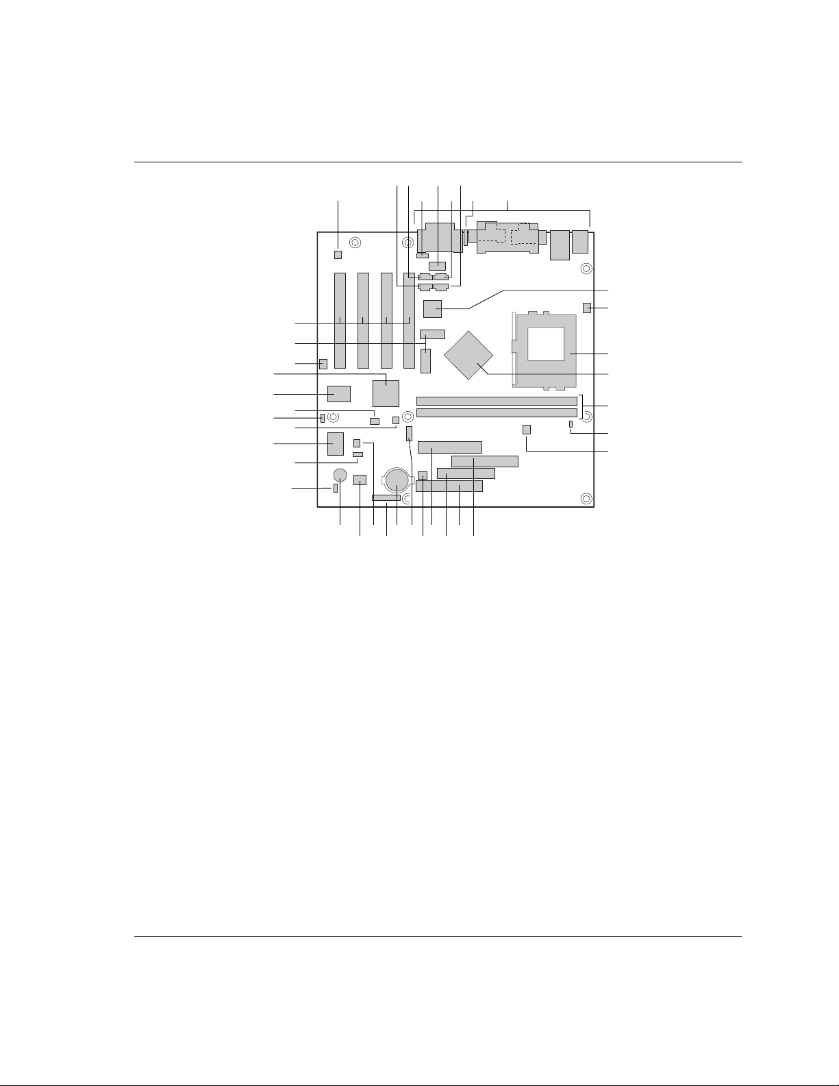
Figure 1 shows the major components on the motherboard.
HH
FF
DD
D
T R
U
GEB
F I
H
QSZ
J
K
L
M
N
O
P
OM07766
C
A
LL
KK
JJ
II
GG
EE
CC
BB
AA
V
W
Y
X
A Crystal Semiconductor CS4297 audio codec T Power supply connector
B ATAPI-style CD-ROM connector U Fan 1 (chassis) connector
C Video source line in connector (optional) V USB front panel connector (optional)
D Legacy CD-ROM connector (optional) W Battery
E Serial port B header X Front panel connector
F Auxiliary line in connector (optional) Y SCSI HD Activity LED connector (optional)
G Telephony connector (optional) Z Intel 82802AB Firmware Hub (FWH)
H Enhanced diagnostics LEDs (optional) AA Speaker
I Back panel connectors BB Alternative 1x3 front panel power LED connector
†
J Intel 82559 LAN controller (optional) CC Wake on LAN
technology connector (optional)
K Fan 3 (processor) connector DD SMSC LPC47B272 super I/O controller
L 370-pin PPGA processor socket EE Chassis intrusion connector (optional)
M Intel 82810 Graphics/Memory Controller Hub
FF Configuration jumper block
(GMCH)
N DIMM sockets GG USB front panel jumper block (optional)
O Hardware monitor (optional) HH
Creative Sound Blaster AudioPCI 64V audio
controller
P Fan 2 connector (optional) II Intel 82801AA I/O Controller Hub (ICH)
Q Secondary IDE connector JJ Sony/Phillips Digital Interface Format connector
(optional)
R Primary IDE connector KK Video memory (optional)
S Diskette drive connector LL PCI slots
Figure 1. Motherboard Components
8
Page 9

Motherboard Features
NOTE
✏
Components labeled optional do not come on all CA810 motherboards.
Microprocessor
The motherboard supports the 370-pin PPGA socketed Celeron processors listed in Table 1. All
supported onboard memory can be cached.
Table 1. Processors Supported by the Motherboard
Processor Speed Host Bus Frequency Cache Size
466 MHz
433 MHz
400 MHz
366 MHz
333 MHz
300A MHz
66 MHz
66 MHz
66 MHz
66 MHz
66 MHz
66 MHz
128 KB
128 KB
128 KB
128 KB
128 KB
128 KB
For the latest information on processor support for the CA810 motherboard, refer to the Intel
boxed motherboard web site at:
http://support.intel.com/support/motherboards/desktop/
For instructions on installing or upgrading the processor, see Chapter 2.
Main Memory
The motherboard has two sockets for installing DIMMs. Minimum memory size is 32 MB;
maximum memory size is 512 MB. Due to the video requirements of the CA810 motherboard,
†
minimum memory for the Windows NT
performance, it is recommended that 64 MB of memory be installed. See Chapter 2 for types of
memory supported and installation instructions.
All supported onboard memory is cacheable.
NOTE
✏
Some of the system memory is dedicated to video.
4.0 operating system is 64 MB. For optimal video
9
Page 10

CA810 Motherboard Product Guide
Graphics Subsystem
The graphics subsystem features the Intel 82810 Graphic/Memory Controller Hub (GMCH).
Visit Intel’s World Wide Web site for information about graphics drivers:
http://support.intel.com/support/motherboards/desktop/
Intel 82810 GMCH
The Intel 82810 GMCH supports the following features:
• Integrated graphics controller
3-D Hyper Pipelined architecture
Full 2-D hardware acceleration
Motion video acceleration
• 3-D graphics visual and texturing enhancements
• Display
Integrated 24-bit 230 MHz RAMDAC
DDC2B compliant
• Video
Hardware motion compensation for software MPEG2 decode
• Integrated graphics memory controller
10
Page 11

Motherboard Features
Table 2 lists the refresh rates supported by the CA810 motherboard.
Table 2. Intel 82810 GMCH Refresh Rates
Resolution Color 60 (Hz) 70 (Hz) 72 (Hz) 75 (Hz) 85 (Hz)
640x200 16 x
640x350 16 x
640x400 256 x x x x
64 K x x x x
16 M x
640x480 16 x x x x
256xxxxx
32 K x x x
64 Kxxxxx
16 Mxxxxx
800x600 256 x xxxx
32 K x x x
64 Kxxxxx
16 Mxxxxx
1024x768 256 x x x x
32 K x x x
64 Kxxxxx
16 Mxxxxx
1056x800 16 x
1280x1024 256 x xxxx
32 K x x
64 Kxxxxx
16 Mxxxxx
GMCH DC-100 (Optional)
In addition to all the features of the GMCH, the optional GMCH DC-100 supports 4 MB of
display cache on the motherboard.
11
Page 12

CA810 Motherboard Product Guide
Audio Subsystem
The audio subsystem consists of these devices:
• Creative Sound Blaster AudioPCI 64V digital controller
• Crystal Semiconductor CS4297 AC ’97 stereo audio codec
• Back panel and onboard audio connectors
Creative Sound Blaster AudioPCI 64V Audio Controller
The Creative Sound Blaster AudioPCI 64V audio controller features:
• Interfaces to the PCI bus as a Plug and Play device
• 100% DOS legacy compatible
• Access to main memory (through the PCI bus) for wavetable synthesis support – does not
require a separate wavetable ROM device
• PC 98 and PC 99 compliant
• Optional Sony/Phillips digital interface format (S/P-DIF)
Crystal Semiconductor CS4297 Stereo Audio Codec
The Crystal Semiconductor CS4297 stereo audio codec features:
• High performance 18-bit stereo full-duplex audio codec with up to 48 kHz sampling rate
• Connects to the Sound Blaster AudioPCI 64V using a five-wire digital interface
Audio Connectors
The audio connectors include the following:
• CD-ROM (legacy-style 2 mm connectors)
• ATAPI-style connectors
CD-ROM audio
Auxiliary line in
Telephony (optional)
Video line in (optional)
• Back panel connectors
Line out
Line in
Mic in
MIDI/Game Port
NOTE
✏
The line out connector, located on the back panel, is designed to power either headphones or
amplified speakers only. Poor audio quality may occur if passive (non-amplified) speakers are
connected to this output.
12
Page 13

Motherboard Features
Audio Drivers and Utilities
Audio drivers and utilities are available from Intel’s World Wide Web site:
http://support.intel.com/support/motherboards/desktop
Speaker
A 47 Ω inductive speaker is mounted on the motherboard. The speaker provides audible error
code (beep code) information during the power-on self test (POST).
LAN Subsystem (Optional)
The Intel 82559 Fast Ethernet Wired for Management (WfM) PCI LAN subsystem provides both
10Base-T and 100Base-TX connectivity. Features include:
• 32-bit, 33 MHz direct bus mastering on the PCI bus
• Shared memory structure in the host memory that copies data directly to/from host memory
• 10Base-T and 100Base-TX capability using a single RJ-45 connector with connection and
activity status LEDs
• IEEE 802.3µ Auto-Negotiation for the fastest available connection
• Jumperless configuration; the LAN subsystem is completely software-configurable
Intel 82559 LAN Controller
The Intel 82559 PCI LAN controller’s features include:
• CSMA/CD Protocol Engine
• PCI bus interface
• DMA engine for movement of commands, status, and network data across the PCI bus
• Integrated physical layer interface, including:
• Jumperless configuration; the LAN subsystem is completely software-configurable
Complete functionality necessary for the 10Base-T and 100Base-TX network interfaces;
when in 10 Mbit/sec mode, the interface drives the cable directly
A complete set of Media Independent Interface (MII) management registers for control
and status reporting
802.3µ Auto-Negotiation for automatically establishing the best operating mode when
connected to other 10Base-T or 100Base-TX devices, whether half- or full-duplex capable
• Integrated power management features, including:
Support for APM
Support for Wake on LAN technology
Support for ACPI D3 state
13
Page 14

CA810 Motherboard Product Guide
LAN Subsystem Software
The Intel 82559 Fast Ethernet WfM PCI LAN software and drivers are available from Intel’s
World Wide Web site.
RJ-45 LAN Connector LEDs
Two LEDs are built into the RJ-45 LAN connector. Table 3 describes the LED states when the
board is powered up and the LAN subsystem is operating.
Table 3. RJ-45 LAN Connector LEDs
LED Color LED State Indicates
Green Off 10 Mbit/sec speed is selected.
On 100 Mbit/sec speed is selected.
Yellow Off LAN link is not established.
On (steady state) LAN link is established.
On (brighter and pulsing) The computer is communicating with another computer on
the LAN.
PCI Enhanced IDE Interface
The PCI enhanced IDE interface handles the exchange of information between the processor and
†
peripheral devices like hard disks, CD-ROM drives, and Iomega Zip
The interface supports:
• Up to four IDE devices (such as hard drives)
• ATAPI devices (such as CD-ROM drives)
• PIO Mode 3 and PIO Mode 4 devices
• Ultra ATA/33 and Ultra ATA/66
• Logical block addressing (LBA) of hard drives larger than 528 MB and extended cylinder head
sector (ECHS) translation modes
• Support for laser servo (LS-120) drives
drives inside the computer.
14
Page 15

Motherboard Features
Input/Output (I/O) Controller
The SMSC LPC47B272 super I/O controller handles the exchange of information between the
processor and external devices, such as a mouse, keyboard, or printer that are connected to the
computer. The controller features the following:
• Low pin count (LPC) interface
• Two serial ports
• Infrared port (IrDA 1.1 compliant)
• One parallel port with Extended Capabilities Port (ECP) and Enhanced Parallel Port (EPP)
support
• PS/2–style mouse and keyboard interfaces
• Interface for one 1.2 MB, 1.44 MB, or 2.88 MB diskette drive
• Intelligent power management, including a programmable wake up event interface
• Dual game port interface
• MPU-401 MIDI support
• Fan control:
Two pulse width modulation (PWM) fan speed control outputs
Two fan tachometer inputs
The BIOS Setup program provides configuration options for the I/O controller.
Real-Time Clock
The motherboard has a time-of-day clock and 100-year calendar that will rollover to 2000 at the
turn of the century. A battery on the motherboard keeps the clock current when the computer is
turned off.
NOTE
✏
The recommended method of accessing the date in systems with Intel motherboards is indirectly
from the Real-Time Clock (RTC) via the BIOS. The BIOS on Intel motherboards and baseboards
contains a century checking and maintenance feature that checks the least two significant digits of
the year stored in the RTC during each BIOS request (INT 1Ah) to read the date and, if less than
80 (i.e., 1980 is the first year supported by the PC), updates the century byte to 20. This feature
enables operating systems and applications using the BIOS date/time services to reliably
manipulate the year as a four-digit value.
For more information on proper date access in systems with Intel motherboards please see:
http://support.intel.com/support/year2000/paper.htm
15
Page 16

CA810 Motherboard Product Guide
USB Support
The motherboard has two USB ports. One of the USB ports can be routed to a front panel
connector. You can connect two USB peripheral devices directly to the computer without an
external hub. To attach more than two devices, connect an external hub to either of the built-in
ports. The motherboard supports the standard universal host controller interface (UHCI) and takes
advantage of standard software drivers written to be compatible with UHCI.
NOTE
✏
Computer systems that have an unshielded cable attached to a USB port might not meet FCC
Class B requirements, even if no device or a low-speed USB device is attached to the cable. Use a
shielded cable that meets the requirements for a high-speed USB device.
BIOS
The BIOS provides the power-on self-test (POST), the BIOS Setup program, the PCI and IDE
auto-configuration utilities, and the video BIOS.
The BIOS can be upgraded by following the instructions in Section 3.
Intel® 82802AB Firmware Hub (FWH)
The BIOS is stored in the Intel 82802AB Firmware Hub. The firmware hub contains a nonvolatile
®
memory core based on Intel
firmware hub incorporates logic features such as a hardware random number generator (RNG).
These logic features enable protection for storing and updating platform information relating to
security and manageability.
flash technology. In addition to storing the system BIOS, the
PCI Auto Configuration
If you install a PCI add-in board in your computer, the PCI auto-configuration utility in the BIOS
automatically detects and configures the resources (IRQs, DMA channels, and I/O space) for that
add-in board. You do not need to run the BIOS Setup program after you install a PCI add-in
board.
IDE Auto Configuration
If you install an IDE device (such as, a hard drive) in your computer, the IDE auto-configuration
utility in the BIOS automatically detects and configures the device for your computer. You do not
need to run the BIOS Setup program after installing an IDE device.
16
Page 17

Motherboard Features
Security Passwords
The BIOS includes security features that restrict whether the BIOS Setup program can be accessed
and who can boot the computer. A supervisor password and a user password can be set for Setup
and for booting the computer, with the following restrictions:
• The supervisor password gives unrestricted access to view and change all Setup options. This
is supervisor mode.
• If only the supervisor password is set, pressing <Enter> at the password prompt of the Setup
program gives the user restricted access to Setup.
• If both the supervisor and user passwords are set, you must enter either the supervisor
password or the user password to access Setup.
• Setting a user password restricts who can boot the computer. The password prompt is
displayed before the computer is booted. If only the supervisor password is set, the computer
boots without asking for a password. If both passwords are set, you can enter either password
to boot the computer.
Expansion Slots
The motherboard has four PCI expansion slots.
Power Management Features
Power management is implemented at several levels, including:
• Software support:
Advanced Power Management (APM)
Advanced Configuration and Power Interface (ACPI)
• Hardware support:
Wake on LAN technology
Instantly Available technology
Resume on Ring
If the board is used with an ACPI-aware operating system, the BIOS can provide ACPI support.
Otherwise, it defaults to APM support.
17
Page 18

CA810 Motherboard Product Guide
Wake on LAN Technology
The optional Wake on LAN technology connector can be used with PCI bus network adapters that
have a remote wake up connector, as shown in Figure 2. Network adapters that are PCI 2.2
compliant assert the wakeup signal through the PCI bus signal PME# (pin A19 on the PCI bus
connectors). The optional onboard LAN subsystem also supports remote wakeup using the PME#
signal.
Network
Interface
Card
Figure 2. Using the Wake on LAN Technology Connector
PCI Slot
Remote
Wake up
connector
Wake on
LAN
technology
connector
Motherboard
CAUTION
For Wake on LAN technology, the 5-V standby line for the power supply must be capable of
±
delivering +5 V
Wake on LAN technology can damage the power supply.
5% at 720 mA. Failure to provide adequate standby current when implementing
18
Page 19

Motherboard Features
Instantly Available Technology
Instantly Available technology enables the board to enter the ACPI S3 (Suspend-to-RAM) sleep
state. While in the S3 sleep state, the computer will appear to be off. When signaled by a wake up
device or event, the system quickly returns to its last known wake state.
The optional standby power indicator (located between the DIMM sockets and power connector)
provides an indication that power is still present to the DIMMs and PCI bus connectors, even when
the computer appears to be off. Figure 3 shows the location of the standby power LED.
DS8E1
OM07804
Standby Power Indicator
Figure 3. Location of Standby Power Indicator LED
CAUTION
For Instantly Available technology, the 5-V standby line for the power supply must be capable of
±
delivering +5 V
feature can damage the power supply.
5 % at 720 mA. Failure to provide adequate standby current when using this
19
Page 20

CA810 Motherboard Product Guide
Resume on Ring
The operation of Resume on Ring can be summarized as follows:
• Resumes operation from either the APM sleep mode or the ACPI S1 state
• Requires only one call to access the computer
• Detects incoming call similarly for external and internal modems; does not use the Wake on
Ring connector
• Requires modem interrupt be unmasked for correct operation
Battery
A battery on the motherboard keeps the clock and the values in CMOS RAM current when your
computer is turned off. See Chapter 2 for instructions on how to replace the battery.
20
Page 21

2 Installing and Replacing Motherboard
Components
This chapter tells you how to:
• Install and remove the motherboard
• Install and remove the processor
• Install and remove memory
• Replace the battery
• Connect IDE drives
• Clear passwords
• Set jumpers
Before You Begin
CAUTION
Before you install this motherboard in a chassis, see Appendix B for regulatory requirements and
precautions.
• Always follow the steps in each procedure in the correct order.
• Set up a log to record information about your computer, such as model, serial numbers,
installed options, and configuration information.
• Use an antistatic wrist strap and a conductive foam pad when working on the motherboard.
WARNINGS
The procedures in this chapter assume familiarity with the general terminology associated with
personal computers and with the safety practices and regulatory compliance required for using
and modifying electronic equipment.
Disconnect the computer from its power source and from any telecommunications links,
networks, or modems before performing any of the procedures described in this chapter.
Failure to disconnect power, telecommunications links, networks, or modems before you open
the computer or perform any procedures can result in personal injury or equipment damage.
Some circuitry on the motherboard can continue to operate even though the front panel power
button is off.
CAUTION
Electrostatic discharge (ESD) can damage components. Perform the procedures described in this
chapter only at an ESD workstation. If such a station is not available, you can provide some ESD
protection by wearing an antistatic wrist strap and attaching it to a metal part of the computer
chassis.
21
Page 22
CA810 Motherboard Product Guide
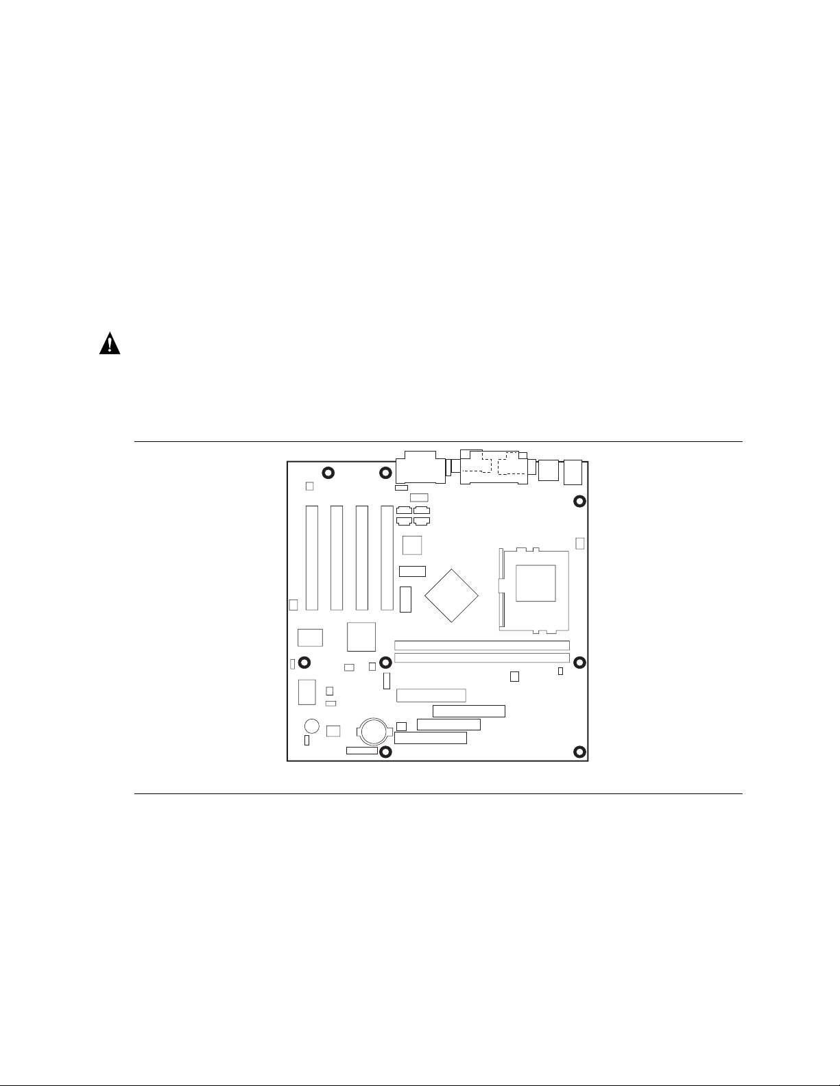
How to Install and Remove the Motherboard
Refer to your chassis manual for instructions on installing and removing the motherboard. On a
microATX chassis, the motherboard is secured to the chassis by eight screws. Figure 4 shows the
locations of the mounting screw holes. On a standard ATX chassis, the motherboard is secured to
the chassis by seven screws and the provided standoff (see Figure 5).
NOTES
✏
You will need a Phillips (#2 bit) screwdriver.
Refer to Appendix B for regulatory requirements and installation instructions and precautions.
WARNING
This procedure should be done only by qualified technical personnel. Disconnect the computer
from its power source before doing the procedures described here. Failure to disconnect the
power before you open the computer can result in personal injury or equipment damage.
22
OM07790
Figure 4. Mounting Screw Holes
Page 23

Installing and Replacing Motherboard Components
How to Install a Motherboard Support Standoff
The CA810 motherboard fits in a microATX chassis, but it can also be installed in a standard ATX
chassis. When it is installed in a standard ATX chassis, one of the motherboard support positions
might not have a corresponding standoff in the chassis. The following steps describe how to install
an additional standoff in a standard ATX chassis and how to secure the motherboard to this added
standoff. The Figure 5 shows the standoff (B), its associated adhesive pad (C), and a standoff
retention pin (A).
A
B
C
Figure 5. Motherboard Support Standoff in a Standard ATX Chassis
OM08553
Do the following steps to install the added standoff for the motherboard:
1. Trial fit the added standoff (B) in the motherboard (in the position indicated in Figure 5), then
position the motherboard in the ATX chassis on the existing standoffs, noting the required
mounting location for the new standoff in the chassis.
2. Remove the motherboard, clean the mounting location, then remove the protective paper
covering the adhesive (C) at the base of the added standoff (B).
3. Remount the motherboard in the chassis and press down on the added standoff (B) until the
adhesive secures it to the chassis.
4. When final fitting the motherboard into the chassis, position the motherboard at the same
height on the added standoff (B) as the other standoffs. Press the standoff retention pin (A)
into the added standoff to lock the motherboard at that height.
23
Page 24

CA810 Motherboard Product Guide
How to Install the Processor
To install a processor, follow these instructions:
1. Observe the precautions in “Before You Begin” (see page 21).
2. Locate the processor socket and raise the socket handle completely (see Figure 6).
PGA370
OM07801
Figure 6. Raising the Socket Handle
3. Aligning the pins of the processor with the socket, insert the processor into the socket
(see Figure 7).
PGA370
24
OM07802
Figure 7. Inserting the Processor into the Socket
Page 25

Installing and Replacing Motherboard Components
4. Close the handle completely (see Figure 8).
PGA370
Figure 8. Closing the Handle
5. Place the fan heatsink on top of the processor (see Figure 9).
OM07803
PGA370
OM07800
Figure 9. Attaching the Heatsink to the Processor
25
Page 26

CA810 Motherboard Product Guide
6. Attach the fan heatsink clips to the processor socket (see Figure 10).
PGA370
A Fan Heatsink Clip
B Processor Socket
Figure 10. Attaching the Fan Heatsink Clip
A
B
OM07798
7. Connect the processor fan cable to the processor fan connector (see Figure 11).
J3J1
J3J1
PGA370
26
OM07799
Figure 11. Connecting the Processor Fan Cable to the Processor Fan Connector
Page 27

Installing and Replacing Motherboard Components
How to Remove the Processor
To remove the processor, follow these instructions:
1. Observe the precautions in “Before You Begin” (see page 21).
2. Disconnect the processor fan cable.
3. Detach the fan heatsink clips.
4. Raise the socket handle completely.
5. Remove the processor.
How to Install Memory
You can install from 32 MB to 512 MB of memory in the DIMM sockets. The board has two
DIMM sockets arranged as banks 0 and 1. As shown in Figure 11 on page 26, the DIMM socket
closest to the processor is for bank 0. The motherboard supports the following memory features:
NOTE
✏
On the CA810 motherboard, the minimum memory required is 64 MB for the Windows NT 4.0
operating system.
For optimal video performance, it is recommended that 64 MB of memory be installed.
• 168-pin 3.3 V DIMMs with gold-plated contacts
• 100 MHz 4-clock unbuffered SDRAM DIMMs
• Non-ECC (64-bit) memory
• A minimum of 32 MB (required); a maximum of 512 MB. For optimal video performance,
use at least 64 MB of system memory.
• Module sizes: 16 MB, 32 MB, 64 MB, 128 MB, 256 MB, and 512 MB
• DIMMs with Serial Presence Detect (SPD) or non-SPD data structure
CAUTION
Because the main system memory is also used as video memory, the CA810 motherboards require
100MHz SDRAM DIMMs even though the processor front side bus is 66 MHz. It is highly
recommended that SPD DIMMs be used, since this allows the chipset to accurately configure
memory settings for optimum performance. If non-SPD memory is installed, the BIOS will attempt
to correctly configure the memory settings, but performance and reliability may be impacted.
27
Page 28

CA810 Motherboard Product Guide
The motherboard supports single- or double-sided DIMMs in the following sizes:
DIMM Size Non-ECC Configuration
16 MB 2 Mbit x 64
32 MB 4 Mbit x 64
64 MB 8 Mbit x 64
128 MB 16 Mbit x 64
256 MB 32 Mbit x 64
When adding memory, be aware that:
• You can install DIMMs in either of the two banks. That is, if only one DIMM is being
installed, it can be placed in either DIMM socket.
• You can use different sizes of DIMMs in different banks.
• The BIOS detects the size and type of installed memory.
28
Page 29

Figure 12 shows the location of the DIMM sockets.
Installing and Replacing Motherboard Components
0
1
OM07791
Figure 12. Installing a DIMM
To install DIMMs, follow these steps:
1. Observe the precautions in “Before You Begin” (see page 21).
2. Turn off all peripheral devices connected to the computer. Turn off the computer. Unplug the
computer.
3. Remove the computer cover and locate the empty DIMM sockets.
4. Holding the DIMM by the edges, remove it from its antistatic package.
5. Make sure the clips at either end of the socket are pushed away from the socket.
6. Position the DIMM above the socket. Align the two small notches in the bottom edge of the
DIMM with the keys in the socket.
7. Insert the bottom edge of the DIMM into the socket (as shown in Figure 12).
8. When the DIMM is seated, push down on the top edge of the DIMM until the retaining clips
snap into place. Make sure the clips are firmly in place.
9. Replace the computer cover.
29
Page 30

CA810 Motherboard Product Guide
How to Remove Memory
To remove a DIMM, follow these steps:
1. Observe the precautions in "Before You Begin" (see page 21).
2. Turn off all peripheral devices connected to the computer. Turn off the computer. Unplug the
computer.
3. Remove the computer cover.
4. Gently spread the retaining clips at each end of the socket. The DIMM pops out of the socket.
5. Hold the DIMM by the edges, lift it away from the socket, and store it in an antistatic package.
6. Reinstall and reconnect any parts you removed or disconnected to reach the DIMM sockets.
How to Replace the Battery
When your computer is turned off, a lithium battery maintains the current time-of-day clock and
the values in CMOS RAM current. Figure 13 on page 31 shows the location of the battery.
The battery should last about seven years. When the battery begins to die, it loses voltage; when
the voltage drops below a certain level, the BIOS Setup program settings stored in CMOS RAM
(for example, the date and time) might not be accurate. Replace the battery with an equivalent
one.
WARNING
Danger of explosion if the battery is incorrectly replaced. Replace only with the same or
equivalent type recommended by the equipment manufacturer. Discard used batteries according
to manufacturer’s instructions.
ATTENTION
Il y a danger d’explosion s’il y a remplacement incorrect de la batterie. Remplacer uniquement
avec une batterie du méme type ou d’un type recommandé par le constructeur. Mettre au rébut
les batteries usagées conformément aux instructions du fabricant.
ADVARSEL!
Lithiumbatteri - Eksplosionsfare ved fejlagtig håndtering. Udskiftning må kun ske med batteri
af samme fabrikat og type. Levér det brugte batteri tilbage til leverandøren.
ADVARSEL
Lithiumbatteri - Eksplosjonsfare. Ved utskifting benyttes kun batteri som anbefalt av
apparatfabrikanten. Brukt batteri returneres apparatleverandøren.
VARNING
Explosionsfara vid felaktigt batteribyte. Använd samma batterityp eller en ekvivalent typ som
rekommenderas av apparattillverkaren. Kassera använt batteri enligt fabrikantens instruktion.
30
Page 31

Installing and Replacing Motherboard Components
VAROITUS
Paristo voi räjähtää, jos se on virheellisesti asennettu. Vaihda paristo ainoastaan
laitevalmistajan suosittelemaan tyyppiin. Hävitä käjtetty paristo valmistajan ohjeiden
mukaisesti.
To replace the battery, follow these steps:
1. Observe the precautions in “Before You Begin” (see page 21).
2. Turn off all peripheral devices connected to the computer. Turn off the computer.
3. Remove the computer cover.
4. Locate the battery on the motherboard (see Figure 13).
5. With a medium flat-bladed screwdriver, gently pry the battery free from its socket. Note the
orientation of the “+” and “-” on the battery.
6. Install the new battery in the socket, orienting the “+” and “-” correctly.
7. Replace the computer cover.
Figure 13. Removing the Battery
NOTE
✏
If your local ordinances permit, you may dispose of individual batteries as normal trash. Do not
expose batteries to excessive heat or fire. Keep all batteries away from children.
OM07792
31
Page 32

CA810 Motherboard Product Guide
How to Connect IDE Drives
The Intel boxed motherboard package includes an IDE cable. It is capable of connecting two
drives to the motherboard.
The cable supports the Ultra ATA/66 interface and is backward compatible with drives using
slower IDE transfer protocols. If an Ultra ATA/66 drive and a drive using any other IDE
transfer protocol are attached to the same cable, the maximum transfer rate for either drive is
33 MB/second.
When building a system with both Ultra ATA/66 drives and slower drives, attach the
Ultra ATA/66 drives to one channel with the Ultra ATA/66 cable. Attach the slower drives
to the other channel with another cable.
How to Clear the Passwords
This procedure assumes that the motherboard is installed in the computer and the configuration
jumper block is set to normal mode.
1. Observe the precautions in “Before You Begin” (see page 21).
2. Turn off all peripheral devices connected to the computer. Turn off the computer. Unplug the
computer.
3. Remove the computer cover.
4. Find the configuration jumper block (see Figure 14).
5. Place the jumper on pins 2-3 as shown below.
3
1
6. Replace the cover, plug in the computer, turn on the computer, and allow it to boot.
7. The computer starts the Setup program. Setup displays the Maintenance menu.
8. Use the arrow keys to select Clear Passwords. Press <Enter> and Setup displays a pop-up
screen requesting that you confirm clearing the password. Select Yes and press <Enter>.
Setup displays the Maintenance Menu again.
9. Press <F10> to save the current values and exit Setup.
10. Turn off the computer. Unplug the computer.
11. Remove the computer cover.
12. To restore normal operation, place the jumper on pins 1-2 as shown below.
3
1
13. Replace the cover, plug in the computer, and turn on the computer.
32
Page 33

Installing and Replacing Motherboard Components
How to Set Jumpers
CAUTION
Always turn off the power and unplug the power cord from the computer before changing the
jumper. Moving the jumper with the power on may result in unreliable computer operation.
3
J7A1
1
A
B
31
J7B2
OM07760
A BIOS Setup configuration jumper block
B USB port configuration jumper block (optional)
Figure 14. Location of the Jumper Blocks
33
Page 34

CA810 Motherboard Product Guide
BIOS Setup Configuration Jumper Block
This three-pin jumper block, shown in Figure 14, enables all motherboard configuration to be done
in BIOS Setup. Table 4 shows the jumper settings for the Setup program modes.
Table 4. Jumper Settings for BIOS Setup Program Modes
Function / Mode Jumper Setting Configuration
Normal
1-2
3
1
The BIOS uses current configuration information and passwords
for booting.
Configure
Recovery
2-3
none
3
1
3
1
After the Power-On Self-Test (POST) runs, the BIOS displays the
Maintenance Menu. Use this menu to clear passwords and to
change optional memory settings.
The BIOS attempts to recover the BIOS configuration. A
recovery diskette is required.
USB Port 0 Configuration Jumper Block (Optional)
This 6-pin jumper block, shown in Figure 14, enables configuration of USB Port 0. Table 5
describes the jumper settings for configuring USB Port 0.
Table 5. USB Port 0 Configuration Jumper Settings
Jumper Setting Configuration
USB Port 0 signals are routed to the back panel
USB Port 0 signals are routed for a front panel USB connector
2-3 and 5-6
1-2 and 4-5
3
1
46
3
1
46
34
Page 35

3 Using the Setup Program
You can use the BIOS Setup program to change the configuration information and boot sequence
for the computer. This chapter tells you how to:
• Access the BIOS Setup program
• Upgrade the BIOS
• Recover the BIOS
• Change the BIOS language
• Clear passwords
For more information about the BIOS Setup program’s menus, options, and defaults settings, see
the CA810 Motherboard Technical Product Specification available on the World Wide Web site:
http://support.intel.com/support/motherboards/desktop
NOTE
✏
For reference purposes, you should write down the current Setup settings. When you make
changes to the settings, update this record.
BIOS Setup Program Modes
The BIOS Setup program has three modes of operation:
• Normal mode for normal operations
• Configure mode for clearing passwords (See Chapter 2 for instructions)
• Recovery mode for recovering the BIOS data
The BIOS Setup program operating mode is controlled by the setting of the configuration jumper
block. The jumper is set to normal mode at the factory.
35
Page 36

CA810 Motherboard Product Guide
✏
NOTE
The Setup menus described in this section apply to CA810 motherboards with BIOS identifier
8C1A100A.86A. Motherboards with other BIOS identifiers might have differences in some of the
Setup menu screens.
Table 6 is an overview of the menu screens in the BIOS Setup program.
Table 6. Setup Menu Screens
Setup Menu Screen Description
Maintenance Clears the Setup passwords. This menu is only available in configure mode.
Main Displays system information.
Advanced Specifies advanced features available through the chipset.
Security Specifies passwords and security features.
Power Specifies power management features.
Boot Specifies boot options and power state controls.
Exit Saves or discards changes to the BIOS Setup program options.
Function Keys
Table 7 shows the function keys available for menu screens.
Table 7. Setup Function Keys
Setup Key Description
<Esc> Exits the menu.
<←> or <→> Selects a different menu screen.
<↑> or <↓> Moves cursor up or down.
<F9> Load the default configuration values for the current menu.
<F10> Save the current values and exit Setup.
<Enter> Executes command or selects the submenu.
Accessing the Setup Program
To enter the Setup program, turn the computer on and immediately press <F2> until you see the
message:
Entering SETUP
36
Page 37

Using the Setup Program
Upgrading the BIOS
Before you upgrade the BIOS, prepare by:
• Obtaining the BIOS upgrade file
• Recording the current BIOS settings
• Creating a bootable diskette
• Creating the BIOS upgrade diskette
Obtaining the BIOS Upgrade File
You can upgrade to a new version of the BIOS by using the BIOS upgrade file. The BIOS upgrade
file is a compressed self-extracting archive that contains all the files you need to upgrade the
BIOS. The BIOS upgrade file contains:
• New BIOS files
• BIOS recovery files
®
• Intel
You can obtain the BIOS upgrade file through your computer supplier or from the Intel World
Wide Web site:
Flash Memory Update Utility
http://support.intel.com/support/motherboards/desktop/
NOTE
✏
Please review the instructions distributed with the update utility before attempting a BIOS
upgrade.
The Intel Flash Memory Update Utility allows you to:
• Upgrade the BIOS in flash memory.
• Update the language section of the BIOS.
Recording the Current BIOS Settings
1. Boot the computer and press <F2> when you see the message:
Press <F2> Key if you want to run SETUP
NOTE
Do not skip step 2. You will need these settings to configure your computer at the end of the
upgrade procedure.
2. Write down the current settings in the BIOS Setup program.
37
Page 38

CA810 Motherboard Product Guide
Creating a Bootable Diskette
NOTE
✏
If your drive A is an LS-120 diskette drive, you must use a 1.44-MB diskette as the bootable BIOS
upgrade diskette. The computer is unable to recover a BIOS from an LS-120 diskette.
To create a bootable diskette using a DOS system:
• Place an unformatted diskette in the diskette drive and format the diskette using the /s option.
Example:
• Alternatively, place a formatted diskette in the diskette drive and use the sys command.
Example:
To create a bootable diskette using a non-DOS system:
1. Obtain the BIOS upgrade file through your computer supplier or from the Intel World Wide
Web site:
2. Copy the BIOS upgrade file to a temporary directory on your hard disk.
3. Change to the temporary directory.
4. To extract the files, double click on the BIOS upgrade file, for example, CABIOSxx.EXE.
5. One of the extracted files is MK_BOOTZ.EXE. Double click on this file to extract the
README.TXT file.
6. Follow the directions in the README.TXT file.
format a: /s
sys a:
http://support.intel.com/support/motherboards/desktop/
Creating the BIOS Upgrade Diskette
1. Obtain the BIOS upgrade file through your computer supplier or from the Intel World Wide
Web site:
http://support.intel.com/support/motherboards/desktop/
2. Copy the BIOS upgrade file to a temporary directory on your hard disk.
3. From the C:\ prompt, change to the temporary directory.
4. To extract the file, type the name of the BIOS upgrade file, for example, CABIOSxx.EXE
5. Press
6. Read the LICENSE.TXT file, which contains the software license agreement, and the
7. Insert the bootable diskette into drive A.
8. To extract the BIOS.EXE file to the diskette, change to the temporary directory that holds the
9. Press <Enter>.
10. The diskette now holds the new BIOS files, the Intel Flash Update Utility, and the recovery
<Enter>. The extracted file contains the following files:
LICENSE.TXT
BIOINSTR.TXT
BIOS.EXE
MK_BOOTZ.EXE
BIOINSTR.TXT file, which contains the instructions for the BIOS upgrade.
BIOS.EXE file and type:
BIOS A:
files.
38
Page 39

Technical Reference
Upgrading the BIOS
CAUTION
Not updating the system boot block when updating the BIOS may result in an untested system
configuration. Some BIOS upgrade releases may require updating the system boot block. To find
out if you need to update the boot block, go to the Intel website at:
http://www.developer.intel.com/design/motherbd
1. Boot the computer with the BIOS upgrade diskette in drive A. Press
<Enter> to go to the
Main menu. The flash memory update utility screen appears.
2. Select
Update flash memory area from a file. Press <Enter>.
3. Select Update System BIOS. Press <Enter>.
4. Use the arrow keys to select the correct
.bio file. Press <Enter>.
5. When the utility asks for confirmation that you want to flash the new BIOS into memory,
select
Continue with programming. Press <Enter>.
6. When the utility displays the message
<Enter>.
Reboot Warning, remove the diskette. Press
7. As the computer boots, check the BIOS identifier (version number) to make sure the upgrade
was successful. If a logo appears, press
8. To enter the BIOS Setup program, press
Press <F2> to Run SETUP
<Esc> to view the POST messages.
<F2> when you see the message:
9. For proper operation, load the BIOS Setup program defaults. To load the defaults, press <F9>.
10. To accept the defaults, press
<Enter>.
11. In Setup, enter the settings you wrote down before beginning the BIOS upgrade.
12. To save the settings, press
13. To accept the settings, press
<F10>.
<Enter>.
14. Turn off the computer and reboot.
Recovering the BIOS
It is unlikely that anything will interrupt the BIOS upgrade; however, if an interruption occurs, the
BIOS could be damaged. The following steps explain how to recover the BIOS if an upgrade fails.
The following procedure uses recovery mode for the Setup program. See Chapter 3 for more
information on Setup modes.
NOTE
Because of the small amount of code available in the boot block area, there is no video support.
You will not see anything on the screen during this procedure. Monitor the procedure by listening
to the speaker and looking at the diskette drive LED.
1. Turn off the computer, disconnect the computer’s power cord, and disconnect all external
peripherals.
2. Remove the computer cover and locate the configuration jumper block (J7A1) (see Figure 1).
39
Page 40

CA810 Motherboard Product Guide
3. Remove the jumper from all pins as shown below to set recovery mode for Setup.
3
1
4. Insert the bootable BIOS upgrade diskette into diskette drive A.
5. Replace the computer cover, connect the power cord, turn on the computer, and allow it to
boot. The recovery process will take a few minutes.
6. Listen to the speaker.
• Two beeps and the end of activity in drive A indicate successful BIOS recovery.
• A series of continuous beeps indicates failed BIOS recovery.
7. If recovery fails, return to step 1 and repeat the recovery process.
8. If recovery is successful, turn off the computer, and disconnect its power cord.
9. Remove the computer cover and continue with the following steps.
10. On the jumper block (J7A1), reinstall the jumper back on pins 1-2 as shown below to set
normal mode for Setup.
3
1
11. Leave the upgrade diskette in drive A, replace the computer cover, and connect the computer’s
power cord.
12. Turn on the computer and continue with the BIOS upgrade (see page 39).
Changing the BIOS Language
You can use the BIOS upgrade utility to change the language the BIOS uses for messages and the
Setup program. Use a bootable diskette containing the Intel Flash Memory Update Utility and
language files (see “Upgrading the BIOS” on page 39).
1. Boot the computer with the bootable diskette in drive A. The BIOS upgrade utility screen
appears.
2. Select
3. Select
4. Select drive A and use the arrow keys to select the correct
5. When the utility asks for confirmation that you want to flash the new language into memory,
6. When the utility displays the message upgrade is complete, remove the diskette. Press
7. The computer will reboot and the changes will take effect.
Update Flash Memory From a File.
Update Language Set. Press <Enter>.
select
Continue with Programming. Press <Enter>.
<Enter>.
.lng file. Press <Enter>.
40
Page 41

4 Technical Reference
Motherboard Connectors
The motherboard’s connectors can be divided into three groups, as shown in Figure 15.
A
B
C
OM07764
Figure 15. Connector Groups
Back panel connectors
A
(see page 42)
Midboard connectors
B
(see page 43)
Front panel connectors
C
(see page 44)
CAUTION
Many of the midboard and front panel connectors provide operating voltage (+5 V DC and
+12 V DC, for example) to devices inside the computer chassis, such as fans and internal
peripherals. These connectors are not overcurrent protected. Do not use these connectors for
powering devices external to the computer chassis. A fault in the load presented by the external
devices could cause damage to the computer, the interconnecting cable, and the external devices
themselves.
41
Page 42

CA810 Motherboard Product Guide
Back Panel Connectors
Figure 16 shows the back panel connectors on the motherboard.
C
A
B
E
D
A PS/2 keyboard or mouse
B PS/2 keyboard or mouse
C RJ-45 LAN connector with indicator
LEDs (optional):
- Speed
Top: Green
Off: 10 Mbps
On: 100 Mbps
- Link
Bottom: Yellow
On: Link
Blink: Packets transferred
G
F
H
D USB port 0
E USB port 1
F VGA port
G Parallel port
H Serial port A
I Enhanced Diagnostics LED (optional)
J MIDI/Game port
K Audio line out
L Audio line in
M Mic in
J
KIML
OM07762
Figure 16. Back Panel Connectors and Indicators
NOTE
✏
The line out connector, located on the back panel, is designed to power either headphones or
amplified speakers only. Poor audio quality may occur if passive (non-amplified) speakers are
connected to this output.
42
Page 43

Midboard Connectors
Figure 17 shows the location of the midboard connectors.
14
Technical Reference
E FA B C
D
8
2
9
1
1
4
1
4
1
1
R
Q
P
O
1
1
N
1
12
8
9
20
10
2
1
1
240
1
M L
11
1
240
1
34
33
39
K I
1
39
J
H
1
G
OM07805
A ATAPI-style CD-ROM J Diskette drive
B Video source line in (optional) K Primary IDE
C Legacy CD-ROM (optional) L Fan 1 (chassis)
D Serial port B header M Power
E Auxiliary line in (optional) N Wake on LAN technology (optional)
F Telephony (optional) O SCSI HD Activity LED (optional)
G Fan 3 (processor) P USB front panel (optional)
H Fan 2 (optional) Q Chassis intrusion (optional)
I Secondary IDE R PCI slots
Figure 17. Midboard Connectors
43
Page 44

CA810 Motherboard Product Guide
Front Panel Connectors
Figure 18 shows the location of the front panel connectors.
CB
1
2
DE
15 1
J10B1
OM07767
216
J9A2
A
GRN
YLW
15
16
F
A Infrared port D Power LED
B Reset switch E On/Off switch
C Hard drive activity LED F Alternate 1x3 front panel power LED
Figure 18. Front Panel Connectors
44
Page 45

Motherboard Resources
Memory Map
Table 8. System Memory Map
Address Range (decimal) Address Range (hex) Size Description
1024 K - 524288 K 100000 – 1FFFFFFF 511 MB Extended Memory
960 K - 1024 K F0000 - FFFFF 64 KB Runtime BIOS
896 K - 960 K E0000 - EFFFF 64 KB Reserved
800 K - 896 K C8000 - DFFFF 96 KB Available high DOS memory (open
640 K - 800 K A0000 - C7FFF 160 KB Video memory and BIOS
639 K - 640 K 9FC00 - 9FFFF 1 KB Extended BIOS data (movable by
512 K - 639 K 80000 - 9FBFF 127 KB Extended conventional memory
0 K - 512 K 00000 - 7FFFF 512 KB Conventional memory
Technical Reference
to ISA and PCI bus)
memory manager software)
DMA Channels
Table 9. DMA Channels
DMA Channel Number Data Width System Resource
0 8- or 16-bits Audio
1 8- or 16-bits Audio / parallel port
2 8- or 16-bits Diskette drive
3 8- or 16-bits Parallel port (for ECP or EPP)/audio
4 DMA controller
5 16-bits Open
6 16-bits Open
7 16-bits Open
45
Page 46

CA810 Motherboard Product Guide
I/O Map
Table 10. I/O Map
Address (hex) Size Description
0000 - 000F 16 bytes DMA controller
0020 - 0021 2 bytes Programmable Interrupt Control (PIC)
0040 - 0043 4 bytes System timer
0060 1 byte Keyboard controller byte—reset IRQ
0061 1 byte System speaker
0064 1 byte Keyboard controller, CMD/STAT byte
0070 -0071 2 bytes System CMOS / Real Time Clock
0072 - 0073 2 bytes CMOS Bank 1
0080 - 0090 DMA controller
0094 – 009F DMA controller
00A0 - 00A1 2 bytes PIC
00B2 - 00B3 2 bytes APM control
00C0 - 00DE 31 bytes DMA
00F0 – 00FF Numeric data processor
0170 - 0177 8 bytes Secondary IDE channel
01F0 - 01F7 8 bytes Primary IDE channel
One of these ranges:
0200 – 0207
0208 – 020F
0210 – 0217
0218 – 021F
0220 - 022F 16 bytes Audio (Sound Blaster Pro†-compatible)
0240 - 024F 16 bytes Audio (Sound Blaster Pro-compatible)
0240 - 024F 16 bytes Audio (Sound Blaster-compatible)
0278 - 027F* 8 bytes LPT2
0228 - 022F* 8 bytes LPT3
02E8 - 02EF* 8 bytes COM4/video (8514A)
02F8 - 02FF* 8 bytes COM2
Can vary from 1 byte
to 8 bytes
Audio / game port
46
One of these ranges:
0320 - 0327
0330 - 0337
0340 - 0347
0350 - 0357
0376 1 byte Secondary IDE channel command port
8 bytes MPU-401 (MIDI)
continued
Page 47

Technical Reference
Table 10. I/O Map (continued)
Address (hex) Size Description
0377, bits 6:0 7 bits Secondary IDE channel status port
0378 - 037F 8 bytes LPT 1
0388- 038B 6 bytes AdLib† (FM synthesizer)
03B0 – 03BB 4 bytes Intel 82810 – DC100 Graphics Controller Hub (GCH)
03C0 – 03DF 2 bytes Graphics Controller Hub (GCH)
03CC 1 byte Video (VGA)
03CE – 03CF 2 bytes Video (VGA)
03D4 – 03D5 2 bytes Video (VGA)
03DA 1 byte Video (VGA)
03E8 – 03EF 8 bytes COM3
03F0 - 03F5 6 bytes Diskette channel 1
03F6 1 byte Primary IDE channel command port
03F8 - 03FF 8 bytes COM1
One of these ranges:
0530 – 0537
0E80 – 0E87
0F40 – 0F47
0800 – 087F Motherboard resources
9000 – 9FFF Intel 82810AA PCI bridge
LPTn + 400h 8 bytes ECP port, LPTn base address + 400h
0CF8 - 0CFB* 4 bytes PCI configuration address register
0CF9** 1 byte Turbo and reset control register
0CFC - 0CFF 4 bytes PCI configuration data register
EF00 – EF3F 64 bytes Windows Sound System
FFA0 - FFA7 8 bytes Primary bus master IDE registers
FFA8 - FFAF 8 bytes Secondary bus master IDE registers
32 contiguous bytes starting on a 32-byte
divisible boundary
64 contiguous bytes starting on a 64-byte
divisible boundary
* Dword access only
** Byte access only
8 bytes Windows Sound System
Intel 82559 LAN controller
Onboard audio controller
47
Page 48

CA810 Motherboard Product Guide
Interrupts
Table 11. Interrupts
IRQ System Resource
NMI I/O channel check
0 Reserved, interval timer
1 Reserved, keyboard buffer full
2 Reserved, cascade interrupt from slave PIC
3 COM2* (user available if COM2 is not present)
4COM1*
5 LPT2 (Plug and Play option)/audio/user available
6 Diskette drive controller
7LPT1*
8 Real time clock
9 User available
10 User available
11 User available
12 Onboard mouse port (if present, else user available)
13 Reserved, math coprocessor
14 Primary IDE (if present, else user available)
15 Secondary IDE (if present, else user available)
* Default, but can be changed to another IRQ.
48
Page 49

A Error Messages
BIOS Beep Codes
Whenever a recoverable error occurs during power-on self-test (POST), the BIOS displays an error
message describing the problem. The BIOS also issues a beep code (one long tone followed by
two short tones) during POST if the video configuration fails (a faulty video card or no card
installed) or if an external ROM module does not properly checksum to zero.
Table 12. Beep Codes
Number of Beeps Description
1 Refresh failure
2 Parity can not be reset
3 First 64 K memory failure
4 Timer not operational
5 Processor failure (Reserved; not used)
6 8042 GateA20 cannot be toggled (memory failure or not present)
7 Exception interrupt error
8 Display memory R/W error
9 ROM checksum error (Reserved; not used)
10 CMOS Shutdown register test error
11 Invalid BIOS (such as, POST module not found)
BIOS Error Messages
Table 13. BIOS Error Messages
Error Message Explanation
GA20 Error An error occurred with Gate-A20 when switching to protected
Pri Master HDD Error
Pri Slave HDD Error
Sec Master HDD Error
Sec Slave HDD Error
Pri Master Drive - ATAPI Incompatible
Pri Slave Drive - ATAPI Incompatible
Sec Master Drive - ATAPI Incompatible
Sec Slave Drive - ATAPI Incompatible
A: Drive Error
B: Drive Error
mode during the memory test.
Could not read sector from corresponding drive.
Corresponding drive is not an ATAPI device. Run Setup to make
sure device is selected correctly.
No response from diskette drive.
continued
49
Page 50

CA810 Motherboard Product Guide
Table 13. BIOS Error Messages (continued)
Error Message Explanation
CMOS Battery Low The battery may be losing power. Replace the battery soon.
CMOS Display Type Wrong The display type is different than what has been stored in CMOS.
CMOS Checksum Bad The CMOS checksum is inco rrect. CMOS memory may have
CMOS Settings Wrong CMOS values are not the same as the last boot. These values
CMOS Date/Time Not Set The time and/or date values stored in CMOS are invalid. Run
DMA Error Error during read/write test of DMA controller.
FDC Failure Error occurred trying to access diskette drive controller.
HDC Failure Error occurred trying to access hard disk controller.
Checking NVRAM..... NVRAM is being checked to see if it is valid.
Update OK! NVRAM was invalid and has been updated.
Updated Failed NVRAM was invalid but was unable to be updated.
Check Setup to make sure type is correct.
been corrupted. Run Setup to reset values.
have either been corrupted or the battery has failed.
Setup to set correct values.
Keyboard Is Locked The system keyboard lock is engaged. The system must be
unlocked to continue to boot.
Keyboard Error Error in the keyboard connection. Make sure keyboard is
connected properly.
KB/Interface Error Keyboard interface test failed.
Memory Size Decreased Memory size has decreased since the last boot. If no memory
was removed, then memory may be bad.
Memory Size Increased Memory size has increased since the last boot. If no memory was
added, there may be a problem with the system.
Memory Size Changed Memory size has changed since the last boot. If no memory was
added or removed, then memory may be bad.
No Boot Device Available System did not find a device to boot.
Off Board Parity Error A parity error occurred on an offboard card. This error is followed
by an address.
On Board Parity Error A parity error occurred in onboard memory. This error is followed
by an address.
Parity Error A parity error occurred in onboard memory at an unknown
address.
NVRAM / CMOS / PASSWORD
cleared by Jumper
<CTRL_N> Pressed CMOS is ignored and NVRAM is cleared. User must enter Setup.
NVRAM, CMOS, and passwords have been cleared. The system
should be powered down and the jumper removed.
50
Page 51

B Regulatory and Integration Information
This appendix contains:
• Safety standards, electromagnetic compatibility regulations, and product certification markings
for this motherboard
• Instructions and precautions for integrators who are installing this motherboard in a chassis
Regulatory Compliance
This motherboard complies with the following safety and EMC regulations when correctly
installed in a compatible chassis
Table 14. Safety Regulations
Regulation Title
UL 1950/CSA950, 3rd edition,
Dated 07-28-95
EN 60950, 2nd Edition, 1992 (with
Amendments 1, 2, 3, and 4)
IEC 950, 2nd edition, 1991 (with
Amendments 1, 2, 3, and 4)
EMKO-TSE (74-SEC) 207/94 Summary of Nordic deviations to EN 60950. (Norway, Sweden,
Bi-National Standard for Safety of Information Technology Equipment
including Electrical Business Equipment. (USA and Canada)
The Standard for Safety of Information Technology Equipment
including Electrical Business Equipment. (European Community)
The Standard for Safety of Information Technology Equipment
including Electrical Business Equipment. (International)
Denmark, and Finland)
Table 15. EMC Regulations
Regulation Title
FCC Class B Title 47 of the Code of Federal Regulations, Parts 2 and 15, Subpart B,
pertaining to unintentional radiators. (USA)
CISPR 22, 2nd Edition, 1993
(Class B)
VCCI Class B (ITE) Implementation Regulations for Voluntary Control of Radio Interference
EN55022 (1994) (Class B) Limits and methods of measurement of Radio Interference
EN50082-1 (1992) Generic Immunity Standard; Currently compliance is determined via
ICES-003 (1997) Interference-Causing Equipment Standard, Digital Apparatus, Class B
AS/NZ 3548 Australian Communications Authority (ACA), Standard for
Limits and methods of measurement of Radio Interference
Characteristics of Information Technology Equipment. (International)
by Data Processing Equipment and Electronic Office Machines.
(Japan)
Characteristics of Information Technology Equipment. (Europe)
testing to IEC 801-2, -3, and -4. (Europe)
(Including CRC c.1374) (Canada)
Electromagnetic Compatibility
51
Page 52

CA810 Motherboard Product Guide
Product Certification Markings
This printed circuit assembly has the following product certification markings:
• UL Joint Recognition Mark: Consists of small c followed by a stylized backward UR and
followed by a small US (Component side)
• Manufacturer’s recognition mark: Consists of a unique UL recognized manufacturer’s logo,
along with a flammability rating (94V-0) (Solder side)
• UL File Number for motherboards: E139761 (Component side)
• PB Part Number: Intel bare circuit board part number (Solder side) 730515-004
• Battery “+ Side Up” marking: located on the component side of the board in close proximity
to the battery holder
• FCC Logo/Declaration: (Solder side)
• ACA (C-Tick) mark: Consists of a unique letter C, with a tick mark; followed by N-232.
Located on the component side of the motherboard and on the shipping container.
• CE Mark: (Component side) The CE mark should also be on the shipping container
Installation Precautions
When you install and test the motherboard, observe all warnings and cautions in the installation
instructions.
To avoid injury, be careful of:
• Sharp pins on connectors
• Sharp pins on printed circuit assemblies
• Rough edges and sharp corners on the chassis
• Hot components (like processors, voltage regulators, and heat sinks)
• Damage to wires that could cause a short circuit
Observe all warnings and cautions that instruct you to refer computer servicing to qualified
technical personnel.
WARNING
Do not open the power supply. Risk of electric shock and burns from high voltage and rapid
overheating. Refer servicing of the power supply to qualified technical personnel.
52
Page 53

Regulatory and Integration Information
Installation Instructions
CAUTION
Follow these guidelines to meet safety and regulatory requirements when installing this board
assembly.
Read and adhere to all of these instructions and the instructions supplied with the chassis and
associated modules. If the instructions for the chassis are inconsistent with these instructions or
the instructions for associated modules, contact the supplier’s technical support to find out how
you can ensure that your computer meets safety and regulatory requirements. If you do not follow
these instructions and the instructions provided by chassis and module suppliers, you increase
safety risk and the possibility of noncompliance with regional laws and regulations.
Ensure Electromagnetic Compatibility (EMC)
Before computer integration, make sure that the power supply and other modules have passed
EMC testing using a motherboard with a processor from the same family and operating at the same
(or higher) speed as the processor on this motherboard.
In the installation instructions for the host chassis, power supply, and other modules pay close
attention to the following:
• Certifications
• External I/O cable shielding and filtering
• Mounting, grounding, and bonding requirements
• Keying connectors when mismating of connectors could be hazardous
If the power supply and other modules have not passed applicable EMC testing before integration,
EMC testing must be conducted on a representative sample of the newly completed computer.
Ensure Chassis and Accessory Module Certifications
Make sure that the chassis, any added subassembly, such as a board or drive assembly, and internal
or external wiring, are certified for the region(s) where the end-product will be used. Marks on the
product are proof of certification. Certification marks are as follows:
In Europe
The CE marking signifies compliance with all relevant European requirements. If the chassis does
not bear the CE marking, obtain a supplier’s Declaration of Conformity to the appropriate
standards required by the European EMC Directive and Low Voltage Directive. Other directives,
such as the Machinery and Telecommunications Directives, might also apply depending on the
type of product. No regulatory assessment is necessary for low voltage DC wiring used internally
or wiring used externally when provided with appropriate overcurrent protection. Appropriate
protection is provided by a maximum 8-A current limiting circuit or a maximum 5-A fuse or
positive temperature coefficient (PTC) resistor. All Intel motherboards now have PTCs on all
external ports that provide DC power externally.
53
Page 54

CA810 Motherboard Product Guide
In the United States
A certification mark by a Nationally Recognized Testing Laboratory (NRTL) such as UL, CSA, or
ETL signifies compliance with safety requirements. External wiring must be UL Listed and
suitable for the intended use. Internal wiring must be UL Listed or Recognized and rated for
applicable voltages and temperatures. The FCC mark (Class A for commercial or industrial only
or Class B for residential) signifies compliance with electromagnetic interference requirements.
In Canada
A nationally recognized certification mark such as CSA or cUL signifies compliance with safety
requirements. No regulatory assessment is necessary for low voltage DC wiring used internally or
wiring used externally when provided with appropriate overcurrent protection. Appropriate
protection is provided by a maximum 8-A current limiting circuit or a maximum 5-A fuse or
positive temperature coefficient (PTC) resistor. All Intel motherboards now have PTCs on all
external ports that provide DC power externally.
Prevent Power Supply Overload
Unless the power supply has inherent overcurrent protection, do not overload the power supply
output. To avoid overloading the power supply, make sure that the calculated total current load of
all the modules within the computer is less than the output current rating of the power supply. If
you do not do this, the power supply could overheat, catch fire, or damage the insulation that
separates hazardous AC line circuitry from low-voltage user accessible circuitry. If the load drawn
by a module cannot be determined by the markings and instructions supplied with the module,
contact the module supplier’s technical support.
Place Battery Marking on the Computer
There is insufficient space on this motherboard to provide instructions for replacing and disposing
of the battery. The following warning must be placed permanently and legibly on the chassis as
near as possible to the battery.
WARNINGS
Danger of explosion if battery is incorrectly replaced.
Replace with only the same or equivalent type recommended by the manufacturer. Dispose of
used batteries according to the manufacturer’s instructions.
Use Only for Intended Applica tions
This motherboard was evaluated for use in computers that will be installed in offices, homes,
schools, computer rooms, and similar locations. The suitability of this product for other
applications, (such as medical, industrial, alarm systems, and test equipment) might require further
evaluation.
54
 Loading...