

Page 1

Intel®
Xeon® Processor E5-1600 /
2600 / 4600 v3 Product Families
Thermal Mechanical Specification and Design Guide
October 2015
Order No.: 330786-003US
Page 2

You may not use or facilitate the use of this document in connection with any infringement or other legal analysis concerning Intel products described
herein. You agree to grant Intel a non-exclusive, royalty-free license to any patent claim thereafter drafted which includes subject matter disclosed
herein.
No license (express or implied, by estoppel or otherwise) to any intellectual property rights is granted by this document.
All information provided here is subject to change without notice. Contact your Intel representative to obtain the latest Intel product specifications and
roadmaps.
The products described may contain design defects or errors known as errata which may cause the product to deviate from published specifications.
Current characterized errata are available on request.
Copies of documents which have an order number and are referenced in this document may be obtained by calling 1-800-548-4725 or visit http://
www.intel.com/design/literature.htm.
Basis, BlueMoon, BunnyPeople, Celeron, Centrino, Cilk, Flexpipe, Intel, the Intel logo, the Intel Anti-Theft technology logo, Intel AppUp, the Intel
AppUp logo, Intel Atom, Intel CoFluent, Intel Core, Intel Inside, the Intel Inside logo, Intel Insider, Intel NetMerge, Intel NetStructure, Intel RealSense,
Intel SingleDriver, Intel SpeedStep, Intel vPro, Intel Xeon Phi, Intel XScale, InTru, the InTru logo, the InTru Inside logo, InTru soundmark, Iris,
Itanium, Kno, Look Inside., the Look Inside. logo, MCS, MMX, Pentium, picoArray, Picochip, picoXcell, Puma, Quark, SMARTi, smartSignaling, Sound
Mark, Stay With It, the Engineering Stay With It logo, The Creators Project, The Journey Inside, Thunderbolt, the Thunderbolt logo, Transcede, Transrf,
Ultrabook, VTune, Xeon, X-GOLD and XMM are trademarks of Intel Corporation in the U.S. and/or other countries.
*Other names and brands may be claimed as the property of others.
Copyright © 2015, Intel Corporation. All rights reserved.
®
Xeon® Processor E5-1600 / 2600 / 4600 v3 Product Families
Intel
Thermal Mechanical Specification and Design Guide October 2015
2 Order No.: 330786-003
Page 3
Revision History—Intel® Xeon® Processor E5-1600 / 2600 / 4600 v3 Product Families
Revision History
Revision
Number
001 Initial release September 2014
002 Added Intel® Xeon® processor E5-4600 v3 product families. June 2015
003 Updated a socket part number on Table 25. October 2015
Description Date
October 2015 Thermal Mechanical Specification and Design Guide
Order No.: 330786-003 3
Intel® Xeon® Processor E5-1600 / 2600 / 4600 v3 Product Families
Page 4

®
Xeon® Processor E5-1600 / 2600 / 4600 v3 Product Families—Contents
Intel
Contents
Revision History..................................................................................................................3
1.0 Introduction................................................................................................................10
1.1 Definition of Terms............................................................................................... 10
2.0 LGA2011-3 Socket Overview....................................................................................... 12
2.1 Socket Components.............................................................................................. 13
2.2 Socket Land Pattern Guidance................................................................................ 17
2.3 Socket Loading Requirements.................................................................................20
2.3.1 Socket Loading Specifications.................................................................... 21
2.4 Socket Maximum temperature................................................................................ 21
2.5 Strain Guidance for Socket....................................................................................22
3.0 Independent Loading Mechanism (ILM) Specifications............................................... 23
3.1 ILM Load Specifications......................................................................................... 24
3.2 ILM Keepout Zones (KOZ)......................................................................................25
3.3 Independent Loading Mechanism (ILM)....................................................................25
3.4 ILM Mechanical Design Considerations and Recommendations.....................................25
3.5 ILM Features........................................................................................................ 26
3.6 Intel® ILM Reference Designs................................................................................. 28
3.6.1 Square ILM.............................................................................................. 28
3.6.2 Narrow ILM.............................................................................................. 30
3.7 ILM Cover............................................................................................................32
3.8 ILM Allowable Board Thickness............................................................................... 33
4.0 Processor Thermal Specifications and Features......................................................... 34
4.1 T
and DTS-Based Thermal Specification Implementation........................................34
case
4.1.1 Margin to Thermal Specification (M)............................................................ 34
4.2 Processor Thermal Features................................................................................... 36
4.2.1 Absolute Processor Temperature................................................................. 36
4.2.2 Short Duration TCC Activation .................................................................. 36
4.3 Processor Thermal Specifications............................................................................ 36
4.3.1 Thermal Specifications...............................................................................37
4.3.2 T
and DTS Based Thermal Specifications.................................................37
CASE
4.3.3 Server Processor Thermal Profiles and Form Factors..................................... 38
4.3.4 Server 4S Processor Thermal Profiles and Form Factors.................................40
4.3.5 Workstation Processor Thermal Profiles and Form Factors..............................41
4.3.6 Embedded Server Processor Thermal Profiles...............................................42
4.3.7 Thermal Metrology.................................................................................... 44
5.0 Processor Thermal Solutions.......................................................................................47
5.1 Processor Boundary Conditions for Shadowed and Spread Core Layouts....................... 47
5.2 Heatsink Design Considerations.............................................................................. 49
5.3 Thermal Design Guidelines..................................................................................... 50
5.3.1 Intel® Turbo Boost Technology................................................................... 50
5.3.2 Thermal Excursion Power........................................................................... 50
5.3.3 Thermal Characterization Parameters.......................................................... 51
5.4 Thermal Interface Material (TIM) Considerations....................................................... 52
5.5 Mechanical Recommendations and Targets............................................................... 53
Intel® Xeon® Processor E5-1600 / 2600 / 4600 v3 Product Families
Thermal Mechanical Specification and Design Guide October 2015
4 Order No.: 330786-003
Page 5

®
Contents—Intel
Xeon® Processor E5-1600 / 2600 / 4600 v3 Product Families
5.5.1 Processor / Socket Stackup Height.............................................................. 53
5.5.2 Processor Heatsink Mechanical Targets........................................................ 54
5.6 Heatsink Mechanical and Structural Considerations....................................................55
5.7 Intel Reference Design Heat Sink............................................................................ 55
5.7.1 2U Square Heatsink Performance................................................................ 57
5.7.2 1U Square Heatsink Performance................................................................ 58
5.7.3 1U Narrow Heatsink Performance................................................................ 59
5.7.4 Workstation Tower Active Heatsink Performance........................................... 60
5.7.5 Mechanical Load Range..............................................................................61
5.7.6 Thermal Interface Material (TIM).................................................................61
6.0 Processor Mechanical Specifications........................................................................... 62
6.1 Package Size........................................................................................................62
6.2 Package Loading Specifications............................................................................... 63
6.3 Processor Mass Specification.................................................................................. 64
6.4 Processor Materials............................................................................................... 64
6.5 Processor Markings............................................................................................... 64
6.6 Package Handling Guidelines.................................................................................. 66
7.0 Boxed Processor Specifications...................................................................................67
7.1 Boxed Processor Thermal Solutions......................................................................... 67
7.1.1 Available Boxed Thermal Solution Configurations...........................................67
7.1.2 Intel® Thermal Solution STS200C (Passive/Active Combination Heat Sink
Solution)................................................................................................ 67
7.1.3 Intel® Thermal Solution STS200P and STS200PNRW (Boxed 25.5 mm Tall
Passive Heat Sink Solutions)......................................................................68
7.1.4 Thermal Interface Material (TIM).................................................................68
7.2 Boxed Processor Cooling Requirements....................................................................69
7.3 Mechanical Specifications...................................................................................... 69
7.4 Fan Power Supply [STS200C]................................................................................. 70
7.5 Boxed Processor Contents......................................................................................71
8.0 Quality Reliability and Ecological Requirements..........................................................72
8.1 Use Conditions..................................................................................................... 72
8.2 Intel® Reference Component Validation....................................................................73
8.2.1 Board Functional Test Sequence..................................................................73
8.2.2 Post-Test Pass Criteria Examples.................................................................73
8.2.3 Recommended BIOS/Processor/Memory Test Procedures................................74
8.3 Material and Recycling Requirements.......................................................................74
Appendix A Component Suppliers..................................................................................... 76
Appendix B Mechanical Drawings......................................................................................78
B.1 Large Package Mechanical Drawing Page 1............................................................... 79
B.2 Large Package Mechanical Drawing Page 2............................................................... 80
B.3 Package Mechanical Drawing Page 1........................................................................81
B.4 Package Mechanical Drawing Page 2........................................................................82
B.5 ILM Backplate Keep Out Zone.................................................................................83
B.6 ILM Mounting Hole Keep Out Zone.......................................................................... 84
B.7 Narrow ILM Keep Out Zone.................................................................................... 85
B.8 Narrow ILM 3D Keep Out Zone............................................................................... 86
B.9 ILM Keep Out Zone............................................................................................... 87
B.10 3D Keep Out Zone.............................................................................................. 88
October 2015 Thermal Mechanical Specification and Design Guide
Order No.: 330786-003 5
Intel® Xeon® Processor E5-1600 / 2600 / 4600 v3 Product Families
Page 6

Intel® Xeon® Processor E5-1600 / 2600 / 4600 v3 Product Families—Contents
B.11 Heat Sink Retaining Ring......................................................................................89
B.12 Heat Sink Spring.................................................................................................90
B.13 Heat Sink Spring Cup.......................................................................................... 91
B.14 1U Narrow Heat Sink Geometry (Page 1)............................................................... 92
B.15 1U Narrow Heat Sink Geometry (Page 2)............................................................... 93
B.16 1U Narrow Heat Sink Assembly (Page 1)................................................................ 94
B.17 1U Narrow Heat Sink Assembly (Page 2)................................................................ 95
B.18 1U Square Heat Sink Geometry (Page 1)................................................................96
B.19 1U Square Heat Sink Geometry (Page 2)................................................................97
B.20 1U Square Heat Sink Assembly (Page 1)................................................................ 98
B.21 1U Square Heat Sink Assembly (Page 2)................................................................ 99
B.22 2U Square Heat Sink Geometry (Page 1).............................................................. 100
B.23 2U Square Heat Sink Geometry (Page 2).............................................................. 101
B.24 2U Square Heat Sink Assembly (Page 1).............................................................. 102
B.25 2U Square Heat Sink Assembly (Page 2).............................................................. 103
Intel® Xeon® Processor E5-1600 / 2600 / 4600 v3 Product Families
Thermal Mechanical Specification and Design Guide October 2015
6 Order No.: 330786-003
Page 7

®
Figures—Intel
Xeon® Processor E5-1600 / 2600 / 4600 v3 Product Families
Figures
1 Hexagonal Array in LGA2011-3..................................................................................12
2 Socket with Labeled Features.................................................................................... 13
3 Contact Wiping Direction.......................................................................................... 14
4 Contact Tip Offset with Respect to Solder Ball..............................................................15
5 Processor Socket Stack Up........................................................................................16
6 Pick and Place Cover with Labeled Features.................................................................16
7 PnP Cover and Socket Assembly................................................................................ 17
8 Socket 2011-3 Land Pattern......................................................................................18
9 Socket 2011-3 Pad Types and Locations..................................................................... 20
10 Socket Temperature Measurement ............................................................................22
11 Processor Stack.......................................................................................................23
12 ILM Load Plate........................................................................................................ 27
13 ILM Backplate......................................................................................................... 28
14 Exploded Square ILM............................................................................................... 29
15 Assembled Square ILM............................................................................................. 30
16 Exploded Narrow ILM............................................................................................... 31
17 Assembled Narrow ILM.............................................................................................32
18 ILM cover............................................................................................................... 33
19 Margin to Thermal Spec (M)......................................................................................35
20 Typical Thermal Profile Graph (Illustration Only).......................................................... 38
21 Case Temperature (T
22 Case Temperature (T
23 Typical Shadowed Layout......................................................................................... 47
24 Typical Spread Core Layout.......................................................................................48
25 Thermal Characterization Parameters......................................................................... 52
26 Integrated Stack Up Height.......................................................................................53
27 Available Cooling Area for Top of Large and Small IHS..................................................54
28 1U Form Factor Heat Sinks....................................................................................... 56
29 2U Form Factor Heat Sinks....................................................................................... 56
30 Workstation Form Factor Heat Sink............................................................................ 57
31 Processor Package Assembly Sketch...........................................................................62
32 Rendering of Intel® Xeon® processor E5-1600 and E5-2600 v3 product families Small
Form Factor............................................................................................................ 63
33 Rendering of Intel® Xeon® processor E5-1600 and E5-2600 v3 product families Large
Form Factor............................................................................................................ 63
34 Small Package Labeling............................................................................................ 65
35 Large Package Labeling............................................................................................ 66
36 STS200C Active / Passive Combination Heat Sink (with Removable Fan) ........................ 68
37 STS200P and STS200PNRW 25.5 mm Tall Passive Heat Sinks ....................................... 68
38 Fan Cable Connector Pin Out for 4-Pin Active Thermal Solution...................................... 71
39 Intel® Xeon® Processor v3 Product Families Large Package Mechanical Drawing Page 1.... 79
40 Intel® Xeon® Processor v3 Product Families Large Package Mechanical Drawing Page 2.... 80
41 Intel® Xeon® Processor v3 Product Families Small Package Mechanical Drawing Page 1.... 81
42 Intel® Xeon® Processor v3 Product Families Small Package Mechanical Drawing Page 2.... 82
43 ILM Backplate Keep Out Zone................................................................................... 83
44 ILM Mounting Hole Keep Out Zone............................................................................. 84
45 Narrow ILM Keep Out Zone....................................................................................... 85
46 Narrow ILM 3D Keep Out Zone.................................................................................. 86
47 Square ILM Keep Out Zone....................................................................................... 87
48 Square 3D Keep Out Zone........................................................................................ 88
49 Heat Sink Retaining Ring.......................................................................................... 89
50 Heat Sink Spring..................................................................................................... 90
51 Heat Sink Spring Cup............................................................................................... 91
52 1U Narrow Heat Sink Geometry (Page 1).................................................................... 92
) Measurement Location for Large Package ..............................45
CASE
) Measurement Location for Small Package.............................. 46
CASE
October 2015 Thermal Mechanical Specification and Design Guide
Order No.: 330786-003 7
Intel® Xeon® Processor E5-1600 / 2600 / 4600 v3 Product Families
Page 8

Intel® Xeon® Processor E5-1600 / 2600 / 4600 v3 Product Families—Figures
53 1U Narrow Heat Sink Geometry (Page 2).................................................................... 93
54 1U Narrow Heat Sink Assembly (Page 1).....................................................................94
55 1U Narrow Heat Sink Assembly (Page 2).....................................................................95
56 1U Square Heat Sink Geometry (Page 1).................................................................... 96
57 1U Square Heat Sink Geometry (Page 2).................................................................... 97
58 1U Square Heat Sink Assembly (Page 1).....................................................................98
59 1U Square Heat Sink Assembly (Page 2).....................................................................99
60 2U Square Heat Sink Geometry (Page 1)...................................................................100
61 2U Square Heat Sink Geometry (Page 2)...................................................................101
62 2U Square Heat Sink Assembly (Page 1)................................................................... 102
63 2U Square Heat Sink Assembly (Page 2)................................................................... 103
Intel® Xeon® Processor E5-1600 / 2600 / 4600 v3 Product Families
Thermal Mechanical Specification and Design Guide October 2015
8 Order No.: 330786-003
Page 9

®
Tables—Intel
Xeon® Processor E5-1600 / 2600 / 4600 v3 Product Families
Tables
1 Terms and Descriptions............................................................................................ 10
2 LGA2011-3 Socket Attributes.................................................................................... 12
3 PIN Count By Pad Definition...................................................................................... 19
4 Socket Load Values..................................................................................................21
5 LGA 2011-3 Maximum Allowable Loads.......................................................................24
6 LGA 2011-3 Minimum Allowable Loads....................................................................... 24
7 LGA 2011-3 Minimum End of Life Loads...................................................................... 25
8 LGA 2011-3 ILM General Keepout Dimensions ............................................................ 25
9 Square ILM Component Thickness and materials..........................................................30
10 Narrow ILM Component Thickness and materials..........................................................32
11 DTS 2.0 Margin From PECI........................................................................................35
12 DTS 2.0 Margin From Processor Register: CSR for PACKAGE_THERM_MARGIN ................ 36
13 Intel® Xeon® Processor E5-1600 and E5-2600 v3 Product Families Stack T
DTS Thermal Profiles and Correction Factors............................................................... 38
14 Intel® Xeon® Processor E5-4600 v3 Product Families Stack Product Family T
DTS Thermal Profiles and Correction Factors............................................................... 40
15 Intel® Xeon® Processor E5-1600 and E5-2600 v3 Product Families 1S Workstation
Stack T
and DTS Thermal Profiles and Correction Factors......................................... 41
case
16 Embedded Server Processor Thermal Profiles.............................................................. 43
17 Processor Boundary Conditions for Shadowed and Spread Core Layouts..........................48
18 Target Stackup Heights From Top of Board to Top of IHS.............................................. 53
19 Available Cooling Area for Large and Small IHS........................................................... 54
20 Heatsink Mechanical Targets..................................................................................... 54
21 Processor Loading Specifications................................................................................64
22 Processor Materials..................................................................................................64
23 Load Limits for Package Handling...............................................................................66
24 Intel
®
Reference or Collaboration Thermal Solutions..................................................... 76
25 LGA2011-3 Socket and ILM Components ....................................................................76
26 List of Mechanical Drawings...................................................................................... 78
case
and
case
and
October 2015 Thermal Mechanical Specification and Design Guide
Order No.: 330786-003 9
Intel® Xeon® Processor E5-1600 / 2600 / 4600 v3 Product Families
Page 10
Intel® Xeon® Processor E5-1600 / 2600 / 4600 v3 Product Families—Introduction
1.0 Introduction
This document provides specifications and guidelines for the design of thermal and
mechanical solutions for the Intel® Xeon® processor E5-1600, E5-2600, and E5-4600
v3 product families.
The components and information described in this document include:
• Thermal profiles and other processor specifications and recommendations
• Processor Mechanical load limits
The goals of this document are:
• To assist board and system thermal mechanical designers
• To assist designers and suppliers of processor heatsinks
1.1
Definition of Terms
Table 1. Terms and Descriptions
Term Description
Bypass Bypass is the area between a passive heatsink and
DTS Digital Thermal Sensor reports a relative die
FSC Fan Speed Control
IHS Integrated Heat Spreader: a component of the
Square ILM Independent Loading Mechanism provides the force
Narrow ILM Independent Loading Mechanism provides the force
LGA2011-3 Socket The processor mates with the system board through
PECI The Platform Environment Control Interface (PECI) is
any object that can act to form a duct. For this
example, it can be expressed as a dimension away
from the outside dimension of the fins to the nearest
surface.
temperature as an offset from TCC activation
temperature.
processor package used to enhance the thermal
performance of the package. Component thermal
solutions interface with the processor at the IHS
surface.
needed to seat the 2011-LGA package onto the
socket contacts and has 56 × 94mm heatsink
mounting hole pattern
needed to seat the 2011-LGA package onto the
socket contacts and has 56 × 94mm heatsink
mounting hole pattern
this surface mount, 2011-contact socket.
a one-wire interface that provides a communication
channel between Intel processor and chipset
components to external monitoring devices.
continued...
Intel® Xeon® Processor E5-1600 / 2600 / 4600 v3 Product Families
Thermal Mechanical Specification and Design Guide October 2015
10 Order No.: 330786-003
Page 11
Introduction—Intel® Xeon® Processor E5-1600 / 2600 / 4600 v3 Product Families
Term Description
Ψ
CA
Case-to-ambient thermal characterization parameter
(psi). A measure of thermal solution performance
using total package power. Defined as (T
Total Package Power. Heat source should always be
specified for Ψ measurements.
Ψ
CS
Case-to-sink thermal characterization parameter. A
measure of thermal interface material performance
using total package power. Defined as (T
Total Package Power.
Ψ
SA
Sink-to-ambient thermal characterization parameter.
A measure of heatsink thermal performance using
total package power. Defined as (TS – TLA) / Total
Package Power.
T
case
The case temperature of the processor measured at
the geometric center of the topside of the IHS.
Tcase-Max The maximum case temperature as specified in a
component specification.
TCC Thermal Control Circuit: Thermal monitor uses the
TCC to reduce the die temperature by using clock
modulation and/or operating frequency and input
voltage adjustment when the die temperature is very
near its operating limits.
T
CONTROL
T
is a static value below TCC activation used
CONTROL
as a trigger point for fan speed control. When DTS >
T
, the processor must comply to the thermal
CONTROL
profile.
TDP Thermal Design Power: Thermal solution should be
designed to dissipate this target power level. TDP is
not the maximum power that the processor can
dissipate.
Thermal Monitor A power reduction feature designed to decrease
temperature after the processor has reached its
maximum operating temperature.
Thermal Profile Line that defines case temperature specification of a
processor at a given power level.
TIM Thermal Interface Material: The thermally conductive
compound between the heatsink and the processor
case. This material fills the air gaps and voids, and
enhances the transfer of the heat from the processor
case to the heatsink.
T
LA
The measured ambient temperature locally
surrounding the processor. The ambient temperature
should be measured just upstream of a passive
heatsink or at the fan inlet for an active heatsink.
T
SA
The system ambient air temperature external to a
system chassis. This temperature is usually
measured at the chassis air inlets.
U A unit of measure used to define server rack spacing
height. 1U is equal to 1.75 in, 2U equals 3.50 in, and
so forth.
LCC Low Core Count, refers to silicon die size
MCC Mid Core Count, refers to silicon die size
HCC High Core Count, refers to silicon die size
CASE
CASE
– TLA) /
– TS) /
October 2015 Thermal Mechanical Specification and Design Guide
Intel® Xeon® Processor E5-1600 / 2600 / 4600 v3 Product Families
Order No.: 330786-003 11
Page 12
Intel® Xeon® Processor E5-1600 / 2600 / 4600 v3 Product Families—LGA2011-3 Socket
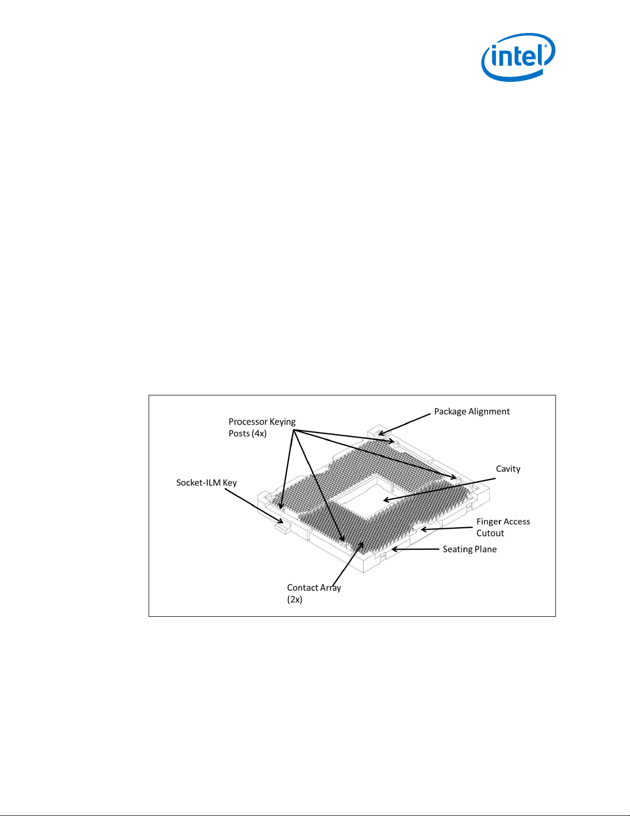
2.0 LGA2011-3 Socket Overview
This section describes a surface mount, LGA (Land Grid Array) socket intended for the
Intel® Xeon® processor E5-1600 and E5-2600 v3 product families processor-based
platform. The socket provides I/O, power and ground contacts for processor operation.
The socket contains 2011 contacts arrayed about a cavity in the center of the socket
with lead-free solder balls for surface mounting on the motherboard.
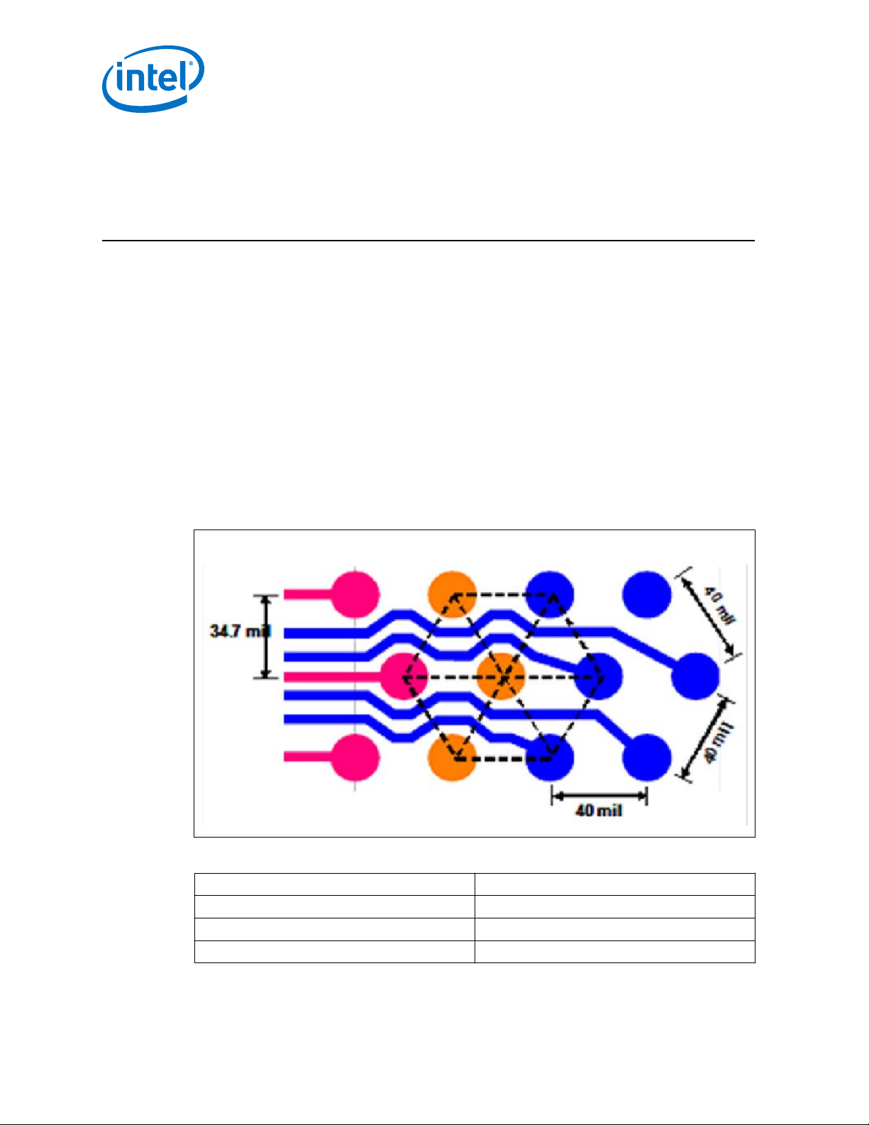
The LGA2011-3 uses a hexagonal area array ball-out which provides many benefits:
• Socket contact density increased by 12% while maintaining 40 mil minimum via
pitch requirements. as compared to a linear array
• Corresponding square pitch array’s would require a 38mil via pitch for the same
package size.
LGA2011-3 has 1.016 mm (40 mil) hexagonal pitch in a 58x43 grid array with 24x16
grid depopulation in the center of the array and selective depopulation elsewhere.
Overview
Figure 1. Hexagonal Array in LGA2011-3
Table 2. LGA2011-3 Socket Attributes
LGA2011-3 Socket Attributes
Component Size 58.5 mm (L) X 51 mm (W)
Pitch 1.016 mm (Hex Array)
Ball Count 2011
Intel® Xeon® Processor E5-1600 / 2600 / 4600 v3 Product Families
Thermal Mechanical Specification and Design Guide October 2015
12 Order No.: 330786-003
Page 13
LGA2011-3 Socket Overview—Intel® Xeon® Processor E5-1600 / 2600 / 4600 v3 Product
Families
The socket must be compatible with the package (processor) and the Independent
Loading Mechanism (ILM). Internal keying posts ensure socket processor
compatibility. An external socket key ensures ILM and socket compatibility. The ILM
reference design includes a back plate; an integral feature for uniform loading on the
socket solder joints and contacts.
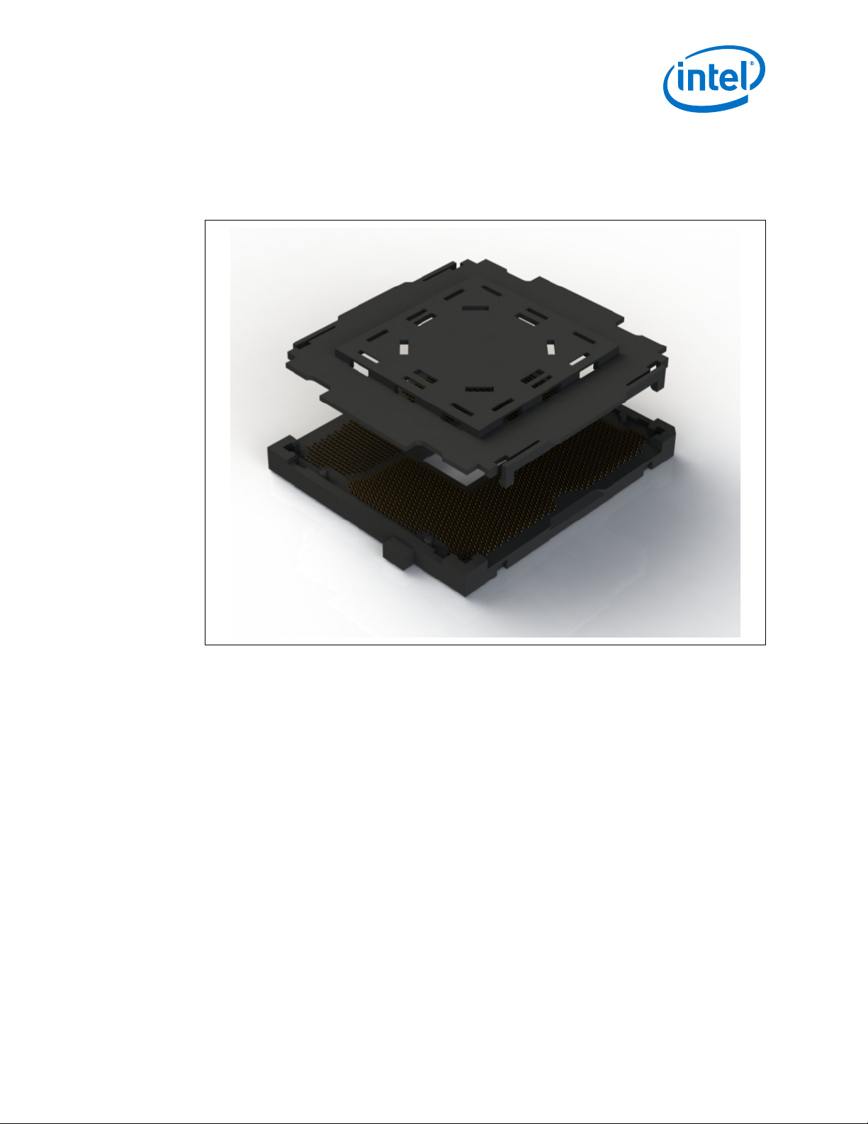
2.1
Socket Components
The socket has two main components, the socket body: composed of a housing solder
balls, and processor contacts, and Pick and Place (PnP) cover. The socket is delivered
as a single integral assembly. Below are descriptions of the integral parts of the
socket.
Socket Body Housing
The housing material is thermoplastic or equivalent with UL 94 V-0 flame rating
capable of withstanding 260°C for 40 seconds (typical reflow/rework). The socket
coefficient of thermal expansion (in the XY plane), and creep properties, are such that
the integrity of the socket is maintained for the environmental conditions listed in the
TMSDG.
The color of the housing will be dark as compared to the solder balls to provide the
contrast needed for pick and place vision systems. A labeled representation of the
socket can be seen in the figure below.
Figure 2. Socket with Labeled Features
Solder Balls
A total of 2011 solder balls corresponding to the contacts are on the bottom of the
socket for surface mounting with the motherboard.
The socket has the following solder ball material:
October 2015 Thermal Mechanical Specification and Design Guide
Order No.: 330786-003 13
Intel® Xeon® Processor E5-1600 / 2600 / 4600 v3 Product Families
Page 14
®
Xeon® Processor E5-1600 / 2600 / 4600 v3 Product Families—LGA2011-3 Socket
Intel
• Lead free SAC305 (SnAgCu) solder alloy with a silver (Ag) content 3%, copper
(Cu) 0.5%, tin (Sn) 96.5% and a melting temperature of approximately 217°C.
The immersion silver (ImAg) motherboard surface finish and solder paste alloy
must be compatible with the SAC305 alloy solder paste.
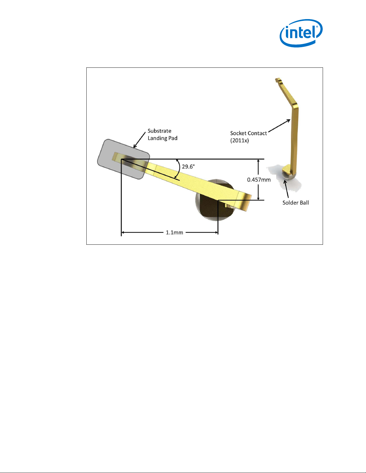
Contacts
The base material for the contacts is high strength copper alloy. For the area on
socket contacts where processor lands will mate, there is a 0.381 mm [0.015 inches]
minimum gold plating over 1.27 mm [0.05 inches] minimum nickel underplate. No
contamination by solder in the contact area is allowed during solder reflow. All socket
contacts are designed such that the contact tip lands within the substrate pad
boundary before any actuation load is applied and remain within the pad boundary at
final installation, after actuation load is applied.
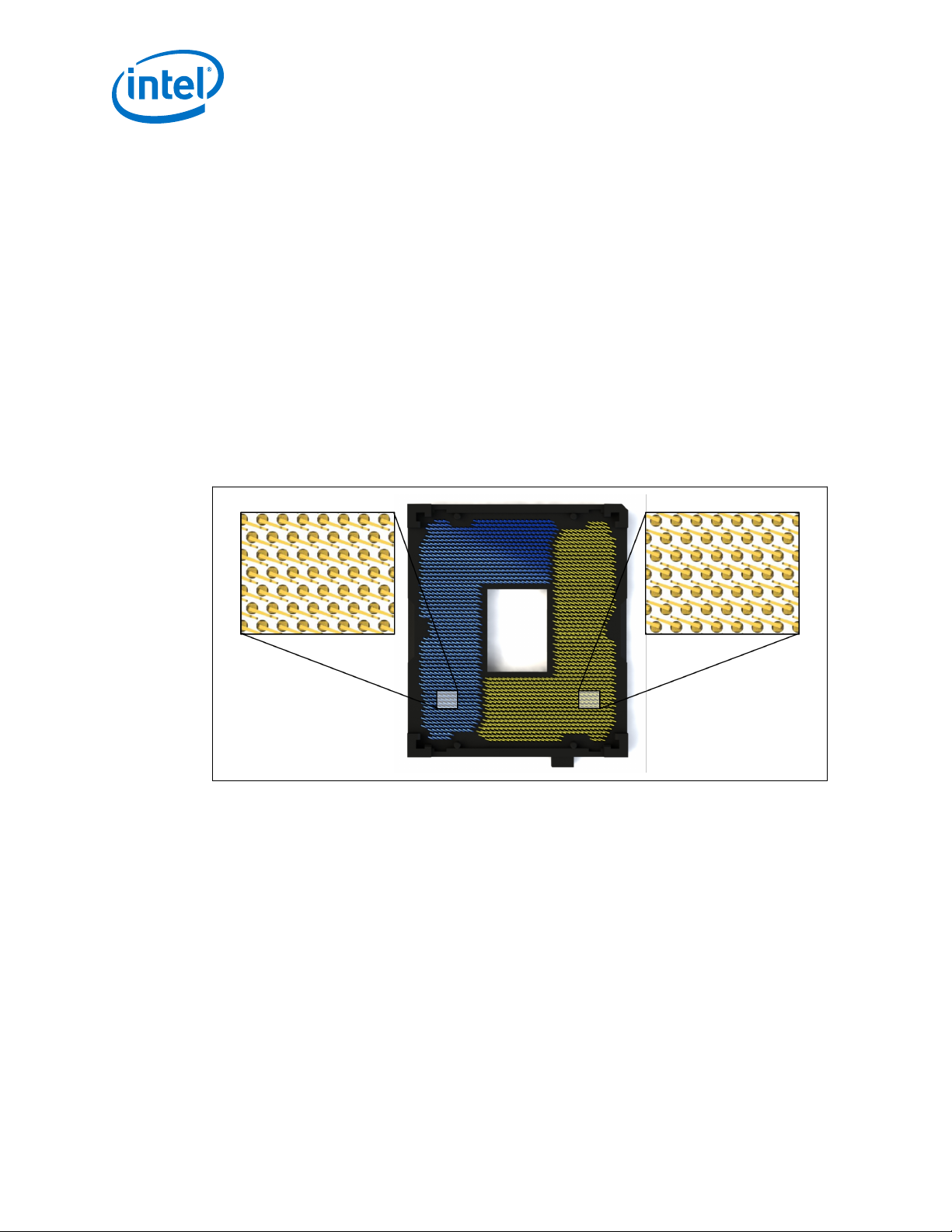
The contacts are laid out in two L-shaped arrays as shown in the figure below. The
detailed view of the contacts indicate the wiping orientation of the contacts in the two
regions to be 29.6°.
Figure 3. Contact Wiping Direction
Overview
The contact between substrate land and socket contact are offset. The following
diagram shows contact offset from solder ball location and orientation of contact tip.
Intel® Xeon® Processor E5-1600 / 2600 / 4600 v3 Product Families
Thermal Mechanical Specification and Design Guide October 2015
14 Order No.: 330786-003
Page 15
®
LGA2011-3 Socket Overview—Intel
Families
Xeon® Processor E5-1600 / 2600 / 4600 v3 Product
Figure 4. Contact Tip Offset with Respect to Solder Ball
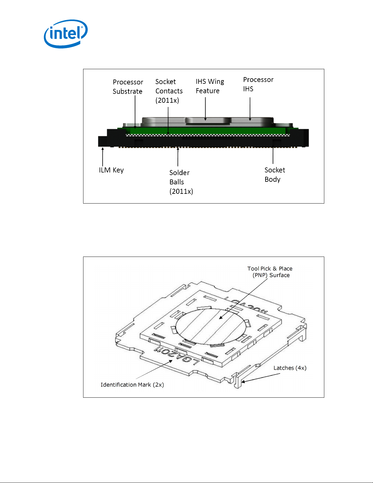
Socket Standoffs
Standoffs on the bottom of the socket base establish the minimum socket height after
solder reflow. The following diagram highlights each feature of the socket-processor
stack up.
October 2015 Thermal Mechanical Specification and Design Guide
Order No.: 330786-003 15
Intel® Xeon® Processor E5-1600 / 2600 / 4600 v3 Product Families
Page 16
®
Xeon® Processor E5-1600 / 2600 / 4600 v3 Product Families—LGA2011-3 Socket
Intel
Figure 5. Processor Socket Stack Up
Overview
Pick and Place Cover
The cover provides a planar surface for vacuum pick up used to place components in
the Surface Mount Technology (SMT) manufacturing line. The proceeding diagram
labels key features of the Pick and Place cover.
Figure 6. Pick and Place Cover with Labeled Features
The cover remains on the socket during reflow to help prevent contamination during
reflow. The cover can withstand 260°C for 40 seconds (typical reflow/rework profile)
and the environmental conditions listed in the TMSDG.
Intel® Xeon® Processor E5-1600 / 2600 / 4600 v3 Product Families
Thermal Mechanical Specification and Design Guide October 2015
16 Order No.: 330786-003
Page 17
LGA2011-3 Socket Overview—Intel® Xeon® Processor E5-1600 / 2600 / 4600 v3 Product
Families
The following figure diagrams the PnP and socket assembly. To reduce risk of damage
to socket contacts the pick and place (PnP) cover remains on the socket during ILM
installation.
Figure 7. PnP Cover and Socket Assembly
Once the ILM with its cover is installed Intel is recommending the PnP cover be
removed to help prevent damage to the socket contacts. To reduce the risk of bent
contacts the PnP Cover and ILM Cover were designed to not be compatible. Covers
can be removed without tools.
The pick and place covers are designed to be interchangeable between socket
suppliers.
2.2
Socket Land Pattern Guidance
The land pattern guidance provided in this section applies to printed circuit board
design. Recommendation for Printed Circuit Board (PCB) Land Patterns is to ensure
solder joint reliability during dynamic stresses, often encountered during shipping and
handling and hence to increase socket reliability.
LGA 2011-3 Land Pattern
The land pattern for the LGA2011-3 socket is 40 mils hexagonal array see the
following figure for detailed location and land pattern type.
October 2015 Thermal Mechanical Specification and Design Guide
Order No.: 330786-003 17
Intel® Xeon® Processor E5-1600 / 2600 / 4600 v3 Product Families
Page 18
®
Xeon® Processor E5-1600 / 2600 / 4600 v3 Product Families—LGA2011-3 Socket
Intel
Overview
Note: There is no round-off (conversion) error between socket pitch (1.016 mm) and board
pitch (40 mil) as these values are equivalent.
Figure 8. Socket 2011-3 Land Pattern
Intel® Xeon® Processor E5-1600 / 2600 / 4600 v3 Product Families
Thermal Mechanical Specification and Design Guide October 2015
18 Order No.: 330786-003
Page 19
®
LGA2011-3 Socket Overview—Intel
Families
Xeon® Processor E5-1600 / 2600 / 4600 v3 Product
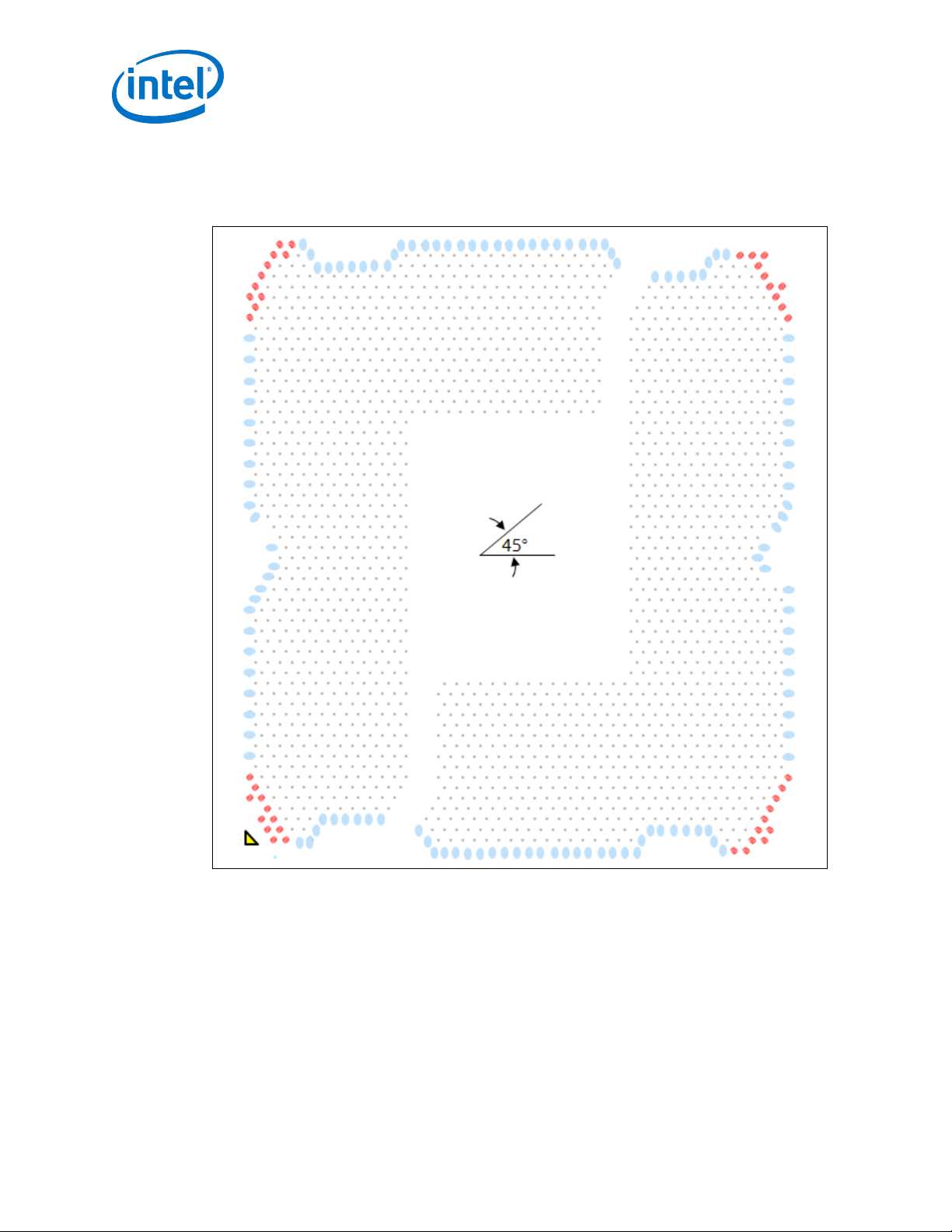
Table 3. PIN Count By Pad Definition
Pad Definition / Padstack Color Quantity
20 X 17 Oblong Partially SMD / O17X20 RED Pins 43
20 X 17 Oblong Partially SMD / O17X20 LIGHT BLUE Pins 123
17 mil Ø MD / C17 GREY Pins 1845
Notes: 1. RED Pins: Corner nCTF pads (43 total) are all designed as 20 X 17 mil oblong partially
soldermask defined pads with an SRO of 17 ±1 mil Ø (shown below). The long axis of the pad is
oriented at 45° from the center of the socket. All nCTF pads require thick traces ideally oriented
at 45° toward the package corner.
2. LIGHT BLUE Pins: Edge CTF pads (total) are all designed as 20 X 17 mil oblong partially
soldermask defined pads with an SRO of 17 ±1 mil Ø (shown below). The long axis of the pad is
oriented at 90° to the socket edge.
3. GREY Pins: Critical to function pins are all designed as 17 mil circular MD (Metal Defined) pads.
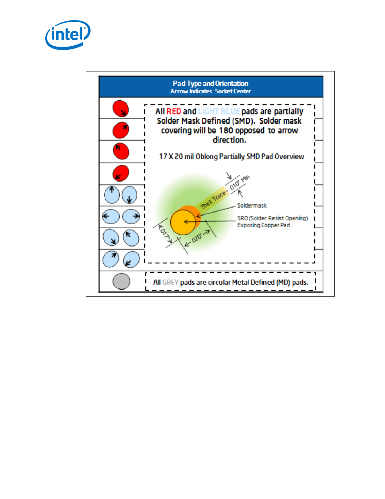
Pad Type Recommendations
Intel defines two types of pad types based on how they are constructed. A metal
defined (MD) pad is one where a pad is individually etched into the PCB with a
minimum width trace exiting it. The solder mask defined (SMD) pad is typically a pad
in a flood plane where the solder mask opening defines the pad size for soldering to
the component. In thermal cycling a MD pad is more robust than a SMD pad type. The
solder mask that defines the SMD pad can create a sharp edge on the solder joint as
the solder ball / paste conforms to the window created by the solder mask. For certain
failure modes the MD pad may not be as robust in shock and vibration (S&V). During
S&V, the predominant failure mode for a MD pad in the corner of the BGA layout is
pad craters and solder joint cracks. A corner MD pad can be made more robust and
behave like a SMD pad by having a wide trace enter the pad. This trace should be 10
mil minimum wide but not to exceed the pad diameter and exit the pad at a 45 degree
angle (parallel to the diagonal of the socket). During board flexure that results from
shock & vibration, a SMD pad is less susceptible to a crack initiating due to the larger
surface area. Intel has defined selected solder joints of the socket as non-critical to
function (NCTF) when evaluating package solder joints post environmental testing.
The signals at NCTF locations are typically redundant ground or non-critical reserved,
so the loss of the solder joint continuity at end of life conditions will not affect the
overall product functionality.
The following figure diagrams shape and location of solder pad types for socket
2011-3.
October 2015 Thermal Mechanical Specification and Design Guide
Order No.: 330786-003 19
Intel® Xeon® Processor E5-1600 / 2600 / 4600 v3 Product Families
Page 20
Intel® Xeon® Processor E5-1600 / 2600 / 4600 v3 Product Families—LGA2011-3 Socket
Figure 9. Socket 2011-3 Pad Types and Locations
Overview
Notes: 1. When ordering PCBs with the Socket R (LGA2011) footprint, it is important to
specify the following verbiage on the FAB drawing as well as within the purchase
requisition: All BGA pads, Soldermask or Metal defined, min/max size tolerance,
should comply with Intel PCB specification, current revision. Nominal BGA pad
size, Soldermask or Metal defined, is Ø +/- 1 mil. This pad size is critical to
function on socket locations.
2. The solder paste stencil aperture recommendation for Socket R (LGA2011) is: 24
mil Ø circular aperture opening with a stencil thickness of 5 mils.
2.3
Socket Loading Requirements
The socket must meet the mechanical loading and strain requirements outlined in the
table below. All dynamic requirements are under room temperature conditions while
all static requirements are under product use condition temperature. Specifically, ILM
and HS load range may vary for different LGA 2011 derivatives (e.g. 2011-0, 2011-1)
due to the package form factor, and the design of loading mechanism and thermal
solution (e.g., HS mass).
Intel® Xeon® Processor E5-1600 / 2600 / 4600 v3 Product Families
Thermal Mechanical Specification and Design Guide October 2015
20 Order No.: 330786-003
Page 21
LGA2011-3 Socket Overview—Intel® Xeon® Processor E5-1600 / 2600 / 4600 v3 Product
Families
2.3.1
Socket Loading Specifications
The table below provides load specifications for the socket. These mechanical limits
should not be exceeded during component assembly, mechanical stress testing, or
standard drop and shipping conditions. All dynamic requirements are under room
temperature conditions while all static requirements are under 100 °C conditions.
Table 4. Socket Load Values
Parameter Load Limits,
SI Units
Min Max Min Max
Static Compressive
per Contact
Static Compressive
(ILM)
Static Compressive
Beginning of Life
(HS)
Static Compressive
End of Life
(HS)
Static Total
Compressive
Dynamic
Compressive
Board Transient
Bend Strain
15 (gf) 38 (gf) 0.53
445 (N) 712 (N) 100 (lbf) 160 (lbf) The total load applied by the enabling mechanism onto
222 (N) 400 (N) 50 (lbf) 90 (lbf) The total load applied by the heatsink mechanism onto
178 (N) 400 (N) 40 (lbf) 90 (lbf) The total load applied by the heatsink mechanism onto
667 (N) 1068 (N ) 150 (lbf) 240 (lbf) The total load applied by enabling mechanism and heat
NA 588 (N) NA 132 (lbf) Quasi-static equivalent compressive load applied during
NA 500 (ue)
for 62
(mil);
400 (ue)
for 100
(mil)
Load Limits,
Imperial Units
1.34 (ozf) The compressive load applied by the package on the
(ozf)
NA 500 (ue)
for 62
(mil);
400 (ue)
for 100
(mil)
Definition
LGA contacts to meet electrical performance. This
condition must be satisfied throughout the life of the
product
the socket as transferred through the package, contacts
and socket seating plane.
the socket as transferred through the package, contacts
and socket seating plane. Measured at Beginning of Life
the socket as transferred through the package, contacts
and socket seating plane. Measured at End of Life
sink onto the socket as transferred through the
package, contacts and socket seating plane.
the mechanical shock from heatsink, calculated using a
reference 600g heatsink with a 25G shock input and an
amplification factor of 3 (600g x 25G x 3 =441N=99
lbf). This specification can have flexibility in specific
values, but the ultimate product of mass times
acceleration should not exceed this value. Intel
reference system shock requirement for this product
family is 25G input as measured at the chassis
mounting location.
This is the strain on boards near to socket BGA corners
during transient loading events through manufacturing
flow or testing. The test guidance can be found in Board
Flexure Initiative (BFI) strain guidance from your local
CQE.
2.4
Socket Maximum temperature
The power dissipated within the socket is a function of the current at the pin level and
the effective pin resistance. To ensure socket long term reliability, Intel defines socket
maximum temperature using a via on the underside of the motherboard. Exceeding
the temperature guidance may result in socket body deformation, or increases in
thermal and electrical resistance which can cause a thermal runaway and eventual
electrical failure. The guidance for socket maximum temperature is listed below:
• Via temperature under socket <78 °C
October 2015 Thermal Mechanical Specification and Design Guide
Order No.: 330786-003 21
Intel® Xeon® Processor E5-1600 / 2600 / 4600 v3 Product Families
Page 22
Intel® Xeon® Processor E5-1600 / 2600 / 4600 v3 Product Families—LGA2011-3 Socket
• The specific via used for temperature measurement is located on the bottom of
the motherboard between pins BC1 and BE1.
• The socket maximum temperature is defined at Thermal Design Current (TDC). In
addition, the heatsink performance targets and boundary conditions must be met
to limit power dissipation through the socket.
To measure via temperature:
1. Drill a hole through the back plate corresponding to the location of pins BC1 and
BE1.
2. Thread a T-type thermocouple (36 - 40 gauge) through the hole and glue it into
the specific measurement via on the underside of the motherboard.
3. Once the glue dries, reinstall the back plate and measure the temperature
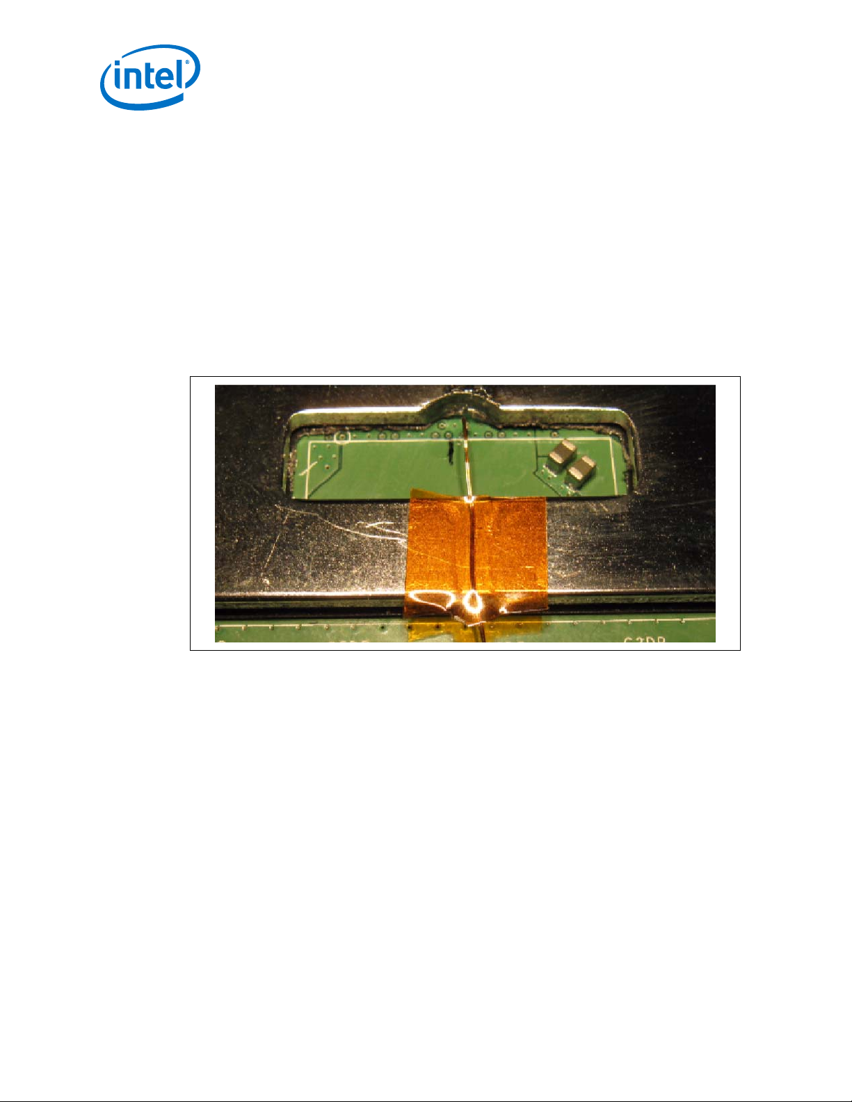
Figure 10. Socket Temperature Measurement
Overview
2.5
Strain Guidance for Socket
Intel provides manufacturing strain guidance commonly referred to as Board Flexure
Initiative or BFI Strain Guidance. The BFI strain guidance apply only to transient bend
conditions seen in board manufacturing assembly environment with no ILM, for
example during In Circuit Test. BFI strain guidance limits do not apply once ILM is
installed. It should be noted that any strain metrology is sensitive to boundary
conditions. Intel recommends the use of BFI to prevent solder joint defects from
occurring in the test process. For additional guidance on BFI, see Manufacturing With
Intel® Components - Strain Measurement for Circuit Board Assembly, also referred as
BFI MAS ( Manufacturing Advantage Services) and BFI STRAIN GUIDANCE SHEET
(LGA2011-3 socket). Consult your Intel Customer Quality Engineer for additional
guidance in setting up a BFI program in your factory.
Note:
When the ILM is attached to the board, the boundary conditions change and the BFI
strain limits are not applicable. The ILM, by design, increases stiffness in and around
the socket and places the solder joints in compression. Intel does not support strain
metrology with the ILM assembled.
Intel® Xeon® Processor E5-1600 / 2600 / 4600 v3 Product Families
Thermal Mechanical Specification and Design Guide October 2015
22 Order No.: 330786-003
Page 23
®
Independent Loading Mechanism (ILM) Specifications—Intel
2600 / 4600 v3 Product Families
Xeon® Processor E5-1600 /
3.0 Independent Loading Mechanism (ILM) Specifications
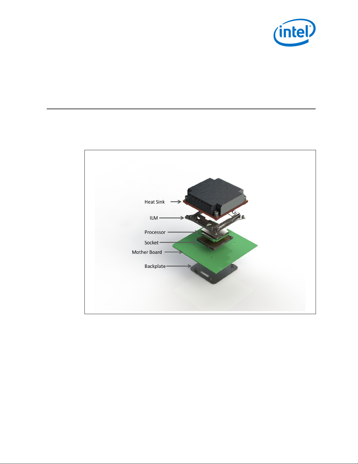
The Independent Loading Mechanism (ILM) provides the force needed to seat the land
LGA package onto the socket contacts. See image below for total processor stack
consisting of all relevant mechanical components.
Figure 11. Processor Stack
The ILM is physically separate from the socket body. The assembly of the ILM is
expected to occur after attaching the socket to the board. The exact assembly location
is dependent on manufacturing preference and test flow.
The mechanical design of the ILM is a key contributor to the overall functionality of the
socket. Intel performs detailed studies on integration of processor package, socket
and ILM as a system. These studies directly impact the design of the ILM. The Intel
reference ILM will be "built to print" from Intel controlled drawings. Intel recommends
using the Intel Reference ILM. Custom non-Intel ILM designs do not benefit from
Intel's detailed studies and may not incorporate critical design parameters.
October 2015 Thermal Mechanical Specification and Design Guide
Order No.: 330786-003 23
Intel® Xeon® Processor E5-1600 / 2600 / 4600 v3 Product Families
Page 24
Intel® Xeon® Processor E5-1600 / 2600 / 4600 v3 Product Families—Independent Loading
Mechanism (ILM) Specifications
The ILM has two critical functions: evenly deliver and distribute the force to seat the
processor onto the socket contacts and ultimately through the socket solder joints.
Another purpose of ILM is to ensure electrical integrity/performance of the socket and
package.
Socket LGA2011-3 has two POR (Plan of Record) ILMs:
1. Square ILM - This ILM has 80x80mm heatsink mounting hole pattern.
2. Narrow ILM - This ILM has 56x94mm heatsink mounting hole pattern.
3.1
ILM Load Specifications
The Independent Loading Mechanism (ILM) provides the force needed to seat the
package onto the socket contacts.
Maximum Allowable Loads
The table below provides load specifications for the processor package. These
maximum limits should not be exceeded during heatsink assembly, shipping
conditions, or standard use condition. Exceeding these limits during test may result in
component failure or other damage to the system. The processor substrate should not
be used as a mechanical reference or load bearing surface for thermal solutions.
Table 5. LGA 2011-3 Maximum Allowable Loads
Item Maximum
Static Pre-Load Compressive (ILM load) 712N (160 lbf)
Static Pre-Load Compressive (HS load) 400N (90 lbf)
Total Socket Static Compressive (ILM+HS=Socket) 1068N (240 lbf)
Minimum Allowable Loads
The ILM is designed to achieve the minimum Socket Static Pre-Load Compressive load
specification. The thermal solution (heatsink) should apply additional load. The
combination of an ILM and HS will be used to achieve the load targets shown in the
table below.
Table 6. LGA 2011-3 Minimum Allowable Loads
Item Minimum
Static Pre-Load Compressive (ILM load) 445N (100 lbf)
Static Pre-Load Compressive (HS load) 222N (50 lbf)
Total Socket Static Compressive (ILM+HS=Socket) 667N (150 lbf)
End of Life Load Targets
The ILM is designed to achieve the minimum end of life loads for the socket. The
thermal solution (heatsink) should apply a portion of the end of life load. The
combination of an ILM and HS will be used to achieve the load targets shown in the
table below.
Intel® Xeon® Processor E5-1600 / 2600 / 4600 v3 Product Families
Thermal Mechanical Specification and Design Guide October 2015
24 Order No.: 330786-003
Page 25
Independent Loading Mechanism (ILM) Specifications—Intel® Xeon® Processor E5-1600 /
2600 / 4600 v3 Product Families
Table 7. LGA 2011-3 Minimum End of Life Loads
Item End of Life Minimum
Static Pre-Load Compressive (ILM load) 311N (70 lbf)
Static Pre-Load Compressive (HS load) 178N (40 lbf)
Total Socket Static Compressive (ILM+HS=Socket) 490N (110 lbf)
3.2
ILM Keepout Zones (KOZ)
The table below lists envelope dimensions for ILM KOZ , both topside and backplate.
For detailed views, refer to dimensioned drawings in Mechanical Drawings on page
78.
Table 8. LGA 2011-3 ILM General Keepout Dimensions
Keepout Type Square ILM Narrow ILM
Topside envelope 93x93 mm (3.6x3.7in) 80x107.5 mm (3.15x4.2in)
ILM Hole Location 46x69.2 mm (1.8x2.7 in)
Backplate Envelope 78x84 mm (3.1x3.3 in)
3.3
Independent Loading Mechanism (ILM)
The Independent Loading Mechanism (ILM) provides the force needed to seat the
package onto the socket contacts. The ILM is a mechanical assembly that is physically
separate from the socket body. The assembly of the ILM to the motherboard is
expected to occur after attaching the socket to the board. The exact assembly location
is dependent on manufacturing preference and test flow.
The mechanical design of the ILM is a key contributor to the overall functionality of the
socket. Intel performs detailed studies on integration of processor package, socket
and ILM as a system. These studies directly impact the design of the ILM. The Intel
reference ILM will be "built to print" from Intel controlled drawings. Intel recommends
using the Intel Reference ILM. Custom non-Intel ILM designs do not benefit from
Intel's detailed studies and may not incorporate critical design parameters.
The ILM has two critical functions: deliver the force to seat the processor onto the
socket contacts resulting in even load transfer through the socket solder joints.
Another purpose of ILM is to ensure electrical integrity/performance of the socket and
package.
3.4
ILM Mechanical Design Considerations and Recommendations
An retention/loading mechanism must be designed to support the processor heatsink
and to ensure processor interface with the socket contact is maintained since there
are no features on the socket for direct attachment of the heatsink or retaining the
processor. In addition to supporting the processor heatsink over the processor, this
mechanism plays a significant role in the robustness of the system in which it is
implemented, in particular:
October 2015 Thermal Mechanical Specification and Design Guide
Order No.: 330786-003 25
Intel® Xeon® Processor E5-1600 / 2600 / 4600 v3 Product Families
Page 26

Intel® Xeon® Processor E5-1600 / 2600 / 4600 v3 Product Families—Independent Loading
Mechanism (ILM) Specifications
• Ensuring that thermal performance of the TIM applied between the IHS and the
heatsink is achievable. TIMs, especially those based on phase change materials,
are very sensitive to applied pressure: the higher the pressure, the better the
initial performance. TIMs such as thermal greases are not as sensitive to applied
pressure. Designs should consider the impact of shock and vibration events on
TIM performance as well as possible decrease in applied pressure over time due to
potential structural relaxation in enabled components.
• Ensuring that system electrical, thermal, and structural integrity is maintained
under shock and vibration events. The mechanical requirements of the attach
mechanism depend on the weight of the heatsink, as well as the level of shock
and vibration that the system must support. The overall structural design of the
baseboard and system must be considered when designing the heatsink and ILM
attach mechanism. Their design should provide a means for protecting the socket
solder joints as well as preventing package pullout from the socket.
• The load applied by the attachment mechanism and the heatsink must comply
with the package specifications, along with the dynamic load added by the
mechanical shock and vibration requirements of the package and socket.
• Load induced onto the package and socket by the ILM may be influenced with
heatsink installed. Determining the performance for any thermal/mechanical
solution is the responsibility of the customer.
A potential mechanical solution for heavy heatsink is the use of a supporting
mechanism such as a backer plate or the utilization of a direct attachment of the
heatsink to the chassis pan. In these cases, the strength of the supporting component
can be utilized rather than solely relying on the baseboard strength. In addition to the
general guidelines given above, contact with the baseboard surfaces should be
minimized during installation in order to avoid any damage to the baseboard.
3.5
Placement of board-to-chassis mounting holes also impacts board deflection and
resultant socket solder ball stress. Customers need to assess the shock for their
designs as heatsink retention (back plate), heatsink mass and chassis mounting holes
may vary.
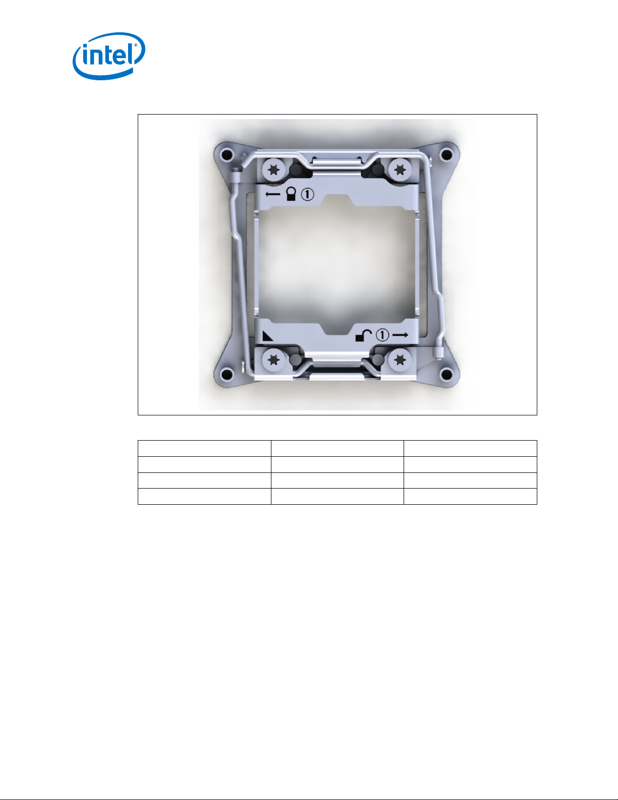
ILM Features
The ILM is defined by four basic features
1. ILM Loadplate: Formed sheet metal that when closed applies four point loads onto
the IHS seating the processor into the socket
2. ILM Frame: Single piece or assembly that mounts to PCB board and provides the
hinge locations for the levers the ILM frame also contains captive mounts for
heatsink attach. An insulator is pre applied by the vendor to the bottom side of
the ILM frame.
3. ILM Actuation levers: Formed loading levers designed to place equal force on both
ends of the ILM load plate. Some of the load is passed through the socket body to
the board inducing a slight compression on the solder joints
4. ILM Backplate: A flat steel back plate with threaded studs to attach to the ILM
frame. A clearance hole is located at the center of the plate to allow access to test
points and backside capacitors. Two additional cut-outs on the backplate provide
clearance for backside voltage regulator components. An insulator is pre applied
by the vendor to the side with the threaded studs.
Intel® Xeon® Processor E5-1600 / 2600 / 4600 v3 Product Families
Thermal Mechanical Specification and Design Guide October 2015
26 Order No.: 330786-003
Page 27
Independent Loading Mechanism (ILM) Specifications—Intel
2600 / 4600 v3 Product Families
Heatsink mounting studs on ILM frame allow for topside thermal solution attach to a
rigid structure. This eliminates the motherboard thickness dependency from the
heatsink mechanical stackup. ILM assembly provides a clamping force between the
ILM frame, backplate and board, resulting in reduced board bending leading to higher
solder joint reliability. ILM lever design provides an interlocking mechanism to ensure
proper opening or closing sequence for the operator. This has been implemented in
both square and narrow ILM.
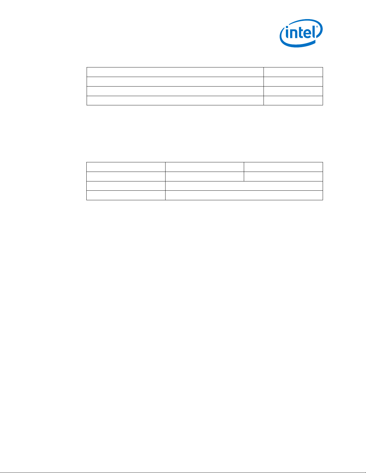
ILM Load Plate Design
Four point loading contributes to minimizing package and socket warpage under non
uniformly distributed load. The reaction force from closing the load plate is transmitted
to the frame and through the captive fasteners to the back plate. Some of the load is
passed through the socket body to the board inducing a slight compression on the
solder joints. The load plate design is common between the two POR ILMS and is
shown in the figure below.
Figure 12. ILM Load Plate
®
Xeon® Processor E5-1600 /
Lever Actuation/Release Forces
Maximum allowable force to actuate the levers not to exceed 4.7 lbf (21 N) at the
point of typical finger placement.
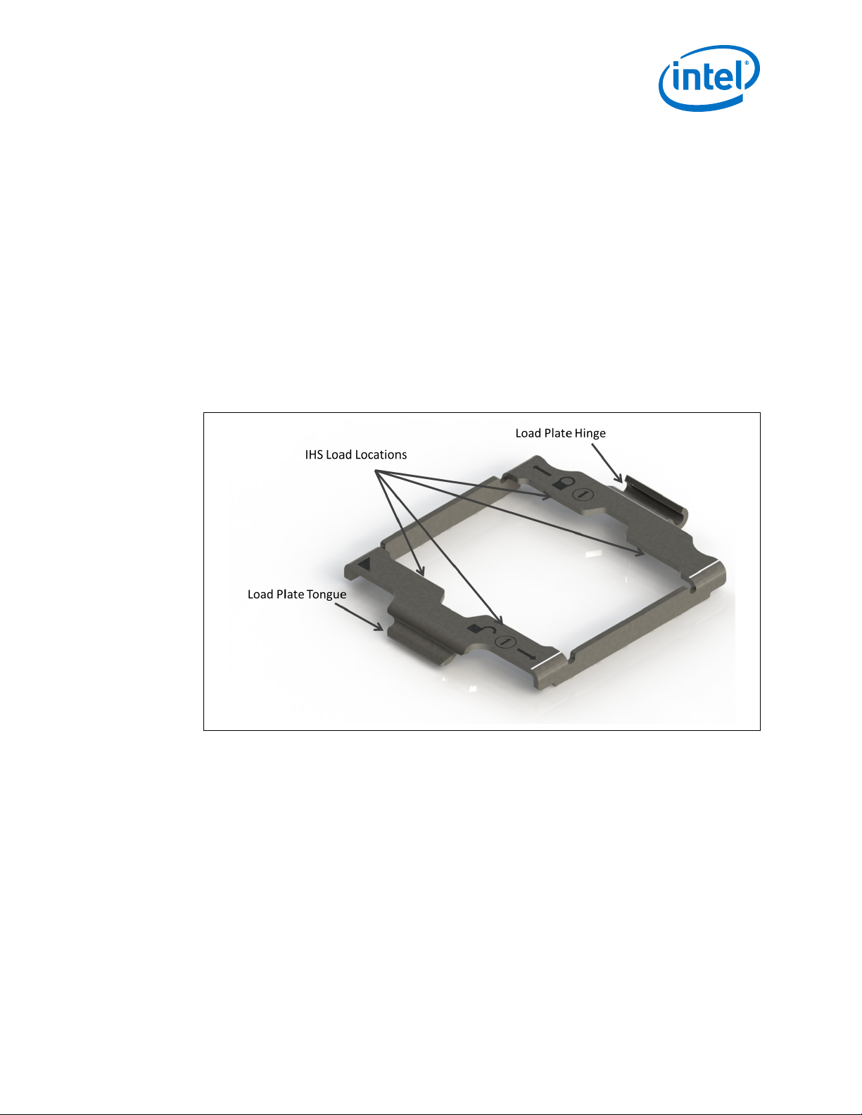
ILM Back Plate Design
The backplate assembly consists of a supporting plate and captive standoffs. It
provides rigidity to the system to ensure minimal board and socket deflection. Four
externally threaded (male) inserts which are press fit into the back plate are for ILM
attachment. Three cavities are located at the center of the plate to allow access to the
baseboard test points and backside capacitors. An insulator is pre-applied to prevent
shorting the board.
October 2015 Thermal Mechanical Specification and Design Guide
Order No.: 330786-003 27
Intel® Xeon® Processor E5-1600 / 2600 / 4600 v3 Product Families
Page 28
Intel® Xeon® Processor E5-1600 / 2600 / 4600 v3 Product Families—Independent Loading
Figure 13. ILM Backplate
Mechanism (ILM) Specifications
3.6
3.6.1
Intel® ILM Reference Designs
Intel has designed and validated two ILMs compatible with Socket LGA2011-3 :
1. Square ILM - 80x80 mm heat sink mounting hole pattern.
2. Narrow ILM - 56x94 mm heat sink mounting hole pattern.
The two POR ILMs share most components, only the top plate and active lever differ
between the two assemblies.
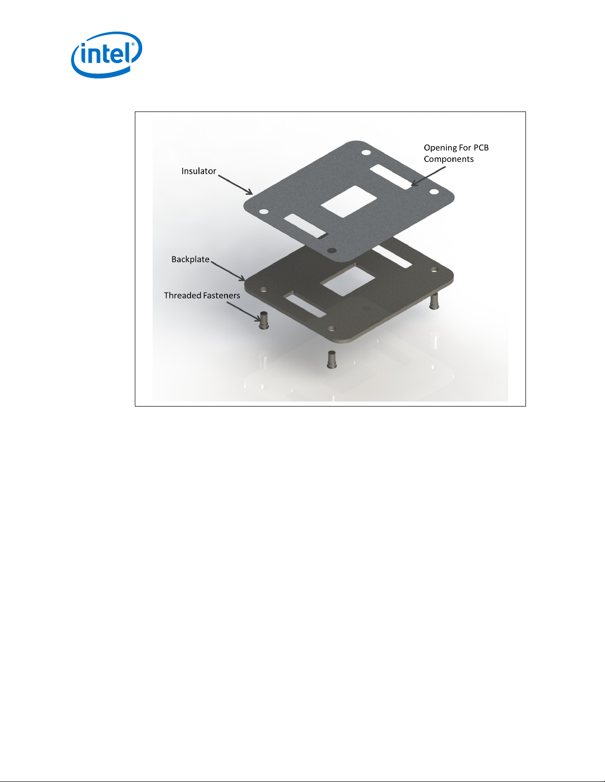
Square ILM
The square ILM consists of two sub assemblies that will be procured as a set from the
enabled vendors. These two components are the ILM assembly and back plate. The
square ILM assembly consists of several pieces as shown and labeled in the following
diagram. The hinge lever, active lever, load plate, top plate,clevises, and the captive
fasteners. For clarity the ILM cover is not shown in this view.
Intel® Xeon® Processor E5-1600 / 2600 / 4600 v3 Product Families
Thermal Mechanical Specification and Design Guide October 2015
28 Order No.: 330786-003
Page 29
Independent Loading Mechanism (ILM) Specifications—Intel® Xeon® Processor E5-1600 /
2600 / 4600 v3 Product Families
Figure 14. Exploded Square ILM
An assembled view is shown in the following figure.
October 2015 Thermal Mechanical Specification and Design Guide
Order No.: 330786-003 29
Intel® Xeon® Processor E5-1600 / 2600 / 4600 v3 Product Families
Page 30
Intel® Xeon® Processor E5-1600 / 2600 / 4600 v3 Product Families—Independent Loading
Figure 15. Assembled Square ILM
Mechanism (ILM) Specifications
Table 9. Square ILM Component Thickness and materials
Component Thickness Material
ILM Frame 1.20 mm 310 Stainless Steel
ILM Load Plate 1.50 mm 310 Stainless Steel
ILM Back Plate 2.20 mm S50C low Carbon Steel
The square ILM supports the legacy 80x80 mm heat sink mounting patterns used in
some form factors.
3.6.2
Narrow ILM
The narrow ILM consists of two sub assemblies that will be procured as a set from the
enabled vendors. These two components are the ILM assembly and back plate. The
ILM assembly is shown in the following figure.
Intel® Xeon® Processor E5-1600 / 2600 / 4600 v3 Product Families
Thermal Mechanical Specification and Design Guide October 2015
30 Order No.: 330786-003
Page 31

Independent Loading Mechanism (ILM) Specifications—Intel
2600 / 4600 v3 Product Families
Figure 16. Exploded Narrow ILM
®
Xeon® Processor E5-1600 /
The narrow ILM assembly consists of several pieces as shown and labeled above. The
hinge lever, active lever, load plate, top plate, clevises, ILM cover, and the captive
fasteners. For clarity the ILM cover is not shown in this view. An assembled view is
shown in the following figure. The Narrow ILM maintains the structure and function of
the square ILM but utilizes separate clevises riveted onto the ILM frame.
October 2015 Thermal Mechanical Specification and Design Guide
Order No.: 330786-003 31
Intel® Xeon® Processor E5-1600 / 2600 / 4600 v3 Product Families
Page 32

Intel® Xeon® Processor E5-1600 / 2600 / 4600 v3 Product Families—Independent Loading
Figure 17. Assembled Narrow ILM
Mechanism (ILM) Specifications
Table 10. Narrow ILM Component Thickness and materials
Component Thickness Material
ILM Frame 1.50 mm 310 Stainless Steel
ILM Clevis 0.80 mm 301 Stainless Steel
ILM Load Plate 1.50 mm 310 Stainless Steel
ILM Back Plate 2.20 mm S50C low Carbon Steel
The narrow ILM supports a smaller east west dimension constraint conducive for use
in space constrained form factors.
3.7
ILM Cover
Intel has developed a cover that will snap on to the ILM for the LGA2011 socket
family.
The ILM cover is intended to reduce the potential for socket contact damage from the
operator / customer fingers being close to the socket contacts to remove or install the
pick and place cover. By design the ILM cover and pick and place covers can not be
installed simultaneously. This cover is intended to be used in place of the pick and
place cover once the ILM is assembled to the board. The ILM will be offered with the
ILM cover pre assembled as well as a discrete part.
Intel® Xeon® Processor E5-1600 / 2600 / 4600 v3 Product Families
Thermal Mechanical Specification and Design Guide October 2015
32 Order No.: 330786-003
Page 33

Independent Loading Mechanism (ILM) Specifications—Intel® Xeon® Processor E5-1600 /
2600 / 4600 v3 Product Families
Figure 18. ILM cover
• Pre-assembled by the ILM vendors to the ILM load plate. It will also be offered as
a discrete component.
• The ILM cover will pop off if a processor is installed in the socket.
• Maintain inter-changeability between validated ILM vendors for LGA2011-3 socket.
• The ILM cover for the LGA2011-3 socket will have a flammability rating of V-0 per
UL 60950-1.
Note: Intel recommends removing the Pick and Place cover (PnP) of the socket body in
manufacturing as soon as possible at the time when ILM is being installed.
ILM Cover Attach/Removal Force
The required force to remove the ILM cover shall not exceed 7.6 N when the load is
applied by finger at the center of cover.
3.8
ILM Allowable Board Thickness
The ILM components described in this document will support board thickness in the
range of 1.5748 - 2.54 mm (0.062" - 0.100"). Boards (PCBs) not within this range
may require modifications to the back plate or other ILM components retention.
Contact the component suppliers (Component Suppliers on page 76) for
modifications.
October 2015 Thermal Mechanical Specification and Design Guide
Order No.: 330786-003 33
Intel® Xeon® Processor E5-1600 / 2600 / 4600 v3 Product Families
Page 34

Intel® Xeon® Processor E5-1600 / 2600 / 4600 v3 Product Families— Processor Thermal
Specifications and Features
4.0 Processor Thermal Specifications and Features
4.1
4.1.1
T
and DTS-Based Thermal Specification
case
Implementation
Thermal solutions should be sized such that the processor complies to the T
thermal profile all the way up to TDP, because, when all cores are active, a thermal
solution sized as such will have the capacity to meet the DTS thermal profile, by
design. When all cores are not active or when Intel Turbo Boost Technology is active,
attempting to comply with the DTS thermal profile may drive system fans to speeds
higher than the fan speed required to comply with the T
thermal profile at TDP.
CASE
In cases where thermal solutions are undersized, and the processor does not comply
with the T
is kept lower than TDP, AND the actual T
thermal profile at TDP, compliance can occur when the processor power
CASE
is below the T
CASE
thermal profile at that
CASE
lower power.
In most situations, implementation of DTS thermal profile can reduce average fan
power and improve acoustics, as compared to T
DTS < T
CONTROL
, the processor is compliant, and T
CONTROL
-based fan speed control. When
and DTS thermal profiles can
CASE
be ignored.
Margin to Thermal Specification (M)
To simplify processor thermal specification compliance, the processor calculates and
reports margin to DTS thermal profile (M) using the following method.
Processor reads firmware programmable values:
1. TCC_OFFSET: In-band: TEMPERATURE_TARGET[27:24]. BIOS must write in a
value before CPL3.
CASE
Processor gathers information about itself:
1. Processor stores the intercept and slope terms (TLA and ΨPA) from the DTS
Thermal Profile for that particular SKU (one-time read only)
2. Processor reads its own energy consumption and calculates power, P
3. Processor reads its own temperature, DTS
Finally, processor calculates the margin value (M) to the specification (solid black line
in the graph below). The PECI command for reading margin (M) is RdPkgConfig(),
Index 10.
M < 0 indicates gap to spec,
processor needs more cooling (for example, increase fan
speed)
M > 0 this indicates margin to spec, processor is sufficiently cooled
Graphically, this is represented below. T
Intel® Xeon® Processor E5-1600 / 2600 / 4600 v3 Product Families
Thermal Mechanical Specification and Design Guide October 2015
34 Order No.: 330786-003
CONTROL_OFFSET
is not writable to a register.
Page 35

Processor Thermal Specifications and Features—Intel® Xeon® Processor E5-1600 / 2600 / 4600
v3 Product Families
Figure 19. Margin to Thermal Spec (M)
DTS 2.0 processor Margin values can be obtained via PECI or Processor register see
documentation below as well as Intel® Xeon® Processor E5-1600 and E5-2600 v3
Product Families, Volume 2 of 2, Registers Datasheet and Intel® Xeon® Processor
E5-1600 and E5-2600 v3 Product Families, Volume 1 of 2, Electrical Datasheet
Table 11. DTS 2.0 Margin From PECI
Service Index
Value
(IV)
(decimal)
Thermal Margin 10 0x0000 15:0--Package
Note: Refer to Intel® Xeon® Processor E5-1600 and E5-2600 v3 Product Families, Volume 2 of 2, Registers Datasheet and
Intel® Xeon® Processor E5-1600 and E5-2600 v3 Product Families, Volume 1 of 2, Electrical Datasheet for further
details
October 2015 Thermal Mechanical Specification and Design Guide
Order No.: 330786-003 35
Parameter
Value
(word)
RdPkgConfig()
Data
(dword)
Temperature
margin in 8.8
format, 32:16-Reserved
Intel® Xeon® Processor E5-1600 / 2600 / 4600 v3 Product Families
WrPkgConfi
g()
Data
(dword)
N/A Package temperature
Description
margin with regards to
DTS Thermal Profile.
Positive indicates
thermal margin, and
package is less than DTS
thermal profile
Page 36

Intel® Xeon® Processor E5-1600 / 2600 / 4600 v3 Product Families—Processor Thermal
Specifications and Features
Table 12. DTS 2.0 Margin From Processor Register: CSR for PACKAGE_THERM_MARGIN
Bus:1 Device:30 Function:0 Offset:E0
Bit Attr Default Description
31:16 RSVD-P 0000h Reserved--Protected
15:0 R0-V 0000h THERM_MARGIN--This field provides Platform
Note: • Refer to Intel® Xeon® Processor E5-1600 and E5-2600 v3 Product Families, Volume 2 of 2, Registers Datasheet and
Intel® Xeon® Processor E5-1600 and E5-2600 v3 Product Families, Volume 1 of 2, Electrical Datasheet for full
documentation of registers and field descriptions
Firmware with running average of the instantaneous
temperature margin above Tspec in 2's complement
8.8 format. This is the recommended field for
Platform firmware to use for fan control. When this
value is negative, it indicates a firmware must
increase the fan speed. With a positive value,
firmware may decrease the speed of the fan
4.2
4.2.1
4.2.2
4.3
Processor Thermal Features
Absolute Processor Temperature
The processor has a software readable field in the TEMPERATURE_TARGET register
that contains the minimum temperature at which the Thermal Control Circuit (TCC)
will be activated and PROCHOT_N will be asserted.
Intel does not test any third party software that reports absolute processor
temperature. As such, Intel cannot recommend the use of software that claims this
capability. Since there is part-to-part variation in the TCC (thermal control circuit)
activation temperature, use of software that reports absolute temperature could be
misleading.
Short Duration TCC Activation
Systems designed to meet thermal capacity may encounter short durations of
throttling, also known as TCC activation, especially when running nonsteady processor
stress applications. This is acceptable and is functionally within the intended
temperature control parameters of the processor. Such short duration TCC activation
is not expected to provide noticeable reductions in application performance, and is
typically within the normal range of processor to processor performance variation.
Processor Thermal Specifications
The processor requires a thermal solution to maintain temperatures within operating
limits. Any attempt to operate the processor outside these limits may result in
permanent damage to the processor and potentially other components within the
system. Maintaining the proper thermal environment is key to reliable, long-term
system operation.
A complete solution includes both component and system level thermal management
features. Component level thermal solutions can include active or passive heatsinks
attached to the processor integrated heat spreader (IHS). Typical system level
thermal solutions may consist of system fans combined with ducting and venting.
Intel® Xeon® Processor E5-1600 / 2600 / 4600 v3 Product Families
Thermal Mechanical Specification and Design Guide October 2015
36 Order No.: 330786-003
Page 37

Processor Thermal Specifications and Features—Intel® Xeon® Processor E5-1600 / 2600 / 4600
v3 Product Families
For more information on designing a component level thermal solution, refer to
Processor Thermal Solutions on page 47.
4.3.1
Thermal Specifications
To allow optimal operation and long-term reliability of Intel processor-based systems,
the processor must remain between the minimum and maximum case temperature
(T
) specifications as defined in the tables in the following sub-sections. Thermal
CASE
solutions that do not provide sufficient thermal cooling may affect the long-term
reliability of the processor and system.
Thermal profiles ensure adherence to Intel reliability requirements.
Intel assumes specific system boundary conditions (system ambient, airflow, heatsink
performance / pressure drop, preheat, etc.) for each processor SKU to develop T
and DTS thermal specifications. For servers each processor will be aligned to either 1U
or 2U system boundary conditions. Customers can use other boundary conditions (for
example a better thermal solution with higher ambient) providing they are compliant
to those specifications. Furthermore, implementing a thermal solution that violates the
thermal profile for extended periods of time may result in permanent damage to the
processor or reduced life. The upper point of the thermal profile consists of the
Thermal Design Power (TDP) and the corresponding T
T
CASE_MAX
) represents a thermal solution design point.
CASE_MAX
value (x = TDP and y =
For embedded servers, communications and storage markets, Intel has SKUs that
support thermal profiles with nominal and short-term conditions designed to meet
NEBS level 3 compliance. For these SKUs, operation at either the nominal or shortterm thermal profiles should result in virtually no TCC activation. Thermal profiles for
these SKUs are found in this chapter as well.
Intel recommends that thermal solution designs target the Thermal Design Power
(TDP). The Adaptive Thermal Monitor feature is intended to help protect the processor
in the event that an application exceeds the TDP recommendation for a sustained time
period. The Adaptive Thermal Monitor feature must be enabled for the processor to
remain within its specifications.
case
4.3.2
T
CASE
and DTS Based Thermal Specifications
To simplify compliance to thermal specifications at processor run time, the processor
has a Digital Thermal Sensor (DTS) based thermal specification. Digital Thermal
Sensor outputs a relative die temperature from TCC activation temperature. T
CASE
based specifications are used for heatsink sizing while DTS-based specs are used for
acoustic and fan speed optimizations while the server is operating. Some SKUs may
share the same T
All thermal profiles, whether based on T
thermal profiles but have distinct DTS thermal profiles.
CASE
or DTS, follow the straight-line equation
CASE
format namely, y = mx + b. Where,
y = temperature (T) in °C
m = slope (Ψ)
x = power (P) in Watts
b = y-intercept (TLA) (LA = local ambient)
October 2015 Thermal Mechanical Specification and Design Guide
Order No.: 330786-003 37
Intel® Xeon® Processor E5-1600 / 2600 / 4600 v3 Product Families
Page 38

Intel® Xeon® Processor E5-1600 / 2600 / 4600 v3 Product Families—Processor Thermal
Figure 20. Typical Thermal Profile Graph (Illustration Only)
Specifications and Features
4.3.3
Server Processor Thermal Profiles and Form Factors
Table 13. Intel® Xeon® Processor E5-1600 and E5-2600 v3 Product Families Stack T
and DTS Thermal Profiles and Correction Factors
Thermal Profiles
T
CASE
(°C)
DTS
(°C)
T
=[0.299
DTS
*P]+58.2
T
=[0.311
DTS
*P]+56.3
T
=[0.310
DTS
*P]+56.3
T
=[0.329
DTS
*P]+54.2
T
=[0.324
DTS
*P]+54.2
T
=[0.363
DTS
*P]+52.2
T
=[0.392
DTS
*P]+51.4
T
=[0.371
DTS
*P]+51.5
DTS max
at TDP
Note: 5
99
95
95
90
90
86
86
85
continued...
Category
Processor
E5-2690 v3 Small
E5-2680 v3 Small
Advanced
E5-2670 v3 Small
E5-2660 v3 Small
E5-2650 v3 Small
E5-2640 v3 Small
Standard
E5-2630 v3 Small
E5-2620 v3 Small
Number
Factor (die)
Package Form
(MCC)
(MCC)
(MCC)
(MCC)
(MCC)
(LCC)
(LCC)
(LCC)
TDP (W)
Core Count
135 12 1U
Square
120 12 1U
Square
120 12 1U
Square
105 10 1U
Square
105 10 1U
Square
90 8 1U
Square
85 8 1U
Square
85 6 1U
Square
C1E
Form Factor
Assumed Heatsink
Disable Offset (°C)
0 18 TC=[0.235*P]
0 10 TC=[0.235*P]
0 10 TC=[0.235*P]
0 10 TC=[0.236*P]
0 10 TC=[0.235*P]
0 10 TC=[0.246*P]
0 10 TC=[0.243*P]
0 10 TC=[0.248*P]
control
T
+58.2
+56.3
+56.3
+54.2
+54.2
+52.2
+51.4
+51.5
case
Intel® Xeon® Processor E5-1600 / 2600 / 4600 v3 Product Families
Thermal Mechanical Specification and Design Guide October 2015
38 Order No.: 330786-003
Page 39

Processor Thermal Specifications and Features—Intel® Xeon® Processor E5-1600 / 2600 / 4600
v3 Product Families
Category
Number
Processor
E5-2609 v3 Small
Basic
E5-2603 v3 Small
E5-2699 v3 Large
E5-2698 v3 Large
E5-2697 v3 Large
Segment Optimized
E5-2695 v3 Large
E5-2683 v3 Large
E5-2685 v3 Small
E5-2667 v3 Small
E5-2643 v3 Small
E5-2637 v3 Small
Frequency Optimized
E5-2623 v3 Small
E5-2687W
v3
Note: 3
Factor (die)
Package Form
(MCC)
(LCC)
(HCC)
(HCC)
(HCC)
(HCC)
(HCC)
(MCC)
(LCC)
(LCC)
(LCC)
(LCC)
Small
(MCC)
C1E
TDP (W)
Core Count
85 6 1U
Square
85 6 1U
Square
145 18 2U
Square
135 16 1U
Square
145 14 2U
Square
120 14 1U
Square
120 14 1U
Square
120 12 1U
Square
135 8 2U
Square
135 6 2U
Square
135 4 2U
Square
Form Factor
Assumed Heatsink
Disable Offset (°C)
2 10 TC=[0.231*P]
0 10 TC=[0.250*P]
0 18 TC=[0.175*P ]
4 18 TC=[0.221*P]+
0 18 TC=[0.177*P]
0 10 TC=[0.221*P]+
0 10 TC=[0.220*P]
0 10 TC=[0.235*P]
3 18 TC=[0.202*P]
2 18 TC=[0.205*P]
2 18 TC=[0.205*P]
control
T
+51.3
+51.5
+51.0
58.2
+51.0
56.1
+56.1
+56.3
+50.5
+49.6
+48.9
T
(°C)
CASE
105 4 1U Square 0 10 TC=[0.250*P]
+53.9
160 10 WS
Passive
0 10 TC=[0.190*P]
+44.3
Tower
Thermal Profiles
DTS
(°C)
T
=[0.325
DTS
*P]+51.3
T
=[0.353
DTS
*P]+51.5
T
=[0.243
DTS
*P]+51.0
T
=[0.277
DTS
*P]+58.2
T
=[0.276
DTS
*P]+51.0
T
=[0.314
DTS
*P]+56.1
T
=[0.285
DTS
*P]+56.1
T
=[0.304
DTS
*P]+56.3
T
=[0.336
DTS
*P]+50.5
T
=[0.369
DTS
*P]+49.6
T
=[0.402
DTS
*P]+48.9
T
=[0.433
DTS
*P]+53.9
T
=
DTS
[0.299*P]
+44.3
DTS max
at TDP
Note: 5
80
83
88
97
93
95
92
94
97
97
97
101
94
Workstation Only
E5-2650Lv3Small
(MCC)
E5-2630Lv3Small 55 8 1U Square 0 10 TC=[0.240*P]
Low Power
65 12 1U Square 0 10 TC=[0.232*P]
+48.5
+47.2
T
=[0.320
DTS
*P]+48.5
T
=[0.372
DTS
*P]+47.2
71
69
continued...
Intel® Xeon® Processor E5-1600 / 2600 / 4600 v3 Product Families
October 2015 Thermal Mechanical Specification and Design Guide
Order No.: 330786-003 39
Page 40

Intel® Xeon® Processor E5-1600 / 2600 / 4600 v3 Product Families—Processor Thermal
Specifications and Features
C1E
Category
Number
Processor
TDP (W)
Factor (die)
Core Count
Form Factor
control
T
T
(°C)
CASE
DTS
(°C)
DTS max
at TDP
Note: 5
Package Form
Thermal Profiles
Assumed Heatsink
Disable Offset (°C)
(LCC)
Notes: 1. These values are specified at VccIN_MAX for all processor frequencies. Systems must be designed to ensure the
processor is not subjected to any static Vcc and Icc combination wherein VccIN exceeds VccIN_MAX at a specified
Icc. Please refer to the electrical loadline specifications.
2. Thermal Design Power (TDP) should be used as a target for processor thermal solution design. Processor power
may exceed TDP for short durations. Please see Intel® Turbo Boost Technology on page 50
3. This SKU is intended for dual processor workstations only and uses workstation specific use conditions for reliability
assumptions.
4. Disabling C1E will result in an automatic reduction of DTSmax so that reliability is still protected. DTSmax will be
reduced by the value shown 'C1E Disable Offset’. If thermal design has not been optimized to the reduced DTSmax
value, throttling may result. Tcontrol is already an offset to DTSmax, therefore the absolute temp at which the
Tcontrol threshold is reached will shift by the same amount.
5. DTS max at TDP is 2°C greater than DTS thermal profile at TDP, but applies only when part is operating at thermal
design power and is installed in a system using microcode update 0x25 or later.
6. Tcase Minimum is 0°C
4.3.4
Server 4S Processor Thermal Profiles and Form Factors
Table 14. Intel® Xeon® Processor E5-4600 v3 Product Families Stack Product Family
T
and DTS Thermal Profiles and Correction Factors
case
Category
Number
Processor
Package Form
E5-4669v3Large
(HCC)
E5-4667v3Large
(HCC)
TDP (W)
Factor (Die)
135 18 1U
135 16 1U
Core Count
Form Factor
Assumed Heatsink
Square
Square
Thermal Profiles DTS
control
T
Offset (°C)
C1E Disable
T
(°C)
CASE
0 10 TC=[0.219*P
]+58.1
0 10 TC=[0.219*P
]+58.1
DTS
(°C)
T
=[0.280
DTS
*P]+58.1
T
=[0.276
DTS
*P]+58.1
max at
TDP
Note: 5
97 -0.007 -0.014
97 -0.007 -0.014
Correction
Factors
TTV
Lukeville
TTV
Looneyville
4S Glueless
High Performance Dense
E5-4655v3Small
(MCC
135 6 1U
Square
0 10 TC=[0.233*P
] + 56.3
T
=[0.352
DTS
*P] + 56.3
100 0.009 0.002
)
E5-4627v3Small
(MCC
135 10 1U
Square
0 10 TC=[0.237*P
] + 56.9
T
=[0.332
DTS
*P] + 56.9
100 0.013 0.006
)
4S Glueless
Frequency Optimized Dense
continued...
Intel® Xeon® Processor E5-1600 / 2600 / 4600 v3 Product Families
Thermal Mechanical Specification and Design Guide October 2015
40 Order No.: 330786-003
Page 41

Processor Thermal Specifications and Features—Intel® Xeon® Processor E5-1600 / 2600 / 4600
v3 Product Families
Category
Number
Processor
TDP (W)
Factor (Die)
Package Form
Core Count
Form Factor
control
T
Offset (°C)
C1E Disable
Thermal Profiles DTS
max at
T
(°C)
CASE
DTS
(°C)
Note: 5
TDP
Correction
Factors
TTV
Lukeville
Assumed Heatsink
Advanced
Standard
Basic
E5-4660v3Large
E5-4650v3Large
E5-4640v3Large
E5-4620v3Large
E5-4610v3Large
(HCC)
(HCC)
(HCC)
(HCC)
(HCC)
120 14 1U
Square
105 12 1U
Square
105 12 1U
Square
105 10 1U
Square
105 10 1U
Square
0 10 TC=[0.221*P
]+56.1
0 10 TC=[0.224*P
]+54.0
0 10 TC=[0.224*P
]+54.0
0 10 TC=[0.225*P
]+54.0
0 10 TC=[0.224*P
]+54.0
T
=[0.312
DTS
*P]+56.1
T
=[0.288
DTS
*P]+54.0
T
=[0.280
DTS
*P]+54.0
T
=[0.289
DTS
*P]+54.0
T
=[0.283
DTS
*P]+54.0
95 -0.005 -0.012
86 -0.001 -0.008
85 -0.001 -0.008
86 0.000 -0.007
85 0.000 -0.007
8
Notes: 1. These values are specified at VccIN_MAX for all processor frequencies. Systems must be designed to ensure the
processor is not subjected to any static Vcc and Icc combination wherein VccIN exceeds VccIN_MAX at a specified
Icc. Please refer to the electrical loadline specifications.
2. Thermal Design Power (TDP) should be used as a target for processor thermal solution design. Processor power
may exceed TDP for short durations. Please see Intel® Turbo Boost Technology on page 50
3. These specifications may be updated as further characterization data becomes available.
4. Minimum T
Specification is 0°C
case
5. DTS max at TDP is 2°C greater than DTS thermal profile at TDP, but applies only when part is operating at thermal
design power and is installed in a system using microcode update 0x25 or later. See doc 550666 for further details
TTV
Looneyville
4.3.5
Workstation Processor Thermal Profiles and Form Factors
Table 15. Intel® Xeon® Processor E5-1600 and E5-2600 v3 Product Families 1S
Category
Processor Number
E5-1680 v3 Small
E5-1660 v3 Small
1S Workstation
E5-1650 v3 Small
E5-1630 v3 Small
Workstation Stack T
TDP (W)
Core Count
Package Form
Factor (Die SIze)
140 8 WS Active
(LCC)
140 8 WS Active
(LCC)
140 6 WS Active
(LCC)
140 4 WS Active
(LCC)
and DTS Thermal Profiles and Correction Factors
case
Thermal Profiles DTS
control
T
T
CASE
(°C)
DTS
(°C)
Form Factor
Assumed Heatsink
C1E Disable Offset (°C)
Tower
Tower
Tower
Tower
3 10 T C=[0.175*P]+
41.7
0 10 TC=[0.173*P]+
41.7
2 10 TC=[0.178*P]+
41.8
5 10 TC=[0.177*P]+
41.4
T
= [0.321*P]
DTS
+ 41.7
T
= [0.352*P]
DTS
+ 41.7
DTS
T
= [0.364*P]
+ 41.8
DTS
T
= [0.428*P]
+ 41.4
continued...
max at
TDP
Note: 5
88
92
94
103
October 2015 Thermal Mechanical Specification and Design Guide
Intel® Xeon® Processor E5-1600 / 2600 / 4600 v3 Product Families
Order No.: 330786-003 41
Page 42

Intel® Xeon® Processor E5-1600 / 2600 / 4600 v3 Product Families—Processor Thermal
Specifications and Features
Thermal Profiles DTS
control
Category
Package Form
Processor Number
E5-1620 v3 Small
(LCC)
E5-1607 v3 Small
(LCC)
E5-1603 v3 Small
(LCC)
Notes: 1. These values are specified at VccIN_MAX for all processor frequencies. Systems must be designed to ensure the
processor is not subjected to any static Vcc and Icc combination wherein VccIN exceeds VccIN_MAX at a specified
Icc. Please refer to the electrical loadline specifications.
2. Thermal Design Power (TDP) should be used as a target for processor thermal solution design. Processor power
may exceed TDP for short durations. Please see Intel® Turbo Boost Technology on page 50
3. This SKU is intended for single processor workstations only and uses workstation specific use conditions for
reliability assumptions.
4. Minimum T
5. DTS max at TDP is 2°C greater than DTS thermal profile at TDP, but applies only when part is operating at thermal
design power and is installed in a system using microcode update 0x25 or later.
Specification is 0°C
case
TDP (W)
Core Count
Factor (Die SIze)
140 4 WS Active
140 4 WS Active
140 4 WS Active
Form Factor
Assumed Heatsink
Tower
Tower
Tower
T
C1E Disable Offset (°C)
5 10 TC=[0.177*P]+
2 10 TC=[0.176*P]
0 10 TC=[0.181*P]
41.4
+41.4
+41.8
T
CASE
(°C)
DTS
(°C)
DTS
T
= [0.428*P]
+ 41.4
T
=[0.423*P]
DTS
+41.4
T
=[0.336*P]
DTS
+41.8
max at
Note: 5
103
102
90
TDP
4.3.6
Embedded Server Processor Thermal Profiles
Embedded Server processor SKUs target higher case temperatures and/or Network
Equipment Building System (NEBS) thermal profiles for embedded communications
server and storage form factors. The following thermal profiles pertain only to those
specific SKUs. Network Equipment Building System is the most common set of
environmental design guidelines applied to telecommunications equipment in the
United States.
Intel® Xeon® Processor E5-1600 / 2600 / 4600 v3 Product Families
Thermal Mechanical Specification and Design Guide October 2015
42 Order No.: 330786-003
Page 43

Processor Thermal Specifications and Features—Intel® Xeon® Processor E5-1600 / 2600 / 4600
v3 Product Families
Table 16. Embedded Server Processor Thermal Profiles
Category
Processor Number
Advanced
E5-2658A v3
E5-2658 v3
E5-2648L v3
Standard
E5-2628L v3
(°C)
control
TDP (W)
Core Count
Package Form Factor
T
Offset (°C)
C1E Disable
CASE
Maximum T
105 12 0 18 91 TC=[0.228
Small
*P] + 52.0
105 12 0 18 87 TC =[0.190
Small
* P] + 52.0
75 12 0 18 87 TC = [0.267
Small
* P] + 52.0
75 10 0 18 87 TC = [0.267
Small
* P] + 52.0
Thermal
Profile
T
CASE
(°C)
(Nominal)
T
CASE
T
CASE
(°C)
(Short
Term)
TC=[0.22
8 *P] +
67.0
T
C
=[0.190 *
P] + 67.0
TC =
[0.267 *
P] + 67.0
TC =
[0.267 *
P] + 67.0
T
DTS
(°C)
(Nominal
)
T
=[0.2
DTS
96 *P] +
52.0
T
=
DTS
[0.258 *
P] + 52.0
T
=
DTS
[0.350 *
P] + 52.0
T
=
DTS
[0.352 *
P] + 52.0
DTS Thermal
Profile
DTS
T
max
at
TDP
(nomi
nal)
Note: 7
85 T
96 *P] +
67.0
81 T
[0.258 *
P] + 67.0
80 T
[0.350 *
P] + 67.0
80 T
=[0.352 *
P] + 67.0
(°C)
DTS
(Short
Term)
=[0.2
DTS
=
DTS
=
DTS
DTS
continued...
DTS
max
at
TDP
(Short
Term)
Note: 7
100
96
95
95
October 2015 Thermal Mechanical Specification and Design Guide
Intel® Xeon® Processor E5-1600 / 2600 / 4600 v3 Product Families
Order No.: 330786-003 43
Page 44

Intel® Xeon® Processor E5-1600 / 2600 / 4600 v3 Product Families—Processor Thermal
Specifications and Features
Category
Processor Number
TDP (W)
Core Count
C1E Disable
Package Form Factor
(°C)
control
T
Offset (°C)
Maximum T
CASE
Thermal
Profile
T
CASE
(°C)
(Nominal)
T
CASE
T
CASE
(°C)
(Short
Term)
T
DTS
(°C)
(Nominal
)
DTS Thermal
Profile
DTS
T
max
at
DTS
(Short
TDP
(nomi
nal)
(°C)
Term)
Note: 7
75 8 0 18 87 TC = [0.267
Small
* P] + 52.0
TC =
[0.267 *
P] + 67.0
T
=
DTS
[0.378 *
P] + 52.0
82 T
=
DTS
[0.378 *
P] + 67.0
E5-2618L v3
Basic
52 6 0 18 88 TC = [0.404
Small
* P] + 52.0
TC =
[0.404 *
P] + 67.0
T
DTS
=[0.509 *
P] + 52.0
81 T
DTS
=[0.509 *
P] + 67.0
E5-2608L v3
Notes: 1. These values are specified at VccIN_MAX for all processor frequencies. Systems must be designed to ensure the
processor is not subjected to any static Vcc and Icc combination wherein VccIN exceeds VccIN_MAX at a specified
Icc. Please refer to the electrical loadline specifications.
2. Thermal Design Power (TDP) should be used as a target for processor thermal solution design at maximum T
Processor power may exceed TDP for short durations. Please see Intel® Turbo Boost Technology on page 50.
CASE
3. Power specifications are defined at all VIDs found in the Intel® Xeon® Processor E5-1600 and E5-2600 v3 Product
Families, Volume 2 of 2, Registers Datasheet and Intel® Xeon® Processor E5-1600 and E5-2600 v3 Product
Families, Volume 1 of 2, Electrical Datasheet . Processors may be delivered under multiple VIDs for each frequency.
4. The Nominal Thermal Profile must be used for all normal operating conditions or for products that do not require
NEBS Level 3 compliance.
5. The Short-Term Thermal Profile may only be used for short-term excursions to higher ambient operating
temperatures, not to exceed 96 hours per instance, 360 hours per year, and a maximum of 15 instances per year,
as compliant with NEBS Level 3. Operation at the Short-Term Thermal Profile for durations exceeding 360 hours
per year violate the processor thermal specifications and may result in permanent damage to the processor.
6. Minimum T
Specification is 0°C
case
7. DTS max at TDP is 2°C greater than DTS thermal profile at TDP, but applies only when part is operating at thermal
design power and is installed in a system using microcode update 0x25 or later.
DTS
max
at
TDP
(Short
Term)
Note: 7
97
96
.
4.3.7
Thermal Metrology
The minimum and maximum case temperatures (T
) specified are measured at the
CASE
geometric top center of the processor integrated heat spreader (IHS). The following
figures illustrate the location where T
temperature measurements should be
CASE
made. The figures also include geometry guidance for modifying the IHS to accept a
thermocouple probe.
Intel® Xeon® Processor E5-1600 / 2600 / 4600 v3 Product Families
Thermal Mechanical Specification and Design Guide October 2015
44 Order No.: 330786-003
Page 45

26.250
25.500
A
B
B
Pin 1 Indicator
1.020 ±0.250
0.790 ±0.150
0.380 ±0.030
Package Center
DETAIL A
0.381 ±0.038
0.510 ±0.080
Grantley Large Package
Units are mm
SECTION B
Processor Thermal Specifications and Features—Intel
v3 Product Families
®
Xeon® Processor E5-1600 / 2600 / 4600
Figure 21. Case Temperature (T
) Measurement Location for Large Package
CASE
Note: Figure is not to scale and is for reference only.
October 2015 Thermal Mechanical Specification and Design Guide
Order No.: 330786-003 45
Intel® Xeon® Processor E5-1600 / 2600 / 4600 v3 Product Families
Page 46

25.230
22.500
A
B
B
PIN 1 INDICATOR
1.020 ±0.250
0.790 ±0.150
0.380 ±0.030
PACKAGE CENTER
DETAIL A
0.381 ±0.038
0.510 ±0.080
SECTION B
Grantley Small Package
Units are mm
®
Xeon® Processor E5-1600 / 2600 / 4600 v3 Product Families—Processor Thermal
Intel
Specifications and Features
Figure 22. Case Temperature (T
) Measurement Location for Small Package
CASE
Note: Figure is not to scale and is for reference only.
Intel® Xeon® Processor E5-1600 / 2600 / 4600 v3 Product Families
Thermal Mechanical Specification and Design Guide October 2015
46 Order No.: 330786-003
Page 47

AirflowDirection
Processor Thermal Solutions—Intel® Xeon® Processor E5-1600 / 2600 / 4600 v3 Product
Families
5.0 Processor Thermal Solutions
5.1
Processor Boundary Conditions for Shadowed and Spread Core Layouts
Intel's processors go into a variety of board layouts and form factors. Boundary
conditions for the SSI EEB layout (sometimes referred to as "shadowed layout") are
included in the table below for 1U, 2U and Workstation systems. A typical shadowed
layout with a 1U heat sink is shown below.
Figure 23. Typical Shadowed Layout
Another approach is the "spread core" layout, where neither processor is "shadowed"
by the other, as shown below.
October 2015 Thermal Mechanical Specification and Design Guide
Order No.: 330786-003 47
Intel® Xeon® Processor E5-1600 / 2600 / 4600 v3 Product Families
Page 48

Intel® Xeon® Processor E5-1600 / 2600 / 4600 v3 Product Families—Processor Thermal
Figure 24. Typical Spread Core Layout
Solutions
Table 17. Processor Boundary Conditions for Shadowed and Spread Core Layouts
4
4
Airflow
ΔP
0)
2
(in H
5
CA_TTV
Ψ
(°C/W)
70W
TLA for each TDP SKU (°C)
80W
85W
105W
120W
135W
6
140W
(CFM) / RPM
10.2 0.233 0.256 41.5 41.5 41.5 41.5 41.5 41.5 N/A N/A N/A
15.2 0.382 0.250 47.4 48.6 49.1 51.4 53.1 54.8 N/A N/A N/A
26.0 0.138 0.201 42.8 43.5 43.9 45.3 46.4 47.5 47.9 48.2 N/A
2600
RPM
Not
meaningful
0.197 38.2 38.5 38.7 39.3 39.7 40.1 40.3 40.5 40.9
for Active
Heatsink
Board
System
2
Layout
3
Form
Factor
Heatsink
Heatsink
1
Description
1U Spread
core,
24
DIMMs
70 x 106 x
25.5mm
(Narrow)
[STS200PNR]
Copper
base
Aluminum
fin
(Passive)
1U SSI
EEB,
16
DIMMs
91.5 x 91.5 x
25.5mm
(Square)
[STS200P]
Copper
base
Aluminum
fin
(Passive)
2U SSI
EEB,
16
DIMMs
91.5 x 91.5 x
64mm
(Square)
[STS200C]
Copper
base
Aluminum
fin with
Heatpipe
(Passive)
WS SSI
EEB,
16
DIMMs
100 x 70 x
123.2mm
(Tower)
Copper
base
Aluminum
fin with
Heatpipe
(Active)
Note:
1. 1U = 1.75" which is the outside-to-outside dimension of the server enclosure.
2. SSI Specification is found at https://ssiforum.org/.
145W
160W
continued...
Intel® Xeon® Processor E5-1600 / 2600 / 4600 v3 Product Families
Thermal Mechanical Specification and Design Guide October 2015
48 Order No.: 330786-003
Page 49

Processor Thermal Solutions—Intel® Xeon® Processor E5-1600 / 2600 / 4600 v3 Product
Families
1
3. Refer to Intel Reference Design Heat Sink on page 55. Dimensions of heat sink do not include socket or processor.
4. Airflow through the heat sink fins with zero bypass. Max target for pressure drop (ΔP) measured in inches H2O.
5. Mean + 3σ performance for a heat sink on top of the Thermal Test Vehicle (TTV). These estimates are
6. System ambient TSA = 35°C. Increase in air temperature inside the chassis (from the front grill to the downstream, or
5.2
2
Board
System
Layout
thermal performance targets needed to meet processor thermal specifications. Includes thermal performance of Honeywell*
PCM45F.
shadowed, processor heatsink). Includes preheat from hard drives, VRs, front processor, etc. as shown below.
3
Form
Factor
Heatsink
Heatsink
Description
Heatsink Design Considerations
4
4
ΔP
Airflow
(CFM) / RPM
0)
2
(in H
5
CA_TTV
Ψ
(°C/W)
70W
TLA for each TDP SKU (°C)
80W
85W
105W
120W
6
135W
140W
not necessarily the
To remove the heat from the processor, three basic parameters should be considered:
145W
160W
• The area of the surface on which the heat transfer takes place - Without any
enhancements, this is the surface of the processor package IHS. One method used
to improve thermal performance is to attach a heatsink to the IHS. A heatsink can
increase the effective heat transfer surface area by conducting heat out of the IHS
and into the surrounding air through fins attached to the heatsink base.
• The conduction path from the heat source to the heatsink fins - Providing a direct
conduction path from the heat source to the heatsink fins and selecting materials
with higher thermal conductivity typically improves heatsink performance. The
length, thickness, and conductivity of the conduction path from the heat source to
the fins directly impact the thermal performance of the heatsink. In particular, the
quality of the contact between the package IHS and the heatsink base has a
higher impact on the overall thermal solution performance as processor cooling
requirements become strict. Thermal interface material (TIM) is used to fill in the
gap between the IHS and the bottom surface of the heatsink, and thereby
improves the overall performance of the thermal stackup (IHS-TIM-Heatsink).
With extremely poor heatsink interface flatness or roughness, TIM may not
adequately fill the gap. The TIM thermal performance depends on its thermal
conductivity as well as the pressure load applied to it.
• The heat transfer conditions on the surface upon which heat transfer takes place Convective heat transfer occurs between the airflow and the surface exposed to
the flow. It is characterized by the local ambient temperature of the air, TLA, and
the local air velocity over the surface. The higher the air velocity over the surface,
the more efficient the resulting cooling. The nature of the airflow can also enhance
heat transfer via convection. Turbulent flow can provide improvement over
laminar flow. In the case of a heatsink, the surface exposed to the flow includes
the fin faces and the heatsink base.
October 2015 Thermal Mechanical Specification and Design Guide
Order No.: 330786-003 49
Intel® Xeon® Processor E5-1600 / 2600 / 4600 v3 Product Families
Page 50

Intel® Xeon® Processor E5-1600 / 2600 / 4600 v3 Product Families—Processor Thermal
Solutions
An active heatsink typically incorporates a fan that helps manage the airflow through
the heatsink.
Passive heatsink solutions require in-depth knowledge of the airflow in the chassis.
Typically, passive heatsinks see slower air speed. Therefore, these heatsinks are
typically larger (and heavier) than active heatsinks due to the increase in fin surface
necessary to meet a required performance. As the heatsink fin density (the number of
fins in a given cross-section) increases, the resistance to the airflow increases; it is
more likely that the air will travel around the heatsink instead of through it, unless air
bypass is carefully managed. Using air-ducting techniques to manage bypass area is
an effective method for maximizing airflow through the heatsink fins.
5.3
5.3.1
Thermal Design Guidelines
Intel® Turbo Boost Technology
Intel® Turbo Boost Technology is a feature available on certain Intel® Xeon
processor E5-1600 and E5-2600 v3 product families SKUs that opportunistically, and
automatically allows the processor to run faster than the marked frequency if the part
is operating below certain power and temperature limits. With Turbo Boost enabled,
the instantaneous processor power
can exceed TDP for short durations resulting in
increased performance.
System thermal design should consider the following important parameters (set via
BIOS):
• POWER_LIMIT_1 (PL1) = average processor power over a long time window
(default setting is TDP)
• POWER_LIMIT_2 (PL2) = average processor power over a short time window
above TDP (short excursions). Maximum allowed by the processor is 20% above
TDP for all SKUs (1.2 * TDP). Note that actual power will include IMON inaccuracy.
• POWER_LIMIT_1_TIME (Tau) = time constant for the exponential weighted
moving average (EWMA) which optimizes performance while reducing thermal
risk. (dictates how quickly power decays from its peak)
Please note that although the processor can exceed PL1 (default TDP) for a certain
amount of time, the
exponential weighted moving average (EWMA) power will never
exceed PL1.
®
A properly designed processor thermal solution is important to maximizing Turbo
Boost performance. However, heatsink performance (thermal resistance, Ψ
) is only
CA
one of several factors that can impact the amount of benefit. Other factors are
operating environment, workload and system design. With Turbo Mode enabled, the
processor may run more consistently at higher power levels, and be more likely to
operate above T
CONTROL
, as compared to when Turbo Mode is disabled. This may result
in higher acoustics.
5.3.2
Thermal Excursion Power
Under fan failure or other anomalous thermal excursions, processor temperature
(either T
or DTS) may exceed the thermal profile for a duration totaling less than
CASE
360 hours per year without affecting long term reliability (life) of the processor. For
Intel® Xeon® Processor E5-1600 / 2600 / 4600 v3 Product Families
Thermal Mechanical Specification and Design Guide October 2015
50 Order No.: 330786-003
Page 51

Processor Thermal Solutions—Intel® Xeon® Processor E5-1600 / 2600 / 4600 v3 Product
Families
more typical thermal excursions, Thermal Monitor is expected to control the processor
power level as long as conditions do not allow the processor to exceed the
temperature at which Thermal Control Circuit (TCC) activation initially occurred.
Under more severe anomalous thermal excursions when the processor temperature
cannot be controlled at or below thermal profile by TCC activation, then data integrity
is not assured. At some higher thresholds, THERMTRIP_N will enable a shut down in
an attempt to prevent permanent damage to the processor.
A designer can check anomalous power ratio of an individual part by reading register
PWR_LIMIT_MISC_INFO and dividing the value of PN_POWER_OF_SKU by the sku
TDP. Please refer to Intel® Xeon® Processor E5-1600 and E5-2600 v3 Product
Families, Volume 2 of 2, Registers Datasheet and Intel® Xeon® Processor E5-1600
and E5-2600 v3 Product Families, Volume 1 of 2, Electrical Datasheet
5.3.3
Thermal Characterization Parameters
The case-to-local ambient Thermal Characterization Parameter ( Ψ CA ) is defined by:
Ψ CA = (T
Where:
T
= Processor case temperature (°C)
CASE
T LA = Local ambient temperature before the air enters the processor heatsink (°C)
TDP = TDP (W) assumes all power dissipates through the integrated heat spreader.
This inexact assumption is convenient for heatsink design.
Ψ
= Ψ
CA
Where:
Ψ
= Thermal characterization parameter of the TIM (°C/W) is dependent on the
CS
thermal conductivity and thickness of the TIM.
Ψ
= Thermal characterization parameter from heatsink-to-local ambient (°C/W) is
SA
dependent on the thermal conductivity and geometry of the heatsink and dependent
on the air velocity through the heatsink fins.
The following figure illustrates the thermal characterization parameters.
- TLA) / TDP
case
+ Ψ
CS
SA
October 2015 Thermal Mechanical Specification and Design Guide
Order No.: 330786-003 51
Intel® Xeon® Processor E5-1600 / 2600 / 4600 v3 Product Families
Page 52

Intel® Xeon® Processor E5-1600 / 2600 / 4600 v3 Product Families—Processor Thermal
Figure 25. Thermal Characterization Parameters
Solutions
5.4
Thermal Interface Material (TIM) Considerations
Thermal Interface Material between the processor IHS and the heatsink base is
necessary to improve thermal conduction from the IHS to the heatsink. Many thermal
interface materials can be pre-applied to the heatsink base prior to shipment from the
heatsink supplier without the need for a separate TIM dispense or attachment process
in the final assembly factory.
All thermal interface materials should be sized and positioned on the heatsink base in
a way that ensures that the entire area is covered. It is important to compensate for
heatsink-to-processor positional alignment when selecting the proper TIM size.
When pre-applied material is used, it is recommended to have a protective cover.
Protective tape is not recommended as the TIM could be damaged during its removal
step.
Thermal performance usually degrades over the life of the assembly and this
degradation needs to be accounted for in the thermal performance. Degradation can
be caused by shipping and handling, environmental temperature, humidity conditions,
load relaxation over time, temperature cycling or material changes (most notably in
the TIM) over time. For this reason, the measured T
may increase over time, depending on the type of TIM material.
value of a given processor
CASE
Intel® Xeon® Processor E5-1600 / 2600 / 4600 v3 Product Families
Thermal Mechanical Specification and Design Guide October 2015
52 Order No.: 330786-003
Page 53

Processor Thermal Solutions—Intel® Xeon® Processor E5-1600 / 2600 / 4600 v3 Product
Families
5.5
Mechanical Recommendations and Targets
Thermal solutions should be designed to meet the mechanical requirements described
in this section.
Keep in mind that the heatsink retention will need to apply additional load in order to
achieve the minimum Socket Static Total Compressive load. This load should be
distributed over the IHS (Integrated Heat Spreader). The dual-loading approach is
represented by the following equation.
F
5.5.1
+ F
ILM
HEATSINK
Processor / Socket Stackup Height
= F
SOCKET
The table below provides the stackup height of a processor and LGA2011-3 socket
with processor fully seated. This value is the root sum of squares summation of: (a)
the height of the socket seating plane above the motherboard after reflow, (b) the
height of the package, from the package seating plane to the top of the IHS, and
accounting for its nominal variation and tolerances given in the processor, socket and
ILM drawings
Table 18. Target Stackup Heights From Top of Board to Top of IHS
Intel® Xeon® Processor E5-1600 and
E5-2600 v3 Product Families
Integrated Stackup Height From Top of Board to Top of ILM
Stud (Dimension A)
Integrated Stackup Height From Top of Board to Top of IHS
Load Lip (Dimension B)
Integrated Stackup Height From Top of Board to Top of IHS
(Dimension C)
Notes: 1. Tolerance Stackus are a Root Sum of Squares (RSS) of all components in stack calculation using
mother board surface as the reference point
2. Intel® Xeon® processor E5-1600 and E5-2600 v3 product families Stackup targets are inclusive
of all package sizes (large and small)
3. All packages are compatible with reference retention solutions and will meet mechanical
specifications
4.678 (+0.367)/(-0.231mm )
1,2,4
6.581±0.289
8.481±0.279
Figure 26. Integrated Stack Up Height
Note: ILM components removed for clarity
October 2015 Thermal Mechanical Specification and Design Guide
Order No.: 330786-003 53
Intel® Xeon® Processor E5-1600 / 2600 / 4600 v3 Product Families
Page 54

Intel® Xeon® Processor E5-1600 / 2600 / 4600 v3 Product Families—Processor Thermal
The table below provides the available surface dimensions for cooling the processor
when fully seated in LGA2011-3 socket. This value is the X and Y dimensions for the
flat top of the IHS.
Table 19. Available Cooling Area for Large and Small IHS
Available Area Large package 45.5 mm x 36.74 mm (1.791 in x 1.446 in)
Small package 40.5 mm x 36.74 mm (1.594 in x 1.446 in)
Figure 27. Available Cooling Area for Top of Large and Small IHS
Solutions
5.5.2
Processor Heatsink Mechanical Targets
Table 20. Heatsink Mechanical Targets
Parameter Min Max Notes
Heatsink Mass (includes
retention)
Heatsink Applied Static
Compressive Load
Heatsink Applied Dynamic only
Compressive load
Notes: 1. These specifications apply to uniform compressive loading in a direction perpendicular to the
processor top surface (IHS).
2. This is the minimum and maximum static force that can be applied by the heatsink retention to
the processor top surface (IHS).
3. This specification prevents excessive baseboard deflection during dynamic events.
4. Dynamic loading is defined as an 11 ms duration average load superimposed on the static load
requirement.
5. An experimentally validated test condition used a heatsink mass of 1.32 lbm (600g) with 25 G
acceleration measured on a shock table with a dynamic amplification factor of 3. This
specification can have flexibility in specific values, but the ultimate product of mass times
acceleration should not exceed this validated dynamic load (1.32 lbm x 25 G x 3= 100 lbf).
222 N (50 lbf) 400 N (90 lbf) 1,2
600 g (1.32 lbm) 3
445 N (100 lbf) 1,4,5
Intel® Xeon® Processor E5-1600 / 2600 / 4600 v3 Product Families
Thermal Mechanical Specification and Design Guide October 2015
54 Order No.: 330786-003
Page 55

Processor Thermal Solutions—Intel® Xeon® Processor E5-1600 / 2600 / 4600 v3 Product
Families
5.6
Heatsink Mechanical and Structural Considerations
An attachment mechanism must be designed to support the heatsink because there
are no features on the socket on which to directly attach a heatsink. In addition to
holding the heatsink in place on top of the IHS, this mechanism plays a significant role
in the performance of the system, in particular:
• Ensuring thermal performance of the TIM applied between the IHS and the
heatsink. TIMs, especially those based on phase change materials, are very
sensitive to applied pressure: the higher the pressure, the better the initial
performance. TIMs such as thermal greases are not as sensitive to applied
pressure. Designs should consider the possible decrease in applied pressure over
time due to potential structural relaxation in enabled components.
• Ensuring system electrical, thermal, and structural integrity under shock and
vibration events, particularly the socket solder joints. The mechanical
requirements of the attachment mechanism depend on the weight of the heatsink
and the level of shock and vibration that the system must support. The overall
structural design of the baseboard and system must be considered when designing
the heatsink attachment mechanism. Their design should provide a means for
protecting socket solder joints, as well as preventing package pullout from the
socket.
Please note that the load applied by the attachment mechanism must comply with the
processor mechanical specifications, along with the dynamic load added by the
mechanical shock and vibration requirements, as discussed in Package Loading
Specifications on page 63.
5.7
A potential mechanical solution for heavy heatsinks is the use of a supporting
mechanism such as a backer plate or the utilization of a direct attachment of the
heatsink to the chassis pan. In these cases, the strength of the supporting component
can be utilized rather than solely relying on the baseboard strength. In addition to the
general guidelines given above, contact with the baseboard surfaces should be
minimized during installation in order to avoid any damage to the baseboard.
Intel Reference Design Heat Sink
Intel has several reference heat sinks for the Grantley platform. This section details
the design targets and performance of each. These heat sinks are also productized as
part of Intel's Boxed Processors retail program (product codes shown in parentheses).
For more information please goto Boxed Processor Specifications on page 67.
Below are the 1U Square and 1U Narrow heatsinks (STS200P and STS200PNRW
respectively).
October 2015 Thermal Mechanical Specification and Design Guide
Order No.: 330786-003 55
Intel® Xeon® Processor E5-1600 / 2600 / 4600 v3 Product Families
Page 56

®
Xeon® Processor E5-1600 / 2600 / 4600 v3 Product Families—Processor Thermal
Intel
Figure 28. 1U Form Factor Heat Sinks
Below are the 2U Square active and passive heatsinks (STS200C).
Figure 29. 2U Form Factor Heat Sinks
Solutions
Below is the Tower Active heatsink.
Intel® Xeon® Processor E5-1600 / 2600 / 4600 v3 Product Families
Thermal Mechanical Specification and Design Guide October 2015
56 Order No.: 330786-003
Page 57

Processor Thermal Solutions—Intel® Xeon® Processor E5-1600 / 2600 / 4600 v3 Product
Families
Figure 30. Workstation Form Factor Heat Sink
Heat Sink Performance
The graphs below show
mean thermal resistance (ΨCA) and pressure drop (ΔP) as a
function of airflow. Best-fit equations are also provided. The sample calculations
match the boundary conditions given in the Processor Boundary Conditions for
Shadowed and Spread Core Layouts on page 47.
5.7.1
2U Square Heatsink Performance
The following performance curves are based on the Intel® Xeon® processor E5-1600
and E5-2600 v3 product families Lukeville and Looneyville thermal test vehicle (TTV).
Refer to Lukeville FCLGA12 Package Thermal/Mechanical Test Vehicle Application Note
for details.
October 2015 Thermal Mechanical Specification and Design Guide
Order No.: 330786-003 57
Intel® Xeon® Processor E5-1600 / 2600 / 4600 v3 Product Families
Page 58

Intel® Xeon® Processor E5-1600 / 2600 / 4600 v3 Product Families—Processor Thermal
Solutions
• ΨCA(mean), µ = 0.127 + (1.3901)*(CFM)
-0.9862
(°C/W). This is based on Lukeville
TTV
• ΨCA(mean), µ = 0.134 + (1.3901)*(CFM)
-0.9862
(°C/W). This is based on
Looneyville TTV
• ΨCA(variance), σ = 0.0062 (°C/W)
• ΔP = (6.91E-05)*(CFM)2 + (3.50E-3)*(CFM) (in. H2O)
5.7.2
Sample calculation when airflow = 26 CFM
• ΨCA Based on Lukeville TTV
— ΨCA(µ) = 0.127 + (1.3901)*(26)
-0.9862
= 0.183 (°C/W)
— ΨCA(µ + 3σ) = 0.183 + 3 * (0.0062) = 0.202 (°C/W)
• ΨCA Based on Looneyville TTV
— ΨCA(µ) = 0.134 + (1.3901)*(26)
-0.9862
= 0.190 (°C/W)
— ΨCA(µ + 3σ) = 0.190 + 3 * (0.0062) = 0.209 (°C/W)
• ΔP = (6.91E-05)*(26)2 + (3.50E-3)*(26) = 0.138 (in. H2O)
1U Square Heatsink Performance
The following performance curves are based on the Intel® Xeon® processor E5-1600
and E5-2600 v3 product families Lukeville and Looneyville thermal test vehicle (TTV).
Refer to Lukeville FCLGA12 Package Thermal/Mechanical Test Vehicle Application Note
for details.
• ΨCA(mean), µ = 0.147 + (1.60914)*(CFM)
Lukeville TTV
• ΨCA(mean), µ = 0.154 + (1.60914)*(CFM)
Looneyville TTV
-1.03664
-1.03664
(°C/W). This is based on
(°C/W). This is based on
Intel® Xeon® Processor E5-1600 / 2600 / 4600 v3 Product Families
Thermal Mechanical Specification and Design Guide October 2015
58 Order No.: 330786-003
Page 59

Processor Thermal Solutions—Intel® Xeon® Processor E5-1600 / 2600 / 4600 v3 Product
Families
• ΨCA(variance), σ = 0.0024 (°C/W)
• ΔP = (2.41E-04)*(CFM)2 + (2.15E-02)*(CFM) (in. H2O)
5.7.3
Sample calculation when airflow = 15.2 CFM.
• ΨCA Based on Lukeville TTV
— ΨCA(µ) = 0.147 + (1.60914)*(15.2)
-1.03664
= 0.243 (°C/W)
— ΨCA(µ + 3σ) = 0.243 + 3 (0.0024) = 0.250 (°C/W)
• ΨCA Based on Looneyville TTV
— ΨCA(µ) = 0.154 + (1.60914)*(15.2)
-1.03664
= 0.250 (°C/W)
— ΨCA(µ + 3σ) = 0.250 + 3 (0.0024) = 0.257 (°C/W)
• ΔP = (2.41E-04)*(15.2)2 + (2.15E-02)*(15.2) = 0.382 (in. H2O)
1U Narrow Heatsink Performance
The following performance curves are based on the Intel® Xeon® processor E5-1600
and E5-2600 v3 product families Lukeville and Looneyville thermal test vehicle (TTV).
Refer to Lukeville FCLGA12 Package Thermal/Mechanical Test Vehicle Application Note
for details.
• ΨCA(mean), µ = 0.151 + (1.254)*(CFM)
TTV
• ΨCA(mean), µ = 0.158 + (1.254)*(CFM)
TTV
• ΨCA(variance), σ = 0.0056 (°C/W)
• ΔP = (5.12E-04)*(CFM)2 + (1.76E-02)*(CFM) (in. H2O)
-0.874
(°C/W). This is based on Lukeville
-0.874
(°C/W). This is based on Looneyville
October 2015 Thermal Mechanical Specification and Design Guide
Order No.: 330786-003 59
Intel® Xeon® Processor E5-1600 / 2600 / 4600 v3 Product Families
Page 60

Intel® Xeon® Processor E5-1600 / 2600 / 4600 v3 Product Families—Processor Thermal
Sample calculation when airflow = 10.2 CFM.
• ΨCA Based on Lukeville TTV
— ΨCA(µ) =0.151 + (1.254)*(10.2)
-0.874
= 0.316 (°C/W)
— ΨCA(µ + 3σ) = 0.316 + 3 (0.0056) = 0.333 (°C/W)
• ΨCA Based on Looneyville TTV
— ΨCA(µ) =0.158 + (1.254)*(10.2)
-0.874
= 0.323 (°C/W)
— ΨCA(µ + 3σ) = 0.323 + 3 (0.0056) = 0.340 (°C/W)
• ΔP = (5.12E-04)*(10.2)2 + (1.76E-02)*(10.2) = 0.233 (in. H2O)
Solutions
5.7.4
Workstation Tower Active Heatsink Performance
The following performance curves are based on the Intel® Xeon® processor E5-1600
and E5-2600 v3 product families Lukeville and Looneyville thermal test vehicle (TTV).
Refer to Lukeville FCLGA12 Package Thermal/Mechanical Test Vehicle Application Note
for details.
• ΨCA(mean), µ = 0.102 + (1.559)*(CFM)
-1.011
(°C/W). This is based on Lukeville
TTV
• ΨCA(mean), µ = 0.109 + (1.559)*(CFM)
-1.011
(°C/W). This is based on Looneyville
TTV
• ΨCA(variance), σ = 0.0101 (°C/W)
Intel® Xeon® Processor E5-1600 / 2600 / 4600 v3 Product Families
Thermal Mechanical Specification and Design Guide October 2015
60 Order No.: 330786-003
Page 61

Processor Thermal Solutions—Intel® Xeon® Processor E5-1600 / 2600 / 4600 v3 Product
Families
Sample calculation when airflow = 23.2 CFM.
• ΨCA Based on Lukeville TTV
— ΨCA(µ) =0.102 + (1.559)*(23.2)
-1.011
= 0.167 (°C/W)
— ΨCA(µ + 3σ) = 0.167 + 3 (0.0101) = 0.197 (°C/W)
• ΨCA Based on Looneyville TTV
— ΨCA(µ) =0.109 + (1.254)*(23.2
-0.874
= 0.174 (°C/W)
— ΨCA(µ + 3σ) = 0.174 + 3 (0.0101) = 0.204 (°C/W)
5.7.5
Mechanical Load Range
Intel's reference heat sinks are thermally validated for the load range described in the
Processor Heatsink Mechanical Targets on page 54.
5.7.6
Thermal Interface Material (TIM)
Honeywell PCM45F material was chosen as the interface material for analyzing
boundary conditions and processor specifications. The recommended minimum
activation load for PCM45F is ~15 PSI [103 kPA]. Meeting the minimum heat sink load
targets described in Processor Heatsink Mechanical Targets on page 54 ensures that
this is accomplished. The largest package has a usable area of ~ 2.6 in2 which
translates to a pressure of 19 PSI [131 kPA] at minimum load of 50 lbf [222 N].
Please refer to Thermal Interface Material (TIM) on page 68 which outlines the TIM
for Boxed Heat Sinks which may be different.
October 2015 Thermal Mechanical Specification and Design Guide
Order No.: 330786-003 61
Intel® Xeon® Processor E5-1600 / 2600 / 4600 v3 Product Families
Page 62

Intel® Xeon® Processor E5-1600 / 2600 / 4600 v3 Product Families—Processor Mechanical
6.0 Processor Mechanical Specifications
The processor is packaged in a Flip-Chip Land Grid Array (FCLGA10) package that
interfaces with the baseboard via an LGA2011-3 socket. The package consists of a
processor mounted on a substrate land-carrier. An integrated heat spreader (IHS) is
attached to the package substrate and core and serves as the mating surface for
processor component thermal solutions, such as a heatsink. Diagram below shows a
sketch of the processor package components and how they are assembled together.
The package components shown below include the following:
1. Integrated Heat Spreader (IHS)
2. Thermal Interface Material (TIM)
3. Processor core (die)
4. Package substrate
5. Capacitors
Specifications
Figure 31. Processor Package Assembly Sketch
Notes: • Socket and baseboard are included for reference and are not part of processor
package.
• Processor package land count may be greater than socket contact count
6.1
Package Size
The processor has two different form factors Small and Large. Both form factors are
compatible with socket 2011-3 (R3) and the reference ILMs. Size of IHS and
dimensions of package substrate vary between the two form factors. For detailed
drawings see Mechanical Drawings on page 78. For Sku specific identification of
package for factors see Processor Thermal Specifications on page 36. All Low Core
Count (LCC) and Mid Core Count (MCC) SKUs are Intel® Xeon® processor E5-1600
and E5-2600 v3 product families Small form factor. All High Core Count (HCC) SKUs
are Intel® Xeon® processor E5-1600 and E5-2600 v3 product families Large form
factor.
Substrate X-Y geometries for each package are:
Intel® Xeon® Processor E5-1600 / 2600 / 4600 v3 Product Families
Thermal Mechanical Specification and Design Guide October 2015
62 Order No.: 330786-003
Page 63

Processor Mechanical Specifications—Intel® Xeon® Processor E5-1600 / 2600 / 4600 v3 Product
Families
• Intel® Xeon® processor E5-1600 and E5-2600 v3 product families Small: 52.5mm
x 45mm
• Intel® Xeon® processor E5-1600 and E5-2600 v3 product families Large: 52.5mm
x 51mm
Figure 32. Rendering of Intel® Xeon® processor E5-1600 and E5-2600 v3 product
families Small Form Factor
Figure 33. Rendering of Intel® Xeon® processor E5-1600 and E5-2600 v3 product
families Large Form Factor
6.2
Package Loading Specifications
The following table provides load specifications for the processor package. These
maximum limits should not be exceeded during heatsink assembly, shipping
conditions, or standard use condition. Exceeding these limits during test may result in
component failure. The processor substrate should not be used as a mechanical
reference or load bearing surface for thermal solutions.
October 2015 Thermal Mechanical Specification and Design Guide
Order No.: 330786-003 63
Intel® Xeon® Processor E5-1600 / 2600 / 4600 v3 Product Families
Page 64

Intel® Xeon® Processor E5-1600 / 2600 / 4600 v3 Product Families—Processor Mechanical
Table 21. Processor Loading Specifications
Parameter Maximum Notes
Static Compressive Load 1068 N (240 lbf) This is the maximum static force that can be applied by the
Dynamic Load 540 N (121 lbf) Dynamic loading is defined as an 11 ms duration average load
Note: • These specifications apply to uniform compressive loading in a direction normal to the processor
IHS.
Specifications
heatsink and Independent Loading Mechanism (ILM).
superimposed on the static load requirement. This load will be
a function of the geometry and mass of the enabling
components used.
6.3
Processor Mass Specification
The typical mass of the processor is currently 45 grams. This mass [weight] includes
all the components that are included in the package.
6.4
Processor Materials
The table below lists some of the package components and associated materials.
Table 22. Processor Materials
Component Material
Integrated heat Spreader Nickel Plated Copper
Substrate Halogen Free, Fiber Reinforced Resin
Substrate lands Gold Plated Copper
6.5
Processor Markings
Labeling locations and information are shown for Intel® Xeon® processor v3 product
families Small and Large packages in the diagrams below.
Intel® Xeon® Processor E5-1600 / 2600 / 4600 v3 Product Families
Thermal Mechanical Specification and Design Guide October 2015
64 Order No.: 330786-003
Page 65

®
Processor Mechanical Specifications—Intel
Families
Xeon® Processor E5-1600 / 2600 / 4600 v3 Product
Figure 34. Small Package Labeling
October 2015 Thermal Mechanical Specification and Design Guide
Order No.: 330786-003 65
Intel® Xeon® Processor E5-1600 / 2600 / 4600 v3 Product Families
Page 66

Intel® Xeon® Processor E5-1600 / 2600 / 4600 v3 Product Families—Processor Mechanical
Figure 35. Large Package Labeling
Specifications
6.6
Package Handling Guidelines
The processor can be inserted into and removed from a socket 15 times. The following
table includes a list of guidelines on package handling in terms of recommended
maximum loading on the processor IHS relative to a fixed substrate. These package
handling loads may be experienced during heatsink removal.
Table 23. Load Limits for Package Handling
Parameter Maximum Recommended
Shear 356 N (80 lbf)
Tensile 156 N (35 lbf)
Torque 3.6 N-m (31.5 in-lbf)
Intel® Xeon® Processor E5-1600 / 2600 / 4600 v3 Product Families
Thermal Mechanical Specification and Design Guide October 2015
66 Order No.: 330786-003
Page 67

Boxed Processor Specifications—Intel® Xeon® Processor E5-1600 / 2600 / 4600 v3 Product
Families
7.0 Boxed Processor Specifications
Intel boxed processors are intended for system integrators who build systems from
components available through distribution channels. The Intel®Xeon® processor
E5-1600 and E5-2600 v3 product families will be offered as Intel boxed processors.
Thermal solutions, however, will be sold separately.
7.1
7.1.1
7.1.2
Boxed Processor Thermal Solutions
Available Boxed Thermal Solution Configurations
Intel will offer three different Boxed Heat Sink solutions to support LGA2011-3 Boxed
Processors
1. Boxed Intel Thermal Solution STS200C (Order Code BXSTS200C): A Passive /
Active Combination Heat Sink Solution that is intended for processors with a 160W
TDP or lower in a pedestal or 145W in 2U+ chassis with appropriate ducting.
2. Boxed Intel Thermal Solution STS200P (Order Code BXSTS100P): A 25.5 mm Tall
Passive Heat Sink Solution that is intended for processors with a 135W TDP or
lower in 1U, or 2U chassis with appropriate ducting. This heat sink is compatible
with the square integrated load mechanism (Square ILM). Check with Blade
manufacturer for compatibility.
3. Boxed Intel Thermal Solution STS200PNRW (Order Code BXSTS200PNRW): A 25.5
mm Tall Passive Heat Sink Solution that is intended for processors with a 135W
TDP or lower in 1U, or 2U chassis with appropriate ducting. This heat sink is
compatible with the narrow integrated load mechanism (Narrow ILM). Check with
Blade manufacturer for compatibility.
Intel® Thermal Solution STS200C (Passive/Active Combination Heat Sink Solution)
The STS200C, based on a 2U passive heat sink with a removable fan, is intended for a
160W TDP or lower in active configuration and 145W TDP in passive configuration.
This heat pipe-based solution is intended to be used as either a passive heat sink in a
2U or larger chassis, or as an active heat sink for pedestal chassis. Although the active
combination solution with the fan installed mechanically fits into a 2U keepout, its use
has not been validated in that configuration. The active fan configuration is primarily
designed to be used in a pedestal chassis where sufficient air inlet space is present.
The STS200C with the fan removed, as with any passive thermal solution, will require
the use of chassis ducting and is targeted for use in rack mount or ducted-pedestal
servers. The recommended retention for these heat sinks is the Square ILM. Refer to
Intel® ILM Reference Designs on page 28 for more info.
October 2015 Thermal Mechanical Specification and Design Guide
Order No.: 330786-003 67
Intel® Xeon® Processor E5-1600 / 2600 / 4600 v3 Product Families
Page 68

Intel® Xeon® Processor E5-1600 / 2600 / 4600 v3 Product Families—Boxed Processor
Figure 36. STS200C Active / Passive Combination Heat Sink (with Removable Fan)
Specifications
7.1.3
Intel® Thermal Solution STS200P and STS200PNRW (Boxed
25.5 mm Tall Passive Heat Sink Solutions)
The STS200P and STS200PNRW are available for use with boxed processors that have
a 135W TDP and lower. These 25.5 mm tall passive solutions are designed to be used
in SSI Blades, 1U, and 2U chassis where ducting is present. The use of a 25.5 mm tall
heatsink in a 2U chassis is recommended to achieve a lower heatsink TLA and more
flexibility in system design optimization. The recommended retention for the STS200P
is the Square ILM. The recommended retention for the STS200PNRW is the Narrow
ILM. Refer to Intel® ILM Reference Designs on page 28 for more info.
Figure 37. STS200P and STS200PNRW 25.5 mm Tall Passive Heat Sinks
7.1.4
Intel® Xeon® Processor E5-1600 / 2600 / 4600 v3 Product Families
Thermal Mechanical Specification and Design Guide October 2015
68 Order No.: 330786-003
Thermal Interface Material (TIM)
These heat sinks will come pre-applied with Dow Corning TC-1996. Please consult
your Intel representative or Dow Corning for more information.
Page 69

Boxed Processor Specifications—Intel® Xeon® Processor E5-1600 / 2600 / 4600 v3 Product
Families
7.2
Boxed Processor Cooling Requirements
Meeting the processor's temperature specifications is a function of the thermal design
of the entire system. The processor temperature specifications are found in Processor
Thermal Specifications on page 36 of this document. Meeting the processor's
temperature specification is the responsibility of the system integrator.
STS200C (Passive/Active Combination Heat Sink Solution)
The active configuration should help meet the thermal processor requirements
particularly for pedestal chassis designs. Some form of ducting is recommended to
meet memory cooling and processor TLA temperature requirements. Use of the active
configuration in a 2U rack mount chassis is not recommended, however.
In the passive configuration a chassis duct should be implemented.
The active solution can be used with a 160W TDP or lower. The passive solution can
be used with a 145W TDP or lower.
STS200P and STS200PNRW (25.5 mm Tall Passive Heat Sink Solution)
These passive solutions are intended for use in SSI Blade, 1U or 2U rack
configurations. It is assumed that a chassis duct will be implemented in all
configurations.
These thermal solutions should be used with a 135W TDP or lower.
For a list of processor and thermal solution boundary conditions for common layouts,
such as Ψca, TLA, airflow, flow impedance, please refer to the section on Processor
Boundary Conditions for Shadowed and Spread Core Layouts on page 47.
7.3
Mechanical Specifications
Boxed Processor Heat Sink Dimensions and Baseboard Keepout Zones
The boxed heat sink (thermal solution) is sold separately from the boxed processor.
Clearance is required around the thermal solution to ensure unimpeded airflow for
proper cooling. Baseboard keepout zones are shown in Mechanical Drawings on page
78 which detail the physical space requirements for each of the boxed heat sinks.
None of the heat sink solutions exceed a mass of 550 grams. See Package Loading
Specifications on page 63 for processor loading specifications.
Boxed Heat Sink Support with ILM
Baseboards designed for Intel® Xeon® processor E5-1600 and E5-2600 v3 product
families processors should include holes that are aligned with the ILM. Please refer to
Independent Loading Mechanism (ILM) Specifications on page 23 chapter for more
information.
Boxed heat sinks will require a #2 Phillips screwdriver to attach to the ILM. The
screws should be tightened until they no longer turn easily. This is approximately 8
inch-pounds [0.90 N-m]. Exceeding this recommendation may damage the screw or
other components.
Please refer the Grantley Manufacturing Advantage Service Document.
October 2015 Thermal Mechanical Specification and Design Guide
Order No.: 330786-003 69
Intel® Xeon® Processor E5-1600 / 2600 / 4600 v3 Product Families
Page 70

Intel® Xeon® Processor E5-1600 / 2600 / 4600 v3 Product Families—Boxed Processor
Specifications
7.4
Fan Power Supply [STS200C]
The 4-pin PWM controlled thermal solution is offered to help provide better control
over pedestal chassis acoustics. Fan RPM is modulated through the use of an ASIC
located on the baseboard that sends out a PWM control signal to the 4th pin of the
connector labeled as Control. This thermal solution requires a constant +12 V supplied
to pin 2 of the active thermal solution and does not support variable voltage control or
3‑pin PWM control.
The fan power header on the baseboard must be positioned to allow the fan heat sink
power cable to reach it. The fan power header identification and location must be
documented in the suppliers platform documentation, or on the baseboard itself. The
baseboard fan power header should be positioned within 7 in. [177.8 mm ] from the
center of the processor socket.
Description Min
Frequency
PWM Control Frequency Range 21,000 25,000 28,000 Hz
Description Min Typical
Steady
+12 V: 12 volt fan power supply 10.8 12 12 13.2 V
IC: Fan Current Draw N/A 1.25 1.5 2.2 A
SENSE: SENSE frequency 2 2 2 2 Pulses per
Nominal
Frequency
Max
Steady
Max
Startup
Max
Frequency
fan revolution
Unit
Unit
Intel® Xeon® Processor E5-1600 / 2600 / 4600 v3 Product Families
Thermal Mechanical Specification and Design Guide October 2015
70 Order No.: 330786-003
Page 71

Boxed Processor Specifications—Intel® Xeon® Processor E5-1600 / 2600 / 4600 v3 Product
Families
Figure 38. Fan Cable Connector Pin Out for 4-Pin Active Thermal Solution
7.5
Pin Number Signal Color
1 Ground Black
2 Power: (+12 V) Yellow
3 SENSE: 2 pulses per revolution Green
4 Control: 21 - 28 KHz Blue
Boxed Processor Contents
The Boxed Processor and Boxed Thermal Solution contents are outlined below.
Boxed Processor
• Intel®Xeon® processor E5-1600 and E5-2600 v3 product families
• Installation and warranty manual
• Intel Inside® Logo
Boxed Thermal Solution
• Thermal solution assembly
• Thermal interface material (pre-applied)
• Installation and warranty manual
October 2015 Thermal Mechanical Specification and Design Guide
Order No.: 330786-003 71
Intel® Xeon® Processor E5-1600 / 2600 / 4600 v3 Product Families
Page 72

Intel® Xeon® Processor E5-1600 / 2600 / 4600 v3 Product Families—Quality Reliability and
Ecological Requirements
8.0 Quality Reliability and Ecological Requirements
8.1
Use Conditions
Intel evaluates reliability performance based on the use conditions (operating
environment) of the end product by using acceleration models.
The use condition environment definitions provided in the tables below are based on
speculative use condition assumptions, and are provided as examples only.
Based on the system enabling boundary condition, the solder ball temperature can
vary and needs to be comprehended for reliability assessment.
Use
Environment
Slow small internal gradient changes due to
external ambient (temperature cycle or
externally heated) Fast, large gradient on/off to
max operating temp. (power cycle or internally
heated including power save features)
High ambient moisture during low-power state
(operating voltage)
High Operating temperature and short duration
high temperature exposures
Use
Environment
Shipping
and
Handling
Shipping
and
Mechanical Shock
• System-level
• Unpackaged
• Trapezoidal
• 25 g
• velocity change is based on packaged weight
Product Weight (lbs)
< 20 lbs
20 to > 40
40 to > 80
80 to < 100
100 to < 120
≥120
Change in velocity is based upon a 0.5 coefficient of restitution.
Random Vibration
• System Level
Speculative
Stress
Condition
Temperature
Cycle
THB/HAST T = 25 -30°C 85%RH
Bake T = 95 - 105°C
Speculative Stress Condition Example Use
Example
Use
Condition
D T = 35 - 44°C
(solder joint)
(ambient)
(contact)
Non-palletized Product Velocity
Change (in/sec)
250
225
205
175
145
125
Total per system:
• 10 minutes per axis
Example
7 yr.
Stress
Equivalent
550-930 cycles
Temp Cycle
(-25°C to 100°C)
110-220 hrs
at 110°C 85%RH
700 - 2500 hrs
at 125°C
Example
10 yr.
Stress
Equivalent
780-1345 cycles
Temp Cycle
(-25°C to 100°C)
145-240 hrs
at 110°C 85%RH
800 - 3300 hrs
at 125°C
Condition
Total of 12 drops
per system:
• 2 drops per
axis
• ± direction
continued...
Intel® Xeon® Processor E5-1600 / 2600 / 4600 v3 Product Families
Thermal Mechanical Specification and Design Guide October 2015
72 Order No.: 330786-003
Page 73

Quality Reliability and Ecological Requirements—Intel® Xeon® Processor E5-1600 / 2600 / 4600
v3 Product Families
Use
Environment
Handling • Unpackaged
• 5 Hz to 500 Hz
• 2.20 g RMS random
• 5 Hz @ 0.001 g2/Hz to 20 Hz @ 0.01 g2/Hz (slope
up)
• 20 Hz to 500 Hz @ 0.01 g2/Hz (flat)
• Random control limit tolerance is ± 3 dB
8.2
Intel® Reference Component Validation
Intel tests reference components individually and as an assembly on mechanical test
boards and assesses performance to the envelopes specified in previous sections by
varying boundary conditions.
While component validation shows a reference design is tenable for a limited range of
conditions, customers need to assess their specific boundary conditions and perform
reliability testing based on their use conditions.
Intel reference components are also used in board functional tests to assess
performance for specific conditions.
8.2.1
Board Functional Test Sequence
Each test sequence should start with components (baseboard, heatsink assembly, and
so on) that have not previously endured any reliability testing.
Speculative Stress Condition Example Use
Condition
• 3 axes
8.2.2
Prior to the mechanical shock and vibration test, the units under test should be
preconditioned for 72 hours at 45°C. The purpose is to account for load relaxation
during burn-in stage.
The test sequence should always start with a visual inspection after assembly, and
BIOS/processor/memory test. The stress test should be then followed by a visual
inspection and then BIOS/processor/memory test.
Post-Test Pass Criteria Examples
The post-test pass criteria examples are:
1. No significant physical damage to the heatsink and retention hardware.
2. Heatsink remains seated and its bottom remains mated flat against the IHS
surface. No visible gap between the heatsink base and processor IHS. No visible
tilt of the heatsink with respect to the retention hardware.
3. No signs of physical damage on baseboard surface due to impact of heatsink.
4. No visible physical damage to the processor package.
5. Successful BIOS/Processor/memory test of post-test samples.
6. Thermal compliance testing to demonstrate that the case temperature
specification can be met.
October 2015 Thermal Mechanical Specification and Design Guide
Order No.: 330786-003 73
Intel® Xeon® Processor E5-1600 / 2600 / 4600 v3 Product Families
Page 74

Intel® Xeon® Processor E5-1600 / 2600 / 4600 v3 Product Families—Quality Reliability and
Ecological Requirements
8.2.3
8.3
Recommended BIOS/Processor/Memory Test Procedures
This test is to ensure proper operation of the product before and after environmental
stresses, with the thermal mechanical enabling components assembled. The test shall
be conducted on a fully operational baseboard that has not been exposed to any
battery of tests prior to the test being considered.
Testing setup should include the following components, properly assembled and/or
connected:
• Appropriate system baseboard.
• Processor and memory.
• All enabling components, including socket and thermal solution parts.
The pass criterion is that the system under test shall successfully complete the
checking of BIOS, basic processor functions and memory, without any errors. Intel PC
Diags is an example of software that can be utilized for this test.
Material and Recycling Requirements
Material shall be resistant to fungal growth. Examples of non-resistant materials
include cellulose materials, animal and vegetable based adhesives, grease, oils, and
many hydrocarbons. Synthetic materials such as PVC formulations, certain
polyurethane compositions (for example, polyester and some polyethers), plastics
which contain organic fillers of laminating materials, paints, and varnishes also are
susceptible to fungal growth. If materials are not fungal growth resistant, then MILSTD-810E, Method 508.4 must be performed to determine material performance.
Cadmium shall not be used in the painting or plating of the socket. CFCs and HFCs
shall not be used in manufacturing the socket.
Any plastic component exceeding 25 gm should be recyclable per the European Blue
Angel recycling standards.
Supplier is responsible for complying with industry standards regarding environmental
care as well as with the specific standards required per supplier's region. More
specifically, supplier is responsible for compliance with the European regulations
related to restrictions on the use of Lead and Bromine containing flame-retardants.
Legislation varies by geography, European Union (RoHS/WEEE), China, California, and
so forth.
The following definitions apply to the use of the terms lead-free, Pb-free, and RoHS
compliant.
Halogen flame retardant free (HFR-Free) PCB: Current guidance for the socket
pad layout supports FR4 and HFR-Free designs. In future revisions of this document,
Intel will be providing guidance on the mechanical impact to using a HFR-free laminate
in the PCB. This will be limited to workstations.
Lead-free and Pb-free: Lead has not been intentionally added, but lead may still
exist as an impurity below 1000 ppm.
RoHS compliant: Lead and other materials banned in RoHS Directive are either (1)
below all applicable substance thresholds as proposed by the EU or (2) an approved/
pending exemption applies.
Intel® Xeon® Processor E5-1600 / 2600 / 4600 v3 Product Families
Thermal Mechanical Specification and Design Guide October 2015
74 Order No.: 330786-003
Page 75

®
Quality Reliability and Ecological Requirements—Intel
v3 Product Families
Xeon® Processor E5-1600 / 2600 / 4600
Note: RoHS implementation details are not fully defined and may change.
October 2015 Thermal Mechanical Specification and Design Guide
Order No.: 330786-003 75
Intel® Xeon® Processor E5-1600 / 2600 / 4600 v3 Product Families
Page 76

Intel® Xeon® Processor E5-1600 / 2600 / 4600 v3 Product Families—Component Suppliers
Appendix A Component Suppliers
Customers can purchase the Intel reference or collaboration thermal solutions from
the suppliers listed in the following table.
®
Table 24. Intel
Reference or Collaboration Thermal Solutions
Item Intel Part Number Supplier PN Delta Supplier
1U Square Heatsink
Assy with TIM
(91.5x91.5x25.5)
1U Narrow Heatsink
Assy with TIM
(70x106x25.5)
2U Active/Combo
Heatsink Assy w/TIM,
Fan Guard
Delrin eRing retainer G13624-001 FT1008-A ITW Electronics
Thermal Interface
Material (TIM)
E89205-001 contact supplier Jason Tsai
G16539-001 contact supplier
E62452-004 contact supplier
N/A PCM45F Honeywell Judy Oles
TC-5022 Dow Corning Ed Benson
Contact Info
Delta Products Corp
Portland, Oregon
jtsai@delta-corp.com
971-205-7074
Business Asia Co., Ltd.
Customers can purchase the Intel LGA2011-3 sockets and reference LGA2011-3 ILMs
from the suppliers listed in the following table.
Foxconn Supplier
Contact Info
Cary Huang 黃寬裕
Foxconn Technology
Co, Inc.
2525 Brockton Dr.,
Suite 300
Austin, TX 78758
Phone: 512-670-2638
cary.huang@foxconn.c
om
Chak Chakir
chak.chakir@itweba.co
m
512-989-7771
judy.oles@honeywell.c
om
+1-509-252-8605
e.benson@dowcorning.
com
+1-617-803-6174
Table 25. LGA2011-3 Socket and ILM Components
Item Intel PN Foxconn (Hon
LGA 2011-3
Socket POR
LGA 2011-3
Square ILM
LGA 2011-3
Narrow ILM
LGA 2011-3
Backplate
Supplier
Contact Info
Intel® Xeon® Processor E5-1600 / 2600 / 4600 v3 Product Families
Thermal Mechanical Specification and Design Guide October 2015
76 Order No.: 330786-003
G64443-001 PE201127-435
G63449-005 PT44L11-4711 2229339-2 AZIF0018-
G43051-006 PT44L12-4711 2229339-1 AZIF0019-
E91834-001 PT44P41-4401 2134440-1 DCA-HSK-182-
Hai)
5-01H
Eric Ling Alex Yeh Cathy Yang Alvin Yap Edmund Poh
Tyco Lotes Amtek Molex
2201838-1 AZIF0001-
P004C
P001C
P001C
T02
NA NA
ITLG63449001 105274-2000
ITLG43051002 105274-1000
ITLE91834001 105142-7000
continued...
Page 77

Component Suppliers—Intel® Xeon® Processor E5-1600 / 2600 / 4600 v3 Product Families
Item Intel PN Foxconn (Hon
Hai)
eric.ling@foxco
nn.com
503-693-3509
x225
Tyco Lotes Amtek Molex
alex.yeh@te.co
m
Tel:
+886-2-21715
280
Cathy@lotes.co
m.cn
Tel:
+1-86-20-8468
6519 x219
alvinyap@amte
k.com.cn
Tel
+(86)752-2634
562
Cathy Yu
cathy_yu@amt
ek.com.cn
Tel
+(86)752-2616
809
edmund.poh@mol
ex.com
Tel
+1-630-718-5416
October 2015 Thermal Mechanical Specification and Design Guide
Order No.: 330786-003 77
Intel® Xeon® Processor E5-1600 / 2600 / 4600 v3 Product Families
Page 78

Intel® Xeon® Processor E5-1600 / 2600 / 4600 v3 Product Families—Mechanical Drawings
Appendix B Mechanical Drawings
The following sections contain mechanical drawings of reference retention designs,
processor package geometry and reference heat sink designs.
Table 26. List of Mechanical Drawings
Package Mechanical Drawing Page 1 on page 81
Large Package Mechanical Drawing Page 2 on page 80
Package Mechanical Drawing Page 1 on page 81
Package Mechanical Drawing Page 2 on page 82
ILM Backplate Keep Out Zone on page 83
ILM Mounting Hole Keep Out Zone on page 84
Narrow ILM Keep Out Zone on page 85
Narrow ILM 3D Keep Out Zone on page 86
ILM Keep Out Zone on page 87
3D Keep Out Zone on page 88
Heat Sink Retaining Ring on page 89
Heat Sink Spring on page 90
1U Narrow Heat Sink Geometry (Page 1) on page 92
1U Narrow Heat Sink Geometry (Page 2) on page 93
1U Narrow Heat Sink Assembly (Page 1) on page 94
1U Narrow Heat Sink Assembly (Page 2) on page 95
1U Square Heat Sink Geometry (Page 1) on page 96
1U Square Heat Sink Geometry (Page 2) on page 97
1U Square Heat Sink Assembly (Page 1) on page 98
1U Square Heat Sink Assembly (Page 2) on page 99
2U Square Heat Sink Geometry (Page 1) on page 100
2U Square Heat Sink Geometry (Page 2) on page 101
2U Square Heat Sink Assembly (Page 1) on page 102
2U Square Heat Sink Assembly (Page 2) on page 103
Intel® Xeon® Processor E5-1600 / 2600 / 4600 v3 Product Families
Thermal Mechanical Specification and Design Guide October 2015
78 Order No.: 330786-003
Page 79

8 7 6 5 4 3 2
H
G
F
E
D
C
B
A
8 7 6 5 4 3 2 1
H
G
F
E
D
C
B
A
B
G
A
C
C
C
(C1)
(C3)
(C5)
(C2)
SOLDER RESIST0.021
F
2
F
4
(B4)
(B3)
(B1)
(B2)
G
2
H
2
J
3
J
2
J
1
H
1
G
1
2X M
1
2X M
3
2X M
2
6X RM
4
M
6
M
5
M
7
THIS DRAWING CONTAINS INTEL CORPORAT ION CONFIDENTIAL INFORMATION. IT IS DISCLOSED IN CONFIDENCE AND ITS CONT ENTS
MAY NOT BE DISCLOSED, REPRODUCED, DI SPLAYED OR MODIFIED, WITHOUT THE PRI OR WRITTEN CONSENT OF INTEL CORPORAT ION.
NOTES:
1
SUBSTRATE MARK AREA.
2
COMPONENT ALLOWABLE AREA.
G57902 1 3
DWG. NO SHT. REV
DEPARTMENT
R
2200 MISSION COLLEGE BLVD.
P.O. BOX 58119
SANTA CLARA, CA 95052-8119
TITLE
PACKAGE MECHANICAL DRAWING
SIZE DRAWING NUMBER REV
A1 G57902 3
SCALE: 4
DO NOT SCALE DRAWING
SHEET 1 OF 3
FINISHMATERIAL
DATEAPPROVED BY
DATECHECKED BY
DATEDRAWN BY
DATEDESIGNED BY
UNLESS OTHERWISE SPECIFIED
INTERPRET DIMENSIONS AND TOLERANCES
IN ACCORDANCE WITH ASME Y14.5M-1994
DIMENSIONS ARE IN MILLIMETERS
ALL UNTOLERANCED LINEAR
DIMENSIONS ±0
ANGLES ±0.5
THIRD ANGLE PROJECTION
PIN 1
SEE DETAIL
B
PIN 1
FIDUCIAL
FIDUCIAL
DETAIL
B
2011X
SCALE 60
SECTION A-A
SEE DETAIL A
SECTION B-B
DETAIL A
SCALE 8
PACKAGE SUBSTRATE
IHS SEALANT
IHS LID
0.245 C
0.125
0.203 C
0.125
TBD C
ALL LGA LANDS
1
SYMBOL MILLIMETERS COMMENTS
B
1
52.5 0.07
B
2
51 0.07
B
3
45 0.3
B
4
45 0.1
C
1
47.5 0.1 j 1 C B
C
2
38.14 0.1 j 1 C A
C
3
49.2 0.1
C
5
49.9
F
2
3.181 0.202
F
4
5.081 0.208
G
1
50.24
j 0.2 C B-A
j 0.15 C G-B
G
2
43.18
H
1
25.12
H
2
21.59
J
1
0.881
J
2
1.016
J
3
0.508
M
1
0.231
M
2
0.553
M
3
0.104
M
4
0.13
M
5
0.875 0.04
M
6
0.574 0.04
M
7
60$
Mechanical Drawings—Intel® Xeon® Processor E5-1600 / 2600 / 4600 v3 Product Families
B.1
Large Package Mechanical Drawing Page 1
Figure 39. Intel® Xeon® Processor v3 Product Families Large Package Mechanical
Drawing Page 1
October 2015 Thermal Mechanical Specification and Design Guide
Order No.: 330786-003 79
Intel® Xeon® Processor E5-1600 / 2600 / 4600 v3 Product Families
Page 80

H
G
F
E
D
C
B
A
H
G
F
E
D
C
B
A
8 7 6 5 4 3 2
8 7 6 5 4 3 2 1
E
D
E
D
2
C
18.2
9.1
12.8
6.4
MAX ALLOWABLE
COMPONENT HEIGHT
1.5
V
1
T
1
R
1
T
2
R
2
V
2
0.23 C E A
J
0.23 C E A
M
THIS DRAWING CONTAINS INTEL CORPORAT ION CONFIDENTIAL INFORMATION. IT IS DISCLOSED IN CONFIDENCE AND ITS CONT ENTS
MAY NOT BE DISCLOSED, REPRODUCED, DI SPLAYED OR MODIFIED, WITHOUT THE PRI OR WRITTEN CONSENT OF INTEL CORPORAT ION.
G57902 2 3
DWG. NO SHT. REV
DEPARTMENT
R
2200 MISSION COLLEGE BLVD.
P.O. BOX 58119
SANTA CLARA, CA 95052-8119
SIZE DRAWING NUMBER REV
A1 G57902 3
SCALE: 4
DO NOT SCALE DRAWING
SHEET 2 OF 3
SEE DETAIL C SEE DETAIL D
DETAIL C
SCALE 8
J
K
DETAIL
D
SCALE 8
M
N
SYMBOL MILLIMETERS COMMENTS
R
1
1.09
R
2
1.09
T
1
13
T
2
0.2
V
1
14
V
2
0.2
Intel® Xeon® Processor E5-1600 / 2600 / 4600 v3 Product Families—Mechanical Drawings
B.2
Large Package Mechanical Drawing Page 2
Figure 40. Intel® Xeon® Processor v3 Product Families Large Package Mechanical
Drawing Page 2
Intel® Xeon® Processor E5-1600 / 2600 / 4600 v3 Product Families
Thermal Mechanical Specification and Design Guide October 2015
80 Order No.: 330786-003
Page 81

8 7 6 5 4 3 2
H
G
F
E
D
C
B
A
8 7 6 5 4 3 2 1
H
G
F
E
D
C
B
A
E
D
C
C
C
B
1
C
1
2X C
3
B
2
C
2
C
4
85X
J
2
42X
J
3
57X J
1
H
1
H
2
G
2
G
1
F
2
F
4
M
5
M
6
2X (M3)
2X (M1)
2X (M2)
6X R(M4)
M
7
THIS DRAWING CONTAINS INTEL CORPORAT ION CONFIDENTIAL INFORMATION. IT IS DISCLOSED IN CONFIDENCE AND ITS CONT ENTS
MAY NOT BE DISCLOSED, REPRODUCED, DI SPLAYED OR MODIFIED, WITHOUT THE PRI OR WRITTEN CONSENT OF INTEL CORPORAT ION.
NOTES:
1 COMPONENT ALLOWABLE AREA. 1.5 mm MAX ALLOWABLE COMPONENT HEIGHT.
G63360 1 2
DWG. NO SHT. REV
DEPARTMENT
R
2200 MISSION COLLEGE BLVD.
P.O. BOX 58119
SANTA CLARA, CA 95052-8119
-
TITLE
PACKAGE MECHANICAL DRAWING
SIZE DRAWING NUMBER REV
A1 G63360 2
SCALE: 4
DO NOT SCALE DRAWING
SHEET 1 OF 3
SEE NOTESSEE NOTES
FINISHMATERIAL
--
DATEAPPROVED BY
--
--
DATECHECKED BY
--
DATEDRAWN BY
--
DATEDESIGNED BY
UNLESS OTHERWISE SPECIFIED
INTERPRET DIMENSIONS AND TOLERANCES
IN ACCORDANCE WITH ASME Y14.5M-1994
DIMENSIONS ARE IN MILLIMETERS
ALL UNTOLERANCED LINEAR
DIMENSIONS ±0
ANGLES ±0.5
THIRD ANGLE PROJECTION
PIN 1FIDUCIAL X3
TOP VIEW
(SOME DRAWING GEOMETRY
REMOVED FOR VISUAL CLARITY)
PIN 1
1 3 5 7 9 11 13 15 17 19 21 23 25 27 29 31 33 35 37 39 41 43 45 47 49 51 53 55 57
2 4 6 8 10 12 14 16 18 20 22 24 26 28 30 32 34 36 38 40 42 44 46 48 50 52 54 56 58
DF
DE
DD
DC
DB
DA
CY
CW
CV
CU
CT
CR
CP
CN
CM
CL
CK
CJ
CH
CG
CF
CE
CD
CC
CB
CA
BY
BW
BV
BU
BT
BR
BP
BN
BM
BL
BK
BJ
BH
BG
BF
BE
BD
BC
BB
BA
AY
AW
AV
AU
AT
AR
AP
AN
AM
AL
AK
AJ
AH
AG
AF
AE
AD
AC
AB
AA
Y
W
V
U
T
R
P
N
M
L
K
J
H
G
F
E
D
C
B
A
FIDUCIAL X2
SEE DETAIL B
BOTTOM VIEW
SEE DETAIL A
SECTION A-A
DETAIL A
SCALE 12
IHS LID
PACKAGE SUBSTRATE
0.245 C
0.125
0.203 C
0.125
IHS SEALANT
DETAIL B
SCALE 60
1
SYMBOL MILLIMETERS COMMENTS
B
1
52.5 0.07
B
2
45 0.07
C
1
49.2 0.1
C
2
42.5 0.1 1 C E
C
3
38.14 0.1 1 C D
C
4
28.5 0.1
G
1
50.24
0.15 C E D
G
2
43.18
H
1
25.12
H
2
21.59
J
1
0.881
J
2
0.508
J
3
1.016
SYMBOL MILLIMETERS COMMENTS
M
1
0.231
M
2
0.553
M
3
0.104
M
4
0.13
M
5
0.875 0.04
0.15 C E D
M
6
0.574 0.04
M
7
60$
SYMBOL
MILLIMETERS
PACKAGE A PACKAGE B
F
2
3.181 0.202 3.101#0.186
F
4
5.081 0.194 5.001#0.177
Mechanical Drawings—Intel® Xeon® Processor E5-1600 / 2600 / 4600 v3 Product Families
B.3
Package Mechanical Drawing Page 1
Figure 41. Intel® Xeon® Processor v3 Product Families Small Package Mechanical
Drawing Page 1
October 2015 Thermal Mechanical Specification and Design Guide
Order No.: 330786-003 81
Intel® Xeon® Processor E5-1600 / 2600 / 4600 v3 Product Families
Page 82

H
G
F
E
D
C
B
A
H
G
F
E
D
C
B
A
8 7 6 5 4 3 2
8 7 6 5 4 3 2 1
( )9.1
( )18.2
( )6.4
( )12.8
2X V
1
2X T
1
2X V
2
2X T
2
MAX ALLOWABLE
COMPONENT HEIGHT
1.5
R
1
R
2
F
G
G
F
C
THIS DRAWING CONTAINS INTEL CORPORAT ION CONFIDENTIAL INFORMATION. IT IS DISCLOSED IN CONFIDENCE AND ITS CONT ENTS
MAY NOT BE DISCLOSED, REPRODUCED, DI SPLAYED OR MODIFIED, WITHOUT THE PRI OR WRITTEN CONSENT OF INTEL CORPORAT ION.
G63360 2 2
DWG. NO SHT. REV
DEPARTMENT
R
2200 MISSION COLLEGE BLVD.
P.O. BOX 58119
SANTA CLARA, CA 95052-8119
-
SIZE DRAWING NUMBER REV
A1 G63360 2
SCALE: 4
DO NOT SCALE DRAWING
SHEET 2 OF 3
1 3 5 7 9 11 13 15 17 19 21 23 25 27 29 31 33 35 37 39 41 43 45 47 49 51 53 55 57
2 4 6 8 10 12 14 16 18 20 22 24 26 28 30 32 34 36 38 40 42 44 46 48 50 52 54 56 58
DF
DE
DD
DC
DB
DA
CY
CW
CV
CU
CT
CR
CP
CN
CM
CL
CK
CJ
CH
CG
CF
CE
CD
CC
CB
CA
BY
BW
BV
BU
BT
BR
BP
BN
BM
BL
BK
BJ
BH
BG
BF
BE
BD
BC
BB
BA
AY
AW
AV
AU
AT
AR
AP
AN
AM
AL
AK
AJ
AH
AG
AF
AE
AD
AC
AB
AA
Y
W
V
U
T
R
P
N
M
L
K
J
H
G
F
E
D
C
B
A
SEE DETAIL C SEE DETAIL D
PIN #1
DETAIL C
2X
SCALE 8
J
K
JbK
DETAIL D
2X
SCALE 8
M
N
MbN
SYMBOL MILLIMETERS COMMENTS
R
1
1.09
R
2
1.09
T
1
13
T
2
0.2
V
1
14
V
2
0.2
Intel® Xeon® Processor E5-1600 / 2600 / 4600 v3 Product Families—Mechanical Drawings
B.4
Package Mechanical Drawing Page 2
Figure 42. Intel® Xeon® Processor v3 Product Families Small Package Mechanical
Drawing Page 2
Intel® Xeon® Processor E5-1600 / 2600 / 4600 v3 Product Families
Thermal Mechanical Specification and Design Guide October 2015
82 Order No.: 330786-003
Page 83

13
4
5678
B
C
D
A
123
4
5678
B
C
D
A
2200 MISSION COLLEGE BLVD.
P.O. BOX 58119
SANTA CLARA, CA 95052-8119
R
2.854
72.5[ ]
3.248
82.5[ ]
.550
13.98[ ]
.880
22.35[ ]
.920
23.38[ ]
.196
4.98[ ]
KOZ_G63998_SKT-R3_BACKPLATE 1 E
DWG. NO SHT. REV
SHEET 1 OF 1
DO NOT SCALE DRAWING
SCALE: 2:1
EKOZ_G63998_SKT-R3_BACKPLATED
REV
DRAWING NUMBER
SIZE
KOZ, SKT-R3 ILM, BACKPLATE
TITLE
PMCI
DEPARTMENT
SEE NOTESSEE NOTES
FINISHMATERIAL
9/30/11E. BUDDRIUS
DATEAPPROVED BY
--
9-27-11T. AULAKH
DATECHECKED BY
9-27-11E.BUDDRIUS
DATEDRAWN BY
9-27-11E.BUDDRIUS
DATEDESIGNED BY
UNLESS OTHERWISE SPECIFIED
INTERPRET DIMENSIONS AND TOLERANCES
IN ACCORDANCE WITH ASME Y14.5M-1994
DIMENSIONS ARE IN INCHES (MM)
THIRD ANGLE PROJECTION
PARTS LIST
DESCRIPTIONPART NUMBER
ITEM NO
QTY
KOZ, SKT-R3 ILM, BACKPLATEKOZ_G63998_SKT-R3_BACKPLATETOP
REVISION HISTORY
ZONE REV DESCRIPTION DATE APPR
- A PRELIMINARY RELEASE 9/30/11 E.B.
2C B UPDATED NOTES 10/8/11 E.B.
6B C UPDATED KOZ 2/2/12 E.B.
- D ADDED PART # TO FILE NAME 3/27/12 E.B.
C6 E REDUCED KOZ WIDTH BY 5MM 5/1/13 E.B.
THIS DRAWING CONTAINS INTEL CORPORAT ION CONFIDENTIAL INFORMATION. IT IS DISCLOSED IN CONFIDENCE AND ITS CONT ENTS
MAY NOT BE DISCLOSED, REPRODUCED, DI SPLAYED OR MODIFIED, WITHOUT THE PRI OR WRITTEN CONSENT OF INTEL CORPORAT ION.
NOTES: 1. THIS DRAWING TO BE USED IN CORELATION WITH SUPPLIED 3D DATA BASE FILE. ALL DIMENSIONS AND
TOLERANCES ON THIS DRAWING TAKE PRECEDENCE OVER SUPPLIED FILE.
2. DIMENSIONS STATED IN INCHES (MILLIMETERS) AND DEFINE ZONES, THEY HAVE NO TOLERANCES ASSOCIATED
WITH THEM.
3. MAXIMUM OUTLINE OF SOCKET MUST BE PLACED SYMMETRIC TO THE ILM HOLE PATTERN FOR PROPER
ILM AND SOCKET FUNCTION.
4 A HEIGHT RESTRICTION ZONE IS DEFINED AS ONE WHERE ALL COMPONENTS PLACED ON THE
SURFACE OF THE MOTHERBOARD MUST HAVE A MAXIMUM HEIGHT NO GREATER THAN THE HEIGHT
DEFINED BY THAT ZONE.
UNLESS OTHERWISE NOTED ALL VIEW DIMENSION ARE NOMINAL. ALL HEIGHT RESTRICTIONS ARE
MAXIMUMS. NEITHER ARE DRIVEN BY IMPLIED TOLERANCES.
A HEIGHT RESTRICTION OF 0.0 MM REPRESENTS THE TOP (OR BOTTOM) SURFACE OF THE MOTHERBOARD
AS THE MAXIMUM HEIGHT. THIS IS A NO COMPONENT PLACEMENT ZONE INCLUDING SOLDER BUMPS.
ILM RETENTION HOLES
LOCATIONS SHOWN FOR REFERENCE ONLY
FOR DETAILS SEE DOCUMENT G63999
LEGEND
ZONE 1:
0.0 MM MAX COMPONENT HEIGHT, NO COMPONENT PLACEMENT,
STIFFENING PLATE CONTACT ZONE
Mechanical Drawings—Intel® Xeon® Processor E5-1600 / 2600 / 4600 v3 Product Families
B.5
ILM Backplate Keep Out Zone
Figure 43. ILM Backplate Keep Out Zone
Intel® Xeon® Processor E5-1600 / 2600 / 4600 v3 Product Families
October 2015 Thermal Mechanical Specification and Design Guide
Order No.: 330786-003 83
Page 84

13
4
5678
B
C
D
A
123
4
5678
B
C
D
A
2200 MISSION COLLEGE BLVD.
P.O. BOX 58119
SANTA CLARA, CA 95052-8119
R
1.811
[46]
2.724
[69.2]
.150 NPTH
[3.81]
.256
[6.5]
OD COPPER WEAR PAD: NON-GROUNDED, SOLDER MASKED
0.0" HEIGHT PACKAGE KEEPOUT
.717
[18.2]
.504
[12.8]
.180
[4.57]
THROUGH ALL ROUTE KEEPOUT
ID COPPER WEAR PAD
.276 ROUTE KEEPOUT, TOP LAYER
[7.01]
KOZ_G63999_SKT-R3_MTG-HOLES 1 E
DWG. NO SHT. REV
SHEET 1 OF 1
DO NOT SCALE DRAWING
SCALE: 3:1
EKOZ_G63999_SKT-R3_MTG-HOLESD
REV
DRAWING NUMBER
SIZE
KOZ, SKT-R3 ILM, MTG HOLES
TITLE
PMCI
DEPARTMENT
SEE NOTESSEE NOTES
FINISHMATERIAL
9/30/11E. BUDDRIUS
DATEAPPROVED BY
--
9-27-11T. AULAKH
DATECHECKED BY
9-27-11E.BUDDRIUS
DATEDRAWN BY
9-27-11E.BUDDRIUS
DATEDESIGNED BY
UNLESS OTHERWISE SPECIFIED
INTERPRET DIMENSIONS AND TOLERANCES
IN ACCORDANCE WITH ASME Y14.5M-1994
DIMENSIONS ARE IN INCHES (MM)
TOLERANCES:
THIRD ANGLE PROJECTION
PARTS LIST
DESCRIPTIONPART NUMBER
ITEM NO
QTY
KOZ, SKT-R3 ILM, MTG HOLESKOZ_G63999_SKT-R3_MTG-HOLESTOP
REVISION HISTORY
ZONE REV DESCRIPTION DATE APPR
- A PRELIMINARY RELEASE 9/27/11 E.B.
A5 B MODIFIED KOZ HOLE SIZES 10/7/11 E.B.
C7,A5 C UPDATED HOLE PATTERN AND KEEP-OUT AREAS 2/2/12 E.B.
B4 D
ADDED PART # TO FILE NAME
ADDED "TOP LAYER" TO RKO DIMENSION
3/28/12 E.B.
B6 E CORRECTED SOCKET KEYING, NO KOZ CHANGES 8/6/12 E.B.
THIS DRAWING CONTAINS INTEL CORPORAT ION CONFIDENTIAL INFORMATION. IT IS DISCLOSED IN CONFIDENCE AND ITS CONT ENTS
MAY NOT BE DISCLOSED, REPRODUCED, DI SPLAYED OR MODIFIED, WITHOUT THE PRI OR WRITTEN CONSENT OF INTEL CORPORAT ION.
NOTES: 1. THIS DRAWING TO BE USED IN CORELATION WITH SUPPLIED 3D DATA BASE FILE. ALL DIMENSIONS AND
TOLERANCES ON THIS DRAWING TAKE PRECEDENCE OVER SUPPLIED FILE.
2. DIMENSIONS STATED IN INCHES (MILLIMETERS) AND DEFINE ZONES, THEY HAVE NO TOLERANCES ASSOCIATED
WITH THEM.
3. MAXIMUM OUTLINE OF SOCKET MUST BE PLACED SYMMETRIC TO THE ILM HOLE PATTERN FOR PROPER
ILM AND SOCKET FUNCTION.
4 A HEIGHT RESTRICTION ZONE IS DEFINED AS ONE WHERE ALL COMPONENTS PLACED ON THE
SURFACE OF THE MOTHERBOARD MUST HAVE A MAXIMUM HEIGHT NO GREATER THAN THE HEIGHT
DEFINED BY THAT ZONE AFTER REFLOW.
UNLESS OTHERWISE NOTED ALL VIEW DIMENSION ARE NOMINAL. ALL HEIGHT RESTRICTIONS ARE
MAXIMUMS. NEITHER ARE DRIVEN BY IMPLIED TOLERANCES.
A HEIGHT RESTRICTION OF 0.0 MM REPRESENTS THE TOP (OR BOTTOM) SURFACE OF THE MOTHERBOARD
AS THE MAXIMUM HEIGHT. THIS IS A NO COMPONENT PLACEMENT ZONE INCLUDING SOLDER BUMPS.
SEE NOTE 5 FOR ADDITIONAL DETAILS.
5 ASSUMING A GENERIC A MAXIMUM COMPONENT HEIGHT ZONE.
CHOICE OF AND COMPONENT PLACEMENT IN THIS ZONE MUST INCLUDE:
- COMPONENT NOMINAL HEIGHT
- COMPONENT TOLERANCES
- COMPONENT PLACEMENT TILT
- SOLDER REFLOW THICKNESS
DO NOT PLACE COMPONENTS IN THIS ZONE THAT WILL EXCEED THIS MAXIMUM COMPONENT HEIGHT.
6 ASSUMES PLACEMENT OF A 0805 CAPACITOR WITH DIMENSIONS:
- CAP NOMINAL HEIGHT = 1.25MM (0.049")
- COMPONENT MAX MATERIAL CONDITION HEIGHT NOT TO EXCEED 1.50MM.
SEE DETAIL A
SOCKET OUTLINE
FOR REFERENCE ONLY
TOP SIDE HOLE DETAIL A
4 PLACES SCALE 15:1
LEGEND
ZONE 1:
0.0 MM MAX COMPONENT HEIGHT, NO COMPONENT PLACEMENT
ZONE 2:
1.67 MM MAX COMPONENT HEIGHT AFTER REFLOW 4 5
1.50 MM MAX (MMC) COMPONENT HEIGHT BEFORE REFLOW 4 6 ZONE 3:
NO ROUTE ZONE THROUGH ALL LAYERS
ZONE 4:
NO ROUTE ZONE
Intel® Xeon® Processor E5-1600 / 2600 / 4600 v3 Product Families—Mechanical Drawings
B.6
ILM Mounting Hole Keep Out Zone
Figure 44. ILM Mounting Hole Keep Out Zone
Intel® Xeon® Processor E5-1600 / 2600 / 4600 v3 Product Families
Thermal Mechanical Specification and Design Guide October 2015
84 Order No.: 330786-003
Page 85

13
4
5678
B
C
D
A
123
4
5678
B
C
D
A
2200 MISSION COLLEGE BLVD.
P.O. BOX 58119
SANTA CLARA, CA 95052-8119
R
3.346
[85]
3.406
[86.5]
3.091
[78.5]
.984
[25]
3.701
[94]
(4.169 )
[105.9]
4X R.234
[5.95]
4X 115.8
1.299
[33]
3.150
[80]
(1.542 )
[39.16]
2.205
[56]
4X 18.6
KOZ_G64001_SKT-R3_ILM-NARROW 1 F
DWG. NO SHT. REV
SHEET 1 OF 1
DO NOT SCALE DRAWING
SCALE: 2:1
FKOZ_G64001_SKT-R3_ILM-NARROWD
REV
DRAWING NUMBER
SIZE
KOZ, SKT-R3 ILM, TOPSIDE, NARROW
TITLE
PMCI
DEPARTMENT
SEE NOTESSEE NOTES
FINISHMATERIAL
9/30/11E. BUDDRIUS
DATEAPPROVED BY
--
9-27-11T. AULAKH
DATECHECKED BY
9-27-11E.BUDDRIUS
DATEDRAWN BY
9-27-11E.BUDDRIUS
DATEDESIGNED BY
UNLESS OTHERWISE SPECIFIED
INTERPRET DIMENSIONS AND TOLERANCES
IN ACCORDANCE WITH ASME Y14.5M-1994
DIMENSIONS ARE IN INCHES (MM)
TOLERANCES:
THIRD ANGLE PROJECTION
REVISION HISTORY
ZONE REV DESCRIPTION DATE APPR
- A PRELIMINARY RELEASE 9/30/11 E.B.
- B ADDED ASSEMBLY ZONE 10/7/11 E.B.
- C UPDATED KOZ 2/2/12 E.B.
- D ADDED PART # TO FILE NAME 3/28/12 E.B.
B6 E REDEFINED DIMENSIONS, NO GEOMETRY CHANGED 4/12/12 E.B.
B6 F REDUCED DIMENSIONS, UPDATED SOCKET KEYING 8/28/12 E.B.
THIS DRAWING CONTAINS INTEL CORPORAT ION CONFIDENTIAL INFORMATION. IT IS DISCLOSED IN CONFIDENCE AND ITS CONT ENTS
MAY NOT BE DISCLOSED, REPRODUCED, DI SPLAYED OR MODIFIED, WITHOUT THE PRI OR WRITTEN CONSENT OF INTEL CORPORAT ION.
NOTES: 1. THIS DRAWING TO BE USED IN CORELATION WITH SUPPLIED 3D DATA BASE FILE. ALL DIMENSIONS AND
TOLERANCES ON THIS DRAWING TAKE PRECEDENCE OVER SUPPLIED FILE.
2. DIMENSIONS STATED IN INCHES (MILLIMETERS) AND DEFINE ZONES, THEY HAVE NO TOLERANCES ASSOCIATED
WITH THEM.
3. MAXIMUM OUTLINE OF SOCKET MUST BE PLACED SYMMETRIC TO THE ILM HOLE PATTERN FOR PROPER
ILM AND SOCKET FUNCTION.
4 A HEIGHT RESTRICTION ZONE IS DEFINED AS ONE WHERE ALL COMPONENTS PLACED ON THE
SURFACE OF THE MOTHERBOARD MUST HAVE A MAXIMUM HEIGHT NO GREATER THAN THE HEIGHT
DEFINED BY THAT ZONE.
UNLESS OTHERWISE NOTED ALL VIEW DIMENSION ARE NOMINAL. ALL HEIGHT RESTRICTIONS ARE
MAXIMUMS. NEITHER ARE DRIVEN BY IMPLIED TOLERANCES.
A HEIGHT RESTRICTION OF 0.0 MM REPRESENTS THE TOP (OR BOTTOM) SURFACE OF THE MOTHERBOARD
AS THE MAXIMUM HEIGHT. THIS IS A NO COMPONENT PLACEMENT ZONE INCLUDING SOLDER BUMPS.
SEE NOTE 5 FOR ADDITIONAL DETAILS.
5 ASSUMING A GENERIC A MAXIMUM COMPONENT HEIGHT ZONE.
CHOICE OF AND COMPONENT PLACEMENT IN THIS ZONE MUST INCLUDE:
- COMPONENT NOMINAL HEIGHT
- COMPONENT TOLERANCES
- COMPONENT PLACEMENT TILT
- SOLDER REFLOW THICKNESS
DO NOT PLACE COMPONENTS IN THIS ZONE THAT WILL EXCEED THIS MAXIMUM COMPONENT HEIGHT.
6 THIS DRAWING DEFINES THE ILM COMPONENT MECHANICAL CLEARANCE REQUIREMENT ONLY.
7 ASSEMBLY AND SERVICEABILITY ZONE SHOWN FOR REFERENCE. SIZE, SHAPE AND HEIGHT OF FINGER
OR ASSEMBLY TOOL ACCESS IS TO BE DETERMINED BY SYSTEM/BOARD ARCHITECT.
7
ILM RETENTION HOLES
FOR DETAILS SEE
DOCUMENT G63999
7
SOCKET OUTLINE FOR
REFERENCE ONLY
FOR SOCKET CAVITY
COMPONENT DETAILS
SEE DOCUMENT G63999
THERMAL RETENTION MOUNTING HOLE
LOCATIONS SHOWN FOR REFERENCE ONLY,
NO THROUGH HOLES ARE REQUIRED IN PCB
LEGEND
ZONE 1:
0.0 MM MAX COMPONENT HEIGHT, NO COMPONENT PLACEMENT,
SOCKET, ILM, AND FINGER ACCESS KEEPIN ZONE
ZONE 2:
1.40MM MAX COMPONENT HEIGHT 4 5 ZONE 3:
1.60MM MAX COMPONENT HEIGHT 4 5
Mechanical Drawings—Intel® Xeon® Processor E5-1600 / 2600 / 4600 v3 Product Families
B.7
Narrow ILM Keep Out Zone
Figure 45. Narrow ILM Keep Out Zone
Intel® Xeon® Processor E5-1600 / 2600 / 4600 v3 Product Families
October 2015 Thermal Mechanical Specification and Design Guide
Order No.: 330786-003 85
Page 86

13
4
5678
B
C
D
A
123
4
5678
B
C
D
A
2200 MISSION COLLEGE BLVD.
P.O. BOX 58119
SANTA CLARA, CA 95052-8119
R
MB-TOP
MB-TOP
A
2.520
[64]
60.0
125.0
125.0
2.362
[60]
3.150
[80]
1.565
[39.75]
1.565
[39.75]
.159
[4.03]
R3.119
[79.23]
R3.016
[76.6]
R3.715
[94.35]
G66105 4 C
DWG. NO SHT. REV
THIS DRAWING CONTAINS INTEL CORPORAT ION CONFIDENTIAL INFORMATION. IT IS DISCLOSED IN CONFIDENCE AND ITS CONT ENTS
MAY NOT BE DISCLOSED, REPRODUCED, DI SPLAYED OR MODIFIED, WITHOUT THE PRI OR WRITTEN CONSENT OF INTEL CORPORAT ION.
SHEET 4 OF 4
DO NOT SCALE DRAWING
SCALE: 1.000
PMCI
CG66105D
REV
DRAWING NUMBER
SIZE
DEPARTMENT
3D HEIGHT RESTRICTIVE
KEEP-OUT-VOLUME ONLY
KOZ'S NOT SHOWN FOR CLARITY
VOLUMETRIC SWEEPS FOR
LOADPLATE AND LEVERS
DURING OPENING AND CLOSING
Intel® Xeon® Processor E5-1600 / 2600 / 4600 v3 Product Families—Mechanical Drawings
B.8
Narrow ILM 3D Keep Out Zone
Figure 46. Narrow ILM 3D Keep Out Zone
Intel® Xeon® Processor E5-1600 / 2600 / 4600 v3 Product Families
Thermal Mechanical Specification and Design Guide October 2015
86 Order No.: 330786-003
Page 87

13
4
5678
B
C
D
A
123
4
5678
B
C
D
A
2200 MISSION COLLEGE BLVD.
P.O. BOX 58119
SANTA CLARA, CA 95052-8119
R
3.091
[78.5]
(3.622)
[92]
3.346
[85]
(3.622)
[92]
3.150
[80]
3.150
[80]
4X 168.2
4X R.236
[6]
4X 154.3
2X 1.406
[35.72]
2X 140.0
3.394
[86.2]
KOZ_G64000_SKT-R3_ILM-SQUARE 1 D
DWG. NO SHT. REV
SHEET 1 OF 1
DO NOT SCALE DRAWING
SCALE: 2:1
DKOZ_G64000_SKT-R3_ILM-SQUARED
REV
DRAWING NUMBER
SIZE
KOZ, SKT-R3 ILM, TOPSIDE, SQUARE
TITLE
PMCI
DEPARTMENT
SEE NOTESSEE NOTES
FINISHMATERIAL
12/29/11E. BUDDRIUS
DATEAPPROVED BY
--
--
DATECHECKED BY
12/29/11E.BUDDRIUS
DATEDRAWN BY
12/29/11E.BUDDRIUS
DATEDESIGNED BY
UNLESS OTHERWISE SPECIFIED
INTERPRET DIMENSIONS AND TOLERANCES
IN ACCORDANCE WITH ASME Y14.5M-1994
DIMENSIONS ARE IN INCHES (MM)
THIRD ANGLE PROJECTION
REVISION HISTORY
ZONE REV DESCRIPTION DATE APPR
- A PRELIMINARY RELEASE 12/29/11 E.B.
- B
REDUCED KOZ SIZE IN THE Y-DIRECTION, INCREASED
SIZE OF ZONE 2, ADDED PART # TO FILE NAME
3/28/12 E.B.
B6 C REDEFINED DIMENSIONS, NO GEOMETRY CHANGED 4/12/12 E.B.
B6 D UPDATED SOCKET KEYING, ADDED 1.6MM ZONE 8/29/12 E.B.
THIS DRAWING CONTAINS INTEL CORPORAT ION CONFIDENTIAL INFORMATION. IT IS DISCLOSED IN CONFIDENCE AND ITS CONT ENTS
MAY NOT BE DISCLOSED, REPRODUCED, DI SPLAYED OR MODIFIED, WITHOUT THE PRI OR WRITTEN CONSENT OF INTEL CORPORAT ION.
NOTES: 1. THIS DRAWING TO BE USED IN CORELATION WITH SUPPLIED 3D DATA BASE FILE. ALL DIMENSIONS AND
TOLERANCES ON THIS DRAWING TAKE PRECEDENCE OVER SUPPLIED FILE.
2. DIMENSIONS STATED IN INCHES (MILLIMETERS) AND DEFINE ZONES, THEY HAVE NO TOLERANCES ASSOCIATED
WITH THEM.
3. MAXIMUM OUTLINE OF SOCKET MUST BE PLACED SYMMETRIC TO THE ILM HOLE PATTERN FOR PROPER
ILM AND SOCKET FUNCTION.
4 A HEIGHT RESTRICTION ZONE IS DEFINED AS ONE WHERE ALL COMPONENTS PLACED ON THE
SURFACE OF THE MOTHERBOARD MUST HAVE A MAXIMUM HEIGHT NO GREATER THAN THE HEIGHT
DEFINED BY THAT ZONE.
UNLESS OTHERWISE NOTED ALL VIEW DIMENSION ARE NOMINAL. ALL HEIGHT RESTRICTIONS ARE
MAXIMUMS. NEITHER ARE DRIVEN BY IMPLIED TOLERANCES.
A HEIGHT RESTRICTION OF 0.0 MM REPRESENTS THE TOP (OR BOTTOM) SURFACE OF THE MOTHERBOARD
AS THE MAXIMUM HEIGHT. THIS IS A NO COMPONENT PLACEMENT ZONE INCLUDING SOLDER BUMPS.
SEE NOTE 5 FOR ADDITIONAL DETAILS.
5 ASSUMING A GENERIC A MAXIMUM COMPONENT HEIGHT ZONE.
CHOICE OF AND COMPONENT PLACEMENT IN THIS ZONE MUST INCLUDE:
- COMPONENT NOMINAL HEIGHT
- COMPONENT TOLERANCES
- COMPONENT PLACEMENT TILT
- SOLDER REFLOW THICKNESS
DO NOT PLACE COMPONENTS IN THIS ZONE THAT WILL EXCEED THIS MAXIMUM COMPONENT HEIGHT.
6 THIS DRAWING DEFINES THE ILM COMPONENT MECHANICAL CLEARANCE REQUIREMENT ONLY.
7
ASSEMBLY AND SERVICEABILITY ZONE SHOWN FOR REFERENCE. SIZE, SHAPE AND HEIGHT OF FINGER
OR ASSEMBLY TOOL ACCESS IS TO BE DETERMINED BY SYSTEM/BOARD ARCHITECT.
7
SOCKET OUTLINE FOR
REFERENCE ONLY
FOR SOCKET CAVITY
COMPONENT DETAILS
SEE DOCUMENT G63999
7
ILM RETENTION
HOLES, FOR
DETAILS SEE
DOCUMENT G63999
THERMAL RETENTION MOUNTING HOLE
LOCATIONS SHOWN FOR REFERENCE ONLY,
NO THROUGH HOLES ARE REQUIRED IN PCB
LEGEND
ZONE 1:
0.0 MM MAX COMPONENT HEIGHT, NO COMPONENT PLACEMENT,
SOCKET, ILM, AND FINGER ACCESS KEEPIN ZONE
ZONE 2:
1.40MM MAX COMPONENT HEIGHT 4 5
ZONE 3:
1.60MM MAX COMPONENT HEIGHT 4 5
Mechanical Drawings—Intel® Xeon® Processor E5-1600 / 2600 / 4600 v3 Product Families
B.9
ILM Keep Out Zone
Figure 47. Square ILM Keep Out Zone
Intel® Xeon® Processor E5-1600 / 2600 / 4600 v3 Product Families
October 2015 Thermal Mechanical Specification and Design Guide
Order No.: 330786-003 87
Page 88

13
4
5678
B
C
D
A
123
4
5678
B
C
D
A
2200 MISSION COLLEGE BLVD.
P.O. BOX 58119
SANTA CLARA, CA 95052-8119
R
MB_TOP
MB_TOP
A
.159
[4.03]
3.622
[92]
2.520
[64]
.630
[16]
60.0
125.0
125.0
R3.124
[79.36]
R3.011
[76.47]
R3.024
[76.82]
1.565
[39.75]
1.565
[39.75]
G66106 4 C
DWG. NO SHT. REV
THIS DRAWING CONTAINS INTEL CORPORAT ION CONFIDENTIAL INFORMATION. IT IS DISCLOSED IN CONFIDENCE AND ITS CONT ENTS
MAY NOT BE DISCLOSED, REPRODUCED, DI SPLAYED OR MODIFIED, WITHOUT THE PRI OR WRITTEN CONSENT OF INTEL CORPORAT ION.
SHEET 4 OF 4
DO NOT SCALE DRAWING
SCALE: 1.000
PMCI
CG66106D
REV
DRAWING NUMBER
SIZE
DEPARTMENT
3D HEIGHT RESTRICTIVE
KEEP-OUT-VOLUME ONLY
KOZ'S NOT SHOWN FOR CLARITY
VOLUMETRIC SWPPES FOR
LOADPLATE AND LEVERS
DURING OPENING AND CLOSING
Intel® Xeon® Processor E5-1600 / 2600 / 4600 v3 Product Families—Mechanical Drawings
B.10
3D Keep Out Zone
Figure 48. Square 3D Keep Out Zone
Intel® Xeon® Processor E5-1600 / 2600 / 4600 v3 Product Families
Thermal Mechanical Specification and Design Guide October 2015
88 Order No.: 330786-003
Page 89

13
4
5678
B
C
D
A
123
4
5678
B
C
D
A
2200 MISSION COLLEGE BLVD.
P.O. BOX 58119
SANTA CLARA, CA 95052-8119
R
5
3.20
0
-0.12
0.126
+0.000
-0.004
[ ]
50.60 0.04
0.0236
0.0015[ ]
MAX.5.20 0.10
0.205
0.003[ ]
4X R0.50 MIN.
[0.020]
57.00 0.20
0.276
0.007[ ]
E75155 1 B
DWG. NO SHT. REV
SHEET 1 OF 1
DO NOT SCALE DRAWING
SCALE: 1
BE75155D
REV
DRAWING NUMBER
SIZE
ROMLEY/GRANTLEY HS RETAINING RING
TITLE
EASD / PTMI
DEPARTMENT
SEE NOTESSEE NOTES
FINISHMATERIAL
DATEAPPROVED BY
06/19/09C. HO
DATECHECKED BY
06/19/09N. ULEN
DATEDRAWN BY
06/19/09N. ULEN
DATEDESIGNED BY
UNLESS OTHERWISE SPECIFIED
INTERPRET DIMENSIONS AND TOLERANCES
IN ACCORDANCE WITH ASME Y14.5-1994
DIMENSIONS ARE IN MILLIMETERS
TOLERANCES:
.X
.5 Angles 1.0
.XX 0.25
.XXX
0.127
THIRD ANGLE PROJECTION
REVISION HISTORY
ZONE REV DESCRIPTION DATE APPROVED
- A RELEASE FOR THERMAL TARGET SPECIFICATION 06/19/09 -
C5B6C5
B4
B O.D. TOLERANCE +/-0.10 TO +/-0.20
SNAP DIAMETER 3.175 TO 3.20, PLUS TOLS
I.D. 5.18 TO 5.20
THICKNESS 0.64 +/-.05 TO 0.60 +/- .04
07/07/09
THIS DRAWING CONTAINS INTEL CORPORATION CONFIDENTIAL INFORMATION. IT IS DISCLOSED IN CONFIDENCE AND ITS CONTENTS
MAY NOT BE DISCLOSED, REPRODUCED, DISPLAYED OR MODIFIED, WITHOUT THE PRIOR WRITTEN CONSENT OF INTEL CORPORATION.
NOTES: 1. THIS DRAWING TO BE USED IN CONJUNCTION WITH SUPPLIED
3D DATABASE. ALL DIMENSIONS AND TOLERANCES ON THIS
DRAWING TAKE PRECEDENCE OVER SUPPLIED DATABASE.
2. PRIMARY DIMENSIONS STATED IN MILLIMETERS.
[BRACKETED] DIMENSIONS STATED IN INCHES.
3. MATERIAL: SPRING STEEL OR STAINLESS STEEL
YIELD STRENGTH >= 90000 PSI (620 MPA) 5
MODULUS OF ELASTICITY >= 28000 KSI (193 GPA) 5
4. FINISH: NI PLATED IF NOT STAINLESS
5 CRITICAL TO FUNCTION DIMENSION
Mechanical Drawings—Intel® Xeon® Processor E5-1600 / 2600 / 4600 v3 Product Families
B.11
Heat Sink Retaining Ring
Figure 49. Heat Sink Retaining Ring
Intel® Xeon® Processor E5-1600 / 2600 / 4600 v3 Product Families
October 2015 Thermal Mechanical Specification and Design Guide
Order No.: 330786-003 89
Page 90

13
4
5678
B
C
D
A
123
4
5678
B
C
D
A
A
A
2200 MISSION COLLEGE BLVD.
P.O. BOX 58119
SANTA CLARA, CA 95052-8119
R
12.70
[0.500]
FREE HEIGHT
O.D. 7.62
+0.08
-0.13
0.300
+0.003
-0.005
[ ]
1.100
[0.0433]
WIRE DIA.
5.50
+0.30
0
0.217
+0.011
-0.000
[ ]
I.D. 5.42
+0.08
-0.13
0.213
+0.003
-0.005
[ ]
E86113 1 C
DWG. NO SHT. REV
SHEET 1 OF 1
DO NOT SCALE DRAWING
SCALE: 1
CE86113D
REV
DRAWING NUMBER
SIZE
SPRING, COMPRESSION, PRE-LOAD
TITLE
EASD / PTMI
DEPARTMENT
SEE NOTESSEE NOTES
FINISHMATERIAL
DATEAPPROVED BY
11/16/09D. LLAPITAN
DATECHECKED BY
11/15/09N. ULEN
DATEDRAWN BY
11/15/09N. ULEN
DATEDESIGNED BY
UNLESS OTHERWISE SPECIFIED
INTERPRET DIMENSIONS AND TOLERANCES
IN ACCORDANCE WITH ASME Y14.5-1994
DIMENSIONS ARE IN MILLIMETERS
TOLERANCES:
.X
.5 Angles 1.0
.XX 0.25
.XXX
0.127
THIRD ANGLE PROJECTION
REVISION HISTORY
ZONE REV DESCRIPTION DATE APPROVED
- A SUPPLIER FEEDBACK 11/15/09 -
B
ALL SPRING SPECIFICATIONS UPATED. SEE NOTE 3. 12/08/09
NOTE 3 C UPDATED SPRING STIFFNESS AND COIL INFO 01/14/10
THIS DRAWING CONTAINS INTEL CORPORATION CONFIDENTIAL INFORMATION. IT IS DISCLOSED IN CONFIDENCE AND ITS CONTENTS
MAY NOT BE DISCLOSED, REPRODUCED, DISPLAYED OR MODIFIED, WITHOUT THE PRIOR WRITTEN CONSENT OF INTEL CORPORATION.
NOTES: 1. THIS DRAWING TO BE USED IN CONJUNCTION WITH SUPPLIED
3D DATABASE. ALL DIMENSIONS AND TOLERANCES ON THIS
DRAWING TAKE PRECEDENCE OVER SUPPLIED DATABASE.
2. PRIMARY DIMENSIONS STATED IN MILLIMETERS.
[BRACKETED] DIMENSIONS STATED IN INCHES.
3. SPRING RATE: K=15.80 +/- 1.5 N/MM [K=90.2 +/- 9.0 LBF/IN] 4
FREE HEIGHT: 12.7 MM [0.500 IN]
SOLID HEIGHT: 5.5 MM [0.217 IN]
WIRE DIAMETER: 1.1 MM [0.043 IN]
TOTAL COILS: 5.0 (ONLY TOTAL COILS SHOWN IN THIS DRAWING)
ACTIVE COILS: 3.0
ENDS: GROUND & CLOSED
TURN: LEFT HAND (AS SHOWN IN VIEWS)
MATERIAL: MUSIC WIRE, ASTM A228 OR JIS-G-3522
FINISH: ZINC PLATED
OTHER GEOMETRY: PER THIS DRAWING
4 CRITICAL TO FUNCTION DIMENSION
4
4
4
FREE HEIGHT
SOLID HEIGHT
4
SECTION A-A
Intel® Xeon® Processor E5-1600 / 2600 / 4600 v3 Product Families—Mechanical Drawings
B.12
Heat Sink Spring
Figure 50. Heat Sink Spring
Intel® Xeon® Processor E5-1600 / 2600 / 4600 v3 Product Families
Thermal Mechanical Specification and Design Guide October 2015
90 Order No.: 330786-003
Page 91

13
4
5678
B
C
D
A
123
4
5678
B
C
D
A
A
A
2200 MISSION COLLEGE BLVD.
P.O. BOX 58119
SANTA CLARA, CA 95052-8119
R
4
9.45
+0.06
0
0.372
+0.002
-0.000
[ ]
4
5.40
+0.13
0
0.213
+0.005
-0.000
[ ]
4
7.95
+0.13
0
0.313
+0.005
-0.000
[ ]
10.45
+0.06
0
0.411
+0.002
-0.000
[ ]
1.000
0.0394[ ]
0.000
0.0000[ ]
4.500
0.1772[ ]
4.50
0.177[ ]
0.000
0.000[ ]
5.50
0.217[ ]
E97837 1 B
DWG. NO SHT. REV
SHEET 1 OF 1
DO NOT SCALE DRAWING
SCALE: 1
BE97837D
REV
DRAWING NUMBER
SIZE
CUP, SPRING RETENTION
TITLE
EASD / PTMI
DEPARTMENT
SEE NOTESSEE NOTES
FINISHMATERIAL
DATEAPPROVED BY
5/5/10D. LLAPITAN
DATECHECKED BY
5/5/10N. ULEN
DATEDRAWN BY
5/5/10N. ULEN
DATEDESIGNED BY
UNLESS OTHERWISE SPECIFIED
INTERPRET DIMENSIONS AND TOLERANCES
IN ACCORDANCE WITH ASME Y14.5-1994
DIMENSIONS ARE IN MILLIMETERS
TOLERANCES:
.X
.5 Angles 1.0
.XX 0.25
.XXX
0.127
THIRD ANGLE PROJECTION
REVISION HISTORY
ZONE REV DESCRIPTION DATE APPROVED
- A INITIAL SUPPLIER RELEASE 5/5/10 -
B ROLLED PART TO -002
REMOVED SKIRT AND MADE SHORTER
8/12/10
THIS DRAWING CONTAINS INTEL CORPORATION CONFIDENTIAL INFORMATION. IT IS DISCLOSED IN CONFIDENCE AND ITS CONTENTS
MAY NOT BE DISCLOSED, REPRODUCED, DISPLAYED OR MODIFIED, WITHOUT THE PRIOR WRITTEN CONSENT OF INTEL CORPORATION.
NOTES: 1. THIS DRAWING TO BE USED IN CONJUNCTION WITH SUPPLIED
3D DATABASE. ALL DIMENSIONS AND TOLERANCES ON THIS
DRAWING TAKE PRECEDENCE OVER SUPPLIED DATABASE.
2. PRIMARY DIMENSIONS STATED IN MILLIMETERS.
[BRACKETED] DIMENSIONS STATED IN INCHES.
3. MATERIAL: SUS301, 304, 430
4 CRITICAL TO FUNCTION DIMENSION
4
SECTION A-A
0.5 x 45 TYP.
Mechanical Drawings—Intel® Xeon® Processor E5-1600 / 2600 / 4600 v3 Product Families
B.13
Heat Sink Spring Cup
Figure 51. Heat Sink Spring Cup
October 2015 Thermal Mechanical Specification and Design Guide
Order No.: 330786-003 91
Intel® Xeon® Processor E5-1600 / 2600 / 4600 v3 Product Families
Page 92

13
4
5678
B
C
D
A
123
4
5678
B
C
D
A
2200 MISSION COLLEGE BLVD.
P.O. BOX 58119
SANTA CLARA, CA 95052-8119
R
4X 12.00
+1.00
0
0.472
+0.039
-0.000
[ ]
4X 13.66
+1.00
0
0.538
+0.039
-0.000
[ ]
25.50 MAX.
[1.00]
47x 21.00
[0.827]
47x 0.20
[0.008]
46x 1.32
[0.052]
106.00
0
-0.25
4.173
+0.000
-0.009
[ ]
70.00
0
-0.25
2.756
+0.000
-0.009
[ ]
C
E95465 1 A
DWG. NO SHT. REV
SHEET 1 OF 2
DO NOT SCALE DRAWING
SCALE: 1
AE95465D
REV
DRAWING NUMBER
SIZE
ROMLEY/GRANTLEY 1U NARROW
HS GEOMETRY
TITLE
EASD / PTMI
DEPARTMENT
SEE NOTESSEE NOTES
FINISHMATERIAL
DATEAPPROVED BY
--
03/23/10C. HO
DATECHECKED BY
03/23/10N. ULEN
DATEDRAWN BY
03/23/10N. ULEN
DATEDESIGNED BY
UNLESS OTHERWISE SPECIFIED
INTERPRET DIMENSIONS AND TOLERANCES
IN ACCORDANCE WITH ASME Y14.5-1994
DIMENSIONS ARE IN MILLIMETERS
TOLERANCES:
.X
.5 Angles 1.0
.XX 0.25
.XXX
0.127
THIRD ANGLE PROJECTION
REVISION HISTORY
ZONE REV DESCRIPTION DATE APPROVED
- A RELEASE FOR SUPPLIER FEEDBACK 03/23/10 -
THIS DRAWING CONTAINS INTEL CORPORATION CONFIDENTIAL INFORMATION. IT IS DISCLOSED IN CONFIDENCE AND ITS CONTENTS
MAY NOT BE DISCLOSED, REPRODUCED, DISPLAYED OR MODIFIED, WITHOUT THE PRIOR WRITTEN CONSENT OF INTEL CORPORATION.
NOTES: 1. THIS DRAWING TO BE USED IN CONJUNCTION WITH
SUPPLIED 3D DATABASE FILE. ALL DIMENSIONS AND TOLERANCES
ON THIS DRAWING TAKE PRECEDENCE OVER SUPPLIED FILE.
2. PRIMARY DIMENSIONS STATED IN MILLIMETERS,
[BRACKETED] DIMENSIONS STATED IN INCHES.
CRITICAL TO FUNCTION DIMENSION.
3. ALL DIMENSION AND TOLERANCES PER ANSI Y14.5-1994.
4. BASE: COPPER, K=380 W/M-K MIN
FINS: QTY 47X 0.2 MM, ALUMINUM, K=220 W/M-K MIN
6. REMOVE ALL BURRS, SHARP EDGES, GREASES, AND/OR
SOLVENTS AFTER MACHINING AND FIN ASSEMBLY.
7. LOCAL FLATNESS ZONE .076 MM [0.003"] CENTERED ON
HEAT SINK BASE.
8. MECHANICAL STITCHING OR CONNECTION ALLOWED ON TOP SURFACE
OF HEATSINK TO INCREASE FIN ARRAY STRUCTURAL STABILITY.
OVERALL FIN HEIGHT MUST STILL BE MAINTAINED.
9 CRITICAL TO FUNCTION DIMENSION.
TOP VIEW
AIRFLOW DIRECTION
SEE DETAIL A
SCALE 6.000
DETAIL A
Intel® Xeon® Processor E5-1600 / 2600 / 4600 v3 Product Families—Mechanical Drawings
B.14
1U Narrow Heat Sink Geometry (Page 1)
Figure 52. 1U Narrow Heat Sink Geometry (Page 1)
Intel® Xeon® Processor E5-1600 / 2600 / 4600 v3 Product Families
Thermal Mechanical Specification and Design Guide October 2015
92 Order No.: 330786-003
Page 93

13
4
5678
B
C
D
A
123
4
5678
B
C
D
A
A
A
2200 MISSION COLLEGE BLVD.
P.O. BOX 58119
SANTA CLARA, CA 95052-8119
R
0.10 [0.003] A B C
9.35
0
-0.06
0.368
+0.000
-0.002
[ ]
38.00±0.50
[1.496±0.019]
38.00±0.50
[1.496±0.019]
94.00
[3.701]
56.00
[2.205]
BASE THICKNESS
4.50
0.13
0.177
0.005[ ]
E95465 2 A
DWG. NO SHT. REV
THIS DRAWING CONTAINS INTEL CORPORATION CONFIDENTIAL INFORMATION. IT IS DISCLOSED IN CONFIDENCE AND ITS CONTENTS
MAY NOT BE DISCLOSED, REPRODUCED, DISPLAYED OR MODIFIED, WITHOUT THE PRIOR WRITTEN CONSENT OF INTEL CORPORATION.
SHEET 2 OF 2
DO NOT SCALE DRAWING
SCALE: 1.500
PTMI
AE95465D
REV
DRAWING NUMBER
SIZE
DEPARTMENT
FLATNESS ZONE,
SEE NOTE 7
BOTTOM VIEW
9
9
9
9
AIRFLOW DIRECTION
AIRFLOW DIRECTION
TOP VIEW
SECTION A-A
SEE DETAIL B
3.0 X 45 CHAMFER
ALL FINS
DETAIL B
SCALE 6.000
0.077 [0.0030]
Mechanical Drawings—Intel® Xeon® Processor E5-1600 / 2600 / 4600 v3 Product Families
B.15
1U Narrow Heat Sink Geometry (Page 2)
Figure 53. 1U Narrow Heat Sink Geometry (Page 2)
Intel® Xeon® Processor E5-1600 / 2600 / 4600 v3 Product Families
October 2015 Thermal Mechanical Specification and Design Guide
Order No.: 330786-003 93
Page 94

13
4
5678
B
C
D
A
123
4
5678
B
C
D
A
2200 MISSION COLLEGE BLVD.
P.O. BOX 58119
SANTA CLARA, CA 95052-8119
R
E95474 1 A
DWG. NO SHT. REV
SHEET 1 OF 2
DO NOT SCALE DRAWING
SCALE: 1.500
AE95474D
REV
DRAWING NUMBER
SIZE
ROMLEY/GRANTLEY 1U NARROW
HS ASSEMBLY
TITLE
PTMI
DEPARTMENT
SEE NOTESSEE NOTES
FINISHMATERIAL
DATEAPPROVED BY
--
03/23/10C. HO
DATECHECKED BY
03/23/10N. ULEN
DATEDRAWN BY
03/23/10N. ULEN
DATEDESIGNED BY
UNLESS OTHERWISE SPECIFIED
INTERPRET DIMENSIONS AND TOLERANCES
IN ACCORDANCE WITH ASME Y14.5-1994
DIMENSIONS ARE IN MILLIMETERS
TOLERANCES:
.X
0.5 Angles 1.0
.XX 0.25
.XXX
0.127
THIRD ANGLE PROJECTION
PARTS LIST
DESCRIPTIONPART NUMBER
ITEM NO
QTY
ROMLEY/GRANTLEY 1U NARROW HS ASSEMBLYE95474-001TOP
ROMLEY/GRANTLEY 1U NARROW HS GEOMETRYE95465-00111
CUP, SPRING RETENTIONE86334-00124
SPRING, COMPRESSION, PRELOADEDE86113-00134
ROMLEY/GRANTLEY HS SCREW, M4 X 0.7E86111-00144
ROMLEY/GRANTLEY HS RETAINING RINGE75155-00154
REVISION HISTORY
ZONE REV DESCRIPTION DATE APPROVED
- A RELEASE FOR SUPPLIER FEEDBACK 03/23/10 -
THIS DRAWING CONTAINS INTEL CORPORATION CONFIDENTIAL INFORMATION. IT IS DISCLOSED IN CONFIDENCE AND ITS CONTENTS
MAY NOT BE DISCLOSED, REPRODUCED, DISPLAYED OR MODIFIED, WITHOUT THE PRIOR WRITTEN CONSENT OF INTEL CORPORATION.
NOTES: 1. THIS DRAWING TO BE USED IN CORRELATION WITH
SUPPLIED 3D DATABASE FILE. ALL DIMENSIONS AND TOLERANCES
ON THIS DRAWING TAKE PRECEDENCE OVER SUPPLIED FILE.
2. PRIMARY DIMENSIONS STATED IN MILLIMETERS,
[BRACKETED] DIMENSIONS STATED IN INCHES.
CRITICAL TO FUNCTION DIMENSION.
3. ALL DIMENSION AND TOLERANCES PER ANSI Y14.5-1994.
4. REMOVE ALL BURRS, SHARP EDGES, GREASES, AND/OR
SOLVENTS AFTER FINAL ASSEMBLY.
5 PART NUMBER AND TORQUE SPEC MARK.
PLACE PART NUMBER AND TORQUE SPEC IN ALLOWABLE AREA,
EITHER SIDE OF PART WHERE SHOWN. BELOW PART NUMBER
CALLOUT, PLACE THE FOLLOWING TEXT:
"RECOMMENDED SCREW TORQUE: 8 IN-LBF"
THE MARK CAN BE AN INK MARK, LASER MARK, PUNCH MARK
OR ANY OTHER PERMANENT MARK THAT IS READABLE AT 1.0X
MAGNIFICATION.
6 PRESS FIT BOTTOM OF CUP LIP FLUSH TO TOP SURFACE OF HEAT SINK.
7 MINIMUM PUSH OUT FORCE = 30 LBF PER CUP.
8 CRITICAL TO FUNCTION DIMENSION.
9 INSTALL E-RING SO THAT BURR/PUNCH DIRECTION/SHARP EDGE
IS AWAY FROM BASE CUP SURFACE
2
3
4
5
1
5
Intel® Xeon® Processor E5-1600 / 2600 / 4600 v3 Product Families—Mechanical Drawings
B.16
1U Narrow Heat Sink Assembly (Page 1)
Figure 54. 1U Narrow Heat Sink Assembly (Page 1)
Intel® Xeon® Processor E5-1600 / 2600 / 4600 v3 Product Families
Thermal Mechanical Specification and Design Guide October 2015
94 Order No.: 330786-003
Page 95

13
4
5678
B
C
D
A
123
4
5678
B
C
D
A
AA
2200 MISSION COLLEGE BLVD.
P.O. BOX 58119
SANTA CLARA, CA 95052-8119
R
4X 81.50
+0.20
-0.25
0.059
+0.007
-0.009
[ ]
(4X 8.06 )
[0.317]
SPRING PRELOAD
ASSEMBLY HEIGHT
1.00
+0.13
0
0.039
+0.005
-0.000[ ]
E95474 2 A
DWG. NO SHT. REV
THIS DRAWING CONTAINS INTEL CORPORATION CONFIDENTIAL INFORMATION. IT IS DISCLOSED IN CONFIDENCE AND ITS CONTENTS
MAY NOT BE DISCLOSED, REPRODUCED, DISPLAYED OR MODIFIED, WITHOUT THE PRIOR WRITTEN CONSENT OF INTEL CORPORATION.
SHEET 2 OF 2
DO NOT SCALE DRAWING
SCALE: 1.500
PTMI
AE95474D
REV
DRAWING NUMBER
SIZE
DEPARTMENT
PRESS FIT DETAILS
ASSEMBLY DETAILS
SECTION A-A
SEE DETAIL A
SEE DETAIL B
DETAIL A
SCALE 6.000
1
2
3
4
5
9 E-RING PUNCH DIRECTION
AWAY FROM THIS SURFACE
DETAIL B
SCALE 6.000
6 & 7
1
2
Mechanical Drawings—Intel® Xeon® Processor E5-1600 / 2600 / 4600 v3 Product Families
B.17
1U Narrow Heat Sink Assembly (Page 2)
Figure 55. 1U Narrow Heat Sink Assembly (Page 2)
October 2015 Thermal Mechanical Specification and Design Guide
Order No.: 330786-003 95
Intel® Xeon® Processor E5-1600 / 2600 / 4600 v3 Product Families
Page 96

13
4
5678
B
C
D
A
123
4
5678
B
C
D
A
2200 MISSION COLLEGE BLVD.
P.O. BOX 58119
SANTA CLARA, CA 95052-8119
R
4X 12.00
+1.00
0
0.472
+0.039
-0.000
[ ]
4X 13.22
+1.00
0
0.520
+0.039
-0.000
[ ]
921.00 0.25
0.827
0.009[ ]
72X 0.200
[0.0079]
FIN THICKNESS
71X 1.272
[0.0501]
FIN PITCH
71X 1.072
[0.0422]
FIN GAP
END GAP
BOTH SIDES OF HEATSINK 10
0.500
0.250
0.0197
0.0098[ ]
B
91.50
0
-0.25
3.602
+0.000
-0.009[ ]
A91.50
0
-0.25
3.602
+0.000
-0.009
[ ]
C
E97838 1 B
DWG. NO SHT. REV
SHEET 1 OF 2
DO NOT SCALE DRAWING
SCALE: 1
BE97838D
REV
DRAWING NUMBER
SIZE
ROMLEY/GRANTLEY 1U HS GEOMETRY
TITLE
EASD / PTMI
DEPARTMENT
SEE NOTESSEE NOTES
FINISHMATERIAL
DATEAPPROVED BY
--
5/5/10D. LLAPITAN
DATECHECKED BY
5/5/10N. ULEN
DATEDRAWN BY
5/5/10N. ULEN
DATEDESIGNED BY
UNLESS OTHERWISE SPECIFIED
INTERPRET DIMENSIONS AND TOLERANCES
IN ACCORDANCE WITH ASME Y14.5-1994
DIMENSIONS ARE IN MILLIMETERS
TOLERANCES:
.X
.5 Angles 1.0
.XX 0.25
.XXX
0.127
THIRD ANGLE PROJECTION
REVISION HISTORY
ZONE REV DESCRIPTION DATE APPROVED
- A INITIAL SUPPLIER RELEASE 5/5/10 -
B ADDED NOTE 10, CENTER FIN ARRAY 8/12/10
THIS DRAWING CONTAINS INTEL CORPORATION CONFIDENTIAL INFORMATION. IT IS DISCLOSED IN CONFIDENCE AND ITS CONTENTS
MAY NOT BE DISCLOSED, REPRODUCED, DISPLAYED OR MODIFIED, WITHOUT THE PRIOR WRITTEN CONSENT OF INTEL CORPORATION.
NOTES: 1. THIS DRAWING TO BE USED IN CONJUNCTION WITH
SUPPLIED 3D DATABASE FILE. ALL DIMENSIONS AND TOLERANCES
ON THIS DRAWING TAKE PRECEDENCE OVER SUPPLIED FILE.
2. PRIMARY DIMENSIONS STATED IN MILLIMETERS,
[BRACKETED] DIMENSIONS STATED IN INCHES.
CRITICAL TO FUNCTION DIMENSION.
3. ALL DIMENSION AND TOLERANCES PER ANSI Y14.5-1994.
4. BASE: COPPER, K=380 W/M-K MIN
FINS: QTY 72X 0.2 MM, ALUMINUM, K=220 W/M-K MIN
5. NA
6. REMOVE ALL BURRS, SHARP EDGES, GREASES, AND/OR
SOLVENTS AFTER MACHINING AND FIN ASSEMBLY.
7. LOCAL FLATNESS ZONE .077 MM [0.003"] CENTERED ON
HEAT SINK BASE.
8. MECHANICAL STITCHING OR CONNECTION ALLOWED ON TOP SURFACE
OF HEATSINK TO INCREASE FIN ARRAY STRUCTURAL STABILITY,
OVERALL FIN HEIGHT MUST STILL BE MAINTAINED.
9 CRITICAL TO FUNCTION DIMENSION.
10 CENTER FIN ARRAY ON HEAT SINK BASE.
TOP VIEW
AIRFLOW DIRECTION
SEE NOTE 8
SEE DETAIL A
SCALE 5.000
DETAIL A
Intel® Xeon® Processor E5-1600 / 2600 / 4600 v3 Product Families—Mechanical Drawings
B.18
1U Square Heat Sink Geometry (Page 1)
Figure 56. 1U Square Heat Sink Geometry (Page 1)
Intel® Xeon® Processor E5-1600 / 2600 / 4600 v3 Product Families
Thermal Mechanical Specification and Design Guide October 2015
96 Order No.: 330786-003
Page 97

13
4
5678
B
C
D
A
123
4
5678
B
C
D
A
A
A
2200 MISSION COLLEGE BLVD.
P.O. BOX 58119
SANTA CLARA, CA 95052-8119
R
0.10 [0.003] A B C
9.35
0
-0.06
0.368
+0.000
-0.002
[ ]
38.00
[1.496]
38.00
[1.496]
80.00
[3.150]
80.00
[3.150]
BASE THICKNESS
4.50
0.13
0.177
0.005[ ]
E97838 2 B
DWG. NO SHT. REV
THIS DRAWING CONTAINS INTEL CORPORATION CONFIDENTIAL INFORMATION. IT IS DISCLOSED IN CONFIDENCE AND ITS CONTENTS
MAY NOT BE DISCLOSED, REPRODUCED, DISPLAYED OR MODIFIED, WITHOUT THE PRIOR WRITTEN CONSENT OF INTEL CORPORATION.
SHEET 2 OF 2
DO NOT SCALE DRAWING
SCALE: 1.500
PTMI
BE97838D
REV
DRAWING NUMBER
SIZE
DEPARTMENT
FLATNESS ZONE,
SEE NOTE 7
BOTTOM VIEW
9
9
9
9
AIRFLOW DIRECTION
AIRFLOW DIRECTION
TOP VIEW
SECTION A-A
SEE DETAIL B
SEE DETAIL D
DETAIL B
SCALE 6.000
SCALE 6.000
DETAIL D
3.0 [0.118] X 45
ALL FINS
0.077 [0.0030]
1.00 [0.039] A B
Mechanical Drawings—Intel® Xeon® Processor E5-1600 / 2600 / 4600 v3 Product Families
B.19
1U Square Heat Sink Geometry (Page 2)
Figure 57. 1U Square Heat Sink Geometry (Page 2)
October 2015 Thermal Mechanical Specification and Design Guide
Order No.: 330786-003 97
Intel® Xeon® Processor E5-1600 / 2600 / 4600 v3 Product Families
Page 98

13
4
5678
B
C
D
A
123
4
5678
B
C
D
A
2200 MISSION COLLEGE BLVD.
P.O. BOX 58119
SANTA CLARA, CA 95052-8119
R
E97839 1 B
DWG. NO SHT. REV
SHEET 1 OF 2
DO NOT SCALE DRAWING
SCALE: 1.500
BE97839D
REV
DRAWING NUMBER
SIZE
ROMLEY/GRANTLEY 1U HS ASSEMBLY
TITLE
PTMI
DEPARTMENT
SEE NOTESSEE NOTES
FINISHMATERIAL
DATEAPPROVED BY
--
5/5/10D. LLAPITAN
DATECHECKED BY
5/5/10N. ULEN
DATEDRAWN BY
5/5/10N. ULEN
DATEDESIGNED BY
UNLESS OTHERWISE SPECIFIED
INTERPRET DIMENSIONS AND TOLERANCES
IN ACCORDANCE WITH ASME Y14.5-1994
DIMENSIONS ARE IN MILLIMETERS
TOLERANCES:
.X
0.5 Angles 1.0
.XX 0.25
.XXX
0.127
THIRD ANGLE PROJECTION
PARTS LIST
DESCRIPTIONPART NUMBER
ITEM NO
QTY
ROMLEY/GRANTLEY 1U HS ASSEMBLYE97839-002TOP
ROMLEY/GRANTLEY 1U HS GEOMETRYE97838-00111
CUP, SPRING RETENTION, WITH SKIRTE97837-00224
SPRING, COMPRESSION, PRELOADEDE86113-00134
ROMLEY/GRANTLEY HS SCREW, M4 X 0.7E91775-00144
ROMLEY/GRANTLEY HS RETAINING RINGE75155-00154
DELRIN RETAINER/SPACERG13624-00164
REVISION HISTORY
ZONE REV DESCRIPTION DATE APPROVED
- A INITIAL SUPPLIER RELEASE 5/5/10 -
B ROLLED ASSEMBLY TO -002
UPDATED CUP TO -002
UPDATED SCREW TO CLIENT VERSION
ADDED DELRIN SPACER TO ASSEMBLY
8/12/10
THIS DRAWING CONTAINS INTEL CORPORATION CONFIDENTIAL INFORMATION. IT IS DISCLOSED IN CONFIDENCE AND ITS CONTENTS
MAY NOT BE DISCLOSED, REPRODUCED, DISPLAYED OR MODIFIED, WITHOUT THE PRIOR WRITTEN CONSENT OF INTEL CORPORATION.
NOTES: 1. THIS DRAWING TO BE USED IN CORRELATION WITH
SUPPLIED 3D DATABASE FILE. ALL DIMENSIONS AND TOLERANCES
ON THIS DRAWING TAKE PRECEDENCE OVER SUPPLIED FILE.
2. PRIMARY DIMENSIONS STATED IN MILLIMETERS,
[BRACKETED] DIMENSIONS STATED IN INCHES.
CRITICAL TO FUNCTION DIMENSION.
3. ALL DIMENSION AND TOLERANCES PER ANSI Y14.5-1994.
4. REMOVE ALL BURRS, SHARP EDGES, GREASES, AND/OR
SOLVENTS AFTER FINAL ASSEMBLY.
5 PART NUMBER AND TORQUE SPEC MARK.
PLACE PART NUMBER AND TORQUE SPEC IN ALLOWABLE AREA,
EITHER SIDE OF PART WHERE SHOWN. BELOW PART NUMBER
CALLOUT, PLACE THE FOLLOWING TEXT:
"RECOMMENDED SCREW TORQUE: 8 IN-LBF"
THE MARK CAN BE AN INK MARK, LASER MARK, PUNCH MARK
OR ANY OTHER PERMANENT MARK THAT IS READABLE AT 1.0X
MAGNIFICATION.
6 PRESS FIT BOTTOM OF CUP LIP FLUSH TO TOP SURFACE OF HEAT SINK.
7 MINIMUM PUSH OUT FORCE = 30 LBF PER CUP.
8 CRITICAL TO FUNCTION DIMENSION.
9 INSTALL E-RING SO BURR/PUNCH DIRECTION/SHARP
EDGE IS AWAY FROM BASE CUP SURFACE.
10 ALLOWABLE PROTRUSION OF CUP FROM BASE.
9
2
3
4
5
1
6
5
Intel® Xeon® Processor E5-1600 / 2600 / 4600 v3 Product Families—Mechanical Drawings
B.20
1U Square Heat Sink Assembly (Page 1)
Figure 58. 1U Square Heat Sink Assembly (Page 1)
Intel® Xeon® Processor E5-1600 / 2600 / 4600 v3 Product Families
Thermal Mechanical Specification and Design Guide October 2015
98 Order No.: 330786-003
Page 99

13
4
5678
B
C
D
A
123
4
5678
B
C
D
A
AA
2200 MISSION COLLEGE BLVD.
P.O. BOX 58119
SANTA CLARA, CA 95052-8119
R
81.00
+0.13
0
0.039
+0.005
-0.000
[ ]
(4X 9.36 )
[0.369]
SPRING PRELOAD
ASSEMBLY HEIGHT
100.00 0.35
0.000
0.013[ ]
E97839 2 B
DWG. NO SHT. REV
THIS DRAWING CONTAINS INTEL CORPORATION CONFIDENTIAL INFORMATION. IT IS DISCLOSED IN CONFIDENCE AND ITS CONTENTS
MAY NOT BE DISCLOSED, REPRODUCED, DISPLAYED OR MODIFIED, WITHOUT THE PRIOR WRITTEN CONSENT OF INTEL CORPORATION.
SHEET 2 OF 2
DO NOT SCALE DRAWING
SCALE: 1.500
PTMI
BE97839D
REV
DRAWING NUMBER
SIZE
DEPARTMENT
PRESS FIT DETAILS
ASSEMBLY DETAILS
E-RING ORIENTATION DETAILS
SECTION A-A
SEE DETAIL A
SEE DETAIL B
DETAIL A
SCALE 6.000
1
2
3
4
5
SEE DETAIL C
6
DETAIL B
SCALE 6.000
6 & 7
SCALE 30.000
DETAIL C
9 E-RING PUNCH DIRECTION
AWAY FROM THIS SURFACE
Mechanical Drawings—Intel® Xeon® Processor E5-1600 / 2600 / 4600 v3 Product Families
B.21
1U Square Heat Sink Assembly (Page 2)
Figure 59. 1U Square Heat Sink Assembly (Page 2)
October 2015 Thermal Mechanical Specification and Design Guide
Order No.: 330786-003 99
Intel® Xeon® Processor E5-1600 / 2600 / 4600 v3 Product Families
Page 100

13
4
5678
B
C
D
A
123
4
5678
B
C
D
A
2200 MISSION COLLEGE BLVD.
P.O. BOX 58119
SANTA CLARA, CA 95052-8119
R
4X 12.00
+1.00
0
0.472
+0.039
-0.000
[ ]
4X 12.00
+1.00
0
0.472
+0.039
-0.000
[ ]
64.00 MAX.
[2.520]
B
91.50
0
-0.25
3.602
+0.000
-0.009[ ]
A91.50
0
-0.25
3.602
+0.000
-0.009
[ ]
C
E95132 1 B
DWG. NO SHT. REV
SHEET 1 OF 2
DO NOT SCALE DRAWING
SCALE: 1
BE95132D
REV
DRAWING NUMBER
SIZE
ROMLEY/GRANTLEY 2U HS VOLUMETRIC,
DIE CAST BASES ONLY
TITLE
EASD / PTMI
DEPARTMENT
SEE NOTESSEE NOTES
FINISHMATERIAL
DATEAPPROVED BY
--
3/29/10D. LLAPITAN
DATECHECKED BY
3/29/10N. ULEN
DATEDRAWN BY
3/29/10N. ULEN
DATEDESIGNED BY
UNLESS OTHERWISE SPECIFIED
INTERPRET DIMENSIONS AND TOLERANCES
IN ACCORDANCE WITH ASME Y14.5-1994
DIMENSIONS ARE IN MILLIMETERS
TOLERANCES:
.X
.5 Angles 1.0
.XX 0.25
.XXX
0.127
THIRD ANGLE PROJECTION
REVISION HISTORY
ZONE REV DESCRIPTION DATE APPROVED
2B2 A VOLUME FOR DIE CAST GEOMETRY
INTEGRATED SPRING/SCREW CUP FEATURE IN TO
CAST GEOMETRY
3/29/10 -
B ROLLED PART TO -002
CHANGED SPRING CUP GEOMETRY TO FIT DELRIN SPACER
7/21/10
THIS DRAWING CONTAINS INTEL CORPORATION CONFIDENTIAL INFORMATION. IT IS DISCLOSED IN CONFIDENCE AND ITS CONTENTS
MAY NOT BE DISCLOSED, REPRODUCED, DISPLAYED OR MODIFIED, WITHOUT THE PRIOR WRITTEN CONSENT OF INTEL CORPORATION.
NOTES: 1. THIS DRAWING TO BE USED IN CONJUNCTION WITH
SUPPLIED 3D DATABASE FILE. ALL DIMENSIONS AND TOLERANCES
ON THIS DRAWING TAKE PRECEDENCE OVER SUPPLIED FILE.
2. PRIMARY DIMENSIONS STATED IN MILLIMETERS,
[BRACKETED] DIMENSIONS STATED IN INCHES.
CRITICAL TO FUNCTION DIMENSION.
3. ALL DIMENSION AND TOLERANCES PER ANSI Y14.5-1994.
4. HEAT SINK VOLUMETRIC. ALL HEAT SINK GEOMETRY
MUST FIT WITHIN THE SPACE DEFINED BY THIS DRAWING..
6. REMOVE ALL BURRS, SHARP EDGES, GREASES, AND/OR
SOLVENTS AFTER MACHINING AND FIN ASSEMBLY.
7. LOCAL FLATNESS ZONE .076 MM [0.003"] CENTERED ON
HEAT SINK BASE.
8. NO EXPOSED CORNER FINS ALLOWED. CHAMFER ALL
EXPOSED FIN CORNERS TO THE VALUE SPECIFIED.
9 CRITICAL TO FUNCTION DIMENSION.
TOP VIEW
AIRFLOW DIRECTION
SEE NOTE 8
SEE NOTE 4
PARTS LIST
DESCRIPTIONPART NUMBER
ITEM NO
QTY
ROMLEY 2U HS VOLUMETRICE95132-002TOP
Intel® Xeon® Processor E5-1600 / 2600 / 4600 v3 Product Families—Mechanical Drawings
B.22
2U Square Heat Sink Geometry (Page 1)
Figure 60. 2U Square Heat Sink Geometry (Page 1)
Intel® Xeon® Processor E5-1600 / 2600 / 4600 v3 Product Families
Thermal Mechanical Specification and Design Guide October 2015
100 Order No.: 330786-003
 Loading...