

Page 1

Intel® Xeon® Processor 5600 Series
Datasheet, Volume 1
June 2011
Reference Number: 323369-002
Page 2

INFORMATION IN THIS DOCUMENT IS PROVIDED IN CONNECTION WITH INTEL® PRODUCTS. NO LICENSE, EXPRESS OR IMPLIED,
BY ESTOPPEL OR OTHERWISE, TO ANY INTELLECTUAL PROPERTY RIGHTS IS GRANTED BY THIS DOCUMENT. EXCEPT AS
PROVIDED IN INTEL'S TERMS AND CONDITIONS OF SALE FOR SUCH PRODUCTS, INTEL ASSUMES NO LIABILITY WHATSOEVER,
AND INTEL DISCLAIMS ANY EXPRESS OR IMPLIED WARRANTY, RELATING T O SALE AND/OR USE OF INTEL PRODUCT S INCLUDING
LIABILITY OR WARRANTIES RELA TING T O FITNES S FOR A PARTICULAR PURPOSE, MERCHANT ABILITY, OR INFRINGEMENT OF ANY
PATENT, COPYRIGHT OR OTHER INTELLECTUAL PROPERTY RIGHT. Intel products are not intended for use in medical, life savin g, or
life sustaining applications.
Intel may make changes to specifications and product descriptions at any time, without notice.
Designers must not rely on the absence or characteristics of any features or instructions marked “reserved” or “undefined.” Intel
reserves these for future definition and shall have no responsibility whatsoev er for conflicts or incompatibilities arising from future
changes to them.
®
The Intel
deviate from published specifications. Current characterized errata are available on request.
Intel processor numbers are not a measure of performance. Processor numb ers differentia te features withi n each processo r family,
not across different processor families. See http://www.intel.com/products/processor_number for details. Over time processor
numbers will increment based on changes in clock, speed, cache, FSB, or other features, and increments are not intended to
represent proportional or quantitative increases in any particular feature. Current roadmap processor number progression is not
necessarily representative of future roadmaps. See www.intel.com/products/processor_number for details.
Xeon® Processor 5600 Series may contain design defects or errors known as errata which may cause the product to
Hyper-Threading Technology requires a computer system with a processor supporting HT Technology and an HT Technologyenabled chipset, BIOS and operating system. Performance will va ry de pe ndi ng on the specific hardware and software y ou use. For
more information including details on which processors support HT Technology, see
http://www.intel.com/products/ht/hyperthreading_more.htm.
Enabling Execute Disable Bit functionality requires a PC with a processor with Execute Disable Bit capability and a supporting
operating system. Check with your PC manufacturer on whether your system delivers Execute Disable Bit functionality.
64-bit computing on Intel architecture requires a computer system with a processor, chipset, BIOS, operating system, device
drivers and applications enabled for Intel® 64 architecture. Performance will vary depending on your hardware and software
configurations. Consult with your system vendor for more information.
Intel® AES-NI requires a computer system with an AES-NI enabled processor, as well as non-Intel software to execute the
instructions in the correct sequence. AES-NI is available on select Intel® processors. For availability, consult your reseller or
system manufacturer. For more information, see http://software.intel.com/en-us/articles/intel-advanced-encryption-standardinstructions-aes-ni/
Intel® Virtualization Technology requires a computer system with an enabled Intel® processor, BIOS, virtual machine monitor
(VMM) and, for some uses, certain computer system software enabled for it. Functionality, performance or other benefits will vary
depending on hardware and software configur ations and may re quire a BIOS update. S oftware applicatio ns may not be compatible
with all operating systems. Please check with your application vendor.
Intel® Turbo Boost Technology requires a PC with a processor with Intel Turbo Boost Technology capability. Intel Turbo Boost
Technology performance varies depending on hardware, software and overall system configuration. Check with your PC
manufacturer on whether your system delivers Intel Turbo Boost Technology. For more information, see www.intel.com.
Enhanced Intel SpeedStep® Technology. See the http://processorfinder.intel.com or contact your Intel representative for more
information.
Intel, Xeon, Intel 64, Enhanced Intel SpeedStep Technology, and the Intel logo are trademarks of Intel Corporation in the U .S. and
other countries.
*Other brands and names are the property of their respective owners.
Copyright © 2008-2011, Intel Corporation.
2 Intel® Xeon® Processor 5600 Series Datasheet Volume 1
Page 3

Contents
1Introduction............................................................................................................11
1.1 Processor Features............................................................................................12
1.2 Platform Features............................... .. .............................................................12
1.3 Terminology .....................................................................................................13
1.4 References.......................................................................................................15
1.5 Statement of Volatility .......................................................................................15
2 Electrical Specifications...........................................................................................17
2.1 Processor Signaling ...........................................................................................17
2.1.1 Intel® QuickPath Interconnect ...............................................................17
2.1.2 DDR3 Signal Groups..............................................................................17
2.1.3 Platform Environmental Control Interface (PECI).......................................17
2.1.4 Processor Sideband Signals....................................................................18
2.1.5 System Reference Clock ........................................................................18
2.1.6 Test Access Port (TAP) Signals................................................................19
2.1.7 Power / Other Signals............................................................................19
2.1.8 Reserved or Unused Signals...................................................................27
2.2 Signal Group Summary............................. ............................ .............................27
2.3 Mixing Processors..............................................................................................29
2.4 Flexible Motherboard Guidelines (FMB)............................. ... .. ........................... .. ..30
2.5 Absolute Maximum and Minimum Ratings .............................................................30
2.6 Processor DC Specifications ................................................................................31
2.6.1 VCC Overshoot Specifications.................................................................35
2.6.2 Die Voltage Validation ...........................................................................36
2.7 Intel QuickPath Interconnect Specifications...........................................................44
2.8 AC Specifications...............................................................................................47
2.9 Processor AC Timing Waveforms .........................................................................54
3 Signal Quality Specifications....................................................................................65
3.1 Overshoot/Undershoot Tolerance.........................................................................65
4 Package Mechanical Specifications ..........................................................................67
4.1 Package Mechanical Specifications.......................................................................67
4.1.1 Package Mechanical Drawing..................................................................67
4.1.2 Processor Component Keep-Out Zones ....................................................70
4.1.3 Package Loading Specifications...............................................................70
4.1.4 Package Handling Guidelines..................................................................70
4.1.5 Package Insertion Specifications.............................................................70
4.1.6 Processor Mass Specification ......... .. ............................ .. .. .. .....................71
4.1.7 Processor Materials................................... .. .. ............................ ............71
4.1.8 Processor Markings...............................................................................71
5Land Listing.............................................................................................................73
5.1 Listing by Land Name ........................... .. .. .......................... .. .. ...........................73
5.2 Listing by Land Number ............................ .........................................................90
6 Signal Definitions .................................................................................................. 109
6.1 Signal Definitions .................................................. .. ........................................ 109
7 Thermal Specifications .......................................................................................... 113
7.1 Package Thermal Specifications......................... .. .. ........................... ................. 113
7.1.1 Thermal Specifications......................................................................... 113
7.1.2 Thermal Metrology.............................................................................. 128
7.2 Processor Thermal Features.............................................................................. 128
7.2.1 Processor Temperature........................................... .. .. .. ....................... 128
Intel® Xeon® Processor 5600 Series Datasheet Volume 1 3
Page 4

7.2.2 Adaptive Thermal Monitor.....................................................................129
7.2.3 On-Demand Mode ...............................................................................131
7.2.4 PROCHOT# Signal...............................................................................131
7.2.5 THERMTRIP# Signal ............................................................................132
7.3 Platform Environment Control Interface (PECI)....................................................132
7.3.1 PECI Client Capabilities ........................................................................133
7.3.2 Client Command Suite ...... .. .. .................................................. ... .. ........134
7.3.3 Multi-Domain Commands .....................................................................153
7.3.4 Client Responses.................................................................................153
7.3.5 Originator Responses...........................................................................155
7.3.6 Temperature Data...............................................................................155
7.3.7 Client Management............... .. ......................... .. .. .......................... .. .. ..156
7.4 Storage Conditions Specifications.......................................................................158
8Features................................................................................................................161
8.1 Power-On Configuration (POC)...........................................................................161
8.2 Clock Control and Low Power States........................... .. .. ....................................162
8.2.1 Thread and Core Power State Descriptions..............................................163
8.2.2 Package Power State Descriptions .........................................................164
8.2.3 Intel Xeon Processor 5600 Series C-State Power Specifications..................165
8.3 Sleep States ...................................................................................................165
8.4 Intel
®
Turbo Boost Technology............................................. .. ...........................166
8.5 Enhanced Intel SpeedStep® Technology ................... ......................... .. .. .............166
9 Boxed Processor Specifications..............................................................................167
9.1 Introduction....................................................................................................167
9.1.1 Available Boxed Thermal Solution Configurations.....................................167
9.1.2 Intel® Thermal Solution STS100C
(Passive/Active Combination Heat Sink Solution).....................................167
9.1.3 Intel Thermal Solution STS100A (Active Heat Sink Solution) .....................168
9.1.4 Intel Thermal Solution STS100P
(Boxed 25.5 mm Tall Passive Heat Sink Solution)....................................169
9.2 Mechanical Specifications..................................................................................169
9.2.1 Boxed Processor Heat Sink Dimensions and Baseboard Keepout Zones.......170
9.2.2 Boxed Processor Retention Mechanism and Heat Sink
Support (URS)....................... .. .. ................................................... .. .. ..179
9.3 Fan Power Supply [STS100C (Combo) and STS100A (Active) Solutions]....... ...........180
9.3.1 Boxed Processor Cooling Requirements..................................................181
9.4 Boxed Processor Contents.................................................................................183
4 Intel® Xeon® Processor 5600 Series Datasheet Volume 1
Page 5

Figures
2-1 Active ODT for a Differential Link Example............................................................17
2-2 Input Device Hysteresis .....................................................................................18
2-3 VCC Static and Transient Tolerance Loadlines1,2,3,4..............................................35
2-4 VCC Overshoot Example Waveform......................................................................36
2-5 Load Current Versus Time (Frequency Optimized Server/Workstation),2................... 37
2-6 Load Current Versus Time (Advanced Server/Workstation),2................................... 37
2-7 Load Current Versus Time (Standard Server/Workstation),2....................................38
2-8 Load Current Versus Time (Low Power & LV-60W),2...................... .........................38
2-9 Load Current Versus Time (Low Power & LV-40W),2...................... .........................39
2-10 VTT Static and Transient Tolerance Loadlines........................................................40
2-11 Intel QuickPath Interconnect Electrical Test Setup for Validating
Standalone TX Voltage and Timing Parameters......................................................54
2-12 Intel QuickPath Interconnect Electrical Test Setup for Validating
TX + Worst-Case Interconnect Specifications ........................................................55
2-13 Distribution Profile of Common Mode Noise for Either Tx or Rx.................................55
2-14 Distribution Profile of UI-UI Jitter and Accumulated Jitter........................................56
2-15 Eye Mask at the End of Tx + Channel...................................................................56
2-16 Differential Clock Crosspoint Specification.............................................................57
2-17 Differential Clock Measurement Points for Duty Cycle and Period .............................57
2-18 Differential Clock Measurement Points for Rise and Fall time ...................................57
2-19 Single-Ended Clock Measurement Points for Absolute Cross Point and Swing .............58
2-20 Single-Ended Clock Measurement Points for Delta Cross Point ......... ........................ 58
2-21 Differential Clock Measurement Point for Ringback.................................................58
2-22 DDR3 Command / Control and Clock Timing Waveform ..........................................59
2-23 DDR3 Clock to Output Timing Waveform ..............................................................59
2-24 DDR3 Clock to DQS Skew Timing Waveform .........................................................60
2-25 TAP Valid Delay Timing Waveform .......................................................................60
2-26 Test Reset (TRST#), Asynch GTL Input, and PROCHOT# Timing Waveform ............... 61
2-27 THERMTRIP# Power Down Sequence ...................................................................61
2-28 Voltage Sequence Timing Requirements ...............................................................62
2-29 VID Step Times and Vcc Waveforms ....................................................................63
3-1 Maximum Acceptable Overshoot/Undershoot Waveform..........................................66
4-1 Processor Package Assembly Sketch ....................................................................67
4-2 Processor Package Drawing (Sheet 1 of 2)............................................................68
4-3 Processor Package Drawing (Sheet 2 of 2)............................................................69
4-4 Processor Top-Side Markings ..............................................................................71
7-1 Frequency Optimized Server/Workstation Platform Thermal Profile (6 Core) ............ 115
7-2 Frequency Optimized Server/Workstation Platform Thermal Profile (4 Core) ............ 116
7-3 Advanced Server/Workstation Platform Thermal Profile A and B (6 Core) ................ 117
7-4 Advanced Server/Workstation Platform Thermal Profile A and B (4 Core) ................ 119
7-5 Standard Server/Workstation Platform Thermal Profile (6 Core)............................. 121
7-6 Standard Server/Workstation Platform Thermal Profile (4 Core)............................. 122
7-7 Low Power Platform 60W Thermal Profile (6 Core) ............................................... 123
7-8 Low Power Platform 40W Thermal Profile (4 Core) ............................................... 124
7-9 LV-60W Processor Dual Thermal Profile.............................................................. 125
7-10 LV-40W Processor Dual Thermal Profile.............................................................. 127
7-11 Case Temperature (TCASE) Measurement Location............................. .. ............... 128
7-12 Frequency and Voltage Ordering........................................................................ 130
7-13 Ping()............................................................................................................ 134
7-14 Ping() Example............................................................................................... 134
Intel® Xeon® Processor 5600 Series Datasheet Volume 1 5
Page 6

7-15 GetDIB() ........................................................................................................135
7-16 Device Info Field Definition ...............................................................................135
7-17 Revision Number Definition...............................................................................135
7-18 GetTemp()......................................................................................................136
7-19 GetTemp() Example.........................................................................................136
7-20 PCI Configuration Address.................................................................................137
7-21 PCIConfigRd().................................................................................................138
7-22 PCIConfigWr().................................................................................................140
7-23 Thermal Status Word .................... .. ........................... .. ............................ ........142
7-24 Thermal Data Configuration Register ..................................................................143
7-25 Machine Check Read MbxSend() Data Format......................................................143
7-26 ACPI T-State Throttling Control Read / Write Definition.........................................147
7-27 Energy Accumulator Register Definition ..............................................................148
7-28 MbxSend() Command Data Format ............... .. ............................ .. .. .. .................149
7-29 MbxSend()......................................................................................................150
7-30 MbxGet()........................................................................................................151
7-31 Temperature Sensor Data Format ......................................................................155
7-32 PECI Power-Up Timeline ...................................................................................157
8-1 PROCHOT# POC Timing Requirements................................................................161
8-2 Power States........................................................... .. .. .......................... .. .. ......163
9-1 STS100C Passive / Active Combination Heat Sink (with Removable Fan) .................168
9-2 STS100C Passive / Active Combination Heat Sink (with Fan Removed)....................168
9-3 STS100A Active Heat Sink ................................................................................169
9-4 STS100P 25.5 mm Tall Passive Heat Sink............................................................169
9-5 Top Side Baseboard Keep-Out Zones..................................................................171
9-6 Top Side Baseboard Mounting-Hole Keep-Out Zones.............................................172
9-7 Bottom Side Baseboard Keep-Out Zones.............................................................173
9-8 Primary and Secondary Side 3D Height Restriction Zones......................................174
9-9 Volumetric Height Keep-Ins...............................................................................175
9-10 Volumetric Height Keep-Ins...............................................................................176
9-11 4-Pin Fan Cable Connector (For Active Heat Sink) ................................................177
9-12 4-Pin Base Baseboard Fan Header (For Active Heat Sink) ......................................178
9-13 Thermal Solution Installation.............................................................................180
9-14 Fan Cable Connector Pin Out For 4-Pin Ac tive Thermal Solution..............................181
6 Intel® Xeon® Processor 5600 Series Datasheet Volume 1
Page 7

Tables
1-1 Intel® Xeon® Processor 5600 Series Feature Set Overview....................................12
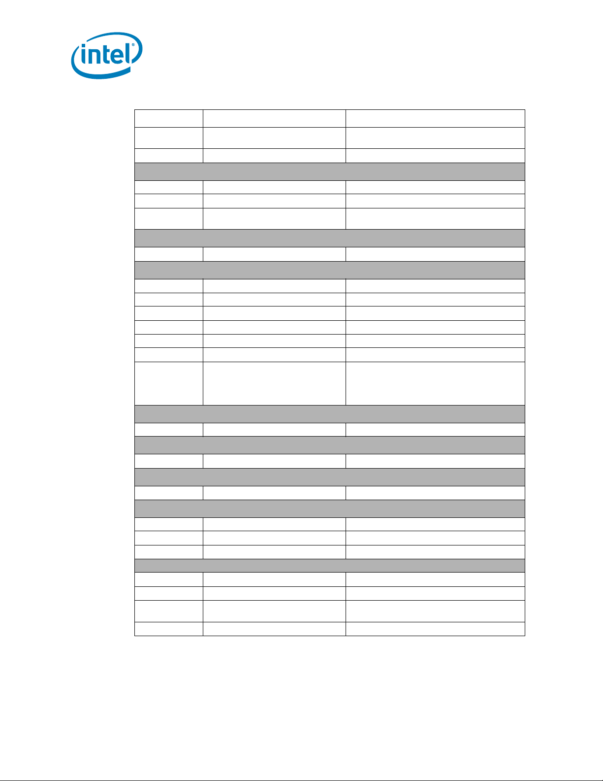
1-2 References.......................................................................................................15
2-1 Processor Power Supply Voltages1.......................................................................19
2-2 Voltage Identification Definition...........................................................................21
2-3 Power-On Configuration (POC[7:0]) Decode..........................................................25
2-4 VTT Voltage Identification Definition ....................................................................26
2-5 Signal Groups....................... .......................... .. .. ......................... .. .. .................27
2-6 Signals With On-Die Termination (ODT).................. .. .. .. .. ............................ .. .. .. ....29
2-7 Processor Absolute Minimum and Maximum Ratings...............................................31
2-8 Voltage and Current Specifications.......................................................................31
2-9 VCC Static and Transient Tolerance.....................................................................34
2-10 VCC Overshoot Specifications..............................................................................35
2-11 VTT Static and Transient Tolerance.....................................................................39
2-12 DDR3 and DDR3L Signal Group DC Specifications ..................................................41
2-13 PECI Signal DC Electrical Limits...........................................................................41
2-14 System Reference Clock DC Specifications............................................................42
2-15 RESET# Signal DC Specifications.........................................................................42
2-16 TAP Signal Group DC Specifications .....................................................................43
2-17 xxxPWRGOOD Signal Group DC Specifications.......................................................43
2-18 Processor Sideband Signal Group DC Specifications................................................43
2-19 Common Intel QuickPath Interconnect Specifications .............................................44
2-20 Parameter Values for Intel QuickPath Interconnect Channels at 4.8 GT/s ..................45
2-21 Parameter Values for Intel QuickPath Interconnect Channel at 5.86 or
6.4 GT/s ..........................................................................................................47
2-22 System Reference Clock AC Specifications .................................................. .. .. .. ....48
2-23 DDR3/DDR3L Electrical Characteristics and AC Specifications at 800 MT/s.................48
2-24 DDR3 Electrical Characteristics and AC Specifications at 1066 MT/s.......................... 49
2-25 DDR3/DDR3L Electrical Characteristics and AC Specifications at 1333 MT/s ............... 51
2-26 Processor Sideband Signal Group AC Specifications................................................52
2-27 TAP Signal Group AC Specifications......................................................................53
2-28 VID Signal Group AC Specifications......................................................................53
3-1 Overshoot/Undershoot Tolerance.........................................................................65
4-1 Processor Loading Specifications .........................................................................70
4-2 Package Handling Guidelines............................. .. ........................... .. .. .................70
4-3 Processor Materials............................................................................................71
5-1 Land Name.......................................................................................................73
5-2 Land Number....................................................................................................90
6-1 Signal Definitions .................................................. .......................................... 109
7-1 Frequency Optimized Server/Workstation Platform Thermal Specifications .............. 114
7-2 Frequency Optimized Server/Workstation Platform Thermal Profile (6 Core) ............ 115
7-3 Frequency Optimized Server/Workstation Platform Thermal Profile (4 Core) ............ 116
7-4 Advanced Server/Workstation Platform Thermal Specifications .............................. 117
7-5 Advanced Server/Workstation Thermal Profile A (6 Core)...................................... 118
7-6 Advanced Server/Workstation Thermal Profile B (6 Core)..................................... 118
7-7 Advanced Server/Workstation Thermal Profile A (4 Core)...................................... 119
7-8 Advanced Server/Workstation Thermal Profile B (4 Core)..................................... 120
7-9 Standard Server/Workstation Platform Thermal Specifications............................... 120
7-10 Standard Server/Workstation Platform Thermal Profile (6 Core)............................. 121
7-11 Standard Server/Workstation Platform Thermal Profile (4 Core)............................. 122
Intel® Xeon® Processor 5600 Series Datasheet Volume 1 7
Page 8

7-12 Low Power Platform 60W Thermal Specifications..................................................123
7-13 Low Power Platform 60W Thermal Profile (6 Core)................................................123
7-14 Low Power Platform 40W Thermal Specifications..................................................124
7-15 Low Power Platform 40W Thermal Profile (4 Core)................................................125
7-16 LV-60W Processor Thermal Specifications............................................................125
7-17 LV-60W Processor Dual Thermal Profile...............................................................126
7-18 LV-40W Processor Thermal Specifications............................................................126
7-19 LV-40W Processor Dual Thermal Profile...............................................................127
7-20 Summary of Processor-Specific PECI Commands..................................................133
7-21 GetTemp() Response Definition ................ ............................ .. .. .. .. .....................137
7-22 PCIConfigRd() Response Definition.....................................................................138
7-23 PCIConfigWr() Device/Function Support..............................................................138
7-24 PCIConfigWr() Response Definition.....................................................................140
7-25 Mailbox Command Summary.............................................................................141
7-26 Counter Definition............................................................................................142
7-27 Machine Check Bank Definitions.........................................................................143
7-28 ACPI T-state Duty Cycle Definition .....................................................................146
7-29 MbxSend() Response Definition ................................................ .. .. .....................150
7-30 MbxGet() Response Definition ...........................................................................151
7-31 Domain ID Definition............................................ .. .. ........................................153
7-32 Multi-Domain Command Code Reference.............................................................153
7-33 Completion Code Pass/Fail Mask........................................................................154
7-34 Device Specific Completion Code (CC) Definition..................................................154
7-35 Originator Response Guidelines.................................................................... .. .. ..155
7-36 Error Codes and Descriptions.............................................................................156
7-37 PECI Client Response During Power-Up (During ‘Data Not Ready’)..........................156
7-38 Storage Condition Ratings.................................................................................158
8-1 Power-On Configuration Signal Options...............................................................161
8-2 Coordination of Thread Power States at the Core Level .........................................163
8-3 Processor C-State Power Specifications...............................................................165
8-4 Processor S-States...........................................................................................166
9-1 PWM Fan Frequency Specifications For 4-Pin Active Thermal Solution......................181
9-2 Fan Specifications For 4-Pin Active Thermal Solution.............................................181
9-3 Fan Cable Connector P in Out for 4-Pin Active Thermal Solution ..............................181
8 Intel® Xeon® Processor 5600 Series Datasheet Volume 1
Page 9
Revision History
Revision
Number
-001 • Initial Release March 2010
-002 • Added Section 1.5: Statement of Volatility June 2011
Description Date
§
Intel® Xeon® Processor 5600 Series Datasheet Volume 1 9
Page 10

10 Intel® Xeon® Processor 5600 Series Datasheet Volume 1
Page 11

Introduction
1 Introduction
The Intel® Xeon® processor 5600 series is a server/workstation multi-core processor
based on 32 nm process technology. The processors feature two Intel® QuickPath
Interconnect point-to-point links capable of up to 6.4 GT/s, up to 12 MB of shared
cache, and an Integrated Memory Controller. The processors are optimized for
performance with the power efficiencies of a low-power microarchitecture to enable
smaller, quieter systems.
This datasheet provides DC and AC electrical specifications, signal integrity, differential
signaling specifications, pinout and signal definitions, package mechanical
specifications and thermal requirements, and additional features pertinent to
implementation and operation of the processor.
The Intel Xeon processor 5600 series features a range of Thermal Design Power (TDP)
envelopes from 40W TDP up to 130W TDP, and is segmented into multiple platforms:
• 2-Socket Frequency Optimized Server/Workstation Platforms support a 130 W
Thermal Design Power (TDP) SKU and up to 6 core support. These platforms
provide optimal overall performance and reliability, in addition to high-end graphics
support.
• 2-Socket Advanced Server/Workstation Platforms support a 95 W Thermal Design
Power (TDP) SKU. These platforms provide optimal overall performance featuring
up to 6 core support.
• 2-Socket Standard Server/Workstation Platforms support 80 W TDP processor
SKUs supporting up to 6 cores. These platforms provide optimal performance per
watt for rack-optimized platforms.
• Low Power Platforms implement 60 W TDP (up to 6 cores) and 40 W TDP (up to 4
cores) processor SKU’s. These processors are intended for dual-processor server
blades and embedded servers.
• 1-Socket Workstation Platforms support Intel® Xeon® Processor W3680. These
platforms enable a wide range of options for either the performance, power, or cost
sensitive customer.
• Platforms supporting Higher Case Temperature Low-Voltage Processors with 60 W
TDP (up to 6 cores) and 40 W TDP (up to 4 cores). The higher case temperatures
are intended to meet the short-term thermal profile requirements of NEBS Level 3.
These 2-socket processors are ideal for thermally-constrained form factors in
embedded servers, communications and storage markets. Specifications denoted
as LV-60W apply to the Intel® Xeon® Processor L5638. Specifications denoted as
LV-40W apply to the Intel® Xeon® Processor L5618.
®
Note: All references to “chipset” in this document pertain to the Intel
Intel® Xeon® Processor 5600 Series Datasheet Volume 1 11
®
5500 chipset.
Intel
Intel is committed to delivering processors for both server and workstation platforms
that maximize performance while meeting all Intel Quality and Reliability goals. The
product’s reliability assessment is based on a datasheet compliant system and
reference use condition. Intel utilizes a broad set of use condition assumptions (that is,
percentage of time in active vs. inactive operation, non-operating conditions, and the
number of power cycles per year) to ensure proper operation over the life of the
5520 chipset and the
Page 12
product. The reference use condition differs between workstation and server processor
SKU’s. Implementing processors outside of reference use conditions may affect
reliability performance.
1.1 Processor Features
Introduction
.
Table 1-1 provides an overview the Intel Xeon processor 5600 series feature set.
Table 1-1. Intel® Xeon® Processor 5600 Series Feature Set Overview
Feature Intel® Xeon® Processor 5600 Series
Cache Sizes Instruction Cache: 32 kB
12 MB Last-Level Cache shared among all cores
Data Transfer Rate (GT/s) Two full-width Intel® QuickPath Interconnect links;
Memory Support Integrated Memory Controller supports up to 3 channels of
DDR3 Memory Speed (MHz) 800, 1066, 1333
Multi-Core Support Up to 6 cores per processor (package)
®
Intel
Hyper-Threading Technology 2 threads per core
Dual Processor Support Up to 2 processor sockets per platform
Package 1366-land FC-LGA
DDR3 or DDR3L memory, with up to 3 DIMMs per channel
Data Cache: 32 kB
256 kB Mid-Level Cache per core
Up to 6.40 GT/s in each direction
The Intel Xeon processor 5600 series support all the existing Streaming SIMD
Extensions 2 (SSE2), Streaming SIMD Extensions 3 (SSE3) and Streaming SIMD
Extensions 4 (SSE4) instructions. Additionally, Intel Xeon processor 5600 series
support Intel® AES New Instructions (Intel® AES-NI).
The Intel Xeon processor 5600 series support Direct Cache Access (DCA). DCA enables
supported I/O adapter to pre-fetch data from memory to the processor cache, thereby
avoiding cache misses and improving application response times.
These processors support a maximum physical address size of 40 bits. Also supported
is IA-32e paging which adds support for 1 GB (2
4 kB page size support for linear to physical address translation.
Finally, these processors support several advanced technologies including Execute
Disable Bit, Intel
®
64 Technology, Enhanced Intel SpeedStep® Technology, Intel®
Virtualization Technology (Intel® VT), Intel® Hyper-Threading Technology, and Intel®
Turbo Boost Technology.
1.2 Platform Features
Various new component and platform capabilities are available with the implementation
of Intel Xeon processor 5600 series.
New memory subsystem capabilities include Low Voltage DDR3 (DDR3L) DIMM support
for power optimization. The Intel Xeon processor 5600 series also add features to
provide improved manageability of memory channels. The DDR_THERM2# signal has
been added to support high-temperature DIMMs and their 2X refresh requirements.
12 Intel
30
) page size in addition to 2 MB and
®
Xeon® Processor 5600 Series Datasheet Volume 1
Page 13

Introduction
Intel Xeon processor 5600 series are based on a low-power microarchitecture that
supports operation within various C-states. Additionally, six execution cores and power
management coordination logic are optimized to manage C-state support at both the
execution core and package levels. An Intel Turbo Boost Technology optimization
feature is supported on these processors for improved energy efficiency.
®
Trusted Execution Technology (Intel® TXT) is also supported and represents a
Intel
set of enhanced hardware components designed to help protect sensitive information
from software-based attacks. Features include capabilities in the microprocessor,
chipset, I/O subsystems, and other platform components. When coupled with suitably
enabled operating systems and applications, Intel TXT helps protect the confidentiality
and integrity of data in the face of increasingly hostile security environment.
1.3 Terminology
A ‘#’ symbol after a signal name refers to an active low signal, indicating a signal is in
the active state when driven to a low voltage level. For example, when RESET# is low,
a reset has been requested.
A ‘_N’ and ‘_P’ after a signal name refers to a differential pair.
Commonly used terms are explained here for clarification:
• 1366-land FC-LGA package — The Intel Xeon processor 5600 series is available
in a Flip-Chip Land Grid Array (FC-LGA) package, consisting of processor mounted
on a land grid array substrate with an integrated heat spreader (IHS).
• DDR3 — Double Data Rate 3 synchronous dynamic random access memory
(SDRAM) is the DDR memory standard, developed as the successor to DDR2
SDRAM.
• Enhanced Intel SpeedStep
Technology allows the operating system to reduce power consumption when
performance is not needed.
• Execute Disable Bit — Execute Disable allows memory to be marked as
executable or non-executable, when combined with a supporting operating system.
If code attempts to run in non-executable memory the processor raises an error to
the operating system. This feature can prevent some classes of viruses or worms
that exploit buffer over run vulnerabilities and can thus help improve the overall
security of the system. See the Intel
Developer's Manuals for more detailed information.
• Functional Operation — Refers to the normal operating conditions in which all
processor specifications, including DC, AC, signal quality , m echanical, and thermal,
are satisfied.
• Integrated Memory Controller (IMC) — This is a memory controller that is
integrated in the processor die. Intel Xeon processor 5600 series can support up to
3 channels of DDR3, DDR3L memory , with up to 3 DIMMs per channel. Please refer
to Intel Plan of Record for supported DIMM types, densities and configurations.
®
• Intel
faster than the marked frequency if the part is operating under power,
temperature, and current specification limits of the Thermal Design Power (TDP).
This results in increased performance of both single and multi-threaded
applications.
• Intel
extensions to Intel processors and chipsets that, with appropriate software,
enhance the platform security capabilities.
Turbo Boost Technology - A way to automatically run the processor core
®
Trusted Execution Technology - A highly versatile set of hardware
®
Technology — Enhanced Intel SpeedStep®
®
64 and IA-32 Architecture Software
Intel® Xeon® Processor 5600 Series Datasheet Volume 1 13
Page 14

Introduction
• Intel® QuickPath Interconnect (Intel® QPI) — A cache-coherent, links-based
interconnect specification for Intel processors, chipsets, and I/O bridge
components.
• Intel® 64 Architecture — An enhancement to Intel's IA-32 architec ture, allowing
the processor to execute operating systems and applications written to take
advantage of Intel
®
64.
• Intel® Virtualization Technology (Intel® VT) — A set of hardware
enhancements to Intel server and client platforms that can improve virtualization
solutions. VT provides a foundation for widely-deployed virtualization solutions and
enables more robust hardware assisted virtualization solution.
• Integrated Heat Spreader (IHS) — A component of the processor package used
to enhance the thermal performance of the package. Component thermal solutions
interface with the processor at the IHS surface.
• Jitter — Any timing variation of a transition edge or edges from the defined Unit
Interval (UI).
• LGA1366 Socket — The 1366-land FC-LGA package mates with the system board
through this surface mount, 1366-contact socket.
• Network Equipment Building System (NEBS) — The most common set of
environmental design guidelines applied to telecommunications equipment in the
United States.
• Serve r SKU — A processor Stock Keeping Unit (SKU) to be installed in either
server or workstation platforms. Electrical, power and thermal specifications for
these SKU’s are based on specific use condition assumptions. Server processors
may be further categorized as Frequency Optimized, Advanced, Standard and Low
Power SKUs. For further details on use condition assumptions, please refer to the
latest Product Release Qualification (PRQ) Report available via your Customer
Quality Engineer (CQE) contact.
• Storage Conditions — Refers to a non-operational state. The processor may be
installed in a platform, in a tray , or loose. Processors ma y be sealed in packaging or
exposed to free air. Under these conditions, processor lands should not be
connected to any supply voltages, have any I/Os biased, or receive any clocks.
• Unit Interval (UI) — Signaling convention that is binary and unidirectional. In
this binary signaling, one bit is sent for every edge of the forwarded clock, whether
it be a rising edge or a falling edge. If a number of edges are collected at instances
, t2, tn,...., tk then the UI at instance “n” is defined as:
t
1
UI n = t n - t
• Workstation SKU — A processor SKU to be installed in workstation platforms
only. Electrical, power and thermal specifications for these processors have been
developed based on Intel’s reliability goals at a reference use condition. In addition,
the processor validation and production test conditions have been optimized based
on these conditions. Operating “Workstation” processors in a server environment or
other application, could impact reliability performance, which means Intel’s
reliability goals may not be met. For further details on use condition assumptions or
reliability performance, please refer to the latest Product Release Qualification
(PRQ) Report available via your Customer Quality Engineer (CQE) contact.
14 Intel
n - 1
®
Xeon® Processor 5600 Series Datasheet Volume 1
Page 15
Introduction
1.4 References
Platform designers are strongly encouraged to maintain familiarity with the most up-todate revisions of processor and platform collateral.
Table 1-2. References
Advanced Configuration and Power Interface Specification www.acpi.info.
Compact Electronics Bay Specification: A Server System
Infrastructure (SSI) Specification for Value Servers and Workstations
Electronics Bay Specification for 2008 Servers and Workstation
Entry-Level Electronics-Bay Specifications: A Server System
Infrastructure (SSI) Specification for Entry Pedestal Servers and
Workstations
Thin Electronics Bay Specification: A Server System Infrastructure
(SSI) Specification for Rack-Optimized Servers
®
Intel
64 and IA-32 Architecture Software Developer's Manual
• Volume 1: Basic Architecture
• Volume 2A: Instruction Set Reference, A-M
• Volume 2B: Instruction Set Reference, N-Z
• Volume 3A: System Programming Guide, Part 1
• Volume 3B: Systems Programming Guide, Part 2
®
64 and IA-32 Architectures Optimization Reference Manual 248966 1
Intel
®
Intel
Xeon® Processor 5600 Series Datasheet, Volume 2 323370 1
®
Intel
Xeon® Processor 5500/5600 Series Thermal/Mechanical
Design Guide
Document Location / Document#1Notes
www.ssiforum.org
1
253665
253666
253667
253668
253669
321323 1
Notes:
1. Document is available publicly at http://www.intel.com.
1.5 Statement of Volatility
No Intel Xeon processor 5600 series product family processors retain any end user data
when powered down and/or when the parts are physically removed from the socket.
§
Intel® Xeon® Processor 5600 Series Datasheet Volume 1 15
Page 16

Introduction
16 Intel
®
Xeon® Processor 5600 Series Datasheet Volume 1
Page 17
Electrical Specifications
T
X
R
X
R
TT
R
TT
R
TT
R
TT
Signal
Signal
2 Electrical Specifications
2.1 Processor Signaling
The Intel Xeon processor 5600 series include 1366 lands, which utilize various signaling
technologies. Signals are grouped by electrical characteristics and buffer type into
various signal groups. These include Intel QuickPath Interconnect, DDR3 (Reference
Clock, Command, Control, and Data), Platform Environmental Control Interface (PECI),
Processor Sideband, System Reference Clock, Test Access Port (TAP), and Power/Other
signals. Refer to Table 2-5 for details.
2.1.1 Intel® QuickPath Interconnect
The Intel Xeon processor 5600 series provide two Intel QuickPath Interconnect ports
for high speed serial transfer between other enabled components. Each port consists of
two uni-directional links (for transmit and receive). A differential signaling scheme is
utilized, which consists of opposite-polarity (D_P, D_N) signal pairs.
On-die termination (ODT) is included on the processor silicon and terminated to V
Intel chipsets also provide ODT, thus eliminating the need to terminate on the system
board. Figure 2-1 illustrates the active ODT.
Figure 2-1. Active ODT for a Differential Link Example
2.1.2 DDR3 Signal Groups
The memory interface utilizes DDR3 technology, which consists of numerous signal
groups. These include: Reference Clocks, Command Signals, Control Signals, and Data
Signals. Each group consists of numerous signals, which may utilize various signaling
technologies. Please refer to Table 2-5 for further details.
2.1.3 Platform Environmental Control Interface (PECI)
PECI is an Intel proprietary interface that provides a communication channel between
Intel processors and chipset components to external thermal monitoring devices. The
processor contains a Digital Thermal Sensor (DTS) that reports a relative die
temperature as an offset from Thermal Control Circuit (TCC) activation temperature.
Temperature sensors located throughout the die are implemented as analog-to-digital
converters calibrated at the factory. PECI provides an interface for external devices to
read processor temperature, perform processor manageability functions, and manage
processor interface tuning and diagnostics. Please refer to Section 7.3 for processor
specific implementation details for PECI.
SS
.
Intel® Xeon® Processor 5600 Series Datasheet Volume 1 17
Page 18
Electrical Specifications
Minimum V
P
Maximum V
P
Minimum V
N
Maximum V
N
PECI High Range
PECI Low Range
Valid Input
Signal Range
Minimum
Hysteresis
V
TTD
PECI Ground
The PECI interface operates at a nominal voltage set by V
specifications shown in Table 2-13 is used with devices normally operating from a V
interface supply.
2.1.3.1 Input Device Hysteresis
The PECI client and host input buffers must use a Schmitt-triggered input design for
improved noise immunity. Pl ease refer to Figure 2-2 and Table 2-13.
Figure 2-2. Input Device Hysteresis
. The set of DC electrical
TTD
TTD
2.1.4 Processor Sideband Signals
Intel Xeon processor 5600 series include sideband signals that provide a variety of
functions. Details can be found in Table 2-5.
All Asynchronous Processor Sideband signals are required to be asserted/deasserted
for at least eight BCLKs in order for the processor to recognize the proper signal state.
See Table 2-18 and Table 2-26 for DC and AC specifications, respectively. Refer to
Section 3 for applicable signal integrity specifications.
2.1.5 System Reference Clock
The processor core, processor uncore, Intel QuickPath Interconnect link, and DDR3
memory interface frequencies are generated from BCLK_DP and BCLK_DN signals.
There is no direct link between core frequency and Intel QuickPath Interconnect link
frequency (for example, no core frequency to Intel QuickPath Interconnect multiplier).
The processor maximum core frequency, Intel QuickPath Interconnect link frequency
and DDR memory frequency are set during manufacturing. It is possible to override the
processor core frequency setting using software. This permits operation at lower core
frequencies than the factory set maximum core frequency.
The processor core frequency is configured during reset by using values stored within
the device during manufacturing. The stored value sets the lowest core multiplier at
which the particular processor can operate. If higher speeds are desired, the
appropriate ratio can be configured via the IA32_PERF_CTL MSR (MSR 199h); Bits
[15:0].
18 Intel
®
Xeon® Processor 5600 Series Datasheet Volume 1
Page 19
Electrical Specifications
Clock multiplying within the processor is provided by the internal phase locked loop
(PLL), which requires a constant frequency BCLK_DP, BCLK_DN input, with exceptions
for spread spectrum clocking. DC specifications for the BCLK_DP, BCLK_DN inputs are
provided in Table 2-14 and AC specifications in Table 2-22. These specifications must
be met while also meeting the associated signal quality specifications outlined in
Section 3.
2.1.6 Test Access Port (TAP) Signals
Due to the voltage levels supported by other components in the Test Access Port (TAP)
logic, it is recommended that the processor(s) be first in the TAP chain and followed by
any other components within the system. A translation buffer should be used to
connect to the rest of the chain unless one of the other components is capable of
accepting an input of the appropriate voltage. Similar considerations must be made for
TCK, TDO, TMS, and TRST#. Two copies of each signal may be required with each
driving a different voltage level.
Processor TAP signal DC specifications can be found in Table 2-18. AC specifications are
located in Table 2-27.
Note: While TDI, TMS and TRST# do not include On-Die Termination (OD T), these signals are
weakly pulled-up via a 1-5 kΩ resistor to V
TT
.
Note: While TCK does not include ODT, this signal is weakly pulled-down via a
1-5 kΩ resistor to V
SS
.
2.1.7 Power / Other Signals
Processors also include various other signals including power/ground, sense points, and
analog inputs. Details can be found in Table 2-5.
Table 2-1 outlines the required voltage supplies necessary to support Intel Xeon
processor 5600 series.
Table 2-1. Processor Power Supply Voltages
Power Rail Nominal Voltage Notes
V
CC
V
CCPLL
V
DDQ
V
, V
TTA
TTD
See Table 2-9;
Figure 2-3
1.80 V
1.50 V
1.35 V
See Table 2-11;
Figure 2-10
1
Each processor includes a dedicated VR11.1 regulator.
Each processor includes dedicated V
Each processor and DDR3 / DDR3L stack shares a dedicated voltage
regulator. It is expected that regulators will support both 1.50 and
1.35 V.
Each processor includes a dedicated VR11.0 regulator.
= V
+ V
V
TT
TTA
VID range is 1.025-1.2000 V; 20 mV offset (see Table 2-4); V
represents a typical voltage. V
31.5 mV offset from V
; P1V1_Vtt is VID[4:2] controlled,
TTD
TT_MIN
(typ).
TT
and PLL circuits.
CCPLL
and V
TT_MAX
loadlines represent a
TT
Note:
1. Refer to Table 2-8 for voltage and current specifications.
2.1.7.1 Power and Ground Lands
For clean on-chip power distribution, processors include lands for all required voltage
supplies. These include:
Intel® Xeon® Processor 5600 Series Datasheet Volume 1 19
Page 20

Electrical Specifications
•210 each VCC (271 ea. VSS) lands must be supplied with the voltage determined by
the VID[7:0] signals. Table 2-2 defines the voltage level associated with each core
VID pattern. Table 2-9 and Figure 2-3 represent V
•3 each V
lands, connected to a 1.8 V supply, power the Phase Lock Loop (PLL)
CCPLL
static and transient limits.
CC
clock generation circuitry. An on-die PLL filter solution is implemented within the
processor.
• 45 eac h V
(17 ea. VSS) lands, connected to a 1.50 / 1.35 V supply, provide
DDQ
power to the processor DDR3 interface. This supply also powers the DDR3 memory
subsystem.
•7 each V
(5 ea. VSS) and 26 ea. V
TTA
(17 ea. VSS) lands must be supplied with
TTD
the voltage determined by the VTT_VID[4:2] signals. Coupled with a 20 mV offset,
this corresponds to a VTT_VID pattern of ‘010xxx10’. Table 2-4 specifies the
voltage levels associated with each VTT
represent V
static and transient limits.
TT
VID pattern. Table 2-11 and Figure 2-10
_
All VCC, V
CCPLL, VDDQ, VTTA
, and V
lands must be connected to their respective
TTD
processor power planes, while all VSS lands must be connected to the system ground
plane.
2.1.7.2 Decoupling Guidelines
Due to its large number of transistors and high internal clock speeds, the processor is
capable of generating large current swings between low and full power states. This may
cause voltages on power planes to sag below their minimum values if bulk decoupling is
not adequate. Larger bulk storage (C
), such as electrolytic capacitors, supply
BULK
current during longer lasting changes in current demand, for example coming out of an
idle condition. Similarly, they act as a storage well for current when entering an idle
condition from a running condition. Care must be taken in the baseboard design to
ensure that the voltages provided to the processor remain within the specifications
listed in Table 2-8. Failure to do so can result in timing violations or reduced lifetime of
the processor.
2.1.7.3 Processor VCC Voltage Identification (VID) Signals
The voltage set by the VID signals is the maximum reference voltage regulator (VR)
output to be delivered to the processor VCC lands. VID signals are CMOS push/pull
outputs. Please refer to Table 2-18 for the DC specifications for these signals.
Individual processor VID values may be calibrated during manufacturing such that two
devices at the same core frequency may have different default VID settings.
The processor uses eight voltage identification signals, VID[7:0], to support automatic
selection of power supply voltages. Table 2-2 specifies the voltage level corresponding
to the state of VID[7:0]. A ‘1’ in this table refers to a high voltage level and a ‘0’ refers
to a low voltage level. If the processor socket is empty (SKTOCC# pulled high), or the
voltage regulation circuit cannot supply the voltage that is requested, the voltage
regulator must disable itself.
The processor provides the ability to operate while transitioning to an adjacent VID and
its associated processor core voltage (V
). This is represented by a DC shift in the
CC
loadline. It should be noted that a low-to-high or high-to-low voltage state change may
result in as many VID transitions as necessary to reach the target core voltage.
T ransitions abov e the maximum specified VID are not permitted. Table 2-8 includes VID
step sizes and DC shift ranges. Minimum and maximum voltages must be maintained
as shown in Table 2-9.
20 Intel
®
Xeon® Processor 5600 Series Datasheet Volume 1
Page 21
Electrical Specifications
The VRM or EVRD utilized must be capable of regulating its output to the value defined
by the new VID. DC specifications for dynamic VID transitions are included in
Table 2-18, while AC specifications are included in Table 2-28.
Power source characteristics must be guaranteed to be stable whenever the supply to
the voltage regulator is stable.
Table 2-2. Voltage Identification Definition (Sheet 1 of 5)
VID7 VID6 VID5 VID4 VID3 VID2 VID1 VID0 V
000000 0 0 OFF
000000 0 1 OFF
000000 1 01.60000
000000 1 11.59375
000001 0 01.58750
000001 0 11.58125
000001 1 01.57500
000001
000010
0 0 0 0 1 0 0 1 1.55625
0 0 0 0 1 0 1 0 1.55000
0 0 0 0 1 0 1 1 1.54375
000011 0 01.53750
000011 0 11.53125
000011 1 01.52500
000011 1 11.51875
000100 0 01.51250
000100 0 11.50625
000100 1 01.50000
000100 1 11.49375
000101 0 01.48750
000101 0 11.48125
000101 1 01.47500
000101 1 11.46875
000110 0 01.46250
000110 0 11.45625
000110 1 01.45000
000110 1 11.44375
000111 0 01.43750
000111 0 11.43125
000111 1 01.42500
000111 1 11.41875
001000 0 01.41250
001000 0 11.40625
001000 1 01.40000
001000 1 11.39375
1 1 1.56875
0 0 1.56250
CC_MAX
Intel® Xeon® Processor 5600 Series Datasheet Volume 1 21
Page 22

Table 2-2. Voltage Identification Definition (Sheet 2 of 5)
Electrical Specifications
VID7 VID6 VID5 VID4 VID3 VID2 VID1 VID0 V
CC_MAX
001001 0 01.38750
001001 0 11.38125
001001 1 01.37500
001001 1 11.36875
001010 0 01.36250
001010 0 11.35625
001010 1 01.35000
001010 1 11.34375
001011 0 01.33750
001011 0 11.33125
001011 1 01.32500
001011 1 11.31875
001100 0 01.31250
001100 0 11.30625
001100 1 01.30000
001100 1 11.29375
001101 0 01.28750
001101 0 11.28125
001101 1 01.27500
001101 1 11.26875
001110 0 01.26250
001110 0 11.25625
001110 1 01.25000
001110 1 11.24375
001111 0 01.23750
001111 0 11.23125
001111 1 01.22500
001111 1 11.21875
010000 0 01.21250
010000 0 11.20625
010000 1 01.20000
010000 1 11.19375
010001 0 01.18750
010001 0 11.18125
010001 1 01.17500
010001 1 11.16875
010010 0 01.16250
010010 0 11.15625
010010 1 01.15000
010010 1 11.14375
010011 0 01.13750
010011 0 11.13125
22 Intel
®
Xeon® Processor 5600 Series Datasheet Volume 1
Page 23
Electrical Specifications
Table 2-2. Voltage Identification Definition (Sheet 3 of 5)
VID7 VID6 VID5 VID4 VID3 VID2 VID1 VID0 V
010011 1 01.12500
010011 1 11.11875
010100 0 01.11250
010100 0 11.10625
010100 1 01.10000
010100 1 11.09375
010101 0 01.08750
010101 0 11.08125
010101 1 01.07500
010101 1 11.06875
010110 0 01.06250
010110 0 11.05625
010110 1 01.05000
010110 1 11.04375
010111 0 01.03750
010111 0 11.03125
010111 1 01.02500
010111 1 11.01875
011000 0 01.01250
011000 0 11.00625
011000 1 01.00000
011000 1 10.99375
011001 0 00.98750
011001 0 10.98125
011001 1 00.97500
011001 1 10.96875
011010 0 00.96250
011010 0 10.95625
011010 1 00.95000
011010 1 10.94375
011011 0 00.93750
011011 0 10.93125
011011 1 00.92500
011011 1 10.91875
011100 0 00.91250
011100 0 10.90625
011100 1 00.90000
011100 1 10.89375
011101 0 00.88750
011101 0 10.88125
011101 1 00.87500
011101 1 10.86875
CC_MAX
Intel® Xeon® Processor 5600 Series Datasheet Volume 1 23
Page 24
Table 2-2. Voltage Identification Definition (Sheet 4 of 5)
Electrical Specifications
VID7 VID6 VID5 VID4 VID3 VID2 VID1 VID0 V
CC_MAX
011110 0 00.86250
011110 0 10.85625
011110 1 00.85000
011110 1 10.84375
011111 0 00.83750
011111 0 10.83125
011111 1 00.82500
011111 1 10.81875
100000 0 00.81250
100000 0 10.80625
100000 1 00.80000
100000 1 10.79375
100001 0 00.78750
100001 0 10.78125
100001 1 00.77500
100001 1 10.76875
100010 0 00.76250
100010 0 10.75625
100010 1 00.75000
100010 1 10.74375
100011 0 00.73750
100011 0 10.73125
100011 1 00.72500
100011 1 10.71875
100100 0 00.71250
100100 0 10.70625
100100 1 00.70000
100100 1 10.69375
100101 0 00.68750
100101 0 10.68125
100101 1 00.67500
100101 1 10.66875
100110 0 00.66250
100110 0 10.65625
100110 1 00.65000
100110 1 10.64375
100111 0 00.63750
100111 0 10.63125
100111 1 00.62500
100111 1 10.61875
101000 0 00.61250
101000 0 10.60625
24 Intel
®
Xeon® Processor 5600 Series Datasheet Volume 1
Page 25
Electrical Specifications
Table 2-2. Voltage Identification Definition (Sheet 5 of 5)
VID7 VID6 VID5 VID4 VID3 VID2 VID1 VID0 V
101000 1 00.60000
101000 1 10.59375
101001 0 00.58750
101001 0 10.58125
101001 1 00.57500
101001 1 10.56875
101010 0 00.56250
101010 0 10.55625
101010 1 00.55000
101010 1 10.54375
101011 0 00.53750
101011 0 10.53125
101011 1 00.52500
101011 1 10.51875
101100 0 00.51250
101100 0 10.50625
101100 1 00.50000
111111 1 0 OFF
111111 1 1 OFF
Notes:
1. When the “11111111” VID pattern is observed, or when the SKTOCC# pin is pulled high, the voltage
regulator output should be disabled.
2. The VID range includes VID transitions that may be initiated by thermal events, Extended HALT state
transitions (see Section 8.2), higher C-States (see Section 8.2) or Enhanced Intel SpeedStep
transitions (see Section 8.5). The Extended HALT state must be enabled for the processor to
remain within its specifications
3. Once the VRM/EVRD is operating after power-up, if either the Output Enable signal is de-asserted or a
specific VID off code is received, the VRM/EVRD must turn off its output (the output should go to high
impedance) within 500 ms and latch off until power is cycled.
CC_MAX
®
Technology
2.1.7.3.1 Power-On Configuration (POC) Logic
VID[7:0] signals also serve a second function. During power-up, Power-On
Configuration POC[7:0] logic levels are MUX’ed onto these signals via 1-5 kΩ pull-up or
pull down resistors located on the baseboard. These values provide voltage regulator
keying (VID[7]), inform the processor of the platforms power delivery capabilities
(MSID[2:0]), and program the gain applied to the ISENSE input (CSC[2:0]). Table 2-3
maps VID signals to the corresponding POC functionality.
Table 2-3. Power-On Configuration (POC[7:0]) Decode (Sheet 1 of 2)
Function Bits POC Settings Description
VR_Key VID[7] 0b for VR11.1 Electronic safety key
Spare VID[6] 0b (default) Reserved for future use
Intel® Xeon® Processor 5600 Series Datasheet Volume 1 25
distinguishing VR11.1
Page 26
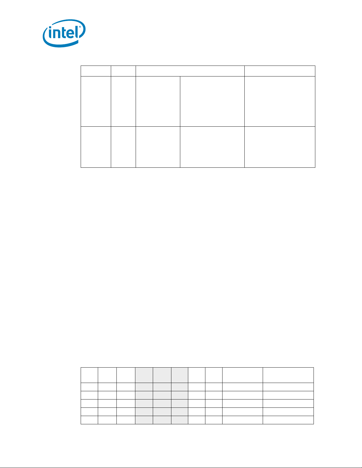
Table 2-3. Power-On Configuration (POC[7:0]) Decode (Sheet 2 of 2)
Function Bits POC Settings Description
CSC[2:0] VID[5:3] -000b
-001b
-010b
-011b
-100b
-101b
-111b
MSID[2:0] VID[2:0] -001b
-011b
-100b
-101b
-110b
Note:
1. This setting is defined for future use; no Intel Xeon processor 5600 series SKU is defined with ICC_MAX=40
A.
2. In general, set PWM IMON slope to 900 mV = IMAX, where IMAX = ICCMAX. For the 130 W SKU, set IMON
slope to 900 mV= 180 A. All other SKUs must match the values shown above. Please consult the PWM
datasheet for the IMON slope setting.
Feature Disabled
ICC_MAX = 40 A
40 W TDP / ICC_MAX = 50 A
60 W TDP / ICC_MAX = 80 A
80W TDP / ICC_MAX = 100 A
95W TDP / ICC_MAX = 120 A
130W TDP / ICC_MAX =
150A
40 W TDP / 50 A ICC_MAX
60 W TDP / 80 A ICC_MAX
80 W TDP / 100 A ICC_MAX
95 W TDP / 120 A ICC_MAX
130 W TDP / 150 A ICC_MAX
1
2
Current Sensor Configuration
(CSC) programs the gain
applied to the ISENSE A/D
output. ISENSE data is then
used to dynamically calculate
current and power.
MSID[2:0] signals are provided
to indicate the Market Segment
for the processor and may be
used for future processor
compatibility or keying. See
Section 8.1 for platform timing
requirements of the MSID[2:0]
signals.
Electrical Specifications
Some POC signals include specific timing requirements. Please refer to Section 8.1 for
further details.
2.1.7.4 Processor VTT Voltage Identification (VTT_VID) Signals
The voltage set by the VTT_VID signals is the typical reference voltage regulator (VR)
output to be delivered to the processor V
regulator will supply all V
TTA
and V
TTD
outputs. Please refer to Table 2-18 for the DC specifications for these signals.
Individual processor VTT_VID values may be calibrated during manufacturing such that
two devices at the same core frequency may have different default VTT_VID settings.
The processor utilizes three voltage identification signals to support automatic selection
of power supply voltages. These correspond to VTT_VID[4:2]. The V
delivered to the processor lands must also encompass a 20 mV offset (See Table 2-4;
V
) above the voltage level corresponding to the state of the VTT_VID[7:0] signals
TT_TYP
(See Table 2-4; VR 11.0 Voltage). Table 2-11 and Figure 2-10 provide the resulting
static and transient tolerances. Please note that the maximum and minimum electrical
loadlines are defined by a 31.5 mV tolerance band above and below V
Power source characteristics must be guaranteed to be stable whenever the supply to
the voltage regulator is stable.
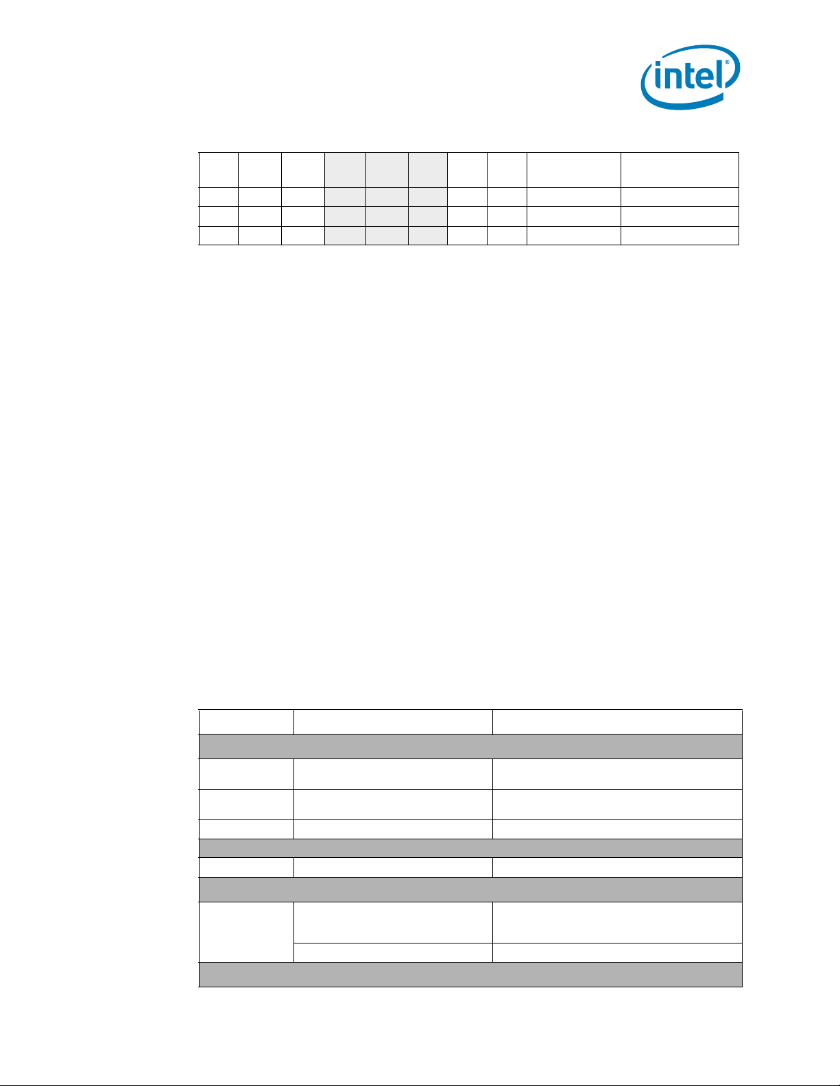
Table 2-4. VTT Voltage Identification Definition (Sheet 1 of 2)
VID7 VID6 VID5 VID4 VID3 VID2 VID1 VID0
010
010
010
010
010
0 0 0 1 0 1.200 V 1.220 V
0 0 1 1 0 1.175 V 1.195 V
0 1 0 1 0 1.150 V 1.170 V
0 1 1 1 0 1.125 V 1.145 V
1 0 0 1 0 1.100 V 1.120 V
TTA
and V
lands. It is expected that one
TTD
lands. VTT_VID signals are CMOS push/pull
VR 11.0
Voltage
voltage level
TT
valu es.
TT_TYP
V
TT_TYP
(Voltage + Offset)
26 Intel
®
Xeon® Processor 5600 Series Datasheet Volume 1
Page 27
Electrical Specifications
Table 2-4. VTT Voltage Identification Definition (Sheet 2 of 2)
VID7 VID6 VID5 VID4 VID3 VID2 VID1 VID0
0101 0 1 1 0 1.075 V 1.095 V
010
010
1 1 0 1 0 1.050 V 1.070 V
1 1 1 1 0 1.025 V 1.045 V
2.1.8 Reserved or Unused Signals
All Reserved (RSVD) signals must remain unconnected. Connection of these signals to
, V
, V
, V
V
CC
TTA
TTD
component malfunction or incompatibility with future processors. See Section 5 for the
land listing and the location of all Reserved signals.
For reliable operation, connect unused inputs or bidirectional signals to an appropriate
signal level. Unused Intel QuickPath Interconnect input and output pins can be left
floating. Unused active high inputs should be connected through a resistor to ground
). Unused outputs can be left unconnected; however, this may interfere with some
(V
SS
TAP functions, complicate debug probing, and prev ent boundary scan testing. A resistor
must be used when tying bidirectional signals to power or ground. When tying any
signal to power or ground, including a resistor will also allow for system testability.
Resistor values should be within ± 20% of the impedance of the baseboard trace,
unless otherwise noted in the appropriate platform design guidelines.
TAP signals do not include on-die termination, however they may include resistors on
package (refer to Section 2.1.6 for details). Inputs and utilized outputs must be
terminated on the baseboard. Unused outputs may be terminated on the baseboard or
left unconnected. Note that leaving unused outputs unterminated may interfere with
some TAP functions, complicate debug probing, and prevent boundary scan testing.
, VSS, or any other signal (including each other) can result in
DDQ
VR 11.0
Voltage
V
TT_TYP
(Voltage + Offset)
2.2 Signal Group Summary
Signals are aligned in Table 2-5 by buffer type and characteristics. “Buffer Type”
denotes the applicable signaling technology and specifications.
Table 2-5. Signal Groups (Sheet 1 of 2)
Signal Group Buffer Type Signals
Intel® QuickPath Interconnect Signals
Differential Intel®
Differential Intel®
Single ended Analog Input QPI[0/1]_COMP
DDR3 Reference Clocks
Differential Output DDR{0/1/2}_CLK_[P/N][3:0]
DDR3 Command Signals
Single ended CMOS Output DDR{0/1/2}_RAS#, DDR{0/1/2}_CAS#,
DDR3 Control Signals
QuickPath Interconnect Input QPI[0/1]_DRX_D[N/P][19:0],
QuickPath Interconnect Output QPI[0/1]_DTX_D[N/P][19:0],
2
2
Asynchronous Output DDR{0/1/2}_RESET#
2
1
QPI[0/1]_CLKRX_DP, QPI[0/1]_CLKRX_DN
QPI[0/1]_CLKTX_DP, QPI[0/1]_CLKTX_DN
DDR{0/1/2}_WE#, DDR{0/1/2}_MA[15:0],
DDR{0/1/2}_BA[2:0], DDR{0/1/2}_MA_PAR
Intel® Xeon® Processor 5600 Series Datasheet Volume 1 27
Page 28
Notes:
Table 2-5. Signal Groups (Sheet 2 of 2)
Signal Group Buffer Type Signals
Single ended CM OS Output DDR{0/1/2}_CS#[7:0], DDR{0/1/2}_ODT[5:0],
Single ended Analog Input DDR_VREF, DDR_COMP[2:0]
DDR3 Data Signals
Single ended CMOS Input/Output DDR{0/1/2}_DQ[63:0], DDR{0/1/2}_ECC[7:0]
Differential CMOS Input/Output DDR{0/1/2}_DQS_[N/P][17:0]
Single ended Asynchronous Input DDR{0/1/2}_PAR_ERR#[2:0],
Platform Environmental Control Interface (PECI)
Single ended Asynchronous Input/Output PECI
Processor Sideband Signals
Single ended GTL Input/Output BPM#[7:0], CAT_ERR#
Single ended Asynchronous Input PECI_ID#
Single ended Asynchronous GTL Output PRDY#, THERMTRIP#
Single ended Asynchronous GTL Input PREQ#
Single ended Asynchronous GTL Input/Output PROCHOT#
Single ended Asynchronous CMOS Output PSI#, TAPPWRGOOD
Single ended CMOS Output VID[7:6],
PWRGOOD Signal
Single ended Asynchronous Input VCCPWRGOOD, VDDPWRGOOD, VTTPWRGOOD
Reset Signal
Single ended Reset Input RESET#
System Reference Clock
Differential Input BCLK_DP, BCLK_DN
Test Access Port (TAP) Signals
Differential CMOS Output BCLK_ITP_DP, BCLK_ITP_DN
Single ended Input TCK, TDI, TMS, TRST#
Single ended GTL Output TDO
Power/Other Signals
2
Power / Ground V
Analog Input COMP0, ISENSE
Sense Points VCCSENSE, VSSSENSE, VSS_SENSE_VTTD,
Other SKTOCC#, DBR#
Electrical Specifications
1
DDR{0/1/2}_CKE[3:0]
DDR_THERM#, DDR_THERM2#
VID[5:3]/CSC[2:0],
VID[2:0]/MSID[2:0],
VTT_VID[4:2]
, V
CCPLL
, V
DDQ, VTTA
CC
, V
TTD
VTTD_SENSE
, V
SS
1. Refer to Section 5 for land assignments and Section 6 for signal definitions.
2. DDR{0/1/2} refers to DDR3 channel 0, DDR3 channel 1, and DDR3 Channel 2
Signals that include on-die termination (ODT) are listed in Table 2-6.
28 Intel
®
Xeon® Processor 5600 Series Datasheet Volume 1
Page 29
Electrical Specifications
Table 2-6. Signals With On-Die Termination (ODT)
Intel® QuickPath Interconnect Interface Signal Group
QPI[1:0]_DRX_DP[19:0], QPI[1:0]_DRX_DN[19:0], QPI[1:0]_TRX_DP[19:0], QPI[1:0]_TRX_DN[19:0],
QPI[0/1]_CLKRX_D[N/P], QPI[0/1]_CLKTX_D[N/P]
DDR3 Signal Group
DDR{0/1/2}_DQ[63:0], DDR{0/1/2}_DQS_[N/P][17:0], DDR{0/1/2}_ECC[7:0],
DDR{0/1/2}_PAR_ERR#[2:0]
Processor Sideband Signal Group
BPM#[7:0]6, PECI_ID#7, PREQ#
Test Access Port (TAP) Signal Group
4
TCK
, TDI5, TMS5, TRST#
Power/Other Signal Group
TAPPWRGOOD8, VCCPWRGOOD, VDDPWRGOOD, VTTPWRGOOD
1,2
3
1
6,
TAPPWRGOOD
5
9
8
1
Notes:
1. Unless otherwise specified, signals have ODT in the package with a 50 Ω pull-down to V
2. Unless otherwise specified, all DDR3 signals are terminated to V
3. DDR{0/1/2}_PAR_ERR#[2:0] are terminated to V
4. TCK does not include ODT, this signal is weakly pulled-down via a 1-5 kΩ resistor to VSS.
5. TDI, TMS, TRST# do not include ODT, these signals are weakly pulled-up via 1-5kΩ resistor to V
6. BPM[7:0]# and PREQ# signals have ODT in package with 35 Ω pull-ups to V
7. PECI_ID# has ODT in package with a 1-5 kΩ pull-up to VTT.
8. TAPPWRGOOD has ODT in package with a 1-2.5 kΩ pull-up to V
9. VCCPWRGOOD, VDDPWRGOOD, and VTTPWRGOOD have ODT in package with a 5-20 kΩ pull-down to V
DDQ.
DDQ
TT
/2.
TT.
.
.
SS
.
TT
2.3 Mixing Processors
Intel supports dual-processor (DP) configurations consisting of processors:
• from the same power optimization segment.
• that support the same maximum Intel QuickPath Interconnect and DDR3 memory
speeds.
• that share symmetry across physical packages with respect to the number of
logical processor per package, number of cores per package, number of Intel
QuickPath Interconnect interfaces, and cache topology.
• that have identical Extended Family, Extended Model, Processor Type, Family Code
and Model Number as indicated by the Function 1 of the CPUID instruction.
Note: Processors must operate with the same Intel QuickPath Interconnect, DDR3 memory
and core frequency.
While Intel does nothing to prevent processors from operating together, some
combinations may not be supported due to limited validation, which may result in
uncharacterized errata. Coupling this fact with the large number of Intel Xeon
processor 5600 series processor attributes, the following population rules and stepping
matrix have been developed to clearly define supported configurations.
• Processors must be of the same power-optimization segment. This insures
processors include the same maximum Intel QuickPath Interconnect and DDR3
operating speeds and cache sizes.
• Processors must operate at the same core frequency. Note, processors within the
same power-optimization segment supporting different maximum core frequencies
can be operated within a system. However, both must operate at the highest
frequency rating commonly supported. Mixing components operating at different
internal clock frequencies is not supported and will not be validated by Intel.
.
SS
Intel® Xeon® Processor 5600 Series Datasheet Volume 1 29
Page 30

Electrical Specifications
• Processors must share symmetry across physical packages with respect to the
number of logical processors per package, number of cores per package (but not
necessarily the same subset of cores within the packages), number of Intel
QuickPath Interconnect interfaces and cache topology.
• Mixing steppings is only supported with processors that have identical Extended
Family, Extended Model, Processor Type, Family Code and Model Number as
indicated by the Function 1 of the CPUID instruction. Mixing processors of different
steppings, but the same mode (as per CPUID instruction) is supported. Details
®
regarding the CPUID instruction are provide in the Intel
64 and IA-32
Architectures Software Developer’s Manual, Volume 2A.
• After AND ’ing the fe ature flag and extended feature flags from the installed
processors, any processor whose set of feature flags exactly matches the AND’ed
feature flags can be selected by the BIOS as the BSP. If no processor exactly
matches the AND’ed feature flag values, then the processor with the numerically
lower CPUID should be selected as the BSP.
• Intel requires that the proper microcode update be loaded on each processor
operating within the system. Any processor that does not have the proper
microcode update loaded is considered by Intel to be operating out-of-specification.
• Customers are fully responsible for the v alidation of their system configurations
Note: Processors within a system must operate at the same frequency per bits [15:8] of the
FLEX_RATIO MSR (Address: 194h); however this does not apply to frequency
transitions initiated due to thermal events, Extended HALT, Enhanced Intel SpeedStep
Technology transitions signal (See Section 8).
2.4 Flexible Motherboard Guidelines (FMB)
The Flexible Motherboard (FMB) guidelines are estimates of the maximum values the
processor will have over certain time periods. The values are only estimates and actual
specifications for future processors may differ. Processors may or may not have
specifications equal to the FMB value in the foreseeable future. System designers
should meet the FMB values to ensure their systems will be compatible with future
processors.
2.5 Absolute Maximum and Minimum Ratings
Table 2-7 specifies absolute maximum and minimum ratings only, which lie outside the
functional limits of the processor. Only within specified operation limits, can
functionality and long-term reliability be expected.
At conditions outside functional operation condition limits, but within absolute
maximum and minimum ratings, neither functionality nor long-term reliability can be
expected. If a device is returned to conditions within functional operation limits after
having been subjected to conditions outside these limits, but within the absolute
maximum and minimum ratings, the device may be functional, but with its lifetime
degraded depending on exposure to conditions exceeding the functional operation
condition limits.
At conditions exceeding absolute maximum and minimum ratings, neither functionality
nor long-term reliability can be expected. Moreover, if a device is subjected to these
conditions for any length of time then, when returned to conditions within the
functional operating condition limits, it will either not function or its reliability will be
severely degraded.
30 Intel
®
Xeon® Processor 5600 Series Datasheet Volume 1
Page 31

Electrical Specifications
Although the processor contains protective circuitry to resist damage from static
electric discharge, precautions should always be taken to avoid high static voltages or
electric fields.
Table 2-7. Processor Absolute Minimum and Maximum Ratin gs
Symbol Parameter Min Max Unit Notes
V
V
CCPLL
V
V
V
T
CASE
T
STORAGE
V
ISENSE
Notes:
1. For functional operation, all processor electri cal, signal quality, mechanical and thermal specifications must
2. Overshoot and undershoot voltage guidelines for input, output, and I/O signals are outlined in Section 3.
3. V
4. 5% tolerance
5. Storage temperature is applicable to storage conditions only. In this scenario, the processor must not
6. This rating applies to the processor and does not include any tray or packaging.
7. Failure to adhere to this specification can affect the long-term reliability of the processor
Processor core voltage with respect to V
CC
Processor PLL voltage with respect to V
Processor I/O supply voltage for DDR3
DDQ
with respect to V
Processor uncore analog voltage with
TTA
respect to V
Processor uncore digital voltage with
TTD
respect to V
Processor case temperature See
Storage temperature See
Analog input voltage with respect to VSS
for sensing core current consumption
be satisfied.
Excessive overshoot or undershoot on any signal will likely result in permanent damage to the processor.
and V
TTA
receive a clock, and no lands can be connected to a voltage bias. Storage within these limits will not affect
the long-term reliability of the device. For functional operation, please refer to the processor case
temperature specification.
should be derived from the same voltage regulator (VR).
TTD
SS
SS
SS
-0.3 1.4 V
SS
-0.3 2.0 V 4
SS
-0.3 1.8 V 4
-0.3 1.4 V 3
-0.3 1.4 V 3
Section 7
Section 7.4
-0.3 1.15 V
Section 7
Section 7.4
See
See
1,2
°C
°C5,6,7
2.6 Processor DC Specifications
DC specifications are defined at the processor pads, unless otherwise noted.
DC specifications are only valid while meeting specifications for case temperature
(T
specified in Section 7, “Thermal Specifications”), clock frequency, and input
CASE
voltages. Care should be taken to read all notes associated with each specification.
Table 2-8. Voltage and Current Specifications (Sheet 1 of 3)
Symbol Parameter
VID VCC VID Range - 0.750 1.350 V 2,3
V
CC
V
VID_STEP
V
CCPLL
V
DDQ
Intel® Xeon® Processor 5600 Series Datasheet Volume 1 31
Core Voltage
(Launch - FMB)
VID step size during a
transition
PLL Voltage
(DC + AC specification)
I/O Voltage for DDR3
(DC + AC specification)
Voltage
Plane
V
CC
- ± 6.250 mV 9
V
CCPLL
V
DDQ
Min Typ Max Unit Notes
V
=VID-(ICC * 0.8 mΩ)
CCMAX
=(VID-VRTOL)-(ICC*0.8 mΩ)
V
CCMIN
See Table 2-9 and Figure 2-3
0.95*V
(Typ)
0.95*V
(Typ)
CCPLL
DDQ
1.800 1.05*V
1.500 1.05*V
(Typ)
(Typ)
CCPLL
DDQ
V 3,4,6,7,11
V10
V10
1
Page 32
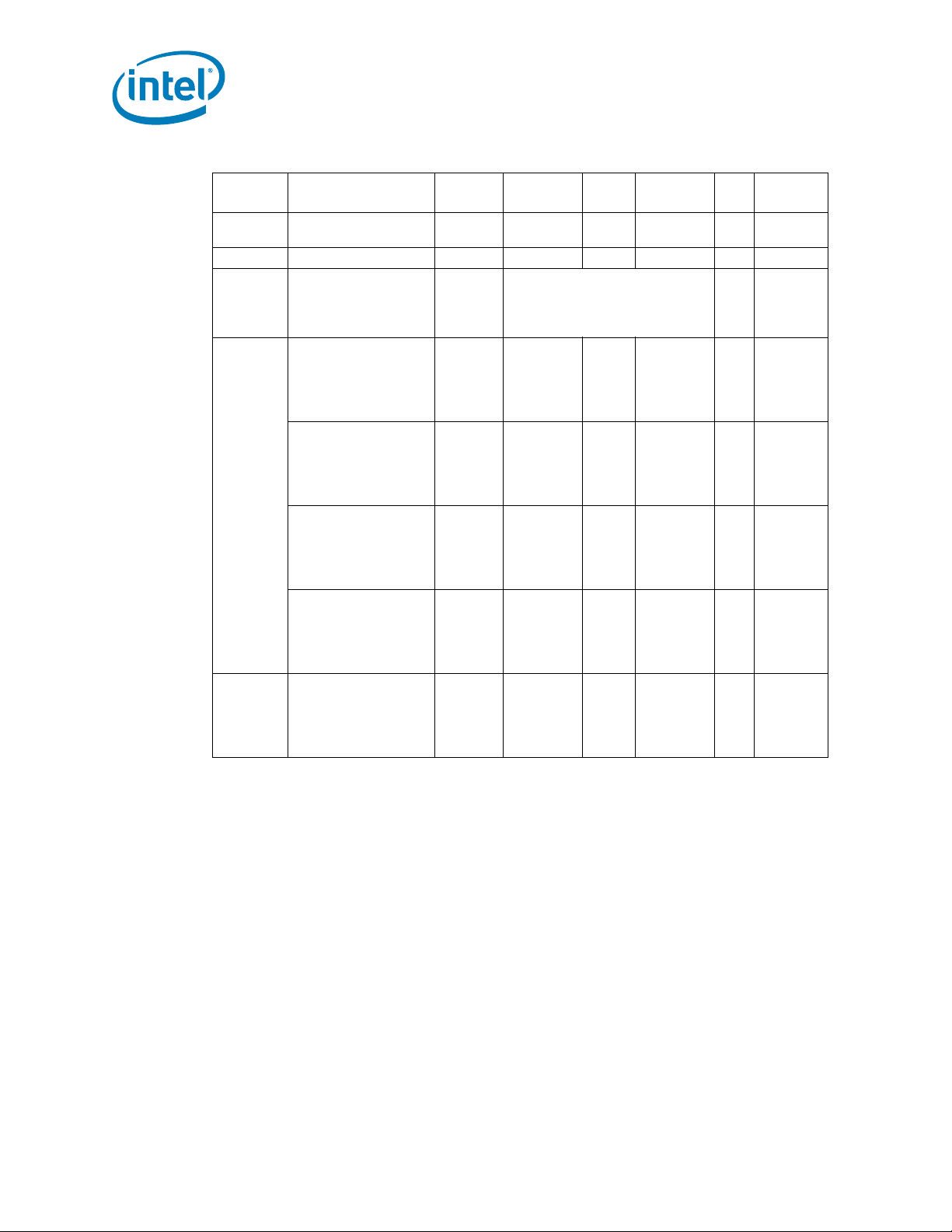
Table 2-8. Voltage and Current Specifications (Sheet 2 of 3)
Electrical Specifications
Symbol Parameter
V
DDQ
VTT_VID V
V
I/O Voltage for DDR3L
(DC + AC specification)
VID Range - 1.045 1.220 V 2,3
TT
Uncore Voltage
TT
(Launch - FMB)
I
CC_MAX
I
CCPLL_MAX
I
DDQ_MAX
I
TT_MAX
Max. Processor Current:
Frequency Optimized
Server/Workstation
(TDP = 130 W)
(Launch - FMB)
Max. Processor Current:
Advanced
Server/Workstation
(TDP = 95 W)
(Launch - FMB)
Max. Processor Current:
Standard
Server/Workstation
(TDP = 80 W)
(Launch - FMB)
Max. Processor Current:
Low Power & LV-60W
(TDP = 60 W)
(Launch - FMB)
Max. Processor Current:
Low Power & LV-40W
(TDP = 40 W)
(Launch - FMB)
Voltage
Plane
V
DDQ
V
TT
V
CC
V
CCPLL
V
DDQ
V
TTA
V
TTD
V
CC
V
CCPLL
V
DDQ
V
TTA
V
TTD
V
CC
V
CCPLL
V
DDQ
V
TTA
V
TTD
V
CC
V
CCPLL
V
DDQ
V
TTA
V
TTD
V
CC
V
CCPLL
V
DDQ
V
TTA
V
TTD
Min Typ Max Unit Notes
0.95*V
1.350 1.075*V
DDQ
(Typ)
V
=VTT_VID-(ITT*6 mΩ)
TT_TYP
V
TT_MAX=VTTTYP
V
TT_MIN=VTTTYP
(Typ)
+ 31.5 mV
- 31.5 mV
V10
DDQ
V 3,5,8,11
See Table 2-11 and Figure 2-10
150
1.1
9
6
22
120
1.1
9
6
22
100
1.1
9
6
22
80
1.1
9
6
20
50
1.1
9
6
20
A
A
A
A
A
A
A
A
A
A
A
A
A
A
A
A
A
A
A
A
A
A
A
A
A
1
11
11
11
11
11
32 Intel
®
Xeon® Processor 5600 Series Datasheet Volume 1
Page 33

Electrical Specifications
Table 2-8. Voltage and Current Specifications (Sheet 3 of 3)
Symbol Parameter
I
CC_TDC
I
CCPLL_TDC
I
DDQ_TDC
I
TT_TDC
Thermal Design
Current:
Frequency Optimized
Server/Workstation
(TDP = 130 W)
(Launch - FMB)
Thermal Design
Current:
Advanced
Server/Workstation
(TDP = 95 W)
(Launch - FMB)
Thermal Design
Current:
Standard
Server/Workstation
(TDP = 80 W)
(Launch - FMB)
Thermal Design
Current:
Low Power & LV-60W
(TDP = 60 W)
(Launch - FMB)
Thermal Design
Current:
Low Power & LV-40W
(TDP = 40 W)
(Launch - FMB)
I
DDQ_S3
DDR3 System Memory
Interface Supply
Current in Standby
State
Voltage
Plane
V
CC
V
CCPLL
V
DDQ
V
TTA
V
TTD
V
CC
V
CCPLL
V
DDQ
V
TTA
V
TTD
V
CC
V
CCPLL
V
DDQ
V
TTA
V
TTD
V
CC
V
CCPLL
V
DDQ
V
TTA
V
TTD
V
CC
V
CCPLL
V
DDQ
V
TTA
V
TTD
V
DDQ
Min Typ Max Unit Notes
110
1.1
9
6
22
101
1.1
9
6
22
70
1.1
9
6
22
60
1.1
9
6
20
40
1.1
9
6
20
A
11,12
A
A
A
A
A
11,12
A
A
A
A
A
11,12
A
A
A
A
A
11,12
A
A
A
A
A
11,12
A
A
A
A
1 A 13,14
1
Notes:
1. Unless otherwise noted, all specifications in this table apply to all processors.
2. Individual processor VID and/or VTT_VID values may be calibrated during manufacturing such that two
devices at the same speed may have different settings.
3. These voltages are targets only. A variable voltage source should exist on systems in the event that a
different voltage is required.
4. The V
5. The V
6. Refer to Table 2-9 and corresponding Figure 2-3. The processor should not be subjected to any static V
7. Minimu m V
8. Refer to Table 2-11 and corresponding Figure 2-10. The processor should not be subjected to any static V
9. This specification represents the V
10.Baseboard b andwidth is limited to 20 MHz.
11.FMB is the flexible motherboard guidelines. See Section 2.4 for FMB details.
12.ICC_TDC (Thermal Design Current) is the sustained (DC equivalent) current that the processor is capable of
voltage specification requirements are measured across vias on the platform for the VCCSENSE and
CC
VSSSENSE pins close to the socket with a 100 MHz bandwidth oscilloscope, 1.5 pF maximum probe
capacitance, and 1 MΩ minimum impedance . The maximum length of ground wire on the probe should be
less than 5 mm. Ensure external noise from the system is not coupled in the scope probe.
voltage specification requirements are measured across vias on the platform for the VTTD_SENSE
TT
and VSS_SENSE_VTTD lands close to the socket with a 100 MHz bandwidth oscilloscope, 1.5 pF maximum
probe capacitance, and 1 MΩ minimum imped ance. The max imum length o f ground wire on the probe should
be less than 5 mm. Ensure external noise from the system is not coupled in the scope probe.
level that exceeds the V
can shorten processor lifetime.
Table 7-1. I
drawing I
processor current draw over various time durations.
and maximum ICC are specified at the maximum processor case temperature (T
CC
is specified at the relative V
CC_MAX
for up to 10 ms. Refer to Figure 2-5 through Figure 2-8 for further details on the average
CC_MAX
level that exceeds the V
can shorten processor lifetime.
requirements for VID transitions are included in Figure 2-29.
drawing indefinitely and should be used for the voltage regulator temperature assessment. The voltage
regulator is responsible for monitoring its temperature and asserting the necessary signal to inform the
processor of a thermal excursion.
associated with any particular current. Failure to adhere to this specification
CC_MAX
point on the VCC load line. The processor is capable of
CC_MAX
associated with any particular current. Failure to adhere to this specification
TT_MAX
reduction due to each VID transition. See Section 2.1.7.3. AC timing
CC
CASE
CC
) shown in
TT
Intel® Xeon® Processor 5600 Series Datasheet Volume 1 33
Page 34

Electrical Specifications
13.Specification is at T
14.Characterized by design (not tested)
CASE
= 50 °C.
Table 2-9. VCC Static and Transient Tolerance
ICC (A) V
0 VID - 0.000 VID - 0.015 VID - 0.030
5 VID - 0.004 VID - 0.019 VID - 0.034
10 VID - 0.008 VID - 0.023 VID - 0.038
15 VID - 0.012 VID - 0.027 VID - 0.042
20 VID - 0.016 VID - 0.031 VID - 0.046
25 VID - 0.020 VID - 0.035 VID - 0.050
30 VID - 0.024 VID - 0.039 VID - 0.054
35 VID - 0.028 VID - 0.043 VID - 0.058
40 VID - 0.032 VID - 0.047 VID - 0.062
45 VID - 0.036 VID - 0.051 VID - 0.066
50 VID - 0.040 VID - 0.055 VID - 0.070
55 VID - 0.044 VID - 0.059 VID - 0.074
60 VID - 0.048 VID - 0.063 VID - 0.078
65 VID - 0.052 VID - 0.067 VID - 0.082
70 VID - 0.056 VID - 0.071 VID - 0.086
75 VID - 0.060 VID - 0.075 VID - 0.090
80 VID - 0.064 VID - 0.079 VID - 0.094
85 VID - 0.068 VID - 0.083 VID - 0.098
90 VID - 0.072 VID - 0.087 VID - 0.102
95 VID - 0.076 VID - 0.091 VID - 0.106
100 VID - 0.080 VID - 0.095 VID - 0.110
105 VID - 0.084 VID - 0.099 VID - 0.114
110 VID - 0.088 VID - 0.103 VID - 0.118
115 VID - 0.092 VID - 0.107 VID - 0.122
120 VID - 0.096 VID - 0.111 VID - 0.126
125 VID - 0.100 VID - 0.115 VID - 0.130
130 VID - 0.104 VID - 0.119 VID - 0.134
135 VID - 0.108 VID - 0.123 VID - 0.138
140 VID - 0.112 VID - 0.127 VID - 0.142
145 VID - 0.116 VID - 0.131 VID - 0.146
150 VID - 0.120 VID - 0.135 VID - 0.150
(V) V
CC_MAX
(V) V
CC_TYP
(V) Notes
CC_MIN
1,2,3,4
Notes:
1. The V
overshoot specifications.
2. This table is intended to aid in reading discrete points on Figure 2-3.
3. The loadlines specify voltage limits at the die measured at the VCC_SENSE and VSS_SENSE lands. V oltag e
regulation feedback for voltage regulator circuits must also be taken from processor VCC_SENSE and
VSS_SENSE lands.
CC_MIN
and V
4. Processor core current (I
loadlines represent static and transient limits. Please see Section 2.6.1 for VCC
CC_MAX
) ranges are valid up to I
CC
CC_MAX
34 Intel
of the processor SKU as defined in Table 2-8.
®
Xeon® Processor 5600 Series Datasheet Volume 1
Page 35

Electrical Specifications
VID - 0.000
VID - 0.020
VID - 0.040
VID - 0.060
VID - 0.080
VID - 0.100
VID - 0.120
VID - 0.140
VID - 0.160
VID - 0.180
0 10 20 30 40 50 60 70 80 90 100 110 120 130 140 150
Icc [A]
Vcc [V]
Figure 2-3. VCC Static and Transient Tolerance Loadlines
Notes:
1. The V
overshoot specifications.
2. Refer to Table 2-9 for V
3. The loadlines specify voltage limits at the die measured at the VCC_SENSE and VSS_SENSE lands. Voltage
regulation feedback for voltage regulator circuits must also be taken from processor VCC_SENSE and
VSS_SENSE lands.
4. Processor core current (I
CC_MIN
and V
loadlines represent static and transient limits. Please see Section 2.6.1 for V
CC_MAX
Static and Transient Tolerance.
CC
) ranges are valid up to I
CC
CC_MAX
1,2,3,4
CC
of the processor SKU as defined in Table 2-8.
2.6.1 VCC Overshoot Specifications
The processor can tolerate short transient overshoot events where VCC exceeds the VID
voltage when transitioning from a high-to-low current load condition. This overshoot
cannot exceed VID + V
OS_MAX
(V
OS_MAX
VID). These specifications apply to the processor die voltage as measured across the
VCC_SENSE and VSS_SENSE lands.
Table 2-10. VCC Overshoot Specifications
Symbol Parameter Min Max Units Figure Notes
V
OS_MAX
T
OS_MAX
Intel® Xeon® Processor 5600 Series Datasheet Volume 1 35
Magnitude of VCC overshoot above VID - 50 mV 2-4
Time duration of VCC overshoot above VID - 25 µs 2-4
is the maximum allowable overshoot above
Page 36

Electrical Specifications
Example Overshoot Waveform
0 5 10 15 20 25
Time [us]
Voltage [V]
VID - 0.000
VID + 0.050
V
OS
T
OS
TOS: Overshoot time above VID
OS
: Overshoot above VID
Figure 2-4. V
Overshoot Example Waveform
CC
Notes:
1. V
2. T
is the measured overshoot voltage.
OS
is the measured time duration above VID.
OS
V
2.6.2 Die Voltage Validation
Core voltage (VCC) overshoot events at the processor must meet the specifications in
Table 2-10 when measured across the VCC_ SENSE and VSS_SENSE lands. Overshoot
events that are < 10 ns in duration may be ignored. These measurements of processor
die level overshoot should be taken with a 100 MHz bandwidth limited oscilloscope.
36 Intel
®
Xeon® Processor 5600 Series Datasheet Volume 1
Page 37

Electrical Specifications
Notes:
Notes:
105
110
115
120
125
130
135
140
145
150
155
0.01 0.1 1 10 100 1000
Time Du ra tio n , (s )
Sustained Current (A)
95.0
100.0
105.0
110.0
115.0
120.0
125.0
0.01 0.1 1 10 100 1000
Time Duration, (s)
Sustained Current (A)
Figure 2-5. Load Current Versus Time (Frequency Optimized Server/Workstation)
1. Processor or voltage regulator thermal protection circuitry should not trip for load currents greater than
2. Not 100% tested. Specified by design characterization.
I
CC_TDC
.
1,2
Figure 2-6. Load Current Versus Time (Advanced Server/Workstation)
Intel® Xeon® Processor 5600 Series Datasheet Volume 1 37
1. Processor or voltage regulator thermal protection circuitry should not trip for load currents greater than
2. Not 100% tested. Specified by design characterization.
.
I
CC_TDC
1,2
Page 38

Electrical Specifications
Notes:
Notes:
65
70
75
80
85
90
95
100
105
0.01 0.1 1 10 100 1000
Time Duration, (s)
Sustained Current (A)
45
50
55
60
65
70
75
80
85
0.01 0.1 1 10 100 1000
Time Duration , (s )
Sustained Current (A)
Figure 2-7. Load Current Versus Time (Standard Server/Workstation)
1. Processor or voltage regulator thermal protection circuitry should not trip for load currents greater than
2. Not 100% tested. Specified by design characterization.
I
CC_TDC
.
1,2
Figure 2-8. Load Current Versus Time (Low Power & LV-60W)
1. Processor or voltage regulator thermal protection circuitry should not trip for load currents greater than
2. Not 100% tested. Specified by design characterization.
I
CC_TDC
.
1,2
38 Intel
®
Xeon® Processor 5600 Series Datasheet Volume 1
Page 39

Electrical Specifications
Notes:
35
40
45
50
55
0.01 0.1 1 10 100 1000
Time Duration, T
VR_AVE
(s)
Figure 2-9. Load Current Versus Time (Low Power & LV-40W)
Sust ai ned Cu r re nt ( A )
1. Processor or voltage regulator thermal protection circuitry should not trip for load currents greater than
2. Not 100% tested. Specified by design characterization.
I
CC_TDC
.
1,2
Table 2-11. VTT Static and Transient Tolerance (Sheet 1 of 2)
ITT (A) V
(V) V
TT_Max
(V) V
TT_Typ
(V) Notes
TT_Min
0 VTT_VID + 0.0315 VTT_VID - 0.0000 VTT_VID - 0.0315
1 VTT_VID + 0.0255 VTT_VID - 0.0060 VTT_VID - 0.0375
2 VTT_VID + 0.0195 VTT_VID - 0.0120 VTT_VID - 0.0435
3 VTT_VID + 0.0135 VTT_VID - 0.0180 VTT_VID - 0.0495
4 VTT_VID + 0.0075 VTT_VID - 0.0240 VTT_VID - 0.0555
5 VTT_VID + 0.0015 VTT_VID - 0.0300 VTT_VID - 0.0615
6 VTT_VID - 0.0045 VTT_VID - 0.0360 VTT_VID - 0.0675
7 VTT_VID - 0.0105 VTT_VID - 0.0420 VTT_VID - 0.0735
8 VTT_VID - 0.0165 VTT_VID - 0.0480 VTT_VID - 0.0795
9 VTT_VID - 0.0225 VTT_VID - 0.0540 VTT_VID - 0.0855
10 VTT_VID - 0.0285 VTT_VID - 0.0600 VTT_VID - 0.0915
11 VTT_VID - 0.0345 VTT_VID - 0.0660 VTT_VID - 0.0975
12 VTT_VID - 0.0405 VTT_VID - 0.0720 VTT_VID - 0.1035
13 VTT_VID - 0.0465 VTT_VID - 0.0780 VTT_VID - 0.1095
14 VTT_VID - 0.0525 VTT_VID - 0.0840 VTT_VID - 0.1155
15 VTT_VID - 0.0585 VTT_VID - 0.0900 VTT_VID - 0.1215
16 VTT_VID - 0.0645 VTT_VID - 0.0960 VTT_VID - 0.1275
17 VTT_VID - 0.0705 VTT_VID - 0.1020 VTT_VID - 0.1335
18 VTT_VID - 0.0765 VTT_VID - 0.1080 VTT_VID - 0.1395
1,2,3,4
Intel® Xeon® Processor 5600 Series Datasheet Volume 1 39
Page 40

Table 2-11. VTT Static and Transient Tolerance (Sheet 2 of 2)
-0.2125
-0.2000
-0.1875
-0.1750
-0.1625
-0.1500
-0.1375
-0.1250
-0.1125
-0.1000
-0.0875
-0.0750
-0.0625
-0.0500
-0.0375
-0.0250
-0.0125
0.0000
0.0125
0.0250
0.0375
0.0500
0 5 10 15 20 25
ITT [A]
VTT_VID DevIatIon
ITT (A) V
19 VTT_VID - 0.0825 VTT_VID - 0.1140 VTT_VID - 0.1455
20 VTT_VID - 0.0885 VTT_VID - 0.1200 VTT_VID - 0.1515
21 VTT_VID - 0.0945 VTT_VID - 0.1260 VTT_VID - 0.1575
22 VTT_VID - 0.1005 VTT_VID - 0.1320 VTT_VID - 0.1635
23 VTT_VID - 0.1065 VTT_VID - 0.1380 VTT_VID - 0.1695
24 VTT_VID - 0.1125 VTT_VID - 0.1440 VTT_VID - 0.1755
25 VTT_VID - 0.1185 VTT_VID - 0.1500 VTT_VID - 0.1815
26 VTT_VID - 0.1245 VTT_VID - 0.1560 VTT_VID - 0.1875
27 VTT_VID - 0.1305 VTT_VID - 0.1620 VTT_VID - 0.1935
28 VTT_VID - 0.1365 VTT_VID - 0.1680 VTT_VID - 0.1995
Note:
listed in this table is the sum of I
1. I
TT
2. This table is intended to aid in reading discrete points on Figure 2-10.
3. The V
offset from V
4. The loadlines specify voltage limits at the die measured at the VTTD_SENSE and VSS_SENSE_VTTD lands.
Voltage regulation feedback for regulator circuits must also be taken from VTTD_SENSE and
VSS_SENSE_VTTD lands.
TT_MIN
and V
TT_TYP
TT_MAX
.
(V) V
TT_Max
TTA
and I
(V) V
TT_Typ
.
TTD
loadlines represent static and transient limits. Each is char acterized by a ±31.5 mV
Electrical Specifications
(V) Notes
TT_Min
1,2,3,4
Figure 2-10. VTT Static and Transient Tolerance Loadlines
40 Intel
Notes:
1. The V
2. Refer to Table 2-4 for processor VTT_VID information.
3. Refer to Table 2-11 for V
TT_MIN
offset from V
and V
TT_TYP
loadlines represent static and transient limits. Each is char acterized by a ±31.5 mV
TT_MAX
.
Static and Transient Tolerance.
TT
®
Xeon® Processor 5600 Series Datasheet Volume 1
Page 41

Electrical Specifications
Table 2-12. DDR3 and DDR3L Signal Group DC Specifications
Symbol Parameter Min Typ Max Units Notes
V
V
V
V
R
R
R
R
R
Data ODT
ParErr ODT
I
DDR_COMP0 COMP Resistance 99 100 101 Ω 8
DDR_COMP1 COMP Resistance 24.65 24.9 25.15 Ω 8
DDR_COMP2 COMP Resistance 128.7 130 131.3 Ω 8
Input Low Voltage 0.43*V
IL
Input High Voltage 0.57*V
IH
Output Low Voltage (V
OL
Output High Voltage V
OH
Clock Buffer On
ON
Resistance
Command Buffer On
ON
Resistance
Control Buffer On
ON
Resistance
Data Buffer On
ON
Resistance
RESET Buffer On
ON
Resistance
On-Die T e rmination for
Data Signals
On-Die T e rmination for
Parity Error bits
Input Leakage Current N/A N/A ± 500 mA
LI
DDQ
/ 2)* (R
DDQ
/(RON+R
VTT_TERM
- ((V
DDQ
(R
/(RON+R
ON
21 31 Ω 5
16 24 Ω 5
21 31 Ω 5
21 33 Ω 5
553Ω 5
45
90
90 110 Ω
/ 2)*
DDQ
VTT_TERM
ON
1
V2,
DDQ
V3, 4
))
))
55
V6
V4,6
Ω 7
110
Notes:
1. Unless otherwise noted, all specifications in this table apply to all processor frequencies.
is the maximum voltage level at a receiving agent that will be interpreted as a logical low value.
2. V
IL
is the minimum voltage level at a receiving agent that will be interpreted as a logical high value.
3. V
IH
and VOH may experience excursions above V
4. V
IH
signal quality specifications. Refer to Section 3.
5. This is the pull down driver resistance.
6. R
VTT_TERM
DIMM datasheet.
7. The minimum and maximum values for these signals are programmable by BIOS to one of the pairs.
8. COMP resistance must be provided on the system board with 1% resistors.
is the termination on the DIMM and not controlled by the processor. Please refer to the applicable
. However, input signal drivers must comply with the
DDQ
Table 2-13. PECI Signal DC Electrical Limits (Sheet 1 of 2)
Symbol Definition and Conditions Min Max Units Notes
V
In
V
Hysteresis
V
N
V
P
R
Pullup
I
Leak+
I
Leak-
C
Bus
Input Voltage Range -0.150 V
Hysteresis 0.100 * V
Negative-edge threshold voltage 0.275 * V
Positive-edge threshold voltage 0.550 * V
Pullup Resistance
= 0.75 * V
(V
OH
High impedance state leakage to
V
(V
leak
= VOL)
TTD
TTD
)
High impedance leakage to GND
(V
= VOH)
leak
N/A 50 Ω
N/A 50 µA 3
N/A 25 µA 3
Bus capacitance per node N/A 10 pF 4,5
TTD
TTD
TTD
+ 0.150 V
TTD
0.500 * V
0.725 * V
TTD
TTD
1
V
V2,6
V2,6
Intel® Xeon® Processor 5600 Series Datasheet Volume 1 41
Page 42

Table 2-13. PECI Signal DC Electrical Limits (Sheet 2 of 2)
Symbol Definition and Conditions Min Max Units Notes
V
Noise
Signal noise immunity above
300 MHz
0.100 * V
TTD
Electrical Specifications
N/A V
p-p
1
Note:
1. V
2. It is expected that the PECI driver will take into account, the variance in the receiver input thresholds and
3. The leakage specification applies to powered devices on the PECI bus.
4. One node is counted for each client and one node for the s ystem host. Extended tr ace lengths might appear
5. Excessive capacitive loading on the PECI line may slow down the signal rise/f all times and consequently
6. Please refer to Figure 2-2 for further information.
supplies the PECI interface. PECI behavior does not affect V
TTD
consequently, be able to drive its output within safe limits (-0.150 V to 0.275*V
0.725*V
TTD
to V
+0.150 for the high level).
TTD
as additional nodes.
limit the maximum bit rate at which the interface can operate.
Table 2-14. System Reference Clock DC Specifications
Symbol Parameter Min Max
V
BCLK_diff_ih
V
BCLK_diff_il
(abs)
V
cross
V
(rel)
cross
ΔV
cross
Notes:
1. Unless otherwise noted, all specifications in this table apply to all processor frequencies.
2. Crossing Voltage is d efined as the instantaneous voltage v alue when the rising edge of BCLK_DN is equal to
the falling edge of BCLK_DP.
3. V
Havg
4. The crossing point must meet the absolute and relative crossing point specifications simultaneously.
5. V
Havg
6. V
CROSS
Differential Input High
Voltage
Differential Input Low
Voltage
Absolute
Crossing Point
Relative
Crossing Point
Range of
Crossing Points
0.150 N/A V
N/A -0.150 V
0.250 0.550 V
0.250 +
0.5*(VH
- 0.700)
avg
N/A 0.140 V 2-20 6
is the statistical average of the VH measured by the oscilloscope.
can be measured directly using “Vtop” on Agilent* and “High” on Tektronix* oscilloscopes.
is defined as the total variation of all crossing voltages as defined in Note 2.
0.5*(VH
min/max specifications.
TTD
TTD
Unit Figure Notes
0.550 +
- 0.700)
avg
V 2-16 3,4,5
for the low level and
2-16
2-19
2, 4
1
Table 2-15. RESET# Signal DC Specifications
Symbol Parameter Min Typ Max Units Notes
V
IL
V
IH
R
ON
I
LI
Notes:
1. Unless otherwise noted, all specifications in this table apply to all processor frequencies.
2. The V
3. For V
4. V
IH
specifications in Section 3.
42 Intel
Input Low Voltage
Input High Voltage
Buffer On Resistance
0.7 * V
TTA
10 18
Input Leakage Current ± 200 μA
referred to in these specifications refers to instantaneous V
TTA
between 0 V and V
IN
may experience excursions above VTT. However, input signal drivers must comply with the signal quality
. Measured when the driver is tri-stated.
TTA
0.6 * V
TTA
V2
V2,4
Ω
3
.
TTA
®
Xeon® Processor 5600 Series Datasheet Volume 1
1
Page 43

Electrical Specifications
Table 2-16. TAP Signal Group DC Specifications
Symbol Parameter Min Typ Max Units Notes
1
V
IL
V
IH
V
OL
V
OH
R
ON
I
LI
Input Low Voltage
Input High Voltage
0.60 * V
TTA
Input Low Voltage
Input High Voltage
Buffer On Resistance
V
TTA
10 18 Ω
Input Leakage Current ± 200 μA
Notes:
1. Unless otherwise noted, all specifications in this table apply to all processor frequencies.
2. The V
3. For V
4. V
referred to in these specifications refers to instantaneous V
TTA
between 0 V and V
IN
and VOH may experience excursions above VTT. However, input signal drivers must comply with the
IH
signal quality specifications in Section 3.
. Measured when the driver is tri-stated.
TTA
Table 2-17. xxxPWRGOOD Signal Group DC Specifications
Symbol Parameter Min Typ Max Units Notes
V
IL
V
IL
V
IH
V
IH
R
ON
Input Low Voltage for
VCCPWRGOOD and
VTTPWRGOOD signals
Input Low Voltage for
VDDPWRGOOD signal
Input High Voltage for
VCCPWRGOOD and
VTTPWRGOOD signals
Input High Voltage for
VDDPWRGOOD signal
Buffer On Resistance
0.75 * V
TTA
0.87 V 4,6
10 18 Ω
0.40 * V
TTA
V
TTA * RON
0.25 * V
+ R
TTA
sys_term
.
TTA
/ (RON
)
V2,5
0.29 V 6
V 2,4,5
V2
V2,4
V2
V2,4
3
1
I
LI
Notes:
1. Unless otherwise noted, all specifications in this table apply to all processor frequencies.
2. The V
3. For V
4. V
specifications in Section 3.
5. This specification applies to the VCCPWRGOOD and VTTPWRGOOD signals.
6. This specification applies to the VDDPWRGOOD signal.
Input Leakage Current ± 200 μA
referred to in these specifications refers to instantaneous V
TTA
between 0 V and V
IN
may experience excursions above VTT. However, input signal drivers must comply with the signal quality
IH
. Measured when the driver is tri-stated.
TTA
TTA
.
3
Table 2-18. Processor Sideband Signal Group DC Specifications (Sheet 1 of 2)
Symbol Parameter Min Typ Max Units Notes
V
Input Low Voltage 0.64
IL
V
Input Low Voltage for
IL
PROCHOT# Signal
Input Low Voltage for
V
IL
PECI ID Signal
Input High Voltage 0.76
V
IH
V
Input High Voltage for
IH
PECI ID Signal
085
* VTTA
* VTTA
0.61
0.15
* VTTA
* VTTA
* VTTA
V2
V2
V
V2
V
Intel® Xeon® Processor 5600 Series Datasheet Volume 1 43
1
Page 44

Electrical Specifications
Table 2-18. Processor Sideband Signal Group DC Specifications (Sheet 2 of 2)
Symbol Parameter Min Typ Max Units Notes
V
V
ODT On-Die Termination 45 55 4
R
R
COMP0 COMP Resistance 49.4 49.9 50.4 Ω 6
Notes:
1. Unless otherwise noted, all specifications in this table apply to all processor frequencies.
2. The V
3. R
4. Applies to all Processor Sideband signals, unless otherwise mentioned in Table 2-6 .
5. This specification only applies to DDR_THERM# and DDR_THERM2#signals.
6. COMP resistance must be provided on the syst em board with 1% resistors. COMP0 resistors are t ied to V
Output Low Voltage V
OL
Output High Voltage V
OH
Buffer On Resistance for
ON
Processor Sideband Signals
Buffer On Resistance for
ON
VID[7:0] Signals
Input Leakage Current for
I
LI
Processor Sideband Signals
Input Leakage Current for
I
LI
DDR_THERM# and
DDR_THERM2# Signals
referred to in these specifications refers to instantaneous V
TTA
is the termination on the system and is not controlled by the processor.
SYS_TERM
TTA
10 18 Ω
* RON /
TTA
(R
ON
+ R
SYS_TERM
)
100 Ω
± 200 μA
± 50 μA5
.
TTA
1
V2,3
V2
.
SS
2.7 Intel QuickPath Interconnect Specifications
Intel QuickPath Interconnect specifications are defined at the processor
pins. In most cases, termination resistors are not required as these are integrated into
the processor silicon (Refer to Table 2-6).
Table 2-19. Common Intel QuickPath Interconnect Specifications (Sheet 1 of 2)
Symbol Parameter Min Nom Max Unit Notes
UIavg Avg UI size at “f” GT/s
(f = 4.8, 5.86, or 6.4)
T
slew-rise-fall-pin
Z
TX_LOW_CM_DC
ΔZ
TX_LOW_CM_DC
Defined as the slope of the rising or
falling waveform as measured between
+/- 100 mV of the differential transmitter
output, for any data or clock.
DC resistance of Tx terminations at half
the single ended swing (usually
0.25*V
Tx-diff-pp-pin
Defined as: ± (max(Z
min(Z
TX_LOW_CM_DC))
expressed in %, over full range of Tx
) bias point
single ended voltage
Z
RX_LOW_CM_DC
ΔZ
RX_LOW_CM_DC
N
MIN-UI-Validation
Z
TX_HIGH_CM_DC
DC resistance of Rx terminations at half
the single ended swing (usually
0.25*V
Tx-diff-pp-pin
Defined as: ± (max(Z
min(Z
RX_LOW_CM_DC))
expressed in %, over full range of Rx
single ended voltage
) bias point
# of UI over which the eye mask v ol tag e
and timing spec needs to be validated
Single ended DC impedance to GND for
either D+ or D- of any data bit at Tx
TX_LOW_CM_DC
/ Z
TX_LOW_CM_DC
RX_LOW_CM_DC
/ Z
RX_LOW_CM_DC
) -
) -
0.999 *
Nom
1000/f 1.001 *
Nom
psec
10 25 V / nsec
38 52 Ω
-6 0 6 % of
Z
TX_LOW_CM_DC
38 52 Ω
-6 0 6 % of
Z
RX_LOW_CM_DC
1,000,000 UI
10k Ω 1
44 Intel
®
Xeon® Processor 5600 Series Datasheet Volume 1
Page 45
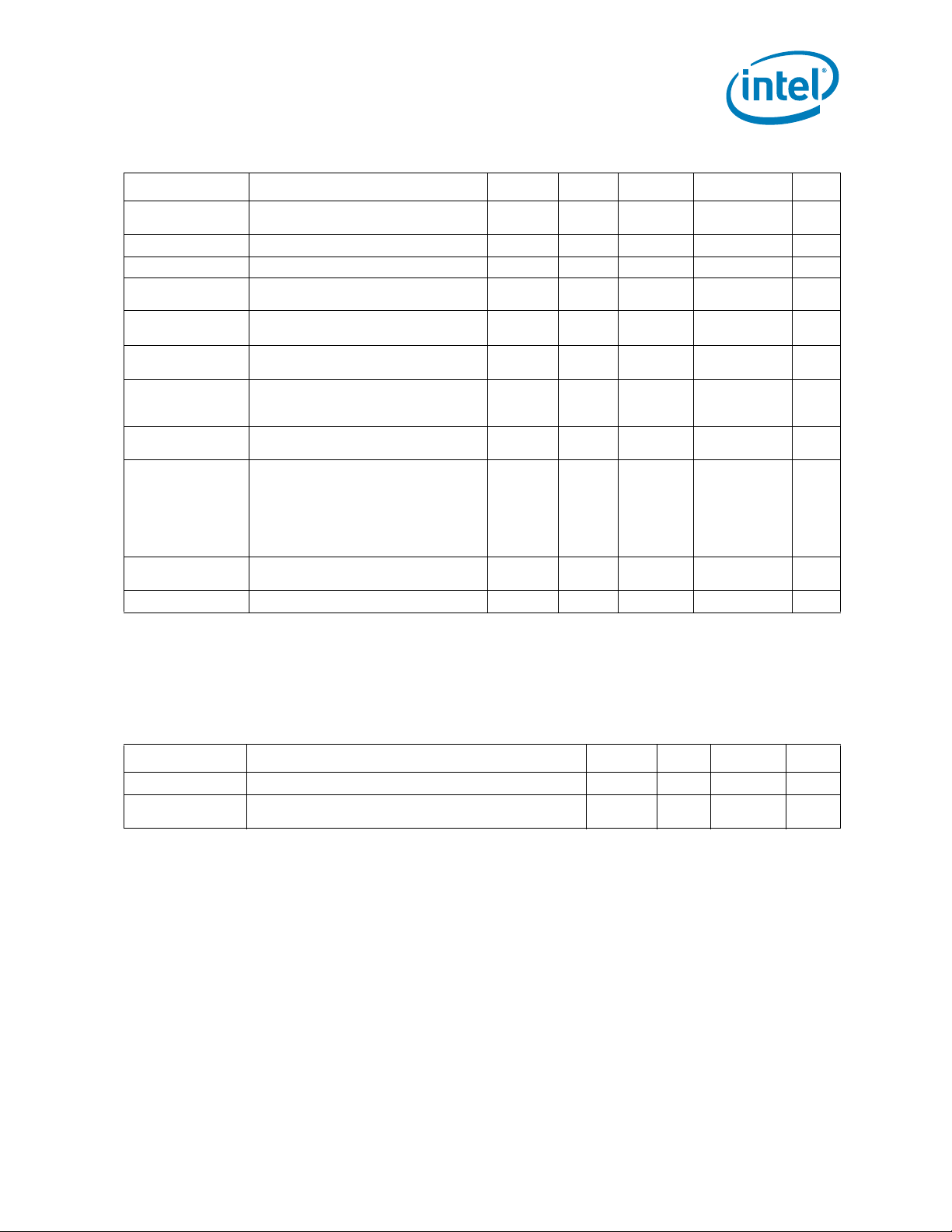
Electrical Specifications
Table 2-19. Common Intel QuickPath Interconnect Specifications (Sheet 2 of 2)
Symbol Parameter Min Nom Max Unit Notes
Z
RX_HIGH_CM_DC
Z
TX_LINK_DETECT
V
TX_LINK_DETECT
T
DATA_TERM_SKEW
T
INBAND_RESET_SENSE
T
CLK_DET
T
CLK_FREQ_DET
Single ended DC impedance to GND for
either D+ or D- of any data bit at Rx
Link Detection Resistor 500 2000 Ω
Link Detection Resistor Pull-up Voltage 1.6 V
Skew between first to last data
termination meeting Z
Time taken by inband reset detector to
sense Inband Reset
RX_LOW_CM_DC
Time taken by clock detector to observe
clock stability
Time taken by clock frequency detector
to decide slow vs. operational clock after
stable clock
T
Refclk-Tx - Variability
T
Refclk-jitter-rms-onepll
Phase variability between Reference Clk
(at Tx input) and Tx output
Accumulated rms jitter over n UI of a
given PLL model output in response to
the jittery reference clock input. The PLL
output is generated by convolving t he
measured reference clock phase jitter
with a given PLL transfer function. Here
n=12.
BER
Lane
Bit Error Rate per lane valid for 4.8, 5.86
and 6.4 GT/s
QPI[1,0]_COMP COMP Resistance 21.0-1% 21.0 21.0+1% Ω
10k Ω 2
128 UI
1.5 µs
20k UI
32 Reference
Clock Cycles
500 psec
0.5 psec
1.0E-14 Events
Notes:
1. Used during initialization. It is the state of “OFF” condition for the t r ans mitter. That is, wh en the output driver is disconnected
and only the minimum termination is connected. The link detection resistor is assumed not connected when specifying this
parameter.
2. Used during initialization. It is the state of “OFF” condition for the receiver when only the minimum termination is connected.
Table 2-20. Parameter Values for Intel QuickPath Interconnect Channels at 4.8 GT/s
(Sheet 1 of 2)
Symbol Parameter Min Max Unit N otes
V
Tx-diff-pp-pin
V
Tx-cm-dc-pin
Transmitter differential swing 800 1400 mV
Transmitter output DC common mode, defined as average
and VD- Use setup of Figure 2-11.
of V
D+
0.23 0.27 Fraction of
V
TX-diff-pp-pin
Intel® Xeon® Processor 5600 Series Datasheet Volume 1 45
Page 46
Electrical Specifications
Table 2-20. Parameter Values for Intel QuickPath Interconnect Channels at 4.8 GT/s
(Sheet 2 of 2)
Symbol Parameter Min M a x Unit Notes
V
Tx-cm-ac-pin
TX
duty-pin
TX
jitUI-UI-1E-7pin
TX
jitUI-UI-1E-9pin
TX
clk-acc-jit-N_UI-1E-7
TX
clk-acc-jit-N_UI-1E-9
T
Tx-data-clk-skew-pin
T
Rx-data-clk-skew-pin
V
Rx-cm-dc-pin
V
Rx-cm-ac-pin
T
Rx-margin
Transmitter output AC common mode, defined as ((VD+ +
)/2 - V
V
D-
Figure 2-13 for illustration of A C common mode distributio n
and spec limits.
Tx-cm-ac-pin
). Use setup of Figure 2-11 and
Average of UI-UI jitter, using setup of Figure 2-11. This
appears as bimodal peaks in UI-UI jitter distribution
Figure 2-14.
UI-UI jitter measured at Tx output pins with 1E-7
probability , using setup of Figure 2-11. Refer to Figure 2-14
for illustration of UI-UI jitter distribution and spec limits
UI-UI jitter measured at Tx output pins with 1E-9
probability , using setup of Figure 2-11. Refer to Figure 2-14
for illustration of UI-UI jitter distribution and spec limits
P-P accumulated jitter out of any Tx data or clock over 0 <=
n <= N UI where N=12, measured with 1E-7 probability.
Refer to Figure 2-14 for illustration
P-P accumulated jitter out of any Tx data or clock over 0 <=
n <= N UI where N=12, measured with 1E-9 probability.
Refer to Figure 2-14 for illustration
Delay of any data lane relative to the clock lane, as
measured at Tx output
Delay of any data lane relative to the clock lane, as
measured at Tx+ channel. This parameter is a collective
sum of effects of data clock mismatches in Tx and on the
medium connecting Tx and Rx.
DC common mode ranges at the Rx input for any data or
clock channel, defined as average of V
AC common mode ranges at the Rx input for any data or
clock channel, defined as((V
Refer to Figure 2-13 for illustration.
Measured timing margin during receiver margining with any
receiver equalizer off or for Tx EQ only based systems
+ VD-)/2 - V
D+
and VD-.
D+
RX-cm-dc-pin
).
-0.0375 0.0375 Fraction of
V
TX-diff-pp-pin
-0.078 0.078 UI
-0.085 0.085 UI
-0.09 0.09 UI
00.15UI
00.17UI
-0.4 0.4 UI
02UI1
-1 1 2
145 350 mV
-50 50 mV
0.1 UI
Notes:
1. Refers to routing lengths of 10 - 15 inches (25.4 - 38.1 cm).
2. Refers to routing lengths of 0 - 10 inches (0 - 25.4 cm).
46 Intel
®
Xeon® Processor 5600 Series Datasheet Volume 1
Page 47
Electrical Specifications
Table 2-21. Parameter Values for Intel QuickPath Interconnect Channel at 5.86 or
6.4 GT/s
Symbol Parameter Min Max Unit Note
V
Tx-diff-pp-pin
V
Tx-cm-dc-pin
V
Tx-cm-ac-pin
TX
duty-pin
TX
jitUI-UI-1E-7pin
TX
jitUI-UI-1E-9pin
TX
clk-acc-jit-N_UI-1E-7
TX
clk-acc-jit-N_UI-1E-9
T
Tx-data-clk-skew-pin
T
Rx-data-clk-skew-pin
V
Rx-cm-dc-pin
V
Rx-cm-ac-pin
T
Rx-margin
V
Rx-margin
Transmitter differential swing 800 1400 mV
Transmitter output DC common mode, defined as
average of V
Transmitter output AC common mode, defined as
+ VD–)/2 - V
((V
D+
Figure 2-11 and Figure 2-13 for illustration of AC
common mode distribution and spec limits.
and VD–. Use setup of Figure 2-11.
D+
TX-cm-dc-pin
). Use setup of
Average of UI-UI jitter, using setup of Figure 2-11.
This appears as bimodal peaks in UI-UI jitter
distribution Figure 2-14
UI-UI jitter measured at Tx output pins with 1E-7
probability, using setup of Figure 2-11. Refer to
Figure 2-14 for illustration of UI-UI jitter distribution
and spec limits
UI-UI jitter measured at Tx output pins with 1E-9
probability, using setup of Figure 2-11. Refer to
Figure 2-14 for illustration of UI-UI jitter distribution
0.23 0.27 Fraction of
V
TX-diff-pp-pin
–0.0375 0.0375 Fraction of
V
TX-diff-pp-pin
-0.078 0.078 UI
-0.088 0.088 UI
-0.095 0.095 UI
and spec limits.
P-P accumulated jitter out of any Tx data or clock
over 0 <= n <= N UI where N=12, measured with
00.15 UI
1E-7 probability. Refer to Figure 2-14 for illustration
P-P accumulated jitter out of any Tx data or clock
over 0 <= n <= N UI where N=12, measured with
00.17 UI
1E-9 probability. Refer to Figure 2-14 for illustration
Delay of any data lane relative to clock lane, as
measured at Tx output
Delay of any data lane relative to the clock lane, as
measured at the end of Tx+Channel. This parameter
is a collective sum of effects of data clock mismatches
-0.4 0.4 UI
02 UI1
-1 1 2
in Tx and on the medium connecting Tx and Rx.
DC common mode ranges at the Rx input for any data
or clock channel, defined as average of V
AC common mode ranges at the Rx input for any data
or clock channel, defined as ((V
). Refer to Figure 2-13 for illustration.
dc-pin
Measured timing margin during receiver margining
with any receiver equalizer off or forTx EQ only based
+ VD-)/2 - V
D+
and VD-.
D+
RX-cm-
145 350 mV
–50 50 mV
0.1 UI
systems
Measured voltage margin during receiver margining
with receiver equalizer off
40 mV
Notes:
1. Refers to routing lengths of 10 - 15 inches (25.4 - 38.1 cm).
2. Refers to routing lengths of 0 - 10 inches (0 - 25.4 cm).
2.8 AC Specifications
AC specifications are defined at the processor pads, unless otherwise noted.
Therefore, proper simulation is the only means to verify proper timing and signal
quality. Care should be taken to read all notes associated with each parameter.
Intel® Xeon® Processor 5600 Series Datasheet Volume 1 47
Page 48

Electrical Specifications
Table 2-22. System Reference Clock AC Specifications
Parameter Min Nom Max Unit Figure Notes
BCLK Frequency (SSC-off) 133.29 133.33 133.37 MHz 2-17 2
BCLK Frequency (SSC-on) 132.62 133.33 133.37 MHz 2-17 2
ER
BCLK-diffRise
T
BCLK-Dutycycle
T
BCLK-diff-jit
Notes:
1. Unless otherwise noted, all specifications in this table apply to all processor frequencies.
2. SSC is Spread Spectrum Clocking. The processor core clock frequency is derived from BCLK. The system
reference clock to processor core clock ratio is determined during initialization as described in
Section 2.1.5.
3. Rise and fall time slopes (V/ns) are measured between +150 mV and -150 mV of the differential output of
reference clock.
4. Phase drift between reference clocks at two connected ports.
, ER
BCLK-diffFall
1.0 4.0 V/ns 2-18 3
40 50 60 % 2-17
500 ps 4
Table 2-23. DDR3/DDR3L Electrical Characteristics and AC Specifications at 800 MT/s
(Sheet 1 of 2)
Channel 0
Channel 1
Symbol Parameter
Channel 2
Unit Figure Note
1
Latency Timings
tCL – tRCD – tRP CAS Latency – RAS to CAS Delay –
Pre-charge Command Period
Electrical Characteristics
T
SLR_D
DQ[63:0], DQS_N[17:0],
DQS_P[17:0], ECC[7:0]
Input Slew Rate
Clock Timings
T
CK
T
CH
T
CL
T
SKEW
CLK Period 3 2.50 ns
CLK High Time 1.50 1.25 ns
CLK Low Time 1.50 1.25 ns
Skew Between Any System
Memory Differential Clock Pair
(CLK_P/CLK_N)
Command Signal Timings
T
CMD_CO
RAS#, CAS#, WE#, MA[15:0],
BA[2:0] Edge placement accuracy
Control Signal Timings
T
CTRL_CS
CS#[7:0], CKE[3:0], ODT[3:0]
Edge placement accuracy
Data and Strobe Signal Timings
T
T
DVA
SU
+ T
+ T
DVB
HD
DQ[63:0] Valid before and after
DQS[17:0] Rising or Falling Edge
DQ Input Setup plus Hold Time to
DQS Rising or Falling Edge
Max Min
6 – 6 – 6 t
CK
4.0 1.0 V/ns 2
+155 ps
+375 -375 ps 2-22 3,4,6
+375 -375 ps 2-22 3,6
0.67 * UI UI 7
0.25 * UI ns 2-23 1,2,7
48 Intel
®
Xeon® Processor 5600 Series Datasheet Volume 1
Page 49

Electrical Specifications
Table 2-23. DDR3/DDR3L Electrical Characteristics and AC Specifications at 800 MT/s
(Sheet 2 of 2)
Channel 0
Channel 1
Symbol Parameter
T
DQS_CO
T
DQS_CO
T
WPRE
T
WPST
T
DQSS
DQS Edge Placement Accuracy to
CK Rising Edge BEFORE write
leveling
DQS Edge Placement Accuracy to
CK Rising Edge AFTER write
leveling
DQS/DQS# Write Preamble
Duration
DQS/DQS# Write Postamble
Duration
CK Rising Edge Output Access
Time, Where a Write Command Is
Referenced, to the First DQS Rising
Edge
Notes:
1. Unless otherwise noted, all specifications in this table apply to all processor frequencies. Timing
specifications only depend on the operatin g freq ue ncy of th e memory channel and not the maximum rated
frequency.
2. When the single ended slew rate of the input Data or Strobe signals, within a byte group, are below 1.0
V/ns, the tSU and tHD specifications must be increased by a derating factor. The input single ended slew
rate is measured DC to AC levels; V
edges. Use the worse case minimum slew rate measured between Data and Strobe, within a byte group, to
determine the required derating value. No derating is required for single ended slew rates equal to or
greater than 1.0 V/ns.
3. Edge Placement Accuracy (EPA): The silicon contains digital logic that automatically adjusts the timing
relationship between the DDR reference clocks and DDR signals. The BIOS initiates a training procedure
that will place a given signal appropriately within the clock period. The difference in delay between the
signal and clock is accurate to within ±EPA. This EPA includes jitter, skew, within die variation and several
other effects.
4. Data to Strobe read setup and Data from Strobe read hold minimum requirements specified at the
processor pad are determined with the minimum Read DQS/DQS# delay.
5. C
6. The system memory clock outputs are differential (CLK and CLK#), the CLK rising edge is referenc ed at the
7. The system memory strobe outputs are differential (DQS and DQS#), the DQS rising edge is referenced at
8. This values specifies the parameter after write leveling, representing the residual error in the controller
(CAS Write Latency) is the delay, in clock cycles, between the rising edge of CK where a write
WL
command is referenced and the first rising strobe edge where the first byte of write data is present. The
value is determined by the value of the CL (CAS Latency) setting.
C
WL
crossing point where CLK is rising and CLK# is falling.
the crossing point where DQS is rising and DQS# is falling, and the DQS falling edge is referenced at the
crossing point where DQS is falling and DQS# is rising.
after training, and does not include any effects from the DRAM itself.
_DC to VIH_AC for rising edges, and VIH_DC to VIL_AC for falling
IL
Channel 2
Unit Fig u re Note
Max Min
+375 -375 ns 3,6,7
+275 -275 ns 3,6,7,8
2.379 ns
1.371 1.129 ns
CWL x (TCK
+ 4)
ns 5,6
Table 2-24. DDR3 Electrical Characteristics and AC Specifications at 1066 MT/s (Sheet 1
of 2)
Channel 0
Channel 1
Symbol Parameter
Latency Timings
tCL – tRCD – tRP CAS Latency – RAS to CAS Delay –
Pre-charge Command Period
Electrical Characteristics
Intel® Xeon® Processor 5600 Series Datasheet Volume 1 49
Channel 2
Max Min
7 – 7 – 7
8 - 8 - 8
Unit Figure Note
tCK
Page 50

Electrical Specifications
Table 2-24. D DR3 Electrical Characteristics and AC Specifications at 1066 MT/s (Sheet 2
of 2)
Channel 0
Channel 1
Symbol Parameter
T
SLR_D
DQ[63:0], DQS_P[17:0],
DQS_N[17:0], ECC[7:0]
Input Slew Rate
Clock Timings
T
CK
T
CH
T
CL
T
SKEW
CLK Period <2.50 1.875 ns
CLK High Time 1.25 0.94 ns
CLK Low Time 1.25 0.94 ns
Skew Between Any System
Memory Differential Clock Pair
(CLK_P/CLK_N)
Command Signal Timings
T
CMD_CO
RAS#, CAS#, WE#, MA[15:0],
BA[2:0] Edge placement accuracy
Control Signal Timings
T
CTRL_CS
CS#[7:0], CKE[3:0], ODT[3:0]
Edge placement accuracy
Data and Strobe Signal Timings
T
DVA
+ T
T
SU
T
DQS_CO
+ T
DVB
HD
DQ[63:0] Valid before and after
DQS[17:0] Rising or Falling Edge
DQ Input Setup plus Hold Time to
DQS Rising or Falling Edge
DQS Edge Placement Accuracy to
CK Rising Edge BEFORE write
leveling
T
DQS_CO
DQS Edge Placement Accuracy to
CK Rising Edge AFTER write
leveling
T
WPRE
T
WPST
T
DQSS
DQS/DQS# Write Preamble
Duration
DQS/DQS# Write Postamble
Duration
CK Rising Edge Output Access
Time, Where a Write Command Is
Referenced, to the First DQS Rising
Edge
Channel 2
Unit Figure Note
Max M in
4.0 1.0 V/ns 2
+155 ps
+300 -300 ps 2-22 3,4,6
+300 -300 ps 2-22 3,6
0.67 * UI UI 7
0.25 * UI ns 2-23 1,2,7
+300 -300 ns 3,6,7
+206 -206 ns 3,6,7,8
1.781 ns
1.031 0.844 ns
C
x (TCK
WL
+ 4)
ns 5,6
Notes:
1. Unless otherwise noted, all specifications in this table apply to all processor frequencies.
2. When the single ended slew rate of the input Data or Strobe signals, within a byte group, are below 1.0
V/ns, the tSU and tHD specifications must be increased by a derating factor. The input single ended slew
rate is measured DC to AC levels; V
edges. Use the worse case minimum slew rate measured between Data and Strobe, within a byte group, to
determine the required derating value. No derating is required for single ended slew rates equal to or
greater than 1.0 V/ns.
3. Edge Placement Accuracy (EPA): The silicon contains digital logic that automatically adjusts the timing
relationship between the DDR reference clocks and DDR signals. The BIOS initiates a training procedure
that will place a given signal appropriately within the clock period. The difference in delay between the
signal and clock is accurate to within ±EPA. This EPA includes jitter, skew, within die variation and several
other effects.
4. Data to Strobe read setup and Data from Strobe read hold minimum requirements specified at the
processor pad are determined with the minimum Read DQS/DQS# delay.
_DC to VIH_AC for rising edges, and VIH_DC to VIL_AC for falling
IL
50 Intel
®
Xeon® Processor 5600 Series Datasheet Volume 1
Page 51

Electrical Specifications
5. CWL (CAS Write Latency) is the delay, in clock cycles, between the rising edge of CK where a write
command is referenced and the first rising strobe edge where the first byte of write data is present. The
CWL value is determined by the value of the CL (CAS Latency) setting.
6. The system memory clock outputs are differential (CLK and CLK#), the CLK rising edge is referenc ed at the
crossing point where CLK is rising and CLK# is falling.
7. The system memory strobe outputs are differential (DQS and DQS#), the DQS rising edge is referenced at
the crossing point where DQS is rising and DQS# is falling, and the DQS falling edge is referenced at the
crossing point where DQS is falling and DQS# is rising.
8. This values specifies the parameter after write leveling, representing the residual error in the controller
afrter training, and does not include any effects from the DRAM itself.
Table 2-25. DDR3/DDR3L Electrical Characteristics and AC Specifications at 1333 MT/s
(Sheet 1 of 2)
Channel 0
Channel 1
Symbol Parameter
System Memory Latency Timings
tCL – tRCD – tRP CAS Latency – RAS to CAS Delay –
Pre-charge Command Period
Electrical Characteristics
T
SLR_D
DQ[63:0], DQS_N[17:0],
DQS_P[17:0], ECC[7:0], MA[15:0]
Input Slew Rate
System Memory Clock Timings
T
CK
T
CH
T
CL
T
SKEW
CLK Period <1.875 1.50 ns
CLK High Time 0.94 0.75 ns
CLK Low Time 0.94 0.75 ns
Skew Between Any System
Memory Differential Clock Pair
(CLK_P/CLK_N)
System Memory Command Signal Timings
T
CMD_CO
RAS#, CAS#, WE#, MA[15:0],
BA[2:0] Edge placement accuracy
System Memory Control Signal Timings
T
CTRL_CS
CS#[7:0], CKE[3:0], ODT[3:0]
Edge placement accuracy
System Memory Data and Strobe Signal Timings
T
DVA
+ T
T
SU
T
DQS_CO
T
DQS_CO
+ T
DVB
HD
DQ[63:0] Valid before and after
DQS[17:0] Rising or Falling Edge
DQ Input Setup plus Hold Time to
DQS Rising or Falling Edge
DQS Edge Placement Accuracy to
CK Rising Edge BEFORE write
leveling
DQS Edge Placement Accuracy to
CK Rising Edge AFTER write
leveling
Channel 2
Unit Figure Note
Max Min
8 - 8 - 8
tCK
9 - 9 - 9
4.0 1.0 V/ns 2
+155 ps
+250 -250 ps 2-22 3,4,6
+250 -250 ps 2-22 3,6
0.67 * UI UI 7
0.25 * UI ns 1,2,7
+250 -250 ns 2-24 3,6,7
+165 -165 ns 2-24 3,6,7,8
Intel® Xeon® Processor 5600 Series Datasheet Volume 1 51
Page 52

Electrical Specifications
Table 2-25. DDR3/DDR3L Electrical Characteristics and AC Specifications at 1333 MT/s
(Sheet 2 of 2)
Channel 0
Channel 1
Symbol Parameter
T
WPRE
T
WPST
T
DQSS
DQS/DQS# Write Preamble
Duration
DQS/DQS# Write Postamble
Duration
CK Rising Edge Output Access
Time, Where a Write Command Is
Referenced, to the First DQS Rising
Edge
Notes:
1. Unless otherwise noted, all specifications in this table apply to all processor frequencies.
2. When the single ended slew rate of the input Data or Strobe signals, within a byte group, are below 1.0
V/ns, the tSU and tHD specifications must be increased by a derating factor. The input single ended slew
rate is measured DC to AC levels; V
edges. Use the worse case minimum slew rate measured between Data and Strobe, within a byte group, to
determine the required derating value. No derating is required for single ended slew rates equal to or
greater than 1.0 V/ns.
3. Edge Placement Accuracy (EPA): The silicon contains digital logic that automatically adjusts the timing
relationship between the DDR reference clocks and DDR signals. The BIOS initiates a training procedure
that will place a given signal appropriately within the clock period. The difference in delay between the
signal and clock is accurate to within ±EPA. This EPA includes jitter, skew, within die variation and several
other effects.
4. Data to Strobe read setup and Data from Strobe read hold minimum requirements specified at the
processor pad are determined with the minimum Read DQS/DQS# delay.
5. CWL (CAS Write Latency) is the delay, in clock cycles, between the rising edge of CK where a write
command is referenced and the first rising strobe edge where the first byte of write data is present. The
CWL value is determined by the value of the CL (CAS Latency) setting.
6. The system memory clock outputs are differential (CLK and CLK#), the CLK rising edge is referenced at the
crossing point where CLK is rising and CLK# is falling.
7. The system memory strobe outputs are differential (DQS and DQS#), the DQS rising edge is refe renced at
the crossing point where DQS is rising and DQS# is falling, and the DQS falling edge is referenced at the
crossing point where DQS is falling and DQS# is rising.
8. This values specifies the parameter after write leveling, representing the residual error in the controller
afrter training, and does not include any effects from the DRAM itself.
_DC to VIH_AC for rising edges, and VIH_DC to VIL_AC for falling
IL
Channel 2
Max M in
1.425 ns
0.825 0.674 ns
CWL x (TCK
+ 4)
Unit Figure Note
ns 5,6
Table 2-26. Processor Sideband Signal Group AC Specifications (Sheet 1 of 2)
T# Parameter Min Max Unit Figure
Asynchronous GTL input pulse width 8 BCLKs
Tb: V
stable to VTTPWRGOOD assertion 1 500 ms 2-28 5,7,8,10
TT
Td: VTTPWRGOOD assertion to Dynamic V
Processor
Te: V
stable to VDDPWRGOOD assertion 100 ns 2-28 5,6,7
DDQ
Tf: VTTPWRGOOD to valid VID 0 10 µs 2-28
Th: V
stable to VCCPWRGOOD assertion 0.05 650 ms 2-28
CC
Ti: V
stable to VCCPWRGOOD assertion 1 ms 2-28
CCPLL
Tj: BCLK stable to VCCPWRGOOD assertion 10 BCLKs 2-28
Tk: VCCPWRGOOD assertion to RESET# de-assertion 1 10 ms 2-28
Tm: VTTPWRGOOD assertion to VCCPWRGOOD
assertion
Tn: V
rise time 1.5 ms 2-28 14
CCPLL
Tq: PROCHOT# pulse width 500 µs 2-26
Tr:THERMTRIP# assertion until V
/ VTT removed 500 ms 2-27
CC
52 Intel
VID from
TT
10 µs 2-28 9
1ms2-28
®
Xeon® Processor 5600 Series Datasheet Volume 1
Notes
1,2,3,4
Page 53

Electrical Specifications
Table 2-26. Processor Sideband Signal Group AC Specifications (Sheet 2 of 2)
T# Parameter Min Max Unit Figure
VTTPWRGOOD de-assertion to V
T
: Time from BCLK land until signal valid at output 0.5 2.275 ns 11
CO
T
: Processor Sideband Input signals with respect to
SU
BCLK
: Processor Sideband Input signals with respect to
T
H
BCLK
: Power-On Configuration Hold Time (PROCHOT#) 106 BCLK 8-1 13
T
H
Notes:
1. Unless otherwise noted, all specifications in this table apply to all processor frequencies.
2. All AC timings for the Asynchronous GTL signals are referenced to the BCLK_P rising edge at Crossing
Voltage (V
at 0.5 * V
3. These signals may be driven asynchronously.
4. Refer to Section 8 for additional timing requirements for entering and leaving low power states.
5. xxPWRGOOD signal has no edge rate requirement, but edge must be monotonic.
6. VDDPWRGOOD must be asserted no later then VCCPWRGOOD. There is no releationship between
VDDPWRGOOD and VCC ramp.
7. There is no dependency between V DDPWRGOOD and VTTPWRGOOD assertion.
8. VTTPWRGOOD must accurately reflect the state of VTT and must not glitch whenever VTT or VDD is
applied.
9. VTT must read VTTFINAL before VCCPWRGOOD assertion.
10. It may be required to add delay on the board to meet the 1 ms minimum processor requirement.
11. Based on a test load of 50 Ω to V
12. Specified for synchronous signals.
13. Applies to PROCHOT# signal only. Please see Section 2.1.7.3.1 and Section 8.1 for information regarding
Power-On Configuration options.
14. Rise time is measured from 10% to 90% of the final voltage.
). VCCPWRGOOD, VTTPWRGOOD and VDDPWRG OOD are referenced to BCLK_P rising edge
CROSS
.
TT
below specification 100 ns
TT
.
TT
Table 2-27. TAP Signal Group AC Specifications
Notes
1,2,3,4
600 ps 12
600 ps
T# Parameter Min Max Unit Figure
TCK Period 31.25 ns
T
: TDI, TMS Setup Time 1 ns 2-25
s
T
: TDI, TMS Hold Time 1 ns 2-25
h
T
: TDO Clock to Output Delay 0.5 4 ns 2-25
x
T
: TRST# Assert Time 2 T
q
Notes:
1. Unless otherwise noted, all specifications in this table apply to all processor frequencies.
2. Not 100% tested. Specified by design characterization.
3. It is recommended that TMS be asserted while TRST# is being deasserted.
Table 2-28. VID Signal Group AC Specifications
T# Parameter Min Max Unit Figure Notes
Ta: VID Step Time 1.25 µs 2-29
Tb: VID Down Transition to Valid V
Tc: VID Up Transition to Valid V
Td: VID Down Transition to Valid V
Te: VID Up Transition to Valid V
Notes:
1. Platform support for VID transitions is required for the processor to operate within specifications.
(min) 0 µs 2-29
CC
(min) 15 µs 2-29
CC
(max) 15 µs 2-29
CC
(max) 0 µs 2-29
CC
TCK
Notes
1,2,3
2-26
1
Intel® Xeon® Processor 5600 Series Datasheet Volume 1 53
Page 54

Electrical Specifications
Tx Package
Silicon TX
Ideal Loads
SI Tx pin terminations are set to optimum values
(targeted around 42.5 ohms si ngle-ended)
2.9 Processor AC Timing Waveforms
The following figures are to be used in conjunction with the AC specifications included
in Table 2-19 through Table 2-28.
Note: For Figure 2-11 through Figure 2-29, the following apply:
1. All System Reference Clock signal AC specifications are referenced to the Crossing
Voltage (V
2. All TAP signal group AC specifications are referenced to the TCK at 0.5 * V
processor lands. All TAP signal group timings (TMS, TDI, and so forth) are
referenced at 0.5 * V
3. All CMOS signal AC specifications are referenced at 0.5 * VTT at the processor
lands.
The Intel QuickPath Interconnect electrical test setup are shown in Figure 2-11 and
Figure 2-12.
Figure 2-11. Intel QuickPath Interconnect Electrical Test Setup for Validating
Standalone TX Voltage and Timing Parameters
) of the BCLK_DP and BCLK_DN at rising edge of BCLK_DP.
CROSS
at the processor die (pads).
TT
at the
TT
54 Intel
®
Xeon® Processor 5600 Series Datasheet Volume 1
Page 55

Electrical Specifications
S i lic o n
T x b it
(D ata )
W o rs t-C a s e Inte r c o n n e ct
Id e a l
Loads
Tx
Package
S i lic o n
T x b it
(C loc k)
Id e a l
Loads
Lossless Interconnect Phase
Matc h ed to D a ta B it In te rc o n n e c t
0.5* (VD+ - VD-) - X_cm_dc_pin
Figure 2-12. Intel QuickPath Interconnect Electrical Test Setup for Validating
TX + Worst-Case Interconnect Specifications
Figure 2-13. Distribution Profile of Common Mode Noise for Either Tx or Rx
Intel® Xeon® Processor 5600 Series Datasheet Volume 1 55
Page 56

Figure 2-14. Distribution Profile of UI-UI Jitter and Accumulated Jitter
P-P n UI ac jitter
with Prob = 1E-7
P-P n UI ac jitter
with Prob = 1E-9
V
Rx-diff-pp-pin
Probability
= 1E -9
Timing Margin
Distribution
Probability
= 1E -9
T
Rx-diff-pp-pin
Voltage Margin
Distribution
Electrical Specifications
Figure 2-15. Eye Mask at the End of Tx + Channel
56 Intel
®
Xeon® Processor 5600 Series Datasheet Volume 1
Page 57

Electrical Specifications
660 670 680 690 700 710 720 730 740 750 760 770 780 790 800 810 820 830 840 850
200
250
300
350
400
450
500
550
600
650
VHavg (mV)
Crossin g Point (mV)
550 mV
250 mV
250 + 0.5 (VHavg - 700)
550 + 0.5 (VHavg - 700)
Figure 2-16. Differential Clock Crosspoint Specification
Figure 2-17. Differential Clock Measurement Points for Duty Cycle and Period
Figure 2-18. Differential Clock Measurement Points for Rise and Fall time
Intel® Xeon® Processor 5600 Series Datasheet Volume 1 57
Page 58

Electrical Specifications
Figure 2-19. Single-Ended Clock Measurement Points for Absolute Cross Point and Swing
Figure 2-20. Single-Ended Clock Measurement Points for Delta Cross Point
Figure 2-21. Differential Clock Measurement Point for Ringback
58 Intel
®
Xeon® Processor 5600 Series Datasheet Volume 1
Page 59
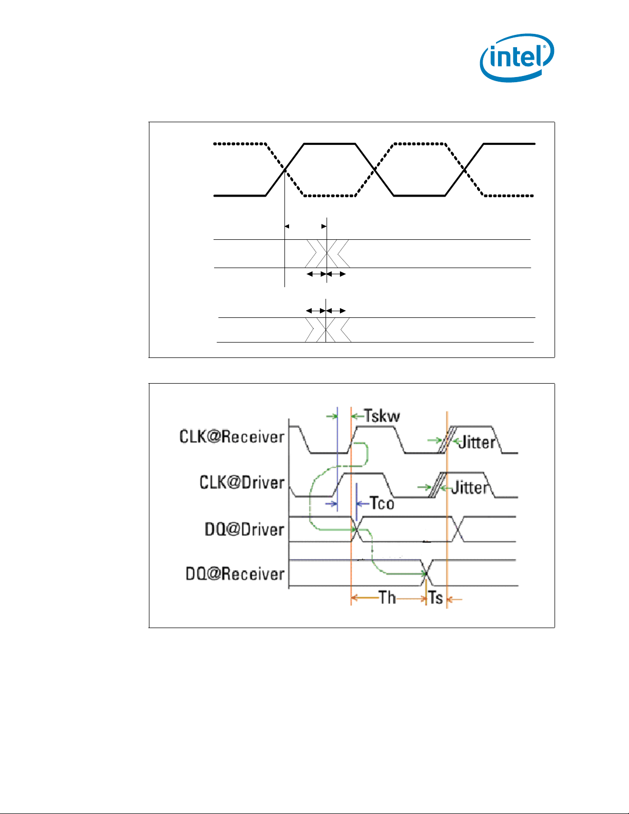
Electrical Specifications
CK# (IMC)
MA , B S,
RAS#,
CAS#, WE#
(IMC)
CK (IMC)
Control Signals
(IMC)
Tcm d_c o
Tcm d_co
BIOS
Programmabl e
Delay
Tcm d_c s
Tcm d_c s
Figure 2-22. DDR3 Command / Control and Clock Timing Waveform
Figure 2-23. DDR3 Clock to Output Timing Waveform
Intel® Xeon® Processor 5600 Series Datasheet Volume 1 59
Page 60
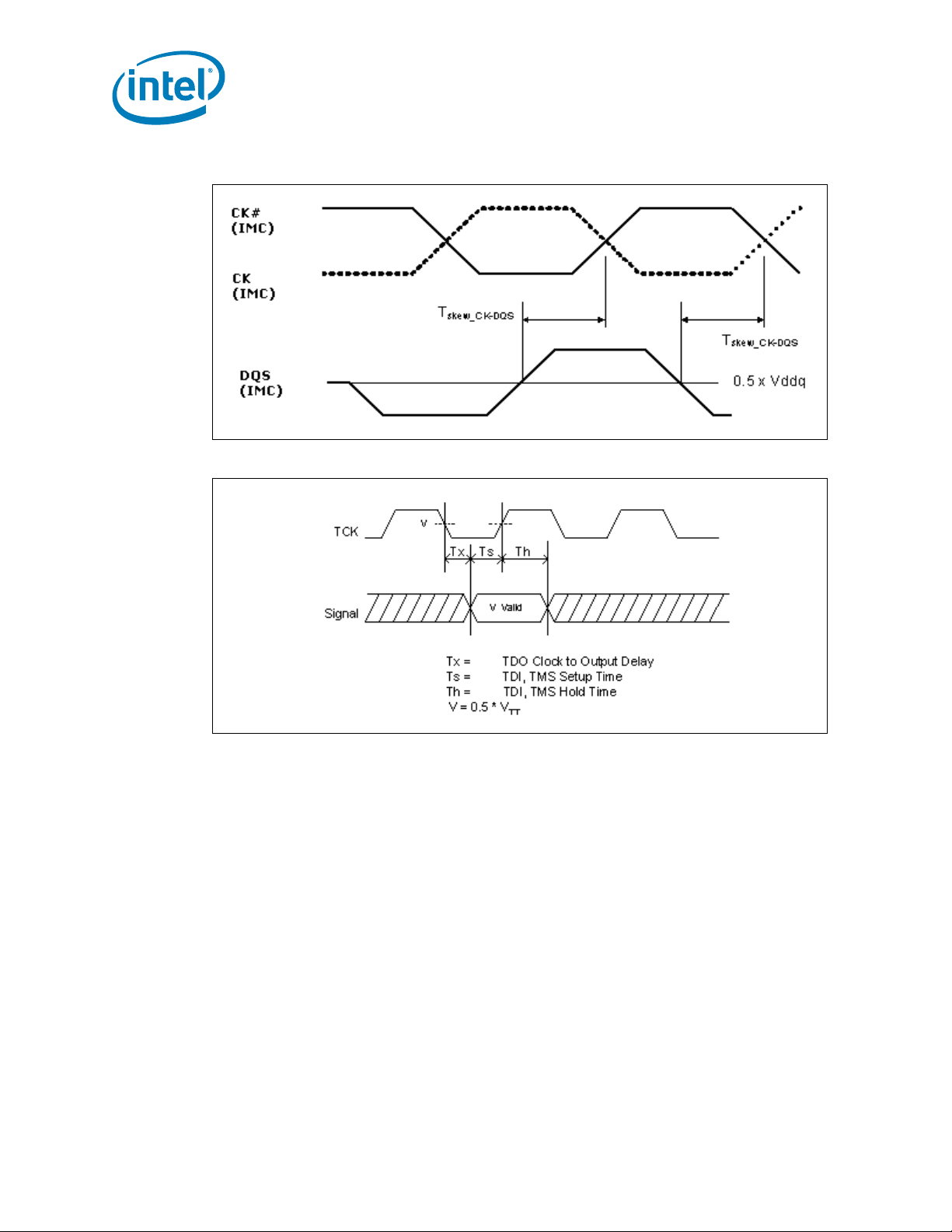
Figure 2-24. DDR3 Clock to DQS Skew Timing Waveform
Figure 2-25. TAP Valid Delay Timing Waveform
Electrical Specifications
Note: Please refer to Table 2-18 for TAP Signal Group DC specifications and Table 2-27 for TAP Signal Group
AC specifications.
60 Intel
®
Xeon® Processor 5600 Series Datasheet Volume 1
Page 61

Electrical Specifications
TRST# Assert Time, V = 0.5 * V
TTA
V
T
q
PROCHOT# Pulse Width, V = V
TTA
=
Tq
THERMTRIP#
V
CC
V
TT
Tr
Tr: THERMTRIP# assertion unti l VCC, VTT removal
Figure 2-26. Test Reset (TRST#), Asynch GTL Input, and PROCHOT# Timing Waveform
Figure 2-27. THERMTRIP# Power Down Sequence
Intel® Xeon® Processor 5600 Series Datasheet Volume 1 61
Page 62

Figure 2-28. Voltage Sequence Timing Requirements
VTTPWRGOOD
V
TT
BCLK
VCCPWRGOOD
VCC VID[7:0]
V
CC
V
DDQ
VDDPWRGOOD
RESET#
V
CCPLL
LFM VID From C P U
V
CCBOOT
Tk
Tj
POC
MSID
V
LFM
Th
VTT VID FINAL
VTT_VID[2:0]
V
TTBOOT
V
TTSAFE
VT T VID from
VID Buffer
V
TTFINAL
Tb
Tm
Td
VDDPW R GO O D m ust assert before or at the same time as
VCCPWRGOOD assertion
VTT must be stable before VCCPWR GO O D
assertion
Varies based on BIOS execution
Dynamic VID From CPU
Tf
Refer to VRD11.1 specification for details on Vcc ramp timings
Ti
Te
Electrical Specifications
62 Intel
®
Xeon® Processor 5600 Series Datasheet Volume 1
Page 63

Electrical Specifications
Note: In order In order to ensure Timestamp Counter (TSC) synchronization across sockets in multi-socket
systems, the RESET# deassertion edge should arrive at the same BCLK rising edge at both sockets and
should meet the Tsu and Th requirement of 600ps relative to BCLK, as outlined in Table 2-26.
Figure 2-29. VID Step Times and Vcc Waveforms
Note: This waveform illustrates an example of an Intel Adaptive Thermal Monitor transition or an Intel
Enhanced SpeedStep Technology transition that is six VID step down from the current state and six
steps back up. Any arbitrary up or down transition can be generalized from this waveform.
§
Intel® Xeon® Processor 5600 Series Datasheet Volume 1 63
Page 64

Electrical Specifications
64 Intel
®
Xeon® Processor 5600 Series Datasheet Volume 1
Page 65

Signal Quality Specifications
3 Signal Quality Specifications
Data transfer requires the clean reception of data and clock signals. Ringing below
receiver thresholds, non-monotonic signal edges, and excessive voltage swings will
adversely affect system timings. Ringback and signal non-monotonicity cannot be
tolerated since these phenomena may inadvertently advance receiver state machines.
Excessive signal swings (overshoot and undershoot) are detrimental to silicon gate
oxide integrity, and can cause device failure if absolute voltage limits are exceeded.
Overshoot and undershoot can also cause timing degradation due to the build up of
inter-symbol interference (ISI) effects.
For these reasons, it is crucial that the designer work towards a solution that provides
acceptable signal quality across all systematic variations encountered in volume
manufacturing.
This section documents signal quality metrics used to derive topology and routing
guidelines through simulation. All specifications are specified at the processor die (pad
measurements).
Specifications for signal quality are for measurements at the processor core only and
are only observable through simulation. Therefore, proper signal simulation is the only
means of properly verifying timing and signal quality requirements.
3.1 Overshoot/Undershoot Tolerance
Overshoot (or undershoot) is the absolute value of the maximum voltage above or
below VSS. The overshoot/undershoot specifications limit transitions beyond V
due to the fast signal edge rates. The processor can be damaged by single and/or
V
SS
repeated overshoot or undershoot events on any input, output, or I/O buffer if the
charge is large enough (that is, if the over/undershoot is great enough). Baseboard
designs which meet signal integrity and timing requirements and which do not exceed
the maximum overshoot or undershoot limits will insure reliable IO performance for the
lifetime of the processor.
The pulse magnitude, duration, and activity factor must all be used to determine if the
overshoot/undershoot pulse is within specifications.
Note: Oscillations below the reference voltage cannot be subtracted from the total
Table 3-1. Overshoot/Undershoot Tolerance
overshoot/undershoot pulse duration.
Signal Group Min Undershoot Max Overshoot Duration
Intel QuickPath Interconnect -0.1 * V
DDR3 -0.1 * V
Processor Sideband Signals -0.1 * V
System Reference Clock -0.3 1.15 NA
Notes:
1. These specifications are measured at the processor pin.
2. Refer to Figure 3-1 for description of Overshoot/Undershoot magnitude and duration.
TT
DDQ
TT
1.2 * V
1.2 * V
1.2 * V
TT
DDQ
TT
0.5 * T
CCIO
500 ps
50 ns
or
CH
Intel® Xeon® Processor 5600 Series Datasheet Volume 1 65
Page 66

Figure 3-1. Maximum Acceptable Overshoot/Undershoot Waveform
Vss
Overshoot
Duration
Undershoot
Duration
Overshoot
Undershoot
Signal Quality Specifications
§
66 Intel
®
Xeon® Processor 5600 Series Datasheet Volume 1
Page 67

Package Mechanical Specifications
IHS
Substrate
LGA1366 Socket
System Board
Capacitors
TIM
IHS
Substrate
LGA
System Board
Capacitors
Die
TIM
4 Package Mechanical
Specifications
4.1 Package Mechanical Specifications
The processor is packaged in a Flip-Chip Land Grid Array (FC-LGA) package that
interfaces with the baseboard via an LGA1366 socket. The package consists of a
processor mounted on a substrate land-carrier. An integrated heat spreader (IHS) is
attached to the package substrate and core and serves as the mating surface for
processor component thermal solutions, such as a heatsink. Figure 4-1 shows a sketch
of the processor package components and how they are assembled together. Refer to
the Intel
complete details on the LGA1366 socket.
The package components shown in Figure 4-1 include the following:
1. Integrated Heat Spreader (IHS)
2. Thermal Interface Material (TIM)
3. Processor core (die)
4. Package substrate
5. Capacitors
®
Xeon® Processor 5500/5600 Series Thermal/Mechanical Design Guide for
Figure 4-1. Processor Package Assembly Sketch
Note:
1. Socket and baseboard are included for reference and are not part of processor package.
4.1.1 Package Mechanical Drawing
The package mechanical drawings are shown in Figure 4-2 and Figure 4-2. The
drawings include dimensions necessary to design a thermal solution and reflect the
processor as received by Intel. These dimensions include:
1. Package reference with tolerances (total height, length, width, and so forth)
2. IHS parallelism and tilt
3. Land dimensions
4. Top-side and back-side component keep-out dimensions
5. Reference datums
Intel® Xeon® Processor 5600 Series Datasheet Volume 1 67
Page 68

6. All drawing dimensions are in mm.
7. Guidelines on potential IHS flatness variation with socket load plate actuation and
installation of the cooling solution is available in the Intel® Xeon® Processor
5500/5600 Series Thermal/Mechanical Design Guide.
Figure 4-2. Processor Package Drawing (Sheet 1 of 2)
Package Mechanical Specifications
68 Intel
®
Xeon® Processor 5600 Series Datasheet Volume 1
Page 69

Package Mechanical Specifications
Figure 4-3. Processor Package Drawing (Sheet 2 of 2)
Intel® Xeon® Processor 5600 Series Datasheet Volume 1 69
Page 70

4.1.2 Processor Component Keep-Out Zones
The processor may contain components on the substrate that define component
keep-out zone requirements. A thermal and mechanical solution design must not
intrude into the required keep-out zones. Do not contact the Test Pad Area with
conductive material. Decoupling capacitors are typically mounted to either the topside
or land-side of the package substrate. See Figure 4-2 and Figure 4-2 for keep-out
zones. The location and quantity of package capacitors may change due to
manufacturing efficiencies but will remain within the component keep-in.
4.1.3 Package Loading Specifications
Table 4-1 provides load specifications for the processor package. These maximum
limits should not be exceeded during heatsink assembly, shipping conditions, or
standard use condition. Exceeding these limits during test may result in component
failure. The processor substrate should not be used as a mechanical reference or load-
.
Table 4-1. Processor Loading Specifications
bearing surface for thermal solutions.
Parameter Maximum Notes
Static Compressive Load 890 N [200 lbf] 1, 2, 3
Dynamic Compressive Load 1779 N [400 lbf] [max static compressive + dynamic load] 1, 3, 4
Package Mechanical Specifications
Notes:
1. These specifications apply to uniform compressive loading in a direction normal to the processor IHS.
2. This is the maximum static force that can be applied by the heatsink and Independent Loading Mechanism
(ILM).
3. These specifications are based on limited testing for design characterization. Loading limits are for the
package constrained by the limits of the processor socket.
4. Dynamic loading is defined as an 11 ms duration average load superimposed on the static load
requirement.
5. See Intel® Xeon® Processor 5500/5600 Series Thermal/Mechanical Desi gn Guide for min imum so cket lo ad
to engage processor within socket.
4.1.4 Package Handling Guidelines
Table 4-2 includes a list of guidelines on package handling in terms of recommended
maximum loading on the processor IHS relative to a fixed substrate. These package
handling loads may be experienced during heatsink removal.
Table 4-2. Package Handling Guidelines
Parameter Maximum Recommended Notes
Shear 70 lbs
Tensile 25 lbs
Torque 35 in.lbs
4.1.5 Package Insertion Specifications
The processor can be inserted into and removed from an LGA1366 socket 15 times. The
socket should meet the LGA1366 requirements detailed in the Intel® Xeon® Processor
5500/5600 Series Thermal/Mechanical Design Guide.
70 Intel
®
Xeon® Processor 5600 Series Datasheet Volume 1
Page 71

Package Mechanical Specifications
4.1.6 Processor Mass Specification
The typical mass of the processor is 35 grams. This mass [weight] includes all the
components that are included in the package.
4.1.7 Processor Materials
Table 4-3 lists some of the package components and associated materials.
Table 4-3. Processor Materials
Component Material
Integrated Heat Spreader (IHS) Nickel Plated Copper
Substrate Fiber Reinforced Resin
Substrate Lands Gold Plated Copper
4.1.8 Processor Markings
Figure 4-4 shows the topside markings on the processor. This diagram is to aid in the
identification of the processor.
Figure 4-4. Processor Top-Side Markings
§
Intel® Xeon® Processor 5600 Series Datasheet Volume 1 71
Page 72

Package Mechanical Specifications
72 Intel
®
Xeon® Processor 5600 Series Datasheet Volume 1
Page 73

Land Listing
5 Land Listing
5.1 Listing by Land Name
Table 5-1. Land Name (Sheet 1 of 36)
Land Name
BCLK_DN AH35 CMOS I
BCLK_DP AJ35 CMOS I
BCLK_ITP_DN AA4 CMOS O
BCLK_ITP_DP AA5 CMOS O
BPM#[0] B3 GTL I/O
BPM#[1] A5 GTL I/O
BPM#[2] C2 GTL I/O
BPM#[3] B4 GTL I/O
BPM#[4] D1 GTL I/O
BPM#[5] C3 GTL I/O
BPM#[6] D2 GTL I/O
BPM#[7] E2 GTL I/O
CAT_ERR# AC37 GTL I/O
COMP0 AB41 Analog
QPI0_CLKRX_DN AR42 QPI I
QPI0_CLKRX_DP AR41 QPI I
QPI0_CLKTX_DN AF42 QPI O
QPI0_CLKTX_DP AG42 QPI O
QPI0_COMP AL43 Analog
QPI0_DRX_DN[0] AU37 QPI I
QPI0_DRX_DN[1] AV38 QPI I
QPI0_DRX_DN[10] AT42 QPI I
QPI0_DRX_DN[11] AR43 QPI I
QPI0_DRX_DN[12] AR40 QPI I
QPI0_DRX_DN[13] AN42 QPI I
QPI0_DRX_DN[14] AM43 QPI I
QPI0_DRX_DN[15] AM40 QPI I
QPI0_DRX_DN[16] AM41 QPI I
QPI0_DRX_DN[17] AP40 QPI I
QPI0_DRX_DN[18] AP39 QPI I
QPI0_DRX_DN[19] AR38 QPI I
QPI0_DRX_DN[2] AV37 QPI I
QPI0_DRX_DN[3] AY36 QP I I
QPI0_DRX_DN[4] BA37 QPI I
QPI0_DRX_DN[5] AW38 QPI I
Land
No.
Buffer
Type
Direction
Table 5-1. Land Name (Sheet 2 of 36)
Land Name
QPI0_DRX_DN[6] AY38 QPI I
QPI0_DRX_DN[7] AT39 QPI I
QPI0_DRX_DN[8] AV40 QPI I
QPI0_DRX_DN[9] AU41 QPI I
QPI0_DRX_DP[0] AT37 QPI I
QPI0_DRX_DP[1] AU38 QPI I
QPI0_DRX_DP[10] AU42 QPI I
QPI0_DRX_DP[11] AT43 QPI I
QPI0_DRX_DP[12] AT40 QPI I
QPI0_DRX_DP[13] AP42 QPI I
QPI0_DRX_DP[14] AN43 QPI I
QPI0_DRX_DP[15] AN40 QPI I
QPI0_DRX_DP[16] AM42 QPI I
QPI0_DRX_DP[17] AP41 QPI I
QPI0_DRX_DP[18] AN39 QPI I
QPI0_DRX_DP[19] AP38 QPI I
QPI0_DRX_DP[2] AV36 QPI I
QPI0_DRX_DP[3] AW36 QPI I
QPI0_DRX_DP[4] BA36 QPI I
QPI0_DRX_DP[5] AW37 QPI I
QPI0_DRX_DP[6] BA38 QPI I
QPI0_DRX_DP[7] AU39 QPI I
QPI0_DRX_DP[8] AW40 QPI I
QPI0_DRX_DP[9] AU40 QPI I
QPI0_DTX_DN[0] AH38 QPI O
QPI0_DTX_DN[1] AG39 QPI O
QPI0_DTX_DN[10] AE43 QPI O
QPI0_DTX_DN[11] AE41 QPI O
QPI0_DTX_DN[12] AC42 QPI O
QPI0_DTX_DN[13] AB43 QPI O
QPI0_DTX_DN[14] AD39 QPI O
QPI0_DTX_DN[15] AC40 QPI O
QPI0_DTX_DN[16] AC38 QPI O
QPI0_DTX_DN[17] AB38 QPI O
QPI0_DTX_DN[18] AE38 QPI O
QPI0_DTX_DN[19] AF40 QPI O
Land
No.
Buffer
Type
Direction
Intel® Xeon® Processor 5600 Series Datasheet Volume 1 73
Page 74

Land Listing
Table 5-1. Land Name (Sheet 3 of 36)
Land Name
QPI0_DTX_DN[2] AK38 QPI O
QPI0_DTX_DN[3] AJ39 QPI O
QPI0_DTX_DN[4] AJ40 QPI O
QPI0_DTX_DN[5] AK41 QPI O
QPI0_DTX_DN[6] AH42 QPI O
QPI0_DTX_DN[7] AJ42 QPI O
QPI0_DTX_DN[8] AH43 QPI O
QPI0_DTX_DN[9] AG41 QPI O
QPI0_DTX_DP[0] AG38 QPI O
QPI0_DTX_DP[1] AF39 QPI O
QPI0_DTX_DP[10] AF43 QPI O
QPI0_DTX_DP[11] AE42 QPI O
QPI0_DTX_DP[12] AD42 QPI O
QPI0_DTX_DP[13] AC43 QPI O
QPI0_DTX_DP[14] AD40 QPI O
QPI0_DTX_DP[15] AC41 QPI O
QPI0_DTX_DP[16] AC39 QPI O
QPI0_DTX_DP[17] AB39 QPI O
QPI0_DTX_DP[18] AD38 QPI O
QPI0_DTX_DP[19] AE40 QPI O
QPI0_DTX_DP[2] AK37 QPI O
QPI0_DTX_DP[3] AJ38 QPI O
QPI0_DTX_DP[4] AH40 QPI O
QPI0_DTX_DP[5] AK40 QPI O
QPI0_DTX_DP[6] AH41 QPI O
QPI0_DTX_DP[7] AK42 QPI O
QPI0_DTX_DP[8] AJ43 QPI O
QPI0_DTX_DP[9] AG40 QPI O
QPI1_CLKRX_DN AR6 QPI I
QPI1_CLKRX_DP AT6 QPI I
QPI1_CLKTX_DN AE6 QPI O
QPI1_CLKTX_DP AF6 QPI O
QPI1_COMP AL6 Analog
QPI1_DRX_DN[0] AV8 QPI I
QPI1_DRX_DN[1] AW7 QPI I
QPI1_DRX_DN[10] AR1 QPI I
QPI1_DRX_DN[11] AR5 QPI I
QPI1_DRX_DN[12] AN2 QPI I
QPI1_DRX_DN[13] AM1 QPI I
QPI1_DRX_DN[14] AM3 QPI I
QPI1_DRX_DN[15] AP4 QPI I
Land
No.
Buffer
Type
Direction
Table 5-1. Land Name (Sheet 4 of 36)
Land Name
QPI1_DRX_DN[16] AN4 QPI I
QPI1_DRX_DN[17] AN6 QPI I
QPI1_DRX_DN[18] AM7 QPI I
QPI1_DRX_DN[19] AL8 QPI I
QPI1_DRX_DN[2] BA8 QPI I
QPI1_DRX_DN[3] AW5 QPI I
QPI1_DRX_DN[4] BA6 QPI I
QPI1_DRX_DN[5] AY5 QPI I
QPI1_DRX_DN[6] AU6 QPI I
QPI1_DRX_DN[7] AW3 QPI I
QPI1_DRX_DN[8] AU3 QPI I
QPI1_DRX_DN[9] AT2 QPI I
QPI1_DRX_DP[0] AU8 QPI I
QPI1_DRX_DP[1] AV7 QPI I
QPI1_DRX_DP[10] AT1 QPI I
QPI1_DRX_DP[11] AR4 QPI I
QPI1_DRX_DP[12] AP2 QPI I
QPI1_DRX_DP[13] AN1 QPI I
QPI1_DRX_DP[14] AM2 QPI I
QPI1_DRX_DP[15] AP3 QPI I
QPI1_DRX_DP[16] AM4 QPI I
QPI1_DRX_DP[17] AN5 QPI I
QPI1_DRX_DP[18] AM6 QPI I
QPI1_DRX_DP[19] AM8 QPI I
QPI1_DRX_DP[2] AY8 QPI I
QPI1_DRX_DP[3] AV5 QPI I
QPI1_DRX_DP[4] BA7 QPI I
QPI1_DRX_DP[5] AY6 QPI I
QPI1_DRX_DP[6] AU7 QPI I
QPI1_DRX_DP[7] AW4 QPI I
QPI1_DRX_DP[8] AU4 QPI I
QPI1_DRX_DP[9] AT3 QPI I
QPI1_DTX_DN[0] AH8 QPI O
QPI1_DTX_DN[1] AJ7 QPI O
QPI1_DTX_DN[10] AF3 QPI O
QPI1_DTX_DN[11] AD1 QPI O
QPI1_DTX_DN[12] AD3 QPI O
QPI1_DTX_DN[13] AB3 QPI O
QPI1_DTX_DN[14] AE4 QPI O
QPI1_DTX_DN[15] AD4 QPI O
QPI1_DTX_DN[16] AC6 Q PI O
Land
No.
Buffer
Type
Direction
74 Intel
®
Xeon® Processor 5600 Series Datasheet Volume 1
Page 75

Land Listing
Table 5-1. Land Name (Sheet 5 of 36)
Land Name
QPI1_DTX_DN[17] AD7 QPI O
QPI1_DTX_DN[18] AE5 QPI O
QPI1_DTX_DN[19] AD8 QPI O
QPI1_DTX_DN[2] AJ6 QPI O
QPI1_DTX_DN[3] AK5 QPI O
QPI1_DTX_DN[4] AK4 QPI O
QPI1_DTX_DN[5] AG6 QPI O
QPI1_DTX_DN[6] AJ2 QPI O
QPI1_DTX_DN[7] AJ1 QPI O
QPI1_DTX_DN[8] AH4 QPI O
QPI1_DTX_DN[9] AG2 QPI O
QPI1_DTX_DP[0] AG8 QPI O
QPI1_DTX_DP[1] AJ8 QPI O
QPI1_DTX_DP[10] AF2 QPI O
QPI1_DTX_DP[11] AE1 QPI O
QPI1_DTX_DP[12] AD2 QPI O
QPI1_DTX_DP[13] AC3 QPI O
QPI1_DTX_DP[14] AE3 QPI O
QPI1_DTX_DP[15] AC4 QPI O
QPI1_DTX_DP[16] AB6 QPI O
QPI1_DTX_DP[17] AD6 QPI O
QPI1_DTX_DP[18] AD5 QPI O
QPI1_DTX_DP[19] AC8 QPI O
QPI1_DTX_DP[2] AH6 QPI O
QPI1_DTX_DP[3] AK6 QPI O
QPI1_DTX_DP[4] AJ4 QPI O
QPI1_DTX_DP[5] AG7 QPI O
QPI1_DTX_DP[6] AJ3 QPI O
QPI1_DTX_DP[7] AK1 QPI O
QPI1_DTX_DP[8] AH3 QPI O
QPI1_DTX_DP[9] AH2 QPI O
DBR# AF10 Asynch I
DDR_COMP[0] AA8 Analog
DDR_COMP[1] Y7 Analog
DDR_COMP[2] AC1 Analog
DDR_THERM# AB5 CMOS I
DDR_THERM2# AF4 CMOS I
DDR_VREF L23 Analog I
DDR0_BA[0] B16 CMOS O
DDR0_BA[1] A16 CMOS O
DDR0_BA[2] C28 CMOS O
Land
No.
Buffer
Type
Direction
Table 5-1. Land Name (Sheet 6 of 36)
Land Name
DDR0_CAS# C12 CMOS O
DDR0_CKE[0] C29 CMOS O
DDR0_CKE[1] A30 CMOS O
DDR0_CKE[2] B30 CMOS O
DDR0_CKE[3] B31 CMOS O
DDR0_CLK_N[0] K19 CLOCK O
DDR0_CLK_N[1] C19 CLOCK O
DDR0_CLK_N[2] E18 CLOCK O
DDR0_CLK_N[3] E19 CLOCK O
DDR0_CLK_P[0] J19 CLOCK O
DDR0_CLK_P[1] D19 CLOCK O
DDR0_CLK_P[2] F18 CLOCK O
DDR0_CLK_P[3] E20 CLOCK O
DDR0_CS#[0] G15 CMOS O
DDR0_CS#[1] B10 CMOS O
DDR0_CS#[2] C13 CMOS O
DDR0_CS#[3] B9 C MOS O
DDR0_CS#[4] B15 CMOS O
DDR0_CS#[5] A7 C MOS O
DDR0_CS#[6]/
DDR0_ODT[4]
DDR0_CS#[7]/
DDR0_ODT[5]
DDR0_DQ[0] W41 CMOS I/O
DDR0_DQ[1] V41 CMOS I/O
DDR0_DQ[10] K42 CMOS I/O
DDR0_DQ[11] K43 CMOS I/O
DDR0_DQ[12] P42 CMOS I/O
DDR0_DQ[13] P41 CMOS I/O
DDR0_DQ[14] L43 CMOS I/O
DDR0_DQ[15] L42 CMOS I/O
DDR0_DQ[16] H41 CMOS I/O
DDR0_DQ[17] H43 CMOS I/O
DDR0_DQ[18] E42 CMOS I/O
DDR0_DQ[19] E43 CMOS I/O
DDR0_DQ[2] R43 CMOS I/O
DDR0_DQ[20] J42 CMOS I/O
DDR0_DQ[21] J41 CMOS I/O
DDR0_DQ[22] F43 CMOS I/O
DDR0_DQ[23] F42 CMOS I/O
DDR0_DQ[24] D40 CMOS I/O
DDR0_DQ[25] C41 CMOS I/O
Land
No.
C11 CMOS O
B8 CMOS O
Buffer
Type
Direction
Intel® Xeon® Processor 5600 Series Datasheet Volume 1 75
Page 76

Land Listing
Table 5-1. Land Name (Sheet 7 of 36)
Land Name
DDR0_DQ[26] A38 CMOS I/O
DDR0_DQ[27] D37 CMOS I/O
DDR0_DQ[28] D41 CMOS I/O
DDR0_DQ[29] D42 CMOS I/O
DDR0_DQ[3] R42 CMOS I/O
DDR0_DQ[30] C38 CMOS I/O
DDR0_DQ[31] B38 CMOS I/O
DDR0_DQ[32] B5 C MOS I/O
DDR0_DQ[33] C4 CMOS I/O
DDR0_DQ[34] F1 CMOS I/O
DDR0_DQ[35] G3 CMOS I/O
DDR0_DQ[36] B6 C MOS I/O
DDR0_DQ[37] C6 CMOS I/O
DDR0_DQ[38] F3 CMOS I/O
DDR0_DQ[39] F2 CMOS I/O
DDR0_DQ[4] W40 CMOS I/O
DDR0_DQ[40] H2 CMOS I/O
DDR0_DQ[41] H1 CMOS I/O
DDR0_DQ[42] L1 CMOS I/O
DDR0_DQ[43] M1 CMOS I/O
DDR0_DQ[44] G1 CMOS I/O
DDR0_DQ[45] H3 CMOS I/O
DDR0_DQ[46] L3 CMOS I/O
DDR0_DQ[47] L2 CMOS I/O
DDR0_DQ[48] N1 CMOS I/O
DDR0_DQ[49] N2 CMOS I/O
DDR0_DQ[5] W42 CMOS I/O
DDR0_DQ[50] T1 CMOS I/O
DDR0_DQ[51] T2 CMOS I/O
DDR0_DQ[52] M3 CMOS I/O
DDR0_DQ[53] N3 CMOS I/O
DDR0_DQ[54] R4 CMOS I/O
DDR0_DQ[55] T3 CMOS I/O
DDR0_DQ[56] U4 CMOS I/O
DDR0_DQ[57] V1 CMOS I/O
DDR0_DQ[58] Y2 CMOS I/O
DDR0_DQ[59] Y3 CMOS I/O
DDR0_DQ[6] U41 CMOS I/O
DDR0_DQ[60] U1 CMOS I/O
DDR0_DQ[61] U3 CMOS I/O
DDR0_DQ[62] V4 CMOS I/O
Land
No.
Buffer
Type
Direction
Table 5-1. Land Name (Sheet 8 of 36)
Land Name
DDR0_DQ[63] W4 CMOS I/O
DDR0_DQ[7] T42 CMOS I/O
DDR0_DQ[8] N41 CMOS I/O
DDR0_DQ[9] N43 CMOS I/O
DDR0_DQS_N[0] U43 CMOS I/O
DDR0_DQS_N[1] M41 CMOS I/O
DDR0_DQS_N[10] M43 CMOS I/O
DDR0_DQS_N[11] G43 CMOS I/O
DDR0_DQS_N[12] C39 CMOS I/O
DDR0_DQS_N[13] D4 CMOS I/O
DDR0_DQS_N[14] J1 CMOS I/O
DDR0_DQS_N[15] P1 CMOS I/O
DDR0_DQS_N[16] V3 CMOS I/O
DDR0_DQS_N[17] B35 CMOS I/O
DDR0_DQS_N[2] G41 CMOS I/O
DDR0_DQS_N[3] B40 CMOS I/O
DDR0_DQS_N[4] E4 CMOS I/O
DDR0_DQS_N[5] K3 CMOS I/O
DDR0_DQS_N[6] R3 CMOS I/O
DDR0_DQS_N[7] W1 CMOS I/O
DDR0_DQS_N[8] D35 CMOS I/O
DDR0_DQS_N[9] V42 CMOS I/O
DDR0_DQS_P[0] T43 CMOS I/O
DDR0_DQS_P[1] L41 CMOS I/O
DDR0_DQS_P[10] N42 CMOS I/O
DDR0_DQS_P[11] H42 CMOS I/O
DDR0_DQS_P[12] D39 CMOS I/O
DDR0_DQS_P[13] D5 CMOS I/O
DDR0_DQS_P[14] J2 CMOS I/O
DDR0_DQS_P[15] P2 CMOS I/O
DDR0_DQS_P[16] V2 CMOS I/O
DDR0_DQS_P[17] B36 CMOS I/O
DDR0_DQS_P[2] F41 CMOS I/O
DDR0_DQS_P[3] B39 CMOS I/O
DDR0_DQS_P[4] E3 CMOS I/O
DDR0_DQS_P[5] K2 CMOS I/O
DDR0_DQS_P[6] R2 CMOS I/O
DDR0_DQS_P[7] W2 CMOS I/O
DDR0_DQS_P[8] D34 CMOS I/O
DDR0_DQS_P[9] V43 CMOS I/O
DDR0_ECC[0] C36 CMOS I/O
Land
No.
Buffer
Type
Direction
76 Intel
®
Xeon® Processor 5600 Series Datasheet Volume 1
Page 77

Land Listing
Table 5-1. Land Name (Sheet 9 of 36)
Land Name
DDR0_ECC[1] A36 CMOS I/O
DDR0_ECC[2] F32 CMOS I/O
DDR0_ECC[3] C33 CMOS I/O
DDR0_ECC[4] C37 CMOS I/O
DDR0_ECC[5] A37 CMOS I/O
DDR0_ECC[6] B34 CMOS I/O
DDR0_ECC[7] C34 CMOS I/O
DDR0_MA[0] A20 CMOS O
DDR0_MA[1] B21 CMOS O
DDR0_MA[10] B19 CMOS O
DDR0_MA[11] A26 CMOS O
DDR0_MA[12] B26 CMOS O
DDR0_MA[13] A10 CMOS O
DDR0_MA[14] A28 CMOS O
DDR0_MA[15] B29 CMOS O
DDR0_MA[2] C23 CMOS O
DDR0_MA[3] D24 CMOS O
DDR0_MA[4] B23 CMOS O
DDR0_MA[5] B24 CMOS O
DDR0_MA[6] C24 CMOS O
DDR0_MA[7] A25 CMOS O
DDR0_MA[8] B25 CMOS O
DDR0_MA[9] C26 CMOS O
DDR0_MA_PAR B20 CMOS O
DDR0_ODT[0] F12 CMOS O
DDR0_ODT[1] C9 CMOS O
DDR0_ODT[2] B11 CMOS O
DDR0_ODT[3] C7 CMOS O
DDR0_PAR_ERR#[0] D25 Asynch I
DDR0_PAR_ERR#[1] B28 Asynch I
DDR0_PAR_ERR#[2] A27 Asynch I
DDR0_RAS# A15 CMOS O
DDR0_RESET# D32 CMOS O
DDR0_WE# B13 CMOS O
DDR1_BA[0] C18 CMOS O
DDR1_BA[1] K13 CMOS O
DDR1_BA[2] H27 CMOS O
DDR1_CAS# E14 CMOS O
DDR1_CKE[0] H28 CMOS O
DDR1_CKE[1] E27 CMOS O
DDR1_CKE[2] D27 CMOS O
Land
No.
Buffer
Type
Direction
Table 5-1. Land Name (Sheet 10 of 36)
Land Name
DDR1_CKE[3] C27 CMOS O
DDR1_CLK_N[0] D21 CLOCK O
DDR1_CLK_N[1] G20 CLOCK O
DDR1_CLK_N[2] L18 CLOCK O
DDR1_CLK_N[3] H19 CLOCK O
DDR1_CLK_P[0] C21 CLOCK O
DDR1_CLK_P[1] G19 CLOCK O
DDR1_CLK_P[2] K18 CLOCK O
DDR1_CLK_P[3] H18 CLOCK O
DDR1_CS#[0] D12 CMOS O
DDR1_CS#[1] A8 C MOS O
DDR1_CS#[2] E15 CMOS O
DDR1_CS#[3] E13 CMOS O
DDR1_CS#[4] C17 CMOS O
DDR1_CS#[5] E10 CMOS O
DDR1_CS#[6]/
DDR1_ODT[4]
DDR1_CS#[7]/
DDR1_ODT[5]
DDR1_DQ[0] AA37 CMOS I/O
DDR1_DQ[1] AA36 CMOS I/O
DDR1_DQ[10] P39 CMOS I/O
DDR1_DQ[11] N39 CMOS I/O
DDR1_DQ[12] R34 CMOS I/O
DDR1_DQ[13] R35 CMOS I/O
DDR1_DQ[14] N37 CMOS I/O
DDR1_DQ[15] N38 CMOS I/O
DDR1_DQ[16] M35 CMOS I/O
DDR1_DQ[17] M34 CMOS I/O
DDR1_DQ[18] K35 CMOS I/O
DDR1_DQ[19] J35 CMOS I/O
DDR1_DQ[2] Y35 CMOS I/O
DDR1_DQ[20] N34 CMOS I/O
DDR1_DQ[21] M36 CMOS I/O
DDR1_DQ[22] J36 CMOS I/O
DDR1_DQ[23] H36 CMOS I/O
DDR1_DQ[24] H33 CMOS I/O
DDR1_DQ[25] L33 CMOS I/O
DDR1_DQ[26] K32 CMOS I/O
DDR1_DQ[27] J32 CMOS I/O
DDR1_DQ[28] J34 CMOS I/O
DDR1_DQ[29] H34 CMOS I/O
Land
No.
C14 CMOS O
E12 CMOS O
Buffer
Type
Direction
Intel® Xeon® Processor 5600 Series Datasheet Volume 1 77
Page 78

Land Listing
Table 5-1. Land Name (Sheet 11 of 36)
Land Name
DDR1_DQ[3] Y34 CMOS I/O
DDR1_DQ[30] L32 CMOS I/O
DDR1_DQ[31] K30 CMOS I/O
DDR1_DQ[32] E9 CMOS I/O
DDR1_DQ[33] E8 CMOS I/O
DDR1_DQ[34] E5 CMOS I/O
DDR1_DQ[35] F5 CMOS I/O
DDR1_DQ[36] F10 CMOS I/O
DDR1_DQ[37] G8 CMOS I/O
DDR1_DQ[38] D6 CMOS I/O
DDR1_DQ[39] F6 CMOS I/O
DDR1_DQ[4] AA35 CMOS I/O
DDR1_DQ[40] H8 CMOS I/O
DDR1_DQ[41] J6 CMOS I/O
DDR1_DQ[42] G4 CMOS I/O
DDR1_DQ[43] H4 CMOS I/O
DDR1_DQ[44] G9 CMOS I/O
DDR1_DQ[45] H9 CMOS I/O
DDR1_DQ[46] G5 CMOS I/O
DDR1_DQ[47] J5 CMOS I/O
DDR1_DQ[48] K4 CMOS I/O
DDR1_DQ[49] K5 CMOS I/O
DDR1_DQ[5] AB36 CMOS I/O
DDR1_DQ[50] R5 CMOS I/O
DDR1_DQ[51] T5 CMOS I/O
DDR1_DQ[52] J4 CMOS I/O
DDR1_DQ[53] M6 CMOS I/O
DDR1_DQ[54] R8 CMOS I/O
DDR1_DQ[55] R7 CMOS I/O
DDR1_DQ[56] W6 CMOS I/O
DDR1_DQ[57] W7 CMOS I/O
DDR1_DQ[58] Y10 CMOS I/O
DDR1_DQ[59] W10 CMOS I/O
DDR1_DQ[6] Y40 CMOS I/O
DDR1_DQ[60] V9 CMOS I/O
DDR1_DQ[61] W5 CMOS I/O
DDR1_DQ[62] AA7 CMOS I/O
DDR1_DQ[63] W9 CMOS I/O
DDR1_DQ[7] Y39 CMOS I/O
DDR1_DQ[8] P34 CMOS I/O
DDR1_DQ[9] P35 CMOS I/O
Land
No.
Buffer
Type
Direction
Table 5-1. Land Name (Sheet 12 of 36)
Land Name
DDR1_DQS_N[0] Y37 CMOS I/O
DDR1_DQS_N[1] R37 CMOS I/O
DDR1_DQS_N[10] P37 CMOS I/O
DDR1_DQS_N[11] K37 CMOS I/O
DDR1_DQS_N[12] K33 CMOS I/O
DDR1_DQS_N[13] F7 CMOS I/O
DDR1_DQS_N[14] J7 CMOS I/O
DDR1_DQS_N[15] M4 CMOS I/O
DDR1_DQS_N[16] Y5 CMOS I/O
DDR1_DQS_N[17] E35 CMOS I/O
DDR1_DQS_N[2] L36 CMOS I/O
DDR1_DQS_N[3] L31 CMOS I/O
DDR1_DQS_N[4] D7 CMOS I/O
DDR1_DQS_N[5] G6 CMOS I/O
DDR1_DQS_N[6] L5 CMOS I/O
DDR1_DQS_N[7] Y9 CMOS I/O
DDR1_DQS_N[8] G34 CMOS I/O
DDR1_DQS_N[9] AA4 1 CMOS I/O
DDR1_DQS_P[0] Y38 CMOS I/O
DDR1_DQS_P[1] R38 CMOS I/O
DDR1_DQS_P[10] P36 CMOS I/O
DDR1_DQS_P[11] L37 CMOS I/O
DDR1_DQS_P[12] K34 CMOS I/O
DDR1_DQS_P[13] F8 CMOS I/O
DDR1_DQS_P[14] H7 CMOS I/O
DDR1_DQS_P[15] M5 CMOS I/O
DDR1_DQS_P[16] Y4 CMOS I/O
DDR1_DQS_P[17] F35 CMOS I/O
DDR1_DQS_P[2] L35 CMOS I/O
DDR1_DQS_P[3] L30 CMOS I/O
DDR1_DQS_P[4] E7 CMOS I/O
DDR1_DQS_P[5] H6 CMOS I/O
DDR1_DQS_P[6] L6 CMOS I/O
DDR1_DQS_P[7] Y8 CMOS I/O
DDR1_DQS_P[8] G33 CMOS I/O
DDR1_DQS_P[9] AA40 CMOS I/O
DDR1_ECC[0] D36 CMOS I/O
DDR1_ECC[1] F36 CMOS I/O
DDR1_ECC[2] E33 CMOS I/O
DDR1_ECC[3] G36 CMOS I/O
DDR1_ECC[4] E37 CMOS I/O
Land
No.
Buffer
Type
Direction
78 Intel
®
Xeon® Processor 5600 Series Datasheet Volume 1
Page 79

Land Listing
Table 5-1. Land Name (Sheet 13 of 36)
Land Name
DDR1_ECC[5] F37 CMOS I/O
DDR1_ECC[6] E34 CMOS I/O
DDR1_ECC[7] G35 CMOS I/O
DDR1_MA[0] J14 CMOS O
DDR1_MA[1] J16 CMOS O
DDR1_MA[10] H14 CMOS O
DDR1_MA[11] E23 CMOS O
DDR1_MA[12] E24 CMOS O
DDR1_MA[13] B14 CMOS O
DDR1_MA[14] H26 CMOS O
DDR1_MA[15] F26 CMOS O
DDR1_MA[2] J17 CMOS O
DDR1_MA[3] L28 CMOS O
DDR1_MA[4] K28 CMOS O
DDR1_MA[5] F22 CMOS O
DDR1_MA[6] J27 CMOS O
DDR1_MA[7] D22 CMOS O
DDR1_MA[8] E22 CMOS O
DDR1_MA[9] G24 CMOS O
DDR1_MA_PAR D20 CMOS O
DDR1_ODT[0] D11 CMOS O
DDR1_ODT[1] C8 CMOS O
DDR1_ODT[2] D14 CMOS O
DDR1_ODT[3] F11 CMOS O
DDR1_PAR_ERR#[0] C22 Asynch I
DDR1_PAR_ERR#[1] E25 Asynch I
DDR1_PAR_ERR#[2] F25 Asynch I
DDR1_RAS# G14 CMOS O
DDR1_RESET# D29 CMOS O
DDR1_WE# G13 CMOS O
DDR2_BA[0] A17 CMOS O
DDR2_BA[1] F17 CMOS O
DDR2_BA[2] L26 CMOS O
DDR2_CAS# F16 CMOS O
DDR2_CKE[0] J26 CMOS O
DDR2_CKE[1] G26 CMOS O
DDR2_CKE[2] D26 CMOS O
DDR2_CKE[3] L27 CMOS O
DDR2_CLK_N[0] J21 CLOCK O
DDR2_CLK_N[1] K20 CLOCK O
DDR2_CLK_N[2] G21 CLOCK O
Land
No.
Buffer
Type
Direction
Table 5-1. Land Name (Sheet 14 of 36)
Land Name
DDR2_CLK_N[3] L21 CLOCK O
DDR2_CLK_P[0] J22 CLOCK O
DDR2_CLK_P[1] L20 CLOCK O
DDR2_CLK_P[2] H21 CLOCK O
DDR2_CLK_P[3] L22 CLOCK O
DDR2_CS#[0] G16 CMOS O
DDR2_CS#[1] K14 CMOS O
DDR2_CS#[2] D16 CMOS O
DDR2_CS#[3] H16 CMOS O
DDR2_CS#[4] E17 CMOS O
DDR2_CS#[5] D9 CMOS O
DDR2_CS#[6]/
DDR2_ODT[4]
DDR2_CS#[7]/
DDR2_ODT[5]
DDR2_DQ[0] W34 CMOS I/O
DDR2_DQ[1] W35 CMOS I/O
DDR2_DQ[10] R39 CMOS I/O
DDR2_DQ[11] T36 CMOS I/O
DDR2_DQ[12] W39 CMOS I/O
DDR2_DQ[13] V39 CMOS I/O
DDR2_DQ[14] T41 CMOS I/O
DDR2_DQ[15] R40 CMOS I/O
DDR2_DQ[16] M39 CMOS I/O
DDR2_DQ[17] M40 CMOS I/O
DDR2_DQ[18] J40 CMOS I/O
DDR2_DQ[19] J39 CMOS I/O
DDR2_DQ[2] V36 CMOS I/O
DDR2_DQ[20] P40 CMOS I/O
DDR2_DQ[21] N36 CMOS I/O
DDR2_DQ[22] L40 CMOS I/O
DDR2_DQ[23] K38 CMOS I/O
DDR2_DQ[24] G40 CMOS I/O
DDR2_DQ[25] F40 CMOS I/O
DDR2_DQ[26] J37 CMOS I/O
DDR2_DQ[27] H37 CMOS I/O
DDR2_DQ[28] H39 CMOS I/O
DDR2_DQ[29] G39 CMOS I/O
DDR2_DQ[3] U36 CMOS I/O
DDR2_DQ[30] F38 CMOS I/O
DDR2_DQ[31] E38 CMOS I/O
DDR2_DQ[32] K12 CMOS I/O
Land
No.
L17 CMOS O
J15 CMOS O
Buffer
Type
Direction
Intel® Xeon® Processor 5600 Series Datasheet Volume 1 79
Page 80

Land Listing
Table 5-1. Land Name (Sheet 15 of 36)
Land Name
DDR2_DQ[33] J12 CMOS I/O
DDR2_DQ[34] H13 CMOS I/O
DDR2_DQ[35] L13 CMOS I/O
DDR2_DQ[36] G11 CMOS I/O
DDR2_DQ[37] G10 CMOS I/O
DDR2_DQ[38] H12 CMOS I/O
DDR2_DQ[39] L12 CMOS I/O
DDR2_DQ[4] U34 CMOS I/O
DDR2_DQ[40] L10 CMOS I/O
DDR2_DQ[41] K10 CMOS I/O
DDR2_DQ[42] M9 CMOS I/O
DDR2_DQ[43] N9 CMOS I/O
DDR2_DQ[44] L11 CMOS I/O
DDR2_DQ[45] M10 CMOS I/O
DDR2_DQ[46] L8 CMOS I/O
DDR2_DQ[47] M8 CMOS I/O
DDR2_DQ[48] P7 CMOS I/O
DDR2_DQ[49] N6 CMOS I/O
DDR2_DQ[5] V34 CMOS I/O
DDR2_DQ[50] P9 CMOS I/O
DDR2_DQ[51] P10 CMOS I/O
DDR2_DQ[52] N8 CMOS I/O
DDR2_DQ[53] N7 CMOS I/O
DDR2_DQ[54] R10 CMOS I/O
DDR2_DQ[55] R9 CMOS I/O
DDR2_DQ[56] U5 CMOS I/O
DDR2_DQ[57] U6 CMOS I/O
DDR2_DQ[58] T10 CMOS I/O
DDR2_DQ[59] U10 CMOS I/O
DDR2_DQ[6] V37 CMOS I/O
DDR2_DQ[60] T6 CMOS I/O
DDR2_DQ[61] T7 CMOS I/O
DDR2_DQ[62] V8 CMOS I/O
DDR2_DQ[63] U9 CMOS I/O
DDR2_DQ[7] V38 CMOS I/O
DDR2_DQ[8] U38 CMOS I/O
DDR2_DQ[9] U39 CMOS I/O
DDR2_DQS_N[0] W36 CMOS I/O
DDR2_DQS_N[1] T38 CMOS I/O
DDR2_DQS_N[10] T40 CMOS I/O
DDR2_DQS_N[11] L38 CMOS I/O
Land
No.
Buffer
Type
Direction
Table 5-1. Land Name (Sheet 16 of 36)
Land Name
DDR2_DQS_N[12] G38 CMOS I/O
DDR2_DQS_N[13] J11 CMOS I/O
DDR2_DQS_N[14] K8 CMOS I/O
DDR2_DQS_N[15] P4 CMOS I/O
DDR2_DQS_N[16] V7 CMOS I/O
DDR2_DQS_N[17] G31 CMOS I/O
DDR2_DQS_N[2] K39 CMOS I/O
DDR2_DQS_N[3] E40 CMOS I/O
DDR2_DQS_N[4] J9 CMOS I/O
DDR2_DQS_N[5] K7 CMOS I/O
DDR2_DQS_N[6] P5 CMOS I/O
DDR2_DQS_N[7] T8 CMOS I/O
DDR2_DQS_N[8] G30 CMOS I/O
DDR2_DQS_N[9] T35 CMOS I/O
DDR2_DQS_P[0] W37 CMOS I/O
DDR2_DQS_P[1] T37 CMOS I/O
DDR2_DQS_P[10] U40 CMOS I/O
DDR2_DQS_P[11] M38 CMOS I/O
DDR2_DQS_P[12] H38 CMOS I/O
DDR2_DQS_P[13] H11 CMOS I/O
DDR2_DQS_P[14] K9 CMOS I/O
DDR2_DQS_P[15] N4 CMOS I/O
DDR2_DQS_P[16] V6 CMOS I/O
DDR2_DQS_P[17] H31 CMOS I/O
DDR2_DQS_P[2] K40 CMOS I/O
DDR2_DQS_P[3] E39 CMOS I/O
DDR2_DQS_P[4] J10 CMOS I/O
DDR2_DQS_P[5] L7 CMOS I/O
DDR2_DQS_P[6] P6 CMOS I/O
DDR2_DQS_P[7] U8 CMOS I/O
DDR2_DQS_P[8] G29 CMOS I/O
DDR2_DQS_P[9] U35 CMOS I/O
DDR2_ECC[0] H32 CMOS I/O
DDR2_ECC[1] F33 CMOS I/O
DDR2_ECC[2] E29 CMOS I/O
DDR2_ECC[3] E30 CMOS I/O
DDR2_ECC[4] J31 CMOS I/O
DDR2_ECC[5] J30 CMOS I/O
DDR2_ECC[6] F31 CMOS I/O
DDR2_ECC[7] F30 CMOS I/O
DDR2_MA[0] A18 CMOS O
Land
No.
Buffer
Type
Direction
80 Intel
®
Xeon® Processor 5600 Series Datasheet Volume 1
Page 81

Land Listing
Table 5-1. Land Name (Sheet 17 of 36)
Land Name
DDR2_MA[1] K17 CMOS O
DDR2_MA[10] H17 CMOS O
DDR2_MA[11] H23 CMOS O
DDR2_MA[12] G23 CMOS O
DDR2_MA[13] F15 CMOS O
DDR2_MA[14] H24 CMOS O
DDR2_MA[15] G25 CMOS O
DDR2_MA[2] G18 CMOS O
DDR2_MA[3] J20 CMOS O
DDR2_MA[4] F20 CMOS O
DDR2_MA[5] K23 CMOS O
DDR2_MA[6] K22 CMOS O
DDR2_MA[7] J24 CMOS O
DDR2_MA[8] L25 CMOS O
DDR2_MA[9] H22 CMOS O
DDR2_MA_PAR B18 CMOS O
DDR2_ODT[0] L16 CMOS O
DDR2_ODT[1] F13 CMOS O
DDR2_ODT[2] D15 CMOS O
DDR2_ODT[3] D10 CMOS O
DDR2_PAR_ERR#[0] F21 Asynch I
DDR2_PAR_ERR#[1] J25 Asynch I
DDR2_PAR_ERR#[2] F23 Asynch I
DDR2_RAS# D17 CMOS O
DDR2_RESET# E32 CMOS O
DDR2_WE# C16 CMOS O
GTLREF AJ37 Analog I
ISENSE AK8 Analog I
PECI AH36 Asynch I/O
PECI_ID# AK35 Asynch I
PRDY# B41 GTL O
PREQ# C42 GTL I
PROCHOT# AG35 GTL I/O
PSI# AP7 CMOS O
RESET# AL39 Asynch I
RSVD A31
RSVD A40
RSVD AF1
RSVD AG1
RSVD AG4
RSVD AG5
Land
No.
Buffer
Type
Direction
Table 5-1. Land Name (Sheet 18 of 36)
Land Name
RSVD AK2
RSVD AK7
RSVD AK36
RSVD AL3
RSVD AL38
RSVD AL4
RSVD AL40
RSVD AL41
RSVD AL5
RSVD AM36
RSVD AM38
RSVD AN36
RSVD AN38
RSVD AR36
RSVD AR37
RSVD AT36
RSVD AT4
RSVD AT5
RSVD AU2
RSVD AV1
RSVD AV2
RSVD AV35
RSVD AV42
RSVD AV43
RSVD AW2
RSVD AW39
RSVD AW41
RSVD AW42
RSVD AY3
RSVD AY35
RSVD AY39
RSVD AY4
RSVD AY40
RSVD AY41
RSVD B33
RSVD BA4
RSVD BA40
RSVD C31
RSVD C32
RSVD D30
RSVD D31
Land
No.
Buffer
Type
Direction
Intel® Xeon® Processor 5600 Series Datasheet Volume 1 81
Page 82

Land Listing
Table 5-1. Land Name (Sheet 19 of 36)
Land Name
RSVD E28
RSVD F27
RSVD F28
RSVD G28
RSVD H29
RSVD J29
RSVD K15
RSVD K24
RSVD K25
RSVD K27
RSVD K29
RSVD L15
RSVD U11
RSVD V11
SKTOCC# AG36 O
TAPPWRGOOD AH5 CMOS O
TCK AH10 TAP I
TDI AJ9 TAP I
TDO AJ10 TAP O
THERMTRIP# AG37 GTL O
TMS AG10 TAP I
TRST# AH9 TAP I
VCC AH11 PWR
VCC AH33 PWR
VCC AJ11 PWR
VCC AJ33 PWR
VCC AK11 PWR
VCC AK12 PWR
VCC AK13 PWR
VCC AK15 PWR
VCC AK16 PWR
VCC AK18 PWR
VCC AK19 PWR
VCC AK21 PWR
VCC AK24 PWR
VCC AK25 PWR
VCC AK27 PWR
VCC AK28 PWR
VCC AK30 PWR
VCC AK31 PWR
VCC AK33 PWR
Land
No.
Buffer
Type
Direction
Table 5-1. Land Name (Sheet 20 of 36)
Land Name
VCC AL12 PWR
VCC AL13 PWR
VCC AL15 PWR
VCC AL16 PWR
VCC AL18 PWR
VCC AL19 PWR
VCC AL21 PWR
VCC AL24 PWR
VCC AL25 PWR
VCC AL27 PWR
VCC AL28 PWR
VCC AL30 PWR
VCC AL31 PWR
VCC AL33 PWR
VCC AL34 PWR
VCC AM12 PWR
VCC AM13 PWR
VCC AM15 PWR
VCC AM16 PWR
VCC AM18 PWR
VCC AM19 PWR
VCC AM21 PWR
VCC AM24 PWR
VCC AM25 PWR
VCC AM27 PWR
VCC AM28 PWR
VCC AM30 PWR
VCC AM31 PWR
VCC AM33 PWR
VCC AM34 PWR
VCC AN12 PWR
VCC AN13 PWR
VCC AN15 PWR
VCC AN16 PWR
VCC AN18 PWR
VCC AN19 PWR
VCC AN21 PWR
VCC AN24 PWR
VCC AN25 PWR
VCC AN27 PWR
VCC AN28 PWR
Land
No.
Buffer
Type
Direction
82 Intel
®
Xeon® Processor 5600 Series Datasheet Volume 1
Page 83

Land Listing
Table 5-1. Land Name (Sheet 21 of 36)
Land Name
VCC AN30 PWR
VCC AN31 PWR
VCC AN33 PWR
VCC AN34 PWR
VCC AP12 PWR
VCC AP13 PWR
VCC AP15 PWR
VCC AP16 PWR
VCC AP18 PWR
VCC AP19 PWR
VCC AP21 PWR
VCC AP24 PWR
VCC AP25 PWR
VCC AP27 PWR
VCC AP28 PWR
VCC AP30 PWR
VCC AP31 PWR
VCC AP33 PWR
VCC AP34 PWR
VCC AR10 PWR
VCC AR12 PWR
VCC AR13 PWR
VCC AR15 PWR
VCC AR16 PWR
VCC AR18 PWR
VCC AR19 PWR
VCC AR21 PWR
VCC AR24 PWR
VCC AR25 PWR
VCC AR27 PWR
VCC AR28 PWR
VCC AR30 PWR
VCC AR31 PWR
VCC AR33 PWR
VCC AR34 PWR
VCC AT10 PWR
VCC AT12 PWR
VCC AT13 PWR
VCC AT15 PWR
VCC AT16 PWR
VCC AT18 PWR
Land
No.
Buffer
Type
Direction
Table 5-1. Land Name (Sheet 22 of 36)
Land Name
VCC AT19 PWR
VCC AT21 PWR
VCC AT24 PWR
VCC AT25 PWR
VCC AT27 PWR
VCC AT28 PWR
VCC AT30 PWR
VCC AT31 PWR
VCC AT33 PWR
VCC AT34 PWR
VCC AT9 PWR
VCC AU10 PWR
VCC AU12 PWR
VCC AU13 PWR
VCC AU15 PWR
VCC AU16 PWR
VCC AU18 PWR
VCC AU19 PWR
VCC AU21 PWR
VCC AU24 PWR
VCC AU25 PWR
VCC AU27 PWR
VCC AU28 PWR
VCC AU30 PWR
VCC AU31 PWR
VCC AU33 PWR
VCC AU34 PWR
VCC AU9 PWR
VCC AV10 PWR
VCC AV12 PWR
VCC AV13 PWR
VCC AV15 PWR
VCC AV16 PWR
VCC AV18 PWR
VCC AV19 PWR
VCC AV21 PWR
VCC AV24 PWR
VCC AV25 PWR
VCC AV27 PWR
VCC AV28 PWR
VCC AV30 PWR
Land
No.
Buffer
Type
Direction
Intel® Xeon® Processor 5600 Series Datasheet Volume 1 83
Page 84

Land Listing
Table 5-1. Land Name (Sheet 23 of 36)
Land Name
VCC AV31 PWR
VCC AV33 PWR
VCC AV34 PWR
VCC AV9 PWR
VCC AW10 PWR
VCC AW12 PWR
VCC AW13 PWR
VCC AW15 PWR
VCC AW16 PWR
VCC AW18 PWR
VCC AW19 PWR
VCC AW21 PWR
VCC AW24 PWR
VCC AW25 PWR
VCC AW27 PWR
VCC AW28 PWR
VCC AW30 PWR
VCC AW31 PWR
VCC AW33 PWR
VCC AW34 PWR
VCC AW9 PWR
VCC AY10 PWR
VCC AY12 PWR
VCC AY13 PWR
VCC AY15 PWR
VCC AY16 PWR
VCC AY18 PWR
VCC AY19 PWR
VCC AY21 PWR
VCC AY24 PWR
VCC AY25 PWR
VCC AY27 PWR
VCC AY28 PWR
VCC AY30 PWR
VCC AY31 PWR
VCC AY33 PWR
VCC AY34 PWR
VCC AY9 PWR
VCC BA10 PWR
VCC BA12 PWR
VCC BA13 PWR
Land
No.
Buffer
Type
Direction
Table 5-1. Land Name (Sheet 24 of 36)
Land Name
VCC BA15 PWR
VCC BA16 PWR
VCC BA18 PWR
VCC BA19 PWR
VCC BA24 PWR
VCC BA25 PWR
VCC BA27 PWR
VCC BA28 PWR
VCC BA30 PWR
VCC BA9 PWR
VCC M11 PWR
VCC M13 PWR
VCC M15 PWR
VCC M19 PWR
VCC M21 PWR
VCC M23 PWR
VCC M25 PWR
VCC M29 PWR
VCC M31 PWR
VCC M33 PWR
VCC N11 PWR
VCC N33 PWR
VCC R11 PWR
VCC R33 PWR
VCC T11 PWR
VCC T33 PWR
VCC W11 PWR
VCC_SENSE AR9 Analog
VCCPLL U33 PWR
VCCPLL V33 PWR
VCCPLL W33 PWR
VCCPWRGOOD AR7 Asynch I
VDDPWRGOOD AA6 Asynch I
VDDQ A14 PWR
VDDQ A19 PWR
VDDQ A24 PWR
VDDQ A29 PWR
VDDQ A9 PWR
VDDQ B12 PWR
VDDQ B17 PWR
VDDQ B22 PWR
Land
No.
Buffer
Type
Direction
84 Intel
®
Xeon® Processor 5600 Series Datasheet Volume 1
Page 85
Land Listing
Table 5-1. Land Name (Sheet 25 of 36)
Land Name
VDDQ B27 PWR
VDDQ B32 PWR
VDDQ B7 PWR
VDDQ C10 PWR
VDDQ C15 PWR
VDDQ C20 PWR
VDDQ C25 PWR
VDDQ C30 PWR
VDDQ D13 PWR
VDDQ D18 PWR
VDDQ D23 PWR
VDDQ D28 PWR
VDDQ E11 PWR
VDDQ E16 PWR
VDDQ E21 PWR
VDDQ E26 PWR
VDDQ E31 PWR
VDDQ F14 PWR
VDDQ F19 PWR
VDDQ F24 PWR
VDDQ G17 PWR
VDDQ G22 PWR
VDDQ G27 PWR
VDDQ H15 PWR
VDDQ H20 PWR
VDDQ H25 PWR
VDDQ J18 PWR
VDDQ J23 PWR
VDDQ J28 PWR
VDDQ K16 PWR
VDDQ K21 PWR
VDDQ K26 PWR
VDDQ L14 PWR
VDDQ L19 PWR
VDDQ L24 PWR
VDDQ M17 PWR
VDDQ M27 PWR
VID[0]/MSID[0] AL10 CMOS O
VID[1]/MSID[1] AL9 CMOS O
VID[2]/MSID[2] AN9 CMOS O
VID[3]/CSC[0] AM10 CMOS O
Land
No.
Buffer
Type
Direction
Table 5-1. Land Name (Sheet 26 of 36)
Land Name
VID[4]/CSC[1] AN10 CMOS O
VID[5]/CSC[2] AP9 CSMO O
VID[6] AP8 CMOS O
VID[7] AN8 CMOS O
VSS A35 GND
VSS A39 GND
VSS A4 GND
VSS A41 GND
VSS A6 GND
VSS AA3 GND
VSS AA34 GND
VSS AA38 GND
VSS AA39 GND
VSS AA9 GND
VSS AB37 GND
VSS AB4 GND
VSS AB40 GND
VSS AB42 GND
VSS AB7 GND
VSS AC2 GND
VSS AC36 GND
VSS AC5 GND
VSS AC7 GND
VSS AC9 GND
VSS AD11 GND
VSS AD33 GND
VSS AD37 GND
VSS AD41 GND
VSS AD43 GND
VSS AE2 GND
VSS AE39 GND
VSS AE7 GND
VSS AF35 GND
VSS AF38 GND
VSS AF41 GND
VSS AF5 GND
VSS AG11 GND
VSS AG3 GND
VSS AG33 GND
VSS AG43 GND
VSS AG9 GND
Land
No.
Buffer
Type
Direction
Intel® Xeon® Processor 5600 Series Datasheet Volume 1 85
Page 86

Land Listing
Table 5-1. Land Name (Sheet 27 of 36)
Land Name
VSS AH1 GND
VSS AH34 GND
VSS AH37 GND
VSS AH39 GND
VSS AH7 GND
VSS AJ34 GND
VSS AJ36 GND
VSS AJ41 GND
VSS AJ5 GND
VSS AK10 GND
VSS AK14 GND
VSS AK17 GND
VSS AK20 GND
VSS AK22 GND
VSS AK23 GND
VSS AK26 GND
VSS AK29 GND
VSS AK3 GND
VSS AK32 GND
VSS AK34 GND
VSS AK39 GND
VSS AK43 GND
VSS AK9 GND
VSS AL1 GND
VSS AL11 GND
VSS AL14 GND
VSS AL17 GND
VSS AL2 GND
VSS AL20 GND
VSS AL22 GND
VSS AL23 GND
VSS AL26 GND
VSS AL29 GND
VSS AL32 GND
VSS AL35 GND
VSS AL36 GND
VSS AL37 GND
VSS AL42 GND
VSS AL7 GND
VSS AM11 GND
VSS AM14 GND
Land
No.
Buffer
Type
Direction
Table 5-1. Land Name (Sheet 28 of 36)
Land Name
VSS AM17 GND
VSS AM20 GND
VSS AM22 GND
VSS AM23 GND
VSS AM26 GND
VSS AM29 GND
VSS AM32 GND
VSS AM35 GND
VSS AM37 GND
VSS AM39 GND
VSS AM5 GND
VSS AM9 GND
VSS AN11 GND
VSS AN14 GND
VSS AN17 GND
VSS AN20 GND
VSS AN22 GND
VSS AN23 GND
VSS AN26 GND
VSS AN29 GND
VSS AN3 GND
VSS AN32 GND
VSS AN35 GND
VSS AN37 GND
VSS AN41 GND
VSS AN7 GND
VSS AP1 GND
VSS AP10 GND
VSS AP11 GND
VSS AP14 GND
VSS AP17 GND
VSS AP20 GND
VSS AP22 GND
VSS AP23 GND
VSS AP26 GND
VSS AP29 GND
VSS AP32 GND
VSS AP35 GND
VSS AP36 GND
VSS AP37 GND
VSS AP43 GND
Land
No.
Buffer
Type
Direction
86 Intel
®
Xeon® Processor 5600 Series Datasheet Volume 1
Page 87

Land Listing
Table 5-1. Land Name (Sheet 29 of 36)
Land Name
VSS AP5 GND
VSS AP6 GND
VSS AR11 GND
VSS AR14 GND
VSS AR17 GND
VSS AR2 GND
VSS AR20 GND
VSS AR22 GND
VSS AR23 GND
VSS AR26 GND
VSS AR29 GND
VSS AR3 GND
VSS AR32 GND
VSS AR35 GND
VSS AR39 GND
VSS AT11 GND
VSS AT14 GND
VSS AT17 GND
VSS AT20 GND
VSS AT22 GND
VSS AT23 GND
VSS AT26 GND
VSS AT29 GND
VSS AT32 GND
VSS AT35 GND
VSS AT38 GND
VSS AT41 GND
VSS AT7 GND
VSS AT8 GND
VSS AU1 GND
VSS AU11 GND
VSS AU14 GND
VSS AU17 GND
VSS AU20 GND
VSS AU22 GND
VSS AU23 GND
VSS AU26 GND
VSS AU29 GND
VSS AU32 GND
VSS AU35 GND
VSS AU36 GND
Land
No.
Buffer
Type
Direction
Table 5-1. Land Name (Sheet 30 of 36)
Land Name
VSS AU43 GND
VSS AU5 GND
VSS AV11 GND
VSS AV14 GND
VSS AV17 GND
VSS AV20 GND
VSS AV22 GND
VSS AV23 GND
VSS AV26 GND
VSS AV29 GND
VSS AV32 GND
VSS AV39 GND
VSS AV4 GND
VSS AV41 GND
VSS AW1 GND
VSS AW11 GND
VSS AW14 GND
VSS AW17 GND
VSS AW20 GND
VSS AW22 GND
VSS AW23 GND
VSS AW26 GND
VSS AW29 GND
VSS AW32 GND
VSS AW35 GND
VSS AW6 GND
VSS AW8 GND
VSS AY11 GND
VSS AY14 GND
VSS AY17 GND
VSS AY2 GND
VSS AY20 GND
VSS AY22 GND
VSS AY23 GND
VSS AY26 GND
VSS AY29 GND
VSS AY32 GND
VSS AY37 GND
VSS AY42 GND
VSS AY7 GND
VSS B2 GND
Land
No.
Buffer
Type
Direction
Intel® Xeon® Processor 5600 Series Datasheet Volume 1 87
Page 88

Land Listing
Table 5-1. Land Name (Sheet 31 of 36)
Land Name
VSS B37 GND
VSS B42 GND
VSS BA11 GND
VSS BA14 GND
VSS BA17 GND
VSS BA20 GND
VSS BA26 GND
VSS BA29 GND
VSS BA3 GND
VSS BA35 GND
VSS BA39 GND
VSS BA5 GND
VSS C35 GND
VSS C40 GND
VSS C43 GND
VSS C5 GND
VSS D3 GND
VSS D33 GND
VSS D38 GND
VSS D43 GND
VSS D8 GND
VSS E1 GND
VSS E36 GND
VSS E41 GND
VSS E6 GND
VSS F29 GND
VSS F34 GND
VSS F39 GND
VSS F4 GND
VSS F9 GND
VSS G12 GND
VSS G2 GND
VSS G32 GND
VSS G37 GND
VSS G42 GND
VSS G7 GND
VSS H10 GND
VSS H30 GND
VSS H35 GND
VSS H40 GND
VSS H5 GND
Land
No.
Buffer
Type
Direction
Table 5-1. Land Name (Sheet 32 of 36)
Land Name
VSS J13 GND
VSS J3 GND
VSS J33 GND
VSS J38 GND
VSS J43 GND
VSS J8 GND
VSS K1 GND
VSS K11 GND
VSS K31 GND
VSS K36 GND
VSS K41 GND
VSS K6 GND
VSS L29 GND
VSS L34 GND
VSS L39 GND
VSS L4 GND
VSS L9 GND
VSS M12 GND
VSS M14 GND
VSS M16 GND
VSS M18 GND
VSS M2 GND
VSS M20 GND
VSS M22 GND
VSS M24 GND
VSS M26 GND
VSS M28 GND
VSS M30 GND
VSS M32 GND
VSS M37 GND
VSS M42 GND
VSS M7 GND
VSS N10 GND
VSS N35 GND
VSS N40 GND
VSS N5 GND
VSS P11 GND
VSS P3 GND
VSS P33 GND
VSS P38 GND
VSS P43 GND
Land
No.
Buffer
Type
Direction
88 Intel
®
Xeon® Processor 5600 Series Datasheet Volume 1
Page 89

Land Listing
Table 5-1. Land Name (Sheet 33 of 36)
Land Name
VSS P8 GND
VSS R1 GND
VSS R36 GND
VSS R41 GND
VSS R6 GND
VSS T34 GND
VSS T39 GND
VSS T4 GND
VSS T9 GND
VSS U2 GND
VSS U37 GND
VSS U42 GND
VSS U7 GND
VSS V10 GND
VSS V35 GND
VSS V40 GND
VSS V5 GND
VSS W3 GND
VSS W38 GND
VSS W43 GND
VSS W8 GND
VSS Y1 GND
VSS Y11 GND
VSS Y33 GND
VSS Y36 GND
VSS Y41 GND
VSS Y6 GND
VSS_SENSE AR8 Analog
VSS_SENSE_VTTD AE37 Analog
VTT_VID2 AV3 CMOS O
VTT_VID3 AF7 CMOS O
VTT_VID4 AV6 CMOS O
VTTA AD10 PWR
VTTA AE10 PWR
VTTA AE11 PWR
VTTA AE33 PWR
VTTA AF11 PWR
VTTA AF33 PWR
VTTA AF34 PWR
VTTA AG34 PWR
VTTD AA10 PWR
Land
No.
Buffer
Type
Direction
Table 5-1. Land Name (Sheet 34 of 36)
Land Name
VTTD AA11 PWR
VTTD AA33 PWR
VTTD AB10 PWR
VTTD AB11 PWR
VTTD AB33 PWR
VTTD AB34 PWR
VTTD AB8 PWR
VTTD AB9 PWR
VTTD AC10 PWR
VTTD AC11 PWR
VTTD AC33 PWR
VTTD AC34 PWR
VTTD AC35 PWR
Land
No.
Buffer
Type
Direction
Intel® Xeon® Processor 5600 Series Datasheet Volume 1 89
Page 90

Land Listing
Table 5-1. Land Name (Sheet 35 of 36)
Land Name
VTTD AD34 PWR
VTTD AD35 PWR
VTTD AD36 PWR
VTTD AD9 PWR
VTTD AE34 PWR
VTTD AE35 PWR
VTTD AE8 PWR
Land
No.
Buffer
Type
Direction
5.2 Listing by Land Number
Table 5-2. Land Number (Sheet 1 of 35)
Land Name
DDR0_MA[13] A10 CMOS O
VDDQ A14 PWR
DDR0_RAS# A15 CMOS O
DDR0_BA[1] A16 CMOS O
DDR2_BA[0] A17 CMOS O
DDR2_MA[0] A18 CMOS O
VDDQ A19 PWR
DDR0_MA[0] A20 CMOS O
VDDQ A24 PWR
DDR0_MA[7] A25 CMOS O
DDR0_MA[11] A26 CMOS O
DDR0_PAR_ERR#[2] A27 Asynch I
DDR0_MA[14] A28 CMOS O
VDDQ A29 PWR
DDR0_CKE[1] A30 CMOS O
RSVD A31
VSS A35 GND
DDR0_ECC[1] A36 CMOS I/O
DDR0_ECC[5] A37 CMOS I/O
DDR0_DQ[26] A38 CMOS I/O
VSS A39 GND
VSS A4 GND
RSVD A40
VSS A41 GND
BPM#[1] A5 GTL I/O
VSS A6 GND
DDR0_CS#[5] A7 CMOS O
DDR1_CS#[1] A8 CMOS O
Land
No.
Buffer
Type
Direction
Table 5-1. Land Name (Sheet 36 of 36)
Land Name
VTTD AE9 PWR
VTTD AF36 PWR
VTTD AF37 PWR
VTTD AF8 PWR
VTTD AF9 PWR
VTTD_SENSE AE36 Analog
VTTPWRGOOD AB35 Asynch I
Land
No.
Buffer
Type
Direction
Table 5-2. Land Number (Sheet 2 of 35)
Land Name
VDDQ A9 PWR
VTTD AA10 PWR
VTTD AA11 PWR
VSS AA3 GND
VTTD AA33 PWR
VSS AA34 GND
DDR1_DQ[4] AA35 CMOS I/O
DDR1_DQ[1] AA36 CMOS I/O
DDR1_DQ[0] AA37 CMOS I/O
VSS AA38 GND
VSS AA39 GND
BCLK_ITP_DN AA4 CMOS O
DDR1_DQS_P[9] AA40 CMOS I/O
DDR1_DQS_N[9] AA41 CMOS I/O
BCLK_ITP_DP AA5 CMOS O
VDDPWRGOOD AA6 Asynch I
DDR1_DQ[62] AA7 CMOS I/O
DDR_COMP[0] AA8 Analog
VSS AA9 GND
VTTD AB10 PWR
VTTD AB11 PWR
QPI1_DTX_DN[13] AB3 QPI O
VTTD AB33 PWR
VTTD AB34 PWR
VTTPWRGOOD AB35 Asynch I
DDR1_DQ[5] AB36 CMOS I/O
VSS AB37 GND
QPI0_DTX_DN[17] AB38 QPI O
Land
No.
Buffer
Type
Direction
90 Intel
®
Xeon® Processor 5600 Series Datasheet Volume 1
Page 91

Land Listing
Table 5-2. Land Number (Sheet 3 of 35)
Land Name
QPI0_DTX_DP[17] AB39 QPI O
VSS AB4 GND
VSS AB40 GND
COMP0 AB41 Analog
VSS AB42 GND
QPI0_DTX_DN[13] AB43 QPI O
DDR_THERM# AB5 CMOS I
QPI1_DTX_DP[16] AB6 QPI O
VSS AB7 GND
VTTD AB8 PWR
VTTD AB9 PWR
DDR_COMP[2] AC1 Analog
VTTD AC10 PWR
VTTD AC11 PWR
VSS AC2 GND
QPI1_DTX_DP[13] AC3 QPI O
VTTD AC33 PWR
VTTD AC34 PWR
VTTD AC35 PWR
VSS AC36 GND
CAT_ERR# AC37 GTL I/O
QPI0_DTX_DN[16] AC38 QPI O
QPI0_DTX_DP[16] AC39 QPI O
QPI1_DTX_DP[15] AC4 QPI O
QPI0_DTX_DN[15] AC40 QPI O
QPI0_DTX_DP[15] AC41 QPI O
QPI0_DTX_DN[12] AC42 QPI O
QPI0_DTX_DP[13] AC43 QPI O
VSS AC5 GND
QPI1_DTX_DN[16] AC6 QPI O
VSS AC7 GND
QPI1_DTX_DP[19] AC8 QPI O
VSS AC9 GND
QPI1_DTX_DN[11] AD1 QPI O
VTTA AD10 PWR
VSS AD11 GND
QPI1_DTX_DP[12] AD2 QPI O
QPI1_DTX_DN[12] AD3 QPI O
VSS AD33 GND
VTTD AD34 PWR
VTTD AD35 PWR
Land
No.
Buffer
Type
Direction
Table 5-2. Land Number (Sheet 4 of 35)
Land Name
VTTD AD36 PWR
VSS AD37 GND
QPI0_DTX_DP[18] AD38 QPI O
QPI0_DTX_DN[14] AD39 QPI O
QPI1_DTX_DN[15] AD4 QPI O
QPI0_DTX_DP[14] AD40 QPI O
VSS AD41 GND
QPI0_DTX_DP[12] AD42 QPI O
VSS AD43 GND
QPI1_DTX_DP[18] AD5 QPI O
QPI1_DTX_DP[17] AD6 QPI O
QPI1_DTX_DN[17] AD7 QPI O
QPI1_DTX_DN[19] AD8 QPI O
VTTD AD9 PWR
QPI1_DTX_DP[11] AE1 QPI O
VTTA AE10 PWR
VTTA AE11 PWR
VSS AE2 GND
QPI1_DTX_DP[14] AE3 QPI O
VTTA AE33 PWR
VTTD AE34 PWR
VTTD AE35 PWR
VTTD_SENSE AE36 Analog
VSS_SENSE_VTTD AE37 Analog
QPI0_DTX_DN[18] AE38 QPI O
VSS AE39 GND
QPI1_DTX_DN[14] AE4 QPI O
QPI0_DTX_DP[19] AE40 QPI O
QPI0_DTX_DN[11] AE41 QPI O
QPI0_DTX_DP[11] AE42 QPI O
QPI0_DTX_DN[10] AE43 QPI O
QPI1_DTX_DN[18] AE5 QPI O
QPI1_CLKTX_DN AE6 QPI O
VSS AE7 GND
VTTD AE8 PWR
VTTD AE9 PWR
RSVD AF1
DBR# AF10 Asynch I
VTTA AF11 PWR
QPI1_DTX_DP[10] AF2 QPI O
QPI1_DTX_DN[10] AF3 QPI O
Land
No.
Buffer
Type
Direction
Intel® Xeon® Processor 5600 Series Datasheet Volume 1 91
Page 92

Land Listing
Table 5-2. Land Number (Sheet 5 of 35)
Land Name
VTTA AF33 PWR
VTTA AF34 PWR
VSS AF35 GND
VTTD AF36 PWR
VTTD AF37
VSS AF38 GND
QPI0_DTX_DP[1] AF39 QPI O
DDR_THERM2# AF4
QPI0_DTX_DN[19] AF40 QPI O
VSS AF41 GND
QPI0_CLKTX_DN AF42 QPI O
QPI0_DTX_DP[10] AF43 QPI O
VSS AF5 GND
QPI1_CLKTX_DP AF6 QPI O
VTT_VID3 AF7 CMOS O
VTTD AF8 PWR
VTTD AF9 PWR
RSVD AG1
TMS AG10 TAP I
VSS AG11 GND
QPI1_DTX_DN[9] AG2 QPI O
VSS AG3 GND
VSS AG33 GND
VTTA AG34 PWR
PROCHOT# AG35 GTL I/O
SKTOCC# AG36 O
THERMTRIP# AG37 GTL O
QPI0_DTX_DP[0] AG38 QPI O
QPI0_DTX_DN[1] AG39 QPI O
RSVD AG4
QPI0_DTX_DP[9] AG40 QPI O
QPI0_DTX_DN[9] AG41 QPI O
QPI0_CLKTX_DP AG42 QPI O
VSS AG43 GND
RSVD AG5
QPI1_DTX_DN[5] AG6 QPI O
QPI1_DTX_DP[5] AG7 QPI O
QPI1_DTX_DP[0] AG8 QPI O
VSS AG9 GND
VSS AH1 GND
TCK AH10 TAP I
Land
No.
Buffer
Type
Direction
Table 5-2. Land Number (Sheet 6 of 35)
Land Name
VCC AH11 PWR
QPI1_DTX_DP[9] AH2 QPI O
QPI1_DTX_DP[8] AH3 QPI O
VCC AH33 PWR
VSS AH34 GND
BCLK_DN AH35 CMOS I
PECI AH36 Asynch I/O
VSS AH37 GND
QPI0_DTX_DN[0] AH38 QPI O
VSS AH39 GND
QPI1_DTX_DN[8] AH4 QPI O
QPI0_DTX_DP[4] AH40 QPI O
QPI0_DTX_DP[6] AH41 QPI O
QPI0_DTX_DN[6] AH42 QPI O
QPI0_DTX_DN[8] AH43 QPI O
TAPPWRGOOD AH5
QPI1_DTX_DP[2] AH6 QPI O
VSS AH7 GND
QPI1_DTX_DN[0] AH8 QPI O
TRST# AH9 TAP I
QPI1_DTX_DN[7] AJ1 QPI O
TDO AJ10 TAP O
VCC AJ11 PWR
QPI1_DTX_DN[6] AJ2 QPI O
QPI1_DTX_DP[6] AJ3 QPI O
VCC AJ33 PWR
VSS AJ34 GND
BCLK_DP AJ35 CMOS I
VSS AJ36 GND
GTLREF AJ37 Analog I
QPI0_DTX_DP[3] AJ38 QPI O
QPI0_DTX_DN[3] AJ39 QPI O
QPI1_DTX_DP[4] AJ4 QPI O
QPI0_DTX_DN[4] AJ40 QPI O
VSS AJ41 GND
QPI0_DTX_DN[7] AJ42 QPI O
QPI0_DTX_DP[8] AJ43 QPI O
VSS AJ5 GND
QPI1_DTX_DN[2] AJ6 QPI O
QPI1_DTX_DN[1] AJ7 QPI O
QPI1_DTX_DP[1] AJ8 QPI O
Land
No.
Buffer
Type
Direction
92 Intel
®
Xeon® Processor 5600 Series Datasheet Volume 1
Page 93

Land Listing
Table 5-2. Land Number (Sheet 7 of 35)
Land Name
TDI AJ9 TAP I
QPI1_DTX_DP[7] AK1 QPI O
VSS AK10 GND
VCC AK11 PWR
VCC AK12 PWR
VCC AK13 PWR
VSS AK14 GND
VCC AK15 PWR
VCC AK16 PWR
VSS AK17 GND
VCC AK18 PWR
VCC AK19 PWR
RSVD AK2
VSS AK20 GND
VCC AK21 PWR
VSS AK22 GND
VSS AK23 GND
VCC AK24 PWR
VCC AK25 PWR
VSS AK26 GND
VCC AK27 PWR
VCC AK28 PWR
VSS AK29 GND
VSS AK3 GND
VCC AK30 PWR
VCC AK31 PWR
VSS AK32 GND
VCC AK33 PWR
VSS AK34 GND
PECI_ID# AK35 Asynch I
RSVD AK36
QPI0_DTX_DP[2] AK37 QPI O
QPI0_DTX_DN[2] AK38 QPI O
VSS AK39 GND
QPI1_DTX_DN[4] AK4 QPI O
QPI0_DTX_DP[5] AK40 QPI O
QPI0_DTX_DN[5] AK41 QPI O
QPI0_DTX_DP[7] AK42 QPI O
VSS AK43 GND
QPI1_DTX_DN[3] AK5 QPI O
QPI1_DTX_DP[3] AK6 QPI O
Land
No.
Buffer
Type
Direction
Table 5-2. Land Number (Sheet 8 of 35)
Land Name
RSVD AK7
ISENSE AK8 Analog I
VSS AK9 GND
VSS AL1 GND
VID[0]/MSID[0] AL10 CMOS O
VSS AL11 GND
VCC AL12 PWR
VCC AL13 PWR
VSS AL14 GND
VCC AL15 PWR
VCC AL16 PWR
VSS AL17 GND
VCC AL18 PWR
VCC AL19 PWR
VSS AL2 GND
VSS AL20 GND
VCC AL21 PWR
VSS AL22 GND
VSS AL23 GND
VCC AL24 PWR
VCC AL25 PWR
VSS AL26 GND
VCC AL27 PWR
VCC AL28 PWR
VSS AL29 GND
RSVD AL3
VCC AL30 PWR
VCC AL31 PWR
VSS AL32 GND
VCC AL33 PWR
VCC AL34 PWR
VSS AL35 GND
VSS AL36 GND
VSS AL37 GND
RSVD AL38
RESET# AL39 Asynch I
RSVD AL4
RSVD AL40
RSVD AL41
VSS AL42 GND
QPI0_COMP AL43 Analog
Land
No.
Buffer
Type
Direction
Intel® Xeon® Processor 5600 Series Datasheet Volume 1 93
Page 94

Land Listing
Table 5-2. Land Number (Sheet 9 of 35)
Land Name
RSVD AL5
QPI1_COMP AL6 Analog
VSS AL7 GND
QPI1_DRX_DN[19] AL8 QPI I
VID[1]/MSID[1] AL9 CMOS O
QPI1_DRX_DN[13] AM1 QPI I
VID[3]/CSC[0] AM10 CMOS O
VSS AM11 GND
VCC AM12 PWR
VCC AM13 PWR
VSS AM14 GND
VCC AM15 PWR
VCC AM16 PWR
VSS AM17 GND
VCC AM18 PWR
VCC AM19 PWR
QPI1_DRX_DP[14] AM2 QPI I
VSS AM20 GND
VCC AM21 PWR
VSS AM22 GND
VSS AM23 GND
VCC AM24 PWR
VCC AM25 PWR
VSS AM26 GND
VCC AM27 PWR
VCC AM28 PWR
VSS AM29 GND
QPI1_DRX_DN[14] AM3 QPI I
VCC AM30 PWR
VCC AM31 PWR
VSS AM32 GND
VCC AM33 PWR
VCC AM34 PWR
VSS AM35 GND
RSVD AM36
VSS AM37 GND
RSVD AM38
VSS AM39 GND
QPI1_DRX_DP[16] AM4 QPI I
QPI0_DRX_DN[15] AM40 QPI I
QPI0_DRX_DN[16] AM41 QPI I
Land
No.
Buffer
Type
Direction
Table 5-2. Land Number (Sheet 10 of 35)
Land Name
QPI0_DRX_DP[16] AM42 QPI I
QPI0_DRX_DN[14] AM43 QPI I
VSS AM5 GND
QPI1_DRX_DP[18] AM6 QPI I
QPI1_DRX_DN[18] AM7 QPI I
QPI1_DRX_DP[19] AM8 QPI I
VSS AM9 GND
QPI1_DRX_DP[13] AN1 QPI I
VID[4]/CSC[1] AN10 CMOS O
VSS AN11 GND
VCC AN12 PWR
VCC AN13 PWR
VSS AN14 GND
VCC AN15 PWR
VCC AN16 PWR
VSS AN17 GND
VCC AN18 PWR
VCC AN19 PWR
QPI1_DRX_DN[12] AN2 QPI I
VSS AN20 GND
VCC AN21 PWR
VSS AN22 GND
VSS AN23 GND
VCC AN24 PWR
VCC AN25 PWR
VSS AN26 GND
VCC AN27 PWR
VCC AN28 PWR
VSS AN29 GND
VSS AN3 GND
VCC AN30 PWR
VCC AN31 PWR
VSS AN32 GND
VCC AN33 PWR
VCC AN34 PWR
VSS AN35 GND
RSVD AN36
VSS AN37 GND
RSVD AN38
QPI0_DRX_DP[18] AN39 QPI I
QPI1_DRX_DN[16] AN4 QPI I
Land
No.
Buffer
Type
Direction
94 Intel
®
Xeon® Processor 5600 Series Datasheet Volume 1
Page 95

Land Listing
Table 5-2. Land Number (Sheet 11 of 35)
Land Name
QPI0_DRX_DP[15] AN40 QPI I
VSS AN41 GND
QPI0_DRX_DN[13] AN42 QPI I
QPI0_DRX_DP[14] AN43 QPI I
QPI1_DRX_DP[17] AN5 QPI I
QPI1_DRX_DN[17] AN6 QPI I
VSS AN7 GND
VID[7] AN8 CMOS O
VID[2]/MSID[2] AN9 CMOS O
VSS AP1 GND
VSS AP10 GND
VSS AP11 GND
VCC AP12 PWR
VCC AP13 PWR
VSS AP14 GND
VCC AP15 PWR
VCC AP16 PWR
VSS AP17 GND
VCC AP18 PWR
VCC AP19 PWR
QPI1_DRX_DP[12] AP2 QPI I
VSS AP20 GND
VCC AP21 PWR
VSS AP22 GND
VSS AP23 GND
VCC AP24 PWR
VCC AP25 PWR
VSS AP26 GND
VCC AP27 PWR
VCC AP28 PWR
VSS AP29 GND
QPI1_DRX_DP[15] AP3 QPI I
VCC AP30 PWR
VCC AP31 PWR
VSS AP32 GND
VCC AP33 PWR
VCC AP34 PWR
VSS AP35 GND
VSS AP36 GND
VSS AP37 GND
QPI0_DRX_DP[19] AP38 QPI I
Land
No.
Buffer
Type
Direction
Table 5-2. Land Number (Sheet 12 of 35)
Land Name
QPI0_DRX_DN[18] AP39 QPI I
QPI1_DRX_DN[15] AP4 QPI I
QPI0_DRX_DN[17] AP40 QPI I
QPI0_DRX_DP[17] AP41 QPI I
QPI0_DRX_DP[13] AP42 QPI I
VSS AP43 GND
VSS AP5 GND
VSS AP6 GND
PSI# AP7 CMOS O
VID[6] AP8 CMOS O
VID[5]/CSC[2] AP9 CMOS O
QPI1_DRX_DN[10] AR1 QPI I
VCC AR10 PWR
VSS AR11 GND
VCC AR12 PWR
VCC AR13 PWR
VSS AR14 GND
VCC AR15 PWR
VCC AR16 PWR
VSS AR17 GND
VCC AR18 PWR
VCC AR19 PWR
VSS AR2 GND
VSS AR20 GND
VCC AR21 PWR
VSS AR22 GND
VSS AR23 GND
VCC AR24 PWR
VCC AR25 PWR
VSS AR26 GND
VCC AR27 PWR
VCC AR28 PWR
VSS AR29 GND
VSS AR3 GND
VCC AR30 PWR
VCC AR31 PWR
VSS AR32 GND
VCC AR33 PWR
VCC AR34 PWR
VSS AR35 GND
RSVD AR36
Land
No.
Buffer
Type
Direction
Intel® Xeon® Processor 5600 Series Datasheet Volume 1 95
Page 96

Land Listing
Table 5-2. Land Number (Sheet 13 of 35)
Land Name
RSVD AR37
QPI0_DRX_DN[19] AR38 QPI I
VSS AR39 GND
QPI1_DRX_DP[11] AR4 QPI I
QPI0_DRX_DN[12] AR40 QPI I
QPI0_CLKRX_DP AR41 QPI I
QPI0_CLKRX_DN AR42 QPI I
QPI0_DRX_DN[11] AR43 QPI I
QPI1_DRX_DN[11] AR5 QPI I
QPI1_CLKRX_DN AR6 QPI I
VCCPWRGOOD AR7 Asynch I
VSS_SENSE AR8 Analog
VCC_SENSE AR9 Analog
QPI1_DRX_DP[10] AT1 QPI I
VCC AT10 PWR
VSS AT11 GND
VCC AT12 PWR
VCC AT13 PWR
VSS AT14 GND
VCC AT15 PWR
VCC AT16 PWR
VSS AT17 GND
VCC AT18 PWR
VCC AT19 PWR
QPI1_DRX_DN[9] AT2 QPI I
VSS AT20 GND
VCC AT21 PWR
VSS AT22 GND
VSS AT23 GND
VCC AT24 PWR
VCC AT25 PWR
VSS AT26 GND
VCC AT27 PWR
VCC AT28 PWR
VSS AT29 GND
QPI1_DRX_DP[9] AT3 QPI I
VCC AT30 PWR
VCC AT31 PWR
VSS AT32 GND
VCC AT33 PWR
VCC AT34 PWR
Land
No.
Buffer
Type
Direction
Table 5-2. Land Number (Sheet 14 of 35)
Land Name
VSS AT35 GND
RSVD AT36
QPI0_DRX_DP[0] AT37 QPI I
VSS AT38 GND
QPI0_DRX_DN[7] AT39 QPI I
RSVD AT4
QPI0_DRX_DP[12] AT40 QPI I
VSS AT41 GND
QPI0_DRX_DN[10] AT42 QPI I
QPI0_DRX_DP[11] AT43 QPI I
RSVD AT5
QPI1_CLKRX_DP AT6 QPI I
VSS AT7 GND
VSS AT8 GND
VCC AT9 PWR
VSS AU1 GND
VCC AU10 PWR
VSS AU11 GND
VCC AU12 PWR
VCC AU13 PWR
VSS AU14 GND
VCC AU15 PWR
VCC AU16 PWR
VSS AU17 GND
VCC AU18 PWR
VCC AU19 PWR
RSVD AU2
VSS AU20 GND
VCC AU21 PWR
VSS AU22 GND
VSS AU23 GND
VCC AU24 PWR
VCC AU25 PWR
VSS AU26 GND
VCC AU27 PWR
VCC AU28 PWR
VSS AU29 GND
QPI1_DRX_DN[8] AU3 QPI I
VCC AU30 PWR
VCC AU31 PWR
VSS AU32 GND
Land
No.
Buffer
Type
Direction
96 Intel
®
Xeon® Processor 5600 Series Datasheet Volume 1
Page 97

Land Listing
Table 5-2. Land Number (Sheet 15 of 35)
Land Name
VCC AU33 PWR
VCC AU34 PWR
VSS AU35 GND
VSS AU36 GND
QPI0_DRX_DN[0] AU37 QPI I
QPI0_DRX_DP[1] AU38 QPI I
QPI0_DRX_DP[7] AU39 QPI I
QPI1_DRX_DP[8] AU4 QPI I
QPI0_DRX_DP[9] AU40 QPI I
QPI0_DRX_DN[9] AU41 QPI I
QPI0_DRX_DP[10] AU42 QPI I
VSS AU43 GND
VSS AU5 GND
QPI1_DRX_DN[6] AU6 QPI I
QPI1_DRX_DP[6] AU7 QPI I
QPI1_DRX_DP[0] AU8 QPI I
VCC AU9 PWR
RSVD AV1
VCC AV10 PWR
VSS AV11 GND
VCC AV12 PWR
VCC AV13 PWR
VSS AV14 GND
VCC AV15 PWR
VCC AV16 PWR
VSS AV17 GND
VCC AV18 PWR
VCC AV19 PWR
RSVD AV2
VSS AV20 GND
VCC AV21 PWR
VSS AV22 GND
VSS AV23 GND
VCC AV24 PWR
VCC AV25 PWR
VSS AV26 GND
VCC AV27 PWR
VCC AV28 PWR
VSS AV29 GND
VTT_VID2 AV3 CMOS O
VCC AV30 PWR
Land
No.
Buffer
Type
Direction
Table 5-2. Land Number (Sheet 16 of 35)
Land Name
VCC AV31 PWR
VSS AV32 GND
VCC AV33 PWR
VCC AV34 PWR
RSVD AV35
QPI0_DRX_DP[2] AV36 QPI I
QPI0_DRX_DN[2] AV37 QPI I
QPI0_DRX_DN[1] AV38 QPI I
VSS AV39 GND
VSS AV4 GND
QPI0_DRX_DN[8] AV40 QPI I
VSS AV41 GND
RSVD AV42
RSVD AV43
QPI1_DRX_DP[3] AV5 QPI I
VTT_VID4 AV6 CMOS O
QPI1_DRX_DP[1] AV7 QPI I
QPI1_DRX_DN[0] AV8 QPI I
VCC AV9 PWR
VSS AW1 GND
VCC AW10 PWR
VSS AW11 GND
VCC AW12 PWR
VCC AW13 PWR
VSS AW14 GND
VCC AW15 PWR
VCC AW16 PWR
VSS AW17 GND
VCC AW18 PWR
VCC AW19 PWR
RSVD AW2
VSS AW20 GND
VCC AW21 PWR
VSS AW22 GND
VSS AW23 GND
VCC AW24 PWR
VCC AW25 PWR
VSS AW26 GND
VCC AW27 PWR
VCC AW28 PWR
VSS AW29 GND
Land
No.
Buffer
Type
Direction
Intel® Xeon® Processor 5600 Series Datasheet Volume 1 97
Page 98
Land Listing
Table 5-2. Land Number (Sheet 17 of 35)
Land Name
QPI1_DRX_DN[7] AW3 QPI I
VCC AW30 PWR
VCC AW31 PWR
VSS AW32 GND
VCC AW33 PWR
VCC AW34 PWR
VSS AW35 GND
QPI0_DRX_DP[3] AW36 QPI I
QPI0_DRX_DP[5] AW37 QPI I
QPI0_DRX_DN[5] AW38 QPI I
RSVD AW39
QPI1_DRX_DP[7] AW4 QPI I
QPI0_DRX_DP[8] AW40 QPI I
RSVD AW41
RSVD AW42
QPI1_DRX_DN[3] AW5 QPI I
VSS AW6 GND
QPI1_DRX_DN[1] AW7 QPI I
VSS AW8 GND
VCC AW9 PWR
VCC AY10 PWR
VSS AY11 GND
VCC AY12 PWR
VCC AY13 PWR
VSS AY14 GND
VCC AY15 PWR
VCC AY16 PWR
VSS AY17 GND
VCC AY18 PWR
VCC AY19 PWR
VSS AY2 GND
VSS AY20 GND
VCC AY21 PWR
VSS AY22 GND
VSS AY23 GND
VCC AY24 PWR
VCC AY25 PWR
VSS AY26 GND
VCC AY27 PWR
VCC AY28 PWR
VSS AY29 GND
Land
No.
Buffer
Type
Direction
Table 5-2. Land Number (Sheet 18 of 35)
Land Name
RSVD AY3
VCC AY30 PWR
VCC AY31 PWR
VSS AY32 GND
VCC AY33 PWR
VCC AY34 PWR
RSVD AY35
QPI0_DRX_DN[3] AY36 QPI I
VSS AY37 GND
QPI0_DRX_DN[6] AY38 QPI I
RSVD AY39
RSVD AY4
RSVD AY40
RSVD AY41
VSS AY42 GND
QPI1_DRX_DN[5] AY5 QPI I
QPI1_DRX_DP[5] AY6 QPI I
VSS AY7 GND
QPI1_DRX_DP[2] AY8 QPI I
VCC AY9 PWR
DDR0_CS#[1] B10 CMOS O
DDR0_ODT[2] B11 CMOS O
VDDQ B12 PWR
DDR0_WE# B13 CMOS O
DDR1_MA[13] B14 CMOS O
DDR0_CS#[4] B15 CMOS O
DDR0_BA[0] B16 CMOS O
VDDQ B17 PWR
DDR2_MA_PAR B18 CMOS O
DDR0_MA[10] B19 CMOS O
VSS B2 GND
DDR0_MA_PAR B20 CMOS O
DDR0_MA[1] B21 CMOS O
VDDQ B22 PWR
DDR0_MA[4] B23 CMOS O
DDR0_MA[5] B24 CMOS O
DDR0_MA[8] B25 CMOS O
DDR0_MA[12] B26 CMOS O
VDDQ B27 PWR
DDR0_PAR_ERR#[1] B28 Asynch I
DDR0_MA[15] B29 CMOS O
Land
No.
Buffer
Type
Direction
98 Intel
®
Xeon® Processor 5600 Series Datasheet Volume 1
Page 99

Land Listing
Table 5-2. Land Number (Sheet 19 of 35)
Land Name
BPM#[0] B3 GTL I/O
DDR0_CKE[2] B30 CMOS O
DDR0_CKE[3] B31 CMOS O
VDDQ B32 PWR
RSVD B33
DDR0_ECC[6] B34 CMOS I/O
DDR0_DQS_N[17] B35 CMOS I/O
DDR0_DQS_P[17] B36 CMOS I/O
VSS B37 GND
DDR0_DQ[31] B38 CMOS I/O
DDR0_DQS_P[3] B39 CMOS I/O
BPM#[3] B4 GTL I/O
DDR0_DQS_N[3] B40 CMOS I/O
PRDY# B41 GTL O
VSS B42 GND
DDR0_DQ[32] B5 CMOS I/O
DDR0_DQ[36] B6 CMOS I/O
VDDQ B7 PWR
DDR0_CS#[7]/
DDR0_ODT[5]
DDR0_CS#[3] B9 CMOS O
VCC BA10 PWR
VSS BA11 GND
VCC BA12 PWR
VCC BA13 PWR
VSS BA14 GND
VCC BA15 PWR
VCC BA16 PWR
VSS BA17 GND
VCC BA18 PWR
VCC BA19 PWR
VSS BA20 GND
VCC BA24 PWR
VCC BA25 PWR
VSS BA26 GND
VCC BA27 PWR
VCC BA28 PWR
VSS BA29 GND
VSS BA3 GND
VCC BA30 PWR
VSS BA35 GND
QPI0_DRX_DP[4] BA36 QPI I
Land
No.
B8 CMOS O
Buffer
Type
Direction
Table 5-2. Land Number (Sheet 20 of 35)
Land Name
QPI0_DRX_DN[4] BA37 QPI I
QPI0_DRX_DP[6] BA38 QPI I
VSS BA39 GND
RSVD BA4
RSVD BA40
VSS BA5 GND
QPI1_DRX_DN[4] BA6 QPI I
QPI1_DRX_DP[4] BA7 QPI I
QPI1_DRX_DN[2] BA8 QPI I
VCC BA9 PWR
VDDQ C10 PWR
DDR0_CS#[6]/
DDR0_ODT[4]
DDR0_CAS# C12 CMOS O
DDR0_CS#[2] C13 CMOS O
DDR1_CS#[6]/
DDR1_ODT[4]
VDDQ C15 PWR
DDR2_WE# C16 CMOS O
DDR1_CS#[4] C17 CMOS O
DDR1_BA[0] C18 CMOS O
DDR0_CLK_N[1] C19 CLOCK O
BPM#[2] C2 GTL I/O
VDDQ C20 PWR
DDR1_CLK_P[0] C21 CLOCK O
DDR1_PAR_ERR#[0] C22 Asynch I
DDR0_MA[2] C23 CM OS O
DDR0_MA[6] C24 CM OS O
VDDQ C25 PWR
DDR0_MA[9] C26 CM OS O
DDR1_CKE[3] C27 CMOS O
DDR0_BA[2] C28 CMOS O
DDR0_CKE[0] C29 CMOS O
BPM#[5] C3 GTL I/O
VDDQ C30 PWR
RSVD C31
RSVD C32
DDR0_ECC[3] C33 CMOS I/O
DDR0_ECC[7] C34 CMOS I/O
VSS C35 GND
DDR0_ECC[0] C36 CMOS I/O
DDR0_ECC[4] C37 CMOS I/O
Land
No.
C11 CMOS O
C14 CMOS O
Buffer
Type
Direction
Intel® Xeon® Processor 5600 Series Datasheet Volume 1 99
Page 100

Land Listing
Table 5-2. Land Number (Sheet 21 of 35)
Land Name
DDR0_DQ[30] C38 CMOS I/O
DDR0_DQS_N[12] C39 CMOS I/O
DDR0_DQ[33] C4 CMOS I/O
VSS C40 GND
DDR0_DQ[25] C41 CMOS I/O
PREQ# C42 GTL I
VSS C43 GND
VSS C5 GND
DDR0_DQ[37] C6 CMOS I/O
DDR0_ODT[3] C7 CMOS O
DDR1_ODT[1] C8 CMOS O
DDR0_ODT[1] C9 CMOS O
BPM#[4] D1 GTL I/O
DDR2_ODT[3] D10 CMOS O
DDR1_ODT[0] D11 CMOS O
DDR1_CS#[0] D12 CMOS O
VDDQ D13 PWR
DDR1_ODT[2] D14 CMOS O
DDR2_ODT[2] D15 CMOS O
DDR2_CS#[2] D16 CMOS O
DDR2_RAS# D17 CMOS O
VDDQ D18 PWR
DDR0_CLK_P[1] D19 CLOCK O
BPM#[6] D2 GTL I/O
DDR1_MA_PAR D20 CMOS O
DDR1_CLK_N[0] D21 CLOCK O
DDR1_MA[7] D22 CMOS O
VDDQ D23 PWR
DDR0_MA[3] D24 CMOS O
DDR0_PAR_ERR#[0] D25 Asynch I
DDR2_CKE[2] D26 CMOS O
DDR1_CKE[2] D27 CMOS O
VDDQ D28 PWR
DDR1_RESET# D29 CMOS O
VSS D3 GND
RSVD D30
RSVD D31
DDR0_RESET# D32 CMOS O
VSS D 33 GND
DDR0_DQS_P[8] D34 C MOS I/O
DDR0_DQS_N[8] D35 CMOS I/O
Land
No.
Buffer
Type
Direction
Table 5-2. Land Number (Sheet 22 of 35)
Land Name
DDR1_ECC[0] D36 CMOS I/O
DDR0_DQ[27] D37 CMOS I/O
VSS D38 GND
DDR0_DQS_P[12] D39 CMOS I/O
DDR0_DQS_N[13] D4 CMOS I/O
DDR0_DQ[24] D40 CMOS I/O
DDR0_DQ[28] D41 CMOS I/O
DDR0_DQ[29] D42 CMOS I/O
VSS D43 GND
DDR0_DQS_P[13] D5 CMOS I/O
DDR1_DQ[38] D6 CMOS I/O
DDR1_DQS_N[4] D7 CMOS I/O
VSS D8 GND
DDR2_CS#[5] D9 CMOS O
VSS E1 GND
DDR1_CS#[5] E10 CMOS O
VDDQ E11 PWR
DDR1_CS#[7]/
DDR1_ODT[5]
DDR1_CS#[3] E13 CMOS O
DDR1_CAS# E14 CMOS O
DDR1_CS#[2] E15 CMOS O
VDDQ E16 PWR
DDR2_CS#[4] E17 CMOS O
DDR0_CLK_N[2] E18 CLOCK O
DDR0_CLK_N[3] E19 CLOCK O
BPM#[7] E2 GTL I/O
DDR0_CLK_P[3] E20 CLOCK O
VDDQ E21 PWR
DDR1_MA[8] E22 CMOS O
DDR1_MA[11] E23 CMOS O
DDR1_MA[12] E24 CMOS O
DDR1_PAR_ERR#[1] E25 Asynch I
VDDQ E26 PWR
DDR1_CKE[1] E27 CMOS O
RSVD E28
DDR2_ECC[2] E29 CMOS I/O
DDR0_DQS_P[4] E3 CMOS I/O
DDR2_ECC[3] E30 CMOS I/O
VDDQ E31 PWR
DDR2_RESET# E32 CMOS O
DDR1_ECC[2] E33 CMOS I/O
Land
No.
E12 CMOS O
Buffer
Type
Direction
100 Intel
®
Xeon® Processor 5600 Series Datasheet Volume 1
 Loading...