

Page 1

82540EP Gigabit Ethernet Controller
Networking Silicon
Datasheet
Revision 1.2
April 2003
Page 2

INFORMA TION IN THIS DOCUMENT IS PROVIDED IN CONNECTION WITH INTEL PRODUCTS. NO LICENSE, EXPRESS OR IMPLIED, BY
ESTOPPEL OR OTHERWISE, TO ANY INTELLECTUAL PROPERTY RIGHTS IS GRANTED BY THIS DOCUMENT. EXCEPT AS PROVIDED IN
INTEL'S TERMS AND CONDITIONS OF SALE FOR SUCH PRODUCTS, INTEL ASSUMES NO LIABILITY WHA TSOEVER, AND INTEL DISCLAIMS
ANY EXPRESS OR IMPLIED WARRANTY, RELATING TO SALE AND/OR USE OF INTEL PRODUCTS INCLUDING LIABILITY OR WARRANTIES
RELATING TO FITNESS FOR A PARTICULAR PURPOSE, MERCHANTABILITY, OR INFRINGEMENT OF ANY PATENT, COPYRIGHT OR OTHER
INTELLECTUAL PROPERTY RIGHT.
Intel products are not intended for use in medical, life saving, or life sustaining applications.
Intel may make changes to specifications and product descriptions at any time, without notice.
Designers must not rely on the absence or characteristics of any features or instructions marked "reserved" or "undefined." Intel reserves these for
future definition and shall have no responsibility whatsoever for conflicts or incompatibilities arising from future changes to them.
The Intel products referenced in this document may contain design defects or errors known as errata which may cause the product to deviate from
published specifications. Current characterized errata are available on request.
Contact your local Intel sales office or your distributor to obtain the latest specifications and before placing your product order.
Copies of documents which have an order number and are referenced in this document, or other Intel literature may be obtained by calling 1-800-548-
4725 or by visiting Intel's website at http://www.intel.com.
*Other names and brands may be claimed as the property of others.
Copyright © Intel Corporation, 2002-2003
ii Datasheet
Page 3

Revision History
Date Revision Notes
Apr 2002 0.25 Initial Release
Nov 2002 1.0 Changed document status to Intel Confidential.
Jan 2003 1.1 Section 1.0. Replaced Block Diagram
Section 2.6. Ad ded Table footnote
Section 4.1, 4.2, 4.3. Replaced tables
Section 5.1. Added Visual Pin Reference
Sectio n 4. 4 Remo v e d P o we r Sup pl y Characterist ic s; add ed no te to I/O Ch ar ac -
teristics
Section 5.0 Repl aced Pinout Diagram
Apr 2003 1.2 Removed confidential status.
Section 1. 0. Added prod uc t orderin g co de.
Networking Silicon — 82540EP
Datasheet iii
Page 4

82540EP — Networking Silicon
Note: This page is int entionally left blank.
iv Datasheet
Page 5

Networking Silicon — 82540EP
Contents
1.0 Introduction......................................................................................................................... 1
1.1 Document Scope.......... ................... ............................ ................... .......................3
1.2 Reference Documents...........................................................................................3
1.3 Product Code ........................................................................................................3
2.0 Features of the 82540EP Gigab it Ethernet Controller........................................................5
2.1 PCI Features.........................................................................................................5
2.2 MAC Specific Features.......................................................................................... 5
2.3 PHY Specific Fea tu re s.......... ................... ............................. ................... .............6
2.4 Host Offloading Features ................................................... ....... ................. ......... ..6
2.5 Manageability Features.........................................................................................7
2.6 Addition al Dev ice Fea tu r e s... ................... ............................. ............................ ....8
2.7 Technology Features.............................................................................................8
3.0 Signal Descriptions....................................................... ....... ............ ....... ....... ............ .........9
3.1 Signal Type Definitions..................................................................... .......... ....... ....9
3.2 PCI Bus Interface..................................................................................................9
3.2.1 PCI Address, Data and Cont r o l Si g nal s.............................. .....................9
3.2.2 Arbitrat ion Signals.............................. ................... ............................. ....11
3.2.3 Interrupt Signal.......................................................................................11
3.2.4 System Signal s..................... ................... ................... ............................11
3.2.5 Error Reporting Signals..........................................................................11
3.2.6 Power Man agem ent Signals ..................................................................12
3.2.7 Impe dance Comp ens ation Signals.........................................................12
3.2.8 SMB S ignals...........................................................................................12
3.3 EEPROM and Serial FLASH Interface Signals ...................................................12
3.4 Miscellan eou s Signals................................................. ................... .....................13
3.4.1 LED Signals............................................................................................ 13
3.4.2 Other Signals..........................................................................................13
3.5 PHY Signals... ................... ................... .................. ............................. ................14
3.5.1 Crystal Sign al s..... ............................ ............................ ................... .......14
3.5.2 Analog Signal s..... ................... .................. ................... ..........................14
3.6 Test Interface Signals..........................................................................................15
3.7 Power Supply Connections ................................................................................. 15
3.7.1 Digital Supplies.......................................................................................15
3.7.2 Analog Supplies .....................................................................................15
3.7.3 Ground and No Connect s........................ ............................ ...................16
3.7.4 Control Signals.......................................................................................16
4.0 Voltage, Temperat ure, and Timing Specifications............................................................17
4.1 Absolute Maximum Ratings.................................................................................17
4.2 Recomm ended Ope ra ting Conditions .................................................................17
4.3 DC Specifications................................................................................................18
4.4 AC Characteristics................. ............................. ................... ............................ ..21
4.5 Timing Specifications ........................... .................. ............................. ................22
4.5.1 PCI Bus Interface................................................................................... 22
4.5.2 Link Interface Timing..............................................................................26
Datasheet v
Page 6

82540EP — Networking Silicon
4.5.3 EEPROM Interface................................................................................. 26
5.0 Package and Pin out Information................................... ............................ ................... ....27
5.1 Device Ident ification ............................................... ............................ ................27
5.2 Package Information.............. ................... ............................ ............................. .28
5.3 Thermal Specifications........................................................................................29
5.4 Pinout Information ..................................................... .......... ....... ....... ....... ....... ....30
5.5 Visual Pin Reference...........................................................................................39
vi Datasheet
Page 7

1.0 Introduction
The Intel® 82540EP Gigabit Et hern et Contr oll er is a sing le, co mpact component wi th an integ rat ed
Gigabit Ethernet Media Access Control (MA C) and physical layer (PHY) functions. For desktop,
workstation and mobile PC Network designs with critical space constraints, the Intel
allows for a Gigabit Ethernet implementation in a very small area that is footprint compatible with
current generation 10/100 Mbps Fast Ethernet designs
®
The Intel
physical laye r circ uitry to provide a standard IEEE 802 .3 Ethernet interface for 1000BASE-T,
100BASE-TX, and 10B ASE -T applic at ions (80 2.3, 802. 3u, an d 802.3ab ). The cont roll er is capabl e
of transmitting and receiving data at rates of 1000 Mbps, 100 Mbps, or 10 Mbps. In addition to
managing MA C and PHY layer functions, the control ler provides a 32-bit wide direct Peri pheral
Component Interconnect (PCI) 2.2 compliant interface capable of operating at 33 or 66 MHz.
The 82540EP also incorporates the CLKRUN protocol and ha rdware supported downshift
capabilit y to two or three-pair 100 Mb/s operation. These features optimize mobile applications.
82540EP integrates Intel’s fourth generation gigabit MAC design with fully integrated,
Networking Silicon — 82540EP
®
82540EP
The Intel
®
82540EP’ s on-board System Management Bus (SMB) port enables network
manageabilit y implementations requ ired by information tech nology personnel for remote control
and alerting via the LAN. Wit h SMB, managemen t packe ts can be rout ed to or from a management
processor . The SMB port en ables industry standards, such as In telligent P latform Man agement
Interface (IPMI) and Alert Standard Forum (ASF), to be implemented using the 82540EP. In
addition, on chi p ASF 1.0 circuitry provid es alerting and remote control capabilities wit h
standardized interfaces.
The 82540EP Gigabit Ethernet Controller architecture is designed to deliv er high performance and
PCI bus efficien cy. Wide inter n al da ta pat h s eli mi n at e p er f o r man ce bottlenecks by efficie n tl y
handling large address and data words. The 82540EP controller include s advanced interru pt
handling featu res to limit PCI bus traffic and a PCI interface that maximizes the use of bursts for
eff icient bus usage. The 82540EP caches up to 64 packet descriptors in a single burst for efficient
PCI bandwidth use. A large 64 KByte on-chip packet bu ffer maintains superior performance as
available PCI bandwidth changes. In addition, using hardwa re ac ce leration, the controll er offloads
tasks from the host controller , s uch as TCP/UDP/IP checksum calculations and TCP segmentation.
2
The 82540EP is packag ed in a 15 mm
196-ball grid array and is pin compatible with both the
82551QM 10/100 Mbps F as t Et hernet Multifuncti on PCI/CardBus Controller and the 82540EM
Gigabit Ethernet Controller (which does not have added power saving features like CLKRUN).
Datasheet 1
Page 8
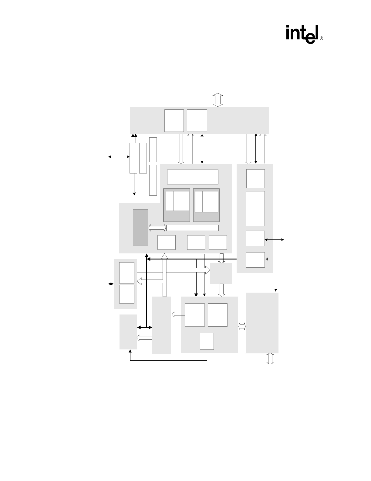
82540EP — Networking Silicon
PCI
i/f
PCI I/F
4-wire EEPROM Inte rfac e
SMBus Interface
blocks)
(Many
Clock / Reset
EEPROM
Configs
Default
ACPI
LED
HW
Packet Buffer
64K bytes
Manageability
FIFOs
Mgmt
ASF
CSR Register
Access
Statistics
Master
FIFO
read
Data Alignment
descriptor
FIFOs
engine
RX
Packet Buffer Interface
RX
In
CSR Register
Access
TX Data
RX Data
Filter
RX Data
RX
Master
FIFO
write
FIFOs
Flow
Ctrl
RX MAC
Core
PCI
Control
Target
descriptor
engine
TX
Target Logic
DMA
TX
Out
TX
Arb
Tx
TX MAC
GMII
MAC Core
Control, Status
& Interrupt
Registers
82540EP Architecture
Flash Interfac e
MDIOFlash
PHY
Link
TX
(Copper)
Interface
MDI
Figure 1. Gigabit Eth ernet Controller Bl ock Di agram
2 Datasheet
Page 9

1.1 Document Scope
This document contains datasheet specifications for the 82540EP Gigabit Ethernet Cont roller,
including si gnal descriptions, DC and AC parameters, packaging data, and pinout information .
1.2 Reference Documents
This application assumes that the designer is acquainted with high-speed design and board la yout
techniques. The following documents provide additiona l information:
• 82544EI/82544GC Gigabit Ethernet Control ler Software Developer's Manual, Revision 0.25,
Intel Corporation.
• PCI Local Bus Specification, Revision 2.3, PCI Special Interest Group.
• PCI Bus Power Management Interface Specification, Rev. 1.1, PCI Special Interest Group.
• IEEE Standard 802.3, 1996 Edition, Institute of Electrical and Electronics Engineers (IEEE).
• IEEE Standard 802.3u, 1995 Edition, Institute of Electrical and Electronics Engineers (IEEE).
• IEEE Standard 802.3x, 1997 Edition, Institute of Electrical and Electronics Engineers (IEEE).
• IEEE Standard 802.3z, 1998 Edition, Institute of Elec trical and Electronics Engi nee r s (IEEE).
Networking Silicon — 82540EP
• IEEE Standard 802.3ab, 1999 Edition, Institute of Electrical and Electronics Engineers
(IEEE).
• 82559 Fast Ethernet Controllers Tim ing Device Selection Guide, AP-419, Intel Corporation.
• PCI Mobile Design Guide, Rev. 1.1, PCI Special Interest Group
1.3 Product Code
The product ordering code for the 82540EP is: RC82540EP.
Datasheet 3
Page 10

82540EP — Networking Silicon
Note: Th is page is intentionally left blank.
4 Datasheet
Page 11

Networking Silicon — 82540EP
2.0 Features of the 82540EP Gigabit Ethernet Controller
2.1 PCI Features
Features Benefits
• Application flexibility for LAN on Motherboard
PCI Revision 2. 3 support fo r 32-bit wid e interface at
33 MHz and 66 MHz
Algori thms that opt imally us e advance d PCI, MWI,
MRM, and MRL commands
CardBus Information Services (CIS) Pointer
CLKRUN# Signal • PCI clock suspension for lo w power mobile design
(LOM) or embedded solutions
• 64-bit addressing for system s with more th an 4
Gigabytes of physical memory
• Support for new PCI 2.3 interrupt status/control
• Efficient bus operations
• Enables CardBus operation (when us ed with
ext ernal FLASH device and series termination on
PCI bus)
2.2 MAC Specific Features
Features Benefits
Low- latency transmit and r eceive qu eues
IEEE 802.3x compliant flow control support with
softw are controllable pa use times and threshold
values
Caches up to 64 packet des cri ptors in a single bur st • Efficient use of PCI bandwid th
Programmable host memory receive buffers (256
Bytes to 16 KBytes) and cache line size (16 Bytes to
256 Bytes)
Wide, optimized internal data path architecture
64 KByte configu rable Transmit and Receive FIFO
buffers
Descriptor ring management hardware for transmit
and receive
Optimized descr iptor fetching and w rite-back
mechanisms
Mechanism available for reducing interrupts
generated by transmit and recei ve ope rations
Support for transm ission and receptio n of pack ets up
to 16 KBytes
• Netw ork pack ets handled withou t waiting or buffer
overflow.
• Control over t he transmi ssions of pause frames
through software or hardware triggering
• Frame loss reduced from receive overruns
• Efficient use of PCI bandw idth
• Low latency da ta handling
• Superior DMA t ransfer rate pe rfo rmance
• No external FIFO memory requirements
• FIFO size adjustable to application
• Simple software programming model
• Effi ci ent system mem ory and use of PCI
bandwidth
• Maxi m ize s sy s t em performa nc e and throug hput
• Enable s jum b o f ram es
Datasheet 5
Page 12

82540EP — Networking Silicon
2.3 PH Y Spe cif ic Fe atu res
Features Benefits
Integrated PHY for 10/100/1000 Mbps full and half
duplex op eration
IEEE 802.3ab Auto-Negotiation support
IEEE 802.3ab PHY compliance and compatibility
State-of-the-art DSP architecture implements digital
adaptive equalization, echo cancellation, and crosstalk cancellation
PHY ability to autom atically detect polari ty and cable
lengths and MDI versus MDI-X cable at all speeds
2.4 Host Offloading Features
Features Benefits
T ransmit and receive IP, TCP and UDP checksum offloading capabil ities
Transmit TCP segmentation
Advanced packet filtering
IEEE 802.1q VLAN support with VLAN tag insertion,
strippin g an d pac k et filt e ring for up to 409 6 VL AN tags
Descriptor ring management hardware for transmit
and receive
16 KByte jumbo frame support
Interrupt coalescing (multiple packets per interrupt)
• Smaller footprint and lower power dissipation
compar ed to multi- chip MAC and PHY solutions
• Automatic link configuration including speed,
duplex, and flow control
• Robust operat ion over the installed base of
Category-5 (CAT-5) twisted pair cabling
• Robust performance in noisy environments
• Tolerance of com m on electrical signal
impairments
• Easier network installation and maintenance
• End-to -end wiring t olerance
• Lower CPU utilization
• Increased throug hput and lower CPU utilizat ion
• Large send offload feature (in Microsoft*
Window s* XP) compatible
• 16 exact matched packets (unicast or multicast)
• 409 6-b i t has h f ilt er for multicast fra me s
• Promiscu ous (unicast and multicast) transfer
mode support
• Optical filtering of inv alid frames
• Ability to create multiple virtual LAN segments
• Optimi zed f etc hing and writ e-bac k mech anis ms f or
efficient system memory and PCI bandwidth
usage
• High throughput for large data transfers on
networks supporting jumbo frames
• Increased throug hput by reducing interrupts
generated by tr ansmit an d receive operatio ns
6 Datasheet
Page 13

2.5 Manageability Features
Features Benefits
Networking Silicon — 82540EP
Manageability features: SMB port, ASF 1.0, ACPI,
Wa ke on LAN, and PXE
On-board SMB port
Compliance with PCI Power Management 1.1 and
ACPI 2.0 register set compliant including:
• D0 and D 3 power states
• Network Device Class Power Management
Specification 1.1
• PCI Sp ecification 2.2
SNMP and R M O N statistic counters
SDG 3.0, WfM 2.0, and PC2001 com pliance
Wa ke on LAN sup port
Two or three-pair cable downshift • Assures link under adverse cable configurations
• Netw or k m anagemen t flexibi lity
• Enab les IPMI and ASF impl em entations
• Allow s pac k et s ro ut ing t o an d from ei th er L AN port
and a se rver management processor
• PCI po wer management capability requirements
for PC and embe dded applications
• Easy system monitorin g with indust ry standard
consoles
• Remote network management capabilities through
DMI 2.0 and SNMP software
• Packet recognitio n and wake-up for NIC and LOM
applic ations with out softw are configuration
Datasheet 7
Page 14

82540EP — Networking Silicon
2.6 Additional Device Features
Features Benefits
Four activity and link indication outputs that di re ctly
drive LEDs
Progra mm a ble LE D f u nctiona li t y
Internal PLL for clock generation can use a 25 MHz
crystal
JTAG (IEEE 1149.1) Test Access Port built in silicon • Simplified testing using boundary scan
On-chip power control circuitry
Four software definable pins
Supports little endian byte ordering for both 32 and 64
bit sys t em s and bi g en dian byte ord ering for 64 bit
systems
Two or t hree-pair cable dow nshift • Supports modular har dware acc essories
Provi de s lo op back capabilitie s • Validates silicon int e gr i ty
Minimal ballout change from the 82540EM • Pin Compatibility
a. If applying the “low-power” EEPROM setting for the 82540EP chip, then only external voltage regulator circuits should be used
instead of the on-chip power control circuitry
a
2.7 Technology Features
• Link and activity indications (10, 100, and 1000
Mbps) on each port
• Software definable function (speed , link, and
activity) and bl inking allowing flexible LED
implementations
• Lower component count and system cost
• Redu c ed number of on -board power supply
regulators
• Simplified power supply design in less powercritical applications
• Additional flexibil ity for LE Ds or other low spe ed
I/O devices
• Portable across application architectures
Features Benefits
196-pin Ball Grid Array (TFBGA) package • 15 mm2 component making LOM designs easier
Pin compatible with 82551 QM and 82540EM
controllers
Implemented in 0. 15u CMOS process
Operating temperature: 0
operating temperature
Heat sink or forced airflow not required
65
° C to 140° C stor age temperature ran ge
PCI Signaling: 3.3 V (5 V tolerant) PCI signaling
Typic al tar ge t e d pow er dissipation:
• 1.38W @ D0 1000 Mb/s
• 386mW @ D3 100 Mb/s (wake-up enabled)
• <20mW @ D3 wake-up disabled
° C to 70° C (maximum)
• Enables 10/100 Mbps Fast Ethernet or 1000 Mbps
Gigabit Ethernet implementations on the same
board wi th only minor stuffing option changes
• Offe r s lowest ge ometry to mini m ize power and
size while maintainin g Intel quality reliability
standards
• Simple thermal design
• Lower power requirements for mobile applications
8 Datasheet
Page 15

3.0 Signal Descriptions
Note: The ta rgeted signal names are subject to change without notice. Verify with your local Intel sales
office that you have th e latest information before finalizing a design.
3.1 Signal Type Definitions
The signals of the 82540EP controller are electrically defined as foll ows:
Name Definition
I Input. Standard input onl y di gital signal.
O
TS
STS
OD
A
P
Output. Standard output onl y digital signal.
Tri-state. Bi-directional three-state digital input/output signal.
Sustained Tri-state. Sustained digital three-stat e signal driven by one agent at a t ime.
An agent driving the STS pin low must actively drive it high for at least one clock before letting it
float. The next agent of the signal cannot drive the pin earlier than one clock after it has been
released by the previous agent.
Open Dr ai n . Wired-OR wi th other ag ents.
The signaling agent asserts the OD signal, but the signal is returned to the inactive state by a
weak pull-up resistor. The pull-up resistor may require two or three clock periods to fully restore
the signal to the de-a sserted state.
Analog. PHY analog data signal .
Power. Power connection, voltage reference, or other reference connection.
Networking Silicon — 82540EP
3.2 PCI Bus Interface
When the Reset signal (RST #) is asserted, the 82540EP will not drive any PCI output or bidirectional pins except the Power Management Event signal (PME#).
3.2.1 PCI Address, Data and Control Signals
Symbol Type Name and Function
Address and Data.
bus transaction includes an address phase followed by one or more data phases.
The address phase is the clock cycle when the Fram e signal (FRA ME#) is asserted
AD[31:0]
TS
low. During the address phase AD[31:0] contain a physical addre ss (32 bits). For I/O,
this is a byte add ress, and for configuratio n and memory, a DWO RD address . The
82540EP device uses littl e endian byte ordering.
During data phases, AD[7:0] contain the least significant byte (LSB) and AD[31:24]
contai n t he mos t signifi ca nt byte (MSB) .
Datasheet 9
Address and data signals are multiplexed on the same PCI pins. A
Page 16

82540EP — Networking Silicon
Symbol Type Name and Function
CBE[3:0]#
PAR TS
FRAME# STS
IRDY# STS
TRDY# STS
STOP# STS
IDSEL# I
DEVSEL# STS
VIO P
TS
Bus Command and Byte Enables. Bus comm and and byte enable signals are
multiplex ed on the sam e PCI pins. During the ad dress phase of a transaction,
CBE[3:0]# define the bus command. In the data phase, CBE[3:0]# are used as byte
enables. The byte enables are valid for the entire data phase and determine which byte
lanes c ontain meaningful da ta.
CBE0# applies to byte 0 (LSB) and CBE3# applies to byte 3 (MSB).
Parity. Th e Par ity signal is iss ue d to im plement even parity acr os s AD [31:0] an d
CBE[3:0]#. PAR is stable and valid one clock after the address phas e. During dat a
phases, PAR is stable and valid one clock after either IRDY# is asserted on a write
trans act ion or TR DY# is asserted af t er a rea d t ran sa ctio n. Onc e PAR is va lid, it r em ains
valid until one clock af ter the com pletion of th e cu r r e nt data phas e.
When t he 82540EP controller is a bus m aster, it drives PAR f or address a nd write data
phases, and as a slave device, drive s PAR for read data ph as es .
Cycle Frame.
beginning and length of an access and indicate the beginning of a bus transaction.
While FRAME# is asserted, data transfers cont inue. FR AME# is de-asserted when the
transaction is in the final data phas
Initiator Ready. Initiator Ready indicates the ability of the 82540EP controller (as bus
maste r device) to complet e the current data phase of the transaction. IRDY# is used in
conjunction with the T arget Ready signal (TRDY#). The data phase is completed on any
clock when both IRDY# and TRDY# are asserted.
During the write cycle, IRDY# indicates t hat valid data is present on AD[3 1:0]. For a
read cycl e , it in dica te s the mas t er is rea dy to ac cep t da ta. Wai t cycl es are ins erted un til
both IRD Y# and TRDY# are asserted together. The 82540EP controller drives IRDY#
when acting as a master and samples it when acting as a slave.
Target Ready. The Target Ready signal in dicates the ability of the 82540EP controller
(as a sele cted device) to comple te the current data phase of the transaction. TRDY# is
used in conjunction with the I nitiator Ready signal (IRD Y#). A data p hase is compl eted
on an y clock when both TRDY# and IRDY# are sam pled asse rted.
During a read cycle, TRDY# indicates that valid data is present on AD[31:0]. For a write
cycle, it indicate s the target is ready to accep t data. Wai t cycles are inserted until both
IRDY# and TRDY# are asserted together. The 82540EP device drives TRDY# when
acting as a slave and samples it when acting as a master.
Stop. The Stop signal indicates the current target is requesting the master to stop the
current transaction. As a slave, the 82540EP controller drives STOP# to request the
bus master to stop the transacti on. As a master, the 82540EP controller receiv es
STOP# from the slave to stop the current transaction.
Init ialization Device Select. The Initialization Device Select signal is used by the
82540 EP as a chip select signal during configuration read an d write tran sactions.
Device Select. When the De vice Select signal is actively driven by the 82540EP, it
signals notifies the bus master that it has decoded its address as the target of the
current access. As an input, DEVSEL# indicates whether any device on the bus has
been selected.
VIO. The VIO signal is a voltage reference for the PCI interface (3.3 V or 5 V PCI
signaling environment). It is used as the clamping voltage.
Note: An external resistor is re qu ir e d between the voltage refer ence and the VIO pin.
The target resistor value is 100 K
The Frame signal is driven by the
e.
Ω
82540EP device to indicate the
10 Datasheet
Page 17

3.2.2 Arbitration Signals
Symbol Type Name and Function
REQ# TS
GNT# I
LOCK# I
Request Bus. The Request Bus signal is used to request control of the bus from the
arbiter. This signal is point-to-point.
Grant Bus. The Gra nt Bus signal notifies the 82540EP that bus access has been
granted. This is a point-to-point signal.
Lock Bus. The Lock Bus signal is asserted by an ini tiator to require sole access to a
target me mo ry device du r ing two or mor e se parate tra ns fer s. The 825 40EP device
does not implement bus locking.
3.2.3 Interrupt Signal
Symbol Type Name and Function
Networking Silicon — 82540EP
INTA# TS
Interrupt A. Interrupt A is u se d t o re que st an in ter rupt by port 1 o f t he 82 54 0EP . It i s an
active low, level-triggered interrupt signal.
3.2.4 System Signals
Symbol Type Name and Function
PCI Clock.
CLK I
M66EN I 66 MHz Enable. M66EN indicates whether the system bus is enabled for 66MHz.
RST# I
CLKRUN#
I/O
OD
is an input to the
(INTA#) and PCI Reset signal (RST#), are sampled on the rising edge of CLK. All other
timing parameters are defined with re spect to this edge.
PCI Reset. When the PCI Reset sign al is asserted, all PCI outp ut signals, except the
Power Management Event si gnal (PME #), are floa ted and all input signals are ignored.
The PME# context is preserved, depending on power management settings.
Most of the internal st ate of the 82540EP is reset on the de-assertion (rising edge) of
RST#.
Clock Run. This signal is used by the syst em to pause the PCI clock si gnal. It is used
by the 825 40EP controlle r to re quest the PCI clock. When t h e CL KRUN # fea tu r e is
disabled, leave this pi n unconnected.
The PCI Clock signal provides timing for all transactions on the PCI bus and
3.2.5 Error Reporting Signals
82540EP
device. All other PCI signals, except the Interrupt A
Symbol Type Name and Function
System Error. The System Error signal is used by the 82540EP controller to report
SERR# OD
PERR# STS
address parity errors. SERR# is open drain and is actively driven for a single PCI clock
when reporting the error.
Parity Error. The Parity Error sig nal is used by the 82540EP controller to repo rt da ta
parity errors during all PCI transactions except by a Special Cycle. PERR# is sustained
tri-state and must be driven active by the 82540EP controller two data clocks after a
data pari ty error is detected. Th e m inimum du ration of PE RR# is one clock for each
data phase a data parity error is present.
Datasheet 11
Page 18

82540EP — Networking Silicon
3.2.6 Power Management Signals
Symbol Type Name and Function
LAN_
PWR_
GOOD
PME# OD
AUX_PWR I
I
Power Good (Power-on Reset). The Power Good signal is used to indicate that stable
power is available for the 82540EP. When the signal is low, the 82540EP holds itself in
reset state and floats all PCI signals.
Power Ma nagement Event. The 8254 0EP device dr ives this signal low when it
receives a wake-up event and either the PME Enable bit in the Power Management
Control/Status Register or the Advanced Power Management E nable (APME) bit of the
Wa ke-up Control Register (WUC) is 1b.
Auxiliary Power. If the Auxiliary Power signal is high, then auxiliary power i s available
and the 82540EP device should support the D3cold power state.
3.2.7 Impedance Compensation Signals
Symbol Type Name and Function
N Device Impedance Compensation. This signal sho uld be connec t e d t o an external
ZN_COMP I/O
ZP_COMP I/O
precision resistor (to VDD) that is indicative of the PCI trace load. This cell is used to
dynamically determine the drive strength required on the N-channel transistors in the
PCI I/O cells.
P Device Impedance Compensation. This signal sho uld be conn ec ted to an external
precision resistor (to VSS) that is indicative of the PCI trace load. This cell is used to
dynamically det ermine the drive strength required on the P-channel tr ansistors in the
PCI I/O cells.
3.2.8 SMB Signals
Symbol Type Name and Function
SMBCLK I/O SMB Clock. The SMB Cl ock signal is an open drain signal for se ri al SMB interface.
SMBDATA I/O
SMBALRT# O
SMB Data. The SMB Data signal is an open drain signal for serial SMB interface.
SMB Alert. The SMB Alert si gnal is open drain for serial SMB interface.
3.3 EEPROM and Serial FLASH Interface Signals
Symbol Type Name and Function
EE_DI O
EE_DO I
EE_CS O
EE_SK O
EEPROM Data Input. The EEPROM Data Input pin is used for output to the memory
device.
EEPROM Data Output. The EEPROM Data Output pin is used for input from the
memory device. The EE_DO includes an internal pull-up resi stor.
EEPROM Chip Select. The EEPRO M Chip Selec t signal is used to enable the device.
EEPROM Serial Clock. The EEPROM Shift Clock provides the clock rate for the
EEPROM interface, which is approximately 1 MHz.
12 Datasheet
Page 19

Symbol Type Name and Function
FL_CE# O FLASH Chip Enable Output. Used to enable FLASH device.
FL_SCK O
FL_SI O
FL_SO I
FLASH Serial Clock Output. The clock rate of the serial FLASH interface is
approxim ately 1 MHz.
FLASH Serial Data Input. This pin is an output to the memory device.
FLASH Serial Data Output. This pin is an input from the FLASH memory. It has an
internal pullup device.
3.4 Miscellaneous Signals
3.4.1 LED Signals
Symbol Type Name and Functio n
LED0 / LINK# O
LED1 / ACT# O
LED2 / LINK100# O
LED3 / LINK1000# O
LED0 / LINK Up. Programmable LED indication. Defaults to indicate link
connectivity .
LED1 / Activity. Programmable LED indication. Defaults to flash to indicate
transmit or receive activity.
LED2 / LINK 100. Programmable LED indication. Defaults to indicate link at
100 Mbps.
LED3 / LINK 1000. Progra mm a bl e LED in dicatio n. Defau l ts t o ind ic ate link at
1000 Mbps.
Networking Silicon — 82540EP
3.4.2 Other Signals
Symbol Type Name and Function
SDP[7:6]
SDP[1:0]
TS
Software Defined Pin. The Soft wa re D efined Pin s are reser ved and programm a ble
with res pe ct to i nput a nd ou tp ut ca pa bil ity. These de f au lt to i nput s igna ls up on po w er -up
but may be configured differently by the EEPROM. The upper four bits may be mapped
to the G eneral Purpose Interrupt bits if they are configured as input signals.
Note: SDP5 is not i ncluded in the group of Software Defined Pins.
Datasheet 13
Page 20

82540EP — Networking Silicon
3.5
PHY Signals
3.5.1 Crystal Signals
Symbol Type Name and Function
XTAL1 I
XTAL2 O
3.5.2 Analog Signals
Symbol Type Name and Function
REF P
MDI[0]+/- A
MDI[1]+/- A
MDI[2]+/- A
MDI[3]+/- A
Crystal One. The Crystal On e pin is a 25 MHz +/- 50 ppm in put signal. It can be
connected to either an oscillator or crystal. If a crystal is used, Crystal Two (XTAL2)
must also be connected.
Crystal Two. Crystal T wo is the output of an internal oscillator circuit used to drive a
crystal into oscillation. If an external oscillator is used in the design, XTAL2 must be
disconnected.
Reference. This Reference signal should be connected to VSS through an external
2.49 K
Ω resistor.
Media Dependent Interface [0].
1000BASE-T: In MDI configuration, MDI[0]+/- corresponds to BI_DA+/-, and in MDI-X
config ur ation, MDI [ 0] +/ - co r responds t o BI_D B+/-.
100BASE-TX: In MDI configuration, MDI[0]+/- is used for the transmit pair, and in MDI-X
config ur at ion, MDI[0]+/- is use d for the rec eive pair.
10BASE-T: In MDI configuration, MDI[0]+/- is used for the transmit pair, and in MDI-X
config ur at ion, MDI[0]+/- is use d for the rec eive pair.
Media Dependent Interface [1].
1000BASE-T: In MDI configuration, MDI[1]+/- corresponds to BI_DB+/-, and in MDI-X
config ur ation, MDI [ 1] +/ - co r responds t o BI_DA+/-.
100BASE-TX: In MDI configuration, MDI[1]+/- is used for the receive pair, and in MDI-X
config ur at ion, MDI[1]+/- is used for the t rans it pair.
10BASE-T: In MDI config uration, MDI[ 1 ]+/- is used for the rec eive pair, and in MDI-X
config ur at ion, MDI[1]+/- is used for the t rans it pair.
Media Dependent Interface [2].
1000BASE-T: In MDI configuration, MDI[2]+/- corresponds to BI_DC+/-, and in MDI-X
config ur ation, MDI [ 2] +/ - co r responds t o BI_D D + / -.
100BASE-TX: Unuse d.
10BASE-T: Unused.
Media Dependent Interface [3].
1000BASE-T: In MDI configuration, MDI[3]+/- corresponds to BI_DD+/-, and in MDI-X
config ur ation, MDI [ 3] +/ - co r responds t o BI_D C + / -.
100BASE-TX: Unuse d.
10BASE-T: Unused.
14 Datasheet
Page 21

3.6 Test Interface Signals
Symbol Type Name and Function
JTA G_TCK I JTAG Clock.
JTA G_TDI I JTAG TDI.
JTA G_TDO O JTAG TDO.
JTA G_TMS I JTAG TMS.
JTA G_
TRST#
TEST I
CLKVIEW O
I
JTAG Reset. This is an activ e low reset signal for JTAG. This signal should be
terminated using a pull-down resistor to ground. I t must not be left unconnected.
Factory Test Pin.
Clock View. Ou tput f or GTX _CLK an d RX_CLK during IEEE PHY con f ormance te sting .
The clock is selected by register programming.
3.7 Power Supply Connections
3.7.1 Digital Supplies
Networking Silicon — 82540EP
Symbol Type Name and Function
VDDO P 3.3 V I/O Power Suppl y.
DVDD P 1.5 V Digital Core Power Supply.
3.7.2 Analog Supplies
Symbol Type Name and Function
AVDDH P 3.3 V Analog Power Supply.
AVDDL P 2.5 V Analog Power Supply.
Datasheet 15
Page 22

82540EP — Networking Silicon
3.7.3 Ground and No Connects
Symbol Type Name and Function
GND P Ground.
NC P
No Connect. Do not connect any circuitry to these pins. Pull-up or pull-down resistors
should not be connected to these pins.
3.7.4 Control Signals
Symbol Type Name and Function
1.5V Control. LDO voltage regulator output to drive external pass transistor. If 1.5V is
CTRL_15 A
CTRL_25 A
already present in the system, leave output unconnected. To achieve optimal D
consu mp tio n ( <5 0 mw), leave the output unconnected and use a high-effic ie nc y
external switching regulator.
2.5V Control. LDO voltage regulator output to drive external pass transistor. If 2.5V is
already present in the system, leave output unconnected. To achieve optimal D
consu mp tio n ( <5 0 mw), leave the output unconnected and use a high-effic ie nc y
external switching regulator.
power
3
power
3
16 Datasheet
Page 23

Networking Silicon — 82540EP
4.0 Voltage, Temperature, and Timing Specifications
Note: The spec if i cati on val ues li sted in this sec tion are subjec t to chan ge without notic e. Verify with your
local Intel sales office that you have the lates t information before finalizing a design.
4.1 Absolute Maximum Ratings
Storage
a
-40 125
Table 1. Absolute Maximum Ratings
Symbol Parameter Min Max Unit
V
DD
V
IN
I
IN
T
STG
a. Maximum ratings are referenced to ground (VS S). Permanent device damage is likely to oc cur if the r atin gs in this tab le are
exceeded. These values should not be used as the limits for normal device operations.
DC suppl y voltage -0.3 7 V
Input voltage -1 VDD + 0.3 V
DC input pin current -10 10 mA
temperature
4.2 Recommended Operating Conditions
Table 2. Recommended Operating Conditionsa (Sheet 1 of 2)
Symbol Parameter Condition Min Typ Max Unit
°C
T
OP
V
IO
V
DD
Operating
T emperature
VIO Voltage
Range
Periphery
Voltage
Range
3.3V ± 10% 33.33.6V
070
35.25V
°C
Datasheet 17
Page 24

82540EP — Networking Silicon
Table 2. Recommended Operating Conditionsa (Sheet 2 of 2)
Symbol Parameter Condition Min Typ Max Unit
V
AH
V
D
V
AL
a. Sustained operation of the device at conditions exceeding these values, even if they are within the absolute maximum rating
limits, might result in permanent damage.
Analog High
VDD Range
Core Digital
Voltage
Range
Analog Low
VDD Range
4.3 DC Specifications
T ab le 3. DC Characteristics
Symbol Parameter Min Typ Max Units
VDD (3.3)
(2.5) DC supply voltage on AVDDL 2.38 2.5 2.62 V
V
DD
V
(1.5) DC supply voltage on DVDD 1.43 1.5 1.57 V
DD
DC supply voltage on VDDO or
AVDDH
3.3V ± 10% 33.33.6V
1.5V ± 5% 1.425 1.5 1.575 V
2.5V ± 5% 2.375 2.5 2.625 V
3.00 3.3 3.60 V
Table 4. Power Specifications - D0a
D0a
unplugg ed /no lin k @10 Mbps @100 M bps @1000 M bps
Typ Icc
(mA)
3.3V
2.5V 20 20 30 35 55 60 145 150
1.5V 100 120 95 100 115 125 400 425
Total
Device
Power
40 40 55 65 65 80 125 125
325 mW 400 mW 525 mW 1.38 W 1.5 W
Max Ic c
(mA)
Ty p Icc
(mA)
Ma x I cc
(mA)
Typ Icc
(mA)
Max Icc
(mA)
Typ Icc
(mA)
M a x I c c
(mA)
18 Datasheet
Page 25

T ab le 5. Power Specifications - D3cold
Networking Silicon — 82540EP
D3cold - wake-up enabled
unplugged/no link @10 Mbps @100Mbps
Typ Icc
(mA)
3.3V
2.5V 20 20 30 30 55 55 20 20 0.1 0.1
1.5V 40 40 30 35 55 60 10 10 1 1
Total
Device
Power
a. Special Note: To obtain the benefit of max power savings mode, do not use the internal voltage regulator control circuit and external pass transis-
tors. Use external switching regulators for highest efficiency.
240 mW 300 mW 385 mW 195 mW 20 mW
Max Icc
(mA)
Typ Icc
(mA)
Max Icc
(mA)
Typ Icc
(mA)
Max Icc
(mA)
40 40 55 55 50 50 40 40 6 8
D3cold - wake
disabled - max
power savings
mode disabled
Typ Ic c
(mA)
Max Icc
(mA)
D3cold - wake
disabled - max
power savin g s
mode enabled
Typ Icc
(mA)
Max Icc
a
(mA)
Table 6. Po wer Specif ic a tions D(r) Un in it i a liz e d
D(r) Uninitialized
(LAN_PWR_GOOD=0)
Ty p I cc
(mA)
Max Icc
(mA)
3.3V
2.5V 40 45
1.5V 190 200
T otal Devi ce
Power
40 45
520 mW
Table 7. Power Specifications - Complete Subsystem
Complete Subsystem (Reference Design)
Including Magnetics, LED, Regulator Circuits
D3cold - wake
3.3V
disabled - max
power savings
mode disabled
Typ Icc
(mA)
Max Icc
(mA)
40 40 60 60 60 60 130 130 6 8
D3cold wake-
enabled @10Mbps
Typ Icc
(mA)
Max Icc
(mA)
D3cold wake-
enabled @100Mbps
Typ Icc
(mA)
Max Icc
(mA)
D0 @1000Mbps
active
Typ
(mA)
Icc
Max Icc
(mA)
D3cold - wake
disabled - max
power savings
mode enabled
Ty p I c c
(mA)
Max Icc
(mA)
Datasheet 19
Page 26

82540EP — Networking Silicon
Table 7. Power Specifications - Complete Subsystem
2.5V 20 20 40 40 80 80 240 245 0.1 0.1
1.5V 10 10 30 35 55 60 400 425 1 1
Subsystem
3.3V current
70 mA 135 mA 200 mA 800 mA 10 mA
T ab le 8. I/O Characteristics
Symbol Parameter Condition Min Typ Max Unit
V
V
V
OL
V
OH
V
SH
I
OL
I
OH
I
IN
I
OZ
C
C
OUT
C
PUD
a. TTL3 signals include: EE_DI, EE_SK, EE_CS, and JTAG_TDO.
TTL6 signals include: CLKRUN#, FL_CE#, FL_SCK, FL_SI, and CLK_VIEW.
TTL12 signals include: LED0 / LINK #, LED1 / ACT #, LED2 / LINK100 #, LED3 / LINK1000 #, SDP0, SDP1, SDP6, and SDP7.
Voltage input LOW -0.5 0.8 V
IL
Voltage input HIGH 2
IH
Voltage output LOW 0.4 V
Voltage output HIGH 2.4 V
Schmitt Trigger Hysterysis 0.1 V
Output current LOW
3mA drivers (TTL 3)
a
6mA drivers (TTL 6)
12mA drivers (TTL12)
Output current HIGH
3mA drivers (TTL 3)
a
6mA drivers (TTL 6)
12mA drivers (TTL12)
Input Current
TTL inputs
Inputs with pull-down resistors
TTL inputs with pull-up resistors
3-stat e output leak ag e cu r r e nt
Input ca pacitance
IN
Output capacitance
Pull-up/down Resistor value 7.5 20 kΩ
V
OL
V
OL
V
OL
V
OH
V
OH
V
OH
V
= VDD or
IN
V
SS
VIN = VDD
V
= V
IN
SS
= V
V
OH
or
DD
V
SS
Any input and
bi-directional
buffer
Any output
buffer
V
DD
+0.3
3
6
12
-3
-6
-12
-10
150
-150
±1
10 µA
480 µA
-480 µA
-10 ±1 10 µA
2.5 pF
2pF
V
mA
mA
mA
mA
mA
mA
20 Datasheet
Page 27

4.4 AC Characteristics
Table 9. AC Characteristics: 3.3 V Interfacing
Symbol Parameter Min Typ Max Unit
PCICLK Clock frequency in PCI mode 66 MHz
Table 10. 25 MHz Clock Input Requ irements
Symbol Parameter
Networking Silicon — 82540EP
a
Min Typ Max Unit
fi_TX_CLK TX_CLK_IN frequency 25 - 50 ppm 25
a. This parameter applies to an oscillator connected to the Crystal One (XTAL1) input. Alternatively, a crystal may be connected
to XTAL1 and XTAL2 as the frequency source for the internal oscillator.
T ab le 11. Link Interface Clock Requirements
Symbol Parameter Min Typ Max Unit
a
fGTX
a. GTX_CLK is used externally for test purposes only.
GTX_C LK fr eq uency 125 MHz
T ab le 12. EEPROM Interface Clock Requirements
Symbol Parameter Min Typ Max Unit
fSK 1MHz
Table 13. AC Test Loads for General Output Pins
Symbol Signal Name Value Units
CL TDO 10 pF
CL PME#, SDP[7:0] 16 pF
CL EE_DI, EE_SK 18 pF
CL RX_ACTIVITY, TX_ACTIVITY, LINK_UP 20 pF
25 + 50
ppm
MHz
Datasheet 21
Page 28

82540EP — Networking Silicon
L
Figure 1. AC Test Loads for General Output Pins
4.5 Timing Specifications
Note: Timing specifications are subj ect to change. Verify with your local Intel sales office that you ha ve
the latest information before finalizing a design.
4.5.1 PCI Bus Interface
C
4.5.1.1 PCI Bus In ter face Clock
Table 14. PCI Bus Interf ace Clock Parameters
Symbol Parameter
TCYC CLK cycle time 15 30 30 ns
TH CLK high time 6 11 ns
TL CLK low time 6 11 ns
CLK slew rate 1.5 4 1 4 V/ns
RST# slew rate
a. Rise and fall times are specified in terms of the edge rate measured in V/ ns. This slew rat e must be met acr oss the
minimum peak-to-peak portion of the clock waveform as shown.
b. T he minimum RST# slew rate applies only to the rising (de-assertion) edge of the reset signal and ensures that system
noise cannot render a monotonic signal to appear bouncing in the switching range.
Figure 2 . PCI Clock Timing
3.3 V Clock
0.5 Vcc
0.4 Vcc
0.3 Vcc
b
a
0.6 Vcc
PCI 66 MHz PCI 33 MHz
Units
Min Max Min Max
50 50 mV/ns
Tcyc
Th
0.4 Vcc p-to-p
(minimum)
0.2 Vcc
Tl
22 Datasheet
Page 29

4.5.1.2 PCI Bus Interface Timing
T ab le 15. PCI Bus Interface Timing Parameters
Networking Silicon — 82540EP
Symbol Parameter
PCI 66MHz PCI 33 MHz
Min Max Min Max
TVAL
TVAL(ptp)
CLK to signal valid delay: bussed
signals
CLK to si gnal valid delay: pointto-poi nt signals
2 6 2 11 ns
2 6 2 12 ns
TON Float to active delay 2 2 ns
TOFF Active to float delay 14 28 ns
TSU
TSU(ptp)
Input setup time to CLK: bussed
signals
Input setup time to CLK: point-topoint signals
37ns
5 10, 12 ns
TH Input hol d time fro m CLK 0 0 ns
TRRSU REQ64# to RST# setup time 10*
TCYC 10*TCYC ns
TRRH RST# to REQ64# hold time 0 0 ns
NOTES:
1. Output timing measurements are as shown.
2. REQ# and GNT# signals are point-to-point and have different output valid delay and input setup times than
busse d signals. GNT# has a setup of 10 ns; REQ# has a setup o f 12 ns. All ot her signals ar e bussed.
3. Input timing measurements are as shown.
Figure 3. PCI Bus Interface Output Timing Measurement
Units
V
TH
PCI_CLK
Output
Delay
Tri-State
Output
VTEST
output current≤ leakage current
T
ON
TOFF
V
TEST
V
(3.3V Signalling)
STEP
V
TL
Datasheet 23
Page 30

82540EP — Networking Silicon
t
Figure 4. PCI Bus Interface Input Timing Measurement Conditions
V
TH
PCI_CLK
T
SU
V
TH
Input V
V
TL
V
TEST
Input
Valid
V
T
TEST
H
Table 16. PCI Bus Interf ace Ti ming Measurement Conditions
Symbol Parameter
VTH Input measurement test voltage (high) 0.6*VCC V
VTL Input measurement test voltage (low) 0.2*VCC V
VTEST Output measurement test voltage 0.4*VCC V
Input signal slew rate 1.5 V/ns
Figure 5 . TVAL (max) Rising Edge Test Loa d
V
TEST
PCI 66 MHz
3.3 v
MAX
V
TL
Unit
Pin
1/2 inch max.
Test
Poin
25Ω
10 pF
24 Datasheet
Page 31

Figure 6. TVAL (max) Falling Edge Test Load
Networking Silicon — 82540EP
Figure 7. TVAL (min) Test Load
Pin
Pin
1kΩ
1/2 inch max.
10 pF
1/2 inch max.
10 pF
25Ω
1kΩ
V
Test
Point
CC
Test
Point
V
CC
Figure 8. TVAL Test Load (PCI 5 V Signaling Environment)
NOTE:
Pin
1/2 inch max.
50 pF
Note: 50 pF load used for maximum times. Minimum times are specified with 0 pF load.
Test
Point
Datasheet 25
Page 32

82540EP — Networking Silicon
4.5.2 Link Interface Timing
T ab le 17. Rise and Fall Times
Symbol Parameter Condition Min Max Unit
TR Clock rise time 0.8 V to 2.0 V 0.7 ns
TF Clock fall time 2.0 V to 0.8 V 0 .7 ns
TR Data rise time 0.8 to 2. 0 V 0.7 ns
TF Data fall time 2.0 V to 0.8 V 0.7 ns
Figure 9. Link Interface Rise/Fall Timing
2.0 V
0.8 V
4.5.3 EEPROM Interface
Table 18. Link Int erf ace Clock Requirements
Symbol Parameter Min Typ Max Unit
TPW EE_SK pulse width TPERIOD*128 ns
a. The EEPROM clock is derived from a 125 MHz internal clock.
Table 19. Link Int erf ace Clock Requirements
Symbol Parameter
TDOS EE_DO setup time TCYC*2 ns
TDOH EE_D O ho ld time 0 ns
a.
The EE_DO setup and hold time is a function of the PCI bus CLK cycle time but is referenced to O_EE_SK.
T
T
R
a
Min Typ Max Unit
F
26 Datasheet
Page 33

5.0 Package and Pinout Information
This section des cribes the 82540EP device, manufactured in a 196-le ad ball grid array measuring
15mm X 15mm. External product identification is shown in Figure 10. The nominal ball pitch is
1mm. The pin number-to-signal mapping is in dicated beginning with Table 19.
5.1 Dev ice Iden tification
Figure 10. 82540EP Device Identification Markings
RC82540EP
Networking Silicon — 82540EP
YYWW © 'ZZ
Tnnnnnnnn
Country
82540EP Product Name
YYWW Date Code
Tnnnnnnnn Lot Trace Code
(c)’ZZ Copyright Information
Country Country of O rigin Assembly
NOTE: “•“indicates the location of pin 1. It is not an actual mark on the device
Datasheet 27
Page 34

82540EP — Networki ng Silicon
5.2 Package Information
The 82540EP de vice is a 196-lead ball grid arra y (TFBGA) measuring 15 mm2. The package
dimensions are detailed in Figure 11. The nominal ball pitch is 1 mm.
Figure 11. 82540EP Mechanical Specifications
28 Datasheet
Page 35

5.3 Thermal Specifications
Networking Silicon — 82540EP
The 82540EP device is specified for operation when the ambient temperature (TA) is within the
range of 0
°
C to 70
°
C.
TC (case temperature) is calculated using the equation:
TC = TA + P (θJA - q JC)
TJ (junction temperature) is calcula ted using the equation:
TJ = TA + P θJA
P (power c onsumpti on) i s ca lcula ted b y us ing th e t ypica l ICC, a s ind ic ated i nTable 4 of Section 4.0,
and nominal VCC. The thermal resistances are shown in Table 18.
Table 18. Thermal Chara cteris tics
Symbol Parameter
θJA Thermal resistance, junction-to-ambient 28.1 25.0 23.7 22.8
θJC Thermal resistance, junction-to-case 6.1 6.1 6.1 6.1
Thermal resistances are determined empiric ally with test devices mounted on standard ther mal test
boards. Real sys tem designs may hav e dif f erent c harac teris tics due to board thi ckn ess, a rrangeme nt
of ground planes, and proximity of other components. The cas e temperature measurements should
be used to assure that the 82540EP device is operat ing under recommended conditions.
Value at specifi e d air fl ow (m/s )
Units
0123
°C/
Watt
°C/
Watt
Datasheet 29
Page 36

82540EP — Networki ng Silicon
5.4 Pinout Information
Table 19. PCI Address , Dat a, a nd Control Signal s
Signal Pin Signal Pin Signal Pin
PCI_AD[0] N7 PCI_AD[16] K1 CBE0# M4
PCI_AD[1] M7 PCI_AD[17] E3 CBE1# L3
PCI_AD[2] P6 PCI_AD[18] D1 CBE2# F3
PCI_AD[3] P5 PCI_AD[19] D2 CBE3# C4
PCI_AD[4] N5 PCI_AD[20] D3 PAR J1
PCI_AD[5] M5 PCI_AD[21] C1 FRAME# F2
PCI_AD[6] P4 PCI_AD[22] B1 IRDY# F1
PCI_AD[7] N4 PCI_AD[23] B2 TRDY# G3
PCI_AD[8] P3 PCI_AD[24] B4 STOP# H1
PCI_AD[9] N3 PCI_AD[25] A5 DEVSEL# H3
PCI_AD[10] N2 PCI_AD[26] B5 VIO G2
PCI_AD[11] M1 PCI_AD[27] B6 IDSEL A4
PCI_AD[12] M2 PCI_AD[28] C6
PCI_AD[13] M3 PCI_AD[29] C7
PCI_AD[14] L1 PCI_AD[30] A8
PCI_AD[15] L2 PCI_AD[31] B8
Table 20. PCI Arbitrat i on S ig na l s
Signal Pin
REQ# C3
GNT# J3
Table 21. Interrupt Signals
Signal Pin
INTA# H2
Table 22. System Signals
Signal Pin Signal Pin Signal Pin
CLK G1 M66EN C2 RST# B9
T able 23. Error Reporting Signals
Signal Pin Signal Pin
SERR# A2 PERR# J2
30 Datasheet
Page 37

Table 24. Power Management Signals
Signal Pin Signal Pin
Networking Silicon — 82540EP
LAN_PWR_
GOOD
PME# A6 CLKRUN# C8
A9 AUX_PWR J12
Table 25. Impedance Co m pensation S ignals
Signal Pin Signal Pin
ZN_COMP H4 ZP_COMP G4
Table 26. SMB Signals
Signal Pin Signal Pin Signal Pin
SMBCLK A10 SMBDATA C9 SMBALRT# B10
Table 27. EEPROM and Serial FLAS H Interface Signals
Signal Pin Signal Pin Signal Pin
EE_SK M10 EE_DI P10 FL_SCK N9
EE_DO N10 FL_CE# M 9 FLSO P9
EE_CS P7 FL_SI M11
Table 28. LED Signals
Signal Pin Signal Pin
LED0 / LINK# A12 LED2 / LINK100# B11
LED1 / ACT# C11 LED3 / LINK1000# B12
Table 29. Other Sign al s
Signal Pin Signal Pin Signal Pin
SDP0 N14 SDP6 N13 CTRL_15 P11
SDP1 P13 SDP7 M12 CTRL_25 B13
Table 30. IEEE Test Signals
Signal Pin
CLK_VIEW M8
Datasheet 31
Page 38

82540EP — Networki ng Silicon
Table 31. PHY Signals
Signal Pin Signal Pin Signal Pin
XTAL1 K14 MDI0+ C13 MDI2+ F13
XTAL2 J14 MDI1- E14 MDI3- H14
REF B14 MDI1+ E13 MDI3+ H13
MDI0- C14 MDI2- F14
Table 32. Test Interface Signals
Signal Pin Signal Pin Signal Pin
JTAG_TCK L14 JTAG_TDO M14 JTAG_RST# L13
JTAG_TDI M13 JTAG_TMS L12 TEST A13
Table 33. Digital Power Signals
Signal Pin Signal Pin Signal Pin
DVDD (1.5V) E 11 DVDD (1.5V) J8 DVDD (1.5V) L9
DVDD (1.5V) E 12 DVDD (1.5V) J9 DVDD (1.5V) L10
DVDD (1.5V) G5 DVDD (1.5V) J10 VDDO (3.3V) A3
DVDD (1.5V) G6 DVDD (1.5V) J11 VDDO (3.3V) A7
DVDD (1.5V) G13 DVDD (1.5V) K5 VDDO (3.3V) A11
DVDD (1.5V) H5 DVDD (1.5V) K6 VDDO (3.3V) E1
DVDD (1.5V) H6 DVDD (1.5V) K7 VDDO (3.3V) K3
DVDD (1.5V) H7 DVDD (1.5V) K8 VDDO (3.3V) K4
DVDD (1.5V) H8 DVDD (1.5V) K9 VDDO (3.3V) K13
DVDD (1.5V) H11 DVDD (1.5V) K10 VDDO (3.3V) N6
DVDD (1.5V) J5 DVDD (1.5V) K11 VDDO (3.3V) N8
DVDD (1.5V) J6 DVDD (1.5V) L4 V DDO (3.3V) P2
DVDD (1.5V) J7 DVDD (1.5V) L5 V DDO (3.3V) P12
T able 34. Analog Power Signals
Signal Pin Signal Pin Signal Pin
AVDDL (2.5 V) D9 AVDDL (2.5 V) G12 AVDDL (2.5 V) L8
AVDDL (2.5 V) D11
32 Datasheet
Page 39

Table 35. Grounds and No Connect Signals
Signal Pin Signal Pin Signal Pin Signal Pin
GND B3 GND E7 GND G 9 NC A1
GND B7 GND E8 GND G10 NC A14
GND C10 GND E9 GND G11 NC C5
GND C12 GND E10 GND G14 NC D10
GND D4 GND F4 GND H9 NC D12
GND D5 GND F5 GND H10 NC D14
GND D6 GND F6 GND K2 NC F12
GND D7 GND F7 GND K12 NC H12
GND D8 GND F8 GND L6 NC J4
GND D13 GND F9 GND L11 NC J13
GND E2 GND F10 GND M6 NC L7
GND E4 GND F11 GND N1 NC N11
GND E5 GND G7 GND N12 NC P1
GND E6 GND G8 GND P8 NC P14
Networking Silicon — 82540EP
Table 36. Signal Nam es in Pin Order (Sheet 1 of 6)
Signal Name Pin
NC A1
SERR# A2
VDDO (3.3V) A3
IDSEL A4
PCI_AD[25] A5
PME# A6
VDDO (3.3V) A7
PCI_AD[30] A8
LAN_PWR_GOOD A9
SMBCLK A10
VDDO (3.3V) A11
LED0 / LINK# A12
TEST A13
NC A14
PCI_AD[22] B1
PCI_AD[23] B2
GND B3
PCI_AD[24] B4
Datasheet 33
Page 40

82540EP — Networki ng Silicon
Table 36. Signal Names in Pin Order (S he et 2 of 6) (Continued)
Signal Name Pin
PCI_AD[26] B5
PCI_AD[27] B6
GND B7
PCI_AD[31] B8
RST# B9
SMBALRT# B10
LED2 / LI NK100# B11
LED3 / LI NK1000# B12
CTRL_25 B13
REF B14
PCI_AD[21] C1
M66EN C2
REQ# C3
CBE3# C4
NC C5
PCI_AD[28] C6
PCI_AD[29] C7
CLKRUN# C8
SMBDATA C9
GND C10
LED1 / ACT# C11
GND C12
MDI0+ C13
MDI0- C14
PCI_AD[18] D1
PCI_AD[19] D2
PCI_AD[20] D3
GND D4
GND D5
GND D6
GND D7
GND D8
AVDDL (2.5 V) D9
NC D10
AVDDL (2.5 V) D11
NC D12
GND D13
NC D14
34 Datasheet
Page 41

Table 36. Signal Names in Pin Order (Sheet 3 of 6) (Continued)
Signal Name Pin
VDDO (3.3V) E1
GND E2
PCI_AD[17] E3
GND E4
GND E5
GND E6
GND E7
GND E8
GND E9
GND E10
D VDD (1.5V) E11
D VDD (1.5V) E12
MDI1+ E13
MDI1- E14
IRDY# F1
FRAME# F2
CBE2# F3
GND F4
GND F5
GND F6
GND F7
GND F8
GND F9
GND F10
GND F11
NC F12
MDI2+ F13
MDI2- F14
CLK G1
VIO G2
TRDY# G3
ZP_COMP G4
DVDD (1.5V) G5
DVDD (1.5V) G6
GND G7
GND G8
GND G9
GND G10
Networking Silicon — 82540EP
Datasheet 35
Page 42

82540EP — Networki ng Silicon
Table 36. Signal Names in Pin Order (S he et 4 of 6) (Continued)
Signal Name Pin
GND G11
AVDDL (2.5 V) G12
DVDD (1.5V) G1 3
GND G14
STOP# H1
INTA# H2
DEVSEL# H3
ZN_COMP H4
DVDD (1.5V) H5
DVDD (1.5V) H6
DVDD (1.5V) H7
DVDD (1.5V) H8
GND H9
GND H10
DVDD (1.5V) H11
NC H12
MDI3+ H13
MDI3- H14
PAR J1
PERR# J2
GNT# J3
NC J4
DVDD (1.5V) J5
DVDD (1.5V) J6
DVDD (1.5V) J7
DVDD (1.5V) J8
DVDD (1.5V) J9
DVDD (1.5V) J10
DVDD (1.5V) J11
AUX_PWR J12
NC J13
XTAL2 J14
PCI_AD[16] K1
GND K2
VDDO (3.3V) K3
VDDO (3.3V) K4
DVDD (1.5V) K 5
DVDD (1.5V) K 6
36 Datasheet
Page 43

Table 36. Signal Names in Pin Order (Sheet 5 of 6) (Continued)
Signal Name Pin
D VDD (1.5V) K7
D VDD (1.5V) K8
D VDD (1.5V) K9
D VDD (1.5V) K10
D VDD (1.5V) K11
GND K12
VDDO (3.3V) K13
XTAL1 K14
PCI_AD[14] L1
PCI_AD[15] L2
CBE1# L3
D VDD (1.5V) L4
D VDD (1.5V) L5
GND L6
NC L7
AVDDL (2.5 V) L8
D VDD (1.5V) L9
D VDD (1.5V) L10
GND L11
JTAG_TMS L12
JTAG_RST# L13
JTAG_TCK L14
PCI_AD[11] M1
PCI_AD[12] M2
PCI_AD[13] M3
CBE0# M4
PCI_AD[5] M5
GND M6
PCI_AD[1] M7
CLK_VIEW M8
FL_CE# M9
EE_SK M10
FL_SI M11
SDP7 M12
JTAG_TDI M13
JTAG_TDO M14
GND N1
PCI_AD[10] N2
Networking Silicon — 82540EP
Datasheet 37
Page 44

82540EP — Networki ng Silicon
Table 36. Signal Names in Pin Order (S he et 6 of 6) (Continued)
Signal Name Pin
PCI_AD[9] N3
PCI_AD[7] N4
PCI_AD[4] N5
VDDO (3.3V) N6
PCI_AD[0] N7
VDDO (3.3V) N8
FL_SCK N9
EE_DO N10
NC N11
GND N12
SDP6 N13
SDP0 N14
NC P1
VDDO (3.3V) P2
PCI_AD[8] P3
PCI_AD[6] P4
PCI_AD[3] P5
PCI_AD[2] P6
EE_CS P7
GND P8
FL_SO P9
EE_DI P10
CTRL_15 P11
VDDO (3.3V) P12
SDP1 P13
NC P14
38 Datasheet
Page 45

5.5 Visual Pi n Reference
Networking Silicon — 82540EP
AB
•
NC
14
TEST
13
LINK
12
3.3V
11
SMB
10
CLK
LAN
9
PWRGD
AD30 AD31
8
3.3V VSS AD29 VSS VSS VSS VSS 1.5V 1.5V 1.5V NC AD1 AD0 EECS
7
PME# AD27 AD28 VSS VSS VSS 1.5V 1.5V 1.5V 1.5V VSS VSS 3.3V AD2
6
AD25 AD26 NC VSS VSS VSS 1.5V 1.5V 1.5V 1.5V 1.5V AD5 AD4 AD3
5
IDSEL AD24 CBE# [3] VSS VSS VSS PCIZP PCIZN NC 3.3V 1.5V
4
3.3V VSS REQ# AD20 AD17
3
SERR# AD23 M66EN AD19 VSS
2
NC AD22 AD21 AD18 3.3V IRDY# CLK STOP# PAR AD16 AD14 AD11 VSS NC
1
CDE FGH J KLMNP
PHY
MDI-
REF
[0]
CTRL 25MDI+
[0]
LINK
VSS NC 1.5V NC
1000
LINK
ACT
100
LED
SMB
VSS NC VSS VSS VSS VSS 1.5V 1.5V 1.5V EESK EEDO EEDI
ALRT#
SMB
RST#
DAT
CLK
RUN#
MDI-
NC
VSS
2.5V
PHY
2.5V
PHY
VSS VSS VSS VSS 1.5V 1.5V 1.5V
MDI-
[1]
[2]
MDI+
MDI+
[1]
[2]
1.5V VSS VSS 1.5V 1.5V 1.5V VSS
VSS VSS VSS VSS 1.5V 1.5V 1.5V
CBE#
[2]
FRAME
#
MDI-
VSS
1.5V
2.5V
PHY
TRDY#
VIO INTA# PERR# VSS AD15 AD12 AD10 3.3V
XTAL2 XTAL1 JTCK JTDO SDP[0] NC
[3]
MDI+
NC 3.3V JTRST# JTDI SDP[6] SDP[1]
[3]
AUX
NC
DEV
SEL#
VSS JTMS SDP[7] VSS 3.3V
PWR
GNT# 3.3V
FLSH
FLSH
CE_N
2.5V
CLK
PHY
VIEW
CBE#
CBE#
AD13 AD9 AD8
[1]
SI
[0]
ABCDEFGHJKLMNP
CTRL
NC
FLSH
FLSH
SCK
3.3V VSS
AD7 AD6
14
13
12
11
15
10
9
SO
8
7
6
5
4
3
2
1
Figure 12. Ball Grid Array / Pin Reference for 196-TFB GA (thru-the-top view)
Datasheet 39
 Loading...