

Page 1

DUAL SERIAL TRANSCEIVER (DST)
82503 PRODUCT FEATURE SET OVERVIEW
Y
Single Component Ethernet* Interface
to Both 802.3 10BASE-T and AUI
Y
Automatic or Manual Port Selection
Y
Manchester Encoder/Decoder and
Clock Recovery
Y
No Glue Interface to Industry-Standard
LAN Controllers
Ð Intel 82586, 82590, 82593 and 82596
Ð AMD 7990 (LANCE*)
Ð National Semiconductor 8390 and
83932 (SONIC*)
Ð Western Digital 83C690
Ð Fujitsu 86950 (Etherstar*)
INTERFACE FEATURES
82503
Y
Y
Y
Y
Y
Y
Y
Y
Diagnostic Loopback
Reset, Low Power Modes
Network Status Indicators
Defeatable Jabber Timer
User Test Modes
10 MHz Transmit Clock Generator
One Micron CHMOS** IV (Px48)
Technology
Single 5-V Supply
TPE
Y
Complies with 10BASE-T, IEEE Std.
802.3i-1990 for Twisted Pair Ethernet
Y
Selectable Polarity Switching
Y
Direct Interface to TPE Analog Filters
Y
On-Chip TPE Squelch
Y
Defeatable Link Integrity (LI)
Y
Support of Cable Lengthsl100m
AUI
Y
Complies with IEEE 802.3 AUI Standard
Y
Direct Interface to AUI Transformers
Y
On-Chip AUI Squelch
A block diagram of a typical application is shown in Figure 1. The 82503 Dual Serial Transceiver is a high-integration CMOS device designed to simplify interfacing industry standard Ethernet LAN Controllers to IEEE
802.3 local area network applications (10BASE5, 10BASE2, and 10BASE-T). The component supports both
an attachment unit interface (AUI) and a Twisted Pair Ethernet interface (TPE). It allows OEMs to design a
state-of-the-art media interface that is jumperless and fully automatic. The 82503 includes on-chip AUI and
TPE drivers and receivers; it offers designers a cost-effective, integrated solution for interfacing LAN controllers to the wire medium.
**CHMOS is a patented process of Intel Corporation.
*Ethernet is a registered trademark of Xerox Corporation.
LANCE is a registered trademark of Advanced Micro Devices.
Etherstar is a registered trademark of Fujitsu Electronics.
Sonic is a registered trademark of National Semiconductor Corporation.
*Other brands and names are the property of their respective owners.
Information in this document is provided in connection with Intel products. Intel assumes no liability whatsoever, including infringement of any patent or
copyright, for sale and use of Intel products except as provided in Intel’s Terms and Conditions of Sale for such products. Intel retains the right to make
changes to these specifications at any time, without notice. Microcomputer Products may have minor variations to this specification known as errata.
October 1995COPYRIGHT©INTEL CORPORATION, 1996 Order Number: 290421-004
Page 2

82503 Dual Serial Transceiver (DST)
CONTENTS PAGE
1.0 82503 PRODUCT FEATURES
2.0 PIN DEFINITION ААААААААААААААААААААААА 5
2.1 Power Pins АААААААААААААААААААААААААА 6
2.2 Clock Pins ААААААААААААААААААААААААААА 6
2.3 AUI Pins ААААААААААААААААААААААААААААА 6
2.4 TPE Pins АААААААААААААААААААААААААААА 7
2.5 Controller Interface Pins ААААААААААААА 7
2.6 Mode Pins ААААААААААААААААААААААААААА 8
2.7 LED Pins АААААААААААААААААААААААААААА 9
3.0 82503 ARCHITECTURE АААААААААААААА 10
3.1 Clock Generation ААААААААААААААААААА 10
3.2 Transmit Blocks АААААААААААААААААААА 10
3.3 Receive Blocks ААААААААААААААААААААА 11
3.4 Collision Detection ААААААААААААААААА 13
3.5 Link Integrity ААААААААААААААААААААААА 13
3.6 Jabber Function АААААААААААААААААААА 13
3.7 TPE Loopback ААААААААААААААААААААА 13
3.8 SQE Test Function ААААААААААААААААА 14
3.9 Port Selection АААААААААААААААААААААА 14
3.10 LED Description ААААААААААААААААААА 14
3.11 Polarity Switching ААААААААААААААААА 14
3.12 Controller Interface АААААААААААААААА 15
ААААААААА 3
CONTENTS PAGE
4.0 RESET, LOW POWER AND TEST
MODES
4.1 Reset АААААААААААААААААААААААААААААА 16
4.2 Low Power and High Impedance
4.3 Diagnostic Loopback ААААААААААААААА 16
4.4 Customer Test Modes (Continuous
5.0 APPLICATION EXAMPLE АААААААААААА 17
5.1 Introduction АААААААААААААААААААААААА 17
5.2 Design Guidelines АААААААААААААААААА 17
5.3 Layout Guidelines АААААААААААААААААА 17
6.0 PACKAGE THERMAL
SPECIFICATIONS АААААААААААААААААААААА 19
7.0 ELECTRICAL SPECIFICATIONS
AND TIMINGS АААААААААААААААААААААААААА 20
АААААААААААААААААААААААААААААААА 16
Modes
ААААААААААААААААААААААААААААААА 16
AUI/TPE Transmit) АААААААААААААААААА 16
2
Page 3
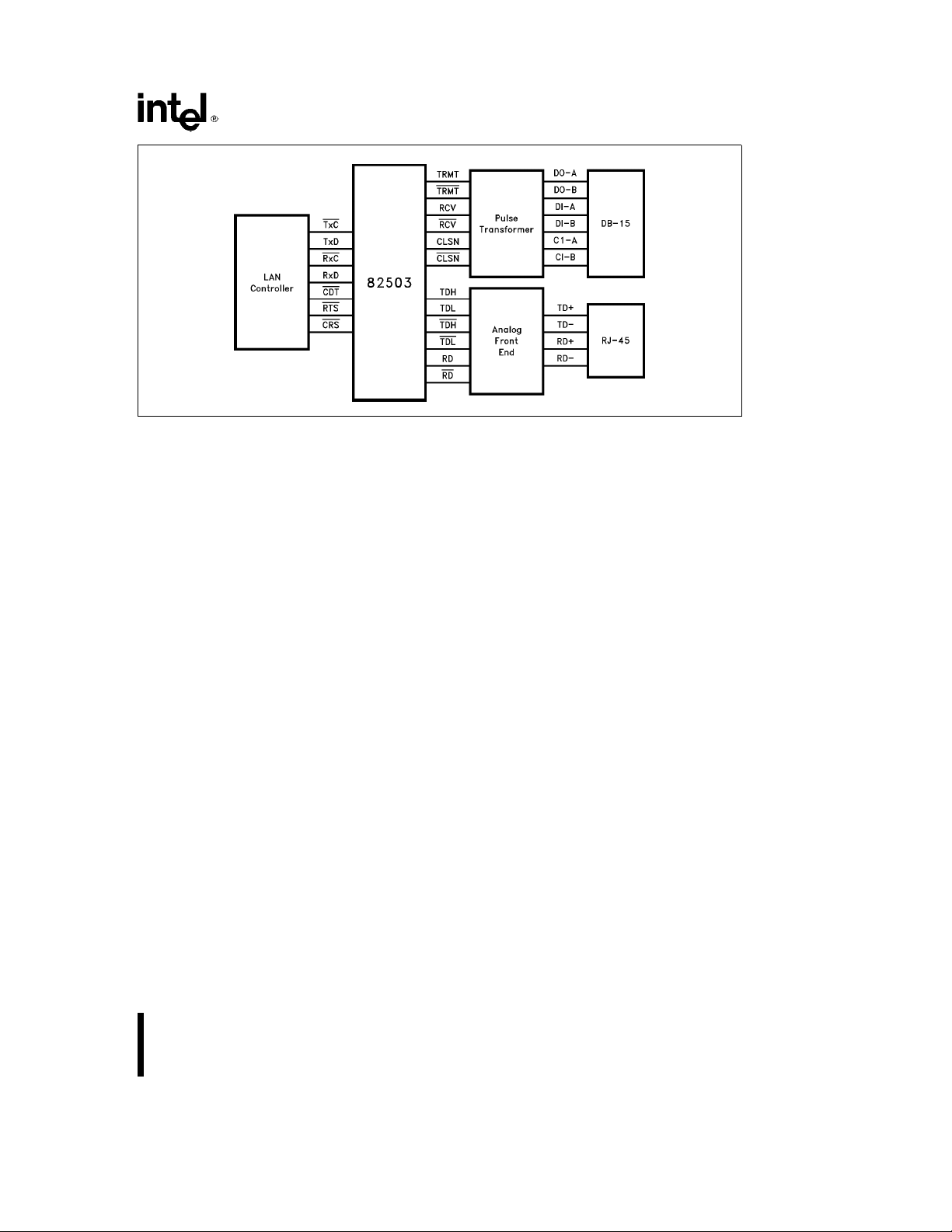
Figure 1. Application Block Diagram
82503
290421– 1
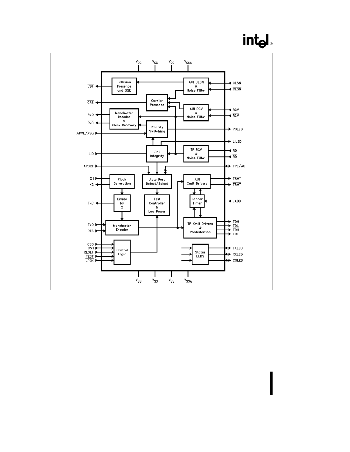
1.0 82503 PRODUCT FEATURES
The 82503 incorporates all the active circuitry required to interface Ethernet controllers to 10BASE-T
networks or the attachment unit interface (AUI). It
supports a direct no-glue interface to Intel’s family of
high-performance LAN controllers (82586, 82590,
82593, and 82596). The 82503 also provides a direct no-glue interface to the National Semiconductor
8390 and 83932 (SONIC), the Western Digital
83C690, the Advanced Micro Devices 7990
(LANCE) and 79C900 (ILACC), and the Fujitsu
86950 (Etherstar) controllers.
This component includes three advanced features:
jumperless two-port design capability, automatic port
selection, and polarity switching. The jumperless
TPE or AUI port selection capability allows designers maximum ease-of-use and network flexibility. Automatic port selection ensures complete software
compatibility with existing 10BASE2 and 10BASE5
software drivers. The 82503’s polarity switching feature will detect and correct polarity errors on the
twisted pairÐthe most common wiring fault in twisted pair networks.
The 82503 contains all the circuitry needed to meet
the 10BASE-T specification, including link integrity, a
jabber timer and internal predistortion. Deselecting
link integrity allows the component to be used in
some prestandard networks. The 82503’s jabber
timer prevents the station from continuously transmitting and is defeatable for simple design charac-
terization. The predistortion circuitry eliminates line
overcharge and reduces jitter on 10BASE-T links.
The 82503 can also support twisted pair cable
lengths of up to 200m when placed in TPE Extended
Squelch Mode (XSQ).
This component incorporates six LED drivers to display transmit data, receive data, collision, link integrity, polarity faults and port selections, allowing for
complete network monitoring by the user. The transmit, receive and collision LEDs indicate the rate of
activity by the frequency of flashing. The 82503 also
has a low power mode. During low power, many of
the 82503’s pins are in a high-impedance state to
facilitate board-level testing.
The 82503’s diagnostic loopback control enables it
to route a transmission signal from the LAN controller through its Manchester encoder-decoder circuitry
and back to the LAN controller. This provides effective network node fault detection and isolation capabilities. In addition, the 82503 supports diagnostic
test modes that generate continuous tranmission of
data through the twisted pair port, allowing designers to measure the analog performance of their design.
The 82503 is available in 44-lead PLCC and 44-lead
QFP packages and is fabricated with Intel’s lowpower, high-speed, CHMOS IV technology using a
single 5-V supply.
3
Page 4
82503
290421– 2
Figure 2. 82503 Functional Block Diagram
4
Page 5
2.0 PIN DEFINITION
82503
290421– 3
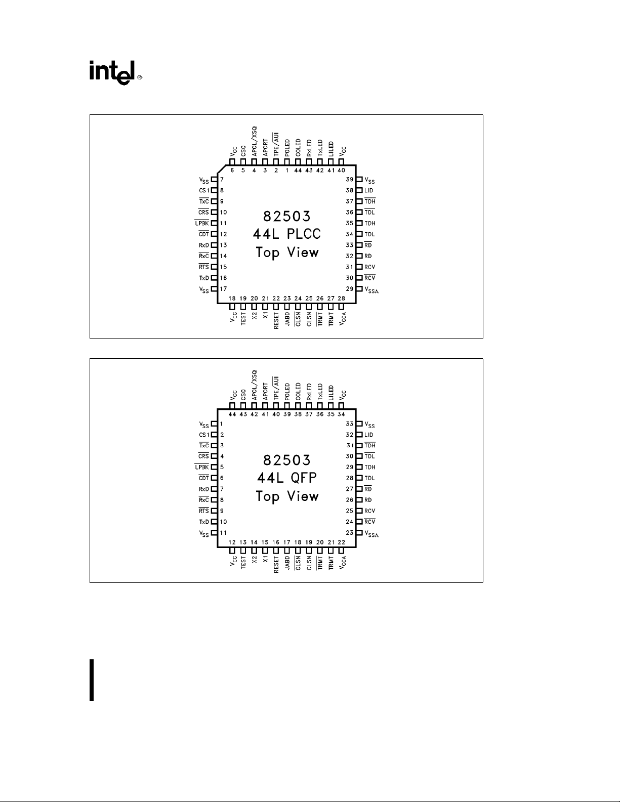
Figure 3. 44-Lead PLCC Pin Configuration
Figure 4. 44-Lead QFP Pin Configuration
290421– 44
5
Page 6
82503
2.1 Power Pins
Symbol
(1)
V
SS
(1)
V
CC
(1)
V
CCA
(1)
V
SSA
NOTE:
and V
1. V
CC
Separate decoupling and noise conditioning (e.g., ferrite beads) should be used.
PLCC QFP
Pin Pin
Type Name and Function
7, 17, 39 1, 11, 33 Supply Digital Ground.
6, 18, 40 44, 12, 34 Supply Digital VCC. A 5-Vg5% Power Supply.
28 22 Supply Analog VCC. A 5-Vg5% Power Supply.
29 23 Supply Analog Ground.
must be connected to the same power supply. VSSand V
CCA
must be connected to the same ground.
SSA
2.2 Clock Pins
Symbol
X1 21 15 I CLOCK CRYSTAL. A 20 MHz crystal input. This pin can be driven
X2 20 14 O CLOCK CRYSTAL. A 20 MHz crystal output. X1 can be driven with
PLCC QFP
Pin Pin
Type Name and Function
with an external MOS level clock when X2 is left floating.
an external MOS level clock when this pin is left floating.
2.3 AUI Pins
Symbol
TRMT 27 21 O TRANSMIT PAIR. A differential output driver pair that drives the
TRMT
RCV 31 25 I RECEIVE PAIR. A differentially driven input pair which is tied to the
RCV
CLSN 25 19 I COLLISION PAIR. A differentially driven input pair tied to the
CLSN
PLCC QFP
Pin Pin
26 20 O
30 24 I
24 18 I
Type Name and Function
transmit pair of the transceiver cable. The output bit stream is
Manchester encoded. Following the last transition, which is positive
at TRMT, the differential voltage is reduced to zero volts.
receive pair of the Ethernet transceiver cable. The first transition on
RCV is negative-going to indicate the beginning of the frame. The
last transition is positive-going to indicate the end of the frame. The
received bit stream is assumed to be Manchester encoded.
collision presence pair of the Ethernet transceiver cable. The
collision presence signal is a 10 MHz square wave. The first
transition at CLSN is negative-going to indicate the beginning of the
signal; the last transition is positive-going to indicate the end of the
signal.
6
Page 7
2.4 TPE Pins
Symbol
TDH 35 29 O TP TRANSMIT PAIR DRIVERS. These four outputs constitute the
TDH
TDL 34 28 O
TDL
RD 32 26 I TP RECEIVE PAIR. The differential twisted pair receiver. The
RD
PLCC QFP
Pin Pin
37 31 O
36 30 O
33 27 I
Type Name and Function
twisted-pair drivers, which have predistortion capabilities. The TDH/
TDH outputs generate the 10 Mb/s Manchester Encoded data. The
TDL/TDL
occurrences (100 ns pulses). During the second half of a fat bit
(either high or low), the TDL/TDL outputs are inverted with respect
to TDH/TDH
jitter by preventing overcharge on the twisted pair medium.
receiver pair is connected to the twisted pair medium and is driven
with 10 Mb/s Manchester encoded data.
outputs mirror the TDH/TDH outputs except for fat bit
outputs. This signal behavior reduces the amount of
2.5 Controller Interface Pins
Symbol
TxC 93OTRANSMIT CLOCK. A 10 MHz clock output tied directly to the
TxD 16 10 I TRANSMIT DATA. TTL input. NRZ serial data is clocked in on TxD
RTS 15 9 I REQUEST TO SEND. TTL input. An active low input signal
RxC 14 8 O RECEIVE CLOCK. A 10 MHz clock output tied directly to the
RxD 13 7 O RECEIVE DATA. Received NRZ data (synchronous to RxC) passed
CRS 10 4 O CARRIER SENSE. Output that alerts the Ethernet controller that
CDT 12 6 O COLLISION DETECT. Output that indicates presence of a collision.
PLCC QFP
Pin Pin
Type Name and Function
transmit clock pin of the Ethernet controller. Changes sense
depending on controller selected. Active low for Intel and Fujitsu
controller interfaces, active high for National and AMD interfaces.
Can drive one TTL load.
from the Ethernet controller. Connects directly to the transmit data
pin of the Ethernet controller.
synchronous to TxC
port. Changes sense depending on controller selected. Active low
for the Intel controller interface, active high for National, AMD, and
Fujitsu interfaces.
receive clock pin of the Ethernet controller. This clock is the
recovered clock from incoming data on the active port. Changes
sense depending on controller selected. Active low for Intel and
Fujitsu controller interfaces, active high for National and AMD
interfaces. Can drive one TTL load.
to the Ethernet controller. Connect directly to the receive data pin of
the controller. Can drive one TTL load.
data is present on the active port. Connects directly to the carrier
sense pin of the Ethernet controller. Changes sense depending on
controller mode selected. Active low for Intel controller interface,
active high for National, AMD, and Fujitsu interfaces. Can drive one
TTL load.
Connects directly to the collision detect pin of the Ethernet
controller. Changes sense depending on controller selected. Active
low for Intel and Fujitsu controller interfaces, active high for National
and AMD interfaces. Can drive one TTL load.
which enables data transmission on the active
82503
7
Page 8
82503
2.6 Mode Pins
Symbol
TPE/AUI 2 40 I/O PORT SELECT. TTL input/LED output. If APORT is low,
APORT 3 41 I AUTOMATIC PORT SELECTION. TTL input. When high, 82503
APOL/XSQ 4 42 I AUTOMATIC POLARITY CORRECTION/EXTENDED
LID 38 32 I LINK INTEGRITY DISABLE. TTL input. If high, link integrity
CS0 5 43 I CONTROLLER SELECT. Selects the appropriate interface for
CS1 8 2 I
LPBK 11 5 I LOOPBACK. TTL input. An active low input signal that causes
JABD 23 17 I JABBER DISABLE. TTL input. When high, this pin disables the
TEST 19 13 I TEST MODE ENABLE. TTL input. When TEST is high and
RESET 22 16 I RESET. TTL input. When high, resets internal circuitry. On the
PLCC QFP
Pin Pin
Type Name and Function
TPE/AUI
high) or AUI port (TPE/AUI low). If APORT is high, the 82503 will
indicate the port selected by driving TPE/AUI
(AUI). TPE/AUI
will automatically select TPE or AUI port based on presence of
valid link beats or frames on the TPE receive input. Mode
selected will be indicated on TPE/AUI
SQUELCH ENABLE. TTL input. When high, the extended
squelch mode is disabled and automatic polarity correction is
enabled. Both junctions (APOL and XSQ) are enabled when this
pin is at a high impedance state. When low, both functions
become disabled. The presence of a polarity fault on the TPE
receive pair is indicated on POLED regardless of the state of
APOL.
function is disabled. If low, link integrity function is enabled.
the desired Ethernet controller. When CS0/1
Intel controllers. When CS0/1
controllers. When CS0/1
National controllers. When CS0/1
controllers. (See Table 2.)
the 82503 to enter diagnostic loopback mode. The twisted pair
or AUI medium will be removed from the circuit, thus isolating
the node from the network. When not connected, this pin
assumes the inactive (high) state. Diagnostic loopback does not
disable the operation of the link integrity processor, link beat
generator, or automatic port selection.
jabber function. When low, the jabber function is enabled and
the device performs AUI or TP jabber protection for the active
port. If this pin and TEST are asserted during a falling edge of
RESET, the 82503 enters its low power mode; when either this
pin or TEST deasserts, then the 82503 transitions to its normal
operating mode.
RESET is deasserted, a customer test mode is directly
accessed. When driven low, test mode is disabled. If this pin and
JABD are asserted during a falling edge of RESET, the 82503
enters its low power mode; when either this pin or JABD
deasserts, then the 82503 transitions to its normal operating
mode.
falling edge of RESET, either test mode or low power mode can
be entered depending on the state of JABD and TEST.
is an input and selects either the TPE port (TPE/AUI
can drive an LED pull-up.
.
e
0/1, supports Fujitsu
e
1/0, supports Western Digital and
e
1/1, supports AMD
high (TPE) or low
e
0/0, supports
8
Page 9
2.7 LED Pins
Symbol
TxLED 42 36 I/O TRANSMIT LED. LED output. Indicates transmit status of the AUI or
RxLED 43 37 I/O RECEIVE LED. LED output. Indicates receive status of the AUI or
COLED 44 38 I/O COLLISION LED. LED output. Indicates collision status of the AUI
LILED 41 35 O LINK INTEGRITY LED. LED output. Normally on (low) output which
POLED 1 39 O POLARITY INDICATION. LED output. If the 82503 detects that the
PLCC QFP
Pin Pin
Type Name and Function
TPE port. Normally off (high) output. Turns on to indicate
transmission. Flashes at a rate dependent on the level of transmit
activity. Upon entering a customer test mode, this pin must be
driven high either through an LED, or a resistor.
TPE port. Normally off (high) output. Turns on to indicate reception.
Flashes at a rate dependent on the level of receive activity. Upon
entering a customer test mode, this pin must be driven high either
through an LED, or a resistor.
or TPE port. Normally off (high) output. Turns on to indicate
collision. Flashes at a rate dependent on the level of collision
activity. This pin is also used to determine which customer test
modes are entered.
indicates good link integrity on the TPE port during TPE mode.
Remains on when link integrity function has been disabled. Turns off
during AUI mode or when link integrity fails in TPE mode. Minimum
off time is 100 ms, minimum on time is set by the link integrity
function.
receive TPE wires are reversed, POLED will turn on (low) to indicate
the fault. POLED remains on even if APOL/XSQ is high and the
82503 has automatically corrected for the reversed wires.
82503
NOTE:
1. The LED outputs have a weak pull-up capable of sourcing 500 mA. They can sink 10 mA while still meeting TTL levels. All
LEDs can be used as indication pins if no LED is needed. Some of these outputs include pulse width conditioning, which
should be accounted for in software.
9
Page 10

82503
3.0 82503 ARCHITECTURE
3.1 Clock Generation
A 20 MHz parallel resonant crystal is used to control
the clock generation oscillator, which provides the
basic 20 MHz clock source. An internal divide-bytwo counter generates the 10 MHz
required by the IEEE 802.3 specification.
We recommend a crystal that meets the following
specifications be used.
Quartz Crystal
#
20 MHzg0.002% at 25§C
#
Accuracyg0.005% over full operating tempera-
#
ture, 0
Ctoa70§C
§
Parallel resonant with 20 pF Load Fundamental
#
Mode
Maximum Series Resistance: R
#
Several vendors have such crystals; either-off-the
shelf or custom made. Two possible vendors are:
1. M-Tron Industries, Inc.
Yankton, SD 57078
Specifications;
Part No. HC49 with 20 MHz, 50 PPM over 0
a
70§C, and 20 pF fundamental load.
2. Crystek Corporation
100 Crystal Drive
Ft. Myers, FL 33907
Part No. 013212
The accuracy of the Crystal Oscillator frequency depends on the PC board characteristics, therefore it is
advisable to keep the X1 and X2 traces as short as
possible. The optimum value of C1 and C2 should
be determined experimentally under nominal operating conditions. The typical value of C1 and C2 is
between 22 pF and 35 pF.
An external 20 MHz MOS-level clock may be applied
to pin X1, if pin X2 is left floating.
g
0.01% clock
SERIES
e
30X
Cto
§
3.2 Transmit Blocks
3.2.1 MANCHESTER ENCODER
The 20 MHz clock is used to Manchester-encode
data on the TxD input. This clock is also divided by
two to produce the 10 MHz clock the LAN controller
needs for synchronizing its RTS
Data encoding and transmission begins with RTS
asserting. Since the first bit of a transmission is a 1,
the first transition is always negative on the transmit
outputs (TRMT or TD pins). Transmission ends
when RTS
positive at the transmit outputs (TRMT or TD pins)
and may occur at the center of the bit cell if the last
data bit to be transmitted is a 1, or at the boundary
of the bit cell if the last data bit to be sent is a 0.
Immediately after the end of a transmission, all signals on the RCV pair (when AUI mode is selected)
are inhibited for 4 to 5 ms. This dead time is necessary for proper operation of the SQE (heartbeat)
test.
3.2.2 AUI CABLE DRIVER
The AUI cable driver (TRMT pair) is a differential
circuit, which interfaces to the AUI cable through a
pulse transformer.
High voltage protection is achieved by using a transformer to isolate the transmit pins (TRMT pair) from
the transceiver cable. The total transmit circuit inductance, including the 802.3 transceiver transformers, should be a minimum of 27 mH for Ethernet applications.
3.2.3 TWISTED PAIR CABLE DRIVER
The twisted pair line drivers (TD pairs) begin transmitting the serial Manchester bit stream 3 bit times
after RTS
tortion algorithm to improve jitter performance for up
to 100 meters of twisted pair cable. The line drivers
reduce their drive level during the second half of
‘‘fat’’ (100 ns) Manchester pulses and maintain a full
drive level during all ‘‘thin’’ (50 ns) pulses and during
the first half of the ‘‘fat’’ pulses. This reduces line
overcharging during ‘‘fat’’ pulses, a major source of
jitter.
deasserts. The last transition is always
is asserted. The line drivers use a predis-
and TxD signals.
10
Page 11
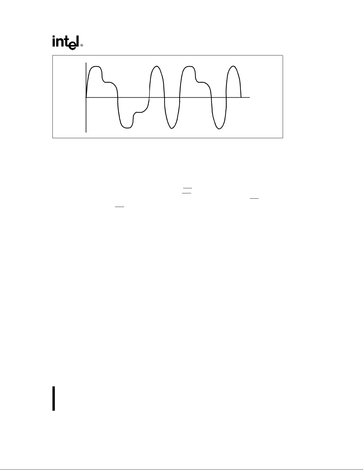
Figure 5. TPE Predistortion
82503
290421– 4
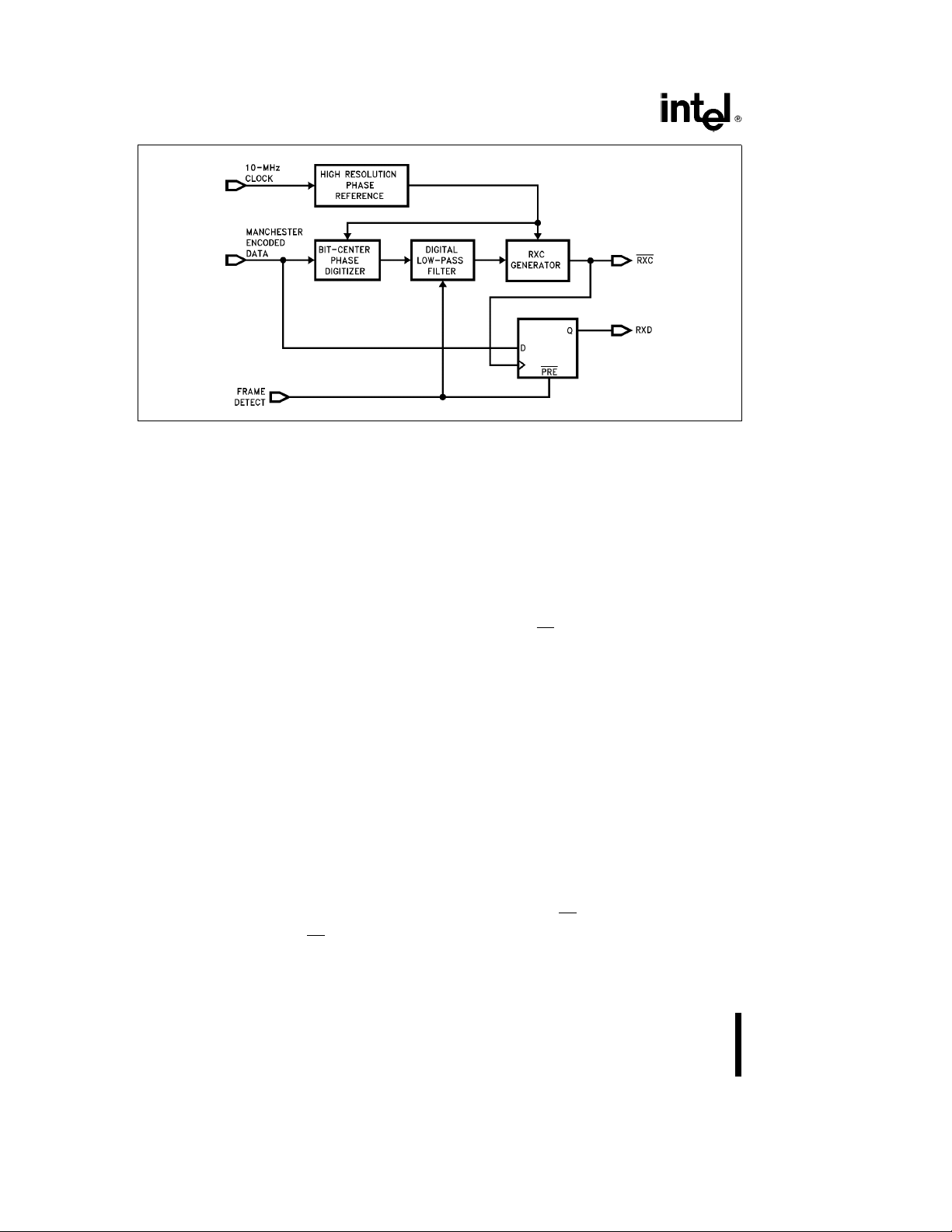
3.3 Receive Blocks
3.3.1 MANCHESTER DECODER AND CLOCK
RECOVERY
The 82503 performs Manchester decoding and timing recovery of the incoming data in AUI and TPE
modes.
The Manchester-encoded data stream is decoded to
separate the Receive Clock (RxC
Data (RxD) from the differential signal. The 82503
uses an advanced digital technique to perform the
decoding function. The use of digital circuitry instead
of analog circuitry (e.g., a phase-lock loop) to perform the decoding ensures that the decoding function is less sensitive to variations in operating conditions.
A high-resolution phase reference is used to digitize
the phase of the incoming data bit-center transition.
The digitizer has a phase resolution of 1/32 of a bit
time.
) and the Receive
The digitized phase is filtered by a digital low-pass
filter to remove rapid phase variations, i.e., phase
jitter. Slow phase variations, such as those caused
by small differences between the data frequency
and the clock frequency, are not filtered by the lowpass filter.
The RxC generator digitally sets the phases of the
two RxC
bit-center transition by (/4 bit time. RxC
transitions to respectively lead and lag the
is used to
recover RxD by sampling the incoming data with an
edge-triggered flip-flop.
Lock is achieved by reducing the time constant of
the digital filter to zero at the start of a new frame.
Any uncertainty in the bit-center phase of the first
transition that is caused by jitter is subsequently removed by gradually increasing the filter time constant during the following preamble. By that time, the
phase of the bit center is output by the filter, and
lock is achieved. Lock is achieved within the first 14
bit times as seen by the AUI inputs. The maximum
bit-cell timing distortion (jitter) tolerated by the Manchester decoder circuitry is
g
18 ns (data) for AUI, andg13.5 ns for TPE (data
g
12 ns (preamble),
and preamble).
11
Page 12
82503
290421– 5
Figure 6. Manchester Decoder and Clock Recovery
3.3.2 AUI RECEIVE AND COLLISION BUFFERS
The AUI receive and collision inputs are driven
through isolation transformers to provide high voltage protection and DC common mode voltage rejection. The incoming signals are converted to digital
levels and passed to the Manchester decoder and
collision detection circuitry.
3.3.3 AUI RECEIVE AND COLLISION SQUELCH CIRCUITS
Both the receive (RCV) and collision (CLSN) pairs
have the following squelch characteristics.
The squelch circuits are turned on at idle.
#
A pulse is rejected if the peak differential voltage
#
is more positive than
pulse width.
A pulse is considered valid if its peak differential
#
voltage is more negative than
width, measured at
25 ns.
The squelch circuits are disabled by the first valid
#
negative differential pulse on either the AUI receive (RCV) or the AUI collision (CLSN) pair.
If a positive differential pulse occurs on either the
#
AUI receive or collision pairs for greater than
160 ns, End of Frame (EOF) is assumed and the
squelch circuitry is turned on.
3.3.4 TPE RECEIVE BUFFER
The TPE receive pins (RD and RD
the twisted pair medium through an analog front
end. The analog front end contains the line coupling
b
160 mV regardless of
b
b
285 mV, is greater than
300 mV and its
) are connected to
devices and EMI filters necessary to conform to the
10BASE-T standards and local RF regulations. The
input differential voltage range for the TPE receiver
is greater than 500 mV and less than 3.1V differential.
3.3.5 TPE RECEIVE SQUELCH CIRCUITS
The TPE receive buffer distinguishes valid receive
differential data, link test pulses, and the idle condition according to the requirements of the 10BASE-T
standard. Signals at the output of the EMI filter (thus
at the RD and RD
All differential pulses of peak magnitude less than
#
300 mV are rejected.
All continuous sinusoids with a differential ampli-
#
tude less than 6.2 V
2 MHz are rejected.
All sine waves of single cycle duration starting
#
with phase 0
than 6.2 V
16 MHz are rejected, if the single cycle is preceeded and followed by 4 bit times of silence
(i.e., a signal less than 300 mV).
3.3.6 TPE Extended Squelch Mode
By placing the 82503 into TPE extended squelch
mode, the 82503 can support cable lengths greater
than the 100m specified in the 10Base-T IEEE standard (802.3i-1990). The squelch thresholds for the
signals at the RD/RD
4.5 dB. This allows Grade 5 twisted-pair cable to be
used to overcome attenuation and multipair crosstalk for cable lengths up to 200 meters.
pair) are rejected as follows:
and a frequency less than
PP
or 180§that have an amplitude less
§
, and a frequency of 2 MHz to
PP
pair are typically reduced by
12
Page 13

82503
TPE extended squelch mode is enabled by presenting a high-impedance (
pin. This can be done by floating the APOL/XSQ pin,
tying APOL/XSQ low through a 100 KX resistor, or
driving APOL/XSQ with a three-state buffer. When
driven high or low using a TTL driver or a low impedance pull-up or pull-down (
squelch is disabled and the driven level at the
APOL/XSQ pin determines the state of the polaritycorrection function (APOL/XSQ
ty correction, APOL/XSQ
rection). The TPE extended squelch feature is transparent to previous steppings of the 82503. Polarity
correction is always enabled when the TPE extended-squelch feature is enabled (APOL/XSQ
The APOL/XSQ pin senses a high-impedance state
by an active-polling circuit implemented at the pin.
Two small polling devices attempt to pull the APOL/
XSQ pin up to V
high-impedance state, the devices will be successful
in pulling the APOL/XSQ pin high and low. If the pin
is driven high or low, the polling devices will not be
able to successfully pull the pin in the opposite direction. In this way, an internal state machine can
correctly determine one of three states of the
APOL/XSQ pin. The pin is polled every 25.6 ms.
l
100 KX) at the APOL/XSQ
k
2KX) extended
e
e
and down to VSS. If the pin is in a
CC
1 enables polari-
0 disables polarity cor-
e
Z).
3.4 Collision Detection
3.4.1 AUI COLLISION DETECTION
Collision detection in the AUI mode is performed by
the attached transceiver, and signalled to the 82503
on the CLSN pair. A 10 MHz
square wave with transition times between 35 ns
and 70 ns indicates the collision. The 82503 reports
this to the LAN controller on the CDT
a
25%, orb15%,
pin.
to the twisted pair medium as an indication to the
remote MAU that the link is good. These pulses will
be transmitted 8 ms to 24 ms after the end of the
last transmission or link test pulse.
The link integrity function continuously monitors activity on the receive circuit. If neither valid data nor
link test pulses are received, the link integrity processor declares the link bad, and disables transmission and reception on the media, loopback, and the
SQE test function. Transmission of link test pulses
and monitoring receive activity are not affected. The
idle time required for the link integrity processor to
determine the link is bad is 50 ms to 150 ms.
Once a frame or a sequence of 2 to 10 valid consecutive link test pulses are detected, the Link Integrity
Processor declares the link is good, and reconnects
the transmitter and receiver.
The link integrity function can be disabled by driving
the LID pin high or by disabling automatic port selection (APORT
option is intended primarily for use with pre10BASE-T networks.
e
0) and selecting the AUI port. This
3.6 Jabber Function
The 82503 contains a jabber timer to implement the
jabber function. If a transmission continues beyond
the limits specified, the jabber function inhibits further transmission and asserts the collision indicator,
CDT. The limits for jabber transmission are 20 ms to
150 ms in TPE Mode, and 8 ms to 16 ms in AUI
mode. For both AUI and TPE mode, the transmission inhibit period extends until the 82503 detects
sufficient idle time (between 250 ms and 750 ns) on
the RTS
by driving the JABD high.
signal. The jabber function can be disabled
3.4.2 TPE COLLISION DETECTION
Collision detection in the TPE mode is indicated by
simultaneous transmission and reception on the
twisted pair link segment. The CDT
ed for the duration of both RTS
received data; CRS
either RTS
a collision, the source of RxD will be the received
data. If the received data stream ends before the
transmit data stream, the RxD source will be
changed to transmit data stream until it ends.
or the presence of received data. During
is asserted for the duration of
signal is assert-
and the presence of
3.5 Link Integrity
The 82503 supports the link integrity function as defined by 10BASE-T. During long periods of idle on
the transmitter, link test pulses will be transmitted on
In TPE mode the link integrity function continues to
operate even if the jabber function is inhibiting transmission. Link test pulses continue to be sent and the
receive circuit continues to be monitored. Additionally, the link integrity function reconnects to a restored
link without waiting for the transmit input to go idle
when the jabber function is inhibiting transmission.
3.7 TPE Loopback
In TPE mode the 82503 implements the transmit to
receive loopback (DO to DI) mode specified in the
10BASE-T standard. This mode loops back transmitted data through the receive path.
This function is required to maintain full compatibility
with coax MAUs where the data loopback is a natural result of the architecture.
13
Page 14
82503
The transmit to receive loopback function is disabled
when the jabber function or link integrity function is
inhibiting transmission.
3.8 SQE Test Function
The 82503 supports the SQE test function when in
TPE mode or in Diagnostic Loopback mode. The
82503 will assert its CDT
pin within 0.6 msto1.6ms
after the end of a transmission, and it will remain
asserted for 5- to 15-bit times. If the 82503 is in the
TPE mode and is not in diagnostic loopback mode,
the link integrity function will disable the SQE test
function when it detects a bad link.
3.9 Port Selection
The 82503 features both manual and automatic port
selection. To enable automatic port selection, connect APORT to V
mode and monitors link integrity. If the link is good,
the 82503 stays in TPE mode and pulls TPE/AUI
high to indicate that the TPE port was selected. If
link integrity fails, the 82503 switches to AUI mode
and pulls TPE/AUI
is now active. TPE/AUI
port selection (on for AUI, off for TPE mode). Note
that LILED will be on if TPE mode is selected and off
if AUI mode is selected. If link integrity is disabled
while automatic port selection is enabled, the 82503
defaults to TPE mode. If the 82503 changes ports
while RTS
is active, transmission is terminated with
an End of Frame marker on the old port. Transmission of the remaining packet fragment is not allowed
on the new port. Transmissions will begin with a
complete data packet.
The port can be manually selected by driving
APORT low. TPE/AUI
TPE/AUI
e
selected, the circuitry for the unused port is powered
down. Changing ports requires 100 ms to allow the
circuitry for the new port to resume normal operation.
Configuration
LID APORT TPE/AUI
X 0 0 AUI (TPE Port Powered Down)
X 0 1 TPE (AUI Port Powered Down)
01 X*Automatic Port Selection
11 X*TPE
. The 82503 then starts in TPE
CC
low to indicate that the AUI port
can drive an LED to indicate
e
0 selects AUI mode, and
1 TPE mode. When the port is manually
Table 1. Port Selection
State
3.10 LED Description
The 82503 supports six LED pins to indicate the
status of important states; TPE/AUI
POLED, LILED, RxLED, COLED. Each pin is capable
of directly driving an LED.
3.10.1 TPE/AUI
When automatic port selection is enabled (APORT is
high), TPE/AUI
becomes an LED output and turns
off if TPE mode is selected and on if AUI mode is
selected.
3.10.2 TxLED
Transmit status. This LED is normally off and flashes
at 2.5 Hz, 5 Hz, and 10 Hz to indicate respectively a
low, medium, and high rate of transmit activity.
3.10.3 RxLED
Receive LED. This LED is normally off and flashes at
2.5 Hz, 5 Hz, and 10 Hz to indicate respectively a
low, medium, and high rate of receive activity.
3.10.4 COLED
Collision LED. This LED is normally off and flashes
at 2.5 Hz, 5 Hz, and 10 Hz to indicate respectively a
low, medium, and high rate of collision activity.
3.10.5 POLED
Polarity Fault. This LED is normally off and turns on
to indicate a polarity fault in the receive pair of the
10BASE-T link. Operation of this pin is not affected
by the state of the polarity correction function
(APOL/XSQ
e
X).
3.10.6 LILED
Link Integrity status. When Aport is enabled
(APORT
e
1), this LED is normally on (driven low)
to indicate the presence of a valid 10BASE-T link
when the TPE port is active. The LED will turn off
(driven high) when the link fails. When link integrity is
disabled (LID
(APORT
APORT is disabled (APORT
manually selected (TPE/AUI
e
e
1) while APORT is enabled
1) this LED is turned on (driven low). If
e
0) and the AUI port is
e
0) the LED output is
tristated.
, TxLED,
NOTE:
*TPE/AUI
14
is an output pin when APORTe1.
3.11 Polarity Switching
In TPE mode, the 82503 monitors receive link beats
and end-of-frame delimiters for a possible receiver
Page 15

Figure 7. Polarity Fault State Diagram
82503
290421– 6
polarity error due to crossed wires. If Pin 4 of the
82503 is high and the TPE receive pins are reversed, the 82503 will correct the error by reversing
the signals internally, and turn POLED on (low) to
indicate that the fault has been detected and corrected. The polarity correction function is defeatable
by driving the APOL/XSQ input low. However, the
polarity fault will continue to be indicated on the
POLED.
3.12 Controller Interface
Connecting the 82503 to one of the Intel Ethernet
controllers (82586, 82590, 82593, 82596) requires
no additional components. Simply drive CS0 and
CS1 both low, and connect TxC
RxD, CRS
controller pins.
, CDT, and LPBK
, TxD, RTS, RxC,
to the corresponding
The 82503 also works with other Ethernet controllers without additional components, including the
National Semiconductor 8390 and 83932 (SONIC),
Western Digital 83C690, Fujitsu 86950 (Etherstar),
depending on the state of and CS0 and CS1 inputs.
The interface of the 82503 to the AMD 7990
(LANCE) requires external logic to control the LPBK
pin of the 82503. Note that when an AMD LAN controller is used to interface to the 82503, the LPBK
pin of the 82503 becomes active high. That is, the
82503 enters diagnostic loopback mode when LPBK
pin is high and is in normal operation mode when
pin is low.
LPBK
The logic sense of the 82503 controller pins will
change and should be connected to the controller
pins according to the following table.
15
Page 16

82503
Table 2. Controller Interface Selection
82503
Pin
(1)
CS0
CS1 0 0 1 1
Pin Pin Sense Pin Sense Pin Sense Pin Sense
TxC TxC Low TXC High TCLK High TCKN Low
TxD TxD High TXD High TX High TXD High
RTS
RxC
RxD RxD High RXD High RX High RXD High
CRS
CDT CDT Low COL High CLSN High XCOL Low
LPBK LPBK Low LPBK High LPBK High
NOTES:
1. CS0 and CS1 are intended to be static pins only. Switching CS0 and CS1 during network reception or transmission will
produce unpredictable results.
2. Refer to Section 3.12.
Intel
Controller
825XX
011 0
RTS Low TXE High TENA High TEN High
RxC Low RXC High RCLK High RCKN Low
CRS Low CRS High RENA High XCD High
National, WD AMD
Controllers Controller
8390, 83C690, 7990 (LANCE),
83832 (SONIC) 79C900 (ILACC)
(Note 2)
Fujitsu
Controllers
86950 (Etherstar)
4.0 RESET, LOW-POWER AND
TEST MODES
4.1 Reset
When RESET is asserted the device resets its internal circuits. RESET is required after power up, and
before data can be transmitted or received. It is allowed any time thereafter, but any existing receive or
transmit activity will be lost, and all state machines
(Link integrity, Jabber, and Polarity Correction) return to their initial states. TEST must be held low for
a device reset to prevent entering a test for low power mode. During RESET, TxC
terruption (in Fujitsu mode both TxC
continuously).
continues without in-
and RxC run
4.2 Low Power and High Impedance
Modes
When RESET is deasserted while both TEST and
JABD are held high, the 82503 enters its low power
and high impedance modes. The majority of internal
circuitry is powered down, and many inputs and outputs are three-stated. These pins are: APORT,
APOL/XSQ, LID, TPE/AUI
, RxD, TxD, CRS and CDT. When either JABD
LPBK
or TEST is deasserted, the device begins a power
on cycle which lasts less than 1 ms. During this cycle, all inputs are ignored and all transmissions are
disabled. If RTS
normal operation, the remainder of that packet fragment is not transmitted. Normal transmissions are
resumed at the start of the first complete data packet.
is active when the device returns to
, POLED, LILED, RTS,
4.3 Diagnostic Loopback
This is a diagnostic test mode to help in fault isolation and detection. Serial NRZ data input on TxD is
Manchester encoded and then looped back through
the Manchester decoder (TMD) appearing at the
RxD output. Collision detect is asserted following
each transmission to simulate the SQE test. Output
cable drivers and input amplifiers are disconnected
from the controller interface pins while in this mode.
The link integrity and polarity fault detection functions are not inhibited by diagnostic loopback mode.
If otherwise enabled, they continue to function.
4.4 Customer Test Mode (Continuous AUI/TPE Transmit)
In this mode, the 82503 continuously transmits data
without the intervention of a LAN controller. Transmission is at 10 MHz (11-bit pattern), and can occur
on either the TPE or AUI port. The jabber timer is
disabled in this mode, allowing users to easily test
the 10BASE-T harmonic content specification and
the quality of their analog front end design without
complex software exercisers.
Customer Test ModeÐand Low Power Mode are selected at the deassertion of RESET as shown in the
following table. (Note that the 82503 must be in nonloopback mode before it can enter the customer test
mode.)
16
Page 17

Table 3. Test and Low Power Mode Selection
RESET TEST JABD TxLED
v
v
v
NOTE:
1. A standard LED connection to these pins is sufficient to pull them to a logic 1.
0 X X X X Normal Mode
1 0 1 1 1 Cont Tx 10 MHz
1 1 X X X Low Power
(1)
RxLED
(1)
COLED
(1)
82503
Mode Selected
The port on which the continuous transmit appears
is determined by the APORT and TPE/AUI
automatic port selection is enabled (APORT
then the TPE port broadcasts the continuous transmit. If manual port selection is enabled (APORT
0), then TPE/AUI selects the port (1 for TPE, 0 for
AUI). Test mode is disabled when TEST is deasserted and the device is reset.
pins. If
e
5.0 APPLICATION EXAMPLE
5.1 Introduction
The 82503 is designed to work directly with the Intel
LAN controllers (82586, 82590, 82593, and 82596),
as well as AMD’s Am7990, National Semiconductor’s 8390, Western Digital’s 82C690, and Fujitsu’s
86950. The serial interface signals connect directly
between one of the aforementioned LAN controllers
and the 82503 without the need for external logic.
This example is targeted toward interfacing the
82503 to the Intel 82596 in a two-port (TPE/AUI)
application.
5.2 Design Guidelines
AUI Pulse Transformer
In order to meet the 16V fault tolerance specification
of 802.3 a pulse transformer is recommended for the
transmit, receive and collision pairs. The transformer
should be placed between the TRMT, RCV, and
CLSN pairs of the 503, and the DO, DI, and CI pairs
respectively, of the AUI (DB-15 connector). The
pulse transformer should have a parallel inductance
of 75 mH minimum (100 mH recommended).
Several vendors stock such transformers. Two possible vendors are:
1. Pulse Engineering (P/N PE-64103)
2. Valor Electronics (P/N LT6003)
Terminating Resistors
1)
The terminating resistors used across the receive
and collision pairs are recommended to be 78.7 X
e
g
1%.
Analog Front-End
The 82503 provides six TPE pins (TDH, TDH
, RD, and RD) that connect to the Analog Front
TDL
End through a resistor summing network (Figure 7).
AFE solutions can be made discretely or purchased
from several manufacturers. Two different solutions
are described in Application Note 356. The example
shown here uses a Pulse Engineering AFE package
PE65434 which includes EMI filter, isolation transformer, and common mode choke. The output of the
AFE connects directly to the 10BASE-T connector
(RJ-45).
Decoupling
It is recommended that 0.01 mF X7R and 0.001 mF
NPO decoupling capacitors be placed between the
V
and V
CCA
Clock Generation
The clock input to the 82503 can be from a clock
oscillator or a crystal. If a clock oscillator is used, X1
should be driven, and X2 left floating. If a crystal
oscillator is used, refer to Section 3.1 for crystal
specifications.
A complete 82596/82503 TPE/AUI Ethernet Solution is shown at the end of this section.
of the 82503 to V
CCD
SSA
5.3 Layout Guidelines
General
The analog section, as well as, the entire board itself
should conform to good high-frequency practices
and standards to minimize switching transients and
parasitic interaction between various circuits. To
achieve this, the following guidelines are presented.
and V
, TDL,
SSD
.
17
Page 18

82503
18
290421– 7
Figure 8. Application Example Schematic
Page 19

82503
Make power supply and ground traces as thick as
possible. This will reduce high-frequency cross coupling caused by the inductance of thin traces.
Connect logic and chassis ground together.
Separate and decouple all of the analog and digital
power supply lines.
Close signal paths to ground as close as possible to
their sources to avoid ground loops and noise cross
coupling.
Use high-loss magnetic beads on power supply distribution lines.
Crystal
The crystal should be adjacent to the 82503 and
trace lengths should be as short as possible. The X1
and X2 traces should be symmetrical.
82503 Analog Differential Signals
The differential signals from the 82503 to the transformers, analog front end, and the connectors
should be symmetrical for each pair and as short as
possible. Differential signal layout should be performed to a characteristic impedance of 78X (for
AUI) or 100X (for TPE).
As a general rule, the trace widths should be one to
three times the distance between the PCB layers to
eliminate excessive trace inductance.
The differential signals should also be isolated from
the high speed logic signals on the same layer as
well as on any sublayers of the PCB.
Group each of the circuits together, but keep them
separate from each other. Separate their grounds.
In layout, the circuitry from the connectors to the
filter network, should have the ground plane removed from beneath it. This will prevent ground
noise from being induced into the analog front end.
All trace bends should not exceed 45 degrees.
6.0 PACKAGE THERMAL
SPECIFICATIONS
The 82503 Dual Serial Transceiver is specified for
operation when case temperature (T
range of 0
Ctoa85§C. The case temperature can
§
be measured in any environment, to determine if the
82503 is within the specified operating range. The
case temperature should be measured at the center
of the top surface opposite the pins.
The acceptable operating ambient temperature (T
is guaranteed as long as T
bient temperature can be calculated from the i
is not violated. The am-
C
and ijcfrom the following equations:
e
T
T
T
a
T
J
J
A
Pci
C
e
T
A
e
T
C
a
b
Pci
Pc(i
jc
ja
b
ijc)
ja
Values for ijaand ijcare given in Table 4 for the 44lead PLCC and 44-lead QFP packages. Various values for i
maximum T
various airflows.
at different airflows. Table 5 shows the
ja
allowable (without exceeding TC)at
A
Table 4. Thermal Resistance
(
C/Watt) ijcand i
§
ijavs AirflowÐft/min (m/s)
Package ijc0 200 400 600 800 1000
44-Lead 19 57 48 43 41 39 37
PLCC
44-Lead 26 98 94 78 70 66 64
QFP
(0) (1.01) (2.03) (3.04) (4.06) (5.07)
Table 5. Maximum TAat Various Airflows
ijavs AirflowÐft/min (m/s)
Package 0 200 400 600 800 1000
44-Lead 66 71 73 74 75 76
PLCC
44-Lead 49 51 59 63 65 66
(0) (1.01) (2.03) (3.04) (4.06) (5.07)
QFP
) is within the
C
ja
)
A
ja
19
Page 20

82503
7.0 ELECTRICAL SPECIFICATIONS AND TIMINGS
ABSOLUTE MAXIMUM RATINGS
Case Temperature Under Bias ААААААА0§Ctoa85§C
Storage Temperature ААААААААААb65§Ctoa140§C
NOTICE: This is a production data sheet. The specifications are subject to change without notice.
*
WARNING: Stressing the device beyond the ‘‘Absolute
Maximum Ratings’’ may cause permanent damage.
These are stress ratings only. Operation beyond the
‘‘Operating Conditions’’ is not recommended and extended exposure beyond the ‘‘Operating Conditions’’
may affect device reliability.
All Output and Supply Voltages АААААb0.5V toa7V
All Input Voltages АААААААААААААb1.0V toa6.0V
DC CHARACTERISTICS (T
e
0§Ctoa85§C, V
C
(1)
CC
e
5Vg5%, V
CCA
e
5Vg5%)
Symbol Parameter Min Max Units Test Conditions
(2)
VIL(TTL)
VIH(TTL)
(2)
I
LI
VOL(MOS)
Input Low Voltage
(2)
Input High Voltage 2.0 V
Input Leakage Current
(3)
Output Low Voltage 0.45 V I
VOH(MOS) Output High Voltage 3.9 V I
VOL(LED)
(4)
Output Low Voltage 0.45 V I
VOH(LED) Output High Voltage 3.9 V I
I
R
V
LP
DIFF
IDF
(TPE)
Leakage Current, Low
Power Mode
Input Differential Resistance
(7)
Input Differential Accept
(5)
Input Differential Reject
Input Differential Accept (XSQ) (Note 8)
Input Differential Reject (XSQ)
(8)
RS(TPE)
V
(AUI)
IDF
Output Source Resistance 6 13 XlI
(9)
Input Differential Accept
Input Differential Reject
V
ODF
NOTES:
1. The voltage levels for RCV, CLSN, and RD pairs are
2. TTL Input Pins: TxD, RTS
3. MOS Output Pins: TxC
4. LED Pins: TPE/AUI
5. Pins: APORT, APOL/XSQ, LID, TPE/AUI
CDT
6. Pins: RD to RD
7. TPE Input Pins: RD, and RD
8. Typically it is
9. TPE Output Pins: TDH, TDH
10. AUI Input Pins: RCV, and CLSN pairs.
11. AUI Output Pins: TRMT pair.
(10)
(AUI)
, CS0, CS1, JABD, TEST, and RESET.
Output Differential Voltage
, TPE/AUI, APORT, APOL/XSQ, LID, CS0, CS1, LPBK, JABD, TEST, RESET.
, RxD, RxC, CRS, CDT.
, TxLED, RxLED, COLED, POLED, LILED. VOLmeasured 10 ns after falling edge of TxC.
, RCV to RCV, and CLSN to CLSN.
b
4.5 dB below normal squelch level.
. See Section 3.3.4 and Section 3.3.5.
, TDL, and TDL.RSmeasures VCCor VSSto Pin.
, POLED, LILED, RTS, LPBK, RxD, TxD, CRS,
b
0.3 0.8 V
g
g
(6)
10 kX dc
g
0.500
g
0.300
g
0.450
b
0.75V toa8.5V.
g
g
0.300 V
g
g
0.180 V
g
g
0.160 V
g
1.20 V
CC
10 mA 0.0VsV
10 mA 0.0VsV
V
s
I
e
4mA
OL
eb
500 mA
OH
e
10 mA
OL
eb
500 mA
OH
s
I
3.1 VP5 MHzsfs10 MHz
3.1 V
1.5 V
P
P
P
e
25 mA
l
LOAD
P
P
VCC, RESETe1
V
CC
20
Page 21

82503
DC CHARACTERISTICS (T
e
0§Ctoa85§C, V
C
CC
e
5Vg5%, V
e
5Vg5%) (Continued)
CCA
Symbol Parameter Min Max Units Test Conditions
I
(AUI) AUI Output Short Circuit Current
OSC
VU(AUI) Output Differential Undershoot
V
(AUI) Differential Idle Voltage
ODI
ICC(HOT) Power Supply Current
I
CC
I
CC
I
CCSB
Power Supply Current 75 mA APORTe1
Power Supply Current 60 mA APORTe0
Standby Supply Current
PD (HOT) Power Dissipation
(11)
(12)
(13)
(12)
g
150 mA Short Circuit to VCCor GND
b
100 mV
g
40 mV
65 mA APORTe1
1 mA Low Power Mode, 20 mA Typical
0.38 W APORTe1, Continuous Transmission
on AUI
PD Power Dissipation 0.40 W APORTe1, Continuous Transmission
on AUI
PD
SB
(14)
C
IN
NOTES:
11. Measured 8.0 ms after last positive transition of data packet.
12. I
CC
and load resistors removed.
13. Pins CS0 and CS1 connected to V
from power down assertionÐnot tested.
14. Characterized, not tested. (Controller interface and mode pins only.)
Standby Power Dissipation
Input Capacitance 10 pF at fe1 MHz
HOT measurements made at T
(13)
ea
85§C. Additionally, TRMT, TRMT, TDH, TDH, TDL, TDL are loaded with 20 pF
C
or VSSthrough a 2.5 kX (or less) resistor. I
CC
5.25 mW Low Power Mode, 105 mW Typical
is typically at 20 mA after 30s
CCSB
AC TIMING CHARACTERISTICS
290421– 8
Figure 9. MOS Input Voltage Levels
(TTL Compatible) for Timing Measurements
(TxD, RTS, TPE/AUI, APORT, APOL/XSQ,
LID, LPBK
, JABD, TEST, and RESET).
290421– 10
Figure 11. Voltage Levels for Differential Input
Timing Measurements (RCV and CLSN Pairs).
290421– 9
Figure 10. Voltage Levels for MOS Level
Output Timing Measurements
(TxC, RxD, RxC, CRS, and CDT).
290421– 11
Figure 12. Voltage Levels for TRMT Pair
Output Timing Measurements.
21
Page 22

82503
AC TIMING CHARACTERISTICS (Continued)
290421– 13
290421– 12
Figure 13. Voltage Levels for
TDH, TDL, TDH
, and TDL.
AC MEASUREMENT CONDITIONS
1. T
e
0§Ctoa85§C, V
C
CC
e
5Vg5%.
2. The AC MOS, TTL and differential signals are referred to in Figures, 8, 9, 10, 11, 12, and 13.
3. AC loads
a. MOS: 20 pF total capacitance to ground.
b. AUI Differential: a 10 pF total capacitance from each terminal to ground and a load resistor of 78X
g
in parallel with a 27 mH
1% inductor between terminals.
c. TPE: 20 pF total capacitance to ground.
4. All parameters become valid 200 ms after the supply voltage and input clock has stabilized, or after RESET
deasserts.
Figure 14. Voltage Levels for Differential Input
Timing Measurements (RD Pair).
g
1%
CLOCK TIMING
(15)
Symbol Parameter Min Typ Max Units
t
1
t
2
t
3
t
4
t
5
NOTE:
15. Refers to External Clock Input.
X1 Cycle Time 49.995 50.005 ns
X1 Fall Time 5 ns
X1 Rise Time 5 ns
X1 Low Time 15 ns
X1 High Time 15 ns
Figure 15. X1 Input Voltage Levels for Timing Measurements
22
290421– 14
Page 23

Controller Interface Timings (Intel Mode)
TRANSMIT TIMINGS (Intel)
Symbol Parameter Min Typ Max Units
t
10
t
11
t
12
t
13
t
14
t
15
t
16
t
17
TxC Cycle Time 99.99 100.01 ns
TxC High/Low Time 40 ns
TxC Rise/Fall Time 5 ns
TxD and RTS Rise/Fall Time 10 ns
TxD Setup Time to TxC
TxD Hold Time from TxC
RTS Setup Time to TxC
RTS Hold Time from TxC
v
v
v
v
45 ns
0ns
45 ns
0ns
82503
Figure 16. Transmit Timing (Intel)
290421– 15
23
Page 24

82503
RECEIVE TIMING (Intel)
Symbol Parameter Min Typ Max Units
t
20
t
21
t
22
t
23
t
24
t
25
t
26
t
27
t
28
RxC Cycle Time 96 100 ns
RxC High Time 36 ns
RxC Low Time 40 ns
RxC Rise/Fall Time 5 ns
RxC Delay from CRS
RxD Rise/Fall Time 5 ns
RxD Setup from RxC
RxD Hold from RxC
CRS Deassertion Hold Time from RxC High 10 40 ns
v
v
v
30 ns
30 ns
1100 1400 ns
Figure 17. Receive Timing (Intel)
290421– 16
24
Page 25

Controller Interface Timings (National Mode)
TRANSMIT TIMINGS (National)
Symbol Parameter Min Typ Max Units
t
30
t
31
t
32
t
33
t
34
t
35
t
36
NOTE:
16. All delay and width measurements on TxC are made at 1.5V.
TXC Cycle Time
TXC High/Low Time 40 50 ns
TXC Rise/Fall Time at 20% to 80% 5 ns
TXD Setup Time to TXC
TXD Hold Time from TXC
TXE Setup Time to TXC
TXE Hold Time from TXC
(16)
99.99 100.01 ns
u
u
u
u
20 ns
0ns
20 ns
0ns
82503
Figure 18. Transmit Timing (National)
290421– 17
25
Page 26

82503
RECEIVE TIMINGS (National)
Symbol Parameter Min Typ Max Units
t
40
t
41
t
42
t
43
t
44
t
45
t
46
t
47
NOTE:
17. All delay and width measurements on RXC are made at 1.5V.
RxC Cycle Time 96 100 ns
RxC High/Low Time
RxC Rise/Fall Time at 20% to 80% 5 ns
RXD Rise/Fall Time at 20% to 80% 5 ns
RXD Setup Time to RxC
RXD Hold Time from RxC
RxC Delay from CRS
RxC Continuing Beyond CRS
(17)
u
40 50 60 ns
u
u
v
30 ns
20 ns
1400 ns
5 cycles
26
290421– 18
Figure 19. Receiving Timings (National)
Page 27

Controller Interface Timing (AMD Mode)
82503
TRANSMIT TIMINGS
Symbol Parameter Min Typ Max Units
t
50
t
51
t
52
t
53
t
54
t
55
t
56
t
57
NOTE:
18. Delay times for TX, TENA, and TCLK are measured from 0.8V for falling edges, and 2.0V for rising edges.
(18)
(AMD)
TCLK Cycle Time 99.99 100.01 ns
TCLK High Time (@0.8V to 2.0V) 45 50 58 ns
TCLK Low Time (@2.0V to 0.8V) 45 50 58 ns
TCLK Rise/Fall Time (@0.8V to 2.0V) 2.5 5 ns
TX Setup Time to TCLK
TX Hold Time from TCLK
TENA Setup Time to TCLK
TENA Hold Time from TCLK
u
u
Figure 20. Transmit Timings (AMD)
u
u
20 ns
5ns
20 ns
5ns
290421– 19
27
Page 28

82503
RECEIVE TIMINGS
Symbol Parameter Min Typ Max Units
t
60
t
61
t
62
t
63
t
64
t
65
t
66
t
67
t
68
NOTE:
19. Delay times for RX, RENA, and RCLK are measured from 0.8V for falling edges and 2.0V for rising edges.
(19)
(AMD)
RCLK Cycle Time 96 100 ns
RCLK High Time (@0.8V to 2.0V) 38 50 ns
RCLK Low Time (@2.0V to 0.8V) 38 50 ns
RCLK Rise/Fall Time (@0.8V to 2.0V) 2.5 5 ns
RX Rise/Fall Time (@0.8V to 2.0V) 2.5 5 ns
RX Hold time from RCLK
RX Setup Time to RCLK
RENA Deassertion Hold Time from RCLK
RCLK Delay from RENA
Figure 21. Receive Timings (AMDÐStart of Frame)
u
u
u
u
10 ns
45 ns
40 50 80 ns
450 ns
290421– 20
28
290421– 21
Figure 22. Receive Timings (AMDÐEnd of Frame)
Page 29

Controller Interface Timings (Fujitsu Mode)
TRANSMIT TIMINGS (Fujitsu)
Symbol Parameter Min Typ Max Units
t
70
t
71
t
72
t
73
t
74
t
75
t
76
NOTE:
20. Timing measurements are referenced at 1.5V level.
TCKN Cycle Time 99.99 100.01 ns
TCKN High/Low Time
TCKN Rise/Fall Time at 20% to 80% 5 ns
TXD Setup Time to TCKN
TXD Hold Time from TCKN
TEN Setup Time to TCKN
TEN Hold Time from TCKN
(20)
40 50 ns
(20)
v
(20)
v
(20)
v
(20)
v
20 ns
0ns
20 ns
0ns
82503
Figure 23. Transmit Timings (Fujitsu)
290421– 22
29
Page 30

82503
RECEIVE TIMINGS (Fujitsu)
Symbol Parameter Min Typ Max Units
t
80
t
81
t
82
t
83
t
84
t
85
t86XCD Deassertion Hold Time from RCKN
t
87
t
88
NOTE:
21. Timing measurements are referenced at 1.5V.
RCKN Cycle Time 96 100 ns
RCKN High/Low Time
RCKN Rise/Fall Time at 20% to 80% 5 ns
RXD Setup Time from RCKN
RXD Hold Time from RCKN
XCD Assertion Hold Time from RCKN
XCD Deassertion Setup Time from RCKN
RCKN Delay from XCD
(21)
u
(21)
35 50 60 ns
(21)
v
(21)
v
(21)
v
(21)
v
(21)
v
20 ns
10 ns
010 ns
120 ns
80 130 ns
1400 ns
30
290421– 23
Figure 24. Receive Timings (FujitsuÐStart of Frame)
290421– 24
Figure 25. Receive Timings (FujitsuÐEnd of Frame)
Page 31

TPE Timings
TPE TRANSMIT TIMINGS
Symbol Parameter Min Typ Max Units
t
t
t
t
t
t
t
t
t
t
t
90
91
92
93
94
95
96
97
98
99
100
TxD to TD Bit Loss at Start of Packet 2 bits
TxD to TD Steady State Propagation Delay 400 ns
TxD to TD Startup Delay 600 ns
TDH and TDL Pairs Edge Skew (@VCC/2) 1.5 3 ns
TDH and TDL Pairs Rise/Fall Times (@0.5V to V
b
0.5V) 2 5 ns
CC
TDH and TDL Pairs Bit Cell Center to Center 99 100 101 ns
TDH and TDL Pairs Bit Cell Center to Boundary 49 50 51 ns
TDH and TDL Pairs Return to Zero from Last TDH
u
250 400 ns
Link Test Pulse Width 98 100 102 ns
Last TD Activity to Link Test Pulse 8 13 24 ms
Link Test Pulse to Data Separation 190 200 ns
82503
Figure 26. TPE Transmit Timings (Start of Frame)
Figure 27. TPE Transmit Timings (End of Frame)
290421– 25
290421– 26
31
Page 32

82503
290421– 27
Figure 28. TPE Transmit Timings (Link Test Pulse)
TPE RECEIVE TIMINGS
Symbol Parameter Min Typ Max Units
t
t
t
t
t
t
t
t
t
105
106
107
108
109
110
111
112
113
RD to RxD Bit Loss at Start of Packet 4 19 bits
RD to RxD Invalid Bits Allowed at Start of Packet 1 bits
RD to RxD Steady State Propagation Delay 400 ns
RD to RxD Start UP Delay 2.4 ms
RD Pair Bit Cell Center Jitter
RD Pair Bit Cell Boundary Jitter
g
13.5 ns
g
13.5 ns
RD Pair Held High from Last Valid Positive Transition 230 400 ns
CRS Assertion Delay (Intel, NS, and Fuji Mode) 700 ns
(AMD Mode) 1500 ns
CRS Deassertion Delay 450 ns
32
290421– 28
Figure 29. TPE Receive Timings (Start of Frame)
Page 33

290421– 29
Figure 30. TPE Receive Timings (End of Frame)
TPE COLLISION TIMINGS
Symbol Parameter Min Typ Max Units
t
115
t
116
t
117
t
118
Onset of Collision (RD Pair and RTS Active) to CDT Assert 900 ns
End of Collision (RD Pair or RTS Inactive) to CDT Deassert 900 ns
CDT Assert to RxD Sourced from RD Pair 900 ns
CDT Deassert (RD Pair Inactive) to RxD Sourced from TxD 900 ns
82503
Figure 31. TPE Collision Timings (Start of Collision)
290421– 30
33
Page 34

82503
290421– 31
Figure 32. TPE Collision Timings (End of Collision)
TPE LINK INTEGRITY TIMINGS
Symbol Parameter Min Typ Max Units
t
120
t
121
t
122
NOTES:
20. Linkbeats closer in time to this value are considered noise, and are rejected.
21. Linkbeats further apart in time than this value are not considered consecutive, and are rejected.
Last RD Activity to Link Fault (Link Loss Timer) 50 100 150 ms
Minimum Received Linkbeat Separation
Maximum Received Linkbeat Separation
(20)
(21)
25 7ms
25 50 150 ms
34
290421– 32
Figure 33. TPE Link Integrity Timings
Page 35

AUI Timings
AUI TRANSMIT TIMINGS
Symbol Parameter Min Typ Max Units
t
t
t
t
t
t
125
126
127
128
129
130
TxD to TRMT Pair Steady State Propagation Delay 200 ns
TRMT Pair Rise/Fall Times 3 5 ns
Bit Cell Center to Bit Cell Center of TRMT Pair 99.5 100 100.5 ns
Bit Cell Center to Bit Cell Boundary of TRMT Pair 49.5 50 50.5 ns
TRMT Pair Held at Positive Differential at Start of Idle 200 ns
TRMT Pair Return tos40 mV from Last Positive Transition 8.0 ms
290421– 33
Figure 34. AUI Transmit Timings
82503
AUI RECEIVE TIMINGS
Symbol Parameter Min Typ Max Units
t
t
t
t
t
t
135
136
137
138
139
140
RCV Pair Rise/Fall Times 10 ns
RCV Pair Bit Cell Center Jitter in Preamble
RCV Pair Bit Cell Center/Boundary Jitter in Data
g
12 ns
g
18 ns
RCV Pair Idle Time after Transmission 8 ms
RCV Pair Return to Zero from Last Positive Transition 160 ns
CRS Assertion Delay (Intel, National, Fujitsu Modes) 100 ns
(AMD Mode) 1050 ns
t
t
141
142
CRS Deassertion Delay 350 ns
CRS Inhibited after Frame Transmission 4 4.3 5 ms
290421– 34
Figure 35. AUI Receive Timings
35
Page 36

82503
AUI COLLISION TIMINGS
Symbol Parameter Min Typ Max Units
t
t
t
t
t
t
t
145
146
147
148
149
150
151
CLSN Pair Cycle Time 80 118 ns
CLSN Pair Rise/Fall Times 10 ns
CLSN Pair Return to Zero from Last Positive Transition 160 ns
CLSN Pair High/Low Times 35 70 ns
CDT Assertion Time 75 ns
CDT Deassertion Time 300 ns
CRS Deassertion Time (Intel Mode Only, RCV Pair Idle) 450 ns
290421– 35
Figure 36. AUI Collision Timings
AUI NOISE FILTER TIMINGS
Symbol Parameter Min Typ Max Units
@
t
t
152
153
RCV Pair Noise Filter Pulse Width Accept (
CLSN Pair Noise Filter Pulse Width Accept (
b
285 mV) 25 ns
@
b
285 mV) 25 ns
290421– 36
Figure 37. AUI Noise Filter Timings
36
Page 37

82503
LOOPBACK TIMINGS
Symbol Parameter Min Typ Max Units
t
155
t
156
t
157
t
158
t
159
t
160
NOTE:
22. Guarantees proper processing of transmitted packets. Violation of this specification will not result in spurious data trans-
mission. Incoming data packets occuring during transitions on LPBK
TxD to RxD Bit Loss at Start of Packet 16 bits
TxD to RxD Steady State Propagation Delay 600 ns
TxD to RxD Startup Delay 2.2 ms
SQE Test Wait Time 0.6 1.2 1.6 ms
SQE Test Duration 0.5 0.8 1.5 ms
LPBK Setup/Hold Times to RTS
(22)
1.0 ms
will not be accepted.
Figure 38. Loopback Timings
290421– 37
37
Page 38

82503
JABBER TIMINGS
Symbol Parameter Min Typ Max Units
t
165
t
166
t
167
LED TIMINGS
Symbol Parameter Min Typ Max Units
Maximum Length Transmission before Jabber Fault (TPE) 20 25 150 ms
Maximum Length Transmission before Jabber Fault (AUI) 10 13 18 ms
Minimum Idle Time to Clear Jabber Function 250 420 750 ms
Figure 39. Jabber Timings
t
t
t
t
170
171
172
173
TxLED, RxLED, COLED On Time 50 450 ms
TxLED, RxLED, COLED Off Time 50 ms
LILED On Time 50 ms
LILED Off Time 100 ms
290421– 38
38
290421– 39
Figure 40. LED Timings
Page 39

82503
MODE TIMINGS
(23, 24)
Symbol Parameter Min Typ Max Units
t
175
t
176
t
177
t
178
NOTES:
23. Guarantees Proper processing of data packets. Violation of these specifications will not affect the integrity of the network.
24. Mode pins are: APORT, APOL/XSQ, LID, JABD, and TPE/AUI
25. Any data received within 100 ms of a mode transmission will be considered invalid.
Mode Pins Setup to RTS
Mode Pins Hold from RTS
v
u
Mode Pins Setup to RD Active
Mode Pins Hold from RD Active
(25)
(25)
100 ms
100 ms
100 ms
100 ms
.
290421– 53
Figure 41. Mode Timings
39
Page 40

82503
RESET, TEST, AND LOW POWER MODE TIMINGS
Symbol Parameter Min Typ Max Units
t
t
t
180
181
182
TEST and JABD Setup Time to RESET
RESET Pulse Width 300 ns
Low Power Mode Deactivation from TEST and JABD
Figure 42. Reset Timings (Test Mode)
v
50 ns
v
1ms
290421– 41
40
290421– 43
Figure 43. Reset Timings (Start of Low Power Mode)
290421– 42
Figure 44. Reset Timings (End of Low Power Mode)
Page 41

PACKAGE DIMENSIONS
PLASTIC LEADED CHIP CARRIER
Figure 45. Principle Dimensions and Data
82503
290421– 45
Figure 46. Molded Details
290421– 46
41
Page 42

82503
290421– 47
Figure 47. Terminal Details
42
290421– 48
Figure 48. Standard Package Bottom View (Tooling Option 1)
Page 43

Figure 49. Standard Package Bottom View (Tooling Option II)
82503
290421– 49
Figure 50. Detail J. Terminal Detail
290421– 50
43
Page 44
82503
290421– 51
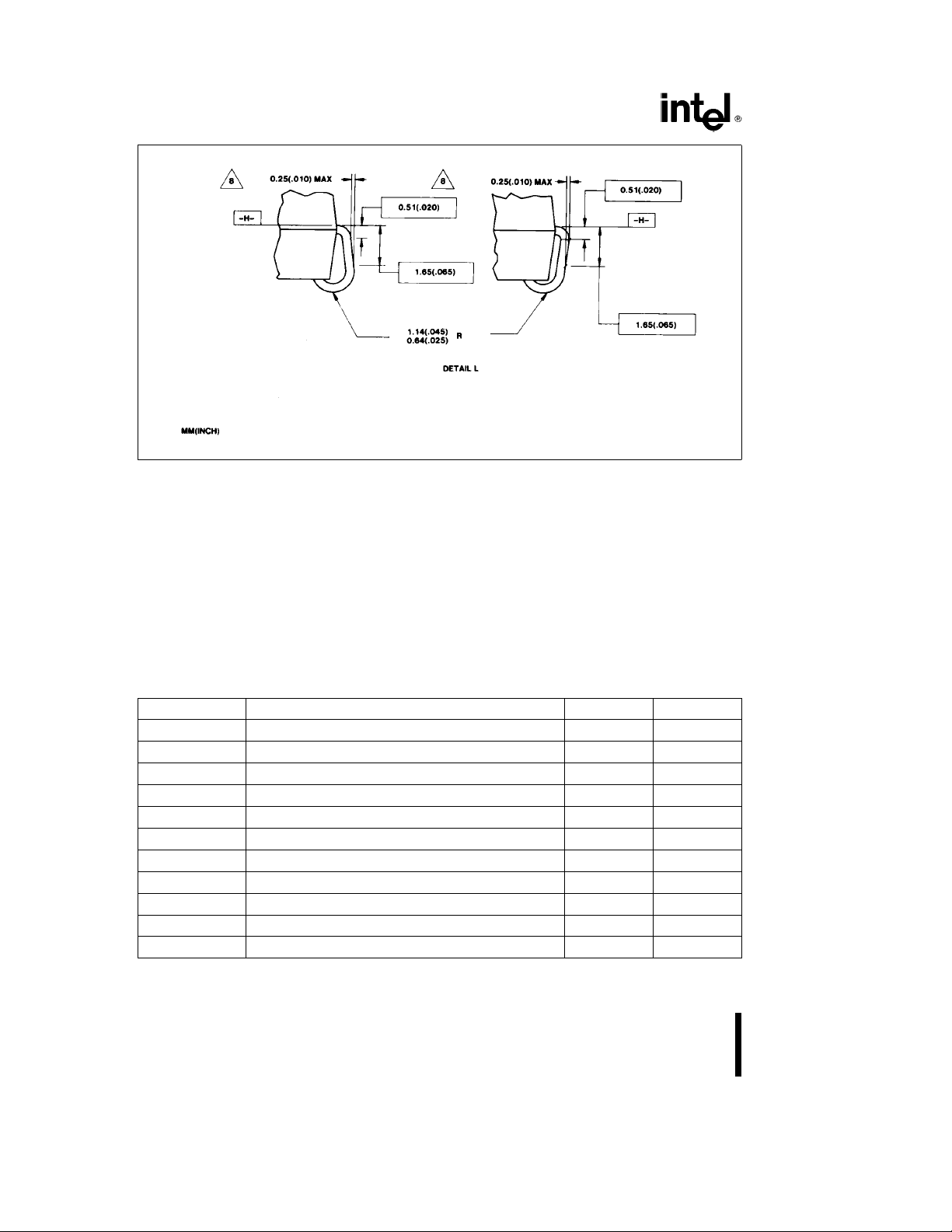
Figure 51. Detail L. Terminal Details
NOTES:
The above diagrams use a 20-lead PLCC package to show symbols for package dimensions. The table below indicates
dimensions in mm that are specific to the 44-lead PLCC package.
1. All dimensions and tolerances conform to ANSI Y14.5M-1982.
2. Datum plane ÐHÐ located at top of mold parting line and coincident with top of lead, where lead exits plastic body.
3. Datums D–E and F–G to be determined where center leads exit plastic body at datum plane ÐHÐ.
4. To be determined at seating plane ÐCÐ.
5. Dimensions D
6. Pin 1 identifier is located within one of the two defined zones.
7. Locations to datum ÐAÐ and ÐBÐ to be determined at plane ÐHÐ.
8. These two dimensions determine maximum angle of the lead for certain socket applications. If unit is intended to be
socketed, it is advisable to review these dimensions with the socket supplier.
9. Controlling dimension, inch.
10. All dimensions and tolerances include lead trim offset and lead plating finish.
11. Tweezing surface planarity is defined as the furthest any lead on a side may be from the datum. The datum is established by touching the outermost lead on that side and parallel to D–E or F–G.
and E1do not include mold protrusion.
1
Symbol Description Min Max
A Overall Height 4.19 4.57
A
1
Distance from Lead Shoulder to Seating Plane 2.29 3.05
D Overall Package Dimension 17.4 17.7
D
1
D
2
Plastic Body Dimension 16.5 16.7
Foot Print 15.0 16.0
E Overall Package Dimension 17.4 17.7
E
1
E
2
Plastic Body Dimension 16.5 16.7
Foot Print 15.0 16.0
CP Seating Plans Coplanarity 0.00 0.10
TCP Tweezing Coplanarity 0.00 0.10
LT Lead Thickness 0.23 0.38
44
Page 45

44-LEAD QUAD FLATPACK PACKAGE
82503
Figure 52. 44-Lead Quad Flatpack Package
Symbol Description Min Nom Max
A Package Height 2.35
A1 Stand Off 0 0.60
B Lead Width 0.2 0.3 0.4
C Lead Thickness 0.1 0.15 0.2
D
1
E
1
e
1
Package Body 10
Package Body 10
Lead Pitch 0.65 0.8 0.95
D Terminal Dimension 12.0 12.4 12.8
E Terminal Dimension 12 12.4 12.8
L
1
Foot Length 0.38 0.58 0.78
Y Coplanarity 0.1
T Lead Angle 0 10
NOTE:
Unless otherwise specified, all units are in millimeters.
290421– 52
§
45
 Loading...