

Infineon BCR148 Schematic [ru]
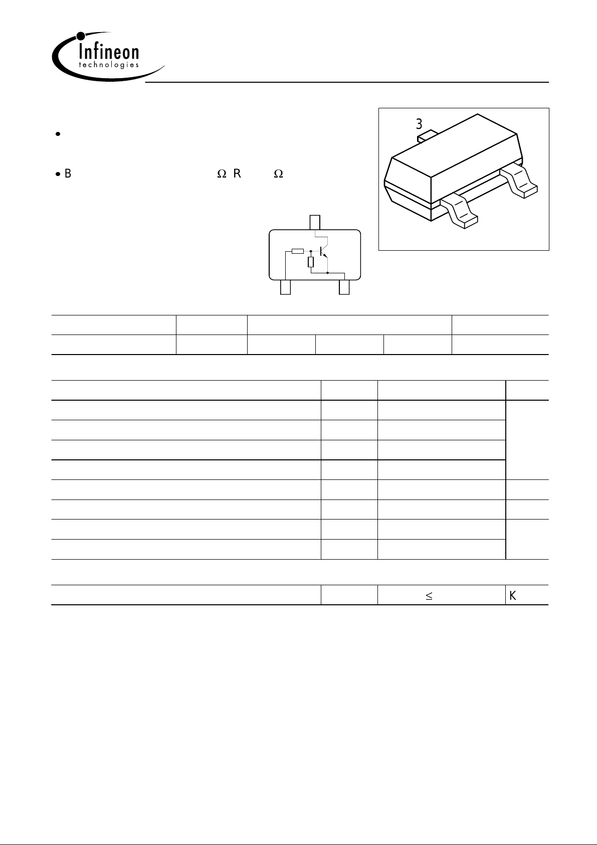
NPN Silicon Digital Transistor
g
Switching circuit, inverter, interface circuit,
driver circuit
Built in bias resistor (R1=47k, R2=47k)
BCR148
3
C
3
R
1
R
2
21
EB
EHA07184
1
Type Marking Pin Configuration Package
BCR148 WEs 1 = B 2 = E 3 = C SOT23
Maximum Ratings
Parameter
Collector-emitter voltage
Collector-base voltage
Emitter-base voltage 10
Input on Voltage
DC collector current
Total power dissipation, TS = 102 °C P
Junction temperature
Symbol Value Unit
V
CEO
V
V
V
I
T
T
C
CBO
EBO
i(on)
tot
j
st
50
50
70 mA
150 °C
-65 ... 150Storage temperature
2
VPS05161
V50
mW200
Thermal Resistance
Junction - soldering point
1
For calculation of R
please refer to Application Note Thermal Resistance
thJA
1)
R
thJS
240 K/W
Nov-29-20011
BCR148
A
Electrical Characteristics at T
=25°C, unless otherwise specified
Parameter Symbol Values Unit
min. typ. max.
DC Characteristics
Collector-emitter breakdown voltage
I
= 100 µA, IB = 0
C
Collector-base breakdown voltage
I
= 10 µA, IE = 0
C
Collector cutoff current
V
= 40 V, IE = 0
CB
Emitter cutoff current
V
= 10 V, IC = 0
EB
DC current gain 1)
I
= 5 mA, VCE = 5 V
C
Collector-emitter saturation voltage1)
I
= 10 mA, IB = 0.5 mA
C
V
(BR)CEO
V
(BR)CBO
I
CBO
I
EBO
h
FE
V
CEsat
50 - - V
50 - -
- - 100 nA
- - 164 µA
70 - - -
- - 0.3 V
Input off voltage
I
= 100 µA, VCE = 5 V
C
Input on Voltage
I
= 2 mA, VCE = 0.3 V
C
Input resistor
Resistor ratio
AC Characteristics
I
= 10 mA, VCE = 5 V, f = 100 MHz
C
V
= 10 V, f = 1 MHz
CB
V
i(off)
V
i(on)
R
1
R1/R
f
T
C
cb
0.8 - 1.5
1 - 3
32 47 62
2
0.9 1 1.1 -
k
- - MHz100Transition frequency
- 3 pFCollector-base capacitance
-
1) Pulse test: t < 300s; D < 2%
Nov-29-20012
 Loading...