Icom IC-r2500, IC-r1500 Service Manual

iC-r1500
iC-r2500
S-14233MZ-C1
Jun. 2006
COMMUNICATIONS RECEIVERS
3%26)#%
-!.5!,
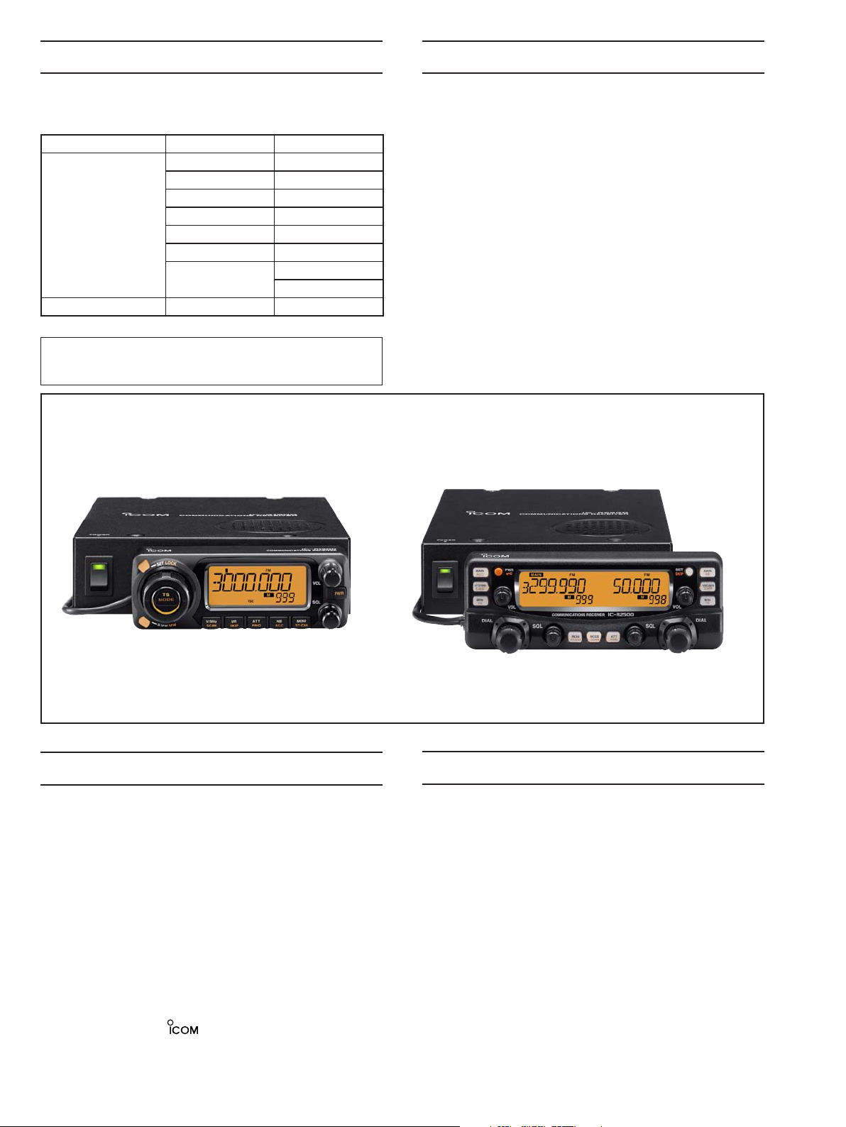
This service manual describes the latest service information
for the IC-R1500 and IC-R2500 COMMUNICATIONS
RECEIVERS at the time of publication.
Be sure to include the following four points when ordering
replacement parts:
1. 10-digit Icom parts numbers
2. Component name and informations
3. Equipment model name and unit name
4. Quantity required
<SAMPLE ORDER>
1110001811 S.IC TA7S04F IC-R2500 Main-A unit 5 pieces
8810008960 Screw FH M2.6 IC-R2500 Chassis 8 pieces
Addresses are provided on the inside back cover for your
convenience.
NEVER connect the receiver to an AC outlet or to a DC
power supply that uses more than 16 V. Such a connection
could cause a fire hazard and/or electric shock.
DO NOT expose the receiver to rain, snow or any liquids.
DO NOT reverse the polarities of the power supply when
connecting the receiver.
DO NOT apply an RF signal of more than 20 dBm (100 mW)
to the antenna connector. This could damage the receiver’s
front end.
1. Make sure a problem is internal before disassembling
the receiver.
2. DO NOT open the transceiver until the receiver is
disconnected from its power source.
3. DO NOT force any of the variable components. Turn
them slowly and smoothly.
4. DO NOT short any circuits or electronic parts. An
insulated turning tool MUST be used for all adjustments.
5. DO NOT keep power ON for a long time when the
receiver is defective.
6. READ the instructions of test equipment thoroughly
before connecting equipment to the receiver.
To upgrade quality, any electrical or mechanical parts
and internal circuits are subject to change without
notice or obligation.
Icom, Icom Inc. and logo are registered trademarks of Icom Incorporated (Japan) in the United States, the United
Kingdom, Germany, France, Spain, Russia and/or other countries.
INTRODUCTION CAUTION
ORDERING PARTS
REPAIR NOTES
MODEL VERSION SYMBOL
IC-R1500
IC-R2500
Europe EUR
U.K. UK
U.S.A. USA
Canada CAN
France FRA
South East Asia SEA
Export
IC-R2500* U.S.A. USA-2
*UT-122 is already installed as DIGITAL UNIT.
(IC-R2500)
(IC-R1500)
EXP
EXP-1

TABLE OF CONTENTS
SECTION 1 SPECIFICATIONS
SECTION 2 INSIDE VIEWS
SECTION 3 DISASSEMBLY INSTRUCTIONS
SECTION 4 CIRCUIT DESCRIPITON
4-1 RECEIVER CIRCUITS. . . . . . . . . . . . . . . . . . . . . . . . . . . . . . . . . . . . . . . . . . . . . . . . . . . . . . . . 4-1
4-2 PLL CIRCUITS . . . . . . . . . . . . . . . . . . . . . . . . . . . . . . . . . . . . . . . . . . . . . . . . . . . . . . . . . . . . . 4-4
4-3 DIGITAL MODE OPERATION WITH UT-122 . . . . . . . . . . . . . . . . . . . . . . . . . . . . . . . . . . . . . . . 4-5
4-4 POWER SUPPLY CIRCUITS. . . . . . . . . . . . . . . . . . . . . . . . . . . . . . . . . . . . . . . . . . . . . . . . . . . 4-6
4-5 CPU PORT ALLOCATION . . . . . . . . . . . . . . . . . . . . . . . . . . . . . . . . . . . . . . . . . . . . . . . . . . . . . 4-7
SECTION 5 ADJUSTMENT PROCEDURES
5-1 PREPARATION . . . . . . . . . . . . . . . . . . . . . . . . . . . . . . . . . . . . . . . . . . . . . . . . . . . . . . . . . . . . . 5-1
5-2 MAIN-A UNIT ADJUSTMENT . . . . . . . . . . . . . . . . . . . . . . . . . . . . . . . . . . . . . . . . . . . . . . . . . . 5-3
5-3 MAIN-B UNIT ADJUSTMENT (R2500 only) . . . . . . . . . . . . . . . . . . . . . . . . . . . . . . . . . . . . . . . 5-5
SECTION 6 PARTS LIST
SECTION 7 MECHANICAL PARTS AND DISASSEMBLY
SECTION 8 SEMICONDUCTOR INFORMATION
SECTION 9 BOARD LAYOUTS
9-1 LOGIC UNIT . . . . . . . . . . . . . . . . . . . . . . . . . . . . . . . . . . . . . . . . . . . . . . . . . . . . . . . . . . . . . . . 9-1
9-2 MAIN-A UNIT. . . . . . . . . . . . . . . . . . . . . . . . . . . . . . . . . . . . . . . . . . . . . . . . . . . . . . . . . . . . . . . 9-3
9-3 MAIN-B UNIT (R2500 only) . . . . . . . . . . . . . . . . . . . . . . . . . . . . . . . . . . . . . . . . . . . . . . . . . . . . 9-5
9-4 CONTROL UNITS . . . . . . . . . . . . . . . . . . . . . . . . . . . . . . . . . . . . . . . . . . . . . . . . . . . . . . . . . . . 9-7
9-4 UT-122 (Optional product; DIGITAL UNIT for [R2500; USA-2]) . . . . . . . . . . . . . . . . . . . . . . . . . 9-7
SECTION 10 BLOCK DIAGRAM
SECTION 11 VOLTAGE DIAGRAM

SECTION 1 SPECIFICATIONS
2
2
2
¤
¤
¤
¤
.
¤
¤
¤
M GENERAL
• Frequency coverage
0
A.S.U
010.0 :
1
2581
–000.
7981
–
.
3
000
181
.9923
ecnarF
02.15–002.05
ehtO
• Mode :
• Number of memory channels :
1
4
1
0 :
10.
evoba naht r
1
*
: For IC-R2500. Available on Main band only.
Sub band does not cover outside of frequency range; 50 to 1300.000000 MHz.
2
*
: Guaranteed: 0.495–3000.000 MHz range only
FM, AM, WFM, USB*1, LSB*1, CW, DV*1,*2, P25*1,*
1
*
: For R2500. Available on Main band only.
2
*
: For R2500. Available when optional UT-118 is installed.
3
*
: For R2500. Available when optional UT-122 is installed, and depending on versions.
2600
0.641
–000.44
–
031
000.042
• Tuning steps : 1 Hz, 10 Hz, 20 Hz, 50 Hz, 100 Hz, 500 Hz, 1 kHz, 2.5 kHz, 5 kHz, 6.25 kHz,
8.33 kHz, 9 kHz, 10 kHz, 12.5 kHz, 15 kHz, 20 kHz, 25 kHz, 30 kHz, 50 kHz,
100 kHz, 125 kHz, 150 kHz, 200 kHz, 500 kHz, 1 MHz, 10 MHz, USER TS
• Operating temperature range : 0°C to +60°C; +32°F to +140°F
1
2
,
* 999999.908–00
*
999999.668–000.158
000000.0031–000.698
999999.0181–100000.003
1
* 999999.7681–000.
1
* 999998.5032
1
* 999999.1182–000.7532
1
* 999999.8682–000.3582
,
1
* 999997.9013–000.8982
*
,
1
* 999997.4513–000.6313
*
,
1
* 999999
*
1
2
,
* 999999.92–000010.0 :
*
0000
999999.701–005.78
0000
00000.044–000.03
00
000.0
1
,
2
* 999999.9923–0
*
3
• Current drain (at 12.0 V DC: approx.)
[1500] POWER ON Standby 650 mA
Max. audio Less than 1.2 A
*While using controller (R1500): plus 50 mA with above current value.
[1500/2500] POWER OFF PC (USB VBAS-ON) 550 mA typ.
PC (VBAS-OFF) 15 mA typ.
Controller (R1500) 15 mA
[2500] single band operation Standby 650 mA
Max. audio Less than 1.2 A
Dualwatch operation Standby 850 mA
Max. audio Less than 1.5 A
*While using controller (R2500): plus 110 mA with above current value.
• Frequency stability : ±3 ppm (–10°C to +60°C)
• Power supply requirement : 12 V DC ±15% (Negative ground)
• Current drain (At 12 V DC ; approx.)
• Dimensions (projections not included) :
146(W)×41(H)×206(D) mm; 5
111(W)×40(H)×26.5(D) mm; 4
140(W)×50(H)×27.5(D) mm; 5
• Weight (approx.) :
MAIN UNIT 1.2 kg; 2 lb 10 oz (1500)
3
⁄4(W)×15⁄8(H)×8
3
⁄8(W)×19⁄16(H)×8
1
⁄2(W)×131⁄32(H)×1
1.35 kg; 2 lb 15 oz (2500)
17
CONTROLLER 0.2 kg; 2 lb 7
0.25 kg; 2 lb 8
⁄32 oz (1500)
13
⁄16 oz (2500)
• Antenna connector : BNC (50 Ω)
1
⁄8(D) in
1
⁄32(D) in
3
⁄32(D) in
1 - 1

y
¤
¤
y
M RECEIVER
• Receive system : Triple-conversion superheterodyne and down converter
• Intermediate frequencies : 1st: 266.700 MHz, 2nd: 10.700 MHz, 3rd: 450 kHz (except for WFM mode)
• Sensitivity :
•
F
M
(
2
3
5
2
8
9.94–000.0
0.0
0.0
92–0
0
;.veD zHk5.3/zHk1
99
HM999.932–00
HM
9.972–000.042
99
HM
9.9
99
HM999.996–000.003
0
031–000.007
0.
9.9922–100000.0031
0
2
FW
•
00
0
–
0.
3
M
k1(
5.25/zH
5
00.007
31
922–100000.00
000.0032
MA )
•
1
9
9
–
4.0
7.
5
9.41–008.1
;.DOM %03/zHk1(
01
HM9
z
99
HM
1
999.992–000.0
5
0
00.003
–
HM
00.007
•
1
Bd
WC/BSS
01(
1–008.
4
6–000.05
)N
/S
HM9
97.1–594.0
z
99
HM
9.
9.94–000.51
zHM99
9.99
31–000.007
M000.00
z
z
z
zHM00
HM000.0003
veD zHk
HM000.0031–0
HM999.9
HM000.0003–
HM000.0031–0
)DA
NIS Bd21
0 naht
sseL:zHM999.92–000.8
ht
sseL:zHM
na
ht sseL:z
:
s
eL
s
eL:
Vµ36.
0 na
Vµ36.
Vµ5.0
V
5.
µ
0 naht
V
µ5.0 naht ss
Vµ5.0 naht sseL:
h
t sseL
:
:zHM99
a
sse
ht
L
eL:z
a
t ss
h
)DANIS Bd21 ;.
µ36.0 n
V
µ6.5 na
V
Vµ81 n
Vµ4.1 naht sseL:zHM999.996–000.0
:z
sseL
:z
:z
/S Bd
N
Vµ8.1 naht sseL
Vµ81 naht
Vµ65 naht sseL
Vµ52 naht sseL:z
:
Vµ5.2 naht sseL
Vµ5.2 naht sseL:zHM999.94–000.5
seL:z
s
Vµ2 naht
Vµ2 naht sseL:zHM999.996
V
µ5.2 naht sseL:z
Vµ5 naht sseL:z
:
Vµ5.0 naht sseL
Vµ5.0 naht sseL:
sseL:zHM99
.0
Vµ4
naht
Vµ5.0
naht sseL:zH
• Selectivity :
)lacipyt( Bd 6–/zHk 8.2 naht eroMMA/WC/BSS
C/BSS
A
M
MF/MA
FW/
W
F
ht
eroM
t eroMM
zHk 0.6 naht eroMMF/MA/W
–/zHk 51 naht eroMMF/M
na
Hk0
32 nah
)lacipyt( Bd 6–/
)lacipyt( Bd 6
)
ipyt( Bd 6–/zHk 05
lac
)lacipyt( Bd6–/z
• Audio output power : More than 0.5 W (at 10% distortion with an 8 Ω load)
1
• Ext. speaker connector : 2-conductor 3.5 (d) mm (
• Packet connector : 2-conductor 3.5 (d) mm (
• Data connector : 3-conductor 2.5 (d) mm (
⁄8″)/8 Ω
1
⁄8″)
1
⁄10″)
• IF shift variable range : More than ±1.2 kHz
All stated specifications are subject to change without notice or obligation.
1 - 2
2 - 1
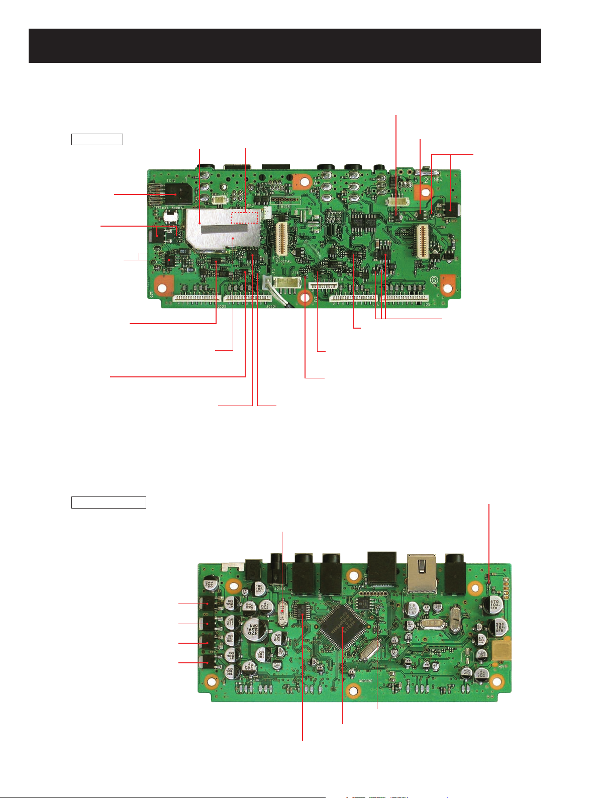
SECTION 2 INSIDE VIEWS
LOGIC UNIT
TOP VIEW
BOTTOM VIEW
+33V regulator
IC2: BA6161F
D2: 1SS355
VSC/TONE filter
(IC2021: LM2904)
IC-R2500 only
AF +8V regulator
(Q5: 2SB1201, Q8: XP1501)
AF amplifier
(IC12: LA4425A)
USB HUB
(IC32: USB2502)
USB +3.3V regulator
IC1: S-812C33
Q31: 2SB789
Q32: 2SC4116
VCC line controller
Q4: 2SJ377
Q6: DTC144EU
−5V regulator
IC8: µPC1553
D6: 1SS272
D8: MA8051
VSC/TONE filter
(IC21: LM0904)
AF selecter
(IC23: SN74AHC2053)
AF selecter
(IC2023: SN74AHC2053)
IC-R2500 only
USB audio IC
(IC16: PCM2901M)
Electric VR
(IC17: SM6451B)
AF amplifier
(Q18: 2SC4617)
AF amplifier
(Q2018: 2SC4617)
IC-R2500 only
CPU5V regulator
(IC3: XC6202P502PR)
L5V regulator
(IC9: AN78L05)
CPU reset IC (IC35: S-80942)
SP mute switch (Q12: 2SC4213)
CPU (IC18: M30624FGPGP)
DTMF decoder (IC19: BU8872FS)
A+5V regulator (IC6: TA7805)
A+8V regulator (IC7: AN7708)
B+5V regulator (IC2006: TA7805F)
IC-R2500 only
B+8V regulator (IC2007: TA7708SP)
IC-R2500 only
Clock oscillator (X2: CR-818 4.19304 MHz)
(
)
( )
(
)
( )
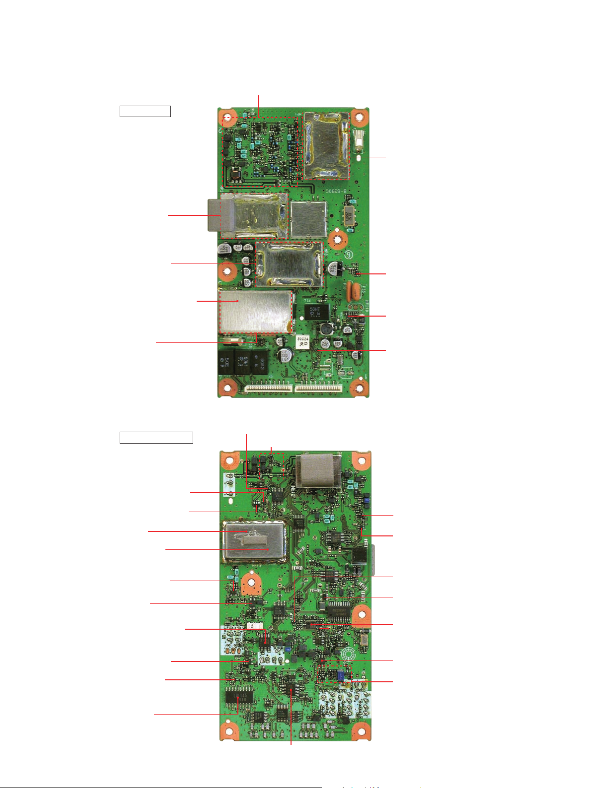
Down converter circuit
1st VCO circuit
2nd VCO circuit
DDS circuit
RF circuits
• MAIN-A UNIT
Noise blanker amplifier
(Q68: 2SK882)
APCO5V regulator
(Q77: 2SA1832)
Buffer
(Q60: 2SC4617)
AM detecter circuit
WFM IF IC
(IC16: LA1145M)
IF IC (FM)
(IC24: TA31136)
RSSI meter amplifier
(IC25: NJM2904V, D80: 1SS400)
AGC amplifier
(Q58: 2SC4617)
2nd IF amplifier
(Q66: 3SK131)
2nd mixer
(IC19: TA4107F)
1st IF amplifier
(Q44: 3SK131)
1st mixer
(IC14: SPM5001)
+5V regulator
(Q23: UNR9111)
DVCO +5V regulator
(Q78: UNR9111)
DPLL 3.3V regulator
(IC2: S-812C33AMC)
D3.3V regulator (Q10: UNR9111)
IF IC (Band scope)
(IC20: TA31136)
ATT circuits
TOP VIEW
BOTTOM VIEW
SSB decoder
(IC23: TA4101F)
DDSREF 8V regulator
(D120: DAN222)
DDS REF 8V regulator
(Q90: XP4311)
HF 8V regulator
(Q25: XP4311)
HF band RF amplifier
(Q22: 2SC5226)
PLL 3.3V regulator
(IC9: S-812C33AMC)
2 - 2
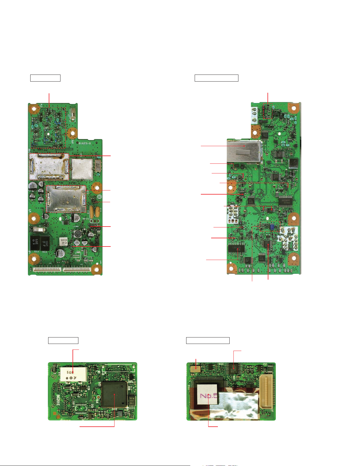
• MAIN-B UNIT (IC-R2500 only)
• UT-122 (Optinal product; DIGTAL UNIT for [IC-R2500: USA-2])
Noise blanker
(Q68: 2SK882)
BAPCO5V regulator
(Q77: 2SA1832)
3rd IF filter
(FI1: CFWKA450)
Buffer
(Q60: 2SC4617)
AM detecter circuit
IF IC (WFM)
(IC16: LA1145M)
IF IC (FM)
(IC24: TA31136)
AGC amplifier
(Q58: 2SC4617)
2nd IF amplifier
(Q66: 3SK131)
2nd mixer
(IC19: TA4107F)
1st IF amplifier
(Q44: 3SK131)
1st mixer
(IC14: SPM5001)
+5V regulator
(Q23: UNR9111)
ATT circuit
HF filters
1st VCO circuit
2st VCO circuit
TOP VIEW
BOTTOM VIEW
TOP VIEW
BOTTOM VIEW
RSSI meter amplifier
(IC25: NJM2904V
D80: 1SS400)
PLL 3.3V regulator
(IC9: S-812C33AMC)
Clock oscillator
(X1: CR-798)
Liner codec
(IC9: AK4550VT)
EEPROM
(IC17: HN58X2416TI)
CPU
(IC12: HD64F2239TE16)
2 - 3
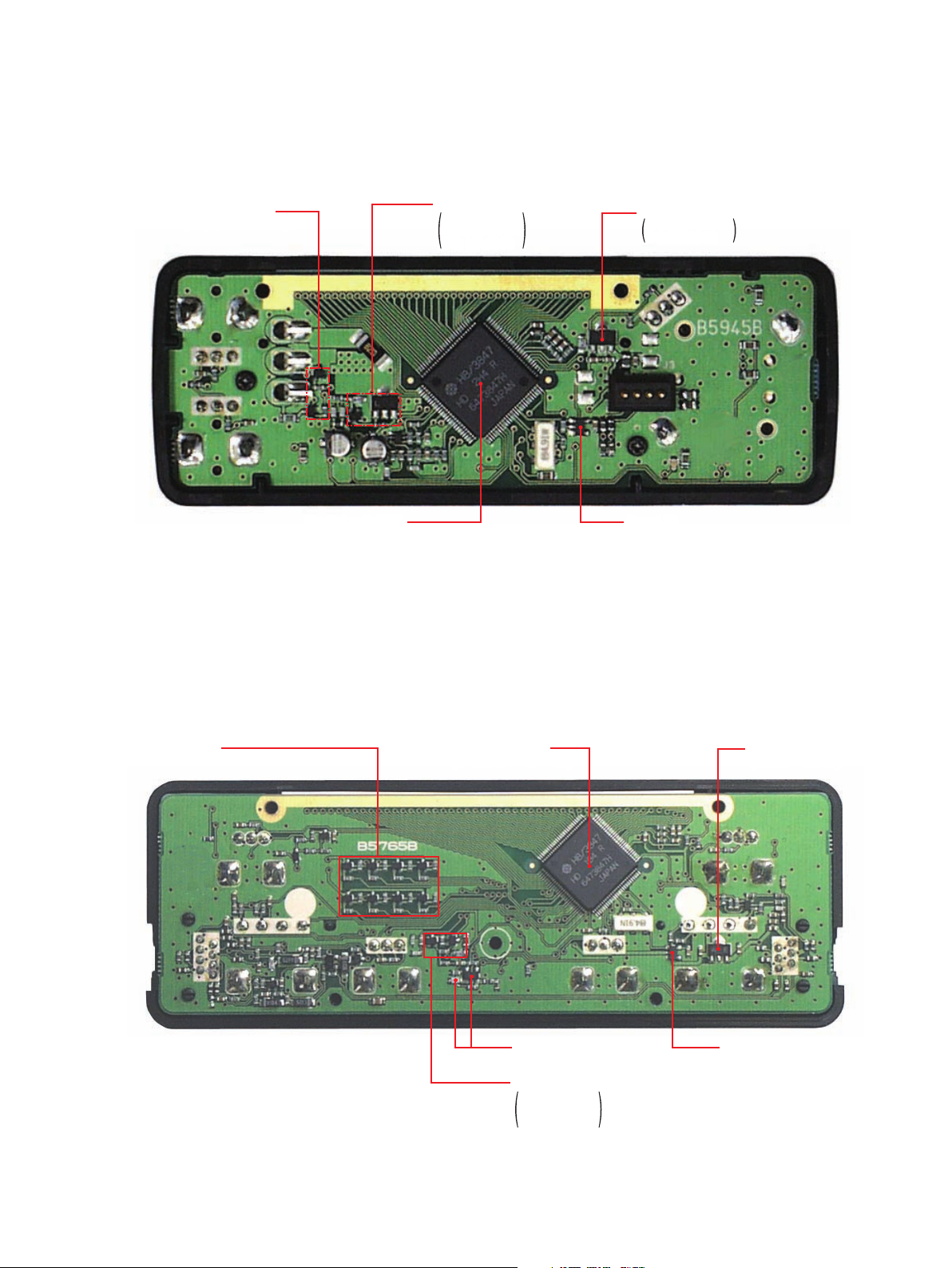
• CONTROL UNIT (R1500)
• CONTROL UNIT (R2500)
Color controller
(Q6,Q7: 2SC4116)
Control unit CPU
(IC6: HD6433842RB36H)
Reset IC
(IC2: S-80945CLMC-G7F)
+5V regurator
IC5: TA78L05F
D4: MA8062
+8V regurator
Q1: 2SC4116
Q3: 2SA1734
D5: MA8068
Color controller
(Q6, Q7: 2SC4116)
Control unit CPU
(IC6: HD6433842RB36H)
Reset IC
(IC2: S-80945CLMC-G7F)
+5V regulator
IC5: TA78L05F
D4: MA8062
+8V regulator
Q1: 2SC4116
Q3: 2SA1734
D5: MA8068
Dimmer
+8V regurator
(Q1: 2SC4116)
+5V regurator
(IC3: TA78L05F)
Sub CPU
(IC4: HD6473847RH)
Reset IC
(IC2: S-80945CLMC)
Data comparator
(IC1: TA75S01F)
LED drivers
(Q6-Q13: 2SC4116)
+8V regurator
Q1: 2SC4116
Q3: 2SA1586
D1: MA8091
+5V regurator
(IC3: TA78L05F)
Control unit CPU
(IC4: HD6473847RH)
Reset IC
(IC2: S-80945CLMC)
Data comparator
(IC1: TA75S01F, D2: MA8047)
3 - 1
SECTION 3 DISASSEMBLY INSTRUCTIONS
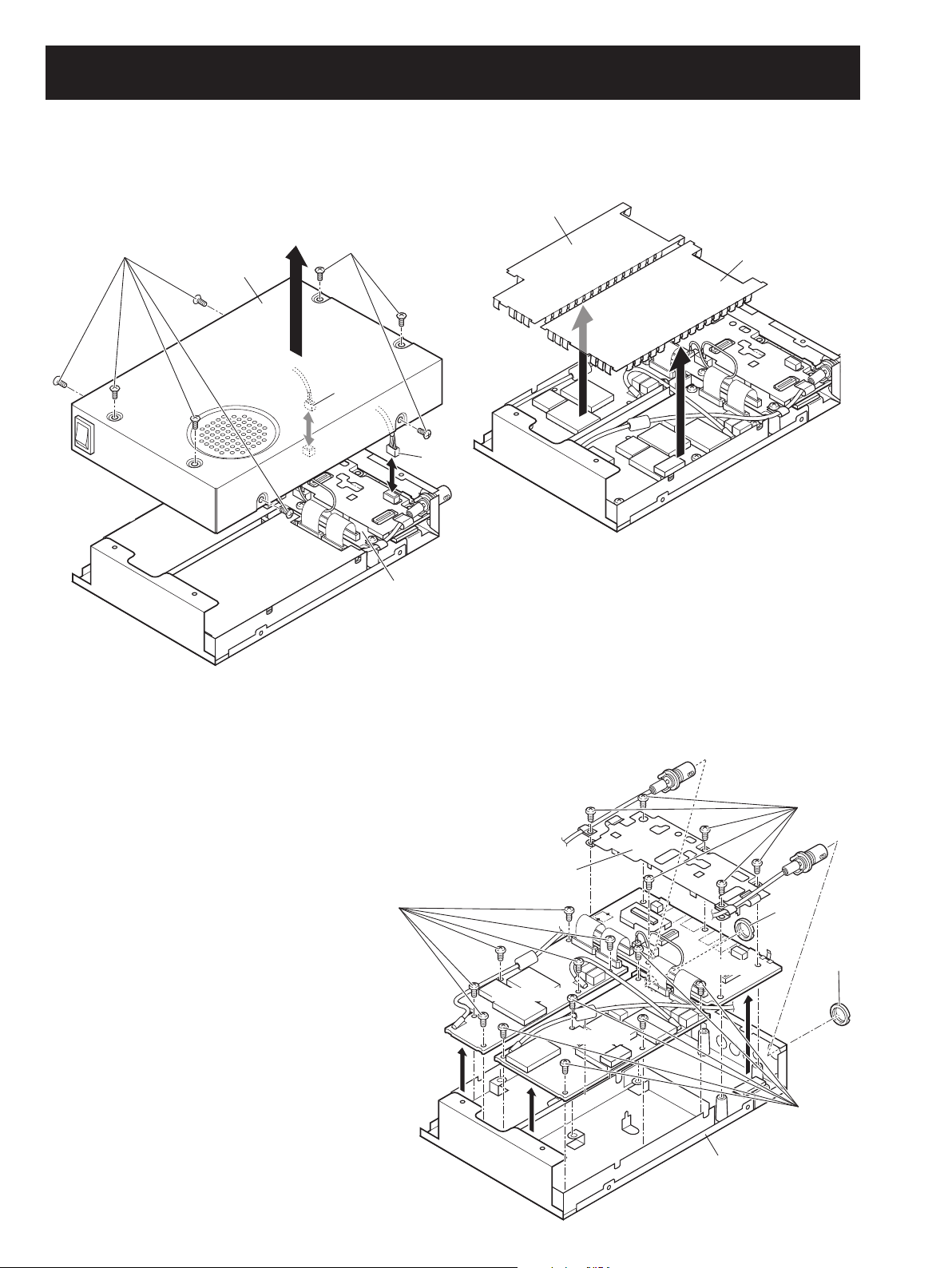
• Removing the top cover and shield covers
q Unscrew 8 screws, A.
w Unplug the connectors B and C from the LOGIC unit.
e Remove the top cover in the direction of the arrow.
r Remove the shield covers D and E* in the direction of
the arrow.
• Removing the LOGIC unit, MAIN-A unit and MAIN-B* unit
q Unscrew nut F*, G.
w Unscrew 6 screws H from the LOGIC unit and remove the LOGIC plate.
e Unscrew 6 screws I from the MAIN-A unit and 6 screws J* from the MAIN-B unit*.
r Remove the units in the direction of the arrows.
Top cover
A
B
C
D
E
LOGIC Unit
A
*
F
G
Chassis
LOGIC UNIT
LOGIC Plate
*
*
MAIN-A UNIT
MAIN-B UNIT
H
I
J
* IC-R2500 only
* IC-R2500 only
3 - 2
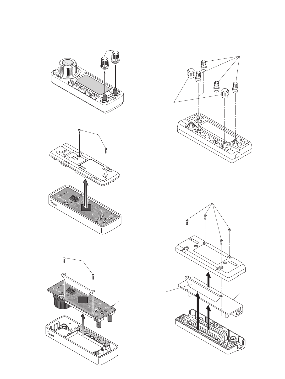
• CONTROL unit disassembly (R1500)
q Remove 2 knobs A.
w Unscrew 2 screws B, and remove the cover.
e Unscrew 2 screws C, and remove the LCD plate.
r Remove the CONTROL unit.
• CONTROL unit disassembly (R2500)
q Remove 6 knobs A.
w Unscrew 4 screws B, and remove the cover.
e Remove the plate C, and remove CONTROL unit.
CONTROL UNIT
CONTROL UNIT
SECTION 4 CIRCUIT DESCRIPTION
4-1 RECEIVE CIRCUITS
4-1-1RF CIRCUITS (MAIN-A/-B UNITS)
The MAIN-A UNIT has eight RF circuits and one down converter
circuit to provide wide receiving range. The received signals from
the antenna connector (CHASSIS; J1) are applied to RF circuits
or down converter circuit according to the received frequency,
and amplified within the frequency coverage.
IC-R2500 contains MAIN-B UNIT which has 4 RF circuits to
provide dulalwatch or diversity capability .
The 0.01–50 MHz signals from the antenna are passed
through the attenuator (D1, D3), band switch (D9) and lowpass fi lter (LPF; L20, L26, C54, C60, C68, C72, C81, C88),
then applied to one of the RF circuit.
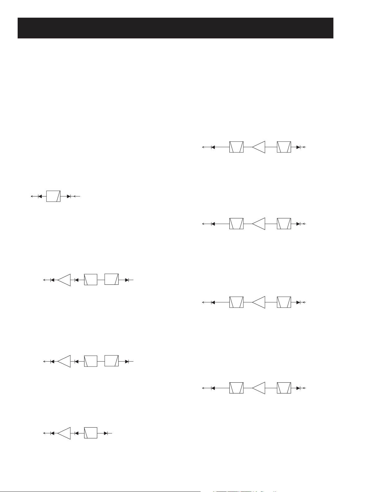
• 0.01–1.8 MHz*
The 0.01–1.8 MHz signals are passed through the band
switch (D29), LPF (L48, L52, C134, C148, C171, C173) and
another band switch (D56), then applied to the 1st mixer
(IC14, pins 4, 5).
<0.01–18 MHz>
D56
• 1.8–15.0 MHz*
The 1.8–15.0 MHz signals are passed through the band
switch (D25), LPF (L43, L47, L50, C102, C120, C125, C131,
C135, C140), high-pass filter (HPF; L57, L60, L72, C150,
C161, C163, C174, C178, C618, C619) and another band
switch (D49), and then applied to the RF amplifier (Q22).
The amplified signals are then applied to the 1st mixer
(IC14, pins 4, 5) via the band switch (D102).
<1.8–15 MHz>
To the
1st mixer
(IC14, pins 4, 5)
• 15.0–30 MHz*
The 15.0–30 MHz signals are passed through the band
switch (D82), LPF (L46, L49, C116, C118, C124, C130,
C136), HPF (L55, L58, C139, C149, C151, C162, C164)
and another band switch (D83), and then applied to the RF
amplifi er (Q22). The amplifi ed signals are then applied to the
1st mixer (IC14, pins 4, 5) via the band switch (D102).
<15–30 MHz>
To the
1st mixer
(IC14, pins 4, 5)
• 30–50 MHz*
The 30–50 MHz signals are passed through the band switch
(D30), HPF (L77, L82, C201, C206, C208, C213, C216)
and another band switch (D48), and then applied to the RF
amplifi er (Q22). The amplifi ed signals are then applied to the
1st mixer (IC14, pins 4, 5) via the band switch (D102).
<30–50 MHz>
To the
1st mixer
(IC14, pins 4, 5)
LPF
D102
Q22
Q22
Q22
RF
amp.
RF
amp.
RF
amp.
D29
From the LPF
D49D102
HPF
HPF
HPF
LPF
LPF
D30D48
D25
D82D83D102
From the LPF
From the LPF
From the LPF
The 50–1300 MHz signals from the antenna are passed
through the anttenuator (D1, D3), band switch (D7) and LPF
(L5, C33, C34), then applied to one of the RF circuit.
• 50–150 MHz
The received signals 50–150 MHz are passed through the
band switch (D5) and the tunable bandpass fi lter (BPF; D8,
D16–D18, D28, D31, L9, L21, L25, L31, L33, C39, C41,
C44, C49, C70), and then applied to the RF amplifi er (Q15).
The amplified signals are passed through another tunable
BPF (D35, D36, L53, L62, L69, L73, C142, C154, C199) and
another band switch (D44), and then applied to the 1st mixer
(IC14, pins 4, 5).
<50–150 MHz>
To the
1st mixer
(IC14, pins 4, 5)
D44
D35, D36
BPF
Q15
RF
amp.
D8, D16–D18
D28, D31
BPF
D5
From the HPF
• 150–350 MHz
The received signals 150–350 MHz are passed through the band
switch (D6) and BPF (D32, L10, L12, L34, L37, L39, C40, C42,
C45, C50, C82, C114, C117), and applied to the RF amplifier
(Q17). The amplified signals are passed through another BPF
(D37, L56, L67, L71, C155, C167, C183, C195) and another band
switch (D46), and then applied to the 1st mixer (IC14, pins 4, 5).
<150–350 MHz>
To the
1st mixer
(IC14, pins 4, 5)
D46
D37
BPF
Q17
RF
amp.
D32
BPF
D6
From the HPF
• 350–700 MHz
The received signals 350–700 MHz are passed through the
band switch (D14) and BPF (D26, D27, L24, L32, L40, C65,
C71, C81, C106), then applied to the RF amplifier (Q16). The
amplifi ed signals are passed through another BPF (D38, D39,
L54, L64, L74, L78, C144, C172, C211) and another band switch
(D47), and then applied to the 1st mixer (IC14, pins 4, 5).
<350–700 MHz>
To the
1st mixer
(IC14, pins 4, 5)
D47
D38, D39
BPF
Q16
RF
amp.
D26, D27
BPF
D14
From the HPF
• 700–1300 MHz
The received signals 700–1300 MHz are passed through the
band switch (D13) and BPF (D19, D23, D33, D34, L22, L27,
L36, L36, L41, L44, C66, C77, C119), then applied to the RF
amplifier (Q18). The amplified signals are passed through
another BPF (D40, D41, L51, L59, L68, L72, C168, C176,
C205) and the band switch (D45), and then applied to the
1st mixer (IC14, pins 4, 5).
<700–1300 MHz>
To the
1st mixer
(IC14, pins 4, 5)
D45
D40, D41
BPF
Q18
RF
amp.
D19, D23
BPF
D13
From the HPF
*MAIN-A UNIT only
4 - 1
• 1300–3300 MHz*
The 1300–3300 MHz signals from the antenna are applied to
the down converter circuit where those signals are converted
into the lower frequencies.
<DOWN CONVERTER>
D42
To the RF circuits
(350–1300 MHz)
LPF
LO signals from VCO (Q19, D43)
IC5
amp.
RF
HPF
Q11
Buff
amp.
D15
From the
antenna
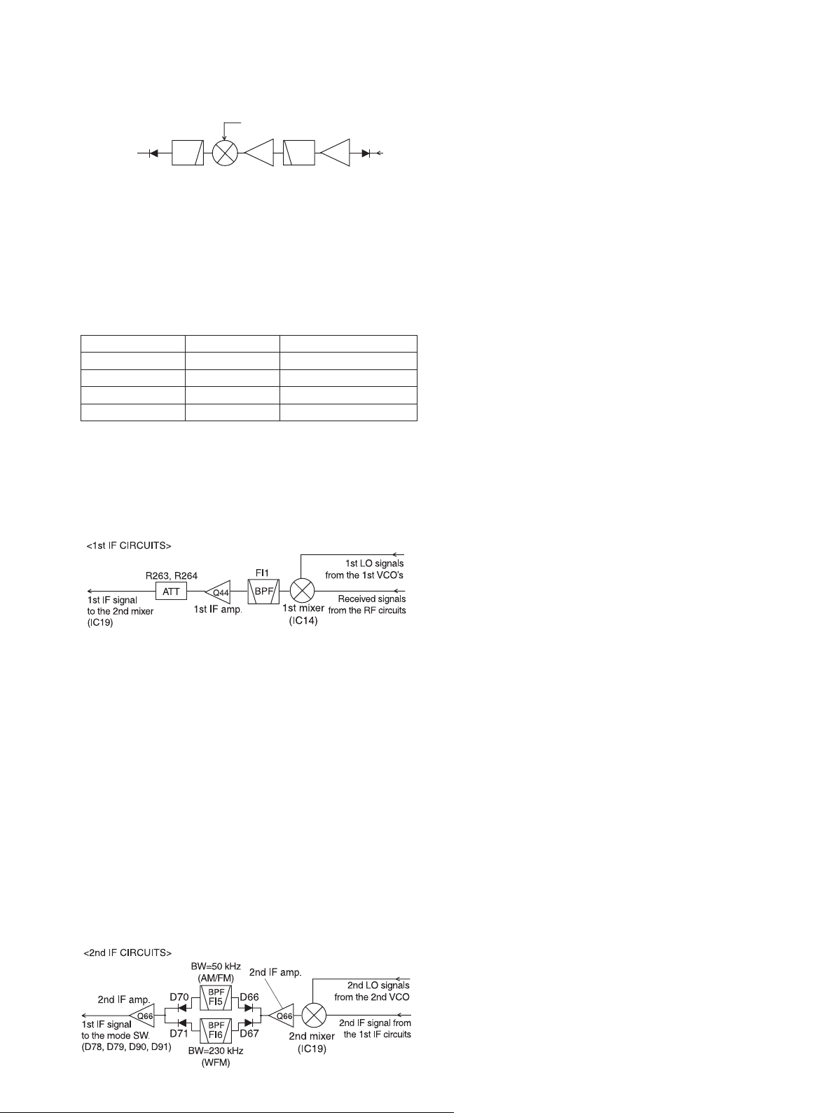
In FM or AM mode, the 2nd IF signal is passed through the
FI5 (band width=50 kHz) via mode switches (D66, D70),
In WFM mode, the 2nd IF signal is passed through the FI6
(band width=230 kHz) via mode switches (D67, D71).
The fi ltered 2nd IF signal is applied to the 2nd IF amplifi er
(Q66). The amplifi ed 2nd IF signals are then applied to the
3rd IF and demodulation circuits.
The received signals are applied to the buffer amplifi er (Q11)
via the band switch (D15). The buffer-amplifi ed signals are
applied to the RF amplifi er (IC5, pin 1) via HPF (L35, L38,
C89, C92, C93, C100, C103). The amplified signals are
output from pin 4, and applied to the mixer (IC6, pin 1) and
down-converted. The down converted signals are output
from pin 6, then applied to the RF circuits via LPF (L66,
C190, C193) and band switch (D42). The LO frequencies
and convered frequencies are shown as below.
RX frequency LO frequency Convered frequency
1300–1700 MHz 1001 MHz 350–700 MHz
1700–2300 MHz 1001 MHz 700–1300 MHz
2300–2700 MHz 2002 MHz 350–700 MHz
2700–3300 MHz 2002 MHz 700–1300 MHz
4-1-2 1st IF CIRCUITS
The 1st IF circuits contain a 1st mixer, 1st IF amplifi er and
1st IF fi lter. The 1st IF mixer converts the received signals
into a fi xed frequency of the 1st Intermediate Frequency (IF)
signal. The converted 1st IF signal is filtered at the 1st IF
fi lters, then amplifi ed at the 1st IF amplifi er.
The converted signals from the RF circuits are applied to the
1st IF mixer (IC14, pins 4, 5) and converted into the 266.7
MHz 1st IF signal by being mixed with the 1st LO (Local
Oscillator) signals from the 1st-VCO’s.
The converted IF signal is passed through the 1st IF filter
(FI1) to fi lter out the unwanted signals, then applied to the 1st
IF amplifi er (Q44). The amplifi ed 1st IF signal is then applied
to the 2nd mixer (IC19, pin 4) via attenuator (R263, R264).
4-1-3 2nd IF CIRCUITS (MAIN UNIT)
The 2nd IF circuits contain the 2st mixer, 2nd IF amplifier
and the 2nd IF fi lters.
4-1-4 NOISE BLANKER CIRCUIT
The noise blanker (NB) circuit reduces pulse type noises
in the received signals. When the received signals contain
pulse type noise components, the NB circuit reduces the
noisy AF signals by cutting off the 2nd IF line.
In AM, SSB or CW mode and the NB function is activated, a
portion of the 2nd IF signal from the band switch (D70, D71)
is amplifi ed at NB amplifi er (Q68) and applied to the IF IC
(IC16, pin 2).
When the 2nd IF signal contains a pulse noise, the RSSI
signal corresponding to the pulse noise level is output from pin
17. The output RSSI signal turns Q49 ON and Q65 turns OFF,
thus the Q66 is inactivated and the 2nd IF signal is cut off.
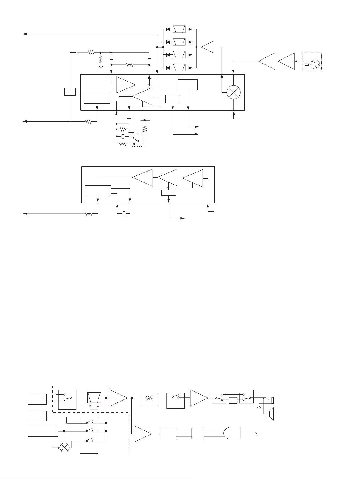
4-1-5 3rd IF AND DEMODULATOR CIRCUITS
(MAIN-A/B UNIT)
The 2nd IF signal is converted into the 3rd IF signal (except
WFM mode) and demodulated in the IF IC. The IF IC
contains a 3rd mixer, limiter amplifi er, quadrature detector,
etc. in its package.
In FM mode, the 2nd IF signal from the 2nd IF amplifier
(Q66) is applied to the IF IC (IC24, pin 16) via mode switch
(D78) and IF gain control circuit (D97).
The applied 2nd IF signal is converted into the 3rd IF signal
by being mixed with 3rd LO signal from the TCXO (X1), at
the 3rd mixer in the IF IC (IC24).㩷The converted 3rd IF signal
is output from pin 3 and applied to the 3rd IF amplifi er (Q62).
The amplifi ed 3rd IF signal is passed through one of the 3rd
IF fi lter according to the receiving mode.
The filtered 3rd IF signal is applied to the limiter amplifier
(IC24, pin 5), then applied to the demodulator circuit (pin 10,
X2) and FM-demodulated. The FM-demodulated AF signals
are output from pin 9, then applied to the AF circuits.
In AM and CW mode, the 3rd IF signal from the 3rd IF fi lter
is applied to the 3rd IF amplifier (Q61). The amplified 3rd
IF is applied to the AM demodulator circuit (D75) via the
buffer amplifi er (Q63). The AM-demodulated AF signals are
applied to AF circuits via the AF selector (IC27, pins 3, 4).
The 1st IF signal from the 1st IF circuits is converted into
the 10.7 MHz 2nd IF signal by being mixed with the 2nd LO
signals from the 2nd-VCO.
The converted 2nd IF signal is applied to the 2nd IF amplifi er
(Q60). The amplifi ed 2nd IF signal is passed through the 2nd
IF fi lter to fi lter out the unwanted signals.
In SSB mode, the 3rd IF signal from the buffer amplifier
(Q63) are applied to the AF mixer (IC23, pin 6) and
converted into the AF signal by being mixed with the 447.3–
452.7 kHz BFO signal from the DDS circuits. The converted
audio signals are applied to the AF selector (IC27, pin 1)
after being fi ltered at the HPF (IC31, pins 1, 4).
In WFM mode, the 2nd IF signal is applied to the IF IC
(IC16, pin 2) via the 2nd IF amplifi er (Q66) and mode switch
(D90, D91). The 2nd IF signal is amplified at the limiter
amplifier, then applied to the demodulator circuit (pins 11,
12, X2) and FM-demodulated. The FM-demodulated AF
signals are output from pin 8, then applied to the AF circuits
via the AF selector (IC27, pins 8, 9).
*MAIN-A UNIT only
4 - 2
<3rd IF AND DEMODULATOR CIRCUITS (FM)>
3rd IF signal to the AM demodulator circuits
2
D/A converter
FM-demodulated signals
to the AF circuits
<2nd IF AND DEMODULATOR CIRCUITS (WFM)>
IC8
1
Quodrature
Detector
9
X2
8
Noise
Amp.
D94D96
BPF
FI9
D69D73
Limit’r
Amp.
735
RSSI
BPF
FI8
BPF
FI7
BPF
Detector
Noise
D93D95
D68D72
Q62
3rd IF amp.
10.25 MHz
3rd LO signal
2
Q71
REF
amp.
Q80
REF
amp.
TCXO
X2
IF IC (IC24)
1110
+5V
Q73
1312
“NOISE” signal to the CPU (IC18, pin 16)
“RSSI” signal to theAGC amplifier (Q67)
16
2nd IF signal from the 2nd IF circuits
Limit’r
Amp.
Quodrature
Detector
9
FM-demodulated signals
to the AF circuits
1112
X3
4-1-6 AF CIRCUITS (LOGIC UNIT)
The demodulated AF signals from the demodulator circuits are
amplifi ed and fi ltered in the AF circuits.
In FM mode, the demodulated AF signals from the
demodulator circuits are passed through the AF select
switch (IC4, pins 1, 7) and BPF (IC27, pins 1, 3 and 5, 7),
then applied to the AF amplifi er (Q18).
In other than FM mode, the demodulated AF signals from
the demodulator circuits are passed through the AF select
switch (MAIN-A/B; UNIT ;IC27, pins 8, 9; WFM, pins 3, 4;
AM, pins 1, 2; SSB), then applied to the AF amplifi er (Q18).
The amplified AF signal are applied to the electric volume
(IC17, pins 6, 7) for level adjustment. The level adjusted
AF signals are passed through the speaker mute switch
(Q12) and applied to the AF power amplifier (IC12, pin 1).
The power-amplified AF signals are applied to the internal
speaker via J1 (J6) or an external speaker/ear phone via the
phone switch (S1), attenuator (R19, R20) and J1 (J6).
• AF CIRCUITS
FM
IF IC
(IC24)
WFM
IF IC
(IC16)
AM demodulator
(D75)
From the BFO
IC4
9
7
AF
selector
8
AM
AF mixer (IC23)*
SSB
1
8
3
1
IC27
51
BPF
73
IC27
AF
selector
AF
Amp.
9
4
2
MAIN-A/B UNIT LOGIC UNIT
Q18
IC17
67 14
Ele. VR
Q15
AF
Amp.
12
Limit’r
Amp.
RSSI
Limit’r
Amp.
IF IC (IC16)
17
“RSSI” signal to the NB circuits
2
2nd IF signal from the 2nd IF circuits
In the USB (Universal Serial Bus) audio output mode, the AF
signals from the AF amplifi er (Q18) are applied to another AF
amplifi er (Q15). The amplifi ed AF signals are passed through
the USB audio selector (IC2038, pins 1, 3), then applied
to the USB audio IC (IC16, pin 12) then converted into the
USB audio data. The converted audio data is applied to the
connected PC via the USB HUB (IC32, pins 5, 6 and 2, 3).
4-1-7 SQUELCH CIRCUIT
• NOISE SQUELCH (MAIN-A/B UNITS)
The noise squelch mutes the AF output signals when no RF
signals are received. By detecting noise components in the
demodulated AF signals, the squelch circuit toggles the AF
power amplifi er ON and OFF.
A portion of the demodulated signals from the IF IC (IC24,
pin 9) are applied to the D/A converter (IC8, pin 1) for level
adjustment. The level-adjusted AF signals are output from
pin 2, and passed through the noise filter (R421, R417,
C520, C523). The fi ltered noise signals are then applied to
the noise amplifier (IC24, pins 7, 8) to be amplified noise
components only.
The amplified noise components are converted into the
Phone switch (S1)
2
D+
D–
3
AT T
USB connector
(J2)
(CHASSIS; J6)
Speaker (CHASSIS; SP1)
To the PC
*MAIN-A UNIT only
D+
D–
Powe r
Amp.
5
IC12
USB
HUB
Q12, D8
SP
mute sw.
IC16 IC32
126
USB
audio
4 - 3

pulse-type signal at the noise detector section, and output
from pin 13 as the “NOIS” signal. The “NOIS” signal is
applied to the CPU (IC18, pin 16). And the CPU outputs
control signals “LSTB,” “VDAT,” “VCK” from pins 61, 57, 58,
to the expander (IC34) according to the “NOIS” signal level.
Then the expander outputs “SPPWR” signal from pin 7 to
toggle the AF+8V regulator (Q5, Q8) ON and OFF.
The expander also outputs “SPMUTE” signal to the speaker
switch (Q12, D28) at the same time, to disconnect the AF line.
• TONE SQUELCH (LOGIC UNIT)
The tone squelch detects the tone (CTCSS/DTCS) signal
in the demodulated AF signals, and opens the squelch only
when the matched sub-audible tone frequency is detected in
the received signal.
While the tone squelch is in use, and the received signal
contains no sub-audible tone or mismatched tone frequency,
the tone squelch mutes the AF signals even if the noise
squelch is open.
A portion of the demodulated AF signals from the IF IC
(MAIN-A/B; IC24, pin 9) are passed though the tone filter
(IC21/IC2021, pins 5, 7) to suppress unwanted voice signals.
The fi ltered tone signals are applied to the CPU (IC18, pin
93/85).
• 1st VCO’s
The 1st VCO is composed by two VCO’s; as the 1st LO
signal generator for 0.01–483.29 MHz and 483.3–3300 MHz
reception range.
[When receiving 0.01–265.6999 MHz signals]
-1st VCO 1 (Q28, D53)-
Generates 532.4–749.95 MHz LO signals. The VCO output
signal is buffer-amplifi ed by Q27. The buffer amplifi ed signals
are passed through the LO siwtch (D58) and buffer amplifi er
(IC15, pins 1, 4).
-1st VCO 2 (Q30, D54)-
Generates 750–1066.65 MHz LO signals. The VCO output
signal is buffer-amplifi ed by Q29. The buffer amplifi ed signals
are passed through the LO siwtch (D59) and buffer amplifi er
(IC15, pins 1, 4).
The buffer amplifi ed VCO output signals from pin 4 of IC15
are passed through the attenuator (R137, R138, R152), LO
switch (D57) and another attenuator (R153, R154, R156),
and applied to the
divided LO signals are buffer-amplified by Q34, and then
passed through the HPF (L113, C316, C321), LPF (L115,
L118, C326, C322), LO switch (D85) and attenuator (R214,
R217, R226), before being applied to the 1st mixer (IC14,
pins 1, 6).
1
/2 frequency divider (IC11, pin 2). The
The CPU decodes the CTCSS/DTCS signal, and outputs
control signals “LSTB,” “VDAT,” “VCK” from pins 61, 57, 58, to
the expander (IC34) according to the applied CTCSS/DTCS
signal. Then the expander outputs “SPPWR” signal from pin
7 to toggle the AF+8V regulator (Q5, Q8) ON and OFF.
The expander also outputs “SPMUTE” signal to the speaker
switch (Q12, D28) at the same time, to disconnect the AF line.
4-1-8 BANDSCOPE CIRCUITS* (MAIN-A UNIT)
A portion of the 2nd IF signal from the 2nd mixer (IC19, pin
5) is applied to the IF IC (IC20, pin 16) via the 2nd IF fi lter
(FI2). The 2nd IF signal is converted into the 3rd IF signal by
being mixed with 3rd LO signal from the DDS circuits, at the
3rd mixer in the IF IC (IC20).䇭The converted 3rd IF signal
is output from pin 3 and passed through the 3rd IF fi lter FI4.
The fi ltered signal is amplifi ed at the limiter amplifi er in the
IC to produce the RSSI signal which corresponding to the
received signal level.
The RSSI signal “SCAD” is output from pin 12, and applied
to the CPU (IC18, pin 89). The CPU converts the RSSI signal
into the digital signal, and outputs to connected PC via USB
HUB (IC32, pins 19, 20 and 2, 3) to indicate the received
signal level for bandscope function on the PC screen.
4-2 PLL CIRCUITS
4-2-1 VCO CIRCUITS (MAIN-A/B UNITS)
DOWN CONVERTER VCO*
The down converter VCO (Q19, D43) generates the 1001
MHz LO signals for down conversion.
The VCO output signals are buffer amplified by Q13,
and applied to the mixer (IC6, pin 3) for frequency downconversion, via the band switches (D11, D12, D21, D22).
When the recceiving 2000 MHz and above, the VCO outputs
are doubled by being passed through the HPF (L23, C61,
C69, C75), and applied to the mixer (IC6, pin 3) as the 2002
MHz LO signals via the band switches (D12, D22).
[When receiving 266.7–33000 MHz signals]
-1st VCO 1 (Q28, D53)-
Generates 532.4–749.95 MHz LO signals. The VCO output
signal is buffer-amplifi ed by Q27. The buffer amplifi ed signals
are passed through the LO siwtch (D58) and buffer amplifi er
(IC15, pins 1, 4).
-1st VCO 2 (Q30, D54)-
Generates 750–1066.65 MHz LO signals. The VCO output
signal is buffer-amplifi ed by Q29. The buffer amplifi ed signals
are passed through the LO siwtch (D59) and buffer amplifi er
(IC15, pins 1, 4).
The buffer amplifi ed VCO output signals from pin 4 of IC15
are passed through the attenuator (R137, R138, R152) and
LO switches (D60, D84) and BPF (L107, L108, C276, C278,
C288, C292, C298), before being applied to the 1st mixer
(IC14, pins 1, 6).
• 2nd VCO
The 2nd VCO (Q47, D62, D63) generates the LO signals
for producing 2nd IF signal. The oscillated signals are buffer
amplifi ed by Q50, and applied to the 2nd mixer (IC19, pin 1)
via LPF (L158, C456, C459, C462) and attenuator (R276).
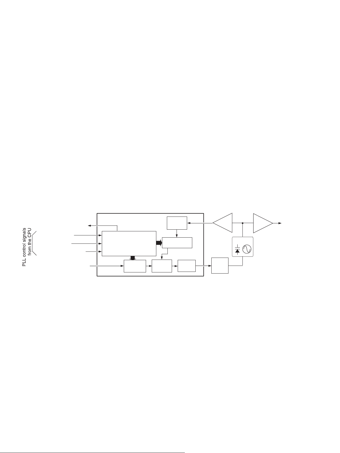
4-2-2 PLL CIRCUITS (MAIN-A/B UNIT)
The PLL circuits provide stable oscillation of the receive LO
frequencies. The PLL circuit compares the phase of the
divided VCO frequency with the reference frequency. The PLL
output frequency is controlled by the divided ratio (N-data)
from the CPU.
• DOWN CONVERTER PLL*
A portion of the VCO output signals are amplified at the
buffer amplifi er (Q14) and then applied to the PLL IC (IC4,
pin 8). The applied signals are divided at the prescaler and
programmable counter according to the N-data “DAT1” from
the expnader (IC3, pin 2) controlled by the CPU (LOGIC
UNIT; IC18). The divided signal is phase compared with the
reference frequency from the reference amplifi er (Q5) at the
phase comparator.
4 - 4
*MAIN-A UNIT only
The phase difference is output from pin 5 as a pulse type
signal after being passed through the internal charge pump.
The output signal is applied to the VCO (Q19, D43) after
being converted into the DC voltage (lock voltage) at the
loop filter (R84, R102, R106, C180, C188, C202, C645,
C646).
• 1st PLL
-1st VCO 1 (Q28, D53)-
A portion of the VCO output signals from the buffer amplifi er
(IC12, pin 4) are applied to the PLL IC (IC10, pin 8) via the
buffer amplifier (Q39). The applied signals are divided at
the prescaler and programmable counter according to the
N-data “DAT1” from the expnader (IC7, pin 2) controlled by
the CPU (IC18). The divided signal is phase compared with
the reference frequency at the phase comparator.
The phase difference is output from pin 5 as a pulse type
signal after being passed through the internal charge pump.
The output signal is applied to the VCO (Q27, Q28, D52,
D53) after being converted into the DC voltage (lock voltage)
at the loop fi lter (Q35, Q36).
-1st VCO 2 (Q30, D54)-
A portion of the VCO output signals from the buffer amplifi er
(IC12, pin 4) are applied to the PLL IC (IC10, pin 8) via the
buffer amplifier (Q39). The applied signals are divided at
the prescaler and programmable counter according to the
N-data “DAT1” from the expnader (IC7, pin 2) controlled by
the CPU (IC18). The divided signal is phase compared with
the reference frequency at the phase comparator.
The phase difference is output from pin 5 as a pulse type
signal after being passed through the internal charge pump.
The output signal is applied to the VCO (Q27, Q28, D52,
D53) after being converted into the DC voltage (lock voltage)
at the loop fi lter (Q35, Q36).
• 2nd PLL
A portion of the VCO (Q47, D62, D63) output signals from
the buffer (Q50) are applied to the PLL IC (IC13, pin 11)
via the buffer (Q41). The applied signals are divided at
the prescaler and programmable counter according to the
N-data “DAT1” from the expnader (IC3, pin 2) controlled by
the CPU (IC18). The divided signal is phase compared with
the reference frequency from the reference amplifi er (Q31)
at the phase comparator.
The phase difference is output from pin 5 as a pulse type
signal after being passed through the internal charge pump.
The output signal is applied to the VCO (Q47, D62, D63)
after being converted into the DC voltage (lock voltage) at
the loop fi lter (R235, R238, C354, C355, C362).
If the oscillated signal drifts, its phase changes from that of
the reference frequency, causing a lock voltage change to
compensate for the drift in the oscillated frequency.
<THE CONCEPT OF PLL CIRCUITS>
PLL IC
PLL unlock detect signal
PLL strobe signal
PLL crock signal
PLL serial data (N-data)
Reference frequency signal
4-3 DIGITAL MODE OPERATION WITH UT-122
DATA interface
Reference
counter
†
A portion of the 450 kHz 3rd IF signal from IF IC (MAIN-A UNIT;
IC24, pin 13) is applied to the LOGIC UNIT via the IF amplifi er
(MAIN-A UNIT; Q76, Q77). The applied 3rd IF signal is passed
through the IF switch (LOGIC UNIT; IC2028, pins 1, 7) and buffer
amplifier (LOGIC UNIT; Q2023), then applied to the attached
UT-122 via J2017 (pin 11).
The applied 3rd IF signal is passed through the IF filter
(UT-122; FI1) to remove unwanted signals, and applied to
the A/D converter (UT-122; IC8, pin 3) to be converted into
the digital signal via BPF. The converted digital signal is
then applied to the DSP (Digital Signal Proccesor; IC7) and
demodulated. The demodulated signal is then applied to the
liner codec (UT-122; IC9) to be converted in to the analog
audio signals.
Programmable
Phase
detector
Prescaler
counter
Charge
pump
Buffer
Loop
filter
amp.
VCO
Buffer
amp.
to a mixer
The converted audio signals are applied to the same AF
circuits as analog receiving from the AF switch (IC23, pin 7).
†
Optional product (DIGITAL UNIT for R2500; [USA-2])
4 - 5
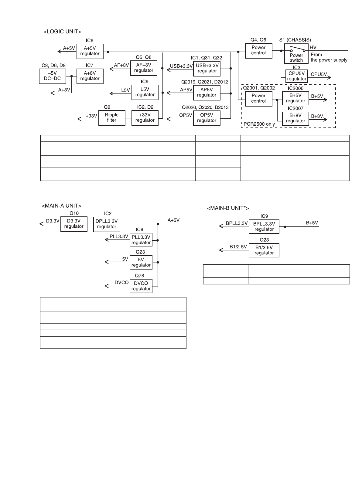
4-4 POWER SUPPLY CIRCUITS
VOLTAGE LINE DESTINATION VOLTAGE LINE DESTINATION
HV Same voltage as the connected power supply. AP5V Optional UT-122.
AF+8V AF power amplifi er (IC12). OP5V Optional UT-108/UT-118.
L5V
+33V Loop fi lter (MAIN-A/B UNITS; Q35, Q36). A+8V
USB3.3V USB HUB (IC20, IC32), USB audio IC (IC16). –5V AGC amplifi er (MAIN UNIT; IC25).
Electric volume (IC17), tone fi lter (IC21), AF switch
(IC4, IC23), etc.
A+5V
MAIN-A UNIT.
VOLTAGE LINE DESTINATION
DPLL3.3V Down converter circuit; PLL IC (IC4).
D3.3V
PLL3.3V 1st and 2nd PLL circuits; PLL IC (IC10, IC13).
5V Divider (IC11), reference oscillator (X1), etc.
DVCO5V
Down converter circuit; mixer (IC6), RF amplifi er (IC15), etc.
Down converter circuit; VCO (Q19, D43), buffer (Q14), etc.
VOLTAGE LINE DESTINATION
BPLL3.3V 1st and 2nd PLL circuits; PLL IC (IC10, IC13).
B1/2 5V Divider (IC11).
*R2500 only
4 - 6
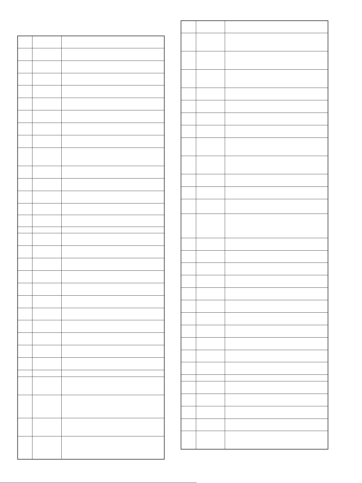
4-5 CPU PORT ALLOCATION
4-5-1 CPU (LOGIC UNIT; IC18)
Pin
No.
16 NOIS
17 BNOIS
18 PWRSW
19 BMST3*
20 CCS
21 BP1STB*
22 BP2STB*
23 BDSTB*
27 PDIN Input port for USB data.
28 PDOUT Outputs USB data.
31 SCL Outputs clock signal to the EEPROM (IC14, pin 5).
33 OPSO
34 OPSI
35 OPSCK
36 AIRQ
37 ASTB
38 ASI
39 ASO
40 ACK
41 DSPS
42 IMST
43 BUSY
44 SDL I/O port for EEPROM (IC14, pin 6).
45 OPAFSEL
46 OPAFINH
47 BOPAFSEL*
48 BOPAFINH*
PORT
NAME
4 BMST2
5 BCK
8 BMST1
9 CSHIFT
DESCRIPTION
Outputs strobe signal to the expander (MAIN-B
UNIT; IC18, pin1).
Outputs clock signal to the expander (MAIN-B
UNIT; IC17, pin 3).
Outputs strobe signal to the expander (MAIN-B
UNIT; IC3, pin1).
Outputs clock frequency shift signal to the
clock shift circuit (D6).
Input port for “NOIS” signal from the IF IC
(MAIN-A UNIT; IC24, pin 13).
Input port for “BNOISE” signal from the IF IC
(MAIN-B UNIT; IC24, pin 13).
Input port for power witch (CHASSIS; S1).
“Low”=While the power switch is turned.
Outputs strobe signal to the expander (MAIN-B
UNIT; IC17, pin 1).
Outputs optional unit select signal to the
attached optional unit via the pin 20 of J2018.
“High”=While the optional unit is attached.
Outputs PLL strobe signla to the 1st PLL IC
(MAIN-B UNIT; IC10, pin 11).
Outputs PLL strobe signla to the 2nd PLL IC
(MAIN-B UNIT; IC13, pin 13).
Outputs strobe signal to the D/A converter
(MAIN-B; IC8, pin 6).
Output serial data to the attached optional unit
via the pin 18 of J2018.
Input port for serial data from the attached
optional unit via the pin17 of J2018.
Outputs clock signal to the Attached optional
unit via the pin 16 of J2018.
Input port for data request signal from the
attached UT-122 via the pin 19 of the J2017.
Outputs strobe signal to the attached UT-122
via the pin 20 of the J2017.
Input port for serial data from the attached
UT-122 via the pin 17 of the J2017.
Outputs serial data to the attached UT-122 via
the pin 18 of the J2017.
Outputs clock signal to the attached UT-122 via
the pin 16 of the J2017.
Outputs DSP select signal to the attached DSP
unit via pin 7 of J15.
Outputs DSP strobe signal to the attached
DSP unit via pin 3 of J15.
Outputs busy signal to the attached optional
unit via pin 7 of J7.
Outputs control signal to the AF switch (IC23,
pin 5).
“High”=While the optional unit is activated.
Outputs control signal to the AF switch (IC23,
pin 2).
“High”=The AF line for the optional unit is dis-
connected.
Outputs control signal to the AF switch
(IC2031, pin 5).
“High”=While the optional unit is activated.
Outputs control signal to the AF switch
(IC2031, pin 2).
“High”=The AF line for the optional unit is dis-
connected.
Pin
No.
PORT
NAME
49 RXMUTE
53 APAFSEL
54 APAFINH
57 VDAT
58 VCK
59 VSTB
61 LSTB
64 PWR
65 DTMSTD
66 DTMSD
67 DTMCK
70 PDSTB
73 VBUS
75 DSTB
76 P2STB
77 P1STB
78 DPSTB
79 MST0
80 MST1
81 MST2
82 BCMAD*
83 BVSCAF*
85 BRTONE*
86 BSMAD*
88 TEMP Input port for internal temperature detection.
89 SCAD
90 CMAD
91 VSCAF
93 RTONE
98 USBPOW
Input port for mute signal from the attached
optional unit via the pin 24 of J2018.
“High”=While the audio output is muted.
Outputs control signal to the AF switch (IC4,
pin 5).
“High”=While the UT-122 is in use.
Outputs control signal to the AF switch (IC4, pin
2).
“High”=While the attached UT-122 is inactivated.
Outputs serial data to the electric volume
(IC17, pin 16).
Outputs clock signal to the electric volume
(IC17, pin 15).
Outputs strobe signal to the electric volume
(IC17, pin 14).
Outputs strobe signal to the expander (IC34,
pin 1).
Outputs control signal to the power controller
(Q4, Q6).
“High”=While the receivers power is ON.
Input port for detecting signal from the DTMF
decoder (IC19, pin 14).
“High”=When the DTMF signal is detected.
Input port for DTMF signal from the DTMF
decoder (IC19, pin 9).
Outputs clock signal from the DTMF decoder
(IC19, pin 11).
Outputs strobe signal to the DDS IC (MAIN-A
UNIT; IC22, pin 41).
Input port for USB connection detecting signal
from the VBUS line.
“High”=While a PC is connected through [USB] con nector on the receiver's main unit.
Outputs strobe signal to the D/A converter
(MAIN-A; IC8, pin 6).
Outputs strobe signal to the 2nd PLL IC
(MAIN-A UNIT; IC13, pin 13).
Outputs strobe signal to the 1st PLL IC
(MAIN-A UNIT; IC12, pin 11).
Outputs strobe signal to the down converter
PLL IC (MAIN-A UNIT; IC4, pin 11).
Outputs strobe signal to the expander (MAIN-A;
IC3, pin 1).
Outputs strobe signal to the expander (MAIN-A;
IC18, pin 1).
Outputs strobe signal to the expander (MAIN-A;
IC3, pin 1).
Input port for RSSI signal from the RSSI signal
selector (MAIN-A; IC30, pin 1).
Input port for VSC signal from the tone filter
(IC2021, pin 7).
Input port for CTCSS signals from the tone
fi lter (MAIN-B UNIT; IC21, pin 1).
Inputport for RSSI signal from the IF IC
(MAIN-A/B UNITS; IC16, pin 13).
Input port for RSSI signal from the IF IC (MAIN-A/
B UNITS; IC20, pin 5) for band scope function.
Input port for RSSI signal from the IF IC
(MAIN-A UNIT; IC30, pin 1) for AFC function.
Input port for VSC signal from the tone filter
(IC21, pin 1).
Input port for CTCSS signals from the tone
fi lter (MAIN-A UNIT; IC21, pin 7).
Outputs voltage line control signal to the 3.3V
regulator (IC1, Q31, Q32, Q33).
“High”=During in the USB audio mode.
DESCRIPTION
*R2500 only
4 - 7
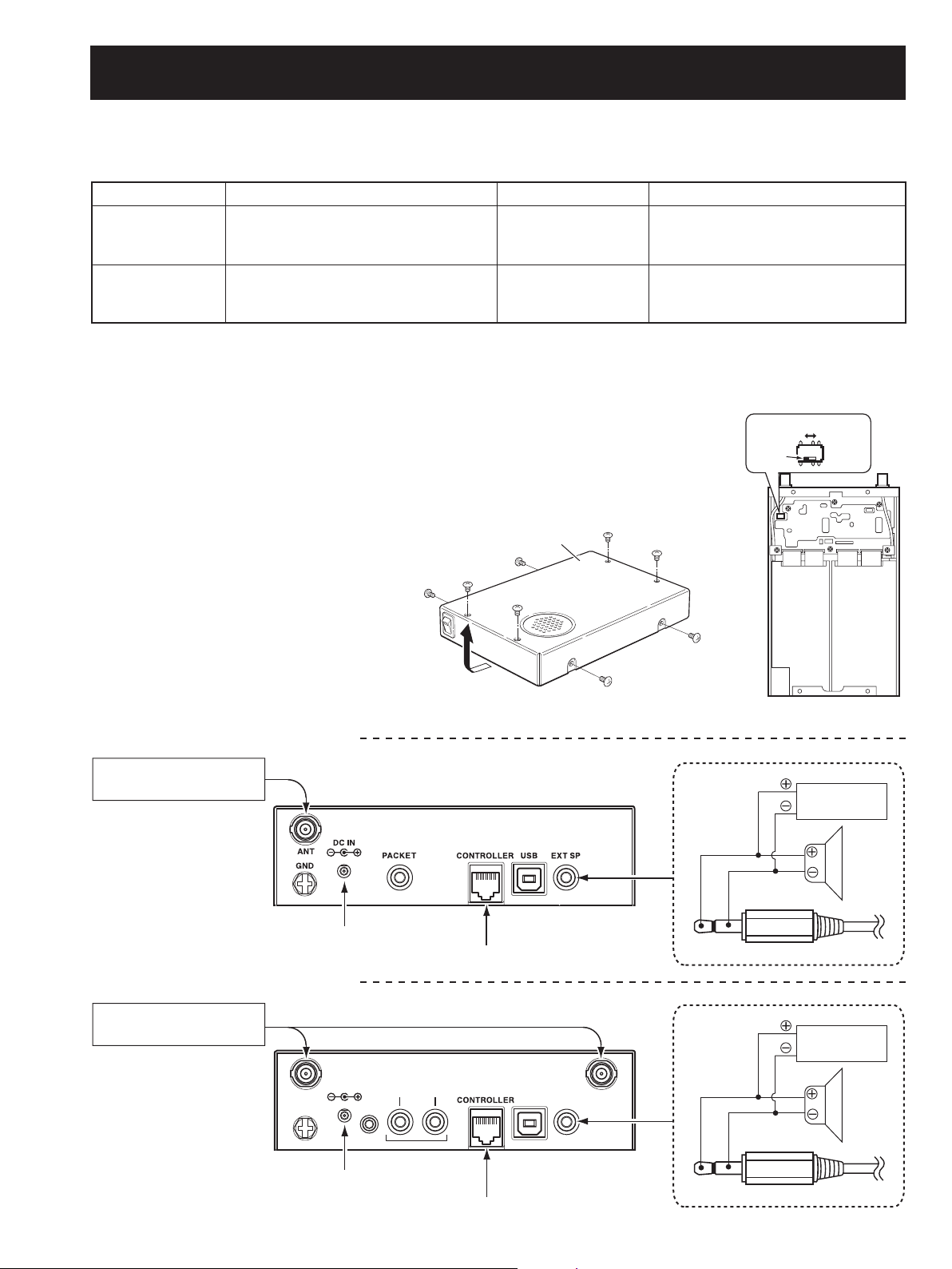
SECTION 5 ADJUSTMENT PROCEDURES
5-1 PREPARATION
When adjusting IC-R1500/R2500, controller for the R1500/R2500 and JIG cable (see the illust below) are required.
¤ REQUIRED TEST EQUIPMENTS
EQUIPMENT GRADE AND RANGE EQUIPMENT GRADE AND RANGE
Standard signal
generator (SSG)
Frequency counter
CAUTION!: BACK UP the originally programmed memory data in the receiver before starting the adjustment.
There is possiblity of losing original memory data when the adjustment is finished.
Before starting adjustment:
• Remove the top cover and sheild cover on the MAIN-A UNIT. (Refer to the “SECTION 3” for details)
• Set the AF switch to “PHONES.” (Refer to the instruction manual for details)
Frequency range : 0.1–3300 MHz
Output level : 0.1 µV to 32 mV
(–127 to –17 dBm)
Frequency range : 0.1–30 MHz
Frequency accuracy : ±1 ppm or better
Sensitivity : 100 mV or better
AC milliwattmeter Measuring range : 10 µW to 100 mW
External speaker
Input impedance : 8
Capacity : More than 5 W
Ω
3
HCT
IWS
4OPCOVER
2%+!%0
0
(
/
.
3%
• CONNECTION
<FOR IC-R1500 ADJUSTMENT>
3TANDARDSIGNALGENERATOR
33'
TOTHESUPPLIED!#ADAPTER
<FOR IC-R2500 ADJUSTMENT>
3TANDARDSIGNALGENERATOR
33'
2EARPANEL
TOTHE)#2#/.42/,,%2
2EARPANEL
.
)#$
4.! 4.!
$.'
!4!$
%+#!0
4%+#!0
4
0348%"35
s*)'CABLE
MILLIVOLTMETER
!&
'.$
CONDUCTORDMM
s*)'CABLE
MILLIVOLTMETER
!#
3PEAKER
7
v7
!#
3PEAKER
7
/PTIONALPRODUCTFOR;5+=
TOTHESUPPLIED!#ADAPTER
TOTHE)#2#/.42/,,%2
5 - 1
!&
'.$
CONDUCTORDMM
v7
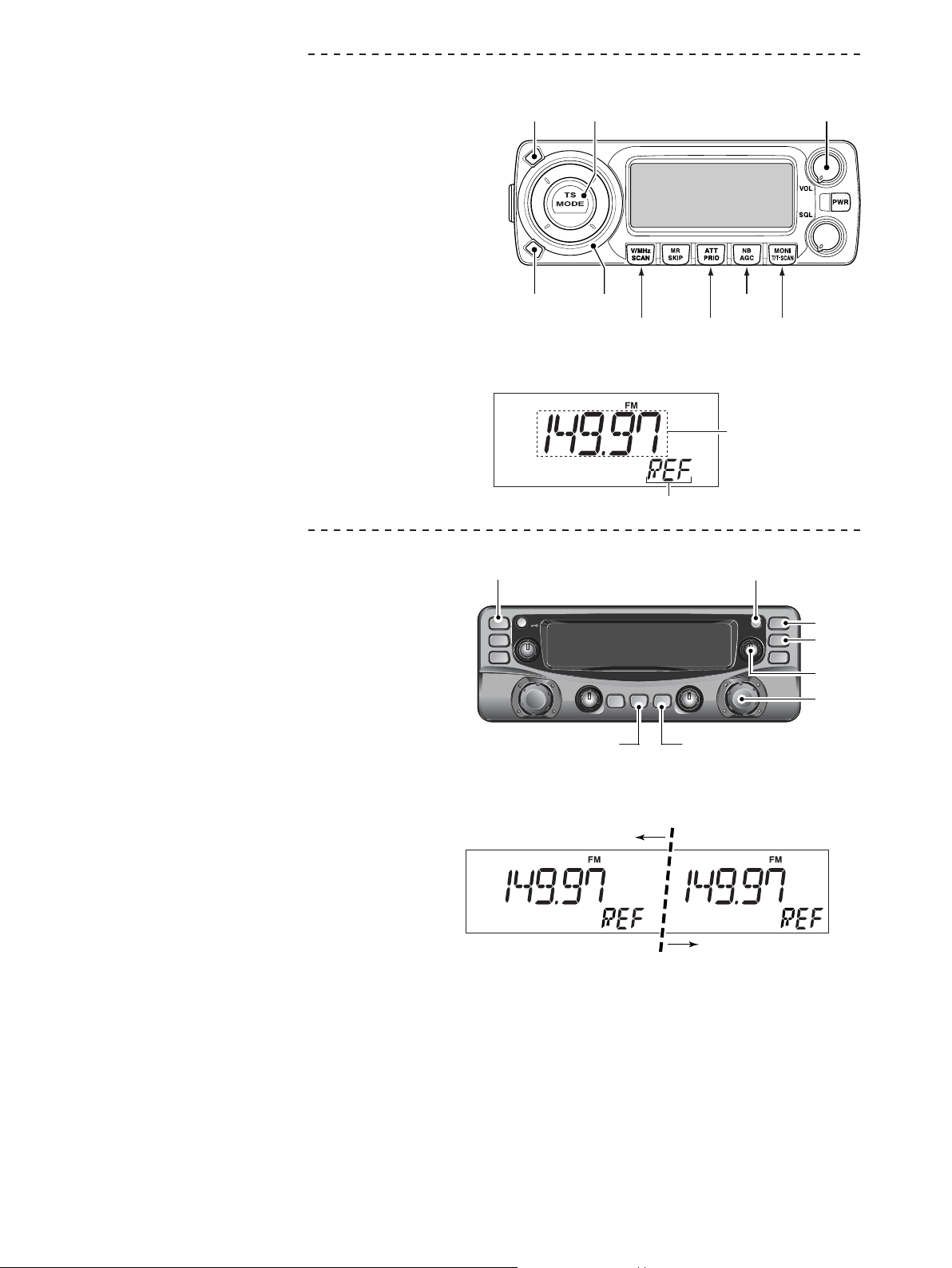
<FOR IC-R1500 ADJUSTMENT>
ENTERING ADJUSTMENT MODE
¤
Set the direction of the [VOL] to 12 o'clock (11–1 o'clock).
q
Push and hold [TS•MODE]+[ATT•PRIO]+[NB•AGC]
w
+[MONI•T/T-SCAN] key, and turn the power switch (MAIN
UNIT) ON.
KEY ASSIGNMENTS FOR THE ADJUSTMENT MODE
¤
• [SET•LOCK] : Selects the next adjustment item.
• [S.MW•MW] :
Selects the previous adjustment item.
• CONTROLLER
[SET•LOCK]
[TS•MODE]
[VOL]
• [DIAL] :
Adjusts the value for the item manually.
• [TS•MODE] : Adjusts the value for the item automatically.
Stores the set value.
• [V/MHz•SCAN] : Verify the adjustment value for the item.
• [VOL] : Adjust the audio output level.
<FOR IC-R2500 ADJUSTMENT>
ENTERING ADJUSTMENT MODE
¤
Set the direction of the [VOL] (Right) to 12 o'clock
q
(11–1 o'clock).
Push and hold [MAIN•NB]+[MAIN•AGC]+[ATT•PRIO]
w
+[MODE•SCAN] key, and turn the power switch (MAIN
UNIT) ON.
KEY ASSIGNMENTS FOR THE ADJUSTMENT MODE
¤
• [MAIN•NB] : Selects the next adjustment item.
• [VFO/MR•S.MW] (Right band)
:
Selects the previous adjustment item.
[S.MW•MW]
[DIAL]
[V/MHz•SCAN]
• DISPLAY EXAMPLE
• CONTROLLER
[MAIN•AGC]
PWR
MAIN
AGC
VFO/MR
S.MW
MHz
TS
[MODE•SCAN]
Adjustment item
ATT
MONI
MODE
SCAN
T/T-SCAN
PRIO
[NB•AGC]
[ATT•PRIO]
SQLSQL
[ATT•PRIO]
[MONI•T/T-SCAN]
Adjustment frequency
[SET•SKIP]
SET
MAIN
[MAIN•NB]
NB
SKIP
VFO/MR
VOLVOL
DIALDIAL
[VFO/MR]
S.MW
MHz
TS
[VOL]
[DIAL]
• [DIAL] (Right band)
:
Adjusts the value for the item manually.
• [SET•SKIP] : Adjusts the value for the item automatically.
Stores the set value.
• [ATT•PRIO] : Verify the adjustment value for the item.
• [VOL] (Right band)
: Adjust the audio output level.
• DISPLAY EXAMPLE
MAIN-A UNIT adjustment
MAIN-B UNIT adjustment
5 - 2
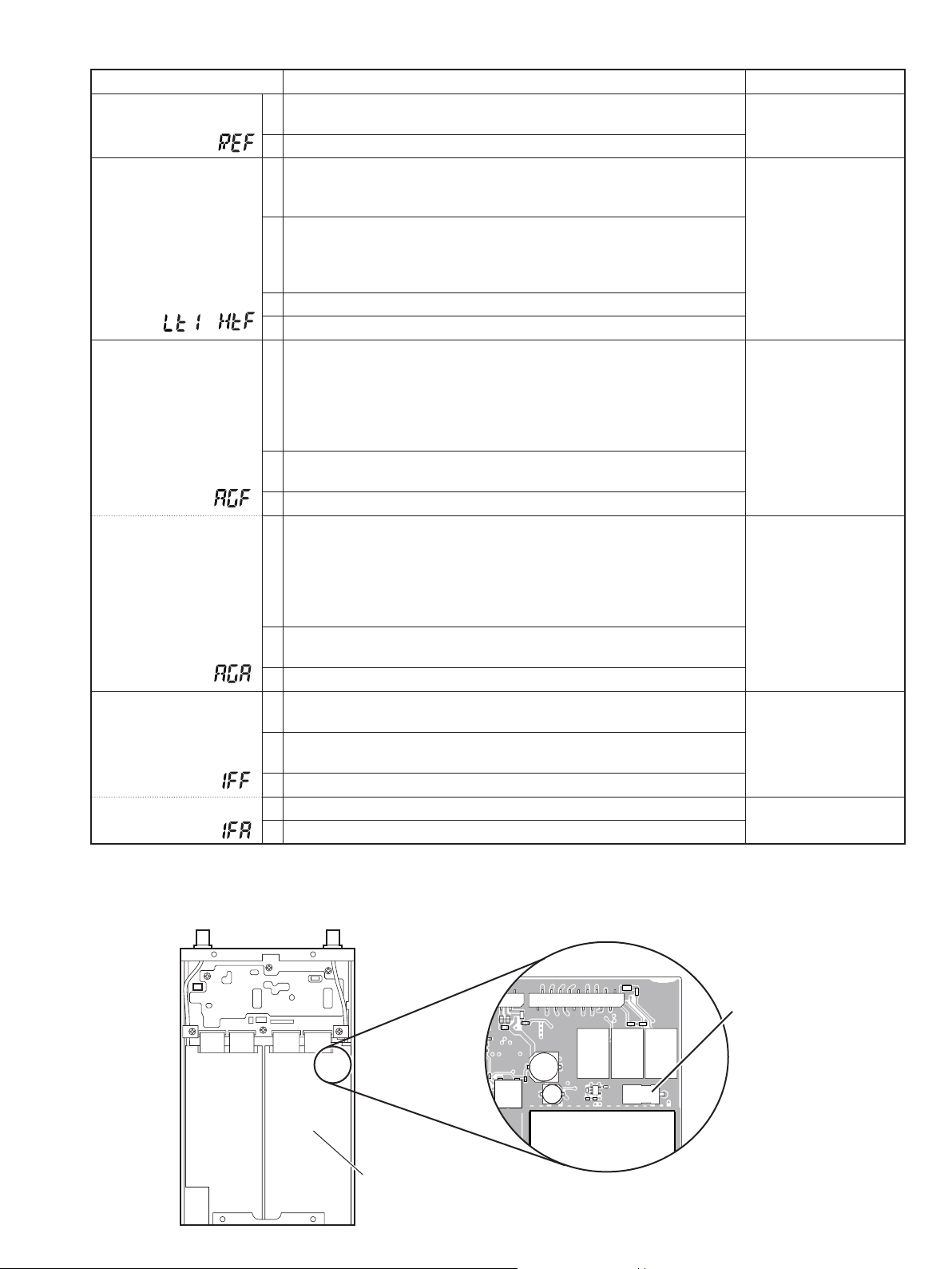
5-2 MAIN-A UNIT ADJUSTMENT
ADJUSTMENT OPERATION VALUE
REFERENCE
FREQUENCY
[REF]
BPF
[LT1]–[HTF]
–
AGC GAIN
(FM)
[AGF]
(AM)
[AGA]
IF GAIN
(FM)
[IFF]
(AM)
[IFA]
†
Refer to the “ADJUSTMENT ITEM LIST“ on page 5-7.
‡
The output level of the standard signal generator (SSG) is indicated as the SSG's open circuit.
*Displayed on the controller's display.
1 • Connect a frequency counter to the J5 connector on the MAIN-A
UNIT (see the illust below).
2 • Push [TS•MODE]/[SET•SKIP] to store the set value.
1 • Preset the adjustment items as below before the “BPF“ adjustment.
[AGA] : “8A”
[IFA] : “25”
2 • Connect an SSG to the antenna connector “ANT1” and set as;
Frequency : Specifi ed frequency*
Modulation : none
Level : Specifi ed level
†
3 • Push [TS•MODE]/[SET•SKIP] to store the adjustment value.
4 • Repeat 2–3 for each specifi ed frequency and level for [LT1] to [HTF].
1 • Connect an SSG to the antenna connector and set as;
Frequency : Specifi ed frequency*
Mode : FM
Modulation : 1 kHz
Deviation : 3.5 kHz
Level : +34 dBµ (–73 dBm)
‡
2 • Connect a speaker and milliwatt meter then set the audio output level
to 50 mW with [VOL].
3 • Push [SET•LOCK]/[MAIN•NB] to select next adjustment item.
4 • Set the SSG as;
Frequency : Specifi ed frequency*
Mode : AM
Modulation : 1 kHz
Deviation : 70%
Level : +34 dBµ (–73 dBm)
‡
5••Set the audio output level to 50 mW with [DIAL].
Verify that the demodulated audio signals are not distorted badly.
6 • Push [TS•MODE]/[SET•SKIP] to store the adjustment value.
1 • Set the SSG as;
Level : OFF
2 • Connect a speaker and milliwatt meter then set the audio output level
to 50 mW with [VOL].
3 • Push [SET•LOCK]/[MAIN•NB] to select next adjustment item.
4 • Set the audio output level to 80 µW with [DIAL]. 80 µW
5 • Push [TS•MODE]/[SET•SKIP] to store the adjustment value.
10.25000 MHz
Automatic adjustment
50 mW
50 mW
50 mW
-!).!5.)4
J5
2EMOVETHESHEILDCOVER
5 - 3
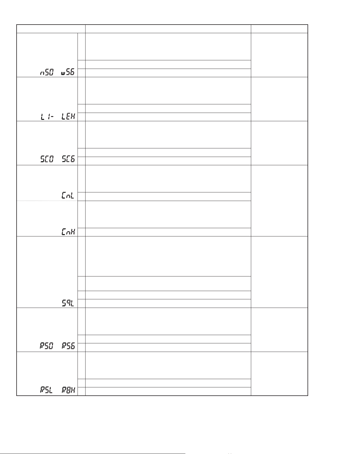
5-2 MAIN-A UNIT ADJUSTMENT (coninued)
ADJUSTMENT OPERATION VALUE
S-METER
[NS0]–[WS6]
–
S-METER FLATNESS
[L1]–[LEH]
–
BAND SCOPE
[SC0]–[SC6]
–
CENTER METER
[CML] (LOW)
[CMH] (HIGH) 1 • Set the SSG as;
SQUELCH
[SQL]
RSSI
[RS0]–[RS6]
–
RSSI FLATNESS
[R5L]–[R8H]
–
†
Refer to the “ADJUSTMENT ITEM LIST“ on page 5-7.
‡
The output level of the standard signal generator (SSG) is indicated as the SSG's open circuit.
*Displayed on the controller's display.
1 • Set the SSG as;
Frequency : Specifi ed frequency*
Modulation : None
Level : Specifi ed level
†
2 • Push [TS•MODE]/[SET•SKIP] to store the adjustment value.
3 • Repeat 1–2 for each specifi ed frequency and value for [NS0] to [WS6].
1 • Set the SSG as;
Frequency : Specifi ed frequency*
Modulation : None
Level : Specifi ed level
†
2 • Push [TS•MODE]/[SET•SKIP] to store the adjustment value.
3 • Repeat 1-2 for each specifi ed frequency and value for [L1] to [LEH].
1 • Set the SSG as;
Frequency : Specifi ed frequency *
Modulation : None
Level : Specifi ed level
†
2 • Push [TS•MODE]/[SET•SKIP] to store the adjustment value.
3 • Repeat 1–2 for each specifi ed frequency and value for [SC0] to [SC6].
1 • Set the SSG as;
Frequency : 3 kHz lower than specifi ed frequency*
Modulation : None
Level : +34 dBµ (–73 dBm)
‡
2 • Push [TS•MODE]/[SET•SKIP] to store the adjustment value.
Frequency : 3 kHz higher than specifi ed frequency*
Modulation : None
Level : +34 dBµ (–73 dBm)
‡
2 • Push [TS•MODE]/[SET•SKIP] to store the adjustment value.
1 • Set the SSG as;
Frequency : Specifi ed frequency*
Mode : FM
Modulation : 1 kHz
Deviation : 3.5 kHz
Level : –13 dBµ (–120 dBm)
‡
2 • Set the [SQL] value to close the squelch with [DIAL]. Then set the
[SQL] value at the point where the audio signals just appear.
3 • Turn the SSG output OFF, and verify that the squelch is closed.
4 • Push [TS•MODE]/[SET•SKIP] to store the adjustment value.
1 • Set the SSG as;
Frequency : Specifi ed frequency*
Modulation : None
Level : Specifi ed level
†
2 • Push [TS•MODE]/[SET•SKIP] to store the adjustment value.
3 • Repeat 1–2 for each specifi ed frequency and value for [RS0] to [RS6].
1 • Set the SSG as;
Frequency : Specifi ed frequency*
Modulation : None
Level : Specifi ed level
†
2 • Push [TS•MODE]/[SET•SKIP] to store the adjustment value.
3 • Repeat 1–2 for each specifi ed frequency and value for [R5L] to [R8H].
Automatic adjustment
Automatic adjustment
Automatic adjustment
Automatic adjustment
Automatic adjustment
Automatic adjustment
Automatic adjustment
5 - 4
 Loading...