

Page 1
GUIDE FOR CD
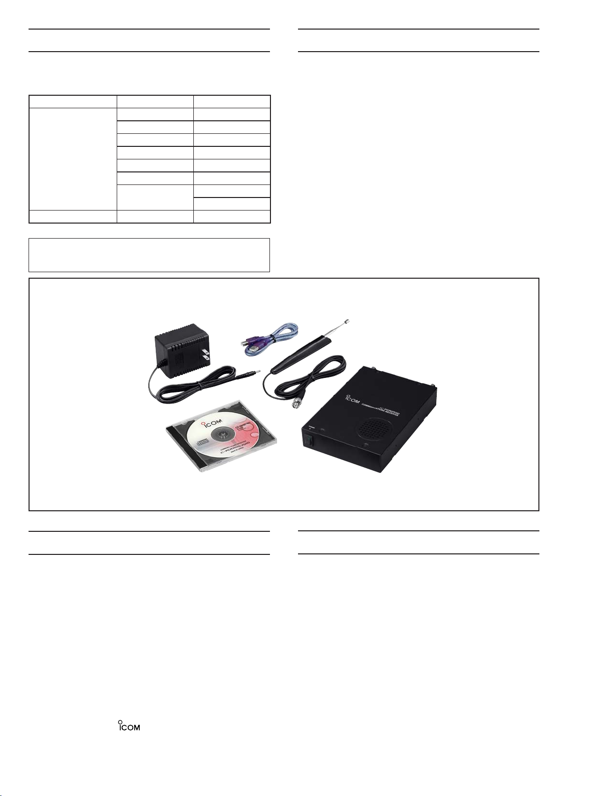
1) COMPOSION
PCR1500_2500 PCR1500_2500.pdf
FYC PCR1500_2500_A3format.pdf
PCR1500_2500_A4format.pdf
PCR1500_2500_MANUAL.pdf
Installer
ar505eng.exe
README.txt
2) DESCRIPTION
PCR1500_2500.pdf
The service manual for IC-PCR1500 and IC-PCR2500 including all service information in this CD. This file is mainly used
for viewing on the computer display and checking page order to make printed service manual. Or when you want to find a
component, you can find very fast using “FIND” function (except Board Layouts).
PCR1500_2500_A3format.pdf
Consists of A3 format pages (Board layouts, Mechanical parts and disassembly, and etc.). This file is used for
printing out A3 format pages.
PCR1500_2500_A4format.pdf
Consists of A4 format pages (Board layouts, Mechanical parts and disassembly, and etc.). This file is used for
printing out A4 format pages.
PCR1500_2500_MANUAL.pdf
The instruction manual for IC-PCR1500 and IC-PCR2500. The contents of this file is exactly same as supplied
instruction manual with product and consists of all A4 format pages. If you have A4 format printer, you can print
and make brand new instruction manual any time you want. This file is also very helpful when you want to change
or set product setting condition for adjustment or else.
1
Page 2

ar505eng.exe
ar505eng.exe is an installation program of Adobe Acrobat® Reader 5.0 (English version) for Microsoft® Windows®
95/98/Me/NT/2000/XP users.
README.txt
README.txt is a readme text about this service manual for Windows® user that not installed Adobe Acrobat® Reader
yet.
=========================================================================================
Icom, Icom Inc. and Icom logo are registered trademarks of Icom Incorporated (Japan) in the United states, the
United Kingdom, Germany, France, Spain, Russia and/or other countries.
Adobe Acrobat Reader Copyright © 1987-2002 Adobe Systems Incorporated. All rights reserved.
Adobe, the Adobe logo, Acrobat, and the Acrobat logo are trademarks of Adobe Systems Incorporated.
Microsoft and Windows are registered trademarks of Microsoft Corporation in the U.S.A. and other countries.
Copyright 2006 Icom Inc.
=========================================================================================
2
Page 3

3%26)#%
-!.5!,
iC-pcr1500
iC-pcr2500
S-14222MZ-C1
Jun. 2006
COMMUNICATIONS RECEIVERS
Page 4
This service manual describes the latest service information
for the IC-PCR1500 and IC-PCR2500 COMMUNICATIONS
RECEIVERS at the time of publication.
Be sure to include the following four points when ordering
replacement parts:
1. 10-digit Icom parts numbers
2. Component name and informations
3. Equipment model name and unit name
4. Quantity required
<SAMPLE ORDER>
1110001811 S.IC TA7S04F IC-PCR2500 Main-A unit 5 pieces
8810008960 Screw FH M2.6 IC-PCR2500 Chassis 8 pieces
Addresses are provided on the inside back cover for your
convenience.
NEVER connect the receiver to an AC outlet or to a DC
power supply that uses more than 16 V. Such a connection
could cause a fire hazard and/or electric shock.
DO NOT expose the receiver to rain, snow or any liquids.
DO NOT reverse the polarities of the power supply when
connecting the receiver.
DO NOT apply an RF signal of more than 20 dBm (100 mW)
to the antenna connector. This could damage the receiver’s
front end.
1. Make sure a problem is internal before disassembling
the receiver.
2. DO NOT open the transceiver until the receiver is
disconnected from its power source.
3. DO NOT force any of the variable components. Turn
them slowly and smoothly.
4. DO NOT short any circuits or electronic parts. An
insulated turning tool MUST be used for all adjustments.
5. DO NOT keep power ON for a long time when the
receiver is defective.
6. READ the instructions of test equipment thoroughly
before connecting equipment to the receiver.
To upgrade quality, any electrical or mechanical parts
and internal circuits are subject to change without
notice or obligation.
Icom, Icom Inc. and logo are registered trademarks of Icom Incorporated (Japan) in the United States, the United
Kingdom, Germany, France, Spain, Russia and/or other countries.
INTRODUCTION CAUTION
ORDERING PARTS
REPAIR NOTES
MODEL VERSION SYMBOL
IC-PCR1500
IC-PCR2500
Europe EUR-1
U.K. UK-1
U.S.A. USA-1
Canada CAN-1
France FRA-1
South East Asia SEA-1
Export
EXP-2
EXP-3
IC-PCR2500* U.S.A. USA-3
*UT-122 is already installed as DIGITAL UNIT.
(IC-PCR2500)
Page 5

TABLE OF CONTENTS
SECTION 1 SPECIFICATIONS
SECTION 2 INSIDE VIEWS
SECTION 3 DISASSEMBLY INSTRUCTIONS
SECTION 4 CIRCUIT DESCRIPITON
4-1 RECEIVER CIRCUITS. . . . . . . . . . . . . . . . . . . . . . . . . . . . . . . . . . . . . . . . . . . . . . . . . . . . . . . . 4-1
4-2 PLL CIRCUITS . . . . . . . . . . . . . . . . . . . . . . . . . . . . . . . . . . . . . . . . . . . . . . . . . . . . . . . . . . . . . 4-4
4-3 DIGITAL MODE OPERATION WITH UT-122 . . . . . . . . . . . . . . . . . . . . . . . . . . . . . . . . . . . . . . . 4-5
4-4 POWER SUPPLY CIRCUITS. . . . . . . . . . . . . . . . . . . . . . . . . . . . . . . . . . . . . . . . . . . . . . . . . . . 4-6
4-5 CPU PORT ALLOCATION. . . . . . . . . . . . . . . . . . . . . . . . . . . . . . . . . . . . . . . . . . . . . . . . . . . . . 4-7
SECTION 5 ADJUSTMENT PROCEDURES
5-1 PREPARATION . . . . . . . . . . . . . . . . . . . . . . . . . . . . . . . . . . . . . . . . . . . . . . . . . . . . . . . . . . . . . 5-1
5-2 MAIN-A UNIT ADJUSTMENT . . . . . . . . . . . . . . . . . . . . . . . . . . . . . . . . . . . . . . . . . . . . . . . . . . 5-3
5-3 MAIN-B UNIT ADJUSTMENT (PCR2500 only). . . . . . . . . . . . . . . . . . . . . . . . . . . . . . . . . . . . . 5-5
SECTION 6 PARTS LIST
SECTION 7 MECHANICAL PARTS AND DISASSEMBLY
SECTION 8 SEMICONDUCTOR INFORMATION
SECTION 9 BOARD LAYOUTS
9-1 LOGIC UNIT . . . . . . . . . . . . . . . . . . . . . . . . . . . . . . . . . . . . . . . . . . . . . . . . . . . . . . . . . . . . . . . 9-1
9-2 MAIN-A UNIT . . . . . . . . . . . . . . . . . . . . . . . . . . . . . . . . . . . . . . . . . . . . . . . . . . . . . . . . . . . . . . . 9-3
9-3 MAIN-B UNIT (PCR2500 only) . . . . . . . . . . . . . . . . . . . . . . . . . . . . . . . . . . . . . . . . . . . . . . . . . 9-5
9-4 UT-122 (Optional product; DIGITAL UNIT for [PCR2500; USA-3]) . . . . . . . . . . . . . . . . . . . . . . 9-7
SECTION 10 BLOCK DIAGRAM
SECTION 11 VOLTAGE DIAGRAM
Page 6

SECTION 1 SPECIFICATIONS
2
2
2
¤
¤
¤
)
p
y
)
(
¤
¤
¤
.
¤
¤
¤
M GENERAL
• Frequency coverage
A.S.U
1
3
ecnarF
1
4
1
0 :
10.
evoba naht r
*1:
S
*2: yl
FM, AM, WFM, USB*1, LSB*1, CW, DV*1,*2, P25*1,*
1
*
: For PCR2500. Available on Main band only.
2
*
: For PCR2500. Available when optional UT-118 is installed.
3
*
: For PCR2500. Available when optional UT-122 is installed, and depending on versions.
2600
8.33 kHz, 9 kHz, 10 kHz, 12.5 kHz, 15 kHz, 20 kHz, 25 kHz, 30 kHz, 50 kHz,
100 kHz, 125 kHz, 150 kHz, 200 kHz, 500 kHz, 1 MHz, 10 MHz, USER TS
nat
S :
M
CP
:FFO r
P
*
M
CP
146(W)×41(H)×206(D) mm; 5
1.35 kg; 2 lb 15 oz (PCR2500)
ehtO
• Mode :
• Number of memory channels :
• Tuning steps : 1 Hz, 10 Hz, 20 Hz, 50 Hz, 100 Hz, 500 Hz, 1 kHz, 2.5 kHz, 5 kHz, 6.25 kHz,
• Operating temperature range : 0°C to +60°C; +32°F to +140°F
• Frequency stability : ±3 ppm (–10°C to +60°C)
• Power supply requirement : 12 V DC ±15% (Negative ground)
NO
[PCR1500]
[PCR2500]
• Current drain (At 12 V DC ; approx.)
rewoP
e
woP
uD
awla
rewoP
repo hct
FO
• Dimensions (projections not included) :
• Weight (approx.) : 1.2 kg; 2 lb 10 oz (PCR1500)
• Antenna connector : BNC (50 Ω)
1
2
0
010.0 :
,
* 999999.908–00
*
999999.668–000.158
000000.0031–000.698
999999.0181–100000.003
1
2581
–000.
7981
–
.
000
181
.9923
02.15–002.05
* 999999.7681–000.
1
* 999998.5032
1
* 999999.1182–000.7532
1
* 999999.8682–000.3582
,
1
* 999997.9013–000.8982
*
,
1
* 999997.4513–000.6313
*
,
1
* 999999
*
1
2
,
* 999999.92–000010.0 :
*
0000
999999.701–005.78
0.641
–000.44
–
000.042
b
u
dnab
ybd
0000
00000.044–000.03
031
00
000.0
1
,
2
* 999999.9923–0
*
o
dnab niaM no elbaliavA .0052RCP-CI roF
lno
y
.yln
o egnar zHM000.0003–594.0 :deetnarauG
n
3
.zHM
000000.0031 ot 05 ;egnar ycneuqerf revocs
)lacipyt(Am 056
A 2.1 naht sseLoidua .xa
)N
SU(
SABV B
55
O-
cipyt(Am 0
)la
)lacipyt(Am 51 )FFO-SABV BSU( C
dnatS :noitarepo dnab elgnis
6 yb
)lacipyt(Am 05
A 2.1 naht sseLoidua .xaM
ybdnatS :noita
058
U
F
FO SABV BS
*: PCR2500 only.
)lacipyt(Am
A 5.1 naht sseLoidua .xa
)lacipyt(Am 055)NO SABV BSU( CP :F
laci
t(Am 51
3
⁄4(W)×15⁄8(H)×8
1
⁄8(D) in
1 - 1
Page 7

y
¤
¤
y
M RECEIVER
• Receive system : Triple-conversion superheterodyne and down converter
• Intermediate frequencies : 1st: 266.700 MHz, 2nd: 10.700 MHz, 3rd: 450 kHz (except for WFM mode)
• Sensitivity :
•
F
M
(
2
3
5
2
8
9.94–000.0
0.0
0.0
92–0
0
;.veD zHk5.3/zHk1
99
HM999.932–00
HM
9.972–000.042
99
HM
9.9
99
HM999.996–000.003
0
031–000.007
0.
9.9922–100000.0031
0
2
FW
•
00
0
–
0.
3
M
k1(
5.25/zH
5
00.007
31
922–100000.00
000.0032
MA )
•
1
9
9
–
4.0
7.
5
9.41–008.1
;.DOM %03/zHk1(
HM9
z
99
HM
1
999.992–000.0
5
0
00.003
–
HM
00.007
•
1
Bd
WC/BSS
01(
1–008.
4
6–000.05
)N
/S
HM9
97.1–594.0
z
99
HM
9.
zHM99
9.94–000.51
9.99
31–000.007
M000.00
z
z
z
zHM00
HM000.0003
veD zHk
HM000.0031–0
HM999.9
HM000.0003–
01
HM000.0031–0
)DA
NIS Bd21
0 naht
sseL:zHM999.92–000.8
ht
sseL:zHM
na
ht sseL:z
:
s
eL
s
eL:
Vµ36.
0 na
Vµ36.
Vµ5.0
V
5.
µ
0 naht
V
µ5.0 naht ss
Vµ5.0 naht sseL:
h
t sseL
:
:zHM99
a
sse
ht
L
eL:z
a
t ss
h
µ36.0 n
V
µ6.5 na
V
Vµ81 n
)DANIS Bd21 ;.
Vµ4.1 naht sseL:zHM999.996–000.0
:z
sseL
:z
:z
/S Bd
N
Vµ8.1 naht sseL
Vµ81 naht
Vµ65 naht sseL
Vµ52 naht sseL:z
:
Vµ5.2 naht sseL
Vµ5.2 naht sseL:zHM999.94–000.5
seL:z
s
Vµ2 naht
Vµ2 naht sseL:zHM999.996
V
µ5.2 naht sseL:z
Vµ5 naht sseL:z
:
Vµ5.0 naht sseL
Vµ5.0 naht sseL:
sseL:zHM99
.0
Vµ4
naht
Vµ5.0
naht sseL:zH
• Selectivity :
)lacipyt( Bd 6–/zHk 8.2 naht eroMMA/WC/BSS
C/BSS
A
M
MF/MA
FW/
W
F
ht
eroM
t eroMM
zHk 0.6 naht eroMMF/MA/W
–/zHk 51 naht eroMMF/M
na
Hk0
32 nah
)lacipyt( Bd 6–/
)lacipyt( Bd 6
)
ipyt( Bd 6–/zHk 05
lac
)lacipyt( Bd6–/z
• Audio output power : More than 0.5 W (at 10% distortion with an 8 Ω load)
1
• Ext. speaker connector : 2-conductor 3.5 (d) mm (
• Packet connector : 2-conductor 3.5 (d) mm (
• Data connector : 3-conductor 2.5 (d) mm (
⁄8″)/8 Ω
1
⁄8″)
1
⁄10″)
• IF shift variable range : More than ±1.2 kHz
All stated specifications are subject to change without notice or obligation.
1 - 2
Page 8
2 - 1
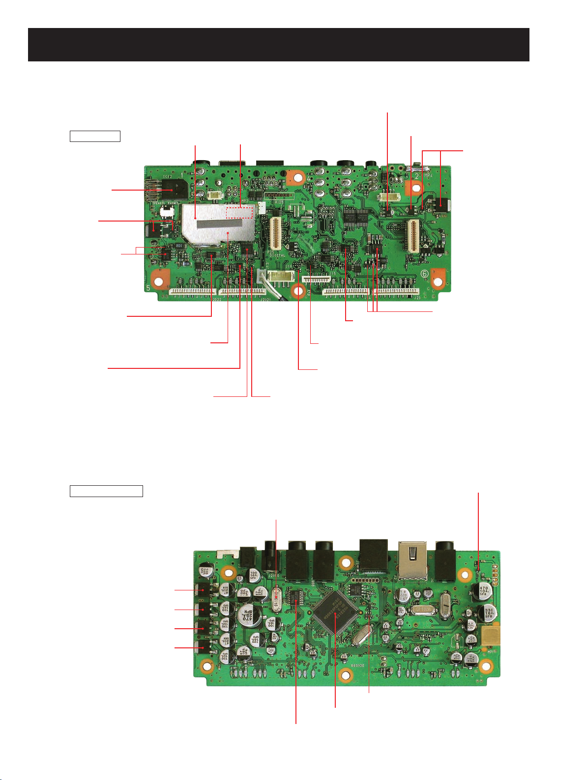
SECTION 2 INSIDE VIEWS
LOGIC UNIT
TOP VIEW
BOTTOM VIEW
+33V regulator
IC2: BA6161F
D2: 1SS355
VSC/TONE filter
(IC2021: LM2904)
IC-PCR2500 only
AF +8V regulator
(Q5: 2SB1201, Q8: XP1501)
AF amplifier
(IC12: LA4425A)
USB HUB
(IC32: USB2502)
USB +3.3V regulator
IC1: S-812C33
Q31: 2SB789
Q32: 2SC4116
VCC line controller
Q4: 2SJ377
Q6: DTC144EU
−5V regulator
IC8: µPC1553
D6: 1SS272
D8: MA8051
VSC/TONE filter
(IC21: LM0904)
AF selecter
(IC23: SN74AHC2053)
AF selecter
(IC2023: SN74AHC2053)
IC-PCR2500 only
USB audio IC
(IC16: PCM2901M)
Electric VR
(IC17: SM6451B)
AF amplifier
(Q18: 2SC4617)
AF amplifier
(Q2018: 2SC4617)
IC-PCR2500 only
CPU5V regulator
(IC3: XC6202P502PR)
L5V regulator
(IC9: AN78L05)
CPU reset IC (IC35: S-80942)
SP mute switch (Q12: 2SC4213)
CPU (IC18: M30624FGPGP)
DTMF decoder (IC19: BU8872FS)
A+5V regulator (IC6: TA7805)
A+8V regulator (IC7: AN7708)
B+5V regulator (IC2006: TA7805F)
IC-PCR2500 only
B+8V regulator (IC2007: TA7708SP)
IC-PCR2500 only
Clock oscillator (X2: CR-818 4.19304 MHz)
(
)
( )
(
)
(
)
Page 9
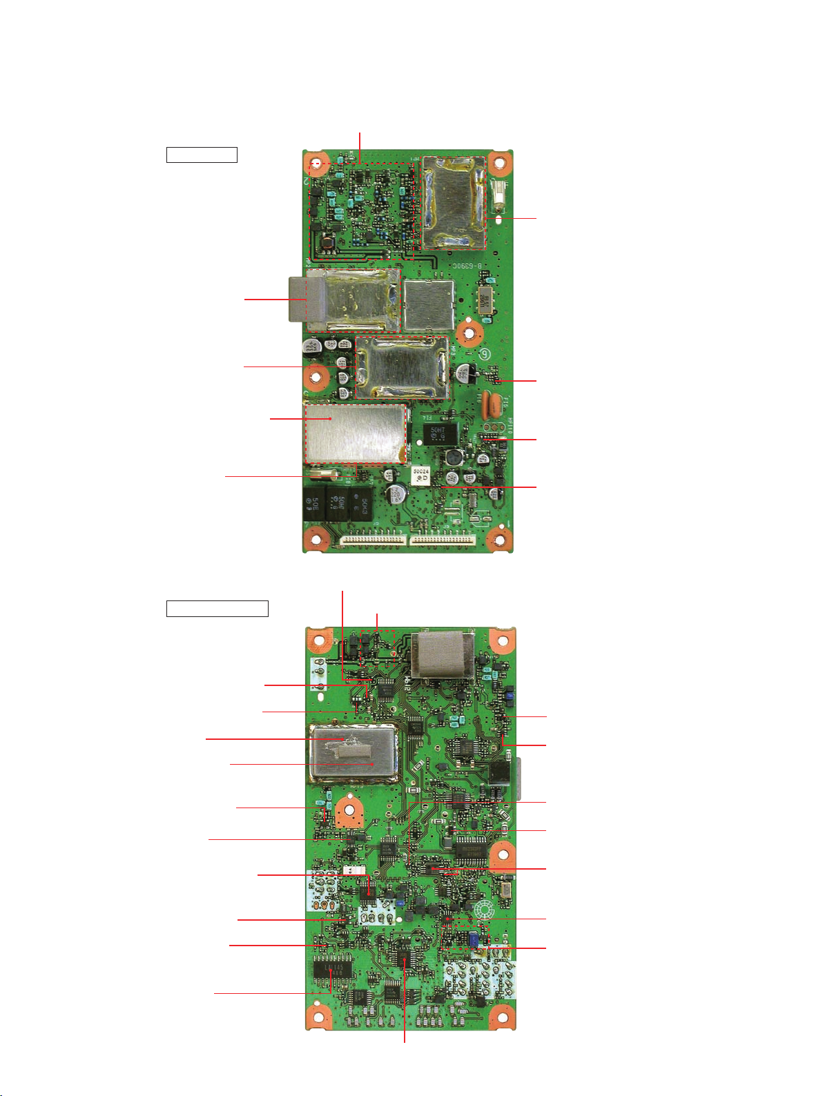
Down converter circuits
1st VCO circuits
2nd VCO circuits
DDS circuits
RF circuits
• MAIN-A UNIT
Noise blanker amplifier
(Q68: 2SK882)
APCO5V regulator
(Q77: 2SA1832)
Buffer
(Q60: 2SC4617)
AM detecter circuits
WFM IF IC
(IC16: LA1145M)
NFM, FM, IF IC (IC24: TA31136)
RSSI meter amplifier
(IC25: NJM2904V, D80: 1SS400)
AGC amplifier
(Q58: 2SC4617)
2nd IF amplifier
(Q66: 3SK131)
2nd mixer
(IC19: TA4107F)
1st IF amplifier
(Q44: 3SK131)
1st mixer
(IC14: SPM5001)
+5V regulator
(Q23: UNR9111)
DVCO +5V regulator
(Q78: UNR9111)
DPLL 3.3V regulator
(IC2: S-812C33AMC)
D3.3V regulator (Q10: UNR9111)
IF IC (Band scope)
(IC20: TA31136)
ATT circuits
TOP VIEW
BOTTOM VIEW
SSB decoder
(IC23: TA4101F)
DDSREF 8V regulator
(D120: DAN222)
DDS REF 8V regulator
(Q90: XP4311)
HF 8V regulator
(Q25: XP4311)
HF band RF amplifier
(Q22: 2SC5226)
PLL 3.3V regulator
(IC9: S-812C33AMC)
2 - 2
Page 10
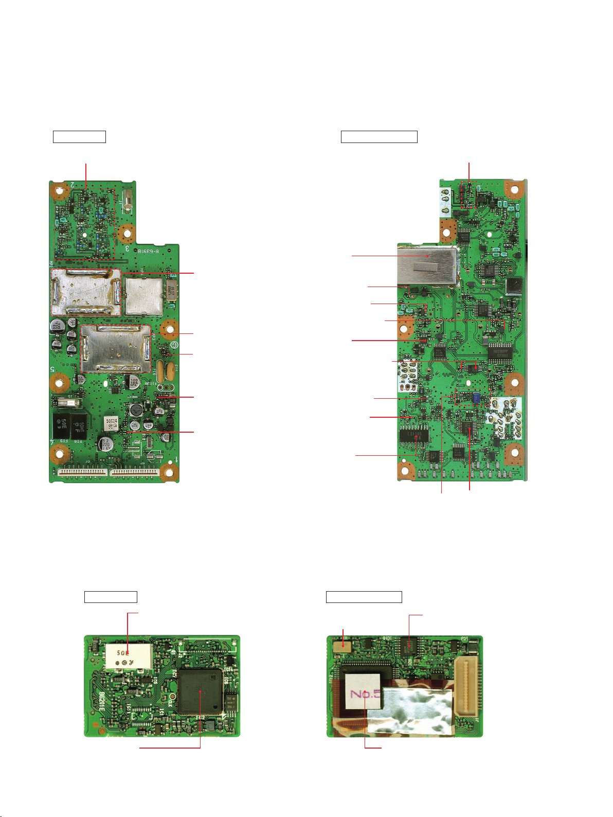
• MAIN-B UNIT (IC-PCR2500 only)
• UT-122 (Optinal product; DIGTAL UNIT for [IC-PCR2500: USA-3])
Noise blanker
(Q68: 2SK882)
BAPCO5V regulator
(Q77: 2SA1832)
3rd IF filter
(FI1: CFWKA450)
Buffer
(Q60: 2SC4617)
AM detecter circuits
WFM IF IC
(IC16: LA1145M)
NFM, FM, IF IC
(IC24: TA31136)
AGC amplifier
(Q58: 2SC4617)
2nd IF amplifier
(Q66: 3SK131)
2nd mixer
(IC19: TA4107F)
1st IF amplifier
(Q44: 3SK131)
1st mixer
(IC14: SPM5001)
+5V regulator
(Q23: UNR9111)
ATT circuits
HF filter circuits
1st VCO circuits
2st VCO circuits
TOP VIEW
BOTTOM VIEW
TOP VIEW
BOTTOM VIEW
RSSI meter amplifier
(IC25: NJM2904V
D80: 1SS400)
PLL 3.3V regulator
(IC9: S-812C33AMC)
Clock oscillator
(X1: CR-798)
Liner codec
(IC9: AK4550VT)
EEPROM
(IC17: HN58X2416TI)
CPU
(IC12: HD64F2239TE16)
2 - 3
Page 11
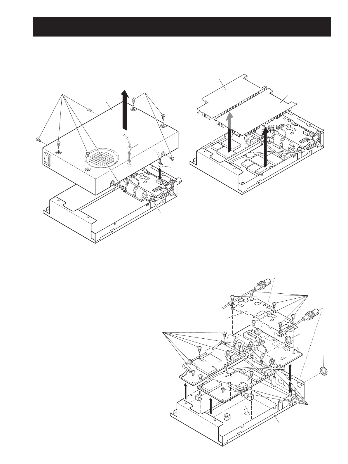
3 - 1
SECTION 3 DISASSEMBLY INSTRUCTIONS
• Removing the top cover and shield covers
q Unscrew 8 screws, A.
w Unplug the connectors B and C from the LOGIC unit.
e Remove the top cover in the direction of the arrow.
r Remove the shield covers D and E* in the direction of
the arrow.
• Removing the LOGIC unit, MAIN-A unit and MAIN-B* unit
q Unscrew nut F*, G.
w Unscrew 6 screws H from the LOGIC unit and remove the LOGIC plate.
e Unscrew 6 screws I from the MAIN-A unit and 6 screws J* from the MAIN-B unit*.
r Remove the units in the direction of the arrows.
Top cover
A
B
C
D
E
LOGIC Unit
A
*
Chassis
* IC-PCR2500 only
* IC-PCR2500 only
J
LOGIC Plate
*
MAIN-B UNIT*
MAIN-A UNIT
LOGIC UNIT
F
H
*
G
I
Page 12
SECTION 4 CIRCUIT DESCRIPTION
4-1 RECEIVE CIRCUITS
4-1-1RF CIRCUITS (MAIN-A/-B UNITS)
The MAIN-A UNIT has eight RF circuits and one down converter
circuit to provide wide receiving range. The received signals from
the antenna connector (CHASSIS; J1) are applied to RF circuits
or down converter circuit according to the received frequency,
and amplified within the frequency coverage.
IC-PCR2500 contains MAIN-B UNIT which has 4 RF circuits to
provide dulalwatch or diversity capability .
The 0.01–50 MHz signals from the antenna are passed
through the attenuator (D1, D3), band switch (D9) and lowpass fi lter (LPF; L20, L26, C54, C60, C68, C72, C81, C88),
then applied to one of the RF circuit.
• 0.01–1.8 MHz*
The 0.01–1.8 MHz signals are passed through the band
switch (D29), LPF (L48, L52, C134, C148, C171, C173) and
another band switch (D56), then applied to the 1st mixer
(IC14, pins 4, 5).
<0.01–18 MHz>
D56
• 1.8–15.0 MHz*
The 1.8–15.0 MHz signals are passed through the band
switch (D25), LPF (L43, L47, L50, C102, C120, C125, C131,
C135, C140), high-pass filter (HPF; L57, L60, L72, C150,
C161, C163, C174, C178, C618, C619) and another band
switch (D49), and then applied to the RF amplifier (Q22).
The amplified signals are then applied to the 1st mixer
(IC14, pins 4, 5) via the band switch (D102).
<1.8–15 MHz>
To the
1st mixer
(IC14, pins 4, 5)
• 15.0–30 MHz*
The 15.0–30 MHz signals are passed through the band
switch (D82), LPF (L46, L49, C116, C118, C124, C130,
C136), HPF (L55, L58, C139, C149, C151, C162, C164)
and another band switch (D83), and then applied to the RF
amplifi er (Q22). The amplifi ed signals are then applied to the
1st mixer (IC14, pins 4, 5) via the band switch (D102).
<15–30 MHz>
To the
1st mixer
(IC14, pins 4, 5)
• 30–50 MHz*
The 30–50 MHz signals are passed through the band switch
(D30), HPF (L77, L82, C201, C206, C208, C213, C216)
and another band switch (D48), and then applied to the RF
amplifi er (Q22). The amplifi ed signals are then applied to the
1st mixer (IC14, pins 4, 5) via the band switch (D102).
<30–50 MHz>
To the
1st mixer
(IC14, pins 4, 5)
LPF
D102
Q22
Q22
Q22
RF
amp.
RF
amp.
RF
amp.
D29
From the LPF
D49D102
HPF
HPF
HPF
LPF
LPF
D30D48
D25
D82D83D102
From the LPF
From the LPF
From the LPF
The 50–1300 MHz signals from the antenna are passed
through the anttenuator (D1, D3), band switch (D7) and LPF
(L5, C33, C34), then applied to one of the RF circuit.
• 50–150 MHz
The received signals 50–150 MHz are passed through the
band switch (D5) and the tunable bandpass fi lter (BPF; D8,
D16–D18, D28, D31, L9, L21, L25, L31, L33, C39, C41,
C44, C49, C70), and then applied to the RF amplifi er (Q15).
The amplified signals are passed through another tunable
BPF (D35, D36, L53, L62, L69, L73, C142, C154, C199) and
another band switch (D44), and then applied to the 1st mixer
(IC14, pins 4, 5).
<50–150 MHz>
To the
1st mixer
(IC14, pins 4, 5)
D44
D35, D36
BPF
Q15
RF
amp.
D8, D16–D18
D28, D31
BPF
D5
From the HPF
• 150–350 MHz
The received signals 150–350 MHz are passed through the band
switch (D6) and BPF (D32, L10, L12, L34, L37, L39, C40, C42,
C45, C50, C82, C114, C117), and applied to the RF amplifier
(Q17). The amplified signals are passed through another BPF
(D37, L56, L67, L71, C155, C167, C183, C195) and another band
switch (D46), and then applied to the 1st mixer (IC14, pins 4, 5).
<150–350 MHz>
To the
1st mixer
(IC14, pins 4, 5)
D46
D37
BPF
Q17
RF
amp.
D32
BPF
D6
From the HPF
• 350–700 MHz
The received signals 350–700 MHz are passed through the
band switch (D14) and BPF (D26, D27, L24, L32, L40, C65,
C71, C81, C106), then applied to the RF amplifier (Q16). The
amplifi ed signals are passed through another BPF (D38, D39,
L54, L64, L74, L78, C144, C172, C211) and another band switch
(D47), and then applied to the 1st mixer (IC14, pins 4, 5).
<350–700 MHz>
To the
1st mixer
(IC14, pins 4, 5)
D47
D38, D39
BPF
Q16
RF
amp.
D26, D27
BPF
D14
From the HPF
• 700–1300 MHz
The received signals 700–1300 MHz are passed through the
band switch (D13) and BPF (D19, D23, D33, D34, L22, L27,
L36, L36, L41, L44, C66, C77, C119), then applied to the RF
amplifier (Q18). The amplified signals are passed through
another BPF (D40, D41, L51, L59, L68, L72, C168, C176,
C205) and the band switch (D45), and then applied to the
1st mixer (IC14, pins 4, 5).
<700–1300 MHz>
To the
1st mixer
(IC14, pins 4, 5)
D45
D40, D41
BPF
Q18
RF
amp.
D19, D23
BPF
D13
From the HPF
*MAIN-A UNIT only
4 - 1
Page 13
• 1300–3300 MHz*
The 1300–3300 MHz signals from the antenna are applied to
the down converter circuit where those signals are converted
into the lower frequencies.
<DOWN CONVERTER>
D42
To the RF circuits
(350–1300 MHz)
LPF
LO signals from VCO (Q19, D43)
IC5
amp.
RF
HPF
Q11
Buff
amp.
D15
From the
antenna
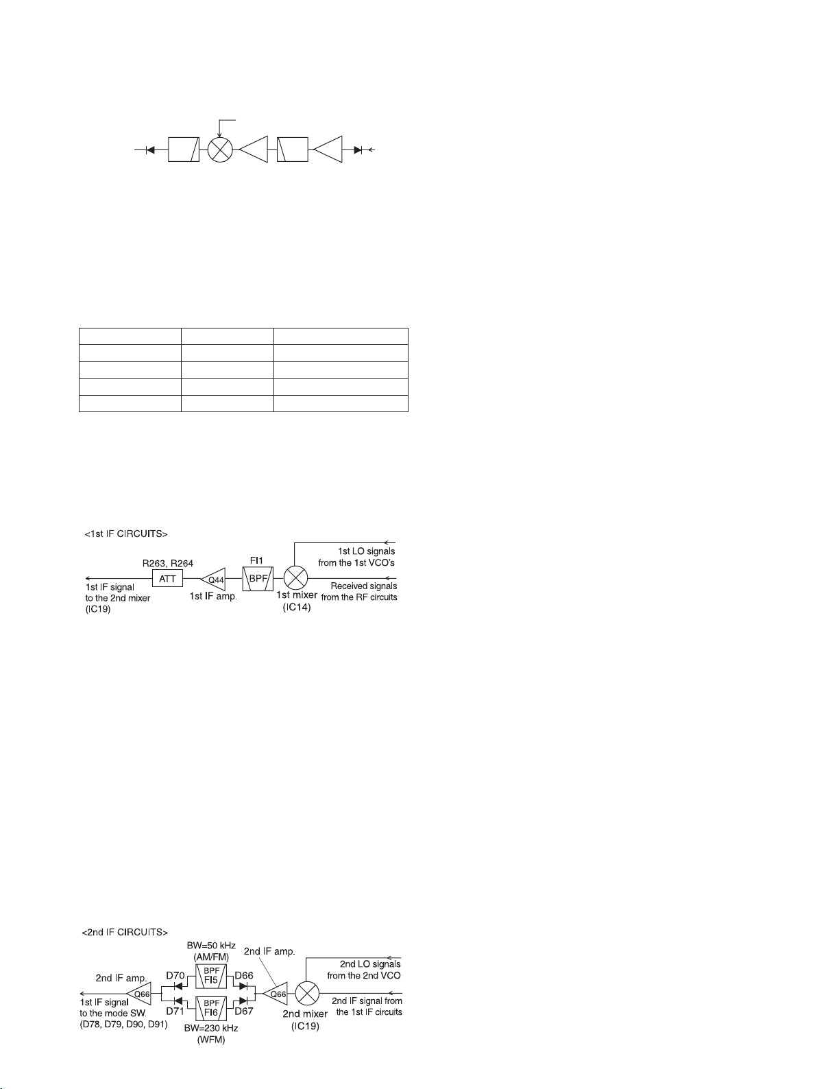
In FM or AM mode, the 2nd IF signal is passed through the
FI5 (band width=50 kHz) via mode switches (D66, D70),
In WFM mode, the 2nd IF signal is passed through the FI6
(band width=230 kHz) via mode switches (D67, D71).
The fi ltered 2nd IF signal is applied to the 2nd IF amplifi er
(Q66). The amplifi ed 2nd IF signals are then applied to the
3rd IF and demodulation circuits.
The received signals are applied to the buffer amplifi er (Q11)
via the band switch (D15). The buffer-amplifi ed signals are
applied to the RF amplifi er (IC5, pin 1) via HPF (L35, L38,
C89, C92, C93, C100, C103). The amplified signals are
output from pin 4, and applied to the mixer (IC6, pin 1) and
down-converted. The down converted signals are output
from pin 6, then applied to the RF circuits via LPF (L66,
C190, C193) and band switch (D42). The LO frequencies
and convered frequencies are shown as below.
RX frequency LO frequency Convered frequency
1300–1700 MHz 1001 MHz 350–700 MHz
1700–2300 MHz 1001 MHz 700–1300 MHz
2300–2700 MHz 2002 MHz 350–700 MHz
2700–3300 MHz 2002 MHz 700–1300 MHz
4-1-2 1st IF CIRCUITS
The 1st IF circuits contain a 1st mixer, 1st IF amplifi er and
1st IF fi lter. The 1st IF mixer converts the received signals
into a fi xed frequency of the 1st Intermediate Frequency (IF)
signal. The converted 1st IF signal is filtered at the 1st IF
fi lters, then amplifi ed at the 1st IF amplifi er.
The converted signals from the RF circuits are applied to the
1st IF mixer (IC14, pins 4, 5) and converted into the 266.7
MHz 1st IF signal by being mixed with the 1st LO (Local
Oscillator) signals from the 1st-VCO’s.
The converted IF signal is passed through the 1st IF filter
(FI1) to fi lter out the unwanted signals, then applied to the 1st
IF amplifi er (Q44). The amplifi ed 1st IF signal is then applied
to the 2nd mixer (IC19, pin 4) via attenuator (R263, R264).
4-1-3 2nd IF CIRCUITS (MAIN UNIT)
The 2nd IF circuits contain the 2st mixer, 2nd IF amplifier
and the 2nd IF fi lters.
4-1-4 NOISE BLANKER CIRCUIT
The noise blanker (NB) circuit reduces pulse type noises
in the received signals. When the received signals contain
pulse type noise components, the NB circuit reduces the
noisy AF signals by cutting off the 2nd IF line.
In AM, SSB or CW mode and the NB function is activated, a
portion of the 2nd IF signal from the band switch (D70, D71)
is amplifi ed at NB amplifi er (Q68) and applied to the IF IC
(IC16, pin 2).
When the 2nd IF signal contains a pulse noise, the RSSI
signal corresponding to the pulse noise level is output from pin
17. The output RSSI signal turns Q49 ON and Q65 turns OFF,
thus the Q66 is inactivated and the 2nd IF signal is cut off.
4-1-5 3rd IF AND DEMODULATOR CIRCUITS
(MAIN-A/B UNIT)
The 2nd IF signal is converted into the 3rd IF signal (except
WFM mode) and demodulated in the IF IC. The IF IC
contains a 3rd mixer, limiter amplifi er, quadrature detector,
etc. in its package.
In FM mode, the 2nd IF signal from the 2nd IF amplifier
(Q66) is applied to the IF IC (IC24, pin 16) via mode switch
(D78) and IF gain control circuit (D97).
The applied 2nd IF signal is converted into the 3rd IF signal
by being mixed with 3rd LO signal from the TCXO (X1), at
the 3rd mixer in the IF IC (IC24).㩷The converted 3rd IF signal
is output from pin 3 and applied to the 3rd IF amplifi er (Q62).
The amplifi ed 3rd IF signal is passed through one of the 3rd
IF fi lter according to the receiving mode.
The filtered 3rd IF signal is applied to the limiter amplifier
(IC24, pin 5), then applied to the demodulator circuit (pin 10,
X2) and FM-demodulated. The FM-demodulated AF signals
are output from pin 9, then applied to the AF circuits.
In AM and CW mode, the 3rd IF signal from the 3rd IF fi lter
is applied to the 3rd IF amplifier (Q61). The amplified 3rd
IF is applied to the AM demodulator circuit (D75) via the
buffer amplifi er (Q63). The AM-demodulated AF signals are
applied to AF circuits via the AF selector (IC27, pins 3, 4).
The 1st IF signal from the 1st IF circuits is converted into
the 10.7 MHz 2nd IF signal by being mixed with the 2nd LO
signals from the 2nd-VCO.
The converted 2nd IF signal is applied to the 2nd IF amplifi er
(Q60). The amplifi ed 2nd IF signal is passed through the 2nd
IF fi lter to fi lter out the unwanted signals.
In SSB mode, the 3rd IF signal from the buffer amplifier
(Q63) are applied to the AF mixer (IC23, pin 6) and
converted into the AF signal by being mixed with the 447.3–
452.7 kHz BFO signal from the DDS circuits. The converted
audio signals are applied to the AF selector (IC27, pin 1)
after being fi ltered at the HPF (IC31, pins 1, 4).
In WFM mode, the 2nd IF signal is applied to the IF IC
(IC16, pin 2) via the 2nd IF amplifi er (Q66) and mode switch
(D90, D91). The 2nd IF signal is amplified at the limiter
amplifier, then applied to the demodulator circuit (pins 11,
12, X2) and FM-demodulated. The FM-demodulated AF
signals are output from pin 8, then applied to the AF circuits
via the AF selector (IC27, pins 8, 9).
*MAIN-A UNIT only
4 - 2
Page 14
<3rd IF AND DEMODULATOR CIRCUITS (FM)>
3rd IF signal to the AM demodulator circuits
2
D/A converter
FM-demodulated signals
to the AF circuits
<2nd IF AND DEMODULATOR CIRCUITS (WFM)>
IC8
1
Quodrature
Detector
9
X2
8
Noise
Amp.
D94D96
BPF
FI9
D69D73
Limit’r
Amp.
735
RSSI
BPF
FI8
BPF
FI7
BPF
Detector
Noise
D93D95
D68D72
Q62
3rd IF amp.
10.25 MHz
3rd LO signal
2
Q71
REF
amp.
Q80
REF
amp.
TCXO
X2
IF IC (IC24)
1110
+5V
Q73
1312
“NOISE” signal to the CPU (IC18, pin 16)
“RSSI” signal to theAGC amplifier (Q67)
16
2nd IF signal from the 2nd IF circuits
Limit’r
Amp.
Quodrature
Detector
9
FM-demodulated signals
to the AF circuits
1112
X3
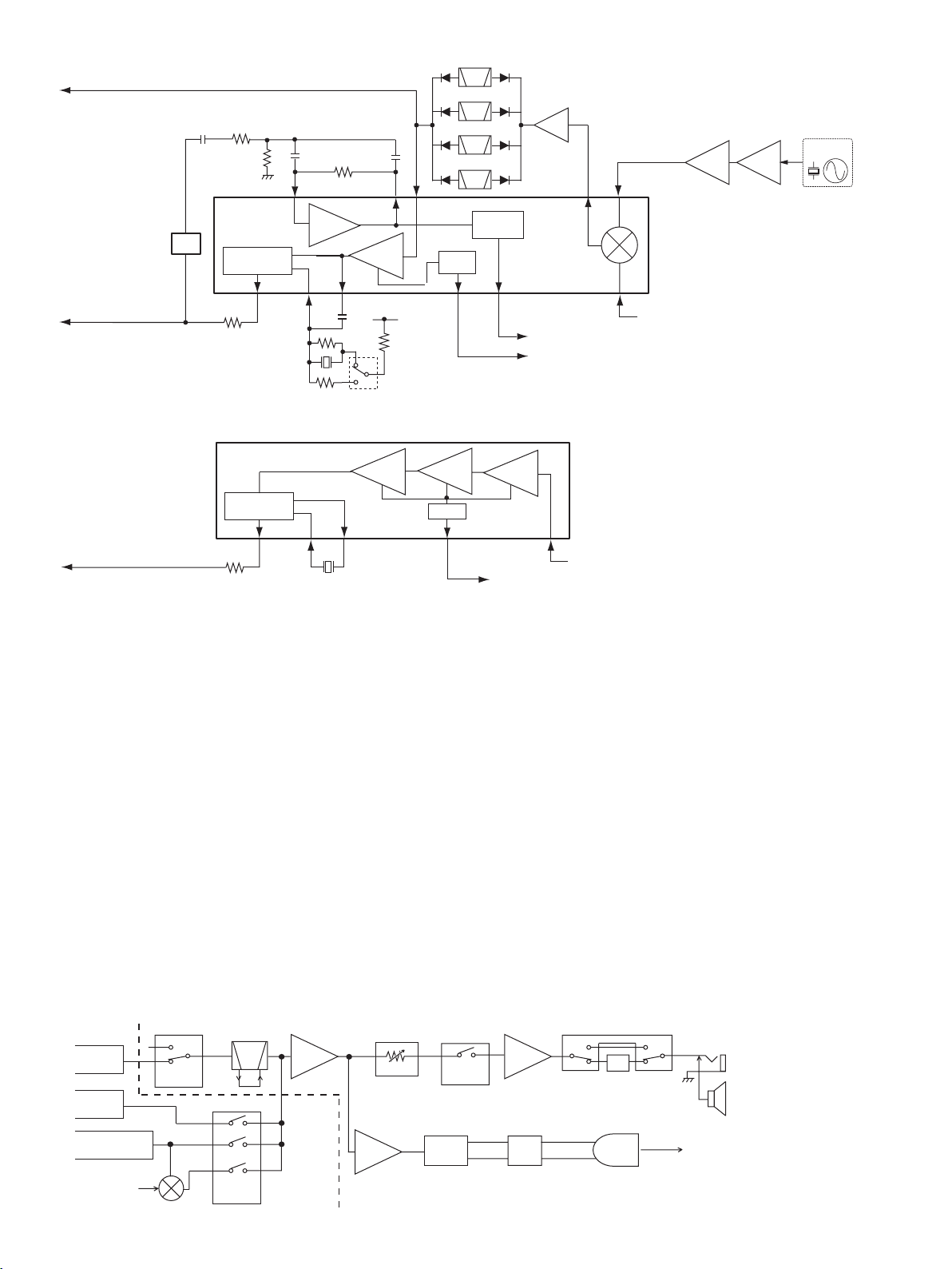
4-1-6 AF CIRCUITS (LOGIC UNIT)
The demodulated AF signals from the demodulator circuits are
amplifi ed and fi ltered in the AF circuits.
In FM mode, the demodulated AF signals from the
demodulator circuits are passed through the AF select
switch (IC4, pins 1, 7) and BPF (IC27, pins 1, 3 and 5, 7),
then applied to the AF amplifi er (Q18).
In other than FM mode, the demodulated AF signals from
the demodulator circuits are passed through the AF select
switch (MAIN-A/B; UNIT ;IC27, pins 8, 9; WFM, pins 3, 4;
AM, pins 1, 2; SSB), then applied to the AF amplifi er (Q18).
The amplified AF signal are applied to the electric volume
(IC17, pins 6, 7) for level adjustment. The level adjusted
AF signals are passed through the speaker mute switch
(Q12) and applied to the AF power amplifier (IC12, pin 1).
The power-amplified AF signals are applied to the internal
speaker via J1 (J6) or an external speaker/ear phone via the
phone switch (S1), attenuator (R19, R20) and J1 (J6).
• AF CIRCUITS
FM
IF IC
(IC24)
WFM
IF IC
(IC16)
AM demodulator
(D75)
From the BFO
9
7
selector
8
AM
AF mixer (IC23)*
IC4
AF
SSB
1
8
3
1
IC27
51
BPF
73
IC27
AF
selector
AF
Amp.
9
4
2
MAIN-A/B UNIT LOGIC UNIT
Q18
IC17
67 14
Ele. VR
Q15
AF
Amp.
12
Limit’r
Amp.
RSSI
Limit’r
Amp.
IF IC (IC16)
17
“RSSI” signal to the NB circuits
2
2nd IF signal from the 2nd IF circuits
In the USB (Universal Serial Bus) audio output mode, the AF
signals from the AF amplifi er (Q18) are applied to another AF
amplifi er (Q15). The amplifi ed AF signals are passed through
the USB audio selector (IC2038, pins 1, 3), then applied
to the USB audio IC (IC16, pin 12) then converted into the
USB audio data. The converted audio data is applied to the
connected PC via the USB HUB (IC32, pins 5, 6 and 2, 3).
4-1-7 SQUELCH CIRCUIT
• NOISE SQUELCH (MAIN-A/B UNITS)
The noise squelch mutes the AF output signals when no RF
signals are received. By detecting noise components in the
demodulated AF signals, the squelch circuit toggles the AF
power amplifi er ON and OFF.
A portion of the demodulated signals from the IF IC (IC24,
pin 9) are applied to the D/A converter (IC8, pin 1) for level
adjustment. The level-adjusted AF signals are output from
pin 2, and passed through the noise filter (R421, R417,
C520, C523). The fi ltered noise signals are then applied to
the noise amplifier (IC24, pins 7, 8) to be amplified noise
components only.
The amplified noise components are converted into the
D+
IC12
Powe r
Amp.
USB
D–
5
HUB
Q12, D8
SP
mute sw.
IC16 IC32
126
USB
audio
4 - 3
2
D+
D–
3
Phone switch (S1)
AT T
To the PC
USB connector
(J2)
(CHASSIS; J6)
Speaker (CHASSIS; SP1)
*MAIN-A UNIT only
Page 15

pulse-type signal at the noise detector section, and output
from pin 13 as the “NOIS” signal. The “NOIS” signal is
applied to the CPU (IC18, pin 16). And the CPU outputs
control signals “LSTB,” “VDAT,” “VCK” from pins 61, 57, 58,
to the expander (IC34) according to the “NOIS” signal level.
Then the expander outputs “SPPWR” signal from pin 7 to
toggle the AF+8V regulator (Q5, Q8) ON and OFF.
The expander also outputs “SPMUTE” signal to the speaker
switch (Q12, D28) at the same time, to disconnect the AF line.
• TONE SQUELCH (LOGIC UNIT)
The tone squelch detects the tone (CTCSS/DTCS) signal
in the demodulated AF signals, and opens the squelch only
when the matched sub-audible tone frequency is detected in
the received signal.
While the tone squelch is in use, and the received signal
contains no sub-audible tone or mismatched tone frequency,
the tone squelch mutes the AF signals even if the noise
squelch is open.
A portion of the demodulated AF signals from the IF IC
(MAIN-A/B; IC24, pin 9) are passed though the tone filter
(IC21/IC2021, pins 5, 7) to suppress unwanted voice signals.
The fi ltered tone signals are applied to the CPU (IC18, pin
93/85).
• 1st VCO’s
The 1st VCO is composed by two VCO’s; as the 1st LO
signal generator for 0.01–483.29 MHz and 483.3–3300 MHz
reception range.
[When receiving 0.01–265.6999 MHz signals]
-1st VCO 1 (Q28, D53)-
Generates 532.4–749.95 MHz LO signals. The VCO output
signal is buffer-amplifi ed by Q27. The buffer amplifi ed signals
are passed through the LO siwtch (D58) and buffer amplifi er
(IC15, pins 1, 4).
-1st VCO 2 (Q30, D54)-
Generates 750–1066.65 MHz LO signals. The VCO output
signal is buffer-amplifi ed by Q29. The buffer amplifi ed signals
are passed through the LO siwtch (D59) and buffer amplifi er
(IC15, pins 1, 4).
The buffer amplifi ed VCO output signals from pin 4 of IC15
are passed through the attenuator (R137, R138, R152), LO
switch (D57) and another attenuator (R153, R154, R156),
and applied to the
divided LO signals are buffer-amplified by Q34, and then
passed through the HPF (L113, C316, C321), LPF (L115,
L118, C326, C322), LO switch (D85) and attenuator (R214,
R217, R226), before being applied to the 1st mixer (IC14,
pins 1, 6).
1
/2 frequency divider (IC11, pin 2). The
The CPU decodes the CTCSS/DTCS signal, and outputs
control signals “LSTB,” “VDAT,” “VCK” from pins 61, 57, 58, to
the expander (IC34) according to the applied CTCSS/DTCS
signal. Then the expander outputs “SPPWR” signal from pin
7 to toggle the AF+8V regulator (Q5, Q8) ON and OFF.
The expander also outputs “SPMUTE” signal to the speaker
switch (Q12, D28) at the same time, to disconnect the AF line.
4-1-8 BANDSCOPE CIRCUITS* (MAIN-A UNIT)
A portion of the 2nd IF signal from the 2nd mixer (IC19, pin
5) is applied to the IF IC (IC20, pin 16) via the 2nd IF fi lter
(FI2). The 2nd IF signal is converted into the 3rd IF signal by
being mixed with 3rd LO signal from the DDS circuits, at the
3rd mixer in the IF IC (IC20).䇭The converted 3rd IF signal
is output from pin 3 and passed through the 3rd IF fi lter FI4.
The fi ltered signal is amplifi ed at the limiter amplifi er in the
IC to produce the RSSI signal which corresponding to the
received signal level.
The RSSI signal “SCAD” is output from pin 12, and applied
to the CPU (IC18, pin 89). The CPU converts the RSSI signal
into the digital signal, and outputs to connected PC via USB
HUB (IC32, pins 19, 20 and 2, 3) to indicate the received
signal level for bandscope function on the PC screen.
4-2 PLL CIRCUITS
4-2-1 VCO CIRCUITS (MAIN-A/B UNITS)
DOWN CONVERTER VCO*
The down converter VCO (Q19, D43) generates the 1001
MHz LO signals for down conversion.
The VCO output signals are buffer amplified by Q13,
and applied to the mixer (IC6, pin 3) for frequency downconversion, via the band switches (D11, D12, D21, D22).
When the recceiving 2000 MHz and above, the VCO outputs
are doubled by being passed through the HPF (L23, C61,
C69, C75), and applied to the mixer (IC6, pin 3) as the 2002
MHz LO signals via the band switches (D12, D22).
[When receiving 266.7–33000 MHz signals]
-1st VCO 1 (Q28, D53)-
Generates 532.4–749.95 MHz LO signals. The VCO output
signal is buffer-amplifi ed by Q27. The buffer amplifi ed signals
are passed through the LO siwtch (D58) and buffer amplifi er
(IC15, pins 1, 4).
-1st VCO 2 (Q30, D54)-
Generates 750–1066.65 MHz LO signals. The VCO output
signal is buffer-amplifi ed by Q29. The buffer amplifi ed signals
are passed through the LO siwtch (D59) and buffer amplifi er
(IC15, pins 1, 4).
The buffer amplifi ed VCO output signals from pin 4 of IC15
are passed through the attenuator (R137, R138, R152) and
LO switches (D60, D84) and BPF (L107, L108, C276, C278,
C288, C292, C298), before being applied to the 1st mixer
(IC14, pins 1, 6).
• 2nd VCO
The 2nd VCO (Q47, D62, D63) generates the LO signals
for producing 2nd IF signal. The oscillated signals are buffer
amplifi ed by Q50, and applied to the 2nd mixer (IC19, pin 1)
via LPF (L158, C456, C459, C462) and attenuator (R276).
4-2-2 PLL CIRCUITS (MAIN-A/B UNIT)
The PLL circuits provide stable oscillation of the receive LO
frequencies. The PLL circuit compares the phase of the
divided VCO frequency with the reference frequency. The PLL
output frequency is controlled by the divided ratio (N-data)
from the CPU.
• DOWN CONVERTER PLL*
A portion of the VCO output signals are amplified at the
buffer amplifi er (Q14) and then applied to the PLL IC (IC4,
pin 8). The applied signals are divided at the prescaler and
programmable counter according to the N-data “DAT1” from
the expnader (IC3, pin 2) controlled by the CPU (LOGIC
UNIT; IC18). The divided signal is phase compared with the
reference frequency from the reference amplifi er (Q5) at the
phase comparator.
4 - 4
*MAIN-A UNIT only
Page 16
The phase difference is output from pin 5 as a pulse type
signal after being passed through the internal charge pump.
The output signal is applied to the VCO (Q19, D43) after
being converted into the DC voltage (lock voltage) at the
loop filter (R84, R102, R106, C180, C188, C202, C645,
C646).
• 1st PLL
-1st VCO 1 (Q28, D53)-
A portion of the VCO output signals from the buffer amplifi er
(IC12, pin 4) are applied to the PLL IC (IC10, pin 8) via the
buffer amplifier (Q39). The applied signals are divided at
the prescaler and programmable counter according to the
N-data “DAT1” from the expnader (IC7, pin 2) controlled by
the CPU (IC18). The divided signal is phase compared with
the reference frequency at the phase comparator.
The phase difference is output from pin 5 as a pulse type
signal after being passed through the internal charge pump.
The output signal is applied to the VCO (Q27, Q28, D52,
D53) after being converted into the DC voltage (lock voltage)
at the loop fi lter (Q35, Q36).
-1st VCO 2 (Q30, D54)-
A portion of the VCO output signals from the buffer amplifi er
(IC12, pin 4) are applied to the PLL IC (IC10, pin 8) via the
buffer amplifier (Q39). The applied signals are divided at
the prescaler and programmable counter according to the
N-data “DAT1” from the expnader (IC7, pin 2) controlled by
the CPU (IC18). The divided signal is phase compared with
the reference frequency at the phase comparator.
The phase difference is output from pin 5 as a pulse type
signal after being passed through the internal charge pump.
The output signal is applied to the VCO (Q27, Q28, D52,
D53) after being converted into the DC voltage (lock voltage)
at the loop fi lter (Q35, Q36).
• 2nd PLL
A portion of the VCO (Q47, D62, D63) output signals from
the buffer (Q50) are applied to the PLL IC (IC13, pin 11)
via the buffer (Q41). The applied signals are divided at
the prescaler and programmable counter according to the
N-data “DAT1” from the expnader (IC3, pin 2) controlled by
the CPU (IC18). The divided signal is phase compared with
the reference frequency from the reference amplifi er (Q31)
at the phase comparator.
The phase difference is output from pin 5 as a pulse type
signal after being passed through the internal charge pump.
The output signal is applied to the VCO (Q47, D62, D63)
after being converted into the DC voltage (lock voltage) at
the loop fi lter (R235, R238, C354, C355, C362).
If the oscillated signal drifts, its phase changes from that of
the reference frequency, causing a lock voltage change to
compensate for the drift in the oscillated frequency.
<THE CONCEPT OF PLL CIRCUITS>
PLL IC
PLL unlock detect signal
PLL strobe signal
PLL crock signal
PLL serial data (N-data)
Reference frequency signal
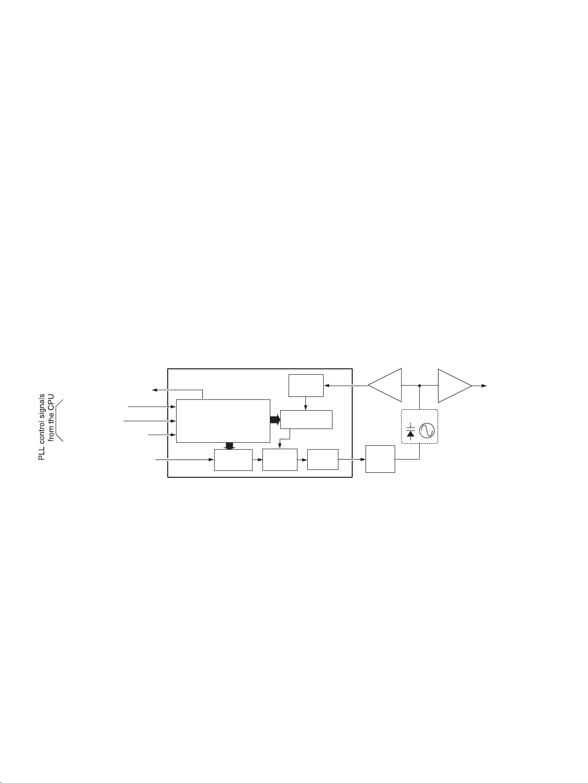
4-3 DIGITAL MODE OPERATION WITH UT-122
DATA interface
Reference
counter
†
A portion of the 450 kHz 3rd IF signal from IF IC (MAIN-A UNIT;
IC24, pin 13) is applied to the LOGIC UNIT via the IF amplifi er
(MAIN-A UNIT; Q76, Q77). The applied 3rd IF signal is passed
through the IF switch (LOGIC UNIT; IC2028, pins 1, 7) and buffer
amplifier (LOGIC UNIT; Q2023), then applied to the attached
UT-122 via J2017 (pin 11).
The applied 3rd IF signal is passed through the IF filter
(UT-122; FI1) to remove unwanted signals, and applied to
the A/D converter (UT-122; IC8, pin 3) to be converted into
the digital signal via BPF. The converted digital signal is
then applied to the DSP (Digital Signal Proccesor; IC7) and
demodulated. The demodulated signal is then applied to the
liner codec (UT-122; IC9) to be converted in to the analog
audio signals.
Programmable
Phase
detector
Prescaler
counter
Charge
pump
Buffer
Loop
filter
amp.
VCO
Buffer
amp.
to a mixer
The converted audio signals are applied to the same AF
circuits as analog receiving from the AF switch (IC23, pin 7).
†
Optional product (DIGITAL UNIT for PCR2500; [USA-3])
4 - 5
Page 17
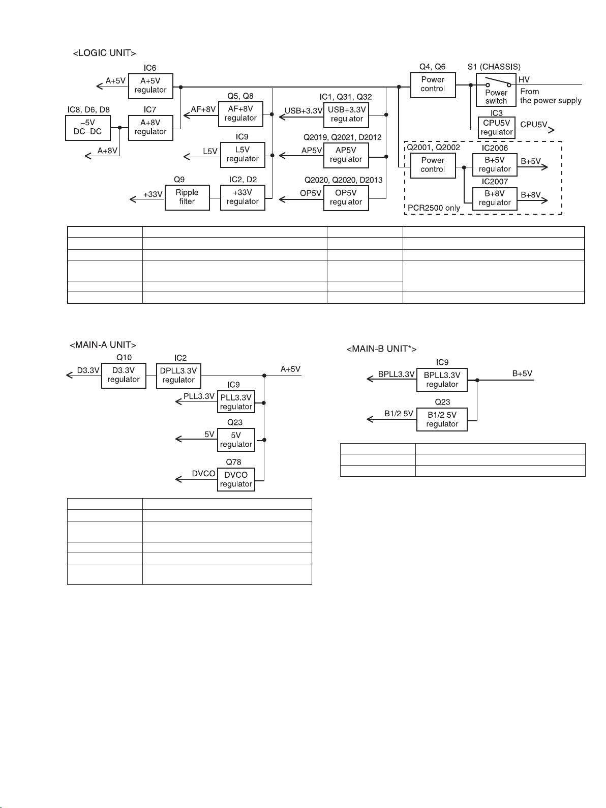
4-4 POWER SUPPLY CIRCUITS
VOLTAGE LINE DESTINATION VOLTAGE LINE DESTINATION
HV Same voltage as the connected power supply. AP5V Optional UT-122.
AF+8V AF power amplifi er (IC12). OP5V Optional UT-108/UT-118.
L5V
+33V Loop fi lter (MAIN-A/B UNITS; Q35, Q36). A+8V
USB3.3V USB HUB (IC20, IC32), USB audio IC (IC16). –5V AGC amplifi er (MAIN UNIT; IC25).
Electric volume (IC17), tone fi lter (IC21), AF switch
(IC4, IC23), etc.
A+5V
MAIN-A UNIT.
VOLTAGE LINE DESTINATION
DPLL3.3V Down converter circuit; PLL IC (IC4).
D3.3V
PLL3.3V 1st and 2nd PLL circuits; PLL IC (IC10, IC13).
5V Divider (IC11), reference oscillator (X1), etc.
DVCO5V
Down converter circuit; mixer (IC6), RF amplifi er (IC15), etc.
Down converter circuit; VCO (Q19, D43), buffer (Q14), etc.
VOLTAGE LINE DESTINATION
BPLL3.3V 1st and 2nd PLL circuits; PLL IC (IC10, IC13).
B1/2 5V Divider (IC11).
*PCR2500 only
4 - 6
Page 18

4-5 CPU PORT ALLOCATION
4-5-1 CPU (LOGIC UNIT; IC18)
Pin
No.
PORT
NAME
4 BMST2
5 BCK
8 BMST1
9 CSHIFT
16 NOIS
17 BNOIS
18 PWRSW
19 BMST3*
20 CCS
21 BP1STB*
22 BP2STB*
23 BDSTB*
27 PDIN Input port for USB data.
28 PDOUT Outputs USB data.
31 SCL Outputs clock signal to the EEPROM (IC14, pin 5).
33 OPSO
34 OPSI
35 OPSCK
36 AIRQ
37 ASTB
38 ASI
39 ASO
40 ACK
41 DSPS
42 IMST
43 BUSY
44 SDL I/O port for EEPROM (IC14, pin 6).
45 OPAFSEL
46 OPAFINH
47 BOPAFSEL*
48 BOPAFINH*
Outputs strobe signal to the expander (MAIN-B
UNIT; IC18, pin1).
Outputs clock signal to the expander (MAIN-B
UNIT; IC17, pin 3).
Outputs strobe signal to the expander (MAIN-B
UNIT; IC3, pin1).
Outputs clock frequency shift signal to the
clock shift circuit (D6).
Input port for “NOIS” signal from the IF IC
(MAIN-A UNIT; IC24, pin 13).
Input port for “BNOISE” signal from the IF IC
(MAIN-B UNIT; IC24, pin 13).
Input port for power witch (CHASSIS; S1).
“Low”=While the power switch is turned.
Outputs strobe signal to the expander (MAIN-B
UNIT; IC17, pin 1).
Outputs optional unit select signal to the
attached optional unit via the pin 20 of J2018.
“High”=While the optional unit is attached.
Outputs PLL strobe signla to the 1st PLL IC
(MAIN-B UNIT; IC10, pin 11).
Outputs PLL strobe signla to the 2nd PLL IC
(MAIN-B UNIT; IC13, pin 13).
Outputs strobe signal to the D/A converter
(MAIN-B; IC8, pin 6).
Output serial data to the attached optional unit
via the pin 18 of J2018.
Input port for serial data from the attached
optional unit via the pin17 of J2018.
Outputs clock signal to the Attached optional
unit via the pin 16 of J2018.
Input port for data request signal from the
attached UT-122 via the pin 19 of the J2017.
Outputs strobe signal to the attached UT-122
via the pin 20 of the J2017.
Input port for serial data from the attached
UT-122 via the pin 17 of the J2017.
Outputs serial data to the attached UT-122 via
the pin 18 of the J2017.
Outputs clock signal to the attached UT-122 via
the pin 16 of the J2017.
Outputs DSP select signal to the attached DSP
unit via pin 7 of J15.
Outputs DSP strobe signal to the attached
DSP unit via pin 3 of J15.
Outputs busy signal to the attached optional
unit via pin 7 of J7.
Outputs control signal to the AF switch (IC23,
pin 5).
“High”=While the optional unit is activated.
Outputs control signal to the AF switch (IC23,
pin 2).
“High”=The AF line for the optional unit is dis-
connected.
Outputs control signal to the AF switch
(IC2031, pin 5).
“High”=While the optional unit is activated.
Outputs control signal to the AF switch
(IC2031, pin 2).
“High”=The AF line for the optional unit is dis-
connected.
DESCRIPTION
Pin
No.
PORT
NAME
49 RXMUTE
53 APAFSEL
54 APAFINH
57 VDAT
58 VCK
59 VSTB
61 LSTB
64 PWR
65 DTMSTD
66 DTMSD
67 DTMCK
70 PDSTB
73 VBUS
75 DSTB
76 P2STB
77 P1STB
78 DPSTB
79 MST0
80 MST1
81 MST2
82 BCMAD*
83 BVSCAF*
85 BRTONE*
86 BSMAD*
88 TEMP Input port for internal temperature detection.
89 SCAD
90 CMAD
91 VSCAF
93 RTONE
98 USBPOW
Input port for mute signal from the attached
optional unit via the pin 24 of J2018.
“High”=While the audio output is muted.
Outputs control signal to the AF switch (IC4,
pin 5).
“High”=While the UT-122 is in use.
Outputs control signal to the AF switch (IC4, pin
2).
“High”=While the attached UT-122 is inactivated.
Outputs serial data to the electric volume
(IC17, pin 16).
Outputs clock signal to the electric volume
(IC17, pin 15).
Outputs strobe signal to the electric volume
(IC17, pin 14).
Outputs strobe signal to the expander (IC34,
pin 1).
Outputs control signal to the power controller
(Q4, Q6).
“High”=While the receivers power is ON.
Input port for detecting signal from the DTMF
decoder (IC19, pin 14).
“High”=When the DTMF signal is detected.
Input port for DTMF signal from the DTMF
decoder (IC19, pin 9).
Outputs clock signal from the DTMF decoder
(IC19, pin 11).
Outputs strobe signal to the DDS IC (MAIN-A
UNIT; IC22, pin 41).
Input port for USB connection detecting signal
from the VBUS line.
“High”=While a PC is connected through [USB] con nector on the receiver's main unit.
Outputs strobe signal to the D/A converter
(MAIN-A; IC8, pin 6).
Outputs strobe signal to the 2nd PLL IC
(MAIN-A UNIT; IC13, pin 13).
Outputs strobe signal to the 1st PLL IC
(MAIN-A UNIT; IC12, pin 11).
Outputs strobe signal to the down converter
PLL IC (MAIN-A UNIT; IC4, pin 11).
Outputs strobe signal to the expander (MAIN-A;
IC3, pin 1).
Outputs strobe signal to the expander (MAIN-A;
IC18, pin 1).
Outputs strobe signal to the expander (MAIN-A;
IC3, pin 1).
Input port for RSSI signal from the RSSI signal
selector (MAIN-A; IC30, pin 1).
Input port for VSC signal from the tone filter
(IC2021, pin 7).
Input port for CTCSS signals from the tone
fi lter (MAIN-B UNIT; IC21, pin 1).
Inputport for RSSI signal from the IF IC
(MAIN-A/B UNITS; IC16, pin 13).
Input port for RSSI signal from the IF IC (MAIN-A/
B UNITS; IC20, pin 5) for band scope function.
Input port for RSSI signal from the IF IC
(MAIN-A UNIT; IC30, pin 1) for AFC function.
Input port for VSC signal from the tone filter
(IC21, pin 1).
Input port for CTCSS signals from the tone
fi lter (MAIN-A UNIT; IC21, pin 7).
Outputs voltage line control signal to the 3.3V
regulator (IC1, Q31, Q32, Q33).
“High”=During in the USB audio mode.
DESCRIPTION
*PCR2500 only
4 - 7
Page 19
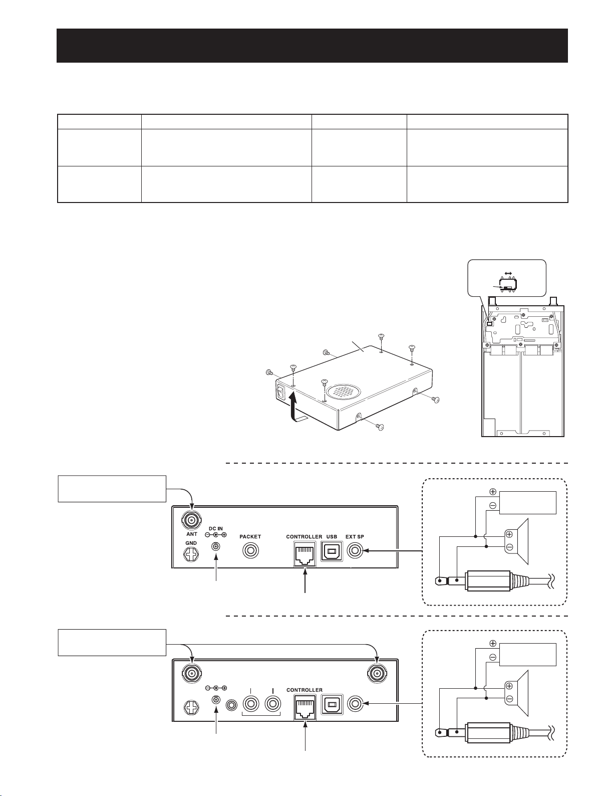
SECTION 5 ADJUSTMENT PROCEDURES
5-1 PREPARATION
When adjusting IC-PCR1500/PCR2500, controller for the R1500/R2500 and JIG cable (see the illust below) are required.
¤ REQUIRED TEST EQUIPMENTS
EQUIPMENT GRADE AND RANGE EQUIPMENT GRADE AND RANGE
Standard signal
generator (SSG)
Frequency counter
CAUTION!: BACK UP the originally programmed memory data in the receiver before starting the adjustment.
There is possiblity of losing original memory data when the adjustment is finished.
Before starting adjustment:
• Remove the top cover and sheild cover on the MAIN-A UNIT. (Refer to the “SECTION 3” for details)
• Set the AF switch to “PHONES.” (Refer to the instruction manual for details)
Frequency range : 0.1–3300 MHz
Output level : 0.1 µV to 32 mV
(–127 to –17 dBm)
Frequency range : 0.1–30 MHz
Frequency accuracy : ±1 ppm or better
Sensitivity : 100 mV or better
AC milliwattmeter Measuring range : 10 µW to 100 mW
External speaker
Input impedance : 8
Capacity : More than 5 W
Ω
2%+!%0
3
IWS
0
(
/
HCT
4OPCOVER
.
3%
• CONNECTION
<FOR IC-PCR1500 ADJUSTMENT>
3TANDARDSIGNALGENERATOR
33'
TOTHESUPPLIED!#ADAPTER
<FOR IC-PCR2500 ADJUSTMENT>
3TANDARDSIGNALGENERATOR
33'
4.! 4.!
$.'
s*)'CABLE
2EARPANEL
TOTHE)#2#/.42/,,%2
!&
'.$
CONDUCTORDMM
!#
MILLIVOLTMETER
3PEAKER
7
v7
s*)'CABLE
2EARPANEL
.
)#$
4%+#!0
%+#!0
4
!4!$
0348%"35
!#
MILLIVOLTMETER
3PEAKER
7
/PTIONALPRODUCTFOR;5+=
TOTHESUPPLIED!#ADAPTER
TOTHE)#2#/.42/,,%2
5 - 1
!&
'.$
CONDUCTORDMM
v7
Page 20
<FOR IC-PCR1500 ADJUSTMENT>
ENTERING ADJUSTMENT MODE
¤
Set the direction of the [VOL] to 12 o'clock (11–1 o'clock).
q
Push and hold [TS•MODE]+[ATT•PRIO]+[NB•AGC]
w
+[MONI•T/T-SCAN] key, and turn the power switch (MAIN
UNIT) ON.
KEY ASSIGNMENTS FOR THE ADJUSTMENT MODE
¤
• [SET•LOCK] : Selects the next adjustment item.
• [S.MW•MW] :
Selects the previous adjustment item.
• CONTROLLER
[SET•LOCK]
[TS•MODE]
[VOL]
• [DIAL] :
Adjusts the value for the item manually.
• [TS•MODE] : Adjusts the value for the item automatically.
Stores the set value.
• [V/MHz•SCAN] : Verify the adjustment value for the item.
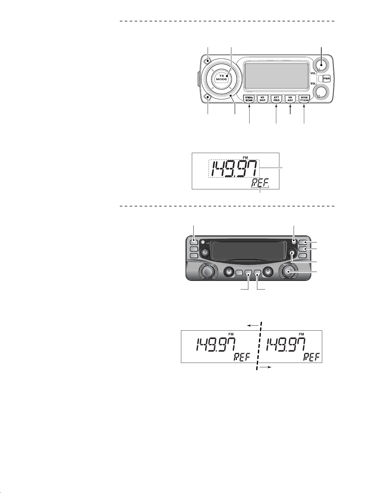
• [VOL] : Adjust the audio output level.
<FOR IC-PCR2500 ADJUSTMENT>
ENTERING ADJUSTMENT MODE
¤
Set the direction of the [VOL] (Right) to 12 o'clock
q
(11–1 o'clock).
Push and hold [MAIN•NB]+[MAIN•AGC]+[ATT•PRIO]
w
+[MODE•SCAN] key, and turn the power switch (MAIN
UNIT) ON.
KEY ASSIGNMENTS FOR THE ADJUSTMENT MODE
¤
• [MAIN•NB] : Selects the next adjustment item.
• [VFO/MR•S.MW] (Right band)
:
Selects the previous adjustment item.
[S.MW•MW]
[DIAL]
[V/MHz•SCAN]
• DISPLAY EXAMPLE
• CONTROLLER
[MAIN•AGC]
PWR
MAIN
AGC
VFO/MR
S.MW
MHz
TS
[MODE•SCAN]
Adjustment item
MONI
T/T-SCAN
ATT
MODE
SCAN
PRIO
[NB•AGC]
[ATT•PRIO]
SQLSQL
[ATT•PRIO]
[MONI•T/T-SCAN]
Adjustment frequency
[SET•SKIP]
SET
MAIN
[MAIN•NB]
NB
SKIP
VFO/MR
VOLVOL
DIALDIAL
[VFO/MR]
S.MW
MHz
TS
[VOL]
[DIAL]
• [DIAL] (Right band)
:
Adjusts the value for the item manually.
• [SET•SKIP] : Adjusts the value for the item automatically.
Stores the set value.
• [ATT•PRIO] : Verify the adjustment value for the item.
• [VOL] (Right band)
: Adjust the audio output level.
• DISPLAY EXAMPLE
MAIN-A UNIT adjustment
MAIN-B UNIT adjustment
5 - 2
Page 21
5-2 MAIN-A UNIT ADJUSTMENT
ADJUSTMENT OPERATION VALUE
REFERENCE
FREQUENCY
[REF]
BPF
[LT1]–[HTF]
–
AGC GAIN
(FM)
[AGF]
(AM)
[AGA]
IF GAIN
(FM)
[IFF]
(AM)
[IFA]
†
Refer to the “ADJUSTMENT ITEM LIST“ on page 5-7.
‡
The output level of the standard signal generator (SSG) is indicated as the SSG's open circuit.
*Displayed on the controller's display.
1 • Connect a frequency counter to the J5 connector on the MAIN-A
UNIT (see the illust below).
2 • Push [TS•MODE]/[SET•SKIP] to store the set value.
1 • Preset the adjustment items as below before the “BPF“ adjustment.
[AGA] : “8A”
[IFA] : “25”
2 • Connect an SSG to the antenna connector “ANT1” and set as;
Frequency : Specifi ed frequency*
Modulation : none
Level : Specifi ed level
†
3 • Push [TS•MODE]/[SET•SKIP] to store the adjustment value.
4 • Repeat 2–3 for each specifi ed frequency and level for [LT1] to [HTF].
1 • Connect an SSG to the antenna connector and set as;
Frequency : Specifi ed frequency*
Mode : FM
Modulation : 1 kHz
Deviation : 3.5 kHz
Level : +34 dBµ (–73 dBm)
‡
2 • Connect a speaker and milliwatt meter then set the audio output level
to 50 mW with [VOL].
3 • Push [SET•LOCK]/[MAIN•NB] to select next adjustment item.
4 • Set the SSG as;
Frequency : Specifi ed frequency*
Mode : AM
Modulation : 1 kHz
Deviation : 70%
Level : +34 dBµ (–73 dBm)
‡
5••Set the audio output level to 50 mW with [DIAL].
Verify that the demodulated audio signals are not distorted badly.
6 • Push [TS•MODE]/[SET•SKIP] to store the adjustment value.
1 • Set the SSG as;
Level : OFF
2 • Connect a speaker and milliwatt meter then set the audio output level
to 50 mW with [VOL].
3 • Push [SET•LOCK]/[MAIN•NB] to select next adjustment item.
4 • Set the audio output level to 80 µW with [DIAL]. 80 µW
5 • Push [TS•MODE]/[SET•SKIP] to store the adjustment value.
10.25000 MHz
Automatic adjustment
50 mW
50 mW
50 mW
-!).!5.)4
J5
2EMOVETHESHEILDCOVER
5 - 3
Page 22

5-2 MAIN-A UNIT ADJUSTMENT (coninued)
ADJUSTMENT OPERATION VALUE
S-METER
[NS0]–[WS6]
–
S-METER FLATNESS
[L1]–[LEH]
–
BAND SCOPE
[SC0]–[SC6]
–
CENTER METER
[CML] (LOW)
[CMH] (HIGH) 1 • Set the SSG as;
SQUELCH
[SQL]
RSSI
[RS0]–[RS6]
–
RSSI FLATNESS
[R5L]–[R8H]
–
†
Refer to the “ADJUSTMENT ITEM LIST“ on page 5-7.
‡
The output level of the standard signal generator (SSG) is indicated as the SSG's open circuit.
*Displayed on the controller's display.
1 • Set the SSG as;
Frequency : Specifi ed frequency*
Modulation : None
Level : Specifi ed level
†
2 • Push [TS•MODE]/[SET•SKIP] to store the adjustment value.
3 • Repeat 1–2 for each specifi ed frequency and value for [NS0] to [WS6].
1 • Set the SSG as;
Frequency : Specifi ed frequency*
Modulation : None
Level : Specifi ed level
†
2 • Push [TS•MODE]/[SET•SKIP] to store the adjustment value.
3 • Repeat 1-2 for each specifi ed frequency and value for [L1] to [LEH].
1 • Set the SSG as;
Frequency : Specifi ed frequency *
Modulation : None
Level : Specifi ed level
†
2 • Push [TS•MODE]/[SET•SKIP] to store the adjustment value.
3 • Repeat 1–2 for each specifi ed frequency and value for [SC0] to [SC6].
1 • Set the SSG as;
Frequency : 3 kHz lower than specifi ed frequency*
Modulation : None
Level : +34 dBµ (–73 dBm)
‡
2 • Push [TS•MODE]/[SET•SKIP] to store the adjustment value.
Frequency : 3 kHz higher than specifi ed frequency*
Modulation : None
Level : +34 dBµ (–73 dBm)
‡
2 • Push [TS•MODE]/[SET•SKIP] to store the adjustment value.
1 • Set the SSG as;
Frequency : Specifi ed frequency*
Mode : FM
Modulation : 1 kHz
Deviation : 3.5 kHz
Level : –13 dBµ (–120 dBm)
‡
2 • Set the [SQL] value to close the squelch with [DIAL]. Then set the
[SQL] value at the point where the audio signals just appear.
3 • Turn the SSG output OFF, and verify that the squelch is closed.
4 • Push [TS•MODE]/[SET•SKIP] to store the adjustment value.
1 • Set the SSG as;
Frequency : Specifi ed frequency*
Modulation : None
Level : Specifi ed level
†
2 • Push [TS•MODE]/[SET•SKIP] to store the adjustment value.
3 • Repeat 1–2 for each specifi ed frequency and value for [RS0] to [RS6].
1 • Set the SSG as;
Frequency : Specifi ed frequency*
Modulation : None
Level : Specifi ed level
†
2 • Push [TS•MODE]/[SET•SKIP] to store the adjustment value.
3 • Repeat 1–2 for each specifi ed frequency and value for [R5L] to [R8H].
Automatic adjustment
Automatic adjustment
Automatic adjustment
Automatic adjustment
Automatic adjustment
Automatic adjustment
Automatic adjustment
5 - 4
Page 23

5-3 MAIN-B UNIT ADJUSTMENT (PCR2500 only)
ADJUSTMENT OPERATION VALUE
BPF
[LT1]–[HTF]
–
AGC GAIN
(FM)
[AGF]
(AM)
[AGA]
IF GAIN
(FM)
[IFF]
(AM)
[IFA]
‡
The output level of the standard signal generator (SSG) is indicated as the SSG's open circuit.
*Displayed on the controller's display.
1 • Set the adjustment items as below before the “BPF” adjustment.
[AGA] : “8A”
[IFA] : “25”
2 • Connect an SSG to the antenna connector “ANT1” and set as;
Frequency : Specifi ed frequency*
Modulation : none
Level : Specifi ed level
†
3 • Push [SET•SKIP] to store the set value.
4 • Repeat 2–3 for each specifi ed frequency then level for [LT1] to [HTF].
1 • Connect an SSG to the antenna connector and set as;
Frequency : Specifi ed frequency*
Mode : FM
Deviation : 3.5 kHz
Level : +34 dBµ (–73 dBm)
‡
Modulation : 1 kHz
2 • Connect a speaker and milliwatt meter and set the audio output level
to 50 mW with [VOL].
3 • Push [MAIN•NB] to select next adjustment item.
4 • Set the SSG as;
Frequency : Specifi ed frequency*
Mode : AM
Deviation : 70%
Level : +34 dBµ (–73 dBm)
‡
Modulation : 1 kHz
5••Set the audio output level to 50 mW with [DIAL].
Verify that the demodulated audio signals are not distorted badly.
6 • Push [SET•SKIP] to store the adjustment value.
1 • Set the SSG as;
Level : OFF
2 • Connect a speaker and milliwatt meter then set the audio output level
to 50 mW with [VOL].
3 • Push [SET•LOCK]/[MAIN•NB] to select next adjustment item.
4 • Set the audio output level to 80 µW with [DIAL]. 80 µW
5 • Push [TS•MODE]/[SET•SKIP] to store the adjustment value.
Automatic adjustment
50 mW
50 mW
50 mW
5 - 5
Page 24

5-3 MAIN-B UNIT ADJUSTMENT (PCR2500 only; continued)
ADJUSTMENT OPERATION VALUE
S-METER
[NS0]–[WS6]
–
S-METER FLATNESS
[L5L]–[L8H]
–
CENTER METER
[CML] (LOW)
[CMH] (HIGH) 1 • Set the SSG as;
SQUELCH
[SQL]
RSSI
[RS0]–[RS6]
–
RSSI FLATNESS
[R5L]–[R8H]
–
†
Refer to the “ADJUSTMENT ITEM LIST“ on page 5-7.
‡
The output level of the standard signal generator (SSG) is indicated as the SSG's open circuit.
*Displayed on the controller's display.
1 • Set the SSG as;
Frequency : Specifi ed frequency*
Modulation : None
Level : Specifi ed level
†
2 • Push [SET•SKIP] to store the adjustment value.
3 • Repeat 1–2 for each specifi ed frequency and value for [NS0] to [WS6].
1 • Set the SSG as;
Frequency : Specifi ed frequency*
Modulation : None
Level : Specifi ed level
†
2 • Push [SET•SKIP] to store the adjustment value.
3 • Repeat 1-2 for each specifi ed frequency and value for [L5L] to [L8H].
1 Set the SSG as;
Frequency : 3 kHz lower than specifi ed frequency*
Modulation : None
Level : +34 dBµ (–73 dBm)
‡
2 • Push [SET•SKIP] to store the adjustment value.
Frequency : 3 kHz higher than specifi ed frequency*
Modulation : None
Level : +34 dBµ (–73 dBm)
‡
2 • Push [SET•SKIP] to store the adjustment value.
1 • Set the SSG as;
Frequency : Specifi ed frequency*
Mode : FM
Modulation : 1 kHz
Deviation : 3.5 kHz
Level : –13 dBµ (–120 dBm)
‡
2 • Set the [SQL] value to close the squelch with [DIAL]. Then set the
[SQL] value at the point where the audio signals just appear.
3 • Turn the SSG output OFF, and verify that the squelch is closed.
4 • Push [SET•SKIP] to store the adjustment value.
1 • Set the SSG as;
Frequency : Specifi ed frequency*
Modulation : None
Level : Specifi ed level
†
2 • Push [SET•SKIP] to store the adjustment value.
3 • Repeat 1–2 for each specifi ed frequency and value for [RS0] to [RS6].
1 • Set the SSG as;
Frequency : Specifi ed frequency*
Modulation : None
Level : Specifi ed level
†
2 • Push [SET•SKIP] to store the adjustment value.
3 • Repeat 1–2 for each specifi ed frequency and value for [R5L] to [R8H].
Automatic adjustment
Automatic adjustment
Automatic adjustment
Automatic adjustment
Automatic adjustment
Automatic adjustment
5 - 6
Page 25

• ADJUSTMENT ITEM LIST
ADJUSTMENT
ITEM
REFERENCE
FREQUENCY
Disp.RFLevel
(dBµ/dBm)
REF* –
LT1 35/–72
MT1 35/–72
HT1 35/–72
LT2 35/–72
MT2 35/–72
HT2 35/–72
LT3 35/–72
MT3 35/–72
HT3 35/–72
LT4 35/–72
HT4 35/–72
LT5 35/–72
MT5 35/–72
HT5 35/–72
LT6 35/–72
MT6 35/–72
HT6 35/–72
LT7 35/–72
HT7 35/–72
BPF
LT8 35/–72
MT8 35/–72
HT8 35/–72
LT9 35/–72
MT9 35/–72
HT9 35/–72
LTA 35/–72
HTA 35/–72
LTB 40/–67
MTB 40/–67
HTB 40/–67
LTC 40/–67
HTC 40/–67
LTD 40/–67
HTD 40/–67
LTE 40/–67
THE 40/–67
LTF 40/–67
MTF 40/–67
HTF 40/–67
AGC gain
IF gain
AGF 34/–73
AGA 34/–73
IFF off
IFA off
NS0 0/–107
NS3 7/–100
NS5 14/–93
NS7 24/–83
NS9 34/–73
NS2 49/–58
NS4 64/–43
NS6 79/–28
S-METER
WS0 0/–107
WS3 7/–100
WS5 14/–93
WS7 24/–83
WS9 34/–73
WS2 49/–58
WS4 64/–43
WS6 79/–28
NS0 4/–103
*: Not necessary for MAIN-B adjustment.
†
The output level of the standard signal generator (SSG) is indicated as the SSG's open circuit.
ADJUSTMENT
†
ITEM
S-METER
S-METER
FLATNESS
Disp.RFLevel
(dBµ/dBm)
NS3 11/–96
NS5 18/–89
NS7 26/–81
NS9 34/–73
NS2 45/–62
NS4 55/–52
NS6 65/–42
WS0 9/–98
WS3 16/–91
WS5 22/–85
WS7 28/–79
WS9 34/–73
WS2 45/–62
WS4 55/–52
WS6 65/–42
L1-* 34/–73
L2-* 34/–73
L3-* 34/–73
L4-* 34/–73
L5L 34/–73
L51 34/–73
L52 34/–73
L53 34/–73
L54 34/–73
L55 34/–73
L56 34/–73
L57 34/–73
L5H 34/–73
L6L 34/–73
L61 34/–73
L62 34/–73
L63 34/–73
L64 34/–73
L65 34/–73
L66 34/–73
L6H 34/–73
L7L 34/–73
L71 34/–73
L72 34/–73
L73 34/–73
L74 34/–73
L75 34/–73
L76 34/–73
L77 34/–73
L78 34/–73
L7H 34/–73
L8L 34/–73
L81 34/–73
L82 34/–73
L83 34/–73
L84 34/–73
L85 34/–73
L86 34/–73
L87 34/–73
L88 34/–73
L89 34/–73
L8A 34/–73
L8H 34/–73
L9L* 34/–73
L9H* 34/–73
LAL* 34/–73
LA1* 34/–73
ADJUSTMENT
†
ITEM
Disp.RFLevel
LA2* 34/–73
LA3* 34/–73
LA4* 34/–73
LA5* 34/–73
LA6* 34/–73
LA7* 34/–73
LA8* 34/–73
LAH* 34/–73
LBL* 34/–73
LB1* 34/–73
LB2* 34/–73
LB3* 34/–73
LB4* 34/–73
LB5* 34/–73
LB6* 34/–73
LB7* 34/–73
LB8* 34/–73
LB9* 34/–73
LBA* 34/–73
LBH* 34/–73
LCL* 34/–73
S-METER
FLATNESS
LCH* 34/–73
LDL* 39/–68
LD1* 39/–68
LD2* 39/–68
LD3* 39/–68
LD4* 39/–68
LD5* 39/–68
LD6* 39/–68
LD7* 39/–68
LD8* 39/–68
LDH* 39/–68
LEL* 39/–68
LE1* 39/–68
LE2* 39/–68
LE3* 39/–68
LE4* 39/–68
LE5* 39/–68
LE6* 39/–68
LE7* 39/–68
LE8* 39/–68
LE9* 39/–68
LEA* 40/–67
LEH* 42/–65
SC0* 0/–107
SC3* 10/–97
SC5* 20/–87
BAND SCOPE
SC7* 30/–77
SC9* 40/–67
SC2* 50/–57
SC4* 60/–47
SC6* 70/–37
CENTER
METER
CML 34/–73
CMH 34/–73
SQUELCH SQL –13/–120
RS0 –5/–112
RS3 0/–107
RSSI
RS5 5/–102
RS7 10/–97
RS9 15/–92
RS2 20/–87
5 - 7
†
(dBµ/dBm)
ADJUSTMENT
ITEM
RSSI
FLATNESS
Disp.RFLevel
(dBµ/dBm)
RS4 25/–82
RS6 35/–72
R5L 20/–87
R51 20/–87
R52 20/–87
R53 20/–87
R54 20/–87
R55 20/–87
R56 20/–87
R57 20/–87
R5H 20/–87
R6L 20/–87
R61 20/–87
R62 20/–87
R63 20/–87
R64 20/–87
R65 20/–87
R66 20/–87
R6H 20/–87
R7L 20/–87
R71 20/–87
R72 20/–87
R73 20/–87
R74 20/–87
R75 20/–87
R76 20/–87
R77 20/–87
R78 20/–87
R7H 20/–87
R8L 20/–87
R81 20/–87
R82 20/–87
R83 20/–87
R84 20/–87
R85 20/–87
R86 20/–87
R87 20/–87
R88 20/–87
R89 20/–87
R8A 20/–87
R8H 20/–87
†
Page 26

SECTION 6 PARTS LIST
• IC-PCR1500 IC-PCR2500
[LOGIC UNIT]
REF ORDER
NO. N O.
IC1 1180002391 S.REG S-812C33AMC-C2N-G T 47.3/40.1
IC2 1110002350 S.IC BA6161F T 10.3/20.8
IC3 1110006090 S.IC XC6202P502PR T 119.7/41.1
IC4 1130011781 S.IC SN74AHC2G53HDCT3 T 91.2/15.5
IC6 1180001071 S.IC TA7805F (TE16L Q) B 132.5/43.4
IC7 1180002910 S.REG AN7708SP-E1 B 131.3/34.5
IC8 1110001401 S.IC µPC1555G2-E1-A T 104/23.7
IC9 1180000970 S.IC AN78L05M-(E1) T 109.1/40.1
IC12 1110003091 IC LA4425A-E
IC14 1140012950 S.IC 24LC512T-I/SM B 64.6/43
IC15 1130011990 S.IC SN74LVC1G08DCKR T 31.9/33.6
IC16 1190002240 S.IC PCM2901E/2K T 38.7/33.4
IC17 1130011860 S.IC SM6451BT-G-E2 T 46.3/23.6
IC18 1140013082 S.IC M30624FGPGP (RX2879A2)
[EUR-1], [UK-1], [CAN-1], [EXP-3] B 73.9/33.1
1140013083 S.IC M30624FGPGP RX2879A-3
[SEA-1] B 73.9/33.1
1140013085 S.IC M30624FGPGP (RX2879A-5)
[FRA-1], [EXP-2] B 73.9/33.1
1140013090 S.IC M30624FGPGP (RX-2879B)
[USA-1], [USA-3] B 73.9/33.1
IC19 1130012960 S.IC BU8872FS-E2 B 91.7/39.6
IC20 1190002231 S.IC CP2101-GM T 27.4/29.1
IC21 1110006380 S.IC LM2904PWR T 90.1/23.9
IC23 1130011781 S.IC SN74AHC2G53HDCT3 T 74.6/16.6
IC27 1110006380 S.IC LM2904PWR T 81.3/19.4
IC32 1190002261 S.IC USB2502-AEZG T 24.1/37.3
IC34 1130011760 S.IC CD4094BPWR T 92/37.5
IC35 1110005771 S.IC S-80942CNMC-G9CT2G B 59.1/31.7
IC36 1130011760 S.IC CD4094BPWR T 97.6/37.5
IC37 1130011990 S.IC SN74LVC1G08DCKR B 58.5/35.7
IC40 1130011781 S.IC SN74AHC2G53HDCT3 T 51.8/48
IC41 1130011781 S.IC SN74AHC2G53HDCT3 T 48.4/48
IC2006* 1180001071 S.IC TA7805F (TE16L Q) B 132.5/26.3
IC2007* 1180002910 S.REG AN7708SP-E1 B 131.3/17.8
IC2021* 1110006380 S.IC LM2904PWR T 30.3/21
IC2023* 1130011781 S.IC SN74AHC2G53HDCT3 T 42.9/16.1
IC2027* 1110006380 S.IC LM2904PWR T 33.7/15.3
IC2028* 1130011781 S.IC SN74AHC2G53HDCT3 T 59.2/39.8
IC2029* 1130011781 S.IC SN74AHC2G53HDCT3 T 95.5/14.7
IC2031* 1130011781 S.IC SN74AHC2G53HDCT3 T 24.7/16.2
IC2038* 1130011801 S.IC SN74AHC1G66HDBV3 T 48.2/35.8
IC2039* 1130011781 S.IC SN74AHC2G53HDCT3 T 81.1/25.3
Q4 1550000100 S.FET 2SJ377 (TE16L1 NQ) T 131.5/43.1
Q5 1520000651 S.TR 2SB1201S-TL-E T 6.5/31.8
Q6 1590000430 S.TR DTC144EUA T106 T 124.6/41.5
Q8 1590001170 S.TR XP1501-(TX) AB T 13/31.8
Q9 1530003630 S.TR 2SC4617 TLS T 16.7/20.6
Q12 1530003091 S.TR 2SC4213-B (TE85R F) B 10/52.4
Q15 1510001100 S.TR 2SA1832-GR (TE85R) T 45.1/33.4
Q18 1530003630 S.TR 2SC4617 TLS T 69.1/14.1
Q25 1590003240 S.TR UNR9114J-(TX) T 32.5/38.1
Q26 1590003450 S.TR UNR9214J-(TX) T 32.3/36
Q31 1520000201 S.TR 2SB798-T2-AZ DK T 38.8/40.8
Q32 1530002691 S.TR 2SC4116-GR (TE85R F) T 43.3/39.3
Q33 1590003450 S.TR UNR9214J-(TX) T 44.1/42.8
Q2001* 1590000430 S.TR DTC144EUA T106 T 133/31.8
Q2002* 1520000561 S.TR 2SB1123 T-TD-E T 132/23
Q2015* 1510001100 S.TR 2SA1832-GR (TE85R) T 48.9/31.2
Q2018* 1530003630 S.TR 2SC4617 TLS T 48.4/15.9
Q2019* 1520000201 S.TR 2SB798-T2-AZ DK T 66.1/24.7
Q2020* 1520000201 S.TR 2SB798-T2-AZ DK T 125.9/23
Q2021* 1530002851 S.TR 2SC4116-BL (TE85R F) T 69.2/21.6
Q2022* 1530002851 S.TR 2SC4116-BL (TE85R F) T 123.8/18.9
Q2023* 1510001100 S.TR 2SA1832-GR (TE85R) T 53.6/36.2
Q2024* 1510001100 S.TR 2SA1832-GR (TE85R) T 119.6/18.4
Q2039* 1590003450 S.TR UNR9214J-(TX) T 64.8/29.6
D1 1710000840 S.DIO 1SR154-400 TE25 T 107.5/55.5
D2 1750000550 S.DIO 1SS355 TE-17 T 9.8/24.5
D6 1750000111 S.DIO 1SS272 (TE85R F) T 99.8/16.4
D8 1730002320 S.ZEN MA8051-M (TX) T 102.5/16.8
D14 1790001250 S.DIO MA2S111-(TX)
Except [EUR-1], [UK-1], [USA-1], [USA-2] only T 84.6/41.3
D15 1790001250 S.DIO MA2S111-(TX)
[USA-1], [FRA-1], [CAN-1] only T 83.4/41.3
D16 1790001250 S.DIO MA2S111-(TX)
[UK-1], [USA-1], [CAN-1] only T 81.6/41.3
D17 1790001250 S.DIO MA2S111-(TX)
[EUR-1], [FRA-1] only T 80.4/41.3
*IC-PCR2500 only
DESCRIPTION
M.
H/V
LOCATION
[LOGIC UNIT]
REF ORDER
NO. N O.
D18 1790001250 S.DIO MA2S111-(TX) T 79.2/41.3
D20 1790001250 S.DIO MA2S111-(TX)
[EUR-1], [FRA-1] only T 84.2/38.7
D21 1790001250 S.DIO MA2S111-(TX) T 83/38.7
D23 1790001250 S.DIO MA2S111-(TX) T 80/38.8
D24 1790001250 S.DIO MA2S111-(TX)
[EUR-1], [FRA-1] only T 78.8/38.8
D26 1750000771 S.VCP HVC376BTRF-E B 68.6/22.2
D27 1790001250 S.DIO MA2S111-(TX) T 43.5/41.2
D28 1750000940 S.DIO ISS400 TE61 T 89.4/30.8
D30 1750000940 S.DIO ISS400 TE61 T 50.8/52.5
D31 1750000940 S.DIO ISS400 TE61 T 51.6/51.3
D32 1750000940 S.DIO ISS400 TE61 T 48.9/53.7
D33 1750000940 S.DIO ISS400 TE61 T 48.3/51.3
D34 1750000940 S.DIO ISS400 TE61 T 79.4/43.3
D35 1790001240 S.DIO MA2S728-(TX) T 112.1/34.5
D36 1790001240 S.DIO MA2S728-(TX) B 57.9/41.8
D37 1790001240 S.DIO MA2S728-(TX) B 59.2/40
D2012* 1790001250 S.DIO MA2S111-(TX) T 67.3/21.1
D2013* 1790001250 S.DIO MA2S111-(TX) T 125.7/18.8
D2029* 1750000940 S.DIO ISS400 TE61 T 63.7/27.6
X1 6050012260 S.XTL CR-815 (24.000 MHz) B 24.8/36.4
X2 6050012320 S.XTL CR-818 (4.194304 MHz) B 100.1/38.9
X3 6050012270 S.XTL CR-816 (12.000 MHz) B 34.6/34.2
X4 6050012270 S.XTL CR-816 (12.000 MHz) B 61.7/23
L2 6180002651 COL RCR875DNP-472K
L5 6200007420 S.COL ELJFC 101K-F T 99.9/23.9
L6 6200003520 S.COL ELJFB 102K-F T 16.3/24.9
L7 6200007420 S.COL ELJFC 101K-F T 107.2/18.6
R1 7030003500 S.RES ERJ3GEYJ 332 V (3.3 k) T 102.2/29
R2 7030003620 S.RES ERJ3GEYJ 333 V (33 k) T 104/29
R4 7030005050 S.RES ERJ2GEJ 103 X (10 k) T 126.4/41.3
R5 7030010040 S.RES ERJ2GEJ-JPW T 37.2/46.4
R6 7030010040 S.RES ERJ2GEJ-JPW T 36.6/48.8
R7 7030005000 S.RES ERJ2GEJ 471 X (470) T 126/42.9
R8 7030005290 S.RES ERJ2GEJ 682 X (6.8 k) T 15.3/33
R11 7030008410 S.RES ERJ2GEJ 392 X (3.9 k) T 13.7/34
R13 7030005040 S.RES ERJ2GEJ 472 X (4.7 k) T 86.8/46.4
R14 7030005010 S.RES ERJ2GEJ 681 X (680) T 15.3/32.1
R15 7030003450 S.RES ERJ3GEYJ 122 V (1.2 k) T 12.6/24.8
R18 7030005691 S.RES ERA3YED 123V (12 k) T 19.3/34.5
R19 7030005120 S.RES ERJ2GEJ 102 X (1 k) T 13.6/36.2
R20 7030000500 S.RES MCR10EZHJ 10 k T 10.9/36
R22 7030003380 S.RES ERJ3GEYJ 331 V (330) T 115.5/39.2
R23 7030003220 S.RES ERJ3GEYJ 150 V (15) T 101.6/19
R25 7030005160 S.RES ERJ2GEJ 105 X (1 M) B 21/38.2
R28 7030003680 S.RES ERJ3GEYJ 104 V (100 k) T 19.3/20.1
R29 7030000100 S.RES MCR10EZHJ 4.7 (4R7) B 8/49.3
R30 7030003200 S.RES ERJ3GEYJ 100 V (10) T 107.7/16.1
R31 7030003630 S.RES ERJ3GEYJ 393 V (39 k) T 16.7/18.8
R32 7030005000 S.RES ERJ2GEJ 471 X (470) T 28.4/42.2
R33 7030005090 S.RES ERJ2GEJ 104 X (100 k) T 23.8/41.8
R40 7030005050 S.RES ERJ2GEJ 103 X (10 k) B 10.3/49.6
R41 7030005060 S.RES ERJ2GEJ 333 X (33 k) B 10.7/48.4
R44 7030005240 S.RES ERJ2GEJ 473 X (47 k) T 38.3/24.8
R46 7030005220 S.RES ERJ2GEJ 223 X (22 k) B 30.2/22.6
R47 7030005030 S.RES ERJ2GEJ 152 X (1.5 k) T 30/33.6
R48 7030007250 S.RES ERJ2GEJ 220 X (22) T 32.6/31.6
R50 7030005600 S.RES ERJ2GEJ 273 X (27 k) T 46.1/35.4
R52 7030007340 S.RES ERJ2GEJ 153 X (15 k) B 61.2/39.6
R53 7030007250 S.RES ERJ2GEJ 220 X (22) T 31.1/31.6
R54 7030005160 S.RES ERJ2GEJ 105 X (1 M) T 40.3/28.4
R56 7030005090 S.RES ERJ2GEJ 104 X (100 k) B 59.5/42.6
R58 7030004980 S.RES ERJ2GEJ 101 X (100) T 47/33.6
R60 7030005040 S.RES ERJ2GEJ 472 X (4.7 k) T 47.2/29.6
R64 7030007340 S.RES ERJ2GEJ 153 X (15 k) B 94.9/44.2
R65 7030008410 S.RES ERJ2GEJ 392 X (3.9 k) B 94.9/43.3
R68 7030008300 S.RES ERJ2GEJ 184 X (180 k) T 84.9/24.7
R72 7030005310 S.RES ERJ2GEJ 124 X (120 k) T 94.4/26.3
R73 7030009150 S.RES ERJ2GEJ 824 X (820 k) T 84.6/23.5
R74 7030008010 S.RES ERJ2GEJ 123 X (12 k) T 95.2/24.7
R75 7030005700 S.RES ERJ2GEJ 274 X (270 k) T 85.8/23.1
R79 7030005170 S.RES ERJ2GEJ 474 X (470 k) T 95.3/22.3
R80 7030005080 S.RES ERJ2GEJ 823 X (82 k) T 94.4/22.3
R82 7030007350 S.RES ERJ2GEJ 393 X (39 k) T 89.6/20.6
R83 7030005100 S.RES ERJ2GEJ 154 X (150 k) T 89.6/21.5
R86 7030007350 S.RES ERJ2GEJ 393 X (39 k) T 90.8/21.3
R88 7030004980 S.RES ERJ2GEJ 101 X (100) T 66.8/16.9
R89 7030007290 S.RES ERJ2GEJ 222 X (2.2 k) T 67.2/15
DESCRIPTION
M.=Mounted side (T: Mounted on the Top side, B: Mounted on the Bottom side)
S.=Surface mount
M.
LOCATION
H/V
6 - 1
Page 27

[LOGIC UNIT]
REF ORDER
NO. N O.
R90 7030005080 S.RES ERJ2GEJ 823 X (82 k) T 92.6/21.3
R91 7030005240 S.RES ERJ2GEJ 473 X (47 k) T 127/28.5
R98 7030005060 S.RES ERJ2GEJ 333 X (33 k) T 69.6/16.9
R99 7030005240 S.RES ERJ2GEJ 473 X (47 k) T 124.2/34.1
R102 7030005100 S.RES ERJ2GEJ 154 X (150 k) T 68.7/16.9
R103 7030005090 S.RES ERJ2GEJ 104 X (100 k) T 70/18.5
R105 7030005090 S.RES ERJ2GEJ 104 X (100 k) T 91.8/20.1
R107 7030005160 S.RES ERJ2GEJ 105 X (1 M) T 112.1/33
R108 7030005160 S.RES ERJ2GEJ 105 X (1 M) T 113/33
R109 7030005160 S.RES ERJ2GEJ 105 X (1 M) T 113.9/33
R110 7030005210 S.RES ERJ2GEJ 822 X (8.2 k) T 110.6/32.8
R111 7030005090 S.RES ERJ2GEJ 104 X (100 k) T 109.7/32.9
R112 7030005090 S.RES ERJ2GEJ 104 X (100 k) T 108.8/32.9
R119 7030005240 S.RES ERJ2GEJ 473 X (47 k) T 75.5/18.8
R126 7030004980 S.RES ERJ2GEJ 101 X (100) T 83.7/17
R127 7030008410 S.RES ERJ2GEJ 392 X (3.9 k) T 86/19.4
R130 7030005220 S.RES ERJ2GEJ 223 X (22 k) T 77/20.7
R135 7030005170 S.RES ERJ2GEJ 474 X (470 k) T 85/17
R136 7030005090 S.RES ERJ2GEJ 104 X (100 k) T 82.1/17
R139 7030005050 S.RES ERJ2GEJ 103 X (10 k) T 83.8/16.1
R140 7030005050 S.RES ERJ2GEJ 103 X (10 k) T 84.7/14.9
R144 7030005720 S.RES ERJ2GEJ 563 X (56 k) T 87.2/15.3
R146 7030005220 S.RES ERJ2GEJ 223 X (22 k) T 88.5/17.4
R149 7030005120 S.RES ERJ2GEJ 102 X (1 k) T 86.5/52.3
R150 7030003200 S.RES ERJ3GEYJ 100 V (10) B 111.5/9.9
R151 7030003200 S.RES ERJ3GEYJ 100 V (10) B 113.9/9.1
R152 7030005050 S.RES ERJ2GEJ 103 X (10 k) T 24.1/28.9
R153 7030005040 S.RES ERJ2GEJ 472 X (4.7 k) T 24.1/30.5
R155 7030005090 S.RES ERJ2GEJ 104 X (100 k) T 28.6/35.7
R156 7030005090 S.RES ERJ2GEJ 104 X (100 k) T 28.4/34.8
R157 7030005110 S.RES ERJ2GEJ 224 X (220 k) T 45.7/31.9
R171 7030005050 S.RES ERJ2GEJ 103 X (10 k) B 68.8/24.5
R172 7030005050 S.RES ERJ2GEJ 103 X (10 k) B 58.6/33.9
R173 7030005240 S.RES ERJ2GEJ 473 X (47 k) B 65.2/27.8
R174 7030005240 S.RES ERJ2GEJ 473 X (47 k) B 85.4/35.8
R175 7030005240 S.RES ERJ2GEJ 473 X (47 k) T 91.3/32.1
R176 7030005240 S.RES ERJ2GEJ 473 X (47 k) T 92.3/32.1
R177 7030005240 S.RES ERJ2GEJ 473 X (47 k) T 93.6/32.1
R178 7030005240 S.RES ERJ2GEJ 473 X (47 k) T 90/41.8
R179 7030005240 S.RES ERJ2GEJ 473 X (47 k) T 93.6/41.8
R180 7030005160 S.RES ERJ2GEJ 105 X (1 M) B 38.2/37.4
R181 7030005240 S.RES ERJ2GEJ 473 X (47 k) T 31.3/28.1
R182 7030005240 S.RES ERJ2GEJ 473 X (47 k) T 64.8/31.6
R185 7030005120 S.RES ERJ2GEJ 102 X (1 k) T 13.7/29.4
R186 7030005240 S.RES ERJ2GEJ 473 X (47 k) T 15.3/29.4
R187 7030005240 S.RES ERJ2GEJ 473 X (47 k) T 63.7/35.3
R188 7030005240 S.RES ERJ2GEJ 473 X (47 k) T 64.9/34.4
R189 7030005240 S.RES ERJ2GEJ 473 X (47 k) T 64.9/35.3
R191 7030005240 S.RES ERJ2GEJ 473 X (47 k) B 66.6/49.7
R192 7030005240 S.RES ERJ2GEJ 473 X (47 k) B 78/44.7
R195 7030010040 S.RES ERJ2GEJ-JPW B 76.8/43.9
R197 7030008010 S.RES ERJ2GEJ 123 X (12 k) B 68.5/20.8
R198 7030007320 S.RES ERJ2GEJ 225 X (2.2 M) B 67.3/22
R199 7030005090 S.RES ERJ2GEJ 104 X (100 k) B 71/20.9
R201 7510001661 S.TMR NTCG16 4LH 473JT B 93.4/8
R202 7030005090 S.RES ERJ2GEJ 104 X (100 k) B 94.5/8.8
R203 7030005120 S.RES ERJ2GEJ 102 X (1 k) T 45.2/39.2
R204 7030005120 S.RES ERJ2GEJ 102 X (1 k) T 45.6/42.4
R206 7030005120 S.RES ERJ2GEJ 102 X (1 k) T 51.8/24.2
R207 7030005050 S.RES ERJ2GEJ 103 X (10 k) B 26.4/23.4
R208 7030006610 S.RES ERJ2GEJ 394 X (390 k) B 24.8/23.4
R209 7030005160 S.RES ERJ2GEJ 105 X (1 M) B 96/39.4
R210 7030005160 S.RES ERJ2GEJ 105 X (1 M) T 79.8/7
R211 7030000020 S.RES MCR10EZHJ 1 (010) T 72.7/51.4
R212 7030005090 S.RES ERJ2GEJ 104 X (100 k) T 41.9/40.8
R213 7030005240 S.RES ERJ2GEJ 473 X (47 k) B 65/39.5
R215 7030005050 S.RES ERJ2GEJ 103 X (10 k) T 43.7/28.3
R216 7030005050 S.RES ERJ2GEJ 103 X (10 k) T 44.9/29.2
R217 7030005050 S.RES ERJ2GEJ 103 X (10 k) T 47.7/28.7
R218 7030005600 S.RES ERJ2GEJ 273 X (27 k) T 42.1/27.7
R219 7030005600 S.RES ERJ2GEJ 273 X (27 k) T 45.3/27.9
R220 7030005600 S.RES ERJ2GEJ 273 X (27 k) T 46.5/28.3
R221 7030005010 S.RES ERJ2GEJ 681 X (680) T 46/18
R222 7030005090 S.RES ERJ2GEJ 104 X (100 k) B 81.2/23.3
R224 7030005050 S.RES ERJ2GEJ 103 X (10 k) T 52.9/52.5
R225 7030005050 S.RES ERJ2GEJ 103 X (10 k) T 48.8/54.8
R226 7030005240 S.RES ERJ2GEJ 473 X (47 k) T 67.8/16.9
R227 7030005240 S.RES ERJ2GEJ 473 X (47 k) B 71/21.8
R229 7030005120 S.RES ERJ2GEJ 102 X (1 k) B 80.1/22.3
R230 7030005120 S.RES ERJ2GEJ 102 X (1 k) T 91.7/18.9
R231 7030005120 S.RES ERJ2GEJ 102 X (1 k) T 76.4/27.6
R234 7030005120 S.RES ERJ2GEJ 102 X (1 k) T 44.5/31.6
R235 7030004980 S.RES ERJ2GEJ 101 X (100) B 33.4/21.8
R240 7030003560 S.RES ERJ3GEYJ 103 V (10 k) T 36.6/43.3
R241 7030005220 S.RES ERJ2GEJ 223 X (22 k) B 11.4/54.6
R242 7030005220 S.RES ERJ2GEJ 223 X (22 k) T 39.5/24.4
R243 7030004980 S.RES ERJ2GEJ 101 X (100) T 40.7/25.8
R244 7030010040 S.RES ERJ2GEJ-JPW T 77/19.1
R245 7030005160 S.RES ERJ2GEJ 105 X (1 M) B 26.8/22.2
R246 7030005290 S.RES ERJ2GEJ 682 X (6.8 k) T 84.3/33.6
R247 7030005290 S.RES ERJ2GEJ 682 X (6.8 k) T 83.2/34.6
*IC-PCR2500 only
DESCRIPTION
M.
H/V
LOCATION
[LOGIC UNIT]
REF ORDER
NO. N O.
R248 7030005290 S.RES ERJ2GEJ 682 X (6.8 k) T 82.7/33.6
R249 7030005290 S.RES ERJ2GEJ 682 X (6.8 k) T 83.3/32
R250 7030005090 S.RES ERJ2GEJ 104 X (100 k) T 61.3/49.9
R251 7030005120 S.RES ERJ2GEJ 102 X (1 k) T 63/49.9
R252 7030005120 S.RES ERJ2GEJ 102 X (1 k) B 68.3/50.6
R260 7030005090 S.RES ERJ2GEJ 104 X (100 k) B 56.2/35.4
R261 7030005090 S.RES ERJ2GEJ 104 X (100 k) T 40/45.2
R263 7030010040 S.RES ERJ2GEJ-JPW T 25/41.3
R265 7030010040 S.RES ERJ2GEJ-JPW T 28.4/41.3
R266 7030010040 S.RES ERJ2GEJ-JPW T 28.4/40.4
R269 7030005220 S.RES ERJ2GEJ 223 X (22 k) T 30.5/39.1
R270 7030005220 S.RES ERJ2GEJ 223 X (22 k) T 31.1/40.8
R2003* 7030007850 S.RES ERJ8ENF 1001V (1 k) T 134/28.1
R2013* 7030005040 S.RES ERJ2GEJ 472 X (4.7 k) T 74.6/48.6
R2050* 7030005600 S.RES ERJ2GEJ 273 X (27 k) T 49.4/33.1
R2058* 7030004980 S.RES ERJ2GEJ 101 X (100) T 48.5/33.1
R2060* 7030005040 S.RES ERJ2GEJ 472 X (4.7 k) T 51.6/27.7
R2068* 7030008300 S.RES ERJ2GEJ 184 X (180 k) T 28.7/18.4
R2072* 7030005310 S.RES ERJ2GEJ 124 X (120 k) T 23.8/23.6
R2073* 7030009150 S.RES ERJ2GEJ 824 X (820 k) T 29.6/18.4
R2074* 7030008010 S.RES ERJ2GEJ 123 X (12 k) T 22.5/20.5
R2075* 7030005700 S.RES ERJ2GEJ 274 X (270 k) T 31.4/18.4
R2079* 7030005170 S.RES ERJ2GEJ 474 X (470 k) T 24.6/20.5
R2080* 7030005080 S.RES ERJ2GEJ 823 X (82 k) T 23.7/20.5
R2082* 7030007350 S.RES ERJ2GEJ 393 X (39 k) T 35/22.6
R2083* 7030005100 S.RES ERJ2GEJ 154 X (150 k) T 35.4/21.7
R2086* 7030007350 S.RES ERJ2GEJ 393 X (39 k) T 36.9/20.4
R2088* 7030004980 S.RES ERJ2GEJ 101 X (100) T 46.9/18
R2089* 7030007290 S.RES ERJ2GEJ 222 X (2.2 k) T 47.8/18
R2090* 7030005080 S.RES ERJ2GEJ 823 X (82 k) T 22.5/19.3
R2093* 7030005050 S.RES ERJ2GEJ 103 X (10 k) T 115.7/35.1
R2094* 7030005050 S.RES ERJ2GEJ 103 X (10 k) T 115.7/34.2
R2096* 7030010040 S.RES ERJ2GEJ-JPW T 115.7/33.3
R2098* 7030005060 S.RES ERJ2GEJ 333 X (33 k) T 48.7/12.9
R2102* 7030005100 S.RES ERJ2GEJ 154 X (150 k) T 47.8/12.9
R2103* 7030005090 S.RES ERJ2GEJ 104 X (100 k) T 46.6/13.9
R2105* 7030005090 S.RES ERJ2GEJ 104 X (100 k) T 25.6/22.9
R2115* 7030007300 S.RES ERJ2GEJ 332 X (3.3 k) T 66/20.3
R2116* 7030007300 S.RES ERJ2GEJ 332 X (3.3 k) T 127/17.8
R2117* 7030005050 S.RES ERJ2GEJ 103 X (10 k) T 71/20.5
R2119* 7030005240 S.RES ERJ2GEJ 473 X (47 k) T 38.9/16.7
R2120* 7030004980 S.RES ERJ2GEJ 101 X (100) T 53/38.2
R2121* 7030005050 S.RES ERJ2GEJ 103 X (10 k) T 122.7/17
R2122* 7030004980 S.RES ERJ2GEJ 101 X (100) T 119.8/20.6
R2125* 7030005000 S.RES ERJ2GEJ 471 X (470) T 53.9/38.2
R2126* 7030004980 S.RES ERJ2GEJ 101 X (100) T 39.8/13.5
R2127* 7030008410 S.RES ERJ2GEJ 392 X (3.9 k) T 29/14.6
R2128* 7030007340 S.RES ERJ2GEJ 153 X (15 k) T 118.8/20.6
R2130* 7030005220 S.RES ERJ2GEJ 223 X (22 k) T 38.9/13.5
R2131* 7030005040 S.RES ERJ2GEJ 472 X (4.7 k) T 55/38
R2132* 7030007320 S.RES ERJ2GEJ 225 X (2.2 M) T 121.1/18.4
R2135* 7030005170 S.RES ERJ2GEJ 474 X (470 k) T 32.6/17.9
R2136* 7030005090 S.RES ERJ2GEJ 104 X (100 k) T 33.5/17.9
R2139* 7030005050 S.RES ERJ2GEJ 103 X (10 k) T 39.3/18.7
R2140* 7030005050 S.RES ERJ2GEJ 103 X (10 k) T 34.4/17.9
R2141* 7030005080 S.RES ERJ2GEJ 823 X (82 k) T 117.6/19.3
R2143* 7030005080 S.RES ERJ2GEJ 823 X (82 k) T 117.2/18.1
R2144* 7030005720 S.RES ERJ2GEJ 563 X (56 k) T 27.8/14.3
R2146* 7030005220 S.RES ERJ2GEJ 223 X (22 k) T 26.9/16.7
R2147* 7030003200 S.RES ERJ3GEYJ 100 V (10) T 43.1/9.5
R2148* 7030003200 S.RES ERJ3GEYJ 100 V (10) B 45/9
R2149* 7030005120 S.RES ERJ2GEJ 102 X (1 k) T 74.9/52.9
R2150* 7030005120 S.RES ERJ2GEJ 102 X (1 k) T 55.2/29.6
R2151* 7030005090 S.RES ERJ2GEJ 104 X (100 k) B 84.1/26.5
R2152* 7030006610 S.RES ERJ2GEJ 394 X (390 k) T 39.8/15.1
R2157* 7030005110 S.RES ERJ2GEJ 224 X (220 k) T 50.3/31.5
R2159* 7030005090 S.RES ERJ2GEJ 104 X (100 k) T 55.1/36.4
R2160* 7030005120 S.RES ERJ2GEJ 102 X (1 k) T 54.8/33.7
R2206* 7030005120 S.RES ERJ2GEJ 102 X (1 k) T 51.2/26.5
R2214* 7030005160 S.RES ERJ2GEJ 105 X (1 M) T 81.4/28.4
R2226* 7030005240 S.RES ERJ2GEJ 473 X (47 k) B 43/15.4
R2229* 7030005120 S.RES ERJ2GEJ 102 X (1 k) T 84.2/26.8
R2230* 7030005120 S.RES ERJ2GEJ 102 X (1 k) B 86.4/27.7
R2234* 7030005120 S.RES ERJ2GEJ 102 X (1 k) T 49.9/29.8
R2237* 7030005090 S.RES ERJ2GEJ 104 X (100 k) T 24.4/11.9
R2238* 7030006610 S.RES ERJ2GEJ 394 X (390 k) T 25/13.1
R2239* 7030005090 S.RES ERJ2GEJ 104 X (100 k) T 39.8/16.7
R2244* 7030010040 S.RES ERJ2GEJ-JPW T 38.9/15.1
R2246* 7030005090 S.RES ERJ2GEJ 104 X (100 k) T 116/24.2
R2247* 7030010040 S.RES ERJ2GEJ-JPW T 115.7/28.3
R2248* 7030005240 S.RES ERJ2GEJ 473 X (47 k) B 88.6/10.4
R2249* 7030005060 S.RES ERJ2GEJ 333 X (33 k) T 63.2/29.2
R2250* 7030010040 S.RES ERJ2GEJ-JPW B 87.5/11.5
C1 4030006900 S.CER C1608 JB 1H 103K-T T 47.3/42.5
C2 4510008130 S.ELE 16 CE 220 BS B 43.9/40
C3 4510009150 S.ELE EEE1EA470WP B 13.5/11.7
C5 4510009150 S.ELE EEE1EA470WP B 122.2/43
C6 4510009150 S.ELE EEE1EA470WP B 106.9/41.1
C7 4030006860 S.CER C1608 JB 1H 102K-T T 105.2/29
DESCRIPTION
M.=Mounted side (T: Mounted on the Top side, B: Mounted on the Bottom side)
S.=Surface mount
M.
H/V
LOCATION
6 - 2
Page 28

[LOGIC UNIT]
REF ORDER
NO. N O.
C8 4030006900 S.CER C1608 JB 1H 103K-T T 7.4/16.8
C9 4030016790 S.CER ECJ0EB1C103K T 42.8/48.3
C11 4030006900 S.CER C1608 JB 1H 103K-T T 131.2/38.2
C13 4030006900 S.CER C1608 JB 1H 103K-T T 106.4/29
C15 4030006860 S.CER C1608 JB 1H 102K-T T 86/51.2
C16 4030006860 S.CER C1608 JB 1H 102K-T T 21.7/48.3
C17 4030017460 S.CER ECJ0EB1E102K T 122.8/40.5
C18 4510008490 S.ELE EEE1CS100SR B 14.9/32.3
C19 4510008780 S.ELE EEE1EA471P B 111.4/31.1
C21 4030011600 S.CER C1608 JB 1E 104K-T T 86/47.8
C22 4510008760 S.ELE EEE1HA4R7SR B 14/26.8
C23 4510008500 S.ELE EEE1CA101WP B 114.3/40.6
C24 4030017460 S.CER ECJ0EB1E102K T 132.3/38.6
C28 4030011600 S.CER C1608 JB 1E 104K-T T 127.8/27.4
C29 4030011600 S.CER C1608 JB 1E 104K-T T 129.4/35.7
C30 4030018910 S.CER C1608 JB 0J 475K-T T 19/36.7
C32 4030017460 S.CER ECJ0EB1E102K T 21.6/46.6
C33 4030006900 S.CER C1608 JB 1H 103K-T T 105.9/39.3
C34 4510008770 S.ELE EEE1ES4R7SR B 116.6/48.1
C37 4510008500 S.ELE EEE1CA101WP B 131.7/52
C38 4510008500 S.ELE EEE1CA101WP B 121.9/34.5
C39 4510008760 S.ELE EEE1HA4R7SR B 13.5/20.2
C40 4030011600 S.CER C1608 JB 1E 104K-T T 99.8/21.6
C41 4510008500 S.ELE EEE1CA101WP B 101.3/27.7
C42 4030006880 S.CER C1608 JB 1H 472K-T T 14.8/20.9
C43 4030017460 S.CER ECJ0EB1E102K T 124.6/39.6
C44 4510008540 S.ELE EEE1CA100SR B 102.3/16.3
C45 4030010210 S.CER C3216 JB 1C 105M-T T 100.5/28.4
C46 4030006880 S.CER C1608 JB 1H 472K-T T 15.2/17.6
C48 4030006860 S.CER C1608 JB 1H 102K-T T 5.5/39.2
C49 4510008760 S.ELE EEE1HA4R7SR B 19.9/12.5
C50 4510008540 S.ELE EEE1CA100SR B 100.9/21.7
C51 4030017390 S.CER ECJ0EC1H180J B 18.7/37.4
C52 4030018910 S.CER C1608 JB 0J 475K-T T 28.8/39.3
C53 4510008870 S.ELE EEE1AA471UP B 8.9/42
C54 4550007650 S.TAN F931V105MAABMA T 19.2/17.1
C55 4510008500 S.ELE EEE1CA101WP B 110.5/49.2
C56 4030011600 S.CER C1608 JB 1E 104K-T T 106.5/16.1
C57 4030016930 S.CER ECJ0EB1A104K T 105.9/41.4
C58 4510008500 S.ELE EEE1CA101WP B 108.3/20.6
C59 4030006880 S.CER C1608 JB 1H 472K-T T 19.3/18.8
C60 4030011600 S.CER C1608 JB 1E 104K-T B 5.8/48.3
C61 4030017390 S.CER ECJ0EC1H180J B 19.2/38.6
C62 4510008810 S.ELE EEE1CA331UP B 6.7/32.2
C63 4550002980 S.TAN TEESVA 1C 225M8R T 104.6/16.6
C65 4030006860 S.CER C1608 JB 1H 102K-T T 3.7/42.7
C66 4030016930 S.CER ECJ0EB1A104K T 22.6/41.5
C68 4030011600 S.CER C1608 JB 1E 104K-T T 3.7/41.3
C69 4030017760 S.CER ECJ0EB1H222K T 2.9/56.1
C70 4030011600 S.CER C1608 JB 1E 104K-T B 7.9/56.2
C74 4030016930 S.CER ECJ0EB1A104K T 41.5/21
C78 4030018860 S.CER ECJ0EB0J105K B 10.3/50.5
C79 4030016930 S.CER ECJ0EB1A104K B 59.5/44.5
C80 4030018860 S.CER ECJ0EB0J105K T 44.9/35.9
C81 4030016930 S.CER ECJ0EB1A104K B 35.6/21.7
C82 4030016930 S.CER ECJ0EB1A104K B 29.3/22.6
C83 4030016930 S.CER ECJ0EB1A104K B 57.9/44.8
C85 4030016930 S.CER ECJ0EB1A104K T 30.3/35.4
C86 4030018860 S.CER ECJ0EB0J105K T 44.8/35
C87 4030017460 S.CER ECJ0EB1E102K T 44.3/19.2
C88 4510009000 S.ELE EEE1AA330WR B 32.6/41.5
C89 4510008490 S.ELE EEE1CS100SR B 51.1/21.7
C90 4510008490 S.ELE EEE1CS100SR B 45.3/28.3
C91 4030018910 S.CER C1608 JB 0J 475K-T T 49.8/22.2
C92 4030016930 S.CER ECJ0EB1A104K T 46.4/30.5
C93 4030018860 S.CER ECJ0EB0J105K T 47.2/32.4
C94 4510009000 S.ELE EEE1AA330WR B 44.7/33.3
C95 4510008490 S.ELE EEE1CS100SR B 37.3/40.9
C96 4030016790 S.CER ECJ0EB1C103K B 41.3/32.4
C97 4030016790 S.CER ECJ0EB1C103K T 35.3/38.4
C100 4510008490 S.ELE EEE1CS100SR B 51.2/26.7
C101 4030016930 S.CER ECJ0EB1A104K B 90/43.6
C102 4030016930 S.CER ECJ0EB1A104K T 88.5/46
C103 4030016930 S.CER ECJ0EB1A104K B 95.9/42.2
C105 4030017420 S.CER ECJ0EC1H470J B 96.9/38.5
C107 4030017420 S.CER ECJ0EC1H470J B 96/37.8
C109 4030017760 S.CER ECJ0EB1H222K T 95.6/26.8
C111 4030016930 S.CER ECJ0EB1A104K T 84.6/22.6
C112 4030016970 S.CER ECJ0EB1C223K T 95.6/25.9
C113 4030017460 S.CER ECJ0EB1E102K T 92.9/26.3
C116 4030017730 S.CER ECJ0EB1E471K T 94.8/23.5
C117 4030017430 S.CER ECJ0EC1H101J T 85.8/24.7
C122 4030016780 S.CER ECJ0EB1C153K T 93.5/21.1
C123 4030017460 S.CER ECJ0EB1E102K T 88/21.5
C124 4030018900 S.CER ECJ0EB0J474K T 66/14.8
C126 4510008490 S.ELE EEE1CS100SR B 69.7/12.8
C129 4030016930 S.CER ECJ0EB1A104K T 91.7/21.3
C130 4030017510 S.CER ECJ0EC1H680J T 69.3/15.7
C131 4030016930 S.CER ECJ0EB1A104K T 93.4/19.9
C134 4030018890 S.CER ECJ0EB0J224K T 70.9/18.5
C135 4030017460 S.CER ECJ0EB1E102K T 70.5/16.9
*IC-PCR2500 only
DESCRIPTION
M.
H/V
LOCATION
[LOGIC UNIT]
REF ORDER
NO. N O.
C142 4030016790 S.CER ECJ0EB1C103K T 72.9/14.4
C144 4030017780 S.CER ECJ0EB1E472K T 78.8/16.5
C148 4510008490 S.ELE EEE1CS100SR B 86.5/17.3
C154 4030016790 S.CER ECJ0EB1C103K T 78.3/21.7
C158 4030016970 S.CER ECJ0EB1C223K T 86/18.5
C159 4030016790 S.CER ECJ0EB1C103K T 76.1/20.1
C164 4030016970 S.CER ECJ0EB1C223K T 87.2/18
C165 4510008490 S.ELE EEE1CS100SR B 83.2/14.4
C167 4030016790 S.CER ECJ0EB1C103K T 87.6/16.5
C171 4030016930 S.CER ECJ0EB1A104K T 83.8/14.9
C172 4030017780 S.CER ECJ0EB1E472K T 88.1/15.3
C175 4030016790 S.CER ECJ0EB1C103K T 93.7/17.6
C178 4050000240 S.FED NFM18PC104R1C3D B 96.3/5.6
C183 4050000240 S.FED NFM18PC104R1C3D B 97.8/5.6
C187 4050000240 S.FED NFM18PC104R1C3D T 96/8.4
C202 4030017490 S.CER C1608 JB 1A 105K-T T 23/29.1
C203 4030018860 S.CER ECJ0EB0J105K T 20.7/28.9
C204 4030018910 S.CER C1608 JB 0J 475K-T T 21.8/28.5
C210 4030017340 S.CER ECJ0EC1H010B B 66.7/24.6
C211 4030017600 S.CER ECJ0EC1H080C B 65.3/25.5
C212 4030017030 S.CER ECJ0EB1A273K B 56.9/31.3
C213 4030016930 S.CER ECJ0EB1A104K B 65.9/26.7
C214 4030016930 S.CER ECJ0EB1A104K B 77.4/23.2
C215 4030016930 S.CER ECJ0EB1A104K B 80.4/40.6
C216 4030016930 S.CER ECJ0EB1A104K T 89.9/43
C217 4030016930 S.CER ECJ0EB1A104K T 90.9/43
C218 4030016970 S.CER ECJ0EB1C223K T 49.9/26.5
C219 4030016970 S.CER ECJ0EB1C223K T 50.9/22.1
C220 4030016930 S.CER ECJ0EB1A104K T 19.1/35.6
C221 4030016930 S.CER ECJ0EB1A104K T 19.6/40.6
C222 4030016930 S.CER ECJ0EB1A104K T 20.9/33.2
C223 4030016930 S.CER ECJ0EB1A104K T 29/37
C224 4030017390 S.CER ECJ0EC1H180J B 36.6/37.4
C225 4030017390 S.CER ECJ0EC1H180J B 39.8/37.4
C226 4030016930 S.CER ECJ0EB1A104K T 65.8/31.6
C227 4030016930 S.CER ECJ0EB1A104K B 58.4/37.5
C230 4030017460 S.CER ECJ0EB1E102K T 15.3/34.3
C231 4030017460 S.CER ECJ0EB1E102K T 15.3/30.3
C232 4030016930 S.CER ECJ0EB1A104K T 15.3/31.2
C233 4030017500 S.CER ECJ0EC1H560J B 66.9/23.4
C234 4030016790 S.CER ECJ0EB1C103K B 69.7/20.4
C235 4030016790 S.CER ECJ0EB1C103K B 70.6/19.7
C236 4030017730 S.CER ECJ0EB1E471K B 71.5/19.7
C237 4030017460 S.CER ECJ0EB1E102K T 42.5/42.6
C238 4030016930 S.CER ECJ0EB1A104K T 45.2/40.8
C239 4030016930 S.CER ECJ0EB1A104K B 95.4/8.8
C240 4050000260 S.FED CKD510JB1H220S-T T 93.8/9.2
C242 4050000260 S.FED CKD510JB1H220S-T B 83.5/6
C243 4050000260 S.FED CKD510JB1H220S-T T 91.5/9.2
C244 4050000260 S.FED CKD510JB1H220S-T T 84.6/9.2
C245 4050000260 S.FED CKD510JB1H220S-T B 87.3/6
C246 4050000260 S.FED CKD510JB1H220S-T T 88.5/9.2
C247 4050000260 S.FED CKD510JB1H220S-T B 89.6/6
C250 4050000270 S.FED CKD510JB1H471S-T B 105.2/6.1
C252 4050000260 S.FED CKD510JB1H220S-T T 104.4/9.2
C254 4050000260 S.FED CKD510JB1H220S-T T 106.7/9.2
C255 4050000260 S.FED CKD510JB1H220S-T B 107.5/6.1
C256 4050000260 S.FED CKD510JB1H220S-T T 109/9.2
C257 4050000260 S.FED CKD510JB1H220S-T B 109.8/6.1
C258 4050000260 S.FED CKD510JB1H220S-T T 111.3/9.2
C261 4050000260 S.FED CKD510JB1H220S-T B 113.9/6.1
C262 4050000260 S.FED CKD510JB1H220S-T T 114.5/9.2
C263 4050000260 S.FED CKD510JB1H220S-T B 116.2/6.1
C264 4050000260 S.FED CKD510JB1H220S-T T 116.8/9.2
C265 4050000260 S.FED CKD510JB1H220S-T B 118.5/6.1
C266 4050000240 S.FED NFM18PC104R1C3D B 120.4/6.1
C267 4050000250 S.FED NFM21CC223R1H3D T 119.1/9.2
C268 4030016790 S.CER ECJ0EB1C103K B 27.8/23.7
C270 4030017460 S.CER ECJ0EB1E102K B 79.6/23.2
C271 4030017780 S.CER ECJ0EB1E472K B 78.5/22.2
C272 4030017780 S.CER ECJ0EB1E472K T 92.8/18.2
C273 4030017780 S.CER ECJ0EB1E472K T 76.4/28.6
C275 4030016930 S.CER ECJ0EB1A104K T 45.9/19.2
C276 4030018240 S.CER ECJ0EB1E562K B 25.9/22.2
C280 4030017460 S.CER ECJ0EB1E102K T 110.9/51.9
C281 4030016930 S.CER ECJ0EB1A104K T 38.9/23.2
C282 4030016930 S.CER ECJ0EB1A104K T 42.3/25.8
C283 4030016930 S.CER ECJ0EB1A104K T 50.1/19.8
C2005* 4510009150 S.ELE EEE1EA470WP B 121.9/20.3
C2011* 4030006900 S.CER C1608 JB 1H 103K-T B 131.6/22.1
C2015* 4030017460 S.CER ECJ0EB1E102K T 73.3/52.9
C2021* 4030016930 S.CER ECJ0EB1A104K T 74.6/49.5
C2028* 4030011600 S.CER C1608 JB 1E 104K-T B 127.1/25.8
C2029* 4030011600 S.CER C1608 JB 1E 104K-T B 125.9/8.4
C2037* 4510008500 S.ELE EEE1CA101WP B 121.9/27.4
C2038* 4510008500 S.ELE EEE1CA101WP B 121.9/13.2
C2092* 4030016930 S.CER ECJ0EB1A104K T 51.5/30.9
C2109* 4030017760 S.CER ECJ0EB1H222K T 23.8/22.4
C2111* 4030016930 S.CER ECJ0EB1A104K T 30.5/18.4
C2112* 4030016970 S.CER ECJ0EB1C223K T 22.5/21.4
C2113* 4030017460 S.CER ECJ0EB1E102K T 27.8/18.4
DESCRIPTION
M.=Mounted side (T: Mounted on the Top side, B: Mounted on the Bottom side)
S.=Surface mount
M.
LOCATION
H/V
6 - 3
Page 29

[LOGIC UNIT]
REF ORDER
NO. N O.
C2116* 4030017730 S.CER ECJ0EB1E471K T 25.5/20.9
C2117* 4030017430 S.CER ECJ0EC1H101J T 34.6/20.4
C2122* 4030016780 S.CER ECJ0EB1C153K T 24.1/19.3
C2123* 4030017460 S.CER ECJ0EB1E102K T 36/20.4
C2124* 4030018900 S.CER ECJ0EB0J474K T 48.7/18
C2126* 4510008490 S.ELE EEE1CS100SR B 45.5/17.1
C2129* 4030016930 S.CER ECJ0EB1A104K T 37.8/20.4
C2130* 4030017510 S.CER ECJ0EC1H680J T 48.2/14.1
C2131* 4030016930 S.CER ECJ0EB1A104K T 24.7/22.4
C2134* 4030018890 S.CER ECJ0EB0J224K T 46.6/14.8
C2135* 4030017460 S.CER ECJ0EB1E102K T 46/12.7
C2136* 4030018860 S.CER ECJ0EB0J105K T 65.2/21.5
C2137* 4030016790 S.CER ECJ0EB1C103K T 66.2/21.5
C2140* 4030016790 S.CER ECJ0EB1C103K T 127.7/26
C2141* 4030018860 S.CER ECJ0EB0J105K T 128.6/26
C2142* 4030016790 S.CER ECJ0EB1C103K T 41/13.6
C2144* 4030017780 S.CER ECJ0EB1E472K T 42.9/13.6
C2145* 4510008520 S.ELE EEE1CA470SP B 114.3/14.6
C2148* 4510008490 S.ELE EEE1CS100SR B 33.3/15.9
C2150* 4030016930 S.CER ECJ0EB1A104K T 55.1/39.2
C2151* 4030016790 S.CER ECJ0EB1C103K T 54.8/32.8
C2152* 4030017460 S.CER ECJ0EB1E102K T 117.6/21.1
C2154* 4030016790 S.CER ECJ0EB1C103K T 37.6/13.1
C2157* 4030017720 S.CER ECJ0EB1H331K T 118.1/18.1
C2158* 4030016970 S.CER ECJ0EB1C223K T 29/15.5
C2159* 4030016790 S.CER ECJ0EB1C103K T 38/14.3
C2160* 4030017460 S.CER ECJ0EB1E102K T 117.6/20.2
C2164* 4030016970 S.CER ECJ0EB1C223K T 28.3/16.4
C2165* 4510008490 S.ELE EEE1CS100SR B 37.2/15.9
C2166* 4030018910 S.CER C1608 JB 0J 475K-T T 117.2/16
C2167* 4030016790 S.CER ECJ0EB1C103K T 27.3/15.5
C2169* 4030016930 S.CER ECJ0EB1A104K T 61.4/41.9
C2171* 4030016930 S.CER ECJ0EB1A104K T 35.3/17.9
C2172* 4030017780 S.CER ECJ0EB1E472K T 26.9/14.3
C2173* 4030016790 S.CER ECJ0EB1C103K T 94.6/18.2
C2175* 4030016790 S.CER ECJ0EB1C103K T 25.6/11.9
C2179* 4050000240 S.FED NFM18PC104R1C3D B 27.3/5.6
C2180* 4050000260 S.FED CKD510JB1H220S-T T 25.8/9.2
C2181* 4050000260 S.FED CKD510JB1H220S-T T 23.5/9.2
C2182* 4050000260 S.FED CKD510JB1H220S-T B 21.4/6
C2183* 4050000260 S.FED CKD510JB1H220S-T T 21.2/9.2
C2184* 4050000260 S.FED CKD510JB1H220S-T B 19.1/6
C2185* 4050000260 S.FED CKD510JB1H220S-T T 16.3/9.2
C2189* 4050000260 S.FED CKD510JB1H220S-T B 36.8/6.1
C2191* 4050000260 S.FED CKD510JB1H220S-T T 36.1/9.2
C2192* 4050000260 S.FED CKD510JB1H220S-T B 39.1/6.1
C2193* 4050000260 S.FED CKD510JB1H220S-T T 38.8/9.2
C2194* 4050000260 S.FED CKD510JB1H220S-T T 41.4/9.2
C2195* 4050000260 S.FED CKD510JB1H220S-T B 41.4/6.1
C2197* 4050000260 S.FED CKD510JB1H220S-T B 45.2/6.1
C2198* 4050000260 S.FED CKD510JB1H220S-T T 44.8/9.2
C2200* 4050000260 S.FED CKD510JB1H220S-T T 48.2/9.2
C2201* 4050000240 S.FED NFM18PC104R1C3D B 51.7/6.1
C2202* 4050000250 S.FED NFM21CC223R1H3D B 48.7/7.3
C2203* 4050000240 S.FED NFM18PC104R1C3D B 29.3/5.6
C2204* 4050000240 S.FED NFM18PC104R1C3D T 28.3/8.5
C2205* 4030016930 S.CER ECJ0EB1A104K T 83.3/25.2
C2270* 4030017460 S.CER ECJ0EB1E102K B 83.7/25.3
C2271* 4030017780 S.CER ECJ0EB1E472K T 83.3/26.8
C2272* 4030017780 S.CER ECJ0EB1E472K B 85.5/28.6
C2277* 4030016790 S.CER ECJ0EB1C103K T 55.1/40.4
C2278* 4030017400 S.CER ECJ0EC1H220J T 99.9/46.5
C2279* 4030017400 S.CER ECJ0EC1H220J T 94.8/51.3
J2 6450002100 CNR CMS1410-010010
J3 6510025040 CNR HEC2711-01-620
J4 6510015541 S.CNR B4B-ZR-SM4-TF (LF) (SN) T 109.5/46.6
J5 6510023170 CNR 3008L-6P6C <KIN>
J6 6450000140 CNR HSJ0807-01-010
J12 6510014961 S.CNR B2B-ZR-SM4-TF (LF) (SN)
[FRA-1], [SEA-1], [EXP-2] only T 32/47.4
J15 6510019971 S.CNR 52808-1071
[FRA-1], [SEA-1], [EXP-2] only T 76.9/10.3
J16 6510018971 S.CNR B4B-PH-SM4-TB (LF) (SN)
[FRA-1], [SEA-1], [EXP-2] only T 61.4/11.5
J23 6510020531 S.CNR 52808-1871
[FRA-1], [SEA-1], [EXP-2] only T 112/4.7
J24 6510020531 S.CNR 52808-1871
[FRA-1], [SEA-1], [EXP-2] only T 89.9/4.7
J2008* 6450000140 CNR HSJ0807-01-010
J2010* 6450001430 CNR HSJ1462-01-010
J2017* 6510021970 S.CNR AXN330C130P T 59.1/30.5
J2018* 6510021970 S.CNR AXN330C130P T 120/29.3
J2021* 6510020531 S.CNR 52808-1871 T 44.3/4.7
J2022* 6510020531 S.CNR 52808-1871 T 22.3/4.7
S1 2220000700 S.SW SW-168 (SSSS820101) T 10.5/40.2
EP5 6910014690 S.BEA MPZ1608S221A-T T 110.3/57.6
*IC-PCR2500 only
DESCRIPTION
M.
H/V
LOCATION
[LOGIC UNIT]
REF ORDER
NO. N O.
EP6 6910014690 S.BEA MPZ1608S221A-T T 117.6/56.8
EP8 6910012350 S.BEA MMZ1608Y 102BT T 43.3/50.3
EP10 6910014690 S.BEA MPZ1608S221A-T T 20.9/57.5
EP15 6910012350 S.BEA MMZ1608Y 102BT T 86/57.5
EP18 6910014690 S.BEA MPZ1608S221A-T T 38.8/44.1
EP19 6910014690 S.BEA MPZ1608S221A-T T 34/41.2
EP25 6910014690 S.BEA MPZ1608S221A-T T 26.4/46
EP26 6910014690 S.BEA MPZ1608S221A-T T 29.4/50.2
EP29 6910014690 S.BEA MPZ1608S221A-T T 21.7/51.7
EP30 6910014690 S.BEA MPZ1608S221A-T T 20.2/31
EP31 6910012350 S.BEA MMZ1608Y 102BT T 32.1/40.5
EP32 6910012350 S.BEA MMZ1608Y 102BT T 34/39.9
EP41 6910014690 S.BEA MPZ1608S221A-T T 120.8/9.6
EP42 6910014690 S.BEA MPZ1608S221A-T B 119.8/8.4
EP43 6910014690 S.BEA MPZ1608S221A-T B 93.7/6.1
EP44 6910014690 S.BEA MPZ1608S221A-T B 98.2/7.4
EP45 6910015120 S.BEA MMZ2012D 301BT B 63.8/53
EP46 6910012350 S.BEA MMZ1608Y 102BT T 54.5/50.7
EP47 6910012350 S.BEA MMZ1608Y 102BT T 51.2/54.8
EP48 6910015120 S.BEA MMZ2012D 301BT T 61.7/51.4
EP49 6910012350 S.BEA MMZ1608Y 102BT B 65.8/50.8
EP50 6910015120 S.BEA MMZ2012D 301BT T 61.7/54.1
EP51 6910014690 S.BEA MPZ1608S221A-T T 9.6/17.3
EP53 6910014690 S.BEA MPZ1608S221A-T T 86/50
EP60 6910014690 S.BEA MPZ1608S221A-T T 41.6/44.1
EP2001* 6910014690 S.BEA MPZ1608S221A-T B 52.4/7.9
EP2002* 6910014690 S.BEA MPZ1608S221A-T B 50.3/5.6
EP2003* 6910014690 S.BEA MPZ1608S221A-T B 30.7/5.6
EP2004* 6910014690 S.BEA MPZ1608S221A-T B 26.2/7.4
EP2013* 6910012350 S.BEA MMZ1608Y 102BT T 99.9/48.6
EP2014* 6910012350 S.BEA MMZ1608Y 102BT T 98.5/56.7
EP2015* 6910012350 S.BEA MMZ1608Y 102BT T 74.3/57.3
EP2017* 6910012350 S.BEA MMZ1608Y 102BT T 96.9/52
EP2037* 6910012350 S.BEA MMZ1608Y 102BT T 124.2/28.5
EP2038* 6910012350 S.BEA MMZ1608Y 102BT T 125.6/28.5
EP2053* 6910014690 S.BEA MPZ1608S221A-T T 74.9/51.2
EP2061* 6910012350 S.BEA MMZ1608Y 102BT T 98.7/48.6
DESCRIPTION
M.
H/V
LOCATION
[MAIN-A UNIT]
REF ORDER
NO. N O.
IC1 1130011760 S.IC CD4094BPWR B 20.7/42.1
IC2 1180002391 S.REG S-812C33AMC-C2N-G B 24.7/51.4
IC3 1130011760 S.IC CD4094BPWR B 32.8/32.5
IC4 1130011670 S.IC MB15E03SLPFV1-G-BND-ER
Except [FRA-1], [SEA-1], [USA-1], [USA-3] only T 26.3/43.7
IC5 1110005120 S.IC µPC2749TB-E3 T 7.9/47.4
IC6 1110005230 S.IC µPC2757TB-E3 T 11/44.8
IC7 1110003780 S.IC NJM2902V-TE1 B 39.1/16.2
IC8 1190000350 S.IC M62363FP-650C B 71.9/14.7
IC9 1180002391 S.REG S-812C33AMC-C2N-G B 65.6/21.3
IC10 1130011670 S.IC MB15E03SLPFV1-G-BND-E
Except [FRA-1], [SEA-1], [USA-1], [USA-3] only B 56.2/18.9
IC11 1110004610 S.IC µPB1508GV-E1 T 54.4/38.6
IC13 1130012930 S.IC MB15F63ULPVA1-G T 68/32.7
IC14 1190002051 S.IC SPM5001-TL-E
[FRA-1], [SEA-1], [EXP-2] only B 36/53.1
IC15 1110006870 S.IC µPC2709TB-E3 T 42.2/25.1
IC16 1110004441 S.IC LA1145M-TLM-E B 110/58.9
IC17 1130011760 S.IC CD4094BPWR B 71.5/41.2
IC18 1130011760 S.IC CD4094BPWR B 117.2/39.9
IC19 1110005461 S.IC TA4107F (TE12L F) B 68.5/53.1
IC20 1110003201 S.IC TA31136FNG (EL)
[FRA-1], [SEA-1], [EXP-2], [CAN-1] only B 85.5/47.7
IC21 1130006891 S.IC TC7S04FU (TE85R F)
[FRA-1], [SEA-1], [EXP-2] only T 96.7/12.2
IC22 1140004550 S.IC M65343FP/SC1287 T 91/19.6
IC23 1110004870 S.IC TA4101F (TE12L F) B 93.8/22.3
IC24 1110003201 S.IC TA31136FNG (EL) B 106.4/36.3
IC25 1110003800 S.IC NJM2904V-TE1 B 78/27.1
IC26 1130011801 S.IC SN74AHC1G66HDBV3 B 101/35.4
IC27 1130011770 S.IC CD4066BPWR B 119/50.3
IC28 1110006490 S.IC LMV321IDCKR B 100.2/44
IC29 1130013010 S.IC SN74AHC1G08DCK3 B 86.4/12.4
IC30 1130011781 S.IC SN74AHC2G53HDCT3 B 85.1/23.9
IC31 1110006490 S.IC LMV321IDCKR B 113.5/46.5
IC32 1110006490 S.IC LMV321IDCKR T 105/19
Q1 1590003290 S.TR UNR9213J-(TX) B 6.4/41.5
Q2 1590003230 S.TR UNR9113J-(TX) B 2.8/45
Q3 1590002010 S.TR XP1114 (TX) B 13.5/31.1
Q4 1590002010 S.TR XP1114 (TX) B 13.2/33.6
Q5 1530003591 S.TR 2SC5277-D2-TL-E T 25/48.5
Q6 1590002010 S.TR XP1114 (TX) B 19/26
Q7 1590002010 S.TR XP1114 (TX) B 15.7/27.5
Q8 1530003630 S.TR 2SC4617 TLS B 4.9/44.8
DESCRIPTION
M.=Mounted side (T: Mounted on the Top side, B: Mounted on the Bottom side)
S.=Surface mount
M.
H/V
LOCATION
6 - 4
Page 30

[MAIN-A UNIT]
REF ORDER
NO. N O.
Q9 1590001810 S.TR XP1113 (TX) B 15.6/50.6
Q10 1590003380 S.TR UNR9111J-(TX) B 17.2/46.4
Q11 1530003260 S.TR 2SC5006-T1 T 6.6/55
Q12 1530003450 S.TR 2SC4835-R (TX) B 14.9/20.9
Q13 1530003781 S.TR 2SC5624VH-TL-E T 16.2/55.8
Q14 1530003260 S.TR 2SC5006-T1 T 17.3/50.8
Q15 1580000790 S.FET 3SK318YB-TL-E B 19.8/17.6
Q16 1580000790 S.FET 3SK318YB-TL-E T 19.4/25
Q17 1580000790 S.FET 3SK318YB-TL-E T 20.7/17.9
Q18 1580000800 S.FET 3SK324UG-TL-E T 21.2/34.3
Q19 1530003260 S.TR 2SC5006-T1 T 24.2/55.7
Q20 1590003230 S.TR UNR9113J-(TX) T 52.7/8.2
Q21 1590003230 S.TR UNR9113J-(TX) T 44.1/6.1
Q22 1530003431 S.TR 2SC5226-4-TL-E B 29.4/4.7
Q23 1590003380 S.TR UNR9111J-(TX) B 43.2/45.3
Q24 1530003591 S.TR 2SC5277-D2-TL-E B 60.2/18.2
Q25 1590001960 S.TR XP4311 (TX) B 34.5/4.7
Q27 1530003550 S.TR 2SC5193-T1 T 43/16.9
Q28 1530003550 S.TR 2SC5193-T1 T 45.5/15.9
Q29 1530003550 S.TR 2SC5193-T1 T 51.6/19
Q30 1530003550 S.TR 2SC5193-T1 T 54.1/18
Q31 1530003630 S.TR 2SC4617 TLS T 63.8/25.7
Q32 1590003280 S.TR UNR9211J-(TX) T 44.1/11.7
Q33 1590003280 S.TR UNR9211J-(TX) T 52.7/13.8
Q34 1530003450 S.TR 2SC4835-R (TX) T 55/45.5
Q35 1560000541 S.FET 2SK880-Y (T5RICOM F) B 58.5/12.4
Q36 1530003001 S.TR 2SC4117-BL (TE85R F) B 58.3/7.4
Q39 1530003450 S.TR 2SC4835-R (TX) B 50.4/27
Q41 1530002601 S.TR 2SC4215-O (TE85R F) T 64.7/41.2
Q42 1590001960 S.TR XP4311 (TX) T 84.5/47.6
Q43 1530003630 S.TR 2SC4617 TLS T 99.7/64.7
Q44 1580000540 S.FET 3SK131-T2-LA B 63.7/61.6
Q45 1590001650 S.TR XP4601 (TX) B 102.1/54.6
Q46 1590003290 S.TR UNR9213J-(TX) B 101.3/47.8
Q47 1530003550 S.TR 2SC5193-T1 T 72.8/36.3
Q48 1530002851 S.TR 2SC4116-BL (TE85R F) T 88.5/7.8
Q49 1530003630 S.TR 2SC4617 TLS B 99.7/50.8
Q50 1530003450 S.TR 2SC4835-R (TX) T 75/43.5
Q52 1590001960 S.TR XP4311 (TX) B 97.8/48.3
Q53 1590003380 S.TR UNR9111J-(TX) B 99/58.1
Q54 1590002010 S.TR XP1114 (TX) B 120/33.7
Q55 1590002010 S.TR XP1114 (TX) B 117.5/33.7
Q56 1590002010 S.TR XP1114 (TX) B 85/53.2
Q57 1590003290 S.TR UNR9213J-(TX) B 99.8/62.7
Q58 1530003630 S.TR 2SC4617 TLS B 102.3/60.8
Q59 1590001960 S.TR XP4311 (TX) B 99.2/55
Q60 1530003630 S.TR 2SC4617 TLS T 73.5/61.8
Q61 1560000561 S.FET 2SK882-GR (TE85L F) B 99.3/11
Q62 1560000561 S.FET 2SK882-GR (TE85L F) B 116.5/23.3
Q63 1530003630 S.TR 2SC4617 TLS B 98.7/19
Q64 1590003290 S.TR UNR9213J-(TX) B 100.4/27.8
Q65 1530003630 S.TR 2SC4617 TLS T 90.2/52.6
Q66 1580000540 S.FET 3SK131-T2-LA B 94.2/54.5
Q67 1530003630 S.TR 2SC4617 TLS B 78.8/13.7
Q68 1560000561 S.FET 2SK882-GR (TE85L F) T 93.2/58.1
Q69 1510001100 S.TR 2SA1832-GR (TE85R) B 83.3/16.9
Q70 1510001100 S.TR 2SA1832-GR (TE85R) B 83.4/19.7
Q71 1530003450 S.TR 2SC4835-R (TX) B 110.9/29.5
Q72 1590003290 S.TR UNR9213J-(TX) B 74.6/26.5
Q73 1530003630 S.TR 2SC4617 TLS B 101.4/40.6
Q74 1590001770 S.TR XP1213 (TX) B 86.4/15.8
Q75 1530003630 S.TR 2SC4617 TLS B 74.4/30.2
Q76 1530002601 S.TR 2SC4215-O (TE85R F) T 114.4/43.9
Q77 1510001100 S.TR 2SA1832-GR (TE85R) T 108.1/44.9
Q78 1590003380 S.TR UNR9111J-(TX) B 23.6/48.4
Q79 1530003630 S.TR 2SC4617 TLS B 64.2/10.1
Q80 1530003630 S.TR 2SC4617 TLS B 88.4/4.1
Q81 1590003290 S.TR UNR9213J-(TX) B 100.7/29.8
Q90 1590001960 S.TR XP4311 (TX) T 84/10.4
Q91 1590003290 S.TR UNR9213J-(TX) B 28.6/45.7
D1 1790001621 S.DIO 1SV308 (TPL3 F) B 10.8/50.1
D2 1750000520 S.DIO DAN222TL B 23.8/30.1
D3 1790001621 S.DIO 1SV308 (TPL3 F) B 10/46.4
D4 1750000520 S.DIO DAN222TL B 27.6/26.8
D5 1790001621 S.DIO 1SV308 (TPL3 F) B 6.3/26.6
D6 1790001621 S.DIO 1SV308 (TPL3 F) T 7.1/27.2
D7 1790001621 S.DIO 1SV308 (TPL3 F) B 10.9/36.9
D8 1720000801 S.VCP 1SV290 (TPH3 F) B 11.5/23.4
D9 1790001621 S.DIO 1SV308 (TPL3 F) B 8.9/37.7
D11 1790001621 S.DIO 1SV308 (TPL3 F) T 10.9/49.1
D12 1790001621 S.DIO 1SV308 (TPL3 F) T 12.2/49.1
D13 1790001621 S.DIO 1SV308 (TPL3 F) T 8.4/31.4
D14 1790001621 S.DIO 1SV308 (TPL3 F) T 8.4/27.2
D15 1790001621 S.DIO 1SV308 (TPL3 F) B 10.7/56.6
D16 1720000801 S.VCP 1SV290 (TPH3 F) B 9.6/20.6
D17 1720000801 S.VCP 1SV290 (TPH3 F) B 8.3/21
D18 1720000801 S.VCP 1SV290 (TPH3 F) B 10.9/20.6
D19 1720000650 S.VCP 1SV286 (TPH3) T 12.7/34.5
D21 1790001621 S.DIO 1SV308 (TPL3 F) T 11.8/56.4
DESCRIPTION
M.
H/V
LOCATION
[MAIN-A UNIT]
REF ORDER
NO. N O.
D22 1790001621 S.DIO 1SV308 (TPL3 F) T 13.5/53.9
D23 1720000650 S.VCP 1SV286 (TPH3) T 14.3/34.5
D24 1790001621 S.DIO 1SV308 (TPL3 F) T 8.1/9.1
D25 1790001621 S.DIO 1SV308 (TPL3 F) B 10.4/7.2
D26 1720000650 S.VCP 1SV286 (TPH3) T 15.1/26
D27 1720000691 S.VCP 1SV282 (TPH2 F)
[FRA-1], [SEA-1], [EXP-2] only T 15.1/28.5
D28 1720000801 S.VCP 1SV290 (TPH3 F) B 16.9/16.7
D29 1790001621 S.DIO 1SV308 (TPL3 F) T 9.6/4.2
D30 1790001621 S.DIO 1SV308 (TPL3 F) B 10.4/9.2
D31 1720000801 S.VCP 1SV290 (TPH3 F) B 15.6/16.7
D32 1720000691 S.VCP 1SV282 (TPH2 F)
[FRA-1], [SEA-1], [EXP-2] only T 17.7/19.5
D33 1720000650 S.VCP 1SV286 (TPH3) T 18.1/33.7
D34 1720000650 S.VCP 1SV286 (TPH3) T 17.2/35.5
D35 1720000801 S.VCP 1SV290 (TPH3 F) B 27/18.5
D36 1720000801 S.VCP 1SV290 (TPH3 F) B 25.7/18.5
D37 1720000691 S.VCP 1SV282 (TPH2 F)
[FRA-1], [SEA-1], [EXP-2] only T 28.1/17.6
D38 1720000650 S.VCP 1SV286 (TPH3) T 24.8/26.3
D39 1720000691 S.VCP 1SV282 (TPH2 F)
[FRA-1], [SEA-1], [EXP-2] only T 25.2/28.1
D40 1720000650 S.VCP 1SV286 (TPH3) T 27.6/34.5
D41 1720000650 S.VCP 1SV286 (TPH3) T 28.2/36.3
D42 1790001621 S.DIO 1SV308 (TPL3 F) T 11.6/41.8
D43 1720000401 S.VCP 1SV245 (TPH3 F)
[FRA-1], [SEA-1], [EXP-2] only T 22.1/53
D44 1790001621 S.DIO 1SV308 (TPL3 F) B 32.1/26.2
D45 1790001621 S.DIO 1SV308 (TPL3 F) T 32.3/32.7
D46 1790001621 S.DIO 1SV308 (TPL3 F) T 32.3/29.9
D47 1790001621 S.DIO 1SV308 (TPL3 F) T 32.3/31.3
D48 1790001621 S.DIO 1SV308 (TPL3 F) B 19.9/11.1
D49 1790001621 S.DIO 1SV308 (TPL3 F) B 24.7/9.1
D50 1750000520 S.DIO DAN222TL B 26.8/5.3
D51 1750000520 S.DIO DAN222TL B 21.8/13.1
D52 1790001621 S.DIO 1SV308 (TPL3 F) T 55.3/9.4
D53 1750000981 S.VCP 1SV278 (TPH3 F) T 44.6/9.1
D54 1750000981 S.VCP 1SV278 (TPH3 F) T 53.2/11.2
D55 1790001621 S.DIO 1SV308 (TPL3 F) T 46.5/7.3
D56 1750000581 S.DIO 1SV307 (TPH3 F)
[FRA-1], [SEA-1], [EXP-2] only T 34.8/26.8
D57 1790001260 S.DIO MA2S077-(TX) T 49.6/26.6
D58 1790001621 S.DIO 1SV308 (TPL3 F) T 42.4/21.1
D59 1790001621 S.DIO 1SV308 (TPL3 F) T 47.9/21.4
D60 1790001260 S.DIO MA2S077-(TX) B 45.5/42.9
D61 1790001260 S.DIO MA2S077-(TX) B 83.6/33.3
D62 1720000641 S.VCP 1SV284 (TPH3 F)
[FRA-1], [SEA-1], [EXP-2] only T 74.9/27.9
D63 1720000641 S.VCP 1SV284 (TPH3 F)
[FRA-1], [SEA-1], [EXP-2] only T 74.1/31
D66 1790001260 S.DIO MA2S077-(TX) B 75.9/62.6
D67 1790001260 S.DIO MA2S077-(TX) B 75.9/59.1
D68 1790001260 S.DIO MA2S077-(TX) B 118.2/21.2
D69 1790001260 S.DIO MA2S077-(TX) B 118.2/6.3
D70 1790001260 S.DIO MA2S077-(TX) B 87.3/58.4
D71 1790001260 S.DIO MA2S077-(TX) B 85.3/57
D72 1790001260 S.DIO MA2S077-(TX) B 106.2/22.8
D73 1790001260 S.DIO MA2S077-(TX) B 106.2/9.1
D74 1750000520 S.DIO DAN222TL B 98.2/30.4
D75 1790001670 S.DIO RB706F-40T106 B 101.8/21.7
D76 1790001240 S.DIO MA2S728-(TX) B 81.3/14.9
D78 1790001260 S.DIO MA2S077-(TX) T 101.4/44.7
D79 1790001260 S.DIO MA2S077-(TX) T 94.8/59.9
D80 1750000940 S.DIO ISS400 TE61 B 79.7/23.4
D81 1750000940 S.DIO ISS400 TE61 B 87.4/18.5
D82 1790001621 S.DIO 1SV308 (TPL3 F) T 10.4/8.2
D83 1790001621 S.DIO 1SV308 (TPL3 F) T 23.5/8.2
D84 1790001260 S.DIO MA2S077-(TX) T 49.6/27.9
D85 1790001260 S.DIO MA2S077-(TX) B 46.3/46.6
D90 1790001260 S.DIO MA2S077-(TX) T 98.9/44.7
D91 1790001260 S.DIO MA2S077-(TX) B 96.3/58.4
D92 1790001260 S.DIO MA2S077-(TX) B 85.3/32.5
D93 1790001260 S.DIO MA2S077-(TX) B 118.2/13.8
D94 1790001260 S.DIO MA2S077-(TX) B 118.2/15.1
D95 1790001260 S.DIO MA2S077-(TX) B 106.2/15.3
D96 1790001260 S.DIO MA2S077-(TX) B 106.2/16.6
D97 1790001621 S.DIO 1SV308 (TPL3 F) B 102.1/44.9
D98 1750000370 S.DIO DA221 TL T 11.3/6.3
D99 1750000370 S.DIO DA221 TL B 13.1/3.5
D100 1750000370 S.DIO DA221 TL T 13.5/12.6
D101 1750000370 S.DIO DA221 TL B 10.6/13.4
D102 1750000581 S.DIO 1SV307 (TPH3 F)
[FRA-1], [SEA-1], [EXP-2] only T 33.1/26.8
D103 1790001240 S.DIO MA2S728-(TX) B 82.1/21.9
D110 1750000940 S.DIO ISS400 TE61 B 84.4/14.5
D120 1750000520 S.DIO DAN222TL B 77/34.9
FI1 2040001270 S.SAW EFCH266MWNT1 T 48.6/58.8
FI2 2020002230 S.CER SFECV10M7CQ0C01-R0 B 78.4/52.1
FI4 2020001460 CER CFWLA450KHFA-B0
DESCRIPTION
M.=Mounted side (T: Mounted on the Top side, B: Mounted on the Bottom side)
S.=Surface mount
M.
LOCATION
H/V
6 - 5
Page 31

[MAIN-A UNIT]
REF ORDER
NO. N O.
FI5 2020001751 CER SFVLF10M7MF00-B0
FI6 2020001451 CER SFTLF10M7GA00-B0
FI7 2020001470 CER CFWLA450KL6A002-B0
FI8 2020001460 CER CFWLA450KHFA-B0
FI9 2020001210 CER CFWLA450KEFA-B0
X1 6050012250 S.XTL CR-814 (10.25 MHz) B 84.4/3.5
X2 6070000190 S.DCR CDBCB450KCAY24-R0 T 104.4/38.2
X3 6070000270 S.DCR CDSCB10M7GA141-R0 T 112.5/54.7
L1 6200005501 S.COL NLV32T-471J B 4.8/52.5
L2 6200001981 S.COL NLV25T-1R0J B 8.5/52.5
L3 6200001981 S.COL NLV25T-1R0J B 7.9/48.5
L4 6200005501 S.COL NLV32T-471J B 4.1/48.5
L5 6200010330 S.COL C2012C-R18G-A B 7.1/32.6
L6 6200005011 S.COL NLV25T-100J B 9.2/25.6
L7 6200007280 S.COL ELJND 47NJF T 8/21.1
L8 6200005501 S.COL NLV32T-471J B 10.2/33.6
L9 6200010340 S.COL C2012C-R33G-A B 9.2/23.2
L10 6200007280 S.COL ELJND 47NJF T 8.4/18.7
L11 6200007360 S.COL ELJND R47J T 10/27.2
L12 6200007280 S.COL ELJND 47NJF T 10.2/18.7
L13 6200007340 S.COL ELJND R22J T 7.8/35.4
L20 6200010320 S.COL C2012C-R15G-A T 3.9/12.5
L21 6200009920 S.COL C2012C-R10G-A B 7.3/18.9
L22 6200005691 S.COL ELJRE 18NGFA T 11.1/36.2
L23 6200005611 S.COL ELJRE 3N9ZFA T 15.6/50.9
L24 6200005691 S.COL ELJRE 18NGFA T 11.6/27.3
L25 6200009990 S.COL C2012C-R22G-A B 8.2/15.7
L26 6200010330 S.COL C2012C-R18G-A T 8.5/12.1
L27 6200010210 S.COL C2012C-22NG-A T 13.7/32.3
L28 6200006771 S.COL ELJRE 1N5ZFA T 15.4/53
L30 6200005641 S.COL ELJRE 6N8ZFA T 11.7/55.1
L31 6200010540 S.COL C2012C-47NG-A B 10.8/16.9
L32 6200010850 S.COL LQW18AN22NG00D T 14.6/24.2
L33 6200010000 S.COL C2012C-56NG-A B 13/16.4
L34 6200010910 S.COL LQW18AN56NG00D T 14.6/15.6
L35 6200010130 S.COL LQW18AN6N8C00D T 7/51.7
L36 6200010130 S.COL LQW18AN6N8C00D T 16/32.9
L37 6200009980 S.COL C2012C-18NG-A T 15.9/18.3
L38 6200010130 S.COL LQW18AN6N8C00D T 7/50.4
L39 6200009980 S.COL C2012C-18NG-A T 17.6/15.6
L40 6200010850 S.COL LQW18AN22NG00D T 16.4/25.9
L41 6200011870 S.COL LQW18AN2N2D00D T 16/35.5
L42 6200005501 S.COL NLV32T-471J T 13.8/4.8
L43 6200002041 S.COL NLV25T-101J B 12.8/6.2
L44 6200011870 S.COL LQW18AN2N2D00D T 18.1/32.4
L45 6200005011 S.COL NLV25T-100J T 11.2/11.1
L46 6200010350 S.COL C2012C-R27G-A T 14.6/9.5
L47 6200011220 S.COL C2012C-R47J-A B 15.6/7
L48 6200003941 S.COL NLV25T-5R6J T 16.9/3.8
L49 6200010340 S.COL C2012C-R33G-A T 17.3/9.8
L50 6200005200 S.COL ELJNC R68K-F B 19/7
L51 6200005641 S.COL ELJRE 6N8ZFA T 25/32.7
L52 6200003941 S.COL NLV25T-5R6J T 20.3/3.8
L53 6200003281 S.COL NLV25T-2R2J B 22.4/18
L54 6200011770 S.COL LQW18ANR10G00D T 22.6/25.4
L55 6200011220 S.COL C2012C-R47J-A T 19.9/11.9
L56 6200005190 S.COL MLF1608D R56K-T T 24/18.1
L57 6200011790 S.COL NLV25T-8R2J B 20/2.3
L58 6200011220 S.COL C2012C-R47J-A T 22.1/11.9
L59 6200010910 S.COL LQW18AN56NG00D T 24.9/34.9
L60 6200002861 S.COL NLV25T-4R7J B 25/2.3
L61 6200010850 S.COL LQW18AN22NG00D T 30/16.8
L62 6200010000 S.COL C2012C-56NG-A B 30.2/17.6
L63 6200005501 S.COL NLV32T-471J T 25.1/4.8
L64 6200011730 S.COL LQW18AN10NG00D T 26.5/24.5
L65 6200003550 S.COL MLF1608A 4R7K-T T 26.6/52.9
L66 6200005641 S.COL ELJRE 6N8ZFA T 9.3/42.8
L67 6200010850 S.COL LQW18AN22NG00D T 30/18.1
L68 6200010140 S.COL LQW18AN3N9C00D T 28.1/32.7
L69 6200010540 S.COL C2012C-47NG-A B 29.6/20.1
L70 6200010020 S.COL C2012C-12NG-A T 24.9/52.7
L71 6200010910 S.COL LQW18AN56NG00D T 30.7/20.3
L72 6200011810 S.COL C1608CB-1N5K T 29.8/34.6
L73 6200009930 S.COL C2012C-68NG-A B 31.8/20.1
L74 6200011730 S.COL LQW18AN10NG00D T 27.3/26.4
L75 6200005011 S.COL NLV25T-100J B 10.9/11.1
L76 6200005011 S.COL NLV25T-100J B 29.1/24.5
L77 6200009990 S.COL C2012C-R22G-A B 14/9.7
L78 6200010850 S.COL LQW18AN22NG00D T 28.6/26.4
L79 6200009351 S.COL ELJRE R22GFA T 21/50.9
L80 6200001981 S.COL NLV25T-1R0J T 28.2/21.7
L81 6200008730 S.COL ELJND R10J T 31.8/36.5
L82 6200010350 S.COL C2012C-R27G-A B 16.5/9.7
L83 6200007360 S.COL ELJND R47J T 27.4/30.3
L84 6200005011 S.COL NLV25T-100J T 25.4/11.3
L85 6200002041 S.COL NLV25T-101J B 63.6/13.7
L86 6200002841 S.COL NLV25T-R22J T 41.7/6.9
DESCRIPTION
M.
H/V
LOCATION
[MAIN-A UNIT]
REF ORDER
NO. N O.
L87 6140004591 S.COL LR-517A T 30.4/8.6
L88 6200002631 S.COL NLV25T-R10J T 50.3/9
L89 6200001981 S.COL NLV25T-1R0J B 43.3/43
L90 6200003950 S.COL HF50ACC 322513-T B 69.6/22.2
L91 6200001981 S.COL NLV25T-1R0J B 43.8/47.6
L92 6200006020 S.COL LQP18MN3N9C02D T 55.1/10.7
L93 6200001981 S.COL NLV25T-1R0J T 51.4/38.6
L94 6200005621 S.COL ELJRE 4N7ZFA T 45.7/27.4
L95 6200006070 S.COL LQP18MN10NG02D T 47.3/9.1
L97 6200006040 S.COL LQP18MN5N6C02D T 55.1/12
L98 6200006070 S.COL LQP18MN10NG02D T 42.6/9.7
L99 6200006040 S.COL LQP18MN5N6C02D T 45.9/9.1
L100 6200006040 S.COL LQP18MN5N6C02D T 51.2/11.8
L101 6200005601 S.COL ELJRE 3N3ZFA T 47.6/35.2
L104 6200005741 S.COL ELJRE 47NGFA T 43.8/19
L105 6200005721 S.COL ELJRE 33NGFA T 52.4/21.3
L106 6130002961 S.COL #617DB-1327=P3 B 38.5/47.4
L107 6200005621 S.COL ELJRE 4N7ZFA T 46.8/38.1
L108 6200005651 S.COL ELJRE 8N2ZFA T 46.8/40.7
L109 6130003000 S.COL #617DB-1714=P3 B 42.5/53.1
L110 6200005701 S.COL ELJRE 22NGFA T 52.8/43.8
L112 6130003000 S.COL #617DB-1714=P3 B 37.2/58.8
L113 6200005721 S.COL ELJRE 33NGFA T 51.4/45.7
L115 6200005681 S.COL ELJRE 15NGFA T 49.6/44.8
L116 6200005681 S.COL ELJRE 15NGFA T 41.9/27.5
L117 6200005701 S.COL ELJRE 22NGFA B 51.1/24.1
L118 6200005681 S.COL ELJRE 15NGFA T 47/44.4
L119 6200001981 S.COL NLV25T-1R0J B 45/23.9
L120 6200010540 S.COL C2012C-47NG-A T 42.2/60.4
L122 6200007001 S.COL ELJRE 82NGFA T 64.7/37
L123 6200010210 S.COL C2012C-22NG-A B 54.5/60.2
L124 6200010100 S.COL C2012C-33NG-A T 54.9/59.2
L125 6200010020 S.COL C2012C-12NG-A B 56.8/62.9
L126 6200010020 S.COL C2012C-12NG-A B 57.8/60.2
L127 6200003281 S.COL NLV25T-2R2J T 73/25.8
L128 6200003281 S.COL NLV25T-2R2J T 106.5/63.4
L129 6200002041 S.COL NLV25T-101J T 103/63.2
L130 6200006671 S.COL ELJRE 68NGFA T 65.5/39.2
L131 6200005521 S.COL NLV25T-470J T 106.1/59.1
L132 6200010000 S.COL C2012C-56NG-A T 75.9/24.9
L133 6200005011 S.COL NLV25T-100J B 83.8/36.4
L134 6200005031 S.COL NLV25T-180J B 88.8/37.4
L135 6200005691 S.COL ELJRE 18NGFA B 66.5/62.2
L136 6200010010 S.COL C2012C-39NG-A T 76.4/31.9
L137 6200007021 S.COL NLV25T-270J B 86.3/37.4
L138 6200005691 S.COL ELJRE 18NGFA B 67.8/62.2
L139 6200005721 S.COL ELJRE 33NGFA B 66.5/59.6
L140 6200009871 S.COL NLV25T-120J B 86.3/40.8
L143 6200003281 S.COL NLV25T-2R2J T 76.7/38.1
L144 6200002041 S.COL NLV25T-101J B 68/49.8
L145 6200005491 S.COL NLV32T-331J B 88/31
L146 6200003630 S.COL MLF1608D R68K-T T 90.5/9
L147 6200005491 S.COL NLV32T-331J B 92.9/34.5
L148 6200005501 S.COL NLV32T-471J B 91/31
L150 6200005741 S.COL ELJRE 47NGFA T 73.1/43.7
L152 6200004600 S.COL MLF1608D R15K-T T 90.2/4.8
L153 6200005501 S.COL NLV32T-471J B 91/26.9
L154 6200007120 S.COL ELJND 1R0J B 74.7/52.7
L155 6200003540 S.COL MLF1608D R22K-T T 91.7/4.8
L156 6200003540 S.COL MLF1608D R22K-T T 93.9/4.8
L158 6200005721 S.COL ELJRE 33NGFA T 66.4/44.4
L159 6200005140 S.COL MLF1608D R33K-T T 96.5/5.5
L160 6200005721 S.COL ELJRE 33NGFA T 63.8/44.4
L161 6200004790 S.COL MLF1608D R47K-T T 97.3/8.7
L162 6200001981 S.COL NLV25T-1R0J B 89.9/15.6
L163 6200001981 S.COL NLV25T-1R0J T 92.5/11.4
L164 6200003231 S.COL NLV32T-181J B 120.2/11.6
L165 6200005501 S.COL NLV32T-471J B 119.3/24.8
L166 6200011850 S.COL NL453232T-331J-PF B 100.3/14.1
L167 6200002041 S.COL NLV25T-101J B 89.9/19.8
L168 6200006380 S.COL ELJFC 150K B 90.7/55.5
L169 6150004881 S.COL LS-513-LF T 98.4/48.8
L170 6200007120 S.COL ELJND 1R0J B 72.8/55.2
L171 6200007120 S.COL ELJND 1R0J B 71.9/52.7
L172 6200009141 S.COL NLV25T-6R8J B 22.5/2.3
R2 7030005120 S.RES ERJ2GEJ 102 X (1 k) T 28.7/49.8
R3 7030008300 S.RES ERJ2GEJ 184 X (180 k) T 26.7/47.4
R4 7030005050 S.RES ERJ2GEJ 103 X (10 k) B 5.3/43.1
R5 7030007270 S.RES ERJ2GEJ 151 X (150) B 25.1/48.4
R6 7030005120 S.RES ERJ2GEJ 102 X (1 k) T 29.3/47
R7 7030005120 S.RES ERJ2GEJ 102 X (1 k) T 25.5/47
R8 7030005120 S.RES ERJ2GEJ 102 X (1 k) B 11/52.5
R9 7030009280 S.RES ERJ2GEJ 391 X B 12/50.1
R10 7030005580 S.RES ERJ2GEJ 560 X (56) B 8/46.4
R11 7030005120 S.RES ERJ2GEJ 102 X (1 k) B 10.4/48.5
R12 7030005120 S.RES ERJ2GEJ 102 X (1 k) B 11.3/40.8
R13 7030004980 S.RES ERJ2GEJ 101 X (100) B 6.7/24.9
R14 7030005040 S.RES ERJ2GEJ 472 X (4.7 k) T 10.6/47.5
R15 7030004980 S.RES ERJ2GEJ 101 X (100) B 9.4/30.7
DESCRIPTION
M.=Mounted side (T: Mounted on the Top side, B: Mounted on the Bottom side)
S.=Surface mount
M.
H/V
LOCATION
6 - 6
Page 32

[MAIN-A UNIT]
REF ORDER
NO. N O.
R16 7030005040 S.RES ERJ2GEJ 472 X (4.7 k) B 11.9/57.6
R17 7030005240 S.RES ERJ2GEJ 473 X (47 k) B 13.5/22.3
R18 7030005040 S.RES ERJ2GEJ 472 X (4.7 k) T 13.4/49.5
R19 7030005040 S.RES ERJ2GEJ 472 X (4.7 k) T 10.6/50.8
R20 7030007290 S.RES ERJ2GEJ 222 X (2.2 k) B 5.6/55.5
R21 7030005530 S.RES ERJ2GEJ 100 X (10) T 11/52
R23 7030004980 S.RES ERJ2GEJ 101 X (100) T 8.9/25.1
R24 7030005240 S.RES ERJ2GEJ 473 X (47 k) B 12/20.4
R25 7030005000 S.RES ERJ2GEJ 471 X (470) T 9.9/35
R26 7030005720 S.RES ERJ2GEJ 563 X (56 k) T 8.1/56
R28 7030004990 S.RES ERJ2GEJ 221 X (220) T 7.8/53.8
R29 7030005120 S.RES ERJ2GEJ 102 X (1 k) B 17/54.2
R30 7030005120 S.RES ERJ2GEJ 102 X (1 k) B 15/54.2
R31 7030007270 S.RES ERJ2GEJ 151 X (150) T 8.7/54.8
R33 7030008300 S.RES ERJ2GEJ 184 X (180 k) T 20.4/22.5
R34 7030005240 S.RES ERJ2GEJ 473 X (47 k) T 14/27.2
R35 7030005240 S.RES ERJ2GEJ 473 X (47 k) T 12.4/36.1
R36 7030005240 S.RES ERJ2GEJ 473 X (47 k) B 19.9/21.1
R37 7030005600 S.RES ERJ2GEJ 273 X (27 k) T 14.9/54.1
R38 7030008300 S.RES ERJ2GEJ 184 X (180 k) T 19.9/15.9
R39 7030005240 S.RES ERJ2GEJ 473 X (47 k) T 18.4/35
R40 7030005240 S.RES ERJ2GEJ 473 X (47 k) B 15.1/18.4
R41 7030005040 S.RES ERJ2GEJ 472 X (4.7 k) B 17.2/21.5
R42 7030005240 S.RES ERJ2GEJ 473 X (47 k) T 17.3/21.2
R43 7030005120 S.RES ERJ2GEJ 102 X (1 k) T 17.9/41.4
R45 7030005310 S.RES ERJ2GEJ 124 X (120 k) B 18/18
R46 7030005310 S.RES ERJ2GEJ 124 X (120 k) T 18.3/27.9
R47 7030010040 S.RES ERJ2GEJ-JPW T 14.7/2.4
R48 7030005300 S.RES ERJ2GEJ 150 X (15) T 18.1/54.1
R49 7030008300 S.RES ERJ2GEJ 184 X (180 k) T 21.4/32.6
R50 7030004990 S.RES ERJ2GEJ 221 X (220) T 17.7/49.2
R51 7030005310 S.RES ERJ2GEJ 124 X (120 k) T 18.9/19.1
R52 7030008300 S.RES ERJ2GEJ 184 X (180 k) T 18.8/26.7
R53 7030005310 S.RES ERJ2GEJ 124 X (120 k) T 19.4/36.5
R55 7030005720 S.RES ERJ2GEJ 563 X (56 k) T 18.9/51
R56 7030005300 S.RES ERJ2GEJ 150 X (15) T 19.3/53.6
R57 7030008300 S.RES ERJ2GEJ 184 X (180 k) T 20.3/36.3
R58 7030005530 S.RES ERJ2GEJ 100 X (10) T 18.8/55.2
R59 7030005580 S.RES ERJ2GEJ 560 X (56) B 22.4/15.5
R60 7030008300 S.RES ERJ2GEJ 184 X (180 k) B 19.4/15.9
R61 7030008300 S.RES ERJ2GEJ 184 X (180 k) T 20.1/19.6
R62 7030007270 S.RES ERJ2GEJ 151 X (150) B 27.4/51.4
R63 7030004980 S.RES ERJ2GEJ 101 X (100) T 7.1/45.2
R64 7030005580 S.RES ERJ2GEJ 560 X (56) B 21.9/26.2
R65 7030005580 S.RES ERJ2GEJ 560 X (56) B 21.8/34.3
R66 7030005050 S.RES ERJ2GEJ 103 X (10 k) B 34.9/16.8
R69 7030004970 S.RES ERJ2GEJ 470 X (47) B 24.1/15.1
R70 7030005580 S.RES ERJ2GEJ 560 X (56) T 23.1/19.9
R72 7030004970 S.RES ERJ2GEJ 470 X (47) T 23/27.5
R74 7030004980 S.RES ERJ2GEJ 101 X (100) B 44.2/17.1
R76 7030004970 S.RES ERJ2GEJ 470 X (47) T 25.6/19.7
R77 7030010040 S.RES ERJ2GEJ-JPW B 35.4/19.6
R78 7030010040 S.RES ERJ2GEJ-JPW B 42.5/20.5
R79 7030006010 S.RES RR0510P-472-D (4.7 k) T 29.3/56.2
R80 7030005790 S.RES RR0510P-331-D (330) T 20/55
R81 7030005820 S.RES RR0510P-103-D (10 k) T 28.3/56.2
R82 7030008410 S.RES ERJ2GEJ 392 X (3.9 k) T 26.5/35.8
R83 7030004970 S.RES ERJ2GEJ 470 X (47) T 23.2/36
R84 7030005120 S.RES ERJ2GEJ 102 X (1 k) T 21/43.4
R85 7030010040 S.RES ERJ2GEJ-JPW T 24.3/23.1
R86 7030008290 S.RES ERJ2GEJ 183 X (18 k) B 37.2/20.5
R87 7030008290 S.RES ERJ2GEJ 183 X (18 k) B 40.9/20.5
R88 7030005240 S.RES ERJ2GEJ 473 X (47 k) T 24.9/29.3
R89 7030005050 S.RES ERJ2GEJ 103 X (10 k) B 42.4/14.5
R90 7030005240 S.RES ERJ2GEJ 473 X (47 k) B 27/20.5
R91 7030005240 S.RES ERJ2GEJ 473 X (47 k) T 27.3/19.7
R92 7030004970 S.RES ERJ2GEJ 470 X (47) T 27.8/51.8
R93 7030005080 S.RES ERJ2GEJ 823 X (82 k) B 39.7/20.9
R94 7030007290 S.RES ERJ2GEJ 222 X (2.2 k) T 23.2/9.4
R95 7030004980 S.RES ERJ2GEJ 101 X (100) T 13.8/44.2
R96 7030005120 S.RES ERJ2GEJ 102 X (1 k) B 28.1/18.1
R99 7030005240 S.RES ERJ2GEJ 473 X (47 k) T 27.4/37.4
R100 7030005080 S.RES ERJ2GEJ 823 X (82 k) B 38.4/20.9
R101 7030007290 S.RES ERJ2GEJ 222 X (2.2 k) B 24.7/7.1
R102 7030005290 S.RES ERJ2GEJ 682 X (6.8 k) T 17.9/44.5
R103 7030005050 S.RES ERJ2GEJ 103 X (10 k) B 37.2/21.5
R104 7030005050 S.RES ERJ2GEJ 103 X (10 k) B 39.1/22.2
R105 7030005040 S.RES ERJ2GEJ 472 X (4.7 k) T 11.4/43
R106 7030010040 S.RES ERJ2GEJ-JPW T 17.8/46.6
R107 7030005050 S.RES ERJ2GEJ 103 X (10 k) B 35.9/12.5
R108 7030005050 S.RES ERJ2GEJ 103 X (10 k) B 41.8/10.8
R109 7030005120 S.RES ERJ2GEJ 102 X (1 k) T 23.5/50.5
R110 7030005040 S.RES ERJ2GEJ 472 X (4.7 k) T 14.1/41.8
R111 7030004980 S.RES ERJ2GEJ 101 X (100) B 31.6/24.5
R112 7030005080 S.RES ERJ2GEJ 823 X (82 k) B 37.1/12
R113 7030005080 S.RES ERJ2GEJ 823 X (82 k) B 41/12
R114 7030004980 S.RES ERJ2GEJ 101 X (100) T 30.3/27.9
R115 7030005050 S.RES ERJ2GEJ 103 X (10 k) B 39.8/11.6
R116 7030004980 S.RES ERJ2GEJ 101 X (100) T 31.9/34.1
R117 7030004980 S.RES ERJ2GEJ 101 X (100) T 29.5/30.9
R118 7030008290 S.RES ERJ2GEJ 183 X (18 k) B 37.6/10.8
DESCRIPTION
M.
H/V
LOCATION
[MAIN-A UNIT]
REF ORDER
NO. N O.
R119 7030008290 S.RES ERJ2GEJ 183 X (18 k) B 40.8/10.8
R120 7030010040 S.RES ERJ2GEJ-JPW B 36.9/9.1
R121 7030010040 S.RES ERJ2GEJ-JPW B 40.7/9.2
R122 7030007290 S.RES ERJ2GEJ 222 X (2.2 k) B 18.9/12.4
R125 7030007290 S.RES ERJ2GEJ 222 X (2.2 k) B 24.7/11.2
R126 7030005050 S.RES ERJ2GEJ 103 X (10 k) B 38.5/11.6
R128 7030004970 S.RES ERJ2GEJ 470 X (47) T 24.9/13.8
R129 7030005030 S.RES ERJ2GEJ 152 X (1.5 k) T 55.2/8.2
R130 7030005050 S.RES ERJ2GEJ 103 X (10 k) B 70/33.8
R131 7030005050 S.RES ERJ2GEJ 103 X (10 k) B 67.3/31.3
R132 7030005050 S.RES ERJ2GEJ 103 X (10 k) B 63.1/32.7
R133 7030005050 S.RES ERJ2GEJ 103 X (10 k) B 67.7/33.7
R134 7030005220 S.RES ERJ2GEJ 223 X (22 k) B 69.5/36
R135 7030005220 S.RES ERJ2GEJ 223 X (22 k) B 66.1/30.7
R136 7030005220 S.RES ERJ2GEJ 223 X (22 k) B 63.5/31.5
R137 7030008280 S.RES ERJ2GEJ 271 X (270) T 43.5/28.6
R138 7030010090 S.RES ERJ2GEJ 180 X (18) T 44/27.4
R139 7030005110 S.RES ERJ2GEJ 224 X (220 k) B 61.7/17.5
R140 7030004990 S.RES ERJ2GEJ 221 X (220) B 64.1/17.5
R141 7030005120 S.RES ERJ2GEJ 102 X (1 k) T 43.5/8.3
R142 7030005220 S.RES ERJ2GEJ 223 X (22 k) B 66.1/34.7
R143 7030004980 S.RES ERJ2GEJ 101 X (100) B 29/6.8
R144 7030005120 S.RES ERJ2GEJ 102 X (1 k) T 51.6/26.6
R145 7030005120 S.RES ERJ2GEJ 102 X (1 k) B 66.1/31.7
R146 7030005120 S.RES ERJ2GEJ 102 X (1 k) B 64.7/32.7
R147 7030005120 S.RES ERJ2GEJ 102 X (1 k) B 66.1/33.7
R148 7030005120 S.RES ERJ2GEJ 102 X (1 k) T 52.1/10.4
R149 7030005030 S.RES ERJ2GEJ 152 X (1.5 k) T 46.6/6.1
R150 7030009280 S.RES ERJ2GEJ 391 X B 60.8/14.8
R151 7030005120 S.RES ERJ2GEJ 102 X (1 k) B 60.8/16.4
R152 7030008280 S.RES ERJ2GEJ 271 X (270) T 44.5/28.6
R153 7030004980 S.RES ERJ2GEJ 101 X (100) T 52.7/24.4
R154 7030005590 S.RES ERJ2GEJ 680 X (68) T 53.2/25.6
R155 7030005120 S.RES ERJ2GEJ 102 X (1 k) T 51.6/28
R156 7030004980 S.RES ERJ2GEJ 101 X (100) T 53.7/24.4
R157 7030005120 S.RES ERJ2GEJ 102 X (1 k) B 69.5/35
R158 7030005290 S.RES ERJ2GEJ 682 X (6.8 k) B 32.5/3.8
R159 7030007270 S.RES ERJ2GEJ 151 X (150) B 58.7/14.4
R160 7030005040 S.RES ERJ2GEJ 472 X (4.7 k) T 47.7/27.8
R161 7030010990 S.RES RR0510P-272-D (2.7 k) T 42.3/13.1
R162 7030010990 S.RES RR0510P-272-D (2.7 k) T 50.9/15.3
R163 7030010990 S.RES RR0510P-272-D (2.7 k) T 42.8/15
R164 7030010990 S.RES RR0510P-272-D (2.7 k) T 51.4/17.1
R165 7030010990 S.RES RR0510P-272-D (2.7 k) T 41.1/16.4
R166 7030010990 S.RES RR0510P-272-D (2.7 k) T 49.7/18.5
R168 7030008280 S.RES ERJ2GEJ 271 X (270) T 45.7/12.5
R169 7030008280 S.RES ERJ2GEJ 271 X (270) T 54.3/15.2
R170 7030004980 S.RES ERJ2GEJ 101 X (100) T 66.5/29.7
R171 7030005220 S.RES ERJ2GEJ 223 X (22 k) B 54.3/24.2
R173 7030005220 S.RES ERJ2GEJ 223 X (22 k) B 57.2/23.2
R174 7030005220 S.RES ERJ2GEJ 223 X (22 k) B 55.7/26.3
R175 7030007290 S.RES ERJ2GEJ 222 X (2.2 k) B 39/41.9
R176 7030004980 S.RES ERJ2GEJ 101 X (100) B 41.9/50.2
R177 7030004980 S.RES ERJ2GEJ 101 X (100) T 63.4/35.4
R178 7030005220 S.RES ERJ2GEJ 223 X (22 k) B 53.5/23.2
R179 7030004970 S.RES ERJ2GEJ 470 X (47) T 51.8/41.1
R180 7030005050 S.RES ERJ2GEJ 103 X (10 k) B 56/23.6
R181 7030005050 S.RES ERJ2GEJ 103 X (10 k) B 57.1/25.9
R182 7030005050 S.RES ERJ2GEJ 103 X (10 k) B 54.7/26.3
R183 7030005050 S.RES ERJ2GEJ 103 X (10 k) B 53.7/26.3
R184 7030004990 S.RES ERJ2GEJ 221 X (220) B 38/53.9
R185 7030004970 S.RES ERJ2GEJ 470 X (47) T 55.7/42.2
R186 7030010040 S.RES ERJ2GEJ-JPW B 45.9/53.1
R187 7030004980 S.RES ERJ2GEJ 101 X (100) T 43.6/22.4
R188 7030004970 S.RES ERJ2GEJ 470 X (47) T 66.7/25.4
R189 7030005000 S.RES ERJ2GEJ 471 X (470) T 65/28.2
R190 7030005100 S.RES ERJ2GEJ 154 X (150 k) T 62.2/25.7
R191 7030004990 S.RES ERJ2GEJ 221 X (220) B 38/52.3
R192 7030005060 S.RES ERJ2GEJ 333 X (33 k) T 54.9/43.4
R193 7030004980 S.RES ERJ2GEJ 101 X (100) T 46.5/19.4
R194 7030005000 S.RES ERJ2GEJ 471 X (470) T 44.6/22.4
R195 7030004980 S.RES ERJ2GEJ 101 X (100) T 54.5/21.3
R197 7030005120 S.RES ERJ2GEJ 102 X (1 k) T 48/41.9
R199 7030004970 S.RES ERJ2GEJ 470 X (47) B 40.5/57.6
R201 7030005120 S.RES ERJ2GEJ 102 X (1 k) T 63.4/23.7
R202 7030007290 S.RES ERJ2GEJ 222 X (2.2 k) T 46.8/22.8
R203 7030004980 S.RES ERJ2GEJ 101 X (100) B 56.2/11.1
R204 7030004990 S.RES ERJ2GEJ 221 X (220) B 59.9/13.9
R205 7030005120 S.RES ERJ2GEJ 102 X (1 k) B 57.9/10.4
R206 7030007570 S.RES ERJ2GEJ 122 X (1.2 k) B 58.3/9.2
R208 7030007300 S.RES ERJ2GEJ 332 X (3.3 k) B 56.7/9.7
R210 7030005040 S.RES ERJ2GEJ 472 X (4.7 k) B 46.3/48.4
R211 7030005000 S.RES ERJ2GEJ 471 X (470) B 62.1/5.2
R212 7030007340 S.RES ERJ2GEJ 153 X (15 k) B 60.3/7
R213 7030004980 S.RES ERJ2GEJ 101 X (100) B 52.3/18.5
R214 7030007280 S.RES ERJ2GEJ 331 X (330) B 46.7/51.5
R215 7030010040 S.RES ERJ2GEJ-JPW T 40.1/58.8
R217 7030010090 S.RES ERJ2GEJ 180 X (18) B 45.8/49.9
R223 7030005000 S.RES ERJ2GEJ 471 X (470) T 54.7/4.5
R226 7030007280 S.RES ERJ2GEJ 331 X (330) B 43.1/49.9
R228 7030004980 S.RES ERJ2GEJ 101 X (100) T 72.3/39.6
DESCRIPTION
M.=Mounted side (T: Mounted on the Top side, B: Mounted on the Bottom side)
S.=Surface mount
M.
LOCATION
H/V
6 - 7
Page 33

[MAIN-A UNIT]
REF ORDER
NO. N O.
R229 7030005040 S.RES ERJ2GEJ 472 X (4.7 k) B 65.7/10.1
R230 7030005000 S.RES ERJ2GEJ 471 X (470)
[FRA-1], [SEA-1], [EXP-2] B 43.7/28.6
7030007290 S.RES ERJ2GEJ 222 X (2.2 k)
Except [FRA-1], [SEA-1], [EXP-2] B 43.7/28.6
R231 7030008270 S.RES RR0510R-104-D (100 k) T 54.7/5.5
R232 7030005090 S.RES ERJ2GEJ 104 X (100 k) B 50/25.2
R233 7030005120 S.RES ERJ2GEJ 102 X (1 k) T 45/45.2
R234 7030007290 S.RES ERJ2GEJ 222 X (2.2 k) B 52.3/20.5
R235 7030005030 S.RES ERJ2GEJ 152 X (1.5 k) T 68.6/21.3
R236 7030010040 S.RES ERJ2GEJ-JPW B 52.1/60.2
R238 7030005050 S.RES ERJ2GEJ 103 X (10 k) T 70.7/26.4
R240 7030007300 S.RES ERJ2GEJ 332 X (3.3 k) T 66.2/37.8
R242 7030010040 S.RES ERJ2GEJ-JPW T 104.7/62.5
R243 7030007280 S.RES ERJ2GEJ 331 X (330) T 104.7/64.1
R244 7030004980 S.RES ERJ2GEJ 101 X (100) T 73.3/28.3
R246 7030005090 S.RES ERJ2GEJ 104 X (100 k) T 66.5/41.1
R247 7030007290 S.RES ERJ2GEJ 222 X (2.2 k) T 84.5/45.3
R249 7030005120 S.RES ERJ2GEJ 102 X (1 k) B 82.2/32.5
R250 7030005090 S.RES ERJ2GEJ 104 X (100 k) B 61.5/59.1
R251 7030005600 S.RES ERJ2GEJ 273 X (27 k) B 61.5/60.7
R252 7030010040 S.RES ERJ2GEJ-JPW B 61.5/62.3
R253 7030005040 S.RES ERJ2GEJ 472 X (4.7 k) B 61.9/64.7
R254 7030005110 S.RES ERJ2GEJ 224 X (220 k) B 115.2/60
R255 7030009290 S.RES ERJ2GEJ 562 X (5.6 k) B 115.6/58.3
R256 7030005050 S.RES ERJ2GEJ 103 X (10 k) B 115.6/57
R257 7030005000 S.RES ERJ2GEJ 471 X (470) B 75.5/57
R258 7030005040 S.RES ERJ2GEJ 472 X (4.7 k) T 100.1/63.1
R259 7030005000 S.RES ERJ2GEJ 471 X (470) B 67.9/64.5
R260 7030005090 S.RES ERJ2GEJ 104 X (100 k) B 66.5/64.1
R261 7030005000 S.RES ERJ2GEJ 471 X (470) B 64.8/58.4
R262 7030005240 S.RES ERJ2GEJ 473 X (47 k) B 102.6/56.4
R263 7030004990 S.RES ERJ2GEJ 221 X (220) B 67.9/57.8
R264 7030010040 S.RES ERJ2GEJ-JPW B 67.5/56.6
R266 7030006010 S.RES RR0510P-472-D (4.7 k) T 77.4/34.1
R267 7030009290 S.RES ERJ2GEJ 562 X (5.6 k) T 115.6/54.1
R268 7030005050 S.RES ERJ2GEJ 103 X (10 k) T 98.5/63.1
R270 7030005230 S.RES ERJ2GEJ 334 X (330 k) B 102.6/52.7
R272 7030004980 S.RES ERJ2GEJ 101 X (100) T 71.3/41.2
R273 7030005800 S.RES RR0510P-102-D (1 k) T 77.4/35.6
R275 7030010990 S.RES RR0510P-272-D (2.7 k) T 73.2/34.6
R276 7030005530 S.RES ERJ2GEJ 100 X (10) B 62.3/45.5
R277 7030005000 S.RES ERJ2GEJ 471 X (470) B 80.9/51
R278 7030007290 S.RES ERJ2GEJ 222 X (2.2 k) B 85/30.2
R279 7030004990 S.RES ERJ2GEJ 221 X (220) T 84.2/7.3
R282 7030005060 S.RES ERJ2GEJ 333 X (33 k) B 101.3/51.3
R283 7030005050 S.RES ERJ2GEJ 103 X (10 k) B 102.3/49.1
R284 7030005000 S.RES ERJ2GEJ 471 X (470) B 101.3/49.7
R286 7030007280 S.RES ERJ2GEJ 331 X (330) T 76.1/40.2
R287 7030006610 S.RES ERJ2GEJ 394 X (390 k) T 87.3/9.8
R289 7030004980 S.RES ERJ2GEJ 101 X (100) T 72.7/41.2
R290 7030005050 S.RES ERJ2GEJ 103 X (10 k) B 103.9/61.6
R291 7030005120 S.RES ERJ2GEJ 102 X (1 k) B 89.7/48.6
R292 7030005040 S.RES ERJ2GEJ 472 X (4.7 k) B 118/55.7
R293 7030005030 S.RES ERJ2GEJ 152 X (1.5 k) T 75.5/41.7
R294 7030010040 S.RES ERJ2GEJ-JPW B 104.9/59.1
R295 7030007300 S.RES ERJ2GEJ 332 X (3.3 k) T 73.9/41.7
R298 7030005120 S.RES ERJ2GEJ 102 X (1 k) B 104.9/54
R299 7030005600 S.RES ERJ2GEJ 273 X (27 k) B 104.4/62.8
R300 7030007250 S.RES ERJ2GEJ 220 X (22) B 102.8/47.4
R301 7030004990 S.RES ERJ2GEJ 221 X (220) T 77/43.5
R302 7030005050 S.RES ERJ2GEJ 103 X (10 k) B 99.7/48.6
R303 7030005000 S.RES ERJ2GEJ 471 X (470) T 68.5/42.3
R304 7030004980 S.RES ERJ2GEJ 101 X (100) T 86.1/9.1
R306 7030005050 S.RES ERJ2GEJ 103 X (10 k) B 119.4/55.5
R307 7030005240 S.RES ERJ2GEJ 473 X (47 k) B 102.8/62.8
R308 7030005060 S.RES ERJ2GEJ 333 X (33 k) B 102.3/64
R309 7030005600 S.RES ERJ2GEJ 273 X (27 k) B 103.5/64.5
R311 7030005040 S.RES ERJ2GEJ 472 X (4.7 k) B 101.3/63.1
R313 7030003600 S.RES ERJ3GEYJ 223 V (22 k) B 100.6/64.5
R314 7030008280 S.RES ERJ2GEJ 271 X (270) T 68.7/41.1
R315 7030005600 S.RES ERJ2GEJ 273 X (27 k) B 120.4/55.5
R316 7030010090 S.RES ERJ2GEJ 180 X (18) T 70.1/44.4
R317 7030004970 S.RES ERJ2GEJ 470 X (47) T 68.5/44.4
R320 7030005120 S.RES ERJ2GEJ 102 X (1 k) B 93.2/25.7
R322 7030008280 S.RES ERJ2GEJ 271 X (270) T 70.1/43.4
R323 7030010040 S.RES ERJ2GEJ-JPW T 73/59.8
R325 7030005100 S.RES ERJ2GEJ 154 X (150 k) T 71.9/62
R326 7030005120 S.RES ERJ2GEJ 102 X (1 k) B 102.3/58.8
R327 7030005240 S.RES ERJ2GEJ 473 X (47 k) B 97/61
R328 7030005000 S.RES ERJ2GEJ 471 X (470) T 69.9/62
R329 7030005580 S.RES ERJ2GEJ 560 X (56) T 74/59.8
R330 7030005050 S.RES ERJ2GEJ 103 X (10 k) B 75.1/64.4
R331 7030005580 S.RES ERJ2GEJ 560 X (56) T 98.1/10.3
R332 7030005040 S.RES ERJ2GEJ 472 X (4.7 k) B 119/4.9
R334 7510001511 S.TMR NTCG16 4LH 223JT B 101/9.1
R335 7030005090 S.RES ERJ2GEJ 104 X (100 k) B 99.3/8.8
R336 7030007290 S.RES ERJ2GEJ 222 X (2.2 k) B 77.4/64.4
R337 7030007290 S.RES ERJ2GEJ 222 X (2.2 k) B 77.4/58.3
R338 7030005100 S.RES ERJ2GEJ 154 X (150 k) B 101.6/10.3
R339 7030009160 S.RES ERJ2GEJ 181 X (180) B 77.4/63.5
DESCRIPTION
M.
H/V
LOCATION
[MAIN-A UNIT]
REF ORDER
NO. N O.
R340 7030004980 S.RES ERJ2GEJ 101 X (100) B 80.2/65.3
R341 7030004980 S.RES ERJ2GEJ 101 X (100) B 77.4/60
R342 7030005090 S.RES ERJ2GEJ 104 X (100 k) T 98.5/12.4
R343 7030005040 S.RES ERJ2GEJ 472 X (4.7 k) B 116.2/20.1
R344 7030005040 S.RES ERJ2GEJ 472 X (4.7 k) B 116.2/12.7
R345 7030005040 S.RES ERJ2GEJ 472 X (4.7 k) B 116.2/5.2
R347 7030004980 S.RES ERJ2GEJ 101 X (100) B 79.6/57
R348 7030005000 S.RES ERJ2GEJ 471 X (470) B 119/27.7
R349 7030004980 S.RES ERJ2GEJ 101 X (100) B 113.3/20.1
R350 7030004980 S.RES ERJ2GEJ 101 X (100) B 113.3/12.7
R351 7030004980 S.RES ERJ2GEJ 101 X (100) B 113.7/5.2
R352 7030004980 S.RES ERJ2GEJ 101 X (100) B 101.2/17.8
R353 7030005060 S.RES ERJ2GEJ 333 X (33 k) B 100/17.4
R355 7030005240 S.RES ERJ2GEJ 473 X (47 k) B 114.5/14.2
R359 7030007270 S.RES ERJ2GEJ 151 X (150) B 97.1/11.1
R360 7030010040 S.RES ERJ2GEJ-JPW B 95.5/11.1
R361 7030005040 S.RES ERJ2GEJ 472 X (4.7 k) B 99/25.3
R362 7030005040 S.RES ERJ2GEJ 472 X (4.7 k) B 121.4/13.8
R363 7030005030 S.RES ERJ2GEJ 152 X (1.5 k) B 113.3/14.7
R364 7030007290 S.RES ERJ2GEJ 222 X (2.2 k) B 83.9/65.8
R365 7030007290 S.RES ERJ2GEJ 222 X (2.2 k) B 82.1/56.6
R366 7030007220 S.RES ERA3YED 202V (2 k) T 97.2/29.4
R367 7030007290 S.RES ERJ2GEJ 222 X (2.2 k) B 86.2/58.7
R368 7030007290 S.RES ERJ2GEJ 222 X (2.2 k) B 83.3/57
R369 7030005240 S.RES ERJ2GEJ 473 X (47 k) B 112.1/19.7
R370 7030005240 S.RES ERJ2GEJ 473 X (47 k) B 112.1/12.2
R371 7030005240 S.RES ERJ2GEJ 473 X (47 k) B 112/5
R372 7030007300 S.RES ERJ2GEJ 332 X (3.3 k) B 96.2/26.5
R374 7030007220 S.RES ERA3YED 202V (2 k) T 95.9/28.3
R375 7030007220 S.RES ERA3YED 202V (2 k) T 94.6/28.3
R376 7030007230 S.RES ERA3YED 102V (1 k) T 95.3/30.1
R380 7030005530 S.RES ERJ2GEJ 100 X (10) B 89/25
R381 7030007270 S.RES ERJ2GEJ 151 X (150) B 115.9/26.1
R382 7030005220 S.RES ERJ2GEJ 223 X (22 k) B 107.1/20.4
R383 7030005220 S.RES ERJ2GEJ 223 X (22 k) B 107/12.9
R384 7030005220 S.RES ERJ2GEJ 223 X (22 k) B 107/5.4
R385 7030005110 S.RES ERJ2GEJ 224 X (220 k) B 98.4/17.4
R386 7030008370 S.RES ERJ2GEJ 561 X (560) B 94/24.5
R387 7030005050 S.RES ERJ2GEJ 103 X (10 k) B 87.6/56
R388 7030007220 S.RES ERA3YED 202V (2 k) T 93.3/28.3
R389 7030007230 S.RES ERA3YED 102V (1 k) T 94/31.4
R390 7030004980 S.RES ERJ2GEJ 101 X (100) B 100.7/19
R392 7030005090 S.RES ERJ2GEJ 104 X (100 k) B 114.5/21.5
R393 7030007220 S.RES ERA3YED 202V (2 k) T 92/28.3
R394 7030007230 S.RES ERA3YED 102V (1 k) T 92.7/30.1
R395 7030004980 S.RES ERJ2GEJ 101 X (100) B 90.2/23
R396 7030007220 S.RES ERA3YED 202V (2 k) T 90.7/28.3
R397 7030007230 S.RES ERA3YED 102V (1 k) T 91.4/31.4
R398 7030005120 S.RES ERJ2GEJ 102 X (1 k) B 97.1/19.9
R399 7030007220 S.RES ERA3YED 202V (2 k) T 89.4/28.3
R400 7030007230 S.RES ERA3YED 102V (1 k) T 90.1/30.1
R402 7030004980 S.RES ERJ2GEJ 101 X (100) B 98.9/21.7
R403 7030005050 S.RES ERJ2GEJ 103 X (10 k) B 91.7/58.5
R404 7030005220 S.RES ERJ2GEJ 223 X (22 k) B 91.7/60.1
R405 7030005050 S.RES ERJ2GEJ 103 X (10 k) T 88.6/52.6
R406 7030007220 S.RES ERA3YED 202V (2 k) T 88.1/28.3
R407 7030007230 S.RES ERA3YED 102V (1 k) T 88.8/31.4
R408 7030005090 S.RES ERJ2GEJ 104 X (100 k) B 90.7/52.6
R409 7030007300 S.RES ERJ2GEJ 332 X (3.3 k) B 91.7/53.5
R410 7030005000 S.RES ERJ2GEJ 471 X (470) B 95.2/57.1
R411 7030007200 S.RES ERA3YEB 202V (2 k) T 86.8/28.3
R412 7030007210 S.RES ERA3YEB 102V (1 k) T 87.5/30.1
R413 7030005000 S.RES ERJ2GEJ 471 X (470) T 92.1/52.6
R414 7030005220 S.RES ERJ2GEJ 223 X (22 k) B 105.7/30.4
R415 7030005120 S.RES ERJ2GEJ 102 X (1 k) B 99.9/23.3
R416 7030008400 S.RES ERJ2GEJ 182 X (1.8 k) B 102.7/28.4
R417 7030008010 S.RES ERJ2GEJ 123 X (12 k) B 104.1/30.2
R418 7030007200 S.RES ERA3YEB 202V (2 k) T 85.5/28.3
R419 7030007210 S.RES ERA3YEB 102V (1 k) T 86.2/31.4
R420 7030005000 S.RES ERJ2GEJ 471 X (470) T 93.2/51.1
R421 7030005050 S.RES ERJ2GEJ 103 X (10 k) B 104.1/32
R422 7030007200 S.RES ERA3YEB 202V (2 k) T 84.2/28.3
R423 7030007210 S.RES ERA3YEB 102V (1 k) T 84.9/30.1
R424 7030010040 S.RES ERJ2GEJ-JPW B 80.4/12.7
R425 7030005070 S.RES ERJ2GEJ 683 X (68 k) B 101.9/23.7
R426 7030007300 S.RES ERJ2GEJ 332 X (3.3 k) T 91.3/58.7
R428 7030005090 S.RES ERJ2GEJ 104 X (100 k) B 100.9/23.7
R429 7030005120 S.RES ERJ2GEJ 102 X (1 k) B 80.2/14.8
R430 7030007290 S.RES ERJ2GEJ 222 X (2.2 k) B 95.2/51.5
R431 7030007320 S.RES ERJ2GEJ 225 X (2.2 M) B 79.1/17
R432 7030007270 S.RES ERJ2GEJ 151 X (150) T 95.8/56.6
R433 7030005100 S.RES ERJ2GEJ 154 X (150 k) B 76/23.6
R434 7030004990 S.RES ERJ2GEJ 221 X (220) T 91.3/60.3
R435 7030004980 S.RES ERJ2GEJ 101 X (100) T 91.3/61.9
R436 7030005060 S.RES ERJ2GEJ 333 X (33 k) B 77.1/33.3
R437 7030008410 S.RES ERJ2GEJ 392 X (3.9 k) B 83.1/14.5
R438 7030008370 S.RES ERJ2GEJ 561 X (560) B 83.1/15.4
R439 7030008010 S.RES ERJ2GEJ 123 X (12 k) B 79.9/33.2
R440 7030005050 S.RES ERJ2GEJ 103 X (10 k) B 88.6/2.1
R442 7030005290 S.RES ERJ2GEJ 682 X (6.8 k) B 81.5/12.8
R443 7030007340 S.RES ERJ2GEJ 153 X (15 k) B 79.7/21.1
DESCRIPTION
M.=Mounted side (T: Mounted on the Top side, B: Mounted on the Bottom side)
S.=Surface mount
M.
H/V
LOCATION
6 - 8
Page 34

[MAIN-A UNIT]
REF ORDER
NO. N O.
R444 7030005050 S.RES ERJ2GEJ 103 X (10 k) B 76/22
R445 7030005240 S.RES ERJ2GEJ 473 X (47 k) B 77.6/21.9
R446 7030007290 S.RES ERJ2GEJ 222 X (2.2 k) T 96.2/44.8
R447 7030005050 S.RES ERJ2GEJ 103 X (10 k) B 108.6/28.8
R448 7030007290 S.RES ERJ2GEJ 222 X (2.2 k) T 93.2/61.9
R449 7030005050 S.RES ERJ2GEJ 103 X (10 k) B 110.9/27.7
R450 7030004980 S.RES ERJ2GEJ 101 X (100) T 78.3/10
R451 7030005120 S.RES ERJ2GEJ 102 X (1 k) B 102/38.9
R452 7030005070 S.RES ERJ2GEJ 683 X (68 k) B 77.9/22.9
R453 7030005120 S.RES ERJ2GEJ 102 X (1 k) B 109/31.1
R454 7030005160 S.RES ERJ2GEJ 105 X (1 M) B 80.8/20.6
R455 7030007060 S.RES ERJ2GEJ 684X (680 k) B 77.6/32.1
R456 7030005090 S.RES ERJ2GEJ 104 X (100 k) B 80.6/7.4
R459 7030005090 S.RES ERJ2GEJ 104 X (100 k) B 85/19.2
R460 7030007290 S.RES ERJ2GEJ 222 X (2.2 k) T 99.8/61.9
R461 7030010040 S.RES ERJ2GEJ-JPW B 87/63.7
R462 7030004980 S.RES ERJ2GEJ 101 X (100) B 75.1/23.6
R463 7030007320 S.RES ERJ2GEJ 225 X (2.2 M) B 76.3/31.5
R464 7030007290 S.RES ERJ2GEJ 222 X (2.2 k) B 97.5/58.3
R465 7030005050 S.RES ERJ2GEJ 103 X (10 k) B 85.4/20.4
R467 7030007290 S.RES ERJ2GEJ 222 X (2.2 k) B 103.1/35.5
R468 7030004980 S.RES ERJ2GEJ 101 X (100) T 103.4/44.7
R469 7030005120 S.RES ERJ2GEJ 102 X (1 k) B 111.1/31.5
R470 7030005120 S.RES ERJ2GEJ 102 X (1 k) B 103.1/37.1
R471 7030005220 S.RES ERJ2GEJ 223 X (22 k) B 77.4/11.7
R472 7030005220 S.RES ERJ2GEJ 223 X (22 k) B 85/17.6
R473 7030009270 S.RES ERJ2GEJ 821 X (820) B 86.3/18.4
R474 7030010040 S.RES ERJ2GEJ-JPW B 103.2/39.3
R475 7030005290 S.RES ERJ2GEJ 682 X (6.8 k) B 103.1/24.2
R476 7030005300 S.RES ERJ2GEJ 150 X (15) T 103.4/43.7
R477 7030007290 S.RES ERJ2GEJ 222 X (2.2 k) T 104.6/44.2
R478 7030005050 S.RES ERJ2GEJ 103 X (10 k) B 75.9/30.3
R479 7030005720 S.RES ERJ2GEJ 563 X (56 k) B 78.3/11.7
R480 7510001571 S.TMR NTCG16 4LH 104JT B 79.4/11.4
R481 7030005210 S.RES ERJ2GEJ 822 X (8.2 k) B 77.1/9.6
R482 7030009200 S.RES ERJ2GEJ 390 X (39) B 105.6/44.1
R483 7030007290 S.RES ERJ2GEJ 222 X (2.2 k) B 103.3/40.6
R484 7030005290 S.RES ERJ2GEJ 682 X (6.8 k) B 81/22.9
R485 7030005220 S.RES ERJ2GEJ 223 X (22 k) B 105.5/25.1
R486 7030005240 S.RES ERJ2GEJ 473 X (47 k) B 99.8/40.5
R487 7030005070 S.RES ERJ2GEJ 683 X (68 k) B 107.2/24.6
R488 7030005090 S.RES ERJ2GEJ 104 X (100 k) B 80/34.5
R489 7030005240 S.RES ERJ2GEJ 473 X (47 k) B 98.6/40.1
R490 7030005220 S.RES ERJ2GEJ 223 X (22 k) B 30.1/45.8
R491 7030005220 S.RES ERJ2GEJ 223 X (22 k) B 26.7/44
R492 7030005220 S.RES ERJ2GEJ 223 X (22 k) B 25.7/44
R493 7030005220 S.RES ERJ2GEJ 223 X (22 k) B 28.5/40.1
R494 7030005050 S.RES ERJ2GEJ 103 X (10 k) B 29/41.3
R495 7030005050 S.RES ERJ2GEJ 103 X (10 k) B 29/42.5
R496 7030005050 S.RES ERJ2GEJ 103 X (10 k) B 29/43.7
R497 7030005050 S.RES ERJ2GEJ 103 X (10 k) B 29.9/44.6
R498 7030005120 S.RES ERJ2GEJ 102 X (1 k) B 31.3/2.7
R499 7030005000 S.RES ERJ2GEJ 471 X (470) B 56.2/12.4
R501 7030005040 S.RES ERJ2GEJ 472 X (4.7 k) T 108.1/42.3
R502 7030004980 S.RES ERJ2GEJ 101 X (100) T 111.6/45.3
R503 7030007300 S.RES ERJ2GEJ 332 X (3.3 k) T 116.3/42.4
R504 7030005160 S.RES ERJ2GEJ 105 X (1 M) T 108.1/43.3
R505 7030005170 S.RES ERJ2GEJ 474 X (470 k) T 105.9/42.7
R506 7030005220 S.RES ERJ2GEJ 223 X (22 k) B 109.7/36.7
R507 7030005080 S.RES ERJ2GEJ 823 X (82 k) B 11/61
R508 7030010040 S.RES ERJ2GEJ-JPW T 120.9/42.1
R510 7030005530 S.RES ERJ2GEJ 100 X (10) B 47.2/17.9
R511 7030005530 S.RES ERJ2GEJ 100 X (10) B 62.6/9.9
R512 7030005090 S.RES ERJ2GEJ 104 X (100 k) B 41.3/56.3
R513 7030005040 S.RES ERJ2GEJ 472 X (4.7 k) B 102.5/43.1
R514 7030010040 S.RES ERJ2GEJ-JPW B 71/33.8
R515 7030005110 S.RES ERJ2GEJ 224 X (220 k) B 18.5/20.3
R516 7030005110 S.RES ERJ2GEJ 224 X (220 k) T 21.6/15.1
R517 7030005110 S.RES ERJ2GEJ 224 X (220 k) T 19.2/22.8
R518 7030005170 S.RES ERJ2GEJ 474 X (470 k) T 20.9/31.4
R519 7030005000 S.RES ERJ2GEJ 471 X (470) T 41.1/21.1
R520 7030005000 S.RES ERJ2GEJ 471 X (470) T 49.7/22.7
R521 7030003860 S.RES ERJ3GE JPW V T 14.5/48.2
R522 7030010040 S.RES ERJ2GEJ-JPW T 12.1/51.2
R523 7030005040 S.RES ERJ2GEJ 472 X (4.7 k) B 107.4/32
R524 7030005120 S.RES ERJ2GEJ 102 X (1 k) B 109/32
R525 7030005000 S.RES ERJ2GEJ 471 X (470) B 84.4/7.8
R526 7030005000 S.RES ERJ2GEJ 471 X (470) B 85.7/7.4
R527 7030005100 S.RES ERJ2GEJ 154 X (150 k) B 90.2/4.6
R528 7030004990 S.RES ERJ2GEJ 221 X (220) T 65.3/25.4
R529 7030007280 S.RES ERJ2GEJ 331 X (330) B 62.9/17.5
R530 7030010040 S.RES ERJ2GEJ-JPW T 26.9/49
R531 7030005110 S.RES ERJ2GEJ 224 X (220 k) B 82.3/6.9
R532 7030005120 S.RES ERJ2GEJ 102 X (1 k) B 102.9/30.5
R533 7030004970 S.RES ERJ2GEJ 470 X (47) B 90.7/24.5
R534 7030004990 S.RES ERJ2GEJ 221 X (220) B 80.6/6.2
R535 7030010040 S.RES ERJ2GEJ-JPW B 87/60.6
R536 7030010040 S.RES ERJ2GEJ-JPW T 33.1/12.1
R537 7030010040 S.RES ERJ2GEJ-JPW T 109.3/53.9
R538 7030010040 S.RES ERJ2GEJ-JPW B 81.5/16.5
R539 7030010040 S.RES ERJ2GEJ-JPW B 81.7/20.6
DESCRIPTION
M.
H/V
LOCATION
[MAIN-A UNIT]
REF ORDER
NO. N O.
R550 7030005220 S.RES ERJ2GEJ 223 X (22 k) B 111.2/45.9
R551 7030005100 S.RES ERJ2GEJ 154 X (150 k) B 112.9/43.6
R552 7030005100 S.RES ERJ2GEJ 154 X (150 k) B 114/44.5
R553 7030005120 S.RES ERJ2GEJ 102 X (1 k) T 106.8/60.8
R554 7030005120 S.RES ERJ2GEJ 102 X (1 k) T 106.3/57
R578 7030010040 S.RES ERJ2GEJ-JPW T 103.2/19.1
R583 7030009530 S.RES ERJ2GEJ 270 X (27) T 22.7/23.7
R584 7030007250 S.RES ERJ2GEJ 220 X (22) T 24.1/16.4
R585 7030005240 S.RES ERJ2GEJ 473 X (47 k) B 81.7/23.9
R590 7030007250 S.RES ERJ2GEJ 220 X (22) B 21.9/20.1
R591 7030003860 S.RES ERJ3GE JPW V T 9.2/33.6
R592 7030005230 S.RES ERJ2GEJ 334 X (330 k) T 13.3/37.3
R593 7030005110 S.RES ERJ2GEJ 224 X (220 k) T 17.2/37.4
R594 7030008290 S.RES ERJ2GEJ 183 X (18 k) B 78/10.5
R595 7030005120 S.RES ERJ2GEJ 102 X (1 k) B 78.4/15.2
R610 7030003860 S.RES ERJ3GE JPW V B 65/40.9
R611 7030011140 S.RES ERJ8GEYJ JPW B 62.7/25.2
R612 7030003860 S.RES ERJ3GE JPW V B 59.6/30.7
R613 7030011140 S.RES ERJ8GEYJ JPW B 52.8/33.3
R614 7030011140 S.RES ERJ8GEYJ JPW B 45/31.7
R615 7030011140 S.RES ERJ8GEYJ JPW B 41.8/2.7
R616 7030011140 S.RES ERJ8GEYJ JPW B 60.7/4
R617 7030011140 S.RES ERJ8GEYJ JPW B 65.2/4.1
R618 7030007310 S.RES ERJ2GEJ 155 X (1.5 M) T 21.2/41.8
R619 7030008290 S.RES ERJ2GEJ 183 X (18 k) B 82.3/34.3
R620 7030010040 S.RES ERJ2GEJ-JPW B 73.6/37.6
R621 7030000010 S.RES MCR10EZHJ JPW B 74.2/35.9
R622 7030010040 S.RES ERJ2GEJ-JPW B 78.5/32.6
R623 7030010040 S.RES ERJ2GEJ-JPW B 79.1/31.4
R624 7030010040 S.RES ERJ2GEJ-JPW B 21.1/47.3
R625 7030010040 S.RES ERJ2GEJ-JPW B 18.5/27.8
R626 7030010040 S.RES ERJ2GEJ-JPW B 12.9/48.9
R627 7030010040 S.RES ERJ2GEJ-JPW B 7.7/50.7
C1 4030016930 S.CER ECJ0EB1A104K B 11.5/59.8
C3 4030016790 S.CER ECJ0EB1C103K T 27.7/47.4
C4 4030017360 S.CER ECJ0EC1H030B T 28.7/48.2
C5 4030016930 S.CER ECJ0EB1A104K B 11.5/55.2
C6 4030017730 S.CER ECJ0EB1E471K T 22.1/42.2
C7 4030016790 S.CER ECJ0EB1C103K T 29.7/48.7
C8 4030016930 S.CER ECJ0EB1A104K B 17.3/50.7
C9 4030017460 S.CER ECJ0EB1E102K B 19.7/45.4
C10 4030016930 S.CER ECJ0EB1A104K B 14/27
C11 4030016930 S.CER ECJ0EB1A104K B 22.5/50.9
C12 4030017360 S.CER ECJ0EC1H030B T 23.9/47
C13 4030017460 S.CER ECJ0EB1E102K B 6.6/44.5
C14 4030016930 S.CER ECJ0EB1A104K B 28.7/36.1
C15 4030016930 S.CER ECJ0EB1A104K B 6.6/45.5
C16 4030017730 S.CER ECJ0EB1E471K T 22/43.8
C21 4050000240 S.FED NFM18PC104R1C3D T 120.6/39.8
C24 4030017460 S.CER ECJ0EB1E102K B 11.8/45
C25 4030016930 S.CER ECJ0EB1A104K B 10.8/45
C26 4030017780 S.CER ECJ0EB1E472K B 11.7/25.4
C27 4030017460 S.CER ECJ0EB1E102K T 10.5/21.7
C28 4030017620 S.CER ECJ0EC1H100C T 10.5/20.7
C29 4030017460 S.CER ECJ0EB1E102K B 11.8/27
C30 4050000240 S.FED NFM18PC104R1C3D T 120.6/38.3
C32 4030017340 S.CER ECJ0EC1H010B T 11.8/47.1
C33 4030017430 S.CER ECJ0EC1H101J B 8.2/34.5
C34 4030017430 S.CER ECJ0EC1H101J B 8.2/30.7
C36 4050000240 S.FED NFM18PC104R1C3D T 121.6/35.2
C38 4030016930 S.CER ECJ0EB1A104K B 11.3/41.8
C39 4030017460 S.CER ECJ0EB1E102K B 6.3/23.7
C40 4030017390 S.CER ECJ0EC1H180J T 7/18.7
C41 4030017460 S.CER ECJ0EB1E102K B 7.2/23
C42 4030017500 S.CER ECJ0EC1H560J T 7.5/16.6
C43 4030017730 S.CER ECJ0EB1E471K T 13.4/47.4
C44 4030017420 S.CER ECJ0EC1H470J B 6.3/21.7
C45 4030017640 S.CER ECJ0EC1H150J T 7.5/15.6
C46 4050000250 S.FED NFM21CC223R1H3D T 127.6/12.1
C47 4050000240 S.FED NFM18PC104R1C3D T 119.6/11.1
C48 4030017730 S.CER ECJ0EB1E471K B 4.4/55.1
C49 4030017420 S.CER ECJ0EC1H470J B 6.7/20.5
C50 4030017430 S.CER ECJ0EC1H101J T 8.7/16.1
C52 4030017620 S.CER ECJ0EC1H100C T 11.1/29.6
C53 4030017460 S.CER ECJ0EB1E102K T 9.8/29.6
C54 4030017620 S.CER ECJ0EC1H100C T 1.8/14.2
C56 4030017460 S.CER ECJ0EB1E102K T 5.4/35.7
C57 4030017620 S.CER ECJ0EC1H100C T 5.4/34.7
C59 4030017340 S.CER ECJ0EC1H010B T 14.4/50.4
C60 4030018070 S.CER ECJ0EC1H300J T 1.4/12.5
C61 4030017340 S.CER ECJ0EC1H010B T 13.1/51.3
C62 4030017730 S.CER ECJ0EB1E471K T 10/52.5
C63 4030017380 S.CER ECJ0EC1H050B T 6.6/56.6
C64 4030009990 S.CER C1608 CH 1H 200J-T T 10.4/15.6
C65 4030017660 S.CER ECJ0EC1H330J T 8.9/24.2
C66 4030017390 S.CER ECJ0EC1H180J T 11.3/33.5
C68 4030009990 S.CER C1608 CH 1H 200J-T T 3.9/14.2
C69 4030017380 S.CER ECJ0EC1H050B T 14.3/51.8
C70 4030017420 S.CER ECJ0EC1H470J B 7/17.3
DESCRIPTION
M.=Mounted side (T: Mounted on the Top side, B: Mounted on the Bottom side)
S.=Surface mount
M.
LOCATION
H/V
6 - 9
Page 35

[MAIN-A UNIT]
REF ORDER
NO. N O.
C71 4030017400 S.CER ECJ0EC1H220J T 10.1/24.6
C72 4030017430 S.CER ECJ0EC1H101J T 5.9/12.5
C73 4030017730 S.CER ECJ0EB1E471K T 17.6/52.9
C74 4030017350 S.CER ECJ0EC1H020B T 11/53.6
C75 4030017340 S.CER ECJ0EC1H010B T 12.4/52.8
C77 4030009990 S.CER C1608 CH 1H 200J-T T 10.7/32.3
C80 4030017460 S.CER ECJ0EB1E102K T 14/28.8
C81 4030017600 S.CER ECJ0EC1H080C T 6.9/12.5
C82 4030017460 S.CER ECJ0EB1E102K T 12.5/15.6
C83 4030017460 S.CER ECJ0EB1E102K T 14.7/36.2
C84 4030017730 S.CER ECJ0EB1E471K T 9.1/56
C86 4030017430 S.CER ECJ0EC1H101J B 13/20.4
C87 4030017460 S.CER ECJ0EB1E102K T 12.5/24
C88 4030017500 S.CER ECJ0EC1H560J T 6.9/10.9
C89 4030017550 S.CER ECJ0EC1H1R5B T 7.8/52.9
C90 4030017420 S.CER ECJ0EC1H470J B 18/54.2
C91 4030017730 S.CER ECJ0EB1E471K T 13.4/56.2
C92 4030017620 S.CER ECJ0EC1H100C T 6.1/53.1
C93 4030017340 S.CER ECJ0EC1H010B T 8.7/51.1
C94 4030017460 S.CER ECJ0EB1E102K B 16.6/22.7
C95 4030017460 S.CER ECJ0EB1E102K T 18.4/37.1
C96 4030016930 S.CER ECJ0EB1A104K T 6.1/9.7
C97 4030017420 S.CER ECJ0EC1H470J B 16/54.2
C98 4030017460 S.CER ECJ0EB1E102K B 13.5/19
C100 4030017380 S.CER ECJ0EC1H050B T 6.1/49.1
C101 4030017460 S.CER ECJ0EB1E102K B 18.5/19.4
C102 4030016930 S.CER ECJ0EB1A104K B 11.6/3.6
C103 4030017550 S.CER ECJ0EC1H1R5B T 7.5/49.3
C104 4030017460 S.CER ECJ0EB1E102K T 18.2/23
C105 4030017730 S.CER ECJ0EB1E471K T 20/41.4
C106 4030017430 S.CER ECJ0EC1H101J T 17.6/25.2
C107 4030017430 S.CER ECJ0EC1H101J B 18/16.4
C108 4030017460 S.CER ECJ0EB1E102K B 17.6/22.7
C109 4030016930 S.CER ECJ0EB1A104K T 10.4/13.2
C110 4030017620 S.CER ECJ0EC1H100C T 16.5/54.1
C111 4030017730 S.CER ECJ0EB1E471K T 18.9/49.4
C112 4030017730 S.CER ECJ0EB1E471K T 16.5/48.8
C113 4030017460 S.CER ECJ0EB1E102K T 21.1/16.1
C114 4030017460 S.CER ECJ0EB1E102K T 17.2/22.4
C115 4030016930 S.CER ECJ0EB1A104K T 16.3/7
C116 4030017670 S.CER ECJ0EC1H390J T 12/8.6
C117 4030017430 S.CER ECJ0EC1H101J T 18.4/17.5
C118 4030017670 S.CER ECJ0EC1H390J T 13/8.6
C119 4030017430 S.CER ECJ0EC1H101J T 19.4/34.9
C120 4030017700 S.CER ECJ0EC1H151J B 15.2/4.2
C121 4030017460 S.CER ECJ0EB1E102K B 20.3/19.4
C122 4030017460 S.CER ECJ0EB1E102K B 16.7/18.5
C123 4030017730 S.CER ECJ0EB1E471K T 20/27.2
C124 4030017700 S.CER ECJ0EC1H151J T 13/10.3
C125 4030017680 S.CER ECJ0EC1H820J B 15.6/5.4
C126 4030017730 S.CER ECJ0EB1E471K T 18.8/52.4
C127 4030017460 S.CER ECJ0EB1E102K T 20/32.4
C128 4030017730 S.CER ECJ0EB1E471K T 21.3/19.9
C129 4030017460 S.CER ECJ0EB1E102K T 21/27.2
C130 4030017630 S.CER ECJ0EC1H120J T 16.5/8.2
C131 4030017720 S.CER ECJ0EB1H331K B 16.2/4.2
C132 4030017730 S.CER ECJ0EB1E471K T 6.1/47.2
C133 4030017460 S.CER ECJ0EB1E102K T 22.2/19.9
C134 4030017910 S.CER ECJ0EB1H152K T 17.9/5.8
C135 4030017400 S.CER ECJ0EC1H220J B 18.3/5.3
C136 4030017680 S.CER ECJ0EC1H820J T 18.3/11.7
C137 4030017530 S.CER ECJ0EC1H0R5B T 9/45.6
C138 4030017730 S.CER ECJ0EB1E471K T 21.3/36.3
C139 4030017440 S.CER ECJ0EC1H221J T 18.1/8.2
C140 4030017710 S.CER ECJ0EC1H181J B 19.5/4.8
C141 4030016930 S.CER ECJ0EB1A104K B 30.1/48.5
C142 4030017460 S.CER ECJ0EB1E102K B 25.3/16.7
C143 4030017460 S.CER ECJ0EB1E102K B 25.4/15.5
C144 4030017460 S.CER ECJ0EB1E102K T 22/27.5
C145 4030017460 S.CER ECJ0EB1E102K T 22.6/29.2
C146 4030017460 S.CER ECJ0EB1E102K T 22.2/36.3
C147 4030004750 S.CER C2012 JB 1H 103K-T B 44.5/18.8
C148 4030017450 S.CER ECJ0EB1E271K T 20.3/2.1
C149 4030017460 S.CER ECJ0EB1E102K T 19.4/9.4
C150 4030017770 S.CER ECJ0EB1E332K B 21.1/7
C151 4030017710 S.CER ECJ0EC1H181J T 19.8/8.2
C152 4030009510 S.CER C1608 CH 1H 010B-T T 19.1/56.4
C153 4030017730 S.CER ECJ0EB1E471K T 27.8/50.2
C154 4030017380 S.CER ECJ0EC1H050B B 24.4/17.9
C155 4030017460 S.CER ECJ0EB1E102K T 24.3/20.2
C156 4030017460 S.CER ECJ0EB1E102K T 25.2/21.8
C157 4030017460 S.CER ECJ0EB1E102K T 26.8/28.7
C159 4030017460 S.CER ECJ0EB1E102K B 26/20.5
C160 4030017460 S.CER ECJ0EB1E102K B 26.6/29.7
C161 4030018110 S.CER ECJ0EB1H272K B 21.1/5.4
C162 4030016790 S.CER ECJ0EB1C103K T 21/9.4
C163 4030017910 S.CER ECJ0EB1H152K B 22.1/5.6
C164 4030017460 S.CER ECJ0EB1E102K T 21.5/8.2
C165 4030009520 S.CER C1608 CH 1H 020B-T T 21.2/55.6
C166 4030011600 S.CER C1608 JB 1E 104K-T T 27.2/55.7
C167 4030017360 S.CER ECJ0EC1H030B T 25.7/16.8
DESCRIPTION
M.
H/V
LOCATION
[MAIN-A UNIT]
REF ORDER
NO. N O.
C168 4030017730 S.CER ECJ0EB1E471K T 24/37.3
C169 4030017730 S.CER ECJ0EB1E471K B 23.5/34.3
C170 4030017420 S.CER ECJ0EC1H470J T 14.8/44.2
C171 4030017460 S.CER ECJ0EB1E102K T 22.4/4.6
C172 4030017360 S.CER ECJ0EC1H030B T 24.8/24.3
C173 4030016930 S.CER ECJ0EB1A104K T 22.8/3.4
C174 4030016790 S.CER ECJ0EB1C103K B 24.1/5.4
C175 4030006860 S.CER C1608 JB 1H 102K-T T 25.9/55.7
C176 4030017560 S.CER ECJ0EC1H2R5B T 26.5/34.2
C177 4030017460 S.CER ECJ0EB1E102K T 19.9/37.7
C178 4030017770 S.CER ECJ0EB1E332K B 23.7/7.1
C179 4030016930 S.CER ECJ0EB1A104K T 23.7/13.2
C180 4340000510 S.MLR ECHU01153JX5 T 19.6/44.2
C181 4030009520 S.CER C1608 CH 1H 020B-T T 22.5/55.6
C182 4030017730 S.CER ECJ0EB1E471K T 12.8/44.4
C183 4030017460 S.CER ECJ0EB1E102K T 28.5/19.2
C185 4030017340 S.CER ECJ0EC1H010B T 9/44.1
C186 4030016930 S.CER ECJ0EB1A104K B 25.1/5.5
C187 4030016930 S.CER ECJ0EB1A104K T 22.8/6.3
C188 4340000260 S.MLR ECPU1C104MA5 T 20.3/46.6
C189 4030017730 S.CER ECJ0EB1E471K T 13.3/43
C190 4030017360 S.CER ECJ0EC1H030B T 8.1/41.8
C192 4550007600 S.TAN F920J106MPABMA T 28.8/53.5
C193 4030017360 S.CER ECJ0EC1H030B T 9.9/41.5
C194 4030017780 S.CER ECJ0EB1E472K B 26.6/24.5
C195 4030017460 S.CER ECJ0EB1E102K T 30.7/25.6
C197 4030017400 S.CER ECJ0EC1H220J T 24.9/50.6
C199 4030017780 S.CER ECJ0EB1E472K B 31.6/23.5
C201 4030017440 S.CER ECJ0EC1H221J B 13/12.2
C202 4030017730 S.CER ECJ0EB1E471K T 22.3/50.2
C203 4030016790 S.CER ECJ0EB1C103K B 8.4/11.6
C204 4030017460 S.CER ECJ0EB1E102K T 24.2/30.6
C205 4030017460 S.CER ECJ0EB1E102K T 30.2/32.9
C206 4030017910 S.CER ECJ0EB1H152K B 14/12.2
C208 4030017510 S.CER ECJ0EC1H680J B 15.3/12.6
C209 4030017570 S.CER ECJ0EC1H040B T 22.3/51.5
C210 4030017460 S.CER ECJ0EB1E102K T 26.1/21.6
C211 4030017460 S.CER ECJ0EB1E102K T 30.5/30.9
C212 4030017460 S.CER ECJ0EB1E102K T 30/37.2
C213 4030017730 S.CER ECJ0EB1E471K B 16.5/12.2
C214 4030017620 S.CER ECJ0EC1H100C T 30.3/26.9
C215 4030004750 S.CER C2012 JB 1H 103K-T B 44.5/14.4
C216 4030017690 S.CER ECJ0EC1H121J B 17.7/12.3
C217 4030016790 S.CER ECJ0EB1C103K B 19.9/13.1
C218 4030016930 S.CER ECJ0EB1A104K T 25.4/8.7
C219 4030016790 S.CER ECJ0EB1C103K B 77.5/17.9
C220 4030016930 S.CER ECJ0EB1A104K T 53.3/6.6
C221 4030016930 S.CER ECJ0EB1A104K T 44.7/4.5
C222 4030016930 S.CER ECJ0EB1A104K T 25.9/13.8
C223 4030017460 S.CER ECJ0EB1E102K T 54.7/7
C224 4030016790 S.CER ECJ0EB1C103K B 62.2/16
C225 4030017460 S.CER ECJ0EB1E102K T 55.7/7
C226 4030017780 S.CER ECJ0EB1E472K B 61.5/13.5
C227 4030017460 S.CER ECJ0EB1E102K T 67.2/35.6
C228 4030006860 S.CER C1608 JB 1H 102K-T T 41.9/4.7
C229 4030017380 S.CER ECJ0EC1H050B B 62.2/18.7
C230 4030016930 S.CER ECJ0EB1A104K T 68.4/9.5
C231 4030016930 S.CER ECJ0EB1A104K B 66.4/15.6
C232 4030017400 S.CER ECJ0EC1H220J T 51.6/25.6
C233 4030017460 S.CER ECJ0EB1E102K T 46.1/4.9
C234 4030017460 S.CER ECJ0EB1E102K B 66/19.1
C235 4030017460 S.CER ECJ0EB1E102K B 52.2/28.6
C236 4030017460 S.CER ECJ0EB1E102K T 53.3/27.1
C237 4550007030 S.TAN TEESVP 0J 106M8R T 70.1/36.7
C238 4510008540 S.ELE EEE1CA100SR T 68.4/13.4
C239 4030017380 S.CER ECJ0EC1H050B B 59.5/16.4
C240 4510008540 S.ELE EEE1CA100SR T 73.2/13.4
C241 4030017460 S.CER ECJ0EB1E102K B 46.7/43.4
C242 4030017460 S.CER ECJ0EB1E102K T 47.1/4.9
C243 4030017460 S.CER ECJ0EB1E102K T 70.9/34.7
C244 4030017780 S.CER ECJ0EB1E472K T 31.9/4.7
C245 4550006250 S.TAN TEESVA 1A 106M8R T 49.1/38.6
C246 4030017350 S.CER ECJ0EC1H020B T 46.8/27.8
C247 4030017460 S.CER ECJ0EB1E102K T 47.3/26.6
C248 4030017460 S.CER ECJ0EB1E102K T 67.9/30.2
C249 4030017620 S.CER ECJ0EC1H100C T 51.4/36
C250 4030017400 S.CER ECJ0EC1H220J T 54.4/26.1
C251 4030016930 S.CER ECJ0EB1A104K T 64/30.5
C252 4030017460 S.CER ECJ0EB1E102K T 55.2/35.1
C253 4030016930 S.CER ECJ0EB1A104K T 50.5/36
C254 4030007010 S.CER C1608 CH 1H 100D-T T 41.1/11.5
C255 4030007010 S.CER C1608 CH 1H 100D-T T 49.7/13.6
C256 4030018860 S.CER ECJ0EB0J105K T 65.3/30.5
C257 4030017460 S.CER ECJ0EB1E102K T 52.4/36
C258 4030006990 S.CER C1608 CH 1H 080D-T T 44/13.6
C259 4030009920 S.CER C1608 CH 1H 050B-T T 47.4/15.2
C260 4030009530 S.CER C1608 CH 1H 030B-T T 52.6/15.7
C261 4030009910 S.CER C1608 CH 1H 040B-T T 55.5/14.9
C263 4030009510 S.CER C1608 CH 1H 010B-T T 41.1/14.3
C264 4030009500 S.CER C1608 CH 1H 0R5B-T T 49.7/16.4
C265 4030017460 S.CER ECJ0EB1E102K B 56.2/14.3
DESCRIPTION
M.=Mounted side (T: Mounted on the Top side, B: Mounted on the Bottom side)
S.=Surface mount
M.
H/V
LOCATION
6 - 10
Page 36

[MAIN-A UNIT]
REF ORDER
NO. N O.
C266 4030016930 S.CER ECJ0EB1A104K B 39/43.7
C267 4030016790 S.CER ECJ0EB1C103K B 38.4/45
C268 4030016930 S.CER ECJ0EB1A104K B 56.2/13.4
C269 4030017460 S.CER ECJ0EB1E102K B 39/42.8
C270 4030017460 S.CER ECJ0EB1E102K T 46.7/18.1
C271 4030016790 S.CER ECJ0EB1C103K B 35.4/43.5
C273 4030017460 S.CER ECJ0EB1E102K T 47.1/36.4
C274 4030009500 S.CER C1608 CH 1H 0R5B-T T 41.1/18.5
C275 4030009500 S.CER C1608 CH 1H 0R5B-T T 49.7/20.6
C276 4030017350 S.CER ECJ0EC1H020B T 45.2/36.9
C277 4550007030 S.TAN TEESVP 0J 106M8R T 62.6/31.9
C278 4030017350 S.CER ECJ0EC1H020B T 45.7/38.1
C279 4030016790 S.CER ECJ0EB1C103K T 65/29.2
C280 4030017420 S.CER ECJ0EC1H470J T 54.1/42.2
C281 4030017420 S.CER ECJ0EC1H470J T 44.5/20.3
C282 4030017420 S.CER ECJ0EC1H470J T 54/22.6
C283 4030017460 S.CER ECJ0EB1E102K T 71.3/31.3
C284 4030017460 S.CER ECJ0EB1E102K T 62.8/33.9
C286 4030016930 S.CER ECJ0EB1A104K T 45.5/20.3
C287 4030017460 S.CER ECJ0EB1E102K T 66/35.2
C288 4030017360 S.CER ECJ0EC1H030B T 44.7/38.1
C289 4030017460 S.CER ECJ0EB1E102K T 51.4/42.4
C290 4030017620 S.CER ECJ0EC1H100C T 55.9/43.4
C291 4030017460 S.CER ECJ0EB1E102K T 50.2/24
C292 4030017540 S.CER ECJ0EC1HR75B T 45.7/40.2
C293 4030017460 S.CER ECJ0EB1E102K T 47.7/19.9
C294 4030017460 S.CER ECJ0EB1E102K B 44.9/11
C295 4030016930 S.CER ECJ0EB1A104K T 55/22.6
C296 4030017460 S.CER ECJ0EB1E102K T 55.9/18.4
C297 4030016790 S.CER ECJ0EB1C103K T 62.2/24.1
C298 4030017560 S.CER ECJ0EC1H2R5B T 45/41.4
C299 4030017460 S.CER ECJ0EB1E102K T 53.2/28.6
C300 4030017460 S.CER ECJ0EB1E102K T 56/22.6
C301 4030017400 S.CER ECJ0EC1H220J T 44.4/24
C302 4030016790 S.CER ECJ0EB1C103K T 66.6/28.2
C304 4030017460 S.CER ECJ0EB1E102K B 60.5/12.4
C305 4030017460 S.CER ECJ0EB1E102K T 49.2/42.3
C306 4030017460 S.CER ECJ0EB1E102K T 42.3/11.5
C307 4030017460 S.CER ECJ0EB1E102K T 50.9/13.2
C308 4030017460 S.CER ECJ0EB1E102K T 65.9/27.2
C309 4510009000 S.ELE EEE1AA330WR T 63/14.5
C310 4030017460 S.CER ECJ0EB1E102K B 47.6/19.6
C311 4030017460 S.CER ECJ0EB1E102K T 45.6/22.4
C312 4550000510 S.TAN TEESVA 1V 473M8R B 52.8/11.1
C313 4030016790 S.CER ECJ0EB1C103K T 74/63.4
C314 4030016790 S.CER ECJ0EB1C103K B 41.7/58.1
C315 4030017460 S.CER ECJ0EB1E102K B 40.3/60.8
C316 4030017640 S.CER ECJ0EC1H150J T 52.8/45.5
C317 4030016790 S.CER ECJ0EB1C103K B 40/56.4
C318 4030017460 S.CER ECJ0EB1E102K B 61.4/10.4
C320 4030017780 S.CER ECJ0EB1E472K B 55.7/9.7
C321 4030017640 S.CER ECJ0EC1H150J T 51.2/43.8
C322 4030017460 S.CER ECJ0EB1E102K B 47.6/16.2
C323 4030017460 S.CER ECJ0EB1E102K T 47.2/24
C325 4030017460 S.CER ECJ0EB1E102K B 46.7/49.9
C326 4030017570 S.CER ECJ0EC1H040B T 50.3/46.2
C327 4030017400 S.CER ECJ0EC1H220J B 52.7/17.3
C330 4030017460 S.CER ECJ0EB1E102K T 44.4/25.8
C331 4030016790 S.CER ECJ0EB1C103K B 37.2/61.2
C332 4030017550 S.CER ECJ0EC1H1R5B T 49.1/45.8
C334 4030006860 S.CER C1608 JB 1H 102K-T B 60.8/8.7
C335 4550000550 S.TAN TEESVA 1V 224M8R B 54/5.8
C336 4550000550 S.TAN TEESVA 1V 224M8R B 54/7.9
C338 4030017460 S.CER ECJ0EB1E102K B 63.2/8.5
C339 4030018070 S.CER ECJ0EC1H300J T 42.4/58.4
C340 4030017380 S.CER ECJ0EC1H050B B 52.3/19.5
C341 4030009920 S.CER C1608 CH 1H 050B-T T 76.2/27.9
C342 4510008880 S.ELE EEE1VA330WP T 63.9/3.8
C344 4030017460 S.CER ECJ0EB1E102K B 44.9/49.9
C345 4030017730 S.CER ECJ0EB1E471K B 44/49.9
C346 4030017620 S.CER ECJ0EC1H100C T 47.9/46.1
C348 4510008540 S.ELE EEE1CA100SR T 62.4/9.7
C349 4550000530 S.TAN TEESVA 1V 104M8R T 51.4/5.1
C351 4030017340 S.CER ECJ0EC1H010B T 46.7/45.6
C352 4030017620 S.CER ECJ0EC1H100C T 41.6/28.6
C353 4030017590 S.CER ECJ0EC1H070C T 46.7/46.6
C354 4030006880 S.CER C1608 JB 1H 472K-T T 69.9/28.7
C355 4550004040 S.TAN TEESVA 0J 685M8R T 68.6/24.6
C356 4030017620 S.CER ECJ0EC1H100C B 45.3/28.6
C357 4030017460 S.CER ECJ0EB1E102K T 45/46.6
C358 4030017460 S.CER ECJ0EB1E102K B 52.3/21.5
C360 4030017610 S.CER ECJ0EC1H090C T 63.4/36.4
C361 4030017580 S.CER ECJ0EC1H060C B 51.6/61.4
C362 4340000300 S.MLR ECHU 1C 223JX5 T 70.7/23.1
C363 4030017460 S.CER ECJ0EB1E102K T 67.5/41.1
C364 4030017640 S.CER ECJ0EC1H150J T 63.3/37.6
C366 4030017620 S.CER ECJ0EC1H100C T 63.8/38.8
C367 4030017460 S.CER ECJ0EB1E102K T 101/62.2
C368 4030018140 S.CER ECJ0EB1H391K T 101.2/64.7
C369 4030017380 S.CER ECJ0EC1H050B B 59.2/62.1
C370 4030017460 S.CER ECJ0EB1E102K B 63.2/58.7
DESCRIPTION
M.
H/V
LOCATION
[MAIN-A UNIT]
REF ORDER
NO. N O.
C371 4030017460 S.CER ECJ0EB1E102K B 60.3/60.2
C372 4030017780 S.CER ECJ0EB1E472K B 115.5/61.6
C373 4030017460 S.CER ECJ0EB1E102K T 66.9/42.3
C374 4030018890 S.CER ECJ0EB0J224K B 62.8/63.8
C375 4030017460 S.CER ECJ0EB1E102K B 64.8/59.3
C376 4030009990 S.CER C1608 CH 1H 200J-T B 85.4/34.1
C377 4030016790 S.CER ECJ0EB1C103K B 82.1/37.1
C378 4030018070 S.CER ECJ0EC1H300J B 87.7/35.3
C379 4510008540 S.ELE EEE1CA100SR T 110.1/61.8
C380 4510008660 S.ELE EEE0JA220SR T 99.2/58.1
C381 4030017630 S.CER ECJ0EC1H120J B 86.1/35.3
C382 4030017460 S.CER ECJ0EB1E102K B 68.9/64.5
C383 4030017590 S.CER ECJ0EC1H070C B 65.3/64
C384 4030016930 S.CER ECJ0EB1A104K B 104.9/56.2
C385 4550006350 S.TAN TEESVB2 1A 226M8R T 94.8/64.4
C386 4030017460 S.CER ECJ0EB1E102K B 66.5/57.5
C387 4030017490 S.CER C1608 JB 1A 105K-T B 115.4/55.3
C388 4030007050 S.CER C1608 CH 1H 220J-T T 76.1/34.8
C389 4030017390 S.CER ECJ0EC1H180J B 83.4/40.3
C390 4550006250 S.TAN TEESVA 1A 106M8R T 96.8/61.6
C391 4030017380 S.CER ECJ0EC1H050B B 84.6/40.8
C392 4030017460 S.CER ECJ0EB1E102K B 66.5/55.7
C394 4030007010 S.CER C1608 CH 1H 100D-T T 74.8/36.3
C395 4030017590 S.CER ECJ0EC1H070C B 83.4/41.3
C396 4030017460 S.CER ECJ0EB1E102K B 66/49.7
C397 4030016790 S.CER ECJ0EB1C103K B 82.1/51
C398 4030016970 S.CER ECJ0EB1C223K T 116.5/53.2
C399 4030006980 S.CER C1608 CH 1H 070D-T T 74.8/38.9
C400 4030017780 S.CER ECJ0EB1E472K T 86.7/7.9
C401 4030017660 S.CER ECJ0EC1H330J T 85.6/7.4
C402 4030016930 S.CER ECJ0EB1A104K B 86.3/43.3
C403 4510008540 S.ELE EEE1CA100SR T 104.7/53.9
C404 4030017730 S.CER ECJ0EB1E471K B 60.4/64.1
C405 4030017460 S.CER ECJ0EB1E102K B 65.4/54
C406 4030017460 S.CER ECJ0EB1E102K T 71.3/39.6
C407 4030016930 S.CER ECJ0EB1A104K T 73.2/32.6
C408 4030016930 S.CER ECJ0EB1A104K T 86.1/10
C409 4030009510 S.CER C1608 CH 1H 010B-T T 73.5/38.9
C410 4030016790 S.CER ECJ0EB1C103K T 84.6/8.5
C411 4030016930 S.CER ECJ0EB1A104K B 103.5/48.7
C412 4030017460 S.CER ECJ0EB1E102K B 73.3/51.8
C413 4030017440 S.CER ECJ0EC1H221J B 102.2/51.3
C414 4510008500 S.ELE EEE1CA101WP T 72.1/52.7
C415 4030017460 S.CER ECJ0EB1E102K T 73.2/33.6
C416 4030016930 S.CER ECJ0EB1A104K B 83.8/30.7
C417 4030017450 S.CER ECJ0EB1E271K B 88.4/33.5
C418 4030016790 S.CER ECJ0EB1C103K B 65.4/51.7
C419 4030017780 S.CER ECJ0EB1E472K B 104.9/61.6
C420 4030016930 S.CER ECJ0EB1A104K B 74.9/37.9
C421 4030016930 S.CER ECJ0EB1A104K B 122/36.6
C422 4030016930 S.CER ECJ0EB1A104K T 71.7/43.1
C423 4030017490 S.CER C1608 JB 1A 105K-T T 86.4/45.9
C425 4030016930 S.CER ECJ0EB1A104K B 74.6/49.8
C426 4030017910 S.CER ECJ0EB1H152K B 90/34.5
C427 4030018140 S.CER ECJ0EB1H391K B 90/33.5
C428 4510008600 S.ELE EEE1CA4R7NR T 105.1/48.1
C429 4030016930 S.CER ECJ0EB1A104K B 87.3/43.3
C430 4030017460 S.CER ECJ0EB1E102K B 70.4/50.3
C431 4030017780 S.CER ECJ0EB1E472K B 118.5/57.9
C433 4030016930 S.CER ECJ0EB1A104K T 86.2/48
C436 4030018890 S.CER ECJ0EB0J224K B 118.9/56.7
C437 4030017460 S.CER ECJ0EB1E102K T 73.9/40.7
C438 4030017460 S.CER ECJ0EB1E102K T 77/42.5
C439 4030017660 S.CER ECJ0EC1H330J T 90.5/6.9
C440 4030018140 S.CER ECJ0EB1H391K B 93.2/29.8
C442 4030017400 S.CER ECJ0EC1H220J T 71.7/44.4
C443 4030017510 S.CER ECJ0EC1H680J B 89/26.9
C444 4030017700 S.CER ECJ0EC1H151J T 91.7/7.3
C446 4030017450 S.CER ECJ0EB1E271K T 92.7/7.3
C447 4030017460 S.CER ECJ0EB1E102K B 73.5/57
C448 4030017720 S.CER ECJ0EB1H331K B 93/26.9
C450 4030017680 S.CER ECJ0EC1H820J T 93.2/8.5
C452 4030017460 S.CER ECJ0EB1E102K T 93.7/7.3
C453 4030016930 S.CER ECJ0EB1A104K B 80.8/46.6
C455 4030017510 S.CER ECJ0EC1H680J T 71.4/58.1
C456 4030017620 S.CER ECJ0EC1H100C T 68.5/43.4
C457 4030017710 S.CER ECJ0EC1H181J T 94.9/7.3
C458 4030016790 S.CER ECJ0EB1C103K B 81.2/47.8
C459 4030017570 S.CER ECJ0EC1H040B T 66.9/43.3
C460 4030017690 S.CER ECJ0EC1H121J T 96/3.9
C461 4030017400 S.CER ECJ0EC1H220J B 74.5/57
C462 4030017640 S.CER ECJ0EC1H150J T 65.3/43.3
C463 4030017670 S.CER ECJ0EC1H390J T 96.5/7.1
C464 4030017430 S.CER ECJ0EC1H101J T 98.1/7.1
C467 4030017780 S.CER ECJ0EB1E472K T 96.5/10.3
C468 4030016790 S.CER ECJ0EB1C103K T 70.3/60.8
C469 4030016790 S.CER ECJ0EB1C103K B 104/9.1
C470 4030017400 S.CER ECJ0EC1H220J B 77.4/65.3
C471 4030016790 S.CER ECJ0EB1C103K B 77.8/57.1
C472 4030018140 S.CER ECJ0EB1H391K B 116.5/14.2
C473 4030016930 S.CER ECJ0EB1A104K B 101.6/16.4
DESCRIPTION
M.=Mounted side (T: Mounted on the Top side, B: Mounted on the Bottom side)
S.=Surface mount
M.
LOCATION
H/V
6 - 11
Page 37

[MAIN-A UNIT]
REF ORDER
NO. N O.
C474 4030016930 S.CER ECJ0EB1A104K B 115/19.7
C475 4030016930 S.CER ECJ0EB1A104K B 115/12.1
C476 4030016930 S.CER ECJ0EB1A104K B 114.9/5
C477 4030017720 S.CER ECJ0EB1H331K B 115.5/14.2
C478 4030016790 S.CER ECJ0EB1C103K B 80.8/56.6
C479 4030016930 S.CER ECJ0EB1A104K B 97.1/10.1
C480 4030018860 S.CER ECJ0EB0J105K T 96.9/14
C481 4030016790 S.CER ECJ0EB1C103K B 82.9/65.8
C482 4030018140 S.CER ECJ0EB1H391K B 100/16.4
C483 4030017460 S.CER ECJ0EB1E102K T 94.9/10.3
C484 4030016930 S.CER ECJ0EB1A104K B 120/27.7
C485 4030016930 S.CER ECJ0EB1A104K B 97.4/25.3
C486 4030016790 S.CER ECJ0EB1C103K B 71.4/50.3
C487 4030016930 S.CER ECJ0EB1A104K B 120.9/9.6
C488 4030017460 S.CER ECJ0EB1E102K T 91.7/9.3
C489 4030017450 S.CER ECJ0EB1E271K B 117.3/25.5
C490 4030016790 S.CER ECJ0EB1C103K B 118.5/22.4
C491 4030018900 S.CER ECJ0EB0J474K B 95.8/25.3
C492 4030016930 S.CER ECJ0EB1A104K B 94.6/25.8
C493 4030016930 S.CER ECJ0EB1A104K T 92.9/9.6
C495 4550006250 S.TAN TEESVA 1A 106M8R T 88.1/11.6
C497 4030017730 S.CER ECJ0EB1E471K B 98.4/16.4
C498 4030016930 S.CER ECJ0EB1A104K B 107.4/19.2
C499 4030016930 S.CER ECJ0EB1A104K B 107.4/11.7
C500 4030016930 S.CER ECJ0EB1A104K B 107/3.8
C501 4030016950 S.CER ECJ0EB1A473K B 91.6/19.9
C502 4030016930 S.CER ECJ0EB1A104K T 98.5/25.2
C503 4030016930 S.CER ECJ0EB1A104K B 115.9/25.1
C504 4030016930 S.CER ECJ0EB1A104K B 89/23.4
C505 4030016790 S.CER ECJ0EB1C103K B 88.6/56
C506 4030016790 S.CER ECJ0EB1C103K B 114.5/22.5
C507 4030016930 S.CER ECJ0EB1A104K B 100.7/20
C508 4510008540 S.ELE EEE1CA100SR T 104.1/28.5
C510 4030016930 S.CER ECJ0EB1A104K B 90.2/22
C511 4030016930 S.CER ECJ0EB1A104K B 92.3/24.5
C512 4030017570 S.CER ECJ0EC1H040B B 91.3/57.3
C513 4030016790 S.CER ECJ0EB1C103K B 89.7/53.5
C514 4030017440 S.CER ECJ0EC1H221J B 98.4/22.9
C515 4030016930 S.CER ECJ0EB1A104K T 94.8/11.7
C516 4030017780 S.CER ECJ0EB1E472K B 99.9/21.7
C517 4030017780 S.CER ECJ0EB1E472K B 94/56.6
C518 4030016790 S.CER ECJ0EB1C103K B 106.2/31.6
C519 4030016790 S.CER ECJ0EB1C103K B 92.8/51.9
C520 4030017440 S.CER ECJ0EC1H221J B 104.1/31.1
C522 4030017780 S.CER ECJ0EB1E472K B 98.4/23.9
C523 4030017440 S.CER ECJ0EC1H221J B 102.9/32.1
C524 4030017620 S.CER ECJ0EC1H100C T 91.1/57.1
C525 4030016930 S.CER ECJ0EB1A104K B 105.3/31.6
C526 4030017730 S.CER ECJ0EB1E471K B 103.3/29.3
C527 4030016930 S.CER ECJ0EB1A104K B 96.9/23.7
C528 4030017460 S.CER ECJ0EB1E102K T 83.3/20.7
C529 4030016930 S.CER ECJ0EB1A104K T 83.3/17.2
C530 4030016930 S.CER ECJ0EB1A104K T 83.3/22.3
C531 4030016930 S.CER ECJ0EB1A104K T 84.2/31.5
C534 4030016790 S.CER ECJ0EB1C103K B 90.2/3
C536 4030017430 S.CER ECJ0EC1H101J B 97.9/21.7
C537 4030016930 S.CER ECJ0EB1A104K B 96.9/21.7
C538 4030018890 S.CER ECJ0EB0J224K B 80/17
C539 4510008130 S.ELE 16 CE 220 BS T 110.1/30.4
C540 4030017730 S.CER ECJ0EB1E471K B 81.5/18.5
C541 4030017780 S.CER ECJ0EB1E472K T 94.8/56.6
C542 4030018860 S.CER ECJ0EB0J105K B 83.2/8.3
C543 4030016930 S.CER ECJ0EB1A104K T 107.4/34.5
C544 4030017510 S.CER ECJ0EC1H680J B 96.2/51.5
C545 4030016790 S.CER ECJ0EB1C103K T 93.2/54
C546 4030017730 S.CER ECJ0EB1E471K B 81.5/17.6
C548 4030016790 S.CER ECJ0EB1C103K T 92.2/61.9
C549 4030017580 S.CER ECJ0EC1H060C B 110.9/26.8
C550 4030016790 S.CER ECJ0EB1C103K T 93.2/60.3
C551 4550006250 S.TAN TEESVA 1A 106M8R B 80.6/2.9
C553 4030016930 S.CER ECJ0EB1A104K B 82.3/5.9
C554 4510009060 S.ELE EEE1HA3R3SR T 78.2/13.4
C555 4030016930 S.CER ECJ0EB1A104K B 79.9/32.3
C556 4030016790 S.CER ECJ0EB1C103K T 96.2/43.8
C557 4030016790 S.CER ECJ0EB1C103K T 91.3/63.5
C558 4030017430 S.CER ECJ0EC1H101J B 105.1/40.6
C559 4030017460 S.CER ECJ0EB1E102K B 113.1/29.5
C560 4030016790 S.CER ECJ0EB1C103K
Except [UK-1], [FRA-1], [EXP-2], [EXP-3] B 106.7/40.6
4030017040 S.CER ECJ0EB1A333K
[UK-1], [FRA-1], [EXP-2], [EXP-3] B 106.7/40.6
C561 4030016930 S.CER ECJ0EB1A104K B 112.4/31.1
C563 4030017460 S.CER ECJ0EB1E102K B 76.3/32.4
C564 4030016790 S.CER ECJ0EB1C103K B 97/60
C565 4030016930 S.CER ECJ0EB1A104K B 75.1/22
C566 4030016790 S.CER ECJ0EB1C103K T 105.6/44.2
C567 4030016790 S.CER ECJ0EB1C103K B 87/20.4
C568 4030017460 S.CER ECJ0EB1E102K B 104.2/41.6
C569 4030016790 S.CER ECJ0EB1C103K B 107.2/44.1
C570 4030017780 S.CER ECJ0EB1E472K B 103.6/23
C571 4030016930 S.CER ECJ0EB1A104K B 104.3/24.6
DESCRIPTION
M.
H/V
LOCATION
[MAIN-A UNIT]
REF ORDER
NO. N O.
C572 4030016930 S.CER ECJ0EB1A104K B 74.6/28.3
C573 4030017460 S.CER ECJ0EB1E102K B 79.1/34.5
C574 4030016930 S.CER ECJ0EB1A104K B 121.4/55.5
C575 4030016930 S.CER ECJ0EB1A104K B 103.1/33.9
C576 4030017380 S.CER ECJ0EC1H050B B 30.6/6.8
C577 4030017360 S.CER ECJ0EC1H030B B 31.3/4.3
C578 4030016930 S.CER ECJ0EB1A104K B 30.3/2.7
C579 4030016930 S.CER ECJ0EB1A104K B 32.9/2.6
C582 4030009920 S.CER C1608 CH 1H 050B-T T 74.1/29.7
C583 4030016790 S.CER ECJ0EB1C103K B 90.7/48.6
C584 4030016790 S.CER ECJ0EB1C103K B 89.7/45.7
C585 4030016790 S.CER ECJ0EB1C103K B 117.4/19.7
C586 4030016790 S.CER ECJ0EB1C103K B 107.4/21.6
C587 4030016790 S.CER ECJ0EB1C103K B 117.4/12.2
C588 4030016790 S.CER ECJ0EB1C103K B 107.4/14.1
C589 4030016790 S.CER ECJ0EB1C103K B 117.4/5
C590 4030016790 S.CER ECJ0EB1C103K B 107.4/6.6
C591 4030016930 S.CER ECJ0EB1A104K T 116.3/44
C592 4030016930 S.CER ECJ0EB1A104K T 112.5/45.3
C593 4030016790 S.CER ECJ0EB1C103K B 103.4/44.1
C594 4050000260 S.FED CKD510JB1H220S-T B 122.9/20.8
C595 4050000260 S.FED CKD510JB1H220S-T B 126.9/27
C596 4050000260 S.FED CKD510JB1H220S-T B 126.7/19.8
C597 4050000260 S.FED CKD510JB1H220S-T B 122.9/26
C598 4050000260 S.FED CKD510JB1H220S-T B 126.9/29.3
C599 4050000270 S.FED CKD510JB1H471S-T B 122.9/30.6
C600 4050000260 S.FED CKD510JB1H220S-T B 126.7/17.5
C601 4050000260 S.FED CKD510JB1H220S-T B 123.3/46.4
C602 4050000260 S.FED CKD510JB1H220S-T B 123.4/17.3
C603 4050000270 S.FED CKD510JB1H471S-T B 126.9/51.4
C604 4050000260 S.FED CKD510JB1H220S-T B 120.9/18.5
C605 4050000260 S.FED CKD510JB1H220S-T B 126.8/43.7
C606 4050000260 S.FED CKD510JB1H220S-T B 126.9/47.7
C607 4050000260 S.FED CKD510JB1H220S-T B 123.3/48.7
C608 4050000270 S.FED CKD510JB1H471S-T B 123.3/53.3
C609 4050000260 S.FED CKD510JB1H220S-T B 122.9/28.3
C610 4050000260 S.FED CKD510JB1H220S-T B 126.9/24.7
C611 4050000260 S.FED CKD510JB1H220S-T B 126.9/31.6
C612 4050000270 S.FED CKD510JB1H471S-T B 126.9/53.7
C613 4050000270 S.FED CKD510JB1H471S-T B 126.8/39.9
C614 4030018910 S.CER C1608 JB 0J 475K-T B 23.1/46.6
C615 4030018910 S.CER C1608 JB 0J 475K-T B 27.1/47.4
C616 4030017350 S.CER ECJ0EC1H020B T 12.2/54
C618 4030018920 S.CER ECJ0EB1H392K B 22.5/4.4
C619 4030017910 S.CER ECJ0EB1H152K B 23.1/5.6
C620 4030017420 S.CER ECJ0EC1H470J B 108.6/30.1
C622 4030017460 S.CER ECJ0EB1E102K B 110.2/31.5
C623 4030016790 S.CER ECJ0EB1C103K B 86.9/7.8
C624 4030016790 S.CER ECJ0EB1C103K B 85.2/6.2
C626 4030016930 S.CER ECJ0EB1A104K B 21.4/15.5
C627 4030016790 S.CER ECJ0EB1C103K B 86.2/10.5
C628 4030016790 S.CER ECJ0EB1C103K B 82.9/23.2
C631 4030006900 S.CER C1608 JB 1H 103K-T T 23.2/33.3
C632 4030017610 S.CER ECJ0EC1H090C B 87.7/2.1
C633 4030017620 S.CER ECJ0EC1H100C B 112.2/51.7
C634 4030016790 S.CER ECJ0EB1C103K B 85.8/55.9
C635 4030016930 S.CER ECJ0EB1A104K B 90.9/17.7
C636 4030016930 S.CER ECJ0EB1A104K B 82.4/13.3
C640 4030016950 S.CER ECJ0EB1A473K B 112.4/44.8
C641 4030016780 S.CER ECJ0EB1C153K B 111.2/44.3
C642 4030016930 S.CER ECJ0EB1A104K B 111.2/47.3
C643 4030017460 S.CER ECJ0EB1E102K T 105.4/57
C644 4030016790 S.CER ECJ0EB1C103K B 115.3/46.2
C645 4340000260 S.MLR ECPU1C104MA5 T 22.2/48.8
C646 4030018390 S.CER ECJ0EB1A563K T 17.9/45.4
C650 4030016930 S.CER ECJ0EB1A104K T 105.7/16.7
C651 4030017440 S.CER ECJ0EC1H221J T 105/20.8
C652 4030017460 S.CER ECJ0EB1E102K B 12.6/22.5
C653 4030017460 S.CER ECJ0EB1E102K B 13.9/24.4
C670 4030016930 S.CER ECJ0EB1A104K B 67.5/47.3
C671 4030017460 S.CER ECJ0EB1E102K B 68.4/47.3
C674 4030017460 S.CER ECJ0EB1E102K B 62.7/41.4
C675 4030017460 S.CER ECJ0EB1E102K B 67.2/41.4
C676 4030017460 S.CER ECJ0EB1E102K B 76.3/39.6
C677 4030016930 S.CER ECJ0EB1A104K B 71.8/37.9
C678 4030016930 S.CER ECJ0EB1A104K B 73.5/32.8
C679 4030017460 S.CER ECJ0EB1E102K B 73.5/34.1
C680 4030017420 S.CER ECJ0EC1H470J B 71/32.2
C681 4030017460 S.CER ECJ0EB1E102K B 70/32.2
C682 4030017460 S.CER ECJ0EB1E102K B 63.7/29.2
C683 4030017420 S.CER ECJ0EC1H470J B 61.3/35
C684 4030017420 S.CER ECJ0EC1H470J B 63.1/36.4
C685 4030017460 S.CER ECJ0EB1E102K B 63.1/37.4
C686 4030017460 S.CER ECJ0EB1E102K B 63.1/38.4
C687 4030017460 S.CER ECJ0EB1E102K B 61.2/39.2
C688 4030017460 S.CER ECJ0EB1E102K B 40.7/32.4
C689 4030017460 S.CER ECJ0EB1E102K B 38.9/32.2
C690 4030017460 S.CER ECJ0EB1E102K B 38.1/31.3
C691 4030017460 S.CER ECJ0EB1E102K B 38.1/30.4
C692 4030017460 S.CER ECJ0EB1E102K B 27.2/35.9
C693 4030017460 S.CER ECJ0EB1E102K T 82/36.3
DESCRIPTION
M.=Mounted side (T: Mounted on the Top side, B: Mounted on the Bottom side)
S.=Surface mount
M.
H/V
LOCATION
6 - 12
Page 38

[MAIN-A UNIT]
REF ORDER
NO. N O.
C694 4030017460 S.CER ECJ0EB1E102K T 65.5/53.9
C695 4030017460 S.CER ECJ0EB1E102K T 40.2/44.8
C696 4030017460 S.CER ECJ0EB1E102K T 40.2/43
C697 4030017460 S.CER ECJ0EB1E102K B 54.7/14.3
C698 4030017490 S.CER C1608 JB 1A 105K-T B 33.1/7.5
C699 4030016930 S.CER ECJ0EB1A104K B 47.8/21.7
C700 4030017460 S.CER ECJ0EB1E102K B 31/45.8
C702 4030017400 S.CER ECJ0EC1H220J B 9.3/50.7
J1 6510018450 CNR TMP-S01X-B1
J2 6510020531 S.CNR 52808-1871
[FRA-1], [SEA-1], [EXP-2] only T 124.9/23.2
J3 6510020531 S.CNR 52808-1871
[FRA-1], [SEA-1], [EXP-2] only T 124.9/45.3
J5 6510018450 CNR TMP-S01X-B1
EP1 6910012350 S.BEA MMZ1608Y 102BT B 62.6/20.9
EP2 6910012350 S.BEA MMZ1608Y 102BT B 60.8/20.1
EP3 6910012350 S.BEA MMZ1608Y 102BT T 70.6/33
EP4 6910012350 S.BEA MMZ1608Y 102BT T 64.2/32.7
EP5 6910014690 S.BEA MPZ1608S221A-T T 118.8/39
EP6 6910014690 S.BEA MPZ1608S221A-T T 126.8/9.9
EP7 6910014690 S.BEA MPZ1608S221A-T T 119.8/34.5
EP8 6910014690 S.BEA MPZ1608S221A-T T 119.6/8.6
DESCRIPTION
M.
H/V
LOCATION
[MAIN-B UNIT] (IC-PCR2500 only)
REF ORDER
NO. N O.
IC3 1130011760 S.IC CD4094BPWR B 24.9/26
IC7 1110003780 S.IC NJM2902V-TE1 B 39.1/15.2
IC8 1190000350 S.IC M62363FP-650C B 74.6/10.7
IC9 1180002391 S.REG S-812C33AMC-C2N-G B 66.5/13.8
IC10 1130011671 S.IC MB15E03SLPFV1-G-BND-E1 B 56.2/17.9
IC11 1110004610 S.IC µPB1508GV-E1 T 54.4/38
IC13 1130012930 S.IC MB15F63ULPVA1-G T 70.7/28.7
IC14 1190002051 S.IC SPM5001-TL-E B 32.6/43
IC15 1110006870 S.IC µPC2709TB-E3 T 42.2/24.1
IC16 1110004441 S.IC LA1145M-TLM-E B 110/47.2
IC17 1130011760 S.IC CD4094BPWR B 74.2/36
IC18 1130011760 S.IC CD4094BPWR B 117.2/28.2
IC19 1110005461 S.IC TA4107F (TE12L F) B 69.1/43
IC24 1110003201 S.IC TA31136FNG (EL) B 106.4/24.5
IC25 1110003800 S.IC NJM2904V-TE1 B 81.1/22.1
IC26 1130011801 S.IC SN74AHC1G66HDBV3 B 101/23.7
IC27 1130011770 S.IC CD4066BPWR B 119/38.5
IC28 1110006490 S.IC LMV321IDCKR B 100.2/32.2
IC29 1130013010 S.IC SN74AHC1G08DCK3 T 84.8/26.8
IC30 1130011781 S.IC SN74AHC2G53HDCT3 T 90.2/28
IC32 1110006490 S.IC LMV321IDCKR T 92.3/13.4
Q1 1590003290 S.TR UNR9213J-(TX) T 4.8/26.5
Q2 1590003230 S.TR UNR9113J-(TX) B 2.2/23.7
Q3 1590002010 S.TR XP1114 (TX) B 18.5/20.3
Q4 1590002010 S.TR XP1114 (TX) B 18.5/22.9
Q8 1530003630 S.TR 2SC4617 TLS B 5.3/23.7
Q12 1530003450 S.TR 2SC4835-R (TX) B 18.7/9.9
Q15 1580000790 S.FET 3SK318YB-TL-E B 22.9/5.2
Q16 1580000790 S.FET 3SK318YB-TL-E T 17.6/13.4
Q17 1580000790 S.FET 3SK318YB-TL-E T 22.5/5.7
Q18 1580000800 S.FET 3SK324UG-TL-E T 20.6/21.7
Q20 1590003230 S.TR UNR9113J-(TX) T 52.7/7.2
Q21 1590003230 S.TR UNR9113J-(TX) T 44.1/5.1
Q23 1590003380 S.TR UNR9111J-(TX) B 49.4/50.6
Q24 1530003630 S.TR 2SC4617 TLS B 60.8/12.2
Q27 1530003550 S.TR 2SC5193-T1 T 43/15.9
Q28 1530003550 S.TR 2SC5193-T1 T 45.5/14.9
Q29 1530003550 S.TR 2SC5193-T1 T 51.6/18
Q30 1530003550 S.TR 2SC5193-T1 T 54.1/17
Q31 1530003630 S.TR 2SC4617 TLS T 66.5/21.9
Q32 1590003280 S.TR UNR9211J-(TX) T 44.1/10.7
Q33 1590003280 S.TR UNR9211J-(TX) T 52.7/12.8
Q34 1530003450 S.TR 2SC4835-R (TX) T 55/44.9
Q35 1560000541 S.FET 2SK880-Y (T5RICOM F) B 58.2/11.4
Q36 1530003001 S.TR 2SC4117-BL (TE85R F) B 58.5/5.9
Q39 1530003450 S.TR 2SC4835-R (TX) B 50.4/26
Q41 1530002601 S.TR 2SC4215-O (TE85R F) T 67.4/37.2
Q43 1530003630 S.TR 2SC4617 TLS T 99.7/52.9
Q44 1580000540 S.FET 3SK131-T2-LA B 57.1/43.3
Q45 1590001650 S.TR XP4601 (TX) B 102.1/42.8
Q46 1590003290 S.TR UNR9213J-(TX) B 101.3/36
Q47 1530003550 S.TR 2SC5193-T1 T 75.5/32.3
Q49 1530003630 S.TR 2SC4617 TLS B 99.7/39.2
Q50 1530003450 S.TR 2SC4835-R (TX) T 77.7/39.5
DESCRIPTION
M.
H/V
LOCATION
[MAIN-B UNIT] (IC-PCR2500 only)
REF ORDER
NO. N O.
Q52 1590001960 S.TR XP4311 (TX) B 97.8/36.5
Q54 1590002010 S.TR XP1114 (TX) B 120/21.9
Q55 1590002010 S.TR XP1114 (TX) B 117.5/21.9
Q56 1590002010 S.TR XP1114 (TX) B 85/41.4
Q57 1590003290 S.TR UNR9213J-(TX) B 99.8/50.9
Q58 1530003630 S.TR 2SC4617 TLS B 102.3/49
Q59 1590001960 S.TR XP4311 (TX) B 99.2/43.2
Q60 1530003630 S.TR 2SC4617 TLS T 74.3/50
Q61 1560000561 S.FET 2SK882-GR (TE85L F) B 93.6/17.7
Q62 1560000561 S.FET 2SK882-GR (TE85L F) B 116.7/16.9
Q63 1530003630 S.TR 2SC4617 TLS B 92.1/25.7
Q64 1590003290 S.TR UNR9213J-(TX) B 100/17.9
Q65 1530003630 S.TR 2SC4617 TLS T 90.2/40.8
Q66 1580000540 S.FET 3SK131-T2-LA B 94.2/42.7
Q67 1530003630 S.TR 2SC4617 TLS B 82.1/10.1
Q68 1560000561 S.FET 2SK882-GR (TE85L F) T 93.1/46.4
Q69 1510001100 S.TR 2SA1832-GR (TE85R) B 86.2/13.3
Q70 1510001100 S.TR 2SA1832-GR (TE85R) B 86/15.4
Q71 1530003630 S.TR 2SC4617 TLS B 111.8/21.2
Q73 1530003630 S.TR 2SC4617 TLS B 101.4/28.8
Q74 1590001770 S.TR XP1213 (TX) B 89.2/10.8
Q76 1530002601 S.TR 2SC4215-O (TE85R F) T 111.8/32.9
Q77 1510001100 S.TR 2SA1832-GR (TE85R) T 108.1/33.1
Q79 1530003630 S.TR 2SC4617 TLS B 62.8/6.1
Q81 1590003290 S.TR UNR9213J-(TX) B 101.6/20.2
Q82 1530003591 S.TR 2SC5277-D2-TL-E T 94.8/2.7
D1 1790001621 S.DIO 1SV308 (TPL3 F) B 11/25.1
D3 1790001621 S.DIO 1SV308 (TPL3 F) B 9.1/24.3
D5 1790001621 S.DIO 1SV308 (TPL3 F) B 6.1/14.7
D6 1790001621 S.DIO 1SV308 (TPL3 F) T 4.8/14.7
D7 1790001621 S.DIO 1SV308 (TPL3 F) B 11/21
D8 1720000801 S.VCP 1SV290 (TPH3 F) B 13.1/11.8
D13 1790001621 S.DIO 1SV308 (TPL3 F) T 6.1/18.1
D14 1790001621 S.DIO 1SV308 (TPL3 F) T 6.1/14.7
D16 1720000801 S.VCP 1SV290 (TPH3 F) B 14.4/9.1
D17 1720000801 S.VCP 1SV290 (TPH3 F) B 13.1/9.1
D18 1720000801 S.VCP 1SV290 (TPH3 F) B 15.7/9.1
D19 1720000650 S.VCP 1SV286 (TPH3) T 12.2/24.3
D23 1720000650 S.VCP 1SV286 (TPH3) T 13.9/24.3
D26 1720000650 S.VCP 1SV286 (TPH3) T 12.8/15.9
D27 1720000691 S.VCP 1SV282 (TPH2 F) T 14.6/16.7
D28 1720000801 S.VCP 1SV290 (TPH3 F) B 19/4.5
D31 1720000801 S.VCP 1SV290 (TPH3 F) B 17.7/4.5
D32 1720000691 S.VCP 1SV282 (TPH2 F) T 19.6/6
D33 1720000650 S.VCP 1SV286 (TPH3) T 17/23.4
D34 1720000650 S.VCP 1SV286 (TPH3) T 16.2/25.4
D35 1720000801 S.VCP 1SV290 (TPH3 F) B 28.9/8.1
D36 1720000801 S.VCP 1SV290 (TPH3 F) B 28.9/6.8
D37 1720000691 S.VCP 1SV282 (TPH2 F) T 28.9/5.1
D38 1720000650 S.VCP 1SV286 (TPH3) T 25.7/13.2
D39 1720000691 S.VCP 1SV282 (TPH2 F) T 26.5/15
D40 1720000650 S.VCP 1SV286 (TPH3) T 28.1/22.5
D41 1720000650 S.VCP 1SV286 (TPH3) T 28.9/24.3
D44 1790001621 S.DIO 1SV308 (TPL3 F) B 32.9/17.7
D45 1790001621 S.DIO 1SV308 (TPL3 F) T 33/20.7
D46 1790001621 S.DIO 1SV308 (TPL3 F) T 33.8/16.8
D47 1790001621 S.DIO 1SV308 (TPL3 F) T 33/19.4
D52 1790001621 S.DIO 1SV308 (TPL3 F) T 55.3/8.4
D53 1750000981 S.VCP 1SV278 (TPH3 F) T 44.6/8.1
D54 1750000981 S.VCP 1SV278 (TPH3 F) T 53.2/10.2
D55 1790001621 S.DIO 1SV308 (TPL3 F) T 46.5/6.3
D57 1790001260 S.DIO MA2S077-(TX) T 49.6/25.6
D58 1790001621 S.DIO 1SV308 (TPL3 F) T 42.4/20.1
D59 1790001621 S.DIO 1SV308 (TPL3 F) T 47.9/20.4
D60 1790001260 S.DIO MA2S077-(TX) T 45.3/40.9
D62 1720000641 S.VCP 1SV284 (TPH3 F) T 77.6/23.9
D63 1720000641 S.VCP 1SV284 (TPH3 F) T 76.8/27
D66 1790001260 S.DIO MA2S077-(TX) B 76/50.9
D67 1790001260 S.DIO MA2S077-(TX) B 76/49.6
D69 1790001260 S.DIO MA2S077-(TX) B 110.7/6.8
D70 1790001260 S.DIO MA2S077-(TX) B 87.3/46.6
D71 1790001260 S.DIO MA2S077-(TX) B 85.3/45.3
D73 1790001260 S.DIO MA2S077-(TX) B 98.6/7.9
D74 1750000520 S.DIO DAN222TL B 99.5/20.2
D75 1790001670 S.DIO RB706F-40T106 B 95.2/28.5
D76 1790001240 S.DIO MA2S728-(TX) B 83.5/11.8
D78 1790001260 S.DIO MA2S077-(TX) T 101.4/32.9
D79 1790001260 S.DIO MA2S077-(TX) T 94.7/48.1
D80 1750000940 S.DIO ISS400 TE61 B 81.5/28.4
D81 1750000940 S.DIO ISS400 TE61 B 90.2/13.5
D84 1790001260 S.DIO MA2S077-(TX) T 49.6/26.9
D85 1790001260 S.DIO MA2S077-(TX) T 45.8/43.4
D90 1790001260 S.DIO MA2S077-(TX) T 98.9/32.9
D91 1790001260 S.DIO MA2S077-(TX) B 96.3/46.6
D93 1790001260 S.DIO MA2S077-(TX) B 110.7/14.3
D94 1790001260 S.DIO MA2S077-(TX) B 110.7/8.1
D95 1790001260 S.DIO MA2S077-(TX) B 98.7/15.8
D96 1790001260 S.DIO MA2S077-(TX) B 100.4/8.7
D97 1790001621 S.DIO 1SV308 (TPL3 F) B 102.1/33.1
DESCRIPTION
M.=Mounted side (T: Mounted on the Top side, B: Mounted on the Bottom side)
S.=Surface mount
M.
LOCATION
H/V
6 - 13
Page 39

[MAIN-B UNIT] (IC-PCR2500 only)
REF ORDER
NO. N O.
D103 1790001240 S.DIO MA2S728-(TX) T 87.2/28.8
D110 1750000940 S.DIO ISS400 TE61 B 85.4/10.2
FI1 2040001270 S.SAW EFCH266MWNT1 T 47.5/52.2
FI5 2020001751 CER SFVLF10M7MF00-B0
FI6 2020001451 CER SFTLF10M7GA00-B0
FI8 2020001460 CER CFWLA450KHFA-B0
FI9 2020001210 CER CFWLA450KEFA-B0
X2 6070000190 S.DCR CDBCB450KCAY24-R0 T 104.4/26.5
X3 6070000270 S.DCR CDSCB10M7GA141-R0 T 112.5/42.9
L1 6200005501 S.COL NLV32T-471J B 4.3/26.8
L2 6200001981 S.COL NLV25T-1R0J B 8/26.8
L3 6200001981 S.COL NLV25T-1R0J B 14.6/25.3
L4 6200005501 S.COL NLV32T-471J B 14.6/29.1
L5 6200010330 S.COL C2012C-R18G-A B 4.1/19.7
L6 6200005011 S.COL NLV25T-100J B 11/13.9
L7 6200007280 S.COL ELJND 47NJF T 9/10
L8 6200005501 S.COL NLV32T-471J B 8.8/18.7
L9 6200010340 S.COL C2012C-R33G-A B 10.9/10.9
L10 6200007280 S.COL ELJND 47NJF T 12.3/9.6
L11 6200007360 S.COL ELJND R47J T 7.9/16
L12 6200007280 S.COL ELJND 47NJF T 14/9.6
L13 6200007340 S.COL ELJND R22J T 8.6/22.8
L21 6200009920 S.COL C2012C-R10G-A B 10.9/8.5
L22 6200005691 S.COL ELJRE 18NGFA T 10.1/23.8
L24 6200005691 S.COL ELJRE 18NGFA T 9.7/15.5
L25 6200009990 S.COL C2012C-R22G-A B 12.2/3.3
L27 6200010210 S.COL C2012C-22NG-A T 13/22.1
L31 6200010540 S.COL C2012C-47NG-A B 12.9/6
L32 6200010850 S.COL LQW18AN22NG00D T 12.1/14.1
L33 6200010000 S.COL C2012C-56NG-A B 15.5/3.3
L34 6200010910 S.COL LQW18AN56NG00D T 15.6/3.5
L36 6200010130 S.COL LQW18AN6N8C00D T 14.7/20.3
L37 6200009980 S.COL C2012C-18NG-A T 17.4/6.1
L39 6200009980 S.COL C2012C-18NG-A T 18.5/3.5
L40 6200010850 S.COL LQW18AN22NG00D T 14.1/14.8
L41 6200011870 S.COL LQW18AN2N2D00D T 15.5/23.5
L44 6200011870 S.COL LQW18AN2N2D00D T 16.2/21.6
L51 6200010130 S.COL LQW18AN6N8C00D T 24.4/20.7
L53 6200003281 S.COL NLV25T-2R2J B 25.6/5.3
L54 6200011770 S.COL LQW18ANR10G00D T 21/13.7
L56 6200005190 S.COL MLF1608D R56K-T T 25.9/5.6
L59 6200010910 S.COL LQW18AN56NG00D T 25.8/22.9
L61 6200010850 S.COL LQW18AN22NG00D T 30.8/4.3
L62 6200010000 S.COL C2012C-56NG-A B 32.5/9.1
L64 6200011730 S.COL LQW18AN10NG00D T 27.6/12.4
L67 6200010850 S.COL LQW18AN22NG00D T 31.6/6.2
L68 6200010140 S.COL LQW18AN3N9C00D T 28.8/20.7
L69 6200010540 S.COL C2012C-47NG-A B 30.3/12.3
L71 6200010910 S.COL LQW18AN56NG00D T 32.3/3
L72 6200011810 S.COL C1608CB-1N5K T 30.4/22.5
L73 6200009930 S.COL C2012C-68NG-A B 32.5/12.4
L74 6200011730 S.COL LQW18AN10NG00D T 28.4/14.2
L76 6200005011 S.COL NLV25T-100J B 29.6/17.9
L78 6200010850 S.COL LQW18AN22NG00D T 30.2/12.4
L80 6200001981 S.COL NLV25T-1R0J B 32.9/3.1
L81 6200008730 S.COL ELJND R10J T 32.4/24.5
L83 6200007360 S.COL ELJND R47J T 28.2/17.6
L85 6200002041 S.COL NLV25T-101J B 64.7/9.8
L86 6200002841 S.COL NLV25T-R22J T 41.7/5.9
L88 6200002631 S.COL NLV25T-R10J T 50.3/8
L89 6200001981 S.COL NLV25T-1R0J B 48.7/42.8
L90 6200003950 S.COL HF50ACC 322513-T B 69.4/17
L91 6200001981 S.COL NLV25T-1R0J B 47.6/47
L92 6200006020 S.COL LQP18MN3N9C02D T 55.1/9.7
L93 6200001981 S.COL NLV25T-1R0J T 51.4/38
L94 6200005621 S.COL ELJRE 4N7ZFA T 45.7/26.4
L95 6200006070 S.COL LQP18MN10NG02D T 47.3/8.1
L97 6200006040 S.COL LQP18MN5N6C02D T 55.1/11
L98 6200006070 S.COL LQP18MN10NG02D T 42.6/8.7
L99 6200006040 S.COL LQP18MN5N6C02D T 45.9/8.1
L100 6200006040 S.COL LQP18MN5N6C02D T 51.2/10.8
L101 6200005601 S.COL ELJRE 3N3ZFA T 47.6/34.6
L104 6200005741 S.COL ELJRE 47NGFA T 43.8/18
L105 6200005721 S.COL ELJRE 33NGFA T 52.4/20.3
L106 6130003000 S.COL #617DB-1714=P3 B 35/36.9
L107 6200005621 S.COL ELJRE 4N7ZFA T 46.8/37.5
L108 6200005651 S.COL ELJRE 8N2ZFA T 46.8/40.1
L109 6130003000 S.COL #617DB-1714=P3 B 38.2/43
L110 6200005701 S.COL ELJRE 22NGFA T 52.8/43.2
L112 6130003000 S.COL #617DB-1714=P3 B 33.8/48.7
L113 6200005721 S.COL ELJRE 33NGFA T 51.4/45.1
L115 6200005681 S.COL ELJRE 15NGFA T 49.3/43.2
L116 6200005681 S.COL ELJRE 15NGFA T 41.9/26.5
L117 6200005701 S.COL ELJRE 22NGFA B 51.1/23.1
L118 6200005681 S.COL ELJRE 15NGFA T 47.6/44.8
DESCRIPTION
M.
H/V
LOCATION
[MAIN-B UNIT] (IC-PCR2500 only)
REF ORDER
NO. N O.
L119 6200001981 S.COL NLV25T-1R0J B 45/22.9
L120 6200010540 S.COL C2012C-47NG-A T 40.8/53
L122 6200007001 S.COL ELJRE 82NGFA T 67.4/33
L123 6200010210 S.COL C2012C-22NG-A B 54.7/51.8
L124 6200010100 S.COL C2012C-33NG-A T 54.1/52.4
L125 6200010020 S.COL C2012C-12NG-A B 57.3/52.9
L126 6200010020 S.COL C2012C-12NG-A B 56.4/49.2
L127 6200003281 S.COL NLV25T-2R2J T 75.7/21.8
L128 6200003281 S.COL NLV25T-2R2J T 106.5/51.6
L129 6200002041 S.COL NLV25T-101J T 103/51.4
L130 6200006671 S.COL ELJRE 68NGFA T 68.2/35.2
L131 6200005521 S.COL NLV25T-470J T 106.2/47.3
L132 6200010000 S.COL C2012C-56NG-A T 78.6/20.9
L135 6200005691 S.COL ELJRE 18NGFA B 60.8/40.7
L136 6200010010 S.COL C2012C-39NG-A T 79.1/27.6
L138 6200005691 S.COL ELJRE 18NGFA B 61.5/42.5
L139 6200005721 S.COL ELJRE 33NGFA B 62.8/42.5
L143 6200003281 S.COL NLV25T-2R2J T 79.4/34.1
L144 6200002041 S.COL NLV25T-101J B 67.3/36.5
L150 6200005741 S.COL ELJRE 47NGFA T 75.8/39.7
L154 6200007120 S.COL ELJND 1R0J B 74.3/46
L158 6200005721 S.COL ELJRE 33NGFA T 69.1/40.4
L160 6200005721 S.COL ELJRE 33NGFA T 66.5/40.4
L164 6200003231 S.COL NLV32T-181J B 112.7/12.1
L165 6200005501 S.COL NLV32T-471J B 118.8/14
L166 6200011850 S.COL NL453232T-331J-PF B 93.7/20.8
L168 6200006380 S.COL ELJFC 150K B 90.7/43.8
L169 6150004881 S.COL LS-513-LF T 98.4/37
L170 6200007120 S.COL ELJND 1R0J B 71.5/46
L171 6200007120 S.COL ELJND 1R0J B 73.4/43.5
R4 7030005050 S.RES ERJ2GEJ 103 X (10 k) B 3.7/23.7
R8 7030005120 S.RES ERJ2GEJ 102 X (1 k) B 10.5/26.8
R9 7030009280 S.RES ERJ2GEJ 391 X B 12.1/25.5
R10 7030005580 S.RES ERJ2GEJ 560 X (56) B 7.1/24.3
R11 7030005120 S.RES ERJ2GEJ 102 X (1 k) B 12.6/24.3
R12 7030005120 S.RES ERJ2GEJ 102 X (1 k) B 9.8/22.6
R13 7030004980 S.RES ERJ2GEJ 101 X (100) B 8.5/13.9
R15 7030004980 S.RES ERJ2GEJ 101 X (100) B 6.6/17.3
R17 7030005240 S.RES ERJ2GEJ 473 X (47 k) B 14.4/11
R23 7030004980 S.RES ERJ2GEJ 101 X (100) T 7.5/13.9
R24 7030005240 S.RES ERJ2GEJ 473 X (47 k) B 16.9/7.9
R25 7030005000 S.RES ERJ2GEJ 471 X (470) T 8.6/20.4
R33 7030005240 S.RES ERJ2GEJ 473 X (47 k) T 16.4/11.7
R34 7030005240 S.RES ERJ2GEJ 473 X (47 k) T 11.7/17.1
R35 7030005240 S.RES ERJ2GEJ 473 X (47 k) T 13.9/26.4
R36 7030005240 S.RES ERJ2GEJ 473 X (47 k) B 22/8.1
R38 7030005240 S.RES ERJ2GEJ 473 X (47 k) T 20.7/4.3
R39 7030005240 S.RES ERJ2GEJ 473 X (47 k) T 17.8/25.8
R40 7030005240 S.RES ERJ2GEJ 473 X (47 k) B 19/6.6
R41 7030005040 S.RES ERJ2GEJ 472 X (4.7 k) B 21/10.6
R42 7030005240 S.RES ERJ2GEJ 473 X (47 k) T 19.4/9
R45 7030005310 S.RES ERJ2GEJ 124 X (120 k) B 21.1/5
R46 7030005310 S.RES ERJ2GEJ 124 X (120 k) T 16.6/16.4
R49 7030008300 S.RES ERJ2GEJ 184 X (180 k) T 20.6/20
R51 7030005310 S.RES ERJ2GEJ 124 X (120 k) T 20.7/7.5
R52 7030008300 S.RES ERJ2GEJ 184 X (180 k) T 17/15.2
R53 7030005310 S.RES ERJ2GEJ 124 X (120 k) T 18.3/22.5
R57 7030008300 S.RES ERJ2GEJ 184 X (180 k) T 20/23.5
R59 7030005580 S.RES ERJ2GEJ 560 X (56) B 23.5/3.1
R60 7030008300 S.RES ERJ2GEJ 184 X (180 k) B 22.3/3.4
R61 7030008300 S.RES ERJ2GEJ 184 X (180 k) T 21.9/7.5
R64 7030005580 S.RES ERJ2GEJ 560 X (56) B 18.2/14
R65 7030005580 S.RES ERJ2GEJ 560 X (56) B 22.2/21.8
R66 7030005050 S.RES ERJ2GEJ 103 X (10 k) B 35.9/15
R69 7030004970 S.RES ERJ2GEJ 470 X (47) B 26.8/3.1
R70 7030005580 S.RES ERJ2GEJ 560 X (56) T 25/7.7
R72 7030004970 S.RES ERJ2GEJ 470 X (47) T 20.2/15.7
R74 7030004980 S.RES ERJ2GEJ 101 X (100) B 44.2/16.1
R76 7030004970 S.RES ERJ2GEJ 470 X (47) T 26/7.7
R77 7030010040 S.RES ERJ2GEJ-JPW B 35.6/19.5
R78 7030010040 S.RES ERJ2GEJ-JPW B 42.5/19.5
R83 7030004970 S.RES ERJ2GEJ 470 X (47) T 24.2/24
R85 7030010040 S.RES ERJ2GEJ-JPW T 22.5/12.4
R86 7030008290 S.RES ERJ2GEJ 183 X (18 k) B 37.2/19.5
R87 7030008290 S.RES ERJ2GEJ 183 X (18 k) B 40.9/19.5
R88 7030005240 S.RES ERJ2GEJ 473 X (47 k) T 26.2/16.1
R89 7030005050 S.RES ERJ2GEJ 103 X (10 k) B 42.4/13.5
R90 7030005240 S.RES ERJ2GEJ 473 X (47 k) B 27.3/8.6
R91 7030005240 S.RES ERJ2GEJ 473 X (47 k) T 28.9/7.9
R93 7030005080 S.RES ERJ2GEJ 823 X (82 k) B 39.7/19.9
R96 7030005120 S.RES ERJ2GEJ 102 X (1 k) B 30.6/8.6
R99 7030005240 S.RES ERJ2GEJ 473 X (47 k) T 27.6/25.3
R100 7030005080 S.RES ERJ2GEJ 823 X (82 k) B 38.4/19.9
R103 7030005050 S.RES ERJ2GEJ 103 X (10 k) B 37.2/20.5
R104 7030005050 S.RES ERJ2GEJ 103 X (10 k) B 39.1/21.2
R107 7030005050 S.RES ERJ2GEJ 103 X (10 k) B 35.9/11.8
R108 7030005050 S.RES ERJ2GEJ 103 X (10 k) B 42/9.8
R111 7030004980 S.RES ERJ2GEJ 101 X (100) B 31.6/16.9
R112 7030005080 S.RES ERJ2GEJ 823 X (82 k) B 37.2/11
DESCRIPTION
M.=Mounted side (T: Mounted on the Top side, B: Mounted on the Bottom side)
S.=Surface mount
M.
H/V
LOCATION
6 - 14
Page 40

[MAIN-B UNIT] (IC-PCR2500 only)
REF ORDER
NO. N O.
R113 7030005080 S.RES ERJ2GEJ 823 X (82 k) B 41/11
R114 7030004980 S.RES ERJ2GEJ 101 X (100) T 33.4/5.7
R115 7030005050 S.RES ERJ2GEJ 103 X (10 k) B 39.8/10.6
R116 7030004980 S.RES ERJ2GEJ 101 X (100) T 32.5/22
R117 7030004980 S.RES ERJ2GEJ 101 X (100) T 30.5/14.9
R118 7030008290 S.RES ERJ2GEJ 183 X (18 k) B 37.2/10
R119 7030008290 S.RES ERJ2GEJ 183 X (18 k) B 41/9.8
R120 7030010040 S.RES ERJ2GEJ-JPW B 38.1/8
R121 7030010040 S.RES ERJ2GEJ-JPW B 40.7/8.2
R126 7030005050 S.RES ERJ2GEJ 103 X (10 k) B 38.5/10.6
R129 7030005030 S.RES ERJ2GEJ 152 X (1.5 k) T 55.2/7.2
R130 7030005050 S.RES ERJ2GEJ 103 X (10 k) B 72.7/29.8
R131 7030005050 S.RES ERJ2GEJ 103 X (10 k) B 70/27.3
R132 7030005050 S.RES ERJ2GEJ 103 X (10 k) B 65.8/28.7
R133 7030007340 S.RES ERJ2GEJ 153 X (15 k) B 70.4/29.7
R134 7030005220 S.RES ERJ2GEJ 223 X (22 k) B 72.2/32
R135 7030005220 S.RES ERJ2GEJ 223 X (22 k) B 68.8/26.7
R136 7030005220 S.RES ERJ2GEJ 223 X (22 k) B 66.2/27.5
R137 7030008280 S.RES ERJ2GEJ 271 X (270) T 43.5/27.6
R138 7030010090 S.RES ERJ2GEJ 180 X (18) T 44/26.4
R139 7030005110 S.RES ERJ2GEJ 224 X (220 k) B 61.1/14
R140 7030004990 S.RES ERJ2GEJ 221 X (220) B 64.8/11.8
R141 7030005120 S.RES ERJ2GEJ 102 X (1 k) T 43.5/7.3
R142 7030005060 S.RES ERJ2GEJ 333 X (33 k) B 68.8/30.7
R144 7030005120 S.RES ERJ2GEJ 102 X (1 k) T 51.6/25.6
R145 7030005120 S.RES ERJ2GEJ 102 X (1 k) B 68.8/27.7
R146 7030005120 S.RES ERJ2GEJ 102 X (1 k) B 67.4/28.7
R147 7030005120 S.RES ERJ2GEJ 102 X (1 k) B 68.8/29.7
R148 7030005120 S.RES ERJ2GEJ 102 X (1 k) T 52.1/9.4
R149 7030005030 S.RES ERJ2GEJ 152 X (1.5 k) T 46.6/5.1
R150 7030009280 S.RES ERJ2GEJ 391 X B 62/14
R151 7030008370 S.RES ERJ2GEJ 561 X (560) B 60.2/14
R152 7030008280 S.RES ERJ2GEJ 271 X (270) T 44.5/27.6
R153 7030004980 S.RES ERJ2GEJ 101 X (100) T 52.7/23.4
R154 7030005590 S.RES ERJ2GEJ 680 X (68) T 53.2/24.6
R155 7030005120 S.RES ERJ2GEJ 102 X (1 k) T 51.6/27
R156 7030004980 S.RES ERJ2GEJ 101 X (100) T 53.7/23.4
R157 7030005120 S.RES ERJ2GEJ 102 X (1 k) B 72.2/31
R159 7030007270 S.RES ERJ2GEJ 151 X (150) B 59.7/15.6
R160 7030005040 S.RES ERJ2GEJ 472 X (4.7 k) T 47.7/26.8
R161 7030010990 S.RES RR0510P-272-D (2.7 k) T 42.3/12.1
R162 7030010990 S.RES RR0510P-272-D (2.7 k) T 50.9/14.3
R163 7030010990 S.RES RR0510P-272-D (2.7 k) T 42.8/14
R164 7030010990 S.RES RR0510P-272-D (2.7 k) T 51.4/16.1
R165 7030010990 S.RES RR0510P-272-D (2.7 k) T 41.1/15.4
R166 7030010990 S.RES RR0510P-272-D (2.7 k) T 49.7/17.5
R168 7030008280 S.RES ERJ2GEJ 271 X (270) T 45.7/11.5
R169 7030008280 S.RES ERJ2GEJ 271 X (270) T 54.3/14.2
R170 7030004980 S.RES ERJ2GEJ 101 X (100) T 68.5/25.2
R171 7030007350 S.RES ERJ2GEJ 393 X (39 k) B 54.3/23.2
R173 7030007350 S.RES ERJ2GEJ 393 X (39 k) B 57.2/22.2
R174 7030007350 S.RES ERJ2GEJ 393 X (39 k) B 55.7/25.3
R175 7030007290 S.RES ERJ2GEJ 222 X (2.2 k) B 34.4/32.1
R176 7030004980 S.RES ERJ2GEJ 101 X (100) B 38.7/38.8
R177 7030004980 S.RES ERJ2GEJ 101 X (100) T 66.1/31.4
R178 7030007350 S.RES ERJ2GEJ 393 X (39 k) B 53.5/22.2
R179 7030004970 S.RES ERJ2GEJ 470 X (47) T 51.8/40.5
R180 7030005050 S.RES ERJ2GEJ 103 X (10 k) B 56/22.6
R181 7030005050 S.RES ERJ2GEJ 103 X (10 k) B 57.1/24.9
R182 7030005050 S.RES ERJ2GEJ 103 X (10 k) B 54.7/25.3
R183 7030005050 S.RES ERJ2GEJ 103 X (10 k) B 53.7/25.3
R184 7030004990 S.RES ERJ2GEJ 221 X (220) B 34.5/43.8
R185 7030004970 S.RES ERJ2GEJ 470 X (47) T 55.7/41.6
R186 7030010040 S.RES ERJ2GEJ-JPW B 40.1/46.1
R187 7030004980 S.RES ERJ2GEJ 101 X (100) T 43.6/21.4
R188 7030004970 S.RES ERJ2GEJ 470 X (47) T 69.4/21.4
R189 7030005000 S.RES ERJ2GEJ 471 X (470) T 67.7/23.6
R190 7030005100 S.RES ERJ2GEJ 154 X (150 k) T 64.9/21.7
R191 7030004990 S.RES ERJ2GEJ 221 X (220) B 34.5/42.2
R192 7030005060 S.RES ERJ2GEJ 333 X (33 k) T 54.9/42.8
R193 7030004980 S.RES ERJ2GEJ 101 X (100) T 46.5/18.4
R194 7030005000 S.RES ERJ2GEJ 471 X (470) T 44.6/21.4
R195 7030004980 S.RES ERJ2GEJ 101 X (100) T 54.5/20.3
R197 7030005120 S.RES ERJ2GEJ 102 X (1 k) T 48.1/41.3
R199 7030004970 S.RES ERJ2GEJ 470 X (47) B 37.2/47.7
R201 7030005120 S.RES ERJ2GEJ 102 X (1 k) T 66.1/19.7
R202 7030007290 S.RES ERJ2GEJ 222 X (2.2 k) T 46.8/21.8
R203 7030004980 S.RES ERJ2GEJ 101 X (100) B 56.2/9.9
R204 7030004990 S.RES ERJ2GEJ 221 X (220) B 60.6/9.9
R205 7030005120 S.RES ERJ2GEJ 102 X (1 k) B 57.9/9
R206 7030007570 S.RES ERJ2GEJ 122 X (1.2 k) B 58.3/7.8
R208 7030007300 S.RES ERJ2GEJ 332 X (3.3 k) B 56.7/8.7
R210 7030005040 S.RES ERJ2GEJ 472 X (4.7 k) B 46.5/43.2
R211 7030005000 S.RES ERJ2GEJ 471 X (470) B 60.4/2.1
R212 7030007340 S.RES ERJ2GEJ 153 X (15 k) B 60/3.3
R213 7030004980 S.RES ERJ2GEJ 101 X (100) B 52.3/17.5
R214 7030007280 S.RES ERJ2GEJ 331 X (330) B 42.4/37.9
R215 7030010040 S.RES ERJ2GEJ-JPW T 39/51
R217 7030010090 S.RES ERJ2GEJ 180 X (18) B 40.7/38.7
R223 7030005000 S.RES ERJ2GEJ 471 X (470) T 54.7/3.5
R226 7030007280 S.RES ERJ2GEJ 331 X (330) B 40.3/37.5
DESCRIPTION
M.
H/V
LOCATION
[MAIN-B UNIT] (IC-PCR2500 only)
REF ORDER
NO. N O.
R228 7030004980 S.RES ERJ2GEJ 101 X (100) T 75/35.6
R229 7030005040 S.RES ERJ2GEJ 472 X (4.7 k) B 64.7/6.3
R230 7030005000 S.RES ERJ2GEJ 471 X (470) B 46.6/26.5
R231 7030008270 S.RES RR0510R-104-D (100 k) T 54.7/4.5
R232 7030005090 S.RES ERJ2GEJ 104 X (100 k) B 50/24.2
R233 7030005120 S.RES ERJ2GEJ 102 X (1 k) T 45.5/45.1
R234 7030007290 S.RES ERJ2GEJ 222 X (2.2 k) B 52.3/19.5
R235 7030005030 S.RES ERJ2GEJ 152 X (1.5 k) T 71.3/17.3
R236 7030010040 S.RES ERJ2GEJ-JPW B 52.2/51.8
R238 7030005050 S.RES ERJ2GEJ 103 X (10 k) T 73.4/22.4
R240 7030007300 S.RES ERJ2GEJ 332 X (3.3 k) T 68.9/33.8
R242 7030010040 S.RES ERJ2GEJ-JPW T 104.7/50.9
R243 7030007280 S.RES ERJ2GEJ 331 X (330) T 104.7/52.5
R244 7030004980 S.RES ERJ2GEJ 101 X (100) T 76/24.3
R246 7030005090 S.RES ERJ2GEJ 104 X (100 k) T 69.2/37.1
R250 7030005090 S.RES ERJ2GEJ 104 X (100 k) B 55.3/45.5
R251 7030005600 S.RES ERJ2GEJ 273 X (27 k) B 56.9/45.5
R252 7030010040 S.RES ERJ2GEJ-JPW B 58.5/45.5
R253 7030005040 S.RES ERJ2GEJ 472 X (4.7 k) B 60.4/45.2
R254 7030005110 S.RES ERJ2GEJ 224 X (220 k) B 115.2/48.3
R255 7030009290 S.RES ERJ2GEJ 562 X (5.6 k) B 115.6/46.5
R256 7030005050 S.RES ERJ2GEJ 103 X (10 k) B 115.6/45.3
R258 7030005040 S.RES ERJ2GEJ 472 X (4.7 k) T 99.9/51.4
R259 7030005000 S.RES ERJ2GEJ 471 X (470) B 62.7/44.6
R260 7030005090 S.RES ERJ2GEJ 104 X (100 k) B 60.4/42.5
R261 7030005000 S.RES ERJ2GEJ 471 X (470) B 53.9/42.2
R262 7030005240 S.RES ERJ2GEJ 473 X (47 k) B 102.6/44.7
R263 7030004990 S.RES ERJ2GEJ 221 X (220) B 65.4/46.2
R264 7030010040 S.RES ERJ2GEJ-JPW B 65.4/45.2
R266 7030006010 S.RES RR0510P-472-D (4.7 k) T 79.9/30
R267 7030009290 S.RES ERJ2GEJ 562 X (5.6 k) T 116.3/40.8
R268 7030005050 S.RES ERJ2GEJ 103 X (10 k) T 98.3/51.4
R270 7030005230 S.RES ERJ2GEJ 334 X (330 k) B 102.6/41
R272 7030004980 S.RES ERJ2GEJ 101 X (100) T 74/37.2
R273 7030005800 S.RES RR0510P-102-D (1 k) T 79.9/31.6
R275 7030010990 S.RES RR0510P-272-D (2.7 k) T 75.9/30.6
R276 7030005530 S.RES ERJ2GEJ 100 X (10) B 65.4/41.1
R282 7030005060 S.RES ERJ2GEJ 333 X (33 k) B 101.3/39.6
R283 7030005050 S.RES ERJ2GEJ 103 X (10 k) B 102.3/37.4
R284 7030005000 S.RES ERJ2GEJ 471 X (470) B 101.3/38
R286 7030007280 S.RES ERJ2GEJ 331 X (330) T 78.8/36.2
R289 7030004980 S.RES ERJ2GEJ 101 X (100) T 75.4/37.2
R290 7030005050 S.RES ERJ2GEJ 103 X (10 k) B 103.9/49.9
R292 7030005040 S.RES ERJ2GEJ 472 X (4.7 k) B 118/43.9
R293 7030005030 S.RES ERJ2GEJ 152 X (1.5 k) T 78.2/37.7
R294 7030010040 S.RES ERJ2GEJ-JPW B 104.9/47.3
R295 7030007300 S.RES ERJ2GEJ 332 X (3.3 k) T 76.6/37.7
R298 7030005120 S.RES ERJ2GEJ 102 X (1 k) B 104.9/42.3
R299 7030005600 S.RES ERJ2GEJ 273 X (27 k) B 104.4/51.1
R300 7030007250 S.RES ERJ2GEJ 220 X (22) B 102.8/35.6
R301 7030004990 S.RES ERJ2GEJ 221 X (220) T 79.9/39.3
R302 7030005050 S.RES ERJ2GEJ 103 X (10 k) B 99.7/36.8
R303 7030005000 S.RES ERJ2GEJ 471 X (470) T 71.2/38.3
R306 7030005050 S.RES ERJ2GEJ 103 X (10 k) B 119.4/43.7
R307 7030005240 S.RES ERJ2GEJ 473 X (47 k) B 102.8/51.1
R308 7030005060 S.RES ERJ2GEJ 333 X (33 k) B 102.3/52.3
R309 7030005600 S.RES ERJ2GEJ 273 X (27 k) B 103.5/52.7
R311 7030005040 S.RES ERJ2GEJ 472 X (4.7 k) B 101.3/51.4
R313 7030003600 S.RES ERJ3GEYJ 223 V (22 k) B 100.6/52.7
R314 7030008280 S.RES ERJ2GEJ 271 X (270) T 71.4/37.1
R315 7030005600 S.RES ERJ2GEJ 273 X (27 k) B 120.4/43.7
R316 7030010090 S.RES ERJ2GEJ 180 X (18) T 72.8/40.4
R317 7030004970 S.RES ERJ2GEJ 470 X (47) T 71.2/40.4
R322 7030008280 S.RES ERJ2GEJ 271 X (270) T 72.8/39.4
R323 7030010040 S.RES ERJ2GEJ-JPW T 73.8/48
R325 7030005100 S.RES ERJ2GEJ 154 X (150 k) T 72.7/50.2
R326 7030005120 S.RES ERJ2GEJ 102 X (1 k) B 102.3/47.1
R327 7030005240 S.RES ERJ2GEJ 473 X (47 k) B 97/49.3
R328 7030005000 S.RES ERJ2GEJ 471 X (470) T 70.7/50.2
R329 7030005580 S.RES ERJ2GEJ 560 X (56) T 74.8/48
R330 7030005050 S.RES ERJ2GEJ 103 X (10 k) B 75.2/53.3
R332 7030005040 S.RES ERJ2GEJ 472 X (4.7 k) B 111.5/5.4
R334 7510001511 S.TMR NTCG16 4LH 223JT B 96/15.8
R335 7030005090 S.RES ERJ2GEJ 104 X (100 k) B 94.3/15.6
R336 7030007290 S.RES ERJ2GEJ 222 X (2.2 k) B 77.6/53
R337 7030007290 S.RES ERJ2GEJ 222 X (2.2 k) B 77.2/46.2
R338 7030005100 S.RES ERJ2GEJ 154 X (150 k) B 95.8/17
R339 7030009160 S.RES ERJ2GEJ 181 X (180) B 77.6/52
R340 7030004980 S.RES ERJ2GEJ 101 X (100) B 80.7/53.6
R341 7030004980 S.RES ERJ2GEJ 101 X (100) B 77.2/48.4
R344 7030005040 S.RES ERJ2GEJ 472 X (4.7 k) B 108.7/13.2
R345 7030005040 S.RES ERJ2GEJ 472 X (4.7 k) B 108.7/5.7
R347 7030004980 S.RES ERJ2GEJ 101 X (100) B 80/45.3
R348 7030005000 S.RES ERJ2GEJ 471 X (470) B 120.2/17.2
R350 7030004980 S.RES ERJ2GEJ 101 X (100) B 105.8/13.2
R351 7030004980 S.RES ERJ2GEJ 101 X (100) B 106.2/5.7
R352 7030004980 S.RES ERJ2GEJ 101 X (100) B 94.6/24.5
R353 7030005060 S.RES ERJ2GEJ 333 X (33 k) B 93.4/24.1
R355 7030005240 S.RES ERJ2GEJ 473 X (47 k) B 109/7.9
R359 7030007270 S.RES ERJ2GEJ 151 X (150) B 92.9/14.7
R360 7030010040 S.RES ERJ2GEJ-JPW B 92.8/13.1
DESCRIPTION
M.=Mounted side (T: Mounted on the Top side, B: Mounted on the Bottom side)
S.=Surface mount
M.
LOCATION
H/V
6 - 15
Page 41

[MAIN-B UNIT] (IC-PCR2500 only)
REF ORDER
NO. N O.
R362 7030005040 S.RES ERJ2GEJ 472 X (4.7 k) B 113.9/14.3
R363 7030005030 S.RES ERJ2GEJ 152 X (1.5 k) B 105.8/7.4
R364 7030007290 S.RES ERJ2GEJ 222 X (2.2 k) B 83.6/54.1
R365 7030007290 S.RES ERJ2GEJ 222 X (2.2 k) B 82.1/44.8
R367 7030007290 S.RES ERJ2GEJ 222 X (2.2 k) B 86.1/46.9
R368 7030007290 S.RES ERJ2GEJ 222 X (2.2 k) B 83.3/45.3
R370 7030005240 S.RES ERJ2GEJ 473 X (47 k) B 104.6/12.7
R371 7030005240 S.RES ERJ2GEJ 473 X (47 k) B 104.5/5.5
R381 7030007270 S.RES ERJ2GEJ 151 X (150) B 116.7/19.1
R383 7030005220 S.RES ERJ2GEJ 223 X (22 k) B 99.5/13.4
R384 7030005220 S.RES ERJ2GEJ 223 X (22 k) B 99.5/5.9
R385 7030005110 S.RES ERJ2GEJ 224 X (220 k) B 91.8/24.1
R387 7030005050 S.RES ERJ2GEJ 103 X (10 k) B 87.7/44.3
R390 7030004980 S.RES ERJ2GEJ 101 X (100) B 94.1/25.7
R392 7030005090 S.RES ERJ2GEJ 104 X (100 k) B 115.6/15
R398 7030005120 S.RES ERJ2GEJ 102 X (1 k) B 91.4/27.4
R403 7030005050 S.RES ERJ2GEJ 103 X (10 k) B 91.7/46.7
R404 7030005220 S.RES ERJ2GEJ 223 X (22 k) B 91.7/48.3
R405 7030005050 S.RES ERJ2GEJ 103 X (10 k) T 88.6/40.9
R408 7030005090 S.RES ERJ2GEJ 104 X (100 k) B 90.7/40.9
R409 7030007300 S.RES ERJ2GEJ 332 X (3.3 k) B 91.7/41.8
R410 7030005000 S.RES ERJ2GEJ 471 X (470) B 95.2/45.3
R413 7030005000 S.RES ERJ2GEJ 471 X (470) T 92.1/40.8
R414 7030005220 S.RES ERJ2GEJ 223 X (22 k) B 106.7/18.6
R415 7030005120 S.RES ERJ2GEJ 102 X (1 k) B 92.4/29
R416 7030008400 S.RES ERJ2GEJ 182 X (1.8 k) B 102.4/16.8
R417 7030008010 S.RES ERJ2GEJ 123 X (12 k) B 105/17.8
R420 7030005000 S.RES ERJ2GEJ 471 X (470) T 93.2/39.3
R421 7030005050 S.RES ERJ2GEJ 103 X (10 k) B 104.1/20.2
R424 7030010040 S.RES ERJ2GEJ-JPW B 82.5/8.1
R425 7030005070 S.RES ERJ2GEJ 683 X (68 k) B 90.4/29
R426 7030007300 S.RES ERJ2GEJ 332 X (3.3 k) T 91.2/46.9
R428 7030005090 S.RES ERJ2GEJ 104 X (100 k) B 93.4/29
R429 7030005120 S.RES ERJ2GEJ 102 X (1 k) B 82/12.1
R430 7030007290 S.RES ERJ2GEJ 222 X (2.2 k) B 95.2/39.8
R431 7030007320 S.RES ERJ2GEJ 225 X (2.2 M) B 80.7/12.2
R432 7030007270 S.RES ERJ2GEJ 151 X (150) T 95.8/44.8
R433 7030005100 S.RES ERJ2GEJ 154 X (150 k) B 79.2/18.7
R434 7030004990 S.RES ERJ2GEJ 221 X (220) T 91.2/48.5
R435 7030004980 S.RES ERJ2GEJ 101 X (100) T 91.2/50.1
R436 7030005060 S.RES ERJ2GEJ 333 X (33 k) B 78.4/29
R437 7030008410 S.RES ERJ2GEJ 392 X (3.9 k) B 84.7/12.2
R438 7030008370 S.RES ERJ2GEJ 561 X (560) B 85.8/11.2
R439 7030008010 S.RES ERJ2GEJ 123 X (12 k) B 82.5/26.8
R440 7030005000 S.RES ERJ2GEJ 471 X (470) B 110.6/22.4
R442 7030005290 S.RES ERJ2GEJ 682 X (6.8 k) B 83.7/9.7
R443 7030007340 S.RES ERJ2GEJ 153 X (15 k) B 83.5/15.6
R444 7030005050 S.RES ERJ2GEJ 103 X (10 k) B 79.5/16.8
R445 7030005240 S.RES ERJ2GEJ 473 X (47 k) B 81.3/16.8
R446 7030007290 S.RES ERJ2GEJ 222 X (2.2 k) T 96.2/33.1
R447 7030004990 S.RES ERJ2GEJ 221 X (220) B 111.4/18.4
R448 7030007290 S.RES ERJ2GEJ 222 X (2.2 k) T 93/50.1
R449 7030005100 S.RES ERJ2GEJ 154 X (150 k) B 112/22.8
R450 7030004980 S.RES ERJ2GEJ 101 X (100) T 82.2/11.5
R451 7030005120 S.RES ERJ2GEJ 102 X (1 k) B 102/27.2
R452 7030005070 S.RES ERJ2GEJ 683 X (68 k) B 81.3/17.8
R454 7030005160 S.RES ERJ2GEJ 105 X (1 M) B 84.4/15.6
R455 7030007060 S.RES ERJ2GEJ 684X (680 k) B 81.5/26.8
R459 7030005090 S.RES ERJ2GEJ 104 X (100 k) B 87.7/13.9
R460 7030007290 S.RES ERJ2GEJ 222 X (2.2 k) T 100.2/50.1
R461 7030010040 S.RES ERJ2GEJ-JPW B 86.7/51.9
R462 7030004980 S.RES ERJ2GEJ 101 X (100) B 78.2/18.7
R463 7030007320 S.RES ERJ2GEJ 225 X (2.2 M) B 80.3/26.3
R464 7030007290 S.RES ERJ2GEJ 222 X (2.2 k) B 97.5/46.6
R465 7030005050 S.RES ERJ2GEJ 103 X (10 k) B 88.4/15.2
R467 7030007290 S.RES ERJ2GEJ 222 X (2.2 k) B 103.1/23.7
R468 7030004980 S.RES ERJ2GEJ 101 X (100) T 103.4/32.9
R469 7030004970 S.RES ERJ2GEJ 470 X (47) B 110.2/23.6
R470 7030005120 S.RES ERJ2GEJ 102 X (1 k) B 103.1/25.3
R471 7030005220 S.RES ERJ2GEJ 223 X (22 k) B 79.9/7.1
R472 7030005220 S.RES ERJ2GEJ 223 X (22 k) B 88/12.7
R473 7030009270 S.RES ERJ2GEJ 821 X (820) B 89/13.9
R474 7030010040 S.RES ERJ2GEJ-JPW B 103.2/27.6
R475 7030005290 S.RES ERJ2GEJ 682 X (6.8 k) B 92.4/30.8
R476 7030005300 S.RES ERJ2GEJ 150 X (15) T 103.4/31.9
R477 7030007290 S.RES ERJ2GEJ 222 X (2.2 k) T 104.6/32.5
R479 7030005720 S.RES ERJ2GEJ 563 X (56 k) B 82.5/6.5
R480 7510001571 S.TMR NTCG16 4LH 104JT B 81.3/6.8
R481 7030005210 S.RES ERJ2GEJ 822 X (8.2 k) B 81.3/4.7
R482 7030009200 S.RES ERJ2GEJ 390 X (39) B 105.6/32.3
R483 7030007290 S.RES ERJ2GEJ 222 X (2.2 k) B 103.3/28.8
R484 7030005290 S.RES ERJ2GEJ 682 X (6.8 k) B 84.3/27.5
R485 7030005220 S.RES ERJ2GEJ 223 X (22 k) B 95.4/31.2
R486 7030005240 S.RES ERJ2GEJ 473 X (47 k) B 99.8/28.8
R487 7030005070 S.RES ERJ2GEJ 683 X (68 k) B 95.4/32.2
R488 7030005090 S.RES ERJ2GEJ 104 X (100 k) B 88.1/28.9
R489 7030005240 S.RES ERJ2GEJ 473 X (47 k) B 98.8/27.9
R499 7030005000 S.RES ERJ2GEJ 471 X (470) B 56.2/11.1
R501 7030005040 S.RES ERJ2GEJ 472 X (4.7 k) T 108.1/30.6
R502 7030004980 S.RES ERJ2GEJ 101 X (100) T 109.8/33.8
R503 7030007300 S.RES ERJ2GEJ 332 X (3.3 k) T 113.6/31.5
DESCRIPTION
M.
H/V
LOCATION
[MAIN-B UNIT] (IC-PCR2500 only)
REF ORDER
NO. N O.
R504 7030005160 S.RES ERJ2GEJ 105 X (1 M) T 108.1/31.6
R505 7030005170 S.RES ERJ2GEJ 474 X (470 k) T 105.9/30.9
R506 7030005220 S.RES ERJ2GEJ 223 X (22 k) B 109.7/24.9
R507 7030005080 S.RES ERJ2GEJ 823 X (82 k) B 5/31
R508 7030010040 S.RES ERJ2GEJ-JPW T 115.2/32.3
R510 7030005530 S.RES ERJ2GEJ 100 X (10) B 47.2/16.9
R511 7030005530 S.RES ERJ2GEJ 100 X (10) B 61.3/5.9
R512 7030005090 S.RES ERJ2GEJ 104 X (100 k) B 37.6/46
R513 7030005040 S.RES ERJ2GEJ 472 X (4.7 k) B 102.5/31.3
R514 7030010040 S.RES ERJ2GEJ-JPW B 73.7/29.8
R515 7030005110 S.RES ERJ2GEJ 224 X (220 k) B 23.3/7.9
R516 7030005110 S.RES ERJ2GEJ 224 X (220 k) T 21.7/2.8
R517 7030005110 S.RES ERJ2GEJ 224 X (220 k) T 14.8/11.7
R518 7030005170 S.RES ERJ2GEJ 474 X (470 k) T 18.2/20
R519 7030005000 S.RES ERJ2GEJ 471 X (470) T 41.1/20.1
R520 7030005000 S.RES ERJ2GEJ 471 X (470) T 49.7/22.2
R521 7030005000 S.RES ERJ2GEJ 471 X (470) B 112/19.6
R522 7030004990 S.RES ERJ2GEJ 221 X (220) B 110.2/20.3
R523 7030005040 S.RES ERJ2GEJ 472 X (4.7 k) B 109.7/22.4
R524 7030004990 S.RES ERJ2GEJ 221 X (220) T 68.2/21.2
R525 7030007280 S.RES ERJ2GEJ 331 X (330) B 62.3/11.5
R532 7030005120 S.RES ERJ2GEJ 102 X (1 k) B 102.4/18.6
R533 7030005050 S.RES ERJ2GEJ 103 X (10 k) B 78.6/26.3
R535 7030010040 S.RES ERJ2GEJ-JPW B 86.7/48.6
R537 7030010040 S.RES ERJ2GEJ-JPW T 109.3/42.1
R540 7030005120 S.RES ERJ2GEJ 102 X (1 k) T 89.9/13
R541 7030005120 S.RES ERJ2GEJ 102 X (1 k) T 93.3/2.4
R542 7030010040 S.RES ERJ2GEJ-JPW T 96.8/3.2
R543 7030008300 S.RES ERJ2GEJ 184 X (180 k) T 93.7/1.2
R544 7030004990 S.RES ERJ2GEJ 221 X (220) T 96.9/1.2
R553 7030005120 S.RES ERJ2GEJ 102 X (1 k) T 106.8/49.1
R554 7030005120 S.RES ERJ2GEJ 102 X (1 k) T 105.5/45.3
R578 7030010040 S.RES ERJ2GEJ-JPW T 90.5/14.5
R583 7030009530 S.RES ERJ2GEJ 270 X (27) T 20.9/12
R584 7030007250 S.RES ERJ2GEJ 220 X (22) T 25.6/3.9
R585 7030005240 S.RES ERJ2GEJ 473 X (47 k) B 84.3/26.6
R590 7030007250 S.RES ERJ2GEJ 220 X (22) B 25.1/7.4
R591 7030003860 S.RES ERJ3GE JPW V T 6.9/19.9
R592 7030005230 S.RES ERJ2GEJ 334 X (330 k) T 13.9/28
R593 7030005110 S.RES ERJ2GEJ 224 X (220 k) T 17.5/27.3
R594 7030008290 S.RES ERJ2GEJ 183 X (18 k) B 80.1/5.6
R595 7030005120 S.RES ERJ2GEJ 102 X (1 k) B 81.3/8.5
C5 4030016930 S.CER ECJ0EB1A104K B 6.6/31
C9 4030017460 S.CER ECJ0EB1E102K B 20.9/20.3
C13 4030017460 S.CER ECJ0EB1E102K B 7.1/23.3
C14 4030016930 S.CER ECJ0EB1A104K B 20.1/28.1
C15 4030016930 S.CER ECJ0EB1A104K B 7.1/22.3
C21 4050000240 S.FED NFM18PC104R1C3D T 119.7/29.6
C24 4030017460 S.CER ECJ0EB1E102K B 12.1/23.1
C25 4030016930 S.CER ECJ0EB1A104K B 11/23.1
C26 4030017780 S.CER ECJ0EB1E472K B 13.5/13.5
C27 4030017460 S.CER ECJ0EB1E102K T 9.9/11.7
C28 4030017620 S.CER ECJ0EC1H100C T 10.9/11.7
C29 4030017460 S.CER ECJ0EB1E102K B 13.5/14.5
C30 4050000240 S.FED NFM18PC104R1C3D T 119.7/28.1
C33 4030017430 S.CER ECJ0EC1H101J B 6.6/20.2
C34 4030017430 S.CER ECJ0EC1H101J B 6.1/18.8
C36 4050000240 S.FED NFM18PC104R1C3D T 122/26.9
C39 4030017460 S.CER ECJ0EB1E102K B 8/12.5
C40 4030017390 S.CER ECJ0EC1H180J T 9/8.6
C41 4030017460 S.CER ECJ0EB1E102K B 8.4/11.2
C42 4030017500 S.CER ECJ0EC1H560J T 10.6/8.6
C44 4030017420 S.CER ECJ0EC1H470J B 8/9.9
C45 4030017640 S.CER ECJ0EC1H150J T 10.6/7.5
C46 4050000250 S.FED NFM21CC223R1H3D B 126.9/6.4
C47 4050000240 S.FED NFM18PC104R1C3D T 120.6/9.7
C49 4030017420 S.CER ECJ0EC1H470J B 10.7/6.9
C50 4030017430 S.CER ECJ0EC1H101J T 12.3/7.5
C52 4030017620 S.CER ECJ0EC1H100C T 8.7/18.4
C53 4030017460 S.CER ECJ0EB1E102K T 7.7/18.4
C56 4030017460 S.CER ECJ0EB1E102K T 6.9/24.6
C57 4030017620 S.CER ECJ0EC1H100C T 6.9/23.6
C64 4030009990 S.CER C1608 CH 1H 200J-T T 11.8/5.8
C65 4030017660 S.CER ECJ0EC1H330J T 7.5/12.9
C66 4030017390 S.CER ECJ0EC1H180J T 10.6/21.1
C70 4030017420 S.CER ECJ0EC1H470J B 10.2/5.7
C71 4030017400 S.CER ECJ0EC1H220J T 8.7/13.4
C77 4030009990 S.CER C1608 CH 1H 200J-T T 10.3/19.9
C80 4030017460 S.CER ECJ0EB1E102K T 12.7/18
C82 4030017460 S.CER ECJ0EB1E102K T 13.2/4.9
C83 4030017460 S.CER ECJ0EB1E102K T 14.9/27.3
C86 4030017430 S.CER ECJ0EC1H101J B 16.9/9.5
C87 4030017460 S.CER ECJ0EB1E102K T 10.9/12.9
C94 4030017460 S.CER ECJ0EB1E102K B 19.6/11.9
C95 4030017460 S.CER ECJ0EB1E102K T 19.2/26.7
C98 4030017460 S.CER ECJ0EB1E102K B 16.3/5.3
C101 4030017460 S.CER ECJ0EB1E102K B 21.6/6.9
C104 4030017460 S.CER ECJ0EB1E102K T 15.5/12.8
C106 4030017430 S.CER ECJ0EC1H101J T 15.5/14.1
DESCRIPTION
M.=Mounted side (T: Mounted on the Top side, B: Mounted on the Bottom side)
S.=Surface mount
M.
H/V
LOCATION
6 - 16
Page 42

[MAIN-B UNIT] (IC-PCR2500 only)
REF ORDER
NO. N O.
C107 4030017430 S.CER ECJ0EC1H101J B 20.1/4.2
C108 4030017460 S.CER ECJ0EB1E102K B 21.4/11.9
C113 4030017460 S.CER ECJ0EB1E102K T 22.1/4
C114 4030017460 S.CER ECJ0EB1E102K T 19.2/7.6
C117 4030017430 S.CER ECJ0EC1H101J T 20.7/5.9
C119 4030017430 S.CER ECJ0EC1H101J T 18.3/21.6
C121 4030017460 S.CER ECJ0EB1E102K B 23.3/6.9
C122 4030017460 S.CER ECJ0EB1E102K B 20/6.6
C123 4030017730 S.CER ECJ0EB1E471K T 18.2/15.7
C127 4030017460 S.CER ECJ0EB1E102K T 19.4/19.5
C128 4030017730 S.CER ECJ0EB1E471K T 23.1/7.7
C129 4030017460 S.CER ECJ0EB1E102K T 19.2/15.7
C133 4030017460 S.CER ECJ0EB1E102K T 24.1/7.7
C138 4030017730 S.CER ECJ0EB1E471K T 21.2/23.9
C142 4030017460 S.CER ECJ0EB1E102K B 28.2/4.3
C143 4030017460 S.CER ECJ0EB1E102K B 28.9/3.1
C144 4030017460 S.CER ECJ0EB1E102K T 21.2/15.8
C145 4030017460 S.CER ECJ0EB1E102K T 19.8/17.4
C146 4030017460 S.CER ECJ0EB1E102K T 22.2/23.9
C147 4030004750 S.CER C2012 JB 1H 103K-T B 44.5/17.8
C154 4030017380 S.CER ECJ0EC1H050B B 28.9/5.7
C155 4030017460 S.CER ECJ0EB1E102K T 27.2/7.4
C156 4030017460 S.CER ECJ0EB1E102K T 26/9.8
C157 4030017460 S.CER ECJ0EB1E102K T 28.3/16.1
C159 4030017460 S.CER ECJ0EB1E102K B 26.8/7.4
C160 4030017460 S.CER ECJ0EB1E102K B 27.6/17
C167 4030017360 S.CER ECJ0EC1H030B T 27.3/4.3
C168 4030017730 S.CER ECJ0EB1E471K T 23.2/24
C169 4030017730 S.CER ECJ0EB1E471K T 24.2/26.1
C172 4030017360 S.CER ECJ0EC1H030B T 24.1/12.4
C176 4030017560 S.CER ECJ0EC1H2R5B T 26.5/20.8
C177 4030017460 S.CER ECJ0EB1E102K T 20/24.5
C183 4030017460 S.CER ECJ0EB1E102K T 29.4/6.7
C194 4030017780 S.CER ECJ0EB1E472K B 27.4/19
C195 4030017460 S.CER ECJ0EB1E102K T 33.8/4.4
C199 4030017780 S.CER ECJ0EB1E472K B 32/15.7
C204 4030017460 S.CER ECJ0EB1E102K T 25.3/17.6
C205 4030017460 S.CER ECJ0EB1E102K T 30.9/20.7
C210 4030017460 S.CER ECJ0EB1E102K B 31.2/2.8
C211 4030017460 S.CER ECJ0EB1E102K T 31/13.7
C212 4030017460 S.CER ECJ0EB1E102K T 30.5/25.5
C214 4030017620 S.CER ECJ0EC1H100C T 33.4/15.1
C215 4030004750 S.CER C2012 JB 1H 103K-T B 44.5/13.4
C219 4030016790 S.CER ECJ0EB1C103K B 79.5/12.6
C220 4030016930 S.CER ECJ0EB1A104K T 53.3/5.6
C221 4030016930 S.CER ECJ0EB1A104K T 44.7/3.5
C223 4030017460 S.CER ECJ0EB1E102K T 54.7/6
C224 4030016790 S.CER ECJ0EB1C103K B 63.2/14.4
C225 4030017460 S.CER ECJ0EB1E102K T 55.7/6
C226 4030017780 S.CER ECJ0EB1E472K B 61.6/9.9
C227 4030017460 S.CER ECJ0EB1E102K T 69.9/31.6
C228 4030006860 S.CER C1608 JB 1H 102K-T T 41.9/3.7
C229 4030016790 S.CER ECJ0EB1C103K B 62.8/12.7
C230 4030016930 S.CER ECJ0EB1A104K B 62.6/9.9
C231 4030016930 S.CER ECJ0EB1A104K B 67.4/10.6
C232 4030017400 S.CER ECJ0EC1H220J T 51.6/24.6
C233 4030017460 S.CER ECJ0EB1E102K T 46.1/3.9
C234 4030017460 S.CER ECJ0EB1E102K B 69/10.6
C235 4030017460 S.CER ECJ0EB1E102K B 52.2/27.6
C236 4030017460 S.CER ECJ0EB1E102K T 53.3/26.1
C237 4550007030 S.TAN TEESVP 0J 106M8R T 72.8/32.7
C238 4510008540 S.ELE EEE1CA100SR T 67.1/9.7
C239 4030017380 S.CER ECJ0EC1H050B B 59/13.4
C240 4510008540 S.ELE EEE1CA100SR T 73/9.7
C241 4030017460 S.CER ECJ0EB1E102K B 47.4/40.7
C242 4030017460 S.CER ECJ0EB1E102K T 47.1/3.9
C243 4030017460 S.CER ECJ0EB1E102K T 73.6/30.7
C245 4550006250 S.TAN TEESVA 1A 106M8R T 49.1/38
C246 4030017350 S.CER ECJ0EC1H020B T 46.8/26.8
C247 4030017460 S.CER ECJ0EB1E102K T 47.3/25.6
C248 4030017460 S.CER ECJ0EB1E102K T 70.4/26.2
C249 4030017620 S.CER ECJ0EC1H100C T 51.4/35.4
C250 4030017400 S.CER ECJ0EC1H220J T 54.4/25.1
C251 4030016930 S.CER ECJ0EB1A104K T 66.7/26.5
C252 4030017460 S.CER ECJ0EB1E102K T 55.2/34.5
C253 4030016930 S.CER ECJ0EB1A104K T 50.5/35.4
C254 4030007010 S.CER C1608 CH 1H 100D-T T 41.1/10.5
C255 4030007010 S.CER C1608 CH 1H 100D-T T 49.7/12.6
C256 4030018860 S.CER ECJ0EB0J105K T 68/26.5
C257 4030017460 S.CER ECJ0EB1E102K T 52.4/35.4
C258 4030006990 S.CER C1608 CH 1H 080D-T T 44/12.6
C259 4030009920 S.CER C1608 CH 1H 050B-T T 47.4/14.2
C260 4030009530 S.CER C1608 CH 1H 030B-T T 52.6/14.7
C261 4030009910 S.CER C1608 CH 1H 040B-T T 55.5/13.9
C263 4030009510 S.CER C1608 CH 1H 010B-T T 41.1/13.3
C264 4030009500 S.CER C1608 CH 1H 0R5B-T T 49.7/15.4
C265 4030017460 S.CER ECJ0EB1E102K B 56.2/13.3
C266 4030016930 S.CER ECJ0EB1A104K B 35.6/32.5
C267 4030016790 S.CER ECJ0EB1C103K B 35/34.5
C268 4030016930 S.CER ECJ0EB1A104K B 56.2/12.4
C269 4030017460 S.CER ECJ0EB1E102K B 35.6/31.6
DESCRIPTION
M.
H/V
LOCATION
[MAIN-B UNIT] (IC-PCR2500 only)
REF ORDER
NO. N O.
C270 4030017460 S.CER ECJ0EB1E102K T 46.7/17.1
C271 4030016790 S.CER ECJ0EB1C103K B 32/32.9
C273 4030017460 S.CER ECJ0EB1E102K T 47.1/35.8
C274 4030009500 S.CER C1608 CH 1H 0R5B-T T 41.1/17.5
C275 4030009500 S.CER C1608 CH 1H 0R5B-T T 49.7/19.6
C276 4030017350 S.CER ECJ0EC1H020B T 45.2/36.1
C277 4550007030 S.TAN TEESVP 0J 106M8R T 65.3/27.9
C278 4030017350 S.CER ECJ0EC1H020B T 45.7/37.3
C279 4030016790 S.CER ECJ0EB1C103K T 67.3/24.8
C280 4030017420 S.CER ECJ0EC1H470J T 54.1/41.6
C281 4030017420 S.CER ECJ0EC1H470J T 44.5/19.3
C282 4030017420 S.CER ECJ0EC1H470J T 54/21.6
C283 4030017460 S.CER ECJ0EB1E102K T 74/27.3
C284 4030017460 S.CER ECJ0EB1E102K T 65.5/29.9
C286 4030016930 S.CER ECJ0EB1A104K T 45.5/19.3
C287 4030017460 S.CER ECJ0EB1E102K T 68.7/31.2
C288 4030017360 S.CER ECJ0EC1H030B T 44.7/37.3
C289 4030017460 S.CER ECJ0EB1E102K T 51.4/41.8
C290 4030017620 S.CER ECJ0EC1H100C T 55.9/42.8
C291 4030017460 S.CER ECJ0EB1E102K T 51.1/23
C292 4030017540 S.CER ECJ0EC1HR75B T 45.7/38.9
C293 4030017460 S.CER ECJ0EB1E102K T 47.7/18.9
C294 4030017460 S.CER ECJ0EB1E102K B 44.9/10
C295 4030016930 S.CER ECJ0EB1A104K T 55/21.6
C296 4030017460 S.CER ECJ0EB1E102K T 55.9/17.4
C297 4030016790 S.CER ECJ0EB1C103K T 64.9/20.1
C298 4030017560 S.CER ECJ0EC1H2R5B T 44.7/38.9
C299 4030017460 S.CER ECJ0EB1E102K T 53.2/27.6
C300 4030017460 S.CER ECJ0EB1E102K T 56/21.6
C301 4030017400 S.CER ECJ0EC1H220J T 44.4/23
C302 4030016790 S.CER ECJ0EB1C103K T 69.3/23.6
C304 4030017460 S.CER ECJ0EB1E102K B 60/8.4
C305 4030017460 S.CER ECJ0EB1E102K T 49.3/41.7
C306 4030017460 S.CER ECJ0EB1E102K T 42.3/10.5
C307 4030017460 S.CER ECJ0EB1E102K T 50.9/12.2
C308 4030017460 S.CER ECJ0EB1E102K T 68.6/22.6
C309 4510009000 S.ELE EEE1AA330WR T 61.6/10.2
C310 4030017460 S.CER ECJ0EB1E102K B 47.6/18.6
C311 4030017460 S.CER ECJ0EB1E102K T 45.6/21.4
C312 4550000510 S.TAN TEESVA 1V 473M8R B 52.8/10.1
C313 4030016790 S.CER ECJ0EB1C103K T 74.7/51.6
C314 4030016790 S.CER ECJ0EB1C103K B 37.7/48.9
C315 4030017460 S.CER ECJ0EB1E102K B 36.9/51
C316 4030017640 S.CER ECJ0EC1H150J T 52.8/44.9
C317 4030016790 S.CER ECJ0EB1C103K B 36.7/48.9
C318 4030017460 S.CER ECJ0EB1E102K B 61.3/7.5
C320 4030017780 S.CER ECJ0EB1E472K B 55.7/8.7
C321 4030017640 S.CER ECJ0EC1H150J T 51.4/43.4
C322 4030017460 S.CER ECJ0EB1E102K B 47.6/15.2
C323 4030017460 S.CER ECJ0EB1E102K T 47.2/23
C325 4030017460 S.CER ECJ0EB1E102K B 41.2/37.5
C326 4030017570 S.CER ECJ0EC1H040B T 50.3/45.6
C327 4030017400 S.CER ECJ0EC1H220J B 52.7/16.3
C330 4030017460 S.CER ECJ0EB1E102K T 44.4/24.8
C331 4030016790 S.CER ECJ0EB1C103K B 32.2/52.5
C332 4030017550 S.CER ECJ0EC1H1R5B T 49.8/44.4
C334 4030006860 S.CER C1608 JB 1H 102K-T B 62.1/3.3
C335 4550000550 S.TAN TEESVA 1V 224M8R B 54.5/4.8
C336 4550000550 S.TAN TEESVA 1V 224M8R B 54/6.9
C338 4030017460 S.CER ECJ0EB1E102K B 62.8/4.6
C339 4030018070 S.CER ECJ0EC1H300J T 40.6/51
C340 4030017380 S.CER ECJ0EC1H050B B 52.3/18.5
C341 4030009920 S.CER C1608 CH 1H 050B-T T 78.9/23.9
C342 4510008880 S.ELE EEE1VA330WP T 63.5/3.8
C344 4030017460 S.CER ECJ0EB1E102K B 41.2/39.9
C345 4030017730 S.CER ECJ0EB1E471K B 40.3/39.9
C346 4030017620 S.CER ECJ0EC1H100C T 49.3/45.6
C348 4510008540 S.ELE EEE1CA100SR T 70.9/3.1
C349 4550000530 S.TAN TEESVA 1V 104M8R T 51.4/4.1
C351 4030017340 S.CER ECJ0EC1H010B T 47.2/43.7
C352 4030017620 S.CER ECJ0EC1H100C T 41.6/27.6
C353 4030017590 S.CER ECJ0EC1H070C T 47.7/46
C354 4030006880 S.CER C1608 JB 1H 472K-T T 72.6/24.8
C355 4550004040 S.TAN TEESVA 0J 685M8R T 71.3/20.6
C356 4030017620 S.CER ECJ0EC1H100C B 48.2/26.5
C357 4030017460 S.CER ECJ0EB1E102K T 44.7/43.9
C358 4030017460 S.CER ECJ0EB1E102K B 52.3/20.5
C360 4030017610 S.CER ECJ0EC1H090C T 66.1/32.4
C361 4030017580 S.CER ECJ0EC1H060C B 52.4/53
C362 4340000300 S.MLR ECHU 1C 223JX5 T 73.4/19.1
C363 4030017460 S.CER ECJ0EB1E102K T 70.2/37.1
C364 4030017640 S.CER ECJ0EC1H150J T 66/33.6
C366 4030017620 S.CER ECJ0EC1H100C T 66.5/34.8
C367 4030017460 S.CER ECJ0EB1E102K T 101.2/51
C368 4030018140 S.CER ECJ0EB1H391K T 101.2/52.9
C369 4030017380 S.CER ECJ0EC1H050B B 58/48.6
C370 4030017460 S.CER ECJ0EB1E102K B 54.9/43.8
C371 4030017460 S.CER ECJ0EB1E102K B 56.5/46.7
C372 4030017780 S.CER ECJ0EB1E472K B 115.5/49.9
C373 4030017460 S.CER ECJ0EB1E102K T 69.6/38.3
C374 4030018890 S.CER ECJ0EB0J224K B 59.4/44.2
DESCRIPTION
M.=Mounted side (T: Mounted on the Top side, B: Mounted on the Bottom side)
S.=Surface mount
M.
LOCATION
H/V
6 - 17
Page 43

[MAIN-B UNIT] (IC-PCR2500 only)
REF ORDER
NO. N O.
C375 4030017460 S.CER ECJ0EB1E102K B 54.9/42.2
C379 4510008540 S.ELE EEE1CA100SR T 110.1/49.7
C380 4510008660 S.ELE EEE0JA220SR T 99.2/46.4
C382 4030017460 S.CER ECJ0EB1E102K B 61.7/44.6
C383 4030017590 S.CER ECJ0EC1H070C B 59.4/42.5
C384 4030016930 S.CER ECJ0EB1A104K B 104.9/44.5
C385 4550006350 S.TAN TEESVB2 1A 226M8R T 94.6/52.6
C386 4030017460 S.CER ECJ0EB1E102K B 63.7/44.5
C387 4030017490 S.CER C1608 JB 1A 105K-T B 115.4/43.6
C388 4030007050 S.CER C1608 CH 1H 220J-T T 78.8/30.8
C390 4550006250 S.TAN TEESVA 1A 106M8R T 96.8/49.8
C392 4030017460 S.CER ECJ0EB1E102K B 67/45.2
C394 4030007010 S.CER C1608 CH 1H 100D-T T 77.5/32.3
C396 4030017460 S.CER ECJ0EB1E102K B 66.9/40.8
C398 4030016970 S.CER ECJ0EB1C223K T 117.5/40.4
C399 4030006980 S.CER C1608 CH 1H 070D-T T 77.5/34.9
C403 4510008540 S.ELE EEE1CA100SR T 104.7/42.2
C404 4030017730 S.CER ECJ0EB1E471K B 61.5/46.2
C405 4030017460 S.CER ECJ0EB1E102K B 68.6/45.2
C406 4030017460 S.CER ECJ0EB1E102K T 74/35.6
C407 4030016930 S.CER ECJ0EB1A104K T 75.9/28.6
C409 4030009510 S.CER C1608 CH 1H 010B-T T 76.2/34.9
C411 4030016930 S.CER ECJ0EB1A104K B 103.5/36.9
C412 4030017460 S.CER ECJ0EB1E102K B 65.5/42.4
C413 4030017440 S.CER ECJ0EC1H221J B 102.2/39.6
C414 4510008500 S.ELE EEE1CA101WP T 86.7/35.2
C415 4030017460 S.CER ECJ0EB1E102K T 75.9/29.6
C418 4030016790 S.CER ECJ0EB1C103K B 68.6/40.7
C419 4030017780 S.CER ECJ0EB1E472K B 104.9/49.9
C420 4030016930 S.CER ECJ0EB1A104K B 76.7/32.7
C421 4030016930 S.CER ECJ0EB1A104K B 122.3/25.4
C422 4030016930 S.CER ECJ0EB1A104K T 74.4/39.1
C425 4030016930 S.CER ECJ0EB1A104K B 75.4/43.9
C428 4510008600 S.ELE EEE1CA4R7NR T 105.1/36.4
C430 4030017460 S.CER ECJ0EB1E102K B 70.6/40.5
C431 4030017780 S.CER ECJ0EB1E472K B 118.5/46.1
C436 4030018890 S.CER ECJ0EB0J224K B 118.9/44.9
C437 4030017460 S.CER ECJ0EB1E102K T 76.6/36.7
C438 4030017460 S.CER ECJ0EB1E102K T 79.4/38.1
C442 4030017400 S.CER ECJ0EC1H220J T 74.4/40.4
C447 4030017460 S.CER ECJ0EB1E102K B 72.9/46.8
C455 4030017510 S.CER ECJ0EC1H680J T 71.6/46.4
C456 4030017620 S.CER ECJ0EC1H100C T 71.2/39.4
C459 4030017570 S.CER ECJ0EC1H040B T 69.6/39.3
C462 4030017640 S.CER ECJ0EC1H150J T 68/39.3
C468 4030016790 S.CER ECJ0EB1C103K T 70.7/48.6
C469 4030016790 S.CER ECJ0EB1C103K B 97.4/17
C470 4030017400 S.CER ECJ0EC1H220J B 77.6/54
C471 4030016790 S.CER ECJ0EB1C103K B 78.8/44.8
C472 4030018140 S.CER ECJ0EB1H391K B 107/7.9
C473 4030016930 S.CER ECJ0EB1A104K B 95/23.1
C475 4030016930 S.CER ECJ0EB1A104K B 107.5/12.6
C476 4030016930 S.CER ECJ0EB1A104K B 107.4/5.5
C477 4030017720 S.CER ECJ0EB1H331K B 108/7.9
C478 4030016790 S.CER ECJ0EB1C103K B 81.2/44.8
C479 4030016930 S.CER ECJ0EB1A104K B 92.4/15.9
C481 4030016790 S.CER ECJ0EB1C103K B 82.6/54.1
C482 4030018140 S.CER ECJ0EB1H391K B 93.4/23.1
C484 4030016930 S.CER ECJ0EB1A104K B 119.2/17.2
C486 4030016790 S.CER ECJ0EB1C103K B 71.6/40.5
C487 4030016930 S.CER ECJ0EB1A104K B 113.9/9.8
C489 4030017450 S.CER ECJ0EB1E271K B 118.8/16
C490 4030016790 S.CER ECJ0EB1C103K B 117.3/11.7
C497 4030017730 S.CER ECJ0EB1E471K B 91.8/23.1
C499 4030016930 S.CER ECJ0EB1A104K B 99.9/12.2
C500 4030016930 S.CER ECJ0EB1A104K B 98.5/5
C503 4030016930 S.CER ECJ0EB1A104K B 115.7/19.1
C505 4030016790 S.CER ECJ0EB1C103K B 88.6/44.3
C506 4030016790 S.CER ECJ0EB1C103K B 114.9/16.4
C507 4030016930 S.CER ECJ0EB1A104K B 94.1/26.7
C512 4030017570 S.CER ECJ0EC1H040B B 91.3/45.5
C513 4030016790 S.CER ECJ0EB1C103K B 89.7/41.8
C516 4030017780 S.CER ECJ0EB1E472K B 92.4/27.4
C517 4030017780 S.CER ECJ0EB1E472K B 94/44.9
C518 4030016790 S.CER ECJ0EB1C103K B 106.3/19.8
C519 4030016790 S.CER ECJ0EB1C103K B 92.8/40.2
C520 4030017440 S.CER ECJ0EC1H221J B 104.5/19
C522 4030017780 S.CER ECJ0EB1E472K B 91.4/29
C523 4030017440 S.CER ECJ0EC1H221J B 103.6/19
C524 4030017620 S.CER ECJ0EC1H100C T 91.1/45.3
C525 4030016930 S.CER ECJ0EB1A104K B 105.4/19.8
C526 4030017730 S.CER ECJ0EB1E471K B 102.4/17.7
C534 4030016790 S.CER ECJ0EB1C103K B 108.6/20.3
C538 4030018890 S.CER ECJ0EB0J224K B 80.7/13.2
C539 4510008130 S.ELE 16 CE 220 BS T 113/23.6
C540 4030017730 S.CER ECJ0EB1E471K B 83.1/13.4
C541 4030017780 S.CER ECJ0EB1E472K T 94.8/44.8
C543 4030016930 S.CER ECJ0EB1A104K T 107.4/22.7
C544 4030017510 S.CER ECJ0EC1H680J B 96.2/39.8
C545 4030016790 S.CER ECJ0EB1C103K T 93.2/42.2
C546 4030017730 S.CER ECJ0EB1E471K T 80.5/11.1
DESCRIPTION
M.
H/V
LOCATION
[MAIN-B UNIT] (IC-PCR2500 only)
REF ORDER
NO. N O.
C548 4030016790 S.CER ECJ0EB1C103K T 92.1/50.1
C549 4030016790 S.CER ECJ0EB1C103K B 113.4/21.2
C550 4030016790 S.CER ECJ0EB1C103K T 93/48.5
C554 4510009060 S.ELE EEE1HA3R3SR T 85.5/13.2
C555 4030016930 S.CER ECJ0EB1A104K B 83.7/23.5
C556 4030016790 S.CER ECJ0EB1C103K T 96.2/32.1
C557 4030016790 S.CER ECJ0EB1C103K T 91.2/51.7
C558 4030017430 S.CER ECJ0EC1H101J B 105.1/28.8
C559 4030017460 S.CER ECJ0EB1E102K B 111.5/24
C560 4030017040 S.CER ECJ0EB1A333K B 106.7/28.8
C561 4030016930 S.CER ECJ0EB1A104K B 112.4/24
C563 4030017460 S.CER ECJ0EB1E102K B 80.3/27.3
C564 4030016790 S.CER ECJ0EB1C103K B 97/48.3
C565 4030016930 S.CER ECJ0EB1A104K B 78.2/17.1
C566 4030016790 S.CER ECJ0EB1C103K T 105.6/32.5
C567 4030016790 S.CER ECJ0EB1C103K B 90/15.2
C568 4030017460 S.CER ECJ0EB1E102K B 104.2/29.8
C569 4030016790 S.CER ECJ0EB1C103K B 107.2/32.3
C570 4030017780 S.CER ECJ0EB1E472K B 92.9/32.2
C571 4030016930 S.CER ECJ0EB1A104K B 93.8/31.2
C573 4030017460 S.CER ECJ0EB1E102K B 88.1/27.9
C574 4030016930 S.CER ECJ0EB1A104K B 121.4/43.7
C575 4030016930 S.CER ECJ0EB1A104K B 103.1/22.1
C582 4030009920 S.CER C1608 CH 1H 050B-T T 76.8/25.7
C587 4030016790 S.CER ECJ0EB1C103K B 109.9/12.7
C588 4030016790 S.CER ECJ0EB1C103K B 99.9/14.6
C589 4030016790 S.CER ECJ0EB1C103K B 109.9/5.5
C590 4030016790 S.CER ECJ0EB1C103K B 100/7.1
C591 4030016930 S.CER ECJ0EB1A104K T 114/32.7
C592 4030016930 S.CER ECJ0EB1A104K T 109.8/34.8
C593 4030016790 S.CER ECJ0EB1C103K B 103.4/32.3
C594 4050000260 S.FED CKD510JB1H220S-T B 122.9/11.8
C595 4050000260 S.FED CKD510JB1H220S-T B 126.9/18.6
C596 4050000260 S.FED CKD510JB1H220S-T B 126.9/11
C597 4050000260 S.FED CKD510JB1H220S-T B 122.9/15.8
C599 4050000270 S.FED CKD510JB1H471S-T B 122.9/22.2
C600 4050000260 S.FED CKD510JB1H220S-T B 126.9/8.7
C601 4050000260 S.FED CKD510JB1H220S-T B 123.3/37.6
C603 4050000270 S.FED CKD510JB1H471S-T B 126.9/42.6
C605 4050000260 S.FED CKD510JB1H220S-T B 126.9/34.6
C606 4050000260 S.FED CKD510JB1H220S-T B 126.9/38.6
C607 4050000260 S.FED CKD510JB1H220S-T B 123.3/39.9
C609 4050000260 S.FED CKD510JB1H220S-T B 122.9/19.9
C610 4050000260 S.FED CKD510JB1H220S-T B 126.9/14.8
C611 4050000260 S.FED CKD510JB1H220S-T B 126.9/22.6
C612 4050000270 S.FED CKD510JB1H471S-T B 126.9/44.9
C613 4050000270 S.FED CKD510JB1H471S-T B 126.9/30.8
C614 4030016930 S.CER ECJ0EB1A104K B 24.4/3.1
C627 4030016790 S.CER ECJ0EB1C103K T 85.5/28.8
C628 4030016790 S.CER ECJ0EB1C103K T 87.7/29.8
C631 4030006900 S.CER C1608 JB 1H 103K-T T 22.5/21.3
C633 4030017620 S.CER ECJ0EC1H100C B 112.2/40.1
C634 4030016790 S.CER ECJ0EB1C103K B 86.2/43.8
C638 4030016930 S.CER ECJ0EB1A104K T 89/13.9
C639 4030016790 S.CER ECJ0EB1C103K T 92.1/1.2
C640 4030017360 S.CER ECJ0EC1H030B T 95.3/1.2
C643 4030017460 S.CER ECJ0EB1E102K T 106.4/45.3
C644 4030016790 S.CER ECJ0EB1C103K T 93.3/4
C650 4030016930 S.CER ECJ0EB1A104K T 92.7/11.3
C651 4030017440 S.CER ECJ0EC1H221J T 92.3/15.3
C652 4030017460 S.CER ECJ0EB1E102K B 15.1/7.2
C653 4030017460 S.CER ECJ0EB1E102K B 15.4/12.8
C669 4030017460 S.CER ECJ0EB1E102K B 65.6/43.3
C670 4030017460 S.CER ECJ0EB1E102K B 66.8/33.9
C671 4030016790 S.CER ECJ0EB1C103K B 67.7/33.9
C672 4030016790 S.CER ECJ0EB1C103K B 68.6/38.7
C673 4030016790 S.CER ECJ0EB1C103K B 68.6/39.6
C674 4030016790 S.CER ECJ0EB1C103K B 61.7/35.7
C675 4030017460 S.CER ECJ0EB1E102K B 69/35.4
C676 4030017460 S.CER ECJ0EB1E102K B 69.9/35.9
C677 4030017460 S.CER ECJ0EB1E102K B 61.2/37.2
C678 4030017460 S.CER ECJ0EB1E102K B 55/38.9
C679 4030017460 S.CER ECJ0EB1E102K B 60.1/36.1
C680 4030017460 S.CER ECJ0EB1E102K B 59.2/36
C681 4030017460 S.CER ECJ0EB1E102K B 55/36.2
C683 4030017460 S.CER ECJ0EB1E102K B 60.6/30.3
C684 4030016930 S.CER ECJ0EB1A104K B 82.7/36.9
C688 4030017460 S.CER ECJ0EB1E102K B 29.7/26.4
C690 4030017460 S.CER ECJ0EB1E102K B 37.6/25.6
C692 4030017460 S.CER ECJ0EB1E102K B 60.6/31.7
C695 4030016930 S.CER ECJ0EB1A104K B 50.1/49.1
C696 4030017460 S.CER ECJ0EB1E102K B 49.9/41.1
C697 4030017460 S.CER ECJ0EB1E102K B 54.2/13.6
C703 4030017460 S.CER ECJ0EB1E102K B 18.9/27.7
C704 4030017460 S.CER ECJ0EB1E102K B 7.4/29
C705 4030017460 S.CER ECJ0EB1E102K T 7.1/28.5
C706 4030017460 S.CER ECJ0EB1E102K B 15.7/20.7
C707 4030017460 S.CER ECJ0EB1E102K B 17.2/18
C708 4030017460 S.CER ECJ0EB1E102K B 51.2/4.9
C710 4030018860 S.CER ECJ0EB0J105K T 24.4/28.2
C724 4030017520 S.CER ECJ0EC1H0R3B T 18.8/23.7
DESCRIPTION
M.=Mounted side (T: Mounted on the Top side, B: Mounted on the Bottom side)
S.=Surface mount
M.
H/V
LOCATION
6 - 18
Page 44

[MAIN-B UNIT] (IC-PCR2500 only)
REF ORDER
NO. N O.
C725 4030017440 S.CER ECJ0EC1H221J B 34.5/9.7
C726 4030017440 S.CER ECJ0EC1H221J B 34.5/8.7
C727 4030017440 S.CER ECJ0EC1H221J B 35.1/7
C728 4030017460 S.CER ECJ0EB1E102K B 35.5/16.2
C729 4030017460 S.CER ECJ0EB1E102K B 35.4/13.2
J1 6510018450 CNR TMP-S01X-B1
J2 6510020531 S.CNR 52808-1871 T 124.9/14.2
J3 6510020531 S.CNR 52808-1871 T 124.9/36.2
J5 6510018450 CNR TMP-S01X-B1
EP1 6910012350 S.BEA MMZ1608Y 102BT B 65.3/16.9
EP2 6910012350 S.BEA MMZ1608Y 102BT B 63.5/16.1
EP3 6910012350 S.BEA MMZ1608Y 102BT T 73.3/29
EP4 6910012350 S.BEA MMZ1608Y 102BT T 66.9/28.7
EP5 6910014690 S.BEA MPZ1608S221A-T T 118.9/26.3
EP6 6910014690 S.BEA MPZ1608S221A-T T 125/2
EP7 6910014690 S.BEA MPZ1608S221A-T T 119.8/22.7
EP8 6910014690 S.BEA MPZ1608S221A-T T 118.1/9.7
DESCRIPTION
M.
H/V
LOCATION
• UT-122
(Optional product; DIGITAL UNIT for [PCR2500: USA-3]
[MAIN UNIT]
REF ORDER
NO. N O.
IC1 1180002590 S.REG XC6204B332MR B 2.1/19.5
IC2 1180002860 S.REG XC9215A15CMR B 3/30.4
IC3 1180002590 S.REG XC6204B332MR T 23.7/7.5
IC4 1110003800 S.IC NJM2904V-TE1 T 14.5/11.8
IC5 1110006230 S.IC NJM2711F-TE1 B 14.6/16.4
IC7 1140011981 S.IC TMS320VC5416ZGU120 B 11.8/30.4
IC8 1190002080 S.IC AD7476ARTZ-500RL7 T 14.7/18.4
IC9 1130011610 S.IC AK4550VT-E2 T 23.5/19.3
IC10 1110006230 S.IC NJM2711F-TE1 T 24.2/29.8
IC12 1140011881 S.IC HD64F2239TE16V T 11.8/30.4
IC14 1110005731 S.IC S-80928CNMC-G8Y-G B 19.6/38.1
IC15 1130011600 S.IC TC7MET541AFK (EC) T 7/16.4
IC17 1130010390 S.IC HN58X2416TI B 8.9/38.5
Q1 1530002060 S.TR 2SC4081 T106 R B 23.4/21.9
FI1 2020002320 S.CER CFWKA450KEFA B 20.7/12.1
X1 6050012080 S.XTL CR-798 (12.288 MHz) T 23.4/36.4
L1 6200003590 S.COL EXCCL3225U1 T 23.5/2.5
L2 6200003960 S.COL MLF1608A 1R0K-T B 3.6/23.6
L3 6200003960 S.COL MLF1608A 1R0K-T T 24.6/12.1
L4 6200003960 S.COL MLF1608A 1R0K-T T 1/24.3
L5 6200003960 S.COL MLF1608A 1R0K-T B 3.6/24.8
L6 6200003960 S.COL MLF1608A 1R0K-T B 3.7/37.2
L7 6200011440 S.COL NLFV25T-330K-PF B 3.1/33.3
L8 6200003960 S.COL MLF1608A 1R0K-T B 21.1/5.4
R1 7030003860 S.RES ERJ3GE JPW V B 3.7/26
R2 7030005030 S.RES ERJ2GEJ 152 X (1.5 k) B 16.3/6.4
R3 7030004980 S.RES ERJ2GEJ 101 X (100) B 8.2/8
R4 7030004980 S.RES ERJ2GEJ 101 X (100) T 19.6/8.4
R5 7030004980 S.RES ERJ2GEJ 101 X (100) B 14/12.6
R6 7030004980 S.RES ERJ2GEJ 101 X (100) B 11.5/16.8
R7 7030005030 S.RES ERJ2GEJ 152 X (1.5 k) B 15.5/13.9
R9 7030005040 S.RES ERJ2GEJ 472 X (4.7 k) B 20.7/21.9
R10 7030009710 S.RES ERJ2GEJ 203 X (20 k) T 17.5/13.9
R12 7030005120 S.RES ERJ2GEJ 102 X (1 k) T 4.3/9.8
R15 7030005120 S.RES ERJ2GEJ 102 X (1 k) T 11.1/8.6
R16 7030009710 S.RES ERJ2GEJ 203 X (20 k) T 18.8/11.3
R17 7030008400 S.RES ERJ2GEJ 182 X (1.8 k) B 21.6/21.2
R18 7030009290 S.RES ERJ2GEJ 562 X (5.6 k) B 21.8/19.4
R19 7030007340 S.RES ERJ2GEJ 153 X (15 k) B 13.7/13.9
R20 7030005050 S.RES ERJ2GEJ 103 X (10 k) T 15.6/14.3
R21 7030005040 S.RES ERJ2GEJ 472 X (4.7 k) T 11.2/13.9
R22 7030005120 S.RES ERJ2GEJ 102 X (1 k) B 4.3/6.6
R23 7030005120 S.RES ERJ2GEJ 102 X (1 k) B 5.5/8
R24 7030005120 S.RES ERJ2GEJ 102 X (1 k) B 1.9/10.3
R25 7030005120 S.RES ERJ2GEJ 102 X (1 k) B 7.3/8
R26 7030005120 S.RES ERJ2GEJ 102 X (1 k) T 15.3/9.3
R27 7030005120 S.RES ERJ2GEJ 102 X (1 k) T 2.7/7.6
R28 7030005120 S.RES ERJ2GEJ 102 X (1 k) B 6.4/8
R29 7030005120 S.RES ERJ2GEJ 102 X (1 k) T 4.6/6.2
DESCRIPTION
M.
H/V
LOCATION
[MAIN UNIT]
REF ORDER
NO. N O.
R30 7030005120 S.RES ERJ2GEJ 102 X (1 k) T 3.9/4.3
R31 7030005120 S.RES ERJ2GEJ 102 X (1 k) T 3.6/2.8
R32 7030005120 S.RES ERJ2GEJ 102 X (1 k) B 14.2/5.1
R33 7030009710 S.RES ERJ2GEJ 203 X (20 k) T 19.6/9.6
R34 7030009710 S.RES ERJ2GEJ 203 X (20 k) T 18.9/13.5
R35 7030005040 S.RES ERJ2GEJ 472 X (4.7 k) B 19.6/19.5
R36 7030004970 S.RES ERJ2GEJ 470 X (47) B 18.4/19.2
R37 7030005120 S.RES ERJ2GEJ 102 X (1 k) T 18/17.7
R38 7030007300 S.RES ERJ2GEJ 332 X (3.3 k) T 17.7/16
R39 7030009290 S.RES ERJ2GEJ 562 X (5.6 k) T 17.7/15.1
R41 7030005240 S.RES ERJ2GEJ 473 X (47 k) B 16.5/37.9
R42 7030007250 S.RES ERJ2GEJ 220 X (22) T 12.1/16.1
R43 7030005210 S.RES ERJ2GEJ 822 X (8.2 k) B 17.1/18.7
R45 7030005210 S.RES ERJ2GEJ 822 X (8.2 k) T 11.6/17.4
R46 7030005040 S.RES ERJ2GEJ 472 X (4.7 k) B 14.7/22.5
R47 7030004980 S.RES ERJ2GEJ 101 X (100) T 18.3/20
R48 7030005050 S.RES ERJ2GEJ 103 X (10 k) T 23.8/14.9
R49 7030010040 S.RES ERJ2GEJ-JPW T 25/14.6
R50 7030005040 S.RES ERJ2GEJ 472 X (4.7 k) T 20.9/32.2
R52 7030005050 S.RES ERJ2GEJ 103 X (10 k) B 20.6/27.2
R53 7030005040 S.RES ERJ2GEJ 472 X (4.7 k) B 19.8/30.6
R54 7030005040 S.RES ERJ2GEJ 472 X (4.7 k) T 6.1/20.7
R55 7030005040 S.RES ERJ2GEJ 472 X (4.7 k) T 2.7/34.4
R56 7030005040 S.RES ERJ2GEJ 472 X (4.7 k) B 19.4/32.1
R57 7030005120 S.RES ERJ2GEJ 102 X (1 k) B 23.2/19.2
R58 7030005120 S.RES ERJ2GEJ 102 X (1 k) B 24.4/20
R59 7030004970 S.RES ERJ2GEJ 470 X (47) T 25.7/37.3
R61 7030005240 S.RES ERJ2GEJ 473 X (47 k) B 25.1/21.9
R62 7030005240 S.RES ERJ2GEJ 473 X (47 k) T 25.7/32.7
R63 7030005240 S.RES ERJ2GEJ 473 X (47 k) T 25.7/34.3
R64 7030005240 S.RES ERJ2GEJ 473 X (47 k) B 5.3/11.6
R65 7030004970 S.RES ERJ2GEJ 470 X (47) T 25.7/27.2
R66 7030005240 S.RES ERJ2GEJ 473 X (47 k) B 7.3/19.2
R67 7030007290 S.RES ERJ2GEJ 222 X (2.2 k) T 22/28.4
R68 7030005090 S.RES ERJ2GEJ 104 X (100 k) T 22/25.9
R70 7030008290 S.RES ERJ2GEJ 183 X (18 k) T 9.1/10.2
R71 7030005600 S.RES ERJ2GEJ 273 X (27 k) T 8.2/10.2
R72 7030008290 S.RES ERJ2GEJ 183 X (18 k) T 7.3/10.2
R73 7030005600 S.RES ERJ2GEJ 273 X (27 k) T 6.4/9.2
R74 7030005600 S.RES ERJ2GEJ 273 X (27 k) T 5.5/9.2
R75 7030005050 S.RES ERJ2GEJ 103 X (10 k) T 9.3/12.4
R76 7030007340 S.RES ERJ2GEJ 153 X (15 k) T 8.4/12.4
R77 7030005050 S.RES ERJ2GEJ 103 X (10 k) T 7.5/12.9
R78 7030007340 S.RES ERJ2GEJ 153 X (15 k) T 6.6/12.7
R79 7030007340 S.RES ERJ2GEJ 153 X (15 k) T 5.7/12
R80 7030005240 S.RES ERJ2GEJ 473 X (47 k) B 20.1/35.5
R82 7030005240 S.RES ERJ2GEJ 473 X (47 k) T 3.5/17.2
R83 7030005050 S.RES ERJ2GEJ 103 X (10 k) B 2.1/38.6
R85 7030005050 S.RES ERJ2GEJ 103 X (10 k) B 4.3/38.8
R87 7030005240 S.RES ERJ2GEJ 473 X (47 k) T 10.7/18.5
R89 7030010040 S.RES ERJ2GEJ-JPW T 3.3/37.4
R90 7030008370 S.RES ERJ2GEJ 561 X (560) T 22/30
R91 7030005240 S.RES ERJ2GEJ 473 X (47 k) T 23.3/25.1
R92 7030005240 S.RES ERJ2GEJ 473 X (47 k) T 24.5/25.1
R93 7030007260 S.RES ERJ2GEJ 330 X (33) T 23.1/23.9
R94 7030005240 S.RES ERJ2GEJ 473 X (47 k) T 7.8/19.8
R95 7030005240 S.RES ERJ2GEJ 473 X (47 k) T 17.1/19.6
R96 7030005120 S.RES ERJ2GEJ 102 X (1 k) T 1.6/11.8
R97 7030005120 S.RES ERJ2GEJ 102 X (1 k) T 1.9/18.6
R100 7030010040 S.RES ERJ2GEJ-JPW T 2.5/23.3
C1 4550007070 S.TAN TEESVP 1A 475M8R B 1.2/15.3
C2 4550007070 S.TAN TEESVP 1A 475M8R B 2/27.6
C3 4550007070 S.TAN TEESVP 1A 475M8R T 23/4.9
C4 4030017420 S.CER ECJ0EC1H470J B 22.7/1.7
C5 4030016930 S.CER ECJ0EB1A104K B 1.3/17.3
C6 4030016930 S.CER ECJ0EB1A104K B 4.4/27.2
C7 4030016930 S.CER ECJ0EB1A104K T 21.5/7.7
C8 4030016930 S.CER ECJ0EB1A104K B 23.7/5.6
C9 4030017420 S.CER ECJ0EC1H470J B 9.1/8
C10 4550006250 S.TAN TEESVA 1A 106M8R B 23.5/3.3
C11 4030017460 S.CER ECJ0EB1E102K B 5.9/23.4
C12 4030017460 S.CER ECJ0EB1E102K B 4.9/35.2
C13 4030017460 S.CER ECJ0EB1E102K T 24.5/10
C14 4550007030 S.TAN TEESVP 0J 106M8R B 4.9/21.3
C15 4550007030 S.TAN TEESVP 0J 106M8R B 2.9/35.6
C16 4550007030 S.TAN TEESVP 0J 106M8R T 22.4/10.8
C17 4550006250 S.TAN TEESVA 1A 106M8R B 14.8/9.5
C18 4030016930 S.CER ECJ0EB1A104K B 16.4/12.7
C19 4030016930 S.CER ECJ0EB1A104K B 16.4/11.5
C20 4030017420 S.CER ECJ0EC1H470J T 17.5/9.7
C21 4550006250 S.TAN TEESVA 1A 106M8R B 11.8/13
C22 4030016930 S.CER ECJ0EB1A104K B 12.4/16.8
C23 4030017680 S.CER ECJ0EC1H820J B 13.2/9
C24 4030017730 S.CER ECJ0EB1E471K T 18.4/9.7
C26 4030016930 S.CER ECJ0EB1A104K T 14/14.3
C27 4030017590 S.CER ECJ0EC1H070C B 14.6/13.9
C28 4030016930 S.CER ECJ0EB1A104K B 20.9/19.4
C30 4030017450 S.CER ECJ0EB1E271K T 19.3/14.7
C31 4030017420 S.CER ECJ0EC1H470J T 4.9/13.2
DESCRIPTION
M.=Mounted side (T: Mounted on the Top side, B: Mounted on the Bottom side)
S.=Surface mount
M.
LOCATION
H/V
6 - 19
Page 45

[MAIN UNIT]
REF ORDER
NO. N O.
C32 4030016930 S.CER ECJ0EB1A104K B 19.6/18.6
C33 4030016790 S.CER ECJ0EB1C103K T 12.4/14.6
C35 4030017420 S.CER ECJ0EC1H470J B 3.1/7.2
C36 4030017420 S.CER ECJ0EC1H470J B 4.3/7.5
C38 4030017420 S.CER ECJ0EC1H470J B 3/11.3
C39 4030017760 S.CER ECJ0EB1H222K B 19.6/20.4
C40 4030017420 S.CER ECJ0EC1H470J B 7.8/9.9
C41 4030017420 S.CER ECJ0EC1H470J T 12.9/9.3
C42 4030017420 S.CER ECJ0EC1H470J T 3.2/8.8
C43 4030017460 S.CER ECJ0EB1E102K B 16.5/39.7
C44 4030017420 S.CER ECJ0EC1H470J T 7.6/8.7
C45 4030017420 S.CER ECJ0EC1H470J B 3.9/8.7
C46 4030017420 S.CER ECJ0EC1H470J T 3.4/6.4
C47 4030017460 S.CER ECJ0EB1E102K B 18.6/26.9
C48 4030017460 S.CER ECJ0EB1E102K B 18.7/34.9
C49 4030017420 S.CER ECJ0EC1H470J T 3.4/5.5
C50 4030017420 S.CER ECJ0EC1H470J T 2.4/3.7
C51 4030017420 S.CER ECJ0EC1H470J B 15.1/5.1
C52 4030016930 S.CER ECJ0EB1A104K B 17.1/19.6
C53 4030017460 S.CER ECJ0EB1E102K B 18.8/33.7
C55 4550007030 S.TAN TEESVP 0J 106M8R T 14.8/15.7
C56 4030017460 S.CER ECJ0EB1E102K T 18.4/20.9
C57 4030017460 S.CER ECJ0EB1E102K B 12.3/21.4
C58 4030016930 S.CER ECJ0EB1A104K T 12.5/17.4
C59 4030017460 S.CER ECJ0EB1E102K T 22/33.1
C60 4030017760 S.CER ECJ0EB1H222K T 22.1/14.9
C62 4030017460 S.CER ECJ0EB1E102K B 12.8/20.5
C63 4030016930 S.CER ECJ0EB1A104K T 19.9/20
C64 4030017460 S.CER ECJ0EB1E102K T 23/14
C65 4030016930 S.CER ECJ0EB1A104K T 18.9/17.6
C66 4550007030 S.TAN TEESVP 0J 106M8R T 22.4/12.6
C67 4030017490 S.CER C1608 JB 1A 105K-T T 20/17.2
C68 4030017460 S.CER ECJ0EB1E102K T 1.2/26.5
C69 4030017460 S.CER ECJ0EB1E102K T 1.6/38.1
C70 4030017490 S.CER C1608 JB 1A 105K-T T 20.9/37.9
C71 4030017460 S.CER ECJ0EB1E102K T 19.2/37.5
C72 4030016930 S.CER ECJ0EB1A104K B 24.4/19.1
C73 4030016930 S.CER ECJ0EB1A104K T 25.7/38.9
C74 4030017620 S.CER ECJ0EC1H100C T 23.6/32.2
C75 4030016930 S.CER ECJ0EB1A104K T 24.8/32.7
C76 4030017460 S.CER ECJ0EB1E102K B 4.9/18.8
C77 4030017460 S.CER ECJ0EB1E102K T 24.8/27.2
C78 4030017460 S.CER ECJ0EB1E102K B 10.3/21.3
C79 4030017460 S.CER ECJ0EB1E102K T 18.9/38.7
C80 4030017460 S.CER ECJ0EB1E102K T 9.3/21.3
C81 4030017460 S.CER ECJ0EB1E102K T 10.3/13.3
C82 4550007070 S.TAN TEESVP 1A 475M8R T 2.8/21.9
C83 4030016790 S.CER ECJ0EB1C103K B 17.4/39.7
C84 4030016930 S.CER ECJ0EB1A104K T 4.9/21.5
C86 4030017460 S.CER ECJ0EB1E102K B 1.2/37.9
C88 4030017730 S.CER ECJ0EB1E471K B 1.4/23.1
C89 4030017490 S.CER C1608 JB 1A 105K-T B 2.9/21.9
C90 4030017730 S.CER ECJ0EB1E471K B 1.5/24.8
C91 4030017730 S.CER ECJ0EB1E471K B 4.8/4.9
C92 4030016930 S.CER ECJ0EB1A104K T 22/31.6
C93 4030017380 S.CER ECJ0EC1H050B T 21.1/29.9
C94 4030016930 S.CER ECJ0EB1A104K T 23.9/27.2
J1 6510018440 S.CNR AXN430C330P T 13.2/4.3
DESCRIPTION
M.=Mounted side (T: Mounted on the Top side, B: Mounted on the Bottom side)
S.=Surface mount
M.
H/V
LOCATION
6 - 20
Page 46

7 - 1
SECTION 7 MECHANICAL PARTS AND DISASSEMBLY
Screw abbreviations
B0, BT: Self-tapping PH: Pan head
NI-ZU: Nickel-Zinc ZK: Black
EP1 EP5
MP1
W1
EP2
MP2
[CHASSIS PARTS]
* Design is depended on versions.
REF. NO. ORDER NO. DESCRIPTION QTY.
J1 6510015550 Connector BNC-R117 1
J2 6510015550 Connector BNC-R117 [PCR2500 only] 1
S1 2260002400 Switch DS850K-S-LG 1
SP1 2510001160 Speaker 057P0802 1
W5 9020320050 Wire 51/99/290/B09A/W19A 1
W7 8900007640 Cable OPC-740 1
W8 8900007640 Cable OPC-740 [PCR2500 only] 1
W10 8900014760 Cable OPC-1563 1
W12 8900014760 Cable OPC-1563 [PCR2500 only] 1
W13 8900007640 Cable OPC-740 1
W14 8900007640 Cable OPC-740 [PCR2500 only] 1
MP1 8510017270 2879 Case 1
MP2 8510017280 2879 A-shield case 1
MP3 8510017300 2879 A-shield cover 1
MP4 8510017290 2879 B-shield case [PCR2500 only] 1
MP5 8510017310 2879 B-shield cover [PCR2500 only] 1
MP9 8510017390 2879 LOGIC plate 1
MP10 8930055551 Thermally sheet (W)-1 1
MP11 8930015640 Cord holder (SX-713) 2
MP20 8810008631 Screw B0 3×6 NI-ZC3 (BT) 6
MP21 8810008631 Screw B0 3×6 NI-ZC3 (BT)
[PCR2500 only]
6
MP22 8810007231 Screw (H) 3×8 ZC3 6
MP23 8810009021 Screw M2.6×5 ZK3 8
MP25 8820000530 Screw M4×8 NI 1
MP26 8850001561 Toothed washer (A) M4 ZC3 1
MP27 8850000140 Washer M4 BS NI 1
MP30 8930069080 2879 A-sponge 1
MP31 8930064990 Sponge (ID) 4
MP32 8930068060 2879 SP net 1
MP33 8930068800 Sponge (IU) 2
MP34 8930068770 Rubber sheet (BS) 1
REF. NO. ORDER NO. DESCRIPTION QTY.
J1 6510018450 Connector TMP-S01X-B1 1
J5 6510018450 S.connector TMP-S01X-B1 1
MP5 8510014460 2509 VCO cover 1
MP6 8510014460 2509 VCO cover 1
MP7 8510014460 2509 VCO cover 1
MP8 8510016460 2775 VCO cover 1
MP11 8930058840 Shield sponge (T) 1
MP12 8510017360 2879 DDS case 1
MP13 8510017370 2879 DBM case 1
MP14 8930061120 Shield sponge (AA) 1
MP15 8510005350 VCO plate shield prate (A) (FX-637) 1
MP16 8930058840 Shield sponge (T) 1
MP17 8930069060 Rubber sheet (BT) 1
[MAIN-A UNIT]
REF. NO. ORDER NO. DESCRIPTION QTY.
J1 6510018450 Connector TMP-S01X-B1 1
J5 6510018450 Connector TMP-S01X-B1 1
MP6 8510014460 2509 VCO cover 1
MP7 8510014460 2509 VCO cover 1
MP8 8510016460 2775 VCO cover 1
MP9 8510017370 2879 DBM case 1
MP10 8930061120 Shield sponge (AA) 1
MP11 8930069060 Rubber sheet (BT) 1
[MAIN-B UNIT] (IC-PCR2500 only)
REF. NO. ORDER NO. DESCRIPTION QTY.
W8 9016910300 WIRE51/99/130/B11A/D33A 1
MP1 8510017380 2879 coil cover 1
MP2 8510017400 2879 A-LOGIC plate 1
MP3 8930058990 Shield sponge (V) 1
MP4 8930062740
2590 M-spring 1
[LOGIC UNIT]
REF. NO. ORDER NO. DESCRIPTION QTY.
W1
Optional product
Cable OPC-1045 1
EP1 3310001920 2032 antenna 1
EP2 7800000330 Data CD-R74 1
EP5
Optional product
Adapter AD-113E ACC
[EUR-1], [FRA-1], [EXP-3]
1
Optional product
Adapter AD-113A ACC
[USA-1], [EXP-2], [CAN-1], [USA-3]
1
MP1 8930055180 Leg cushion (G) 1
MP2 8950004610 S-5 1
[ACCESORIES]
REF. NO. ORDER NO. DESCRIPTION QTY.
—
Optional product
UT-122 (incl. MP1) 1
[DIGITAL UNIT] (PCR2500: [USA-3] only)
Page 47

7 - 2
MP10(MB)*
MP9(MB)*
J1(C)
J2(C)*
EP2(C)
Note
(C) : CHASSIS
(MA) : MAIN-A unit
(MB) : MAIN-B unit
(L) : LOGIC unit
(D) : DIGITAL unit
B
A
A
B
C
D
C
D
MP13(MA)
MP12(MA)
MP7(MA)
MP11(MA)
MP6(MA)
MP8(MA)
MP5(MA)
J1(MA)
J5(MA)
W8(L)
MP4(L)
MP2(L)
MP3(L)
W8(C)
W10(C)
W7(C)
MP3(C)
MP5(C)*
MP9(C)
MP11(C)
MP20(C)
MP20(C)
MP31(C)
MP22(C)
MP22(C)
MP10(C)
MP25(C)
MP26(C)
MP27(C)
MP1(L)
MP15(MA)
MP16(MA)
MP17(MA)
MP14(MA)
MAIN-A UNIT
MAIN-B UNIT
DIGITAL UNIT
**
LOGIC UNIT
MP6(MB)*
MP8(MB)*
MP7(MB)*
J1(MB)*
J5(MB)*
MP23(C)
MP23(C)
MP23(C)
MP6(C)
MP23(C)
SP1(C)
S1(C)
W5(C)
W1(C)
MP30(C)
MP32(C)
W13(C)
W14(C)
MP21(C)*
MP21(C)*
*
: PCR2500 only
* *
: PCR2500; [USA-3] only
MP11(C)*
MP1(C)
J1(C)
MP2(C)
MP4(C)
J2(C)
W12(C)*
MP1(D)
**
13.5(
17
/
32
)
206(8
7
/
64
)
224.5(8
27
/
32
)
5(
13
/
64
)
146(547/64)
1.5(1/16) 41(139/64)
42.5(143/64)
Unit: mm (inch)
Page 48

A
C
!
#
A
C
A1
A2
C1
C2
A
C
A
C
#
!
!
3
$
'
D
G
S
D
S
G1
G2
$
3
'
'
"
%
#
"
%
#
%
"
"
#
#
B1
E
B2
C1
C2
"
%
#
"
#
%
E1
B1
B2
C1
C2
B
C C
E
"
%
#
E
C
B
E
G
G
D
D
S
S
SECTION PARTS LISTSECTION 8 SEMICONDUCTOR INFORMATION
E1
C2
B1
C1
E2
B2
%
#
"
#
%
"
• TRANSISTORS AND FET'S • DIODES
NAME SYMBOL INSIDE VIEW
2SA1832 GR SG
2SB1123 T-TD BF
2SB1201 S-TL
XP1113
XP1114
B1201
7L
7Q
NAME SYMBOL INSIDE VIEW
2SK880 Y XY
2SK882 GR TGR
3SK131 L
3SK318
V12
YB-
NAME SYMBOL INSIDE VIEW
XP4311 3X
XP4601 5C
NAME SYMBOL INSIDE VIEW
1SR154-400
1SS400
1SV284
1SV286
1SV308
MA2S077
MA2S111
MA2S728
1SS355
1SV307
1SV282
MA8051 M
14
A
TL
T7
TX
S
A
B
A
TX
TD
5-1
2SB798 DK
2SC4116 BL
2SC4116 GR
2SC4117 BL
2SC4213 B
2SC4215 O
2SC4617 S
2SC4835 R
2SC5006
2SC5193
2SC5226 4
2SC5277 D2
LL
LG
CL
AB
QO
BR
3M
24
T88
LN4
D2
2SC5624 VH-
3SK324 UG
DTC144EU
UNR9113J
UNR9211J
UNR9213J
UNR9214J
UNR9111J
UNR9114J
26
8C
8A
8C
8A
6A
6D
XP1213 9L
1SS272 A1
1SV245
HVC376B
1SV290
DA221
RB706F-40
T3
B9
TJ
K
3J
DAN222 N
2SJ377 4L
XP1501 AB 5R
8 - 1
Page 49

SECTION 9 BOARD LAYOUTS
The combination of this page and the next page
shows the unit layout in the same configuration as the
actual P.C. Board.
• LOGIC UNIT (TOP VIEW)
P1
1
2
Internal speaker
(CHASSIS: SP1)
W1
Power switch
(J4:CHASSIS)
S1
V5 V10 V15V0 V25 V30 V35V20 V45 V50 V55V40 V60
H0
H5
H10
H15
J2022
2
NC
BSMAD
GND
GND
1
to MAIN-B unit “J3”
H20
GND
GND
GND
BNOIS
BAFO
BFDET
H25
BOE
BIFOUT
GND
GND
B+5V
B+5V
18
GND
B+8V
17
H30
H35
J2021
2
GND
BMST3
GND
BPPS
1
to MAIN-B unit “J2”
H40
BMST2
BPLSTB
BMST1
BP2STB
GND
GND
BDSTB
BMDAT
GND
BMCK
H45
+33V
GND
18
GND
–5V
17
H50
J13
H55
W8
J16
H60
H65
H70
H75
H80
H85
J24
2
NC
SMAD
GND
SCAD
1
to MAIN-A unit “J3”
GND
GND
NOIS
AFO
H90
GND
IFOUT
GND
FDET
OE
GND
+5V
+5V
18
GND
+8V
17
H95
H100
H105
J23
2
MST2
DPSTR
PPS
GND
1
to MAIN-A unit “J2”
MST1
P1STB
MST0
P2STB
H110
GND
GND
MDAT
MCK
H115
+33V
DSTB
PDSTB
PDRES
18
GND
–5V
17
H120
H125
H130
H135
9 - 1
Page 50

• LOGIC UNIT (BOTTOM VIEW)
V5V10V15 V0V25V30V35 V20V45V50V55 V40V60
H135
H130
H125
H120
H115
H110
H105
H100
H95
H90
H85
H80
H75
H70
H65
H60
H55
H50
H45
H40
H35
9 - 2
H30
H25
H20
H15
H10
H5
H0
Page 51

• MAIN-A UNIT (TOP VIEW)
The combination of this page and the next page
shows the unit layout in the same configuration as the
actual P.C. Board.
To antenna connector
(CHASSIS: J1)
J3
J2
18
GND
SCAD
GND
AFO
FDET
GND
GND
+5V
+8V
2
18
GND
PPS
MST0
P2STB
GND
PDRES
PDSTB
–5V
2
CK
WFDT
SMAD
GND
NOIS
GND
IFOUT
OE
+5V
GND
MST2
DPSTB
P1STB
MST1
GND
DAT
DSTB
+33V
GND
17
to LOGIC unit
“J24”
1
17
to LOGIC unit
“J23”
1
to MAIN-B unit
“J5”
V5 V10 V15V0 V25 V30 V35V20 V45 V50 V55V40 V65V60
H0
H5
H10
H15
H20
H25
H30
H35
H40
H45
H50
H55
H60
H65
H70
H75
H80
H85
H90
H95
H100
H105
H110
H115
H120
H125
H130
9 - 3
Page 52

• MAIN-A UNIT (BOTTOM VIEW)
V5V10V15 V0V25V30V35 V20V45V50V55 V40V65 V60
H130
H125
H120
H115
H110
H105
H100
H95
H90
H85
H80
H75
H70
H65
H60
H55
H50
H45
H40
H35
9 - 4
H30
H25
H20
H15
H10
H5
H0
Page 53

2
1
17
to LOGIC unit
“J2021”
J2
18
B–5V
GND
GND
BCK
GND
BP2STB
BMST1
BPPS
GND
GND
B+33V
BDSTB
BDAT
GND
BMST2
BP1STB
GND
BMST3
2
1
17
to LOGIC unit
“J2022”
J3
18
B+8V
B+5V
GND
GND
BFDET
BAFO
GND
GND
GND
GND
B+5V
BOE
BIFOUT
GND
BNOIS
GND
BSMAD
BWFDT
to MAIN-A unit
“J5”
To antenna connector
(CHASSIS: J2)
• MAIN-B UNIT (TOP VIEW; PCR2500 only)
H5
H10
H15
H20
H25
H30
H35
H40
H45
H50
H55
H60
H65
H70
H75
H80
H85
H90
H95
H100
H105
H110
H115
H120
H125
H130
H0
V5 V10 V15V0 V25 V30 V35V20 V45 V50 V55V40
9 - 5
Page 54

• MAIN-B UNIT (BOTTOM VIEW; PCR2500 only)
H130
H125
H120
H115
H110
H105
H100
H95
H90
H85
H80
H75
H70
H65
H60
H55
H50
H45
H40
H35
H30
H25
H20
H15
H10
H5
H0
V5V10V15 V0V25V30V35 V20V45V50V55 V40
9 - 6
Page 55

V5
V10
V15
V0
V25
V30
V35
V20
V40
H5 H10 H15 H20 H25H0
15
16
30
to LOGIC unit “J2017”
J1
1
RXD
TXD
RTS
GND
D IF
MD
CPU RES
CTS
TEMP
SCK
SI
SO
CIRQ
CCS
FLASH RXD
AFOUT
FLASH TXD
RMUT
BUSY
RSSI
MIC
BASE OUT
PTTO
PTTI
+3.3V
AFON
MMUT
VCC
+5V
GND
• UT-122 (Optinal product: DIGTAL UNIT for [IC-PCR2500: USA-3])
(TOP VIEW)
The combination of this page and the next page
shows the unit layout in the same configuration as the
actual P.C. Board.
9 - 7
Page 56

H25 H20 H15 H10 H5 H0
V5
V10
V15
V0
V25
V30
V35
V20
V40
• UT-122 (Optinal product: DIGTAL UNIT for [IC-PCR2500: USA-3])
(BOTTOM VIEW)
9 - 8
Page 57

SECTION 10 BLOCK DIAGRAM
Explanatory notes
+B LINE
RX LINE (PCR1500/2500)
RX LINE (PCR2500 only)
RX COMMON LINE
PCR 2500 only
J3
S1
CPU5V
REG
L5V
REG
RESET
PWR
CTRL
PWR
CTRL
B+5V
REG
A+5V
REG
B+8V
REG
A+8V
REG
–5V
DC-DC
FIL
RIPPLE
AF+9V
REG
PWR
CTRL
J5
1
1
2
2
3
3
4
4
5
5
6
6
J2
To the
PC
To the
UT-122
1
2
3
4
X3:
CR-816 (12.000 MHz)
J2010
J2008
J8
J6
SP1
S1: SW-168
ATT
AF
AMP AF
AMP
AMP
AMP
BPF
EEPROM
X4:
CR-816 (12 MHz)
AP5V
REG
BUFF
OP5V
REG
BUFF
X2: 4.194304 MHz
BPF
AF
AMP
POWER-SW
DC-JACK
IC3: XC6202P502
IC35: S-80942
Q4: 2SJ377
Q6: DTC144EU
PWR
RESET
L5V
MAIN-B PWR CONTROL
IC9: AN78L05
Q2002: 2SB1123
Q2001: DTC144EU
IC2006: TA7805
IC2007: AN7708
B+5V
B+8V
IC6: TA7805
IC7: AN7708
A+5V
A+8V
+33V
REG
+33V
IC2: BA6161F
D2: 1SS355
Q9: 2SC4617
Q5: 2SB1201
Q8: XP1501
AF+9V
USB+3.3V
REG
IC1: S-812C33
USBPOW
Q31: 2SB798
Q32: 2SC4116
D27: MA2S111
Q33: UNR9214
USB+3.3V
–5V
IC8: PC1555
D6: 1SS272
D8: MA8051
FRONT/
APDATA
SELECT
D30, D33: 1SS400
IC40, IC41: SN74AHC2G53
VBAS
IC32: USB2502
USB+3.3V
VBAS
CTRL
Q25: UNR9114
Q26: UNR9214
IC15: SN74LVC1G08
USB UART
BRIDGE
IC20: CP2101
USB-AUDIO
IC16:
PCM2901E
D+/D–
D+/D–
D+/D–
USB+3.3V
USB+3.3V
USB+3.3V
AF+8V
SP
MUTE
SPMUTE
APAFON
ELEC.
VR
OPTION
IC12:
LA4425A
Q12: 2SC4213
D28, D2029: 1SS400
IC17: SM6451B Q18:
2SC4617
L5V
L5V
USB
AUDIO
SELECT
L5V L5V
L5V
Q2015:
2SA1832
Q15:
2SA1832
IC2038:
SN74AHC1G66
USBINSEL
BEEP
L5V
AF
SELECT
OPAFINH
OPAFSEL
L5V
IC27: LM2904
L5V L5V
SELECT
APAFSELAPAFINH
AF
[ANA_AP/DV:SEL]
[AF-DIV.:OFF]
[FM/AP: SEL]
[DV/AM/etc: OFF]
FDET
APAFOUT
IC18: M30624
CPU5V
CPU5V
IC14: 24LC512
CLOCK
SHIFT
D26: HVC376
VBAS
CTRL
CPU5V
D34: 1SS400
LEVEL
CONV.
CPU5V
IC37: SN74LVC1G08
D14-D18, D20-D24:
IC34, IC36: CD4094
UT-122 UNIT
UT-108/118 UNIT
CPU5V
VCCAPPWR
Q2019: 2SB798
Q2021: 2SC4116
D2012: MA2S111
SELECT
SMETER
Q2022: 2SC4116
Q2020: 2SB798
VCCOPPWR
D2013: MA2S111
AP5V
OP5V
AP5V
SMAD
BSMAD
IFOUTINHIFOUTSEL
AP5V
IFOUT
IFOUTINH
IFOUT
SELECT
BIFOUT
L5V
IFOUTSEL
IC2039:
SN74AHC2G53
IC2028:
SN74AHC2G53
Q2023: 2SA1832
OPTION
JUDGE
Q2039:
UNR9214
IC23:
SN74AHC2G53
SELECT
FDET
DET
FDETSEL
OP5V
Q2024:
2SA1832
FDETINH
L5V
BFDET
CPU5V
OP5V
TXD, RXD
232RX, 232TX
DTMF
DEC
L5V
FDET
L5V
2SC4617
[AF-DIV.: OFF]
IC2023:
SN74AHC2G53
SELECT
L5V
Q2018:
L5V
SELECT
BOPAFSEL
AF
[ANA_AP/DV: SEL]
APAFOUT
L5V
BOPAFINH BAPAFINH
IC2027: LM2904
[FM/AP: SEL]
BFDET
AF
BAPAFSEL
[DV/AM/etc: OFF]
APAFOUT
IC4:
SN74AHC2G53
IC2031:
SN74AHC2G53
AFO
BAFO
FROM
MAIN-B UNIT
FROM
MAIN-A UNIT
FDET
L5V
TONE
FIL.
VSC
FIL.
IC21:
LM2904 [1/2]
IC21:
LM2904 [1/2]
FIL.
IC2021:
LM2904 [1/2]
L5V
VSC
IC2021:
LM2904 [1/2]
TONE
FIL.
BFDET
BFDET
FDET
MA2S111
IC19:
BU8872FS
IC2029:
SN74AHC2G53
REV.
PROTECT
D36, D37:
MA2S728
L5V
X1:
CR-815 (24.000 MHz)
SP-OUT / LINE
SELECT
UT-106UNIT
USB HUB
CPU
MATRIX
EXPAND
OPTION
OPTION
LOGIC UNIT
10 - 1
Page 58

J1
ATT
LPF
HPF
BUFF
HPF
RF
AMP
HPF
BUFF
BUFF
VCO
FIL
LOOP
PLL
IC
DVCO5V
REG
BPF
BPF
BPF
BPF
RF
AMP
RF
AMP
RF
AMP
RF
AMP
BPF
BPF
BPF
BPF
BPF
CTRL
LPF
LPFHPF
LPFHPF
HPF
RF
AMP
BPFATT
Q60: 2SC4617
BPF
BPF
2NDIF
AMP
NB
GATE
ATT
BPF
LPFHPF
BUFF
1/2
ATT
ATT
BUFF
VCO
VCO
FIL
LOOP
BUFF
PLL
IC
LPF
HF8V
REG
1/2 5V
REG
BUFF
BUFF
ATT
LPF
BUFF
BUFF
VCO
FIL
LOOP
FIL
RIPPLE
PLL
IC
BPF
D/A DDS
AMP
LPF HPF X3
D/A
BPF
CERAMIC
LPF
HPF
GATE
CTRL
AGC
AMP
BPF
CERAMIC
BPF
CERAMIC
BPF
CERAMIC
BPF
IF
AMP
APCO5V
REG
AMP
IF
AMP
BUFF
AM
DET
HPFLPF
D/A
D/A
AGC
AMP
D/A
AGC
AMP
METER
AMP
HPF
DDSREF 8V
REG
BUFF
D3VS
A+5V
A+8V
AGCSV
ANT
BAND
SW
BAND
SW
BAND
SW
SW
BAND BAND
SW
Lo
SELECT
D3.3V
REG
DPLL3.3V
REG
BAND
SW
AGC
AGC
CTRL
BAND
SW
BAND
SW
BAND
SW
BAND
SW SW
BAND
BAND
SWSW
BAND
MODE
SW
SW
MODE
SW
MODE
MODE
SW
NB
AMP
SW
MODE
Lo
SW
Lo
SW
Lo
SW
Lo
SW
Lo
SW
Lo
SW
VCO
SELECT
SELECT
VCO
SHIFT
SHIFT
REF
AMP
ATT
CTRL
ATTC
D9: 1SV308
DPLL3.3VD3.3VDVCO5V
REF
AMP
REF
DPLL3.3V
Q5: 2SC5277
DVCO5V
DVCO5V
Q14: 2SC5006
DVCO5V
Q19: 2SC5006
D43: 1SV245
Q13: 2SC5624
DPLL3.3V
D1GLO
D2GLO
BAND
SW
SW
BAND
D3.3V
D3.3V
D15: 1SV308
D7:1SV308
VCO1
TUENV2, 3
Q12: 2SC4835
D8, D16, D18: 1SV290
TUENV2
D32: 1SV282
TUENV3
D26: 1SV286
D33, D34: 1SV286
D19, D23: 1SV286
BAND5
BAND6
BAND7
BAND8
3SK318
Q16:
3SK324
Q18:
TUENV1
TUENV1
TUENV1
TUENV1
D35, D36: 1SV290
D37: 1SV282
D38: 1SV286
D39: 1SV282
D40, D41: 1SV286
D24: 1SV308
Q72: UNR9213
Q75: 2SC4617
D29: 1SV308
D98: DA221
D25: 1SV308
D99: DA221
D82: 1SV308
D100: DA221
D30: 1SV308
D101: DA221
D49: 1SV308
D83: 1SV308
D48: 1SV308
Q22:
2SC5226
HF8V
A+8V
BAND1, 4
HF8V
D56: 1SV307F
Q25: XP4311
IC14:
SPM5001
FI1: EFCH266MWNT1
A+8V
IFAGC
Q44: 3SK131
IC19: TA4107F
D66: MA2S077
D67: MA2S077
FI5: SFVLF10M7MF00
FI6: SFTLF10M7GA00
D70: MA2S077
D71: MA2S077
A+5V
A+8V
Q65: 2SC4617
Q68:
2SK882
D97: 1SV308
IC28: LMV321
IFCON
TUENV2
SW
BAND
SW
BAND
SW
BAND
D5:1SV308
D6: 1SV308
D14: 1SV308
D13: 1SV308
BAND
SW
D46: 1SV308
SW
SW
D44: 1SV308
BAND
SW
BAND
D45: 1SV308
BAND
D47: 1SV308
D60: MA2S077
D85: MA2S077
D84: MA2S077
5V5V
5V
Q23:
UNR9111
VCO5V
VCO5V
VCO5V
VCO5V
A+5V
IC15:
PC2709TB
D58:1SV308
D59:1SV308
Q29:
2SC5193
Q28: 2SC5193
D53: 1SV278
D54: 1SV278
Q30: 2SC5193
Q32: UNR9211
Q33: UNR9211
Q21: UNR9113
D55: 1SV308
Q20: UNR9113
D52: 1SV308
VCO1
VCO2
VSF1
VSF2
A+33VA+5V
A+8V
PLL3.3V
Q39: 2SC4835
Q35: 2SK880
Q36: 2SC4117
IC10: MB15E03SL
Q24:
2SC5277
A+5V
REF
A+5V
VCO5V
AMP
REF REF
A+8V
A+8V
A+5V
A+5V
PLL3.3V
Q41: 2SC4215
IC13:
MB15F63UL
Q31:
2SC4617
A+5V
A+5V
DDSREF 8V
IC22: SC-1287 Q48: 2SC4116
TUNE
CTRL
A+33V
A–5V
A+5V
DAT
CK
DSTB
IC8:
M62363FP [4/8]
SCOPE
CTRL.
A+5V
PFL4
IC20: TA31136
IC16: LA1145M
NB
NB-SW
AGC
CTRL.
SCAD
Q45: XP4601
Q43: 2SC4617
Q46: UNR9213
Q49: 2SC4617
Q52: XP4311
Q58:
2SC4617
AGC
CTRL.
Q57: UNR9213
/WF5
WFDET
WFDET
D68: MA2S077
MODE
SW
D93: MA2S077
MODE
SW
D69: MA2S077
MODE
SW
D72: MA2S077
MODE
SW
D95: MA2S077
MODE
SW
D73: MA2S077
MODE
SW
D94: MA2S077D96: MA2S077
SW SW
MODEMODE
FI9: CFWS450E
FI8: CFWS450HT
FI7: CFWS450K3
Q62:
2SK882
DET
CTRL
NOISE
CTRL.
FIL2
FIL3
APCO5V
APCO5V
IFOUT
D61: MA2S077
SW
SW
MODE
MODE
D92: MA2S077
REF
AMP
2SC4617
Q80:
TCXO
A+5V
REF
2SC4835
A+5V
AMP
REF
Q71:
IC8:
M62363FP [1/8]
X1: CR-814
M62363FP [1/8]
IC8:
AGCSET
AGC
CTRL.
IFAGC
RFAGC
RFAGC
RFAGC
RFAGC
RFAGC
ADJ
SELECT
Q67: 2SC4617
D81: 1SS400
Q69, Q70: 2SA1832
Q74: XP1213
AGCF
SCAN
A+8V
A–5V
IC25: NJM2904V [1/2]
D80: 1SS400
SMAD
HFAGC
HFAGC
IC29: SN74AHC1G08
IC30: SN74AHC2G53
IC24: TA31136
Q61: 2SK882 Q63: 2SC4617 D75: RD706
AFAM
IC23: TA4101F
AFSSB
IC31: LMV321
A+5V
AF
SELECT
SSBAF
AMAF
WFDET
AFO
DAT
CK
DSTB
EXPAND
DC
BUFF
BAND1
BAND2
BAND3
BAND4
BAND4
BAND3
BAND2
SW
BAND
D102: 1SV307F
BAND1
HF8V
D3.3V
D42: 1SV308
D3.3V
D28,D31: 1SV290
BAND5
BAND5
BAND6
BAND6
BAND7
BAND7
BAND8BAND8
A+5V
PFL2
D57: MA2S077
532.4–749.95 MHz
750–1066.65 MHz
PLL3.3V
REG
PLL3.3V
FI4: CFWS450HT
DOWN.
CONV.
PS
D3VS
Q91: UNR9213
DDSREF 8V
PFL3
PFL4
D120: DAN222
Q90: XP4311
D103: MA2S728
IFSW
Q76: 2SC4215
RSSI
A+5V
AGCF SCAN
FDET
D27: 1SV282
D76: MA2S728
(10.25 MHz)
IC27: CD4066BPWR
IF
GAIN
CTRL
D78, D79, D90,
D91: MA2S077
Q66: 3SK131
X3: CDSCB10M7GA141
IF AGC/WF5
2NDIF
AMP
Q42:
XP4311
FI2:
SFECV10
M7CQ0C01
1st IF
AMP
IC11:
PB1508GV
Q34:
2SC4835
Q9:
XP1113
D1, D3: 1SV308
Q1: UNR9213
Q2: UNR9113
Q8: 2SC4617
IC4:
MB15E03SL
Q11:
2SC5006
IC5:
PC2749TB
IC6:
PC2757TB
D11, D12:
1SV308
D21, D22:
1SV308
Q27:
2SC5193
Q79:
2SC4617
IC25:
NJM2904V [1/2]
IC32:
LMV321
X2:
CDBC450CX24
Q73: 2SC4617
IC26: SN74AHC1G66
D74: DAN222
Q64: UNR9213
Q81: UNR9213
IC1, IC3, IC17, IC18:
CD4094
Q3, Q4, Q6, Q7, Q54: XP1114
Q55, Q56: XP1114
Q59: XP4311
D2, D4: DAN222
Q53: UNR9111
IC21:
TC7S04FU
Q50:
2SC4835
Q47: 2SC5193
D62, D63: 1SV284
Q77:
2SA1832
Q78:
UNR9111
IC9:
S-812C33AMC
Q10:
UNR9111
IC2:
S-812C33AMC
HF-RF
AMP
CTRL.
Q17:
3SK318
Q15:
3SK318
IC7:
NJM2902
T1, T4
TUNV1,
TUNV4
D50, D51:
DAN222
J5
To
MAIN
-B
UNIT
Explanatory notes
+B LINE
RX LINE (PCR1500/2500)
MAIN-A UNIT
WFM-IC
DOWN CONV.
1st-Mix
2nd-Mix
1st-VCO
2nd-VCO
DDS
IFIC
IF-IC
2nd-IF: 10.7 MHz
1300.000001–3299.999999 MHz
50.000000–1300.000000 MHz
0.01–1.799999 MHz
1.8–14.999999 MHz
15–29.999999 MHz
30–49.999999 MHz
50–149.999999 MHz
150–349.999999 MHz
1001 MHz/2002 MHz
532.4–1066.65 MHz
266.7–532.35 MHz
1st-IF: 266.7/265.7/267.7 MHz
254.947301–267.0027 MHz
(1000.5 MHz/2001 MHz)
350–699.999999 MHz
700–1300.000000 MHz
[To LOGIC UNIT]
SSB DEC
10 - 2
Page 59

J1
ATT
HPF
BPF
BPF
BPF
BPF
RF
AMP
RF
AMP
RF
AMP
RF
AMP
BPF
BPF
BPF
BPF
BPF
CTRL
BPF
1st IF
AMP
ATTBPF
BPF
2ND IF
AMP
NB
GATE
ATT
BPF
LPFHPF
BUFF
1/2
ATT
ATT
BUFF
VCO
VCO
FIL
LOOP
BUFF
PLL
IC
+5
REG
BUFF
BUFF
ATT
LPF
BUFF
BUFF
VCO
FIL
LOOP
FIL
RIPPLE
PLL
IC
D/A
GATE
CTRL
AGC
AMP
BPF
CERAMIC
BPF
CERAMIC
BPF
IF
AMP
+5
REG
AMP
IF
AMP
BUFF
AM
DET
D/A
D/A
AGC
AMP
J5
AGC
AMP
BUFF
A+5V
AGCSV
ANT
BAND
SW
BAND
SW
MODE
SW
SW
MODE
SW
MODE
MODE
SW
NB
AMP
SW
MODE
Lo
SW
Lo
SW
Lo
SW
Lo
SW
Lo
SW
Lo
SW
VCO
SELECT
SELECT
VCO
SHIFT
SHIFT
REF
AMP
ATT
CTRL
Q1: UNR9213
Q2: UNR9113
Q8: 2SC4617
D7: 1SV308
BVCO1
BTUENV2, 3
Q12: 2SC4835
D8, D16, D18: 1SV290
BTUENV2
D32: 1SV282
BTUENV3
D26: 1SV286
D19, D23: 1SV286
D33, D34: 1SV286
BBAND5
BBAND6
BBAND7
BBAND8
Q15:
3SK318
BTUENV1
BTUENV1
BTUENV1
BTUENV1
D35, D36: 1SV290
D37: 1SV282
D38: 1SV286
D39: 1SV282
D40, D41: 1SV286
IC14: SPM5001
FI1: EFCH266MWNT1
B8V
BIFAGC
Q44: 3SK131
IC19: TA4107F
D66: MA2S077
D67: MA2S077
FI5: SFVLF10M7MF00
FI6: SFTLF10M7GA00
D70: MA2S077
D71: MA2S077
B5V
B8V
BIFAGC
Q65: 2SC4617
Q68:
2SK882
B/WF5
BIFCON
BTUENV2
SW
BAND
SW
BAND
SW
BAND
D5:1SV308
D6: 1SV308
D14: 1SV308
D13: 1SV308
BAND
SW
D46: 1SV308
SW
SW
D44: 1SV308
BAND
SW
BAND
D45: 1SV308
BAND
D47: 1SV308
D60: MA2S077
D85: MA2S077
D84: MA2S077
B1/2 5V
B1/2 5V
Q23:
UNR9111
B1/2 5V
BVCO5V
BVCO5V
BVCO5V
BVCO5V
B5V
IC15:
PC2709TB
D58: 1SV308
D59: 1SV308
Q27:
2SC5193
Q28: 2SC5193
D53: 1SV278
D54: 1SV278
Q30: 2SC5193
Q32: UNR9211
Q33: UNR9211
Q20: UNR9113
D52: 1SV308
BVCO1
BVCO2
BVSF1
BVSF2
B+33VB5V
B8V
BPLL3.3V
Q39: 2SC4835
Q35: 2SK880
Q36: 2SC4117
IC10: MB15E03SL
Q24:
2SC4617
B5V
BREF
B5V
BVCO5V
BREF
B8V
B8V
B5V
B5V
BPLL3.3V
Q41: 2SC4215
Q31:
2SC4617
TUNE
CTRL
B+33V
B–5V
BTUNV1_
BTUNV4
B5V
DAT
CK
DSTB
IC16: LA1145M
BNB
NB-SW
AGC
CTRL.
Q45: XP4601
Q43: 2SC4617
Q46: UNR9213
Q49: 2SC4617
Q52: XP4311
Q58:
2SC4617
AGC
CTRL.
Q57: UNR9213
B/WF5
BWFDET
BWFDET
X3: CDSCB10M7GA141
D68: MA2S077
D93: MA2S077
MODE
SW
D69: MA2S077
MODE
SW
D72: MA2S077
D95: MA2S077
MODE
SW
D73: MA2S077
MODE
SW
D94: MA2S077D96: MA2S077
SW SW
MODEMODE
FI9: CFWS450E
FI8: CFWS450HT
FI7: CFWS450K3
Q62:
2SK882
X2:
CDBC450CX24
DET
CTRL
NOISE
CTRL.
FIL2
FIL3
BAPCO5V
BAPCO5V
BIFOUT
[To LOGIC UNIT]
REF
AMP
2SC5277
Q82:
B5V
BREF
2SC4617
B5V
AMP
REF
Q71:
To
MAIN-A
UNIT
M62363FP[1/8]
IC8:
BAGCSET
AGC
CTRL.
BIFAGC
BRFAGC
BRFAGC
BRFAGC
BRFAGC
BRFAGC
ADJ
SELECT
Q67: 2SC4617
BAGCF
BSCAN
B8V
B–5V
BSMAD
IC29: SN74AHC1G08
IC30: SN74AHC2G53
IC24:TA31136
Q61: 2SK882 Q63: 2SC4617 D75: RB706
BAFAM
B5V
AF
SELECT
BAMAF
BWFDET
BAFO
BDAT
BCK
BDSTB
EXPAND
DC
BUFF
IC3, IC17, IC18: CD4094
D28, D31: 1SV290
BBAND5
BBAND5
BBAND6
BBAND6
BBAND7
BBAND7
BBAND8
BBAND8
B5V
BPFL2
D57: MA2S077
REG
+3.3
BPLL3.3V
D103: MA2S728
BIFSW
Q76: 2SC4215
BRSSI
B5V
BAGCF BSCAN
BFDET
D27: 1SV282
BATTC
IC27:
CD4066BPWR
D78, D79, D90,
D91: MA2S077
D97: 1SV308
IC28: LMV321
IF
GAIN
CTRL
Q66:
3SK131
Q60:
2SC4617
Q16:
3SK318
D1, D3:
1SV308
Q18:
3SK324
Q34:
2SC4835
IC11:
PB1508GV
Q21: UNR9113
D55: 1SV308
Q29:
2SC5193
Q79:
2SC4617
2ND IF
AMP
Q69, Q70: 2SA1832
Q74: XP1213
D81: 1SS400
D76: MA2S728
IC25:
NJM2904V[1/2]
IC32:
LMV321
METER
AMP
IC25: NJM2904V [1/2]
D80: 1SS400
Q73: 2SC4617
IC26: SN74AHC1G66
Q64: UNR9213
Q81: UNR9213
D74: DAN222
Q50:
2SC4835
Q47: 2SC5193
D62, D63: 1SV284
IC13:
MB15F63UL
REF
AMP
Q77:
2SA1832
IC9:
S-812C33AMC
IC8: M62363FP [4/8]
IC7:
NJM2902
BT1_BT4
Q3, Q4, Q54, Q55, Q56: XP1114
Q59: XP4311
MAIN-B UNIT
(PCR2500 only)
Q17: 3SK318
Explanatory notes
+B LINE
RX LINE (PCR1500/2500)
IFIC
1st-Mix
2nd-Mix
1st-VCO
2nd-VCO
WFM-IC
50–149.999999 MHz
150–349.999999 MHz
350–699.999999 MHz
700–1300.000000 MHz
532.4–1066.65 MHz
266.7–532.35 MHz
532.4–749.95 MHz
750–1066.65 MHz
1st-IF: 266.7/265.7/267.7 MHz
2nd-IF: 10.7 MHz
254.947301–267.0027 MHz
50–1300.000000 MHz
10 - 3
Page 60

SECTION 11 VOLTAGE DIAGRAM
PCR2500 only
PCR2500 only
PCR2500 only
PCR2500 only
PCR2500 only
Explanatory notes
+B LINE
RX LINE (PCR1500/2500)
RX LINE (PCR2500 only)
RX COMMON LINE
PCR 2500 only
BA6161F
IC2
1
DRIVE
2
NC
3
NC
4
VIN5GND
6
NC
7
NC
8
FB
0.001
C17
1k
R2160
MA2S111
D27
4.7K
R2013
0.01
C13
10
C50
56P
C233
1k
R2149
0.01
C97
J12
1
2
34
MMZ1608Y102BT
EP2038
6.8KR247
0.001
C2152
R2003
1K
R91 47K
MPZ1608S221A
EP6
0R2247
10K
R224
D18
100
C37
47
C5
MMZ1608Y102BT
EP2061
1k
R229
UNR9214J
Q2039
47K
R175
100K
R260
10
C95
100K
R222
1SS272
D6
1
2
3
4
330P
C2157
0.1
C214
CD4094BPWR
IC36
1
STR
2
D
3
CLK
4
Q1
5
Q2
6
Q3
7
Q4
8
GND9QS
10
Q’S
11
Q8
12
Q7
13
Q6
14
Q5
15
OE
16
V+
AN7708SP
IC7
I O
G
1SS400
D34
R22 330
PC1555G2IC8
1
GND
2
TRG
3
OUT
4
RESET
5
VCONT
6
VTH
7
DISCHARGE
8
VCC
AXN330C130P
J2017
123456789
1011121314
15
161718192021222324252627282930
1SS400
D32
47K
R186
0.001
C24
0.001
C32
0.0056
C276
100K
R212
DTC144EU
Q6
47K
R182
1P
C210
MA2S728
D35
MMZ1608Y102BT
EP32
SN74AHC2G53HDCT3
IC2028
1
COM
2
INH
3
GND
4
GND5A
6
Y1
7
Y0
8
VCC
0.0047
C2271
0.1
C221
33
C88
0.001
C2160
1
C202
MMZ2012D301B
EP50
XP1501
Q8
123 4
5
22K
R269
IC2038
123
4
5
2SB798
Q2020
0.01
C2140
47K
R178
1M
R54
HEC2711-01-620
J3
4.7K
R2131
MPZ1608S221A
EP30
4.7K
R60
82K
R2143
2SA1832
Q15
1k
R204
10K
R2121
6.8KR248
4.7
C52
100
C41
1
C2141
10K
R172
1
C86
12K
R18
MMZ1608Y102BT
EP46
10K
R225
TA7805FIC2006
I O
G
0.001
C43
47K
R213
1M
R109
1kR230
47KR176
100
C38
47
C3
82K
R2141
100K
R2151
HVC376B
D26
10
C90
0.001
C230
CR-815X1
HSJ0807-01-010
J8
2SB1201
Q5
NTCG16
R201
1SS400
D33
R99
47K
1
C2136
SN74AHC2G53HDCT3
IC2039
1
COM
2
INH
3
GND
4
GND5A
6
Y1
7
Y0
8
VCC
100K
R261
470
C19
MA2S111
D2012
R2096
0
18P
C224
0.1
C222
47K
R174
220K
R2157
47K
R179
SN74AHC2G53HDCT3
IC41
1
COM
2
INH
3
GND
4
GND5A
6
Y1
7
Y0
8
VCC
0.001
C270
0.001
C280
MPZ1608S221A
EP51
0.0047
C42
27K
R50
USB2502
IC32
1
VDDA33
2
USBDP0
3
USBDN0
4
VSS
5
USBDN1
6
USBDP1
7
VDDA33
8
USBDP2
9
USBDN2
10
VSS11GR1/NON_REM0
12
GR2/NON_REM1
13
PRTPWR_POL14PRTPWR15OCS_N16SELF_PWR17VSS18VDD18
19
SDA/SMBDATA
20
SCL/SMBCLK/CFG_SEL0
21
CFG_SEL1
22
CLKIN_EN
23
TEST
24
RESET_N
25
VBUS_DET
26
VSS
27
VDD18
28
VDD33CR
29
VSS
30
XTAL2
31
XTAL1/CLKIN
32
VDDA18PLL33VDDA33PLL
34
ATEST/REG_EN
35
RBIAS
36
VSS
37
0.01
C2137
22P
C2279
2SC4116
Q32
MPZ1608S221A
EP19
0.001
C237
6.8KR249
0
R5
0.1
C21
0.01
C234
3008L-6P6C
J5
1
1
2
2
3
3
4
4
5
5
6
6
47K
R227
DTC144EU
Q2001
100
C23
100
C58
MPZ1608S221A
EP5
R110
8.2K
1M
R108
100K
R28
EP47
1kR231
1SR154
D1
2SB798
Q31
0.1
C28
1k
R185
0.01
C33
CR-816
X3
2.2 MSVA
C63
2.2M
R2132
0.001
C15
0.1
C29
6.8KR246
220
C2
D16
2SB1123
Q2002
0.1
C238
0.01
C1
15K
R2128
47
C6
MMZ1608Y102BT
EP2015
0.1
C66
0.1
C2029
18P
C225
1MR107
2SA1832
Q2024
0.001C2270
0.1
C227
0.0047
C2272
S-812C33AMC
IC1
1
GBD2VIN3VOUT
4NC5
NC
4.7
C30
MPZ1608S221A
EP29
100
R2122
CD4094BPWR
IC34
1
STR
2
D
3
CLK
4
Q1
5
Q2
6
Q3
7
Q4
8
GND9QS
10
Q’S
11
Q8
12
Q7
13
Q6
14
Q5
15
OE
16
V+
MMZ1608Y102BT
EP15
100K
R250
100
R2120
0
R6
SN74AHC2G53HDCT3
IC2029
1
COM
2
INH
3
GND
4
GND5A
6
Y1
7
Y0
8
VCC
HSJ0807-01-010
J6
1
C80
D14
UNR9214J
Q33
0.1
C223
R31
39K
0.01
C2277
0.01
C2173
1k
R2248
0.01
C235
3.3K
R2116
M30624FGPGP
IC18
1
P94/DA12P93/DA0
3
P92/TB2IN
4
P91/TB1IN
5
P90/TB0IN
6
BYTE
7
CNVSS
8
P87/XCIN
9
P86/XCOUT
10
RESET
11
XOUT
12
VSS
13
XIN
14
VCC1
15
P85/NMI
16
P84/INT2
17
P83/INT1
18
P82/INT0
19
P81/TA4IN/U
20
P80/TA4OUT/U
21
P77/TA3IN
22
P76/TA3OUT
23
P75/TA2IN/W
24
P74/TA2OUT/W
25
P73/CTS2/RTS2/TA1IN/V
26
P
72/CLK2/TA1OUT/V
27
P71/RXD2/SCL2/TA0IN/TB5IN
28
P70/TXD2/SDA2/TAOUT
29
P67/TXD1/SDA1
30
P66/RXD1/SCL1
31
P65/CLK1
32
P64/CTS1/RTS1/CTS0/CLKS1
33
P63/TXD0/SDA0
34
P62/RXD0/SCL0
35
P61/CLK0
36
P60/CTS0/RTS0
37
P57/TDY/CLKOUT
38
P56/ALE
39
P55/HOLD
40
P54/HLDA
41
P53/BCLK
42
P52/RD
43
P51/WRH/BHE
44
P50/WRL/WR
45
P47/CS3
46
P46/CS2
47
P45/CS1
48
P44/CS0
49
P43/A19
50
P42/A18
51
P41/A1752P40/A1653P37/A1554P36/A1455P35/A1356P34/A1257P33/A1158P32/A1059P31/A960VCC261P30/A862VSS63P27/AN27/A764P26/AN26/A665P25/AN25/A566P24/AN24/A467P23/AN23/A368P22/AN22/A2
69
P21/AN21/A1
70
P20/AN20/A071P17/D15/INT5
72
P16/D14/INT4
73
P15/D13/INT3
74
P14/D1275P13/D11
76
P12/D10
77
P11/D9
78
P10/D8
79
P07/AN07/D7
80
P06/AN06/D6
81
P05/AN05/D5
82
P04/AN04/D4
83
P03/AN03/D3
84
P02/AN02/D2
85
P01/AN01/D1
86
P00/AN00/D0
87
P107/AN7/KI3
88
P106/AN6/KI2
89
P105/AN5/KI1
90
P104/AN4/KI0
91
P103/AN3
92
P102/AN2
93
P101/AN1
94
AVSS
95
P100/AN0
96
VREF
97
AVCC
98
P97/ADTRG/SIN4
99
P96/ANEX1/SOUT4
100
P95/ANEX0/CLK4
2SC4116
Q2021
4.7K
R13
MPZ1608S221A
EP26
100
C55
470
R2125
1k
R2229
AXN330C130P
J2018
123456789
1011121314
15
161718192021222324252627282930
EP49
CR-816
X4
6.8K
R8
L5
100H
0.01
C11
0.1
C56
0.0047
C46
2SB798
Q2019
1
C54
R30 10
47K
R187
47K
R181
D15
MMZ1608Y102BT
EP2017
1k
R2249
4.7
C204
1
C45
2879
MP1
1
2
MMZ1608Y102BT
EP31
0.1
C92
1MR25
4.7
C34
1kR2230
0.1
C2205
XC6202P502PR
IC3
I O
G
D2
1SS355
0
R263
10K
R152
0.1
C2150
4.7
C2166
18P
C51
100K
R2159
10K
R171
24LC512T
IC14
1
A0
2
A1
3
A2
4
VSS5SDA
6
SCL
7
WP
8
VCC
MMZ1608Y102BT
EP2013
0.1
C85
0.1
C40
47K
R192
MMZ1608Y102BT
EP8
SN74AHC2G53HDCT3
IC40
1
COM
2
INH
3
GND
4
GND5A
6
Y1
7
Y0
8
VCC
10
C18
1k
R251
100K
R202
R15
1.2K
R111 100K
R2093
10K
100K
R155
0.1
C57
470P
C236
0.0047
C271
100
C2037
4.7
C22
MA2S111
MA2S111
MA2S111
MA2S111
MA2S111
D23
L7
100H
0.01
C9
1k
R203
100K
R199
680
R14
0.001
C16
470
R32
1
R211
R23
15
100K
R33
AN7708SP
IC2007
I O
G
0.01
C8
47K
R191
1.5K
R47
P1
1
2
27K
R2050
0.1
C217
47K
R173
2SA1832
Q2015
0.1
C226
MPZ1608S221A
EP60
MA2S111
MA2S111
MA2S111
MA2S111
MA2S111
D17
0.01
C268
MA2S728
D36
SP1
R52
15K
3.9K
R11
1M
R2214
CMS1410-016010
J2
To the
PC
1
2
3
4
0
R3232
HSJ1462-01-010
J2010
1k
R252
R112 100K
2SC4617
Q9
B4B-ZR-SM4-TF
J4
1
2
3
4
56
33
C94
0.1
C239
MPZ1608S221A
EP25
1SS400
D30
100K
R156
100
R58
0
R266
R2
33K
0.1
C79
0.027
C212
0.1
C2092
CP2101
IC20
1
DCD
2
RI
3
GND
4
D+
5
D–
6
VDD
7
REGIN
8
VBIS9RST10NC11SUSPEND12SUSPEND13NC14NC
15
NC
16
NC
17
NC
18
NC
19
NC
20
NC
21
NC
22NC23
CTS
24
RTS
25
RXD
26
TXD
27
DSR
28
DTR
0.1
C2021
390K
R208
4.7
C39
2.2M
R198
1k
R234
12K
R197
0.0047
C272
MA2S111
D2013
1kR2150
MPZ1608S221A
EP53
MMZ2012D301B
EP45
47K
R188
0.1
C232
D22
R1
3.3K
1M
R180
0.1
C215
0
R195
3.3K
R2115
22
R53
2SC4116
Q2022
HSJ0807-01-010
J2008
TA7805F
IC6
I O
G
0.0047
C59
2SA1832
Q2023
MMZ1608Y102BT
EP2037
1
C93
0.1
C83
0.1
C213
2SJ377
Q4
47KR177
0.001
C7
10
C44
0.001
C2015
SN74LVC1G08DCKR
IC15
1
A
2
B
3
GND4Y
5
VCC
1k
R149
220K
R157
R56
100K
1M
R245
D20
MMZ1608Y102BT
EP2062
PCM2901E
IC16
1D+2D–3
VBUS4DGNDU5HID06HID17HID28SEL09SEL110VCCC11AGNDC12VINL13VINR14VCOM
15
VOUTR
16
VOUTL
17
VCCP1
18
AGNDP
19
VCCP2
20
XTO
21
XTI
22
AGNDX
23
VCCX
24
TEST025TEST1
26
DGND
27
VDD
28
SSPND
MA2S728
D37
MMZ1608Y102BT
EP2014
100KR2246
0.1
C2028
0.1
C216
MPZ1608S221A
EP18
100
R2058
22
R48
10K
R2117
L2
4.7M
22K
R270
47
C2145
1SS400
D31
0
R265
10K
R240
R2094
10K
10K
R207
8P
C211
1k
R2234
4.7K
R153
4.7
C49
47K
R189
2879
MP2
123
0.0047
C273
470
R7
UNR9214J
Q26
L6
1000H
0.1
C220
0.01
C96
UNR9114J
Q25
0.1
C2169
MMZ2012D301B
EP48
MA8051
D8
MPZ1608S221A
EP2053
1
C203
0.001
C231
10K
R4
D21
100
C2038
22P
C2278
0.01
C2011
MPZ1608S221A
EP10
0.01
C2151
47
C2005
D24
AN78L05M
IC9
I O
G
S-80942CNMC
IC35
1
OUT
2
VDD
3
VSS
4
NC
5
CD
18P
C61
SN74LVC1G08DCKR
IC37
1
A
2
B
3
GND4Y
5
VCC
BDSTB
OPSO
BFDET
FDET
OPSCK
CCS
FDETBFDET
FDETINH
FDETSEL
BUSY
OPT3
OPT2
OPT1
RXMUTE
OPSI
ACK
ASTB
APPWR
450kHzIN
PWR
PWR
BPWR
B8V
B8V
B5V
B5V
VCC
5V
5V
8V
8V
VCC
BEEP
BMDAT
BMST2
BMCK
BMST1
BMST3
CCS
BP1STB
BP2STB
BDSTB
OPT1
OPT2
OPT3
VDAT
LSTB
VCK
SPMUTE
USBINSEL
PDRES
DSPS
DRES
IFOUTSEL
PPS
BPPS
BPWR
APPWR
OPPWR
SPPWR
FDETINH
FDETSEL
IFOUTINH
AOPT
IFOUTBIFOUT
BNOIS
NOIS
USBINSEL
USBINSEL
OPPWR
SPPWR
VBUS
VBUS
ASI
AIRQ
ASO
5V
TEMP
–5V
USBPOW
PWRSW
L5V
USB3.3V
5V
BOE
BOE
BUSY
SMADBSMAD
L5V
APRSSI
APAFON
APRMT
OE
TXD2
TXD2
OPSO
OPSI
OPSCK
AIRQ
ASTB
ASI
ASO
ACK
DINT
IMST
BUSY
BUSY
OPAFSEL
OPAFINH
BOPAFSEL
BOPAFINH
RXMUTE
APRMT
APAFSEL
APAFINH
BAPAFSEL
BAPAFINH
VDAT
VCK
VSTB
LSTB
AOPT
PWR
DTMSTD
DTMSD
DTMCK
IMST1
PDSTB
OE
OE
MCK
MDAT
USBPOW
RTONE
VSCAF
TEMP
BRTONE
BVSCAF
MST2
MST1
MST0
FDET
BFDET
FPOW
FPOW
LRX
LRX
TXD
APTXD
APTXD
APRXD
APRXD
CSHIFT
SMAD
BSMAD
CMAD
AP5V
SCAD
APBUSY
BCMAD
D+
D–
BEEP
L5V
L5VL5V
L5V
VBUS
BP1STB
OPV2
OPV2
DSTB
P2STB
P1STB
DPSTR
5V
5V
VCC
VCC
VCC
VCC
L5V
CPU5V
CPU5V
CPU5V
APAFOUT
AFOUT
AFOUT
SDA
DS232TX
DS232RX
UT-114 / 118
DET-A
DET-B
CHASSIS UNIT
SP
APCO
USB_VBUS
APAGND
12.00MHz
BAND4
BAND3
BAND2
BAND1
DIGITAL
MODE
EXP_TYPE
EXP_DI
VBUS
OP5V
12.00MHz
24.00MHz
1500/2500
P25
DS232RX DS232TX
SN74AHC1G66HDBV3
A A
B B
C
D
E
F
G
H
I
J
K
LOGIC UNIT
5.0V
5.10V
4.98V
11.83V
2.21V
0.56V
7.93V
–5.1V
11.74V
24.0V
33.7V
23.5V
7.7V
3.32V
3.33V
1.8V
3.41V
5.12
4.85
4.0
2.39
4.23V
2.73V
4.95V
4.82V
3.33V
11 - 1
Page 61

C
D
E
F
G
H
I
J
K
EP2001
MPZ1608S221A
–5V
–5V
+33V
+33V
EP2002
MPZ1608S221A
BDSTB
R2147
BMDAT
10
R2148
BMCK
10
BMST2
BP2STB
BP1STB
BMST1
BPPS
BMST3
EP2003
MPZ1608S221A
B8V
EP2004
MPZ1608S221A
B5V
NFM18PC104R1C3
BOE
BIFOUT
BFDET
BNOIS
BAFO
BSMAD
MCK
MDAT
EP42
MPZ1608S221A
EP41
MPZ1608S221A
PDSTB
DSTB
PDRES
R150
10
MDAT
R151
10
MCK
MST1
P2STB
P1STB
MST0
DPSTR
PPS
MST2
EP44
MPZ1608S221A
8V
5V
EP43
MPZ1608S221A
OE
L5V
L5V
PCR2500 only
L5V
L5VL5V
BFDET
BCMAD
16
VDD
15
NC
DTMSTD
14
EST
13
NC
12
BU8872FS
NC
DTMCK
11
ACK
10
NC
DTMSD
9
SD
C102
0.1
0.1
C101
BRTONE
BVSCAF
VSCAF
RTONE
CMAD
FDET
L5V
L5V
R2060
IC19
R64
15K
R2206
INPUT
OSC0
OSCI
GND
4.7K
1
X2
2
NC
NC
NC
NC
1k
4.194304MHZ
3
4
5
6
R209
1M
7
8
C103
R65
0.0022
C2109
R20
10K
R19
1k
0.1
3.9K
C107
R2072
120K
47P
S1
SW-168
C105
C2112
47P
R2074
12K
0.022
R68
R2068
C2111
180K
C48
180K
0.1
0.001
C2113
820K
R2073
0.0022
C109
R73
820K
C53
470
0.001
R2075
270K
C111
R72
120K
0.1
IC12
LA4425A
C60
R29
567
8
123
4
R74
12K
5.1V
0.022
C112
0.001
C113
270K
R75
7.72V
C65
330
C62
5
4
3
0.1
4.7
IC2021
LM2904PWR
R2082
8
123
0.001
C68
1
2
C2116
39K
C116
470P
470P
567
4
0.1
C69
C2117
100P
0.0022
R2079
470K
R2080
82K
150K
R2083
R79
470K
R80
IC21
LM2904PWR
C117
BEEP
C70
0.1
R2105
100K
0.1
C2131
0.015
C2122
R2086
39K
0.001
C2123
C2124
0.47
0.015
C122
82K
R82
39K
R83
100P
150K
0.001
C123
R242
22K
C281
0.1
22K
R241
Q12
2SC4213
1
C78
R2090
82K
Q2018
2SC4617
R88
R86
L5V
100
R2088
0.1
C2129
10
C2126
2.2K
R2089
100
39K
R243
100K
R89
C124
R2102
150K
R2098
68P
C2130
33K
R90
82K
C129
0.1
10
C126
1.48V
2.2K
0.47
R41
33K
R40
10K
C130
Q18
2SC4617
0.1
C74
C282
0.1
0.4V
R102
150K
R98
68P
33K
0.61V
47K
R44
D2029
1SS400
C2142
C2134
R2103
C2135
0.1
C131
0.1
C81
D28
1SS400
0.01
0.22
100K
0.001
C134
R103
C135
R46
22K
0.22
100K
0.001
0.1
C82
R105
100K
BOPAFINH
FDET
R235
100
APAFON
SPMUTE
0V
R2226
47K
IC2023
SN74AHC2G53HDCT3
1
COM
VCC
2
INH
3
GND
4
GND5A
47K
R226
OPAFINH
R221
680
0.001
C87
BOPAFSEL
AFOUT
R2152
8
7
Y0
6
Y1
0.0047
C2144
100K
R2239
5.1V
0.01
C142
1
COM
VCC
2
INH
Y0
3
GND
Y1
4
GND5A
IC23
SN74AHC2G53HDCT3
C275
0.1
4.7
C91
0.022
C219
10
C89
R2126
100
C2164
R2127
0.022
3.9K
0.022
8
123
8
123
MDT
MCK
MLEN
DVSS
ROUT
AVSS
VRR
R2130
22K
RIN
R206
1k
R126
567
4
22K
R127
3.9K
2.54V
R130
567
4
16
15
14
13
12
11
10
9
C2154
2.48V
C2158
0.01
100
R2135
R2136
C2159
C154
470K
100K
0.01
R136
0.01
100K
C218
0.022
10K
R2139
R2140
10K
C158
R135
C159
0.022
470K
0.01
C100
C2165
10KR215
10KR216
10KR217
10
390K
8
7
6
C144
0.0047
L5V
C2148
IC2027
LM2904PWR
R2119
47K
IC27
LM2904PWR
R119
47K
AFO
IC17
SM6451B
1
RSTN
2
ADRS1
3
ADRS2
4
DVDD
5
LOUT
6
LIN
7
AVDD
8
VRL
C283
0.1
10
R2244
C148
OPAFSEL
10
R244
4.98V
0
5.05V
0
LOGIC UNIT
Explanatory notes
+B LINE
RX LINE (PCR1500/2500)
RX LINE (PCR2500 only)
RX COMMON LINE
10
R139
R140
R2144
10K
10K
C2167
0.01
56K
0.1
C2171
C164
C167
0.01
R144
C165
0.022
56K
10
R218
27K
R219
27K
R220
27K
R2146
22K
0.0047
C2172
IC2031
SN74AHC2G53HDCT3
1
COM
2
INH
3
GND
4
GND5A
R146
22K
0.0047
C172
IC4
SN74AHC2G53HDCT3
1
2
3
4
0.1
C171
APAFINH
VDAT
VCK
VSTB
PCR 2500 only
VCC
Y0
Y1
COM
VCC
INH
GND
GND5A
0V
R2238
8
7
6
Y0
Y1
5.1V
390K
L5V
BAFO
L5V
C2175
8
7
6
C175
BFDET
BAPAFINH
L5V
BAPAFSEL
100K
R2237
0.01
BAFO
APAFOUT
0V
0.01
APAFOUT
APAFSEL
BFDET
FDET
FDET
IFOUT
FDET
NOIS
AFO
SMAD
SCAD
C2201
NFM18PC104R1C3
C2202
NFM21CC223R1H3
C2198
22P
C2194
22P
C2193
22P
C2189
22P
C2204
NFM18PC104R1C3
BRF+5
C2182
C266
NFM18PC104R1C3
C265
22P
C263
22P
C261
22P
C257
22P
C255
22P
C250
470P
C183
NFM18PC104R1C3
C187
NFM18PC104R1C3
C178
NFM18PC104R1C3
C243
22P
C246
22P
C244
22P
C2200
22P
C2197
22P
C2195
22P
C2192
22P
C2191
22P
PCR2500 only
C2203
C2179
NFM18PC104R1C3
C2180
22P
C2181
22P
22P
C2183
22P
C2184
22P
C2185
22P
DSPS
IMST
DINT
DRES
R210
1M
C267
NFM21CC223R1H3
C264
22P
C262
22P
C258
22P
C256
22P
C254
22P
C252
22P
C240
22P
C247
22P
C245
22P
C242
22P
J13
PD054-02M
J16
18
17
16
15
14
13
12
11
10
9
8
7
6
5
4
3
2
1
18
17
16
15
14
13
12
11
10
9
8
7
6
5
4
3
2
1
10
9
8
7
6
5
4
3
2
1
1
2
1
2
3
4
18
17
16
15
14
13
12
11
10
9
8
7
6
5
4
3
2
1
18
17
16
15
14
13
12
11
10
9
8
7
6
5
4
3
2
1
56
J23
52808-1871
J24
52808-1871
J2021
52808-1871
To
MAIN-B UNIT
J2
J2022
52808-1871
To
MAIN-B UNIT
J3
J15
52808-1071
P1
B4B-PH-SM4-TB
W8
1
W9
2
3
4
To DSP P1
or
To
OPTINAL UNIT
UT-106
To
MAIN-A UNIT
J2
To
MAIN-A UNIT
J3
From
DSP
J16
11 - 2
Page 62

A
B
C
D
E
F
G
H
I
J
K
L
M
0.0047
C199
0
R611
R163
2.7K
L47
C2012C
0.001
C242
2SC5193
Q28
0.1
C221
470
R519
R51
120K
220K
R517
0
R624
0.001
C296
0.1
C266
0.001
C299
10
C192
EFCH266MWNT1
FI1
I O
20P
C64
L3
1.0H
82K
R507
10K
R133
L38
47P
C683
L1
470H
470P
C169
MA2S077
D85
2.5P
C298
3P
C190
L80
1.0H
L44
LQW18AN2N2D00
R155
1k
NFM18PC104R1C3
C21
100P
C106
10K
R183
2.2K
R20
0.001
C265
470P
C168
UNR9111J
Q23
R188
47
0.001
C248
0.1
C141
82P
C125
3SK318
Q17
1SV308
D49
4.7K
R18
0.001
C690
15P
C321
33
C309
UNR9111J
Q10
0.0015
C619
L64
LQW1608A10NG00
L25
C2012C
0
R186
220
R28
D24
1SV308
R99
47K
L86
0.22H
MB15F63UL
IC13
1
VPIF
2
DOIF
3
GND
4
SW
5
DORF
6
VPRF
7
LD/FOUT
8
PSRF9GND10XFINRF
11
FINRF
12
VCCRF
13
LE
14
DATA
15
CLOCK
16
VCCIF
17
OSCIN
18
XFINIF
19
FINIF
20
PSIF
C2012C
L70
0.1
C179
18P
C40
D26
1SV286
470P
C202
R15
100
0.1
C231
0.001
C27
47P
C97
0.001
C681
R41
4.7K
10 MSVA
C245
0.1
C578
10
R21
180K
R57
R35
47K
0.1
C253
0.001
C183
10
C238
22P
C301
L119
1.0H
R179
47
470
R520
R72
47
CD4094BPWR
IC3
1
STR
2
D
3
CLK
4
Q1
5
Q2
6
Q3
7
Q4
8
GND9QS
10
Q’S
11
Q8
12
Q7
13
Q6
14
Q5
15
OE
16
V+
22
R584
R169
270
5P
C63
1k
R109
22K
R491
1SV308
D15
R39
47K
2P
C165
0.001
C156
R189
470
R36
47K
R59
56
470P
C6
0.1
C25
10K
R494
47P
C684
0.047 SVA
C312
0
R615
0.1
C173
1k
R6
D13
1SV308
0.001
C300
0
R514
R91
47K
22P
C609
470P
C62
0.1
C14
10P
C255
470P
C213
0.22 SVA
C336
1SV308
D21
10P
C54
22P
C596
0.001
C247
R154
68
150P
C124
0.001
C652
3SK324
Q18
3.9nH
L23
10K
R130
R166
2.7K
D28
1SV290
D9
1SV308
XP1114
Q6
1
2
3 4
5
56P
C42
MA2S077
D60
3P
C193
0.0047
C354
0
R616
47P
C170
L21
C2012C
0.001
C236
0.001
C149
1
C698
1k
R29
0.001
C325
100P
C50
150
R159
0.1
C230
R235
1.5K
R190
150K
0.001
C241
1k
R147
PC2709TB
IC15
1
IN
2
GND
3
GND4OUT
5
GND
6
VCC
0.001
C142
0.001
C688
1P
C152
R164
2.7K
UNR9213J
Q91
47P
C44
22K
R174
R148
1K
1.5nH
L28
100
R95
470P
C153
180K
R60
0.001
C155
3P
C12
0.001
C283
R229
4.7K
10
C237
D41
1SV286
0.001
C338
R88
47K
0.001
C306
CD4094BPWR
IC1
1
STR
2
D
3
CLK
4
Q1
5
Q2
6
Q3
7
Q4
8
GND9QS
10
Q’S
11
Q8
12
Q7
13
Q6
14
Q5
15
OE
16
V+
L13
0.22H
D19
1SV286
470P
C126
R156
100
0.0015
C206
10P
C254
L71
LQW18AN56NG00
L40
LQW1608A22NG00
180P
C140
10
C277
100P
C119
L72
1.5nH
R34
47K
L53
2.2H
L55
C2012C
470P
C132
617DB
L109
L117
22nH
D48
1SV308
1.5P
C89
100K
R512
0.1
C109
470P
C612
R23
100
1P
C351
0.001
C305
330K
R592
SPM5001
IC14
1
G1
2
D1
3
D24S2
5
S1
6
G2
0.001
C41
0.001
C94
0.001
C685
R117
100
L43
100H
470P
C599
5P
C239
L22
18nH
47P
C281
R175
2.2K
DAN222
D2
R11
1k
1SV308
D59
0.01
C317
6.8 MSVA
C355
10P
C352
470K
R518
XP1113Q9
1
2
3
4
5
22K
R142
150
R31
L63
470H
180K
R3
R76
47
D16
1SV290
1k
R84
L42
470H
0.001
C270
2P
C616
0.1
C626
UNR9111J
Q78
L88
0.1H
0.1
C1
47P
C49
R82
3.9K
0.1
C251
22P
C597
100
R176
22P
C232
4.7K
R79
R184
220
0.001
C146
10P
C346
0.1
C295
D47
1SV308
1SV308
D12
R40
47K
10K
R495
L75
10H
470P
C345
270P
C148
0.01
C217
22P
C594
10P
C356
0.01
C279
1SV278
D53
10P
C249
0.001
C357
0.0033
C178
0
R612
L37
C2012C
0.1
C220
MA2S077
D84
PC2749TB
IC5
1
IN
2
GND
3
GND4OUT
5
GND
6
VCC
22P
C135
R83
47
4.7K
R16
10K
R182
D46
1SV308
0.056
C646
0.5P
C275
0.5P
C274
0.001
C322
0
R617
0.001
C121
27K
R37
0.001
C273
R195
100
39P
C118
DA221
D98
4.7K
R19
L98
10nH
2SC5006
Q19
100P
C117
22P
C605
2879
MP13
1
2
5P
C576
R213
100
R168
270
0.001
C133
D18
1SV290
22K
R135
0.001
C653
D40
1SV286
0.001
C233
15P
C316
D37
1SV282
56P
C88
L115
15nH
4.7
C615
R144
1k
R231
100K
220
R50
D23
1SV286
L9
C2012C
R143
100
22P
C595
0.1
C10
0.001
C95
5P
C69
39P
C116
L39
C2012C
L31
C2012C
L8
470H
R150
390
1SV308
D42
L82
C2012C
0.001
C9
2509
MP1
123
4
L118
15nH
1SV308
D52
MB15E03SLPFV1
IC10
1
OSCI
2
OSCO
3
VP
4
VCC
5
DO
6
GND
7
XFIN
8
FIN9CLK
10
DAT
11
LE
12
PS
13
ZC
14
L/F
15
P
16
R
220K
R593
330P
C131
R234
2.2K
0.001
C108
R204
220
L26
C2012C
R33
180K
0.1
C186
XP4311
Q25
1
2
3
4
5
6
L104
47nH
MMZ1608Y102BT
EP2
R151
1k
L59
LQW18AN56NG00
0.001
C101
0.01
C3
R205
1k
3P
C577
R4
10K
30P
C339
470P
C112
1k
R146
L85
100H
470P
C16
L67
LQW1608A22NG00
L60
4.7H
R64
56
10H
L84
1SV308
D82
47P
C282
DAN222
D51
56K
R26
R191
220
0.01
C203
D3
1SV308
10
R511
2P
C278
0
R613
0
R536
0.001
C144
47P
C70
470
R499
R24
47K
22K
R136
0.001
C686
6.8H
L172
R226
330
0.001
C145
0.001
C171
R232
100K
0.001
C284
1SV245
D43
470P
C111
R10
56
100P
C107
1k
R43
0.1
C5
2SC4835
Q39
470P
C123
R85
0
TMP-S01X-B1
J1
ANT
D38
1SV286
R233
1k
D32
1SV282
0.0039
C618
220P
C139
L2
1.0H
100
R63
D35
1SV290
0.001
C127
L32
LQW1608A22NG00
L61
0.001
C234
L62
C2012C
100P
C72
22K
R178
100P
C34
0.1
C268
0.22 SVA
C335
1P
C185
R185
47
R111
100
D39
1SV282
100
R177
PC2757TB
IC6
1
RFI
2
GND
3
LO4PS
5
VCC
6
IFO
18P
C66
D1
1SV308
L10
47nH
470P
C73
470P
C84
D17
1SV290
R114
100
D7
1SV308
1k
R7
180K
R61
L76
10H
2509
MP2
123
4
L69
C2012C
L49
C2012C
2SC4117
Q36
R8
1k
0.001
C104
NFM18PC104R1C3
C30
L34
LQW18AN56NG00
0.001
C682
0.001
C157
R116
100
68P
C208
0.1
C645
0.1
C11
2SK880
Q35
MB15E03SLPFV1
IC4
1
OSCI
2
OSCO
3
VP
4
VCC
5
DO
6
GND
7
XFIN
8
FIN
9
CLK
10
DAT
11
LE
12
PS
13
ZC
14
L/F
15
P
16
R
470P
C182
1SV308
D11
0
R106
0.001
C160
MMZ1608Y102BT
EP1
UNR9113J
Q20
8P
C81
L108
8.2nH
150P
C120
330
R529
22P
C610
470P
C613
20P
C77
10
C240
0.001
C210
L51
6.8nH
L81
0.1H
L20
C2012C
0.01
C174
2SC5226
Q22
220P
C201
R162
2.7K
L4
470H
0.0047
C226
L116
15nH
DAN222
D50
22P
C327
R70
56
1SV308
D83
3P
C167
L101
3.3nH
0.001
C205
0
R614
D30
1SV308
0.001
C195
4P
C261
0.001
C159
4.7K
R14
R214
330
1SV308
D58
R197
1k
120P
C216
R42
47K
L90
HF50ACC322513
L97
5.6nH
10K
R180
47P
C680
470P
C138
NFM18PC104R1C3
C47
MPZ1608S221A
EP5
0.001
C82
D45
1SV308
R158
6.8K
0.001
C304
L48
5.6H
R206
1.2K
J2
TO
LOGIC
UNIT
J23
TO
LOGIC
UNIT
J24
1
2
3
4
5
6
7
8
9
10
11
12
13
14
15
16
17
18
L6
10H
#617DB
L106
10K
R131
2SC5193
Q27
L57
8.2H
0
R521
R17
47K
0.1
C8
6.8nH
6.8nH
L35
2P
C276
0.001
C113
L91
1.0H
2775
MP4
123
4
D34
1SV286
R187
100
2SC4617
Q79
0.001
C39
D27
1SV282
10P
C28
L100
5.6nH
UNR9113J
Q21
1SV308
D22
L73
C2012C
L68
LQW18AN3N9C00
MPZ1608S221A
EP7
0.001
C344
22K
R493
15
R56
DA221
D99
0.0015
C134
R230
2.2K
10
R510
0.001
C291
0.001
C257
NFM21CC223R1H3
C46
22P
C604
4P
C326
6.8K
R102
1
C256
R122
2.2K
3P
C260
0.001
C243
22K
R171
DA221
D100
R152
270
1k
R498
0.5P
C137
30P
C60
IC11
PB1508GV
1
VCC
2
IN
3
IN
4
GND5GND
6
NC
7
OUT
8
NC
0.001
C695
4.7
C614
0.001
C225
470P
C603
220K
R515
R208
3.3K
0.001
C164
L107
4.7nH
0.01
C224
R69
47
0.01
C314
R202
2.2K
XP1114
Q3
1
2
3
4
5
D36
1SV290
R210
4.7K
L11
0.47H
R165
2.7K
4.7K
R110
0.001
C269
R211
470
47P
C280
1k
R30
1.5P
C332
D14
1SV308
22P
C602
R129
1.5K
0.001
C334
R217
18
22P
C601
L113
33nH
1P
C32
L12
47nH
33P
C65
1k
R2
180P
C151
R9
390
0.1
C218
0.5P
C264
22
R590
0.001
C289
2P
C246
L33
C2012C
0.001
C294
20P
C68
5P
C229
L92
3.9nH
0.001
C287
5P
C259
L94
4.7nH
1SV308
D25
1P
C93
0.001
C211
0.1
C102
0.001
C53
R141
1K
L5
C2012C
22P
C702
1.5P
C103
R45
120K
L41
LQW18AN2N2D00
0.001
C687
0.0027
C161
0.001
C315
0.001
C80
UNR9211J
Q32
0.001
C122
2SC4617
Q31
L24
18nH
R94
2.2K
100P
C86
6.8nH
L30
0.01
C162
47
R92
220
R528
2SC5006
Q14
0.001
C318
0.001
C98
150
R5
R212
15K
0.1 SVA
C349
0.75P
C292
2.5P
C176
0.001
C323
0.001
C311
56K
R55
L27
C2012C
3P
C288
2P
C181
22P
C197
L56
0.56H
L7
47nH
L45
10H
100
R170
L89
1.0H
R161
2.7K
R13
100
D44
1SV308
0.001
C29
3SK318
Q16
5P
C154
0
R522
0.01
C631
0.001
C689
MMZ1608Y102BT
EP4
D8
1SV290
0.001
C56
15
R48
1SV307
D56
0.1
C115
0.001
C696
L120
C2012C
22P
C611
L105
33nH
22K
R490
L58
C2012C
22K
R492
22K
R173
L52
5.6H
10P
C52
NFM18PC104R1C3
C36
DA221
D101
2SC5624
Q13
0
R625
2SC4835
Q34
1.5M
R618
2P
C74
10P
C110
0.0047
C194
22P
C607
0.001
C307
R193
100
10K
R497
R47
0
L74
LQW1608A10NG00
L46
C2012C
R96
1k
0.015
C180
R160
4.7K
UNR9211J
Q33
5P
C100
470P
C43
R138
18
DAN222
D4
0.001
C143
0.1
C222
XP1114
Q4
1
2
3
4
5
4P
C209
R137
270
8P
C258
0.01
C271
1P
C61
47
R199
2SC5193
Q30
D31
1SV290
0.001
C13
0.01
C7
15P
C45
0.1
C96
0.1
C15
0.1
C579
D29
1SV308
0
R591
3P
C172
82P
C136
L36
LQW18AN6N8C00
0.01
C331
220K
R516
3P
C4
L83
0.47H
R128
47
L78
LQW1608A22NG00
R25
470
47P
C90
0.1
C699
10P
C57
10P
C92
10P
C290
0.001
C252
0.0047
C244
L50
0.68H
10P
C214
Q1
UNR9213J
XP1114
Q7
1
2
3
4
5
0.001
C87
4.7K
R105
470P
C91
MPZ1608S221A
EP8
22K
R134
470P
C105
0
R530
L87
LR-517A
2SC5277
Q24
0.001
C308
R139
220K
1P
C263
6.8nH
L66
1k
R145
27
R583
0.0033
C150
0.001
C227
10K
R132
J3
1
2
3
4
5
6
7
8
9
10
11
12
13
14
15
16
17
18
R101
2.2K
120K
R46
R38
180K
10
R58
0.001
C114
0.22H
L79
R215
0
R149
1.5K
2SC5277
Q5
0.001
C358
0.0047
C26
0.1
C188
0.1
C166
2SC5193
Q29
0.001
C293
MMZ1608Y102BT
EP3
0.1
C38
0
R627
S-812C33AMC
IC2
1
GBD
2
VIN
3
VOUT4NC
5
NC
0.001
C223
10K
R81
7P
C353
Q2
UNR9113J
33
C342
0.001
C310
1P
C59
0.001
C235
R12
1k
S-812C33AMC
IC9
1
GBD2VIN3VOUT
4NC5
NC
22P
C606
0.001
C697
0.001
C177
Q12
2SC4835
R203
100
MA2S077
D57
150
R62
0.001
C83
3SK318
Q15
L99
5.6nH
4.7H
L65
10K
R181
0
R626
D33
1SV286
0.001
C212
220
R140
1P
C75
470P
C48
22P
C598
470P
C128
0.01
C267
0.001
C700
0.001
C175
617DB
L112
0.001
C228
1SV307
D102
L95
10nH
R194
470
10
C348
180K
R52
22P
C600
10K
R496
L93
1.0H
12P
C130
MPZ1608S221A
EP6
0.0015
C163
D5
1SV308
1SV278
D54
R90
47K
330
R80
0.01
C302
0.1
C286
0.1
C187
120K
R53
R223
470
R192
33K
0.001
C330
0.001
C24
22P
C71
0.001
C691
470P
C608
0.001
C204
0.001
C692
1k
R157
L110
22nH
R65
56
2SC5006
Q11
R125
2.2K
0.0047
C320
D6
1SV308
R153
100
5P
C340
100P
C33
R49
180K
L54
0.1H
22P
C250
0.001
C129
L77
C2012C
TMP-S01X-B1
J5
470P
C189
1SV308
D55
VCO2
CK
DAT1
P1STB
PPS
VSF1
TUNV3
TUNV1
TUNV1
TUNV2
VSF2
TUNV1
A+33V
+5V
+5V
TUNV1
BAND8
BAND7
BAND6
CK
B8
BAND4
BAND3
BAND2
BAND1
B4B7
BAND5
BAND7
BAND6
VCO1
+8V +8V
VCO1
BAND5
TUNV2
+8V
+8V
D2GLO
D1GLO
CK
DAT1
+5V
+5V
CK
DAT1
P2STB
MST0
CK
B5
B6
B7
D3VS
D1GLO
D2GLO
ATTC
B8
B7
B6
B5
B1
B2
B3
B4
B4
B3
B1
B2
DAT1
P2STB
A–5V
–5V
+33V
A+33V
PDSTB
DSTB
PDRES
DAT1
CK
MST1
DPSTB
P1STB
MST0
PPS
MST2
+8V
+5V
RF+5
IFOUT
FDET
NOIS
AFO
SMAD
WFDT
SCAD
OE
OE
BAND1
BAND2
BAND3
BAND4
BAND4
BAND8
TUNV2
DAT
PPS
DPSTB
PPS
MST0
PFL2
VCO1
VSF2
VSF1
OE
+5V
+5V
PFL2
+8V
+8V
TUNV3
TUNV4
D3VS
+5V
LQW1608A22NG00
L132
C2012C
5P
C582
L127
2.2H
5P
C341
2509
MP3
123
4
0.022
C362
R238
10K
1SV284
D62
1SV284
D63
R244
100
Q8
2SC4617
350 MHz–700 MHz
150 MHz–350 MHz
50 MHz–150 MHz
30 MHz–50 MHz
15 MHz–30 MHz
1.8 MHz–15MHz
0.01 MHz–1.8 MHz
1.3 GHz–3.3 GHz
0.01 MHz–1300 MHz
1.001/2.002 GHz
532.4–749.95 MHz
750–1066.65 MHz
532.4–1066.65 MHz
266.7–532.35MHz
700 MHz–1300 MHz
266.7MHz (1.5 MHz)
MAIN-A UNIT
Explanatory notes
+B LINE
RX LINE (PCR1500/2500)
0.73V
4.3V 3.6V
7.93V
4.78V
3.27V
1.2V
0.75V
1.02V
0.74V
4.28V
2.54V
2.95V
1.73V
0.74V
0.95V
0.95V
2.55V
2.67V
0.77V
1.72V
0.74V
4.2V
4.12V
0.46V
1.74V
0.45V
2.77V
4.17V
3.68
3.91V
1.88V
0.91V
7.79V
0.87V
4.41V
Measurement conditions
for voltage value
[Measureing each conditions]
[Frequency: 146.02 MHz, Mode: FM
BW: 15 kHz] [none signals]
4.05V
0.74V
4.54
4.78V
4.7V
0V
4.78V
4.78V
4.77V
4.26V
2.07V
1.9V
0V
2.96V
7.16V
4.16V
3.43V
2.07V
1.62V
6.48V
1.14V
4.6V
1.01V
4.74V
0.55V
9.5V
4.05V
1.37V
3.32V
1.44V
0.82V
2.96V
11 - 3
Page 63

A
B
C
D
E
F
G
H
I
J
K
L
M
0.1
C591
MA2S077
D92
0.001
C674
M62363FPIC8
1
VIN1
2
VOUT1
3
VOUT2
4
VIN2
5
VDD
6
LD
7
CLK
8
DI
9
VIN3
10
VOUT3
11
VOUT4
12
VIN4
13
VIN5
14
VOUT5
15
VOUT6
16
VIN6
17
DO
18
VDAREF
19
RESET
20
GND
21
VIN7
22
VOUT7
23
VOUT8
24
VIN8
0.001
C643
0.01
C587
R291
1k
220K
R531
470P
C546
0
R610
L147
330H
0.1
C510
0.0047
C517
R249
1k
LS-513
L169
R330
10K
0.01
C586
6P
C361
0.047
C640
NJM2904V
IC25
123
4
567
8
R463
2.2M
R440
10K
R311
4.7K
22K
R506
390P
C472
2SC4835
Q71
0.1
C384
3SK131
Q44
0.01
C397
R298
1k
R420
470
R386
560
470
R525
CD4094BPWR
IC18
1
STR
2
D
3
CLK
4
Q1
5
Q2
6
Q3
7
Q4
8
GND9QS
10
Q’S
11
Q8
12
Q7
13
Q6
14
Q5
15
OE
16
V+
0.01
C478
R488
100K
1
C423
R419
1K
R431
2.2M
R390
100
R397
1K
L144
100H
R331
56
R477
2.2K
0.01
C410
R320
1k
R359
150
0.01
C469
1k
R201
100
R74
0.001
C367
R360
0
LMV321IDCK
IC28
1
2
3
4
5
0.0047
C400
33P
C439
330P
C477
0.022
C398
2SA1832
Q69
MA2S077
D68
R332
4.7K
0.01
C505
R340
100
MA2S077
D91
0.1
C511
L148
470H
MA2S077
D72
XP4601
Q45
1
2
3
4
5
6
R345
4.7K
LMV321IDCK
IC31
1
2
3
4
5
2SC4617
Q58
R257
470
2SC4617
Q63
R483
2.2K
2SC4617
Q60
L164
180H
R372
3.3K
0.001
C371
R329
56
2SC4617
Q75
R448
2.2K
0.1
C503
R351
100
R409
3.3K
R393
2K
0.1
C553
R399
2K
0.001
C447
CD4094BPWR
IC17
1
STR
2
D
3
CLK
4
Q1
5
Q2
6
Q3
7
Q4
8
GND9QS
10
Q’S
11
Q8
12
Q7
13
Q6
14
Q5
15
OE
16
V+
0.01
C147
0.1
C499
R276
10
0
R77
0.1
C411
R410
470
0.1
C565
100P
C558
0
R539
R447
10K
SC-1287
IC22
1
VSS
2
FSK1
3
FSK0
4
ETC0
5
ETC1
6
VDD
7
SYS_CLK
8
NUM0
9
NUM1
10
NUM2
11
VDD
12
VSS13DA014DA115DA216DA317DA418VSS19DA520DA621DA722DA8
23
DA9
24
VDD
25
ROMCE
26
RESET
27
VSS
28
VDD
29
PDM0
30
PDM1
31
PDM2
32
Q
33
I
34
VSS
35UL36P137
TREE
38P239
VDD
40
VSS
41
STRB
42
DATA
43
CON_CLK
44
VDD
R415
1K
R337
2.2K
0.01
C550
0.1
C500
100
R502
R306
10K
R236
0
2SC4617
Q67
0.01
C481
MA2S077
D67
220P
C413
0.015
C641
SN74AHC1G08DCK3
IC29
1
2
3
4
5
R294
0
0.001
C405
0.01
C518
15
R476
4.7K
R501
R383
22K
R278
2.2K
1M
R504
R487
68K
R323
0
0
R535
R355
47K
100P
C464
0.1
C537
R362
4.7K
0.01
C377
R446
2.2K
R327
47K
R315
27K
0.1
C530
XP4311
Q52
1
2
3
4
5
6
R350
100
0.01
C471
0.1
C484
R464
2.2K
MA2S077
D93
R456
100K
R277
470
0.1
C479
33P
C401
LMV321IDCK
IC32
1
2
3
4
5
L167
100H
390P
C427
0.22
C374
L124
C2012C
0.01
C468
R475
6.8K
R449
10K
R435
100
0
R538
0.001
C528
L125
C2012C
R262
47K
R388
2K
R452
68K
470P
C526
R439
12K
R292
4.7K
R264
0
0.01
C623
0.001
C676
0.001
C452
0.01
C215
0.01
C545
10
C508
R471
22K
L139
33nH
R425
68K
150K
R527
R270
330K
0.01
C590
R462
100
DAN222
D120
0.1
C592
0.01
C297
UNR9213J
Q46
R335
100K
R396
2K
0.01
C557
R428
100K
470P
C540
82K
R113
MA2S077
D73
0.01
C219
R453
1k
12P
C381
0.1
C525
2SC4617
Q80
MA2S077
D94
R371
47K
0.001
C412
R418
2K
82P
C450
0.01
C490
R308
33K
390P
C368
2SK882
Q62
0
R537
0.001
C622
0.01
C628
R344
4.7K
220P
C520
L163
1.0H
R484
6.8K
100P
C536
1SS400
D80
6P
C549
4.7K
R513
TA4107FIC19
1
LO1
2
VCC
3
RF2
4
RF15IF1
6
IF2
7
GND
8
LO2
R256
10K
1SV308
D97
XP1114
Q55
1
2
3 4
5
R481
8.2K
1k
R553
UNR9111J
Q53
470K
R505
R395
100
0.1
C420
R454
1M
MA2S077
D71
R338
150K
1H
L170
UNR9213J
Q57
MA2S077
D70
1
C387
R406
2K
R473
820
R485
22K
270P
C446
0.01
C567
1SS400
D110
R287
390K
0.47
C491
R367
2.2K
R403
10K
R472
22K
SFECV10M7CQ0C01
FI2
I O
0.0047
C522
0.1
C504
R470
1k
L128
2.2H
MA2S077
D79
0
R623
270P
C489
0.01
C506
0.1
C408
10K
R103
0.1
C502
R455
680K
R417
12K
R242
0
0.1
C492
1K
R595
R469
1k
330P
C448
10P
C524
0.1
C475
R385
220K
0.0047
C570
R290
10K
47
R533
0.01
C519
18K
R87
L159
0.33H
R313
22K
30P
C378
0.01
C458
L156
0.22H
0.001
C559
R254
220K
RB706F
D75
1
C542
IC20 TA31136FNG
1
OSCIN
2
OSCOUT
3
MIXOUT
4
VCC
5
IFIN
6
DEC
7
FILOUT
8
FILIN9AFOUT
10
QUAD
11
IFOUT
12
RSSI
13
N-DET
14
N-REC
15
GND
16
MIXIN
R309
27K
4P
C512
0.0047
C516
0.001
C430
R352
100
R328
470
22K
R550
10K
R115
0.01
C624
MA2S077
D66
R400
1K
0.01
C556
R261
470
L133
10H
0.01
C584
0.0047
C419
0
R120
82K
R93
18K
R119
R402
100
220P
C651
R438
560
22 MSVB2
C385
0.22
C538
R478
10K
10K
R104
R267
5.6K
R430
2.2K
CFWS450HT
FI8
I O
2SC4617
Q43
470P
C404
R336
2.2K
10K
R66
L165
470H
0.001
C382
R408
100K
0.1
C425
1k
R524
0.001
C573
R465
10K
SFTLF10M7GA00
FI6
I O
22
C380
R407
1K
R404
22K
R489
47K
0.1
C498
R284
470
9P
C632
L146
0.68H
47K
R585
CFWS450HT
FI4
I O
0.01
C627
MA2S077
D96
10
C403
0.0047
C467
R411
2K
R263
220
0.01
C589
0.01
C644
0.1
C474
22P
C461
R347
100
R363
1.5K
R250
100K
0
R622
0.1
C527
0.1
C515
10 MSVA
C495
20P
C376
L168
15H
82K
R112
MA2S077
D95
0.1
C473
DAN222
D74
0
R461
18K
R594
68P
C443
180P
C457
R387
10K
R416
1.8K
0.001
C693
R361
4.7K
0.01
C313
L140
12H
0.0015
C426
0.01
C418
0.1
C485
0.1
C561
39P
C463
R433
150K
2SA1832
Q70
R450
100
0.01
C513
0.001
C563
R474
0
0.1
C402
R353
33K
2SK882
Q61
0.1
C507
R283
10K
R253
4.7K
R302
10K
UNR9213J
Q72
XP1114
Q56
1
2
3 4
5
R268
10K
0.001
C679
18K
R118
NJM2902V
IC7
1
2
3
4
5
6
7
8
9
10
11
12
13
14
0
R578
0.1
C529
XP4311Q59
1
2
3
4
5
6
R479
56K
22P
C470
0.1
C493
47P
C620
R326
1k
R451
1K
0.01
C583
0
R78
7P
C383
1k
R532
0.22
C436
0
R121
0.001
C694
0.001
C386
L134
18H
2SC4215
Q76
0.01
C560
470P
C497
R342
100K
R348
470
5P
C369
MA2S077
D78
R258
4.7K
0.001
C370
UNR9213J
Q81
L137
27H
R300
22
L138
18nH
R370
47K
0.001
C671
10K
R107
2SC4617
Q73
R443
15K
R304
100
R480
NTCG16
0.01
C486
0.1
C670
L152
0.15U
R412
1K
0.01
C585
1
C480
150K
R551
R252
0
1SS400
D81
0
R620
L131
47H
R365
2.2K
XP1114
Q54
1
2
3 4
5
82K
R100
0.1
C650
R251
27K
LA1145M
IC16
1
NC
2
IFIN
3
IFB
4
IFGND
5
MSTRT
6
MSLP
7
MATT
8
DET
9
AFC
10
IFOUT11QUAD
12
VOUT
13
VCC
14
IFCNT
15
DETGND
16
MUTE
17
RSSI
18
SD
19
SDOUT
20
NC
R307
47K
0.1
C677
R421
10K
R394
1K
330H
L166
CR-814X1
1
VCONT
2
GND
3
OUT
4
VCC
R437
3.9K
R434
220
XP4311
Q90
1
2
3
4
5
6
0.1
C429
R389
1K
0.1
C575
0.001
C568
470
R526
0.1
C531
R380
10
10
C379
2SC4617
Q65
SFVLF10M7MF00
FI5
I O
R482
39
2SC4617
Q49
R369
47K
3SK131
Q66
220P
C514
0.1
C453
0.0047
C372
R299
27K
10K
R89
10 MSVA
C551
R368
2.2K
R392
100K
R436
33K
270P
C417
TC7S04FU
IC21
1
2
3
4
5
2SC4116
Q48
150P
C444
R429
1k
68P
C455
7P
C395
R325
150K
TA4101F
IC23
1
IFOUT
2
VCC
3
OSCIN
4
BASE5BASE
6
BASE
7
GND
8
COLECT
0.01
C593
R405
10K
R243
330
10 MSVA
C390
1H
L171
UNR9213J
Q64
0.01
C548
5P
C391
220
R534
R486
47K
68P
C544
0.1
C636
0.01
C534
0.0047
C431
0.001
C375
R282
33K
10K
R108
2SA1832
Q77
1H
L154
0.01
C566
CDSCB10M7GA141
X3
L155
0.22H
0.1
C416
4.7K
R523
2SK882
Q68
0.001
C483
R366
2K
L153
470H
0.0047
C541
R255
5.6K
R382
22K
4.7
C428
0.1
C555
SN74AHC1G66HDBV3
IC26
1
2
3
4
5
TA31136FNGIC24
1
OSCIN
2
OSCOUT
3
MIXOUT
4
VCC
5
IFIN
6
DEC
7
FILOUT
8
FILIN9AFOUT
10
QUAD
11
IFOUT
12
RSSI
13
N-DET
14
N-REC
15
GND
16
MIXIN
SN74AHC2G53HDCT3
IC30
1
COM
2
INH
3
GND
4
GND5A
6
Y1
7
Y0
8
VCC
0.01
C564
0
R621
R381
150
0.1
C543
0.001
C675
CFWS450E
FI9
I O
CD4066BPWR
IC27
1
I/O1
2
O/I1
3
O/I2
4
I/O2
5
CONT2
6
CONT3
7
VSS8I/O3
9
O/I3
10
O/I4
11
I/O4
12
CONT4
13
CONT1
14
VDD
0.01
C588
0.1
C642
R384
22K
L129
100H
0.001
C488
0.1
C476
L135
18nH
3.3K
R503
0
R508
R426
3.3K
18K
R619
MA2S728
D103
0.1
C678
R445
47K
0.1
C421
0.001
C396
MA2S077
D90
R423
1K
R374
2K
R444
10K
MA2S728
D76
MA2S077
D69
R341
100
R424
0
0.1
C574
R247
2.2K
0.01
C569
R259
470
3.3
C554
18K
R86
390P
C482
R468
100
10K
R126
R376
1K
0.1
C571
CFWS450K3
FI7
I O
390P
C440
CDBC450CX24
X2
1k
R554
R442
6.8K
R279
220
R413
470
R334
NTCG16
R260
100K
R432
150
10P
C633
0.001
C392
R339
180
XP1213
Q74
1
2
34
5
L161
0.47H
L162
1.0H
R398
1 K
2879
MP12
123
4
R459
100K
R460
2.2K
0.01
C634
R467
2.2K
0.1
C433
150K
R552
L123
C2012C
R364
2.2K
220
C539
0.047
C501
120P
C460
R414
22K
R375
2K
18P
C389
L145
330H
220P
C523
0.1
C635
R343
4.7K
L126
C2012C
R422
2K
XP4311
Q42
1
2
3
4
5
6
0.1
C487
R349
100
MA2S077
D61
0.1
C572
CK
DAT
PDSTB
PDRES
/WF5
FIL2
FIL1
FIL0
FIL5
PFL3
WFDT
B4B7
FDET
/WF5
WFM5
AM5
WFM5
SSB5
AFO
AFO
AFAM
AFAM
/WF5
+8V
A-5V
A-5V
+5V
+8V
+8V
+8V
+8V
A-5V
+5V
+5V
A+33V
A+33V
TUNV1
TUNV4
CK
DSTB
DAT
T4
T3
T2
T1
SCAD
REFV
FIL2
FIL3
FIL0
FIL1
FIL4
FIL5
/WF5
WFM
FL5
FL4
FL1
FL0
FL3
FL2
WFM
MST2
DAT1
CK
MST1
DAT
CK
NB
/WF5
REFV
SQLSET
FDET
SQLSET
AGCSV
AGCSET
AGCSET
NOIS
IFSW
IFOUT
PFL4
+5V
WFM
AGCF
SCAN
PFL3
PFL4
FL5
FL4
FL3
FL2
FL1
FL0
SSB5
AM5
NB
IFSW
WFM5
+5V
IFCON
IFCON
SCAN
AGCF
AGCSV
FIL3
+5V
REF
FIL4
+5V
+5VJ
+5VJ
+5V
+5VJ
+5VJ
AFSB
+5V
+5V
AGCSV
+5V
TUNV3
TUNV2
+5V
OE
+8V
+8V
SMAD
SMAD
+5V
+5V
+8V
PFL4
PFL3
VCO2
450 kHz (2.8 kHz)
450 kHz
(6 kHz)
450 kHz
(15 kHz)
100K
R246
R322
270
0.001
C437
R303
470
22P
C388
L136
C2012C
R301
220
7P
C399
R293
1.5K
R275
2.7K
0.1
C422
2SC4835
Q50
100
R228
10P
C366
22P
C442
L158
33nH
L150
47nH
1P
C409
4P
C459
10P
C456
15P
C364
R273
1K
R295
3.3K
2SC4215
Q41
L143
2.2H
9P
C360
R317
47
R289
100
100
R286
330
0.001
C406
R316
18
68nH
L130
C414
3.3K
R240
2SC5193
Q47
R272
100
0.1
C407
0.001
C415
15P
C462
R314
270
R266
4.7K
0.001
C373
82nH
L122
L160
33nH
10P
C394
0.001
C363
0.001
C438
+8V
+8V
+5V
447.3 – 452.7 kHz/10.05 – 10.35 MHz/11.25–11.35 MHz
447.3–452.7 kHz
10.05 –10.35 MHz/
11.25 –11.35 MHz
WFM/NB
10.7 MHz (230 kHz)
254.947301–257.0027 MHz
MAIN-A UNIT
Explanatory notes
+B LINE
RX LINE (PCR1500/2500)
7.26V
0.48V
Measurement conditions
for voltage value
[Measureing each conditions]
[Frequency: 146.02 MHz, Mode: FM
BW: 15 kHz] [none signals]
6.13V
1.69V
1.87V
2.72V
0.89V
0.25V
2.56V
6.0V
2.04V
1.88V
0V
0.68V
3.76V
0.48V
4.82V
4.7V
0.61V
4.69V
3.55V
1.75V
1.14V
4.34V
0V
4.85V
4.7V
1.31V
2.04V
1.31V
7.69V
4.74V
2.80V
0.48V
4.7V
0V
7.53V
0.63V
5.02V
4.46V
7.56V
4.73V
0V
0V
4.81V
0V
8.0V
4.24V
7.99V
0V
6.75V
1.69V
1.4
1.86V
1.17V
6.1V
1.56V
0.69V
5.91V
0.64V
0V
4.80V
0V
0V
0V
11 - 4
Page 64

A
B
C
D
E
A
B
C
D
E
R163
2.7K
0.001
C242
2SC5193
Q28
0.1
C221
470
R519
R51
120K
220K
R517
0.001
C296
0.1
C266
0.001
C299
EFCH266MWNT1
FI1
I O
20P
C64
L3
1.0H
82K
R507
L1
470H
470P
C169
MA2S077
D85
2.5P
C298
L80
1.0H
L44
2.2nH
R155
1k
NFM18PC104R1C3
C21
100P
C106
10K
R183
0.001
C265
470P
C168
UNR9111J
Q23
3SK318
Q17
15P
C321
33
C309
L64
10nH
R186
0
R99
47K
L86
0.22H
18P
C40
D26
1SV286
0.1
C231
0.001
C27
10
C24
180K
R57
R35
47K
0.1
C253
0.001
C183
10
C238
22P
C301
L119
1.0H
R179
47
470
R520
R72
47
22
R584
R169
270
R39
47K
0.001
C156
0.1
C25
0.047
C312
D13
1SV308
0.001
C300
0
R514
R91
47K
22P
C609
10P
C255
0.22
C336
22P
C596
0.001
C247
R154
68
3SK324
Q18
R166
2.7K
D7
1SV308
56P
C42
MA2S077
D60
0.001
C236
0.001
C325
100P
C50
150
R159
0.1
C230
0.001
C241
PC2709TB
IC15
1
IN
2
GND
3
GND4OUT
5
GND
6
VCC
R164
2.7K
22K
R174
R148
1K
0.001
C155
R229
4.7K
D41
1SV286
0.001
C338
R88
47K
0.001
C306
L13
0.22H
D19
1SV286
R156
100
10P
C254
L71
56nH
L40
22nH
100P
C119
L72
1.5nH
R34
47K
617DB
L109
L117
22nH
R512
100K
470P
C612
R23
100
1P
C351
0.001
C305
330K
R592
SPM5001
IC14
1
G1
2
D1
3
D24S2
5
S1
6
G2
R117
100
470P
C599
5P
C239
L22
18nH
47P
C281
R175
2.2K
R11
1k
1SV308
D59
0.01
C317
10P
C352
470K
R518
R76
47
0.001
C270
L88
0.1H
0.1
C5
R82
3.9K
22P
C597
100
R176
22P
C232
R184
220
0.001
C146
10P
C346
0.1
C295
D47
1SV308
470PC345
22P
C594
10P
C356
1SV278
D53
10P
C249
C357
0.001
L37
C2012C
0.1
C220
C708
0.001
MA2S077
D84
R83
47
10K
R182
D46
1SV308
0.5P
C275
0.5P
C274
0.001
C322
0.001
C273
R195
100
L98
10nH
100P
C117
22P
C605
2879
MP13
1
2
R213
100
R168
270
0.001
C133
D40
1SV286
0.001
C233
15P
C316
D37
1SV282
L115
15nH
R144
1k
R231
100K
D23
1SV286
22P
C595
0.001
C95
L39
C2012C
R150
390
L118
15nH
1SV308
D52
MB15E03SLPFV1
IC10
1
OSCI
2
OSCO
3
VP
4
VCC
5
DO
6
GND
7
XFIN
8
FIN9CLK
10
DAT
11
LE
12
PS
13
ZC
14
L/F
15
P
16
R
220K
R593
R234
2.2K
R204
220
R33
180K
L104
47nH
R151
1k
L59
56nH
R205
1k
R4
10K
R15
100
30P
C339
L85
100H
L67
22nH
R64
56
47P
C282
R191
220
D3
1SV308
10
R511
2P
C278
0.001
C144
470
R499
R226
330
0.001
C145
R232
100K
R10
56
2SC4835
Q39
470P
C123
R85
0
TMP-S01X-B1
J1
ANT
D38
1SV286
R233
1k
D32
1SV282
L2
1.0H
0.001
C127
L32
22nH
L61
22nH
22K
R178
0.1
C268
0.22
C335
R185
47
D39
1SV282
18P
C66
D1
1SV308
L10
47nH
R114
100
180K
R61
2509
MP2
123
4
2SC4117
Q36
R8
1k
0.001
C104
NFM18PC104R1C3
C30
L34
56nH
0.001
C157
R116
100
2SK880
Q35
UNR9113J
Q20
C34
100P
L108
8.2nH
330
R529
22P
C610
470P
C613
20P
C77
0.001
C210
L51
6.8nH
L81
0.1H
L8
470µ
R162
2.7K
L4
470H
0.0047
C226
L116
15nH
22P
C327
R70
56
3P
C167
L101
3.3nH
0.001
C205
0.001
C195
4P
C261
R214
330
1SV308
D58
R197
1k
R42
47K
L90
HF50ACC322513
L97
5.6nH
10K
R180
470P
C138
NFM18PC104R1C3
C47
MPZ1608S221A
EP5
0.001
C82
D45
1SV308
0.001
C304
R206
1.2K
J2
1
2
3
4
5
6
7
8
9
10
11
12
13
14
15
16
17
18
#617DB
L106
2SC5193
Q27
2P
C276
0.001
C113
L91
1.0H
2775
MP4
123
4
D34
1SV286
R187
100
2SC4617
Q79
D27
1SV282
10P
C28
L100
5.6nH
UNR9113J
Q21
L68
3.9nH
MPZ1608S221A
EP7
0.001C344
R230
2.2K
10
R510
0.001
C291
0.001
C257
NFM21CC223R1H3
C46
4P
C326
3P
C260
22K
R171
R152
270
IC11
PB1508GV
1
VCC
2
IN
3
IN
4
GND5GND
6
NC
7
OUT
8
NC
0.001
C695
0.001
C225
470P
C603
R208
3.3K
L107
4.7nH
0.01
C224
0.01
C314
R202
2.2K
R210
4.7K
L11
0.47H
R165
2.7K
0.001
C269
R211
470
47P
C280
1.5P
C332
D14
1SV308
R129
1.5K
0.001
C334
R217
18
22P
C601
L113
33nH
L12
47nH
33P
C65
R9
390
0.5P
C264
0.001
C289
2P
C246
0.001
C294
C33
100P
5P
C229
L92
3.9nH
8P
C259
L94
4.7nH
0.001
C211
0.001
C53
R141
1K
L5
C2012C
L41
2.2nH
0.001
C315
0.001
C80
UNR9211J
UNR9211J
Q32
L24
18nH
0.001
C318
R212
15K
0.1
C349
0.75P
C292
2.5P
C176
0.001
C323
0.001
C311
L27
C2012C
3P
C288
L56
0.56H
L7
47nH
L89
1.0H
R161
2.7K
3SK318
Q16
0.01
C631
0.3P
C724
0.001
C56
0.001
C696
L120
C2012C
22P
C611
L105
33nH
22K
R173
10P
C52
NFM18PC104R1C3
C36
2SC4835
Q34
22P
C607
0.001
C307
R193
100
L74
10nH
R160
4.7K
PLL IC
1st VCO
Q33
R138
18
R137
270
5P
C258
0.01
C271
47
R199
2SC5193
Q30
0.001
C13
15P
C45
0.1
C15
0
R591
3P
C172
L36
6.8nH
0.01
C331
220K
R516
L83
0.47H
L78
22nH
R25
470
10P
C57
10P
C290
0.001
C252
10P
C214
Q1
UNR9213J
0.001
C87
MPZ1608S221A
EP8
2SC5277
Q24
R139
220K
1P
C263
27
R583
J3
TO
LOGIC
UNIT
J2022
TO
LOGIC
UNIT
J2021
1
2
3
4
5
6
7
8
9
10
11
12
13
14
15
16
17
18
120K
R46
R38
180K
0.001
C114
R215
0
R149
1.5K
0.001
C358
2SC5193
Q29
0.001
C293
0.001
C223
C881
0.001
7P
C353
Q2
UNR9113J
33
C342
0.001
C310
0.001
C235
R12
1k
22P
C606
0.001
C697
0.001
C177
R203
100
MA2S077
D57
0.001
C83
L99
5.6nH
10K
R181
D33
1SV286
0.001
C212
220
R140
470P
C128
0.01
C267
617DB
L112
0.001
C228
L95
10nH
R194
470
10
C348
180K
R52
22P
C600
L93
1.0H
MPZ1608S221A
EP6
1SV278
D54
0.1
C286
120K
R53
R223
470
R192
33K
0.001
C330
0.001
C24
22P
C71
0.001
C204
L110
22nH
R65
56
0.0047
C320
D6
1SV308
R153
100
5P
C340
R49
180K
L54
0.1H
22P
C250
0.001
C129
TMP-S01X-B1
J5
1SV308
D55
C704
0.001
C705
0.001
BVCO2
BCK
BDAT1
BP1STB
PPS
BVSF1
BTUNV3
BTUNV1
BTUNV1
BTUNV2
BVSF2
B+33V
B+33V B+33V
B5V
B5V
B5V
B5V
B+33V
BTUNV1
BAND7
BBAND6
BBAND5
BBAND5
BVCO1
BVCO1
B8V
C729
0.001
B5V
B5V
B5V
B5V
BP2STB
R–5V
B+33V
BDSTB
BDAT1
BCK
BMST2
BP1STB
BMST1
BPPS
BMST3
B8V
B8V B8V
B8V
B5V
RF+5
BIFOUT
BFDET
BNOIS
BAFO
BSMAD
BWFDT
BOE
BBAND8
220P
C726
BTUNV2
BTUNV2
BDAT
B5V
B5V
B5V
B5V
BPFL2
B8V
B8V
B8V
B8V
B8V
C727
220P
C707
0.001
C703
0.001
Q3
XP1114
1
2
3
5
C9
0.001
B5V
C706
0.001
C710
1
C692
0.001
C690
0.001
C29
0.001
1
STR
2
D
3
CLK
4
Q1
5
Q2
6
Q3
7
Q4
8
GND9QS
10
11
Q8
12
Q7
13
Q6
14
Q5
15
OE
16
V+
Q4
XP1114
1
2
3
5
C688
0.001
C14
0.1
C683
0.001
BMST1
BOE
BVSF1
BVSF2
BVCO1
BDAT1
BCK
BATTC
IC3
CD4094BPWR
Q’S
BBAND5
BBAND6
BBAND8
BBAND7
4
4
L25
C2012C
C41
0.001
C107
100P
C70
47P
L6
10H
R41
4.7K
C101
0.001
C614
0.1
C122
0.001
C653
0.001
L21
C2012C
R590
22
R36
47k
L69
C2012C
C108
0.001
L31
C2012C
C154
5P
R59
56
L62
C2012C
Q15
3SK318
R90
47K
C160
0.001
Q12
2SC4835
D17
1SV290
C199
0.0047
C159
0.001
D36
1SV290
L9
C2012C
L33
C2012C
R111
100
C121
0.001
D8
1SV290
D5
1SV308
R96
1k
R45
120K
R17
47K
C86
100P
L73
C2012C
C143
0.001
C142
0.001
D28
1SV290
C98
0.001
C26
0.0047
R13
100
D35
1SV290
R24
47K
C652
0.001
C49
47P
R40
47K
L53
2.2H
C39
0.001
C44
47P
180K
R60
C94
0.001
D16
1SV290
D31
1SV290
L76
10H
C194
0.0047
R515
220K
R69
47
4.32V
0.50V
BTUNV4
BTUNV3
D18
1SV290
BTUNV2
D44
1SV308
BTUNV1
R540
1k
C640
3P
R543
180K
R541
1k
C644
0.01
R542
0
C63
0.1
R544
220
C639
0.01
3.10V
0.75V
Q82
2SC5277
MAIN-B UNIT
PCR2500 only
F
F
G
G
H
H
I
I
Q8
2SC4617
350 MHz–700 MHz
150 MHz–350 MHz
50 MHz–1.3 GHz
532.4–749.95 MHz
750–1066.65 MHz
532.4–1066.65 MHz
266.7–532.35MHz
700 MHz–1.3 GHz
266.7MHz (1.5 MHz)
RX LINE
Explanatory notes
+B LINE
50 MHz–150 MHz
1st mixer
4.74V
4.38V
7.93V
0.49V 4.33V
0.50V
4.33V
4.36V
4.37V
3.81V
4.18V
0.68V
0.91V
Measurement conditions
for voltage value
[Measureing each condition]
[Frequency: 146.02 MHz, Mode: FM
BW: 15 kHz, Signal: none]
4.14V
4.60V
22.8V
0.56V
3.66V
0.96V
11 - 5
Page 65

A
B
C
D
E
0.1
C591
0.01
C674
0.001
C679
M62363FPIC8
1
VIN1
2
VOUT1
3
VOUT2
4
VIN2
5
VDD
6
LD
7
CLK
8
DI
9
VIN3
10
VOUT3
11
VOUT4
12
VIN4
13
VIN5
14
VOUT5
15
VOUT6
16
VIN6
17
DO
18
VDAREF
19
RESET
20
GND
21
VIN7
22
VOUT7
23
VOUT8
24
VIN8
0.001
C643
470P
C546
0.0047
C517
LS-513
L169
R330
10K
0.01
C588
C361
6P
10K
R133
NJM2904V
IC25
123
4
567
8
R463
2.2M
R311
4.7K
22K
R506
390P
C472
0.1
C384
3SK131
Q44
R188
47
R298
1k
0.001
C248
R420
470
CD4094BPWR
IC18
1
STR
2
D
3
CLK
4
Q1
5
Q2
6
Q3
7
Q4
8
GND9QS
10
Q’S
11
Q8
12
Q7
13
Q6
14
Q5
15
OE
16
V+
0.01
C478
R488
100K
R431
2.2M
R390
100
L144
100H
R477
2.2K
MB15F63UL
IC13
1
VPIF
2
DOIF
3
GND
4
SW
5
DORF
6
VPRF
7
LD/FOUT
8
PSRF9GND10XFINRF
11
FINRF
12
VCCRF
13
LE
14
DATA
15
CLOCK
16
VCCIF
17
OSCIN
18
XFINIF
19
FINIF
20
PSIF
R359
150
0.01
C469
1k
R201
0.1
C231
100
R74
0.001
C367
R360
0
LMV321IDCK
IC28
1
2
3
4
5
330P
C477
0.022
C398
2SA1832
Q69
MA2S077
D23
R332
4.7K
0.01
C505
R340
100
MA2S077
D91
R189
470
MA2S077
D95
XP4601
Q45
1
2
3
4
5
6
R345
4.7K
2SC4617
Q58
2SC4617
Q63
R483
2.2K
2SC4617
Q60
L164
180H
0.001
C371
R329
56
R448
2.2K
0.1
C503
R351
100
R409
3.3K
0.001
C447
CD4094BPWR
IC17
1
STR
2
D
3
CLK
4
Q1
5
Q2
6
Q3
7
Q4
8
GND9QS
10
Q’S
11
Q8
12
Q7
13
Q6
14
Q5
15
OE
16
V+
10K
R130
0.01
C147
0.0047
C354
R276
10
0
R77
0.001
C676
R410
470
0.1
C565
100P
C558
0
R539
R235
1.5K
R190
150K
R415
1K
1k
R147
R337
2.2K
0.01
C550
0.1
C500
100
R502
R306
10K
R236
0
0.001
C283
2SC4617
Q67
0.01
C481
10
C237
MA2S077
D67
220P
C413
SN74AHC1G08DCK3
IC29
1
2
3
4
5
R294
0
0.001
C405
0.001
C669
0.01
C518
15
R476
4.7K
R501
1M
R504
R487
68K
10
C277
R323
0
0
R535
R355
47K
R362
4.7K
R446
2.2K
R315
27K
XP4311
Q52
1
2
3
4
5
6
6.8
C355
0.01
C471
0.1
C484
R464
2.2K
33K
R142
0.1
C479
LMV321IDCK
IC32
1
2
3
4
5
0.22
C374
L124
C2012C
0.01
C468
R475
6.8K
0.1
C251
R435
100
L125
C2012C
R262
47K
R452
68K
470P
C526
R439
12K
R292
4.7K
R264
0
0.01
C279
0.01
C215
0.01
C545
R471
22K
L139
33nH
R425
68K
R270
330K
0.01
C590
R462
100
0.1
C592
0.01
C297
UNR9213J
Q46
R335
100K
0.01
C557
R428
100K
470P
C540
82K
R113
MA2S077
D73
0.01
C219
22K
R135
0.1
C525
MA2S077
D94
R371
47K
0.001
C412
0.01
C490
R308
33K
390P
C368
2SK882
Q62
0
R537
0.01
C628
220P
C520
R484
6.8K
1SS400
D80
4.7K
R513
TA4107FIC19
1
LO1
2
VCC
3
RF2
4
RF15IF1
6
IF2
7
GND
8
LO2
R256
10K
1SV308
D97
XP1114
Q55
1
2
3 4
5
R481
8.2K
1k
R553
MMZ1608Y102BT
EP2
470K
R505
0.1
C420
R454
1M
MA2S077
D71
R338
150K
1H
L170
UNR9213J
Q57
MA2S077
D70
1
C387
R473
820
R485
22K
0.01
C567
1k
R146
1SS400
D110
R367
2.2K
R403
10K
R472
22K
0.0047
C522
R470
1k
L128
2.2H
MA2S077
D79
270P
C489
0.01
C506
10K
R103
R455
680K
R417
12K
R242
0
22K
R136
1K
R595
10P
C524
R385
220K
0.0047
C570
0.001
C284
R290
10K
0.01
C519
18K
R87
R313
22K
R254
220K
RB706F
D75
R309
27K
4P
C512
0.001
C234
0.0047
C516
0.001
C430
R352
100
R328
470
10K
R115
MA2S077
D66
0.01
C556
100
R177
R261
470
0.0047
C419
0
R120
82K
R93
18K
R119
220P
C651
R438
560
22
C385
0.22
C538
10K
R104
R267
5.6K
R430
2.2K
2SC4617
Q43
470P
C404
MMZ1608Y102BT
EP1
R336
2.2K
10K
R66
L165
470H
0.001
C382
R408
100K
0.1
C425
0.001
C573
R465
10K
10
C240
I O
22
C380
R404
22K
R489
47K
0.1
C499
R284
470
47K
R585
10K
R533
MA2S077
D96
10
C403
R263
220
0.01
C589
0.1
C475
R347
100
R363
1.5K
R250
100K
L90
HF50ACC322513
L168
15H
82K
R112
0.1
C473
DAN222
D74
0
R461
10K
R131
18K
R594
R387
10K
R416
1.8K
0.01
C313
0.01
C418
1
C256
R433
150K
2SA1832
Q70
0.001
C243
R450
100
0.01
C513
0.001
C563
R474
0
R353
33K
2SK882
Q61
0.1
C507
R283
10K
R253
4.7K
R302
10K
XP1114
Q56
1
2
3 4
5
R268
10K
18K
R118
NJM2902V
IC7
1
2
3
4
5
6
7
8
9
10
11
12
13
14
0
R578
XP4311Q59
1
2
3
4
5
6
R479
56K
22P
C470
R326
1k
R451
1K
0
R78
7P
C383
1k
R532
0.22
C436
0
R121
0.001
C386
2SC4215
Q76
0.01
C560
470P
C497
R348
470
5P
C369
MA2S077
D78
R258
4.7K
0.001
C287
0.001
C370
UNR9213J
Q81
R300
22
L138
18nH
0.001
C671
10K
R107
2SC4617
Q73
R443
15K
R480
NTCG16
0.01
C486
0.1
C670
0.01
C587
R252
0
2SC4617
Q31
1SS400
D81
L131
47H
R365
2.2K
XP1114
Q54
1
2
3 4
5
82K
R100
0.1
C650
220
R524
R251
27K
LA1145M
IC16
1
NC
2
IFIN
3
IFB
4
IFGND
5
MSTRT
6
MSLP
7
MATT
8
DET
9
AFC
10
IFOUT11QUAD
12
VOUT
13
VCC
14
IFCNT
15
DETGND
16
MUTE
17
RSSI
18
SD
19
SDOUT
20
NC
R307
47K
R421
10K
330H
L166
R437
3.9K
R434
220
0.1
C575
0.001
C568
100
R170
10
C379
2SC4617
Q65
SFVLF10M7MF00
FI5
I O
R482
39
MMZ1608Y102BT
EP4
2SC4617
Q49
R370
47K
3SK131
Q66
0.0047
C372
R299
27K
10K
R89
R368
2.2K
R392
100K
R436
33K
R429
1k
68P
C455
R325
150K
0.01
C593
R405
10K
R243
330
10
C390
1H
L171
UNR9213J
Q64
0.01
C548
R486
47K
68P
C544
0.0047
C431
0.001
C375
R282
33K
10K
R108
2SA1832
Q77
1H
L154
0.01
C566
CDSCB10M7GA141
X3
4.7K
R523
2SK882
Q68
0.0047
C541
R255
5.6K
R383
22K
4.7
C428
0.1
C555
SN74AHC1G66HDBV3
IC26
1
2
3
4
5
TA31136FNGIC24
1
OSCIN
2
OSCOUT
3
MIXOUT
4
VCC
5
IFIN
6
DEC
7
FILOUT
8
FILIN9AFOUT
10
QUAD
11
IFOUT
12
RSSI
13
N-DET
14
N-REC
15
GND
16
MIXIN
SN74AHC2G53HDCT3
IC30
1
COM
2
INH
3
GND
4
GND5A
6
Y1
7
Y0
8
VCC
0.01
C564
22K
R134
R381
150
0.1
C543
0.001
C678
CFWS450E
FI9
I O
CD4066BPWR
IC27
1
I/O1
2
O/I1
3
O/I2
4
I/O2
5
CONT2
6
CONT3
7
VSS8I/O3
9
O/I3
10
O/I4
11
I/O4
12
CONT4
13
CONT1
14
VDD
0.001
C308
1k
R145
R384
22K
L129
100H
0.1
C476
0.001
C227
L135
18nH
10K
R132
3.3K
R503
0
R508
R426
3.3K
MA2S728
D103
R445
47K
0.1
C421
0.001
C396
MA2S077
D90
R444
10K
MA2S728
D76
MA2S077
D69
MMZ1608Y102BT
EP3
R341
100
R424
0
0.1
C574
0.01
C569
R259
470
3.3
C554
18K
R86
390P
C482
R468
100
10K
R126
S-812C33AMC
IC9
1
GBD2VIN3VOUT
4NC5
NC
0.1
C571
CFWS450HT
FI8
I O
CDBC450CX24
X2
1k
R554
R442
6.8K
R413
470
R334
NTCG16
R260
100K
R432
150
10P
C633
0.001
C392
R339
180
XP1213
Q74
1
2
34
5
R398
1 K
R459
100K
R460
2.2K
0.01
C634
0.01
C302
R467
2.2K
L123
C2012C
R364
2.2K
1k
R157
220
C539
R414
22K
220P
C523
R344
4.7K
L126
C2012C
0.1
C487
R350
100
0.001
C675
0.001
C677
R327
47K
B/WF5
BFIL2
BFIL1
BFIL5
BWFDT
BFDET
B/WF5
BWFM5
BAM5
BWFM5
BAM5
BWFM5
BAFO
BAFO
BAFAM
BAFAM
BAFAM
B/WF5
B5VB5V
B5V
B5V
B5V
B5V
B8V
B–5V
B–5V
B5V
B8V
B8V
B8V
B8V
B–5V
B5V
B5V
B+33V
BTUNV1
BTUNV4
220P
C725
BCK
BDSTB
BDAT
BT4
BT3
BT2
BT1
BFIL2
BFIL3
BWFM5
BFIL1
BFIL4
BFIL5
B/WF5
BWFM
BFL5
BFL4
BFL1
BWFM
BFL3
BFL2
BMST2
BDAT1
BCK
BMST1
BDAT
BCK
BNB
B/WF5
BREFV
BSQLSET
BFDET
BSQLSET
BAGCSV
BAGCSET
BAGCSET
BNOIS
BIFSW
BIFOUT
B5VB5V
B5VB5V
B5V
BCK
BDAT1
BP2STB
BAGCFB
SCAN
BPFL2
BPFL2
BFL5
BFL4
BFL3
BFL2
BFL1
BWFM
BAM5
BNB
BIFSW
B5V
B5V
B5V
BIFCON
BIFCON
BSCAN
BAGCF
BAGCSV
BFIL3
B5V
B5V
B5V
B5V
BFIL4
B5V
B5V
B5V
B5V
B5V
BAGCSV
BTUNV3
BTUNV2
0.01
C627
BOE
B8V
B8V
BPPS
BSMADBSMAD
0.01
C673
0.01
C672
BVCO2
BVCO2
450 kHz (6 kHz)
450 kHz (15 kHz)
FI6 SFTLF10M7GA00
C559
0.001
Q71
2SC4617
R469
47
C561
0.1
R522
220
R440
470
R447
220
C549
0.01
R449
150K
R521
470
C534
0.01
MAIN-B UNIT
PCR2500 only
F
G
H
I
B8V B8V
B8V
B8V
B8V
B8V
100K
R246
L132
C2012C
R322
270
0.001
C437
R303
470
22P
C388
L136
C2012C
5P
C582
R301
220
7P
C399
R293
1.5K
R275
2.7K
0.1
C422
2SC4835
Q50
100
R228
10P
C366
22P
C442
L127
2.2H
L158
33nH
L150
47nH
1P
C409
5P
C341
4P
C459
10P
C456
15P
C364
R273
1K
R295
3.3K
2SC4215
Q41
L143
2.2H
9P
C360
R317
47
R289
100
100
R286
330
0.001
C406
R316
18
68nH
L130
2509
MP3
123
4
C414
3.3K
R240
2SC5193
Q47
0.022
C362
R272
100
R238
10K
0.1
C407
0.001
C415
15P
C462
R314
270
1SV284
D62
R266
4.7K
0.001
C373
82nH
L122
L160
33nH
10P
C394
0.001
C363
0.001
C438
1SV284
D63
R244
100
0.1
C484
B8V
B5V
WFM IC
10.7 MHz (230 kHz)
IF IC
10.7 MHz (26 kHz)
2nd mixer
254.947301–257.0027 MHz
2nd VCO
PLL IC
Measurement conditions
for voltage value
[Measureing each conditions]
[Frequency: 146.02 MHz, Mode: FM
BW: 15 kHz, Signal: none]
3.32V
6.13V
4.39V
1.87V
0.24V
5.97V
2.06V
0.69V
4.65V
1.92V
4.76V
0.66V
4.46V
7.69V
5.96V
0.66V
11 - 6
Page 66

1
VIN
VSS
3
CE
4
NC
5
VOUT
C1
4.7
C5
0.1
C14
10
IC1
XC6204B332M
2
C11
0.001
3.3V
IC3
XC6204B332M
VIN
VSS
CE4NC
5
VOUT
C3
4.7
C16
10
C7
0.1
C13
0.001
C2
4.7
C15
10
C6
0.1
C12
0.001
L7
NLFV25T-330K-PF
IC2
XC9215A15CMR
1
VIN
2
VSS
3
CE/MODE
4
VOUT
5
LX
1
2
3
R1
JPW
1.5V
3.3V
C10
10
C21
10
R17
1.8k
C8
0.1
C22
0.1
C28
0.1
R6
100
R7
1.5k
C27
7p
R35
4.7k
R19
15k
2
3
4
5
R18
5.6k
R9
4.7k
5.0V
1
C18
0.1
I O
FI1
CFWKA450KEFA
R2
1.5k
IC5
NJM2711F
R34
20k
R38
3.3k
C30
270p
R39
5.6k
R5
100
C24
470p
R33
20k
R37
1k
R16
20k
C20
47p
R4
100
C19
0.1
C26
0.1
R21
4.7k
C33
0.01
C23
82p
R20
10k
R10
20k
C17
10
IC4
NJM2904V
1 2 3 4
5678
QOUTQOUT
5.0V
L8
1H
C31
47p
C44
47p
R12
1k
R15
1k
RSSI
PTTO
RSSI
PTTO
PTTI
232CTS
CLK
IN1
SI
232RTS
232TXD
OUT1
IN3
SO
232RXD
C35
47p
C36
47p
C38
47p
C40
47p
C41
47p
C42
47p
C45
47p
C46
47p
C49
47p
C50
47p
C51
47p
R22 1k
R23 1k
R24 1k
R25 1k
R26 1k
R27 1k
R28 1k
R29 1k
R30 1k
R31 1k
R32 1k
BUSY
CLk
SO
SI
OUT1
PTTI
IN1
TEMP
232RXD
232TXD
232RTS
232CTS
1
2
3
4
5
6
7
8
9
10
11
12
13
14
15
PTTI
PTTO
MIC
RSSI
BUSY
CTS
RTS
TXD
RXD
D_IF
D_IF D_IF
CPU_RES
TEMP
GND
MD
BASE_OUT
IC9
AK4550VT
1
VCOM
2
AINR
3
AINL
4
VSS
5
VDD
6
DEM0
7
DEM1
8
SDT09SDT1
10
LRCK
11
MCLK
12
SCLK
13
PWAD
14
PWDA
15
AOUTL
16
AOUTR
C66
10
Q1
2SC4081 R
R48
10K
IC17
HN58X2416TI
1
A0
2
A1
3
A2
4
VSS
5
SDA
6
SCL
7
WP
8
VCC
R68
100k
C70
1
C55
10
C82
4.7
IC7
TMS320VC5416ZGU120
A1
CVSS
B1
A22
C2
CVSS
C1
DVDD
D4
A10
D3
HD7
D2
A11
D1
A12
E4
A13
E3
A14
E2
A15
E1
CVDD
F4
HAS
F3
DVSS
F2
CVSS
F1
CVDD
G2
HCS
G1
HR/W
G3
READY
G4
PS
H1
DS
H2
IS
H3
R/W
H4
MSTRB
J1
IOSTRB
J2
MSC
J3
XF
J4
HOLDA
K1
IAQ
K2
HOLD
K3
BIO
L1
MP/MC
L2
DVDD
L3
CVSS
M1
BDR1
M2
BFSR1
N13
BFSX1
M13
BDX1
L12
DVDD
L13
DVSS
K10
CLKMD1
K11
CLKMD2
K12
CLKMD3
K13
HPI16
J10
HD2
J11
TOUT
J12
EMU0
J13
EMU1/OFF
H10
TDO
H11
TDI
H12
TRST
H13
TCK
G12
TMS
G13
CVSS
G11
CVDD
G10
HPIENA
F13
DVSS
F12
CLKOUT
F11
HD3
F10
X1
E13
X2/CLKIN
E12RSE11D0E10
D1
D13D2D12D3D11D4C13D5C12
A16
C11
DVSS
B13
A17
B12
A18
N1
CVSS
N2
BCLKR1
M3
HCNTL0
N3
DVSS
K4
BCLKR0
L4
BCLKR2
M4
BFSR0
N4
BFSR2
K5
BDR0
L5
HCNTL1
M5
BDR2
N5
BCLKX0
K6
BCLKX2
L6
CVSS
M6
HINT
N6
CVDD
M7
BFSX0
N7
BFSX2
L7
HRDY
K7
DVDD
N8
DVSS
M8
HD0
L8
BDX0
K8
BDX2
N9
IACK
M9
HBIL
L9
NMI
K9
INT0
N10
INT1
M10
INT2
L10
INT3
N11
CVDD
M11
HD1
L11
CVSS
N12
BCLKX1
M12
DVSS
A13
A19
A12
A20
B11
CVSS
A11
DVDD
D10D6C10D7B10D8A10D9D9
D10C9D11B9D12
A9
HD4
D8
D13C8D14B8D15
A8
HD5
B7
CVDD
A7
CVSS
C7
HDS1
D7
DVSS
A6
HDS2
B6
DVDD
C6A0D6A1A5A2B5A3C5
HD6
D5A4A4A5B4A6C4A7A3A8B3A9C3
CVDD
A2
A21
B2
DVSS
R82
47k
L3
1H
R49
JPW
L2
1H
L1
EXCCL3225U
C52
0.1
C73
0.1
R46
4.7k
C58
0.1
C32
0.1
C72
0.1
C63
0.1
C65
0.1
R54
4.7k
R55
4.7k
C4
47p
R36
47
R42
22
R50 4.7k
C9
47p
R58
1k
C56
0.001
J1
16
17
18
19
20
21
22
23
24
25
26
27
28
29
30
R85
10k
R47
100
C83
0.01
R83
10k
C71
0.001
C75
0.1
C84
0.1
R45
8.2k
R43
8.2k
R59
47
R41
47k
R57
1k
R61
47k
R64
47k
R66
47k
L4
1H
IC15
TC7MET541AFK
1
G1
2
A1
3
A2
4
A3
5
A4
6
A5
7
A6
8
A7
9
A8
10
GND
11
Y8
12
Y7
13
Y6
14
Y5
15
Y4
16
Y3
17
Y2
18
Y1
19
G2
20
VCC
R87
47k
C39
0.0022
X1
CR-798
12.288MHz
VCON
12
GND3OUT
4
VCC
R75 10k
R77 10k
R70 18k
R72 18k
R76 15k
R78 15k
R79 15k
R71 27k
R73 27k
R74 27k
IC8
AD7476ARTZ-REEL
1
VDD
2
GND
3
VIN4SCLK
5
SDATA
6
CS
C88
470p
C89
1
L5
1H
C90
470p
L6
1H
C91
470p
C43
0.001
C53
0.001
R52
10k
R53
4.7k
R56
4.7k
C57
0.001
C48
0.001
C47
0.001
C59
0.001
C62
0.001
C64
0.001
C69
0.001
C77
0.001
C81
0.001
C78
0.001
C80
0.001
C86
0.001
C79
0.001
C76
0.001
R3
100
C60
0.0022
R89
JPW
R62
47k
R65
47
R63
47k
C67
1
IC10
NJM2711F
1
2
3
4
5
R90
560
R67
2.2k
C92
0.1
R91
47k
R92
47k
C94
0.1
R94
47k
R95
47k
R961kR97
1k
C74
10p
R80
47k
R100
JPW
CP1
C93
5p
R93
33
IC14
S-80928CNMCG8Y G
1
OUT
2
VDD
3
VSS
4
NC
5
CD
IC12
HD64F2239TE16V
1
PE5/D52PE6/D63PE7/D74PD0/D85PD1/D96PD2/D107PD3/D118PD4/D129PD5/D1310PD6/D1411PD7/D1512CVCC13PC0/A014VSS15PC1/A116PC2/A217PC3/A318PC4/A419PC5/A520PC6/A621PC7/A722PB0/A8/TIOCA3
23
PB1/A9/TIOCB3
24
PB2/A10/TIOCC3
25
PB3/A11/TIOCD3
26
PB4/A12/TIOCA4
27
PB5/A13/TIOCB4
28
PB6/A14/TIOCA5
29
PB7/A15/TIOCB5
30
PA0/A16
31
PA1/A17/TXD2
32
PA2/A18/RXD2
33
PA3/A19/SCK2
34
P10/TIOCA0/A20
35
P11/TIOCB0/A21
36
P12/TIOCC0/TCLKA/A22
37
P13/TIOCD0/TCLKB/A23
38
P14/TIOCA1/IRQ0
39
P15/TIOCB1/TCLKC
40
P16/TIOCA2/IRQ1
41
P17/TIOCB2/TCLKD
42
AVSS
43
P97/DA1
44
P96/DA0
45
P47/AN7
46
P46/AN6
47
P45/AN5
48
P44/AN4
49
P43/AN3
50
P42/AN2
51
P41/AN152P40/AN0
53
VREF
54
AVCC
55
MD056MD1
57
OSC258OSC1
59
RES
60
NMI
61
STBY
62
VCC
63
XTAL
64
VSS
65
EXTAL
66
FWE
67
MD2
68
PF7/
69
PF6/AS
70
PF5/RD
71
PF4/HWR
72
PF3/LWR/ADTRG/IRQ3
73
PF2/WAIT
74
PF1/BACK/BUZZ
75
PF0/BREQ/IRQ2
76
P30/TXD0
77
P31/RXD0
78
P32/SCK0/SDA1/IRQ4
79
P33/TXD1/SCL1
80
P34/RXD1/SDA0
81
P35/SCK1/SCL0/IRQ5
82
P36
83
P77/TXD3
84
P76/RXD3
85
P75/TMO3/SCK3
86
P74/TMO2/MRES
87
P73/TMO1/CS7
88
P72/TMO0/CS6
89
P71/TMRI23/TMCI23/CS5
90
P70/TMRI01/TMCI01/CS4
91
PG0/IRQ6
92
PG1/CS3/IRQ7
93
PG2/CS2
94
PG3/CS1
95
PG4/CS0
96
PE0/D0
97
PE1/D1
98
PE2/D2
99
PE3/D3
100
PE4/D4
OUT1
SI0
HRDY
HCS
HINT
HAS
BFSR0
IN3
BDR0
BDR0
BCLKR0
HBIL
RS
BCLKX1
SI
BFSR0
BDR1
INT1
MD2
HRDY
BCLKX1
RS
BCLKR0
BFSX1
SO0
232RXD
BCLKX1
BDX1
HCNTL1
HD3
HD1
HR/W
HD0
HCS
PTTO
HCNTL0
HAS
HD7
HD6
RSSI
RSSI
HDS2
CCSI
BDR1
HDS1
HD5
BFSX1
C68
0.001
SCK0
HD5
HD2
CCSI
CCSI
HD4
HD6
BUSY
BUSY
PTTIN
HD7
PTTOUT
HINT
HCNTL1
PTTI
BDX1
PTTIN
RESETB
HD4
HCNTL0
BFSX1
SO
CIRQO
HD3
HBIL
CCSI
HD2
HR/W
CLK
SCK0
HD1
INT1
HDS2
PTTOUT
SO0
HD0
HDS1
AFOUT
AFOUT
IN1
MCIN
CIRQO
SI0
232TXD
232RTS
232CTS
AGND
A/D
CPU_RES
LINER CODEC
UT-122
(Optional product:
DIITAL UNIT for [IC-PCR2500: USA-3])
IF-FILTER
DVDD 3.3V
DVDD 3.3V
DVDD 3.3V
CVDD 1.5V
CVDD 1.5V
CVDD 1.5V
SCK
SI
SO
CIRQ
CCS
AFOUT
RMUT
MMUT
VCC
+5V
5.0V
3.3V
5.0V
3.3V
FLASH_RXD
1.5V
1.3V
Explanatory notes
+B LINE
RX LINE (PCR1500/2500)
1.7V
2.4V
1.6V
5.0V
1.5V
3.3V
1.5V
3.3V
2.4V
3.3V
11 - 7
Page 67

&.O3EC#HENG4EH2OAD4AIPEI4AIWAN2/#
0HONE &AX
52, HTTPWWWASIAICOMCOM
%MAILSALES ASIAICOMCOM
:ACDELA0LAINE2UE"RINDEJONCDES-OULINAIS
"04OULOUSE#EDEX&RANCE
0HONE &AX
52, HTTPWWWICOMFRANCECOM
%MAILICOM ICOMFRANCECOM
5NIT3EA3T(ERNE"AY+ENT#4,$5+
0HONE &AX
52, HTTPWWWICOMUKCOUK
%MAILINFO ICOMUKCOUK
#TRA2UBI3ANT#UGATDEL6ALLES"ARCELONA30!).
0HONE &AX
52, HTTPWWWICOMSPAINCOM
%MAILICOM ICOMSPAINCOM
#ORPORATE(EADQUARTERS
TH!VENUE.%"ELLEVUE7!53!
0HONE &AX
52, HTTPWWWICOMAMERICACOM
%MAILSALES ICOMAMERICACOM
#USTOMER3ERVICE
0HONE
'LENWOOD#ENTRE
(IGHWAY$ELTA"#6+"#ANADA
0HONE &AX
52, HTTPWWWICOMCANADACOM
%MAILINFO ICOMCANADACOM
!".
5NIT'ARDEN2OAD#LAYTON6)#!USTRALIA
0HONE &AX
52, HTTPWWWICOMNETAU
%MAILSALES ICOMNETAU
!(ARRIS2OAD%AST4AMAKI
!UCKLAND.EW:EALAND
0HONE &AX
52, HTTPWWWICOMCONZ
%MAILINQUIRIES ICOMCONZ
2OOM#TH&LOOR,ONG3ILVER-ANSION.O
9ONG$ING2OAD(AIDIAN$ISTRICT"EIJING#HINA
0HONE&AX
52, HTTPWWWBJICOMCOM
%MAILBJICOM BJICOMCOM
3OPOT-AJA0OLAND
0HONE &AX
%MAILICOMPOLSKA ICOMPOLSKACOMPL
+AMIMINAMI(IRANOKU/SAKA*APAN
0HONE
&AX
52, HTTPWWWICOMCOJPWORLDINDEXHTML
#OMMUNICATION%QUIPMENT
(IMMELGEISTER3TR$$USSELDORF'ERMANY
0HONE &AX
52, HTTPWWWICOMEUROPECOM
%MAILINFO ICOMEUROPECOM
Page 68

1-1-32, Kamiminami, Hirano-ku, Osaka 547-0003, Japan
S-14222MZ-C1
© 2006 Icom Inc.
 Loading...