
SERVICE
MANUAL
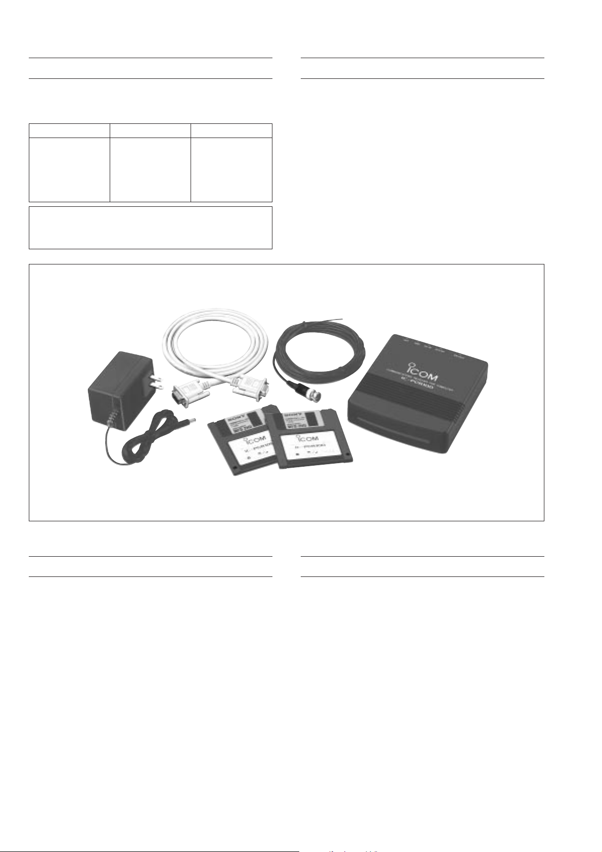
COMMUNICATION
RECEIVER FOR COMPUTER
iC-pcr100
REPAIR NOTES
1. Make sure a problem is internal before disassembling
the receiver.
2.
DO NOT open the receiver until the receiver is discon-
nected from its power source.
3.
DO NOT force any of the variable components. Turn
them slowly and smoothly.
4.
DO NOT short any circuits or electronic parts. An insu-
lated tuning tool MUST be used for all adjustments.
5.
DO NOT keep power ON for a long time when the
receiver is defective.
6.
READ the instructions of test equipment thoroughly
before connecting equipment to the receiver.
INTRODUCTION
DANGER
This service manual describe the latest service information
for the IC-PCR100 COMMUNICATION RECEIVER FOR
COMPUTER at the time of publication.
NEVER connect the receiver to an AC outlet or to a DC
power supply that uses more than 16 V. Such a connection
could cause a fire hazard and/or electric shock.
DO NOT expose the receiver to rain, snow or any liquids.
DO NOT reverse the polarities of the power supply when
connecting the receiver.
DO NOT apply an RF signal of more than 20 dBm (100
mW) to the antenna connector. This could damage the
receiver’s front end.
Be sure to include the following four points when ordering
replacement parts:
1. 10-digit order numbers
2. Component part number and name
3. Equipment model name and unit name
4. Quantity required
<SAMPLE ORDER>
1130004200 S.IC TC4S66F IC-PCR100 MAIN UNIT 1 piece
8810008660 Screw PH B0 3 ×8 NI-ZU IC-PCR100 CHASSIS 4 pieces
Addresses are provided on the inside back cover for your
convenience.
ORDERING PARTS
To upgrade quality, any electrical or mechanical parts and
internal circuits are subject to change without notice or
obligation
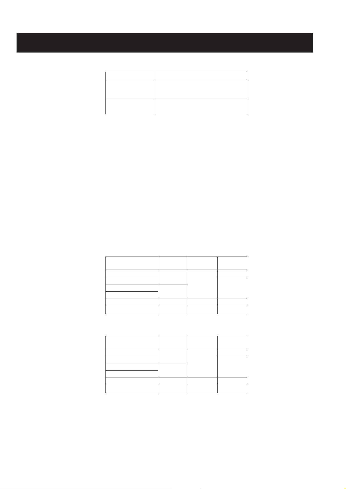
MODEL
IC-PCR100
Europe
U.K.
Canada
U.S.A-1
Other
EUR
UK
CAN
USA-1
OTH
VERSION SYMBOL

TABLE OF CONTENTS
SECTION 1 SPECIFICATIONS
SECTION 2 INSIDE VIEWS
SECTION 3 DISASSEMBLY INSTRUCTIONS
SECTION 4 CIRCUIT DESCRIPTION
4 - 1 RECEIVER CIRCUITS............................................................................................................................. 4 - 1
4 - 2 PLL CIRCUITS........................................................................................................................ ................ 4 - 4
4 - 3 POWER SUPPLY CIRCUITS.................................................................................................................. 4 - 5
4 - 4 CPU PORT ALLOCATIONS .................................................................................................................... 4 - 6
SECTION 5 ADJUSTMENT PROCEDURES
5 - 1 PREPARATION BEFOR SERVICING ..................................................................................................... 5 - 1
5 - 2 PLL ADJUSTMENTS .............................................................................................................................. 5 - 3
5 - 3 IF PEAK AND TOTAL GAIN ADJUSTMENTS ....................................................................................... 5 - 5
5 - 4 SOFTWARE ADJUSTMENTS ................................................................................................................ 5 - 7
SECTION 6 PARTS LIST
SECTION 7 MECHANICAL PARTS AND DISASSEMBLY
SECTION 8 SEMI-CONDUCTOR INFORMATION
SECTION 9 BOARD LAYOUTS
9 - 1 MAIN UNIT.............................................................................................................................................. 9 - 1
SECTION 10 BLOCK DIAGRAM
SECTION 11 VOLTAGE DIAGRAM
11 - 1 MAIN UNIT ............................................................................................................................................ 11 - 1
M GENERAL
• Frequency range :
*Specifications guaranteed 0.5–1300 MHz only
• Mode : AM, FM, WFM
• Frequency stability : ±5 ppm (at 1300 MHz: ±0˚C to +50˚C; +32˚F to +122˚F)
• Frequency resolution : 1 kHz (minimum)
• Power supply requirement : 13.8 V DC ±15 % for receiver unit; or supplied AC adaptor (negative ground)
• Current drain (at 13.8 V DC) : Power ON (PC power OFF) 0.1 A
Max. audio 0.7 A
Standby (squelched) 0.6 A
• Usable temperature range : ±0˚C to +50˚C; +32˚F to +122˚F
• Antenna connector : BNC (50 Ω)
• RS-232C connector : D-sub 9-pin (female)
• Dimensions : 131(W)
✕35(H)✕164.1(D) mm;
5
5
⁄32(W)✕13⁄8(H)✕615⁄32(D) inch
• Weight : approx. 0.5 kg; 1 lb 2 oz
M RECEIVER
• Receive system : Triple-conversion superheterodyne
• Intermediate frequency : 1st 266.7 MHz
2nd 10.7 MHz
3rd 450 kHz (except WFM)
• Sensitivity (typical)* :
• Squelch sensitivity :
(at threshold)
• Selectivity (typical) : WFM 230 kHz/–6 dB
WFM/FM/AM 50 kHz/–6 dB
FM/AM 15 kHz/–6dB
FM/AM/SSB/CW 6 kHz/–6 dB
• Max audio output : Mono 200 mW
(at 10% distortion with an 8Ω load) Stereo 100 mW
• External speaker connector : 3-conductor 3.5(d) mm (
1
⁄8")/4–8 Ω
Frequency
[MHz]
0.5 – 1.799
1.8 – 27.999
28.0 – 29.999
30.0 – 49.999
50.0 – 699.999
700.0 –1300.000
1 - 1
SECTION 1 SPECIFICATIONS
Version Frequency Range (MHz)
0.010 – 823.999*
U.S.A.-1 849.001 – 868.999
894.001 – 1300.000
Europe, U.K.
0.010 – 1300.000*
Canada Other
FM
—
0.5 µV
0.32 µV
0.4 µV
AM
2.5 µV
1.8 µV
1.0 µV
1.3 µV
WFM
—
0.79 µV
1.0 µV
*FM and WFM are measured at 12 dB SINAD; AM is measured at
10 dB S/N.; 230 kHz (for WFM), 15 kHz (for FM) and 6 kHz (for
AM) passband widths are selected.
Frequency
[MHz]
0.5 – 1.799
1.8 – 27.999
28.0 – 29.999
30.0 – 49.999
50.0 – 699.999
700.0 –1300.000
FM
—
0.63 µV
0.5 µV
0.63 µV
WFM
—
5.6 µV
10 µV
AM
1.8 µV
0.89 µV
0.71 µV
0.89 µV
2 - 1
SECTION 2 INSIDE VIEWS
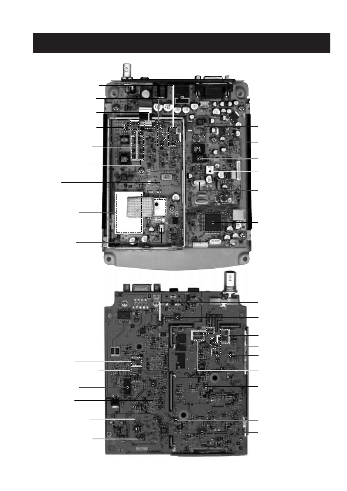
¡MAIN UNIT
Bottom view
Top view
0.01–1.8 MHz RF filter circuit
1.8–15 MHz RF filter circuit
15–30 MHz RF filter circuit
VCO3 circuit
Reference oscillator
(X5: CR-629 12.8 MHz)
VCO1, VCO2 circuits
AGC control circuit
AGC amplifier (Q45: 2SC4211)
FM discriminator
(X2: CDBCA450CX24)
CPU
(IC21: HD6433644A)
IF 15 kHz filter
(FI7: CFWS450E)
IF 6 kHz filter
(FI6: CFWS450HT)
AM demodulator
(D63: 1SS372)
FM 3rd LO signal
(X1: CR-630 12.5 MHz)
150–300 MHz RF filter circuit
350–700 MHz RF filter circuit
700–1300 MHz RF filter circuit
AF amplifier (IC23: M62429)
AF power amplifier (IC25: NJM2073)
0.01–1.8 MHz RF filter circuit
30–50 MHz RF filter circuit
50–150 MHz RF filter circuit
1st mixer (IC4: µPC2721)
PLL IC (IC8: MC145220)
WFM demodulator IC
(IC7: LA1832M)
FM demodulator IC
(IC10: TA31136)
IF amplifier (Q29: 3SK131)
EEPROM (IC20: X25020SI)
2nd mixer (IC5: µPC2721)
HF RF amplifier (Q12: 2SK2171)
3 - 1
SECTION 3 DISASSEMBLY INSTRUCTIONS
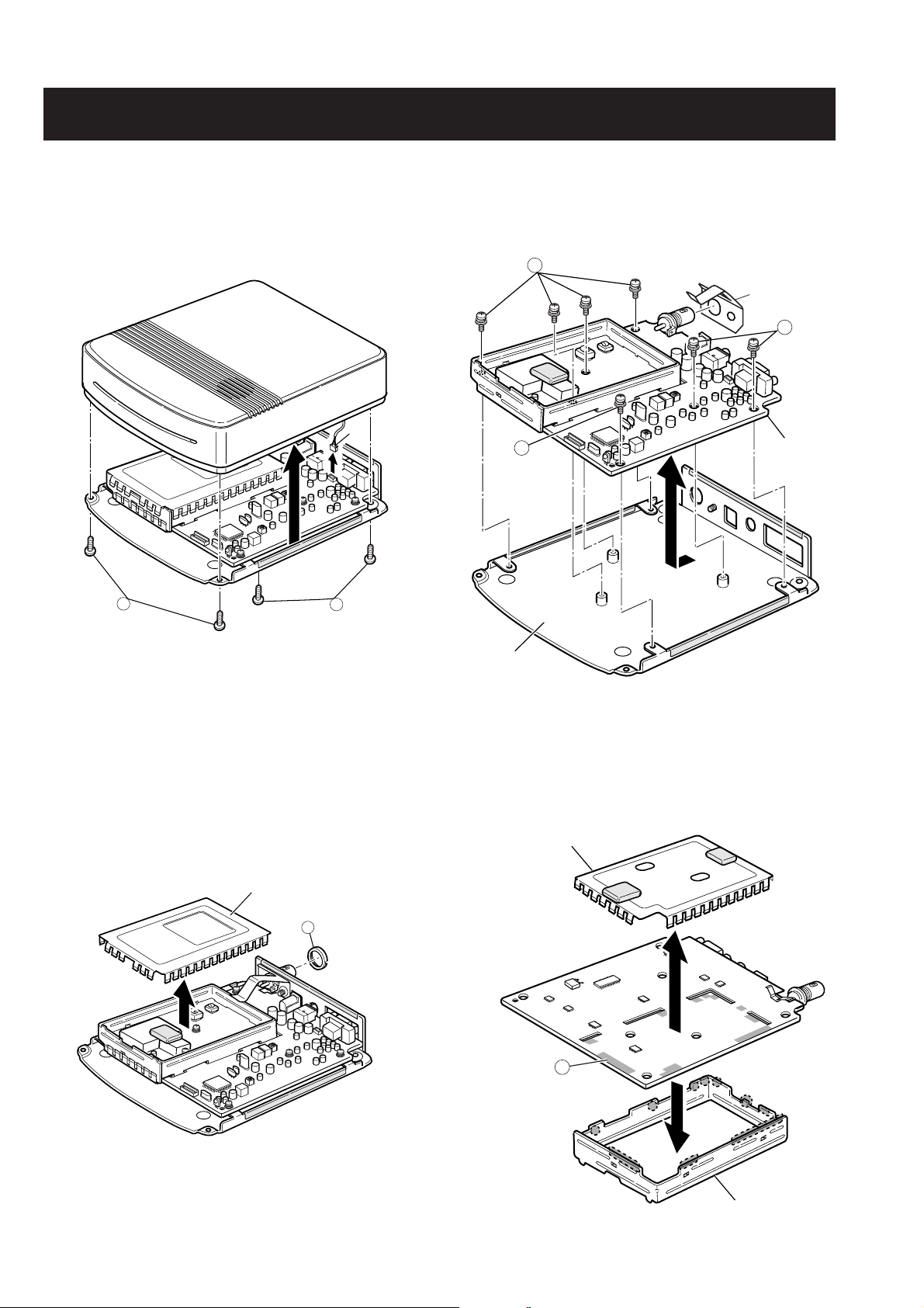
• Removing the cover panel
1 Unscrew 4 screws, A.
2 Disconnect the speaker jack J8.
3 Remove the cover panel in the direction of the arrow.
• Removing the antenna plug and shield U-plate
1 Unscrew the nut, B.
2 Remove the shield cover in the direction of the arrow.
A
A
Cover panel
J8
Shield L-plate
Shield case
D
B
Shield U-plate
C
C
MAIN UNIT
Chassis
C
• Removing the MAIN unit
1 Unscrew 7 screws from the MAIN unit, C (set screw, 3
mm), to separate the chassis and unit.
2 Remove the unit in the direction of the arrow.
• Removing the shield plate
1 Remove the shield plate in the direction of the arrow.
2 Unsolder 9 points, D, to separate the shield plate and
MAIN unit.
SECTION 4 CIRCUIT DESCRIPTION
4 - 1
4-1 RECEIVER CIRCUITS
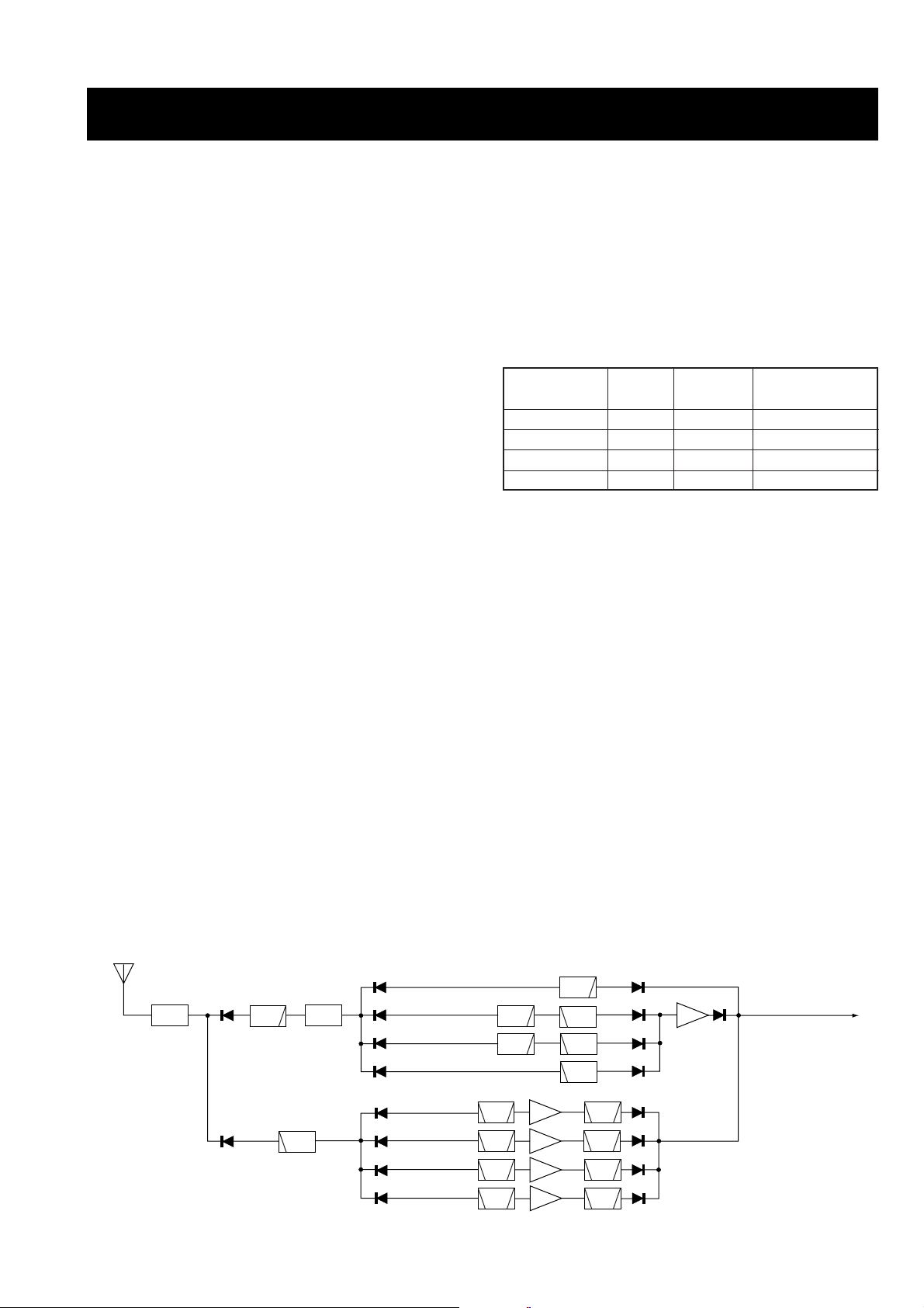
4-1-1 RF ATTENUATOR CIRCUIT
The attenuator circuit attenuates the signal strength to
approx. 20 dB to protect the RF amplifier from distortion
when excessively strong signals are received.
The RF signals from the antenna connector are passed
through or bypass the “L” type attenuator (R1, R3). The signals are then applied to the RF filter circuit.
4-1-2 RF FILTER CIRCUIT
The applied signals pass through either the low-pass filter or
the high-pass filter circuits via the band switching diodes.
• RF signals below 50 MHz
The RF signals below 50 MHz are passed through the lowpass filter (L1, L2, C7–C11) via the band switching diode
(D2). The filtered signals are applied to the HF RF circuit.
• RF signals above 50 MHz
The RF signals above 50 MHz are applied to the high-pass
filter (L172, C477, C478) after passing through the band
switching diode (D4). The filtered signals are then applied to
the VHF/UHF RF circuit.
4-1-3 HF RF CIRCUIT
The HF RF circuit amplifies the received signals within the
range 0.01–50 MHz and filters out-of-band signals.
The HF RF circuit consists of three low-pass filters, three
high-pass filters and one RF amplifier.
The filtered signals below 1.8 MHz from the RF filter circuit
are passed through the low-pass filter (L3, L4, C14–C16)
between the band swithing diodes (D6, D35), and are then
applied to the 1st mixer circuit (IC4) directly.
The 1.8–14.999 MHz signals pass through the low-pass filter (L6, L7, C21–C25) and high-pass filter (L8, L9,
C26–C30) between the band switching diodes (D3, D7), and
are then applied to the 1st mixer circuit after being amplified
at the RF amplifier (Q12).
The 15–29.999 MHz signals pass through the low-pass filter
(L10, L11, C33–C37) and high-pass filter (L11, L12,
C38–C42) between the band switching diodes (D90, D91),
and are then applied to the 1st mixer circuit via the RF amplifier circuit (Q12).
The 30–49.999 MHz signals pass through the high-pass filter (L14, L15, C45–C49) between the band switching diodes
(D8, D5), and are then applied to the 1st mixer circuit via the
RF amplifier circuit (Q12).
• Filters
4-1-4 VHF/UHF RF CIRCUIT
The VHF/UHF RF circuit amplifies the received signals within the range 50–1300 MHz and filters out-of-band signals.
The VHF/UHF RF circuit consists of 4 bands of filter circuits
with an RF amplifier for each.
The 50–149.999 MHz signals from the RF filter pass through
high-pass filter (D11, L17, C53–C55, D12, D82, D83, L18,
C57) via the band switching diode (D10), and are then
amplified at the RF amplifier (Q8) between the tunable
bandpass filters (D13, D80, L19–L21, D14, D81, L23–L25).
The filtered signals are applied to the 1st mixer circuit (IC4)
via the band switching diode (D15).
For improving the characteristic of the bandpass filter circuit,
the shift switch (Q31) shifts the cut off frequency of the highpass filter (D12, D82, D83, L18, C57). The shift switch (Q31)
is controlled by the VCO 1 signal from the CPU (IC21).
Receive freq.
SW diode
Filter select
Components
(MHz) signal
0.01–1.799
1.8–14.999
15.0–29.999
30.0–49.999
D6, D35
D3, D7
D90, D91
D8, D5
B0
B1
B2
B3
L3–L5, C14–C17
L6–L9, C21–C30
L10–L13, C33–C42
L14, L15, C45–C49
• RF filter and amplifier circuits
0.01–50 MHz
50–150 MHz
150–350 MHz
350–700 MHz
700–1300 MHz
50–1300 MHz
1.8–15 MHz
15–30 MHz
0.01–1.8 MHz
30–50 MHz
Tuned
BPF
ATT AGC
Tuned
BPF
Tuned
BPF
Tuned
BPF
HPF
Tuned
BPF
Tuned
BPF
Tuned
BPF
Tuned
BPF
HPF
HPF
LPF
LPF
LPF
HPF
RF Amp.
RF Amp.
To 1st mixer circuit
RF Amp.
LPF
RF Amp.
RF Amp.
Q12
Q8
Q9
Q10
Q11
4 - 2
The 150–349.999 MHz signals from the band switching
diode (D16) pass through the high-pass filter (L27–L29,
C69–C74) and tunable bandpass filter (D18, L31–L33), and
are then amplified at the RF amplifier (Q9) and pass through
another tunable bandpass filter (D19, L35–L37). The filtered
signals are applied to the 1st mixer circuit (IC4) via the band
switching diode (D20).
The 350–699.999 MHz signals from the band switching
diode (D21) pass through the high-pass filter (L40, C92–
C94) and tunable bandpass filter (D22, D23, L41, L42). The
filtered signals are then amplified at the RF amplifier (Q10)
and pass through the tunable bandpass filters (D24, D77,
L45–L47). The filtered signals are applied to the 1st mixer
circuit (IC4) via the band switching diode (D25).
The 700–1300 MHz signals from the band switching diode
(D26) pass through the high-pass filter (L141, C110, C606)
and 2-stage tunable bandpass filters (D27, D28, L163, D29,
D30, L51–L53). The filtered signals are then amplified at the
RF amplifier (Q11) and pass through the tunable bandpass
filters (D31, D32, L56, L178). The filtered signals are applied
to the 1st mixer circuit (IC4) via the band switching diode
(D33).
The tunable bandpass filters employ varactor diodes to tune
the center frequency of the RF passband for wide bandwidth
receiving and good image response rejection. These diodes
are controlled by TUNV signal from the CPU (IC21, pin 54)
via the tune controller (IC22b).
• Tunable bandpass filters
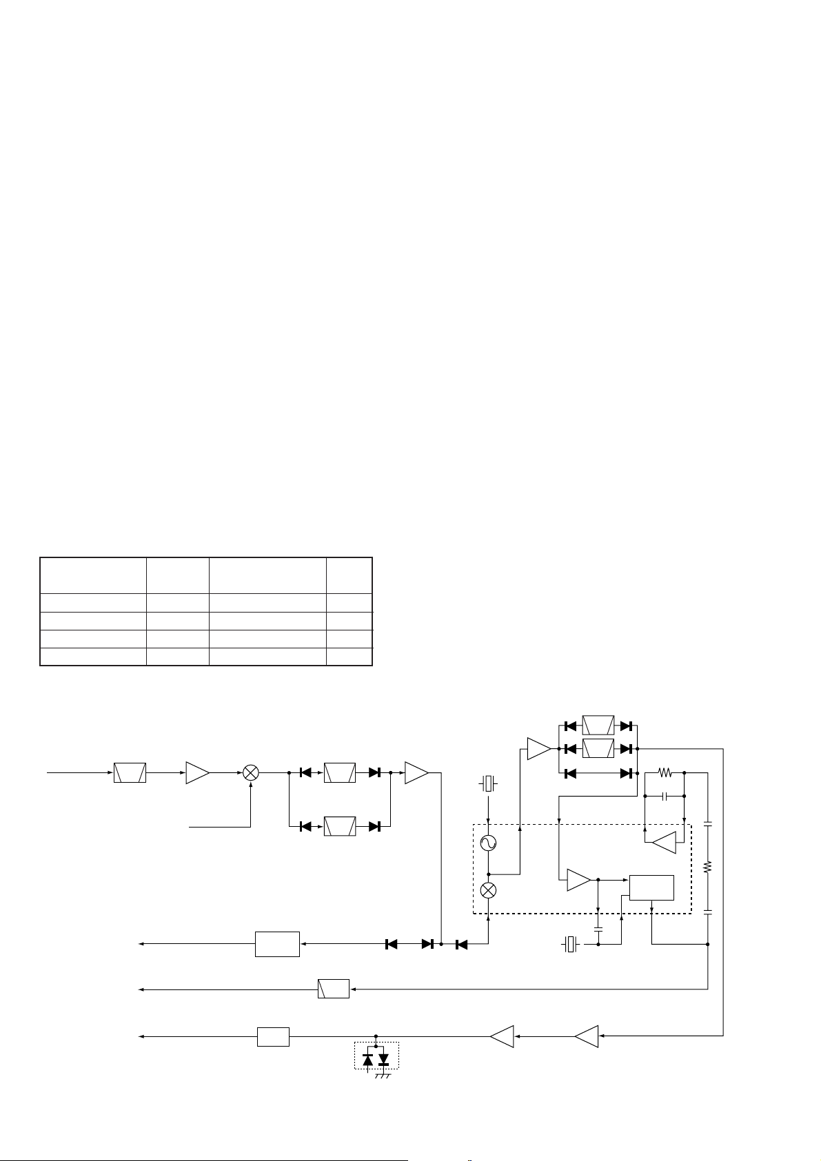
4-1-5 1ST MIXER CIRCUIT
The 1st mixer circuit converts the received RF signals into a
fixed frequency of the 1st IF signal with a PLL output frequency. By changing the PLL frequency, only the desired
frequency will pass through the bandpass filters at the next
stage of the 1st mixer.
The filtered RF signals are mixed with 1st LO signals at the
1st mixer circuit (IC4) to produce a 266.7 MHz 1st IF signal.
The 1st IF signal is output from pin 5, and passed through
the bandpass filter (FI1) to suppress unwanted harmonic
components. The filtered 1st IF signal is applied to the IF circuit.
The 1st LO signals are generated at the VCO 1 (Q14, Q15)
or VCO 2 (Q18, Q19) circuit (according to the receiving frequency band) and are amplified at the buffer amplifier
(IC26). The amplified signals are then applied to the 1st
mixer (IC4, pin 2) directly or passed through the divider circuit (IC6).
4-1-6 1ST IF AND 2ND MIXER CIRCUITS
The 2nd mixer circuit converts the 1st IF signal into a 2nd IF
signal.
The filtered 266.7 MHz 1st IF signal from the bandpass filter
(FI1) is amplified at the 1st IF amplifier (Q13) then mixed
with the 2nd LO signal at the 2nd mixer circuit (IC5) to produce a 10.7 MHz 2nd IF signal. The 2nd IF signal is passed
through either 2 bandpass filters (FI2 or FI3; depending on
the selected mode and bandwidth). The filtered 2nd IF signal is amplified at the IF amplifier (Q29), then applied to the
WFM demodulator or 3rd IF circuit.
Receive freq. BPF select Varactor RF
(MHz) signal diodes amp.
50.0–149.999
150.0–349.999
350.0–699.999
700.0–1300.0
B4
B5
B6
B7
D11–D14, D80–D83
D18, D19
D22–D24, D77
D27–D32
Q8
Q9
Q10
Q11
• IF and demodulator circuits
3rd
Mixer
IC10
2nd Mixer BW: 50 kHz
BW: 230 kHz
2nd LO
IF Amp.
IF Amp.
1st IF signal from
1st mixer (IC4)
3rd
LO
IF Amp.
Limiter
Active
filter
X2
450 kHz
X1
10.25 MHz
IC5
16
11 10
13
5
7
8
9
Q38
Q29
Q13
BPF FI2
FI3
FM
Detector
FI6
FI7
WFM
Detector
WFM
FM
AM
HPF
ANL
IF Amp.
Buffer Amp.
Q43
Q42
AM
detector
IC7
D63Q44, D52
to AF switch IC14
4 - 3
4-1-7 3RD MIXER CIRCUIT
The 3rd mixer circuit mixes the 2nd IF signal and 3rd LO signal to produce a 450 kHz 3rd IF signal (except WFM mode).
The 10.7 MHz 2nd IF signal from the IF amplifier (Q29) is
applied to the 3rd mixer section in the FM IF IC (IC10, pin
16). The applied signal is mixed with a 3rd LO signal generated by X1 (10.25 MHz) to produce a 450 kHz 3rd IF signal.
The 3rd IF signal is output from pin 3, and passed through
one of 2 bandpass filters (FI6 or FI7) or bypassed, according to the selected mode after being amplified at the IF
amplifier (Q38). The filtered or bypassed signal is applied to
the each demodulator circuit (except WFM mode).
• Bandpass filter selection
4-1-8 DEMODULATOR CIRCUITS
The demodulator circuit converts the 2nd IF signal into AF
signals. 3 separate demodulator circuits are employed for
each mode.
(1) WFM mode
The 10.7 MHz 2nd IF signal from the IF amplifier (Q29) is
applied to the WFM demodulator circuit (IC7, pin 1).
The IF signal is applied to the quadrature detector section
(IC7, pin 11) to demodulate AF signals. The demodulated AF
signals are output from pin 14, 15, and are then applied to
the AF switch circuit.
(2) FM mode
The filtered or bypassed 3rd IF signal is applied to the quadrature detector section in the FM IF IC (IC10, pin 10) then
mixed with the signal generated by the discriminator (X2) to
demodulate AF signals. The AF signals are output from pin
9 and applied to the AF switch circuit via the high-pass filter
circuit (IC11).
(3) AM mode
The filtered 3rd IF signal from the one of 2 bandpass filters
(FI6 or FI7) is amplified at the IF and buffer amplifiers (Q42,
Q43). The amplified IF signal is applied to the AM detector
circuit (D63) to be converted into AF signals, and the AF signals are applied to the AF switch circuit.
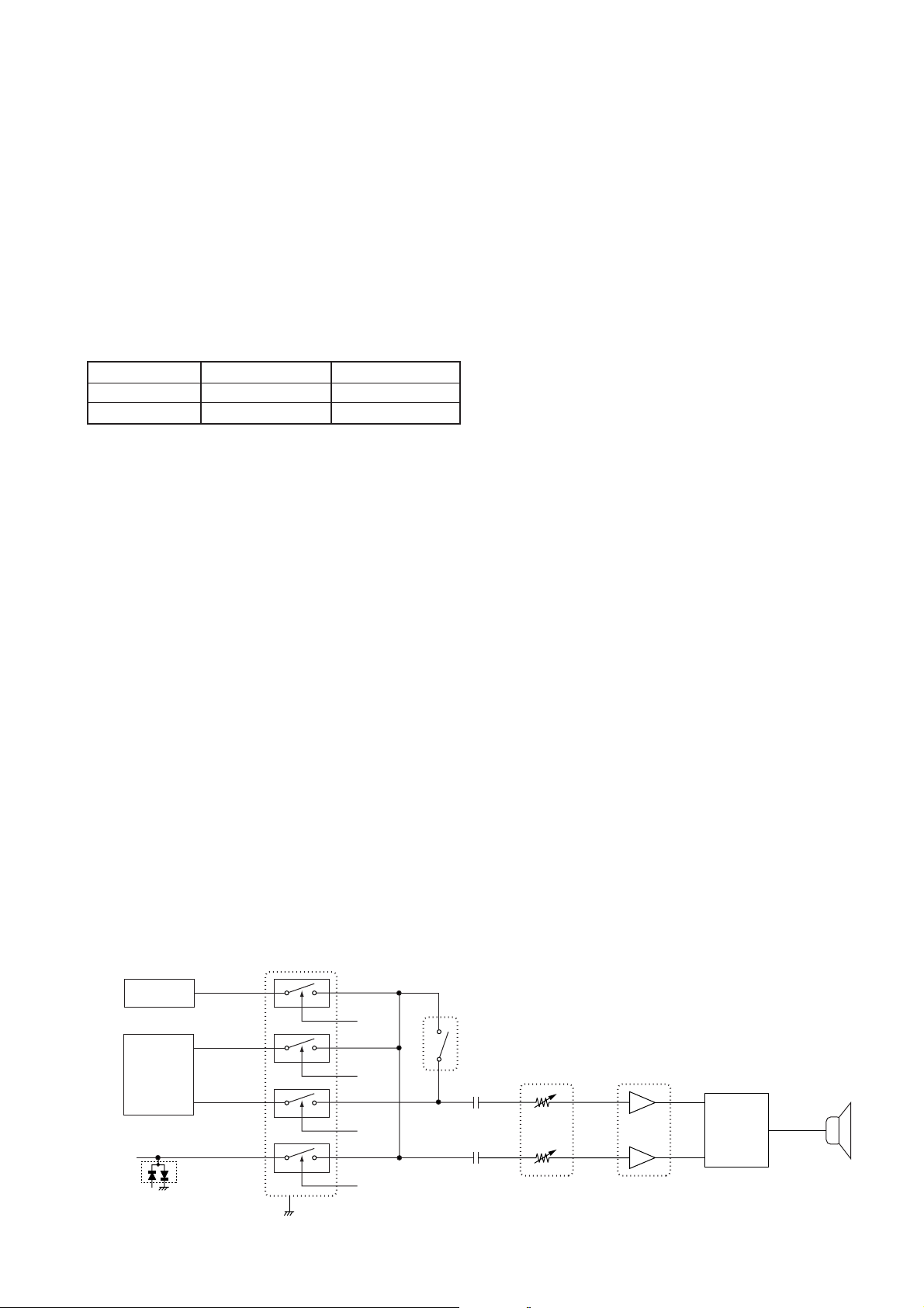
4-1-9 AF SWITCH CIRCUIT
The demodulated AF signals from the demodulator circuits
are applied to the AF switch (IC14). This consists of 4 analog switches which are selected with a mode signal from the
CPU (IC21) via the I/O expander (IC3). The switched AF signals are applied to the AF circuit.
4-1-10 AF CIRCUIT
The AF signals from the AF switch circuit are passed
through the AF mute switch and then amplified at the AF
power amplifier circuit.
The AF signals from the AF switch are applied to the electronic volume control circuit (IC23, pin 1). The level controlled AF signals are output from pin 2 and applied to the AF
power amplifier (IC25, pin 6). The power amplified AF signals are applied to the internal speaker via the [EXT SP]
jack.
The electronic volume control circuit controls AF gain, therefore, the AF output level varies according to the [VOL] setting and also the squelch conditions.
4-1-11 SQUELCH CIRCUIT
A squelch circuit cuts out AF signals when no RF signal is
received or when the S-meter signal is lower than the
[SQUELCH] control setting level. By detecting noise components in the AF signals, the CPU controls the electronic volume control circuit.
• NOISE SQUELCH
Some noise components in the AF signals from pin 9 of the
FM IF IC (IC10) are applied to the noise amplifier section in
the IC (IC10, pin 8). The amplified signals are output from
pin 7. The output signals are applied to the noise and buffer
amplifiers (Q58, Q59) and rectified at the noise detector
(D89) to be converted into DC voltage, then applied to the
CPU (IC21, pin 60) as an NOIN signal.
Modes Bandpass filter Passband width
AM FI6 6 kHz
FM FI7 15 kHz
• Squelch and AF amplifier circuits
IC14
11 10
98
43
1
7
D63
IC10
FM
Detector
IC9
WFM
Detector
AM
Detector
AFFM
AWFL
AWFR
AFAM
12
13
6
5
2
FM5
WFM5
WFM5
AM5
AF switch
IC29
Electronic
volume
8
1
IC23
7
2
AF power
Amplifier
7
6
IC25
External SP jack
1
J7
3
SP
• S-METER SQUELCH
The S-meter signal is applied to the CPU from the meter
amplifier circuit (IC13a) via the SMAD line, and also the Smeter squelch setting level is applied to the CPU. The CPU
compares these signals, then outputs a control signal to the
electronic volume control circuit (IC23) to cut out AF signals.
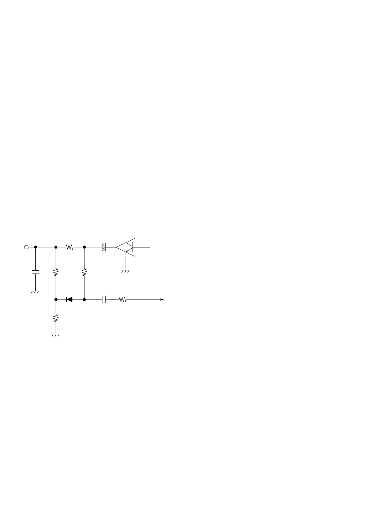
4-1-12 AUTOMATIC NOISE LIMITER CIRCUIT
The ANL (Automatic Noise Limiter) circuit (D62, Q44,
R381–R384) reduces pulse noises. The ANL function activates only when AM mode is selected.
The AM detector output signal from D63 is applied to the
cathode of D62 passing through R381 where it is divided by
R381 and R382. The signal is also applied to the anode of
D62, passing through R383 and R384.
When the ANL function is activated (Q44 is ON), C375 is
grounded. The detector output, including pulse noise, is
applied to the cathode of D62 only. If pulse noises are
received, the cathode voltage of D62 becomes higher than
the anode voltage and D62 turns OFF. Thus, while pulse
noises are received, the detected signal is not applied to the
AF switch(IC14).
4-1-13 AGC CIRCUIT
The AGC (Auto Gain Control) circuit reduces IF amplifier
gain to keep the audio output at a constant level.
An RSSI signal is used for AGC function from the WFM IF
IC (IC7, pin 20) while in WFM mode, or used from the FM IF
IC (IC10, pin 12) while in FM, AM (except WFM) mode.
The RSSI output signal is amplified at the AGC amplifier
(Q33) during WFM operation. In other modes, the RSSI signal is amplified at the AGC amplifier (Q45), and passes
through the time constant circuit (Q46, Q47, R284, R290,
R291, C372, C373, C905) and is then applied to the IF
amplifiers (Q13, Q39). The AGC control signal is applied to
the VHF/UHF tunable bandpass filters after being amplified
at the VHF/UHF AGC amplifier (IC13b).
AGC speed is controlled by changing the time constant at
the AGC control line with resistors (R284, R290, R291) and
capacitors (C372, C373, C905). R290 and C372 are used
for AGC slow, and R284 and C905 are used for AGC fast
mode’s time constant. However, R291 and C373 are connected to the AGC control line while scanning to obtain the
fastest AGC response.
4-1-14 S-METER CIRCUIT
The S-meter circuit indicates the relative received signal
strength while receiving and changes depending on the
received signal strength.
A portion of the AGC signal is applied to the meter amplifier
circuit (IC13a). The amplified signal is then applied to the
CPU (IC21, pins 64) as an SMAD signal to drive the Smeter.
The SMAD signal is also used for noise and S-meter
squelch operation by comparison with the [SQUELCH] control setting level and received signal strength at the CPU.
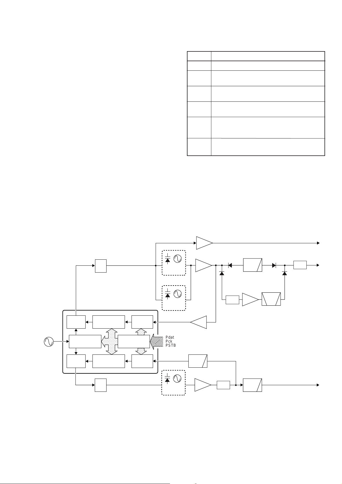
4-2 PLL CIRCUITS
4-2-1 GENERAL
The PLL circuit provides stable oscillation of the 1st and 2nd
local frequencies. The PLL circuit consists of the PLL IC,
charge pump, loop filter and reference oscillator and
employs a pulse swallow counter.
4-2-2 1ST LO LOOP
The 1st LO circuit generates the 1st LO frequencies, and the
signals are applied to the 1st mixer circuit.
The generated signal from VCO 1 (Q14, Q15) or VCO 2
(Q18, Q19) is applied to the prescaler section in the PLL IC
(IC8, pin 8) after being amplified at the buffer amplifiers
(IC26, Q27). The applied signal is prescaled in the PLL IC
based on the divided ratio (N-data) to produce approx. 50
kHz signals which are applied to the phase detector section.
The generated reference signal from the reference oscillator
(X5; 12.8 MHz) is applied to the programmable divider section in the PLL IC (IC8, pin 1). The applied signal is
prescaled in the PLL IC based on the divided ratio (1/256) to
produce approx. 50 kHz phase signals. The reference phase
signals are applied to the phase detector section.
The phase detector section compares 2 of the applied
phase signals. The phase detected signals are passed
through the charge pump section and then output from pin 4
of the PLL IC. The output signals are applied to the loop filter circuit (Q25, Q26) to be converted into DC voltage as a
PLL lock voltage. The lock voltage is applied to the CPU
(IC22, pin 61) via the buffer amplifer (Q24) as an L1AD signal to control the VHF/UHF tunable bandpass filter.
4 - 4
• Automatic noise limiter circuit
+
R383 R375 Q44
D62 C377 R385
R381
R382
R384C378
ANL
AF signal
from D63
to AF switch
IC14
4 - 5
4-2-3 2ND LO LOOP
The 2nd LO circuit generates the 2nd LO frequencies, and
the signals are applied to the 2nd mixer circuit.
The generated signal at the VCO 3 (Q34) enters the PLL IC
(IC8, pin 13) via the buffer amplifier (Q35), is divided ath the
programmable divider seiction and is then applied to the
phase detector section.
The phase detector compares the input signal with a reference frequency, and then outputs the out-of-phase signal
(pulse-type signals) from pin17
The pulse-type signal is converted into DC voltage (lock
voltage) at the loop filter (Q36, Q37), and then applied to the
VCO 3 to stabilize the oscillated frequency.
4-3 POWER SUPPLY CIRCUITS
4-3-1 VOLTAGE LINES
Description
The voltage from a DC power supply.
The same voltage as the ACHV line which is
controlled by the [POWER] switch.
Common 5 V line converted from the HV line by
the +5 regulator circuit (IC16).
Common 8 V line converted from the HV line by
the +8 regulator circuit (IC17).
Common 33 V line converted from the HV line by
the 33 V DC-DC convertor circuit (IC18). The
output voltage is applied to the PLL circuit.
Common 5 V line converted from the ACHV line
by the L+5 regulator circuit (IC15).
Line
ACHV
HV
+5
+8
+33
L+5
• PLL circuit
Loop
filter
Loop
filter
Buffer
Amp.
Amp.
Buffer
Buffer
Q36, Q37
Q25, Q26
Q35
Q27
Q22
Q24
IC6
IC26
Q34
D72–D74
Q14, Q15
D39, D40
Q18, Q19
D42, D43
to 1st mixer circuit
1st LO-freq.:
532.4–1066.65 MHz
2nd LO-freq.:
255–257 MHz
1st LO-freq.:
266.7–532.35 MHz
to 2nd mixer circuit
L1AD to the CPU
1/2
ATT
ATT
LPF
LPF
BPF
LPF
VCO1
VCO3
VCO2
X5
12.8 MHz
Shift register/
data latch
PLL IC (IC8)
Prescaler
Phase
detector
Programmable
counter
Prescaler
Phase
detector
Programmable
counter
Programmable
divider
Pdat
Pck
PSTB
4-4 PORT ALLOCATIONS
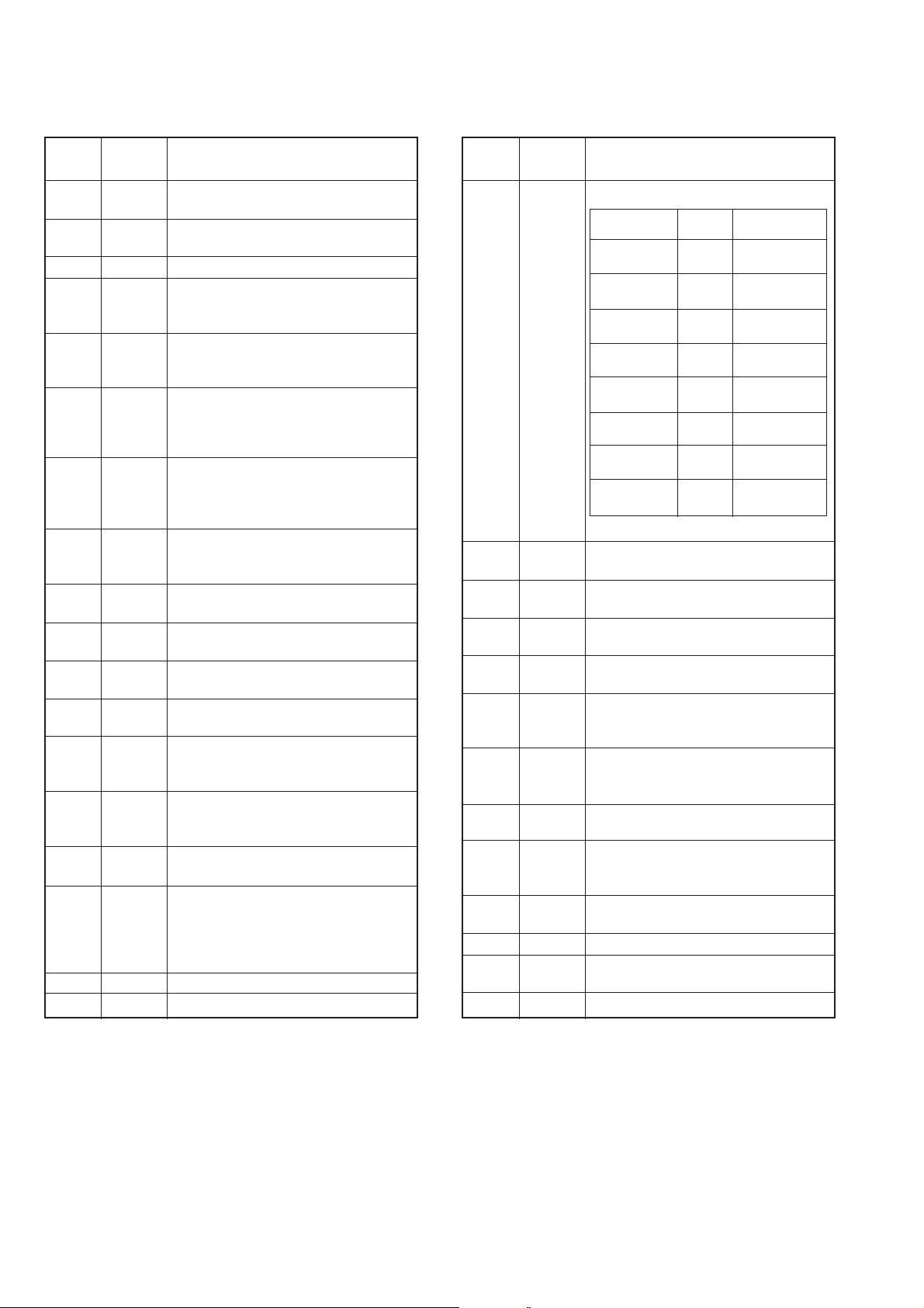
4-4-1 CPU (IC20) CPU (IC20) — continued
4 - 6
Input port from WFM IC (IC7, pin 7) for
the stereo indicator.
Input ports for the CPU system clock
oscillator (X6; 9.8304 MHz).
Input port for the reset signal.
Outputs power switching circuit control
signal.
High : While turning power ON.
Outputs attenuator control signals.
Low: When attenuator function is
ON.
Outputs AGC time constant control
signals.
High : While scanning (fastest AGC
speed).
Outputs AGC time constant control
signals.
Low : When WFM or FM mode is
selected (AGC-fast).
Outputs ANL control signals.
High : While ANL fuction is ON.
(AM mode only)
Outputs AF mixing control signal for
the stereo audio.
Outputs strobe signals for the output
expander ICs (IC1, IC3).
Outputs data signal for the electronic
volume IC (IC23).
Input port for serial signal from the
EEPROM IC (IC20).
Outputs data signal for the EEPROM
IC (IC20) and output expander ICs
(IC1, IC3).
Outputs clock signal for the EEPROM
IC (IC20) and output expander ICs
(IC1, IC3).
Outputs chip select signal to the EEPROM IC (IC20).
Outputs 1st LO filter select signals.
High : When frequencies from 0.01 to
265.699 MHz are displayed.
Low : When frequencies from 265.7
to 1300.0 MHz are displayed.
Outputs VCO1 shift signals.
Outputs VCO2 shift signals.
1
8, 9
10
17
18
19
20
21
22
23, 24
25
26
27
28
29
34
35
36
FMST
OSC1,
OSC2
RES
POCO
ATTC
SCAN
AGCS
ANL
SWAF
MST1,
MST2
AFDT
MSI
MSO
Mck
ECS
PFL2
VSF1
VSF2
Pin Port
Description
number name
Output VCO2/VCO1 select signals.
Outputs strobe signals for reference
frequency and VXO frequency.
Outputs strobe signals for the PLL IC
(IC8).
Outputs serial data signals for the
PLL IC (IC8).
Outputs serial clock signal for the PLL
IC (IC8).
Input port for data signal from the
connected PC via the RS-232C interface IC (IC9).
Outputs data signal to the connected
PC via the RS-232C interface IC
(IC9).
Outputs tunable bandpass filter control voltage.
Input port for unlock signal from the
PLL IC (IC8).
Low : PLL unlock
Input port signal strength detection
signal (NOIN; pulse-type).
Input port for 1st LO PLL lock voltage.
Input port for the CTCSS decoded
signal.
Input port for S-meter signal.
37, 38
39
41
42
43
48
49
54
59
60
61
62
63
VCO1,
VCO2
DST1
PSTB
Pdat
Pck
RXD
TXD
TUNE
LCT
NOIN
L1AD
CTAD
SMAD
Pin Port
Description
number name
VCO freq.
[MHz]
533.40–
749.90
750.00–
1064.70
533.40–
534.35
532.40–
533.35
534.40–
749.95
750.00–
1066.65
533.30–
749.95
750.00–
1033.300
Display freq.
[MHz]
0.01–
108.299
108.3–
265.699
265.7–
266.699
266.7–
267.699
267.7–
483.299
483.3–
799.999
800.0–
1016.699
1016.7–
1300.000
Selected
VCO
VCO1
VCO2
VCO1
VCO1
VCO1
VCO2
VCO1
VCO2
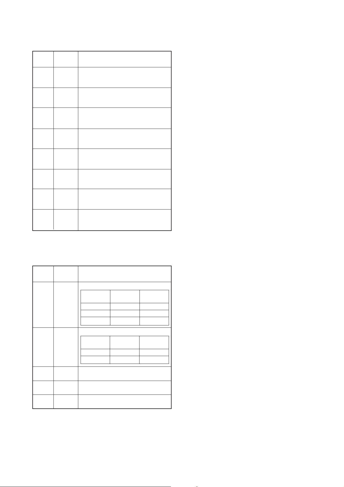
4-4-2 OUTPUT EXPANDER IC
(1) IC1
(2) IC3
4 - 7
Outputs low-pass filter select signal.
High: When frequencies below 1.8
MHz are displayed.
Outputs bandpass filter select signal.
High: When frequencies from 1.8 to
14.999 MHz are displayed.
Outputs bandpass filter select signal.
High: When frequencies from 15.0 to
29.999 MHz are displayed.
Outputs bandpass filter select signal.
High: When frequencies from 30.0 to
49.999 MHz are displayed.
Outputs bandpass filter select signal.
High: When frequencies from 700.0
to 1300.0 MHz are displayed.
Outputs bandpass filter select signal.
High: When frequencies from 350.0
to 699.999 MHz are displayed.
Outputs bandpass filter select signal.
High: When frequencies from 150.0
to 349.999 MHz are displayed.
Outputs bandpass filter select signal.
High: When frequencies from 50.0 to
149.999 MHz are displayed.
Pin Port
Description
number name
4
5
6
7
11
12
13
14
B0C
B1C
B2C
B3C
B7C
B6C
B5C
B4C
Output 450 kHz IF filter select signals.
Output 10.7 MHz IF filter select signals.
Outputs AM mode select signals.
High: When AM mode is selected.
Outputs FM mode select signals.
High: When FM mode is selected.
Outputs WFM mode select signals.
High: When WFM mode is selected.
Pin Port
Description
number name
4–6
7, 14
11
12
13
FL1–FL3
FL4, FL5
AM5
FM
WFM
SW
signal
FL1
FL2
FL3
Bandpass
filter
FI6
FI7
By-pass
Passband
width
6 kHz
15 kHz
—
SW
signal
FL4
FL5
Bandpass
filter
FI2
FI3
Passband
width
50 kHz
230 kHz
 Loading...