

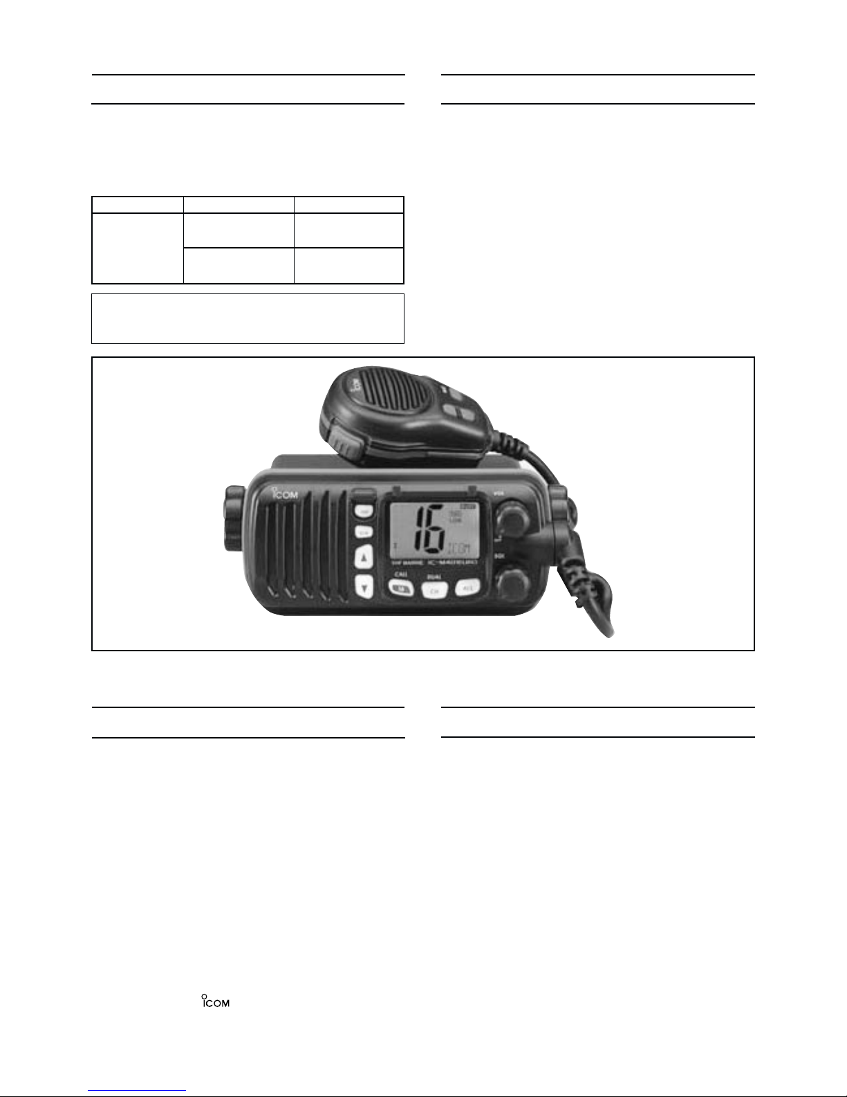
Icom IC-M401E Service Manual

VHF MARINE TRANSCEIVER
iC-m401e
SERVICE
MANUAL
INTRODUCTION
DANGER
This service manual describes the latest service information
for the IC-M401E VHF MARINE TRANSCEIVER at the time
of publication.
4 versions of the IC-M401E have been designed. This service manual covers each version.
MODEL
IC-M401E
VERSION
UK, EUR, HOL,
FRG
EUR-1
SYMBOL
BLACK
WHITE
ORDERING PARTS
Be sure to include the following four points when ordering
replacement parts:
1. 10-digit order numbers
2. Component part number and name
3. Equipment model name and unit name
4. Quantity required
<SAMPLE ORDER>
1110003200 S.IC TA31136FN IC-M401E MAIN UNIT 5 pieces
8820001210 Screw 2438 screw IC-M401E Chassis 12 pieces
Addresses are provided on the inside back cover for your
convenience.
NEVER connect the transceiver to an AC outlet or to a DC
power supply that uses more than 16 V. This will ruin the
transceiver.
DO NOT expose the transceiver to rain, snow or any liquids.
DO NOT reverse the polarities of the power supply when
connecting the transceiver.
DO NOT apply an RF signal of more than 20 dBm (100mW)
to the antenna connector. This could damage the transceiver's front end.
REPAIR NOTES
1. Make sure a problem is internal before disassembling
the transceiver.
2. DO NOT open the transceiver until the transceiver is dis-
connected from its power source.
3. DO NOT force any of the variable components. Turn
them slowly and smoothly.
4. DO NOT short any circuits or electronic parts. An insulat-
ed turning tool MUST be used for all adjustments.
5. DO NOT keep power ON for a long time when the trans-
ceiver is defective.
6. DO NOT transmit power into a signal generator or a
sweep generator.
7. ALWAYS connect a 40 dB to 50 dB attenuator between
the transceiver and a deviation meter or spectrum analyzer when using such test equipment.
8. READ the instructions of test equipment thoroughly
before connecting equipment to the transceiver.
To upgrade quality, anyelectrical or mechanical parts and
internal circuits are subject to change without notice or
obligation.
Icom, Icom Inc. and are registered trademarks of Icom Incorporated (Japan) in the United States, the United Kingdom,
Germany, France, Spain, Russia and/or other countries.

SECTION 1 SPECIFICATIONS
SECTION 2 INSIDE VIEWS
SECTION 3 DISASSEMBLY INSTRUCTIONS
SECTION 4 CIRCUIT DESCRIPTION
4-1 RECEIVER CIRCUITS . . . . . . . . . . . . . . . . . . . . . . . . . . . . . . . . . . . . . . . . . . . . . 4-1
4-2 TRANSMITTER CIRCUITS . . . . . . . . . . . . . . . . . . . . . . . . . . . . . . . . . . . . . . . . . . 4-2
4-3 PLL CIRCUITS . . . . . . . . . . . . . . . . . . . . . . . . . . . . . . . . . . . . . . . . . . . . . . . . . . . 4-3
4-4 DSC CIRCUITS. . . . . . . . . . . . . . . . . . . . . . . . . . . . . . . . . . . . . . . . . . . . . . . . . . . 4-4
4-5 LOGIC CIRCUITS . . . . . . . . . . . . . . . . . . . . . . . . . . . . . . . . . . . . . . . . . . . . . . . . . 4-4
4-6 POWER SUPPLY CIRCUITS . . . . . . . . . . . . . . . . . . . . . . . . . . . . . . . . . . . . . . . . . 4-4
4-7 PORT ALLOCATIONS . . . . . . . . . . . . . . . . . . . . . . . . . . . . . . . . . . . . . . . . . . . . . . 4-5
SECTION 5 ADJUSTMENT PROCEDURES
5-1 PREPARATION . . . . . . . . . . . . . . . . . . . . . . . . . . . . . . . . . . . . . . . . . . . . . . . . . . . 5-1
5-2 PLL ADJUSTMENTS. . . . . . . . . . . . . . . . . . . . . . . . . . . . . . . . . . . . . . . . . . . . . . . 5-2
5-3 TRANSMITTER ADJUSTMENTS . . . . . . . . . . . . . . . . . . . . . . . . . . . . . . . . . . . . . 5-3
5-4 RECEIVER ADJUSTMENTS . . . . . . . . . . . . . . . . . . . . . . . . . . . . . . . . . . . . . . . . . 5-3
SECTION 6 PARTS LIST
6-1 IC-M401E . . . . . . . . . . . . . . . . . . . . . . . . . . . . . . . . . . . . . . . . . . . . . . . . . . . . . . . 6-1
6-2 HM-132 . . . . . . . . . . . . . . . . . . . . . . . . . . . . . . . . . . . . . . . . . . . . . . . . . . . . . . . . . 6-6
SECTION 7 MECHANICAL PARTS AND DISASSEMBLY
7-1 IC-M401E . . . . . . . . . . . . . . . . . . . . . . . . . . . . . . . . . . . . . . . . . . . . . . . . . . . . . . . 7-1
7-2 HM-132 . . . . . . . . . . . . . . . . . . . . . . . . . . . . . . . . . . . . . . . . . . . . . . . . . . . . . . . . . 7-3
SECTION 8 SEMI-CONDUCTOR INFORMATION
SECTION 9 BOARD LAYOUTS
9-1 VR BOARD . . . . . . . . . . . . . . . . . . . . . . . . . . . . . . . . . . . . . . . . . . . . . . . . . . . . . . 9-1
9-2 SQL BOARD . . . . . . . . . . . . . . . . . . . . . . . . . . . . . . . . . . . . . . . . . . . . . . . . . . . . . 9-1
9-3 HM-132 . . . . . . . . . . . . . . . . . . . . . . . . . . . . . . . . . . . . . . . . . . . . . . . . . . . . . . . . . 9-1
9-4 LOGIC-E BOARD . . . . . . . . . . . . . . . . . . . . . . . . . . . . . . . . . . . . . . . . . . . . . . . . . 9-2
9-5 MAIN-E UNIT . . . . . . . . . . . . . . . . . . . . . . . . . . . . . . . . . . . . . . . . . . . . . . . . . . . . 9-4
SECTION 10 BLOCK DIAGRAM
SECTION 11 VOLTAGE DIAGRAM
11-1 LOGIC-E BOARD . . . . . . . . . . . . . . . . . . . . . . . . . . . . . . . . . . . . . . . . . . . . . . . . . 11-1
11-2 MAIN-E UNIT . . . . . . . . . . . . . . . . . . . . . . . . . . . . . . . . . . . . . . . . . . . . . . . . . . . . 11-2
11-3 HM-132 . . . . . . . . . . . . . . . . . . . . . . . . . . . . . . . . . . . . . . . . . . . . . . . . . . . . . . . . 11-3
TABLE OF CONTENTS

1 - 1
SECTION 1 SPECIFICATIONS
‘‘
GENERAL
• Frequency coverage : 156.000–161.450 MHz (Tx)
156.000–163.425 MHz (Rx)
• Mode : 16K0G3E (FM)
16K0G2B (DSC)
• Power supply requirement : 13.8 V DC (negative ground)
• Usable temperature range : –20˚C to +60˚C
• Frequency stability : ±10 ppm (–20˚C to +60˚C)
• Current drain (at 13.8 V DC) : Transmit at 25 W 5.5 A (max.)
Receive max. audio 1.5 A (max.)
• Antenna impedance : 50 Ω
(nominal)
• Input impedance (MIC) : 2 kΩ
• Output impedance (Audio) : 4 Ω
• Dimensions (projections not included) : 153(W)
×67(H)×141.6(D) mm
• Weight (approx.) : 950 g
‘‘
TRANSMITTER
• Output power (at 13.8 V DC) : High 25 W
Low 1 W
• Modulation : Variable reactance frequency modulation
• Maximum frequency deviation : ±5.0 kHz
• Spurious emissions : Less than 0.25 µW
• Adjacent channel power : More than 70 dB
• Residual modulation : More than 40 dB
• Audio harmonic distortion : Less than 10% at 60% deviation
• Audio frequency response : +1 dB to –3 dB of 6 dB octave from 300 Hz to 3000 Hz
‘‘
RECEIVER
• Receive system : Double conversion superheterodyne system
• Intermediate frequencies : 1st 21.7 MHz
2nd 450 kHz
• Sensitivity : Less than –2 dBµ emf typical at 20 dB SINAD
• Squelch sensitivity : Less than 0 dBµ emf typical
• Adjacent channel selectivity : More than 70 dB
• Spurious response : More than 70 dB
• Intermodulation rejection ratio : More than 70 dB
• Hum and noise : More than 40 dB
• Audio frequency response : +1 dB to –3 dB of –6 dB octave from 300 Hz to 3000 Hz
Specifications are measured in accordance with EN301 025-2, -3
All stated specifications are subject to change without notice or obligation.

1 - 2
*
1
Low power only, *2 For [UK] version only
‘‘
VHF MARINE CHANNEL LIST
USA
*
2
01A
03A
05A
06
07A
08
09
10
11
12
13*
14
15*
1
16
17*
1
18A
19A
20
20A
21A
INT
01
02
03
04
05
06
07
08
09
10
11
12
13
14
15*
1
16
17*
1
18
19
20
21
Transmit
156.050
156.050
156.100
156.150
156.150
156.200
156.250
156.250
156.300
156.350
156.350
156.400
156.450
156.500
156.550
156.600
156.650
156.700
156.750
156.800
156.850
156.900
156.900
156.950
156.950
157.000
157.000
157.050
157.050
Receive
160.650
156.050
160.700
160.750
156.150
160.800
160.850
156.250
156.300
160.950
156.350
156.400
156.450
156.500
156.550
156.600
156.650
156.700
156.750
156.800
156.850
161.500
156.900
161.550
156.950
161.600
157.000
161.650
157.050
USA *
2
22A
23A
24
25
26
27
28
37A
61A
63A
64A
65A
66A
67*
68
69
70
71
72
73
INT
22
23
24
25
26
27
28
37A*
2
60
61
62
63
64
65
66
67
68
69
70
71
72
73
Transmit
157.100
157.100
157.150
157.150
157.200
157.250
157.300
157.350
157.400
157.850
156.025
156.075
156.075
156.125
156.175
156.175
156.225
156.225
156.275
156.275
156.325
156.325
156.375
156.425
156.475
Rx only
156.575
156.625
156.675
Receive
161.700
157.100
161.750
157.150
161.800
161.850
161.900
161.950
162.000
157.850
160.625
160.675
156.075
160.725
160.775
156.175
160.825
156.225
160.875
156.275
160.925
156.325
156.375
156.425
156.475
156.525
156.575
156.625
156.675
USA
*
2
74
77*
1
78A
79A
80A
81A
82A
83A
84
84A
85
85A
86
86A
87
87A
88
88A
INT
74
75*
1
76*
1
77
78
79
80
81
82
83
84
85
86
87
88
Transmit
156.725
156.775
156.825
156.875
156.925
156.925
156.975
156.975
157.025
157.025
157.075
157.075
157.125
157.125
157.175
157.175
157.225
157.225
157.275
157.275
157.325
157.325
157.375
157.375
157.425
157.425
Receive
156.725
156.775
156.825
156.875
161.525
156.925
161.575
156.975
161.625
157.025
161.675
157.075
161.725
157.125
161.775
157.175
161.825
157.225
161.875
157.275
161.925
157.325
161.975
157.375
162.025
157.425
Channel No. Frequency (MHz) Channel No. Frequency (MHz) Channel No. Frequency (MHz)
2 - 1
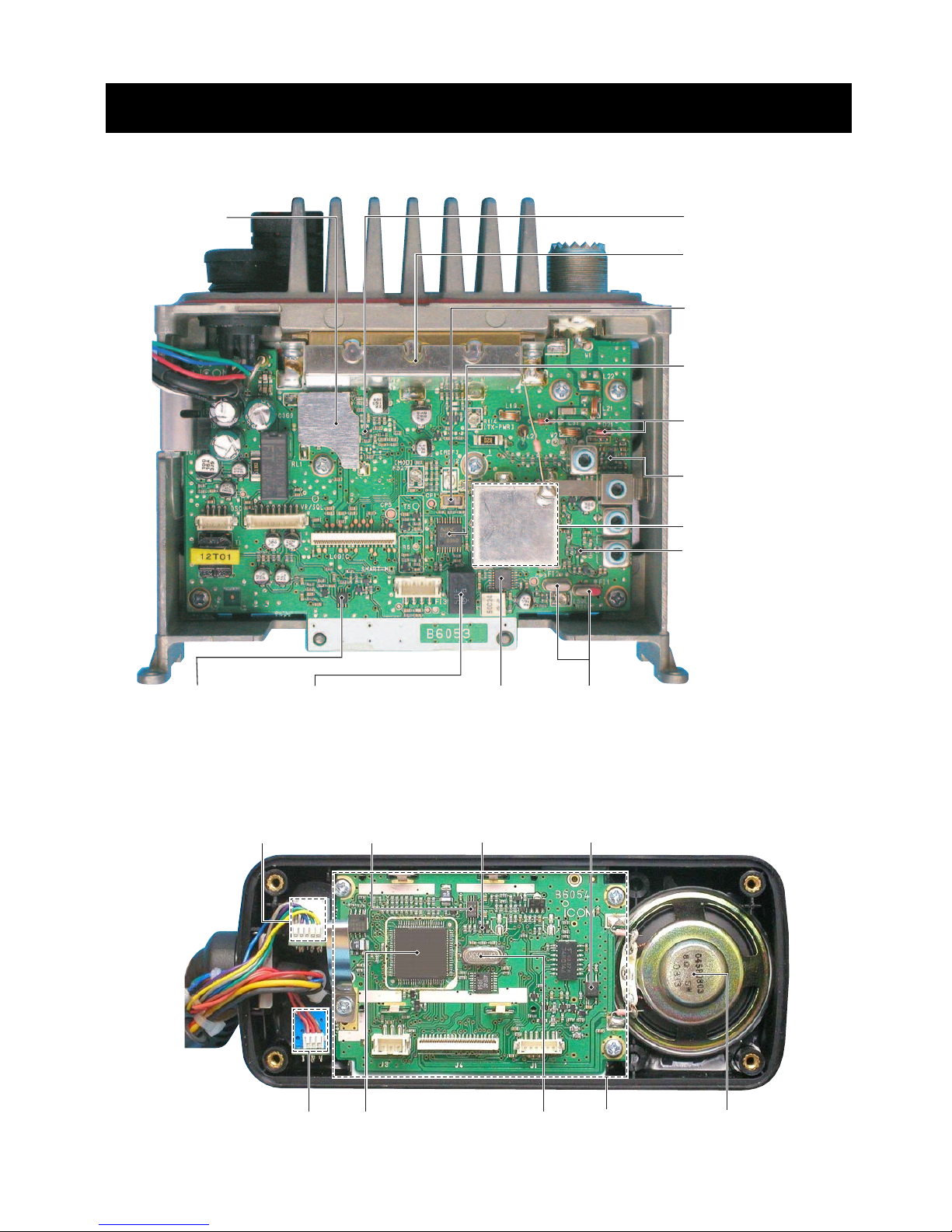
SECTION 2 INSIDE VIEWS
•
FRONT UNIT
•
MAIN-E UNIT
Antenna switching
circuit
(D14, D21: XB15A308)
VCO circuit
PLL reference oscillator
(X1: CR-768)
1st mixer
(Q22: 3SK131)
YGR amplifier
(Q12: 2SC3775)
Pre-driver
(Q10: 2SC4226)
Power amplifier
(IC3: RA35H1516M-01)
1st IF filter 21.7 MHz
(FI1: FL-368, FI2: FL-363)
FM IF IC
(IC2: TA31136FN)
2nd IF filter
(FI3: CFWLA450KFFA)
PLL IC
(IC1: µPD3140GS)
AF mute
(IC4: TC4W66FU)
RF amplifier
(Q21: 3SK131)
Photo coupler
(IC8: PC357N6T)
Reset IC
(IC2: S-80942CNMC)
System clock
9.8304 MHz
(X1: CR-739)
CPU
(IC1: HD6433847RB82H)
SQL board LOGIC-E board Speaker
VR board
EEPROM
(IC4: HN58X2432TI)
3 - 1
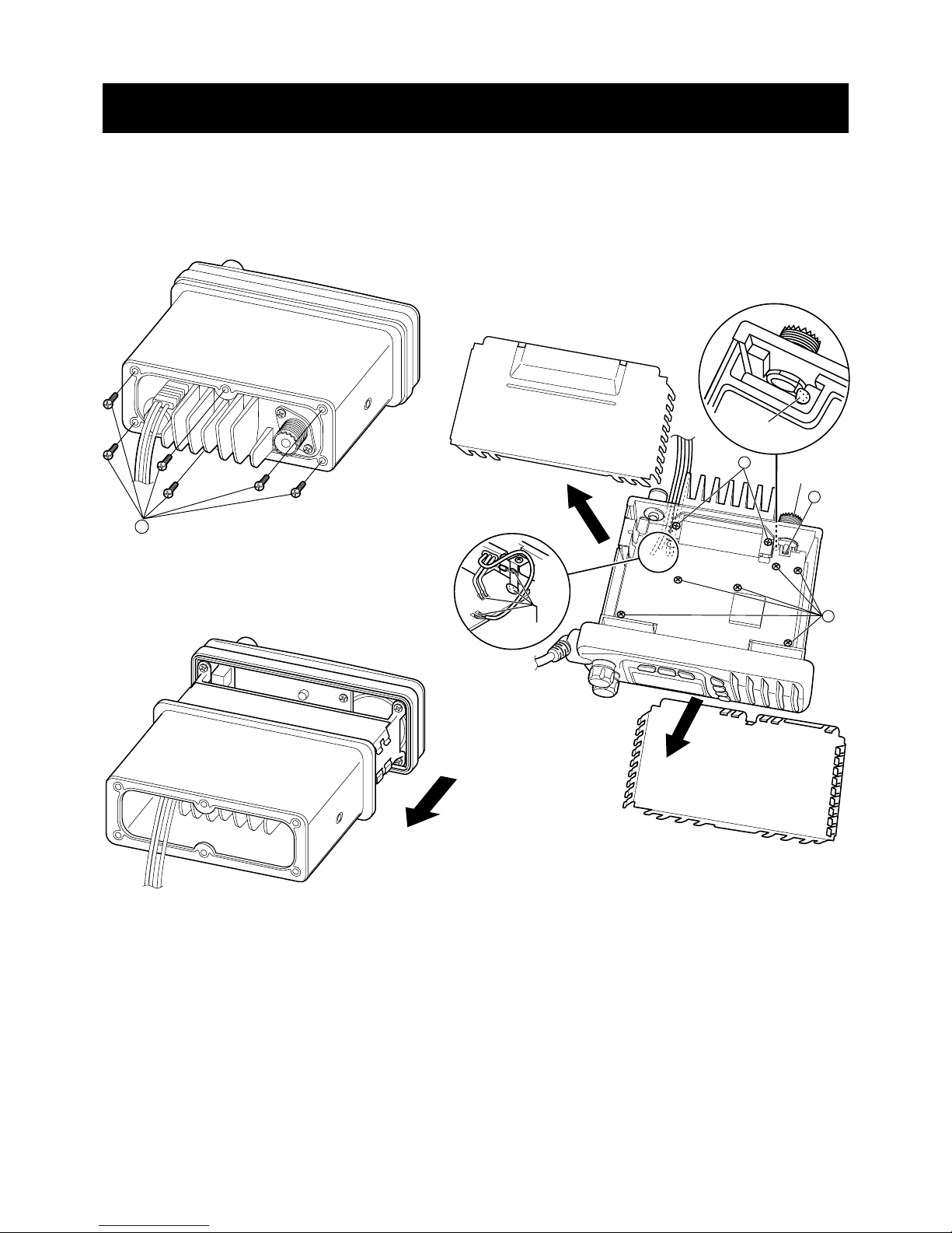
SECTION 3 DISASSEMBLY INSTRUCTIONS
•
REMOVING THE CASE
1 Unscrew 6 screws, A.
Note: When replacing the screw, 10–12 kg of torque MUST
be applied to ensure water resistance.
•
REMOVING THE MAIN-E UNIT
1 Remove the shield covers, MP31 and MP33.
2 Unsolder the antenna connector, B (1 point).
3 Unsolder bottom side [A] (6 points), and side [B] (1 point),
as shown below.
4 Unscrew 2 screws, C, and 6 screws, D, to remove the
MAIN-E unit.
A
Bottom side [A]
Unsolder
Unsolder
MP33 A-shield cover
Antenna
connector
Bottom side [B]
D
C
B
MP31 B-shield cover
2 Slide the case free of the chassis in the direction
of the arrow.
SECTION 4 CIRCUIT DESCRIPTION
4 - 1
4-1 RECEIVER CIRCUITS
4-1-1 ANTENNA SWITCHING CIRCUIT
(MAIN-E UNIT)
The antenna switching circuit functions as a low-pass filter
while receiving and as resonator circuit while transmitting.
The circuit does not allow transmit signals to enter receiver
circuits.
Received signals enter the MAIN-E unit from the antenna
connector and pass through the low-pass filter (L21, L22,
C127, C130, C133). The signals are then applied to the RF
circuit via the antenna switching circuit (D14, D21, L31,
C141, C142).
4-1-2 RF CIRCUIT (MAIN-E UNIT)
The RF circuit amplifies signals within the range of frequency coverage and filters out-of-band signals.
The signals from the antenna switching circuit pass through
a tunable bandpass filter (D25, L35, C150, C152) where the
object signals are applied to the RF amplifier circuit (Q21).
The amplified signals at Q21are applied to the 3-stage tunable bandpass filter (D26-D28, L36, L38, L39, C161, C162,
C164, C173-C178) to suppress unwanted signals and
improve the selectivity. The signals are then applied to the
1st mixer circuit (Q22).
4-1-3 1ST MIXER AND 1ST IF CIRCUITS
(MAIN-E UNIT)
The 1st mixer circuit converts the received signal to a fixed
frequency of the 1st IF signal with a 1st LO (VCO output) frequency. By changing the 1st LO frequency, only the desired
frequency will be passed through two crystal filters at the
next stage of the mixer.
The signals from the RF circuit are mixed with the VCO signals at the 1st mixer circuit (Q22) to produce a 21.7 MHz 1st
IF signal.
The 1st IF signal is applied to two crystal filters (FI1, FI2) to
suppress out-of-band signals and is then amplified at the IF
amplifier (Q23). The amplified signal is applied to the 2nd
mixer circuit (IC2).
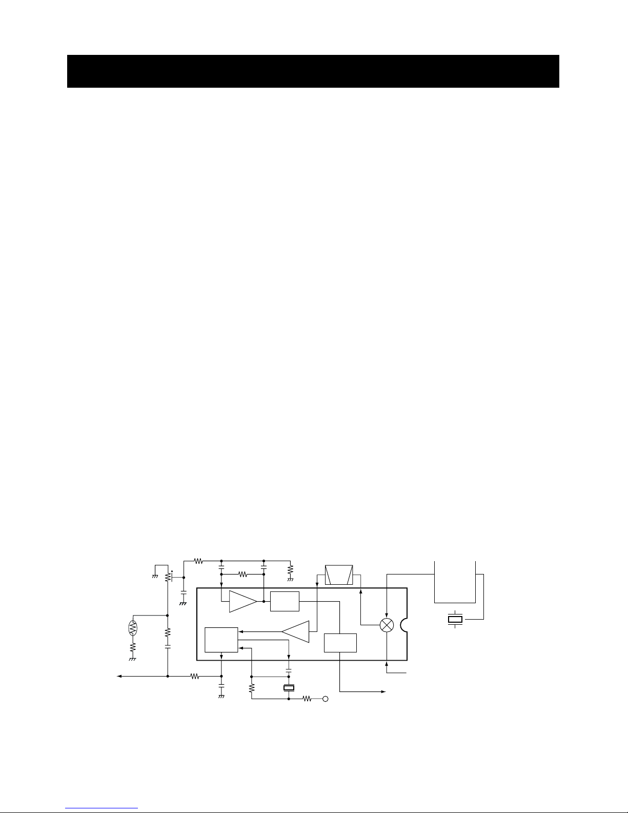
4-1-4 2ND IF AND DEMODULATOR CIRCUITS
(MAIN-E UNIT)
The 2nd mixer circuit converts the 1st IF signal to a 2nd IF
signal. A double superheterodyne system (which converts
receive signals twice) improves the image rejection ratio and
obtains stable receiver gain.
The FM IF IC (IC2) contains the 2nd local oscillator, 2nd
mixer, limiter amplifier, quadrature detector, and noise
detector circuits, etc.
The 1st IF signal from Q23 is applied to the 2nd mixer section of IC2 (pin 16), and is mixed with a 21.25 MHz 2nd LO
signal generated at the PLL circuit using the reference frequency (21.25 MHz) to produce a 450 kHz 2nd IF signal.
The 2nd IF signal from IC2 (pin 3) is passed through the
ceramic filter (FI3), where unwanted signals are suppressed, and is then applied to the 2nd IF (limiter) amplifier
in IC2 (pin 5). The signal is applied to the FM detector section in IC2 for demodulation into AF signals.
The FM detector circuit employs a quadrature detection
method (linear phase detection), which uses a ceramic discriminator (X2) for phase delay to obtain a non-adjusting circuit. The detected signal from IC2 (pin 9) is applied to the AF
circuit.
Mixer
16
Limiter
amp.
2nd IF filter
450 kHz
PLL IC
IC1
X1
21.25 MHz
X2
(21.25 MHz)
Noise
detector
IC2 TA31136F
14
1st IF (21.7 MHz)
from the IF amplifier (Q23)
"SQL" signal to the CPU
(LOGIC-E unit; IC1,pin 90)
11109
87 5 3
AF signal "DET"
R5
Squelch level
adjustment pot
(R214)
2
17
16
Active
filter
FI3
Noise
amp.
FM
detector
C218
C220
C211
R221
R213
C212
R219
R206
C205
R212
C213
R205
R215
R216
R218
• 2ND IF AND DEMODULATOR CIRCUITS
4 - 2
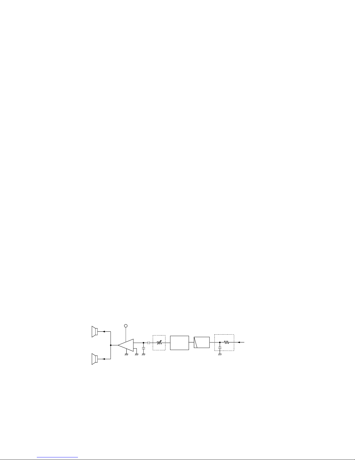
4-1-5 AF AMPLIFIER CIRCUIT
(MAIN-E AND FRONT UNITS)
The AF amplifier circuit amplifies the detected signals to
drive a speaker. The AF circuit includes an AF mute circuit
for the squelch.
AF signals from IC2 (pin 9) are applied to the de-emphasis
circuit (R231, C232). The de-emphasis circuit is an integrated circuit with frequency characteristic of –6 dB/octave.
The integrated signals pass through the bandpass filter
(Q31, R232, R234–R237, C233, C234) to suppress unwant-
ed noise signals.
The filtered signals are applied to the AF mute circuit (IC4),
and then passes through the [VOLUME] control (VR board;
R1) via the “VOL1” signal. The signals are applied to the AF
power amplifier (IC9, pin 1). The output signal from IC9 (pin
4) drives the internal (external) speaker.
4-1-6 SQUELCH CIRCUIT (MAIN-E UNIT)
A squelch circuit cuts out AF signals when no RF signals are
received. By detecting noise components in the AF signals,
the squelch circuit switches the AF mute switch.
A portion of the AF signals from the FM IF IC (IC2, pin 9)
pass through the squelch adjustment pot (R214), and are
then applied to the active filter section (IC2, pin 8). The
active filter section filters and amplifies noise components.
The amplified signals are converted into the pulse-type signals at the noise detector section. The detected signals outputs from pin 14 as the “SQL” signal.
The “SQL” signal from the FM IF IC is applied to the CPU
(LOGIC-E board; IC1, pin 90). The CPU analyzes the noise
condition and outputs as the “RMUTM” signal to the AF mute
switch (IC4).
4-2 TRANSMITTER CIRCUITS
4-2-1 MICROPHONE AMPLIFIER CIRCUIT
(MAIN-E UNIT)
The microphone amplifier circuit amplifies audio signals with
+6 dB/octave pre-emphasis from the microphone to a level
needed at the modulation circuit.
The AF signals from the microphone are amplified at the
microphone amplifier (IC7, pins6, 7) via the analog switch
(IC4, pins 5, 6). A capacitor (C302) and resistor (R303) are
connected to the amplifier to obtain the pre-emphasis characteristics.
The amplified signals are passed through the MIX circuit
(IC7, pins 1, 2) to do amplitude limiting, and are then applied
to the splatter filter (IC8, pins 1, 3) to suppress unwanted 3
kHz or higher signals. The filtered signals are then applied
to the modulation circuit.
4-2-2 MODULATION CIRCUIT (MAIN-E UNIT)
The modulation circuit modulates the VCO oscillating signal
(RF signal) using the microphone audio signals.
Audio signals from the splatter filter (IC8, pins 1, 3) pass
through the frequency deviation adjustment pot (R327) and
are then applied to the modulation circuit (D3, D4) to change
the reactance of D3, D4 and modulate the oscillated signal
at the VCO (Q4, Q5).
4-2-3 DRIVE AMPLIFIER CIRCUIT (MAIN-E UNIT)
The drive amplifier circuit amplifies the VCO oscillating signal to a level needed at the power amplifier.
The VCO output is buffer-amplified by Q6 and Q7, and is
then applied to the Tx/Rx switch (D7). The transmit signal
from the Tx/Rx switch is amplified to the pre-drive (Q10) and
YGR (Q12) amplifiers to obtain an approximate 50 mW signal level. The amplified signal is then applied to the RF
power amplifier (IC3).
AF
MUTE
BPF
IC9
R1
IC4
External SP
Internal SP
(FRONT unit)
Vcc
PWR
AMP
"DET" signal from the
FM IF IC (IC2, pin 9)
de-emphasis
circuit
R231
C232
(VR board)
• AF AMPLIFIER CIRCUIT
4 - 3
4-2-4 POWER AMPLIFIER CIRCUIT (MAIN-E UNIT)
The power amplifier circuit amplifies the driver signal to an
output power level.
IC3 is a power module which has amplification output capabilities of about 35 W with 50 mW input. The output from IC3
(pin 4) is passed through the antenna switching circuit (D14)
and is then applied to the antenna connector via the lowpass filter.
4-2-5 APC CIRCUIT (MAIN-E UNIT)
The APC circuit stabilizes transmit output power.
The RF output signal from the power amplifier (IC3; pin 4) is
detected at the power detector circuit (D12, D13, L19, C121,
C124) and is then applied to one of the differential amplifier
inputs (Q16, pin 5) via the High/Low control circuit (Q17,
R114). The applied voltage controls the differential amplifier
output (Q16, pin 2) and the bias voltage control (Q13). Thus
the APC circuit maintains a constant output power.
4-3 PLL CIRCUITS
4-3-1 GENERAL
The PLL circuit provides stable oscillation of the transmit frequency and receive 1st LO frequency. The PLL circuit compares the phase of the divided VCO frequency to the reference frequency. The PLL output frequency is controlled by a
crystal oscillator and the divided ratio of the programmable
divider.
IC1 on the MAIN-E unit is a dual PLL IC which controls both
VCO circuits for Tx and Rx, and contains a prescaler, programmable counter, programmable divider, phase detector,
charge pump, etc.
The PLL circuit, using a one chip PLL IC (MAIN-E unit; IC1),
directly generates the transmit frequency and receive 1st IF
frequency with VCOs. The PLL sets the divided ratio based
on serial data from the CPU on the LOGIC-E board and
compares the phases of VCO signals with the reference
oscillator frequency. The PLL IC detects the out-of-step
phase and output from pins 8 for Tx and Rx. The reference
frequency (21.25 MHz) is oscillated at X1 (MAIN-E unit).
T5
D12
D13
L19
"TMUT" signal from the CPU
(LOGIC-E board; IC1, pin 83)
Vcc
1
23
4
HI/LO
"TXDET" signal to the CPU
(LOGIC-E board; IC1, pin 92)
Q13
Q16
Q15
Q17
C137
C121
R112
R113
Q12
YGR
amp.
RF signal
from PLL
to antenna
RF detector
circuit
APC control circuit
Power module
IC3
R125
R116
R115
R114
C124
Shift register
Prescaler
Phase
detector
Loop
filter
Programmable
counter
Programmable
divider
X1
21.25 MHz
21.25 MHz signal to the
FM IF IC (IC2, pin 2)
VCO
Buffer
Buffer
Buffer
Q7
Q3
Q6
3
4
5
PSTB
IC1 (PLL IC)
PCK
PDATA
to transmitter circuit
to 1st mixer circuit
D7
D8
17
16
8
2
Q4, Q5, D3, D4
• APC CIRCUIT
• PLL CIRCUIT

4 - 4
4-3-2 TX AND RX LOOP (MAIN-E UNIT)
The generated signal at the VCO (Q4, Q5, D3, D4) enters
the PLL IC (IC1, pin 2) and is divided at the programmable
divider section and is then applied to the phase detector
section.
The phase detector compares the input signal with a reference frequency, and then outputs the out-of-phase signal
(pulse-type signal) from pin 8.
The pulse-type signal is converted into DC voltage (lock
voltage) at the loop filter (R7–R9, R41, C4, C5, C43, C44),
and is then applied to varactor diodes (D3, D4) of the VCO
to stabilize the oscillated frequency.
4-3-4 VCO CIRCUIT (MAIN-E UNIT)
The VCO outputs from Q4, Q5 are buffer-amplified at the
buffer amplifiers (Q6 and Q7), and are then sent to the Tx/Rx
switch (D7 and D8). The receive LO signal is applied to the
1st mixer circuit (Q22) through a low-pass filter, and the
transmit signal is applied to the pre-drive amplifier (Q10). A
portion of the VCO output is reapplied to the PLL IC (IC1, pin
2) via the buffer amplifier (Q3).
4-4 ATIS AND DSC CIRCUITS
4-4-1 ATIS ENCODE CIRCUIT
(LOGIC-E BOARD AND MAIN-E UNIT)
The FSK signal of ATIS created at CPU (LOGIC-E board;
IC1) is passed through the ladder type D/A convertor
(R41–R56) to convert into the analog signal. The analog signal is applied to the buffer amplifier (LOGIC-E board; IC9),
and then applied to the mixer circuit (MAIN-E unit; IC7, pins
1, 2) to mix with signals from the microphone. The signal
passes through the low-pass filter (MAIN-E unit; IC8, pins 1,
3) and is then applied to the VCO circuit as modulation signal.
4-4-2 DSC ENCODE CIRCUIT (MAIN-E UNIT)
The DSC signal created at the optional DSC controller (DS-
100) is applied to the T1 via the J7, and then as floating system output. The signal is applied to the buffer amplifier
(Q61), and then passes through the 6 dB/oct pre-emphasis
circuit (R417, C416). The signal is applied to the mixer circuit (IC7, pins 1, 2) to mix with signals from the microphone.
The signal passes through the low-pass filter (IC8, pins 1, 3)
and is then applied to the VCO circuit as modulation signal.
4-5 LOGIC CIRCUITS (LOGIC-E BOARD)
• CPU
IC1 is an 8 bit signal chip micro-computer and contains LCD
driver, serial I/O, timer, A/D converter, programmable I/O,
ROM and RAM.
• SYSTEM CLOCK CIRCUIT
X1 is a ceramic oscillator and oscillate 9.8304 MHz system
clock for the CPU (IC1).
• RESET CIRCUIT
IC2 is a reset IC. When turn power ON, IC2 outputs a reset
signal (“LOW” pulse) to the CPU (IC1, pin 15) via the “RES”
line.
• LOW BATTERY DETECTOR
VCC voltage is divided by R84, R85 and is applied to the low
battery detector section in the CPU (IC1, pin 91) via the
“LBAT” line.
• DIMMER CIRCUIT
The CPU (IC1), Q1, Q2 and Q3 are dimmer circuit and control the 4 steps the LCD backlight (DS2–DS7).
4-6 POWER SUPPLY CIRCUITS
VOLTAGE LINES
LINE
HV
HVS
VCC
5V
T5
R5
R8
DESCRIPTION
The voltage from the connected DC power supply.
Same voltage as the HV line which is passed
through the [PWR] switch (VR unit; R1).
Same voltage as the HVS line. The voltage is
applied to the optional DSC controller (DS-100).
Common 5 V converted from the VCC line at the
5V regulator circuit (MAIN-E unit; IC10).
Transmit 5 V controlled by the T5 control circuit
(MAIN-E unit; Q52, Q57) using the “SEND” signal from the CPU (LOGIC-E board; IC1). The
controlled voltage is applied to the transmitter
circuit.
Receive 5 V controlled by the R5 control circuit
(MAIN-E unit; Q53, Q54) using the “RCV” signal
from the CPU (LOGIC-E board; IC1). The controlled voltage is applied to the receiver circuit.
Receive 8 V controlled by the R5 control circuit
(MAIN-E unit; Q55, Q56) using the “R5” signal.
The controlled voltage is applied to the receiver
circuit.
KEYM
PTT
TAG
SCN
UP
DN
UNLK
4 - 5
Pin Port
Description
number name
Pin Port
Description
number name
1
2
3
5
6
7
8
16
17
18
20
21
22
23
27
28
29
31
83
84
89
90
91
92
CONT1
CONT2
BEEPM
CH16
CH
H/L
HANG
PCK
PSTB
PDATA
ICFC
BPLVL
ECK
EDA
HI/LO
RRXD
RTXD
BPFV
TMUT
NMEAI
SQLV
SQL
LBAT
TXDET
Outputs control signal for the LCD
contrast.
Outputs beep audio signal.
Input port for the CH16 switch.
Low: While CH16 switch is pushed.
Input port for the CH switch.
Low: While CH switch is pushed.
Input port for the H/L switch.
Low: While H/L switch is pushed.
Input port for the MIC hanging signal.
Low: While MIC is pull-up.
Outputs clock signal to the PLL IC
(MAIN-E unit; IC1, pin 4).
Outputs strobe signals to the PLL IC
(MAIN-E unit; IC1, pin 3).
Outputs data signals to the PLL IC
(MAIN-E unit; IC1, pin 5).
Outputs control signal to switch NMEA
or ICF3.
Outputs beep volume control signal.
Low: Beep audio is maximum.
Outputs clock signal for the EEPROM
(LOGIC-E board; IC2, pin 6).
I/O port for the EEPROM data signals.
Output port for RF output power (High
or Low) select signal.
Input port for the cloning data.
Output port for the cloning data.
Outputs bandpass filter select signals.
Low: Receiving more than 160 MHz.
High: Receiving less than 160 MHz.
Outputs transmit mute signal.
High: While transmitting.
Input port for DS-100 data.
Input port for the squelch volume
level.
Input port from the FM IF IC (MAIN-E
unit; IC2) for the squelch operation.
Input port for the connected power
supply voltage detection (low battery
indicator).
Input port for TX LED control signal.
93
94
95
96
97
98
99
Input port for the HM-132 functions.
2.02 V: [
Y] is pushed.
3.00 V: [Z] is pushed.
3.84 V: [16/C] is pushed.
Input port for the PTT switch from HM-
132.
Low: While PTT is pushed.
Input port for the TAG switch.
Low: While TAG switch is pushed.
Input port for the SCN switch.
Low: While SCN switch is pushed.
Input port for the UP switch.
Low: While UP switch is pushed.
Input port for the DOWN switch.
Low: While DOWN switch is pushed.
Input port for the PLL unlock signal.
Low: While PLL is locked.
4-7 PORT ALLOCATIONS
4-7-1 CPU (LOGIC-E BOARD; IC1)
CONT1
0
1
CONT2
0
1
CONTRAST
LIGHT
DEEP
Pin Port
Description
number name
4
6
13
14
RMUTM
PTTM
SEND
RCV
Outputs the AF mute switch (MAIN-E
unit; IC4) control signal.
Low: While squelched
Outputs main microphone (HM-132)
select signal to the analog switch
(MAIN-E unit; IC4).
Outputs the T5 regulator (MAIN-E
unit; Q52, Q57) control signal.
High: While transmitting
Outputs the R5 regulator (MAIN-E
unit; Q53, Q54) control signal.
High: While receiving.
4-7-2 I/O EXPANDER IC (LOGIC-E BOARD; IC3)
 Loading...