

Page 1

SERVICE
MANUAL
VHF AIR BAND TRANSCEIVER
iA110
Page 2
ORDERING PARTS
Be sure to include the following four points when ordering
replacement parts:
1. 10-digit order numbers
2. Component part number and name
3. Equipment model name and unit name
4. Quantity required
<SAMPLE ORDER>
1130008830 S.IC TB31207AFN IC-A110 MAIN UNIT 5 pieces
8810009130 Screw BT M3x12 NI-ZU IC-A110 Bottom cover 10 pieces
Addresses are provided on the inside back cover for your
convenience.
INTRODUCTION
This service manual describes the latest service information for the IC-A110 VHF AIR BAND TRANSCEIVER at the
time of publication.
MODEL
IC-A110
VERSION SYMBOL
General GEN
General-1 GEN-1
U.S.A. USA
U.S.A.-1 USA-1
To upgrade quality, any electrical or mechanical parts and
internal circuits are subject to change without notice or
obligation.
DANGER
NEVER connect the transceiver to an AC outlet or to a DC
power supply that uses more than 16 V. This will ruin the
transceiver.
DO NOT expose the transceiver to rain, snow or any liquids.
DO NOT reverse the polarities of the power supply when
connecting the transceiver.
DO NOT apply an RF signal of more than 20 dBm (100 mW)
to the antenna connector. This could damage the transceiver’s front end.
REPAIR NOTES
1. Make sure a problem is internal before disassembling
the transceiver.
2. DO NOT open the transceiver until the transceiver is
disconnected from its power source.
3. DO NOT force any of the variable components. Turn
them slowly and smoothly.
4. DO NOT short any circuits or electronic parts. An insu-
lated tuning tool MUST be used for all adjustments.
5. DO NOT keep power ON for a long time when the trans-
ceiver is defective.
6. DO NOT transmit power into a signal generator or a
sweep generator.
7. ALWAYS connect a 50 dB to 60 dB attenuator between
the transceiver and a deviation meter or spectrum analyzer when using such test equipment.
8. READ the instructions of test equipment thoroughly
before connecting equipment to the transceiver.
Page 3

TABLE OF CONTENTS
SECTION 1 SPECIFICATIONS
SECTION 2 INSIDE VIEWS
SECTION 3 CIRCUIT DESCRIPTION
3 - 1 RECEIVER CIRCUITS............................................................................................................................. 3 - 1
3 - 2 TRANSMITTER CIRCUITS ..................................................................................................................... 3 - 3
3 - 3 PLL CIRCUITS............................................................................................................... .......................... 3 - 4
3 - 4 POWER SUPPLY CIRCUITS .................................................................................................................. 3 - 5
3 - 5 PORT ALLOCATIONS ............................................................................................................................. 3 - 5
SECTION 4 ADJUSTMENT PROCEDURES
4 - 1 PREPARATION ....................................................................................................................................... 4 - 1
4 - 2 PLL ADJUSTMENT.................................................................................................................................. 4 - 3
4 - 3 TRANSMITTER ADJUSTMENT.............................................................................................................. 4 - 3
4 - 4 RECEIVER ADJUSTMENT...................................................................................................................... 4 - 5
SECTION 5 PARTS LIST
SECTION 6 MECHANICAL PARTS AND DISSASEMBLY
SECTION 7 SEMI-CONDUCTOR INFORMATION
SECTION 8 BOARD LAYOUTS
8 - 1 FRONT UNIT ................................................................................................................. .......................... 8 - 1
8 - 2 MAIN UNIT............................................................................................................................................... 8 - 3
SECTION 9 BLOCK DIAGRAM
SECTION 10 VOLTAGE DIAGRAM
10 - 1 FRONT UNIT ..........................................................................................................................................10 - 1
10 - 2 MAIN UNIT..............................................................................................................................................10 - 2
Page 4
1 - 1
SECTION 1 SPECIFICATIONS
‘‘
GENERAL
• Frequency coverage : 118.000–136.975 MHz
• Channel spacing : 25 kHz [GEN], [GEN-1]
25 kHz/8.33 kHz [USA], [USA-1]
• Type of emission : AM (6K00A3E)
• Number of memory channels : 20 channels
• Antenna connector : SO-239 (50 Ω)
• Power supply requirement : 13.75 V DC or 27.5 V DC (negative ground)
• Current drain (at 13.75 V DC) : Transmit 5.0 A
Receive max. audio output 4.0 A
stand-by 500 mA
• Frequency stability : ±5 ppm
• Usable temperature range : –30˚C to +60˚C; –22˚F to +140˚F
• Dimensions (projections not included) : 150(W) × 50(H) × 180(D) mm; 5
29
⁄32(W) × 131⁄32(H) × 73⁄32(D) in
• Weight (with ant., BP-209) : 1.5 g; 3 lb 5 oz
‘‘
TRANSMITTER
• RF output power (at 13.75 V DC) : 9.0 W (typical)
• Modulation system : Last stage modulation
• Input impedance : 600 Ω
• Modulation limitting : 70–100 %
• Audio harmonic distortion : Less than 10 % (at 85 % modulation)
• Ham and noise ratio : More than 40 dB
• Spurious emissions : –16 dBm or less (except ±62.5 kHz of operating frequency)
• Antenna requirements : Standard 50 Ω antenna with a VSWR < 3 : 1
‘‘
RECEIVER
• Receive system : Double conversion superheterodyne system
• Intermediate frequencies : 1st 38.85 MHz
2nd 450 kHz
• Sensitivity : Less than 1 µV at 6 dB S/N
• Squelch sensitivity : Less than 0.35 µV at threshold
• Selectivity :
• Spurious response rejection ratio : More than 74 dBµ
• Hum and noise : More than 25 dB
• Audio output power (at 13.75 V DC) : Ext SP More than 10.0 W at 10 % distortion with an 8 Ω load
Side tone More than 100 mW at 10 % distortion with an 500 Ω load
• Audio output impedance : Ext SP 8 Ω
Side tone 500 Ω
Specifications are measured in accordance with FCC Part87 and RTCA DO-186a.
(RTCA DO-186a: Class C/E, Class 4/6)
All stated specifications are subject to change without notice or obligation.
At 25 kHz channel spacing
At 8.33 kHz channel spacing
±8 kHz
±17 kHz
±25 kHz
Less than 6 dB
Less than 40 dB
Less than 60 dB
±2.778 kHz
±7.37 kHz
Less than 6 dB
Less than 60 dB
Page 5
Low-pass filter
Antenna switching circuit
Crystal band pass filter
(FI1: FL-306)
Ceramic band pass filter
(FI3: CFWM450D)
Ceramic band pass filter
(FI4: CFG450H [USA/-1] only)
VCO circuit
APC amplifier
(Q11: 2SC4081)
Crystal band pass filter
(FI2: FL-307 [USA/-1] only)
Power complifier
(Q51: MRF137)
TCXO
(X1: CR-653)
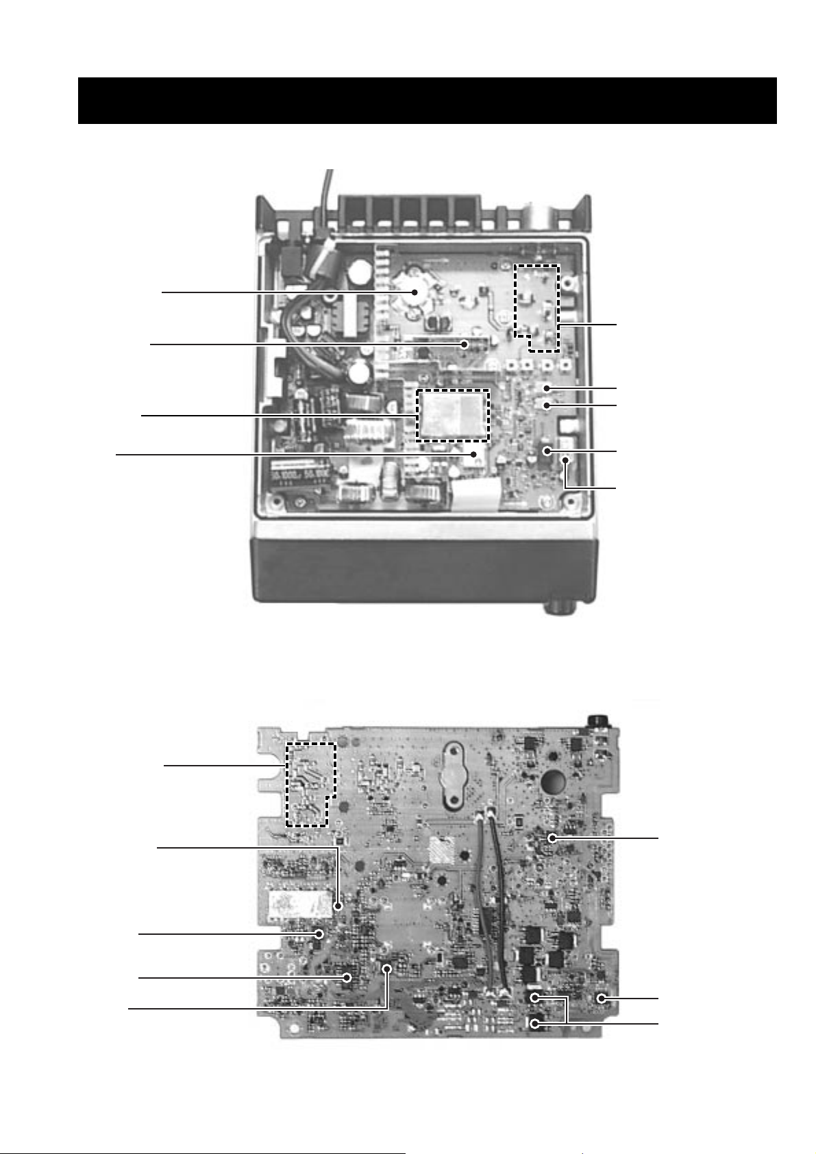
2 - 1
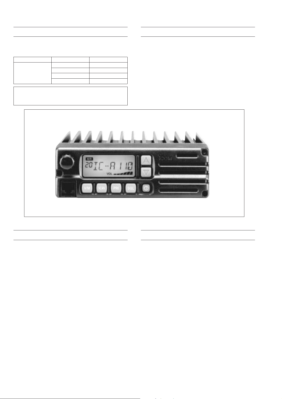
SECTION 2 INSIDE VIEWS
¡MAIN UNIT
<TOP VIEW>
AF amplifier
(IC37: TDA7233D)
RX 1st mixer
(Q2: 3SK184)
2nd IF IC
(IC40: TA31136FN)
PLL IC
(IC2: TB31207AFN)
PWM modulator
(IC44: µPC311)
EEPROM
(IC4: BA3308F)
Low-pass filter
Antenna switching circuit
AF power amplifier
(Q92,93: 2SK2414)
<BOTTOM VIEW>
Page 6
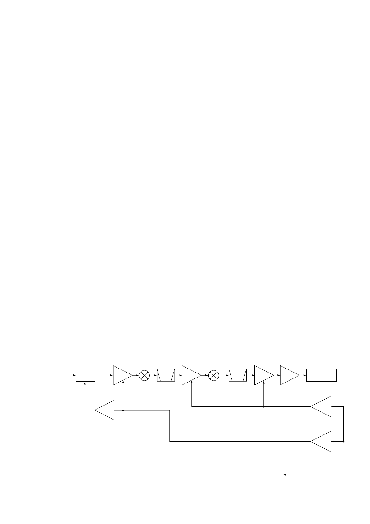
3 - 1
SECTION 3 CIRCUIT DESCRIPTION
3-1 RECEIVER CIRCUITS
3-1-1 ANTENNA SWITCHING CIRCUIT
The antenna switching circuit functions as a low-pass filter
while receiving. However, its impedance becomes very high
while D1 and D2 are turned ON. Thus transmit signals are
blocked from entering the receiver circuits. The antenna
switching circuit employs a λ⁄4 type diode switching system.
The passed signals are then applied to the RF amplifier circuit.
Received signals are passed through the low-pass filter (L2,
L3, L48, C1–C6, C330, C331). The filtered signals are
applied to the λ⁄4 type antenna switching circuit (D1, D2).
3-1-2 RF CIRCUIT
The RF circuit amplifies signals within the range of frequency coverage and filters out-of-band signals.
The signals from the antenna switching circuit are amplified
at the RF amplifier (Q1) after passing through the RX attenuator (D38, L52, R295), bandpass filter (L27, L8, C10,
C164, C165, C21) and two-stage tunable bandpass filters
(the first filter is consisted of D6, L9, C342, C405 and the
second filter is consisted of D37, L49, C23, C406). The
amplified signals are applied to the 1st mixer circuit (Q2,
gate 1) after out-of-band signals are suppressed at the
another two-stage tunable bandpass filters (D7, L10, C28,
C407 and D8, L11, C61, C553).
The tunable bandpass filters (D6–D8, D37) which employ
varactor diodes, track the filters and are controlled by the
PLL IC (IC2) via the tune buffer amplifier (Q79) using
“TUNE” signal. These diodes tune the center frequency of
an RF passband for wide bandwidth receiving and good
image response rejection.
3-1-3 1ST MIXER AND 1ST IF CIRCUITS
The 1st mixer circuit converts the received signal into a fixed
frequency of the 1st IF signal with a PLL output frequency.
By changing the PLL frequency, only the desired frequency
will pass through a crystal filter at the next stage of the 1st
mixer.
The filtered signals from the RF circuit are mixed at the 1st
mixer (Q2) with a 1st LO signal coming from the VCO circuit
to produce a 38.85 MHz 1st IF signal.
The 1st IF signal is applied to a pair of crystal filter [Wide
mode: FI1, Narrow mode: FI2] to suppress out-of-band signals. The filtered 1st IF signal is applied to the IF amplifier
(Q3), then applied to the 2nd mixer circuit (IC40, pin 16).
3-1-4 2ND MIXER AND 2ND IF CIRCUITS
The 2nd mixer circuit converts the 1st IF signal into a 2nd IF
signal. Adouble conversion superheterodyne system (which
converts receive signals twice) improves the image rejection
ratio and obtains stable receiver gain.
The 1st IF signal from the IF amplifier is applied to the 2nd
mixer section of the IF IC (IC2, pin 16), and is mixed with the
38.4 MHz 2nd LO signal to be converted into a 450 kHz 2nd
IF signal.
A2nd LO signal (38.4 MHz) is produced at the PLLcircuit by
tripling it’s reference frequency (12.8 MHz).
The 2nd IF signal from the 2nd mixer (IC2, pin 3) passes
through a ceramic filter [Wide mode: FL3, Narrow mode:
FI4] to remove unwanted heterodyned frequencies. It is then
amplified at the 2nd IF amplifiers (Q4–Q6).
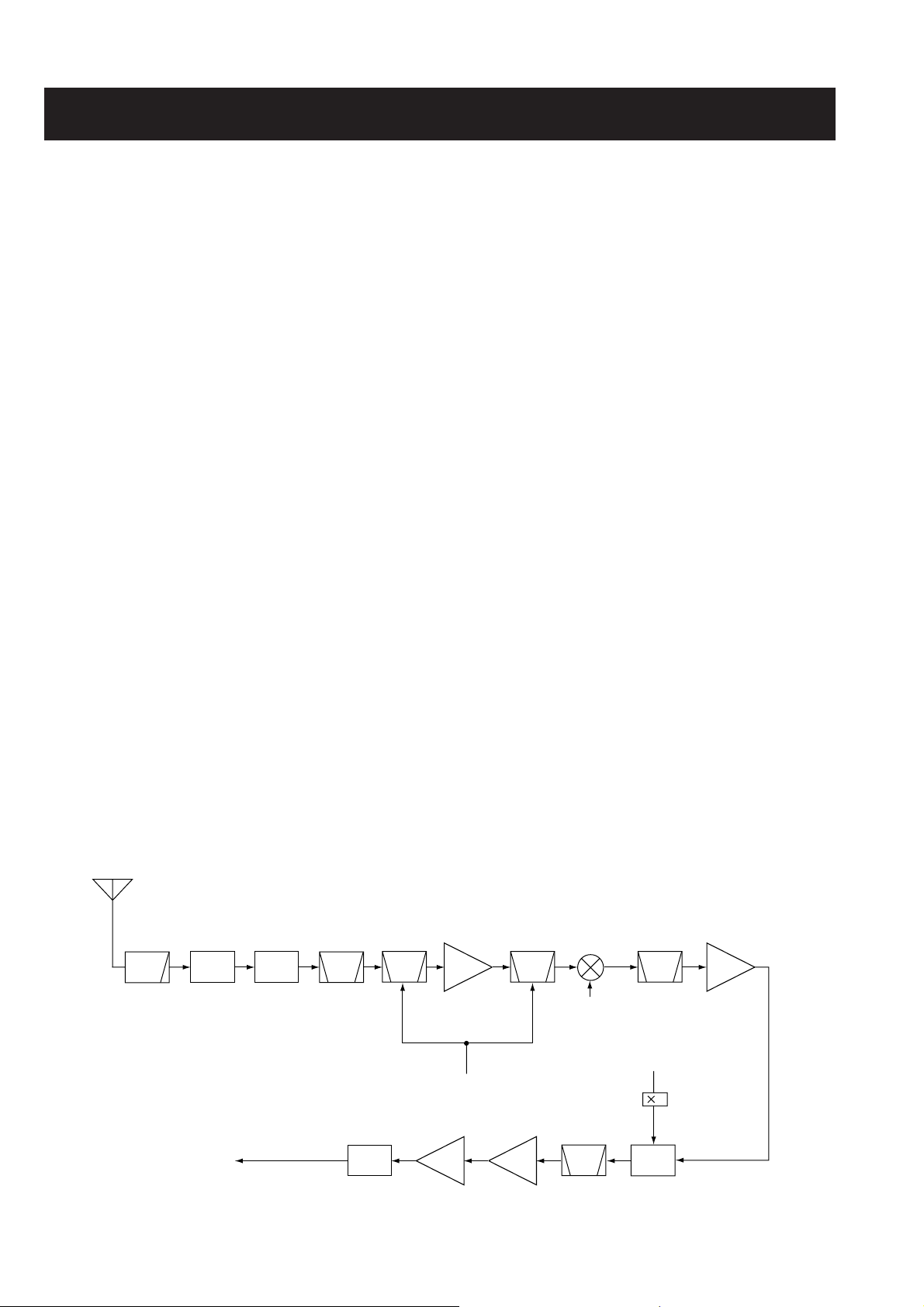
• Receiver construction
118.000–136.975 MHz
D1–D3 Q1
LPF
Ant SW
to AF circuit
D38
ATT
BPF
D6,
D37
Tuned Tuned XTAL
BPF
AM
DET
RF
AMP
"TUNE" signal
IF
AMP
Q6
Q4,
Q5
BPF
AMP
D7,
D8
IF
1st mixer
Q2
1st LO signal
79.15–98.125 MHz
from VCO circuit
Tripler
Q83, Q84
450 kHz
XTAL
BPF
FI3 [Wide],
FI4 [Narrow]
FI1 [Wide],
FI2 [Narrow]
38.85 MHz
BPF
12.8 MHz signal
from TCXO (X1)
3
2nd LO signal
38.4 MHz
2nd IF
IC
Q3
IF
AMP
Page 7
3 - 2
3-1-5 AM DETECTOR CIRCUIT (MAIN UNIT)
The AM detector circuit converts the 2nd IF signal into AF
signals.
The amplified 2nd IF signal from the 2nd IF amplifier (Q6) is
applied to the AM detector circuit (Q7). It is then detected for
conversioin to AF signals.
The AF signals are applied to the AF circuit.
3-1-6 AF CIRCUIT (MAIN UNIT)
The AF circuit amplifies the demodulated AF signals to drive
a speaker.
The AF signals are passed through the low pass filter (IC31,
pin 1), and then applied to the MOD/AF select swtich (IC22,
pin 7).
The AF signals are amplified at the AF amplifier (IC42, pin
3), and are then passed through the RMUTE swtich (IC6)
and electric-volume switch (IC13, pins 14, 15) to control AF
level. The level controlled signals are then applied to the
mute switch (IC30, pin 1).
While in using the internal speaker or connecting outer
speaker jack, the AF signals are applied to the MOD/AF
swtich (IC48, pin 7) via the AF mute swtich (IC28). The
applied AF signals are compared at the PWM IC (IC44) with
the reference signal from the triangular wave oscillator
(IC45), and are then converted to the PWM wave form. The
AF signals are amplified at the FET driver (IC47) and AF
power amplifiers (Q92, Q93). The amplified AF signals are
applied to the SP mute switch (D66, Q101, Q100) via the
line filter (L62–L64, L81, C456, C457, C462, C463). The filtered AF signals are applied to the internal speaker via the
[EXT SP] jack (J7).
While in connecting the head set, the AF signals are amplified at the AF power amplifier (IC37, pin 8), and then applied
to the ACC connector (J6, pin 6) via the impedance convertor (T1).
3-1-7 SQUELCH CIRCUIT
(MAIN AND FRONT UNITS)
The squelch circuit cuts out AF signals when receiving no
modulated signal. When no voice modulation is included in
the signal, the squelch circuit cuts out the AF signal by comparing voice audio and noise audio components in the AF
detected signals.
The 2nd IF signal from the IF IC (MAIN unit; IC40, pin 3)
passes through the 450 kHz ceramic filter (Wide mode: FI3,
Narrow mode: FI4) to remove out-of-band signals, and then
applied to the IF amplifier.
A portion of the amplified 2nd IF signal from the IF amplifier
(MAIN unit; Q4) is applied to the IF amplifier section on the
IF IC (MAIN unit; IC40, pin 5). The amplified signal passes
through the RSSI section, and are then applied to the
squelch amplifier (MAIN unit; IC11, pin 1) as “RSSI” signal.
The amplified “RSSI” signal at IC11 is output from pin 4 as
“SQLI” signal, and is then applied to the CPU (FRONT unit;
IC1, pin 74). The CPU analyzes the noise condition and outputs the “AFMUT” signal via the output expander IC
(FRONT unit; IC5) to switch the SP mute switch (Q100,
Q101), etc. When connecting the head set, “RMUTE” signal
from the CPU via the output expander IC (FRONT unit; IC5)
is applied to the RMUTE circuit (MAIN unit; IC6, Q80, Q81).
Even when the squelch is closed, the mute switch (IC30)
opens at the moment of emitting beep tones.
3-1-8 AGC CIRCUIT (MAIN UNIT)
The AGC (Automatic Gain Control) circuit reduces signal
fading and keeps the audio output level constant.
AF signal from the AM detector circuit (Q7) is amplified at
AGC amplifiers (Q77, Q78). The amplified signal from Q77
is applied to the IF amplifier (Q4, Q5). The other amplified
signal from Q78 is applied to the RF amplifier (Q1), and the
RX attenuator (D38) via the buffer amplifier (Q73).
These amplifiers reduce the amplifier gain of IF amplifiers
(Q4, Q5) and the RF amplifier (Q1) while receiving a strong
signal.
• AGC circuit
From the ant.
D38
RX ATT
Q73
Buffer
RF
AMP
Q1
1st mixer
Q2
XTAL
BPF
IF
AMP
Q3
2nd mixer
IC40
"IF AGC" signal
"RF AGC" signal
BPF
Q4, Q5
IF
AMP
Q6
IF
AMP
to AF circuit
D7
AM
DETECTOR
Q77
AGC
AMP
Q78
AGC
AMP
Page 8
3 - 3
3-2 TRANSMITTER CIRCUITS
3-2-1 MICROPHONE AMPLIFIER CIRCUIT
(MAIN UNIT)
The microphone amplifier circuit amplifies audio signals
from the microphone, within +6 dB/octave pre-emphasis
characteristics (300 Hz–3 kHz), to a level needed for the
modulation circuit.
The AF signals from the microphone are applied to the
IN/EXT MIC switch (IC16, pin 7) via the “MIC” signal. When
using a headset, “EXTMIC” signal are applied to the external switch (IC16, pin 6) via R336 to adjust the external
microphone level. The output signal from IC16 (pin 1) are
applied to the ALC amplifier (IC4, pin 9) via R110 to adjust
the microphone sensitivity.
The output signal from IC4 (pin 7) are amplified at the AF
amplifier (IC5), and then applied to the MOD/AF switch via
the high-pass filter (IC51) and low-pass filter (IC19) to filter
out RF components. The filtered signals are applied to the
modulation circuit.
3-2-2 MODULATION CIRCUIT (MAIN UNIT)
The modulation circuit modulates the VCO oscillating signal
(RF signal) using the microphone AF signal.
The audio signals are passed through the MOD/AF switch
(IC48, pin 6) via the modulation depth adjustment pot R121.
The signals are converted to the PWM wave form at the
PWM (Pulse-Width-Modulation) IC (IC44, pin 3), and power
amplified at the FET driver (IC47, pin 5) and power MOS
FET (Q92, Q93). The power-amplified signals are passed
through the line filter (L62–L64, L81, C456, C457, C462,
C463, C468), and then applied to the drain of power amplifier (Q51) for the last stage modulation.
3-2-3 DRIVE/POWER AMPLIFIER CIRCUITS
(MAIN UNIT)
The amplifier circuit amplifies the VCO oscillating signal to
the output power level.
The signal from the buffer amplifiers (Q14, Q15) is passed
through the TX/RX switch (D11), and is amplified at the preamplifier (Q42), pre-drivers (Q20, Q21) and the power
amplifier (Q51) to obtain 9 W of RF power.
The amplified signal is passed through the antenna swtiching circuit (D3) and low-pass filter, and is then applied to the
antenna connector.
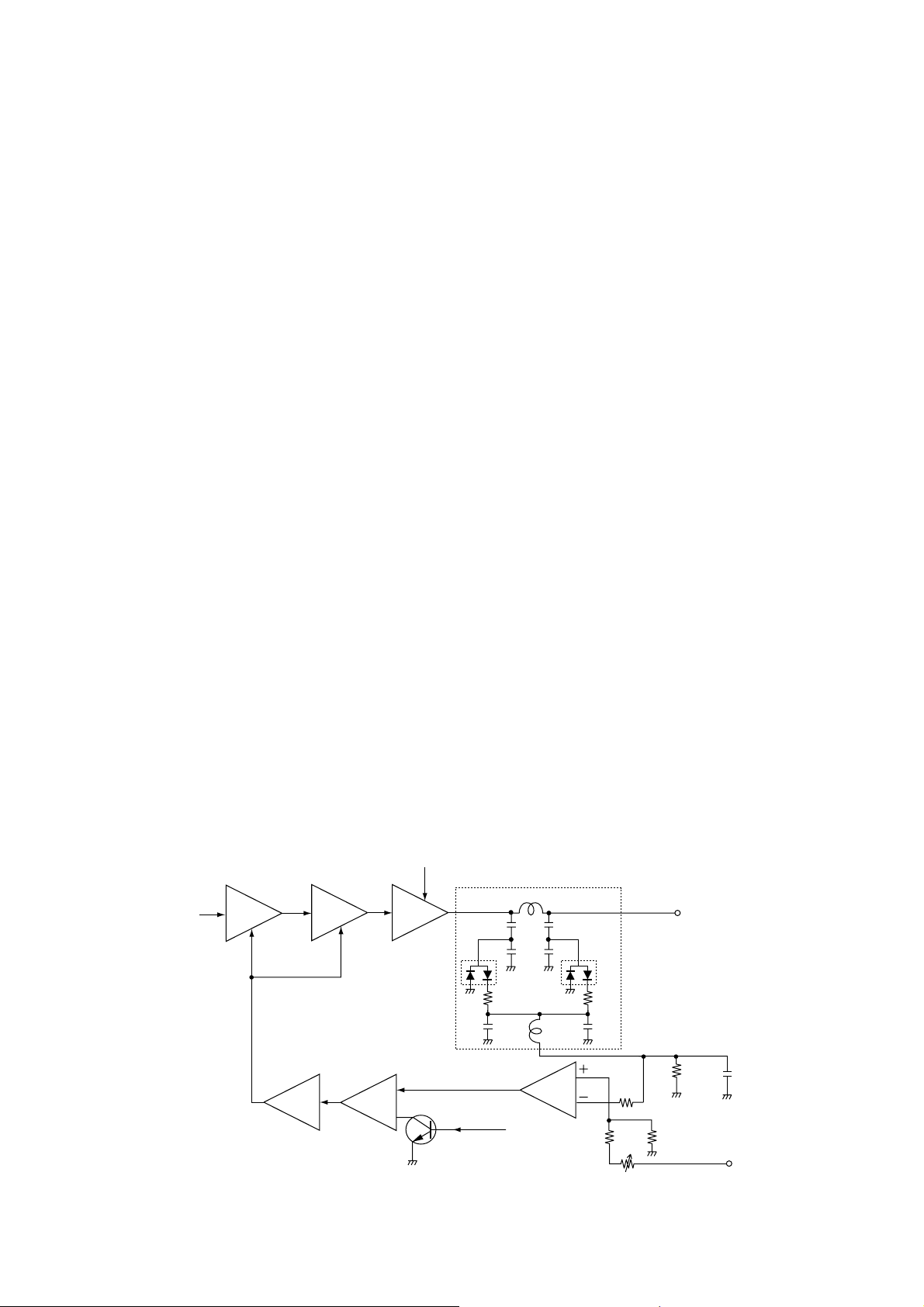
3-2-4 APC CIRCUIT (MAIN UNIT)
The APC (Automatic Power Control) circuit protects the
drive and power amplifiers from mismatched output loads.
The APC detector circuit (D4, D5) detects forward and
refrected signals respectively. The combined voltage is at a
minimum level when the antenna is matched at 50 Ω and is
increased when it is mismatched.
The detected voltage is applied to one of the APC controller
inputs (IC50, pin 3) and a power setting voltage is applied to
the other input (pin 1). When the antenna impedance is mismatched, the detected voltage exceeds the reference voltage. Thus the bias voltage of the pre-drivers is decreased.
• APC control circuit
Pre-amplified signal
(from MAIN unit; Q42)
PRE
DRIVE
Q20
Q98
"MOD V" signal from the AF power amplifiers
(MAIN unit; Q92, Q93)
PWR
CNT
PRE
DRIVE
Q21
Q51
PWR
AMP
Q11
APC
AMP
Power detector circuit
C14 C13
C17
Q99
"TMUT" signal from the
expander IC
(Front unit; IC5; pin 14)
D5
C18
IC50
L6
C16
D4
R2R3
L75
C19
APC
CNT
(Power adjustment)
R148
R149
R150
to the Antenna
R153
R151
C139
T8
Page 9
3 - 4
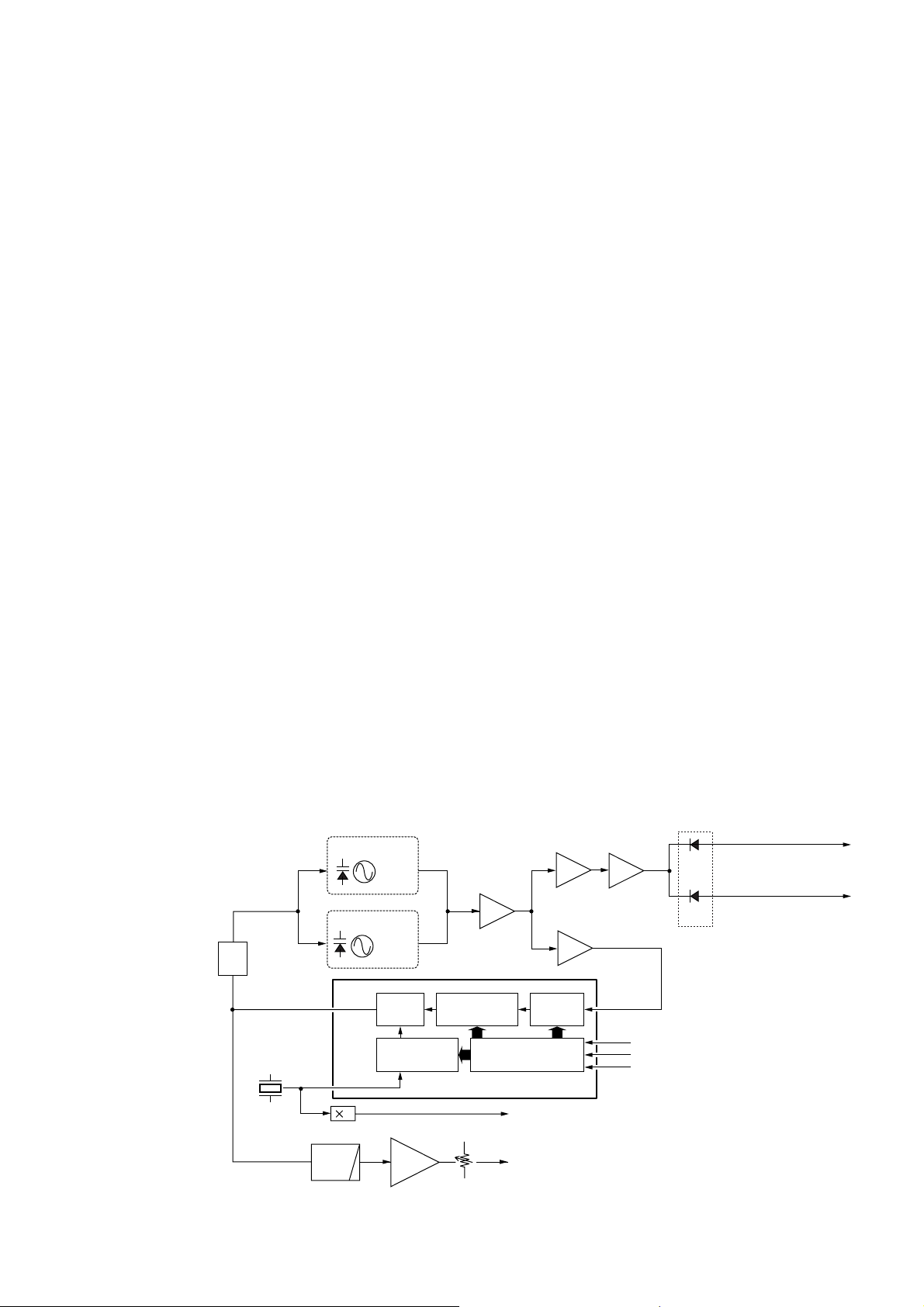
3-3 PLL CIRCUIT
3-3-1 GENERAL (MAIN UNIT)
A PLL circuit provides stable oscillation of the transmit frequency and receive 1st LO frequency. The PLL output compares the phase of the divided VCO frequency to the reference frequency. The PLL output frequency is controlled by
the divided ratio (N-data) of a programmable divider.
The PLL circuit contains of the TX-VCO and RX-VCO circuits. The oscillated signals are applied to the buffer amplifiers (Q43, Q12) then applied to the PLL IC (IC2, pin 8). IC2
is a dual PLL IC which controls VCO circuits for TX and RX.
The PLL circuit, using a one chip PLL IC (IC2), directly generates the transmit frequency and receive 1st IF frequency
with VCOs. The PLL sets the divided ratio based on serial
data from the CPU on the FRONT unit and compares the
phases of VCO signals with the reference oscillator frequency. The PLL IC detects the out-of-step phase and output from pin 9 for TX and RX, respectively. The reference
frequency (12.8 MHz) is oscillated at X1.
3-3-2 TX LOOP
The generated signal at the TX-VCO (Q44, D64) enters the
PLL IC (IC2, pin 8), and is divided at the programmable
divider section and is then applied to the phase detector
section.
The phase detector compares the input signal with a reference frequency, and then outputs the out-of-phase signal
(pulse-type signal) from pin 9.
The pulse-type signal is converted into DC voltage (lock
voltage) at the loop filter (R61, R62, C59, C60), and then
applied to the varactor diode (D64) of the TX-VCO to stabilize the oscillated frequency.
3-3-3 RX LOOP
The generated signal at the RX-VCO (Q59, D65) enters the
PLL IC (IC2, pin 8), and is divided at the programmable
divider section. The divided signal is then applied to the
phase detector section.
The phase detector compares the input signal with a reference frequency, and then outputs the out-of-phase signal
(pulse-type signal) from pin 9.
The pulse-type signal is converted into DC voltage (lock
voltage) at the loop filter (R61, R62, C59, C60), and then
applied to the varactor diode (D65) of the RX-VCO to stabilize the oscillated frequency. The lock voltage is also used
for the receiver circuit for the bandpass filter center frequency. The lock voltage from the PLL IC (IC2, pin 9) passes
through the low-pass filter, and is applied to the tune buffer
amplifier (Q79). The amplified signal is applied to the RF
bandpass filters (D7, D8 and D6, D37) via the tune adjustment pot (R59).
3-3-4 VCO CIRCUIT
The VCO outputs from Q44 (TX) and Q59 (RX) are buffer
amplified at Q43, and are applied to the buffer amplifiers
(Q14, Q15). The amplified signal is applied to the T/R switch
(D10, D11). The receive LO signal is applied to the 1st mixer
circuit (Q2), and the transmit signal is applied to the preamplifier (Q42).
A portion of the VCO signal is amplified at the buffer amplifier (Q12), and then fed back to the PLL IC (IC2, pin 8).
• PLL circuit
Shift register
Prescaler
Phase
detector
Loop
filter
Programmable
counter
Programmable
divider
TCXO (X1)
12.8 MHz
Q44,
D64
TX VCO
RX VCO
Buff.
D10
D11
Q12
Q43
3
4
5
SCK
IC2 (PLL IC)
SO
PLSTB
to transmitter circuit
to 1st mixer circuit (Q2)
14
9
LPF
8
Q59,
D65
Buff.
Q14
Buff.
Q15
TX/RX
switch
Buff.
3
Q83, Q84
to the RF BPF
(D7 and D8, D6 and D37)
38.4 MHz 2nd LO signal
to the 2nd IF IC (IC40, pin 2)
Tune
buff.
R59
(RF BPF adjustment)
Q79
Page 10
3 - 5
3-4 POWER SUPPLY CIRCUITS
VOLTAGE LINES (MAIN UNIT)
LINE
VCC
8V
+5V
CPU5V
T8
R8
DESCRIPTION
The voltage from the external DC power connector which is controlled by the power switch
([VOL] control).
Common 8 V converted from the VCC line by the
+8 V regulator circuit (IC29). The output voltage
is applied to the +5 V regulator circuit (IC7), the
ripple filter (Q16), and etc.
Common 5 V converted from the 8V line by the
+5V regulator (IC7) and +5V current amplifier
(Q22, Q23, D15) circuits. The output voltage is
applied to the electric volume IC (IC13), buffer
amplifiers (Q68, Q69), and etc.
Common 5 V converted from the VCC line by +8
V regulator (Q82, D35) and +5 V regulator circuits (IC26). The output 5 V voltage is applied to
the CPU (FRONT unit; IC1).
8 V for transmitter circuits regulated by the +8 V
regulator circuit (IC29).
8 V for receiver circuits regulated by the +8 V
regulator circuit (IC29).
3-5 PORT ALLOCATIONS
3-5-1 OUTPUT EXPANDER IC (FRONT unit: IC5)
Pin
number
4, 5
6
7
11
12
13
14
Port
name
LED1,
LED2
TRC
R/T
SMUT
AFMUT
RMUT
TMUT
Description
Outputs backlight control signals.
Outputs control signal to the MOD/AF
swtich (MAIN unit: IC48, pin 5) and
etc.
High:While transmitting.
Outputs control signal to the TX/RX
switch (MAIN unit: Q58, pin 1) for
VCO.
Low: While transmitting.
Outputs AF mute swtich (MAIN unit:
IC30, Q86, Q75, Q74, D43) control
signal.
Low: While squelched.
Outputs control signal to the mute
switch (MAIN unit; Q100, Q101, D66)
for speaker amplifier, and etc.
Low: While the speaker output is
muted.
Outputs RMUTE switch (IC6) control
signal.
Low: While squelched.
Outputs T8 regulator control signal.
Low: When TX is muted.
LED1
Low
High
Low
High
LED2
Low
Low
High
High
Backlight condition
Light OFF
No establishment
Light ON, Dimmer ON
Light ON, Dimmer OFF
Page 11
Description
Input ports for the key matrix.
Input port for the CPU reset signal.
Outputs control signal for the power
supply circuit.
High:Power is ON.
Outputs beep audio signals.
Outputs clock signal to the EEPROM
(FRONT unit; IC4, pin 6).
Outputs data signal to the EEPROM
(FRONT unit; IC4, pin 5).
Outputs chip select signal to the EEP-
ROM (FRONT unit; IC4, pin 1).
Input port for the [DIAL] control signal.
Outputs control signal to the expander
IC (FRONT unit; IC5, pin 15).
Outputs strobe signals to the
expander IC (FRONT unit; IC5, pin 1).
Outputs chip select signal to the elec-
tric volume (MAIN unit; IC13).
Low: While volume is controlled.
Outputs serial clock to the PLL IC
(MAIN unit; IC2, pin 3), the expander
IC (FRONT unit; IC5, pin 3) and the
electric volume (MAIN unit; IC13, pin
8).
Input port for the data signal from the
EEPROM (FRONT unit; IC4, pin 2).
Outputs serial data to the PLL IC
(MAIN unit; IC2, pin 4), the expander
IC (FRONT unit; IC5, pin 2) and the
electric volume (MAIN unit; IC13, pin
9).
Outputs strobe signals to the PLL IC
(MAIN unit; IC2, pin 5).
Outputs 2nd IF filter’s select signal.
High:While wide is selected.
Input port for the unlock signal from
the PLL IC (MAIN unit; IC2, pin 11).
Low: PLL is unlocked.
Input port for the cloning signal.
Output port for the cloning signal.
Input port for the POWER switch.
Low: While POWER switch is
pushed
Input port for the squelch signal.
Port
name
KR4
RESET
PSWC
BEEP
ECK
ESO
ECS
DLA,
DLB
OE
EXSTB
VCS
SCK
ESI
SO
PLSTB
FISW
UNLK
CLIN
CLO
PSW
SQLI
Pin
number
1, 2, 3,
5, 8, 12
9
10
11
13
14
15
16,
17
18
19
20
21
22
23
24
25
69
70
71
72
74
3 - 6
Pin
number
76
77
78–80
Port
name
HANG
PTT
KR1–KR2
Description
Input port for the microphone hanger
detection signal.
Low: Microphone on hook.
Input port for the PTT switch.
High:While PTT switch is pushed.
Input ports for the key matrix.
3-5-2 CPU (FRONT unit; IC1)
Page 12
4-1 PREPARATION
• Some versions may need the optional CS-A110 CLONING SOFTWARE and OPC-478, OPC-592
CLONING CABLE for setting the
adjustment frequency.
• All adjustments must be performed on the [Wide] mode.
■ REQUIRED TEST EQUIPMENT
4 - 1
SECTION 4 ADJUSTMENT PROCEDURES
■ VFO CHANNEL ID LIST
• Channel spacing: 8.33/25 kHz [USA/USA-1] • Channel spacing: 25 kHz [GEN/GEN-1]
EQUIPMENT
DC power supply
RF power meter
(terminated type)
Frequency counter
Modulation analyzer
Distortion meter
External speaker
GRADE AND RANGE
Output voltage : 13.75 V DC
Current capacity : 10 A or more
Measuring range : 1–50 W
Frequency range : 50–300 MHz
Impedance : 50 Ω
SWR : Less than 1.2 : 1
Frequency range : 0.1–300 MHz
Frequency accuracy: ±1 ppm or better
Sensitivity : 100 mV or better
Frequency range : DC–300 MHz
Measuring range : 0 to 100 %
Frequency range : 1 kHz±10 %
Measuring range : 1 to 100 %
Impedance : 8 Ω
EQUIPMENT
DC voltmeter
Digital multimeter
Audio generator
Standard signal
generator (SSG)
AC millivoltmeter
Attenuator
Terminator
GRADE AND RANGE
Input impedance : 50 kΩ/V DC or better
Input impedance : 10 MΩ/V DC or better
Frequency range : 300–3000 Hz
Measuring range : 1–500 mV
Frequency range : 0.1–300 MHz
Output level : 0.1 µV–32 mV
(–127 to –17 dBm)
Measuring range : 10 mV–10 V
Power attenuation : 40 or 50 dB
Capacity : 50 W or more
Impedance : 50 Ω
Capacity : 50 W or more
Operating Freq.
(MHz)
118.0000
118.0000
118.0083
118.0167
118.0250
118.0250
118.0333
118.0417
118.0500
118.0500
118.0583
118.0667
118.0750
118.0750
118.0833
118.0917
118.1000
118.1000
etc
Channel spacing
(kHz)
25
8.33
8.33
8.33
25
8.33
8.33
8.33
25
8.33
8.33
8.33
25
8.33
8.33
8.33
25
8.33
Channel ID
(Displayed Freq.)
118.000
118.005
118.010
118.015
118.020
118.030
118.035
118.040
118.050
118.055
118.060
118.065
118.070
118.080
118.085
118.090
118.100
118.105
Operating Freq.
(MHz)
118.0000
118.0250
118.0500
118.0750
118.1000
etc
Channel spacing
(kHz)
25
25
25
25
25
Channel ID
(Displayed Freq.)
118.000
118.025
118.050
118.075
118.100
Page 13

4 - 2
■ CONNECTION
12345678
Audio generator
Pin 4 (PTT)
• MIC JACK PIN CONNECTION
Pin 7 (GND)
AC millivoltmeter
Pin 5
(MICE )
Pin 6
(MIC )
Modulation
analyzer
Attenuator
40 dB or 50 dB
RF power meter
50 Ω, 1–50 W
Standard signal generator (SSG)
0.1–300 MHz
–127 to –17 dBm (0.1 µV to 32 mV)
CAUTION!
DO NOT transmit
while an SSG is
connected to the
antenna connector.
Frequency
counter
to the antenna connector
Pow er supply
DC 13.75 V, 10 A
Distortion
meter
AC millivoltmeter
to the external speaker jack
Speaker (8 Ω)
OPC-592
OPC-478
to the microphone connector
Cloning connection
DB9 female plug
(incl. level converter circuit)
to an RS-232C port
AC millivoltmeter
Audio generator
300 Hz to 3 kHz
Personal
computer
Page 14

4 - 3
4-2 PLL ADJUSTMENT
Vdd
VOLTAGE
PLL LOCK
VOLTAGE
TUNE
VOLTAGE
REFERENCE
FREQUENCY
ADJUSTMENT
ADJUSTMENT ADJUSTMENT CONDITION
MEASUREMENT
VALUE
POINT
UNIT LOCATION UNIT ADJUST
1
1
2
1
1
• Operating frequency :
118.000 MHz
• Receiving
• Operating frequency :
118.000 MHz
• Receiving
• Transmitting
• Operating frequency :
118.000 MHz
• Receiving
• Operating frequency :
136.950 MHz
• Connect an RF power meter or a
50 Ω dummy load to the antenna
connector.
• Transmitting
MAIN
MAIN
MAIN
Rear
panel
Connect a digital
multi-meter to drain
terminal of Q51.
Connect a digital
multi-meter to the
check point CP2.
Connect a digital
multi-meter to the
check point CP1.
Loosely couple the
frequency counter
to the antenna connector.
13.5 V
0.5 V
0.5 V
0.7 V
136.9500 MHz
MAIN
MAIN
MAIN
MAIN
R392
L41
L40
R59
X1
4-3 TRANSMITTER ADJUSTMENT
OUTPUT
POWER
MODULATION
DEPTH
HEAD SET
MODULATION
ADJUSTMENT
ADJUSTMENT ADJUSTMENT CONDITION
MEASUREMENT
VALUE
POINT
UNIT LOCATION UNIT ADJUST
1
1
2
1
• Operating frequency :
127.000 MHz
• No audio applied to the [MIC]
jack.
• Transmitting
• Operating frequecy :
127.000 MHz
• Connect an audio generator to
the [MIC] jack and set as :
1 kHz/10 mVrms
• Set a modulation analyzer as :
HPF : OFF
LPF : OFF
De-emphasis : OFF
Detector : (P–P)/2
• Pre-set R110 and R121 on the
MAIN unit to the center position.
• Transmitting
• Set an audio generator as:
1 kHz/1 mVrms
• Transmitting
• Operating frequency :
127.000 MHz
• Connect an audio generator to
the [EXT MIC] jack and set as :
1 kHz/1 mVrms
• Transmitting
Rear
panel
Rear
panel
Rear
panel
Connect an RF
power meter to the
antenna connector.
Connect a modulation analyzer to the
antenna connector
through an attenuator.
Connect a modulation analyzer to the
antenna connector
through an attenuator.
9.0 W
90 %
30 %
30 %
MAIN
MAIN
MAIN
R150
R121
R110
R336
Page 15

4 - 4
pin 4 ( GND)
pin 5 ( PTT)
J6, pin 3
Audio input point
pin 2 ( MICE)
pin 3 ( MIC)
Audio
generator
DC power supply
13.75 V/10 A
R336
Head set modulation
adjustment
Q51
Vdd voltage check point
R59
TUNE voltage adjustment
CP1
TUNE voltage check point
R150
Output power adjustment
L40
PLL lock voltage
adjustment for TX
CP2
PLL lock voltage
check point
R392
Vdd voltage adjustment
R121
R110
Modulation depth
adjustment
L41
PLL lock voltage
adjustment for RX
X1
Reference frequency
adjustment
Page 16

4 - 5
4-4 RECEIVER ADJUSTMENT
“SQUELCH ADJUSTMENT” must be performed at “SQUELCH ADJUSTMENT MODE”.
RX
SENSITIVITY
SQUELCH
ADJUSTMENT
ADJUSTMENT ADJUSTMENT CONDITION
MEASUREMENT
VALUE
POINT
UNIT LOCATION UNIT ADJUST
1
2
1
2
3
• Operating frequency :
118.000 MHz
• Pre-set L9, L10, L11, L49 on the
MAIN unit to max. CCW.
• Connect an SSG to the antenna
connector and set an SSG as :
Level : 1.0 µV
*
(–107 dBm)
Modulation : ± 1 kHz
Mod. depth : 30 %
• Receiving
• Operating frequency :
136.975 MHz
• Receiving
• Enter the “Squelch adjustment
mode”.
1): Program 118.000 MHz into
memory channel.
2): Turn power OFF.
3): While pushing [SQL], [TS],
[SCAN], turn power ON.
• Connect an SSG to the antenna
connector and set an SSG as :
Level : 0.18 µV
*
(–122 dBm)
Modulation : OFF
• Receiving
• Set an SSG as :
Level : 5.6 µV
*
(–92 dBm)
Modulation : OFF
Rear
panel
Front
panel
Connect an AC millivoltmeter and distortion meter with 8
Ω load to the external [SP] jack.
Display
Maximum AF output
level
Maximum AF output
level
MAIN
*This output level of the standard signal generator (SSG) is indicated as SSG’s open circuit.
L9, L10,
L11, L49
R59
• Verify the display indicates “sqADJ02”.
NOTE: If the display shows other, turn
[MAIN DIAL] to select
“sqADJ02”.
• Push the [SCAN] key to set the threshold level.
• Verify the display indicates “sqADJ25”.
• Push the [SCAN] key to set the tight
level.
• Turn power OFF to cancell the “Squelch adjustment mode”.
NOTE: Until turn power OFF, “Squelch adjustment mode” is not cancelled, and once pushing the [SCAN] key,
display indicates “sqADJ02” (threshold level adjustment) or “sqADJ25” (tight level adjustment) repeatedly
Page 17

4 - 6
DC power supply
13.75 V/10 A
L11
L10
L49
L9
R59
RX sensitivity adjustment
Page 18

5 - 1
S.=Surface mount
IC1 1140008780 S.IC HD6433823A19D
IC2 1130009110 S.IC S-80942ANMP-DD6-T2
IC3 1130007110 S.IC TC7W04FU (TE12L)
IC4 1130008670 S.IC 25LC160T-I/SN
IC5 1130007510 S.IC BU4094BCFV-E1
Q1 1590000440 S.TRANSISTOR DTA143ZUA T106
Q2 1510000880 S.TRANSISTOR 2SA1622-6-TL
Q3 1530003280 S.TRANSISTOR 2SC4211-6-TL
Q4 1590001980 S.TRANSISTOR XP4315 (TX)
Q5 1590000440 S.TRANSISTOR DTA143ZUA T106
Q6 1590000680 S.TRANSISTOR DTC114EUA T106
Q7 1590000680 S.TRANSISTOR DTC114EUA T106
D5 1790001280 S.DIODE MA111 (TX)
D6 1750000130 S.DIODE DA204U T107
X1 6060000600 S.CERAMIC PBRC 3.68 AR
L1 6200003960 S.COIL MLF1608A 1R0K-T
L2 6200003540 S.COIL MLF1608D R22K-T
R1 7030003800 S.RESISTOR ERJ3GEYJ 105 V (1 MΩ)
R2 7030003680 S.RESISTOR ERJ3GEYJ 104 V (100 kΩ)
R3 7030003680 S.RESISTOR ERJ3GEYJ 104 V (100 kΩ)
R4 7030003580 S.RESISTOR ERJ3GEYJ 153 V (15 kΩ)
R5 7030003580 S.RESISTOR ERJ3GEYJ 153 V (15 kΩ)
R6 7030003580 S.RESISTOR ERJ3GEYJ 153 V (15 kΩ)
R7 7030003580 S.RESISTOR ERJ3GEYJ 153 V (15 kΩ)
R8 7030003560 S.RESISTOR ERJ3GEYJ 103 V (10 kΩ)
R9 7030003680 S.RESISTOR ERJ3GEYJ 104 V (100 kΩ)
R10 7030003680 S.RESISTOR ERJ3GEYJ 104 V (100 kΩ)
R11 7030003370 S.RESISTOR ERJ3GEYJ 271 V (270 Ω)
R12 7030003350 S.RESISTOR ERJ3GEYJ 181 V (180 Ω)
R13 7030003350 S.RESISTOR ERJ3GEYJ 181 V (180 Ω)
R14 7030003640 S.RESISTOR ERJ3GEYJ 473 V (47 kΩ)
R15 7030003590 S.RESISTOR ERJ3GEYJ 183 V (18 kΩ)
R16 7030003540 S.RESISTOR ERJ3GEYJ 682 V (6.8 kΩ)
R17 7030003620 S.RESISTOR ERJ3GEYJ 333 V (33 kΩ)
R18 7030003680 S.RESISTOR ERJ3GEYJ 104 V (100 kΩ)
R19 7030003680 S.RESISTOR ERJ3GEYJ 104 V (100 kΩ)
R20 7030003680 S.RESISTOR ERJ3GEYJ 104 V (100 kΩ)
R21 7030003680 S.RESISTOR ERJ3GEYJ 104 V (100 kΩ)
R22 7030003680 S.RESISTOR ERJ3GEYJ 104 V (100 kΩ)
R23 7030003680 S.RESISTOR ERJ3GEYJ 104 V (100 kΩ)
R24 7030003680 S.RESISTOR ERJ3GEYJ 104 V (100 kΩ)
R26 7030003680 S.RESISTOR ERJ3GEYJ 104 V (100 kΩ)
R27 7030003680 S.RESISTOR ERJ3GEYJ 104 V (100 kΩ)
R28 7030003440 S.RESISTOR ERJ3GEYJ 102 V (1 kΩ)
R29 7030003680 S.RESISTOR ERJ3GEYJ 104 V (100 kΩ)
R30 7030003560 S.RESISTOR ERJ3GEYJ 103 V (10 kΩ)
R31 7030003560 S.RESISTOR ERJ3GEYJ 103 V (10 kΩ)
R32 7030003560 S.RESISTOR ERJ3GEYJ 103 V (10 kΩ)
R33 7030003560 S.RESISTOR ERJ3GEYJ 103 V (10 kΩ)
R34 7030003500 S.RESISTOR ERJ3GEYJ 332 V (3.3 kΩ)
R36 7030003600 S.RESISTOR ERJ3GEYJ 223 V (22 kΩ)
R37 7030003680 S.RESISTOR ERJ3GEYJ 104 V (100 kΩ)
R38 7030003680 S.RESISTOR ERJ3GEYJ 104 V (100 kΩ)
R41 7030003610 S.RESISTOR ERJ3GEYJ 273 V (27 kΩ)
R42 7030003610 S.RESISTOR ERJ3GEYJ 273 V (27 kΩ)
R43 7030003580 S.RESISTOR ERJ3GEYJ 153 V (15 kΩ)
R44 7030003580 S.RESISTOR ERJ3GEYJ 153 V (15 kΩ)
R45 7030003580 S.RESISTOR ERJ3GEYJ 153 V (15 kΩ)
R46 7030003610 S.RESISTOR ERJ3GEYJ 273 V (27 kΩ)
R47 7030003580 S.RESISTOR ERJ3GEYJ 153 V (15 kΩ)
C1 4030006860 S.CERAMIC C1608 JB 1H 102K-T-A
C2 4030006860 S.CERAMIC C1608 JB 1H 102K-T-A
C3 4030007090 S.CERAMIC C1608 CH 1H 470J-T-A
C4 4030007090 S.CERAMIC C1608 CH 1H 470J-T-A
C5 4030006860 S.CERAMIC C1608 JB 1H 102K-T-A
C6 4030007090 S.CERAMIC C1608 CH 1H 470J-T-A
C7 4030006850 S.CERAMIC C1608 JB 1H 471K-T-A
C8 4030006850 S.CERAMIC C1608 JB 1H 471K-T-A
C9 4030008560 S.CERAMIC C1608 CH 1H 300J-T-A
C10 4030008560 S.CERAMIC C1608 CH 1H 300J-T-A
C11 4030008890 S.CERAMIC C1608 JB 1C 273K-T-A
C12 4030011600 S.CERAMIC C1608 JB 1C 104KT-N
C13 4030011600 S.CERAMIC C1608 JB 1C 104KT-N
C14 4030011600 S.CERAMIC C1608 JB 1C 104KT-N
C15 4030007090 S.CERAMIC C1608 CH 1H 470J-T-A
C16 4030011600 S.CERAMIC C1608 JB 1C 104KT-N
C17 4030011600 S.CERAMIC C1608 JB 1C 104KT-N
C18 4030006860 S.CERAMIC C1608 JB 1H 102K-T-A
C19 4030006860 S.CERAMIC C1608 JB 1H 102K-T-A
C20 4030011600 S.CERAMIC C1608 JB 1C 104KT-N
C21 4030006860 S.CERAMIC C1608 JB 1H 102K-T-A
C22 4030011600 S.CERAMIC C1608 JB 1C 104KT-N
C23 4550006480 S.TANTALUM TEMSVA1C 475M-8L
C24 4030011600 S.CERAMIC C1608 JB 1C 104KT-N
C25 4030011600 S.CERAMIC C1608 JB 1C 104KT-N
C26 4030011600 S.CERAMIC C1608 JB 1C 104KT-N
C27 4550006250 S.TANTALUM TEMSVA1A 106M-8L
C28 4030006860 S.CERAMIC C1608 JB 1H 102K-T-A
C29 4030006860 S.CERAMIC C1608 JB 1H 102K-T-A
C30 4030007090 S.CERAMIC C1608 CH 1H 470J-T-A
C31 4030006860 S.CERAMIC C1608 JB 1H 102K-T-A
C32 4030006860 S.CERAMIC C1608 JB 1H 102K-T-A
C33 4030006860 S.CERAMIC C1608 JB 1H 102K-T-A
C34 4030006860 S.CERAMIC C1608 JB 1H 102K-T-A
C35 4030006860 S.CERAMIC C1608 JB 1H 102K-T-A
C36 4030006860 S.CERAMIC C1608 JB 1H 102K-T-A
J1 6510020510
S.CONNECTOR
FH12-40S-0.5SV
J2 6450001470 CONNECTOR 95003-2881
DS1 5030001740 LCD HLC7453-012400
DS2 5040002030 S.LED CL-170Y-CD-T
DS3 5040002030 S.LED CL-170Y-CD-T
DS4 5040002030 S.LED CL-170Y-CD-T
DS5 5040002030 S.LED CL-170Y-CD-T
DS6 5040002030 S.LED CL-170Y-CD-T
DS7 5040002030 S.LED CL-170Y-CD-T
S1 2250000420 ENCODER EVQB2CFC620B
SP1 2510000880 SPEAKER SME-45W
W1 7120000470 JUMPER ERDS2T0
W2 7120000470 JUMPER ERDS2T0
W3 7030003860 S.JUMPER ERJ3GE JPW V
W4 7030003860 S.JUMPER ERJ3GE JPW V
W6 8900007680 CABLE OPC-741 (N:40 L:55)
EP1 0910051553 PCB B 5319C
EP2 8930037960 LCD CONTACT SRCN-1705 ZSS
REF ORDER
DESCRIPTION
NO. NO.
[FRONT UNIT]
REF ORDER
DESCRIPTION
NO. NO.
[FRONT UNIT]
SECTION 5 PARTS LIST
Page 19

5 - 2
S.=Surface mount
IC2 1130008830 S.IC TB31207AFN (EL)
IC4 1110003670 S.IC BA3308F-T1
IC5 1110002750 S.IC TA75S01F (TE85R)
IC6 1130004200 S.IC TC4S66F (TE85R)
IC7 1180000800 S.IC S-81350HG-KD-T1
IC11 1110002400 S.IC NJM2107F-TE1
IC13 1130008370 S.IC TC9260F (HR)
IC15 1110005010 S.IC MC33063AD
IC16 1130006220 S.IC TC4W53FU (TE12L)
IC17 1130006220 S.IC TC4W53FU (TE12L) [USA/-1] only
IC18 1130006220 S.IC TC4W53FU (TE12L) [USA/-1] only
IC19 1110003780 S.IC NJM2902V-TE1
IC22 1130006220 S.IC TC4W53FU (TE12L)
IC26 1180000420 S.IC TA78L05F (TE12R)
IC28 1130004200 S.IC TC4S66F (TE85R)
IC29 1180002010 S.REG BA08FP-E2
IC30 1130004200 S.IC TC4S66F (TE85R)
IC31 1110002750 S.IC TA75S01F (TE85R)
IC37 1110003250 S.IC TDA7233D (TDA7233D013TR)
IC40 1110003200 S.IC TA31136FN (EL)
IC41 1110005030 IC TA8208H
IC42 1110002750 S.IC TA75S01F (TE85R)
IC43 1190001210 S.IC HIP4081AIB-E2
IC44 1110005130 S.IC µPC311G2
IC45 1110005100 S.IC NJM072BM-TE1
IC46 1110005010 S.IC MC33063AD
IC47 1190001210 S.IC HIP4081AIB-E2
IC48 1130006220 S.IC TC4W53FU (TE12L)
IC50 1110002750 S.IC TA75S01F (TE85R)
IC51 1110002750 S.IC TA75S01F (TE85R)
Q1 1580000420 S.FET 3SK184-R (TX)
Q2 1580000420 S.FET 3SK184-R (TX)
Q3 1530002600 S.TRANSISTOR 2SC4215-O (TE85R)
Q4 1530002600 S.TRANSISTOR 2SC4215-O (TE85R)
Q5 1530002600 S.TRANSISTOR 2SC4215-O (TE85R)
Q6 1530002600 S.TRANSISTOR 2SC4215-O (TE85R)
Q7 1530003280 S.TRANSISTOR 2SC4211-6-TL
Q11 1530002280 S.TRANSISTOR 2SC4081 T107 S
Q12 1530002560 S.TRANSISTOR 2SC4403-3-TL
Q14 1530002560 S.TRANSISTOR 2SC4403-3-TL
Q15 1530002930 S.TRANSISTOR 2SC4228 (M) -T1 R45
Q16 1530002850 S.TRANSISTOR 2SC4116-BL (TE85R)
Q20 1560001100 S.FET 2SK3074 (TE12L)
Q21 1560001060 S.FET 2SK3075 (TE12L)
Q22 1530003280 S.TRANSISTOR 2SC4211-6-TL
Q23 1520000460 S.TRANSISTOR 2SB1132 T100 R
Q33 1590001980 S.TRANSISTOR XP4315 (TX)
Q42 1530002920 S.TRANSISTOR 2SC4226-T2 R25
Q43 1530002920 S.TRANSISTOR 2SC4226-T2 R25
Q44 1530002920 S.TRANSISTOR 2SC4226-T2 R25
Q51 1590002840 FET MRF137
Q52 1510000880 S.TRANSISTOR 2SA1622-6-TL
Q53 1590000980 S.TRANSISTOR DTB123EK T147
Q58 1590001810 S.TRANSISTOR XP1113 (TX)
Q59 1530002920 S.TRANSISTOR 2SC4226-T2 R25
Q68 1590001980 S.TRANSISTOR XP4315 (TX)
Q69 1590000980 S.TRANSISTOR DTB123EK T147
Q70 1590000980 S.TRANSISTOR DTB123EK T147
Q71 1590001940 S.TRANSISTOR DTC144EE TL
Q72 1590001980 S.TRANSISTOR XP4315 (TX)
Q73 1530002060 S.TRANSISTOR 2SC4081 T107 R
Q74 1520000200 S.TRANSISTOR 2SB798-T2 DK
Q75 1530002060 S.TRANSISTOR 2SC4081 T107 R
Q77 1540000520 S.TRANSISTOR 2SD1819A (TX) R
Q78 1540000520 S.TRANSISTOR 2SD1819A (TX) R
Q79 1560000530 S.FET 2SK880-GR (TE85R)
Q80 1590000720 S.TRANSISTOR DTA144EUA T106
Q81 1590000430 S.TRANSISTOR DTC144EUA T106
Q82 1530002280 S.TRANSISTOR 2SC4081 T107 S
Q83 1530002380 S.TRANSISTOR 2SC4215-Y (TE85R)
Q84 1530002380 S.TRANSISTOR 2SC4215-Y (TE85R)
Q86 1590001980 S.TRANSISTOR XP4315 (TX)
Q87 1560001120 S.FET 2SK2414-Z-E1
Q88 1560001120 S.FET 2SK2414-Z-E1
Q89 1590001170 S.TRANSISTOR XP1501-(TX) .AB
Q90 1510001020 TRANSISTOR 2SA1471R
Q91 1560001120 S.FET 2SK2414-Z-E1
Q92 1560001120 S.FET 2SK2414-Z-E1
Q93 1560001120 S.FET 2SK2414-Z-E1
Q94 1590002870 S.FET FW215-TL
Q96 1590000430 S.TRANSISTOR DTC144EUA T106
Q97 1590000430 S.TRANSISTOR DTC144EUA T106
Q98 1510000770 S.TRANSISTOR 2SA1586-GR (TE85R)
Q99 1530002850 S.TRANSISTOR 2SC4116-BL (TE85R)
Q100 1590002870 S.FET FW215-TL
Q101 1590000430 S.TRANSISTOR DTC144EUA T106
Q102 1530002280 S.TRANSISTOR 2SC4081 T107 S
D1 1750000510 S.DIODE UM9401F
D2 1750000510 S.DIODE UM9401F
D3 1750000510 S.DIODE UM9401F
D4 1790001670 S.DIODE RB706F-40T106
D5 1790001670 S.DIODE RB706F-40T106
D6 1720000370 S.VARICAP HVU350TRF
D7 1720000370 S.VARICAP HVU350TRF
D8 1720000370 S.VARICAP HVU350TRF
D10 1790000620 S.DIODE MA77 (TX)
D11 1790000620 S.DIODE MA77 (TX)
D14 1790001330 S.ZENER MA8036-L (TX)
D15 1790001280 S.DIODE MA111 (TX)
D26 1790001340 S.DIODE DE5SC6M-4061
D27 1790001280 S.DIODE MA111 (TX)
D28 1750000580 S.DIODE 1SV307 (TPH3) [USA/-1] only
D29 1750000580 S.DIODE 1SV307 (TPH3)
D30 1750000580 S.DIODE 1SV307 (TPH3)
D31 1750000580 S.DIODE 1SV307 (TPH3) [USA/-1] only
D35 1730002460 S.ZENER MA8330-M (TX)
D36 1790000700 DIODE DSA3A1
D37 1720000370 S.VARICAP HVU350TRF
D38 1750000530 S.DIODE 1SV271 (TPH3)
D43 1750000260 S.DIODE 1SS352 (TPH3)
D44 1730002320 S.ZENER MA8051-M (TX)
D50 1750000530 S.DIODE 1SV271 (TPH3)
D51 1750000530 S.DIODE 1SV271 (TPH3)
D52 1750000530 S.DIODE 1SV271 (TPH3)
D53 1790001250 S.DIODE MA2S111-(TX)
D54 1790001250 S.DIODE MA2S111-(TX)
D55 1790000670 S.DIODE SB07-03C-TB
D56 1790001340 S.DIODE DE5SC6M-4061
D57 1790000670 S.DIODE SB07-03C-TB
D62 1790000670 S.DIODE SB07-03C-TB
D64 1720000370 S.VARICAP HVU350TRF
D65 1720000370 S.VARICAP HVU350TRF
D66 1790000670 S.DIODE SB07-03C-TB
FI1 2010002400 S.MONOLITH FL-306 (38.850 MHz)
FI2 2010002410 S.MONOLITH FL-307 (38.850 MHz) [USA/-1] only
FI3 2020001540 CERAMIC CFWM450D
FI4 2020001660 CERAMIC CFG450H [USA/-1] only
FI5 4580000110 S.FILTER ACF321825-223-T
FI6 2040000500 LC BNX-002-01
X1 6050010830 S.XTAL CR-657 (12.800 MHz)
L2 6110001670 COIL LA-253
L3 6110001740 COIL LA-263
L4 6110001610 COIL LA-244
L5 6110001610 COIL LA-244
L6 6110001550 COIL LA-235
L7 6170000230 COIL LW-25
L8 6200003350 S.COIL ELJNC R27K-F
L9 6150005000 S.COIL LS-527
L10 6150005000 S.COIL LS-527
L11 6150005000 S.COIL LS-527
L12 6200002710 S.COIL ELJFC 1R8K-F
L14 6200001630 S.COIL ELJNC R10K-F
L15 6200003300 S.COIL ELJNC R22K-F
L17 6200003290 S.COIL ELJNC R12K-F
L19 6200005730 S.COIL ELJRE 39NG-F
L20 6200002380 S.COIL LQN 1A 56NJ04
L21 6200008400 S.COIL 0.35-1.6-6TL 36N
L22 6200005740 S.COIL ELJRE 47NG-F
L23 6200008480 S.COIL 0.30-1.4-5TR 25N
L26 6200003590 S.COIL EXCCL3225U1
L27 6200003350 S.COIL ELJNC R27K-F
L31 6200007000 S.COIL ELJRE 82NG-F
L33 6200004480 S.COIL MLF1608D R82K-T
L35 6200008270 S.COIL 0.26-1.0-5TL 17N
REF ORDER
DESCRIPTION
NO. NO.
[MAIN UNIT]
REF ORDER
DESCRIPTION
NO. NO.
[MAIN UNIT]
Page 20

5 - 3
S.=Surface mount
L36 6140000670 COIL LR-89
L39 6200004480 S.COIL MLF1608D R82K-T
L40 6200009080 S.COIL MC152-E558CN-100025=P3
L41 6200004850 S.COIL MC152-E558CN-100024
L42 6200004480 S.COIL MLF1608D R82K-T
L43 6200004480 S.COIL MLF1608D R82K-T
L48 6110001600 COIL LA-243
L49 6150005000 S.COIL LS-527
L50 6110001730 COIL LA-262
L52 6200004480 S.COIL MLF1608D R82K-T
L53 6190001500 COIL HK-08S070-1310
L54 6200007000 S.COIL ELJRE 82NG-F
L55 6200003310 S.COIL ELJFC R33M-F
L56 6200003310 S.COIL ELJFC R33M-F
L57 6200003310 S.COIL ELJFC R33M-F
L60 6200005010 S.COIL NL 252018T-100J
L61 6190001510 COIL HK-10S080-1210
L62 6190001500 COIL HK-08S070-1310
L63 6190001500 COIL HK-08S070-1310
L64 6190001500 COIL HK-08S070-1310
L65 6200005010 S.COIL NL 252018T-100J
L67 6200008760 S.COIL 0.26-0.9-9TR 30N
L68 6200009120 S.COIL 0.20-0.7-4TR 8.8N
L69 6200008270 S.COIL 0.26-1.0-5TL 17N
L70 6110001520 COIL LA-232
L71 6110002110 COIL LA-382
L72 6200002040 S.COIL NL 252018T-101J
L73 6200002040 S.COIL NL 252018T-101J
L75 6200004480 S.COIL MLF1608D R82K-T
L77 6200009140 S.COIL NL 252018T-6R8J
L78 6190001520 S.COIL ZBFS5101-PT
L79 6190001520 S.COIL ZBFS5101-PT
L80 6190001520 S.COIL ZBFS5101-PT
L81 6190001520 S.COIL ZBFS5101-PT
L82 6200004450 S.COIL ELJFC 6R8M-F
L83 6200004880 S.COIL ELJFC 3R3K-F
L84 6200004880 S.COIL ELJFC 3R3K-F
L85 6200004450 S.COIL ELJFC 6R8M-F
L86 6190001520 S.COIL ZBFS5101-PT
L87 6200006990 S.COIL ELJRE 56NG-F
R1 7030006070 S.RESISTOR ERJ12YJ101U (100 Ω)
R2 7030003480 S.RESISTOR ERJ3GEYJ 222 V (2.2 kΩ)
R3 7030003500 S.RESISTOR ERJ3GEYJ 332 V (3.3 kΩ)
R9 7030003720 S.RESISTOR ERJ3GEYJ 224 V (220 kΩ)
R11 7030003800 S.RESISTOR ERJ3GEYJ 105 V (1 MΩ)
R12 7030003730 S.RESISTOR ERJ3GEYJ 274 V (270 kΩ)
R13 7030003680 S.RESISTOR ERJ3GEYJ 104 V (100 kΩ)
R14 7030003770 S.RESISTOR ERJ3GEYJ 564 V (560 kΩ)
R15 7030003280 S.RESISTOR ERJ3GEYJ 470 V (47 Ω)
R17 7030003280 S.RESISTOR ERJ3GEYJ 470 V (47 Ω)
R18 7030003720 S.RESISTOR ERJ3GEYJ 224 V (220 kΩ)
R19 7030003720 S.RESISTOR ERJ3GEYJ 224 V (220 kΩ)
R20 7030003720 S.RESISTOR ERJ3GEYJ 224 V (220 kΩ)
R21 7030003640 S.RESISTOR ERJ3GEYJ 473 V (47 kΩ)
R24 7030003670 S.RESISTOR ERJ3GEYJ 823 V (82 kΩ)
R25 7030003560 S.RESISTOR ERJ3GEYJ 103 V (10 kΩ)
R26 7030003320 S.RESISTOR ERJ3GEYJ 101 V (100 Ω)
R27 7030003470 S.RESISTOR ERJ3GEYJ 182 V (1.8 kΩ)
R28 7030003320 S.RESISTOR ERJ3GEYJ 101 V (100 Ω)
R30 7030003590 S.RESISTOR ERJ3GEYJ 183 V (18 kΩ)
R31 7030003460 S.RESISTOR ERJ3GEYJ 152 V (1.5 kΩ)
R34 7030003470 S.RESISTOR ERJ3GEYJ 182 V (1.8 kΩ)
R35 7030003320 S.RESISTOR ERJ3GEYJ 101 V (100 Ω)
R36 7030003600 S.RESISTOR ERJ3GEYJ 223 V (22 kΩ)
R37 7030003650 S.RESISTOR ERJ3GEYJ 563 V (56 kΩ)
R38 7030003460 S.RESISTOR ERJ3GEYJ 152 V (1.5 kΩ)
R40 7030003480 S.RESISTOR ERJ3GEYJ 222 V (2.2 kΩ)
R41 7030003600 S.RESISTOR ERJ3GEYJ 223 V (22 kΩ)
R42 7030003460 S.RESISTOR ERJ3GEYJ 152 V (1.5 kΩ)
R43 7030003500 S.RESISTOR ERJ3GEYJ 332 V (3.3 kΩ)
R45 7030003650 S.RESISTOR ERJ3GEYJ 563 V (56 kΩ)
R46 7030003320 S.RESISTOR ERJ3GEYJ 101 V (100 Ω)
R48 7030003650 S.RESISTOR ERJ3GEYJ 563 V (56 kΩ)
R49 7030003750 S.RESISTOR ERJ3GEYJ 394 V (390 kΩ)
R50 7030003430 S.RESISTOR ERJ3GEYJ 821 V (820 Ω)
R59 7310003600 S.TRIMMER EVM-1XSX50 B54 (503)
R61 7030003480 S.RESISTOR ERJ3GEYJ 222 V (2.2 kΩ)
R62 7030003440 S.RESISTOR ERJ3GEYJ 102 V (1 kΩ)
R63 7030003480 S.RESISTOR ERJ3GEYJ 222 V (2.2 kΩ)
R64 7030003680 S.RESISTOR ERJ3GEYJ 104 V (100 kΩ)
R65 7030003220 S.RESISTOR ERJ3GEYJ 150 V (15 Ω)
R66 7030003220 S.RESISTOR ERJ3GEYJ 150 V (15 Ω)
R67 7030003220 S.RESISTOR ERJ3GEYJ 150 V (15 Ω)
R68 7030003480 S.RESISTOR ERJ3GEYJ 222 V (2.2 kΩ)
R69 7030003700 S.RESISTOR ERJ3GEYJ 154 V (150 kΩ)
R70 7030003400 S.RESISTOR ERJ3GEYJ 471 V (470 Ω)
R71 7030003280 S.RESISTOR ERJ3GEYJ 470 V (47 Ω)
R72 7030003660 S.RESISTOR ERJ3GEYJ 683 V (68 kΩ)
R73 7030003370 S.RESISTOR ERJ3GEYJ 271 V (270 Ω)
R74 7030003630 S.RESISTOR ERJ3GEYJ 393 V (39 kΩ)
R75 7030003340 S.RESISTOR ERJ3GEYJ 151 V (150 Ω)
R76 7030003560 S.RESISTOR ERJ3GEYJ 103 V (10 kΩ)
R77 7030003560 S.RESISTOR ERJ3GEYJ 103 V (10 kΩ)
R78 7030003300 S.RESISTOR ERJ3GEYJ 680 V (68 Ω)
R79 7030003340 S.RESISTOR ERJ3GEYJ 151 V (150 Ω)
R80 7030003300 S.RESISTOR ERJ3GEYJ 680 V (68 Ω)
R85 7030003620 S.RESISTOR ERJ3GEYJ 333 V (33 kΩ)
R86 7030003360 S.RESISTOR ERJ3GEYJ 221 V (220 Ω)
R87 7030003330 S.RESISTOR ERJ3GEYJ 121 V (120 Ω)
R95 7030003600 S.RESISTOR ERJ3GEYJ 223 V (22 kΩ)
R99 7030003270 S.RESISTOR ERJ3GEYJ 390 V (39 Ω)
R101 7030003560 S.RESISTOR ERJ3GEYJ 103 V (10 kΩ)
R108 7030003440 S.RESISTOR ERJ3GEYJ 102 V (1 kΩ)
R110 7310003610 S.TRIMMER EVM-1XSX50 B14 (103)
R111 7030003680 S.RESISTOR ERJ3GEYJ 104 V (100 kΩ)
R112 7030003270 S.RESISTOR ERJ3GEYJ 390 V (39 Ω)
R113 7030003620 S.RESISTOR ERJ3GEYJ 333 V (33 kΩ)
R114 7510001100 S.THERMISTOR NTCCM1608 4LH 104KC
R115 7030003680 S.RESISTOR ERJ3GEYJ 104 V (100 kΩ)
R116 7030003770 S.RESISTOR ERJ3GEYJ 564 V (560 kΩ)
R117 7030003800 S.RESISTOR ERJ3GEYJ 105 V (1 MΩ)
R118 7030003690 S.RESISTOR ERJ3GEYJ 124 V (120 kΩ)
R119 7030003680 S.RESISTOR ERJ3GEYJ 104 V (100 kΩ)
R120 7030003680 S.RESISTOR ERJ3GEYJ 104 V (100 kΩ)
R121 7310003580 S.TRIMMER EVM-1XSX50 B15 (104)
R122 7030003630 S.RESISTOR ERJ3GEYJ 393 V (39 kΩ)
R123 7030003630 S.RESISTOR ERJ3GEYJ 393 V (39 kΩ)
R124 7030003630 S.RESISTOR ERJ3GEYJ 393 V (39 kΩ)
R126 7030003560 S.RESISTOR ERJ3GEYJ 103 V (10 kΩ)
R127 7030003560 S.RESISTOR ERJ3GEYJ 103 V (10 kΩ)
R128 7030003560 S.RESISTOR ERJ3GEYJ 103 V (10 kΩ)
R131 7030003440 S.RESISTOR ERJ3GEYJ 102 V (1 kΩ)
R132 7030003560 S.RESISTOR ERJ3GEYJ 103 V (10 kΩ)
R148 7030003600 S.RESISTOR ERJ3GEYJ 223 V (22 kΩ)
R149 7030003520 S.RESISTOR ERJ3GEYJ 472 V (4.7 kΩ)
R150 7310003610 S.TRIMMER EVM-1XSX50 B14 (103)
R151 7030003500 S.RESISTOR ERJ3GEYJ 332 V (3.3 kΩ)
R152 7030003320 S.RESISTOR ERJ3GEYJ 101 V (100 Ω)
R153 7030003540 S.RESISTOR ERJ3GEYJ 682 V (6.8 kΩ)
R174 7030003650 S.RESISTOR ERJ3GEYJ 563 V (56 kΩ)
R181 7030003700 S.RESISTOR ERJ3GEYJ 154 V (150 kΩ)
R182 7030003760 S.RESISTOR ERJ3GEYJ 474 V (470 kΩ)
R183 7030003800 S.RESISTOR ERJ3GEYJ 105 V (1 MΩ)
R184 7030003800 S.RESISTOR ERJ3GEYJ 105 V (1 MΩ)
R186 7030003700 S.RESISTOR ERJ3GEYJ 154 V (150 kΩ)
R187 7030003680 S.RESISTOR ERJ3GEYJ 104 V (100 kΩ)
R188 7030003640 S.RESISTOR ERJ3GEYJ 473 V (47 kΩ)
R192 7030003660 S.RESISTOR ERJ3GEYJ 683 V (68 kΩ)
R193 7030003400 S.RESISTOR ERJ3GEYJ 471 V (470 Ω)
R194 7030003490 S.RESISTOR ERJ3GEYJ 272 V (2.7 kΩ)
R208 7030003320 S.RESISTOR ERJ3GEYJ 101 V (100 Ω)
R209 7030003640 S.RESISTOR ERJ3GEYJ 473 V (47 kΩ)
R211 7030003540 S.RESISTOR ERJ3GEYJ 682 V (6.8 kΩ)
R212 7030003440 S.RESISTOR ERJ3GEYJ 102 V (1 kΩ)
R218 7030003520 S.RESISTOR ERJ3GEYJ 472 V (4.7 kΩ)
R219 7030000210 S.RESISTOR MCR10EZHJ 39 Ω (390)
R220 7030003550 S.RESISTOR ERJ3GEYJ 822 V (8.2 kΩ)
R221 7030000520 S.RESISTOR MCR10EZHJ 15 kΩ
R223 7030003620 S.RESISTOR ERJ3GEYJ 333 V (33 kΩ)
R224 7030003440 S.RESISTOR ERJ3GEYJ 102 V (1 kΩ)
R225 7030003560 S.RESISTOR ERJ3GEYJ 103 V (10 kΩ)
R226 7030003680 S.RESISTOR ERJ3GEYJ 104 V (100 kΩ)
R228 7030003480 S.RESISTOR ERJ3GEYJ 222 V (2.2 kΩ)
R229 7030003480 S.RESISTOR ERJ3GEYJ 222 V (2.2 kΩ)
R230 7030003520 S.RESISTOR ERJ3GEYJ 472 V (4.7 kΩ)
[USA/-1] only
R231 7030003520 S.RESISTOR ERJ3GEYJ 472 V (4.7 kΩ)
[USA/-1] only
R232 7030003520 S.RESISTOR ERJ3GEYJ 472 V (4.7 kΩ)
R233 7030003520 S.RESISTOR ERJ3GEYJ 472 V (4.7 kΩ)
R234 7030003600 S.RESISTOR ERJ3GEYJ 223 V (22 kΩ)
R235 7030003600 S.RESISTOR ERJ3GEYJ 223 V (22 kΩ)
REF ORDER
DESCRIPTION
NO. NO.
[MAIN UNIT]
REF ORDER
DESCRIPTION
NO. NO.
[MAIN UNIT]
Page 21

5 - 4
S.=Surface mount
R236 7030003600 S.RESISTOR ERJ3GEYJ 223 V (22 kΩ)
R237 7030003600 S.RESISTOR ERJ3GEYJ 223 V (22 kΩ)
R238 7030003600 S.RESISTOR ERJ3GEYJ 223 V (22 kΩ)
R239 7030003600 S.RESISTOR ERJ3GEYJ 223 V (22 kΩ)
R240 7030003600 S.RESISTOR ERJ3GEYJ 223 V (22 kΩ)
R241 7030003600 S.RESISTOR ERJ3GEYJ 223 V (22 kΩ)
R242 7030003600 S.RESISTOR ERJ3GEYJ 223 V (22 kΩ)
R243 7030003320 S.RESISTOR ERJ3GEYJ 101 V (100 Ω)
R251 7030003520 S.RESISTOR ERJ3GEYJ 472 V (4.7 kΩ)
R256 7030003490 S.RESISTOR ERJ3GEYJ 272 V (2.7 kΩ)
R267 7030003560 S.RESISTOR ERJ3GEYJ 103 V (10 kΩ)
R273 7030003760 S.RESISTOR ERJ3GEYJ 474 V (470 kΩ)
R280 7030003560 S.RESISTOR ERJ3GEYJ 103 V (10 kΩ)
R281 7030003750 S.RESISTOR ERJ3GEYJ 394 V (390 kΩ)
R288 7030003440 S.RESISTOR ERJ3GEYJ 102 V (1 kΩ)
R289 7030003720 S.RESISTOR ERJ3GEYJ 224 V (220 kΩ)
R295 7030003350 S.RESISTOR ERJ3GEYJ 181 V (180 Ω)
R297 7030003760 S.RESISTOR ERJ3GEYJ 474 V (470 kΩ)
R301 7030003600 S.RESISTOR ERJ3GEYJ 223 V (22 kΩ)
R321 7030003640 S.RESISTOR ERJ3GEYJ 473 V (47 kΩ)
R322 7030004040 S.RESISTOR ERJ3GEYJ 4R7 V (4.7 Ω)
R323 7030003560 S.RESISTOR ERJ3GEYJ 103 V (10 kΩ)
R325 7030003370 S.RESISTOR ERJ3GEYJ 271 V (270 Ω)
R327 7030003340 S.RESISTOR ERJ3GEYJ 151 V (150 Ω)
R328 7030003650 S.RESISTOR ERJ3GEYJ 563 V (56 kΩ)
R329 7030003690 S.RESISTOR ERJ3GEYJ 124 V (120 kΩ)
R330 7510001000 S.THERMISTOR TBPS1R154K475H5Q
R331 7030003720 S.RESISTOR ERJ3GEYJ 224 V (220 kΩ)
R332 7030003690 S.RESISTOR ERJ3GEYJ 124 V (120 kΩ)
R333 7030003560 S.RESISTOR ERJ3GEYJ 103 V (10 kΩ)
R334 7030003770 S.RESISTOR ERJ3GEYJ 564 V (560 kΩ)
R335 7030004050 S.RESISTOR ERJ3GEYJ 1R0 V (1 Ω)
R336 4610001530 S.TRIMMER EVM-1XSX50 B13 (102)
R338 7030003560 S.RESISTOR ERJ3GEYJ 103 V (10 kΩ)
R340 7030003410 S.RESISTOR ERJ3GEYJ 561 V (560 Ω)
R342 7030003560 S.RESISTOR ERJ3GEYJ 103 V (10 kΩ)
R355 7030003480 S.RESISTOR ERJ3GEYJ 222 V (2.2 kΩ)
R356 7030003660 S.RESISTOR ERJ3GEYJ 683 V (68 kΩ)
R357 7030003800 S.RESISTOR ERJ3GEYJ 105 V (1 MΩ)
R358 7030003670 S.RESISTOR ERJ3GEYJ 823 V (82 kΩ)
R359 7030003320 S.RESISTOR ERJ3GEYJ 101 V (100 Ω)
R361 7030003800 S.RESISTOR ERJ3GEYJ 105 V (1 MΩ)
R362 7030003450 S.RESISTOR ERJ3GEYJ 122 V (1.2 kΩ)
R363 7030003680 S.RESISTOR ERJ3GEYJ 104 V (100 kΩ)
R364 7030003810 S.RESISTOR ERJ3GEYJ 125 V (1.2 MΩ)
R365 7030003680 S.RESISTOR ERJ3GEYJ 104 V (100 kΩ)
R366 7030003680 S.RESISTOR ERJ3GEYJ 104 V (100 kΩ)
R367 7030003560 S.RESISTOR ERJ3GEYJ 103 V (10 kΩ)
R368 7030003590 S.RESISTOR ERJ3GEYJ 183 V (18 kΩ)
R369 7030003560 S.RESISTOR ERJ3GEYJ 103 V (10 kΩ)
R370 7030003560 S.RESISTOR ERJ3GEYJ 103 V (10 kΩ)
R371 7030003560 S.RESISTOR ERJ3GEYJ 103 V (10 kΩ)
R372 7030003320 S.RESISTOR ERJ3GEYJ 101 V (100 Ω)
R373 7030003320 S.RESISTOR ERJ3GEYJ 101 V (100 Ω)
R374 7030003680 S.RESISTOR ERJ3GEYJ 104 V (100 kΩ)
R375 7030003530 S.RESISTOR ERJ3GEYJ 562 V (5.6 kΩ)
R376 7030003770 S.RESISTOR ERJ3GEYJ 564 V (560 kΩ)
R377 7030003240 S.RESISTOR ERJ3GEYJ 220 V (22 Ω)
R378 7030003560 S.RESISTOR ERJ3GEYJ 103 V (10 kΩ)
R379 7030003680 S.RESISTOR ERJ3GEYJ 104 V (100 kΩ)
R380 7030006060 S.RESISTOR ERJ12YJ100U (10 Ω)
R381 7030003580 S.RESISTOR ERJ3GEYJ 153 V (15 kΩ)
R383 7030003560 S.RESISTOR ERJ3GEYJ 103 V (10 kΩ)
R386 7030003700 S.RESISTOR ERJ3GEYJ 154 V (150 kΩ)
R387 7030003700 S.RESISTOR ERJ3GEYJ 154 V (150 kΩ)
R388 7030003520 S.RESISTOR ERJ3GEYJ 472 V (4.7 kΩ)
R389 7030003490 S.RESISTOR ERJ3GEYJ 272 V (2.7 kΩ)
R390 7030003410 S.RESISTOR ERJ3GEYJ 561 V (560 Ω)
R391 7030003400 S.RESISTOR ERJ3GEYJ 471 V (470 Ω)
R392 7310003660 S.TRIMMER EVM-1XSX50 B55 (504)
R393 7030003580 S.RESISTOR ERJ3GEYJ 153 V (15 kΩ)
R394 7030003580 S.RESISTOR ERJ3GEYJ 153 V (15 kΩ)
R395 7030003650 S.RESISTOR ERJ3GEYJ 563 V (56 kΩ)
R396 7030003640 S.RESISTOR ERJ3GEYJ 473 V (47 kΩ)
R397 7030003640 S.RESISTOR ERJ3GEYJ 473 V (47 kΩ)
R398 7030003480 S.RESISTOR ERJ3GEYJ 222 V (2.2 kΩ)
R399 7030003440 S.RESISTOR ERJ3GEYJ 102 V (1 kΩ)
R400 7030003440 S.RESISTOR ERJ3GEYJ 102 V (1 kΩ)
R401 7030003480 S.RESISTOR ERJ3GEYJ 222 V (2.2 kΩ)
R403 7030003480 S.RESISTOR ERJ3GEYJ 222 V (2.2 kΩ)
R404 7030003480 S.RESISTOR ERJ3GEYJ 222 V (2.2 kΩ)
R405 7030003650 S.RESISTOR ERJ3GEYJ 563 V (56 kΩ)
R406 7030003470 S.RESISTOR ERJ3GEYJ 182 V (1.8 kΩ)
R407 7030003700 S.RESISTOR ERJ3GEYJ 154 V (150 kΩ)
R408 7030003700 S.RESISTOR ERJ3GEYJ 154 V (150 kΩ)
R409 7030004890 S.RESISTOR ERJ3GEYF 434 V (430 kΩ)
R410 7030004860 S.RESISTOR ERJ3GEYF 184 V (180 kΩ)
R411 7030005260 S.RESISTOR ERJ3GEYF 394 V (390 kΩ)
R412 7030003560 S.RESISTOR ERJ3GEYJ 103 V (10 kΩ)
R413 7030003550 S.RESISTOR ERJ3GEYJ 822 V (8.2 kΩ)
R414 7030003550 S.RESISTOR ERJ3GEYJ 822 V (8.2 kΩ)
R415 7030003440 S.RESISTOR ERJ3GEYJ 102 V (1 kΩ)
R417 7030003480 S.RESISTOR ERJ3GEYJ 222 V (2.2 kΩ)
R418 7030003760 S.RESISTOR ERJ3GEYJ 474 V (470 kΩ)
R419 7030003560 S.RESISTOR ERJ3GEYJ 103 V (10 kΩ)
R420 7030003480 S.RESISTOR ERJ3GEYJ 222 V (2.2 kΩ)
R422 7030003800 S.RESISTOR ERJ3GEYJ 105 V (1 MΩ)
R423 7030003320 S.RESISTOR ERJ3GEYJ 101 V (100 Ω)
R424 7030003680 S.RESISTOR ERJ3GEYJ 104 V (100 kΩ)
R425 7030003600 S.RESISTOR ERJ3GEYJ 223 V (22 kΩ)
R426 7030003640 S.RESISTOR ERJ3GEYJ 473 V (47 kΩ)
R427 7030003620 S.RESISTOR ERJ3GEYJ 333 V (33 kΩ)
R428 7030003380 S.RESISTOR ERJ3GEYJ 331 V (330 Ω)
R429 7030003560 S.RESISTOR ERJ3GEYJ 103 V (10 kΩ)
R430 7030003570 S.RESISTOR ERJ3GEYJ 123 V (12 kΩ)
R431 7030003540 S.RESISTOR ERJ3GEYJ 682 V (6.8 kΩ)
R432 7030003650 S.RESISTOR ERJ3GEYJ 563 V (56 kΩ)
R433 7030003640 S.RESISTOR ERJ3GEYJ 473 V (47 kΩ)
R434 7030003560 S.RESISTOR ERJ3GEYJ 103 V (10 kΩ)
R435 7030000410 S.RESISTOR MCR10EZHJ 1.8 kΩ
R436 7030003620 S.RESISTOR ERJ3GEYJ 333 V (33 kΩ)
R437 7030003440 S.RESISTOR ERJ3GEYJ 102 V (1 kΩ)
R438 7030003400 S.RESISTOR ERJ3GEYJ 471 V (470 Ω)
[USA/-1] only
R439 7030003400 S.RESISTOR ERJ3GEYJ 471 V (470 Ω)
[USA/-1] only
R440 7030003560 S.RESISTOR ERJ3GEYJ 103 V (10 kΩ)
R441 7030003500 S.RESISTOR ERJ3GEYJ 332 V (3.3 kΩ)
R442 7030003560 S.RESISTOR ERJ3GEYJ 103 V (10 kΩ)
R443 7030003560 S.RESISTOR ERJ3GEYJ 103 V (10 kΩ)
R444 7030003560 S.RESISTOR ERJ3GEYJ 103 V (10 kΩ)
R445 7030003430 S.RESISTOR ERJ3GEYJ 821 V (820 Ω)
R446 7030003550 S.RESISTOR ERJ3GEYJ 822 V (8.2 kΩ)
R447 7030003450 S.RESISTOR ERJ3GEYJ 122 V (1.2 kΩ)
R448 7030003420 S.RESISTOR ERJ3GEYJ 681 V (680 Ω)
R449 7030003280 S.RESISTOR ERJ3GEYJ 470 V (47 Ω)
R450 7030003560 S.RESISTOR ERJ3GEYJ 103 V (10 kΩ)
R451 7030004040 S.RESISTOR ERJ3GEYJ 4R7 V (4.7 Ω)
R452 7030003530 S.RESISTOR ERJ3GEYJ 562 V (5.6 kΩ)
R453 7030003440 S.RESISTOR ERJ3GEYJ 102 V (1 kΩ)
R454 7030003520 S.RESISTOR ERJ3GEYJ 472 V (4.7 kΩ)
R455 7030003450 S.RESISTOR ERJ3GEYJ 122 V (1.2 kΩ)
R456 7030003720 S.RESISTOR ERJ3GEYJ 224 V (220 kΩ)
R457 7030003700 S.RESISTOR ERJ3GEYJ 154 V (150 kΩ)
R458 7030003440 S.RESISTOR ERJ3GEYJ 102 V (1 kΩ)
R459 7030003560 S.RESISTOR ERJ3GEYJ 103 V (10 kΩ)
R460 7030004040 S.RESISTOR ERJ3GEYJ 4R7 V (4.7 Ω)
R461 7030003530 S.RESISTOR ERJ3GEYJ 562 V (5.6 kΩ)
R462 7030003560 S.RESISTOR ERJ3GEYJ 103 V (10 kΩ)
R463 7030003760 S.RESISTOR ERJ3GEYJ 474 V (470 kΩ)
R464 7030003500 S.RESISTOR ERJ3GEYJ 332 V (3.3 kΩ)
R465 7030003560 S.RESISTOR ERJ3GEYJ 103 V (10 kΩ)
R466 7030003560 S.RESISTOR ERJ3GEYJ 103 V (10 kΩ)
R467 7030003800 S.RESISTOR ERJ3GEYJ 105 V (1 MΩ)
R468 7030006190 S.RESISTOR ERJ12YJ2R2U (2.2 Ω)
R470 7030003600 S.RESISTOR ERJ3GEYJ 223 V (22 kΩ)
R471 7030003600 S.RESISTOR ERJ3GEYJ 223 V (22 kΩ)
R472 7030003680 S.RESISTOR ERJ3GEYJ 104 V (100 kΩ)
R473 7030001160 S.RESISTOR MCR50JZHJ 180 Ω (181)
R474 7030004040 S.RESISTOR ERJ3GEYJ 4R7 V (4.7 Ω)
R475 7030003520 S.RESISTOR ERJ3GEYJ 472 V (4.7 kΩ)
R476 7030003440 S.RESISTOR ERJ3GEYJ 102 V (1 kΩ)
R478 7030003670 S.RESISTOR ERJ3GEYJ 823 V (82 kΩ)
R479 7510001100 S.THERMISTOR NTCCM1608 4LH 104KC
R484 7030003510 S.RESISTOR ERJ3GEYJ 392 V (3.9 kΩ)
C1 4030011210 S.CERAMIC GRM42-6 CH 330J 500PT
C2 4030011070 S.CERAMIC GRM42-6 CH 050C 500PT
C3 4030011230 S.CERAMIC GRM42-6 CH 390J 500PT
C4 4030011030 S.CERAMIC GRM42-6 CK 1R5C 500PT
C5 4030011180 S.CERAMIC GRM42-6 CH 220J 500PT
C6 4030011260 S.CERAMIC GRM42-6 W5R 102K 500PT
C7 4030011180 S.CERAMIC GRM42-6 CH 220J 500PT
REF ORDER
DESCRIPTION
NO. NO.
[MAIN UNIT]
REF ORDER
DESCRIPTION
NO. NO.
[MAIN UNIT]
Page 22

[MAIN UNIT][MAIN UNIT]
S.=Surface mount
C8 4030007080 S.CERAMIC C1608 CH 1H 390J-T-A
C9 4030007040 S.CERAMIC C1608 CH 1H 180J-T-A
C10 4030007100 S.CERAMIC C1608 CH 1H 560J-T-A
C11 4030011260 S.CERAMIC GRM42-6 W5R 102K 500PT
C12 4030011180 S.CERAMIC GRM42-6 CH 220J 500PT
C13 4030011020 S.CERAMIC GRM42-6 CK 010C 500PT
C14 4030011020 S.CERAMIC GRM42-6 CK 010C 500PT
C15 4030011180 S.CERAMIC GRM42-6 CH 220J 500PT
C16 4030011120 S.CERAMIC GRM42-6 CH 100D 500PT
C17 4030011120 S.CERAMIC GRM42-6 CH 100D 500PT
C18 4030006860 S.CERAMIC C1608 JB 1H 102K-T-A
C19 4030006860 S.CERAMIC C1608 JB 1H 102K-T-A
C20 4030011260 S.CERAMIC GRM42-6 W5R 102K 500PT
C21 4030007010 S.CERAMIC C1608 CH 1H 100D-T-A
C22 4030007050 S.CERAMIC C1608 CH 1H 220J-T-A
C23 4030009560 S.CERAMIC C1608 CH 1H R75B-T-A
C24 4030006860 S.CERAMIC C1608 JB 1H 102K-T-A
C25 4030006860 S.CERAMIC C1608 JB 1H 102K-T-A
C26 4030006860 S.CERAMIC C1608 JB 1H 102K-T-A
C27 4030006860 S.CERAMIC C1608 JB 1H 102K-T-A
C28 4030006860 S.CERAMIC C1608 JB 1H 102K-T-A
C29 4030007060 S.CERAMIC C1608 CH 1H 270J-T-A
C30 4030006860 S.CERAMIC C1608 JB 1H 102K-T-A
C31 4030009500 S.CERAMIC C1608 CH 1H 0R5B-T-A
C32 4030007060 S.CERAMIC C1608 CH 1H 270J-T-A
C33 4030009530 S.CERAMIC C1608 CH 1H 030B-T-A
C34 4030006860 S.CERAMIC C1608 JB 1H 102K-T-A
C36 4030006860 S.CERAMIC C1608 JB 1H 102K-T-A
C37 4030006860 S.CERAMIC C1608 JB 1H 102K-T-A
C39 4030006900 S.CERAMIC C1608 JB 1E 103K-T-A
C40 4030006860 S.CERAMIC C1608 JB 1H 102K-T-A
C41 4030006900 S.CERAMIC C1608 JB 1E 103K-T-A
C42 4030006900 S.CERAMIC C1608 JB 1E 103K-T-A
C43 4030006860 S.CERAMIC C1608 JB 1H 102K-T-A
C44 4030011600 S.CERAMIC C1608 JB 1C 104KT-N
C46 4030006900 S.CERAMIC C1608 JB 1E 103K-T-A
C47 4030011600 S.CERAMIC C1608 JB 1C 104KT-N
C48 4030011600 S.CERAMIC C1608 JB 1C 104KT-N
C50 4030011600 S.CERAMIC C1608 JB 1C 104KT-N
C51 4030006900 S.CERAMIC C1608 JB 1E 103K-T-A
C52 4030011600 S.CERAMIC C1608 JB 1C 104KT-N
C53 4030006900 S.CERAMIC C1608 JB 1E 103K-T-A
C54 4030006900 S.CERAMIC C1608 JB 1E 103K-T-A
C55 4030006900 S.CERAMIC C1608 JB 1E 103K-T-A
C56 4550006560 S.TANTALUM ECST1CY225R
C58 4510004440
S.ELECTROLYTIC
ECEV1HA010SR
C59 4550006360 S.TANTALUM ECST1VY104R
C60 4550006150 S.TANTALUM ECST1CY105R
C61 4030006860 S.CERAMIC C1608 JB 1H 102K-T-A
C62 4030006860 S.CERAMIC C1608 JB 1H 102K-T-A
C63 4030006860 S.CERAMIC C1608 JB 1H 102K-T-A
C68 4030006860 S.CERAMIC C1608 JB 1H 102K-T-A
C69 4030006860 S.CERAMIC C1608 JB 1H 102K-T-A
C70 4030006860 S.CERAMIC C1608 JB 1H 102K-T-A
C71 4030006860 S.CERAMIC C1608 JB 1H 102K-T-A
C72 4030009990 S.CERAMIC C1608 CH 1H 200J-T-A
C73 4030006860 S.CERAMIC C1608 JB 1H 102K-T-A
C74 4030007040 S.CERAMIC C1608 CH 1H 180J-T-A
C75 4030006860 S.CERAMIC C1608 JB 1H 102K-T-A
C77 4030006860 S.CERAMIC C1608 JB 1H 102K-T-A
C78 4030009990 S.CERAMIC C1608 CH 1H 200J-T-A
C82 4030006860 S.CERAMIC C1608 JB 1H 102K-T-A
C85 4030006860 S.CERAMIC C1608 JB 1H 102K-T-A
C87 4030007030 S.CERAMIC C1608 CH 1H 150J-T-A
C91 4030006860 S.CERAMIC C1608 JB 1H 102K-T-A
C92 4030006860 S.CERAMIC C1608 JB 1H 102K-T-A
C95 4030007060 S.CERAMIC C1608 CH 1H 270J-T-A
C96 4030006860 S.CERAMIC C1608 JB 1H 102K-T-A
C97 4030006860 S.CERAMIC C1608 JB 1H 102K-T-A
C98 4030007030 S.CERAMIC C1608 CH 1H 150J-T-A
C99 4030006860 S.CERAMIC C1608 JB 1H 102K-T-A
C100 4030006860 S.CERAMIC C1608 JB 1H 102K-T-A
C101 4030007070 S.CERAMIC C1608 CH 1H 330J-T-A
C102 4030007050 S.CERAMIC C1608 CH 1H 220J-T-A
C103 4030007100 S.CERAMIC C1608 CH 1H 560J-T-A
C110 4030012600 S.CERAMIC C2012 JB 1A 105M-T-A
C112 4550006220 S.TANTALUM TEMSVA0J 156M-8L
C113 4510004630
S.ELECTROLYTIC
ECEV1CA100SR
C114 4550006140 S.TANTALUM ECST1EY474R
C115 4030006860 S.CERAMIC C1608 JB 1H 102K-T-A
C116 4030006900 S.CERAMIC C1608 JB 1E 103K-T-A
C117 4030009970 S.CERAMIC C1608 JB 1H 182K-T-A
C118 4030009630 S.CERAMIC C1608 JB 1H 822K-T-A
C119 4030007130 S.CERAMIC C1608 CH 1H 101J-T-A
C120 4030012610 S.CERAMIC C2012 JB 1C 474K-T-A
C121 4030006900 S.CERAMIC C1608 JB 1E 103K-T-A
C122 4030006860 S.CERAMIC C1608 JB 1H 102K-T-A
C123 4550006220 S.TANTALUM TEMSVA0J 156M-8L
C124 4030006860 S.CERAMIC C1608 JB 1H 102K-T-A
C126 4030011600 S.CERAMIC C1608 JB 1C 104KT-N
C127 4030006900 S.CERAMIC C1608 JB 1E 103K-T-A
C128 4030011600 S.CERAMIC C1608 JB 1C 104KT-N
C129 4510007460
S.ELECTROLYTIC
10 SV 22M
C130 4030006860 S.CERAMIC C1608 JB 1H 102K-T-A
C131 4030006860 S.CERAMIC C1608 JB 1H 102K-T-A
C132 4550006710 S.TANTALUM ECST1AX226R
C133 4550006140 S.TANTALUM ECST1EY474R
C134 4550006710 S.TANTALUM ECST1AX226R
C135 4030006860 S.CERAMIC C1608 JB 1H 102K-T-A
C138 4510004630
S.ELECTROLYTIC
ECEV1CA100SR
C139 4030006860 S.CERAMIC C1608 JB 1H 102K-T-A
C140 4030006860 S.CERAMIC C1608 JB 1H 102K-T-A
C141 4030006860 S.CERAMIC C1608 JB 1H 102K-T-A
C148 4030006860 S.CERAMIC C1608 JB 1H 102K-T-A
C149 4030006860 S.CERAMIC C1608 JB 1H 102K-T-A
C153 4030012600 S.CERAMIC C2012 JB 1A 105M-T-A
C154 4030007050 S.CERAMIC C1608 CH 1H 220J-T-A
C156 4030011600 S.CERAMIC C1608 JB 1C 104KT-N
C164 4030007010 S.CERAMIC C1608 CH 1H 100D-T-A
C165 4030007060 S.CERAMIC C1608 CH 1H 270J-T-A
C167 4030006860 S.CERAMIC C1608 JB 1H 102K-T-A
C168 4510005950
S.ELECTROLYTIC
ECEV1HA0R1SR
C170 4030012600 S.CERAMIC C2012 JB 1A 105M-T-A
C175 4550006540 S.TANTALUM ECST1CY475R
C177 4550006300 S.TANTALUM ECST1AY475R
C188 4030007070 S.CERAMIC C1608 CH 1H 330J-T-A
C189 4030006860 S.CERAMIC C1608 JB 1H 102K-T-A
C190 4030009500 S.CERAMIC C1608 CH 1H 0R5B-T-A
C192 4030007010 S.CERAMIC C1608 CH 1H 100D-T-A
C193 4030006860 S.CERAMIC C1608 JB 1H 102K-T-A
C195 4030009990 S.CERAMIC C1608 CH 1H 200J-T-A
C206 4510006670
S.ELECTROLYTIC
ECEV1CA471P
C208 4030007130 S.CERAMIC C1608 CH 1H 101J-T-A
C209 4030012610 S.CERAMIC C2012 JB 1C 474K-T-A
C211 4510007320
ELECTROLYTIC
50 YXG 470M
C212 4510007320
ELECTROLYTIC
50 YXG 470M
C213 4030006860 S.CERAMIC C1608 JB 1H 102K-T-A
C214 4030006860 S.CERAMIC C1608 JB 1H 102K-T-A
C217 4030007080 S.CERAMIC C1608 CH 1H 390J-T-A
C218 4030006860 S.CERAMIC C1608 JB 1H 102K-T-A
C220 4030006860 S.CERAMIC C1608 JB 1H 102K-T-A
C224 4030011600 S.CERAMIC C1608 JB 1C 104KT-N
C226 4550005980 S.TANTALUM TEMSVA1A 475M-8L
C228 4030006900 S.CERAMIC C1608 JB 1E 103K-T-A
C229 4030006900 S.CERAMIC C1608 JB 1E 103K-T-A
C230 4030006900 S.CERAMIC C1608 JB 1E 103K-T-A
C231 4030006860 S.CERAMIC C1608 JB 1H 102K-T-A
C232 4030010210 S.CERAMIC C3216 JB 1C 105M-T-A
C233 4030012600 S.CERAMIC C2012 JB 1A 105M-T-A
C234 4030012600 S.CERAMIC C2012 JB 1A 105M-T-A
C235 4030006900 S.CERAMIC C1608 JB 1E 103K-T-A
C241 4030011190 S.CERAMIC GRM42-6 CH 270J 500PT
C242 4030017080 S.CERAMIC GRH111 CH 820J 500PT
C249 4030006860 S.CERAMIC C1608 JB 1H 102K-T-A
C250 4030006860 S.CERAMIC C1608 JB 1H 102K-T-A
C251 4030006860 S.CERAMIC C1608 JB 1H 102K-T-A
C253 4030006860 S.CERAMIC C1608 JB 1H 102K-T-A
C255 4030006860 S.CERAMIC C1608 JB 1H 102K-T-A
C256 4030008880 S.CERAMIC C1608 JB 1C 223K-T-A
C257 4030009970 S.CERAMIC C1608 JB 1H 182K-T-A
C258 4030006900 S.CERAMIC C1608 JB 1E 103K-T-A
C259 4030008860 S.CERAMIC C1608 JB 1C 153K-T-A
C260 4030006860 S.CERAMIC C1608 JB 1H 102K-T-A
C261 4030008880 S.CERAMIC C1608 JB 1C 223K-T-A
C262 4030011340 S.CERAMIC C1608 CH 1H 471J-T-A
C263 4030012660 S.CERAMIC C1608 JB 1C 683K-T-N
C264 4030007120 S.CERAMIC C1608 CH 1H 820J-T-A
C265 4030011600 S.CERAMIC C1608 JB 1C 104KT-N
C266 4030011600 S.CERAMIC C1608 JB 1C 104KT-N
C267 4030011600 S.CERAMIC C1608 JB 1C 104KT-N
C268 4030011600 S.CERAMIC C1608 JB 1C 104KT-N
C277 4030006860 S.CERAMIC C1608 JB 1H 102K-T-A
C279 4030007000 S.CERAMIC C1608 CH 1H 090D-T-A
C286 4030009500 S.CERAMIC C1608 CH 1H 0R5B-T-A
5 - 5
REF ORDER
DESCRIPTION
NO. NO.
REF ORDER
DESCRIPTION
NO. NO.
Page 23

[MAIN UNIT][MAIN UNIT]
S.=Surface mount
C288 4030006860 S.CERAMIC C1608 JB 1H 102K-T-A
C289 4030011600 S.CERAMIC C1608 JB 1C 104KT-N
C290 4030011600 S.CERAMIC C1608 JB 1C 104KT-N
C292 4030008920 S.CERAMIC C1608 JB 1C 473K-T-A
C293 4030010760 S.CERAMIC C1608 CH 1H 331J-T-A
C295 4030006860 S.CERAMIC C1608 JB 1H 102K-T-A
C298 4510006660
S.ELECTROLYTIC
ECEV1HA330P
C299 4030006890 S.CERAMIC C1608 JF 1H 103Z-T-A
C300 4030011600 S.CERAMIC C1608 JB 1C 104KT-N
C301 4510004540
S.ELECTROLYTIC
ECEV0JA470SR
C308 4030006900 S.CERAMIC C1608 JB 1E 103K-T-A
C309 4030011600 S.CERAMIC C1608 JB 1C 104KT-N
C312 4030006860 S.CERAMIC C1608 JB 1H 102K-T-A
C313 4030011600 S.CERAMIC C1608 JB 1C 104KT-N
C314 4030011600 S.CERAMIC C1608 JB 1C 104KT-N
C315 4030006900 S.CERAMIC C1608 JB 1E 103K-T-A
C316 4030011180 S.CERAMIC GRM42-6 CH 220J 500PT
C317 4030006900 S.CERAMIC C1608 JB 1E 103K-T-A
C318 4030006900 S.CERAMIC C1608 JB 1E 103K-T-A
C319 4030006900 S.CERAMIC C1608 JB 1E 103K-T-A
[USA/-1] only
C320 4030006900 S.CERAMIC C1608 JB 1E 103K-T-A
C321 4030006860 S.CERAMIC C1608 JB 1H 102K-T-A
C322 4510005630
S.ELECTROLYTIC
ECEV1EA330SP
C323 4030006860 S.CERAMIC C1608 JB 1H 102K-T-A
C324 4030006860 S.CERAMIC C1608 JB 1H 102K-T-A
C325 4030011600 S.CERAMIC C1608 JB 1C 104KT-N
C326 4550006560 S.TANTALUM ECST1CY225R
C327 4030006900 S.CERAMIC C1608 JB 1E 103K-T-A
C328 4030006900 S.CERAMIC C1608 JB 1E 103K-T-A
C329 4030006900 S.CERAMIC C1608 JB 1E 103K-T-A
C330 4030011110 S.CERAMIC GRM42-6 CH 090D 500PT
C331 4030011160 S.CERAMIC GRM42-6 CH 150J 500PT
C332 4030006900 S.CERAMIC C1608 JB 1E 103K-T-A
[USA/-1] only
C333 4030006900 S.CERAMIC C1608 JB 1E 103K-T-A
C337 4030011600 S.CERAMIC C1608 JB 1C 104KT-N
C338 4030011600 S.CERAMIC C1608 JB 1C 104KT-N
C339 4030008470 S.CERAMIC C1608 JB 1H 272K-T-A
C340 4030011600 S.CERAMIC C1608 JB 1C 104KT-N
C341 4030006900 S.CERAMIC C1608 JB 1E 103K-T-A
C342 4030006950 S.CERAMIC C1608 CH 1H 040C-T-A
C343 4510006220
S.ELECTROLYTIC
ECEV1CA101UP
C344 4030009500 S.CERAMIC C1608 CH 1H 0R5B-T-A
C346 4030006960 S.CERAMIC C1608 CH 1H 050C-T-A
[USA/-1] only
C347 4030011600 S.CERAMIC C1608 JB 1C 104KT-N
C348 4030006900 S.CERAMIC C1608 JB 1E 103K-T-A
C349 4030008650 S.CERAMIC C1608 JB 1H 332K-T-A
C353 4030011600 S.CERAMIC C1608 JB 1C 104KT-N
C354 4030011600 S.CERAMIC C1608 JB 1C 104KT-N
C358 4030007090 S.CERAMIC C1608 CH 1H 470J-T-A
C359 4030007050 S.CERAMIC C1608 CH 1H 220J-T-A
C360 4030006860 S.CERAMIC C1608 JB 1H 102K-T-A
C361 4030006950 S.CERAMIC C1608 CH 1H 040C-T-A
[USA/-1] only
C362 4030006860 S.CERAMIC C1608 JB 1H 102K-T-A
C366 4030006860 S.CERAMIC C1608 JB 1H 102K-T-A
C374 4030006860 S.CERAMIC C1608 JB 1H 102K-T-A
C378 4030006870 S.CERAMIC C1608 JB 1H 222K-T-A
C379 4550006300 S.TANTALUM ECST1AY475R
C380 4550006150 S.TANTALUM ECST1CY105R
C381 4030011600 S.CERAMIC C1608 JB 1C 104KT-N
C382 4030006900 S.CERAMIC C1608 JB 1E 103K-T-A
C383 4550006390 S.TANTALUM TEMSVA1C 335M-8L
C384 4030011600 S.CERAMIC C1608 JB 1C 104KT-N
C385 4030008900 S.CERAMIC C1608 JB 1C 333K-T-A
C387 4510006670
S.ELECTROLYTIC
ECEV1CA471P
C388 4510005750
S.ELECTROLYTIC
ECEV1EA220SP
C389 4030006860 S.CERAMIC C1608 JB 1H 102K-T-A
C390 4030011600 S.CERAMIC C1608 JB 1C 104KT-N
C391 4030009500 S.CERAMIC C1608 CH 1H 0R5B-T-A
C392 4030007020 S.CERAMIC C1608 CH 1H 120J-T-A
[USA/-1] only
C395 4030006950 S.CERAMIC C1608 CH 1H 040C-T-A
C396 4030012610 S.CERAMIC C2012 JB 1C 474K-T-A
C397 4030012610 S.CERAMIC C2012 JB 1C 474K-T-A
C398 4030009000 S.CERAMIC C2012 JB 1C 224K-T-A
C399 4510006220
S.ELECTROLYTIC
ECEV1CA101UP
C400 4510004640
S.ELECTROLYTIC
ECEV1CA470SP
C401 4510004640
S.ELECTROLYTIC
ECEV1CA470SP
C402 4030008980 S.CERAMIC C2012 JB 1C 154K-T-A
C403 4030012600 S.CERAMIC C2012 JB 1A 105M-T-A
C404 4030012610 S.CERAMIC C2012 JB 1C 474K-T-A
C405 4030009350 S.CERAMIC C1608 CH 1H 3R5B-T-A
C406 4030006960 S.CERAMIC C1608 CH 1H 050C-T-A
C407 4030009530 S.CERAMIC C1608 CH 1H 030B-T-A
C409 4030006860 S.CERAMIC C1608 JB 1H 102K-T-A
C410 4030006860 S.CERAMIC C1608 JB 1H 102K-T-A
C413 4550006160 S.TANTALUM ECST1CY155R
C415 4030007060 S.CERAMIC C1608 CH 1H 270J-T-A
C416 4030007030 S.CERAMIC C1608 CH 1H 150J-T-A
C417 4030006860 S.CERAMIC C1608 JB 1H 102K-T-A
C418 4030006860 S.CERAMIC C1608 JB 1H 102K-T-A
C419 4030001170 S.CERAMIC GRM42-6 B 102K 50PT
C420 4030006900 S.CERAMIC C1608 JB 1E 103K-T-A
C421 4030007050 S.CERAMIC C1608 CH 1H 220J-T-A
C422 4030007070 S.CERAMIC C1608 CH 1H 330J-T-A
C423 4030006970 S.CERAMIC C1608 CH 1H 060D-T-A
C424 4030007100 S.CERAMIC C1608 CH 1H 560J-T-A
C425 4030006900 S.CERAMIC C1608 JB 1E 103K-T-A
C426 4030009990 S.CERAMIC C1608 CH 1H 200J-T-A
C427 4030007080 S.CERAMIC C1608 CH 1H 390J-T-A
C428 4030006900 S.CERAMIC C1608 JB 1E 103K-T-A
C429 4030009550 S.CERAMIC C1608 CH 1H 2R5B-T-A
C430 4030006900 S.CERAMIC C1608 JB 1E 103K-T-A
C431 4510006220
S.ELECTROLYTIC
ECEV1CA101UP
C433 4510004650
S.ELECTROLYTIC
ECEV1EA4R7SR
C434 4030006960 S.CERAMIC C1608 CH 1H 050C-T-A
C436 4510004630
S.ELECTROLYTIC
ECEV1CA100SR
C437 4510004630
S.ELECTROLYTIC
ECEV1CA100SR
C438 4030006900 S.CERAMIC C1608 JB 1E 103K-T-A
C439 4030007170 S.CERAMIC C1608 CH 1H 221J-T-A
C441 4510006220
S.ELECTROLYTIC
ECEV1CA101UP
C442 4030006900 S.CERAMIC C1608 JB 1E 103K-T-A
C443 4030011600 S.CERAMIC C1608 JB 1C 104KT-N
C444 4030006900 S.CERAMIC C1608 JB 1E 103K-T-A
C445 4510006220
S.ELECTROLYTIC
ECEV1CA101UP
C446 4030010760 S.CERAMIC C1608 CH 1H 331J-T-A
C447 4030012600 S.CERAMIC C2012 JB 1A 105M-T-A
C448 4510006220
S.ELECTROLYTIC
ECEV1CA101UP
C449 4030006900 S.CERAMIC C1608 JB 1E 103K-T-A
C450 4030010040 S.CERAMIC C1608 JB 1H 561K-T-A
C452 4510007230
ELECTROLYTIC
50 YXG 1000UF
C453 4510005870
S.ELECTROLYTIC
ECEV1HA3R3SR
C454 4550003210 S.TANTALUM TEMSVD2 1D 226M-12R
C455 4030006900 S.CERAMIC C1608 JB 1E 103K-T-A
C456 4030017070 S.CERAMIC GRM42-2 R 474K 50PT
C457 4030017070 S.CERAMIC GRM42-2 R 474K 50PT
C462 4030017070 S.CERAMIC GRM42-2 R 474K 50PT
C463 4030017070 S.CERAMIC GRM42-2 R 474K 50PT
C468 4030017070 S.CERAMIC GRM42-2 R 474K 50PT
C472 4030006860 S.CERAMIC C1608 JB 1H 102K-T-A
C500 4030009650 S.CERAMIC C1608 CH 1H 240J-T-A
C501 4030007050 S.CERAMIC C1608 CH 1H 220J-T-A
C502 4030007110 S.CERAMIC C1608 CH 1H 680J-T-A
C503 4030006980 S.CERAMIC C1608 CH 1H 070D-T-A
C504 4030007150 S.CERAMIC C1608 CH 1H 151J-T-A
C505 4510007320 ELECTROLYTIC 50 YXG 470M
C506 4510004420
S.ELECTROLYTIC
ECEV0JV330SR
C507 4030008960 S.CERAMIC C2012 JB 1C 104K-T-A
C508 4030010020 S.CERAMIC C1608 JB 1H 122K-T-A
C509 4030010020 S.CERAMIC C1608 JB 1H 122K-T-A
C512 4030006860 S.CERAMIC C1608 JB 1H 102K-T-A
C513 4510004630
S.ELECTROLYTIC
ECEV1CA100SR
C514 4030006860 S.CERAMIC C1608 JB 1H 102K-T-A
C515 4030006860 S.CERAMIC C1608 JB 1H 102K-T-A
C516 4030011600 S.CERAMIC C1608 JB 1C 104KT-N
C517 4030006860 S.CERAMIC C1608 JB 1H 102K-T-A
C518 4030016990 S.CERAMIC GRM42-2 R 105K 50PT
C519 4030011250 S.CERAMIC GRM42-6 W5R 471K 500PT
C520 4030011280 S.CERAMIC C1608 CH 1H 271J-T-A
C521 4510004650
S.ELECTROLYTIC
ECEV1EA4R7SR
C522 4030007050 S.CERAMIC C1608 CH 1H 220J-T-A
C523 4030006870 S.CERAMIC C1608 JB 1H 222K-T-A
C524 4030008550 S.CERAMIC C2012 JF 1H 473Z-T-A
C525 4030006860 S.CERAMIC C1608 JB 1H 102K-T-A
C529 4030008920 S.CERAMIC C1608 JB 1C 473K-T-A
C530 4030008770 S.CERAMIC C1608 JB 1H 562K-T-A
C531 4510007390 ELECTROLYTIC 50 YK 220M
C533 4030009530 S.CERAMIC C1608 CH 1H 030B-T-A
C535 4510005520 ELECTROLYTIC 50 MV 330 HC
C536 4030011600 S.CERAMIC C1608 JB 1C 104KT-N
C537 4030006860 S.CERAMIC C1608 JB 1H 102K-T-A
5 - 6
REF ORDER
DESCRIPTION
NO. NO.
REF ORDER
DESCRIPTION
NO. NO.
Page 24

[MAIN UNIT]
S.=Surface mount
C538 4030007140 S.CERAMIC C1608 CH 1H 121J-T-A
C539 4030007010 S.CERAMIC C1608 CH 1H 100D-T-A
C540 4030006860 S.CERAMIC C1608 JB 1H 102K-T-A
C541 4030011600 S.CERAMIC C1608 JB 1C 104KT-N
C542 4030011600 S.CERAMIC C1608 JB 1C 104KT-N
C543 4030011600 S.CERAMIC C1608 JB 1C 104KT-N
C544 4030007150 S.CERAMIC C1608 CH 1H 151J-T-A
C545 4030007020 S.CERAMIC C1608 CH 1H 120J-T-A
C546 4030007000 S.CERAMIC C1608 CH 1H 090D-T-A
C547 4030009650 S.CERAMIC C1608 CH 1H 240J-T-A
C548 4030006860 S.CERAMIC C1608 JB 1H 102K-T-A
C549 4030016990 S.CERAMIC GRM42-2 R 105K 50PT
C550 4030006860 S.CERAMIC C1608 JB 1H 102K-T-A
C551 4030007090 S.CERAMIC C1608 CH 1H 470J-T-A
C552 4030009530 S.CERAMIC C1608 CH 1H 030B-T-A
C553 4550006540 S.TANTALUM ECST1CY475R
C554 4030011250 S.CERAMIC GRM42-6 W5R 471K 500PT
C555 4030009650 S.CERAMIC C1608 CH 1H 240J-T-A
C556 4030009650 S.CERAMIC C1608 CH 1H 240J-T-A
C557 4030004750 S.CERAMIC C2012 JB 1H 103K-T-A
C558 4030006860 S.CERAMIC C1608 JB 1H 102K-T-A
C575 4030017070 S.CERAMIC GRM42-2 R 474K 50PT
J5 6510020510
S.CONNECTOR
FH12-40S-0.5SV
J6 6510009400 CONNECTOR B7B-ZR
J7 6450000140 CONNECTOR HSJ0807-01-010
T1 5920000750
TRANSFORMER
ST-82 (P)
W1 8900009210 CABLE OPC-905
W2 7120000470 JUMPER ERDS2T0
W3 7120000470 JUMPER ERDS2T0
W4 7120000470 JUMPER ERDS2T0
W15 7030003860 S.JUMPER ERJ3GE JPW V
W25 7030003860 S.JUMPER ERJ3GE JPW V [GEN/-1] only
W27 7030003860 S.JUMPER ERJ3GE JPW V
W28 7030003860 S.JUMPER ERJ3GE JPW V [GEN/-1] only
W29 7030007150 S.JUMPER MCR50JZHJ JPW (000)
W32 7030003860 S.JUMPER ERJ3GE JPW V
W33 7030003860 S.JUMPER ERJ3GE JPW V
W34 7030003970 S.JUMPER MCR18EZHJ JPW (000)
W35 7030007150 S.JUMPER MCR50JZHJ JPW (000)
W38 7030000010 S.JUMPER MCR10EZHJ JPW (000)
W39 7030003970 S.JUMPER MCR18EZHJ JPW (000)
W40 7030003970 S.JUMPER MCR18EZHJ JPW (000)
W41 7030003860 S.JUMPER ERJ3GE JPW V
W42 7030003860 S.JUMPER ERJ3GE JPW V
W43 7030003860 S.JUMPER ERJ3GE JPW V
W44 7030003860 S.JUMPER ERJ3GE JPW V
W46 7030003860 S.JUMPER ERJ3GE JPW V
W47 7030000010 S.JUMPER MCR10EZHJ JPW (000)
W48 7030003970 S.JUMPER MCR18EZHJ JPW (000)
W49 7030007150 S.JUMPER MCR50JZHJ JPW (000)
W51 7030003860 S.JUMPER ERJ3GE JPW V
W71 7030003860 S.JUMPER ERJ3GE JPW V
WS1 8970023550 AX2270 J LEAD SET (2) /MA
EP1 0910051545 PCB B 5318E
EP2 6910013270 BEAD 2643-625002
EP3 9040901901 TUBE IRRAX 0.7 (d) L=12 mm
EP4 9040901901 TUBE IRRAX 0.7 (d) L=12 mm
5 - 7
REF ORDER
DESCRIPTION
NO. NO.
Page 25

J7 6450000140 Connector HSJ0807-01-010 1
W1 8900009210 Cable OPC-905 1
MP1 8510011660 2088 VCO case 1
MP2 8930013590 Alumi sheet N 1
MP3 8510012940 2270 IF FIL sheild 1
MP4 8510012950 2270 A-shield plate 1
MP5 8510012920 2270 B-shield plate 1
MP6 8510012910 2270 rug 1
MP7 8930051860 2270 A-sheet 1
MP8 8510012960 2270 C-shield plate 1
MP9 8950000180 Cable tie-80 1
MP11 8930052670 Thermally sheet 1
MP12 8930052660 Rubber sheet 1
SECTION 6 MECHANICAL PARTS AND DISSASEMBLY
6 - 1
[CHASSIS PARTS]
REF. NO ORDER NO. DESCRIPTION QTY.
J1 6510004880 Connector MR-DS-E 01 1
MP1 8010017870 2270 chassis 1
MP2 8810008660 Screw PH BT M3 × 8 NI-ZU 8
MP3 8810008490 Setscrew H M2.6 × 8 NI 2
MP4 8810008660 Screw PH BT M3 × 8 NI-ZU 2
MP5 8810009130 Screw PH BT M3 × 12 NI-ZU 4
MP6 8930050080 2270 IC clip 1
MP7 8820000870 1705 cap screw 3
MP8 8110007150 2270 cover 1
MP9 8930049650 Thermal sheet (H) 1
MP10 8930036771 1705 main seal-1 1
MP11 8930050130 2270 jack sheet 1
MP12 8310027320 Display seal (U) [USA/-1] only 1
MP13 8930051440 2270 thermal sheet TC-200TKC 1
MP17 8310048070 Serial No seal (BE) A110 [GEN/-1]
Serial No seal (BE) A110 FCC [USA/-1] 1
MP18 8930051830 2270 B-sheet 1
MP19 8930051820 2270 A-sponge 1
[ACCESSORIES]
REF. NO ORDER NO. DESCRIPTION QTY.
F1 5210000070 Fuse FGB 10A 2
W1
Optional product
DC power cable OPC-344 1
W2 8900000730 Microphone (HANG) cable OPC-049 1
MC1
Optional product
Microphone HM-100 1
MP1 8010016730 150 mounting bracket 1
MP3 8820000530 Flange bolt M4 × 8 NI 4
MP4 8810000470 PH M5 × 12 (+/-) 4
MP5 8810005840 PH A M5 × 20 4
MP6 8850000150 Flat washer M5 NI BS 4
MP7 8850000390 Spring washer M5 4
MP8 8830000120 Nut M5 4
MP9 6910004210 731 microphone hanger set
(incl. 2 screws, 2 washers) 1
[FRONT UNIT]
REF. NO ORDER NO. DESCRIPTION QTY.
J2 6450001470 Connector 95003-2881 1
DS1 5030001740 LCD HLC7453-012400 1
EP2 8930037960 LCD contact SRCN-1705 ZSS 1
SP1 2510000880 Speaker SME-45W 1
MP1 8210012610 1705 reflector 1
MP2 8930036830 1705 LCD holder 1
MP3 8930036820 1705 LCD filter 1
MP4 8930037660 1705 LCD sheet 1
MP6 8210013310 1705 front panel assembly 1
MP7 8930049760 1705 front key (C) 1
MP8 8610009840 Knob N234 1
MP10 8810009130 Screw PH BT M3 × 12 NI-ZU 3
[MAIN UNIT]
REF. NO ORDER NO. DESCRIPTION QTY.
Screw abbreviations BT:Self-tapping PH: Pan head
NI: Nickel NI-ZU: Nickel-Zinc
BS: Brass
MC1 W1
MP1
MP9
W2
MP3
MP4
MP5
F1MP8MP7MP6
Page 26

6 - 2
OPPOSITE DIRECTION TO THE MAIN UNIT
MP1 (C)
MP9 (C)
J1 (C)
MP4 (C)
MP13 (C)
MP12 (C)
MP17 (C)
MP2 (F)
EP2 (F)
DS1 (F)
J2 (F)
FRONT UNIT
MP1 (F)
MP10 (F)
MAIN UNIT
MP12 (M)
MP2 (C)
MP5 (M)
MP9 (M)
MP6 (C)
MP4 (M)
MP11 (M)
MP2 (C)
MP3 (C)
MP6 (M)
W1 (M)
MP2 (C)
MP8 (M)
MP2 (M)
MP2 (C)
MP10 (C)
MP8 (F)
MP7 (C)
MP6 (F)
MP7 (F)
MP7 (C)
SP1 (F)
MP4 (F)
MP3 (F)
MP3 (M)
MP7 (C)
MP2 (C)
MP11 (C)
J7 (M)
MP19 (C)
MP18 (C)
MP8 (C)
Unit abbreviations (F): FRONT UNIT (M): MAIN UNIT (C): CHASSIS PARTS
MP5 (C)
MP5 (C)
Page 27

B
E
C
B
E
C
B
E
C
B
E
C
B
C
E
B
C
E
B
E
C
B
E
C
B
E
C
B
E
C
B
E
C
B
E
C
B
E
C
B
E
C
B
E
C
B
E
C
G
S
D
G
S
D
D
G
S
B
E
C
B
E
C
B
E
C
B
E
C
B
E
C
B
E
C
E1
B1
B2
C1
C2
B1
E
B2
C1
C2
E1
C2
B1
C1
E2
B2
G2
G1
S
D
G2
G1
D
S
G
SS
D
G
S
D
G
D
S
S1
G1
S2
G2
D1
D1
D2
D2
G
S
D
• TRANSISTORS AND FET’S
2SA1471R 2SA1586 GR 2SA1622 6 TL
(Symbol: SG) (Symbol: M6)
2SB798 T2 DK
(Symbol: DK)
2SB1132 T100 R
(Symbol: BART)
2SC4081 T107 R 2SC4081 T107 S 2SC4116 BL 2SC4211-6-TL
2SC4215 O
(Symbol: BR) (Symbol: BS) (Symbol: LL) (Symbol: L6)
(Symbol: QO)
2SC4215 Y 2SC4226 T2 R25 2SC4228(M)-T1 R45 2SC4403 3 TL
2SD1819 A R
2SK2414-Z-E1 2SK3074 2SK3075 2SK880 GR
3SK184 R
DTA143ZUA T106 DTA144EUA T106 DTB123 EK T147 DTC114EUA T106
DTC144 EE TL
DTC144EUA T106 XP1501 AB
XP4315
FW215-TL
MRF137
XP1113
(Symbol: QY) (Symbol: R25) (Symbol: R45) (Symbol: LY3)
(Symbol: LG)
(Symbol: UW) (Symbol: UB F) (Symbol: XG)
(Symbol: 3R R)
(Symbol: 113) (Symbol: 16) (Symbol: F12) (Symbol: 24)
(Symbol: 26)
(Symbol: 5R)(Symbol: 26)
(Symbol: CB)
(Symbol: MRF133)(Symbol: W215)
(Symbol: 7L)
A
C
A
C
1SS352 1SV271 1SV307
(Symbol: C1) (Symbol: TG) (Symbol: TX)
DA204 U T107 DE5SC6M-4061
(Symbol: K) (Symbol: 5SC6)
HVU350 TRF
(Symbol: 4)
MA111
(Symbol: 1B)
A
C
MA2S111 MA77
(Symbol: A) (Symbol: 4B)
MA8051 M MA8330 M
MA8036 L
(Symbol: 3_6)
(Symbol: 5-1) (Symbol: 33-)
RB706F-40 T106 SB07-03C-TB
(Symbol: 3J) (Symbol: J)
• DIODES
A
C
UM9401F
SECTION 7 SEMI-CONDUCTOR INFORMATION
7 - 1
Page 28

8 - 1
SECTION 8 BOARD LAYOUTS
The combination of this page and the next page show
the unit layout in the same configuration as the actual
P.C.Board.
8-1 FRONT UNIT
¡TOP VIEW
I
MP2
HANG
MIC
PTT
CLON
V/M SCAN PRI SQL
GND
MICE
AFO
8V
Page 29

1
3
4
5
80
1
61
60
41
4021
20
1
45
8
14
58
1
89
16
W1 W2
SPE SP
GND
GND
SPE
SPE
SP
SP
8V
VCC
5V
TRC
TMUT
PSWC
CPU5V
MICE
MIC
PTT
PTTS
GND
GND
GND
GND
GND
RMUT
AFMUT
SMUT
VCS
SCK
SO
BEEP
FISW
UNLK
PLSTB
SO
SCK
R/T
PDET
SQLI
GND
GND
GND
2
40
1
39
J1
FROM MAIN
UNIT J5
8 - 2
¡BOTTOM VIEW
Page 30

110
11 20
1
12
14
58
110
11 20
13
45
MP1
1
1
3
3
4
4
5
5
1
3
4
5
MP4
MP8
MP5
EXT SP
RED
BLACK
W1
W4
W2
W3
GND
GND
SPE
SPE
SP
SP
8V
VCC
5V
TRC
TMUT
PSWC
CPU5V
MICE
MIC
PTT
PTTS
GND
GND
GND
GND
GND
RMUT
AFMUT
SMUT
VCS
SCK
SO
BEEP
FISW
UNLK
PLSTB
SO
SCK
R/T
NC
SQLI
GND
GND
GND
240
139
J5
TO FRONT UNIT J1
J1
8-2 MAIN UNIT
¡TOP VIEW
8 - 3
The combination of this page and the next page show
the unit layout in the same configuration as the actual
P.C.Board.
Page 31

445
5
113
3
1
45
8
14
58
1
45
8
14
58
14
58
1
89
16
1
3
4
5
17
814
14
58
1
8
16
9
1
78
14
1
45
8
1
45
8
1
45
8
1
89
16
MP3
W36 (RED)
W37 (BLACK)
¡BOTTOM VIEW
8 - 4
Page 32

IF AGC
RF AGC
TUNE
RSSI
TRC
SQLI
DC POWER SUPPLY
PSWC
CPU
RMUTE
R/T
TMUTE
LEDC1
LEDC2DS1
HLC7453-012400
FRONT UNIT
MAIN UNIT
+8V
TRC
RX
COMMON LINE
TX
DATA BUS LINE
FISW
EXTMIC
EPTT
+5V
PTTS
LCD
SP
HANG
MIC
PTT
+8V
CLONE I/O
AF OUT
TMUT
VCO
DC-DC CONVERTOR
TX:118.0~136.975MHz
RX:79.15~98.125MHz
2nd IF=450KHz
13.8V or 24.0V
CPU5V
BEEP
8V
VCC
TX & RX=118.0~136.975MHz
+5V
MOD
AF
MOD V
8V
+5V
1st MIX
AF MUTE
1st IF=38.85MHz
12.8MHz
2nd Lo:38.4MHz
1st Lo:79.15MHz~98.125MHz
T8
+5V
D5: MA111
D15: MA111
D62: SB07-03C
IC1
TX:118.0~136.975MHz
D66: SB07-03C
PSWC
SMUTE
D14: MA8036L
HD6433823A19D
D51~D52
1SV271 X2
D43: 1SS352
Q2
3SK184
Q51
MRF137
AMP
PWR
Q42
2SC4403
AMP
PRE
IC11:NJM2107F
SQL
CONT
R110
MIC
LEVEL ADJ
J7
EXT SP
LPF
[ ANT ]
D38
1SV271
RX
ATT
D6,D37
HVU350 X2
RF
BPF
D7,D8
HVU350 X2
RF
BPF
D29
1SV307
FIL
SW
D30
1SV307
FIL
SW
Q7
2SC4211
AM
DET
Q16
2SC4116
RIPPLE
FIL
LOOP
FIL
R59
TUNE
ADJ
R121
MOD ADJ
Q58
XP1113
VCO
R/T SW
Q4
XP4315
R/T
CONT
IC2
S-80942ANMP
RESET
IC3
TC7W04FU
I/O BUFF
Q2: 2SA1622
Q3: 2SC4211
I/O BUFF
IC29
BA08FP
+8V
REG
Q22: 2SC4211
Q23: 2SB1132
+5V
CURRENT
AMP
Q33
XP4315
R/T
CONT
IC4
25LC160T-I/SN
EEPROM
J6
ACC
1
2
3
4
5
6
7
SP
D27: MA111
Q52: 2SA1622
PTT
CONT
IC19
NJM2902V
LPF
IC22
TC4W53FU
MOD/AF
SW
D10,D11
MA77 X2
R/T
SW
IC5
BU4094BC
EXPAND
IC7
S-81350HG
+5V
REG
Q71: DTC144EE
Q70: DTB123EK
T8
SW
IC26
TA78L05F
+5
REG
D56
DE5SC6M
DC-DC
DET
D35: MA8330
Q82: 2SC4081
+8V
REG
D26
DE5SC6M
DC-DC
DET
LINE
FILTER
LINE
FILTER
Q92,Q93
2SK2414 X2
AF
POWER
AMP
Q87,Q88
2SK2414 X2
POWER
AMP
Q90
2SA1471
POWER
SW
IC45
NJM072BM
REF,V
OSC
LPF
D1~D3
UM9401F X3
ANT
SW
IC28
TC4S66F
AF MUTE
IC4: BA3308F
AMP
ALC
Q91
2SK2414
DC-DC
CONVERT
AMP
IC15
MC33063AD
DC-DC
CONVERT
CONTROL
IC46
MC33063AD
DC-DC
CONVERT
CONTROL
Q72: XP4315
Q53: DTB123EK
R8
SW
Q59: 2SC4226
RX VCO
D65: HVU350
Q89
XP1501AB
POWER
SW CTRL
D44: MA8051
IC40: TA31136FN
2nd IF
IC
IC18
TC4W53FU
W28
W/N
SW
FI3
CFWM450D
CERAMIC
BPF
T1
ST-82P
IMPE-
CONVERT
DANCE
IC31
TA75S01F
LPF
IC13
TC9260F
E-VOL
Q77
2SD1819A
AMP
AGC
Q78
2SD1819A
AMP
AGC
FI1
FL-306
XTAL
BPF
Q74: 2SB798
Q75: 2SC4081
S MUTE
Q86: XP4315
Q98
2SA1586
PWR
CNT
D4,D5
RB706F X2
PWR
DET
IC50
TA75S01F
APC
CNT
D57: SB07-03C
IC47: HIP4081A
FET
DRIVER
D55: SB07-03C
IC43: HIP4081A
FET
DRIVER
X1
TCXO
(12.8MHz)
Q99
2SC4116
T MUTE
AMP
Q79
2SK880
TUNE
BUFF
Q83,Q84
2SC4215 X2
TRIPLER
AMP
X1
PBRC3.68AR
(3.68MHz)
Q96: DTC144EU
Q97: DTC144EU
SP OUT
CONT
IC48
TC4W53FU
MOD/AF
SW
Q94
FW215
SP OUT
SW
IC30
TC4S66F
S MUTE
SW
IC16
TC4W53FU
IN/EXT
MIC SW
D53.D54: MA2S111
Q73: 2SC4081
BUFF
Q69
DTB123EK
BUFF
Q1
3SK184
AMP
RF
S1
DIAL
VCC
+5V
R8
T8
IC37
TDA7233D
AMP
AF
IC42
TA75S01F
AMP
AF
D50: 1SV271
Q3: 2SC4215
AMP
IF
Q4~Q5
2SC4215 X2
AMP
IF
Q20
2SK3074
PRE
DRIVE
Q11
2SC4081
AMP
APC
Q15
CR-657
2SC4228
BUFF
Q14
2SC4403
BUFF
Q12
2SC4403
BUFF
Q43
2SC4226
BUFF
Q1: DTA143ZU
Q7: DTC114EU
BUFF
Q5: DTA143ZU
Q6: DTC114EU
BUFF
IC2
TB31207AFN
PLL IC
Q21
2SK3075
PRE
DRIVE
R336
EXT MIC
LEVEL ADJ
J2
MIC CONNECTOR
1
2
3
4
5
6
7
8
DS2~DS7
CL-170Y-CD X6
LCD
BACK LIGHT
D6
DA204U
PROTECT
Q6
2SC4215
AMP
IF
Q44:2SC4226
TX VCO
D64: HVU350
IC47A
HIP4081A
FET
DRIVER
R150
POWER ADJ
IC51
TA75S01F
HPF
W1
+
-
1
2
Q101: DTC144EU
Q100: FW215
SP MUTE
IC41
TA8208H
AMP
PWR
S2
VUP
S3
VDN
S4
V/M
S5
SCAN
S6
PRI
S7
SQL
S8
POWER
TS
IC5
TA75S01F
AMP
AF
Q102
2SC4081
POWER
SW CTRL
D36
DSA3A1
PROTECT
IC6:TC4S66F
Q80:DTA144EU
R MUTE
Q81:DTC144EU
IC44
uPC311
MOD
PWM
FI4
[USA/-1] only
[USA/-1] only
CFG450H
CERAMIC
BPF
IC17
TC4W53FU
W/N
SW
D28
1SV307
FIL
SW
D31
1SV307
FIL
SW
FI2
FL-307
XTAL
BPF
Q68
XP4315
BUFF
W25
SECTION 9 BLOCK DIAGRAM
9 - 1
Page 33

TS
POWER
VUP
VDN
V/M
SCAN
SQL
8V
CLON
AFO
PTT
MICE
MIC
GND
HANG
SQLI
PDET
MIC
MICE
VCC
GND
GND
GND
GND
GND
GND
PTT
PTTS
GND
R/T
SPE
SPE
SP
SP
PRI
from Main
KR1
KR2
KR1
KR2
SEG24
8V
SEG23
SEG22
SEG21
SEG20
SEG19
KR4 SEG18
SEG17
SEG16
PSWC
SEG15
BEEP SEG14
SEG13
ECK
SEG12
ESO SEG11
ECS
SEG10
DLA SEG9
DLB SEG8
OE
SEG7
EXSTB SEG6
VCS
SEG5
BEEP
PSWC
5V
CPU5V
ESI
ECK
RMUT
ESO
AFMUT
SMUT
VCS
8V
SCK
SO
5V
BEEP
TRC
TMUT
UNLK
PSWC
PLSTB
CPU5V
SO
SCK
EXSTB
SO OE
SCK TMUT
LED1
RMUT
LED2 AFMUT
TRC SMUT
ECS
LEDC1
LEDC2
8V
8V
LED2
LED1
8V
LED2
LED1
CLO
CLIN
HANG
LED1
LED2
5V
HANG
8V
PSW
KR4
COM4
COM3
COM2
COM1
SEG1
SEG2
SEG3
SEG4SCK
SEG5ESI
SEG6SO
SEG7
PTTS
PLSTB
SEG8HANG
SEG9PDET
SEG10SQLI
SEG11
SEG12PSW
SEG13CLO
SEG14CLIN
SEG15UNLK
SEG16SEG32COM4
SEG17SEG31COM3
SEG18SEG30COM2
SEG19SEG29COM1
SEG20SEG28SEG1
SEG21SEG27SEG2
SEG22SEG26SEG3
SEG23SEG25SEG4
SEG24
SEG25
SEG26
SEG27
SEG28
SEG29
SEG30
SEG31
SEG32
PTTS
SQLI
KR3
KR3
FISW
FISW
R/T
R/T
IC1
PB7/AN7
1
PB6/AN6
80
P32/RESO
20
P33/SCK31
21
P53/WKP3/SEG4
40
P54/WKP4/SEG5
41
P77/SEG24
60
P80/SEG25
61
AVSS
2
X1
3
X2
4
VSS
5
OSC2
6
OSC1
7
TEST
8
RES
9
P10/TMOW
10
P11/TMOFL
11
P12/TMOFH
12
P13/TMIG
13
P14/IRQ4/ADTRG
14
P15/IRQ1/TMIC
15
P16/IRQ2
16
P17/IRQ3/TMIF
17
P30/PWM
18
P31/UD
19
P34/RXD3122P35/TXD3123P36/AEVH24P37/AEVL
25
CVCC
26
VSS
27
V328V229V130V0
31
VCC32PA3/COM433PA2/COM334PA1/COM235PA0/COM136P50/WKP0/SEG1
37
P51/WKP1/SEG2
38
P52/WKP2/SEG3
39
P55/WKP5/SEG6
42
P56/WKP6/SEG7
43
P57/WKP7/SEG8
44
P60/SEG9
45
P61/SEG10
46
P62/SEG11
47
P63/SEG12
48
P64/SEG13
49
P65/SEG14
50
P66/SEG15
51
P67/SEG16
52
P70/SEG17
53
P71/SEG18
54
P72/SEG19
55
P73/SEG20
56
P74/SEG21
57
P75/SEG22
58
P76/SEG23
59
P81/SEG26
62
P82/SEG27
63
P83/SEG28
64
P84/SEG29/M
65
P85/SEG30/DO
66
P86/SEG31/CL2
67
P87/SEG32/CL1
68
P40/SCK32
69
P41/RXD32
70
P42/TXD32
71
P43/IRQ0
72
AVCC
73
PB0/AN0
74
PB1/AN1
75
PB2/AN2
76
PB3/AN3
77
PB4/AN4
78
PB5/AN5
79
IC4
CS
1
SO
2
WP
3
VSS4SI
5
SCK
6
HOLD
7
VCC
8
IC3
1
2
3
4 5
6
7
8
IC5
STR
1
D
2
CLK
3
Q1
4
Q2
5
Q3
6
Q4
7
VSS8QS
9
QS
10
Q8
11
Q7
12
Q6
13
Q5
14
OE
15
VDD
16
Q2
Q3
D5
MA111
D6
C27
PTT
MICE
MIC
5V
8V
SP
10
+
J2
DS1
COM41COM32COM23COM14SEG15SEG26SEG37SEG48SEG59SEG610SEG711SEG812SEG9
13
SEG1014AEG1115SEG1216SEG1317SEG1418SEG1519SEG1620SEG1721SEG1822SEG1923SEG2024SEG2125SEG2226SEG2327SEG2428SEG2529SEG2630SEG2731SEG2832SEG2933SEG3034SEG3135SEG32
36
DS2DS3
DS5 DS6 DS7
X1
IC2
OUT
1
VDD
2
VSS3NC
4
CD
5
L1
L2
R1R2
R4 15k
R5 15k
R6 15k
R7 15k
R8
R10
R11
R12
R13
R14
47k
18k
R15
R16
6.8k
33k
R17
R18
100k
R19 100k
R20 100k
R21 100k
R22 100k
R23
R24
1k
R28
R29
100k
R30 10k
R26
R31
R32 R33 R34
R36
R37
R38
R41 27k
R42 27k
R43 15k
R44 15k
R45 15k
R46 27k
R47 15k
R27
C1 0.001
C2 0.001
C3 47p
C4 47p
C5 0.001
C6 47p
C7
C8
C9
C10
C11
C12
C13
0.1
C14
C15
C17
C19 0.001
C18 0.001
C20 0.1
C22
C23 4.7
+
C24 0.1
C25
0.1
C26
0.1
C28
C29
C30 47p
C31
C32
C36
J1
W4
W2
W1
SP
SPE
C33 0.001
C34 0.001
C35 0.001
R9
C16
C21
R3
Q6
Q4
6
5
4 3
2
1
S8
S2
S3
S4
S5
S6
S7
Q5
W3
Q7
Q1
SP1
+
-
S1
A
B
COM
2
3
1
4 5
PDET
GND
GND
GND
11
13
25
37
39
9
7
35
33
31
29
27
23
21
19
17
15
5
3
1
DS4
CL-170Y-CD CL-170Y-CD CL-170Y-CD
CL-170Y-CD CL-170Y-CD CL-170Y-CD
180
180
270
DTA143ZU
DTC114EU
DTA143ZU
DTC114EU
0.1
HLC7453-012400
47p
100k
EVQB2CFC620B
0.001
10k
S-80942ANMP-DD6
0.1
0.027
0.001
0.1
30p
30p
PBRC3.68AR
1M
100k
100k
100k
100k
100k
100k
22k
100k
0.1
25LC160T-I/SN
0.001
0.001
HD6433823A19D
0.001
10k
10k 10k 3.3k
100k
XP4315
0.1
BU4094BCFV
DA204U
470p
1uH
470p
0.001
100k
0.22uH
TC7W04FU
2SA1622
2SC4211
MICROPHONE
CP1
CP4
Unit J5
to
Dimmer OFF : 0V
Light : 7.8V
Dark : 6.1V
Dimmer OFF : 0V
Light : 7.7V
Dark : 6.1V
RX : 0V
TX : 4.95V
RX : 7.07V
TX : 0V
5.0V
1.51V
3.0V 4.5V
5.04V
4.75V
0V
4.95V
Dimmer OFF : 0V
Light : 7.8V
Dark : 6.1V
SECTION 10 VOLTAGE DIAGRAM
10-1 FRONT UNIT
10 - 1
Page 34

R12
1
S
10k
10k
6
0.15
:
10-2 MAIN UNIT
to FRONT
Unit J1
(EXT SP)
U U
U
4.7k
8
7
6
5
4
3
2
1
R447
1.2k
R438
470
C344
C361
C320
FI1
FL-306
0.5p
FI2
FL-307
U
4p
FISW
0.01
R365
100k
R366
100k
C126
0.1
R362
R131
1k
Q81
DTC144EU
C267
1.2k
0.1
MOD
D30
Note
U : [USA/-1] only
J5
1
3
5
7
9
11
13
15
17
19
21
23
25
27
29
31
33
35
37
39
J7
SPE
SPE
J6
8V
EMIC
EPTT
AFOUT
L86
ZBFS5101-PT
RMUT
AFMUT
SMUT
VCC
BEEP
FISW
TRC
UNLK
TMUT
PLSTB
PSWC
CPU5V
MICE
SQLI
PTTS
VCS
SCK
SCK
MIC
PTT
SP
SP
8V
SO
5V
SO
R/T
5V
VCC
8V
5V
VCC
8V
a
TX: 0 V
RX: 2.14 V
5V
5V
5V
TX: 4.96 V
RX: 0 V
PTTS
C341
TX: 0 V
RX: 8.05 V
PTT
MIC
MICE
C550
0.001
C551
47p
R8
C224
IC17
TC4W53FU
C228
0.01
L73
100uH
C53
0.01
TX: 0 V
RX: 0.94 V
R46
100
C54
0.01
TX: 2.07 V
RX: 2.05 V
C340
0.1
1k
R110
10k
R321
47k
C382
0.01
W25
R273
470k
R323
10k
U
5V
FISW
IF AGC
C258
C378
C383
C52
0.01
C268
0.0022
3.3
0.1
0.1
R235
22k
0.1
C229
C353
0.1
W28
IC18
U
22p
1k
R34
1.8k
C235
0.01
C508
C48
0.1
C47
0.1
R38
R118
120k
R119
100k
R281
390k
R225
R223
D27
C404
0.47
IC37
TDA7233D
4
3
2
1
T1
ST-82(P)
0.0012
TX: 0 V
RX: 2.13 V
1.5k
125
3
10k
33k
MA111
+VS
GND
MUTE
GND
8V
VCC
5V
TC4W53FU
1
2
3
4
L72
R40
2.2k
R370
10k
D51
+
—
R120
100k
R226
R444
10k
100uH
Q5
2SC4215
1SV271
IC5
TA75S01F
4
C541
0.1
100k
OUTPUT
SVR
—INPUT
+INPUT
R380
10
R174
56k
R41
22k
C327
0.01
TX: 2.28 V
RX: 2.3 V
R116
C309
0.1
R476
1k
R336
1k
C343
100
C381
R322
8
7
6
5
FISW
R43
3.3k
TX: 0 V
RX: 4.83 V
C50
R371
0.1
10k
R42
1.5k
C55
0.01
C542
C543
0.1
0.1
R454
4.7k
R455
560k
R122
R123
39k
39k
C117
0.0018
8
7
6
5
C403
1
W71
R340
560
C387
470
5
6
7
8
C379
4.7
0.1
C374
0.001
4.7
C46
0.01
IF AGC
R8
C154
R37
56k
Q4
R35
2SC4215
100
R36
22k
C266
0.1
R115
100k
Q52
2SA1622
0.01
R224
C312
0.001
C230
0.01
FI3
CFWM450D
O
I
FI4
CFG450H
U
31
2
54
FISW
C51
0.01
Q6
2SC4215
TX: 0 V
RX: 1.88 V
D52
1SV271
C328
0.01
1.2k
C118
0.0082
IC16
TC4W53FU
R338
W15
C380
1
R124
39k
R456
R457
10k
220k
C119
150k
100p
D43
1SS352
IC51
TA75S01F
5
1
+
3
—
2
C121
0.01
5
1
+
3
—
1
2
3
4
8V
MICE
TX: 8.28 V
SQL Open: 8.3 V
SQL Close: 0.3 V
Q74
2SB798
C384
0.1
R484
3.9k
8
7
6
5
C509
0.0012
R45
56k
R50
820
4
R234
22k
IC31
TA75S01F
4
2
TX: 2.15 V
RX: 2.03 V
C1101R108
Q75
2SC4081
R325
270
C339
0.01
R383
1
2
3
4
R49
R48
0.0027
R112
C112
10k
SMUT
390k
56k
R329
39
15
C156
C390
R288
1k
C2341C233
Q7
2SC4211
R328
56k
R331
220k
R330
TBPS1R154K475H5Q
120k
R236
22k
C256
0.022
R111
100k
IC4
BA3308F
8
9
10
11
12
13
14
R361
1M
Q86
XP4315
3
2
1
0.1
0.1
C257
0.0018
IC22
TC4W53FU
8
7
6
5
NC
IN2
NF2
NF1
NC
IN1
NC
D44
MA8051
C44
0.1
1
R332
120k
IC19c
NJM2902V
10
9
—
W20
R113
33k
OUT2
NC
VCC
ALC
NC
GND
OUT1
4
5
6
8V
R327
150
C433
R333
10k
C56
2.2
8+
7
6
5
4
3
2
1
C338
0.1
IC30
TC4S66F
VCC
4.7
C315
0.01
C43
0.001
IC40
TA31136FN
1
OSCIN
2
OSCOUT
3
MIXOUT
4
VCC
5
IFIN
6
DEC
7
FILOUT
8
FILIN
Q77
2SD1819A
R334
560k
R237
22k
TX: 2.18 V
RX: 2.05 V
1
2
3
4
R114
NTCCM16084LH
21
3
45
12
3
R238
22k
C259
R342
R188 47k
D14
MA8036
8V
SMUT
54
IC28
TC4S66F
MIXIN
GND
N-REC
N-DET
RSSI
IFOUT
QUAD
AFOUT
R355
TX: 0 V
RX: 0.52 V
Q78
2SD1819A
0.015
10k
C11310C116
C115
C507
0.1
R432
56k
2.2k
R356
C260
0.001
C128
0.1
68k
0.001
16
15
14
13
12
11
10
9
5V
AFMUT
TX: 0 V
RX: 5.9 V
C42
0.01
W51
RSSI
IC19b
NJM2902V
5
+
6
—
TX: 2.17 V
RX: 2.05 V
0.01
R1171MC114
R467
C354
0.1
IC19d
NJM2902V
Q3
2SC4215
RF AGC
7
TX: 2.14 V
RX: 2.05 V
0.47
1M
C314
—+14
R239
22k
0.1
R437
C170
C58
13
12
R381
R378
1k
TX: 0 V
RX: 3.77 V
1
1
Q33
XP4315
3
2
1
15k
10k
C313
C41
0.01
5V
FISW
2nd LO
R8
R184
1M
R240
22k
C263
0.068
0.1
R8
R31
R478
C261
C522
C431
1.5k
82k
0.022
22p
MOD
100
C337
R30
18k
W27C39
R368
R369
D50
1SV271
C40
0.001
RSSI
R182
470k
R479
NTCCM16084LH
2
+
3
—
C262
470p
R241
R242
22k
C264
82p
4
5
6
IC13
TC9260F
9
10
11
12
13
14
15
16
0.1
W33
0.01
18k
10K
5.0 V
135
4
11
22k
DATA
STB
AGND
LD2
LD1
IN
OUT
VDD
C333
1SV307
0.01
R232
4.7k
D31
C332
1SV307
0.01
U
R228
2.2k
R230
Q69
DTB123EK
IC11
NJM2107F
4+
—
2
R183
1M
1
IC19a
NJM2902V
TX: 2.17 V
RX: 2.05 V
R301
22k
C349
0.0033
C385
0.033
C420
0.01
R363
100k
5V 5V
TRC
8V
SMUT
VCS
SO
5V
CX
CS
AGND
LD2
LD1
IN
OUT
VSS
AF
8V
VCC
5V
R448
680
C395
4p
R439
U
470
U
C392
12p
0 V
Q68
XP4315
3
2
1
C265
0.1
R364
1.2M
135
+
4
—
2
IC42
TA75S01F
4.02 V
R132
10k
C127
0.01
R186
150k
C177
3
4.7
21
45
R187
100k
Q80
DTA144EU
U
U
C346
5p
4
5
6
IC6
TC4S66F
TX: 4.98 V
SQL Open: 5 V
SQL Close: 0 V
D29
1SV307
C4345pR233
C318
0.01
D28
1SV307
U
C319
0.01
5V
2nd LO
R8
5V
5V
5V
R367
10k
C153
1
5V
5V
R181
R379
5V
R231
150K
100k
C31
C101
C97
C251
R78
R63
C60
C425
R/T
1
33p
0.001
0.001
68
2.2k
0.01
C506
C214
33
0.001
4
3
0.5p
D8
HVU350
C32
27p
R474
4.7
R99
39
C99
0.001
R77
10k
D11
MA77
Q16 2SC4116
R62
1k
C428
0.01
C426
20p
W47
R243
100
R20
TUNE
R435
1.8k
C521
4.7
D10
MA77
C123
15
TX: 2.4 V
RX: 2.44 V
TX: 0 V
RX 2.96 V
L57
0.33uH
Q84
2SC4215
C63
R64
100k
R218
4.7k
220k
0.001
C519
470p
W29
R431
R76
C124
C277
C427
6.8k
10k
0.001
39p
C255
0.001
4.7k
Q2
3SK184
R26
TUNE
1st LO
TUNE
CP1
R8
2nd LO
5V
TX: 7.95 V
RX: 0 V
Q70
DTB123EK
C348
100
TUNE
R8
RF AGC
TX
VCC
T8
1st LO
8V
TX: 2.0 V
RX: 2.04V
0.01
8V
C91
0.001
R372
100
C421
22p
C87
15p
1st LO
C149
C415
R59
0.001
L54
82nH
27p
L19
39nH
Q42
2SC4226
Q79
2SK880
50k
Q71
DTC144EE
R24
82k
C95
27p
TX: 5.31 V
RX: 0 V
R87
120
C290
0.1
C61
0.001
C430
0.01
L55
0.33uH
R27
1.8k
L12
1.8uH
R28
100
C36
U
U
R229
2.2k
4.7k
R8
FISW
5V
SQLI
5V
TRC
8V
SMUT
VCS
SCK
SO
BEEP
RMUT
5V
0.001
C37
0.001
R8
2nd LO
R/T
2nd LO
T8
VCC8VR8
MOD
T8
VCC8VR8
MOD
5V
VCC8VR8
MOD
5V
0 V
C34
C416
R95
C96
L17
R359
R358
C423
6p
C422
TMUT
0.001
15p
22k
0.001
0.12uH
100
82k
33p
C33
C552
R25
R85
C289
C417
R373
L56
3p
3p
10k
Q20
2SK3074
33k
C82
0.001
0.1
0.001
100
0.33uH
R8
MOD
AF
8V
VCC
5V
R357
1M
C533
R21
R86
C85
R375
5.6k
C424
L26
C325
1
2
3p
47k
220
0.001
56p
Q83
2SC4215
X1
CR-657
L11
LS-527
C98
15p
L20
56nH
EXCCL3225U
VCC
C92
0.001
R79
150
R80
68
0.1
C122
TX: 0 V
RX: 6.04 V
R374
100k
VCON
GND
0.001
C323
C226
0.001
4.7
L22
47nH
C472
0.001
VCC
OUT
C407
3p
R19
220k
C30
0.001
TX: 5.02 V
RX: 5.11 V
0.001
CP2
Q21
2SK3075
R101
10k
L87
56nH
C556
24p
TX: 7.1 V
RX: 7.13 V
TX: 7.05 V
RX: 0.54 V
R376
560k
R436
33k
L77
6.8uH
C429
2.5p
C28
0.001
D7
HVU350
C29
27p
R14
560k
TX: 10.43 V
RX: 10.45 V
C78
20p
C555
Q58 XP1113
1
2
3
C213
R475
R18
C329
24p
R61
2.2k
W46
0.001
4.7k
220k
0.01
W49
W48
R377
22
L10
LS-527
R17
47
C175
4.7
R8
C102
R449
C77
T8
C24
22p
47
0.001
5
4
0.001
VCC
UNLK
L23
25nH
L21
L15
R75
L39
0.82uH
L43
0.82uH
R251
4.7k
TUNE
R8
RF AGC
36nH
Q15
2SC4228
0.22uH
150
TX: 0 V
RX: 7.09 V
C59
IC2
TB31207AFN
9
CP2
10
GND
11
LD
12
BO
13
XOUT
14
XIN
15
VCC
16
CP1
C558
0.001
0.1
C103
C167
C27
56p
0.001
0.001
W38
C418
0.001
Q1
3SK184
C168
0.1
L33
0.82uH
L42
0.82uH
R15
TX: 0 V
RX: 5.6 V
RF AGC
47
L67
30nH
C500
C100
D64
HVU350
D65
HVU350
FIN2
BS2
BS1
STB
DATA
CLK
GND
FIN1
C26
0.001
24p
C217
0.001
R4151kC74
R74
39k
TX: 5.42 V
RX: 5.44 V
C409
0.001
C193
0.001
C195
20p
C537
0.001
R256
2.7k
C288
0.001
C545
12p
C544
150p
8
7
6
5
4
3
2
1
TX: 0.39 V
RX: 2.08 V
C25
0.001
L35
17nH
39p
18p
R194
2.7k
L82
6.8uH
L85
6.8uH
SCKSOPLSTB
C501
R13
100k
22p
L14
0.1uH
R73
270
C538
120p
L40
MC152E558CN100025
C547
24p
L41
MC152E558CN100024
R71
C71
SP
TX:
RX
C502
68p
Q
2
R450
R459
47
0.001
C20
470
C402
R335
1
COMPLETE VIEW
10 - 2
Page 35

C
0
CHASSIS
MOD V
TX: 0 V
RX: 5.6 V
RF AGC
Q1
3SK184
R15
47
C26
0.001
418
L67
.001
30nH
C500
24p
C217
C168
0.1
C100
0.001
R4151kC74
18p
R74
39k
TX: 5.42 V
RX: 5.44 V
C409
0.001
C193
0.001
L33
D64
FIN2
DATA
GND
FIN1
BS2
BS1
STB
CLK
HVU350
C537
C288
D65
HVU350
C544
8
7
6
5
4
3
2
1
0.001
0.001
150p
C195
20p
R256
2.7k
C545
12p
N
38
0.82uH
L42
0.82uH
TX: 0.39 V
RX: 2.08 V
C25
0.001
39p
R194
2.7k
L82
6.8uH
L85
6.8uH
L35
17nH
C501
22p
L40
MC152E558CN100025
L41
MC152E558CN100024
R13
100k
L14
0.1uH
R73
270
C538
120p
C547
24p
TX: 0 V
RX: 1.7 V
R12
C502
68p
Q14
2SC4403
R450
10k
R459
10k
R71
47
C71
0.001
C206
470
C402
0.15
R3351C388
T8
270k
L68
8.8nH
R8
C503
R221
R451
4.7
Q44
2SC4226
R452
R460
4.7
Q59
2SC4226
R461
IC41
TA8208H
C398
0.22
C358
47p
L49
LS-527
R11
1M
L69
17nH
7p
C504
150p
R220
8.2k
15k
T8
C539
10p
5.6k
C546
9p
5.6k
IN1
NF1
GND
MF2
987654321
121110
C399
100
22
C389
0.001
C70
0.001
C520
270p
C413
C72
20p
R72
68k
C73
0.001
C192
C279
IN2
RIP
D37
HVU350
C359
22p
TUNE
R8
RF AGC
R468
2.2
R219
39
1.5
C218
0.001
C540
0.001
TX: 1.03 V
RX: 0 V
L83
3.3uH
10p
R453
1k
C548
0.001
L84
3.3uH
R458
1k
9p
OUT2
BOOT2
GND
VCC
BOOT1
C40147C40047C396
C250
C190
C286
OUT1
C23
0.75p
C406
5p
R289
220k
C554
470p
0.001
0.5p
C391
0.5p
0.5p
TX: 0 V
RX: 0.8 V
TX: 3.64 V
RX: 3.65 V
Q12
2SC4403
C209
0.47
R9
C360
R473
180
TX: 7.94 V
RX: 0 V
C249
C189
0.001
C69
0.001
0.47
220k
0.001
D53
MA2S111
0.001
C397
0.47
C75
R192
R70
D6
C22
0.001
68k
470
HVU350
22p
Q51
MRF137
C188
33p
Q43
2SC4226
R208
100
C405
D54
MA2S111
R193
470
TX: 3.72 V
RX: 3.73 V
L31
82nH
R68
2.2k
R69
150k
C68
0.001
3.5p
R209
47k
R446
C208
R65
15
100p
C324
8.2k
C342
4p
L9
LS-527
Q73
2SC4081
13.53 V
C419
0.001
0.001
C530
0.0056
C529
0.047
R445
C164
10p
L27
0.27uH
TX: 6.68 V
RX: 0 V
MOD V
8V
R8
D38
1SV271
MOD V
C62
C321
R295
0.001
0.001
C308
0.01
TX: 0 V
RX: 7.93 V
180
C362
0.001
L52
L70
LA-232
C322
33
Q53
DTB123EK
C326
2.2
C9
0.82uH
L71
LA-382
TX: 2.44 V
RX: 0 V
R430
12k
C517
0.001
10.44 V
IC29
BA08FP
IO
G
Q72
XP4315
3
2
1
18p
C242
L5
LA-244
D2
L50
LA-262
82p
D5
RB706F-40
Q98
2SA1586
0 V
C516
0.1
UM9401F
MOD V
C241
27p
R428
4
5
6
C8
C20
0.001
330
C129
39p
C316
22
R429
10k
D1
22p
Q11
2SC4081
Q99
2SC4116
C130
C317
0.01
C347
0.1
L4
LA-244
UM9401F
L6
LA-235
C15
22p
R3
3.3k
C18
0.001
C515
0.001
R427
33k
IC7
S-81350HG-KD
IO
G
0.001
C14
C17
1p
10p
R426
47k
C514
R152
R153
100
6.8k
0.001
C7
22p
C11
0.001
C131pC12
C16
10p
L75
0.82uH
C410
0.001
C139
0.001
R425
22k
C513
10
TX: 1.69 V
RX: 0 V
5.0 V
C131
0.001
Q100
FW215
8
7
6
5
C6
0.001L3LA-263L2LA-253
D3
UM9401F
L7
LW-25
22p
D4
RB706F-40
R2
C19
R423
R424
100k
5
1
+—4
3
2
IC50
TA75S01F
R150 10k W32
R127
10k
C13222R126
1
D1
S1
2
D1
Q1
3
D2
S2
4
D2
G2
C4
1.5pC25p
C5
22pC339pC133p
R1
100
C148
0.001
2.2k
0.001
100
C512
0.001
C140
0.001
R149
4.7k
Q22
2SC4211
10k
C549
1
R462
10k
C165
C10
27p
56p
C21
10p
L8
0.27uH
TX: 0 V
RX: 0.83 V
C366
0.001
R297
470k
L36
LR-89
DC2
C220
0.001
T8
MOD V
TMUT
R66
15
VCC
R67
15
VCC
MOD V
TMUT
VCC
8V
VCC
820
C133
0.47
C253
R151
R148
22k
0.001
3.3k
R463
R464
L48
LA-243
C330
9p
T8
T8
C138
C141
D15
MA111
R128
D66
SB07-03C
470k
3.3k
CP5CP6CP7
10
0.001
Q23
2SB1132
10k
R466
10k
R465
5.0 V
10k
C331
15p
C134
22
Q101
DTC144EU
C135
0.001
5.03 V
IC26
C30147C300
R471
22k
100k
5
6
7
8
C505
470
TX: 0 V
SQL Open: 4.9 V
SQL Close: 0 V
TA78L05F
0.1
C553
4.7
R280
10k
IC44
uPC311G2
R433
Q96
DTC144EU
OI
G
R470
22k
R417
2.2k
47k
R434
C293
330p
C523
0.0022
10k
D62
SB07-03C
CPU5V
PSWC
5V
AF
MOD
R4221MR121
TRC
AF
MOD
5V
R442
10k
R443
10k
PSWC
MOD V
VCC
Q97
DTC144EU
VCC
W35
4
3
2
1
R420
Q94
FW215
R440
10k
C292
Q102
2SC4081
C536
0.1
2.2k
0.047
(W36)
C299
0.01
IC48
TC4W53FU
8
7
6
5
C525
876
D1D2D2
123
10.45 V
C212
470
0.001
R419
Q82
2SC4081
C298
33
D35
MA8330
5
S2S1Q1 D1
4
10k
C231
0.001
G2
L78
ZBFS5101-PT
R267
10k
1
2
3
4
C120
0.47
R409
430k
R392
500k
R411
390k
R441
C518
R418
L53
HK-08S070-1310
C232
1
1
R413
R410
R414
3.3k
470k
8.2k
180k
8.2k
D26
DE5SC6M
C445
100
R412
10k
R404
2.2k
R403
R472
C450
2.2k
C444
0.01
Q87
2SK2414-Z
Q88
2SK2414-Z
100k
560p
C446
330p
C443
0.1
Q93
2SK2414-Z
Q92
2SK2414-Z
IC46
MC33063AD
1
2
3
4
D55
SB07-03C
C436
W43
W44
39.7 V
SWC
SWE
TIMCAP
GND
IC45
NJM072BM
1
2
3
4
10
FI5
ACF321825-223
C452
C575
0.47
LPKSEN
COMPIN
—
+
R393
15k
W34
20
19
18
17
16
15
14
13
12
11
IC43
HIP4081AIB
1000
DRVC
VCC
+
—
C43710C438
BHO
BHS
BLO
BLS
VDD
VCC
ALS
ALO
AHS
AHO
L62
HK-08S0701310
C524
0.047
8
7
6
5
8
7
6
5
C453
3.3
C45422C455
D56
DE5SC6M
L60
10uH
0.01
BHB
BHI
DIS
VSS
BLI
ALI
AHI
HDEL
LDEL
AHB
R405
R406
R394
R395
R397
1
2
3
4
5
6
7
8
9
10
56k
1.8k
15k
56k
47k
L63
HK-08S0701310
C456
0.47
D57
SB07-03C
0.01
L65
10uH
R396
C447
R386
47k
1
150k
C457
0.47
IC47
HIP4081AIB
20
BHO
19
BHS
18
BLO
17
BLS
16
VDD
15
VCC
14
ALS
13
ALO
12
AHS
11
AHO
C449
R388
R387
C462
0.01
4.7k
150k
L64
HK-08S0701310
0.47
C463
0.47
BHB
BHI
DIS
VSS
BLI
ALI
AHI
HDEL
LDEL
AHB
L61
HK-10S080-1210
Q91
2SK2414-Z
D36
DSA3A1
C448
100
C439
220p
R389
2.7k
R401
R398
C441
1
2
3
4
5
6
7
8
9
10
2.2k
2.2k
100
IC15
MC33063AD
1
2
3
4
MOD V
L80
ZBFS5101-PT
L81
ZBFS5101-PT
C468
0.47
R407
150k
FI6
BNX-002-01
12
C535
330
3456
C557
Q90
2SA1471R
54
123
R399
1k
C442
0.01
SWC
SWE
TIM CAP
GND
0.01
R408
150k
Q89
XP1501
R400
DRVC
LPKSEN
COMPIN
C295
VCC
1k
0.001
GN1
C531
8
7
6
5
220
W2
DC1
(W37)
L79
13.72 V
10.1 V
GN2
ZBFS5101-PT
C211
470
R391
470
R211
6.8k
R212
R390
560
1k
J1
W3
W4
CP3
CP4
(ANT)
+
1
—
2
EP2
W1
SCKSOPLSTB
SP
VCC
R8
MOD
AF
8V
5V
a
TMUT
VCC8VR8
TRC
5V
VCC
MOD
AF
5V
VCC
AF
MOD5VVCC
AFMUT
VCC
VCC
COMPLETE VIEW
Page 36

10-2 MAIN UNIT
Note
U : [USA/-1] only
J5
1
to FRONT
Unit J1
(EXT SP)
3
5
7
9
11
13
15
17
19
21
23
25
27
29
31
33
35
37
39
J7
SPE
SPE
J6
8V
EMIC
EPTT
AFOUT
L86
ZBFS5101-PT
RMUT
AFMUT
SMUT
VCS
SCK
VCC
BEEP
FISW
TRC
UNLK
TMUT
PLSTB
PSWC
CPU5V
SCK
MICE
SQLI
PTTS
SP
SP
8V
SO
5V
SO
R/T
MIC
PTT
a
CHASSIS
MOD V
L80
ZBFS5101-PT
L81
ZBFS5101-PT
C468
0.47
R407
150k
FI6
BNX-002-01
12
C535
330
3456
54
123
R399
1k
C442
0.01
SWC
SWE
TIM CAP
GND
R408
C557
0.01
Q90
2SA1471R
LPKSEN
COMPIN
150k
Q89
XP1501
R400
C295
DRVC
VCC
1k
0.001
GN1
C531
8
7
6
5
220
13.72 V
W2
DC1
(W37)
L79
ZBFS5101-PT
10.1 V
R391
R211
R390
VCC
GN2
C211
470
470
6.8k
R212
1k
560
L4
LA-244
L6
LA-235
22p
C14
1p
C17
10p
R3
3.3k
C18
0.001
R152
R153
C515
0.001
R426
47k
R427
33k
C514
IC7
S-81350HG-KD
IO
G
5V
MOD V
C131pC12
C16
100
6.8k
0.001
C7
C11
0.001
10p
L75
0.82uH
C410
0.001
C139
0.001
R425
22k
C513
10
TX: 1.69 V
RX: 0 V
5.0 V
C131
8
7
6
5
C6
0.001L3LA-263L2LA-253
22p
D3
UM9401F
L7
LW-25
22p
R424
100k
5
+—4
2
IC50
TA75S01F
C13222R126
0.001
Q100
FW215
D1
S1
D1
Q1
D2
S2
D2
G2
MOD
AF
VCC
5V
C4
1.5pC25p
C5
22pC339pC133p
R1
100
C148
0.001
C253
0.001
D4
RB706F-40
R2
2.2k
C19
0.001
R423
100
C512
0.001
C140
0.001
R148
1
22k
3
R151
3.3k
R149
4.7k
R150 10k W32
Q22
R127
2SC4211
10k
C133
0.47
10k
1
2
3
4
C549
1
R463
R462
10k
R464
L48
LA-243
C330
9p
T8
T8
C138
C141
D15
MA111
R128
D66
SB07-03C
470k
3.3k
CP5CP6CP7
10
0.001
Q23
2SB1132
10k
R466
10k
R465
C331
5.0 V
C134
Q101
DTC144EU
10k
VCC
15p
5.03 V
IC26
C30147C300
C553
100k
IC44
uPC311G2
5
6
7
8
C505
470
TX: 0 V
SQL Open: 4.9 V
SQL Close: 0 V
VCC
TA78L05F
OI
0.1
4.7
R280
10k
R433
47k
Q96
DTC144EU
G
R470
R417
R434
C293
22k
2.2k
330p
C523
10k
0.0022
CPU5V
R471
22k
PSWC
5V
AF
MOD
R4221MR121
TRC
AF
MOD
5V
R442
10k
22
C135
0.001
AF
PSWC
MOD5VVCC
R443
10k
MOD V
VCC
Q97
DTC144EU
VCC
AFMUT
D30
C333
1SV307
D31
1SV307
5.0 V
135
—
R183
1M
4
1
DATA
STB
AGND
LD2
LD1
IN
OUT
VDD
0.01
R232
4.7k
C332
0.01
U
R228
2.2k
R230
Q69
DTB123EK
IC11
NJM2107F
4+
2
IC19a
NJM2902V
TX: 2.17 V
RX: 2.05 V
R301
22k
C349
0.0033
C385
0.033
C420
0.01
R363
100k
5V 5V
TRC
8V
SMUT
VCS
SO
5V
CX
CS
AGND
LD2
LD1
IN
OUT
VSS
AF
8V
VCC
5V
R8
C224
IC17
TC4W53FU
C228
0.01
L73
100uH
TX: 0 V
RX: 0.94 V
R46
100
C54
0.01
TX: 2.07 V
RX: 2.05 V
R234
22k
C340
0.1
TX: 2.15 V
RX: 2.03 V
1k
R110
R321
47k
C382
0.01
0.1
W25
U
5V
FISW
IF AGC
C53
0.01
C52
0.1
R235
22k
C258
0.01
C268
0.1
C229
10k
R273
C353
470k
0.1
C378
0.0022
R323
10k
C383
3.3
W28
IC18
U
22p
1k
R34
1.8k
C235
0.01
C508
C48
0.1
C47
0.1
R38
R118
120k
R119
100k
R281
390k
R225
R223
D27
C404
0.47
IC37
TDA7233D
4
3
2
1
T1
ST-82(P)
0.0012
TX: 0 V
RX: 2.13 V
1.5k
125
+
3
—
R120
100k
10k
33k
MA111
+VS
GND
MUTE
GND
8V
VCC
5V
TC4W53FU
1
2
3
4
L72
R40
2.2k
R370
10k
D51
IC5
TA75S01F
R226
R444
10k
OUTPUT
R380
10
100uH
Q5
2SC4215
1SV271
4
100k
SVR
—INPUT
+INPUT
C541
0.1
R174
R41
C327
C309
R476
R336
56k
22k
0.01
TX: 2.28 V
RX: 2.3 V
R116
560k
0.1
1k
1k
5
6
7
8
C343
100
C381
0.1
R322
4.7
C542
0.1
C55
0.01
R454
C403
W71
8
7
6
5
C50
0.1
R122
39k
1
R43
R42
4.7k
C117
C387
C379
C374
FISW
3.3k
TX: 0 V
RX: 4.83 V
R371
10k
1.5k
C543
0.1
R455
R123
39k
0.0018
8
7
6
5
R340
560
470
4.7
0.001
C46
0.01
IF AGC
R8
C154
R37
56k
Q4
R35
2SC4215
100
TX: 0 V
RX: 2.14 V
R36
22k
5V
C266
0.1
R115
100k
5V
5V
VCC
8V
5V
TX: 4.96 V
RX: 0 V
Q52
2SA1622
PTTS
C341
0.01
C312
R224
0.001
TX: 0 V
RX: 8.05 V
PTT
MIC
MICE
5V
VCC
8V
C550
0.001
C551
47p
C230
0.01
FI3
CFWM450D
O
I
FI4
CFG450H
U
31
2
54
FISW
C51
0.01
Q6
2SC4215
TX: 0 V
RX: 1.88 V
D52
1SV271
C328
0.01
1.2k
C118
0.0082
IC16
TC4W53FU
R338
W15
C380
1
R456
R124
39k
10k
R457
C119
220k
150k
100p
D43
1SS352
IC51
TA75S01F
5
1
+
3
—
2
C121
0.01
5
1
+
3
—
1
2
3
4
8V
MICE
TX: 8.28 V
SQL Open: 8.3 V
SQL Close: 0.3 V
Q74
2SB798
C384
0.1
R484
3.9k
8
7
6
5
C509
0.0012
R45
56k
R50
820
4
IC31
TA75S01F
4
2
C1101R108
Q75
2SC4081
R325
270
C339
0.01
R383
1
2
3
4
R49
R48
0.0027
R112
C112
10k
390k
56k
R329
39
15
SMUT
R236
22k
120k
C256
R361
0.022
1M
Q86
XP4315
3
2
1
C156
C390
R288
1k
C2341C233
Q7
2SC4211
R328
56k
R331
220k
R330
TBPS1R154K475H5Q
R111
100k
8
9
10
11
12
13
14
0.1
0.1
C257
0.0018
IC22
TC4W53FU
8
7
6
5
IC4
BA3308F
NC
IN2
NF2
NF1
NC
IN1
NC
D44
MA8051
C44
0.1
1
R332
120k
IC19c
NJM2902V
10
9
—
W20
R113
33k
OUT2
VCC
ALC
GND
OUT1
4
5
6
NC
NC
C338
IC30
TC4S66F
8V
R333
10k
VCC
R327
C433
C56
8+
7
6
5
4
3
2
1
0.1
150
C315
0.01
C43
0.001
IC40
TA31136FN
1
2
3
4
5
6
7
8
4.7
2.2
21
12
OSCIN
OSCOUT
MIXOUT
VCC
IFIN
DEC
FILOUT
FILIN
Q77
2SD1819A
R334
560k
R237
22k
TX: 2.18 V
RX: 2.05 V
1
2
3
4
R114
NTCCM16084LH
R188 47k
D14
3
45
3
R238
22k
C259
R342
MA8036
8V
SMUT
54
IC28
TC4S66F
MIXIN
GND
N-REC
N-DET
RSSI
IFOUT
QUAD
AFOUT
R355
TX: 0 V
RX: 0.52 V
Q78
2SD1819A
0.015
10k
C11310C116
C115
C507
0.1
R432
56k
2.2k
C260
0.001
R356
C128
0.1
68k
0.001
TX: 0 V
RX: 5.9 V
16
15
14
13
12
11
10
9
5V
IC19b
NJM2902V
5
6
TX: 2.17 V
RX: 2.05 V
R1171MC114
AFMUT
W51
+
—
0.01
C42
0.01
RSSI
C354
0.1
R467
IC19d
NJM2902V
Q3
2SC4215
RF AGC
7
TX: 2.14 V
RX: 2.05 V
0.47
1M
C314
R437
TX: 0 V
RX: 3.77 V
C170
1
C58
1
R239
22k
13
—+14
12
R381
R378
0.1
1k
15k
10k
Q33
XP4315
3
2
1
C313
C263
0.068
C41
0.01
R31
5V
FISW
2nd LO
R8
R184
1M
R478
C261
R240
22k
C522
0.1
R8
C431
1.5k
82k
0.022
22p
MOD
100
C337
R30
18k
W27C39
R368
R369
D50
1SV271
C40
0.001
RSSI
R182
470k
R479
NTCCM16084LH
2
+
3
—
C262
470p
R241
R242
22k
C264
82p
4
5
6
9
10
11
12
13
14
15
16
0.1
W33
0.01
18k
10K
11
22k
IC13
TC9260F
R447
1.2k
R438
470
U U
U
4.7k
8
7
6
5
4
3
2
1
C344
0.5p
U
C361
4p
FISW
C320
0.01
R365
R366
C126
0.1
R131
1k
Q81
DTC144EU
R362
FI1
FL-306
FI2
FL-307
C267
MOD
100k
100k
1.2k
C395
C392
0.1
C177
4.7
4p
U
U
12p
Q68
XP4315
3
2
1
135
IC42
TA75S01F
C127
R187
R448
680
C4345pR233
C318
0.01
R439
470
U
U
C346
5p
C319
5V
2nd LO
R8
5V
0 V
5V
4
5
6
5V
C265
0.1
R364
1.2M
+
4
—
2
4.02 V
R132
10k
0.01
R186
150k
3
21
45
100k
IC6
TC4S66F
TX: 4.98 V
SQL Open: 5 V
Q80
DTA144EU
SQL Close: 0 V
U
0.01
R367
C153
D29
1SV307
D28
1SV307
10k
1
5V
5V
R181
R379
5V
150K
100k
R231
C31
C101
C97
C251
R78
R63
C60
C425
R/T
1
33p
0.001
0.001
68
Q16 2SC4116
2.2k
0.01
C506
33
C214
0.001
4
3
R474
4.7
R99
C99
R77
D11
MA77
R62
1k
C428
C426
20p
D8
C32
39
0.001
10k
0.01
W47
R243
0.5p
HVU350
27p
TUNE
R435
1.8k
C521
D10
C123
TX: 2.4 V
RX: 2.44 V
TX: 0 V
RX 2.96 V
L57
Q84
2SC4215
100
R20
4.7
MA77
15
0.33uH
R64
100k
C63
R218
4.7k
220k
0.001
C519
470p
W29
R431
R76
C124
C277
C427
6.8k
10k
0.001
39p
C255
0.001
4.7k
0.001
TUNE
TUNE
R8
2nd LO
5V
TX: 7.95 V
RX: 0 V
Q2
3SK184
R26
100
TUNE
R8
RF AGC
1st LO
TX
CP1
TX: 2.0 V
RX: 2.04V
Q70
DTB123EK
C348
0.01
VCC
T8
1st LO
8V
8V
C91
0.001
R372
100
C421
22p
1st LO
C149
C415
C87
15p
R59
0.001
L54
82nH
27p
L19
39nH
Q42
2SC4226
Q79
2SK880
50k
Q71
DTC144EE
R24
82k
C95
27p
TX: 5.31 V
RX: 0 V
R87
120
C290
0.1
C61
0.001
C430
0.01
L55
0.33uH
R27
1.8k
L12
1.8uH
R28
100
C36
U
U
R229
2.2k
4.7k
FISW
5V
SQLI
5V
TRC
8V
SMUT
VCS
SCK
SO
BEEP
RMUT
5V
0.001
R8
C37
R8
2nd LO
R/T
2nd LO
T8
VCC
8VR8MOD
T8
VCC
8VR8MOD
5V
VCC
8VR8MOD
5V
0 V
C34
C416
R95
C96
L17
R359
R358
C423
6p
C422
TMUT
0.001
15p
22k
0.001
0.12uH
100
82k
33p
C33
C552
3p
R25
10k
Q20
2SK3074
R85
33k
C82
0.001
C289
C417
0.001
R373
100
L56
0.33uH
3p
0.1
R8
MOD
AF
8V
VCC
5V
R357
1M
R375
5.6k
C533
3p
R21
47k
L26
R86
220
C85
0.001
C325
C424
56p
Q83
2SC4215
X1
CR-657
1
2
L11
LS-527
C98
15p
L20
56nH
EXCCL3225U
VCC
C92
0.001
R79
150
R80
68
0.1
C122
0.001
TX: 0 V
RX: 6.04 V
R374
100k
C323
C226
VCON
GND
0.001
4.7
L22
47nH
C472
0.001
VCC
OUT
C407
3p
R19
220k
C30
0.001
TX: 5.02 V
RX: 5.11 V
0.001
CP2
D7
C29
R14
Q21
2SK3075
TX: 10.43 V
RX: 10.45 V
R101
10k
L87
56nH
C556
24p
TX: 7.1 V
RX: 7.13 V
TX: 7.05 V
RX: 0.54 V
R376
560k
R436
33k
L77
6.8uH
C429
2.5p
C28
0.001
HVU350
27p
560k
C78
20p
C555
Q58 XP1113
1
2
3
C213
R475
R18
C329
24p
R61
2.2k
W46
0.001
4.7k
W49
W48
220k
0.01
R377
22
L10
LS-527
R17
47
C175
4.7
R8
C102
R449
C77
T8
22p
47
0.001
C24
5
4
0.001
VCC
UNLK
L23
25nH
L21
L15
R75
L39
0.82uH
L43
0.82uH
R251
4.7k
TUNE
R8
RF AGC
36nH
Q15
2SC4228
0.22uH
150
TX: 0 V
RX: 7.09 V
C59
IC2
TB31207AFN
9
CP2
10
GND
11
LD
12
BO
13
XOUT
14
XIN
15
VCC
16
CP1
C558
0.001
0.1
C103
C167
C27
56p
0.001
0.001
W38
C418
0.001
Q1
3SK184
C168
0.1
L33
0.82uH
L42
0.82uH
R15
TX: 0 V
RX: 5.6 V
RF AGC
47
L67
30nH
C500
C100
D64
HVU350
D65
HVU350
FIN2
BS2
BS1
STB
DATA
CLK
GND
FIN1
C26
0.001
24p
0.001
R415
1k
R74
39k
TX: 5.42 V
RX: 5.44 V
C409
0.001
C193
0.001
C537
0.001
C288
0.001
C544
150p
8
7
6
5
4
3
2
1
C217
C74
18p
C195
20p
R256
2.7k
C545
12p
TX: 0.39 V
RX: 2.08 V
C25
39p
L82
L85
R13
0.001
L35
17nH
C501
22p
L14
R73
R194
2.7k
L40
MC152E558CN-
6.8uH
100025
L41
MC152E558CN-
6.8uH
100024
SCKSOPLSTB
C538
120p
C547
24p
SP
100k
0.1uH
270
R71
C71
C206
470
TX: 0 V
RX: 1.7 V
47
0.001
R12
270k
R8
L68
8.8nH
C502
68p
C503
R221
T8
Q14
2SC4403
R451
4.7
R450
10k
Q44
2SC4226
R452
R460
4.7
R459
10k
Q59
2SC4226
R461
IC41
TA8208H
C398
0.22
C402
0.15
R3351C388
C358
47p
L49
LS-527
R11
1M
L69
17nH
7p
C504
150p
R220
8.2k
15k
T8
C539
10p
5.6k
C546
9p
5.6k
IN1
NF1
GND
MF2
987654321
121110
C399
100
22
C389
0.001
C70
0.001
C520
270p
C413
C72
20p
R72
68k
C73
0.001
C192
C279
IN2
RIP
D37
HVU350
C359
22p
TUNE
R8
RF AGC
R468
2.2
R219
39
1.5
C218
0.001
C540
0.001
TX: 1.03 V
RX: 0 V
L83
3.3uH
10p
R453
1k
C548
0.001
L84
3.3uH
R458
1k
9p
OUT2
BOOT2
GND
VCC
BOOT1
C40147C40047C396
R8
MOD
AF
8V
VCC
5V
C250
C190
C286
OUT1
C23
0.75p
C406
5p
R289
220k
C554
470p
0.001
0.5p
C391
0.5p
0.5p
TX: 0 V
RX: 0.8 V
TX: 3.64 V
RX: 3.65 V
Q12
2SC4403
C209
0.47
R9
C360
R473
180
TX: 7.94 V
RX: 0 V
C249
C189
0.001
C69
0.001
0.47
220k
0.001
D53
MA2S111
0.001
C397
0.47
C75
R192
R70
D6
C22
0.001
68k
470
HVU350
22p
Q51
MRF137
R193
L31
C188
33p
Q43
2SC4226
R68
R69
R208
100
C405
3.5p
D54
MA2S111
470
TX: 3.72 V
RX: 3.73 V
82nH
2.2k
150k
C68
0.001
R209
47k
R446
C208
R65
15
100p
C324
8.2k
C342
4p
L9
LS-527
Q73
2SC4081
13.53 V
C419
0.001
C530
0.0056
C529
0.047
a
0.001
R445
C164
10p
L27
0.27uH
TX: 6.68 V
RX: 0 V
MOD V
8V
R8
D38
1SV271
MOD V
C62
C321
R295
180
0.001
0.001
C308
0.01
TX: 0 V
RX: 7.93 V
C362
0.001
L52
L70
LA-232
C322
33
Q53
DTB123EK
C326
2.2
C9
0.82uH
L71
LA-382
TX: 2.44 V
RX: 0 V
R430
12k
C517
0.001
10.44 V
IC29
BA08FP
IO
G
Q72
XP4315
3
2
1
18p
C242
L5
LA-244
D2
L50
LA-262
82p
D5
RB706F-40
Q98
2SA1586
0 V
C516
0.1
UM9401F
MOD V
C241
27p
R428
4
5
6
C8
C20
0.001
330
C129
TRC
39p
C316
22
22p
R429
10k
Q99
2SC4116
C317
C347
D1
UM9401F
C15
Q11
2SC4081
C130
0.001
0.01
0.1
C165
C10
27p
56p
C21
10p
L8
0.27uH
TX: 0 V
RX: 0.83 V
C366
0.001
R297
470k
L36
LR-89
DC2
C220
0.001
T8
MOD V
TMUT
R66
15
VCC
R67
15
VCC
MOD V
TMUT
VCC
8V
VCC
820
VCC8VR8
TMUT
Q102
2SC4081
4
3
2
1
R420
2.2k
Q94
FW215
R440
10k
D62
SB07-03C
W35
C292
0.047
C536
0.1
(W36)
C299
0.01
IC48
TC4W53FU
8
7
6
5
C525
876
D1D2D2
123
10.45 V
C212
470
Q82
2SC4081
C298
33
D35
MA8330
0.001
5
G2
S2S1Q1 D1
4
R419
10k
L53
HK-08S070-1310
C231
0.001
C120
0.47
R267
R409
R392
R411
C232
10k
430k
500k
390k
1
L78
ZBFS5101-PT
1
2
3
4
R413
R410
180k
R414
8.2k
R441
3.3k
C518
1
R418
470k
8.2k
D26
DE5SC6M
C445
100
R412
10k
R404
2.2k
R403
2.2k
C444
0.01
Q87
2SK2414-Z
Q88
2SK2414-Z
R472
C450
C446
330p
100k
560p
C443
0.1
Q93
2SK2414-Z
Q92
2SK2414-Z
IC46
MC33063AD
1
2
3
4
D55
SB07-03C
C436
10
W43
W44
39.7 V
SWC
SWE
TIMCAP
GND
IC45
NJM072BM
1
2
3
4
FI5
ACF321825-223
C575
0.47
LPKSEN
COMPIN
—
+
R393
15k
W34
20
19
18
17
16
15
14
13
12
11
IC43
HIP4081AIB
C452
1000
DRVC
VCC
+
—
C43710C438
BHO
BHS
BLO
BLS
VDD
VCC
ALS
ALO
AHS
AHO
L62
HK-08S0701310
C524
0.047
8
7
6
5
8
7
6
5
C453
3.3
C45422C455
D56
DE5SC6M
L60
10uH
0.01
BHB
BHI
DIS
VSS
BLI
ALI
AHI
HDEL
LDEL
AHB
R405
R406
R394
R395
R397
1
2
3
4
5
6
7
8
9
10
56k
1.8k
15k
56k
47k
L63
HK-08S0701310
C456
0.47
D57
SB07-03C
0.01
L65
10uH
R396
C447
R386
1
47k
150k
C457
0.47
IC47
HIP4081AIB
20
BHO
19
BHS
18
BLO
17
BLS
16
VDD
15
VCC
14
ALS
13
ALO
12
AHS
11
AHO
C449
R388
R387
C462
0.01
4.7k
150k
L64
HK-08S0701310
0.47
C463
0.47
BHB
BHI
DIS
VSS
BLI
ALI
AHI
HDEL
LDEL
AHB
L61
HK-10S080-1210
Q91
2SK2414-Z
D36
DSA3A1
R401
C448
100
R398
C441
C439
220p
R389
2.7k
1
2
3
4
5
6
7
8
9
10
2.2k
2.2k
100
IC15
MC33063AD
1
2
3
4
J1
W3
W4
CP3
CP4
(ANT)
+
1
—
2
EP2
W1
LEFT SIDE RIGHT SIDE
10 - 2
Page 37

6-9-16, Kamihigashi, Hirano-ku, Osaka 547-0002, Japan
Phone : 06 6793 5302
Fax : 06 6793 0013
Communication Equipment
Himmelgeister Str. 100, D-40225 Düsseldorf, Germany
Phone: 0211 346047 Fax : 0211 333639
URL : http://www.icomeurope.com
Unit 9, Sea St., Herne Bay, Kent, CT6 8LD, U.K.
Phone: 01227 741741 Fax : 01227 741742
URL : http://www.icomuk.co.uk
Zac de la Plaine, Rue Brindejonc des Moulinais
BP 5804, 31505 Toulouse Cedex, France
Phone: 561 36 03 03 Fax : 561 36 03 00
URL : http://www.icom-france.com
Crta. de Gracia a Manresa Km. 14,750
08190 Sant Cugat del Valles Barcelona, SPAIN
Phone: (93) 590 26 70 Fax : (93) 589 04 46
URL : http://www.icomspain.com
<
Corporate Headquarters
>
2380 116th Avenue N.E., Bellevue, WA 98004, U.S.A.
Phone: (425) 454-8155 Fax : (425) 454-1509
URL : http://www.icomamerica.com
<
Customer Service
>
Phone: (425) 454-7619
A.C.N. 006 092 575
290-294 Albert Street, Brunswick, Victoria, 3056, Australia
Phone: 03 9387 0666 Fax : 03 9387 0022
URL : http://www.icom.net.au
6F No. 68, Sec. 1 Cheng-Teh Road, Taipei, Taiwan, R.O.C.
Phone: (02) 2559 1899 Fax : (02) 2559 1874
3071 #5 Road, Unit 9, Richmond, B.C., V6X 2T4, Canada
Phone: (604) 273-7400 Fax : (604) 273-1900
URL : http://www.icomcanada.com
Page 38

6-9-16, Kamihigashi, Hirano-ku Osaka 547-0002, Japan
S-13608HI-CD
c 2000 Icom Inc.
 Loading...