

Page 1

HF/50MHz TRANSCEIVER
S-14407XZ-C1
Feb. 2008
Page 2
INTRODUCTION CAUTION
This service manual describes the latest service information
for the IC-7700 HF/50MHz TRANSCEIVER at the time of
publication.
MODEL VERSION
USA
EUR
FRA
IC-7700
ITR
ESP
UK
KOR
NEVER connect the transceiver to an AC outlet or to a DC
power supply that uses more than specifed. This will ruin
the transceiver.
DO NOT expose the transceiver to rain, snow or any liquids.
DO NOT reverse the polarities of the power supply when
connecting the transceiver.
DO NOT apply an RF signal of more than 20 dBm (100 mW) to
the antenna connector. This could damage the transceiver’s
front-end.
To upgrade quality, any electrical or mechanical parts and
internal circuits are subject to change without notice or
obligation.
ORDERING PARTS
Be sure to include the following four points when ordering
replacement parts:
1. 10-digit Icom parts numbers
2. Component name
3. Equipment model name and unit name
4. Quantity required
<ORDER EXAMPLE>
1110003491 S.IC TA31136FNG IC-7700 MAIN UNIT 5 pieces
8820001210 Screw 2438 screw IC-7700 Top cover 10 pieces
Addresses are provided on the inside back cover for your
convenience.
Icom, Icom Inc. and
Kingdom, Germany, France, Spain, Russia and/or other countries.
logo are registered trademarks of Icom Incorporated (Japan) in the United States, the United
REPAIR NOTES
1. Make sure the problem is internal before disassembling
the transceiver.
2. DO NOT open the transceiver until the transceiver is
disconnected from its power source.
3. DO NOT force any of the variable components. Turn
them slowly and smoothly.
4. DO NOT short any circuits or electronic parts. An
insulated tuning tool MUST be used for all adjustments.
5. DO NOT keep power ON for a long time when the
transceiver is defective.
6. DO NOT transmit power into a Standard Signal
Generator or a Sweep Generator.
7. ALWAYS connect a 50 dB to 60 dB attenuator between
the transceiver and a Deviation Meter or Spectrum
Analyzer when using such test equipment.
8. READ the instructions of test equipment throughly
before connecting a test equipment to the transceiver.
Page 3

CONTENTS
SECTION 1 SPECIFICATIONS
SECTION 2 INSIDE VIEWS
SECTION 3 CIRCUIT DESCRIPITON
3-1 RECEIVER CIRCUITS. . . . . . . . . . . . . . . . . . . . . . . . . . . . . . . . . . . . . . . . . . . . . . . . . . . . . . . . 3-1
3-2 TRANSMITTER CIRCUITS . . . . . . . . . . . . . . . . . . . . . . . . . . . . . . . . . . . . . . . . . . . . . . . . . . . . 3-3
3-3 FREQUENCY SYNTHESIZER CIRCUITS . . . . . . . . . . . . . . . . . . . . . . . . . . . . . . . . . . . . . . . . 3-4
3-4 MAIN CPU PORT ALLOCATIONS . . . . . . . . . . . . . . . . . . . . . . . . . . . . . . . . . . . . . . . . . . . . . . 3-5
SECTION 4 ADJUSTMENT PROCEDURES
4-1 PREPARATION . . . . . . . . . . . . . . . . . . . . . . . . . . . . . . . . . . . . . . . . . . . . . . . . . . . . . . . . . . . . . 4-1
4-2 ADJUSTMENTS ON THE OSC UNIT AND PLL UNIT . . . . . . . . . . . . . . . . . . . . . . . . . . . . . . . 4-3
4-3 ADJUSTMENTS ON THE RF UNIT . . . . . . . . . . . . . . . . . . . . . . . . . . . . . . . . . . . . . . . . . . . . . 4-5
4-4 ADJUSTMENTS ON THE PA200W BOARD. . . . . . . . . . . . . . . . . . . . . . . . . . . . . . . . . . . . . . . 4-7
4-5 ADJUSTMENTS ON THE MAIN UNIT (including RF UNIT) . . . . . . . . . . . . . . . . . . . . . . . . . . . 4-9
4-6 ADJUSTMENTS ON THE SCOPE UNIT. . . . . . . . . . . . . . . . . . . . . . . . . . . . . . . . . . . . . . . . . . 4-11
4-7 AUTOMATIC ADJUSTMENTS. . . . . . . . . . . . . . . . . . . . . . . . . . . . . . . . . . . . . . . . . . . . . . . . . . 4-12
SECTION 5 PARTS LIST
SECTION 6 MECHANICAL PARTS
SECTION 7 BOARD LAYOUTS
SECTION 8 GENERAL WIRING
SECTION 9 BLOCK DIAGRAM
SECTION 10 SCHEMATIC DIAGRAM
FRONT UNIT. . . . . . . . . . . . . . . . . . . . . . . . . . . . . . . . . . . . . . . . . . . . . . . . . . . . . . . . . . . . . . . 10-1
LOGIC UNIT . . . . . . . . . . . . . . . . . . . . . . . . . . . . . . . . . . . . . . . . . . . . . . . . . . . . . . . . . . . . . . . 10-2
MAIN UNIT. . . . . . . . . . . . . . . . . . . . . . . . . . . . . . . . . . . . . . . . . . . . . . . . . . . . . . . . . . . . . . . . . 10-8
PLL UNIT. . . . . . . . . . . . . . . . . . . . . . . . . . . . . . . . . . . . . . . . . . . . . . . . . . . . . . . . . . . . . . . . . . 10-12
OSC UNIT . . . . . . . . . . . . . . . . . . . . . . . . . . . . . . . . . . . . . . . . . . . . . . . . . . . . . . . . . . . . . . . . . 10-13
ANT-SW UNIT . . . . . . . . . . . . . . . . . . . . . . . . . . . . . . . . . . . . . . . . . . . . . . . . . . . . . . . . . . . . . . 10-16
DIGISEL UNIT . . . . . . . . . . . . . . . . . . . . . . . . . . . . . . . . . . . . . . . . . . . . . . . . . . . . . . . . . . . . . . 10-16
RF UNIT. . . . . . . . . . . . . . . . . . . . . . . . . . . . . . . . . . . . . . . . . . . . . . . . . . . . . . . . . . . . . . . . . . . 10-17
NETWORK BOARD. . . . . . . . . . . . . . . . . . . . . . . . . . . . . . . . . . . . . . . . . . . . . . . . . . . . . . . . . . 10-22
CTRL BOARD . . . . . . . . . . . . . . . . . . . . . . . . . . . . . . . . . . . . . . . . . . . . . . . . . . . . . . . . . . . . . . 10-23
FILTER UNIT . . . . . . . . . . . . . . . . . . . . . . . . . . . . . . . . . . . . . . . . . . . . . . . . . . . . . . . . . . . . . . . 10-24
PA200W BOARD . . . . . . . . . . . . . . . . . . . . . . . . . . . . . . . . . . . . . . . . . . . . . . . . . . . . . . . . . . . . 10-25
SCOPE UNIT. . . . . . . . . . . . . . . . . . . . . . . . . . . . . . . . . . . . . . . . . . . . . . . . . . . . . . . . . . . . . . . 10-26
DC-DC UNIT . . . . . . . . . . . . . . . . . . . . . . . . . . . . . . . . . . . . . . . . . . . . . . . . . . . . . . . . . . . . . . . 10-29
Page 4

SECTION 1 SPECIFICATIONS
D
D
General
• Frequency coverage (unit: MHz) :
Receiver 0.030000–60.000000*
Transmitter 1.800000–1.999999*2, 3.500000–3.999999*2,
5.330500*3, 5.346500*3, 5.366500*3, 5.371500*3,
5.403500*3, 7.000000–7.300000*2,
10.100000–10.150000*2, 14.000000–14.350000*2,
• Operating mode : USB, LSB, CW, RTTY, PSK31, AM, FM
• Number of memory channels : 101 (99 regular, 2 scan edges)
• Antenna connector : SO-239×4 (antenna impedance: 50 1)
• Operating temperature range : 0˚C to +50˚C; +32˚F to +122˚F
• Frequency stability : Less than ±0.05 ppm (approx. 5 min. after from turn
• Frequency resolution : 1Hz
• Power supply requirement : 85–265 V AC (universal input)
• Power consumption :
Receive Stand-by 200 VAtypical
Max. audio 210 VA typical
Transmit at 200 W 800 VA
• Dimensions (projections not included) : 425×149×437 mm; 1623⁄32×57⁄8×177⁄32 in
• Weight : Approx. 22.5 kg; 50 lb
• ACC 1 connectors : 8-pin DIN connector
• ACC 2 connectors : 7-pin DIN connector
• Display* : 7-inch (diagonal) TFT color LCD (800×480)
• EXT-DISPLAY connector : D-sub 15S
• CI-V connector : 2-conductor 3.5 (d) mm (1⁄8w)
• RS-232C connector : D-sub 9-pin
• USB connector : USB (Universal Serial Bus)1.1/2.0×2
18.068000–18.168000*2, 21.000000–21.450000*2,
24.890000–24.990000*2, 28.000000–29.700000*2,
50.000000–54.000000*
*1Some frequency ranges are not guaranteed.
2
*
Depending on versions. *3USA version only.
the main power, [I/O], ON, 0–50˚C; 32–122˚F)
1
2
Transmitter
• Transmit output power :
SSB, CW, RTTY, PSK31, FM
AM 5–50 W
• Modulation system :
SSB D.P.S.N. modulation
AM Digital low power modulation
FM Digital phase modulation
• Spurious emission :
Harmonics More than 60 dB (HF bands)
Unwanted emission More than 50 dB (HF bands)
(except Harmonics)
Out of band emission More than 40 dB (HF bands)
• Carrier suppression : More than 63 dB
• Unwanted side-band suppression : More than 80 dB
•∂TX variable range : ±9.999 kHz
• Microphone connector : 8-pin connector (600 1)
• ELEC-KEY connector : 3-conductor 6.35 (d) mm (1⁄4w)
• KEY connector : 3-conductor 6.35 (d) mm (1⁄4w)
• RELAY connector : Phono (RCA)
• ALC connector : Phono (RCA)
5–200 W
More than 70 dB (50 MHz band)
More than 66 dB (50 MHz band)
More than 60 dB (50 MHz band)
1 - 1
Page 5

D
D
D
D
Receiver
• Receive system : Double conversion superheterodyne system
• Intermediate frequencies :
1st 64.455 MHz
2nd 36 kHz
• Sensitivity (typical) :
SSB, CW, RTTY (BW=2.4 kHz, 10 dB S/N)
0.100000– 1.799999 MHz 0.5 µV
1.800000–29.990000 MHz 0.16 µV
50.000000–54.000000 MHz 0.13 µV (pre-amp 2 ON)
AM (BW=6 kHz, 10 dB S/N)
0.100000– 1.799999 MHz 6.3 µV
1.800000–29.990000 MHz 2 µV (pre-amp 1 ON)
50.000000–54.000000 MHz 1 µV
FM (BW=15 kHz, 12 dB SINAD)
28.000000–29.990000 MHz 0.5 µV (pre-amp 1 ON)
50.000000–54.000000 MHz 0.32 µV (pre-amp 2 ON)
• Internal Modulate Distortion (typical) : Dynamic range 109 dB
(at 14.100 MHz, 100 kHz separation, pre-amp OFF,
CW mode; BW=500 Hz)
• Selectivity :
SSB, RTTY (BW=2.4 kHz) More than 2.4 kHz/–3 dB
Less than 3.6 kHz/–60 dB
CW (BW=500 Hz) More than 500 Hz/–3 dB
Less than 700 Hz/–60 dB
AM (BW=6 kHz) More than 6.0 kHz/–3 dB
Less than 15.0 kHz/–60 dB
FM (BW=15 kHz) More than 12.0 kHz/–6 dB
Less than 20.0 kHz/–60 dB
• Spurious and image rejection ratio : More than 70 dB
• Squelch sensitivity (pre-amp OFF) :
SSB, CW, RTTY, PSK31 Less than 5.6 µ V
FM Less than 1 µV
• RIT variable range : ±9.999 kHz
• Audio output power : More than 2.6 W at 10% distortion with an 8 1 load
• PHONES connector : 3-conductor 6.35 (d) mm (1⁄4w)
• EXT-SP connectors : 2-conductor 3.5 (d) mm (1⁄8w)/8 1
(pre-amp 1 ON)
(pre-amp 1 ON)
(pre-amp 1 ON)
(pre-amp 2 ON)
Antenna tuner
• Matching impedance range : 16.7 to 150 1 unbalanced
(HF bands; VSWR better than 3:1)
20 to 125 1 unbalanced
(50 MHz band; VSWR better than 2.5:1)
• Minimum operating input : 8W (HF bands)
15 W (50 MHz band)
• Tuning accuracy : VSWR 1.5:1 or less
• Insertion loss (after tuning) : Less than 1.0 dB
All stated specifications are typical and subject to change without notice or obligation.
1 - 2
Page 6
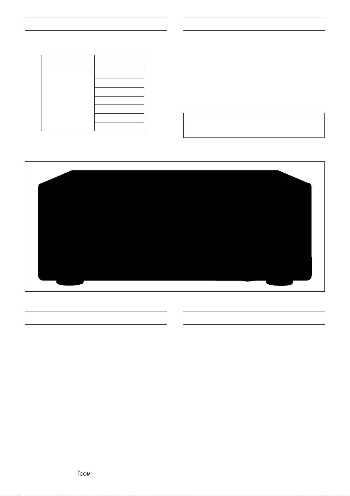
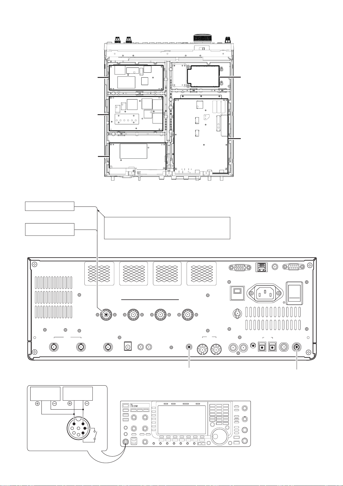
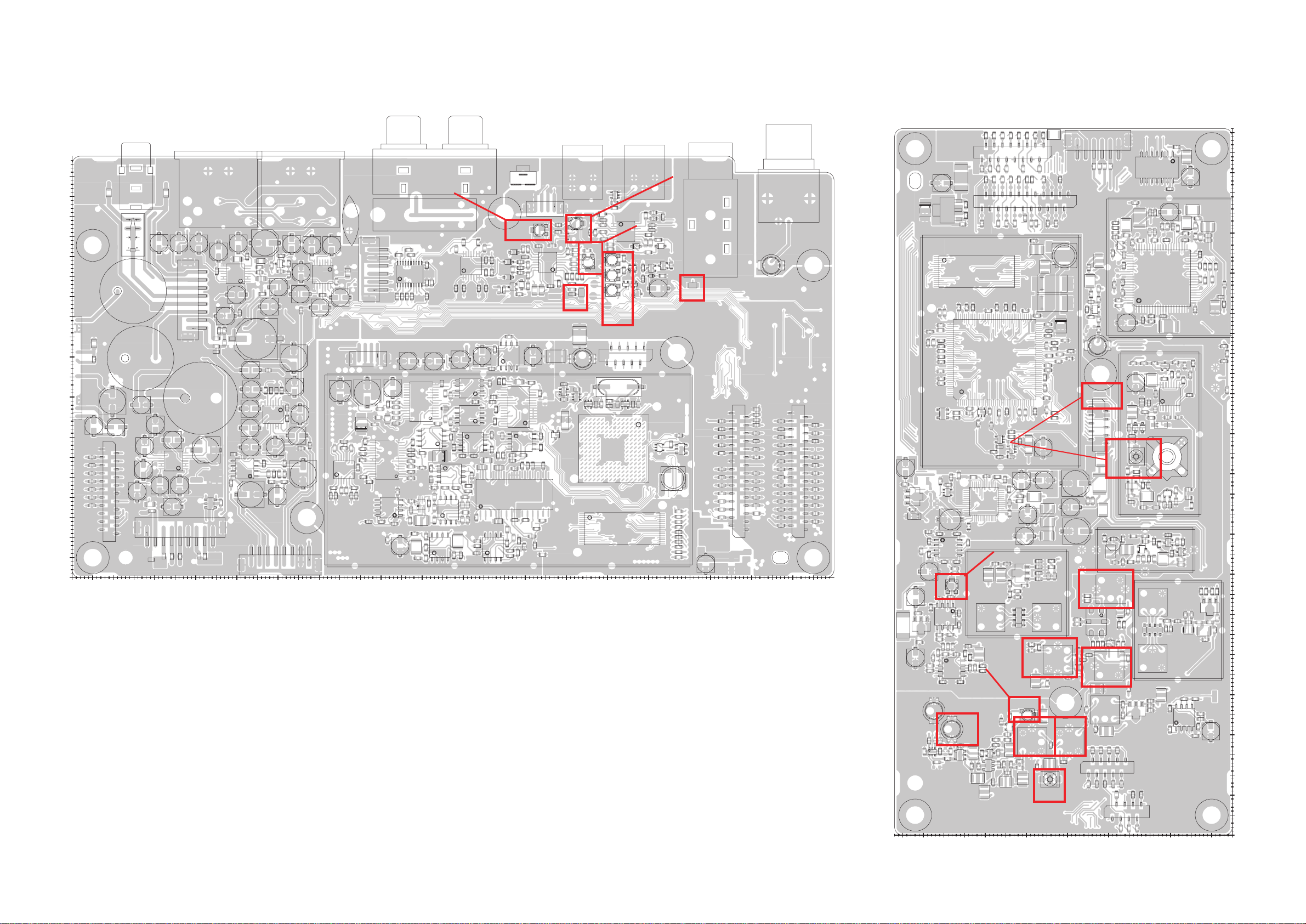
SECTION 2 INSIDE VIEW
(viewing from the bottom)
RF UNIT
MAIN UNIT
PLL UNIT
DIGISEL UNIT
(under the cover)
SCOPE UNIT
OSC UNIT
2 - 1
Page 7
SECTION 3 CIRCUIT DESCRIPTION
3-1 RECEIVER CIRCUITS
ANT-SW UNIT
Antenna switching relays (RL51, 61, 71, 81) select the RX
signals which are from [ANT1]–[ANT4], and the relays are
controlled by relay controller (IC11). RX signals from [ANT1]
–[ANT3] are applied to the CTRL BOARD, RX signals from
[ANT4] are applied to the RF UNIT directly.
CTRL BOARD
The CTRL BOARD has TX/RX switch which toggles the RF
path between in TX and RX.
RX signals from the ANT-SW UNIT are passed through the
TX/RX switches (RL252–254), and applied to the RF UNIT.
RF UNIT
RF UNIT contains receive circuits; from RX BPF to 2nd
RX IF AMP. The RX signals are filtered by BPFs to remove
unwanted signals and amplified, then down-converted twice
into 2nd IF signal.
The received signals from the ANT-SW UNIT and CTRL
BOARD are passed through some relays and attenuators,
then filtered by BPFs which is assigned to filter the RX
signals that desired to receive. The filtered RX signals are
amplified by RF AMPs before being applied to the 1st mixer.
• 0.03–30 MHz SIGNALS
The RX signals from the band SW (RL351) are passed
though one of the BPF or LPF. The filtered signals are
entered to the DIGISEL UNIT, and gone through or
by-passed the DIGISEL (Digital RF Selector Switch) filter.
When the DIGISEL function is activated, the RX signals
are passed through the DIGISEL SW (RL21) and narrow
bandwidth filter (D_SEL) which filters out unwanted signals
with its sharpen frequency response. The filtered signals are
amplified by the RF AMP (Q201) which recovers the insert
loss of the D_SEL filter, then backed to the RF UNIT via
DIGISEL SW (RL2).
• 30–60 MHz SIGNALS
RX signals from the band SW (RL351) are passed though
one of the BPFs (Fc=50–54 MHz or Fc=54–60 MHz) to
remove unwanted signals.
The filtered signals are amplified by one of (or both of)
the Pre-AMPs (or by-passed; according to the setting).
The amplified RX signals are then applied to the 1st mixer
(Q1211, 1212) via the LPF.
The RX signals are mixed with the 1st LO signals from PLL
UNIT (the 1st LO signals are gone through LO AMP (Q1301),
HPF and LPF before being applied.) to be converted into
the 1st RX IF signal.
A portion of 1st IF signal is applied to the SCOPE UNIT via
buffer (Q1352).
The converted 1st RX IF signal is then filtered by one of 1st
IF filters on the MCF BOARDs (FI1401). Selecting of the
filter to pass is carried out by IF SW (IC1402, 1403). The
filtered 1st RX IF signal is amplified by two 1st IF AMPs
(Q1401–1403), then splitted into two before being applied
to the 2nd mixers; as a image rejection mixer (IC501,
1502). Each divided 1st RX IF signal is mixed with 2nd LO
signals from the PLL UNIT (gone through ATT, LO AMP
(Q1651), buffer (IC1651) and another buffer (IC1651)), to be
converted into the 36 kHz 2nd RX IF signal.
One of the LO signal is 90 degrees phase-shifted before
being applied to the 2nd mixer (IC1502), and the converted
2nd RX IF is 90 degrees phase-shifted too.
These converted 2nd RX IF signals are buffer-amplified
by buffer (IC1502/IC1501) and amplified by 2nd IF AMP
(IC1504/IC1503). Then the 2nd RX IF signals whose phase
is different each other are phase-shifted by the phase shifter
(IC1505), then composed by the composer (IC1505).
The composed 2nd RX IF signal is amplified by another 2nd
IF AMP (IC1506), then entered to the MAIN UNIT.
The RX signals from the DIGISEL UNIT are applied to or
by-passed the Pre-AMP.
When the Pre-AMP1/2 is activated, the RX signals are
applied to the Pre-AMP1 (for all HF bands) or Pre-AMP2
(for 24 MHz and above) via P.AMP SW (RL1004), and the
amplified RX signals are applied to the 1st mixer (IC1051)
via the P.AMP SWs (RL1005, 1006) and LPF.
The RX signals are mixed with the 1st LO signals from
the PLL UNIT (1st LO signals are gone through LO AMPs
(Q1105, 1104, 1101) before being applied.) to be converted
into the 1st RX IF signal.
• FREQUENCY CONFIGURATION
Signal Frequency Signal Frequency
1st RX IF 64.455 MHz 1st RX LO 64.485–124.455 MHz
2nd RX IF 36 kHz 2nd RX LO 64.491 MHz
1st TX IF 36 kHz 1st TX LO 64.485–124.455 MHz
2nd TX IF 455 kHz 2nd TX LO 64 MHz
3rd TX IF (*)
*; Refer to "SPECIFICATIONS."
3 - 1
Page 8

MAIN UNIT
MIAN UNIT contains receive circuits; from demodulator
to AF circuits. The 2nd IF signal is demodulated by digital
audio processing circuits.
• DEMODULATOR CIRCUIT
The 36 kHz 2nd RX IF signal from the MAIN UNIT is
applied to the Analog to Digital Converter (ADC; IC1251) via
the IF mute SW (IC1201) and unbalance-balance convert
circuit (IC1211, 1231), to be converted into the 24-bit serial
data. The serial data is applied to the DSP (IC1001) and
processed as digital audio signals. The processed digital
audio signals are then applied to the Digital Audio Converter
(DAC; IC1501) to be converted into the analog audio
signals; as recovered AF signals.
The recovered AF signals are applied to the RX AF circuits
via buffer (IC1751).
• RX AF CIRCUITS
The recovered AF signals are amplified and level-adjusted,
then output from the audio interfaces. (The destination of AF
output signals is depends on the setting)
<OUTPUT FROM Int./Ext. SPEAKER>
The recovered AF signals from the buffer (IC1751) are
passed through the SQL SW (Q351), and applied to the
AF AMP (IC331). The amplified AF signals are splitted into
two AF lines; one is bound for the headphones jack (J2) on
the FRONT UNIT, another is bound for the internal speaker
(SP1)/external speaker via the external SP jack (J751) on
the MAIN UNIT. Both of AF signals on each AF lines are
applied to the 2-channel Voltage Controlled Amplifier (VCA;
IC311) whose gain is determined by applied control voltage
to be adjusted its signal level.
SCOPE UNIT
The 1st RX/TX IF signal from the buffer (Q1352) on the RF
UNIT are passed through the scope IF SW (IC31), scope
ATT, LPF and BPF (dual tuned), and amplified by scope
AMP (Q2) then applied to the 2nd scope mixer (D101).
The 1st IF signal is converted into the 45 MHz 2nd scope IF
signal (S2IF), and filtered to remove unwanted signals, then
amplified by the 2nd scope IF AMPs (Q201 and Q202). The
amplified 2nd scope IF signal is applied to the 3rd scope
mixer (D4) to be converted into the 200 kHz 3rd scope IF
signal. The converted signal is amplified by the 3rd scope IF
AMP (IC401), filtered by the active LPF (IC403), level-limited
by the saturation AMP (IC404). The level-limited signal is
applied to the ADC (IC501) which samples the 200 kHz 3rd
scope IF signal (0–2.5 V) into digital signal, then applied to
the DSP (IC601) as the serial data.
The DSP processes input data, then output to the CPU to
display the frequency and relative signal strength of RX
signals on the spectrum screen.
The level-adjusted AF signals are applied to the AF power
AMP (IC281) which power-amplifies to obtain audio output
power, via LPF (Q291/301).
The power-amplified AF signals are passed through the AF
mute SW (RL261), then applied to the internal speaker (SP1)
via the external SP jack (J751), or an external speaker on
the MAIN UNIT.
When the headphones are connected to the headphones
jack (J2) on the FRONT UNIT, the power-amplified AF
signals from the AF power AMP (IC281) are applied to the
connected headphones.
<TO THE AUDIO STORAGE>
When recording received audio, recovered AF signals from
the buffer (IC1571) are also send to the audio storage
(IC203) on the LOGIC UNIT to be recorded.
<OUTPUT FROM ACC PORT>
The recovered AF signals from the buffer (IC1571) are
amplified by AF AMPs (IC241), the amplified AF signals
are applied to the VCA (IC231) to be adjusted its signal
level. The level-adjusted AF signals are output from [ACC1]
socket.
3 - 2
Page 9

3-2 TRANSMITTER CIRCUITS
MAIN UNIT
The MAIN UNIT contains transmit circuits; from MIC AMP to
modulator cicuit.
CTRL BOARD
The CTRL BOARD mainly contains circuits for parameter
detection of TX signal; Forward Wave, Reflected wave,
Reactance, Resistance, antenna current and voltage.
• TX AF CIRCUITS
The audio signals from the microphone (MIC signals)
are amplified by MIC AMP (IC171) and level-adjusted by
VCA (IC171). The level-adjusted MIC signals are passed
through the MIC mute SW (IC201) and MIC line selector
(IC211) which selects the MIC line; MIC signals from the
microphone jack on the FRONT UNIT, or from [ACC1]
socket on the MAIN UNIT.
The MIC signals are then applied to the limiter AMP (IC221)
which limits the amplitude of MIC signals. The amplitudelimited MIC signals are applied to the ADC (IC1251) via the
unbalance-balance convert circuit (IC1311, 1321, 1331),
to be converted into the 24-bit serial data. The serial data
is applied to the DSP (IC1001) and processed as digital
audio signals. The processed digital audio signals are then
applied to the Digital to Analog Converter (DAC; IC1501) to
be converted into the analog audio signals; as the 36 kHz
1st TX IF signal. The 1st TX IF signal is entered to the RF
UNIT.
RF UNIT
RF UNIT contains transmit circuits; TX mixers and AMPs.
The 36 kHz 1st TX IF signal from the MAIN UNIT is applied
to the 1st TX mixer (IC503) to be mixed with the 491 kHz
3rd LO signal from the PLL UNIT, to be converted into
the 455 kHz 2nd TX IF signal. The converted 2nd TX IF is
amplified by the 2nd IF AMP (Q501), filtered by 2nd TX IF
filter (FI1501 for BW=20 kHz or FI1502 for BW=4 kHz). The
filtered 2nd TX signal is amplified by 2nd IF AMP (Q504),
and applied to the 2nd TX mixer (D505) to be mixed with the
64 MHz 2nd LO signal from the PLL UNIT, to be converted
into the 64.455 MHz 3rd TX IF signal. The converted 3rd
TX IF signal is passed through the BPF (FI503), amplified
by 3rd IF AMP (Q506), and filtered by the LPF. The filtered
3rd TX IF signal is applied to the 3rd TX mixer (D506) to
be mixed with the 3rd LO signal from the PLL UNIT, to
be converted into the 4th TX IF signal (=TX signal). The
converted TX signal is filtered by the LPF, amplified by RF
AMP (Q508), passed through one of BPFs, then applied to
the YGR AMP (Q801).
TX signal from the FILTER UNIT is passed through several
detection circuits in sequence, then applied to the antenna
[ANT1]–[ANT4].
• FOR (Forward Wave) voltage detection circuit
A portion of TX signal is rectified by current trans (L101) and
diode (D102), and the produced DC voltage is composed
by C103, C106 and C116 to detect FOR voltage (Forward
wave components). The detected voltage is amplified by
IC101 and applied to the A/D port of CPU (IC1).
• REF (Reflected Wave) voltage detection circuit
A portion of TX signal is rectified by current trans (L101) and
diode (D101), and the produced DC voltage is composed by
C102, C105, C115, C120 and C121 to detect REF voltage
(Reflected wave components). The detected voltage is
amplified by IC101 and applied to the A/D port of CPU (IC1).
• Reactance components detection circuit
A portion of TX signal which is detected by current trans
(L151) and TX signal which is divided by C153 and C158
are amplified by C-MOS IC. This AMP, as the first stage,
employs a C-MOS type AMP to detect the low TX signal.
The inverter AMP requires input level lower than others
need, and provides high speed operation for stable high
frequency operation with low TX signal.
The amplified signal is adjusted its wavefor m, then applied
to the IC155 and IC156 for phase comparison. The output
signal is rectified by D153 and D154, composed and
amplified by IC201, then applied to the A/D port of the CPU
(IC1).
• Resistance components detection
A portion of TX signal which is detected by current trans
(L201) and TX signal which is divided by C202, C205 and
C206 are adjusted so that two of these are the same on the
voltage. And two of these are rectified composed each other
to detect the resistance components. When the detected
voltage is increased, Q201 is activated to amplify the signal
for high detection sensitivity.
The amplified TX signal is entered to the PA200W BOARD.
PA200W BOARD
• TX AMPLIFIERS
The TX signal from the RF UNIT is amplified by the RF AMP
(Q101), Pre-drive (Q201), drive (Q301) and power (Q401A,
B) amplifiers in sequence, to obtain TX output power. The
power-amplified TX signal is entered to the FILTER UNIT.
FILTER UNIT
• TX FILTERS
The power-amplified TX signal from the PA200W BOARD
is passed through one of BPFs (according to the TX
frequency) to remove unwanted signals including harmonic
components. The filtered TX signal is then entered to the
CTRL BOARD.
3 - 3
Page 10
3-3 FREQUENCY SYNTHESIZER CIRCUITS
PLL UNIT
PLL UNIT provides LO signals; 1st LO for TX/RX IF circuits,
2nd RX LO (64.491 MHz), 2nd TX LO (64 MHz), 3rd TX LO
(491 kHz), marker frequency (100 kHz), reference frequency
for the SCOPE UNIT (40 MHz) and clock signal for the DSP
UNIT (12.888 MHz). These LO signals are generated by the
reference signal from the OSC UNIT as reference.
This transeiver employs the Direct Digital Synthesizer (DDS)
which digitally creates arbitrary waveforms and frequencies
from a fixed source frequency, to provide extremely high
resolution and stability frequency and pure wavefor m.
• Reference frequency signal
The 10 MHz reference frequency signal generated on
the OSC UNIT is applied to the 4th harmonic extractor
(Q702, L702, 703) via buffer (Q30) to produce the 40 MHz
reference signal.
• 1st LO signals
The 40 MHz reference signal from the harmonic extractor
is amplified by Q101, and applied to the DDS (IC101)
as the clock signal. The DDS generates the 10.4122038
–10.4963312 MHz sine waves, and these are passed
through the ceramic filter (FI101; Fc=10.7 MHz) to adjust
the wavefor m, then applied to the PLL IC (IC201) via buffer
(Q151).
<2nd TX LO signal>
The VCO output signal from the hybrid divider is passed
through the ATT, and applied to the 2nd LO AMP (Q591).
The amplified VCO output signal is passed through the BPF,
then entered to the RF UNIT as the 2nd TX LO signal.
<2nd RX LO signal>
The VCO output signal from the hybrid divider is passed
through the ATT, and applied to the 2nd LO AMP (Q801).
The amplified VCO output signal is passed through the ATT
and, applied to the 2nd LO mixer (D821) and mixed with
the 491 kHz 3rd TX LO signal from the 3rd TX LO oscillator
(IC651), to convert into the 64.491 MHz 2nd RX LO signal.
The converted 2nd RX LO signal is passed through the
ATT and BPF, and applied to the 2nd LO AMP (Q831). The
amplified signal is entered to the RF UNIT as the 2nd RX
LO signal.
• 3rd TX LO signal
The 40 MHz reference signal from the harmonic extractor
is amplified by IC652, and applied to the DDS (IC565) as
the clock signal. Using the clock signal, the DDS directly
generates the 491 kHz 3rd TX LO signal.
The output signal of DDS is passed through the LPF and
HPF, and applied to the buffer AMP (Q680). The bufferamplified 2rd TX LO signal is entered to the RF UNIT via
ATT.
The PLL IC (IC201) controls the oscillating frequency
of 6 VCOs (VCO1 to VCO6) using the reference signal
generated by the DDS as reference frequency.
VCO
VCO1 Q220 64.485–72.454999 MHz
VCO2 Q230 72.455–79.454999 MHz
VCO3 Q240 79.455–86.454999 MHz
VCO4 Q250 86.455–94.454999 MHz
VCO5 Q260 94.455–109.454999 MHz
VCO6 Q270 109.455–124.455 MHz
Oscillator
component
Oscillating frequency
The output signals of each VCOs (1st LO signals) are
buffer-amplified by Q301, passed through the HPF and
LPF, then amplified by the 1st LO AMPs (Q302 and Q351).
The amplified 1st LO signals are buffer-amplified by Q352,
passed through the LPF, HPF and ATT, then output to the
RF UNIT as 1st LO signals (64.485–124.455 MHz).
• 2nd LO signals
The 40 MHz reference signal from the harmonic extractor is
amplified by IC503, and applied to the DDS (IC501) as the
clock signal. The DDS generates the reference frequency
which controls the oscillating frequency of 64 MHz VCO
(Q541).
The output signal of 64 MHz VCO (Q541) is buffer-amplified
by Q561, and applied to the hybrid divider.
The hybrid divider divides the VCO output into two; 2nd TX
LO and 2nd RX LO.
• DSP system clock
The 40 MHz reference signal from the harmonic extractor
is amplified by IC1651, and applied to the DDS (IC1652)
as the clock signal. Using the clock signal, the DDS directly
generates 12.288 MHz system clock signal. The system
clock signal is passed through the LPF and HPF, and
applied to the buffer (Q1680). The buffer-amplified system
clock signal is entered to the MAIN UNIT via ATT.
• Scope clock
The 40 MHz reference signal from the harmonic extractor is
amplified by Q1601, and entered to the SCOPE UNIT.
3 - 4
Page 11

3-4 MAIN CPU (IC604) PORT ALLOCATIONS
Pin
No.
Clock signal to 4094/LMX2306 (PLL UNIT).
42
(DDS for 1st LO PLL-IC/DDS, 2nd TX LO DDS, 3rd TX LO)
"Serial data to 4094/LMX2306 (PLL UNIT).
43
(DDS for 1st LO PLL-IC/DDS, 2nd TX LO DDS, 3rd TX LO)
44 N/C O
45 Mode status (1Lo or T2Lo) output. O
46 Chip select siganl to PLL. I/O
47 Strobe to the PLL. O
51 Clock signal to units other than PLL and SCOPE. O
52 Serial data (other than PLL, SCOPE and DSP). O
53 N/C O
54 CI-V format data (UART). O
55 CI-V format data (UART). I
56 Clock to the DSP IC. O
57 Seral data (TXD/RXD) to the DSP. O
58 START signal to the TUNER UNIT (UART, 9600). O
142 Serial data to the DAC (BU9480) for ext. S-meter. O
140 Clock (A-clock) to the DAC (BU9480) for ext. S-meter. O
138 Clock (B-clock) to the DAC (BU9480) for ext. S-meter. O
137 Power line for liner circuit control signal. O "H"=Power ON
113 Forword wave detected voltage (A/D). I
114 Refl ected wave detected voltage (A/D). I
115 ALC fedback voltage (A/D). I
116 Drain current (fi nal amp.). I
117 Drain voltage (fi nal amp.). I
118 PA UNIT temparature. I
119 Cooling fan motor current. I
120 Voltage from key pad (rear panel). I
133 Serial data to the FRONT CPU (UART, 38400). O
134 Serial data from the FRONT CPU (UART, 38400). I
135 CW/RTTY keying signal to the DSP. O "L"=Key pushed
81 Mute control signal. I "H"=Mute
82 TX power line control signal. O "L"=TX
83 Noise pulse. I
105 RX power line control signal. O "L"=RX
3 Serial communication with the scope DDS (AD9857) detect signal. O "H"=detected
33 Serial data to the SCOPE UNIT DDS/PLL/DSP. O
34 Strobe to the scope PLL (LMX2306). O
59 Chip selet signal to the scope DDS (AD9857). O "L"=AD9875 is slected
60 Profi le (0/1) select signal to the scope DDS (AD9857). O "H"=Profi le 1 is selected.
61 Clock signal to the DDS/PLL/DSP. O
121 DSP data (TXD/RXD). I
122 Hand shake signal from SCOPE DSP. I
123 Extra port for SCOPE DSP. I
124 Serial data from SCOPE DSP. I
125 N/C I
126 Through signal from the TUNER UNIT. I "H"=Through
127 Key input from the tUNER UNIT. I "H"=Tuner ON
128 Straight key input (A/D). I "L"=Key pushed
Description
IN/
OUT
O
O
Condtion
3 - 5
Page 12

3-4 MAIN CPU (IC604) PORT ALLOCATIONS (continued)
Pin
No.
23 Clock to the EEPRROM (HN58X2464TI). O
24 Serial data from the EEPRROM (HN58X2464TI). I/O
26 Clock signal to the EEPROM (DIGISEL UNIT; CAT24WC256). O
27 Serial data from/to the EEPROM (DIGISEL UNIT; CAT24WC256). I/O
30 RTTY keying. I "H"="space" is marked
31 Transverter control signal from the [ACC] connector. I
21 PLL unlock signal. I "L"=Unlocked
5–
Address bus lines. O
20
73–
Data bus lines. I/O
71
84 WAIT signal (bus line control). I "L"=Wait.
85 SEND signal. O "L"=TX
86 Dual Port SRAM intrude signal. I
87 "L" indicator control signal (bus control). O "L"= lights.
88 "H" indicator control signal (bus control). O "H"= lights.
89 READ data (bus contol). O
90 Address data (bus contol). O
94 PTT/ACC SEND input. I "H"=TX
107 Squelch signal to the [ACC] connector. O
109 Squelch signal. O
35 External SEND (lead relay) signal output. O "H"=Relay ON
36 External SEND (IC relay) signal output. O "H"=Relay ON
37 Chip select signal to the Dual Port SRAM. O "L"=SRAM is selected.
38 Chip select signal to the expander. O
Description
IN/
OUT
"L"= Transverter is
"H"= Squelch open (RX
"L"= Squelch open (Mute
"L"= Expander is
Condtion
activated.
LED lights)
OFF)
selected.
3 - 6
Page 13
SECTION 4 ADJUSTMENT PROCEDURE
4-1 PREPARATION
¤ REQUIRED EQUIPMENTS
EQUIPMENT SPECIFICATION EQUIPMENT SPECIFICATION
Spectrum analyzer
RF power
(terminated type)
Frequency Counter
Modulation
Analyzer
Audio Generator
Frequency range : At least 90 MHz
Bandwidth : 100 kHz or more
Measuring range : 10–300 W
Frequency range : 1.8–100 MHz
Impedance : 50
SWR : Less than 1.2 : 1
Frequency range : 0.1–100 MHz
Frequency accuracy :
Input level : Less than 1 mW
Frequency range : 30–300 MHz
Measuring range : 0 to ±10 kHz
Frequency range : 300–3000 Hz
Output level : 1–500 mV
Ω
±0.5 ppm or better
Digital multimeter
Standard Signal
Generator (SSG)
AC Millivoltmeter Measuring range : 10 mV to 10 V
External Speaker
Attenuator
CAUTION!: BACK UP originally programmed contents (Memory channels, Common settings, etc.) in the transceiver before
starting adjustment. When all adjustments are completed, these contents in the transceiver will be cleared.
Input impedance : 50 kΩ/DC or more
Measuring range : Voltage: 0.1–10V
Current: 5A/30A
Frequency range : 0.1–100 MHz
Output level : 0.1 µV to 32 mV
(–127 to –17 dBm)
Input impedance : 8
Capacity : More than 5 W
Power attenuation : 50 or 60 dB
Capacity : More than 200 W
Ω
¤ EXPOSING UNITS
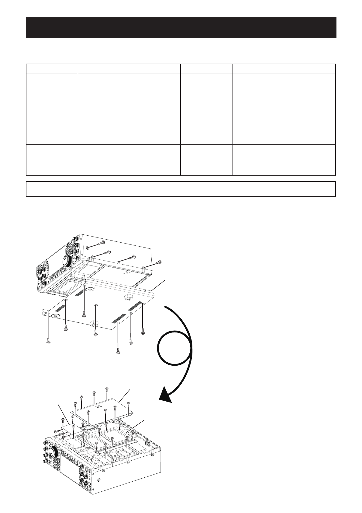
CAUTION: The transceiver weighs approx. 22.5 kg (50 lb). Always have two people available to carry, lift or turn over the transceiver.
1) Remove 8 screws from the both sides.
2) Remove 7 screws from the bottom, then remove the
bottom cover.
Bottom cover
OSC UNIT cover
RF UNIT cover
PLL/SCOPE UNITs cover
3) Turn over the transceiver.
4) Remove 8 screws from the RF UNIT cover, 10 screws
from the PLL/SCOPE UNITs cover and 10 screws
from the OSC UNIT cover, then remove those covers.
4 - 1
Page 14
¤ UNITS LOCATION
<Bottom view>
SCOPE UNIT
PLL UNIT
MAIN UNIT
¤ CONNECTIONS
SSG
RF power meter
OSC UNIT
RF UNIT
CAUTION !
DO NOT select an TX adjustment item while an SSG
is connected to the antenna connector.
AC millvolt
meter
RX ANT
Audio
generator
<Rear view>
CW KEY
-
RS
232C
I
REF I/O
10MHz
-
10dBm
SSG
AC
S/P DIF
REMOTE
INOUT
EXT-DISPLAY
15A
ANT 1 AN T 2 ANT 3 ANT 4
DC OUT
INOUT
X-VERTER
15V
MAX1A
METER
EXT
KEYPAD
EXT-SP
ACC
12
GND
ALC
ALCRELAY
ADJ
SINAD METER
(for adjustments on the OSC UNIT)
<Front view>
[MIC]
PTT
4 - 2
Page 15

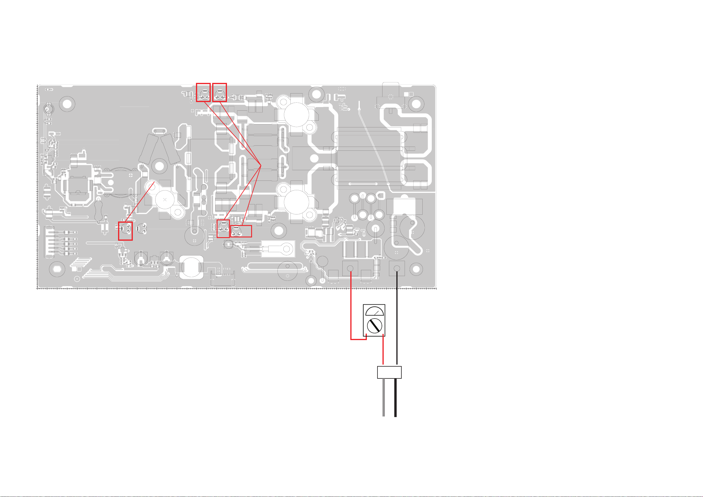
4-2 ADJUSTMENTS ON THE OSC UNIT AND PLL UNIT
ADJUSTMENT ADJUSTMENT CONDITION OPERATION
REFERENCE
SIGNAL LEVEL
REFERENCE
SIGNAL LEVEL
(40MHz)
HPL
LOCK VOL T A GE
(VCO1)
(VCO2) 2 • Frequency : 14.999 MHz
(VCO3) 3 • Frequency : 21.999 MHz
(VCO4) 4 • Frequency : 29.999 MHz
(VCO5) 5
(VCO6) 6 • Frequency : 60.000 MHz
1st LO
OUTPUT LEVEL
2nd LO
LOCK VOL T A GE
RX 2nd LO
LEVEL
TX 2nd LO
LEVEL
1 • Reference signal source :
External
• Receiving
1 • Receiving 1) Connect a Spectrum Analyzer to
1 • Frequency : 7.999 MHz
• Mode : USB
• Receiving
• Mode : USB
• Receiving
• Mode : USB
• Receiving
• Mode : USB
• Receiving
• Frequency : 44.999 MHz
• Mode : USB
• Receiving
• Mode : USB
• Receiving
1 • Frequency : 14.999 MHz
• Mode : USB
• Receiving
1 • Frequency : 14.100 MHz
• Mode : USB
• Receiving
1 • Frequency : 14.100 MHz
• Mode : USB
• Receiving
1 • Frequency : 14.100 MHz
• Mode : USB
• T r ansmitting
1) Connect an Standard Signal
Generator to J1071 ([EXT-REF I/O]
terminal on the rear panel) and set
as;
Frequecy : 10.000 MHz
Level : –10.0 dBm
Modulation : None
2) Connect a Spectrum Analyzer to
J1072.
3) Adjust the REF signal level with
L1061 and L1062.
CP701 (PLL UNIT).
2) Adjust the REF signal (40 MHz)
level with L702 and L703.
1) Connect a Digital multimeter to CP2
"LV2" (PLL UNIT).
2) Adjust the lock voltage with C222.
1) Connect a Digital multimeter to CP2
"LV2" (PLL UNIT).
2) Adjust the lock voltage with C232.
1) Connect a Digital multimeter to CP2
"LV2" (PLL UNIT).
2) Adjust the lock voltage with C242.
1) Connect a Digital multimeter to CP2
"LV2" (PLL UNIT).
2) Adjust the lock voltage with C252.
1) Connect a Digital multimeter to CP2
"LV2" (PLL UNIT).
2) Adjust the lock voltage with C262.
1) Connect a Digital multimeter to CP2
"LV2" (PLL UNIT).
2) Adjust the lock voltage with C272.
1) Connect a Spectrum Analyzer to
J351 "1LO" (PLL UNIT).
2) Adjust the output level with R357.
1) Connect a Digital multimeter to CP3
"LV3" (PLL UNIT).
2) Adjust the lock voltage with C546.
1) Connect a Spectrum Analyzer to
J831 "R2LO" (PLL UNIT).
2) Adjust the output level with L801
and L834.
1) Connect a Dummy Load to [ANT1].
2) Connect a Spectrum Analyzer to
J561 "T2LO" (PLL UNIT).
3) Adjust the output level with L565
and L566.
ADJUSTMENT
POINT
L1061, L1062
(OSC UNIT)
(repeatedly)
L702, L703
(PLL UNIT)
(repeatedly)
C222
(PLL UNIT)
C232
(PLL UNIT)
C242
(PLL UNIT)
C252
(PLL UNIT)
C262
(PLL UNIT)
C272
(PLL UNIT)
R357
(PLL UNIT)
C546
(PLL UNIT)
L801, L834
(PLL UNIT)
(repeatedly)
L565, L566
(PLL UNIT)
(repeatedly)
VALUE
Maximum
level
Maximum
level
3.9–4.1 V
3.9–4.1 V
3.9–4.1 V
3.9–4.1 V
3.9–4.1 V
3.9–4.1 V
2.35–2.85
dBm
1.7–2.3 V
Max. level
(–20.0
dBm ±3.0
dB)
Max.
level
(3.0 dBm
±3.0 dB)
4 - 3
Page 16
L1061
L1062
J1072
J1071
From SG
To RF voltmeter
CP2
HPL lock voltage check
C232
(VCO2)
C222
(VCO1)
R357
1st LO level adjustment
L703
Reference signal level (40MHz) adjustment
L702
CP701
C272
HPL lock voltage adjustment
(VCO6)
C262
(VCO5)
C252
(VCO4)
C242
(VCO3)
J351
C546
2nd LO lock voltage adjust
CP3
L834
L801
L565
L566
TX 2nd LO level
adjustment
J831
J561
RX 2nd LO level
adjustment
- ADJUSTMENT AND CHECK POINTS -
• PLL UNIT (TOP VIEW)
• PLL UNIT
(TOP VIEW)
RX 2nd LO level
adjustment
1
C831
R2Lo
J831
TO RF J1651
R692
R691
R690
C691
J831
C692
R686 R687
C668 C669 C670 C671 C672
C666
C663 C664
C653
DACK
TOMAINJ801
R1680
C1670
R1707
R1706
C1669
T3Lo
J681
R812
R814
TO RF J501
C811
R689
Q680
R685
R688
C690
C654 C655 C657 C658
C1684C1685
C661
MP1651
L1682
C1671 C1672 C1673
IC652
J1681
C1682
C1683
C1668
C1667
L1681
R1691
R1692
IC651
R656
C1666
C1691
C660
R1690
C1681
R693
Q1680
R1686
R1689
C1692
C1680
R1679
R1676
R1678
IC1652
Q831
C834C835
R834R835
L834
L834
C813
Q811
L812
C812
L683
C687
C686
C688C689
C667
C665
C659
R657
C1689
9
R1687
R1688
R1693
R1685
C1690
MP1653
R1673
R1675
R1677
R1664 R1665
R1666 R1667
R1668 R1669
R1670 R1671
R1672
R1674
C1661
C1664C1665
L831
FI831
C838
C832
MP651
C684C685
L682
C682
C683
L681
C681
C680
R679 R680
R677 R678
R675 R676
R673 R674
R671 R672
R669 R670
R667 R668
R665 R666
R663 R664
R661 R662
R659 R660
R658
R655
2nd LO lock voltage adjust
R1656R1657
R1658 R1659
R1660 R1661
R1662 R1663
R1651
C1651
IC1651
R1652
C1652
R1694
C1659 C1660
IC1701
R1705
C1711
C1655 C1656
C1658
R565
MP653
R546
L543
C549
C546
C550
C546
C545
C546
R580
R711
C526
C525
R506
IC503
R503
R504
D821
L801
Q561
R563
R564
Q541
R544
R545
C543
C580
C517C518C519
C520
EP1708
EP1701
EP1702
EP1703
EP1704
EP1705
EP1706
EP1707
EP1709
4
V0 V5 V10 V15 V20 V25 V30 V35 V40 V45 V50 V55 V60 V65 V70 V75 V80 V85 V90 V95 V100 V105 V110
H0H5H10
H20H25
H15
H30H35
H40H45
C566
R570
R561
C551
C547 C548
D542
Q580
R582
C504 C506
R573
R571
R572
L541
MP541
R581
MP501
L822
L821
C542
C581
TO RF J502
L801
R574 R575
L542
R556
IC501
H50
L562
R839
Q832
C553
R554
C559
C515C516
J561
C837
C554
Q540
R540
C540
R548
R550
C558
R509
C514
C507
C532
R522
L530 L531
H55H60
T2Lo
J561
C836
C802
C803
R803
R802
C541
C521
C552
R555
R537
C509 C510 C511 C512 C513
C533
TX 2nd LO level
adjustment
L566
C20
C21
L566
L565
L565
Q801
C801
6
CP3
CP3
J1601
TO SCOPE J3
LV3
C503
L501
L532
C1751
C1752
C1753
C1754
C1755
H65H70
10M
C1756
C1757
C703
C704
L701
L30
L703
R712
R704
L702
D501
Q502
C501
C502
R534
C535
C534
EP22
C22
EP21
EP20
C565
C593
L1603
C1613
C1612
C1611
L1602
C1609
SAD
L703
C712
C710
C709
L702
H75H80
L20
C1610
C1608
Q1601
C1607
R1608
C711
C705
J31
TO OSC
J1702
7
8
R272
L272
R270
C274
R274
C278
(VCO6)
L270
R1602R1606
R1607
C1601
C713
R709
R708
R710
1st LO level adjustment
J351
1Lo
J351
TO RF J351
C294
D272
R262 R263
R273
C293
C277
C273
C272
C272
D271
D270
CP701
R101 R102 R103
Q101
L102
C291
L262
C275
C263
C264
R260
R264
C262
R271
C276
C268
C272
(VCO5)
C260
L271
L260
CP701
R604
IC602
Reference signal level (40MHz) adjustment
C101
R104
R105
R108
C107
C108
C109
R106
C106
C102
C104
C103
C105
R107
C110
DIP
L451
C453
C441
C442
C444
C445
C446
C448
R364
R366
C447
R441
C451
C452
R365
L442
C361
C292
HPL lock voltage adjustment
C267
C262
C265
R261
C266
L452
D262
R252 R253
R254
D441
L252
C254
R250
C258
C262
(VCO4)
C250
L261
D261
D263
C604
R603
C124
C118
C111
L250
C605
TO RF J1001
C122
C123
C120
R109
R110
R111
R112
C117
C116
IC101
C115
C114
C119
R113
C112
C113
C128
R138
L103
C443
L441
R442
R443
C449
Q441
C290
C289
C257
C253
C252
C252
D250
J601
MKR
IC103IC104
L101
C121
IC102
R131R132
R133
FI101
L123
C255
R251
C256
C353
D252
R242 R243
R244
C252
L251
5
L242
C244
R357
R358
R359
C355
C357
C351
C352
Q351
L351
R352
R356
C356
C288
C287
C247
C245
C243
R240
C242
R241
C246
C248
C242
(VCO3)
C240 C241
L240
D240
LV1
CP1
R357
R357
R353
D242
C242
L241
MP221
R355
R234
C354
R232 R233
L232
C234
C230
L230
C311
R354
C286
C285
C239
C237
C233
R230
C232
C238
C232
(VCO2)
D231
C296
D230
MP101
B6724D
PLL
H90H95H100H105
H85
H110H115
H120
H125H130
H135
C309
C334
C335
C337
C341
C344
C310
L332
R341
C336
D341
L302
R343
L341
Q341
C284
Q280Q281Q282Q283Q284Q285
D232
R222 R223
C283
L222
C235
C223
C224
R220
R224
Q220Q230Q240Q250Q260Q270
C222
R231
C236
C228
C232
(VCO1)
C220 C221
L231
L220
MP201
R210
C219
C201
C203
C208
C206
R206
IC201
C202
L201
C2
R4R5R6
Q41
D201
176x113 t=1.6(2)
H145H150
H140
To RF voltmeter
From SG
• OSC UNIT
(TOP VIEW)
J1072
J1071
C1072
Q1070
C1008
C1048
L1044
Q1042
C1052
R1045
R1046
R1092
R1091
R1043
C1043
C1044
C1092
C1050
Q1043
C1074
R1044
EP1091
C1093
R1075
R1080
C1075
R1074
R1012
D1011
Q1011
C1018
C1017
R1064
R
R1068
Q1062
C1062
R1067
L1061
C1064
C1067
R1065
L1061
C1051
RL1010
EP1092
R1095
C1091
C1042
IC1091
R1099
C1094
R1100
IC1092
R1094
R1093
R1098
R1061
C6110
C1063
R1063
R1062
C1016
C1005
D1010
Q1061
C1004
Q1010
R1096
R1097
R1102
C1019
C1007
R1071
R1073
D1071
D1072
R1011
C1006
R1072
C1071
J1071
C2017
N
R2018
J2016
Q1012Q1013
C2016
R2017
X10
R2016
J2016
C1010
C1011
IC10
C1012
C1013
C1015
EP1010
C1014
EP1070
J2017
C1070
C1069
EP1069
Q1101
R1101
C1101
R1077
J1072
R1078
R1079
C1073
C1077
R305
L331
C302
R306R307
R304
C332C333
C301
C331
R301
R342
C342
C229
C227
C225
R221
C226
C222
D221
D220
R201
Q201
C212
C204
C205
R205
D205
IC2
R3
R19
C54
R303
Q301
C308
R302
D222
C51
C52C53
IC51
R51
L1062
3
C222
L280
R61
L221
C61
C64
C210
C209
C259
R17
R16
L2
R15
R14
R13
R11
R10
EP12
EP11
CP2
CP2
LV2
HPL lock voltage check
J2019
BROWN
TO DC-DC
J2018
J2019
C16
C15
C18
C17
EP10
C19
TO LOGIC
C14
EP13
J2018
2
H155
H160
H165
H170
H175
RL1011
L1062
C1031
C1066
C1030
L1024
C1047
C1028
L1021
R1027
C1026
C1025
Q1022
R1028
C1033
R1025
R1021
C1021
R1020
C1023
C1032
Q1021
R1023
R1026
R1024
C1024
Q1023
C1045
C1020
L1020
C1046
L1041
R1022
L1042
C1022
L1043
R1047
R1013
C1053
B6734B
L1023
C1027
L1022
V0 V5 V10 V15 V20 V25 V30 V35 V40
H0H5H10H15H20H25H30H35H40H45H50H55H60H65H70
4 - 4
Page 17
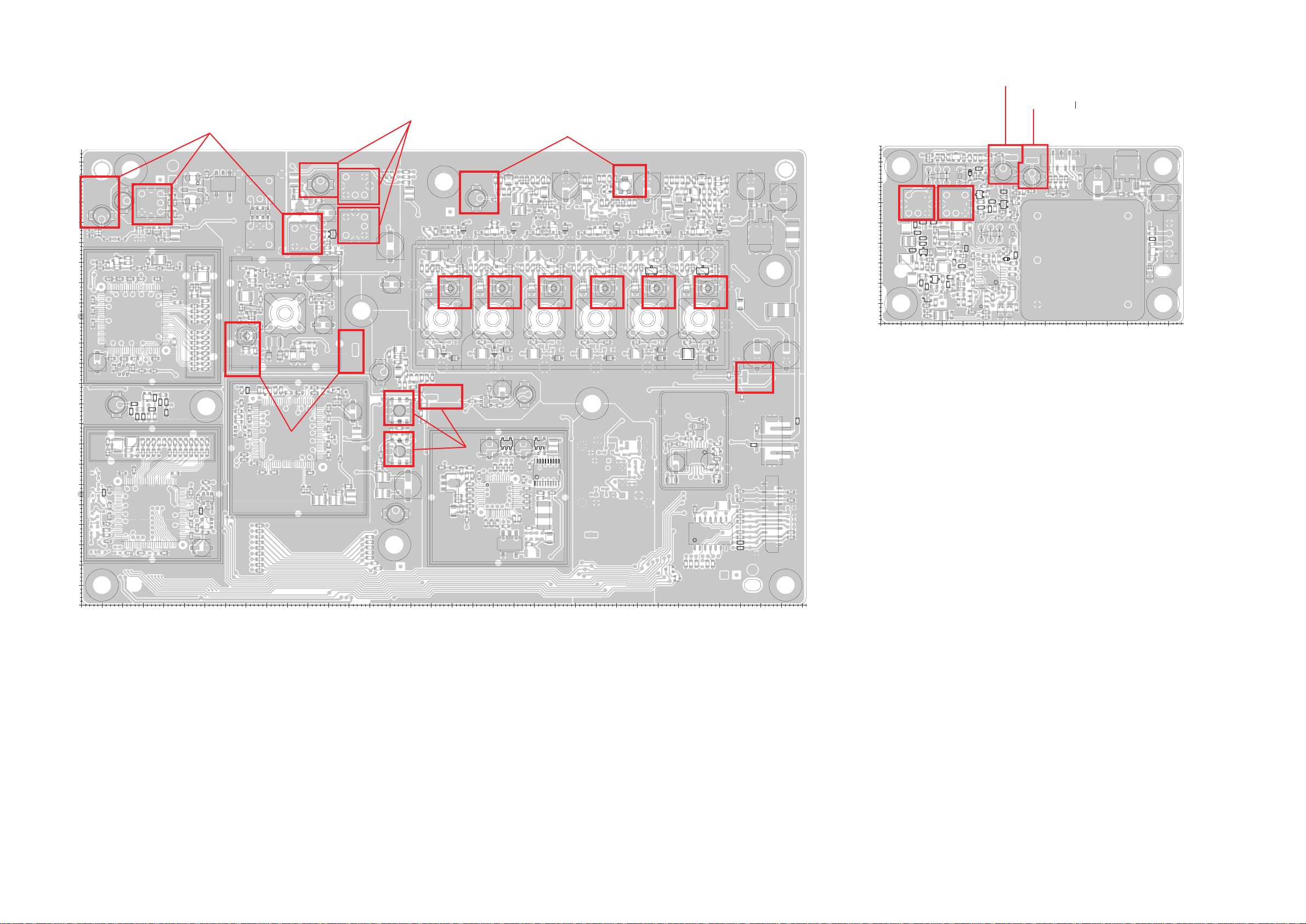
4-3 ADJUSTMENTS ON THE RF UNIT
s
ADJUSTMENT ADJUSTMENT CONDITION OPERATION
PRERARATION
(Preset)
(MCF-M) 4• Set the L1401 and L1402 as below.
(MCF-W) 5• Set the L1401 and L1402 as below.
(MCF-N) 6• Set the L1401 and L1402 as below.
1 • Frequency : 14.150 MHz
• Mode : USB
• ANTENNA : [ANT1]
2• Connect a Digital multimeter to
• [P.AMP1] : "ON"
• Receiving
• Connect a Digital multimeter to
CP1102" (RF UNIT).
CP1103" (RF UNIT).
3• Set R1228 (RF UNIT) to center
position.
Center position
3 rotation
Core
3.5 rotations
Core
ADJUSTMENT
POINT
R1101
(RF UNIT)
R1132
(RF UNIT)
R1228
(RF UNIT)
L1401, L1402
(MCF-M BOARD)
L1401, L1402
(MCF-W BOARD)
VALUE
4.4–4.6 V
4.4–4.6 V
Center
position
–
–
RECEIVE
SENSITIVITY
(HF BAND)
IMAGE
RESPONSE
RECEIVE
SENSITIVITY
(50 MHz BAND)
IF THROUGH
(50 MHz)
1 • Frequency : 14.150 MHz
• Mode : USB
• ANTENNA : [ANT1]
• Receiving
1 • Frequency : 14.150 MHz
• Mode : USB
• ANTENNA : [ANT1]
• Receiving
1 • Frequency : 50.0200 MHz
• Mode : USB
• ANTENNA : [ANT1]
• [PREAMP2] : "ON"
• Receiving
1 • Frequency : 50.0200 MHz
• Mode : USB
• Receiving
4.5 rotations
Core
1) Connect an SSG to the [ANT1] and
set as;
Frequecy : 14.1515 MHz
Level : 0 dBµ
Modulation : None
2) Connect an AC Millivoltmeter to the
[EXP-SP].
3) Adjust the sensitivity with L1408
and L1058.
1) Connect an SSG to the [ANT1] and
set as;
Frequecy : 14.0765 MHz
Level : +94 dBµ
Modulation : None
2) Connect an AC Millivoltmeter to the
[EXP-SP].
3) Adjust the sensitivity with R1516
and C1656.
1) Connect an SSG to the [ANT1] and
set as;
Frequecy : 50.0215 MHz
Level : –10 dBµ
Modulation : None
2) Connect an AC Millivoltmeter to the
[EXP-SP].
3) Adjust the sensitivity with L1222.
1) Connect an SSG to the [ANT1] and
set as;
Frequecy : 64.455 MHz
Level : +94 dBµ
Modulation : None
2) Monitoring the S-METER on the
display, adjust the swing width with
C1265.
L1401, L1402
(MCF-N BOARD)
L1408, L1058
(repeatedly)
(RF UNIT)
R1516, C1656
(RF UNIT)
L1222
(RF UNIT)
C1265
(RF UNIT)
–
Max. audio
output leve
Min. audio
output leve
Max. audio
output leve
Min.
swing
width
l
l
l
4 - 5
Page 18
R1101
Preset
R1228
L1058
RX sensitivity adjustment
L1408
Image response adjustment
R1516
C1656
RX sensitivity
(50MHz)
adjustment
L1222
C1265
TX output power adjustment
L505
C576
L512
R538
TX total gain adjustment
R1132
IF through (50MHz)
adjustment
Preset
L1401
L1402
Preset
L1401
L1402
Preset
L1401
L1402
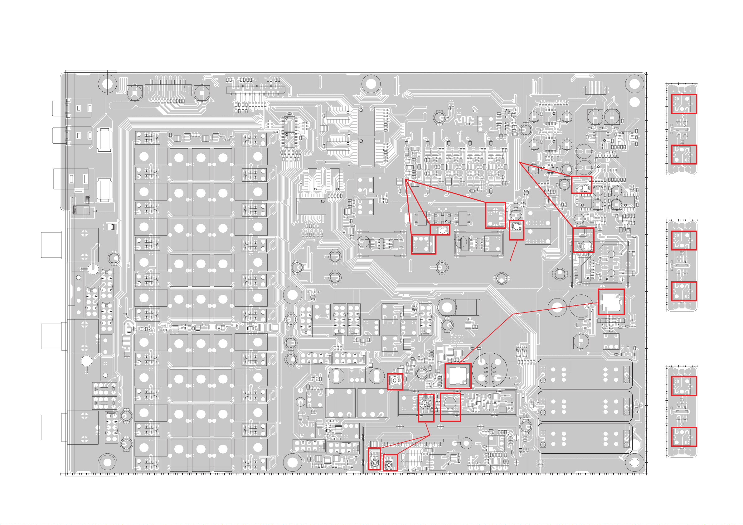
- ADJUSTMENT AND CHECK POINTS -
• RF UNIT (TOP VIEW)
KEYPAD
METER
J2001
D2001
DC-OUT
D2002
XVRT
RL381
RXANT-IN
RL410
RL431
RXANT-OUT
9
J2002J2003
EP2002
J103
RL352
J104
R405
J105
1
2002F1002F
2A
FUSE
C397
V
TO RF J810
R388
RL401
J391
RL351
R264
C287
R262
RL353
L268
R322
L326
E
TO CTRL J351
J106
RL402
J108
F
TO ANT-SW J3
C2010
RL2
L27
RL22
L57
RL52
L87
RL82
L117
RL112
L147
RL142
L177
RL172
L207
RL202
L237
RL232
L267
RL262
H175
• MCF-M BOARD
(TOP VIEW)
C2006
C2012
L25
L55
L85
L145
L294
L205
L235
L265
L3
C7
C297
L293
EP2004
J2006
TO MAIN J941
R1
R3
C272
J2007
C2007
C2013
C2015
C2016
C2017
EP2014
EP2015
EP2016
TO DC-DC J7
C10
6L5L
C2019
EP2017
RED
C8
C9
C11
L4
EP2018
EP2013
J2007
L26
L56
L86
L116
L115
L146
L295
L176
C302
L291
C283
L175
C304
D262
L292
C285
R263
Q260
C286
C303
R260
L296
L206
L236
L266
L24
L54
L84
L114
L144
L174
L204
L234
L264
EP2005
C2009
D260
EP2007
C2004
EP2006
EP2008
C2023
EP2010
EP2009
C2022
R2007
C2021
C276
J2006
R2008
R2009
R2010
L260
R261
C2018
C2020
EP2012
EP2011
R2011
R2012
C398
RL1
L23
R121
R122
R123
R101
R103
R105
R104
R135
201CI101CI
R134
R133
C399
R118
R120
R107
R108
R102
R106
R117
R119
RL21
C1724
L53
RL51
L83
L113
RL81
RL111
I
C1723
J351
TO PLL J351
R1706
C1722
8
L143
RL141
J102
RL902
R320
L320
G
J2004
L173
RL171
TO DIGISEL J1
J101
L203
RL201
IF through (50MHz)
TO DIGISEL J2
L1005
L1004
L233
RL231
L263
RL261
C1014
L1006
RL1006
4
4091C3091C
L1902
EP1901
IC1701
R1712
R1715
IC1703
R1720
R1721
R1722
C1717
C1718
C1720
C1721
C910C914
Q901
L905
RL1003RL1004
Q1005
EP1802
L1008
C1011
C1013
R1006
R1008
C1038
R1024
C1041
C1037
L1013
Q1205
D1001
R1018
R1002
C1001
R1019
L1052
R1056
L1053
C1054
C1053
C1057
C1067
C1055
C1056
7
R1909
C1202
L1015
R1133
R1134
L522
L1208
L1011
L1056
C1125
R1132
C577
D506
R1132
R576
R575
C574
R577
MP511
L1009
C1104
R1105
R1910
R1911
R1912
R1913
R1914
R1915
R1916
R1902
R1903
R1904
R1905
R1906
R1907
R1908
L646
R610
L513
L1213
0
42
1C
L1216
L1210
6
32
1C
C1250
L1228
C1266
C1265
C1265
R1228
CP1102
C1101
R1101
R1101
R1101
L650
L648
D619 D620
L1214
L1211
C1248C1249
R1203
R1135
C759
C756
C761
C755
L649
C751
C750
C749
C760
C745
L512
C1246
L1218
C1247
L1219
J1001
J601
TO PLL
L1220
IC1051
C1123
L651
L647
Q1701
C1241
IC1904
IC1903
IC1702
2091CI1091CI
2091C1091C
TX output power adjustment
L521
R1709
R1710
R1711
R580
C569
R579
C590
R578
L527
C568
C589
C567
L519
C565
L518
C566
C564
R562
L514
J503
W
J352
TO RF J1101
RL903
RL1201
L1201
C1201
R1211
EP1813
EP1814
EP1816
L1007
C1265
L1010
adjustment
EP1810 EP1811
C1034
L1054
R1071
C1032
R1055
C1071
R1132
C1073
L1071
C1072
L1072
EP1815
L1012
CP1103
RL1005
DIP
D
TO PA200W J1
J801
L644
L645
C758
C741
C740
C738
C739
L643
C737
R611
C733
C732
C734
C735
C747
L641
L642
D617 D618
L510
C576
C576
L512
J808
RX sensitivity adjustment
RL1202
R1210
R1209
C1215
C1244C1245
L1217
C1214
R1208
C1268
D1201
R1316
C1083
M
IC1081
C1252
Q1212
R1227
R1228
R1232
R1226
Q1211
C1251
R1228
Preset
R1104
C1124
R1103
C736
R1315
C743 C744
C731
C729
C1256
T
R1054
EP1832
C1084
C1085
EP1831
C742
R609
C730
FI503
C576
U
L1060
CP802
R820
R821
R819
C807
R817
CP801
D616
L639
C722
C723
C718
C719
L637
D615
D614
C726
L640
L634
C725
C727 C728
Image response adjustment
C724
C706
C707
L638
L633
C720
R608
C721
C717
C716
C702
C703
C715
L636
L632
C713
C714
D613
L509
L508
TX total gain adjustment
TO SCOPE J11
MP506
6
C1360
L1353
R1360
TO SCOPE J1
R1151
L1063
C1066
C1070
C1074
L1058
R1314
L1307
L1223
C1312
L1301
RX sensitivity
C1302
C1303
L1222
L1103
R1107
C1122
R1114
Q1101
L1101
C1102
L1062
C1062
C1061
L1222
L1055
L1102
C1103
J1301
C1064
C804
L803
L635
C709
C708
C704
C701
C700
L631
R613
C1357
C1305
C1304
D505
C1306
C710
C711 C712
C705
R607
C699
C698
C697
R614
R612
L505
MP502
L1058
C1153
L1303
L1302
C1314
R1302
R1111
R1113
L1105
R1122
C1126
C1106
L629
C690
C691
L628
C686
C687
L627
D611 D612
MP1058
C1307
Q1301
Q1102
R1118
C1111
R1117
R1119
C1112
J502
R1116
L1304
C1110
L1104
L630
C685
C684
L626
C801
L801
R801
C802
C693
C692
C689
L505
R1304
R1123
D801
C695 C696
C688
C682 C683
J
L1305
C1116
C1109
R1121
R811
Q804
Q805
R810
R816
R815
R814
R813
C814
R812
C813
C816
D802
C694
R606
C681
R534
C539
R537
C540
R538
R538
L507
TO PLL J561
EP1092
EP1093
L1151
C1405
C1093
C1308
R1307
C1309
(50MHz)
MP1301
C1310
C1313
20
1
1D1011
W
R1124
Q1105
R1126
C1117
C1118
D
R1127
C1115
C1113
Q1104
TO RF J391
J810
C507
C513
C520
Q509
Q503
R538
C506
R509
C512
C519
R518
C522
FI502
IC501
R508
C510
C511
IC502
R516
R517
C521
IC503
C518
C525
R519
R585
Q501
C526
C527
R525
R504
R505
C503
C505
V
FI501
RF
TO PLL J831
B6721D
5
Q1702 Q1703
C1091 C1092
EP1091
EP1833
EP1835
EP1837
C1403
C1406C1407
adjustment
IC1402
021
9211
1C
R
J1101
R1130
TO RF J352
C1121
9
8
1
2
11C
11R
R1073
R1072
MP1101
TO MAIN J831
J1501
R501
R502
R503
C501
C502
C508
C509
R506
R507
C515
C514
TO PLL J681
J501
R510
L
C517
R1516
C524
R1516
C523
R523
L504
R524
C528
R526
R527
R1517
C1517
R1529
C1507
C1656
C1508
C1656
C1655
R1657
J1651
K
C1659
IC1704
C1706
MCF-W BOARD
J1405
MCF-M BOARD
J1403
MCF-N BOARD
J1401
IC1506
R1540
C1536
C1530
C1523
R1524
R1533
1351R0351R
C1526 C1527
R1523
C1522
R1522
R1536
IC1505
41
51
R3
15
1R2
C1512 C1513
151
R
3
C1537
C1538
R1541 R1543
R1661
R1539
C1663
R1662
C1535
EP1505
R1519
C1515
C1516
R1515
R1518
C1514
C1511
R1506
C1509
C1521
2051CI1051CI
R1501
J1501
C1540
C1539
C1541
C1531
C1534
C1529
R1532
R1534
R1535
R1516
C1528
4051CI3051CI
C1525
R1527
R1528
R1525
C1524
2051Q1051Q
C1503
C1504
L1501
C1519
C1656
L1652
R1665
R1658
8561C7561C
R1660
IC1651
R1659
MP1652
C1703
L1408
R1409
C1429
W1411
C1441
R1411
R1412
L1408
C1704C1705
Q1402
C1428
R1408
R1402
Q1403
L1407
C1423
J1406
J1404
J1402
2
IC1652
R1675
R1520
R1508
C1520
R1521
R1507
C1506
R1504
C1502
MP1408
C1433
R1413
C1431
C1421
R1544
R1511
R1503
C1505
C1518
C1501
L1405 L1406
R1415
C1420
C1662
R1663
R1677
R1502
IC1403
C1510
R1509 R1510
C1418
H155H160H165H170
H140H145H150
H90H95H100H105H110H115H120H125H130H135
MP1651
H85
H65H70H75H80
H50H55H60
H20H25H30H35H40H45
H15
H0H5H10
V0 V5 V10
H0H5H10H15H20H25H30H35
L1401
MCF-M
C1404 C1405
B6739A
L1402
TUONI
• MCF-N BOARD
(TOP VIEW)
V0 V5 V10
H0H5H10H15H20H25H30H35
L1401
MCF-N
C1404 C1405
B6740A
L1402
TUONI
• MCF-W BOARD
(TOP VIEW)
V0 V5 V10
H0H5H10H15H20H25H30H35
L1401
MCF-W
C1404
B6722A
L1402
TUONI
V0 V5 V10 V15 V20 V25 V30 V35 V40 V45 V50 V55 V60 V65 V70 V75 V80 V85 V90 V95 V100V105V110V115V120V125V130V135V140V145V150V155V160V165V170V175V180V185V190V195V200V205V210V215V220V225V230V235V240V245V250
C1401
C1403
C1402
C1406
C1407
C1408
C1401
C1403
C1402
C1406
C1407
C1408
C1401
C1402
C1406
C1408
FI1401
FI1401
FI1401
MIDDLE
Preset
2041L1041L
NARROW
Preset
2041L1041L
WIDE
Preset
2041L1041L
4 - 6
Page 19
4-4 ADJUSTMENTS ON THE PA200W BOARD
ADJUSTMENT ADJUSTMENT CONDITION OPERATION
IDLING
(Preparation)
IDLING
(DRIVER AMP.)
"IDLING" must be adjusted by cold-started.
1 • Mode : USB
• MIC gain : Minimum
2 1) Set 3 variable resisters to the preset
1 • Frequency : 14.100 MHz
• Mode : USB
• T r ansmitting
• Connect an Audio Generator to the
MIC jack (see the page 4-2) and set
it as;
Frequency : 1.5 kHz
Level : 1 mV
point.
2) Disconnect the W1 from the PA200W
BOARD, and connect an Ammeter
between the PA200W BOARD and
W1.
3) Measure the driving current, and
note it as the initial value.
• Adjust the driving current with R301.
ADJUSTMENT
POINT
––
R301, R407,
R410
R301
VALUE
Max.
counter
clockwise
+1.0 A
more than
initial value
IDLING
(FINAL AMP.)
1 • Frequency : 14.100 MHz
• Mode : USB
• T r ansmitting
2 R410 (for main
3 Apply slight vibration to the PA200W BOARD, and verify that the current is stable against the vibration.
• Adjust the driving current with
variable resisters.
R407 (for main
adjustment)
R425 (for critical
adjustment)
adjustment)
R426 (for critical
adjustment)
+2.0 A
more than
initial value
+3.0 A
more than
initial value
4 - 7
Page 20
Idling adjustment (Driver amp.)
R301
R407
R410
R425
R426
Idling adjustment (Final amp.)
- ADJUSTMENT AND CHECK POINTS -
• PA200W BOARD
(TOP VIEW)
C113
3
J1
DIP
R101
TO RF J801
C106
R107
TO MAIN J851
2
V0 V5 V10 V15 V20 V25 V30 V35 V40 V45 V50 V55 V60 V65 V70 V75 V80 V85 V90 V95 V100
H0H5H10H15
D
R102
R103
B6728A
R117
C102
C104
R113
R106
R105
C103
R104
C107
C108
R108
Q101
C110
C109
L101
C111
C112
R119
L102
J2
R203
C202
C114
R112
R111
R110
Q201
R201
C201
R115
R118
R202
L4
C4
L6
C6
L3
C3
L2
C2
L1
C1
J2
H20
PA200W
C204
C206
Idling adjustment (Driver amp.)
R205
L202
C305
L201
C207
C303
C307
C309
R301
R4
Q1
C8
R2
R1
H25H30H35H40H45
C301
R305
R302
L301
R301
Q2
R310
H50H55
R425
R407
L307
C403
R407
C405
C407
C318
C319
2
1
3
R
7
0
3
R
4
C311
L306
R401
R425
R423
R402
C401C402
C409
D401
C413
L401
D403D404
R403
C415
R416 R418
R420R422
C411
R408R409
R411
R413
Q401A
L403
J402
R427
Idling adjustment (Final amp.)
W401
L304
Q301
Q301
C314
IC2
C10
C12
C11
C9
H60
H65H70H75H80H85
C7
C317
L7
R309
L305
R410
L303
C408
C406
C404
C313
R404
R405
R410
J5
H90H95
R406
C414
L402
R424
D1
C17
GRAY
BLACK
TO DC-DC J8
C416
R412
R426
R426
R5
C16
C15
R7
R6
J5
H100H105H110
Q401B
R414
D402
C412
C410
5
R3
C513
H120H125H130
H115
Q401
Q401
R508
R514
H135
R563
R507
C507
6
C551
R551
R565
R552
R513
H140H145
EP501
C515
D551
H150
C553
R554
R523
GRAY
H155
R502
R564
C554
C
J401
TO FILTER J901
L404
L404
R501
R511
R512
W501
R521
R522
R503
C506
R504
C510
C511
C512
C514
H160H165H170H175
C503
C502
EP503
C501
C505
EP502
BLACK
L501
H180
C417
C419
H185H190
C504
1
7
C418
C420
H195
H200
Ammeter
–
+: Gray
+
W1
(from REG UNIT)
–: Black
4 - 8
Page 21
4-5 ADJUSTMENTS ON THE MAIN UNIT (including RF UNIT)
ADJUSTMENT ADJUSTMENT CONDITION OPERATION
PREPARATION
(Preset)
TRANSMIT
OUTPUT
POWER
TRANSMIT
TOTAL GAIN
TRANSMIT
HIGH POWER
(HF)
TRANSMIT
HIGH POWER
(50 MHz)
AM CARRYER
POWER
APC Vd
(Drain-Volatge)
APC Id
(Drain-Current)
1 • Receiving 1) Turn the power OFF.
2• Set the variable resister to the preset
3• Set the variable resister to the preset
3• Connect a Digital multimeter to the
1 • Frequency : 14.100 MHz
• Mode : USB
• T r ansmitting
2 • Frequency : 14.100 MHz
• Mode : FM
• MIC gain : Maximum
• T r ansmitting
1 • Frequency : 14.100 MHz
• Mode : USB
• MIC gain : Center
• T r ansmitting
1 • Frequency : 14.100 MHz
• Mode : RTTY
• T r ansmitting
1 • Frequency : 50.100 MHz
• Mode : RTTY
• T r ansmitting
1 • Frequency : 14.100 MHz
• Mode : AM
• MIC input : OFF
• T r ansmitting
1 • Frequency : 1.900 MHz
• Mode : RTTY
• T r ansmitting
2•
3 • Adjust the RF power with R2042. R2042 220 W
4 • Disconnect the CP2051 from the
1 • Frequency : 24.900 MHz
• Mode : RTTY
• MIC : OFF
2• Set the variable resister to the preset
• T r ansmitting
2) Push and hold [F-INP]+[MW] keys,
and turn the power ON (All clear).
point.
point.
CP2001.
1) Connect an Audio Generator to the
MIC jack (see the page 4-2) and set
it as;
Frequency : 1.5 kHz
Level : 1 mV
2) Connect an RF Power Meter to the
[ANT1].
3) Adjust the RF power.
1) Set the SSG as;
Frequency : 1 kHz
Level : 10 mV
2) Connect an RF Power Meter to the
[ANT1].
3) Adjust the RF power.
1) Connect an Audio Generator to the
MIC jack (see the page 4-2) and set
it as;
Frequency : 1.5 kHz
Level : 1 mV
2) Connect an RF Power Meter to the
[ANT1].
3) Adjust the RF power.
• Connect an RF Power Meter to the
[ANT1]. R2072 200 W
• Connect an RF Power Meter to the
[ANT1]. R2068 200 W
• Connect an RF Power Meter to the
[ANT1].
• Connect the CP2051 to the GND.
Turn the R2042 max. counter
clockwise.
GND.
• Connect the CP2051, CP2041 to the
GND.
point.
90° to CCW
(Center position)
ADJUSTMENT
POINT
––
R2042 Max. CW
R2006
R2028 0.3–0.7 V
L505→C576
L512
(RF UNIT)
(in sequence,
repeatedly)
C576
(RF UNIT)
R538
(RF UNIT)
R2065 50 W
CP2051
R2042
(CCW rotation)
CP2051
CP2051, CP2041
R2006
→
VALUE
3 o'clock
position
Maximum
output
power
Maximum
output
power
130 W
to the
GND
Max.
CCW
Disconnect
from GND
to the
GND
90° to
CCW
3• Disconnect the W1 from the PA200W
BOARD, and connect an Ammeter
between the PA200W BOARD and
W1.
4• Disconnect the CP2051 and CP2041
from the GND.
4 - 9
R2006
(CW rotatioin)
CP2051, CP2041
12.0 A
Disconnect
from GND
Page 22
S3LO LV adjustment
L201
Scope Gain adjustment
Scope Attenuation adjustment
L203
L202
L5L5L6
R11
C41
R416
Preset
TX power adjustment
R2072
R2068
R2065
Preset/APC(Vd) adjustment
CP2041
CP801
C824
Scope adjustment
Preset/APC(Id) adjustment
R2006
R2042
R2028
CP2051
- ADJUSTMENT AND CHECK POINTS -
J1
• MAIN UNIT
(TOP VIEW)
J751
EP752
2
C281
C271
C282
R282
C283
C285
C284
IC281
EP942
EP944
R946
R948
R950
J941
R951
R953
3
H5
H0
V0 V5 V10 V15 V20 V25 V30 V35 V40 V45 V50 V55 V60 V65 V70 V75 V80 V85 V90 V95 V100
RL261
H10
C286
TO RF J2006
J941
C334
J811
ORANGE
EP751
J741
C748
C287
C318
C316
C317
C315
C332
EP816
EP815
C400
TO DC-DC J3
H15H20
C745
C236
J841
TO DISPLAY J605
TO VR-A J107
C313
IC311
C314
C333
J811
EP812
EP813
EP814
H25H30
• SCOPE UNIT (TOP VIEW)
L52
R879
R880
R882
R883
R885
R887
R889
J814
J2021
R624
R403
C1
IC31
C214
R604
R606
R607
C606
R625
R626
C605
C604
C603
C602
C601
R512
IC607
R509
C426
C434
R416
R415
C408
C409
R405
R404
C410
C24
C40
R36
TO LOGIC
R211
IC201
R210
R605
R636
R623
R500
R507
C509
IC502
C507
C429
IC404
R421
R417
C425
R416
C422
IC403
R414
C424
R410
C406
C407
R402
C403
C411
IC401
R412
J1
R1
R38
D1
C3
B6725D
R890
C215C216
R61
IC671
C608
C607
C628
C627
R511
C506
C508
R424
R301
L401
C401
R413
C421
‚s
J1
TO RF J1301
L1
C4C5C6
L2
SCOPE
IC821
IC501
C420
R411
L3
R60
R888
C609
C626
R634
C504
L304
L302
D3
D2
R884
R886
R79
R63
R64
R62
C610
C611
IC601
C629
C625
IC603
C663
R612
R611
R505
R504
R503
R501
C501
R305
C302
L303
C301
R303
MP301
R5
R6
Q1
R4
R3
C10
R2
L4
C7
C9
C42
C43
L13
C8
J731
J721
Preset/APC(Id) adjustment
C722
RL721
C1461
TO PA J2
R1901
R1885
R1900
R1899
R1898
IC1921
R1897
R1896
C1921C1922
R1922
J851
J851
J831
J831
C1623
R1482
C1484
R1423
1741R2641R
R1422
R1421
C1425
C1481
C1423
C1422
R1461
R1354
R1615
R1623
C1351
C1621
C1611
IC1401
R1362
IC1351
R1353
C1642
R1621
R1622
R1611
R1614
C1604
C1353
C1362
C1631
R1410
R1409
C1407
R1407
C1403
C1402
C1201
R1204
R1214
H80
R1411
C1203
C1605
IC1601
EP1401
R1408
C1317
IC1201
R1203
C1204
C1215
C1211
R1211
R1212 R1213
H85H90H95
R1921
R1562
IC1531
R1313
C1313
CP1471
C1564
C1222
R1221
R1223
IC1211
C1603
C1226
C1602
IC1221
C1524
C1514
C1551
C1541
C1563
R1534
IC1311
R1312
C1335
R1215
R1892
R1895
C1601
C1213
R1225
C1227
C1217
C1225
R1222
R1932
R1935
R1311
IC1931
C1312
C761
C234
C237
R234
C235
C233
R232
R236
C242
C842
EP842
EP843
C843
C311
C361
IC361
R233
IC231
C232
C231
R245
R171
C161
C844
C171
C174
C176
C201
C464
R213
IC221
R226
C225
C762
R763
Q761
R764
R761
R762
R231
C243
R246
C194
C162
C197
C198
C196
IC191
C193
R194
R192
C191
C195
R195
TO RF J1501
C164
R172
C175
R176
R177
R178
R179
R180R181
IC171
C177
C178
C179
R473
R224
R223
C221
R225
C223
C222
R221
R222
C226
C224
C426
R1492
R182
C1483
R1491
IC1451
C1451
C1453
C1463
R1451
R1452
4
TO LOGIC J810
J821
EP811
H35
J821
H40H45H50
H55
H65H70H75
H60
IC1511 IC1521
R1331R1332
R1224
C1224
C1543
IC1331
C1315
C1254
C1232
R1231
R1233
MP1001
R1933
C1263
R1934
C1577
C1264
R1893
R1930R1931
R1894
R1579
C1930C1931
C1553
C1506
C1503
C1331C1333
C1255
IC1231
H100
C1576
R1501
C1265
C1507
C1323
5
EP1498
R1572
R1323
C1327
D2005
D2004
R2002
C1578
IC1571
R1571
C1237
R1232
R721
J901
R2006
R2004
R2006
R2006
D2002
R2019
Q2001
R2001
CP2051
R2020
R2013
R2017
R2009
R2014
D2001
R2008
R2012
R2028
R2018
R2010
R2011
R2007
R2015
R2016
CP2001
R2005
IC2001
CP1472
R1010
C1575
C1571
R1574
C1501
IC1501
Q1201
C1325
IC1321
C1322
R1322
C1321
R1321
R1261
R1262
R1263
R1264
C1266
IC1251
C1257
R1253
R1255
R1254
R1235
R1251
R1234
R1241
C1235
EP1251
R1242
R1011
C1234
H105H110H115
TO LOGIC J826
R2042
R2041
R2042
R2003
R2042
R2024
R2022
R2025
R2029
R2030
R2066
C2059
R2062
R2070
R2061
C2002
R2067
R2071
CP2051
J801
C1441
C1431
IC1441
R1441
IC1431
FI1121
H120
Preset/APC(Vd) adjustment
IC701
C101
J701J702
R1012
R2027
R2073
CP2051
R2028
CP2079
CP2078
D2091
R2093
R2094
R2044
R2026
C2004
R2043
R2028
CP2077
S
TO PLL J1681
C1132
R1132
H125
R2045
C2045
R1141
C1142
C703
R2072
R2068
R2065
R2072
R2068
R2065
X1141
IC1001
R2091
R2092
R2095
R1911
Preset
R2023
C2003
IC2051
R2054
R2053
C2051
R2051
D2041
D2051
R2046
R2072
R2074
Q2060
R2069
R2068
Q2056Q2057
R2065
Q2055
TX power adjustment
C2060
R2060
D2053
Q2058
C2058
R2063
Q2059
R2064
CP2041
CP2041
J711
CP2041
6
J1151
L1001
R1111
R1113
R418
R420
R419
R402
R404
R417
R415
R401
R427
R426
TO LOGIC J809
IC1112
C1652
H150
IC1131IC1132
C1131
C1141
R1131
IC1111
IC1101
H130H135H140H145
TO OSC J1071
N
J762
DIP
B6723E
J911
TO LOGIC J808
C928
EP992
C991
EP991
R926
R924
R922
R921
R918
R916
R914
R912
R891
R893
H165
EP987
R985
R983
R981
R979
R977
R975
R973
R971
R969
R967
R965
R963
R961
J911 J961
R992
R927
R925
R923
R920
R919
R917
R915
R913
R911
R890
R892
H155H160
J761
1
MAIN
R986
R984
R982
R978
R976
J961
R974
R972
R970
R968
R966
R964
R962
S3LO LV adjustment
7
H175H180
H170
Scope Attenuation adjustment
1
C213
R620
R621
MP601
C521
C522
IC505
C524
C523
R419
R418
Scope Gain adjustment
R423
R422
C428
R416
C53
C423
C57
IC2
R81
C55
C56
C405
C404
‚t
J11
TO RF J808
C22
C39
2
R891
J2021
R878
R881
R72
R78
R65
R75
R77
J2020
R73
R66
R74
R76
C671
L671
C613
C612
C614
R627
C624
C623
C672
R615
R610
C661
FI501
C660
IC602
C664
C503
R506
L502
R502
C502
C54
R308
C304
R306
Q301
C303
R307
R304
R302
D4
L203
R208
R206
R207
L203
L204
R11
4
R11
R11
L11
C46
C44
C45
C11
L14
C41
C23
L552
C617
C621
C622
R618
C505
L53
R858
L301
C210
IC803
C808
C725
R739
R732
R736
C750
C740
IC820
C730 C731
L720
R811
Q810
R803
R801
IC801
C803
C805
C824
Q841
R843
R841
R844
R845
R847
Q842
R850
R848
L842
R106
R105
R107
L101 L102
L10
C432
R431
TO OSC J2016
6
EP55
L802
C809
L762
C764
L761
L763
C762C763
R735
C761
C766
C734
C767
C765
C738 C739
R723
R724
R726
C733
R725
R737
C768
C769
C770
L764
R745
R764
R765
R810
C811
R802
R812
C807
C813
C862
R766
C812
R771
MP801
L822
R860
R842
R846
C842
C846
R849
C847
Q872
R113
MP802
C844
C843
R103
R112
C106
C101
Q101
C108
C110
R111
C102
C107
C109
L104
L103
R104
C103
R437 R438
MP101
R435
IC405
R433
CP401
R436
C433
R429
3
DIP
H0H5H10H15H20H25H30H35H40H45H50H55H60H65H70H75H80H85H90H95H100H105H110H115H120H125H130H135H140H145H150H155H160H165H170H175
V0 V5 V10 V15 V20 V25 V30 V35 V40 V45 V50 V55 V60 V65 V70 V75 V80
J2013
EP59
EP60
EP57
EP54
J6
BLUE
R53
J2013
TO DC-DC
EP58
C723
C724
L721
R71
J813
J2020
TO LOGIC
L551
C667
C666
C662
C551
C615
C616
R628
R629
R630
R631
R632
C618
R633
R635
C619
C620
R622
R617
R616
C832
C833
L501
L54
C845
R861
R856
R857
C202
C212
Q202
R209
C208
R205
C209
L6
L5
L6
C12
C13
L12
C41
C41
R722
C727
L722
R721
C726
C751
R720
C737
R734
Q720
R729
C736
C741C742
R738
R742
C722
C721
R813
C802
CP801
C806
L821
D821
D822
C821
C823
C822
C824
R822
C825
C827
Q821
C828
C826
R821
C854
L851
Q843
R859
C851
R854
C852
R109
L205
R108
R110
C206
R203
C205
C17
R12
Q2
C18
L8
R871
J2017
R870
R865
R869
J2016
R862
R866
R867
R731
C720
C810
L801
C801
R809
R808
R806
R814
R823
L823
C829
R852 R853
C849
C848
R851
C850
D101
R9
C16
R8
TO DIGISEL J2017
J2016
MP701
R730
L51
EP56
L701
R727
R704R705
R701
R703
C703
Q701
C702
R702
TO PLL J1601
C21
J3
5
‚p
CP801
J601
L825
C824
R855
C831
C830
L841
C855
C856
L852
C853
L201
L201
C211
C201
FI201
L202
Q201
R201
R202
C204
C207
R204
L202
L7
R7
Scope adjustment
C14
L9
C15
R864
R872
R874
J2017
R863
R873
R876
R877
R868
4 - 10
Page 23
4-6 ADJUSTMENTS ON THE SCOPE UNIT
ADJUSTMENT ADJUSTMENT CONDITION OPERATION
PREPARATION
(Common setting)
3rd LO LOCK
VOLTAGE
SCOPE 1 • Receiving • Connect a Signal Generator to [ANT1]
SCOPE GAIN 1 • Receiving • Adjust the waveform to set the peak
SCOPE
ATTENUATION
1 • Frequency : 14.200 MHz
• Mode : CW
• [P.AMP] : "OFF"
• [SCOPE] : "ON"
• [SCOPE ATT] : "OFF"
• [SPAN] : ±25 kHz
1
–
2 • Receiving • Connect a Signal Generator to J1
3 • Receiving • Connect a Signal Generator to [ANT1]
1 • [SCOPE ATT] : 30 dB
• Receiving
1) Connect a Digital multimeter to the
CP801.
2) Adjust the lock voltage.
and set as;
Frequency : 14.200 MHz
Modulation : None
Level : +54 dBµ
(SCOPE UNIT) and set as;
Frequency : 71.715 MHz
Modulation : None
Level : +100 dBµ
and set as;
Frequency : 14.200 MHz
Modulation : None
Level : +54 dBµ
of the wave spectrum reaches the 6th
scale.
• Adjust the waveform to set
of the wave spectrum reaches the 3rd
scale.
–––
the peak
ADJUSTMENT
POINT
C824 2.2–2.8 V
L203→L202
L201→L5→L6
C41 (in sequence)
L5, L6, C41
(repeatedly)
L5, L6
(repeatedly)
→
→
and
C41
R416 (see fi g. 1).
R11 (see fi g. 2)
VALUE
Maximum
waveform
on the
SCOPE
screen
Minimum
waveform
on the
SCOPE
screen
Maximum
waveform
on the
SCOPE
screen
<fig. 1>
<fig. 2>
3rd scale
6th scale
4 - 11
Page 24
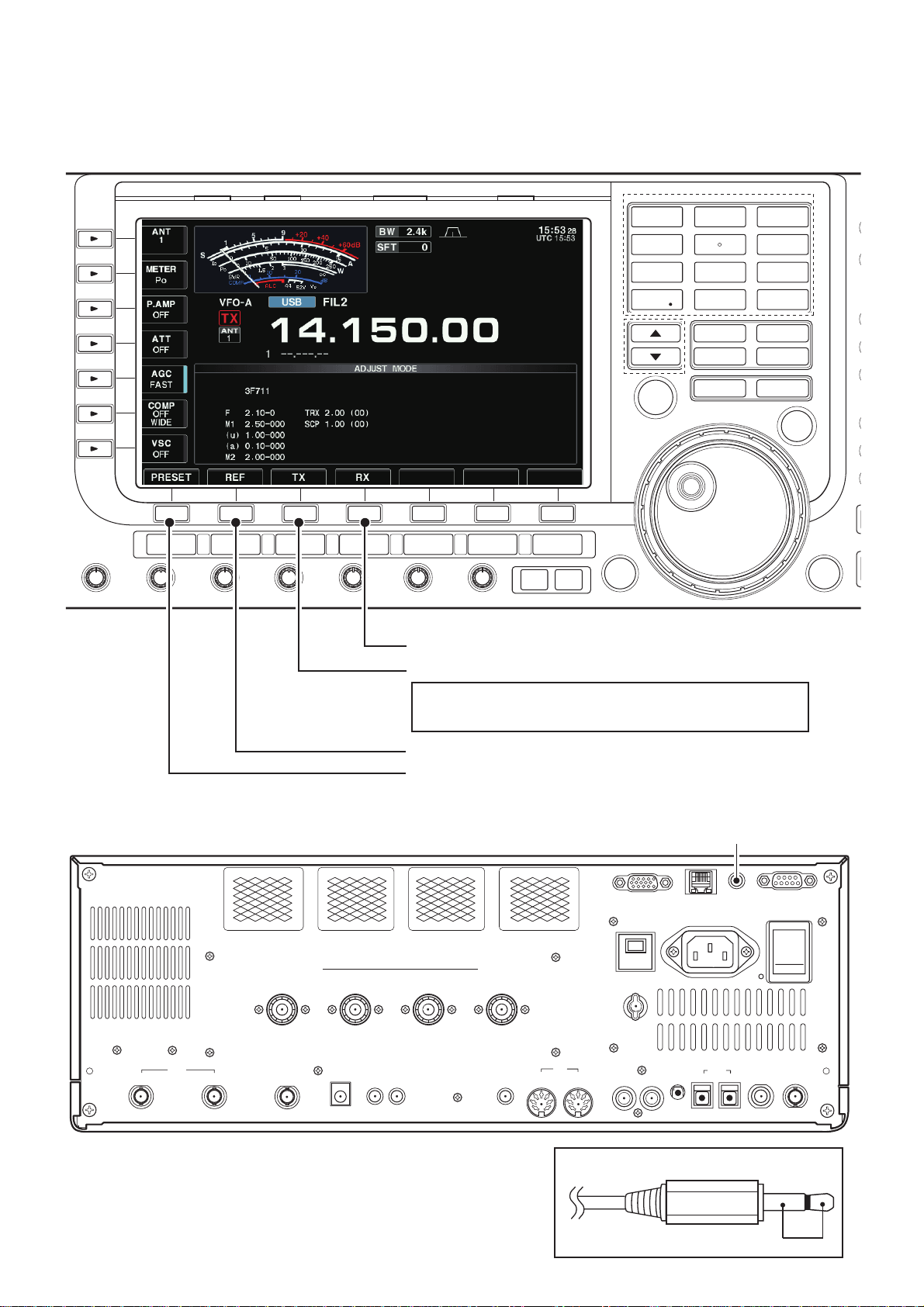
4-7 AUTOMATIC ADJUSTMENTS
¤ ENTERING AUTOMATIC ADJUSTMENT MODE
1) Connect the short plug to the [REMOTE] terminal (see the illust bellow).
2) Push and hold [SSB]+[CW] keys and turn the power ON, then the adjustment main menu appears.
3) When the automatic adjustments are fi nished, turn the power OFF to quit the adjustment mode.
<Main menu>
LOCKTX RX SPLIT
F-1 F-2 F-3 F-4 F-5 F-6 F-7
SSB CW
RTTY/PSK
AM/FM DATA
M.SCOPE
EXIT/SET
REC
VOICE MEMORYBRIGHTCONTRASTVOX GAINMONI GAINCOMP XOV ITNAEVIRD
Receiver adjustment (page 4-15)
Transmitter adjustment (page 4-13)
PLAY
AUTO
TUNE
1.8
10
21
GENE
XFC
3.5
1
14
4
24
7
50
7
2
18
5
28
8
F-INP
0
MP-W MP-R
MW V/M
A/B A=B
TS
3
6
9
ENT
LOCK
• CONNECTION
RX ANT
CAUTION: When a TX adjustment item is selected,
the transceiver transmits automatically.
Reference frequency adjustment (page 4-17)
Other adjustment (page 4-17)
ALC
ADJ
Short plug
REMOTE
AC
S/P DIF
CW KEY
INOUT
-
RS
232C
I
REF I/O
10MHz
-
10dBm
<Rear view>
EXT-DISPLAY
15A
EXT
KEYPAD
ANT 3
ANT 4
EXT-SP
GND
ACC
12
ALCRELAY
ANT 1 AN T 2
DC OUT
15V
INOUT
X-VERTER
MAX1A
METER
4 - 12
• Short plug
3.5 mm (1/8’’ ) monoral plug
(Short)
Page 25
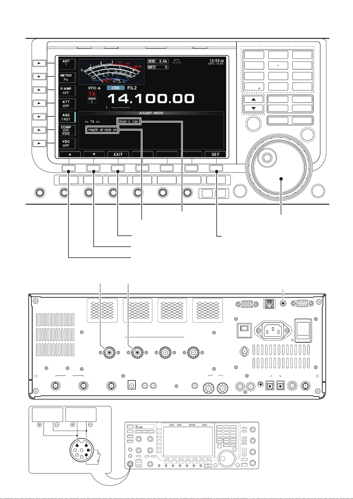
4-7-1 AUTOMATIC ADJUSTMENTS (TRANSMITTER)
<TX adjustment screen>
LOCKTX RX SPLIT
F-1 F-2 F-3 F-4 F-5 F-6 F-7
SSB CW
RTTY/PSK
AM/FM DATA
M.SCOPE
EXIT/SET
REC
VOICE MEMORYBRIGHTCONTRASTVOX GAINMONI GAINCOMP XOV ITNAEVIRD
Adjustment value
Adjustment item
PLAY
AUTO
TUNE
1.8
10
21
GENE
XFC
1
4
7
3.5
14
24
50
Adjusts
7
2
18
5
28
8
F-INP
0
MP-W MP-R
MW V/M
A/B A=B
TS
3
6
9
ENT
LOCK
Return to main menu
Selects the next adjustment item
Selects the previous adjustment item
• CONNECTION FOR TX ADJUSTMENTS
RF Power Meter
RX ANT
INOUT
ANT 1 AN T 2
X-VERTER
100 ohm Dummy Load (SWR=2)
DC OUT
15V
METER
MAX1A
<Rear view>
ANT 3
EXT
KEYPAD
ANT 4
EXT-SP
Stores the adjustment value
Short plug
(see page 4-12)
AC
S/P DIF
REMOTE
INOUT
EXT-DISPLAY
15A
GND
ACC
12
ALC
ALCRELAY
ADJ
CW KEY
-
RS
232C
I
REF I/O
10MHz
-
10dBm
AC millvolt
meter
Audio
generator
[MIC]
<Front view>
PTT
4 - 13
Page 26
4-7-2 AUTOMATIC ADJUSTMENTS (TRANSMITTER)
ADJUSTMENT ADJUSTMENT CONDITION OPERATION
PREPARATION 1 1) Connect an Audio Generator to the MIC jack and set it as;
POWER METER
(HF BAND)
<Preset>
<10 W> 2 • Transmitting (Automatically) 1) Adjust the transmit power using
<50 W> 3 • T r ansmitting (Automatically) [POWER HF
<100 W> 4 • Transmitting (Automatically) [POWER HF
<150 W> 5 • Transmitting (Automatically) [POWER HF
<200 W> 6 • Transmitting (Automatically) [POWER HF
POWER METER
(50 MHz BAND)
<50 W> 8 • T r ansmitting (Automatically) [POWER 50M
<100 W> 9 • Transmitting (Automatically) [POWER 50M
<150 W> 10 • Tr ansmitting (Automatically) [POWER 50M
<195 W> 11 • Tr ansmitting (Automatically) [POWER 50M
[RESERVE
POWER SET]
(NO AJUSTMENT)
POWER DOWN 1 • Transmitting (Automatically) 1) Adjust the transmit power using
ALC METER 1 • T ransmitting (Automatically) •Push [F-7] key.
DRIVE LEVEL 1 • T ransmitting (Automatically) •Push [F-7] key.
DRAIN VOL T A GE
METER
DRAIN
CURRENT
METER
Frequency : 1.5 kHz
Level : 10 mV
2) Connect an RF power meter to the [ANT1].
3) Connect an terminator (SWR=2) to the [ANT2].
1
–
7 • Transmitting (Automatically) 1) Adjust the transmit power using
1
–
1 • T r ansmitting (Automatically) •Push [F-7] key.
1 • T r ansmitting (Automatically) •Push [F-7] key.
• Push [F-7] key.
[MAIN DIAL].
2) Push [F-7] key.
[MAIN DIAL].
2) Push [F-7] key.
• "RESERVE POWER SET" appears.
Push [F-7] key.
[MAIN DIAL].
2) Push [F-7] key.
ADJUSTMENT
ITEM
––
[POWER HF/
50M 0W]
[POWER HF
10W]
50W]
100W]
150W]
200W]
[POWER 50M
10W]
50W]
100W]
150W]
200W]
––
[POWER for
Power Down
HF/50M]
[ALC]
[DRIVE]
[Vd48V]
[Id 0A] –
VALUE
–
10 W
50 W
100 W
150 W
195 W
10 W
50 W
100 W
150 W
195 W
100 W
(Automatic
adjustment)
(Automatic
adjustment)
(Automatic
adjustment)
0A
5A 2 • Transmitting (Automatically) • Monitoring drain current on the
display, adjust the current using
[MAIN DIAL], then push [F-7] key.
10A 3 • Transmitting (Automatically) • Monitoring drain current on the
display, adjust the current using
[MAIN DIAL], then push [F-7] key.
SWR METER 1 • Tr ansmitting (Automatically) •Push [F-7] key.
(Returns to adjustment main menu)
4 - 14
[Id 5A] 5 A
[Id 10A] 10 A
[SWR]
(Automatic
adjustment)
Page 27

4-7-2 AUTOMATIC ADJUSTMENTS (RECEIVER)
<RX adjustment screen>
LOCKTX RX SPLIT
F-1 F-2 F-3 F-4 F-5 F-6 F-7
SSB CW
RTTY/PSK
AM/FM DATA
M.SCOPE
EXIT/SET
REC
VOICE MEMORYBRIGHTCONTRASTVOX GAINMONI GAINCOMP XOV ITNAEVIRD
Adjustment value
Adjustment item
PLAY
AUTO
TUNE
1.8
10
21
GENE
XFC
1
4
7
3.5
14
24
50
Adjusts
7
2
18
5
28
8
F-INP
0
MP-W MP-R
MW V/M
A/B A=B
TS
3
6
9
ENT
LOCK
Return to main menu
Selects next adjustment item
Selects previous adjustment item
• CONNECTION FOR RX ADJUSTMENTS
SSG
ANT 1 AN T 2
RX ANT
AC millivolt meter
INOUT
X-VERTER
+
−
DC OUT
15V
MAX1A
METER
<Rear view>
ANT 3
EXT
KEYPAD
ANT 4
EXT-SP
Stores the adjustment value
Short plug
(see page 4-?)
AC
S/P DIF
REMOTE
INOUT
EXT-DISPLAY
15A
GND
ACC
12
ALC
ALCRELAY
ADJ
CW KEY
-
RS
232C
I
REF I/O
10MHz
-
10dBm
Speaker (8 Ω)
+
−
3.5 mm (1/8’’ ) monoral plug
4 - 15
Page 28

4-7-2 AUTOMATIC ADJUSTMENTS (RECEIVER)
ADJUSTMENT ADJUSTMENT CONDITION OPERATION
TOTAL GAIN
(PREPARATION)
HF (P.AMP OFF) 1 • Receiving 1) Set the SSG as;
HF (P.AMP ON) 2 • Receiving • Adjust the AF output level using
50MHz (P.AMP
OFF)
50MHz (P.AMP
ON)
EXTERNAL AGC 1 • Receiving 1) Set the SSG as;
HF S-METER
HF (S0 LEVEL)
HF (S9 LEVEL) 2 • Receiving 1) Set the SSG as;
HF (S9+60 dBu
LEVEL)
50MHz
S-METER
50MHz (S0
LEVEL)
50MHz (S9
LEVEL)
50MHz (S9+60 dBu
LEVEL)
1 • Receiving 1) Connect an AC millivoltmeter to
3 • Receiving • Adjust the AF output level using
4 • Receiving • Adjust the AF output level using
1 • Receiving 1) Set the SSG as;
3 • Receiving 1) Set the SSG as;
4 • Receiving 1) Set the SSG as;
5 • Receiving 1) Set the SSG as;
6 • Receiving 1) Set the SSG as;
[EXT-SP].
2)
Connect an SSG to the [ANT1] and
set it as;
Frequency : 14.1515 MHz
Modulation : None
Level : +60 dBµ
2) Set the audio output level to 0 dB
(Set it as reference).
3) Set the SSG as;
Level : "OFF"
4) Adjust the AF output level using
[MAIN DIAL], then push [F-7] key.
[MAIN DIAL], then push [F-7] key.
[MAIN DIAL], then push [F-7] key.
[MAIN DIAL], then push [F-7] key.
Level : +70 dBµ
2) Push [F-7] key.
3)
Wait until the beep "Pi!"
sounds (approx. 20 sec.)
NEVER CHANGE the SSG output
level until the beep souds.
Level : "OFF"
2)
Push [F-7] key. (the beep "Pi!" sounds)
3) Soon, another beeps "PiPi!" sound.
NEVER
level until the 2nd beep souds.
Level : +34 dBµ
2)
Push [F-7] key. (the beep "Pi!" sounds)
3) Soon, another beeps "PiPi!" sound.
NEVER
level until the 2nd beep souds.
Level : +94 dBµ
2)
Push [F-7] key. (the beep "Pi!" sounds)
3) Soon, another beeps "PiPi!" sound.
NEVER
level until the 2nd beep souds.
Frequency : 50.1515 MHz
Modulation : None
Level : "OFF"
2)
Push [F-7] key. (the beep "Pi!" sounds)
3) Soon, another beeps "PiPi!" sound.
NEVER
level until the beep souds.
Level : +34 dBµ
2)
Push [F-7] key. (the beep "Pi!" sounds)
3) Soon, another beeps "PiPi!" sound.
NEVER
level until the beep souds.
Level : +94 dBµ
2)
Push [F-7] key. (the beep "Pi!" sounds)
3) Soon, another beeps "PiPi!" sound.
NEVER
level until the beep souds.
4) (Returns to adjustment main menu)
CHANGE
CHANGE
CHANGE
CHANGE
CHANGE
CHANGE
the SSG output
the SSG output
the SSG output
the SSG output
the SSG output
the SSG output
ADJUSTMENT
ITEM
––
[Total Gain HF
PRE OFF]
[Total Gain HF
PRE ON]
[Total Gain 50M
PRE OFF]
[Total Gain 50M
PRE ON]
[AGC]
[HF S0 LEVEL]
[HF S9 LEVEL]
[ HF S9+60
LEVEL]
[50M S0 LEVEL]
[50M S9 LEVEL]
[50MHz (S9+60
dBu LEVEL)
VALUE
–30 dB
(Automatic
adjustment)
(Automatic
adjustment)
(Automatic
adjustment)
4 - 16
Page 29
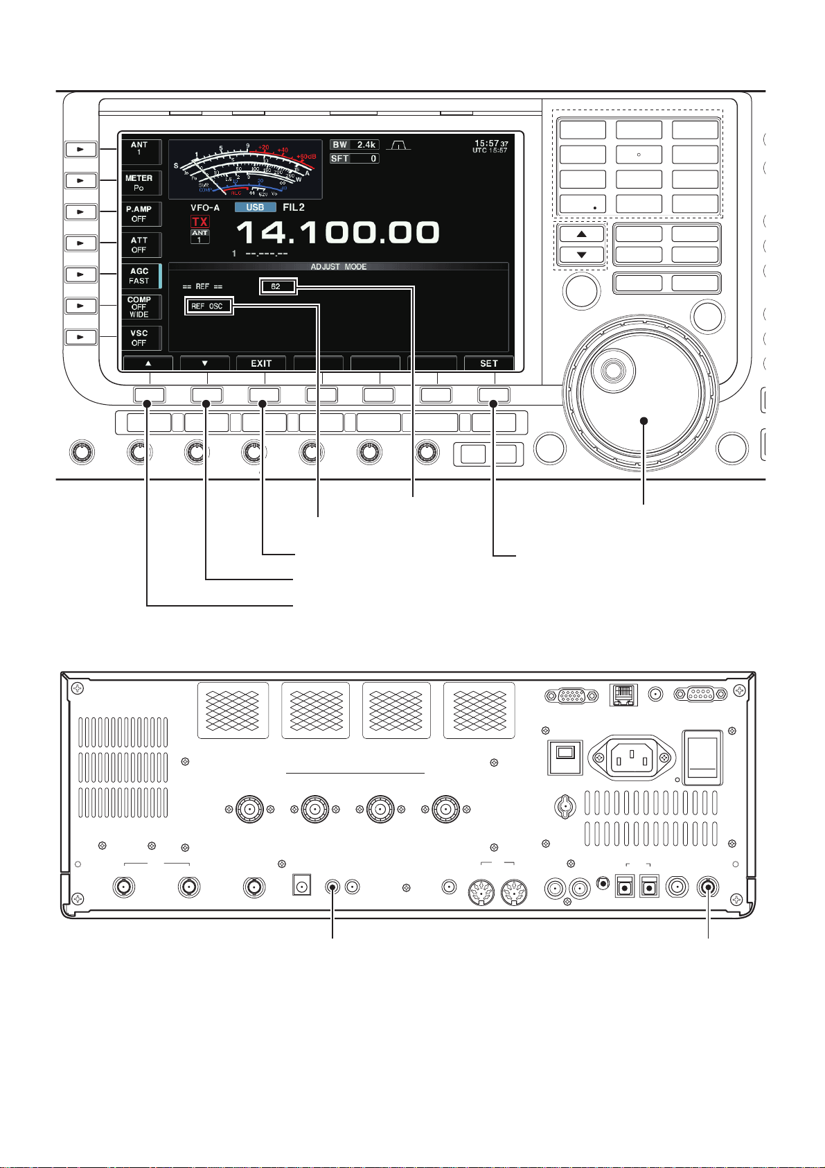
4-7-3 REFERENCE FREQUENCY
<Reference frequency adjustment screen>
LOCKTX RX SPLIT
F-1 F-2 F-3 F-4 F-5 F-6 F-7
SSB CW
RTTY/PSK
AM/FM DATA
M.SCOPE
EXIT/SET
REC
VOICE MEMORYBRIGHTCONTRASTVOX GAINMONI GAINCOMP XOV ITNAEVIRD
Adjustment value
Adjustment item
PLAY
AUTO
TUNE
1.8
10
21
GENE
XFC
1
4
7
3.5
14
24
50
Adjusts
7
2
18
5
28
8
F-INP
0
MP-W MP-R
MW V/M
A/B A=B
TS
3
6
9
ENT
LOCK
Return to main menu
Never push (Disable)
Never push (Disable)
• CONNECTION FOR RX ADJUSTMENTS
ANT 2
DC OUT
15V
METER
MAX1A
Digital multimeter Frequency counter
RX ANT
ANT 1
INOUT
X-VERTER
<Rear view>
ANT 3
EXT
KEYPAD
ANT 4
EXT-SP
Stores the adjustment value
AC
S/P DIF
REMOTE
INOUT
EXT-DISPLAY
15A
GND
ACC
12
ALC
ALCRELAY
ADJ
CW KEY
-
RS
232C
I
REF I/O
10MHz
-
10dBm
4 - 17
Page 30

4-7-3 REFERENCE FREQUENCY
ADJUSTMENT ADJUSTMENT CONDITION OPERATION
REFERENCE
FREQUENCY
1• Wait more than 5 min. from
turning main power ON with
[I/O] on the rear panel, then
adjust the reference frequency.
1) Connect a Frequency Counter to
the [REF I/O] connector.
2) Adjust the reference frequency
using [MAIN DIAL].
4-7-4 OTHER ADJUSTMENTS
ADJUSTMENT ADJUSTMENT CONDITION OPERATION
PRESET
EXT. METER
PRESET
DIGISEL VR
1
–
1
–
1) Connect a Voltage meter to the
[METER] terminal.
2) Adjust the voltage using [MAIN
DIAL].
3) Push [F-7] key.
1) Set the [DIGI-SEL] (on the front
panel) to center.
2) Push [F-7] key.
ADJUSTMENT
ITEM
[REF]
ADJUSTMENT
ITEM
[EXT. METER]
[DIGISEL VR]
VALUE
10.0000000
MHz
(±0.1 Hz)
VALUE
0 V
Center
position
4 - 18
Page 31

SECTION 5 PARTS LIST
[RF UNIT]
REF ORDER
NO. NO.
IC101 1130011510 S.IC BU2099FV-E2 T 146.4/152.3
IC102 1130011510 S.IC BU2099FV-E2 T 153.5/152.3
IC501 1110006100 S.IC NJM5534MD-TE1 T 156.6/40.9
IC502 1110006100 S.IC NJM5534MD-TE1 T 144.4/40.9
IC503 1110005461 S.IC TA4107F (TE12L,F) T 133.6/40.9
IC1051 1190002010 S.IC SD5400CY <TOMO> T 7.1/100.2
IC1081 1110006180 S.IC UPG2009TB-E3 T 39/91.7
IC1402 1190002110 S.IC NJG1519KC1-TE3 T 30.5/49.3
IC1403 1190002110 S.IC NJG1519KC1-TE3 T 30/4.2
IC1501 1110006121 S.IC DBM9A41-G-TR T 88/15.3
IC1502 1110006121 S.IC DBM9A41-G-TR T 96.5/15.3
IC1503 1110006100 S.IC NJM5534MD-TE1 T 119.2/7.5
IC1504 1110006100 S.IC NJM5534MD-TE1 T 119.2/25.9
IC1505 1110006190 S.IC NJM074M-TE1 T 136.2/16.7
IC1506 1110006100 S.IC NJM5534MD-TE1 T 147.6/19.3
IC1651 1130011921 S.IC TC74LCX00F (EL,F) T 89.7/26.5
IC1652 1110005420 S.IC BA15532F-E2 T 147.6/8.7
IC1653 1110005100 S.IC NJM072BM-TE1 B 156/8.7
IC1701 1130011530 S.IC CD74HC4094M96 T 129/142.5
IC1702 1130011530 S.IC CD74HC4094M96 T 129/133
IC1703 1160000131 S.IC TD62783AFG (S,EL) T 117.3/143.1
IC1704 1180000790 S.IC AN78L10M (E1) T 65.4/27.8
IC1901 1160000131 S.IC TD62783AFG (S,EL) T 140.9/119.5
IC1902 1160000131 S.IC TD62783AFG (S,EL) T 154.5/119.5
IC1903 1130011530 S.IC CD74HC4094M96 T 143.7/131.5
IC1904 1130011530 S.IC CD74HC4094M96 T 157.3/131.5
Q260 1590001330 S.TR DTA114EUA T106 T 63.8/211.2
Q320 1590001330 S.TR DTA114EUA T106 B 63.8/211.4
Q381 1590000680 S.TR DTC114EUA T106 B 86.4/237
Q383 1590000680 S.TR DTC114EUA T106 B 106.6/231.2
Q384 1590000680 S.TR DTC114EUA T106 B 110/231.2
Q385 1590000680 S.TR DTC114EUA T106 B 101.5/240
Q386 1590000680 S.TR DTC114EUA T106 B 105.4/236.8
Q387 1590000680 S.TR DTC114EUA T106 B 86.4/234.1
Q401 1530002841 S.TR 2SC4116-Y (TE85R,F) B 50.8/233.9
Q402 1530002060 S.TR 2SC4081 T106 R B 54.2/236.2
Q403 1590001330 S.TR DTA114EUA T106 B 54.2/233.4
Q404 1590000680 S.TR DTC114EUA T106 B 50.8/236.7
Q421 1590000680 S.TR DTC114EUA T106 B 88.8/145.7
Q422 1590000680 S.TR DTC114EUA T106 B 92.3/145.6
Q501 1580000751 S.FET 3SK294 (TE85L,F) T 123.7/42.5
Q502 1590000680 S.TR DTC114EUA T106 B 118.1/52.2
Q503 1590002710 S.TR UMH11NTN T 118/52.5
Q504 1560000561 S.FET 2SK882-GR (TE85L,F) B 109.2/59
Q506 1560000561 S.FET 2SK882-GR (TE85L,F) B 106.7/99.1
Q507 1530003151 S.TR 2SC4673D-TD-E B 87.2/118.2
Q508 1530003841 S.TR 2SC5501-4-TR-E B 121.7/120
Q509 1590001960 S.TR XP4311 (TX) T 123.2/51.3
Q801 1530003851 S.TR 2SC5551F-TD-E B 162.2/68.6
Q802 1520000531 S.TR 2SB1119S-TD-E B 159/97.5
Q803 1590000680 S.TR DTC114EUA T106 B 166.6/96.9
Q804 1590002710 S.TR UMH11NTN T 158.9/59.4
Q805 1590000680 S.TR DTC114EUA T106 T 157.3/56.6
Q901 1590001960 S.TR XP4311 (TX) T 77.5/142.3
Q902 1530003851 S.TR 2SC5551F-TD-E B 65/139.3
Q1005 1590001960 S.TR XP4311 (TX) T 41.6/141.6
Q1006 1530003851 S.TR 2SC5551F-TD-E B 25.9/142.3
Q1007 1530003851 S.TR 2SC5551F-TD-E B 35.4/130.6
Q1008 1530003851 S.TR 2SC5551F-TD-E B 35.4/116.8
Q1101 1530003860 TR 2SC3950D
Q1102 1590000680 S.TR DTC114EUA T106 T 18.5/66.3
Q1103 1520000561 S.TR 2SB1123 T-TD-E B 15.4/72.3
Q1104 1530003860 TR 2SC3950D
Q1105 1530003841 S.TR 2SC5501-4-TR-E T 17.5/58
Q1205 1590001960 S.TR XP4311 (TX) T 21.2/135.7
Q1209 1530003851 S.TR 2SC5551F-TD-E B 50.3/109.5
Q1210 1530003851 S.TR 2SC5551F-TD-E B 64.5/109.5
Q1211 1560001311 S.FET MMBFU310LT1G T 28/90.6
Q1212 1560001311 S.FET MMBFU310LT1G T 34/90.6
Q1213 1590000680 S.TR DTC114EUA T106 B 30/63.2
Q1214 1520000561 S.TR 2SB1123 T-TD-E B 32/73.4
Q1301 1530003151 S.TR 2SC4673D-TD-E T 29.7/66.1
Q1352 1530003851 S.TR 2SC5551F-TD-E B 60.9/77.5
Q1401 1530003841 S.TR 2SC5501-4-TR-E B 58.4/15
Q1402 1530003021 S.TR 2SC4402-3-TL-E T 64.7/17.8
Q1403 1530003021 S.TR 2SC4402-3-TL-E T 64.7/10.9
Q1501 1530003450 S.TR 2SC4835-R (TX) T 110.2/8.6
Q1502 1530003450 S.TR 2SC4835-R (TX) T 110.2/20.8
Q1651 1530002601 S.TR 2SC4215-O (TE85R,F) B 98.3/35.1
Q1701 1590001960 S.TR XP4311 (TX) T 72.7/98.9
Q1702 1590001960 S.TR XP4311 (TX) T 54.7/52
Q1703 1590001960 S.TR XP4311 (TX) T 54.7/54.5
Q2001 1530002060 S.TR 2SC4081 T106 R B 160.7/233.8
Q2002 1590001330 S.TR DTA114EUA T106 B 146.5/142.6
D1 1790001250 S.DIO MA2S111-(TX) B 147/218.8
D21 1790001250 S.DIO MA2S111-(TX) B 131.5/218.8
D51 1790001250 S.DIO MA2S111-(TX) B 116/218.8
D81 1790001250 S.DIO MA2S111-(TX) B 100.6/218.8
D111 1790001250 S.DIO MA2S111-(TX) B 85/218.8
D141 1790001250 S.DIO MA2S111-(TX) B 69.5/218.8
D171 1790001250 S.DIO MA2S111-(TX) B 50/218.8
D201 1790001250 S.DIO MA2S111-(TX) B 34.5/218.8
D231 1790001250 S.DIO MA2S111-(TX) B 19.1/218.8
D260 1750000581 S.DIO 1SV307 (TPH3,F) T 65.1/175.7
DESCRIPTION
M.
H/V
LOCATION
[RF UNIT]
REF ORDER
NO. NO.
D261 1790001250 S.DIO MA2S111-(TX) B 3.8/218.8
D262 1750000581 S.DIO 1SV307 (TPH3,F) T 65/204.5
D320 1750000581 S.DIO 1SV307 (TPH3,F) B 65.1/175.7
D321 1750000581 S.DIO 1SV307 (TPH3,F) B 65/204.5
D351 1790001250 S.DIO MA2S111-(TX) B 87/227.1
D352 1790001250 S.DIO MA2S111-(TX) B 83.1/233.5
D353 1790001250 S.DIO MA2S111-(TX) B 72.6/227.1
D373 1790001250 S.DIO MA2S111-(TX) B 78.5/242.3
D391 1750000581 S.DIO 1SV307 (TPH3,F) B 95.7/233
D392 1750000581 S.DIO 1SV307 (TPH3,F) B 95.7/236.5
D393 1750000581 S.DIO 1SV307 (TPH3,F) B 92.7/236.5
D401 1790001250 S.DIO MA2S111-(TX) B 50.9/228.5
D402 1790000980 S.DIO MA742 (TX) B 46.1/235.1
D410 1790001250 S.DIO MA2S111-(TX) B 37/224.9
D421 1790000620 S.DIO MA77 (TX) B 86/143
D422 1790000620 S.DIO MA77 (TX) B 95/143
D423 1790000620 S.DIO MA77 (TX) B 88.7/136.9
D424 1790000620 S.DIO MA77 (TX) B 92.5/136.9
D431 1790001250 S.DIO MA2S111-(TX) B 30.9/224.9
D501 1790000620 S.DIO MA77 (TX) B 107.1/41
D502 1790000620 S.DIO MA77 (TX) B 115/41
D503 1790000620 S.DIO MA77 (TX) B 104.5/53.9
D504 1790000620 S.DIO MA77 (TX) B 112.4/53.9
D505 1750000431 S.DIO HSB88WSTR-E T 100.9/71.4
D506 1750000431 S.DIO HSB88WSTR-E T 100.9/113
D536 1790001250 S.DIO MA2S111-(TX) B 114.6/105.5
D601 1790000620 S.DIO MA77 (TX) B 124.1/60.2
D602 1790000620 S.DIO MA77 (TX) B 145.1/60.2
D603 1790000620 S.DIO MA77 (TX) B 124.1/71
D604 1790000620 S.DIO MA77 (TX) B 145.1/71
D605 1790000620 S.DIO MA77 (TX) B 124.1/81.8
D606 1790000620 S.DIO MA77 (TX) B 145.1/81.8
D607 1790000620 S.DIO MA77 (TX) B 124.1/92.6
D608 1790000620 S.DIO MA77 (TX) B 145.1/92.6
D609 1790000620 S.DIO MA77 (TX) B 124.1/103.5
D610 1790000620 S.DIO MA77 (TX) B 145.1/103.5
D611 1790000620 S.DIO MA77 (TX) T 124.1/66.3
D612 1790000620 S.DIO MA77 (TX) T 145.1/66.3
D613 1790000620 S.DIO MA77 (TX) T 124.1/74.2
D614 1790000620 S.DIO MA77 (TX) T 145.1/75.3
D615 1790000620 S.DIO MA77 (TX) T 124.1/84.4
D616 1790000620 S.DIO MA77 (TX) T 145.1/84.3
D617 1790000620 S.DIO MA77 (TX) T 124.1/93.3
D618 1790000620 S.DIO MA77 (TX) T 145.1/93.3
D619 1790000620 S.DIO MA77 (TX) T 124.1/102.3
D620 1790000620 S.DIO MA77 (TX) T 145.1/102.3
D801 1790000620 S.DIO MA77 (TX) T 148.2/62
D802 1750000581 S.DIO 1SV307 (TPH3,F) T 148.2/60.2
D806 1790000620 S.DIO MA77 (TX) B 89.3/94.5
D873 1790001250 S.DIO MA2S111-(TX) B 27.7/226.1
D1001 1750000581 S.DIO 1SV307 (TPH3,F) T 18.9/136
D1101 1790000620 S.DIO MA77 (TX) T 10.6/53.7
D1102 1790000620 S.DIO MA77 (TX) T 25.5/53.7
D1201 1750000581 S.DIO 1SV307 (TPH3,F) T 46.3/92.3
D1653 1750000550 S.DIO 1SS355 TE-17 B 149.6/11.4
D1654 1750000550 S.DIO 1SS355 TE-17 B 149.7/6
D1701 1790001670 S.DIO RB706F-40T106 B 161.9/14.3
D2001 1790001750 S.DIO DSM3MA4 T 120.2/241.3
D2002 1790001750 S.DIO DSM3MA4 T 115.6/241.3
D2003 1790001670 S.DIO RB706F-40T106 B 165.6/240.3
D2004 1750000550 S.DIO 1SS355 TE-17 B 154.7/234
FI501 2020001070 CER CFWLA455KDFA-B0 (CFWS455D)
FI502 2020001510 CER CFWLA455KJFA-B0 (CFWS455IT)
FI503 2010002580 S.FIL FL-348 (64.455 MHz) T 112/87
L1 6200005521 S.COL NLV25T-470J B 149.9/159.8
L2 6200005521 S.COL NLV25T-470J B 143.9/159.8
L3 6200010830 S.COL C2520C-3R3G-A T 147.8/183.8
L4 6200010830 S.COL C2520C-3R3G-A T 147.8/195.9
L5 6200010830 S.COL C2520C-3R3G-A T 147/188.1
L6 6200010830 S.COL C2520C-3R3G-A T 147/200.2
L21 6200005521 S.COL NLV25T-470J B 134.4/161
L22 6200005521 S.COL NLV25T-470J B 128.4/161
L23 6140004040 COL LR-443
L24 6140004050 COL LR-444
L25 6140004050 COL LR-444
L26 6140004050 COL LR-444
L27 6140004040 COL LR-443
L51 6200005521 S.COL NLV25T-470J B 118.9/161
L52 6200005521 S.COL NLV25T-470J B 112.9/161
L53 6140004060 COL LR-445
L54 6140004080 COL LR-446
L55 6140004080 COL LR-446
L56 6140004080 COL LR-446
L57 6140004060 COL LR-445
L81 6200005521 S.COL NLV25T-470J B 103.5/161
L82 6200005521 S.COL NLV25T-470J B 97.5/161
L83 6140004090 COL LR-447
L84 6140004230 COL LR-458
L85 6140004230 COL LR-458
L86 6140004230 COL LR-458
L87 6140004090 COL LR-447
L111 6200005521 S.COL NLV25T-470J B 88/161
L112 6200005521 S.COL NLV25T-470J B 82/161
L113 6140004090 COL LR-447
DESCRIPTION
M.=Mounted side (T: Mounted on the Top side B: Mounted on the Bottom side)
5 - 1
M.
S.=Surface mount
H/V
LOCATION
Page 32

[RF UNIT]
REF ORDER
NO. NO.
L114 6140004100 COL LR-448
L115 6140004100 COL LR-448
L116 6140004100 COL LR-448
L117 6140004090 COL LR-447
L141 6200005521 S.COL NLV25T-470J B 72.5/161
L142 6200005521 S.COL NLV25T-470J B 66.5/161
L143 6140004110 COL LR-449
L144 6140004120 COL LR-450
L145 6140004120 COL LR-450
L146 6140004120 COL LR-450
L147 6140004110 COL LR-449
L171 6200005521 S.COL NLV25T-470J B 53/161
L172 6200005521 S.COL NLV25T-470J B 47/161
L173 6140004140 COL LR-451
L174 6140004150 COL LR-452
L175 6140004150 COL LR-452
L176 6140004150 COL LR-452
L177 6140004140 COL LR-451
L201 6200007021 S.COL NLV25T-270J B 37.5/161
L202 6200007021 S.COL NLV25T-270J B 31.5/161
L203 6140004160 COL LR-453
L204 6140004180 COL LR-454
L205 6140004180 COL LR-454
L206 6140004180 COL LR-454
L207 6140004160 COL LR-453
L231 6200005011 S.COL NLV25T-100J B 22.1/161
L232 6200005011 S.COL NLV25T-100J B 16.1/161
L233 6140004190 COL LR-455
L234 6140004210 COL LR-456
L235 6140004210 COL LR-456
L236 6140004210 COL LR-456
L237 6140004190 COL LR-455
L260 6200003281 S.COL NLV25T-2R2J T 63.7/169
L261 6200009141 S.COL NLV25T-6R8J B 8.1/160.4
L262 6200009141 S.COL NLV25T-6R8J B 2.1/160.4
L263 6140004220 COL LR-457
L264 6140004160 COL LR-453
L265 6140004160 COL LR-453
L266 6140004160 COL LR-453
L267 6140004220 COL LR-457
L268 6200003281 S.COL NLV25T-2R2J T 63.2/220.8
L291 6200003281 S.COL NLV25T-2R2J T 64.1/191.4
L292 6200003281 S.COL NLV25T-2R2J T 63.8/217.7
L293 6200010180 S.COL LQW2BHN82NG03L T 64.1/180.7
L294 6200002981 S.COL NLV32T-R56J T 64.4/185.2
L295 6200010180 S.COL LQW2BHN82NG03L T 64.1/195
L296 6200010870 S.COL C2520C-R33G-A (0.33U) T 63.7/201.1
L320 6200001831 S.COL NLV32T-100J T 64.2/158.2
L321 6200003281 S.COL NLV25T-2R2J B 68/195.8
L322 6200003281 S.COL NLV25T-2R2J B 62.8/220.7
L323 6200003011 S.COL NLV32T-R27J B 64.4/179.8
L324 6200003001 S.COL NLV32T-R22J B 63.5/188.2
L325 6200003011 S.COL NLV32T-R27J B 63.8/196.3
L326 6200001831 S.COL NLV32T-100J T 53.1/221.6
L391 6200005491 S.COL NLV32T-331J B 102.6/231.2
L392 6200005491 S.COL NLV32T-331J B 83.5/239.9
L393 6200003211 S.COL NLV32T-820J B 92.6/229.7
L394 6200005491 S.COL NLV32T-331J B 103.5/227.8
L395 6200005491 S.COL NLV32T-331J B 108.2/224.7
L421 6200008641 S.COL NLV32T-391J B 95.7/148.9
L501 6200003261 S.COL NLV32T-101J B 124.7/42.6
L502 6200003261 S.COL NLV32T-101J B 128.7/39.2
L503 6200003261 S.COL NLV32T-101J B 128.7/42.6
L504 6200003520 S.COL ELJFB 102K-F T 120.4/39.5
L505 6150004090 COL LS-469 (C-13969)
L507 6140003530 COL LR-395
L508 6140003210 S.COL LR-358 T 100.9/77.3
L509 6140003770 S.COL LR-414 4KBL (STP-01435) T 112/78.4
L510 6140003770 S.COL LR-414 4KBL (STP-01435) T 112/95.6
L511 6200003031 S.COL NLV32T-R47J B 110.7/100.7
L512 6150004280 COL LS-484B (C-14927)
L513 6140002551 S.COL #617DB-1919=P3 T 100.9/106.9
L514 6140002551 S.COL #617DB-1919=P3 T 100.9/119.1
L515 6200003001 S.COL NLV32T-R22J B 92.5/123.6
L516 6200003021 S.COL NLV32T-R33J B 94.8/117.7
L517 6200001831 S.COL NLV32T-100J B 98.8/123.6
L518 6200010720 S.COL C2520C-56NG-A T 106.5/126.4
L519 6200010860 S.COL C2520C-R10G-A (0.1U) T 110/128.2
L521 6140003900 COL LR-489
L522 6140003890 COL LR-488
L523 6200010381 S.COL ELJRE R15JFA B 96.2/97
L524 6180002971 S.COL NLV32T-068J B 88.5/108.5
L525 6180002971 S.COL NLV32T-068J B 90.7/112.5
L526 6180002971 S.COL NLV32T-068J B 95/113.2
L527 6200010660 S.COL C2520C-R15G-A (0.15U) T 115/127.4
L528 6200003261 S.COL NLV32T-101J B 120.1/36.8
L529 6200010381 S.COL ELJRE R15JFA B 96.2/93.8
L601 6200003101 S.COL NLV32T-3R9J B 125/63.7
L602 6200003131 S.COL NLV32T-120J B 128.5/60.2
L603 6200003131 S.COL NLV32T-120J B 134.9/64.4
L604 6200003131 S.COL NLV32T-120J B 140.7/60.2
L605 6200003101 S.COL NLV32T-3R9J B 144.3/63.7
L606 6200002961 S.COL NLV32T-4R7J B 125/74.5
L607 6200001851 S.COL NLV32T-5R6J B 128.5/71
L608 6200001851 S.COL NLV32T-5R6J B 134.6/75.2
L609 6200001851 S.COL NLV32T-5R6J B 140.7/71
L610 6200002961 S.COL NLV32T-4R7J B 144.3/74.5
L611 6200002991 S.COL NLV32T-2R2J B 125/85.3
L612 6200003111 S.COL NLV32T-6R8J B 128.5/81.8
L613 6200003111 S.COL NLV32T-6R8J B 134.6/86
L614 6200003111 S.COL NLV32T-6R8J B 140.7/81.8
L615 6200002991 S.COL NLV32T-2R2J B 144.3/85.3
L616 6200002991 S.COL NLV32T-2R2J B 125/96.2
L617 6200003321 S.COL NLV32T-3R3J B 128.5/92.6
DESCRIPTION
M.
H/V
LOCATION
[RF UNIT]
REF ORDER
NO. NO.
L618 6200003321 S.COL NLV32T-3R3J B 134.6/96.8
L619 6200003321 S.COL NLV32T-3R3J B 140.7/92.6
L620 6200002991 S.COL NLV32T-2R2J B 144.3/96.1
L621 6200003061 S.COL NLV32T-1R2J B 125/107
L622 6200003091 S.COL NLV32T-2R7J B 128.5/103.5
L623 6200003091 S.COL NLV32T-2R7J B 134.6/107.7
L624 6200003091 S.COL NLV32T-2R7J B 140.7/103.5
L625 6200003061 S.COL NLV32T-1R2J B 144.3/107
L626 6200003331 S.COL NLV32T-1R0J T 128.1/63.3
L627 6200003081 S.COL NLV32T-1R8J T 128.1/66.3
L628 6200003081 S.COL NLV32T-1R8J T 134.6/65.7
L629 6200003081 S.COL NLV32T-1R8J T 141.2/66.3
L630 6200003331 S.COL NLV32T-1R0J T 141.2/63.3
L631 6200003041 S.COL NLV32T-R68J T 128.1/72.3
L632 6200003071 S.COL NLV32T-1R5J T 128.1/75.3
L633 6200003071 S.COL NLV32T-1R5J T 134.6/74.7
L634 6200003071 S.COL NLV32T-1R5J T 141.2/75.3
L635 6200003041 S.COL NLV32T-R68J T 141.2/72.3
L636 6200002981 S.COL NLV32T-R56J T 128.1/81.3
L637 6200003051 S.COL NLV32T-R82J T 128.1/84.4
L638 6200003051 S.COL NLV32T-R82J T 134.6/83.7
L639 6200003051 S.COL NLV32T-R82J T 141.2/84.3
L640 6200002981 S.COL NLV32T-R56J T 141.2/81.3
L641 6200003021 S.COL NLV32T-R33J T 128.1/90.3
L642 6200003041 S.COL NLV32T-R68J T 128.1/93.3
L643 6200003041 S.COL NLV32T-R68J T 134.6/92.7
L644 6200003041 S.COL NLV32T-R68J T 141.2/93.3
L645 6200003021 S.COL NLV32T-R33J T 141.2/90.3
L646 6200005491 S.COL NLV32T-331J T 128.1/105.3
L647 6200007810 S.COL LQH31HN95NK03L T 126.8/98.7
L648 6200009810 S.COL LQH31HNR61J03L T 128.1/102.3
L649 6200009810 S.COL LQH31HNR61J03L T 134.4/101
L650 6200009810 S.COL LQH31HNR61J03L T 141.2/102.3
L651 6200007810 S.COL LQH31HN95NK03L T 142.6/98.7
L801 6200005491 S.COL NLV32T-331J T 155.2/62.9
L802 6200003261 S.COL NLV32T-101J B 151.1/62.1
L803 6140003970 COL LR-494
L804 6200003241 S.COL NLV32T-221J B 152.1/76.8
L904 6200001831 S.COL NLV32T-100J B 76.7/140.7
L905 6140004380 COL LR-498
L906 6200009690 S.COL LQH43CN101K03L B 77.6/137
L1004 6140003890 COL LR-488
L1005 6180001000 COL LAL 04NA 102K
L1006 6140003900 COL LR-489
L1007 6140003800 COL LR-439
L1008 6190001650 COL ELC06D102E
L1009 6190001650 COL ELC06D102E
L1010 6140003880 COL LR-486
L1011 6140003880 COL LR-486
L1012 6140003800 COL LR-439
L1013 6200010680 S.COL C2520C-R22G-A (0.22U) T 21.8/139.4
L1015 6200007790 S.COL LQW2BHNR15J03L T 47.6/117.6
L1052 6200010740 S.COL C2520C-R27G-A T 6.7/139.9
L1053 6200010740 S.COL C2520C-R27G-A T 6/136.1
L1054 6200010740 S.COL C2520C-R27G-A T 6.7/132.3
L1055 6140003960 COL LR-495
L1056 6200010730 S.COL C2520C-68NG-A T 13/116.3
L1058 6190001631 COL #E544EN-100021
L1060 6200010730 S.COL C2520C-68NG-A T 51.2/87.5
L1062 6200011450 S.COL C2520C-R39G-A T 53.4/83.7
L1063 6200010650 S.COL C2520C-R12G-A (0.12U) T 53/79.9
L1071 6200007780 S.COL LQW2BHNR12J03L T 2.7/128
L1072 6200007780 S.COL LQW2BHNR12J03L T 3.3/130.8
L1101 6140003920 COL LR-491
L1102 6200010650 S.COL C2520C-R12G-A (0.12U) T 7.1/82.2
L1103 6180001250 COL LAL 04NA 3R3K
L1104 6200010870 S.COL C2520C-R33G-A (0.33U) T 5.6/64.2
L1105 6140003910 COL LR-490
L1151 6140004640 COL LR-519
L1201 6200007780 S.COL LQW2BHNR12J03L T 58.4/121
L1208 6140003800 COL LR-439
L1209 6200001831 S.COL NLV32T-100J B 56.9/115.2
L1210 6140004440 COL LR-503
L1211 6200009690 S.COL LQH43CN101K03L T 56.8/102.1
L1212 6200001831 S.COL NLV32T-100J B 71.4/115.2
L1213 6140004440 COL LR-503
L1214 6200009690 S.COL LQH43CN101K03L T 71.4/102.1
L1216 6140003800 COL LR-439
L1217 6200007750 S.COL LQW2BHN56NJ03L T 49.7/94
L1218 6200007770 S.COL LQW2BHNR10J03L T 48.9/99.4
L1219 6200007790 S.COL LQW2BHNR15J03L T 44.9/100.3
L1220 6140000930 COL LR-116
L1221 6200003261 S.COL NLV32T-101J B 38.1/76.3
L1222 6150001770 COL LS-198
L1223 6200007750 S.COL LQW2BHN56NJ03L T 33.8/78.6
L1228 6200010870 S.COL C2520C-R33G-A (0.33U) T 44.9/104.9
L1301 6200008090 S.COL LQW2BHN68NJ03L T 30.3/75.1
L1302 6200008090 S.COL LQW2BHN68NJ03L T 31/71.5
L1303 6200007790 S.COL LQW2BHNR15J03L T 34.1/69.5
L1304 6200010870 S.COL C2520C-R33G-A (0.33U) T 33.8/64.2
L1305 6200003001 S.COL NLV32T-R22J T 28.2/61.3
L1306 6200001831 S.COL NLV32T-100J B 34.7/68.3
L1307 6200003001 S.COL NLV32T-R22J T 34.2/75
L1351 6200001831 S.COL NLV32T-100J B 69.1/77.9
L1353 6200010740 S.COL C2520C-R27G-A T 65.1/76.1
L1405 6200007770 S.COL LQW2BHNR10J03L T 52.4/6
L1406 6200007750 S.COL LQW2BHN56NJ03L T 52.4/9.6
L1407 6140003930 COL LR-492
L1408 6190001621 COL #E544EN-100028
L1409 6200003191 S.COL NLV32T-470J B 75.4/5.4
L1501 6200003520 S.COL ELJFB 102K-F T 106.3/27.2
L1652 6200002520 S.COL ELJNC R18K-F T 96.6/23.6
L1653 6200001831 S.COL NLV32T-100J B 87.3/30.6
L1654 6200001831 S.COL NLV32T-100J B 97.8/40.7
DESCRIPTION
M.
H/V
LOCATION
M.=Mounted side (T: Mounted on the Top side B: Mounted on the Bottom side)
5 - 2
S.=Surface mount
Page 33

[RF UNIT]
REF ORDER
NO. NO.
L1655 6200001831 S.COL NLV32T-100J B 97.5/46.3
L1701 6200001831 S.COL NLV32T-100J B 121.8/148.2
L1902 6200001831 S.COL NLV32T-100J T 151.5/137.7
L2001 6200009790 S.COL BLM31PG121SN1 B 123.5/238.5
L2003 6200003261 S.COL NLV32T-101J B 142/241.8
L2004 6200003261 S.COL NLV32T-101J B 154.5/237.6
R1 7030003640 S.RES ERJ3GEYJ 473 V (47 k) T 148.7/177.3
R3 7030003860 S.RES ERJ3GE JPW V T 146.5/178.8
R101 7030003320 S.RES ERJ3GEYJ 101 V (100) T 150/158.2
R102 7030003320 S.RES ERJ3GEYJ 101 V (100) T 138/153.3
R103 7030003320 S.RES ERJ3GEYJ 101 V (100) T 140.9/154.1
R104 7030003320 S.RES ERJ3GEYJ 101 V (100) T 138/154.9
R105 7030003320 S.RES ERJ3GEYJ 101 V (100) T 140.9/155.7
R106 7030003320 S.RES ERJ3GEYJ 101 V (100) T 138/148.5
R107 7030003320 S.RES ERJ3GEYJ 101 V (100) T 140.9/147.7
R108 7030003320 S.RES ERJ3GEYJ 101 V (100) T 140.9/149.3
R117 7030003320 S.RES ERJ3GEYJ 101 V (100) T 138/150.1
R118 7030003320 S.RES ERJ3GEYJ 101 V (100) T 140.9/150.9
R119 7030003320 S.RES ERJ3GEYJ 101 V (100) T 138/151.7
R120 7030003320 S.RES ERJ3GEYJ 101 V (100) T 140.9/152.5
R121 7030003320 S.RES ERJ3GEYJ 101 V (100) T 154.7/160.6
R122 7030003320 S.RES ERJ3GEYJ 101 V (100) T 153.4/160.6
R123 7030003320 S.RES ERJ3GEYJ 101 V (100) T 152.1/160.6
R133 7030003560 S.RES ERJ3GEYJ 103 V (10 k) T 151.2/145.8
R134 7030003320 S.RES ERJ3GEYJ 101 V (100) T 152.5/145.8
R135 7030003320 S.RES ERJ3GEYJ 101 V (100) T 153.8/145.8
R260 7030003320 S.RES ERJ3GEYJ 101 V (100) T 63.2/204.1
R261 7030003440 S.RES ERJ3GEYJ 102 V (1 k) T 63.8/166.5
R262 7030003440 S.RES ERJ3GEYJ 102 V (1 k) T 65.8/222
R263 7030003680 S.RES ERJ3GEYJ 104 V (100 k) T 63.2/206.9
R264 7030003480 S.RES ERJ3GEYJ 222 V (2.2 k) T 70/222.6
R320 7030008180 S.RES ERJ12YJ331U (330) T 64.2/162.8
R321 7030003320 S.RES ERJ3GEYJ 101 V (100) B 63.2/204.9
R322 7030008180 S.RES ERJ12YJ331U (330) T 58.3/222
R323 7030003680 S.RES ERJ3GEYJ 104 V (100 k) B 63.2/208.1
R351 7030003340 S.RES ERJ3GEYJ 151 V (150) B 73.8/233.5
R352 7030003300 S.RES ERJ3GEYJ 680 V (68) B 76.9/233.5
R354 7030003280 S.RES ERJ3GEYJ 470 V (47) B 66.7/227.1
R355 7030003320 S.RES ERJ3GEYJ 101 V (100) B 69.8/227.1
R381 7030003520 S.RES ERJ3GEYJ 472 V (4.7 k) B 108.2/227.9
R382 7030003360 S.RES ERJ3GEYJ 221 V (220) B 75.3/240.7
R383 7030003680 S.RES ERJ3GEYJ 104 V (100 k) B 106.6/227.9
R384 7030003420 S.RES ERJ3GEYJ 681 V (680) B 99.9/228.7
R385 7030003420 S.RES ERJ3GEYJ 681 V (680) B 99/232.1
R386 7030003480 S.RES ERJ3GEYJ 222 V (2.2 k) B 99.9/225.1
R387 7030003560 S.RES ERJ3GEYJ 103 V (10 k) B 98.4/236.2
R388 7540000130 ABS 2P-50A-301
R389 7030003420 S.RES ERJ3GEYJ 681 V (680) B 87.4/239.2
R390 7030003560 S.RES ERJ3GEYJ 103 V (10 k) B 101.4/237.8
R391 7030003680 S.RES ERJ3GEYJ 104 V (100 k) B 101.5/236.2
R392 7030003420 S.RES ERJ3GEYJ 681 V (680) B 99.9/227.1
R393 7030003420 S.RES ERJ3GEYJ 681 V (680) B 99/230.5
R394 7030003420 S.RES ERJ3GEYJ 681 V (680) B 87.4/240.8
R395 7030003420 S.RES ERJ3GEYJ 681 V (680) B 98.4/239.4
R396 7030003420 S.RES ERJ3GEYJ 681 V (680) B 98.4/237.8
R401 7030003360 S.RES ERJ3GEYJ 221 V (220) B 55.3/230.7
R402 7030003680 S.RES ERJ3GEYJ 104 V (100 k) B 50.9/231.7
R403 7030003480 S.RES ERJ3GEYJ 222 V (2.2 k) B 48.3/236.5
R404 7030003860 S.RES ERJ3GE JPW V B 48.3/233.7
R405 7540000130 ABS 2P-50A-301
R421 7030003440 S.RES ERJ3GEYJ 102 V (1 k) B 87.9/139.5
R422 7030003440 S.RES ERJ3GEYJ 102 V (1 k) B 93.1/139.5
R423 7030003440 S.RES ERJ3GEYJ 102 V (1 k) B 86.1/139.5
R424 7030003440 S.RES ERJ3GEYJ 102 V (1 k) B 94.9/139.5
R425 7030003410 S.RES ERJ3GEYJ 561 V (560) B 95.6/145.7
R426 7030003410 S.RES ERJ3GEYJ 561 V (560) B 92.2/135
R427 7030003320 S.RES ERJ3GEYJ 101 V (100) B 89.7/142.6
R428 7030003400 S.RES ERJ3GEYJ 471 V (470) B 89.7/139.5
R429 7030003400 S.RES ERJ3GEYJ 471 V (470) B 91.3/139.5
R501 7030003440 S.RES ERJ3GEYJ 102 V (1 k) T 162.7/36.4
R502 7030003560 S.RES ERJ3GEYJ 103 V (10 k) T 162.7/35.1
R503 7030003440 S.RES ERJ3GEYJ 102 V (1 k) T 162.7/39
R504 7030003440 S.RES ERJ3GEYJ 102 V (1 k) T 162.7/42.9
R505 7030003320 S.RES ERJ3GEYJ 101 V (100) T 162.7/45.5
R506 7030003320 S.RES ERJ3GEYJ 101 V (100) T 150.5/37.7
R507 7030003440 S.RES ERJ3GEYJ 102 V (1 k) T 150.5/39
R508 7030003440 S.RES ERJ3GEYJ 102 V (1 k) T 150.5/42.9
R509 7030003320 S.RES ERJ3GEYJ 101 V (100) T 150.5/45.5
R510 7030003320 S.RES ERJ3GEYJ 101 V (100) T 138.3/37.7
R511 7030003320 S.RES ERJ3GEYJ 101 V (100) B 132.9/37.5
R513 7030003860 S.RES ERJ3GE JPW V B 85.3/113.7
R514 7030003440 S.RES ERJ3GEYJ 102 V (1 k) B 128.7/36.7
R515 7030003410 S.RES ERJ3GEYJ 561 V (560) B 128.7/45.1
R516 7030003440 S.RES ERJ3GEYJ 102 V (1 k) T 138.3/42.8
R517 7030009591 S.RES ERA3YED 472V (4.7 k) T 138.3/41.5
R518 7030003400 S.RES ERJ3GEYJ 471 V (470) T 126.6/44.5
R519 7030003560 S.RES ERJ3GEYJ 103 V (10 k) T 126.6/43.2
R520 7030003630 S.RES ERJ3GEYJ 393 V (39 k) B 124/38.4
R521 7030003600 S.RES ERJ3GEYJ 223 V (22 k) B 125.6/38.4
R523 7030003360 S.RES ERJ3GEYJ 221 V (220) T 123.7/39.3
R524 7030003560 S.RES ERJ3GEYJ 103 V (10 k) T 117.8/39.5
R525 7030003480 S.RES ERJ3GEYJ 222 V (2.2 k) T 118/43.2
R526 7030003440 S.RES ERJ3GEYJ 102 V (1 k) T 118.1/35.8
R527 7030003560 S.RES ERJ3GEYJ 103 V (10 k) T 116/36.6
R528 7030003560 S.RES ERJ3GEYJ 103 V (10 k) B 106.3/44.5
R529 7030003560 S.RES ERJ3GEYJ 103 V (10 k) B 114.3/44.5
R530 7030003560 S.RES ERJ3GEYJ 103 V (10 k) B 107.9/52.2
R531 7030003560 S.RES ERJ3GEYJ 103 V (10 k) B 115.9/52.2
R532 7030003440 S.RES ERJ3GEYJ 102 V (1 k) B 115.9/55.7
R533 7030003560 S.RES ERJ3GEYJ 103 V (10 k) B 114.3/55.7
R534 7030003560 S.RES ERJ3GEYJ 103 V (10 k) T 118.9/55.7
R535 7030003480 S.RES ERJ3GEYJ 222 V (2.2 k) B 103.8/58
DESCRIPTION
M.
H/V
LOCATION
[RF UNIT]
REF ORDER
NO. NO.
R536 7030003490 S.RES ERJ3GEYJ 272 V (2.7 k) B 107/58.4
R537 7030003320 S.RES ERJ3GEYJ 101 V (100) T 115.8/59.4
R538 7310005400 S.TRI EVM-3VSX50 BE4 (223) T 108.6/55.5
R539 7030003380 S.RES ERJ3GEYJ 331 V (330) B 113/59
R540 7030003220 S.RES ERJ3GEYJ 150 V (15) B 94.7/65.9
R541 7030003380 S.RES ERJ3GEYJ 331 V (330) B 92.3/65.2
R543 7030003380 S.RES ERJ3GEYJ 331 V (330) B 97.1/65.2
R545 7030004030 S.RES ERJ3GEYJ 5R6 V (5.6) B 100.9/64.5
R546 7030003430 S.RES ERJ3GEYJ 821 V (820) B 100.9/61.2
R547 7030003430 S.RES ERJ3GEYJ 821 V (820) B 98.7/60.6
R548 7030004030 S.RES ERJ3GEYJ 5R6 V (5.6) B 101/77.3
R550 7030003860 S.RES ERJ3GE JPW V B 108.3/70.3
R552 7030004040 S.RES ERJ3GEYJ 4R7 V (4.7) B 113.8/99
R553 7030003560 S.RES ERJ3GEYJ 103 V (10 k) B 112.8/105.5
R554 7030003440 S.RES ERJ3GEYJ 102 V (1 k) B 108.1/104
R556 7030003400 S.RES ERJ3GEYJ 471 V (470) B 109.8/96.1
R558 7030003320 S.RES ERJ3GEYJ 101 V (100) B 105.8/92.1
R562 7030003320 S.RES ERJ3GEYJ 101 V (100) T 102.9/125.6
R563 7030003300 S.RES ERJ3GEYJ 680 V (68) B 94.7/120.8
R564 7030003620 S.RES ERJ3GEYJ 333 V (33 k) B 92.3/116.9
R566 7030003330 S.RES ERJ3GEYJ 121 V (120) B 97.3/120
R567 7030003230 S.RES ERJ3GEYJ 180 V (18) B 98.8/110.7
R568 7030009851 S.RES ERA3YED 271V (270) B 98.1/108.2
R569 7030009851 S.RES ERA3YED 271V (270) B 99.7/108.2
R570 7030003520 S.RES ERJ3GEYJ 472 V (4.7 k) B 118.4/125.7
R571 7030003560 S.RES ERJ3GEYJ 103 V (10 k) B 115.3/124.1
R572 7030004040 S.RES ERJ3GEYJ 4R7 V (4.7) B 121.7/115.8
R573 7030003400 S.RES ERJ3GEYJ 471 V (470) B 115.3/114.2
R574 7030003280 S.RES ERJ3GEYJ 470 V (47) B 118.4/114.2
R575 7030009851 S.RES ERA3YED 271V (270) T 119.2/113
R576 7030003230 S.RES ERJ3GEYJ 180 V (18) T 120.5/113
R577 7030009851 S.RES ERA3YED 271V (270) T 119.7/110.9
R578 7030003230 S.RES ERJ3GEYJ 180 V (18) T 117.9/124.7
R579 7030009851 S.RES ERA3YED 271V (270) T 118.6/126.6
R580 7030009851 S.RES ERA3YED 271V (270) T 119.9/126.6
R581 7030003430 S.RES ERJ3GEYJ 821 V (820) B 92/97.8
R582 7030004030 S.RES ERJ3GEYJ 5R6 V (5.6) B 96.2/100.1
R583 7030003430 S.RES ERJ3GEYJ 821 V (820) B 93.9/99.4
R585 7030003600 S.RES ERJ3GEYJ 223 V (22 k) T 126.6/41.9
R587 7030003200 S.RES ERJ3GEYJ 100 V (10) B 120.9/123
R589 7030003400 S.RES ERJ3GEYJ 471 V (470) B 118.4/124.1
R590 7030003430 S.RES ERJ3GEYJ 821 V (820) B 98.6/78.1
R591 7030003430 S.RES ERJ3GEYJ 821 V (820) B 103.4/78.1
R592 7030000300 S.RES MCR10EZHJ 220 (221) B 126.6/124.3
R601 7030000260 S.RES MCR10EZHJ 100 (101) B 134.6/68.2
R602 7030000260 S.RES MCR10EZHJ 100 (101) B 134.6/79
R603 7030000260 S.RES MCR10EZHJ 100 (101) B 134.6/89.8
R604 7030000260 S.RES MCR10EZHJ 100 (101) B 134.6/100.7
R605 7030000260 S.RES MCR10EZHJ 100 (101) B 134.6/111.5
R606 7030000260 S.RES MCR10EZHJ 100 (101) T 134.6/60
R607 7030000260 S.RES MCR10EZHJ 100 (101) T 134.6/69
R608 7030000260 S.RES MCR10EZHJ 100 (101) T 134.6/78
R609 7030000260 S.RES MCR10EZHJ 100 (101) T 134.6/87
R610 7030003400 S.RES ERJ3GEYJ 471 V (470) T 124.1/105.3
R611 7030000260 S.RES MCR10EZHJ 100 (101) T 134.6/97
R612 7030009851 S.RES ERA3YED 271V (270) T 124/69.5
R613 7030003230 S.RES ERJ3GEYJ 180 V (18) T 124.7/71.7
R614 7030009851 S.RES ERA3YED 271V (270) T 125.3/69.5
R801 7030003380 S.RES ERJ3GEYJ 331 V (330) T 152.4/62.9
R802 7030003340 S.RES ERJ3GEYJ 151 V (150) B 155.2/61.4
R803 7030003440 S.RES ERJ3GEYJ 102 V (1 k) B 159.4/76.1
R804 7030003490 S.RES ERJ3GEYJ 272 V (2.7 k) B 157/75.3
R805 7030003280 S.RES ERJ3GEYJ 470 V (47) B 154.1/84.4
R805 7030003300 S.RES ERJ3GEYJ 680 V (68) B 154.1/84.4
R806 7030003320 S.RES ERJ3GEYJ 101 V (100) B 156.5/83.4
R806 7030003330 S.RES ERJ3GEYJ 121 V (120) B 156.5/83.4
R807 7030003320 S.RES ERJ3GEYJ 101 V (100) B 156.5/85.2
R807 7030003330 S.RES ERJ3GEYJ 121 V (120) B 156.5/85.2
R808 7030003640 S.RES ERJ3GEYJ 473 V (47 k) B 162.8/96.7
R809 7030003460 S.RES ERJ3GEYJ 152 V (1.5 k) B 164.4/96.7
R810 7030003680 S.RES ERJ3GEYJ 104 V (100 k) T 156.5/59.4
R811 7030003560 S.RES ERJ3GEYJ 103 V (10 k) T 159.5/56.6
R812 7030009851 S.RES ERA3YED 271V (270) T 151.1/59.4
R813 7030003230 S.RES ERJ3GEYJ 180 V (18) T 152.4/59.4
R814 7030009851 S.RES ERA3YED 271V (270) T 153.7/59.4
R815 7030003320 S.RES ERJ3GEYJ 101 V (100) T 153.8/56.5
R816 7030003680 S.RES ERJ3GEYJ 104 V (100 k) T 155.1/56.5
R817 7030003860 S.RES ERJ3GE JPW V T 153.4/77.5
R818 7030003320 S.RES ERJ3GEYJ 101 V (100) B 158/67
R819 7030003860 S.RES ERJ3GE JPW V
[FRA], [ITR], [ESP], [KOR] only T 155.4/84.7
R832 7030003290 S.RES ERJ3GEYJ 560 V (56) B 85/98.1
R833 7030003480 S.RES ERJ3GEYJ 222 V (2.2 k) B 87.4/98.8
R834 7030003440 S.RES ERJ3GEYJ 102 V (1 k) B 87.4/95.7
R835 7030003440 S.RES ERJ3GEYJ 102 V (1 k) B 85/94.9
R836 7030003500 S.RES ERJ3GEYJ 332 V (3.3 k) B 85/93.3
R903 7030003280 S.RES ERJ3GEYJ 470 V (47) B 80.5/141.5
R905 7030003320 S.RES ERJ3GEYJ 101 V (100) B 60.3/141
R906 7030003440 S.RES ERJ3GEYJ 102 V (1 k) B 64.1/135
R907 7030004050 S.RES ERJ3GEYJ 1R0 V (1) B 72/134.2
R908 7030003530 S.RES ERJ3GEYJ 562 V (5.6 k) B 70/138
R1001 7030003640 S.RES ERJ3GEYJ 473 V (47 k) B 44/98
R1002 7030003480 S.RES ERJ3GEYJ 222 V (2.2 k) T 16.6/135.8
R1005 7030003550 S.RES ERJ3GEYJ 822 V (8.2 k) B 34.8/146.1
R1006 7030007230 S.RES ERA3YED 102V (1 k) T 37.7/142.8
R1007 7030004030 S.RES ERJ3GEYJ 5R6 V (5.6) B 27.7/138.5
R1008 7030003240 S.RES ERJ3GEYJ 220 V (22) T 37.7/140.2
R1009 7030010980 S.RES ERA3YHD 470V (47) B 45.4/129.5
R1010 7030010980 S.RES ERA3YHD 470V (47) B 45.4/112.2
R1013 7030007230 S.RES ERA3YED 102V (1 k) B 29.7/129.8
R1014 7030007230 S.RES ERA3YED 102V (1 k) B 29.7/116
R1015 7030003530 S.RES ERJ3GEYJ 562 V (5.6 k) B 28.1/129.8
R1016 7030003530 S.RES ERJ3GEYJ 562 V (5.6 k) B 28.1/116
R1018 7030003650 S.RES ERJ3GEYJ 563 V (56 k) T 17.3/133.7
DESCRIPTION
M.
H/V
LOCATION
M.=Mounted side (T: Mounted on the Top side B: Mounted on the Bottom side)
5 - 3
S.=Surface mount
Page 34

[RF UNIT]
REF ORDER
NO. NO.
R1019 7030003560 S.RES ERJ3GEYJ 103 V (10 k) T 15.4/133.9
R1023 7030010980 S.RES ERA3YHD 470V (47) B 32.6/137.7
R1024 7030003200 S.RES ERJ3GEYJ 100 V (10) T 27.3/142.6
R1027 7030003200 S.RES ERJ3GEYJ 100 V (10) B 38.9/133.8
R1028 7030003200 S.RES ERJ3GEYJ 100 V (10) B 38.9/119.9
R1029 7030010980 S.RES ERA3YHD 470V (47) B 28.9/133.8
R1030 7030010980 S.RES ERA3YHD 470V (47) B 28.9/120
R1051 7030003800 S.RES ERJ3GEYJ 105 V (1 M) B 3.1/103.2
R1054 7030011500 S.RES ERA3YHD 270V (27) T 48.9/88.3
R1055 7030000010 S.RES MCR10EZHJ JPW (000) T 7.3/128
R1056 7030000010 S.RES MCR10EZHJ JPW (000) T 6.5/144
R1071 7030010980 S.RES ERA3YHD 470V (47) T 3.6/132.5
R1072 7030000010 S.RES MCR10EZHJ JPW (000) T 3.6/45.2
R1073 7030000010 S.RES MCR10EZHJ JPW (000) T 5.4/45.2
R1074 7030000010 S.RES MCR10EZHJ JPW (000) B 1.9/45.3
R1075 7030000010 S.RES MCR10EZHJ JPW (000) B 4.3/45.3
R1101 7310004860 S.TRI EVM-3YSX50 B53 (502) T 3.9/109.9
R1102 7030005871 S.RES ERA3YKD 104V (100 k) B 3.8/99.5
R1103 7030007680 S.RES ERJ8ENF 47R0V (47) T 2.3/95.4
R1104 7030007680 S.RES ERJ8ENF 47R0V (47) T 10.4/92.9
R1105 7030003500 S.RES ERJ3GEYJ 332 V (3.3 k) T 7.3/112.4
R1106 7030009620 S.RES ERJ12YJ120U (12) B 4.4/82.2
R1107 7030010980 S.RES ERA3YHD 470V (47) T 8.4/79.8
R1109 7030007180 S.RES ERJ12YJ150U (15) B 7.4/74.4
R1110 7030003480 S.RES ERJ3GEYJ 222 V (2.2 k) B 15.5/68.5
R1111 7030003480 S.RES ERJ3GEYJ 222 V (2.2 k) T 17.8/69.7
R1113 7030003480 S.RES ERJ3GEYJ 222 V (2.2 k) T 17.8/68.4
R1114 7030004040 S.RES ERJ3GEYJ 4R7 V (4.7) T 4.7/74.8
R1115 7030006240 S.RES ERJ12YJ181U (180) B 7.4/70.2
R1116 7030007230 S.RES ERA3YED 102V (1 k) T 8.3/64.8
R1117 7030004040 S.RES ERJ3GEYJ 4R7 V (4.7) T 8.3/66.1
R1118 7030003480 S.RES ERJ3GEYJ 222 V (2.2 k) T 8.6/68.1
R1119 7030003470 S.RES ERJ3GEYJ 182 V (1.8 k) T 6/68.1
R1120 7030006070 S.RES ERJ12YJ101U (100) B 6.6/59.1
R1121 7030003240 S.RES ERJ3GEYJ 220 V (22) T 5.4/60.5
R1122 7030010980 S.RES ERA3YHD 470V (47) T 12/69
R1123 7030003480 S.RES ERJ3GEYJ 222 V (2.2 k) T 18.3/62.7
R1124 7030003460 S.RES ERJ3GEYJ 152 V (1.5 k) T 18.3/60.1
R1125 7030003420 S.RES ERJ3GEYJ 681 V (680) B 13/57.9
R1126 7030003200 S.RES ERJ3GEYJ 100 V (10) T 15.6/57.9
R1127 7030010980 S.RES ERA3YHD 470V (47) T 9.4/57.2
R1128 7030003470 S.RES ERJ3GEYJ 182 V (1.8 k) T 10.6/52.1
R1129 7030003470 S.RES ERJ3GEYJ 182 V (1.8 k) T 25.6/52.1
R1130 7030003480 S.RES ERJ3GEYJ 222 V (2.2 k) T 16/51.8
R1131 7030003640 S.RES ERJ3GEYJ 473 V (47 k) B 6.6/109.4
R1132 7310004860 S.TRI EVM-3YSX50 B53 (502) T 4.6/115.8
R1133 7030003500 S.RES ERJ3GEYJ 332 V (3.3 k) T 8.5/117.6
R1134 7030003640 S.RES ERJ3GEYJ 473 V (47 k) T 8.5/116.3
R1135 7030005871 S.RES ERA3YKD 104V (100 k) T 1.8/102.3
R1151 7030010980 S.RES ERA3YHD 470V (47) T 55/74.2
R1152 7030010980 S.RES ERA3YHD 470V (47) B 48.3/65
R1203 7030000010 S.RES MCR10EZHJ JPW (000) T 41.6/103
R1208 7030003480 S.RES ERJ3GEYJ 222 V (2.2 k) T 49.4/91
R1209 7030003560 S.RES ERJ3GEYJ 103 V (10 k) T 52.8/91.7
R1210 7030003650 S.RES ERJ3GEYJ 563 V (56 k) T 54.1/91.7
R1211 7030003860 S.RES ERJ3GE JPW V T 58.8/124.7
R1212 7030003860 S.RES ERJ3GE JPW V B 64.1/97.4
R1213 7030003200 S.RES ERJ3GEYJ 100 V (10) B 57.1/111.7
R1214 7030003200 S.RES ERJ3GEYJ 100 V (10) B 71.1/111.7
R1216 7030003280 S.RES ERJ3GEYJ 470 V (47) B 55.3/109.5
R1217 7030003280 S.RES ERJ3GEYJ 470 V (47) B 69.3/109.5
R1220 7030003280 S.RES ERJ3GEYJ 470 V (47) B 57.8/119.1
R1221 7030003440 S.RES ERJ3GEYJ 102 V (1 k) B 51.7/106
R1222 7030003530 S.RES ERJ3GEYJ 562 V (5.6 k) B 54.9/104.5
R1223 7030003280 S.RES ERJ3GEYJ 470 V (47) B 70.5/119.1
R1224 7030003440 S.RES ERJ3GEYJ 102 V (1 k) B 65.7/106
R1225 7030003530 S.RES ERJ3GEYJ 562 V (5.6 k) B 68.9/104.5
R1226 7030003410 S.RES ERJ3GEYJ 561 V (560) T 28.5/94.3
R1227 7030003410 S.RES ERJ3GEYJ 561 V (560) T 33.5/94.3
R1228 7310004860 S.TRI EVM-3YSX50 B53 (502) T 31/94.3
R1229 7030003480 S.RES ERJ3GEYJ 222 V (2.2 k) B 31.3/69.5
R1230 7030003480 S.RES ERJ3GEYJ 222 V (2.2 k) B 31.3/67.7
R1231 7030003480 S.RES ERJ3GEYJ 222 V (2.2 k) B 31.3/65.9
R1232 7030003600 S.RES ERJ3GEYJ 223 V (22 k) T 31/89.5
R1233 7030010980 S.RES ERA3YHD 470V (47) B 34.9/77.8
R1301 7030010980 S.RES ERA3YHD 470V (47) B 31/89.5
R1302 7030003860 S.RES ERJ3GE JPW V T 28.8/69.3
R1304 7030003620 S.RES ERJ3GEYJ 333 V (33 k) T 31/62.9
R1306 7030006230 S.RES ERJ12YJ151U (150) B 33.4/61.9
R1307 7030003300 S.RES ERJ3GEYJ 680 V (68) T 32.1/57.3
R1314 7030000010 S.RES MCR10EZHJ JPW (000) T 38.5/74
R1315 7030000010 S.RES MCR10EZHJ JPW (000) T 45.1/89
R1316 7030000010 S.RES MCR10EZHJ JPW (000) T 43/92
R1357 7030007230 S.RES ERA3YED 102V (1 k) B 66/77.8
R1358 7030003530 S.RES ERJ3GEYJ 562 V (5.6 k) B 66.7/75.4
R1359 7030010980 S.RES ERA3YHD 470V (47) B 57.4/77.8
R1360 7030007230 S.RES ERA3YED 102V (1 k) T 64.5/73.8
R1401 7030003200 S.RES ERJ3GEYJ 100 V (10) B 59.6/10.9
R1402 7030003300 S.RES ERJ3GEYJ 680 V (68) T 62.8/15
R1403 7030007230 S.RES ERA3YED 102V (1 k) B 62.2/13.4
R1404 7030009861 S.RES ERA3YED 471V (470) B 62.2/16.5
R1405 7030003340 S.RES ERJ3GEYJ 151 V (150) B 62.2/19.6
R1406 7030009591 S.RES ERA3YED 472V (4.7 k) B 58.1/18.4
R1407 7030003550 S.RES ERJ3GEYJ 822 V (8.2 k) B 54.1/19.9
R1408 7030003200 S.RES ERJ3GEYJ 100 V (10) T 64.1/15
R1409 7030009591 S.RES ERA3YED 472V (4.7 k) T 69.3/15
R1410 7030006091 S.RES ERA3YED 822V (8.2 k) B 68/13.6
R1411 7030005871 S.RES ERA3YKD 104V (100 k) T 66.7/12.4
R1412 7030003200 S.RES ERJ3GEYJ 100 V (10) T 67.3/17.1
R1413 7030003200 S.RES ERJ3GEYJ 100 V (10) T 64.7/8.1
R1414 7030005871 S.RES ERA3YKD 104V (100 k) B 69.6/13.6
R1415 7030010980 S.RES ERA3YHD 470V (47) T 65.4/4.9
R1416 7030003320 S.RES ERJ3GEYJ 101 V (100) B 70.7/5.4
R1419 7030003860 S.RES ERJ3GE JPW V B 80.2/15
DESCRIPTION
M.
H/V
LOCATION
[RF UNIT]
REF ORDER
NO. NO.
R1501 7030010980 S.RES ERA3YHD 470V (47) T 88.7/10
R1502 7030009841 S.RES ERA3YHD 330V (33) T 104/5.1
R1503 7030009851 S.RES ERA3YED 271V (270) T 113.1/5.4
R1504 7030011050 S.RES ERA3YHD 100V (10) T 110/6.7
R1505 7030006091 S.RES ERA3YED 822V (8.2 k) B 106.5/23.5
R1506 7030007230 S.RES ERA3YED 102V (1 k) T 113/12.7
R1507 7030007230 S.RES ERA3YED 102V (1 k) T 113.1/8
R1508 7030007230 S.RES ERA3YED 102V (1 k) T 113.1/9.3
R1509 7030007230 S.RES ERA3YED 102V (1 k) T 118/3.8
R1510 7030005321 S.RES ERA3YED 103V (10 k) T 124.4/3.8
R1511 7030007230 S.RES ERA3YED 102V (1 k) T 125/6.2
R1512 7030003380 S.RES ERJ3GEYJ 331 V (330) T 116.9/15.8
R1513 7030003380 S.RES ERJ3GEYJ 331 V (330) T 125.2/15.8
R1514 7030005321 S.RES ERA3YED 103V (10 k) T 129/15.8
R1515 7030005321 S.RES ERA3YED 103V (10 k) T 129/11.9
R1516 7310005380 S.TRI EVM-3VSX50 B13 (102) T 125.3/26
R1517 7030005321 S.RES ERA3YED 103V (10 k) T 124.3/29.6
R1518 7030005321 S.RES ERA3YED 103V (10 k) T 129/10.6
R1519 7030005321 S.RES ERA3YED 103V (10 k) T 141/13.7
R1520 7030005321 S.RES ERA3YED 103V (10 k) T 129/9.3
R1521 7030010980 S.RES ERA3YHD 470V (47) T 96.5/9.9
R1522 7030009841 S.RES ERA3YHD 330V (33) T 103.9/17.3
R1523 7030009851 S.RES ERA3YED 271V (270) T 113.1/17.6
R1524 7030011050 S.RES ERA3YHD 100V (10) T 110/18.9
R1525 7030007230 S.RES ERA3YED 102V (1 k) T 113/24.9
R1526 7030003460 S.RES ERJ3GEYJ 152 V (1.5 k) B 106.5/21.9
R1527 7030007230 S.RES ERA3YED 102V (1 k) T 113.1/21.5
R1528 7030007230 S.RES ERA3YED 102V (1 k) T 113.1/20.2
R1529 7030007230 S.RES ERA3YED 102V (1 k) T 117.9/29.6
R1530 7030003380 S.RES ERJ3GEYJ 331 V (330) T 116.9/17.6
R1531 7030003380 S.RES ERJ3GEYJ 331 V (330) T 125.2/17.6
R1532 7030005321 S.RES ERA3YED 103V (10 k) T 129/21.5
R1533 7030005321 S.RES ERA3YED 103V (10 k) T 129/17.6
R1534 7030005321 S.RES ERA3YED 103V (10 k) T 129/22.8
R1535 7030005321 S.RES ERA3YED 103V (10 k) T 129/24.1
R1536 7030005321 S.RES ERA3YED 103V (10 k) T 141/16.5
R1537 7030003320 S.RES ERJ3GEYJ 101 V (100) B 133.9/22.7
R1538 7030003320 S.RES ERJ3GEYJ 101 V (100) B 139.1/22.7
R1539 7030008061 S.RES ERA3YED 222V (2.2 k) T 146/14.5
R1540 7030010390 S.RES ERA3YED 821V (820) T 144.2/19.5
R1541 7030003320 S.RES ERJ3GEYJ 101 V (100) T 151.5/12.8
R1542 7030003320 S.RES ERJ3GEYJ 101 V (100) B 145.5/22.7
R1543 7030009691 S.RES ERA3YED 101V (100) T 151.5/19.5
R1544 7030007230 S.RES ERA3YED 102V (1 k) T 126.3/6.2
R1651 7030003380 S.RES ERJ3GEYJ 331 V (330) B 91.5/36.8
R1652 7030003220 S.RES ERJ3GEYJ 150 V (15) B 92.4/34.4
R1653 7030003380 S.RES ERJ3GEYJ 331 V (330) B 93.1/36.8
R1654 7030003280 S.RES ERJ3GEYJ 470 V (47) B 95.6/38.3
R1655 7030003400 S.RES ERJ3GEYJ 471 V (470) B 100.5/36.8
R1656 7030003630 S.RES ERJ3GEYJ 393 V (39 k) B 95.7/34.3
R1657 7030003680 S.RES ERJ3GEYJ 104 V (100 k) T 96.6/28.5
R1658 7030003320 S.RES ERJ3GEYJ 101 V (100) T 96.6/25.9
R1659 7030009691 S.RES ERA3YED 101V (100) T 87.8/20.6
R1660 7030009691 S.RES ERA3YED 101V (100) T 92.2/20.6
R1661 7030003560 S.RES ERJ3GEYJ 103 V (10 k) T 148.8/13.2
R1662 7030003560 S.RES ERJ3GEYJ 103 V (10 k) T 143.3/13.2
R1663 7030003560 S.RES ERJ3GEYJ 103 V (10 k) T 147.5/4.2
R1664 7030003560 S.RES ERJ3GEYJ 103 V (10 k) B 146.9/8.7
R1665 7030003320 S.RES ERJ3GEYJ 101 V (100) T 96.6/27.2
R1667 7030003360 S.RES ERJ3GEYJ 221 V (220) B 149.3/9.5
R1668 7030003360 S.RES ERJ3GEYJ 221 V (220) B 149.3/7.9
R1670 7030003800 S.RES ERJ3GEYJ 105 V (1 M) B 152.3/10.3
R1673 7030003440 S.RES ERJ3GEYJ 102 V (1 k) B 159.7/11.4
R1674 7030009851 S.RES ERA3YED 271V (270) B 159.7/14.5
R1675 7030009591 S.RES ERA3YED 472V (4.7 k) T 143.3/9.3
R1677 7030009591 S.RES ERA3YED 472V (4.7 k) T 144.7/4.2
R1702 7030003320 S.RES ERJ3GEYJ 101 V (100) B 108.7/138.6
R1703 7030003320 S.RES ERJ3GEYJ 101 V (100) B 108.7/140.2
R1704 7030003320 S.RES ERJ3GEYJ 101 V (100) B 108.7/141.8
R1705 7030003320 S.RES ERJ3GEYJ 101 V (100) B 108.7/143.4
R1706 7030003320 S.RES ERJ3GEYJ 101 V (100) T 108.7/145
R1707 7030003320 S.RES ERJ3GEYJ 101 V (100) B 108.7/145
R1709 7030003480 S.RES ERJ3GEYJ 222 V (2.2 k) T 121.9/130.2
R1710 7030003480 S.RES ERJ3GEYJ 222 V (2.2 k) T 121.9/131.5
R1711 7030003540 S.RES ERJ3GEYJ 682 V (6.8 k) T 121.9/132.8
R1712 7030003540 S.RES ERJ3GEYJ 682 V (6.8 k) T 121.9/134.1
R1713 7030003660 S.RES ERJ3GEYJ 683 V (68 k) B 121.9/132.5
R1714 7030003660 S.RES ERJ3GEYJ 683 V (68 k) B 121.9/134.1
R1715 7030003540 S.RES ERJ3GEYJ 682 V (6.8 k) T 121.9/135.4
R1719 7030003660 S.RES ERJ3GEYJ 683 V (68 k) B 121.9/135.7
R1720 7030003680 S.RES ERJ3GEYJ 104 V (100 k) T 108.7/140.2
R1721 7030003680 S.RES ERJ3GEYJ 104 V (100 k) T 108.7/141.8
R1722 7030003680 S.RES ERJ3GEYJ 104 V (100 k) T 108.7/143.4
R1902 7030003200 S.RES ERJ3GEYJ 100 V (10) T 144.7/111.3
R1903 7030003200 S.RES ERJ3GEYJ 100 V (10) T 143.4/111.3
R1904 7030003200 S.RES ERJ3GEYJ 100 V (10) T 142.1/111.4
R1905 7030003200 S.RES ERJ3GEYJ 100 V (10) T 140.9/111.3
R1906 7030003200 S.RES ERJ3GEYJ 100 V (10) T 139.6/111.3
R1907 7030003200 S.RES ERJ3GEYJ 100 V (10) T 138.4/111.3
R1908 7030003200 S.RES ERJ3GEYJ 100 V (10) T 137.1/111.3
R1909 7030003200 S.RES ERJ3GEYJ 100 V (10) T 159.6/111.3
R1910 7030003200 S.RES ERJ3GEYJ 100 V (10) T 158.3/111.3
R1911 7030003200 S.RES ERJ3GEYJ 100 V (10) T 157/111.3
R1912 7030003200 S.RES ERJ3GEYJ 100 V (10) T 155.7/111.3
R1913 7030003200 S.RES ERJ3GEYJ 100 V (10) T 154.5/111.3
R1914 7030003200 S.RES ERJ3GEYJ 100 V (10) T 153.2/111.3
R1915 7030003200 S.RES ERJ3GEYJ 100 V (10) T 151.9/111.3
R1916 7030003200 S.RES ERJ3GEYJ 100 V (10) T 150.6/111.3
R1917 7030003560 S.RES ERJ3GEYJ 103 V (10 k) B 136.1/115
R1918 7030003560 S.RES ERJ3GEYJ 103 V (10 k) B 149.4/115
R1919 7030003560 S.RES ERJ3GEYJ 103 V (10 k) B 137.7/115
R1920 7030003560 S.RES ERJ3GEYJ 103 V (10 k) B 151/115
R1921 7030003560 S.RES ERJ3GEYJ 103 V (10 k) B 139.3/115
R1922 7030003560 S.RES ERJ3GEYJ 103 V (10 k) B 152.6/115
DESCRIPTION
M.
H/V
LOCATION
M.=Mounted side (T: Mounted on the Top side B: Mounted on the Bottom side)
5 - 4
S.=Surface mount
Page 35

[RF UNIT]
REF ORDER
NO. NO.
R1923 7030003560 S.RES ERJ3GEYJ 103 V (10 k) B 140.9/115
R1924 7030003560 S.RES ERJ3GEYJ 103 V (10 k) B 154.2/115
R1925 7030003560 S.RES ERJ3GEYJ 103 V (10 k) B 142.5/115
R1926 7030003560 S.RES ERJ3GEYJ 103 V (10 k) B 155.8/115
R1927 7030003560 S.RES ERJ3GEYJ 103 V (10 k) B 144.1/115
R1928 7030003560 S.RES ERJ3GEYJ 103 V (10 k) B 157.4/115
R1929 7030003560 S.RES ERJ3GEYJ 103 V (10 k) B 145.7/115
R1930 7030003560 S.RES ERJ3GEYJ 103 V (10 k) B 159/115
R1932 7030003560 S.RES ERJ3GEYJ 103 V (10 k) B 160.6/115
R2001 7030003480 S.RES ERJ3GEYJ 222 V (2.2 k) B 166.5/237.4
R2002 7030003520 S.RES ERJ3GEYJ 472 V (4.7 k) B 155.8/231.4
R2003 7030003480 S.RES ERJ3GEYJ 222 V (2.2 k) B 164.9/237.4
R2004 7030003620 S.RES ERJ3GEYJ 333 V (33 k) B 156.6/233.8
R2005 7030003580 S.RES ERJ3GEYJ 153 V (15 k) B 158.2/233.8
R2006 7030003520 S.RES ERJ3GEYJ 472 V (4.7 k) B 158.9/231.4
R2007 7030003860 S.RES ERJ3GE JPW V T 161.9/169.2
R2008 7030003860 S.RES ERJ3GE JPW V T 161.9/167.9
R2009 7030003860 S.RES ERJ3GE JPW V T 161.9/166.6
R2010 7030003860 S.RES ERJ3GE JPW V T 161.9/165.3
R2011 7030003860 S.RES ERJ3GE JPW V T 161.9/164
R2012 7030003860 S.RES ERJ3GE JPW V T 161.9/162.7
C1 4030006880 S.CER C1608 JB 1H 472K-T B 146.9/161.6
C2 4030006880 S.CER C1608 JB 1H 472K-T B 146.1/159.2
C3 4030006880 S.CER C1608 JB 1H 472K-T B 147.7/159.2
C4 4030006880 S.CER C1608 JB 1H 472K-T B 147/222
C5 4030006880 S.CER C1608 JB 1H 472K-T B 150/218.8
C6 4030006880 S.CER C1608 JB 1H 472K-T B 147/220.4
C7 4030018620 S.CER C1608 CH 1H 222J-T T 148.6/181.5
C8 4030018590 S.CER C1608 CH 1H 122J-T T 148.6/192.3
C9 4030018590 S.CER C1608 CH 1H 122J-T T 148.6/193.6
C10 4030018620 S.CER C1608 CH 1H 222J-T T 148.6/203.1
C11 4030018600 S.CER C1608 CH 1H 152J-T T 148.6/191
C21 4030006880 S.CER C1608 JB 1H 472K-T B 131.4/161.6
C22 4030006880 S.CER C1608 JB 1H 472K-T B 130.6/159.2
C23 4030006880 S.CER C1608 JB 1H 472K-T B 132.2/159.2
C24 4030006880 S.CER C1608 JB 1H 472K-T B 131.5/222
C25 4030006880 S.CER C1608 JB 1H 472K-T B 134.5/218.8
C26 4030006880 S.CER C1608 JB 1H 472K-T B 131.5/220.4
C27 4030017810 S.CER C1608 CH 1H 102J-T B 139.2/170.3
C28 4030017810 S.CER C1608 CH 1H 102J-T B 139.2/171.9
C29 4030010760 S.CER C1608 CH 1H 331J-T B 138.6/185.4
C30 4030007140 S.CER C1608 CH 1H 121J-T B 140.2/185.4
C31 4030007160 S.CER C1608 CH 1H 181J-T B 130.9/185.4
C32 4030007060 S.CER C1608 CH 1H 270J-T B 129.3/185.4
C33 4030010760 S.CER C1608 CH 1H 331J-T B 134.1/190.1
C34 4030007090 S.CER C1608 CH 1H 470J-T B 132.5/190.1
C35 4030007160 S.CER C1608 CH 1H 181J-T B 130.9/190.1
C36 4030007060 S.CER C1608 CH 1H 270J-T B 129.3/190.1
C37 4030010760 S.CER C1608 CH 1H 331J-T B 138.6/195
C38 4030007140 S.CER C1608 CH 1H 121J-T B 140.2/195
C39 4030017810 S.CER C1608 CH 1H 102J-T B 139.2/209.9
C40 4030017810 S.CER C1608 CH 1H 102J-T B 139.2/208.3
C51 4030006880 S.CER C1608 JB 1H 472K-T B 115.9/161.6
C52 4030006880 S.CER C1608 JB 1H 472K-T B 115.1/159.2
C53 4030006880 S.CER C1608 JB 1H 472K-T B 116.7/159.2
C54 4030006880 S.CER C1608 JB 1H 472K-T B 116/222
C55 4030006880 S.CER C1608 JB 1H 472K-T B 119/218.8
C56 4030006880 S.CER C1608 JB 1H 472K-T B 116/220.4
C57 4030017800 S.CER C1608 CH 1H 561J-T B 123.7/170.3
C58 4030010760 S.CER C1608 CH 1H 331J-T B 123.7/171.9
C59 4030010760 S.CER C1608 CH 1H 331J-T B 123.1/185.4
C60 4030007080 S.CER C1608 CH 1H 390J-T B 124.7/185.4
C61 4030007100 S.CER C1608 CH 1H 560J-T B 115.4/185.4
C62 4030010760 S.CER C1608 CH 1H 331J-T B 113.8/185.4
C63 4030010760 S.CER C1608 CH 1H 331J-T B 118.6/190.1
C64 4030007090 S.CER C1608 CH 1H 470J-T B 117/190.1
C65 4030010760 S.CER C1608 CH 1H 331J-T B 115.4/190.1
C66 4030007100 S.CER C1608 CH 1H 560J-T B 113.8/190.1
C67 4030010760 S.CER C1608 CH 1H 331J-T B 123.1/195
C68 4030007080 S.CER C1608 CH 1H 390J-T B 124.7/195
C69 4030017800 S.CER C1608 CH 1H 561J-T B 123.7/209.9
C70 4030010760 S.CER C1608 CH 1H 331J-T B 123.7/208.3
C81 4030006880 S.CER C1608 JB 1H 472K-T B 100.5/161.6
C82 4030006880 S.CER C1608 JB 1H 472K-T B 99.7/159.2
C83 4030006880 S.CER C1608 JB 1H 472K-T B 101.3/159.2
C84 4030006880 S.CER C1608 JB 1H 472K-T B 100.6/222
C85 4030006880 S.CER C1608 JB 1H 472K-T B 103.7/218.8
C86 4030006880 S.CER C1608 JB 1H 472K-T B 100.6/220.4
C87 4030017800 S.CER C1608 CH 1H 561J-T B 108.3/170.3
C88 4030011330 S.CER C1608 CH 1H 391J-T B 108.3/171.9
C89 4030007160 S.CER C1608 CH 1H 181J-T B 107.7/185.4
C90 4030007070 S.CER C1608 CH 1H 330J-T B 109.3/185.4
C91 4030007030 S.CER C1608 CH 1H 150J-T B 100/185.4
C92 4030007120 S.CER C1608 CH 1H 820J-T B 98.4/185.4
C93 4030007140 S.CER C1608 CH 1H 121J-T B 103.2/190.1
C94 4030007100 S.CER C1608 CH 1H 560J-T B 101.6/190.1
C95 4030007120 S.CER C1608 CH 1H 820J-T B 100/190.1
C96 4030007030 S.CER C1608 CH 1H 150J-T B 98.4/190.1
C97 4030007160 S.CER C1608 CH 1H 181J-T B 107.7/195
C98 4030007070 S.CER C1608 CH 1H 330J-T B 109.3/195
C99 4030017800 S.CER C1608 CH 1H 561J-T B 108.3/209.9
C100 4030011330 S.CER C1608 CH 1H 391J-T B 108.3/208.3
C111 4030006880 S.CER C1608 JB 1H 472K-T B 85/161.6
C112 4030006880 S.CER C1608 JB 1H 472K-T B 84.2/159.2
C113 4030006880 S.CER C1608 JB 1H 472K-T B 85.8/159.2
C114 4030006880 S.CER C1608 JB 1H 472K-T B 85/222
C115 4030006880 S.CER C1608 JB 1H 472K-T B 87.1/219.6
C116 4030006880 S.CER C1608 JB 1H 472K-T B 85/220.4
C117 4030010760 S.CER C1608 CH 1H 331J-T B 92.8/170.3
C118 4030007150 S.CER C1608 CH 1H 151J-T B 92.8/171.9
C119 4030007150 S.CER C1608 CH 1H 151J-T B 93.7/185.4
C120 4030007060 S.CER C1608 CH 1H 270J-T B 92.1/185.4
DESCRIPTION
M.
H/V
LOCATION
[RF UNIT]
REF ORDER
NO. NO.
C121 4030007060 S.CER C1608 CH 1H 270J-T B 84.4/185.4
C122 4030007140 S.CER C1608 CH 1H 121J-T B 82.8/185.4
C123 4030007150 S.CER C1608 CH 1H 151J-T B 87.6/190.1
C124 4030007010 S.CER C1608 CH 1H 100D-T B 86/190.1
C125 4030007140 S.CER C1608 CH 1H 121J-T B 84.4/190.1
C126 4030007060 S.CER C1608 CH 1H 270J-T B 82.8/190.1
C127 4030007150 S.CER C1608 CH 1H 151J-T B 92.1/195
C128 4030007060 S.CER C1608 CH 1H 270J-T B 93.7/195
C129 4030010760 S.CER C1608 CH 1H 331J-T B 92.8/209.9
C130 4030007150 S.CER C1608 CH 1H 151J-T B 92.8/208.3
C141 4030006880 S.CER C1608 JB 1H 472K-T B 69.5/161.6
C142 4030006880 S.CER C1608 JB 1H 472K-T B 68.7/159.2
C143 4030006880 S.CER C1608 JB 1H 472K-T B 70.3/159.2
C144 4030006880 S.CER C1608 JB 1H 472K-T B 66.4/220.4
C145 4030006880 S.CER C1608 JB 1H 472K-T B 72.6/218.8
C146 4030006880 S.CER C1608 JB 1H 472K-T B 69.5/220.4
C147 4030007170 S.CER C1608 CH 1H 221J-T B 77.2/170.3
C148 4030007170 S.CER C1608 CH 1H 221J-T B 77.2/171.9
C149 4030007130 S.CER C1608 CH 1H 101J-T B 78.2/185.4
C150 4030007050 S.CER C1608 CH 1H 220J-T B 76.6/185.4
C151 4030007070 S.CER C1608 CH 1H 330J-T B 68.8/185.4
C152 4030007080 S.CER C1608 CH 1H 390J-T B 67.2/185.4
C153 4030007120 S.CER C1608 CH 1H 820J-T B 72.1/190.1
C154 4030007050 S.CER C1608 CH 1H 220J-T B 70.5/190.1
C155 4030007080 S.CER C1608 CH 1H 390J-T B 68.8/190.1
C156 4030007070 S.CER C1608 CH 1H 330J-T B 67.2/190.1
C157 4030007130 S.CER C1608 CH 1H 101J-T B 76.6/195
C158 4030007050 S.CER C1608 CH 1H 220J-T B 78.2/195
C159 4030007170 S.CER C1608 CH 1H 221J-T B 77.2/209.9
C160 4030007170 S.CER C1608 CH 1H 221J-T B 77.2/208.3
C171 4030006880 S.CER C1608 JB 1H 472K-T B 50/161.6
C172 4030006880 S.CER C1608 JB 1H 472K-T B 49.2/159.2
C173 4030006880 S.CER C1608 JB 1H 472K-T B 50.8/159.2
C174 4030006880 S.CER C1608 JB 1H 472K-T B 50/222
C175 4030006880 S.CER C1608 JB 1H 472K-T B 53.1/218.8
C176 4030006880 S.CER C1608 JB 1H 472K-T B 50/220.4
C177 4030007170 S.CER C1608 CH 1H 221J-T B 57.8/170.3
C178 4030007110 S.CER C1608 CH 1H 680J-T B 57.8/171.9
C179 4030007090 S.CER C1608 CH 1H 470J-T B 58.7/185.4
C180 4030007090 S.CER C1608 CH 1H 470J-T B 57.1/185.4
C181 4030007070 S.CER C1608 CH 1H 330J-T B 49.4/185.4
C182 4030007070 S.CER C1608 CH 1H 330J-T B 47.8/185.4
C183 4030007120 S.CER C1608 CH 1H 820J-T B 52.6/190.1
C185 4030007070 S.CER C1608 CH 1H 330J-T B 49.4/190.1
C186 4030007070 S.CER C1608 CH 1H 330J-T B 47.8/190.1
C187 4030007090 S.CER C1608 CH 1H 470J-T B 57.1/195
C188 4030007090 S.CER C1608 CH 1H 470J-T B 58.7/195
C189 4030007170 S.CER C1608 CH 1H 221J-T B 57.7/209.9
C190 4030007110 S.CER C1608 CH 1H 680J-T B 57.7/208.3
C201 4030006880 S.CER C1608 JB 1H 472K-T B 34.5/161.6
C202 4030006880 S.CER C1608 JB 1H 472K-T B 33.7/159.2
C203 4030006880 S.CER C1608 JB 1H 472K-T B 35.3/159.2
C204 4030006880 S.CER C1608 JB 1H 472K-T B 34.5/222
C205 4030006880 S.CER C1608 JB 1H 472K-T B 36.8/219.6
C206 4030006880 S.CER C1608 JB 1H 472K-T B 34.5/220.4
C207 4030007160 S.CER C1608 CH 1H 181J-T B 42.3/170.3
C208 4030007090 S.CER C1608 CH 1H 470J-T B 42.3/171.9
C209 4030007090 S.CER C1608 CH 1H 470J-T B 43.2/185.4
C210 4030007040 S.CER C1608 CH 1H 180J-T B 41.6/185.4
C211 4030007030 S.CER C1608 CH 1H 150J-T B 33.9/185.4
C212 4030007050 S.CER C1608 CH 1H 220J-T B 32.3/185.4
C213 4030007090 S.CER C1608 CH 1H 470J-T B 37.1/190.1
C214 4030006990 S.CER C1608 CH 1H 080D-T B 35.5/190.1
C215 4030007050 S.CER C1608 CH 1H 220J-T B 33.9/190.1
C216 4030007030 S.CER C1608 CH 1H 150J-T B 32.3/190.1
C217 4030007090 S.CER C1608 CH 1H 470J-T B 41.6/195
C218 4030007040 S.CER C1608 CH 1H 180J-T B 43.2/195
C219 4030007160 S.CER C1608 CH 1H 181J-T B 42.2/209.9
C220 4030007090 S.CER C1608 CH 1H 470J-T B 42.2/208.3
C231 4030006880 S.CER C1608 JB 1H 472K-T B 19.1/161.6
C232 4030006880 S.CER C1608 JB 1H 472K-T B 18.3/159.2
C233 4030006880 S.CER C1608 JB 1H 472K-T B 19.9/159.2
C234 4030006880 S.CER C1608 JB 1H 472K-T B 19.1/222
C235 4030006880 S.CER C1608 JB 1H 472K-T B 22.2/218.8
C236 4030006880 S.CER C1608 JB 1H 472K-T B 19.1/220.4
C237 4030007140 S.CER C1608 CH 1H 121J-T B 26.9/170.3
C238 4030007040 S.CER C1608 CH 1H 180J-T B 26.9/171.9
C239 4030007070 S.CER C1608 CH 1H 330J-T B 27.8/185.4
C240 4030007040 S.CER C1608 CH 1H 180J-T B 26.2/185.4
C241 4030007010 S.CER C1608 CH 1H 100D-T B 18.5/185.4
C242 4030007070 S.CER C1608 CH 1H 330J-T B 16.9/185.4
C243 4030007090 S.CER C1608 CH 1H 470J-T B 21.7/190.1
C245 4030007070 S.CER C1608 CH 1H 330J-T B 18.5/190.1
C246 4030007010 S.CER C1608 CH 1H 100D-T B 16.9/190.1
C247 4030007070 S.CER C1608 CH 1H 330J-T B 26.2/195
C248 4030007040 S.CER C1608 CH 1H 180J-T B 27.8/195
C249 4030007140 S.CER C1608 CH 1H 121J-T B 26.8/209.9
C250 4030007040 S.CER C1608 CH 1H 180J-T B 26.8/208.3
C260 4030011600 S.CER C1608 JB 1E 104K-T B 67.7/156
C261 4030006880 S.CER C1608 JB 1H 472K-T B 5.1/161.6
C262 4030006880 S.CER C1608 JB 1H 472K-T B 4.3/159.2
C263 4030006880 S.CER C1608 JB 1H 472K-T B 5.9/159.2
C264 4030006880 S.CER C1608 JB 1H 472K-T B 3.8/222
C265 4030006880 S.CER C1608 JB 1H 472K-T B 6.9/218.8
C266 4030006880 S.CER C1608 JB 1H 472K-T B 3.8/220.4
C267 4030007130 S.CER C1608 CH 1H 101J-T B 11.6/170.3
C268 4030007030 S.CER C1608 CH 1H 150J-T B 11.6/171.9
C269 4030007050 S.CER C1608 CH 1H 220J-T B 12.5/185.4
C270 4030007020 S.CER C1608 CH 1H 120J-T B 10.9/185.4
C271 4030007050 S.CER C1608 CH 1H 220J-T B 4.8/185.4
C272 4030011600 S.CER C1608 JB 1E 104K-T T 63.8/179
C273 4030007050 S.CER C1608 CH 1H 220J-T B 6.4/190.1
C274 4030006980 S.CER C1608 CH 1H 070D-T B 4.8/190.1
C275 4030007050 S.CER C1608 CH 1H 220J-T B 3.2/190.1
DESCRIPTION
M.
H/V
LOCATION
M.=Mounted side (T: Mounted on the Top side B: Mounted on the Bottom side)
5 - 5
S.=Surface mount
Page 36

[RF UNIT]
REF ORDER
NO. NO.
C276 4030006880 S.CER C1608 JB 1H 472K-T T 65.6/169.4
C277 4030007050 S.CER C1608 CH 1H 220J-T B 10.9/195
C278 4030007020 S.CER C1608 CH 1H 120J-T B 12.5/195
C279 4030007130 S.CER C1608 CH 1H 101J-T B 11.5/209.9
C280 4030007030 S.CER C1608 CH 1H 150J-T B 11.5/208.3
C283 4030011600 S.CER C1608 JB 1E 104K-T T 63.8/193.3
C285 4030006880 S.CER C1608 JB 1H 472K-T T 63.5/215.2
C286 4030006880 S.CER C1608 JB 1H 472K-T T 63.5/213.4
C287 4030006880 S.CER C1608 JB 1H 472K-T T 67.9/221.2
C297 4030007140 S.CER C1608 CH 1H 121J-T T 64.5/182.4
C302 4030007040 S.CER C1608 CH 1H 180J-T T 65.2/188.8
C303 4030007120 S.CER C1608 CH 1H 820J-T T 63.9/197.5
C304 4030007040 S.CER C1608 CH 1H 180J-T T 65.2/197.5
C320 4030011600 S.CER C1608 JB 1E 104K-T B 63.5/185.8
C321 4030011600 S.CER C1608 JB 1E 104K-T B 64.5/198.8
C322 4030006880 S.CER C1608 JB 1H 472K-T B 63.2/217.7
C323 4030006880 S.CER C1608 JB 1H 472K-T B 63.2/214.6
C324 4030011770 S.CER C1608 CH 1H 060B-T B 63.7/190.7
C327 4030007100 S.CER C1608 CH 1H 560J-T B 63.5/184.2
C329 4030007110 S.CER C1608 CH 1H 680J-T B 63.7/193.9
C331 4030007100 S.CER C1608 CH 1H 560J-T B 64.5/200.4
C353 4030006880 S.CER C1608 JB 1H 472K-T B 87.1/225.4
C354 4030006880 S.CER C1608 JB 1H 472K-T B 89.8/224.1
C355 4030006880 S.CER C1608 JB 1H 472K-T B 84.5/225.4
C356 4030006880 S.CER C1608 JB 1H 472K-T B 83.1/235.1
C357 4030006880 S.CER C1608 JB 1H 472K-T B 83.2/236.7
C358 4030006880 S.CER C1608 JB 1H 472K-T B 80/233.5
C359 4030006880 S.CER C1608 JB 1H 472K-T B 69.8/225.4
C360 4030006880 S.CER C1608 JB 1H 472K-T B 72.6/225.4
C361 4030006880 S.CER C1608 JB 1H 472K-T B 75.4/225.4
C388 4030006880 S.CER C1608 JB 1H 472K-T B 78.5/240.7
C389 4030010210 S.CER C3216 JB 1C 105M-T B 92/240.3
C390 4030011600 S.CER C1608 JB 1E 104K-T B 105.7/234.1
C391 4030011600 S.CER C1608 JB 1E 104K-T B 98.4/241
C392 4030011600 S.CER C1608 JB 1E 104K-T B 83.5/242.2
C393 4030008860 S.CER C1608 JB 1H 153K-T B 96.2/229.5
C394 4030010210 S.CER C3216 JB 1C 105M-T B 92.2/234.1
C395 4030008860 S.CER C1608 JB 1H 153K-T B 95.5/224.2
C396 4030011600 S.CER C1608 JB 1E 104K-T B 109.8/227.9
C397 4550006470 S.TAN TEESVB2 1D 106M8R T 108.3/228.8
C398 4030011600 S.CER C1608 JB 1E 104K-T T 158/152.3
C399 4030011600 S.CER C1608 JB 1E 104K-T T 147.3/147.6
C401 4030006880 S.CER C1608 JB 1H 472K-T B 50.9/230.1
C402 4030010210 S.CER C3216 JB 1C 105M-T B 41.9/235.1
C403 4030009520 S.CER C1608 CH 1H 020B-T B 43.9/233.7
C404 4030007050 S.CER C1608 CH 1H 220J-T B 43.9/236.5
C405 4030010760 S.CER C1608 CH 1H 331J-T B 46.1/237.3
C410 4030006880 S.CER C1608 JB 1H 472K-T B 38.6/224.9
C411 4030006880 S.CER C1608 JB 1H 472K-T B 40.2/224.9
C421 4030006880 S.CER C1608 JB 1H 472K-T B 84.5/139.5
C422 4030006880 S.CER C1608 JB 1H 472K-T B 96.5/139.5
C423 4030006880 S.CER C1608 JB 1H 472K-T B 86/135.7
C424 4030006880 S.CER C1608 JB 1H 472K-T B 95.2/135.7
C425 4030006880 S.CER C1608 JB 1H 472K-T B 89/135
C426 4030006880 S.CER C1608 JB 1H 472K-T B 91.3/142.6
C427 4030006880 S.CER C1608 JB 1H 472K-T B 93.1/142.6
C428 4030006880 S.CER C1608 JB 1H 472K-T B 87.9/142.6
C431 4030006880 S.CER C1608 JB 1H 472K-T B 32.5/224.9
C432 4030006880 S.CER C1608 JB 1H 472K-T B 34.1/224.9
C501 4030011600 S.CER C1608 JB 1E 104K-T T 162.7/33.8
C502 4030018590 S.CER C1608 CH 1H 122J-T T 162.7/37.7
C503 4030018600 S.CER C1608 CH 1H 152J-T T 162.7/41.6
C505 4030011330 S.CER C1608 CH 1H 391J-T T 162.7/44.2
C506 4030011600 S.CER C1608 JB 1E 104K-T T 157.9/44.8
C507 4510008540 S.ELE EEE1CA100SR T 156.6/47.9
C508 4510008540 S.ELE EEE1CA100SR T 156.6/33.9
C509 4030011600 S.CER C1608 JB 1E 104K-T T 155.3/37
C510 4030008470 S.CER C1608 JB 1H 272K-T T 150.5/41.6
C511 4030011280 S.CER C1608 CH 1H 271J-T T 150.5/44.2
C512 4030011600 S.CER C1608 JB 1E 104K-T T 145.7/44.8
C513 4510008540 S.ELE EEE1CA100SR T 144.4/47.9
C514 4030011600 S.CER C1608 JB 1E 104K-T T 143.1/37
C515 4510008540 S.ELE EEE1CA100SR T 144.4/33.9
C516 4030017810 S.CER C1608 CH 1H 102J-T B 132.9/39.1
C517 4030011600 S.CER C1608 JB 1E 104K-T T 133.6/38
C518 4030011600 S.CER C1608 JB 1E 104K-T T 133.6/43.8
C519 4030011600 S.CER C1608 JB 1E 104K-T T 133.6/45.1
C520 4510008540 S.ELE EEE1CA100SR T 133.6/48.2
C521 4030011600 S.CER C1608 JB 1E 104K-T T 138.3/40.2
C522 4030011600 S.CER C1608 JB 1E 104K-T T 126.6/45.8
C523 4030011600 S.CER C1608 JB 1E 104K-T T 126.6/38
C524 4510008540 S.ELE EEE1CA100SR T 126.9/34.9
C525 4030006880 S.CER C1608 JB 1H 472K-T T 129.4/41.9
C526 4030011600 S.CER C1608 JB 1E 104K-T T 123.7/40.6
C527 4030006880 S.CER C1608 JB 1H 472K-T T 120.8/43.2
C528 4030011600 S.CER C1608 JB 1E 104K-T T 118.1/34.4
C529 4030011600 S.CER C1608 JB 1E 104K-T B 115.9/44.5
C530 4030011600 S.CER C1608 JB 1E 104K-T B 107.9/44.5
C531 4030006880 S.CER C1608 JB 1H 472K-T B 104.7/42
C532 4030006880 S.CER C1608 JB 1H 472K-T B 112.7/42
C533 4030006880 S.CER C1608 JB 1H 472K-T B 106.3/52.2
C534 4030006880 S.CER C1608 JB 1H 472K-T B 114.3/52.2
C535 4030006880 S.CER C1608 JB 1H 472K-T B 108.5/55.7
C536 4030011600 S.CER C1608 JB 1E 104K-T B 115.9/58.8
C538 4030008920 S.CER C1608 JB 1H 473K-T B 105.4/58.4
C539 4030011600 S.CER C1608 JB 1E 104K-T T 116.5/55.7
C540 4510008540 S.ELE EEE1CA100SR T 113.4/55.7
C541 4030011600 S.CER C1608 JB 1E 104K-T B 111.4/59
C544 4030009530 S.CER C1608 CH 1H 030B-T B 112/81.2
C546 4030011340 S.CER C1608 CH 1H 471J-T B 100.9/70.2
C551 4030006880 S.CER C1608 JB 1H 472K-T B 111.2/98.2
C552 4030017810 S.CER C1608 CH 1H 102J-T B 111.2/105.5
C553 4030011770 S.CER C1608 CH 1H 060B-T B 110.5/103.2
C554 4030011600 S.CER C1608 JB 1E 104K-T B 108.2/96.1
DESCRIPTION
M.
H/V
LOCATION
[RF UNIT]
REF ORDER
NO. NO.
C555 4030007030 S.CER C1608 CH 1H 150J-T B 105/96.1
C556 4030006880 S.CER C1608 JB 1H 472K-T B 105.8/93.7
C558 4030007040 S.CER C1608 CH 1H 180J-T B 100.9/116.7
C559 4030006880 S.CER C1608 JB 1H 472K-T B 90/124.4
C560 4030007080 S.CER C1608 CH 1H 390J-T B 92.3/119.5
C561 4030006880 S.CER C1608 JB 1H 472K-T B 97.3/116.9
C562 4030017810 S.CER C1608 CH 1H 102J-T B 87/111.7
C563 4030011600 S.CER C1608 JB 1E 104K-T B 98.8/126.7
C564 4030007080 S.CER C1608 CH 1H 390J-T T 104.2/125.6
C565 4030007130 S.CER C1608 CH 1H 101J-T T 108.8/125.4
C566 4030007120 S.CER C1608 CH 1H 820J-T T 106.6/129.1
C567 4030007090 S.CER C1608 CH 1H 470J-T T 110.8/125.9
C568 4030007130 S.CER C1608 CH 1H 101J-T T 112.7/128.2
C569 4030011600 S.CER C1608 JB 1E 104K-T T 120.7/124.7
C570 4030006900 S.CER C1608 JB 1H 103K-T B 115.3/125.7
C571 4030011600 S.CER C1608 JB 1E 104K-T B 128/126.2
C572 4030006900 S.CER C1608 JB 1H 103K-T B 124.9/126.2
C573 4030011600 S.CER C1608 JB 1E 104K-T B 115.3/115.8
C574 4030011600 S.CER C1608 JB 1E 104K-T T 121.8/111.6
C576 4610001590 S.TRI TZC3R100A110R00 T 106.6/87
C577 4030011600 S.CER C1608 JB 1E 104K-T T 121.8/114.4
C578 4030007100 S.CER C1608 CH 1H 560J-T B 92/96.2
C579 4030006980 S.CER C1608 CH 1H 070D-T B 94.6/97
C580 4030007100 S.CER C1608 CH 1H 560J-T B 93.8/94.6
C581 4030007050 S.CER C1608 CH 1H 220J-T B 153.5/40.9
C582 4030007050 S.CER C1608 CH 1H 220J-T B 141.3/40.9
C584 4030009650 S.CER C1608 CH 1H 240J-T B 91.6/108.2
C585 4030006980 S.CER C1608 CH 1H 070D-T B 93.2/109.9
C586 4030007070 S.CER C1608 CH 1H 330J-T B 94.9/108.2
C587 4030007010 S.CER C1608 CH 1H 100D-T B 95.7/110.7
C588 4030007060 S.CER C1608 CH 1H 270J-T B 96.5/108.2
C589 4030007020 S.CER C1608 CH 1H 120J-T T 113.5/124.7
C590 4030007100 S.CER C1608 CH 1H 560J-T T 117.3/126.6
C595 4030006860 S.CER C1608 JB 1H 102K-T B 116.3/106
C601 4030017810 S.CER C1608 CH 1H 102J-T B 125.7/66.4
C602 4030017810 S.CER C1608 CH 1H 102J-T B 125.7/68.2
C603 4030011600 S.CER C1608 JB 1E 104K-T B 129/66.4
C604 4030007140 S.CER C1608 CH 1H 121J-T B 128.3/63.6
C605 4030010760 S.CER C1608 CH 1H 331J-T B 130.1/63.6
C606 4030007160 S.CER C1608 CH 1H 181J-T B 132.6/59.3
C607 4030007060 S.CER C1608 CH 1H 270J-T B 132.6/61.1
C608 4030010760 S.CER C1608 CH 1H 331J-T B 131.9/63.6
C609 4030007090 S.CER C1608 CH 1H 470J-T B 137.3/63.6
C610 4030007160 S.CER C1608 CH 1H 181J-T B 136.6/61.1
C611 4030007060 S.CER C1608 CH 1H 270J-T B 136.6/59.3
C612 4030007140 S.CER C1608 CH 1H 121J-T B 141/63.6
C613 4030010760 S.CER C1608 CH 1H 331J-T B 139.1/63.6
C614 4030017810 S.CER C1608 CH 1H 102J-T B 143.6/66.4
C615 4030011600 S.CER C1608 JB 1E 104K-T B 140.3/66.4
C616 4030017810 S.CER C1608 CH 1H 102J-T B 143.6/68.2
C617 4030017800 S.CER C1608 CH 1H 561J-T B 125.7/77.2
C618 4030010760 S.CER C1608 CH 1H 331J-T B 125.7/79
C619 4030011600 S.CER C1608 JB 1E 104K-T B 129/77.2
C620 4030010760 S.CER C1608 CH 1H 331J-T B 128.3/74.4
C621 4030007080 S.CER C1608 CH 1H 390J-T B 130.1/74.4
C622 4030007080 S.CER C1608 CH 1H 390J-T B 132.6/70
C623 4030010760 S.CER C1608 CH 1H 331J-T B 132.6/71.9
C624 4030007090 S.CER C1608 CH 1H 470J-T B 131.9/74.4
C625 4030010760 S.CER C1608 CH 1H 331J-T B 137.3/74.4
C626 4030007080 S.CER C1608 CH 1H 390J-T B 136.6/71.9
C627 4030010760 S.CER C1608 CH 1H 331J-T B 136.6/70.1
C628 4030007080 S.CER C1608 CH 1H 390J-T B 141/74.4
C629 4030010760 S.CER C1608 CH 1H 331J-T B 139.1/74.4
C630 4030010760 S.CER C1608 CH 1H 331J-T B 143.6/77.2
C631 4030011600 S.CER C1608 JB 1E 104K-T B 140.3/77.2
C632 4030017800 S.CER C1608 CH 1H 561J-T B 143.6/79
C633 4030017800 S.CER C1608 CH 1H 561J-T B 125.7/88
C634 4030011330 S.CER C1608 CH 1H 391J-T B 125.7/89.8
C635 4030011600 S.CER C1608 JB 1E 104K-T B 129/88
C636 4030007160 S.CER C1608 CH 1H 181J-T B 128.3/85.2
C637 4030007070 S.CER C1608 CH 1H 330J-T B 130.1/85.2
C638 4030007030 S.CER C1608 CH 1H 150J-T B 132.6/80.9
C639 4030007120 S.CER C1608 CH 1H 820J-T B 132.6/82.7
C640 4030007100 S.CER C1608 CH 1H 560J-T B 131.9/85.2
C641 4030007140 S.CER C1608 CH 1H 121J-T B 137.3/85.2
C642 4030007030 S.CER C1608 CH 1H 150J-T B 136.6/82.7
C643 4030007120 S.CER C1608 CH 1H 820J-T B 136.6/80.9
C644 4030007070 S.CER C1608 CH 1H 330J-T B 141/85.2
C645 4030007160 S.CER C1608 CH 1H 181J-T B 139.1/85.2
C646 4030011330 S.CER C1608 CH 1H 391J-T B 143.6/88
C647 4030011600 S.CER C1608 JB 1E 104K-T B 140.3/88
C648 4030017800 S.CER C1608 CH 1H 561J-T B 143.6/89.8
C649 4030010760 S.CER C1608 CH 1H 331J-T B 125.7/98.9
C650 4030007150 S.CER C1608 CH 1H 151J-T B 125.7/100.7
C651 4030011600 S.CER C1608 JB 1E 104K-T B 129/98.9
C652 4030007150 S.CER C1608 CH 1H 151J-T B 128.3/96
C653 4030007060 S.CER C1608 CH 1H 270J-T B 130.1/96
C654 4030007060 S.CER C1608 CH 1H 270J-T B 132.6/91.7
C655 4030007140 S.CER C1608 CH 1H 121J-T B 132.6/93.5
C656 4030007010 S.CER C1608 CH 1H 100D-T B 131.9/96
C657 4030007150 S.CER C1608 CH 1H 151J-T B 137.3/96
C658 4030007060 S.CER C1608 CH 1H 270J-T B 136.6/93.5
C659 4030007140 S.CER C1608 CH 1H 121J-T B 136.6/91.7
C660 4030007060 S.CER C1608 CH 1H 270J-T B 141/96
C661 4030007150 S.CER C1608 CH 1H 151J-T B 139.1/96
C662 4030007150 S.CER C1608 CH 1H 151J-T B 143.6/98.8
C663 4030011600 S.CER C1608 JB 1E 104K-T B 140.3/98.8
C664 4030010760 S.CER C1608 CH 1H 331J-T B 143.6/100.7
C665 4030007170 S.CER C1608 CH 1H 221J-T B 125.7/109.7
C666 4030007170 S.CER C1608 CH 1H 221J-T B 125.7/111.5
C667 4030011600 S.CER C1608 JB 1E 104K-T B 129/109.7
C668 4030007130 S.CER C1608 CH 1H 101J-T B 128.3/106.9
C669 4030007050 S.CER C1608 CH 1H 220J-T B 130.1/106.9
C670 4030007080 S.CER C1608 CH 1H 390J-T B 132.6/102.6
DESCRIPTION
M.
H/V
LOCATION
M.=Mounted side (T: Mounted on the Top side B: Mounted on the Bottom side)
5 - 6
S.=Surface mount
Page 37

[RF UNIT]
REF ORDER
NO. NO.
C671 4030007070 S.CER C1608 CH 1H 330J-T B 132.6/104.4
C672 4030007050 S.CER C1608 CH 1H 220J-T B 137.3/106.9
C673 4030007120 S.CER C1608 CH 1H 820J-T B 131.9/106.9
C674 4030007080 S.CER C1608 CH 1H 390J-T B 136.6/104.4
C675 4030007070 S.CER C1608 CH 1H 330J-T B 136.6/102.6
C676 4030007050 S.CER C1608 CH 1H 220J-T B 141/106.9
C677 4030007130 S.CER C1608 CH 1H 101J-T B 139.1/106.9
C678 4030007170 S.CER C1608 CH 1H 221J-T B 143.6/109.7
C679 4030011600 S.CER C1608 JB 1E 104K-T B 140.3/109.7
C680 4030007170 S.CER C1608 CH 1H 221J-T B 143.6/111.5
C681 4030007170 S.CER C1608 CH 1H 221J-T T 127.4/59.8
C682 4030007110 S.CER C1608 CH 1H 680J-T T 127.4/61.1
C683 4030011600 S.CER C1608 JB 1E 104K-T T 130.2/61.1
C684 4030007090 S.CER C1608 CH 1H 470J-T T 131/63.8
C685 4030007090 S.CER C1608 CH 1H 470J-T T 132.3/63.8
C686 4030007070 S.CER C1608 CH 1H 330J-T T 131.7/65.9
C687 4030007070 S.CER C1608 CH 1H 330J-T T 131.7/67.2
C688 4030007010 S.CER C1608 CH 1H 100D-T T 134.6/61.6
C689 4030007120 S.CER C1608 CH 1H 820J-T T 134.6/62.9
C690 4030007070 S.CER C1608 CH 1H 330J-T T 137.6/67.2
C691 4030007070 S.CER C1608 CH 1H 330J-T T 137.6/65.9
C692 4030007090 S.CER C1608 CH 1H 470J-T T 137.1/63.3
C693 4030007090 S.CER C1608 CH 1H 470J-T T 138.4/63.3
C694 4030007110 S.CER C1608 CH 1H 680J-T T 141.9/59.8
C695 4030011600 S.CER C1608 JB 1E 104K-T T 139.1/61.1
C696 4030007050 S.CER C1608 CH 1H 220J-T T 141.9/61.1
C697 4030007160 S.CER C1608 CH 1H 181J-T T 126.6/69.5
C698 4030007090 S.CER C1608 CH 1H 470J-T T 127.9/69.5
C699 4030011600 S.CER C1608 JB 1E 104K-T T 130.2/70.1
C700 4030007090 S.CER C1608 CH 1H 470J-T T 131/72.3
C701 4030007040 S.CER C1608 CH 1H 180J-T T 132.3/72.3
C702 4030007030 S.CER C1608 CH 1H 150J-T T 131.7/74.8
C703 4030007050 S.CER C1608 CH 1H 220J-T T 131.7/76.2
C704 4030006990 S.CER C1608 CH 1H 080D-T T 134.6/71.9
C705 4030007090 S.CER C1608 CH 1H 470J-T T 134.6/70.6
C706 4030007030 S.CER C1608 CH 1H 150J-T T 137.6/74.8
C707 4030007050 S.CER C1608 CH 1H 220J-T T 137.6/76.2
C708 4030007040 S.CER C1608 CH 1H 180J-T T 137.1/72.3
C709 4030007090 S.CER C1608 CH 1H 470J-T T 138.4/72.3
C710 4030007090 S.CER C1608 CH 1H 470J-T T 141.9/68.8
C711 4030011600 S.CER C1608 JB 1E 104K-T T 139.1/70.1
C712 4030007160 S.CER C1608 CH 1H 181J-T T 141.9/70.1
C713 4030007140 S.CER C1608 CH 1H 121J-T T 127.4/79.1
C714 4030007040 S.CER C1608 CH 1H 180J-T T 127.4/77.8
C715 4030011600 S.CER C1608 JB 1E 104K-T T 130.2/79.1
C716 4030007070 S.CER C1608 CH 1H 330J-T T 131/81.3
C717 4030007040 S.CER C1608 CH 1H 180J-T T 132.3/81.3
C718 4030007010 S.CER C1608 CH 1H 100D-T T 131.7/83.9
C719 4030007070 S.CER C1608 CH 1H 330J-T T 131.7/85.2
C720 4030007010 S.CER C1608 CH 1H 100D-T T 134.6/79.6
C721 4030007090 S.CER C1608 CH 1H 470J-T T 134.6/80.9
C722 4030007010 S.CER C1608 CH 1H 100D-T T 137.6/83.9
C723 4030007070 S.CER C1608 CH 1H 330J-T T 137.6/85.2
C724 4030007040 S.CER C1608 CH 1H 180J-T T 137.1/81.3
C725 4030007070 S.CER C1608 CH 1H 330J-T T 138.4/81.3
C726 4030007040 S.CER C1608 CH 1H 180J-T T 141.9/77.8
C727 4030011600 S.CER C1608 JB 1E 104K-T T 139.1/79.1
C728 4030007140 S.CER C1608 CH 1H 121J-T T 141.9/79.1
C729 4030007130 S.CER C1608 CH 1H 101J-T T 127.4/88.1
C730 4030007030 S.CER C1608 CH 1H 150J-T T 127.4/86.8
C731 4030011600 S.CER C1608 JB 1E 104K-T T 130.2/88.1
C732 4030007050 S.CER C1608 CH 1H 220J-T T 131/90.3
C733 4030007020 S.CER C1608 CH 1H 120J-T T 132.3/90.3
C734 4030009500 S.CER C1608 CH 1H 0R5B-T T 131.7/92.9
C735 4030007050 S.CER C1608 CH 1H 220J-T T 131.7/94.2
C736 4030006980 S.CER C1608 CH 1H 070D-T T 134.6/88.6
C737 4030007050 S.CER C1608 CH 1H 220J-T T 134.6/89.9
C738 4030009500 S.CER C1608 CH 1H 0R5B-T T 137.6/92.9
C739 4030007050 S.CER C1608 CH 1H 220J-T T 137.6/94.2
C740 4030007020 S.CER C1608 CH 1H 120J-T T 137.1/90.3
C741 4030007050 S.CER C1608 CH 1H 220J-T T 138.4/90.3
C742 4030007030 S.CER C1608 CH 1H 150J-T T 141.9/86.8
C743 4030011600 S.CER C1608 JB 1E 104K-T T 139.1/88.1
C744 4030007130 S.CER C1608 CH 1H 101J-T T 141.9/88.1
C745 4030007140 S.CER C1608 CH 1H 121J-T T 128.5/99
C747 4030011600 S.CER C1608 JB 1E 104K-T T 129.3/97
C749 4030009550 S.CER C1608 CH 1H 2R5B-T T 131.9/101.4
C750 4030011770 S.CER C1608 CH 1H 060B-T T 131.2/99.3
C751 4030007010 S.CER C1608 CH 1H 100D-T T 132.6/99.3
C755 4030009550 S.CER C1608 CH 1H 2R5B-T T 137.1/101.4
C756 4030011770 S.CER C1608 CH 1H 060B-T T 137.9/99.3
C758 4030011600 S.CER C1608 JB 1E 104K-T T 140/97
C759 4030007140 S.CER C1608 CH 1H 121J-T T 140.8/99
C760 4030011770 S.CER C1608 CH 1H 060B-T T 129.9/99.3
C761 4030011770 S.CER C1608 CH 1H 060B-T T 136.3/99.3
C801 4030006880 S.CER C1608 JB 1H 472K-T T 158/62.9
C802 4030011600 S.CER C1608 JB 1E 104K-T T 151.1/62.9
C803 4030011600 S.CER C1608 JB 1E 104K-T B 153.6/61.4
C804 4030011600 S.CER C1608 JB 1E 104K-T T 159.1/73.1
C805 4030011600 S.CER C1608 JB 1E 104K-T B 153.8/79.6
C806 4030006900 S.CER C1608 JB 1H 103K-T B 154.6/76.1
C807 4030011600 S.CER C1608 JB 1E 104K-T T 153.4/74.7
C812 4030006900 S.CER C1608 JB 1H 103K-T B 163.6/99.1
C813 4030006880 S.CER C1608 JB 1H 472K-T T 150.6/56.5
C814 4030012600 S.CER C2012 JB 1A 105M-T T 152.2/56.2
C815 4030006990 S.CER C1608 CH 1H 080D-T B 158/70.1
C816 4030012600 S.CER C2012 JB 1A 105M-T T 149/56.1
C839 4030006880 S.CER C1608 JB 1H 472K-T B 89.1/98
C840 4030011600 S.CER C1608 JB 1E 104K-T B 85/96.5
C841 4030006880 S.CER C1608 JB 1H 472K-T B 87.4/92.6
C871 4030006880 S.CER C1608 JB 1H 472K-T B 27.7/224.5
C872 4030006880 S.CER C1608 JB 1H 472K-T B 24.6/225
C904 4030006900 S.CER C1608 JB 1H 103K-T B 71/142.3
C906 4030006880 S.CER C1608 JB 1H 472K-T B 62.2/135.6
DESCRIPTION
M.
H/V
LOCATION
[RF UNIT]
REF ORDER
NO. NO.
C907 4030011600 S.CER C1608 JB 1E 104K-T B 80.5/139.8
C909 4030011600 S.CER C1608 JB 1E 104K-T B 65.7/135
C910 4030006880 S.CER C1608 JB 1H 472K-T T 79.7/143.5
C911 4030009920 S.CER C1608 CH 1H 050B-T B 60.3/139.3
C912 4030006900 S.CER C1608 JB 1H 103K-T B 81.7/137
C913 4030011600 S.CER C1608 JB 1E 104K-T B 75.1/134.2
C914 4030006880 S.CER C1608 JB 1H 472K-T T 79.7/140.8
C915 4030006900 S.CER C1608 JB 1H 103K-T B 68.8/134.2
C917 4030007010 S.CER C1608 CH 1H 100D-T B 68.6/128.1
C919 4030006880 S.CER C1608 JB 1H 472K-T B 60.3/145.6
C920 4030006880 S.CER C1608 JB 1H 472K-T B 60.6/131
C1001 4030007170 S.CER C1608 CH 1H 221J-T T 16.6/137.1
C1008 4030006880 S.CER C1608 JB 1H 472K-T B 50.7/134.3
C1009 4030006880 S.CER C1608 JB 1H 472K-T B 49.9/119.8
C1010 4030012600 S.CER C2012 JB 1A 105M-T B 38.1/139.5
C1011 4030012600 S.CER C2012 JB 1A 105M-T T 38.1/144.4
C1012 4030010210 S.CER C3216 JB 1C 105M-T B 38.8/145.6
C1013 4030012600 S.CER C2012 JB 1A 105M-T T 38.1/138.6
C1014 4030018810 S.CER C3216 CH 1H 333J-T T 25.5/147.7
C1016 4030012600 S.CER C2012 JB 1A 105M-T B 41.4/129.2
C1017 4030012600 S.CER C2012 JB 1A 105M-T B 41.4/118.2
C1020 4030012600 S.CER C2012 JB 1A 105M-T B 33.5/126.1
C1021 4030012600 S.CER C2012 JB 1A 105M-T B 33.5/112.2
C1024 4030010210 S.CER C3216 JB 1C 105M-T B 29.7/125.5
C1025 4030010210 S.CER C3216 JB 1C 105M-T B 29.6/111.6
C1026 4030010210 S.CER C3216 JB 1C 105M-T B 22.1/132.5
C1027 4030010210 S.CER C3216 JB 1C 105M-T B 22.1/119.9
C1028 4030006880 S.CER C1608 JB 1H 472K-T B 11.5/122.4
C1029 4030006880 S.CER C1608 JB 1H 472K-T B 12.2/136.9
C1032 4030011600 S.CER C1608 JB 1E 104K-T T 15.4/131.3
C1033 4550006470 S.TAN TEESVB2 1D 106M8R B 38.2/150.2
C1034 4550006470 S.TAN TEESVB2 1D 106M8R T 19.5/131.4
C1037 4030007090 S.CER C1608 CH 1H 470J-T T 24.3/144.5
C1038 4030017810 S.CER C1608 CH 1H 102J-T T 37.7/141.5
C1039 4030017810 S.CER C1608 CH 1H 102J-T B 39.9/147.3
C1040 4030017810 S.CER C1608 CH 1H 102J-T B 35.7/137.7
C1041 4030006990 S.CER C1608 CH 1H 080D-T T 27.3/141.3
C1046 4030007010 S.CER C1608 CH 1H 100D-T B 18.7/125.9
C1048 4030017810 S.CER C1608 CH 1H 102J-T B 31.3/129.8
C1049 4030017810 S.CER C1608 CH 1H 102J-T B 31.3/116
C1050 4030017810 S.CER C1608 CH 1H 102J-T B 28.8/127.5
C1051 4030017810 S.CER C1608 CH 1H 102J-T B 28.8/113.6
C1052 4030007100 S.CER C1608 CH 1H 560J-T B 44.9/119.3
C1053 4030007110 S.CER C1608 CH 1H 680J-T T 3.1/141.7
C1054 4030007010 S.CER C1608 CH 1H 100D-T T 4.4/141.7
C1055 4030007140 S.CER C1608 CH 1H 121J-T T 3.6/139.6
C1056 4030007050 S.CER C1608 CH 1H 220J-T T 3.6/138.3
C1057 4030007130 S.CER C1608 CH 1H 101J-T T 3.1/136.1
C1060 4030017810 S.CER C1608 CH 1H 102J-T B 3.1/109
C1061 4030007090 S.CER C1608 CH 1H 470J-T T 49.2/83.9
C1062 4030007170 S.CER C1608 CH 1H 221J-T T 50.5/83.9
C1064 4030007090 S.CER C1608 CH 1H 470J-T T 50/81.8
C1066 4030007010 S.CER C1608 CH 1H 100D-T T 50/77.8
C1067 4030007010 S.CER C1608 CH 1H 100D-T T 3.6/133.8
C1068 4030009510 S.CER C1608 CH 1H 010B-T B 28.9/132.2
C1069 4030009510 S.CER C1608 CH 1H 010B-T B 28.9/118.4
C1070 4030006980 S.CER C1608 CH 1H 070D-T T 50/79.2
C1071 4030007100 S.CER C1608 CH 1H 560J-T T 5.7/128.3
C1072 4030007170 S.CER C1608 CH 1H 221J-T T 3.6/125.6
C1073 4030007080 S.CER C1608 CH 1H 390J-T T 4.4/128.3
C1074 4030007060 S.CER C1608 CH 1H 270J-T T 50/80.5
C1081 4030006900 S.CER C1608 JB 1H 103K-T B 38.3/96.1
C1082 4030006900 S.CER C1608 JB 1H 103K-T B 39.7/91.8
C1083 4030006900 S.CER C1608 JB 1H 103K-T T 42.6/90.3
C1084 4030006880 S.CER C1608 JB 1H 472K-T T 41/88.2
C1085 4030006880 S.CER C1608 JB 1H 472K-T T 39.7/88.2
C1091 4030006880 S.CER C1608 JB 1H 472K-T T 51.8/51.9
C1092 4030006880 S.CER C1608 JB 1H 472K-T T 51.8/54.6
C1093 4030006880 S.CER C1608 JB 1H 472K-T T 39.5/55.6
C1101 4030006900 S.CER C1608 JB 1H 103K-T T 7/109.2
C1102 4030006900 S.CER C1608 JB 1H 103K-T T 8.6/84.6
C1103 4030011600 S.CER C1608 JB 1E 104K-T T 4.4/83.7
C1104 4030011600 S.CER C1608 JB 1E 104K-T T 8.6/112.4
C1106 4030011600 S.CER C1608 JB 1E 104K-T T 4.7/71.3
C1107 4030011600 S.CER C1608 JB 1E 104K-T B 11.7/75.9
C1109 4030007090 S.CER C1608 CH 1H 470J-T T 8.3/62.2
C1110 4030006900 S.CER C1608 JB 1H 103K-T T 8.3/63.5
C1111 4030011600 S.CER C1608 JB 1E 104K-T T 7.3/68.1
C1112 4030006900 S.CER C1608 JB 1H 103K-T T 4.7/68.1
C1113 4030007090 S.CER C1608 CH 1H 470J-T T 5.4/59.2
C1114 4030006900 S.CER C1608 JB 1H 103K-T B 5.5/62.1
C1115 4030011600 S.CER C1608 JB 1E 104K-T T 8.3/60.1
C1116 4030006900 S.CER C1608 JB 1H 103K-T T 18.3/61.4
C1117 4030007010 S.CER C1608 CH 1H 100D-T T 14.3/57.9
C1118 4030011600 S.CER C1608 JB 1E 104K-T T 13/57.9
C1119 4030006880 S.CER C1608 JB 1H 472K-T T 10.6/50.8
C1120 4030006880 S.CER C1608 JB 1H 472K-T T 25.6/50.8
C1121 4030011600 S.CER C1608 JB 1E 104K-T T 14.7/51.8
C1122 4030009530 S.CER C1608 CH 1H 030B-T T 5.8/79.8
C1123 4030006900 S.CER C1608 JB 1H 103K-T T 1.9/99.2
C1124 4030006900 S.CER C1608 JB 1H 103K-T T 8.6/94.2
C1125 4030006900 S.CER C1608 JB 1H 103K-T T 8.5/115
C1126 4030011600 S.CER C1608 JB 1E 104K-T T 10.5/69
C1151 4030007110 S.CER C1608 CH 1H 680J-T B 42.1/66.9
C1152 4030007110 S.CER C1608 CH 1H 680J-T B 49.1/66.9
C1153 4030017810 S.CER C1608 CH 1H 102J-T T 55/71.4
C1201 4030007110 S.CER C1608 CH 1H 680J-T T 58.8/123.4
C1202 4030007110 S.CER C1608 CH 1H 680J-T T 58.8/118.6
C1203 4030006880 S.CER C1608 JB 1H 472K-T B 60.6/124.9
C1204 4030006880 S.CER C1608 JB 1H 472K-T B 60.6/94.2
C1214 4030007170 S.CER C1608 CH 1H 221J-T T 49.4/92.3
C1215 4030011600 S.CER C1608 JB 1E 104K-T T 51.5/91.7
C1226 4030009500 S.CER C1608 CH 1H 0R5B-T B 46.6/109.5
C1227 4030009500 S.CER C1608 CH 1H 0R5B-T B 60.6/109.5
DESCRIPTION
M.
H/V
LOCATION
M.=Mounted side (T: Mounted on the Top side B: Mounted on the Bottom side)
5 - 7
S.=Surface mount
Page 38

[RF UNIT]
REF ORDER
NO. NO.
C1228 4030009920 S.CER C1608 CH 1H 050B-T B 64.1/101.5
C1231 4030006900 S.CER C1608 JB 1H 103K-T B 59.4/114.4
C1232 4030006900 S.CER C1608 JB 1H 103K-T B 68.9/114.4
C1234 4030006900 S.CER C1608 JB 1H 103K-T B 48.6/106
C1235 4030006880 S.CER C1608 JB 1H 472K-T B 59.4/104.6
C1236 4030006900 S.CER C1608 JB 1H 103K-T T 58.5/104.6
C1238 4030006900 S.CER C1608 JB 1H 103K-T B 62.6/106
C1239 4030006880 S.CER C1608 JB 1H 472K-T B 73.4/104.6
C1240 4030006900 S.CER C1608 JB 1H 103K-T T 69.7/104.6
C1241 4030006900 S.CER C1608 JB 1H 103K-T T 69.7/98.3
C1244 4030007040 S.CER C1608 CH 1H 180J-T T 52.2/97
C1245 4030007130 S.CER C1608 CH 1H 101J-T T 49.4/97
C1246 4030007120 S.CER C1608 CH 1H 820J-T T 50.6/99.8
C1247 4030007090 S.CER C1608 CH 1H 470J-T T 47.2/99.8
C1248 4030007130 S.CER C1608 CH 1H 101J-T T 48/102
C1249 4030007020 S.CER C1608 CH 1H 120J-T T 44.9/102
C1250 4030007040 S.CER C1608 CH 1H 180J-T T 47.2/104.2
C1251 4030006900 S.CER C1608 JB 1H 103K-T T 27.2/94.3
C1252 4030006900 S.CER C1608 JB 1H 103K-T T 34.8/94.3
C1253 4030006900 S.CER C1608 JB 1H 103K-T B 34.9/76
C1255 4030017810 S.CER C1608 CH 1H 102J-T B 31/87.9
C1256 4030007010 S.CER C1608 CH 1H 100D-T T 31/88.2
C1257 4030011600 S.CER C1608 JB 1E 104K-T B 31/83.6
C1258 4030007080 S.CER C1608 CH 1H 390J-T B 37/89.5
C1264 4030007110 S.CER C1608 CH 1H 680J-T B 64.1/99.2
C1265 4610001830 S.TRI TZB4S100AB10R00 T 41/107.4
C1266 4030007020 S.CER C1608 CH 1H 120J-T T 44.9/107.8
C1267 4030006880 S.CER C1608 JB 1H 472K-T B 29.9/60.5
C1268 4030006980 S.CER C1608 CH 1H 070D-T T 49.4/95.7
C1302 4030007060 S.CER C1608 CH 1H 270J-T T 28.1/76.1
C1303 4030006980 S.CER C1608 CH 1H 070D-T T 28.1/74.1
C1304 4030007070 S.CER C1608 CH 1H 330J-T T 28.1/72.8
C1305 4030007010 S.CER C1608 CH 1H 100D-T T 34/72.4
C1306 4030009650 S.CER C1608 CH 1H 240J-T T 28.1/71.5
C1307 4030007030 S.CER C1608 CH 1H 150J-T T 34/66.9
C1308 4030006900 S.CER C1608 JB 1H 103K-T T 33.6/60.4
C1309 4030007080 S.CER C1608 CH 1H 390J-T T 31/59.9
C1310 4030007080 S.CER C1608 CH 1H 390J-T T 29.5/57.3
C1311 4030006900 S.CER C1608 JB 1H 103K-T B 37.3/69
C1312 4030007060 S.CER C1608 CH 1H 270J-T T 32/75.3
C1313 4030007060 S.CER C1608 CH 1H 270J-T T 29.5/58.6
C1314 4030007030 S.CER C1608 CH 1H 150J-T T 31.4/69.3
C1355 4030006880 S.CER C1608 JB 1H 472K-T B 68.1/73.8
C1357 4030007000 S.CER C1608 CH 1H 090D-T T 64.5/72.5
C1358 4030011600 S.CER C1608 JB 1E 104K-T B 64.4/77.8
C1360 4030011600 S.CER C1608 JB 1E 104K-T T 68/75.2
C1361 4030007020 S.CER C1608 CH 1H 120J-T B 60.2/82.2
C1403 4030017810 S.CER C1608 CH 1H 102J-T T 34.3/52.7
C1404 4030017810 S.CER C1608 CH 1H 102J-T B 34.7/2.9
C1405 4030006900 S.CER C1608 JB 1H 103K-T T 42.1/57.7
C1406 4030017810 S.CER C1608 CH 1H 102J-T T 32.1/46.3
C1407 4030017810 S.CER C1608 CH 1H 102J-T T 27.3/46.3
C1418 4030017810 S.CER C1608 CH 1H 102J-T T 27.1/4.6
C1419 4030017810 S.CER C1608 CH 1H 102J-T B 34.7/6.1
C1420 4030007120 S.CER C1608 CH 1H 820J-T T 55.1/5
C1421 4030007150 S.CER C1608 CH 1H 151J-T T 55.1/7.8
C1423 4030010750 S.CER C1608 CH 1H 201J-T T 52.4/12.8
C1424 4030007010 S.CER C1608 CH 1H 100D-T B 56.5/10.9
C1425 4030011600 S.CER C1608 JB 1E 104K-T B 58.1/21.6
C1426 4030011600 S.CER C1608 JB 1E 104K-T B 58.1/20
C1427 4030006900 S.CER C1608 JB 1H 103K-T B 55.7/19.9
C1428 4030006980 S.CER C1608 CH 1H 070D-T T 65.4/15
C1429 4030006900 S.CER C1608 JB 1H 103K-T T 68/15
C1430 4030007040 S.CER C1608 CH 1H 180J-T B 79.6/12.6
C1431 4030017810 S.CER C1608 CH 1H 102J-T T 65.4/6.2
C1432 4030018600 S.CER C1608 CH 1H 152J-T B 79.6/9.8
C1433 4030011600 S.CER C1608 JB 1E 104K-T T 67.5/6.7
C1434 4030009920 S.CER C1608 CH 1H 050B-T B 98.1/13.9
C1435 4030009920 S.CER C1608 CH 1H 050B-T B 94.9/13.9
C1436 4030011600 S.CER C1608 JB 1E 104K-T B 72.3/5.4
C1437 4030007170 S.CER C1608 CH 1H 221J-T B 77.8/9.8
C1441 4030006880 S.CER C1608 JB 1H 472K-T T 66.7/15
C1501 4030018640 S.CER C2012 CH 1H 103J-T T 88/5.4
C1502 4550003220 S.TAN TEESVA 1E 105M8R T 106/7.6
C1503 4030006900 S.CER C1608 JB 1H 103K-T T 107.2/21.5
C1504 4030012610 S.CER C2012 JB 1C 474K-T T 107/23.1
C1505 4030007010 S.CER C1608 CH 1H 100D-T T 110/5.4
C1506 4030010760 S.CER C1608 CH 1H 331J-T T 113.1/6.7
C1507 4510008540 S.ELE EEE1CA100SR T 111.8/28.7
C1508 4030011600 S.CER C1608 JB 1E 104K-T T 108.7/30.5
C1509 4030018800 S.CER C3216 CH 1H 223J-T T 112/11
C1510 4030007110 S.CER C1608 CH 1H 680J-T T 121.2/3.8
C1511 4510008540 S.ELE EEE1CA100SR T 118.1/12.7
C1512 4030011600 S.CER C1608 JB 1E 104K-T T 119.7/15.8
C1513 4030011600 S.CER C1608 JB 1E 104K-T T 122.4/15.8
C1514 4510008540 S.ELE EEE1CA100SR T 124/12.7
C1515 4030007160 S.CER C1608 CH 1H 181J-T T 129/13.2
C1516 4030009350 S.CER C1608 CH 1H 3R5B-T T 129/14.5
C1517 4030007110 S.CER C1608 CH 1H 680J-T T 121.1/29.6
C1518 4030018640 S.CER C2012 CH 1H 103J-T T 96.5/5.4
C1519 4550003220 S.TAN TEESVA 1E 105M8R T 105.9/19.8
C1520 4030006900 S.CER C1608 JB 1H 103K-T T 107.2/9.3
C1521 4030012610 S.CER C2012 JB 1C 474K-T T 107/10.9
C1522 4030007010 S.CER C1608 CH 1H 100D-T T 110/17.6
C1523 4030010760 S.CER C1608 CH 1H 331J-T T 113.1/18.9
C1524 4030018800 S.CER C3216 CH 1H 223J-T T 111.9/23.2
C1525 4510008540 S.ELE EEE1CA100SR T 118.1/20.7
C1526 4030011600 S.CER C1608 JB 1E 104K-T T 119.7/17.6
C1527 4030011600 S.CER C1608 JB 1E 104K-T T 122.4/17.6
C1528 4510008540 S.ELE EEE1CA100SR T 124/20.7
C1529 4030017870 S.CER C1608 CH 1H 681J-T T 129/20.2
C1530 4030011330 S.CER C1608 CH 1H 391J-T T 129/18.9
C1531 4510008500 S.ELE EEE1CA101WP T 141.4/26.5
C1532 4030011600 S.CER C1608 JB 1E 104K-T B 137.5/24.2
DESCRIPTION
M.
H/V
LOCATION
[RF UNIT]
REF ORDER
NO. NO.
C1533 4030011600 S.CER C1608 JB 1E 104K-T B 135.5/24.2
C1534 4510008500 S.ELE EEE1CA101WP T 134.3/26.5
C1535 4030011600 S.CER C1608 JB 1E 104K-T T 143.3/14.5
C1536 4030017870 S.CER C1608 CH 1H 681J-T T 142.9/19.5
C1537 4510008500 S.ELE EEE1CA101WP T 156.5/14.7
C1538 4030011600 S.CER C1608 JB 1E 104K-T T 154.7/10.2
C1539 4030011600 S.CER C1608 JB 1E 104K-T T 151.5/24.2
C1540 4510008500 S.ELE EEE1CA101WP T 156.5/21.8
C1541 4030007050 S.CER C1608 CH 1H 220J-T T 147.7/25.2
C1651 4030006880 S.CER C1608 JB 1H 472K-T B 95.7/35.9
C1652 4030006880 S.CER C1608 JB 1H 472K-T B 97.9/37.6
C1653 4030006880 S.CER C1608 JB 1H 472K-T B 102.1/36.8
C1654 4030017810 S.CER C1608 CH 1H 102J-T B 98.3/31.8
C1655 4030009530 S.CER C1608 CH 1H 030B-T T 100.3/28.9
C1656 4610001970 S.TRI TZC3P200A110R00 T 99.7/25.6
C1657 4030017810 S.CER C1608 CH 1H 102J-T T 85.9/19.9
C1658 4030017810 S.CER C1608 CH 1H 102J-T T 94.1/19.9
C1659 4030011600 S.CER C1608 JB 1E 104K-T T 83.5/28.7
C1660 4030011600 S.CER C1608 JB 1E 104K-T B 158/14.5
C1661 4030011600 S.CER C1608 JB 1E 104K-T B 153.4/3.6
C1662 4030011600 S.CER C1608 JB 1E 104K-T T 150.3/4.2
C1663 4030011600 S.CER C1608 JB 1E 104K-T T 143.3/11.9
C1665 4030006900 S.CER C1608 JB 1H 103K-T B 152.3/7.1
C1666 4030006880 S.CER C1608 JB 1H 472K-T B 82.9/35
C1701 4030006880 S.CER C1608 JB 1H 472K-T B 75/100
C1702 4030006880 S.CER C1608 JB 1H 472K-T B 75.8/104
C1703 4510004601 ELE 16 ME 1000 HC
C1704 4030011600 S.CER C1608 JB 1E 104K-T T 66.9/24.1
C1705 4030011600 S.CER C1608 JB 1E 104K-T T 64/24.1
C1706 4510009150 S.ELE EEE1EA470WP T 58.1/27.8
C1707 4030011600 S.CER C1608 JB 1E 104K-T B 117.3/148.2
C1717 4030006880 S.CER C1608 JB 1H 472K-T T 104.9/138.6
C1718 4030006880 S.CER C1608 JB 1H 472K-T T 104.9/140.2
C1720 4030006880 S.CER C1608 JB 1H 472K-T T 104.9/143.4
C1721 4030006880 S.CER C1608 JB 1H 472K-T T 104.9/141.8
C1722 4030006880 S.CER C1608 JB 1H 472K-T T 104.9/145
C1723 4030006880 S.CER C1608 JB 1H 472K-T T 104.9/146.6
C1724 4030011600 S.CER C1608 JB 1E 104K-T T 126.6/147.5
C1725 4030011600 S.CER C1608 JB 1E 104K-T B 121.3/137.3
C1901 4030011600 S.CER C1608 JB 1E 104K-T T 136/126.9
C1902 4030011600 S.CER C1608 JB 1E 104K-T T 149.6/126.9
C1903 4030011600 S.CER C1608 JB 1E 104K-T T 143.7/137.7
C1904 4030011600 S.CER C1608 JB 1E 104K-T T 157.1/137.7
C2001 4030007130 S.CER C1608 CH 1H 101J-T B 129.3/242.3
C2002 4030006880 S.CER C1608 JB 1H 472K-T B 142/238.7
C2003 4030006880 S.CER C1608 JB 1H 472K-T B 146.5/139.7
C2004 4030011340 S.CER C1608 CH 1H 471J-T T 159/173.7
C2006 4030011340 S.CER C1608 CH 1H 471J-T T 172.8/171.6
C2007 4510009150 S.ELE EEE1EA470WP T 167/189.7
C2009 4030011340 S.CER C1608 CH 1H 471J-T T 159.1/175.2
C2010 4510009150 S.ELE EEE1EA470WP T 167/218.4
C2012 4030011340 S.CER C1608 CH 1H 471J-T T 172.8/178.8
C2013 4030006880 S.CER C1608 JB 1H 472K-T T 163.5/209.3
C2015 4030006880 S.CER C1608 JB 1H 472K-T T 163.5/206.7
C2016 4030006880 S.CER C1608 JB 1H 472K-T T 163.5/204.1
C2017 4030006880 S.CER C1608 JB 1H 472K-T T 163.5/201.5
C2018 4030006880 S.CER C1608 JB 1H 472K-T T 172.8/156.9
C2019 4030006880 S.CER C1608 JB 1H 472K-T T 163.5/198.9
C2020 4030006880 S.CER C1608 JB 1H 472K-T T 172.8/161.5
C2021 4030011340 S.CER C1608 CH 1H 471J-T T 172.8/168.9
C2022 4030011340 S.CER C1608 CH 1H 471J-T T 159/170.7
C2023 4030011340 S.CER C1608 CH 1H 471J-T T 159/172.2
RL1 6330001860 RLY UA2-12NU
RL2 6330001860 RLY UA2-12NU
RL21 6330001860 RLY UA2-12NU
RL22 6330001860 RLY UA2-12NU
RL51 6330001860 RLY UA2-12NU
RL52 6330001860 RLY UA2-12NU
RL81 6330001860 RLY UA2-12NU
RL82 6330001860 RLY UA2-12NU
RL111 6330001860 RLY UA2-12NU
RL112 6330001860 RLY UA2-12NU
RL141 6330001860 RLY UA2-12NU
RL142 6330001860 RLY UA2-12NU
RL171 6330001860 RLY UA2-12NU
RL172 6330001860 RLY UA2-12NU
RL201 6330001860 RLY UA2-12NU
RL202 6330001860 RLY UA2-12NU
RL231 6330001860 RLY UA2-12NU
RL232 6330001860 RLY UA2-12NU
RL261 6330001860 RLY UA2-12NU
RL262 6330001860 RLY UA2-12NU
RL351 6330001721 RLY ATN207-K1
RL352 6330001721 RLY ATN207-K1
RL353 6330001721 RLY ATN207-K1
RL381 6330001770 RLY SIP-1A-12Y
RL401 6330001770 RLY SIP-1A-12Y
RL402 6330001721 RLY ATN207-K1
RL410 6330001860 RLY UA2-12NU
RL431 6330001860 RLY UA2-12NU
RL902 6330001721 RLY ATN207-K1
RL903 6330001721 RLY ATN207-K1
RL1003 6330001721 RLY ATN207-K1
RL1004 6330001721 RLY ATN207-K1
RL1005 6330001721 RLY ATN207-K1
RL1006 6330001721 RLY ATN207-K1
RL1201 6330001721 RLY ATN207-K1
RL1202 6330001721 RLY ATN207-K1
J101 6510007020 CNR TMP-J01X-V6
J102 6510007020 CNR TMP-J01X-V6
DESCRIPTION
M.
H/V
LOCATION
M.=Mounted side (T: Mounted on the Top side B: Mounted on the Bottom side)
5 - 8
S.=Surface mount
Page 39

[RF UNIT]
REF ORDER
NO. NO.
J103 6510023750 CNR 01K1971-10 ()
J104 6510023750 CNR 01K1971-10 ()
J105 6510023750 CNR 01K1971-10 ()
J106 6510007020 CNR TMP-J01X-V6
J108 6510007020 CNR TMP-J01X-V6
J351 6510007020 CNR TMP-J01X-V6
J352 6510007020 CNR TMP-J01X-V6
J391 6510007020 CNR TMP-J01X-V6
J501 6510007020 CNR TMP-J01X-V6
J502 6510007020 CNR TMP-J01X-V6
J503 6510007020 CNR TMP-J01X-V6
J801 6510007020 CNR TMP-J01X-V6
J808 6510007020 CNR TMP-J01X-V6
J810 6510007020 CNR TMP-J01X-V6
J1001 6510007020 CNR TMP-J01X-V6
J1101 6510007020 CNR TMP-J01X-V6
J1301 6510007020 CNR TMP-J01X-V6
J1401 6910004741 CNR IMSA-9202B-1-03Z041-PT1
J1402 6910004741 CNR IMSA-9202B-1-03Z041-PT1
J1403 6910004741 CNR IMSA-9202B-1-03Z041-PT1
J1404 6910004741 CNR IMSA-9202B-1-03Z041-PT1
J1405 6910004741 CNR IMSA-9202B-1-03Z041-PT1
J1406 6910004741 CNR IMSA-9202B-1-03Z041-PT1
J1501 6510015541 S.CNR B4B-ZR-SM4-TF (LF) (SN) T 168.2/21.6
J1651 6510007020 CNR TMP-J01X-V6
J2001 6510024940 CNR HEC2305-016250
J2002 6510023730 CNR LGY6502-0600C
J2003 6510023730 CNR LGY6502-0600C
J2004 6510007020 CNR TMP-J01X-V6
J2006 6510019991 S.CNR 52808-2271 (2291) T 168.3/166.7
J2007 6510018921 S.CNR B8B-PH-SM4-TB (LF) (SN) T 168.2/204.1
F3 5210000041 FUS FGB 2A PBF (FGB0 125V)
F2001 5220000230 HOL S-N5054 #01
F2002 5220000230 HOL S-N5054 #01
W1 8970024311 WIR 1.5D COAXIAL TUBE/C31
W3 9030090170 WIR OPC-1805
W1411 7120000480 S.JMP MJP-0.4-T T 67.2/15
EP902 6910012350 S.BEA MMZ1608Y 102BT B 60.6/134.1
EP903 6910012350 S.BEA MMZ1608Y 102BT B 60.6/148.7
EP904 6910012350 S.BEA MMZ1608Y 102BT B 104.9/141.8
EP1091 6910014690 S.BEA MPZ1608S221A-T T 49/51.9
EP1092 6910014690 S.BEA MPZ1608S221A-T T 49/53.2
EP1093 6910014690 S.BEA MPZ1608S221A-T T 49/54.5
EP1201 6910012350 S.BEA MMZ1608Y 102BT B 59/124.9
EP1202 6910012350 S.BEA MMZ1608Y 102BT B 59/94.2
EP1210 6910012350 S.BEA MMZ1608Y 102BT B 59/128
EP1229 6910014690 S.BEA MPZ1608S221A-T B 28.2/69.2
EP1309 6910014690 S.BEA MPZ1608S221A-T B 38.1/72.4
EP1504 6910014690 S.BEA MPZ1608S221A-T B 132.3/22.7
EP1505 6910014690 S.BEA MPZ1608S221A-T T 143.3/10.6
EP1654 6910012350 S.BEA MMZ1608Y 102BT B 84.5/35
EP1801 6910012350 S.BEA MMZ1608Y 102BT B 78.9/102.4
EP1802 6910012350 S.BEA MMZ1608Y 102BT T 41.6/139.1
EP1803 6910014690 S.BEA MPZ1608S221A-T B 75.8/102.4
EP1805 6910012350 S.BEA MMZ1608Y 102BT B 104.9/143.4
EP1806 6910012350 S.BEA MMZ1608Y 102BT B 78.9/105.6
EP1807 6910012350 S.BEA MMZ1608Y 102BT B 75.8/105.6
EP1808 6910012350 S.BEA MMZ1608Y 102BT B 154.1/14.5
EP1809 6910012350 S.BEA MMZ1608Y 102BT B 104.9/145
EP1810 6910012350 S.BEA MMZ1608Y 102BT T 23.1/132.8
EP1811 6910012350 S.BEA MMZ1608Y 102BT T 23.1/135.6
EP1812 6910012350 S.BEA MMZ1608Y 102BT B 104.9/146.6
EP1813 6910012350 S.BEA MMZ1608Y 102BT T 55.2/131.7
EP1814 6910012350 S.BEA MMZ1608Y 102BT T 55.2/130.4
EP1815 6910012350 S.BEA MMZ1608Y 102BT T 6.8/124
EP1816 6910012350 S.BEA MMZ1608Y 102BT T 55.2/133
EP1817 6910012350 S.BEA MMZ1608Y 102BT B 15.4/140.2
EP1818 6910012350 S.BEA MMZ1608Y 102BT B 104.9/138.6
EP1826 6910012350 S.BEA MMZ1608Y 102BT B 104.9/140.2
EP1828 6910014690 S.BEA MPZ1608S221A-T B 172.1/100
EP1830 6910012350 S.BEA MMZ1608Y 102BT B 69.6/10.5
EP1831 6910012350 S.BEA MMZ1608Y 102BT T 38.4/88.2
EP1832 6910012350 S.BEA MMZ1608Y 102BT T 42.3/88.2
EP1833 6910012350 S.BEA MMZ1608Y 102BT T 49/50.6
EP1834 6910012350 S.BEA MMZ1608Y 102BT B 27.5/2.9
EP1835 6910012350 S.BEA MMZ1608Y 102BT T 49/48
EP1836 6910012350 S.BEA MMZ1608Y 102BT B 27.5/6.1
EP1837 6910012350 S.BEA MMZ1608Y 102BT T 49/49.3
EP1838 6910012350 S.BEA MMZ1608Y 102BT B 27.5/4.5
EP1901 6910014690 S.BEA MPZ1608S221A-T T 136.8/137.7
EP2001 6910012350 S.BEA MMZ1608Y 102BT B 166.5/245.8
EP2002 6910014690 S.BEA MPZ1608S221A-T T 115.4/235.4
EP2003 6910012350 S.BEA MMZ1608Y 102BT B 142.1/245.8
EP2004 6910012350 S.BEA MMZ1608Y 102BT T 172.8/177.5
EP2005 6910012350 S.BEA MMZ1608Y 102BT T 161.9/175.2
EP2006 6910012350 S.BEA MMZ1608Y 102BT T 172.8/172.9
EP2007 6910012350 S.BEA MMZ1608Y 102BT T 161.9/173.7
EP2008 6910012350 S.BEA MMZ1608Y 102BT T 161.9/172.2
EP2009 6910012350 S.BEA MMZ1608Y 102BT T 161.9/170.7
EP2010 6910012350 S.BEA MMZ1608Y 102BT T 172.8/170.2
EP2011 6910012350 S.BEA MMZ1608Y 102BT T 172.8/160.2
EP2012 6910012350 S.BEA MMZ1608Y 102BT T 172.8/158.2
EP2013 6910014690 S.BEA MPZ1608S221A-T T 163.5/208
EP2014 6910014690 S.BEA MPZ1608S221A-T T 163.5/205.4
EP2015 6910014690 S.BEA MPZ1608S221A-T T 163.5/202.8
EP2016 6910014690 S.BEA MPZ1608S221A-T T 163.5/200.2
EP2017 6910014690 S.BEA MPZ1608S221A-T T 163.5/197.6
EP2018 6910014690 S.BEA MPZ1608S221A-T T 163.5/210.6
DESCRIPTION
M.
H/V
LOCATION
[MCF-W BOARD]
REF ORDER
NO. NO.
FI1401 2030000281 S.MLH FL-364A (64.455 MHz) T 19.9/6.5
L1401 6150004280 COL LS-484B (C-14927)
L1402 6150004280 COL LS-484B (C-14927)
C1401 4030006900 S.CER C1608 JB 1H 103K-T T 4.3/6.5
C1402 4030007030 S.CER C1608 CH 1H 150J-T T 14.6/6.5
C1404 4030006990 S.CER C1608 CH 1H 080D-T T 18.5/2.1
C1406 4030007030 S.CER C1608 CH 1H 150J-T T 25.3/6.5
C1408 4030006900 S.CER C1608 JB 1H 103K-T T 35.6/6.5
DESCRIPTION
M.
H/V
LOCATION
[MCF-M BOARD]
REF ORDER
NO. NO.
FI1401 2030000331 S.MLH FL-358A (64.455 MHz) T 19.9/6.5
L1401 6150004280 COL LS-484B (C-14927)
L1402 6150004280 COL LS-484B (C-14927)
C1401 4030006900 S.CER C1608 JB 1H 103K-T T 4.3/6.5
C1402 4030009920 S.CER C1608 CH 1H 050B-T T 14.6/6.5
C1403 4030007020 S.CER C1608 CH 1H 120J-T T 13.3/6.5
C1404 4030006990 S.CER C1608 CH 1H 080D-T T 18.5/2.1
C1405 4030009920 S.CER C1608 CH 1H 050B-T T 21.3/2.1
C1406 4030007020 S.CER C1608 CH 1H 120J-T T 25.3/6.5
C1407 4030009920 S.CER C1608 CH 1H 050B-T T 26.6/6.5
C1408 4030006900 S.CER C1608 JB 1H 103K-T T 35.6/6.5
DESCRIPTION
M.
H/V
LOCATION
[MCF-N BOARD]
REF ORDER
NO. NO.
FI1401 2030000510 S.MLH FL-396 (64.455 MHz) T 19.9/6.5
L1401 6150004280 COL LS-484B (C-14927)
L1402 6150004280 COL LS-484B (C-14927)
C1401 4030006900 S.CER C1608 JB 1H 103K-T T 4.3/6.5
C1402 4030007020 S.CER C1608 CH 1H 120J-T T 14.6/6.5
C1403 4030007020 S.CER C1608 CH 1H 120J-T T 13.3/6.5
C1404 4030007030 S.CER C1608 CH 1H 150J-T T 18.5/2.1
C1405 4030007030 S.CER C1608 CH 1H 150J-T T 21.3/2.1
C1406 4030007020 S.CER C1608 CH 1H 120J-T T 25.3/6.5
C1407 4030007020 S.CER C1608 CH 1H 120J-T T 26.6/6.5
C1408 4030006900 S.CER C1608 JB 1H 103K-T T 35.6/6.5
DESCRIPTION
M.=Mounted side (T: Mounted on the Top side B: Mounted on the Bottom side)
S.=Surface mount
M.
H/V
LOCATION
5 - 9
Page 40

[MAIN UNIT]
REF ORDER
NO. NO.
IC171 1110006300 S.IC NJM2172V-TE1 T 48.8/40.6
IC191 1110006300 S.IC NJM2172V-TE1 T 60.8/75.6
IC201 1130005641 S.IC TC4W53F (TE12L,F) B 47/33.2
IC211 1130005641 S.IC TC4W53F (TE12L,F) B 47/26.4
IC221 1110001901 S.IC uPC4570G2-E1-A T 41.9/27.2
IC231 1110006300 S.IC NJM2172V-TE1 T 39.7/75.7
IC241 1110001901 S.IC uPC4570G2-E1-A B 41.4/65
IC281 1110006141 IC LA4485-E
IC311 1110006300 S.IC NJM2172V-TE1 T 24.6/29.1
IC331 1110001901 S.IC uPC4570G2-E1-A B 24.5/22.6
IC361 1120002830 S.IC NJM2125F-TE1-#FZZB T 33.6/18.4
IC701 1130011990 S.IC SN74LVC1G08DCKR T 131.8/95.3
IC721 1190001930 S.IC PS7122AL-1A-E3 B 81.5/89.5
IC741 1180001541 S.IC TA78L08F (TE12L,F) B 27.2/81.9
IC1001 1140014340 S.IC TMS320C6727BZDH275 T 131.5/32.1
IC1101 1130014251 S.IC AT29LV040A-15TU
[FRA], [ITR], [ESP], [KOR] only T 133.5/12.2
IC1111 1130010461 S.IC TC7SH08FU (TE85L,JF) T 142.6/32.4
IC1112 1110006411 S.IC R3111N111A-TR-F T 147.9/32
IC1131 1130008361 S.IC TC7SHU04FU (TE85L,JF) T 134.3/43.2
IC1132 1130008041 S.IC TC7SH04FU (TE85L,JF) T 125.3/43.2
IC1201 1130009981 S.IC TC7W53FK (TE85L,F) T 84.7/18.2
IC1211 1110006100 S.IC NJM5534MD-TE1 T 89.3/7.6
IC1221 1110006100 S.IC NJM5534MD-TE1 T 91.3/16.9
IC1231 1110006100 S.IC NJM5534MD-TE1 T 102.2/7.6
IC1251 1110006111 S.IC AK5394AVSP/P T 107.4/20.7
IC1311 1110006100 S.IC NJM5534MD-TE1 T 92/25.8
IC1321 1110006100 S.IC NJM5534MD-TE1 T 109.2/33.9
IC1331 1110006100 S.IC NJM5534MD-TE1 T 97.3/33.7
IC1351 1110001901 S.IC uPC4570G2-E1-A T 77/17.4
IC1361 1180001771 S.IC TA79L05F (TE12L,F) B 73.5/7.1
IC1401 1110007190 S.IC AK5383VFP-E2/P T 76.5/29.4
IC1431 1130006891 S.IC TC7S04FU (TE85R,F) T 122.5/45
IC1441 1130012160 S.IC SN74LVC1GU04DCKR T 119.4/46.3
IC1451 1110005610 S.IC NJM2058V-TE1 T 66/26.9
IC1501 1190002090 S.IC AD1854JRSZRL T 108.4/42.5
IC1511 1110006100 S.IC NJM5534MD-TE1 T 96.5/40.4
IC1521 1110006100 S.IC NJM5534MD-TE1 T 96.5/47.2
IC1531 1110006100 S.IC NJM5534MD-TE1 T 87.3/34.7
IC1571 1110006100 S.IC NJM5534MD-TE1 T 106/55.3
IC1601 1130012580 S.IC AK4355-VF-E2 T 84.7/43.8
IC1611 1110005420 S.IC BA15532F-E2 B 81.2/44
IC1651 1180003110 S.REG TLV1117CDCYR B 156.2/7.7
IC1801 1130011530 S.IC CD74HC4094M96 B 173.1/56.9
IC1841 1130011530 S.IC CD74HC4094M96 B 173.1/68.7
IC1921 1130012000 S.IC M62352AGP C60Q T 81.9/75.6
IC1931 1110005610 S.IC NJM2058V-TE1 T 96.9/77.7
IC2001 1110005610 S.IC NJM2058V-TE1 T 115.5/78.5
IC2051 1110005610 S.IC NJM2058V-TE1 T 134.4/86.2
Q1 1530002060 S.TR 2SC4081 T106 R B 35.9/73.4
Q11 1530002060 S.TR 2SC4081 T106 R B 50.8/74.4
Q21 1540000441 S.TR 2SD1619T-TD-E B 39.1/82.1
Q22 1590001330 S.TR DTA114EUA T106 B 43.6/86.1
Q31 1530002060 S.TR 2SC4081 T106 R B 31.9/77.9
Q201 1590000680 S.TR DTC114EUA T106 B 39.5/36.9
Q211 1590000680 S.TR DTC114EUA T106 B 40.1/30.2
Q261 1530002060 S.TR 2SC4081 T106 R B 14.8/75.9
Q281 1590001050 S.TR DTC114TUA T106 B 4.4/57.6
Q282 1540000471 S.TR 2SD1801S-TL-E B 18.4/49.9
Q291 1560001131 S.FET CPH3403-TL-E B 20.1/35.5
Q301 1560001131 S.FET CPH3403-TL-E B 28.9/28.2
Q351 1550000010 S.FET 2SJ364-Q (TX) B 23.2/13.6
Q721 1590001050 S.TR DTC114TUA T106 B 97.2/92.9
Q722 1590001050 S.TR DTC114TUA T106 B 82/80.8
Q731 1590001050 S.TR DTC114TUA T106 B 47/79.7
Q761 1530002060 S.TR 2SC4081 T106 R T 50.4/78.2
Q810 1530002060 S.TR 2SC4081 T106 R B 40.8/56.1
Q1201 1590000680 S.TR DTC114EUA T106 T 117.3/35.5
Q2001 1510000510 S.TR 2SA1576A T106R T 106.9/72.4
Q2002 1560001260 S.FET 2SK3018 T106 B 116.5/76.1
Q2003 1590002430 S.TR DTA144EE TL B 119.3/72.9
Q2051 1510000510 S.TR 2SA1576A T106R B 145/83.1
Q2052 1590001050 S.TR DTC114TUA T106 B 141.9/83.1
Q2055 1530003091 S.TR 2SC4213-B (TE85R,F) T 137.3/70.7
Q2056 1590002430 S.TR DTA144EE TL T 136.4/73
Q2057 1590002150 S.TR DTC144TE TL T 134.4/73
Q2058 1560001260 S.FET 2SK3018 T106 T 140.6/77.1
Q2059 1530002060 S.TR 2SC4081 T106 R T 143.5/77.7
Q2060 1590002710 S.TR UMH11NTN T 136/77.1
D1 1750000550 S.DIO 1SS355 TE-17 B 36.8/78.5
D11 1750000550 S.DIO 1SS355 TE-17 B 50.7/80.1
D161 1730002280 S.ZEN MA8091-M (TX) B 46/58.4
D261 1750000550 S.DIO 1SS355 TE-17 B 14.9/79.8
D361 1750000550 S.DIO 1SS355 TE-17 B 23.4/11.4
D721 1750000550 S.DIO 1SS355 TE-17 B 92.5/90.4
D1351 1730002320 S.ZEN MA8051-M (TX) B 71.7/16.3
D2001 1750000550 S.DIO 1SS355 TE-17 T 109.1/72.9
D2002 1750000550 S.DIO 1SS355 TE-17 T 107.3/81.1
D2003 1730002340 S.ZEN MA8047-M (TX) B 113.2/75.2
D2004 1750000550 S.DIO 1SS355 TE-17 T 105.9/74.8
D2005 1750000550 S.DIO 1SS355 TE-17 T 105.9/78.6
D2041 1750000550 S.DIO 1SS355 TE-17 T 142.8/82.6
D2051 1750000550 S.DIO 1SS355 TE-17 T 136.9/82.5
D2052 1790001240 S.DIO MA2S728-(TX) B 144.2/77.5
D2053 1790001260 S.DIO MA2S077-(TX) T 140.7/75.2
D2054 1790001250 S.DIO MA2S111-(TX) B 147/78.5
D2091 1750000550 S.DIO 1SS355 TE-17 T 128.5/90.6
FI1121 2040000790 S.LC EXCCET103U T 119.7/39.2
DESCRIPTION
M.
H/V
LOCATION
[MAIN UNIT]
REF ORDER
NO. NO.
X1141 6050011660 S.XTL CR-754 (30.000 MHz) T 132.7/47.5
L171 6200003261 S.COL NLV32T-101J B 45.9/41.2
L191 6200003261 S.COL NLV32T-101J B 60.4/77.2
L231 6200003261 S.COL NLV32T-101J B 43.6/76
L311 6200003261 S.COL NLV32T-101J B 36.1/26.1
L701 6200003191 S.COL NLV32T-470J B 141.5/93.6
L702 6200003191 S.COL NLV32T-470J B 138.1/93.6
L711 6200003261 S.COL NLV32T-101J B 163.7/81.4
L721 6200003261 S.COL NLV32T-101J B 55.7/80.6
L731 6200003261 S.COL NLV32T-101J B 47.9/85.3
L732 6200003261 S.COL NLV32T-101J B 51.9/85.3
L733 6200003261 S.COL NLV32T-101J B 55.7/85.3
L734 6200003261 S.COL NLV32T-101J B 51.4/95.2
L735 6200003261 S.COL NLV32T-101J B 60.1/87.7
L741 6200003261 S.COL NLV32T-101J B 31.6/87.5
L742 6200003261 S.COL NLV32T-101J B 34.2/90.8
L1001 6180003501 S.COL SLF6028T-100M1R3-PF T 145.9/24.7
R1 7030003520 S.RES ERJ3GEYJ 472 V (4.7 k) B 40.1/78.6
R2 7030003620 S.RES ERJ3GEYJ 333 V (33 k) B 36.1/75.7
R3 7030003580 S.RES ERJ3GEYJ 153 V (15 k) B 38.4/73.3
R4 7030003520 S.RES ERJ3GEYJ 472 V (4.7 k) B 32.6/73.4
R11 7030003520 S.RES ERJ3GEYJ 472 V (4.7 k) B 51/78.2
R12 7030003620 S.RES ERJ3GEYJ 333 V (33 k) B 51/76.7
R13 7030003580 S.RES ERJ3GEYJ 153 V (15 k) B 53.2/74.3
R14 7030003520 S.RES ERJ3GEYJ 472 V (4.7 k) B 47.7/74.3
R21 7030003560 S.RES ERJ3GEYJ 103 V (10 k) B 43.6/82
R22 7030009891 S.RES ERA3YED 151V (150) B 43.7/83.8
R31 7030003640 S.RES ERJ3GEYJ 473 V (47 k) B 31.7/75.6
R32 7030003560 S.RES ERJ3GEYJ 103 V (10 k) B 31.5/84.3
R161 7030003360 S.RES ERJ3GEYJ 221 V (220) B 38.6/60.3
R162 7030003440 S.RES ERJ3GEYJ 102 V (1 k) B 41.8/60.3
R163 7030003420 S.RES ERJ3GEYJ 681 V (680) B 40.9/53.9
R171 7030003860 S.RES ERJ3GE JPW V T 37/61.5
R172 7030003520 S.RES ERJ3GEYJ 472 V (4.7 k) T 47.6/51.7
R173 7030003860 S.RES ERJ3GE JPW V B 52.7/41.9
R174 7030003560 S.RES ERJ3GEYJ 103 V (10 k) B 50/43.7
R175 7030003720 S.RES ERJ3GEYJ 224 V (220 k) B 49.8/45.9
R176 7030003560 S.RES ERJ3GEYJ 103 V (10 k) T 50.9/46.6
R177 7030003550 S.RES ERJ3GEYJ 822 V (8.2 k) T 49.6/46.6
R178 7030003640 S.RES ERJ3GEYJ 473 V (47 k) T 47/46.6
R179 7030003620 S.RES ERJ3GEYJ 333 V (33 k) T 48.3/46.6
R180 7030003560 S.RES ERJ3GEYJ 103 V (10 k) T 52.2/42.3
R181 7030003560 S.RES ERJ3GEYJ 103 V (10 k) T 52.2/39.7
R182 7030003440 S.RES ERJ3GEYJ 102 V (1 k) T 57.7/33
R192 7030003560 S.RES ERJ3GEYJ 103 V (10 k) T 60.8/70.4
R193 7030003520 S.RES ERJ3GEYJ 472 V (4.7 k) B 61.7/74.4
R194 7030003440 S.RES ERJ3GEYJ 102 V (1 k) T 64.2/73.7
R195 7030003580 S.RES ERJ3GEYJ 153 V (15 k) T 55.6/66.5
R196 7030003600 S.RES ERJ3GEYJ 223 V (22 k) B 61.2/80
R198 7030003620 S.RES ERJ3GEYJ 333 V (33 k) B 61.2/81.8
R201 7030003320 S.RES ERJ3GEYJ 101 V (100) B 48.8/40.6
R202 7030003320 S.RES ERJ3GEYJ 101 V (100) B 42.7/36.6
R203 7030003440 S.RES ERJ3GEYJ 102 V (1 k) B 43/32.9
R208 7030003640 S.RES ERJ3GEYJ 473 V (47 k) B 41.2/34.9
R211 7030003560 S.RES ERJ3GEYJ 103 V (10 k) B 51.6/27.6
R212 7030003560 S.RES ERJ3GEYJ 103 V (10 k) B 51.6/25.8
R213 7030003580 S.RES ERJ3GEYJ 153 V (15 k) T 39.2/30.7
R214 7030003320 S.RES ERJ3GEYJ 101 V (100) B 41.2/32.9
R215 7030003520 S.RES ERJ3GEYJ 472 V (4.7 k) B 43/26.1
R216 7030003620 S.RES ERJ3GEYJ 333 V (33 k) B 41.2/26.1
R217 7030003860 S.RES ERJ3GE JPW V B 44.4/16.3
R218 7030003640 S.RES ERJ3GEYJ 473 V (47 k) B 40/28.2
R221 7030003680 S.RES ERJ3GEYJ 104 V (100 k) T 49/25.8
R222 7030003560 S.RES ERJ3GEYJ 103 V (10 k) T 50.3/25.8
R223 7030003440 S.RES ERJ3GEYJ 102 V (1 k) T 46.5/28.4
R224 7030003320 S.RES ERJ3GEYJ 101 V (100) T 51.6/28.5
R225 7030003320 S.RES ERJ3GEYJ 101 V (100) T 48.4/23.9
R226 7030003320 S.RES ERJ3GEYJ 101 V (100) T 38.6/23.6
R231 7030003440 S.RES ERJ3GEYJ 102 V (1 k) T 52.5/75.5
R232 7030003620 S.RES ERJ3GEYJ 333 V (33 k) T 45.5/77.3
R233 7030003560 S.RES ERJ3GEYJ 103 V (10 k) T 45.5/76
R234 7030003620 S.RES ERJ3GEYJ 333 V (33 k) T 42.5/80
R235 7030003560 S.RES ERJ3GEYJ 103 V (10 k) B 39.9/76.9
R236 7030003560 S.RES ERJ3GEYJ 103 V (10 k) T 35.1/76.3
R241 7030003440 S.RES ERJ3GEYJ 102 V (1 k) B 33.2/67.5
R242 7030003660 S.RES ERJ3GEYJ 683 V (68 k) B 34.6/64.7
R243 7030003560 S.RES ERJ3GEYJ 103 V (10 k) B 32.2/63.9
R244 7030003560 S.RES ERJ3GEYJ 103 V (10 k) B 35.6/62.3
R245 7030003320 S.RES ERJ3GEYJ 101 V (100) T 40.7/66
R246 7030003320 S.RES ERJ3GEYJ 101 V (100) T 46.2/70.7
R251 7030003680 S.RES ERJ3GEYJ 104 V (100 k) B 48/65.9
R252 7030003680 S.RES ERJ3GEYJ 104 V (100 k) B 46.4/65.9
R253 7030003400 S.RES ERJ3GEYJ 471 V (470) B 47.1/68.2
R254 7030003440 S.RES ERJ3GEYJ 102 V (1 k) B 11.2/93
R255 7030003480 S.RES ERJ3GEYJ 222 V (2.2 k) B 11.2/90.1
R256 7030003680 S.RES ERJ3GEYJ 104 V (100 k) B 47.1/63.5
R257 7030003570 S.RES ERJ3GEYJ 123 V (12 k) B 45.5/61.7
R261 7030003360 S.RES ERJ3GEYJ 221 V (220) B 18.9/78
R262 7030003440 S.RES ERJ3GEYJ 102 V (1 k) B 18.9/76.6
R271 7030004040 S.RES ERJ3GEYJ 4R7 V (4.7) B 18.6/61.4
R272 7030003860 S.RES ERJ3GE JPW V B 21.5/92.7
R281 7030003640 S.RES ERJ3GEYJ 473 V (47 k) B 3.5/55
R282 7030003560 S.RES ERJ3GEYJ 103 V (10 k) T 5.3/54.4
R283 7030003440 S.RES ERJ3GEYJ 102 V (1 k) B 29.9/33.4
R284 7030003480 S.RES ERJ3GEYJ 222 V (2.2 k) B 13.3/37.3
R285 7030003410 S.RES ERJ3GEYJ 561 V (560) B 16.9/54.8
R286 7030004040 S.RES ERJ3GEYJ 4R7 V (4.7) B 21.3/69.5
R291 7030003560 S.RES ERJ3GEYJ 103 V (10 k) B 24.6/35.7
R292 7030003440 S.RES ERJ3GEYJ 102 V (1 k) B 16.6/35.5
R301 7030003560 S.RES ERJ3GEYJ 103 V (10 k) B 32/30.8
DESCRIPTION
M.
H/V
LOCATION
M.=Mounted side (T: Mounted on the Top side B: Mounted on the Bottom side)
5 - 10
S.=Surface mount
Page 41

[MAIN UNIT]
REF ORDER
NO. NO.
R311 7030003520 S.RES ERJ3GEYJ 472 V (4.7 k) B 28.7/33.4
R312 7030003440 S.RES ERJ3GEYJ 102 V (1 k) B 32/32.7
R313 7030003560 S.RES ERJ3GEYJ 103 V (10 k) B 26.2/26.2
R314 7030003560 S.RES ERJ3GEYJ 103 V (10 k) B 23.1/26.2
R315 7030003520 S.RES ERJ3GEYJ 472 V (4.7 k) B 14/35
R316 7030003480 S.RES ERJ3GEYJ 222 V (2.2 k) B 31.3/36.9
R317 7030003470 S.RES ERJ3GEYJ 182 V (1.8 k) B 35.3/35.5
R318 7030003470 S.RES ERJ3GEYJ 182 V (1.8 k) B 35.2/37.2
R319 7030003470 S.RES ERJ3GEYJ 182 V (1.8 k) B 34.6/33.2
R320 7030003470 S.RES ERJ3GEYJ 182 V (1.8 k) B 35.9/33.2
R321 7030003480 S.RES ERJ3GEYJ 222 V (2.2 k) B 36/31.2
R331 7030003580 S.RES ERJ3GEYJ 153 V (15 k) B 30.4/22.1
R335 7030003640 S.RES ERJ3GEYJ 473 V (47 k) B 33.5/22.9
R336 7030003440 S.RES ERJ3GEYJ 102 V (1 k) B 20.6/19.3
R337 7030003560 S.RES ERJ3GEYJ 103 V (10 k) B 17.9/21.4
R338 7030003440 S.RES ERJ3GEYJ 102 V (1 k) B 16.3/21.4
R339 7030003560 S.RES ERJ3GEYJ 103 V (10 k) B 22.5/16.6
R340 7030003320 S.RES ERJ3GEYJ 101 V (100) B 26.7/18.4
R341 7030003320 S.RES ERJ3GEYJ 101 V (100) B 19.5/25.3
R351 7030003560 S.RES ERJ3GEYJ 103 V (10 k) B 20.7/16.6
R353 7030003440 S.RES ERJ3GEYJ 102 V (1 k) B 24.3/16.6
R354 7030003500 S.RES ERJ3GEYJ 332 V (3.3 k) B 26.6/15.8
R361 7030003600 S.RES ERJ3GEYJ 223 V (22 k) B 20.7/12.9
R362 7030003700 S.RES ERJ3GEYJ 154 V (150 k) B 23.4/9.7
R363 7030003460 S.RES ERJ3GEYJ 152 V (1.5 k) B 28.5/11.4
R364 7030003320 S.RES ERJ3GEYJ 101 V (100) B 35.9/19.1
R365 7030003640 S.RES ERJ3GEYJ 473 V (47 k) B 38.9/19.7
R366 7030003560 S.RES ERJ3GEYJ 103 V (10 k) B 32.5/11.4
R401 7030003320 S.RES ERJ3GEYJ 101 V (100) T 147.3/7.7
R402 7030003320 S.RES ERJ3GEYJ 101 V (100) T 147.3/12.6
R403 7030003320 S.RES ERJ3GEYJ 101 V (100) B 65.1/44.3
R404 7030003320 S.RES ERJ3GEYJ 101 V (100) T 147.3/11.3
R405 7030003320 S.RES ERJ3GEYJ 101 V (100) B 147.6/35.3
R406 7030003320 S.RES ERJ3GEYJ 101 V (100) B 65.1/39.5
R407 7030003320 S.RES ERJ3GEYJ 101 V (100) B 65.1/42.7
R408 7030003320 S.RES ERJ3GEYJ 101 V (100) B 65.1/33.1
R409 7030003320 S.RES ERJ3GEYJ 101 V (100) B 65.1/41.1
R410 7030003320 S.RES ERJ3GEYJ 101 V (100) B 65.1/34.7
R411 7030003320 S.RES ERJ3GEYJ 101 V (100) B 65.1/37.9
R412 7030003320 S.RES ERJ3GEYJ 101 V (100) B 65.1/36.3
R413 7030003320 S.RES ERJ3GEYJ 101 V (100) B 122.6/50.8
R414 7030003320 S.RES ERJ3GEYJ 101 V (100) B 147.6/36.9
R415 7030003320 S.RES ERJ3GEYJ 101 V (100) T 147.3/8.9
R416 7030003320 S.RES ERJ3GEYJ 101 V (100) B 144.5/36.3
R417 7030003320 S.RES ERJ3GEYJ 101 V (100) T 147.3/10.1
R418 7030003320 S.RES ERJ3GEYJ 101 V (100) T 147.3/16.5
R419 7030003320 S.RES ERJ3GEYJ 101 V (100) T 147.3/13.9
R420 7030003320 S.RES ERJ3GEYJ 101 V (100) T 147.3/15.2
R421 7030003320 S.RES ERJ3GEYJ 101 V (100) B 147.6/42.9
R422 7030003320 S.RES ERJ3GEYJ 101 V (100) B 147.6/40.9
R424 7030003320 S.RES ERJ3GEYJ 101 V (100) B 144.5/39.8
R425 7030003320 S.RES ERJ3GEYJ 101 V (100) B 147.6/38.9
R426 7030003320 S.RES ERJ3GEYJ 101 V (100) T 147.3/5.1
R427 7030003320 S.RES ERJ3GEYJ 101 V (100) T 147.3/6.4
R428 7030003320 S.RES ERJ3GEYJ 101 V (100) B 132.8/20.9
R473 7030003860 S.RES ERJ3GE JPW V T 55.6/32.2
R560 7030003680 S.RES ERJ3GEYJ 104 V (100 k) B 10/32.8
R721 7310003820 TRI EVN-D2AA03 B14
R722 7030003560 S.RES ERJ3GEYJ 103 V (10 k) B 112/100.7
R723 7540000270 S.ASB ERZVF2M201 B 69.5/97.9
R724 7030003200 S.RES ERJ3GEYJ 100 V (10) B 91.7/87.6
R725 7030003390 S.RES ERJ3GEYJ 391 V (390) B 88/91.3
R741 7030003550 S.RES ERJ3GEYJ 822 V (8.2 k) B 47.1/81.9
R745 7030006230 S.RES ERJ12YJ151U (150) B 28.4/75
R761 7030003320 S.RES ERJ3GEYJ 101 V (100) T 48.4/77.7
R762 7030003580 S.RES ERJ3GEYJ 153 V (15 k) T 50.6/76.3
R763 7030003390 S.RES ERJ3GEYJ 391 V (390) T 50.7/80.2
R764 7030003580 S.RES ERJ3GEYJ 153 V (15 k) T 52.5/78.2
R801 7030003410 S.RES ERJ3GEYJ 561 V (560) B 125.8/52.7
R802 7030007860 S.RES ERJ3GEYJ 8R2V (8.2) B 123.9/52.3
R803 7030003410 S.RES ERJ3GEYJ 561 V (560) B 125.8/50.5
R841 7030003860 S.RES ERJ3GE JPW V B 21.3/72.2
R890 7030003320 S.RES ERJ3GEYJ 101 V (100) T 157.7/17
R891 7030003320 S.RES ERJ3GEYJ 101 V (100) T 166/18
R892 7030003320 S.RES ERJ3GEYJ 101 V (100) T 157.7/15
R893 7030003320 S.RES ERJ3GEYJ 101 V (100) T 166.2/16
R901 7030003320 S.RES ERJ3GEYJ 101 V (100) B 117.1/95.1
R902 7030003320 S.RES ERJ3GEYJ 101 V (100) B 115.5/95.1
R911 7030003320 S.RES ERJ3GEYJ 101 V (100) T 157.7/19
R912 7030003320 S.RES ERJ3GEYJ 101 V (100) T 166/20
R913 7030003320 S.RES ERJ3GEYJ 101 V (100) T 157.7/21
R914 7030003320 S.RES ERJ3GEYJ 101 V (100) T 166/22
R915 7030003320 S.RES ERJ3GEYJ 101 V (100) T 157.7/23
R916 7030003320 S.RES ERJ3GEYJ 101 V (100) T 166/24
R917 7030003320 S.RES ERJ3GEYJ 101 V (100) T 157.7/25
R918 7030003320 S.RES ERJ3GEYJ 101 V (100) T 166/26
R919 7030003320 S.RES ERJ3GEYJ 101 V (100) T 157.7/27
R920 7030003320 S.RES ERJ3GEYJ 101 V (100) T 157.7/31
R921 7030003320 S.RES ERJ3GEYJ 101 V (100) T 166.1/30
R922 7030003320 S.RES ERJ3GEYJ 101 V (100) T 166/32
R923 7030003320 S.RES ERJ3GEYJ 101 V (100) T 157.7/33
R924 7030003320 S.RES ERJ3GEYJ 101 V (100) T 166/34
R925 7030003320 S.RES ERJ3GEYJ 101 V (100) T 157.7/35
R926 7030003320 S.RES ERJ3GEYJ 101 V (100) T 166/36
R927 7030003320 S.RES ERJ3GEYJ 101 V (100) T 157.7/37
R945 7030003860 S.RES ERJ3GE JPW V B 10/27
R946 7030003860 S.RES ERJ3GE JPW V T 4.8/26
R947 7030003860 S.RES ERJ3GE JPW V B 10/25
R948 7030003860 S.RES ERJ3GE JPW V T 4.8/24
R949 7030003860 S.RES ERJ3GE JPW V B 10/23
R950 7030003860 S.RES ERJ3GE JPW V T 4.8/22
R951 7030003320 S.RES ERJ3GEYJ 101 V (100) T 4.8/20
R952 7030003320 S.RES ERJ3GEYJ 101 V (100) B 10/20.9
R953 7030003320 S.RES ERJ3GEYJ 101 V (100) T 4.8/18
DESCRIPTION
M.
H/V
LOCATION
[MAIN UNIT]
REF ORDER
NO. NO.
R956 7030003860 S.RES ERJ3GE JPW V B 10/17.5
R961 7030003320 S.RES ERJ3GEYJ 101 V (100) T 172.1/13
R962 7030003320 S.RES ERJ3GEYJ 101 V (100) T 180.4/14
R963 7030003320 S.RES ERJ3GEYJ 101 V (100) T 172.1/15
R964 7030003320 S.RES ERJ3GEYJ 101 V (100) T 180.4/16
R965 7030003320 S.RES ERJ3GEYJ 101 V (100) T 172.1/17
R966 7030003860 S.RES ERJ3GE JPW V T 180.4/18
R967 7030003860 S.RES ERJ3GE JPW V T 172.1/19
R968 7030003860 S.RES ERJ3GE JPW V T 180.4/20
R969 7030003320 S.RES ERJ3GEYJ 101 V (100) T 172.1/21
R970 7030003320 S.RES ERJ3GEYJ 101 V (100) T 180.4/22
R971 7030003320 S.RES ERJ3GEYJ 101 V (100) T 172.1/23
R972 7030003320 S.RES ERJ3GEYJ 101 V (100) T 180.4/24
R973 7030003320 S.RES ERJ3GEYJ 101 V (100) T 172.1/25
R974 7030003320 S.RES ERJ3GEYJ 101 V (100) T 180.4/26
R975 7030003320 S.RES ERJ3GEYJ 101 V (100) T 172.1/27
R976 7030003320 S.RES ERJ3GEYJ 101 V (100) T 180.4/28
R977 7030003320 S.RES ERJ3GEYJ 101 V (100) T 172.1/29
R978 7030003320 S.RES ERJ3GEYJ 101 V (100) T 180.4/30
R979 7030003320 S.RES ERJ3GEYJ 101 V (100) T 172.1/31
R981 7030003320 S.RES ERJ3GEYJ 101 V (100) T 172.1/33
R982 7030003320 S.RES ERJ3GEYJ 101 V (100) T 180.4/34
R983 7030003320 S.RES ERJ3GEYJ 101 V (100) T 172.1/35
R984 7030003860 S.RES ERJ3GE JPW V T 180.4/36
R985 7030003860 S.RES ERJ3GE JPW V T 172.1/37
R986 7030003860 S.RES ERJ3GE JPW V T 180.4/38
R992 7030003320 S.RES ERJ3GEYJ 101 V (100) T 157.7/39
R1001 7030003640 S.RES ERJ3GEYJ 473 V (47 k) B 140.6/23.8
R1002 7030003640 S.RES ERJ3GEYJ 473 V (47 k) B 136.4/21.6
R1003 7030003640 S.RES ERJ3GEYJ 473 V (47 k) B 142.6/25.2
R1004 7030003640 S.RES ERJ3GEYJ 473 V (47 k) B 141.6/32.6
R1005 7030003640 S.RES ERJ3GEYJ 473 V (47 k) B 143.8/37.9
R1006 7030003640 S.RES ERJ3GEYJ 473 V (47 k) B 147.5/30.5
R1007 7030003640 S.RES ERJ3GEYJ 473 V (47 k) B 147.3/26.2
R1008 7030003640 S.RES ERJ3GEYJ 473 V (47 k) B 147.3/24.6
R1009 7030003640 S.RES ERJ3GEYJ 473 V (47 k) B 147.5/32.3
R1010 7030008240 S.RES ERJ12Y0R00U T 117.4/55.1
R1011 7030003860 S.RES ERJ3GE JPW V T 114.2/5.7
R1012 7030008240 S.RES ERJ12Y0R00U T 123.2/60.3
R1013 7030008240 S.RES ERJ12Y0R00U B 150/18.4
R1014 7030003640 S.RES ERJ3GEYJ 473 V (47 k) B 120.5/24.3
R1015 7030003640 S.RES ERJ3GEYJ 473 V (47 k) B 120.5/26.9
R1016 7030003640 S.RES ERJ3GEYJ 473 V (47 k) B 120.5/25.6
R1017 7030003640 S.RES ERJ3GEYJ 473 V (47 k) B 120.5/29.5
R1018 7030003640 S.RES ERJ3GEYJ 473 V (47 k) B 117.9/30.2
R1019 7030003640 S.RES ERJ3GEYJ 473 V (47 k) B 120.5/31.5
R1020 7030003640 S.RES ERJ3GEYJ 473 V (47 k) B 117.9/32.4
R1021 7030003640 S.RES ERJ3GEYJ 473 V (47 k) B 120.5/33
R1111 7030003640 S.RES ERJ3GEYJ 473 V (47 k) T 145.4/33.2
R1112 7030003640 S.RES ERJ3GEYJ 473 V (47 k) B 143.4/32.6
R1113 7030003640 S.RES ERJ3GEYJ 473 V (47 k) T 147.4/35.4
R1131 7030003320 S.RES ERJ3GEYJ 101 V (100) T 137.5/43.2
R1132 7030003320 S.RES ERJ3GEYJ 101 V (100) T 128.5/43.2
R1141 7030003800 S.RES ERJ3GEYJ 105 V (1 M) T 130.4/44
R1151 7030004040 S.RES ERJ3GEYJ 4R7 V (4.7) B 133.5/42.3
R1152 7030003520 S.RES ERJ3GEYJ 472 V (4.7 k) B 127.3/41.5
R1153 7030003520 S.RES ERJ3GEYJ 472 V (4.7 k) B 126/41.5
R1201 7030003500 S.RES ERJ3GEYJ 332 V (3.3 k) B 97.5/11.9
R1202 7030003480 S.RES ERJ3GEYJ 222 V (2.2 k) B 95.3/9.2
R1203 7030003640 S.RES ERJ3GEYJ 473 V (47 k) T 86.6/18.5
R1204 7030003860 S.RES ERJ3GE JPW V T 82/14.2
R1211 7030009591 S.RES ERA3YED 472V (4.7 k) T 83.9/4.8
R1212 7030009591 S.RES ERA3YED 472V (4.7 k) T 85.9/4.8
R1213 7030003860 S.RES ERJ3GE JPW V T 85.9/7.5
R1214 7030003320 S.RES ERJ3GEYJ 101 V (100) T 83.1/11
R1215 7030003320 S.RES ERJ3GEYJ 101 V (100) T 92.7/5.6
R1221 7030003320 S.RES ERJ3GEYJ 101 V (100) T 87.9/17.4
R1222 7030003320 S.RES ERJ3GEYJ 101 V (100) T 94.7/14.4
R1223 7030006601 S.RES ERA3YED 272V (2.7 k) T 87.9/14.3
R1224 7030010390 S.RES ERA3YED 821V (820) T 96/18.1
R1225 7030009691 S.RES ERA3YED 101V (100) T 95.4/20
R1231 7030003320 S.RES ERJ3GEYJ 101 V (100) T 98.4/7.9
R1232 7030003320 S.RES ERJ3GEYJ 101 V (100) T 106.3/5.4
R1233 7030006601 S.RES ERA3YED 272V (2.7 k) T 98.2/6.1
R1234 7030010390 S.RES ERA3YED 821V (820) T 107.2/9.9
R1235 7030009691 S.RES ERA3YED 101V (100) T 105.6/12
R1241 7030009591 S.RES ERA3YED 472V (4.7 k) T 108.5/9.2
R1242 7030009591 S.RES ERA3YED 472V (4.7 k) T 109.8/7.7
R1251 7030003200 S.RES ERJ3GEYJ 100 V (10) T 111.6/10.3
R1252 7030003640 S.RES ERJ3GEYJ 473 V (47 k) B 106.1/15.3
R1253 7030003320 S.RES ERJ3GEYJ 101 V (100) T 110.1/14.3
R1254 7030003640 S.RES ERJ3GEYJ 473 V (47 k) T 112.7/12.2
R1255 7030003640 S.RES ERJ3GEYJ 473 V (47 k) T 114.2/14.2
R1256 7030003460 S.RES ERJ3GEYJ 152 V (1.5 k) B 114.8/15.7
R1261 7030003640 S.RES ERJ3GEYJ 473 V (47 k) T 109.3/27.9
R1262 7030003640 S.RES ERJ3GEYJ 473 V (47 k) T 110.6/27.9
R1263 7030003640 S.RES ERJ3GEYJ 473 V (47 k) T 111.8/27.9
R1264 7030003640 S.RES ERJ3GEYJ 473 V (47 k) T 114.4/27.9
R1301 7030009591 S.RES ERA3YED 472V (4.7 k) B 105/27.1
R1302 7030009591 S.RES ERA3YED 472V (4.7 k) B 110.6/29.7
R1311 7030009691 S.RES ERA3YED 101V (100) T 96.1/21.5
R1312 7030009591 S.RES ERA3YED 472V (4.7 k) T 93.1/22.4
R1313 7030005321 S.RES ERA3YED 103V (10 k) T 87.2/27.2
R1315 7030003320 S.RES ERJ3GEYJ 101 V (100) B 92.7/24.5
R1316 7030003320 S.RES ERJ3GEYJ 101 V (100) B 92.7/22.5
R1321 7030009691 S.RES ERA3YED 101V (100) T 106.9/29.1
R1322 7030009591 S.RES ERA3YED 472V (4.7 k) T 106.9/30.5
R1323 7030005321 S.RES ERA3YED 103V (10 k) T 104.4/35.3
R1325 7030003320 S.RES ERJ3GEYJ 101 V (100) B 110.6/34.9
R1326 7030003320 S.RES ERJ3GEYJ 101 V (100) B 110.6/31.3
R1331 7030009591 S.RES ERA3YED 472V (4.7 k) T 97.5/30.3
R1332 7030009591 S.RES ERA3YED 472V (4.7 k) T 94.8/30.3
R1333 7030003320 S.RES ERJ3GEYJ 101 V (100) B 93.2/32.6
R1334 7030003320 S.RES ERJ3GEYJ 101 V (100) B 93.7/30.1
DESCRIPTION
M.
H/V
LOCATION
M.=Mounted side (T: Mounted on the Top side B: Mounted on the Bottom side)
5 - 11
S.=Surface mount
Page 42

[MAIN UNIT]
REF ORDER
NO. NO.
R1351 7030006521 S.RES ERA3YED 561V (560) B 74.5/12.2
R1352 7030003360 S.RES ERJ3GEYJ 221 V (220) B 77.3/13.6
R1353 7030003680 S.RES ERJ3GEYJ 104 V (100 k) T 78.2/13.4
R1354 7030003680 S.RES ERJ3GEYJ 104 V (100 k) T 72/13.9
R1355 7030003680 S.RES ERJ3GEYJ 104 V (100 k) B 77.8/17.1
R1356 7030003380 S.RES ERJ3GEYJ 331 V (330) B 76.6/17.9
R1361 7030003560 S.RES ERJ3GEYJ 103 V (10 k) B 77.6/12
R1362 7030003560 S.RES ERJ3GEYJ 103 V (10 k) T 76.5/9.4
R1363 7030003410 S.RES ERJ3GEYJ 561 V (560) B 77.9/8.5
R1401 7030003520 S.RES ERJ3GEYJ 472 V (4.7 k) B 76.2/32.3
R1402 7030003520 S.RES ERJ3GEYJ 472 V (4.7 k) B 80.7/29.9
R1407 7030003640 S.RES ERJ3GEYJ 473 V (47 k) T 82.3/27.7
R1408 7030003200 S.RES ERJ3GEYJ 100 V (10) T 85/27.4
R1409 7030003320 S.RES ERJ3GEYJ 101 V (100) T 82.3/30.6
R1410 7030003640 S.RES ERJ3GEYJ 473 V (47 k) T 82.3/31.8
R1411 7030003640 S.RES ERJ3GEYJ 473 V (47 k) T 82.7/33.7
R1421 7030003640 S.RES ERJ3GEYJ 473 V (47 k) T 70.6/30.9
R1422 7030003640 S.RES ERJ3GEYJ 473 V (47 k) T 70.6/32.1
R1423 7030003640 S.RES ERJ3GEYJ 473 V (47 k) T 71.2/34
R1441 7030003800 S.RES ERJ3GEYJ 105 V (1 M) T 119.4/44.4
R1451 7030009691 S.RES ERA3YED 101V (100) T 62.8/20.4
R1452 7030009591 S.RES ERA3YED 472V (4.7 k) T 64/20.4
R1453 7030003520 S.RES ERJ3GEYJ 472 V (4.7 k) B 69.2/20.6
R1454 7030003520 S.RES ERJ3GEYJ 472 V (4.7 k) B 69.3/16.8
R1455 7030005321 S.RES ERA3YED 103V (10 k) B 69.2/34.9
R1461 7030009691 S.RES ERA3YED 101V (100) T 69/20.4
R1462 7030009591 S.RES ERA3YED 472V (4.7 k) T 67.8/20.4
R1463 7030005321 S.RES ERA3YED 103V (10 k) B 69.2/23.8
R1471 7030009591 S.RES ERA3YED 472V (4.7 k) T 67.8/32.3
R1472 7030009591 S.RES ERA3YED 472V (4.7 k) B 70.8/34.9
R1481 7030003320 S.RES ERJ3GEYJ 101 V (100) B 69.2/22.2
R1482 7030003320 S.RES ERJ3GEYJ 101 V (100) T 73.5/38.2
R1491 7030003860 S.RES ERJ3GE JPW V T 63.7/32.3
R1492 7030003860 S.RES ERJ3GE JPW V T 66/33.9
R1501 7030003360 S.RES ERJ3GEYJ 221 V (220) T 102.6/38.9
R1511 7030005351 S.RES ERA3YED 182V (1.8 k) B 102/39.6
R1512 7030007230 S.RES ERA3YED 102V (1 k) B 98.9/39.6
R1513 7030007230 S.RES ERA3YED 102V (1 k) B 99/37.2
R1514 7030010770 S.RES ERA3YED 681V (680) B 94.5/40.6
R1521 7030005351 S.RES ERA3YED 182V (1.8 k) B 101.6/45.7
R1522 7030007230 S.RES ERA3YED 102V (1 k) B 98.5/45.7
R1523 7030007230 S.RES ERA3YED 102V (1 k) B 98.5/44.1
R1524 7030010770 S.RES ERA3YED 681V (680) B 94.4/44.3
R1525 7030007230 S.RES ERA3YED 102V (1 k) B 97.5/41.7
R1531 7030006461 S.RES ERA3YED 152V (1.5 k) B 90.6/40.2
R1532 7030007230 S.RES ERA3YED 102V (1 k) B 87.4/36.3
R1533 7030006461 S.RES ERA3YED 152V (1.5 k) B 90.6/41.8
R1534 7030007230 S.RES ERA3YED 102V (1 k) T 92/35
R1535 7030009691 S.RES ERA3YED 101V (100) B 83.1/33.3
R1541 7030003320 S.RES ERJ3GEYJ 101 V (100) B 90.6/38.6
R1542 7030003320 S.RES ERJ3GEYJ 101 V (100) B 107/36.1
R1551 7030003320 S.RES ERJ3GEYJ 101 V (100) B 96.4/50.6
R1552 7030003320 S.RES ERJ3GEYJ 101 V (100) B 103.8/47.3
R1561 7030003320 S.RES ERJ3GEYJ 101 V (100) B 90.1/36.2
R1562 7030003320 S.RES ERJ3GEYJ 101 V (100) T 88.8/38.4
R1571 7030003520 S.RES ERJ3GEYJ 472 V (4.7 k) T 104.9/48.8
R1572 7030003520 S.RES ERJ3GEYJ 472 V (4.7 k) T 103.7/48.8
R1573 7030003360 S.RES ERJ3GEYJ 221 V (220) B 108.1/52.1
R1574 7030003520 S.RES ERJ3GEYJ 472 V (4.7 k) T 111.5/48.5
R1575 7030003360 S.RES ERJ3GEYJ 221 V (220) B 107.8/54.3
R1576 7030003520 S.RES ERJ3GEYJ 472 V (4.7 k) B 107.8/55.9
R1577 7030003320 S.RES ERJ3GEYJ 101 V (100) B 109.8/52.1
R1578 7030003320 S.RES ERJ3GEYJ 101 V (100) B 99.6/57.1
R1579 7030009691 S.RES ERA3YED 101V (100) T 101.9/52
R1601 7030003320 S.RES ERJ3GEYJ 101 V (100) B 86/41.8
R1605 7030007230 S.RES ERA3YED 102V (1 k) B 97.4/37.2
R1611 7030009591 S.RES ERA3YED 472V (4.7 k) T 78.6/41.1
R1612 7030009591 S.RES ERA3YED 472V (4.7 k) B 76.9/38.7
R1613 7030009961 S.RES ERA3YED 221V (220) B 76.9/40.5
R1614 7030009591 S.RES ERA3YED 472V (4.7 k) T 78.6/39.8
R1615 7030009591 S.RES ERA3YED 472V (4.7 k) T 74.4/39.9
R1616 7030009961 S.RES ERA3YED 221V (220) B 81.6/37
R1617 7030009691 S.RES ERA3YED 101V (100) B 74.6/39.4
R1621 7030005321 S.RES ERA3YED 103V (10 k) T 78.6/43.6
R1622 7030005321 S.RES ERA3YED 103V (10 k) T 78.6/42.4
R1623 7030005341 S.RES ERA3YED 332V (3.3 k) T 74.7/42
R1624 7030007661 S.RES ERA3YED 331V (330) B 75.2/45.7
R1625 7030006521 S.RES ERA3YED 561V (560) B 72.2/47.3
R1626 7030006461 S.RES ERA3YED 152V (1.5 k) B 72.2/44.2
R1627 7030007661 S.RES ERA3YED 331V (330) B 75.5/49.5
R1628 7030005341 S.RES ERA3YED 332V (3.3 k) B 75.5/51.1
R1631 7030003320 S.RES ERJ3GEYJ 101 V (100) B 84.2/47.5
R1641 7030003320 S.RES ERJ3GEYJ 101 V (100) B 83.9/40
R1651 7030003330 S.RES ERJ3GEYJ 121 V (120) B 160.5/4.9
R1652 7030011740 S.RES ERJ12YJ1R5U B 170.6/10.3
R1653 7030011740 S.RES ERJ12YJ1R5U B 166.6/10.3
R1701 7030003860 S.RES ERJ3GE JPW V B 114.8/23.6
R1822 7030003320 S.RES ERJ3GEYJ 101 V (100) B 165.9/56.7
R1823 7030003320 S.RES ERJ3GEYJ 101 V (100) B 166.9/58.2
R1824 7030003320 S.RES ERJ3GEYJ 101 V (100) B 165.9/59.7
R1833 7030003320 S.RES ERJ3GEYJ 101 V (100) B 166.8/61.2
R1834 7030003320 S.RES ERJ3GEYJ 101 V (100) B 179.1/54.4
R1835 7030003320 S.RES ERJ3GEYJ 101 V (100) B 179.9/56.1
R1859 7030003320 S.RES ERJ3GEYJ 101 V (100) B 166/67.5
R1860 7030003320 S.RES ERJ3GEYJ 101 V (100) B 166.8/69.1
R1861 7030003320 S.RES ERJ3GEYJ 101 V (100) B 165.9/70.7
R1863 7030003320 S.RES ERJ3GEYJ 101 V (100) B 179.8/65.9
R1881 7030003860 S.RES ERJ3GE JPW V B 178.7/62.8
R1882 7030003860 S.RES ERJ3GE JPW V B 172.6/47.1
R1883 7030003860 S.RES ERJ3GE JPW V B 174.5/47.2
R1884 7030003860 S.RES ERJ3GE JPW V B 170.6/47.1
R1885 7030003860 S.RES ERJ3GE JPW V T 82.3/80.4
R1886 7030003860 S.RES ERJ3GE JPW V B 176.8/47.2
R1887 7030003860 S.RES ERJ3GE JPW V B 163.8/61.2
DESCRIPTION
M.
H/V
LOCATION
[MAIN UNIT]
REF ORDER
NO. NO.
R1888 7030003860 S.RES ERJ3GE JPW V B 182.3/54.4
R1889 7030003860 S.RES ERJ3GE JPW V B 182.7/56.1
R1890 7030003860 S.RES ERJ3GE JPW V B 162.8/67.5
R1891 7030003860 S.RES ERJ3GE JPW V B 166.7/72.3
R1892 7030003320 S.RES ERJ3GEYJ 101 V (100) T 93.2/81.8
R1893 7030003320 S.RES ERJ3GEYJ 101 V (100) T 100.1/82.1
R1894 7030003320 S.RES ERJ3GEYJ 101 V (100) T 100.5/72.1
R1895 7030003320 S.RES ERJ3GEYJ 101 V (100) T 93.2/72.1
R1896 7030003860 S.RES ERJ3GE JPW V T 82.5/70
R1897 7030003860 S.RES ERJ3GE JPW V T 81.3/70
R1898 7030003860 S.RES ERJ3GE JPW V T 80.1/70
R1899 7030003860 S.RES ERJ3GE JPW V T 78.9/70
R1900 7030003860 S.RES ERJ3GE JPW V T 79.3/80.3
R1901 7030003860 S.RES ERJ3GE JPW V T 81.7/81.6
R1902 7030003860 S.RES ERJ3GE JPW V B 135.8/69.3
R1903 7030003860 S.RES ERJ3GE JPW V B 107.9/72.3
R1904 7030003860 S.RES ERJ3GE JPW V B 110.6/72.8
R1905 7030003860 S.RES ERJ3GE JPW V B 135.9/81.5
R1906 7030003860 S.RES ERJ3GE JPW V B 125.4/71.4
R1907 7030003860 S.RES ERJ3GE JPW V B 104.8/72.7
R1908 7030003860 S.RES ERJ3GE JPW V B 136.9/71.8
R1909 7030003860 S.RES ERJ3GE JPW V B 124.9/75.6
R1910 7030003860 S.RES ERJ3GE JPW V B 127.7/86.6
R1911 7030003860 S.RES ERJ3GE JPW V T 143.5/89.8
R1912 7030003860 S.RES ERJ3GE JPW V B 123.5/80.3
R1913 7030003860 S.RES ERJ3GE JPW V B 123.3/72.7
R1914 7030003860 S.RES ERJ3GE JPW V B 76.1/78.5
R1921 7030009851 S.RES ERA3YED 271V (270) T 87.3/73.4
R1922 7030009891 S.RES ERA3YED 151V (150) T 86.1/70
R1930 7030003320 S.RES ERJ3GEYJ 101 V (100) T 100.5/79.1
R1931 7030003320 S.RES ERJ3GEYJ 101 V (100) T 100.5/76
R1932 7030003560 S.RES ERJ3GEYJ 103 V (10 k) T 95/83.5
R1933 7030003560 S.RES ERJ3GEYJ 103 V (10 k) T 98.6/83.5
R1934 7030003560 S.RES ERJ3GEYJ 103 V (10 k) T 98.7/72.1
R1935 7030003560 S.RES ERJ3GEYJ 103 V (10 k) T 95.1/72.1
R2001 7030003440 S.RES ERJ3GEYJ 102 V (1 k) T 108.6/70.6
R2002 7030003440 S.RES ERJ3GEYJ 102 V (1 k) T 104.9/71.7
R2003 7030003620 S.RES ERJ3GEYJ 333 V (33 k) T 120.2/85
R2004 7030003680 S.RES ERJ3GEYJ 104 V (100 k) T 118/86.1
R2005 7030003520 S.RES ERJ3GEYJ 472 V (4.7 k) T 116.5/82.7
R2006 7310005390 S.TRI EVM-3VSX50 BQ3 (472) T 113.5/86.6
R2007 7030003320 S.RES ERJ3GEYJ 101 V (100) T 110.7/72.6
R2008 7030003450 S.RES ERJ3GEYJ 122 V (1.2 k) T 113.3/82.6
R2009 7030003520 S.RES ERJ3GEYJ 472 V (4.7 k) T 109.9/79.8
R2010 7030003720 S.RES ERJ3GEYJ 224 V (220 k) T 110.7/75.2
R2011 7030003640 S.RES ERJ3GEYJ 473 V (47 k) T 116.1/72.6
R2012 7030003720 S.RES ERJ3GEYJ 224 V (220 k) T 110.7/81.8
R2013 7030003480 S.RES ERJ3GEYJ 222 V (2.2 k) T 108.8/77.2
R2014 7030003380 S.RES ERJ3GEYJ 331 V (330) T 109.5/81.8
R2015 7030000340 S.RES MCR10EZHJ 470 (471) T 112.2/71.6
R2016 7030000340 S.RES MCR10EZHJ 470 (471) T 114/71.6
R2017 7030003560 S.RES ERJ3GEYJ 103 V (10 k) T 108.8/76
R2018 7030003660 S.RES ERJ3GEYJ 683 V (68 k) T 110.7/77.9
R2019 7030003680 S.RES ERJ3GEYJ 104 V (100 k) T 106.9/76.7
R2020 7510001511 S.TMR NTCG16 4LH 223JT T 108.8/78.6
R2021 7030003320 S.RES ERJ3GEYJ 101 V (100) B 120.1/80.3
R2022 7030003740 S.RES ERJ3GEYJ 334 V (330 k) T 120.3/81.2
R2023 7030003320 S.RES ERJ3GEYJ 101 V (100) T 140.8/87.8
R2024 7030005681 S.RES ERA3YKD 473V (47 k) T 122.1/81.7
R2025 7030008121 S.RES ERA3YED 682V (6.8 k) T 122.1/80.5
R2026 7030003320 S.RES ERJ3GEYJ 101 V (100) T 125.8/86
R2027 7030009861 S.RES ERA3YED 471V (470) T 125/81.5
R2028 7310005370 S.TRI EVM-3VSX50 BQ2 (471) T 125.3/78.5
R2029 7030008121 S.RES ERA3YED 682V (6.8 k) T 121.8/79.3
R2030 7030005681 S.RES ERA3YKD 473V (47 k) T 121.8/78.1
R2041 7030003860 S.RES ERJ3GE JPW V T 118.1/87.8
R2042 7310005420 S.TRI EVM-3VSX50 B15 (104) T 122.3/88.2
R2043 7030003560 S.RES ERJ3GEYJ 103 V (10 k) T 129.1/84.3
R2044 7030003560 S.RES ERJ3GEYJ 103 V (10 k) T 128.9/86.1
R2045 7030003760 S.RES ERJ3GEYJ 474 V (470 k) T 130.6/83
R2046 7030003380 S.RES ERJ3GEYJ 331 V (330) T 139.9/81
R2048 7030003660 S.RES ERJ3GEYJ 683 V (68 k) B 118.3/80.3
R2051 7030009920 S.RES ERJ3GEYJ 335 V (3.3 M) T 140.4/83.4
R2052 7030003600 S.RES ERJ3GEYJ 223 V (22 k) B 145.1/85.3
R2053 7030003820 S.RES ERJ3GEYJ 155 V (1.5 M) T 142.3/84.1
R2054 7030003840 S.RES ERJ3GEYJ 225 V (2.2 M) T 140/85.4
R2055 7030003720 S.RES ERJ3GEYJ 224 V (220 k) B 143.7/80.8
R2057 7030003310 S.RES ERJ3GEYJ 820 V (82) B 142.8/71.7
R2059 7030003200 S.RES ERJ3GEYJ 100 V (10) B 140.4/78.1
R2060 7030003680 S.RES ERJ3GEYJ 104 V (100 k) T 138.6/74.4
R2061 7030003380 S.RES ERJ3GEYJ 331 V (330) T 121.4/73.1
R2062 7030003820 S.RES ERJ3GEYJ 155 V (1.5 M) T 120.2/75
R2063 7030003640 S.RES ERJ3GEYJ 473 V (47 k) T 143.3/75.2
R2064 7030003440 S.RES ERJ3GEYJ 102 V (1 k) T 145.5/77.8
R2065 7310005420 S.TRI EVM-3VSX50 B15 (104) T 131/71.6
R2066 7030003720 S.RES ERJ3GEYJ 224 V (220 k) T 121.8/76.9
R2067 7030003720 S.RES ERJ3GEYJ 224 V (220 k) T 121.4/71.8
R2068 7310005430 S.TRI EVM-3VSX50 BE5 (224) T 131/75.4
R2069 7030003680 S.RES ERJ3GEYJ 104 V (100 k) T 134/76.5
R2070 7030003620 S.RES ERJ3GEYJ 333 V (33 k) T 122.6/75
R2071 7030003680 S.RES ERJ3GEYJ 104 V (100 k) T 121.4/70.6
R2072 7310005430 S.TRI EVM-3VSX50 BE5 (224) T 131/79.2
R2073 7030003600 S.RES ERJ3GEYJ 223 V (22 k) T 123.8/75
R2074 7030003680 S.RES ERJ3GEYJ 104 V (100 k) T 134/79.5
R2075 7030003840 S.RES ERJ3GEYJ 225 V (2.2 M) B 147.8/80.8
R2076 7030003640 S.RES ERJ3GEYJ 473 V (47 k) B 148.5/77
R2091 7030003400 S.RES ERJ3GEYJ 471 V (470) T 141.1/90.9
R2092 7030003680 S.RES ERJ3GEYJ 104 V (100 k) T 139.3/90.2
R2093 7030003660 S.RES ERJ3GEYJ 683 V (68 k) T 128.9/89
R2094 7030003800 S.RES ERJ3GEYJ 105 V (1 M) T 128.9/87.8
R2095 7030003680 S.RES ERJ3GEYJ 104 V (100 k) T 141.1/89.4
C1 4030006880 S.CER C1608 JB 1H 472K-T B 36/71.2
DESCRIPTION
M.
H/V
LOCATION
M.=Mounted side (T: Mounted on the Top side B: Mounted on the Bottom side)
5 - 12
S.=Surface mount
Page 43

[MAIN UNIT]
REF ORDER
NO. NO.
C11 4030006880 S.CER C1608 JB 1H 472K-T B 50.8/72.2
C21 4030006880 S.CER C1608 JB 1H 472K-T B 43.6/80.2
C31 4030006880 S.CER C1608 JB 1H 472K-T B 32.2/80.2
C101 4030011600 S.CER C1608 JB 1E 104K-T T 131.6/93.4
C161 4510008510 S.ELE EEE1CA471P T 44.7/59.5
C162 4510008540 S.ELE EEE1CA100SR T 47.9/67.5
C163 4030011600 S.CER C1608 JB 1E 104K-T B 44/55
C164 4510008500 S.ELE EEE1CA101WP T 53.8/54.7
C171 4510008550 S.ELE EEE1HA010SR T 43.3/51.7
C172 4030011600 S.CER C1608 JB 1E 104K-T B 52.3/44.4
C173 4030007120 S.CER C1608 CH 1H 820J-T B 49.8/47.7
C174 4510008550 S.ELE EEE1HA010SR T 43.5/46.9
C175 4510008550 S.ELE EEE1HA010SR T 54/47.6
C176 4510008540 S.ELE EEE1CA100SR T 43.2/42.1
C177 4510008540 S.ELE EEE1CA100SR T 55.3/40.7
C178 4510008550 S.ELE EEE1HA010SR T 54.6/35.4
C179 4510008550 S.ELE EEE1HA010SR T 49.3/32.6
C191 4510008550 S.ELE EEE1HA010SR T 65.1/69.8
C192 4030017840 S.CER C2012 CH 1H 222J-T B 61.6/72.6
C193 4030019090 S.CER C2012 JB 1C 225M-T T 66.9/76
C194 4510008540 S.ELE EEE1CA100SR T 55.4/70.6
C195 4510008550 S.ELE EEE1HA010SR T 60.2/67.3
C196 4510008540 S.ELE EEE1CA100SR T 55.6/76.1
C197 4510008550 S.ELE EEE1HA010SR T 63/82.8
C198 4510008540 S.ELE EEE1CA100SR T 58.2/82.8
C201 4510008550 S.ELE EEE1HA010SR T 43.2/37.3
C202 4030011600 S.CER C1608 JB 1E 104K-T B 45.8/36.6
C211 4030011600 S.CER C1608 JB 1E 104K-T B 51.6/24
C212 4030011600 S.CER C1608 JB 1E 104K-T B 46.3/29.8
C213 4030012600 S.CER C2012 JB 1A 105M-T B 41.2/22.6
C221 4030007170 S.CER C1608 CH 1H 221J-T T 47.7/25.8
C222 4030011600 S.CER C1608 JB 1E 104K-T T 51.6/25.8
C223 4510008500 S.ELE EEE1CA101WP T 56.1/25.9
C224 4510008540 S.ELE EEE1CA100SR T 49.8/20.4
C225 4510008500 S.ELE EEE1CA101WP T 43.3/20.7
C226 4030011600 S.CER C1608 JB 1E 104K-T T 51.5/23.9
C231 4510008540 S.ELE EEE1CA100SR T 39.9/70.5
C232 4030012600 S.CER C2012 JB 1A 105M-T T 45.9/74.5
C233 4030012600 S.CER C2012 JB 1A 105M-T T 45.8/78.9
C234 4510008540 S.ELE EEE1CA100SR T 40.3/83.3
C235 4030012600 S.CER C2012 JB 1A 105M-T T 40.1/79.3
C236 4510008540 S.ELE EEE1CA100SR T 30.7/83.2
C237 4510008540 S.ELE EEE1CA100SR T 35.5/81.2
C241 4030010760 S.CER C1608 CH 1H 331J-T B 36.4/64.7
C242 4510008540 S.ELE EEE1CA100SR T 37.2/65.2
C243 4510008540 S.ELE EEE1CA100SR T 50.1/72.4
C261 4030006880 S.CER C1608 JB 1H 472K-T B 19/80.5
C262 4030006880 S.CER C1608 JB 1H 472K-T B 14.7/78
C271 4510008180 ELE EEUFC1E102S
C272 4030011600 S.CER C1608 JB 1E 104K-T B 18.6/58.4
C281 4510008180 ELE EEUFC1E102S
C282 4030009000 S.CER C2012 JB 1C 224K-T T 5.3/58.3
C283 4510008500 S.ELE EEE1CA101WP T 9.8/43.9
C284 4510008550 S.ELE EEE1HA010SR T 5.2/37.8
C285 4510008550 S.ELE EEE1HA010SR T 10.6/37.5
C286 4510008550 S.ELE EEE1HA010SR T 16.8/43
C287 4510008190 ELE EEUFC1E222S
C288 4030011600 S.CER C1608 JB 1E 104K-T B 18.7/69.5
C291 4030011600 S.CER C1608 JB 1E 104K-T B 22.7/35.7
C292 4030008950 S.CER C2012 JB 1C 823K-T B 16.8/37.3
C293 4030008880 S.CER C1608 JB 1H 223K-T B 16.6/33.9
C301 4030008950 S.CER C2012 JB 1C 823K-T B 28.9/30.8
C302 4030011600 S.CER C1608 JB 1E 104K-T B 32.2/28.6
C311 4510008500 S.ELE EEE1CA101WP T 32.6/31.8
C313 4510008550 S.ELE EEE1HA010SR T 24.4/34.3
C314 4510008540 S.ELE EEE1CA100SR T 26.1/23
C315 4510008540 S.ELE EEE1CA100SR T 21.3/23
C316 4510008540 S.ELE EEE1CA100SR T 17.6/32.8
C317 4510008550 S.ELE EEE1HA010SR T 17.3/26.9
C318 4510008540 S.ELE EEE1CA100SR T 20.2/38.1
C319 4030012600 S.CER C2012 JB 1A 105M-T B 33/37.8
C320 4030012600 S.CER C2012 JB 1A 105M-T B 36.2/29.5
C331 4030008650 S.CER C1608 JB 1H 332K-T B 19.5/21.4
C332 4030019090 S.CER C2012 JB 1C 225M-T T 18.9/18.3
C333 4510008540 S.ELE EEE1CA100SR T 24.3/17.7
C334 4510008540 S.ELE EEE1CA100SR T 15.8/21.5
C351 4030011600 S.CER C1608 JB 1E 104K-T B 18.9/14.4
C354 4550007480 S.TAN F930J106MAABMA B 32.8/15.7
C355 4550007480 S.TAN F930J106MAABMA B 29/13.7
C361 4030011600 S.CER C1608 JB 1E 104K-T T 36/18.6
C400 4030006880 S.CER C1608 JB 1H 472K-T T 19.2/4.5
C426 4510008800 S.ELE EEE1EA100SR T 65.1/46.5
C427 4030011600 S.CER C1608 JB 1E 104K-T B 64.7/49.8
C428 4030006880 S.CER C1608 JB 1H 472K-T B 66.3/49.8
C429 4030006880 S.CER C1608 JB 1H 472K-T B 67.9/49.8
C430 4030006880 S.CER C1608 JB 1H 472K-T B 69.7/49.8
C464 4510008540 S.ELE EEE1CA100SR T 43.2/32.5
C701 4030011600 S.CER C1608 JB 1E 104K-T B 139/99.5
C702 4030011600 S.CER C1608 JB 1E 104K-T B 124/99.5
C703 4030011600 S.CER C1608 JB 1E 104K-T T 131.6/92.1
C711 4030006880 S.CER C1608 JB 1H 472K-T B 163.7/77.8
C721 4030006880 S.CER C1608 JB 1H 472K-T B 54.9/77.5
C722 4010005380 CER HM13SJ YB 472K 500V
C723 4030006880 S.CER C1608 JB 1H 472K-T B 90.6/90.5
C724 4030006880 S.CER C1608 JB 1H 472K-T B 90.6/93.8
C731 4030006880 S.CER C1608 JB 1H 472K-T B 63.8/90.8
C732 4030006880 S.CER C1608 JB 1H 472K-T B 62.8/85.2
C733 4030006880 S.CER C1608 JB 1H 472K-T B 52.1/98.6
C734 4030006880 S.CER C1608 JB 1H 472K-T B 42.2/97.7
C735 4030006880 S.CER C1608 JB 1H 472K-T B 53.4/81.2
C736 4030006880 S.CER C1608 JB 1H 472K-T B 50.9/81.9
C737 4030006880 S.CER C1608 JB 1H 472K-T B 47.1/77.5
C741 4030006880 S.CER C1608 JB 1H 472K-T B 36.4/88.6
C742 4030006880 S.CER C1608 JB 1H 472K-T B 28.7/97.8
DESCRIPTION
M.
H/V
LOCATION
[MAIN UNIT]
REF ORDER
NO. NO.
C743 4030006880 S.CER C1608 JB 1H 472K-T B 33.1/84.3
C745 4510008540 S.ELE EEE1CA100SR T 25.9/83.3
C746 4030011600 S.CER C1608 JB 1E 104K-T B 28.2/85.2
C747 4030011600 S.CER C1608 JB 1E 104K-T B 28.1/78.6
C748 4510008540 S.ELE EEE1CA100SR T 21.1/83.3
C761 4510008500 S.ELE EEE1CA101WP T 46.8/83.4
C762 4510008540 S.ELE EEE1CA100SR T 53.3/83.1
C842 4030006880 S.CER C1608 JB 1H 472K-T T 35.7/61.5
C843 4030006880 S.CER C1608 JB 1H 472K-T T 35/56.3
C844 4030006880 S.CER C1608 JB 1H 472K-T T 37/58.5
C851 4030006880 S.CER C1608 JB 1H 472K-T B 72.1/71.7
C852 4030006880 S.CER C1608 JB 1H 472K-T B 72.1/73.5
C853 4030006880 S.CER C1608 JB 1H 472K-T B 72.1/75.3
C854 4030006880 S.CER C1608 JB 1H 472K-T B 72.1/77.1
C855 4030006880 S.CER C1608 JB 1H 472K-T B 72.2/79.8
C911 4030006880 S.CER C1608 JB 1H 472K-T B 159/19.6
C912 4030006880 S.CER C1608 JB 1H 472K-T B 168.2/21
C913 4030006880 S.CER C1608 JB 1H 472K-T B 158/21
C914 4030006880 S.CER C1608 JB 1H 472K-T B 168.2/23
C915 4030006880 S.CER C1608 JB 1H 472K-T B 154.4/24.3
C916 4030006880 S.CER C1608 JB 1H 472K-T B 168.2/25
C917 4030006880 S.CER C1608 JB 1H 472K-T B 154.4/26.1
C918 4030006880 S.CER C1608 JB 1H 472K-T B 168.2/27
C919 4030006880 S.CER C1608 JB 1H 472K-T B 154.4/27.9
C921 4030006880 S.CER C1608 JB 1H 472K-T B 168.3/31
C922 4030006880 S.CER C1608 JB 1H 472K-T B 168.2/33
C923 4030006880 S.CER C1608 JB 1H 472K-T B 154.8/34.1
C924 4030006880 S.CER C1608 JB 1H 472K-T B 168.2/35
C925 4030006880 S.CER C1608 JB 1H 472K-T B 154.8/35.9
C928 4030006880 S.CER C1608 JB 1H 472K-T T 166.1/41.9
C943 4030006880 S.CER C1608 JB 1H 472K-T B 12.9/28.1
C944 4030006880 S.CER C1608 JB 1H 472K-T B 3.2/29.1
C974 4030006880 S.CER C1608 JB 1H 472K-T B 180.4/26
C975 4030006880 S.CER C1608 JB 1H 472K-T B 172.1/27
C978 4030006880 S.CER C1608 JB 1H 472K-T B 180.4/30
C979 4030006880 S.CER C1608 JB 1H 472K-T B 172.1/31
C981 4030006880 S.CER C1608 JB 1H 472K-T B 172.1/33
C982 4030006880 S.CER C1608 JB 1H 472K-T B 172.1/35
C987 4030006880 S.CER C1608 JB 1H 472K-T B 172.1/39
C991 4030006880 S.CER C1608 JB 1H 472K-T T 166.1/39.3
C1001 4510007130 S.ELE EEFCD 0J 470R B 142.2/14.7
C1002 4510007130 S.ELE EEFCD 0J 470R B 137.4/14.7
C1003 4030011600 S.CER C1608 JB 1E 104K-T B 120.5/23
C1004 4030011600 S.CER C1608 JB 1E 104K-T B 119.7/39
C1005 4030011600 S.CER C1608 JB 1E 104K-T B 124.5/21.6
C1006 4030011600 S.CER C1608 JB 1E 104K-T B 123.7/41.1
C1007 4030011600 S.CER C1608 JB 1E 104K-T B 120.5/34.7
C1008 4030011600 S.CER C1608 JB 1E 104K-T B 120.5/28.2
C1009 4030011600 S.CER C1608 JB 1E 104K-T B 120.5/36
C1010 4030011600 S.CER C1608 JB 1E 104K-T B 127.4/21.6
C1011 4030011600 S.CER C1608 JB 1E 104K-T B 128.6/41.5
C1012 4030011600 S.CER C1608 JB 1E 104K-T B 130/21.6
C1013 4030011600 S.CER C1608 JB 1E 104K-T B 134.8/21.5
C1014 4030011600 S.CER C1608 JB 1E 104K-T B 134.9/42.3
C1015 4030011600 S.CER C1608 JB 1E 104K-T B 140.6/26.8
C1016 4030011600 S.CER C1608 JB 1E 104K-T B 140.5/28.4
C1017 4030011600 S.CER C1608 JB 1E 104K-T B 145.3/33
C1018 4030011600 S.CER C1608 JB 1E 104K-T B 136.4/42.3
C1019 4030011600 S.CER C1608 JB 1E 104K-T B 138/21.5
C1020 4030011600 S.CER C1608 JB 1E 104K-T B 138/42.3
C1021 4030011600 S.CER C1608 JB 1E 104K-T B 140.6/25.2
C1022 4030011600 S.CER C1608 JB 1E 104K-T B 140.5/39.5
C1023 4030016930 S.CER ECJ0EB1A104K B 128.5/29.1
C1024 4030016930 S.CER ECJ0EB1A104K B 128.5/30.1
C1025 4030016930 S.CER ECJ0EB1A104K B 128.5/31.1
C1026 4030016930 S.CER ECJ0EB1A104K B 128.5/32.1
C1027 4030016930 S.CER ECJ0EB1A104K B 128.5/33.1
C1028 4030016930 S.CER ECJ0EB1A104K B 128.5/34.1
C1029 4030016930 S.CER ECJ0EB1A104K B 133.4/29.1
C1030 4030016930 S.CER ECJ0EB1A104K B 133.4/30.1
C1031 4030016930 S.CER ECJ0EB1A104K B 133.4/31.1
C1032 4030016930 S.CER ECJ0EB1A104K B 133.4/32.1
C1033 4030016930 S.CER ECJ0EB1A104K B 133.4/33.1
C1034 4030016930 S.CER ECJ0EB1A104K B 133.4/34.1
C1035 4030016930 S.CER ECJ0EB1A104K B 132.2/29.1
C1036 4030016930 S.CER ECJ0EB1A104K B 131.3/30.7
C1037 4030016930 S.CER ECJ0EB1A104K B 130.3/29.1
C1038 4030016930 S.CER ECJ0EB1A104K B 129.8/30.7
C1039 4030016930 S.CER ECJ0EB1A104K B 129.8/34
C1040 4030016930 S.CER ECJ0EB1A104K B 130.5/32.3
C1041 4030016930 S.CER ECJ0EB1A104K B 131.8/34
C1042 4030016930 S.CER ECJ0EB1A104K B 132.2/32.3
C1043 4550007480 S.TAN F930J106MAABMA B 120/21
C1044 4030016930 S.CER ECJ0EB1A104K B 130.7/34
C1101 4030011600 S.CER C1608 JB 1E 104K-T B 122.5/10.8
C1121 4030011600 S.CER C1608 JB 1E 104K-T B 122.3/43.8
C1122 4550007480 S.TAN F930J106MAABMA B 124.7/45
C1131 4030011600 S.CER C1608 JB 1E 104K-T T 136.2/43.2
C1132 4030011600 S.CER C1608 JB 1E 104K-T T 127.2/43.2
C1141 4030007030 S.CER C1608 CH 1H 150J-T T 132.4/43.2
C1142 4030007030 S.CER C1608 CH 1H 150J-T T 130.4/42.7
C1201 4030011600 S.CER C1608 JB 1E 104K-T T 82.4/19
C1202 4550007520 S.TAN F931A106MAABMA B 93.7/16.5
C1203 4030011600 S.CER C1608 JB 1E 104K-T T 82.3/16.8
C1204 4340000250 S.MLR ECHU 1C 104JX5 T 84.8/14.2
C1211 4340000250 S.MLR ECHU 1C 104JX5 T 83.5/7.7
C1212 4030007050 S.CER C1608 CH 1H 220J-T B 87.4/7.5
C1213 4340000250 S.MLR ECHU 1C 104JX5 T 93.6/9.1
C1214 4550007500 S.TAN F931D106MBABMA B 85/7.6
C1215 4030011600 S.CER C1608 JB 1E 104K-T T 85.9/10.2
C1216 4550007500 S.TAN F931D106MBABMA B 91.3/8.9
C1217 4030011600 S.CER C1608 JB 1E 104K-T T 94.3/5.6
C1221 4550007500 S.TAN F931D106MBABMA B 88.5/19.3
C1222 4030011600 S.CER C1608 JB 1E 104K-T T 87.9/20.1
DESCRIPTION
M.
H/V
LOCATION
M.=Mounted side (T: Mounted on the Top side B: Mounted on the Bottom side)
5 - 13
S.=Surface mount
Page 44

[MAIN UNIT]
REF ORDER
NO. NO.
C1223 4550007500 S.TAN F931D106MBABMA B 88.4/13.6
C1224 4030011600 S.CER C1608 JB 1E 104K-T T 96/14.4
C1225 4030018580 S.CER C1608 CH 1H 821J-T T 94.7/18.1
C1226 4030007050 S.CER C1608 CH 1H 220J-T T 90.5/22.4
C1227 4030011600 S.CER C1608 JB 1E 104K-T T 95.5/16.2
C1231 4550007500 S.TAN F931D106MBABMA B 102.6/11.2
C1232 4030011600 S.CER C1608 JB 1E 104K-T T 98.4/9.1
C1233 4550007500 S.TAN F931D106MBABMA B 110.8/9.7
C1234 4030011600 S.CER C1608 JB 1E 104K-T T 108.2/6.2
C1235 4030018580 S.CER C1608 CH 1H 821J-T T 105.6/8.6
C1236 4030007050 S.CER C1608 CH 1H 220J-T B 101.5/6.8
C1237 4030011600 S.CER C1608 JB 1E 104K-T T 106.3/6.7
C1241 4550007520 S.TAN F931A106MAABMA B 106.7/7.8
C1251 4550007480 S.TAN F930J106MAABMA B 97.5/16.4
C1252 4550007480 S.TAN F930J106MAABMA B 103.3/17.1
C1253 4030011810 S.CER C1608 JB 1A 224K-T B 99.9/16.8
C1254 4030011810 S.CER C1608 JB 1A 224K-T T 98.1/15
C1255 4030017840 S.CER C2012 CH 1H 222J-T T 103.5/14.1
C1256 4550007480 S.TAN F930J106MAABMA B 111.2/15.6
C1257 4030011600 S.CER C1608 JB 1E 104K-T T 107.5/14.3
C1261 4550007480 S.TAN F930J106MAABMA B 98.5/23.3
C1262 4550007480 S.TAN F930J106MAABMA B 103.3/22.6
C1263 4030009000 S.CER C2012 JB 1C 224K-T T 99.5/27.5
C1264 4030009000 S.CER C2012 JB 1C 224K-T T 100.8/29.2
C1265 4030017840 S.CER C2012 CH 1H 222J-T T 103.6/27.4
C1266 4030011600 S.CER C1608 JB 1E 104K-T T 107.4/27.2
C1267 4550007520 S.TAN F931A106MAABMA B 108.6/25.2
C1301 4550007480 S.TAN F930J106MAABMA B 108.6/27.7
C1311 4030017810 S.CER C1608 CH 1H 102J-T B 92.7/26.5
C1312 4030007050 S.CER C1608 CH 1H 220J-T T 96.2/22.8
C1313 4030011600 S.CER C1608 JB 1E 104K-T T 87.1/24.5
C1314 4550007520 S.TAN F931A106MAABMA B 86.2/25.4
C1315 4030011600 S.CER C1608 JB 1E 104K-T T 97/25.4
C1316 4550007500 S.TAN F931D106MBABMA B 95.6/24.1
C1317 4030011600 S.CER C1608 JB 1E 104K-T T 87.9/22.4
C1318 4550007500 S.TAN F931D106MBABMA B 90/25.1
C1321 4030017810 S.CER C1608 CH 1H 102J-T T 109.5/30.5
C1322 4030007050 S.CER C1608 CH 1H 220J-T T 113.8/32.4
C1323 4030011600 S.CER C1608 JB 1E 104K-T T 103.4/30.5
C1324 4550007520 S.TAN F931A106MAABMA B 104.2/32.1
C1325 4030011600 S.CER C1608 JB 1E 104K-T T 113.8/35.2
C1326 4550007500 S.TAN F931D106MBABMA B 113.7/32.1
C1327 4030011600 S.CER C1608 JB 1E 104K-T T 104.6/30.5
C1328 4550007500 S.TAN F931D106MBABMA B 107.2/32.1
C1330 4030007170 S.CER C1608 CH 1H 221J-T B 83.7/26.6
C1331 4030007050 S.CER C1608 CH 1H 220J-T T 101.9/35.5
C1333 4030011600 S.CER C1608 JB 1E 104K-T T 101.9/31.9
C1334 4550007500 S.TAN F931D106MBABMA B 100/34.1
C1335 4030011600 S.CER C1608 JB 1E 104K-T T 92.7/32.4
C1336 4550007500 S.TAN F931D106MBABMA B 97.7/30.1
C1351 4030011600 S.CER C1608 JB 1E 104K-T T 75.1/13.9
C1352 4550007500 S.TAN F931D106MBABMA B 74.3/16.1
C1353 4030011600 S.CER C1608 JB 1E 104K-T T 79/21.3
C1354 4550007500 S.TAN F931D106MBABMA B 81.8/16.2
C1355 4030007090 S.CER C1608 CH 1H 470J-T B 77.3/15.2
C1361 4030011600 S.CER C1608 JB 1E 104K-T B 79.5/7
C1362 4510008540 S.ELE EEE1CA100SR T 79.6/7.9
C1363 4030011600 S.CER C1608 JB 1E 104K-T B 73.4/10.6
C1401 4550007480 S.TAN F930J106MAABMA B 81.8/26.3
C1402 4030011600 S.CER C1608 JB 1E 104K-T T 82.3/24.8
C1403 4030011810 S.CER C1608 JB 1A 224K-T T 82.3/26.4
C1404 4550007520 S.TAN F931A106MAABMA B 79.5/32.8
C1405 4030011600 S.CER C1608 JB 1E 104K-T B 80.7/31.1
C1406 4030017840 S.CER C2012 CH 1H 222J-T B 79.8/27.6
C1407 4030011600 S.CER C1608 JB 1E 104K-T T 82.3/29
C1408 4550007480 S.TAN F930J106MAABMA B 76.7/27.5
C1421 4550007480 S.TAN F930J106MAABMA B 74.4/22.9
C1422 4030011600 S.CER C1608 JB 1E 104K-T T 72.2/23.9
C1423 4030011810 S.CER C1608 JB 1A 224K-T T 70.7/25.1
C1424 4030017840 S.CER C2012 CH 1H 222J-T B 71.9/27.1
C1425 4030011600 S.CER C1608 JB 1E 104K-T T 70.5/29.3
C1426 4550007520 S.TAN F931A106MAABMA B 74.2/26.4
C1431 4030011600 S.CER C1608 JB 1E 104K-T T 122.5/46.9
C1441 4030011600 S.CER C1608 JB 1E 104K-T T 119.4/48.2
C1442 4030006860 S.CER C1608 JB 1H 102K-T B 121.2/47
C1451 4030006860 S.CER C1608 JB 1H 102K-T T 63.5/22.4
C1453 4030011600 S.CER C1608 JB 1E 104K-T T 65.4/21.7
C1454 4550007480 S.TAN F930J106MAABMA B 65.7/16.9
C1455 4030011600 S.CER C1608 JB 1E 104K-T B 64.4/23.3
C1456 4550007480 S.TAN F930J106MAABMA B 69.4/38.9
C1461 4030006860 S.CER C1608 JB 1H 102K-T T 68.5/22.4
C1463 4030011600 S.CER C1608 JB 1E 104K-T T 66.6/21.7
C1464 4550007480 S.TAN F930J106MAABMA B 69.5/27.4
C1472 4550007660 S.TAN F931E105MAABMA B 71.8/38.9
C1481 4030011600 S.CER C1608 JB 1E 104K-T T 69.4/27.4
C1482 4550007520 S.TAN F931A106MAABMA B 66.4/22.1
C1483 4030011600 S.CER C1608 JB 1E 104K-T T 66/32.3
C1484 4550007500 S.TAN F931D106MBABMA T 70.2/38.3
C1501 4030011600 S.CER C1608 JB 1E 104K-T T 113.6/45.9
C1502 4550007520 S.TAN F931A106MAABMA B 108.9/48.4
C1503 4030011600 S.CER C1608 JB 1E 104K-T T 102.1/43.7
C1504 4550007520 S.TAN F931A106MAABMA B 108.9/46
C1505 4550007520 S.TAN F931A106MAABMA B 105.1/43.1
C1506 4030011600 S.CER C1608 JB 1E 104K-T T 102.3/44.9
C1507 4030011600 S.CER C1608 JB 1E 104K-T T 102.9/41.9
C1512 4030018610 S.CER C1608 CH 1H 182J-T B 94.8/42.5
C1513 4030018610 S.CER C1608 CH 1H 182J-T B 101.7/37.7
C1514 4030007050 S.CER C1608 CH 1H 220J-T T 90.6/39.5
C1522 4030018610 S.CER C1608 CH 1H 182J-T B 94.8/46.4
C1523 4030018610 S.CER C1608 CH 1H 182J-T B 101.6/43.9
C1524 4030007050 S.CER C1608 CH 1H 220J-T T 90.6/45.9
C1531 4030017800 S.CER C1608 CH 1H 561J-T B 87.5/38
C1532 4030017800 S.CER C1608 CH 1H 561J-T B 92/36.1
C1533 4030007050 S.CER C1608 CH 1H 220J-T B 84.7/36.6
DESCRIPTION
M.
H/V
LOCATION
[MAIN UNIT]
REF ORDER
NO. NO.
C1541 4030011600 S.CER C1608 JB 1E 104K-T T 91.9/38.7
C1542 4550007500 S.TAN F931D106MBABMA B 94.8/36.6
C1543 4030011600 S.CER C1608 JB 1E 104K-T T 97.9/43.8
C1544 4550007500 S.TAN F931D106MBABMA B 108.1/38.7
C1551 4030011600 S.CER C1608 JB 1E 104K-T T 91.9/45.3
C1552 4550007500 S.TAN F931D106MBABMA B 93.8/51.5
C1553 4030011600 S.CER C1608 JB 1E 104K-T T 101.4/48.3
C1554 4550007500 S.TAN F931D106MBABMA B 103.8/51.2
C1561 4030011600 S.CER C1608 JB 1E 104K-T B 87.4/34.7
C1562 4550007500 S.TAN F931D106MBABMA B 88.5/32.1
C1563 4030011600 S.CER C1608 JB 1E 104K-T T 92.7/36.9
C1564 4550007500 S.TAN F931D106MBABMA T 89.2/30.2
C1571 4030019130 S.CER C2012 CH 1H 562JT-NS T 108.5/48.7
C1572 4030018580 S.CER C1608 CH 1H 821J-T B 107.8/57.5
C1573 4030018580 S.CER C1608 CH 1H 821J-T B 105.3/56
C1574 4030011600 S.CER C1608 JB 1E 104K-T B 111.6/53.7
C1575 4510008540 S.ELE EEE1CA100SR T 111.9/55.2
C1576 4030011600 S.CER C1608 JB 1E 104K-T T 102.6/56.8
C1577 4510008540 S.ELE EEE1CA100SR T 99.5/55.2
C1578 4030007050 S.CER C1608 CH 1H 220J-T T 106/60
C1601 4510008540 S.ELE EEE1CA100SR T 94.2/54.3
C1602 4030011600 S.CER C1608 JB 1E 104K-T T 89.7/48.4
C1603 4030011600 S.CER C1608 JB 1E 104K-T T 90.5/42.1
C1604 4030011600 S.CER C1608 JB 1E 104K-T T 78.6/38.4
C1605 4510008540 S.ELE EEE1CA100SR T 87.8/53.9
C1611 4030019130 S.CER C2012 CH 1H 562JT-NS T 76.5/39.5
C1612 4030018580 S.CER C1608 CH 1H 821J-T B 81.5/38.7
C1613 4030018580 S.CER C1608 CH 1H 821J-T B 79.1/39.7
C1621 4030018620 S.CER C1608 CH 1H 222J-T T 76.7/43.2
C1622 4030011600 S.CER C1608 JB 1E 104K-T B 70.8/47.3
C1623 4510008500 S.ELE EEE1CA101WP T 71.6/46.1
C1624 4030017870 S.CER C1608 CH 1H 681J-T B 73.8/47.3
C1625 4030017870 S.CER C1608 CH 1H 681J-T B 77.6/50.3
C1631 4510008540 S.ELE EEE1CA100SR T 81.5/53.9
C1632 4030011600 S.CER C1608 JB 1E 104K-T B 84.2/49.1
C1641 4030011600 S.CER C1608 JB 1E 104K-T B 81.8/40.5
C1642 4510008540 S.ELE EEE1CA100SR T 77.8/47.2
C1651 4030011600 S.CER C1608 JB 1E 104K-T B 162.6/12.9
C1652 4510008540 S.ELE EEE1CA100SR T 153.8/3.4
C1653 4030011600 S.CER C1608 JB 1E 104K-T B 152.5/3.9
C1654 4030017490 S.CER C1608 JB 1A 105K-T B 161.8/4.9
C1655 4550007460 S.TAN F930G107MBABMA B 149.6/11.8
C1801 4030011600 S.CER C1608 JB 1E 104K-T B 175.5/50.1
C1841 4030011600 S.CER C1608 JB 1E 104K-T B 175/62.8
C1921 4030011600 S.CER C1608 JB 1E 104K-T T 86.1/77.8
C1922 4030011600 S.CER C1608 JB 1E 104K-T T 86.1/73.4
C1930 4030011600 S.CER C1608 JB 1E 104K-T T 101.9/79
C1931 4030011600 S.CER C1608 JB 1E 104K-T T 101.9/76
C2001 4030011600 S.CER C1608 JB 1E 104K-T B 112.9/72.6
C2002 4030011600 S.CER C1608 JB 1E 104K-T T 118.2/73.2
C2003 4030011600 S.CER C1608 JB 1E 104K-T T 140.8/86.6
C2004 4030011600 S.CER C1608 JB 1E 104K-T T 127/85.9
C2045 4030006860 S.CER C1608 JB 1H 102K-T T 130.6/81.8
C2051 4030006860 S.CER C1608 JB 1H 102K-T T 139.2/83.4
C2053 4030012600 S.CER C2012 JB 1A 105M-T B 143.8/74.3
C2056 4030012600 S.CER C2012 JB 1A 105M-T B 139.2/74.2
C2057 4030012600 S.CER C2012 JB 1A 105M-T B 139.9/72.3
C2058 4510008540 S.ELE EEE1CA100SR T 142.3/72
C2059 4030009530 S.CER C1608 CH 1H 030B-T T 121.4/75
C2060 4030011600 S.CER C1608 JB 1E 104K-T T 138.6/77.2
C2061 4030012600 S.CER C2012 JB 1A 105M-T B 139.6/76.2
RL261 6330001860 RLY UA2-12NU
RL721 6330000540 RLY 2-1419131-2 (OMR-109F)
CP2041 6910009670 S.CHK HK3-S-T T 150.7/72.8
CP2051 6910009670 S.CHK HK3-S-T T 123.6/71
J701 6510023701 CNR TORX178S (F)
J702 6510023711 CNR TOTX178S (F)
J711 6510023740 CNR LGR4609-7000
J721 6450001130 CNR JPJ2042-01-110
J731 6510023671 CNR TCS4480-0141577
J741 6510023661 CNR TCS4470-0141577
J751 6510023720 CNR LGY6501-0600C
J761 6510023750 CNR 01K1971-10 ()
J762 6510007020 CNR TMP-J01X-V6
J801 6510007020 CNR TMP-J01X-V6
J811 6510020251 S.CNR B9B-PH-SM4-TB (LF) (SN) T 26.2/12.5
J821 6510018921 S.CNR B8B-PH-SM4-TB (LF) (SN) T 50.5/3.2
J831 6510015541 S.CNR B4B-ZR-SM4-TF (LF) (SN) T 71.9/54.5
J841 6510018921 S.CNR B8B-PH-SM4-TB (LF) (SN) T 28.1/69.2
J851 6510023261 S.CNR B6B-PH-SM4-TB (LF) (SN) T 72.1/76.7
J901 6510015541 S.CNR B4B-ZR-SM4-TF (LF) (SN) T 114.8/91.9
J911 6510020001 S.CNR 52808-3071 (3090) T 161.9/26.5
J941 6510019991 S.CNR 52808-2271 (2291) T 9/21.5
J961 6510020001 S.CNR 52808-3071 (3090) T 176.3/26.5
J1151 6510019971 S.CNR 52808-1071 T 134.4/55.4
EP426 6910014690 S.BEA MPZ1608S221A-T B 64.7/53.5
EP428 6910014690 S.BEA MPZ1608S221A-T B 66.3/53.5
EP429 6910014690 S.BEA MPZ1608S221A-T B 67.9/53.5
EP430 6910014690 S.BEA MPZ1608S221A-T B 69.7/53.5
EP711 6910012350 S.BEA MMZ1608Y 102BT B 163/93.5
EP721 6910014690 S.BEA MPZ1608S221A-T B 85.2/96.6
EP731 6910014690 S.BEA MPZ1608S221A-T B 64.3/86.8
EP732 6910014690 S.BEA MPZ1608S221A-T B 42.2/96.1
EP741 6910014690 S.BEA MPZ1608S221A-T B 55.5/96.9
EP742 6910014690 S.BEA MPZ1608S221A-T B 28.7/96
EP751 6910014730 S.BEA MPZ2012S331A-T T 22.8/95.8
DESCRIPTION
M.
H/V
LOCATION
M.=Mounted side (T: Mounted on the Top side B: Mounted on the Bottom side)
5 - 14
S.=Surface mount
Page 45

[MAIN UNIT]
REF ORDER
NO. NO.
EP752 6910014730 S.BEA MPZ2012S331A-T T 8.9/95.9
EP811 6910014690 S.BEA MPZ1608S221A-T T 32.2/5.3
EP812 6910014690 S.BEA MPZ1608S221A-T T 30.8/5.4
EP813 6910014690 S.BEA MPZ1608S221A-T T 26.2/5.3
EP814 6910012350 S.BEA MMZ1608Y 102BT T 24.2/5.3
EP815 6910014690 S.BEA MPZ1608S221A-T T 22.2/5.4
EP816 6910014690 S.BEA MPZ1608S221A-T T 19.4/16.6
EP842 6910014690 S.BEA MPZ1608S221A-T T 35/59.6
EP843 6910014690 S.BEA MPZ1608S221A-T T 35/57.6
EP851 6910012350 S.BEA MMZ1608Y 102BT B 75.3/71.7
EP852 6910012350 S.BEA MMZ1608Y 102BT B 75.3/73.5
EP853 6910012350 S.BEA MMZ1608Y 102BT B 75.3/75.3
EP854 6910014690 S.BEA MPZ1608S221A-T B 75.3/77.1
EP855 6910012350 S.BEA MMZ1608Y 102BT B 75.3/80.1
EP941 6910012350 S.BEA MMZ1608Y 102BT B 10/31
EP942 6910012350 S.BEA MMZ1608Y 102BT T 4.8/30
EP943 6910012350 S.BEA MMZ1608Y 102BT B 9.9/29
EP944 6910012350 S.BEA MMZ1608Y 102BT T 4.8/28
EP954 6910012350 S.BEA MMZ1608Y 102BT B 10/19.3
EP987 6910012350 S.BEA MMZ1608Y 102BT T 172.1/39
EP991 6910012350 S.BEA MMZ1608Y 102BT T 166.1/38
EP992 6910012350 S.BEA MMZ1608Y 102BT T 166.1/40.6
EP1001 6910014690 S.BEA MPZ1608S221A-T B 119.2/17
EP1251 6910014690 S.BEA MPZ1608S221A-T T 112.3/8.1
EP1401 6910014690 S.BEA MPZ1608S221A-T T 85/31
EP1498 6910014690 S.BEA MPZ1608S221A-T T 103.6/71.7
EP1651 6910014690 S.BEA MPZ1608S221A-T B 162.6/11.1
EP1911 6910014690 S.BEA MPZ1608S221A-T B 120.1/83.4
DESCRIPTION
M.
H/V
LOCATION
[PLL UNIT]
REF ORDER
NO. NO.
IC1 1130011530 S.IC CD74HC4094M96 B 151.5/16.9
IC2 1130009691 S.IC TC74HCT7007AF (F) T 152.7/17.7
IC51 1180001251 S.IC TA7808F (TE16L,Q) T 164.8/92.2
IC61 1180000421 S.IC TA78L05F (TE12R,F) B 168.5/68.5
IC101 1190002101 S.IC AD9951YSVZ T 101.2/27.2
IC102 1130010560 S.IC SN74AHC244PWR T 113/33
IC103 1180003190 S.REG uPD120N33TA-E1-A T 111.4/40.1
IC104 1180003200 S.REG uPD120N18TA-E1-A T 103.2/40.1
IC201 1130013270 S.IC ADF4116BRUZ T 149.5/36.7
IC501 1140007881 S.IC TC190G08EFG0046JDZ/SC1246A T 50.1/42.7
IC503 1130003831 S.IC TC7S04F (TE85R,F) T 38.5/43.1
IC602 1130006441 S.IC TC7S08F (TE85R,F) T 98.2/50.6
IC651 1140007881 S.IC TC190G08EFG0046JDZ/SC1246A T 12.7/71
IC652 1130003831 S.IC TC7S04F (TE85R,F) T 10.2/58.4
IC1651 1130003831 S.IC TC7S04F (TE85R,F) T 30.7/26.5
IC1652 1140007881 S.IC TC190G08EFG0046JDZ/SC1246A T 16.7/22.8
IC1701 1130006441 S.IC TC7S08F (TE85R,F) T 30.4/20.3
Q1 1590001050 S.TR DTC114TUA T106 B 158.2/17.2
Q30 1530002060 S.TR 2SC4081 T106 R B 74.5/32.1
Q41 1590000680 S.TR DTC114EUA T106 T 142.8/8.9
Q101 1530003151 S.TR 2SC4673D-TD-E T 89.7/30.3
Q151 1530002060 S.TR 2SC4081 T106 R B 130.9/43.8
Q201 1590000680 S.TR DTC114EUA T106 T 154.3/38.1
Q220 1560000331 S.FET 2SK210-GR (TE85R,F) T 150.8/83
Q230 1560000331 S.FET 2SK210-GR (TE85R,F) T 138.3/83
Q240 1560000331 S.FET 2SK210-GR (TE85R,F) T 125.8/83
Q250 1560000331 S.FET 2SK210-GR (TE85R,F) T 113.3/83
Q260 1560000331 S.FET 2SK210-GR (TE85R,F) T 100.8/83
Q270 1560000331 S.FET 2SK210-GR (TE85R,F) T 88.9/83
Q280 1590000680 S.TR DTC114EUA T106 T 150.3/92.8
Q281 1590000680 S.TR DTC114EUA T106 T 137.8/92.8
Q282 1590000680 S.TR DTC114EUA T106 T 125.3/92.8
Q283 1590000680 S.TR DTC114EUA T106 T 112.8/92.8
Q284 1590000680 S.TR DTC114EUA T106 T 100.3/92.8
Q285 1590000680 S.TR DTC114EUA T106 T 88.3/92.8
Q301 1530003431 S.TR 2SC5226-4-TL-E T 154.6/102.6
Q302 1530003431 S.TR 2SC5226-4-TL-E B 141.5/99.6
Q303 1530003431 S.TR 2SC5226-4-TL-E B 158/101.7
Q341 1590000680 S.TR DTC114EUA T106 T 148/96.8
Q351 1580000751 S.FET 3SK294 (TE85L,F) T 127.8/103.2
Q352 1530003431 S.TR 2SC5226-4-TL-E B 121/99.6
Q441 1590000680 S.TR DTC114EUA T106 T 111/97
Q502 1590000680 S.TR DTC114EUA T106 T 63.3/52.9
Q540 1530002060 S.TR 2SC4081 T106 R T 57.7/75.9
Q541 1560000331 S.FET 2SK210-GR (TE85R,F) T 41.1/73.5
Q561 1530003431 S.TR 2SC5226-4-TL-E T 41.4/82.4
Q580 1530003431 S.TR 2SC5226-4-TL-E T 45.2/53.1
Q591 1530003151 S.TR 2SC4673D-TD-E B 64.9/84.2
Q592 1520000561 S.TR 2SB1123 T-TD-E B 73/87.3
Q593 1590000680 S.TR DTC114EUA T106 B 72.8/97.5
Q680 1530002060 S.TR 2SC4081 T106 R T 8.5/85.5
Q702 1530002601 S.TR 2SC4215-O (TE85R,F) B 78.1/38.7
Q801 1560000561 S.FET 2SK882-GR (TE85L,F) T 61.1/92.1
Q811 1560000561 S.FET 2SK882-GR (TE85L,F) T 18.3/92.7
Q831 1560000561 S.FET 2SK882-GR (TE85L,F) T 22.1/102.6
Q832 1520000561 S.TR 2SB1123 T-TD-E T 53/99.4
Q833 1590000680 S.TR DTC114EUA T106 B 51.7/106.6
Q1601 1530002601 S.TR 2SC4215-O (TE85R,F) T 80.7/56.2
Q1680 1530002060 S.TR 2SC4081 T106 R T 15.9/51.6
D201 1750000520 S.DIO DAN222TL T 144.7/6.6
D205 1790001250 S.DIO MA2S111-(TX) T 154.3/30.7
D220 1720000590 S.VCP MA357 (TX) T 152.9/61.3
D221 1720000590 S.VCP MA357 (TX) T 152.9/63.4
D222 1790000620 S.DIO MA77 (TX) T 154.9/93.4
D230 1720000590 S.VCP MA357 (TX) T 140.5/61.3
D231 1720000590 S.VCP MA357 (TX) T 140.5/63.4
D232 1790000620 S.DIO MA77 (TX) T 142.5/93.1
D240 1720000590 S.VCP MA357 (TX) T 128/61.3
D242 1790000620 S.DIO MA77 (TX) T 129.9/93.4
D250 1720000590 S.VCP MA357 (TX) T 115.5/61.3
D252 1790000620 S.DIO MA77 (TX) T 117.4/93.4
D261 1720000590 S.VCP MA357 (TX) T 103/63.4
D262 1790000620 S.DIO MA77 (TX) T 104.9/93.4
D263 1720000590 S.VCP MA357 (TX) T 100.3/62.9
D270 1720000590 S.VCP MA357 (TX) T 90.5/61.3
D271 1720000590 S.VCP MA357 (TX) T 88/62.9
D272 1790000620 S.DIO MA77 (TX) T 92.7/93.4
D341 1790000620 S.DIO MA77 (TX) T 147.5/100.5
D342 1160000070 S.DIO DAN202K T146 B 136/91.6
D441 1790000620 S.DIO MA77 (TX) T 110.3/100.1
D501 1750000520 S.DIO DAN222TL T 60.5/53.4
D542 1720000590 S.VCP MA357 (TX) T 45.5/62.1
D821 1750000431 S.DIO HSB88WSTR-E T 43.4/97.3
FI101 2020001820 S.CER SFECV10M5FA00-R0 T 112.2/22.2
FI831 2030000300 S.MLH FL-356 (64.491 MHz) T 27/103
L1 6200003261 S.COL NLV32T-101J B 156.6/23.9
L2 6200003261 S.COL NLV32T-101J T 155.8/24.7
L20 6200003321 S.COL NLV32T-3R3J T 79.6/102.1
L30 6200005491 S.COL NLV32T-331J T 73.1/27.7
L101 6200001831 S.COL NLV32T-100J T 114.6/39.5
L102 6200002641 S.COL NLV25T-R15J T 90.4/23.4
L103 6140002810 S.COL LR-317 ( T 104/15.2
L123 6200004951 S.COL NLV25T-1R8J T 113.7/16.7
L161 6200001981 S.COL NLV25T-1R0J B 123.4/35.6
L201 6200005011 S.COL NLV25T-100J T 143.3/31
L211 6200003661 S.COL NLV25T-R68J B 153/54.3
DESCRIPTION
M.
H/V
LOCATION
M.=Mounted side (T: Mounted on the Top side B: Mounted on the Bottom side)
5 - 15
S.=Surface mount
Page 46

[PLL UNIT]
REF ORDER
NO. NO.
L220 6200010790 S.COL C2520C-3R9G-A T 147.2/62.4
L221 6190001421 COL #E526GN-110502
L222 6200010790 S.COL C2520C-3R9G-A T 147/86.7
L230 6200010830 S.COL C2520C-3R3G-A T 134.7/62.4
L231 6190001421 COL #E526GN-110502
L232 6200010830 S.COL C2520C-3R3G-A T 134.5/86.7
L240 6200010830 S.COL C2520C-3R3G-A T 122.3/62.4
L241 6190001421 COL #E526GN-110502
L242 6200010830 S.COL C2520C-3R3G-A T 122/86.7
L250 6200010820 S.COL C2520C-2R7G-A T 109.8/62.4
L251 6190001421 COL #E526GN-110502
L252 6200010820 S.COL C2520C-2R7G-A T 109.5/86.7
L260 6200010820 S.COL C2520C-2R7G-A T 97.3/62.4
L261 6190001411 COL #E526GN-110501
L262 6200010820 S.COL C2520C-2R7G-A T 97/86.7
L270 6200010810 S.COL C2520C-2R2G-A T 84.9/62.4
L271 6190001411 COL #E526GN-110501
L272 6200010810 S.COL C2520C-2R2G-A T 85.8/86.6
L280 6200005011 S.COL NLV25T-100J T 160/74.6
L302 6200001831 S.COL NLV32T-100J T 142.1/99.8
L331 6200002641 S.COL NLV25T-R15J T 150.6/105.6
L332 6200002411 S.COL NLV25T-056J T 149/102.7
L341 6200003261 S.COL NLV32T-101J T 145.1/97.5
L351 6200001831 S.COL NLV32T-100J T 122.7/101.8
L441 6200002601 S.COL NLV25T-047J T 112.4/102.4
L442 6200010730 S.COL C2520C-68NG-A T 106.5/101
L451 6200002641 S.COL NLV25T-R15J T 103.7/105.5
L452 6200003261 S.COL NLV32T-101J T 106.3/97.9
L501 6200001831 S.COL NLV32T-100J T 66.8/42.4
L530 6200003171 S.COL NLV32T-330J T 57.7/26
L531 6200003171 S.COL NLV32T-330J T 61.8/26
L532 6200003171 S.COL NLV32T-330J T 65.5/26.9
L541 6200010790 S.COL C2520C-3R9G-A T 46.9/65.3
L542 6190001421 COL #E526GN-110502
L543 6200010790 S.COL C2520C-3R9G-A T 39.8/76.6
L544 6200003261 S.COL NLV32T-101J B 45.2/66.1
L545 6200003261 S.COL NLV32T-101J B 55.4/78.2
L561 6200003261 S.COL NLV32T-101J B 76/92
L562 6200001831 S.COL NLV32T-100J T 51.6/105.4
L565 6150004250 COL LS-471A (C-14922)
L566 6150004250 COL LS-471A (C-14922)
L591 6200007790 S.COL LQW2BHNR15J03L B 69/81.9
L651 6200001831 S.COL NLV32T-100J B 4.4/60.7
L681 6200005491 S.COL NLV32T-331J T 30.2/78.1
L682 6200008641 S.COL NLV32T-391J T 29.2/81.5
L683 6200008641 S.COL NLV32T-391J T 18.7/85.7
L701 6200003261 S.COL NLV32T-101J T 73.1/31.8
L702 6150004971 S.COL LS-522-LF T 77.2/38.1
L703 6150004971 S.COL LS-522-LF T 77.2/48.2
L801 6150004280 COL LS-484B (C-14927)
L812 6200003231 S.COL NLV32T-181J T 22.8/92.2
L821 6140003530 COL LR-395
L822 6140003530 COL LR-395
L831 6140003770 S.COL LR-414 4KBL (STP-01435) T 34.4/104.5
L834 6150004280 COL LS-484B (C-14927)
L1601 6200001831 S.COL NLV32T-100J B 87.4/55.3
L1602 6200002641 S.COL NLV25T-R15J T 76.9/57.8
L1603 6200002841 S.COL NLV25T-R22J T 77.2/63.4
L1651 6200001831 S.COL NLV32T-100J B 29.1/11.5
L1681 6200002981 S.COL NLV32T-R56J T 12.3/40.5
L1682 6200003041 S.COL NLV32T-R68J T 8.7/39.7
L1683 6200003051 S.COL NLV32T-R82J B 21.3/44.1
R1 7030003680 S.RES ERJ3GEYJ 104 V (100 k) B 160.9/17.1
R2 7030003560 S.RES ERJ3GEYJ 103 V (10 k) B 158.1/19.4
R3 7030003550 S.RES ERJ3GEYJ 822 V (8.2 k) T 153.3/10.3
R4 7030003550 S.RES ERJ3GEYJ 822 V (8.2 k) T 149.3/10.3
R5 7030003550 S.RES ERJ3GEYJ 822 V (8.2 k) T 148/10.3
R6 7030003550 S.RES ERJ3GEYJ 822 V (8.2 k) T 146.7/10.3
R7 7030003500 S.RES ERJ3GEYJ 332 V (3.3 k) B 162.3/22.3
R9 7030003680 S.RES ERJ3GEYJ 104 V (100 k) B 164.7/23.1
R10 7030003360 S.RES ERJ3GEYJ 221 V (220) T 160/16.8
R11 7030003360 S.RES ERJ3GEYJ 221 V (220) T 160/18.1
R13 7030003360 S.RES ERJ3GEYJ 221 V (220) T 160/20.7
R14 7030003360 S.RES ERJ3GEYJ 221 V (220) T 160/22
R15 7030003360 S.RES ERJ3GEYJ 221 V (220) T 160/23.3
R16 7030003360 S.RES ERJ3GEYJ 221 V (220) T 160/26.1
R17 7030003360 S.RES ERJ3GEYJ 221 V (220) T 160/28.2
R18 7030003550 S.RES ERJ3GEYJ 822 V (8.2 k) B 152.8/22
R19 7030003550 S.RES ERJ3GEYJ 822 V (8.2 k) T 152/10.3
R30 7030003240 S.RES ERJ3GEYJ 220 V (22) B 78/29.7
R31 7030003600 S.RES ERJ3GEYJ 223 V (22 k) B 74.7/27.9
R32 7030003320 S.RES ERJ3GEYJ 101 V (100) B 74.7/34.5
R33 7030003340 S.RES ERJ3GEYJ 151 V (150) B 78/26.1
R51 7030011030 S.RES ERJ1TYJ 270U (27) T 172.7/91.9
R52 7030010550 S.RES ERJ1TYJ 820U (82) B 169.5/91.9
R61 7030011030 S.RES ERJ1TYJ 270U (27) T 169.9/73.2
R101 7030003290 S.RES ERJ3GEYJ 560 V (56) T 87.5/34.1
R102 7030003360 S.RES ERJ3GEYJ 221 V (220) T 90.3/34.1
R103 7030003290 S.RES ERJ3GEYJ 560 V (56) T 94.3/34.1
R104 7030003560 S.RES ERJ3GEYJ 103 V (10 k) T 93.6/32.1
R105 7030003480 S.RES ERJ3GEYJ 222 V (2.2 k) T 94.9/32.1
R106 7030003320 S.RES ERJ3GEYJ 101 V (100) T 91.5/27.1
R107 7030003320 S.RES ERJ3GEYJ 101 V (100) T 93.6/21.2
R108 7030003440 S.RES ERJ3GEYJ 102 V (1 k) T 96.6/32
R109 7030003440 S.RES ERJ3GEYJ 102 V (1 k) T 101.8/34.1
R110 7030003440 S.RES ERJ3GEYJ 102 V (1 k) T 103.1/34.1
R111 7030003440 S.RES ERJ3GEYJ 102 V (1 k) T 104.4/34.1
R112 7030003440 S.RES ERJ3GEYJ 102 V (1 k) T 107.4/31.1
R113 7030003510 S.RES ERJ3GEYJ 392 V (3.9 k) T 105.1/21.4
R114 7030003320 S.RES ERJ3GEYJ 101 V (100) B 103.5/22.6
R115 7030003320 S.RES ERJ3GEYJ 101 V (100) B 101.3/22.6
R131 7030003320 S.RES ERJ3GEYJ 101 V (100) T 114.3/27.9
DESCRIPTION
M.
H/V
LOCATION
[PLL UNIT]
REF ORDER
NO. NO.
R132 7030003410 S.RES ERJ3GEYJ 561 V (560) T 111.5/27.9
R133 7030003320 S.RES ERJ3GEYJ 101 V (100) T 111.5/26.6
R138 7030003860 S.RES ERJ3GE JPW V T 108.7/15.1
R159 7030003200 S.RES ERJ3GEYJ 100 V (10) B 126.4/43.2
R160 7030003370 S.RES ERJ3GEYJ 271 V (270) B 128.2/43.2
R161 7030003640 S.RES ERJ3GEYJ 473 V (47 k) B 133.6/43.2
R201 7030003520 S.RES ERJ3GEYJ 472 V (4.7 k) T 154.4/40
R202 7030003440 S.RES ERJ3GEYJ 102 V (1 k) B 146.8/30
R203 7030003440 S.RES ERJ3GEYJ 102 V (1 k) B 148.6/30
R204 7030003360 S.RES ERJ3GEYJ 221 V (220) B 150.4/30
R205 7030003560 S.RES ERJ3GEYJ 103 V (10 k) T 154.3/32
R206 7030003860 S.RES ERJ3GE JPW V T 142.6/39.9
R210 7030003860 S.RES ERJ3GE JPW V T 150.8/46
R217 7030009861 S.RES ERA3YED 471V (470) B 147.3/49.2
R219 7030009861 S.RES ERA3YED 471V (470) B 152.6/48.9
R220 7030003680 S.RES ERJ3GEYJ 104 V (100 k) T 147.1/83.7
R221 7030003680 S.RES ERJ3GEYJ 104 V (100 k) T 153.8/82.8
R222 7030003360 S.RES ERJ3GEYJ 221 V (220) T 146.4/92.4
R223 7030003440 S.RES ERJ3GEYJ 102 V (1 k) T 152.8/92.4
R224 7030003320 S.RES ERJ3GEYJ 101 V (100) T 144.5/83.7
R230 7030003680 S.RES ERJ3GEYJ 104 V (100 k) T 134.6/83.7
R231 7030003680 S.RES ERJ3GEYJ 104 V (100 k) T 141.4/82.8
R232 7030003360 S.RES ERJ3GEYJ 221 V (220) T 133.9/92.4
R233 7030003440 S.RES ERJ3GEYJ 102 V (1 k) T 140.3/92.4
R234 7030003320 S.RES ERJ3GEYJ 101 V (100) T 132/83.7
R240 7030003680 S.RES ERJ3GEYJ 104 V (100 k) T 122.1/83.7
R241 7030003680 S.RES ERJ3GEYJ 104 V (100 k) T 128.9/82.8
R242 7030003360 S.RES ERJ3GEYJ 221 V (220) T 121.4/92.4
R243 7030003440 S.RES ERJ3GEYJ 102 V (1 k) T 127.8/92.4
R244 7030003320 S.RES ERJ3GEYJ 101 V (100) T 119.5/83.7
R250 7030003680 S.RES ERJ3GEYJ 104 V (100 k) T 109.6/83.7
R251 7030003680 S.RES ERJ3GEYJ 104 V (100 k) T 116.3/82.8
R252 7030003360 S.RES ERJ3GEYJ 221 V (220) T 108.9/92.4
R253 7030003440 S.RES ERJ3GEYJ 102 V (1 k) T 115.3/92.4
R254 7030003320 S.RES ERJ3GEYJ 101 V (100) T 107/83.7
R260 7030003680 S.RES ERJ3GEYJ 104 V (100 k) T 97.1/83.7
R261 7030003680 S.RES ERJ3GEYJ 104 V (100 k) T 103.8/82.8
R262 7030003360 S.RES ERJ3GEYJ 221 V (220) T 96.4/92.4
R263 7030003440 S.RES ERJ3GEYJ 102 V (1 k) T 102.8/92.4
R264 7030003320 S.RES ERJ3GEYJ 101 V (100) T 94.5/83.7
R270 7030003680 S.RES ERJ3GEYJ 104 V (100 k) T 85.2/83.5
R271 7030003680 S.RES ERJ3GEYJ 104 V (100 k) T 91.9/82.8
R272 7030003360 S.RES ERJ3GEYJ 221 V (220) T 83.9/93.4
R273 7030003440 S.RES ERJ3GEYJ 102 V (1 k) T 90.8/92.4
R274 7030003320 S.RES ERJ3GEYJ 101 V (100) T 82.6/83.5
R281 7030003440 S.RES ERJ3GEYJ 102 V (1 k) B 76.1/68.8
R282 7030003440 S.RES ERJ3GEYJ 102 V (1 k) B 73/67.9
R283 7030003440 S.RES ERJ3GEYJ 102 V (1 k) B 76.1/67
R284 7030003440 S.RES ERJ3GEYJ 102 V (1 k) B 73/66.1
R285 7030003440 S.RES ERJ3GEYJ 102 V (1 k) B 76.1/65.2
R286 7030003440 S.RES ERJ3GEYJ 102 V (1 k) B 73/64.3
R301 7030003200 S.RES ERJ3GEYJ 100 V (10) T 154.1/97
R302 7030003440 S.RES ERJ3GEYJ 102 V (1 k) T 155.4/97
R303 7030003360 S.RES ERJ3GEYJ 221 V (220) T 156.7/102.6
R304 7030003490 S.RES ERJ3GEYJ 272 V (2.7 k) T 154.6/104.5
R305 7030003510 S.RES ERJ3GEYJ 392 V (3.9 k) T 154.6/105.8
R306 7030003360 S.RES ERJ3GEYJ 221 V (220) T 152.5/105.2
R307 7030003260 S.RES ERJ3GEYJ 330 V (33) T 152.5/102.6
R308 7030003370 S.RES ERJ3GEYJ 271 V (270) B 141.2/102.1
R309 7030003540 S.RES ERJ3GEYJ 682 V (6.8 k) B 136.2/99.6
R310 7030003500 S.RES ERJ3GEYJ 332 V (3.3 k) B 136.6/101.9
R311 7030003350 S.RES ERJ3GEYJ 181 V (180) B 138.1/98.8
R312 7030003360 S.RES ERJ3GEYJ 221 V (220) B 155.4/102.9
R313 7030003490 S.RES ERJ3GEYJ 272 V (2.7 k) B 160.4/101.6
R314 7030003510 S.RES ERJ3GEYJ 392 V (3.9 k) B 160.4/98.9
R315 7030003360 S.RES ERJ3GEYJ 221 V (220) B 158.2/98.1
R316 7030003280 S.RES ERJ3GEYJ 470 V (47) B 159.3/85.5
R317 7030006220 S.RES ERJ12YJ470U (47) B 151.2/100.5
R318 7030003260 S.RES ERJ3GEYJ 330 V (33) B 144.1/102.1
R341 7030003440 S.RES ERJ3GEYJ 102 V (1 k) T 144.6/102.6
R342 7030003560 S.RES ERJ3GEYJ 103 V (10 k) T 152.5/97
R343 7030003440 S.RES ERJ3GEYJ 102 V (1 k) T 149.9/99.8
R351 7030003200 S.RES ERJ3GEYJ 100 V (10) B 131.2/101.1
R352 7030003280 S.RES ERJ3GEYJ 470 V (47) T 128.9/99.8
R353 7030003520 S.RES ERJ3GEYJ 472 V (4.7 k) T 130.2/99.8
R354 7030003520 S.RES ERJ3GEYJ 472 V (4.7 k) T 134.3/99.8
R355 7030003520 S.RES ERJ3GEYJ 472 V (4.7 k) T 131.5/99.8
R356 7030003320 S.RES ERJ3GEYJ 101 V (100) T 127.6/99.8
R357 7310005390 S.TRI EVM-3VSX50 BQ3 (472) T 132/104.1
R358 7030003280 S.RES ERJ3GEYJ 470 V (47) T 128.2/105.7
R359 7030003320 S.RES ERJ3GEYJ 101 V (100) T 125.6/105.7
R360 7030003320 S.RES ERJ3GEYJ 101 V (100) B 121/103.1
R361 7030003490 S.RES ERJ3GEYJ 272 V (2.7 k) B 123.4/100.7
R362 7030003510 S.RES ERJ3GEYJ 392 V (3.9 k) B 124.6/103.1
R363 7030003320 S.RES ERJ3GEYJ 101 V (100) B 119.2/103.1
R364 7030003410 S.RES ERJ3GEYJ 561 V (560) T 101.8/105.4
R365 7030007860 S.RES ERJ3GEYJ 8R2V (8.2) T 101.3/102.5
R366 7030003410 S.RES ERJ3GEYJ 561 V (560) T 100.5/105.4
R369 7030008240 S.RES ERJ12Y0R00U B 127.6/105.1
R441 7030003440 S.RES ERJ3GEYJ 102 V (1 k) T 109.2/102.6
R442 7030003560 S.RES ERJ3GEYJ 103 V (10 k) T 113.8/99.4
R443 7030003440 S.RES ERJ3GEYJ 102 V (1 k) T 112.5/99.4
R501 7030003360 S.RES ERJ3GEYJ 221 V (220) B 36/31.1
R502 7030003440 S.RES ERJ3GEYJ 102 V (1 k) B 37.8/31.1
R503 7030003440 S.RES ERJ3GEYJ 102 V (1 k) T 39.5/37.4
R504 7030003440 S.RES ERJ3GEYJ 102 V (1 k) T 39.5/36.1
R506 7030003800 S.RES ERJ3GEYJ 105 V (1 M) T 38.1/45.5
R507 7030003860 S.RES ERJ3GE JPW V B 41.4/41.2
R509 7030003440 S.RES ERJ3GEYJ 102 V (1 k) T 56.6/53.9
R522 7030003440 S.RES ERJ3GEYJ 102 V (1 k) T 53.8/28.6
R534 7030003860 S.RES ERJ3GE JPW V T 62.8/36.2
R537 7030003440 S.RES ERJ3GEYJ 102 V (1 k) T 60.7/41.7
R538 7030003360 S.RES ERJ3GEYJ 221 V (220) B 46.2/45.7
R540 7030003440 S.RES ERJ3GEYJ 102 V (1 k) T 55.8/75.8
DESCRIPTION
M.
H/V
LOCATION
M.=Mounted side (T: Mounted on the Top side B: Mounted on the Bottom side)
5 - 16
S.=Surface mount
Page 47

[PLL UNIT]
REF ORDER
NO. NO.
R544 7030003680 S.RES ERJ3GEYJ 104 V (100 k) T 41.3/71.2
R545 7030003680 S.RES ERJ3GEYJ 104 V (100 k) T 41.3/69.9
R546 7030003400 S.RES ERJ3GEYJ 471 V (470) T 38.4/79.4
R548 7030009591 S.RES ERA3YED 472V (4.7 k) T 56.6/64.4
R550 7030009691 S.RES ERA3YED 101V (100) T 55.3/64.4
R554 7030009891 S.RES ERA3YED 151V (150) T 52.5/65.1
R555 7030003380 S.RES ERJ3GEYJ 331 V (330) T 60.1/75
R556 7030006561 S.RES ERA3YED 223V (22 k) T 49.8/62.3
R561 7030003200 S.RES ERJ3GEYJ 100 V (10) T 43.5/78.5
R562 7030003360 S.RES ERJ3GEYJ 221 V (220) B 45.5/81.5
R563 7030003490 S.RES ERJ3GEYJ 272 V (2.7 k) T 41.5/80.5
R564 7030003510 S.RES ERJ3GEYJ 392 V (3.9 k) T 41.5/79.2
R565 7030003360 S.RES ERJ3GEYJ 221 V (220) T 39.2/83.6
R570 7030003230 S.RES ERJ3GEYJ 180 V (18) T 45.6/81.8
R571 7030003230 S.RES ERJ3GEYJ 180 V (18) T 46.4/79.9
R572 7030003290 S.RES ERJ3GEYJ 560 V (56) T 48.2/79.2
R573 7030003260 S.RES ERJ3GEYJ 330 V (33) T 48.2/81.8
R574 7030003300 S.RES ERJ3GEYJ 680 V (68) T 50.1/79.9
R575 7030003220 S.RES ERJ3GEYJ 150 V (15) T 50.1/82.5
R580 7030003380 S.RES ERJ3GEYJ 331 V (330) T 38.9/53.3
R581 7030003360 S.RES ERJ3GEYJ 221 V (220) T 47.1/53.3
R582 7030003600 S.RES ERJ3GEYJ 223 V (22 k) T 43.1/53.3
R583 7030000010 S.RES MCR10EZHJ JPW (000) B 56.1/39.6
R584 7030000010 S.RES MCR10EZHJ JPW (000) B 56/47.4
R587 7030003370 S.RES ERJ3GEYJ 271 V (270) B 57/81.8
R588 7030003230 S.RES ERJ3GEYJ 180 V (18) B 59.6/83.3
R589 7030003370 S.RES ERJ3GEYJ 271 V (270) B 60.6/88.6
R591 7030003320 S.RES ERJ3GEYJ 101 V (100) B 70.4/79.7
R592 7030003560 S.RES ERJ3GEYJ 103 V (10 k) B 61.7/83.4
R593 7030003480 S.RES ERJ3GEYJ 222 V (2.2 k) B 62.4/88.6
R594 7030003320 S.RES ERJ3GEYJ 101 V (100) B 69/85.9
R595 7030003640 S.RES ERJ3GEYJ 473 V (47 k) B 71.9/91.2
R596 7030003540 S.RES ERJ3GEYJ 682 V (6.8 k) B 72.8/94
R603 7030003480 S.RES ERJ3GEYJ 222 V (2.2 k) T 101.6/49.5
R604 7030003440 S.RES ERJ3GEYJ 102 V (1 k) T 94.9/50.6
R605 7030003320 S.RES ERJ3GEYJ 101 V (100) B 103.5/47.3
R651 7030003440 S.RES ERJ3GEYJ 102 V (1 k) B 12.5/81.9
R652 7030003360 S.RES ERJ3GEYJ 221 V (220) B 12.9/58.3
R653 7030003440 S.RES ERJ3GEYJ 102 V (1 k) B 14.7/58.3
R654 7030003440 S.RES ERJ3GEYJ 102 V (1 k) B 16.5/58.3
R655 7030007220 S.RES ERA3YED 202V (2 k) T 30.1/58.6
R656 7030003800 S.RES ERJ3GEYJ 105 V (1 M) T 12.5/58.8
R657 7030003400 S.RES ERJ3GEYJ 471 V (470) T 17.5/58.1
R658 7030007220 S.RES ERA3YED 202V (2 k) T 27.5/58.6
R659 7030007220 S.RES ERA3YED 202V (2 k) T 27.5/59.9
R660 7030007230 S.RES ERA3YED 102V (1 k) T 30.1/59.9
R661 7030007220 S.RES ERA3YED 202V (2 k) T 27.5/61.2
R662 7030007230 S.RES ERA3YED 102V (1 k) T 30.1/61.2
R663 7030007220 S.RES ERA3YED 202V (2 k) T 27.5/62.5
R664 7030007230 S.RES ERA3YED 102V (1 k) T 30.1/62.5
R665 7030007220 S.RES ERA3YED 202V (2 k) T 27.5/63.8
R666 7030007230 S.RES ERA3YED 102V (1 k) T 30.1/63.8
R667 7030007220 S.RES ERA3YED 202V (2 k) T 27.5/65.1
R668 7030007230 S.RES ERA3YED 102V (1 k) T 30.1/65.1
R669 7030007220 S.RES ERA3YED 202V (2 k) T 27.5/66.4
R670 7030007230 S.RES ERA3YED 102V (1 k) T 30.1/66.4
R671 7030007200 S.RES ERA3YEB 202V (2 k) T 27.5/67.7
R672 7030007210 S.RES ERA3YEB 102V (1 k) T 30.1/67.7
R673 7030007200 S.RES ERA3YEB 202V (2 k) T 27.5/70.3
R674 7030007210 S.RES ERA3YEB 102V (1 k) T 30.1/70.3
R675 7030007200 S.RES ERA3YEB 202V (2 k) T 27.5/71.6
R676 7030007210 S.RES ERA3YEB 102V (1 k) T 30.1/71.6
R677 7030007200 S.RES ERA3YEB 202V (2 k) T 27.5/72.9
R678 7030007210 S.RES ERA3YEB 102V (1 k) T 30.1/72.9
R679 7030007200 S.RES ERA3YEB 202V (2 k) T 27.5/74.2
R680 7030007210 S.RES ERA3YEB 102V (1 k) T 30.1/74.2
R682 7030003860 S.RES ERJ3GE JPW V B 74/100.9
R685 7030003460 S.RES ERJ3GEYJ 152 V (1.5 k) T 16.1/85.4
R686 7030003320 S.RES ERJ3GEYJ 101 V (100) T 4.5/83.5
R687 7030003470 S.RES ERJ3GEYJ 182 V (1.8 k) T 8.7/83.5
R688 7030003480 S.RES ERJ3GEYJ 222 V (2.2 k) T 11.3/84.8
R689 7030003360 S.RES ERJ3GEYJ 221 V (220) T 11.3/86.1
R690 7030003370 S.RES ERJ3GEYJ 271 V (270) T 2.6/91.7
R691 7030003230 S.RES ERJ3GEYJ 180 V (18) T 4.5/92.4
R692 7030003370 S.RES ERJ3GEYJ 271 V (270) T 2.6/93.2
R693 7030003500 S.RES ERJ3GEYJ 332 V (3.3 k) T 15.4/83.5
R704 7030003260 S.RES ERJ3GEYJ 330 V (33) T 72.7/37.3
R705 7030003600 S.RES ERJ3GEYJ 223 V (22 k) B 78/36.3
R706 7030003560 S.RES ERJ3GEYJ 103 V (10 k) B 78/32.7
R707 7030003400 S.RES ERJ3GEYJ 471 V (470) B 78/41.1
R708 7030003410 S.RES ERJ3GEYJ 561 V (560) T 82.4/47.6
R709 7030007860 S.RES ERJ3GEYJ 8R2V (8.2) T 83.2/49.6
R710 7030003410 S.RES ERJ3GEYJ 561 V (560) T 83.2/45.5
R711 7030003400 S.RES ERJ3GEYJ 471 V (470) T 38.9/50.1
R712 7030000010 S.RES MCR10EZHJ JPW (000) T 73.3/52.1
R802 7030003400 S.RES ERJ3GEYJ 471 V (470) T 59.6/87.3
R803 7030003560 S.RES ERJ3GEYJ 103 V (10 k) T 59.6/88.6
R804 7030003320 S.RES ERJ3GEYJ 101 V (100) B 58.7/90.5
R805 7030003370 S.RES ERJ3GEYJ 271 V (270) B 50.6/91
R806 7030003230 S.RES ERJ3GEYJ 180 V (18) B 48/91.7
R807 7030003370 S.RES ERJ3GEYJ 271 V (270) B 44.8/91.7
R812 7030003440 S.RES ERJ3GEYJ 102 V (1 k) T 14.1/93.6
R814 7030003560 S.RES ERJ3GEYJ 103 V (10 k) T 16.4/92.9
R815 7030003320 S.RES ERJ3GEYJ 101 V (100) B 23.3/90.6
R831 7030003320 S.RES ERJ3GEYJ 101 V (100) B 37.2/103.9
R832 7030003300 S.RES ERJ3GEYJ 680 V (68) B 38.3/101.3
R833 7030003320 S.RES ERJ3GEYJ 101 V (100) B 39/103.9
R834 7030003380 S.RES ERJ3GEYJ 331 V (330) T 22.7/99.8
R835 7030003320 S.RES ERJ3GEYJ 101 V (100) T 22.7/97
R836 7030003300 S.RES ERJ3GEYJ 680 V (68) B 15.3/99.8
R837 7030003330 S.RES ERJ3GEYJ 121 V (120) B 13.4/100.6
R838 7030003300 S.RES ERJ3GEYJ 680 V (68) B 12.6/98.7
R839 7030003560 S.RES ERJ3GEYJ 103 V (10 k) T 52.3/102.7
R840 7030003540 S.RES ERJ3GEYJ 682 V (6.8 k) B 51.7/103.4
DESCRIPTION
M.
H/V
LOCATION
[PLL UNIT]
REF ORDER
NO. NO.
R1601 7030003370 S.RES ERJ3GEYJ 271 V (270) B 81.5/55.3
R1602 7030003470 S.RES ERJ3GEYJ 182 V (1.8 k) T 82.6/56.4
R1606 7030003360 S.RES ERJ3GEYJ 221 V (220) T 82.6/53.6
R1607 7030003480 S.RES ERJ3GEYJ 222 V (2.2 k) T 85.2/56.4
R1608 7030003440 S.RES ERJ3GEYJ 102 V (1 k) T 78.5/54.6
R1651 7030003400 S.RES ERJ3GEYJ 471 V (470) T 30.2/30.5
R1652 7030003800 S.RES ERJ3GEYJ 105 V (1 M) T 28.3/26.6
R1653 7030003360 S.RES ERJ3GEYJ 221 V (220) B 28.9/23.6
R1654 7030003440 S.RES ERJ3GEYJ 102 V (1 k) B 28.9/25.2
R1655 7030003440 S.RES ERJ3GEYJ 102 V (1 k) B 28.9/26.8
R1656 7030007220 S.RES ERA3YED 202V (2 k) T 30.5/40.4
R1657 7030007220 S.RES ERA3YED 202V (2 k) T 30.5/37.8
R1658 7030007220 S.RES ERA3YED 202V (2 k) T 29.2/37.8
R1659 7030007230 S.RES ERA3YED 102V (1 k) T 29.2/40.4
R1660 7030007220 S.RES ERA3YED 202V (2 k) T 27.9/37.8
R1661 7030007230 S.RES ERA3YED 102V (1 k) T 27.9/40.4
R1662 7030007220 S.RES ERA3YED 202V (2 k) T 26.6/37.8
R1663 7030007230 S.RES ERA3YED 102V (1 k) T 26.6/40.4
R1664 7030007220 S.RES ERA3YED 202V (2 k) T 25.3/37.8
R1665 7030007230 S.RES ERA3YED 102V (1 k) T 25.3/40.4
R1666 7030007220 S.RES ERA3YED 202V (2 k) T 24/37.8
R1667 7030007230 S.RES ERA3YED 102V (1 k) T 24/40.4
R1668 7030007220 S.RES ERA3YED 202V (2 k) T 22.7/37.8
R1669 7030007230 S.RES ERA3YED 102V (1 k) T 22.7/40.4
R1670 7030007200 S.RES ERA3YEB 202V (2 k) T 21.4/37.8
R1671 7030007210 S.RES ERA3YEB 102V (1 k) T 21.4/40.4
R1672 7030007200 S.RES ERA3YEB 202V (2 k) T 18.8/37.8
R1673 7030007210 S.RES ERA3YEB 102V (1 k) T 20.1/40.4
R1674 7030007200 S.RES ERA3YEB 202V (2 k) T 17.5/37.8
R1675 7030007210 S.RES ERA3YEB 102V (1 k) T 18.8/40.4
R1676 7030007200 S.RES ERA3YEB 202V (2 k) T 16.2/37.8
R1677 7030007210 S.RES ERA3YEB 102V (1 k) T 17.5/40.4
R1678 7030007200 S.RES ERA3YEB 202V (2 k) T 14.9/37.8
R1679 7030007210 S.RES ERA3YEB 102V (1 k) T 16.2/40.4
R1680 7030003440 S.RES ERJ3GEYJ 102 V (1 k) T 5.4/27.9
R1685 7030003460 S.RES ERJ3GEYJ 152 V (1.5 k) T 20.6/47.8
R1686 7030003320 S.RES ERJ3GEYJ 101 V (100) T 17.1/48.6
R1687 7030003470 S.RES ERJ3GEYJ 182 V (1.8 k) T 17.8/51.5
R1688 7030003480 S.RES ERJ3GEYJ 222 V (2.2 k) T 19.1/50.4
R1689 7030003360 S.RES ERJ3GEYJ 221 V (220) T 15/46.8
R1690 7030003370 S.RES ERJ3GEYJ 271 V (270) T 13.5/46.8
R1691 7030003230 S.RES ERJ3GEYJ 180 V (18) T 12.8/49.9
R1692 7030003370 S.RES ERJ3GEYJ 271 V (270) T 12/48.1
R1693 7030003360 S.RES ERJ3GEYJ 221 V (220) T 20.6/50.4
R1694 7030003360 S.RES ERJ3GEYJ 221 V (220) T 29/23.4
R1703 7030003440 S.RES ERJ3GEYJ 102 V (1 k) B 30.9/18.6
R1705 7030003860 S.RES ERJ3GE JPW V T 28.1/19.2
R1706 7030003860 S.RES ERJ3GE JPW V T 6.1/17.4
R1707 7030003860 S.RES ERJ3GE JPW V T 6.1/18.7
R1708 7030003360 S.RES ERJ3GEYJ 221 V (220) B 12.1/11.8
C2 4030006880 S.CER C1608 JB 1H 472K-T T 148.9/23.7
C3 4030011600 S.CER C1608 JB 1E 104K-T B 153.2/23.9
C14 4030006880 S.CER C1608 JB 1H 472K-T T 164/43.9
C15 4030006880 S.CER C1608 JB 1H 472K-T T 172.3/26
C16 4030006880 S.CER C1608 JB 1H 472K-T T 172.3/28
C17 4030006880 S.CER C1608 JB 1H 472K-T T 172.3/16.8
C18 4030006880 S.CER C1608 JB 1H 472K-T T 172.3/18.1
C19 4030006880 S.CER C1608 JB 1H 472K-T T 173.6/39
C20 4030006880 S.CER C1608 JB 1H 472K-T T 72.8/106.7
C21 4030006880 S.CER C1608 JB 1H 472K-T T 74.1/106.7
C22 4030006880 S.CER C1608 JB 1H 472K-T T 75.4/106.7
C30 4030011600 S.CER C1608 JB 1E 104K-T B 74.7/26.1
C31 4030011600 S.CER C1608 JB 1E 104K-T B 74.7/29.7
C32 4030011600 S.CER C1608 JB 1E 104K-T B 78/34.5
C51 4510008520 S.ELE EEE1CA470SP T 170.5/101.2
C52 4030011600 S.CER C1608 JB 1E 104K-T T 165.9/99.2
C53 4030011600 S.CER C1608 JB 1E 104K-T T 163.3/99.2
C54 4510008500 S.ELE EEE1CA101WP T 162.5/103.9
C61 4510008520 S.ELE EEE1CA470SP T 164.1/62
C62 4030011600 S.CER C1608 JB 1E 104K-T B 167.2/64.3
C63 4030011600 S.CER C1608 JB 1E 104K-T B 169.8/64.3
C64 4510008500 S.ELE EEE1CA101WP T 171.2/62
C101 4030006880 S.CER C1608 JB 1H 472K-T T 92.3/33.4
C102 4030006880 S.CER C1608 JB 1H 472K-T T 91.5/25.8
C103 4030007110 S.CER C1608 CH 1H 680J-T T 92.3/23.8
C104 4030007070 S.CER C1608 CH 1H 330J-T T 94.3/24.5
C105 4030006880 S.CER C1608 JB 1H 472K-T T 94.3/23.2
C106 4030011600 S.CER C1608 JB 1E 104K-T T 94.3/25.8
C107 4030011600 S.CER C1608 JB 1E 104K-T T 94.3/30
C108 4030011600 S.CER C1608 JB 1E 104K-T T 94.3/28.6
C109 4030011600 S.CER C1608 JB 1E 104K-T T 94.3/27.2
C110 4030011600 S.CER C1608 JB 1E 104K-T T 98.2/20.3
C111 4030011600 S.CER C1608 JB 1E 104K-T T 99.6/20.3
C112 4030011600 S.CER C1608 JB 1E 104K-T T 101/20.3
C113 4030011600 S.CER C1608 JB 1E 104K-T T 103/19.6
C114 4030011600 S.CER C1608 JB 1E 104K-T T 108.1/24.2
C115 4030011600 S.CER C1608 JB 1E 104K-T T 108.1/25.7
C116 4030011600 S.CER C1608 JB 1E 104K-T T 108.1/27.1
C117 4030011600 S.CER C1608 JB 1E 104K-T T 108.1/28.9
C118 4030011600 S.CER C1608 JB 1E 104K-T T 100.4/34.1
C119 4030011600 S.CER C1608 JB 1E 104K-T T 106.4/21.4
C120 4030011600 S.CER C1608 JB 1E 104K-T T 108.8/34.3
C121 4030011600 S.CER C1608 JB 1E 104K-T T 111.7/37.6
C122 4510008540 S.ELE EEE1CA100SR T 107.3/38.9
C123 4030011600 S.CER C1608 JB 1E 104K-T T 103.5/37.6
C124 4510008540 S.ELE EEE1CA100SR T 99.1/38.9
C128 4030007140 S.CER C1608 CH 1H 121J-T T 108.7/19.2
C163 4030011600 S.CER C1608 JB 1E 104K-T B 128.8/46.5
C164 4030006900 S.CER C1608 JB 1H 103K-T B 126.1/38.2
C169 4030010760 S.CER C1608 CH 1H 331J-T B 117.5/33.3
C170 4030011280 S.CER C1608 CH 1H 271J-T B 124.5/38.2
C201 4030011340 S.CER C1608 CH 1H 471J-T T 147.9/42.6
DESCRIPTION
M.
H/V
LOCATION
M.=Mounted side (T: Mounted on the Top side B: Mounted on the Bottom side)
5 - 17
S.=Surface mount
Page 48

[PLL UNIT]
REF ORDER
NO. NO.
C202 4510009280 S.ELE EEE1EA4R7SR T 144.3/35.3
C203 4030006900 S.CER C1608 JB 1H 103K-T T 150/41.3
C204 4030006880 S.CER C1608 JB 1H 472K-T T 153/34.2
C205 4030006880 S.CER C1608 JB 1H 472K-T T 154.3/34.2
C206 4030006880 S.CER C1608 JB 1H 472K-T T 145.3/39.9
C207 4030007030 S.CER C1608 CH 1H 150J-T B 155.9/56.4
C208 4030007030 S.CER C1608 CH 1H 150J-T T 147.3/41.3
C209 4030011340 S.CER C1608 CH 1H 471J-T T 157.2/57
C210 4550000510 S.TAN TEESVA 1V 473M8R T 159/58.8
C211 4550002960 S.TAN TEESVA 1C 155M8R B 146.7/55.4
C212 4030011810 S.CER C1608 JB 1A 224K-T T 154.3/36.2
C219 4550000510 S.TAN TEESVA 1V 473M8R T 150/44.3
C220 4030007130 S.CER C1608 CH 1H 101J-T T 147.1/65.2
C221 4030009520 S.CER C1608 CH 1H 020B-T T 152.7/65.2
C222 4610001830 S.TRI TZB4S100AB10R00 T 152.1/78.6
C223 4030007080 S.CER C1608 CH 1H 390J-T T 148.4/83.7
C224 4030009920 S.CER C1608 CH 1H 050B-T T 145.8/83.7
C225 4030007020 S.CER C1608 CH 1H 120J-T T 153.8/84.1
C226 4030006880 S.CER C1608 JB 1H 472K-T T 153.8/81.5
C227 4030009920 S.CER C1608 CH 1H 050B-T T 152.1/85.6
C228 4550006250 S.TAN TEESVA 1A 106M8R T 146.9/79.3
C229 4030006990 S.CER C1608 CH 1H 080D-T T 152.1/88.3
C230 4030007070 S.CER C1608 CH 1H 330J-T T 134.7/65.2
C232 4610001830 S.TRI TZB4S100AB10R00 T 139.6/78.6
C233 4030007070 S.CER C1608 CH 1H 330J-T T 135.9/83.7
C234 4030009920 S.CER C1608 CH 1H 050B-T T 133.3/83.7
C235 4030009920 S.CER C1608 CH 1H 050B-T T 141.4/84.1
C236 4030006880 S.CER C1608 JB 1H 472K-T T 141.4/81.5
C237 4030009520 S.CER C1608 CH 1H 020B-T T 139.7/85.6
C238 4550006250 S.TAN TEESVA 1A 106M8R T 134.4/79.3
C239 4030009910 S.CER C1608 CH 1H 040B-T T 139.7/88.3
C240 4030007100 S.CER C1608 CH 1H 560J-T T 122.2/65.2
C241 4030009520 S.CER C1608 CH 1H 020B-T T 127.6/65.2
C242 4610001830 S.TRI TZB4S100AB10R00 T 127.1/78.6
C243 4030007070 S.CER C1608 CH 1H 330J-T T 123.4/83.7
C244 4030009520 S.CER C1608 CH 1H 020B-T T 120.8/83.7
C245 4030011770 S.CER C1608 CH 1H 060B-T T 128.9/84.1
C246 4030006880 S.CER C1608 JB 1H 472K-T T 128.8/81.5
C247 4030007040 S.CER C1608 CH 1H 180J-T T 127.2/85.6
C248 4550006250 S.TAN TEESVA 1A 106M8R T 121.8/79.3
C250 4030007100 S.CER C1608 CH 1H 560J-T T 109.7/65.2
C252 4610001860 S.TRI TZB4Z060AB10R00 T 114.6/78.6
C253 4030007080 S.CER C1608 CH 1H 390J-T T 110.9/83.7
C254 4030009530 S.CER C1608 CH 1H 030B-T T 108.3/83.7
C255 4030006980 S.CER C1608 CH 1H 070D-T T 116.3/84.1
C256 4030006880 S.CER C1608 JB 1H 472K-T T 116.3/81.5
C257 4030007050 S.CER C1608 CH 1H 220J-T T 114.7/85.6
C258 4550006250 S.TAN TEESVA 1A 106M8R T 109.3/79.3
C259 4030006880 S.CER C1608 JB 1H 472K-T T 160.4/51.7
C260 4030007090 S.CER C1608 CH 1H 470J-T T 97.2/65.2
C262 4610001860 S.TRI TZB4Z060AB10R00 T 102.1/78.6
C263 4030007080 S.CER C1608 CH 1H 390J-T T 98.4/83.7
C264 4030009530 S.CER C1608 CH 1H 030B-T T 95.8/83.7
C265 4030006980 S.CER C1608 CH 1H 070D-T T 103.8/84.1
C266 4030006880 S.CER C1608 JB 1H 472K-T T 103.8/81.5
C267 4030007050 S.CER C1608 CH 1H 220J-T T 102.2/85.6
C268 4550006250 S.TAN TEESVA 1A 106M8R T 96.8/79.3
C272 4610001860 S.TRI TZB4Z060AB10R00 T 89.6/78.6
C273 4030007050 S.CER C1608 CH 1H 220J-T T 86.5/83.5
C274 4030009530 S.CER C1608 CH 1H 030B-T T 83.9/83.5
C275 4030009530 S.CER C1608 CH 1H 030B-T T 91.9/84.1
C276 4030006880 S.CER C1608 JB 1H 472K-T T 91.9/81.5
C277 4030007050 S.CER C1608 CH 1H 220J-T T 89.7/85.6
C278 4550006250 S.TAN TEESVA 1A 106M8R T 84.3/79.3
C283 4030017810 S.CER C1608 CH 1H 102J-T T 148.4/92.6
C284 4030006880 S.CER C1608 JB 1H 472K-T T 150.4/95
C285 4030017810 S.CER C1608 CH 1H 102J-T T 135.9/92.6
C286 4030006880 S.CER C1608 JB 1H 472K-T T 137.8/95
C287 4030017810 S.CER C1608 CH 1H 102J-T T 123.4/92.6
C288 4030006880 S.CER C1608 JB 1H 472K-T T 127.2/94.4
C289 4030017810 S.CER C1608 CH 1H 102J-T T 110.9/92.6
C290 4030006880 S.CER C1608 JB 1H 472K-T T 114.3/94.8
C291 4030017810 S.CER C1608 CH 1H 102J-T T 98.4/92.6
C292 4030006880 S.CER C1608 JB 1H 472K-T T 100.3/94.9
C293 4030017810 S.CER C1608 CH 1H 102J-T T 86/92.6
C294 4030006880 S.CER C1608 JB 1H 472K-T T 90.8/93.7
C296 4030007060 S.CER C1608 CH 1H 270J-T T 137.7/63.1
C301 4030006880 S.CER C1608 JB 1H 472K-T T 153.8/99.8
C302 4030006880 S.CER C1608 JB 1H 472K-T T 156.7/105.4
C303 4030006880 S.CER C1608 JB 1H 472K-T B 147.2/102.1
C304 4030006880 S.CER C1608 JB 1H 472K-T B 138.7/101.2
C305 4030006880 S.CER C1608 JB 1H 472K-T B 134.4/99.6
C306 4030006880 S.CER C1608 JB 1H 472K-T B 132.6/99.6
C308 4030006880 S.CER C1608 JB 1H 472K-T T 156.2/99.1
C309 4030017810 S.CER C1608 CH 1H 102J-T T 142/105.4
C310 4030011600 S.CER C1608 JB 1E 104K-T T 142.6/103.3
C311 4510008520 S.ELE EEE1CA470SP T 137.3/103.9
C312 4030006880 S.CER C1608 JB 1H 472K-T B 155/98.3
C313 4030006880 S.CER C1608 JB 1H 472K-T B 160.4/104.2
C314 4030006880 S.CER C1608 JB 1H 472K-T B 161.1/95.7
C331 4030007110 S.CER C1608 CH 1H 680J-T T 152.5/99.8
C332 4030007160 S.CER C1608 CH 1H 181J-T T 151.2/102.6
C333 4030007110 S.CER C1608 CH 1H 680J-T T 151.2/99.8
C334 4030007050 S.CER C1608 CH 1H 220J-T T 148.7/105.4
C335 4030006980 S.CER C1608 CH 1H 070D-T T 147.3/105.4
C336 4030007030 S.CER C1608 CH 1H 150J-T T 146.7/102.6
C337 4030007050 S.CER C1608 CH 1H 220J-T T 145.9/105.4
C341 4030006880 S.CER C1608 JB 1H 472K-T T 144.6/105.4
C342 4030006880 S.CER C1608 JB 1H 472K-T T 151.2/97
C344 4030011600 S.CER C1608 JB 1E 104K-T T 143.3/105.4
C351 4030017810 S.CER C1608 CH 1H 102J-T T 123.5/105.4
C352 4030011600 S.CER C1608 JB 1E 104K-T T 122.2/105.4
C353 4510008520 S.ELE EEE1CA470SP T 117.6/103.9
C354 4030006880 S.CER C1608 JB 1H 472K-T T 133/99.8
DESCRIPTION
M.
H/V
LOCATION
[PLL UNIT]
REF ORDER
NO. NO.
C355 4030006880 S.CER C1608 JB 1H 472K-T T 129.5/105.7
C356 4030006880 S.CER C1608 JB 1H 472K-T T 126.3/99.7
C357 4030006880 S.CER C1608 JB 1H 472K-T T 126.9/105.7
C358 4030006880 S.CER C1608 JB 1H 472K-T B 126/100.5
C359 4030006880 S.CER C1608 JB 1H 472K-T B 122.8/103.1
C360 4030006880 S.CER C1608 JB 1H 472K-T B 117.1/100.1
C361 4030006880 S.CER C1608 JB 1H 472K-T T 100.5/100.5
C441 4030007040 S.CER C1608 CH 1H 180J-T T 113.4/105.4
C442 4030007040 S.CER C1608 CH 1H 180J-T T 112.1/105.4
C443 4030007020 S.CER C1608 CH 1H 120J-T T 110.5/102.6
C444 4030007080 S.CER C1608 CH 1H 390J-T T 110.8/105.4
C445 4030011770 S.CER C1608 CH 1H 060B-T T 109.5/105.4
C446 4030007060 S.CER C1608 CH 1H 270J-T T 105.6/105.4
C447 4030007110 S.CER C1608 CH 1H 680J-T T 105.8/103.3
C448 4030006880 S.CER C1608 JB 1H 472K-T T 108.2/105.4
C449 4030006880 S.CER C1608 JB 1H 472K-T T 115.6/98.6
C451 4030007110 S.CER C1608 CH 1H 680J-T T 102.6/102.5
C452 4030007160 S.CER C1608 CH 1H 181J-T T 103.9/102.5
C453 4030011600 S.CER C1608 JB 1E 104K-T T 106.9/105.4
C501 4030006880 S.CER C1608 JB 1H 472K-T T 61.4/50.3
C502 4030011600 S.CER C1608 JB 1E 104K-T T 62.7/50.3
C503 4510008540 S.ELE EEE1CA100SR T 65.9/48
C504 4030011600 S.CER C1608 JB 1E 104K-T T 44/32.9
C505 4550007470 S.TAN F931A107MNMBMA B 46/31
C506 4030011600 S.CER C1608 JB 1E 104K-T T 46.8/32.9
C507 4030011600 S.CER C1608 JB 1E 104K-T T 55.5/32.8
C509 4030011600 S.CER C1608 JB 1E 104K-T T 60/37.2
C510 4030011600 S.CER C1608 JB 1E 104K-T T 60/39.8
C511 4030011600 S.CER C1608 JB 1E 104K-T T 60/43.6
C512 4030011600 S.CER C1608 JB 1E 104K-T T 60/46.2
C513 4030011600 S.CER C1608 JB 1E 104K-T T 60/48.8
C514 4030011600 S.CER C1608 JB 1E 104K-T T 56.6/52.6
C515 4030011600 S.CER C1608 JB 1E 104K-T T 52.9/52.7
C516 4030011600 S.CER C1608 JB 1E 104K-T T 50.3/52.7
C517 4030011600 S.CER C1608 JB 1E 104K-T T 40.8/49
C518 4030011600 S.CER C1608 JB 1E 104K-T T 40.8/46.2
C519 4030011600 S.CER C1608 JB 1E 104K-T T 40.8/42.6
C520 4030011600 S.CER C1608 JB 1E 104K-T T 42/35.2
C521 4030011600 S.CER C1608 JB 1E 104K-T T 58.6/53
C522 4550007220 S.TAN F931A476MCMBMA B 47.6/52
C525 4030006880 S.CER C1608 JB 1H 472K-T T 38.1/46.8
C526 4030011600 S.CER C1608 JB 1E 104K-T T 38.1/48.1
C532 4030007070 S.CER C1608 CH 1H 330J-T T 55.1/28.6
C533 4030007110 S.CER C1608 CH 1H 680J-T T 59.2/28.7
C534 4030007110 S.CER C1608 CH 1H 680J-T T 62.5/28.2
C535 4030007070 S.CER C1608 CH 1H 330J-T T 64.8/29.5
C540 4030006880 S.CER C1608 JB 1H 472K-T T 57.8/73.8
C541 4510008540 S.ELE EEE1CA100SR T 58.7/69.5
C542 4340000260 S.MLR ECPU1C104MA5 T 48.2/62
C543 4030007060 S.CER C1608 CH 1H 270J-T T 42.2/63.1
C545 4030008560 S.CER C1608 CH 1H 300J-T T 40/63.8
C546 4610001830 S.TRI TZB4S100AB10R00 T 40.2/66.8
C547 4030007130 S.CER C1608 CH 1H 101J-T T 43.5/69.1
C548 4030007010 S.CER C1608 CH 1H 100D-T T 43.5/73.3
C549 4030007050 S.CER C1608 CH 1H 220J-T T 38.8/73.8
C550 4030006880 S.CER C1608 JB 1H 472K-T T 38.4/70.5
C551 4030009520 S.CER C1608 CH 1H 020B-T T 43.5/75.9
C552 4030017810 S.CER C1608 CH 1H 102J-T T 60.1/76.8
C553 4030006880 S.CER C1608 JB 1H 472K-T T 52.6/80.6
C554 4510008500 S.ELE EEE1CA101WP T 57.5/81.2
C555 4030006880 S.CER C1608 JB 1H 472K-T B 62.6/76.2
C556 4550007220 S.TAN F931A476MCMBMA B 39.8/66.4
C558 4550007520 S.TAN F931A106MAABMA T 53.6/62
C559 4550007400 S.TAN F931A225MAABMA T 51.5/62
C561 4550007520 S.TAN F931A106MAABMA B 41.4/79.9
C562 4030006880 S.CER C1608 JB 1H 472K-T B 43.1/80.7
C563 4030017810 S.CER C1608 CH 1H 102J-T B 75.3/94.8
C564 4030006880 S.CER C1608 JB 1H 472K-T B 75.3/96.6
C565 4510008520 S.ELE EEE1CA470SP T 75/89
C566 4030006880 S.CER C1608 JB 1H 472K-T T 44.1/83.1
C571 4030006880 S.CER C1608 JB 1H 472K-T B 60.7/85.9
C573 4030007040 S.CER C1608 CH 1H 180J-T B 71/94
C574 4030009510 S.CER C1608 CH 1H 010B-T B 68.7/99
C575 4030007040 S.CER C1608 CH 1H 180J-T B 66.5/99.7
C580 4030006880 S.CER C1608 JB 1H 472K-T T 40.2/53.3
C581 4030006880 S.CER C1608 JB 1H 472K-T T 48.4/53.3
C591 4030006880 S.CER C1608 JB 1H 472K-T B 71.9/82.3
C592 4030007060 S.CER C1608 CH 1H 270J-T B 64.2/88.6
C593 4510008540 S.ELE EEE1CA100SR T 75.3/79.5
C594 4030006880 S.CER C1608 JB 1H 472K-T B 72.9/79
C596 4030006880 S.CER C1608 JB 1H 472K-T B 69/87.8
C597 4030007050 S.CER C1608 CH 1H 220J-T B 68.6/84.1
C604 4030011600 S.CER C1608 JB 1E 104K-T T 99/53.7
C605 4510008540 S.ELE EEE1CA100SR T 102.2/53.5
C651 4030006880 S.CER C1608 JB 1H 472K-T B 5/63.3
C652 4030011600 S.CER C1608 JB 1E 104K-T B 5/64.6
C653 4510008540 S.ELE EEE1CA100SR T 3.8/60.3
C654 4030011600 S.CER C1608 JB 1E 104K-T T 7.3/61.1
C655 4030011600 S.CER C1608 JB 1E 104K-T T 10.3/61.1
C656 4550007220 S.TAN F931A476MCMBMA B 6.3/75.1
C657 4030011600 S.CER C1608 JB 1E 104K-T T 12.9/61.1
C658 4030011600 S.CER C1608 JB 1E 104K-T T 17.9/61.1
C659 4030011600 S.CER C1608 JB 1E 104K-T T 22.6/65.3
C660 4030006880 S.CER C1608 JB 1H 472K-T T 14.7/58.1
C661 4030011600 S.CER C1608 JB 1E 104K-T T 7.8/58.8
C662 4550007470 S.TAN F931A107MNMBMA B 23.2/69.1
C663 4030011600 S.CER C1608 JB 1E 104K-T T 2.8/69.8
C664 4030011600 S.CER C1608 JB 1E 104K-T T 2.8/73
C665 4030011600 S.CER C1608 JB 1E 104K-T T 23.3/75
C666 4030011600 S.CER C1608 JB 1E 104K-T T 2.8/75.6
C667 4030011600 S.CER C1608 JB 1E 104K-T T 22.6/77.8
C668 4030011600 S.CER C1608 JB 1E 104K-T T 6.7/80.9
C669 4030011600 S.CER C1608 JB 1E 104K-T T 9.3/80.9
C670 4030011600 S.CER C1608 JB 1E 104K-T T 11.9/80.9
DESCRIPTION
M.
H/V
LOCATION
M.=Mounted side (T: Mounted on the Top side B: Mounted on the Bottom side)
5 - 18
S.=Surface mount
Page 49

[PLL UNIT]
REF ORDER
NO. NO.
C671 4030011600 S.CER C1608 JB 1E 104K-T T 14.5/80.9
C672 4030011600 S.CER C1608 JB 1E 104K-T T 18.4/80.9
C680 4030006880 S.CER C1608 JB 1H 472K-T T 30.1/75.5
C681 4030011340 S.CER C1608 CH 1H 471J-T T 27.5/76.6
C682 4030007120 S.CER C1608 CH 1H 820J-T T 28.1/78.8
C683 4030017870 S.CER C1608 CH 1H 681J-T T 26.8/78.8
C684 4030007070 S.CER C1608 CH 1H 330J-T T 30.1/83.6
C685 4030017800 S.CER C1608 CH 1H 561J-T T 27.5/83.6
C686 4030011280 S.CER C1608 CH 1H 271J-T T 23.2/83.5
C687 4030017810 S.CER C1608 CH 1H 102J-T T 21.3/84.3
C688 4030011280 S.CER C1608 CH 1H 271J-T T 18.9/83.5
C689 4030011600 S.CER C1608 JB 1E 104K-T T 12.8/83.5
C690 4030011600 S.CER C1608 JB 1E 104K-T T 6.4/84.3
C691 4030011600 S.CER C1608 JB 1E 104K-T T 6.2/90.8
C692 4030006880 S.CER C1608 JB 1H 472K-T T 4.5/85.1
C693 4030006880 S.CER C1608 JB 1H 472K-T B 72.2/104.2
C694 4030006880 S.CER C1608 JB 1H 472K-T B 74/104.2
C703 4030017810 S.CER C1608 CH 1H 102J-T T 72.4/35.2
C704 4030006880 S.CER C1608 JB 1H 472K-T T 72.4/33.9
C705 4510008500 S.ELE EEE1CA101WP T 79.3/29.7
C707 4030011600 S.CER C1608 JB 1E 104K-T B 74.7/36.3
C708 4030011600 S.CER C1608 JB 1E 104K-T B 75.4/40.7
C709 4030007070 S.CER C1608 CH 1H 330J-T T 77.2/42.4
C710 4030006880 S.CER C1608 JB 1H 472K-T T 75.2/43.2
C711 4030009540 S.CER C1608 CH 1H 1R5B-T T 79.3/43.2
C712 4030007070 S.CER C1608 CH 1H 330J-T T 77.2/43.9
C713 4030006880 S.CER C1608 JB 1H 472K-T T 81.7/50.9
C801 4030006880 S.CER C1608 JB 1H 472K-T T 62.4/87.3
C802 4030007030 S.CER C1608 CH 1H 150J-T T 58.9/92
C803 4030006900 S.CER C1608 JB 1H 103K-T T 59.6/89.9
C811 4030011600 S.CER C1608 JB 1E 104K-T T 9.8/90.8
C812 4030011600 S.CER C1608 JB 1E 104K-T T 19.4/90.6
C813 4030017800 S.CER C1608 CH 1H 561J-T T 25.4/93.6
C831 4030009910 S.CER C1608 CH 1H 040B-T T 30.4/106.8
C832 4030009510 S.CER C1608 CH 1H 010B-T T 26.5/98.1
C834 4030007030 S.CER C1608 CH 1H 150J-T T 21.4/99.8
C835 4030006900 S.CER C1608 JB 1H 103K-T T 21.4/97
C836 4510008540 S.ELE EEE1CA100SR T 59.5/97.3
C837 4030006880 S.CER C1608 JB 1H 472K-T T 57.6/100.3
C838 4030007020 S.CER C1608 CH 1H 120J-T T 30.4/100.9
C1601 4030006880 S.CER C1608 JB 1H 472K-T T 83.9/56.4
C1602 4030006880 S.CER C1608 JB 1H 472K-T B 84.1/56.1
C1607 4030006880 S.CER C1608 JB 1H 472K-T T 80.6/54
C1608 4030006880 S.CER C1608 JB 1H 472K-T T 78.8/57.4
C1609 4030007100 S.CER C1608 CH 1H 560J-T T 77.2/54.6
C1610 4030008750 S.CER C1608 CH 1H 360J-T T 78.8/60.2
C1611 4030007140 S.CER C1608 CH 1H 121J-T T 76.8/60.2
C1612 4030007020 S.CER C1608 CH 1H 120J-T T 76.8/61.5
C1613 4030007110 S.CER C1608 CH 1H 680J-T T 74.7/62.3
C1651 4030006880 S.CER C1608 JB 1H 472K-T T 30.2/29
C1652 4030011600 S.CER C1608 JB 1E 104K-T T 31/24.2
C1653 4030006880 S.CER C1608 JB 1H 472K-T B 26.3/12.3
C1654 4030011600 S.CER C1608 JB 1E 104K-T B 24.5/12.3
C1655 4030011600 S.CER C1608 JB 1E 104K-T T 26.6/17.2
C1656 4030011600 S.CER C1608 JB 1E 104K-T T 26.6/20.2
C1658 4510008540 S.ELE EEE1CA100SR T 29.2/14.2
C1659 4030011600 S.CER C1608 JB 1E 104K-T T 26.6/22.8
C1660 4030011600 S.CER C1608 JB 1E 104K-T T 26.6/28.1
C1661 4030011600 S.CER C1608 JB 1E 104K-T T 22.8/32.7
C1662 4550007470 S.TAN F931A107MNMBMA B 19/33
C1663 4550007220 S.TAN F931A476MCMBMA B 15.2/14.6
C1664 4030011600 S.CER C1608 JB 1E 104K-T T 20.1/12.9
C1665 4030011600 S.CER C1608 JB 1E 104K-T T 14.5/12.9
C1666 4030011600 S.CER C1608 JB 1E 104K-T T 12.7/33.5
C1667 4030011600 S.CER C1608 JB 1E 104K-T T 11.5/12.9
C1668 4030011600 S.CER C1608 JB 1E 104K-T T 10/32.7
C1669 4030011600 S.CER C1608 JB 1E 104K-T T 6.4/15.9
C1670 4030011600 S.CER C1608 JB 1E 104K-T T 6.1/20.2
C1671 4030011600 S.CER C1608 JB 1E 104K-T T 6.8/22
C1672 4030011600 S.CER C1608 JB 1E 104K-T T 6.8/24.6
C1673 4030011600 S.CER C1608 JB 1E 104K-T T 6.8/28.6
C1680 4030006880 S.CER C1608 JB 1H 472K-T T 14.9/40.4
C1681 4030007160 S.CER C1608 CH 1H 181J-T T 13.6/37.8
C1682 4030007140 S.CER C1608 CH 1H 121J-T T 11.5/38.4
C1683 4030011330 S.CER C1608 CH 1H 391J-T T 11.5/37.1
C1684 4030007080 S.CER C1608 CH 1H 390J-T T 6.4/40.5
C1685 4030011280 S.CER C1608 CH 1H 271J-T T 6.4/37.9
C1686 4030010760 S.CER C1608 CH 1H 331J-T B 19.4/47
C1687 4030018580 S.CER C1608 CH 1H 821J-T B 23.7/46.3
C1688 4030010760 S.CER C1608 CH 1H 331J-T B 21.9/47.8
C1689 4030011600 S.CER C1608 JB 1E 104K-T T 19.9/52.2
C1690 4030011600 S.CER C1608 JB 1E 104K-T T 17.8/46.8
C1691 4030011600 S.CER C1608 JB 1E 104K-T T 14.3/48.6
C1692 4030006880 S.CER C1608 JB 1H 472K-T T 16.3/46.8
C1701 4030006880 S.CER C1608 JB 1H 472K-T B 20.2/25.9
C1702 4030006880 S.CER C1608 JB 1H 472K-T B 18.4/25.9
C1703 4030006880 S.CER C1608 JB 1H 472K-T B 16.6/25.9
C1704 4030006880 S.CER C1608 JB 1H 472K-T B 15.4/23.7
C1705 4030006880 S.CER C1608 JB 1H 472K-T B 15.4/21.9
C1706 4030006880 S.CER C1608 JB 1H 472K-T B 15.4/20.1
C1707 4030006880 S.CER C1608 JB 1H 472K-T B 15.4/18.3
C1709 4030006880 S.CER C1608 JB 1H 472K-T B 9.9/18.3
C1710 4030006880 S.CER C1608 JB 1H 472K-T B 29.1/18.6
C1711 4030011600 S.CER C1608 JB 1E 104K-T T 30.1/18
C1751 4030006880 S.CER C1608 JB 1H 472K-T T 70/16.9
C1752 4030006880 S.CER C1608 JB 1H 472K-T T 70/15.6
C1753 4030006880 S.CER C1608 JB 1H 472K-T T 70/14.3
C1754 4030006880 S.CER C1608 JB 1H 472K-T T 70/13
C1755 4030006880 S.CER C1608 JB 1H 472K-T T 70/11.7
C1756 4030006880 S.CER C1608 JB 1H 472K-T T 71.2/10.4
C1757 4030006880 S.CER C1608 JB 1H 472K-T T 72/9.1
J31 6510007020 CNR TMP-J01X-V6
DESCRIPTION
M.
H/V
LOCATION
[PLL UNIT]
REF ORDER
NO. NO.
J351 6510007020 CNR TMP-J01X-V6
J561 6510007020 CNR TMP-J01X-V6
J601 6510007020 CNR TMP-J01X-V6
J681 6510007020 CNR TMP-J01X-V6
J831 6510007020 CNR TMP-J01X-V6
J1601 6510007020 CNR TMP-J01X-V6
J1681 6510007020 CNR TMP-J01X-V6
J2018 6510019981 S.CNR 52808-1671 (1690) T 167.7/22.5
J2019 6510018971 S.CNR B4B-PH-SM4-TB (LF) (SN) T 167.7/40.8
EP10 6910014690 S.BEA MPZ1608S221A-T T 173.8/45.7
EP11 6910014690 S.BEA MPZ1608S221A-T T 160/14.2
EP12 6910014690 S.BEA MPZ1608S221A-T T 160/15.5
EP13 6910014690 S.BEA MPZ1608S221A-T T 163.2/39.8
EP20 6910012350 S.BEA MMZ1608Y 102BT T 78.8/104.9
EP21 6910012350 S.BEA MMZ1608Y 102BT T 78.8/106.2
EP22 6910012350 S.BEA MMZ1608Y 102BT T 78.8/107.5
EP101 6910012350 S.BEA MMZ1608Y 102BT B 94.7/35
EP102 6910012350 S.BEA MMZ1608Y 102BT B 96.6/35
EP1701 6910012350 S.BEA MMZ1608Y 102BT T 43.2/18.4
EP1702 6910012350 S.BEA MMZ1608Y 102BT T 43.2/17
EP1703 6910012350 S.BEA MMZ1608Y 102BT T 43.2/15.6
EP1704 6910012350 S.BEA MMZ1608Y 102BT T 43.2/14.2
EP1705 6910012350 S.BEA MMZ1608Y 102BT T 43.2/12.8
EP1706 6910012350 S.BEA MMZ1608Y 102BT T 43.2/11.4
EP1707 6910012350 S.BEA MMZ1608Y 102BT T 43.2/10
EP1708 6910012350 S.BEA MMZ1608Y 102BT T 43.2/19.8
EP1709 6910012350 S.BEA MMZ1608Y 102BT T 43.2/8.6
DESCRIPTION
M.=Mounted side (T: Mounted on the Top side B: Mounted on the Bottom side)
S.=Surface mount
M.
H/V
LOCATION
5 - 19
Page 50

[SCOPE UNIT]
REF ORDER
NO. NO.
IC2 1180001771 S.IC TA79L05F (TE12L,F) T 52.1/75.5
IC31 1110006180 S.IC UPG2009TB-E3 T 20.7/72.8
IC201 1180003110 S.REG TLV1117CDCYR T 155.7/69.2
IC401 1110006131 S.IC uPC4094G2-E1-A T 41.6/68.1
IC403 1110006131 S.IC uPC4094G2-E1-A T 54.5/69.7
IC404 1110006131 S.IC uPC4094G2-E1-A T 71.6/69
IC405 1110002700 S.IC NJM2904M-TE1-#FMZB T 29.3/11.7
IC501 1190002031 S.IC AD7650ASTZ T 83.1/60.3
IC502 1130006891 S.IC TC7S04FU (TE85R,F) T 85.3/69.1
IC505 1180003030 S.REG S-812C25AUA-C2FT2G T 84.2/77.1
IC601 1140014320 S.IC TMS320C6720BRFP200 T 118.4/57.7
IC602 1130011930 S.IC SN74LVC1G04DCKR T 96.1/53.5
IC603 1130011930 S.IC SN74LVC1G04DCKR T 98.6/56.4
IC607 1110006411 S.IC R3111N111A-TR-F T 104.9/70.3
IC671 1130014240 S.IC AT49BV040B-TU (SX-3009D) T 140.4/62
IC801 1130013270 S.IC ADF4116BRUZ T 109.2/15.1
IC803 1130009691 S.IC TC74HCT7007AF (F) T 166.3/18.2
IC820 1190001961 S.IC AD9857ASTZ T 138.7/17.1
IC821 1130010461 S.IC TC7SH08FU (TE85L,JF) T 105.3/60.9
Q1 1530002060 S.TR 2SC4081 T106 R T 26.9/54.1
Q2 1530003851 S.TR 2SC5551F-TD-E T 30.9/23.4
Q101 1530003151 S.TR 2SC4673D-TD-E T 56.7/5.4
Q201 1560000561 S.FET 2SK882-GR (TE85L,F) T 47.7/29.5
Q202 1560000561 S.FET 2SK882-GR (TE85L,F) T 45.7/37.2
Q301 1530003151 S.TR 2SC4673D-TD-E T 65.3/51.5
Q701 1530003221 S.TR 2SC4406-4-TL-E T 130.9/33.3
Q720 1530003221 S.TR 2SC4406-4-TL-E T 146.9/27.2
Q810 1530003221 S.TR 2SC4406-4-TL-E T 116.8/16.3
Q821 1560000331 S.FET 2SK210-GR (TE85R,F) T 86.9/24.3
Q841 1530002060 S.TR 2SC4081 T106 R T 85.1/15.8
Q842 1530003431 S.TR 2SC5226-4-TL-E T 72.8/15.5
Q843 1530003431 S.TR 2SC5226-4-TL-E T 71.2/21.9
Q872 1590000680 S.TR DTC114EUA T106 T 70.5/12.4
D1 1750000971 S.DIO CPH5513-TL-E T 19.9/66.1
D2 1750000971 S.DIO CPH5513-TL-E T 17.3/59.2
D3 1750000441 S.DIO 1SV263-TL-E T 20.4/58.8
D4 1750000431 S.DIO HSB88WSTR-E T 54.2/51.8
D101 1750000431 S.DIO HSB88WSTR-E T 51.1/19.3
D821 1750000681 S.VCP 1SV232 (TPH2,F) T 101.5/21.8
D822 1750000681 S.VCP 1SV232 (TPH2,F) T 101.5/23.5
FI201 2030000290 S.MLH FL-357 (45 MHz) T 53.1/33
FI501 2040000790 S.LC EXCCET103U T 97.2/49.4
L1 6200001831 S.COL NLV32T-100J T 20.4/62.9
L2 6200001831 S.COL NLV32T-100J T 14.1/61.8
L3 6200001831 S.COL NLV32T-100J T 10.8/60.2
L4 6200001831 S.COL NLV32T-100J T 21.1/54
L5 6150004280 COL LS-484B (C-14927)
L6 6150004280 COL LS-484B (C-14927)
L7 6200003261 S.COL NLV32T-101J T 36.4/32.8
L8 6140003790 COL LR-442
L9 6200001831 S.COL NLV32T-100J T 25.9/30.5
L10 6200001831 S.COL NLV32T-100J T 34.9/17.3
L11 6200001831 S.COL NLV32T-100J T 29.6/45.9
L12 6200010450 S.COL C2520C-R82G-A (0.82U) T 17.7/44.3
L13 6200010940 S.COL C2520C-39NG-A T 13.2/55
L14 6200010860 S.COL C2520C-R10G-A (0.1U) T 14/50.8
L51 6200001831 S.COL NLV32T-100J T 143/32.4
L52 6200001831 S.COL NLV32T-100J T 174.5/43.3
L53 6200001831 S.COL NLV32T-100J T 74.5/44.9
L54 6200001831 S.COL NLV32T-100J T 78/44.9
L101 6140003530 COL LR-395
L102 6140003530 COL LR-395
L103 6200003021 S.COL NLV32T-R33J T 50.8/6.9
L104 6200001920 S.COL ELJNC R15K-F T 51.1/10.6
L201 6150004250 COL LS-471A (C-14922)
L202 6150004280 COL LS-484B (C-14927)
L203 6150004280 COL LS-484B (C-14927)
L204 6200001831 S.COL NLV32T-100J T 38.4/47.7
L205 6200002431 S.COL NLV25T-082J T 55.4/27.2
L301 6140003530 COL LR-395
L302 6140003530 COL LR-395
L303 6200003041 S.COL NLV32T-R68J T 64.8/56.2
L304 6200001831 S.COL NLV32T-100J T 64.8/59.2
L401 6200003171 S.COL NLV32T-330J T 45/61.5
L501 6200001831 S.COL NLV32T-100J T 81.3/44.9
L502 6200001831 S.COL NLV32T-100J T 84.3/48.1
L551 6180003501 S.COL SLF6028T-100M1R3-PF T 144.3/40.7
L552 6200001831 S.COL NLV32T-100J T 141.6/45.5
L671 6200001831 S.COL NLV32T-100J T 145.8/47.5
L701 6200005491 S.COL NLV32T-331J T 138/34.6
L720 6200011610 S.COL NLC453232T-100K-PF T 126.7/15.4
L721 6200011610 S.COL NLC453232T-100K-PF T 153.7/22.4
L722 6200001831 S.COL NLV32T-100J T 152/25.8
L761 6200003011 S.COL NLV32T-R27J T 152.4/11.1
L762 6200003021 S.COL NLV32T-R33J T 155.8/9.6
L763 6200003251 S.COL NLV32T-R39J T 151.5/5.9
L764 6200003251 S.COL NLV32T-R39J T 131.5/4.1
L801 6200005491 S.COL NLV32T-331J T 113.3/19.5
L802 6200005491 S.COL NLV32T-331J T 169/11.1
L821 6200001831 S.COL NLV32T-100J T 105.4/24.3
L822 6190001441 COL #E526GN-110504
L823 6200001851 S.COL NLV32T-5R6J T 84.4/20.8
L825 6200003261 S.COL NLV32T-101J T 93.5/31.9
L841 6200003261 S.COL NLV32T-101J T 81/31.4
L842 6200003031 S.COL NLV32T-R47J T 68.8/16.8
L851 6200003431 S.COL NLV32T-R10J T 71/25.7
DESCRIPTION
M.
H/V
LOCATION
[SCOPE UNIT]
REF ORDER
NO. NO.
L852 6200001471 S.COL NLV32T-R12J T 70.6/29.5
R1 7030003360 S.RES ERJ3GEYJ 221 V (220) T 22.3/65.9
R2 7030003480 S.RES ERJ3GEYJ 222 V (2.2 k) T 22.4/57.4
R3 7030003440 S.RES ERJ3GEYJ 102 V (1 k) T 23.7/57.4
R4 7030003460 S.RES ERJ3GEYJ 152 V (1.5 k) T 25/54.5
R5 7030003520 S.RES ERJ3GEYJ 472 V (4.7 k) T 29.6/54
R5 7030003580 S.RES ERJ3GEYJ 153 V (15 k) T 29.6/54
R6 7030003440 S.RES ERJ3GEYJ 102 V (1 k) T 28.2/56.1
R7 7030003290 S.RES ERJ3GEYJ 560 V (56) T 31.2/35.4
R8 7030003440 S.RES ERJ3GEYJ 102 V (1 k) T 31/19.8
R9 7030003500 S.RES ERJ3GEYJ 332 V (3.3 k) T 33.4/19.8
R11 7310005400 S.TRI EVM-3VSX50 BE4 (223) T 29.9/49.6
R12 7030003320 S.RES ERJ3GEYJ 101 V (100) T 32.4/26.5
R36 7030003520 S.RES ERJ3GEYJ 472 V (4.7 k) T 18.1/71.7
R38 7030003520 S.RES ERJ3GEYJ 472 V (4.7 k) T 20.9/68.4
R53 7030003320 S.RES ERJ3GEYJ 101 V (100) T 163.3/41.8
R60 7030003320 S.RES ERJ3GEYJ 101 V (100) T 163.3/59.8
R61 7030003320 S.RES ERJ3GEYJ 101 V (100) T 152.4/60.8
R62 7030003320 S.RES ERJ3GEYJ 101 V (100) T 152.4/54.8
R63 7030003320 S.RES ERJ3GEYJ 101 V (100) T 163.3/55.8
R64 7030003320 S.RES ERJ3GEYJ 101 V (100) T 152.4/56.8
R65 7030003320 S.RES ERJ3GEYJ 101 V (100) T 163.3/49.8
R66 7030003320 S.RES ERJ3GEYJ 101 V (100) T 152.4/48.8
R71 7030003320 S.RES ERJ3GEYJ 101 V (100) T 152.4/42.8
R72 7030003320 S.RES ERJ3GEYJ 101 V (100) T 163.3/53.8
R73 7030003320 S.RES ERJ3GEYJ 101 V (100) T 153.7/50.3
R74 7030003320 S.RES ERJ3GEYJ 101 V (100) T 152.4/52.8
R75 7030003320 S.RES ERJ3GEYJ 101 V (100) T 163.3/51.8
R76 7030003320 S.RES ERJ3GEYJ 101 V (100) T 152.4/47.6
R77 7030003320 S.RES ERJ3GEYJ 101 V (100) T 163.3/48.6
R78 7030003320 S.RES ERJ3GEYJ 101 V (100) T 163.3/45.8
R79 7030003320 S.RES ERJ3GEYJ 101 V (100) T 163.3/57.8
R81 7030010520 S.RES ERJ1TYJ 101U (100) T 52.3/79.9
R103 7030003480 S.RES ERJ3GEYJ 222 V (2.2 k) T 60.6/4.9
R104 7030003320 S.RES ERJ3GEYJ 101 V (100) T 51.1/4.3
R105 7030003370 S.RES ERJ3GEYJ 271 V (270) T 51.3/14.9
R106 7030003230 S.RES ERJ3GEYJ 180 V (18) T 53.4/15.8
R107 7030003370 S.RES ERJ3GEYJ 271 V (270) T 51.3/16.1
R108 7030003370 S.RES ERJ3GEYJ 271 V (270) T 52.4/26.2
R109 7030003230 S.RES ERJ3GEYJ 180 V (18) T 55.8/25.3
R110 7030003370 S.RES ERJ3GEYJ 271 V (270) T 52.4/27.4
R111 7030003550 S.RES ERJ3GEYJ 822 V (8.2 k) T 54.1/3.6
R112 7030003320 S.RES ERJ3GEYJ 101 V (100) T 60.6/6.3
R113 7030003860 S.RES ERJ3GE JPW V T 53.3/13.2
R201 7030003430 S.RES ERJ3GEYJ 821 V (820) T 47.5/32.6
R202 7030003430 S.RES ERJ3GEYJ 821 V (820) T 47.5/31.4
R203 7030003280 S.RES ERJ3GEYJ 470 V (47) T 47.5/26.4
R204 7030003560 S.RES ERJ3GEYJ 103 V (10 k) T 43.6/36.2
R205 7030003280 S.RES ERJ3GEYJ 470 V (47) T 39.9/37.1
R206 7030003380 S.RES ERJ3GEYJ 331 V (330) T 46/48.7
R207 7030003220 S.RES ERJ3GEYJ 150 V (15) T 46.7/46.8
R208 7030003380 S.RES ERJ3GEYJ 331 V (330) T 47.5/48.7
R209 7030003640 S.RES ERJ3GEYJ 473 V (47 k) T 41.7/36.6
R210 7030003330 S.RES ERJ3GEYJ 121 V (120) T 152.1/65.5
R211 7030011130 S.RES ERJ1TYJ 1R0U (1) T 163.7/65.8
R301 7030003320 S.RES ERJ3GEYJ 101 V (100) T 47/64.1
R302 7030003370 S.RES ERJ3GEYJ 271 V (270) T 59.2/52.2
R303 7030003230 S.RES ERJ3GEYJ 180 V (18) T 60/54
R304 7030003370 S.RES ERJ3GEYJ 271 V (270) T 60.7/52.2
R305 7030003320 S.RES ERJ3GEYJ 101 V (100) T 67.6/57.5
R306 7030003480 S.RES ERJ3GEYJ 222 V (2.2 k) T 65.2/47
R307 7030003550 S.RES ERJ3GEYJ 822 V (8.2 k) T 62.1/50.5
R308 7030003340 S.RES ERJ3GEYJ 151 V (150) T 68.2/47
R402 7030003440 S.RES ERJ3GEYJ 102 V (1 k) T 45/67
R403 7030003440 S.RES ERJ3GEYJ 102 V (1 k) T 44.1/72.6
R404 7030003440 S.RES ERJ3GEYJ 102 V (1 k) T 45.4/71.4
R405 7030003440 S.RES ERJ3GEYJ 102 V (1 k) T 46.9/70.2
R410 7030003560 S.RES ERJ3GEYJ 103 V (10 k) T 49.9/68.5
R411 7030003560 S.RES ERJ3GEYJ 103 V (10 k) T 40.9/60.6
R412 7030003560 S.RES ERJ3GEYJ 103 V (10 k) T 38.1/66
R413 7030003730 S.RES ERJ3GEYJ 274 V (270 k) T 41.6/62.4
R414 7030003560 S.RES ERJ3GEYJ 103 V (10 k) T 55.3/66.3
R415 7030003560 S.RES ERJ3GEYJ 103 V (10 k) T 59/71.1
R416 7310005410 S.TRI EVM-3VSX50 BQ4 (473) T 62.1/68.1
R417 7030003630 S.RES ERJ3GEYJ 393 V (39 k) T 66.4/67.3
R418 7030003570 S.RES ERJ3GEYJ 123 V (12 k) T 73.1/73.6
R419 7030003220 S.RES ERJ3GEYJ 150 V (15) T 75.5/73.7
R421 7030003860 S.RES ERJ3GE JPW V T 68.1/66.9
R422 7030003560 S.RES ERJ3GEYJ 103 V (10 k) T 69.9/73.6
R423 7030003540 S.RES ERJ3GEYJ 682 V (6.8 k) T 70.7/75.5
R424 7030003860 S.RES ERJ3GE JPW V T 72.8/64.1
R429 7030003860 S.RES ERJ3GE JPW V T 24.7/9
R431 7030003860 S.RES ERJ3GE JPW V T 26.3/15.1
R433 7030005631 S.RES ERA3YKD 154V (150 k) T 28.9/7.6
R435 7030005501 S.RES ERA3YKD 124V (120 k) T 30.2/7.6
R436 7030005501 S.RES ERA3YKD 124V (120 k) T 27/8.2
R437 7030003680 S.RES ERJ3GEYJ 104 V (100 k) T 33.9/9
R438 7030003680 S.RES ERJ3GEYJ 104 V (100 k) T 33.9/11.7
R500 7030003860 S.RES ERJ3GE JPW V T 89.5/66.4
R501 7030003320 S.RES ERJ3GEYJ 101 V (100) T 82.7/54.1
R502 7030003560 S.RES ERJ3GEYJ 103 V (10 k) T 83.2/51.6
R503 7030003560 S.RES ERJ3GEYJ 103 V (10 k) T 86.1/54.2
R504 7030003560 S.RES ERJ3GEYJ 103 V (10 k) T 88.5/55.2
R505 7030003560 S.RES ERJ3GEYJ 103 V (10 k) T 89.2/57
R506 7030003560 S.RES ERJ3GEYJ 103 V (10 k) T 84.4/51.5
R507 7030003320 S.RES ERJ3GEYJ 101 V (100) T 89.1/68.2
R509 7030003640 S.RES ERJ3GEYJ 473 V (47 k) T 88.1/70.9
R511 7030003640 S.RES ERJ3GEYJ 473 V (47 k) T 102.6/61.6
R512 7030003640 S.RES ERJ3GEYJ 473 V (47 k) T 112.5/70.7
R604 7030003640 S.RES ERJ3GEYJ 473 V (47 k) T 130.1/69.8
R605 7030003560 S.RES ERJ3GEYJ 103 V (10 k) T 131.4/66.4
R606 7030003560 S.RES ERJ3GEYJ 103 V (10 k) T 130.1/71
DESCRIPTION
M.
H/V
LOCATION
M.=Mounted side (T: Mounted on the Top side B: Mounted on the Bottom side)
5 - 20
S.=Surface mount
Page 51

[SCOPE UNIT]
REF ORDER
NO. NO.
R607 7030003560 S.RES ERJ3GEYJ 103 V (10 k) T 127/70.7
R610 7030003800 S.RES ERJ3GEYJ 105 V (1 M) T 98/53.7
R611 7030004040 S.RES ERJ3GEYJ 4R7 V (4.7) T 94.2/56.4
R612 7030004040 S.RES ERJ3GEYJ 4R7 V (4.7) T 95.4/57.9
R615 7030003320 S.RES ERJ3GEYJ 101 V (100) T 99.2/53.6
R616 7030003520 S.RES ERJ3GEYJ 472 V (4.7 k) T 103.9/43.1
R617 7030003520 S.RES ERJ3GEYJ 472 V (4.7 k) T 105.1/43.1
R618 7030003520 S.RES ERJ3GEYJ 472 V (4.7 k) T 105.9/45.1
R620 7030003560 S.RES ERJ3GEYJ 103 V (10 k) T 125.4/73.4
R621 7030003560 S.RES ERJ3GEYJ 103 V (10 k) T 122.6/73.8
R622 7030003860 S.RES ERJ3GE JPW V T 108.8/45
R623 7030003860 S.RES ERJ3GE JPW V T 103.9/66.9
R624 7030003560 S.RES ERJ3GEYJ 103 V (10 k) T 122.6/72.5
R625 7030003560 S.RES ERJ3GEYJ 103 V (10 k) T 123.1/70.7
R626 7030003560 S.RES ERJ3GEYJ 103 V (10 k) T 121.7/70.7
R627 7030003560 S.RES ERJ3GEYJ 103 V (10 k) T 105.5/47.9
R628 7030003560 S.RES ERJ3GEYJ 103 V (10 k) T 123.2/40.6
R629 7030003560 S.RES ERJ3GEYJ 103 V (10 k) T 122.6/43.2
R630 7030003560 S.RES ERJ3GEYJ 103 V (10 k) T 121.1/43.2
R631 7030003560 S.RES ERJ3GEYJ 103 V (10 k) T 120.5/39.2
R632 7030003560 S.RES ERJ3GEYJ 103 V (10 k) T 119.7/41.8
R633 7030003560 S.RES ERJ3GEYJ 103 V (10 k) T 118.7/39.5
R634 7030003860 S.RES ERJ3GE JPW V T 101.9/58.5
R635 7030003560 S.RES ERJ3GEYJ 103 V (10 k) T 118/42.1
R636 7030003560 S.RES ERJ3GEYJ 103 V (10 k) T 105.1/66.9
R701 7030003240 S.RES ERJ3GEYJ 220 V (22) T 134.7/34.3
R702 7030003560 S.RES ERJ3GEYJ 103 V (10 k) T 129/34.3
R703 7030003320 S.RES ERJ3GEYJ 101 V (100) T 132.8/34.3
R704 7030003280 S.RES ERJ3GEYJ 470 V (47) T 136/32.4
R705 7030003340 S.RES ERJ3GEYJ 151 V (150) T 128.5/32.4
R720 7030003370 S.RES ERJ3GEYJ 271 V (270) T 148.9/28.3
R721 7030003560 S.RES ERJ3GEYJ 103 V (10 k) T 150.1/28.3
R722 7030003340 S.RES ERJ3GEYJ 151 V (150) T 152.5/28.3
R723 7030003440 S.RES ERJ3GEYJ 102 V (1 k) T 141.6/6.6
R724 7030003440 S.RES ERJ3GEYJ 102 V (1 k) T 141.6/5.4
R725 7030003440 S.RES ERJ3GEYJ 102 V (1 k) T 138.4/4.8
R726 7030003440 S.RES ERJ3GEYJ 102 V (1 k) T 141.6/4
R727 7030003440 S.RES ERJ3GEYJ 102 V (1 k) T 137/28.6
R729 7030003280 S.RES ERJ3GEYJ 470 V (47) T 144.5/26.3
R730 7030003560 S.RES ERJ3GEYJ 103 V (10 k) T 145/29
R731 7030003460 S.RES ERJ3GEYJ 152 V (1.5 k) T 150.2/20
R732 7030003510 S.RES ERJ3GEYJ 392 V (3.9 k) T 151.5/15.7
R734 7030003510 S.RES ERJ3GEYJ 392 V (3.9 k) T 147.6/24.2
R735 7030003280 S.RES ERJ3GEYJ 470 V (47) T 151.1/13.2
R736 7030003280 S.RES ERJ3GEYJ 470 V (47) T 151.5/14.4
R737 7030003440 S.RES ERJ3GEYJ 102 V (1 k) T 138.2/6.6
R738 7030003640 S.RES ERJ3GEYJ 473 V (47 k) T 133.2/27.6
R739 7030003510 S.RES ERJ3GEYJ 392 V (3.9 k) T 151.5/17
R742 7030003860 S.RES ERJ3GE JPW V T 131.9/27.5
R745 7030003860 S.RES ERJ3GE JPW V T 130.9/9
R764 7030003370 S.RES ERJ3GEYJ 271 V (270) T 121.7/2
R765 7030003230 S.RES ERJ3GEYJ 180 V (18) T 119.9/1.2
R766 7030003370 S.RES ERJ3GEYJ 271 V (270) T 118/2
R771 7030003860 S.RES ERJ3GE JPW V T 110.8/1.2
R801 7030003440 S.RES ERJ3GEYJ 102 V (1 k) T 113.6/16.5
R802 7030003440 S.RES ERJ3GEYJ 102 V (1 k) T 114.8/13.1
R803 7030003440 S.RES ERJ3GEYJ 102 V (1 k) T 114.7/14.6
R806 7030003520 S.RES ERJ3GEYJ 472 V (4.7 k) T 106.1/18.7
R808 7030003600 S.RES ERJ3GEYJ 223 V (22 k) T 105.3/21.2
R809 7030003840 S.RES ERJ3GEYJ 225 V (2.2 M) T 107.6/20.2
R810 7030003370 S.RES ERJ3GEYJ 271 V (270) T 117.7/13.8
R811 7030003560 S.RES ERJ3GEYJ 103 V (10 k) T 117.5/18.8
R812 7030003280 S.RES ERJ3GEYJ 470 V (47) T 114.6/10.2
R813 7030003340 S.RES ERJ3GEYJ 151 V (150) T 117.5/24
R814 7030003500 S.RES ERJ3GEYJ 332 V (3.3 k) T 103.9/19.7
R821 7030003680 S.RES ERJ3GEYJ 104 V (100 k) T 83/24.5
R822 7030003680 S.RES ERJ3GEYJ 104 V (100 k) T 90.5/23.2
R823 7030003370 S.RES ERJ3GEYJ 271 V (270) T 87.1/20.3
R841 7030003200 S.RES ERJ3GEYJ 100 V (10) T 81.6/18.5
R842 7030003360 S.RES ERJ3GEYJ 221 V (220) T 85.8/13.6
R843 7030003500 S.RES ERJ3GEYJ 332 V (3.3 k) T 83.8/17.7
R844 7030003540 S.RES ERJ3GEYJ 682 V (6.8 k) T 82.3/16.4
R845 7030003360 S.RES ERJ3GEYJ 221 V (220) T 82.3/15.1
R846 7030003380 S.RES ERJ3GEYJ 331 V (330) T 84/10.6
R847 7030003370 S.RES ERJ3GEYJ 271 V (270) T 74.7/15.5
R848 7030003540 S.RES ERJ3GEYJ 682 V (6.8 k) T 70.2/14.6
R849 7030003500 S.RES ERJ3GEYJ 332 V (3.3 k) T 73/12
R850 7030003390 S.RES ERJ3GEYJ 391 V (390) T 72.4/17.7
R851 7030003360 S.RES ERJ3GEYJ 221 V (220) T 68.8/18.9
R852 7030003490 S.RES ERJ3GEYJ 272 V (2.7 k) T 74.4/21.1
R853 7030003510 S.RES ERJ3GEYJ 392 V (3.9 k) T 74.4/24
R854 7030003360 S.RES ERJ3GEYJ 221 V (220) T 68.8/21.5
R855 7030008180 S.RES ERJ12YJ331U (330) T 87.5/32.2
R856 7030003370 S.RES ERJ3GEYJ 271 V (270) T 66.8/43.9
R857 7030003230 S.RES ERJ3GEYJ 180 V (18) T 64.5/43.1
R858 7030003320 S.RES ERJ3GEYJ 101 V (100) T 64.5/44.6
R859 7030003260 S.RES ERJ3GEYJ 330 V (33) T 68/24.7
R860 7030003400 S.RES ERJ3GEYJ 471 V (470) T 86.1/10.6
R861 7030003860 S.RES ERJ3GE JPW V T 68.2/43.9
R862 7030003320 S.RES ERJ3GEYJ 101 V (100) T 1.7/25.1
R863 7030003320 S.RES ERJ3GEYJ 101 V (100) T 12.7/30.9
R864 7030003320 S.RES ERJ3GEYJ 101 V (100) T 21/29.9
R865 7030003320 S.RES ERJ3GEYJ 101 V (100) T 10/24.1
R866 7030003320 S.RES ERJ3GEYJ 101 V (100) T 1.7/23.1
R867 7030003320 S.RES ERJ3GEYJ 101 V (100) T 1.7/27.1
R868 7030003320 S.RES ERJ3GEYJ 101 V (100) T 10/28.1
R869 7030003860 S.RES ERJ3GE JPW V T 10/22.1
R870 7030003320 S.RES ERJ3GEYJ 101 V (100) T 12.7/26.9
R871 7030003320 S.RES ERJ3GEYJ 101 V (100) T 21/27.9
R872 7030003320 S.RES ERJ3GEYJ 101 V (100) T 21/31.9
R873 7030003320 S.RES ERJ3GEYJ 101 V (100) T 12.7/32.9
R874 7030003320 S.RES ERJ3GEYJ 101 V (100) T 21/33.9
R876 7030003320 S.RES ERJ3GEYJ 101 V (100) T 12.7/28.9
R877 7030003860 S.RES ERJ3GE JPW V T 12.7/34.9
DESCRIPTION
M.
H/V
LOCATION
[SCOPE UNIT]
REF ORDER
NO. NO.
R878 7030003320 S.RES ERJ3GEYJ 101 V (100) T 165.9/46.8
R879 7030003320 S.RES ERJ3GEYJ 101 V (100) T 174.2/47.8
R880 7030003320 S.RES ERJ3GEYJ 101 V (100) T 174.2/49.8
R881 7030003320 S.RES ERJ3GEYJ 101 V (100) T 165.9/50.8
R882 7030003320 S.RES ERJ3GEYJ 101 V (100) T 174.2/51.8
R883 7030003320 S.RES ERJ3GEYJ 101 V (100) T 174.2/53.8
R884 7030003320 S.RES ERJ3GEYJ 101 V (100) T 165.9/54.8
R885 7030003320 S.RES ERJ3GEYJ 101 V (100) T 174.2/55.8
R886 7030003320 S.RES ERJ3GEYJ 101 V (100) T 165.9/56.8
R887 7030003320 S.RES ERJ3GEYJ 101 V (100) T 174.2/57.8
R888 7030003320 S.RES ERJ3GEYJ 101 V (100) T 165.9/58.8
R889 7030003320 S.RES ERJ3GEYJ 101 V (100) T 174.2/59.8
R890 7030003860 S.RES ERJ3GE JPW V T 165.9/60.8
R891 7030003860 S.RES ERJ3GE JPW V T 174.2/45.9
C1 4030006880 S.CER C1608 JB 1H 472K-T T 23.5/72.1
C3 4030006880 S.CER C1608 JB 1H 472K-T T 19/69.1
C4 4030011340 S.CER C1608 CH 1H 471J-T T 17.1/63.3
C5 4030011340 S.CER C1608 CH 1H 471J-T T 20.3/60.8
C6 4030006880 S.CER C1608 JB 1H 472K-T T 17.1/61.6
C7 4030006880 S.CER C1608 JB 1H 472K-T T 20.4/56.8
C8 4030006880 S.CER C1608 JB 1H 472K-T T 13.2/58
C9 4030006880 S.CER C1608 JB 1H 472K-T T 17.5/56.7
C10 4030011600 S.CER C1608 JB 1E 104K-T T 23.7/54.5
C11 4030009510 S.CER C1608 CH 1H 010B-T T 16.9/47.4
C12 4030007040 S.CER C1608 CH 1H 180J-T T 22.4/44.1
C13 4030007040 S.CER C1608 CH 1H 180J-T T 18.2/40.9
C14 4030011340 S.CER C1608 CH 1H 471J-T T 28.2/35.4
C15 4030006880 S.CER C1608 JB 1H 472K-T T 26.4/33.2
C16 4030006880 S.CER C1608 JB 1H 472K-T T 32.2/19.8
C17 4030006880 S.CER C1608 JB 1H 472K-T T 36.4/25.2
C18 4030006960 S.CER C1608 CH 1H 050C-T T 29.8/26.5
C21 4030006880 S.CER C1608 JB 1H 472K-T T 125.9/32.4
C22 4030006880 S.CER C1608 JB 1H 472K-T T 23.5/73.6
C23 4030011600 S.CER C1608 JB 1E 104K-T T 152.4/44.8
C24 4030011600 S.CER C1608 JB 1E 104K-T T 23.5/70.9
C39 4030011600 S.CER C1608 JB 1E 104K-T T 20.8/74.7
C40 4030011600 S.CER C1608 JB 1E 104K-T T 20.9/70.9
C41 4610001830 S.TRI TZB4S100AB10R00 T 13.9/44.2
C42 4030007030 S.CER C1608 CH 1H 150J-T T 17.5/55.4
C43 4030007120 S.CER C1608 CH 1H 820J-T T 15.5/54.6
C44 4030007100 S.CER C1608 CH 1H 560J-T T 17.5/53.7
C45 4030007040 S.CER C1608 CH 1H 180J-T T 16.8/51.6
C46 4030008750 S.CER C1608 CH 1H 360J-T T 18.3/51.6
C53 4510008540 S.ELE EEE1CA100SR T 59.3/76.9
C54 4510008540 S.ELE EEE1CA100SR T 74.4/50.4
C55 4030011600 S.CER C1608 JB 1E 104K-T T 48/75.9
C56 4510008540 S.ELE EEE1CA100SR T 44.2/76.9
C57 4030011600 S.CER C1608 JB 1E 104K-T T 55.3/76.3
C101 4030006880 S.CER C1608 JB 1H 472K-T T 60.6/3.7
C102 4030007150 S.CER C1608 CH 1H 151J-T T 53/5.4
C103 4030011600 S.CER C1608 JB 1E 104K-T T 48.7/6.5
C106 4030006880 S.CER C1608 JB 1H 472K-T T 60.6/7.5
C107 4030007100 S.CER C1608 CH 1H 560J-T T 53/8
C108 4030007110 S.CER C1608 CH 1H 680J-T T 54.8/9.9
C109 4030007140 S.CER C1608 CH 1H 121J-T T 53/10.6
C110 4030007110 S.CER C1608 CH 1H 680J-T T 54.8/11.4
C201 4030007040 S.CER C1608 CH 1H 180J-T T 58.4/35.2
C202 4030007040 S.CER C1608 CH 1H 180J-T T 53.7/37.6
C204 4030006880 S.CER C1608 JB 1H 472K-T T 47.5/33.8
C205 4030007070 S.CER C1608 CH 1H 330J-T T 44/25.2
C206 4030006880 S.CER C1608 JB 1H 472K-T T 47.5/27.6
C207 4030006960 S.CER C1608 CH 1H 050C-T T 44.8/34.8
C208 4030007070 S.CER C1608 CH 1H 330J-T T 41.7/37.8
C209 4030006880 S.CER C1608 JB 1H 472K-T T 39.2/39.7
C210 4030011600 S.CER C1608 JB 1E 104K-T T 37.7/44.8
C211 4030009550 S.CER C1608 CH 1H 2R5B-T T 59.6/35.2
C212 4030006940 S.CER C1608 CH 1H 030C-T T 52.5/37.6
C213 4550007460 S.TAN F930G107MBABMA T 155.7/74.6
C214 4510009270 S.ELE EEEHB1C220UR T 162.4/70.5
C215 4030011600 S.CER C1608 JB 1E 104K-T T 157/64.7
C216 4030017490 S.CER C1608 JB 1A 105K-T T 154.3/64.7
C301 4030007040 S.CER C1608 CH 1H 180J-T T 62.6/54
C302 4030006880 S.CER C1608 JB 1H 472K-T T 67.6/54.7
C303 4030006880 S.CER C1608 JB 1H 472K-T T 63.8/47
C304 4030006880 S.CER C1608 JB 1H 472K-T T 66.8/47
C401 4030008850 S.CER C1608 JB 1H 123K-T T 44.2/63.6
C403 4030018610 S.CER C1608 CH 1H 182J-T T 45/69.6
C404 4030018580 S.CER C1608 CH 1H 821J-T T 40.9/73.4
C405 4030007140 S.CER C1608 CH 1H 121J-T T 42.2/73.4
C406 4030018620 S.CER C1608 CH 1H 222J-T T 46.9/69
C407 4030018620 S.CER C1608 CH 1H 222J-T T 46.9/67.8
C408 4030007010 S.CER C1608 CH 1H 100D-T T 49.9/71.1
C409 4030007140 S.CER C1608 CH 1H 121J-T T 48.7/71.1
C410 4030011600 S.CER C1608 JB 1E 104K-T T 38.1/70.3
C411 4030011600 S.CER C1608 JB 1E 104K-T T 45.2/64.8
C420 4030011600 S.CER C1608 JB 1E 104K-T T 42.1/60.6
C421 4030009510 S.CER C1608 CH 1H 010B-T T 41.6/63.6
C422 4030009510 S.CER C1608 CH 1H 010B-T T 59.2/68.3
C423 4030011600 S.CER C1608 JB 1E 104K-T T 56.6/73.2
C424 4030011600 S.CER C1608 JB 1E 104K-T T 52.3/66.3
C425 4030011600 S.CER C1608 JB 1E 104K-T T 65.2/67.3
C426 4030006900 S.CER C1608 JB 1H 103K-T T 75/71.1
C428 4510008550 S.ELE EEE1HA010SR T 65.6/73.6
C429 4030011600 S.CER C1608 JB 1E 104K-T T 75/66.8
C432 4030011600 S.CER C1608 JB 1E 104K-T T 31.5/15.1
C433 4510008540 S.ELE EEE1CA100SR T 25.9/5.2
C434 4030011600 S.CER C1608 JB 1E 104K-T T 68.1/69.9
C501 4030011600 S.CER C1608 JB 1E 104K-T T 80.1/54.1
C502 4510008540 S.ELE EEE1CA100SR T 79.8/49.6
C503 4510008540 S.ELE EEE1CA100SR T 88.2/51.2
C504 4030011600 S.CER C1608 JB 1E 104K-T T 89.3/59.6
C505 4510008540 S.ELE EEE1CA100SR T 88.4/45.7
DESCRIPTION
M.
H/V
LOCATION
M.=Mounted side (T: Mounted on the Top side B: Mounted on the Bottom side)
5 - 21
S.=Surface mount
Page 52

[RF-B UNIT]
REF ORDER
NO. NO.
C506 4030011600 S.CER C1608 JB 1E 104K-T T 89.1/62.9
C507 4510008580 S.ELE EEE0JA470SR T 78.6/68.5
C508 4030017490 S.CER C1608 JB 1A 105K-T T 76.9/64
C509 4030011600 S.CER C1608 JB 1E 104K-T T 87.2/69
C521 4510008540 S.ELE EEE1CA100SR T 91.4/79.3
C522 4030011600 S.CER C1608 JB 1E 104K-T T 87.3/79.4
C523 4550006250 S.TAN TEESVA 1A 106M8R T 79.4/77.2
C524 4030011600 S.CER C1608 JB 1E 104K-T T 81.1/77.6
C551 4550007460 S.TAN F930G107MBABMA T 126.8/41.6
C601 4030011600 S.CER C1608 JB 1E 104K-T T 113.7/70.6
C602 4030011600 S.CER C1608 JB 1E 104K-T T 115.5/70.8
C603 4030011600 S.CER C1608 JB 1E 104K-T T 117.8/70.6
C604 4030011600 S.CER C1608 JB 1E 104K-T T 119.1/70.6
C605 4030011600 S.CER C1608 JB 1E 104K-T T 120.5/70.7
C606 4030011600 S.CER C1608 JB 1E 104K-T T 125.7/70.8
C607 4030011600 S.CER C1608 JB 1E 104K-T T 131.4/64.5
C608 4030011600 S.CER C1608 JB 1E 104K-T T 131.4/62.9
C609 4030011600 S.CER C1608 JB 1E 104K-T T 130.6/59.2
C610 4030011600 S.CER C1608 JB 1E 104K-T T 131.4/57.1
C611 4030011600 S.CER C1608 JB 1E 104K-T T 131.4/54.9
C612 4030011600 S.CER C1608 JB 1E 104K-T T 131.4/52.9
C613 4030011600 S.CER C1608 JB 1E 104K-T T 130.6/50.2
C614 4030011600 S.CER C1608 JB 1E 104K-T T 129.4/47.4
C615 4030011600 S.CER C1608 JB 1E 104K-T T 125.6/44.5
C616 4030011600 S.CER C1608 JB 1E 104K-T T 124.4/44.7
C617 4030011600 S.CER C1608 JB 1E 104K-T T 121.9/45.1
C618 4030011600 S.CER C1608 JB 1E 104K-T T 119.4/44.4
C619 4030011600 S.CER C1608 JB 1E 104K-T T 117/44.7
C620 4030011600 S.CER C1608 JB 1E 104K-T T 115.8/44.7
C621 4030011600 S.CER C1608 JB 1E 104K-T T 113.9/45.5
C622 4030011600 S.CER C1608 JB 1E 104K-T T 111.3/45.5
C623 4030011600 S.CER C1608 JB 1E 104K-T T 105.2/50.2
C624 4030011600 S.CER C1608 JB 1E 104K-T T 105.2/51.6
C625 4030011600 S.CER C1608 JB 1E 104K-T T 105.1/56.6
C626 4030011600 S.CER C1608 JB 1E 104K-T T 105.5/58.9
C627 4030011600 S.CER C1608 JB 1E 104K-T T 105/63.7
C628 4030011600 S.CER C1608 JB 1E 104K-T T 106.2/63.7
C629 4030011600 S.CER C1608 JB 1E 104K-T T 105.5/54.7
C660 4510008540 S.ELE EEE1CA100SR T 96.5/45.9
C661 4030011600 S.CER C1608 JB 1E 104K-T T 98/51.5
C662 4030011600 S.CER C1608 JB 1E 104K-T T 127.2/44.7
C663 4030011600 S.CER C1608 JB 1E 104K-T T 96.7/56.4
C664 4030011600 S.CER C1608 JB 1E 104K-T T 94.2/53.8
C666 4550007310 S.TAN F930J227MNMBMA T 132.5/43.7
C667 4550007310 S.TAN F930J227MNMBMA T 137.3/43.7
C671 4030011600 S.CER C1608 JB 1E 104K-T T 148/48.2
C672 4030006880 S.CER C1608 JB 1H 472K-T T 100.4/53.6
C702 4030011600 S.CER C1608 JB 1E 104K-T T 130.9/35.3
C703 4030011600 S.CER C1608 JB 1E 104K-T T 133.4/32.4
C720 4030006880 S.CER C1608 JB 1H 472K-T T 127.9/19.6
C721 4030011600 S.CER C1608 JB 1E 104K-T T 128.3/21.7
C722 4510008540 S.ELE EEE1CA100SR T 127.6/25.6
C723 4030006880 S.CER C1608 JB 1H 472K-T T 155/18.7
C724 4030011600 S.CER C1608 JB 1E 104K-T T 155/19.9
C725 4510008540 S.ELE EEE1CA100SR T 155.2/15.2
C726 4030006880 S.CER C1608 JB 1H 472K-T T 149.4/25.7
C727 4030006880 S.CER C1608 JB 1H 472K-T T 151.3/28.3
C730 4030011600 S.CER C1608 JB 1E 104K-T T 129.2/16.8
C731 4030011600 S.CER C1608 JB 1E 104K-T T 129.2/19.6
C733 4030011600 S.CER C1608 JB 1E 104K-T T 138.5/7.8
C734 4030011600 S.CER C1608 JB 1E 104K-T T 148.2/11.4
C736 4030011600 S.CER C1608 JB 1E 104K-T T 141.9/26.3
C737 4030011600 S.CER C1608 JB 1E 104K-T T 148.1/22.3
C738 4030011600 S.CER C1608 JB 1E 104K-T T 141.8/7.8
C739 4030011600 S.CER C1608 JB 1E 104K-T T 144.6/7.8
C740 4030011600 S.CER C1608 JB 1E 104K-T T 148.1/18.9
C741 4030011600 S.CER C1608 JB 1E 104K-T T 137.7/26.6
C742 4030011600 S.CER C1608 JB 1E 104K-T T 135/26.6
C750 4030006900 S.CER C1608 JB 1H 103K-T T 148.2/16
C751 4030006900 S.CER C1608 JB 1H 103K-T T 150.2/18.8
C761 4030007150 S.CER C1608 CH 1H 151J-T T 149.8/11.4
C762 4030007110 S.CER C1608 CH 1H 680J-T T 151.8/8.9
C763 4030011280 S.CER C1608 CH 1H 271J-T T 149.1/8.9
C764 4030007080 S.CER C1608 CH 1H 390J-T T 153.6/8.4
C765 4030011830 S.CER C1608 CH 1H 301J-T T 148.9/7.7
C766 4030007020 S.CER C1608 CH 1H 120J-T T 149.3/5.9
C767 4030007170 S.CER C1608 CH 1H 221J-T T 148.1/5.9
C768 4030011280 S.CER C1608 CH 1H 271J-T T 137.1/1.9
C769 4030006860 S.CER C1608 JB 1H 102K-T T 134.1/2.7
C770 4030011280 S.CER C1608 CH 1H 271J-T T 132.2/2
C801 4030006880 S.CER C1608 JB 1H 472K-T T 109.9/18.6
C802 4510008540 S.ELE EEE1CA100SR T 112.7/23.4
C803 4030006900 S.CER C1608 JB 1H 103K-T T 104/15.7
C805 4550003220 S.TAN TEESVA 1E 105M8R T 102.1/17.3
C806 4340000240 S.MLR ECHU 1C 682JX5 T 107.8/21.9
C807 4030006880 S.CER C1608 JB 1H 472K-T T 113.2/11.9
C808 4030006880 S.CER C1608 JB 1H 472K-T T 160.9/15.2
C809 4510008540 S.ELE EEE1CA100SR T 164/10.1
C810 4030006880 S.CER C1608 JB 1H 472K-T T 117.5/21.4
C811 4030006880 S.CER C1608 JB 1H 472K-T T 117/11.5
C812 4030006880 S.CER C1608 JB 1H 472K-T T 117.5/9.5
C813 4030011600 S.CER C1608 JB 1E 104K-T T 109.6/10.4
C821 4030007060 S.CER C1608 CH 1H 270J-T T 101.4/25.1
C822 4030007100 S.CER C1608 CH 1H 560J-T T 98/24.3
C823 4030006960 S.CER C1608 CH 1H 050C-T T 99.3/24.3
C824 4610001850 S.TRI TZB4R200AB10R00 T 94.3/23.3
C825 4030007130 S.CER C1608 CH 1H 101J-T T 90.6/25.4
C826 4030007060 S.CER C1608 CH 1H 270J-T T 84.5/24.5
C827 4030007020 S.CER C1608 CH 1H 120J-T T 89.1/23.2
C828 4030006880 S.CER C1608 JB 1H 472K-T T 87.1/21.7
C829 4030009500 S.CER C1608 CH 1H 0R5B-T T 81.6/21.5
C830 4030006860 S.CER C1608 JB 1H 102K-T T 83.2/35.1
C831 4030006880 S.CER C1608 JB 1H 472K-T T 83.2/33.9
C832 4510008500 S.ELE EEE1CA101WP T 87.6/38.1
DESCRIPTION
M.
H/V
LOCATION
[SCOPE UNIT]
REF ORDER
NO. NO.
C833 4510008540 S.ELE EEE1CA100SR T 81.6/39.2
C842 4030006880 S.CER C1608 JB 1H 472K-T T 83.1/13.6
C843 4030006860 S.CER C1608 JB 1H 102K-T T 67.3/12.4
C844 4030006880 S.CER C1608 JB 1H 472K-T T 68.6/12.4
C845 4510008520 S.ELE EEE1CA470SP T 75.7/37.8
C846 4030006880 S.CER C1608 JB 1H 472K-T T 82.1/9.9
C847 4030006880 S.CER C1608 JB 1H 472K-T T 73/13.3
C848 4030006880 S.CER C1608 JB 1H 472K-T T 73.1/19
C849 4030006880 S.CER C1608 JB 1H 472K-T T 73.1/21.1
C850 4030006880 S.CER C1608 JB 1H 472K-T T 68.8/20.2
C851 4030006880 S.CER C1608 JB 1H 472K-T T 68.8/22.8
C852 4030007120 S.CER C1608 CH 1H 820J-T T 68/26.5
C853 4030007070 S.CER C1608 CH 1H 330J-T T 67.9/28.4
C854 4030007140 S.CER C1608 CH 1H 121J-T T 73.7/26.5
C855 4030007020 S.CER C1608 CH 1H 120J-T T 73.7/28.8
C856 4030007090 S.CER C1608 CH 1H 470J-T T 73.8/31
C862 4030006880 S.CER C1608 JB 1H 472K-T T 104/13.1
J1 6510007020 CNR TMP-J01X-V6
J3 6510007020 CNR TMP-J01X-V6
J11 6510007020 CNR TMP-J01X-V6
J601 6510019971 S.CNR 52808-1071 T 102.1/32.4
J2013 6510023261 S.CNR B6B-PH-SM4-TB (LF) (SN) T 173.1/32.6
J2016 6510020091 S.CNR 52808-0871 (0890) T 5.9/25.6
J2017 6510019971 S.CNR 52808-1071 T 16.9/30.4
J2020 6510019991 S.CNR 52808-2271 (2291) T 157.8/50.3
J2021 6510019981 S.CNR 52808-1671 (1690) T 170.1/53.3
EP54 6910014690 S.BEA MPZ1608S221A-T T 166.6/32.2
EP55 6910014690 S.BEA MPZ1608S221A-T T 171.4/13.5
EP56 6910014690 S.BEA MPZ1608S221A-T T 141.4/34.8
EP57 6910014690 S.BEA MPZ1608S221A-T T 166.6/29.6
EP58 6910014690 S.BEA MPZ1608S221A-T T 157.5/23.6
EP59 6910014690 S.BEA MPZ1608S221A-T T 166.6/33.6
EP60 6910014690 S.BEA MPZ1608S221A-T T 166.6/31
DESCRIPTION
M.=Mounted side (T: Mounted on the Top side B: Mounted on the Bottom side)
S.=Surface mount
M.
H/V
LOCATION
5 - 22
Page 53

[LOGIC UNIT]
REF ORDER
NO. NO.
IC1 1140011551 S.IC MT48LC16M16A2P-75 T 94.7/50.3
IC2 1140011551 S.IC MT48LC16M16A2P-75 T 94.7/34.2
IC51 1130011591 S.IC IDT70V24L15PFG B 168/84.3
IC52 1140009781 S.IC XC9572XL-10TQG100C B 139.7/86.9
IC53 1110005821 S.IC R3112N281A-TR-F B 15/60.9
IC54 1130007431 S.IC TC7S14FU (TE85R,F) B 19.8/61.9
IC55 1130008041 S.IC TC7SH04FU (TE85L,JF) B 22.7/62.6
IC56 1130010111 S.IC TC7WH04FU (TE12L,F) T 265/70.9
IC101 1130011010 S.IC SN74CBTLV3257PWR <ACE> T 206.5/48.9
IC102 1130006441 S.IC TC7S08F (TE85R,F) B 148.2/67.8
IC103 1140011561 S.IC HD6417751RBP200V T 132.4/39.2
IC104 1130008361 S.IC TC7SHU04FU (TE85L,JF) T 161.4/46.2
IC105 1130012241 S.IC CY2292FXC (SX-2590J) B 158.2/43.8
IC106 1130011110 S.IC TC74VCX04FT (EL) T 159.2/39.9
IC201 1140011551 S.IC MT48LC16M16A2P-75 T 78.8/82.8
IC202 1140011551 S.IC MT48LC16M16A2P-75 T 62.7/82.8
IC203 1140011571 S.IC HD64404BTDV T 61/51.6
IC204 1140011581 S.IC ADV7123KSTZ50 B 77/9.2
IC205 1130011941 S.IC TC7SZ04F (TE85L,F) B 82.1/16.3
IC206 1130012150 S.IC SN74ACT04PWR B 104.5/4.8
IC208 1130014030 S.IC BD6516F-E2 T 22.3/73.4
IC209 1190001920 S.IC AK5355-VT-E2 B 94.3/78.7
IC210 1190001920 S.IC AK5355-VT-E2 B 104/78.7
IC211 1190001910 S.IC AK4384-VT-E2 B 110.7/78.7
IC212 1190001910 S.IC AK4384-VT-E2 B 116.6/78.7
IC403 1130009570 S.IC BR93LC46F-WE2 T 169/40.2
IC404 1130010990 S.IC RTL8139C <GMI> B 180.9/41.9
IC601 1130008041 S.IC TC7SH04FU (TE85L,JF) T 251.7/64
IC602 1130008711 S.IC TC7SET04FU (T5L,JF) T 256.5/65
IC603 1110004770 S.IC BU9480F-E2 B 219.6/69.9
IC604 1140011590 S.IC HD64F2377VFQ33V B 198.4/77.7
IC605 1140009781 S.IC XC9572XL-10TQG100C T 175.5/104
IC607 1130006441 S.IC TC7S08F (TE85R,F) B 206.9/63
IC608 1130006441 S.IC TC7S08F (TE85R,F) B 212.6/63.3
IC609 1130005252 S.IC TC74HC08AF (EL,F) T 178/63.5
IC610 1140008650 S.IC HN58X2464TI T 194.9/63.8
IC801 1180003170 S.REG uPC2933BT-E1-AZ T 21.9/42.4
IC802 1180001541 S.IC TA78L08F (TE12L,F) T 21.9/56.4
IC821 1110002700 S.IC NJM2904M-TE1-#FMZB T 253.4/33.2
IC851 1110003870 S.IC NJM2058M-TE1 B 235.6/63.4
IC852 1110003870 S.IC NJM2058M-TE1 B 114.6/96.2
IC853 1110003870 S.IC NJM2058M-TE1 B 97.8/94.3
IC854 1130005721 S.IC TC7W04F (TE12L,F) T 51.2/102.5
IC2051 1130009831 S.IC TC74VHCT04AF (F) T 264.9/88.4
IC2052 1130005252 S.IC TC74HC08AF (EL,F) B 264.9/94.7
IC2053 1130005721 S.IC TC7W04F (TE12L,F) T 265/99.2
IC2054 1120002921 S.IC ADM202EARNZ T 275.1/94.6
Q601 1530002060 S.TR 2SC4081 T106 R T 256.8/71.4
Q602 1510000510 S.TR 2SA1576A T106R T 251.7/67
Q802 1530002060 S.TR 2SC4081 T106 R T 242.6/83.7
Q803 1540000441 S.TR 2SD1619T-TD-E T 238.6/85.5
Q804 1540000441 S.TR 2SD1619T-TD-E T 238.6/78.3
Q805 1530002060 S.TR 2SC4081 T106 R T 242.6/76.5
Q810 1540000550 S.TR 2SD1664 T100Q T 238.6/91.3
Q821 1520000651 S.TR 2SB1201S-TL-E T 242.2/34.9
Q822 1530002060 S.TR 2SC4081 T106 R T 247.8/38
Q901 1590001960 S.TR XP4311 (TX) B 15.6/100.9
Q902 1590001960 S.TR XP4311 (TX) B 5.7/100.2
Q2051 1510000510 S.TR 2SA1576A T106R T 258.9/85.5
Q2052 1530002280 S.TR 2SC4081 T106 S T 254.9/79.4
D51 1750000550 S.DIO 1SS355 TE-17 T 143.6/99.8
D52 1750000550 S.DIO 1SS355 TE-17
[FRA], [ESP], [UK], [KOR] only T 141.9/99.8
D53 1750000550 S.DIO 1SS355 TE-17
[USA], [EUR], [UK] only T 140.3/99.8
D54 1750000550 S.DIO 1SS355 TE-17
[USA], [EUR], [ITR], [ESP], [UK], [KOR] only T 138.6/99.8
D55 1750000550 S.DIO 1SS355 TE-17 T 137/99.8
D56 1750000550 S.DIO 1SS355 TE-17
[FRA], [ESP], [UK], [KOR] only T 135.3/99.8
D57 1750000550 S.DIO 1SS355 TE-17
[USA], [EUR], [UK] only T 133.7/99.8
D58 1750000550 S.DIO 1SS355 TE-17
[USA], [EUR], [ITR], [ESP], [UK], [KOR] only T 132/99.8
D59 1750000550 S.DIO 1SS355 TE-17 T 130.4/99.8
D60 1750000550 S.DIO 1SS355 TE-17 T 143.6/103.6
D61 1750000550 S.DIO 1SS355 TE-17 T 141.9/103.6
D62 1750000550 S.DIO 1SS355 TE-17 T 140.3/103.6
D63 1750000550 S.DIO 1SS355 TE-17 T 138.6/103.6
D64 1750000550 S.DIO 1SS355 TE-17 T 137/103.6
D65 1750000550 S.DIO 1SS355 TE-17 T 135.3/103.6
D66 1750000550 S.DIO 1SS355 TE-17
[EUR], [FRA], [ITR], [UK] only T 133.7/103.6
D67 1750000550 S.DIO 1SS355 TE-17 T 132/103.6
D68 1750000550 S.DIO 1SS355 TE-17 T 130.4/103.6
D201 1790000980 S.DIO MA742 (TX) B 91.7/11.1
D202 1790000980 S.DIO MA742 (TX) B 91.7/14
D203 1790000980 S.DIO MA742 (TX) B 91.7/16.8
D204 1790000980 S.DIO MA742 (TX) B 110.1/7.9
D205 1790000980 S.DIO MA742 (TX) B 110.1/3
D206 1790000980 S.DIO MA742 (TX) B 16/71.7
D207 1790000980 S.DIO MA742 (TX) B 16/68.2
D208 1790000980 S.DIO MA742 (TX) B 16/79.3
D209 1790000980 S.DIO MA742 (TX) B 16/75.8
D601 1750000550 S.DIO 1SS355 TE-17 T 254.7/71.3
D801 1750000370 S.DIO DA221 TL B 238.7/89.2
D802 1750000370 S.DIO DA221 TL B 238.7/82
D805 1790001611 S.DIO 1SS385 (TE85L,F) B 194.1/113.5
D821 1730002340 S.ZEN MA8047-M (TX) T 247.9/35.1
D851 1750000550 S.DIO 1SS355 TE-17 B 241.9/67.6
DESCRIPTION
M.
H/V
LOCATION
[LOGIC UNIT]
REF ORDER
NO. NO.
D852 1750000550 S.DIO 1SS355 TE-17 B 230.4/67.6
D853 1790000980 S.DIO MA742 (TX) T 99.2/94
D854 1790000980 S.DIO MA742 (TX) B 104.9/92.7
D855 1790000980 S.DIO MA742 (TX) B 88.4/86.7
D856 1790000980 S.DIO MA742 (TX) T 99.1/89.3
D857 1750000550 S.DIO 1SS355 TE-17 B 230.8/57.3
D858 1750000550 S.DIO 1SS355 TE-17 B 239.3/57.1
D860 1790000980 S.DIO MA742 (TX) B 188.2/108.2
D861 1790000980 S.DIO MA742 (TX) B 188.2/110.7
D862 1790000980 S.DIO MA742 (TX) B 188.2/113.2
D863 1790000980 S.DIO MA742 (TX) B 188.2/115.7
D864 1790000980 S.DIO MA742 (TX) B 194.4/101.2
D865 1790000980 S.DIO MA742 (TX) B 194.4/106.2
D866 1790000980 S.DIO MA742 (TX) B 194.4/103.7
D867 1790000980 S.DIO MA742 (TX) B 194.4/108.7
D901 1790000980 S.DIO MA742 (TX) B 194.4/115.9
D2051 1750000550 S.DIO 1SS355 TE-17 T 257.1/79.5
X101 6050011610 S.XTL CR-751 (25.000 MHz) T 160.6/52.4
X201 6050010680 S.XTL CR-628 (24.576 MHz) T 42.9/56.6
X202 6050011910 S.XTL CR-780 (48 MHz) T 79.6/52.9
X601 6050011810 S.XTL CR-755 (15.9744 MHz) T 201.3/94.5
L203 6200002631 S.COL NLV25T-R10J B 96/10.8
L204 6200002631 S.COL NLV25T-R10J B 96/13.7
L205 6200002631 S.COL NLV25T-R10J B 96/16.5
L801 6200003261 S.COL NLV32T-101J T 223.7/32.2
L803 6180003321 S.COL SLF6028T-150M1R0-PF T 200.8/35.7
L804 6180003321 S.COL SLF6028T-150M1R0-PF T 198.2/27.6
L805 6180003321 S.COL SLF6028T-150M1R0-PF T 191.7/27.7
L806 6180003321 S.COL SLF6028T-150M1R0-PF T 176.6/16.1
L807 6180003321 S.COL SLF6028T-150M1R0-PF T 200.8/5.9
L808 6200013300 S.COL SLF12555T-150M2R8-PF T 197.8/16.4
L811 6200001831 S.COL NLV32T-100J T 203.5/27.5
L826 6180003321 S.COL SLF6028T-150M1R0-PF T 21.2/14.6
L2051 6200003241 S.COL NLV32T-221J T 257.7/101.6
R1 7030003520 S.RES ERJ3GEYJ 472 V (4.7 k) T 89.5/69.8
R51 7030003520 S.RES ERJ3GEYJ 472 V (4.7 k) B 129.4/93.4
R52 7030003560 S.RES ERJ3GEYJ 103 V (10 k) B 17.6/61.1
R55 7030003440 S.RES ERJ3GEYJ 102 V (1 k) B 144.1/96.4
R56 7030003440 S.RES ERJ3GEYJ 102 V (1 k) B 147.1/95.6
R57 7030003680 S.RES ERJ3GEYJ 104 V (100 k) T 260.7/71.9
R58 7030003680 S.RES ERJ3GEYJ 104 V (100 k) T 260.7/70.6
R101 7030003680 S.RES ERJ3GEYJ 104 V (100 k) T 266.3/68.6
R102 7030003520 S.RES ERJ3GEYJ 472 V (4.7 k) T 201.1/50.5
R103 7030003520 S.RES ERJ3GEYJ 472 V (4.7 k) T 201.2/48.6
R104 7030003520 S.RES ERJ3GEYJ 472 V (4.7 k) T 211.2/50.7
R105 7030003520 S.RES ERJ3GEYJ 472 V (4.7 k) T 212/47.9
R106 7030003560 S.RES ERJ3GEYJ 103 V (10 k) B 137.2/40.3
R107 7030003560 S.RES ERJ3GEYJ 103 V (10 k) B 137.2/35.1
R108 7030003560 S.RES ERJ3GEYJ 103 V (10 k) B 148.1/36.1
R109 7030003560 S.RES ERJ3GEYJ 103 V (10 k) B 138.5/37.7
R110 7030003560 S.RES ERJ3GEYJ 103 V (10 k) T 148/38.1
R111 7030003560 S.RES ERJ3GEYJ 103 V (10 k) B 138.5/40.3
R112 7030003560 S.RES ERJ3GEYJ 103 V (10 k) T 148/36.8
R113 7030003560 S.RES ERJ3GEYJ 103 V (10 k) B 138.5/35.1
R114 7030003560 S.RES ERJ3GEYJ 103 V (10 k) B 148.1/33.5
R115 7030003560 S.RES ERJ3GEYJ 103 V (10 k) B 134.6/35.1
R116 7030003560 S.RES ERJ3GEYJ 103 V (10 k) B 135.9/35.1
R117 7030003260 S.RES ERJ3GEYJ 330 V (33) B 148.1/29.7
R118 7030003560 S.RES ERJ3GEYJ 103 V (10 k) B 133.3/35.1
R119 7030003560 S.RES ERJ3GEYJ 103 V (10 k) B 147.5/27.6
R120 7030003560 S.RES ERJ3GEYJ 103 V (10 k) B 132/35.1
R121 7030003560 S.RES ERJ3GEYJ 103 V (10 k) B 152/29.7
R122 7030003560 S.RES ERJ3GEYJ 103 V (10 k) B 150.7/29.7
R123 7030003560 S.RES ERJ3GEYJ 103 V (10 k) B 142.2/25
R124 7030003680 S.RES ERJ3GEYJ 104 V (100 k) T 148/34.2
R125 7030003520 S.RES ERJ3GEYJ 472 V (4.7 k) T 148/35.5
R126 7030003560 S.RES ERJ3GEYJ 103 V (10 k) B 135.9/37.7
R127 7030003560 S.RES ERJ3GEYJ 103 V (10 k) B 137.2/37.7
R128 7030003560 S.RES ERJ3GEYJ 103 V (10 k) T 151.4/36.8
R129 7030003560 S.RES ERJ3GEYJ 103 V (10 k) T 151.4/38.1
R130 7030003560 S.RES ERJ3GEYJ 103 V (10 k) B 146.8/42
R131 7030003560 S.RES ERJ3GEYJ 103 V (10 k) B 135.9/40.3
R132 7030003560 S.RES ERJ3GEYJ 103 V (10 k) T 148/39.4
R133 7030003560 S.RES ERJ3GEYJ 103 V (10 k) T 151.4/39.4
R134 7030003200 S.RES ERJ3GEYJ 100 V (10) B 138.5/42.9
R135 7030003200 S.RES ERJ3GEYJ 100 V (10) B 137.2/42.9
R136 7030003200 S.RES ERJ3GEYJ 100 V (10) B 146.8/55.3
R137 7030004050 S.RES ERJ3GEYJ 1R0 V (1) B 129.3/35.1
R138 7030003560 S.RES ERJ3GEYJ 103 V (10 k) B 128/35.1
R139 7030003560 S.RES ERJ3GEYJ 103 V (10 k) B 119.2/34.2
R140 7410000990 S.ARY EXB-V8V 470JV (47) T 114.6/33.1
R141 7410000990 S.ARY EXB-V8V 470JV (47) T 114.6/29.5
R142 7410000990 S.ARY EXB-V8V 470JV (47) T 114.6/40.3
R143 7410000990 S.ARY EXB-V8V 470JV (47) T 114.6/47.5
R144 7410000990 S.ARY EXB-V8V 470JV (47) T 114.6/36.7
R145 7410000990 S.ARY EXB-V8V 470JV (47) T 114.6/43.9
R146 7030003280 S.RES ERJ3GEYJ 470 V (47) T 116/56.9
R147 7030003280 S.RES ERJ3GEYJ 470 V (47) T 117.2/56.9
R148 7410000990 S.ARY EXB-V8V 470JV (47) T 114.6/51.1
R149 7410000990 S.ARY EXB-V8V 470JV (47) T 142.4/57
R150 7410000990 S.ARY EXB-V8V 470JV (47) T 138.8/57
R151 7410000990 S.ARY EXB-V8V 470JV (47) T 135.2/57
R152 7410000990 S.ARY EXB-V8V 470JV (47) T 131.6/57
R153 7030003200 S.RES ERJ3GEYJ 100 V (10) T 114.8/56.9
R154 7410000990 S.ARY EXB-V8V 470JV (47) T 128/57
R155 7410000990 S.ARY EXB-V8V 470JV (47) T 124.4/57
R156 7410000990 S.ARY EXB-V8V 470JV (47) T 120.8/57
R157 7410000800 S.ARY EXB-V8V 103JV (10 k) T 147.9/65.4
DESCRIPTION
M.
H/V
LOCATION
M.=Mounted side (T: Mounted on the Top side B: Mounted on the Bottom side)
5 - 23
S.=Surface mount
Page 54

[LOGIC UNIT]
REF ORDER
NO. NO.
R158 7030003560 S.RES ERJ3GEYJ 103 V (10 k) T 147.8/67.9
R159 7030003560 S.RES ERJ3GEYJ 103 V (10 k) T 147.8/69.2
R161 7030003250 S.RES ERJ3GEYJ 270 V (27) B 160.2/49.5
R162 7030003800 S.RES ERJ3GEYJ 105 V (1 M) T 159.9/48
R163 7030003320 S.RES ERJ3GEYJ 101 V (100) T 154.5/40.3
R164 7030003250 S.RES ERJ3GEYJ 270 V (27) B 162.7/42.6
R165 7030003340 S.RES ERJ3GEYJ 151 V (150) T 159.9/49.2
R166 7030003860 S.RES ERJ3GE JPW V T 159.4/35.9
R167 7030003860 S.RES ERJ3GE JPW V T 158.2/35.9
R170 7030003600 S.RES ERJ3GEYJ 223 V (22 k) T 134.5/23.5
R171 7030003600 S.RES ERJ3GEYJ 223 V (22 k) T 133.2/23.5
R172 7030003600 S.RES ERJ3GEYJ 223 V (22 k) T 128/23.5
R173 7030003600 S.RES ERJ3GEYJ 223 V (22 k) T 129.3/23.5
R174 7030003600 S.RES ERJ3GEYJ 223 V (22 k) T 130.6/23.5
R175 7030003600 S.RES ERJ3GEYJ 223 V (22 k) T 131.9/23.5
R176 7030003600 S.RES ERJ3GEYJ 223 V (22 k) T 126.7/23.5
R201 7030003560 S.RES ERJ3GEYJ 103 V (10 k) T 50.4/68.8
R202 7030003560 S.RES ERJ3GEYJ 103 V (10 k) T 50.4/65.6
R203 7030003560 S.RES ERJ3GEYJ 103 V (10 k) T 49.1/72.7
R204 7030003560 S.RES ERJ3GEYJ 103 V (10 k) T 50.4/72.7
R205 7030003560 S.RES ERJ3GEYJ 103 V (10 k) T 53/68.8
R206 7030003560 S.RES ERJ3GEYJ 103 V (10 k) T 51.7/65.6
R207 7030003560 S.RES ERJ3GEYJ 103 V (10 k) T 51.7/72.7
R208 7030003560 S.RES ERJ3GEYJ 103 V (10 k) T 53/72.7
R209 7030003560 S.RES ERJ3GEYJ 103 V (10 k) T 51.7/68.8
R212 7030003640 S.RES ERJ3GEYJ 473 V (47 k) T 56.9/37.3
R213 7030003640 S.RES ERJ3GEYJ 473 V (47 k) T 54.3/37.3
R218 7030003520 S.RES ERJ3GEYJ 472 V (4.7 k) T 80.8/63.5
R219 7030003520 S.RES ERJ3GEYJ 472 V (4.7 k) T 82/64.8
R220 7030003520 S.RES ERJ3GEYJ 472 V (4.7 k) B 64.9/48.4
R221 7030003560 S.RES ERJ3GEYJ 103 V (10 k) T 67.2/38
R225 7030003560 S.RES ERJ3GEYJ 103 V (10 k) B 59.7/48.4
R226 7030003560 S.RES ERJ3GEYJ 103 V (10 k) B 58.4/48.4
R227 7030003560 S.RES ERJ3GEYJ 103 V (10 k) T 41.4/44.6
R228 7030003560 S.RES ERJ3GEYJ 103 V (10 k) T 44.4/44.6
R229 7030003560 S.RES ERJ3GEYJ 103 V (10 k) T 47.5/43.9
R230 7030003560 S.RES ERJ3GEYJ 103 V (10 k) T 44.4/45.9
R231 7030003560 S.RES ERJ3GEYJ 103 V (10 k) T 47.5/45.2
R232 7030003560 S.RES ERJ3GEYJ 103 V (10 k) B 56.1/47.6
R233 7030003560 S.RES ERJ3GEYJ 103 V (10 k) T 41.4/45.9
R234 7030003560 S.RES ERJ3GEYJ 103 V (10 k) T 47.5/46.5
R235 7030003560 S.RES ERJ3GEYJ 103 V (10 k) T 44.4/47.2
R236 7030003560 S.RES ERJ3GEYJ 103 V (10 k) T 41.4/47.2
R237 7030003560 S.RES ERJ3GEYJ 103 V (10 k) B 56.1/48.9
R238 7030003560 S.RES ERJ3GEYJ 103 V (10 k) T 47.5/47.8
R239 7030003560 S.RES ERJ3GEYJ 103 V (10 k) T 44.4/48.5
R240 7030003560 S.RES ERJ3GEYJ 103 V (10 k) T 41.4/48.5
R241 7030003560 S.RES ERJ3GEYJ 103 V (10 k) B 50/51.9
R242 7030003560 S.RES ERJ3GEYJ 103 V (10 k) T 47.5/49.2
R243 7030003560 S.RES ERJ3GEYJ 103 V (10 k) B 56.1/50.2
R244 7030003560 S.RES ERJ3GEYJ 103 V (10 k) T 74.6/49.2
R245 7030003560 S.RES ERJ3GEYJ 103 V (10 k) T 74.6/42.7
R246 7030003560 S.RES ERJ3GEYJ 103 V (10 k) T 78.3/41.4
R247 7030003560 S.RES ERJ3GEYJ 103 V (10 k) B 64.9/51
R248 7030003560 S.RES ERJ3GEYJ 103 V (10 k) T 74.6/44
R249 7030003560 S.RES ERJ3GEYJ 103 V (10 k) T 74.6/38.8
R250 7030003560 S.RES ERJ3GEYJ 103 V (10 k) T 74.6/40.1
R251 7030003560 S.RES ERJ3GEYJ 103 V (10 k) T 78.3/42.7
R252 7030003560 S.RES ERJ3GEYJ 103 V (10 k) T 78.3/40.1
R253 7030003560 S.RES ERJ3GEYJ 103 V (10 k) T 68.4/38
R254 7030003560 S.RES ERJ3GEYJ 103 V (10 k) T 74.6/41.4
R255 7030003560 S.RES ERJ3GEYJ 103 V (10 k) T 78.3/38.8
R256 7030003560 S.RES ERJ3GEYJ 103 V (10 k) B 62.3/51
R257 7030003560 S.RES ERJ3GEYJ 103 V (10 k) T 74.6/45.3
R258 7030003560 S.RES ERJ3GEYJ 103 V (10 k) B 61/51
R259 7030003560 S.RES ERJ3GEYJ 103 V (10 k) T 78.3/45.3
R260 7030003560 S.RES ERJ3GEYJ 103 V (10 k) B 59.7/51
R261 7030003560 S.RES ERJ3GEYJ 103 V (10 k) T 78.3/46.6
R262 7030003560 S.RES ERJ3GEYJ 103 V (10 k) B 58.4/51
R263 7030003560 S.RES ERJ3GEYJ 103 V (10 k) B 72.9/47.4
R264 7030003560 S.RES ERJ3GEYJ 103 V (10 k) B 66.8/52.3
R265 7030003560 S.RES ERJ3GEYJ 103 V (10 k) T 80.9/46.6
R266 7030003560 S.RES ERJ3GEYJ 103 V (10 k) T 80.9/45.3
R267 7030003560 S.RES ERJ3GEYJ 103 V (10 k) T 74.6/47.9
R268 7030003560 S.RES ERJ3GEYJ 103 V (10 k) B 72.9/44.8
R269 7030003560 S.RES ERJ3GEYJ 103 V (10 k) T 74.6/46.6
R270 7030003560 S.RES ERJ3GEYJ 103 V (10 k) T 78.3/44
R271 7030003560 S.RES ERJ3GEYJ 103 V (10 k) T 80.9/44
R272 7030003560 S.RES ERJ3GEYJ 103 V (10 k) T 77.4/62
R273 7030003560 S.RES ERJ3GEYJ 103 V (10 k) T 77.4/60.8
R274 7030003560 S.RES ERJ3GEYJ 103 V (10 k) B 59.7/54.1
R275 7030003560 S.RES ERJ3GEYJ 103 V (10 k) T 74.6/63.2
R276 7030003560 S.RES ERJ3GEYJ 103 V (10 k) T 74.6/60.8
R277 7030003560 S.RES ERJ3GEYJ 103 V (10 k) T 74.6/59.6
R278 7030003560 S.RES ERJ3GEYJ 103 V (10 k) T 74.6/58.4
R279 7030003560 S.RES ERJ3GEYJ 103 V (10 k) B 58.4/54.1
R280 7030003560 S.RES ERJ3GEYJ 103 V (10 k) T 77.4/63.2
R281 7030003560 S.RES ERJ3GEYJ 103 V (10 k) B 64.2/54.9
R282 7030003560 S.RES ERJ3GEYJ 103 V (10 k) B 64.2/53.6
R283 7030003560 S.RES ERJ3GEYJ 103 V (10 k) B 73.7/59.7
R284 7030003560 S.RES ERJ3GEYJ 103 V (10 k) B 73.7/58.4
R285 7030003560 S.RES ERJ3GEYJ 103 V (10 k) B 61/54.1
R286 7030003560 S.RES ERJ3GEYJ 103 V (10 k) T 77.4/59.6
R287 7030003560 S.RES ERJ3GEYJ 103 V (10 k) T 74.6/56
R288 7030003560 S.RES ERJ3GEYJ 103 V (10 k) T 77.4/57.2
R289 7030003560 S.RES ERJ3GEYJ 103 V (10 k) T 74.6/54.8
R290 7030003560 S.RES ERJ3GEYJ 103 V (10 k) B 62.3/54.1
R291 7030003560 S.RES ERJ3GEYJ 103 V (10 k) T 74.6/57.2
R292 7030003560 S.RES ERJ3GEYJ 103 V (10 k) B 63.6/48.4
R293 7030003560 S.RES ERJ3GEYJ 103 V (10 k) B 62.3/48.4
R294 7030003560 S.RES ERJ3GEYJ 103 V (10 k) B 61/48.4
R295 7030003640 S.RES ERJ3GEYJ 473 V (47 k) B 63.6/51
R296 7030003560 S.RES ERJ3GEYJ 103 V (10 k) T 47.8/65.6
R297 7030003560 S.RES ERJ3GEYJ 103 V (10 k) T 43.9/65.6
DESCRIPTION
M.
H/V
LOCATION
[LOGIC UNIT]
REF ORDER
NO. NO.
R298 7030003560 S.RES ERJ3GEYJ 103 V (10 k) T 43.9/72.7
R299 7030003560 S.RES ERJ3GEYJ 103 V (10 k) T 45.2/65.6
R300 7030003560 S.RES ERJ3GEYJ 103 V (10 k) T 45.2/68.8
R301 7030003560 S.RES ERJ3GEYJ 103 V (10 k) T 45.2/72.7
R302 7030003560 S.RES ERJ3GEYJ 103 V (10 k) T 43.9/68.8
R303 7030003560 S.RES ERJ3GEYJ 103 V (10 k) T 46.5/72.7
R304 7030003560 S.RES ERJ3GEYJ 103 V (10 k) T 46.5/68.8
R305 7030003560 S.RES ERJ3GEYJ 103 V (10 k) T 46.5/65.6
R306 7030003560 S.RES ERJ3GEYJ 103 V (10 k) T 49.1/65.6
R307 7030003560 S.RES ERJ3GEYJ 103 V (10 k) T 49.1/68.8
R308 7030003560 S.RES ERJ3GEYJ 103 V (10 k) T 47.8/72.7
R309 7030003560 S.RES ERJ3GEYJ 103 V (10 k) T 47.8/68.8
R310 7030003560 S.RES ERJ3GEYJ 103 V (10 k) T 74.6/62
R311 7030003560 S.RES ERJ3GEYJ 103 V (10 k) T 77.4/58.4
R313 7030003410 S.RES ERJ3GEYJ 561 V (560) B 79/3.2
R314 7030003340 S.RES ERJ3GEYJ 151 V (150) B 88.5/11.3
R315 7030003340 S.RES ERJ3GEYJ 151 V (150) B 89.8/11.3
R316 7030003340 S.RES ERJ3GEYJ 151 V (150) B 88.5/13.9
R317 7030003340 S.RES ERJ3GEYJ 151 V (150) B 89.8/13.9
R318 7030003340 S.RES ERJ3GEYJ 151 V (150) B 88.5/16.5
R319 7030003340 S.RES ERJ3GEYJ 151 V (150) B 93.6/16.7
R320 7030003240 S.RES ERJ3GEYJ 220 V (22) B 110/6.1
R321 7030003240 S.RES ERJ3GEYJ 220 V (22) B 110/4.8
R322 7030003250 S.RES ERJ3GEYJ 270 V (27) B 13.2/70.6
R323 7030003250 S.RES ERJ3GEYJ 270 V (27) B 13.2/69.3
R324 7030003580 S.RES ERJ3GEYJ 153 V (15 k) B 12.5/72.4
R325 7030003580 S.RES ERJ3GEYJ 153 V (15 k) B 12.5/67.4
R326 7030003250 S.RES ERJ3GEYJ 270 V (27) B 13.2/78.2
R327 7030003250 S.RES ERJ3GEYJ 270 V (27) B 13.2/76.9
R328 7030003580 S.RES ERJ3GEYJ 153 V (15 k) B 12.5/80
R329 7030003580 S.RES ERJ3GEYJ 153 V (15 k) B 12.5/75
R330 7030003560 S.RES ERJ3GEYJ 103 V (10 k) B 21.6/70.6
R331 7030003560 S.RES ERJ3GEYJ 103 V (10 k) B 22.9/70.6
R332 7030003640 S.RES ERJ3GEYJ 473 V (47 k) B 96.9/84.2
R333 7030003640 S.RES ERJ3GEYJ 473 V (47 k) B 93.7/73.3
R334 7030003640 S.RES ERJ3GEYJ 473 V (47 k) T 94/78.7
R335 7030003280 S.RES ERJ3GEYJ 470 V (47) B 95.5/73.3
R336 7030003640 S.RES ERJ3GEYJ 473 V (47 k) B 106.4/84.2
R337 7030003640 S.RES ERJ3GEYJ 473 V (47 k) B 103.4/73.3
R338 7030003640 S.RES ERJ3GEYJ 473 V (47 k) T 103.5/78.7
R339 7030003280 S.RES ERJ3GEYJ 470 V (47) B 105.2/73.3
R340 7030003280 S.RES ERJ3GEYJ 470 V (47) B 113/73.3
R341 7030003640 S.RES ERJ3GEYJ 473 V (47 k) B 110.1/73.3
R342 7030003280 S.RES ERJ3GEYJ 470 V (47) B 118.9/73.3
R343 7030003640 S.RES ERJ3GEYJ 473 V (47 k) B 116.1/73.3
R344 7030003520 S.RES ERJ3GEYJ 472 V (4.7 k) B 108.2/84.2
R345 7030003520 S.RES ERJ3GEYJ 472 V (4.7 k) B 113.7/84.2
R346 7030003560 S.RES ERJ3GEYJ 103 V (10 k) B 109.4/84.2
R347 7030003860 S.RES ERJ3GE JPW V T 20.4/66.7
R348 7030003860 S.RES ERJ3GE JPW V T 24.2/67.6
R350 7030003860 S.RES ERJ3GE JPW V T 80.7/62.1
R351 7030003860 S.RES ERJ3GE JPW V B 56.1/54.9
R353 7030003860 S.RES ERJ3GE JPW V T 60.7/28.5
R355 7030003860 S.RES ERJ3GE JPW V T 59.3/28.5
R356 7030003860 S.RES ERJ3GE JPW V T 62/25.4
R357 7030003860 S.RES ERJ3GE JPW V B 99.8/11.4
R358 7030003860 S.RES ERJ3GE JPW V B 99.8/14.4
R359 7030003860 S.RES ERJ3GE JPW V B 99.8/17.4
R360 7030003860 S.RES ERJ3GE JPW V B 117.6/3.2
R361 7030003320 S.RES ERJ3GEYJ 101 V (100) B 79.7/16.6
R371 7030003200 S.RES ERJ3GEYJ 100 V (10) B 46.5/47.7
R372 7030003200 S.RES ERJ3GEYJ 100 V (10) B 43.2/44.5
R373 7030003200 S.RES ERJ3GEYJ 100 V (10) B 44.3/47.7
R374 7030003200 S.RES ERJ3GEYJ 100 V (10) B 42.1/47.7
R375 7030003200 S.RES ERJ3GEYJ 100 V (10) B 37.7/47.7
R376 7030003200 S.RES ERJ3GEYJ 100 V (10) B 41/44.5
R377 7030003200 S.RES ERJ3GEYJ 100 V (10) B 39.9/47.7
R378 7030003200 S.RES ERJ3GEYJ 100 V (10) B 36.6/44.5
R379 7030003200 S.RES ERJ3GEYJ 100 V (10) B 38.8/44.5
R380 7030003200 S.RES ERJ3GEYJ 100 V (10) B 35.5/47.7
R381 7030003200 S.RES ERJ3GEYJ 100 V (10) B 45.4/44.5
R382 7030003200 S.RES ERJ3GEYJ 100 V (10) B 52.8/37.1
R383 7030003200 S.RES ERJ3GEYJ 100 V (10) B 49.6/34.1
R384 7030003200 S.RES ERJ3GEYJ 100 V (10) B 50.6/37.1
R385 7030003200 S.RES ERJ3GEYJ 100 V (10) B 47.4/34.1
R386 7030003200 S.RES ERJ3GEYJ 100 V (10) B 48.4/37.1
R387 7030003200 S.RES ERJ3GEYJ 100 V (10) B 51.8/34.1
R388 7030003200 S.RES ERJ3GEYJ 100 V (10) B 54/34.1
R418 7030003320 S.RES ERJ3GEYJ 101 V (100) B 187.1/31.6
R419 7030003440 S.RES ERJ3GEYJ 102 V (1 k) T 185.3/53.7
R420 7030003580 S.RES ERJ3GEYJ 153 V (15 k) B 185.3/53.7
R421 7030003470 S.RES ERJ3GEYJ 182 V (1.8 k) B 181.1/53.7
R422 7030003250 S.RES ERJ3GEYJ 270 V (27) B 178.7/53.7
R423 7030003560 S.RES ERJ3GEYJ 103 V (10 k) B 194.9/48.2
R424 7030003560 S.RES ERJ3GEYJ 103 V (10 k) B 191.3/53.7
R427 7030003380 S.RES ERJ3GEYJ 331 V (330) T 187.7/56.3
R428 7030003320 S.RES ERJ3GEYJ 101 V (100) T 267.2/45.1
R429 7030003320 S.RES ERJ3GEYJ 101 V (100) T 267.2/46.3
R430 7030003320 S.RES ERJ3GEYJ 101 V (100) T 267.2/48.7
R431 7030003320 S.RES ERJ3GEYJ 101 V (100) T 267.2/47.5
R432 7030003320 S.RES ERJ3GEYJ 101 V (100) T 250.7/54.2
R433 7030003320 S.RES ERJ3GEYJ 101 V (100) T 251.9/54.2
R434 7030003320 S.RES ERJ3GEYJ 101 V (100) T 250.7/51.6
R435 7030003320 S.RES ERJ3GEYJ 101 V (100) T 251.9/51.6
R436 7030003340 S.RES ERJ3GEYJ 151 V (150) T 268.8/54.8
R437 7030003340 S.RES ERJ3GEYJ 151 V (150) T 268.8/56
R438 7030003340 S.RES ERJ3GEYJ 151 V (150) T 268.8/52.4
R439 7030003340 S.RES ERJ3GEYJ 151 V (150) T 268.8/53.6
R440 7030003340 S.RES ERJ3GEYJ 151 V (150) T 271.5/54.8
R441 7030003340 S.RES ERJ3GEYJ 151 V (150) T 271.5/56
R442 7030003340 S.RES ERJ3GEYJ 151 V (150) T 271.5/53.6
R443 7030003340 S.RES ERJ3GEYJ 151 V (150) T 271.5/52.4
R495 7030003370 S.RES ERJ3GEYJ 271 V (270) T 282.5/43.5
R496 7030003370 S.RES ERJ3GEYJ 271 V (270) T 282.5/60.5
DESCRIPTION
M.
H/V
LOCATION
M.=Mounted side (T: Mounted on the Top side B: Mounted on the Bottom side)
5 - 24
S.=Surface mount
Page 55

[LOGIC UNIT]
REF ORDER
NO. NO.
R601 7030003620 S.RES ERJ3GEYJ 333 V (33 k) T 254.7/68.3
R602 7030003590 S.RES ERJ3GEYJ 183 V (18 k) T 257.1/67.9
R603 7030003540 S.RES ERJ3GEYJ 682 V (6.8 k) T 253.5/66.8
R604 7030003640 S.RES ERJ3GEYJ 473 V (47 k) T 249.9/65.4
R605 7030003680 S.RES ERJ3GEYJ 104 V (100 k) T 255.8/62.8
R606 7030003680 S.RES ERJ3GEYJ 104 V (100 k) T 251.8/61.6
R607 7030003350 S.RES ERJ3GEYJ 181 V (180) B 198.6/92
R608 7030003520 S.RES ERJ3GEYJ 472 V (4.7 k) B 196/92
R609 7030003440 S.RES ERJ3GEYJ 102 V (1 k) B 216.6/85.1
R610 7030003440 S.RES ERJ3GEYJ 102 V (1 k) B 216.6/83.9
R611 7030003440 S.RES ERJ3GEYJ 102 V (1 k) B 216.6/82.7
R612 7030003440 S.RES ERJ3GEYJ 102 V (1 k) B 216.6/81.5
R613 7030003440 S.RES ERJ3GEYJ 102 V (1 k) B 216.6/80.3
R614 7030003440 S.RES ERJ3GEYJ 102 V (1 k) B 216.6/79.1
R615 7030003440 S.RES ERJ3GEYJ 102 V (1 k) B 216.6/77.9
R616 7030003440 S.RES ERJ3GEYJ 102 V (1 k) B 216.6/76.7
R617 7030003800 S.RES ERJ3GEYJ 105 V (1 M) T 217.9/76.7
R618 7030003800 S.RES ERJ3GEYJ 105 V (1 M) T 217.9/77.9
R619 7030003800 S.RES ERJ3GEYJ 105 V (1 M) T 217.9/79.1
R620 7030003800 S.RES ERJ3GEYJ 105 V (1 M) T 217.9/80.3
R621 7030003800 S.RES ERJ3GEYJ 105 V (1 M) T 217.9/81.5
R622 7030003800 S.RES ERJ3GEYJ 105 V (1 M) T 217.9/82.7
R623 7030003800 S.RES ERJ3GEYJ 105 V (1 M) T 217.9/83.9
R624 7030003800 S.RES ERJ3GEYJ 105 V (1 M) T 217.9/85.1
R625 7030003640 S.RES ERJ3GEYJ 473 V (47 k) B 212.5/77.3
R626 7030003600 S.RES ERJ3GEYJ 223 V (22 k) B 212.5/76
R627 7030003640 S.RES ERJ3GEYJ 473 V (47 k) T 205.3/73.2
R628 7030003640 S.RES ERJ3GEYJ 473 V (47 k) T 205.3/74.6
R629 7030003640 S.RES ERJ3GEYJ 473 V (47 k) B 212.4/72.5
R630 7030003520 S.RES ERJ3GEYJ 472 V (4.7 k) T 229.2/86.5
R631 7030003520 S.RES ERJ3GEYJ 472 V (4.7 k) T 229.2/85.3
R632 7030003520 S.RES ERJ3GEYJ 472 V (4.7 k) T 229.2/84.1
R633 7030003520 S.RES ERJ3GEYJ 472 V (4.7 k) T 229.2/82.9
R634 7030003520 S.RES ERJ3GEYJ 472 V (4.7 k) T 229.2/81.7
R635 7030003520 S.RES ERJ3GEYJ 472 V (4.7 k) T 229.2/80.5
R636 7030003640 S.RES ERJ3GEYJ 473 V (47 k) B 209.2/62.9
R637 7030003640 S.RES ERJ3GEYJ 473 V (47 k) B 214.9/62.9
R639 7030003640 S.RES ERJ3GEYJ 473 V (47 k) T 211.8/59.2
R640 7030003640 S.RES ERJ3GEYJ 473 V (47 k) T 216.7/52.2
R641 7030003640 S.RES ERJ3GEYJ 473 V (47 k) T 218/52.2
R642 7030003640 S.RES ERJ3GEYJ 473 V (47 k) T 219.2/52.2
R643 7030003600 S.RES ERJ3GEYJ 223 V (22 k) T 200.7/64.2
R644 7030003560 S.RES ERJ3GEYJ 103 V (10 k) T 201.9/64.2
R645 7030003520 S.RES ERJ3GEYJ 472 V (4.7 k) B 190.4/63.5
R646 7030003720 S.RES ERJ3GEYJ 224 V (220 k) B 183.7/88.4
R647 7030003720 S.RES ERJ3GEYJ 224 V (220 k) B 183.7/86.5
R648 7030003720 S.RES ERJ3GEYJ 224 V (220 k) B 183.7/85.2
R649 7030003720 S.RES ERJ3GEYJ 224 V (220 k) B 183.7/83.9
R650 7030003720 S.RES ERJ3GEYJ 224 V (220 k) B 183.7/82.6
R651 7030003720 S.RES ERJ3GEYJ 224 V (220 k) B 183.7/81.3
R652 7030003720 S.RES ERJ3GEYJ 224 V (220 k) B 183.7/80
R653 7030003720 S.RES ERJ3GEYJ 224 V (220 k) B 183.7/78.7
R654 7030003520 S.RES ERJ3GEYJ 472 V (4.7 k) B 183.7/67.3
R655 7030003520 S.RES ERJ3GEYJ 472 V (4.7 k) B 183.7/68.6
R656 7030003520 S.RES ERJ3GEYJ 472 V (4.7 k) T 181.9/114.5
R657 7030003720 S.RES ERJ3GEYJ 224 V (220 k) B 212.5/78.6
R658 7030003640 S.RES ERJ3GEYJ 473 V (47 k) T 195.4/71.3
R660 7030003640 S.RES ERJ3GEYJ 473 V (47 k) T 193.7/79.4
R661 7030003640 S.RES ERJ3GEYJ 473 V (47 k) T 205.3/77.4
R662 7030003640 S.RES ERJ3GEYJ 473 V (47 k) T 195.9/83.2
R663 7030003640 S.RES ERJ3GEYJ 473 V (47 k) T 207.7/84.2
R665 7030003560 S.RES ERJ3GEYJ 103 V (10 k) T 194.3/83.2
R666 7030003560 S.RES ERJ3GEYJ 103 V (10 k) T 206.3/84.2
R668 7030003640 S.RES ERJ3GEYJ 473 V (47 k) B 200.5/92
R669 7030003640 S.RES ERJ3GEYJ 473 V (47 k) T 205.3/76
R670 7030003640 S.RES ERJ3GEYJ 473 V (47 k) B 189.1/63.5
R671 7030003640 S.RES ERJ3GEYJ 473 V (47 k) B 187.8/63.5
R672 7030003640 S.RES ERJ3GEYJ 473 V (47 k) B 206.6/92
R674 7030003640 S.RES ERJ3GEYJ 473 V (47 k) B 194.3/63.5
R675 7030003640 S.RES ERJ3GEYJ 473 V (47 k) B 193/63.5
R676 7030003640 S.RES ERJ3GEYJ 473 V (47 k) B 193.4/92
R677 7030003520 S.RES ERJ3GEYJ 472 V (4.7 k) T 171.5/115
R678 7030003720 S.RES ERJ3GEYJ 224 V (220 k) B 212.5/79.9
R679 7030003640 S.RES ERJ3GEYJ 473 V (47 k) B 194.7/92
R680 7030003520 S.RES ERJ3GEYJ 472 V (4.7 k) T 172.8/115
R681 7030003520 S.RES ERJ3GEYJ 472 V (4.7 k) T 169.9/115
R687 7030003520 S.RES ERJ3GEYJ 472 V (4.7 k) T 164.5/101.7
R689 7030003520 S.RES ERJ3GEYJ 472 V (4.7 k) T 164.5/105.1
R690 7030003520 S.RES ERJ3GEYJ 472 V (4.7 k) T 164.5/103.8
R691 7030003640 S.RES ERJ3GEYJ 473 V (47 k) T 172.7/64.1
R692 7030003520 S.RES ERJ3GEYJ 472 V (4.7 k) T 164.5/108.5
R693 7030003520 S.RES ERJ3GEYJ 472 V (4.7 k) T 164.5/109.8
R694 7030003640 S.RES ERJ3GEYJ 473 V (47 k) T 28.3/87.7
R695 7030003640 S.RES ERJ3GEYJ 473 V (47 k) T 19.5/88.7
R696 7030003520 S.RES ERJ3GEYJ 472 V (4.7 k) T 164.5/100.2
R697 7030003520 S.RES ERJ3GEYJ 472 V (4.7 k) T 166.2/112.8
R701 7030003860 S.RES ERJ3GE JPW V B 191.7/63.5
R703 7030003640 S.RES ERJ3GEYJ 473 V (47 k) B 197.5/63.9
R801 7030003560 S.RES ERJ3GEYJ 103 V (10 k) T 245.6/83
R802 7030006210 S.RES ERJ12YJ4R7U (4.7) B 236.9/85.2
R803 7030003440 S.RES ERJ3GEYJ 102 V (1 k) B 238.6/87.6
R804 7030006210 S.RES ERJ12YJ4R7U (4.7) B 236.9/78
R805 7030003440 S.RES ERJ3GEYJ 102 V (1 k) B 238.6/80.4
R806 7030003560 S.RES ERJ3GEYJ 103 V (10 k) T 242.7/74.7
R808 7030003860 S.RES ERJ3GE JPW V T 196.1/6.6
R811 7030008240 S.RES ERJ12Y0R00U T 41.7/30.8
R812 7030010440 S.RES ERJ1TYJ 680U (68) T 30/44.2
R813 7030003560 S.RES ERJ3GEYJ 103 V (10 k) T 10.4/12.6
R814 7030003440 S.RES ERJ3GEYJ 102 V (1 k) T 209.1/34.6
R816 7030003560 S.RES ERJ3GEYJ 103 V (10 k) T 242.5/93.1
R817 7030003560 S.RES ERJ3GEYJ 103 V (10 k) T 242.5/91.9
R818 7030000140 S.RES MCR10EZHJ 10 (100) T 235.3/90.1
R819 7030007190 S.RES ERJ12YJ220U (22) T 28.9/51.6
R821 7030003370 S.RES ERJ3GEYJ 271 V (270) T 258.7/37.2
DESCRIPTION
M.
H/V
LOCATION
[LOGIC UNIT]
REF ORDER
NO. NO.
R822 7030009720 S.RES ERJ12YJ102U (1 k) T 258.7/32.5
R823 7030003810 S.RES ERJ3GEYJ 125 V (1.2 M) T 254.5/28
R824 7030003810 S.RES ERJ3GEYJ 125 V (1.2 M) T 250/33.4
R825 7030008170 S.RES ERJ12YJ1R0U (1) T 247.5/29.9
R826 7030003610 S.RES ERJ3GEYJ 273 V (27 k) T 251.9/28
R827 7030003610 S.RES ERJ3GEYJ 273 V (27 k) T 250/30.7
R828 7030003560 S.RES ERJ3GEYJ 103 V (10 k) T 257.1/38.8
R829 7030000340 S.RES MCR10EZHJ 470 (471) T 247.8/40.1
R830 7030003600 S.RES ERJ3GEYJ 223 V (22 k) T 255.2/38.1
R832 7030003600 S.RES ERJ3GEYJ 223 V (22 k) T 254.4/39.9
R833 7030003560 S.RES ERJ3GEYJ 103 V (10 k) T 252.6/38.1
R841 7030003480 S.RES ERJ3GEYJ 222 V (2.2 k) B 113.3/101.9
R842 7030003640 S.RES ERJ3GEYJ 473 V (47 k) B 111.4/101.2
R843 7030003380 S.RES ERJ3GEYJ 331 V (330) B 110.2/102.7
R850 7030003860 S.RES ERJ3GE JPW V B 239.9/68.4
R851 7030003680 S.RES ERJ3GEYJ 104 V (100 k) B 235.3/55.9
R854 7030003770 S.RES ERJ3GEYJ 564 V (560 k) B 233.8/57.3
R855 7030003520 S.RES ERJ3GEYJ 472 V (4.7 k) B 230.5/55.8
R857 7030003560 S.RES ERJ3GEYJ 103 V (10 k) B 111.1/87.7
R858 7030003460 S.RES ERJ3GEYJ 152 V (1.5 k) B 111.1/88.9
R859 7030003470 S.RES ERJ3GEYJ 182 V (1.8 k) B 112.6/90.1
R860 7030003500 S.RES ERJ3GEYJ 332 V (3.3 k) B 108.8/94.9
R861 7030003480 S.RES ERJ3GEYJ 222 V (2.2 k) B 111.4/91.3
R862 7030003480 S.RES ERJ3GEYJ 222 V (2.2 k) B 108.8/91.3
R863 7030003560 S.RES ERJ3GEYJ 103 V (10 k) B 118.1/87.7
R864 7030003460 S.RES ERJ3GEYJ 152 V (1.5 k) B 118.1/88.9
R865 7030003470 S.RES ERJ3GEYJ 182 V (1.8 k) B 116.6/90.1
R866 7030003500 S.RES ERJ3GEYJ 332 V (3.3 k) B 120.4/94.9
R867 7030003480 S.RES ERJ3GEYJ 222 V (2.2 k) B 117.9/91.3
R868 7030003380 S.RES ERJ3GEYJ 331 V (330) B 120.5/91.3
R869 7030003560 S.RES ERJ3GEYJ 103 V (10 k) B 114.9/84.2
R871 7030003680 S.RES ERJ3GEYJ 104 V (100 k) B 236.9/57.8
R872 7030003770 S.RES ERJ3GEYJ 564 V (560 k) B 238.9/58.5
R873 7030003520 S.RES ERJ3GEYJ 472 V (4.7 k) B 241.5/56.3
R874 7030003540 S.RES ERJ3GEYJ 682 V (6.8 k) B 240.3/55.1
R876 7030003410 S.RES ERJ3GEYJ 561 V (560) B 91.8/97.8
R877 7030003700 S.RES ERJ3GEYJ 154 V (150 k) B 94.5/99.2
R878 7030003520 S.RES ERJ3GEYJ 472 V (4.7 k) B 95.3/101.1
R879 7030003550 S.RES ERJ3GEYJ 822 V (8.2 k) B 103.7/99.2
R880 7030003690 S.RES ERJ3GEYJ 124 V (120 k) B 101.1/99.2
R881 7030003520 S.RES ERJ3GEYJ 472 V (4.7 k) B 101.1/101.6
R882 7030003410 S.RES ERJ3GEYJ 561 V (560) B 91.6/87.2
R883 7030003550 S.RES ERJ3GEYJ 822 V (8.2 k) B 92.1/89.3
R884 7030003520 S.RES ERJ3GEYJ 472 V (4.7 k) B 92.9/87.2
R885 7030003410 S.RES ERJ3GEYJ 561 V (560) B 103.7/89.4
R886 7030003550 S.RES ERJ3GEYJ 822 V (8.2 k) B 101.1/89.4
R887 7030003520 S.RES ERJ3GEYJ 472 V (4.7 k) B 101.1/87.9
R888 7030003360 S.RES ERJ3GEYJ 221 V (220) B 241.1/69.8
R889 7030003640 S.RES ERJ3GEYJ 473 V (47 k) B 241.4/71.8
R890 7030003360 S.RES ERJ3GEYJ 221 V (220) B 231.2/69.8
R891 7030003560 S.RES ERJ3GEYJ 103 V (10 k) B 231.9/71.6
R892 7030003730 S.RES ERJ3GEYJ 274 V (270 k) B 232.4/68.3
R893 7030003680 S.RES ERJ3GEYJ 104 V (100 k) B 239.1/70.2
R894 7030003200 S.RES ERJ3GEYJ 100 V (10) B 237.9/69.1
R895 7030003680 S.RES ERJ3GEYJ 104 V (100 k) B 233.1/70.2
R896 7030003200 S.RES ERJ3GEYJ 100 V (10) B 234.3/69.1
R901 7030003200 S.RES ERJ3GEYJ 100 V (10) T 230.7/110.6
R902 7030003200 S.RES ERJ3GEYJ 100 V (10) B 229.7/116.4
R903 7030003200 S.RES ERJ3GEYJ 100 V (10) T 228.7/110.6
R904 7030003200 S.RES ERJ3GEYJ 100 V (10) B 227.7/116.4
R905 7030003200 S.RES ERJ3GEYJ 100 V (10) T 226.7/110.6
R906 7030003200 S.RES ERJ3GEYJ 100 V (10) B 225.7/116.4
R907 7030003200 S.RES ERJ3GEYJ 100 V (10) T 224.7/110.6
R908 7030003200 S.RES ERJ3GEYJ 100 V (10) B 223.7/116.4
R910 7030003200 S.RES ERJ3GEYJ 100 V (10) B 221.7/116.4
R911 7030003200 S.RES ERJ3GEYJ 100 V (10) T 220.7/110.6
R912 7030003200 S.RES ERJ3GEYJ 100 V (10) B 219.7/116.4
R913 7030003200 S.RES ERJ3GEYJ 100 V (10) T 218.7/110.6
R914 7030003200 S.RES ERJ3GEYJ 100 V (10) B 217.7/116.4
R915 7030003200 S.RES ERJ3GEYJ 100 V (10) T 216.7/110.6
R916 7030003200 S.RES ERJ3GEYJ 100 V (10) B 215.7/116.4
R917 7030003200 S.RES ERJ3GEYJ 100 V (10) T 214.7/110.6
R918 7030003200 S.RES ERJ3GEYJ 100 V (10) B 213.7/116.4
R919 7030003200 S.RES ERJ3GEYJ 100 V (10) T 212.7/110.6
R920 7030003200 S.RES ERJ3GEYJ 100 V (10) B 211.7/116.4
R921 7030003200 S.RES ERJ3GEYJ 100 V (10) T 210.7/110.6
R922 7030003200 S.RES ERJ3GEYJ 100 V (10) B 209.7/116.4
R923 7030003200 S.RES ERJ3GEYJ 100 V (10) T 208.7/110.6
R924 7030003200 S.RES ERJ3GEYJ 100 V (10) B 207.7/116.4
R925 7030003200 S.RES ERJ3GEYJ 100 V (10) T 206.7/110.6
R926 7030003200 S.RES ERJ3GEYJ 100 V (10) B 205.7/116.4
R927 7030003200 S.RES ERJ3GEYJ 100 V (10) T 204.7/110.6
R928 7030003200 S.RES ERJ3GEYJ 100 V (10) B 203.7/116.4
R934 7030003200 S.RES ERJ3GEYJ 100 V (10) T 227.7/106.1
R935 7030003200 S.RES ERJ3GEYJ 100 V (10) T 226.7/97.2
R936 7030003200 S.RES ERJ3GEYJ 100 V (10) T 225.7/106.1
R937 7030003200 S.RES ERJ3GEYJ 100 V (10) T 224.7/97.2
R938 7030003200 S.RES ERJ3GEYJ 100 V (10) T 223.7/106.1
R939 7030003200 S.RES ERJ3GEYJ 100 V (10) T 222.7/97.2
R940 7030003200 S.RES ERJ3GEYJ 100 V (10) T 217.7/106.1
R941 7030003200 S.RES ERJ3GEYJ 100 V (10) T 216.7/97.2
R942 7030003200 S.RES ERJ3GEYJ 100 V (10) T 215.7/106.1
R943 7030003200 S.RES ERJ3GEYJ 100 V (10) T 214.7/97.2
R944 7030003200 S.RES ERJ3GEYJ 100 V (10) T 213.7/106.1
R945 7030003200 S.RES ERJ3GEYJ 100 V (10) T 212.8/97.2
R946 7030003200 S.RES ERJ3GEYJ 100 V (10) T 211.7/106.1
R947 7030003200 S.RES ERJ3GEYJ 100 V (10) T 210.9/97.2
R948 7030003200 S.RES ERJ3GEYJ 100 V (10) T 209.7/106.1
R949 7030003200 S.RES ERJ3GEYJ 100 V (10) T 209.4/97.2
R950 7030003200 S.RES ERJ3GEYJ 100 V (10) T 207.7/106.1
R951 7030003200 S.RES ERJ3GEYJ 100 V (10) T 208.1/97.2
R952 7030003200 S.RES ERJ3GEYJ 100 V (10) T 205.7/106.1
R955 7030008240 S.RES ERJ12Y0R00U T 30.1/11.2
R971 7030003860 S.RES ERJ3GE JPW V T 68.7/8
DESCRIPTION
M.
H/V
LOCATION
M.=Mounted side (T: Mounted on the Top side B: Mounted on the Bottom side)
5 - 25
S.=Surface mount
Page 56

[LOGIC UNIT]
REF ORDER
NO. NO.
R972 7030003860 S.RES ERJ3GE JPW V B 59.1/11
R973 7030003860 S.RES ERJ3GE JPW V B 58.1/5.1
R974 7030003860 S.RES ERJ3GE JPW V B 52/14
R975 7030003200 S.RES ERJ3GEYJ 100 V (10) T 59.9/13.4
R976 7030003200 S.RES ERJ3GEYJ 100 V (10) T 58.6/13.4
R982 7030003200 S.RES ERJ3GEYJ 100 V (10) T 49.5/13.4
R983 7030003200 S.RES ERJ3GEYJ 100 V (10) T 46.9/13.4
R996 7030003200 S.RES ERJ3GEYJ 100 V (10) T 44.3/13.4
R997 7030003860 S.RES ERJ3GE JPW V T 33.5/8
R1016 7030003200 S.RES ERJ3GEYJ 100 V (10) T 52.8/107.5
R1017 7030003200 S.RES ERJ3GEYJ 100 V (10) T 54.1/107.5
R1018 7030003200 S.RES ERJ3GEYJ 100 V (10) T 55.4/107.5
R1019 7030003200 S.RES ERJ3GEYJ 100 V (10) T 56.7/107.5
R1020 7030003200 S.RES ERJ3GEYJ 100 V (10) T 58/107.5
R1021 7030003200 S.RES ERJ3GEYJ 100 V (10) T 59.3/107.5
R1022 7030003200 S.RES ERJ3GEYJ 100 V (10) T 60.6/107.5
R1023 7030003200 S.RES ERJ3GEYJ 100 V (10) T 61.9/107.5
R1025 7030003320 S.RES ERJ3GEYJ 101 V (100) T 114.6/90.5
R1026 7030003320 S.RES ERJ3GEYJ 101 V (100) B 116.4/101.2
R1027 7030003320 S.RES ERJ3GEYJ 101 V (100) T 98.9/97.1
R1028 7030003320 S.RES ERJ3GEYJ 101 V (100) B 95.9/88.6
R1029 7030003520 S.RES ERJ3GEYJ 472 V (4.7 k) B 96.5/100
R1030 7030003520 S.RES ERJ3GEYJ 472 V (4.7 k) B 99.1/100
R1031 7030003520 S.RES ERJ3GEYJ 472 V (4.7 k) B 94.2/88.6
R1032 7030003520 S.RES ERJ3GEYJ 472 V (4.7 k) B 99.1/88.6
R1033 7030003860 S.RES ERJ3GE JPW V T 238.5/55.1
R1035 7030003540 S.RES ERJ3GEYJ 682 V (6.8 k) B 229.8/59.3
R1041 7030003520 S.RES ERJ3GEYJ 472 V (4.7 k) B 206.5/113.3
R1042 7030003550 S.RES ERJ3GEYJ 822 V (8.2 k) B 104.7/96.8
R1052 7030008240 S.RES ERJ12Y0R00U T 102.3/73.2
R1053 7030008240 S.RES ERJ12Y0R00U T 269.3/36.4
R1054 7030008240 S.RES ERJ12Y0R00U T 156.3/112.5
R1056 7030003860 S.RES ERJ3GE JPW V T 230.7/97.2
R1057 7030003860 S.RES ERJ3GE JPW V B 101.1/102.8
R1101 7030003200 S.RES ERJ3GEYJ 100 V (10) T 28.3/89
R1102 7030003200 S.RES ERJ3GEYJ 100 V (10) T 19.5/90
R1103 7030003200 S.RES ERJ3GEYJ 100 V (10) T 19.5/92.2
R1104 7030003200 S.RES ERJ3GEYJ 100 V (10) T 28.3/93
R1105 7030003200 S.RES ERJ3GEYJ 100 V (10) T 19.5/94.6
R1106 7030003200 S.RES ERJ3GEYJ 100 V (10) T 28.2/95
R1107 7030003200 S.RES ERJ3GEYJ 100 V (10) T 19.5/96
R1108 7030003200 S.RES ERJ3GEYJ 100 V (10) T 28.2/97
R1109 7030003200 S.RES ERJ3GEYJ 100 V (10) T 19.5/98
R1110 7030003200 S.RES ERJ3GEYJ 100 V (10) T 28.2/99
R1111 7030003200 S.RES ERJ3GEYJ 100 V (10) T 19.5/100
R1112 7030003200 S.RES ERJ3GEYJ 100 V (10) T 28.2/101
R1113 7030003200 S.RES ERJ3GEYJ 100 V (10) T 19.5/103.4
R1115 7030003200 S.RES ERJ3GEYJ 100 V (10) T 28.2/107.3
R1118 7030003440 S.RES ERJ3GEYJ 102 V (1 k) T 5.6/94.5
R1119 7030003440 S.RES ERJ3GEYJ 102 V (1 k) T 14.4/95.5
R1120 7030003440 S.RES ERJ3GEYJ 102 V (1 k) T 5.6/96.5
R1121 7030003440 S.RES ERJ3GEYJ 102 V (1 k) T 14.4/97.5
R1122 7030003440 S.RES ERJ3GEYJ 102 V (1 k) T 5.6/98.5
R1125 7030003200 S.RES ERJ3GEYJ 100 V (10) T 5.6/104.5
R1126 7030003200 S.RES ERJ3GEYJ 100 V (10) T 14.4/103.5
R1127 7030003200 S.RES ERJ3GEYJ 100 V (10) T 5.6/102.8
R1128 7030003200 S.RES ERJ3GEYJ 100 V (10) T 5.6/106.5
R1129 7030003200 S.RES ERJ3GEYJ 100 V (10) T 14.3/107.5
R1151 7030003290 S.RES ERJ3GEYJ 560 V (56) B 11.2/30.4
R1152 7030003320 S.RES ERJ3GEYJ 101 V (100) B 14.3/30.4
R1153 7030003320 S.RES ERJ3GEYJ 101 V (100) B 16.9/29.6
R1154 7030003320 S.RES ERJ3GEYJ 101 V (100) B 14.3/28.9
R1155 7030003320 S.RES ERJ3GEYJ 101 V (100) B 16.9/28.1
R1156 7030003320 S.RES ERJ3GEYJ 101 V (100) B 14.3/27.4
R1157 7030003320 S.RES ERJ3GEYJ 101 V (100) B 16.9/26.6
R1158 7030003320 S.RES ERJ3GEYJ 101 V (100) B 14.3/25.9
R1159 7030003320 S.RES ERJ3GEYJ 101 V (100) B 16.9/25.1
R1160 7030003320 S.RES ERJ3GEYJ 101 V (100) B 14.3/24.4
R1161 7030003320 S.RES ERJ3GEYJ 101 V (100) B 16.9/23.6
R1162 7030003320 S.RES ERJ3GEYJ 101 V (100) B 14.3/22.9
R1163 7030003320 S.RES ERJ3GEYJ 101 V (100) B 16.9/22.1
R1164 7030003320 S.RES ERJ3GEYJ 101 V (100) B 14.3/21.4
R1165 7030003320 S.RES ERJ3GEYJ 101 V (100) B 16.9/20.6
R1166 7030003320 S.RES ERJ3GEYJ 101 V (100) B 14.3/19.9
R1167 7030003320 S.RES ERJ3GEYJ 101 V (100) B 16.9/19.1
R1168 7030003320 S.RES ERJ3GEYJ 101 V (100) B 14.3/18.4
R1169 7030003320 S.RES ERJ3GEYJ 101 V (100) B 16.9/17.6
R1170 7030003320 S.RES ERJ3GEYJ 101 V (100) B 11.2/17.4
R2001 7030003860 S.RES ERJ3GE JPW V T 278.3/72.9
R2051 7030003200 S.RES ERJ3GEYJ 100 V (10) T 257.1/76.4
R2052 7030003620 S.RES ERJ3GEYJ 333 V (33 k) T 257.1/82.6
R2053 7030003540 S.RES ERJ3GEYJ 682 V (6.8 k) T 259/83.3
R2054 7030003640 S.RES ERJ3GEYJ 473 V (47 k) T 258.2/87.5
R2055 7030003580 S.RES ERJ3GEYJ 153 V (15 k) T 255.6/82.6
R2057 7030003860 S.RES ERJ3GE JPW V T 274/84.6
R2058 7030003860 S.RES ERJ3GE JPW V B 281.7/97.1
R2059 7030003860 S.RES ERJ3GE JPW V B 281.7/103.8
R2101 7030003860 S.RES ERJ3GE JPW V T 274.1/54.8
R2102 7030003860 S.RES ERJ3GE JPW V T 274.1/52.4
R2201 7030003860 S.RES ERJ3GE JPW V T 274.2/26.8
R2202 7030003860 S.RES ERJ3GE JPW V T 274.2/24.4
R2203 7030003860 S.RES ERJ3GE JPW V T 274.2/25.6
R2204 7030003860 S.RES ERJ3GE JPW V T 274.2/22
R2205 7030003860 S.RES ERJ3GE JPW V T 274.2/23.2
R2206 7030003860 S.RES ERJ3GE JPW V T 274.2/20.8
R2207 7030003860 S.RES ERJ3GE JPW V T 274.2/19.6
R2208 7030003860 S.RES ERJ3GE JPW V T 274.2/18.4
R2209 7030003860 S.RES ERJ3GE JPW V T 274.2/17.2
C1 4030011600 S.CER C1608 JB 1E 104K-T T 84.8/42.4
C2 4030011600 S.CER C1608 JB 1E 104K-T T 86.6/43.1
C3 4030011600 S.CER C1608 JB 1E 104K-T T 91.4/43.1
C4 4030011600 S.CER C1608 JB 1E 104K-T T 94/43.1
DESCRIPTION
M.
H/V
LOCATION
[LOGIC UNIT]
REF ORDER
NO. NO.
C5 4030011600 S.CER C1608 JB 1E 104K-T T 105.8/43.1
C6 4030011600 S.CER C1608 JB 1E 104K-T T 93.8/57.5
C7 4030011600 S.CER C1608 JB 1E 104K-T T 89/57.5
C8 4030011600 S.CER C1608 JB 1E 104K-T T 84/27
C9 4030011600 S.CER C1608 JB 1E 104K-T T 86.6/27
C10 4030011600 S.CER C1608 JB 1E 104K-T T 91.4/27
C11 4030011600 S.CER C1608 JB 1E 104K-T T 94/27
C12 4030011600 S.CER C1608 JB 1E 104K-T T 105.8/27
C13 4030011600 S.CER C1608 JB 1E 104K-T T 93.8/41.4
C14 4030011600 S.CER C1608 JB 1E 104K-T T 89/41.4
C51 4030011600 S.CER C1608 JB 1E 104K-T B 168.5/73.1
C52 4030011600 S.CER C1608 JB 1E 104K-T B 178.2/84.3
C53 4030011600 S.CER C1608 JB 1E 104K-T B 167.5/95.5
C54 4030011600 S.CER C1608 JB 1E 104K-T T 143.7/78.8
C55 4030011600 S.CER C1608 JB 1E 104K-T B 129.1/80.9
C56 4030011600 S.CER C1608 JB 1E 104K-T B 129.9/87.6
C57 4030011600 S.CER C1608 JB 1E 104K-T T 133.7/91.6
C58 4030011600 S.CER C1608 JB 1E 104K-T T 136.7/91.6
C59 4030011600 S.CER C1608 JB 1E 104K-T B 149.6/87.6
C60 4030011600 S.CER C1608 JB 1E 104K-T B 150.3/81.9
C61 4030009990 S.CER C1608 CH 1H 200J-T B 129.4/92.1
C62 4030011600 S.CER C1608 JB 1E 104K-T B 17/58.8
C63 4030008890 S.CER C1608 JB 1H 273K-T B 14.7/63.2
C64 4030011600 S.CER C1608 JB 1E 104K-T B 19.9/60
C65 4030011600 S.CER C1608 JB 1E 104K-T B 22.9/60.8
C66 4030011600 S.CER C1608 JB 1E 104K-T T 263.7/68.6
C101 4030011600 S.CER C1608 JB 1E 104K-T T 208.7/52.4
C102 4030011600 S.CER C1608 JB 1E 104K-T B 149.4/29.7
C103 4030011600 S.CER C1608 JB 1E 104K-T B 119.2/31.6
C104 4030011600 S.CER C1608 JB 1E 104K-T B 138.5/32.5
C105 4030011600 S.CER C1608 JB 1E 104K-T B 126.3/35.1
C106 4030011600 S.CER C1608 JB 1E 104K-T B 139.8/32.5
C107 4030011600 S.CER C1608 JB 1E 104K-T B 139.8/37.7
C108 4030011600 S.CER C1608 JB 1E 104K-T B 139.8/42.9
C109 4030011600 S.CER C1608 JB 1E 104K-T B 136.5/45.3
C110 4030011600 S.CER C1608 JB 1E 104K-T B 129.3/32.5
C111 4550007520 S.TAN F931A106MAABMA B 148.4/43.3
C112 4030011600 S.CER C1608 JB 1E 104K-T B 146.8/44.6
C113 4550007520 S.TAN F931A106MAABMA B 148.4/48.9
C114 4030011600 S.CER C1608 JB 1E 104K-T B 146.8/47.7
C115 4550007520 S.TAN F931A106MAABMA B 148.4/54
C116 4030011600 S.CER C1608 JB 1E 104K-T B 146.8/50.8
C117 4030011600 S.CER C1608 JB 1E 104K-T B 126.3/32.5
C118 4030011600 S.CER C1608 JB 1E 104K-T B 135.9/32.5
C119 4030011600 S.CER C1608 JB 1E 104K-T B 128/32.5
C120 4030011600 S.CER C1608 JB 1E 104K-T B 127.9/45.3
C121 4030011600 S.CER C1608 JB 1E 104K-T B 127.1/43.5
C122 4030011600 S.CER C1608 JB 1E 104K-T B 127.1/42.2
C123 4030006860 S.CER C1608 JB 1H 102K-T B 119.2/43.1
C124 4030011600 S.CER C1608 JB 1E 104K-T B 126.3/37.7
C125 4030011600 S.CER C1608 JB 1E 104K-T B 126.3/40.3
C126 4030011600 S.CER C1608 JB 1E 104K-T B 130.6/32.5
C127 4030011600 S.CER C1608 JB 1E 104K-T B 146.8/29.7
C128 4030011600 S.CER C1608 JB 1E 104K-T B 146.8/38.5
C129 4030011600 S.CER C1608 JB 1E 104K-T B 132.5/31.8
C130 4030011600 S.CER C1608 JB 1E 104K-T B 130.5/45.3
C131 4030011600 S.CER C1608 JB 1E 104K-T B 127.9/52.2
C132 4030011600 S.CER C1608 JB 1E 104K-T B 133.7/45.3
C133 4030011600 S.CER C1608 JB 1E 104K-T B 146.8/33.5
C134 4030011600 S.CER C1608 JB 1E 104K-T B 139.5/25
C135 4030011600 S.CER C1608 JB 1E 104K-T B 137.2/32.5
C136 4030011600 S.CER C1608 JB 1E 104K-T B 139.8/40.3
C137 4030011600 S.CER C1608 JB 1E 104K-T B 139.8/35.1
C138 4030011600 S.CER C1608 JB 1E 104K-T B 128/40.3
C139 4030011600 S.CER C1608 JB 1E 104K-T B 139.1/45.3
C140 4030006900 S.CER C1608 JB 1H 103K-T B 139.1/52.2
C141 4030011600 S.CER C1608 JB 1E 104K-T B 147.8/71.3
C142 4030011600 S.CER C1608 JB 1E 104K-T T 147.1/71.9
C144 4030011600 S.CER C1608 JB 1E 104K-T T 161.3/44.4
C145 4030007100 S.CER C1608 CH 1H 560J-T T 158/46.2
C146 4030008560 S.CER C1608 CH 1H 300J-T T 162.5/48
C147 4030007060 S.CER C1608 CH 1H 270J-T T 162.5/49.2
C148 4030011600 S.CER C1608 JB 1E 104K-T B 153.7/47.5
C149 4030011600 S.CER C1608 JB 1E 104K-T T 161.3/43.2
C201 4030011600 S.CER C1608 JB 1E 104K-T T 71.6/93.4
C202 4030011600 S.CER C1608 JB 1E 104K-T T 71.6/90.8
C203 4030011600 S.CER C1608 JB 1E 104K-T T 71.6/86.6
C204 4030011600 S.CER C1608 JB 1E 104K-T T 71.6/83.6
C205 4030011600 S.CER C1608 JB 1E 104K-T T 71.6/71.6
C206 4030011600 S.CER C1608 JB 1E 104K-T T 86/83.6
C207 4030011600 S.CER C1608 JB 1E 104K-T T 86/88.4
C208 4030011600 S.CER C1608 JB 1E 104K-T T 55.5/93.4
C209 4030011600 S.CER C1608 JB 1E 104K-T T 55.5/90.8
C210 4030011600 S.CER C1608 JB 1E 104K-T T 55.5/86
C211 4030011600 S.CER C1608 JB 1E 104K-T T 55.5/83.4
C212 4030011600 S.CER C1608 JB 1E 104K-T T 55.5/71.6
C213 4030011600 S.CER C1608 JB 1E 104K-T T 69.9/83.6
C214 4030011600 S.CER C1608 JB 1E 104K-T T 69.9/88.4
C215 4030011600 S.CER C1608 JB 1E 104K-T B 50/43.6
C216 4030011600 S.CER C1608 JB 1E 104K-T B 67.9/39.8
C217 4030011600 S.CER C1608 JB 1E 104K-T B 59.7/45.8
C218 4030011600 S.CER C1608 JB 1E 104K-T B 66.8/46.3
C219 4030011600 S.CER C1608 JB 1E 104K-T B 66.8/48.9
C220 4030011600 S.CER C1608 JB 1E 104K-T B 66.8/45
C221 4030011600 S.CER C1608 JB 1E 104K-T B 72.9/50
C222 4030011600 S.CER C1608 JB 1E 104K-T B 50/48.2
C223 4030011600 S.CER C1608 JB 1E 104K-T B 56.1/45
C224 4030011600 S.CER C1608 JB 1E 104K-T B 56/39.2
C225 4030011600 S.CER C1608 JB 1E 104K-T B 62.3/45.8
C226 4030011600 S.CER C1608 JB 1E 104K-T B 63.6/45.8
C227 4030011600 S.CER C1608 JB 1E 104K-T B 66.8/51
C228 4030011600 S.CER C1608 JB 1E 104K-T B 64.9/45.8
C229 4030011600 S.CER C1608 JB 1E 104K-T B 50/54.6
C230 4030011600 S.CER C1608 JB 1E 104K-T B 56.1/51.5
DESCRIPTION
M.
H/V
LOCATION
M.=Mounted side (T: Mounted on the Top side B: Mounted on the Bottom side)
5 - 26
S.=Surface mount
Page 57

[LOGIC UNIT]
REF ORDER
NO. NO.
C231 4030011600 S.CER C1608 JB 1E 104K-T B 55.8/56.7
C232 4030011600 S.CER C1608 JB 1E 104K-T B 58.4/45.8
C233 4030011600 S.CER C1608 JB 1E 104K-T B 62.3/56.7
C234 4030011600 S.CER C1608 JB 1E 104K-T B 66.8/53.6
C235 4030011600 S.CER C1608 JB 1E 104K-T B 72.7/55.7
C236 4030011600 S.CER C1608 JB 1E 104K-T B 57.1/56.7
C237 4030011600 S.CER C1608 JB 1E 104K-T B 58.4/56.7
C238 4030011600 S.CER C1608 JB 1E 104K-T B 59.7/56.7
C239 4030011600 S.CER C1608 JB 1E 104K-T B 57.2/39.2
C240 4030011600 S.CER C1608 JB 1E 104K-T B 63.6/56.7
C241 4030011600 S.CER C1608 JB 1E 104K-T B 64.9/56.7
C242 4030011600 S.CER C1608 JB 1E 104K-T B 66.8/57.5
C243 4030011600 S.CER C1608 JB 1E 104K-T B 66.8/56.2
C244 4030011600 S.CER C1608 JB 1E 104K-T B 61/45.8
C245 4030011600 S.CER C1608 JB 1E 104K-T B 56.1/46.3
C246 4030011600 S.CER C1608 JB 1E 104K-T B 61/56.7
C247 4030011600 S.CER C1608 JB 1E 104K-T B 56.1/53.6
C248 4030011600 S.CER C1608 JB 1E 104K-T B 66.8/54.9
C249 4030011600 S.CER C1608 JB 1E 104K-T B 66.8/47.6
C250 4030007050 S.CER C1608 CH 1H 220J-T T 46.1/55.4
C251 4030007050 S.CER C1608 CH 1H 220J-T T 46.1/52.8
C252 4030006990 S.CER C1608 CH 1H 080D-T T 77.1/51
C253 4030006990 S.CER C1608 CH 1H 080D-T T 77.1/53.6
C254 4030006900 S.CER C1608 JB 1H 103K-T T 51.8/37.3
C255 4510008520 S.ELE EEE1CA470SP T 44.4/38
C256 4030006900 S.CER C1608 JB 1H 103K-T T 72.6/37.1
C257 4510007130 S.ELE EEFCD 0J 470R T 75/33.9
C258 4030011600 S.CER C1608 JB 1E 104K-T T 78.3/37.5
C259 4030011600 S.CER C1608 JB 1E 104K-T B 61.3/39.8
C260 4030011600 S.CER C1608 JB 1E 104K-T B 83.1/5.5
C261 4030011600 S.CER C1608 JB 1E 104K-T B 84.3/5.5
C262 4030011600 S.CER C1608 JB 1E 104K-T B 82/14
C263 4030011600 S.CER C1608 JB 1E 104K-T B 82/12.8
C264 4030011600 S.CER C1608 JB 1E 104K-T B 75/15.2
C265 4510008540 S.ELE EEE1CA100SR T 80.8/4.8
C266 4030011600 S.CER C1608 JB 1E 104K-T B 81.7/18.6
C267 4030007100 S.CER C1608 CH 1H 560J-T B 93.6/11
C268 4030007100 S.CER C1608 CH 1H 560J-T B 93.6/13.8
C269 4030007100 S.CER C1608 CH 1H 560J-T B 89.8/16.5
C270 4030007050 S.CER C1608 CH 1H 220J-T B 98.5/10.7
C271 4030007050 S.CER C1608 CH 1H 220J-T B 98.5/13.8
C272 4030007050 S.CER C1608 CH 1H 220J-T B 98.5/16.7
C273 4030011600 S.CER C1608 JB 1E 104K-T B 103.3/8.2
C274 4030007170 S.CER C1608 CH 1H 221J-T B 115.5/6.6
C275 4030007170 S.CER C1608 CH 1H 221J-T B 116.4/4
C276 4030007050 S.CER C1608 CH 1H 220J-T B 14/72.4
C277 4030007050 S.CER C1608 CH 1H 220J-T B 14/67.4
C278 4510008500 S.ELE EEE1CA101WP T 15.4/68.7
C279 4030007050 S.CER C1608 CH 1H 220J-T B 14/80
C280 4030007050 S.CER C1608 CH 1H 220J-T B 14/75
C281 4510008500 S.ELE EEE1CA101WP T 15.4/77.3
C283 4510008550 S.ELE EEE1HA010SR T 22.4/80.6
C284 4030011600 S.CER C1608 JB 1E 104K-T B 92/84.2
C285 4510008540 S.ELE EEE1CA100SR T 92.3/83.6
C286 4510008540 S.ELE EEE1CA100SR T 97/83.6
C287 4030011600 S.CER C1608 JB 1E 104K-T B 95.7/84.2
C288 4510008540 S.ELE EEE1CA100SR T 97/77.6
C289 4030011600 S.CER C1608 JB 1E 104K-T B 94.5/84.2
C290 4030011600 S.CER C1608 JB 1E 104K-T B 101.7/84.2
C291 4510008540 S.ELE EEE1CA100SR T 101.7/83.6
C292 4510008540 S.ELE EEE1CA100SR T 106.4/83.6
C293 4030011600 S.CER C1608 JB 1E 104K-T B 104/84.2
C294 4510008540 S.ELE EEE1CA100SR T 106.6/77.6
C295 4030011600 S.CER C1608 JB 1E 104K-T B 105.2/84.2
C296 4030011600 S.CER C1608 JB 1E 104K-T B 112.5/84.2
C297 4510008540 S.ELE EEE1CA100SR T 111.6/77.6
C298 4030011600 S.CER C1608 JB 1E 104K-T B 110.6/84.2
C299 4510008540 S.ELE EEE1CA100SR T 111.1/83.6
C300 4030011600 S.CER C1608 JB 1E 104K-T B 118/84.2
C301 4510008540 S.ELE EEE1CA100SR T 116.6/77.6
C302 4030011600 S.CER C1608 JB 1E 104K-T B 116.4/84.2
C303 4510008540 S.ELE EEE1CA100SR T 115.8/83.6
C422 4030011600 S.CER C1608 JB 1E 104K-T T 168.9/44.8
C423 4030011600 S.CER C1608 JB 1E 104K-T B 184.6/30.6
C424 4030011600 S.CER C1608 JB 1E 104K-T B 178.1/30.6
C425 4030011600 S.CER C1608 JB 1E 104K-T B 173.1/30.6
C426 4030011600 S.CER C1608 JB 1E 104K-T B 166.8/38.9
C427 4030011600 S.CER C1608 JB 1E 104K-T B 166.8/44.8
C428 4030011600 S.CER C1608 JB 1E 104K-T B 166.8/46
C429 4030011600 S.CER C1608 JB 1E 104K-T T 191.3/57.8
C430 4030011600 S.CER C1608 JB 1E 104K-T T 192.5/57.8
C431 4030011600 S.CER C1608 JB 1E 104K-T B 177.5/53.7
C432 4030011600 S.CER C1608 JB 1E 104K-T B 184.1/53.7
C433 4030011600 S.CER C1608 JB 1E 104K-T B 186.5/53.7
C434 4030011600 S.CER C1608 JB 1E 104K-T B 195.3/46.7
C435 4030011600 S.CER C1608 JB 1E 104K-T B 195.3/45.2
C436 4030011600 S.CER C1608 JB 1E 104K-T B 195.3/40.2
C437 4030011600 S.CER C1608 JB 1E 104K-T T 262.6/42.2
C438 4030011600 S.CER C1608 JB 1E 104K-T T 268/43.1
C439 4030011600 S.CER C1608 JB 1E 104K-T T 249.4/51.6
C440 4010008500 CER DEBB33D102KA2B
C601 4030011600 S.CER C1608 JB 1E 104K-T T 254.7/65.1
C602 4030011600 S.CER C1608 JB 1E 104K-T T 253.5/63.9
C603 4030011600 S.CER C1608 JB 1E 104K-T B 212.4/69.5
C604 4030011600 S.CER C1608 JB 1E 104K-T B 202.7/92
C605 4030011600 S.CER C1608 JB 1E 104K-T B 183.7/89.7
C606 4030011600 S.CER C1608 JB 1E 104K-T B 183.7/71.9
C607 4030011600 S.CER C1608 JB 1E 104K-T B 183.7/70.5
C608 4510008540 S.ELE EEE1CA100SR T 210.1/89.7
C609 4510008540 S.ELE EEE1CA100SR T 214.8/89.7
C610 4030006900 S.CER C1608 JB 1H 103K-T B 211.9/88.1
C611 4030006900 S.CER C1608 JB 1H 103K-T B 213.2/88.1
C612 4030007010 S.CER C1608 CH 1H 100D-T T 202.7/91.3
C613 4030007010 S.CER C1608 CH 1H 100D-T T 200.1/91.3
DESCRIPTION
M.
H/V
LOCATION
[LOGIC UNIT]
REF ORDER
NO. NO.
C614 4030011600 S.CER C1608 JB 1E 104K-T B 197.3/92
C615 4030006880 S.CER C1608 JB 1H 472K-T T 215.3/76.7
C616 4030006880 S.CER C1608 JB 1H 472K-T T 215.3/77.9
C617 4030006880 S.CER C1608 JB 1H 472K-T T 215.3/79.1
C618 4030006880 S.CER C1608 JB 1H 472K-T T 215.3/80.3
C619 4030006880 S.CER C1608 JB 1H 472K-T T 215.3/81.5
C620 4030006880 S.CER C1608 JB 1H 472K-T T 215.3/82.7
C621 4030006880 S.CER C1608 JB 1H 472K-T T 215.3/83.9
C622 4030006880 S.CER C1608 JB 1H 472K-T T 215.3/85.1
C623 4510008540 S.ELE EEE1CA100SR T 226/67.5
C624 4030011600 S.CER C1608 JB 1E 104K-T B 223.4/69.9
C625 4510008540 S.ELE EEE1CA100SR T 221.2/67.5
C626 4030011600 S.CER C1608 JB 1E 104K-T B 210.4/62.9
C627 4030011600 S.CER C1608 JB 1E 104K-T B 216.1/62.9
C628 4030011600 S.CER C1608 JB 1E 104K-T T 175.1/57.2
C629 4030011600 S.CER C1608 JB 1E 104K-T T 199.5/64.3
C630 4030011600 S.CER C1608 JB 1E 104K-T T 170.8/92.8
C631 4030011600 S.CER C1608 JB 1E 104K-T T 186.6/98
C632 4030011600 S.CER C1608 JB 1E 104K-T T 186.6/104
C633 4030011600 S.CER C1608 JB 1E 104K-T T 183.1/114.5
C634 4030011600 S.CER C1608 JB 1E 104K-T T 178.5/114.5
C635 4030011600 S.CER C1608 JB 1E 104K-T T 164.5/106.4
C636 4030011600 S.CER C1608 JB 1E 104K-T T 164.5/99
C801 4510008540 S.ELE EEE1CA100SR T 28.3/39.3
C802 4030011600 S.CER C1608 JB 1E 104K-T T 23.4/48.3
C803 4030011600 S.CER C1608 JB 1E 104K-T T 20.4/48.3
C804 4510008520 S.ELE EEE1CA470SP T 14.3/40.5
C805 4510008870 S.ELE EEE1AA471UP T 191.2/37
C806 4510008870 S.ELE EEE1AA471UP T 182.4/25.4
C807 4510008870 S.ELE EEE1AA471UP T 168.9/17.9
C808 4510008870 S.ELE EEE1AA471UP T 189.2/5.6
C809 4510008560 S.ELE EEE1HAR47SR T 244.1/87.2
C810 4510008560 S.ELE EEE1HAR47SR T 244.1/80.1
C811 4510008870 S.ELE EEE1AA471UP T 185.3/16.4
C816 4030006860 S.CER C1608 JB 1H 102K-T T 205/31.1
C817 4030006860 S.CER C1608 JB 1H 102K-T T 203/24.1
C818 4030006860 S.CER C1608 JB 1H 102K-T T 205.4/18
C819 4030006860 S.CER C1608 JB 1H 102K-T T 218.5/17.5
C820 4030006860 S.CER C1608 JB 1H 102K-T T 218.5/14.8
C821 4510008520 S.ELE EEE1CA470SP T 14.5/14.3
C822 4510008500 S.ELE EEE1CA101WP T 255.9/23.7
C823 4030006880 S.CER C1608 JB 1H 472K-T T 250/27.3
C825 4030011600 S.CER C1608 JB 1E 104K-T T 240.8/40.3
C826 4030006860 S.CER C1608 JB 1H 102K-T T 2.5/54.5
C827 4030006860 S.CER C1608 JB 1H 102K-T T 2.5/57.1
C828 4030007130 S.CER C1608 CH 1H 101J-T T 2.5/58.4
C829 4030006860 S.CER C1608 JB 1H 102K-T T 2.5/51.5
C830 4030007130 S.CER C1608 CH 1H 101J-T T 2.5/52.8
C831 4030006860 S.CER C1608 JB 1H 102K-T T 2.5/48.9
C832 4030007130 S.CER C1608 CH 1H 101J-T T 2.5/50.2
C833 4030006860 S.CER C1608 JB 1H 102K-T T 2.5/45
C834 4030007130 S.CER C1608 CH 1H 101J-T T 2.5/46.3
C835 4030011600 S.CER C1608 JB 1E 104K-T T 20.4/52.6
C836 4510008540 S.ELE EEE1CA100SR T 16.5/56.6
C837 4030011600 S.CER C1608 JB 1E 104K-T T 23.4/52.6
C838 4510008540 S.ELE EEE1CA100SR T 27.4/56.5
C850 4030011600 S.CER C1608 JB 1E 104K-T T 54.9/102.5
C851 4510008540 S.ELE EEE1CA100SR T 110.9/90.3
C852 4030009490 S.CER C1608 JB 1H 821K-T B 113.3/88.2
C853 4030009490 S.CER C1608 JB 1H 821K-T B 110/90.1
C855 4510008540 S.ELE EEE1CA100SR T 118.3/90.2
C856 4030009490 S.CER C1608 JB 1H 821K-T B 115.8/88.2
C857 4030009490 S.CER C1608 JB 1H 821K-T B 119.2/90.1
C865 4510008540 S.ELE EEE1CA100SR T 95.2/96.6
C866 4030007160 S.CER C1608 CH 1H 181J-T B 101.1/100.4
C867 4030009880 S.CER C1608 JB 1H 682K-T B 104/95
C868 4030008880 S.CER C1608 JB 1H 223K-T B 104.7/98
C869 4510008540 S.ELE EEE1CA100SR T 88.9/91.2
C871 4510008540 S.ELE EEE1CA100SR T 103.2/91.2
C873 4030011600 S.CER C1608 JB 1E 104K-T B 114.6/90.5
C874 4030011600 S.CER C1608 JB 1E 104K-T B 114.5/101.9
C875 4510008540 S.ELE EEE1CA100SR T 112.2/95.8
C876 4510008540 S.ELE EEE1CA100SR T 116.9/95.8
C877 4030011600 S.CER C1608 JB 1E 104K-T B 97.8/100
C878 4030011600 S.CER C1608 JB 1E 104K-T B 97.2/88.6
C879 4510008540 S.ELE EEE1CA100SR T 102.7/96.3
C880 4510008540 S.ELE EEE1CA100SR T 95/91.2
C883 4510008560 S.ELE EEE1HAR47SR T 230.8/59
C885 4510008560 S.ELE EEE1HAR47SR T 244.9/59
C901 4510008540 S.ELE EEE1CA100SR T 240.4/67.5
C902 4510008540 S.ELE EEE1CA100SR T 230.8/67.5
C903 4030011600 S.CER C1608 JB 1E 104K-T B 235.5/69.1
C904 4030011600 S.CER C1608 JB 1E 104K-T B 235.6/57.8
C905 4510008540 S.ELE EEE1CA100SR T 235.6/67.5
C906 4510008540 S.ELE EEE1CA100SR T 235.5/59
C911 4030006860 S.CER C1608 JB 1H 102K-T B 230.7/110.6
C912 4030006860 S.CER C1608 JB 1H 102K-T B 229.7/113.3
C913 4030006860 S.CER C1608 JB 1H 102K-T B 225.7/113.3
C914 4030006860 S.CER C1608 JB 1H 102K-T B 224.7/110.6
C915 4030006860 S.CER C1608 JB 1H 102K-T B 223.7/113.3
C917 4030006860 S.CER C1608 JB 1H 102K-T B 221.7/113.3
C918 4030006860 S.CER C1608 JB 1H 102K-T B 220.7/110.6
C919 4030006860 S.CER C1608 JB 1H 102K-T B 217.7/113.3
C920 4030006860 S.CER C1608 JB 1H 102K-T B 216.7/110.6
C921 4030006860 S.CER C1608 JB 1H 102K-T B 214.7/110.6
C922 4030006860 S.CER C1608 JB 1H 102K-T B 212.7/110.6
C923 4030006860 S.CER C1608 JB 1H 102K-T B 210.7/110.6
C924 4030006860 S.CER C1608 JB 1H 102K-T B 209.7/113.3
C925 4030006860 S.CER C1608 JB 1H 102K-T B 207.7/113.3
C931 4030006860 S.CER C1608 JB 1H 102K-T T 230.7/94.6
C932 4030006860 S.CER C1608 JB 1H 102K-T B 229.7/106.1
C933 4030006860 S.CER C1608 JB 1H 102K-T T 228.7/94.6
C934 4030006860 S.CER C1608 JB 1H 102K-T B 225.7/106.1
C935 4030006860 S.CER C1608 JB 1H 102K-T T 224.7/94.6
DESCRIPTION
M.
H/V
LOCATION
M.=Mounted side (T: Mounted on the Top side B: Mounted on the Bottom side)
5 - 27
S.=Surface mount
Page 58

[LOGIC UNIT]
REF ORDER
NO. NO.
C936 4030006860 S.CER C1608 JB 1H 102K-T B 223.7/106.1
C937 4030006860 S.CER C1608 JB 1H 102K-T T 222.7/94.6
C938 4030006860 S.CER C1608 JB 1H 102K-T B 217.7/106.1
C939 4030006860 S.CER C1608 JB 1H 102K-T T 216.7/94.6
C940 4030006860 S.CER C1608 JB 1H 102K-T B 215.7/106.1
C941 4030006860 S.CER C1608 JB 1H 102K-T T 214.7/94.6
C942 4030006860 S.CER C1608 JB 1H 102K-T B 213.7/106.1
C943 4030006860 S.CER C1608 JB 1H 102K-T T 212.8/94.6
C944 4030006860 S.CER C1608 JB 1H 102K-T B 211.7/106.1
C945 4030006860 S.CER C1608 JB 1H 102K-T T 211.5/94.6
C946 4030006860 S.CER C1608 JB 1H 102K-T B 209.7/106.1
C947 4030006860 S.CER C1608 JB 1H 102K-T T 59.9/16.2
C948 4030006860 S.CER C1608 JB 1H 102K-T T 58.6/16.2
C949 4030006860 S.CER C1608 JB 1H 102K-T T 57.3/16.2
C950 4030006860 S.CER C1608 JB 1H 102K-T T 49.5/16.2
C951 4030006860 S.CER C1608 JB 1H 102K-T T 46.9/16.2
C952 4030006860 S.CER C1608 JB 1H 102K-T T 68.2/5.3
C953 4030006860 S.CER C1608 JB 1H 102K-T B 59.5/8.7
C954 4030006860 S.CER C1608 JB 1H 102K-T B 58/2.5
C955 4030006860 S.CER C1608 JB 1H 102K-T B 49.6/13.3
C963 4030006860 S.CER C1608 JB 1H 102K-T T 28.2/103.4
C964 4030006860 S.CER C1608 JB 1H 102K-T T 19.5/104.7
C965 4030006860 S.CER C1608 JB 1H 102K-T T 28.2/106
C966 4030006860 S.CER C1608 JB 1H 102K-T T 19.5/109.3
C967 4030006860 S.CER C1608 JB 1H 102K-T T 28.2/110.3
C968 4030006860 S.CER C1608 JB 1H 102K-T T 16.5/101.1
C969 4030006860 S.CER C1608 JB 1H 102K-T T 5.6/101.5
C970 4030006860 S.CER C1608 JB 1H 102K-T T 5.6/107.8
C971 4030006860 S.CER C1608 JB 1H 102K-T T 14.3/106.2
C977 4030006860 S.CER C1608 JB 1H 102K-T T 51.5/107.5
C979 4030006860 S.CER C1608 JB 1H 102K-T T 71.4/117.1
C980 4030006860 S.CER C1608 JB 1H 102K-T T 71.4/112.1
C991 4030006880 S.CER C1608 JB 1H 472K-T T 43.5/2.7
C998 4030006880 S.CER C1608 JB 1H 472K-T T 33.4/4.9
C999 4030006860 S.CER C1608 JB 1H 102K-T T 33.7/10.2
C1001 4030006880 S.CER C1608 JB 1H 472K-T T 15.1/100.9
C1002 4030006880 S.CER C1608 JB 1H 472K-T T 98.9/100.4
C2051 4030011600 S.CER C1608 JB 1E 104K-T T 262/82.3
C2052 4030011600 S.CER C1608 JB 1E 104K-T B 264.9/101.4
C2053 4030011600 S.CER C1608 JB 1E 104K-T T 265/95.7
C2054 4030008680 S.CER C2012 JF 1C 105Z-T T 270.5/89.5
C2055 4030008680 S.CER C2012 JF 1C 105Z-T T 273.6/88.5
C2056 4030008680 S.CER C2012 JF 1C 105Z-T T 279.9/91.2
C2057 4030008680 S.CER C2012 JF 1C 105Z-T T 279.9/95
C2058 4030008680 S.CER C2012 JF 1C 105Z-T T 274.6/100.7
J1 6510022490 S.CNR AXK5S30045P T 94/19.9
J2 6510019870 S.CNR AXK5S40045P T 94/64.9
J52 6510023261 S.CNR B6B-PH-SM4-TB (LF) (SN) T 153.9/103.6
J102 6510019981 S.CNR 52808-1671 (1690) T 153.6/65
J602 6510019971 S.CNR 52808-1071 T 218.9/57
J604 6510019971 S.CNR 52808-1071 T 224.1/82
J804 6510022031 S.CNR B10B-ZR-SM4-TF (LF) (SN) T 6.2/72
J805 6510020081 S.CNR 52808-2071 (2090) T 6.8/48
J806 6510022471 S.CNR 40FLT-SM2-TB (LF) (SN) T 6.9/21.1
J808 6510020001 S.CNR 52808-3071 (3090) T 217.2/114.8
J809 6510020001 S.CNR 52808-3071 (3090) T 217.2/101.7
J810 6510020251 S.CNR B9B-PH-SM4-TB (LF) (SN) T 113.9/115.9
J811 6510021561 S.CNR 52808-2470 (2490) T 50/6.8
J813 6510019991 S.CNR 52808-2271 (2291) T 23.9/99.5
J814 6510019981 S.CNR 52808-1671 (1690) T 10/101
J816 6510019981 S.CNR 52808-1671 (1690) T 60.2/112.4
J820 6510022801 S.CNR B10B-PH-SM4-TB (LF) (SN) T 232.5/23.3
J821 6510020251 S.CNR B9B-PH-SM4-TB (LF) (SN) T 214.8/22.3
J824 6510018971 S.CNR B4B-PH-SM4-TB (LF) (SN) T 244.6/21.7
J826 6510015541 S.CNR B4B-ZR-SM4-TF (LF) (SN) T 81.6/115.8
J2001 6510023720 CNR LGY6501-0600C
J2052 6510023120 CNR CD6109SA1J0 <CVI>
J2101 6510024040 CNR TM11R-5M2-88-LP
J2201 6450001941 CNR KEY-15S-2A3A (LF) (SN)
DS403 5040002930 S.LED SML-512MW T86 T 187.7/53.7
DS491 5040002930 S.LED SML-512MW T86 T 282.5/46.4
DS492 5040002930 S.LED SML-512MW T86 T 282.5/57.5
S51 2260002740 S.SW LS8J2M-T T 15.9/62.2
T401 5920000841 S.TSM H1102NL T 259.2/49.4
EP102 6910013310 S.BEA MMZ1608D121B T 159.4/33.3
EP103 6910013310 S.BEA MMZ1608D121B T 158.2/33.3
EP201 6910012350 S.BEA MMZ1608Y 102BT B 81.7/21.3
EP202 6910012350 S.BEA MMZ1608Y 102BT B 81.7/19.8
EP203 6910012350 S.BEA MMZ1608Y 102BT T 50.6/37.3
EP204 6910012350 S.BEA MMZ1608Y 102BT T 69.6/35.4
EP401 6910013310 S.BEA MMZ1608D121B T 184.1/53.7
EP402 6910013310 S.BEA MMZ1608D121B T 177.5/53.7
EP403 6910013310 S.BEA MMZ1608D121B T 186.5/53.7
EP801 6910013310 S.BEA MMZ1608D121B B 5.7/30.4
EP802 6910013310 S.BEA MMZ1608D121B B 8/29.4
EP803 6910013310 S.BEA MMZ1608D121B B 11.2/28.9
EP804 6910013310 S.BEA MMZ1608D121B B 5.7/28.4
EP805 6910013310 S.BEA MMZ1608D121B B 8/27.4
EP806 6910013310 S.BEA MMZ1608D121B B 11.2/26.9
EP807 6910013310 S.BEA MMZ1608D121B B 5.7/26.4
EP808 6910013310 S.BEA MMZ1608D121B B 8/25.4
EP809 6910013310 S.BEA MMZ1608D121B B 11.2/24.9
EP810 6910013310 S.BEA MMZ1608D121B B 5.7/24.4
EP811 6910013310 S.BEA MMZ1608D121B B 8/23.4
DESCRIPTION
M.
H/V
LOCATION
[LOGIC UNIT]
REF ORDER
NO. NO.
EP812 6910013310 S.BEA MMZ1608D121B B 11.2/22.9
EP813 6910013310 S.BEA MMZ1608D121B B 5.7/22.4
EP814 6910013310 S.BEA MMZ1608D121B B 8/21.4
EP815 6910013310 S.BEA MMZ1608D121B B 11.2/20.9
EP816 6910013310 S.BEA MMZ1608D121B B 5.7/20.4
EP817 6910013310 S.BEA MMZ1608D121B B 8/19.4
EP818 6910013310 S.BEA MMZ1608D121B B 11.2/18.9
EP819 6910013310 S.BEA MMZ1608D121B B 5.7/18.4
EP820 6910013310 S.BEA MMZ1608D121B B 8/17.4
EP821 6910015980 S.BEA MMZ1608S 181CT-AS T 224.4/28.9
EP822 6910015980 S.BEA MMZ1608S 181CT-AS T 224.4/27.7
EP824 6910014730 S.BEA MPZ2012S331A-T T 12/50.5
EP825 6910014730 S.BEA MPZ2012S331A-T T 12/46.5
EP826 6910012350 S.BEA MMZ1608Y 102BT B 12.5/44.5
EP827 6910012350 S.BEA MMZ1608Y 102BT B 12.5/41.8
EP828 6910012350 S.BEA MMZ1608Y 102BT B 12.5/40.5
EP829 6910012350 S.BEA MMZ1608Y 102BT B 12.5/43.2
EP832 6910014730 S.BEA MPZ2012S331A-T T 224.1/25.6
EP833 6910014730 S.BEA MPZ2012S331A-T T 224.1/23.9
EP834 6910014730 S.BEA MPZ2012S331A-T T 208.5/15.8
EP835 6910014730 S.BEA MPZ2012S331A-T T 206.8/15.8
EP836 6910014730 S.BEA MPZ2012S331A-T T 224.1/20.3
EP837 6910014730 S.BEA MPZ2012S331A-T T 224.1/16.2
EP838 6910014730 S.BEA MPZ2012S331A-T T 12/57.5
EP839 6910014730 S.BEA MPZ2012S331A-T T 12/53.5
EP840 6910014730 S.BEA MPZ2012S331A-T T 12/55.7
EP851 6910015970 S.BEA MMZ1608B 301CT-AS T 107.9/109.4
EP852 6910015970 S.BEA MMZ1608B 301CT-AS T 111.9/109.4
EP853 6910015970 S.BEA MMZ1608B 301CT-AS T 115.9/109.4
EP854 6910015970 S.BEA MMZ1608B 301CT-AS T 119.9/109.4
EP901 6910014730 S.BEA MPZ2012S331A-T T 65.6/7.9
EP902 6910014730 S.BEA MPZ2012S331A-T B 57.1/11.1
EP903 6910014730 S.BEA MPZ2012S331A-T B 55.1/5.1
EP904 6910014730 S.BEA MPZ2012S331A-T B 54.2/11.9
EP905 6910014730 S.BEA MPZ2012S331A-T T 35.4/5.9
EP907 6910015980 S.BEA MMZ1608S 181CT-AS T 57.3/13.4
EP908 6910015980 S.BEA MMZ1608S 181CT-AS T 56/13.4
EP909 6910015980 S.BEA MMZ1608S 181CT-AS T 54.7/13.4
EP910 6910015980 S.BEA MMZ1608S 181CT-AS T 53.4/13.4
EP911 6910015980 S.BEA MMZ1608S 181CT-AS T 52.1/13.4
EP912 6910015980 S.BEA MMZ1608S 181CT-AS T 50.8/13.4
EP918 6910014730 S.BEA MPZ2012S331A-T T 71.8/115.5
EP919 6910014730 S.BEA MPZ2012S331A-T T 71.8/113.7
EP920 6910014730 S.BEA MPZ2012S331A-T T 64.7/107.7
EP932 6910014690 S.BEA MPZ1608S221A-T T 229.7/106.1
EP933 6910014690 S.BEA MPZ1608S221A-T T 228.7/97.2
EP972 6910015970 S.BEA MMZ1608B 301CT-AS T 79.3/110.1
EP973 6910015970 S.BEA MMZ1608B 301CT-AS T 82.1/109.9
EP1113 6910014690 S.BEA MPZ1608S221A-T T 28.2/104.7
EP1114 6910014690 S.BEA MPZ1608S221A-T T 19.5/106
EP1116 6910014690 S.BEA MPZ1608S221A-T T 19.5/108
EP1117 6910014690 S.BEA MPZ1608S221A-T T 28.2/109
EP1123 6910015970 S.BEA MMZ1608B 301CT-AS T 14.4/98.8
EP1124 6910015970 S.BEA MMZ1608B 301CT-AS T 5.6/100.2
EP2001 6910012350 S.BEA MMZ1608Y 102BT T 276.2/70.7
EP2002 6910012350 S.BEA MMZ1608Y 102BT T 276.2/72.1
EP2051 6910014730 S.BEA MPZ2012S331A-T T 256.3/98.1
DESCRIPTION
M.
H/V
LOCATION
[MEMORY BOARD]
REF ORDER
NO. NO.
IC1 1130014290 S.IC JS28F128J3D-75 (SX-3009A)
[EUR]
1130014291 S.IC JS28F128J3D-75 (SX-3009A-1)
[USA], [UK]
1130014292 S.IC JS28F128J3D-75 (SX-3009A-2)
[FRA], [ITR], [ESP], [KOR]
IC2 1130013480 S.IC JS28F128J3D-75
C1 4030011600 S.CER C1608 JB 1E 104K-T
C2 4030011600 S.CER C1608 JB 1E 104K-T
C3 4030011600 S.CER C1608 JB 1E 104K-T
C4 4030011600 S.CER C1608 JB 1E 104K-T
C5 4030011600 S.CER C1608 JB 1E 104K-T
C6 4030011600 S.CER C1608 JB 1E 104K-T
J1 6510024410 S.CNR AXK6S30545
J2 6510020120 S.CNR AXK6S40545P
DESCRIPTION
M.=Mounted side (T: Mounted on the Top side B: Mounted on the Bottom side)
S.=Surface mount
M.
H/V
LOCATION
5 - 28
Page 59

[PA200W BOARD]
REF ORDER
NO. NO.
IC2 1180001541 S.IC TA78L08F (TE12L,F) T 58.8/15.1
Q1 1520000531 S.TR 2SB1119S-TD-E T 42.8/19.2
Q2 1590000680 S.TR DTC114EUA T106 T 45.8/13.5
Q101 1560001241 S.FET RD01MUS1-T113 T 5.9/66.4
Q201 1590003051 S.FET PD55003-E T 20.5/53.1
Q301 1590003840 FET MRF148A T 64/45.8
Q401 1560001211 FET MRF150 (SRFJ150MP) M/A
D1 1730000561 S.ZEN RD2.7M-T2B-A B1 T 100.6/22.8
D401 1750000271 S.DIO 1SS301 (TE85L,F) T 116.8/99.1
D402 1750000271 S.DIO 1SS301 (TE85L,F) T 118.3/35.9
D403 1750000271 S.DIO 1SS301 (TE85L,F) T 104/98.3
D404 1750000271 S.DIO 1SS301 (TE85L,F) T 104/35.7
D551 1790000491 S.DIO HSM88ASTR-E T 150.1/35.3
L1 6200005011 S.COL NLV25T-100J T 14.7/18
L2 6200005011 S.COL NLV25T-100J T 14.7/20.5
L3 6200005011 S.COL NLV25T-100J T 14.7/23
L4 6200005011 S.COL NLV25T-100J T 14.7/29
L6 6200005011 S.COL NLV25T-100J T 14.7/25.5
L7 6200010881 S.COL CDRH124NP-330MC T 77.3/11
L101 6200005131 S.COL NLC453232T-101K-PF T 5.6/59.6
L102 6200007220 S.COL EXCCL4532U1 T 6/38.4
L201 6180001240 COL LAL 04NA 820K
L202 6140004350 COL LR-475
L301 6200003261 S.COL NLV32T-101J T 46.1/36.4
L303 6200001831 S.COL NLV32T-100J T 86.9/26.2
L304 2040000490 COL EXC-ELDR25C
L305 2040000490 COL EXC-ELDR25C
L306 6140004340 COL LR-474
L307 6200001831 S.COL NLV32T-100J T 75.7/100.2
L401 6200003261 S.COL NLV32T-101J T 100.4/98.3
L402 6200003261 S.COL NLV32T-101J T 100.1/35.8
L403 6140002590 COL LR-296 (TR18X8X8 D12A)
L404 6140000720 COL LR-95 T 166.4/67
L501 6140002030 COL LR-230 (SK-10M-15Y 120)
R1 7030003440 S.RES ERJ3GEYJ 102 V (1 k) T 42.8/12.8
R2 7030003560 S.RES ERJ3GEYJ 103 V (10 k) T 42.8/14.2
R3 7510001740 TMR DTN-C103F3H-STS-40
R4 7030000380 S.RES MCR10EZHJ 1 k T 39.7/22.5
R5 7030008061 S.RES ERA3YED 222V (2.2 k) T 104.3/23.1
R6 7030007210 S.RES ERA3YEB 102V (1 k) T 103.6/16.5
R7 7030007210 S.RES ERA3YEB 102V (1 k) T 103.6/17.8
R101 7030003370 S.RES ERJ3GEYJ 271 V (270) T 6/87.2
R102 7030003220 S.RES ERJ3GEYJ 150 V (15) T 3.9/86.1
R103 7030003370 S.RES ERJ3GEYJ 271 V (270) T 6/85
R104 7030003360 S.RES ERJ3GEYJ 221 V (220) T 4.8/71.3
R105 7030003430 S.RES ERJ3GEYJ 821 V (820) T 6/73.3
R106 7030003480 S.RES ERJ3GEYJ 222 V (2.2 k) T 9.2/73.8
R107 7030003440 S.RES ERJ3GEYJ 102 V (1 k) T 2.2/64.7
R108 7030003200 S.RES ERJ3GEYJ 100 V (10) T 9.2/68.3
R110 7030000230 S.RES MCR10EZHJ 56 (560) T 11.3/56.6
R111 7030003420 S.RES ERJ3GEYJ 681 V (680) T 13.3/58.6
R112 7030003510 S.RES ERJ3GEYJ 392 V (3.9 k) T 12.6/60.6
R113 7030003500 S.RES ERJ3GEYJ 332 V (3.3 k) T 6.8/75.2
R115 7030003520 S.RES ERJ3GEYJ 472 V (4.7 k) T 13.1/40.8
R117 7030003530 S.RES ERJ3GEYJ 562 V (5.6 k) T 7.7/76.5
R118 7030003550 S.RES ERJ3GEYJ 822 V (8.2 k) T 11.7/40.8
R119 7030008240 S.RES ERJ12Y0R00U T 5/49.6
R201 7030004050 S.RES ERJ3GEYJ 1R0 V (1) T 13.8/48.6
R202 7030003410 S.RES ERJ3GEYJ 561 V (560) T 23.1/43.1
R203 7030010800 S.RES ERJ1TYJ 2R7U (2.7) T 18.4/65.5
R205 7030006260 S.RES ERJ12YJ471U (470) T 30.3/55.7
R301 7310005210 TRI VM5CK-PVB 20 k
R302 7030008180 S.RES ERJ12YJ331U (330) T 48.3/40.6
R305 7030003530 S.RES ERJ3GEYJ 562 V (5.6 k) T 49.6/43.5
R307 7070000830 RES ERG3SJ 101 (100)
R309 7030010570 S.RES ERJ1TYJ 4R7U (4.7) T 80/45.8
R310 7310005200 TRI VM5CK-PVB 2 k
R312 7070000830 RES ERG3SJ 101 (100)
R401 7030010960 S.RES ERJ1TYJ 120U (12) T 89.8/90.7
R402 7030010960 S.RES ERJ1TYJ 120U (12) T 93.5/90.7
R403 7030010960 S.RES ERJ1TYJ 120U (12) T 97.2/90.7
R404 7030010960 S.RES ERJ1TYJ 120U (12) T 90.8/43.3
R405 7030010960 S.RES ERJ1TYJ 120U (12) T 94.5/43.3
R406 7030010960 S.RES ERJ1TYJ 120U (12) T 98.2/43.3
R407 7310005230 TRI VM5CK-PVB 10 k
R408 7030000420 S.RES MCR10EZHJ 2.2 k T 116.3/96
R409 7030000420 S.RES MCR10EZHJ 2.2 k T 116.3/38
R410 7310005230 TRI VM5CK-PVB 10 k
R411 7030010520 S.RES ERJ1TYJ 101U (100) T 107.6/93.9
R412 7030010520 S.RES ERJ1TYJ 101U (100) T 107.5/40.2
R413 7030010520 S.RES ERJ1TYJ 101U (100) T 111.3/93.9
R414 7030010520 S.RES ERJ1TYJ 101U (100) T 111.2/40.2
R416 7070000890 RES ERG3SJ 150 (15)
R418 7070001190 RES ERG3SJ180 (18)
R420 7070000890 RES ERG3SJ 150 (15)
R422 7070001190 RES ERG3SJ180 (18)
R423 7030003460 S.RES ERJ3GEYJ 152 V (1.5 k) T 95.9/98.4
R424 7030003460 S.RES ERJ3GEYJ 152 V (1.5 k) T 99.4/33.6
R425 7310005200 TRI VM5CK-PVB 2 k
R426 7310005200 TRI VM5CK-PVB 2 k
R427 7070001200 RES ERG3SJ100P (10)
R501 7070000890 RES ERG3SJ 150 (15)
R502 7070000890 RES ERG3SJ 150 (15)
R503 7030003500 S.RES ERJ3GEYJ 332 V (3.3 k) T 171.8/16.7
R504 7030003500 S.RES ERJ3GEYJ 332 V (3.3 k) T 169.9/15.9
R507 7030003500 S.RES ERJ3GEYJ 332 V (3.3 k) T 139.1/17.9
R508 7030003500 S.RES ERJ3GEYJ 332 V (3.3 k) T 137.3/19.2
R511 7070000890 RES ERG3SJ 150 (15)
R512 7070000890 RES ERG3SJ 150 (15)
R513 7070001000 RES ERG3SJ 821 (820)
DESCRIPTION
M.
H/V
LOCATION
[PA200W BOARD]
REF ORDER
NO. NO.
R514 7070001000 RES ERG3SJ 821 (820)
R521 7030011160 S.RES RL7520WT-R010-F T 165.2/20.2
R522 7030011160 S.RES RL7520WT-R010-F T 159.6/20.2
R523 7030011160 S.RES RL7520WT-R010-F T 154/20.2
R551 7030010650 S.RES ERJ12YJ823U (82 k) T 144.5/34.2
R552 7030008020 S.RES ERJ12YJ472U (4.7 k) T 141.2/28.3
R554 7030003560 S.RES ERJ3GEYJ 103 V (10 k) T 154.5/34.2
R563 7030008240 S.RES ERJ12Y0R00U T 137.5/28.9
R564 7030008240 S.RES ERJ12Y0R00U T 156.6/30
R565 7030008240 S.RES ERJ12Y0R00U T 146/29.4
C1 4030011600 S.CER C1608 JB 1E 104K-T T 18.9/18
C2 4030006880 S.CER C1608 JB 1H 472K-T T 18.9/20.5
C3 4030006880 S.CER C1608 JB 1H 472K-T T 18.9/23
C4 4030006880 S.CER C1608 JB 1H 472K-T T 18.9/29
C6 4030006880 S.CER C1608 JB 1H 472K-T T 18.9/25.5
C7 4030006900 S.CER C1608 JB 1H 103K-T T 70/6.8
C8 4030006880 S.CER C1608 JB 1H 472K-T T 42.8/15.6
C9 4030011600 S.CER C1608 JB 1E 104K-T T 57.6/11.4
C10 4510008520 S.ELE EEE1CA470SP T 52/15.5
C11 4030006900 S.CER C1608 JB 1H 103K-T T 60.4/11.4
C12 4510008520 S.ELE EEE1CA470SP T 64.9/15.5
C15 4030006880 S.CER C1608 JB 1H 472K-T T 104.3/20.4
C16 4030006880 S.CER C1608 JB 1H 472K-T T 103/23.1
C17 4510008550 S.ELE EEE1HA010SR T 95.9/22.8
C102 4030017810 S.CER C1608 CH 1H 102J-T T 4.1/76.2
C103 4030011600 S.CER C1608 JB 1E 104K-T T 9.2/72.5
C104 4030011600 S.CER C1608 JB 1E 104K-T T 9.5/75.2
C106 4030017320 S.CER GRM21BB11H104KA01L T 2.2/67.7
C107 4030011600 S.CER C1608 JB 1E 104K-T T 9.2/70.9
C108 4030017810 S.CER C1608 CH 1H 102J-T T 9.2/69.6
C109 4030017320 S.CER GRM21BB11H104KA01L T 8.1/62.6
C110 4030017810 S.CER C1608 CH 1H 102J-T T 9/64.2
C111 4030017810 S.CER C1608 CH 1H 102J-T T 9/56.4
C112 4030017320 S.CER GRM21BB11H104KA01L T 8.7/54.8
C113 4030011600 S.CER C1608 JB 1E 104K-T T 5.3/102.4
C114 4030011600 S.CER C1608 JB 1E 104K-T T 13.9/60.6
C201 4030017320 S.CER GRM21BB11H104KA01L T 18.2/43.1
C202 4030017810 S.CER C1608 CH 1H 102J-T T 15.7/61.3
C204 4030008490 S.CER C2012 JB 1H 682K-T T 31.2/61.6
C206 4030008700 S.CER GRM21BB11H473KA01L T 29.3/61.6
C207 4030008700 S.CER GRM21BB11H473KA01L T 34.4/36.7
C301 4030004760 S.CER C2012 JF 1H 104Z-T T 49.4/45.5
C303 4030011600 S.CER C1608 JB 1E 104K-T T 43.4/35.4
C305 4030004760 S.CER C2012 JF 1H 104Z-T T 44.4/42.6
C307 4030017810 S.CER C1608 CH 1H 102J-T T 39.7/31.7
C309 4030011600 S.CER C1608 JB 1E 104K-T T 41.1/31.7
C311 4030018750 S.CER C3225 CH 2J 682K-T T 54.1/58.9
C313 4030011600 S.CER C1608 JB 1E 104K-T T 89.1/26.9
C314 4510008050 ELE 63 ME 220 CZ
C317 4030018790 S.CER C3225 JB 2E 104K-T T 76.8/34
C318 4030011600 S.CER C1608 JB 1E 104K-T T 77.2/96.7
C319 4030018790 S.CER C3225 JB 2E 104K-T T 70.4/79
C401 4030011790 S.CER GRM55RF52A684ZD01L T 92.4/82.2
C402 4030011790 S.CER GRM55RF52A684ZD01L T 92.4/51.8
C403 4030011600 S.CER C1608 JB 1E 104K-T T 79.9/100.1
C404 4030011600 S.CER C1608 JB 1E 104K-T T 88.6/30.3
C405 4030006900 S.CER C1608 JB 1H 103K-T T 79.9/98.8
C406 4030006900 S.CER C1608 JB 1H 103K-T T 88.6/31.6
C407 4030017810 S.CER C1608 CH 1H 102J-T T 79.9/97.5
C408 4030017810 S.CER C1608 CH 1H 102J-T T 88.6/32.9
C409 4030018790 S.CER C3225 JB 2E 104K-T T 111.3/100.2
C410 4030018790 S.CER C3225 JB 2E 104K-T T 111.2/33.9
C411 4030006880 S.CER C1608 JB 1H 472K-T T 114.9/99.1
C412 4030006880 S.CER C1608 JB 1H 472K-T T 116.3/35
C413 4030011600 S.CER C1608 JB 1E 104K-T T 97.8/99.1
C414 4030011600 S.CER C1608 JB 1E 104K-T T 97.4/36.5
C415 4030011790 S.CER GRM55RF52A684ZD01L T 102.8/88.8
C416 4030011790 S.CER GRM55RF52A684ZD01L T 103.8/49
C417 4030018760 S.CER C4532 CH 2A 104K-T T 190.2/82.6
C418 4030018760 S.CER C4532 CH 2A 104K-T T 193.9/82.6
C419 4030018760 S.CER C4532 CH 2A 104K-T T 190.2/53.4
C420 4030018760 S.CER C4532 CH 2A 104K-T T 193.9/53.4
C501 4030018790 S.CER C3225 JB 2E 104K-T T 178.5/30.3
C502 4030018780 S.CER C3225 JB 2J 473K-T T 178.5/33.7
C503 4030018770 S.CER C3216 CH 2J 102J-T T 178.4/36.8
C504 4510006830 ELE 63 ME 470CZ
C505 4510006830 ELE 63 ME 470CZ
C506 4030006880 S.CER C1608 JB 1H 472K-T T 173.7/15.9
C507 4030006880 S.CER C1608 JB 1H 472K-T T 137.2/17
C510 4030018790 S.CER C3225 JB 2E 104K-T T 170.2/13.6
C511 4030018780 S.CER C3225 JB 2J 473K-T T 170.2/10.6
C512 4030018770 S.CER C3216 CH 2J 102J-T T 169.9/7.2
C513 4510008050 ELE 63 ME 220 CZ
C514 4030011790 S.CER GRM55RF52A684ZD01L T 164.8/6.7
C515 4030011790 S.CER GRM55RF52A684ZD01L T 148.4/6.6
C551 4030018370 S.CER ERF22X 6C1H 102J D01L T 144.7/39.5
C553 4030006880 S.CER C1608 JB 1H 472K-T T 152.6/35.5
C554 4030006880 S.CER C1608 JB 1H 472K-T T 159.8/27.8
J1 6510007020 CNR TMP-J01X-V6
J2 6510023261 S.CNR B6B-PH-SM4-TB (LF) (SN) T 6/24
J5 6510020421 S.CNR S4B-PH-SM4-TB (LF) (SN) T 93/4.5
J401 6510017920 CNR 1811P342
J402 6910001040 CNR IPS-1136
W401 9025900670 WIR 23/05/060/B21/W07
W501 9040401001 JMP 74/98/050/X98/X98
EP501 6910011330 TER OT-009 M3
EP502 6910011330 TER OT-009 M3
EP503 6910000640 BEA FSRH090160RN000B
DESCRIPTION
M.=Mounted side (T: Mounted on the Top side B: Mounted on the Bottom side)
5 - 29
M.
S.=Surface mount
H/V
LOCATION
Page 60

[FILTER UNIT]
REF ORDER
NO. NO.
D402 1750000271 S.DIO 1SS301 (TE85L,F) T 11.8/24.3
D452 1750000271 S.DIO 1SS301 (TE85L,F) T 32/20.5
D502 1750000271 S.DIO 1SS301 (TE85L,F) T 54.8/30.3
D552 1750000271 S.DIO 1SS301 (TE85L,F) T 155.6/29.1
D602 1750000271 S.DIO 1SS301 (TE85L,F) T 130.1/20.3
D652 1750000271 S.DIO 1SS301 (TE85L,F) T 93.8/33
D702 1750000271 S.DIO 1SS301 (TE85L,F) T 69.6/20.3
D752 1750000271 S.DIO 1SS301 (TE85L,F) T 113.1/33
D802 1750000271 S.DIO 1SS301 (TE85L,F) T 173.6/25.9
L401 6200005131 S.COL NLC453232T-101K-PF T 25.4/136.7
L402 6140004310 COL LR-471
L403 6140004300 COL LR-470
L404 6140004300 COL LR-470
L405 6200005131 S.COL NLC453232T-101K-PF T 7.3/24.6
L451 6200005131 S.COL NLC453232T-101K-PF T 4.4/143.9
L452 6140004270 COL LR-467
L453 6140004290 COL LR-469
L454 6140004290 COL LR-469
L455 6200005131 S.COL NLC453232T-101K-PF T 28.4/29.9
L501 6200005131 S.COL NLC453232T-101K-PF T 46.3/133.8
L502 6140004280 COL LR-468
L503 6140004270 COL LR-467
L504 6140004270 COL LR-467
L505 6200005131 S.COL NLC453232T-101K-PF T 50.2/29.6
L551 6200005131 S.COL NLC453232T-101K-PF T 150.7/133.8
L552 6140004260 COL LR-466
L553 6140004280 COL LR-468
L554 6140004280 COL LR-468
L555 6200005131 S.COL NLC453232T-101K-PF T 151/29.7
L601 6200005131 S.COL NLC453232T-101K-PF T 129.9/133.8
L602 6140004250 COL LR-465
L603 6140004240 COL LR-464
L604 6140004240 COL LR-464
L605 6200005131 S.COL NLC453232T-101K-PF T 130.1/14.2
L651 6200005131 S.COL NLC453232T-101K-PF T 88.2/133.8
L652 6140004200 COL LR-463
L653 6140004170 COL LR-462
L654 6140004170 COL LR-462
L655 6200005131 S.COL NLC453232T-101K-PF T 92.3/29.8
L701 6200005131 S.COL NLC453232T-101K-PF T 67.2/133.8
L702 6140004130 COL LR-461
L703 6140004070 COL LR-460
L704 6140004070 COL LR-460
L705 6200005131 S.COL NLC453232T-101K-PF T 69.6/14.1
L751 6200005131 S.COL NLC453232T-101K-PF T 109.1/133.8
L752 6110003900 COL LA-592
L753 6110003890 COL LA-591
L754 6110003890 COL LA-591
L755 6200005131 S.COL NLC453232T-101K-PF T 111.4/29.8
L801 6200001831 S.COL NLV32T-100J T 165.9/163.4
L802 6110003880 COL LA-590
L803 6110003870 COL LA-589
L804 6110003870 COL LA-589
L805 6200001831 S.COL NLV32T-100J T 173.9/22.8
C401 4030006880 S.CER C1608 JB 1H 472K-T T 25.4/130.4
C402 4010008200 CER HM11TJ SL 331J 500V
C403 4010008200 CER HM11TJ SL 331J 500V
C404 4010008300 CER HM11TJ SL 391J 500V
C405 4010008300 CER HM11TJ SL 391J 500V
C406 4010008210 CER HM60TJ SL 560J 500V
C407 4010007590 CER HM15SJ SL 681J 500V
C408 4010007590 CER HM15SJ SL 681J 500V
C409 4010007590 CER HM15SJ SL 681J 500V
C410 4010005870 CER HM95SJ SL 221J 500V
C411 4010008280 CER HM95TJ SL 221J 500V
C412 4010008370 CER HM60TJ SL 150J 500V
C413 4010007590 CER HM15SJ SL 681J 500V
C414 4010007590 CER HM15SJ SL 681J 500V
C415 4010007590 CER HM15SJ SL 681J 500V
C416 4010008300 CER HM11TJ SL 391J 500V
C417 4010008230 CER HM60TJ SL 820J 500V
C418 4010007590 CER HM15SJ SL 681J 500V
C419 4010007590 CER HM15SJ SL 681J 500V
C420 4030006880 S.CER C1608 JB 1H 472K-T T 11.6/26.3
C451 4030006880 S.CER C1608 JB 1H 472K-T T 26.6/127.9
C452 4010008290 CER HM95TJ SL 271J 500V
C453 4010008280 CER HM95TJ SL 221J 500V
C454 4010008240 CER HM60TJ SL 101J 500V
C455 4010005810 CER HM74SJ SL 111J 500V
C456 4010007490 CER HM15SJ SL 561J 500V
C457 4010006410 CER HM13SJ SL 471J 500V
C458 4010008250 CER HM74TJ SL 121J 500V
C459 4010005810 CER HM74SJ SL 111J 500V
C461 4010007490 CER HM15SJ SL 561J 500V
C462 4010007490 CER HM15SJ SL 561J 500V
C463 4010008340 CER HM60TJ SL 270J 500V
C464 4010008320 CER HM60TJ SL 390J 500V
C465 4010007490 CER HM15SJ SL 561J 500V
C466 4010008220 CER HM60TJ SL 680J 500V
C467 4030006880 S.CER C1608 JB 1H 472K-T T 32.4/23.4
C468 4010008230 CER HM60TJ SL 820J 500V
C501 4030006880 S.CER C1608 JB 1H 472K-T T 47.6/127.3
C502 4010008280 CER HM95TJ SL 221J 500V
C503 4010008260 CER HM74TJ SL 151J 500V
C504 4010008280 CER HM95TJ SL 221J 500V
C506 4010008200 CER HM11TJ SL 331J 500V
C507 4010008280 CER HM95TJ SL 221J 500V
C508 4010008280 CER HM95TJ SL 221J 500V
C509 4010005810 CER HM74SJ SL 111J 500V
C511 4010008300 CER HM11TJ SL 391J 500V
C512 4010008300 CER HM11TJ SL 391J 500V
C513 4010008260 CER HM74TJ SL 151J 500V
C514 4010008320 CER HM60TJ SL 390J 500V
C515 4010008280 CER HM95TJ SL 221J 500V
C516 4010008280 CER HM95TJ SL 221J 500V
C517 4030006880 S.CER C1608 JB 1H 472K-T T 54.7/28.4
C518 4010008340 CER HM60TJ SL 270J 500V
C551 4030006880 S.CER C1608 JB 1H 472K-T T 149.9/122.5
C552 4010005860 CER HM95SJ SL 201J 500V
C554 4010008230 CER HM60TJ SL 820J 500V
DESCRIPTION
M.
H/V
LOCATION
[FILTER UNIT]
REF ORDER
NO. NO.
C555 4010008370 CER HM60TJ SL 150J 500V
C556 4010008290 CER HM95TJ SL 271J 500V
C557 4010008290 CER HM95TJ SL 271J 500V
C558 4010008320 CER HM60TJ SL 390J 500V
C559 4010008330 CER HM60TJ SL 330J 500V
C560 4010008340 CER HM60TJ SL 270J 500V
C561 4010008200 CER HM11TJ SL 331J 500V
C562 4010008290 CER HM95TJ SL 271J 500V
C563 4010008330 CER HM60TJ SL 330J 500V
C564 4010005650 CER HM60SJ SL 200J 500V
C565 4010008280 CER HM95TJ SL 221J 500V
C566 4010008350 CER HM60TJ SL 220J 500V
C567 4030006880 S.CER C1608 JB 1H 472K-T T 152.2/32.2
C601 4030006880 S.CER C1608 JB 1H 472K-T T 130.2/125
C604 4010008230 CER HM60TJ SL 820J 500V
C605 4010008370 CER HM60TJ SL 150J 500V
C606 4010008280 CER HM95TJ SL 221J 500V
C607 4010008220 CER HM60TJ SL 680J 500V
C608 4010008350 CER HM60TJ SL 220J 500V
C609 4010008340 CER HM60TJ SL 270J 500V
C610 4010008200 CER HM11TJ SL 331J 500V
C611 4010008230 CER HM60TJ SL 820J 500V
C612 4010008360 CER HM60TJ SL 180J 500V
C613 4010008260 CER HM74TJ SL 151J 500V
C614 4010008230 CER HM60TJ SL 820J 500V
C615 4030006880 S.CER C1608 JB 1H 472K-T T 130.2/18.3
C651 4030006880 S.CER C1608 JB 1H 472K-T T 88.3/124.9
C654 4010008360 CER HM60TJ SL 180J 500V
C655 4010008320 CER HM60TJ SL 390J 500V
C656 4010008280 CER HM95TJ SL 221J 500V
C657 4010008220 CER HM60TJ SL 680J 500V
C658 4010008360 CER HM60TJ SL 180J 500V
C659 4010008380 CER HM60TJ SL 120J 500V
C660 4010008280 CER HM95TJ SL 221J 500V
C661 4010008240 CER HM60TJ SL 101J 500V
C662 4010008390 CER HM60TJ SL 100D 500V
C663 4010008250 CER HM74TJ SL 121J 500V
C664 4010008320 CER HM60TJ SL 390J 500V
C665 4030006880 S.CER C1608 JB 1H 472K-T T 96.6/28.6
C701 4030006880 S.CER C1608 JB 1H 472K-T T 68.6/127.5
C703 4010008370 CER HM60TJ SL 150J 500V
C704 4010008350 CER HM60TJ SL 220J 500V
C705 4010005650 CER HM60SJ SL 200J 500V
C706 4010005860 CER HM95SJ SL 201J 500V
C707 4010008310 CER HM60TJ SL 470J 500V
C708 4010008370 CER HM60TJ SL 150J 500V
C709 4010008280 CER HM95TJ SL 221J 500V
C710 4010008350 CER HM60TJ SL 220J 500V
C712 4010008330 CER HM60TJ SL 330J 500V
C713 4010008310 CER HM60TJ SL 470J 500V
C714 4030006880 S.CER C1608 JB 1H 472K-T T 69.6/18.3
C715 4010008360 CER HM60TJ SL 180J 500V
C751 4030006880 S.CER C1608 JB 1H 472K-T T 109.1/125
C755 4010008240 CER HM60TJ SL 101J 500V
C756 4010008210 CER HM60TJ SL 560J 500V
C756 4010008230 CER HM60TJ SL 820J 500V
C757 4010008360 CER HM60TJ SL 180J 500V
C758 4010008210 CER HM60TJ SL 560J 500V
C759 4010008240 CER HM60TJ SL 101J 500V
C760 4010008400 CER HM60TJ SL 060D 500V
C761 4010008310 CER HM60TJ SL 470J 500V
C763 4030006880 S.CER C1608 JB 1H 472K-T T 115.6/28.6
C764 4010005650 CER HM60SJ SL 200J 500V
C765 4010008370 CER HM60TJ SL 150J 500V
C801 4030006880 S.CER C1608 JB 1H 472K-T T 168.6/158.6
C804 4010008360 CER HM60TJ SL 180J 500V
C805 4010008320 CER HM60TJ SL 390J 500V
C806 4010008310 CER HM60TJ SL 470J 500V
C807 4010005600 CER HM60SJ SL 090D 500V
C808 4010008330 CER HM60TJ SL 330J 500V
C809 4010008320 CER HM60TJ SL 390J 500V
C810 4010008410 CER HM60TJ SL 030C 500V
C811 4010005560 CER HM60SJ SL 050C 500V
C813 4030006880 S.CER C1608 JB 1H 472K-T T 175.6/26
RL401 6330001471 RLY AJS1311F-K2
RL402 6330001471 RLY AJS1311F-K2
RL451 6330001471 RLY AJS1311F-K2
RL452 6330001471 RLY AJS1311F-K2
RL501 6330001471 RLY AJS1311F-K2
RL502 6330001471 RLY AJS1311F-K2
RL551 6330001471 RLY AJS1311F-K2
RL552 6330001471 RLY AJS1311F-K2
RL601 6330001471 RLY AJS1311F-K2
RL602 6330001471 RLY AJS1311F-K2
RL651 6330001471 RLY AJS1311F-K2
RL652 6330001471 RLY AJS1311F-K2
RL701 6330001471 RLY AJS1311F-K2
RL702 6330001471 RLY AJS1311F-K2
RL751 6330001471 RLY AJS1311F-K2
RL752 6330001471 RLY AJS1311F-K2
RL801 6330001460 RLY FTR-F1CA012V
RL802 6330001460 RLY FTR-F1CA012V
J901 6510017930 CNR 1771P145-20
J902 6510022031 S.CNR B10B-ZR-SM4-TF (LF) (SN) T 145.3/165.2
J903 6510019971 S.CNR 52808-1071 T 4/156
J904 6510017930 CNR 1771P145-20
J905 6510019421 S.CNR B8B-ZR-SM4-TF (LF) (SN) T 146.8/160.2
DESCRIPTION
M.=Mounted side (T: Mounted on the Top side B: Mounted on the Bottom side)
5 - 30
M.
S.=Surface mount
H/V
LOCATION
Page 61

[DC-DC UNIT]
REF ORDER
NO. NO.
IC201 1180003100 S.REG BD9302FP-E2 T 124.4/52.7
IC401 1180003100 S.REG BD9302FP-E2 T 51.4/52.3
IC601 1180003100 S.REG BD9302FP-E2 T 87.9/52.3
IC801 1180002530 S.REG LM2594M-12 T 160.2/59.4
Q141 1590003310 S.TR DTD113ZK T146 T 28.4/79.8
D141 1750000520 S.DIO DAN222TL T 26.2/77.8
D201 1750000960 S.DIO RB081L-20 T 122.8/61.3
D301 1750000960 S.DIO RB081L-20 T 124.7/44.2
D401 1750000960 S.DIO RB081L-20 T 49.8/61.9
D501 1750000960 S.DIO RB081L-20 T 53.8/43.6
D601 1750000960 S.DIO RB081L-20 T 86.4/60.8
D801 1710000840 S.DIO 1SR154-400 TE25 T 149.2/41.5
D802 1750001011 S.DIO MBRD835LT4G T 150.5/57.5
D803 1750000960 S.DIO RB081L-20 T 156.8/67.5
L141 6200001831 S.COL NLV32T-100J T 30.4/74.4
L201 6200013280 S.COL SLF10145T-330M1R6-PF T 118.5/68.1
L211 6200010881 S.COL CDRH124NP-330MC T 132.7/66.9
L301 6200013280 S.COL SLF10145T-330M1R6-PF T 132.2/37.6
L302 6200010901 S.COL CDRH104RNP-100NC T 116.7/37.5
L401 6200013280 S.COL SLF10145T-330M1R6-PF T 45.8/68.9
L411 6200010881 S.COL CDRH124NP-330MC T 59.6/66.2
L501 6200013280 S.COL SLF10145T-330M1R6-PF T 46.2/37
L601 6200013280 S.COL SLF10145T-330M1R6-PF T 82.4/67.6
L611 6200010881 S.COL CDRH124NP-330MC T 96.2/65.9
L801 6190001640 S.COL SLF12555T-101M1R1-PF T 159/47.5
L802 6190001191 S.COL D10F-#A814AY-101K T 166.3/33
L803 6200013280 S.COL SLF10145T-330M1R6-PF T 147.2/30.8
R141 7030008190 S.RES ERJ12YJ330U (33) T 27/73.6
R201 7030003680 S.RES ERJ3GEYJ 104 V (100 k) T 114.1/59.1
R202 7030003600 S.RES ERJ3GEYJ 223 V (22 k) T 116.9/59.1
R204 7030003610 S.RES ERJ3GEYJ 273 V (27 k) T 117.6/57.2
R205 7030005451 S.RES ERA3YED 153V (15 k) T 118/55.4
R301 7030003670 S.RES ERJ3GEYJ 823 V (82 k) T 113.4/47.4
R302 7030003530 S.RES ERJ3GEYJ 562 V (5.6 k) T 116.4/47.4
R303 7030003530 S.RES ERJ3GEYJ 562 V (5.6 k) T 118.3/46.5
R304 7030003610 S.RES ERJ3GEYJ 273 V (27 k) T 117.6/48.4
R401 7030003670 S.RES ERJ3GEYJ 823 V (82 k) T 41.3/58.8
R402 7030003530 S.RES ERJ3GEYJ 562 V (5.6 k) T 43.3/58.1
R403 7030003530 S.RES ERJ3GEYJ 562 V (5.6 k) T 44/60
R404 7030003610 S.RES ERJ3GEYJ 273 V (27 k) T 44.6/57.2
R405 7030005451 S.RES ERA3YED 153V (15 k) T 45/55
R501 7030003610 S.RES ERJ3GEYJ 273 V (27 k) T 41.5/46
R502 7030003590 S.RES ERJ3GEYJ 183 V (18 k) T 44.3/46
R504 7030003610 S.RES ERJ3GEYJ 273 V (27 k) T 44.9/47.8
R601 7030003680 S.RES ERJ3GEYJ 104 V (100 k) T 78.1/58.7
R602 7030003600 S.RES ERJ3GEYJ 223 V (22 k) T 80.8/58.7
R604 7030003610 S.RES ERJ3GEYJ 273 V (27 k) T 81.3/56.8
R605 7030005451 S.RES ERA3YED 153V (15 k) T 81.9/54.9
R706 7030003860 S.RES ERJ3GE JPW V T 81.8/49.6
R801 7030003640 S.RES ERJ3GEYJ 473 V (47 k) T 155.9/61.4
R802 7030003640 S.RES ERJ3GEYJ 473 V (47 k) T 158.1/62.8
C8 4030006880 S.CER C1608 JB 1H 472K-T T 112.7/17.9
C9 4510008700 S.ELE 25 CV 330 BS T 111.6/11.9
C141 4030011600 S.CER C1608 JB 1E 104K-T T 30.7/79.6
C201 4030011280 S.CER C1608 CH 1H 271J-T T 114.1/57.9
C202 4030006860 S.CER C1608 JB 1H 102K-T T 116.1/57.2
C203 4030011600 S.CER C1608 JB 1E 104K-T T 118/54.2
C204 4030011600 S.CER C1608 JB 1E 104K-T T 129.8/57.3
C205 4030018970 S.CER C3225 JB 1C 226MT-N T 114.9/61.3
C206 4030007130 S.CER C1608 CH 1H 101J-T T 118.9/57.4
C207 4030018970 S.CER C3225 JB 1C 226MT-N T 114.4/54
C211 4030011600 S.CER C1608 JB 1E 104K-T T 129.9/54.5
C212 4550007140 S.TAN TEESVD 1C 107M12R T 134.1/49.5
C213 4030018970 S.CER C3225 JB 1C 226MT-N T 133.1/56.6
C214 4030011600 S.CER C1608 JB 1E 104K-T T 137.3/74.4
C301 4030011280 S.CER C1608 CH 1H 271J-T T 114.7/47.4
C302 4030006860 S.CER C1608 JB 1H 102K-T T 115.5/49.4
C303 4030011600 S.CER C1608 JB 1E 104K-T T 118.5/50.3
C304 4030011600 S.CER C1608 JB 1E 104K-T T 129.6/48.1
C305 4030018970 S.CER C3225 JB 1C 226MT-N T 125.3/39.7
C306 4030007130 S.CER C1608 CH 1H 101J-T T 119/48.4
C307 4030018970 S.CER C3225 JB 1C 226MT-N T 116.3/44.4
C308 4030011600 S.CER C1608 JB 1E 104K-T T 106.9/36.2
C401 4030011280 S.CER C1608 CH 1H 271J-T T 41.3/60
C402 4030006860 S.CER C1608 JB 1H 102K-T T 41.9/56.9
C403 4030011600 S.CER C1608 JB 1E 104K-T T 45/53.8
C404 4030011600 S.CER C1608 JB 1E 104K-T T 56.8/56.6
C405 4030018970 S.CER C3225 JB 1C 226MT-N T 41.9/62.1
C406 4030007130 S.CER C1608 CH 1H 101J-T T 46/57.2
C408 4030011600 S.CER C1608 JB 1E 104K-T T 34.6/60
C411 4030011600 S.CER C1608 JB 1E 104K-T T 56.8/53.8
C412 4550007140 S.TAN TEESVD 1C 107M12R T 61/45.3
C413 4030018970 S.CER C3225 JB 1C 226MT-N T 59.6/54.3
C501 4030011280 S.CER C1608 CH 1H 271J-T T 41.5/47.3
C502 4030006860 S.CER C1608 JB 1H 102K-T T 43.5/47.8
C503 4030011600 S.CER C1608 JB 1E 104K-T T 45.3/49.8
C504 4030011600 S.CER C1608 JB 1E 104K-T T 56.7/47.6
C505 4030018970 S.CER C3225 JB 1C 226MT-N T 43.6/43.8
C506 4030007130 S.CER C1608 CH 1H 101J-T T 46.1/47.8
C508 4030011600 S.CER C1608 JB 1E 104K-T T 35.4/47.1
C601 4030011280 S.CER C1608 CH 1H 271J-T T 78.1/57.4
C602 4030006860 S.CER C1608 JB 1H 102K-T T 80.1/56.8
C603 4030011600 S.CER C1608 JB 1E 104K-T T 82.2/52.9
C604 4030011600 S.CER C1608 JB 1E 104K-T T 93.2/56.6
DESCRIPTION
M.
H/V
LOCATION
[DC-DC UNIT]
REF ORDER
NO. NO.
C605 4030018970 S.CER C3225 JB 1C 226MT-N T 78.9/60.8
C606 4030007130 S.CER C1608 CH 1H 101J-T T 82.5/56.8
C607 4030018970 S.CER C3225 JB 1C 226MT-N T 77.3/55.3
C608 4030018970 S.CER C3225 JB 1C 226MT-N T 79/52.3
C611 4030011600 S.CER C1608 JB 1E 104K-T T 93.2/54
C612 4550007140 S.TAN TEESVD 1C 107M12R T 97.7/45.3
C613 4030018970 S.CER C3225 JB 1C 226MT-N T 95.9/54.4
C801 4510008910 S.ELE EEEFC1C101P T 148.1/48.1
C802 4030011600 S.CER C1608 JB 1E 104K-T T 160.7/62.8
C803 4510008940 S.ELE EEEFC1V470P T 147.6/66.3
C805 4030018970 S.CER C3225 JB 1C 226MT-N T 150/23.5
RL142 6330001760 RLY AW3023
J1 6510022801 S.CNR B10B-PH-SM4-TB (LF) (SN) T 24.5/23.9
J2 6510020251 S.CNR B9B-PH-SM4-TB (LF) (SN) T 24.5/54.1
J3 6510018941 S.CNR B13B-PH-SM4-TB (LF) (SN) T 60.2/24.5
J5 6510018951 S.CNR B7B-PH-SM4-TB (LF) (SN) T 55.9/10.2
J6 6510023261 S.CNR B6B-PH-SM4-TB (LF) (SN) T 80.3/10.2
J7 6510018921 S.CNR B8B-PH-SM4-TB (LF) (SN) T 91/24.5
J8 6510018971 S.CNR B4B-PH-SM4-TB (LF) (SN) T 112.9/24.5
W1 9030090150 WIR OPC-1803
EP201 6910014730 S.BEA MPZ2012S331A-T T 112/57.1
EP211 6910014730 S.BEA MPZ2012S331A-T T 128.3/74.2
EP301 6910014730 S.BEA MPZ2012S331A-T T 124.8/33.2
EP302 6910014730 S.BEA MPZ2012S331A-T T 103.6/28.4
EP401 6910014730 S.BEA MPZ2012S331A-T T 38.9/60.3
EP402 6910014730 S.BEA MPZ2012S331A-T T 33.4/57.6
EP501 6910014730 S.BEA MPZ2012S331A-T T 40/48.8
EP502 6910014730 S.BEA MPZ2012S331A-T T 34.3/49.3
EP601 6910014730 S.BEA MPZ2012S331A-T T 75.7/58.3
EP602 6910014730 S.BEA MPZ2012S331A-T T 75.7/52.2
DESCRIPTION
M.
H/V
LOCATION
[TUNER UNIT]
REF ORDER
NO. NO.
MF1 2710000780 MTR MP24Z ( STEPPING MOTOR
MF2 2710000780 MTR MP24Z ( STEPPING MOTOR
MF3 2710000470 FAN MF60B-12H901
W1 8900012901 CBL OPC-1345R
W2 8900012901 CBL OPC-1345R
W3 8900017140 CBL OPC-927A (P1,N24,L100)
W51 8600037090 CBL SX2590 P51*P52*P53TU
DESCRIPTION
M.=Mounted side (T: Mounted on the Top side B: Mounted on the Bottom side)
S.=Surface mount
M.
H/V
LOCATION
5 - 31
Page 62

[CTRL BOARD]
REF ORDER
NO. NO.
IC1 1140004120 S.IC M38022M2-138FP T 65.7/81.8
IC2 1130010390 S.IC HN58X2416TI T 54/86.9
IC3 1130003921 S.IC TC4S69F (TE85R,F) T 62/59.5
IC4 1180001071 S.IC TA7805F (TE16L,Q) B 71.5/47.5
IC5 1130009691 S.IC TC74HCT7007AF (F) B 92.5/91.6
IC6 1130006441 S.IC TC7S08F (TE85R,F) T 81.7/70.3
IC51 1130011530 S.IC CD74HC4094M96 T 42.2/72.4
IC52 1130007690 S.IC BU4066BCF-E2 B 12.5/76.9
IC55 1130011530 S.IC CD74HC4094M96 B 100.2/76.1
IC56 1130011530 S.IC CD74HC4094M96 B 114.3/76.1
IC57 1160000131 S.IC TD62783AFG (S,EL) T 99.6/73.1
IC58 1160000131 S.IC TD62783AFG (S,EL) T 113.7/73.1
IC101 1110000960 S.IC NJM4558M-TE1-#FMZB T 18.3/47.8
IC151 1120002301 S.IC TC74AC04F (F) B 32.8/53.1
IC153 1130012011 S.IC TC7SZ32F (TE85L,F) T 27.8/48.6
IC154 1130012011 S.IC TC7SZ32F (TE85L,F) T 40.4/48.6
IC155 1130012011 S.IC TC7SZ32F (TE85L,F) T 34.2/51.9
IC156 1130012021 S.IC TC74ACT112F (EL,F) T 35.4/58.9
IC201 1110000960 S.IC NJM4558M-TE1-#FMZB B 61.3/58.2
IC301 1110002690 S.IC NJM2903M-TE1-#FMZB T 80/59
IC401 1160000131 S.IC TD62783AFG (S,EL) T 13.6/86.1
IC402 1160000131 S.IC TD62783AFG (S,EL) T 31.6/84.7
IC403 1160000131 S.IC TD62783AFG (S,EL) B 24.7/88
Q1 1590001330 S.TR DTA114EUA T106 T 78.5/75.2
Q2 1590000680 S.TR DTC114EUA T106 T 77.8/71.2
Q3 1590000680 S.TR DTC114EUA T106 T 128.4/74.5
Q4 1590000680 S.TR DTC114EUA T106 T 128.4/77
Q5 1590000680 S.TR DTC114EUA T106 T 128.4/81.3
Q6 1590000680 S.TR DTC114EUA T106 T 128.4/83.8
Q7 1590000680 S.TR DTC114EUA T106 T 128.4/88.5
Q8 1590000680 S.TR DTC114EUA T106 T 128.4/91
Q9 1590000680 S.TR DTC114EUA T106 T 128.4/95.7
Q10 1590000680 S.TR DTC114EUA T106 T 128.4/100.5
Q11 1590000680 S.TR DTC114EUA T106 B 85.7/99.8
Q51 1590000680 S.TR DTC114EUA T106 T 6.1/78.6
Q52 1590000680 S.TR DTC114EUA T106 T 12.5/78.6
Q53 1590000680 S.TR DTC114EUA T106 B 6.6/72.8
Q54 1560001260 S.FET 2SK3018 T106 B 121.8/80.4
Q55 1590000680 S.TR DTC114EUA T106 B 130.2/68.9
Q59 1590000680 S.TR DTC114EUA T106 T 56.8/69.5
Q151 1590000680 S.TR DTC114EUA T106 B 39.8/42.3
Q152 1590000680 S.TR DTC114EUA T106 B 39.8/39.5
Q153 1590001330 S.TR DTA114EUA T106 B 39.8/45.1
Q201 1560000871 S.FET 2SK515-T1B-A (X33) B 50.4/51.8
Q252 1520000561 S.TR 2SB1123 T-TD-E T 18.8/6.7
Q253 1540000441 S.TR 2SD1619T-TD-E B 26.6/6.7
Q254 1590000680 S.TR DTC114EUA T106 T 24.9/5.4
Q255 1590002420 S.TR UMD3N TR T 97.4/12.1
Q256 1590000680 S.TR DTC114EUA T106 T 101.4/12.4
D1 1730000411 S.ZEN RD5.1M-T2B-A B2 T 69.8/58.7
D2 1710000780 S.DIO MA114 (TX) T 73.8/58.7
D3 1750000201 S.DIO 1SS319 (TE85R,F) B 129.5/98.1
D4 1750000201 S.DIO 1SS319 (TE85R,F) B 129.5/90
D5 1750000201 S.DIO 1SS319 (TE85R,F) B 129.5/82.8
D6 1750000201 S.DIO 1SS319 (TE85R,F) B 129.5/76
D7 1730000031 S.ZEN RD5.6M-T2B-A B2 T 69.8/55.3
D101 1790000491 S.DIO HSM88ASTR-E B 16.5/37.1
D102 1790000491 S.DIO HSM88ASTR-E B 20.5/37.1
D103 1750000201 S.DIO 1SS319 (TE85R,F) B 18.5/57
D151 1790000491 S.DIO HSM88ASTR-E B 33.5/45.3
D152 1790000491 S.DIO HSM88ASTR-E T 37/44.2
D153 1790000491 S.DIO HSM88ASTR-E B 27.6/61.1
D154 1790000491 S.DIO HSM88ASTR-E B 39.4/61.1
D201 1790000491 S.DIO HSM88ASTR-E B 50.3/45.6
D202 1790000491 S.DIO HSM88ASTR-E T 44.9/45.5
D203 1750000201 S.DIO 1SS319 (TE85R,F) B 54.5/58.2
D301 1790000491 S.DIO HSM88ASTR-E B 82.8/52.5
D302 1790000491 S.DIO HSM88ASTR-E B 89.2/58
D303 1710000140 DIO U05G
D304 1750000271 S.DIO 1SS301 (TE85L,F) T 94.6/12.3
X1 6050009890 S.XTL CR-569 (6.144 MHz) T 83.2/79.5
L1 6200003261 S.COL NLV32T-101J T 51.1/76.5
L2 6200003261 S.COL NLV32T-101J T 54.5/77.8
L5 6200005131 S.COL NLC453232T-101K-PF T 121.6/100.3
L51 6200003261 S.COL NLV32T-101J T 106.3/86.9
L52 6200005131 S.COL NLC453232T-101K-PF T 114.9/88.1
L101 6140004410 COL LR-502
L102 6200001831 S.COL NLV32T-100J T 26.7/56.3
L103 6200003261 S.COL NLV32T-101J T 14/56.3
L151 6140004410 COL LR-502
L152 6200001831 S.COL NLV32T-100J T 43.1/62.7
L201 6140004410 COL LR-502
L202 6180003300 COL T6-222J (2.2M)
L301 6140004410 COL LR-502
L302 6200003261 S.COL NLV32T-101J B 76.9/60.8
L403 6140004670 COL LR-527 (CH160808TR271)
L404 6140004670 COL LR-527 (CH160808TR271)
R2 7030003680 S.RES ERJ3GEYJ 104 V (100 k) T 63/71
R3 7030003680 S.RES ERJ3GEYJ 104 V (100 k) T 64.3/71
R4 7030003680 S.RES ERJ3GEYJ 104 V (100 k) T 65.6/71
R5 7030003680 S.RES ERJ3GEYJ 104 V (100 k) T 66.9/71
R6 7030003560 S.RES ERJ3GEYJ 103 V (10 k) T 74.7/71
R7 7030003440 S.RES ERJ3GEYJ 102 V (1 k) T 73.4/71
R8 7030003680 S.RES ERJ3GEYJ 104 V (100 k) T 55.4/72.8
DESCRIPTION
M.
H/V
LOCATION
[CTRL BOARD]
REF ORDER
NO. NO.
R9 7030003680 S.RES ERJ3GEYJ 104 V (100 k) T 54.7/74.7
R10 7030003680 S.RES ERJ3GEYJ 104 V (100 k) T 57.3/72.9
R11 7030003680 S.RES ERJ3GEYJ 104 V (100 k) T 53.4/74.7
R12 7030003440 S.RES ERJ3GEYJ 102 V (1 k) T 78.3/83.9
R13 7030003680 S.RES ERJ3GEYJ 104 V (100 k) T 76.6/75.6
R14 7030003680 S.RES ERJ3GEYJ 104 V (100 k) T 78.5/78.2
R15 7030003440 S.RES ERJ3GEYJ 102 V (1 k) T 61.7/62
R16 7030003320 S.RES ERJ3GEYJ 101 V (100) T 62.2/55.8
R17 7030003560 S.RES ERJ3GEYJ 103 V (10 k) T 54.1/82.2
R18 7030003560 S.RES ERJ3GEYJ 103 V (10 k) T 54.1/80.9
R19 7030003680 S.RES ERJ3GEYJ 104 V (100 k) T 64.7/59
R20 7030003570 S.RES ERJ3GEYJ 123 V (12 k) T 67.7/61.1
R21 7030003650 S.RES ERJ3GEYJ 563 V (56 k) T 66/59
R22 7030003450 S.RES ERJ3GEYJ 122 V (1.2 k) T 73.3/61.1
R23 7030003400 S.RES ERJ3GEYJ 471 V (470) B 105.1/100
R24 7030003440 S.RES ERJ3GEYJ 102 V (1 k) B 102.9/98.8
R25 7030003380 S.RES ERJ3GEYJ 331 V (330) B 126/99.1
R26 7030003380 S.RES ERJ3GEYJ 331 V (330) B 126/97.1
R27 7030003380 S.RES ERJ3GEYJ 331 V (330) B 126/91
R28 7030003380 S.RES ERJ3GEYJ 331 V (330) B 126/89
R29 7030003380 S.RES ERJ3GEYJ 331 V (330) B 126/83.8
R30 7030003380 S.RES ERJ3GEYJ 331 V (330) B 126/81.8
R31 7030003380 S.RES ERJ3GEYJ 331 V (330) B 126/77
R32 7030003380 S.RES ERJ3GEYJ 331 V (330) B 126/75
R40 7030003440 S.RES ERJ3GEYJ 102 V (1 k) T 61.2/99.9
R42 7030003860 S.RES ERJ3GE JPW V T 60.4/71
R43 7030003860 S.RES ERJ3GE JPW V T 60.7/69
R44 7030003860 S.RES ERJ3GE JPW V T 68.2/71
R45 7030003860 S.RES ERJ3GE JPW V T 65.7/68.5
R46 7030003860 S.RES ERJ3GE JPW V T 70.6/68.9
R51 7030003440 S.RES ERJ3GEYJ 102 V (1 k) T 35.5/77.3
R52 7030003440 S.RES ERJ3GEYJ 102 V (1 k) T 34.2/77.3
R53 7030003860 S.RES ERJ3GE JPW V T 32.9/77.3
R54 7030003860 S.RES ERJ3GE JPW V T 31.6/77.3
R55 7030003860 S.RES ERJ3GE JPW V B 29.6/80.1
R56 7030003860 S.RES ERJ3GE JPW V B 28/80.1
R57 7030003860 S.RES ERJ3GE JPW V B 26.4/80.1
R58 7030003860 S.RES ERJ3GE JPW V B 24.8/80.1
R59 7030003860 S.RES ERJ3GE JPW V T 18.3/78.7
R60 7030003860 S.RES ERJ3GE JPW V T 17/76
R61 7030003860 S.RES ERJ3GE JPW V T 15.7/76
R62 7030003860 S.RES ERJ3GE JPW V T 14.4/78.7
R63 7030003860 S.RES ERJ3GE JPW V T 10.6/78.7
R64 7030003860 S.RES ERJ3GE JPW V T 9.3/74.8
R65 7030003860 S.RES ERJ3GE JPW V T 8/74.8
R66 7030003520 S.RES ERJ3GEYJ 472 V (4.7 k) B 15.6/81.6
R67 7030003200 S.RES ERJ3GEYJ 100 V (10) T 99.8/90.4
R68 7030003200 S.RES ERJ3GEYJ 100 V (10) T 98.5/90.4
R69 7030003200 S.RES ERJ3GEYJ 100 V (10) T 97.2/90.4
R70 7030004040 S.RES ERJ3GEYJ 4R7 V (4.7) T 104.8/65.9
R71 7030004040 S.RES ERJ3GEYJ 4R7 V (4.7) T 103.5/65.9
R72 7030004040 S.RES ERJ3GEYJ 4R7 V (4.7) T 102.2/65.9
R73 7030004040 S.RES ERJ3GEYJ 4R7 V (4.7) T 100.9/65.9
R74 7030004040 S.RES ERJ3GEYJ 4R7 V (4.7) T 99.6/65.9
R75 7030004040 S.RES ERJ3GEYJ 4R7 V (4.7) T 98.3/65.9
R76 7030004040 S.RES ERJ3GEYJ 4R7 V (4.7) T 97/65.9
R77 7030004040 S.RES ERJ3GEYJ 4R7 V (4.7) T 95.7/65.9
R78 7030004040 S.RES ERJ3GEYJ 4R7 V (4.7) B 120.1/64.6
R84 7030003240 S.RES ERJ3GEYJ 220 V (22) B 110.5/64.6
R85 7030003240 S.RES ERJ3GEYJ 220 V (22) B 108.9/64.6
R86 7030003560 S.RES ERJ3GEYJ 103 V (10 k) B 116.1/83.6
R87 7030003440 S.RES ERJ3GEYJ 102 V (1 k) T 71.8/94.4
R88 7030003440 S.RES ERJ3GEYJ 102 V (1 k) T 75.7/88.1
R89 7030003440 S.RES ERJ3GEYJ 102 V (1 k) T 73.3/94.4
R90 7030003440 S.RES ERJ3GEYJ 102 V (1 k) T 77.2/88.1
R91 7030003440 S.RES ERJ3GEYJ 102 V (1 k) T 74.8/94.4
R92 7030003440 S.RES ERJ3GEYJ 102 V (1 k) T 78.7/88.1
R93 7030003440 S.RES ERJ3GEYJ 102 V (1 k) T 76.3/94.4
R95 7030003860 S.RES ERJ3GE JPW V T 15.7/78.7
R97 7030003860 S.RES ERJ3GE JPW V T 8/78.7
R101 7030010950 S.RES ERJ1TYJ 100U (10) T 16.4/39.4
R102 7030010950 S.RES ERJ1TYJ 100U (10) T 20.2/39.4
R103 7030003560 S.RES ERJ3GEYJ 103 V (10 k) B 16.7/42.9
R104 7030003560 S.RES ERJ3GEYJ 103 V (10 k) B 20.3/42.9
R105 7030003720 S.RES ERJ3GEYJ 224 V (220 k) B 15.1/44.5
R106 7030003720 S.RES ERJ3GEYJ 224 V (220 k) B 21.9/44.5
R107 7030003660 S.RES ERJ3GEYJ 683 V (68 k) T 12.4/45.8
R108 7030003660 S.RES ERJ3GEYJ 683 V (68 k) T 24.1/45.8
R109 7030003720 S.RES ERJ3GEYJ 224 V (220 k) T 12.4/47.1
R110 7030003720 S.RES ERJ3GEYJ 224 V (220 k) T 24.1/47.1
R111 7030009340 S.RES ERJ3GEYJ 275V (2.7 M) T 12.4/48.4
R112 7030003810 S.RES ERJ3GEYJ 125 V (1.2 M) T 24.1/48.4
R113 7030003440 S.RES ERJ3GEYJ 102 V (1 k) B 14.5/51.4
R114 7030003440 S.RES ERJ3GEYJ 102 V (1 k) B 22.4/51.4
R115 7030009340 S.RES ERJ3GEYJ 275V (2.7 M) T 12.4/49.7
R118 7030003860 S.RES ERJ3GE JPW V B 17.5/40.5
R119 7030003860 S.RES ERJ3GE JPW V B 19.5/40.5
R131 7030003440 S.RES ERJ3GEYJ 102 V (1 k) B 73.1/81
R132 7030003440 S.RES ERJ3GEYJ 102 V (1 k) B 70.1/81.9
R133 7030003440 S.RES ERJ3GEYJ 102 V (1 k) B 73.2/82.8
R134 7030003440 S.RES ERJ3GEYJ 102 V (1 k) B 70.1/83.7
R135 7030003440 S.RES ERJ3GEYJ 102 V (1 k) B 73.2/84.6
R136 7030003440 S.RES ERJ3GEYJ 102 V (1 k) B 70.1/85.5
R137 7030003440 S.RES ERJ3GEYJ 102 V (1 k) B 73.1/86.4
R138 7030003440 S.RES ERJ3GEYJ 102 V (1 k) B 70.1/87.5
R139 7030003440 S.RES ERJ3GEYJ 102 V (1 k) T 63.8/94.4
R140 7030003440 S.RES ERJ3GEYJ 102 V (1 k) T 65.1/94.4
R141 7030003440 S.RES ERJ3GEYJ 102 V (1 k) T 66.4/94.4
R142 7030003440 S.RES ERJ3GEYJ 102 V (1 k) T 67.7/94.4
R143 7030003440 S.RES ERJ3GEYJ 102 V (1 k) T 69/94.4
R144 7030003440 S.RES ERJ3GEYJ 102 V (1 k) T 70.3/94.4
R145 7030003440 S.RES ERJ3GEYJ 102 V (1 k) B 83.5/71.7
R151 7030007190 S.RES ERJ12YJ220U (22) T 32.8/36.7
R152 7030010620 S.RES ERJ12YJ180U (18) B 33.2/36.7
DESCRIPTION
M.
H/V
LOCATION
M.=Mounted side (T: Mounted on the Top side B: Mounted on the Bottom side)
5 - 32
S.=Surface mount
Page 63

[CTRL BOARD]
REF ORDER
NO. NO.
R153 7030007190 S.RES ERJ12YJ220U (22) T 32.8/41.4
R154 7030010620 S.RES ERJ12YJ180U (18) B 33.2/41.4
R155 7030003320 S.RES ERJ3GEYJ 101 V (100) T 33.9/45.5
R157 7030003320 S.RES ERJ3GEYJ 101 V (100) B 27.9/47.4
R158 7030003560 S.RES ERJ3GEYJ 103 V (10 k) B 27.1/49.8
R159 7030003560 S.RES ERJ3GEYJ 103 V (10 k) B 38.5/51.2
R160 7030003280 S.RES ERJ3GEYJ 470 V (47) B 27.1/52.9
R161 7030003280 S.RES ERJ3GEYJ 470 V (47) B 38.5/54.3
R162 7030003440 S.RES ERJ3GEYJ 102 V (1 k) B 25.5/56
R163 7030003440 S.RES ERJ3GEYJ 102 V (1 k) B 40.1/54.3
R164 7030003280 S.RES ERJ3GEYJ 470 V (47) T 30.5/48.6
R165 7030003280 S.RES ERJ3GEYJ 470 V (47) T 37.9/48.6
R166 7030003440 S.RES ERJ3GEYJ 102 V (1 k) T 31.8/48.6
R167 7030003440 S.RES ERJ3GEYJ 102 V (1 k) T 36.6/48.6
R168 7030003280 S.RES ERJ3GEYJ 470 V (47) T 37.3/53
R169 7030003440 S.RES ERJ3GEYJ 102 V (1 k) T 37.3/51.7
R170 7030003280 S.RES ERJ3GEYJ 470 V (47) B 31.9/60.8
R171 7030003280 S.RES ERJ3GEYJ 470 V (47) B 33.5/60.8
R172 7030003480 S.RES ERJ3GEYJ 222 V (2.2 k) B 36.7/60.8
R173 7030003500 S.RES ERJ3GEYJ 332 V (3.3 k) B 30.3/63.9
R174 7030003360 S.RES ERJ3GEYJ 221 V (220) B 44.2/61.6
R201 7030010420 S.RES ERJ1TYJ 560U (56) T 47.3/37.5
R202 7030010420 S.RES ERJ1TYJ 560U (56) B 47.9/37.2
R203 7030010420 S.RES ERJ1TYJ 560U (56) T 47.3/41.5
R204 7030010420 S.RES ERJ1TYJ 560U (56) B 47.9/41.8
R205 7030003560 S.RES ERJ3GEYJ 103 V (10 k) T 47.8/49.1
R206 7030003560 S.RES ERJ3GEYJ 103 V (10 k) B 51.5/48.4
R207 7030003800 S.RES ERJ3GEYJ 105 V (1 M) T 50.2/49.1
R208 7030003560 S.RES ERJ3GEYJ 103 V (10 k) B 53.1/51.5
R209 7030003520 S.RES ERJ3GEYJ 472 V (4.7 k) B 54.8/48.1
R209 7030003600 S.RES ERJ3GEYJ 223 V (22 k) B 54.8/48.1
R210 7030003440 S.RES ERJ3GEYJ 102 V (1 k) B 55.5/50.6
R211 7030003480 S.RES ERJ3GEYJ 222 V (2.2 k) B 60.7/67.4
R212 7030003560 S.RES ERJ3GEYJ 103 V (10 k) B 59.1/49
R213 7030005331 S.RES ERA3YED 562V (5.6 k) B 63.8/64.2
R214 7030005331 S.RES ERA3YED 562V (5.6 k) B 62.2/64.2
R215 7030005871 S.RES ERA3YKD 104V (100 k) B 59.8/65
R216 7030005331 S.RES ERA3YED 562V (5.6 k) B 62.2/52.3
R216 7030008121 S.RES ERA3YED 682V (6.8 k) B 62.2/52.3
R217 7030008121 S.RES ERA3YED 682V (6.8 k) B 63.8/52
R218 7030005871 S.RES ERA3YKD 104V (100 k) B 59.8/51.4
R221 7030003670 S.RES ERJ3GEYJ 823 V (82 k) B 57.4/58.2
R222 7030003680 S.RES ERJ3GEYJ 104 V (100 k) B 65.4/52.7
R223 7030003820 S.RES ERJ3GEYJ 155 V (1.5 M) B 59.8/63.4
R224 7030003820 S.RES ERJ3GEYJ 155 V (1.5 M) B 59.8/53
R225 7030003560 S.RES ERJ3GEYJ 103 V (10 k) B 57.6/61.9
R226 7030003560 S.RES ERJ3GEYJ 103 V (10 k) B 57.6/54.5
R227 7030003560 S.RES ERJ3GEYJ 103 V (10 k) B 54.4/61.7
R228 7030003560 S.RES ERJ3GEYJ 103 V (10 k) B 52.8/61.7
R251 7540000100 ABS SRYH-350L
R301 7030003560 S.RES ERJ3GEYJ 103 V (10 k) B 82.8/49.8
R302 7030003670 S.RES ERJ3GEYJ 823 V (82 k) B 83.4/55.9
R302 7030003680 S.RES ERJ3GEYJ 104 V (100 k) B 83.4/55.9
R303 7030010910 S.RES ERJ1TYJ 150U (15) B 95.9/60.6
R304 7030003670 S.RES ERJ3GEYJ 823 V (82 k) B 84.1/59.9
R305 7030003720 S.RES ERJ3GEYJ 224 V (220 k) B 81.7/57.8
R306 7030003660 S.RES ERJ3GEYJ 683 V (68 k) T 85.2/60.5
R307 7030003660 S.RES ERJ3GEYJ 683 V (68 k) B 80.1/55.1
R308 7030003840 S.RES ERJ3GEYJ 225 V (2.2 M) T 81.6/55.1
R309 7030003720 S.RES ERJ3GEYJ 224 V (220 k) T 88.6/59.8
R310 7030003840 S.RES ERJ3GEYJ 225 V (2.2 M) T 87.8/57.7
R311 7030003440 S.RES ERJ3GEYJ 102 V (1 k) T 85.2/57.7
R311 7030003560 S.RES ERJ3GEYJ 103 V (10 k) T 85.2/57.7
R312 7030003560 S.RES ERJ3GEYJ 103 V (10 k) T 86.5/57.7
R312 7030003680 S.RES ERJ3GEYJ 104 V (100 k) T 86.5/57.7
R313 7030003700 S.RES ERJ3GEYJ 154 V (150 k) B 81.7/55.1
R345 7030003560 S.RES ERJ3GEYJ 103 V (10 k) T 88.3/82.8
R346 7030003680 S.RES ERJ3GEYJ 104 V (100 k) B 105.1/96.5
R351 7030003440 S.RES ERJ3GEYJ 102 V (1 k) B 103.2/9.9
R401 7030003240 S.RES ERJ3GEYJ 220 V (22) T 17.5/93.4
R402 7030003240 S.RES ERJ3GEYJ 220 V (22) T 16.2/93.4
R403 7030003240 S.RES ERJ3GEYJ 220 V (22) T 14.9/93.4
R404 7030003240 S.RES ERJ3GEYJ 220 V (22) T 13.6/93.4
R405 7030003240 S.RES ERJ3GEYJ 220 V (22) T 12.3/93.4
R406 7030003240 S.RES ERJ3GEYJ 220 V (22) T 11/93.4
R407 7030003240 S.RES ERJ3GEYJ 220 V (22) T 9.7/93.4
R408 7030003240 S.RES ERJ3GEYJ 220 V (22) T 8.4/93.4
R409 7030003240 S.RES ERJ3GEYJ 220 V (22) B 36.6/86.7
R410 7030003240 S.RES ERJ3GEYJ 220 V (22) B 35.1/86.7
R411 7030003240 S.RES ERJ3GEYJ 220 V (22) B 33.6/86.7
R412 7030003240 S.RES ERJ3GEYJ 220 V (22) B 32/86.7
R413 7030003240 S.RES ERJ3GEYJ 220 V (22) B 33.2/93
R414 7030003240 S.RES ERJ3GEYJ 220 V (22) B 36.9/92.2
R415 7030003240 S.RES ERJ3GEYJ 220 V (22) B 33.2/91.3
R416 7030003240 S.RES ERJ3GEYJ 220 V (22) B 36.8/90.5
R417 7030003480 S.RES ERJ3GEYJ 222 V (2.2 k) B 30.8/98.5
R418 7030003480 S.RES ERJ3GEYJ 222 V (2.2 k) B 46.4/98.5
R419 7030003480 S.RES ERJ3GEYJ 222 V (2.2 k) B 32.4/98.5
R420 7030003480 S.RES ERJ3GEYJ 222 V (2.2 k) B 48/98.5
R421 7030003480 S.RES ERJ3GEYJ 222 V (2.2 k) B 34/98.5
R422 7030003480 S.RES ERJ3GEYJ 222 V (2.2 k) B 49.6/98.5
R423 7030003480 S.RES ERJ3GEYJ 222 V (2.2 k) B 35.6/98.5
R424 7030003480 S.RES ERJ3GEYJ 222 V (2.2 k) B 51.2/98.5
R425 7030003480 S.RES ERJ3GEYJ 222 V (2.2 k) B 37.2/98.5
R426 7030003480 S.RES ERJ3GEYJ 222 V (2.2 k) B 52.8/98.5
R427 7030003480 S.RES ERJ3GEYJ 222 V (2.2 k) B 38.8/98.5
R428 7030003480 S.RES ERJ3GEYJ 222 V (2.2 k) B 54.4/98.5
R429 7030003480 S.RES ERJ3GEYJ 222 V (2.2 k) B 40.4/98.5
R430 7030003480 S.RES ERJ3GEYJ 222 V (2.2 k) B 56/98.5
R431 7030003480 S.RES ERJ3GEYJ 222 V (2.2 k) B 42/98.5
R432 7030003480 S.RES ERJ3GEYJ 222 V (2.2 k) B 57.6/98.5
R433 7030003720 S.RES ERJ3GEYJ 224 V (220 k) B 46.5/7.9
R434 7030010580 S.RES ERJ1TYJ 1R5U (1.5) T 31/4.6
R434 7030011130 S.RES ERJ1TYJ 1R0U (1) T 31/4.6
DESCRIPTION
M.
H/V
LOCATION
[CTRL BOARD]
REF ORDER
NO. NO.
R435 7030010580 S.RES ERJ1TYJ 1R5U (1.5) T 31/8.8
R435 7030011130 S.RES ERJ1TYJ 1R0U (1) T 31/8.8
R436 7030010580 S.RES ERJ1TYJ 1R5U (1.5) B 38.8/8.8
R436 7030011130 S.RES ERJ1TYJ 1R0U (1) B 38.8/8.8
R437 7030010580 S.RES ERJ1TYJ 1R5U (1.5) B 38.8/4.6
R437 7030011130 S.RES ERJ1TYJ 1R0U (1) B 38.8/4.6
R438 7030003640 S.RES ERJ3GEYJ 473 V (47 k) T 22.7/8.3
R439 7030003340 S.RES ERJ3GEYJ 151 V (150) T 22.7/5.2
R439 7030003400 S.RES ERJ3GEYJ 471 V (470) T 22.7/5.2
R440 7030003400 S.RES ERJ3GEYJ 471 V (470) B 30.5/8.3
R440 7030003440 S.RES ERJ3GEYJ 102 V (1 k) B 30.5/8.3
R441 7030003560 S.RES ERJ3GEYJ 103 V (10 k) B 30.5/5.2
R442 7030003640 S.RES ERJ3GEYJ 473 V (47 k) B 32.1/8.3
R443 7030003640 S.RES ERJ3GEYJ 473 V (47 k) T 99.5/13.5
C1 4510008540 S.ELE EEE1CA100SR T 42.6/80.3
C2 4030011600 S.CER C1608 JB 1E 104K-T T 45.8/82.3
C3 4030006880 S.CER C1608 JB 1H 472K-T B 83.5/100
C4 4030006900 S.CER C1608 JB 1H 103K-T T 56/74.7
C5 4030006900 S.CER C1608 JB 1H 103K-T T 58.6/72.9
C7 4030017810 S.CER C1608 CH 1H 102J-T T 75.3/76.6
C8 4030011600 S.CER C1608 JB 1E 104K-T T 56/81.3
C9 4030009990 S.CER C1608 CH 1H 200J-T T 75.3/80.5
C10 4030011600 S.CER C1608 JB 1E 104K-T T 51.7/79.8
C11 4030006880 S.CER C1608 JB 1H 472K-T T 76.6/78.2
C12 4030009990 S.CER C1608 CH 1H 200J-T T 76.6/81.5
C13 4510008870 S.ELE EEE1AA471UP T 48.6/56.7
C14 4030011600 S.CER C1608 JB 1E 104K-T T 67.4/56.2
C15 4030011600 S.CER C1608 JB 1E 104K-T T 72.9/56.3
C16 4510008500 S.ELE EEE1CA101WP T 75.3/50.5
C17 4510008550 S.ELE EEE1HA010SR T 133.3/100.5
C18 4510008550 S.ELE EEE1HA010SR T 133.3/95.7
C19 4510008550 S.ELE EEE1HA010SR T 138.4/91.9
C20 4510008550 S.ELE EEE1HA010SR T 133.3/89.7
C21 4510008550 S.ELE EEE1HA010SR T 138.4/85.3
C22 4510008550 S.ELE EEE1HA010SR T 133.3/83.1
C23 4510008550 S.ELE EEE1HA010SR T 138.4/78.6
C24 4510008550 S.ELE EEE1HA010SR T 133.3/76.5
C25 4030011600 S.CER C1608 JB 1E 104K-T T 62.2/57.1
C26 4030006880 S.CER C1608 JB 1H 472K-T T 67.4/59
C40 4030011600 S.CER C1608 JB 1E 104K-T T 84/70.6
C41 4030011600 S.CER C1608 JB 1E 104K-T T 78.5/73.2
C43 4030006880 S.CER C1608 JB 1H 472K-T B 85.7/97.3
C45 4030011600 S.CER C1608 JB 1E 104K-T T 92.2/88.2
C46 4510008870 S.ELE EEE1AA471UP T 66.9/49.2
C48 4030011600 S.CER C1608 JB 1E 104K-T B 118.9/97.7
C66 4510008540 S.ELE EEE1CA100SR T 106.6/81.6
C68 4030011600 S.CER C1608 JB 1E 104K-T B 106.7/78.4
C69 4030011600 S.CER C1608 JB 1E 104K-T T 118.4/79.9
C70 4030011600 S.CER C1608 JB 1E 104K-T T 95.8/80.5
C71 4030011600 S.CER C1608 JB 1E 104K-T T 106.9/77.6
C72 4510008540 S.ELE EEE1CA100SR T 111.6/83.3
C88 4030011600 S.CER C1608 JB 1E 104K-T B 6.9/78.2
C101 4030011070 S.CER GRM31M2C2H5R0CY21L B 10.8/12.6
C102 4010005530 CER HM60SJ SL 020C 500V
C103 4010005530 CER HM60SJ SL 020C 500V
C105 4030007070 S.CER C1608 CH 1H 330J-T B 11.4/35.6
C106 4030011540 S.CER C1608 CH 1H 750J-T B 20.3/34
C107 4030017810 S.CER C1608 CH 1H 102J-T B 13.6/42.9
C108 4030017810 S.CER C1608 CH 1H 102J-T B 23.4/42.9
C109 4030006880 S.CER C1608 JB 1H 472K-T B 20/47.9
C110 4030006880 S.CER C1608 JB 1H 472K-T B 16.9/47.9
C111 4510008540 S.ELE EEE1CA100SR T 22.8/54.1
C112 4510008540 S.ELE EEE1CA100SR T 18/54.1
C113 4030006880 S.CER C1608 JB 1H 472K-T B 16.9/50.7
C114 4030006880 S.CER C1608 JB 1H 472K-T B 20/50.7
C115 4030007070 S.CER C1608 CH 1H 330J-T B 11.4/34
C116 4030011540 S.CER C1608 CH 1H 750J-T B 20.3/32.4
C119 4030007100 S.CER C1608 CH 1H 560J-T B 14.7/34
C119 4030007110 S.CER C1608 CH 1H 680J-T B 14.7/34
C120 4030007070 S.CER C1608 CH 1H 330J-T B 11.4/32.4
C121 4030007070 S.CER C1608 CH 1H 330J-T B 10.7/37
C122 4030009530 S.CER C1608 CH 1H 030B-T B 10.6/38.6
C151 4010005540 CER HM60SJ SL 030C 500V
C152 4030007070 S.CER C1608 CH 1H 330J-T B 27.6/45
C153 4030007120 S.CER C1608 CH 1H 820J-T B 29.2/45
C154 4030007070 S.CER C1608 CH 1H 330J-T T 31.1/44.2
C155 4030007120 S.CER C1608 CH 1H 820J-T T 33.9/44.2
C156 4030006880 S.CER C1608 JB 1H 472K-T B 30.8/45
C157 4030006880 S.CER C1608 JB 1H 472K-T B 36.2/45.3
C158 4030007060 S.CER C1608 CH 1H 270J-T B 26/45
C159 4030006880 S.CER C1608 JB 1H 472K-T T 39.6/44.3
C161 4030006880 S.CER C1608 JB 1H 472K-T T 39.9/53
C162 4550003120 S.TAN TEESVD2 1A 476M12R B 44.4/54
C163 4030007170 S.CER C1608 CH 1H 221J-T B 30.3/60.8
C164 4030007170 S.CER C1608 CH 1H 221J-T B 35.1/60.8
C165 4030006880 S.CER C1608 JB 1H 472K-T B 42.1/60.8
C166 4030011600 S.CER C1608 JB 1E 104K-T B 40.1/48.1
C171 4030006880 S.CER C1608 JB 1H 472K-T B 38.5/48.1
C173 4030006880 S.CER C1608 JB 1H 472K-T T 28.4/53
C174 4030006880 S.CER C1608 JB 1H 472K-T T 41.7/45.4
C175 4030006880 S.CER C1608 JB 1H 472K-T T 30.5/52.2
C180 4030011600 S.CER C1608 JB 1E 104K-T T 28.4/51.7
C181 4030011600 S.CER C1608 JB 1E 104K-T T 41.7/44.2
C201 4010005580 CER HM60SJ SL 070D 500V
C202 4010005520 CER HM60SJ SL 010C 500V
C204 4030011570 S.CER CM105 CH 101G 50AT B 47.6/45.3
C205 4030016550 S.CER CM105 CH 151G 50AT T 47.3/45.3
C206 4030009530 S.CER C1608 CH 1H 030B-T T 48.6/45.7
C207 4030006880 S.CER C1608 JB 1H 472K-T T 46.5/49.1
C208 4030006880 S.CER C1608 JB 1H 472K-T B 53.1/48.4
C209 4030017810 S.CER C1608 CH 1H 102J-T T 51.5/49.1
C210 4030006880 S.CER C1608 JB 1H 472K-T B 56.3/48.1
DESCRIPTION
M.
H/V
LOCATION
M.=Mounted side (T: Mounted on the Top side B: Mounted on the Bottom side)
5 - 33
S.=Surface mount
Page 64

[CTRL BOARD]
REF ORDER
NO. NO.
C211 4030006880 S.CER C1608 JB 1H 472K-T B 59.1/67.4
C212 4030006880 S.CER C1608 JB 1H 472K-T B 60.7/49
C213 4030006880 S.CER C1608 JB 1H 472K-T B 65.4/56.6
C214 4030007170 S.CER C1608 CH 1H 221J-T B 56.7/64.1
C215 4030007170 S.CER C1608 CH 1H 221J-T B 56.7/52.3
C216 4030011340 S.CER C1608 CH 1H 471J-T B 56/61.9
C217 4030011340 S.CER C1608 CH 1H 471J-T B 56/54.5
C218 4030006880 S.CER C1608 JB 1H 472K-T B 65.4/59.7
C221 4030009530 S.CER C1608 CH 1H 030B-T T 51.2/45.7
C222 4030009910 S.CER C1608 CH 1H 040B-T T 49.9/45.7
C251 4030011020 S.CER GRM31M4C2H1R0CY21L B 88.3/32.5
C253 4030006880 S.CER C1608 JB 1H 472K-T B 76.3/25.9
C254 4030006880 S.CER C1608 JB 1H 472K-T B 76.3/39.2
C255 4030011090 S.CER GRM31M2C2H7R0DV01L B 107.7/49.3
C301 4010005520 CER HM60SJ SL 010C 500V
[USA], [EUR], [UK]
4030011020 S.CER GRM31M4C2H1R0CY21L
[FRA], [ITR], [ESP], [KOR]
C302 4030007030 S.CER C1608 CH 1H 150J-T T 82.1/51.7
C303 4030007050 S.CER C1608 CH 1H 220J-T T 82.1/49.1
C304 4030017810 S.CER C1608 CH 1H 102J-T B 85.7/55.1
C305 4030017810 S.CER C1608 CH 1H 102J-T B 86.5/57.7
C307 4030006880 S.CER C1608 JB 1H 472K-T T 86.5/60.5
C308 4030011600 S.CER C1608 JB 1E 104K-T B 78.5/55.1
C309 4030011600 S.CER C1608 JB 1E 104K-T T 78.4/55.1
C310 4030009530 S.CER C1608 CH 1H 030B-T T 82.1/50.4
C311 4030012600 S.CER C2012 JB 1A 105M-T T 86.2/55.4
C417 4510008540 S.ELE EEE1CA100SR T 22.6/77.6
C418 4510008540 S.ELE EEE1CA100SR T 40.6/85.6
C419 4030011600 S.CER C1608 JB 1E 104K-T T 19.6/78.7
C420 4030011600 S.CER C1608 JB 1E 104K-T T 38.4/79.2
C425 4030018790 S.CER C3225 JB 2E 104K-T B 77.4/12.1
C426 4030018790 S.CER C3225 JB 2E 104K-T B 60.3/17
C427 4030006860 S.CER C1608 JB 1H 102K-T B 67.1/7.9
C428 4030006860 S.CER C1608 JB 1H 102K-T B 50.1/7.9
C429 4030011600 S.CER C1608 JB 1E 104K-T B 68.9/7.9
C430 4030011600 S.CER C1608 JB 1E 104K-T B 48.3/7.9
C431 4030006880 S.CER C1608 JB 1H 472K-T B 70.7/7.9
C432 4030018790 S.CER C3225 JB 2E 104K-T B 86/12.3
C433 4030018790 S.CER C3225 JB 2E 104K-T B 82.7/11.7
C434 4030006880 S.CER C1608 JB 1H 472K-T T 92.7/11.7
C435 4030011600 S.CER C1608 JB 1E 104K-T B 20.5/80.1
C436 4030011600 S.CER C1608 JB 1E 104K-T B 19.5/101.6
RL252 6330001460 RLY FTR-F1CA012V
RL253 6330001460 RLY FTR-F1CA012V
RL254 6330001770 RLY SIP-1A-12Y
CP1 6910009670 S.CHK HK3-S-T T 67.7/100.1
CP101 6910009670 S.CHK HK3-S-T T 5/83.4
J1 6510023771 S.CNR 52793-2470 (2490) T 101.8/99.6
J2 6510023761 S.CNR S10B-PH-SM4-TB (LF) (SN) T 148.3/82.8
J51 6510023771 S.CNR 52793-2470 (2490) T 43.9/99.6
J52 6510022031 S.CNR B10B-ZR-SM4-TF (LF) (SN) T 133/2.9
J53 6510021431 S.CNR S8B-ZR-SM4A-TF (LF) (SN) T 134.6/65
J101 6510017920 CNR 1811P342
J251 6510017920 CNR 1811P342
J252 6510017920 CNR 1811P342
J301 6510017920 CNR 1811P342
J351 6510007020 CNR TMP-J01X-V6
W1 9029804001 WIR 72/99/040/X98/X98
EP1 9040902903 TUB IRRAX 0.7 (d) L=22 mm
EP3 6910014690 S.BEA MPZ1608S221A-T B 115.7/68.2
EP4 6910014690 S.BEA MPZ1608S221A-T B 113.5/62.3
EP5 6910014730 S.BEA MPZ2012S331A-T B 117.9/95.2
EP6 6910014730 S.BEA MPZ2012S331A-T T 109.7/91.2
EP7 6910014730 S.BEA MPZ2012S331A-T T 106.7/91.2
EP8 6910014730 S.BEA MPZ2012S331A-T T 103.8/91.2
EP9 6910014690 S.BEA MPZ1608S221A-T T 94/91.7
EP10 6910014730 S.BEA MPZ2012S331A-T T 90.8/90.6
EP12 6910015970 S.BEA MMZ1608B 301CT-AS B 95.2/63.3
EP13 6910015970 S.BEA MMZ1608B 301CT-AS T 79.4/63.1
EP14 6910014730 S.BEA MPZ2012S331A-T B 56.3/95.6
EP15 6910014730 S.BEA MPZ2012S331A-T B 44.6/97.9
EP16 6910014730 S.BEA MPZ2012S331A-T T 28.7/95.5
EP401 6910014690 S.BEA MPZ1608S221A-T B 28.1/100.9
EP402 6910014690 S.BEA MPZ1608S221A-T B 21.9/100.9
DESCRIPTION
M.
H/V
LOCATION
[NETWORK BOARD]
REF ORDER
NO. NO.
Q300 1520000561 S.TR 2SB1123 T-TD-E T 205.7/10.5
Q301 1590000680 S.TR DTC114EUA T106 T 201.4/9.1
L50 6110003950 COL LA-598
L60 6110003910 COL LA-593
L70 6110003050 COL LA-492
L80 6110003050 COL LA-492
L90 6110003060 COL LA-493
L100 6110003070 COL LA-494
L110 6110003920 COL LA-594
L120 6140004460 COL LR-504
L130 6140004470 COL LR-505
L131 6140004470 COL LR-505
L300 6180000990 COL LAL 04NA 101K
R300 7030000420 S.RES MCR10EZHJ 2.2 k T 202.8/6.9
R301 7030000420 S.RES MCR10EZHJ 2.2 k T 201.5/11.3
R302 7030000420 S.RES MCR10EZHJ 2.2 k T 206.2/6.9
R303 7030009800 S.RES ERJ12YJ121U (120) T 209.7/5
C1 4620000120 VAR UV44 150P
C2 4620000120 VAR UV44 150P
C3 4010007580 CER HT20SJ SL 201J 3KV
C4 4010007580 CER HT20SJ SL 201J 3KV
C5 4010007580 CER HT20SJ SL 201J 3KV
C6 4010007580 CER HT20SJ SL 201J 3KV
C7 4010007580 CER HT20SJ SL 201J 3KV
C8 4010007580 CER HT20SJ SL 201J 3KV
C9 4010007580 CER HT20SJ SL 201J 3KV
C10 4010007580 CER HT20SJ SL 201J 3KV
C18 4030006880 S.CER C1608 JB 1H 472K-T T 92.6/102.4
C19 4030006880 S.CER C1608 JB 1H 472K-T T 95.2/1.3
C20 4010007570 CER HT15SJ SL 151J 3KV
C21 4010007570 CER HT15SJ SL 151J 3KV
C22 4010007570 CER HT15SJ SL 151J 3KV
C23 4010007570 CER HT15SJ SL 151J 3KV
C24 4010007570 CER HT15SJ SL 151J 3KV
C25 4010007570 CER HT15SJ SL 151J 3KV
C26 4010007570 CER HT15SJ SL 151J 3KV
C27 4010007570 CER HT15SJ SL 151J 3KV
C28 4030006880 S.CER C1608 JB 1H 472K-T T 84.3/102.4
C29 4030006880 S.CER C1608 JB 1H 472K-T T 85.3/1.3
C30 4010007550 CER HT11SJ SL 820J 3KV
C31 4010007550 CER HT11SJ SL 820J 3KV
C32 4010007550 CER HT11SJ SL 820J 3KV
C33 4010007550 CER HT11SJ SL 820J 3KV
C34 4010007550 CER HT11SJ SL 820J 3KV
C35 4010007550 CER HT11SJ SL 820J 3KV
C36 4010007550 CER HT11SJ SL 820J 3KV
C37 4010007550 CER HT11SJ SL 820J 3KV
C38 4030006880 S.CER C1608 JB 1H 472K-T T 65.7/102.4
C39 4030006880 S.CER C1608 JB 1H 472K-T T 71.8/1.3
C40 4010008550 CER DEA1X3F390JC3B
C41 4010008550 CER DEA1X3F390JC3B
C42 4010008550 CER DEA1X3F390JC3B
C43 4010008550 CER DEA1X3F390JC3B
C44 4010008550 CER DEA1X3F390JC3B
C45 4010008550 CER DEA1X3F390JC3B
C46 4010008550 CER DEA1X3F390JC3B
C47 4010008550 CER DEA1X3F390JC3B
C48 4030006880 S.CER C1608 JB 1H 472K-T T 106.1/102.4
C49 4030006880 S.CER C1608 JB 1H 472K-T T 112.1/1.3
C50 4030006880 S.CER C1608 JB 1H 472K-T T 140.7/12
C60 4030006880 S.CER C1608 JB 1H 472K-T T 154.1/12
C70 4030006880 S.CER C1608 JB 1H 472K-T T 167.5/16.1
C80 4030006880 S.CER C1608 JB 1H 472K-T T 181.9/21.5
C90 4030006880 S.CER C1608 JB 1H 472K-T T 195.3/21.3
C100 4030006880 S.CER C1608 JB 1H 472K-T T 204.4/20.7
C110 4030006880 S.CER C1608 JB 1H 472K-T T 205.8/20.7
C120 4030006880 S.CER C1608 JB 1H 472K-T T 207.2/20.6
C211 4030006880 S.CER C1608 JB 1H 472K-T T 196.2/16.4
C212 4030006880 S.CER C1608 JB 1H 472K-T T 194.1/18.9
C213 4030006880 S.CER C1608 JB 1H 472K-T T 192.1/19.6
C214 4030006880 S.CER C1608 JB 1H 472K-T T 190.7/19.6
C301 4030006880 S.CER C1608 JB 1H 472K-T T 210.5/10.1
C303 4030006880 S.CER C1608 JB 1H 472K-T T 199.3/9
RL10 6330001200 RLY VS-12MBU-UC
RL11 6330001200 RLY VS-12MBU-UC
RL20 6330001200 RLY VS-12MBU-UC
RL21 6330001200 RLY VS-12MBU-UC
RL30 6330001200 RLY VS-12MBU-UC
RL31 6330001200 RLY VS-12MBU-UC
RL40 6330001200 RLY VS-12MBU-UC
RL41 6330001200 RLY VS-12MBU-UC
RL50 6330001460 RLY FTR-F1CA012V
RL60 6330001200 RLY VS-12MBU-UC
RL70 6330001200 RLY VS-12MBU-UC
RL80 6330001200 RLY VS-12MBU-UC
RL90 6330001200 RLY VS-12MBU-UC
RL100 6330001200 RLY VS-12MBU-UC
RL110 6330001200 RLY VS-12MBU-UC
RL120 6330001200 RLY VS-12MBU-UC
J1 6510021561 S.CNR 52808-2470 (2490) T 184.9/7.4
J2 6510017930 CNR 1771P145-20
J3 6510017930 CNR 1771P145-20
J4 6510003521 CNR S04B-EH-S (LF) (SN)
DESCRIPTION
M.
H/V
LOCATION
M.=Mounted side (T: Mounted on the Top side B: Mounted on the Bottom side)
5 - 34
S.=Surface mount
Page 65

[NETWORK BOARD]
REF ORDER
NO. NO.
EP2 6910014730 S.BEA MPZ2012S331A-T T 198.2/3.3
EP3 6910014730 S.BEA MPZ2012S331A-T T 183.9/2.7
EP4 6910014730 S.BEA MPZ2012S331A-T T 170.7/4
EP202 6910015970 S.BEA MMZ1608B 301CT-AS T 187.4/11.9
EP203 6910015970 S.BEA MMZ1608B 301CT-AS T 188.4/14.6
EP204 6910015970 S.BEA MMZ1608B 301CT-AS T 189.4/11.9
EP205 6910015970 S.BEA MMZ1608B 301CT-AS T 190.4/14.6
EP206 6910015970 S.BEA MMZ1608B 301CT-AS T 191.4/11.9
EP207 6910015970 S.BEA MMZ1608B 301CT-AS T 192.4/14.6
EP208 6910015970 S.BEA MMZ1608B 301CT-AS T 193.4/11.9
EP209 6910015970 S.BEA MMZ1608B 301CT-AS T 194.4/14.6
EP252 6910015970 S.BEA MMZ1608B 301CT-AS T 175.4/11.8
EP253 6910015970 S.BEA MMZ1608B 301CT-AS T 176.4/14.2
EP254 6910015970 S.BEA MMZ1608B 301CT-AS T 177.4/11.8
EP255 6910015970 S.BEA MMZ1608B 301CT-AS T 178.4/14.2
EP256 6910015970 S.BEA MMZ1608B 301CT-AS T 179.4/11.8
EP257 6910015970 S.BEA MMZ1608B 301CT-AS T 180.4/14.2
EP258 6910015970 S.BEA MMZ1608B 301CT-AS T 181.4/11.8
EP259 6910015970 S.BEA MMZ1608B 301CT-AS T 182.4/14.2
EP300 6910015970 S.BEA MMZ1608B 301CT-AS T 185/11.8
DESCRIPTION
M.
H/V
LOCATION
[ANT-SW BOARD]
REF ORDER
NO. NO.
IC11 1130011510 S.IC BU2099FV-E2 T 160.6/33.6
IC12 1180002391 S.REG S-812C33AMC-C2N-G T 152.4/28.7
Q11 1590001001 S.TR RN2427 (TE85L,F) T 156.9/38.6
Q12 1590001001 S.TR RN2427 (TE85L,F) T 152.3/36.9
Q13 1590001001 S.TR RN2427 (TE85L,F) T 164.7/38.5
Q14 1590001001 S.TR RN2427 (TE85L,F) T 164.7/17.5
D51 1750000550 S.DIO 1SS355 TE-17 T 161.9/13.3
D61 1750000550 S.DIO 1SS355 TE-17 T 118.9/19.7
D71 1750000550 S.DIO 1SS355 TE-17 T 68.7/21.4
D81 1750000550 S.DIO 1SS355 TE-17 T 36.9/19.7
D83 1750000550 S.DIO 1SS355 TE-17 T 28.2/45.3
D84 1750000550 S.DIO 1SS355 TE-17 T 25.8/43
L2 6110001670 COL LA-253
R3 7540000130 ABS 2P-50A-301
R11 7030003320 S.RES ERJ3GEYJ 101 V (100) T 165.5/27.4
R12 7030003320 S.RES ERJ3GEYJ 101 V (100) T 164.2/27.4
R13 7030003320 S.RES ERJ3GEYJ 101 V (100) T 162.9/27.4
R14 7030003320 S.RES ERJ3GEYJ 101 V (100) T 166.2/33.9
R15 7030003320 S.RES ERJ3GEYJ 101 V (100) T 153.9/32.6
R17 7030003320 S.RES ERJ3GEYJ 101 V (100) T 154.7/39.4
R18 7030003320 S.RES ERJ3GEYJ 101 V (100) T 153.9/34
R20 7030003320 S.RES ERJ3GEYJ 101 V (100) T 152.1/39.1
R21 7030003320 S.RES ERJ3GEYJ 101 V (100) T 154.7/36.6
R23 7030003320 S.RES ERJ3GEYJ 101 V (100) T 162.3/39.1
R24 7030003320 S.RES ERJ3GEYJ 101 V (100) T 161/39.1
R26 7030003320 S.RES ERJ3GEYJ 101 V (100) T 162.7/15.6
C1 4010005610 CER HM60SJ SL 100D 500V
C2 4010005660 CER HM60SJ SL 220J 500V
C11 4030011600 S.CER C1608 JB 1E 104K-T T 160.7/29.4
C12 4030011600 S.CER C1608 JB 1E 104K-T T 154.9/27.9
C51 4030006880 S.CER C1608 JB 1H 472K-T T 163.5/13.6
C61 4030006880 S.CER C1608 JB 1H 472K-T T 119.2/21.3
C71 4030006880 S.CER C1608 JB 1H 472K-T T 69/19.9
C81 4030006880 S.CER C1608 JB 1H 472K-T T 37.2/21.3
C83 4030006880 S.CER C1608 JB 1H 472K-T T 26.6/45.6
C84 4030006880 S.CER C1608 JB 1H 472K-T T 25/45.6
RL51 6330001460 RLY FTR-F1CA012V
RL61 6330001460 RLY FTR-F1CA012V
RL71 6330001460 RLY FTR-F1CA012V
RL81 6330001460 RLY FTR-F1CA012V
RL83 6330001780 RLY FTR-MYAA012D
RL84 6330001780 RLY FTR-MYAA012D
J1 6510017930 CNR 1771P145-20
J3 6510007020 CNR TMP-J01X-V6
J4 6510019971 S.CNR 52808-1071 T 153/22
J51 6510000410 CNR MR-DS-E 02
J61 6510000410 CNR MR-DS-E 02
J71 6510000410 CNR MR-DS-E 02
J81 6510000410 CNR MR-DS-E 02
EP2 6910014730 S.BEA MPZ2012S331A-T T 151.5/26.1
DESCRIPTION
M.
H/V
LOCATION
[OSC UNIT]
REF ORDER
NO. NO.
IC10 1180002610 S.REG BA12FP-E2 T 59.9/37.5
IC1091 1190002001 S.IC AD5260BRUZ50 T 26.8/12
IC1092 1130005721 S.IC TC7W04F (TE12L,F) T 23.7/6.1
Q1010 1590000680 S.TR DTC114EUA T106 T 30.7/17.9
Q1011 1590000680 S.TR DTC114EUA T106 T 24.9/36.4
Q1012 1590000680 S.TR DTC114EUA T106 T 44.4/32.8
Q1013 1590000680 S.TR DTC114EUA T106 T 41.8/32.8
Q1021 1530002060 S.TR 2SC4081 T106 R T 11.3/6.3
Q1022 1530002601 S.TR 2SC4215-O (TE85R,F) T 10.4/17.8
Q1023 1590000680 S.TR DTC114EUA T106 T 13.1/11
Q1042 1530002601 S.TR 2SC4215-O (TE85R,F) T 18.8/18.8
Q1043 1590000680 S.TR DTC114EUA T106 T 19.7/11.7
Q1061 1530002060 S.TR 2SC4081 T106 R T 29.8/29.6
Q1062 1530002060 S.TR 2SC4081 T106 R T 24/32
Q1070 1530002060 S.TR 2SC4081 T106 R T 18.3/41.3
Q1101 1530002700 S.TR 2SC4097 T106Q T 66.1/17.8
D1010 1790001250 S.DIO MA2S111-(TX) T 30.5/16
D1011 1790001250 S.DIO MA2S111-(TX) T 21.7/37.4
D1071 1750000381 S.DIO 1SS312 (TE85L,F) T 32.4/27
D1072 1750000381 S.DIO 1SS312 (TE85L,F) T 32.7/30.4
X10 6050012210 XTL CR-772.OCVXO-148A
L1020 6200005491 S.COL NLV32T-331J T 14.7/1.9
L1021 6200003261 S.COL NLV32T-101J T 7.7/10.9
L1022 6200003261 S.COL NLV32T-101J T 6.2/16
L1023 6200003051 S.COL NLV32T-R82J T 6.9/20.3
L1024 6200003051 S.COL NLV32T-R82J T 6.2/23.8
L1041 6200003261 S.COL NLV32T-101J T 15.3/13.7
L1042 6200003261 S.COL NLV32T-101J T 14.7/17.2
L1043 6200003051 S.COL NLV32T-R82J T 15.3/22.4
L1044 6200003051 S.COL NLV32T-R82J T 18.8/24.2
L1061 6150004170 COL LS-476
L1062 6150004170 COL LS-476
R1011 7030003200 S.RES ERJ3GEYJ 100 V (10) T 32.7/17
R1012 7030003200 S.RES ERJ3GEYJ 100 V (10) T 23.8/38.4
R1013 7030003440 S.RES ERJ3GEYJ 102 V (1 k) T 16.9/11.6
R1020 7030003240 S.RES ERJ3GEYJ 220 V (22) T 11.3/1.8
R1021 7030003560 S.RES ERJ3GEYJ 103 V (10 k) T 11.1/4.4
R1022 7030003370 S.RES ERJ3GEYJ 271 V (270) T 15.5/7.9
R1023 7030004040 S.RES ERJ3GEYJ 4R7 V (4.7) T 11.4/14
R1024 7030003370 S.RES ERJ3GEYJ 271 V (270) T 12.3/17.7
R1025 7030003500 S.RES ERJ3GEYJ 332 V (3.3 k) T 10.1/14.2
R1026 7030003480 S.RES ERJ3GEYJ 222 V (2.2 k) T 13/9.1
R1027 7030003360 S.RES ERJ3GEYJ 221 V (220) T 8.8/14.3
R1028 7030003440 S.RES ERJ3GEYJ 102 V (1 k) T 10.2/11.9
R1043 7030003240 S.RES ERJ3GEYJ 220 V (22) T 19.7/14.2
R1044 7030003370 S.RES ERJ3GEYJ 271 V (270) T 20.7/18.6
R1045 7030003500 S.RES ERJ3GEYJ 332 V (3.3 k) T 17.9/15.1
R1046 7030003480 S.RES ERJ3GEYJ 222 V (2.2 k) T 19.5/9.8
R1047 7030003290 S.RES ERJ3GEYJ 560 V (56) T 16.8/17.9
R1061 7030003240 S.RES ERJ3GEYJ 220 V (22) T 27.8/28.4
R1062 7030003560 S.RES ERJ3GEYJ 103 V (10 k) T 29.6/27.7
R1063 7030003380 S.RES ERJ3GEYJ 331 V (330) T 29.9/31.5
R1064 7030003280 S.RES ERJ3GEYJ 470 V (47) T 25.2/34
R1065 7030003400 S.RES ERJ3GEYJ 471 V (470) T 24.3/27.5
R1067 7030003560 S.RES ERJ3GEYJ 103 V (10 k) T 24.3/30.1
R1068 7030003550 S.RES ERJ3GEYJ 822 V (8.2 k) T 26/32.2
R1071 7030003340 S.RES ERJ3GEYJ 151 V (150) T 32.9/33.7
R1072 7030003270 S.RES ERJ3GEYJ 390 V (39) T 34.8/32.8
R1073 7030003340 S.RES ERJ3GEYJ 151 V (150) T 32.9/32.4
R1074 7030003320 S.RES ERJ3GEYJ 101 V (100) T 24.2/41
R1075 7030003280 S.RES ERJ3GEYJ 470 V (47) T 26.2/41.8
R1077 7030003320 S.RES ERJ3GEYJ 101 V (100) T 11.8/41.7
R1078 7030003480 S.RES ERJ3GEYJ 222 V (2.2 k) T 16.4/41.2
R1079 7030003590 S.RES ERJ3GEYJ 183 V (18 k) T 15.1/41.2
R1080 7030003360 S.RES ERJ3GEYJ 221 V (220) T 21.6/41
R1091 7030006091 S.RES ERA3YED 822V (8.2 k) T 19.4/7.2
R1092 7030005341 S.RES ERA3YED 332V (3.3 k) T 19.5/8.5
R1093 7030003560 S.RES ERJ3GEYJ 103 V (10 k) T 25.6/1.4
R1094 7030003540 S.RES ERJ3GEYJ 682 V (6.8 k) T 25.6/2.7
R1095 7030003320 S.RES ERJ3GEYJ 101 V (100) T 22.4/16.7
R1096 7030003440 S.RES ERJ3GEYJ 102 V (1 k) T 32/13.6
R1097 7030003440 S.RES ERJ3GEYJ 102 V (1 k) T 32/12.1
R1098 7030003640 S.RES ERJ3GEYJ 473 V (47 k) T 27.4/16
R1099 7030003480 S.RES ERJ3GEYJ 222 V (2.2 k) T 22.4/10.1
R1100 7030003640 S.RES ERJ3GEYJ 473 V (47 k) T 27.2/6.4
R1101 7030003360 S.RES ERJ3GEYJ 221 V (220) T 66/15.9
R1102 7030005981 S.RES ERA3YED 333V (33 k) T 32/8.8
R2016 7030003440 S.RES ERJ3GEYJ 102 V (1 k) T 48.5/36.1
R2017 7030003440 S.RES ERJ3GEYJ 102 V (1 k) T 45.1/35.7
R2018 7030003440 S.RES ERJ3GEYJ 102 V (1 k) T 42.5/35.7
C1004 4030006880 S.CER C1608 JB 1H 472K-T T 29.9/8.4
C1005 4550007670 S.TAN F931C105MAABMA T 29.2/3.2
C1006 4030006880 S.CER C1608 JB 1H 472K-T T 33/4
C1007 4550007670 S.TAN F931C105MAABMA T 31.3/3.2
C1008 4030011600 S.CER C1608 JB 1E 104K-T T 17.3/2.1
C1010 4510008680 S.ELE EEE1EA220SP T 52.8/35.2
C1011 4030011600 S.CER C1608 JB 1E 104K-T T 58.3/32
C1012 4030011600 S.CER C1608 JB 1E 104K-T T 65.1/34.7
C1013 4030006880 S.CER C1608 JB 1H 472K-T T 63.8/34.7
C1014 4510008680 S.ELE EEE1EA220SP T 69/31.2
C1015 4030006880 S.CER C1608 JB 1H 472K-T T 60.9/32
C1016 4030011600 S.CER C1608 JB 1E 104K-T T 28.7/16
DESCRIPTION
M.
H/V
LOCATION
M.=Mounted side (T: Mounted on the Top side B: Mounted on the Bottom side)
5 - 35
S.=Surface mount
Page 66

[OSC UNIT]
REF ORDER
NO. NO.
C1017 4030011600 S.CER C1608 JB 1E 104K-T T 21.7/34.8
C1018 4030011600 S.CER C1608 JB 1E 104K-T T 23/36.6
C1019 4030011600 S.CER C1608 JB 1E 104K-T T 32.3/14.9
C1020 4030011600 S.CER C1608 JB 1E 104K-T T 13.3/5.2
C1021 4030011600 S.CER C1608 JB 1E 104K-T T 11.3/3.1
C1022 4030011600 S.CER C1608 JB 1E 104K-T T 15.1/11
C1023 4030011600 S.CER C1608 JB 1E 104K-T T 11.9/15.8
C1024 4030011600 S.CER C1608 JB 1E 104K-T T 12.7/14
C1025 4030011600 S.CER C1608 JB 1E 104K-T T 10.2/19.8
C1026 4030011330 S.CER C1608 CH 1H 391J-T T 10.2/21.1
C1027 4030007050 S.CER C1608 CH 1H 220J-T T 7.7/18.2
C1028 4030017800 S.CER C1608 CH 1H 561J-T T 8.9/22.5
C1030 4030007110 S.CER C1608 CH 1H 680J-T T 8.4/24.5
C1031 4030010760 S.CER C1608 CH 1H 331J-T T 10.2/25.1
C1032 4030011600 S.CER C1608 JB 1E 104K-T T 11.1/9.1
C1033 4030011600 S.CER C1608 JB 1E 104K-T T 9.8/10.1
C1042 4030011600 S.CER C1608 JB 1E 104K-T T 22/12.7
C1043 4030011600 S.CER C1608 JB 1E 104K-T T 20.1/16.8
C1044 4030011600 S.CER C1608 JB 1E 104K-T T 19.9/15.5
C1045 4030011600 S.CER C1608 JB 1E 104K-T T 13.2/20.6
C1046 4030011330 S.CER C1608 CH 1H 391J-T T 15/19.8
C1047 4030007050 S.CER C1608 CH 1H 220J-T T 13.2/23.2
C1048 4030017800 S.CER C1608 CH 1H 561J-T T 17.5/21.5
C1050 4030007110 S.CER C1608 CH 1H 680J-T T 20.6/22.1
C1051 4030010760 S.CER C1608 CH 1H 331J-T T 21.7/24.4
C1052 4030011600 S.CER C1608 JB 1E 104K-T T 17.7/8.8
C1053 4030011600 S.CER C1608 JB 1E 104K-T T 16.4/9.7
C1062 4030011600 S.CER C1608 JB 1E 104K-T T 27/30.3
C1063 4030011600 S.CER C1608 JB 1E 104K-T T 29.9/32.8
C1064 4030011600 S.CER C1608 JB 1E 104K-T T 24.3/28.8
C1066 4030007010 S.CER C1608 CH 1H 100D-T T 12.8/25.1
C1067 4030011600 S.CER C1608 JB 1E 104K-T T 26.5/28.4
C1069 4030006880 S.CER C1608 JB 1H 472K-T T 66/21
C1070 4030006880 S.CER C1608 JB 1H 472K-T T 66/22.3
C1071 4030006880 S.CER C1608 JB 1H 472K-T T 36.6/32.8
C1072 4030006880 S.CER C1608 JB 1H 472K-T T 28.8/41.8
C1073 4030006880 S.CER C1608 JB 1H 472K-T T 13.8/41.2
C1074 4030006880 S.CER C1608 JB 1H 472K-T T 20.2/41.1
C1075 4030006880 S.CER C1608 JB 1H 472K-T T 22.9/41
C1077 4030011600 S.CER C1608 JB 1E 104K-T T 11.8/40.4
C1091 4030006880 S.CER C1608 JB 1H 472K-T T 25.6/15.5
C1092 4030006880 S.CER C1608 JB 1H 472K-T T 18.9/5.3
C1093 4030006880 S.CER C1608 JB 1H 472K-T T 22.1/2.7
C1094 4030006880 S.CER C1608 JB 1H 472K-T T 27.9/8.6
C1101 4550006480 S.TAN TEESVA 1C 475M8R T 65.4/12.7
C2016 4030006880 S.CER C1608 JB 1H 472K-T T 43.8/35.7
C2017 4030006880 S.CER C1608 JB 1H 472K-T T 41.2/35.7
C6110 4030011600 S.CER C1608 JB 1E 104K-T T 28.7/26.1
RL1010 6330001860 RLY UA2-12NU
RL1011 6330001860 RLY UA2-12NU
J1071 6510007020 CNR TMP-J01X-V6
J1072 6510007020 CNR TMP-J01X-V6
J2016 6510020091 S.CNR 52808-0871 (0890) T 44.4/40.4
J2017 6510003401 CNR B04B-EH-S (LF) (SN)
EP1010 6910012350 S.BEA MMZ1608Y 102BT T 63.5/32
EP1069 6910014690 S.BEA MPZ1608S221A-T T 66/19.7
EP1070 6910014690 S.BEA MPZ1608S221A-T T 66/23.6
EP1091 6910012350 S.BEA MMZ1608Y 102BT T 20.2/5.3
EP1092 6910012350 S.BEA MMZ1608Y 102BT T 25.6/16.8
DESCRIPTION
M.
H/V
LOCATION
[DIGISEL UNIT]
REF ORDER
NO. NO.
IC1 1130011141 S.IC CAT24WC256X-1.8-T13
[USA], [EUR], [UK] B 98/31.1
1130014370 S.IC CAT24C256XI-T2
[FRA], [ITR], [ESP], [KOR] B 98/31.1
IC4 1130011510 S.IC BU2099FV-E2 T 86/38.6
IC5 1130011510 S.IC BU2099FV-E2 T 85.9/30.3
Q201 1530003851 S.TR 2SC5551F-TD-E T 72.2/60.4
D21 1750000550 S.DIO 1SS355 TE-17 B 79.5/8.5
D51 1750000550 S.DIO 1SS355 TE-17 B 60.2/48.3
D52 1750000550 S.DIO 1SS355 TE-17 B 69.4/51.8
D53 1750000550 S.DIO 1SS355 TE-17 B 47.8/48.3
D54 1750000550 S.DIO 1SS355 TE-17 B 54.7/40
D55 1750000550 S.DIO 1SS355 TE-17 T 32.6/42.1
D56 1750000550 S.DIO 1SS355 TE-17 B 78.1/38.1
D57 1750000550 S.DIO 1SS355 TE-17 B 54.7/36.2
D58 1750000550 S.DIO 1SS355 TE-17 B 53.4/18.4
D59 1750000550 S.DIO 1SS355 TE-17 B 53.1/25.3
D60 1750000550 S.DIO 1SS355 TE-17 B 51/25.3
D61 1750000550 S.DIO 1SS355 TE-17 B 50.7/18.5
D62 1750000550 S.DIO 1SS355 TE-17 B 77.9/12
D63 1750000550 S.DIO 1SS355 TE-17 B 77.9/25.3
D64 1750000550 S.DIO 1SS355 TE-17 B 28/27.7
D65 1750000550 S.DIO 1SS355 TE-17 B 28/20.7
D66 1750000550 S.DIO 1SS355 TE-17 B 77.9/18.6
D67 1750000550 S.DIO 1SS355 TE-17 T 51.7/13.6
D68 1750000550 S.DIO 1SS355 TE-17 B 28/13.7
D69 1750000550 S.DIO 1SS355 TE-17 B 24.6/64.7
D70 1750000550 S.DIO 1SS355 TE-17 B 25.3/41.8
D71 1750000550 S.DIO 1SS355 TE-17 B 19/41.8
D72 1750000550 S.DIO 1SS355 TE-17 B 28.1/40.3
D73 1750000550 S.DIO 1SS355 TE-17 B 21.8/40.2
D74 1750000550 S.DIO 1SS355 TE-17 B 24.5/11.7
D75 1750000550 S.DIO 1SS355 TE-17 B 21/28.7
D201 1710001240 DIO L204BBB
D202 1710001240 DIO L204BBB
D203 1750000550 S.DIO 1SS355 TE-17 T 42.6/62.4
D204 1750000550 S.DIO 1SS355 TE-17 T 42.6/60.7
D205 1750000550 S.DIO 1SS355 TE-17 B 77.5/46.3
L1 6200003261 S.COL NLV32T-101J T 94/37.4
L2 6180000990 COL LAL 04NA 101K
L3 6200003261 S.COL NLV32T-101J T 94/29.9
L4 6200003261 S.COL NLV32T-101J T 94/32.9
L101 6140003980 COL LR-476
L102 6140003990 COL LR-477
L103 6140004001 COL LR-478A
L104 6140004010 COL LR-479
L105 6140004020 COL LR-480
L106 6140004030 COL LR-481
L107 6110003930 COL LA-595
L201 6180000920 COL LAL 03NA 221K
L203 6140003940 COL LR-493
R1 7030003680 S.RES ERJ3GEYJ 104 V (100 k) T 92.3/14.1
R2 7030003560 S.RES ERJ3GEYJ 103 V (10 k) B 96.6/24.1
R3 7030003560 S.RES ERJ3GEYJ 103 V (10 k) B 96.6/22.5
R4 7030003440 S.RES ERJ3GEYJ 102 V (1 k) T 93.2/25.1
R5 7030003440 S.RES ERJ3GEYJ 102 V (1 k) T 93.2/26.4
R6 7030003440 S.RES ERJ3GEYJ 102 V (1 k) T 93.2/27.7
R7 7030003440 S.RES ERJ3GEYJ 102 V (1 k) B 99/24.9
R8 7030003440 S.RES ERJ3GEYJ 102 V (1 k) B 100.6/24.9
R9 7030003360 S.RES ERJ3GEYJ 221 V (220) B 82.3/7.6
R10 7030003360 S.RES ERJ3GEYJ 221 V (220) B 86.7/46.3
R35 7030003360 S.RES ERJ3GEYJ 221 V (220) B 84.3/39.2
R36 7030003360 S.RES ERJ3GEYJ 221 V (220) B 83.5/42.6
R37 7030003360 S.RES ERJ3GEYJ 221 V (220) B 83.5/41
R38 7030003360 S.RES ERJ3GEYJ 221 V (220) B 86.6/41
R39 7030003360 S.RES ERJ3GEYJ 221 V (220) B 86.6/42.6
R40 7030003360 S.RES ERJ3GEYJ 221 V (220) T 80.1/42.6
R41 7030003360 S.RES ERJ3GEYJ 221 V (220) T 79.9/39.6
R42 7030003360 S.RES ERJ3GEYJ 221 V (220) T 79.9/38.4
R43 7030003360 S.RES ERJ3GEYJ 221 V (220) T 79.9/37.2
R44 7030003360 S.RES ERJ3GEYJ 221 V (220) T 80.2/35.6
R45 7030003360 S.RES ERJ3GEYJ 221 V (220) T 80.2/34.3
R46 7030003360 S.RES ERJ3GEYJ 221 V (220) T 79.5/40.8
R47 7030003360 S.RES ERJ3GEYJ 221 V (220) T 78.7/25.8
R48 7030003360 S.RES ERJ3GEYJ 221 V (220) T 79.4/23.2
R49 7030003360 S.RES ERJ3GEYJ 221 V (220) T 80.1/26.2
R50 7030003360 S.RES ERJ3GEYJ 221 V (220) T 80.8/23.6
R51 7030003360 S.RES ERJ3GEYJ 221 V (220) T 81.5/26.5
R52 7030003360 S.RES ERJ3GEYJ 221 V (220) T 86.8/25.4
R53 7030003360 S.RES ERJ3GEYJ 221 V (220) T 86.1/22.8
R54 7030003360 S.RES ERJ3GEYJ 221 V (220) T 85.4/25.4
R55 7030003360 S.RES ERJ3GEYJ 221 V (220) T 84.7/22.8
R56 7030003360 S.RES ERJ3GEYJ 221 V (220) T 84/25.4
R57 7030003360 S.RES ERJ3GEYJ 221 V (220) T 83.3/22.8
R58 7030003360 S.RES ERJ3GEYJ 221 V (220) T 88.4/25.4
R59 7030003440 S.RES ERJ3GEYJ 102 V (1 k) T 93.2/23.8
R100 7030000010 S.RES MCR10EZHJ JPW (000) B 96.1/38
R104 7030003560 S.RES ERJ3GEYJ 103 V (10 k) B 24.4/34.3
R105 7030003560 S.RES ERJ3GEYJ 103 V (10 k) B 17.7/34
R201 7030000380 S.RES MCR10EZHJ 1 k T 57.6/62.7
R202 7030000290 S.RES MCR10EZHJ 180 (181) T 57.6/59.2
R203 7030000220 S.RES MCR10EZHJ 47 (470) T 57.6/60.9
R204 7030003360 S.RES ERJ3GEYJ 221 V (220) B 80.6/45.3
R205 7030003350 S.RES ERJ3GEYJ 181 V (180) T 47.3/60.7
R206 7030003370 S.RES ERJ3GEYJ 271 V (270) T 45/61.4
R207 7030003560 S.RES ERJ3GEYJ 103 V (10 k) T 48.1/62.7
DESCRIPTION
M.
H/V
LOCATION
M.=Mounted side (T: Mounted on the Top side B: Mounted on the Bottom side)
5 - 36
S.=Surface mount
Page 67

[DIGISEL UNIT]
REF ORDER
NO. NO.
R208 7030000200 S.RES MCR10EZHJ 33 (330) T 79.8/60
R209 7030003240 S.RES ERJ3GEYJ 220 V (22) T 76.8/59.7
R210 7030003370 S.RES ERJ3GEYJ 271 V (270) T 71.5/56.6
R211 7030003370 S.RES ERJ3GEYJ 271 V (270) T 72.7/56.5
R213 7030000220 S.RES MCR10EZHJ 47 (470) T 64.6/56
R214 7030003460 S.RES ERJ3GEYJ 152 V (1.5 k) T 60.2/59.3
R215 7030003460 S.RES ERJ3GEYJ 152 V (1.5 k) T 73.3/53.9
R216 7030003680 S.RES ERJ3GEYJ 104 V (100 k) T 92.6/52.8
C1 4030011600 S.CER C1608 JB 1E 104K-T B 96.6/25.7
C4 4030011600 S.CER C1608 JB 1E 104K-T T 87.7/34.4
C5 4030011600 S.CER C1608 JB 1E 104K-T T 84.4/34.4
C21 4030006880 S.CER C1608 JB 1H 472K-T B 79.6/6.8
C35 4030006880 S.CER C1608 JB 1H 472K-T B 83.5/46.3
C51 4030006880 S.CER C1608 JB 1H 472K-T T 60.5/47.6
C52 4030006880 S.CER C1608 JB 1H 472K-T T 72.9/47.5
C53 4030006880 S.CER C1608 JB 1H 472K-T T 48.1/47.6
C54 4030006880 S.CER C1608 JB 1H 472K-T T 54.7/39.7
C55 4030006880 S.CER C1608 JB 1H 472K-T T 32.6/43.7
C56 4030006880 S.CER C1608 JB 1H 472K-T B 80/38.1
C57 4030006880 S.CER C1608 JB 1H 472K-T T 54.7/36.5
C58 4030006880 S.CER C1608 JB 1H 472K-T T 51.9/20.1
C59 4030006880 S.CER C1608 JB 1H 472K-T T 52/27.2
C60 4030006880 S.CER C1608 JB 1H 472K-T T 52/23.8
C61 4030006880 S.CER C1608 JB 1H 472K-T T 52/16.8
C62 4030006880 S.CER C1608 JB 1H 472K-T B 76.3/11.9
C63 4030006880 S.CER C1608 JB 1H 472K-T B 76.2/25.3
C64 4030006880 S.CER C1608 JB 1H 472K-T B 28/24.2
C65 4030006880 S.CER C1608 JB 1H 472K-T B 28/17.2
C66 4030006880 S.CER C1608 JB 1H 472K-T B 76.2/18.5
C67 4030006880 S.CER C1608 JB 1H 472K-T T 53.3/13.9
C68 4030006880 S.CER C1608 JB 1H 472K-T B 28/10.2
C69 4030006880 S.CER C1608 JB 1H 472K-T B 20.9/64.7
C70 4030006880 S.CER C1608 JB 1H 472K-T B 28.4/42.1
C71 4030006880 S.CER C1608 JB 1H 472K-T B 18.6/39.9
C72 4030006880 S.CER C1608 JB 1H 472K-T B 24.9/39.9
C73 4030006880 S.CER C1608 JB 1H 472K-T B 22.1/42
C74 4030006880 S.CER C1608 JB 1H 472K-T B 24.5/8.2
C75 4030006880 S.CER C1608 JB 1H 472K-T B 16.9/25.5
C101 4030011340 S.CER C1608 CH 1H 471J-T B 50.5/52.4
C102 4030011280 S.CER C1608 CH 1H 271J-T B 38.1/52.4
C103 4030011280 S.CER C1608 CH 1H 271J-T B 40.3/52.4
C104 4030007130 S.CER C1608 CH 1H 101J-T B 65.1/52.4
C105 4030006940 S.CER C1608 CH 1H 030C-T B 65.1/44
C106 4030007150 S.CER C1608 CH 1H 151J-T B 40.4/44
C107 4030007150 S.CER C1608 CH 1H 151J-T B 50.5/44
C108 4030007150 S.CER C1608 CH 1H 151J-T B 52.3/44
C109 4030007150 S.CER C1608 CH 1H 151J-T B 37.2/44
C110 4030009520 S.CER C1608 CH 1H 020B-T B 62.5/34
C111 4030009550 S.CER C1608 CH 1H 2R5B-T B 64.3/34
C113 4030007000 S.CER C1608 CH 1H 090D-T B 40.3/34
C114 4030007040 S.CER C1608 CH 1H 180J-T B 70.9/34
C115 4030007040 S.CER C1608 CH 1H 180J-T B 46.9/34
C116 4030007040 S.CER C1608 CH 1H 180J-T B 48.7/34
C117 4030007070 S.CER C1608 CH 1H 330J-T B 65.9/31
C118 4030007090 S.CER C1608 CH 1H 470J-T B 66.9/42.4
C119 4030007040 S.CER C1608 CH 1H 180J-T B 45.1/42.4
C120 4030007040 S.CER C1608 CH 1H 180J-T B 46.9/42.4
C121 4030007040 S.CER C1608 CH 1H 180J-T B 70.9/42.4
C122 4030007000 S.CER C1608 CH 1H 090D-T B 42/42.4
C124 4030009520 S.CER C1608 CH 1H 020B-T B 60.7/42.4
C125 4030009550 S.CER C1608 CH 1H 2R5B-T B 62.5/42.4
C126 4030008360 S.CER C1608 UJ 1H 101J-T B 40.3/7.5
C128 4030009500 S.CER C1608 CH 1H 0R5B-T B 60.5/14.4
C129 4030009510 S.CER C1608 CH 1H 010B-T B 59.7/21.8
C130 4030009520 S.CER C1608 CH 1H 020B-T B 44.3/21.8
C131 4030009910 S.CER C1608 CH 1H 040B-T B 44.6/15.1
C132 4030006990 S.CER C1608 CH 1H 080D-T B 68.6/7.6
C133 4030007040 S.CER C1608 CH 1H 180J-T B 76/28.6
C134 4030008750 S.CER C1608 CH 1H 360J-T B 31.4/15
C135 4030007110 S.CER C1608 CH 1H 680J-T B 34.1/15.2
C136 4030007140 S.CER C1608 CH 1H 121J-T B 76/21.8
C137 4030007140 S.CER C1608 CH 1H 121J-T B 42.1/7.5
C138 4030007130 S.CER C1608 CH 1H 101J-T B 43.9/7.5
C139 4030007160 S.CER C1608 CH 1H 181J-T B 34.9/7.5
C140 4030007160 S.CER C1608 CH 1H 181J-T B 36.7/7.5
C141 4030008330 S.CER C1608 UJ 1H 560J-T B 17.7/59.1
C142 4030008330 S.CER C1608 UJ 1H 560J-T B 13.7/43.7
C143 4030007090 S.CER C1608 CH 1H 470J-T B 17.6/48
C201 4030011600 S.CER C1608 JB 1E 104K-T T 60.2/62.1
C202 4030006900 S.CER C1608 JB 1H 103K-T T 46.5/64.2
C203 4030011600 S.CER C1608 JB 1E 104K-T T 45/64.2
C204 4030011600 S.CER C1608 JB 1E 104K-T T 48/58.6
C205 4030011600 S.CER C1608 JB 1E 104K-T B 61/63
C206 4030011600 S.CER C1608 JB 1E 104K-T T 76.8/61
C207 4030006880 S.CER C1608 JB 1H 472K-T B 59.2/63
C208 4030007010 S.CER C1608 CH 1H 100D-T T 76.8/58.4
C209 4030006880 S.CER C1608 JB 1H 472K-T T 62.9/56.3
C210 4030006900 S.CER C1608 JB 1H 103K-T T 70.2/56.6
C211 4030009000 S.CER C2012 JB 1C 224K-T T 68.6/56.1
C212 4030006880 S.CER C1608 JB 1H 472K-T T 71.7/53.9
C213 4030006880 S.CER C1608 JB 1H 472K-T T 46.5/58.6
C214 4030006880 S.CER C1608 JB 1H 472K-T T 45/58.6
C215 4030006880 S.CER C1608 JB 1H 472K-T B 77.8/44.4
RL2 6330001860 RLY UA2-12NU
RL21 6330001860 RLY UA2-12NU
RL51 6330001860 RLY UA2-12NU
RL52 6330001860 RLY UA2-12NU
RL53 6330001860 RLY UA2-12NU
RL54 6330001860 RLY UA2-12NU
RL55 6330001860 RLY UA2-12NU
DESCRIPTION
M.
H/V
LOCATION
[DIGISEL UNIT]
REF ORDER
NO. NO.
RL56 6330001860 RLY UA2-12NU
RL57 6330001860 RLY UA2-12NU
RL58 6330001860 RLY UA2-12NU
RL59 6330001860 RLY UA2-12NU
RL60 6330001860 RLY UA2-12NU
RL61 6330001860 RLY UA2-12NU
RL62 6330001860 RLY UA2-12NU
RL63 6330001860 RLY UA2-12NU
RL64 6330001860 RLY UA2-12NU
RL65 6330001860 RLY UA2-12NU
RL66 6330001860 RLY UA2-12NU
RL67 6330001860 RLY UA2-12NU
RL69 6330001860 RLY UA2-12NU
RL70 6330001860 RLY UA2-12NU
RL71 6330001860 RLY UA2-12NU
RL72 6330001860 RLY UA2-12NU
RL73 6330001860 RLY UA2-12NU
RL74 6330001860 RLY UA2-12NU
RL75 6330001860 RLY UA2-12NU
RL76 6330001860 RLY UA2-12NU
RL201 6330001860 RLY UA2-12NU
J1 6510007020 CNR TMP-J01X-V6
J2 6510007020 CNR TMP-J01X-V6
J2017 6510019971 S.CNR 52808-1071 T 99.4/27.4
J2018 6510003391 CNR B03B-EH-S (LF) (SN)
W11 8600037250 CBL SX3009 J11*J12DI
EP2 6910014690 S.BEA MPZ1608S221A-T
DESCRIPTION
M.=Mounted side (T: Mounted on the Top side B: Mounted on the Bottom side)
5 - 37
M.
S.=Surface mount
H/V
LOCATION
Page 68

[FRONT UNIT]
REF ORDER
NO. NO.
W1 8900017300 CBL OPC-1838 (P1,N16,L140)
W2 8900015940 CBL OPC-875A (P1,N20,L70)
W3 8900015930 CBL OPC-886A (P1,N10,L75)
W4 8900017280 CBL OPC-1836 (P1,N10,L60)
W5 8900014720 CBL OPC-909A (P1,N10,L110)
W6 8900017290 CBL OPC-1837 (P1,N10,L170)
W7 8900017100 CBL OPC-1825 (P1,N18,L70)
W8 8900015930 CBL OPC-886A (P1,N10,L75)
W9 8900014871 CBL OPC-1332A-1 (P0.5,N40,L100)
W10 8900014720 CBL OPC-909A (P1,N10,L110)
W11 8900015930 CBL OPC-886A (P1,N10,L75)
W12 8900015930 CBL OPC-886A (P1,N10,L75)
W13 8900014871 CBL OPC-1332A-1 (P0.5,N40,L100)
EP1 6910015291 UBD LTA070B790F
EP11 6910011090 SUT RMS20-250-201-P
EP12 0880001460 UBD EX-2500 [EUR]
EP101 6910015650 E.OTH S-G2218-3#01 (MOUNT PLATE)
EP102 6910015650 E.OTH S-G2218-3#01 (MOUNT PLATE)
DESCRIPTION
M.
H/V
LOCATION
[DISPLAY BOARD]
REF ORDER
NO. NO.
IC1 1130009640 S.IC BU4051BCFV-E2 T 113/15
IC3 1130009640 S.IC BU4051BCFV-E2 T 85.2/18.4
IC4 1130009640 S.IC BU4051BCFV-E2 T 43.4/78.7
IC5 1130009640 S.IC BU4051BCFV-E2 T 44.7/68.7
IC6 1140014420 S.IC M30620FCMGP (SX-3009B) T 52.4/39
IC7 1130011510 S.IC BU2099FV-E2 T 72.2/59.8
IC201 1130009301 S.IC TC7SET08FU (T5L,JF) T 81/40.5
IC202 1130009301 S.IC TC7SET08FU (T5L,JF) T 117.2/58.5
IC601 1130011551 S.IC RX-4581NB-F T 35.5/29.3
IC651 1110005821 S.IC R3112N281A-TR-F T 120.7/71.8
Q200 1590000430 S.TR DTC144EUA T106 T 117.7/80.1
Q201 1530003301 S.TR 2SC3647S-TD-E T 100.7/47.1
Q202 1530003301 S.TR 2SC3647S-TD-E T 98.1/26.5
Q203 1530002060 S.TR 2SC4081 T106 R T 85.4/50.2
Q204 1520000651 S.TR 2SB1201S-TL-E T 91/53.9
Q205 1590000680 S.TR DTC114EUA T106 T 82.3/45.9
Q206 1590000680 S.TR DTC114EUA T106 T 134.4/14.6
Q209 1520000651 S.TR 2SB1201S-TL-E T 123.9/59.9
Q210 1530002060 S.TR 2SC4081 T106 R T 117.3/55.3
Q211 1590001330 S.TR DTA114EUA T106 T 131.8/63.5
Q212 1590000680 S.TR DTC114EUA T106 T 84/43.1
Q501 1590000680 S.TR DTC114EUA T106 T 131.5/73.3
Q502 1590000680 S.TR DTC114EUA T106 T 29.6/46
Q503 1590000680 S.TR DTC114EUA T106 T 29.6/48.5
Q504 1590001330 S.TR DTA114EUA T106 T 131.5/68.3
Q505 1590000680 S.TR DTC114EUA T106 T 131.5/70.8
Q601 1510000501 S.TR 2SA1162-GR (TE85R,F) T 113.6/80.4
D7 1750000520 S.DIO DAN222TL T 130.4/18.3
D8 1160000140 S.DIO DAP222 TL T 130.4/16.2
D9 1730002340 S.ZEN MA8047-M (TX) T 85.8/48.1
D10 1730002590 S.ZEN MA8033-H (TX) T 119.5/56.9
D11 1790001670 S.DIO RB706F-40T106 T 135.2/17.1
D12 1790001670 S.DIO RB706F-40T106 T 50.7/54
D601 1790001250 S.DIO MA2S111-(TX) T 111.5/81.6
D602 1790001250 S.DIO MA2S111-(TX) T 113.3/78
D603 1790001250 S.DIO MA2S111-(TX) T 111.5/78.9
X1 6050009870 S.XTL CR-567 (9.8304 MHz) T 35.6/40.5
L201 6200001831 S.COL NLV32T-100J T 31.1/58.1
L204 6200001831 S.COL NLV32T-100J T 25.9/73.2
L210 6190001191 S.COL D10F-#A814AY-101K T 88.9/64.9
L211 6190001191 S.COL D10F-#A814AY-101K T 89.6/30.2
L601 6200001831 S.COL NLV32T-100J T 116.7/77.3
R200 7030003440 S.RES ERJ3GEYJ 102 V (1 k) T 84.6/40.4
R201 7030003470 S.RES ERJ3GEYJ 182 V (1.8 k) T 103.6/43.6
R202 7030003470 S.RES ERJ3GEYJ 182 V (1.8 k) T 103.6/32.9
R203 7030003800 S.RES ERJ3GEYJ 105 V (1 M) T 38.9/40.5
R208 7030003360 S.RES ERJ3GEYJ 221 V (220) T 86.5/45.7
R209 7030003860 S.RES ERJ3GE JPW V T 16.1/24.6
R210 7030003860 S.RES ERJ3GE JPW V T 23.7/24
R212 7030003660 S.RES ERJ3GEYJ 683 V (68 k) T 80.1/45.5
R213 7030003580 S.RES ERJ3GEYJ 153 V (15 k) T 81.8/43.4
R214 7030003440 S.RES ERJ3GEYJ 102 V (1 k) T 50.7/13.4
R215 7030003440 S.RES ERJ3GEYJ 102 V (1 k) T 49.4/13.4
R216 7030003440 S.RES ERJ3GEYJ 102 V (1 k) T 48.1/13.4
R217 7030003440 S.RES ERJ3GEYJ 102 V (1 k) T 46.8/13.4
R218 7030003440 S.RES ERJ3GEYJ 102 V (1 k) T 45.5/13.4
R219 7030003440 S.RES ERJ3GEYJ 102 V (1 k) T 44.2/13.4
R220 7030003440 S.RES ERJ3GEYJ 102 V (1 k) T 41.6/13.6
R221 7030003440 S.RES ERJ3GEYJ 102 V (1 k) T 42.9/13.4
R222 7030003440 S.RES ERJ3GEYJ 102 V (1 k) T 40.6/16.1
R223 7030003440 S.RES ERJ3GEYJ 102 V (1 k) T 39.8/13.5
R224 7030003440 S.RES ERJ3GEYJ 102 V (1 k) T 39.1/16.1
R225 7030003440 S.RES ERJ3GEYJ 102 V (1 k) T 38.3/13.4
R226 7030003440 S.RES ERJ3GEYJ 102 V (1 k) T 37.6/16.1
R227 7030003440 S.RES ERJ3GEYJ 102 V (1 k) T 36.8/13.4
R228 7030003440 S.RES ERJ3GEYJ 102 V (1 k) T 35.5/13.4
DESCRIPTION
M.
H/V
LOCATION
[DISPLAY BOARD]
REF ORDER
NO. NO.
R229 7030003440 S.RES ERJ3GEYJ 102 V (1 k) T 32.9/13.4
R230 7030003440 S.RES ERJ3GEYJ 102 V (1 k) T 34.2/13.4
R232 7030003440 S.RES ERJ3GEYJ 102 V (1 k) T 83.9/13.5
R233 7030003440 S.RES ERJ3GEYJ 102 V (1 k) T 85.2/13.5
R234 7030003440 S.RES ERJ3GEYJ 102 V (1 k) T 86.5/13.5
R235 7030003440 S.RES ERJ3GEYJ 102 V (1 k) T 87.8/13.5
R236 7030003440 S.RES ERJ3GEYJ 102 V (1 k) T 89.1/13.5
R237 7030003440 S.RES ERJ3GEYJ 102 V (1 k) T 90.4/13.5
R238 7030003440 S.RES ERJ3GEYJ 102 V (1 k) T 91.7/13.5
R239 7030003440 S.RES ERJ3GEYJ 102 V (1 k) T 30.8/53.2
R240 7030003440 S.RES ERJ3GEYJ 102 V (1 k) T 30.8/51.9
R241 7030003680 S.RES ERJ3GEYJ 104 V (100 k) T 30.9/54.6
R242 7030003680 S.RES ERJ3GEYJ 104 V (100 k) T 33.5/52.3
R246 7030003440 S.RES ERJ3GEYJ 102 V (1 k) T 65.3/13.4
R247 7030003440 S.RES ERJ3GEYJ 102 V (1 k) T 64/13.4
R248 7030003440 S.RES ERJ3GEYJ 102 V (1 k) T 62.7/13.4
R249 7030003440 S.RES ERJ3GEYJ 102 V (1 k) T 61.4/13.4
R250 7030003440 S.RES ERJ3GEYJ 102 V (1 k) T 60.1/13.4
R251 7030003320 S.RES ERJ3GEYJ 101 V (100) T 58.8/13.4
R252 7030003440 S.RES ERJ3GEYJ 102 V (1 k) T 57.5/13.4
R253 7030003440 S.RES ERJ3GEYJ 102 V (1 k) T 56.2/13.4
R254 7030003680 S.RES ERJ3GEYJ 104 V (100 k) T 54.9/13.4
R255 7030003640 S.RES ERJ3GEYJ 473 V (47 k) T 22.6/14.1
R256 7030003640 S.RES ERJ3GEYJ 473 V (47 k) T 26.5/14.1
R257 7030003670 S.RES ERJ3GEYJ 823 V (82 k) T 23.9/14.1
R258 7030003670 S.RES ERJ3GEYJ 823 V (82 k) T 25.2/14.1
R259 7030003440 S.RES ERJ3GEYJ 102 V (1 k) T 40.9/63.4
R260 7030003440 S.RES ERJ3GEYJ 102 V (1 k) T 16.4/59.4
R261 7030003440 S.RES ERJ3GEYJ 102 V (1 k) T 6.3/58.7
R262 7030003440 S.RES ERJ3GEYJ 102 V (1 k) T 16/56
R263 7030003440 S.RES ERJ3GEYJ 102 V (1 k) T 6.3/55.6
R264 7030003440 S.RES ERJ3GEYJ 102 V (1 k) T 16/54.7
R265 7030003440 S.RES ERJ3GEYJ 102 V (1 k) T 6.3/54.3
R266 7030003440 S.RES ERJ3GEYJ 102 V (1 k) T 16/53.4
R267 7030003440 S.RES ERJ3GEYJ 102 V (1 k) T 6.3/53
R268 7030003440 S.RES ERJ3GEYJ 102 V (1 k) T 15.2/52.1
R270 7030003440 S.RES ERJ3GEYJ 102 V (1 k) T 15.2/50.8
R272 7030003440 S.RES ERJ3GEYJ 102 V (1 k) T 6.3/51.7
R273 7030003440 S.RES ERJ3GEYJ 102 V (1 k) T 6.3/50.4
R274 7030003440 S.RES ERJ3GEYJ 102 V (1 k) T 15.2/49.5
R275 7030003440 S.RES ERJ3GEYJ 102 V (1 k) T 6.3/49.1
R276 7030003440 S.RES ERJ3GEYJ 102 V (1 k) T 15.9/72.6
R278 7030003440 S.RES ERJ3GEYJ 102 V (1 k) T 15.9/62.2
R279 7030003440 S.RES ERJ3GEYJ 102 V (1 k) T 6.3/62
R280 7030003440 S.RES ERJ3GEYJ 102 V (1 k) T 15.9/63.5
R281 7030003440 S.RES ERJ3GEYJ 102 V (1 k) T 6.3/63.3
R282 7030003440 S.RES ERJ3GEYJ 102 V (1 k) T 15.9/64.8
R295 7030003440 S.RES ERJ3GEYJ 102 V (1 k) T 15.9/67.4
R296 7030003440 S.RES ERJ3GEYJ 102 V (1 k) T 6.2/67.2
R297 7030003440 S.RES ERJ3GEYJ 102 V (1 k) T 15.9/68.7
R298 7030003440 S.RES ERJ3GEYJ 102 V (1 k) T 6.3/68.5
R299 7030003440 S.RES ERJ3GEYJ 102 V (1 k) T 6.3/64.6
R300 7030003440 S.RES ERJ3GEYJ 102 V (1 k) T 15.9/71.3
R301 7030003440 S.RES ERJ3GEYJ 102 V (1 k) T 6.3/71.1
R302 7030003560 S.RES ERJ3GEYJ 103 V (10 k) T 6.3/69.8
R303 7030003560 S.RES ERJ3GEYJ 103 V (10 k) T 15.9/70
R304 7030003560 S.RES ERJ3GEYJ 103 V (10 k) T 6.3/65.9
R305 7030003560 S.RES ERJ3GEYJ 103 V (10 k) T 15.9/66.1
R310 7030003440 S.RES ERJ3GEYJ 102 V (1 k) T 14.6/22.4
R311 7030003440 S.RES ERJ3GEYJ 102 V (1 k) T 14.6/21.1
R312 7030003440 S.RES ERJ3GEYJ 102 V (1 k) T 135/20.4
R313 7030003440 S.RES ERJ3GEYJ 102 V (1 k) T 135/19.1
R320 7030003440 S.RES ERJ3GEYJ 102 V (1 k) T 135/26.9
R321 7030003440 S.RES ERJ3GEYJ 102 V (1 k) T 135/25.6
R322 7030003440 S.RES ERJ3GEYJ 102 V (1 k) T 135/24.3
R323 7030003560 S.RES ERJ3GEYJ 103 V (10 k) T 135/28.2
R326 7030003360 S.RES ERJ3GEYJ 221 V (220) T 119.8/54.4
R327 7030003580 S.RES ERJ3GEYJ 153 V (15 k) T 115.4/55.1
R328 7030003660 S.RES ERJ3GEYJ 683 V (68 k) T 115/61.2
R329 7030003560 S.RES ERJ3GEYJ 103 V (10 k) T 52/21.3
R330 7030003500 S.RES ERJ3GEYJ 332 V (3.3 k) T 134.4/63
R333 7030003640 S.RES ERJ3GEYJ 473 V (47 k) T 16/57.3
R334 7030003640 S.RES ERJ3GEYJ 473 V (47 k) T 6.3/56.9
R337 7030003670 S.RES ERJ3GEYJ 823 V (82 k) T 19.7/57.3
R338 7030003670 S.RES ERJ3GEYJ 823 V (82 k) T 2.8/56.9
R339 7070000261 RES ERG2SJ 220 (22)
R340 7070000261 RES ERG2SJ 220 (22)
R342 7030003640 S.RES ERJ3GEYJ 473 V (47 k) T 80.2/38.1
R343 7030003640 S.RES ERJ3GEYJ 473 V (47 k) T 115.1/57.7
R351 7030003440 S.RES ERJ3GEYJ 102 V (1 k) T 135.3/74.9
R352 7030003440 S.RES ERJ3GEYJ 102 V (1 k) T 135.3/76.2
R353 7030003440 S.RES ERJ3GEYJ 102 V (1 k) T 50/69.5
R354 7030003440 S.RES ERJ3GEYJ 102 V (1 k) T 50/66.8
R355 7030003440 S.RES ERJ3GEYJ 102 V (1 k) T 50/68.2
R356 7030003440 S.RES ERJ3GEYJ 102 V (1 k) T 128.4/9.8
R357 7030003440 S.RES ERJ3GEYJ 102 V (1 k) T 119.4/10
R358 7030003440 S.RES ERJ3GEYJ 102 V (1 k) T 128.5/11.8
R359 7030003440 S.RES ERJ3GEYJ 102 V (1 k) T 119.4/11.3
R360 7030003440 S.RES ERJ3GEYJ 102 V (1 k) T 128.5/13.8
R361 7030003440 S.RES ERJ3GEYJ 102 V (1 k) T 119.4/12.6
R362 7030003440 S.RES ERJ3GEYJ 102 V (1 k) T 135/23
R363 7030003440 S.RES ERJ3GEYJ 102 V (1 k) T 135/21.7
R364 7030003640 S.RES ERJ3GEYJ 473 V (47 k) T 51.1/51.6
R365 7030004730 S.RES ERJ3GEYF 222 V (2.2 k) T 49.8/51.6
R366 7030003440 S.RES ERJ3GEYJ 102 V (1 k) T 134.4/70.6
R369 7030003860 S.RES ERJ3GE JPW V T 44.8/51.7
R501 7030003640 S.RES ERJ3GEYJ 473 V (47 k) T 52/22.6
R502 7030003640 S.RES ERJ3GEYJ 473 V (47 k) T 52/23.9
R503 7030003640 S.RES ERJ3GEYJ 473 V (47 k) T 54.7/20.6
R504 7030003440 S.RES ERJ3GEYJ 102 V (1 k) T 134.4/69.3
R505 7030003330 S.RES ERJ3GEYJ 121 V (120) T 134.4/68
R506 7030003640 S.RES ERJ3GEYJ 473 V (47 k) T 52/20
R601 7030003860 S.RES ERJ3GE JPW V T 119.6/80.2
R602 7030003520 S.RES ERJ3GEYJ 472 V (4.7 k) T 115.8/80.2
DESCRIPTION
M.=Mounted side (T: Mounted on the Top side B: Mounted on the Bottom side)
5 - 38
M.
S.=Surface mount
H/V
LOCATION
Page 69

[DISPLAY BOARD]
REF ORDER
NO. NO.
R603 7030003640 S.RES ERJ3GEYJ 473 V (47 k) T 30.3/28.6
R604 7030003560 S.RES ERJ3GEYJ 103 V (10 k) T 30.3/30.1
R651 7030003650 S.RES ERJ3GEYJ 563 V (56 k) T 117.9/74.4
R652 7030003620 S.RES ERJ3GEYJ 333 V (33 k) T 116.6/71.8
R653 7030003520 S.RES ERJ3GEYJ 472 V (4.7 k) T 116.6/74.4
R654 7030003540 S.RES ERJ3GEYJ 682 V (6.8 k) T 134.2/78
R655 7030003540 S.RES ERJ3GEYJ 682 V (6.8 k) T 144/77.2
R656 7030003540 S.RES ERJ3GEYJ 682 V (6.8 k) T 144/75.9
R657 7030003540 S.RES ERJ3GEYJ 682 V (6.8 k) T 144/74.6
C201 4310001170 MLR ECQE1A 124JBB
C202 4030016880 S.CER C4520 CH 3F 150KT-A T 134.5/44.3
C203 4030007020 S.CER C1608 CH 1H 120J-T T 40.2/41.3
C204 4030007020 S.CER C1608 CH 1H 120J-T T 40.1/38.7
C205 4030011600 S.CER C1608 JB 1E 104K-T T 43.2/82.3
C206 4030011600 S.CER C1608 JB 1E 104K-T T 43.4/65.2
C207 4030011600 S.CER C1608 JB 1E 104K-T T 83.9/22
C209 4030011600 S.CER C1608 JB 1E 104K-T T 115.2/18.5
C210 4030011600 S.CER C1608 JB 1E 104K-T T 83/40.4
C211 4030011600 S.CER C1608 JB 1E 104K-T T 117.6/61.2
C212 4510008800 S.ELE EEE1EA100SR T 80.3/50
C213 4510009150 S.ELE EEE1EA470WP T 89.3/40.8
C214 4510008800 S.ELE EEE1EA100SR T 83.7/55.8
C215 4030011600 S.CER C1608 JB 1E 104K-T T 32.4/62.7
C216 4030011600 S.CER C1608 JB 1E 104K-T T 66.1/6.2
C217 4030011600 S.CER C1608 JB 1E 104K-T T 34.2/54.3
C218 4510009150 S.ELE EEE1EA470WP T 36.6/61.8
C219 4030006860 S.CER C1608 JB 1H 102K-T T 34.2/55.7
C220 4030011600 S.CER C1608 JB 1E 104K-T T 28.7/72.1
C221 4030011600 S.CER C1608 JB 1E 104K-T T 113.2/55.1
C222 4030011600 S.CER C1608 JB 1E 104K-T T 82.6/13.5
C223 4030011600 S.CER C1608 JB 1E 104K-T T 144.6/33.9
C224 4030011600 S.CER C1608 JB 1E 104K-T T 41.9/39
C225 4030011600 S.CER C1608 JB 1E 104K-T T 70/55.6
C226 4030011600 S.CER C1608 JB 1E 104K-T T 18.7/60.7
C227 4030011600 S.CER C1608 JB 1E 104K-T T 33.1/66.2
C228 4510008800 S.ELE EEE1EA100SR T 32.6/70.4
C229 4030011600 S.CER C1608 JB 1E 104K-T T 6.3/73.7
C230 4030006880 S.CER C1608 JB 1H 472K-T T 50.6/55.9
C231 4030011600 S.CER C1608 JB 1E 104K-T T 64.6/38.9
C232 4030011600 S.CER C1608 JB 1E 104K-T T 47.4/53
C241 4030011600 S.CER C1608 JB 1E 104K-T T 106.5/17.3
C242 4030011600 S.CER C1608 JB 1E 104K-T T 106.5/16
C243 4030011600 S.CER C1608 JB 1E 104K-T T 106.5/14.7
C244 4030011600 S.CER C1608 JB 1E 104K-T T 106.5/13.4
C245 4030011600 S.CER C1608 JB 1E 104K-T T 119.4/17.8
C246 4030011600 S.CER C1608 JB 1E 104K-T T 119.4/16.5
C247 4030011600 S.CER C1608 JB 1E 104K-T T 119.4/15.2
C248 4030011600 S.CER C1608 JB 1E 104K-T T 119.4/13.9
C254 4030011600 S.CER C1608 JB 1E 104K-T T 50.2/79.6
C255 4030011600 S.CER C1608 JB 1E 104K-T T 50.2/80.9
C257 4030011600 S.CER C1608 JB 1E 104K-T T 79.2/19.4
C258 4030011600 S.CER C1608 JB 1E 104K-T T 79.2/20.7
C259 4030011600 S.CER C1608 JB 1E 104K-T T 79.2/16.8
C260 4030011600 S.CER C1608 JB 1E 104K-T T 79.2/18.1
C261 4030011600 S.CER C1608 JB 1E 104K-T T 93.1/16.8
C262 4030011600 S.CER C1608 JB 1E 104K-T T 93.1/18.1
C263 4030011600 S.CER C1608 JB 1E 104K-T T 93.1/19.4
C264 4030011600 S.CER C1608 JB 1E 104K-T T 93.1/20.7
C265 4030011600 S.CER C1608 JB 1E 104K-T T 50.2/77
C266 4030011600 S.CER C1608 JB 1E 104K-T T 50.2/78.3
C601 4510008800 S.ELE EEE1EA100SR T 113/73.1
C602 4030011600 S.CER C1608 JB 1E 104K-T T 30.3/27.3
C651 4030008890 S.CER C1608 JB 1H 273K-T T 123.3/72
C652 4030011600 S.CER C1608 JB 1E 104K-T T 117.9/71.8
J1 6510022471 S.CNR 40FLT-SM2-TB (LF) (SN) T 11/59.6
J4 6510020531 S.CNR 52808-1871 T 40.8/8.8
J5 6510019971 S.CNR 52808-1071 T 87.7/8.8
J7 6510019971 S.CNR 52808-1071 T 60.7/8.8
J8 6510019971 S.CNR 52808-1071 T 124/12.3
J201 6510022471 S.CNR 40FLT-SM2-TB (LF) (SN) T 9.5/28.4
J202 6510022471 S.CNR 40FLT-SM2-TB (LF) (SN) T 19.9/28.4
J203 6510020081 S.CNR 52808-2071 (2090) T 26/59.7
J205 6510003401 CNR B04B-EH-S (LF) (SN)
J301 6510021181 S.CNR SM2 (8.0) B-BHS1TB(LF)(SN) T 141.7/44.8
J601 6510021861 CNR BH-800.4GG <LTC>
J602 6510020081 S.CNR 52808-2071 (2090) T 139.7/70.5
J603 6510019971 S.CNR 52808-1071 T 102.7/8.8
J604 6510019981 S.CNR 52808-1671 (1690) T 140.1/27.4
J605 6510018961 S.CNR B2B-PH-SM4-TB (LF) (SN) T 87.5/81.9
J606 6510022191 S.CNR B3B-PH-SM4-TB (LF) (SN) T 99.4/82.9
T201 5910000981 TSM 3319-T088-LF
BT601 3020000110 LTM CR2032
EP203 6910014690 S.BEA MPZ1608S221A-T T 30.4/62.3
EP205 6910014690 S.BEA MPZ1608S221A-T T 47.4/54.3
EP207 6910014690 S.BEA MPZ1608S221A-T T 143.9/32
EP208 6910014690 S.BEA MPZ1608S221A-T T 31/64.9
EP209 6910014690 S.BEA MPZ1608S221A-T T 6.3/72.4
DESCRIPTION
M.
H/V
LOCATION
[VR-A BOARD]
REF ORDER
NO. NO.
R1 7210002970 VAR RV-314 (RK0972210 10KB/10KB)
R2 7210002970 VAR RV-314 (RK0972210 10KB/10KB)
R3 7030003520 S.RES ERJ3GEYJ 472 V (4.7 k) T 22.7/61.5
R4 7030003520 S.RES ERJ3GEYJ 472 V (4.7 k) T 18.2/61.5
R5 7030003520 S.RES ERJ3GEYJ 472 V (4.7 k) T 24.2/39
R6 7030003520 S.RES ERJ3GEYJ 472 V (4.7 k) T 19.5/39
R101 7030003860 S.RES ERJ3GE JPW V T 8.8/56.1
R102 7030003860 S.RES ERJ3GE JPW V T 4.6/56.1
R103 7030003860 S.RES ERJ3GE JPW V T 3.3/56
R104 7030003860 S.RES ERJ3GE JPW V T 9.4/9
R105 7030003860 S.RES ERJ3GE JPW V T 8.2/9
R106 7030003860 S.RES ERJ3GE JPW V T 6.2/9
R107 7030003860 S.RES ERJ3GE JPW V T 4.2/8.1
R108 7030003860 S.RES ERJ3GE JPW V T 12/23.5
C1 4030006880 S.CER C1608 JB 1H 472K-T T 20.7/39
C2 4030006880 S.CER C1608 JB 1H 472K-T T 23/39
C3 4030006880 S.CER C1608 JB 1H 472K-T T 19.5/61.5
C4 4030006880 S.CER C1608 JB 1H 472K-T T 21.5/61.5
J103 6510019971 S.CNR 52808-1071 T 9.5/60.6
J104 6510020711 S.CNR 52793-1070 (1090) T 9.7/2.4
J106 6510019981 S.CNR 52808-1671 (1690) T 4.8/40.9
J107 6510025270 S.CNR S6B-PH-SM4-TB (LF) (SN) T 3.7/18.5
EP107 6910012350 S.BEA MMZ1608Y 102BT T 13.1/56.1
EP108 6910012350 S.BEA MMZ1608Y 102BT T 14.4/56.1
EP111 6910012350 S.BEA MMZ1608Y 102BT T 10.1/56.1
EP112 6910012350 S.BEA MMZ1608Y 102BT T 7.4/56.1
EP113 6910012350 S.BEA MMZ1608Y 102BT T 6/56.1
EP114 6910012350 S.BEA MMZ1608Y 102BT T 16.1/8.9
EP115 6910012350 S.BEA MMZ1608Y 102BT T 16.1/13.5
EP116 6910012350 S.BEA MMZ1608Y 102BT T 14.8/13.5
EP117 6910012350 S.BEA MMZ1608Y 102BT T 13.5/13.5
EP118 6910012350 S.BEA MMZ1608Y 102BT T 12.2/13.5
EP119 6910012350 S.BEA MMZ1608Y 102BT T 10.9/13.5
EP120 6910012350 S.BEA MMZ1608Y 102BT T 15.5/21.7
EP121 6910012350 S.BEA MMZ1608Y 102BT T 15.5/22.9
EP122 6910012350 S.BEA MMZ1608Y 102BT T 15.5/20.5
DESCRIPTION
M.
[VR-B BOARD]
REF ORDER
NO. NO.
R1 7210002970 VAR RV-314 (RK0972210 10KB/10KB)
R2 7210002970 VAR RV-314 (RK0972210 10KB/10KB)
R3 7210002970 VAR RV-314 (RK0972210 10KB/10KB)
R4 7030003520 S.RES ERJ3GEYJ 472 V (4.7 k) T 12.7/78
R5 7030003520 S.RES ERJ3GEYJ 472 V (4.7 k) T 11.3/78
R6 7030003520 S.RES ERJ3GEYJ 472 V (4.7 k) T 12.7/42.4
R7 7030003520 S.RES ERJ3GEYJ 472 V (4.7 k) T 11.3/42.4
R8 7030003520 S.RES ERJ3GEYJ 472 V (4.7 k) T 12.2/14
R9 7030003520 S.RES ERJ3GEYJ 472 V (4.7 k) T 10.9/14
C1 4030006880 S.CER C1608 JB 1H 472K-T T 10/42.4
C2 4030006880 S.CER C1608 JB 1H 472K-T T 12.7/39.7
C3 4030006880 S.CER C1608 JB 1H 472K-T T 10.1/78
C4 4030006880 S.CER C1608 JB 1H 472K-T T 13.9/78
C5 4030006880 S.CER C1608 JB 1H 472K-T T 9.7/14
C6 4030006880 S.CER C1608 JB 1H 472K-T T 12.2/16.6
J1 6510019971 S.CNR 52808-1071 T 4/42.4
DESCRIPTION
M.
[VR-C BOARD]
REF ORDER
NO. NO.
R1 7210001130 VAR RK097111T005A (10KB)
R2 7210001130 VAR RK097111T005A (10KB)
R3 7210001130 VAR RK097111T005A (10KB)
R4 7210001130 VAR RK097111T005A (10KB)
R5 7210001130 VAR RK097111T005A (10KB)
R6 7210001130 VAR RK097111T005A (10KB)
R7 7210001130 VAR RK097111T005A (10KB)
R11 7030003520 S.RES ERJ3GEYJ 472 V (4.7 k) B 139.3/11
R12 7030003520 S.RES ERJ3GEYJ 472 V (4.7 k) B 117.2/11
R13 7030003520 S.RES ERJ3GEYJ 472 V (4.7 k) B 95.1/11
R14 7030003520 S.RES ERJ3GEYJ 472 V (4.7 k) B 74.5/11
R15 7030003520 S.RES ERJ3GEYJ 472 V (4.7 k) B 8.2/11
R16 7030003520 S.RES ERJ3GEYJ 472 V (4.7 k) B 30.3/11
R17 7030003520 S.RES ERJ3GEYJ 472 V (4.7 k) B 52.4/11
C11 4030006880 S.CER C1608 JB 1H 472K-T B 139.3/9.7
C12 4030006880 S.CER C1608 JB 1H 472K-T B 117.2/9.7
C13 4030006880 S.CER C1608 JB 1H 472K-T B 95.1/9.7
C14 4030006880 S.CER C1608 JB 1H 472K-T B 74.5/9.7
C15 4030006880 S.CER C1608 JB 1H 472K-T B 8.2/9.7
C16 4030006880 S.CER C1608 JB 1H 472K-T B 30.3/9.7
C17 4030006880 S.CER C1608 JB 1H 472K-T B 52.4/9.7
J1 6510019971 S.CNR 52808-1071 B 81.8/5.5
DESCRIPTION
M.=Mounted side (T: Mounted on the Top side B: Mounted on the Bottom side)
5 - 39
M.
S.=Surface mount
H/V
LOCATION
H/V
LOCATION
H/V
LOCATION
Page 70

[SW-A BOARD]
REF ORDER
NO. NO.
R2 7030003400 S.RES ERJ3GEYJ 471 V (470) B 9.3/83.2
R3 7030003420 S.RES ERJ3GEYJ 681 V (680) B 8.6/61.5
R4 7030003390 S.RES ERJ3GEYJ 391 V (390) B 8.6/60.2
R12 7030003400 S.RES ERJ3GEYJ 471 V (470) B 36.7/81.7
R13 7030003480 S.RES ERJ3GEYJ 222 V (2.2 k) B 10.8/47
R14 7030003520 S.RES ERJ3GEYJ 472 V (4.7 k) B 21.2/71
R22 7030003480 S.RES ERJ3GEYJ 222 V (2.2 k) B 97.7/81.5
R23 7030003520 S.RES ERJ3GEYJ 472 V (4.7 k) B 99.3/63.3
R24 7030003580 S.RES ERJ3GEYJ 153 V (15 k) B 99.3/55
R25 7030003480 S.RES ERJ3GEYJ 222 V (2.2 k) B 99.3/30.1
R26 7030003520 S.RES ERJ3GEYJ 472 V (4.7 k) B 99.3/19.9
R27 7030003580 S.RES ERJ3GEYJ 153 V (15 k) B 98.1/19.9
R29 7030003580 S.RES ERJ3GEYJ 153 V (15 k) B 43/71
R30 7030003400 S.RES ERJ3GEYJ 471 V (470) B 56.5/81.7
R31 7030003400 S.RES ERJ3GEYJ 471 V (470) B 76.3/81.7
C2 4030011600 S.CER C1608 JB 1E 104K-T B 91.2/72.7
C4 4030011600 S.CER C1608 JB 1E 104K-T B 99.2/71.1
C5 4030011600 S.CER C1608 JB 1E 104K-T B 90.5/69.9
C9 4030011600 S.CER C1608 JB 1E 104K-T B 96.8/52.4
J1 6510020081 S.CNR 52808-2071 (2090) B 95/65.4
DS5 5040002980 S.LED SML-512DW-T86 T 9.5/93.7
DS6 5040002930 S.LED SML-512MW T86 T 9/92.4
DS7 5040002930 S.LED SML-512MW T86 T 9.5/45.3
DS12 5040002930 S.LED SML-512MW T86 T 35.9/76.2
DS15 5040002990 S.LED SML-512UWT86 T 9/62.1
DS16 5040002930 S.LED SML-512MW T86 T 9/60.8
DS17 5040002930 S.LED SML-512MW T86 T 55.7/76.2
DS18 5040002930 S.LED SML-512MW T86 T 75.5/76.2
S1 2260002740 S.SW LS8J2M-T T 8.3/85.2
S2 2260002740 S.SW LS8J2M-T T 9.8/70.1
S3 2260002740 S.SW LS8J2M-T T 8.3/54.7
S4 2260002740 S.SW LS8J2M-T T 8.3/39.3
S11 2260002740 S.SW LS8J2M-T T 35.7/70.8
S14 2260002740 S.SW LS8J2M-T T 100.2/81.3
S15 2260002740 S.SW LS8J2M-T T 100.2/69.3
S16 2260002740 S.SW LS8J2M-T T 100.2/57.3
S17 2260002740 S.SW LS8J2M-T T 100.2/45.3
S18 2260002740 S.SW LS8J2M-T T 100.2/33.3
S19 2260002740 S.SW LS8J2M-T T 100.2/21.3
S20 2260002740 S.SW LS8J2M-T T 100.2/9.3
S21 2260002740 S.SW LS8J2M-T T 55.5/70.8
S22 2260002740 S.SW LS8J2M-T T 75.3/70.8
DESCRIPTION
M.
H/V
LOCATION
[SW-B BOARD]
REF ORDER
NO. NO.
J1 6510020531 S.CNR 52808-1871 B 117/18.5
S1 2260002740 S.SW LS8J2M-T T 22.1/22.8
S2 2260002740 S.SW LS8J2M-T T 44.1/22.8
S3 2260002740 S.SW LS8J2M-T T 66.1/22.8
S4 2260002740 S.SW LS8J2M-T T 88.1/22.8
S5 2260002740 S.SW LS8J2M-T T 110.1/22.8
S6 2260002740 S.SW LS8J2M-T T 132.1/22.8
S7 2260002740 S.SW LS8J2M-T T 154.1/22.8
S8 2260002740 S.SW LS8J2M-T T 22.1/13.9
S9 2260002740 S.SW LS8J2M-T T 44.1/13.9
S10 2260002740 S.SW LS8J2M-T T 66.1/13.9
S11 2260002740 S.SW LS8J2M-T T 88.1/13.9
S12 2260002740 S.SW LS8J2M-T T 110.1/13.9
S13 2260002740 S.SW LS8J2M-T T 132.1/13.9
S14 2260002740 S.SW LS8J2M-T T 154.1/13.9
S15 2260002740 S.SW LS8J2M-T T 146.3/2.3
S16 2260002740 S.SW LS8J2M-T T 158.1/2.3
S17 2260002740 S.SW LS8J2M-T T 175.6/4.5
DESCRIPTION
M.
H/V
LOCATION
[JACK BOARD]
REF ORDER
NO. NO.
L4 6180000900 COL LAL 03NA 101K
L5 6180000900 COL LAL 03NA 101K
L6 6180000900 COL LAL 03NA 101K
L101 6180000900 COL LAL 03NA 101K
L102 6180000900 COL LAL 03NA 101K
L103 6180000900 COL LAL 03NA 101K
R1 7030006240 S.RES ERJ12YJ181U (180) B 5.8/30.9
R2 7030006240 S.RES ERJ12YJ181U (180) B 6.1/21.8
C1 4030006880 S.CER C1608 JB 1H 472K-T T 18.9/41.2
C2 4030006880 S.CER C1608 JB 1H 472K-T B 3.3/36.9
C101 4030006880 S.CER C1608 JB 1H 472K-T T 3/19
C102 4030006880 S.CER C1608 JB 1H 472K-T T 6.9/19
J1 6510020711 S.CNR 52793-1070 (1090) T 9.2/42.6
J2 6510023891 CNR S-G4617#01F
J102 6510023900 CNR LGR4619-7000
EP1 6910014690 S.BEA MPZ1608S221A-T B 27.5/30.8
EP2 6910014690 S.BEA MPZ1608S221A-T B 4.3/28.4
EP3 6910014690 S.BEA MPZ1608S221A-T B 4/24.3
EP101 6910012350 S.BEA MMZ1608Y 102BT T 3/16.4
EP102 6910012350 S.BEA MMZ1608Y 102BT T 6.9/16.4
DESCRIPTION
M.
H/V
LOCATION
[MIC BOARD]
REF ORDER
NO. NO.
L1 6200003261 S.COL NLV32T-101J B 4.5/17.8
L2 6200003261 S.COL NLV32T-101J B 2.4/12.5
L3 6200003261 S.COL NLV32T-101J B 4.5/2
C1 4030006880 S.CER C1608 JB 1H 472K-T B 8.6/16.1
C2 4030006880 S.CER C1608 JB 1H 472K-T B 2.8/5.5
C3 4030006880 S.CER C1608 JB 1H 472K-T B 14.2/12.4
C4 4030007130 S.CER C1608 CH 1H 101J-T B 10.1/11.2
C5 4030006880 S.CER C1608 JB 1H 472K-T B 1.5/5.5
C6 4030006880 S.CER C1608 JB 1H 472K-T B 9.6/.9
C7 4030006880 S.CER C1608 JB 1H 472K-T B 7.7/10.1
C8 4030007090 S.CER C1608 CH 1H 470J-T B 9.4/13.9
J1 6510000191 CNR FM214-8SS (P) -1
J2 6510019971 S.CNR 52808-1071 B 12.7/20.2
EP2 6910012350 S.BEA MMZ1608Y 102BT B 4.1/6.3
EP3 6910012350 S.BEA MMZ1608Y 102BT B 7.6/2
EP4 6910012350 S.BEA MMZ1608Y 102BT B 10.5/16
EP5 6910012350 S.BEA MMZ1608Y 102BT B 2.7/8.1
EP6 6910012350 S.BEA MMZ1608Y 102BT B 7.7/7.7
EP7 6910015130 S.BEA MMZ1608D 301BT B 17.2/10.8
EP8 6910015130 S.BEA MMZ1608D 301BT B 15.9/10.8
EP9 6910015130 S.BEA MMZ1608D 301BT B 10.2/6.9
EP10 6910015130 S.BEA MMZ1608D 301BT B 11.5/9.1
EP11 6910012350 S.BEA MMZ1608Y 102BT B 5.4/14.1
EP12 6910014690 S.BEA MPZ1608S221A-T B 15.2/15
DESCRIPTION
M.=Mounted side (T: Mounted on the Top side B: Mounted on the Bottom side)
S.=Surface mount
M.
H/V
LOCATION
5 - 40
Page 71

[USB BOARD]
REF ORDER
NO. NO.
R1 7030003380 S.RES ERJ3GEYJ 331 V (330) B 52/36.1
R2 7030003380 S.RES ERJ3GEYJ 331 V (330) B 46.2/36.1
R3 7030003380 S.RES ERJ3GEYJ 331 V (330) B 28/36.1
R4 7030003450 S.RES ERJ3GEYJ 122 V (1.2 k) B 22.5/28.2
R5 7030003580 S.RES ERJ3GEYJ 153 V (15 k) B 47.4/30.6
R6 7030003520 S.RES ERJ3GEYJ 472 V (4.7 k) B 32.7/30.6
R7 7030003480 S.RES ERJ3GEYJ 222 V (2.2 k) B 22.7/22.3
R103 7030003860 S.RES ERJ3GE JPW V B 12.8/23.5
R104 7030003860 S.RES ERJ3GE JPW V B 11.5/23.5
R113 7030003860 S.RES ERJ3GE JPW V B 11.6/12.2
R114 7030003860 S.RES ERJ3GE JPW V B 12.8/12.2
C1 4030011600 S.CER C1608 JB 1E 104K-T B 33.4/25
J106 6510019971 S.CNR 52808-1071 B 27.2/22.5
J107 6510026080 CNR XM7A-0441
J108 6510026080 CNR XM7A-0441
J109 6510022031 S.CNR B10B-ZR-SM4-TF (LF) (SN) B 2.6/27.8
DS8 5040002930 S.LED SML-512MW T86 T 12.4/36.1
DS9 5040002930 S.LED SML-512MW T86 T 39.1/36.1
DS10 5040002930 S.LED SML-512MW T86 T 58.6/36.1
DS11 5040002990 S.LED SML-512UWT86 T 12.4/23.8
S1 2260002740 S.SW LS8J2M-T T 58.9/31.5
S2 2260002740 S.SW LS8J2M-T T 38.9/31.5
S3 2260002740 S.SW LS8J2M-T T 12.2/31.5
EP102 6910014730 S.BEA MPZ2012S331A-T B 10/23.5
EP105 6910014730 S.BEA MPZ2012S331A-T B 14.4/23.5
EP112 6910014730 S.BEA MPZ2012S331A-T B 10/12.2
EP115 6910014730 S.BEA MPZ2012S331A-T B 14.4/12.2
DESCRIPTION
M.
H/V
LOCATION
[TENKEY BOARD]
REF ORDER
NO. NO.
IC1 1130011510 S.IC BU2099FV-E2 B 23.2/113.2
R1 7030003480 S.RES ERJ3GEYJ 222 V (2.2 k) B 14.9/121.7
R2 7030003520 S.RES ERJ3GEYJ 472 V (4.7 k) B 15.9/112
R3 7030003580 S.RES ERJ3GEYJ 153 V (15 k) B 16/101.9
R4 7030003540 S.RES ERJ3GEYJ 682 V (6.8 k) B 16.1/121.7
R5 7030003480 S.RES ERJ3GEYJ 222 V (2.2 k) B 31.5/121.7
R6 7030003520 S.RES ERJ3GEYJ 472 V (4.7 k) B 32.7/112.2
R7 7030003580 S.RES ERJ3GEYJ 153 V (15 k) B 32.7/102.7
R8 7030003540 S.RES ERJ3GEYJ 682 V (6.8 k) B 30.3/121.7
R9 7030003480 S.RES ERJ3GEYJ 222 V (2.2 k) B 53/121.7
R10 7030003520 S.RES ERJ3GEYJ 472 V (4.7 k) B 54.2/112.2
R11 7030003580 S.RES ERJ3GEYJ 153 V (15 k) B 54.2/102.7
R12 7030003540 S.RES ERJ3GEYJ 682 V (6.8 k) B 51.8/121.7
R51 7030003540 S.RES ERJ3GEYJ 682 V (6.8 k) B 85.7/117.8
R52 7030003420 S.RES ERJ3GEYJ 681 V (680) B 88.2/116.7
R53 7030003480 S.RES ERJ3GEYJ 222 V (2.2 k) B 86.5/112
R54 7030003520 S.RES ERJ3GEYJ 472 V (4.7 k) B 86.2/92.3
R55 7030003420 S.RES ERJ3GEYJ 681 V (680) B 91/95.1
R56 7030003420 S.RES ERJ3GEYJ 681 V (680) B 91/85.6
R57 7030003580 S.RES ERJ3GEYJ 153 V (15 k) B 86.2/82.7
R58 7030003540 S.RES ERJ3GEYJ 682 V (6.8 k) B 84.6/73.3
R59 7030003420 S.RES ERJ3GEYJ 681 V (680) B 91/76.1
R60 7030003480 S.RES ERJ3GEYJ 222 V (2.2 k) B 84.6/60.1
R61 7030003520 S.RES ERJ3GEYJ 472 V (4.7 k) B 84.6/47.4
R62 7030003580 S.RES ERJ3GEYJ 153 V (15 k) B 84.6/41.7
R63 7030003540 S.RES ERJ3GEYJ 682 V (6.8 k) B 85.7/24
R65 7030003480 S.RES ERJ3GEYJ 222 V (2.2 k) B 85.7/10
R66 7030003520 S.RES ERJ3GEYJ 472 V (4.7 k) B 75.4/6.6
C1 4030011600 S.CER C1608 JB 1E 104K-T B 13.7/121.7
C2 4030011600 S.CER C1608 JB 1E 104K-T B 32.7/121.7
C3 4030011600 S.CER C1608 JB 1E 104K-T B 54.3/121.7
C4 4030011600 S.CER C1608 JB 1E 104K-T B 25.4/109
C51 4030011600 S.CER C1608 JB 1E 104K-T B 87/10
C52 4030011600 S.CER C1608 JB 1E 104K-T B 85.8/60.1
C53 4030011600 S.CER C1608 JB 1E 104K-T B 87.2/119.2
J1 6510022471 S.CNR 40FLT-SM2-TB (LF) (SN) B 9/93.8
J4 6510019971 S.CNR 52808-1071 B 98/101
J5 6510019971 S.CNR 52808-1071 B 6.5/120.5
J7 6510018971 S.CNR B4B-PH-SM4-TB (LF) (SN) B 93.7/53.6
J8 6510019971 S.CNR 52808-1071 B 97.7/12.5
DS51 5040002930 S.LED SML-512MW T86 T 91/115.6
DS52 5040002930 S.LED SML-512MW T86 T 91/95.1
DS53 5040002930 S.LED SML-512MW T86 T 91/85.6
DS54 5040002930 S.LED SML-512MW T86 T 91/76.1
S1 2260002740 S.SW LS8J2M-T T 12/86.7
S2 2260002740 S.SW LS8J2M-T T 12/78.7
S3 2260002740 S.SW LS8J2M-T T 55.5/78.7
S4 2260002740 S.SW LS8J2M-T T 34/86.7
S5 2260002740 S.SW LS8J2M-T T 34/78.7
S6 2260002740 S.SW LS8J2M-T T 55.5/86.7
S7 2260002740 S.SW LS8J2M-T T 12/66.3
S8 2260002740 S.SW LS8J2M-T T 34/67.9
S11 2260002740 S.SW LS8J2M-T T 12.5/126.6
S12 2260002740 S.SW LS8J2M-T T 12.5/117.1
S13 2260002740 S.SW LS8J2M-T T 12.5/107.6
S14 2260002740 S.SW LS8J2M-T T 12.5/98.1
S15 2260002740 S.SW LS8J2M-T T 34/126.6
S16 2260002740 S.SW LS8J2M-T T 34/117.1
S17 2260002740 S.SW LS8J2M-T T 34/107.6
S18 2260002740 S.SW LS8J2M-T T 34/98.1
S19 2260002740 S.SW LS8J2M-T T 55.5/126.6
S20 2260002740 S.SW LS8J2M-T T 55.5/117.1
S21 2260002740 S.SW LS8J2M-T T 55.5/107.6
S22 2260002740 S.SW LS8J2M-T T 55.5/98.1
S23 2260002740 S.SW LS8J2M-T T 55.5/67.9
S24 2260002740 S.SW LS8J2M-T T 60.4/56.5
S51 2260002740 S.SW LS8J2M-T T 90.8/122.7
S52 2260002740 S.SW LS8J2M-T T 90.8/111.7
S53 2260002740 S.SW LS8J2M-T T 90.8/91.2
S54 2260002740 S.SW LS8J2M-T T 90.8/81.7
S55 2260002740 S.SW LS8J2M-T T 90.8/72.2
S56 2260002740 S.SW LS8J2M-T T 90.8/55.7
S57 2260002740 S.SW LS8J2M-T T 90.8/46.2
S58 2260002740 S.SW LS8J2M-T T 90.8/36.7
S59 2260002740 S.SW LS8J2M-T T 90.8/22.8
S60 2260002740 S.SW LS8J2M-T T 90.8/4.4
S61 2260002740 S.SW LS8J2M-T T 69.7/4.2
DESCRIPTION
M.=Mounted side (T: Mounted on the Top side B: Mounted on the Bottom side)
S.=Surface mount
M.
H/V
LOCATION
5 - 41
Page 72

[PBT BOARD]
REF ORDER
NO. NO.
R1 7210003290 VAR RV-321
R2 7030003520 S.RES ERJ3GEYJ 472 V (4.7 k) T 12.6/12.5
R3 7030003520 S.RES ERJ3GEYJ 472 V (4.7 k) T 11.4/12.5
C1 4030006880 S.CER C1608 JB 1H 472K-T T 10.2/12.5
C2 4030006880 S.CER C1608 JB 1H 472K-T T 13.8/12.5
J1 6510019971 S.CNR 52808-1071 T 7/23
S1 2250000410 ECR TP90D96E20-30F-2178-1
DESCRIPTION
(RK0972210C1K 10KB/10KB)
M.
H/V
LOCATION
[PITCH BOARD]
REF ORDER
NO. NO.
R1 7210003170 VAR RV-318 (RK09L1120CON)
R2 7030003520 S.RES ERJ3GEYJ 472 V (4.7 k) T 7.8/7.5
C1 4030006880 S.CER C1608 JB 1H 472K-T T 7.8/4.9
J1 6510019971 S.CNR 52808-1071 T 4.1/7.5
DESCRIPTION
M.
H/V
LOCATION
[LED BOARD]
REF ORDER
NO. NO.
R1 7030003450 S.RES ERJ3GEYJ 122 V (1.2 k) T 124/2.9
R2 7030003420 S.RES ERJ3GEYJ 681 V (680) T 100/2.9
R3 7030003460 S.RES ERJ3GEYJ 152 V (1.5 k) T 19.9/2.9
R4 7030003400 S.RES ERJ3GEYJ 471 V (470) T 59.9/2.9
J1 6510020711 S.CNR 52793-1070 (1090) T 24/12.2
DS1 5040003000 S.LED SML-A12UT-T86 T 124/1.3
DS2 5040002961 S.LED SML-A12MT T86J T 100/1.3
DS3 5040003010 S.LED SML-A12WT T 19.9/1.3
DS4 5040002970 S.LED CL-270WB-D-TS T 59.9/1.3
DESCRIPTION
M.=Mounted side (T: Mounted on the Top side B: Mounted on the Bottom side)
S.=Surface mount
M.
H/V
LOCATION
5 - 42
Page 73

SECTION 6 MECHANICAL PARTS
[FRONT UNIT] (FR)
REF ORDER
NO. NO.
W1† 8900017300 OPC-1838 1
†
8900015940 OPC-875A 1
W2
†
8900015930 OPC-886A 1
W3
†
8900017280 OPC-1836 1
W4
†
8900014720 OPC-909A 1
W5
†
8900017290 OPC-1837 1
W6
†
8900017100 OPC-1825 1
W7
†
8900015930 OPC-886A 1
W8
†
8900014871 OPC-1332A-1 1
W9
†
8900014720 OPC-909A 1
W10
†
8900015930 OPC-886A 1
W11
†
8900015930 OPC-886A 1
W12
†
8900014871 OPC-1332A-1 1
W13
EP1 6910015291 LTA070B790F 1
EP11 6910011090 RMS20-250-201-1P 1
EP12 0880001460 ROTARY ENCODER EX-2500 #03 1
EP101 6910015650 MOUNT PLATE (S-G2218-3#01) 1
EP102 6910015650 MOUNT PLATE (S-G2218-3#01) 1
MP1 8210024170 3009 FRONT PANEL 1
MP2 8210024180 3009 TENKEY PANEL 1
MP3 8930073070 3009 LENS HOLDER 1
MP4 8930073080 3009 A-LENS 1
MP5 8930073090 3009 B-LENS 3
MP6 8610013460 KNOB N-311 (A) 1
MP7 8610011790 KNOB N-305 1
MP8 8610013320 KNOB N-362 RING 2
MP9 8610013290 KNOB N-361 6
MP10 8610013340 KNOB N-359 6
MP11 8610013300 KNOB N-359 COVER 7
MP12 8610013350 KNOB N-360 1
MP18 8610013260 KNOB K-267 1
MP19 8610013230 KNOB K-268 1
MP20 8610013240 KNOB K-269 1
MP21 8610013490 KNOB K-270 1
MP22 8610013500 KNOB K-271 1
MP23 8610013360 KNOB K-272 1
MP24 8610013370 KNOB K-273 1
MP25 8610013400 KNOB K-274 1
MP26 8610013410 KNOB K-274 (A) 1
MP27 8610013420 KNOB K-274 (B) 1
MP28 8610013430 KNOB K-275 1
MP29 8610013440 KNOB K-275 (A) 1
MP30 8610013380 KNOB K-276 1
MP31 8610013510 KNOB K-277 1
MP32 8610013250 KNOB K-278 1
MP33 8610013390 KNOB K-279 1
MP34 8610013450 KNOB K-280 1
MP35 8310069970 3009 WINDOW PLATE 1
MP36 8010020932 3009 SUB CHASSIS-2 1
MP37 8930073040 3009 JACK PLATE 1
MP38 8930075651 3009 FRONT PLATE-1 1
MP39 8930073060 3009 VR PLATE 1
MP40 8930073100 3009 CLICK PLATE 1
MP41 8310069830 3009 NAME PLATE 1
MP42 8930073210 DOUBLE SIDE TAPE (AS) 2
MP43 8930073220 DOUBLE SIDE TAPE (AT) 2
MP45 8930061620 2590 LCD SPONGE 1
MP46 8610011830 KNOB N-301 1
MP47 8610011741 KNOB N-307-1 7
MP48 8930072990 2844 AL SHEET 1
MP49 8930061460 2590 BRAKE SPACER 1
MP50 8930061470 2590 BRAKE PLATE 1
MP51 8930061731 SPONGE (HI)-1 2
MP52 8850002010 PLAIN WASHER (AG) 1
MP53 8930061450 2590 BRAKE BUTTON 1
MP56 8810008971 0TAP 1FLAT WASHERB0 2X3.5NI-ZC3 (BT) 2
MP57 8810005701 0-SCREW PH M2X4 ZK3 2
MP58 8810008761 SCREW BT B0 2X8 NI-ZC3 (BT) 9
MP59 8810008761 SCREW BT B0 2X8 NI-ZC3 (BT) 10
MP60 8810008761 SCREW BT B0 2X8 NI-ZC3 (BT) 10
MP61 8810008761 SCREW BT B0 2X8 NI-ZC3 (BT) 4
MP62 8810008761 SCREW BT B0 2X8 NI-ZC3 (BT) 2
MP63 8810009561 SCREW BT B0 2X6 NI-ZK3 (BT) 4
MP64 8810009561 SCREW BT B0 2X6 NI-ZK3 (BT) 2
MP66 8810008661 SCREW BT B0 3X8 NI-ZC3 (BT) 11
MP67 8810008661 SCREW BT B0 3X8 NI-ZC3 (BT) 4
MP68 8810008790 SCREW M3X6 NI 18
MP69 8810008661 SCREW BT B0 3X8 NI-ZC3 (BT) 2
MP70 8810008761 SCREW BT B0 2X8 NI-ZC3 (BT) 3
MP72 8610007420 KNOB SPRING NO.6601 9
MP73 8610009240 KNOB SPRING NO.7800P 7
MP81 8930074280 SPONGE (JU) 1
MP82 8930074810 3009 D-SPONGE 3
MP83 8930074820 3009 E-SPONGE 4
MP85 8930074330 3009 KEY RUBBER 3
MP86 8930074290 INSULATION SHEET (LY) 1
MP87 8930060200 HIMELON SHEET (CJ) 2
MP88 8930074760 DOUBLE SIDE TAPE (AX) 7
MP89 8930074830 INSULATION SHEET (LZ) 1
MP90 8930062950 SHIELD SPONGE (AF) 2
MP91 8930071560 SHIELD SPONGE (BN) 1
MP92 8930075050 SHIELD TAPE (T) 1
†
: Refer to “GENERAL WIRING” for the connection.
DESCRIPTION
*: Refer to “BOARD LAYOUTS” for the location.
QTY.
[FRONT UNIT] (FR)
REF ORDER
NO. NO.
MP93 8930075040 INSULATION SHEET (MA) 1
MP94 8930075060 SHIELD TAPE (U) 1
MP95 8930043121 RUBBER SHEET (AE)-1 1
MP96 8930075170 3009 VR SPRING 1
MP97 8930017190 EARTH SPRING (F) 3
MP98 8930028840 SPONGE (DF) 2
MP99 8930028840 SPONGE (DF) 2
MP100 8930075990 AL SHEET (AP) 1
DESCRIPTION
QTY.
[DISPLAY BOARD] (DIS)
REF ORDER
NO. NO.
J1* 6510022471 40FLT-SM2-TB (LF) (SN) 1
J4* 6510020531 52808-1871 1
J5* 6510019971 52808-1071 1
J7* 6510019971 52808-1071 1
J8* 6510019971 52808-1071 1
J201* 6510022471 40FLT-SM2-TB (LF) (SN) 1
J202* 6510022471 40FLT-SM2-TB (LF) (SN) 1
J203* 6510020081 52808-2071 1
J205 6510003401 B04B-EH-S (LF) (SN) 1
J301* 6510021181 SM02 (8.0)B-BHS-1-TB (LF) (SN) 1
J601 6510021861 BH-800-4GG 1
J602* 6510020081 52808-2071 1
J603* 6510019971 52808-1071 1
J604* 6510019981 52808-1671 1
J605* 6510018961 B2B-PH-SM4-TB (LF) (SN) 1
J606* 6510022191 B3B-PH-SM4-TB (LF) (SN) 1
BT601* 3020000110 CR2032 1
T201* 5910000981 3319-T088-LF 1
MP209 8510015390 2591 REG PLATE 1
MP301 8510015390 2591 REG PLATE 1
DESCRIPTION
QTY.
[JACK BOARD] (JCK)
REF ORDER
NO. NO.
J1* 6510020711 52793-1070 1
J2* 6510023891 S-G4617#01F 1
J102* 6510023900 LGR4619-7000 1
DESCRIPTION
QTY.
[LED BOARD] (LED)
REF ORDER
NO. NO.
J1* 6510020711 52793-1070 1
DESCRIPTION
QTY.
[MIC BOARD] (MIC)
REF ORDER
NO. NO.
J1* 6510000191 FM214-8SS (P)-1 1
J2* 6510019971 52808-1071 1
DESCRIPTION
QTY.
[PBT BOARD] (PBT)
REF ORDER
NO. NO.
R1 7210003290 RV-321 (RK0972210C1K 10KB/10KB) 1
J1* 6510019971 52808-1071 1
S1 2250000410 TP90D96E20-30F-2178-1 1
DESCRIPTION
QTY.
[PITCH BOARD] (PIT)
REF ORDER
NO. NO.
R1 7210003170 RV-318 1
J1* 6510019971 52808-1071 1
DESCRIPTION
QTY.
Screw abbreviations A, B0, BT: Self-tapping PH: Pan head ZK: Black NI-ZU: Nickel-Zinc SUS: Stainless
6 - 1
Page 74

[SW-A BOARD] (SWA)
REF ORDER
NO. NO.
J1* 6510020081 52808-2071 1
MP1 8930074270 3009 C-SPONGE 3
MP2 8930055010 RUBBER SHEET (AX) 1
DESCRIPTION
QTY.
[SW-B BOARD] (SWB)
REF ORDER
NO. NO.
J1* 6510020531 52808-1871 1
DESCRIPTION
QTY.
[TENKEY BOARD] (TEN)
REF ORDER
NO. NO.
J1* 6510022471 40FLT-SM2-TB (LF) (SN) 1
J4* 6510019971 52808-1071 1
J5* 6510019971 52808-1071 1
J7* 6510018971 B4B-PH-SM4-TB (LF) (SN) 1
J8* 6510019971 52808-1071 1
DESCRIPTION
QTY.
[VR-A BOARD] (VRA)
REF ORDER
NO. NO.
R1 7210002970 RV-314 (RK0972210 10KB/10KB) 1
R2 7210002970 RV-314 (RK0972210 10KB/10KB) 1
J103* 6510019971 52808-1071 1
J104* 6510020711 52793-1070 1
J106* 6510019981 52808-1671 1
J107* 6510025270 S6B-PH-SM4-TB (LF) (SN) 1
DESCRIPTION
QTY.
[VR-B BOARD] (VRB)
REF ORDER
NO. NO.
R1 7210002970 RV-314 (RK0972210 10KB/10KB) 1
R2 7210002970 RV-314 (RK0972210 10KB/10KB) 1
R3 7210002970 RV-314 (RK0972210 10KB/10KB) 1
J1* 6510019971 52808-1071 1
DESCRIPTION
QTY.
[VR-C BOARD] (VRC)
REF ORDER
NO. NO.
R1 7210001130 RK097111T005A 10KB 1
R2 7210001130 RK097111T005A 10KB 1
R3 7210001130 RK097111T005A 10KB 1
R4 7210001130 RK097111T005A 10KB 1
R5 7210001130 RK097111T005A 10KB 1
R6 7210001130 RK097111T005A 10KB 1
R7 7210001130 RK097111T005A 10KB 1
J1* 6510019971 52808-1071 1
DESCRIPTION
QTY.
[USB BOARD] (USB)
REF ORDER
NO. NO.
J106* 6510019971 52808-1071 1
J107 6510026080 XM7A-0441 1
J108 6510026080 XM7A-0441 1
J109:* 6510022031 B10B-ZR-SM4-TF (LF) (SN) 1
DESCRIPTION
*: Refer to “BOARD LAYOUTS” for the location.
†
: Refer to “GENERAL WIRING” for the connection.
QTY.
6 - 2
Page 75

• OVERALL
UNIT ABBREVIATIONS:
FR: FRONT UNIT
CH: CHASSIS
MAN: MAIN UNIT
LG: LOGIC UNIT
DIS: DISPLAY BOARD
JCK: JACK BOARD
LED: BOARD
MIC: MIC BOARD
PBT: PBT BOARD
PIT: PITCH BOARD
TUN: TUNER UNIT
ANT: ANT-SW BOARD
CTL: CTRL BOARD
DCD: DC-DC UNIT
DGL: DIGISEL UNIT
FIL: FILTER UNIT
NET: NETWORK BOARD
PA: PA UNIT
PA2: PA200W BOARD
PLL: PLL UNIT
REG: REG UNIT
RF: RF UNIT
SCP: SCOPE UNIT
MP2(CH)
MP144(CH)
MP29(CH)
MP143(CH)
MP144(CH)
MP144(CH)
FRONT UNIT ASSEMBLY
MP3(CH)
MP22(CH)x2
MP29(CH)
MP20(CH)x2
MP21(CH)x2
6 - 3
Page 76

• FRONT UNIT
MP36(FR)
MP38(FR)
SW-A BOARD
DISPLAY BOARD
LED BOARD
MP11(FR)x5
MP9(FR)x5
MP10(FR)x5
MP1(FR)
MP41(FR)
MP3(FR)
MP5(FR)
MP18(FR)
MP20(FR)
MP5(FR)
MP4(FR)
MP11(FR)
MP82(FR)x3
MP19(FR)
MP39(FR)
MP5(FR)
J2(J)
J102(J)
MP1(SWA)x3
MP21(FR)
JACK BOARD
J2(J)
J102(J)
J1(MIC)
MP22(FR)
MP23(FR)
VR-C BOARD
J1(MIC)
MP37(FR)
MP33(FR)
MP27(FR)
MP26(FR)
MP28(FR)
MP29(FR)
MP31(FR)
MP47x7
R1(VRA)
R2(VRA)
R1−R3(VRB)x3
MP85(FR)x3
VR1−VR7(VC)
VR-A BOARD
MP25(FR)
MP30(FR)
MP24(FR)
VR-B BOARD
MP43(FR)
MP32(FR)
MP83(FR)x4
MP34(FR)
MP45(FR)
MP43(FR)
MP96(FR)
MP43(FR)
R1(PBT)
MP8(FR)
PBT BOARD
MP8(FR)
MP97(FR)x2
MP43(FR)
MP40(FR)
EP12(FR)
PITCH BOARD
R1(PTC)
SW-B BOARD
MP50(FR)
MP52(FR)
MP49(FR)
EP11(FR)
TENKEY BOARD
EP11(FR)
MP51(FR)x2
MP53(FR)
MP12(ACC)
MP16(ACC)
MP15(ACC)
MP17(ACC)
MP14(ACC)
MP35(FR)
MP19(ACC)
MP2(FR)
MP11(ACC)x2
MP18(ACC)
6 - 4
MP10(FR)
MP46(FR)
MP9(FR)
MP7(FR)
MP6(FR)
MP11(FR)
UNIT ABBREVIATIONS:
FR: FRONT UNIT
CH: CHASSIS
MAN: MAIN UNIT
LG: LOGIC UNIT
DIS: DISPLAY BOARD
JCK: JACK BOARD
LED: BOARD
MIC: MIC BOARD
PBT: PBT BOARD
PIT: PITCH BOARD
TUN: TUNER UNIT
ANT: ANT-SW BOARD
CTL: CTRL BOARD
DCD: DC-DC UNIT
DGL: DIGISEL UNIT
FIL: FILTER UNIT
NET: NETWORK BOARD
PA: PA UNIT
PA2: PA200W BOARD
PLL: PLL UNIT
REG: REG UNIT
RF: RF UNIT
SCP: SCOPE UNIT
Page 77

[CHASSIS PARTS] (CH)
REF ORDER
NO. NO.
P111* 6510003240 TMP-P01X-A1 1
P112* 6510003240 TMP-P01X-A1 1
P115* 6510003240 TMP-P01X-A1 1
P116* 6510003240 TMP-P01X-A1 1
P117* 6510003240 TMP-P01X-A1 1
P118* 6510003240 TMP-P01X-A1 1
P119* 6510003240 TMP-P01X-A1 1
P120* 6510003240 TMP-P01X-A1 1
P121* 6510003240 TMP-P01X-A1 1
P122* 6510003240 TMP-P01X-A1 1
P123* 6510003240 TMP-P01X-A1 1
P124* 6510003240 TMP-P01X-A1 1
P131* 6510003240 TMP-P01X-A1 1
P132* 6510003240 TMP-P01X-A1 1
P134* 6510003240 TMP-P01X-A1 1
P135* 6510003240 TMP-P01X-A1 1
P136* 6510003240 TMP-P01X-A1 1
P137* 6510003240 TMP-P01X-A1 1
P138* 6510003240 TMP-P01X-A1 1
P139* 6510003240 TMP-P01X-A1 1
P140* 6510003240 TMP-P01X-A1 1
P141* 6510003240 TMP-P01X-A1 1
P201* 6510019130 PHR-8 1
P202* 6510019130 PHR-8 1
P211* 6510018990 PHR-4 1
P212* 6510020280 PHR-9 1
P213* 6510019010 PHR-13 1
P231* 5610000490 PHR-6 1
P232* 5610000490 PHR-6 1
P241* 6510003630 EHR-03 1
P242* 6510003640 EHR-04 1
P243* 6510019000 PHR-7 1
P251* 5610000350 PHR-10 1
P252* 5610000350 PHR-10 1
P261* 6510020280 PHR-9 1
P262* 6510020280 PHR-9 1
P301* 6510009600 ZHR-4 1
P302* 6510009600 ZHR-4 1
P331* 5610000490 PHR-6 1
P332* 5610000490 PHR-6 1
P341* 5610000490 PHR-6 1
P342* 6510019130 PHR-8 1
P343* 6510020750 PHR-3 1
P381* 6510009660 ZHR-10 1
P382* 6510009660 ZHR-10 1
DESCRIPTION
SP1 2510001390 2844 SP BOX 1
†
8900015500 OPC-1113A 1
W1
†
8900017320 OPC-1840 1
W2
†
8900017270 OPC-1835 1
W3
†
8900017330 OPC-1841 1
W4
†
8900017510 OPC-1851 1
W5
†
8900015120 OPC-942B 1
W6
†
8900017080 OPC-1806 1
W7
†
8900017240 OPC-1832 1
W8
†
8900017250 OPC-1833 1
W9
†
8900017110 OPC-1814 1
W10
†
8900017310 OPC-1839 1
W11
†
8900017090 OPC-1826 1
W12
†
8900013031 OPC-1346R 1
W101
†
8900013041 OPC-1347R 1
W102
†
8900013051 OPC-1348R 1
W103
†
9025900220 62/99/390/C31/C31 1
W111
†
9086700300 WIRE 8 1
W112
†
9030090320 OPC-1859 1
W113
†
9025900590 62/99/360/C31/C31 1
W115
†
9086700300 WIRE 8 1
W116
†
9025900590 62/99/360/C31/C31 1
W117
†
9086700300 WIRE 8 1
W118
†
9025900590 62/99/360/C31/C31 1
W119
†
9086700300 WIRE 8 1
W120
†
9025900620 62/99/510/C31/C31 1
W121
†
9086700300 WIRE 8 1
W122
†
9025900620 62/99/510/C31/C31 1
W123
†
9086700300 WIRE 8 1
W124
†
9030090310 OPC-1850 1
W125
†
9030090330 OPC-1860 1
W127
†
9030090450 OPC-1881 1
W129
†
9025900590 62/99/360/C31/C31 1
W131
†
9086700300 WIRE 8 1
W132
†
9030090160 OPC-1804 1
W133
†
9025900280 62/99/600/C31/C31 1
W134
†
9086700300 WIRE 8 1
W135
†
9025900110 62/99/300/C31/C31 1
W136
†
9086700300 WIRE 8 1
W137
†
9025900110 62/99/300/C31/C31 1
W138
†
9086700300 WIRE 8 1
W139
†
9025900210 62/99/450/C31/C31 1
W140
†
9086700300 WIRE 8 1
W141
†
9030090350 17/02/470/B11/B11 1
W201
†
9030090350 17/02/470/B11/B11 1
W202
†
9030090350 17/02/470/B11/B11 1
W203
†
9030090350 17/02/470/B11/B11 1
W204
†
9030090350 17/02/470/B11/B11 1
W205
†
9030090360 15/09/470/B11/B11 1
W206
†
9030090360 15/09/470/B11/B11 1
W207
†
9030090350 17/02/470/B11/B11 1
W208
†
9030090280 17/01/490/B11/B11 1
W211
†
9030090280 17/01/490/B11/B11 1
W212
†
9030090280 17/01/490/B11/B11 1
W213
†
9030090280 17/01/490/B11/B11 1
W214
†
9030090370 17/03/430/B11/B11 1
W221
*: Refer to “BOARD LAYOUTS” for the location.
†
: Refer to “GENERAL WIRING” for the connection.
QTY.
[CHASSIS PARTS] (CH)
REF ORDER
NO. NO.
W222† 9030090370 17/03/430/B11/B11 1
†
9030090370 17/03/430/B11/B11 1
W223
†
9030090370 17/03/430/B11/B11 1
W224
†
9030090370 17/03/430/B11/B11 1
W225
†
9030090370 17/03/430/B11/B11 1
W226
†
9030090370 17/03/430/B11/B11 1
W227
†
9030090370 17/03/430/B11/B11 1
W228
†
9030090370 17/03/430/B11/B11 1
W229
†
9030090410 17/06/360/B11/B11 1
W231
†
9030090410 17/06/360/B11/B11 1
W232
†
9030090410 17/06/360/B11/B11 1
W233
†
9030090420 15/09/360/B11/B11 1
W234
†
9030090410 17/06/360/B11/B11 1
W235
†
9030090410 17/06/360/B11/B11 1
W236
†
9030090430 17/07/250/B06/B11 1
W241
†
9030090430 17/07/250/B06/B11 1
W242
†
9030090430 17/07/250/B06/B11 1
W243
†
9030090440 17/10/180/B06/B11 1
W244
†
9030090440 17/10/180/B06/B11 1
W245
†
9030090440 17/10/180/B06/B11 1
W246
†
9030090440 17/10/180/B06/B11 1
W247
†
9030090190 17/04/600/B11/B11 1
W251
†
9030090190 17/04/600/B11/B11 1
W252
†
9030090190 17/04/600/B11/B11 1
W253
†
9030090190 17/04/600/B11/B11 1
W254
†
9030090190 17/04/600/B11/B11 1
W255
†
9030090190 17/04/600/B11/B11 1
W256
†
9030090190 17/04/600/B11/B11 1
W257
†
9030090190 17/04/600/B11/B11 1
W258
†
9030090190 17/04/600/B11/B11 1
W259
†
9030090180 15/05/600/B11/B11 1
W261
†
9030090180 15/05/600/B11/B11 1
W262
†
9030090180 15/05/600/B11/B11 1
W263
†
9030090180 15/05/600/B11/B11 1
W264
†
9030090180 15/05/600/B11/B11 1
W265
†
9030090180 15/05/600/B11/B11 1
W266
†
9030090180 15/05/600/B11/B11 1
W267
†
9030090180 15/05/600/B11/B11 1
W268
†
9030090180 15/05/600/B11/B11 1
W269
†
9030090341 OPC-1861A 1
W271
†
9030090290 51/99/360/B09A/B09A 1
W301
†
9086400440 WIRE 08 A A 1
W302
†
9030090290 51/99/360/B09A/B09A 1
W303
†
9086400440 WIRE 08 A A 1
W304
†
9030090120 OPC-1800 1
W311
†
9030090130 OPC-1801 1
W321
†
9030090260 17/01/370/B11/B11 1
W331
†
9030090250 17/02/370/B11/B11 1
W332
†
9030090240 17/03/370/B11/B11 1
W333
†
9030090230 17/04/370/B11/B11 1
W334
†
9030090220 17/05/370/B11/B11 1
W335
†
9030090380 17/06/370/B11/B11 1
W336
†
9030090390 51/99/730/B11A/B11A 1
W341
†
9086400440 WIRE 08 A A 1
W342
†
9030090390 51/99/730/B11A/B11A 1
W343
†
9086400440 WIRE 08 A A 1
W344
†
9030090390 51/99/730/B11A/B11A 1
W345
†
9086400440 WIRE 08 A A 1
W346
†
9030090400 51/99/640/B11A/B11A 1
W347
†
9086400440 WIRE 08 A A 1
W348
†
9030090140 OPC-1802 1
W351
†
8900013060 OPC-1349 1
W371
†
9025900300 23/01/070/B09/B09 1
W381
†
9025900310 23/02/070/B09/B09 1
W382
†
9025900320 23/03/070/B09/B09 1
W383
†
9025900330 23/04/070/B09/B09 1
W384
†
9025900340 23/05/070/B09/B09 1
W385
†
9025900350 23/06/070/B09/B09 1
W386
†
9025900360 23/07/070/B09/B09 1
W387
†
9025900370 23WIRE /08/070/B09/B09 1
W388
†
9025900380 23/09/070/B09/B09 1
W389
†
9025900390 23/00/070/B09/B09 1
W390
DESCRIPTION
EP5 6910011941 ZCAT2436-1330A (-BK) 1
MP1 8010020910 3009 CHASSIS 1
MP2 8110009271 3009 U-COVER-1 1
MP3 8110009281 3009 L-COVER-1 1
MP4 8210024160 3009 REAR PANEL 1
MP5 8930074920 3009 A-SP ANGLE 1
MP6 8510018430 3009 DC-DC COVER 1
MP7 8930073120 3009 RF CONNECTOR ANGLE 1
MP8 8510018490 3009 RF COVER 1
MP9 8930073130 3009 MAIN CONNECTOR ANGLE 1
MP10 8510018440 3009 LOGIC CASE 1
MP11 8510018450 3009 LOGIC COVER 1
MP12 8510018500 3009 SCOPE PLATE 1
MP13 8510018510 3009 RF PLATE 1
MP14 8510018520 3009 A-RF PLATE 1
MP15 8510018530 3009 OSC PLATE 1
MP16 8510018480 3009 PLL COVER 1
MP19 8930061281 2590 ANT ANGLE-1 1
MP20 8930061350 2590 MAIN STAND 2
MP21 8930061840 2590 A-STAND SHEET 2
MP22 8930011680 RUBBER REG (G) 2
MP23 8510016281 2590 K-PLATE-1 1
MP24 8930056160 DOUBLESIDED TAPE (AG) 4
MP25 8510015851 2590 FILTER CASE-1 1
MP26 8930062770 HIMELON SHEET (CN) 1
MP29 8930073801 RACK MOUNT ANGLE (B)-1 2
MP101 8810008451 SCREW BiH M4X8 ZK3 14
MP102 8810008451 SCREW BiH M4X8 ZK3 7
MP103 8810008451 SCREW BiH M4X8 ZK3 4
6 - 5
QTY.
Page 78

[CHASSIS PARTS] (CH)
REF ORDER
NO. NO.
MP104 8810008451 SCREW BiH M4X8 ZK3 4
MP105 8810008451 SCREW BiH M4X8 ZK3 2
MP106 8810000391 SCREW PH M4X12 ZC3 2
MP107 8830000360 PAIRNUT M5 NI 1
MP108 8850000150 FLAT WASHER M5 BS NI 2
MP109 8810009991 SCREW BT B0 3X8 NI-ZK3 (BT) 1
MP110 8810005771 SCREW BiH M3X8 ZK3 2
MP111 8810005771 SCREW BiH M3X8 ZK3 4
MP112 8810005771 SCREW BiH M3X8 ZK3 3
MP113 8810005771 SCREW BiH M3X8 ZK3 8
MP114 8810008661 SCREW BT B0 3X8 NI-ZC3 (BT) 2
MP115 8810008661 SCREW BT B0 3X8 NI-ZC3 (BT) 4
MP116 8810008661 SCREW BT B0 3X8 NI-ZC3 (BT) 2
MP117 8810009061 SCREW M3X6 ZK3 4
MP118 8810009311 SCREW FLAT B0 3X6 NI-ZC3 (BT) 4
MP119 8810009311 SCREW FLAT B0 3X6 NI-ZC3 (BT) 4
MP120 8810009311 SCREW FLAT B0 3X6 NI-ZC3 (BT) 11
MP121 8810008661 SCREW BT B0 3X8 NI-ZC3 (BT) 10
MP122 8810008661 SCREW BT B0 3X8 NI-ZC3 (BT) 8
MP123 8810009391 SCREW BT B0 3X18NI-ZC3 (BT) 3
MP124 8810008661 SCREW BT B0 3X8 NI-ZC3 (BT) 2
MP125 8810008661 SCREW BT B0 3X8 NI-ZC3 (BT) 4
MP126 8810008661 SCREW BT B0 3X8 NI-ZC3 (BT) 2
MP127 8810008661 SCREW BT B0 3X8 NI-ZC3 (BT) 14
MP128 8810008631 SCREW BT B0 3X6 NI-ZC3 (BT) 8
MP129 8810008631 SCREW BT B0 3X6 NI-ZC3 (BT) 11
MP130 8810008661 SCREW BT B0 3X8 NI-ZC3 (BT) 6
MP131 8810008661 SCREW BT B0 3X8 NI-ZC3 (BT) 7
MP132 8810007231 SETSCREW (H) 3X8 ZC3 4
MP133 8810008661 SCREW BT B0 3X8 NI-ZC3 (BT) 7
MP134 8930040720 1768 B-CLIP 1
MP135 8810008661 SCREW BT B0 3X8 NI-ZC3 (BT) 9
MP136 8930020860 IC-HOLDER (FX-969) 2
MP137 8810008661 SCREW BT B0 3X8 NI-ZC3 (BT) 9
MP138 8810008661 SCREW BT B0 3X8 NI-ZC3 (BT) 6
MP139 8810008661 SCREW BT B0 3X8 NI-ZC3 (BT) 4
MP140 8950003640 COATING CLIP CS-2 4
MP141 8810008661 SCREW BT B0 3X8 NI-ZC3 (BT) 1
MP142 8930056160 DOUBLESIDED TAPE (AG) 1
MP143 8930073240 3009 A-NET 1
MP144 8930073250 3009 B-NET 3
MP145 8930071680 ANP-1D 3
MP146 8930058170 SHIELD SPONGE (O) 1
MP149 8930073900 3009 SPACER 3
MP150 8930075530 2590 RUBBER (A) 3
MP151 8930068760 2590 MAGNETIC SHIELD 1
MP152 8860001460 3009 EARTH PLATE 1
MP153 8860001460 3009 EARTH PLATE 1
MP154 8810006111 SCREW ROUND FLAT M4X9 ZK3 4
MP155 8810010281 SCREW ROUND FLAT M4X15 ZK3 2
MP156 8930058170 SHIELD SPONGE (O) 1
MP157 8930071890 SHIELD SPONGE (BT) 1
MP158 8930071890 SHIELD SPONGE (BT) 1
MP159 8930071890 SHIELD SPONGE (BT) 1
MP160 8930074770 3009 DC-DC SPRING 1
MP161 8930074550 SPONGE (JT) 1
MP162 8930015640 CODE HOLDER (SX-713) 1
MP163 8860001460 3009 EARTH PLATE 1
MP164 8930071550 SHIELD SPONGE (BM) 1
MP165 8930071550 SHIELD SPONGE (BM) 1
MP166 8860001460 3009 EARTH PLATE 1
MP171 8930048121 SHIELD TAPE (A)-1 1
MP172 8930048961 SHIELD TAPE (B)-1 1
MP173 8930049131 SHIELD TAPE (D)-1 1
MP174 8930048121 SHIELD TAPE (A)-1 1
MP175 8930048961 SHIELD TAPE (B)-1 1
MP176 8930048971 SHIELD TAPE (C)-1 1
MP177 8930049131 SHIELD TAPE (D)-1 1
MP178 8930049131 SHIELD TAPE (D)-1 1
MP179 8930049131 SHIELD TAPE (D)-1 2
MP180 8930074740 SHIELD SPONGE (CE) 4
MP181 8930074750 FERRITE SHEET (V) 1
MP185 8930071810 SPONGE (JK) 1
MP186 8930071810 SPONGE (JK) 1
MP187 8930074910 SPONGE (JZ) 4
MP188 8930006960 SPONGE (Y) 2
MP189 8930073230 RUBBER SHEET (BZ) 2
MP190 8930006960 SPONGE (Y) 3
MP191 8930060310 SHIELD TAPE (P) 2
MP192 8930049131 SHIELD TAPE (D)-1 1
MP193 8850001710 SEALING WASHER (R) 4
MP194 8930039620 LEG CUSHION (A) 2
DESCRIPTION
QTY.
6 - 6
Page 79

• CHASSIS (TOP SIDE)
MP7(PA)
MP11(CH)
EP1(REG)
LOGIC UNIT
MP10(CH)
MP2001(LG)x2
MP151(CH)
MP23(CH)
MF1(PA)
MP9(PA)
PA200W BOARD
MF2(PA)
MP8(PA)
MP6(PA)
CTRL BOARD
MP10(PA)
MP6(TUN)
MP4(CH)
ANT-SW BOARD
J51(ANT)
J61(ANT)
J71(ANT)
J81(ANT)
MP19(CH)
MF3(TUN)
MF1(REG)
MP6(CH)
MP201(DCD)
DC-DC UNIT
MP403(DCD)
MP603(DCD)
MP203(DCD)
MP401(DCD)
MP601(DCD)
MP801(DCD)
MP1(CH)
MP193(CH)x2
MP187(CH)x4
FILTER UNIT
MP3(TUN)x4
MP149(CH)x3
MP193(CH)x2
MP5(CH)
SP1(CH)
MP2(TUN)x2
MF1(TUN)
MP1(TUN)x2
MF2(TUN)
MP4(TUN)
MF5(TUN)
UNIT ABBREVIATIONS:
FR: FRONT UNIT
CH: CHASSIS
MAN: MAIN UNIT
LG: LOGIC UNIT
DIS: DISPLAY BOARD
JCK: JACK BOARD
LED: BOARD
MIC: MIC BOARD
PBT: PBT BOARD
PIT: PITCH BOARD
TUN: TUNER UNIT
ANT: ANT-SW BOARD
CTL: CTRL BOARD
DCD: DC-DC UNIT
DGL: DIGISEL UNIT
FIL: FILTER UNIT
NET: NETWORK BOARD
PA: PA UNIT
PA2: PA200W BOARD
PLL: PLL UNIT
REG: REG UNIT
RF: RF UNIT
SCP: SCOPE UNIT
6 - 7
Page 80

• CHASSIS (BOTTOM SIDE)
MP136(CH)x2
MP1105(RF)
MP1102(RF)
RF UNIT
MP1101(RF)
MP1652(RF)
MP7(CH)
MP1301(RF)
J103(RF)
J104(RF)
MP8(CH)
J105(RF)
MP152(CH)
MP16(CH)
MP161(CH)
UNIT ABBREVIATIONS:
FR: FRONT UNIT
CH: CHASSIS
MAN: MAIN UNIT
LG: LOGIC UNIT
DIS: DISPLAY BOARD
JCK: JACK BOARD
LED: BOARD
MIC: MIC BOARD
PBT: PBT BOARD
PIT: PITCH BOARD
TUN: TUNER UNIT
ANT: ANT-SW BOARD
CTL: CTRL BOARD
DCD: DC-DC UNIT
DGL: DIGISEL UNIT
FIL: FILTER UNIT
NET: NETWORK BOARD
PA: PA UNIT
PA2: PA200W BOARD
PLL: PLL UNIT
REG: REG UNIT
RF: RF UNIT
SCP: SCOPE UNIT
MP9(CH)
MCF (WIDE) BOARD
MCF (MIDDLE) BOARD
MCF (NARROW) BOARD
MP9(DSL)
MP8(DSL)
MP13(CH)
MP1651(RF)
MP14(CH)
REG UNIT
OSC UNIT
MP511(RF)
MP502(RF)
MP15(CH)
MP12(CH)
MAIN UNIT
MP134(CH)
MP101(MA)
MP502(PLL)
MP101(PLL)
MP501(PLL)
MP301(SCP)
MP651(PLL)
MP1651(PLL)
MP601(SCP)
MP102(PLL)
MP652(PLL)
MP541(PLL)
MP201(PLL)
SCOPE UNIT
MP222(PLL)
MP1652(PLL)
MP221(PLL)
MP201(PLL)
PLL UNIT
MP1(CH)
MP101(SCP)
MP802(SCP)
MP801(SCP)
MP701(SCP)
6 - 8
Page 81

[ANT-SW BOARD] (ANT)
REF ORDER
NO. NO.
J1* 6510017930 1771P145-20 1
J3* 6510007020 TMP-J01X-V6 1
J4* 6510019971 52808-1071 1
J51* 6510000410 MR-DSE-02 1
J61* 6510000410 MR-DSE-02 1
J71* 6510000410 MR-DSE-02 1
J81* 6510000410 MR-DSE-02 1
DESCRIPTION
QTY.
[CTRL BOARD] (CTR)
REF ORDER
NO. NO.
CP1* 6910009670 HK3-S-T 1
CP101* 6910009670 HK3-S-T 1
J1* 6510023771 52793-2470 1
J2* 6510023761 S10B-PH-SM4-TB (LF) (SN) 1
J51* 6510023771 52793-2470 1
J52* 6510022031 B10B-ZR-SM4-TF (LF) (SN) 1
J53* 6510021431 S8B-ZR-SM4A-TF (LF) (SN) 1
J101* 6510017920 1811P342 1
J251* 6510017920 1811P342 1
J252* 6510017920 1811P342 1
J301* 6510017920 1811P342 1
J351* 6510007020 TMP-J01X-V6 1
W1 9029804001 72/99/040/X98/X98 1
EP1 9040902903 IRRAX D=0.7 L=22MM 1
MP1 8510015760 2590 A-CTRL CASE 1
MP2 8930014140 EARTH SPRING (D) 1
MP3 8930048681 INSULATION PIPE (K)-1 1
MP4 8930048681 INSULATION PIPE (K)-1 1
MP5 8930048681 INSULATION PIPE (K)-1 1
MP6 8930048681 INSULATION PIPE (K)-1 1
MP7 8930014140 EARTH SPRING (D) 1
DESCRIPTION
QTY.
[DC-DC UNIT] (DCD)
REF ORDER
NO. NO.
J1* 6510022801 B10B-PH-SM4-TB (LF) (SN) 1
J2* 6510020251 B9B-PH-SM4-TB (LF) (SN) 1
J3* 6510018941 B13B-PH-SM4-TB (LF) (SN) 1
J5* 6510018951 B7B-PH-SM4-TB (LF) (SN) 1
J6* 6510023261 B6B-PH-SM4-TB (LF) (SN) 1
J7* 6510018921 B8B-PH-SM4-TB (LF) (SN) 1
J8* 6510018971 B4B-PH-SM4-TB (LF) (SN) 1
†
9030090150 OPC-1803 1
W1
MP201 8510015720 2590 DC-DC A-CASE 1
MP203 8930074750 FERRITE SHEET (V) 1
MP401 8510015720 2590 DC-DC A-CASE 1
MP403 8930074750 FERRITE SHEET (V) 1
MP601 8510015720 2590 DC-DC A-CASE 1
MP603 8930074750 FERRITE SHEET (V) 1
MP801 8510015740 2590 DC-DC B-CASE 1
DESCRIPTION
QTY.
[DIGISEL UNIT] (DSL)
REF ORDER
NO. NO.
J1* 6510007020 TMP-J01X-V6 1
J2* 6510007020 TMP-J01X-V6 1
J11* 6510009870 PD054-02M 1
J12* 6510009870 PD054-02M 1
J2017* 6510019971 52808-1071 1
J2018* 6510003391 B03B-EH-S (LF) (SN) 1
†
9030090110 61/99/070/D33D/D33D 1
W11
†
9011130220 WIRE 08 DD 1
W12
MP1 8930062740 2590 M-SPRING 1
MP2 8930062740 2590 M-SPRING 1
MP3 8930062740 2590 M-SPRING 1
MP4 8930062740 2590 M-SPRING 1
MP5 8930062740 2590 M-SPRING 1
MP8 8510018460 3009 DIGISEL CASE 1
MP9 8510018470 3009 DIGISEL COVER 1
MP14 8810007231 SETSCREW (H) 3X8 ZC3 7
MP15 8810007231 SETSCREW (H) 3X8 ZC3 6
DESCRIPTION
QTY.
[FILTER UNIT] (FIL)
REF ORDER
NO. NO.
J901* 6510017930 1771P145-20 1
J902* 6510022031 B10B-ZR-SM4-TF (LF) (SN) 1
J903* 6510019971 52808-1071 1
J904* 6510017930 1771P145-20 1
J905* 6510019421 B8B-ZR-SM4-TF (LF) (SN) 1
DESCRIPTION
*: Refer to “BOARD LAYOUTS” for the location.
†
: Refer to “GENERAL WIRING” for the connection.
QTY.
[LOGIC UNIT] (LG)
REF ORDER
NO. NO.
J1* 6510022490 AXK5S30045P 1
J2* 6510019870 AXK5S40045P 1
J52* 6510023261 B6B-PH-SM4-TB (LF) (SN) 1
J102* 6510019981 52808-1671 1
J602* 6510019971 52808-1071 1
J604* 6510019971 52808-1071 1
J804* 6510022031 B10B-ZR-SM4-TF (LF) (SN) 1
J805* 6510020081 52808-2071 1
J806* 6510022471 40FLT-SM2-TB (LF) (SN) 1
J808* 6510020001 52808-3071 1
J809* 6510020001 52808-3071 1
J810* 6510020251 B9B-PH-SM4-TB (LF) (SN) 1
J811* 6510021561 52808-2470 1
J813* 6510019991 52808-2271 1
J814* 6510019981 52808-1671 1
J816* 6510019981 52808-1671 1
J820* 6510022801 B10B-PH-SM4-TB (LF) (SN) 1
J821* 6510020251 B9B-PH-SM4-TB (LF) (SN) 1
J824* 6510018971 B4B-PH-SM4-TB (LF) (SN) 1
J826* 6510015541 B4B-ZR-SM4-TF (LF) (SN) 1
J2001* 6510023720 LGY6501-0600C 1
J2052* 6510023120 CD6109SA1J0 1
J2101* 6510024040 TM11R-5M2-88-LP 1
J2201* 6450001941 KEY-15S-2A3A (LF) (SN) 1
MP201 8930065740 2590 D-EARTH SPRING 1
MP2001 8930049470 RUBBER SHEET (AS) 2
MP2051 8850001860 FLAT WASHER M3 SUS 3X6X0.5 2
MP2052 8850000420 S-WASHER M3 NI 2
DESCRIPTION
QTY.
[MEMORY BOARD] (MEM)
REF ORDER
NO. NO.
J1* 6510024410 AXK6S30545 1
J2* 6510020120 AXK6S40545P 1
MP1 8930025070 SPONGE (CW) 1
MP2 8930025070 SPONGE (CW) 1
MP3 8930063720 AL SHEET (AN) 1
DESCRIPTION
QTY.
[NETWORK BOARD] (NET)
REF ORDER
NO. NO.
J1* 6510021561 52808-2470 1
J2* 6510017930 1771P145-20 1
J3* 6510017930 1771P145-20 1
J4* 6510003521 S04B-EH-S (LF) (SN) 1
MP1 8510011480 1900 AL COVER 1
DESCRIPTION
QTY.
[OSC UNIT] (OSC)
REF ORDER
NO. NO.
J1071* 6510007020 TMP-J01X-V6 1
J1072* 6510007020 TMP-J01X-V6 1
J2016* 6510020091 52808-0871 1
J2017* 6510003401 B04B-EH-S (LF) (SN) 1
DESCRIPTION
QTY.
[PA UNIT] (PA)
REF ORDER
NO. NO.
P2* 6510018990 PHR-4 1
P3* 5610000500 179228-3 1
P4* 5610000500 179228-3 1
MF1 2710000860 FBA08A12H 1
MF2 2710000860 FBA08A12H 1
†
8900012790 OPC-1299 1
W1
†
9030090030 16/00/320/B11/V05 1
W2
†
9030090030 16/00/320/B11/V05 1
W3
†
9030090040 16WIRE /08/400/B11/V05 1
W4
†
9030090040 16WIRE /08/400/B11/V05 1
W5
MP1 8820000551 CAP BOLTM4X8 ZK3 8
MP2 8930047252 1900 SPACER-2 7
MP6 8510015991 2590 PA COVER-1 1
MP7 8410002550 2590 PA HEATSINK 1
MP8 8930062121 2590 PA SHEET-1 1
MP9 8930073140 3009 PA ANGLE 1
MP10 8930061221 2590 R-PA ANGLE-1 1
MP12 8930062210 THERMALLY SHEET (AL) 1
MP13 8810009040 SETSCREW (H) 2.6X10 NI 6
MP14 8810007231 SETSCREW (H) 3X8 ZC3 10
MP15 8810008661 SCREW BT B0 3X8 NI-ZC3 (BT) 8
MP16 8810008661 SCREW BT B0 3X8 NI-ZC3 (BT) 5
MP20 8930063150 THERMALLY SHEET (AR) 2
MP21 8950003640 COATING CLIP CS-2 2
DESCRIPTION
QTY.
6 - 9
Page 82

[PA200W BOARD] (PA2)
REF ORDER
NO. NO.
J1* 6510007020 TMP-J01X-V6 1
J2* 6510023261 B6B-PH-SM4-TB (LF) (SN) 1
J5* 6510020421 S4B-PH-SM4-TB (LF) (SN) 1
J401* 6510017920 1811P342 1
J402* 6910001040 IPS-1136 1
†
9025900670 23/05/060/B21/W07 1
W401
†
9040401001 74/98/050/X98/X98 1
W501
EP501 6910011330 OT-009 M3 1
EP502 6910011330 OT-009 M3 1
DESCRIPTION
QTY.
[PLL UNIT] (PLL)
REF ORDER
NO. NO.
J31* 6510007020 TMP-J01X-V6 1
J351* 6510007020 TMP-J01X-V6 1
J561* 6510007020 TMP-J01X-V6 1
J601* 6510007020 TMP-J01X-V6 1
J681* 6510007020 TMP-J01X-V6 1
J831* 6510007020 TMP-J01X-V6 1
J1601* 6510007020 TMP-J01X-V6 1
J1681* 6510007020 TMP-J01X-V6 1
J2018* 6510019981 52808-1671 1
J2019* 6510018971 B4B-PH-SM4-TB (LF) (SN) 1
MP1 8930074860 RUBBER SHEET (CA) 5
MP101 8510010760 1876 DDS CASE 1
MP102 8510010770 1876 DDS COVER 1
MP201 8510013510 2355 VCO CASE 1
MP221 8510018760 3009 VCO CASE 1
MP222 8510015790 2590 VCO COVER 1
MP223 8810007231 SETSCREW (H) 3X8 ZC3 4
MP224 8930062300 RUBBER SHEET (BI) 1
MP501 8510010760 1876 DDS CASE 1
MP502 8510010770 1876 DDS COVER 1
MP541 8510018770 3009 PLL CASE 1
MP561 8930065740 2590 D-EARTH SPRING 1
MP601 8930065740 2590 D-EARTH SPRING 1
MP651 8510010760 1876 DDS CASE 1
MP652 8510010770 1876 DDS COVER 1
MP653 8510010850 1897 D/A CASE 1
MP821 8510015800 2590 2LO CASE 1
MP1651 8510010760 1876 DDS CASE 1
MP1652 8510010770 1876 DDS COVER 1
MP1653 8510010850 1897 D/A CASE 1
DESCRIPTION
QTY.
[REG UNIT] (REG)
REF ORDER
NO. NO.
MF1 2710000520 SB0812H-ICOM-00 1
EP1 6910016052 FP2212B-2 [USA] 1
6910016062 FP2212C-2 Except [USA] 1
DESCRIPTION
*: Refer to “BOARD LAYOUTS” for the location.
†
: Refer to “GENERAL WIRING” for the connection.
QTY.
[RF UNIT] (RF)
REF ORDER
NO. NO.
J101* 6510007020 TMP-J01X-V6 1
J102* 6510007020 TMP-J01X-V6 1
J103* 6510023750 01K1971-10 1
J104* 6510023750 01K1971-10 1
J105* 6510023750 01K1971-10 1
J106* 6510007020 TMP-J01X-V6 1
J108* 6510007020 TMP-J01X-V6 1
J351* 6510007020 TMP-J01X-V6 1
J352* 6510007020 TMP-J01X-V6 1
J391* 6510007020 TMP-J01X-V6 1
J501* 6510007020 TMP-J01X-V6 1
J502* 6510007020 TMP-J01X-V6 1
J503* 6510007020 TMP-J01X-V6 1
J801* 6510007020 TMP-J01X-V6 1
J808* 6510007020 TMP-J01X-V6 1
J810* 6510007020 TMP-J01X-V6 1
J1001* 6510007020 TMP-J01X-V6 1
J1101* 6510007020 TMP-J01X-V6 1
J1301* 6510007020 TMP-J01X-V6 1
J1401* 6910004741 IMSA-9202B-1-03Z041-PT1 1
J1402* 6910004741 IMSA-9202B-1-03Z041-PT1 1
J1403* 6910004741 IMSA-9202B-1-03Z041-PT1 1
J1404* 6910004741 IMSA-9202B-1-03Z041-PT1 1
J1405* 6910004741 IMSA-9202B-1-03Z041-PT1 1
J1406* 6910004741 IMSA-9202B-1-03Z041-PT1 1
J1501* 6510015541 B4B-ZR-SM4-TF (LF) (SN) 1
J1651* 6510007020 TMP-J01X-V6 1
J2001* 6510024940 HEC2305-016250 1
J2002* 6510023730 LGY6502-0600C 1
J2003* 6510023730 LGY6502-0600C 1
J2004* 6510007020 TMP-J01X-V6 1
J2006* 6510019991 52808-2271 1
J2007* 6510018921 B8B-PH-SM4-TB (LF) (SN) 1
P1* 6510003240 TMP-P01X-A1 1
P2* 6510003240 TMP-P01X-A1 1
F3* 5210000041 FGB 2A PBF 1
F2001 5220000230 S-N5054 #01 1
F2002 5220000230 S-N5054 #01 1
†
9024940010 62/99/420/C31/C31 1
W1
†
9086700300 WIRE 8 1
W2
†
9030090170 OPC-1805 1
W3
MP501 8930065740 2590 D-EARTH SPRING 1
MP502 8510015800 2590 2LO CASE 1
MP504 8510016490 2590 LOGIC B-PLATE 1
MP505 8930065740 2590 D-EARTH SPRING 1
MP506 8930063270 2590 EARTH SPRING 1
MP511 8510015900 2590 M-2LO CASE 1
MP551 8930065740 2590 D-EARTH SPRING 1
MP552 8510017200 2427 A-SHIELD PLATE 1
MP801 8930065740 2590 D-EARTH SPRING 1
MP1058 6910001130 10M SHIELD CASE 1
MP1101 8510016060 2590 HF CASE 1
MP1102 8510018610 3009 HF COVER 1
MP1105 8930073570 3009 RF SPRING 1
MP1301 8510018600 3009 50M CASE 1
MP1302 8930058170 SHIELD SPONGE (O) 1
MP1303 8930065740 2590 D-EARTH SPRING 1
MP1408 6910001130 10M SHIELD CASE 1
MP1501 8930065740 2590 D-EARTH SPRING 1
MP1502 8930065740 2590 D-EARTH SPRING 1
MP1504 8930065740 2590 D-EARTH SPRING 1
MP1505 8510017200 2427 A-SHIELD PLATE 1
MP1651 8510016340 2590 2MIX CASE 1
MP1652 8510016390 2590 SHIELD PLATE 1
MP1653 8510017200 2427 A-SHIELD PLATE 1
MP1654 8930025070 SPONGE (CW) 1
DESCRIPTION
QTY.
[SCOPE UNIT] (SCP)
REF ORDER
NO. NO.
J1* 6510007020 TMP-J01X-V6 1
J3* 6510007020 TMP-J01X-V6 1
J11* 6510007020 TMP-J01X-V6 1
J601* 6510019971 52808-1071 1
J2013* 6510023261 B6B-PH-SM4-TB (LF) (SN) 1
J2016* 6510020091 52808-0871 1
J2017* 6510019971 52808-1071 1
J2020* 6510019991 52808-2271 1
J2021* 6510019981 52808-1671 1
MP101 8510015810 2590 MIX CASE 1
MP301 8510015810 2590 MIX CASE 1
MP601 8510015770 2590 DSP CASE 1
MP701 8510015880 2590 S2LO CASE 1
MP801 8510015891 2590 S3LO CASE-1 1
MP802 8510014870 2577 RX-VCO CASE 1
DESCRIPTION
6 - 10
QTY.
Page 83

[TUNER UNIT] (TUN)
REF ORDER
NO. NO.
P51* 5610000350 PHR-10 1
P52* 6510009610 ZHR-5 1
P53* 6510009610 ZHR-5 1
MF1 2710000780 MP24Z 1
MF2 2710000780 MP24Z 1
MF3 2710000470 MF60B-12H901 1
†
8900012901 OPC-1345R 1
W1
†
8900012901 OPC-1345R 1
W2
†
8900017140 OPC-927A 1
W3
†
9025900490 23/00/230/B11/B09 1
W51
†
9025900490 23/00/230/B11/B09 1
W52
†
9025900490 23/00/230/B11/B09 1
W53
†
9025900490 23/00/230/B11/B09 1
W54
†
9025900490 23/00/230/B11/B09 1
W55
†
9025900500 23WIRE /08/230/B11/B09 1
W56
†
9025900500 23WIRE /08/230/B11/B09 1
W57
†
9025900500 23WIRE /08/230/B11/B09 1
W58
†
9025900500 23WIRE /08/230/B11/B09 1
W59
†
9025900500 23WIRE /08/230/B11/B09 1
W60
MP1 8950003200 UJ6-5 (UNIVERSAL COUPLINGS) 2
MP2 8930030112 1414 PLATE-2 2
MP3 8820000881 1528 SCREW-1 4
MP4 8930061271 2590 MOTOR ANGLE-1 1
MP5 8510015832 2590 TUNER CASE-2 1
MP6 8510015870 2590 TUNER COVER 1
MP7 8810005161 CAP BOLT M3X20 ZK3 4
MP8 8810007231 SETSCREW (H) 3X8 ZC3 6
MP9 8810007231 SETSCREW (H) 3X8 ZC3 4
MP10 8810008631 SCREW BT B0 3X6 NI-ZC3 (BT) 6
MP11 8810008631 SCREW BT B0 3X6 NI-ZC3 (BT) 6
MP12 8810008631 SCREW BT B0 3X6 NI-ZC3 (BT) 4
MP13 8850000130 FLAT WASHER M3 BS NI 3X8X0.5 4
MP14 8930006960 SPONGE (Y) 1
MP16 8930058760 SHIELD SPONGE (S) 1
DESCRIPTION
QTY.
[ACCESSORIES] (ACC)
REF ORDER
NO. NO.
J1 6510023200 P031010 2
J2 5610000280 MP-12M 1
J3 6450001271 TCP0577-715267 1
J4 6450001281 TCP0587-715467 1
P1 5610000410 AP-319 3
P2 5610000430 AP331 3
P3 5610000420 AP-338 1
DESCRIPTION
F1 5210000041 FGB 2A PBF 1
W1 8900005250 OPC-510 [USA], [KOR] 1
8900005130 OPC-492 [EUR], [FRA], [ITR], [ESP] 1
8900005120 OPC-491 [UK] 1
MP2 8810008451 SCREW BiH M4X8 ZK3 6
MP3 8960000630 HEX DRIVER DH-20 1
MP4 8930061360 2590 SUB STAND 2
MP5 8930061840 2590 A-STAND SHEET 2
MP6 8930072140 MR PROTECTION CAP 4
MP11 8810010591 SCREW BT B0 3X20NI-ZC3 (BT) 2
MP12 8610010040 KNOBN-239 FINGER REST 1
MP13 8810003560 HEX TOP SCREW M4X6 SUS 1
MP14 8610013270 KNOB N-363 BASE 1
MP15 8610013310 KNOB N-363 COVER 1
MP16 8610013280 KNOB N-363 PLATE 1
MP17 8930073200 KNOB N-363 SHEET 1
MP18 8610013590 KNOB N-363 RING 1
MP19 8610013710 KNOB N-363 A-SPACER 1
*: Refer to “BOARD LAYOUTS” for the location.
†
: Refer to “GENERAL WIRING” for the connection.
QTY.
6 - 11
Page 84

SECTION 7 BOARD LAYOUTS
<FRONT UNIT>
• DISPLAY BOARD
(TOP VIEW)
1
Q200
Q601
D601
J606
J606
J605
J605
J601
BT601
C255
MP1
DISPLAY
C205
B6751D
R655
R656
R657
R351
R352
R654
R601
L601
R602
D602
D603
TO SP
C254
C265
C266
IC4
TO LOGIC J805
J203
2
J602
R366
R504
R505
Q501
Q504 Q505
C651
IC651
R651
C652
R652 R653
C601
TO MAIN J752
CR2032
R353
R355
IC5
C228
C220
L204
R276
R295
R297
R300
R303
R298
R301
R302
C229
R296
EP209
R339
R354
C227
R305
R304
R330
Q211
L210
C206
R259
EP208
EP203
R280
R282
R281
R299
J602
TO SW-A J1
Q209
D10
IC202
C211
R343
R328
IC7
C218
C215
L201
J203
R337
C226
R260
R333
R278
J1
R334
R261
R279
J1
TO TENKEY J1
R338
• LED BOARD
(TOP VIEW)
EP207
J301
C223
J604
J301
R320
R321
R322
R323
R362
C202
TO LCD
R326
Q210
R327
C221
J604
R363
T201
J106
D11
TO VR-A
Q206
R312
R313
D7D8
R358
R360
J8
C245
C246
C247
C248
R357
R359
R361
C209
IC1
4
R1R2R3 R4
DS1DS2DS3 DS4
R356
J8
TO VR-B J1
• PBT BOARD
(TOP VIEW)
PBT
S1
B-6758A
J1
TO TENKEY J4
C1
C2
R2
R3
R1
H0H5H10H15H20
V0 V5 V10 V15 V20 V25 V30 V35 V40 V45
• TENKEY BOARD
(TOP VIEW)
• PITCH BOARD
(TOP VIEW)
R1
J1
R2
J1
C1
H0H5H10H15
V0 V5 V10 V15
• MIC BOARD
(TOP VIEW)
V0 V5 V10 V15 V20
H0H5H10H15
• USB BOARD
• JACK BOARD
(TOP VIEW)
J1
J1
C1
J1
V0 V5 V10 V15 V20 V25 V30 V35 V40
L4
L6
L5
TO VR-A J103
J2
C101
C102
B6761B
EP101
EP102
JACK
J102
L101 L102
H0H5H10H15H20H25H30
L103
(TOP VIEW)
C241
C242
C243
C244
J603
J603
TO USB J106
C261
C262
C263
C264
R238
R237
R236
R235
R234
IC3
R233
R232
C222
C257
C258
C259
C260
R246
R247
R248
R249
R250
R251
R252
R253
R254
R503
R506
R214
R215
R216
R217
R218
R219
R221
R220
R222
R223
R224
R225
R226
R227
R228
R230
R229
R256
R258
R257
R255
J5
TO VR-C J1
C216
H60H65H70H75H80H85H90H95H100H105H110H115H120H125H130H135H140H145
J7
H55
J4 J5J7
J4
J1
TO SW-B J1
H25H30H35H40H45H50
J205
H20
TO MAIN SENSOR
R311
3
H0H5H10H15
V0 V5 V10 V15 V20 V25 V30 V35 V40 V45 V50 V55 V60 V65 V70 V75 V80 V85 V90 V95
Q203
C212
R364
R365
R270
R274
R273
R275
R201R202
Q201
R208
D9
Q212
Q205
R213
R212
Q502 Q503
C213
C203
IC201
X1
R200
C210
R203
J202
C231
IC6
C224
R342
C204
Q202
C201
L211
R502
IC601
C602
R603
R604
TO LOGIC J106
R210
J202
R209
J201
J201
TO LCD
C207
R329
R501
R310
R340
Q204
C214
C225
D12
C230
C232
EP205
R369
R242
C217
C219
R241
R239
R240
R262
R264
R266
R268
R263
R265
R267
R272
H90H95H100H105H110H115H120H125H130
H80H85
LED
B-6757B
H70H75
H65
H35H40H45H50H55H60
TO TENKEY J5
H30
J1
H5H10H15H20H25
H0
V0 V5 V10 V15
S11
1.8(1)
S12
10(4)
S13
21(7)
S14
GENE(.)
S1
UP
S2 S3
DOWN
S7
XFC
H0H5H10H15H20H25H30H35H40H45H50H55H60H65H70H75H80H85H90H95H100
V0 V5 V10 V15 V20 V25 V30 V35 V40 V45 V50 V55 V60 V65 V70 V75 V80 V85 V90 V95 V100V105V110V115V120V125V130V135
• SW-A BOARD
(TOP VIEW)
DS5
DS6
S1
POWER
S2
TRANSMIT
DS15
DS16
S3
TUNER
DS7
S4
TIMER
S15
S16
14(5)
S17
24(8)
S18
50(0)
S4
MP-W
S5
MW
S8
MP1
DS12
S11
VOX
DS17 DS18
S21 S22
BK-IN
S19
7(3)3.5(2)
S20
18(6)
S21
28(9)
S22
F-INP(ENT)
S6
MP-R
V/M
S23
A=BA/B
TS
1PM1PM
S24
MONITOR
LOCK
S51
FILTER
DS51
S52
PBT CL
DS52
S53
DIGI-SEL
DS53
S54
APF-TPF
DS54
S55
NOTCH
S56
RIT
S57
d-TX
S58
RIT-CL
S59
SPEECH
S61
S60
SPLIT
A
S14S15S16S17S18S19S20
B
C
D
• SW-B BOARD
E
(TOP VIEW)
DS8 DS9 DS10
DS11
J107
H0H5H10H15H20H25H30H35H40H45H50H55H60H65H70
V0 V5 V10 V15 V20 V25 V30 V35
J108
• VR-A BOARD
(TOP VIEW)
B6759B
VR-A
R1
J103
TO JACK J1
R103
J106
J107
TO MAIN J841
R107
H0H5H10H15H20H25
V0 V5 V10 V15 V20 V25 V30 V35 V40 V45 V50 V55 V60 V65 V70
R102
EP112
EP113
TO DISPLAY J604
J106
J107
R105
R106
C3
C4
R3
R4
J103
R101
EP107
EP108
EP111
C1
C2
R5
R6
R2
R108
EP121
EP120
EP122
EP116
EP115
EP117
EP118
EP119
R104
EP114
J104
J104
TO MIC J2
S1S2S3
• VR-B BOARD
(TOP VIEW)
R1
B6760A
R2
J1
J1
TO DISPLAY J4
R3
H0H5H10H15
V0 V5 V10 V15 V20 V25 V30 V35 V40 V45 V50 V55 V60 V65 V70 V75 V80 V85 V90
C3
C1
C5
R5
R7
R9
C4
R4
VR-B
R6
C2
C6
R8
• VR-C BOARD
(TOP VIEW)
V15
V0 V5 V10
H0H5H10H15H20H25H30H35H40H45H50H55H60H65H70H75H80H85H90H95H100H105H110H115H120H125H130H135H140H145
V20
R5
R6
R7
R1R2R3R4
7 - 1
F
G
H0H5H10H15H20H25H30H35H40H45H50H55H60H65H70H75H80H85H90H95H100
V0 V5 V10 V15 V20 V25 V30 V35 V40 V45 V50 V55 V60 V65 V70 V75 V80 V85 V90 V95
S1 S2 S3 S4 S5 S6 S7
F-1
S8 S9 S10 S11 S12 S13 S14
SSB
H0H5H10H15H20H25H30H35H40H45H50H55H60H65H70H75H80H85H90H95H100H105H110H115H120H125H130H135H140H145H150H155H160H165H170H175H180
V0 V5 V10 V15 V20 V25
CW
3-F2-F
F-4
MF/MAKSP/YTTR
DATA
M.SCOPE
REC PLAY
7-F6-F5-F
EXIT/SET
61S51S
AUTO TUNE
S17
Page 85

• JACK BOARD
(BOTTOM VIEW)
• VR-C BOARD
(BOTTOM VIEW)
R11 R12 R13 R14 R15R16R17
C11 C12 C13 C14 C15C16C17
B-6756
VR-C
C2
EP1
R1
EP2
EP3
R2
• USB BOARD
(BOTTOM VIEW)
B6754A
USB
• VR-B BOARD
(BOTTOM VIEW)
V40
V30V35
V20V25
V0V5V10V15
H0 H5 H10 H15 H20 H25 H30
R1 R2 R3
2
V85V90
V70V75V80
• MIC BOARD
(BOTTOM VIEW)
J2
EP4
C1
EP12
C8
C3
EP7
EP8
C4
EP10
EP9
J106
TO DISPLAY
B6762A
6R5R
C1
C6
TO LOGIC
R4
1
EP105
J106
R7
EP115
4
• VR-A BOARD
(BOTTOM VIEW)
J2
C7
EP6
EP3
J109
R103
R114
• PITCH BOARD
(BOTTOM VIEW)
B-6763A
L1
V15V20
EP11
L2
V10
EP5
EP2
C2
C5
V5
L3
V0
H0 H5 H10 H15
PITCH
V0V5V10V15
TO TENKEY J8
H0 H5 H10 H15
• PBT BOARD
(BOTTOM VIEW)
V0V5V10V15V20V25V30V35V40V45
H0 H5 H10 H15 H20
• LED BOARD
(BOTTOM VIEW)
2
• DISPLAY BOARD
(BOTTOM VIEW)
• TENKEY BOARD
(BOTTOM VIEW)
5
J109
EP102
R104
EP112
R113
3
V0V5V10V15V20V25V30V35
H0 H5 H10 H15 H20 H25 H30 H35 H40 H45 H50 H55 H60 H65 H70
J4
TO PBT J1
J4
C53
R51
R52
R53
6
R55
R54
R56
R57
R59
R58
1
R12
R9
C3
1R
0
1R
1
R8
R5
C2
C4
7R6R
9
7
V70
J7
TO SENSOR
C52
J7
V55V60V65
26R16R06R
B6753C
TENKEY
101.8x137 t=1.6(2)
4
J5
TO LED J1
R4
R1
C1
J5
IC1
R2
J1
TO DISPLAY J1
R3
10
J1
V85V90V95V100V105V110V115V120V125V130V135
V80
3
V55V60V65V70V75
V50
TO DISPLAY J5
J1
V0V5V10
H0 H5 H10 H15 H20 H25 H30 H35 H40 H45 H50 H55 H60 H65 H70 H75 H80 H85 H90 H95 H100H105H110H115H120H125H130H135H140H145
V15V20
• SW-B BOARD
(BOTTOM VIEW)
1
B6755B
3
5
SW-B
V50V55V60V65
V30V35V40V45V50
V25
V30V35V40V45
V10V15V20
V5
V0
V15V20V25
H0 H5 H10 H15 H20 H25
J8
TO PITCH J1
J8
8
R36R
C51
56
2
R66
V0V5V10V15V20V25V30V35V40V45
H0 H5 H10 H15 H20 H25 H30 H35 H40 H45 H50 H55 H60 H65 H70 H75 H80 H85 H90 H95 H100
MP1
V10
V5
V0
H0 H5 H10 H15
• SW-A BOARD
(BOTTOM VIEW)
4
R22
5
C4
J1
32R
R
42
C9
6
R31
C2
C5
J1 TO DISPLAY J602
1
R30
R29
MP2
R12
B6752B
SW-A
R14
87
V95
R2
H0 H5 H10 H15 H20 H25 H30 H35 H40 H45 H50 H55 H60 H65 H70 H75 H80 H85 H90 H95 H100 H105 H110 H115 H120 H125 H130
V75V80V85V90
R3
R4
V0V5V10V15
1
V50V55V60V65V70
R13
9
V35V40V45
3
H0 H5 H10 H15 H20 H25 H30 H35 H40 H45 H50 H55 H60 H65 H70 H75 H80 H85 H90 H95 H100 H105 H110 H115 H120 H125 H130 H135 H140 H145
V0V5V10V15V20V25V30V35V40V45V50V55V60V65V70V75V80V85V90V95
V25V30
J1
J1 TO DISPLAY J4
10
9
876
4
2
R27
2R52R
6
2
V0V5V10V15V20V25
H0 H5 H10 H15 H20 H25 H30 H35 H40 H45 H50 H55 H60 H65 H70 H75 H80 H85 H90 H95 H100H105H110H115H120H125H130H135H140H145H150H155H160H165H170H175H180
V20
V10V15
V5
V0
H0 H5 H10 H15 H20 H25 H30 H35 H40 H45 H50 H55 H60 H65 H70 H75 H80 H85 H90 H95 H100
7 -
Page 86

• LO IC UNIT
(TOP VIEW)
2
C970
R1128
R1125
R1127
C969
J814
EP1124
R1122
R1120
R1118
J804
J804
TO USB J109
C828
C827
C826
C830
C829
C832
C831
C834
C833
J805
J805
J203
TO DISPLAY
J806
EP838
EP840
EP839
EP824
EP825
R813
3
H0H5
V0 V5 V10 V15 V20 V25 V30 V35 V40 V45 V50 V55 V60 V65 V70 V75 V80 V85 V90 V95 V100V105V110V115V120
H10
J814
R1129
C971
R1126
EP1123
R1121
R1119
J806
C804
C821
J2021
TO SCOPE
C966
EP1116
EP1114
C964
R1113
C968
C1001
R1111
R1109
R1107
R1105
R1103
R1102
R695
182C872C
S51
C836
TO DISPLAY J202
H15
R347
C835
C803
J2020
J813
TO SCOPE
C967
EP1117
R1115
C965
EP1113
C963
R1112
J813
R1110
R1108
R1106
R1104
R1101
R694
C283
IC208
R348
IC802
C838
C837
R819
C802
R812
IC801
C801
L826
R955
C999
R997
EP905
C998
J811
TO TUNER J1
H20H25H30H35
IC854
892R792R
R308R309
R303R304R305
R203
R204
R201R202
R302
R296
R299 R300 R301
R306 R307
X201
C250C251
R242
R239R240
R238
R235R236
R234
R233
R230
R231
R227 R228
R229
C255
R811
C950
C951
R982
R983
R996
J811
C991
H45H50H55H60
H40
C979
EP918
J816
C977
R1016
R1017
R1018
R1019
R1020
R1021
R1022
C850
C208C209C210C211C212
702R602R
R208
R205
R209
IC203
C254
R212
R213
EP203
R353
R355
C947
C948
C949
R975
R976
EP907
EP908
EP909
EP910
EP911
EP912
EP919
C980
J816
TO PLL
EP920
R1023
J2018
C213 C214
IC202
R221
R253
EP204
R356
R971
EP901
C952
H65
J826
EP972
EP973
C201C202C203C204C205
IC201
R219
R218
R275
R280
R350
R310
R272
R276
R273
R277
R286
R278
R311
R288
R291
R287
R289
X202
C252 C253
R244
R267
R261 R265
R269
R257 R259
R266
R248
R270 R271
R245
R251
R246
R254
R250
R252
R249
R255
C258
C256
C257
C265
H70H75H80
J826
TO MAIN
J901
C880
C206 C207
C285
R334
R1
J2
C6C7
IC1
C1
C13C14
IC2
11C01C9C8C
J1
H85H90H95
C865
5
C1002
R1027
D853
D856
C286C288
EP851
C879
78C968C
1
C291
C292
R338
C294
R1052
J2
TO MEMORY
5C4C3C2C
C
21
J1
TO MEMORY
4
H100H105
J810
EP852
C875
C851
R1025
C299
C297
J2
R153
R148
R140 341R241R141R541R441R
J1
H110H115
EP853
C876
C855
C303
C301
R146
R147
EP854
H120H125
J810
TO MAIN
R154R155R156
R172
R173
R176
J821
D63
D64
D65
D66
D67
D68
D54
D55
D56
D57
D58
D59
CP103CP105
CP104
C57
C58
CP60
CP58
CP56
CP54
IC103
R170
R171
R174
R175
H135H140H145H150
H130
J52
D60
D61
D62
D51
D52
D53
C54
CP61
CP59
CP57
CP55
J52
J102
C142
R159
R158
R157
J102
R149R150R151R152
CP101
CP102
R132 R133
R110
R129
R112
R128
R125
R124
B6726D
LOGIC
286x120 t=1.6(6ivh)
R1054
R165
R162
C145
R163
IC106
R166
R167
EP102
EP103
H155H160
6
X101
C144
C149
C147
C146
IC104
R697
R693
R692
C635
R689
R690
R687
R696
C636
H165H170
R677
R680
R681
C630
R691
C422
IC403
C807
C633
C634
R656
IC605
IC609
C628
EP402
C806
L806
H175H180H185
R925
R927
L804
L808
X601
C612C613
C629
R643
R644
R102
R103
L803
L811
C817
L807
H200H205
R952
R666
R661
R669
R628
R627
J602
IC101
C816
EP1132
EP1134
EP1135
EP1136
EP1137
C818
EP835
EP1140
C632
C631
R662
R665
R660
R658
IC610
C429
C430
R427
R419
DS403
EP401
EP403
C805
L805
C811
R808
C808
H190H195
R921
R923
R948
R950
R949
R951
C608
R663
C101
R814
EP834
J808
R915
R917
R919
R942
R944
R946
J809
R941
R943
R945
R947
C939
C941
C943
C945
C609
C622
R624
C621
R623
C620
R622
R621
C619
R620
C618
C617
R619
C616
R618
C615
R617
CP601
R639
R640
R104
R105
GREEN
J821
EP1131
J821
H210H215
R907
R911
R913
R938
R940
R937
R939
C935
C937
J604
J604
C625
J602
R641
R642
J2
TO DC-DC
C1008
L801
C1006
EP821
EP822
C1003
EP832
EP833
EP836
C1005
C819C820
EP837
C1007
H220H225H230
R905
R936
R935
C623
J820
R901
R903
R934
EP932
EP933
R1056
C931
C933
R630
R631
R632
R633
R634
R635
C902
C883
J1
TO DC-DC
J820
J808
TO MAIN
J961
J809
TO MAIN
J911
Q810
R818
Q803
Q804
C905
C906
R1033
YELLOW
H235H240
R816
R817
C809
Q802
R801
C810
Q805
R806
C901
C885
C439
C825
R829
Q822
D821
Q821
R825
J824
J824
TO FAN
H245H250H255H260
1
L2051
IC2053
EP2051
C2053
C2054
C2055
IC2051
R2054
Q2051
R2053
C2051
R2055
Q2052
D2051
7
R2051 R2052
R57
Q601
D601
R58
IC56
R101
C66
R601
R602
Q602
R603
IC602
R604
C601
IC601
C602
R605
R606
R437
R441
R436
R432
R433
R434
R435
T401
C437
R832
R828
R830
R833
R821R822
IC821
R824
R827
R823
R826
C823
C822
R440
R442
R439
R438
R443
R430
R431
R429
R428
C438
R1053
J2052
C2058
IC2054
C2056 C2057
R2057
J2001
R2001
EP2002
EP2001
R496
J2101
DS492
R2101
R2102
C440
DS491
R495
J2201
R2201
R2203
R2202
R2205
R2204
R2206
R2207
R2208
R2209
8
H265
H270H275
H280H285
H290H295
7 -
• MEMMORY BOARD
(TOP VIEW)
C4
J2
J2
C5 C6
C1
IC1IC2
C2 C3
J1
J1
B-6727
MEMORY
65x40 t=1.6(2)
V0 V5 V10 V15 V20 V25 V30 V35 V40
H0H5H10H15H20H25H30H35H40H45H50H55H60
Page 87

• LO IC UNIT
(BOTTOM VIEW)
R2058R2059
MP2001
MP2001
H295
H290
R902
R904
R906
R908
R910
R912
R914
R916
R918
R920
R922
R924
R926
R928
C912
C913
C915
C917
C911
C932
C2052
IC2052
D801
R803
R802
D802
R805
R804
R889
R888
D851
R873
H275H280H285
H265H270
H255H260
H250
R891
R893
R895
R894
R896
C903
R890
R850
R872
D858
R874
D852
R892
IC851
R1035
R871
C904
R854
D857
R851
R855
C919
C914
C918
C920
C934
C936
C938
C940
R609
R610
R611
R612
R613
R614
R615
R616
C624
IC603
C627
H225H230H235H240H245
H220
R1041
C924
C925
C921
C922
C923
C942
C944
C946
R672
C610
C611
R678
R657
R625
R626
R629
C603
R636
R637
C626
IC608
IC607
D805
D861D862D863
D860
R841
C874
D864D865 D866D867D901
R55
C53
C614
C604
R668
R676
R679
R607
R608
C605
R646
R647
R648
C52
R649
R650
R651
R652
IC604
R703
R674
R675
R423
C434
C435
C436
H205H210H215
R653
C606
C607
R655
R654
R670
R671
R701
R645
C431
C432
C433
R420
R421
R424
R418
R422
IC404
C423
C424
H185H190H195H200
IC51
C51
R161
C428
C427
C426
C425
IC105
R164
H175H180
R56
C59
C60
C148
C102
R121
R122
IC52
C141
IC102
R136
C115
C140
C116
C113
C114
C112
C139
C111
R130
C136 C137
R108
R114
C133
C106C107C108
R117
C127C128
R119
C134
R123
H150H155H160H165H170
H145
R51
C61
C56
C55
C109
C130
C132
R134
R135
R106 R107
R131
R109R111 R113
R126
R127
R115
R116
R118
R120
R137
C110
C135
C104
C118
C126
C129
H135H140
R866
C857
C131
C120
C121
C122
C138
C124C125
C105
R138
C117
C119
R843
R842
R1026
IC852
C873
R861 R862
R867R868
R859
R865
C856
C852
R858
R864
R857
R863
C296
C298
C300
C302
R869
R345
IC211IC212
R340
R342
R343
C123
R139
C103
C274
C275
R360
H115H120H125H130
R1057
R878
R881
R1030
R1029
C877
C866
R879 R880
C868
R1042
C867
R860
D854
C853
R885 R886
C293
C295
R336
R344
R346
IC210
R339
R341
R809
D204 D205
R320
IC206
R321
R877
R876
IC853
R1028
R1031
R1032
C878
R883
R882
R884
R887
C290
R337
R357R358R359
C270C271C272
C273
H105H110
C287
R332
IC209
R335
L205
L204
L203
H100
D855
C284
C289
R333
R283
R284
C242
C235
C243
C248
C234
R264
C227
C221
C219
R263
C249
C218
R268
C220
C216
EP201
EP202
R319
D203
D202
C267C268
D201
C266
R361
R318
C269
IC205
R316
R317
R314
R315
C261
H90 H95
C264
C262
C263
IC204
C260
R313
H70 H75 H80 H85
C236
C237
C238
C240
C241
R281
R282
R247
R220
C228
C231
C233
C246
R274
R285
R290
R295
R256
R258
R260
R292
R293
R294
R225
C225
C226
C217
C244
C259
C229
R279
R351
C247
R241
R262
C230
R243
R226
C222
R237
R232
C232
C245
C223
C224
C239
R371
R373
R374
R375
R377
R380
R372
R376
R378
R379
R381
C215
R382
R384
R386
R383
R385
R387
R388
R1183
R1171
R1172
R1175
MP201
C955
R974
EP904
EP902
H65
R972
C953
R973
EP903
C954
R1182
R1181
H35
H50 H55 H60
H40 H45
Q901
D206 D207D208 D209
R330
R331
IC55
C63
IC54
R52
IC53
C65
C64
C62
R1174
R1173
R1153
R1154
R1155
R1156
R1157
R1158
R1159
R1160
R1161
R1162
R1163
R1164
R1165
R1166
R1167
R1168
R1169
Q902
R328 R329
R326
R327
R324 R325
C276 C277C279 C280
R322
R323
EP826
EP829
EP827
EP828
R1151R1152
EP801
EP802
EP803
EP804
EP805
EP806
EP807
EP808
EP809
EP810
EP811
EP812
EP813
EP814
EP815
EP816
EP817
EP818
EP819
EP820
R1170
H10 H15 H20 H25 H30
V0V5V10V15V20V25V30V35V40V45V50V55V60V65V70V75V80V85V90V95V100V105V110V115V120
H0 H5
• MEMMORY BOARD
(BOTTOM VIEW)
MP1
MP2
V0V5V10V15V20V25V30V35V40
H0 H5 H10 H15 H20 H25 H30 H35 H40 H45 H50 H55 H60
7 -
Page 88

• MAIN UNIT
(TOP VIEW)
J751
EP752
2
C281
C271
C282
R282
C283
C285
C284
IC281
EP942
EP944
R946
R948
R950
J941
R951
R953
3
H5
H0
V0 V5 V10 V15 V20 V25 V30 V35 V40 V45 V50 V55 V60 V65 V70 V75 V80 V85 V90 V95 V100
J741
RL261
C748
C286
C287
C318
C316
TO RF J2006
C317
J941
C315
C334
C332
EP816
J811
ORANGE
EP815
C400
H10H15H20
TO DC-DC J3
EP751
C745
J841
TO DISPLAY J605
TO VR-A J107
C313
IC311
C314
C333
J811
EP813
EP814
H25H30
C236
EP812
• SCOPE UNIT (TOP VIEW)
L52
R879
R880
R882
R883
R885
R887
R889
J814
J2021
R624
R403
C1
IC31
C214
R604
R606
R607
C606
R625
R626
C605
C604
C603
C602
C601
R512
IC607
R509
C426
C434
R416
R415
C408
C409
R405
R404
C410
C24
C40
R36
TO LOGIC
R211
IC201
R210
R605
R636
R623
R500
R507
C509
IC502
C507
C429
IC404
R421
R417
C425
R416
C422
IC403
R414
C424
R410
C406
C407
R402
C403
C411
IC401
R412
R1
R38
D1
C3
B6725D
R890
C215C216
R61
IC671
C608
C607
C628
C627
R511
C506
C508
R424
R301
L401
C401
C421
R413
‚s
J1
TO RF J1301
L1
C4C5C6
L2
SCOPE
IC821
IC501
C420
R411
L3
R60
R888
C609
C626
R634
C504
L304
L302
D3
D2
R884
R886
R79
R63
R64
R62
C610
C611
IC601
C629
C625
IC603
C663
R612
R611
R505
R504
R503
R501
C501
R305
C302
L303
C301
R303
MP301
R5
R6
Q1
R4
R3
C10
R2
L4
C7
C9
C42
C43
L13
C8
C521
R81
J11
TO RF J808
1
C213
R620
R621
MP601
C522
IC505
C524
C523
R419
R418
R423
R422
C428
C53
C423
C57
IC2
C55
C56
C405
C404
‚t
C22
C39
J731
J721
C722
RL721
C1461
TO PA J2
R1901
R1885
R1900
R1899
R1898
IC1921
R1897
R1896
C1921C1922
R1922
J851
J851
J831
J831
C1623
R1482
C1484
R1423
1741R2641R
R1422
R1421
C1425
C1481
C1423
C1422
R1461
R1354
R1615
R1623
C1351
C1621
C1611
IC1401
R1362
IC1351
R1353
C1642
R1621
R1622
R1611
R1614
C1604
C1353
C1362
C1631
R1410
R1409
C1407
R1407
C1403
C1402
C1201
R1204
R1214
C1203
R1411
R1211
EP1401
R1408
IC1201
C1204
C1211
C1605
IC1601
C1317
R1203
C1215
R1212 R1213
R1921
R1562
IC1531
R1313
C1313
CP1471
C1564
C1222
R1221
R1223
IC1211
C1603
C1226
C1602
IC1221
C1524
C1514
C1563
C1551
C1541
R1534
IC1311
R1312
C1335
R1215
R1892
R1895
C1601
C1213
R1225
C1227
C1217
C1225
R1222
R1932
R1935
R1311
IC1931
C1312
H80H85H90H95
C761
C234
C237
R234
C235
C233
R232
R236
C242
C842
EP842
EP843
C843
C311
C361
IC361
R233
IC231
C232
R246
C231
R245
R171
C161
C844
C171
C174
C176
C201
C464
R213
IC221
R226
C225
C762
R763
Q761
R764
R761
R762
R231
C243
C194
C162
C197
C198
C196
IC191
C193
R194
R192
C191
C195
R195
TO RF J1501
C164
R172
C175
R176
R177
R178
R179
R180R181
IC171
C177
C178
C179
R473
R224
R223
C221
R225
C223
C222
R221
R222
C226
C224
C426
R1492
R182
C1483
R1491
IC1451
C1451
C1453
C1463
R1451
R1452
4
TO LOGIC J810
J821
EP811
H35
J821
H40H45H50H55
H65H70H75
H60
IC1511 IC1521
R1331R1332
R1224
C1224
C1543
IC1331
C1315
C1254
C1232
R1231
R1233
MP1001
C1263
R1933
R1934
C1577
C1264
R1893
R1930R1931
R1894
R1579
C1930C1931
C1553
C1506
C1503
C1331C1333
C1255
IC1231
H100
C1576
R1501
C1265
C1507
C1323
5
EP1498
R1572
R1323
C1327
D2005
D2004
R2002
C1578
IC1571
R1571
C1237
R1232
R721
J901
R2004
R2006
R2006
D2002
R2019
Q2001
R2001
R2020
R2013
R2017
R2009
D2001
R2014
R2012
R2018
R2010
R2007
R2008
R2015
R2016
R2005
IC2001
R2011
CP2001
CP1472
R1010
C1575
C1571
R1574
C1501
IC1501
Q1201
C1325
IC1321
C1322
C1321
R1322
R1321
R1261
R1262
R1263
R1264
C1266
IC1251
C1257
R1253
R1255
R1254
R1235
R1251
R1234
R1241
C1235
EP1251
R1242
R1011
C1234
H105H110H115
TO LOGIC J826
R2041
R2003
R2024
R2022
R2025
R2029
R2030
R2066
C2059
R2062
R2061
C2002
R2067
R2071
CP2051
J801
C1441
C1431
IC1441
R1441
FI1121
R2042
R2042
R2027
R2028
R2073
R2070
CP2051
CP2079
CP2078
R1012
IC1431
H120
IC701
C101
C703
D2091
R2093
R2094
R2044
R2026
R2028
S
IC2051
C2004
R2043
R2045
C2045
R2074
R2072
Q2060
R2069
R2068
Q2056Q2057
R2065
R2072
R2068
CP2077
R2065
TO PLL J1681
J1151
X1141
R1141
IC1131IC1132
C1142
C1132
C1141
R1132
IC1001
IC1101
H130H135H140H145
H125
D2051
C1131
J701J702
R2091
R2092
R2095
R1911
Q2055
C2060
R2060
R2054
R2046
C2051
R2023
C2003
D2053
R2051
Q2058
R2053
C2058
D2041
R2063
Q2059
R2064
CP2041
CP2041
TO OSC J1071
N
J711
J761
J762
1
DIP
6
B6723E
MAIN
R1131
IC1111
L1001
R1111
R1113
R418
R420
R419
R402
R404
R417
R415
R401
R427
R426
TO LOGIC J809
J911 J961
IC1112
C1652
H150
R992
R927
R925
R923
R920
R919
R917
R915
R913
R911
R890
R892
H155H160
J911
TO LOGIC J808
C928
EP992
C991
EP991
R926
R924
R922
R921
R918
R916
R914
R912
R891
R893
H165
EP987
R985
R983
R981
R979
R977
R975
R973
R971
R969
R967
R965
R963
R961
H170
R986
R984
R982
R978
R976
J961
R974
R972
R970
R968
R966
R964
R962
7
H175H180
2
R891
J2021
R878
R881
R72
R78
R65
R75
R77
R53
J2020
R73
R66
R71
R76
C23
C671
L671
L551
L552
C667
C666
C613
C614
C662
C551
C615
C616
R629
R630
C617
R632
C618
R635
C619
C620
C621
C622
R622
R617
R618
R627
C623
R616
FI501
C660
C505
L502
L501
C502
L54
L53
C54
R308
R861
C304
R856
R306
C303
R857
R858
R307
L301
R208
R206
R207
IC602
R74
C612
C624
C672
R615
R610
C661
C664
C503
R506
R502
Q301
R304
R302
D4
L203
L204
C210
4
R11
R11
L11
L5
C12
C46
C44
C45
L14
C13
L12
C11
C41
C41
J2020
R628
R633
C209
BLUE
J2013
TO LOGIC
R631
C832
C833
C845
C202
C212
Q202
C208
L6
TO DC-DC
J813
R204
R209
R205
R7
C14
J6
EP56
L701
R701
C702
5
C830
L201
C211
C201
C207
L202
R877
EP59
R703
Q701
R702
J3
C831
FI201
C204
C15
R874
R873
J2013
EP60
EP57
EP54
MP701
L51
R704R705
C703
TO PLL J1601
C21
J601
L825
R855
L841
C856
R201
R202
L7
L9
R864
R872
J2017
R863
R730
R727
‚p
C824
L852
Q201
R876
R722
C727
R721
R720
Q720
R738
R742
CP801
C855
C853
L205
R110
C206
R871
R870
R868
R867
L722
R729
C736
C741C742
C825
C854
C852
R109
R108
R203
R12
C18
L8
EP58
C726
R734
C722
R813
C802
L821
D822
C821
C823
C822
C824
R822
C827
Q821
C826
R821
L851
R859
C851
C205
C17
Q2
J2017
R865
J2016
R862
R866
C723
C724
L721
C751
R731
C737
C720
C721
C810
L801
C801
C806
R809
R808
R806
R814
D821
R823
C828
L823
C829
R852 R853
C849
C848
Q843
R851
C850
R854
D101
R9
C16
R8
TO DIGISEL J2017
R869
J2016
IC803
C808
C725
R739
R732
C750
C740
IC820
C730 C731
L720
R811
Q810
R803
R801
C803
C805
Q841
R843
R841
R844
R845
R847
Q842
R850
R848
L842
R106
R105
R107
L101 L102
L10
C432
R431
TO OSC J2016
R736
IC801
6
EP55
L802
C809
L762
C764
L761
L763
C762C763
R735
C761
C766
C734
C767
C765
C738 C739
R723
R724
R726
C733
R725
R737
C768
C769
C770
L764
R745
R764
R765
R810
C811
R802
R812
C807
C813
C862
R766
C812
R771
MP801
L822
R860
R842
R846
C842
C846
C847
R849
Q872
R113
MP802
C844
C843
R103
R112
C106
C101
Q101
C108
C110
R111
C102
C107
C109
L104
L103
R104
C103
R437 R438
MP101
R435
IC405
R433
CP401
R436
C433
R429
3
DIP
H0H5H10H15H20H25H30H35H40H45H50H55H60H65H70H75H80H85H90H95H100H105H110H115H120H125H130H135H140H145H150H155H160H165H170H175
V0 V5 V10 V15 V20 V25 V30 V35 V40 V45 V50 V55 V60 V65 V70 V75 V80
7 -
Page 89

• SCOPE UNIT (TOP VIEW)
H175
• MAIN UNIT
(TOP VIEW)
H165H170
H150H155H160
H145
H140
H135
H110H115H120H125H130
H100H105
H95
H85 H90
H75 H80
H70
MASK
MASK
R1889
R1888
EP1911
R2021
Q2003
EP1001
R1020
R1018
R2048
Q2002
R722
R1914
C1408
R1356
R1628
R1627
R1401
EP855
EP854
EP853
EP852
EP851
R1624
C1421
R1351
R1617
C1426
C1352
C1363
C1624
C855
C854
C853
C852
C851
IC1361
R1625 R1626
C1472
C1424
D1351
C1622
R1472
EP430
C430
R1463
R1481
R1453
R723
C1464
C1456
R1455
R1454
EP429
C429
EP428
C428
C1482
C1454
C731
EP731
C732
R198
R196
L191
R193
C192
EP426
C427
R403
R407
R409
R406
R411
R412
R410
R408
C1455
C1552
R1333
R1334
C1202
C1311
R1315
R1316
EP721
R725
C723C724
D721
R724
R1533
R1531
R1541
R1561
C1532
C1318
C1216
C1562
C1223
C1221
C1531
R1532
C1561
C1212
R1601
C1314
C1214
C1632
R1631
C1533
R1641
C1330
R1535
C1641
R1616
C1354
Q722
C1612
C1401
IC721
IC1611
C1405
R1402
C1404
C1406
C1361
C1613
C1355
R1352
R1361
R1355
R1363
C1625
R1613
R1612
R901
R902
R1701
R1256
D2003
C2001
C1326
C1574
C1256
R1325
R1326
R1302
R1904
C1233
R1577
C1502
C1504
C1301
C1267
C1544
C1572
R1576
R1575
R1903
C1573
R1573
R1542
C1328
R1252
C1241
R1907
R1552
C1505
R1301
C1554
R1511 R1512
C1324
C1262
C1252
R1578
R1521 R1522
C1523
C1513
C1334
C1253
C1231
C1236
R1523
R1513
C1261
C1336
R1525
C1251
R1201
Q721
R1605
R1551
C1316
C1522
C1512
R1202
R1524
R1514
C1542
C733
EP741
L734
L735
L732
L733
C735
C736
L721
D11
R11
C721
R12
Q11
R13
C11
C172
R173
R211
R212
C211
C734
EP732
Q22
L731
R22
Q21
R21
R741
Q731
R1
C737
L231
R235
R14
R253
R251
R256
C173
R175
R174
R201
IC201 IC211
C212
R3
R252
IC241
R257
R161R162
D161
Q810
C163
R163
L171
Q201
C202
R202
R208
R203
R214
Q211
R218
R215
R216
C213
R365
R217
C742
EP742
L742
C741
L741
C743
R32
13C12C
D1
Q31
R2
R31
Q1
R4
C1
R241
R242
C241
R243
R244
C319
R316
R318
R317
R319
R320
R312
R301
R321
C320
C302
L311
R335
R331
R364
C354
R366
R272
C746
IC741
C747
R745
R283
R311
C301
Q301
R340
C355
R363
R291
R313 R314
R354
IC331
R261
R262
R841
R286
C288
C291
Q291
R341
C331
R336
R351
R353
R339
Q351
R361
D361
R362
R254 R255
C261
D261
C262
Q261
R271
C272
R285
Q282
C292
R284
R315
R292
C293
C943
R337
R338
C351
EP941
R560
EP943
R945
R947
R949
R952
EP954
R956
Q281
R281
C944
V0V5V10V15V20V25V30V35V40V45V50V55V60V65V70V75V80V85V90V95V100
H110
H115H120
H105
H100
H85 H90 H95
H70 H75 H80
H40
H45 H50 H55 H60 H65
H35
H30
H20 H25
H10 H15
H0 H5
C701
L701
R2052
C1017
Q2051
R424
R416
D2052
C2053
R1005
R2055
R1112
R2057
R1003
C1001
Q2052
R1004
R2059
C1022
C1016
C1015
C1021
R1001
C2057
C2061
C2056
L702
C1020
C1019
C1002
R1908
R1905
R1902
C1018
R1002
C1014
C1013
R1151
C1034
C1033
C1042
C1032
C1031
C1030
C1035
C1029
R428
EP711
L711
C711
R1891
R1861
R1860
R1890
R1883
IC1801IC1841
R1882
C987
C982
C981
C979
C975
H175
R1884
R1652
R1859
R1887
R1833
R1824
R1823
R1822
C924
C922
C921
C918
C916
C914
R1653
C1651
EP1651
C1654
R1651
319C219C
C911
IC1651
H160H165H170
R1863
R1881
C1841
R1835
R1834
C1801
R1886
C978
C974
H180
R2075
D2054
R2076
R421
R422
R425
R414
C925
R405
C923
R1009
R1006
C919
R1007
C917
R1008
C915
R1013
C1655
C1653
MP1651
H155
H150
R2078R2079
C1041
C1036
MASK
R2077
C702
R1910
R1912
R1909
R1913
R1906
R802
R801
R413
R803
C1442
C1122
C1121
R1152
R1153
C1011
C1006
C1004
C1044
C1040
C1038C1039
C1037
C1012
C1009
C1007
C1028
C1027
R1021
C1026
R1019
C1025
C1024
R1017
C1023
C1008
R1015
R1016
R1014
C1003
C1005
C1010
C1043
C1101
H125
H130H135H140H145
H55 H60 H65
H50
H40 H45
H25 H30 H35
H10 H15 H20
V0V5V10V15V20V25V30V35V40V45V50V55V60V65V70V75V80
H0 H5
7 -
Page 90

• ANT-SW UNIT
(TOP VIEW)
R3
2
RL84
3
V0 V5 V10 V15 V20 V25 V30 V35 V40 V45
H0H5H10H15H20
• NETWORK BOARD
(TOP VIEW)
V0 V5 V10 V15 V20 V25 V30 V35 V40 V45 V50 V55 V60 V65 V70 V75 V80 V85 V90 V95 V100
H0H5H10
H15H20
H25H30H35H40H45H50H55H60H65H70H75H80H85H90H95H100H105H110H115H120H125H130H135H140H145H150H155H160H165H170H175H180H185H190H195H200H205H210H215H220H225H230H235H240H245H250H255H260H265
• CTRL UNIT
(TOP VIEW)
J3
D83
TO RF J108
C83
C84
D84
RL83
C81
RL81
D81
F
RL71
ANT-SW
B6733A
D71
C71
C1
TO CTRL J301
J1
L2
C61
A
RL61
D61
RL51
R20
R17
Q11
Q12
R21
R18
R15
IC12
C12
EP2
J4
C2
H30H35
H25
C38
C30
C31
C32
C37
H40
H45H50H55
RL30
RL20
C20
C21
C33
C22
C35
C36
C39
RL31
RL10
C18
C28
C23
C24
C34
C26
C29
RL21
C48
C4
C3
6
C
C25
10
C
9
C27
C
C19
RL11
H60H65
RL40
5
C
8
C
C49
RL41
7
C
TO CTRL J252
J2
O
TO CTRL J251
C40
C41
C43
C42
C45
C44
C47
C46
J3
P
MP1
H75
H70
H80H85
3
L70
L80
L50
L60
RL60
RL50
06
0
C
5C
2
TO CTRL J51
RL70
C70
J1
B6732B
L90
EP253
EP252
EP254
EP4
H90
L100
RL80 RL90
C80
EP255
EP257
EP259
EP300
EP256
EP258
J1
EP3
H100
H95
C90
C213
C214
C212
C211
EP203
EP205
EP207
EP209
EP202
EP204
EP206
EP208
H105H110
L120
L110
RL110
RL100
C100
C110
C120
R301
Q300
C301
Q301
C303
R300
R302
R303
EP2
J4
L300
TO MF3
H120
H115
H125
4
L130
L131
RL120
H130
H135H140
H145
H150
H155
1
R23
R24
Q13
R14
IC11
C11
R11
R12
R13
J4
TO FILTER J903
Q14
R26
C51
D51
4
H165
H160
1
TO
J905
FILTER
J2
J53
Q3 Q4 Q5 Q6 Q7 Q8 Q9 Q10
6
J52
J53
J902
85CI75CI
J301
TX/RX-A
R70
R71
R72
R73
R74
R75
R76
R77
A
J1
TO
ANTI
ANT-SW
J252
TUOT
P
J251
TUIN
J3
O
NETWORK
TO
L301
R310
R309
R312
C307
C311
R311
MP1
R306
R308
IC301
EP13
C309
R22
C15
D1D2D7
C26
C14
R20
R21
R19
IC3
R16
C25
R15
C13
L152
IC156
L102
C40
IC6
Q1
C41
Q2
R13
R6
R7
R46
R44
R5
R4
R45
R3
R2
R42
R43
C5
R10
Q59
C4
R8
R9
R11
IC51
ƒ³
R60
R61
R64
R65
FOR
L103
C301
C310
C302
C303
C16
4
C46
RL253
RL252
L202
D303
L404
C201
C209
C221
R207
C222
C206
R205
C205
R201
R203
C207
D202
C181
C174
IC154
C161
R168
IC155
C173
C111
C112
C159
R165
D152
R167
R169
R155
R166
C175
R164
C154 C155
IC153
C180
801R701R
011R901R
211R111R
IC101
R115
L201
C
2
0
2
R151
R153
C151
C
1
0
3
R102
R101
‚q
³ƒRWS
L151
L101
C102
B
CTIN
J101
FILTER
TO
J2
NETWORK
Q256
TO
R443
Q255
D304
C434
R251
L403
B6731C
CTRL
R435
R438R439
J904
TO
Q252
FILTER
5
Q254
J351
RL254
R434
3
J52
E
RX-ANT
TO RF J106
H0H5H10H15H20H25H30H35H40H45H50H55H60H65H70H75H80H85H90H95H100H105H110H115H120H125H130H135H140H145H150
V0 V5 V10 V15 V20 V25 V30 V35 V40 V45 V50 V55 V60 V65 V70 V75 V80 V85 V90 V95 V100 V105
H170
1
C17
J1
TO
J811
LOGIC
CP1
SETI
J51
J2
MF2
MF1
TUNER
TO
C19
C21
C23
C20
C22
C18
L5
L52
EP6
EP7
L51
EP8
J1
CP1
R40
J51
R67
R68
R69
EP9
C45
EP10
W1
R92
R90
R93
R88
R91
R89
R87
R144
R143
R142
R141
R140
R139
W1
IC2
C418
J1
EP16
TO NETWORK
IC402
‚q
R401
R402
R403
R404
IC401
R405
R406
R407
R408
2
C24
C69
C72
C66
C71
C70
R345
X1
R12
R14
C11 C12
C7C8C9
IC1
L2
R17
R18
C10
L1
C2
C1
C420
R51
R52
R53
R54
C417
C419
R59
R95
R62
25Q15Q
R63
R97
CP101
REF
CP101
7 - 7
Page 91

• CTRL UNIT
(BOTTOM VIEW)
H150
H140 H145
H110 H115 H120 H125 H130 H135
H105
H95 H100
H90
H80 H85
H70 H75
H45 H50 H55 H60 H65
H35 H40
H30
H25
H5 H10 H15 H20
R351
C432
C433
C425
C431
C429
C427
C428
C430
R433
R436
R437
R442
R440 R441
Q253
C101
• ANT-SW UNIT
(BOTTOM VIEW)
Q55
6D5D4D3D
R31
R30
R32
R78
EP3
EP4
R84
IC201
R85
R303
EP12
D302
C305
R304
R305
L302
C218
R223
R221
D203
R227
R228
R174
C165
R172
C164
R171
R170
C163
D153D154
R145
MP2
R213
R214
R211
R215
C211
C214
R173
C255
C251
C253C254
C426
R202
R152
C106
C116
C119
C105
C115
C120
C121
D201
R204
C204
Q151 Q152Q153
C157
R154
D151
C156
C153
C152
C158
D102
R119
R118
R103R104
D101
R105R106
C107C108
C122
C304
R302
R301
D301
R313
R307
C308
IC4
R222
C213
R217
R216
C212
R218
R224
R212
622R522R
C215
C210
712C612C
R210
R209
R208
C208
R206
Q201
C162
R163
C166
R159
R161
C171
IC151
R157
R158
R160
R162
R114
C109 C110
D103
C113C114
R113
Q54
C68
IC55IC56
R133
R131
R132
R55
R56
R57
R58
C435
R66
IC52
Q53
C88
R27
R28
R29
R86
R135
R137
R134
R138
R136
MP7
R416
R409
R410
R411
R412
IC403
R25
R26
J51
C48
EP5
R346
R23
R24
IC5
Q11
C43
C3
H170
H165
H160
H140 H145
H150 H155
H135
H120 H125 H130
H115
H105 H110
H100
H80 H85 H90 H95
H70 H75
H60 H65
H55
J81J71J61
V0V5V10V15V20V25V30V35V40V45
H25 H30 H35 H40 H45 H50
H20
H5 H10 H15
H0
• NETWORK BOARD
(BOTTOM VIEW)
R432
EP14
R430
R428
R426
R424
R422
MP7
R420
R418
EP15
R431
R429
R427
R414
R425
R423
R415
R421
R413
R419
R417
EP401
V0V5V10V15V20V25V30V35V40V45V50V55V60V65V70V75V80V85V90V95V100
H10
H190 H195
H255 H260 H265
EP402
C436
H250
H205 H210 H215 H220 H225 H230 H235 H240 H245
H200
H165 H170 H175 H180 H185
H135 H140 H145 H150 H155 H160
H110
H100 H105
H115 H120 H125 H130
H80 H85 H90 H95
H45 H50 H55 H60 H65 H70 H75
H20 H25 H30 H35 H40
H0 H5
H15
H0
V0V5V10V15V20V25V30V35V40V45V50V55V60V65V70V75V80V85V90V95V100V105
7 -
Page 92

• RF UNIT (TOP VIEW)
KEYPAD
METER
J2001
D2001
DC-OUT
D2002
XVRT
RL381
RXANT-IN
RL410
RL431
RXANT-OUT
9
J2002J2003
EP2002
J103
RL352
J104
R405
J105
1
2002F1002F
2A
FUSE
C397
V
TO RF J810
R388
RL401
J391
RL351
R264
C287
R262
RL353
L268
R322
L326
E
TO CTRL J351
J106
RL402
J108
F
TO ANT-SW J3
C2010
RL2
L27
RL22
L57
RL52
L87
RL82
L117
RL112
L147
RL142
L177
RL172
L207
RL202
L237
RL232
L267
RL262
H175
• MCF-M BOARD
(TOP VIEW)
C2006
C2012
L25
L145
L294
L205
L235
L265
L3
C7
C297
L293
EP2004
J2006
TO MAIN J941
R1
R3
C272
J2007
C2007
C2013
C2015
C2016
C2017
EP2014
EP2015
EP2016
TO DC-DC J7
C10
6L5L
C2019
EP2017
RED
C8
C9
C11
L4
EP2018
EP2013
J2007
L26
L56
L86
L116
L55
L85
L115
L146
L295
L176
C302
L291
C283
L175
C304
D262
L292
C285
R263
Q260
C286
C303
R260
L296
L206
L236
L266
L24
L54
L84
L114
L144
L174
L204
L234
L264
EP2005
C2009
D260
EP2007
C2004
EP2006
EP2008
C2023
EP2010
EP2009
C2022
R2007
C2021
C276
J2006
R2008
R2009
R2010
L260
R261
RL1
R2011
C2020
R2012
L23
L53
L83
L113
L143
R320
L173
RL171
L233
L263
C2018
EP2012
EP2011
R121
R122
R123
R101
RL21
RL51
RL81
RL111
8
RL141
L320
G
TO DIGISEL J1
L203
RL201
RL231
RL261
C398
201CI101CI
R103
R120
R105
R102
R104
R119
I
TO PLL J351
J102
J2004
J101
TO DIGISEL J2
RL1006
4
R118
R108
R117
RL902
L1005
L1006
V0 V5 V10
H0H5H10H15H20H25H30H35
MCF-M
H155H160H165H170
C1404 C1405
B6739A
H140H145H150
TUONI
• MCF-N BOARD
(TOP VIEW)
V0 V5 V10
H0H5H10H15H20H25H30H35
MCF-N
H90H95H100H105H110H115H120H125H130H135
H85
H65H70H75H80
H50H55H60
H20H25H30H35H40H45
H15
H0H5H10
C1404 C1405
B6740A
TUONI
• MCF-W BOARD
(TOP VIEW)
V0 V5 V10
H0H5H10H15H20H25H30H35
MCF-W
C1404
B6722A
TUONI
C1401
C1403
C1402
C1406
C1407
C1408
C1401
C1403
C1402
C1406
C1407
C1408
C1401
C1402
C1406
C1408
FI1401
FI1401
FI1401
MIDDLE
2041L1041L
NARROW
2041L1041L
WIDE
2041L1041L
IC1506
R1540
C1536
C1530
R1533
1351R0351R
C1526 C1527
C1523
R1523
C1522
R1524
Q1402
L1407
R1412
R1522
R1536
IC1505
41
51
R3
15
1R2
C1512 C1513
151
R
3
C1537
C1538
R1541 R1543
C1663
R1515
C1509
C1521
EP1505
R1518
R1675
R1520
R1508
C1520
R1521
IC1652
R1507
C1502
C1506
R1504
R1544
R1511
R1503
C1505
C1518
C1662
R1663
R1677
C1510
R1509 R1510
R1502
R1661
R1539
C1535
R1662
R1519
C1515
C1516
C1514
C1511
R1506
2051CI1051CI
MP1651
R1501
C1501
MP1652
MP1408
R1409
C1429
W1411
C1441
C1428
R1408
R1402
R1411
Q1403
C1423
J1406
J1404
J1402
C1421
R1413
C1433
C1431
R1415
C1420
L1405 L1406
IC1403
C1418
2
7
D
C758
R611
C747
C1244C1245
M
L510
C1268
R1103
C739
C735
R1228
L1217
C1252
R1227
R1226
C1251
C1124
L644
L642
D617 D618
J801
L645
C741
C740
C738
L643
C737
C733
C732
C734
L641
C576
L512
J808
RL1202
R1210
R1209
C1215
C1214
R1208
D1201
R1316
C1083
IC1081
Q1212
R1232
Q1211
R1228
R1104
TO PA200W J1
R821
R819
D616
C742
L639
C743 C744
C722
C723
L638
C736
R609
C718
C719
C731
L637
C729
C730
D615
FI503
C576
U
TO SCOPE J11
T
L1062
L1060
C1062
C1061
R1054
R1315
EP1832
C1084
C1085
EP1831
C1256
L1055
L1101
C1102
C1103
R1909
C1202
L1015
L522
L1208
C577
D506
L1011
R576
R575
R1910
R1911
R1912
R1913
R1914
R1915
R1916
R1902
R1903
R1904
R1905
R1906
R1907
R1908
C574
R577
MP511
L1009
L513
L1213
L1210
C1266
C1265
L646
R610
0
42
1C
L1216
6
32
1C
L1228
C1265
C1250
R1203
L651
C759
L650
C756
C761
C755
L649
C751
C750
C749
C760
C745
L648
L647
D619 D620
Q1701
L1214
C1241
L1211
C1246
L1218
C1247
C1248C1249
L1219
J1001
J601
TO PLL
L1220
4091C3091C
IC1904
R135
R134
R133
C399
R107
R106
C1724
R1706
C1722
C1723
J351
R1722
C1720
IC1701
IC1703
R1721
C1721
R1720
C1718
C1717
L1902
EP1901
R1715
R1712
IC1702
R1711
R1710
IC1903
R1709
C568
L519
C566
J503
J352
C910C914
Q901
RL1003RL1004
Q1005
EP1802
C1011
C1013
R1006
R1008
C1038
L905
L1008
EP1816
EP1813
RL903
EP1814
L1007
L1010
2091C1091C
L521
R580
C569
R579
C590
R578
L527
C589
C567
C565
L518
C564
R562
W
TO RF J1101
RL1201
C1201
R1211
2091CI1091CI
L514
L1201
L1004
R1024
C1041
C1014
C1037
R1056
C1054
C1053
C1055
L1013
L1052
C1056
C1001
L1053
R1002
Q1205
D1001
C1057
C1067
R1018
R1019
R1071
EP1810 EP1811
C1034
L1054
L1072
C1032
C1071
C1073
R1055
L1071
C1072
EP1815
L1012
RL1005
R1133
CP1103
R1134
L1056
R1132
C1125
R1132
C1104
R1105
R1101
CP1102
C1101
R1101
R1135
IC1051
C1123
CP802
R820
CP801
C726
L640
C725
C727 C728
C724
C720
R608
C721
C717
C716
C715
L636
C713
C714
L509
6
J1301
TO SCOPE J1
L1063
C1064
C1066
C1070
C1074
L1223
L1222
R1107
L1102
C1122
R817
C707
C703
L508
L1353
C1302
Q1101
DIP
C807
D614
L634
C706
L633
C702
L632
D613
MP506
C1360
R1360
R1151
R1314
L1307
C1312
L1301
C1303
L1103
R1114
C804
L803
L635
C704
L631
C1357
C1305
C1304
C709
C708
C701
C700
R613
D505
C1306
C711 C712
C705
C699
MP502
C1153
L1302
R1111
C1106
C710
R607
C698
C697
R614
R612
L1058
L1303
C1314
R1302
R1113
L1105
R1122
C1126
L629
C690
C691
L628
C686
C687
L627
D611 D612
MP1058
C1307
Q1301
Q1102
R1118
C1111
R1117
R1119
C1112
J502
R1116
L1304
C1110
L1104
L630
C685
C684
L626
C801
L801
R801
C802
C693
C692
C689
L505
R1304
R1123
D801
C695 C696
C688
C682 C683
J
C1116
C1109
L1305
R1121
D802
R606
C1308
R1124
C1115
Q804
R810
R814
R813
R812
C694
C681
R537
L507
C1309
C1113
L1151
C1313
Q1105
V
TO RF J391
R811
Q805
R816
J810
R815
C814
C813
C816
Q509
R534
Q503
C539
C540
R538
R538
TO PLL J561
B6721D
Q1702 Q1703
C1091 C1092
EP1091
EP1092
EP1093
EP1833
C1405
C1093
C1403
R1307
MP1301
C1310
021
9211
20
1
1C
1D1011
R
W
R1130
R1126
C1121
C1117
C1118
8
9
1
2
11C
11R
D
R1127
MP1101
Q1104
EP1837
IC1402
C507
C513
C520
RF
EP1835
J1101
TO RF J352
R505
R509
C519
C522
FI502
C1406C1407
C506
C512
R518
FI501
R1073
R1072
R504
C503
C505
IC501
R508
C510
C511
IC502
R516
R517
C521
IC503
C518
C525
R519
R585
Q501
C526
C527
R525
TO PLL J831
5
R503
R507
R523
L504
R524
J1405
J1403
J1401
TO MAIN J831
J1501
R501
R502
C501
C502
C508
C509
R506
C1541
C515
C514
J501
R510
C517
C524
C523
C528
R526
R527
C1531
TO PLL J681
L
C1534
R1516
R1516
R1517
C1517
4051CI3051CI
R1529
C1507
C1508
L1501
C1656
C1655
C1656
R1665
R1657
R1658
J1651
IC1651
K
C1659
C1703
IC1704
C1706
MCF-W BOARD
MCF-M BOARD
MCF-N BOARD
J1501
C1540
C1539
C1529
R1532
R1534
R1535
C1528
C1525
R1527
R1528
R1525
C1524
2051Q1051Q
C1503
C1504
C1519
L1652
8561C7561C
R1660
R1659
L1408
C1704C1705
V0 V5 V10 V15 V20 V25 V30 V35 V40 V45 V50 V55 V60 V65 V70 V75 V80 V85 V90 V95 V100V105V110V115V120V125V130V135V140V145V150V155V160V165V170V175V180V185V190V195V200V205V210V215V220V225V230V235V240V245V250
7 -
Page 93

• MCF-M BOARD
(BOTTOM VIEW)
• RF UNIT (BOTTOM VIEW)
EP1828
H0 H5 H10 H15 H20 H25 H30 H35
V0V5V10
• MCF-N BOARD
(BOTTOM VIEW)
H0 H5 H10 H15 H20 H25 H30 H35
V0V5V10
• MCF-W BOARD
(BOTTOM VIEW)
H0 H5 H10 H15 H20 H25 H30 H35
V0V5V10
H170H175
D1701
R1673R1674
C1660
IC1653
R1668
C1665
R1667
R1664
C1437
R1401
C1424
R1670
D1653
EP1830
EP1808
MP1502
C1434 C1435
R1419
C1430 C1432
R1414
R1410
R1403R1404R1405
R1406
Q1401
C1426
C1427
R1407
C1425
R1526
R1542
R1538
C1532
C1533
R1537
EP1504
R1505
MP1653
L1653
C1654
R1656
R1652
Q1651
C1651
EP1654
C1666
C581
C582
C516
R511
L502
L503
R514
R521
R520
L528
D502
D501
C531C532
C1653
R1655
C1652
L1654
R1654
R1653
R1651
MASK
C611
C606
R515
L501
Q502
C529
R529
C530
R528
L1655
R531R532
C534
D504
R530
C533
D503
MP504
C536
R533
R539
C541
Q504
C535
R536
C538
R535
MP505
H145H150H155H160H165
H125H130H135H140
H105H110H115H120
H80 H85 H90 H95 H100
H60 H65 H70 H75
C1661
MASK
L1409
D1654
C1436
R1416
H45 H50 H55
MP1504
C1404
C1419
EP1834
EP1836
EP1838
H30 H35 H40
R1125
R1120
R1075
R1074
V0V5V10V15V20V25V30V35V40V45V50V55V60V65V70V75V80V85V90V95V100V105V110V115V120V125V130V135V140V145V150V155V160V165V170V175V180V185V190V195V200V205V210V215V220V225V230V235V240V245V250
H0 H5 H10 H15 H20 H25
R818
R802
C803
L802
D602
L605
C616
C614 C615
L604
C612
C613
C609
C610
R601
L603
C607
C608
C605
C603
L602
C604
C602
C601
L601
D601
R545
R546
R547
R543
R540
R541
C1152
R1152
C1151
R1306
R1230
R1231
Q1213
C1267
C1114
Q801
C815
D604
L609
C627
C622
L607
D603
C546
MP1505
C1311
L1306
R1229
EP1229
MP1303
R1110
R1115
MP801
R803
R804
L610
C628
C629
C625
C626
C623
C624
C621
C620
L606
R550
C1355
EP1309
Q1214
Q1103
R1109
R1358
L608
C1253
C806
C1107
C630 C631
C619
C617
R548
L1221
R806
R807
C805
R805
L804
L615
C632
R602
C618
C646 C647
L614
C644
C645
C641
C642
C643
L613
C638
C639
C640
C637
C635
L612
C636
C633
L611
D605D606
C544
MP501
R591
R590
L1351
R1357
C1358
Q1352
C1361
R1359
R1233
C1255
C1257
R1106
C648
R603
C634
C1258
R1301
C659
C654
MP552
R558
Q803
R809
C812
R808
Q802
D610
C1264
R583
R1102
L625
C664
L624
C676
C677
C672
C675
C674
R604
C671
C670
C673
C669
L622
C668
C650
L621
D609
C595
D536
R552
R553
L511
C552
C553
R554
Q506
R582
R833 R834
EP1806 EP1807
EP1801 EP1803
C1702
C1701
C1239
R1225
R1224
C1228
C1238
C1235
R1222
R1221
C1234
R1051
L620
C662 C663
L619
C660
C661
C657
C658
L618
C655
C656
C653
C651
L617
C652
C649
L616
D607D608
C551
R556
C554
C556
C555
L523
L529
C579
C580
C578
R581
D806
C839
C841
C840
R832
R835
R836
R1212
R1001
C1082
C1081
R1932
R1930
R1928
R1926
R1924
R1922
R1920
R1918
R1929
C678 C679
C680
R1927
R1925
R1923
R1921
R1919
R1917
R605
L623
C667
C665
C666
R572
Q508
R573R574
C573
MP551
C558
R569
R567
R568
C588
C587
C586
C585
C584
L524
C562
R1214
Q1210
C1227
R1213
R1216R1217
Q1209
C1226
0101R9001R
1201C0201C
C1025
R1131
C1060
R566
C561
L526
R563
L516
R564
C560
L525
Q507
R513
L1212
R1223
C1232
C1231
R1220
L1209
C1009
C1052
7101C6101C
R1028
8001Q7001Q
9401C8401C
4101R3101R
C1069
R1030
C1051
6101R5101R
7201C6201C
C1028
R592
R587
R589
R571
L517
L515
C559
C571 C572
R570
C570
C563
C917
C1203 C1204
EP1201 EP1202EP1210
C1024
C1050
C1046
Q2002
C2003
R1713
R1719
R1714
C1725
R1702
R1703
R1704
EP1818
EP1826
EP904
C422
C424
R424
R422
R426
R429
C425
D423D424
R421
R423
C423
C421
C912
R903
C907
L906
L904
C913 C915
R907
C920
C1008
R1027
C1068
R1029
C904
R908
C909
Q902
R906
C906
R905
C911
EP902EP903
C1010
C1040
R1023
R1007
EP1817
C1029
R1705
EP1805
D422
C427
C426
R427 R428
C428
D421
Q1006
R1707
EP1809
C1012
L1
C3
C1
MP1501
C2
L2
C28
C27
L21
C23
C21
C22
L22
C58
L1701
C1707
EP1812
R425
L421
Q422
Q421
C919
C1039
C1033
R1005
L51
C53
C51
C52
L52
L81
C83
C81
C82
L82
L111
C113
C111
C112
L112
L141
C143
C141
C142
C260
L142
L171
C173
C171
C172
L172
L201
C203
C201
C202
L202
L231
C233
C231
C232
L232
L261
C263
C261
C262
L262
C57
C87
C88
C117
C118
C147
C148
D320
C177
C178
C208
C207
C238
C237
C267
C268
C30
C29
C31
C32
C60
C59
C61
C62
C90
C89
C91
C92
C119
C120
C121
C122
C149
C150
C151
C152
L323
C327
C320
C179
C180
C181
C182
C209
C210
C211
C212
C239
C240
C241
C242
C269
C270
C271
C38
C37
C33
C34
C35
C36
C68
C67
C63
C64
C65
C66
C98
C97
C93
C94
C95
C96
C128
C127
C123
C124
C125
C126
C158
C157
C153
C154
C155
L321
C156
C324
L324
C183
C185
C186
C213
C214
C215
C216
C243
C245
C246
C273
C274
C275
C331
C321
L325
C329
C188
C187
C218
C217
C248
C247
C278
C277
D321
R321R323
C39
C40
C69
C70
C100
C99
C129
C130
C159
C160
C189
C190
C219
C220
C249
C250
C279
C280
C5
C6
C4
C25
C24
C26
C55
C54
C56
C396
L395
R381
C85
C86
C115
C116
C145
C146
141D111D18D15D12D1D 162D132D102D171D
Q320
C144
C322 C323
C175
C176
C205
C206
C235
C236
C265
C266
R383
L394
C84
R384
R386
R392
C393
C395
L393
C354
C353
D351
C114
C355
C360C361
D353
C359
R354R355
L322
D401
C174
C204
C234
C264
C401
C411
C410
D410
C432
C431
D431
D873
C871
C872
R2001
R2003
Q2001
R2006
R2005
R2004
R2002
L2004
D2004
C2002
L2001
Q384
Q383
C390
Q386
L391
R391
R390
R385
R393
R387
R396
D391D392
D393
C394
Q381
Q387
C357
D352
C356
C358
R351R352
R401
Q402 Q403
R402
Q401
Q404
R403 R404
D402
C405
C403C404
C402
EP2001
D2003
EP2003
L2003
C2001
Q385
C391
R395
C389
R389
R394
C392
L392
C388
D373
R382
7 - 1
Page 94

• PA W BOARD
(TOP VIEW)
• FILTER UNIT
(TOP VIEW)
C113
3
J1
R101
TO RF J801
C106
R107
D
R102
R103
R117
C102
C104
R113
R106
R105
C103
R104
C107
C108
R108
Q101
C110
C109
R112
L101
R111
C111
R110
C112
R119
R118
L102
J2
TO MAIN J851
J2
2
V0 V5 V10 V15 V20 V25 V30 V35 V40 V45 V50 V55 V60 V65 V70 V75 V80 V85 V90 V95 V100
H0H5H10H15
R425
R407
L307
C403
C405
C407
C318
C413
R423
L401
DIP
R401
R402
R403
B6728A
PA200W
2
1
3
R
4
R203
C204
C202
C114
Q201
R201
C201
R115
L4
C4
L6
C6
L3
C3
C2
L2
C1
L1
C206
R205
R202
L201
C207
H25H30H35H40H45
H20
C307
R4
L202
C311
C301
R305
C305
R302
Q301
L301
C303
C309
R301
R310
Q1
C8
R2
Q2
R1
IC2
C10
C11
C9
H50H55
C319
7
0
3
R
Q301
C314
C12
C7
H60
H65H70H75H80H85
L306
L304
R309
L305
C317
L7
L303
C408
C406
C404
C313
C401C402
R404
R405
R410
J5
H90H95
R406
C414
L402
R424
C17
GRAY
BLACK
TO DC-DC J8
R416 R418
R420R422
D1
J5
H100H105H110
C409
D401
D403D404
C415
C411
R408R409
R411
R413
Q401A
L403
J402
R427
W401
C416
Q401B
R412
R414
D402
C412
C410
R426
R5
C16
C15
R7
R6
5
R3
C513
H120H125H130
H115
Q401
Q401
R508
R514
H135
R563
R507
C507
6
C551
R551
R565
R552
R513
H140H145
EP501
C515
D551
H150
C553
R554
R523
GRAY
H155
R502
R564
C554
C
J401
TO FILTER J901
L404
L404
R501
R511
R512
W501
R521
R522
R503
C506
R504
C510
C511
C512
C514
H160H165H170H175
C503
C502
EP503
C501
C505
EP502
BLACK
L501
H180
C417
C419
H185H190
C504
1
7
2
L801
J902
C418
C420
TO CTRL J52
J902
3
H195
H200
B5958C
RL801
C801
RL551
J904
J905
J905
J903
J903
L551
RL601
L601
RL751RL752
RL651
RL701
RL501
RL451
RL401
L451
C601
L751
C751
L651
C651
C701
L701
C501
L501
C451
L401
C401
4
C809
L804
C810
C811
C566
C565
C551
C614
C613
L754
C761
C663
C664
C662
C713
C712
L504
C516
C515
L454
C464
C465
C466
L404
C418
C419
L803
C808
L554
C760
C807
C564
L553
C563
C561
C562
L604
C611
C610
C612
C757
C758
C759
C765
7
L654
C661
407L307L
C660
C715
C710
C709
C513
C512
C511
C514
C461
C462
C463
L403
5
C417
C414
C413
C416
C415
C804
C805
C806
L802
9
C559
C560
C558
8
L603
C556
C557
C607C608
C606
RL802
1
50M
J901
C813
L805
D802
C555
L552
D552
C567
C552 C554
L555
L602
RL552
7M
RL602
10M
C605
C604
D602
C609
L753
C756
C755
C657
C656
L653
C658
C659
L503
6
C518
L453
954C854C
C457
C412
C411
C410
C409
L752
C764
L702
C708
C706
C707
C506
C507
C508
C509
L452
C456
L402
C408
C407
D752
L652
C654
C655
D652
C704
L502
C703
C503
C504
454C354C
C455
C452
C405
C402
C403
L605
C615
C763
L755
C665
L655
C705
D702
C714
C502
D502
C517
L505
C468
C467
D452
L455
C406
D402
C420
L405
C404
24/28M14M18/21M
RL652
RL702
L705
RL502
4.63/5M
RL452
3.5M
RL402
1.9M
H0H5H10H15H20H25H30H35H40H45H50H55H60H65H70H75H80H85H90H95H100H105H110H115H120H125H130H135H140H145H150H155H160H165H170H175H180H185H190
V0 V5 V10 V15 V20 V25 V30 V35 V40 V45 V50 V55 V60 V65 V70 V75 V80 V85 V90 V95 V100 V105 V110 V115 V120 V125 V130 V135 V140 V145 V150 V155 V160 V165 V170
7 - 11
Page 95

• FILTER UNIT
(BOTTOM VIEW)
H185 H190
H180
H165 H170 H175
H155 H160
H115 H120 H125 H130 H135 H140 H145 H150
H110
H105
H75 H80 H85 H90 H95 H100
H70
H55 H60 H65
• PA W BOARD
(BOTTOM VIEW)
H40 H45 H50
H35
H30
H10 H15 H20 H25
H5
H0
V0V5V10V15V20V25V30V35V40V45V50V55V60V65V70V75V80V85V90V95V100V105V110V115V120V125V130V135V140V145V150V155V160V165V170
V0V5V10V15V20V25V30V35V40V45V50V55V60V65V70V75V80V85V90V95V100
H155 H160 H165 H170 H175 H180 H185 H190 H195 H200
H130
H135 H140 H145 H150
H120 H125
H105
H110 H115
H90 H95 H100
H80 H85
H65 H70 H75
H60
H30 H35 H40 H45 H50 H55
H25
H0 H5 H10 H15 H20
7 - 1
Page 96

• PLL UNIT
(TOP VIEW)
DIP
R242 R243
L242
C244
R240
R244
C248
C252
C240 C241
L251
L240
R359
C351
C352
L351
C356
C287
C247
C243
C242
LV1
CP1
L451
R364
R366
C447
C451
C452
R365
C361
C292
D262
C267
C265
R261
C266
C262
C446
C448
C453
L442
L452
R252 R253
L252
C254
R254
C441
C442
C444
C445
R441
D441
R250
C258
C353
C443
L441
R442
R443
C449
Q441
C290
D252
C289
C257
C255
C253
R251
C256
C252
C262
C250
L261
D261
D263
C604
R603
C124
C118
C111
L250
D250
J601
C605
MKR
5
TO RF J1001
IC103IC104
L101
C122
C123
R109
IC101
C112
C113
C121
C120
R110
R111
IC102
R112
C117
R131R132
C116
R133
C115
C114
FI101
C119
R113
C128
L123
R138
L103
R2Lo
J831
TO RF J1651
R692
R691
R690
C691
C692
R686 R687
C668 C669 C670 C671 C672
C666
C663 C664
C653
DACK
TOMAINJ801
R1680
C1670
R1707
R1706
C1669
1
T3Lo
J681
R812
R814
TO RF J501
C811
R689
Q680
R685
R688
C690
C654 C655 C657 C658
C1684C1685
C661
MP1651
L1682
C1668
C1671 C1672 C1673
IC652
J1681
C1682
C1683
C1667
L1681
R1691
R1692
R693
IC651
R656
C660
R657
Q1680
C1691
R1686
R1689
R1690
C1692
R1679
C1680
R1676
R1678
C1681
C1666
IC1652
L834
Q811
L683
R1687
C1690
R1677
R1674
T2Lo
TO RF J502
C831
C832
C683
C681
R679 R680
R677 R678
R675 R676
R673 R674
R671 R672
R669 R670
R667 R668
R665 R666
R663 R664
R661 R662
R659 R660
R658
R1662 R1663
C1659 C1660
C1655 C1656
FI831
MP651
C684C685
L682
C682
C680
R655
R1658 R1659
R1660 R1661
R1651
C1651
IC1651
R1652
R1694
R1705
C1711
C1658
C1652
C838
L681
R1656R1657
IC1701
L831
MP653
C546
L822
D821
L801
L821
R565
C566
Q561
R573
R570
R563
R571
R564
R546
L543
Q541
C549
R544
C550
R545
C546
C545
R574 R575
R572
R561
C551
C547 C548
L541
C543
R556
D542
C542
MP541
Q580
R580
R711
C526
C525
R506
IC503
R503
R504
R581
R582
C580
C517C518C519
C520
C504 C506
EP1708
EP1701
EP1702
EP1703
EP1704
EP1705
EP1706
EP1707
EP1709
C581
IC501
MP501
Q831
C834C835
R834R835
C813
L812
C812
C687
C686
C688C689
C667
C665
C659
C1689
9
R1688
R1693
R1685
MP1653
R1673
R1675
R1664 R1665
R1666 R1667
R1668 R1669
R1670 R1671
R1672
C1661
C1664C1665
L562
R839
L542
R554
C559
J561
C837
Q832
C836
Q801
C802
C803
R803
R802
C801
C554
C553
Q540
R540
C540
R548
R550
C558
R509
C515C516
C514
C507
C532
R522
L530 L531
6
C552
R555
C541
CP3
J1601
LV3
D501
C521
Q502
C501
C502
C503
L501
R537
C509 C510 C511 C512 C513
R534
C535
C533
C534
L532
C1751
C1752
C1753
C1754
C1755
C20
C21
C22
L566
L565
C565
C593
C1613
C1612
C1611
TO SCOPE J3
SAD
R712
C710
R704
C703
C704
L701
L30
10M
C1756
C1757
L1603
EP22
EP21
EP20
L20
8
R272
C274
R274
C278
1Lo
J351
TO RF J351
C294
D272
R262 R263
R273
C293
L272
C277
R270
C273
C272
C291
L262
C275
C263
C264
R260
R264
R271
C276
C268
C272
C260
L271
D271
L270
C1610
L1602
C1608
Q1601
C1601
R1602R1606
R1607
C1607
R1608
C1609
L703
C712
C711
C709
L702
C705
C713
R709
R708
R710
CP701
R101 R102 R103
J31
TO OSC
J1702
7
L260
D270
R604
IC602
C101
R104
R105
R108
C107
Q101
C108
C109
R106
C106
C102
C104
C103
C105
L102
R107
C110
MP101
4
V0 V5 V10 V15 V20 V25 V30 V35 V40 V45 V50 V55 V60 V65 V70 V75 V80 V85 V90 V95 V100 V105 V110
H0H5H10H15H20H25H30H35H40H45H50H55H60H65H70H75H80H85H90H95H100H105H110H115H120H125H130H135
C357
R358
Q351
R356
C288
C245
R241
C246
D240
R352
R357
C355
R353
D242
MP221
R357
R355
R234
C242
L241
C311
C354
R354
C286
R232 R233
C285
C239
L232
C237
C233
C234
R230
C238
C232
C230
D231
C296
L230
D230
B6724D
PLL
C309
C334
C335
C337
C341
C344
C310
L332
R341
C336
D341
L302
R343
L341
Q341
C284
Q280Q281Q282Q283Q284Q285
D232
R222 R223
C283
L222
C235
C223
C224
R220
R224
R231
C236
Q220Q230Q240Q250Q260Q270
C228
C232
C220 C221
L231
L220
MP201
R210
C219
C201
C203
C208
C206
R206
IC201
C202
L201
C2
R4R5R6
Q41
D201
176x113 t=1.6(2)
H145H150H155
H140
• OSC UNIT
(TOP VIEW)
J1072
J1071
C1072
Q1070
C1008
C1048
L1044
Q1042
C1052
R1045
R1091
R1046
R1092
R1043
C1043
C1044
C1092
C1050
Q1043
C1074
EP1091
R1044
C1093
R1080
D1011
C1017
L1061
C1051
R1095
C1042
R1099
R1074
C1075
R1012
Q1011
C1018
R1064
Q1062
R1067
C1064
R1065
RL1010
EP1092
C1091
IC1092
R1094
R1093
R1075
R1068
C1062
C1067
IC1091
R
C1094
R1100
R1098
R1061
C6110
C1063
R1063
R1062
C1016
C1005
D1010
Q1061
C1004
Q1010
R1096
R1097
R1102
C1019
C1007
R1071
R1073
D1071
D1072
R1011
C1006
R1072
C1071
J2016
J2016
R2016
C2016
C2017
R2017
R2018
Q1012Q1013
N
X10
C1010
C1011
IC10
C1012
C1013
C1015
EP1010
C1014
EP1070
J2017
C1070
C1069
EP1069
Q1101
R1101
C1101
R1077
C1073
R1078
R1079
C1077
R305
L331
C302
R306R307
R304
C332C333
C301
C331
R342
R301
C342
C229
C227
C225
R221
C226
C222
D221
D220
R201
Q201
C212
C204
C205
R205
D205
IC2
R3
R19
C54
R303
Q301
C308
R302
D222
C51
C52C53
IC51
R51
3
C222
L280
R61
L221
C61
C64
C210
C209
CP2
LV2
C259
R17
R16
L2
R15
R14
R13
R11
R10
EP12
EP11
J2019
BROWN
TO DC-DC
J2018
J2019
C16
C15
C18
C17
EP10
C19
TO LOGIC
C14
EP13
J2018
2
H165H170
H160
H175
RL1011
L1062
C1031
C1066
C1030
L1024
C1047
C1028
L1021
R1027
C1026
C1025
Q1022
R1028
C1033
R1025
R1021
C1021
R1020
C1023
C1032
Q1021
R1023
R1026
R1024
C1024
C1045
Q1023
C1020
L1020
C1046
L1041
R1022
L1042
C1022
L1043
R1047
R1013
C1053
B6734B
L1023
C1027
L1022
V0 V5 V10 V15 V20 V25 V30 V35 V40
H0H5H10H15H20H25H30H35H40H45H50H55H60H65H70
7 - 1
Page 97

• OSC UNIT
(BOTTOM VIEW)
• PLL UNIT
(BOTTOM VIEW)
C313
MP1
R312
Q303
R313 R314
R315
C314
V20V25V30V35V40
V15
R52
R316
C303
R317
C312
MP1
V10
V5
V0
H0 H5 H10 H15 H20 H25 H30 H35 H40 H45 H50 H55 H60 H65 H70
IC61
C62C63
CP2
R9
C207
L211
R217
R219
R202
R203
R204
C3
L1
R7
R1
R18
R2
Q1
IC1
C304
R318
R308
R310
R309
Q302
R311
D342
C211
MP1
R369
R360
C359
R362
R351
C305
C306
R363
R361
C358
Q352
C360
MP1
C1602
R1601
L1601
MP601
C163
Q151
R159
R160
R161
C164
C170
L161
C169
R605
EP101
EP102
R114
R115
CP701
C693
C694
R682
C574
C575
Q593
C564
C573
R596
C563
L561
R595
C596
Q592
R594
C597
C591
L591
C594
R591
R281
R282
R283
R284
R285
R286
C708
R707
Q702
C707
R705
C32
R32
Q30
R706
C31
R30
R31
C30
R33
CP3
Q591
MP1
R589
C592
R593
C571
R592
C555
CP1
Q833
R840
MP561
R805
R804
R588
R587
R583
R806 R807
R562
L545
L544
C522
R584
R538
C505
R831
R833
R832
R815
C562
C561
R1703
R1655
R1654
R1653
C1710
L1651
C1653
C662
C1687
C1654
C556
R507
R501
R502
C1688
L1683
C1701
C1686
C1662
C1702
C1703
R836
R837
R838
R651
C656
C652
C651
R652
R653
R654
C1704
C1705
C1706
C1707
C1663
L651
C1709
R1708
H165
H170 H175
H155 H160
H145 H150
H135 H140
H120
H125 H130
H110 H115
H90 H95 H100 H105
H85
H75 H80
H65 H70
H55 H60
H50
H40 H45
H30 H35
H20 H25
H15
V0V5V10V15V20V25V30V35V40V45V50V55V60V65V70V75V80V85V90V95V100V105V110
H0 H5 H10
7 - 1
Page 98

SECTION 8 WIRING DIAGRAM
• FRONT UNIT
J203
GND
1
GND
2
LRXD
3
LTXD
4
NC
5
LG_PWR
6
NC
7
LG_RES
8
+3R3V
9
GND
10
GND
11
C15V
12
C15V
13
C15V
14
NC
15
+8V
16
MSND
TO LOGIC UNIT
17
GND
18
NC
19
VDD5VF
20
J605
SPE
2
INTSP
1
TO SPEAKER
J606
NC
3
SPE
2
INTSP
1
TO MAIN UNIT
M8V
MUD
GND
GND
W1
8900017300
34567
J106
1
2
M8V
MUD
GND
GND
VR-A
BOARD
MICI
6
M ICE
5
PHO
4
PHE
3
AFO
2
AFE
1
78
TO MAIN UNIT
J107
AGL
MSND
PHNI
SQLS
DASH
DOT
M IGL
PWRL
8
9
10111213141516
OPC-1838
8910111213141516
AGL
SQL
MSND
SQLS
PHNI
DASH
DOT
PWRL
MIGL
PHE
PHO
PHE
NC
NC NC
PHNI
GND
DASH
DOT
GND
MICI
M8V
MUD
SQLS
MSND
GND
GND
M ICE
GND
AFO
SQL
34567
GND
GND
+3R3V
2
+3R3V
J103
J104
GND
GND
1
J604
10
9
8
7
6
5
4
3
2
1
OPC-886A
8900015930
10
9
8
7
6
5
4
3
2
1
OPC-1836
8900017280
GND
LDPS
STBDNCPWRD
VOXD
W2
34567
J1
1
2
PWRD
LDPS
GND
VOXD
STBD
SW-A
BOARD
J1
1
2
3
4
5
W3
6
7
8
9
10
J2
1
2
3
4
5
W4
6
7
8
9
10
TIMD
TRAK
PWRK
TN2D
MOND
TN1D
1011121314151617181920
OPC-875A
8900015940
891011121314151617181920
TN1D
TN2D
TIMD
MOND
TRAK
PWRK
PHE
PHO
PHE
NC
PHNI
GND
DASH
DOT
GND
MICI
M8V
MUD
SQLS
MSND
GND
GND
M ICE
GND
AFO
DISPLAY
KI8
KI9
KI7
BKIDNCNC
GND
2
8
9
34567
NC
KI8
KI7
KI9
BKIDNCNC
GND
JACK
BOARD
MIC
BOARD
BOARD
J301
CFLH
1
GND
2
GND
1
J602
GND
KYSL
+3R3V
NC
8
9
10
OPC-909A
W5
8900014720
34567
J1
1
2
KYSLNCGND
+3R3V
VR-B
BOARD
DELL
DELL
CN2
H
1
L
2
R0
CLK
GND
1
2
34567
CN1
W13
40
R0
GND
GND
LCLK
1
2
34567
J202
NBL
AFL
NRL
RFL
GND
GND
1
2
34567
8910
NBL
AFL
NRL
RFL
GND
GND
GND
9
10
J8
OPC-1837
W6
8900017290
1
2
J106
GND
GND
USB
BOARD
D-2
VBUS2
9
10
J109
To LOGIC
LCD
B1
W7
J112
B2
B2
F1K
F1K
F2K
GND
B3
B4R3VSB0DE
GND
F2K
F3K
F4K
34567
F3K
F4K
HSB4B5
GND
131415161718192021222324252627282930313233
HS
B5
GND
F5K
F6K
F7K
OPC-1825
8900017100
F7K
F6K
F5K
R4
GND
R1G5GND
R2
8
9
3536373839
34
R4
R1
R2
GND
8
9
G4
GND
G2
G0
G1R3R5
GNDB3GND
G3
10111213141516171819202122232425262728293031323334353637383940
OPC-1332A-1
8900014871
G1
G5
G0
G4
G3
G2
R5
GND
10111213141516171819202122232425262728293031323334353637383940
GND
GND
To LOGIC UNIT
LDPS
NBD
NRD
AGD
KI10
GND
USBD
NC
1
2
8
34567
J603
34567
8910
NBD
NRD
AGD
USBD
GND
LDPS
KI10
NC
SW-B
BOARD
GND
GND_2
D+2
GND
D+1
D-1
VBUS1
GND_1
1
2
8
34567
1112
CONT
BRIGHT
GND
DE
GNDB0VDD
VS
SSBK
89101112131415161718
SSBK
VDD
VDDB1VDD
GND
UD/RL
34567
89101112
GND
GND
GND
CNTV
BRIV
LVDD4
UD/RL
LVDD3
DATK
EXTK
AMK
ATK
RTYK
MSCK
PLYK
RECK
CWK
2
8
9
34567
101112131415161718
ATK
EXTK
DATK
CWK
RTYK
PLYK
RECK
MSCK
AMK
LED
BOARD
1
2
J201
LVDD1
LVDD2
CNTL
BRIL
AVXL
GND
1
GND
+3R3V
1
2
J5
W8
8900015930
BRIL
+3R3V
34567
OPC-886A
8910
CNTL
AVXL
J4
VR-C
BOARD
OPC-909A
8900014720
J1
LDPS
1
NC
2
TXD
3
4
LCKD
5
SPLD
NC
NC
NC
GND
LST1
LDPS
NC
+5V
NC
DGSL
NCL
P2B
P2A
P1B
P1A
PITL
TSK
KI0
KI1
KI2
KI3
GND
GND GND
NC
+3R3V
NC
KI5
KI4
GND
GND
RSA
RSB
UPK
DWK
VMK
MPWK
MWK
MPRK
XFCK
ABK
EQRK
LDAT
LCK
LOE
DRVL
VOXL
CMPL
MONL
8
34567
DRVL
VOXL
CMPL
MONL
W10
6
7
8
9
10
40
39
38
37
36
35
34
33
32
31
30
29
28
27
26
25
24
23
W9
22
21
20
19
18
17
16
15
14
13
12
11
10
9
8
7
6
5
4
3
2
1
J1
8900014871
OPC-1332A-1
J205
+5V
1
MSB
MSA
GND
GND
9
10
1
2
GND
1
2
2
3
3
4
4
GND
J1
GND
LDPS
10
NC
9
TXD
8
RXDRXD
7
LCKD
6
SPLD
5
NC
4
NC
3
NC
2
GND
1
J5
J1
1
LST1
2
LDPS
3
NC
4
+5V
5
NC
6
DGSL
7
NCL
8
P2B
9
P2A
10
P1B
11
P1A
12
PITL
13
TSK
14
KI0
15
KI1
16
KI2
17
KI3
18
GND
19
20
NC
21
+3R3
22
NC
23
KI5
24
KI4
25
GND
26
GND
27
RSA
28
RSB
29
UPK
30
DWK
31
VMK
32
MPWK
33
MWK
34
MPRK
35
XFCK
36
ABK
37
EQRK
38
LDAT
39
LCK
40
LOE
MAIN-SENSOR
RMS20-250-201-P
J4
P1A
1
P1B
2
P2A
3
P2B
4
GND
5
GND
6
NC
7
NCL
8
DGSL
9
+3R3V
10
8900015930
J8
GND
1
NC
2
+3R3V
3
GND
4
PITL
5
NC
6
NC
7
NC
8
NC
9
GND
10
8900015930
V
BOARD
TEN-KEY
J7
1
+5V
2
RSB
3
RSA
4
GND
W11
OPC-886A
W12
OPC-886A
1
2
3
4
10
P1A
9
P1B
8
P2A
7
P2B
6
GND
5
GND
4
NC
3
NCL
2
DGSL
1
+3R3
J1
GND
10
NC
9
+3R3V
8
GND
7
PITL
6
NC
5
NC
4
NC
3
NC
2
GND
1
J1
RIT-SENSOR
EX-2500 #03
FRONT UNIT
(page 10-1)
PBT
V
PITCH
BOARD
BOARD
8 - 1
Page 99

• OTHER THAN FRONT UNIT
W301-304
123
4
123
4
TO SCOPE UNIT
J1501
TXIF
-12V
GND
1234567
J2007
1234567
+5V
GND
GND
+3R3V
+8V
RXIF
+15V
RF UNIT
(page 10-17)
TO PA200W UNIT
RX-ONLY
PAI
FROM ANT-SW UNIT
FROM CTRL UNIT
RX-ANT
J106J108 J351J501 J502J801 J808J1001 J2004
MK R
T3LO
FROM PLL UNIT
T2LO
FROM PLL UNIT
R2LO
FROM PLL UNIT
J1651 J101 J1301
1LO
FROM PLL UNIT
RF IN
FROM PLL UNIT
TO DIGISEL UNIT
FROM DIGISEL UNIT
RF OUT
SCPT
TO SCOPE UNIT
SCP
+15V
GND
DRESL
RSTBR
RSTBT
MUTEI
8
8
R8V
T8V
MDAT
BPST
EPAD
AGCI
AGCO
DRIV
J2006
GND
1
NC
2
3
NC
4
5
NC
6
GND
7
8
MCK
9
10
GND
11
W10
12
13
14
MET
15
16
17
18
19
ALC
20
21
GND
22
OPC-1814
8900017110
PA UNIT
MF1 MF 2
FAN2
FAN1
FANG
FILTER UNIT
(page 10-24)
ANT-SW UNIT
(page 10-16)
FANG
PA200W BOARD
(page 10-25)
+15V
+15V
GND
GND
GND
TO FILTER UNIT
PAO
J401
W101
J901
PAO
FROM PA200W BOARD
EP501
J904
J903
J4
+48V
413
2
CTIN
GND
STB
CK
9
10
OPC-1826
8900017090
1
2
CK
GND
STB
EP502
TO CTRL UNIT
-
DATA
8
34567
DATA
123
4
J5
123
4
+15V
ANT4R
GND
NC
OE--NC
1
2
34567
10
8
9
OE
NC
NC
GND
+15V
ANT4R
FROM/TO CTRL UNIT
W111-112
J1
PAI
IDL
IDH
PAT8
THML
GND
J2
W102
GND
GND
STB
CK
DATA
OE
ANT4R
+15V
GND
2M
3R5M
5M
18M
14M
24M
10M
7M
50M
RX-ONLY
TO RF UNIT
TX/RX-A
FR OM RF UNIT
12345
12345
J905
1
2
3
4
5
6
7
8
J902
1
2
3
4
5
6
7
8
9
10
J3
J1
W115-116
W133
W113-114
MKR
T O R F UNIT
W131-132
T3LO
T O R F UNIT
W127-128
T2LO
W129-130
R2LO
T O R F UNIT
PLL UNIT
(page 10-12)
J53
W371W381-390
1
1
2
2
3
3
4
4
5
5
6
6
7
7
8
8
J52
1
1
2
2
3
3
4
4
5
5
6
6
7
7
8
8
9
9
10
10
1
2
3
4
5
6
7
8
1
2
3
4
5
6
7
8
9
10
W103
GND
GND
STB
CK
DATA
OE
ANT4R
+15V
GND
2M
3R5M
5M
18M
14M
24M
10M
7M
50M
J301
J101
CTIN
FROM FILTER UNIT
AZPWAW
FROM/TO
ANT-SW UNIT
TX/RX-A
W 51-60
AZ
AY
AX
AW
T15V
PZ
PY
PX
PW
T15V
10
J2
5
4
3
2
1
5
4
3
2
1
RX-ANT
PZAYT15V
AX
PX
T15V
PY
1
2
8
9
34567
34567
8910
1
2
5
4
3
2
1
MF 2
5
4
3
2
1
MF 1
W125
J351J561J601 J681 J831
1LO
T O R F UNIT
J351
T O R F UNIT
CTRL BOARD
(page 10-23)
TO RF UNIT
J2
TUIN
FROM/TO CTRL UNIT
GND
4
4
NC
3
3
NC
2
2
TFAN
1
1
J4
MF 3
W123-124
J1681
W121-122
W140-141
W119-120
W117-118
DACK
TO MA I N UNIT
FROM OSC UNIT
5M
7M
10M
34567
7M
5M
10M
SAD
J1601
14M
18M
24M
VHF
GND
8
9
101112131415161718192021222324
W3W12
VHF
24M
18M
14M
GND
J31
TUIN
W1
TUOT
J252J251
FROM/TO NETWORK BOARD
J3
FROM/TO CTRL UNIT
J51
FROM/TO NETWORK BOARD
W2
TUOT
J1
10MHz
GND
GND
1
2
24
GND
GND
3R5M
3R5M
TO SCOPE UNIT
NETWORK BOARD
(page 10-22)
TUNER UNIT
FANC
FANC
1314151617181920212223
+15V
+15V
+15V
+15V
W201-208
J2018
GND
16
GND
15
R8V
14
GND
13
T8V
12
GND
11
GND
10
PSL
PST
CN22
CN21
PCK
PDAT
DRESH
UNLK
GND
+5V
GND
+15V
GND
123
4
J2 0 19
123
4
W211-214
W136-137
W138-139
W271-274
W1
W2-5
+15V
+15V
+15V
GND
GND
GND
-12V
+3R3V
T8V
FORV
REFV
GND
TOE
FSTB
CSTB
TDAT
TCK
GND
TDRS
NVHF
CO2
VHCI
CO1
VHCO
CO3
101112
8
9
CO2
CO1
CO3
VHCO
VHCI
GNDL
ISTA
IKEY
THRI
CI2
GND
CI3
CI1
GND
VDD1R5
34567
1
2
CI2
CI3
CI1
GND
GND
W11
9
8
7
6
5
4
3
2
1
J1
1
2
3
4
5
6
7
8
9
10
11
12
13
14
15
16
17
18
19
20
21
22
23
24
OPC-1839
8900017310
W5
8 - 2
Page 100

W301-304
W140-141
W134-135
J941
GND
22
NC
21
R8V
20
NC
19
T8V
18
NC
17
GND
16
MDAT
15
MCK
14
DRESL
13
GND
W1 0
W1 1
12
11
10
9
8
7
6
5
4
3
2
1
W331-335
RSTBR
RSTBT
BPST
ME T
MUTEI
EPAD
AGCI
AGCO
ALC
DRIV
GND
REF I/O
GND
J851
J816
10
11
12
13
14
15
16
W221-229
W201-208
W117-118
W119-120
W121-122
W123-124
W211-214
W134-135
W136-137
W138-139
W271-274
W1
W2-5
1
2
3
4
5
6
7
8
9
PAT8
FROM OSC UNIT
IDL
IDH
GND
GND
R8V
GND
T8V
GND
GND
PSL
PST
CN22
CN21
PCK
PDAT
DRESH
UNLK
GND
J801J762
THM L
12345
J811
12345
J811
DACK
GND
-12V
1
1
VDD1R5
THRI
1
J831
FR OM P LL UNIT
+15V
+8V
+5V
2
34567
34567
2
IKEY
GNDL
ISTA
2
34567
OPC-1851
8900017510
123
4
123
4
GND
GND
TXIF
RXIF
R8V
GND
TDRS
+3R3V
GND
GND
+3R3V
GND
8
9
J961
8
9
1
J808
R8V
GND
ORV
TDAT
TCK
REFV
FSTB
CSTB
GND
TOE
F
8
9
101112131415161718192021222324
W5
CTFL
T8V
RSTBR
BPST
FANV
RSTBT
DULS
34567
89101112131415161718192021222324252627282930
2
T8V
CTFL
BPST
DULS
FANV
RSTBT
RSTBR
GND
-12V
GND
+15V
T8V
GND
+3R3V
DAVOX
DVOX
DSKY
OPC-1840
8900017320
DSKY
DVOX
DAVOX
+15V
+15V
VSQL
DX1
TND
DFX
DFR
1
DFR
DFX
DX
TND
VSQL
(DISPLAY BOARD)
J606
NC
3
3
SPE
2
2
IN T S P
1
W341-348
1
J107
(VR-A BOARD)
AFE
1
1
AFO
2
2
PHE
3
3
PHO
4
4
MICE
5
5
MICI
6
6
D-2
8
9
8910
8
9
8910
D-2
VBUS2
10
10
VBUS2
GND
(USB BOARD)
(DISPLAY BOARD)
J203
J109
W351
J805
J804
GND
1
1
1
1
GND
GND_1
2
2
2
2
GND
D+1
D+1
GND
VBUS1
D-1
34567
34567
34567
34567
GND
D-1
VBUS1
D+2
GND_ 2
GND
D+2
J841
SPE
8
SPDO
SPDO
GND
123
123
123
123
GND
7
6
5
4
3
2
1
SPDI
SPDI
8
7
6
5
4
3
2
1
GND
4
4
W311
4
4
GND
MAIN UNIT
(page 10-8)
DAT
RTD
NSQ
DSPR
RTD
NSQ
DSPR
MET
DSPCK
101112131415161718192021222324252627282930
MET
DSPCK
ASTB
EPAD
MUTEI
DRESL
MSTB
MC K
8
9
MCK
ASTB
EPAD
M STB
DRESL
MUTEI
GND
GND
M
1
2
34567
J911
J809
GND
GND
MDAT
SEND
1
SEND
SATT
SMUT
34567
2
SMUT
SATT
FORV
FORV
REFV
REFV
THML
THML
ALCL
ALCL
SQLS
EXRL2
MHSK 0
DRESD
EXRL1
101112131415161718192021222324252627282930
EXRL1
GND
GND
SKYS
FRWT
MHSK 1
2
8
9
34567
GND
GND
FRWT
SKYS
MHSK1
MHSK0
DRESDM
SQS
VOXAFE
TRVI
GND
OPC-1113A
W1W2
GND
SQLS
TRVI
VOXAFE
TRAS
TRAS
RTKI
RTKI
SENI
SENI
SQS
EXRL2
RXDET
IDL
VDL
VOXAF
8900015500
89101112131415161718192021222324252627282930
VDL
IDL
VOXAF
RXDET
GND
1
GND
RXREC
RXRECE
1234567
J821
1234567
1
2
1
2
J810
RXREC
RXRECE
MICRECE
M ICREC
34567
34567
MICREC
MICRECE
MICPLAY
MICPLAYE
RXPLAY
MICPLAY
MICPLAYE
RXPLAYE
8
8
8
8
RXPLAY
RXPLAYE
IN T S P
AFE
AFO
PHE
PHO
MICE
MICI
J901
W321
9
9
J826
GND
LOGIC UNIT
(page 10-2)
FANG
FAN2
FANG
J824
FAN1
123
123
4
4
J1
SCP
FROM RF UNIT
J11
SCPT
FROM RF UNIT
J3
SAD
FROM
UNIT
PLL
J1071
REF I/O
TO MAIN UNIT
J1072
10MHz
TO PLL UNIT
DDAT
GND
DSTB
DSDA
DSAP
DCK
DSON
DSCL
1
2
34567
J814
OPC-1833
8900017250
W9W8
1
J2021
GND
DCK
DSAP
DSTB
DSDA
DDAT
DSCL
DSON
J813
J2020
SHSK0
SHSK1
1
SHSK1
SHSK0
DGND
FRWT
2
34567
DGND
FRWT
SPS0
SST1
DX1S
DFXS
SYNCIO
DFRS
8
9
10111213141516171819202122
OPC-1832
8900017240
DFRS
SPSO
DFXS
SST1
DX1S
SYNCIO
SST2
SST2
SDAT
SDAT
SATT
GND
SSR
DGND
SMUT
GND
DRESDS
SCK
SST
DRES
34567
8910111213141516171819202122
2
GND
SCK
DGND
SST
DRESDS
SSR
SMUT
DRESL
SATT
GND
SCOPE UNIT
(page 10-26)
OSS2
OSS1
OCK
GND
GND
J2016
J2016
GND
OSC UNIT
(page 10-13)
GND
OCS
ODAT
1234567
8
8
OPC-1806
W7 W6
8900017080
1234567
OCS
OCK
GND
GND
OSS2
OSS1
ODAT
C15V
J2017
GND
+8V
GND
4
4
3
3
2
2
1
1
OSS1
OSS2
OCK
GND
GND
8
GND
J1
J2
GND
ODAT
OCS
9
10111213141516
34567
8910111213141516
1
2
GND
GND
OCS
OCK
ODAT
OSS1
OSS2
J2 0 17
RF OUT
TO RF UNIT
RF IN
FROM RF UNIT
J2017
DIGISEL UNIT
(page 10-16)
GND
DSON
DSTB
DSAP
1
2
34567
OPC-942B
8900015120
8910
DSTB
DSAP
GND
DSON
J2013
GND
1
+15V
GND
2
3
4
5
6
J2018
1
2
3
4
5
6
3
3
2
2
1
1
-12V
+5V
+3R3V
+8V
GND
DSCL
DRES
DSDA
GND
DCK
DDAT
8
9
10
34567
1
2
DSCL
DRES
GND
DCK
DSDA
DDAT
+3R3V
GND
1
2
GND
GND
W231-236
1
2
1
2
SPE
IN T S P
NC
LRXD
LTXD
34567
NC
LRXD
LTXD
J605
LG_PWR
LG_PWR
SP1
(DISPLAY BOARD)
NC
C15VNCC15V
NC
+3R3V
LG_RES
GND
8
9
OPC-1835
8900017270
W3 W4
NC
+3R3C
LG_RES
MSND
GND
+8V
C15V
GND
1011121314151617181920
34567
891011121314151617181920
2
NC
C15V
C15V
NC
GND
+8V
MSND
J7
GND
1
-12V
2
+5V
3
+3R3V
4
+8V
5
+15V
6
+15V
7
GND
8
+48V
1
+48V
2
GND
3
GND
4
GND
GND
C15V
1
2
3
4
5
6
7
8
1
2
3
4
VDD5VF
1
VDD5VF
J3
GND
12345
J6
12345
W241-243
W244-247
W271-274
FRONT UNIT
LVDD4
LVDD3
LVDD2
LVDD1
GND
GND
NC
(DISPLAY BOARD)
J202
1
J806
LVDD1
LVDD2
1
2
34567
34567
1
2
+5V
GND
GND
GND
+3R3V
+8V
+5V
-12V
GND
34567
8910111213141516171819202122232425262728293031323334353637383940
2
NC
NC
GND
GND
GND
LVDD3
LVDD4
8
9
101112
89101112
GND
+8V
+5V
+15V
+15V
-12V
+3R3V
GND
GND
6
1234567
J5
1234567
6
REG UNIT
(EP1)
VS
DE
UD/RL
VS
DE
UD/RL
13
13
GND
+3R3V
DC-DC UNIT
(page 10-29)
+3R3V
+15V
GND
y
HS
HS
+8V
GND
GND
C15V
B3
B0NCGND
B2R5GND
B1
G3
B5
B4
B4
B5
J820
J1
GND
G5
GND
OPC-1841
8900017330
B0
B3
B2
B1
G3
G5
G4
GND
GND
GND
LG_PWR
1
2
1
2
1
2
1
2
GND
LG_PWR
-12V
GND
+15V
GND
+8V
+15VNC-12V
+3R3V
+3R3V
8
9
34567
34567
34567
34567
10
8910
W251-259 W261-269
8
9
10
8910
NC
GND
+8V
+15V
+15V
+3R3V
+3R3V
+15V
+15V
GND
GND
123
4
J8
123
4
G2
R3
G0
R4G4R0
GND
G1
9
10111213141516171819202122232425262728293031323334353637383940
R5
R3
R4
G0
G2
G1
GND
GND
VDD1R5
1
J821
1
1
1
J2
GND
VDD1R5
LG_PWR
GND
C15V
W1
1
2
839410
2
1
7
172
839
H8V
H8V
GND
NC
NC
R2
R1
GND
8
R1
R2
GND
VDD3R3
VDD3R3
VDD1R5
2
34567
34567
2
2
34567
34567
2
VDD3R3
VDD1R5
VDD3R3
C15V
GND
GND
34567
4105
GND
C15V
GND
R0
VDD5
VDD5
GND
5116
C15V
GND
LCLK
34567
GND
LCLK
C15V
PWRS
C15V
PWRS
H8V
GND
8910
11612
LG_PWR
GND
GND
1
2
GND
GND
8
9
8
9
8
9
8
9
GND
H8V
W1
12
GND
8 - 3
 Loading...