

Page 1
CIRCUIT DESCRIPTION
1
1 RECEIVER CIRCUITS
1-1 RF SWITCHING CIRCUIT
(CTRL AND RF-A UNITS)
The RF switching circuit leads receive signals to bandpass
filters from an antenna connector while receiving. However,
the circuit leads the signal from the RF power amplifier to the
antenna connector while transmitting.
RF signals from [ANT 1] or [ANT 2] pass through the antenna selector (RL3), transmit/receive switching relays (RL1,
RL2, RL4), and low-pass filter (L27, L28, C63–C66, C105),
and are then applied to the RF-A unit via J2.
The signals from the CTRL unit either bypass or pass
through the 6 dB (RF-A unit, RL121, R121) and/or 12 dB
(RF-Aunit, RL122, R123) attenuators via the antenna selector (RL101). By selecting the attenuators, 0 (bypass), 6, 12
and 18 dB attenuations are obtained. The signals are then
applied to the RF filters.
When the [RX ANT] is selected, the RF signals are passed
through the low-pass filter (RF-A unit, L112, L111,
C111–C116), then applied to the antenna selector (RF-A
unit, RL101).
1-2 RF BANDPASS FILTER CIRCUIT
(RF-A UNIT AND BPF BOARD)
RF bandpass filters pass only the desired band signals and
suppress any undesired band signals. The RF circuit has 11
bandpass filters and 1 low-pass filter.
(1) 0.03–1.6 MHz (BPF BOARD)
The signals pass through the low-pass filter (L181–L183,
C181–C185), attenuator (R181–R183), and are then applied
to the RF amplifiers (Q501, Q601).
(2) 1.6–60 MHz (RF-A UNIT AND BPF BOARD)
The signals pass through the high-pass filter (L171–L174,
C171–C174) to suppress excessively strong signals below
1.6 MHz. The filtered signals are applied to one of 11 bandpass filters on the table at right above, and then applied to
or bypassed the pre-amplifier circuit.
1-3 PRE-AMPLIFIER CIRCUITS (RF-A UNIT)
The IC-756PRO™ has 2 gain levels of pre-amplifier circuits.
One has 10 dB gain for the 1.8–21 MHz bands and the other
one has 16 dB gain for the upper 24 MHz bands.
When the [P.AMP] switch is set to [P.AMP1] or [P.AMP2], the
signals are applied to the pre-amplifier 1 (Q441, Q442) or
pre-amplifier 2 (IC451) circuit, respectively. Pre-amplified or
bypassed signals are applied to the RF amplifier circuits
(Q501, Q502 and Q601, Q602).
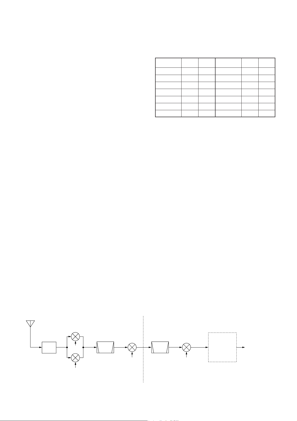
1-4 RF AMPLIFIER AND 1ST MIXER CIRCUITS
(RF-A UNIT)
The 1st mixer circuit mixes the receive signals with the 1st
LO signal to convert the receive signal frequencies into a
64.455 MHz 1st IF signal. The IC-756PRO
™ has two 1st
mixer circuits for the dualwatch function.
The signals from the pre-amplifier circuit, or signals which
bypass the pre-amplifiers, are divided at L491. Each signal
is applied to a 60 MHz cut-off low-pass filter, RF amplifier
(Q501, Q502 and Q601, Q602) and then to a 1st mixer
(Q511–Q514 or Q611–Q614).
Each 1st LO signal (64.4850–124.4550 MHz) enters the RF
-A unit from the PLL unit via J561 or J661. The LO signals
are amplified at the LO amplifier (Q561 or Q661), filtered by
a low-pass filter, and then applied to each 1st mixer.
• Used RF filter
* : On the BPF board
• Receiver construction
LPF or
BPF
1st LO B
1st LO A
2nd LO
64.0 MHz
Crystal
filter
FI711a/b
1st mixer A
Q511–Q514
1st mixer B
Q611–Q614
2nd mixer
Q941–Q944
3rd LO
491 kHz
3rd mixer
IC151
64.455 MHz
0.03–60.0 MHz
Ceramic
filter
FI132, FI111
455 kHz
to squelch gate
(IC301)
36 kHz
DSP-A
board
RF-A UNIT MAIN-A UNIT
Band
0.03–1.6 MHz
1.6–2 MHz
2–3 MHz
3–4 MHz
4–6 MHz
6–8 MHz
8–11 MHz
Band
11–15 MHz
15–22 MHz
22–30 MHz
30–50 MHz
50–54 MHz
54–60 MHz
Control
signal
B7
B8
B9
B10W
B10
B10W
Control
signal
B0
B1
B2
B3
B4
B5
B6
Input
diode
N/A
*D2001
*D2021
*D2041
*D2061
*D2081
D261
Input
diode
D281
D301
D321
D341
D361
D341
Downloaded by
RadioAmateur.EU
Page 2

2
1-5 1ST IF CIRCUIT (RF-A UNIT)
The 1st IF circuit filters and amplifies the 1st IF signal. The
1st IF signal combined at L653 is applied to a pair of MCF
(Monolithic Crystal Filter; FI711a/b) to suppress out-of-band
signals.
The level of converted 1st IF signal is adjusted at the PIN
attenuators (D531–D533, D535 or D631–D633, D635) controlled by the [BAL] controller for the dualwatch function. The
signal is applied to the 1st IF amplifier (Q551 or Q651) and
then combined at L653.
The combined signal passes through the 3 dB attenuator
(R711–R713) and MCFs (FI711a/b). The signal is amplified
at the 1st IF amplifier (Q721). The amplified signal is then
applied to the 2nd mixer circuit.
1-6 2ND MIXER CIRCUIT (RF-A UNIT)
The 2nd mixer circuit mixes the amplified 1st IF signal and
2nd LO signal (64.00 MHz) for conversion into the 2nd IF
signal.
The 1st IF signal from the 1st IF amplifier (Q721) is converted into a 455 kHz 2nd IF signal at the 2nd mixer circuit
(D941).
The 2nd IF signal is applied to the noise blanker gate (MAINA unit) via the J741.
1-7 NOISE BLANKER CIRCUIT (MAIN-A UNIT)
The noise blanker circuit detects pulse-type noise, and turns
OFF the signal line when the noise appears.
The 2nd IF signal from the RF-A unit is applied to the noise
blanker gate (D112, D116). A portion of the 2nd IF signal
from RF-A unit is amplified at the noise amplifiers
(Q271–Q273, Q279), and is then detected at the noise
detector (D271) to convert the noise components to DC voltages.
The signal is then applied to the noise blanker switch (Q276,
Q278). At the moment the detected voltage exceeds Q276’s
threshold level, Q278 outputs a blanking signal to close the
noise blanker gate (D113, D114). The PLL unlock signal are
also applied to Q278, to control the noise blanker gate.
Some DC voltage from the noise detector circuit is fed back
to the noise amplifiers (Q271–Q273) via the DC amplifiers
(Q274, Q275). The DC amplifiers function as an AGC circuit
to reduce average noise. Therefore, the noise blanker function shuts off pulse-type noise only.
1-8 2ND IF CIRCUIT (MAIN-A UNIT)
The 2nd IF circuit amplifies and filters the 2nd IF signal, and
applies the 2nd IF signal to the 3rd mixer circuit.
The 2nd IF signal from the noise blanker gate (D113, D114)
is amplified at the 2nd IF amplifier (Q141) and passed
through the ceramic filter (FI111). The filtered signal is
applied to the 3rd mixer circuit.
1-9 3RD MIXER AND 3RD IF CIRCUITS
(MAIN-A UNIT)
The 3rd mixer circuit mixes the 2nd IF signal and the 3rd LO
signal to obtain the 3rd IF (36 kHz) signal.
The 2nd IF signal from the ceramic filter (FI111) is applied to
the 3rd mixer circuit (IC151, pin 1). The 3rd LO signal from
the PLL unit is applied to the 3rd mixer (IC151, pin 5). The
mixed signal is output from pin 6.
The 3rd IF signal is passed through the low-pass filter
(IC201a) and amplified at the 3rd IF amplifier (IC201b). The
filtered and amplified signal is then applied to the DSP-A
board via DRIF line.
1-10 DSP RECEIVER CIRCUIT (DSP-A BOARD)
The DSP (Digital Signal Processor) circuit enables digital IF
filter, digital noise reduction, digital PSN (Phase Shift
Network)/Low Power/Phase demodulation, digital automatic
notch, and etc.
The 36 kHz 3rd IF signal from the 3rd IF amplifier (MAIN-A
unit, IC201b) is amplified at the differential amplifiers
(IC2301a/b) after being passed through the T/R switch
(IC2291), and is then applied to the A/D converter (IC2321).
The coverted signal is level shifted 5V to 3.3 V at the level
converter (IC2051).
Differential
converter
A/D
converter
DRIF
DRAF
• DSP receiver circuit
6
7
1
IC2291
IC2301b/a IC2321
Level
converter
IC2051
D/A
converter
IC2052
Level
converter
IC2351
DSP IC
IC2001
LPF
IC2401
T/R switch
13
12
14
IC2372x
15
9
1
IC2372y
HPF
IC2441a
Mixer
amplifier
IC2381b
5
3
4
IC2372z
7
4
1
IC2473
MAIN-A unit DSP-A board MAIN-A unit
36 kHz
3rd IF
signal
AF
signals
“TXS” signal
“TXS” signal
“TXS” signal
5
11
10
Page 3

3
The level shifted signal is applied to the DSP IC (IC2001) for
36 kHz digital IF filter, demodulation, automatic notch and
noise reduction, etc. The output signal is level shifted 3.3 V
to 5V at the level converter (IC2052), and is applied to the
D/A converter (IC2351) to convert into the analog audio signals.
The converted audio signals are passed through the active
filter (IC2371a), AF amplifier (IC2371b), analog switches
(IC2372, pins 14, 13 and pins 1, 15) then applied to the lowpass filter (IC2401). The filtered signals are passed through
the analog switches (IC2372, pins 4, 3 and IC2473, pins 1,
7), high-pass filter (IC2441A) and mixer amplifier (IC2471A),
and then applied to the MAIN-A unit via J2001 (pin 13) as
the DRAF signal.
1-11 TWIN PBT CIRCUIT (DSP-A BOARD)
General PBT (Passband Tuning) circuit shifts the center frequency of IF signal to electronically narrow the passband
width. The IC-756PRO
™ uses the DSP circuit for the digital
PBT function and actually shifts the both lower and higher
passbands of 3rd IF filter within ±1.8 kHz.
The twin PBT circuit in DSP IC (IC2001) controlled by the
[TWIN PBT] controller adjusts the 3rd IF passband width
and rejects interference.
1-12 AGC CIRCUIT (DSP-A BOARD)
The AGC (Automatic Gain Control) circuit reduces IF amplifier gain and attenuates IF signal to keep the audio output at
a constant level.
The receiver gain is determined by the voltage on the AGC
line (IC2461, pin 4). The D/A converter for AGC (IC2461)
supplies control voltage to the AGC line and sets the receiver gain with the [RF/SQL] control.
The 3rd IF signal from the level converter (IC2051) is detected at the AGC detector section in DSP IC (IC2001), and is
applied to the D/A converter for AGC via the level converter
(IC2052). The AGC voltage is amplified at the buffer amplifier (IC2471b) and is applied to the MAIN-A unit to control the
AGC line.
When receiving strong signals, the detected voltage increases and the AGC voltage decreases via the buffer amplifier
(IC2471b). As the AGC voltage is used for the bias voltage
of the IF amplifier (RF-A unit; Q721), IF amplifier gain is
decreased.
1-13 S-METER CIRCUIT (MAIN-A UNIT)
The S-meter circuit indicates the relative received signal
strength while receiving by utilizing the AGC voltage which
changes depending on the received signal strength.
A portion of the AGC bias voltage from the DSP-A board is
applied to the differential amplifier (IC101a, pin 2) where the
difference between the AGC and reference voltage is detected.
The detected voltage is passed through the analog switch
(IC3631, pins 12, 14) as the SML signal and applied to the
main CPU (IC3501, pin 108) to activate the S/RF meter via
the sub CPU (IC401) on the DISPLAY board.
1-14 SQUELCH CIRCUIT (MAIN-A UNIT)
The squelch circuit mutes audio output when the S-meter
signal is lower than the [RF/SQL] setting level.
The S-meter signal is applied to the main CPU (IC3501, pin
108) and is compared with the threshold level set by the
[RF/SQL] control. The [RF/SQL] setting signal is applied to
the main CPU via the sub CPU (DISPLAY board; IC401, pin
91). The main CPU analyzes the compared signal and outputs control signal to the squelch gate (IC301, pin 5) via the
interface IC (IC3653, pin 19) to open or close the squelch as
the SQLS signal.
1-15 AF AMPLIFIER CIRCUIT (MAIN-A UNIT)
The AF amplifier amplifies the audio signals to a suitable driving level for the speaker.
The AF signals (DRAF) from the DSP-A board are passed
through the squelch gate (IC301) and amplified at the AF
amplifier section of IC311 (pins 2, 4), and volume is controlled by the AFGV signal at the VCA section (pins 7–9).
The volume controlled AF signals are passed through the AF
mute gate (IC331, pins 1, 7), then applied to the AF power
amplifier (IC332, pin 1) via the ripple filter (Q331).
The amplified audio signals are passed through the
[PHONES] and [EXT SP] jacks then applied to the internal
speaker when no plug is connected to the jacks.
The AF mute gate is controlled by the [AF] control via the
sub and main CPUs.
[PHONES]
[EXT SP]
Int. speaker
IC332
AF
power
amp.
DRAF
• AF amplifier circuit
7
6
1
IC301 IC311
Mute switchSquelch gate
Ripple
filter
Q331
MAIN-A unitDSP-A board
“SQLS” signal
“AFGV” signal
5
6
7
1
IC331
“AFMS” signal
2
AMP VCA
Page 4

4
2 TRANSMITTER CIRCUITS
2-1 MICROPHONE AMPLIFIER CIRCUIT
(MAIN-A UNIT)
The microphone amplifier circuit amplifies microphone audio
signals to a level needed for the DSP circuit.
Audio signals from the [MIC] connector (MIC board; J1, pin
1) are amplified at the audio amplifier section in IC451 (pins
21, 22) via the analog switch (IC3002, pins 12, 14), then
applied to the buffer amplifier section (IC451, pin 5) and
VCA section. The gain controlled signals are output from
(IC451, pin 9) and passed through the analog switch
(IC3005, pins 14, 12) and then applied to the DSP circuit as
the DTAF signal.
The VCA section in IC451 (pins 7–9) controls microphone
input gain according to the [MIC GAIN] control level using
the MIGV signal coming from the main CPU via the I/O
expander (IC3751, pin 4).
2-2 VOX CIRCUIT (MAIN-A UNIT)
The VOX (Voice-Operated Transmission) circuit sets transmitting conditions according to voice input.
A portion of the amplified audio signals from the AF amplifier section in IC451 are again amplified at the VOX amplifier
section IC451 (pin 9), also gain contolloed signals at the
VCA section (pin 9) are amplified at the AF amplifier
(IC3004b, pins 6, 7), and then applied to the main CPU
(IC3501, pin 106) after passing through the analog switch
(IC362, pins 6, 1) as the VOXL signal.
The VOGV signal is applied to the VCA section in IC3003
(pin 7–9) from the main CPU via the I/O expander (IC3751,
pin 9) to adjust VOX actionable sensitivity. This is controlled
by the VOX gain set in the VOX SET mode.
2-3 DSP TRANSMITTER CIRCUIT
(DSP-A BOARD)
The microphone audio signals from the MAIN-A unit via the
DTAF line are applied to the analog switch (IC2201, pin 4)
and output from pin 3 or 5 to the each modulation circuits.
(1) When SSB mode
The audio signals from the analog switch (IC2201, pin 5) are
amplified at the limitter amplifier (IC2281b) and applied to
the low-pass filter (IC2281d/c) to limit the transmit passband
width.
The filtered signals are then applied to the differential amplifiers (IC2301a/b) via the analog switch (IC2201) and T/R
switch (IC2291).
(2) When FM/AM modes
The audio signals from the analog switch (IC2201, pin 3) are
applied to the modulation adjustment pots (R2227: FM
mode, R2229: AM mode) via the limitter amplifier, preemphasis circuit (only FM mode) and splatter filter consist of
IC2211. The level adjusted signals are applied to the differential amplifiers (IC2301a/b) after being passed through the
analog switch (IC2201) and T/R switch (IC2291). The preemphasis circuit is cancelled by Q2201, Q2202, Q2211 on
AM mode.
The amplified signals at the differential amplifiers
(IC2301a/b) are applied to the A/D converter (IC2321). The
coverted signals are level shifted 5V to 3.3 V at the level
converter (IC2051).
The level shifted signal is applied to the DSP IC (IC2001)
and modulated at the DSP IC to produce the 36 kHz transmitter IF signal. The modulated IF signal from the DSP IC is
level shifted 3.3 V to 5V at the level converter (IC2052), and
is applied to the D/A converter (IC2351) to convert into the
analog IF signal.
The converted IF signal is passed through the active filter
(IC2371a), buffer amplifier (IC2371b), analog switch
(IC2372, pins 14, 12) then applied to the low-pass filter
(IC2381d/c). The filtered signal is applied to the MAIN unit
via J2001 (pin 28) as the DTIF signal.
When SSB or RTTY mode, a portion of the filtered signal
from the low-pass filter (IC2381d/c) is amplified at the IF and
buffer amplifiers (IC2381b/c) and is applied to the transmit
monitor circuit for the monitor function.
2-4 SPEECH COMPRESSOR CIRCUIT
(DSP BOARD)
The speech compressor compresses the transmitter audio
input signals to increase the average output level (average
talk power).
When the speech compressor function is ON, the level shifted signal from the level converter (IC2051) is applied to the
DSP IC (IC2001) and compressed at the DSP IC to obtain
an average audio level.
At the same time, the compressed signals are modulated at
the DSP IC and applied to the level converter (IC2052).
1st LO
D771
Ceramic
filter
Crystal
filter
FI711
LPF BPFs
FI131
Ceramic
filter
FI133
MIC
Bandwidth
15 kHz
455 kHz
DSP-A
board
RF-A UNIT
MAIN-A UNIT
AMP VCA
FM/AM
modes
other
modes
3rd LO
(491 kHz)
IC221
64.455 kHz
2nd LO
(64.00 MHz)
D741
36 kHz IF
IC451
11
12
13
14
IC3005x
“MOSL” signal
DTAF DTIF
Page 5

5
2-5 IF AMPLIFIER AND MIXER CIRCUITS
(MAIN-A AND RF-A UNITS)
The modulated 3rd IF signal from the DSP-A board (DTIF:
36 kHz) is applied to the 3rd mixer circuit (MAIN-A unit;
IC221, pin 1). The applied 3rd IF signal is mixed with the 3rd
LO signal from the DDS circuit (PLL unit; IC701) to produce
a 455 kHz 2nd IF signal.
The 2nd IF signal is output from pin 6 and amplified at the IF
amplifier (MAIN-A unit; Q241). The amplified signal is
passed through the ceramic bandpass filter (MAIN-A unit;
FI131: FM/AM modes, FI133: other modes) for unwanted
signals are suppressed. The filtered 2nd IF signal is ampllified at IF amplifier (MAIN-A unit; Q261) and applied to the
2nd mixer circuit on the RF-A unit via J101.
The 2nd IF signal is mixed with the 64 MHz 2nd LO signal,
coming from the PLL unit, at the 2nd mixer circuit (RF-Aunit;
D741) to obtain a 64.455 MHz 1st IF signal. The 1st IF signal is passed through the MCFs (RF-Aunit; FI71 1a/b) to cutoff the undesired signals then amplified at the IF amplifier
(RF-A unit; Q751) via the T/R switch (RF-A unit; D711). The
amplified 1st IF signal is applied to the 1st IF mixer circuit
(RF-A unit; D771).
The operating (transmitting) frequency is produced at the 1st
IF mixer circuit (RF-A unit; D771) by mixing the 1st IF and
1st LO signals. The mixed signal is then applied to the RF
circuit.
2-6 RF CIRCUIT (RF-A AND PA UNITS)
The RF circuit amplifies operating (transmitting) frequency
to obtain 100 W of RF output.
The signal from the 1st IF mixer is passed through the lowpass filter (RF-A unit; L961, L962, C961–C965) and amplified at the RF amplifier (RF-Aunit; IC961). The amplified signal is again amplified at the wide-band YGR amplifier (RF-A
unit, IC151) after passing through one of 11 bandpass
(Refer to page 1 for bandpass filters used) and high-pass filters, and is then applied to the PAunit via J151.
The signal applied from the RF-Aunit is amplified at the predrive (Q1), drive (Q2, Q3) and power amplifiers (Q4, Q5) in
sequence to obtain a stable 100 W of RF output power. The
amplified signal is applied to one of 8 low-pass filters in the
FILTER unit.
2-7 LOW-PASS FILTER CIRCUIT (FILTER UNIT)
The low-pass filter circuit contains 8 Chebyschev low-pass
filters to suppress the higher harmonic components.
The signal from the power amplifiers on the PA unit is
applied to one of 8 low-pass filters, which is selected by the
I/O expander (IC11) in the CTRLunit via the buffer amplifier
(CTRL unit; IC12).
The filtered signal is then applied to one of 2 antenna connectors via the CTRL only/and TUNER unit/s.
2-8 ALC CIRCUIT (MAIN-A UNIT)
The ALC (Automatic Level Control) circuit controls the gain
of IF amplifiers in order for the transceiver to output a constant RF power set by the [RF POWER] control even when
the supplied voltage shifts, and etc.
The RF power level is detected at one of the APC detector
circuits (CTRL unit; D2) to be converted into DC voltage and
applied to the MAIN-A unit as the FORV signal.
The FORV signal from the CTRL unit is applied to the comparator (IC551b, pin 6). The POCV signal, controlled by the
[RF POWER] control via the I/O expander (IC3751, pin 5), is
also applied to the other input (pin 5) for reference. The
compared signal is output from pin 7 and applied to the IF
amplifiers in the MAIN-A (Q261) and RF-A (Q751) units to
control amplifying gain.
When the FORV signal exceeds the POCV voltage, ALC
bias voltage from the comparator controls the IF amplifiers.
This adjusts the output power to a specified level from the
[RF POWER] control until the FORV and POCV voltages are
equalized.
In AM mode, the comparator operates as an averaging ALC
amplifier. Q502 turns ON and the POCV voltage is shifted
for 40 W AM output power (maximum) through R510.
DTAF
• DSP Transmitter circuit
LPF
IC2281c/dIC2281b
IC2211a
LPF
IC2211b
MAIN-A unit DSP-A board
AF
signal
“MODS” signal
4
9
5
3
IC2201z
Mode switch
Differential
converter
A/D
converter
DTIF
6
7
1
IC2291
IC2301a/b
IC2321
Level
converter
IC2051
D/A
converter
IC2052
Level
converter
IC2351
DSP IC
IC2001
LPF
IC2381d/c
T/R switch
13
12
14
IC2372x
MAIN-A unit
36 kHz IF
“TXS” signal
“TXS” signal
5
12
13
14
IC2201x
Mode switch
11
11
Limitter
Limitter
SSB
mode
FM/AM
mode
Page 6

6
The ALC bias voltage is also applied to the ALC meter amplifier (IC551a, pin 2) to obtain an ALC meter signal (ALCL).
The amplified signal is passed through the analog switch (IC
3631, pins 13, 14) and applied to the main CPU (IC3501, pin
108) to drive the S/RF meter via the sub CPU (IC401) on the
DISPLAY board.
An external ALC input from the [ALC] jack or [ACC] sockets
is applied to the buffer amplifier (Q521). External ALC operation is identical to that of the internal ALC.
The FORV signal is also applied to the power meter amplifier (IC571a, pin 3). The amplified signal is passed through
the analog switch (IC3631, pins 1, 15) as an FORL signal
and applied to the main CPU (IC3501, pin 109) to drive the
S/RF meter when the power meter is selected.
2-9 APC CIRCUIT (MAIN-A UNIT)
The APC (Automatic Power Control) circuit protects the
power amplifiers on the PAunit from high SWR and excessive current.
The reflected wave signal appears and increases when the
connected antenna is mismatched to 50 Ω. The APC detector circuit (CTRL unit; D1 and L1) detects the reflected signal, and applies it to the APC circuit (IC551c, pin 9) as a
REFV signal.
When the REFV signal level increases, the APC circuit
decreases the ALC voltage to activate the APC.
For the current APC, the power transistor current is obtained
by detecting the voltages (ICH and ICL) which appear at
both terminals of the current detector (PA unit; R28). The
detected voltages are applied to the differential amplifier
(IC551d, pins 12, 13). When the current of transistors is
increased, the amplifier controls the ALC line to prevent
excessive current flow.
A portion of the REFV signal is applied to the SWR meter
amplifier (IC571b, pin 5). The amplified signal is passed
through the analog switch (IC3631, pins 3, 4) as an REFL
signal and applied to the main CPU (IC3501, pin 110) to
drive the S/RF meter when the SWR meter is selected.
2-10 TEMPERATURE PROTECTION CIRCUIT
(PA UNIT)
The cooling fan (CHASSIS; MF1) is activated while transmitting or when the temperature of the power amplifier
exceeds the preset value. The temperature protection circuit
consists of Q10–Q13 and R50.
While transmitting, Q10 and Q12 are turned ON, and provide a voltage to the cooling fan to rotate at medium speed.
The thermistor (R50) detects the temperature of the final
amplifier (Q5), and activates Q11 and Q13 to accelerate the
cooling fan when the detected temperature exceeds 70˚C
(158˚F). The cooling fan rotates at high speed at 80˚C
(176˚F) or more.
The thermistor keeps the cooling fan rotating even while
receiving until the Q5 temperature drops to 60˚C (140˚F) or
below.
2-11 MONITOR CIRCUIT
(DSP-A BOARD AND MAIN-A UNIT)
The microphone audio signals can be monitored to check
voice characteristics.
(1) When FM/AM modes (MAIN-A UNIT)
Aportion of the microphone audio signals from the VCAsection in IC451 are applied to the analog switch (IC361). The
selected audio signals are applied to IC371 (pin 2), and the
output signals from pin 9 are applied to the AF amplifier circuit (IC311, pin 7).
(2) When SSB/RTTY modes
(DSP-A BOARD)
A portion of the transmit IF signal from the low-pass filter
(IC2381d/c) is amplified at the IF (IC2381b) and buffer
(IC2381a) amplifiers, and applied to the digital mixer circuit
(IC2302). The applied signal is mixed with a 36 kHz LO signal from the D/A converter (IC2342) to demodulate into the
AF signals. The demodulated signals are passed through
the buffer amplifier (IC2381a), low-pass filter (IC2441b/c)
and AF amplifier (IC2441d), and then applied to the MAIN-A
unit as the DMAF signal.
The DMAF signal from the DSP-A board is amplified at the
ALC amplifier (MAIN-A unit; IC372, pins 13, 1) and applied
to the VCA section of IC371 (MAIN-A unit; pins 7, 9). The
volume controlled AF signals is applied to the AF amplifier
circuit (MAIN-A unit; IC311, pin 7).
3 PLL CIRCUITS
3-1 GENERAL
The PLL unit generates a pair of 1st LO frequencies
(64.485–124.455 MHz) for dualwatch and spectrum scope
functions; a 2nd LO frequency (64 MHz), 3rd LO frequency
(491 kHz) and sweep LO frequency for the spectrum scope
function.
The 1st LO PLLs adopt a mixer-less dual loop PLL system
and has 4 VCO circuits. The LOs, except the 2nd, use DDSs
while the 2nd LO uses the fixed frequency of the crystal
oscillator.
3-2 1ST LO PLL CIRCUIT
The 1st LO PLLs contain a main and reference loop as a
dual loop system. Both PLLs have equivalent circuits— this
manual describes only the 1st LO PLL A circuit.
The reference loop generates a 10.747 to 10.865 MHz frequency using a DDS circuit, and the main loop generates a
64.485 to 124.455 MHz frequency using the reference loop
frequency.
(1) REFERENCE LOOP PLL
The oscillated signal at the reference VCO (Q151, D151) is
amplified at the buffer amplifiers (Q152, Q102) and is then
applied to the DDS IC (IC101, pin 46). The signal is then
divided and detected on phase with the DDS generated frequency.
The detected signal output from the DDS IC (pin 56) is converted into DC voltage (lock voltage) at the loop filter
(R135–R137, C121, C151) and then fed back to the reference VCO circuit (Q151, D151).
Page 7

7
(2) MAIN LOOP PLL
The oscillated signal at one of the main loop VCOs (Q201,
D201, D202), (Q221, D221, D222), (Q251, D251–D254) and
(Q271, D271–D274) is amplified at the buffer amplifiers
(Q301, IC320) and is then applied to the PLL IC (IC381, pin
6) via the low-pass filter (L303, C304–C307). The signal is
then divided and detected on phase with the reference loop
output frequency.
The detected signal output from the PLL IC (pin 2) is converted into a DC voltage (lock voltage) at the loop filter and
then fed back to one of the VCO circuits (Q201, D201,
D202), (Q221, D221, D222), (Q251, D251–D254) and
(Q271, D271–D274).
The oscillated signal is amplified at the buffer amplifiers
(Q301, IC320) and then applied to the RF-Aunit as a 1st LO
A signal after being passed through the low-pass filters
(L303, C304–C307 and L351–L353, C351–C356) and highpass filter (L354, C358–C360) and mute circuit (D361).
3-3 2ND LO AND REFERENCE OSCILLATOR CIR-
CUITS
The reference oscillator (X52, Q51) generates a 32.00056
MHz frequency for the 4 DDS circuits as a system clock and
for the LO output. The oscillated signal is doubled at the
doubler circuit (Q71, Q81) and the 64.0 MHz frequency is
picked up at the double tuned filter (L81, L82). The 64.0
MHz signal is applied to the RF-A unit as a 2nd LO signal.
3-4 3RD LO CIRCUIT
The DDS IC (IC701) generates a 10-bit digital signal using
the 32 MHz system clock. The digital signal is converted into
an analog wave signal at the D/A converter (R701–R720).
The converted analog wave is passed through the bandpass
filter (L702, L703, C709–C713) and then applied to the
MAIN-A unit as the 3rd LO signal.
3-5 MARKER CIRCUIT
The divided signal at the DDS circuit (IC101) is used for the
marker signals with the IC-756PRO
™.
The reference signal for the DDS circuit (32.0 MHz) is divided to produce an acceptable frequency signal, 16 MHz, with
the programmable divider then divided again by 160 to
obtain 100 kHz cycle square-wave signals.
The generated marker signals are output from pin 66 of the
DDS IC (IC101), and are then applied to the RF unit via the
mute switch (IC192) and J851 as the MKR signal.
• PLL CIRCUIT
64.485–
124.455 MHz
10.747–
10.865 MHz
64.485–
124.455 MHz
64.0 MHz
77.8 MHz
ANT
1st mixer A
Q511–Q514
491 kHz
to scope circuit
(RF-A unit, D831)
to scope circuit
(RF-A unit, IC841)
IC801IC701
IC101
IC381
IC901
Q71
Q81
Q902
S2LOS3LO
3LO2LO
1LOB
1LOA
77.8 MHz
RF-A unit
PLL unit
MAIN-A unit
Q201
Q221
Q251
Q271
Q151
1st LO PLL A
circuit
Phase
detector
1/N divider
1/22
Phase
detector
12 bit
D/A
Main loop PLL
Ref. loop PLL
DDS
1st mixer B
1st LO
PLL B
circuit
✕2
DDS
D/A
DDS
D/A
PLL
IC
Crystal
filter
2nd mixer
D941
3rd mixer
IC151
64.455 MHz
to DSP-A board
Reference oscillator
X52: 32.0 MHz
BPFBPF
Loop
filter
LPF
LPF
Downloaded by
RadioAmateur.EU
Page 8

8
4 ANTENNA TUNER CIRCUITS
4-1 MATCHING CIRCUIT (TUNER UNIT)
The matching circuit is a T-network. Using 2 tuning motors,
the matching circuit obtains rapid overall tuning speed.
Using relays (RL1–RL15), the relay control signals from the
antenna tuner CPU (CTRL unit; IC5) via the buffer amplifier
(IC1, IC2) ground one of the taps of L3–L12 and add capacitors (C27–C43). After selecting the coils and capacitors, 2
motors (CTRL unit; MF1, MF2) adjust C44 and C45 using
the antenna tuner CPU (CTRL unit; IC5) and the motor controller (CTRL unit; Q211–Q218, D211, D213, D215, D217) to
obtain a low SWR (Standing Wave Ratio).
4-2 DETECTOR CIRCUIT (CTRL UNIT)
(1) SWR detector
Forward and reflected power are picked up by a current
transformer (L1), detected by D2 and D1, and then amplified
at IC1a and IC1b, respectively. The amplified voltages are
applied to the antenna tuner CPU (IC5, pins 2, 3). The tuner
CPU detects the SWR.
(2) Reactance components detector
Reactance components are picked up by comparing the
phases of the RF current and RF voltage. The RF current is
detected by L4 and R16 and buffer-amplified at IC14e and
IC2a and then applied to the phase comparator (IC3a). RF
voltages are detected by C12–C14 and then applied to the
phase comparator (IC3b) after being amplified at the buffer
amplifiers (IC14c, IC2b). The output signal from the phase
comparator (IC3a, pin 6 for RF current, IC3b pin 7 for RF
voltage) is rectified at D7 and D6 for conversion into DC voltage. The rectified voltage signals are combined, then amplified at the inverter amplifier (IC4b), then applied to the
antenna tuner CPU (IC5, pin 64).
A C-MOS IC is used for the buffer amplifier (IC14) to
improve functionable sensitivity; the inverter amplifier (IC4)
is very responsive even with a low signal level input.
Together, these ensure quick and stable signal detection
even at low RF signal level input.
(3) Resistance components detector
Resistance components are picked up by L8, and detected
by D8, D9 and Q5. The detected resistance components are
amplified at the inverter amplifier (IC4a), and then applied to
the antenna tuner CPU (IC5, pin 1).
4-3 MOTOR CONTROL CIRCUIT
(CTRL AND TUNER UNITS)
The control circuit of the internal antenna tuner consists of
the CPU, EEPROM (Electronically-Erasable Programmable
Read Only Memory), tuning motors and tuning relays.
(1) CPU and EEPROM (CTRL unit)
The antenna tuner CPU (IC5) controls the tuning motors via
the motor controller (Q211–Q218, D211, D213, D215, D217)
and tuning relays, and memorizes the best preset position in
100 kHz steps. The memory contents are stored in the EEPROM (IC6) without a backup battery.
(2) Tuning motors (CTRL and TUNER units)
A motor controller (Q211–Q218, D211, D213, D215, D217)
rotates the tuning motors (TUNER unit; MF1, MF2) to obtain
a low SWR.
(3) Tuning relays (TUNER unit)
According to the operating frequency band and antenna
condition, tuning relays select the capacitors and coils.
3-4-4 ANTENNA TUNER CPU PORT ALLOCATION
(CTRL unit; IC5)
1
2
3
4
6
7
13
15
17
21
22, 23
26
27–32
34–40
41–48
64
Input port for the resistance components detection voltage.
Input port for the reflected RF
power voltage.
Inpout port for the forward RF
power voltage.
Input port for the transceiver power
OFF.
Inputs low level signal when operating the antenna tuner in 50 MHz
band.
Input port for reference voltage setting.
Outputs tuner data signal.
Input port for the serial signal.
Input port for the [TUNER]
ON/OFF signal.
Input port for the TX/RX switching
signal.
Input port for the antenna tunner
CPU system clock.
Outputs the coil selection signal.
High : While 46–60 MHz band is
displayed.
Output the coil selection signal.
Output the capacitor selection signal.
Output pulse-type control signals
for the tuning motors (MF1, MF2).
Input port for the reactance components detection voltage.
R
REF
FOR
PWRS
STDU
SETI
KEY
START
THRU
SEND
CL1, CL2
DUAL
L24M, L18M,
L14M, L10M,
L7M, L3.5M
CO3, CO2,
CO1, CI3,
CI2, CI1
PZ, PY, PX,
PW, RZ, RY,
RX, RW
P
Pin Port
Description
number name
Page 9

9
5 SCOPE CIRCUITS
5-1 SCOPE RECEIVER CIRCUIT (RF-A UNIT)
A portion of the 64.455 MHz 1st IF signal from the 1st mixer
circuit (Q511–Q514: while receiving) or IF amplifier (Q751:
while transmitting) is passed through the PIN attenuator
(D801) and amplified at the IF amplifiers (Q811, Q812), and
then mixed with the 77.8 MHz scope 2nd LO (S2LO) signal
at the mixer circuit (D831) to produce the 13.345 MHz IF signal. The mixed IF signal is passed through the ceramic
bandpass filters (FI843, FI841) to suppress unwanted signals. The filtered IF signal is applied to the FM IF IC (IC841,
pin 16).
The applied 13.345 MHz IF signal is mixed with the sweep
LO (S3LO) signals from the PLLunit at the FM IF IC (IC841),
which includes the RSSI terminal. The mixed IF signals are
filtered at the ceramic bandpass filter (FI842) then applied to
the limiter amplifier section in the FM IF IC (IC841, pin 5).
The applied IF signals are converted into DC voltages
according to the applied IF signal strength at the RSSI section in the IC.
The converted voltages are output from pin12 (IC841) and
amplified at IC871b, then applied to the MAIN-A unit as the
SCPL signal.
Some of the DC voltages from the FM IF IC (IC841) are
amplified at IC871a to produce AGC voltages for the IF
amplifiers (Q811, Q812), producing wider dynamic range.
By sweeping LO signals (S3LO) are applied to the mixer
section in the FM IF IC (IC841), the spectrum scope function
is activated.
5-2 SWEEP LO CIRCUIT (PLL UNIT)
The sweep LO signals (S3LO) are generated by the DDS IC
(IC801) using the 32 MHz system clock. A10-bit digital signal is converted into analog wave signals at the D/A converter (R801–R820). The converted analog wave is passed
through the bandpass filter (L802, L803, C809–C813) then
applied to the RF-A unit after being amplified at the buffer
amplifier (Q802).
6 POWER SUPPLY CIRCUITS
6-1 PA UNIT
6-2 FRONT UNIT
• SCOPE CIRCUIT DIAGRAM
RF-A unit
1st mixer A
Q511–Q514
Q811
to 2nd mixer circuit
to the MAIN-A unit
SCPL signal
Q812
D831 FI843 FI841
Ceramic
BPF
Ceramic
BPF
IF
amp.
IC871a
AGC
IC871b
amp.
IF
amp.
Ceramic
BPF
Limiter
amp.
Mixer
IC841
FI842
S3LO signal
(12.79–12.99 MHz*)
S2LO signal
(77.80 MHz)
1st LO
signal
16
12
5
3
2
RSSI
*depending on sweeping passband width
RF signals
LINE
PHV
HV
14V
14VA
8V
5V
H5V
DESCRIPTION
The voltage from an external power supply via
the common filter circuit (FILTER unit; L501,
L502).
The same voltage as the PHV line passed
through a fuse (F1).
The same voltage as the HV line passed through
the switching relay (RL1).
The same voltage as the 14 V line is applied to
the AF power amplifier (MAIN-Aunit; IC332).
Common 8 V converted from the 14 V line and
regulated by the +8 regulator circuit (IC3).
Common 5 V converted from the 14 V line and
regulated by the +5 regulator circuit (IC2).
Common 5 V converted from the HV line and
regulated by the H5V regulator circuit (IC1).
LINE
5VF
–15V
–7V
–8V
+18V
DESCRIPTION
Common 5 V converted from the 14 V line and
regulated by the +5 regulator circuit (IC861).
Common –15 V converted from the 14 V line and
converted by the –15 DC-DC converter circuit
(IC841, Q841, D841). The voltage is applied to
the –7 V, –8 V regulator circuits and etc.
Common –7 V converted from the –15 V line and
regulated by the –7 regulator circuit (IC501).
Common –8 V converted from the –15 V line and
regulated by the –8V regulator circuit (IC881).
Common 18 V converted from the 14 V line and
converted by the 18 V DC-DC converter circuit
(IC821, Q821, D822).
Page 10

10
6-3 MAIN-A UNIT
6-4 CTRL AND PLL UNITS
7 LOGIC CIRCUITS
7-1 BAND SELECTION DATA
(RF-A, CTRL AND PLL UNITS)
To select the correct bandpass, low-pass filters and VCOs
on the RF-A, FILTER and PLL units, the main CPU (MAINA unit, IC3501) outputs the following band selection data via
the I/O expander (RF-Aunit, IC901, IC902, CTRL unit, IC11)
or DDS IC (PLL unit, IC101, IC401) depending on the displayed frequency.
The D/A convertor (MAIN-A unit, IC3751) output signal from
pin 7 is amplified at IC101b (pins 5–7) to obtain the band
voltage for external equipment via the [ACC 2] connector pin
4.
0.003–1.599999
1.6–1.999999
2.0–2.999999
3.0–3.999999
4.0–5.999999
6.0–7.999999
8.0–10.999999
11.0–14.999999
15.0–19.999999
20.0–21.999999
22.0–29.999999
30.0–44.999999
45.0–49.999999
50.0–54.000000
54.000001–
60.000000
Frequency
IC901, IC902
IC11 IC101 IC401
[MHz]
(RF-A unit)
(CTRL) (PLL) (PLL)
BPF LPF VCO-A VCO-B
B0
B1
B2
B3
B4
B5
B6
B7
B8
B9
B10W
B10
B10W
L1S
L2S
L3S
L4S
L5S
L6S
L7
VA1S
VA2S
VA3S
VA4S
VB1S
VB2S
VB3S
VB4S
LINE
R8V
T8V
DESCRIPTION
Receive 8 V converted from the 14 V line and
regulated by the R8V regulator circuit (Q601,
Q602, D601).
Transmit 8 V converted from the 14 V line and
regulated by the T8V regulator circuit (Q611,
Q612, D611).
LINE
5V
5V
DESCRIPTION
Common 5 V for the antenna tuner CPU (CTRL
unit; IC5) and the EEPROM (CTRL unit; IC6),
converted from the 14 V line and regulated by
the +5 regulator circuit (CTRL unit; IC13).
Common 5 V for each PLL-A and PLL-B circuits
regulated from the 8 V line and regulated by the
+5 regulator circuit (PLL unit; IC382: PLL-A,
IC682: PLL-B).
Downloaded by
RadioAmateur.EU
 Loading...