

.......
for
free
by
RadioAmateur.eu
'.
HF ALL BAND TRANSCEIVER
IC-73D
•
MAINTENANCE
DIICOMI
ICOM
1-6-19. Kamikurazukuri Hirano-ku.
Phone:
Telex:
ICOM
a.oPE
Himmelgeister Stress 100
4000
Duesseldorf 1
Weat Germany
Phone:0211-346047
Telex:41-8688082
ICOM
AMaleA,
2112 116th
Bellevue.
Phone:t2(6)454-8165
Telex:230-162210 !COM AMER
3331
Dalla ••
Phone:1214)620-2781
Mnue
WA
90004
TowelWOOd
T_
76234
INCORPORATED
(oo1793~1
ICOM
TR
J63649
G.M.B.H.
Ie.
N.E.
Suite
BVUE
307
Dr
.•
Osaka.
ICOM
810 S.W. Marina
Val'lCOU\ler.
Phone:I8(4)321-1833
Telex:21-464315
ICOM
7 Duke Street.
Victoria Australia
Phone:(03)629-7582
Telex:71-35621 ICOMAS AA36621
MANUAL
Japan
CANADA
AUS1RALIA,
Oriw
BC Canada
Windsor
LTD.
PlY. Ltd.
3181
SECTION
for
free
by
RadioAmateur.eu
1.
SPECIFICATIONS
TABLE OF CONTENTS
.............................................
1-1
SECTION
SECTION
SECTION
SECTION
SECTION
SECTION
SECTION
2.
OPERATING CONTROLS
3.
CIRCUIT DESCRIPTION
3 - 1 RECEIVING CIRCUITS
3 - 2 TRANSMITTING
3
-
31ST
3 - 4 DISPLAY
4. INSIDE
5.
BLOCK DIAGRAM
6.
OPTIONS INSTALLATION
7.
MECHANICAL PARTS AND DISASSEMBLY
8.
MAINTENANCE AND
- 1 MEASURING INSTRUMENTS REQUIRED
8
LOCAL OSCILLATOR CIRCUITS
UNIT
VIEWS.
FOR
. . . . . . . . . . . . . . . . . . . . . . . . . . . . . . . . . . . . . . . . . . . . .
............................................
ADJUSTMENT
.......................................
........................................
.............
CIRCUITS...
.........................................
......................................
ADJUSTMENT.
"".
. . . . . . . . . . . . . . . . . . .
... . .. . ... ...
......................
.......................
. . . . . . . . . . . . . . . . . . . . . . . . . .
....
. .
... . ..
..
...
..
..
2 - 1 -- 4
3 - 1 -- 8
3 - 1
3 - 3
3-6
3-8
4 - 1 --4
5 - 1
6
-1
-- 9
7 - 1 --23
8
-1 --19
8-1
•
8 - 2 PLL ADJUSTMENT
- 3 RECEIVER ADJUSTMENT
8
8 - 4 TRANSMITTER ADJUSTMENT
SECTION
SECTION 10. PARTS LIST
SECTION
SECTION 12. BOARD
9. VOLTAGE (CIRCUIT) DIAGRAMS
11. SCHEMATIC DIAGRAM
LAYOUT
........
..................................................
.........................................
..............................................
,
........
................................
............................
...............................
'"
.. , ...
...
. .
.. ..
...
8 - 2
8 8 - 13
9 - 1 -- 14
10 - 1 --20
11
SEPARATE
11
- 1
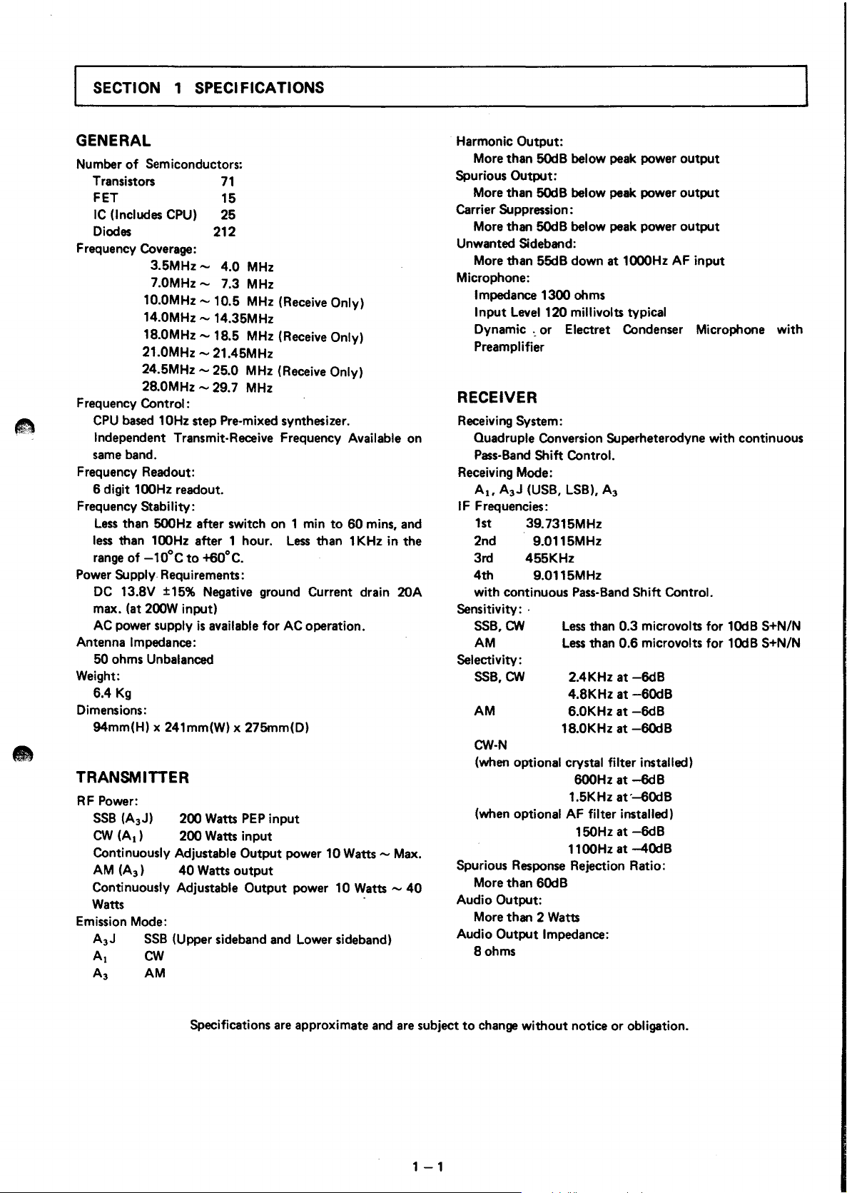
SECTION 1 SPECIFICATIONS
for
free
by
RadioAmateur.eu
GENERAL
Number
Frequency
Frequency Control:
Frequency Readout:
Frequency Stability:
Power Supply. Requirements:
Antenna
Weight:
Dimensions:
of
Semiconductors:
Transistors
FET 15
IC
(Includes
Diodes 212
CPU
based
Independent Transmit-Receive Frequency Available on
same
6 digit
Less
than 500Hz after switch
less
than 100Hz after 1 hour.
range
DC
13.8V ±15% Negative ground Current drain
max. (at 200W input)
AC power supply
50 ohms Unbalanced
Kg
6.4
94mm(H) x 241mm(W) x 275mm(D)
CPU)
Coverage:
3.5MHz - 4.0 MHz
7.0MHz - 7.3 MHz
10.0MHz - 10.5 MHz (Receive Only)
14.0MHz
18.0MHz - 18.5 MHz (Receive Only)
21.0MHz -
24.5MHz
28.0MHz -
10Hz step Pre-mixed synthesizer.
band.
100Hz readout.
of
-10° C to
Impedance:
71
25
-14.35MHz
21.45MHz
- 25.0 MHz (Receive Only)
29.7 MHz
on
1 min
to
60 mins,
Less
than 1 KHz
+60°
C.
is
available
for
AC operation.
TRANSMITTER
RF
Power:
SSB
(A3J) 200 Watts
CW
(AI)
Continuously Adjustable
AM
(A
3
Continuously Adjustable
Watts .
Emission Mode:
A3J
Al
A3
200 Watts input
)
40
SSB
(Upper sideband
CW
AM
Watts output
PEP
input
Output power 10 Watts - Max.
Output power 10 Watts -
and
Lower sideband)
in
and
the
lOA
40
Harmonic Output:
More than 50dB below
Spurious Output:
More than 50dB below
Carrier Suppression:
More than 50dB below
Unwanted Sideband:
More than 55dB down at
Microphone:
Impedance 1300 ohms
Input
Level
120 millivolts typical
Dynam1c
Preamplifier
: or Electret Condenser Microphone
peak
power
peak
power output
peak
power
1000Hz AF input
RECEIVER
Receiving System:
Quadruple Conversion Superheterodyne
Pass-Band
Receiving Mode:
AI,
IF Frequencies:
1st 39.7315MHz
2nd
3rd 455KHz
4th
with
Sensitivity: .
SSB,CW
AM
Selectivity:
SSB,CW
AM
CW-N
(when optional crystal
(when optional AF filter installed)
Spurious
More than
Audio Output:
More than 2 Watts
Audio
8 ohms
Shift Control.
A3J (USB, LSB),
9.0115MHz
9.0115MHz
continuous
Response
Output Impedance:
Pass-Band
Less
than 0.3 microvolts
Less
than 0.6 microvolts
2.4KHz at
4.8KHz at -6OdB
6.0KHz at
18.0KHz at -SOdB
600Hz at
1.5KHz
150Hz at
1100Hz at -4OdB
Rejection Ratio:
SOdB
A3
Shift Control.
-SdB
-SdB
filter
installed)
-6dB
at
'-SOdB
-SdB
output
output
with
for
for
with
continuous
10dB S+N/N
10dB S+N/N
Specifications
are
approximate
and
are
subject
1 - 1
to
change
without
notice
or
obligation.

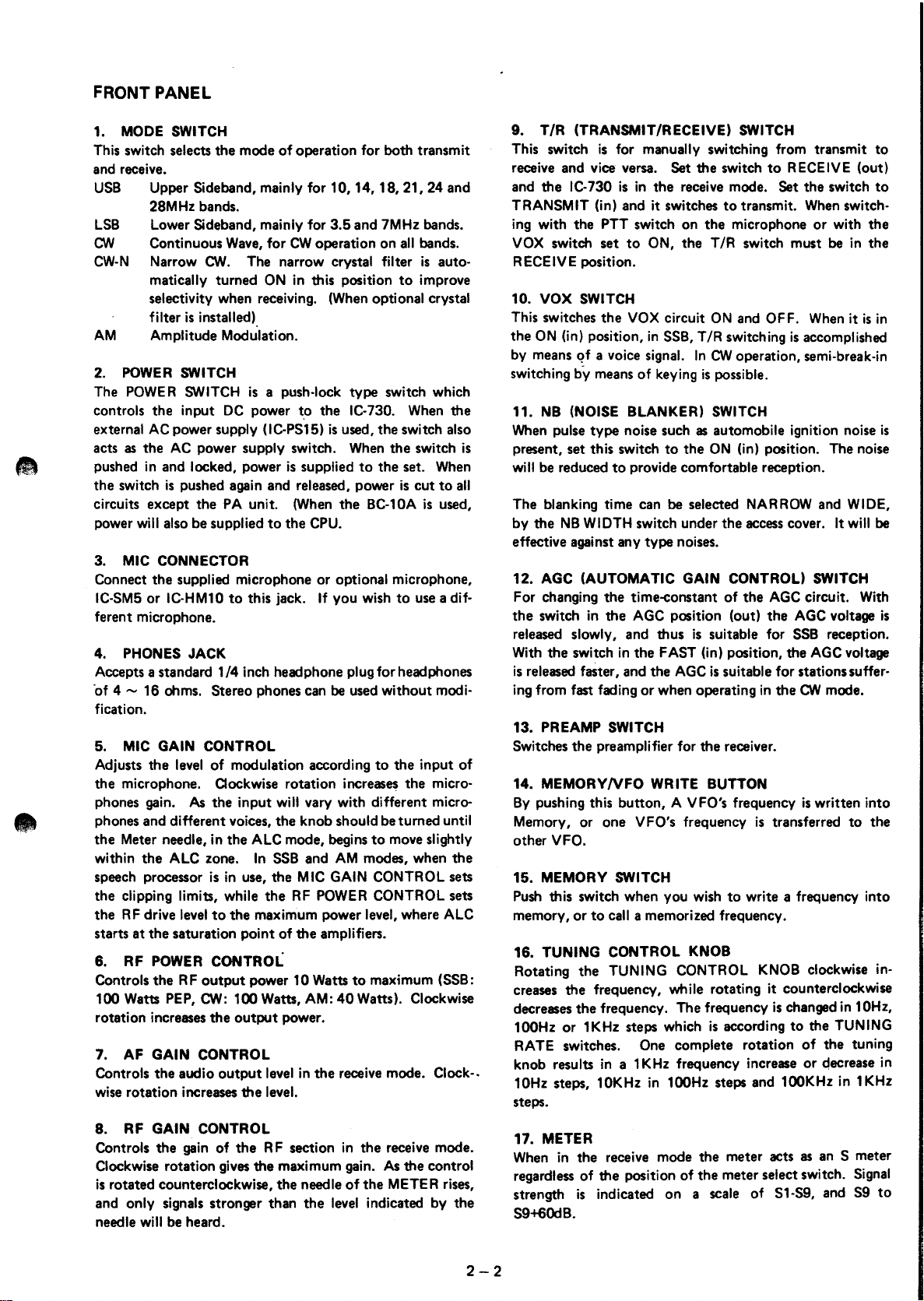
SECTION 2 OPERATING CONTROLS
for
free
by
RadioAmateur.eu
2
-,
FRONT PANEL
O
TRANSMIT
@METER
IN'oICATOA------------
5./lT(;H,----------
--------
-----
~
DISPLAY
SWITCH
SWITCH
® MOOE
, MIC
(4 PHONES
5 MIC
re
Il
1
8 RF
It
~
l
5.IIT'CH-----------
co,m"CTOA
JA,CK
GAIN
RF
POWER
NB (Noi$8
AF GAIN
AGC
PREAMP SWITCH
BI.nker)
CONTROL--------------------'
GAIN
CONTAOL-----------------------'
5WITC:H----------------------------'
---
-------
CCIN1'AelL---------------~
CClN1'ACIL----------------
5."TC;H---------------~
L
__________________
___________________________
..J
L
_____________
L
___________
~
MEM
1----
-
14
2!
TUNING
ORYIVFO
7T'
RIT
DIAL
LOCK SWITCH
RATE SWITCH
CONTROL
WRITE
SWITCH
INDI
CATOR
CONTROL
SW
ITCH
KNOB
BUTTON
SWITCH
ES
2-2
~1
ANTI·
VOX
CCIN1'AelL---
l1
CW
MONITOR
~N.B.
WIDTH
!l
FREOUENCY SET
5WITCH---
2 - 3 REAR PANEL CONNECTIONS
(4~ANTENNA
(gIGROUNO
@POWER
CCIN"EC:Ta'A--I~
TERMINAL
50'CK'"
-------I-~
3~VOX
I---------
~1=
I SPEAKEA
HI-
1!~~I_---
DELAY
====~~~::
----------
~IA(:CE
CONTROL
PROCESSOR
SWITCH
ill
SWR
SWITCH
SET
CONTROL
GA
IN
CONTROL
(4~,EXTERNAL
,'~,:ev
'5
5'OAV
BACK
TERMINAL
lT
ERMINAL
SOCKET
UP
ALC
JACK
JACK
2-
1
•
for
free
by
RadioAmateur.eu
FRONT PANEL
1.
MODE
This switch selects the mode
and receive.
USB
LSB
ON Continuous
CW-N
AM
2.
POWER
The
controls the input
external
acts
as
pushed
the switch
circuits except the
power
3.
MIC
Connect the supplied microphone or optional microphone,
IC-SM5
ferent microphone.
PHONES JACK
4.
Accepts a standard
'of 4 - 16 ohms. Stereo phones can
fication.
5.
MIC
Adjusts the
the microphone. Oockwise rotation increases the microphones gain. As the input
phones and different voices, the knob should be turned until
the
Meter needle, in the ALC mode, begins
within the ALC zone.
speech processor
the clipping
the
RF
starts
6. RF
Controls the RF
100 Watts PEP,
rotation increases
7. AF
Controls the audio
wise rotation increases
SWITCH
of
operation for both transmit
Upper Sideband, mainly for 10, 14,
28M
Hz
bands.
Lower Sideband, mainly for
Wave,
for
Narrow ON. The narrow crystal filter
matically turned
selectivity when receiving.
is
filter
Amplitude Modulation.
POWER
AC
the
in
will
or IC-HM10
drive
at
the saturation point
GAIN CONTROL
installed).
SWITCH
SWITCH
power supply (lC-PS15)
AC
power supply switch. When the switch
and locked, power
is
pushed again and released, power
also be supplied
CONNECTOR
1/4
GAIN
CONTROL
level
of
is
limits, while
level
to
POWER
CONTROL
output
CW:
the
output
ON
is
a push-lock type switch which
DC
power
PA
unit.
to
to
this jack.
inch headphone plug for headphones
modulation according
will
In
SSB
in
use, the
the
the maximum power level, where ALC
of
power 10 Watts
100 Watts,
output
the
power.
level
level.
3.5
and 7MHz bands.
CW
operation on
in this position
(When
to
the IC-730. When the
is
used, the switch also
is
supplied
(When
the BC-10A
the
CPU.
If
you wish
be
used without modi-
vary with different micro-
and
AM
MIC
GAIN
RF
POWER
the amplifiers.
to
AM:
40
in
the receive mode. Clock-.
18,21,24
to
optional crystal
to
the set. When
to
to
the input
to
move slightly
modes, when
CONTROL sets
CONTROL sets
maximum (SSB:
Watts). Clockwise
all
bands.
is
improve
is
cut
is
use a dif-
and
auto-
to
all
used,
the
of
9.
T/R (TRANSMIT/RECEIVE)
This switch
receive and vice versa. Set the switch
the
and
TRANSMIT (in) and it switches
ing with the PTT switch on the microphone
VOX
switch set
R
ECE
IV
10. VOX
This switches
the
ON
by means
switching
11.
NB
When
is
present, set this switch
will
be reduced
The blanking time can be selected
by the
effective against any type noises.
12. AGC
For changing the time-constant
the
switch
released slowly, and thus
With the switch
is
released faster, and the
ing from fast fading
13.
PREAMP SWITCH
Switches the preamplifier for the receiver.
MEMORYNFO WRITE BUTTON
14.
By
pushing this button, A VFO's frequency
Memory,
other
VFO.
15. MEMORY
Push this switch when you wish
memory,
TUNING CONTROL
16.
Rotating the TUNING CONTROL
creases the frequency, while rotating it counterclockwise
decreases the frequency. The frequency
100Hz
RATE switches. One complete rotation
knob results
10Hz steps, 10KHz
steps.
is
for manually switching from transmit
IC-730
E position.
(in) position,
(NOISE BLANKER)
pulse
NB
or
is
in
the receive mode. Set the switch
to
ON, the T/R switch must
SWITCH
the
VOX
circuit
in
SSB, T/R switching
qf
a voice signal.
by means
WIDTH
(AUTOMATIC GAIN CONTROL)
in
or
or
1KHz steps which
of
keying
type
noise such
to
the
to
provide comfortable reception.
switch under the access cover.
the
AGC
position (out)
in
the FAST (in) position, the
AGC
or
when operating
one VFO's frequency
SWITCH
to
call a memorized frequency.
KNOB
in
a 1
KHz
frequency increase
in
100Hz steps and 100KHz
SWITCH
to
RECEIVE (out)
to
transmit.
ON
and OFF. When it
In
CW
operation, semi-break-in
is
possible.
SWITCH
as
automobile ignition noise
ON
(in) position. The noise
NARROW and WIDE,
of
the
is
suitable for
is
suitable for stations suffer-
is
to
write a frequency into
KNOB
is
according
When
is
accomplished
AGC
circuit.
the
AGC
SSB
in
the
CW
is
transferred
clockwise
is
changed
to
of
or
or
SWITCH
AGC
mode.
written into
the TUNING
the tuning
decrease
to
to
switch-
with
the
be
in
the
is
in
It
will
be
With
voltage
reception.
voltage
to
the
in-
in
10Hz,
in
1KHz
is
is
in
8. RF GAIN CONTROL
Controls the gain
Clockwise rotation gives the maximum gain.
is
rotated counterclockwise, the needle
and only signals stronger than the
needle
will
of
be heard.
the
R F section
in
the receive mode.
As the control
of
the METER rises,
level
indicated by the
2-2
17. METER
in
When
regardless
strength
S9+6OdB.
the receive mode the meter acts
of
is
the position
indicated on a scale
of
the meter select switch. Signal
as
of
S1-S9, and S9
an S meter
to
In
for
free
by
RadioAmateur.eu
the transmit mode the meter has
are selected by the Meter
Po;
Indicates the relative
measured by placing
to
the
SWR
position.
ALC;
In
this position the meter functions when the RF
output reaches a certain level.
18. METER
Selects meter function
TRANSMIT INDICATOR
19.
Illuminates
20. FREQUENCY DISPLAY
The frequency
display tube.
displayed, the frequency can easily be read. The frequencies
indicated are the carrier frequencies
USB,
LSB
SWITCH
when the transceiver
of
Since the 1
and
CW.
Switch (18). They are
output
the
switch located inside the
in
the transmit mode.
the IC-730
MHz
is
and 1
two
functions which
as
follows:
power.
is
in
the transmit mode.
displayed on a luminescent
KHz
of
SWR
can be
top
cover
decimal points are
each mode
in
AM,
24. DIAL
After the IC-730
chewing, mobile operation, etc., push the
switch the VFO
frequency, thus inactivating the operation
knob. To change frequency, the dial lock must first be
disengaged by pushing and releasing the
again.
25.
Switches the RIT circuit
26. RIT CONTROL
Shifts the receive frequency ±800Hz either side
mit frequency. When
is
illuminated. Rotating the control
the
the
the
27.
Illuminates
LOCK
RIT SWITCH
receive frequency, and rotating
receive frequency. The frequency shifted by turning
RIT Control
RIT INDICATOR
is
is
when R
SWITCH
is
set
to
a certain frequency for rag
DIAL
electronically locked
ON
and OFF.
the
RIT
is
ON, the RIT INDICATOR
not
indicated on the frequency display.
IT
is
turned ON.
at
the displayed
of
DIAL
LOCK
to
the (+) side raises
to
the
(-)
LOCK
the tuning
switch
of
the trans-
side lowers
•
Remember, if you turn the R
receive frequency and rotate the
frequency displayed will not change.
21. NORMAL/SPLIT
Selects the relationship
(out) position, one VFO
In
the SPT (in) position, one VFO
the other
22.
You can select either of the built-in two VFO's with this
switch.
with the NORMAL/SPLIT switch. The switch performs the
following operations according
A.
A.
B.
is
for receive.
VFO
SWITCH
It
also selects the relationship
(NORMAL) Selects the
receive.
(SPLIT)
(NORMAL) Selects the
Selects
for transmit.
receive.
IT
SWITCH
RIT CONTROL knob, the
(TRANSCEIVE/SPLIT) SWITCH
of
the two VFO's.
is
for both transmit and receive.
to
its position.
"A"
VFO for both transmit and
"A"
VFO for receive and
"B"
VFO
ON
to
change the
In
the
is
for transmit and
of
the two VFO's
"B"
in
both transmit and
NORM
VFO
28.
BAND
The
BAND
selecting one of the 500KHz segments. The selectable bands
are 3.5KHz, 7MHz, 10MHz, 14MHz, 18MHz,
24MHz and 28MHz. (28MHz band
500KHz segments.)
PASS-BAND SHIFT (TUNING) CONTROL
29.
Allows continuous shifting
lower side
a nearby signal. When the optional crystal filter F
installed, this control allows continuous tuning
pass-band selectivity by moving
the
upper
selectivity, but also can improve the audio tone. Normal
position
SSB.
CONTROLS
30. SPEECH PROCESSOR
Switches the speech processor circuit
circuit enables greater talk power and better results
operation.
SWITCH
SWITCH
in
SSB
or
lower side
is
in
is
an
11
and
CWo
in
the center position and
UNDER
THE ACCESS COVER
position rotary switch used for
21
is
separated
of
the pass-band from upper or
This
will
reduce interference by
the
SSB
SWITCH
and
filter up
CWo
to
Not only improves
is
2.4KHz wide
ON
and OFF. This
to
of
800Hz from
MHz,
four
L-3O
the
in
D X
in
is
B.
(SPLIT)
TUNING RATE SWITCHES
23.
The small vernier marks
correspond
by pushing
Selects
for transmit.
to
10Hz, 100Hz
the
switch either 10Hz, 100Hz
"B"
VFO for receive and
on
the tuning knob are changed
or
1KHz steps which
"A"
is
or 1 KHz.
VFO
to
selected
31.
SWR
SWITCH
When measuring SWR, calibration SET and
functions are selected with this switch. When reading
make sure the METER switch on
R F position.
32.
SWR
SET CONTROL
This control calibrates the meter needle
position when you want
The METER switch must be
must be transmitting a carrier.
to
the
determine the value
in
the
RF position and the set
2-3
SWR
front panel
to
the
reading
is
SWR
of
SWR
in
the
SET
SWR.
33.
for
free
by
RadioAmateur.eu
VOX GAIN
This
control
the
VOX circuit.
control
speech.
34.
This
just
short
35.
In
by
This
of
VOX gain
from
36.
Switches
NARROW (short) and WIDE (long).
NARROW
37.
This
(monitor)
your
38.
This
quency
Do
so
VOX DELAY (VOX
controls
it
so
transmit
pauses in normal speech.
ANTI-VOX
VOX (SSB)
sound from
trouble
the
ANTI-VOX circuit
the
operator's
N.B. WIDTH SWITCH
the
CW
MONITOR
control
desired level
FREQUENCY
control
of
not
turn
CONTROL
adjusts
that
control
or
audio
the
it
input
signal level via
For
VOX
operation
the
VOX circuit will
time
the
transmit
to
CONTROL
operation,
the
speaker causing a switch
can
be
prevented
so
voice,
blanking
WIDE position according
adjusts
during ON
for
SET
is
for
fine
PLL
unit,
unless
to
receive switching will
the
VOX circuit
with
that
the
not
by
action
(MONn
the
easy listening.
you
CONTROL
audio
transmit
CONTROL
adjustment
which
want
the
microphone
in SSB,
operate
constant)
receive switching time. Ad-
by
this
VOX circuit
.sound from
time
volume
is
local oscillator frequency.
to
change
CONTROL
adjusting
control
of
the
Set
to
operation.
of
the
the
adjust
with
not
occur
may
be
to
the
input
along with
only
the
speaker.
noise blanker
the
switch in
incoming noise.
of
the
Adjust
reference fre-
frequency.
to
the
normal
during
operated
transmit.
level
the
operates
the
side
tone
it
to
REAR PANE L CONNECTIONS
39.
MEMORY BACKUP (RL) TERMINAL
For
connection
installation
'.
the
current
BC·10A
By
changing an internal
used
for
terminal can be used
this limit.
40.
EXTERNAL
This terminal
ALC signal
By
using
connectors,
terminal.
VHF and UHF
the
IC-730
connection.
41.
EXTERNAL
When an external speaker
of
a 9 -
12V
DC
connection
drain
is
recommended.
Transmit/Receive relay
can
from
optional
this terminal
is
possible. This terminal
The
to
the
is
low,
for
connector,
to
switch
ALC
TERMINAL
be used
a linear amplifier
adapter,
operation
output
SPEAKER
for
IC-EX205
can
using a suitable transverter
is
a few milliwatts.
is
power
supply.
vehicle's
fixed installation use
be
JACK
used,
control
24V
1A
input
or
transverter.
used
connect
battery
this terminal
DC.
terminal
and
for
Formobile
can
terminal. This
Don't
of
changing internal
TRANSVERTER
is
for Transverter
it
to
be
made
of
the
can
be
exceed
external
with
this jack.
Use a speaker
external speaker
not
.
function.
42_ KEY JACK
For
ON
keying
the
43.
ACCESSORY (ACC) SOCKET
Various
such as
over,
and
SOCKET CONNECTIONS
ACC
No.
PIN
1.
2.
3.
4.
5.
6.
7.
8.
9.
10.
11.
12.
13.
14.-24.
44.
ANTENNA (ANT) CONNECTOR
This
is
ance
is
45.
GROUND
To
prevent electrical shock,
be sure
TERMINAL.
strap
as possible and
possible, even in mobile installations.
46.
POWER SOCKET
For
connection
suitable
with
an impedance
is
connected,
operation,
terminal v.oltage
functions
modulation
so
forth.
connect
are available
output,
The
0®@@@@
00@@@@
Q)@@@@@
CD
0 ®
NC (no
13.8
switch
Connected
switch.
the
Output
output
Output
(Input
8 Volts DC available
can
Input
Ground
NC
8 Volts DC available
selected.
Input
Volts DC
transverter.
Output
Output
NC
used
50
ohms
to
power
connection)
Volts DC in
operation.
When
transmit
from
regardless
from
for MIC gain
not
be directly
for external ALC voltage.
for
TRANSVERTER
is
reference voltage
for external
to
connect
and
connect
TERMINAL
ground
the
For
best results use as heavy a gauge wire
of
the
supply.
the
the
key here.
must
be
through
receiver
table
below shows
@@
@ Outside view
FUNCTION
conjunction
to
Push-to-tal k, T
grounded,
mode.
the
receive
of
AF
Transmitter
control
when
actuated.
when
applied,
an
equipment
make
IC-PS15's DC
set
band
antenna
with
a PL-259
TVI,
BCI
the
of
8 ohms. When
built-in speaker
For
electronic
less
than
0.4V
DC.
the
accessory
output, T /R
those
terminals.
with
the
/R
change-over
the
set
operates in
detector
output
for
switching.
through
connection
stage. Fixed
or
AF gain.
MIC amplifier stage.
stage.)
transmitting. (relay
Max. 5mA).
the
control.
can
band
to
the
and
power
28MHz
operate
band
When 8
with
switching.
set. Its imped-
connector.
other
problems,
the
GROUND
as
short
cord,
or
the
does
socket
change-
power
is
a
or
as
other
2-4
SECTION 3 CIRCUIT DESCRIPTION
for
free
by
RadioAmateur.eu
3·1
3·'
The receiving
LPF
attenuated about 4Od8 by a
reduces
The
of
The
the
When
position, the
amplifier, consisting
the gain
on the entire band.
To the preamplifier, power source
regardless
PREAMP switch
through the switch
as
transmit mode
is
and
pushed in.
05
ceiver input line
The
selected
switch through the
The
is
diodes located at the
filter.
pectively.
The
consisting
has
The 1st Local Oscillator functions at the operating fre-
quency plus 1st IF (39.7315MHz) frequency.
the
RECEIVING CIRCUITS
• 1 RF CIRCUITS
signal
from
the antenna
unit
to
J2·1, where frequencies
High-Pass
intermodulation
signal
is
usually fed
RLl.
set
employs the OFM (Direct
front
end,
to
get wide dynamic
the PREAMP switch on the
signal
of
about 10dB and the intercept
if
the preamplifier
is
R8V
is
applied
or
applied
selected
to
its
base,
RL 1
is
not
is
turned on in the transmit mode and shunts the re-
to
signal
passed
by
the band switching signal sent from the BAND
band-pass
signal
a +18dBm intercept
BPF
for
These
passed
of
unit
filters
the band
filters
04 • 07
through J6.
by
strong
to
03
directly through the contacts
is
fed
to
of
01
and
is
pushed in, the emitter
and
RL 1
is
actuated in the
to
the
base
when
08
is
turned on
the
bias
voltage
actuated
ground
03
PRE·MIX
the
even
to
prevent
is
fed
to a band-pass
unit.
are
provided
of
operation
input
have
about 2dB insertion
band-pass
(Doubly Balanced Mixer). This
point
and 6dB insertion
is
fed
from
less
than 3.5MHz
filter. This
BC
signals.
Feed
Mixer) system at
range.
front
panel
is
the preamplifier. The pre-
02,
is
designed
point
(13.8V)
turned on
of
if
and
filter
is
always applied
or
off.
of
03
is
receive
03
through R4. In the
as
the
TRV
is
not
applied
the PREAMP switch
RF
feedback.
filter
for
each
band,
by
turning ON the
output
is
fed
circuits
to
the 1st mixer
loss.
It
is
P3
of
filter
in the
to
provide
of
26dBm
When
grounded
mode,
signal
to
which
and
of
loss
OBM
fed from
the
are
ON
the
03
one
the
res-
21.0MHz
24.5MHz
28.0MHz
28.5MHz
29.0MHz
29.5MHz
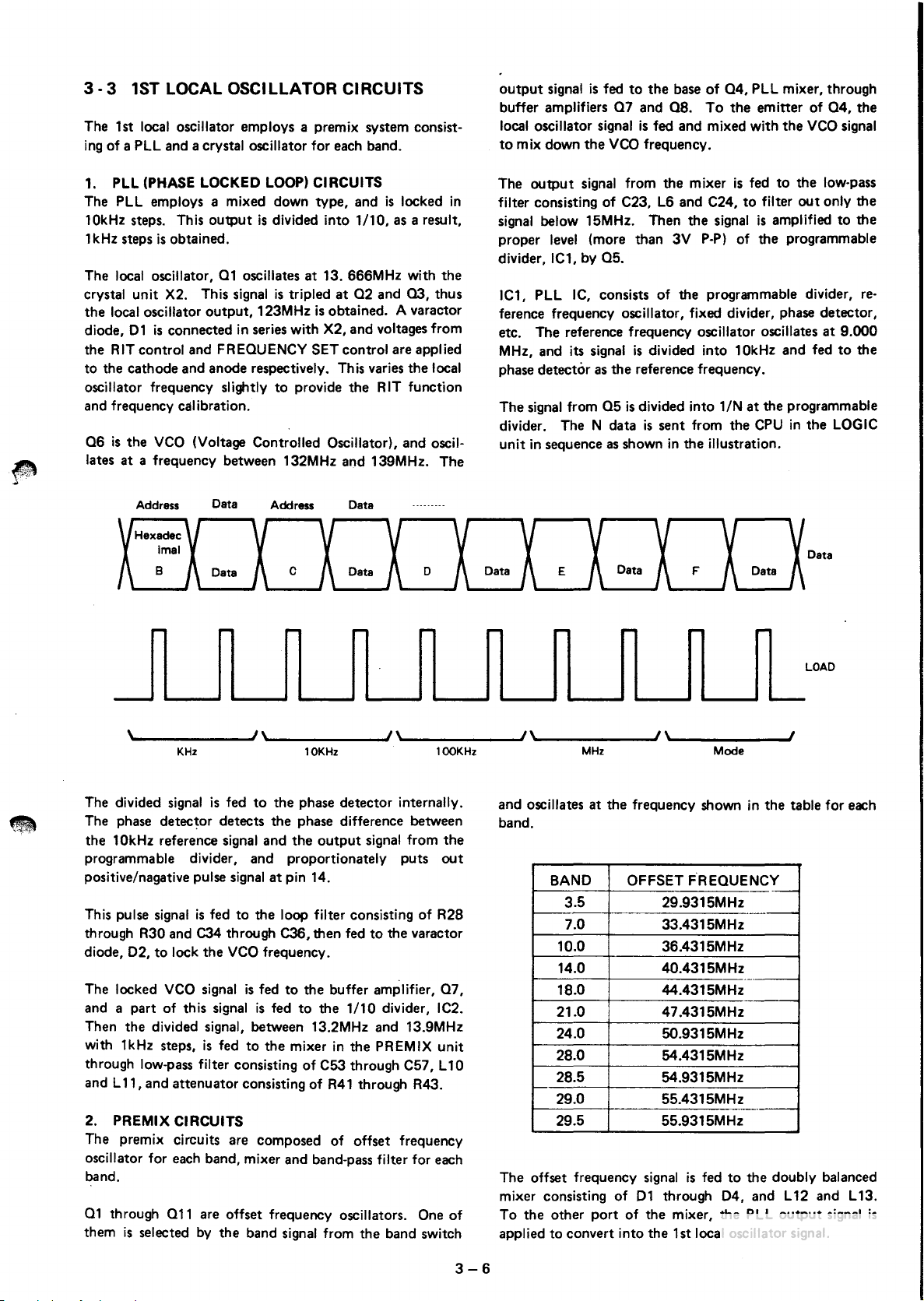
The center frequency
39.7315MHz due
IF
The 1st
monolithic crystal
switching diode, then fed
has a pass
The 1
is
applied
determined by R36 and C67.
oscillation.
The amplified 1
transmit/receive switching diode.
and
totally
The 1st IF signal
3
is
is
-1
The 2nd IF signal fed
to
fed
The
signal
gate
The amplified signal
IC2, voltage comparator
016
shunts over-voltage
A part
of
IC2. The detected
R42.
ON
which turns
pin 3
with
provides the
time)
MAl N unit).
constant
of
the AGC
signal
band
of
st
IF ampl ifier
to
its 2nd gate. The attack time constant
st
the 2nd
passed
- 2 SECOND
the Noise
MOS
genarates
of
When
of
IC2. This voltage
time constant
can
Amplifier
(39.7315MHz)
FETs,
the reference voltage, 1.2V,
the detected
the detected voltage
08
AGC function. This time constant (attack·
be
changed by the NB WIDTH switch
When
is
determined by R46 and C42. The release-time
is
determined by R34, R38, R47 and C42.
60.6315MHz
64.1315MHz "" 64.8315MHz
67.6315MHz
68.1315MHz
68.6315MHz
69.1315MHz
of
the 1st IF
to
the 10Hz step tuning.
converted at the 1st mixer
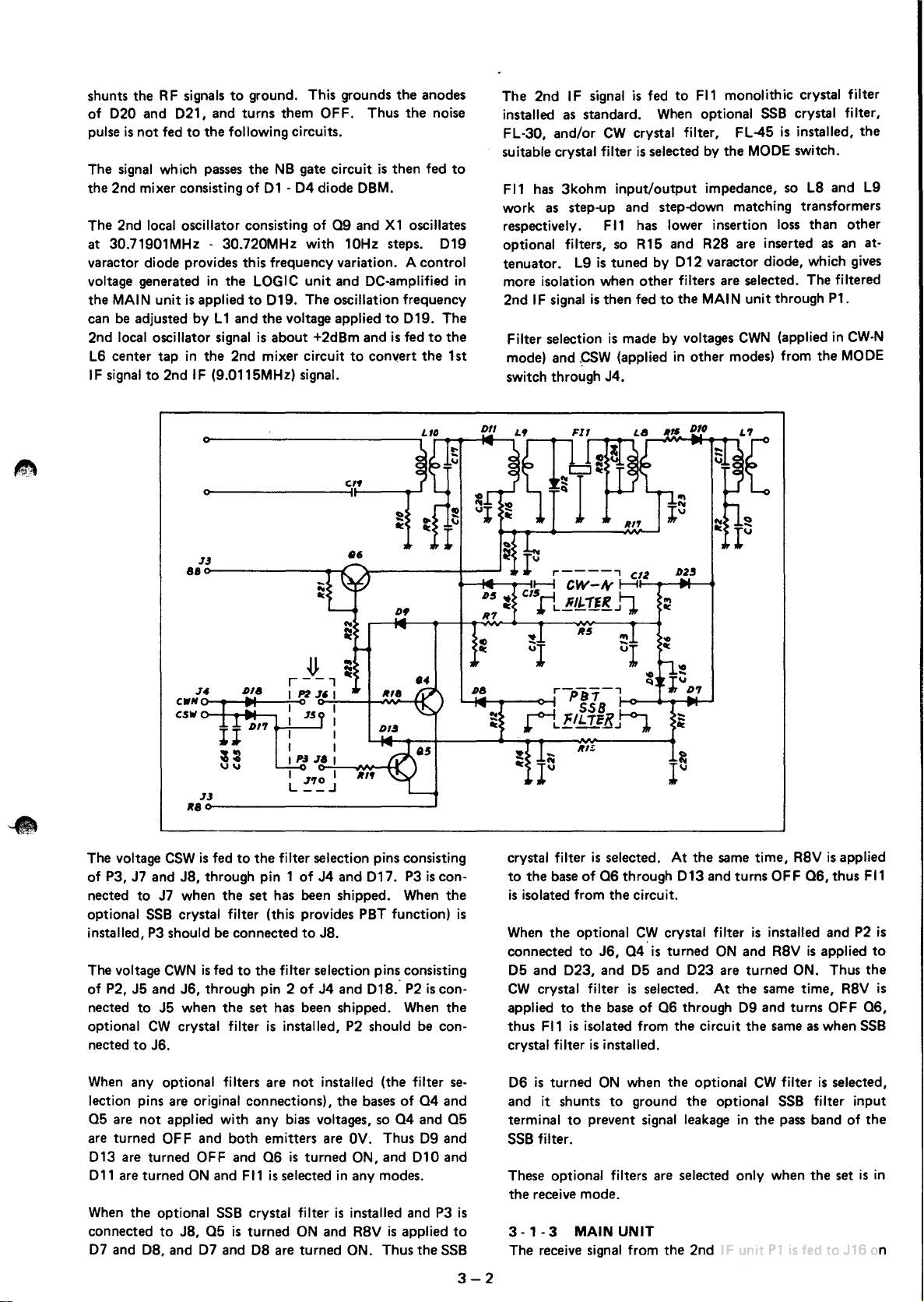
filter
FI2 through
to
the 1st IF amplifier
15kHz
at
-3dB
06
is
aMOS F ET,
C81
I F
signal
is
image
rejection ratio
Fll
is
then fed
IF
CIRCUITS
from
the
and Noise Blanker
is
amplified with
and
IC1, high gain amplifier with AGC.
is
detected by
and
noise
to
prevent long delay-times.
signal
from
signal
is
fed
ON
as
well. 2.5V
is
increased
of
R34
and
it
is
set
at the
""
61.3315MHz
""
68.3315MHz
""
68.8315MHz
""
69.3315MHz
""
69.8315MHz
is
varied 39.7305MHz-
is
020
transmit/receive
points.
and
an
AGC voltage
prevents VH F parasitic
fed
to F 11
Fll
RF
unit
014
pulses
014
to
the
exceeds
C42 (attack-time), This
WI
DE
through 021
is
the
same
is
more than
to
the 2nd IF
is
input
gate
01
and
and then fed
are
detected.
for
is
used
base
of
0.6V,
is
usually applied
when
08
position, the time
fed
to
06.
as
to
J2 and
circuits.
02,
IC2.
for
the AGC
07
through
07
is
turned
turns ON,
(S4
the
FI2
is
F12,
SOdB.
unit.
dual
to
015
to
on the
1st
This
range
for
BAND
3.5MHz
7.0MHz
10.0MHz
14.0MHz
18.0MHz
LO
each
is
changed
band
with
1 kHz
is
as
follows;
1st LO FREOUENCY
43.1319MHz
46.6315MHz
49.6315MHz""
53.6315MHz
57.6315MHz
steps
and its frequency
""
43.8315MHz
""
47.3315MHz
SO.3315MHz
""
54.3315MHz
""
58.3315MHz
3-1
Average
AGC function. Only when the detected voltage
1.2V
puts
The
and
by the
OJ
voltage at pin 2
caused
out
NB
usually
is
by a noise pulse, pin 3
lV
pulse,
gate
circuit
020
reverse
turned
ON
of
IC2 will
and
it
turns ON the NB
is
composed
and 021
voltage (6.6V) applied
by
are
a noise pulse,
of
turned
be
0.6V due
output
020,
ON
and
to
the cathode.
024
is
terminal
gate
switch
021
024
turned ON
to
exceeds
of
and
is
When
the
IC2
03.
024,
OFF
and
shunts the RF signals
for
free
by
RadioAmateur.eu
of
020
and
021,
is
not
pulse
fed
The signal which passes the
the 2nd mixer consisting
The 2nd local oscillator consisting
at 30.71901MHz . 30.720MHz with 10Hz steps.
to
ground. This grounds
and turns them OFF. Thus
to
the
following circuits.
NB
gate circuit
of
01 -04
diode
of
Q9 and
is
OBM.
the
the
then
X1
anodes
noise
fed
to
oscillates
019
varactor diode provides this frequency variation. A control
voltage generated
the
MAIN
unit
can be adjusted by L 1 and
2nd local oscillator signal
L6
center
tap
IF
signal
to
2nd
in
the
LOGIC unit and
is
applied
to
019.
the
is
about +2dBm and
in
the
2nd mixer circuit
IF
(9.0115MHz) signal.
~C-amplified
The oscillation frequency
voltage applied
to
convert
to
is
019.
fed
to
the
in
The
the
1st
The 2nd I F signal
installed as standard. When optional
FL-30, and/or
suitable crystal filter
FI1
has
3kohm
is
fed
to
FI1
CW
crystal filter, FL-45
is
selected by the
input/output
impedance, so
monolithic crystal filter
SSB
crystal filter,
is
MODE
installed,
switch.
LS
the
and L9
work as step-up and step-down matching transformers
FI1
respectively.
optional filters, so R15 and R2S are inserted
tenuator.
L9
has lower insertion loss than other
is
tuned by
012
varactor diode, which gives
as
an at-
more isolation when other filters are selected. The filtered
2nd
IF
signal
is
then fed
Filter selection
is
mode) and pSW (applied
switch through
J4.
to
the
MAIN
made by voltages
in
other modes) from the
DIO
unit through P1.
CWN
(applied
in
CW-N
MODE
O----------------ill~--~~
J3
88~----------~~
J4
eWH
0-
.......
O-+-
J3
is
fed
the
_.+----;-0
......
f-..,
to
the
filter selection pins consisting
set has been shipped. When
csw
R8~----------------------~
The voltage
of
P3, J7 and JS, through pin 1
nected
optional
CSW
to
J7 when
SSB
crystal filter (this provides PBT function)
installed, P3 should be connected
The voltage
of P2,
nected
optional
nected
J5
to
to
and
CW
J6.
CWN
is
J6,
through pin 2
J5
when
crystal filter
fed
to
the
filter selection
the
set has been shipped. When
is
installed, P2 should be con·
of
to
of
J4
JS.
J4
elf
416
Df
and
017.
P3
pin~
consisting
and O1S. P2
is
is
con-
the
con-
the
D2J
..
II<
Itl!;
crystal filter
to
the
is
isolated from
base
is
selected. At
of
06
through
the
circuit.
the
013
same time,
and turns
OFF
RSV
06,
is
applied
thus
FI1
is
CW
When the optional
connected
05
CW
applied
thus
crystal filter
to
J6,
and
023,
crystal filter
to
the
FI1
is
isolated from
is
and
base
installed.
crystal filter
04
is
turned
05
and
023
is
selected. At the same time,
of
06
through
the
circuit
is
installed and P2
ON
and
RSV
is
applied
are turned ON. Thus
RSV
09
and turns OFF
the
same as when
is
to
the
is
06,
SSB
When any optional filters are
lection pins are original connections),
05
are
are turned OFF and both emitters are
013
are turned OFF and
011 are turned
the
When
connected
07
and
not
installed (the filter
not
applied with any bias voltages, so
06
is
turned ON, and
ON
and
FI1
is
selected
optional SSB crystal filter
to
JS,
05
is
OS,
and
07
turned
and
ON
and
OS
are turned ON. Thus
the
bases
of
04
OV.
Thus
in
any modes.
is
installed and P3
RSV
is
applied
04
and
09
010
the
se-
and
05
and
and
is
to
SSB
3-2
06
is
turned
and it shunts
terminal
ON
when
the
to
ground
to
prevent signal leakage
optional
the
optional
in
CW
filter
SSB
the
pass band
SSB filter.
These optional filters are selected only when
the
receive mode.
3-1-3
The receive signal from
MAIN
UNIT
the
2nd I F unit
P1
is
is
selected,
filter input
of
the
set
fed
to
J16
is
the
in
on
the
for
free
by
RadioAmateur.eu
MAIN
010
is
1st
gate
2nd
gate,
termined
The amplified 2nd
mixer
03,
ON
in the receive mode.
oscillator signal
2nd
I F
In
SSS
mechanical
M F -455-11
11
AZ
and
11GZ
C7S
are
AM mode, the 3rd
In
ceramic
The
output
mixer consisting
9.0115MHz 4th
is
the
same
of
the
amplifier
07.
pectively.
2nd gate,
signal
is
The source voltage
i.e., incoming signal level. This voltage
then fed
justment and
3 -
1-
4
The
VXO
9.4665MHz, and this frequency
by changing the voltage applied
This voltage is varied
CONTROL on the
012
in the receive mode. In the transmit mode, a voltage
adjusted
oscillation frequency
9.4665MHz. This signal
mixer,
plifier
When
sition, the
the center frequency
455kHz, the center frequency
455kHz signal
with
the 9.4665MHz
dition
pass
through both
455kHz.
When
the
VXO
frequency
unit.
In
the receive mode, 01 is turned
turned OF F
of
IF amplifier
AGC voltage is applied. Its attack time
by
R4
dual
signal
or
CW
filter
AZ
has
1.5kohm and 240pF
has
not
used
filter
one
input
06
Soth amplifiers employ dual
To
AGC voltage
fed
to
to
IF
circuit
by
and
012.
the
Pass-Band
VXO
of
the
PB
by
the RSV, and the signal
01,
dual
gate
MOS
and C4.
IF
signal
is
fed
to
the 1st gate
gate
MOS
FET through
To
the 2nd gate, 9.4665MHz local
for
IF
TUNE
or
is
converted
mode, the 3rd
through
or
1.5kohm and 20pF. Thus, C75 through
for
through
from
of
IF signal again. The local oscillator signal
for
tuned circuit. The
through a switching diode
the 1st gate, the
the OET
the S-meter. R42
R41
is
TUNE
R66
is
4th
mixer
oscillates at 9.4665MHz, and 9.0115MHz,
is
Pass-Band
Shift
is
into
455kHz 3rd I F signal.
IF
signal
04
and
M F -455-11 GZ
the 11GZ.
IF
signal is
05
and
07.
the 455kHz filters
04
and
05,
the 3rd mixer, and fed
is
applied respectively. The ampl ified
UNIT
through J6, Pin 5.
of
OS
is
varied according
for
full-scale adjustment.
AND
PBT CIRCUITS
consisting
front
applied
Shift
of
converted
VXO
pass-bands
Control
increased,
of
can
by
R13, PASS BAND
panel, and applied
to
is
fixed at the center frequency,
is
fed
to
04
and
Control
the 2nd I F signal
into
signal. This
Shift
system and incoming
of
is
slid toward the right side, the
as
02,
PST
is
applied, and the
is
passed
06,
which
is
employed
input/output
passed
is
fed
and converted
to
4th
I F signal
OS,
gate
IF
signal
is
is
amplified
is
for
meter zero-point ad-
011 and
be
changed by ± 1.5kHz
to
013
013
through
the 2nd
05
through
is
set
at the center po-
is
of
3rd I F signal: This
9.0115MHz signal
is
the normal con-
the filters, 9.0115MHz and
an
example; 9.4675MHz
ON
and
is
fed
to
the
FET.
To
the
is
de-
of
the 3rd
which
is
turned
through FI1
are
turned ON.
for F Ilo
impedance
through
to
the center tap
is
then amplifier
MOS FET
fed and
to
AGC voltage
X1
oscillates at
varactor diode.
to
013
011,
gate
a.buffer
converted
FI2
a balanced
into
fed
to
IF
res-
to
the
by
07,
SHIFT
through
and
the
of
03,
3rd
am-
into
again
signals
(9.4665MHz+1kHz), 9.0115MHz, the center frequency
the 2nd IF signal
This 456kHz signal
again
with
456kHz, 3rd
the 455kHz
455kHz
pass-band
time,
band
center position
is
width
lower
3
In
fed
port
put
C39, C40, L2 through L4, etc. C39, C40 and L2 through
L4
shunted
a
mode
The detected
amplifier. The amplified
and fed
on the
IntheAM
A part
05.
Toe detected AF signal
amplifier. The amplified
and then fed
As
lector
is
over the threshold voltage,
voltage connected
When
voltage,
is
fast attack/slow
the collector
I F amplifiers.
from
When
is
in parallel
shorter.
3 - 1 - 6
AF signal
panel
MAIN
output
the internal speaker through the PHONES jack and EXTERNAL
transmit mode
3-3
filter
is
if
the optional
width
equivalent
is narrowed electrically from either the upper
side
continuously
-1
- 5 DETECTOR CIRCUITS
the
SSB
to
IC2, product detector in the OET
of
IC2, a BFO signal
out
from
are
connected in
to
to
get proper BFO frequency.
to
07,
front
mode, the
of
the amplified signal
an
AGC voltage, a part
is
fed
then fed
the applied voltage
or
discharged through
the
RF
the AGC switch on the
turned ON, and R13 and C10 (in
AF
from
is
fed
unit.
power in
SPEAKER jack. This IC
is
converted
is
the 9.4675MHz
IF signal
filter.
is
also shifted toward the lower side.
is
narrowed
of
to
and
pin
ground respectively according
AF
low-pass
panel.
to
to
to
the
zero,
of
On
GAIN
with
POWER
to
The signal
to
is
In
shifted toward the lower side, and the total
SSB
the control
the normal
CW
modes, a 9.0115MHz,
3.
The BFO
series
signal
4th
low-pass
AGC detector
base
of
to
the emitter,
02
is
RS
release
02
and supplied
the AGC line, the
control
RS
and the AGC time constant
AMPLIFIER
the VOLUME control,
pin 1 of
an
S ohm load. The
produce the
into
456kHz, 3rd
converted
off
other words, the
filter
from
by
up
with
is
fed
AF
filter,
IF
signal
is
fed
AF
filter
02.
02
turned OFF and the voltage
(high value resistor). This provides
AGC. AGC voltage
is
IC1
is
amplified
into
9.0115MHz signal
VXO
signal. However, the
from
the center frequency
pass-band
FL-30
is
installed, the total
the upper side. Thus the
is
the widest bandwidth and
SSB
bandwidth, and the band-
to
SOOHz.
4th
unit.
is
applied and
is
X1,
to
pin 5
signal
then
to
is
fed
is
then fed
to
pin 3
signal
07.
of
the
4th
01.
The detected
When
is
turned
charges
becomes
to
superimposed.
front
AF
povver
CW
side-tone.
an
composed
and
L2
of
IC1
is
put
the VOLUME control
to
01,
to
of
IC1, operational
is
put
IF
signal
the applied voltage
ON
C6
less
each
2nd gate
RF
gain control voltage
panel
is
series)
CIRCUIT
RS-2,
amplifier on the
with
IC1
output
is
activated in the
of
IF
signal.
of
of
the
At
this
or
IF
signal
To
the other
AF signal
of
through
to
the selected
operational
out
from
IF
amplifier.
AM
out
from
at
DC
and a negative
through R9.
than threshold
is
taken
pushed in,
are
connected
on the
to
get 2 watts
signal
OS,
X1,
L4
are
pin 7
detector
pin
01
col-
signal
of
C6
from
of
the
010
becomes
front
is
fed
to
is
is
1
is
3 - 2 TRANSMITTING CIRCUITS
for
free
by
RadioAmateur.eu
3 - 2
-1
AF
CIRCUITS
The audio signal
IC4, operational
MIC
GAIN
AF
signal
balanced
same
BFa
9.013MHz
double side band) signal
In the receive
adjusted
pectively
·AM
set voltage
an
carrier
turned
and IC2
In the receive mode and CW
ON and shunts the
ground
modulator,
one
for
signal
by
to
and
CW
unbalanced
is
put
ON and the
is
to
prevent the
3 - 2 - 2
The signal
1 st gate
through
455kHz
same
quency
In the receive mode,
fed
from
In the
MF-455-11GZ
2.4kHz
In
CWF455HT,
and the signal
The
balanced
one used in the receiver's
to
MHz
In the CW mode and
applied
off
down
applied
Thus the positive voltage
normal
next
of
03
signal.
one
is
fixed
from
leaking
SSB
bandwidth,
the
AM
output
mixer
convert
signal
to
and the signal
condition,
to
condition
stages.
from
the
microphone
amplifier
control
is
or
is
in a balanced
IF
output
03,
for
the
and CW modes, the
the
is
the source
the source
R14-2 on the
put
out
the receiver
is
fed and
9.010MHz
mode
R44 and
place
IC2
transmit
applied
condition
out
from
offset
CIRCUITS
from
mixer,
in the
The
the receive. However, the
at
9.4665MHz.
OET
into
the receiver I F circuits.
(or
-llAZ),
to
mode, the
ceramic
passes
from
the selected
consisting
incoming
then fed
is
010
and the signal
on
from
pin
IC2
in
product
mixed
modulated
is
put
and
SSB
R45
are applied
in a carrier
modes,
to
pin 5 through
and a
pin
voltage
condition.
AF
signal
AF
signal
IC2 in the
the
same
MAIN
local
oscillator
02
is
turned
unit
to
remove
455kHz
filter
through
of
4th
signal
to
the I F
key-up
of
09
not
fed
is
turned
is
shunted
is
the
front
1,
the
with
out
transmit
06
3.
transmit
is
unit
ground
455kHz
mechanical
unwanted
which
the
04
mixer.
to
amplifier
condition,
through
to
ON and
not
is
MAIN
panel.
then
fed
OET
detector.
the
audio
OSB
from
pin
mode,
to
null
is
turned
04.
9.0115MHz
In
the
other
is
shunted
mode,
from
the
applied
OET
one
for
to
be
for
this
ON and shunts
to
signal
AM
signal
has a 6kHz
filter
unchanged.
filter
is
and
05
The
9.0115MHz.
a positive voltage
019,
the
next
the
to
ground
applied,
amplified
is
fed
to
pin 3 of
unit,
through
The
to
pin 5 of
unit,
which
To
signal, and a
(carrier suppressed
3.
bias voltages
pins 5 and 7 res-
condition.
OFF
and
Thus
AM
modes,
to
the
05
microphone
to
IC2.
unit
is
receive
converted
mixer
oscillation
prevent
is
fed
filter
which
sideband signal.
is
fed
bandwidth,
then
fed
which
mixer's
The
09.
and
09
stages. In key-
positive voltage
through
09
functions
then fed
amplified
is
pin
7,
In
an
IC2
is
signal
06
ground
is
turned
fed
to
3rd
mixer,
into
is
also
the
signal
the
signal
to
Fll,
has
to
FI2,
to
is
the
same
porpuse
9.0115
is
turned
010.
to
the
the
the
the
the
off-
the
the
fre-
the
the
in
or
is
to
in
MHz
crystal
the
2NO
Then
the
sisting
receiver's
to
convert
The
39.7315MHz
mixer
consisting
for
receiver 1 st
rating
frequency.
When
sitive voltage
026
or
transmission on these bands.
cut
lead
The
desired operating
pass
filter
filter
is
amplified
3 - 2 - 3
The
transmit
up
to
about 1 watt.
linearity.
high
a
L2
gives the
the push-pull
AB
amplifiers
bases
The
voltage set
pensator
Negative feedback
and
base
characteristics.
a
L4,
a broadband
the collectors
to-{;ollector impedance.
Then the signal
L4
secondary
04
and
100
watts
is
The
bases
by
the
bamer
give
proper
is
02
also
runaway caused
04.
R17 and R18 are resistors
from
L7. L7 samples
broadband characteristics.
filter
I F
unit.
signal
of
01
through
2nd
the
10MHz,
is
025
respectively. This
of
the
to
selected
by
04
RF
POWER
signal fed
correct
of
02
by
for
02
of
02
of
05
are class
output.
of
04
emitter
voltage
idling
functions
(or
installed
is
fed
to
the
doubly
04,
which
is
mixer.
incoming
18MHz
diode
produce a clean
amplifier
and
for
In
this
case,
signal
to
signal is fed
of
04
mixer,
applied
for
with
the
and fed
AMPLIFIER
01
phase signals
amplify
and
03
01.
and
03,
by
Rand
and
03,
transformer
02
and
is
fed
impedance
AB
and
05
voltage
of
02.
current.
as
a temperature compensator
by
heating, and
the
to
through
for
or
to
the
frequency
to
to
is
02
01
03,
to
push-pull
of
02
07,
conversion
24.5MHz
the
source
To
desired band.
output.
BANO
the
PA
the
PA
a class A
and
the
signals
are biased
functions
and
is
attached
C applied across each
provides
provides balanced
and
each
base
matching
are biased
06
which
voltage
which
output
optional
the
39.7315MHz.
the
turns
transmit
signal
switch.
unit.
unit
03.
stablility
for
amplifiers
is
provide
and provides
crystal
balanced
same one used in the
the
mixer's
amplifier
which
band
of
CIRCUITS
amplifier
(180
02
up
by
as
matching
of
for
is
is
attached
07,
is the
to
the desired ope-
is
selected, a
07
through
07
OF F and mutes
on
is
fed
The
The
signal
is
amplified
and maintains
degrees apart)
and
to
about
means
of
temperature com-
to
the
and broadband
the
04
and
and
correct
which
class
AB
controlled
adjusted
to
negative feedback
stablility
filter)
in
mixer
con-
purpose
then
the
same
one
po-
027,
these bands,
to
the band-
appropriate
is
then
by
01
for
03
are
class
6 watts.
the barrier
case
of
02.
collector
OC
feed
to
collector-
05
through
phasing_
produce
operation
by the
by
R21
to
to
prevent
the
case
of
and
is
amplified
The
I F signal
is
then fed
to F 11,
9M
lOA
9.0115
3-4
The
for
free
by
RadioAmateur.eu
signal
amplified
pass
filter)
unit
former.
A thermal switch
ON
when the
changes
cooling fan rotates at
normal condition.
fan
switch
through R22
not
The transmit
fed
through the
3 - 2 - 4
The foward power voltage,
voltage,
MAIN
is
as
of
In the
voltage
time
put
In
attack time
time by R68 and C42, and
To the positive terminal
POWER
the
between 10 watts
POWER
The
IC38 through R88
the meter. The swing
The voltage applied
controlled by the
When
voltage
(10 watts). This voltage (output power)
by R149.
When
the maximum
(SSB
divided from 8 volts by R147
justed
the
speed
motor
through R22, R23
is
turned ON, 13.8 volts
only in the transmit mode
to
the
ANT
SWR
ALC
SW8, detected at the F I L
unit
through J20. The foward power voltage, SWF,
fed
to
the negative input terminal
an
ALC voltage. This ALC voltage
09
in the
MAIN
SS8
is
determined
is
determined by C43
out. -
the AM mode,
is
control on the
ALC
voltage
control.
ALC
voltage
the control
is
minimum and the
the control
and
CW:
by
R 150.
by
04
and
05
is
fed
throu{ll
is
case
temperature exceeds 70
of
only,
and the cooling fan rotates at high
signal
(antenna) connector on the rear
detector coil L 15 in the FI L
CIRCUITS
unit
or
CW
013
determined
and
is
and
RF
is
and
the
100 watts, AM:4O watts). This voltage
L8
impedance matching trans-
mounted on the
the cooling fan from
low
speed
At
this time, 8 volts
which
has
and
07
mode, the attack time
by
R70, C43
and
and
014
by
R70
an
average
of
IC28, a voltage from the
front
the
output
and
100 watts
also
fed
amplified
of
the meter
to
the negative terminal
POWER
is
turned
output
turned
fully
output
case
during transmit in the
and
07.
is
supplied
but
also in the receive mode.
passed
the low-pass
SWF
and reflected power
unit,
of
is
fed
in the
RF
and
R 169
R88, and a
are
turned ON,
and
C42, and the
voltage
panel
is
power
by
to
the negative terminal
to
indicate
is
adjusted
control on the
fully
counterclockwise, the
power
clockwise, the voltage
power
is
and
R150,
to
the FI L (low-
of
04
and turns
degrees
low
is
supplied
When
to
are
IC28 and amplified
to
unit.
applied
can
adjusting the
is
can
also the maximum
C.
to
high. This
the thermal
the fan
unit.
fed
the 2nd
of
the ALC
and
the
peak
voltage
and
is
put
out.
to
be
adjusted
ALC
level
by
R91.
of
front
also
miminum
be
adjusted
and
can
This
to
the
motor
speed
filter
is
panel
to
the
gates
release
is
the
release
RF
control
RF
of
on
IC28
panel.
be
ad-
S3
is
a switch
When
S3
of
019
same
as
to
the R F
maximum power
AM mode,
ground and the maximum power
3 - 2 - 5
Audio
signal
input
terminal)
VOX
GAIN
divided by R132
R137.
voltage which
applied. The difference voltage between the
is
only
comparator
a small input level.
terminal (pin 7)
voltage
through R128 and R129 and
time. The
This High level voltage
terminal)
In the
CW
In the key-up condition, the
both pin 2 (negative input terminal) and pin 3 (positive
input
terminal), and pin 1
In the key-down condition, pin 2
R117 and pin 1
C62
and
decided by C62,
To
pin 6
is
applied
becomes
terminal) puts
and
018,
switch
is
3 - 2 - 6
A part
is
to
pin
through the
ceiver audio
voltage. This voltage
creases
VOX
circuit
speaker.
is
is
to
reduce the maximum power toOO watts.
is
switched ON, a voltage
through
in the AM mode. In addition, a voltage
To_
the voltage
charges
of
3 (positive input terminal)
the reference voltage and cuts
028
and R153
POWE
R control through R 168 and
is
adjusted
020
is
turned
VOX
CIRCUITS
from the microphone
of
IC6, comparator, through J3 and R137,
control. To pin 5, a
and
pin 6 (negative
is
divided by R132,
across
is
very high
When
of
IC6B
C63. The charged voltage
VOX
holding time
of
IC5B,
VOX
mode, IC5A
becomes
is
applied
of
IC5B, a bias voltage divided by R125 and R139
as
higher than that
and
turned on,
ANTI
the receiver audio signal
to
and
R128 and R129.
a reference voltage.
out
high level voltage. This turns on
grounds the SEND line, when the
to
VOX
ANTI
VOX
is
present, pin 1
does
not
to
ON
R135,
and
input
R135. Thus the sensitivity
and
the
a voice signal presents, the
becomes
is
applied
control.
is
used
same
(output
at high level. This voltage
pin 5
of
one
set the radio in the transmit mode.
CIRCUITS
level control, R142.
is
applied
function
is
applied
and
019
is
50 watts by R168. In the
and
R168
is
40 watts
is
fed
to
bias
voltage which
R136
is
applied through
terminal), a reference
and
R135
VOX
circuit actuates with
at High level and this
it
decides the VOX holding
can
be
adjusted by R129.
to
pin 5 (positive input
as
a break-in control.
bias
voltage
terminal)
is
grounded through
IC5B. The holding time
When
the voltage at pin 5
at pin 6, pin 7
put
out
of
IC6A, comparator,
of
IC6A puts
to
pin 6
of
off
IC5B. Thus the
with
an
audio from the
to
the
base
turned ON the
is
applied
029,
and the
is
shunted
as
usual.
pin 5 (positive
and
two
is
discharged
is
applied
is
from
When a re-
out
IC5B, and in-
to
R136
terminals
of
the
output
low level.
charges
(output
017
VOX
IC1
is
fed
high level
is
is
to
is
In
the AM mode,
with
R150 in parallel,
to
40 watts.
019
is
turned
ON
and
and
the maximum power
R151
is
connected
is
reduced
3-5
3 -
for
free
by
RadioAmateur.eu
31ST
LOCAL OSCILLATOR CIRCUITS
The 1st local oscillator employs a premix system consisting
of a PLL and a crystal oscillator for each band.
output
buffer amplifiers
signal
is
fed
07
local oscillator signal
to
mix down
the
VCO
to
the
base
of
and
08.
To
is
fed and mixed with
frequency.
04,
PLL mixer, through
the
emitter
the
of
VCO
04,
the
signal
1. PLL
The PLL employs a mixed down type, and
10kHz steps. This
1 kHz steps
The local oscillator,
crystal unit X2. This signal
the
diode, 01
the
to
oscillator frequency slightly
(PHASE LOCKED LOOP) CIRCUITS
is
locked
is
obtained.
local oscillator
is
connected
output
output,
is
divided into
01
oscillates
is
tripled
at
123MHz
in
series with X2, and voltages from
1/10,
13. 666MHz with
at
02
and
is
obtained. A varactor
as a result,
03,
RIT control and FREOUENCY SET control are applied
the cathode and anode respectively. This varies the local
to
provide
the
RIT function
and frequency Cillibration.
06
is
the
VCO
(Voltage Controlled Oscillator), and oscil-
lates
at
a frequency between 132MHz and 139MHz. The
Address
Data
Address Data
in
the
thus
The
output
filter consisting of C23,
signal below 15MHz. Then the signal
proper
divider,
IC1, PLL
signal from the mixer
level
(more than 3V
IC1, by
IC,
05.
consists
is
fed
to
the low·pass
L6
and C24,
of
the programmable divider,
to
filter
is
amplified
poP)
of the programmable
out
only the
to
the
reference frequency oscillator, fixed divider, phase detector,
etc. The reference frequency oscillator oscillates
MHz,
and its signal
phase detector as
The signal from
divider. The N data
unit
in
sequence
is
divided into 10kHz and fed
the
reference frequency.
05
is
divided into 1 IN
is
sent from the
as
shown
in
the illustration.
at
the programmable
CPU
in
the
Data
at
9.000
to
LOGIC
the
\~
The divided signal
The phase detector detects the phase difference between
the
10kHz reference signal and
programmable divider, and proportionately puts
positive/nagative pulse signal
This pulse signal
through R30 and C34 through C36, then fed
diode,
02,
The locked
and a part of this signal
Then the divided signal, between 13.2MHz and 13.9MHz
with 1kHz steps,
through low-pass filter consisting
and L 11, and attenuator consisting of
2.
PREMIX CIRCUITS
The premix circuits are composed
oscillator for each band, mixer and band·pass filter for each
band.
01
through 011 are offset frequency oscillators. One
them
is
_____
KHz
to
lock the
VCO
selected
is
is
fed
signal
is
by
....JI\,,"
______
10KHz
fed
to
the phase detector internally.
the
output
at
pin 14.
to
the loop filter consisting
VCO
frequency.
is
fed
to
the buffer amplifier,
is
fed
to
the
fed
to
the
mixer
in
of
C53 through C57, L10
R41
of
the
band signal from the band switch
JI\,,"
signal from
to
the varactor
1/10
divider, IC2.
the PREMIX unit
through R43.
offset frequency
______
of
100KHz
the
out
R28
07,
of
3-6
..JI\~
_____
and oscillates
MHz
at
....JI\
the frequency shown
band.
BAND
3.5
OFFSET FREOUENCY
29.9315MHz
7.0 33.4315MHz
10.0 36.4315MHz
14.0 40.4315MHz
18.0
44.4315MHz
21.0 47.4315MHz
24.0 5O.9315MHz
28.0 54.4315MHz
28.5 54.9315MHz
29.0 55.4315MHz
29.5 55.9315MHz
The offset frequency signal
mixer consisting
To the other port
applied
to
convert into the 1 st local oscillator signal.
of
01
through
of
the mixer, the PLL
.......
______
is
fed
J
Mode
in
the table for each
--
.-
----
---
to
the doubly balanced
04,
and L 12 and L 13.
output
signal
is
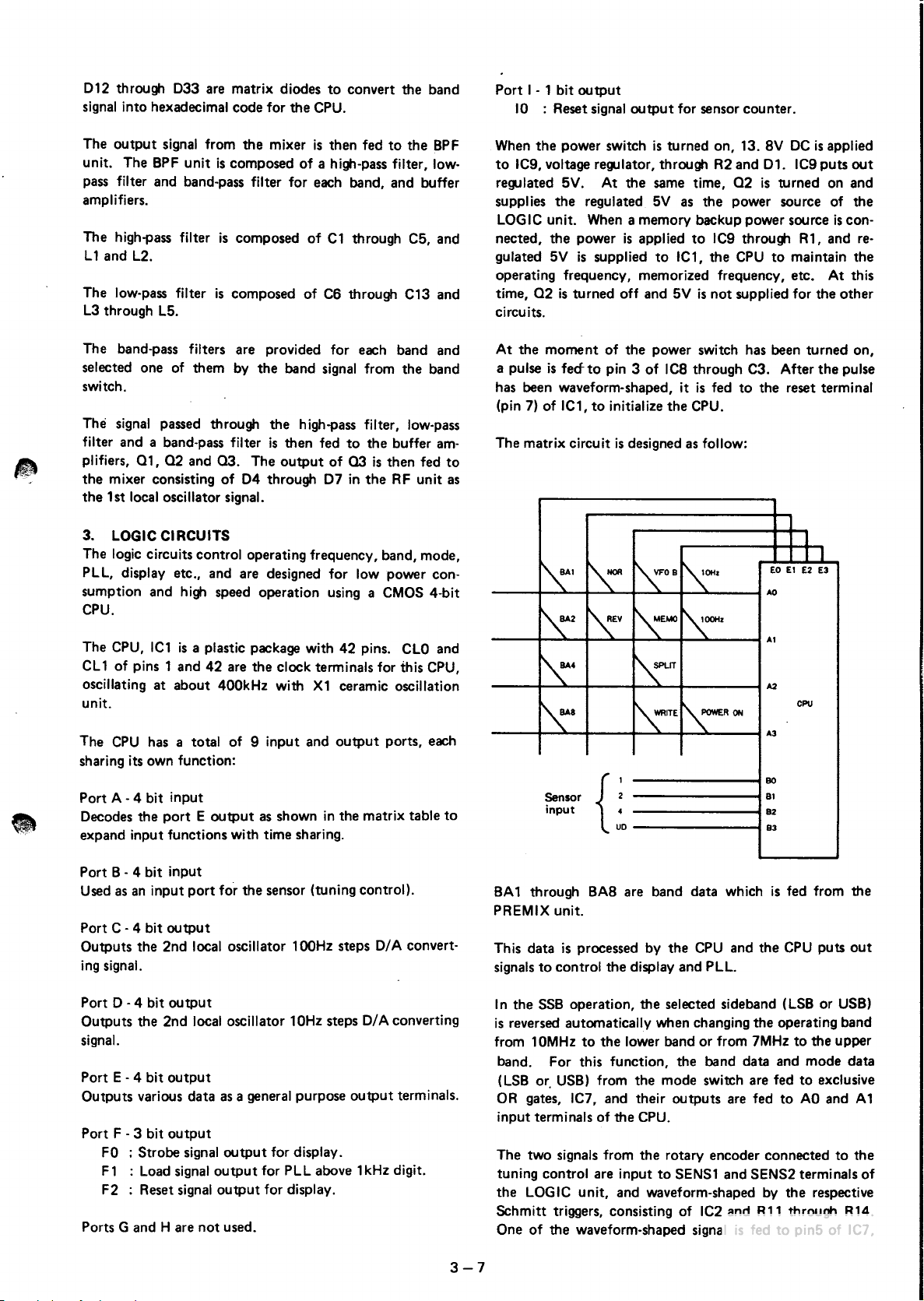
012
for
free
by
RadioAmateur.eu
through
signal into hexadecimal
The
output
unit. The
pass filter and band-pass filter for each band, and buffer
amplifiers.
The high-pass filter
L1
and L2.
The low-pass filter
L3
through L5.
033
are matrix diodes
signal from
BPF
unit
code
the
is
composed
is
composed
is
composed
for
the
mixer
to
convert the band
CPU.
is
then fed
of
a high-pass filter, low-
of
C1
of
C6 through C13 and
to
the
through C5, and
BPF
Port
I - 1 bit
10
When
to
IC9, voltage regulator, through R2 and
regulated 5V.
supplies
LOGIC unit. When a memory backup power source
nected,
gulated 5V
operating frequency, memorized frequency, etc.
time,
circuits.
output
: Reset signal
the
power switch
the
regulated
the
power
is
supplied
02
is
turned
At
output
the
is
applied
off
and 5V
is
same time,
5V
to
for sensor counter.
turned on, 13.
as
the
to
ICg through R1, and
IC1,
the
is
not
av
01.
02
is
power source of
CPU
supplied for
DC
is
ICg
turned on and
to
maintain
the
applied
puts
out
is
con-
At
this
other
the
re-
the
The band-pass filters are provided for each band and
the
selected one of them by
switch.
The signal passed through
filter and a band-pass filter
plifiers,
the
the
3.
The logic circuits control operating frequency, band, mode,
PLL, display etc., and are designed for low power con-
sumption and high speed operation using a CMOS 4-bit
CPU.
The
CL 1
oscillating
unit.
The
sharing its own function:
Port A - 4 bit
Decodes
expand input functions with time sharing.
01,
02
and
03.
mixer consisting
1st local oscillator signal.
LOGIC CIRCUITS
CPU,
IC1
of
pins 1 and
at
about
CPU
has a total
input
the
port E output
of
is
a plastic package with
42
are
400kHz with
of 9 input
band signal from
the
high-pass filter, low-pass
is
then fed
The
output
04
through
the
clock terminals for this CPU,
as shown
to
of
03
07
in
42
X1
ceramic oscillation
and
output
in
the matrix table
the
buffer am-
is
then fed
the
RF unit as
pins.
ports, each
the
CLO
band
to
and
to
At
the
moment
a pulse
has been waveform-shaped, it
(pin 7)
The matrix circuit
is
of
",1
",2
~4
1'\8
Sensor
input
of
the
fecfto
pin 3
IC1,
to
initialize
is
designed as follow:
~NOR
~EV
power switch has been
of
Ica
the
I'\0B
~E~
~sPLIT
~WRITE
~~ON
L
through C3. After
is
fed
to
the
CPU.
I'\OHZ
~z
EO
AO
Al
A2
1.3
eo
Bl
B2
B3
turned
reset terminal
the
on,
pulse
I
I I
El
E2 E3
CPU
Port B -4
Used as an input
Port C -4 bit
Outputs
ing signal.
Port 0 - 4 bit
Outputs
signal.
Port E - 4
Outputs
Port F - 3 bit
FO
; Strobe signal
F 1 : Load signal
F2 : Reset signal
Ports G and H are
bit
input
output
the
2nd
output
the
2nd
bit
output
various
output
port
for
the
sensor (tuning control).
local oscillator 100Hz steps
local oscillator 10Hz steps O/A converting
data
as a general purpose
output
for display.
output
not
for PLL above 1 kHz digit.
output
for display.
used.
0/
output
A convert-
terminals.
BA
1 through BAa are band data which
PREMIX unit.
This data
signals
In
the
is
reversed automatically when changing
from 10MHz
band. For this function, the band data and
(LSB or. USB) from
OR gates, IC7, and their
input terminals
The two signals from
tuning control are input
the
Schmitt triggers, consisting
One
3-7
is
to
control
SSB
operation,
LOGIC unit, and waveform-shaped by
of
the
processed by
the
to
the
of
the
waveform-shaped signal
the
CPU
display and PLL.
the
selected sideband (LSB
lower band
the
CPU.
the
or
from 7MHz
mode
switch are fed
outputs
rotary encoder connected
to
SENS1 and SENS2 terminals
of
IC2 and
and
the
the
are fed
R11
is
fed
is
fed from the
CPU
puts
out
or
USB)
operating band
to
the
upper
mode
data
to
exclusive
to
AO
and A 1
to
the
respective
through R14.
to
pin5 of IC7.
the
of
inverter, then Pin6
for
free
by
RadioAmateur.eu
waveform-shaped signal
differentiated by C12 and
inverter. The
ferentiated by
1C3.
To the other gates
applied and controlled the differentiated signals. The
output
input
This
it holds the
signal
terminal
the operating frequency. When
turned counterclockwise,
the
Two differentiated signals
5 and 6
from pin4. The rotary encoder
revolution, while pin4 of
and trailing edge, resulting in an
revolution. This
consisting of
signals from pins 4 and
NOR
UP
signal
is
present. This
of
.L-Ievel.
of
of
1C3
as a switching signal. The other
is
output
Rl0,
output
Cll
gate
output
the CPU, and the
IC2,
1C4
signal from pin3
and R9, then fed
of
of
IC3
and combined
is
fed
to
CP
terminal of IC5, flip-flop, and
terminal, pin 13,
H-Ievel
the
at
OR
gate, and combined signal
IC2
output
and a half of IC5.
signal
from pin3
then fed
1C3,
the
11
signal
CPU
the
B3
terminal
C12 and
outputs
outputs
output
is
fed
of
IC2 and
to
pinl
of
IC3
is
also dif-
to
pins 5 and 12
switching signal
of
1C3
are fed
as
the
UP
H-Ievel
processes
to
when the
is
then fed
to
increase
tuning control
is
maintained
Cll
are fed
is
50
pulses per
both leading edge
of 100 pulses per
a counter
of
of
IC3,
of
is
to
2-
signal.
UP
to
B3
is
in
to
pins
~utPut
3-bit,
local oscillator
quency resolution.
3 - 4 DISPLAY
This unit
and
DC-DC
voltage source.
The frequency data
and timing control pulse
segment data
control signal
are fed
lighting.
The
R3,
generates a negative voltage and filament voltage for the
display tube, and
ampl ifiers.
to
DC-DC
Cl
in
the
2nd
IF
unit
to
get 10Hz step fre-
UNIT
is
composed of
converter for the display tube and negative
is
put
put
out
the
display
converter
through
C4,
-5V
DS1
display tube, ICl driver
is
fed
to
pins 2 through 5, input
is
fed
to
pin 15. After processing,
out
from pins 16
from pins 6 through 11. These signals
tube
and light
is
composed of
01
through
for the
throug,
the
01,
04,
AGC
circuit and operational
22 with digit
tube with dynamic
L1,
etc. This converter
Rl
IC
port
S,
through
•
This counter
pulses, and serves as a timing buffer between the encoder
and the display
is
any
output
gate, consisting
to
inverter, IC8, then input
with its
terminal which
stopping other operations.
data and up-down data fed
are read by the CPU, performing
related
Immediately after the sensor data have been read, a reset
pulse
is
entiated by C5 and R46, then fed
the counter and up-down latch
The up-down control circuit consisting of
through R21,
control from
When the
vibrator,
and the 3-bit counter counts
pulses from
is
capable of counting a maximum
in
relation
at
the counter,
of
05
level
inverted
gives
to
sensor processing.
put
out
from
C17
the
up-down switches on
UP
or
DOWN
03,
oscillates and pulses are fed
the
rotary encoder.
to
throug,
to
L-Ievel.
priority
IlJ
terminal, and the pulse
throug,
button
of
reading by
the
07,
to
the
This terminal
to
In
the priority routine, counter
to
BO
in
to
clear them.
C21, etc., provides frequency
the
the
CPU.
If
there
output
INT terminal
of
the diode
becomes H-Ievel, input
of
the
CPU
is
a priority
sensor processing by
throug,
this way
to
is
depressed,
pulses the same as
B3
terminals
all
operations
is
differ-
clear terminals
03,
04,
the
microphone.
the
multi-
to
pin6
of
OR
R16
IC4,
of
the
7
After processing, the
PLL from the
it
is
output
also
output
sharing. This data
F2 terminals
terminal outputs clock pulse for
and lower digits are
to
DIA converter consisting
into a analog signal. This analog signal
CPU
outputs
port
E.
This data
in
sequence according
frequency data for the display with time
is
4-bit parallel and 8-digit data.
output
clock pulses for the display and
output
from
of
frequency data for the
is
a 4-bit parallel data and
to
its digits. The
the
PLl.
Data for 1kHz
the
ports C and
R35 through R43
is
fed
0,
to
to
the
port
FO
and fed
convert
E
and
Fl
2nd
3-8

TOP VIEW
for
free
by
RadioAmateur.eu
RJ
OF Shih wI
REGUNIT--------------
DISPLAY
J3 (For Optional AF
RISO (T
lJ (XI
L4
(Xl
ransmit
CWA
LSB
dth
"".1
.--
__
..,-JI----
~-i=--
151 (Transmit
A149
--
Internel
(Transmit l
(AlC
""",h
Speaker
SOW
Adjust!
OW
Adj u
Meter Adjust)
Option,. Marker
.t)
COflnK lor
m
'"
~
o
z
..
z
2!
o
m
<
m
~
..
,
L2 (X l AM·CWT Freq
R45
R44
R93
(LOA
'
C21D!.~M~
Al6S
OET UNI
BAND Switch
'
Ci·j
(AM 4CI'N
.01'.'·---
P
~C1'~~~~~~
""-'-.~--.J-
~~~~
~
--
4 -
FI2
19.0115MHz Crystal
1---4f
1ii~
~:=i~~19
~
e:;;====t=
f-
l1
A66
Ie,
==============~lPF
Adjust)
I M
~~~~~~~M~A~
(455KHz
1455KHz
.
4665MHZ
L
11
(X,
Transmit
(AF
~owef
It Seele
(S
-Meler
AM
Ceramic Filler)
Fillir
SSB
M&ehanical F
I F
IX'
Frequency
Frequency
Amp. IlPC2002V)
erker!
I
N
UN
Adjun)
Zero
Adjuu)
9Ml0A.1
Shih
C'
Y$l81)
Adjust)
UNIT
PA UN IT
IT
iller)
Adj.!

BOTTOM VIEW
for
free
by
RadioAmateur.eu
MIC
SENSOR
8PF
LIS · LI9
L 16 ·
LI4-LI5IB.P
L20
L12 ·
LIO '
LB' L9
L6 · L7
PREMIX
80AA'0-----
UNIT
----
IB
.P. Filt ...
Ll7
{B
.P. Filter lor
'
L211B'Od[lM~'~!'~~~~
LI3IB
.P_
L11 (S.P.
[B
.P.
Filter
IB
.P. Filler
UNIIT·------+---i
----
I-
-
for
..
lor
~
~~
.........
_______
~
==~~'f~:
l
-I--
------L.8
----X2
-t---
(X
· L4 (123MHz
.
L2
(41MHz
(High SpIt.d Divider HD105511
--C31
'''T
BOARD
(PLL
IC TC912S91 XI
(9.c)OOMHz
I F.equfIf!cy
Cryl1.11
(VCO Coli)
B.od-P,u
B.nd-P."
jI3.666MHzCryll.1I
(SWR
Null
Adjust)
UN
IT
Filler)
Flit
••
Adjust)
)
J2
(For Op tional
RLl
(PREAMP
01
·02 (2SK
RF
UNIT
TRV
U,"'---------
Swild",
I2
S',
-,
A"":==~:::::~~
P",~,p"Ii,,'------------~
-
----,
,-
-------------
L------
L
_______
JI
(Fo'
Option.1 Marke. Uo,t!
FII139
--OC"'thli
t
••
n$ffi;l mUli
18
.od
'
04-Cl1
(Double
FI2 (39.73 ISMHz
.7315MHI
C'Y.III
w"e
10 clea.
ng
IOMHz.
BaI.nced
Cryll&1
Filter)
on 24.
Milled
F,'
"r)
4 - 2

DISPLAY
for
free
by
RadioAmateur.eu
UNIT
LPF
LPF
U.'T---------------_
Lll . L12
L13 ,
51
L 15
C31
L2 · L3 j3,
LI4j24
(BAND
jSWA
15WR
(1S
D.teetiOf\
Null
5MHz
UNIT
.....
21MHz
....
28MHz
AdU-----
LPFI------
and
LPFI
---
LPFI---
eo",----
ACC BOARD
iii
______
_ =
I---L."i'_~"
r
-------------"L'
Ibtll'n"
i-----'"""M'
_~=~=============~~
1
L8 110MHz LPF!
·
:
LlO 114MHz LPF)
LS, L617MH
DI$pI-V
IT/A
T/R
DC
FUM j5A)
Tubi
A.I.v!
BOAAD
A.I
.... I
z LPFI
A
12
104 ·
al(>SCl
Q">SC
a31~"~'51-----------~
'
PA
UNIT
r------------
,
05
Idl
lllII
Current
A"'.I---,,--',--
~::=======~-tl
. ,- ,
, "
f'
III
~
"
.'
,
..
~.
,1
,
•
--,
..
. ,
..
,.
I~
f'
' •
..
,
..
4-3
_____________
--,:
=======:~;;;~::;,;j7S
r
I~
I
) .
0-
I
'!1.
-
L--
L---------~
•
----lt-------a.I2SC2097)
•
•
. "
""-
~,
.......
,~
-"
,
....
0712SC2120
,------
;
---L
CooUIlII Fan Controll
0412SC2097)
0
C
Therlmll Switch!
04
·
05
B'"
ANTENNA
7IN'9IIti
CONNECTOA
{SUrll'
05
I1SC0111
ve
Feed bKk
eorllroll
absOrber)
SOCKET
CollI

LOGIC UNIT
for
free
by
RadioAmateur.eu
Ie .. (TC4013C
ICS
h,P04013C
P2
10
PLL
leB
(,.,P04069C
I
C2
(JlP0407,C Clock Pullll G,'".,,'.r---
CO,"",I--------
Cour",r'
Jl---------,:-
RtMl
Up/Down
CO'''oll----I--
CO"''''''
2nd IF UNIT
---\----I'e9"""'''(15
jr--
.
----Ilc.
!IIPD4066C
~------.PlloPREM
VOII.
S.,d
0".
u"PD650-80 CPU)
Al9ulalorl
Input Cormon
I
X
J4
-1""'
e7
L
___
'L
______
u,.PD403OC Mode
l
I
CJ
b,P04011
O.t.
CUp/Down
Control)
COfllroll
~LO'O"R[I-----
l
llX
I Frwqueney Adlj.
OI-Q410oubll
XI
(30.
12MH.lCrvltltll----
O~"!,~~'~;:~~~-----
(No
ill! I
QI
(35K7.
0213SK74 ....
leI
ITA
7124P
allanaJ<! M
Glt.oioes)
NO;M ,"",
oiMA.np.i-------
No",
----
-------------,
'.
___________
I'''·'
___
_
__
_
.,--
___
_
"..".I----------{
~
__
--.J
L
_____
~lMl0'''
~-'t1=,-Fo"D.
~L~
.
Ol'
".HI,,'M
,
;a'''1
For Optiooal
IC2iM51201l
C"
...
sse Fill"
CW FII",
N8
G.It
Filler)
FL-30
Fl~5
Control)
4 - 4

SECTION 5 BLOCK OIAGRAM
for
free
by
RadioAmateur.eu
-
---------.
i
•
I
i
\
,
!
I
Ir-
--,
"I '
I i
II
I:
J 1
1!
I
II
'
1"
__
.J
I
~----
-
,.--------r--·---
r-----H--
i
,
la'i
!'I~
i
I
--
------
I !
-
--~---
,----.......------
~~.
__
L
____
_ L
___
--,
,
!
Q
99
!ll
,
I , i
! •
L ___
____
I I
: I I I
I I t I
I
' I
I I
I
i I
~~:l.L
I I
! ,
,
I !
I !
I
d!
ill
"
:~------i-
I
I
I
I
----
-----------
i
•
I
I ! ;
I I
,,,
II
!
I I
,
! i
I ,
! I •
. I •
,---1
I !
! ,
'
,-----'
I
,
,
.
8':
• •
..
l"~=~L
' I
'I'o,::!
...
I ,
~
,
.,
Ii
:
~ a ~
-'t--::-;_-,
~
I t e ,
•. I
•
•
i
1
-:
I
,
t
I I
I I
, I
:!:
" I
I!
, I
, I
t-.-
_______
r---
I
I
.J
, , I
-
-~
,
•••
-,
,
-,
'
0,
I
. ,
II"
!
'I
i
§
I
5-1
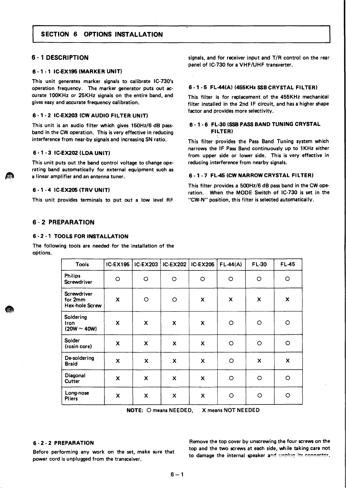
SECTION 6 OPTIONS INSTALLATION
for
free
by
RadioAmateur.eu
6 - 1 DESCRIPTION
6 - 1 • 1 IC·EX195
This
unit
generates
operation frequency. The marker generator puts
curate 100KHz or 25KHz
gives
easy
and
6·1·2
This
band in the
interference from
6
This
rating band automatically
a linear amplifier and
6
This
• 1
• 1
IC·EX203
unit
is
CW
·3
IC·EX202
unit
puts
·4
IC·EX205
unit
provides terminals
(MARKER
marker
accurate frequency calibration.
(CW
an
audio
filter
operation. This
near·by
(LOA
out
the band control voltage
an
(TRV
UNIT)
signals
signals
on the entire band,
AUDIO
antenna tuner.
FILTER
which
gives
is
very effective in reducing
signals
and increasing
UNIT)
for
external equipment
UNIT)
to
put
to
out a low
calibrate IC·730's
UNIT)
150Hz/6 dB
SN
to
change
6 • 2 PREPARATION
out
ratio.
such
level
ac-
and
pass-
ope·
as
RF
signals,
panel
6·1·5
This
filter
factor
6·1
This
narrows the
from upper
reducing interference from nearby
6·1·7
This
ration.
"CW·N"
and
for
receiver input and
of
IC-730
for a VHF/UHF
FL-44(A) (455KHz ssa CRYSTAL
filter
is
for
replacement
installed in the 2nd IF circuit,
and
provides more selectivity.
·6
FL·30
(SSB
PASS
FILTER)
filter
provides the
I F
Pass
Band
side
or
lower
FL-45
(CW
NARROW CRYSTAL
filter
provides a 500Hz/6 dB
When
the MODE Switch
position, this
filter
of
BAND
Pass
Band
continuously up
side.
is
selected automatically.
T/R
control on the rear
transverter.
FILTER)
the 455KHz mechanical
and
has
a higher
TUNING CRYSTAL
Tuning system which
to
This
is
very effective in
signals.
FILTER)
pass
band in the
of
IC-730
shape
1 KHz either
CW
is
set
in the
ope-
•
6·2·1
The following tools
options.
TOOLS FOR
Tools
Philips
Screwdriver
Screwdriver
for
2mm
Hex-hole Screw
Soldering
Iron X X
(20W-40W)
Solder
(rosin core)
De-soldering
Braid
Diagonal
Cutter
Long-nose
Pliers
INSTALLATION
are
needed
for
IC-EX195
0 0 0
the installation
IC-EX203 IC-EX202
X
X X X
X X X
X
X X X
of
the
0
X
0
X
X
IC-EX205
FL-44(A)
0 0
X
X
X 0 0
X 0
X
X 0 0
X X
0
0
FL-30
0
0
X
0
FL-45
0
X
0
0
X
0
0
6 -2 - 2
Before performing any
power cord
PREPARATION
is
unplugged
work
on the
from
the transceiver.
NOTE: 0
set,
make
means
NEEDED, X
sure
that
6-1
Remove
top
and the
to
damage
means
the
top
two
the internal
NOT NEEDED
cover
by
unscrewing the
screws
at
each
speaker
four
screws
on the
side, while taking
and unplug its connector.
care
not

-.-
for
free
by
RadioAmateur.eu
6 · 3 ASSEMBLY PROCEDURE
6·3
· 1
INSTALLATION
1. PARTS LOCATION
OF
THE IC·EX195
When
installing IC-EX202 and/or IC·EX205. also remol/e
the bonom cover by unscrewing the four screws
bottom.
j
KER UNIT)
~~~~~~~------------~~====~
""~
1"
11
OOKH'~!]
~r.rn~~
on
the
;
"h(S21
25K
Hz)
2. A
SSE
MBLY
(1) Insta
ll
this
unit
the attached screws.
Merk,r
Frequency Adjult
PI
(To
PROCEDURE
in
the position shown
Switch
J15
of
(S
1)
T';m""'·-~~---
MAIN
""
It
;
---..J
In
the
photo
using
~;;;;;:=-
·~"'''II:
-.
-
'----------"
(2)
Plug
Pl of this
unit
to
J15
of
-
the
Marker
MAIN
C"''''II''.
(To
J1 A F unill
unit
.
:'Me,,,
6-2
(3)Plug
P2
of
this
unit
to
lR'
Jl
of the
RF unit.

3. CH
for
free
by
RadioAmateur.eu
ECKING
(1)
While
of the unit
quency switch
(2)
Connect the plug of the internal speaker on the top
cover
THE OPERATION
performing the installation, set the marker switch
to
the
"OFF"
in
the "100KHz" position_
to
the original connector, or an external speaker
position and the marker fre-
the external speaker jack on the rear panel.
(3)
Make
sure
the
power switch
OFF. Set the other controls and switches
mode according
the power plug
(4)
Turn the power switch of the IC-730
operates
(5)
Set the marker switch of this unit to the
in
to
to
the
the
receive mode.
the manual
power socket
and the marker frequency switch
of
your
1C-730
in
the receive
of
IC·730. Then connect
of
the IC-730.
ON,
and the set
"ON"
in
the " 100KHz"
is
position. Then turn the tuning control knob, and you
can receive a strong signal on
(6)
Set the marker frequency switch
every 100KHz.
in
the "25KHz"
sition, and you can also receive a strong signal on every
25KHz. These are the complete operations
of
to
turned
position
po
the unit.
6 -3 -2 INSTALLA
(CW AUDIO FILTE R UNI
1. PARTS L
AY
OUT
P1
IToJ30fOETuniti
2. INSTALLATION PROCEDURE
(1)
Loosen
two
retaining screws
and turn the sub-chassis around hinges on the other end
.
as
shown
in
the photo.
TIO
N OF T
HE IC-E
X203
T)
of
the upper sub-chassis,
(7)
When
the operatfons are performed, unplug the power
cord again and replace
4.
CALIBRATION OF THE MAR
(1)
Set the
MODE
Switch
the speaker connector and covers.
KER
in
the "AM" position and
Switch in the "lOMHz" position, then turn
POWER
(2)The FREQUENCY DISPLAY
Turn the TUNING CONTROL knob
Switch.
will
show " 10.100.0".
to
tune to
(or other standard frequency station) on 10.000MHz.
Set
the TUNING
RATE
Switch
in
10Hz steps for fine
tuning.
(3) Turn
(4)
ON
the marker switch
on
the unit and adjust the
FREQUENCY ADJUST trimmer on the unit
"zero beat" with
When
you have performed the calibration, turn OFF
WWV
.
to
the marker switch.
CALIBRATION OF THE TRANSCEIVER
5.
BANO
ON
WWV
make
the
(2)
Loosen the front side screw of the shaft coupling sleeve
of
the band switch and remove the shaft sliding toward
front side.
Install this unit
using
SQ'SWS
to
the position shown
that have been attached.
in
the photo ,
i1)
Set the
TUNING
the lower band edge
as
(2) Ground the
sidetone becomes audible. (Don't transmit.)
(3) Turn
QUENCY SET
are of the same pitch
(4)
The frequency calibration
on the same band,
MODE
RATE
an
example, "21 .000.0
Key
ON
the marker switch, and adjust the FRE-
control
SWitch
SWitch
in
the
CW
position and the
in 100Hz position. Tune
of
the band you want
to
calibrate,
".
jack on the rear panel so that the
of
(In
but
the set, so
zero bead.
is
suHicient on a frequency
it
is
required for each band.
that
the
two
to
CW
tones
6-3

(31
for
free
by
RadioAmateur.eu
Rep
lace the shaft and the upper sub-chassi
Pll ins
erted to J3 of the
IC
·EX203 .
(4)
Plug
Pl of IC-EX203
retaining
(5lThis unit does not require an adjustment, and provides
150Hz/6dB pass band when the set
screWl
of the sub-chassls.
to
J3 of the
OET
unit and plug it
OET
is
s.
Unplug
to
J1
unit. Tighten the
in
the
CW
mode.
of
6 -3 - 3 INSTALLATION OF
1. PARTS
LAYOUT
P3 ITo
J5
of
P2lTO
J6
of
PR
ii
MIX
".:!:!.:====
THE
IC-EX202 (LOA UNIT)
__
L-
~~_.::===::
=::
====r-
J2
-'i---
','o
"11To
PREMIX
i,n
p2
of
LPF
-O'odll
Au.
J3
unit!
unit)
of
ln
2. INSTALLATION PROCEDURE
(1) Loosen the
and turn the sub-chassis around hinges on the other end
as
Install th
(2)
the screws that
(3) Unplug
located the bottom side.
shown
Pl
two
retaining screws of the upper sub-chassis,
in
the photo,
is
unit to the position shown
have been attached.
.nd
P2 from J3 and
in
J6
of
the PREMIX unit
the photo using
6-4

(4) Loosen the screws of the
for
free
by
RadioAmateur.eu
band switch, and remove the
front
side, then the sleeve and the spring pressing wafer
of the band switch.
(5)
Rem
ove the wafer of the band switch from Its shaft,
taking care not
to
damage the wafer.
~aft
coupling sleeve of the
shaft, sliding it towards the
(8)
Run the cords with
the slot under the band switch. Plug
attached to longer wires) to
J6 of the
are the
Replace the
PREM
same order.
PlL
Pl
IX unit,
unit
by
and
P2
of the
J3 and
so
that the colors of the wires
the reverse procedure of (6).
LOA
unit through
Pl
P2
(S-pin plug)
(6opln
plug
to
(6) Remove the cover of the PLL
nectors inserted
screws retaining the unit, and remove the unit from the
chassis.
171
Remove the wafer and its wiring harness through the slot
under the band switch toward upper side.
to
the unit. Then unscrew the four
unit, and unplug con·
(9)Replace the wafer, spring,
by
the reverse procedure of (4) and (5) ,
(10)
Plug
Pl
(6opln
plug attached to longer wires) of the
switch wafer
to J2,
(11)
Remoye the eight screws at each end of the rear panel.
to
Jl
of the
&haft
and shaft coupling sleeve
LOA
unit and P2160pin plug)
,
6
-5

(12) Turn over the rear panel right side, and unplug coaxial
for
free
by
RadioAmateur.eu
cables from
J1
and J3 on the
LPF
board.
-(13) Run the cord with
through the slot at the right corner of
Then plug
P3
to
J5
of
P3
th e
14·pin plug)
ACe
unit.
of
the
the rear box.
LOA
unit
(14) Replace unplugged connectors and the rear panel by the
reverse procedure of
This unit has no requirement for
Ill)
and (12).
adjustment for ope ·
ration.
CHECKING THE OPERATION
3.
Connect a multimeter across
the accessory socket on the rear
Make
sure the voltage shown
Pin
13
panel.
in
the chart
(+) and
is
Pin B (-I
put
out
across
the pins on each band.
Band
Control Voltage Chart
BA
ND
(MHz)
3
.5
7
I.
18 -21
2'·28
10
Band Control Voltage
6.0-6.5V
5.0 - 5.5V
4.0 - 4.5V
3.0
.....
3.5V
2.0 -
2.5V
0
.....
1.2V
of
6 · 3 · 4 INSTALLATION OF IC·EX205ITRV
1. PARTS
LAYOUT
J2
Unsert
Pl
(To
J3
(ln
se"
PJ6
J2
01
P5 01 PA
01 ACC
AF
,";,,--1
,,'11-------,/
";;"'
-1-
- 1
UNIT)
L--t
'_
--
-+
--
-
~"
--
-J'-
'f----
-t--
+---TI
'PJIToJ8
P2 ITo
"
t1n
J9
!t!
~t
PJ
A Switch
01
ACC
01
ACC
of LPF
ing
un'tl
unIt!
un
ll)
A'lev
6-6

2. INSTALLATION PROCEDURE
for
free
by
RadioAmateur.eu
(1) Remove the eight screws
(2)
Turn over the rear panel right side
at
each end
chassis, and unplug coaxial cables from
LPF
unit.
(3)
Install this unit to the position shown
the screws
that
have been attached.
of
the rear panel.
or
put
it on the
J1
and J3 on the
in
the photo using
6·3·5
1. INSTALLATION PROCEDURE
(1) Unscrew the screws retaining the
INSTALLATION
OF
THE
OET unit board, then turn them over
the boards can be seen.
Fl-44
MA
(A)
IN
unit board and
so
that
foil
side
of
(4) Connect
unplug P36 (2-pin plug) inserted J2 on the
and plug
Unplug
the
plug
ACC
Unplug
unit) from
TRV unit. Then plug Pl (4-pin plug) of the TRV unit
to
(5)
Replace unpluged connectors and the reaf panel
reverse procedure
OPERATION
3.
This unit has no requirement for adjustment for the ope·
ration.
When
11
of the ACCESSORY socket, the ALC terminal
rear panel can be used for a VHF/UHF tranwerter INPUT/
OUTPUT terminal.
The transverter's
should be
Transverter INPUT/OUTPUT Frequency
Input/O
Transmit (Output):
Receive (Input):
P2
(with green wire)
it
to
J2
In
the TRV unit.
P5
(orange wire from the
ACC
unit and plug
P3
(with orange wire) of the TRV unit to
it
to
J9
PA
to
J3
on the TRV unit, and
unit.
P3
(2-pin plug with coaxial cable from the LPF
J2
on
the RF unit, and plug it
J2
on the
RF
unit.
of
(1) and (2).
the transverter control signal (+8V)
as
follows:
input/output
frequency and signal
28-30MHz
utput
signal level
Max
150mV across a
l~V
for SIN
lOde
on the
ACC
ACC
unit) from
to
is
applied to P
50
ohm load
J8
J1
unit,
unit,
J8
on the
on the
by
the
on
the
level
(2) Remove the solder of the mechanical filter's terminal
pins and
legs
on
the foil of the
MAIN
soldering braid, then take off the mechanical filter.
on
When
the mechanical filter
is
"MF455·11AZ",
remove C75 - C78 around the filter. (In the case
"M
F-455·11GZ",
(3)
Insert the FL44
nical filter was installaed and retain
C75""
C78 are
(A)
to the position where the mecha·
not
used.)
it
by
nuts then solder its terminal pins.
in
(4) Replace the
to
the chassis
(5)
No
adjustment
MAIN
unit board and the DET unit board
by
the reverse procedure
is
required for operation.
of
6-7
unit, by a de·
also
of
two supplied
(1) .

6 - 3 -6 INSTALLATION OF THE FL-30
for
free
by
RadioAmateur.eu
1. INSTALLATION PROCEDURE
(1) Loosen two retaining screws of the upper sub-chassis,
and turn the sub-chassis over around hinges on the other
end
as
shown
in
the photo.
alhn
8
Lnll
oolitLon
(4)
Replace the 2nd
on the unit, then
(5) Replace the sub-chassis
No
adjustment is required, and the filter provides the
Pa
ss-Band Tuning system.
6 - 3
-7
INSTALLATION OF THE FL-45
1. INSTALLATION PROCEDURE
(1) Install the filter by the same procedure
IF
unit, and unplug P3 inserted to J7
plug
it
to
J8.
by
the reverse procedure of
of
the FL-30.
(1).
(2) Unscrew the screws retaining the 2nd I F unit board,
then
turn it over so that
seen.
foil
side of the board can
be
-
(3)
The location for the filter
holes for mounting the
a
re
predrilled.
is
shown
in
the photo . The
legs
and the leads of the filter
(2) The location for the filter
of
6-3·6.
(3) After replacing the 2nd
serted to J5, then plug
(4)
No
adjustment
5OOHz/6
dB pass·band.
it
to J6 on the
is
required, and the filter provides
is
shown
IF
unit board, unplug P2 in-
on
the photo
2nd
I F unit board.
Be
(indicated on the bottom) of the filter
direction
Insert the filter flush with the board, bend the leads and
legs
them
Trim the leads even with the solder
pletes the Instellation.
sure
to
orient the filter
as
sho
wn
on the photo.
flush with the opposite side of the board and solder
In.
$0
that the in
put
is
facing the same
poinu
. This com-
terminal
6-8
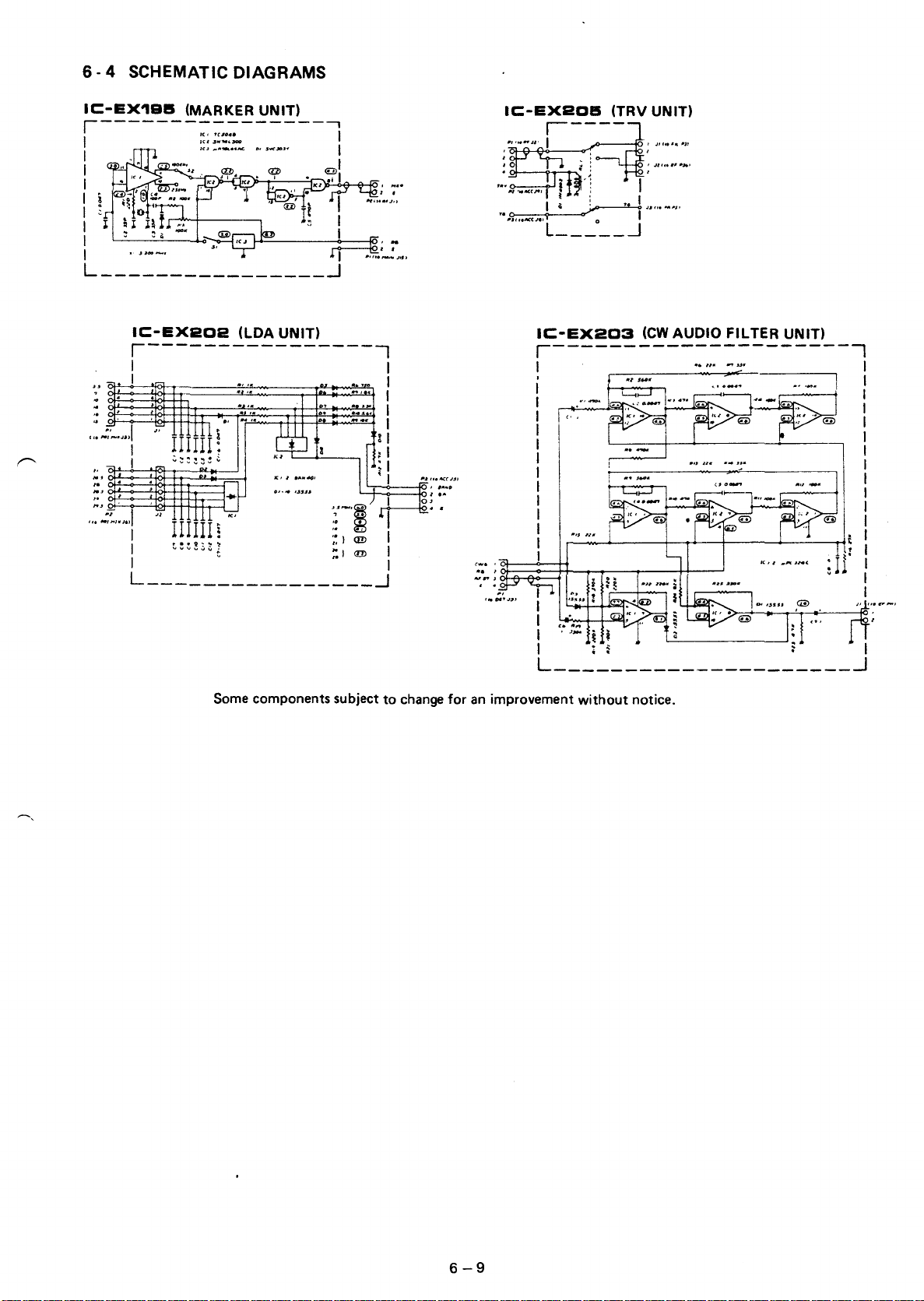
6 - 4 SCHEMATIC DIAGRAMS
for
free
by
RadioAmateur.eu
U:-EX1BI5
,----------------.
I
I
I
I
(MARKER
~ ~ ;!:~!oo
Ie,
........
,IIIG
UNIT)
to·
SYC.JO'"
K'
€])I
.1
I
I
I
I
I I
L
________________
IC-EX2D2
(LOA
UNIT)
~
,----------------,
I I
I I
lIIIIl
!
~~~!oz
£ I
I I
L
________________
IC-EX2DI5
I
I
I
,----
I ;
IC-EX2D3
(TRV
UNIT)
JII
..
(ew
""."
AUDIO
FILTER
UNIT)
,---------------------,
I
-
..
I
I
I
~
I
I
I
I
I ; I
L
_____________________
-.
•
••
". -
".....
;1..1
•
u,
€i)
~
_
I
I I
.•
•
::CI
.•
I
I
6)
I
I
I
I
I
I
I
I
I
I
I
I
I
~
Some components subject
to
change for an improvement without notice.
6-9
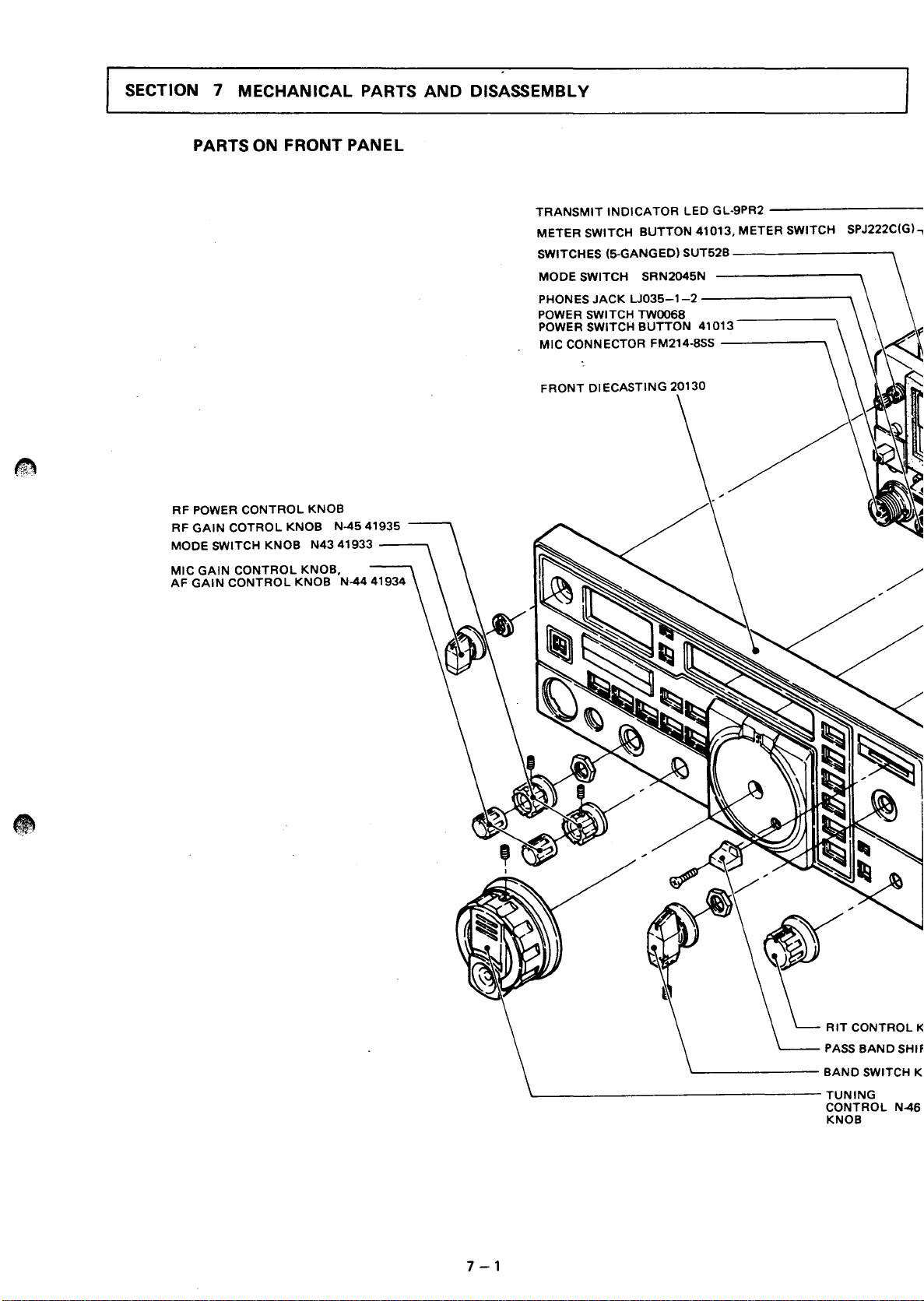
SECTION 7 MECHANICAL PARTS AND DISASSEMBLY
for
free
by
RadioAmateur.eu
PARTS ON FRONT PANEL
RF POWER
RF
GAIN
MODE SWITCH
MIC
AF
GAIN
GAIN
CONTROL
COTROL
CONTROL
CONTROL
KNOB
KNOB
KNOB
N4341933
KNOB,
KNOB
N-4541935
--,
N-4441934
TRANSMIT
METER
SWITCHES 15-GANGEDl SUT52B
MODE
PHONES
POWER SWITCH
POWER SWITCH
MIC
FRONT
INDICATOR
SWITCH
SWITCH SRN2045N
JACK
LJ035-1-2
CONNECTOR FM214-8SS
DlECASTING
BUTTON
TWOO68
BUTTON
20130
LED
41013,
----------"\
41013
GL-9PR2
METER
--------,
-----,
-------SWITCH SPJ222CIGl
l
RIT
CONTROL
BAND
PASS
L-
_______________
7
-1
~------
BAND
SWITCH K
TUNING
CONTROL
KNOB
K
SHIF
N-46

'-------------
for
free
by
RadioAmateur.eu
\.....-------------
'---------
'----------
'--------
BAND
SWITCH SRY202C
.JOINT
41882
'--------
PASS
BAND
SHIFT
CONTROL
RITCONTROL
'----
L-
___
'--
___
RIT
INDICATOR
RIT
SWITCH
PUSH
BUTTON
SWITCHES (6-GANGED) SUH61 H .
SHAFT
SENSOR
MEMORY
AF
GAIN/RF
MIC
GAIN/RF
41880
UNIT
NFO
K121B
LED
BUTTON
GREEN
SHAFT
WRITE
GAIN
CONTROLS
POWER
10K
GL-9PR2
41013.
S2011A503
SWITCH SPJ222N(B)
41940
(BROWN
SWITCH SUT111
K1681
CONTROLS
41940)
K16B1
SHAFT
10KB
MEMORY
10KA
x 2
10KB
x 2
BEARING
SWITCH SUT111
41881
CONTROL
S
BAND
10
SWITCH
liNG
ITROL
)B
KNOB
SHIFT
KNOB
N-4641936
N-4741938
CONTROL
N-4241857
KNOB
TUNING
CONTROL
KNOB
LING
N-4841939
41937

•
for
free
by
RadioAmateur.eu
.....
I
N
FRONT
PANEL
DISASSEMBLY
1
METER
I I
SPONGE
(41997)
SU""",,ASSIS _ _ _
(30243)
_
TRANSMIT
_JY1'
INDICATOR
GL-9PR2
__
o 0
1
FLAT
WASHER
I I
VRNUT
IIIMID
I
-
1
VRNUT
c:z::::::::::r:
J
VRNUT
cz::::::IC)
I
---
SUB-CHASSIS
FLAT
(30243)
WASHER
LED
SOCKET
METER
°
BQ044.32582A
LAMP
PHONES
U035-1·2
JACK
MIC
GAIN/RF
K1881
10K
B.2
POWER
AF
GAIN/RF
K1881
10KA
UN)
10KA
(OUT)
GAIN

)
for
free
by
RadioAmateur.eu
--.J
w
FRONT
PANEL OISASSEMBL Y 2
MODE SWITCH
SRN2045N
-
o
POWER SWITCH
TW0068
I
c 0
c 0
----~-mbd-
M3S WASHER SPACER
--~-m{d-
M3S WASHER
H (40033)
SPACER
(40033)
--------------
----0
---------
H
~
M3x5ROUND
cuB
M3x5
ROUND
POWER SWITCH
41013
BUTTON
MIC
BOARD
B486A
.-
MIC
CONNECTOR
FM214-8SS
o
SUB-CHASSIS
(30243)
"S"
WASHER
NUT

.....
for
free
by
RadioAmateur.eu
I
~
FRONT PANEL DISASSEMBLY 3
I
M3x5 ROUND(+)
M3x5 ROUND (+)
M3x5 ROUND(+)
SPACER
(0) (41930)
I
M3x5 ROUND (+)
SUB·CHASSIS
I
[]
(30243)
SW2
PCB
B-485C
M3x5
ROUND (+)
SUT·52B SWITCHES (5·GANGED)
SUT·111 MEMORY SWITCH
SUT·111
MEMORY!VFD
WRITE SWITCH

FRONT PANEL DISASSEMBLY 4
for
free
by
RadioAmateur.eu
VRNUT
a:::::::c
~
I
CJ1
FLAT
WASHER
RITCONTROL
K121B 10KB
0==
RIT
M2.6x4 ROUND
...
PCB
(B483C)
f
(+)
SUB-CHASSIS
(30243)
RIT
SWITCH BUTTON
41013
RITSWITCH
SPJ222N
TYPE
(B)
LED
SOCKET
RIT
INDICATOR
LED
GL-9PR2
ICOM
~
SCREW
(C)
SPACER 'C)
SWITCHES
SUH61H
(6-GANGED)

FRONT PANEL DISASSEMBLY 5
for
free
by
RadioAmateur.eu
......
I
en
SETSCREW
M2x4 ROUND (+)
BRONZE
PLATE
(41961)
SETSCREW
M2x4
ROUND (+)
BRONZE
f
~
f
1
SUB-CHASSIS
(30243)
VR
NUT
!
M3x5 ROUND (+)
f
1
Ji
SHAFT
41881
BEARING
PASS
BAND SHIFT
CONTROL
S2011A503
10K
(B)
- -
REG
UNIT
REG
PCB
UNIT
(41877)
(B482A)
HOLDER

FRONT PANEL DISASSEMBLY 6
for
free
by
RadioAmateur.eu
DISPLA Y
L
UNIT
(B487C)
SENSOR FRAME (20111)
PCB
.....
I
.....
DISPLAY TUBE
HOLDER
(41878)
rr
DISPLAY TUBE
9-BT-12
SUB·CHASSIS
(30243)
SENSOR
UNIT
SUB·CHASSIS
(30243)
M3x5
OVAL
COUNTERSUNK
(+)
M3x5
OVAL
COUNTERSUNK (+)
M3x5
ROUND
(+)
M3x5
ROUND (+)

FI
for
free
by
RadioAmateur.eu
L TER
UNIT
DISASSEMBLY
I
OO
II
II
"
II
CD
II
II
II
II
II
110
II
ACC BOARD
B-481
-£.-
SET
0
SCREW
C3x6
I
I
I
I
I
I
I
I
I
I
I
I
I
I I
OJ
I I
,
LPF
UNIT
PCB
(B-478D)
-lSETSCREW
C3x6
I
I
I
I
I
~
1
I
I
1aJ
1
0
~
r<sl
I
I
I I
I
I
I
I
I
I
~I
I
:
I
I
I
0
,
I
I
I
I
I
I
~~
i
i
JI
~
\.IV
El
I
r-
I
I
I
I
I
I
I
I
I
I
I
I
I
I
B
AND
SWITCH WAFER
CHASSIS
(20113)
BAND
SWITCH
SRY-202C
~SETSCREW
~
C3x6
~SETSCREW
~
C3x6
~
1!J!j
SETSCREW
C3x6

PARTS ON REAR PANEL
for
free
by
RadioAmateur.eu
.....
I
CO
ANTENNA
FM-MD-RM1
GROUND
SQ-2054
POWER
CONNECTOR
TERMINAL
SOKET
(LLR-6)
r-
@)~
@
D:lEI
@
a
.....,
@
@
HEAT
SINK
(41867)
COVER
"@@
@ @
@
~~
\~
@~@
REAR PANEL
(30238)
@
1-...)
[0]
0
-
:::l
1
"
:T
MEMORY BACK
EXT
ALC
AT-700
EXTERNAL
HSJ0779.o1 A
KEY
JACK
LJ102
ACCESSORY SOCKET
(1625-24R)
UP
TERMINALS
SPEAKER JACK

REAR PANEL DISASSEMBLY
for
free
by
RadioAmateur.eu
•
.....
I
...
o
POWER
LLR-6
M3NUT
0--'-
M3 GROUNDING LUG
M3NUT
SET
EfIpm--I-
SOCKET
SCREW
\
M3
-1-1-
(A) 3xS
M3
LOCK WASHER
LOCK WASHER
REAR PANEL
o
o
(3023S1
___
SET
--~
-----
r,:::=:n
~Sa-2054
GROUND
SCREW
ANTENNA
FM-MD-RM1
~
(A) 3x6
SET
TERMINAL
MEMORY BACK
EXT
AT-700
C]Imt=>--
CONNECTOR
SCREW
(A) 3xS
1-1-
ALC
TERMINAL
UP
0-
E>5.t
SPEAKER JACK
HS
J0779-01A
ACCESSORY
SOCKET
1625-24R
---r-
o
o
REAR PANEL
(30238)
GROUNDING LUG
0
KEY JACK
LJ102
SETNUT

PA
for
free
by
RadioAmateur.eu
UNIT
DISASSEMBLY
.....
I
...
...
lLu
M3x8 ROUNO (+) NI·GALVANIZED
i
___
.u.[Q]..;;O:....u.
_________
O;;;.-.
________
M3x8 ROUND (+) NI-GALVANIZED
i
HEATSINK
(20125)
.....
[Q].L..O.:...Ji.L..-
__
--UU
RE~~;~~EL
PACOVER
(30240)

PA
for
free
by
RadioAmateur.eu
UNIT
DISASSEMBL Y
f
(COM SCREW
IBI-6
f
ICOM
SCREW
IBI-6
f
ICOM
SCREW (BI-6
I
n~
________________
((WJ
M2.3x5
SCREW
ROUND
M2.6x5
N
(+1
FLAT
(+1
~
i
M2.3x5
i SCREW
FLAT
~
Ii)
M2.6x5
ROUND
(+1
(+1
I
FAN
PROPELLER
(411711
FAN
MOTOR
(418661
BRACKET
I
~n
HEAT
SINK
(418671
COVER
I
GEARED
JL
MOTOR
HEAT
(201251
SINK

PA
for
free
by
RadioAmateur.eu
UNIT
DISASSEMBLY
SET SCREW(A)
3x1S
SETSCREW
3x1S
SETSCREW
3xS
"
I
SET
SCREW
(A)
3x6
M2.6xS ROUND
h
T
I
~
(+) D
~
m OHD70M
I
INSULATION
err
WASHER
I
2SD
313
~SC
THERMAL
I 41927
SPEACER (D)
40217
O
THERMAL
SWITCH
I
2097
SWITCH HOLDER
t
~I
GR~3UNDINGerrl
I,.UG
I
~ ~
2SC
1945 I I
SET
SCREW
3X6
M2.6xS ROUND
INSULATION
WASHER
2SC
(A)
1971
THERMAL
f
SWITCH HOLDER
41927 I
SPACER
40217
(+)
PCBB479======================
(0)
~
0
61
I
II : : II
THERMAL
SWITCH
OHD70M
2SC
2097
HEATSINK (20125)
HEATSINK (20125)
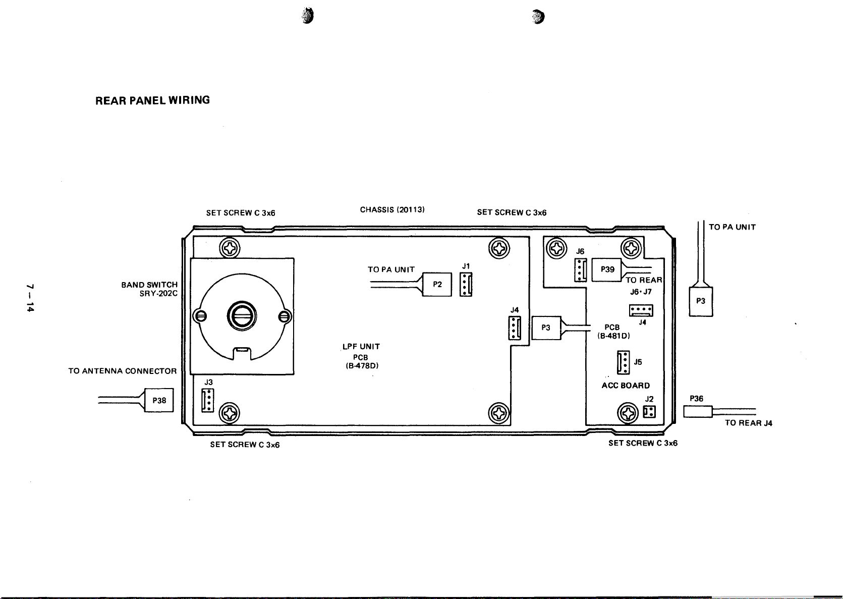
REAR PANEL
for
free
by
RadioAmateur.eu
WIRING
......
I
BAND
TO
ANTENNA
CONNECTOR
-------8
SWITCH
SRY-202C
SET SCREW C
SET SCREW C
3x6
3x6
CHASSIS (20113)
T
OPAUNIT
LPF
UNIT
PCB
(8-4780)
S
SET SCREW C
J1
~
3x6
PCB
(B-481D)
ACCBOARO
SET SCREW C
J4
P3
P36
c=J---.--
3x6
TO PA
TO REAR J4
UNIT

MAIN
for
free
by
RadioAmateur.eu
UNIT
PC
BOARD DISASSEMBLY
......
I
PCB
JB-476C)
ICOM SCREW
(41546) (41546)
(C)
9 ICOM SCREW
o
(C)
9
HALF TAPPED
SPACER (B)
(41592)
CHASSIS CENTER
PLATE
(30239)
ICOM
SCREW
(41546)
SPACER
(C)
9
HALF TAPPED
(41592)
(B)

~
for
free
by
RadioAmateur.eu
I
...
Q)
MAIN UNIT CONNECTOR LOCATION
©
Jt4
TODETUNIT~
ACC
UNIT
P2
~
~
~
Jt5
Jt6
~
r--
Pt
~
Pt8
'---
1
....
P7
IJt3
Jt8
~
:[3
TOACC
~
Jt9
UNIT
-
I
P03
Jt
I::;'
• •
.....-
1····1
Pt7
Jt
HARNESS
-
P2
--
J2t
l::]
7"~
t:!)
J20
Jt2
Pt6 I
J2
~
~
.•..
:.
A
:1
~
Jt7
rn
I~
P04
rn
J7.
rnr
J8
J6
Pt
~P2911
I
~P28Irn
J3
~
J5
Cl
~
J4
Q!J~
__
TO
DETUNIT
TO ACC BOARD
UNIT
to
2nd
IF
UNIT
r---""Ir--
HARNESS TO 2nd
UNIT
P4
IF
HARNESS HARNESS

.....
for
free
by
RadioAmateur.eu
I
....
.....
RF
UNIT CONNECTOR LOCATION
I
~
6
P3
J2
I
~
J3
~
r-
P1
,.,
J5
J1
[;]
©
TO I FIL
TO PA
UNIT
UNIT
ICOM
(41546)
PCB
(B-4740)
SCREW
RF
(C)
UNIT
9
PC
BOARD DISASSEMBLY
ICOM SCREW
(41546)
HALF
(C)
9
TAPPEOSPACER(B)
(41592)
J6
©~
P3
TO
BPF
UNIT
TO 2nd
J4
liD
P3~
IF
UNIT
~
~
P30
HARNESS
...
D
CHASSIS
(20113)

IF UNIT CONNECTOR LOCATION
for
free
by
RadioAmateur.eu
I F
UNIT
PC
BOARD DISASSEMBLY
.....
I
...
co
VCO
CASE
(411141
VCO CASE
(41115)
~
2nd
PCB
(B-493A)
~
LO
----J
~
,....,....
r:::I
P34
P6 I
P24/
I
~
El
J1
rn
J4
J3
~
©
PCB
(B-475C)
2nd LO
ICOM SCREW
(41564)
HALF
VCO CASE (41115)
VCO CASE (41114)
PCB
(B-493A)
(C)
12
TAPPED SPACER(D)
(41592)
CHASSIS
(20113)
ICOM SCREW IC)
(41564)
HALF
TAPPED SPACER(D)
(41592)
12
VCO CASE
TO
RF
UNIT

•
for
free
by
RadioAmateur.eu
•
.....
I
...
CD
TO
FILUNIT
PREMIX
UNIT
TO PLL UNIT
~
CONNECTOR LOCATION
=====:::;,
J8
P2
rn
fJfJ
J7 J8
~
-'
PCB
(8-472C)
PREMIX UNIT DISASSEMBL V
c:;.
SET SCREW (A)
11
3x8
I
1
l
1 1
It
rrn
T
STUD(H)
(40033)
STUD(H)
(40033)
SET
'
I J
TOP COVER
'.MIX
'.MIX
If
BOTTOM COVER
I
fTTI
T
SCREW (A)
3.
'.MIX
SHIELDING CASE
SHIELDING CASE
SHIELDING CASE
(41.)
(41887)
(41.)
TO LOGIC UNIT
P1
HARNESS
J3
J1
L
~~
~
P1
~J5
• • •
~~il
• • •
: ]
B_-----TO-RF
=======.J
~
~
P1
TO BPF UNIT
UNIT
I
r:::F' M3
I SWASHER
M3
SWASHER I
r:::F'
CHASSIS
(20113)
I

BPF
for
free
by
RadioAmateur.eu
P2
UNIT
CONNECTOR LOCATION
BPF
UNIT
~
" 3)(8
DISASSEMBLY
SET SCREW
(A)
~
-S
PLL
SHIELDING CASE TOP COVER
(41186)
SETSCREW
3x6
.....
I
...
~
TO PRE.
P1
TO PRE.
MIX
MIX
UNIT
UNIT
J8
J2
TO RF
P3
UNIT
J6
PCB
(8-47381
I
I
rQl
I
r:::FJ
I
STUD (HI
(40033)
M3
SWASHER
STUD (HI
(40033)
M3
SWASHER
I
I
rfJl
I
s::P
I
PLl.
SHIELDING CASE
(41884)
SHIELDING CASE BOTTOM COVER
CHASSIS
(20113)
(41185)
-----
----------_.---_
..
_._---_._-----------

,.aI.
for
free
by
RadioAmateur.eu
'
'711
"
I
N
...
DET UNIT CONNECTOR LOCATION
@~J2
-
PCB
(B-471C)
DET UNIT DISASSEMBLY
ICOM SCREW
(41546)
(C)
9
ICOM SCREW (CI 9
(41546)
HALF
TAPPED
SPACER (B)
(41592)
~
I...
J3
J1
p~~
-
~-----------------
HARNESS
HARNESS

PLL UNIT
for
free
by
RadioAmateur.eu
CONNECTOR
LOCATION
TO
PRE.
PI
MIX
UNIT
J7
PLL UNIT DISASSEMBLY
'----------
___
PLL
SHIELDING
I
• (418861
CASE TOP COVER
It""
• • •
....
J1
P2
.....
1 rc:==r1
••
I:..!.!.!I
J2
P32
PCB
(B-471CI
SET SCREW(AI
f
:::g~§~~~~~!:j
t
3x6
J1
J2
BQ
SET SCREW(AI
11
3x6
PLL
SHIELDING
PLL
SHIELDING
(418841
CASE
CASE
(418851
BOTTOM
I
It
STUDH
fQ1
I
c:F'M3
5 WASHER
CHASSIS
(201131
(4003;)1
STUD
(400331' y
M3
5 WASHER
H
rrn
I
c:F'
COVER
TO
LOGIC
UNIT
HARNESS
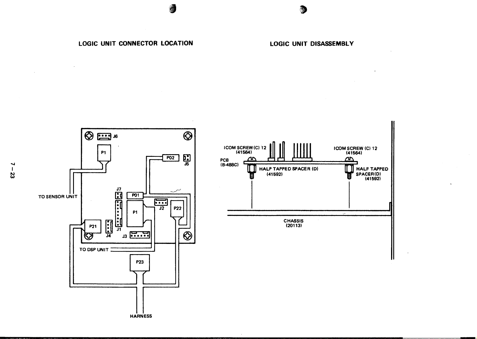
TO
for
free
by
RadioAmateur.eu
SENSOR
LOGIC UNIT CONNECTOR LOCATION
~
1:"·'
J6
r---
P1
~
UNIT
P02 I
[:J
J5
PCB
lB-488C)
LOGIC UNIT DISASSEMBLY
ICOM
SCREW lC)
141564)
12
HALF
TAPPED
SPACERlD)
141592)
TO
OSP
UNIT
===;==~
HARNESS
P23
CHASSIS
(20113)

SECTION 8 MAINTENANCE AND ADJUSTMENT
for
free
by
RadioAmateur.eu
..
8·1
(1) FREQUENCY COUNTER FREQUENCY RANGE
(2)
(3)
(4)
(5)
(~)
(7)
(8)
(9)
MEASURING INSTRUMENTS REQUIRED
ACCURACY
SENSITIVITY 100mV or BETTER
SIGNAL GENERATOR FREQUENCY RANGE
OUTPUT VOLTAGE
MULTIMETER
MILLIVOLTMETER
AC
RF
VOLTMETER
RF
WATTMETER (Terminal Type)
AF OSCILLATOR
OSCI
LLOSCOPE
NOISE GENERATOR
NOTE: indicates
indicates
These
also
an
an
are
adjusting
instrument connecting
used
or
in the board layout and schematic diagrams.
50KilNOL T OR
MEASURING RANGE 10mV - 2V
FREQUENCY RANGE
MEASURING RANGE
MEASURING RANGE 20 - 200 Watts
FREQVENCY RANGE 1.8 - 30MHz
IMPEDANCE
SWR
OUTPUT FREQUENCY
OUTPUT VOLTAGE
FREQUENCY RANGE
MEASURING
(Generates ingnition-like noise containing harmonics beyond
instrument connecting point.
point
FOR
ADJUSTMENT
BETTER
RANGE
and its readings.
0.1
- 90MHz
BETTER
0.1
-20
0.1
0.01 - 10V
THAN
MHz - 40MHz
- 90dB
- 80MHz
50 OHMS
LESS
THAN
200 - 3000Hz
o - 100mV
DC"'"
20MHz
0.01 - 10V
±1
ppm
(OdB = 1J.1V)
1.1
3OMHz.1
8-1

8 -2 PLL ADJUSTMENT
for
free
by
RadioAmateur.eu
00
N
Adjustment
item
LO adjustment
Locked loop
adjustment
I
Lock
adjustment
1)
Connect
the PLL unit.
2)
Adjust
becomes
1)
Connect the oscilloscope (for 20 MHz)
to
2)
Adjust L3 and
becomes
1)
Set the mode switch
display frequency at 13.900.0 MHz.
Connect the oscilloscope
2)
PLL UNIT.
3)
Adjust the core
age
Adjusting procedures
an
R F voltmeter
L1
and L2
maximum.
R26
of
the PLL
L4
maximum.
of
is
4.8
to
5.2V.
so
that
UNIT.
so
that
to
L8
so
to R 11
the
the
AM or
to
R28
that
of
level
level
CW
and
of
the
the volt-
Measuring
instruments
RF
volt-
meter
Oscilloscope
Oscilloscope
or
DC
volt-
meter
Measuring location Adjusting location
UNIT
PLL
PLL
PLL R28
R11
R26
Terminal
CD
@
®
UNIT
PLL
PLL
PLL
Parts
L1,L2
L3,L4
L8
"
Instrument
reading
Maximum
100
mVor
more.
Maximum
2.5 V
pop
or
more.
4.8-5.2V
(13.900.0 MHz)
1.8-2.2
(14.599.0 MHz)
V
Number
adjusting
of
location
~
[!§J
~
4) Set the displayed frequency at
14.599.0 MHz.
5)
Adjust the core
age
is
1.8
to
of
2.2 V.
L8
so
that the volt-
M4M

;.
for
free
by
RadioAmateur.eu
'ill
Q)
w
Measuring location
Adjustment
item
PLL
frequency
adjustment
I
1)
Set the mode switch
displayed frequency
2)
Set the FREQUENCY SET R162.
MAIN
3) Connect the frequency counter
of
4) With the
the frequency
to
5)
With the R
RIT
adjust the frequency at
RIT
6) Connect the frequency counter
of
7) Adjust
frequency becomes
Adjusting procedures
UNIT
to
the center position.
the
PLL
UNIT.
RIT
SW
at
R2
41.000;() MHz.
IT
SW
knob placed
PCB
to
PLL.
C31
at
41.000.0 MHz.
of
PLL
to
AM or
CW
and
at
13.900.0 MHz.
of
to
R11
turned OFF. adjust
of
the
RIT
PCB
turned ON and
the center position
R2
of
the
to
P1
UNIT
so
that
the
13.200.0 MHz.
Measuring
instruments
Frequency
counter
Frequency
counter
UNIT
PLL
PLL
Terminal
R11
P1
@
CD
®
Adjusting location
UNIT
RIT
RIT
PLL
Parts
(R162)
R2
R3
C31
"
Instrument
reading
(Center)
41.000.0 MHz
41.000.0 MHz
13.200.0 MHz
Number
adjusting
location
~
~
~
of
PRE
frequency
adjustment
MIX
1)
MODE:
2) Connect the frequency counter
of
B.P.F
AM
or
UNIT.
CW
to
P3
Frequency
counter
B.P.F.
P3
®
PRE.
MIX

Adjustment
for
free
by
RadioAmateur.eu
item
Adjusting procedures
Measuring
instruments
Measuring location
UNIT
Terminal
Adjusting location
UNIT
Parts
Instrument
reading
Number
adjusting
location
of
co
I
.,.
PRE
MIX
frequency
adjustment
(continued)
BFO
adjustment
3) With the displayed frequency sequentially varied, adjust
PRE
MIX
UNIT
quencies.
Displayed
frequency
3.600.0 MHz
7.100.0 L2
10.100.0 L3
14.100.0
18.100.0 L5
21.100.0 L6
24.600.0 L7
28.100.0
28.600.0 L9
29.100.0 L10
29.600.0
1)
Mode:
2)
Connect the frequency counter
of
3)
Shunt the cathode
using a clip.
DET
USB
PCB.
each
coil
to
the following fre-
Adjusting
coil
L1
L4
L8
L11 69.331.50
(receiving)
43.331.50 MHz
46.831.50
49.831.50
53.831.50
57.831.50
60.831.50
64.331.50
67.831.50
68.331.50
68.831.50
of
04
to
at
the
Frequency
to
R46
ground
Frequency
counter
DET
R46
04
ground
(j)
®
L1
L2
L3
L4 53.831.50
L5
L6
L7
L8
L9 68.331.50
L10
L11 69.331.50
"
43.331.50 MHz
46.831.50
49.831.50
57.831.50
60.831.50
64.331.50
67.831.50
68.831.50
~
4)
Set the frequency
with
C40
of
5)
Transmitting in the
L2
of
DET
PCB
becomes
9.011.50 MHz.
DET
to
9.012.90 MHz
PCB.
CW
mode, adjust
so
that
the frequency
DET
DET L2
C40 9.012.90 MHz
9.011.50 MHz
~
~

Adjustment
for
free
by
RadioAmateur.eu
item
BFO
adjustment
(continued)
Adjusting procedures
6) Returning
mode, adjust
to
the receiving in the
L3
for
9.010.70 MHz.
CW
Measuring
instruments
Measuring
UNIT
location
Terminal
Adjusting
UNIT
OET L3 9.010.7
location
Parts
Instrument
reading
MHz
Number
adjusting
location
~
of
co
I
C11
IF SHIFT
adjustment
7)
Receicing in the
9.010.10 MHz.
for
1)
Connect the frequency counter
of
MAIN UNIT.
2)
Shift the IF SHIFT knob
3)
Adjust
L11
9.468.30 MHz. (For the
for
adjust
4) Return the knob
5)
Adjust
R3
MHz.
6) With the knob shifted
firm that the frequency
9.464.7 MHz ± 200 Hz. (For the old
type, 9.465.0 MHz ± 200 Hz.)
7)
Adjust R66
MHz during transmission.
LSB
mode, adjust L4
of
MAIN
UNIT
9.468.00 MHz.)
to
a center.
of
REG
PCB
for
fully
becomes
of
MAIN
UNIT
fully
for
old type,
9.466.5
right con-
for 9.466.5
to
left.
04
Frequency
counter
MAIN
04
OET
®
MAIN
MAIN
REG
MAIN R66 9.466.50 MHz
L4
L11
R3
"
9.010.10 MHz
9.468.30 MHz
Contirm
9.466.50 MHz
9.464.70 MHz
±200 Hz
~
DE]
GEJ
B

Adjustment
for
free
by
RadioAmateur.eu
item
LO
2nd
adjustment
1)
Set
mode switch
to
14.100.0 MHz.
Adjusting procedures
to
AM
and
frequency
Measuring
instruments
Measuring location
UNIT
Terminal
Adjusting location
UNIT
Parts
Instrument
reading
Number
adjusting
location
of
2)
Connect the frequency counter
of
RF
UNIT
and
unplug J3.
3)
Place
in the transmitting condition
RF
POWER
4) Adjust L 1
5)
Select 100 Hz
100 Hz tuning rate switch.
6)
Adjust the tuning control
Q)
I
0)
displayed freqeuncy
7)
Adjust R93
MHz.
control
of
2nd LO
steps
of
MAIN
set
to
PCB
by
pushing the
is
14.099.9 MHz.
UNIT
to
maximum.
for
14.100.0
MHz.
so
that
for
14.099.~
R5
with
Frequency
counter
RF
R5 (J3)
@
@
2nd LO
MAIN
L1
R93
"
14.100.0 MHz
14.099.9 MHz
~
~

FREQUENCY ADJUST PARTS LOCATION
for
free
by
RadioAmateur.eu
PLL
UNIT
r----
-----
X
21
3.666MHz
PREMIX
UNIT
--@Pl
'
'-'-''-'-' L 1,
-
-(I)
-1
JJ!II L3,
-
~-L-'-""'-J
--O
I)
{I:9:§O
-
-
R11
R26
13
.2OO0-
L2
C.P
L4
locked
La
Lock
C.P
C31
PlL
13.200.0MHz
C.P
13.900l>'H'
LO
Adjust
Loop Adjust
Adjust
Frequency adjust
--f,com
--to
PlLPl
B.P.F
P2
[IQ2]
L7 64.
19 68.331.5
L10
L 1 43.331.5 (3.6) MHz
L1
....
11 1 Frequency Adjust
331
.5 (24.6) MHz
67.831.5 (28.1) MHz
68,831.5129.1)
69.331.5 (29.6) MHz
46.831.517.1} MHz
49.
831
.5 (10.1) MHz
53.831.5 (14.1) MHz
57.831.5118.1) MHz
60.831.5
128.6)
121.11
MHz
MHz
MHz

DET
for
free
by
RadioAmateur.eu
UNIT
2ND
IF
UNIT
=
I
=
I---<Z>
I----®
r-
L-
R46 C.P
04
9.0115 MHz
~
~
L2
CWo
9.0115 MHz
C40
US89.0129MHz
L4
LSB
CW
9.Q107
AW.
(TXI
9.0101 MHz
(RXI
MHz
11
2nd
14
.100.0 MHz
LO
Adjust
Xl
30.72
(2nd LO)
[JJ]J
MHz-
--

MAIN
for
free
by
RadioAmateur.eu
UNIT
REG
UNIT
'"
I
"'
---@04
f--(of
-ITm
-
--
L'--'-"-J
C.P
R162
CALIBRATION
9.4665
L11
R93 2nd
MHz
IF
SHIFT Adjust
9.468.30 MHz
IF SHIFT Adjust
9.466,50 MHz
LO
14.099.9
Adjust
MHz
RIT
UNIT
r.~~
8A
-I--SEND
13.8
R8
51
RIT
SW
__
[~[]
:-
r-L~"-J
FI2
FI3
RITVR
R3 IF SHIFT Adjust
9.466.50
PlL
Frequency Adjust
41.000.0 MHz
MHz
IRITOFFI
PLL Frequency Adjust
41.000.0MHz
IRITONI

'"
for
free
by
RadioAmateur.eu
I
0
B.P.F. UNIT
PRE
3.5
7
MIX
MH
10
I.
18
21
24.5
28
RF
UNIT
to FILTER
to PA
AS
C.P
28
z
L9. 110
111.
Ll2 24.5
113. Ll4
LlS.
116
11
7.
LlS
Ll9. L20
L21.
L22
MHz
21
18
14
10
7
L2. 3.S
C!P
RF
from
21"1d
from 8PF
IF

8 - 3 RECEIVER ADJUSTMENT
for
free
by
RadioAmateur.eu
co
I
...
...
Adjustment
item
AGCGAIN
adjustment
Adjusting procedures
Adjusting conditions:
0
MODE:
0
Displayed frequency:
0
RF
0
IF SHIFT: CENTER
0
RIT:
0
AGC: FAST
0
PRE
1) Connect
external
8-ohms
2)
Connect
Rotating the tuning control
frequency
receive
the mllivoltmeter.
3)
With input from
(loaded), adjust
minimum reading.
USB
GAIN:
MAX
OFF
AMP: OFF
t~e
SP
terminal in parallel with
speaker.
SSG
set
with
the maximum reading
AC millivoltmeter
to
the
to
14.100.0 MHz,
SSG
L1
14.098.5 MHz.
ANT
connector.
with
set
to
+14 dBIl
of
DET
PCB
to
the
for
of
Measuring
instruments
AC
millivolt-
meter
8-ohms
speaker
SSG
Measuring location
UNIT
Rear
panel
Rear
panel
EXT.
ANT
Terminal
SP
Adjusting location
UNIT
DET
,-
L1
Parts
Instrument
reading
Minimum
Number
adjusting
location
~
of
4)
Adjust
AF
GAIN
so
that reading
the millivoltmeter
5)
With
SSG
output
L6
of
MAIN
the millivoltmeter
than the reading obtained in
At
the time, adjust L6 in the direction
where core
becomes
turned OFF, adjust
UNIT
so
that
is
lowered 30 dB
goes
down.
1 V.
reading
above
of
of
4).
MAIN
L6
~

Adjustment
for
free
by
RadioAmateur.eu
item
Adjusting procedures
Measuring
instruments
Measuring location
UNIT
Terminal
Adjusting location
UNIT
Parts
Instrument
reading
Number
adjusting
location
of
CD
I
S meter SET
Receiving
sensitivity
measurement
N.B. Check
1) With input
(terminating value), adjust R42
MAIN
2)
With input
adjust at
scale
3) Repeat
Confirm that:
With the PREAMP switch turned
the receiving sensitivity
SN
ratio 10
With the PREAMP switch turned
the receiving sensitivity
SN
ratio 10
Confirm that N.B.
NOISE
bands.
from
SSG
UNIT
for
S2
from
SSG
R41
of
MAIN
on the S·meter.
above
1)
and
dB
or
more.
dB
or more in all
has
signal
from
ANT
set
to
+14
on the S·meter.
set
to
+84
UNIT
2)
several
is
-10
dBp./
is
-16
dB~/
bands.
effect by applying
connector in all
dB~
of
dB~
forfull
times.
OFF,
ON,
SSG
(+14
(+84
dB~)
dB~)
MAIN
MAIN
R42
R41
"
S=2
S=
FULL
~
~

8 -4 TRANSMITTER ADJUSTMENT
for
free
by
RadioAmateur.eu
I
Q)
I
....
w
Adjustment
item
SWR
meter
adjustment
ALC
adjustment
Adjusting procedures
Set
the mode switch
1)
to
14
MH.z
and
2)
Connect
wattmeter
3) Rotate R82
POWER
4)
Set
5)
Adjust
meter deflection
transmit mode.
1)
Set the mode switch
switch
2)
Set
side.
Rotate
front
Sl
Sl
5O-ohms
Control
of
MAIN
C31
to
14 MHz.
of
MAIN
RF
panel
to
of
of
POWER
fully
to
meter
dummy Load
the
ANT
MAIN
fully
UNIT
FILTER
becomes
to
UNIT
control on the
clockwise.
CW,
band switch
to
RF.
connector.
UNIT
and
clockwise.
to
SWR.
PCB
so
minimum in
CW
and
to
RF
POWER
or
RF
RF
that the
band
Measuring
instruments
5O-ohms
dummy
Load or
wattmeter
RF
Measuring location
UNIT
Rear
panel
ANT
(R82)
(Sl )
(Sl ) @
Terminal
3
Adjusting location
UNIT
FILTER
Parts
C31
Instrument
reading
Minimum
meter
deflection.
Number
adjusting
location
~
of
3)
Connect
ANT
4) Set meter switch on the
ALCside.
5)
Ground the KEY terminal on the
panel.
5O-ohms
connector.
wattmeter
front
.
,v.
to
panel
the
rear
to
RF
wattmeter
• 4
Rear
panel.
.~.
Qi
- I \
ANT
:4

Adjustment
for
free
by
RadioAmateur.eu
item
Adjusting procedures
Measuring
instruments
Measuring location
UNIT
Terminal
Adjusting location
UNIT
Parts
Instrument
reading
Number
adjusting
location
of
ALC
adjustment
(continued)
CD
I
AM40W
,;
,
adjustment
6)
Adjust
reading
7) Set the
front
8)
Adjust R149
9) Adjust
the meter
right
10) Repeat adjustment
8)
1)
Set the mode switch
fully
2)
Adjust
the
4OW.
Rl50
of
R F wattmeter
l00W.
RF
panel
R91
deflection
end
on the
several
times.
R F
POWE
R control on the
clockwise.
R151
RF
wattmeter's reading
of
the
POWER
to
minimum.
of
MAIN
of
the
ALC
of
MAIN
MAIN
MAIN
unit
so
becomes
control on the
UNIT
for
unit
so
becomes
scale.
of
to
at the
above
6)
AM. Rotate
front
UNIT
so
that
becomes
that
lOW
that
and
panel
MAIN
MAIN
MAIN
MAIN
Rl50
R149 lOW
R91
·R151
l00W
40W
~
~
~
~
Confirming
current on
band
of
each
1)
Removing upper solder on
UNIT.
2)
Confirm
band.
CW:
AM:
-For
v..o-t
to,
90
-l20W,
35-50W
28 MHz band,
...
1'1"
<..t(.~
CW
and
eu-%CIL<'y
AM power in
,)l.
see
R4~
of
,
e
...
al:,l~
each
the next
page.
R F
,
(R48)
. t,..
,.,'.,,
__
..
9
;L.A.JL.M.4f.;;~
..
(-.]ii=t.
<.
Confirming
RF
power.
CW:
9O-120W
AM:
35-5OW

Adjustment
for
free
by
RadioAmateur.eu
item
Adjusting procedures
Measuring
instruments
Measuring location
UNIT
Terminal
Adjusting location
UNIT
Parts
Instrument
reading
Number
adjusting
location
of
co
I
U'I
Confirming
current on
each
band
(continued)
50W
adjustment
SSB
carrier
balancing
adjustment
of
3)
Make
sure
that total current at 100W
CW
does
not
exceed
4) Return
1)
Set
adjust R168
SOW.
Confirm that the
other bands
2)
Then, return S3
1)
Set mode swtich
PROCESSOR
UNIT)
to
2) Connect a spectrum analyzer
ANT
leak at
mum.
S3
minimum.
connector
R45
of
solder
to
of
MAIN
of
is
within
switch (S2
to
OFF and MIC
DET
PCB
LSB
and
19A.
the initial place.
UNIT
to
50W
the
MAIN
UNIT
output
power on
40
to
70W
to
100W
side.
to
SSB,
SPEECH
of
MAIN
GAIN
and
adjust R44
so
that
the carrier
USB
becomes mini-
side,
and
RF
for wattmeter
range.
control
to
the
and
Spectrum
analyzer
Rear
panel
Rear
panel
ANT
(S2)
ANT
@
MAIN
DET
R168
R44,R45
"
Confirming
of
current.
CW:
19A
in
any band.
60W
40
to
70W in
the
bands
other
than 28 MHz.
Confirm that
carrier level
between
and
SO
carrier
(CW
any band.
is
50
dB below
100W) in
@]
~
; ,

Adjustment
for
free
by
RadioAmateur.eu
item
Adjusting procedures
Measuring
instruments
Measuring location
UNIT
Terminal
Adjusting location
UNIT
Parts
Instrument
reading
Number
adjusting
location
of
00
Set mode switch
Speech
processor
adjustment
I
RF
meter
adjustment
1)
2)
Connect
connector.
Oscillator
3) Connect oscilloscope
UNIT.
4) Adjust R99
clipping waveform on the oscillosocpe
becomes
1)
Set meter swtich
MAIN
mode switch
and
2)
Adjust R82
meter
3)
With
side, confirm that the meter indicates
1.2 or
band).
an
~qual.
UNIT
RF
power control
becomes
S1
of
less
AF
oscillator
output:
of
MAIN
to
POWER
to
CW,
of
MAIN
full
MAIN
on the
to
SSB
or AM.
to
MIC
1.5 kHz 100mV
to
R103
UNIT
so
to
R F side, S 1
side,
band
to
14 MHz
to
MAX.
unit
so
that
scale.
UNIT
set
to
SWR
scale
(in any
of
MAIN
that
of
RF
SWR
the
AF
oscillator
Oscilloscope
RF
meter
Front
MAIN
MIC
R103 @
MAIN
MAIN
R99
R82
Waveform clip
should
be
symmetrical in
upper
and
lower
side.
Full
scale
1.2 or
less
@J
~
APC
check
1)
Remove cable
during transmission
2)
Confirm
is
less
than 10A.
that
of
ANT
connector
as
above.
total current at that time
Confirm that
total curren in
any band
than lOA.
is
less

MAIN UNIT
for
free
by
RadioAmateur.eu
I
I-
~~~
.
~~
L6
AGe
GAIN
Adjust
R42 S Meter S2 Adjust
..
I
--6l
-""\IV
'-='=
R4l S Meter Full Scale Adjust
Rgg
)S2SPEECH
53
lOOW-
Rl68
R149
R150
R151
R91
SPEECH
SOW
RB2
LOW
HIGH
AM
ALe
PRO
PRO. SW
5f1N
(S3) Adjust
AF
Meter Adjust
POWER
POWER
POWER (40W) Adjust
Meter
Adjust
Adjust
I
g~F
11O'N1
(lCXJW)
Adjust
Adjust

....
for
free
by
RadioAmateur.eu
z
:>
"-
II:
....
z
:>
....
w
C
8 - 18

a:
for
free
by
RadioAmateur.eu
"
«
lil
a:
g
z
w
'"
N
'"
M
'"
u
....
Z
::::J
a:
~
"-
8 - 19

SECTION 9
for
free
by
RadioAmateur.eu
VOLTAGE
(CIRCUIT) GIAGRAMS
MAIN
UNIT
CIRCUIT & VOLTAGE
DIAGRAM
J
§t--t++1
11&
"
--r-----i'.
'H'
~
t
..
~~
l
•
~I
,.,
."'
~
'
Ib
."
" • ••
.
,
..
i
n~
"
..
'.'
'"
•
..
..
•
,
v
',l.
11
J/$r§:§.
9-
"
"
1

"
for
free
by
RadioAmateur.eu
~
ItiU
",,1
!
h
•
U,
"
u
~l
••
.n
r.;
'"
~
.;
•
..
•
k
."
~1J
Nl
:
~
of
v
~f
• •
v •
"n
.J
•
~
'"
,
•
~~
•
•
~
...
,
5f
....
af.
...
.
r.f'
~
"'r v •
•
•
,
...
""1
~
.
•
r
'"
,
~
•
~fe.~~~.
•
::l
P;,
.. ~ - t
~.,
:!!
iii:
lit
..,
-
[l
•
I
V.jL
'"
,~E
"
~.
.L,
L.,
"cn
~.
"II
',,,
•
,
•
:
•
;
•
'H
;;
v •
t
~
'"
.u
II
t!'.jL
lU
...
;..-
~
•
Itl·
...
i1
'i
.lL
, I
:
•
.u
~
;
•
•
±.5
'T
"",
III
""'t:..
,
5
~l
•
•
•
no
'N
q;
• v
~
'"
...I?
~tI\
,.
. )
'"
•
• v
•
•
...
.,.
'"
.m
1.
'"
..
1
~
'
'
, ..
~5
I
t:>
•
~i
.n
'.!1Y
'"
~
-u
.,.
,
1'!./
,
.n m
.,
,
1
me
,.,
'"
•••
'"
rt
~
r
t
116'
•
:
~
i!l
•
~1
0
~
•
i
".
'"
..
~~
r--I
~
l~
11
''-
."
•
.
.,
1"
• N
~
,
-"
...
:/(.1
...
.It'<>
f'
••
•
•
..,
...
•
•
•
• • •
~
" •
'"
f
n~
~"
"
;;
•
,
•
•
•
51
15
""',,'-
•
:
'"
.
Iv
,..
·
.~
,
..
, .,
'"
..
. "
,
•
"1
"
,.
..
'-
~~
JO'
·
ti'""
I~,
•
U/.,U
,~
"
N

RF
for
free
by
RadioAmateur.eu
UNIT
CIR C
UIT & VOLTAGE
-
OIAGRAM
AOC
PRI
'.J.O
R.
T.
ALe
L'
J5
=
J6
O-C)Q_
.........
.....
,
hn
,
-0-0
...,....,
.....
R41
015
~-f
.~
Rl6
~~
,....
D'~}
()
~.
f-:l
'
~
~~
r-
IJ/1
....
t*ti
~~
,
.
'-1
RJO
RJ2
•
i~
,~
~~
24.SM
2.
2r
IS
"
"
7
'.5
,so
'----+t1H-t+--1
.,.
R1<
R2S
9-2

~-:m"r
for
free
by
RadioAmateur.eu
~
'
~
...
~~"
*1:
It",
bob
~ ~
.1
:x
If"
~
~
....
~
~
C'4
b
l~
~
i%
1'1,1
~
C54
;la
w
-
+-I L23
C$I) C45
L7
:0
L2~::t-I
03
C51
R16
"
~....
....
II;) b b b b b e b
~
~..
~
i!
I:)
..0
))
L22
C<fa
C4'
l2t
,.,
~
~
••
~
~
. , .
II;) b -
=i
~
,...
•
~
~
;
b
S L6
~
. .
;;:;
11>
...
RIO
---w.-
C44
C44
~ri
::.,
~
-.I
.6
L20
'43
(4'
l"
W
--
;:
~ ~ ~ ~
~
1"1
•
1'1,1
~
iiI-'
~
go.
e39
en
::..
1'1,1
!.II
b-
- - b
Lla
C38
C36
Lt1
i:
~
1"\
~
~
~
c.u
;-.
~
w e31
C30
::
L/6
e33
L/5
~
"
w
....
~
~
....
e2f
C2'
:--1
;::m:
::..
1'1,1
...
'.;J
~,
:~
~
DJO I
...
R$2
'H
C6
~
Itt.
••
h
t:I
-0
Lt4-
C21J
(26
L1J
RI2
o
~
'24
"
....
~
~
Jf,.
C20
::tt
-
-0
LIZ
eZl
e21
LII
b
..
~
1113
.,
u "
.......
b
~ ~
w
I
I
GIt
~
'.::1'
'"
:II
1'1,1
_ _
....
-.a
~
CI5
It-f
DJ.
LlO
CI&
C 6
L-
C83
f-
1t"1
T-.I
I-
~
L!~===
~(l~
~
,
~
==============
~======~:!.:~:lJ~~.~~~::~
......
J....b
l2.Qjl:
;:
.
::
~
.,.
:
..
.
.....
h._
.,
••••• _ ••••••
__
•••••
_..
L2
~~
T-
"
LI
~'l"
....!..,'I--'''I
lQOOOI:;:
;;;
!
••••
I
-
..

.............
for
free
by
RadioAmateur.eu
~
•
..
.,,,
f;
~
~1f~
••
@
..
u
~j
•
•
"
•
• •
1--1~
"'''
::;;
..:
a:
..:
"
o
w
"
~
~
o!I
....
:J
u
a:
u
....
Z
:J
u
g
"
•
•
•
•
,
•
,
,
•
•
,
•
""
:~
:~
H
.U
...
•
•
•
•
•
•
'.'
n
•
""
I---'
<C
~
IR
!
•
•
•
,
-
~
•
1
1m
fill·
rh
§ •
lID·
~
...
-
~
~
c-;,
,
; .
i • •
- L
~
(
• •
, .
~
~t
,
",
•
•
,
•
. -
..:
......
•
~~
~
....
...
t
•
•
t:¥
;
i
•
•
•
•
F,lID,
~
lIa
..
...
...
...
I
".
ri'
,
Iltil
~
~
:::
::~2;
I-
eJ
7::®
'ti
:
•
•
~
-
~t'.
0
t-
~l-P'
~~
~
l
•
~~':;~c1qQQ
..
•••
a
~
" .
t;I<:I
;;
,
'"
·u>
..
~t:.
•
~\""~2
..
..
~
@.,
.N
•
~
~
..
II
H •
".
;~
"\..
4
h
~
f~
~
r"
L
r"
L
L .,
~~
I-.--'
~
f
.,
~
~
• I
~
EJ?
•
,-®
•
11
-
~
·
L..
~
,
"
•
•
"
•
•
•
L,
~
•
! •
1"1)
o
••
L-''4
A,
1r-
•
· -
•
•
~
•
~~
.,
t&-
0
Hr-
••
.,
H
~
'7
•
~
0,.
•
~
.,
I::
b~
.3
....
N>
~
®-
•
@...:
"
/..-e
ow
;;
@-...
&..
N.
'"
.~
~
~
9
-3

LOGIC
for
free
by
RadioAmateur.eu
UNIT
VOLTAGE WAVEFORMS
..
UP
CD
\J\
®
~
@ :LJ1
TRIGGER
@
lSL
\J\
IV
TRIGGER\ln
@
@
LL
LfU
LL
LfU
Q)
JlS
1IL
@
®
®
~
rT
-n
r-Ll
@
UlJ
@
UlJ
@
Ull
@
I I I I I I I I
@
@
Ull
flTl
lill
Uti
DOWN
6mS 80rnS
@~
TRIGGER
POWER.ON
@
/I
@
J
@
n
®
~
@
®
~
VFO
®
~
VFO
HEMRY
NOR
SPT
WRlTE~
POWER.OFF
I
MEMORY
33
NO.
Ao
A
L
lJ
H
~
ON
ON
1C1-14(E2)TRIGGER
34
A.
t-lr-
H
35
A.
r-4;-
H
36
As
~
H
~
~c><
®
TRIGGER
1C1-12
1C1-13
1C1-14
ICI-I~
@
TRIGGER
1C1-16
1C1-17
1C1-18
~
EO
LJLJl
EI
JLJU
E2
JUU
E3
~
2001'S
~
FO
FI
1I111~IIU
F2
@
VFO
PITCH
~N
VFO
POWER
53
NO.
Ao
111Hz
H
100H
L
II(
•
L
OFF
to;;
1C1-1
~(E31TRIGGER
3'-
III
L L
H H
L
35
36
II.
lis
H
H
H
L
~
H
~
@
IC1
D/A
FREQ.
~
O.OOICH.
0.01
0.02
0.03
0.04
0.05
0.06
0.07
0.08
0.09
0.10
0.11
0.12
0.13
S S
0.95
0.96
0.97
0.98
0.99
1.00
0.0
0.1
0.2
0.3
0.'-
O.S
0.6
0.7
0.8
0.9
1.0
DATA
2 3
NO.
Co
L
L L
L L
L
L
L L L L
L
L
L L
L
H
H
H
H
H
H
H
H
H
L L L L
KH.
L
H
L H
H H
L
H
L H
H
L
H
L
OUT
5
"
'2
"
'J
L
L L L H
L
L
L L
L
L L L
L
L L L
L L L
S S
L
L
L L
L L
L
L
L L L
L
L
H H
L L
L L
L L L
L
L
L
L
L
L L H L
L
L
L L
L
L
L L L
L
L H
L
L
L
S S
H
L
H
L
H
H
H
L
L
L
L
L
L
L
H
L
H
L
L
H
L
H
H
8 9
Do
L L L
H
L
H
H H H
L
H L
L
H H
L L
H
L
H
L L L
L L L L
10
DI
Dz
L
L
H
L
L H
L H
H H
L
L H
L
L
L L
L L
H
L L
L L
S
S S
H
H
H
H
H
L L H
11
D,
L
L
L
L
L
L
L
L
H
L
L
L
H
@ BAND
BAND N4
~
3.51fNz
'!
10
14
18
21
H.5
28
21:t5 L
29
1f.5
Ne L
® MODE
BAND
3.S-7
I'fHz
10-28
MH.
SW
SW
HOOf
ew
LSB
USB
cw
LSB
USB
U6
8.9
L
H
L
H
L
H
L
H
H
L
:14
lC6
1e6
10.11
1.2
H
H
L
L H
H
H
L L H
L L H
H
L
L
L
:1'-
2
.3
L
L L
H
L
H H
L
L L
H
L H H
H
H
L L
L
H
H
H
L H
H
H H
L L
:14 :14
4 8
H
L
L
1C1-12(EO)TRIGGER
I~OI'S
1C6
3.4
L
L
L
L
L
H
Ie7
L
H
L
L
L
zc'!
9 13
L L L L
L L H L
L
L L
H
H
Ie7
Ie7
10
H L H
L
L
J.
H L
H
11
L
H
9-4

I>¥
for
free
by
RadioAmateur.eu
..
~~f;-I<
~
~--;V;-t
v
"
:!;
..
a:
..
'"
o
w
'"
;!
-'
o
>
....
""
u
"
a:
u
....
z
"
-'
-'
..
'1'
....
"'
..
H-l--+--l-.I~.,
H+-l-J~
9 - 5
7
It~
ut
-
•
~
~
"-
•
~
~~)
(
'.,
-.
C "
"HI
..,HI
m-
01
~
i~
H-
iii
-

•
for
free
by
RadioAmateur.eu
•
,
' .
......,
'.
".1. -
,
:;0
a:
"
"
"
o
w
"
...
"
-'
o
>
.a
Z
:::l
o
Z
N
".
...
..<
9
-6

,
for
free
by
RadioAmateur.eu
..
u
..
It
:;.
"
"
"
,
"
..
c",,.
"'}
,
,,,
1'4'
en
H
• •
t t
~
;
~I"I
,...
:;;
<{
a::
<{
'"
is
w
<{
'"
....
...J
0
>
..
,.
"
,.
,
"
..
.,
....
;:,
u
a::
u
....
z
;:,
X
:;;
w
a::
..
-
I:
~
-
~
HII
~
it'
•
a
••
••
.
~
9 - 1
•
•
H S
HI
."

r
for
free
by
RadioAmateur.eu
::;
<{
II:
<{
"
a
"'
<{
"
>-
...J
a
>
•
•
•
•
....
o.
EO
H1
.,
.;
n.1
.,
~
"
..
..,
•
•
~
-
"
•
"
.,
N
•
~f-
~
.;
u
.,
.,
•
~
....
~
t-
~
"
••
f--t!
..
,
•
...
•
;
-
~
.---
~'UI
t-~,.~.~+-4
eO'
..
"
Q
..
....
p.,
::!
...:
• w
· 0
\
,---~
'\
.,
..
'--
".
U.
K'
•
•
m
..
..
<..J
.,
~
..
".
ro
-ti1
.0
.,.
I
"
v
..
...
on
m
-fit
,
,~
H!
..,
•
••
<0.
•
,
f--t!
• ••
,
....
•
f-;~I-;I<
...
..
,.~
,-
~
/.
.~
.
..
~
).
~
"\
• •
.,
.;
:
u
1
..;
.,
-i
.
•••
!---it
..
,
~
,
OJ
'
>-
'"
:>
u
II:
U
>-
Z
:>
>-
a
"'
,
~
:
~
I
)00
0
~~~~qj.
.. .. • .;
0,
. -
" .
;:
-
~
CI
9 - 8

BAND PASS
for
free
by
RadioAmateur.eu
FILTER
UNIT
CIRCUIT & VOLTAGE
cU
DIAGRAM
'Rll
(ZDI)
8.2
R'.
~5M
?
,0
,.
, 8
.,
2'
.
..,
••
(PIlE
~
0
~,
HIXJ1)
, ,
01
LS
Q3
c.S'
c.s
iI.15V
P2
S
r
9 - 9
en
1;:
I:;
~
~l
(PIlEI/IX
_
~
J.)

FILTER
for
free
by
RadioAmateur.eu
'PA.O
QN{)
R.
ANT
GNO
P3
0·,41
(RF
I
UNIT
PZ)
32)
CIRCUIT DIAGRAM
,~-----
/ /
""""C)---of.~-H-o-,..o_,J
" " ,,--
--------------------7
L~
...
,
ANT
fiNO
9
-10

co
for
free
by
RadioAmateur.eu
I
...
...
DISPLAY UNIT CIRCUIT DIAGRAM
I
R:J
I
I
Jt.AA
If"
FIP
YYYI
I
L
..
....
f).5
I
......
....
.0.
R.
t--
CI
~+
fl..'
...
.D
E,
EZ
Fo
Fz.
E,
S
~I
PI
(LO&IC 3'1)
L-------J~V'~V'~~----~-W_~)
R8
~--------------------~()~
J2.
1"'::::-
L....-
(EF
RF·SV
-~V
1'31)

o Q
for
free
by
RadioAmateur.eu
'"
..
~I
00
"
'"
>1
_ N
U v
"'<
HL.:j:..Cf-I
-
~
..:
a:
..:
'"
i5
w
..:
'"
!:;
o
>
.,
....
:::>
u
a:
u
....
Z
:::>
\:
I
'9r-
CI
r
..
...
r-~LH
•..
,
liN
liN
~
U
f
~

lll-)..
for
free
by
RadioAmateur.eu
Q..ll.lll
_
CI)
CI)
~l9
0001
~
J J
,.......,--"'-J;
lJJ
OJ')
~
~
;~
~-u--t
L
L..
I
I_~_--+-_-
I
1
~
<t:
ex:
C!1
<t:
o
I-
::J
(,)
ex:
(,)
I-
Z
::J
(,)
(,)
<t:
9 - 13

>.
for
free
by
RadioAmateur.eu
~
REG
IF.
UNIT
CI
15.8
SHIFT I
R.,J-,
RCUIT DIAGRAM
r-----
I
I
I
------------- -----
....
\I
+
~
'"
.~NlJ
2
lei
4
N
\J
----
----------,
Q/
~-o8A
5
1
~
N
Q
•
3
+ +
+
",
\I
~
U
I)
u
+
I
I
I
:
88
R8
T8
SENCOR
•
I
L
_____________________________________
UNIT
CIRCUIT DIAGRAM
r-----------------~
SENS1
SENS
~--------_+--_1~--~
E
2
u----..,
E
"
Ttl
I
I
I
I
I
L
_________________
9-14
~

SECTION 10 PARTS LIST
for
free
by
RadioAmateur.eu
~
c.
[EF]
REF. NO. DESCRIPTION
01
02
01
02
03
04
06
06
07
08
09
R1
R2
R3
R4
R5
R6
R7
R8
R9 Resistor
R10
R12
R13
R14 VR(MC/RF
R15
R16
R17
R18 Surge Absorber 05-301
R19
C1
C2
C3
C4
C5 Ceramic 0.0022
C6 Ceramic
C7
C8
C9
C10
L1
L2
L3
L4
S4
S7
sa
Pl1
S1
S2
S3
S5
56
UNIT
PART
Transistor
Transistor 2SK30-Y J2
Diode 1SS53
Diode 1SS53
Diode 1SS53 J7 Jack
Diode 1SS53
Diode 1SS53
Diode 1SS53
Diode 1SS53
LED
LED
Resistor
Trimmer
Trimmer
VR
(RIT)
Resistor
Resistor
Resistor
VR
(AF/RF)
Resistor
Resistor
VR
(PB
SHIFT)
Resistor
Resistor
Resistor
Resistor
Electroly
Electroly
Ceramic
Ceramic
Ceramic
Ceramic
Ceramic 0.0047
Ceramic
Choke 101
Choke 101 L4 P37 Connector SMF-Q1T·1.3
Choke
Choke 101
Lamp
Push
Switch
Push
Switch
Push
Switch
Push
Switch SUT111
Push
Switch
Push
Switch
Rotary
Switch
SW
2SA1015
GL·9PR2 B2
GL·9PR2 B3
1.2K
RGP053
RGP053
K121B
100K
220K
6.8K
K16B1
470K
10K
10K
S2011A503
PWR)
K16B1
100
100
1.2K
100K
0.47
0.1
0.0022
0.0022
0.0022
0.0022
0.0047
0.0047
101
B0044-32582A
SPJ222N Type (B)
SPJ222C Type (G) (METER)
SUT111
SUT628
SUH61 H (SW1)
SRN2045N (MODE)
TW0068
[EF]
UNIT
NO. REF. NO. DESCRIPTION
J1
J4
J5
J6
J9
J13
B1
B4
R25
10K
10K
10K
R25
R25
ELR25
10K
A(lN)
10K
A
R25 P12 Connector
ELR25
R25 P14
10K
B P15 Connector
10K
BX2
R25 P17 Connector 5250-4A
R25 P18 Connector
R25
ELR25
50V
50V
50V
50V
50V
50V
50V
50V
50V
50V
L4
L4
L4
(MNFO
(MEMORY)
(SW2)
(POWE
RC2
RC2
(RIT)
WRITE)
R)
P1
P2
P3 Connector 5250-2A
P4
P6
P7
P11
P13 Connector 5250-4A
P16
P20 Connector 5250-6A
P21
P22
P23 Connector 5250-6A
P24
P25
P27 Connector SMR-06V·B
P28 Connector 6250-04A
P29
P30 Connector 5250-06A
P31
P32 Connector 5250-04A
P33 Connector
P34
P35 Connector 5250-02A
P36
P38
P39
P40
P41
P42
P43 Universal
FH1
F1
Connector
Connector
Pin Jack
Pin Jack
Jack
Jack
Universal
PC.
Board
PC.
Board
PC.
Board
PC.
Board
Connector 5250-2A
Connector 5250-2A
Connector 5250-4A
Connector 5250-2A
Connector
Connector 5260-2A
Connector
Connector
Connector 5250-4A
Connector
Connector 5250-4A
Connector
Connector
Connector 5250-02A
Connector 6250-02A
Connector 5250-02A
Connector
Connector 5250-04A
Connector 1625-03P·1
Connector 1625-03R·1
Universal
Fuse
Holder
Fuse
PART
NO.
LJ035-1·2 (PHONES)
FM214-SSS (MIC)
AT·700
AT·700
U102
HSJ0779-01A
FM·MD·RM1
S0-2054 (GROUND)
B-483B(RIT)
B-484A
B-485C (SW2)
B-486A(MIC)
5250-2A
6250-4A
.
5250-4A
5250-4A
5250-4A
5250-4A
5250-4A
1545p·1
5260-04A
5250-02A
5260-04A
LED
LED
SN11·2
5A
(EXT
(M
(KEY)
(SW1
Socket
Socket
ALC)
BACK
(EXT
(ANT)
)
UP)
SP)
10
-1

[RF]
for
free
by
RadioAmateur.eu
UNIT
[RF]
UNIT
f'A
-.
REF. NO.
01
Q2
OJ
Q4
05
Q6
07
08
Q9
01
02
03
04
05
D6
07
08
09
010
011
012
013
014
015
016
017
018
019
020
021
022
023
025
026
027
028
029
030
031
032
033
034
Fll
FI2
Rl
R2
R3
R4
R5
R6
R7
R8
R9
Rl0
Rl1
R12
R13
R14
R15
R16
R17
DESCRIPTION
FET
FET
Transistor 2SC945P
Transistor 2SC2053
Transistor
FET
FET
Transistor
Transistor 2S8562
Diode
Diode
Diode
Diode
Diode 1SS97
Diode 1SS97
Diode
Diode
Diode
Diode
Diode
Diode
Diode
Diode
Diode
Diode
Diode
Diode
Diode
Diode
Diode
Diode
Diode
Diode 15553
Diode
Diode
Diode
Diode
Zener
Diode
Diode
Diode
Diode
Crystal
Crystal
Resistor
Resistor
Resistor
Resistor
Resistor
Resistor
Resistor
Resistor
Resistor
Resistor
Resistor
Resistor
Resistor
Resistor
Resistor
Resistor
Resistor 220
Filter
Filter
PART
NO.
2SK125
2SK125 R19 Resistor
2SC945P R22 Resistor
3SK81 (3SK51)
3SK74M R24 Resistor
2SC945 R25
lSS53
15553 R29
15553 R30 Resistor
1SS97
1SS97
lSS53
lSS53
lSS53
lSS53
lSS53
15553
lSS53
15553 R43 Resistor
lSS53
15553 R45 Resistor
lSS53
lSS53
lSS53
lSS53
lSS53
lSS53
lSS53
lSS53
15553
lSS53
XZ082
lSS53
15553
15553
lSS53
39M15A
39M15A
22
22
10K
22K
4.7K
100
680
4.7
1
220
56
100
10K
4.7K
2.2K
100
(39.73l5MHz)
(39.73l5MHz)
ELR25
ELR25
ELR25
ELR25
R25
ELR25
ELR25
R25
ELR25
R25
ELR25
ELR25
ELR25
R25
ELR25
ELR25
ELR25
REF. NO. DESCRIPTION
R18 Resistor
R20 Resistor
R21
R23 Resistor
R26 Resistor
R27
R28 Resistor
R31
R32 Resistor
R33 Resistor
R34
R36 Resistor 1M
R37 Resistor
R38 Resistor
R39 Resistor
R40 Resistor
R41
R42 Resistor
R44 Resistor
R46
R47
R48 Resistor
R49
R50 Resistor
R51
R52 Resistor
R53 Resistor
Cl
C2 Barrier Lay
Resistor
Resistor 220
Resistor
Resistor
Resistor
Resistor
Resistor
Resistor
Resistor
Resistor
Resistor
Barrier Lay
PART
47
220
47
220
47
220
47
47
220
47
220
47
220
47
390
470
150
100
2.2K
150
47K
47K
lK
470
lK
2.2K
100
680
10K
22K
4.7K
lK
lK
0.0012
0.0068
C3 8arrier Lay 0.001
C4 8arrier Lay 0.047
C5
C6 Barrier Lay 0.047
C7 8arrier Lay
C8
C9
Cl0
Cl1
C12 Barrier Lay
C13 Ceramic 0.0047
C14 Ceramic 3P
C15 Ceramic 0.0047
C16 Ceramic
C17 Ceramic
C18
C19 Ceramic
C20
C21
C22 Ceramic 1.5P
C23 Ceramic
C24 Ceramic 0.0047
C25
C26 Ceramic
C27 Ceramic
C28
Barrier Lay
Ceramic
8arrier Lay 0.047
Ceramic 0.0047
8arrier Lay 0.1
Ceramic
Ceramic
Ceramic
Ceramic 0.0047 50V
Ceramic 18P
0.047
0.047
0.0047
0.0015
lOP
lP
lOP
0.0047
0.0047
15P
l5P
l8P
2P
NO.
ELR25
ELR25
ELR25
ELR25
ELR25
ELR25
ELR25
ELR25
ELR25
ELR25
ELR25
ELR25
ELR25
ELR25
ELR25
ELR25
ELR25
ELR25
ELR25
ELR25
ELR25
ELR25
ELR25
ELR25
ELR25
ELR25
ELR25
ELR25
ELR25
R25
ELR25
ELR25
ELR25
ELR25
ELR25
50V
50V
50V
25V
25V
25V
25V
50V
25V
50V
12V
50V
50V
50V
50V
50V
50V
50V
50V
50V
50V
50V
50V
50V
50V
50V
50V
10-2

[RF]
for
free
by
RadioAmateur.eu
UNIT
[RF]
UNIT
-.
REF. NO.
C29
C30 Ceramic 0.0047
C31
C32 Ceramic
C33
DESCRIPTION
Ceramic
Ceramic
Ceramic
PART NO.
0.0047 50V
8P
0.75P 50V
8P
C34 Ceramic 0.0047
C35 Ceramic
C36
C37
C38
C39
C40
C41
C42
C43
C44 Ceramic
C45 Barrier Lay
C46
C47 Ceramic
C48 Ceramic 47P
C49
C50
C51
C52 Ceramic
C53
C54
C55
C56 Ceramic
C57
csa
C59 Ceramic
COO
C61
C62 Ceramic
C63 Ceramic
C64 Ceramic
C65
COO
C67 Barrier Lay
C68 Ceramic
C69
C70
C71
cn
C73
C74
C75
C76
C77
C78
C79
cao
C81
C82
C83
C84
Ceramic
Ceramic
Ceramic
Ceramic
Ceramic
Ceramic
Ceramic
Ceramic
Ceramic 47P
Barrier Lay
Barrier Lay 0.047
Ceramic
Ceramic
Barrier Lay 0.047
Ceramic
Ceramic
Ceramic
Barrier Lay
Barrier Lay
Ceramic
Ceramic 0.0047
Ceramic 27P
Ceramic
Ceramic
Ceramic
Ceramic
Ceramic
Ceramic
Ceramic
Ceramic
Barrier Lay
Barrier Lay
Ceramic
Ceramic
Ceramic
Ceramic 22P
Ceramic
0.0047
15P
lP
15P
0.0047
0.0047
24P
2P
24P
0.0047
0.047
4P
0.047
lOOP
22P
lOOP
0.0047
0.0047
5P
5P
0.0047
0.047
0.047
5P
lOP
0.0047
5P
0.1 12V
0.0047
0.0047
24P
0.0047
0.0047 50V
0.0047 50V
22P
220P
0.0047
0.047
0.047
0.0022
0.001
lOP
0.001
REF. NO.
L8
50V
50V
50V
50V
50V
50V
50V L16 Coil
50V
50V
50V
50V
50V
50V L22 Coil
50V L23 Coil LS-194
25V
50V
50V
50V L27 Coil L5-207
25V
25V
50V
50V
50V
25V
50V
50V
50V
50V
50V
25V J3
25V J4
50V
50V
50V
50V
50V
50V
50V
50V
50V
50V
50V
50V
50V
12V
12V
50V
L9
Ll0
L11
L12 Coil L5-197
L13 Coil LS-197
L14
L15
L17
L18 Coil L5-196
L19 Coil LS-195
L20 Coil
L21 Coil L5-195
L24
L25 Coil LR-116
L26
L28
L29 Coil L5-207
L30 Coil
L3l
L32 Coil L5-114
L33 Coil L5-114
RL1 Relay
Jl
J2
J5 Connector 5045-6A
J6 Connector 5045-2A
Pl
Bl
DESCRIPTION
Choke E
Coil
Coil
Coil LS-197
Coil L5-197
Coil
Coil
Coil L5-194
Coil
Coil L5-207
Coil L5-114
Connector 5045-2A
Connector
Connector 5045-2A
Connector 5045-2A
Connector
P.C.
Board B-4740
PART NO.
L0810SKI-l0l
L5-197
L5-197
L5-196
L5-196
L5-196
L5-195
L5-195
LR-116
LS-2l5
BR221D012
5045-4A
5250-8A
K
L1
L2
L3
L4
L5
L6
L7
Coil
Coil
Coil
Coil
Coil
Choke
Choke
EL0810SKI-2R2K
EL0810SKI-l
LR·18
LR-121
LR20
EL0810SKI-101K
EL0810SK
R8K
1-101
K
10 - 3

[2nd]
for
free
by
RadioAmateur.eu
IF]
UNIT
[2nd
IF]
UNIT
"
..
REF. NO.
ICl
IC2
01
02
03
04
05
06
07
08
09
01
02
03
04
05
06
07
08
09
010
011 Diode
012
013
014
015
016
017
018
019
020
021 Diode
022
023
024
Xl
Fll
Rl
R2
R3
R4
R5
R6
R7
R8
R9
Rl0
Rll
R12
R13
R14
R15
R16
R17
R18 Resistor
R19
R20
R21
R22
DESCRIPTION
IC
IC
FET
FET
Transistor 2SC945P
Transistor
Transistor
Transistor
Transistor
Transistor
Transistor
Diode
Diode
Diode
Diode
Diode
Diode
Diode
Diode
Diode lSS53
Diode
Varactor 0 iode
Diode
Diode
Diode
Varistor
Diode
Diode
Varactor Diode
Diode
Diode
Diode
Diode
Crystal
Crystal Filter
Resistor
Resistor
Resistor
Resistor 2.2K
Resistor
Resistor
Resistor
Resistor
Resistor
Resistor
Resistor
Resistor
Resistor
Resistor
Resistor
Resistor
Resistor
Resistor
Resistor
Resistor
Resistor
PART NO. REF. NO. DESCRIPTION PART NO.
TA7124P
M51201L R24
3SK74M R26 Resistor
3SK74M
2SC945P
2SC945P
2SA1015
2SC945P
2SA1015 R34 Resistor 10K R25
2SC945P R36 Resistor
lSS99
lSS99
lSS99 R40
lSS99
lSS53
lSS53
lSS53 R44
lSS53 R45 Resistor
lSS53 R47 Resistor 10K ELR25
lSS53
SVC303Y
lSS53
1N60
lSS53 R52
MVll
lSS53 R54
lSS53 R55 Resistor
1T25
1S953
1S953
lSS53
lSS53
lS953
CR4 (30.72MHz)
9Ml0A
2.2K ELR25
lK
2.2K
100 R25
10K ELR25
100 R25
10K
lK
lK
2.2K ELR25
2.2K
100 ELR25
lK
390
2.2K
1.8K ELR25
10K
10K
10K
4.7K
22K
(9.0115MHz)
ELR25
ELR25
ELR10
ELR2~
ELR25
ELR25
ELR25
ELR25
ELR25
ELR25
ELR25
ELR25
ELR25
ELR25
ELR25
R23 Resistor
Resistor
R25 Resistor
R27 Resistor
R28
R29 Resistor
R30
R31
R33 Resistor 470
R37 Resistor
R38
R39 Resistor
R41
R42 Resistor lOOK ELR25
R43 Resistor 4.7K ELR25
R46 Resistor lOOK ELR25
R48 Resistor 4.7K R25
R49 Resistor
R50
R51
R53 Resistor 10K ELR25
R56 Resistor
R57 Resistor
R58 Resistor 22 ELR25
R59
R60
Cl
C2
C3 Cylinder
C4 Ceramic
C5
C6
C7
C8
Resistor 15K ELR25
Resistor
Resistor 22K
Resistor
Resistor 22
Resistor 470
Resistor
Resistor
Resistor 4.7K
Resistor
Resistor
Resistor 2.2K R25
Resistor
Ceramic
Ceramic
Ceramic
Mylar
Ceramic
Electroly.
C9 Ceramic
Cl0
Cll
C12 Ceramic
C13 Ceramic
C14
C15
C16 Ceramic
C17
C18 Ceramic
C19
C20 Ceramic
C21
C22
C23 Ceramic
C24
C25
C26
C27
Ceramic
Ceramic
Ceramic
Ceramic
Ceramic
Ceramic
Ceramic
Ceramic
Ceramic
Ceramic
10K ELR25
100
lOOK ELR25
lOOK ELR25
470
lOOK ELR25
100
100
2.7K
15K
100
lK
47K
470
22K ELR25
270
10K
10K
10K
22
100 ELR25
0.0047 50V
0.0047 50V
lOOP
27P
68P
0.01 50V
0.0047 50V
10
20P
0.0047 50V
120P 50V
0.001 50V
0.0047 50V
0.0047 50V
0.001 50V
0.0047
120P 50V
0.0047
0.0047 50V
0.0047 50V
0.0047 50V
0.0047 50V
33P
0.0047 50V
0.0047 50V
ELR25
ELR25
R25
ELR25
ELR25
R25
ELR25
R25
ELR25
ELR25
ELR25
ELR25
ELR25
ELR25
ELR25
ELR25
ELR25
ELR25
R25
ELR25
50V
50V
50V
16V
50V
50V
50V
50V
10-4

[2nd
for
free
by
RadioAmateur.eu
IF]
UNIT
[2nd
IF]
UNIT
~
REF. NO. DESCRIPTION PART NO. REF. NO. DESCRIPTION
C29
C30
C3l
C32
C33
C34
C36
C37 Ceramic
C38
C39 Ceramic 0.0047 50V
C40
C41
C42
C43
C44
C45
C46 Ceramic
C47
C48
C51
C52 Ceramic 0.0047 50V
C53 Ceramic
C54
C55
C56
C59 Ceramic
C60 Ceramic
C61
C62
C63
Ceramic 0.0047
Ceramic 0.001
Ceramic
Ceramic 0.0047
Cylinder
Ceramic 0.0047
Ceramic
Ceramic
Ceramic
Ceramic
Electroly.
Ceramic
Ceramic 0.0047
Ceramic
Ceramic 0.0047 50V
Electroly.
Ceramic 15P
Ceramic
Ceramic
Barrier Lay
Ceramic 0.0047
Ceramic
Ceramic
l2P
lOP
0.0047 50V
30P
0.0047 50V
0.0047 50V
0.0047 50V
0.47 50V
15P
lOOP
0.0047 50V
10
27P
0.0047 50V
0.0047 50V
0.1
0.0047 50V
0.0047 50V
0.0047 50V
0.0047 50V
50V
50V B2
50V
50V
50V
50V
50V
50V
50V
50V
l6V
50V
50V
12V
50V
Bl
P.C.
Board B-475C
P.C.
Board B-493A
C64 Ceramic 0.0047 50V
C65
Ceramic
0.0047 50V
PART NO.
••
L1
L3 Coil
L4 Coil L8-199
L5
L6 Coil
L7 Coil
L8
L9 Coil
L10 Coil L8-187
L11
L12 Coil
L13 Coil
Jl
J2
J3
J4 Connector
J5
J6 Connector
J7 Connector
J8
J9
Jl0
Jll
J12
Pl
P2
P3
P4
Coil
Coil
Coil
Coil L8-198
Connector
Connector 5045-4A
Connector
Connector RT-01T-l.3B
Connector
Connector RT-01T-l.3B
Connector RT-01T-l.3B
Connector RT-01T-l.38
Connector
Connector SMF-01T-l.3
Connector SMF-01T-l.3
Connector
L8-198
LS-l99
L8-116
L8-116
L8-187
L8-188
L8-188
L8-189
L8-200
5045-2A
5045-2A
RT-01T-l.3B .
RT-01T-l.3B
RT-01T-l.3B
RT-01T-l.3B
5250-2A
5250-02A
10-5
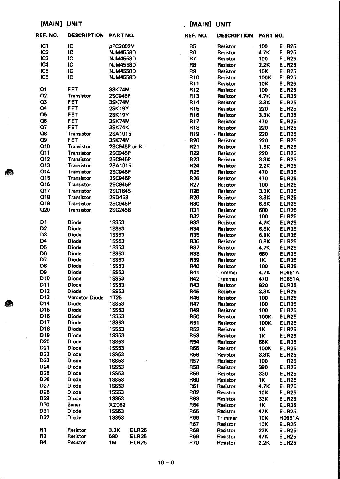
[MAIN]
for
free
by
RadioAmateur.eu
UNIT
[MAIN]
UNIT
,.
-e
REF. NO.
IC1
IC2
1C3
1C4
IC5
IC6
01 FET
02
Q3
04
05
as
07
08
09
010
011
012
013
014
015
016
017
018
019
020
01 Diode
02
03
04
05
06
07
08
09
010
011 Diode
012
013
014
015
016
017
018
019
020
021
022
023
024
025
026
027
028
029
030
031
032
R1
R2
R4
DESCRIPTION
IC
IC
IC
IC
IC
IC
Transistor
FET
FET
FET
FET
FET
Transistor
FET
Transistor
Transistor
Transistor
Transistor
Transistor 2SC945P
Transistor 2SC945P
Transistor
Transistor
Transistor
Transistor
Transistor
Diode
Diode
Diode 1SS53
Diode
Diode
Diode
Diode
Diode
Diode 1SS53
Diode
Varactor Diode
Diode
Diode
Diode
Diode
Diode
Diode
Diode
Diode
Diode
Diode
Diode
Diode
Diode
Diode
Diode
Diode
Zener
Diode
Diode
Resistor
Resistor
Resistor
PART NO.
IlPC2002V
NJM4558D R6
NJM4558D
NJM4558D
NJM4558D R9
NJM4558D
3SK74M
2SC945P
3SK74M
2SK19Y
2SK19Y
3SK74M
3SK74K
2SA1015
3SK74M
or
2SC945P
2SC945P
2SC945P
2SA1015
2SC945P R27
2SC1645
2SD468 R29
2SC945P
2SC2458
1SS53 R33
1SS53
1SS53
1SS53
1SS53
1SS53
1SS53
1SS53
1SS53
1SS53
1T25 R46
1SS53
1SS53 R49
1SS53
1SS53
1SS53
1SS53
1SS53
1SS53
1SS53
1SS53
1SS53
1SS53
1SS53
1SS53
1SS53
1SS53
XZ062
1SS53 R65
1SS53
3.3K ELR25
680 ELR25
1M ELR25
K
REF. NO. DESCRIPTION PART NO.
R5
R7
R8
R10 Resistor
R11
R12 Resistor
R13
R14 Resistor
R15
R16
R17
R18
R19 : Resistor
R20
R21
R22
R23 Resistor
R24 Resistor 2.2K ELR25
R25
R26 Resistor
R28 Resistor 3.3K ELR25
R30
R31
R32
R34
R35 Resistor 6.8K ELR25
R36
R37
R38 Resistor
R39 Resistor
R40
R41
R42 Trimmer
R43
R45 Resistor
R47 Resistor
R50 Resistor
R51
R52
R53
R54
R55
R56
R57 Resistor
R58 Resistor
R59
ROO
R61
R62
R63 Resistor
R64 Resistor
RSS
R67
R68 Resistor
R69 Resistor
R70 Resistor
Resistor
Resistor
Resistor
Resistor 2.2K ELR25
Resistor
Resistor 10K ELR25
Resistor 4.7K ELR25
Resistor
Resistor 3.3K ELR25
Resistor 470 ELR25
Resistor
Resistor
Resistor 1.5K ELR25
Resistor
Resistor
Resistor
Resistor 3.3K ELR25
Resistor 6.8K ELR25
Resistor
Resistor
Resistor 4.7K ELR25
Resistor
Resistor
Resistor 4.7K ELR25
Resistor
Trimmer 4.7K H0651 A
Resistor
Resistor
Resistor
Resistor
Resistor 1K ELR25
Resistor 1K
Resistor 56K ELR25
Resistor
Resistor
Resistor
Resistor 1K
Resistor 4.7K
Resistor
Resistor
Trimmer
Resistor
100
4.7K
100
10K ELR25
100K ELR25
100
3.3K
220
220
220
220
220
3.3K ELR25
470 ELR25
470 ELR25
100
680
100
6.8K
6.8K
680
1K
100
470
820 ELR25
3.3K
100 ELR25
100
100 ELR25
100K ELR25
100K ELR25
100K
3.3K
100
390 ELR25
330 ELR25
10K ELR25
33K ELR25
1K ELR25
47K
10K
10K ELR25
22K
47K
2.2K ELR25
ELR25
ELR25
ELR25
ELR25
ELR25
ELR25
ELR25
ELR25
ELR25
ELR25
ELR25
ELR25
ELR25
ELR25
ELR25
ELR25
ELR25
ELR25
H0651 A
ELR25
ELR25
ELR25
ELR25
ELR25
R25
ELR25
ELR25
ELR25
H0651
A
ELR25
ELR25
10-6

[MAIN]
for
free
by
RadioAmateur.eu
UNIT
[MAIN]
UNIT
"
REF. NO. DESCRIPTION
R71
R72
R73
R74
R75 Resistor
R76
R77 Resistor
R78
R79 Resistor
R80
R82
R83 Resistor
R84 Resistor
R85 Resistor
R86 Resistor
R87
Raa Resistor
R89
ROO
R91
R93
R94
R95
R96
R97
R98
R99
R100
R101
R102
R103 Resistor
R104
R105 Resistor
R106 Resistor
R107 Resistor
R108
R109
R110 Resistor
R111
R112
R113
R114
R115 Resistor
R116 Resistor
R117
R118 Resistor
R119
R120
R121
R122 Resistor
R123
R124
R125
R126
R127
R128
R129
R130
R131
R132 Resistor
R133
R134
R135 Resistor
R136
Resistor 3.3M
Resistor
Resistor
Resistor
Resistor
Resistor
Resistor
Trimmer
Resistor
Resistor
Resistor
Trimmer
Trimmer
Resistor
Resistor
Resistor
Resistor
Resistor
Trimmer
Resistor
Resistor
Resistor
Resistor
Resistor
Resistor
Resistor
Trimmer
Resistor
Resistor
Resistor
Resistor
Resistor
Resistor
Resistor
Resistor
Resistor 1M
Resistor
Resistor
Resistor
Trimmer
Resistor
Resistor
Resistor
Resistor
Resistor
PART
NO.
ELR25
820K
820K
100K
220
220
4.7M
1M
1.8M
10K
1M
1.8M R25
1.8
22M
10K
100
3.3M
4.7M
22M ERC14GJ
47K
10K
22K
22K
3.3M
470K
47K
10K
100K
4.7K
470
100K
10K
4.7K
330
22K
4.7K
4.7K
4.7K
330
1K
100K
10K
10K
10K
4.7K
4.7K
22K
4.7K
10K
27K
470
470
220K
1M
220K
1M
47K
47K
10K
100
820
22
10K
ELR25
ELR25
ELR25
ELR25
ELR25
ERC1.4GJ R143 Resistor
ELR25
ELR25
ELR25
H1051C
ELR25
ERC14GJ
ELR25
ELR25
ELR25
ERC14GJ
H0651 A
H0651A
ELR25
ELR25
ELR25
ELR25
ELR25
H0651 A
ELR25
R25
ELR25
R25 R172
ELR25
ELR25
ELR25
ELR25
ELR25
ELR25
ELR25
ELR25
H1051C
ELR25
ELR25
ELR25
ELR25
ELR25
ELR25
ELR25
ELR25
ELR25
R25
ELR25
ELR25
ELR25
ELR25
ELR25
ELR25
H1051C C23 Ceramic 0.0047
ELR25
ELR25
ELR25
ELR25
R25
ELR25
ELR25
REF. NO. DESCRIPTION
R137
R138
R139 Resistor
R140 Resistor
R141
R142
R144 Resistor
R147 Resistor 10
R149
R1SO
R151
R152 Resistor
R153 Resistor
R154 Resistor
R155 Resistor
R156 Resistor
R157 Resistor
R159 Resistor
R1SO
R161 Resistor
R162
R163 Resistor
R164 Resistor
R166 Resistor
R167 Resistor
R168
R169 Resistor
R170 Resistor
R171 Resistor
R173 Resistor
R174 Resistor
C1
C2 Ceramic 0.0047
C3
C4
C5
C6
C7
C8
C9 Barrier Lay 0.047
C10 Barrier Lay 0.047
C11
C12
C13 Barrier Lay 0.047
C14
C15
C16 Ceramic
C17 Barrier Lay 0.047
C18
C19
C20
C21
C22
C24
C25
C26 Ceramic 0.0047
C27 Ceramic 0.001
C28 Ceramic
C29 Ceramic 0.0047
C30 Ceramic
Trimmer
Resistor
Resistor
Trimmer
Trimmer
Trimmer
Trimmer
Resistor
Trimmer
Trimmer
Resistor
Barrier Lay 0.047
Ceramic
Barrier Lay
Ceramic
Ceramic
Barrier Lay 0.047
Ceramic
Barrier Lay 0.047
Barrier Lay
Barrier Lay
Ceramic
Barrier Lay
Barrier Lay
Ceramic
Ceramic
Ceramic
Ceramic
Ceramic
PART
10K
220
220K
47K
47K
10K
47K
2.2K
33
4.7K
4.7K
47K
47K
47K
47K
47K
1K
4.7K
10
220
10K
4.7K
a.2K
100K
4.7K
100K
10K
100
3.3K
10K
4.7K
470
0.0047
0.047
0.0047
0.001
0.0022
0.047
0.047
390P
390P
0.047
0.047
0.0047
0.0047
0.0047
0.0047
0.001
0.0047
0.0047
NO.
H1051C
ELR25
ELR25
ELR25
ELR25
H1051C
ELR25
ELR25
R25
H0651 A
H0651A
H0651 A
ELR10
R10
ELR10
R10
ELR10
ELR25
ELR25
ELR25
ELR25
H1051C
ELR25
ELR25
ELR25
ELR25
H0851
R25
R25
R25
R25
ELR25
ELR25
25V
SOV
SOV
50V
SOV
SOV
25V
SOV
25V
25V
25V
25V
25V
25V
SOV
50V
25V
25V
25V
50V
50V
50V
SOV
SOV
SOV
SOV
SOV
SOV
SOV
SOV
10
-7

[MAIN]
for
free
by
RadioAmateur.eu
UNIT
[MAIN]
UNIT
..
•
REF. NO. DESCRIPTION
C31
C32 Ceramic
C33 Electroly.
C34
C35 Ceramic
C36 Ceramic
C37
C38
C39
Ceramic
Ceramic
Dip Mica
Dip Mica
Ceramic
C40 Ceramic
C41
C42
C43 Electroly.
C44 Barrier Lay
C45
C47
C48 Electroly.
C49 Ceramic
COO
C51
C52 Electroly.
C53 Ceramic
C54 Electroly.
C55 Mylar
C56 Mylar
C57
C58 Electroly.
C59 Electroly.
C60
C61
C62 Electroly.
C63
C64 Electroly.
C65
C66
C67 Electroly.
C68
C69
C70
C71
C72 Electroly .
C73
C74
C75
C76
C77
C78
C79
C80
C81
C84
C85 Ceramic
8arrier Lay
Electroly. 4.7
Barrier Lay
Ceramic
Electroly.
Electroly.
Mylar
Barrier Lay
Electroly.
Electroly.
Electroly.
Electroly.
Barrier Lay
Barrier Lay
Mylar
Electroly.
Electroly.
Electroly.
Ceramic
Ceramic
Ceramic
Ceramic
Ceramic
Electroly.
Electroly.
Barrier Lay
PART NO.
0:0047
0.001 50V
10 16V
0.0047
0.0047
22P
47
510
82P
0.0047
0.047
0.47
0.1
0.1
0.0047
470
0.0047
470
4.7
10 16V
0.0047
0.22
0.022
0.022
0.022
10 16V
100
0.1
0.47
0.47
1
10
1
0.47
47
0.1
0.1
0.0022
47
100
470
10
120P
120P
120P
120P
270P
47
0.22 50V·
0.1
220P
50V
50V FI1
50V
50V
50V
50V
UJ
50V
50V
25V
16V
OOV
12V
12V
50V
10V
50V
10V
16V
50V
50V
50V
50V
50V
10V
12V
OOV
50V
50V
16V
50V
50V
10V
12V
12V
50V
16V
10V
16V
16V
RH
50V
RH
50V
RH
50V
RH
50V
50V
16V
RC2
REF. NO.
L12
L13
FI2
F13
X1
51
52
DESCRIPTION
Choke LW15
Coil
Mechanical Filter MF-455-11AZ (or 11GZ)
Ceramic Filter
Crystal Filter
Crystal
Switch
Switch
53 Switch
54 Switch
B1
J1
J2 Connector
J3
J4
J5 Connector
J6
J7
J8
J12
J13
J14
J15
J16
J17
J18
J19
J20
J21
P.C.
Board B-476C
Connector 5045-6A
Connector 5045-4A
Connector 5045-4A
Connector 5045-10A
Connector
Connector
Connector
Connector
Connector 5045-2A
Connector
Connector
Connector
Connector
Connector
Connector
Connector
PART NO.
102 L4
CFW455HT
9M10A
HC-43/U
SSS012
SSS012
555012
SSS012
5045-4A
5045-2A
5045-4A
5045-4A
5045-4 A
5045-4A
5045-2A
5045-2A
5045-4A
5045-4A
5045-2A
5045-2A
5045-2A
(9.0115MHz)
9_4665MHz
L1
L2
L3
L4
L5
L6
L7
L8
L9
L10
L11
Coil
Coil
Coil
Coil
Coil
Coil
Coil
Coil
Coil
Coil
Coil
L5175
L5175
L520
L5213
L5100
L5163
L5175
L5175
L5163
L5175
L5141A
10-8

[DET]
for
free
by
RadioAmateur.eu
UNIT
[DET]
UNIT
--
•
REF. NO.
01
02
05
06
07
08
09
010
IC1
IC2
01
02
04
05
06
07
08
09
011
012
013
014
015
016
017
R1
R3
R4
R8
R9
R12
R13
R14
R15
R16
R17
R18
R19
R20
R21
R22
R23
R24
R25
R26
R27
R28
R29
R30
R31
R32
R33
R34
R36
R37
R38
R39
R40
R41
R42
R43
DESCRIPTION
Transistor
Transistor
Transistor
Transistor
Transistor
Transistor
Transistor
Transistor
IC
IC
Diode
Diode
Diode
Diode
Diode
Diode
Diode
Diode
Diode
Diode
Diode
Diode
Diode
Diode
Diode
Resistor
Resistor
Resistor
Resistor
Resistor
Resistor
Resistor
Resistor
Resistor
Resistor
Resistor
Resistor
Resistor
Resistor
Resistor
Resistor
Resistor
Resistor
Resistor
Resistor
Resistor
Resistor
Resistor
Resistor
Resistor
Resistor
Resistor
Resistor
Resistor
Resistor
Resistor
Resistor
Resistor
Resistor
Resistor
Resistor
PART NO.
2SC945P
2SC945P
2SC1636
2SC2458
2SC945P
2SC945P
2SC945P
2SA1015
NJM4558D
JLPC1037H
1N60
1SS53
1SS53
1N60
1SS53
1SS53
1SS53
1SS53
1SS53
1SS53
1SS53
1SS53
1SS53
1SS53
1SS53
4.7K
22K
100 R25
3.3M
47K
1K
4.7K
2.2K
4.7K
47
47K
100K
10K
10K
10K
10K
10K
10K
10K
22K
22K ELR25
100K
100K
3.3M
10K
10K
108M
2.2K
6.8K
6.8K
6.8K
1K
1K
1K
100K ELR25
47K
GR
R25
ELR25
ELR25
ELR25
ELR25
ELR25
ELR25
ELR25
ELR25
ELR25
ELR25
ELR25
ELR25
ELR25
ELR25
ELR25
ELR25
ELR25
ELR25
ELR~5
R10
ELR25
ELR25
ELR25
ELR25
ELR25
ELR25
ELR25
R10
ELR10
ELR10
ELR25
ELR25
REF. NO.
R44
R45
R46
R47
R48
R49
R50
R51
R52
R53
R54
R55
R56
R57
R58
R59
R60
R61
R62
R63
C1
C2
C3
C4
C6 Electroly.
C7
C8 Electroly.
C9
C10 Electroly.
C11
C12 Electroly.
C14
C15
C16
C17
C18
C19 Barrier Lay
C20 Barrier Lay
C22 Electroly.
C23 Electroly.
C24 Mylar
C25 Mylar
C26 Barrier Lay
C27
C28
C29 Ceramic
C30
C31
C32 Electroly.
C33 Ceramic
C34 Ceramic
C35
C36 Ceramic
C37
C38
C39 Ceramic
C40 Trimmer
C41
C42
C43
C44
C45 Electroly.
C46
DESCRIPTION
Trimmer
Trimmer
Resistor
Resistor
Resistor
Resistor
Resistor
Resistor
Resistor
Resistor
Resistor
Resistor
Resistor
Resistor
Resistor 15K ELR25
Resistor
Resistor
Resistor
Resistor
Resistor
Ceramic
Ceramic
Ceramic
Ceramic
Electroly.
Ceramic
Electroly.
Electroly.
Ceramic
Ceramic
Ceramic
Barrier Lay
Electroly.
Electroly.
Ceramic
Ceramic
Ceramic
Ceramic
Ceramic
Dip Mica
Dip Mica
Ceramic
Ceramic
Barrier Lay
PART NO.
10K H0615A
10K
3.3K R25
4.7K ELR25
4.7K ELR25
220
100 R25
4.7K R25
1K
2.2K ELR25
2.2K ELR25
10K ELR25
10K R25
2.2K ELR25
10K ELR25
10K ELR25
3.3K ELR25
2.7K ELR25
47K
100P 50V
0.0047
0.0047
100P 50V
0.47 50V
0.1
10
0.0047
10
4.7
1
4.7
100P 50V
100P
0.0047
0.047 25V
0.1
0.047 25V
4.7
10 25V
0.01
0.01
0.0068
0.1
47
47P
0.0047
0.0047
47
0.001 50V
0.0047 50V
0.0047
0.0047
0.0047
0.0047
56P
CV05E3001
150P
150P
0.0047 50V
120P
1 50V
0.047
H0615A
ELR25
ELR25
BP
R25
50V
50V
12V
25V
50V
50V
35V
10V
35V
50V
50V
12V
50V
50V
50V
50V
35V
10V
50V
50V
50V
10V
50V
50V
50V
50V
50V
50V
50V
50V
25V
RC2
RC2
RC2
10-9

[DET]
for
free
by
RadioAmateur.eu
UNIT
[PA]
UNIT
REF. NO. DESCRIPTION
L1
L2 Coil
L3 Coil
L4 Coil
Bl
Jl
J2 Connector 5045-4A
J3
J4 Connector
Pl
P2
Xl
Coil
P.C.
Board
Connector
Connector
Connector
Connector 5250-2A
Crystal HC-43/U
PART
LS67
LS133
LS212
LSl34
BA77C
5045-4A
5045-4A
RT-OH-13B
5250-10A
NO.
9.0145MHz
REF. NO. DESCRIPTION
01
02
03
Q4
05
06
07
Dl
D2
D4 Diode GP-08
D5
Rl
R2
R3 Resistor
R4
R5 Resistor
R7
R8
R9 Resistor
Rl0
Rll
R12 Resistor
R13 Resistor
R14 Resistor 2.2
R15 Resistor 10 R50
R16 Resistor 10
R17
R18 Resistor 3.3
R19
R20
R21
R22 Resistor 47
R23 Resistor
R24
R25 Resistor
R26
Transistor 2SC1971
Transistor 2SC1945
Transistor 2SC1945
Transistor
Transistor 2SC2097
Transistor 2SD313
Transistor
Diode
Diode MV11
Diode
Resistor
Resistor
Resistor 100
Resistor 3.3 R25
Resistor
Resistor
Resistor
Resistor 3.3
Resistor
Resistor 220
Trimmer
Resistor
Resistor
PART
NO.
2SC2097
2SC2120
MV5
15CD11
220
390
10
2_2
22
22
120
120
68
RSF
2.2
RSF
10
500
22
2.2K
1.8
100
R25
R25
R25
R25
R25
R25
R25
R50
R50
R50
28
28
R50
lW
lW
R50
R25
FR10
lW
R25
R25
R25
FR10
10 - 10
Cl
C2
C3
C4
C5
C6
C7
C8
C9
Cl0
Cl1
C12
C13 Ceramic 470P SL 50V
C14
C15
C16
C17 Ceramic
C18
C19 Electroly. 220 16V
C20 Barrier Lay
C21
C22
C23 Electroly.
C24 Barrier Lay
C25
Ceramic 0.0022
Barrier Lay 0.0012
Ceramic
Barrier
Mylar
Mylar
Cylinder
Barrier Lay
Monolythic
Monolythic
Ceramic 470P SL 50V
Ceramic 470P SL
Ceramic
Ceramic
Ceramic 330P
Electroly.
Ceramic 0.0047 50V
Electroly.
Barrier Lay
lOOP
0.1
0.01
0.01
lOOP
0.1
6800P 50V
6800P 50V
220P
220P
39P
1000
0.1
10
470
0.1
0.1
50V
50V
50V
50V
50V
50V
50V
12V
50V
500V
500V
500V
500V
16V
50V
16V
16V
12V
12V

[PA]
for
free
by
RadioAmateur.eu
UNIT
[FILTER]
UNIT
REF. NO.
C26 Barrier Lay
C27
L1
L2
L3
L4
L5
L6
L7
L8
S1
J1
P1
P2
P3
P4
P5
B1
DESCRIPTION
Barrier Lay
Choke
Trans
Choke
Trans
Choke
Choke
Trans
Trans
Thermal
Connector
Connector
Connector
Connector
Connector
Connector
P.C.
Board
PART
NO.
0.1
0.1
LW·22
LR117
LW18
LR113
LW18
LW18
LR83
LR114
OHD70M
LLR·6
5250-02A
525Q-04A
5250-04A
1545R·1
SMF-Qn·1.3
B-479A
12V
12V
REF. NO.
01
02
03
L1
L2
L3
L5
L6
L7
L8
L9
L10
L11
L12 Coil
L13
L14
L15
L16 Coil
L17
R1
R3
R4
R5
R6
R7
DESCRIPTION
Diode
Diode 1N60
Diode GP08B
Coil
Coil
Coil
Coil
Coil
Coil
Coil
Coil
Coil
Coil
Coil LR57
Coil
Coil LR123
Coil
Resistor
Resistor
Resistor
Resistor
Resistor
Resistor
PART
1N60
LA139
LR49
LR50
LR52
LR51
LR90
LR91
LR53
LR54
LR55
LR56
LR58
102 L4
LA139
68
47K
47K
47K
12K
12K
NO.
R25
ELR26
ELR25
ELR25
ELR25
ELR25
C1
C2
C3
C4
C5
C6
C7
C8
Dip
Mica
Ceramic
Dip
Mica
Ceramic
Dip
Mica
Dip
Mica
Ceramic
Dip
Mica
C9 Ceramic
C10
C11
C12 Ceramic
C13
C14
C15 Ceramic
C16
C17 Ceramic
C18
C19 Ceramic
C20
C21
C22 Ceramic
C23
C24 Ceramic
C25
C26 Ceramic
C27
C28
C29 Ceramic
C30 Ceramic
C31
C32 Ceramic
C33
C34
C35
C36 Ceramic
Dip
Mica
Dip
Mica
Dip
Mica
Ceramic
Ceramic
Ceramic
Ceramic
Ceramic
Ceramic
Ceramic
Ceramic
Ceramic
Trimmer
Ceramic
Ceramic
Ceramic
DM19 680P 500V 1CR
DD31-Q.SL 82P
1200P 5OOV1CR
DM20
DD31·2·SL220P
DM19
DM19
DD31·2·SL120P
DM19 680P
DD35-Q.SL 39P
DM19 390P
DM19 390P
DD38-Q.SL
DM19
DD38-Q.SL
DD31·2·SL220P
DD31·2·SL18>P
DD35-Q.SL
DD31-4·SL330P
DD36-Q·SL 56P
DD31-Q.SL2ooP
DD38-Q.SL1ooP
DD35-Q.SL
DD31·2·SL150P
DD35-Q.SL 39P
DD31-Q.SL150P
DD35-Q.SL 47P
DD35-Q.SL
DD31-Q·SL120P
DD3S-Q-SL 27P
DD38-Q.SL
FCV·IZW20X40
220P
lOOP
lOOP
lOOP
100P 50V
68)P
470P 500V 1CR
470P 500V 1CR
5OOV02
5OOV02
500V 1CR
5OOV02
500V 1CR
5OOV02
500V
500V
27P
5OOV02
6SP
5OOV02
5OOV02
5OOV02
1SP
5OOV02
5OOV02
5OOV02
5OOV02
5OOV02
10P
5OOV02
5OOV02
5OOV02
5OOV02
5OOV02
l5P
5OOV02
5OOV02
5OOV02
lOOP
5OOV02
50V
50V
50V
50V
1CR
1CR
10
-11

[FILTER]
for
free
by
RadioAmateur.eu
UNIT
. [LOGIC]
UNIT
~
,?I.(,~'
•
REF. NO. DESCRIPTION
C37
C38
C39
Bl
RU
Jl
J3
J4
Pl
P2
P3
Sl
Electrolytic
Ceramic
Ceramic
P.C.
Board
Relay
Connector
Connector
Connector
Connector
Connector
Connector
Switch SRY 202C
PART NO.
2201l
0.0047 50V IC2
0.0047
B-478D IC5
SR-202 IC7
5045-4A
5045-4A
5045-4A
16V
50V
REF. NO. DESCRIPTION PART NO.
ICl
1C3
1C4
IC6 IC
IC8 IC
ICS
01
02
5250-6A
5250-6A
5250-2A
03
04
05
02
03
D4
05
06
07
08
09
010
011
012
013
014
015
016
017
018
020
021
022
023
024
025
026
027
028
029
IC
IC
IC
IC
IC
IC
IC
Transistor
Transistor 2SC945
Transistor 2SA798
Transistor
'Transistor
Diode
Diode 15553
Diode
Diode lSS53
Diode 15553
Diode 15553
Diode
Diode lSS53
Diode
Diode 15553
Diode
Diode 15553
Diode lSS53
Diode
Diode
Diode
Diode lSS53
Diode
Diode
Diode
Diode
Diode
Diode
Diode
Diode
Diode
Diode
IlPD650-80
IlPD4071C
IlPD4011C
TC4013C
IlPD4013C
IlPD4066C
IlPD4030C
IlPD4069C
IlA78
L05ACC
2SC945
2SC945
2SA1048
lSS53
1SS53
lSS53
15553
lSS53
lSS53
15553
lSS53
15553
lSS53
lN60
lN60
lN60
lN60
lSS53
lSS53
lSS53
lSS53
10-12
Xl
R2
R3
R4
R6
R7
R8
R9
Rl0
Rl1
R12
R13
R14
R15
R16
R17
R18
R19
R20
Ceralock CSB430A
Resistor
Resistor
Resistor
Resistor
Resistor
Resistor
Resistor
Resistor
Resistor 1M ELR25
Resistor
Resistor
Resistor
Resistor 47K ELR25
Resistor
Resistor
Resistor
Resistor
Resistor
15 R25
4.7K ELR25
lOOK ELR25
820K ELR25
3.3M ELR25
820K ELR25
47K
47K
220K ELR25
1M R25
220K R25
10K ELR25
10K ELR25
150K
lOOK ELR25
2.7K
ELR25
ELR25
ELR25
ELR25
 Loading...