HP INA-54063-TR1, INA-54063-BLK Datasheet

3.0 GHz Low Noise Silicon MMIC
Amplifier
Technical Data
INA-54063
Features
• Ultra-Miniature Package
• Single 5 V Supply (29␣ mA)
• 21.5 dB Gain (1.9 GHz)
• 8.0 dBm P
(1.9 GHz)
1dB
• Positive Gain Slope
• Unconditionally Stable
Applications
• IF Amplifier for DBS
Downconverter, Cellular,
Cordless, Special Mobile
Radio, PCS, ISM, and
Wireless LAN Applications
Equivalent Circuit
(Simplified)
RF
INPUT
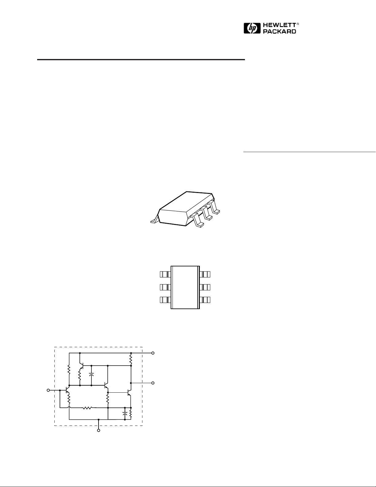
Surface Mount Package SOT-363 (SC-70)
Pin Connections and Package Marking
GND
1
GND
2
INPUT
3
Note:
Package marking provides orientation
and identification.
V
d
RF
OUTPUT
and V
d
54
OUTPUT
6
and V
5
GND
4V
CC
Description
Hewlett-Packard’s INA-54063 is a
Silicon monolithic amplifier that
offers excellent gain and power
output for applications to
3.0␣ GHz. Packaged in an ultraminiature SOT-363 package, it
requires half the board space of a
SOT-143 package.
With its wide bandwidth and high
linearity, the INA-54063 is an
excellent candidate for DBS IF
applications. It also features a
d
unique gain curve which increases over the range from 1 to
2␣ GHz. This gain slope compensates for the gain rolloff found in
typical receiver systems.
The INA-54063 is fabricated using
HP’s 30 GHz f
Silicon bipolar process which
uses nitride self-alignment
submicrometer lithography,
trench isolation, ion implantation,
gold metalization, and polyimide
intermetal dielectric and scratch
protection to achieve superior
performance, uniformity, and
reliability.
ISOSAT™
MAX
GROUND
6-163
5965-5364E

INA-54063 Absolute Maximum Ratings
Absolute
Symbol Parameter Units Maximum
V
d
P
in
T
j
T
STG
Supply Voltage, to Ground V 12
CW RF Input Power dBm 13
Junction Temperature °C 150
Storage Temperature °C -65 to 150
[1]
Thermal Resistance
θ
= 165°C/ W
j-c
Notes:
1. Operation of this device above any
one of these limits may cause
permanent damage.
2. T
= 25°C (T
C
temperature at the package pins
where contact is made to the
circuit board).
is defined to be the
C
[2]
:
Electrical Specifications, T
= 25°C, ZO = 50 Ω, V
C
= 5 V, unless noted
d
Symbol Parameters and Test Conditions Units Min. Typ. Max. Std.
[1]
Dev.
G
Power Gain (|S21|2) f = 1900 MHz dB 19 21.5 0.7
P
NF Noise Figure f = 1900 MHz dB 5.0 0.4
P
1dB
IP
Output Power at 1 dB Gain Compression f = 1900 MHz dBm 8.0
Third Order Intercept Point f = 1900 MHz d Bm 17
3
f = 2150 MHz 15.7
VSWRinInput VSWR f = 1900 MHz 1.4
VSWR
I
t
Note:
1. Standard deviation number is based on measurement of at least 500 parts from three non-consecutive wafer lots during
the initial characterization of this product, and is intended to be used as an estimate for distribution of the typical
specification.
Output VSWR f = 1900 MHz 2.4
out
Device Current mA 29 36 1.8
d
Group Delay f = 1900 MHz ps 272
d
6-164

INA-54063 Typical Performance
T
= 25° C, ZO = 50 Ω, V
C
25
= 5 V, unless noted
d
8
16
6 V
20
5 V
GAIN (dB)
15
10
0.3 0.9 1.2 1.5 1.80.6 2.1 2.72.4 3
FREQUENCY (GHz)
4 V
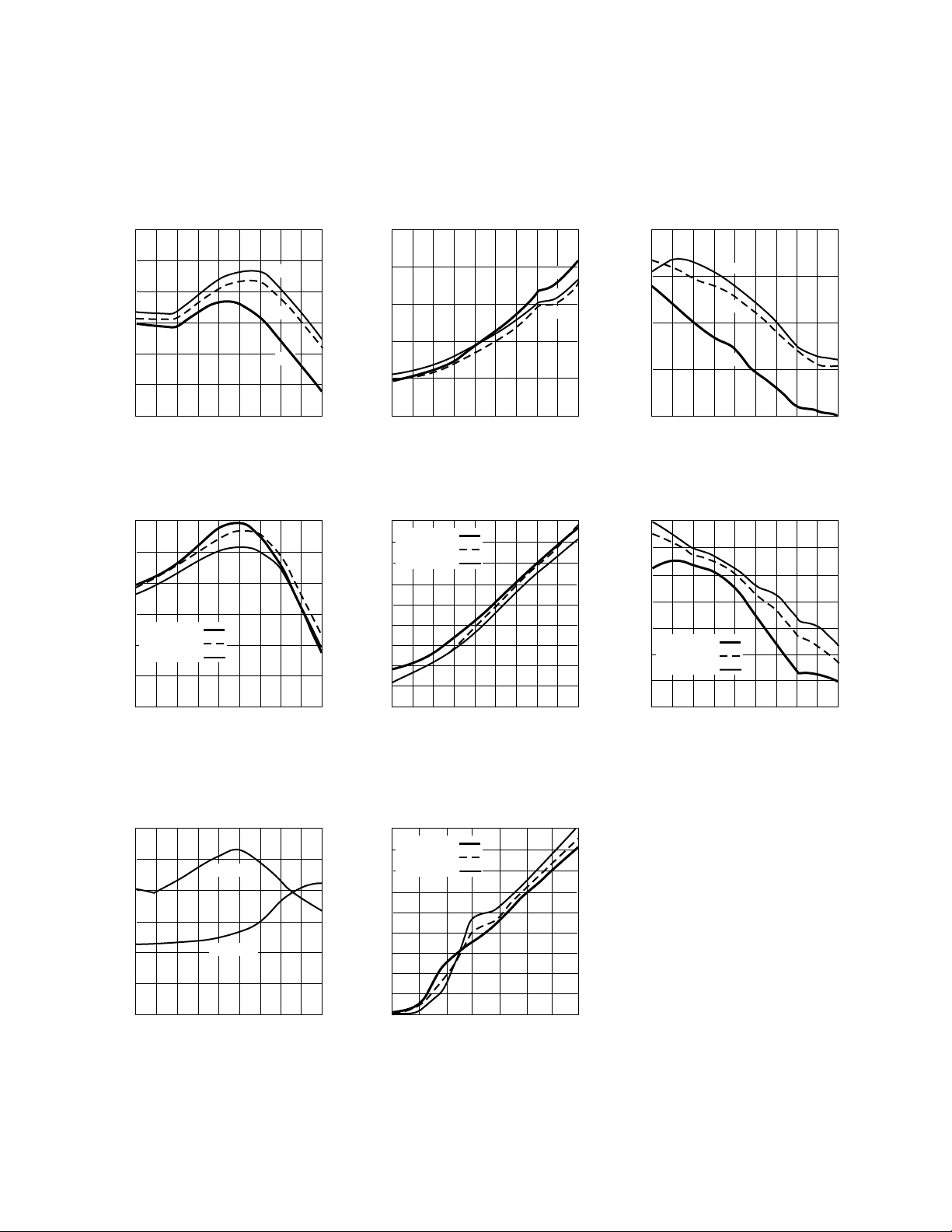
Figure 1. Gain vs. Frequency and
Voltage.
22
20
18
16
TA = +85°C
GAIN (dB)
= +25°C
T
14
A
= –40°C
T
A
12
10
0.3 0.9 1.2 1.5 1.80.6 2.1 2.72.4 3
FREQUENCY (GHz)
Figure 4. Gain vs. Frequency and
Temperature.
7
6
5
NOISE FIGURE (dB)
4
3
0.3 0.9 1.2 1.5 1.80.6 2.1 2.72.4 3 0.3 0.9 1.2 1.5 1.80.6 2.1 2.72.4 3
FREQUENCY (GHz)
Figure 2. Noise Figure vs. Frequency
and Voltage.
4 V
6 V
5 V
12
(dBm)
8
1 dB
P
4
0
Figure 3. Output Power for 1 dB Gain
Compression vs. Frequency and
6 V
5 V
4 V
FREQUENCY (GHz)
Voltage.
7.5
TA = +85°C
7
= +25°C
T
A
= –40°C
T
6.5
A
6
5.5
5
4.5
NOISE FIGURE (dB)
4
3.5
3
0.3 0.9 1.2 1.5 1.80.6 2.1 2.72.4 3
FREQUENCY (GHz)
Figure 5. Noise Figure vs. Frequency
and Temperature.
14
12
10
8
(dBm)
6
1 dB
P
TA = +85°C
4
= +25°C
T
A
= –40°C
T
A
2
0
0.3 0.9 1.2 1.5 1.80.6 2.1 2.72.4 3
FREQUENCY (GHz)
Figure 6. Output Power for P
Compression vs. Frequency and
Temperature.
1dB
Gain
3
2.5
2
1.5
VSWR
1
0.5
0
0.3 0.9 1.2 1.5 1.80.6 2.1 2.72.4 3
VSWR out
VSWR in
FREQUENCY (GHz)
Figure 7. Input and Output VSWR vs.
Frequency.
45
TA = +85°C
40
= +25°C
T
A
= –40°C
T
35
A
30
25
(mA)
d
20
I
15
10
5
0
02345167
(V)
V
d
Figure 8. Supply Current vs. Voltage
and Temperature.
6-165
 Loading...